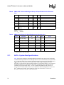
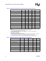
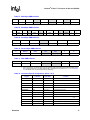
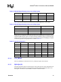
1
Pentium® III Xeon™ Processor at 500 and 550 MHz Datasheet Product Features n n n n n n n Binary compatible with applications running on previous members of the Intel microprocessor family Optimized for 32-bit applications running on advanced 32-bit operating systems Dynamic Execution micro architecture Dual Independent Bus architecture: Separate dedicated external 100MHz System Bus and dedicated internal cache bus operating at full processor core speed Power Management capabilities — System Management mode — Multiple low-power states SMBus interface to advanced manageability features Intel® processor serial number n n n n n n Single Edge Contact (S.E.C.) cartridge packaging technology; the S.E.C. cartridge delivers high performance processing and bus technology in mid-range to high-end servers and workstations 100 MHz system bus speeds data transfer between the processor and the system Integrated high performance16K instruction and 16K data, nonblocking, level-one cache Available in 512K, 1 M, or 2 M unified, nonblocking level-two cache Enables systems which are scaleable up to four processors and 64 GB of physical memory Streaming SIMD Extensions for enhanced video, sound and 3D performance The Intel® Pentium® III Xeon™ processor is designed for mid-range to high-end servers and workstations, and is binary compatible with previous Intel Architecture processors. The Pentium III Xeon processor provides the best performance available for applications running on advanced operating systems such as Windows* 95, Windows NT, and UNIX*. The Pentium III Xeon processor is scalable to four processors in a multiprocessor system and extends the power of the Pentium® Pro processor with new features designed to make this processor the right choice for powerful workstation, advanced server management, and mission-critical applications. Pentium III Xeon processor-based workstations offer the memory architecture required by the most demanding workstation applications and workloads. Specific features of the Pentium III Xeon processor address platform manageability to meet the needs of a robust IT environment, maximize system up time and ensure optimal configuration and operation of servers. The Pentium III Xeon processor enhances the ability of server platforms to monitor, protect, and service the processor and its environment. Order Number: 245094-002 February 2000 Information in this document is provided in connection with Intel products. No license, express or implied, by estoppel or otherwise, to any intellectual property rights is granted by this document. Except as provided in Intel's Terms and Conditions of Sale for such products, Intel assumes no liability whatsoever, and Intel disclaims any express or implied warranty, relating to sale and/or use of Intel products including liability or warranties relating to fitness for a particular purpose, merchantability, or infringement of any patent, copyright or other intellectual property right . Intel products are not intended for use in medical, life saving, or life sustaining applications. Intel may make changes to specifications and product descriptions at any time, without notice Designers must not rely on the absence or characteristics of any features or instructions marked "reserved" or "undefined." Intel reserves these for future definition and shall have no responsibility whatsoever for conflicts or incompatibilities arising from future changes to them. The Pentium® III Xeon™ processor may contain design defects or errors known as errata which may cause the product to deviate from published specifications. Current characterized errata are available on request. Contact your local Intel sales office or your distributor to obtain the latest specifications and before placing your product order. Copies of documents which have an ordering number and are referenced in this document, or other Intel literature may be obtained by calling 1-800548-4725 or by visiting Intel's website at http://www.intel.com. Copyright © Intel Corporation, 2000 *Third-party brands and names are the property of their respective owners. Datasheet Pentium® III Xeon™ Processor at 500 and 550 MHz Contents 1.0 Introduction.........................................................................................................................9 1.1 1.2 2.0 Electrical Specifications....................................................................................................11 2.1 2.2 2.3 2.4 2.5 2.6 2.7 2.8 2.9 2.10 2.11 2.12 3.0 3.3 System Bus Clock Signal Quality Specifications.................................................33 AGTL+ Signal Quality Specifications ..................................................................33 3.2.1 AGTL+ Ringback Tolerance Specifications............................................34 3.2.2 AGTL+ Overshoot/Undershoot Guidelines.............................................34 Non-AGTL+ Signal Quality Specifications...........................................................35 3.3.1 2.5 V Tolerant Buffer Overshoot/Undershoot Guidelines .......................35 3.3.2 2.5 V Tolerant Buffer Ringback Specification.........................................35 3.3.3 2.5 V Tolerant Buffer Settling Limit Guideline ........................................36 Processor Features ..........................................................................................................36 4.1 4.2 4.3 Datasheet The Pentium® III Xeon™ Processor System Bus and VREF ...............................11 Power and Ground Pins ......................................................................................12 Decoupling Guidelines ........................................................................................12 2.3.1 Pentium® III Xeon™ Processor VCCCORE ..............................................13 2.3.2 Level 2 Cache Decoupling .....................................................................13 2.3.3 System Bus AGTL+ Decoupling.............................................................13 System Bus Clock and Processor Clocking ........................................................13 2.4.1 Mixing Processors ..................................................................................15 Voltage Identification ...........................................................................................16 System Bus Unused Pins and Test Pins.............................................................17 System Bus Signal Groups .................................................................................18 2.7.1 Asynchronous vs. Synchronous for System Bus Signals.......................19 Test Access Port (TAP) Connection....................................................................19 Maximum Ratings................................................................................................20 Processor DC Specifications...............................................................................20 AGTL+ System Bus Specifications .....................................................................24 System Bus AC Specifications ............................................................................25 Signal Quality ...................................................................................................................32 3.1 3.2 4.0 Terminology...........................................................................................................9 1.1.1 S.E.C. Cartridge Terminology ................................................................10 References ..........................................................................................................10 Functional Redundancy Checking Mode.............................................................36 Low Power States and Clock Control..................................................................37 4.2.1 Normal State— State 1 ..........................................................................37 4.2.2 Auto Halt Power Down State — State 2 .................................................37 4.2.3 Stop-Grant State — State 3 ...................................................................38 4.2.4 Halt/Grant Snoop State — State 4 .........................................................39 4.2.5 Sleep State — State 5............................................................................39 4.2.6 Clock Control..........................................................................................39 System Management Bus (SMBus) Interface .....................................................40 4.3.1 Processor Information ROM...................................................................41 4.3.2 Scratch EEPROM...................................................................................42 3 Pentium® III Xeon™ Processor at 500 and 550 MHz 4.3.3 4.3.4 4.3.5 4.3.6 4.3.7 5.0 Thermal Specifications and Design Considerations.........................................................49 5.1 5.2 6.0 7.3 Introduction .........................................................................................................71 Mechanical Specifications...................................................................................71 7.2.1 Boxed Processor Heatsink Dimensions ................................................. 73 7.2.2 Boxed Processor Heatsink Weight.........................................................73 7.2.3 Boxed Processor Retention Mechanism ................................................ 73 Thermal Specifications........................................................................................74 7.3.1 Boxed Processor Cooling Requirements ...............................................74 7.3.2 Optional Auxiliary Fan Attachment .........................................................74 7.3.2.1 Clearance Recommendations for Auxiliary Fan ........................ 76 7.3.2.2 Fan Power Recommendations for Auxiliary Fan ....................... 77 7.3.2.3 Thermal Evaluation for Auxiliary Fan ........................................ 78 Integration Tools ..............................................................................................................78 8.1 4 Weight .................................................................................................................60 Cartridge to Connector Mating Details ................................................................60 Pentium® III Xeon™ Processor Substrate Edge Finger Signal Listing ............... 62 Boxed Processor Specifications.......................................................................................71 7.1 7.2 8.0 Thermal Specifications........................................................................................50 5.1.1 Power Dissipation ..................................................................................50 5.1.2 Plate Flatness Specification ...................................................................51 Processor Thermal Analysis ...............................................................................51 5.2.1 Thermal Solution Performance...............................................................51 5.2.2 Thermal Plate to Heat Sink Interface Management Guide..................... 52 5.2.3 Measurements for Thermal Specifications............................................. 53 5.2.3.1 Thermal Plate Temperature Measurement ............................... 53 5.2.3.2 Cover Temperature Measurement Guideline ............................ 54 Mechanical Specifications................................................................................................55 6.1 6.2 6.3 7.0 Processor Information ROM and Scratch EEPROM Supported SMBus Transactions ..............................................................................43 Thermal Sensor......................................................................................43 Thermal Sensor Supported SMBus Transactions..................................44 Thermal Sensor Registers......................................................................46 4.3.6.1 Thermal Reference Registers ................................................... 46 4.3.6.2 Thermal Limit Registers ............................................................46 4.3.6.3 Status Register..........................................................................46 4.3.6.4 Configuration Register...............................................................47 4.3.6.5 Conversion Rate Register .........................................................47 SMBus Device Addressing.....................................................................48 In-Target Probe (ITP) for Pentium® III Xeon™ Processors................................. 78 8.1.1 Primary Function ....................................................................................79 8.1.2 Debug Port Connector Description.........................................................79 8.1.3 Debug Port Signal Descriptions .............................................................80 8.1.4 Debug Port Signal Notes........................................................................82 8.1.4.1 General Signal Quality Notes .................................................... 83 8.1.4.2 Signal Note: DBRESET#...........................................................83 8.1.4.3 Signal Note: TDO and TDI ........................................................83 8.1.4.4 Signal Note: TCK.......................................................................83 8.1.5 Using Boundary Scan to Communicate to the Processor ...................... 85 Datasheet Pentium® III Xeon™ Processor at 500 and 550 MHz 8.2 9.0 Appendix ..........................................................................................................................86 9.1 Datasheet Integration Tool (Logic Analyzer) Considerations ...............................................86 Alphabetical Signals Reference ..........................................................................86 9.1.1 A[35:03]# (I/O)........................................................................................86 9.1.2 A20M# (I)................................................................................................86 9.1.3 ADS# (I/O)..............................................................................................87 9.1.4 AERR# (I/O) ...........................................................................................87 9.1.5 AP[1:0]# (I/O) .........................................................................................87 9.1.6 BCLK (I)..................................................................................................87 9.1.7 BERR# (I/O) ...........................................................................................87 9.1.8 BINIT# (I/O) ............................................................................................88 9.1.9 BNR# (I/O)..............................................................................................88 9.1.10 BP[3:2]# (I/O) .........................................................................................88 9.1.11 BPM[1:0]# (I/O) ......................................................................................88 9.1.12 BPRI# (I).................................................................................................88 9.1.13 BR0# (I/O), BR[3:1]# (I) ..........................................................................88 9.1.14 CPU_SENSE..........................................................................................89 9.1.15 D[63:00]# (I/O)........................................................................................89 9.1.16 DBSY# (I/O) ...........................................................................................90 9.1.17 DEFER# (I).............................................................................................90 9.1.18 DEP[7:0]# (I/O).......................................................................................90 9.1.19 DRDY# (I/O) ...........................................................................................90 9.1.20 EMI .........................................................................................................90 9.1.21 FERR# (O) .............................................................................................90 9.1.22 FLUSH# (I) .............................................................................................90 9.1.23 FRCERR (I/O) ........................................................................................91 9.1.24 HIT# (I/O), HITM# (I/O) ..........................................................................91 9.1.25 IERR# (O)...............................................................................................91 9.1.26 IGNNE# (I)..............................................................................................91 9.1.27 INIT# (I) ..................................................................................................92 9.1.28 INTR - see LINT0 ...................................................................................92 9.1.29 LINT[1:0] (I) ............................................................................................92 9.1.30 LOCK# (I/O) ...........................................................................................92 9.1.31 L2_SENSE .............................................................................................93 9.1.32 NMI - See LINT1 ....................................................................................93 9.1.33 PICCLK (I) ..............................................................................................93 9.1.34 PICD[1:0] (I/O)........................................................................................93 9.1.35 PM[1:0]# (O) ...........................................................................................93 9.1.36 PRDY# (O) .............................................................................................93 9.1.37 PREQ# (I)...............................................................................................93 9.1.38 PWREN[1:0] (I).......................................................................................93 9.1.39 PWRGOOD (I)........................................................................................93 9.1.40 REQ[4:0]# (I/O) ......................................................................................94 9.1.41 RESET# (I) .............................................................................................94 9.1.42 RP# (I/O) ................................................................................................95 9.1.43 RS[2:0]# (I) .............................................................................................95 9.1.44 RSP# (I)..................................................................................................95 9.1.45 SA[2:0] (I) ...............................................................................................95 9.1.46 SELFSB[1:0] (I/O) ..................................................................................96 5 Pentium® III Xeon™ Processor at 500 and 550 MHz 9.2 9.1.47 SLP# (I) ..................................................................................................96 9.1.48 SMBALERT# (O)....................................................................................96 9.1.49 SMBCLK (I) ............................................................................................96 9.1.50 SMBDAT (I/O) ........................................................................................96 9.1.51 SMI# (I) ..................................................................................................96 9.1.52 STPCLK# (I)...........................................................................................97 9.1.53 TCK (I)....................................................................................................97 9.1.54 TDI (I) .....................................................................................................97 9.1.55 TDO (O) .................................................................................................97 9.1.56 TEST_25_A62 (I) ...................................................................................97 9.1.57 TEST_VCC_CORE_XXX (I)...................................................................97 9.1.58 THERMTRIP# (O) ..................................................................................97 9.1.59 TMS (I) ...................................................................................................98 9.1.60 TRDY# (I) ...............................................................................................98 9.1.61 TRST# (I) ...............................................................................................98 9.1.62 VID_L2[4:0], VID_CORE[4:0](O)............................................................98 9.1.63 WP (I) .....................................................................................................98 Signal Summaries ...............................................................................................98 Figures 1 2 3 4 5 6 7 8 9 10 11 12 13 14 15 16 17 18 19 20 21 22 23 24 25 26 27 28 6 Timing Diagram of Clock Ratio Signals...............................................................15 Logical Schematic for Clock Ratio Pin Sharing................................................... 15 I-V Curve for nMOS Device.................................................................................23 BCLK, PICCLK, TCK Generic Clock Waveform.................................................. 29 SMBCLK Clock Waveform ..................................................................................29 Valid Delay Timings ............................................................................................29 Setup and Hold Timings......................................................................................30 FRC Mode BCLK to PICCLK Timing...................................................................30 System Bus Reset and Configuration Timings.................................................... 31 Power-On Reset and Configuration Timings.......................................................31 Test Timings (Boundary Scan)............................................................................32 Test Reset Timings .............................................................................................32 BCLK, TCK, PICCLK Generic Clock Waveform at the Processor Core Pins...... 33 Low to High AGTL+ Receiver Ringback Tolerance............................................. 34 Non-AGTL+ Overshoot/Undershoot, Settling Limit, and Ringback ..................... 35 Stop Clock State Machine...................................................................................38 Logical Schematic of SMBus Circuitry ................................................................40 Thermal Plate View .............................................................................................50 Plate Flatness Reference....................................................................................51 Interface Agent Dispensing Areas and Thermal Plate Temperature Measurement Points ...........................................................................................53 Technique for Measuring TPLATE with 0° Angle Attachment ............................... 54 Technique for Measuring TPLATE with 90° Angle Attachment ............................. 54 Guideline Locations for Cover Temperature (TCOVER) Thermocouple Placement ...........................................................................................................55 Isometric View of Pentium® III Xeon™ Processor S.E.C. Cartridge ................... 56 S.E.C. Cartridge Cooling Solution Attach Details (Notes follow Figure 27) ........ 57 S.E.C. Cartridge Retention Enabling Details (Notes follow Figure 27) ............... 58 S.E.C. Cartridge Retention Enabling Details.......................................................59 Side View of Connector Mating Details...............................................................60 Datasheet Pentium® III Xeon™ Processor at 500 and 550 MHz 29 30 31 32 33 34 35 36 37 38 39 40 41 42 43 44 Top View of Cartridge Insertion Pressure Points ................................................61 Front View of Connector Mating Details..............................................................61 Boxed Pentium® III Xeon™ Processor................................................................71 Side View Space Requirements for the Boxed Processor ..................................72 Front View Space Requirements for the Boxed Processor .................................73 Front Views of the Boxed Processor with Attached Auxiliary Fan (Not Included with Boxed Processor) ..................................................................75 Front View of Boxed Processor Heatsink with Fan Attach Features (Fan Not Included)...............................................................................................75 Cross-sectional View of Grommet Attach Features in the Heatsink (Grommet Shown) ...............................................................................................76 Side View Space Recommendation for the Auxiliary Fan ...................................76 Front View Space Recommendations for the Auxiliary Fan ................................77 Boxed Processor Fan/Heatsink Power Cable Connector Description.................77 Hardware Components of an ITP........................................................................79 AGTL+ Signal Termination ..................................................................................82 TCK with Individual Buffering Scheme ................................................................84 System Preferred Debug Port Layout .................................................................85 PWRGOOD Relationship at Power-On ...............................................................94 Tables 1 2 3 4 5 6 7 8 9 10 11 12 13 14 15 16 17 18 19 20 21 22 23 24 25 Datasheet Core Frequency to System Bus Multiplier Configuration.....................................14 Core and L2 Voltage Identification Definition ......................................................16 Pentium® III Xeon™ Processor System Bus Pin Groups....................................18 Pentium® III Xeon™ Processor Absolute Maximum Ratings ..............................20 Voltage Specifications ........................................................................................21 Current Specifications .........................................................................................22 AGTL+ Signal Groups, DC Specifications at the Processor Core.......................23 CMOS, TAP, Clock and APIC Signal Groups, DC Specifications at the Processor Core ...................................................................................................24 SMBus Signal Group, DC Specifications at the Processor Core ........................24 Pentium® III Xeon™ Processor Internal Parameters for the AGTL+ Bus............25 System Bus AC Specifications (Clock) at the Processor Core............................25 AGTL+ Signal Groups, System Bus AC Specifications at the Processor Core...26 CMOS, TAP, Clock and APIC Signal Groups, AC Specifications at the Processor Core ...................................................................................................26 System Bus AC Specifications (Reset Conditions) .............................................27 System Bus AC Specifications (APIC Clock and APIC I/O) at the Processor Core.....................................................................................................................27 System Bus AC Specifications (TAP Connection) at the Processor Core ..........28 SMBus Signal Group, AC Specifications at the Edge Fingers ............................28 BCLK Signal Quality Specifications for Simulation at the Processor Core..........33 AGTL+ Signal Groups Ringback Tolerance Specifications at the Processor Core.....................................................................................................................34 AGTL+ Overshoot/Undershoot Guidelines at the Processor Core......................35 2.5 V Tolerant Signal Overshoot/Undershoot Guidelines at the Processor Core35 Signal Ringback Specifications for 2.5V Tolerant Signal Simulation at the Processor Core ...................................................................................................36 Processor Information ROM Format ...................................................................41 Current Address Read SMBus Packet ................................................................43 Random Address Read SMBus Packet ..............................................................43 7 Pentium® III Xeon™ Processor at 500 and 550 MHz 26 27 28 29 30 31 32 33 34 35 36 37 38 39 40 41 42 43 44 45 46 47 48 49 50 51 8 Byte Write SMBus Packet ...................................................................................43 Write Byte SMBus Packet ...................................................................................45 Read Byte SMBus Packet...................................................................................45 Send Byte SMBus Packet ...................................................................................45 Receive Byte SMBus Packet ..............................................................................45 ARA SMBus Packet ............................................................................................45 Command Byte Bit Assignments.........................................................................45 Thermal Sensor Status Register .........................................................................47 Thermal Sensor Configuration Register..............................................................47 Thermal Sensor Conversion Rate Register ........................................................48 Thermal Sensor SMBus Addressing on the Pentium® III Xeon™ Processor...... 49 Memory Device SMBus Addressing on the Pentium® III Xeon™ Processor ...... 49 Thermal Design Power .......................................................................................51 Example Thermal Solution Performance at Thermal Plate Power of 50 Watts... 52 Signal Listing in Order by Pin Number ................................................................62 Signal Listing in Order by Pin Name ...................................................................66 Boxed Processor Heatsink Dimensions ..............................................................73 Fan/Heatsink Power and Signal Specifications................................................... 78 Debug Port Pinout Description and Requirements ............................................. 80 BR[3:0]# Signals Rotating Interconnect, 4-Way System..................................... 89 BR[3:0]# Signals Rotating Interconnect, 2-Way System..................................... 89 Agent ID Configuration........................................................................................89 Output Signals ....................................................................................................98 Input Signals1 .....................................................................................................99 I/O Signals (Single Driver).................................................................................100 I/O Signals (Multiple Driver) ..............................................................................100 Datasheet Pentium® III Xeon™ Processor at 500 and 550 MHz 1.0 Introduction The Pentium III Xeon processor is a follow-on to the Pentium Pro and Pentium® II Xeon processors. The Pentium III Xeon processor, like the Pentium Pro and Pentium II Xeon processors, implements a Dynamic Execution micro-architecture — a unique combination of multiple branch prediction, data flow analysis, and speculative execution. This enables Pentium III Xeon processors to deliver higher performance than the Pentium® processor, while maintaining binary compatibility with all previous Intel Architecture processors. The Pentium III Xeon processor is available in 512K, 1MB, and 2MB L2 cache options. The Pentium III Xeon processor, like the Pentium II Xeon processor, executes MMX technology instructions for enhanced media and communication performance. In addition, the Pentium® III processor executes Streaming SIMD Extensions for enhanced floating point and 3-D application performance.The Pentium III Xeon processor also utilizes the Single Edge Contact Cartridge (S.E.C.C.) package technology first introduced on the Pentium® II processor. This packaging technology allows Pentium III Xeon processors to implement the Dual Independent Bus Architecture and have up to 2-MBytes of level 2 cache. Like the Pentium Pro and Pentium II Xeon processors, level 2 cache communication occurs at the full speed of the processor core. The Pentium III Xeon processor extends the concept of processor identification with the addition of a processor serial number. Refer to the Intel® Processor Serial Number for more detailed information on the implementation of the Intel processor serial number. A significant feature of the Pentium III Xeon processor, from a system perspective, is the built-in direct multiprocessing support. For systems with up to four processors, it is important to consider the additional power burdens and signal integrity issues of supporting multiple loads on a high-speed bus. The Pentium III Xeon processor supports both uniprocessor and multiprocessor implementations with up to four processor on each local processor bus, or system bus. The Pentium III Xeon processor system bus operates using GTL+ signaling levels with a new type of buffer utilizing active negation and multiple terminations. This new bus logic is called Assisted Gunning Transistor Logic, or AGTL+. The Pentium III Xeon processors also deviate from the Pentium Pro processor in implementing an S.E.C. cartridge package supported by the 330-Contact Slot Connector (SC330). (See Section 6.0 for the processor mechanical specifications.) This document provides information to allow the user to design a system using Pentium III Xeon processors. 1.1 Terminology In this document, a ‘#’ symbol after a signal name refers to an active low signal. This means that a signal is in the active state (based on the name of the signal) when driven to a low level. For example, when FLUSH# is low, a flush has been requested. When NMI is high, a nonmaskable interrupt has occurred. In the case of lines where the name does not imply an active state but describes part of a binary sequence (such as address or data), the ‘#’ symbol implies that the signal is inverted. For example, D[3:0] = ‘HLHL’ refers to a hex ‘A’, and D [3:0] # = ‘LHLH’ also refers to a hex ‘A’ (H= High logic level, L= Low logic level). The term ‘system bus’ refers to the interface between the processor, system core logic and other bus agents. The system bus is a multiprocessing interface to processors, memory and I/O. The term ‘cache bus’ refers to the interface between the processor and the L2 cache. The cache bus does NOT connect to the system bus, and is not accessible by other agents on the system bus. Cache coherency is maintained with other agents on the system bus through the MESI cache protocol as supported by the HIT# and HITM# bus signals. Datasheet 9 Pentium® III Xeon™ Processor at 500 and 550 MHz The term “Pentium III Xeon processor” refers to the cartridge package which interfaces to a host system board through a SC330 Connector. Pentium III Xeon processors include a processor core, a level 2 cache, system bus termination and various system management features. The Pentium III Xeon processor includes a thermal plate for cooling solution attachment and a protective cover. 1.1.1 S.E.C. Cartridge Terminology The following terms are used often in this document and are explained here for clarification: • Cover — The processor casing on the opposite side of the thermal plate. • Pentium® III Xeon™ processor — The 100 MHz SC330 product including internal components, substrate, thermal plate and cover. • L1 cache — Integrated static RAM used to maintain recently used information. Due to code locality, maintaining recently used information can significantly improve system performance in many applications. The L1 cache is integrated directly on the processor core. • L2 cache —The L2 cache increases the total cache size significantly through the use of multiple components. • Processor substrate — The structure on which components are mounted inside the S.E.C. cartridge (with or without components attached). • Processor core — The processor’s execution engine. • S.E.C. cartridge — The processor packaging technology used by the Pentium III Xeon processor. S.E.C. is short for “Single Edge Contact” cartridge. • Thermal plate — The surface used to connect a heatsink or other thermal solution to the processor. Additional terms referred to in this and other related documentation: • Slot 2 — Former nomenclature for the connector that the S.E.C. cartridge plugs into, just as the Pentium® Pro processor uses Socket . Now called 330-Contact Slot Connector (SC330). • Retention mechanism — A mechanical component designed to hold the processor in a SC330 connector. • SC330 — Abbreviation for the 330-Contact Slot Connector that the S.E.C. cartridge plugs into, just as the Pentium Pro processor uses Socket . 1.2 References The reader of this specification should also be familiar with material and concepts presented in the following documents: • AP-586, Pentium® II Processor Thermal Design Guidelines (Order Number 243331) • CPU-ID Instruction application note (Order Number 241618) • Pentium® III Xeon™ Processor I/O Buffer Models, Viewlogic* XTK* (formally Quad) Format (Electronic Form) • Pentium® III Xeon™ Processor Power Distribution Guidelines (Order Number 245095) • Pentium® III Xeon™ Processor Specification Update (Order Number 244460) 10 Datasheet Pentium® III Xeon™ Processor at 500 and 550 MHz • Pentium® II Xeon™ Processor Support Component Vendor List (http://developer.intel.com/ design/pentiumii/xeon/components/) • Intel Architecture Software Developer's Manual (Order Number 243193) — Volume I: Basic Architecture (Order Number 243190) — Volume II: Instruction Set Reference (Order Number 243191) — Volume III: System Programming Guide (Order Number 243192) • • • • • 330-Contact Slot Connector (SC330) Design Guidelines (Order Number 244428) VRM 8.2 DC–DC Converter Design Guidelines (www.developer.intel.com) VRM 8.3 DC–DC Converter Design Guidelines, rev 1.0 (Order Number 243870) Intel® Pentium® III Processor Bus Terminator Design Guidelines (Order Number 245099) Pentium® III Xeon™ Processor/Intel ® 450NX PCIset AGTL+ Layout Guidelines (Order Number 245097) • 100 MHz 2-Way SMP Pentium ® III Xeon™ Processor/Intel ® 440GX AGPset AGTL+ Layout Guidelines (Order Number 245096) • P6 Family of Processors Hardware Developer's Manual (Order Number 244001) • Pentium® II Processor Developer’s Manual (Order Number 243502) • Pentium® III Xeon™ Processor SMBus Thermal Reference Guidelines (Order Number 245098) • Intel® Processor Serial Number (Order Number 245119) Most or all of this documentation can be found on Intel’s developer’s world wide web site: www.developer.intel.com. 2.0 Electrical Specifications 2.1 The Pentium® III Xeon™ Processor System Bus and V REF Most Pentium III Xeon processor signals use a variation of the Pentium Pro processor GTL+ signaling technology. The Pentium III Xeon processor differs from the Pentium Pro processor in its output buffer implementation. The buffers that drive most of the system bus signals on the Pentium III Xeon processor are actively driven to CCCORE for one clock cycle after the low to high transition to improve rise-times and reduce noise. These signals should still be considered opendrain and require termination to a supply that provides the high signal level. Because this specification is different from the GTL+ specification, it is referred to as Assisted Gunning Transistor Logic (AGTL+) in this document. AGTL+ logic and GTL+ logic are compatible with each other and may both be used on the same system bus. Also refer to the Pentium® II Processor Developer’s Manual for the GTL+ buffer specification. AGTL+ inputs use differential receivers which require a reference signal (VREF). VREF is used by the receivers to determine if a signal is a logical 0 or a logical 1. The Pentium III Xeon processor generates its own version of VREF. VREF must be generated on the baseboard for other devices on the AGTL+ system bus. Termination is used to pull the bus up to the high voltage level and to control signal integrity on the transmission line. The processor contains termination resistors that Datasheet 11 Pentium® III Xeon™ Processor at 500 and 550 MHz provide termination for each Pentium III Xeon processor. These specifications assume the equivalent of 6 AGTL+ loads and termination resistors to ensure the proper timings on rising and falling edges. See test conditions described with each specification. Due to the existence of termination on each of up to 4 processors in a Pentium III Xeon processor system, the AGTL+ bus is typically not a daisy chain topology as in previous P6 family processor systems. Also new to Pentium III Xeon processors, timing specifications are defined to points internal to the processor packaging. Analog signal simulation of the system bus is required when developing Pentium III Xeon processor based systems to ensure proper operation over all conditions. Pentium® III Xeon™ Processor I/O Buffer Models are available for simulation. The 100 MHz 2-Way SMP Pentium® III Xeon™ Processor/Intel® 440GX AGPset AGTL+ Layout Guidelines and Pentium® III Xeon™ Processor/Intel® 450NX PCIset AGTL+ Layout Guidelines contain information on possible layout topologies and other information for analog simulation. 2.2 Power and Ground Pins The operating voltage of the processor core and of the L2 cache die differ from each other. There are two groups of power inputs on the Pentium III Xeon processor package to support this voltage difference between the components in the package. There are also five pins defined on the package for core voltage identification (VID_CORE), and five pins defined on the package for L2 cache voltage identification (VID_L2). These pins specify the voltage required by the processor core and L2 cache respectively. These have been added to cleanly support voltage specification variations on current and future Pentium III Xeon processors. For signal integrity improvement and clean power distribution within the S.E.C. package, Pentium III Xeon processors have 67 VCC (power) and 56 VSS (ground) inputs. The 67 VCC pins are further divided to provide the different voltage levels to the components. VCCCORE inputs for the processor core account for 35 of the VCC pins, while 8 VTT inputs (1.5 V) are used to provide an AGTL+ termination voltage to the processor and 20 VCCL2 inputs are for use by the L2 cache. One VCCSMBUS pin is provided for use by the SMBus and one VCCTAP for the test access port. VCCSMBUS, VCCL2, and VCCCORE must remain electrically separated from each other. On the circuit board, all VCCCORE pins must be connected to a voltage island and all VCCL2 pins must be connected to a separate voltage island (an island is a portion of a power plane that has been divided, or an entire plane). Similarly, all VSS pins must be connected to a system ground plane. 2.3 Decoupling Guidelines Due to the large number of transistors and high internal clock speeds, the processor is capable of generating large average current swings between low and full power states. This causes voltages on power planes to sag below their nominal values if bulk decoupling is not adequate. Care must be taken in the board design to ensure that the voltage provided to the processor remains within the specifications listed in Table 5. Failure to do so can result in timing violations or a reduced lifetime of the component. 2.3.1 Pentium® III Xeon™ Processor VCCCORE Regulator solutions must provide bulk capacitance with a low Effective Series Resistance (ESR) and the system designer must also control the interconnect resistance from the regulator (or VRM pins) to the SC330 connector. Simulation is required. Bulk decoupling for the large current swings 12 Datasheet Pentium® III Xeon™ Processor at 500 and 550 MHz when the part is powering on, or entering/exiting low power states, is provided on the voltage regulation module (VRM) defined in the VRM 8.2 DC–DC Converter Design Guidelines and the VRM 8.3 DC–DC Converter Design Guidelines. The input to VCCCORE should be capable of delivering a recommended minimum dICCCORE/dt defined in Table 6 while maintaining the required tolerances defined in Table 5. See the Pentium® III Xeon™ Processor Power Distribution Guidelines. 2.3.2 Level 2 Cache Decoupling Regulator solutions need to provide bulk capacitance with a low Effective Series Resistance (ESR) in order to meet the tolerance requirements for VCCL2. Use similar design practices as those recommended for VCCCORE. See the Pentium® III Xeon™ Processor Power Distribution Guidelines. 2.3.3 System Bus AGTL+ Decoupling The Pentium III Xeon processor contains high frequency decoupling capacitance on the processor substrate; bulk decoupling must be provided for by the system baseboard for proper AGTL+ bus operation. High frequency decoupling may be necessary at the SC330 connector to further improve signal integrity if noise is picked up at the connector interface. See the Pentium® III Xeon™ Processor Power Distribution Guidelines. 2.4 System Bus Clock and Processor Clocking The BCLK input directly controls the operating speed of the system bus interface. All system bus timing parameters are specified with respect to the rising edge of the BCLK input, measured at the processor core. The Pentium III Xeon processor core frequency must be configured during Reset by using the A20M#, IGNNE#, LINT[1]/NMI, and LINT[0]/INTR pins (see Table 1). The value on these pins during Reset determines the multiplier that the Phase Lock Loop (PLL) will use for the internal core clock. See the P6 Family of Processors Hardware Developer's Manual for the definition of these pins during reset and the operation of the pins after reset. Note: The frequency multipliers supported are shown in Table 1; other combinations will not be validated nor supported by Intel. Also, each multiplier is only valid for use on the product of the frequency indicated in Table 1. Clock multiplying within the processor is provided by the internal PLL, requiring a constant frequency BCLK input. The BCLK frequency ratio cannot be changed dynamically during normal operation or any low power modes. The BCLK frequency ratio can be changed when RESET# is active, assuming that all Reset specifications are met. Table 1. Datasheet Core Frequency to System Bus Multiplier Configuration Multiplication of Processor Core Frequency to System Bus Frequency Product Supported on LINT[1] LINT[0] A20M# IGNNE# 1/2 Reset only L L L L 1/3 Not Supported L L L H 1/4 Not Supported L L H L 1/5 500, 550 MHz L L H H 13 Pentium® III Xeon™ Processor at 500 and 550 MHz Table 1. Core Frequency to System Bus Multiplier Configuration Multiplication of Processor Core Frequency to System Bus Frequency Product Supported on LINT[1] LINT[0] A20M# IGNNE# 2/5 Not Supported L H L L 2/7 Not Supported L H L H 2/9 Not Supported L H H L 2/11 550 MH L H H H 1/6 Not Supported H L L L 1/7 Not Supported H L L H 1/8 Not Supported H L H L Reserved Not Supported H L H H 2/13 Not Supported H H L L 2/15 Not Supported H H L H 2/3 Not Supported H H H L 1/2 Reset Only H H H H See Figure 1 for the timing relationship between the system bus multiplier signals, RESET#, and normal processor operation. Using CRESET# (CMOS Reset) and the timing shown in Figure 1, the circuit in Figure 2 can be used to share these configuration signals. The component used as the multiplexer must not have outputs that drive higher th an 2.5V in order to meet the processor’s 2.5 V tolerant buffer specifications. The multiplexer output current should be limited to 200mA maximum, in case the VCCCORE supply to the processor ever fails. As shown in Figure 2, the pull-up resistors between the multiplexer and the processor (1 kΩ) force a “safe” ratio into the processor in the event that the processor powers up before the multiplexer and/or core logic. This prevents the processor from ever seeing a ratio higher than the final ratio. If the multiplexer were powered by CC2.5, a pull-down resistor could be used on CRESET# instead of the four pull-up resistors between the multiplexer and the Pentium III Xeon processors. In this case, the multiplexer must be designed such that the compatibility inputs are truly ignored, as their state is unknown. In any case, the compatibility inputs to the multiplexer must meet the input specifications of the multiplexer. This may require a level translation before the multiplexer inputs unless the inputs and the signals driving them are already compatible. For FRC mode operation, these inputs to the processor must be synchronized using BCLK to meet setup and hold times to the processors. This may require the use of high-speed programmable logic. 14 Datasheet Pentium® III Xeon™ Processor at 500 and 550 MHz Figure 1. Timing Diagram of Clock Ratio Signals BCLK RESET# CRESET# ≤ Final Ratio Ratio Pins# Compatibility Final Ratio Figure 2. Logical Schematic for Clock Ratio Pin Sharing 2.5 V 2.5 V 1K Ω Mux A20M# 1-4 Processors IGNNE# LINT1/NMI LINT0/INTR Set Ratio: CRESET# Note: 2.4.1 Signal Integrity issues may require this circuit to be modified. Mixing Processors Mixing components of different internal clock frequencies is not supported and has not been validated by Intel. Operating system support for MP with mixed frequency components should also be considered. Also, Intel does not support or validate operation of processors with different cache sizes. Intel only supports and validates multi-processor configurations where all processors operate with the same system bus and core frequencies and have the same L1 and L2 cache sizes. Pentium III Xeon processors with different cache components, but the same cache size are validated and supported. Similarly, Intel does not support or validate the mixing of Pentium III Xeon processors and Pentium II Xeon processors in the same system bus, regardless of frequency or L2 cache sizes. Datasheet 15 Pentium® III Xeon™ Processor at 500 and 550 MHz 2.5 Voltage Identification The Pentium III Xeon processor contains five voltage identification pins for core voltage selection and five voltage identification pins for L2 cache voltage selection. These pins may be used to support automatic selection of both power supply voltages. VID_CORE[4:0] controls the voltage supply to the processor core and VID_L2[4:0] controls the voltage supply to the L2 cache. Both use the same encoding as shown in Table 2. They are not driven signals, but are either an open circuit or a short circuit to VSS. The combination of opens and shorts defines the voltage required by the processor core and L2 cache. The VID pins support variations in processor core voltage specifications and in L2 cache implementations among processors in the Pentium III Xeon processor family. Table 2 shows the recommended range of values to support for both the processor core and the L2 cache. A ‘1’ in this table refers to an open pin and ‘0’ refers to a short to ground. The definition provided below is a superset of the definition previously defined for the Pentium Pro processor (VID4 was not used by the Pentium Pro processor) and is common to the Pentium II, Pentium II Xeon processor, and Pentium III Xeon processors. The power supply must supply the voltage that is requested or it must disable itself. To ensure the system is ready for all Pentium III Xeon processors, a system should support those voltages indicated with a bold x in Table 2. Supporting a smaller range will risk the ability of the system to migrate to possible higher performance processors in the future. Support for a wider range provides more flexibility and is acceptable. Table 2. Core and L2 Voltage Identification Definition 1, 2 (Sheet 1 of 2) Processor Pins Core3 L23 1.80 x x 0 1.85 x x 1 1 1.90 x x 0 1 0 1.95 x x 0 0 1 2.00 x x 0 0 0 0 2.05 x x 1 1 1 1 0 2.1 x x 1 1 1 0 1 2.2 x 1 1 1 0 0 2.3 x 1 1 0 1 1 2.4 x 1 1 0 1 0 2.5 x 1 1 0 0 1 2.6 x 1 1 0 0 0 2.7 x 1 0 1 1 1 2.8 x 1 0 1 1 0 2.9 1 0 1 0 1 3.0 1 0 1 0 0 3.1 1 0 0 1 1 3.2 1 0 0 1 0 3.3 VID4 VID3 VID2 VID1 VID0 0 0 1 0 1 0 0 1 0 0 0 0 0 0 0 0 0 00110b - 01111b 16 VCC Reserved Datasheet Pentium® III Xeon™ Processor at 500 and 550 MHz Table 2. Core and L2 Voltage Identification Definition 1, 2 (Sheet 2 of 2) Processor Pins VID4 VID3 VID2 VID1 VID0 VCC 1 0 0 0 1 3.4 1 0 0 0 0 3.5 1 1 1 1 1 no core Core3 L23 NOTES 1. 0 = Processor pin connected to VSS, 1 = Open on processor; may be pulled up to TTL VIH on baseboard. See the VRM 8.2 DC–DC Converter Design Guidelines and/or the VRM 8.3 DC–DC Converter Design Guidelines. 2. VRM output should be disabled for V CCCORE values less than 1.80V. 3. x = Required Note: The ‘11111’ (all opens) ID can be used to detect the absence of a processor core in a given slot as long as the power supply used does not affect these lines. Detection logic and pull-ups should not affect VID inputs at the power source. (See Section 9.0.) The VID pins should be pulled up to a TTL-compatible level with external resistors to the power source of the regulator only if required by the regulator or external logic monitoring the VID[4:0] signals. The power source chosen must be guaranteed to be stable whenever the supply to the voltage regulator is stable. This will prevent the possibility of the processor supply going above VCCCORE in the event of a failure in the supply for the VID lines. In the case of a DC-to-DC converter, this can be accomplished by using the input voltage to the converter for the VID line pull-ups. A resistor of greater than or equal to 10 kΩ may be used to connect the VID signals to the converter input. See the VRM 8.2 DC–DC Converter Design Guidelines and/or VRM 8.3 DC–DC Converter Design Guidelines for further information. 2.6 System Bus Unused Pins and Test Pins All RESERVED_XXX pins must remain unconnected. Connection of RESERVED_XXX pins to VCCCORE, VCCL2, VSS, VTT, to each other, or to any other signal can result in component malfunction or incompatibility with future members of the Pentium III Xeon processor family. See Section 6.0 for a pin listing of the processor edge connector for the location of each reserved pin. The TEST_25_A62 pin must be connected to 2.5V via a pull-up resistor of between 1 kΩ and 10 kΩ. TEST_VCC_CORE must each be connected individually to VCCCORE through a ~10 kΩ (approximately) resistor. TEST_VTT pins must each be connected individually to VTT with a ~150Ω resistor. TEST_VSS pins must each be connected individually to SS with a ~1kΩ resistor. PICCLK must always be driven with a valid clock input, and the PICD[1:0] lines must be pulled-up to 2.5 V even when the APIC will not be used. A separate pull-up resistor to 2 .5V (keep trace short) is required for each PICD line. For reliable operation, always connect unused inputs to an appropriate signal level. Unused AGTL+ inputs should be left as no connects; AGTL+ termination on the processor provides a high level. Unused active low CMOS inputs should be connected to 2.5V with a ~10 kΩ resistor. Unused active high CMOS inputs should be connected to ground (VSS). Unused outputs may be left unconnected. A resistor must be used when tying bi-directional signals to power or ground. Datasheet 17 Pentium® III Xeon™ Processor at 500 and 550 MHz When tying any signal to power or ground, a resistor will also allow for system testability. For correct operation when using a logic analyzer interface, refer to Section 8.0 for design considerations. 2.7 System Bus Signal Groups In order to simplify the following discussion, the system bus signals have been combined into groups by buffer type. All system bus outputs should be treated as open drain and require a high level source provided externally by the termination or pull-up resistor. AGTL+ input signals have differential input buffers, which use 2/3 V TT as a reference level. AGTL+ output signals require termination to 1.5V. I nthis document, the term “AGTL+ Input” refers to the AGTL+ input group as well as the AGTL+ I/O group when receiving. Similarly, “AGTL+ Output” refers to the AGTL+ output group as well as the AGTL+ I/O group when driving. The AGTL+ buffers employ active negation for one clock cycle after assertion to improve rise times. The CMOS, Clock, APIC, and TAP inputs can each be driven from ground to 2.5V. The CMOS, APIC, and TAP outputs are open drain and should be pulled high to 2.5V.This ensures not only correct operation for current Pentium III Xeon processors, but compatibility for future Pentium III Xeon processor products as well. There is no active negation on CMOS outputs. ~150Ω resistors are expected on the PICD[1:0] lines. Timings are specified into the load resistance as defined in the AC timing tables. See Section 8.0 for design considerations for debug equipment. The SMBus signals should be driven using standard 3.3 V CMOS logic levels. Table 3. Pentium® III Xeon™ Processor System Bus Pin Groups Group Name AGTL+ Input BPRI#, BR[3:1]#1, DEFER#, RESET#, RS[2:0]#, RSP#, TRDY# AGTL+ Output PRDY# AGTL+ I/O A[35:03]#, ADS#, AERR#, AP[1:0]#, BERR#, BINIT#, BNR#, BP[3:2]#, BPM[1:0]#, BR0#1, D[63:00]#, DBSY#, DEP[7:0]#, DRDY#, FRCERR, HIT#, HITM#, LOCK#, REQ[4:0]#, RP# CMOS Input A20M#, FLUSH#, IGNNE#, INIT#, LINT0/INTR, LINT1/NMI, PREQ#, PWRGOOD2, SMI#, SLP#2, STPCLK# CMOS Output FERR#, IERR#, THERMTRIP#2 System Bus Clock bclk APIC Clock picclk APIC I/O 3 picd[1:0] TAP Input TAP Output tck, tdi, tms, trst# 3 TDO SMBus Interface Power/Other 18 Signals 4 SMBDAT, SMBCLK, SMBALERT#, WP VCCCORE, VCCL2, VCCTAP, V CCSMBUS, VID_L2[4:0], VID_CORE[4:0], VTT , VSS, TEST_25_A62, TEST_VCC_CORE, TEST_VSS, PWR_EN[1:0] 2, RESERVED_XXX, SA[2:0], SELFSB[1:0] Datasheet Pentium® III Xeon™ Processor at 500 and 550 MHz NOTES 1. The BR0# pin is the only BREQ# signal that is bi-directional. The internal BREQ# signals are mapped onto BR# pins based on a processor’s agent ID. See Section 9.0 for more information. 2. For information on these signals, see Section 9.0. 3. These signals are specified fo r 2.5V operation. 4. VCCCORE is the power supply for the Pentium® III Xeon™ processor core. VCCL2 is the power supply for the L2 cache memory. VID_CORE[4:0], and VID_L2[4:0] pins are described in Table 2. VTT is used for the AGTL+ termination. VSS is system ground. VCCTAP is theTAP supply. VCCSMBUS is the SM bus supply. Reserved pins must be left unconnected. Do not connect to each other. Test Pins are described in Section 2.6. Other signals are described in Section 9.0. 2.7.1 Asynchronous vs. Synchronous for System Bus Signals All AGTL+ signals are synchronous to BCLK. All of the CMOS, Clock, APIC, and TAP signals can be applied asynchronously to BCLK, except when running two processors as an FRC pair. Synchronization logic is required on signals going to both processors in order to run in FRC mode. The TAP logic can not be used while a processor is running in an FRC pair, and the TAP signals should therefore be at the appropriate inactive levels for FRC operation. Also note the timing requirements for FRC mode operation. With FRC enabled, PICCLK must be 1/4 the frequency of BCLK, synchronized with respect to BCLK, and must always lag BCLK as specified in Table 15 and Figure 8. All APIC signals are synchronous to PICCLK. All TAP signals are synchronous to TCK. All SMBus signals are synchronous to SMBCLK. TCK and SMBCLK may always be asynchronous to all other clocks. 2.8 Test Access Port (TAP) Connection Depending on the voltage levels supported by other components in the Test Access Port (TAP) logic, it is recommended that the Pentium III Xeon processors be first in the TAP chain and followed by any other components within the system. A voltage translation buffer should be used to drive the next device in the chain unless a 3 .3V o r 5V component is used that is capable of accepting a 2.5V input. Similar considerations must be made for TCK, TMS, and TRST#. Multiple copies of each TAP signal may be required if multiple voltage levels are needed within a system. Note: TDI is pulled up to V CCTAP with ~150Ω on the Pentium III Xeon processor cartridge. An open drain signal driving this pin must be able to deliver sufficient current to drive the signal low. Also, no resistor should exist in the system design on this pin as it would be in parallel with this resistor A Debug Port is described in Section 8.0. The Debug Port must be placed at the start and end of the TAP chain with TDI to the first component coming from the Debug Port and TDO from the last component going to the Debug Port. In an MP system, be cautious when including an empty SC330 connector in the scan chain. All connectors in the scan chain must have a processor or termination card installed to complete the chain between TDI and TDO or the system must support a method to bypass the empty connectors; SC330 terminator substrates should tie TDI directly to TDO. (See Section 8.0 for more details.) Datasheet 19 Pentium® III Xeon™ Processor at 500 and 550 MHz 2.9 Maximum Rating Table 4 contains Pentium III Xeon processor stress ratings. Functional operation at the absolute maximum and minimum is not implied nor guaranteed. The processor should not receive a clock while subjected to these conditions. Functional operating conditions are given in the AC and DC tables. Extended exposure to the maximum ratings may affect device reliability. Furthermore, although the processor contains protective circuitry to resist damage from static electric discharge, one should always take precautions to avoid high static voltages or electric fields. Table 4. Pentium® III Xeon™ Processor Absolute Maximum Ratings Symbol Parameter Min Max Unit Notes TSTORAGE Processor storage temperature –40 85 °C VCCCORE Processor core supply voltage with respect to VSS –0.5 Operating voltage + 1.0 V 1 VCCL2 Any processor L2 supply voltage with respect to VSS –0.5 Operating voltage + 1.0 V 1 VSMBUS Any processor SM supply voltage with respect to VSS -0.3 Operating voltage + 1.0 V VCCTAP Any processor TAP supply voltage with respect to VSS -0.3 3.3 V 1 VCCL2 – VCCCORE L2 supply voltage with respect to core voltage. -(Core Operating Voltage L2 Operating Voltage V 1, 2 VinGTL AGTL+ buffer DC input voltage with respect to VSS –0.3 VCCCORE + 0.7 V VinCMOS CMOS & APIC buffer DC input voltage with respect to VSS –0.3 3.3 V VinSMBus SMBus buffer DC input voltage with respect to VSS -0.1 6.0 V IPWR_EN Max PWR_EN[1:0] pin current 100 mA IVID Max VID pin current 5 mA NOTES: 1. Operating voltage is the voltage to which the component is designed to operate. See Table 5. 2. This parameter specifies that the processor will not be immediately damaged by either supply being disabled. 2.10 Processor DC Specifications The voltage and current specifications provided in Table 5 and Table 6 are defined at the processor edge fingers. The processor signal DC specifications in Table 7, Table 8, and Table 9 are defined at the Pentium III Xeon processor core. Each signal trace between the processor edge finger and the processor core carries a small amount of current and has a finite resistance. The current produces a voltage drop between the processor edge finger and the core. Simulations should therefore be run versus these specifications to the processor core. See Section 9.0 for the processor edge finger signal definitions and Table 3 for the signal grouping. 20 Datasheet Pentium® III Xeon™ Processor at 500 and 550 MHz Most of the signals on the Pentium III Xeon processor system bus are in the AGTL+ signal group. These signals are specified to be terminated to VTT. The DC specifications for these signals are listed in Table 7. To ease connection with other devices, the Clock, CMOS, APIC, SMBus and TAP signals are designed to interface at non-AGTL+ levels. The DC specifications for these pins are listed in Table 8 and Table 9. Note: Unless otherwise noted, each specification applies to all Pentium III Xeon processors. Where differences exist between Pentium III Xeon processors, look for the table entries identified by “FMB” in order to design a Flexible Mother Board (FMB) capable of accepting all types of Pentium III Xeon processors. Specifications are only valid while meeting specifications for case temperature, clock frequency and input voltages. Care should be taken to read all notes associated with each parameter Table 5. Voltage Specifications 1 Symbol VCCCORE Parameter Min VCC for processor core FMB Typ Max 1.8-2.1 2.00 All products Unit Notes V 2, 3, 4 2, 3, 4 VCCCORE Tolerance, Static Processor core voltage static tolerance at edge fingers -0.085 0.085 V 7 VCCCORE Tolerance, Transient Processor core voltage transient tolerance at edge fingers -0.130 0.130 V 7 VCCL2 VCC for second level cache FMB 1.8-2.8 V 3, 5 50 0MHz ,5 12KB 50 0MHz , 1MB 50 0MHz , 2MB 55 0MHz ,5 12KB 55 0MHz , 1MB 55 0MHz , 2MB 2.7 2.7 2.0 2.0 2.0 2.0 3, 5 3, 5 3, 5 3, 5 3, 5 3, 5 VCCL2 Tolerance, Static Static tolerance at edge fingers of second level cache supply -0.085 0.085 V 7 VCCL2 Tolerance, Transient Transient tolerance at edge fingers of second level cache supply -0.125 0.125 V 7 VTT AGTL+ bus termination voltage 1.365 1.50 1.635 V 6 VCCSMBUS SMBus supply voltage 3.135 3.3 3.465 V 3.3 V±5% VCCTAP TAP supply voltage 2.375 2.50 2.625 V 2.5 V±5% NOTES 1. Unless otherwise noted, all specifications in this table apply to all processor frequencies and cache sizes. “FMB” is a suggested design guideline for flexible baseboard design. 2. VCCCORE supplies the processor core. FMB refers to the range of possible set points to expect for future Pentium® III Xeon™ processors. 3. These voltages are targets only. A variable voltage source should exist on systems in the event that a different voltage is required. See Section 2.5 for more information. 4. Use the Typical Voltage specification along with the Tolerance specifications to provide correct voltage regulation to the processor. 5. VCCL2 supplies the L2 cache. This parameter is measured at the processor edge fingers. 6. VTT must be held to 1.5V ±9%. It is recommended that VTT be held t o 1.5V ±3% while the Pentium III Xeon processor system bus is idle. This parameter is measured at the processor edge fingers. The SC330 Datasheet 21 Pentium® III Xeon™ Processor at 500 and 550 MHz connector is specified to have a pin self-inductance of 6.0 nH maximum, a pin-to-pin capacitance of 2 pF (maximum at 1 MHz), and an average contact resistance over the 6 V TT pins of 15 mΩ maximum. 7. These are the tolerance requirements, ac ross a 20MHz bandwidth, at the processor edge fingers. The requirements at the processor edge fingers account for voltage drops (and impedance discontinuities) at the processor edge fingers and to the processor core. Voltage must return to within the static voltage specification within 100 us after the transient event. The SC330 connector is specified to have a pin selfinductance of 6.0 nH maximum, a pin-to-pin capacitance of 2 pF (maximum at 1 MHz), and an average contact resistance of 15 mΩ maximum in order to function with the Intel specified voltage regulator module (VRM 8.2 or VRM 8.3). Contact Intel for testing details of these parameters. Not 100% tested. Specified by design characterization. 1 Table 6. Current Specifications 1 Symbol ICCCORE Parameter ICC for processor core FMB Min Typ 1 50 0MHz 55 0MHz ICCL2 Max Unit Notes 16.0 A 2, 5, 6, 7 14.0 15.4 ICC for second level cache FMB1 9.4 50 0MHz, 5 12KB 50 0MHz, 1MB 50 0MHz, 2MB 55 0MHz ,5 12KB 55 0MHz , 1MB 55 0MHz , 2MB 3.4 6.8 6.0 3.5 3.5 6.3 IVTT Termination voltage supply current ISGnt ICC Stop Grant for processor core ICCSLP ICC Sleep for processor core dlccCORE/dt Core ICC slew rate (at the SC330 connector pins dlccL2/dt Second level cache I CC slew rate (at the SC330 connector pins 0 0.3 0 Termination current slew rate (at the SC330 connector pins ICCTAP ICC for TAP power supply ICCSMBUS ICC for SMBus power supply A 3, 6, 7 3, 6, 7 3, 6, 7 3, 6, 7 3, 6, 7 3, 6, 7 3, 6, 7 1.2 A 8 0.8 A 6, 9 0.2 A 6 20 A/µs 10, 11 A/µs 10 10 50 0MHz 55 0MHz dlCCVTT/dt 2, 5, 6, 7 2, 5, 6, 7 5 3 10, 11 10, 11 A/µs 100 mA 10 mA 4, 11 NOTES: 1. Unless otherwise noted, all specifications in this table apply to all processor frequencies and cache sizes. “FMB” is a suggested design guideline for flexible baseboard design. 2. ICCCORE supplies the processor core. 3. Use theTypical Voltage specification with the Tolerance specifications to provide correct voltage regulation to the processor. 4. VTT must be held t o 1.5V ±9%. It is recommended that V TT be held t o 1.5V ±3% while the Pentium ® III Xeon™ processor system bus is idle. This is measured at the processor edge fingers. 5. The typical ICCCORE measurements are an average current draw during the execution of Winstone* 96 under the Windows* 95 operating system. These numbers are meant as a guideline only, not a guaranteed specification. Actual measurements will vary based upon system environmental conditions and configuration. 6. Max ICC measurements are measured at V CC nominal voltage under maximum signal loading conditions. 7. Voltage regulators may be designed with a minimum equivalent internal resistance to ensure that the output voltage, at maximum current output, is no greater than the nominal (i.e., typical) voltage level of V CCCORE (VCCCORE_TYP). In this case, the maximum current level for the regulator, I CCCOR_REG, can be reduced from the specified maximum current I CCCORE_MAX and is calculated by the equation: ICCCORE_REG = ICCCORE_MAX × VCCCORE_TYP / (VCCCORE_TYP+ VCCCORE static tolerance) 8. This is the current required for a single Pentium III Xeon processor. A similar current is drawn through the termination resistors of each load on the AGTL+ bus. V TT is decoupled on the S.E.C. cartridge such that 22 Datasheet Pentium® III Xeon™ Processor at 500 and 550 MHz negative current flow due to the active pull-up to VCCCORE in the Pentium III Xeon processor will not be seen at the processor fingers. 9. The current specified is also for AutoHALT state. 10.Maximum values are specified by design/characterization at nominal V CC and at the SC330 connector pins. 11.Based on simulation and averaged over the duration of any change in current. Use to compute the maximum inductance tolerable and reaction time of the voltage regulator. This parameter is not tested. Table 7. AGTL+ Signal Groups, DC Specifications at the Processor Core Symbol Parameter Min Max Unit Notes VIL Input Low Voltage -0.3 2/3 VTT -0.1 V V 5 VIH Input High Voltage 2/3 VTT +0.1 V VCCCORE V 1, 2, 5 RONN nMOS On Resistance 12.5 W 6, 7 RONP pMOS On Resistance 85 W 6 VOHTS Output High Voltage Tri-state VTT V 1, 5 IL Leakage Current ±100 µA 3 ILO Output Leakage Current ±15 µA 4 NOTES 1. Processor core parameter correlated into a 25Ω resistor to a VTT of 1.5 V. 2. Excursions above VTT to VCCCORE are allowed. 3. (0 ≤ VIN ≤ VCCCORE + 5%). 4. (0 ≤ VOUT ≤ VCCCORE + 5%). 5. The processor core drives high for only one clock cycle. It then drives low or tri-states its outputs. V TT is specified in Table 5. 6. Not 100% tested. Specified by design characterization. 7. This RON specification corresponds to a OL_MAX of 0.49 V when taken into an effective 25 ohm load to V TT of 1.5 V. Figure 3. I-V Curve for nMOS Device 0.12 0.1 IOL (A) 0.08 0.06 0.04 0.02 0 0 0.1 0.2 0.3 0.4 0.5 0.6 0.7 0.8 0.9 1 1.1 1.2 1.3 1.4 1.5 Vout (V) Datasheet 23 Pentium® III Xeon™ Processor at 500 and 550 MHz Table 8. CMOS, TAP, Clock and APIC Signal Groups, DC Specifications at the Processor Core Symbol Parameter Min Max Unit V Notes VIL Input Low Voltage -0.3 0.7 VIH Input High Voltage 1.7 2.625 V 2.5 V + 5% maximum VOL Output Low Voltag 0.5 V Measured at 24mA VOH Output High Voltage 2.625 V All outputs are open-drai n to 2.5V + 5% IOL Output Low Current 24 mA ILI Input Leakage Current ±100 µA 1 ILO Output Leakage Current ±30 µA 2 NOTES: 1. (0 ≤ VIN ≤ 2.62 5V). 2. (0 ≤ VOUT ≤ 2.62 5V). Table 9. SMBus Signal Group, DC Specifications at the Processor Core Symbol Parameter Min Max Unit Notes VIL Input Low Voltage -0.3 0.3 x VCCSMBUS V VIH Input High Voltage 0.7 x VCCSMBUS 3.465 V VOL Output Low Voltage 0.4 V IOL Output Low Current 3 mA Except SMBALERT# IOL2 Output Low Current mA SMBALERT# ILI Input Leakage Current 10 µA ILO Output Leakage Current 10 µA 6 3.3 V + 5% maximum † † SMBALERT# is an open drain signal. 2.11 AGTL+ System Bus Specifications Table 10 below lists parameters controlled within the Pentium III Xeon processor to be taken into consideration during simulation. The valid high and low levels are determined by the input buffers using a reference voltage (VREF) which is generated internally in the processor cartridge from VTT. VREF should be set to the same level for other AGTL+ logic using a voltage divider on the baseboard. It is important that the baseboard impedance be specified and held to a ±10% tolerance, and that the intrinsic trace capacitance for the AGTL+ signal group traces is known and wellcontrolled. For more details on AGTL+, see the 100 MHz 2-Way SMP Pentium ® III Xeon™ Processor/Intel® 440GX AGPset AGTL+ Layout Guidelines and Pentium® III Xeon™ Processor/ Intel® 450NX PCIset AGTL+ Layout Guidelines. Also refer to the Pentium® II Processor Developer’s Manual for the GTL+ buffer specification. 24 Datasheet Pentium® III Xeon™ Processor at 500 and 550 MHz Table 10. Pentium® III Xeon™ Processor Internal Parameters for the AGTL+ Bus Symbol Parameter RTT Termination Resistor VREF Bus Reference Voltage Min Typ Max Units Notes 150 W 1 2/3 VTT V 2 NOTES 1. The Pentium ® III Xeon™ processor contains 1% AGTL+ termination resistors at the end of the signal trace on the processor substrate. 2. VREF is generated on the processor substrate. 2.12 System Bus AC Specifications The system bus timings specified in this section are defined at the Pentium III Xeon processor core pins unless otherwise noted. Timings are tested at the processor core during manufacturing. Timings at the processor edge fingers are specified by design characterization. Information regarding signal characteristics between the processor core pins and the processor edge fingers is found in the Pentium® III Xeon™ Processor I/O Buffer Models, Viewlogic* XTK* Format. See Section 9.0 for the Pentium III Xeon processor edge connector signal definitions. Note: Timing specifications T45-T49 are reserved for future use. All system bus AC specifications for the AGTL+ signal group are relative to the rising edge of the BCLK input. All AGTL+ timings are referenced to 2/3 VTT for both ‘0’ and ‘1’ logic levels unless otherwise specified. Table 11. System Bus AC Specifications (Clock) at the Processor Core T# Parameter Min Nom Max Unit System Bus Frequency 90.00 100.0 100.20 MHz 1, 2, 3 System Bus Frequency 90.00 100.00 MHz 1, 2, 4 T1: BCLK Period 9.98 11.11 ns 4 3, 5 T1: BCLK Period 10.00 11.11 ns 4 4, 5 T2: BCLK Period Stability 150 ps 4 6, 7, 8 T3: BCLK High Time 2.5 ns 4 @>2.0 V T4: BCLK Low Time 2.5 ns 4 @<0.5 V T5: BCLK Rise Time 0.5 1.5 ns 4 (0.5 V–2.0 V) 9 T6: BCLK Fall Time 0.5 1.5 ns 4 (2.0 V–0.5 V) 9 10.0 Figure Notes NOTES 1. Table 1 shows the supported ratios for each processor. 2. Minimum System Bus Frequency is not 100% tested. Specified by design characterization to allow lowe speed system bus operation for up to 6 load systems. 3. Applies to 500MHz products. 4. Applies to 550MHz product. 5. The BCLK period allows a +0.3 ns tolerance for clock driver and routing variation. BCLK must be within specification whenever PWRGOOD is asserted. 6. It is recommended that a clock driver be used that is designed to meet the period stability specification into a test load of 10 to 20 pF. Cycle-to-cycle jitter should be measured on adjacent rising edges of BCLK crossing 1.25 V at the processor core. This cycle-to-cycle jitter present must be accounted for as a component of flight time between the processor(s) and/or core logic components. Positive or negative jitter of up to 150 ps is Datasheet 25 Pentium® III Xeon™ Processor at 500 and 550 MHz allowed between adjacent cycles. Positive or negative jitter of up to 250 ps is tolerated, but will result in up to 100 ps of AGTL+ I/O and CMOS timing degradation (i.e., timing parameters T7-9 and T11-13 will all increase by 100 ps). Thus a system with jitter of 250 ps would need flight times that are 300 ps (100 ps additional jitter + 100 ps I/O timing degradation for both the source and receiver) better than a system with jitter of 150 ps. 7. The clock driver's closed loop jitter bandwidth should be less than 500 kHz (at -20dB). The bandwidth must be set low to allow cascade connected PLL-based devices to track clock drivers with the specified jitter. Therefore the bandwidth of the clock driver's output frequency-attenuation plot should be less than 500 kHz measured at the -20 dB attenuation point. The test load should be 10 to 20 pF. 8. See the 100 MHz 2-Way SMP Pentium® III Xeon™ Processor/Intel® 440GX AGPset AGTL+ Layout Guidelines or the Pentium® III Xeon™ Processor/Intel ® 450NX PCIset AGTL+ Layout Guidelines for additional recommendations. 9. Not 100% tested. Specified by design characterization as a clock driver requirement. Table 12. AGTL+ Signal Groups, System Bus AC Specifications at the Processor Core 1 RL = 25Ω Terminated to 1.5 V T# Parameter Min Max Unit Figure Notes T7: AGTL+ Output Valid Delay -0.07 2.7 ns 6 2 T8: AGTL+ Input Setup Time 1.75 ns 7 3, 4, 5 T9: AGTL+ Input Hold Time 0.62 ns 7 5 T10: RESET# Pulse Width 1.00 ms 10 6 NOTES: 1. These specifications are tested during manufacturing. 2. Valid delay timings for these signals at the processor core are correlated into 25 W ter mination to 1.5V and with VTT set to 1 .5V. 3. A minimum of 3 clocks must be guaranteed between two active-to-inactive transitions of TRDY#. 4. RESET# can be asserted (active) asynchronously, but must be deasserted synchronously. 5. The signal at the processor core must transition monotonically through the overdrive region (2/3 V TT ± 200mV). 6. After the bus ratio on A20M#, IGNNE# and LINT[1:0] are stable, V CCCORE, VCCL2 and BCLK are within specification, and PWRGOOD is asserted. See Figure 10. Table 13. CMOS, TAP, Clock and APIC Signal Groups, AC Specifications at the Processor Core 1, 2 T# Parameter Min Max Unit Figure T11: CMOS Output Valid Delay 1 8 ns 6 3 T12: CMOS Input Setup Time 4 ns 7 4, 5 T13: CMOS Input Hold Tim 1 ns 7 4 T14: CMOS Input Pulse Width, except PWRGOOD and LINT[1:0] 2 BCLKs 6 Active and Inactive states 6 BCLKs 5 6 BCLKs 6 11 7, 8 T14B: LINT[1:0] Input Pulse Width T15: PWRGOOD Inactive Pulse Width 10 Notes NOTES: 1. These specifications are tested during manufacturing. 2. These signals may be driven asynchronously but must be driven synchronously in FRC mode 3. Valid delay timings for these signals are specified int o100W to 2.5V. 4. To ensure recognition on a specific clock, the setup and hold times with respect to BCLK must be met. 5. INTR and NMI are only valid when the local APIC is disabled. LINT[1:0] are only valid when the local APIC is enabled. 6. This specification only applies when the APIC is enabled and the LINT1 or LINT0 pin is configured as an edge triggered interrupt with fixed delivery, otherwise specification T14 applies. 7. When driven inactive or after V CCCORE, VCCL2 and BCLK become stable. PWRGOOD must remain below VIL_MAX from Table 8 until all the voltage planes meet the voltage tolerance specifications i Table 5 and 26 Datasheet Pentium® III Xeon™ Processor at 500 and 550 MHz BCLK has met the BCLK AC specifications in Table 11 for at least 10 clock cycles. PWRGOOD must rise glitch-free and monotonica l y to 2.5V. 8. If the BCLK signal meets its AC specification withi n 150ns of turning on then the PWRGOOD Inactive Pulse Width specification is waived and BCLK may start after PWRGOOD is asserted. PWRGOOD must still remain below VIL_MAX until all the voltage planes meet the voltage tolerance specifications. Table 14. System Bus AC Specifications (Reset Conditions) T# Parameter Min T16: Reset Configuration Signals (A[14:05]#, BR0#, FLUSH#, INIT#) Setup Time 4 T17: Reset Configuration Signals (A[14:05]#, BR0#, FLUSH#, INIT#) Hold Time 2 T18: Reset Configuration Signals (A20M#, IGNNE#, LINT[1:0]) Setup Time 1 T19: Reset Configuration Signals (A20M#, IGNNE#, LINT[1:0]) Delay Time T20: Reset Configuration Signals (A20M#, IGNNE#, LINT[1:0]#) Hold Time 2 Max Unit Figure Notes BCLKs 10 Before deassertion of RESET BCLKs 10 After clock that deasserts RESET# ms 10 Before deassertion of RESET# 5 BCLKs 10 After assertion of RESET# † 20 BCLKs 10 11 After clock that deasserts RESET# 20 † For a Reset, the clock ratio defined by these signals must be a safe value (their final or lower multiplier) within this delay unless PWRGOOD is being driven inactive. Table 15. System Bus AC Specifications (APIC Clock and APIC I/O) at the Processor Core T# Parameter Min Max Unit T21: PICCLK Frequency 2.0 33.3 MHz T21B: FRC Mode BCLK to PICCLK Offset 1.0 4.0 ns T22: PICCLK Period 30.0 500.0 ns 4 T23: PICCLK High Time 12.0 ns 4 T24: PICCLK Low Time 12.0 ns 4 T25: PICCLK Rise Tim 0.25 3.0 ns 4 T26: PICCLK Fall Time 0.25 3.0 ns 4 T27: PICD[1:0] Setup Time 8.0 ns 7 3 T28: PICD[1:0] Hold Time 2.5 ns 7 3 T29: PICD[1:0] Valid Delay 1.5 ns 6 3, 4, 5 10.0 Figure 1 Notes 2 8 2 NOTE: 1. These specifications are tested during manufacturing. 2. With FRC enabled PICCLK must be 1/4 of BCLK and synchronized with respect to BCLK. 3. Referenced to PICCLK rising edge. 4. For open drain signals, valid delay is synonymous with float delay. 5. Valid delay timings for these signals are specif i ed to 2.5V. Datasheet 27 Pentium® III Xeon™ Processor at 500 and 550 MHz Table 16. System Bus AC Specifications (TAP Connection) at the Processor Core Min Max Unit 16.667 MHz 1 T# Parameter Figure Notes T30: TCK Frequency T31: TCK Period 60.0 ns 4 T32: TCK High Time 25.0 ns 4 @1.7 V 2 T33: TCK Low Time 25.0 ns 4 @0.7 V 2 T34: TCK Rise Time 3.0 5.0 ns 4 (0.7 V–1. 7V) 2, 3 T35: TCK Fall Time 3.0 5.0 ns 4 (1.7 V–0. 7V) 2, 3 T36: TRST# Pulse Width 40.0 ns 12 Asynchronous T37: TDI, TMS Setup Time 5.0 ns 11 4 T38: TDI, TMS Hold Tim 14.0 ns 11 4 T39: TDO Valid Delay 1.0 10.0 ns 11 5, 6 25.0 ns 11 2, 5, 6 25.0 ns 11 5, 7, 8 25.0 ns 11 2, 5, 7, 8 T40: TDO Float Dela T41: All Non-Test Outputs Valid Delay T42: All Non-Test Inputs Setup Time T43: All Non-Test Inputs Setup Time 5.0 ns 11 4, 7, 8 T44: All Non-Test Inputs Hold Time 13.0 ns 11 4, 7, 8 2.0 2 NOTES: 1. Unless otherwise noted, these specifications are tested during manufacturing. 2. Not 100% tested. Specified by design characterization. 3. 1 ns can be added to the maximum TCK rise and fall times f or every 1MHz below 16.667MHz. 4. Referenced to TCK rising edge. 5. Referenced to TCK falling edge. 6. Valid delay timing for this signal is spec ified to 2.5V. 7. Non-Test Outputs and Inputs are the normal output or input signals (besides TCK, TRST#, TDI, TDO and TMS). These timings correspond to the response of these signals due to TAP operations. 8. During Debug Port operation, use the normal specified timings rather than the TAP signal timings. Table 17. SMBus Signal Group, AC Specifications at the Edge Fingers † 28 T# Parameter Min Max Unit 100 KHz Figure T50: SMBCLK Frequency T51: SMBCLK Period 10 µs 5 T52: SMBCLK High Time 4.0 µs 5 T53: SMBCLK Low Time 4.7 µs 5 T54: SMBCLK Rise Time 1.0 µs 5 T55: SMBCLK Fall Time 0.3 µs 5 T56: SMBus Output Valid Delay 1.0 µs 6 T57: SMBus Input Setup Time ns 7 T58: SMBus Input Hold Time 0 ns 7 T59: Bus Free Time 4.7 µs 250 Notes † Minimum time allowed between request cycles. Datasheet Pentium® III Xeon™ Processor at 500 and 550 MHz Figure 4 through Figure 12 are to be used in conjunction with the DC specification and AC timings tables. Figure 4. BCLK, PICCLK, TCK Generic Clock Waveform Tr Th 2.0 V 1.25 V Clock 0.5 V Tf Tl Tp Tr = T5, T25, T34 (Rise Time) Tf = T6, T26, T36 (Fall Time) Th = T3, T23, T32 (High Time) Tl = T4, T24, T33 (Low Time) Tp = T1, T22, T31 (BCLK, PICCLK, TCK, Period) Figure 5. SMBCLK Clock Waveform Th Tr 2.97V 2.46V 0.84V SCLK 0.84V Tf Tl Tr = T54 Tf = T55 Th = T52 Tl = T53 Figure 6. Valid Delay Timings Clock Tx Signal Tx V Valid Valid Tpw Tx = T7, T11, T29 (Valid Delay) Tpw = T14, T15 (Pulse Wdith) V Datasheet = 2/3 V TT for GTL+ signal group; 1.25V for CMOS, and APIC signal groups 29 Pentium® III Xeon™ Processor at 500 and 550 MHz Figure 7. Setup and Hold Timings Clock Vclk Ts Signal Th V Valid Ts = T8, T12, T27 (Setup Time) Th = T9, T13, T28 (Hold Time) V = 2/3 VTT for the AGTL+ signal group; 1.25V for the CMOS, and APIC signal groups Vclk = 1.25V for BCLK, and PICCLK Figure 8. FRC Mode BCLK to PICCLK Timing BCLK 1.25 V Lag PICCLK 1.25 V Lag = T21B (FRC Mode BCLK to PICCLK offset) 30 Datasheet Pentium® III Xeon™ Processor at 500 and 550 MHz Figure 9. System Bus Reset and Configuration Timings BCLK Tu Tt RESET# Tv Configuration (A20M#, IGNNE#, LINT[1:0]) Ty Tz Tx Safe Valid Tw Configuration (A[14:5]#, BR0#, FLUSH#, INIT#) Valid Tt = T9 (GTL+ Input Hold Time) Tu = T8 (GTL+ Input Setup Time) Tv = T10 (RESET# Pulse Width) Tw = T16 (Reset Configuration Signals (A[14:5]#, BR0#, FLUSH#, INIT#) Setup Time) Tx = T17 (Reset Configuration Signals (A[14:5]#, BR0#, FLUSH#, INIT#) Hold Time) T20 (Reset Configuration Signals (A20M#, IGNNE#, LINT[1:0]) Hold Time) Ty = T19 (Reset Configuration Signals (A20M#, IGNNE#, LINT[1:0]) Delay Time) Tz = T18 (Reset Configuration Signals (A20M#, IGNNE#, LINT[1:0]) Setup Time) Figure 10. Power-On Reset and Configuration Timings BCLK VCC CORE VTT VCC L2 VCC 2.5 PWRGOOD Ta Tb RESET# Tc Configuration (A20M#, IGNNE#, LINT[1:0]) Valid Ratio Ta = T15 (PWRGOOD Inactive Pulse Width) Tb = T10 (RESET# Pulse Width) Tc = T20 (Reset Configuration Signals (A20M#, IGNNE#, LINT[1:0]) Hold Time) Datasheet 31 Pentium® III Xeon™ Processor at 500 and 550 MHz Figure 11. Test Timings (Boundary Scan) 1.25V TCK Tv Tw Tr Ts 1.25V TDI, TMS Non-Test Input Signals Tx Tu Ty Tz TDO Non-Test Output Signals Tr = T43 (All Non-Test Inputs Setup Time) Ts = T44 (All Non-Test Inputs Hold Time) Tu = T40 (TDO Float Delay) Tv = T37 (TDI, TMS Setup Time) Tw = T38 (TDI, TMS Hold Time) Tx = T39 (TDO Valid Delay) Ty = T41 (All Non-Test Outputs Valid Delay) Tz = T42 (All Non-Test Outputs Float Delay) Figure 12. Test Reset Timings 1.25V TRST# Tq Tq = T36 (TRST# Pulse Width) 3.0 Signal Quality Signals driven on the Pentium III Xeon processor system bus should meet signal quality specifications to ensure that the components read data properly and to ensure that incoming signals do not affect the long term reliability of the component. Specifications are provided for simulation at the processor core. Meeting the specifications at the processor core in Table 18 through Table 22 ensures that signal quality effects will not adversely affect processor operation. 32 Datasheet Pentium® III Xeon™ Processor at 500 and 550 MHz 3.1 System Bus Clock Signal Quality Specifications Table 18 describes the signal quality specifications at the processor core pad for the Pentium III Xeon processor system bus clock (BCLK) signal. Figure 13 shows the signal quality waveform for the system bus clock at the processor core pads. Please see Table 11 for the definition of T numbers and Table 18 for the definition of V numbers. Table 18. BCLK Signal Quality Specifications for Simulation at the Processor Core V# Parameter Min V1: BCLK VIL V2: BCLK VIH 1.7 V3: VIN Absolute Voltage Range –0.7 V4: Rising Edge Ringback 1.7 V5: Falling Edge Ringback Nom 1 Max Unit Figure 0.7 V 13 V 13 V 13 V 13 2 V 13 2 3.3 0.7 Notes NOTES 1. Unless otherwise noted, all specifications in this table apply to all Pentium® III Xeon™ processor frequencies and cache sizes. 2. The rising and falling edge ringback voltage specified is the minimum (rising) or maximum (falling) absolute voltage the BCLK signal can dip back to after passing the V IH (rising) or VIL (falling) voltage limits. This specification is an absolute value. Figure 13. BCLK, TCK, PICCLK Generic Clock Waveform at the Processor Core Pins T3 V3 V4 V2 V1 V5 T6 3.2 V3 T4 T5 AGTL+ Signal Quality Specifications Many scenarios have been simulated to generate a set of AGTL+ layout guidelines which are available in the 100 MHz 2-Way SMP Pentium® III Xeon™ Processor/Intel ® 440GX AGPset AGTL+ Layout Guidelines and Pentium® III Xeon™ Processor/Intel ® 450NX PCIset AGTL+ Layout Guidelines. Also refer to the Pentium® II Processor Developer’s Manual for the specification for the GTL+ buffer specification. Datasheet 33 Pentium® III Xeon™ Processor at 500 and 550 MHz 3.2.1 AGTL+ Ringback Tolerance Specifications Table 19 provides the AGTL+ signal quality specifications for Pentium III Xeon processors for use in simulating signal quality at the processor core pads. Figure 14 describes the signal quality waveform for AGTL+ signals at the processor core pads. For more information on the AGTL+ interface, see the Pentiu ® II Processor Developer’s Manual. Table 19. AGTL+ Signal Groups Ringback Tolerance Specifications at the Processor Core 1, 2, 3 T# Parameter Min Unit Figure α: Overshoot 100 mV 14 τ: Minimum Time at High 0.50 ns 14 ρ: Amplitude of Ringback –20 mV 14 φ: Final Settling Voltage 20 mV 14 δ: Duration of Squarewave Ringback N/A ns 14 Notes 4, 5 NOTES: 1. Unless otherwise noted, all specifications in this table apply to all Pentium® III Xeon™ processor frequencies and cache sizes. 2. Specifications are for the edge rate of 0.3 - 0.8 V/ns. 3. All values specified by design characterization. 4. Ringback below 2/3 VTT + 20 mV is not supported. 5. Intel recommends performing simulations using a r (rho) of -100 mV to allow margin for other sources of system noise. Figure 14. Low to High AGTL+ Receiver Ringback Tolerance τ α 2/3V TT +0.2 φ 2/3V TT ρ 2/3V TT -0.2 δ 1.25V Clk Ref Vstart Clock Time Note: High to Low case is analogous. 3.2.2 AGTL+ Overshoot/Undershoot Guidelines The overshoot/undershoot guideline limits transitions beyond V CC or VSS due to fast signal edge rates. (Overshoot shown in Figure 15 for non-AGTL+ signals can also be applied to AGTL+ signals.) The processor can be damaged by repeated overshoot or undershoot events if great enough. The overshoot/undershoot guideline is shown in Table 20. 34 Datasheet Pentium® III Xeon™ Processor at 500 and 550 MHz Table 20. AGTL+ Overshoot/Undershoot Guidelines at the Processor Core 3.3 Guideline Transition Signal Must Maintain Unit Figure Overshoot Undershoot 0→1 < 2.7 V 15 1→0 > -0.7 V 15 Non-AGTL+ Signal Quality Specifications There are three signal quality parameters defined for non-AGTL+ signals: overshoot/undershoot, ringback, and settling limit. All three signal quality parameters are shown in Figure 15 for the nonAGTL+ signal group at the processor core pads. Figure 15. Non-AGTL+ Overshoot/Undershoot, Settling Limit, and Ringback Overshoot Settli ng L i mi t V HI = V CC 2.5 Ri si ng-Edge Ri ngback V oltage Fal l ing-Edge Ri ngback Settli ng L i mi t VL O VSS T ime U ndershoot 3.3.1 2.5 V Tolerant Buffer Overshoot/Undershoot Guidelines The overshoot/undershoot guideline limits transitions beyond V CC or VSS due to fast signal edge rates. (See Figure 15 for non-AGTL+ signals.) The processor can be damaged by repeated overshoot or undershoot events on 2. 5V tolerant buffers if great enough. The overshoot/undershoot guideline is shown in Table 21. Table 21. 2.5 V Tolerant Signal Overshoot/Undershoot Guidelines at the Processor Core 3.3.2 Guideline Transition Signal Must Maintain Unit Figure Overshoot 0→1 < 3.2 V 15 Undershoot 1→0 > -0.3 V 15 2.5 V Tolerant Buffer Ringback Specification The ringback specification is the voltage at a receiving pin that a signal rings back to after achieving its maximum absolute value. (See Figure 15 for an illustration of ringback.) Excessive ringback can cause false signal detection or extend the propagation delay. Violations of the signal ringback specification are not allowed for 2 .5V tolerant signals. Table 22 shows signal ringback specifications for the 2 .5V tolerant signals to be used for simulations at the processor core. Datasheet 35 Pentium® III Xeon™ Processor at 500 and 550 MHz Table 22. Signal Ringback Specifications fo r 2.5V Tolerant Signal Simulation at the Processor Core 3.3.3 Input Signal Group Transition Maximum Ringback (with Input Diodes Present) Unit Figure Non-AGTL+ Signals 0→1 1.7 V 15 Non-AGTL+ Signals 1→0 0.7 V 15 2.5 V Tolerant Buffer Settling Limit Guideline Settling limit defines the maximum amount of ringing at the receiving pin that a signal must reach before its next transition. The amount allowed is 10% of the total signal swing (VHI – VLO) above and below its final value. A signal should be within the settling limits of its final value, when either in its high state or low state, before it transitions again. Violation of the settling limit guideline is acceptable if simulations of 5 to 10 successive transitions do not show the amplitude of the ringing increasing in the subsequent transitions. 4.0 Processor Feature 4.1 Functional Redundancy Checking Mode Two Pentium III Xeon processor agents may be configured as an FRC (functional redundanc checking) pair. In this configuration, one processor acts as the master and the other acts as a checker, and the pair operates as a single processor. If the checker agent detects a mismatch between its internally sampled outputs and the master processor’s outputs, the checker asserts FRCERR. FRCERR observation can be enabled at the master processor with software. The master enters machine check on an FRCERR provided that Machine Check Execution is enabled. For proper synchronization of signals when operating in FRC mode, see Section 9.1.23. ITP operation is not supported in FRC mode. Systems configured to implement FRC mode must write all of the processors’ internal MSRs to deterministic values before performing either a read or read-modify-write operation using these registers. The following is a list of MSRs that are not initialized by the processors’ reset sequences. 1. All fixed and variable MTRRs, 2. All Machine Check Architecture (MCA) status registers, 3. Microcode Update signature register, and 4. All L2 Cache initialization MSRs. 36 Datasheet Pentium® III Xeon™ Processor at 500 and 550 MHz 4.2 Low Power States and Clock Control The Pentium III Xeon processor allows the use of Auto HALT, Stop-Grant, and Sleep states to reduce power consumption by stopping the clock to specific internal sections of the processor, depending on each particular state. There is no Deep Sleep state on the Pentium III Xeon processor. Refer to for the following sections on low power states for the Pentium III Xeon processor. For the processor to fully realize the low current consumption of the Stop Grant, and Sleep states, an MSR bit must be set. For the MSR at 02AH (Hex), bit 26 must be set to a ‘1’ (power on default is a ‘0’) for the processor to stop all internal clocks during these modes. For more information, see the Intel Architecture Software Developer’s Manual, Volume III: System Programming Guide. Due to not being able to recognize bus transactions during Sleep state, SMP systems are not allowed to have one or more processors in Sleep state and other processors in Normal or Stop Grant states simultaneously. 4.2.1 Normal State— State 1 This is the normal operating state for the processor 4.2.2 Auto Halt Power Down State — State 2 Auto HALT is a low power state entered when the Pentium III Xeon processor executes the HALT instruction. The processor will issue a normal HALT bus cycle on BE[7:0]# and REQ[4:0]# when entering this state. The processor will transition to the Normal state upon the occurrence of SMI#, BINIT#, INIT#, or LINT[1:0] (NMI, INTR). RESET# will cause the processor to immediately initialize itself. SMI# will cause the processor to execute the SMI handler. The return from the SMI handler can be to either Normal Mode or the Auto HALT Power Down state. See Chapter 11 in the Intel Architecture Software Developer’s Manual, Volume III: System Programming Guide. FLUSH# will be serviced during Auto HALT state. The on-chip first level caches and external second level cache will be flushed and the processor will return to the Auto HALT state. A20M# will be serviced during Auto HALT state; the processor will mask physical address bit 20 (A20#) before any look-up in either the on-chip first level caches or external second level cache, and before a read/write transaction is driven on the bus. The system can generate a STPCLK# while the processor is in the Auto HALT Power Down state. The processor will generate a Stop Grant bus cycle when it enters the Stop Grant state from the HALT state. If the processor enters the Stop Grant state from the Auto HALT state, the STPCLK# signal must be deasserted before any interrupts are serviced (see below). When the system deasserts the STPCLK# interrupt signal, the processor will return execution to the HALT state. The processor will not generate a new HALT bus cycle when it re-enters the HALT state from the Stop Grant state. Datasheet 37 Pentium® III Xeon™ Processor at 500 and 550 MHz Figure 16. Stop Clock State Machine HALT Instruction and HALT Bus Cycle Generated 2. Auto HALT Power Down State BCLK running. Snoops and interrupts allowed. INIT#, BINIT#, INTR, NMI, SMI#, RESET# STPC LK# Snoop Event Occurs Snoop Event Serviced STPC LK# 4. HALT/Grant Snoop State BCLK running. Service snoops to caches. De-a ssert ed Snoop Event Occurs Snoop Event Serviced A sse rted 1. Normal State Normal execution. STPCLK# Asserted STPCLK# De-asserted 3. Stop Grant State BCLK running. Snoops and interrupts allowed. SLP# Asserted SLP# De-asserted 5. Sleep State BCLK running. No snoops or interrupts allowed. 4.2.3 Stop-Grant State — State 3 The Stop-Grant state on the Pentium III Xeon processor is entered when the STPCLK# signal is asserted. The Pentium III Xeon processor will issue a Stop-Grant Transaction Cycle. Exit latency from this mode is 10 BLCK periods after the STPCLK# signal is deasserted. Since the AGTL+ signal pins receive power from the system bus, these pins should not be driven (allowing the level to return to VTT) for minimum power drawn by the termination resistors in this state. In addition, all other input pins on the system bus should be driven to the inactive state. BINIT# will not be serviced while the processor is in Stop-Grant state. The event will be latched and can be serviced by software upon exit from Stop-Grant state. FLUSH# will not be serviced during Stop Grant state. RESET# will cause the processor to immediately initialize itself; but the processor will stay in Stop Grant state. A transition back to the Normal state will occur with the deassertion of the STPCLK# signal. A transition to the HALT/Grant Snoop state will occur when the processor detects a snoop phase on the system bus. A transition to the Sleep state will occur with the assertion of the SLP# signal. While in the Stop Grant State, all other interrupts will be latched by the Pentium III Xeon processor, and only serviced when the processor returns to the Normal State. 38 Datasheet Pentium® III Xeon™ Processor at 500 and 550 MHz 4.2.4 Halt/Grant Snoop State — State 4 The Pentium III Xeon processor will respond to snoop phase transactions (initiated by ADS#) on the system bus while in Stop-Grant state or in Auto HALT Power Down state. When a snoop transaction is presented upon the system bus, the processor will enter the HALT/Grant Snoop state. The processor will stay in this state until the snoop on the system bus has been serviced (whether by the processor or another agent on the system bus). After the snoop is serviced, the processor will return to the Stop-Grant state or Auto HALT Power Down state, as appropriate. 4.2.5 Sleep State — State 5 The Sleep state is a very low power state in which the processor maintains its context, maintains the PLL, and has stopped all internal clocks. The Sleep state can only be entered from Stop-Grant state. Once in the Stop-Grant state (verified by the termination of the Stop-Grant Bus transaction cycle), the SLP# pin can be asserted, causing the Pentium III Xeon processor to enter the Sleep state. The system must wait 100 BCLK cycles after the completion of the Stop-Grant Bus cycle before SLP# is asserted. For an MP system, all processors must complete the Stop Grant bus cycle before the subsequent 100 BCLK wait and assertion of SLP# can occur. The processor is in Sleep state 10 BCLKs after the assertion of the SLP# pin. The latency to exit the Sleep state is 10 BCLK cycles. The SLP# pin is not recognized in the Normal, or Auto HALT States. Snoop events that occur during a transition into or out of Sleep state will cause unpredictable behavior. Therefore, transactions should be blocked by system logic during these transitions. In the Sleep state, the processor is incapable of responding to snoop transactions or latching interrupt signals immediately after the assertion of the SLP# pin (one exception is RESET# which causes the processor to re-initialize itself). The system core logic must detect these events and deassert the SLP# signal (and subsequently deassert the STPCLK# signal for interrupts) for the processor to correctly interpret any bus transaction or signal transition. Once in the Sleep state, the SLP# pin can be deasserted if another asynchronous event occurs. No transitions or assertions of signals are allowed on the system bus while the Pentium III Xeon processor is in Sleep state. Any transition on an input signal (with the exception of SLP# or RESET#) before the processor has returned to Stop Grant state will result in unpredictable behavior. If RESET# is driven active while the processor is in the Sleep state, and held active as specified in the RESET# pin specification, then the processor will reset itself, ignoring the transition through Stop Grant State. If RESET# is driven active while the processor is in the Sleep State and normal operation is desired, the SLP# and STPCLK# should be deasserted immediately after RESET# is asserted. 4.2.6 Clock Control The Pentium III Xeon processor provides the clock signal to the L2 Cache. The processor does not stop this clock to the second level cache during Auto HALT Power Down or Stop-Grant states. During Auto HALT Power Down and Stop-Grant states, the processor will continue to process the snoop phase of a system bus cycle. The PICCLK signal should not be removed during the Auto HALT Power Down or Stop-Grant states. When the processor is in the Sleep state, it will not respond to interrupts or snoop transactions. PICCLK can be removed during the Sleep state. Datasheet 39 Pentium® III Xeon™ Processor at 500 and 550 MHz The processor will not enter any low power states until all internal queues for the second level cache are empty. When re-entering Normal state, the processor will resume processing external cache requests as soon as new requests are encountered. 4.3 System Management Bus (SMBus) Interface The Pentium III Xeon processor includes an SMBus interface which allows access to several processor features, including two memory components (referred to as the Processor Information ROM and the Scratch EEPROM) and a thermal sensor on the Pentium III Xeon processor substrate. These devices and their features are described below. The Pentium III Xeon processor SMBus implementation uses the clock and data signals of the SMBus specification. It does not implement the SMBSUS# signals. Figure 17. Logical Schematic of SMBus Circuitry VCC_SMB 10K 10K Core TDIODEA TDIODEC Vcc A0 A1 Processor Information ROM A2 SC SD Vcc STBY# A0 10K Thermal Sensing Device Vcc ALERT# A1 A0 SC SD 10K A1 10K A2 Scratch EEPROM SA2 A159 SA1 A162 SA0 A163 NOTE: 40 SC SD WP WP B148 SMBDATA B161 SMBCLK B160 SMBALERT# A151 Actual implementation may vary. For use in general understanding of the architecture. Datasheet Pentium® III Xeon™ Processor at 500 and 550 MHz 4.3.1 Processor Information ROM An electrically programmed read-only memory with information about the Pentium III Xeon processor is provided on the processor substrate. This information is permanently write-protected. Table 23 shows the data fields and formats provided in the memory. Table 23. Processor Information ROM Format (Sheet 1 of 2) Offset/Section Function Notes HEADER: 00h 8 Data Format Revision Two 4-bit hex digits 01h 16 EEPROM Size Size in bytes (MSB first) 03h 8 Processor Data Address Byte pointer, 00h if not present 04h 8 Processor Core Data Address Byte pointer, 00h if not present 05h 8 L2 Cache Data Address Byte pointer, 00h if not present 06h 8 SEC Cartridge Data Address Byte pointer, 00h if not present 07h 8 Part Number Data Address Byte pointer, 00h if not present 08h 8 Thermal Reference Data Addres Byte pointer, 00h if not present 09h 8 Feature Data Address Byte pointer, 00h if not present 0Ah 8 Other Data Address Byte pointer, 00h if not present 0Bh 16 Reserved Reserved for future use 0Dh 8 Checksum 1 byte checksum PROCESSOR: 0Eh 48 S-spec/QDF Number Six 8-bit ASCII characters 2 Sample/Production 00b = Sample only 6 Reserved Reserved for future use 8 Checksum 1 byte checksum 2 Processor Core Type From CPUID 4 Processor Core Family From CPUID 4 Processor Core Model From CPUID 4 Processor Core Steppin From CPUID 42 Reserved Reserved for future use 16 Maximum Core Frequency 16-bit binary number (in MHz) 16 Core Voltage ID Voltage in mV 8 Core Voltage Tolerance, Hig Edge finger tolerancein mV, + 8 Core Voltage Tolerance, Low Edge finger tolerancein mV, 8 Reserved Reserved for future use CORE: 16h L2 CACHE: 25h Datasheet # of Bits 8 Checksum 1 byte checksum 32 Reserved Reserved for future use 16 L2 Cache Size 16-bit binary number (in Kbytes 4 Number of SRAM Components One 4-bit hex digit 4 Reserved Reserved for future use 16 L2 Cache Voltage ID Voltage in mV 41 Pentium® III Xeon™ Processor at 500 and 550 MHz Table 23. Processor Information ROM Format (Sheet 2 of 2) Offset/Section CARTRIDGE: 32h PART NUMBERS: 38h THERMAL REF.: 70h FEATURES: 74h OTHER: 7Eh 4.3.2 # of Bit Function Notes 8 L2 Cache Voltage Tolerance, High Edge finger tolerancein mV, + 8 L2 Cache Voltage Tolerance, Low Edge finger tolerancein mV, - 4 Cache/Tag Stepping ID One 4-bit hex digit 4 Reserved Reserved for future use 8 Checksu 1 byte checksu 32 Cartridge Revision Four 8-bit ASCII characters 2 Substrate Rev. Software ID 2-bit revision number 6 Reserved Reserved for future use 8 Checksu 1 byte checksu 56 Processor Part Number Seven 8-bit ASCII characters 112 Processor BOM ID Fourteen 8-bit ASCII characters 64 Processor Electronic Signature 64-bit processor number 208 Reserved Reserved for future use 8 Checksu 1 byte checksu 8 Thermal Reference Byte See below 16 Reserved Reserved for future use 8 Checksu 1 byte checksu 32 Processor Core Feature Flags From CPUID 32 Cartridge Feature Flags [6] [5] [4] [3] [2] [1] [0] 4 Number of Devices inTAP Chain One 4-bit hex digit 4 Reserved Reserved for future use 8 Checksu 1 byte checksu 16 Reserved Reserved for future use = Serial Signature = Electronic Signature Present = Thermal Sense Device Present = Thermal Reference Byte Present = OEM EEPROM Present = Core VID Present = L2 Cache VID Present Scratch EEPROM Also available on the SMBus is an EEPROM which may be used for other data at the system or processor vendor’s discretion. The data in this EEPROM, once programmed, can be writeprotected by asserting the active-high WP signal. This signal has a weak pull-down (10 kΩ) to allow the EEPROM to be programmed in systems with no implementation of this signal. The Scratch EEPROM is a 1024 bit part. 42 Datasheet Pentium® III Xeon™ Processor at 500 and 550 MHz 4.3.3 Processor Information ROM and Scratch EEPROM Supported SMBus Transactions The Processor Information ROM responds to three SMBus packet types: current address read, random address read, and sequential read. The Scratch EEPROM responds to two additional packet types: byte write and page write. Table 24 diagrams the current address read. The internal address counter keeps track of the address accessed during the last read or write operation, incremented by one. Address “roll over” during reads is from the last byte of the last eight byte page to the first byte of the first page. “Roll over” during writes is from the last byte of the current eight byte page to the first byte of the same page. Table 25 diagrams the random read. The write with no data loads the address desired to be read. Sequential reads may begin with a current address read or a random address read. After the SMBus host controller receives the data word it responds with an acknowledge. This will continue until the SMBus host controller responds with a negative acknowledge and a stop. Table 26 diagrams the byte write. The page write operates the same way as the byte write except that the SMBus host controller does not send a stop after the first data byte and acknowledge. The Scratch EEPROM internally increments its address. The SMBus host controller continues to transmit data bytes until it terminates the sequence with a stop. All data bytes will result in an acknowledge from the Scratch EEPROM. If more than eight bytes are written the internal address will “roll over” and the previous data will be overwritten. In the tables, ‘S’ represents the SMBus start bit, ‘P’ represents a stop bit, ‘R’ represents a read bit, ‘W’ represents a write bit, ‘A’ represents an acknowledge, and ‘// /’ represents a negative acknowledge. The shaded bits are transmitted by the Processor Information ROM or Scratch EEPROM, and the bits that aren’t shaded are transmitted by the SMBus host controller. In the tables the data addresses indicate 8 bits. The SMBus host controller should transmit 8 bits, but as there are only 128 addresses, the most significant bit is a don’t care. Table 24. Current Address Read SMBus Packet S Device Address R A Data /// P 1 7 bits 1 1 8 bits 1 1 Table 25. Random Address Read SMBus Packet S Device Address W A Data Address A S Device Address R A Data /// P 1 7 bits 1 1 8 bits 1 1 7 bits 1 1 8 bits 1 1 Table 26. Byte Write SMBus Packet S Device Addres W A Data Addres A Data A P 1 7 bits 1 1 8 bits 1 8 bits 1 1 4.3.4 Thermal Sensor The Pentium III Xeon processor’s thermal sensor provides a means of acquiring thermal data from the processor with an exceptional degree of precision. The thermal sensor is composed of control logic, SMBus interface logic, a precision analog-to-digital converter, and a precision current source. The thermal sensor drives a small current through the p-n junction of a thermal diode located on the same silicon die as the processor core. The forward bias voltage generated across the Datasheet 43 Pentium® III Xeon™ Processor at 500 and 550 MHz thermal diode is sensed and the precision A/D converter derives a single byte of thermal reference data, or a “thermal byte reading.” System management software running on the processor or on a microcontroller can acquire the data from the thermal sensor to thermally manage the system. Upper and lower thermal reference thresholds can be individually programmed for the thermal diode. Comparator circuits sample the register where the single byte of thermal data (thermal byte reading) is stored. These circuits compare the single byte result against programmable threshold bytes. The alert signal on the Pentium III Xeon processor SMBus (SMBALERT#) will assert when either threshold is crossed. To increase the usefulness of the thermal diode and thermal sensor, Intel has added a new procedure to the manufacturing and test flow of the Pentium III Xeon processor. This procedure determines the Thermal Reference Byte and programs it into the Processor Information ROM. The Thermal Reference Byte is uniquely determined for each unit. The procedure causes each unit to dissipate its maximum power (which can vary from unit to unit) while at the same time maintaining the thermal plate at its maximum specified operating temperature. Correctly used, this feature permits an efficient thermal solution while preserving data integrity. The thermal byte reading can be used in conjunction with the Thermal Reference Byte in the Processor Information ROM. Byte 9 of the Processor Information ROM contains the address in the ROM of this byte, described in more detail in Section 4.3.1. The thermal byte reading from the thermal sensor can be compared to this Thermal Reference Byte to provide an indication of the difference between the temperature of the processor core at the instant of the thermal byte reading and the temperature of the processor core under the steady state conditions of high power and maximum TPLATE specifications. The nominal precision of the least significant bit of a thermal byte is 1°C. Reading the thermal sensor is explained in Section 4.3.5. See the Pentium® III Xeon™ Processor SMBus Thermal Reference Guidelines for more details and further recommendations on the use of this feature in Pentium III Xeon processor-based systems. The thermal sensor feature in the processor cannot be used to measure TPLATE. The TPLATE specification in Section 5.0 must be met regardless of the reading of the processor's thermal sensor in order to ensure adequate cooling for the entire Pentium III Xeon processor. The thermal sensor feature is only available while VCCCORE and VCCSMBUS are at valid levels and the processor is not in a low-power state. 4.3.5 Thermal Sensor Supported SMBus Transactions The thermal sensor responds to five of the SMBus packet types: write byte, read byte, send byte, receive byte, and Alert Response Address (ARA). The send byte packet is used for sending oneshot commands only. The receive byte packet accesses the register commanded by the last read byte packet. If a receive byte packet was preceded by a write byte or send byte packet more recently than a read byte packet, then the behavior is undefined. Table 27 through Table 31 diagram the five packet types. In these figures, ‘S’ represents the SMBus start bit, ‘P’ represents a stop bit, ‘Ack’ represents an acknowledge, and ‘///’ represents a negative acknowledge. The shaded bits are transmitted by the thermal sensor, and the bits that aren’t shaded are transmitted by the SMBus host controller. Table 32 shows the encoding of the command byte. 44 Datasheet Pentium® III Xeon™ Processor at 500 and 550 MHz Table 27. Write Byte SMBus Packet S Address Write Ack Command Ack Data Ack P 1 7 bits 1 1 8 bits 1 8 bits 1 1 Table 28. Read Byte SMBus Packet S Addres Write Ack Command Ack S Addres Read Ack Data /// P 1 7 bits 1 1 8 bits 1 1 7 bits 1 1 8 bits 1 1 Table 29. Send Byte SMBus Packet S Addres Write Ack Command Ack P 1 7 bits 1 1 8 bits 1 1 Table 30. Receive Byte SMBus Packet S Address Read Ack Data /// P 1 7 bits 1 1 8 bits 1 1 Table 31. ARA SMBus Packet S ARA Read Ack Address /// P 1 0001 100 1 1 Device Address† 1 1 † This is an 8-bit field. The device which sent the alert will respond to the ARA Packet with its address in the seven most significant bits. The least significant bit is undefined and may return as a ‘1’ or ‘0’. See Section 4.3.7 for details on the Thermal Sensor Device addressing. Table 32. Command Byte Bit Assignments (Sheet 1 of 2) Register RESERVED Datasheet Command 00h Reset State N/A Function Reserved for future use RRT 01h N/A Read processor core thermal data RS 02h N/A Read status byte (flags, busy signal) RC 03h 0000 0000 Read configuration byte RCR 04h 0000 0010 Read conversion rate byte RESERVED 05h 0111 1111 Reserved for future use RESERVED 06h 1100 1001 Reserved for future use RRHL 07h 0111 1111 Read processor core thermal diode T HIGH limit RRLL 08h 1100 1001 Read processor core thermal diode T LOW limit WC 09h N/A Write configuration byte WCR 0Ah N/A Write conversion rate byte RESERVED 0Bh N/A Reserved for future use 45 Pentium® III Xeon™ Processor at 500 and 550 MHz Table 32. Command Byte Bit Assignments (Sheet 2 of 2) Register Command Reset State Function RESERVED 0Ch N/A Reserved for future use WRHL 0Dh N/A Write processor core thermal diode THIGH limit WRLL 0Eh N/A Write processor core thermal diode TLOW lim OSHT 0Fh N/A One shot command (use send byte packet) RESERVED 10h – FFh N/A Reserved for future use All of the commands are for reading or writing registers in the thermal sensor except the one-shot command (OSHT). The one-shot command forces the immediate start of a new conversion cycle. If a conversion is in progress when the one-shot command is received, then the command is ignored. If the thermal sensor is in standby mode when the one-shot command is received, a conversion is performed and the sensor returns to standby mode. The one-shot command is not supported when the thermal sensor is in auto-convert mode. The default command after reset is to a reserved value (00h). After reset, receive byte packets will return invalid data until another command is sent to the thermal sensor. 4.3.6 Thermal Sensor Register 4.3.6.1 Thermal Reference Registers The processor core and thermal sensor internal thermal reference registers contain the thermal reference value of the thermal sensor and the processor core thermal diodes. This value ranges from +127 to -128 decimal and is expressed as a two’s complement, eight-bit number. These registers are saturating, i.e., values above 127 are represented at 127 decimal, and values below -128 are represented as -128 decimal. 4.3.6.2 Thermal Limit Registers The thermal sensor has two thermal limit registers; they define high and low limits for the processor core thermal diode. The encoding for these registers is the same as for the thermal reference registers. If the diode thermal value equals or exceeds one of its limits, then its alarm bit in the Status Register is triggered. 4.3.6.3 Status Register The status register shown in Table 33 indicates which (if any) thermal value thresholds have been exceeded. It also indicates if a conversion is in progress or if an open circuit has been detected in the processor core thermal diode connection. Once set, alarm bits stay set until they are cleared by a status register read. A successful read to the status register will clear any alarm bits that may have been set, unless the alarm condition persists. 46 Datasheet Pentium® III Xeon™ Processor at 500 and 550 MHz Table 33. Thermal Sensor Status Register 4.3.6.4 Bit Name Function 7 (MSB) BUSY A one indicates that the device’s analog to digital converter is busy converting. 6 RESERVED Reserved for future use 5 RESERVED Reserved for future use 4 RHIGH A one indicates that the processor core thermal diode high temperature alarm has activated. 3 RLOW A one indicates that the processor core thermal diode low temperature alarm has activated. 2 OPE A one indicates an open fault in the connection to the processor core diode. 1 RESERVED Reserved for future use. 0 (LSB) RESERVED Reserved for future use. Configuration Register The configuration register controls the operating mode (standby vs. auto-convert) of the thermal sensor. Table 34 shows the format of the configuration register. If the RUN/STOP bit is set (high) then the thermal sensor immediately stops converting and enters standby mode. The thermal sensor will still perform analog to digital conversions in standby mode when it receives a one-shot command. If the RUN/STOP bit is clear (low) then the thermal sensor enters auto-conversion mode. Table 34. Thermal Sensor Configuration Register Bit 7 (MSB) 4.3.6.5 Name RESERVED Reset State Function 0 Reserved for future use. 6 RUN/STOP 0 Standby mode control bit. If high, the device immediately stops converting, and enters standby mode. If low, the device converts in either one-shot mode or automatically updates on a timed basis. 5-0 RESERVED 0 Reserved for future use. Conversion Rate Register The contents of the conversion rate register determine the nominal rate at which analog to digital conversions happen when the thermal sensor is in auto-convert mode. Table 35 shows the mapping between conversion rate register values and the conversion rate. As indicated in Table 32, the conversion rate register is set to its default state of 02h (0.2 5Hz nominally) when the thermal sensor is powered up. There is a ±25% error tolerance between the conversion rate indicated in the conversion rate register and the actual conversion rate. Datasheet 47 Pentium® III Xeon™ Processor at 500 and 550 MHz Table 35. Thermal Sensor Conversion Rate Register 4.3.7 Register Contents Conversion Rate (Hz) 00h 0.0625 01h 0.125 02h 0.25 03h 0.5 04h 1 05h 2 06h 4 07h 8 08h to FF Reserved for future use SMBus Device Addressing Of the addresses broadcast across the SMBus, the memory components claim those of the form “1010XXYZb”. The “XX” and “Y” bits are used to enable the devices on the cartridge at adjacent addresses. The Y bit is hard-wired on the cartridge to VSS (‘0’) for the Scratch EEPROM and pulled to VCCSMBUS (‘1’) for the Processor Information ROM. The “XX” bits are defined by the processor slot via the SA0 and SA1 pins on the SC330 connector. These address pins are pulled down weakly (10 kΩ) to ensure that the memory components are in a known state in systems which do not support the SMBus, or only support a partial implementation. The “Z” bit is the read/write bit for the serial bus transaction. The thermal sensor internally decodes 1 of 3 upper address patterns from the bus of the form “0011XXXZb”, “1001XXXZb” or “0101XXXZb”. The device’s addressing, as implemented, uses SA2 and SA1 and includes a Hi-Z state for the SA2 address pin. Therefore the thermal sensor supports 6 unique resulting addresses. To set the Hi-Z state for SA2, the pin must be left floating. The system should drive SA1 and SA0, and will be pulled low (if not driven) by the 10k Ω pulldown resistor on the processor substrate. Attempting to drive either of these signals to a Hi-Z state would cause ambiguity in the memory device address decode, possibly resulting in the devices not responding, thus timing out or hanging the SMBus. As before, the “Z” bit is the read/write bit for the serial bus transaction. Note: Addresses of the form “0000XXXXb” are Reserved and should not be generated by an SMBus master. The thermal sensor latches the SA1 and SA2 signals at power up. System designers should ensure that these signals are at valid input levels (see Table 9) before the thermal sensor powers up. This should be done by pulling the pins to VCCSMBUS or VSS via a 1 kΩ or smaller resistor. Additionally, SA2 may be left unconnected to achieve the tri-state or “Z” state. If the designer desires to drive the SA1 or SA2 pin with logic the designer must ensure that the pins are at valid input levels (see Table 9) before VCCSMBUS begins to ramp. The system designer must also ensure that their particular system implementation does not add excessive capacitance (>50 pF) to the address inputs. Excess capacitance at the address inputs may cause address recognition problems. Figure 17 shows a logical diagram of the pin connections. Table 36 and Table 37 describe the address pin connections and how they affect the addressing of the devices. 48 Datasheet Pentium® III Xeon™ Processor at 500 and 550 MHz Table 36. Thermal Sensor SMBus Addressing on the Pentium ® III Xeon™ Processor Address (Hex) Upper Address1 3Xh 5Xh Slot Selec SA1 SA2 b[7:0] 0011 0 0 0011000Xb 0011 1 0 0011010Xb 0101 9Xh 8-bit Address Word on Serial Bus 0 2 0101001Xb 2 Z 0101 1 Z 0101011Xb 1001 0 1 1001100Xb 1001 1 1 1001110Xb NOTES 1. Upper address bits are decoded in conjunction with the select pins. 2. A tri-state or “Z” state on this pin is achieved by leaving this pin unconnected. Note: System management software must be aware of the slot number-dependent changes in the address for the thermal sensor. Table 37. Memory Device SMBus Addressing on the Pentium® III Xeon™ Processor Address (Hex) Upper Address Slot Select Memory Device Selec R/W Device Addressed bits 7-4 (SA1) bit 3 (SA0) bit 2 bit 1 bit 0 A0h/A1h 1010 0 0 0 X Scratch EEPROM 1 A2h/A3h 1010 0 0 1 X Processor Information ROM 1 A4h/A5h 1010 0 1 0 X Scratch EEPROM 2 A6h/A7h 1010 0 1 1 X Processor Information ROM 2 A8h/A9h 1010 1 0 0 X Scratch EEPROM 3 Aah/Abh 1010 1 0 1 X Processor Information ROM 3 Ach/Adh 1010 1 1 0 X Scratch EEPROM 4 Aeh/Afh 1010 1 1 1 X Processor Information ROM 4 Though this addressing scheme is targeted for up to 4-way MP systems, more processors can be supported by using a multiplexed (or separate) SMBus implementation. 5.0 Thermal Specifications and Design Consideration The Pentium III Xeon processor will use a thermal plate for heatsink attachment. The thermal plate interface is intended to provide for multiple types of thermal solutions. This chapter will provide the necessary data for a thermal solution to be developed. See Figure 18 for thermal plate location. Datasheet 49 Pentium® III Xeon™ Processor at 500 and 550 MHz Figure 18. Thermal Plate View 5.1 Thermal Specifications This section provides power dissipation specifications for each variation of the Pentium III Xeon processor. The thermal plate flatness is also specified for the S.E.C. cartridge. 5.1.1 Power Dissipation Table 38 provides the thermal design power dissipation for Pentium III Xeon processors. While the processor core dissipates the majority of the thermal power, the system designer should also be aware of the thermal power dissipated by the second level cache. Systems should design for the highest possible thermal power, even if a processor with lower frequency or smaller second level cache is planned. The thermal plate is the attach location for all thermal solutions. The maximum temperature for the entire thermal plate surface is shown in Table 38. The processor power is dissipated through the thermal plate and other paths. The power dissipation is a combination of power from the processor core, the second level cache and the AGTL+ bus termination resistors. The overall system thermal design must comprehend the total processor power. The combined power from the processor core and the second level cache that dissipates through the thermal plate is the thermal plate power. The heatsink should be designed to dissipate the thermal plate power. The thermal sensor feature of the processor cannot be used to measure TPLATE. The TPLATE specification must be met regardless of the reading of the processor's thermal sensor in order to ensure adequate cooling for the entire Pentium III Xeon processor. 50 Datasheet Pentium® III Xeon™ Processor at 500 and 550 MHz Table 38. Thermal Design Power 1 Processor Core Frequency (MHz) L2 Cache Size Core Power (W) L2 Power (W) AGTL+ Power4 (W) Processor Power2 (W) Thermal Plate Power3 (W) Min TPLATE (°C) Max TPLATE (°C) Min TCOVER (°C) Max TCOVER (°C) FMB5 - 35.2 21.0 2 50.0 50.0 0 68 0 75 500 512K 28.0 12.0 2 36.0 37.0 0 75 0 75 500 1M 28.0 19.0 2 44.0 45.0 0 75 0 75 500 2M 28.0 11.6 2 36.2 37.1 0 75 0 75 550 512K 30.8 7.0 2 34.0 35.0 0 68 0 75 550 1M 30.8 7.0 2 34.0 35.0 0 68 0 75 550 2M 30.8 12.4 2 39.5 40.5 0 68 0 75 NOTES 1. These values are specified at nominal V CCCORE for the processor core and nominal V CCL2 for the L2 cache. 2. Processor power indicates the worst case power that can be dissipated by the entire processor. This value will be determined after the product has been characterized. It is not possible for the AGTL+ bus, the L2 cache and the processor core to all be at full power simultaneously. 3. The combined power that dissipates through the thermal plate is the thermal plate power. This value will be determined after the product has been characterized. The value shown follows the expectation that virtually all of the power will dissipate through the thermal plate. 4. AGTL+ power is the worst case power dissipated in the termination resistors for the AGTL+ bus. 5. “FMB” is a suggested design guideline for a flexible baseboard design. Notice that worst case L2 power and worst case processor power do not occur on the same processor. 5.1.2 Plate Flatness Specification The thermal plate flatness for the Pentium III Xeon processor is specified to 0.010" across the entire thermal plate surface, with no more than a 0.003" step anywhere on the surface of the plate, as shown in Figure 19. Figure 19. Plate Flatness Reference .003/1.00x1.00 Datasheet 51 Pentium® III Xeon™ Processor at 500 and 550 MHz 5.2 Processor Thermal Analysis 5.2.1 Thermal Solution Performance Processor cooling solutions should attach to the thermal plate. The processor cover is not designed for thermal solution attachment. The complete thermal solution must adequately control the thermal plate and cover temperatures below the maximum and above the minimum specified in Table 38. The performance of any thermal solution is defined as the thermal resistance between the thermal plate and the ambient air around the processor (Θthermal plate to ambient). The lower the thermal resistance between the thermal plate and the ambient air, the more efficient the thermal solution is. The required Θthermal plate to ambient is dependent upon the maximum allowed thermal plate temperature (TPLATE), the local ambient temperature (TLA) and the thermal plate power (PPLATE). Θthermal plate to ambient = (TPLATE – TLA)/PPLATE The maximum TPLATE and the thermal plate power are listed in Table 38. TLA is a function of the system design. Table 39 provides the resultant thermal solution performance for a Pentium III Xeon processor at maximum power dissipation allowable under FMB constraints for different ambient air temperatures around the processor Table 39. Example Thermal Solution Performance at Thermal Plate Power of 50 Watts Thermal Solution Performance Local Ambient Temperature (T LA) Θthermal plate to ambient 35 °C 40 °C 45 °C (°C/watt) 0.8 0.7 0.6 The Θthermal plate to ambient value is made up of two primary components: the thermal resistance between the thermal plate and heatsink (Θthermal plate to heatsink) and the thermal resistance between the heatsink and ambient air around the processor (Θheatsink to air). A critical, but controllable factor to decrease the resultant value of Θthermal plate to heatsink is management of the thermal interface between the thermal plate and heatsink. The other controllable factor (Θheatsink to air) is determined by the design of the heatsink and airflow around the heatsink. General Information on thermal interfaces and heatsink design constraints can be found in AP-586, Pentium® II Processor Thermal Design Guidelines. 5.2.2 Thermal Plate to Heat Sink Interface Management Guide Figure 20 shows suggested interface agent dispensing areas when using an Intel suggested interface agent. Actual user area and interface agent selections will be determined by system issues in meeting the TPLATE requirements. 52 Datasheet Pentium® III Xeon™ Processor at 500 and 550 MHz Figure 20. Interface Agent Dispensing Areas and Thermal Plate Temperature Measurement Points 1.960 .980 NOTES 6. Interface agent suggestions: ShinEtsu* G749 or Thermoset* TC330; Dispense volume adequate to ensure required minimum area of coverage when cooling solution is attached. Areas A and C are suggested for the 512-Kbyte L2 cache product and areas A, B, and D for the 1-Mbyte and 2-Mbyte L2 cache products. Recommended cooling solution mating surface flatness is no greater than 0.007" or flatter. 7. Temperature of the entire thermal plate surface not to exceed specification. Use any combination of interface agent, cooling solution, flatness condition, etc., to ensure this condition is met. Thermocouple measurement locations are the expected high temperature locations without external heat source influence. Ensure that external heat sources do not cause a violation of T PLATE requirements 5.2.3 Measurements for Thermal Specifications 5.2.3.1 Thermal Plate Temperature Measurement To ensure functional and reliable processor operation, the processor’s thermal plate temperature (TPLATE) must be maintained at or below the maximum TPLATE and at or above the minimum TPLATE specified in Table 38. Power from the processor core and L2 cache is transferred to the thermal plate at 2 locations on the 512-Kbyte L2 cache product and 3 locations on the 1-Mbyte and Datasheet 53 Pentium® III Xeon™ Processor at 500 and 550 MHz 2-Mbyte L2 cache products. Figure 20 shows the locations for TPLATE measurement directly above these transfer locations. Figure 23 shows the 4 locations for TCOVER measurement, directly above component locations on the back side of the processor substrate. Thermocouples are used to measure TPLATE and special care is required to ensure an accurate temperature measurement. Before taking any temperature measurements, the thermocouples must be calibrated. When measuring the temperature of a surface, errors can be introduced in the measurement if not handled properly. Such measurement errors can be due to a poor thermal contact between the thermocouple junction and the measured surface, conduction through thermocouple leads, heat loss by radiation and convection, or by contact between the thermocouple cement and the heatsink base. To minimize these errors, the following approach is recommended: • Use 36 gauge or finer diameter K, T, or J type thermocouples. Intel's laboratory testing was done using a thermocouple made by Omega* (part number: 5TC-TTK-36-36). • Attach each thermocouple bead or junction to the top surface of the thermal plate at the locations specified in Figure 20 using high thermal conductivity cements. • A thermocouple should be attached at a 0° angle if no heatsink is attached to the thermal plate. If a heatsink is attached to the thermal plate but the heatsink does not cover the location specified for TPLATE measurement, the thermocouple should be attached at a 0° angle (refer to Figure 21). • The thermocouple should be attached at a 90° angle if a heatsink is attached to the thermal plate and the heatsink covers the location specified for T PLATE measurement (refer to Figure 22). • The hole size through the heatsink base to route the thermocouple wires out should be smaller than 0.150" in diameter • Make sure there is no contact between the thermocouple cement and heatsink base. This contact will affect the thermocouple reading. Figure 21. Technique for Measuring TPLATE with 0° Angle Attachment Figure 22. Technique for Measuring TPLATE with 90° Angle Attachment 5.2.3.2 Cover Temperature Measurement Guideline The maximum and minimum S.E.C. cartridge cover temperature (TCOVER) for Pentium III Xeon processors are specified in Table 38. Meeting this temperature specification is required to ensure correct and reliable operation of the processor. In the design of a system, other sources of heat convection, conduction or radiation should be evaluated for any possible effect on the cartridge cover temperature. In a system free from such external sources of heat, the higher temperature 54 Datasheet Pentium® III Xeon™ Processor at 500 and 550 MHz areas on the cover have been characterized and are illustrated in Figure 23. If no external heat sources are present, TCOVER thermal measurements should be made at these points. The cover is not designed for thermal solution attachment. Figure 23. Guideline Locations for Cover Temperature (TCOVER) Thermocouple Placement NOTE: 8. Four thermocouple attach locations at ±0.015". Thermocouple measurement locations are the expected high temperature locations, without external heat source influence. Temperature of entire cover surface not to exceed 7 °C. Ensure that external heat sources do not cause a violation of T COVER requirements. 6.0 Mechanical Specification Pentium III Xeon processors use S.E.C. cartridge package technology. The S.E.C. cartridge contains the processor core, L2 cache and other components. The S.E.C. cartridge package connects to the baseboard through an edge connector. Mechanical specifications for the processor are given in this section. See Section 1.1.1 for a complete terminology listing. Figure 24 shows the thermal plate side view and the cover side view of the Pentium III Xeon processor. Figure 25 shows the Pentium III Xeon S.E.C. cartridge cooling solution attachment feature details on the thermal plate and depict package form factor dimensions and retention enabling features of the S.E.C. cartridge. The processor edge connector defined in this document is referred to as SC330. See the SC330 connector specifications for further details on the edge connector. Datasheet 55 Pentium® III Xeon™ Processor at 500 and 550 MHz Table 40 and Table 41 provide the edge finger and SC330 connector signal definitions for Pentium III Xeon processors. The signal locations on the SC330 edge connector are to be used for signal routing, simulation and component placement on the baseboard. Figure 24. Isometric View of Pentium® III Xeon™ Processor S.E.C. Cartridge NOTES: Use of retention holes and retention indents are optional. 11.For SC330 connector specifications, see the 330-Contact Slot Connector (SC330) Design Guidelines. 56 Datasheet Pentium® III Xeon™ Processor at 500 and 550 MHz 3.000 ± .017 2.658 ±.035 Figure 25. S.E.C. Cartridge Cooling Solution Attach Details (Notes follow Figure 27) Datasheet 57 Pentium® III Xeon™ Processor at 500 and 550 MHz Figure 26. S.E.C. Cartridge Retention Enabling Details (Notes follow Figure 27) .325 ± .004 5.350 ± .008 2X Ø .125 ± .002 2X .280 ± .009 6.000 58 +.015 - .008 Datasheet Pentium® III Xeon™ Processor at 500 and 550 MHz Figure 27. S.E.C. Cartridge Retention Enabling Details .277 ± .174 22 P .919 ± .010 .189 2 4.840 ± .032 (FRONTSIDE HEIGHT) P 4.777 ± .036 4.836 ± .008 (BACKSIDE HEIGHT) .287 ± .016 .150 ± .010 SECTION P-P .733 ± .013 SECTION F-F NOTES 1. Maximum protrusion of the mechanical heatsink attach media into cartridge during assembly or in an installed condition not to exceed 0.160" from external face of thermal plate. 2. Specified cover retention indent dimension is at the external end of the indent. Indent walls have 1.0 degree draft, with the wider section on the external end. 3. Clip extension on internal surface of retention slots should be as little as possible and not to exceed 0.040". 12.Tapped holes for cooling solution attach. Max torque recommendation for a screw in tapped hole is 8±1 inch-lb. Datasheet 59 Pentium® III Xeon™ Processor at 500 and 550 MHz 6.1 Weight The maximum weight of a Pentium III Xeon processor is approximately 500 grams. 6.2 Cartridge to Connector Mating Details The staggered edge connector layout of the Pentium III Xeon processor makes the processor susceptible to damage from hot socketing (inserting the cartridge while power is applied to the connector). Extra care should be taken to ensure hot socketing does not occur. The electrical and mechanical integrity of the processor edge fingers are specified for up to 50 insertion/extraction cycles. Figure 28. Side View of Connector Mating Details Z Y X 4.995 ± .036 4 10 FULLY INSTALLED 5 .049 ± .028 (.144) NOTES: 4. Dimensional variation when cartridge is fully installed and the substrate is bottomed in the connector. Actual system installed height and tolerance is subject to user’s manufacturing tolerance of SC330 connector to baseboard. 5. Retention devices for this cartridge must accommodate this cartridge “Float” relative to connector, without preload to the edge contacts in “X” and “Y” axes. 10.Fully installed dimensions must be maintained by the user’s retention device. Cartridge backout from fully installed position may not exceed 0.020. 60 Datasheet Pentium® III Xeon™ Processor at 500 and 550 MHz Figure 29. Top View of Cartridge Insertion Pressure Points Figure 30. Front View of Connector Mating Details Z Y X .168 ± .021 NOTE: 5. Retention devices for this cartridge must accommodate this cartridge “Float” relative to connector, without preload to the edge contacts in “X” and “Y” axes. Datasheet 61 Pentium® III Xeon™ Processor at 500 and 550 MHz 6.3 Pentium® III Xeon™ Processor Substrate Edge Finger Signal Listing Table 40 is the Pentium III Xeon processor substrate edge finger listing in order by pin number Table 41 is the Pentium III Xeon processor substrate edge connector listing in order by pin name. Table 40. Signal Listing in Order by Pin Number (Sheet 1 of 4) Pin No. 62 Pin Name Signal Buffer Type Pin No. Pin Name Signal Buffer Type A1 EMI Connect to VSS B1 PWR_EN[1] Short to PWR_EN[0] A2 VCC_TAP TAP Supply B2 VCC_CORE CPU Core VCC A3 EMI Connect to VSS B3 RESERVED_B3 DO NOT CONNECT A4 VSS Ground B4 TEST_VSS_B4 Pull down to VSS A5 VTT AGTL+ VTT Supply B5 VCC_CORE CPU Core VCC A6 VTT AGTL+ VTT Supply B6 VTT AGTL+ VTT Supply A7 SELFSB1 CMOS I/O B7 VTT AGTL+ VTT Supply A8 VSS Ground B8 VCC_CORE CPU Core VCC DO NOT CONNECT A9 SELFSB0 CMOS I/O B9 RESERVED_B9 A10 VSS Ground B10 FLUSH# CMOS Input A11 TEST_VSS_A11 Pull down to VSS B11 VCC_CORE CPU Core VCC A12 IERR# CMOS Output B12 SMI# CMOS Input A13 VSS Ground B13 INIT# CMOS Input A14 A20M# CMOS Input B14 VCC_CORE CPU Core VCC A15 FERR# CMOS Output B15 STPCLK# CMOS Input A16 VSS Ground B16 TCK TAP Clock A17 IGNNE# CMOS Input B17 VCC_CORE CPU Core VCC A18 TDI TAP Input B18 SLP# CMOS Input A19 VSS Ground B19 TMS TAP Input A20 TDO TAP Output B20 VCC_CORE CPU Core VCC A21 PWRGOOD CMOS Input B21 TRST# TAP Input A22 VSS Ground B22 RESERVED_B22 DO NOT CONNECT A23 TEST_VCC_CORE_A23 Pull up to VCC_CORE B23 VCC_CORE CPU Core VCC A24 THERMTRIP# B24 RESERVED_B24 DO NOT CONNECT DO NOT CONNECT CMOS Output A25 VSS Ground B25 RESERVED_B25 A26 RESERVED_A26 DO NOT CONNECT B26 VCC_CORE CPU Core VCC A27 LINT[0] CMOS Input B27 TEST_VCC_CORE_B27 Pull up to VCC_CORE A28 VSS Ground B28 LINT[1] CMOS Input A29 PICD[0] CMOS I/O B29 VCC_CORE CPU Core VCC A30 PREQ# CMOS Input B30 PICCLK APIC Clock Input A31 VSS Ground B31 PICD[1] CMOS I/O A32 BP#[3] AGTL+ I/O B32 VCC_CORE CPU Core VCC A33 BPM#[0] AGTL+ I/O B33 BP#[2] AGTL+ I/O A34 VSS Ground B34 RESERVED_B34 DO NOT CONNECT A35 BINIT# AGTL+ I/O B35 VCC_CORE CPU Core VCC A36 DEP#[0] AGTL+ I/O B36 PRDY# AGTL+ Output A37 VSS Ground B37 BPM#[1] AGTL+ I/O Datasheet Pentium® III Xeon™ Processor at 500 and 550 MHz Table 40. Signal Listing in Order by Pin Number (Sheet 2 of 4) Pin No. Datasheet Pin Name Signal Buffer Type Pin No. Pin Name Signal Buffer Type A38 DEP#[1] AGTL+ I/O B38 VCC_CORE CPU Core VCC A39 DEP#[3] AGTL+ I/O B39 DEP#[2] AGTL+ I/O A40 VSS Ground B40 DEP#[4] AGTL+ I/O A41 DEP#[5] AGTL+ I/O B41 VCC_CORE CPU Core VCC A42 DEP#[6] AGTL+ I/O B42 DEP#[7] AGTL+ I/O A43 VSS Ground B43 D#[62] AGTL+ I/O A44 D#[61] AGTL+ I/O B44 VCC_CORE CPU Core VCC A45 D#[55] AGTL+ I/O B45 D#[58] AGTL+ I/O A46 VSS Ground B46 D#[63] AGTL+ I/O A47 D#[60] AGTL+ I/O B47 VCC_CORE CPU Core VCC AGTL+ I/O A48 D#[53] AGTL+ I/O B48 D#[56] A49 VSS Ground B49 D#[50] AGTL+ I/O A50 D#[57] AGTL+ I/O B50 VCC_CORE CPU Core VCC A51 D#[46] AGTL+ I/O B51 D#[54] AGTL+ I/O A52 VSS Ground B52 D#[59] AGTL+ I/O A53 D#[49] AGTL+ I/O B53 VCC_CORE CPU Core VCC A54 D#[51] AGTL+ I/O B54 D#[48] AGTL+ I/O A55 VSS Ground B55 D#[52] AGTL+ I/O A56 CPU_SENSE Voltage Sense B56 VCC_CORE CPU Core VCC A57 VSS Ground B57 L2_SENSE Voltage Sense A58 D#[42] AGTL+ I/O B58 VCC_CORE CPU Core VCC A59 D#[45] AGTL+ I/O B59 D#[41] AGTL+ I/O A60 VSS Ground B60 D#[47] AGTL+ I/O A61 D#[39] AGTL+ I/O B61 VCC_CORE CPU Core VCC A62 TEST_25_A62 Pull up to 2. 5V B62 D#[44] AGTL+ I/O A63 VSS Ground B63 D#[36] AGTL+ I/O A64 D#[43] AGTL+ I/O B64 VCC_CORE CPU Core VCC A65 D#[37] AGTL+ I/O B65 D#[40] AGTL+ I/O A66 VSS Ground B66 D#[34] AGTL+ I/O A67 D#[33] AGTL+ I/O B67 VCC_CORE CPU Core VCC AGTL+ I/O A68 D#[35] AGTL+ I/O B68 D#[38] A69 VSS Ground B69 D#[32] AGTL+ I/O A70 D#[31] AGTL+ I/O B70 VCC_CORE CPU Core VCC A71 D#[30] AGTL+ I/O B71 D#[28] AGTL+ I/O A72 VSS Ground B72 D#[29] AGTL+ I/O A73 D#[27] AGTL+ I/O B73 VCC_CORE CPU Core VCC A74 D#[24] AGTL+ I/O B74 D#[26] AGTL+ I/O A75 VSS Ground B75 D#[25] AGTL+ I/O A76 D#[23] AGTL+ I/O B76 VCC_CORE CPU Core VCC A77 D#[21] AGTL+ I/O B77 D#[22] AGTL+ I/O A78 VSS Ground B78 D#[19] AGTL+ I/O A79 D#[16] AGTL+ I/O B79 VCC_CORE CPU Core VCC A80 D#[13] AGTL+ I/O B80 D#[18] AGTL+ I/O 63 Pentium® III Xeon™ Processor at 500 and 550 MHz Table 40. Signal Listing in Order by Pin Number (Sheet 3 of 4) Pin No. 64 Pin Name Signal Buffer Type Pin No. Pin Name Signal Buffer Type A81 VSS Ground B81 D#[20] AGTL+ I/O A82 TEST_VTT_A82 Pull up to VTT B82 VCC_CORE CPU Core VCC A83 RESERVED_A83 DO NOT CONNECT B83 RESERVED_B83 DO NOT CONNECT A84 VSS Ground B84 RESERVED_B84 DO NOT CONNECT A85 D#[11] AGTL+ I/O B85 VCC_CORE CPU Core VCC A86 D#[10] AGTL+ I/O B86 D#[17] AGTL+ I/O A87 VSS Ground B87 D#[15] AGTL+ I/O A88 D#[14] AGTL+ I/O B88 VCC_CORE CPU Core VCC A89 D#[09] AGTL+ I/O B89 D#[12] AGTL+ I/O A90 VSS Ground B90 D#[07] AGTL+ I/O A91 D#[08] AGTL+ I/O B91 VCC_CORE CPU Core VCC A92 D#[05] AGTL+ I/O B92 D#[06] AGTL+ I/O A93 VSS Ground B93 D#[04] AGTL+ I/O A94 D#[03] AGTL+ I/O B94 VCC_CORE CPU Core VCC A95 D#[01] AGTL+ I/O B95 D#[02] AGTL+ I/O A96 VSS Ground B96 D#[00] AGTL+ I/O A97 BCLK System Bus Clock B97 VCC_CORE CPU Core VCC A98 TEST_ VSS _A98 Pull down to VSS B98 RESET# AGTL+ Input A99 VSS Ground B99 FRCERR AGTL+ I/O A100 BERR# AGTL+ I/O B100 VCC_CORE CPU Core VCC A101 A#[33] AGTL+ I/O B101 A#[35] AGTL+ I/O A102 VSS Ground B102 A#[32] AGTL+ I/O A103 A#[34] AGTL+ I/O B103 VCC_CORE CPU Core VCC A104 A#[30] AGTL+ I/O B104 A#[29] AGTL+ I/O A105 VSS Ground B105 A#[26] AGTL+ I/O A106 A#[31] AGTL+ I/O B106 VCC_L2 L2 Cache VCC AGTL+ I/O A107 A#[27] AGTL+ I/O B107 A#[24] A108 VSS Ground B108 A#[28] AGTL+ I/O A109 A#[22] AGTL+ I/O B109 VCC_L2 L2 Cache VCC A110 A#[23] AGTL+ I/O B110 A#[20] AGTL+ I/O A111 VSS Ground B111 A#[21] AGTL+ I/O A112 A#[19] AGTL+ I/O B112 VCC_L2 L2 Cache VCC A113 A#[18] AGTL+ I/O B113 A#[25] AGTL+ I/O A114 VSS Ground B114 A#[15] AGTL+ I/O A115 A#[16] AGTL+ I/O B115 VCC_L2 L2 Cache VCC A116 A#[13] AGTL+ I/O B116 A#[17] AGTL+ I/O A117 VSS Ground B117 A#[11] AGTL+ I/O A118 A#[14] AGTL+ I/O B118 VCC_L2 L2 Cache VCC A119 VSS Ground B119 A#[12] AGTL+ I/O A120 A#[10] AGTL+ I/O B120 VCC_L2 L2 Cache VCC A121 A#[05] AGTL+ I/O B121 A#[08] AGTL+ I/O A122 VSS Ground B122 A#[07] AGTL+ I/O A123 A#[09] AGTL+ I/O B123 VCC_L2 L2 Cache VCC Datasheet Pentium® III Xeon™ Processor at 500 and 550 MHz Table 40. Signal Listing in Order by Pin Number (Sheet 4 of 4) Pin No. Datasheet Pin Name Signal Buffer Type Pin No. Pin Name Signal Buffer Type A124 A#[04] AGTL+ I/O B124 A#[03] AGTL+ I/O A125 VSS Ground B125 A#[06] AGTL+ I/O A126 RESERVED_A126 DO NOT CONNECT B126 VCC_L2 L2 Cache VCC A127 BNR# AGTL+ I/O B127 AERR# AGTL+ I/O A128 VSS Ground B128 REQ#[0] AGTL+ I/O A129 BPRI# AGTL+ Input B129 VCC_L2 L2 Cache VCC A130 TRDY# AGTL+ Input B130 REQ#[1] AGTL+ I/O A131 VSS Ground B131 REQ#[4] AGTL+ I/O A132 DEFER# AGTL+ Input B132 VCC_L2 L2 Cache VCC A133 REQ#[2] AGTL+ I/O B133 LOCK# AGTL+ I/O A134 VSS Ground B134 DRDY# AGTL+ I/O A135 REQ#[3] AGTL+ I/O B135 VCC_L2 L2 Cache VCC A136 HITM# AGTL+ I/O B136 RS#[0] AGTL+ Input A137 VSS Ground B137 HIT# AGTL+ I/O A138 DBSY# AGTL+ I/O B138 VCC_L2 L2 Cache VCC A139 RS#[1] AGTL+ Input B139 RS#[2] AGTL+ Input A140 VSS Ground B140 RP# AGTL+ I/O A141 BR2# AGTL+ Input B141 VCC_L2 L2 Cache VCC A142 BR0# AGTL+ I/O B142 BR3# AGTL+ Input A143 VSS Ground B143 BR1# AGTL+ Input A144 ADS# AGTL+ I/O B144 VCC_L2 L2 Cache VCC A145 AP#[0] AGTL+ I/O B145 RSP# AGTL+ Input A146 VSS Ground B146 AP#[1] AGTL+ I/O A147 VID_CORE[2] Open or Short to VSS B147 VCC_L2 L2 Cache VCC A148 VID_CORE[1] Open or Short to VSS B148 WP SMBus Input A149 VSS Ground B149 VID_CORE[3] Open or Short to VSS A150 VID_CORE[4] Open or Short to VSS B150 VCC_L2 L2 Cache VCC A151 SMBALERT# SMBus Aler B151 VID_CORE[0] Open or Short to VSS A152 VSS Ground B152 VID_L2[0] Open or Short to VSS A153 VID_L2[2] Open or Short to VSS B153 VCC_L2 L2 Cache VCC A154 VID_L2[1] Open or Short to VSS B154 VID_L2[4] Open or Short to VSS A155 VSS Ground B155 VID_L2[3] Open or Short to VSS A156 VTT AGTL+ VTT Supply B156 VCC_L2 L2 Cache VCC A157 VTT AGTL+ VTT Supply B157 VTT AGTL+ VTT Supply A158 VSS Ground B158 VTT AGTL+ VTT Supply A159 SA2 SMBus Input B159 VCC_L2 L2 Cache VCC A160 VCC_SM SMBus Supply B160 SMBCLK SMBus Clock A161 VSS Ground B161 SMBDA SMBus Data A162 SA1 SMBus Input B162 VCC_L2 L2 Cache VCC A163 SA0 SMBus Input B163 RESERVED_B163 DO NOT CONNECT A164 VSS Ground B164 EMI Connect to VSS A165 PWR_EN[0] Short to PWR_EN[1] B165 EMI Connect to VSS 65 Pentium® III Xeon™ Processor at 500 and 550 MHz Table 41. Signal Listing in Order by Pin Name (Sheet 2 of 9) Table 41. Signal Listing in Order by Pin Name (Sheet 1 of 9) Pin No. 66 Pin Name Signal Buffer Type Pin No. Pin Name Signal Buffer Typ B124 A#[03] AGTL+ I/O A100 BERR# AGTL+ I/O A124 A#[04] AGTL+ I/O A35 BINIT# AGTL+ I/O A121 A#[05] AGTL+ I/O A127 BNR# AGTL+ I/O B125 A#[06] AGTL+ I/O B33 BP#[2] AGTL+ I/O B122 A#[07] AGTL+ I/O A32 BP#[3] AGTL+ I/O B121 A#[08] AGTL+ I/O A33 BPM#[0] AGTL+ I/O A123 A#[09] AGTL+ I/O B37 BPM#[1] AGTL+ I/O A120 A#[10] AGTL+ I/O A129 BPRI# AGTL+ Input B117 A#[11] AGTL+ I/O A142 BR0# AGTL+ I/O B119 A#[12] AGTL+ I/O B143 BR1# AGTL+ Input A116 A#[13] AGTL+ I/O A141 BR2# AGTL+ Input A118 A#[14] AGTL+ I/O B142 BR3# AGTL+ Input B114 A#[15] AGTL+ I/O A56 CPU_SENSE Voltage Sense A115 A#[16] AGTL+ I/O B96 D#[00] AGTL+ I/O B116 A#[17] AGTL+ I/O A95 D#[01] AGTL+ I/O A113 A#[18] AGTL+ I/O B95 D#[02] AGTL+ I/O A112 A#[19] AGTL+ I/O A94 D#[03] AGTL+ I/O B110 A#[20] AGTL+ I/O B93 D#[04] AGTL+ I/O B111 A#[21] AGTL+ I/O A92 D#[05] AGTL+ I/O A109 A#[22] AGTL+ I/O B92 D#[06] AGTL+ I/O A110 A#[23] AGTL+ I/O B90 D#[07] AGTL+ I/O B107 A#[24] AGTL+ I/O A91 D#[08] AGTL+ I/O B113 A#[25] AGTL+ I/O A89 D#[09] AGTL+ I/O B105 A#[26] AGTL+ I/O A86 D#[10] AGTL+ I/O A107 A#[27] AGTL+ I/O A85 D#[11] AGTL+ I/O B108 A#[28] AGTL+ I/O B89 D#[12] AGTL+ I/O B104 A#[29] AGTL+ I/O A80 D#[13] AGTL+ I/O A104 A#[30] AGTL+ I/O A88 D#[14] AGTL+ I/O A106 A#[31] AGTL+ I/O B87 D#[15] AGTL+ I/O B102 A#[32] AGTL+ I/O A79 D#[16] AGTL+ I/O A101 A#[33] AGTL+ I/O B86 D#[17] AGTL+ I/O A103 A#[34] AGTL+ I/O B80 D#[18] AGTL+ I/O B101 A#[35] AGTL+ I/O B78 D#[19] AGTL+ I/O A14 A20M# CMOS Input B81 D#[20] AGTL+ I/O A144 ADS# AGTL+ I/O A77 D#[21] AGTL+ I/O B127 AERR# AGTL+ I/O B77 D#[22] AGTL+ I/O A145 AP#[0] AGTL+ I/O A76 D#[23] AGTL+ I/O B146 AP#[1] AGTL+ I/O A74 D#[24] AGTL+ I/O A97 BCLK System Bus Clock B75 D#[25] AGTL+ I/O Datasheet Pentium® III Xeon™ Processor at 500 and 550 MHz Table 41. Signal Listing in Order by Pin Name (Sheet 3 of 9) Pin No. Pin Name Signal Buffer Type Table 41. Signal Listing in Order by Pin Name (Sheet 4 of 9) Pin No. Pin Name Signal Buffer Typ B74 D#[26] AGTL+ I/O A36 DEP#[0] AGTL+ I/O A73 D#[27] AGTL+ I/O A38 DEP#[1] AGTL+ I/O B71 D#[28] AGTL+ I/O B39 DEP#[2] AGTL+ I/O B72 D#[29] AGTL+ I/O A39 DEP#[3] AGTL+ I/O A71 D#[30] AGTL+ I/O B40 DEP#[4] AGTL+ I/O A70 D#[31] AGTL+ I/O A41 DEP#[5] AGTL+ I/O B69 D#[32] AGTL+ I/O A42 DEP#[6] AGTL+ I/O A67 D#[33] AGTL+ I/O B42 DEP#[7] AGTL+ I/O B66 D#[34] AGTL+ I/O B134 DRDY# AGTL+ I/O A68 D#[35] AGTL+ I/O A1 EMI Connect to VSS B63 D#[36] AGTL+ I/O A3 EMI Connect to VSS A65 D#[37] AGTL+ I/O B164 EMI Connect to VSS B68 D#[38] AGTL+ I/O B165 EMI Connect to VSS A61 D#[39] AGTL+ I/O A15 FERR# CMOS Output B65 D#[40] AGTL+ I/O B10 FLUSH# CMOS Input B59 D#[41] AGTL+ I/O B99 FRCERR AGTL+ I/O A58 D#[42] AGTL+ I/O B137 HIT# AGTL+ I/O A64 D#[43] AGTL+ I/O A136 HITM# AGTL+ I/O B62 D#[44] AGTL+ I/O A12 IERR# CMOS Output A59 D#[45] AGTL+ I/O A17 IGNNE# CMOS Input A51 D#[46] AGTL+ I/O B13 INIT# CMOS Input B60 D#[47] AGTL+ I/O A27 LINT[0] CMOS Input B54 D#[48] AGTL+ I/O B28 LINT[1] CMOS Input A53 D#[49] AGTL+ I/O B133 LOCK# AGTL+ I/O B49 D#[50] AGTL+ I/O B57 L2_SENSE Voltage Sense A54 D#[51] AGTL+ I/O B30 PICCLK APIC Clock Input B55 D#[52] AGTL+ I/O A29 PICD[0] CMOS I/O A48 D#[53] AGTL+ I/O B31 PICD[1] CMOS I/O B51 D#[54] AGTL+ I/O B36 PRDY# AGTL+ Output A45 D#[55] AGTL+ I/O A30 PREQ# CMOS Input B48 D#[56] AGTL+ I/O A165 PWR_EN[0] Short to PWR_EN[1] A50 D#[57] AGTL+ I/O B1 PWR_EN[1] Short to PWR_EN[0] B45 D#[58] AGTL+ I/O A21 PWRGOOD CMOS Input B52 D#[59] AGTL+ I/O B128 REQ#[0] AGTL+ I/O A47 D#[60] AGTL+ I/O B130 REQ#[1] AGTL+ I/O A44 D#[61] AGTL+ I/O A133 REQ#[2] AGTL+ I/O B43 D#[62] AGTL+ I/O A135 REQ#[3] AGTL+ I/O B46 D#[63] AGTL+ I/O B131 REQ#[4] AGTL+ I/O A138 DBSY# AGTL+ I/O A126 RESERVED_A126 DO NOT CONNECT A132 DEFER# AGTL+ Input A26 RESERVED_A26 DO NOT CONNECT Datasheet 67 Pentium® III Xeon™ Processor at 500 and 550 MHz Table 41. Signal Listing in Order by Pin Name (Sheet 5 of 9) Pin No. A83 68 Pin Name RESERVED_A83 Signal Buffer Type Table 41. Signal Listing in Order by Pin Name (Sheet 6 of 9) Pin No. Pin Name Signal Buffer Typ DO NOT CONNECT B21 TRST# TAP Input B163 RESERVED_B163 DO NOT CONNECT B100 VCC_CORE CPU Core VCC B22 RESERVED_B22 DO NOT CONNECT B103 VCC_CORE CPU Core VCC B24 RESERVED_B24 DO NOT CONNECT B11 VCC_CORE CPU Core VCC B25 RESERVED_B25 DO NOT CONNECT B14 VCC_CORE CPU Core VCC B3 RESERVED_B3 DO NOT CONNECT B17 VCC_CORE CPU Core VCC B34 RESERVED_B34 DO NOT CONNECT B2 VCC_CORE CPU Core VCC B83 RESERVED_B83 DO NOT CONNECT B20 VCC_CORE CPU Core VCC B84 RESERVED_B84 DO NOT CONNECT B23 VCC_CORE CPU Core VCC B9 RESERVED_B9 DO NOT CONNECT B26 VCC_CORE CPU Core VCC B98 RESET# AGTL+ Input B29 VCC_CORE CPU Core VCC B140 RP# AGTL+ I/O B32 VCC_CORE CPU Core VCC B136 RS#[0] AGTL+ Input B35 VCC_CORE CPU Core VCC A139 RS#[1] AGTL+ Input B38 VCC_CORE CPU Core VCC B139 RS#[2] AGTL+ Input B41 VCC_CORE CPU Core VCC B145 RSP# AGTL+ Input B44 VCC_CORE CPU Core VCC A163 SA0 SMBus Input B47 VCC_CORE CPU Core VCC A162 SA1 SMBus Input B5 VCC_CORE CPU Core VCC A159 SA2 SMBus Input B50 VCC_CORE CPU Core VCC A9 SELFSB0 CMOS I/O B53 VCC_CORE CPU Core VCC A7 SELFSB1 CMOS I/O B56 VCC_CORE CPU Core VCC B18 SLP# CMOS Input B58 VCC_CORE CPU Core VCC A151 SMBALERT# SMBus Aler B61 VCC_CORE CPU Core VCC B160 SMBCLK SMBus Clock B64 VCC_CORE CPU Core VCC B161 SMBDA SMBus I/O B67 VCC_CORE CPU Core VCC B12 SMI# CMOS Input B70 VCC_CORE CPU Core VCC B15 STPCLK# CMOS Input B73 VCC_CORE CPU Core VCC B16 TCK TAP Clock B76 VCC_CORE CPU Core VCC A18 TDI TAP Input B79 VCC_CORE CPU Core VCC A20 TDO TAP Output B8 VCC_CORE CPU Core VCC A62 TEST_25_A62 Pull up to 2. 5V B82 VCC_CORE CPU Core VCC A23 TEST_VCC_CORE_A23 Pull up to VCC_CORE B85 VCC_CORE CPU Core VCC B27 TEST_VCC_CORE_B27 Pull up to VCC_CORE B88 VCC_CORE CPU Core VCC A11 TEST_VSS_A11 Pull down to VSS B91 VCC_CORE CPU Core VCC A98 TEST_VSS_A98 Pull down to VSS B94 VCC_CORE CPU Core VCC B4 TEST_VSS_B4 Pull down to VSS B97 VCC_CORE CPU Core VCC A82 TEST_VTT_A82 Pull up to VTT B106 VCC_L2 L2 Cache VCC A24 THERMTRIP# CMOS Output B109 VCC_L2 L2 Cache VCC B19 TMS TAP Input B112 VCC_L2 L2 Cache VCC A130 TRDY# AGTL+ Input B115 VCC_L2 L2 Cache VCC Datasheet Pentium® III Xeon™ Processor at 500 and 550 MHz Table 41. Signal Listing in Order by Pin Name (Sheet 7 of 9) Pin No. Pin Name Signal Buffer Type Table 41. Signal Listing in Order by Pin Name (Sheet 8 of 9) Pin No. Pin Name Signal Buffer Typ B118 VCC_L2 L2 Cache V CC A131 VSS Ground B120 VCC_L2 L2 Cache V CC A134 VSS Ground B123 VCC_L2 L2 Cache V CC A137 VSS Ground B126 VCC_L2 L2 Cache V CC A140 VSS Ground B129 VCC_L2 L2 Cache V CC A143 VSS Ground B132 VCC_L2 L2 Cache V CC A146 VSS Ground B135 VCC_L2 L2 Cache V CC A149 VSS Ground B138 VCC_L2 L2 Cache V CC A152 VSS Ground B141 VCC_L2 L2 Cache V CC A155 VSS Ground B144 VCC_L2 L2 Cache V CC A158 VSS Ground B147 VCC_L2 L2 Cache V CC A16 VSS Ground B150 VCC_L2 L2 Cache V CC A161 VSS Ground B153 VCC_L2 L2 Cache V CC A164 VSS Ground B156 VCC_L2 L2 Cache V CC A19 VSS Ground B159 VCC_L2 L2 Cache V CC A22 VSS Ground B162 VCC_L2 L2 Cache V CC A25 VSS Ground A160 VCC_SM SMBus Supply A28 VSS Ground A2 VCC_TAP TAP Supply A31 VSS Ground B151 VID_CORE[0] Open or Short to VSS A34 VSS Ground A148 VID_CORE[1] Open or Short to VSS A37 VSS Ground A147 VID_CORE[2] Open or Short to VSS A4 VSS Ground B149 VID_CORE[3] Open or Short to VSS A40 VSS Ground A150 VID_CORE[4] Open or Short to VSS A43 VSS Ground B152 VID_L2[0] Open or Short to VSS A46 VSS Ground A154 VID_L2[1] Open or Short to VSS A49 VSS Ground A153 VID_L2[2] Open or Short to VSS A52 VSS Ground B155 VID_L2[3] Open or Short to VSS A55 VSS Ground B154 VID_L2[4] Open or Short to VSS A57 VSS Ground A10 VSS Ground A60 VSS Ground A102 VSS Ground A63 VSS Ground A105 VSS Ground A66 VSS Ground A108 VSS Ground A69 VSS Ground A111 VSS Ground A72 VSS Ground A114 VSS Ground A75 VSS Ground A117 VSS Ground A78 VSS Ground A119 VSS Ground A8 VSS Ground A122 VSS Ground A81 VSS Ground A125 VSS Ground A84 VSS Ground A128 VSS Ground A87 VSS Ground A13 VSS Ground A90 VSS Ground Datasheet 69 Pentium® III Xeon™ Processor at 500 and 550 MHz Table 41. Signal Listing in Order by Pin Name (Sheet 9 of 9) Pin No. 70 Pin Name Signal Buffer Type A93 VSS Ground A96 VSS Ground A99 VSS Ground A156 VTT AGTL+ VTT Supply A157 VTT AGTL+ VTT Supply A5 VTT AGTL+ VTT Supply A6 VTT AGTL+ VTT Supply B157 VTT AGTL+ VTT Supply B158 VTT AGTL+ VTT Supply B6 VTT AGTL+ VTT Supply B7 VTT AGTL+ VTT Supply B148 WP SMBus Input Datasheet Pentium® III Xeon™ Processor at 500 and 550 MHz 7.0 Boxed Processor Specifications 7.1 Introduction The Pentium III Xeon processor is also offered as an Intel boxed processor. Intel boxed processors are intended for system integrators who build systems from baseboards and off-the-shelf components. The boxed Pentium III Xeon processor is supplied with an attached passive heatsink. This section documents baseboard and system requirements for the heatsink that will be supplied with the boxed Pentium III Xeon processor. This section is particularly important for OEMs that manufacture baseboards for system integrators. Unless otherwise noted, all figures in this chapter are dimensioned in inches. Figure 31 shows a mechanical representation of the boxed Pentium III Xeon processor. Figure 31. Boxed Pentium® III Xeon™ Processor 7.2 Mechanical Specifications This section documents the mechanical specifications of the boxed Pentium III Xeon processor heatsink. The boxed processor ships with an attached passive heatsink. Clearance is required around the heatsink to ensure proper installation of the processor and unimpeded airflow for proper cooling. The space requirements and dimensions for the boxed processor are shown in Figure 32 (Side View), Figure 33 (Front View), and Table 42. All dimensions are in inches. Datasheet 71 Pentium® III Xeon™ Processor at 500 and 550 MHz Figure 32. Side View Space Requirements for the Boxed Processor A B 72 Datasheet Pentium® III Xeon™ Processor at 500 and 550 MHz Figure 33. Front View Space Requirements for the Boxed Processor D C 7.2.1 Boxed Processor Heatsink Dimensions Table 42. Boxed Processor Heatsink Dimensions Fig. Ref. Label 7.2.2 Dimensions (Inches) Min Typ A Heatsink Depth (off heatsink attach point) 1.025 B Heatsink Height (above baseboard 0.626 C Heatsink Height (see front view) 4.235 D Heatsink Width (see front view) 5.05 Max Boxed Processor Heatsink Weight The boxed processor heatsink will not weigh more than 350 grams. 7.2.3 Boxed Processor Retention Mechanism The boxed Pentium III Xeon processor requires a retention mechanism that supports and secures the Single Edge Contact Cartridge (S.E.C.C.) in the 330-contact slot connector. An S.E.C.C. retention mechanism is not provided with the boxed processor. Baseboards designed for use by Datasheet 73 Pentium® III Xeon™ Processor at 500 and 550 MHz system integrators should include a retention mechanism and appropriate installation instructions. The boxed Pentium III Xeon processor does not require additional heatsink supports. Heatsink supports will not ship with the boxed Pentium III Xeon processor. 7.3 Thermal Specifications This section describes the cooling requirements of the heatsink solution utilized by the boxed processor. 7.3.1 Boxed Processor Cooling Requirements The boxed processor passive heatsink requires airflow horizontally across the heatsink to cool the processor. The boxed processor heatsink will keep the processor thermal plate temperature, TPLATE, within the specifications, provided adequate airflow is directed into the system chassis, across the heatsink and out of the system chassis. System integrators should perform thermal testing using thermocouples (see Section 5.2) to evaluate the thermal efficiency of the system. Alternately, system integrators may use software to monitor the thermal information available via the Processor Information ROM and thermal sensor (see Section 4.3) to evaluate the thermal efficiency of the system. 7.3.2 Optional Auxiliary Fan Attachment The boxed processor’s passive heatsink includes features that allow for attachment of a standard 40mm auxiliary fan (with 36mm mounting hole spacing) to improve airflow over the passive heatsink. System integrators must evaluate the thermal performance of their system (see above) and consider the baseboard manufacturer’s recommendations for thermal management before deciding if an auxiliary fan is warranted. If an auxiliary fan is needed (e.g., for the front processor in a multiprocessor system), it may be attached to the face of the boxed processor’s passive heatsink. To facilitate this, the boxed processor’s passive heatsink includes features in the heatsink fins (see Figure 35 and Figure 36) onto which fan mounting hardware (grommets and screws) can be attached. Two grommets and four screws (two different lengths to accommodate different fan thicknesses) are included with the boxed Pentium III Xeon processor. The boxed Pentium III Xeon processor does not ship with an auxiliary fan. Specifications for the heatsink features are shown in Figure 36. 74 Datasheet Pentium® III Xeon™ Processor at 500 and 550 MHz Figure 34. Front Views of the Boxed Processor with Attached Auxiliary Fan (Not Included with Boxed Processor) Figure 35. Front View of Boxed Processor Heatsink with Fan Attach Features (Fan Not Included) 1.26 Datasheet 75 Pentium® III Xeon™ Processor at 500 and 550 MHz Figure 36. Cross-sectional View of Grommet Attach Features in the Heatsink (Grommet Shown) 7.3.2.1 Clearance Recommendations for Auxiliary Fan If an auxiliary fan is used, clearance must be provided in front of the boxed processor passive heatsink to accommodate the mechanical and airflow clearance requirements of the fan and mounting hardware. Baseboard-mounted components and chassis members should not violate the clearance requirements for the auxiliary fan. Figure 37 and Figure 38 shows the clearance recommended for a standard 40mm fan and air inlet. Required airspace clearance for fans may vary by manufacturer. Consult your fan documentation and/or fan manufacturer for airspace specifications. Figure 37. Side View Space Recommendation for the Auxiliary Fan .24 1.5 76 Datasheet Pentium® III Xeon™ Processor at 500 and 550 MHz Figure 38. Front View Space Recommendations for the Auxiliary Fan 7.3.2.2 Fan Power Recommendations for Auxiliary Fan To facilitate power to the auxiliary fan and provide fan monitoring, a fan-sense capable power header may be provided on the baseboard near every processor that may need an auxiliary fan. Although the boxed processor does not ship with an auxiliary fan, it is highly recommended that a power header be provided. It is also recommended that the power header be consistent with the power header for other boxed processors that feature a fan-sense capable fan heatsink. Figure 39 shows the boxed processor fan/heatsink power cable connector. Table 43 shows the boxed processor fan power cable connector requirements. Figure 39. Boxed Processor Fan/Heatsink Power Cable Connector Description Pin Signal 1 GND Straight square pin, 3-pin terminal housing with polarizing ribs and friction locking ramp 2 +12V 0.100" pin pitch, 0.025" square pin width. 3 SENSE Waldom*/Molex* P/N 22-01-3037 or equivalent. Match with straight pin, friction lock header on motherboard Waldom/Molex P/N 22-23-2031, AMP* P/N 640456-3, or equivalent. 1 Datasheet 2 3 77 Pentium® III Xeon™ Processor at 500 and 550 MHz Table 43. Fan/Heatsink Power and Signal Specifications Description +12 V: 12 volt fan power supply Min Typ 7V 12 V IC: Fan current draw SENSE: SENSE frequency (baseboard should pull this pin up to appropriate VCC with resistor (typically 12 kΩ) 7.3.2.3 Max 13. 8V 100 mA 2 pulses per fan revolution Thermal Evaluation for Auxiliary Fan Given the complex and unique nature of baseboard layouts, and the special chassis required to support them, thermal performance may vary greatly with each baseboard/chassis combination. Baseboard manufacturers must evaluate and recommend effective thermal solutions for their specific designs, particularly designs that are proprietary or have nonstandard layouts. Such thermal solutions must take all system components into account. The power requirements of all processors that will be supported by the baseboard should be accommodated. The boxed Pentium III Xeon processor is designed to provide a flexible cooling solution, including the option to attach an auxiliary fan. Should the system thermal evaluation warrant the requirement for an auxiliary fan, an auxiliary fan must be included with the baseboard to allow the thermal requirements of the system to be met. 8.0 Integration Tools The integration tool set for the Pentium III Xeon processor system designs will include an In-Target Probe (ITP) for program execution control, register/memory/IO access, and breakpoint control. This tool provides functionality commonly associated with debuggers and emulators. An ITP uses the on-chip debug features of the Pentium III Xeon processor to provide program execution control. Use of an ITP will not affect the high speed operations of the processor signals, ensuring the system can operate at full speed with an ITP attached. This document describes an ITP as well as a number of technical issues that must be taken into account when including an ITP and logic analyzer interconnect tools in a debug strategy. The tool descriptions that follow are meant to be nonexclusive and refer to the internal Intel ITP tool as well as third party vendor ITP tools. Thus, the tools mentioned should not be considered as Intel's tools, but as debug tools in the generic sense. In general, the information in this chapter may be used as a basis for including integration tools in any Pentium III Xeon processor-based system designs. The logic analyzer interconnect tool keepout zones described in this chapter should be used as general guidelines for Pentium III Xeon processor system designs. 8.1 In-Target Probe (ITP) for Pentium ® III Xeon™ Processors An In-Target Probe (ITP) for Pentium III Xeon processor is a debug tool which allows access to onchip debug features via a small port on the system board called the debug port. An ITP communicates to the processor through the debug port using a combination of hardware and software. The software is Windows NT 4.0 running on a host PC. The hardware consists of a PCI board in the host PC connected to the signals which make up the Pentium III Xeon processor's 78 Datasheet Pentium® III Xeon™ Processor at 500 and 550 MHz debug interface. Due to the nature of an ITP, the processor may be controlled without affecting any high speed signals. This ensures that the system can operate at full speed with an ITP attached. Intel will use an ITP for internal debug and system validation and recommends that all Pentium III Xeon processor-based system designs include a debug port. This is especially important if Intel assistance is required in debugging a system-processor interrelationship issue. 8.1.1 Primary Function The primary function of an ITP is to provide a control and query interface for one or more processors. With an ITP, one can control program execution and have the ability to access processor registers, system memory and I/O. Thus, one can start and stop program execution using a variety of breakpoints, single-step the program at the assembly code level, as well as read and write registers, memory and I/O. The on-chip debug features will be controlled from a Windows NT 4.0 software application running on a Pentium or P6 family processor-based PC with a PCI card slot. (See Figure 40.) Figure 40. Hardware Components of an ITP PCI Add-In Card 2m Cabl Plugs in to your host PC (12.5 in.) 2 in. Cabl Debug Port Connector Connects to Debug Port on target board Buffer Board 8.1.2 Debug Port Connector Description An ITP will connect to the system through the debug port. Recommended connectors, to mate an ITP cable with the debug port on the board, are available in either a vertical or right-angle configuration. Both configurations fit into the same board footprint. The connectors are manufactured by AMP Incorporated and are in the AMPMODU System 50 line. Following are the AMP part numbers for the two connectors: • Amp 30-pin shrouded vertical header: 104068-3 • Amp 30-pin shrouded right-angle header: 104069-5 Note: Datasheet These are high density through hole connectors with pins on 0.050 in. by 0.100 in. centers. Do not confuse these with the more common 0.100 in. by 0.100 in. center headers. The debug port must be mounted on the system baseboard; the processor does not contain a debug port. 79 Pentium® III Xeon™ Processor at 500 and 550 MHz 8.1.3 Debug Port Signal Descriptions Table 44 describes the debug port signals and provides the pin assignment. Table 44. Debug Port Pinout Description and Requirements Name RESET# Pin 1 1 (Sheet 1 of 3) Description Specification Requirement Reset signal from MP cluster to ITP. Terminate2 signal properly at the debug port Debug port must be at the end of the signal trace DBRESET# 3 Allows ITP to reset entire target system. Tie signal to target syste reset (recommendation: PWR OK signal on PCIset as an Ored input Pulled-up signal with the proper resistor (see notes) TCK TMS 5 7 TheTAP (Test Access Port) clock from ITP to MP cluster. Test mode select signal from ITP to MP cluster, controls the TAP finite state machine. Add 1.0 kW pull-up resistor to VCCTAP near driver For MP systems, each processor should receive a separately buffered TCK. Connected to high speed comparator (biased at 2/3 of the level found at the POWERON pin) on an ITP buffer board. Additional load does not change timing calculations for the processor bus agents if routed properly. Open drain output from ITP to the target system. It will be held asserted for 100 ms; capacitance needs to be small enough to recognize assert. The pull-up resistor should be picked to (1) meet VIL of target system and (2) meet specified rise time. Poor routing can cause multiple clocking problems. Should be routed to all components in the boundary scan.3 Add a series termination (UP) resistor or a Bessel filter (MP) on each output. Simulations must be run to determine proper value fo series termination (UP) o Bessel filter (MP) Add 1.0 kW pull-up resistor to VCCTAP near driver Operates synchronously with TCK. Should be routed to all components in the boundary scan.3 For MP systems, each processor should receive a separately buffered TMS. Add a series termination resistor on each output. 80 Notes Simulations should be run t determine the proper value for series termination. TDI 8 Test data input signal from ITP to first component in boundary scan chain of MP cluster; inputs test instructions and data serially. This signal is open-drain from an ITP. However, TDI is pulled up to VCCTAP with ~150W on the Pentium ® III Xeon™ processor. Add a 150 to 330W pull-up resistor (to VCCTAP) if TDI will not be connected directly to a processor. Operates synchronously with TCK. POWERON 9 Used by ITP to determine when target system power is ON and, once target system is ON, enables all debug port electrical interface activity. From target VTT to ITP. Add 1 kW pull-up resistor (to VTT) If no power is applied, an ITP will not drive any signals; isolation provided using isolation gates. Voltage applied is internally used to set AGTL+ threshold (or reference) at 2/3 VTT. Datasheet Pentium® III Xeon™ Processor at 500 and 550 MHz Table 44. Debug Port Pinout Description and Requirements Name TDO Pin 10 Description Test data output signal from last component in boundary scan chain of MP cluster to ITP; test output is read serially. 1 (Sheet 2 of 3) Specification Requirement Notes Add 150W pull-up resistor (to VCCTAP) Operates synchronously with TCK. Each Pentium III Xeo processor have a 25W driver. Design pull-ups to route around empty processor sockets (so resistors are not in parallel) DBINST# 11 Indicates to target system that an ITP is installed. Add ~10 kW pull-up resistor Not required if boundary scan is not used in target system. TRST# 12 Test reset signal fro ITP to MP cluster, used to resetTAP logic. Add ~680W pull-down Asynchronous input signal. To disableTAP reset if ITP not installed. BSEN# 14 Informs target system that ITP is using boundary scan. PREQ0# 16 PREQ0# signal, driven by ITP, makes requests to P0 to enter debug. Add 150 to 330W pull-up resistor (to VCC2.5) PRDY0# 18 PRDY0# signal, driven by P0, informs ITP that P0 is ready for debug. Terminate2 signal properly at the debug port Not required if boundary scan is not used in target system. Debug port must be at the end of the signal trace PREQ1# 20 PREQ1# signal from ITP to P1. Add 150 to 330W pull-up resistor (to VCC2.5) PRDY1# 22 PRDY1# signal fro P1 to ITP. Terminate2 signal properly at the debug port Debug port must be at the end of the signal trace PREQ2# 24 PREQ2# signal from ITP to P2. Add 150 to 330W pull-up resistor (to VCC2.5) PRDY2# 26 PRDY2# signal fro ITP to P2 . Terminate2 signal properly at the debug port Debug port must be at the end of the signal trace PREQ3# Datasheet 28 PREQ3# signal from ITP to P3. Connected to high speed comparator (biased at 2/3 of the level found at the POWERON pin) on an ITP buffer board. Additional load does not change timing calculations for the processor bus agents if routed properly. Connected to high speed comparator (biased at 2/3 of the level found at the POWERON pin) on an ITP buffer board. Additional load does not change timing calculations for the processor bus agents. Connected to high speed comparator (biased at 2/3 of the level found at the POWERON pin) on an ITP buffer board. Additional load does not change timing calculations for the processor bus agents if routed properly. Add 150 to 330W pull-up resistor (to VCC2.5) 81 Pentium® III Xeon™ Processor at 500 and 550 MHz Table 44. Debug Port Pinout Description and Requirements Name PRDY3# Pin 30 (Sheet 3 of 3) Specification Requirement Description PRDY3# signal fro ITP to P3. 1 Notes Terminate2 signal properly at the debug port Debug port must be at the end of the signal trace BCLK 29 Bus clock from the MP cluster. Use a separate driver to drive signal to the debug port. Must be connected to support future steppings of the Pentium III Xeon processors. GND 2, 4, 6, 13, 15, 17, 19, 21, 23, 25, 27 Signal ground. Connected to high speed comparator (biased at 2/3 of the level found at the POWERON pin) on an ITP buffer board. Additional load does not change timing calculations for the processor bus agents if routed properly. A separate driver should be used to avoid loading issues associated with having an ITP either installed or not installed. Connect all pins to signal ground NOTES: 1. Resistor values with “~” preceding them can vary from the specified value; use resistor as close as possible to the value specified. 2. Termination for these signals should include series (~240Ω) and GTL+ termination (conne cted to 1.5V) resistors. See Figure 41. 3. Signal should be at end of daisy chain and the boundary scan chain should be partitioned into two distinct sections to assist in debugging the system: one partition with only the processor(s) for system debug (i.e., used with an ITP) and another with all other components for manufacturing or system test. 8.1.4 Debug Port Signal Notes In general, all open drain AGTL+ outputs from the system must be retained at a proper logic level, whether or not the debug port is installed. RESET# from the processor system should be terminated at the debug port, as shown in Figure 41. Rt should be a 150Ω on RESET#. PRDYn# should have a similar layout, however R t should be 50Ω to match board impedance rather than the normal 150Ω since there are only 2 loads on this signal. Figure 41. AGTL+ Signal Termination 1.5V Short Trac Rt Rs L oad L oad D ebug Port RESET # Sourc R s = 240 Ω 82 Datasheet Pentium® III Xeon™ Processor at 500 and 550 MHz 8.1.4.1 General Signal Quality Notes Signals from the debug port are fed to the system from an ITP via a buffer board and a cable. If system signals routed to the debug port (i.e., TDO, PRDY[x]# and RESET#) are used elsewhere in the system, then dedicated drivers should be used to isolate the signals from reflections coming from the end of this cable. If the Pentium III Xeon processor boundary scan signals are used elsewhere in the system, then the TDI, TMS, TCK, and TRST# signals from the debug port should be isolated from the system signals. In general, no signals should be left floating. Thus, signals going from the debug port to the processor system should not be left floating. If they are left floating, there may be problems when an ITP is not plugged into the connector. 8.1.4.2 Signal Note: DBRESET# The DBRESET# output signal from an ITP is an open drain with about 5Ω of RDS. The usual implementation is to connect it to the PWROK open drain signal on the PCIset components as an OR input to initiate a system reset. In order for the DBRESET# signal to work properly, it must actually reset the entire target system. The signal should be pulled up (Intel recommends a 240Ω resistor, but system designers will need to fine tune specific system designs) to meet two considerations: (1) the signal must be able to meet VIL of the system, and (2) it must allow the signal to meet the specified rise time. When asserted by anITP, the DBRESET# signal will remain asserted for 100 ms. A large capacitance should not be present on this signal as it may prevent a full charge from building up within 100 ms. 8.1.4.3 Signal Note: TDO and TDI The TDO signal of each processor has a 2.5V Tolerant open-drain driver. The TDI signal of each processor contains a 150Ω pull-up to VCCTAP . When connecting one Pentium III Xeon processor to the next, or connecting to the TDI of the first processor, no external pull-up is required. However, the last processor of the chain does require a pull-up before passing the signal to the next device in the chain. 8.1.4.4 Warning: Datasheet Signal Note: TCK A significant number of target systems have had signal integrity issues with the TCK signal. TCK is a critical clock signal and must be routed accordingly; make sure to observe power and ground plane integrity for this signal. Follow the guidelines below and assure the quality of the signal when beginning use of an ITP to debug your target. A significant number of target systems using series terminations methods in MP systems exhibited signal integrity problems on TCK which prevented the use of the debug port and inhibited system debugging. In the paragraphs that follow, Intel has since suggested changing to a simple LC (Bessel) Filter as a strongly suggested improvement to your target design. Bessel filtering is not necessarily required for existing systems that are already working. This method should, however, be used in all future debug port designs. The use of buffering of the individual TCK lines in an MP system is a design requirement. All the design suggestions and requirements that follow require the individual designer to determine component values and TCK implementation success with the use of target design simulations and/or testing. 83 Pentium® III Xeon™ Processor at 500 and 550 MHz Due to the number of loads on the TCK signal, special care should be taken when routing this signal on the baseboard. Poor routing can lead to multiple clocking of some agents on the debug chain. This causes information to be lost through the chain and can result in bad commands being issued to some agents on the chain. The suggested routing scheme is to drive each agent's TCK signals individually from a buffer device. Figure 42 shows how the TCK signal should be routed to the agents in a 4-way Pentium III Xeon processor system incorporating the Intel® 450NX PCIset. A Bessel filter is recommended over a series termination at the output of each buffer. The values shown in Figure 42 are only examples. The designer should determine the LC values appropriate for their particular application. If it is desired to ship production systems without the 2.5V b uffers installed, then pull-up resistors should be placed at the outputs to prevent TCK from floating Figure 42. TCK with Individual Buffering Scheme P0 P1 P2 P3 2.5V Buffers 2.5V Pull up Resistor 100 nH 56 pF 100 nH 56 pF 100 nH TCK 56 pF 100 nH 56 pF 100 nH Debug Port 56 pF 100 nH 56 pF To each NX device, other JTAG ... An ITP buffer board drives the TCK signal through the debug port to the buffer device. 84 Datasheet Pentium® III Xeon™ Processor at 500 and 550 MHz Note: The buffer rise and fall edge rates should NOT be FASTER than 3ns. Edge rates faster than this in the system can contribute to signal reflections which endanger ITP compatibility with the target system. A low voltage buffer capable of drivin g 2.5V outputs such asan 74LVQ244 is suggested to eliminate the need for attenuation. Simulation should be performed to verify that the edge rates of the buffer chosen are not too fast. The pull-up resistor to 2. 5V keeps the TCK signal from floating when an ITP is not connected. The value of this resistor should be such that an ITP can still drive the signal low (~1kΩ). The trace lengths from the buffer to each of the agents should also be kept at a minimum to ensure good signal integrity. The “synchronous” mode of an ITP, needed for debug of FRC pairs, is no longer supported. FRC mode must be disabled when debugging an FRC-capable system. 8.1.5 Using Boundary Scan to Communicate to the Processor An ITP communicates to Pentium III Xeon processors by stopping their execution and sending/ receiving messages over boundary scan pins. As long as each processor is tied into the system boundary scan chain, an ITP can communicate with it. In the simplest case, the processors are back to back in the scan chain, with the boundary scan input (TDI) of the first processor connected up directly to the pin labeled TDI on the debug port and the boundary scan output of the last processor connected up to the pin labeled TDO on the debug port as shown in Figure 43. Figure 43. System Preferred Debug Port Layout V CC TAP TDO TDI Pentium ® II Xeon™ Processor TDO TDI Pentium II Xeon Processor TDO TDI Pentium II Xeon Processor TDO TDI Pentium II Xeon Processor TDI TDO TDI TDO TDI TDO Debug Port (ITP) Datasheet PCIse Component PCIse Component Note: See previous table for recommended pull-up resistor values. 85 Pentium® III Xeon™ Processor at 500 and 550 MHz 8.2 Integration Tool (Logic Analyzer) Considerations Target platforms must be designed to allow for the mechanical keep-out zones. These keep-outs allow a logic analyzer interface to be plugged in between the processor slots. Intel now uses only third party solutions for logic analyzers. The companies that Intel has enabled at the time of publication have been Hewlett-Packard* and Tektronix*. Please contact these vendors for the latest keep-out zone information. 9.0 Appendix This appendix provides an alphabetical listing of all Pentium III Xeon processor signals and tables that summarize the signals by direction: output, input, and I/O. 9.1 Alphabetical Signals Reference This section provides an alphabetical listing of all Pentium III Xeon processor signals. 9.1.1 A[35:03]# (I/O) The A[35:3]# (Address) signals define a 236-byte physical memory address space. When ADS# is active, these pins transmit the address of a transaction; when ADS# is inactive, these pins transmit transaction type information. These signals must connect the appropriate pins of all agents on the Pentium III Xeon processor system bus. The A[35:24]# signals are parity-protected by the AP1# parity signal, and the A[23:03]# signals are parity protected by the AP0# parity signal. On the active-to-inactive transition of RESET#, the processors sample the A[35:03]# pins to determine their power-on configuration. See the Pentium® II Processor Developer’s Manual for details. 9.1.2 A20M# (I) If the A20M# (Address-20 Mask) input signal is asserted, the Pentium III Xeon processor masks physical address bit 20 (A20#) before looking up a line in any internal cache and before driving a read/write transaction on the bus. Asserting A20M# emulates the 8086 processor's address wraparound at the 1-Mbyte boundary. Assertion of A20M# is only supported in real mode. A20M# is an asynchronous signal. However, to ensure recognition of this signal following an I/O write instruction, it must be valid along with the TRDY# assertion of the corresponding I/O Write bus transaction. During active RESET#, each processor begins sampling the A20M#, IGNNE#, and LINT[1:0] values to determine the ratio of core-clock frequency to bus-clock frequency. See Table 1. On the active-to-inactive transition of RESET#, each processor latches these signals and freezes the frequency ratio internally. System logic must then release these signals for normal operation. 86 Datasheet Pentium® III Xeon™ Processor at 500 and 550 MHz 9.1.3 ADS# (I/O) The ADS# (Address Strobe) signal is asserted to indicate the validity of the transaction address on the A[35:03]# pins. All bus agents observe the ADS# activation to begin parity checking, protocol checking, address decode, internal snoop, or deferred reply ID match operations associated with the new transaction. This signal must connect the appropriate pins on all Pentium III Xeon processor system bus agents. 9.1.4 AERR# (I/O) The AERR# (Address Parity Error) signal is observed and driven by all Pentium III Xeon processor system bus agents, and if used, must connect the appropriate pins on all Pentium III Xeon processor system bus agents. AERR# observation is optionally enabled during power-on configuration; if enabled, a valid assertion of AERR# aborts the current transaction. If AERR# observation is disabled during power-on configuration, a central agent may handle an assertion of AERR# as appropriate to the Machine Check Architecture (MCA) of the system. 9.1.5 AP[1:0]# (I/O) The AP[1:0]# (Address Parity) signals are driven by the request initiator along with ADS#, A[35:03]#, REQ[4:0]#, and RP#. AP1# covers A[35:24]#, and AP0# covers A[23:03]#. A correct parity signal is high if an even number of covered signals are low and low if an odd number of covered signals are low. This allows parity to be high when all the covered signals are high. AP[1:0]# should connect the appropriate pins of all Pentium III Xeon processor system bus agents. 9.1.6 BCLK (I) The BCLK (Bus Clock) signal determines the bus frequency. All Pentium III Xeon processor system bus agents must receive this signal to drive their outputs and latch their inputs on the BCLK rising edge. All external timing parameters are specified with respect to the BCLK signal. 9.1.7 BERR# (I/O) The BERR# (Bus Error) signal is asserted to indicate an unrecoverable error without a bus protocol violation. It may be driven by all Pentium III Xeon processor system bus agents, and must connect the appropriate pins of all such agents, if used. However, Pentium III Xeon processors do not observe assertions of the BERR# signal. BERR# assertion conditions are configurable at a system level. Assertion options are defined by the following options: • • • • Datasheet Enabled or disabled. Asserted optionally for internal errors along with IERR#. Asserted optionally by the request initiator of a bus transaction after it observes an error. Asserted by any bus agent when it observes an error in a bus transaction. 87 Pentium® III Xeon™ Processor at 500 and 550 MHz 9.1.8 BINIT# (I/O) The BINIT# (Bus Initialization) signal may be observed and driven by all Pentium III Xeon processor system bus agents, and if used must connect the appropriate pins of all such agents. If the BINIT# driver is enabled during power on configuration, BINIT# is asserted to signal any bus condition that prevents reliable future information. If BINIT# observation is enabled during power-on configuration, and BINIT# is sampled asserted, all bus state machines are reset and any data which was in transit is lost. All agents reset their rotating ID for bus arbitration to the state after reset, and internal count information is lost. The L1 and L2 caches are not affected. If BINIT# observation is disabled during power-on configuration, a central agent may handle an assertion of BINIT# as appropriate to the Machine Check Architecture (MCA) of the system. 9.1.9 BNR# (I/O) The BNR# (Block Next Request) signal is used to assert a bus stall by any bus agent who is unable to accept new bus transactions. During a bus stall, the current bus owner cannot issue any new transactions. Since multiple agents might need to request a bus stall at the same time, BNR# is a wire-OR signal which must connect the appropriate pins of all Pentium III Xeon processor system bus agents. In order to avoid wire-OR glitches associated with simultaneous edge transitions driven by multiple drivers, BNR# is activated on specific clock edges and sampled on specific clock edges. 9.1.10 BP[3:2]# (I/O) The BP[3:2]# (Breakpoint) signals are outputs from the processor that indicate the status of breakpoints. 9.1.11 BPM[1:0]# (I/O) The BPM[1:0]# (Breakpoint Monitor) signals are breakpoint and performance monitor signals. They are outputs from the processor which indicate the status of breakpoints and programmable counters used for monitoring processor performance. 9.1.12 BPRI# (I) The BPRI# (Bus Priority Request) signal is used to arbitrate for ownership of the Pentium III Xeon processor system bus. It must connect the appropriate pins of all Pentium III Xeon processor system bus agents. Observing BPRI# active (as asserted by the priority agent) causes all other agents to stop issuing new requests, unless such requests are part of an ongoing locked operation. The priority agent keeps BPRI# asserted until all of its requests are completed, then releases the bus by deasserting BPRI#. 9.1.13 BR0# (I/O), BR[3:1]# (I) The BR[3:1]# (Bus Request) pins drive the BREQ[3:0]# signals on the system. The BR[3:0]# pins are interconnected in a rotating manner to other processors’ BR[3:0]# pins. Table 45 gives the rotating interconnect between the processor and bus signals for 4-way systems. 88 Datasheet Pentium® III Xeon™ Processor at 500 and 550 MHz Table 45. BR[3:0]# Signals Rotating Interconnect, 4-Way System Bus Signal Agent 0 Pins Agent 1 Pins Agent 2 Pins Agent 3 Pins BREQ0# BR0# BR3# BR2# BR1# BREQ1# BR1# BR0# BR3# BR2# BREQ2# BR2# BR1# BR0# BR3# BREQ3# BR3# BR2# BR1# BR0# Table 46 gives the interconnect between the processor and bus signals for a 2-way system. Table 46. BR[3:0]# Signals Rotating Interconnect, 2-Way System Bus Signal Agent 0 Pins Agent 1 Pins BREQ0# BR0# BR3# BREQ1# BR1# BR0# BREQ2# BR2# BR1# BREQ3# BR3# BR2# During power-up configuration, the central agent must assert its BR0# signal. All symmetric agents sample their BR[3:0]# pins on active-to-inactive transition of RESET#. The pin on which the agent samples an active level determines its agent ID. All agents then configure their BREQ[3:0]# signals to match the appropriate bus signal protocol, as shown in Table 47. Table 47. Agent ID Configuration 9.1.14 BR0# BR1# BR2# BR3# A5# Agent ID L H H H H 0 H H H L H 1 H H L H H 2 H L H H H 3 L H H H L 0(master) H H H L L 0(checker H H L H L 2(master) H L H H L 2(checker CPU_SENSE The CPU_SENSE pin is connected to the VCC_CORE power plane on the substrate. 9.1.15 D[63:00]# (I/O) The D[63:00]# (Data) signals are the data signals. These signals provide a 64-bit data path between the Pentium III Xeon processor system bus agents, and must connect the appropriate pins on all such agents. The data driver asserts DRDY# to indicate a valid data transfer. Datasheet 89 Pentium® III Xeon™ Processor at 500 and 550 MHz 9.1.16 DBSY# (I/O) The DBSY# (Data Bus Busy) signal is asserted by the agent responsible for driving data on the Pentium III Xeon processor system bus to indicate that the data bus is in use. The data bus is released after DBSY# is deasserted. This signal must connect the appropriate pins on all Pentium III Xeon processor system bus agents. 9.1.17 DEFER# (I) The DEFER# signal is asserted by an agent to indicate that a transaction cannot be guaranteed inorder completion. Assertion of DEFER# is normally the responsibility of the addressed memory or I/O agent. This signal must connect the appropriate pins of all Pentium III Xeon processor system bus agents. 9.1.18 DEP[7:0]# (I/O) The DEP[7:0]# (Data Bus ECC Protection) signals provide optional ECC protection for the data bus. They are driven by the agent responsible for driving D[63:00]#, and must connect the appropriate pins of all Pentium III Xeon processor system bus agents which use them. The DEP[7:0]# signals are enabled or disabled for ECC protection during power on configuration. 9.1.19 DRDY# (I/O) The DRDY# (Data Ready) signal is asserted by the data driver on each data transfer, indicating valid data on the data bus. In a multi-cycle data transfer, DRDY# may be deasserted to insert idle clocks. This signal must connect the appropriate pins of all Pentium III Xeon processor system bus agents. 9.1.20 EMI The EMI pins should be connected to baseboard or chassis ground through zero ohm resisters. 9.1.21 FERR# (O) The FERR# (Floating-point Error) signal is asserted when the processor detects an unmasked floating-point error. FERR# is similar to the ERROR# signal on the Intel387 coprocessor, and is included for compatibility with systems using MS-DOS*-type floating-point error reporting. 9.1.22 FLUSH# (I) When the FLUSH# input signal is asserted, processors write back all data in the Modified state from their internal caches and invalidate all internal cache lines. At the completion of this operation, the processor issues a Flush Acknowledge transaction. The processor does not cache any new data while the FLUSH# signal remains asserted. FLUSH# is an asynchronous signal. However, to ensure recognition of this signal following an I/O write instruction, it must be valid along with the TRDY# assertion of the corresponding I/O Write bus transaction. 90 Datasheet Pentium® III Xeon™ Processor at 500 and 550 MHz On the active-to-inactive transition of RESET#, each processor samples FLUSH# to determine its power-on configuration. See Pentium® II Processor Developer’s Manual for details. 9.1.23 FRCERR (I/O) If two processors are configured in a Functional Redundancy Checking (FRC) master/checker pair, as a single “logical” processor, the FRCERR (Functional Redundancy Checking Error) signal is asserted by the checker if a mismatch is detected between the internally sampled outputs and the master’s outputs. The checker's FRCERR output pin must be connected with the master's FRCERR input pin in this configuration. For point-to-point connections, the checker always compares against the master's outputs. For bussed single-driver signals, the checker compares against the signal when the master is the only allowed driver. For bussed multiple-driver wired-OR signals, the checker compares against the signal only if the master is expected to drive the signal low When a processor is configured as an FRC checker, FRCERR is toggled during its reset action. A checker asserts FRCERR for approximately 1 second after the active-to-inactive transition of RESET# if it executes its Built-In Self-Test (BIST). When BIST execution completes, the checker processor deasserts FRCERR if BIST completed successfully, and continues to assert FRCERR if BIST fails. If the checker processor does not execute the BIST action, then it keeps FRCERR asserted for approximately 20 clocks and then deasserts it. All asynchronous signals must be externally synchronized to BCLK by system logic during FRC mode operation. 9.1.24 HIT# (I/O), HITM# (I/O) The HIT# (Snoop Hit) and HITM# (Hit Modified) signals convey transaction snoop operation results, and must connect the appropriate pins of all Pentium III Xeon processor system bus agents. Any such agent may assert both HIT# and HITM# together to indicate that it requires a snoop stall, which can be continued by reasserting HIT# and HITM# together. 9.1.25 IERR# (O) The IERR# (Internal Error) signal is asserted by a processor as the result of an internal error. Assertion of IERR# is usually accompanied by a SHUTDOWN transaction on the Pentium III Xeon processor system bus. This transaction may optionally be converted to an external error signal (e.g., NMI) by system core logic. The processor will keep IERR# asserted until it is handled in software, or with the assertion of RESET#, BINIT#, or INIT#. 9.1.26 IGNNE# (I) The IGNNE# (Ignore Numeric Error) signal is asserted to force the processor to ignore a numeric error and continue to execute noncontrol floating-point instructions. If IGNNE# is deasserted, the processor generates an exception on a noncontrol floating-point instruction if a previous floatingpoint instruction caused an error. IGNNE# has no effect when the NE bit in control register 0 is set. IGNNE# is an asynchronous signal. However, to ensure recognition of this signal following an I/O write instruction, it must be valid along with the TRDY# assertion of the corresponding I/O Write bus transaction. Datasheet 91 Pentium® III Xeon™ Processor at 500 and 550 MHz During active RESET#, the Pentium III Xeon processor begins sampling the A20M#, IGNNE# , and LINT[1:0] values to determine the ratio of core-clock frequency to bus-clock frequency. See Table 1. On the active-to-inactive transition of RESET#, the Pentium III Xeon processor latches these signals and freezes the frequency ratio internally. System logic must then release these signals for normal operation. 9.1.27 INIT# (I) The INIT# (Initialization) signal, when asserted, resets integer registers inside all processors without affecting their internal (L1 or L2) caches or floating-point registers. Each processor then begins execution at the power-on reset vector configured during power-on configuration. The processor continues to handle snoop requests during INIT# assertion. INIT# is an asynchronous signal and must connect the appropriate pins of all Pentium III Xeon processor system bus agents. If INIT# is sampled active on the active to inactive transition of RESET#, then the processor executes its Built-In Self-Test (BIST). 9.1.28 INTR - see LINT0 9.1.29 LINT[1:0] (I) The LINT[1:0] (Local APIC Interrupt) signals must connect the appropriate pins of all APIC Bus agents, including all processors and the core logic or I/O APIC component. When the APIC is disabled, the LINT0 signal becomes INTR, a maskable interrupt request signal, and LINT1 becomes NMI, a nonmaskable interrupt. INTR and NMI are backward compatible with the signals of those names on the Pentium processor. Both signals are asynchronous. Both of these signals must be software configured via BIOS programming of the APIC register space to be used either as NMI/INTR or LINT[1:0]. Because the APIC is enabled by default after reset, operation of these pins as LINT[1:0] is the default configuration. During active RESET#, the Pentium III Xeon processor begins sampling the A20M#, IGNNE# , and LINT[1:0] values to determine the ratio of core-clock frequency to bus-clock frequency. See Table 1. On the active-to-inactive transition of RESET#, the Pentium III Xeon processor samples these signals and latches the frequency ratio internally. System logic must then release these signals for normal operation. 9.1.30 LOCK# (I/O) The LOCK# signal indicates to the system that a transaction must occur atomically. This signal must connect the appropriate pins of all Pentium III Xeon processor system bus agents. For a locked sequence of transactions, LOCK# is asserted from the beginning of the first transaction end of the last transaction. When the priority agent asserts BPRI# to arbitrate for ownership of the Pentium III Xeon processor system bus, it will wait until it observes LOCK# deasserted. This enables symmetric agents to retain ownership of the Pentium III Xeon processor system bus throughout the bus locked operation and ensure the atomicity of lock. 92 Datasheet Pentium® III Xeon™ Processor at 500 and 550 MHz 9.1.31 L2_SENSE The L2_SENSE pin is connected to the VCC_L2 power plane on the substrate. 9.1.32 NMI - See LINT1 9.1.33 PICCLK (I) The PICCLK (APIC Clock) signal is an input clock to the processor and core logic or I/O APIC which is required for operation of all processors, core logic, and I/O APIC components on the APIC bus. During FRC mode operation, PICCLK must be 1/4 of (and synchronous to) BCLK. 9.1.34 PICD[1:0] (I/O) The PICD[1:0] (APIC Data) signals are used for bi-directional serial message passing on the APIC bus, and must connect the appropriate pins of all processors and core logic or I/O APIC components on the APIC bus. 9.1.35 PM[1:0]# (O) The PM[1:0]# (Performance Monitor) signals are outputs from the processor which indicate the status of programmable counters used for monitoring processor performance. 9.1.36 PRDY# (O) The PRDY (Probe Ready) signal is a processor output used by debug tools to determine processor debug readiness. See Section 8.0 for more information on this signal. 9.1.37 PREQ# (I) The PREQ# (Probe Request) signal is used by debug tools to request debug operation of the processors. See Section 8.0 for more information on this signal. 9.1.38 PWREN[1:0] (I) These 2 pins are tied directly together on the processor. They can be used to detect processor presence by applying a voltage to one pin and observing it at the other. See Table 4 for the maximum rating for this signal. 9.1.39 PWRGOOD (I) The PWRGOOD (Power Good) signal is a 2. 5V tolerant processor input. The processor requires this signal to be a clean indication that the clocks and power supplies (VCCCORE, VCCL2, VCCTAP , VCCSMBUS) are stable and within their specifications. Clean implies that the signal will remain low (capable of sinking leakage current), without glitches, from the time that the power supplies are turned on until they come within specification. The signal must then transition monotonically to a high (2.5 V ) state.Figure 44 illustrates the relationship of PWRGOOD to other system signals. Datasheet 93 Pentium® III Xeon™ Processor at 500 and 550 MHz PWRGOOD can be driven inactive at any time, but clocks and power must again be stable before a subsequent rising edge of PWRGOOD. It must also meet the minimum pulse width specification in Table 11 and be followed by a 1 m s RESET# pulse. The PWRGOOD signal must be supplied to the processor; it is used to protect internal circuits against voltage sequencing issues. The PWRGOOD signal does not need to be synchronized for FRC operation. It should be driven high throughout boundary scan operation. Figure 44. PWRGOOD Relationship at Power-On BCLK VCCCORE VCC L2 WRGOOD 1 ms RESET# Clock Ratio 9.1.40 REQ[4:0]# (I/O) The REQ[4:0]# (Request Command) signals must connect the appropriate pins of all Pentium III Xeon processor system bus agents. They are asserted by the current bus owner over two clock cycles to define the currently active transaction type. 9.1.41 RESET# (I) Asserting the RESET# signal resets all processors to known states and invalidates their L1 and L2 caches without writing back any of their contents. RESET# must remain active for one microsecond for a “warm” reset; for a power-on reset, RESET# must stay active for at least one millisecond after CCCORE and CLK have reached their proper specifications. On observing active RESET#, all Pentium III Xeon processor system bus agents will deassert their outputs within two clocks. A number of bus signals are sampled at the active-to-inactive transition of RESET# for power-on configuration. These configuration options are described in the Pentium® II Processor Developer’s Manual. The processor may have its outputs tri-stated via power-on configuration. Otherwise, if INIT# is sampled active during the active-to-inactive transition of RESET#, the processor will execute its Built-In Self-Test (BIST). Whether or not BIST is executed, the processor will begin program execution at the reset-vector (default 0_FFFF_FFF0h). RESET# must connect the appropriate pins of all Pentium III Xeon processor system bus agents. 94 Datasheet Pentium® III Xeon™ Processor at 500 and 550 MHz 9.1.42 RP# (I/O) The RP# (Request Parity) signal is driven by the request initiator, and provides parity protection on ADS# and REQ[4:0]#. It must connect the appropriate pins of all Pentium III Xeon processor system bus agents. A correct parity signal is high if an even number of covered signals are low and low if an odd number of covered signals are low. This definition allows parity to be high when all covered signals are high. 9.1.43 RS[2:0]# (I) The RS[2:0]# (Response Status) signals are driven by the response agent (the agent responsible for completion of the current transaction), and must connect the appropriate pins of all Pentium III Xeon processor system bus agents. 9.1.44 RSP# (I) The RSP# (Response Parity) signal is driven by the response agent (the agent responsible for completion of the current transaction) during assertion of RS[2:0]#, the signals for which RSP# provides parity protection. It must connect the appropriate pins of all Pentium III Xeon processor system bus agents. A correct parity signal is high if an even number of covered signals are low and low if an odd number of covered signals are low. While RS[2:0]# = 000, RSP# is also high, since this indicates it is not being driven by any agent guaranteeing correct parity. 9.1.45 SA[2:0] (I) The SA (Select Address) pins are decoded on the SMBus in conjunction with the upper address bits in order to maintain unique addresses on the SMBus in a system with multiple Pentium III Xeon processors. To set an SA line high, a pull-up resistor should be used that is no larger than 1 k Ω. To set an SA line as low, SA1 and SA0 can be left unconnected; to set SA2 as low, it should be pulled to ground (~10 kΩ). SA2 can also be tri-stated to define additional addresses for the thermal sensor. A tri-state or “Z” state on this pin is achieved by leaving this pin unconnected. Of the addresses broadcast across the SMBus, the memory components claim those of the form “1010XXYZb”. The “XX” and “Y” bits are used to enable the devices on the cartridge at adjacent addresses. The Y bit is hard-wired on the cartridge to VSS (‘0’) for the Scratch EEPROM and pulled to VCCSMBUS (‘1’) for the Processor Information ROM. The “XX” bits are defined by the processor slot via the SA0 and SA1 pins on the SC330 connector. These address pins are pulled down weakly (10 kΩ) on the cartridge to ensure that the memory components are in a known state in systems which do not support the SMBus, or only support a partial implementation. The “Z” bit is the read/write bit for the serial bus transaction. The thermal sensor internally decodes 1 of 3 upper address patterns from the bus of the form “0011XXXZb”, “1001XXXZb” or “0101XXXZb”. The device’s addressing, as implemented, includes a Hi-Z state for one address pin (SA2), and therefore supports 6 unique resulting addresses. The ability of the system to drive this pin to a Hi-Z state is dependent on the baseboard implementation (The pin must be left floating). The system should drive SA1 and SA0, and will be pulled low (if not driven) by the 10k Ω pull-down resistor on the processor substrate. Driving these Datasheet 95 Pentium® III Xeon™ Processor at 500 and 550 MHz signals to a Hi-Z state would cause ambiguity in the memory device address decode, possibly resulting in the devices not responding, thus timing out or hanging the SMBus. As before, the “Z” bit is the read/write bit for the serial bus transaction. For more information on the usage of these pins, see Section 4.3.7. 9.1.46 SELFSB[1:0] (I/O) Pentium III Xeon processors do not have a selectable system bus speed option. For Pentium III Xeon processors SELFSB0 should be left as an open. For systems which only support a 1 0 0MHz system bus SELFSB1 should be grounded or left open. For systems which are intended to support current processors with a 100MHz system bus and future processors with a 1 3 3MHz system bus SELFSB1 may be connected to the baseboard logic which selects betwe en 100MHz a nd 133MHz. For Pentium III Xeon processors and future 1 0 0MHz only processors this signal will pulled to ground via a ~330Ω resistor. Future processors that will support a 133MHz system bus will leave SELFSB1 open. 9.1.47 SLP# (I) The SLP# (Sleep) signal, when asserted in Stop Grant state, causes processors to enter the Sleep state. During Sleep state, the processor stops providing internal clock signals to all units, leaving only the Phase-Locked Loop (PLL) still operating. Processors in this state will not recognize snoops or interrupts. The processor will recognize only assertions of the SLP#, STPCLK#, and RESET# signals while in Sleep state. If SLP# is deasserted, the processor exits Sleep state and returns to Stop Grant state, restarting its internal clock signals to the bus and APIC processor core units. 9.1.48 SMBALERT# (O) SMBALERT# is an asynchronous interrupt line associated with the SMBus Thermal Sensor device. 9.1.49 SMBCLK (I) The SMBCLK (SMBus Clock) signal is an input clock to the system management logic which is required for operation of the system management features of the Pentium III Xeon processor. This clock is asynchronous to other clocks to the processor. 9.1.50 SMBDAT (I/O) The SMBDAT (SMBus DATa) signal is the data signal for the SMBus. This signal provides the single-bit mechanism for transferring data between SMBus devices. 9.1.51 SMI# (I) The SMI# (System Management Interrupt) signal is asserted asynchronously by system logic. On accepting a System Management Interrupt, processors save the current state and enter System Management Mode (SMM). An SMI Acknowledge transaction is issued, and the processor begins program execution from the SMM handler. 96 Datasheet Pentium® III Xeon™ Processor at 500 and 550 MHz 9.1.52 STPCLK# (I) The STPCLK# (Stop Clock) signal, when asserted, causes processors to enter a low power Stop Grant state. The processor issues a Stop Grant Acknowledge transaction, and stops providing internal clock signals to all processor core units except the bus and APIC units. The processor continues to snoop bus transactions and service interrupts while in Stop Grant state. When STPCLK# is deasserted, the processor restarts its internal clock to all units and resumes execution. The assertion of STPCLK# has no effect on the bus clock; STPCLK# is an asynchronous input. 9.1.53 TCK (I) The TCK (Test Clock) signal provides the clock input for the Pentium III Xeon processor Test Bus (also known as the Test Access Port). 9.1.54 TDI (I) The TDI (Test Data In) signal transfers serial test data into the Pentium III Xeon processor. TDI provides the serial input needed for TAP support. 9.1.55 TDO (O) The TDO (Test Data Out) signal transfers serial test data out of the Pentium III Xeon processor. TDO provides the serial output needed for TAP support. 9.1.56 TEST_25_A62 (I) The TEST_25_A62 signal must be connected to a 2. 5V power source through a 1-10 kΩ resistor for proper processor operation. 9.1.57 TEST_VCC_CORE_XXX (I) The TEST_VCC_CORE_XXX signals must be connected separately to VCCCORE via ~10 kΩ resistors. 9.1.58 THERMTRIP# (O) This pin indicates a thermal overload condition (thermal trip). The processor protects itself from catastrophic overheating by use of an internal thermal sensor. This sensor is set well above the normal operating temperature to ensure that there are no false trips. The processor will immediately stop all execution when the junction temperature exceeds approximately 135°C . This is signaled to the system by the THERMTRIP# pin. Once activated, the signal remains latched, and the processor stopped, until RESET# goes active. There is no hysteresis built into the thermal sensor itself. Once the die temperature drops below the trip level, a RESET# pulse will reinitialize the processor and execution will continue at the reset vector. If the temperature has not dropped below the trip level, the processor will continue to drive THERMTRIP# and remain stopped regardless of the state of RESET#. Datasheet 97 Pentium® III Xeon™ Processor at 500 and 550 MHz 9.1.59 TMS (I) The TMS (Test Mode Select) signal is a TAP support signal used by debug tools. 9.1.60 TRDY# (I) The TRDY# (Target Ready) signal is asserted by the target to indicate that it is ready to receive a write or implicit writeback data transfer. TRDY# must connect the appropriate pins of all Pentium III Xeon processor system bus agents. 9.1.61 TRST# (I) The TRST# (Test Reset) signal resets the Test Access Port (TAP) logic. Pentium III Xeon processors self-reset during power on; therefore, it is not necessary to drive this signal during power on reset. 9.1.62 VID_L2[4:0], VID_CORE[4:0](O) The VID (Voltage ID) pins can be used to support automatic selection of power supply voltages. These pins are not signals, but are either an open circuit or a short circuit to VSS on the processor. The combination of opens and shorts defines the voltage required by the processor. The VID pins are needed to cleanly support voltage specification variations on Pentium III Xeon processors. See Table 2 for definitions of these pins. The power supply must supply the voltage that is requested by these pins, or disable itself. See Table 4 for the maximum rating for these signals. 9.1.63 WP (I) WP (Write Protect) can be used to write protect the scratch EEPROM. A high level write-protects the scratch EEPROM. 9.2 Signal Summaries The following tables list attributes of the Pentium III Xeon processor output, input, and I/O signals. Table 48. Output Signals † † 98 Name Active Level Clock Signal Group FERR# Low Asynch CMOS Output IERR# Low Asynch CMOS Output PRDY# Low BCLK AGTL+ Output SMBALERT# Low Asynch SMBus Output TDO High TCK TAP Output THERMTRIP# Low Asynch CMOS Output VID_CORE[4:0] High Asynch Power/Other VID_L2[4:0] High Asynch Power/Other Outputs are not checked in FRC mode. Datasheet Pentium® III Xeon™ Processor at 500 and 550 MHz Table 49. Input Signals 1 Name Active Level Clock Signal Group Qualified A20M# Low Asynch CMOS Input Always 2 BPRI# Low BCLK AGTL+ Input Always BR[3:1]# Low BCLK AGTL+ Input Always BCLK High — System Bus Clock Always DEFER# Low BCLK AGTL+ Input Always FLUSH# Low Asynch CMOS Input Always 2 IGNNE# Low Asynch CMOS Input Always 2 INIT# Low Asynch CMOS Input Always 2 INTR High Asynch CMOS Input APIC disabled mod LINT[1:0] High Asynch CMOS Input APIC enabled mode NMI High Asynch CMOS Input APIC disabled mod PICCLK High — APIC Clock Always PREQ# Low Asynch CMOS Input Always PWRGOOD High Asynch CMOS Input Always RESET# Low BCLK AGTL+ Input Always RS[2:0]# Low BCLK AGTL+ Input Always Always RSP# Low BCLK AGTL+ Input SA[2:0] High SMBCLK Power/Other SMBCLK# High — SMBus Clock Always SLP# Low Asynch CMOS Input During Stop Grant state SMI# Low Asynch CMOS Input STPCLK# Low Asynch CMOS Input TCK High — TAP Clock TDI High TCK TAP Input TMS High TCK TAP Input TRST# Low Asynch TAP Input TRDY# Low BCLK AGTL+ Input WP High Asynch SMBus Input NOTES 1. All asynchronous input signals except PWRGOOD must be synchronous in FRC. 2. Synchronous assertion with active TDRY# ensures synchronization. Datasheet 99 Pentium® III Xeon™ Processor at 500 and 550 MHz Table 50. I/O Signals (Single Driver) Name Active Level Cloc Signal Group Qualified A[35:03]# Low BCLK AGTL+ I/O ADS#, ADS#+1 ADS# Low BCLK AGTL+ I/O Always AGTL+ I/O ADS#, ADS#+1 AP[1:0]# Low BCLK SELFSB[1:0] High — BR0# Low BCLK AGTL+ I/O Always BP[3:2]# Low BCLK AGTL+ I/O Always Power/Other BPM[1:0]# Low BCLK AGTL+ I/O Always D[63:00]# Low BCLK AGTL+ I/O DRDY# DBSY# Low BCLK AGTL+ I/O Always DEP[7:0]# Low BCLK AGTL+ I/O DRDY# DRDY# Low BCLK AGTL+ I/O Always FRCERR High BCLK AGTL+ I/O Always LOCK# Low BCLK AGTL+ I/O Always REQ[4:0]# Low BCLK AGTL+ I/O ADS#, ADS#+1 ADS#, ADS#+1 RP# Low BCLK AGTL+ I/O SMBDAT High SMBCLK SMBus I/O Table 51. I/O Signals (Multiple Driver) 100 Name Active Level Cloc AERR# Low BCLK AGTL+ I/O BERR# Low BCLK AGTL+ I/O Always BNR# Low BCLK AGTL+ I/O Always BINIT# Low BCLK AGTL+ I/O Always HIT# Low BCLK AGTL+ I/O Always AGTL+ I/O Always APIC I/O Always HITM# Low BCLK PICD[1:0] High PICCLK Signal Group Qualified ADS#+3 Datasheet Pentium® III Xeon™ Processor at 500 and 550 MHz 1.0 1.1 1.2 Introduction.........................................................................................................................9 Terminology .......................................................................................................... 9 1.1.1 S.E.C. Cartridge Terminology................................................................ 10 References ......................................................................................................... 10 2.0 2.1 2.2 2.3 2.4 2.5 2.6 2.7 2.8 2.9 2.10 2.11 2.12 Electrical Specifications....................................................................................................11 The Pentium® III Xeon™ Processor System Bus and VREF ........................................ 11 Power and Ground Pins...................................................................................... 12 Decoupling Guidelines........................................................................................ 12 2.3.1 Pentium® III Xeon™ Processor VCCCOR ........................................................... 13 2.3.2 Level 2 Cache Decoupling..................................................................... 13 2.3.3 System Bus AGTL+ Decoupling ............................................................ 13 System Bus Clock and Processor Clocking........................................................ 13 2.4.1 Mixing Processors ................................................................................. 15 Voltage Identification .......................................................................................... 16 System Bus Unused Pins and Test Pins ............................................................ 17 System Bus Signal Groups................................................................................. 18 2.7.1 Asynchronous vs. Synchronous for System Bus Signals ...................... 19 Test Access Port (TAP) Connection ................................................................... 19 Maximum Ratings ............................................................................................... 20 Processor DC Specifications .............................................................................. 20 AGTL+ System Bus Specifications..................................................................... 24 System Bus AC Specifications ........................................................................... 25 3.0 3.1 3.2 3.3 Signal Quality ...................................................................................................................32 System Bus Clock Signal Quality Specifications ................................................ 33 AGTL+ Signal Quality Specifications.................................................................. 33 3.2.1 AGTL+ Ringback Tolerance Specifications ........................................... 34 3.2.2 AGTL+ Overshoot/Undershoot Guidelines ............................................ 34 Non-AGTL+ Signal Quality Specifications .......................................................... 35 3.3.1 2.5 V Tolerant Buffer Overshoot/Undershoot Guidelines ...................... 35 3.3.2 2.5 V Tolerant Buffer Ringback Specification ........................................ 35 3.3.3 2.5 V Tolerant Buffer Settling Limit Guideline........................................ 36 4.0 4.1 4.2 4.3 Processor Features ..........................................................................................................36 Functional Redundancy Checking Mode ............................................................ 36 Low Power States and Clock Control ................................................................. 37 4.2.1 Normal State— State 1.......................................................................... 37 4.2.2 Auto Halt Power Down State — State 2 ................................................ 37 4.2.3 Stop-Grant State — State 3................................................................... 38 4.2.4 Halt/Grant Snoop State — State 4......................................................... 39 4.2.5 Sleep State — State 5 ........................................................................... 39 4.2.6 Clock Control ......................................................................................... 39 System Management Bus (SMBus) Interface..................................................... 40 4.3.1 Processor Information ROM .................................................................. 41 4.3.2 Scratch EEPROM .................................................................................. 42 4.3.3 Processor Information ROM and Scratch EEPROM Supported SMBus Transactions43 4.3.4 Thermal Sensor ..................................................................................... 43 4.3.5 Thermal Sensor Supported SMBus Transactions ................................. 44 4.3.6 Thermal Sensor Registers ..................................................................... 46 Datasheet 101 Pentium® III Xeon™ Processor at 500 and 550 MHz 4.3.7 5.0 5.1 5.2 6.0 6.1 6.2 6.3 7.0 7.1 7.2 7.3 8.0 8.1 8.2 9.0 9.1 102 4.3.6.1 Thermal Reference Registers....................................................46 4.3.6.2 Thermal Limit Registers.............................................................46 4.3.6.3 Status Register ..........................................................................46 4.3.6.4 Configuration Register ...............................................................47 4.3.6.5 Conversion Rate Register..........................................................47 SMBus Device Addressing .....................................................................48 Thermal Specifications and Design Considerations.........................................................49 Thermal Specifications ........................................................................................50 5.1.1 Power Dissipation ...................................................................................50 5.1.2 Plate Flatness Specification ...................................................................51 Processor Thermal Analysis ................................................................................51 5.2.1 Thermal Solution Performance ...............................................................51 5.2.2 Thermal Plate to Heat Sink Interface Management Guide .....................52 5.2.3 Measurements for Thermal Specifications .............................................53 5.2.3.1 Thermal Plate Temperature Measurement................................53 5.2.3.2 Cover Temperature Measurement Guideline ............................54 Mechanical Specifications................................................................................................55 Weight .................................................................................................................60 Cartridge to Connector Mating Details ................................................................60 Pentium® III Xeon™ Processor Substrate Edge Finger Signal Listing................62 Boxed Processor Specifications.......................................................................................71 Introduction..........................................................................................................71 Mechanical Specifications ...................................................................................71 7.2.1 Boxed Processor Heatsink Dimensions..................................................73 7.2.2 Boxed Processor Heatsink Weight .........................................................73 7.2.3 Boxed Processor Retention Mechanism.................................................73 Thermal Specifications ........................................................................................74 7.3.1 Boxed Processor Cooling Requirements................................................74 7.3.2 Optional Auxiliary Fan Attachment .........................................................74 7.3.2.1 Clearance Recommendations for Auxiliary Fan ........................76 7.3.2.2 Fan Power Recommendations for Auxiliary Fan .......................77 7.3.2.3 Thermal Evaluation for Auxiliary Fan.........................................78 Integration Tools ..............................................................................................................78 In-Target Probe (ITP) for Pentium® III Xeon™ Processors .................................78 8.1.1 Primary Function ....................................................................................79 8.1.2 Debug Port Connector Description.........................................................79 8.1.3 Debug Port Signal Descriptions..............................................................80 8.1.4 Debug Port Signal Notes ........................................................................82 8.1.4.1 General Signal Quality Notes ....................................................83 8.1.4.2 Signal Note: DBRESET# ...........................................................83 8.1.4.3 Signal Note: TDO and TDI.........................................................83 8.1.4.4 Signal Note: TCK .......................................................................83 8.1.5 Using Boundary Scan to Communicate to the Processor.......................85 Integration Tool (Logic Analyzer) Considerations................................................86 Appendix ..........................................................................................................................86 Alphabetical Signals Reference...........................................................................86 9.1.1 A[35:03]# (I/O) ........................................................................................86 Datasheet Pentium® III Xeon™ Processor at 500 and 550 MHz 9.1.2 9.1.3 9.1.4 9.1.5 9.1.6 9.1.7 9.1.8 9.1.9 9.1.10 9.1.11 9.1.12 9.1.13 9.1.14 9.1.15 9.1.16 9.1.17 9.1.18 9.1.19 9.1.20 9.1.21 9.1.22 9.1.23 9.1.24 9.1.25 9.1.26 9.1.27 9.1.28 9.1.29 9.1.30 9.1.31 9.1.32 9.1.33 9.1.34 9.1.35 9.1.36 9.1.37 9.1.38 9.1.39 9.1.40 9.1.41 9.1.42 9.1.43 9.1.44 9.1.45 9.1.46 9.1.47 9.1.48 9.1.49 9.1.50 9.1.51 Datasheet A20M# (I) ............................................................................................... 86 ADS# (I/O) ............................................................................................. 87 AERR# (I/O)........................................................................................... 87 AP[1:0]# (I/O)......................................................................................... 87 BCLK (I) ................................................................................................. 87 BERR# (I/O)........................................................................................... 87 BINIT# (I/O) ........................................................................................... 88 BNR# (I/O) ............................................................................................. 88 BP[3:2]# (I/O)......................................................................................... 88 BPM[1:0]# (I/O) ...................................................................................... 88 BPRI# (I) ................................................................................................ 88 BR0# (I/O), BR[3:1]# (I) ......................................................................... 88 CPU_SENSE ......................................................................................... 89 D[63:00]# (I/O) ....................................................................................... 89 DBSY# (I/O)........................................................................................... 90 DEFER# (I) ............................................................................................ 90 DEP[7:0]# (I/O) ...................................................................................... 90 DRDY# (I/O) .......................................................................................... 90 EMI ........................................................................................................ 90 FERR# (O)............................................................................................. 90 FLUSH# (I)............................................................................................. 90 FRCERR (I/O)........................................................................................ 91 HIT# (I/O), HITM# (I/O).......................................................................... 91 IERR# (O) .............................................................................................. 91 IGNNE# (I) ............................................................................................. 91 INIT# (I).................................................................................................. 92 INTR - see LINT0................................................................................... 92 LINT[1:0] (I)............................................................................................ 92 LOCK# (I/O)........................................................................................... 92 L2_SENSE............................................................................................. 93 NMI - See LINT1.................................................................................... 93 PICCLK (I) ............................................................................................. 93 PICD[1:0] (I/O) ....................................................................................... 93 PM[1:0]# (O) .......................................................................................... 93 PRDY# (O)............................................................................................. 93 PREQ# (I) .............................................................................................. 93 PWREN[1:0] (I) ...................................................................................... 93 PWRGOOD (I) ....................................................................................... 93 REQ[4:0]# (I/O)...................................................................................... 94 RESET# (I) ............................................................................................ 94 RP# (I/O)................................................................................................ 95 RS[2:0]# (I) ............................................................................................ 95 RSP# (I) ................................................................................................. 95 SA[2:0] (I)............................................................................................... 95 SELFSB[1:0] (I/O).................................................................................. 96 SLP# (I).................................................................................................. 96 SMBALERT# (O) ................................................................................... 96 SMBCLK (I)............................................................................................ 96 SMBDAT (I/O)........................................................................................ 96 SMI# (I) .................................................................................................. 96 103 Pentium® III Xeon™ Processor at 500 and 550 MHz 9.2 104 9.1.52 STPCLK# (I) ...........................................................................................97 9.1.53 TCK (I) ....................................................................................................97 9.1.54 TDI (I) .....................................................................................................97 9.1.55 TDO (O) ..................................................................................................97 9.1.56 TEST_25_A62 (I)....................................................................................97 9.1.57 TEST_VCC_CORE_XXX (I) ...................................................................97 9.1.58 THERMTRIP# (O) ..................................................................................97 9.1.59 TMS (I)....................................................................................................98 9.1.60 TRDY# (I) ...............................................................................................98 9.1.61 TRST# (I)................................................................................................98 9.1.62 VID_L2[4:0], VID_CORE[4:0](O) ............................................................98 9.1.63 WP (I) .....................................................................................................98 Signal Summaries ...............................................................................................98 Datasheet Pentium® III Xeon™ Processor at 500 and 550 MHz 1 2 3 4 5 6 7 8 9 10 11 12 13 14 15 16 17 18 19 20 21 22 23 24 25 26 27 28 29 30 31 32 33 34 35 36 37 38 39 40 41 42 43 44 Timing Diagram of Clock Ratio Signals .............................................................. 15 Logical Schematic for Clock Ratio Pin Sharing .................................................. 15 I-V Curve for nMOS Device ................................................................................ 23 BCLK, PICCLK, TCK Generic Clock Waveform ................................................. 29 SMBCLK Clock Waveform.................................................................................. 29 Valid Delay Timings............................................................................................ 29 Setup and Hold Timings ..................................................................................... 30 FRC Mode BCLK to PICCLK Timing .................................................................. 30 System Bus Reset and Configuration Timings ................................................... 31 Power-On Reset and Configuration Timings ...................................................... 31 Test Timings (Boundary Scan) ........................................................................... 32 Test Reset Timings............................................................................................. 32 BCLK, TCK, PICCLK Generic Clock Waveform at the Processor Core Pins ..... 33 Low to High AGTL+ Receiver Ringback Tolerance ............................................ 34 Non-AGTL+ Overshoot/Undershoot, Settling Limit, and Ringback..................... 35 Stop Clock State Machine .................................................................................. 38 Logical Schematic of SMBus Circuitry................................................................ 40 Thermal Plate View............................................................................................. 50 Plate Flatness Reference ................................................................................... 51 Interface Agent Dispensing Areas and Thermal Plate Temperature Measurement Points53 Technique for Measuring TPLATE with 0° Angle Attachment .............................. 54 Technique for Measuring TPLATE with 90° Angle Attachment ............................ 54 Guideline Locations for Cover Temperature (TCOVER) Thermocouple Placement55 Isometric View of Pentium® III Xeon™ Processor S.E.C. Cartridge................... 56 S.E.C. Cartridge Cooling Solution Attach Details (Notes follow Figure 27) ........ 57 S.E.C. Cartridge Retention Enabling Details (Notes follow Figure 27) ............... 58 S.E.C. Cartridge Retention Enabling Details ...................................................... 59 Side View of Connector Mating Details .............................................................. 60 Top View of Cartridge Insertion Pressure Points................................................ 61 Front View of Connector Mating Details ............................................................. 61 Boxed Pentium® III Xeon™ Processor ............................................................... 71 Side View Space Requirements for the Boxed Processor.................................. 72 Front View Space Requirements for the Boxed Processor ................................ 73 Front Views of the Boxed Processor with Attached Auxiliary Fan (Not Included with Boxed Processor)75 Front View of Boxed Processor Heatsink with Fan Attach Features (Fan Not Included)75 Cross-sectional View of Grommet Attach Features in the Heatsink (Grommet Shown)76 Side View Space Recommendation for the Auxiliary Fan .................................. 76 Front View Space Recommendations for the Auxiliary Fan ............................... 77 Boxed Processor Fan/Heatsink Power Cable Connector Description ................ 77 Hardware Components of an ITP ....................................................................... 79 AGTL+ Signal Termination ................................................................................. 82 TCK with Individual Buffering Scheme ............................................................... 84 System Preferred Debug Port Layout................................................................. 85 PWRGOOD Relationship at Power-On .............................................................. 94 Datasheet 105 Pentium® III Xeon™ Processor at 500 and 550 MHz 106 Datasheet Pentium® III Xeon™ Processor at 500 and 550 MHz 1 2 3 4 5 6 7 8 9 10 11 12 13 14 15 16 17 18 19 20 21 22 23 24 25 26 27 28 29 30 31 32 33 34 35 36 37 38 39 40 41 42 43 44 45 46 47 48 49 50 Core Frequency to System Bus Multiplier Configuration.................................... 14 Core and L2 Voltage Identification Definition 1, 2...................................................................16 Pentium® III Xeon™ Processor System Bus Pin Groups ................................... 18 Pentium® III Xeon™ Processor Absolute Maximum Ratings.............................. 20 Voltage Specifications 1 .....................................................................................................................21 Current Specifications 1......................................................................................................................22 AGTL+ Signal Groups, DC Specifications at the Processor Core ...................... 23 CMOS, TAP, Clock and APIC Signal Groups, DC Specifications at the Processor Core24 SMBus Signal Group, DC Specifications at the Processor Core........................ 24 Pentium® III Xeon™ Processor Internal Parameters for the AGTL+ Bus ........... 25 System Bus AC Specifications (Clock) at the Processor Core ........................... 25 AGTL+ Signal Groups, System Bus AC Specifications at the Processor Core 1 ..26 CMOS, TAP, Clock and APIC Signal Groups, AC Specifications at the Processor Core 1, 226 System Bus AC Specifications (Reset Conditions)............................................. 27 System Bus AC Specifications (APIC Clock and APIC I/O) at the Processor Core 127 System Bus AC Specifications (TAP Connection) at the Processor Core 1 ............28 SMBus Signal Group, AC Specifications at the Edge Fingers............................ 28 BCLK Signal Quality Specifications for Simulation at the Processor Core 1 ...........33 AGTL+ Signal Groups Ringback Tolerance Specifications at the Processor Core 1, 2, 334 AGTL+ Overshoot/Undershoot Guidelines at the Processor Core ..................... 35 2.5 V Tolerant Signal Overshoot/Undershoot Guidelines at the Processor Core 35 Signal Ringback Specifications for 2 .5V Tolerant Signal Simulation at the Processor Core36 Processor Information ROM Format................................................................... 41 Current Address Read SMBus Packet ............................................................... 43 Random Address Read SMBus Packet.............................................................. 43 Byte Write SMBus Packet................................................................................... 43 Write Byte SMBus Packet................................................................................... 45 Read Byte SMBus Packet .................................................................................. 45 Send Byte SMBus Packet................................................................................... 45 Receive Byte SMBus Packet .............................................................................. 45 ARA SMBus Packet............................................................................................ 45 Command Byte Bit Assignments ........................................................................ 45 Thermal Sensor Status Register......................................................................... 47 Thermal Sensor Configuration Register ............................................................. 47 Thermal Sensor Conversion Rate Register ........................................................ 48 Thermal Sensor SMBus Addressing on the Pentium® III Xeon™ Processor ..... 49 Memory Device SMBus Addressing on the Pentium® III Xeon™ Processor...... 49 Thermal Design Power 1....................................................................................................................51 Example Thermal Solution Performance at Thermal Plate Power of 50 Watts .. 52 Signal Listing in Order by Pin Number................................................................ 62 Signal Listing in Order by Pin Name................................................................... 66 Boxed Processor Heatsink Dimensions.............................................................. 73 Fan/Heatsink Power and Signal Specifications .................................................. 78 Debug Port Pinout Description and Requirements 1 ...........................................................80 BR[3:0]# Signals Rotating Interconnect, 4-Way System .................................... 89 BR[3:0]# Signals Rotating Interconnect, 2-Way System .................................... 89 Agent ID Configuration ....................................................................................... 89 Output Signals † .....................................................................................................................................98 Input Signals 1.........................................................................................................................................99 I/O Signals (Single Driver) ................................................................................ 100 Datasheet 107 Pentium® III Xeon™ Processor at 500 and 550 MHz 51 108 I/O Signals (Multiple Driver)...............................................................................100 Datasheet UNITED STATES, Intel Corporation 2200 Mission College Blvd., P.O. Box 58119, Santa Clara, CA 95052-8119 Tel: +1 408 765-8080 JAPAN, Intel Japan K.K. 5-6 Tokodai, Tsukuba-shi, Ibaraki-ken 300-26 Tel: + 81-29847-8522 FRANCE, Intel Corporation S.A.R.L. 1, Quai de Grenelle, 75015 Paris Tel: +33 1-45717171 UNITED KINGDOM, Intel Corporation (U.K.) Ltd. Pipers Way, Swindon, Wiltshire, England SN3 1RJ Tel: +44 1-793-641440 GERMANY, Intel GmbH Dornacher Strasse 1 85622 Feldkirchen/ Muenchen Tel: +49 89/99143-0 HONG KONG, Intel Semiconductor Ltd. 32/F Two Pacific Place, 88 Queensway, Central Tel: +852 2844-4555 CANADA, Intel Semiconductor of Canada, Ltd. 190 Attwell Drive, Suite 500 Rexdale, Ontario M9W 6H8 Tel: +416 675-2438 BRAZIL, Intel Semicondutores do Brasil Centro Empresarial Nações Unidas - Edifício Torre Oeste Av. das Nações Unidas, 12.901 - 18o. andar - Brooklin Novo 04578.000 São Paulo - S.P. – Brasil Tel: +55-11-5505-2296