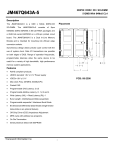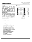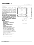
1
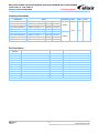
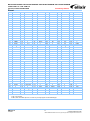
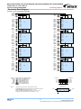
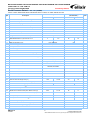
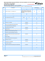
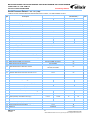
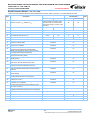
M2Y51H64TU88D0B / M2Y51H64TU88D6B / M2Y1GH64TU8HD0B / M2Y1GH64TU8HD6B 512MB: 64M x 64 / 1GB: 128M x 64 Preliminary Edition Unbuffered DDR2 SDRAM DIMM 240pin Unbuffered DDR2 SDRAM MODULE Based on 64Mx8 DDR2 SDRAM D Die Features • Performance: Speed Sort * DIMM Latency f CK Clock Frequency t CK Clock Cycle f DQ DQ Burst Frequency PC2-5300 PC2-6400 -3C -AC Unit 5 6 333 400 3 2.5 ns 667 800 MHz MHz • Programmable Operation: - Device Latency: 3, 4, 5 - Burst Type: Sequential or Interleave - Burst Length: 4, 8 - Operation: Burst Read and Write • Auto Refresh (CBR) and Self Refresh Modes • Automatic and controlled precharge commands • 14/10/1 Addressing (row/column/rank) – 512MB • 14/10/2 Addressing (row/column/rank) – 1GB • 7.8 µs Max. Average Periodic Refresh Interval • Serial Presence Detect • Gold contacts • SDRAMs in 60 ball BGA Package • RoHS compliance • JEDEC Standard 240-pin Dual In-Line Memory Module • 64Mx64 and 128Mx64 DDR2 Unbuffered DIMM based on 64Mx8 DDR2 SDRAM D die • Intended for 333MHz, and 400MHz applications • Inputs and outputs are SSTL-18 compatible • VDD = VDDQ = 1.8V ± 0.1V • SDRAMs have 4 internal banks for concurrent operation • Differential clock inputs • Data is read or written on both clock edges • Bi-directional data strobe with one clock cycle preamble and one-half clock post-amble • Address and control signals are fully synchronous to positive clock edge Description M2Y51H64TU88D0B, M2Y1GH64TU8HD0B, M2Y51H64TU88D6B and M2Y1GH64TU8HD6B are 240-Pin Double Data Rate 2 (DDR2) Synchronous DRAM Unbuffered Dual In-Line Memory Module (UDIMM), organized as one-rank 64Mx64 and two ranks 128Mx64 high-speed memory array. M2Y51H64TU88D0B and M2Y51H64TU88D6B use eight 64Mx8 DDR2 SDRAMs. M2Y1GH64TU8HD0B and M2Y1GH64TU8HD6B use sixteen 64Mx8 DDR2 SDRAMs. These DIMMs are manufactured using raw cards developed for broad industry use as reference designs. The use of these common design files minimizes electrical variation between suppliers. All Elixir DDR2 SDRAM DIMMs provide a high-performance, flexible 8-byte interface in a 5.25” long space-saving footprint. The DIMM is intended for use in applications operating up to 333MHz and 400MHz clock speeds and achieves high-speed data transfer rates of up to 667MHz and 800MHz. Prior to any access operation, the device latency and burst / length / operation type must be programmed into the DIMM by address inputs A0-A13 and I/O inputs BA0 and BA1 using the mode register set cycle. The DIMM uses serial presence-detect implemented via a serial 2,048-bit EEPROM using a standard IIC protocol. The first 128 bytes of serial PD data are programmed and locked during module assembly. The remaining 128 bytes are available for use by the customer. REV 0.1 08/2008 1 © NANYA TECHNOLOGY CORP. NANYA TECHNOLOGY CORP. reserves the right to change Products and Specifications without notice. M2Y51H64TU88D0B / M2Y51H64TU88D6B / M2Y1GH64TU8HD0B / M2Y1GH64TU8HD6B 512MB: 64M x 64 / 1GB: 128M x 64 Preliminary Edition Unbuffered DDR2 SDRAM DIMM Ordering Information Part Number Speed Organization M2Y51H64TU88D0B-3C 333MHz (3.00ns@ CL = 5) DDR2-667 PC2-5300 M2Y51H64TU88D0B-AC 400MHz (2.50ns@ CL = 5) DDR2-800 PC2-6400 M2Y51H64TU88D6B-3C 333MHz (3.00ns@ CL = 5) DDR2-667 PC2-5300 M2Y51H64TU88D6B-AC 400MHz (2.50ns@ CL = 5) DDR2-800 PC2-6400 M2Y1GH64TU8HD0B-3C 333MHz (3.00ns@ CL = 5) DDR2-667 PC2-5300 M2Y1GH64TU8HD0B-AC 400MHz (2.50ns@ CL = 5) DDR2-800 PC2-6400 M2Y1GH64TU8HD6B-3C 333MHz (3.00ns@ CL = 5) DDR2-667 PC2-5300 M2Y1GH64TU8HD6B-AC 400MHz (2.50ns@ CL = 5) DDR2-800 PC2-6400 Leads Power Green 1.8 V Note 64Mx64 128Mx64 Pin Description CK0-CK2, - CKE0, CKE1 Differential Clock Inputs DQ0-DQ63 Clock Enable DQS0-DQS8 Data input/output Bidirectional data strobes Row Address Strobe Column Address Strobe Write Enable VDD Power (1.8V) , Chip Selects VREF Ref. Voltage for SSTL_18 inputs A0-A9, A11-A13 A10/AP BA0, BA1 ODT0, ODT1 NC DM0-DM8 - Address Inputs VDDSPD Input Data Mask/High Data Strobes Differential data strobes Serial EEPROM positive power supply Column Address Input/Auto-precharge VSS Ground SDRAM Bank Address Inputs SCL Serial Presence Detect Clock Input SDA Serial Presence Detect Data input/output Reset pin Active termination control lines SA0-2 Serial Presence Detect Address Inputs No Connect Note: ODT1, CKE1 and are only support in 1GB module type. REV 0.1 08/2008 2 © NANYA TECHNOLOGY CORP. NANYA TECHNOLOGY CORP. reserves the right to change Products and Specifications without notice. M2Y51H64TU88D0B / M2Y51H64TU88D6B / M2Y1GH64TU8HD0B / M2Y1GH64TU8HD6B 512MB: 64M x 64 / 1GB: 128M x 64 Preliminary Edition Unbuffered DDR2 SDRAM DIMM Pinout Pin Front Pin Front Pin Front Pin Back Pin Back Pin Back 1 VREF 42 NC 2 VSS 43 NC 82 VSS 83 121 VSS 122 DQ4 162 NC 202 DM4 163 VSS 203 NC 3 DQ0 44 4 DQ1 45 VSS 84 NC 85 DQS4 123 VSS 124 DQ5 164 NC 204 VSS VSS 165 NC 205 DQ38 5 VSS 6 46 NC 47 VSS 86 DQ34 87 DQ35 125 DM0 166 VSS 206 DQ39 126 NC 167 NC 207 7 DQS0 48 NC 88 VSS VSS 127 VSS 168 NC 208 DQ44 8 VSS 9 DQ2 49 NC 50 VSS 89 DQ40 128 DQ6 169 VSS 209 DQ45 90 DQ41 129 DQ7 170 VDDQ 210 VSS 10 DQ3 11 VSS 51 VDDQ 52 CKE0 91 VSS 130 VSS 171 CKE1/NC 211 DM5 92 131 DQ12 172 VDD 212 NC 12 13 DQ8 53 DQ9 54 VDD 93 DQS5 132 DQ13 173 NC 213 VSS NC 94 VSS 133 VSS 174 NC 214 DQ46 14 VSS 55 NC 95 DQ42 134 DM1 175 VDDQ 215 DQ47 15 16 56 VDDQ 96 DQ43 135 NC 176 A12 216 VSS DQS1 57 A11 97 VSS 136 VSS 177 A9 217 DQ52 17 VSS 18 NC 58 A7 98 DQ48 137 CK1 178 VDD 218 DQ53 59 VDD 99 DQ49 138 179 A8 219 VSS 19 20 NC 60 A5 100 VSS 139 VSS 180 A6 220 CK2 VSS 61 A4 101 SA2 140 DQ14 181 VDDQ 221 21 DQ10 62 VDDQ 102 NC 141 DQ15 182 A3 222 VSS 22 DQ11 63 A2 103 VSS 142 VSS 183 A1 223 DM6 23 VSS 64 VDD 104 143 DQ20 184 VDD 224 NC 24 DQ16 25 DQ17 65 26 VSS 27 28 KEY 105 DQS6 144 DQ21 VSS 106 VSS 145 VSS 185 KEY 225 VSS CK0 226 DQ54 66 VSS 107 DQ50 146 DM2 67 VDD 108 DQ51 147 NC 186 227 DQ55 187 VDD 228 DQS2 68 NC 109 VSS 148 VSS VSS 188 A0 229 DQ60 29 VSS 69 VDD 110 DQ56 30 DQ18 70 A10/AP 111 DQ57 149 DQ22 189 VDD 230 DQ61 150 DQ23 190 BA1 231 VSS 31 DQ19 71 BA0 112 VSS 32 VSS 72 VDDQ 113 151 VSS 191 VDDQ 232 DM7 152 DQ28 192 233 NC 33 DQ24 73 114 34 DQ25 74 115 DQS7 153 DQ29 193 234 VSS VSS 154 VSS 194 VDDQ 235 DQ62 35 VSS 75 VDDQ 116 DQ58 155 DM3 195 ODT0 236 DQ63 36 76 37 DQS3 77 117 DQ59 156 NC 196 A13 237 VSS ODT1/NC 118 VSS 157 VSS 197 VDD 238 VDDSPD 38 VSS 78 39 DQ26 79 VDDQ 119 SDA 158 DQ30 198 VSS 239 SA0 VSS 120 SCL 159 DQ31 199 DQ36 240 SA1 40 DQ27 80 41 VSS 81 DQ32 160 VSS 200 DQ37 DQ33 161 NC 201 VSS Note: 1. NC = No Connect. 2. , ODT1 and CKE1 (Pins 76, 77 and 171) are only support in 1GB module type. REV 0.1 08/2008 3 © NANYA TECHNOLOGY CORP. NANYA TECHNOLOGY CORP. reserves the right to change Products and Specifications without notice. M2Y51H64TU88D0B / M2Y51H64TU88D6B / M2Y1GH64TU8HD0B / M2Y1GH64TU8HD6B 512MB: 64M x 64 / 1GB: 128M x 64 Preliminary Edition Unbuffered DDR2 SDRAM DIMM Input/Output Functional Description Symbol Type Polarity CK0, CK1, CK2 (SSTL) The positive line of the differential pair of system clock inputs which drives the input to Positive the on-DIMM PLL. All the DDR2 SDRAM address and control inputs are sampled on the Edge rising edge of their associated clocks. , , (SSTL) Negative The negative line of the differential pair of system clock inputs which drives the input to Edge the on-DIMM PLL. CKE0, CKE1 (SSTL) Active High Activates the SDRAM CK signal when high and deactivates the CK signal when low. By deactivating the clocks, CKE low initiates the Power Down mode, or the Self Refresh mode. , (SSTL) Active Low Enables the associated SDRAM command decoder when low and disables the command decoder when high. When the command decoder is disabled, new commands are ignored but previous operations continue. , , (SSTL) Active Low When sampled at the positive rising edge of the clock, , , define the operation to be executed by the SDRAM. VREF Supply Reference voltage for SSTL-18 inputs VDDQ Supply Isolated power supply for the DDR SDRAM output buffers to provide improved noise immunity ODT0, ODT1 Input Active High BA0, BA1 (SSTL) - Selects which SDRAM bank is to be active. During a Bank Activate command cycle, A0-A14 defines the row address (RA0-RA13) when sampled at the rising clock edge. During a Read or Write command cycle, A0-A9 defines the column address (CA0-CA9) when sampled at the rising clock edge. In addition to the column address, AP is used to invoke Autoprecharge operation at the end of the Burst Read or Write cycle. If AP is high, autoprecharge is selected and BA0/BA1 defines the bank to be precharged. If AP is low, autoprecharge is disabled. During a Precharge command cycle, AP is used in conjunction with BA0/BA1 to control which bank(s) to precharge. If AP is high all 4 banks will be precharged regardless of the state of BA0/BA1. If AP is low, then BA0/BA1 are used to define which bank to pre-charge. A0 – A9 A10/AP A11 – A13 (SSTL) - DQ0 – DQ63 (SSTL) Active High VDD, VSS Supply DQS0 – DQS8 – (SSTL) DM0 – DM8 Input Function On-Die Termination control signals Data and Check Bit Input/Output pins. Power and ground for the DDR2 SDRAM input buffers and core logic Negative and Data strobe for input and output data Positive Edge Active High The data write masks, associated with one data byte. In Write mode, DM operates as a byte mask by allowing input data to be written if it is low but blocks the write operation if it is high. In Read mode, DM lines have no effect. SA0 – SA2 - Address inputs. Connected to either VDD or VSS on the system board to configure the Serial Presence Detect EEPROM address. SDA - This bi-directional pin is used to transfer data into or out of the SPD EEPROM. A resistor must be connected from the SDA bus line to V DD to act as a pull-up. SCL - This signal is used to clock data into and out of the SPD EEPROM. A resistor may be connected from the SCL bus time to V DD to act as a pull-up. VDDSPD REV 0.1 08/2008 Supply Serial EEPROM positive power supply. 4 © NANYA TECHNOLOGY CORP. NANYA TECHNOLOGY CORP. reserves the right to change Products and Specifications without notice. M2Y51H64TU88D0B / M2Y51H64TU88D6B / M2Y1GH64TU8HD0B / M2Y1GH64TU8HD6B 512MB: 64M x 64 / 1GB: 128M x 64 Preliminary Edition Unbuffered DDR2 SDRAM DIMM Functional Block Diagram (512MB, 1 Rank, 64Mx8 DDR2 SDRAMs) DQS0 DM0 DQS4 DM4 DM I/O 0 I/O 1 I/O 2 I/O 3 D0 I/O 4 I/O 5 I/O 6 I/O 7 DQ0 DQ1 DQ2 DQ3 DQ4 DQ5 DQ6 DQ7 DQS DQ32 DQ33 DQ34 DQ35 DQ36 DQ37 DQ38 DQ39 DQS1 DM1 DM I/O 0 I/O 1 I/O 2 I/O 3 D1 I/O 4 I/O 5 I/O 6 I/O 7 DQS DQ40 DQ41 DQ42 DQ43 DQ44 DQ45 DQ46 DQ47 DQS2 DM2 DM I/O 0 I/O 1 I/O 2 I/O 3 D2 I/O 4 I/O 5 I/O 6 I/O 7 DQS DQ48 DQ49 DQ50 DQ51 DQ52 DQ53 DQ54 DQ55 DQS3 DM3 DQS DM I/O 0 I/O 1 I/O 2 I/O 3 D6 I/O 4 I/O 5 I/O 6 I/O 7 DQS DM I/O 0 I/O 1 I/O 2 I/O 3 D7 I/O 4 I/O 5 I/O 6 I/O 7 DQS DQS7 DM7 DM I/O 0 I/O 1 I/O 2 I/O 3 D3 I/O 4 I/O 5 I/O 6 I/O 7 DQ24 DQ25 DQ26 DQ27 DQ28 DQ29 DQ30 DQ31 DQS DQ56 DQ57 DQ58 DQ59 DQ60 DQ61 DQ62 DQ63 BA0-BA2: SDRAMs D0-D7 A0-A13: SDRAMs D0-D7 : SDRAMs D0-D7 : SDRAMs D0-D7 : SDRAMs D0-D7 CKE: SDRAMS D0-D7 ODT: SDRAMS D0-D7 BA0-BA1 A0-A13 CKE0 ODT0 08/2008 DM I/O 0 I/O 1 I/O 2 I/O 3 D5 I/O 4 I/O 5 I/O 6 I/O 7 DQS6 DM6 DQ16 DQ17 DQ18 DQ19 DQ20 DQ21 DQ22 DQ23 REV 0.1 DQS DQS5 DM5 DQ8 DQ9 DQ10 DQ11 DQ12 DQ13 DQ14 DQ15 Notes : DM I/O 0 I/O 1 I/O 2 I/O 3 D4 I/O 4 I/O 5 I/O 6 I/O 7 1. 2. 3. 4. 5. V DDSPD VDDQ V DD Serial PD D0-D7 D0-D7 D0-D7 D0-D7 V REF VSS DQ-to-I/O wiring may be changed within a byte. DQ/DQS/DM/CKE/CS relationships are maintained as shown. DQ/DQS/ resistors are 22 Ohms +/- 5% BAx, Ax, , , resistors are 5.1 Ohms +/- 5% Address and control resistors are 22 Ohms +/- 5% Serial PD SCL WP A0 A1 A2 SA0 SA1 SA2 SDA 5 © NANYA TECHNOLOGY CORP. NANYA TECHNOLOGY CORP. reserves the right to change Products and Specifications without notice. M2Y51H64TU88D0B / M2Y51H64TU88D6B / M2Y1GH64TU8HD0B / M2Y1GH64TU8HD6B 512MB: 64M x 64 / 1GB: 128M x 64 Preliminary Edition Unbuffered DDR2 SDRAM DIMM Functional Block Diagram (1GB, 2 Rank, 64Mx8 DDR2 SDRAMs) DQS0 DM0 DQS4 DM4 DM I/O 0 I/O 1 I/O 2 I/O 3 D0 I/O 4 I/O 5 I/O 6 I/O 7 DQ0 DQ1 DQ2 DQ3 DQ4 DQ5 DQ6 DQ7 DQS DM I/O 0 I/O 1 I/O 2 I/O 3 D8 I/O 4 I/O 5 I/O 6 I/O 7 DQS DQ32 DQ33 DQ34 DQ35 DQ36 DQ37 DQ38 DQ39 DQS1 DM1 DM I/O 0 I/O 1 I/O 2 I/O 3 D1 I/O 4 I/O 5 I/O 6 I/O 7 DQS DM I/O 0 I/O 1 I/O 2 I/O 3 D9 I/O 4 I/O 5 I/O 6 I/O 7 DQS DQ40 DQ41 DQ42 DQ43 DQ44 DQ45 DQ46 DQ47 DQS2 DM2 DM I/O 0 I/O 1 I/O 2 I/O 3 D12 I/O 4 I/O 5 I/O 6 I/O 7 DQS DM I/O 0 I/O 1 I/O 2 I/O 3 D5 I/O 4 I/O 5 I/O 6 I/O 7 DQS DM I/O 0 I/O 1 I/O 2 I/O 3 D13 I/O 4 I/O 5 I/O 6 I/O 7 DQS DM I/O 0 I/O 1 I/O 2 I/O 3 D6 I/O 4 I/O 5 I/O 6 I/O 7 DQS DM I/O 0 I/O 1 I/O 2 I/O 3 D14 I/O 4 I/O 5 I/O 6 I/O 7 DQS DM I/O 0 I/O 1 I/O 2 I/O 3 D7 I/O 4 I/O 5 I/O 6 I/O 7 DQS DM I/O 0 I/O 1 I/O 2 I/O 3 D15 I/O 4 I/O 5 I/O 6 I/O 7 DQS DQS6 DM6 DM I/O 0 I/O 1 I/O 2 I/O 3 D2 I/O 4 I/O 5 I/O 6 I/O 7 DQ16 DQ17 DQ18 DQ19 DQ20 DQ21 DQ22 DQ23 DQS DM I/O 0 I/O 1 I/O 2 I/O 3 D10 I/O 4 I/O 5 I/O 6 I/O 7 DQS DQ48 DQ49 DQ50 DQ51 DQ52 DQ53 DQ54 DQ55 DQS3 DM3 DQS7 DM7 DM I/O 0 I/O 1 I/O 2 I/O 3 D3 I/O 4 I/O 5 I/O 6 I/O 7 DQ24 DQ25 DQ26 DQ27 DQ28 DQ29 DQ30 DQ31 BA0-BA1 A0-A13 CKE0 CKE1 ODT0 ODT1 Notes : 08/2008 DQS DQS5 DM5 DQ8 DQ9 DQ10 DQ11 DQ12 DQ13 DQ14 DQ15 REV 0.1 DM I/O 0 I/O 1 I/O 2 I/O 3 D4 I/O 4 I/O 5 I/O 6 I/O 7 DQS DM I/O 0 I/O 1 I/O 2 I/O 3 D11 I/O 4 I/O 5 I/O 6 I/O 7 DQS DQ56 DQ57 DQ58 DQ59 DQ60 DQ61 DQ62 DQ63 BA0-BA1 : SDRAMs D0-D15 A0-A13 : SDRAMs D0-D15 : SDRAMs D0-D15 : SDRAMs D0-D15 : SDRAMs D0-D15 CKE : SDRAMs D0-D7 CKE : SDRAMs D8-D15 ODT : SDRAMs D0-D7 ODT : SDRAMs D8-D15 V DDSPD V DDQ V DD VREF VSS 1. DQ-to-I/O wiring may be changed within a byte. 2. DQ/DQS/DM/CKE/CS relationships are maintained as shown. 3. DQ/DQS/ resistors are 22 Ohms +/- 5% 4. BAx, Ax, , , resistors are 5.1 Ohms +/- 5% 5. Address and control resistors are 22 Ohms +/- 5% Serial PD D0-D15 D0-D15 D0-D15 D0-D15 Serial PD SCL WP A0 A1 A2 SA0 SA1 SA2 SDA 6 © NANYA TECHNOLOGY CORP. NANYA TECHNOLOGY CORP. reserves the right to change Products and Specifications without notice. M2Y51H64TU88D0B / M2Y51H64TU88D6B / M2Y1GH64TU8HD0B / M2Y1GH64TU8HD6B 512MB: 64M x 64 / 1GB: 128M x 64 Preliminary Edition Unbuffered DDR2 SDRAM DIMM Serial Presence Detect – Part 1 of 2 (512MB) 64Mx64 1 RANK UNBUFFERED DDR2 SDRAM DIMM based on 64Mx8,1.8V DDR2 SDRAMs with SPD Byte SPD Entry Value Description -3C -AC Serial PD Data Entry (Hexadecimal) -3C -AC 0 Number of Serial PD Bytes Written during Production 128 80 1 Total Number of Bytes in Serial PD device 2 Fundamental Memory Type 3 4 5 Number of DIMM Ranks 6 Data Width of Assembly 7 Reserved 8 Voltage Interface Level of this Assembly SSTL_1.8V 05 9 DDR2 SDRAM Device Cycle Time at CL=X 10 DDR2 SDRAM Device Access Time from Clock at CL=X 11 DIMM Configuration Type 12 Refresh Rate/Type 13 Primary DDR2 SDRAM Width 14 15 16 17 256 08 DDR2 SDRAM 08 Number of Row Addresses on Assembly 14 0E Number of Column Addresses on Assembly 10 0A 1 rank, Height=30mm 60 X64 40 Undefined 00 3 2.5 30 25 0.45 0.40 45 40 Non parity/ECC 00 7.8μs/self 82 X8 08 Error Checking DDR2 SDRAM Device Width Undefined 00 Reserved Undefined 00 DDR2 SDRAM Device Attributes: Burst Length Supported 4,8 0C DDR2 SDRAM Device Attributes: Number of Device Banks 4 04 18 DDR2 SDRAM Device Attributes: CAS Latencies Supported 3,4,5 38 19 DIMM Mechanical Characteristics 20 DDR2 SDRAM DIMM Type Information 21 DDR2 SDRAM Module Attributes: <4.1(mm) 01 Regular UDIMM (133.35mm) 02 Normal DIMM 00 Support weak Driver, 50Ω ODT, and PASR 07 22 DDR2 SDRAM Device Attributes: General 23 Minimum Clock Cycle at CL=X-1 3.75ns 3D 24 Maximum Data Access Time from Clock at CL=X-1 0.5ns 50 25 Minimum Clock Cycle Time at CL=X-2 5.0ns 50 26 Maximum Data Access Time from Clock at CL=X-2 0.6ns 60 27 Minimum Row Precharge Time (tRP) 28 Minimum Row Active to Row Active delay (tRRD) 15ns 12.5ns 3C 12.5ns 3C 7.5ns 15ns 32 1E 32 29 Minimum RAS to CAS delay (tRCD) 30 Minimum RAS Pulse Width (tRAS) 31 Module Bank Density 32 Address and Command Setup Time Before Clock (tIS) 0.2ns 0.17ns 20 17 33 Address and Command Hold Time After Clock (tIH) 0.27ns 0.25ns 27 25 34 Data Input Setup Time Before Clock (tDS) 0.10ns 0.05ns 10 05 35 Data Input Hold Time After Clock (tDH) 0.17ns 0.12ns 17 12 36 Write Recovery Time (tWR) 15ns 3C 37 Internal Write to Read Command delay (tWTR) 7.5ns 1E 38 Internal Read to Precharge delay (tRTP) 7.5ns 1E 39 Reserved Undefined 00 REV 0.1 08/2008 45ns 2D 512MB 80 7 © NANYA TECHNOLOGY CORP. NANYA TECHNOLOGY CORP. reserves the right to change Products and Specifications without notice. Note M2Y51H64TU88D0B / M2Y51H64TU88D6B / M2Y1GH64TU8HD0B / M2Y1GH64TU8HD6B 512MB: 64M x 64 / 1GB: 128M x 64 Preliminary Edition Unbuffered DDR2 SDRAM DIMM Serial Presence Detect -- Part 2 of 2 (512MB) 64Mx64 1RANK UNBUFFERED DDR2 SDRAM DIMM based on 64Mx8, 1.8V DDR2 SDRAMs with SPD Byte SPD Entry Value Description -3C -AC 00: The number below a decimal point of tRC and tRFC are 0, tRFC is less than 256ns. 30: The number below a decimal point of tRC is 5, tRFC is less than 256ns Serial PD Data Entry (Hexadecimal) -3C -AC 06 36 3C 39 40 Extension of Byte 41 tRC and Byte 42 tRFC 41 Minimum Core Cycle Time (tRC) 42 Min. Auto Refresh Command Cycle Time (tRFC) 43 Maximum Clock Cycle Time (tCK) 44 Max. DQS-DQ Skew Factor (tDQS) 0.24ns 0.2 18 14 45 Read Data Hold Skew Factor (tQHS) 0.34ns 0.30 22 1E 46 PLL Relock Time Undefined 00 47 Tcasemax, DT4R4W Delta Undefined 00 48 Thermal Resistance of DRAM Package from Top (Case) to Ambient (Psi T-A DRAM) Undefined 00 49 DRAM Case Temperature Rise from Ambient due to Activate-Precharge/Mode Bits (DT0/Mode Bits) Undefined 00 50 DRAM Case Temperature Rise from Ambient due to Precharge/Quiet Standby (DT2N/DT2Q) Undefined 00 51 DRAM Case Temperature Rise from Ambient due to precharge Power-Down (DT2P) Undefined 00 52 DRAM Case Temperature Rise from Ambient due to Active Standby (DT3N) Undefined 00 53 DRAM Case Temperature Rise from Ambient due to Active Power-Down with Fast PDN Exit (DT3P fast) Undefined 00 54 DRAM Case Temperature Rise from Ambient due to Active Power-Down with Slow PDN Exit (DT3P slow) Undefined 00 55 DRAM Case Temperature Rise from Ambient due to Page Open Burst Read/DT4R4W Mode Bit (DT4R/DT4R4W Mode Bit) Undefined 00 56 DRAM Case Temperature Rise from Ambient due to Burst Refresh (DT5B) Undefined 00 57 DRAM Case Temperature Rise from Ambient due to Bank Interleave Reads with Auto-Precharge (DT7) Undefined 00 58 Thermal Resistance of PLL Package from Top (Case) to Ambient (Psi T-A PLL) Undefined 00 59 Thermal Resistance of Register Package from Top (Case) to Ambient (Psi T-A Register) Undefined 00 60 PLL Case Temperature Rise from Ambient due to PLL Active (DT PLL Active) Undefined 00 61 Resister Case Temperature Rise from Ambient due to Register Active/Mode Bit (DT Register Active/Mode Bit) Undefined 00 62 SPD Revision 1.3 13 63 Checksum for Byte 0-62 64-71 60.ns 72-255 Reserved 08/2008 127.5ns 7F 8.0ns 80 Checksum data Manufacture’s JEDEC ID Code REV 0.1 57.7ns 92 78 NANYA 7F7F7F0B00000000 Undefined -- 8 © NANYA TECHNOLOGY CORP. NANYA TECHNOLOGY CORP. reserves the right to change Products and Specifications without notice. Note M2Y51H64TU88D0B / M2Y51H64TU88D6B / M2Y1GH64TU8HD0B / M2Y1GH64TU8HD6B 512MB: 64M x 64 / 1GB: 128M x 64 Preliminary Edition Unbuffered DDR2 SDRAM DIMM Serial Presence Detect – Part 1 of 2 (1GB) 128Mx64 2 RANKs UNBUFFERED DDR2 SDRAM DIMM based on 64Mx8, 1.8V DDR2 SDRAMs with SPD Byte SPD Entry Value Description -3C -AC Serial PD Data Entry (Hexadecimal) -3C -AC 0 Number of Serial PD Bytes Written during Production 128 80 1 Total Number of Bytes in Serial PD device 256 08 2 Fundamental Memory Type DDR2 SDRAM 08 3 Number of Row Addresses on Assembly 14 0E 4 Number of Column Addresses on Assembly 10 0A 5 Number of DIMM Ranks 2 ranks, Height=30mm 61 6 Data Width of Assembly X64 40 7 Reserved Undefined 00 8 Voltage Interface Level of this Assembly SSTL_1.8V 05 9 DDR2 SDRAM Device Cycle Time at CL=X 10 DDR2 SDRAM Device Access Time from Clock at CL=X 11 DIMM Configuration Type 12 Refresh Rate/Type 13 Primary DDR2 SDRAM Width 14 Error Checking DDR2 SDRAM Device Width 15 Reserved Undefined 00 16 DDR2 SDRAM Device Attributes: Burst Length Supported 4,8 0C 17 DDR2 SDRAM Device Attributes: Number of Device Banks 4 04 18 DDR2 SDRAM Device Attributes: CAS Latencies Supported 3,4,5 38 19 DIMM Mechanical Characteristics 20 DDR2 SDRAM DIMM Type Information 21 DDR2 SDRAM Module Attributes: 22 DDR2 SDRAM Device Attributes: General 23 3 2.5 30 25 0.45 0.40 45 40 Non parity/ECC 00 7.8μs/self 82 X8 08 Undefined 00 <4.1(mm) 01 Regular UDIMM (133.35mm) 02 Normal DIMM 00 Support weak Driver, 50Ω ODT, and PASR 07 Minimum Clock Cycle at CL=X-1 3.75ns 3D 24 Maximum Data Access Time from Clock at CL=X-1 0.5ns 50 25 Minimum Clock Cycle Time at CL=X-2 5.0ns 50 26 Maximum Data Access Time from Clock at CL=X-2 0.6ns 60 27 Minimum Row Precharge Time (tRP) 28 Minimum Row Active to Row Active delay (tRRD) 29 Minimum RAS to CAS delay (tRCD) 30 Minimum RAS Pulse Width (tRAS) 31 Module Bank Density 32 Address and Command Setup Time Before Clock (tIS) 0.2ns 0.17ns 20 17 33 Address and Command Hold Time After Clock (tIH) 0.27ns 0.25ns 27 25 34 Data Input Setup Time Before Clock (tDS) 0.10ns 0.05ns 10 05 35 Data Input Hold Time After Clock (tDH) 0.17ns 0.12ns 17 12 36 Write Recovery Time (tWR) 15ns 3C 37 Internal Write to Read Command delay (tWTR) 7.5ns 1E 38 Internal Read to Precharge delay (tRTP) 7.5ns 1E 39 Reserved Undefined 00 REV 0.1 08/2008 15ns 12.5ns 3C 7.5ns 15ns 32 1E 12.5ns 3C 32 45ns 2D 512MB 80 9 © NANYA TECHNOLOGY CORP. NANYA TECHNOLOGY CORP. reserves the right to change Products and Specifications without notice. Note M2Y51H64TU88D0B / M2Y51H64TU88D6B / M2Y1GH64TU8HD0B / M2Y1GH64TU8HD6B 512MB: 64M x 64 / 1GB: 128M x 64 Preliminary Edition Unbuffered DDR2 SDRAM DIMM Serial Presence Detect – Part 2 of 2 (1GB) 128Mx64 2 RANKs UNBUFFERED DDR2 SDRAM DIMM based on 64Mx8, 4Banks, 8K Refresh, 1.8V DDR2 SDRAMs with SPD Byte SPD Entry Value Description -3C -AC 00: The number below a decimal point of tRC and tRFC are 0, tRFC is less than 256ns. 30: The number below a decimal point of tRC is 5, tRFC is less than 256ns Serial PD Data Entry (Hexadecimal) -3C -AC 06 36 3C 39 40 Extension of Byte 41 tRC and Byte 42 tRFC 41 Minimum Core Cycle Time (tRC) 42 Min. Auto Refresh Command Cycle Time (tRFC) 43 Maximum Clock Cycle Time (tCK) 44 Max. DQS-DQ Skew Factor (tDQS) 0.24ns 0.2 18 14 45 Read Data Hold Skew Factor (tQHS) 0.34ns 0.30 22 1E 46 PLL Relock Time Undefined 00 47 Tcasemax, DT4R4W Delta Undefined 00 48 Thermal Resistance of DRAM Package from Top (Case) to Ambient (Psi T-A DRAM) Undefined 00 49 DRAM Case Temperature Rise from Ambient due to Activate-Precharge/Mode Bits (DT0/Mode Bits) Undefined 00 50 DRAM Case Temperature Rise from Ambient due to Precharge/Quiet Standby (DT2N/DT2Q) Undefined 00 51 DRAM Case Temperature Rise from Ambient due to precharge Power-Down (DT2P) Undefined 00 52 DRAM Case Temperature Rise from Ambient due to Active Standby (DT3N) Undefined 00 53 DRAM Case Temperature Rise from Ambient due to Active Power-Down with Fast PDN Exit (DT3P fast) Undefined 00 54 DRAM Case Temperature Rise from Ambient due to Active Power-Down with Slow PDN Exit (DT3P slow) Undefined 00 55 DRAM Case Temperature Rise from Ambient due to Page Open Burst Read/DT4R4W Mode Bit (DT4R/DT4R4W Mode Bit) Undefined 00 56 DRAM Case Temperature Rise from Ambient due to Burst Refresh (DT5B) Undefined 00 57 DRAM Case Temperature Rise from Ambient due to Bank Interleave Reads with Auto-Precharge (DT7) Undefined 00 58 Thermal Resistance of PLL Package from Top (Case) to Ambient (Psi T-A PLL) Undefined 00 59 Thermal Resistance of Register Package from Top (Case) to Ambient (Psi T-A Register) Undefined 00 60 PLL Case Temperature Rise from Ambient due to PLL Active (DT PLL Active) Undefined 00 61 Resister Case Temperature Rise from Ambient due to Register Active/Mode Bit (DT Register Active/Mode Bit) Undefined 00 62 SPD Revision 1.3 13 63 Checksum for Byte 0-62 64-71 60.ns Manufacture’s JEDEC ID Code 08/2008 127.5ns 7F 8.0ns 80 Checksum data 72-255 Reserved REV 0.1 57.7ns 93 79 NANYA 7F7F7F0B00000000 Undefined -- 10 © NANYA TECHNOLOGY CORP. NANYA TECHNOLOGY CORP. reserves the right to change Products and Specifications without notice. Note M2Y51H64TU88D0B / M2Y51H64TU88D6B / M2Y1GH64TU8HD0B / M2Y1GH64TU8HD6B 512MB: 64M x 64 / 1GB: 128M x 64 Preliminary Edition Unbuffered DDR2 SDRAM DIMM Absolute Maximum Ratings Symbol VIN, VOUT VDD VDDQ Parameter Rating Units Voltage on I/O pins relative to Vss -0.5 to 2.3 V Voltage on VDD supply relative to Vss -1.0 to +2.3 V Voltage on VDDQ supply relative to Vss -0.5 to +2.3 V Note: Stresses greater than those listed under “Absolute Maximum Ratings” may cause permanent damage to the device. This is stress rating only, and functional operation of the device at these or any other conditions above those indicated in the operational sections of this specification is not implied. Exposure to absolute maximum rating conditions for extended periods may affect reliability. DC operating Conditions Symbol Parameter TCASE Operating Temperature (Ambient) TSTG Storage Temperature (Plastic) Short Circuit Output Current IL Note: 1. 2. 3. Rating Units Note 0 to 95 °C 1,2,3 -55 to 100 °C -5 to 5 μA Case temperature is measured at top and center side of any DRAMs. tCASE > 85°C tREFI = 3.9 μs All DRAM specification only support 0°C < tCASE < 85°C DC Electrical Characteristics and Operating Conditions (TCASE = 0 °C ~ 85 °C; VDDQ = 1.8V ± 0.1V; VDD = 1.8V ± 0.1V, See AC Characteristics) Symbol Parameter VDD VDDQ VSS, VSSQ Min Max Units Notes Supply Voltage 1.7 1.9 V 1 I/O Supply Voltage 1.7 1.9 V 1 0 0 V Supply Voltage, I/O Supply Voltage 0.49VDDQ 0.51VDDQ V 1, 2 VIH (DC) Input High (Logic1) Voltage VREF + 0.125 VDDQ + 0.3 V 1 VIL (DC) Input Low (Logic0) Voltage -0.3 VREF - 0.125 V 1 VREF I/O Reference Voltage Note: 1. Inputs are not recognized as valid until VREF stabilizes. 2. VREF is expected to be equal to 0.5 V DDQ of the transmitting device, and to track variations in the DC level of the same. Peak-to-peak noise on VREF may not exceed 2% of the DC value. Environmental Parameters Symbol Parameter Rating Units Note 3 TOPR Module Operating Temperature Range (ambient) 0 to 55 °C HOPR Operating Humidity (relative) 10 to 90 % TSTG Storage Temperature (Plastic) -55 to 100 °C 1 HSTG Storage Humidity (without condensation) 5 to 95 % 1 PBAR Barometric Pressure (operating & storage) 105 to 69 K Pascal 1,2 Note: 1. 2. 3. Stresses greater than those listed may cause permanent damage to the device. This is a tress rating only, and device functional operation at or above the conditions indicated is not implied. Exposure to absolute maximum rating conditions for extended periods may affect reliability. Up to 9850 ft. The component maximum case temperature shall not exceed the value specified in the component spec. REV 0.1 08/2008 11 © NANYA TECHNOLOGY CORP. NANYA TECHNOLOGY CORP. reserves the right to change Products and Specifications without notice. M2Y51H64TU88D0B / M2Y51H64TU88D6B / M2Y1GH64TU8HD0B / M2Y1GH64TU8HD6B 512MB: 64M x 64 / 1GB: 128M x 64 Preliminary Edition Unbuffered DDR2 SDRAM DIMM Operating, Standby, and Refresh Currents TCASE = 0 °C ~ 85 °C; VDDQ = VDD = 1.8V ± 0.1V (512MB, 1 Rank, 64Mx8 DDR2 SDRAMs) Symbol Parameter/Condition PC2-5300 PC2-6400 Unit TBD I DD0 Operating Current: one bank; active/precharge; tRC = tRC (MIN); tCK = tCK (MIN); DQ, DM, and DQS inputs changing twice per clock cycle; address and control inputs changing once per clock cycle Operating Current: one bank; active/read/precharge; Burst = 2; tRC = tRC (MIN); CL=2.5; tCK = tCK (MIN); IOUT = 0mA; address and control inputs changing once per clock cycle TBD I DD1 I DD2P Precharge Power-Down Standby Current: all banks idle; power-down mode; CKE VIL (MAX); tCK = tCK (MIN) TBD TBD Idle Standby Current: CS VIH (MIN); all banks idle; CKE VIH (MIN); tCK = tCK (MIN); address and control inputs changing once per clock cycle TBD TBD I DD2N Precharge Quiet Standby Current: All banks idle; is HIGH; CKE is HIGH; tCK = tCK (MIN); Other control and address inputs are stable, Data bus inputs are floating. TBD I DD2Q Active Power-Down Current: All banks open; tCK = tCK (MIN), CKE is LOW; Other control and address inputs are STABLE, Data bus inputs are floating. MRS A12 bit is set to low (Fast Power-down Exit). TBD I DD3PF Active Power-Down Current: All banks open; tCK = tCK (MIN), CKE is LOW; Other control and address inputs are STABLE, Data bus inputs are floating. MRS A12 bit is set to high (Slow Power-down Exit). TBD I DD3PS TBD I DD3N Active Standby Current: one bank; active/precharge; CS VIH (MIN); CKE VIH (MIN); tRC = tRAS (MAX); tCK = tCK (MIN); DQ, DM, and DQS inputs changing twice per clock cycle; address and control inputs changing once per clock cycle Operating Current: one bank; Burst = 2; writes; continuous burst; address and control inputs changing once per clock cycle; DQ and DQS inputs changing twice per clock cycle; CL=2.5; t CK = tCK (MIN) TBD I DD4W TBD I DD4R Operating Current: one bank; Burst = 2; reads; continuous burst; address and control inputs changing once per clock cycle; DQ and DQS outputs changing twice per clock cycle; CL = 2.5; t CK = tCK (MIN); IOUT = 0mA I DD5 Auto-Refresh Current: tRC = tRFC (MIN) TBD TBD mA I DD6 Self-Refresh Current: CKE 0.2V TBD TBD mA Operating Current: four bank; four bank interleaving with BL = 4, address and control inputs randomly changing; 50% of data changing at every transfer; tRC = tRC (min); IOUT = 0mA. TBD TBD I DD7 REV 0.1 08/2008 TBD mA TBD mA mA mA TBD mA TBD mA TBD mA TBD mA TBD mA TBD mA mA 12 © NANYA TECHNOLOGY CORP. NANYA TECHNOLOGY CORP. reserves the right to change Products and Specifications without notice. M2Y51H64TU88D0B / M2Y51H64TU88D6B / M2Y1GH64TU8HD0B / M2Y1GH64TU8HD6B 512MB: 64M x 64 / 1GB: 128M x 64 Preliminary Edition Unbuffered DDR2 SDRAM DIMM Operating, Standby, and Refresh Currents TCASE = 0 °C ~ 85 °C; VDDQ = VDD = 1.8V ± 0.1V (1GB, 2 Ranks, 64Mx8 DDR2 SDRAMs) Symbol Parameter/Condition PC2-5300 PC2-6400 Unit TBD I DD0 Operating Current: one bank; active/precharge; tRC = tRC (MIN); tCK = tCK (MIN); DQ, DM, and DQS inputs changing twice per clock cycle; address and control inputs changing once per clock cycle Operating Current: one bank; active/read/precharge; Burst = 2; tRC = tRC (MIN); CL=2.5; tCK = tCK (MIN); IOUT = 0mA; address and control inputs changing once per clock cycle TBD I DD1 I DD2P Precharge Power-Down Standby Current: all banks idle; power-down mode; CKE VIL (MAX); tCK = tCK (MIN) TBD TBD Idle Standby Current: CS VIH (MIN); all banks idle; CKE VIH (MIN); tCK = tCK (MIN); address and control inputs changing once per clock cycle TBD TBD I DD2N Precharge Quiet Standby Current: All banks idle; is HIGH; CKE is HIGH; tCK = tCK (MIN); Other control and address inputs are stable, Data bus inputs are floating. TBD I DD2Q Active Power-Down Current: All banks open; tCK = tCK (MIN), CKE is LOW; Other control and address inputs are STABLE, Data bus inputs are floating. MRS A12 bit is set to low (Fast Power-down Exit). TBD I DD3PF Active Power-Down Current: All banks open; tCK = tCK (MIN), CKE is LOW; Other control and address inputs are STABLE, Data bus inputs are floating. MRS A12 bit is set to high (Slow Power-down Exit). TBD I DD3PS TBD I DD3N Active Standby Current: one bank; active/precharge; CS VIH (MIN); CKE VIH (MIN); tRC = tRAS (MAX); tCK = tCK (MIN); DQ, DM, and DQS inputs changing twice per clock cycle; address and control inputs changing once per clock cycle Operating Current: one bank; Burst = 2; writes; continuous burst; address and control inputs changing once per clock cycle; DQ and DQS inputs changing twice per clock cycle; CL=2.5; t CK = tCK (MIN) TBD I DD4W TBD I DD4R Operating Current: one bank; Burst = 2; reads; continuous burst; address and control inputs changing once per clock cycle; DQ and DQS outputs changing twice per clock cycle; CL = 2.5; t CK = tCK (MIN); IOUT = 0mA I DD5 Auto-Refresh Current: tRC = tRFC (MIN) TBD TBD mA I DD6 Self-Refresh Current: CKE 0.2V TBD TBD mA Operating Current: four bank; four bank interleaving with BL = 4, address and control inputs randomly changing; 50% of data changing at every transfer; tRC = tRC (min); IOUT = 0mA. TBD TBD I DD7 REV 0.1 08/2008 TBD mA TBD mA mA mA TBD mA TBD mA TBD mA TBD mA TBD mA TBD mA mA 13 © NANYA TECHNOLOGY CORP. NANYA TECHNOLOGY CORP. reserves the right to change Products and Specifications without notice. M2Y51H64TU88D0B / M2Y51H64TU88D6B / M2Y1GH64TU8HD0B / M2Y1GH64TU8HD6B 512MB: 64M x 64 / 1GB: 128M x 64 Preliminary Edition Unbuffered DDR2 SDRAM DIMM AC Timing Specifications for DDR2 SDRAM Devices Used on Module (TCASE = 0 °C ~ 85 °C; VDDQ = 1.8V ± 0.1V; VDD = 1.8V ± 0.1V, See AC Characteristics) (Part 1 of 2) Symbol Parameter PC2-5300 PC2-6400 Unit Min. Max. Min. Max. DQ output access time from CK/ -0.45 +0.45 -0.40 +0.40 DQS output access time from CK/ -0.40 +0.40 -0.35 +0.35 ns tCH CK high-level width 0.45 0.55 0.45 0.55 tCK tCL CK low-level width 0.45 0.55 0.45 0.55 tCK tHP Minimum half clk period for any given cycle; defined by clk high (tCH) or clk low (tCL) time tCH or tCL - tCH or tCL - tCK tCK Clock Cycle Time 3 8 2.5 8 ns tDS DQ and DM input setup time(differential data strobe) 0.1 - 0.05 - ns tDH DQ and DM input hold time(differential data strobe) 0.175 - 0.125 - ns tAC tDQSCK ns tIPW Input pulse width 0.6 - 0.6 - tCK tDIPW DQ and DM input pulse width (each input) 0.35 - 0.35 - tCK tHZ Data-out high-impedance time from CK/ - tACmax - tACmax ns tACmin tACmax tACmin tACmax ns tLZ(DQS) DQS low-impedance time from CK/ tLZ(DQ) DQ low-impedance time from CK/ tDQSQ DQS-DQ skew (DQS & associated DQ signals) - 0.24 - 0.20 ns Data hold Skew Factor - 0.34 - 0.3 ns Data output hold time from DQS tHP tQHS - tHP tQHS - ns Write command to 1st DQS latching transition -0.25 +0.25 -0.25 +0.25 tCK DQS input low (high) pulse width (write cycle) 0.35 - 0.35 - tCK tDSS DQS falling edge to CK setup time (write cycle) 0.2 - 0.2 - tCK tDSH DQS falling edge hold time from CK (write cycle) 0.2 - 0.2 - tCK tQHS tQH tDQSS tDQSL,(H) 2tAC min tAC max 2tAC min tAC max ns tMRD Mode register set command cycle time 2 - 2 - tCK tWPST Write postamble 0.40 0.60 0.40 0.60 tCK tWPRE Write preamble 0.35 - 0.35 - tCK 275 - 250 - ps tIH tIS Address and control input hold time Address and control input setup time 200 - 175 - ps tRPRE Read preamble 0.90 1.10 0.90 1.10 tCK tRPST Read postamble 0.40 0.60 0.40 0.60 tCK 7.5 - 7.5 - ns - tIS + tCK + tIH - ns tRRD Active bank A to Active bank B command tDelay Minimum time clocks remains ON after CKE asynchronously drops Low tREFI tIS + tCK + tIH Average Periodic Refresh Interval (85ºC < TCASE ≤ 95ºC) 3.9 3.9 μs Average Periodic Refresh Interval (0ºC ≤ TCASE ≤ 85ºC) 7.8 7.8 μs tOIT OCD drive mode output delay 0 tCCD to 2 REV 0.1 08/2008 12 0 2 12 ns tCK 14 © NANYA TECHNOLOGY CORP. NANYA TECHNOLOGY CORP. reserves the right to change Products and Specifications without notice. M2Y51H64TU88D0B / M2Y51H64TU88D6B / M2Y1GH64TU8HD0B / M2Y1GH64TU8HD6B 512MB: 64M x 64 / 1GB: 128M x 64 Preliminary Edition Unbuffered DDR2 SDRAM DIMM AC Timing Specifications for DDR2 SDRAM Devices Used on Module (TCASE = 0 °C ~ 85 °C; VDDQ = 1.8V ± 0.1V; VDD = 1.8V ± 0.1V, See AC Characteristics) (Part 2 of 2) Symbol PC2-5300 Parameter Min. Max. PC2-6400 Min. Max. Unit tWR Write recovery time without Auto-Precharge 15 - 15 - ns WR Write recovery time with Auto-Precharge tWR/tCK - tWR/tCK - tCK tDAL Auto precharge write recovery + precharge time WR+tRP - WR+tRP - tCK tWTR Internal write to read command delay 7.5 - 7.5 ns tRTP Internal read to precharge command delay 7.5 7.5 ns tRFC+10 tRFC+10 ns 200 200 tCK tXSNR Exit self refresh to a Non-read command tXSRD Exit self refresh to a Read command Exit precharge power down to any Non- read command 2 - 2 - tCK tXARD Exit active power down to read command 2 - 2 - tCK tXARDS Exit active power down to read command tXP tCKE tAOND tAON tAONPD 7-AL 8-AL tCK CKE minimum pulse width 3 3 tCK ODT turn-on delay 2 2 2 2 tCK ODT turn-on tAC (min) tAC (max) tAC (min) tAC (max) ODT turn-on (Power down mode) tAC (min) +2 2tCK + tAC(max) +1 tAC (min) +2 2tCK + tAC(max) +1 ns 2.5 2.5 2.5 2.5 tCK +0.7 +0.7 ns tAOFD ODT turn-off delay tAOF ODT turn-off tAC(min) tAC(max) +0.6 tAC(min) tAC(max) +0.6 ns tAOFPD ODT turn-off (Power down mode) tAC (min)+2 2.5tCK + tAC(max) +1 tAC (min)+2 2.5tCK + tAC(max) +1 ns tANPD ODT to power down entry latency 3 3 tCK tAXPD ODT power down exit latency 8 8 tCK Speed Grade Definition PC2-5300 Symbol Parameter PC2-6400 Min Max Min Max Unit tRAS Row Active Time 45 70,000 45 70,000 ns tRC Row Cycle Time 60 - 57.5 - ns tRCD RAS to CAS delay 15 - 12.5 - ns Row Precharge Time 15 - 12.5 - ns tRP REV 0.1 08/2008 15 © NANYA TECHNOLOGY CORP. NANYA TECHNOLOGY CORP. reserves the right to change Products and Specifications without notice. M2Y51H64TU88D0B / M2Y51H64TU88D6B / M2Y1GH64TU8HD0B / M2Y1GH64TU8HD6B 512MB: 64M x 64 / 1GB: 128M x 64 Preliminary Edition Unbuffered DDR2 SDRAM DIMM Package Dimensions (512MB, 1 Rank, 64Mx8 DDR2 SDRAMs) FRONT 131. 35 5. 171 128. 95 5. 077 Detail A 2.5 0. 098 Detail B 2.30 0.091 10.0 0.394 17.80 0.700 30.00 1.180 (2X) 4.00 0.157 133. 35 5. 250 BACK 63. 00 2. 480 55. 00 2. 165 SIDE 3.80 0.15 Detail A 2. 50 0. 10 4.00 0.157 3.18 Max 0. 125 5. 00 0. 20 1. 50 +/- 0.1 0. 059 +/- 0. 004 1. 27 +/- 0. 10 0. 050 +/- 0. 004 Detail B 0. 8 +/- 0.5 0. 031 +/- 0. 02 1. 00 Pitch 0.039 Note: All dimensions are typical with tolerances of +/- 0. 15 (0. 006 ) unless otherwise stated . Units:Millimeters ( Inches) Note: Device position is only for reference. REV 0.1 08/2008 16 © NANYA TECHNOLOGY CORP. NANYA TECHNOLOGY CORP. reserves the right to change Products and Specifications without notice. M2Y51H64TU88D0B / M2Y51H64TU88D6B / M2Y1GH64TU8HD0B / M2Y1GH64TU8HD6B 512MB: 64M x 64 / 1GB: 128M x 64 Preliminary Edition Unbuffered DDR2 SDRAM DIMM Package Dimensions (1GB, 2 Ranks, 64Mx8 DDR2 SDRAMs) FRONT 131. 35 5. 171 128. 95 5. 077 Detail A 2.5 0. 098 Detail B 2.30 0.091 10.0 0.394 17.80 0.700 30.00 1.180 (2X) 4.00 0.157 133. 35 5. 250 BACK 63. 00 2. 480 55. 00 2. 165 SIDE 3.80 0.15 Detail A 2. 50 0. 10 4.00 0.157 4.00 Max 0. 157 5. 00 0. 20 1. 50 +/- 0.1 0.059 +/- 0. 004 1. 27 +/- 0. 10 0. 050 +/- 0. 004 Detail B 0. 8 +/- 0.5 0. 031 +/- 0. 02 1. 00 Pitch 0.039 Note: All dimensions are typical with tolerances of +/- 0. 15 (0. 006 ) unless otherwise stated . Units:Millimeters ( Inches) Note: Device position is only for reference. REV 0.1 08/2008 17 © NANYA TECHNOLOGY CORP. NANYA TECHNOLOGY CORP. reserves the right to change Products and Specifications without notice. M2Y51H64TU88D0B / M2Y51H64TU88D6B / M2Y1GH64TU8HD0B / M2Y1GH64TU8HD6B 512MB: 64M x 64 / 1GB: 128M x 64 Preliminary Edition Unbuffered DDR2 SDRAM DIMM Revision Log Rev Date 0.1 08/2008 REV 0.1 08/2008 Modification Preliminary Release 18 © NANYA TECHNOLOGY CORP. NANYA TECHNOLOGY CORP. reserves the right to change Products and Specifications without notice.