1
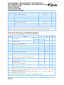
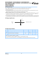
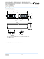
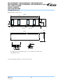
M2U1G64DS8HB1G / M2U51264DS88B1G / M2U25664DSH4B1G
M2Y1G64DS8HB1G / M2Y51264DS88B1G / M2Y25664DSH4B1G (Green)
1GB, 512MB and 256MB
PC3200 and PC2700
Unbuffered DDR DIMM
184 pin Unbuffered DDR DIMM
Based on DDR400/333 512M bit Die B device
Features
• 184 Dual In-Line Memory Module (DIMM)
• Unbuffered DDR DIMM based on 110nm 512M bit die B device
• Performance:
Speed Sort
DIMM
Latency
fCK
Clock Frequency
tCK
Clock Cycle
fDQ DQ Burst Frequency
• DRAM DLL aligns DQ and DQS transitions with clock transitions
• Address and control signals are fully synchronous to positive
clock edge
• Programmable Operation:
- DIMM
Latency: 2, 2.5 (6K); 2.5, 3 (5T)
- Burst Type: Sequential or Interleave
- Burst Length: 2, 4, 8
- Operation: Burst Read and Write
• Auto Refresh (CBR) and Self Refresh Modes
• Automatic and controlled precharge commands
• 7.8 µs Max. Average Periodic Refresh Interval
• Serial Presence Detect EEPROM
• Gold contacts on module PCB
PC2700 PC3200
6K
5T
Unit
2.5
3
166
200
6
5
ns
333
400
MHz
MHz
• Intended for 200 and 166 MHz applications
• Inputs and outputs are SSTL-2 compatible
• VDD = VDDQ = 2.5V ± 0.2V (6K); VDD = VDDQ = 2.6V ± 0.1V (5T)
• SDRAMs have 4 internal banks for concurrent operation
• Differential clock inputs
• Data is read or written on both clock edges
Description
M2U1G64DS8HB1G and M2Y1G64DS8HB1G are unbuffered 200-Pin Double Data Rate (DDR) Synchronous DRAM Unbuffered Dual In-Line
Memory Module (UDIMM) and are organized as two ranks of 128Mbx64 high-speed memory array using sixteen 64Mx8 DDR SDRAMs TSOP
packages. M2U51264DS88B1G and M2Y51264DS88B1G are unbuffered 200-Pin DDR Synchronous DRAM UDIMM and are organized as a
single rank of 64Mbx64 high-speed memory array using eight 64Mx8 DDR SDRAMs TSOP packages. M2U25664DSH4B1G and
M2Y25664DSH4B1G are unbuffered 200-Pin DDR Synchronous DRAM UDIMM and are organized as a single rank of 32Mbx64 high-speed
memory array using four 32Mx16 DDR SDRAMs TSOP packages.
Depending on the speed grade, these DIMMs are intended for use in applications operating up to 200 MHz clock speeds and achieves
high-speed data transfer rates of up to 400 MHz. Prior to any access operation, the device
latency and burst /length/operation type must be
programmed into the DIMM by address inputs and I/O inputs BA0 and BA1 using the mode register set cycle.
The DIMM uses a serial EEPROM and through the use of a standard IIC protocol the serial presence-detect implementation (SPD) can be
accessed. The first 128 bytes of the SPD data are programmed with the module characteristics as defined by JEDEC.
REV 1.2
June 2, 2006
1
.
M2U1G64DS8HB1G / M2U51264DS88B1G / M2U25664DSH4B1G
M2Y1G64DS8HB1G / M2Y51264DS88B1G / M2Y25664DSH4B1G (Green)
1GB, 512MB and 256MB
PC3200 and PC2700
Unbuffered DDR DIMM
Ordering Information
Non-Green Products
Part Number
Size
M2U1G64DS8HB1G-5T
128Mx64
M2U51264DS88B1G-5T
64Mx64
M2U25664DSH4B1G-5T
32Mx64
M2U51264DS88B1G-6K
64Mx64
M2U25664DSH4B1G-6K
32Mx64
Speed
DDR400
PC3200
Devices
3-3-3
200MHz (5ns @ CL = 3)
Power
Leads
2.6V
Gold
DDR333
PC2700
Devices
2.5-3-3
166MHz (6ns @ CL = 2.5)
2.5V
Green products
Part Number
Size
M2Y1G64DS8HB1G-5T
128Mx64
M2Y51264DS88B1G-5T
64Mx64
M2Y25664DSH4B1G-5T
32Mx64
M2Y51264DS88B1G-6K
64Mx64
M2Y25664DSH4B1G-6K
32Mx64
REV 1.2
June 2, 2006
Speed
DDR400
PC3200
Devices
3-3-3
200MHz (5ns @ CL = 3)
Power
Leads
2.6V
Gold
DDR333
PC2700
Devices
2.5-3-3
2
166MHz (6ns @ CL = 2.5)
2.5V
.
M2U1G64DS8HB1G / M2U51264DS88B1G / M2U25664DSH4B1G
M2Y1G64DS8HB1G / M2Y51264DS88B1G / M2Y25664DSH4B1G (Green)
1GB, 512MB and 256MB
PC3200 and PC2700
Unbuffered DDR DIMM
Pin Description
CK0, CK1, CK2,
,
,
Differential Clock Inputs.
DQ0-DQ63
Data input/output
Clock Enable
DQS0-DQS7
Bidirectional data strobes
Row Address Strobe
DM0-DM7
Input Data Mask
Column Address Strobe
VDD
Power
Supply voltage for DQs
CKE0, CKE1
Write Enable
VDDQ
,
Chip Selects
VSS
Ground
A0-A9, A11, A12
Address Inputs
NC
No Connect
A10/AP
Address Input/Auto-precharge
SCL
Serial Presence Detect Clock Input
BA0, BA1
SDRAM Bank Address Inputs
SDA
Serial Presence Detect Data input/output
VREF
Ref. Voltage for SSTL_2 inputs
SA0-2
Serial Presence Detect Address Inputs
VDDID
VDD Identification flag.
VDDSPD
Serial EEPROM positive power supply
Pinout
Pin
Front
Pin
Back
Pin
Front
Pin
Back
Pin
Front
Pin
1
VREF
93
VSS
32
A5
124
VSS
62
VDDQ
154
2
DQ0
94
DQ4
33
DQ24
125
A6
63
3
VSS
95
DQ5
34
VSS
126
DQ28
64
4
DQ1
96
VDDQ
35
DQ25
127
DQ29
65
5
DQS0
97
DM0
36
DQS3
128
VDDQ
6
DQ2
98
DQ6
37
A4
129
7
VDD
99
DQ7
38
VDD
8
DQ3
100
VSS
39
9
NC
101
NC
40
10
NC
102
NC
11
VSS
103
12
DQ8
13
14
Back
155
DQ45
DQ41
156
VDDQ
66
VSS
158
DM3
67
DQS5
159
DM5
130
A3
68
DQ42
160
VSS
DQ26
131
DQ30
69
DQ43
161
DQ46
DQ27
132
VSS
70
VDD
162
DQ47
41
A2
133
DQ31
71
NC
163
NC
NC
42
VSS
134
NC
72
DQ48
164
VDDQ
104
VDDQ
43
A1
135
NC
73
DQ49
165
DQ52
DQ9
105
DQ12
44
NC
136
VDDQ
74
VSS
166
DQ53
DQS1
106
DQ13
45
NC
137
CK0
75
167
NC
15
VDDQ
107
DM1
46
VDD
138
16
CK1
108
VDD
47
NC
139
17
157
NC
76
CK2
168
VDD
VSS
77
VDDQ
169
DM6
109
DQ14
48
A0
140
NC
78
DQS6
170
DQ54
18
VSS
110
DQ15
49
NC
141
A10/AP
79
DQ50
171
DQ55
19
DQ10
111
CKE1/NC
50
VSS
142
NC
80
DQ51
172
VDDQ
20
DQ11
112
VDDQ
51
NC
143
VDDQ
81
VSS
173
NC
21
CKE0
113
NC
52
BA1
144
NC
82
VDDID
174
DQ60
22
VDDQ
114
DQ20
83
DQ56
175
DQ61
23
DQ16
115
A12/NC
53
DQ32
145
VSS
84
DQ57
176
VSS
24
DQ17
116
VSS
54
VDDQ
146
DQ36
85
VDD
177
DM7
25
DQS2
117
DQ21
55
DQ33
147
DQ37
86
DQS7
178
DQ62
26
VSS
118
A11
56
DQS4
148
VDD
87
DQ58
179
DQ63
27
A9
119
DM2
57
DQ34
149
DM4
88
DQ59
180
VDDQ
28
DQ18
120
VDD
58
VSS
150
DQ38
89
VSS
181
SA0
29
A7
121
DQ22
59
BA0
151
DQ39
90
NC
182
SA1
30
VDDQ
122
A8
60
DQ35
152
VSS
91
SDA
183
SA2
31
DQ19
123
DQ23
61
DQ40
153
DQ44
92
SCL
184
VDDSPD
KEY
KEY
Note: All pin assignments are consistent for all 8-byte unbuffered versions.
REV 1.2
June 2, 2006
3
.
M2U1G64DS8HB1G / M2U51264DS88B1G / M2U25664DSH4B1G
M2Y1G64DS8HB1G / M2Y51264DS88B1G / M2Y25664DSH4B1G (Green)
1GB, 512MB and 256MB
PC3200 and PC2700
Unbuffered DDR DIMM
Input/Output Functional Description
Symbol
CK0, CK1, CK2,
,
,
CKE0, CKE1
,
,
,
Function
The system clock inputs. All address and command lines are sampled on the cross point of
the rising edge of CK and falling edge of CK. A Delay Locked Loop (DLL) circuit is driven
from the clock inputs and output timing for read operations is synchronized to the input
clock.
Activates the DDR SDRAM CK signal when high and deactivates the CK signal when low.
By deactivating the clocks, CKE low initiates the Power Down mode or the Self Refresh
mode.
Type
Polarity
(SSTL)
Cross
point
(SSTL)
Active
High
(SSTL)
Active
Low
Enables the associated DDR SDRAM command decoder when low and disables the
command decoder when high. When the command decoder is disabled, new commands are
ignored but previous operations continue. Physical Bank 0 is selected by S0; Bank 1 is
selected by S1.
(SSTL)
Active
Low
When sampled at the positive rising edge of the clock,
be executed by the SDRAM.
,
,
define the operation to
VREF
Supply
Reference voltage for SSTL-2 inputs
VDDQ
Supply
Isolated power supply for the DDR SDRAM output buffers to provide improved noise
immunity
BA0, BA1
(SSTL)
-
Selects which SDRAM bank is to be active.
A0 - A9
A10/AP
A11, A12
(SSTL)
-
During a Bank Activate command cycle, A0-A12 defines the row address (RA0-RA12) when
sampled at the rising clock edge.
During a Read or Write command cycle, A0-A9 defines the column address (CA0-CA9)
when sampled at the rising clock edge. In addition to the column address, AP is used to
invoke auto-precharge operation at the end of the Burst Read or Write cycle. If AP is high,
auto-precharge is selected and BA0/BA1 defines the bank to be precharged. If AP is low,
auto-precharge is disabled.
During a Precharge command cycle, AP is used in conjunction with BA0/BA1 to control
which bank(s) to precharge. If AP is high all 4 banks will be precharged regardless of the
state of BA0/BA1. If AP is low, then BA0/BA1 are used to define which bank to pre-charge.
DQ0 - DQ63
(SSTL)
-
Data and Check Bit input/output pins operate in the same manner as on conventional
DRAMs.
DQS0 - DQS7,
(SSTL)
Active
High
DM0 – DM8
Input
Active
High
VDD, VSS
Supply
Data strobes: Output with read data, input with write data. Edge aligned with read data,
centered on write data. Used to capture write data.
The data write masks, associated with one data byte. In Write mode, DM operates as a byte
mask by allowing input data to be written if it is low but blocks the write operation if it is high.
In Read mode, DM lines have no effect. DM8 is associated with check bits CB0-CB7, and is
not used on x64 modules.
Power and ground for the DDR SDRAM input buffers and core logic
SA0 – SA2
-
Address inputs. Connected to either VDD or VSS on the system board to configure the Serial
Presence Detect EEPROM address.
SDA
-
This bi-directional pin is used to transfer data into or out of the SPD EEPROM. A resistor
must be connected from the SDA bus line to V DD to act as a pull-up.
SCL
-
This signal is used to clock data into and out of the SPD EEPROM. A resistor may be
connected from the SCL bus time to V DD to act as a pull-up.
VDDSPD
REV 1.2
June 2, 2006
Supply
Serial EEPROM positive power supply.
4
.
M2U1G64DS8HB1G / M2U51264DS88B1G / M2U25664DSH4B1G
M2Y1G64DS8HB1G / M2Y51264DS88B1G / M2Y25664DSH4B1G (Green)
1GB, 512MB and 256MB
PC3200 and PC2700
Unbuffered DDR DIMM
Functional Block Diagram
2 Ranks, 16 devices, 64Mx8 DDR SDRAMs, 1GB
DQS0
DM0/DQS9
DQS4
DM4/DQS13
DM
I/O 7
I/O 6
I/O 1
I/O 0
I/O 5
I/O 4
I/O 3
I/O 2
DQ0
DQ1
DQ2
DQ3
DQ4
DQ5
DQ6
DQ7
DQS
D0
DM
I/O 0
I/O 1
I/O 6
I/O 7
I/O 2
I/O 3
I/O 4
I/O 5
DQS
DQ32
DQ33
DQ34
DQ35
DQ36
DQ37
DQ38
DQ39
D8
DQS1
DM1/DQS10
DQS
D4
DM
I/O 0
I/O 1
I/O 6
I/O 7
I/O 2
I/O 3
I/O 4
I/O 5
DQS
D12
DQS5
DM5/DQS14
DM
I/O 7
I/O 6
I/O 1
I/O 0
I/O 5
I/O 4
I/O 3
I/O 2
DQ8
DQ9
DQ10
DQ11
DQ12
DQ13
DQ14
DQ15
DQS
D1
DM
I/O 0
I/O 1
I/O 6
I/O 7
I/O 2
I/O 3
I/O 4
I/O 5
DQS
DQ40
DQ41
DQ42
DQ43
DQ44
DQ45
DQ46
DQ47
D9
DM
I/O 7
I/O 6
I/O 1
I/O 0
I/O 5
I/O 4
I/O 3
I/O 2
DQS
D5
DM
I/O 0
I/O 1
I/O 6
I/O 7
I/O 2
I/O 3
I/O 4
I/O 5
DQS
D13
DQS6
DM6/DQS15
DQS2
DM2/DQS11
DM
I/O 7
I/O 6
I/O 1
I/O 0
I/O 5
I/O 4
I/O 3
I/O 2
DQ16
DQ17
DQ18
DQ19
DQ20
DQ21
DQ22
DQ23
DQS
D2
DM
I/O 0
I/O 1
I/O 6
I/O 7
I/O 2
I/O 3
I/O 4
I/O 5
DQS
DQ48
DQ49
DQ50
DQ51
DQ52
DQ53
DQ54
DQ55
D10
DM
I/O 7
I/O 6
I/O 1
I/O 0
I/O 5
I/O 4
I/O 3
I/O 2
DQS
D6
DM
I/O 0
I/O 1
I/O 6
I/O 7
I/O 2
I/O 3
I/O 4
I/O 5
DQS
D14
DQS7
DM7/DQS16
DQS3
DM3/DQS12
DM
I/O 7
I/O 6
I/O 1
I/O 0
I/O 5
I/O 4
I/O 3
I/O 2
DQ24
DQ25
DQ26
DQ27
DQ28
DQ29
DQ30
DQ31
BA0-BA1
DQS
D3
DM
I/O 0
I/O 1
I/O 6
I/O 7
I/O 2
I/O 3
I/O 4
I/O 5
BA0-BA1 : SDRAMs D0-D15
A0-A13
A0-A13 : SDRAMs D0-D15
: SDRAMs D0-D15
: SDRAMs D0-D15
CKE0
CKE : SDRAMs D0-D7
CKE1
CKE : SDRAMs D8-D15
: SDRAMs D0-D15
Notes :
1.
2.
3.
4.
DM
I/O 7
I/O 6
I/O 1
I/O 0
I/O 5
I/O 4
I/O 3
I/O 2
DQS
DQ56
DQ57
DQ58
DQ59
DQ60
DQ61
DQ62
DQ63
D11
VDDSPD
VDD/VDDQ
VREF
VSS
VDDID
June 2, 2006
SPD
D0-D15
D0-D15
D0-D15
Strap: see Note 4
DQS
D7
DM
I/O 0
I/O 1
I/O 6
I/O 7
I/O 2
I/O 3
I/O 4
I/O 5
DQS
D15
* Clock Wiring
Clock Input
SDRAMs
*CK0/
4 SDRAMs
*CK1/
6 SDRAMs
*CK2/
6 SDRAMs
* Wire per Clock Loading Table/
Wiring Diagrams
Serial PD
SCL
WP
DQ-to-I/O wiring is shown as recommended but may be changed.
DQ/DQS/DM/CKE/S relationships must be maintained as shown.
DQ, DQS, DM/DQS resistors: 22 Ohms.
VDDID strap connections (for memory device VDD, VDDQ):
STRAP OUT (OPEN): VDD = VDDQ
STRAP IN (VSS): VDD is not equal to VDDQ.
REV 1.2
DM
I/O 7
I/O 6
I/O 1
I/O 0
I/O 5
I/O 4
I/O 3
I/O 2
A0
A1
A2
SA0
SA1
SA2
5
SDA
.
M2U1G64DS8HB1G / M2U51264DS88B1G / M2U25664DSH4B1G
M2Y1G64DS8HB1G / M2Y51264DS88B1G / M2Y25664DSH4B1G (Green)
1GB, 512MB and 256MB
PC3200 and PC2700
Unbuffered DDR DIMM
Functional Block Diagram
1 Rank, 8 devices, 64Mx8 DDR SDRAMs, 512MB
DQS4
DM4/DQS13
DQS0
DM0/DQS9
DQ0
DQ1
DQ2
DQ3
DQ4
DQ5
DQ6
DQ7
DM
I/O 7
I/O 6
I/O 1
I/O 0
I/O 5
I/O 4
I/O 3
I/O 2
DQS
DQ32
DQ33
DQ34
DQ35
DQ36
DQ37
DQ38
DQ39
D0
DM
I/O 7
I/O 6
I/O 1
I/O 0
I/O 5
I/O 4
I/O 3
I/O 2
DQS
DQ40
DQ41
DQ42
DQ43
DQ44
DQ45
DQ46
DQ47
D1
DQS2
DM2/DQS11
DQ16
DQ17
DQ18
DQ19
DQ20
DQ21
DQ22
DQ23
D4
DM
I/O 7
I/O 6
I/O 1
I/O 0
I/O 5
I/O 4
I/O 3
I/O 2
DQS
D5
DQS6
DM6/DQS15
DM
I/O 7
I/O 6
I/O 1
I/O 0
I/O 5
I/O 4
I/O 3
I/O 2
DQS
DQ48
DQ49
DQ50
DQ51
DQ52
DQ53
DQ54
DQ55
D2
DQS3
DM3/DQS12
DQ24
DQ25
DQ26
DQ27
DQ28
DQ29
DQ30
DQ31
DQS
DQS5
DM5/DQS14
DQS1
DM1/DQS10
DQ8
DQ9
DQ10
DQ11
DQ12
DQ13
DQ14
DQ15
DM
I/O 7
I/O 6
I/O 1
I/O 0
I/O 5
I/O 4
I/O 3
I/O 2
DM
I/O 7
I/O 6
I/O 1
I/O 0
I/O 5
I/O 4
I/O 3
I/O 2
DQS
D6
DQS7
DM7/DQS16
DM
I/O 7
I/O 6
I/O 1
I/O 0
I/O 5
I/O 4
I/O 3
I/O 2
BA0-BA1
DQS
DQ56
DQ57
DQ58
DQ59
DQ60
DQ61
DQ62
DQ63
D3
BA0-BA1 : SDRAMs D0-D7
A0-A13
DQS
D7
* Clock Wiring
Clock Input
SDRAMs
*CK0/
2 SDRAMs
*CK1/
3 SDRAMs
*CK2/
3 SDRAMs
A0-A13 : SDRAMs D0-D7
: SDRAMs D0-D7
: SDRAMs D0-D7
CKE0
DM
I/O 7
I/O 6
I/O 1
I/O 0
I/O 5
I/O 4
I/O 3
I/O 2
* Wire per Clock Loading Table/
Wiring Diagrams
CKE : SDRAMs D0-D7
: SDRAMs D0-D7
VDDSPD
VDD/VDDQ
VREF
VSS
VDDID
Serial PD
SCL
WP
Notes :
1.
2.
3.
4.
REV 1.2
June 2, 2006
A0
A1
A2
SA0
SA1
SA2
SDA
SPD
D0-D7
D0-D7
D0-D7
Strap: see Note 4
DQ-to-I/O wiring is shown as recommended but may be changed.
DQ/DQS/DM/CKE/S relationships must be maintained as shown.
DQ, DQS, DM/DQS resistors: 22 Ohms.
VDDID strap connections (for memory device VDD, VDDQ):
STRAP OUT (OPEN): V DD = VDDQ
STRAP IN (V SS): VDD is not equal to VDDQ.
6
.
M2U1G64DS8HB1G / M2U51264DS88B1G / M2U25664DSH4B1G
M2Y1G64DS8HB1G / M2Y51264DS88B1G / M2Y25664DSH4B1G (Green)
1GB, 512MB and 256MB
PC3200 and PC2700
Unbuffered DDR DIMM
Functional Block Diagram
1 Rank, 4 devices, 32Mx16 DDR SDRAMs, 256MB
DQS1
DM1/DQS10
DQ8
DQ9
DQ10
DQ11
DQ12
DQ13
DQ14
DQ15
LDQS
DQS0
DM0/DQS9
DQ0
DQ1
DQ2
DQ3
DQ4
DQ5
DQ6
DQ7
UDQS
LDM
I/O 6
I/O 4
I/O 1
I/O 3
I/O 2
I/O 0
I/O 5
I/O 7
D0
UDM
I/O 8
I/O 10
I/O 15
I/O 13
I/O 12
I/O 14
I/O 11
I/O 9
DQS3
DM3/DQS12
DQ24
DQ25
DQ26
DQ27
DQ28
DQ29
DQ30
DQ31
LDQS
DQS2
DM2/DQS11
DQ16
DQ17
DQ18
DQ19
DQ20
DQ21
DQ22
DQ23
UDQS
LDM
I/O 6
I/O 4
I/O 1
I/O 3
I/O 2
I/O 0
I/O 5
I/O 7
D1
UDM
I/O 8
I/O 10
I/O 15
I/O 13
I/O 12
I/O 14
I/O 11
I/O 9
BA0-BA1
DQS5
DM5/DQS14
DQ40
DQ41
DQ42
DQ43
DQ44
DQ45
DQ46
DQ47
LDQS
DQS4
DM4/DQS13
DQ32
DQ33
DQ34
DQ35
DQ36
DQ37
DQ38
DQ39
UDQS
LDQS
DQS6
DM6/DQS15
DQ48
DQ49
DQ50
DQ51
DQ52
DQ53
DQ54
DQ55
UDQS
LDM
I/O 6
I/O 4
I/O 1
I/O 3
I/O 2
I/O 0
I/O 5
I/O 7
D3
UDM
I/O 8
I/O 10
I/O 15
I/O 13
I/O 12
I/O 14
I/O 11
I/O 9
* Clock Wiring
Clock Input
SDRAMs
*CK0/
NC
*CK1/
2 SDRAMs
*CK2/
2 SDRAMs
A0-A13 : SDRAMs D0-D3
: SDRAMs D0-D3
: SDRAMs D0-D3
CKE0
D2
UDM
I/O 8
I/O 10
I/O 15
I/O 13
I/O 12
I/O 14
I/O 11
I/O 9
DQS7
DM7/DQS16
DQ56
DQ57
DQ58
DQ59
DQ60
DQ61
DQ62
DQ63
BA0-BA1 : SDRAMs D0-D3
A0-A13
LDM
I/O 6
I/O 4
I/O 1
I/O 3
I/O 2
I/O 0
I/O 5
I/O 7
* Wire per Clock Loading Table/
Wiring Diagrams
CKE : SDRAMs D0-D3
: SDRAMs D0-D3
VDDSPD
VDD/VDDQ
VREF
VSS
VDDID
Serial PD
SCL
WP
Notes :
1.
2.
3.
4.
A0
A1
A2
SA0
SA1
SA2
SDA
SPD
D0-D3
D0-D3
D0-D3
Strap: see Note 4
DQ-to-I/O wiring is shown as recommended but may be changed.
DQ/DQS/DM/CKE/S relationships must be maintained as shown.
DQ, DQS, DM/DQS resistors: 22 Ohms.
VDDID strap connections (for memory device VDD, VDDQ):
STRAP OUT (OPEN): VDD = VDDQ
STRAP IN (VSS): VDD is not equal to VDDQ.
REV 1.2
June 2, 2006
7
.
M2U1G64DS8HB1G / M2U51264DS88B1G / M2U25664DSH4B1G
M2Y1G64DS8HB1G / M2Y51264DS88B1G / M2Y25664DSH4B1G (Green)
1GB, 512MB and 256MB
PC3200 and PC2700
Unbuffered DDR DIMM
Serial Presence Detect
SPD Values for 1GB
Byte
SPD Entry Value
Description
0
1
2
3
4
5
6.
7
8
9
10
11
12
13
14
15
16
17
18
19
20
21
22
23
24
25
26
27
28
29
30
31
32
33
34
35
36-40
41
42
Number of Serial PD Bytes Written during Production
Total Number of Bytes in Serial PD device
Fundamental Memory Type
Number of Row Addresses on Assembly
Number of Column Addresses on Assembly
Number of DIMM Bank
Data Width of Assembly
Data Width of Assembly (cont’)
Voltage Interface Level of this Assembly
DDR SDRAM Device Cycle Time at CL=3
DDR SDRAM Device Access Time from Clock at CL=3
DIMM Configuration Type
Refresh Rate/Type
Primary DDR SDRAM Width
Error Checking DDR SDRAM Device Width
DDR SDRAM Device Attr: Min Clk Delay, Random Col Access
DDR SDRAM Device Attributes: Burst Length Supported
DDR SDRAM Device Attributes: Number of Device Banks
DDR SDRAM Device Attributes: CAS Latencies Supported
DDR SDRAM Device Attributes: CS Latency
DDR SDRAM Device Attributes: WE Latency
DDR SDRAM Device Attributes:
DDR SDRAM Device Attributes: General
Minimum Clock Cycle at CL=2.5
Maximum Data Access Time (tAC) from Clock at CL=2.5
Minimum Clock Cycle Time at CL=2
Maximum Data Access Time (tAC) from Clock at CL=2
Minimum Row Precharge Time (tRP)
Minimum Row Active to Row Active delay (tRRD)
Minimum RAS to CAS delay (tRCD)
Minimum RAS Pulse Width (tRAS)
Module Bank Density
Address and Command Setup Time Before Clock
Address and Command Hold Time After Clock
Data Input Setup Time Before Clock
Data Input Hold Time After Clock
Reserved
Minimum Active/Auto-Refresh Time (tRC)
SDRAM Device Minimum Auto-Refresh to Active/Auto Refresh
Command Period (tRFC)
43
SDRAM Device Maximum Cycle Time (tCK max)
44
SDRAM Device Maximum DQS-DQ Skew Time (tDQSQ)
45
SDRAM Device Maximum Read Data Hold Skew Factor (tQHS)
46
Superset Information (may be used in future)
47
SDRAM device Attributes – DDR SDRAM DIMM Height
48-61 Superset Information (may be used in future)
62
SPD Revision
63
Checksum Data
64-71 Manufacturer’s JEDED ID Code
72-255 Reserved
REV 1.2
June 2, 2006
8
DDR400
-5T
DDR333
-6K
5ns
0.65ns
6ns
0.7ns
128
256
DDR SDRAM
13
11
2
X64
X64
SSTL 2.5V
Non-Parity
SR/1x(7.8us), Self Refresh Flag
X8
N/A
1 Clock
2,4,8
4
2.5/3
2/25
0
1
Differential Clock
+/-0.2V Voltage Tolerance
6.0ns
7.5ns
0.7ns
0.75ns
N/A
N/A
15ns
18ns
10ns
12ns
15ns
18ns
40ns
42ns
512MB
0.6ns
0.75ns
0.6ns
0.75ns
0.4ns
0.45ns
0.4ns
0.45ns
Undefined
55ns
60ns
70ns
0.4
0.5
72ns
12
0.45
0.55
Undefined
31.75mm
Undefined
1.0
Check sum
0B Hex bank 3
Undefined
Serial PD Data Entry
(Hexadecimal)
DDR400
DDR333
-5T
-6K
80
08
07
0D
0B
02
40
00
04
50
60
65
70
00
82
08
00
01
0E
04
18
0C
01
02
20
C0
60
75
70
75
00
00
3C
48
28
30
3C
48
28
2A
80
60
75
60
75
40
45
40
45
00
37
3C
46
28
50
48
30
00
01
00
10
2D
55
C8
58
7F7F7F0B00000000
--
.
M2U1G64DS8HB1G / M2U51264DS88B1G / M2U25664DSH4B1G
M2Y1G64DS8HB1G / M2Y51264DS88B1G / M2Y25664DSH4B1G (Green)
1GB, 512MB and 256MB
PC3200 and PC2700
Unbuffered DDR DIMM
SPD Values for 512MB
Byte
SPD Entry Value
Description
0
1
2
3
4
5
6.
7
8
9
10
11
12
13
14
15
16
17
18
19
20
21
22
23
24
25
26
27
28
Number of Serial PD Bytes Written during Production
Total Number of Bytes in Serial PD device
Fundamental Memory Type
Number of Row Addresses on Assembly
Number of Column Addresses on Assembly
Number of DIMM Bank
Data Width of Assembly
Data Width of Assembly (cont’)
Voltage Interface Level of this Assembly
DDR SDRAM Device Cycle Time at CL=3
DDR SDRAM Device Access Time from Clock at CL=3
DIMM Configuration Type
Refresh Rate/Type
Primary DDR SDRAM Width
Error Checking DDR SDRAM Device Width
DDR SDRAM Device Attr: Min Clk Delay, Random Col Access
DDR SDRAM Device Attributes: Burst Length Supported
DDR SDRAM Device Attributes: Number of Device Banks
DDR SDRAM Device Attributes: CAS Latencies Supported
DDR SDRAM Device Attributes: CS Latency
DDR SDRAM Device Attributes: WE Latency
DDR SDRAM Device Attributes:
DDR SDRAM Device Attributes: General
Minimum Clock Cycle at CL=2.5
Maximum Data Access Time (tAC) from Clock at CL=2.5
Minimum Clock Cycle Time at CL=2
Maximum Data Access Time (tAC) from Clock at CL=2
Minimum Row Precharge Time (tRP)
Minimum Row Active to Row Active delay (tRRD)
29
Minimum RAS to CAS delay (tRCD)
30
31
32
33
34
35
36-40
41
42
Minimum RAS Pulse Width (tRAS)
Module Bank Density
Address and Command Setup Time Before Clock
Address and Command Hold Time After Clock
Data Input Setup Time Before Clock
Data Input Hold Time After Clock
Reserved
Minimum Active/Auto-Refresh Time (tRC)
SDRAM Device Minimum Auto-Refresh to Active/Auto Refresh
Command Period (tRFC)
43
SDRAM Device Maximum Cycle Time (tCK max)
44
SDRAM Device Maximum DQS-DQ Skew Time (tDQSQ)
45
SDRAM Device Maximum Read Data Hold Skew Factor (tQHS)
46
Superset Information (may be used in future)
47
SDRAM device Attributes – DDR SDRAM DIMM Height
48-61 Superset Information (may be used in future)
62
SPD Revision
63
Checksum Data
64-71 Manufacturer’s JEDED ID Code
72-255 Reserved
REV 1.2
June 2, 2006
9
DDR400
-5T
DDR333
-6K
5ns
0.65ns
6ns
0.7ns
128
256
DDR SDRAM
13
11
1
X64
X64
SSTL 2.5V
Non-Parity
SR/1x(7.8us), Self Refresh Flag
X8
N/A
1 Clock
2,4,8
4
2.5/3
2/25
0
1
Differential Clock
+/-0.2V Voltage Tolerance
6.0ns
7.5ns
0.7ns
0.75ns
N/A
N/A
15ns
18ns
10ns
12ns
15ns
18ns
40ns
42ns
512MB
0.6ns
0.75ns
0.6ns
0.75ns
0.4ns
0.45ns
0.4ns
0.45ns
Undefined
55ns
60ns
70ns
72ns
0.4
0.5
12
0.45
0.55
Undefined
31.75mm
Undefined
1.0
Check sum
0B Hex bank 3
Undefined
Serial PD Data Entry
(Hexadecimal)
DDR400
DDR333
-5T
-6K
80
08
07
0D
0B
01
40
00
04
50
60
65
70
00
82
08
00
01
0E
04
18
0C
01
02
20
C0
60
75
70
75
00
00
3C
48
28
30
3C
28
60
60
40
40
37
46
28
50
48
80
00
30
00
01
00
10
2A
75
75
45
45
3C
48
2D
55
C7
57
7F7F7F0B00000000
--
.
M2U1G64DS8HB1G / M2U51264DS88B1G / M2U25664DSH4B1G
M2Y1G64DS8HB1G / M2Y51264DS88B1G / M2Y25664DSH4B1G (Green)
1GB, 512MB and 256MB
PC3200 and PC2700
Unbuffered DDR DIMM
SPD Values for 256MB
Byte
SPD Entry Value
Description
0
1
2
3
4
5
6.
7
8
9
10
11
12
13
14
15
16
17
18
19
20
21
22
23
24
25
26
27
28
29
30
31
32
33
34
35
36-40
41
42
Number of Serial PD Bytes Written during Production
Total Number of Bytes in Serial PD device
Fundamental Memory Type
Number of Row Addresses on Assembly
Number of Column Addresses on Assembly
Number of DIMM Bank
Data Width of Assembly
Data Width of Assembly (cont’)
Voltage Interface Level of this Assembly
DDR SDRAM Device Cycle Time at CL=3
DDR SDRAM Device Access Time from Clock at CL=3
DIMM Configuration Type
Refresh Rate/Type
Primary DDR SDRAM Width
Error Checking DDR SDRAM Device Width
DDR SDRAM Device Attr: Min Clk Delay, Random Col Access
DDR SDRAM Device Attributes: Burst Length Supported
DDR SDRAM Device Attributes: Number of Device Banks
DDR SDRAM Device Attributes: CAS Latencies Supported
DDR SDRAM Device Attributes: CS Latency
DDR SDRAM Device Attributes: WE Latency
DDR SDRAM Device Attributes:
DDR SDRAM Device Attributes: General
Minimum Clock Cycle at CL=2.5
Maximum Data Access Time (tAC) from Clock at CL=2.5
Minimum Clock Cycle Time at CL=2
Maximum Data Access Time (tAC) from Clock at CL=2
Minimum Row Precharge Time (tRP)
Minimum Row Active to Row Active delay (tRRD)
Minimum RAS to CAS delay (tRCD)
Minimum RAS Pulse Width (tRAS)
Module Bank Density
Address and Command Setup Time Before Clock
Address and Command Hold Time After Clock
Data Input Setup Time Before Clock
Data Input Hold Time After Clock
Reserved
Minimum Active/Auto-Refresh Time (tRC)
SDRAM Device Minimum Auto-Refresh to Active/Auto Refresh
Command Period (tRFC)
43
SDRAM Device Maximum Cycle Time (tCK max)
44
SDRAM Device Maximum DQS-DQ Skew Time (tDQSQ)
45
SDRAM Device Maximum Read Data Hold Skew Factor (tQHS)
46
Superset Information (may be used in future)
47
SDRAM device Attributes – DDR SDRAM DIMM Height
48-61 Superset Information (may be used in future)
62
SPD Revision
63
Checksum Data
64-71 Manufacturer’s JEDED ID Code
72-255 Reserved
REV 1.2
June 2, 2006
10
DDR400
-5T
DDR333
-6K
5ns
0.6ns
6ns
0.7ns
128
256
DDR SDRAM
13
10
1
X64
X64
SSTL 2.5V
Non-Parity
SR/1x(7.8us), Self Refresh Flag
X16
N/A
1 Clock
2,4,8
4
2.5/3
2/2.5
0
1
Differential Clock
+/-0.2V Voltage Tolerance
6.0ns
7.5ns
0.7ns
0.75ns
N/A
N/A
15ns
18ns
10ns
12ns
15ns
18ns
40ns
42ns
256MB
0.6ns
0.75ns
0.6ns
0.75ns
0.4ns
0.45ns
0.4ns
0.45ns
Undefined
55ns
60ns
70ns
72ns
0.4
0.5
12
Undefined
31.75mm
Undefined
Initial
0.45
0.55
0B Hex bank 3
Undefined
Serial PD Data Entry
(Hexadecimal)
DDR400
DDR333
-5T
-6K
80
08
07
0D
0A
01
40
00
04
50
60
65
70
00
82
10
00
01
0E
04
18
0C
01
02
20
C0
60
75
70
75
00
00
3C
48
28
30
3C
48
28
2A
40
60
75
60
75
40
45
40
45
00
37
3C
46
48
28
50
30
00
01
00
10
2D
55
8E
1E
7F7F7F0B00000000
--
.
M2U1G64DS8HB1G / M2U51264DS88B1G / M2U25664DSH4B1G
M2Y1G64DS8HB1G / M2Y51264DS88B1G / M2Y25664DSH4B1G (Green)
1GB, 512MB and 256MB
PC3200 and PC2700
Unbuffered DDR DIMM
Absolute Maximum Ratings
Symbol
VIN, VOUT
Parameter
Voltage on I/O pins relative to VSS
Rating
Units
-0.5 to VDDQ +0.5
V
V
VIN
Voltage on Input relative to VSS
-0.5 to +3.6
VDD
Voltage on VDD supply relative to VSS
-0.5 to +3.6
V
VDDQ
Voltage on VDDQ supply relative to VSS
-0.5 to +3.6
V
0 to +70
°C
-55 to +150
°C
W
mA
TA
TSTG
Operating Temperature (Ambient)
Storage Temperature (Plastic)
PD
Power Dissipation (per device component)
1
IOUT
Short Circuit Output Current
50
Note: Stresses greater than those listed under “Absolute Maximum Ratings” may cause permanent damage to the device. This is stress
rating only, and functional operation of the device at these or any other conditions above those indicated in the operational sections of this
specification is not implied. Exposure to absolute maximum rating conditions for extended periods may affect reliability.
DC Electrical Characteristics and Operating Conditions
TA= 0°C ~ 70°C; VDDQ= VDD= 2.5V±0.2V(6K); TA= 0°C ~ 70°C; VDDQ= VDD= 2.6V±0.1V(5T)
Symbol
Parameter
VDD
Supply Voltage
VDDQ
I/O Supply Voltage
VSS, VSSQ
Min
2.3
5T
2.5
6K
2.3
5T
2.5
Units Notes
2.7
V
1
2.7
V
1
0
0
V
VREF
I/O Reference Voltage
0.49 x VDDQ
0.51 x VDDQ
V
1, 2
VTT
I/O Termination Voltage (System)
VREF – 0.04
VREF + 0.04
V
1, 3
VIH (DC)
Input High (Logic1) Voltage
VREF + 0.15
VDDQ + 0.3
V
1
VIL (DC)
Input Low (Logic0) Voltage
-0.3
VREF - 0.15
V
1
VIN (DC)
Input Voltage Level, CK and
VID (DC)
Input Differential Voltage, CK and
II
IOZ
IOH
IOL
Supply Voltage, I/O Supply Voltage
6K
Max
Inputs
Inputs
Input Leakage Current
Any input 0V ≤ VIN ≤ VDD; (All other pins not under test = 0V)
Output Leakage Current
(DQs are disabled; 0V ≤ Vout ≤ VDDQ
Output High Current
(VOUT = VDDQ -0.373V, min VREF, min VTT)
Output Low Current
(VOUT = 0.373, max VREF, max VTT)
-0.3
VDDQ + 0.3
V
1
0.30
VDDQ + 0.6
V
1, 4
-10
10
µA
1
-10
10
µA
1
-16.8
-
mA
1
16.8
-
mA
1
1. Inputs are not recognized as valid until VREF stabilizes.
2. VREF is expected to be equal to 0.5 VDDQ of the transmitting device, and to track variations in the DC level of the same. Peak-to-peak
noise on VREF may not exceed 2% of the DC value.
3. VTT is not applied directly to the DIMM. VTT is a system supply for signal termination resistors, is expected to be set equal to VREF,
and must track variations in the DC level of VREF.
4. VID is the magnitude of the difference between the input level on CK and the input level on
.
REV 1.2
June 2, 2006
11
.
M2U1G64DS8HB1G / M2U51264DS88B1G / M2U25664DSH4B1G
M2Y1G64DS8HB1G / M2Y51264DS88B1G / M2Y25664DSH4B1G (Green)
1GB, 512MB and 256MB
PC3200 and PC2700
Unbuffered DDR DIMM
AC Characteristics
Notes 1-5 apply to the following Tables; Electrical Characteristics and DC Operating Conditions, AC Operating
Conditions, Operating, Standby, and Refresh Currents, and Electrical Characteristics and AC Timing.)
1. All voltages referenced to VSS.
2. Tests for AC timing, IDD, and electrical, AC and DC characteristics, may be conducted at nominal reference/supply voltage levels, but the
related specifications and device operation are guaranteed for the full voltage range specified.
3. Outputs measured with equivalent load. Refer to the AC Output Load Circuit below.
4. AC timing and IDD tests may use a VIL to VIH swing of up to 1.5V in the test environment, but input timing is still referenced to VREF (or to the
crossing point for CK,
), and parameter specifications are guaranteed for the specified AC input levels under normal use conditions. The
minimum slew rate for the input signals is 1V/ns in the range between VIL (AC) and VIH (AC) unless otherwise specified.
5. The AC and DC input level specifications are as defined in the SSTL_2 Standard (i.e. the receiver effectively switches as a result of the signal
crossing the AC input level, and remains in that state as long as the signal does not ring back above (below) the DC input LOW (HIGH) level.
AC Output Load Circuits
VTT
50 ohms
Output
Timing Reference Point
VOUT
30 pF
AC Operating Conditions
Symbol
Parameter/Condition
VIH (AC)
Input High (Logic 1) Voltage.
VIL (AC)
Input Low (Logic 0) Voltage.
VID (AC)
Input Differential Voltage, CK and
VIX (AC)
Input Differential Pair Cross Point Voltage, CK and
Min
Max
Unit
Notes
V
1, 2
VREF - 0.31
V
1, 2
0.62
VDDQ + 0.6
V
1, 2, 3
(0.5* VDDQ) - 0.2
(0.5* VDDQ) + 0.2
V
1, 2, 4
VREF + 0.31
Inputs
Inputs
1. Input slew rate = 1V/ ns.
2. Inputs are not recognized as valid until VREF stabilizes.
3. VID is the magnitude of the difference between the input level on CK and the input level on
.
4. The value of VIX is expected to equal 0.5*VDDQ of the transmitting device and must track variations in the DC level of the same.
REV 1.2
June 2, 2006
12
.
M2U1G64DS8HB1G / M2U51264DS88B1G / M2U25664DSH4B1G
M2Y1G64DS8HB1G / M2Y51264DS88B1G / M2Y25664DSH4B1G (Green)
1GB, 512MB and 256MB
PC3200 and PC2700
Unbuffered DDR DIMM
Operating, Standby, and Refresh Currents
TA = 0 °C ~ 70 °C; VDDQ= VDD= 2.5V ± 0.2V (6K); VDDQ= VDD= 2.6V ± 0.1V (5T)
Symbol
Parameter/Condition
Notes
IDD0
Operating Current: one bank; active/precharge; tRC = tRC (MIN); tCK = tCK (MIN); DQ, DM, and DQS inputs changing twice per
clock cycle; address and control inputs changing once per clock cycle
1,2
IDD1
Operating Current: one bank; active/read/precharge; Burst = 2; tRC = tRC (MIN); CL=2.5; tCK = tCK (MIN); IOUT = 0mA; address and
control inputs changing once per clock cycle
1,2
Precharge Power-Down Standby Current: all banks idle; power-down mode; CKE ≤ VIL (MAX); tCK = tCK (MIN)
1,2
IDD2P
Idle Standby Current: CS ≥ VIH (MIN); all banks idle; CKE ≥ VIH (MIN); tCK = tCK (MIN); address and control inputs changing once
IDD2N
per clock cycle
1,2
IDD3P
Active Power-Down Standby Current: one bank active; power-down mode; CKE ≤ VIL (MAX); tCK = tCK (MIN)
1,2
IDD3N
Active Standby Current: one bank; active/precharge; CS ≥ VIH (MIN); CKE ≥ VIH (MIN); tRC = tRAS (MAX); tCK = tCK (MIN); DQ, DM, and
DQS inputs changing twice per clock cycle; address and control inputs changing once per clock cycle
1,2
IDD4R
Operating Current: one bank; Burst = 2; reads; continuous burst; address and control inputs changing once per clock cycle;
DQ and DQS outputs changing twice per clock cycle; CL = 2.5; tCK = tCK (MIN); IOUT = 0mA
1,2
IDD4W
Operating Current: one bank; Burst = 2; writes; continuous burst; address and control inputs changing once per clock cycle;
DQ and DQS inputs changing twice per clock cycle; CL=2.5; tCK = tCK (MIN)
1,2
IDD5
Auto-Refresh Current: tRC = tRFC (MIN)
IDD6
Self-Refresh Current: CKE ≤ 0.2V
1,2,3
1,2
IDD7
Operating Current: four bank; four bank interleaving with BL = 4, address and control inputs randomly changing; 50% of
data changing at every transfer; tRC = tRC (min); IOUT = 0mA.
1,2
1. IDD specifications are tested after the device is properly initialized.
2. Input slew rate = 1V/ ns.
3. Current at 7.8 s is time averaged value of IDD5 at tRFC (MIN) and IDD2P over 7.8 s.
All IDD current values are calculated from device level.
1GB
Symbol
PC3200
512MB
256MB
PC2700
PC3200
PC2700
PC3200
PC2700
(mA)
(5T)
(6K)
(5T)
(6K)
(5T)
(6K)
IDD0
1651
1575
801
765
400
382
mA
IDD1
1702
1634
826
794
413
397
mA
IDD2P
60
57
28
27
14
13
mA
IDD2N
476
420
224
198
112
99
mA
IDD3P
211
195
99
92
50
46
mA
IDD3N
852
767
401
361
200
180
mA
IDD4R
2010
1705
980
830
490
415
mA
IDD4W
2195
1910
1072
932
536
466
mA
IDD5
3225
3125
1587
1540
794
770
mA
IDD6
37
38
17
18
9
9
mA
IDD7
5863
4961
2907
2458
1453
1229
mA
REV 1.2
June 2, 2006
13
.
M2U1G64DS8HB1G / M2U51264DS88B1G / M2U25664DSH4B1G
M2Y1G64DS8HB1G / M2Y51264DS88B1G / M2Y25664DSH4B1G (Green)
1GB, 512MB and 256MB
PC3200 and PC2700
Unbuffered DDR DIMM
Package Dimensions
1GB, Non-ECC, 16 TSOP devices
FRONT
133.35
5.250
17.80
0.700
31.75
1.250
10.0
0.394
(2x)4.00
0.157
128.93
5.076
Detail A
2.30
0.91
θ 2.50
0.098
Detail B
Side
BACK
4.00
0.157 MAX
1.27+/- 0.10
0.050 +/- 0.004
Detail B
3.80
0.150
4.00
0.157
Detail A
6.35
0.250
1.80
0.071
1.00 Width
0.039
1.27 Pitch
0.05
Note: All dimensions are typical with tolerances of +/- 0.15 (0.006) unless otherwise stated.
Units: Millimeters (Inches)
Note: Device packaging not drawn to scale. Placed only for references
REV 1.2
June 2, 2006
14
.
M2U1G64DS8HB1G / M2U51264DS88B1G / M2U25664DSH4B1G
M2Y1G64DS8HB1G / M2Y51264DS88B1G / M2Y25664DSH4B1G (Green)
1GB, 512MB and 256MB
PC3200 and PC2700
Unbuffered DDR DIMM
Package Dimensions
512MB, Non-ECC, 8 TSOP devices
FRONT
133.35
5.250
17.80
0.700
31.75
1.250
10.0
0.394
(2x)4.00
0.157
128.93
5.076
Detail A
2.30
0.91
θ 2.50
0.098
Detail B
Side
BACK
1.27+/- 0.10
0.050 +/- 0.004
Detail B
3.80
0.150
4.00
0.157
Detail A
3.18
0.125 MAX
6.35
0.250
1.80
0.071
1.00 Width
0.039
1.27 Pitch
0.05
Note: All dimensions are typical with tolerances of +/- 0.15 (0.006) unless otherwise stated.
Units: Millimeters (Inches)
Note: Device packaging not drawn to scale. Placed only for references
REV 1.2
June 2, 2006
15
.
M2U1G64DS8HB1G / M2U51264DS88B1G / M2U25664DSH4B1G
M2Y1G64DS8HB1G / M2Y51264DS88B1G / M2Y25664DSH4B1G (Green)
1GB, 512MB and 256MB
PC3200 and PC2700
Unbuffered DDR DIMM
Package Dimensions
256MB, Non-ECC, 4 TSOP devices
FRONT
133.35
5.250
17.80
0.700
31.75
1.250
10.00
0.394
(2x)4.00
0.157
128.93
5.076
Detail A
2.30
0.91
θ 2.50
0.098
Detail B
Side
BACK
1.27+/- 0.10
0.050 +/- 0.004
Detail B
3.80
0.150
4.00
0.157
Detail A
3.18
0.125 MAX
6.35
0.250
1.80
0.071
1.00 Width
0.039
1.27 Pitch
0.05
Note: All dimensions are typical with tolerances of +/- 0.15 (0.006) unless otherwise stated.
Units: Millimeters (Inches)
Note: Device packaging not drawn to scale. Placed only for references
REV 1.2
June 2, 2006
16
.
M2U1G64DS8HB1G / M2U51264DS88B1G / M2U25664DSH4B1G
M2Y1G64DS8HB1G / M2Y51264DS88B1G / M2Y25664DSH4B1G (Green)
1GB, 512MB and 256MB
PC3200 and PC2700
Unbuffered DDR DIMM
Revision Log
Rev
Date
Modification
Initial release:
1GB: M2U1G64DS8HB1G – 5T/6K,
0.1
Jun 11,2004
1.0
Nov 10, 2004
Updated: IDD333, IDD400, SPD for all modules
1.1
Nov 19, 2004
For Elixir module
1.2
June 2, 2006
512MB: M2U51264DS88B1G- 5T/6K
256MB: M2U25664DSH4B1G– 5T/6K
REV 1.2
June 2, 2006
Add Green products.
M2Y1G64DS8HB1G – 5T/6K, M2Y51264DS88B1G- 5T/6K, M2Y25664DSH4B1G– 5T/6K
17
.