1
SUPER
C202
R367
C63
C28
C58
C88
49
48
R122
C100
D56
17 C86
C18
R346 R310
R411 R413
R108
R347
R113
J6
ACT5
ACT6
ACT7
U62
R438
U64
C292
R75
C22
C17
R79
C61
C56
C23
D55
JP66
JP26
ACT0 ACT1 ACT2
ACT3
D60
R114
C99
ACT4
C102
I2C#1
ACT_IN#0-7
C85
JP37
JP68
BAR CODE
JP95
R328
C271 C272 32
U24
C62
C29
C57
D61
33
R436
U18
C134
R127
C106
R128
R133
C107
SIDEBAND#2
+
R78
C26
C59
C21
J5
J8
C20
USER'S GUIDE
RP1
J7
U25
R432
ACT8
ACT9
ACT11
ACT10
R292
SAS 826TQ Backplane
C
JP69
J10
R327
R329
TOLERANCES
DECIMAL
ANGLE
X .1
30
XX .03
MACH FINISH
XXX.010
A
C
UPGRADE#1
#1
R326
D58
R325 D54
A
R121
+
R423
R422
R425
R424
C87
R125
R368
R154
C135
C84
R324 D53
1
#2
U72
I2C#2
ACT_IN#8-11
R246
Rev. 1.0b
R123
C132
C299
U71
JP47
C24
C64
REV: 3.1
C133
C75
R155
R156
JP10
JP45:OH#2 TEMP
OPEN:45
C
1-2:50
C
2-3:55
C
Shen/Nina
R137
U26
R168
R167
C136
R166
R184
R185
C149
R183
1
#4
D63
D57
C45
+
R434
UNLESS OTHERWISE
SPECIFIED DIMENSIONS
ARE IN INCHES
SAS826TQ
10/31/2007
SAN JOSE,CA 95131
DESINGER:
TEL:408-503-8000 FAX:408-503-8008
D59
C79
J14
C125
C124
PROJECT NAME:
R136
R135
R134
D64
+
C131
U70
#3
SILKSCREEN
PRIMARY-SIDE
DESIGNED BY SUPERMICRO U.S.A.
www.supermicro.com
DATE:
J12
R194
JP75
C34
F5
C35
F6
F4
J23
SUPER
C104 U31
C80
JP13
JP46
C170
D66
R363
R365
U43
4
C32
F1
#9
RR
C112
R74
JP45
F3
C33
JP52
F7
C193
F8
C171
R216
R319
R333
JP25:OH#1 TEMP
OPEN:45
C
1-2:50
C
2-3:55
C
D62
U1
U36
A
D36
#7
F2
SIDEBAND#3
R73
C115
U2
R202
RT2
C
J16
1
4
R335
C94
R131 C19
R124
C114
C287
+
ALARM#2
1
I2C#3
C5
+
1
R139 R138
D65
C3
U61
U67
JP84
R63
C1
R97
C140
D67
C143
U30
1
4
REV 3.1
SAS826TQ
C194
F9
D70
C141
C144
R431
J24
C214
C173
U65
C130
C138
U45
U29
U69
R427
Y2
C10 U4
JP18
JP84:MODE
1-2:SGPIO
2-3:I2C
1
C
A
C48
R257
+
C148
R249
C291
C289
U49
C158
C159
C174
U63
C286 C212 C213 R229
#10
C156
+
C129
RP4
44
11
1
C232
D77
BZ1
BUZZER RESET
A
C285
JP25
D3
R6 R98
ALARM#1
U20
D68
U32
R242
R243
12
UPGRADE#2
D78
D71
C119
R232
C207
C208
C197
D76
C167
U40
J22
U52
C243 R271
R261 R264
22
34
JP78
23
R226
+
R392
R144
C108
C153
C168
C242
J25
#11
C201
33
C215
U39 R223
JP50
JP35
R265
C245
R266
R272
R263
C244
C162
C177
R410
R412
R360
C206
R352
R350
+
9071 RST
9072 RST
R224
D79
C176
+
C44
+
A
C198
+
®
SAS-826TQ Backplane User’s Guide
The information in this User’s Manual has been carefully reviewed and is believed to be accurate.
The vendor assumes no responsibility for any inaccuracies that may be contained in this document,
makes no commitment to update or to keep current the information in this manual, or to notify any
person or organization of the updates. Please Note: For the most up-to-date version of this
manual, please see our web site at www.supermicro.com.
Super Micro Computer, Inc. ("Supermicro") reserves the right to make changes to the product
described in this manual at any time and without notice. This product, including software, if any,
and documentation may not, in whole or in part, be copied, photocopied, reproduced, translated or
reduced to any medium or machine without prior written consent.
IN NO EVENT WILL SUPERMICRO BE LIABLE FOR DIRECT, INDIRECT, SPECIAL, INCIDENTAL,
SPECULATIVE OR CONSEQUENTIAL DAMAGES ARISING FROM THE USE OR INABILITY TO
USE THIS PRODUCT OR DOCUMENTATION, EVEN IF ADVISED OF THE POSSIBILITY OF
SUCH DAMAGES. IN PARTICULAR, SUPERMICRO SHALL NOT HAVE LIABILITY FOR ANY
HARDWARE, SOFTWARE, OR DATA STORED OR USED WITH THE PRODUCT, INCLUDING THE
COSTS OF REPAIRING, REPLACING, INTEGRATING, INSTALLING OR RECOVERING SUCH
HARDWARE, SOFTWARE, OR DATA.
Any disputes arising between manufacturer and customer shall be governed by the laws of Santa
Clara County in the State of California, USA. The State of California, County of Santa Clara shall
be the exclusive venue for the resolution of any such disputes. Super Micro's total liability for
all claims will not exceed the price paid for the hardware product.
FCC Statement: This equipment has been tested and found to comply with the limits for a Class
A digital device pursuant to Part 15 of the FCC Rules. These limits are designed to provide
reasonable protection against harmful interference when the equipment is operated in a commercial
environment. This equipment generates, uses, and can radiate radio frequency energy and, if not
installed and used in accordance with the manufacturer’s instruction manual, may cause harmful
interference with radio communications. Operation of this equipment in a residential area is likely
to cause harmful interference, in which case you will be required to correct the interference at your
own expense.
California Best Management Practices Regulations for Perchlorate Materials: This Perchlorate
warning applies only to products containing CR (Manganese Dioxide) Lithium coin cells. “Perchlorate
Material-special handling may apply. See www.dtsc.ca.gov/hazardouswaste/perchlorate”
WARNING: Handling of lead solder materials used in this
product may expose you to lead, a chemical known to
the State of California to cause birth defects and other
reproductive harm.
Manual Revision 1.0b
Release Date: October 13, 2008
Unless you request and receive written permission from Super Micro Computer, Inc., you may not
copy any part of this document.
Information in this document is subject to change without notice. Other products and companies
referred to herein are trademarks or registered trademarks of their respective companies or mark
holders.
Copyright © 2008 by Super Micro Computer, Inc.
All rights reserved.
Printed in the United States of America
ii
Safety Information and Technical Specifications
Table of Contents
Contacting Supermicro........................................................................................iv
Returning Merchandise for Service.....................................................................v
Chapter 1 BPN-SAS 826TQ Safety Guideliness
1-1
ESD Safety Guidelines.................................................................................... 1-1
1-2
General Safety Guidelines............................................................................... 1-1
1-3
An Important Note to Users............................................................................. 1-2
Chapter 2 Jumpers and Pin Definitions
2-1
Front Connectors and Jumpers....................................................................... 2-1
Front Connectors............................................................................................. 2-1
SAS Ports......................................................................................................... 2-1
2-2
Front Connector and Pin Definitions................................................................ 2-2
2-3
Front Jumper Locations and Pin Definitions.................................................... 2-4
Explanation of Jumpers................................................................................... 2-4
I2C and SGPIO Modes and Jumper Settings.................................................. 2-5
SAS Port Connections in I2C and SGPIO Settings ........................................ 2-6
Front LED Indicators........................................................................................ 2-6
2-4
Rear Connectors and LED Indicators.............................................................. 2-7
iii
SAS-826TQ Backplane User’s Guide
Contacting Supermicro
Headquarters
Address:
Super Micro Computer, Inc.
980 Rock Ave.
San Jose, CA 95131 U.S.A.
Tel:
+1 (408) 503-8000
Fax:
+1 (408) 503-8008
Email:
[email protected] (General Information)
[email protected] (Technical Support)
Web
Site:
www.supermicro.com
Europe
Address:
Super Micro Computer B.V.
Het Sterrenbeeld 28, 5215 ML
's-Hertogenbosch, The Netherlands
Tel:
+31 (0) 73-6400390
Fax:
+31 (0) 73-6416525
Email:
[email protected] (General Information)
[email protected] (Technical Support)
[email protected] (Customer Support)
Asia-Pacific
Address:
Super Micro Computer, Inc.
4F, No. 232-1, Liancheng Rd.
Chung-Ho 235, Taipei County
Taiwan, R.O.C.
Tel:
+886-(2) 8226-3990
Fax:
+886-(2) 8226-3991
Web
Site:
www.supermicro.com.tw
Technical Support:
Email:
[email protected]
Tel: 886-2-8226-1900
iv
Safety Information and Technical Specifications
Returning Merchandise for Service
A receipt or copy of your invoice marked with the date of purchase is required before any warranty service will be rendered. You can obtain service by calling your
vendor for a Returned Merchandise Authorization (RMA) number. When returning
to the manufacturer, the RMA number should be prominently displayed on the
outside of the shipping carton, and mailed prepaid or hand-carried. Shipping and
handling charges will be applied for all orders that must be mailed when service
is complete.
For faster service, RMA authorizations may be requested online (http://www.supermicro.com/support/rma/).
Whenever possible, repack the backplane in the original Supermicro box, using the
original packaging materials. If these are no longer available, be sure to pack the
backplane in an anti-static bag and inside the box. Make sure that there is enough
packaging material surrounding the backplane so that it does not become damaged
during shipping.
This warranty only covers normal consumer use and does not cover damages incurred in shipping or from failure due to the alteration, misuse, abuse or improper
maintenance of products.
During the warranty period, contact your distributor first for any product problems.
v
SAS-826TQ Backplane User’s Guide
Notes
vi
Safety Information and Technical Specifications
Chapter 1
SAS-826TQ Safety Guideliness
To avoid personal injury and property damage, carefully follow all the safety steps
listed below when accessing your system or handling the components.
1-1 ESD Safety Guidelines
Electric Static Discharge (ESD) can damage electronic components. To prevent damage to your system, it is important to handle it very carefully. The following measures
are generally sufficient to protect your equipment from ESD.
•Use a grounded wrist strap designed to prevent static discharge.
•Touch a grounded metal object before removing a component from the antistatic
bag.
•Handle the RAID card by its edges only; do not touch its components, peripheral
chips, memory modules or gold contacts.
•When handling chips or modules, avoid touching their pins.
•Put the card and peripherals back into their antistatic bags when not in use.
1-2 General Safety Guidelines
•Always disconnect power cables before installing or removing any components
from the computer, including the SAS-826TQ Backplane.
•Disconnect the power cable before installing or removing any cables from the
SAS-826TQ Backplane.
•Make sure that the SAS-826TQ Backplane is securely and properly installed on
the motherboard to prevent damage to the system due to power shortage.
1-1
SAS 826TQ Backplane Specifications
1-3 An Important Note to Users
•All images and layouts shown in this user's guide are based upon the latest PCB
Revision available at the time of publishing. The card you have received may or
may not look exactly the same as the graphics shown in this manual.
1-2
Safety Information and Technical Specifications
Chapter 2
Jumpers and Pin Definitions
2-1 Front Connectors and Jumpers
33
U24
R108
R347
C99
U62
C292
R438
JP37
JP66
R75
J5
17
R367
C63
C28
C58
33
R346 R310
R411 R413
R108
R347
J6
ACT7
U62
R438
U64
C292
JP66
JP26
D55
R114
C99
C102
I2C#1
ACT5
ACT6
JP37
R75
C22
C17
R79
C61
C56
C23
BAR CODE
C21
10
1
C271 C272 32
R113
#1
ACT_IN#0-7
ACT0 ACT1 ACT2
ACT3
D60
17 C86
U24
C18
J5
J8
C20
C125
C124
#3
JP69
C100
C62
C29
C57
JP68
R328
RP1
49
48
R436
JP95
ACT8
ACT9
SIDEBAND#2
C
UPGRADE#1
ACT4
R78
C26
C59
C24
C64
D58
ACT11
ACT10
JP10
JP45:OH#2 TEMP
OPEN:45
C
1-2:50
C
2-3:55
C
C84
R292
A
C
1
#2
D56
J10
F3
C33
R327
R329
R325 D54
A
C88
R122
U18
C134
R127
C106
R128
R133
C107
D61
C85
R324 D53
J7
U25
R121
R432
111
U72
+
R423
R422
R425
R424
C87
R125
R123
C132
R368
R154
C135
R326
R246
13
1
C133
C299
U71
R434
I2C#2
ACT_IN#8-11
C94
D57
C45
+
JP47
D63
C131
U70
R155
R156
1
4
#4
Figure 2-2: Front SAS Ports
2-1
C75
R137
U26
R168
R167
C136
R166
R184
R185
C149
R183
+
48
C100
J6
ACT0 ACT1 ACT2
ACT3
D55
12
1
D62
U1
R136
R135
C79
D59
R134
114
J12
C80
D64
+
F1
J14
16
1
JP25:OH#1 TEMP
OPEN:45
C
1-2:50
C
2-3:55
C
R194
R202
RT2
C32
R131 C19
R124
R139 R138
C104 U31
U43
U45
A
D36
ALARM#2
JP45
1
R363
R365
R74
+
C
1
#7
R216
R319
R333
C112
R97
U36
C10 U4
C3
U61
J16
SIDEBAND#3
R73
C115
U2
C114
C287
C48
C138
JP84:MODE
1-2:SGPIO
2-3:I2C
JP84
R63
C1
JP50
+
JP75
C34
REV: 3.1
TOLERANCES
DECIMAL
ANGLE
X .1
30
XX .03
MACH FINISH
XXX.010
BZ1
BUZZER RESET
JP18
D65
D68
F2
F5
C35
F6
Shen/Nina
F4
J23
UNLESS OTHERWISE
SPECIFIED DIMENSIONS
ARE IN INCHES
SAS826TQ
10/31/2007
SAN JOSE,CA 95131
DESINGER:
TEL:408-503-8000 FAX:408-503-8008
R335
R346 R310
R411 R413
13
U64
C285
C
J22
JP13
JP46
PROJECT NAME:
+
U20
15
1
1
ALARM#1
A
R224
JP25
D3
R6 R98
C215
U39 R223
R392
R144
C108
D67
D66
#9
SILKSCREEN
PRIMARY-SIDE
DESIGNED BY SUPERMICRO U.S.A.
www.supermicro.com
DATE:
117
9072 RST
JP52
F7
C170
SUPER
RR
I2C#3
C5
C193
F8
19
1
C143
U67
1
4
1
C171
C156
D70
C141
C144
R431
U30
U65
C130
C140
U69
R427
C286 C212 C213 R229
JP35
U32
U29
U63
Y2
C214
J24
4
REV 3.1
SAS826TQ
D77
C153
C167
R257
U49
C173
C232
#10
C194
F9
D71
+
C148
R249
C291
11
1
A
C289
12
UPGRADE#2
C129
RP4
44
C158
C159
C174
210
C168
U52
C243 R271
R261 R264
22
34
C208
R226
D78
D76
C119
R232
C207
R242
R243
JP78
U40
C271 C272 32
R114
ACT7
+
C44
C242
J25
#11
23
+
9071 RST
18
1
R265
C245
R266
R272
R263
C244
C162
C177
C201
33
C102
I2C#1
ACT5
ACT6
C21
J8
C202
R410
R412
R360
C206
R352
R350
ACT4
SAS Ports
+
A
21
1
#1
ACT_IN#0-7
JP26
C22
R79
C61
1
C23
C17
C56
BAR CODE
D60
#16. SAS Port #6 J14
#17. SAS Port #7 J16
#18. SAS Port #8 J22
#19. SAS Port #9 J23
#20. SAS Port #10 J24
#21. SAS Port #11 J25
D79
17 C86
R113
C85
JP13, and JP46
#7. SideBand Connector#1 JP66
#8. SideBand Connector#2 JP68
#9. SideBand Connector#3 JP75
C176
D56
C62
C29
C57
D61
C18
U18
JP68
R78
C26
C24
C64
C59
C20
J14
Figure 2-1: Front Connectors
RP1
49
JP69
+
18
#3
C88
R436
JP95
ACT8
ACT9
ACT11
JP10
JP45:OH#2 TEMP
OPEN:45
C
1-2:50
C
2-3:55
C
ACT10
R292
R328
SIDEBAND#2
C
J7
R122
C134
R127
C106
R128
R133
C107
J10
R246
A
UPGRADE#1
#10. SAS Port #0 J5
#11. SAS Port #1 J6
#12. SAS Port #2 J7
#13. SAS Port #3 J8
#14. SAS Port #4 J10
#15. SAS Port #5 J12
C198
R367
C63
C28
U25
R432
R154
C135
R327
R329
R325 D54
1
#2
U72
R326
JP47
12
C
R121
R368
R155
R156
C79
1
D58
C58
C299
U26
R168
R167
C136
R166
R184
R185
C149
R183
R136
R135
R134
+
R423
R422
R425
R424
C87
R125
R123
C132
C133
C75
R137
J12
C80
R202
RT2
F3
C33
C84
D63
14
U71
R434
I2C#2
ACT_IN#8-11
D57
C45
+
U70
R194
4
1
F1
#4
C131
#1. ACT_IN: JP26 and JP47
#2. Chips: MG 9071 and MG 9072
#3. I2C Connector#1 JP37
#4. I2C Connector#2 JP95
#5. I2C Connector#3 JP52
#6. Power Connectors (4-pin): JP10,
+
C197
C104 U31
U43
D59
Front Connectors
+
R363
R365
C112
C115
R74
U45
J16
D64
+
C32
R324 D53
A
D62
U1
U36
R97
C10 U4
+
D66
JP25:OH#1 TEMP
OPEN:45
C
1-2:50
C
2-3:55
C
A
D36
ALARM#2
C94
R131 C19
R124
C114
U2
C287
C48
J22
C125
C124
19
JP84
R63
C1
JP50
JP35
JP75
Shen/Nina
C
R216
R319
R333
SIDEBAND#3
TOLERANCES
DECIMAL
ANGLE
X .1
30
XX .03
MACH FINISH
XXX.010
REV: 3.1
+
JP45
JP52
F5
J23
10/31/2007
SAN JOSE,CA 95131
DESINGER:
TEL:408-503-8000 FAX:408-503-8008
16
#7
1
R139 R138
D65
C3
U61
R335
F2
UNLESS OTHERWISE
SPECIFIED DIMENSIONS
ARE IN INCHES
SAS826TQ
JP18
1
+
JP13
C34
C35
F6
F4
C170
PROJECT NAME:
DESIGNED BY SUPERMICRO U.S.A.
www.supermicro.com
DATE:
C138
D67
I2C#3
C5
1
4
JP46
C171
SUPER
D70
U67
C130
#9
SILKSCREEN
PRIMARY-SIDE
RR
15
BZ1
C140
C143
U65
C285
C
A
JP84:MODE
1-2:SGPIO
2-3:I2C
1
ALARM#1
U20
D68
BUZZER RESET
C141
C144
U30
F8
C193
F7
REV 3.1
C156
D77
C148
R249
R431
J24
1
SAS826TQ
C194
F9
C153
U32
U69
R427
C286 C212 C213 R229
16
#10
+
U29
U63
Y2
C214
C232
4
C197
C167
C291
C289
U49
C159
C173
+
R257
A
11
1
C129
RP4
44
12
UPGRADE#2
D78
C168
U52
C243 R271
R261 R264
22
C208
R226
D71
JP25
D3
R6 R98
C215
U39 R223
R392
R144
C108
D76
C119
R232
C207
C158
C174
16
JP78
+
C44
+
9071 RST
9072 RST
R224
34
#11
C202
+
A
U40
23
R242
R243
C201
33
C242
J25
R410
R412
R360
C206
R352
R350
R265
C245
R266
R272
R263
C244
C162
C177
D79
C176
R73
12
C198
+
SAS 826TQ Backplane Specifications
2-2 Front Connector and Pin Definitions
#1. Activity LED Headers
The activity LED headers, designated JP26
and JP47, are used to indicate the activity
status of each SAS drive. The activity LED
headers are located on the front panel. For the
activity lead headers to work properly, connect
to them using a 10-pin LED cable. This is only
used when the activity LED is not supported
by the hard drive.
SAS Activity LED Header
Pin Definitions (JP26)
Pin #
Definition
Pin #
Definition
1
ACT IN#0
6
ACT IN#4
2
ACT IN#1
7
ACT IN#5
3
ACT IN#2
8
ACT IN#6
4
ACT IN#3
9
ACT IN#7
5
Ground
10
Empty
SAS Activity LED Header
Pin Definitions (JP47)
Pin #
Definition
Pin #
Definition
1
ACT IN#8
6
ACT IN#12
2
ACT IN#9
7
ACT IN#13
3
ACT IN#10
8
ACT IN#14
4
ACT IN#11
9
ACT IN#15
5
Ground
10
Empty
#2. MG9071 and MG9072 Chips
The MG9071 and MG9072 are enclosure
management chips that support the SES-2
controller and SES-2 protocols.
#3/#4/#5. I2C Connectors
The I C Connectors, designated JP37, JP52,
and JP95, are used to monitor HDD activity
and status. See the table on the right for pin
definitions.
I2C Connector
Pin Definitions
(JP37, JP52,
and JP95)
2
2-2
Pin#
Definition
1
Data
2
Ground
3
Clock
4
No Connection
Safety Information and Technical Specifications
#6. Backplane Main Power Connectors
Backplane
Main Power
4-Pin Connector
(JP10, JP13,
and JP46)
The 4-pin connectors, designated JP10,
JP13, and JP46 provide power to the
backplane. See the table on the right for
pin definitions.
Pin#
Definition
1
2 and 3
4
#7/#8/#9. Sideband Headers
SGPIO is the default mode setting. The
sideband headers are designated JP66,
JP68, and JP75. For SES-2 to work properly, you must connect an 8-pin sideband
cable. See the table to the right for pin
definitions.
#10-#21. SAS Ports
The SAS ports are used to connect the SAS
drive cables. The 12 ports are designated
#0 - #11. Each port is also compatible with
SATA drives.
2-3
+12V
Ground
+5V
Sideband Headers
(JP66, JP68, and JP75)
Pin #
Definition
Pin #
Definition
2
SGPIO:
SDIN;
I2C:
Backplane
Addressing
1
Controller
ID (SB6)
4
SGPIO:
SDOUT;
I2C: Reset
3
GND (SB2)
6
GND (SB3)
5
SGPIO:
SLOAD;
I2C: SDA
8
Backplane
ID (SB7)
7
SGPIO:
SCLOCK;
12C: SCL
10
No Connection
9
No Connection
SAS 826TQ Backplane Specifications
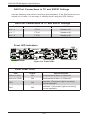
2-3 Front Jumper Locations and Pin Definitions
C202
C44
C28
R367
C63
C58
C
49
48
R122
JP69
C100
D56
17 C86
C18
R346 R310
R411 R413
J6
R108
R347
R113
ACT5
ACT6
R114
C99
ACT4
C102
I2C#1
ACT_IN#0-7
C85
ACT7
U62
C23
R75
C22
R79
C17
C61
C56
D55
C21
J5
J8
C20
Figure 2-3: Front Jumpers
Connector
Pins
Setting
Jumper Settings
Note
JP35
Open: Default
Closed: Reset
9072 Chip Reset #1
JP50
Open: Default
Closed: Reset
9071 Chip Reset #2
JP18
Open: Default
Closed: Reset
Buzzer Reset #2
2-4
2
1
3
2
1
Jumper
the jumper is off the pins.
Jumper Settings
3
R438
JP66
ACT0 ACT1 ACT2
ACT3
D60
U64
C292
JP37
JP26
JP68
R328
BAR CODE
JP95
ACT8
ACT9
ACT11
ACT10
SIDEBAND#2
+
C271 C272 32
U24
C62
C29
C57
U18
R127
C134
R128
R133
C106
C107
D61
33
R436
R368
U72
J10
R292
D58
To modify the operation of the backplane,
jumpers can be used to choose between
optional settings. Jumpers create shorts
between two pins to change the function
of the connector. Pin 1 is identified with
a square solder pad on the printed circuit
board. Note: On two pin jumpers, "Closed"
means the jumper is on and "Open" means
RP1
J7
U25
R432
R154
C135
R327
R329
R78
C26
C59
REV: 3.1
TOLERANCES
DECIMAL
ANGLE
X .1
30
XX .03
MACH FINISH
XXX.010
C88
A
C
UPGRADE#1
#1
R326
R246
C84
R325 D54
A
R121
+
R423
R422
R425
R424
C87
R125
R123
C132
C133
C299
R155
R156
U71
R434
I2C#2
ACT_IN#8-11
R324 D53
1
#2
Explanation of Jumpers
Jumper
D57
C45
+
U70
JP47
C24
C64
Shen/Nina
C75
U26
R168
R167
C136
R166
R184
R185
C149
R183
JP10
JP45:OH#2 TEMP
OPEN:45
C
1-2:50
C
2-3:55
C
UNLESS OTHERWISE
SPECIFIED DIMENSIONS
ARE IN INCHES
SAS826TQ
10/31/2007
SAN JOSE,CA 95131
DESINGER:
TEL:408-503-8000 FAX:408-503-8008
R136
R135
R134
1
PROJECT NAME:
J12
C79
#4
D63
C131
#3
SILKSCREEN
PRIMARY-SIDE
DESIGNED BY SUPERMICRO U.S.A.
www.supermicro.com
DATE:
C104 U31
C80
R194
D59
F1
J14
C125
C124
J23
SUPER
R363
R365
U43
4
JP75
C34
F5
C35
F6
F4
C170
D66
D64
+
#9
RR
JP84
R74
R202
RT2
F3
C33
JP52
JP13
JP46
R216
R319
R333
JP25:OH#1 TEMP
OPEN:45
C
1-2:50
C
2-3:55
C
D62
U1
U36
U45
C32
F2
SIDEBAND#3
C112
C115
U2
R97
C10 U4
A
ALARM#2
JP45
C94
R131 C19
R124
C114
C287
C48
C
J16
1
F7
F8
+
C285
1
R139 R138
+
D36
#7
+
JP84:MODE
1-2:SGPIO
2-3:I2C
D65
C3
U61
R335
JP84
D68
1
I2C#3
C5
C193
C171
C156
JP18
D67
U67
C130
4
1
4
REV 3.1
SAS826TQ
C194
F9
C140
U30
U65
D70
C143
R431
J24
C214
C173
R427
C144
U69
C141
U63
Y2
C286 C212 C213 R229
#10
+
R257
U29
U49
C159
C158
C174
C232
D77
+
C148
R249
C291
C289
11
1
C129
RP4
44
UPGRADE#2
A
C138
C
A
U20
JP50
BZ1
BUZZER RESET
JP25
1
ALARM#1
R144
C108
R73
R392
R63
C1
9072 RST
D3
R6 R98
C215
U39 R223
JP50
U32
R242
R243
12
D71
JP18
C119
R232
C207
C208
D78
D76
C167
U40
J22
U52
34
C243 R271
R261 R264
22
23
R226
C197
C153
C168
C242
J25
JP78
33
+
9071 RST
JP35
R265
C245
R266
R272
R263
C244
C162
C177
R410
R412
R360
C206
R352
R350
#11
C201
+
JP35
R224
D79
C176
R137
+
A
C198
+
Safety Information and Technical Specifications
I2C and SGPIO Modes and Jumper Settings
This backplane can utilize I2C or SGPIO. SGPIO is the default mode and can be
used without making changes to your jumpers. The following information details
which jumper must be configured to use SGPIO mode or restore your backplane
to I2C mode.
Jumper Settings: SGPIO (Default) and I2C
Jumper
JP84
SGPIO (Default) Setting
1-2: SGPIO mode enable
2-5
I2C Setting
2-3: I C mode enable
2
SAS 826TQ Backplane Specifications
SAS Port Connections in I2C and SGPIO Settings
Use the following chart when connecting this backplane. If the SAS ports are connected out of order, it is not easy to identify drives using the LED function.
SAS Port Connections in I2C and SGPIO Settings
Port #
I2C
SGPIO
#0-3
I2C #1
Sideband #1
#4-7
I2C #2
Sideband #2
# 8 - 11
I2C #3
Sideband #3
Front LED Indicators
C202
R367
C63
C28
C58
C100
D56
17 C86
C18
R108
R347
J6
R114
C99
ACT5
ACT6
ACT7
U62
D55
C21
J5
J8
C20
J14
C125
C124
J23
REV: 3.1
Shen/Nina
TOLERANCES
DECIMAL
ANGLE
X .1
30
XX .03
MACH FINISH
XXX.010
Front Panel LEDs
LED
STATE
SPECIFICATION
Alarm #1 (D3)
ON
Overheat/drive failure in Channel 1.
Alarm #2 (D36)
ON
Overheat/drive failure in Channel 2.
D53
ON
Indicates +5V power. Light is on during
normal operation.
D54
ON
Indicates +12V power. Light is on during
normal operation.
2-6
R438
R75
C22
R79
C17
C61
C56
C23
D60
U64
JP66
ACT0 ACT1 ACT2
ACT3
C292
JP37
JP26
JP68
R328
BAR CODE
JP95
ACT8
ACT9
ACT11
R292
SIDEBAND#2
R346 R310
R411 R413
R113
ACT4
C102
I2C#1
ACT_IN#0-7
C85
R78
C59
C24
C64
C26
D58
ACT10
JP10
JP45:OH#2 TEMP
OPEN:45
C
1-2:50
C
2-3:55
C
C34
F5
C35
F6
F4
JP75
C84
C271 C272 32
U24
C62
C29
C57
D61
D54
33
R436
U18
C134
R127
C106
R128
R133
C107
F1
+
RP1
48
R122
JP69
J10
R246
C88
U25
R432
R154
C135
R327
R329
C
R121
R368
R155
R156
C80
1
R326
JP47
A
C
49
UPGRADE#1
U72
I2C#2
ACT_IN#8-11
R325 D54
A
J7
C299
U26
R168
R167
C136
R166
R184
R185
C149
R183
R136
R135
R134
+
R423
R422
R425
R424
C87
R125
C133
R123
C132
C75
R137
J12
C104 U31
U71
R434
R324 D53
1
#2
C45
+
U70
#1
#4
D63
D57
Figure 2-4: Front LEDs
UNLESS OTHERWISE
SPECIFIED DIMENSIONS
ARE IN INCHES
SAS826TQ
10/31/2007
SAN JOSE,CA 95131
DESINGER:
TEL:408-503-8000 FAX:408-503-8008
D59
+
C131
#3
SILKSCREEN
PRIMARY-SIDE
PROJECT NAME:
D64
C79
C32
F3
C33
JP13
JP46
C170
RR
DESIGNED BY SUPERMICRO U.S.A.
www.supermicro.com
DATE:
JP25:OH#1 TEMP
OPEN:45
C
1-2:50
C
2-3:55
C
R194
A
D36
ALARM#2
JP45
#9
SUPER
R363
R365
U43
4
JP52
F7
F8
C193
C171
D66
JP84
R74
C
1
F2
SIDEBAND#3
C112
R97
C3
D62
U1
U36
R202
RT2
#7
R216
R319
R333
R73
C115
U2
Alarm 2
J16
R335
C94
R131 C19
R124
R139 R138
+
U61
C143
1
4
I2C#3
C5
1
C114
C287
D67
U67
+
R63
C1
C141
C144
R431
U30
1
4
REV 3.1
SAS826TQ
C194
C156
D70
C140
R427
J24
C214
C173
U65
C138
U45
U29
U69
JP84:MODE
1-2:SGPIO
2-3:I2C
D65
D68
C10 U4
JP18
C130
C48
R257
U63
Y2
C286 C212 C213 R229
#10
F9
D77
+
C148
R249
C291
C289
U49
C158
C159
C174
C232
C197
JP50
C129
A
+
BUZZER RESET
RP4
44
11
1
JP25
1
C
J22
U32
34
12
R226
UPGRADE#2
U20
D53
+
C285
+
ALARM#1
A
R224
BZ1
C119
R232
C207
C208
+
D71
D3
R6 R98
C215
U39 R223
R392
R144
C108
D76
C167
U40
C153
C168
U52
23
R242
R243
JP78
33
C243 R271
R261 R264
22
J25
R410
R412
R360
C206
R352
R350
#11
C201
D78
9072 RST
C242
C162
C177
D79
C176
9071 RST
JP35
Alarm 1
R265
C245
R266
R272
R263
C244
+
C44
+
A
C198
Safety Information and Technical Specifications
2-4 Rear Connectors and LED Indicators
C
A
R181
A
FAIL#10
R176
C
C
D27
SAS/SATA HHD #7
SAS #2
SAS/SATA HHD #2
SAS #8
SAS/SATA HHD #8
SAS #3
SAS/SATA HHD #3
SAS #9
SAS/SATA HHD #9
SAS #4
SAS/SATA HHD #4
SAS #10
SAS/SATA HHD #10
SAS #5
SAS/SATA HHD #5
SAS #11
SAS/SATA HHD #11
Failure LED
SAS #0
D12
D5
SAS #1
D13
D6
SAS #2
D14
D7
SAS #3
D15
D8
SAS #4
D18
D19
SAS #5
D21
D20
SAS #6
D22
D23
SAS #7
D24
D29
SAS #8
D25
D30
SAS #9
D26
D31
SAS #10
D27
D32
SAS #11
D28
D33
A
D31
R180
SAS/SATA HHD #6
SAS #7
FAIL#9
SAS #6
SAS/SATA HHD #1
C
A
SAS/SATA HHD #0
Hard Drive Activity
13159 AC,ESOJ NAS
ACT#9
SAS Drive
Number
Rear LED Indicators
.A.S.U ORCIMREPUS YB DENGISED
moc.orcimrepus.www
:ETAD
:REGN8IS0E08D-305-804:XAF 0008-305-804:LET
C
D26
R175
:EMAN TCEJORP
7002/13/01
aniN/nehS
D32
QT628SAS
1.3 :VER
SAS #1
2-7
REPUS
SILKSCREEN
RR
SECONDARY-SIDE
ESIWREHTO SSELNU
SNOISNEMID DEIFICEPS
SEHCNI NI ERA
SAS #0
Rear LED
ACT#10
Rear
Connector
D33
R182
SAS Drive
Number
A
A
R165
FAIL#6
C
A
D23
R164
ACT#6
J18
SAS
#9
Rear SAS/SATA Connectors
Rear
Connector
FAIL#11
D26
D31
D22
C
SAS #9
J18
SECNARELOT
ELGNA
LAMICED
1. X
03
30. XX
HSINIF HCAM
010X. XX
R177
SAS
#10
C
A
J19
D29
Figure 2-5: Rear Connectors and LEDs
D28
A
J13
ACT#11
FAIL#7
R178
D27
D32
C
A
R173
SAS #10
J19
C
J20
SAS
#11
ACT#7
D24
C
A D8
R90
FAIL#3
C
A
D22
D23
SAS #11
J20
A
R179
R88
ACT#3
D15
C
SAS
#6
D30
A
J15
SAS
#7
D28
D33
FAIL#8
R96
D19
FAIL#4
A
SAS #6
J13
C
A
C
A
R95
D18
R85
D5
FAIL#0
C
A
R83
D12
ACT#0
J4
D24
D29
ACT#4
C
C
D15
D8
SAS
#3
SAS #7
J15
R174
D25
D20
J9
SAS
#4
C
A
SAS #8
J17
D25
D30
J17
SAS
#8
ACT#8
FAIL#5
R150 R149
R87
SAS #3
J4
C
A
A
FAIL#1
D6
SAS #4
J9
D21
A
D12
D5
D18
D19
D13
R84
J2
J1
SAS
#0
#5
ACT#1
D13
D6
C
#1
SAS #5
J11
J11
SAS
ACT#5
R89
SAS
A D7
#2
D21
D20
FAIL#2
C
A
R86
C
D14
SAS #0
J1
C
SAS #1
J2
D14
D7
J3
SAS
ACT#2
SAS #2
J3
SAS 826TQ Backplane Specifications
Disclaimer (cont.)
The products sold by Supermicro are not intended for and will not be used in life support systems, medical equipment, nuclear facilities or systems, aircraft, aircraft devices,
aircraft/emergency communication devices or other critical systems whose failure to perform be reasonably expected to result in significant injury or loss of life or catastrophic
property damage. Accordingly, Supermicro disclaims any and all liability, and should
buyer use or sell such products for use in such ultra-hazardous applications, it does so
entirely at its own risk. Furthermore, buyer agrees to fully indemnify, defend and hold
Supermicro harmless for and against any and all claims, demands, actions, litigation,
and proceedings of any kind arising out of or related to such ultra-hazardous use or
sale.
2-8