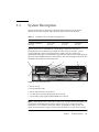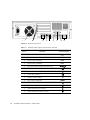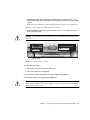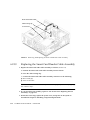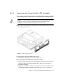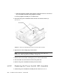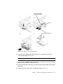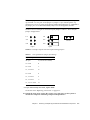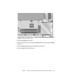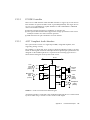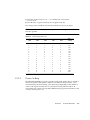
1
Sun Blade™ 100 Service Manual
Sun Microsystems, Inc.
901 San Antonio Road
Palo Alto, CA 94303
U.S.A. 650-960-1300
Part No. 806-3416-10
October 2000, Revision A
Send comments about this document to: [email protected]
Copyright 2000 Sun Microsystems, Inc., 901 San Antonio Road, Palo Alto, CA 94303-4900 U.S.A. All rights reserved.
This product or document is distributed under licenses restricting its use, copying, distribution, and decompilation. No part of this product or
document may be reproduced in any form by any means without prior written authorization of Sun and its licensors, if any. Third-party
software, including font technology, is copyrighted and licensed from Sun suppliers.
Parts of the product may be derived from Berkeley BSD systems, licensed from the University of California. UNIX is a registered trademark in
the U.S. and other countries, exclusively licensed through X/Open Company, Ltd.
Sun, Sun Microsystems, the Sun logo, AnswerBook2, docs.sun.com, Sun Blade, ShowMe How, Power Management, and Solaris are trademarks,
registered trademarks, or service marks of Sun Microsystems, Inc. in the U.S. and other countries. All SPARC trademarks are used under license
and are trademarks or registered trademarks of SPARC International, Inc. in the U.S. and other countries. Products bearing SPARC trademarks
are based upon an architecture developed by Sun Microsystems, Inc.
The OPEN LOOK and Sun™ Graphical User Interface was developed by Sun Microsystems, Inc. for its users and licensees. Sun acknowledges
the pioneering efforts of Xerox in researching and developing the concept of visual or graphical user interfaces for the computer industry. Sun
holds a non-exclusive license from Xerox to the Xerox Graphical User Interface, which license also covers Sun’s licensees who implement OPEN
LOOK GUIs and otherwise comply with Sun’s written license agreements.
The Energy Star Logo is a registered trademark of EPA. As an Energy Star® partner, Sun Microsystems, Inc. has determined
that configurations of this product that bear the Energy Star logo meet the Energy Star guidelines for energy efficiency.
Federal Acquisitions: Commercial Software—Government Users Subject to Standard License Terms and Conditions.
DOCUMENTATION IS PROVIDED “AS IS” AND ALL EXPRESS OR IMPLIED CONDITIONS, REPRESENTATIONS AND WARRANTIES,
INCLUDING ANY IMPLIED WARRANTY OF MERCHANTABILITY, FITNESS FOR A PARTICULAR PURPOSE OR NON-INFRINGEMENT,
ARE DISCLAIMED, EXCEPT TO THE EXTENT THAT SUCH DISCLAIMERS ARE HELD TO BE LEGALLY INVALID.
Copyright 2000 Sun Microsystems, Inc., 901 San Antonio Road, Palo Alto, CA 94303-4900 Etats-Unis. Tous droits réservés.
Ce produit ou document est distribué avec des licences qui en restreignent l’utilisation, la copie, la distribution, et la décompilation. Aucune
partie de ce produit ou document ne peut être reproduite sous aucune forme, par quelque moyen que ce soit, sans l’autorisation préalable et
écrite de Sun et de ses bailleurs de licence, s’il y en a. Le logiciel détenu par des tiers, et qui comprend la technologie relative aux polices de
caractères, est protégé par un copyright et licencié par des fournisseurs de Sun.
Des parties de ce produit pourront être dérivées des systèmes Berkeley BSD licenciés par l’Université de Californie. UNIX est une marque
déposée aux Etats-Unis et dans d’autres pays et licenciée exclusivement par X/Open Company, Ltd.
Sun, Sun Microsystems, le logo Sun, AnswerBook2, docs.sun.com, Sun Blade, ShowMe How, Power Management, et Solaris sont des marques
de fabrique ou des marques déposées, ou marques de service, de Sun Microsystems, Inc. aux Etats-Unis et dans d’autres pays. Toutes les
marques SPARC sont utilisées sous licence et sont des marques de fabrique ou des marques déposées de SPARC International, Inc. aux EtatsUnis et dans d’autres pays. Les produits portant les marques SPARC sont basés sur une architecture développée par Sun Microsystems, Inc.
L’interface d’utilisation graphique OPEN LOOK et Sun™ a été développée par Sun Microsystems, Inc. pour ses utilisateurs et licenciés. Sun
reconnaît les efforts de pionniers de Xerox pour la recherche et le développement du concept des interfaces d’utilisation visuelle ou graphique
pour l’industrie de l’informatique. Sun détient une licence non exclusive de Xerox sur l’interface d’utilisation graphique Xerox, cette licence
couvrant également les licenciés de Sun qui mettent en place l’interface d’utilisation graphique OPEN LOOK et qui en outre se conforment aux
licences écrites de Sun.
LA DOCUMENTATION EST FOURNIE “EN L’ETAT” ET TOUTES AUTRES CONDITIONS, DECLARATIONS ET GARANTIES EXPRESSES
OU TACITES SONT FORMELLEMENT EXCLUES, DANS LA MESURE AUTORISEE PAR LA LOI APPLICABLE, Y COMPRIS NOTAMMENT
TOUTE GARANTIE IMPLICITE RELATIVE A LA QUALITE MARCHANDE, A L’APTITUDE A UNE UTILISATION PARTICULIERE OU A
L’ABSENCE DE CONTREFAÇON.
Please
Recycle
Regulatory Compliance Statements
Your Sun product is marked to indicate its compliance class:
•
•
•
Federal Communications Commission (FCC) — USA
Department of Communications (DOC) — Canada
Voluntary Control Council for Interference (VCCI) — Japan
Please read the appropriate section that corresponds to the marking on your Sun product before attempting to install the
product.
FCC Class A Notice
This device complies with Part 15 of the FCC Rules. Operation is subject to the following two conditions:
1. This device may not cause harmful interference.
2. This device must accept any interference received, including interference that may cause undesired operation.
Note: This equipment has been tested and found to comply with the limits for a Class A digital device, pursuant to Part 15 of
the FCC Rules. These limits are designed to provide reasonable protection against harmful interference when the equipment
is operated in a commercial environment. This equipment generates, uses, and can radiate radio frequency energy, and if it is
not installed and used in accordance with the instruction manual, it may cause harmful interference to radio communications.
Operation of this equipment in a residential area is likely to cause harmful interference, in which case the user will be required
to correct the interference at his own expense.
Shielded Cables: Connections between the workstation and peripherals must be made using shielded cables to comply with
FCC radio frequency emission limits. Networking connections can be made using unshielded twisted-pair (UTP) cables.
Modifications: Any modifications made to this device that are not approved by Sun Microsystems, Inc. may void the
authority granted to the user by the FCC to operate this equipment.
FCC Class B Notice
This device complies with Part 15 of the FCC Rules. Operation is subject to the following two conditions:
1. This device may not cause harmful interference.
2. This device must accept any interference received, including interference that may cause undesired operation.
Note: This equipment has been tested and found to comply with the limits for a Class B digital device, pursuant to Part 15 of
the FCC Rules. These limits are designed to provide reasonable protection against harmful interference in a residential
installation. This equipment generates, uses and can radiate radio frequency energy and, if not installed and used in
accordance with the instructions, may cause harmful interference to radio communications. However, there is no guarantee
that interference will not occur in a particular installation. If this equipment does cause harmful interference to radio or
television reception, which can be determined by turning the equipment off and on, the user is encouraged to try to correct the
interference by one or more of the following measures:
•
•
•
•
Reorient or relocate the receiving antenna.
Increase the separation between the equipment and receiver.
Connect the equipment into an outlet on a circuit different from that to which the receiver is connected.
Consult the dealer or an experienced radio/television technician for help.
Shielded Cables: Connections between the workstation and peripherals must be made using shielded cables in order to
maintain compliance with FCC radio frequency emission limits. Networking connections can be made using unshielded
twisted pair (UTP) cables.
Modifications: Any modifications made to this device that are not approved by Sun Microsystems, Inc. may void the
authority granted to the user by the FCC to operate this equipment.
iii
ICES-003 Class A Notice - Avis NMB-003, Classe A
This Class A digital apparatus complies with Canadian ICES-003.
Cet appareil numérique de la classe A est conforme à la norme NMB-003 du Canada.
ICES-003 Class B Notice - Avis NMB-003, Classe B
This Class B digital apparatus complies with Canadian ICES-003.
Cet appareil numérique de la classe B est conforme à la norme NMB-003 du Canada.
iv
Sun Blade 100 Service Manual • October 2000
BSMI Class A Notice
The following statement is applicable to products shipped to Taiwan and marked as Class A on the product compliance
label.
v
vi
Sun Blade 100 Service Manual • October 2000
Declaration of Conformity
Compliance Model Number:
202
Product Name:
Sun Blade™ 100
EMC
USA—FCC Class B
This device complies with Part 15 of the FCC Rules. Operation is subject to the following two conditions:
1. This device may not cause harmful interference.
2. This device must accept any interference received, including interference that may cause undesired operation.
European Union
This equipment complies with the following requirements of the EMC Directive 89/336/EEC:
EN55022:1995/CISPR22:1997
EN550024:1998
Class B
EN61000-4-2
4 kV (Direct), 8 kV (Air)
EN61000-4-3
3 V/m
EN61000-4-4
1.0 kV Power Lines, 0.5 kV Signal Lines
EN61000-4-5
1 kV Line-Line, 2 kV Line-Gnd Power Lines
EN61000-4-6
3V
EN61000-4-8
3 A/m
EN61000-4-11
Pass
EN61000-3-2:1995
Pass
EN61000-3-3:1995
Pass
Safety
This equipment complies with the following requirements of the Low Voltage Directive 73/23/EEC:
EC Type Examination Certificates:
EN60950:1992, 2nd Edition, Amendments 1,2,3,4,11
TUV Rheinland Certificate No. S2055723
IEC 950:1991, 2nd Edition, Amendments 1,2,3,4
Evaluated to all CB Countries
CB Scheme Certificate No. JPTUV-001881
Supplementary Information
This product was tested and complies with all the requirements for the CE Mark.
/S/
Dennis P. Symanski
Manager, Compliance Engineering
/S/
DATE
Peter Arkless
Quality Manager
Sun Microsystems, Inc.
901 San Antonio Road, MPK15-102
Palo Alto, CA 94303-4900, USA
Sun Microsystems Scotland, Limited
Springfield, Linlithgow
West Lothian, EH49 7LR
Scotland, United Kingdom
Tel: 650-786-3255
Fax: 650-786-3723
Tel: 0506-670000
Fax: 0506 760011
DATE
vii
viii
Sun Blade 100 Service Manual • October 2000
Safety Agency Compliance
Statements
Read this section before beginning any procedure. The
following text provides safety precautions to follow when
installing a Sun Microsystems product.
Placement of a Sun Product
Caution – Do not block or cover the openings
of your Sun product. Never place a Sun
product near a radiator or heat register.
Failure to follow these guidelines can cause
overheating and affect the reliability of your
Sun product.
Safety Precautions
For your protection, observe the following safety
precautions when setting up your equipment:
■
■
■
Follow all cautions and instructions marked on the
equipment.
Ensure that the voltage and frequency of your power
source match the voltage and frequency inscribed on
the equipment’s electrical rating label.
Never push objects of any kind through openings in
the equipment. Dangerous voltages may be present.
Conductive foreign objects could produce a short
circuit that could cause fire, electric shock, or damage
to your equipment.
Symbols
The following symbols may appear in this book:
Caution – There is risk of personal injury and
equipment damage. Follow the instructions.
Caution – Hot surface. Avoid contact. Surfaces
are hot and may cause personal injury if
touched.
Caution – Hazardous voltages are present. To
reduce the risk of electric shock and danger to
personal health, follow the instructions.
Modifications to Equipment
Caution – The workplace-dependent noise
level defined in DIN 45 635 Part 1000 must be
70Db(A) or less.
SELV Compliance
Safety status of I/O connections comply to SELV
requirements.
Power Cord Connection
Caution – Sun products are designed to work
with single-phase power systems having a
grounded neutral conductor. To reduce the
risk of electric shock, do not plug Sun
products into any other type of power system.
Contact your facilities manager or a qualified
electrician if you are not sure what type of
power is supplied to your building.
Caution – Not all power cords have the same
current ratings. Household extension cords do
not have overload protection and are not
meant for use with computer systems. Do not
use household extension cords with your Sun
product.
Caution – Your Sun product is shipped with a
grounding type (three-wire) power cord. To
reduce the risk of electric shock, always plug
the cord into a grounded power outlet.
Do not make mechanical or electrical modifications to the
equipment. Sun Microsystems is not responsible for
regulatory compliance of a modified Sun product.
ix
Lithium Battery
Caution – This system contains a replaceable
lithium battery, Mitsubishi Part Number
R-2032. Lithium batteries may explode if
mishandled. Do not dispose of the battery in
fire. Do not disassemble it or attempt to
recharge it.
Einhaltung sicherheitsbehördlicher
Vorschriften
Auf dieser Seite werden Sicherheitsrichtlinien beschrieben,
die bei der Installation von Sun-Produkten zu beachten
sind.
Sicherheitsvorkehrungen
Treffen Sie zu Ihrem eigenen Schutz die folgenden
Sicherheitsvorkehrungen, wenn Sie Ihr Gerät installieren:
System Unit Cover
You must remove the cover of your Sun computer system
unit to add cards, memory, or internal storage devices. Be
sure to replace the cover before powering on your computer
system.
Caution – Do not operate Sun products
without top cover in place. Failure to take this
precaution may result in personal injury and
system damage.
■
■
■
Beachten Sie alle auf den Geräten angebrachten
Warnhinweise und Anweisungen.
Vergewissern Sie sich, daß Spannung und Frequenz
Ihrer Stromquelle mit der Spannung und Frequenz
übereinstimmen, die auf dem Etikett mit den
elektrischen Nennwerten des Geräts angegeben sind.
Stecken Sie auf keinen Fall irgendwelche Gegenstände
in Öffnungen in den Geräten. Leitfähige Gegenstände
könnten aufgrund der möglicherweise vorliegenden
gefährlichen Spannungen einen Kurzschluß
verursachen, der einen Brand, Stromschlag oder
Geräteschaden herbeiführen kann.
Laser Compliance Notice
Symbole
Sun products that use laser technology comply with Class 1
laser requirements.
Die Symbole in diesem Handbuch haben folgende
Bedeutung:
Class 1 Laser Product
Luokan 1 Laserlaite
Klasse 1 Laser Apparat
Laser KLasse 1
Achtung – Gefahr von Verletzung und
Geräteschaden. Befolgen Sie die
Anweisungen.
Achtung – Hohe Temperatur. Nicht berühren,
da Verletzungsgefahr durch heiße Oberfläche
besteht.
CD-ROM or DVD-ROM
Caution – Use of controls, adjustments, or the
performance of procedures other than those
specified herein may result in hazardous
radiation exposure.
Achtung – Gefährliche Spannungen.
Anweisungen befolgen, um Stromschläge und
Verletzungen zu vermeiden.
Nehmen Sie keine mechanischen oder elektrischen
Änderungen an den Geräten vor. Sun Microsystems,
übernimmt bei einem Sun-Produkt, das geändert wurde,
keine Verantwortung für die Einhaltung behördlicher
Vorschriften
x
Sun Blade 100 Service Manual • October 2000
Aufstellung von Sun-Geräten
Achtung – Um den zuverlässigen Betrieb
Ihres Sun-Geräts zu gewährleisten und es vor
Überhitzung zu schützen, dürfen die
Öffnungen im Gerät nicht blockiert oder
verdeckt werden. Sun-Produkte sollten
niemals in der Nähe von Heizkörpern oder
Heizluftklappen aufgestellt werden.
Achtung – Der arbeitsplatzbezogene
Schalldruckpegel nach DIN 45 635 Teil 1000
beträgt 70Db(A) oder weniger.
Einhaltung der SELV-Richtlinien
Die Sicherung der I/O-Verbindungen entspricht den
Anforderungen der SELV-Spezifikation.
Anschluß des Netzkabels
Achtung – Sun-Produkte sind für den Betrieb
an Einphasen-Stromnetzen mit geerdetem
Nulleiter vorgesehen. Um die
Stromschlaggefahr zu reduzieren, schließen
Sie Sun-Produkte nicht an andere
Stromquellen an. Ihr Betriebsleiter oder ein
qualifizierter Elektriker kann Ihnen die Daten
zur Stromversorgung in Ihrem Gebäude
geben.
Achtung – Nicht alle Netzkabel haben die
gleichen Nennwerte. Herkömmliche, im
Haushalt verwendete Verlängerungskabel
besitzen keinen Überlastungsschutz und sind
daher für Computersysteme nicht geeignet.
Achtung – Ihr Sun-Gerät wird mit einem
dreiadrigen Netzkabel für geerdete
Netzsteckdosen geliefert. Um die Gefahr eines
Stromschlags zu reduzieren, schließen Sie das
Kabel nur an eine fachgerecht verlegte,
geerdete Steckdose an.
Lithiumbatterie
Achtung – Dieses System enthält eine
austauschbare Lithiumbatterie, Mitsubishi
Teilenummer R-2032. Diese Batterie darf nur
von einem qualifizierten Servicetechniker
ausgewechselt werden, da sie bei falscher
Handhabung explodieren kann. Werfen Sie
die Batterie nicht ins Feuer. Versuchen Sie auf
keinen Fall, die Batterie auszubauen oder
wiederaufzuladen.
Gehäuseabdeckung
Sie müssen die obere Abdeckung Ihres Sun-Systems
entfernen, um interne Komponenten wie Karten,
Speicherchips oder Massenspeicher hinzuzufügen. Bringen
Sie die obere Gehäuseabdeckung wieder an, bevor Sie Ihr
System einschalten.
Achtung – Bei Betrieb des Systems ohne obere
Abdeckung besteht die Gefahr von
Stromschlag und Systemschäden.
Einhaltung der Richtlinien für Laser
Sun-Produkte, die mit Laser-Technologie arbeiten,
entsprechen den Anforderungen der Laser Klasse 1.
Class 1 Laser Product
Luokan 1 Laserlaite
Klasse 1 Laser Apparat
Laser KLasse 1
CD-ROM or DVD-ROM
Achtung – Die Verwendung von anderen
Steuerungen und Einstellungen oder die
Durchführung von Prozeduren, die von den
hier beschriebenen abweichen, können
gefährliche Strahlungen zur Folge haben.
xi
Conformité aux normes de sécurité
Ce texte traite des mesures de sécurité qu’il convient de
prendre pour l’installation d’un produit Sun Microsystems.
Mesures de sécurité
Pour votre protection, veuillez prendre les précautions
suivantes pendant l’installation du matériel :
■
■
■
Suivre tous les avertissements et toutes les
instructions inscrites sur le matériel.
Vérifier que la tension et la fréquence de la source
d’alimentation électrique correspondent à la tension et
à la fréquence indiquées sur l’étiquette de
classification de l’appareil.
Ne jamais introduire d’objets quels qu’ils soient dans
une des ouvertures de l’appareil. Vous pourriez vous
trouver en présence de hautes tensions dangereuses.
Tout objet conducteur introduit de la sorte pourrait
produire un court-circuit qui entraînerait des
flammes, des risques d’électrocution ou des dégâts
matériels.
Symboles
Vous trouverez ci-dessous la signification des différents
symboles utilisés :
Attention: – risques de blessures corporelles
et de dégâts matériels. Veuillez suivre les
instructions.
Attention: – surface à température élevée.
Evitez le contact. La température des surfaces
est élevée et leur contact peut provoquer des
blessures corporelles.
Attention: – présence de tensions
dangereuses. Pour éviter les risques
d’électrocution et de danger pour la santé
physique, veuillez suivre les instructions.
Modification du matériel
Ne pas apporter de modification mécanique ou électrique
au matériel. Sun Microsystems n’est pas responsable de la
conformité réglementaire d’un produit Sun qui a été
modifié.
xii
Sun Blade 100 Service Manual • October 2000
Positionnement d’un produit Sun
Attention: – pour assurer le bon
fonctionnement de votre produit Sun et pour
l’empêcher de surchauffer, il convient de ne
pas obstruer ni recouvrir les ouvertures
prévues dans l’appareil. Un produit Sun ne
doit jamais être placé à proximité d’un
radiateur ou d’une source de chaleur.
Attention: – Le niveau de pression acoustique
au poste de travail s'élève selon la norme DIN
45 635 section 1000, à 70 dB (A) ou moins.
Conformité SELV
Sécurité : les raccordements E/S sont conformes aux
normes SELV.
Connexion du cordon d’alimentation.
Attention: – les produits Sun sont conçus
pour fonctionner avec des alimentations
monophasées munies d’un conducteur neutre
mis à la terre. Pour écarter les risques
d’électrocution, ne pas brancher de produit
Sun dans un autre type d’alimentation secteur.
En cas de doute quant au type d’alimentation
électrique du local, veuillez vous adresser au
directeur de l’exploitation ou à un électricien
qualifié.
Attention: – tous les cordons d’alimentation
n’ont pas forcément la même puissance
nominale en matière de courant. Les rallonges
d’usage domestique n’offrent pas de
protection contre les surcharges et ne sont pas
prévues pour les systèmes d’ordinateurs. Ne
pas utiliser de rallonge d’usage domestique
avec votre produit Sun.
Class 1 Laser Product
Luokan 1 Laserlaite
Klasse 1 Laser Apparat
Laser KLasse 1
CD-ROM or DVD-ROM
Attention: – votre produit Sun a été livré
équipé d’un cordon d’alimentation à trois fils
(avec prise de terre). Pour écarter tout risque
d’électrocution, branchez toujours ce cordon
dans une prise mise à la terre.
Attention: – L’utilisation de contrôles, de
réglages ou de performances de procédures
autre que celle spécifiée dans le présent
document peut provoquer une exposition à
des radiations dangereuses.
Batterie au lithium
Attention: – Ce système est équipé d’une pile au
lithium qui peut être remplacée, référence
n˚ Mitsubishi R-2032. Les piles au lithium
risquent d’exploser en cas de manipulation
maladroite. Ne jetez en aucun cas la pile au feu.
N’essayez en aucun cas de la démonter, ni de la
recharger.
Couvercle
Pour ajouter des cartes, de la mémoire, ou des unités de
stockage internes, vous devrez démonter le couvercle de
l’unité système Sun. Ne pas oublier de remettre ce couvercle
en place avant de mettre le système sous tension.
Attention: – il est dangereux de faire
fonctionner un produit Sun sans le couvercle
en place. Si l’on néglige cette précaution, on
encourt des risques de blessures corporelles et
de dégâts matériels.
Conformité aux certifications Laser
Les produits Sun qui font appel aux technologies lasers sont
conformes aux normes de la classe 1 en la matière.
xiii
Normativas de seguridad
El siguiente texto incluye las medidas de seguridad que se
deben seguir cuando se instale algún producto de Sun
Microsystems.
Precauciones de seguridad
Para su protección observe las siguientes medidas de
seguridad cuando manipule su equipo:
■
■
■
Siga todas los avisos e instrucciones marcados en el
equipo.
Asegúrese de que el voltaje y la frecuencia de la red
eléctrica concuerdan con las descritas en las etiquetas
de especificaciones eléctricas del equipo.
No introduzca nunca objetos de ningún tipo a través
de los orificios del equipo. Pueden haber voltajes
peligrosos. Los objetos extraños conductores de la
electricidad pueden producir cortocircuitos que
provoquen un incendio, descargas eléctricas o daños
en el equipo.
Símbolos
Ubicación de un producto Sun
Precaución – Para asegurar la fiabilidad de
funcionamiento de su producto Sun y para
protegerlo de sobrecalentamien-tos no deben
obstruirse o taparse las rejillas del equipo. Los
productos Sun nunca deben situarse cerca de
radiadores o de fuentes de calor.
Precaución – De acuerdo con la norma DIN 45
635, Parte 1000, se admite un nivel de presión
acústica para puestos de trabajo máximo de
70Db(A).
Cumplimiento de la normativa SELV
El estado de la seguridad de las conexiones de entrada/
salida cumple los requisitos de la normativa SELV.
Conexión del cable de alimentación eléctrica
En este libro aparecen los siguientes símbolos:
Precaución – Existe el riesgo de lesiones
personales y daños al equipo. Siga las
instrucciones.
Precaución – Superficie caliente. Evite el
contacto. Las superficies están calientes y
pueden causar daños personales si se tocan.
Precaución – Voltaje peligroso presente. Para
reducir el riesgo de descarga y daños para la
salud siga las instrucciones.
Modificaciones en el equipo
No realice modificaciones de tipo mecánico o eléctrico en el
equipo. Sun Microsystems no se hace responsable del
cumplimiento de las normativas de seguridad en los
equipos Sun modificados.
xiv
Sun Blade 100 Service Manual • October 2000
Precaución – Los productos Sun están
diseñados para trabajar en una red eléctrica
monofásica con toma de tierra. Para reducir el
riesgo de descarga eléctrica, no conecte los
productos Sun a otro tipo de sistema de
alimentación eléctrica. Póngase en contacto
con el responsable de mantenimiento o con un
electricista cualificado si no está seguro del
sistema de alimentación eléctrica del que se
dispone en su edificio.
Precaución – No todos los cables de
alimentación eléctrica tienen la misma
capacidad. Los cables de tipo doméstico no
están provistos de protecciones contra
sobrecargas y por tanto no son apropiados
para su uso con computadores. No utilice
alargadores de tipo doméstico para conectar
sus productos Sun.
Precaución – Con el producto Sun se
proporciona un cable de alimentación con
toma de tierra. Para reducir el riesgo de
descargas eléctricas conéctelo siempre a un
enchufe con toma de tierra.
Class 1 Laser Product
Luokan 1 Laserlaite
Klasse 1 Laser Apparat
Laser KLasse 1
CD-ROM or DVD-ROM
Precaución – El manejo de los controles, los
ajustes o la ejecución de procedimientos
distintos a los aquí especificados pueden
exponer al usuario a radiaciones peligrosas.
Batería de litio
Precaución – Este sistema contiene una batería de
litio reemplazable, número de pieza Mitsubishi
R-2032. Estas baterías pueden explotar si se las
manipula incorrectamente. No tire baterías al fuego.
No las desarme ni intente recargarlas.
Tapa de la unidad del sistema
Debe quitar la tapa del sistema cuando sea necesario añadir
tarjetas, memoria o dispositivos de almacenamiento
internos. Asegúrese de cerrar la tapa superior antes de
volver a encender el equipo.
Precaución – Es peligroso hacer funcionar los
productos Sun sin la tapa superior colocada.
El hecho de no tener en cuenta esta precaución
puede ocasionar daños personales o
perjudicar el funcionamiento del equipo.
Aviso de cumplimiento con requisitos de láser
Los productos Sun que utilizan la tecnología de láser
cumplen con los requisitos de láser de Clase 1.
xv
GOST-R Certification Mark
Nordic Lithium Battery Cautions
Norge
ADVARSEL – Litiumbatteri —
Eksplosjonsfare.Ved utskifting benyttes kun
batteri som anbefalt av apparatfabrikanten.
Brukt batteri returneres apparatleverandøren.
Sverige
VARNING – Explosionsfara vid felaktigt
batteribyte. Använd samma batterityp eller
en ekvivalent typ som rekommenderas av
apparattillverkaren. Kassera använt batteri
enligt fabrikantens instruktion.
Danmark
ADVARSEL! – Litiumbatteri —
Eksplosionsfare ved fejlagtig håndtering.
Udskiftning må kun ske med batteri af samme
fabrikat og type. Levér det brugte batteri
tilbage til leverandøren.
Suomi
VAROITUS – Paristo voi räjähtää, jos se on
virheellisesti asennettu. Vaihda paristo
ainoastaan laitevalmistajan suosittelemaan
tyyppiin. Hävitä käytetty paristo valmistajan
ohjeiden mukaisesti.
xvi
Sun Blade 100 Service Manual • October 2000
Contents
Regulatory Compliance Statements
iii
Safety Agency Compliance Statements
Preface
1.
2.
3.
ix
xxxiii
Product Description
1-1
1.1
Product Overview
1.2
I/O Devices
1.3
System Description
1.4
Replaceable Components
SunVTS Overview
1-3
1-4
1-5
2-1
2.1
SunVTS Description
2.2
SunVTS Requirements
2.3
SunVTS References
Power-On Self-Test
1-7
2-1
2-2
2-2
3-1
3.1
POST Overview
3-1
3.2
Pre-POST Preparation
3-1
3.2.1
Setting Up a TIP Connection
3.2.2
Verifying the Baud Rate
3-2
3-3
xvii
4.
3.3
Initializing POST
3.4
Maximum and Minimum POST Levels
3-4
3.4.1
diag-level Variable Set to max
3-4
3.4.2
diag-level Variable Set to min
3-7
3.5
POST Progress and Error Reporting
3.6
Bypassing POST
3.7
Resetting Variables to Default Settings
3.8
Initializing Motherboard POST
3-11
3-15
Troubleshooting Procedures
3-15
3-15
4-1
4.1
Power-On Failure
4.2
Video Output Failure
4.3
Hard Drive, CD-ROM, or DVD-ROM Drive Failure
4.4
Power Supply Test
4.5
DIMM Failure
4.6
OpenBoot PROM On-Board Diagnostics
4.7
xviii
3-3
4-1
4-2
4-3
4-4
4-5
4-5
4.6.1
Watch-Clock Diagnostic
4.6.2
Watch-Net and Watch-Net-All Diagnostics
4.6.3
Probe-IDE Diagnostic
4.6.4
Test device alias, device path, -All Diagnostic
OpenBoot Diagnostics
4-6
4-6
4-8
4-8
4-10
4.7.1
Starting the OpenBoot Diagnostics Menu
4.7.2
OpenBoot Diagnostics
4-10
4-14
4.7.2.1
PCI/PCIO Diagnostic
4.7.2.2
EBus DMA/TCR Registers Diagnostic
4.7.2.3
Ethernet Diagnostic
4.7.2.4
Keyboard Diagnostic
4.7.2.5
Mouse Diagnostic
4.7.2.6
Diskette Drive (Floppy) Diagnostic
4.7.2.7
Parallel Port Diagnostic
4.7.2.8
Serial Port Diagnostic
Sun Blade 100 Service Manual • October 2000
4-15
4-16
4-16
4-17
4-18
4-19
4-19
4-18
4.7.3
5.
6.
4.7.2.9
NVRAM Diagnostic
4-20
4.7.2.10
Audio Diagnostic
4.7.2.11
EIDE Diagnostic
4-21
4.7.2.12
Video Diagnostic
4-22
4.7.2.13
All Above Diagnostic
4-20
4-22
Exiting the OpenBoot Diagnostic Menu
Preparing for Component Removal and Replacement
5.1
Safety Requirements
5.2
Safety Symbols
5.3
Safety Precautions
5-2
5-2
5.3.1
Modification to Equipment
5-2
5.3.2
Placement of a Sun Product
5-3
5.3.3
Power Cord Connection
5.3.4
Electrostatic Discharge
5.3.5
Lithium Battery
5-3
5-3
5-4
Tools Required
5.5
Powering Off the System
5.6
Removing the System Cover
5.7
Attaching the Antistatic Wrist Strap
5-4
5-4
5-6
5-6
Removing and Replacing Major Subassemblies
6.2
Power Supply
5-1
5-1
5.4
6.1
4-25
6-1
6-1
6.1.1
Removing the Power Supply
6-1
6.1.2
Replacing the Power Supply
6-2
Cable Assemblies
6-3
6.2.1
Removing the Diskette Drive Data Cable Assembly
6-3
6.2.2
Replacing the Diskette Drive Data Cable Assembly
6-4
6.2.3
Removing the Diskette Drive Power Cable Assembly
6-5
6.2.4
Replacing the Diskette Drive Power Cable Assembly
6-6
6.2.5
Removing the Primary IDE Cable Assembly
6-6
xix
6.3
6.4
7.
7.2
7.3
7.4
6.2.7
Removing the Secondary IDE Cable Assembly
6-7
6.2.8
Replacing the Secondary IDE Cable Assembly
6-8
6.2.9
Removing the Smart Card Reader Cable Assembly
6-9
6.2.10
Replacing the Smart Card Reader Cable Assembly
6-10
6.2.11
Removing the Power Switch/LED Assembly
6-11
6.2.12
Replacing the Power Switch/LED Assembly
6-12
Speaker Assembly
6-13
6.3.1
Removing the Speaker Assembly
6-13
6.3.2
Replacing the Speaker Assembly
6-15
Fan Assembly
6-16
6.4.1
Removing the Fan Assembly
6-16
6.4.2
Replacing the Fan Assembly
6-17
Diskette Drive
7-1
7-1
7.1.1
Removing the Diskette Drive
7-1
7.1.2
Replacing the Diskette Drive
7-2
Smart Card Reader
7-3
7.2.1
Removing the Smart Card Reader
7-3
7.2.2
Replacing the Smart Card Reader
7-4
Hard Drives
6-7
7-5
7.3.1
Removing a Primary Hard Drive
7-5
7.3.2
Replacing a Primary Hard Drive
7-7
7.3.3
Installing a Secondary Hard Drive
CD-ROM or DVD-ROM Drive
7-7
7-10
7.4.1
Removing a CD-ROM or DVD-ROM Drive
7-10
7.4.2
Replacing a CD-ROM or DVD-ROM Drive
7-11
Removing and Replacing the Motherboard and Related Components
8.1
xx
Replacing the Primary IDE Cable Assembly
Removing and Replacing Storage Devices
7.1
8.
6.2.6
CPU
8-2
Sun Blade 100 Service Manual • October 2000
8-1
8.2
8.3
8.4
8.5
8.6
9.
10.
8.1.1
Removing the CPU
8-2
8.1.2
Replacing the CPU
8-3
NVRAM/TOD
8-6
8.2.1
Removing the NVRAM/TOD
8-6
8.2.2
Replacing the NVRAM/TOD
8-7
DIMMs
8-8
8.3.1
Removing a DIMM
8-8
8.3.2
Replacing a DIMM
8-10
PCI Card
8-12
8.4.1
Removing a PCI Card
8-12
8.4.2
Replacing a PCI Card
8-13
Motherboard
8-15
8.5.1
Removing the Motherboard
8-15
8.5.2
Replacing the Motherboard
8-17
Riser Board
8-20
8.6.1
Removing the Riser Board
8-20
8.6.2
Replacing the Riser Board
8-21
Finishing Component Replacement
9.1
Replacing the System Cover
9.2
Powering On the System
9-1
9-1
9-2
OpenBoot Emergency Procedures
10-1
10.1
OpenBoot Emergency Procedures for Systems With Standard (Non-USB)
Keyboards 10-1
10.2
OpenBoot Emergency Procedures for Systems With USB Keyboards
10.2.1
Stop-A Functionality
10.2.2
Stop-N Equivalent Functionality
10.2.3
Stop-F Functionality
10-3
10.2.4
Stop-D Functionality
10-3
10-2
10-2
10-2
xxi
A. Product Specifications and Reference Information
A.1
Physical Specifications
A.2
Electrical Specifications
A.3
Environmental Requirements
A.4
Reference Information
A.5
A-1
A-2
A-2
A-3
A.4.1
IDE Cabling Configuration
A.4.2
Jumper Settings
A.4.3
CD Handling and Use
A-3
A-3
A-4
A.4.3.1
Inserting a CD Into the CD-ROM or DVD-ROM Drive
A-4
A.4.3.2
Ejecting a CD From the CD-ROM or DVD-ROM Drive
A-4
A.4.3.3
Cleaning the CD-ROM or DVD-ROM Drive
A.4.3.4
Handling and Storing CDs
Modem Setup Specifications
Setting Up the Modem
A.5.2
Changing the Serial Port Speed
A.5.3
Modem Recommendations
A-5
A-5
A-6
A-6
A.5.3.1
Cable
A.5.3.2
Modem Switch Settings (AT Commands)
A-6
B-1
B.1
Power Supply Connectors
B.2
Universal Serial Bus Connector
B.3
IEEE 1394 Connector
B-1
B.4
Twisted-Pair Ethernet Connector
B-3
B-4
B-5
B.4.1
TPE Cable-Type Connectivity
B.4.2
External UTP-5 Cable Lengths
B.5
Serial Port Connector
B.6
Parallel Port Connector
B.7
Audio Connectors
Sun Blade 100 Service Manual • October 2000
B-7
B-10
A-4
A-5
A.5.1
B. Signal Descriptions
xxii
A-1
B-8
B-6
B-6
A-7
B.8
Video Connector
B-11
C. Functional Description
C-1
C.1
System
C-1
C.2
Motherboard Components
C.2.1
CPU
C.2.2
IChip2 ASIC
C.2.3
SouthBridge ASIC
C.2.4
C.2.5
C-3
C-4
C-4
C.2.3.1
SuperI/O Functions
C.2.3.2
PCI IDE Controller
C.2.3.3
AC97 Compliant Audio Interface
C.2.3.4
SMBus Interface
PCI Graphics
C-4
C-5
C-6
ATI Rage XL ASIC
C-6
C.2.4.2
Graphics Memory
C-6
PCIO-2 ASIC
C-6
C.2.5.1
Ethernet
C.2.5.2
USB
C.2.5.3
IEEE 1394
C-6
C-7
C-7
C.2.6
PCI to PCI Bridge ASIC
C.2.7
Flash PROM
C.2.8
Smart Card Interface
C.2.9
NVRAM/TOD
Reset Types
C.4
Clocking
C-5
C-6
C.2.4.1
C.3
C.5
C-3
C-7
C-7
C-8
C-9
C-9
C-10
C.4.1
Clock Generation
C.4.2
OpenBoot PROM Jumpers: CPU Speed Selection
Power Control
C.5.1
C-10
C-11
C-11
Power Switch
C-11
C.5.1.1
Power-On
C-12
C.5.1.2
Power-Off
C-12
xxiii
C.5.2
C.5.3
C.6
On-Board VRM
C.5.2.1
On-Board VRM requirements
C.5.2.2
Power-On Beep
C.5.2.3
Power-On LED Control
Memory Architecture
C.8
SDRAM Address Multiplexing
C.6.2
DIMMs
C.9
SDRAM DIMM Configuration
C-16
C-17
C-17
C-18
Port Allocations
C.7.2
PCI Address Assignments
C-18
C-19
C.7.2.1
PCI Bus A Address Assignments
C-19
C.7.2.2
PCI Bus B Address Assignments
C-19
Interrupts
C.9.1
C-20
Interrupt Interface
C-20
C-20
Energy Star
C-21
C.9.1.1
Energy Star Power Consumption Tier 1
C.9.1.2
Energy Star Tier 2, Guideline A
C-21
C.9.1.3
Energy Star Tier 2, Guideline B
C-22
C.9.1.4
USB
C.10
Motherboard
C.11
Riser Board
C.12
Jumper Descriptions
C.13
Enclosure
D. USB Supplement
xxiv
Speed and Timing
C.7.1
Power
C-14
C-17
Address Mapping
C.8.1
C-14
C-14
C.6.1
C.6.3
C-12
C-13
Optional Secondary Hard Drive
C.6.2.1
C.7
C-12
C-22
C-22
C-24
C-25
C-26
D-1
D.1
USB Keyboard and Mouse
D.2
USB Power Management
Sun Blade 100 Service Manual • October 2000
D-1
D-2
C-21
D.2.1
Storage Devices
D-2
D.2.2
Printer Devices
D-3
D.2.3
Hot Plug
D.2.4
Cabling
D.2.5
Devices Supported
D.2.6
Man Pages Available
Glossary
Index
D-3
D-3
D-3
D-4
Glossary-1
Index-1
xxv
xxvi
Sun Blade 100 Service Manual • October 2000
Figures
FIGURE 1-1
Sun Blade 100 System
FIGURE 1-2
Front Panel Overview
1-5
FIGURE 1-3
Back Panel Overview
1-6
FIGURE 1-4
Sun Blade 100 System Replaceable Parts
FIGURE 3-1
Setting Up a TIP Connection
FIGURE 5-1
Front Panel Power Switch
FIGURE 5-2
Removing the System Cover 5-6
FIGURE 5-3
Attaching the Wrist Strap to the Chassis
FIGURE 6-1
Removing and Replacing the Power Supply 6-2
FIGURE 6-2
Removing and Replacing the Diskette Drive Cable Assembly
FIGURE 6-3
Removing and Replacing the Diskette Drive Power Cable Assembly
FIGURE 6-4
Removing and Replacing the Primary IDE Cable Assembly 6-7
FIGURE 6-5
Removing and Replacing the Secondary IDE Cable Assembly
FIGURE 6-6
Removing and Replacing the Smart Card Reader Cable Assembly 6-10
FIGURE 6-7
Removing the Front Bezel
FIGURE 6-8
Removing and Replacing the Power Switch/LED Assembly 6-12
FIGURE 6-9
Removing and Replacing the Speaker Assembly
FIGURE 6-10
Removing and Replacing the Fan Assembly
FIGURE 7-1
Removing and Replacing the Diskette Drive 7-2
1-2
1-8
3-2
5-5
5-7
6-4
6-5
6-8
6-11
6-15
6-17
xxvii
FIGURE 7-2
Removing and Replacing the Smart Card Reader 7-4
FIGURE 7-3
Removing and Replacing a Primary Hard Drive
FIGURE 7-4
Installing a Secondary Hard Drive
FIGURE 7-5
Secondary Hard Drive Cabling Configuration 7-10
FIGURE 7-6
Removing and Replacing a CD-ROM or DVD-ROM Drive 7-11
FIGURE 8-1
Removing and Replacing the CPU 8-3
FIGURE 8-2
Example of Open and Closed Speed Setting Jumpers
FIGURE 8-3
Removing and Replacing the NVRAM/TOD 8-7
FIGURE 8-4
DIMM Installation Order 8-9
FIGURE 8-5
Removing and Replacing a DIMM 8-10
FIGURE 8-6
Removing and Replacing a PCI Card 8-13
FIGURE 8-7
Removing and Replacing the Motherboard 8-17
FIGURE 8-8
JP1/JP2 Jumper Settings for the Flash PROM
FIGURE 8-9
Removing and Replacing the Riser Board 8-21
FIGURE 9-1
Replacing the System Cover
FIGURE 9-2
System Power Switch 9-2
FIGURE A-1
IDE Cabling Configuration
FIGURE B-1
Power Supply Connector J501 Pin Configuration
FIGURE B-2
USB Connector J17, J18 Pin Configuration
FIGURE B-3
IEEE 1394 Connector J20, J30 Pin Configuration B-4
FIGURE B-4
TPE Connector J19 Pin Configuration
FIGURE B-5
Serial Port Connector J36 Pin Configuration B-7
FIGURE B-6
Parallel Port Connector J9 Pin Configuration B-8
FIGURE B-7
Audio Connector Configuration
FIGURE B-8
Video Connector J37 Pin Configuration B-11
FIGURE C-1
Sun Blade 100 System Functional Block Diagram
FIGURE C-2
Audio Circuit Functional Block Diagram C-5
FIGURE C-3
PROM Interface C-8
xxviii
7-6
7-9
8-18
9-2
A-3
B-1
B-3
B-5
B-10
Sun Blade 100 Service Manual • October 2000
C-2
8-5
FIGURE C-4
Smart Card Interface Header C-9
FIGURE C-5
Secondary Hard Drive Cabling Configuration C-14
FIGURE C-6
Sun Blade 100 Memory Block Diagram C-15
FIGURE C-7
Motherboard Layout Diagram
FIGURE C-8
Riser Board Layout Diagram, Side 1 C-24
FIGURE C-9
Riser Board Layout Diagram, Side 2 C-25
C-23
xxix
xxx
Sun Blade 100 Service Manual • October 2000
Tables
TABLE 1-1
Supported I/O Devices
TABLE 1-2
Sun Blade 100 System Physical Dimensions
TABLE 1-3
Back Panel Description and Connector Symbols 1-6
TABLE 1-4
Sun Blade 100 System Replaceable Components
TABLE 2-1
SunVTS Documentation 2-3
TABLE 4-1
Internal Drives Identification 4-3
TABLE 4-2
DIMM Physical Memory Address
TABLE 4-3
Selected OpenBoot PROM On-Board Diagnostic Tests
TABLE 8-1
CPU Speed Detect Jumper, JP3 Settings 8-5
TABLE 8-2
Flash PROM Jumper Settings 8-18
TABLE A-1
Sun Blade 100 Physical Specifications A-1
TABLE A-2
Sun Blade 100 System Electrical Specifications
TABLE A-3
Sun Blade 100 System Environmental Requirements
TABLE B-1
Power Supply Connector J501 Pin Assignments
TABLE B-2
USB Connector J17, J18 Pin Assignments B-3
TABLE B-3
IEEE 1394 Connector J20, J30 Pin Assignments
TABLE B-4
TPE Connector J19 Pin Assignments
TABLE B-5
TPE UTP-5 Cables
TABLE B-6
Serial Port Connector J36 Pin Assignments
TABLE B-7
Parallel Port Connector J9 Pin Assignments B-8
1-4
1-5
1-9
4-5
4-9
A-2
A-2
B-2
B-4
B-5
B-6
B-7
xxxi
xxxii
TABLE B-8
Audio Connector Line Assignment B-10
TABLE B-9
Video Connector J37 Pin Assignments
TABLE C-1
Clock Frequencies
TABLE C-2
CPU Speed Jumpers Setting
TABLE C-3
Spare OpenBoot PROM configuration C-11
TABLE C-4
VRM Voltage ID Codes C-13
TABLE C-5
SDRAM Address Multiplexing
TABLE C-6
DIMMs Performance Range
TABLE C-7
SDRAM size options (DIMMs only)
TABLE C-8
Port Allocations C-18
TABLE C-9
PCI Address Assignments
TABLE C-10
Boot PROM/Flash PROM Address Assignments
TABLE C-11
Maximum Sleep Mode Power C-21
TABLE C-12
Tier 2, Guideline A
TABLE C-13
Riser Board Connectors, Side 1
C-24
TABLE C-14
Riser Board Connectors, Side 2
C-25
B-11
C-10
C-11
C-16
C-17
C-17
C-19
C-21
Sun Blade 100 Service Manual • October 2000
C-20
Preface
The Sun Blade 100 Service Manual provides detailed procedures that describe the
removal and replacement of replaceable parts in the Sun Blade™ 100 computer
system. The service manual also includes information about the use and
maintenance of the system. This book is written for technicians, system
administrators, authorized service providers (ASPs), and advanced computer system
end users who have experience troubleshooting and replacing hardware.
About the Multimedia Links in this
Manual
Removal and replacement procedures for selected system components are also
illustrated with interactive multimedia audio and video instructions in the
Sun Blade 100 Hardware Documentation CD-ROM, which is linked to the online
version of this manual. These multimedia links can be accessed wherever you see
this film-clip icon:
xxxiii
How This Book Is Organized
Chapter 1 describes the major components of the system.
Chapter 2 describes the execution of individual tests for verifying hardware
configuration and functionality.
Chapter 3 describes the execution of POST and provides examples of POST output
patterns.
Chapter 4 provides troubleshooting advice and suggested corrective actions for
hardware problems.
Chapter 5 explains how to work safely when replacing system components. Provides
procedures for powering off the system, removing the system cover, and attaching
the wrist strap.
Chapter 6 provides procedures for removing and replacing major subassemblies.
Chapter 7 provides procedures for removing and replacing storage devices.
Chapter 8 provides procedures for removing and replacing the motherboard and
various components.
Chapter 9 provides procedures for replacing the system cover and powering on the
system.
Chapter 10 provides OpenBoot Emergency procedures specific to the USB keyboard.
Appendix A provides specifications on power and environment, system dimensions,
weight, memory mapping, and peripheral component interconnect (PCI) card slots.
Appendix B provides signal descriptions, instructions for connecting the system unit
to a 10BASE-T/100BASE-T twisted-pair Ethernet (TPE) local area network (LAN),
and modem settings for systems used in specific network telecommunication
applications.
Appendix C provides functional descriptions of the system.
Appendix D provides a discussion of USB devices used in the system.
xxxiv
Sun Blade 100 Service Manual • October 2000
Using UNIX Commands
This document may not contain information on basic UNIX® commands and
procedures such as shutting down the system, booting the system, and configuring
devices.
See one or more of the following for this information:
■
Solaris Handbook for Sun Peripherals
■
AnswerBook2™ online documentation for the Solaris™ software environment
■
Other software documentation that you received with your system
The Sun Blade 100 Getting Started Guide gives more information on how to use these
documents.
xxxv
Typographic Conventions
Typeface
Meaning
Examples
AaBbCc123
The names of commands, files,
and directories; on-screen
computer output
Edit your .login file.
Use ls -a to list all files.
% You have mail.
AaBbCc123
Text that you type (when
contrasted with the on-screen
computer output)
% su
Password:
AaBbCc123
Book titles, new words or terms,
words to be emphasized
Read Chapter 6 in the User’s Guide.
These are called class options.
You must be superuser to do this.
Command-line variable; replace
with a real name or value
To delete a file, type rm filename.
Shell Prompts
xxxvi
Shell
Prompt
C shell
machine_name%
C shell superuser
machine_name#
Bourne shell and Korn shell
$
Bourne shell and Korn shell superuser
#
Sun Blade 100 Service Manual • October 2000
Accessing Sun Documentation Online
The docs.sun.comSM web site enables you to access Sun technical documentation
on the Web. You can browse the docs.sun.com archive or search for a specific book
title or subject at:
http://docs.sun.com
Ordering Sun Documentation
Fatbrain.com, an Internet professional bookstore, stocks select product
documentation from Sun Microsystems, Inc.
For a list of documents and how to order them, visit the Sun Documentation Center
on Fatbrain.com at:
http://www.fatbrain.com/documentation/sun
Sun Welcomes Your Comments
We are interested in improving our documentation and welcome your comments
and suggestions. You can email your comments to us at:
[email protected]
Please include the part number (806-3416-10) of your document in the subject line of
your email.
xxxvii
xxxviii
Sun Blade 100 Service Manual • October 2000
CHAPTER
1
Product Description
The Sun Blade™ 100 workstations are uniprocessor systems that use the family of
UltraSPARC™ processors. They support high-performance CPU module
(UltraSPARC-IIe) processing. FIGURE 1-1 shows the Sun Blade 100 system.
This chapter contains the following topics:
■
■
■
■
Section 1.1
Section 1.2
Section 1.3
Section 1.4
“Product Overview” on page 1-3
“I/O Devices” on page 1-4
“System Description” on page 1-5
“Replaceable Components” on page 1-7
1-1
FIGURE 1-1
1-2
Sun Blade 100 System
Sun Blade 100 Service Manual • October 2000
1.1
Product Overview
The Sun Blade 100 system provides the following features:
■
Desktop-style system enclosure
■
200-watt power supply
■
One ATA66 15-Gbyte hard drive, X-option for an additional hard drive
■
CD-ROM drive or DVD-ROM drive
■
CD-quality audio
■
1.44-megabyte (Mbyte) manual-eject diskette drive
■
Smart card reader
■
500-MHz UltraSPARC-IIe processor (CPU) with heatsink
■
Three long PCI slots
■
33-MHz, 32-bit peripheral component interconnect (PCI)
■
ATI Rage XL on-board graphics, 8 Mbyte SGRAM (external)
■
One serial port
■
One parallel port
■
10-megabit/100-megabit per second Ethernet
■
Two IEEE 1394 ports
■
Four USB ports, two for keyboard and mouse
Chapter 1
Product Description
1-3
1.2
I/O Devices
The Sun Blade 100 system uses the I/O devices listed in TABLE 1-1.
TABLE 1-1
Supported I/O Devices
I/O Device
Description
17-inch (43-cm)
color monitor
1280 x 1024 resolution, 76- or 66-Hz refresh rate, 110 dots per inch
(dpi)
20-inch (51-cm)
color monitor
1152 x 900 resolution, 76- or 66-Hz refresh rate, 84 dpi
1280 x 1024 resolution, 76- or 66-Hz refresh rate, 93 dpi
960 x 680 resolution, 112-Hz refresh rate, 70 dpi
24-inch (61-cm)
color monitor
1920 x 1200 resolution, 70-Hz refresh rate, 103 dpi
1600 x 1000 resolution, 76- or 66-Hz refresh rate, 86 dpi
1400 x 900 resolution, 76-Hz refresh rate, 77 dpi
1280 x 800 resolution, 76-Hz refresh rate, 69 dpi
1-4
Keyboard
Sun USB Type-6: AT 101 layout
Mouse
Sun USB: 3-button, crossbow mouse
Sun Blade 100 Service Manual • October 2000
1.3
System Description
System components are housed in a desktop-style enclosure. Overall chassis
dimensions for the Sun Blade 100 system are listed in the following table.
TABLE 1-2
Sun Blade 100 System Physical Dimensions
Unit
Width
Height
Depth
Sun Blade 100 desktop
enclosure
17.52 inches
(44.5 cm)
4.65 inches
(11.8 cm)
18.00 inches
(45.7 cm)
System electronics are contained on a single plug-in printed circuit board
(motherboard). The motherboard contains the CPU, memory modules, system
control application-specific integrated circuits (ASIC), and I/O ASICs. The
motherboard plugs into a riser board that provides the system power and Integrated
Drive Electronics (IDE) hard drive data interface. The following figures illustrate the
Sun Blade 100 system front and back views.
2
3
4
5
1
FIGURE 1-2
Front Panel Overview
1. Power switch
2. Power-indicator LED
3. Smart card reader (see note below)
4. 3.5-inch drive bay (optional diskette drive shown)
5. 5.25-inch drive bay (optional DVD-ROM drive shown)
Note – Although the smart card reader is physically configured in the Sun Blade 100
workstation at introduction, the driver support necessary to make the reader
functional is not available in the Solaris release preinstalled on this system. The
smart card reader driver support will be made available in a future Solaris release.
Chapter 1
Product Description
1-5
1
2
4
5
6
7
FIGURE 1-3
Back Panel Overview
TABLE 1-3
Back Panel Description and Connector Symbols
Item in
Figure 3
1-6
3
Explanation
8
9
Back Panel Symbol
1
Power connector
None
2
PCI card slot 3 (33 MHz)
PCI-3
2
PCI card slot 2 (33 MHz)
PCI-2
2
PCI card slot 1 (33 MHz)
PCI-1
3
Universal serial bus (USB) connectors (four)
4
Twisted-pair Ethernet (TPE) connector
5
IEEE 1394 connectors (two)
6
VGA video connector
7
Parallel connector, DB-25
8
Serial connector (RS-232)
9
Audio module headphones connector
9
Audio module line-out connector
9
Audio module line-in connector
9
Audio module microphone connector
Sun Blade 100 Service Manual • October 2000
SERIAL
1.4
Replaceable Components
This section lists the authorized replaceable parts for the Sun Blade 100 system.
FIGURE 1-4 illustrates the system components. TABLE 1-4 lists the replaceable
components. The numbered components in FIGURE 1-4 correlate to the numbered
components listed in TABLE 1-4.
Consult your authorized Sun sales representative or service provider to confirm a
part number before ordering a replacement part.
Chapter 1
Product Description
1-7
14*
15*
1
16*
2
17*
18*
3*
19*
13
20*
4
12
5
11
6
10
7
8
9
FIGURE 1-4
1-8
Sun Blade 100 System Replaceable Parts
Sun Blade 100 Service Manual • October 2000
TABLE 1-4
Sun Blade 100 System Replaceable Components
Item
Component
Description
1
CD-ROM drive
48x CD-ROM drive
1
DVD-ROM drive
DVD-ROM drive
2
Hard drive (2d drive is X-option)
Disk drive, 15-Gbyte, 7200 RPM, ATA
3
Smart card reader
Smart card reader with enclosure
4
Manual eject diskette drive
Internal diskette drive
5
Speaker assembly
System speaker with cable
6
Central processing unit (CPU)
500-MHz, 256-Kbyte internal cache
7
NVRAM/TOD
Non-volatile RAM/Time of day
8
128-Mbyte DIMM
128-Mbyte DIMM
8
256-Mbyte DIMM
256-Mbyte DIMM
8
512-Mbyte DIMM
512-Mbyte DIMM
9
Motherboard
System main logic board
10
Fan assembly
System cooling fan with cable
11
PCI card
Generic PCI card
12
Riser board
3-slot PCI expansion and power interface card
13
Power supply
200-watt power supply with power cable
*
Cable kit (items with asterisk)
Cables for major components
14*
Secondary IDE cable
Secondary HDD and IDE2 cable
15*
Primary IDE cable
Primary HDD, CD/DVD-ROM, IDE1 cable
16*
IDE power cable
CD/DVD-ROM, primary hard drive,
secondary hard drive power cable
17*
Power switch and LED cable
Power switch, LED, and power cable assembly
18*
Smart card reader cable
Smart card reader cable
19*
Diskette drive power cable
Diskette drive power cable
20*
Diskette drive data cable
Diskette drive data cable
Note – Consult your authorized Sun sales representative or service provider before
ordering a replacement part.
Chapter 1
Product Description
1-9
1-10
Sun Blade 100 Service Manual • October 2000
CHAPTER
2
SunVTS Overview
This chapter contains an overview of the SunVTS™ diagnostic tool.
This chapter contains the following topics:
■ Section 2.1 “SunVTS Description” on page 2-1
■ Section 2.2 “SunVTS Requirements” on page 2-2
■ Section 2.3 “SunVTS References” on page 2-2
2.1
SunVTS Description
SunVTS is Sun’s online Validation Test Suite. SunVTS is a comprehensive software
diagnostic package that tests and validates hardware by verifying the connectivity
and functionality of most hardware controllers, devices, and platforms.
SunVTS can be tailored to run on various types of systems ranging from desktops to
servers with customizable features to meet the varying requirements of many
diagnostic situations.
Use SunVTS to validate a system during development, production, receiving
inspection, troubleshooting, periodic maintenance, and system or subsystem
stressing.
SunVTS executes multiple diagnostic tests from one graphical user interface (GUI)
that provides test configuration and status monitoring. The user interface can run in
the Common Desktop Environment (CDE) or OPEN LOOK environments or through
a TTY-mode interface for situations when running a GUI is not possible.
The SunVTS interface can run on one system to display the SunVTS test session of
another system on the network.
SunVTS is distributed with each SPARC™ Solaris™ operating environment release.
It is located on the Sun Computer Systems Supplement CD.
2-1
2.2
SunVTS Requirements
Your system must meet the following requirements to run SunVTS:
2.3
■
The SunVTS packages must be installed. The main package is SUNWvts. There
are additional supporting packages that differ based on the version of the Solaris
operating environment that is installed. For specific details, refer to the
corresponding SunVTS documentation (described below).
■
The system must be booted to the multiuser level (level 3).
■
To run SunVTS with a GUI, that GUI must be installed. Otherwise, run SunVTS
with the TTY-mode interface.
SunVTS References
To find out more information about the use of SunVTS, refer to the SunVTS
documentation that corresponds to the Solaris software version that you are running
(see TABLE 2-1).
The following list describes the content of each SunVTS document:
2-2
■
SunVTS 4.x User’s Guide describes how to install, configure, and run the SunVTS
diagnostic software.
■
SunVTS 4.x Quick Reference Card provides an overview of how to use the SunVTS
CDE interface.
■
SunVTS 4.x Test Reference Manual provides details about each individual SunVTS
test.
Sun Blade 100 Service Manual • October 2000
These documents are part of the Solaris on Sun Hardware AnswerBook2™ collection.
The part number for each document is different for each version of Solaris: check the
version of Solaris that you are using and find the appropriate part number for the
document. This collection is distributed on the Sun Computer Systems Supplement CD
with each SPARC Solaris release and is also accessible at http://docs.sun.com.
TABLE 2-1
SunVTS Documentation
Solaris Release
Corresponding
SunVTS Release
Document Title
Solaris 8.x
SunVTS 4.x
SunVTS 4.x User’s Guide
SunVTS 4.x Quick Reference Card
SunVTS 4.x Test Reference Manual
Chapter 2
SunVTS Overview
2-3
2-4
Sun Blade 100 Service Manual • October 2000
CHAPTER
3
Power-On Self-Test
This chapter describes how to initiate power-on self-test (POST) diagnostics.
This chapter contains the following topics:
■
■
■
■
■
■
■
3.1
Section 3.1
Section 3.2
Section 3.3
Section 3.4
Section 3.6
Section 3.7
Section 3.8
“POST Overview” on page 3-1
“Pre-POST Preparation” on page 3-1
“Initializing POST” on page 3-3
“Maximum and Minimum POST Levels” on page 3-4
“Bypassing POST” on page 3-15
“Resetting Variables to Default Settings” on page 3-15
“Initializing Motherboard POST” on page 3-15
POST Overview
POST is useful in determining if a portion of the system has failed and should be
replaced. POST detects approximately 95 percent of system faults and is located in
the motherboard OpenBoot™ PROM. The setting of two NVRAM variables, diagswitch? and diag-level, determines whether POST is executed and to what level
POST is executed (see Section 3.3 “Initializing POST” on page 3-3).
3.2
Pre-POST Preparation
Pre-POST preparation includes:
■
Setting up a terminal interface processor (TIP) connection to another workstation
or terminal to view POST progress and error messages. See Section 3.2.1 “Setting
Up a TIP Connection” on page 3-2.
3-1
■
3.2.1
Verifying baud rates between a workstation and a monitor or terminal. See
Section 3.2.2 “Verifying the Baud Rate” on page 3-3.
Setting Up a TIP Connection
A TIP connection enables a remote shell window to be used as a terminal to display
test data from a tested system. The serial port B of a tested system is connected to
another Sun workstation monitor or TTY-type terminal.
To set up a TIP connection, proceed as follows:
1. Connect the serial port of the tested system to the serial port of a second Sun
workstation using a serial null modem cable (connect cable pins 2-3, 3-2, 7-20, and
20-7), as shown in FIGURE 3-1.
2
2
3
3
7
7
20
20
FIGURE 3-1
Setting Up a TIP Connection
2. At the second Sun workstation, check the /etc/remote file by changing to the
/etc directory and editing the remote file. The following sample remote file text
shows connection to the serial port:
hardwire: /dv=/dev/term:br#9600:el=^C^S^Q^U^D:ie=%$:oe=^D:
3. In a shell window on the second Sun workstation, type tip hardwire.
% tip hardwire
connected
The shell window becomes a TIP window directed to the serial port of the tested
system. When power is applied to the tested system, POST messages are displayed
in this shell window.
4. When POST is completed, disconnect the TIP connection as follows:
3-2
Sun Blade 100 Service Manual • October 2000
a. Open another shell window at the second workstation.
b. Type ps -a to view the active TIP line and process ID (PID) number.
c. Type the following to disconnect the TIP hardwire process.
% kill -9 PID#
3.2.2
Verifying the Baud Rate
To verify the baud rate between the tested system and a terminal or another Sun
workstation monitor:
1. Open a shell window.
2. Type eeprom.
3. Verify the following serial port default settings:
tty-mode = 9600,8,n,1
Note – Ensure that the settings are consistent with TTY-type terminal or
workstation monitor settings.
3.3
Initializing POST
POST can be initialized in two ways, max or min, by setting the diag-switch? to
true and the diag-level to either max or min, followed by power-cycling the
system.
To set the diag-switch? to true and power-cycle the system:
1. At the system prompt, type:
ok% setenv diag-switch? true
2. Power-cycle the system by pressing and releasing the power switch on the front
panel.
Chapter 3
Power-On Self-Test
3-3
3. Observe the monitor to verify that POST is executing.
4. When the POST is complete, type the following at the system prompt:
ok% setenv diag-switch? false
3.4
Maximum and Minimum POST Levels
Two levels of POST are available: maximum (max) level and minimum (min) level.
The system initiates the selected level of POST based upon the setting of
diag-level, an NVRAM variable. The default setting for diag-level is max.
To set the diag-level variable to min before power-cycling the system, type:
ok% setenv diag-level min
To return to the default setting:
ok% setenv diag-level max
An example of a max-level POST output at the serial port is provided in Section 3.4.1
“diag-level Variable Set to max” on page 3-4. An example of a min-level POST
output at the serial port is provided in Section 3.4.2 “diag-level Variable Set to
min” on page 3-7.
3.4.1
diag-level Variable Set to max
When you set the diag-level variable to max, POST enables an extended set of
diagnostic-level tests. This mode requires approximately two minutes to complete
(with 128 Mbytes of DIMM installed). CODE EXAMPLE 3-1 shows a typical serial port
POST output with diag-level set to max and a single 512 Mbyte DIMM installed.
Note – Video output is disabled while POST is initialized.
3-4
Sun Blade 100 Service Manual • October 2000
CODE EXAMPLE 3-1
diag-level Variable Set to max
@(#) Sun Blade 100 4.0 [obdiag.fixes] Version 1 created 2000/06/
09 14:42
Executing Power On SelfTest
@(#) Sun (Sun Blade 100) POST 1.2.3 08:55 PM on 05/29/00
Init POST BSS
Init System BSS
NVRAM Tests
NVRAM Battery Detect Test
NVRAM Scratch Addr Test
NVRAM Scratch Data Test
DMMU TLB Tags
DMMU TLB Tag Access Test
DMMU TLB RAM
DMMU TLB RAM Access Test
Probe Ecache
Probe Ecache
Ecache Size = 0x00040000 bytes = 256 Kbytes
CPU Clock
Initializing SouthBridge
Nominal CPU speed is 500 MHz
All CPU Basic Tests
V9 Instruction Test
CPU Soft Trap Test
CPU Softint Reg and Int Test
All Basic MMU Tests
DMMU Primary Context Reg Test
DMMU Secondary Context Reg Test
DMMU TSB Reg Test
DMMU Tag Access Reg Test
IMMU TSB Reg Test
IMMU Tag Access Reg Test
All Basic Cache Tests
Dcache RAM Test
Icache RAM Test
UltraSPARC-IIe MCU Control & Status Regs Init
Initializing Memory and MC registers
DIMM 0: 512 MBytes = 0x20000000 bytes
DIMM 1: 0 MBytes = 0x00000000 bytes
Chapter 3
Power-On Self-Test
3-5
CODE EXAMPLE 3-1
diag-level Variable Set to max
DIMM 2: 0 MBytes = 0x00000000 bytes
DIMM 3: 0 MBytes = 0x00000000 bytes
Found 1 DIMMs in bank 0
Bank 0: 512 MBytes
DIMM 1: 0 MBytes = 0x00000000 bytes
DIMM 2: 0 MBytes = 0x00000000 bytes
DIMM 3: 0 MBytes = 0x00000000 bytes
Found 1 DIMMs in bank 0
Bank 0: 512 MBytes
DIMM0 is a 32M x 8 device
MC0 = 0x00000000.56a0bc04
MC1 = 0x00000000.c0804000
MC2 = 0x00000000.0f15000e
MC3 = 0x00000000.00000086
Ecache Tests
Displacement Flush Ecache
Ecache RAM Addr Test
Ecache Tag Addr Test
Memory Init
Malloc Post Memory
Memory Addr Check w/o Ecache
Load Post In Memory
Run POST from MEM
.........
Map PROM/STACK/NVRAM in DMMU
Update Master Stack/Frame Pointers
CPU MODULE upa_config is 0x0000003e.00000000
All FPU Basic Tests
FPU Regs Test
FPU Move Regs Test
All Basic UltraSPARC-IIe IOMMU Tests
UltraSPARC-IIe IOMMU Regs Test
UltraSPARC-IIe IOMMU RAM Addr Test
UltraSPARC-IIe IOMMU CAM Address Test
PBMA PCI Config Space Regs Test
PBMA Control/Status Reg Test
PBMA Diag Reg Test
UltraSPARC-IIe IO Regs Test
All Advanced CPU Tests
IU ASI Access Test
FPU ASI Access Test
All CPU Error Reporting Tests
CPU Data Access Trap Test
3-6
Sun Blade 100 Service Manual • October 2000
CODE EXAMPLE 3-1
diag-level Variable Set to max
CPU Addr Align Trap Test
DMMU Access Priv Page Test
DMMU Write Protected Page Test
Audio Tests
Memory Tests
Init Memory
Info : 512MB at DIMM Slot 0
Start Addr: 0x00000000.00800000
Init with 0x00000000.00000000:
.......
Memory Addr Check with Ecache Test
Info : 512MB at DIMM Slot 0
Start Addr: 0x00000000.00800000
Write 0xffffffff.ffffffff: .......
Read: .......
Write 0xaaaaaaaa.aaaaaaaa: .......
Read: .......
Write 0x55555555.55555555: .......
Read: .......
Write 0x00000000.00000000: .......
Read: .......
ECC Memory Addr Test
Info : 512MB at DIMM Slot 0
Start Addr: 0x00000000.00800000
Size: 504 MBytes
Size: 504 MBytes
Size: 504 MBytes
Status of this POST run:PASS
3.4.2
diag-level Variable Set to min
When you set the diag-level variable to min, POST enables an abbreviated set of
diagnostic-level tests. This mode requires approximately one minute to complete
(with 128 Mbytes of DIMM installed). CODE EXAMPLE 3-2 shows a serial port POST
output with diag-level set to min and a single 512 Mbyte DIMM installed.
Note – Video output is disabled while POST is initialized.
Chapter 3
Power-On Self-Test
3-7
CODE EXAMPLE 3-2
diag-level Variable Set to min
@(#) Sun Blade 100 4.0 [obdiag.fixes] Version 1
created 2000/06/09 14:42
Executing Power On SelfTest
@(#) Sun Blade 100 POST 1.2.5 09:09 PM on 08/04/00
Init POST BSS
Init System BSS
NVRAM Tests
NVRAM Battery Detect Test
NVRAM Scratch Addr Test
NVRAM Scratch Data Test
DMMU TLB Tags
DMMU TLB Tag Access Test
DMMU TLB RAM
DMMU TLB RAM Access Test
Probe Ecache
Probe Ecache
Ecache Size = 0x00040000 bytes = 256 Kbytes
CPU Clock
Initializing SouthBridge
Nominal CPU speed is 500 MHz
All CPU Basic Tests
V9 Instruction Test
CPU Soft Trap Test
CPU Softint Reg and Int Test
All Basic MMU Tests
DMMU Primary Context Reg Test
DMMU Secondary Context Reg Test
DMMU TSB Reg Test
DMMU Tag Access Reg Test
IMMU TSB Reg Test
IMMU Tag Access Reg Test
All Basic Cache Tests
Dcache RAM Test
Icache RAM Test
UltraSPARC-IIe MCU Control & Status Regs Init
Initializing Memory and MC registers
DIMM 0: 512 MBytes = 0x20000000 bytes
DIMM 1: 0 MBytes = 0x00000000 bytes
3-8
Sun Blade 100 Service Manual • October 2000
CODE EXAMPLE 3-2
diag-level Variable Set to min
DIMM 2: 0 MBytes = 0x00000000 bytes
DIMM 3: 0 MBytes = 0x00000000 bytes
Found 1 DIMMs in bank 0
Bank 0: 512 MBytes
DIMM0 is a 32M x 8 device
MC0 = 0x00000000.56a0bc04
MC1 = 0x00000000.c0804000
MC2 = 0x00000000.0f1f000e
MC3 = 0x00000000.00000086
Ecache Tests
Displacement Flush Ecache
Ecache RAM Addr Test
Ecache Tag Addr Test
Memory Init
Malloc Post Memory
Memory Addr Check w/o Ecache
Load Post In Memory
Run POST from MEM
.........
Map PROM/STACK/NVRAM in DMMU
Update Master Stack/Frame Pointers
CPU MODULE upa_config is 0x0000003e.00000000
All FPU Basic Tests
FPU Regs Test
FPU Move Regs Test
All Basic UltraSPARC-IIe IOMMU Tests
UltraSPARC-IIe IOMMU Regs Test
UltraSPARC-IIe IOMMU RAM Addr Test
UltraSPARC-IIe IOMMU CAM Address Test
PBMA PCI Config Space Regs Test
PBMA Control/Status Reg Test
PBMA Diag Reg Test
UltraSPARC-IIe IO Regs Test
All Advanced CPU Tests
IU ASI Access Test
FPU ASI Access Test
All CPU Error Reporting Tests
CPU Data Access Trap Test
CPU Addr Align Trap Test
DMMU Access Priv Page Test
DMMU Write Protected Page Test
Audio Tests
Memory Tests
Chapter 3
Power-On Self-Test
3-9
CODE EXAMPLE 3-2
diag-level Variable Set to min
Init Memory
Info : 512MB at DIMM Slot 0
Start Addr: 0x00000000.00800000 Size: 504 MBytes
Init with 0x00000000.00000000:..................................
................................................................
Memory Addr Check with Ecache Test
Info : 512MB at DIMM Slot 0
Start Addr: 0x00000000.00800000 Size: 504 MBytes
Write 0xffffffff.ffffffff:...................................
................................................................
Read:...........................................................
................................................................
Write 0xaaaaaaaa.aaaaaaaa:......................................
................................................................
Read:........................................................
................................................................
Write 0x55555555.55555555:.......................................
................................................................
Read:........................................................
................................................................
Write 0x00000000.00000000:.....................................
................................................................
Read:........................................................
................................................................
ECC Memory Addr Test
Info : 512MB at DIMM Slot 0
Start Addr: 0x00000000.00800000 Size: 504 MBytes
Status of this POST run:PASS
manufacturing mode=SYS_INT
Time Stamp [hour:min:sec] 00:52:44 [month/date year] 08/08 2000
Power On Selftest Completed
Status = 0000.0000.0000.0000 ffff.ffff.f00b.5ce8
0002.3333.0200.001b
3-10
Sun Blade 100 Service Manual • October 2000
3.5
POST Progress and Error Reporting
POST progress indications are visible when a TTY-type terminal or a TIP line is
connected between the serial port of the tested system and a second Sun
workstation.
In most cases, POST also attempts to send a failure message to the POST monitoring
system. CODE EXAMPLE 3-3 shows the typical appearance of an error message.
Note – The system does not automatically boot if a POST error occurs; it halts at the
system prompt to alert the user to a failure.
CODE EXAMPLE 3-3
Typical Error Code Failure Message
Block Memory Check Test
Info : 128MB at Dimm Slot 0
Start Addr: 0x00000000.00800000 Size: 120 MBytes
Write 0x33333333.33333333
................................................................
................
........................................
Read
................................................................
...............
........................................
Write 0x55555555.55555555
................................................................
......
........................................
Read
................................................................
................
........................................
Write 0xcccccccc.cccccccc
................................................................
................
........................................
Read
................................................................
................
Chapter 3
Power-On Self-Test
3-11
CODE EXAMPLE 3-3
Typical Error Code Failure Message
........................................
Write 0xaaaaaaaa.aaaaaaaa
................................................................
................
........................................
Read
................................................................
................
........................................
Info : 128MB at Dimm Slot 1
Start Addr: 0x00000000.20000000 Size: 128 MBytes
Write 0x33333333.33333333
................................................................
................
................................................
Read
................................................................
................
................................................
Write 0x55555555.55555555
................................................................
................
................................................
Read
................................................................
................
................................................
Write 0xcccccccc.cccccccc
................................................................
................
................................................
Read
................................................................
................
................................................
Write 0xaaaaaaaa.aaaaaaaa
................................................................
................
................................................
Read
................................................................
................
3-12
Sun Blade 100 Service Manual • October 2000
CODE EXAMPLE 3-3
Typical Error Code Failure Message
................................................
Info : 128MB at Dimm Slot 2
Start Addr: 0x00000000.40000000 Size: 128 MBytes
Write 0x33333333.33333333
................................................................
................
................................................
Read ....
***********************
STATUS =FAILED
TEST
=Block Memory Check
SUSPECT=BMX
MESSAGE=Memory Blk Checker Pat compare error
blk addr 00000000.40400000
------ Exp -----33333333.33333333
33333333.33333333
33333333.33333333
33333333.33333333
33333333.33333333
33333333.33333333
33333333.33333333
33333333.33333333
------ Obs -----00000000.00000000
00000000.00000000
00000000.00000000
00000000.00000000
00000000.00000000
00000000.00000000
00000000.00000000
00000000.00000000
Status of this POST run:
FAIL
manufacturing mode=OFF
Time Stamp [hour:min:sec] 19:17:10 [month/date year] 05/22 2000
Power On Selftest Completed
Status = 0000.0000.0000.0001
0000.3333.0200.001b
ffff.ffff.f00b.4238
Speed Jumper is set to 0000.0000.0000.0000
Software Power ON
@(#) Sun Grover 4.0 Version 201 created 2000/05/08 15:52
CPU SPEED 0x0000.0000.1dcd.6500
Initializing Memory Controller
MCR0 0000.0000.56a0.bc04
MCR1 0000.0000.c080.4000
Chapter 3
Power-On Self-Test
3-13
CODE EXAMPLE 3-3
Typical Error Code Failure Message
MCR2 0000.0000.0f70.0aaa
MCR3 0000.0000.0000.018f
Clearing E$ Tags Done
Clearing I/D TLBs Done
Probing Memory Done
Clearing Memory Done
MEM BASE = 0000.0000.4000.0000
MEM SIZE = 0000.0000.0800.0000
MMUs ON
Copy Done
PC = 0000.01ff.f000.27cc
PC = 0000.0000.0000.2810
Decompressing into Memory Done
Size = 0000.0000.0006.4f10
ttya initialized
Reset Control: BXIR:0 BPOR:0 SXIR:0 SPOR:1 POR:0
Probing upa at 1f,0 pci
Probing upa at 0,0 SUNW,UltraSPARC-IIe SUNW,UltraSPARC-IIe (256
KB)
Loading Support Packages: kbd-translator
Loading onboard drivers: ebus flashprom eeprom idprom
Probing Memory Bank #0 128 Megabytes
Probing Memory Bank #1 128 Megabytes
Probing Memory Bank #2 128 Megabytes
Probing Memory Bank #3
0 Megabytes
Probing /pci@1f,0 Device 7 isa dma floppy parallel power serial
serial
Probing /pci@1f,0 Device 1 Nothing there
Probing /pci@1f,0 Device c network firewire usb
Probing /pci@1f,0 Device 3 pmu i2c temperature dimm dimm dimm ppm
beep
fan-control
Probing /pci@1f,0 Device 8 sound
Probing /pci@1f,0 Device d ide disk cdrom
Probing /pci@1f,0 Device 2 Nothing there
Probing /pci@1f,0 Device 13 SUNW,m64B
Probing /pci@1f,0 Device 5 pci
Probing /pci@1f,0/pci@5 Device 0 Nothing there
Probing /pci@1f,0/pci@5 Device 1 Nothing there
Probing /pci@1f,0/pci@5 Device 2 Nothing there
Sun Grover (UltraSPARC-IIe 500MHz), No Keyboard
OpenBoot 4.0, 384 MB memory installed, Serial #13583889.
3-14
Sun Blade 100 Service Manual • October 2000
CODE EXAMPLE 3-3
Typical Error Code Failure Message
Ethernet address 8:0:20:cf:46:11, Host ID: 61067537.
Power On Self Test Failed.
ok
3.6
Cause: DIMM2
Bypassing POST
To bypass POST:
● At the system prompt, type:
ok% setenv diag-level? off
ok% setenv diag-switch? false
3.7
Resetting Variables to Default Settings
To set the system NVRAM parameters to the original default settings:
● At the system prompt, type:
ok% set-defaults
3.8
Initializing Motherboard POST
To initialize the motherboard POST:
1. Power off the system.
2. Before replacing the motherboard, remove any optional components, such as PCI
cards, then repeat the POST.
Chapter 3
Power-On Self-Test
3-15
Note – Non-optional components such as DIMMs, the motherboard, the power
supply, and the keyboard must be installed for POST to execute properly. Removing
the optional system components and retesting the system isolates the possibility that
those components are the cause of the failure.
3-16
Sun Blade 100 Service Manual • October 2000
CHAPTER
4
Troubleshooting Procedures
This chapter describes how to troubleshoot possible hardware problems and
suggests corrective actions.
This chapter contains the following topics:
■
■
■
■
■
■
■
4.1
Section 4.1
Section 4.2
Section 4.3
Section 4.4
Section 4.5
Section 4.6
Section 4.7
“Power-On Failure” on page 4-1
“Video Output Failure” on page 4-2
“Hard Drive, CD-ROM, or DVD-ROM Drive Failure” on page 4-3
“Power Supply Test” on page 4-4
“DIMM Failure” on page 4-5
“OpenBoot PROM On-Board Diagnostics” on page 4-5
“OpenBoot Diagnostics” on page 4-10
Power-On Failure
This section provides examples of power-on failure symptoms and suggested
actions.
Symptom
The system does not power up when you press the power switch.
Actions
1. Ensure that the AC power cord is properly connected to the system and to the wall
receptacle. Verify that the wall receptacle is supplying AC power to the system.
2. If the wall receptacle AC power has been verified, but the system does not power
on, the system power supply may be defective. See Section 4.4 “Power Supply
Test” on page 4-4.
4-1
4.2
Video Output Failure
This section provides video output failure symptoms and suggested actions. Perform
the suggested actions until you isolate the problem.
Symptom
The video does not display on the system monitor.
Actions
1. Check the monitor power cord to ensure that the cord is connected to the monitor
and to the wall receptacle.
2. Verify that the wall receptacle is supplying power to the monitor.
3. Check the video cable connection between the monitor and the motherboard
video output connector.
4. Check that the CPU is properly seated.
5. If video still does not display on the monitor, the monitor, graphics card, or
motherboard video chip may be defective.
4-2
Sun Blade 100 Service Manual • October 2000
4.3
Hard Drive, CD-ROM, or DVD-ROM
Drive Failure
This section provides hard drive, CD-ROM drive, or DVD-ROM drive failure
symptoms and suggested actions. Perform the suggested actions until you isolate the
problem.
Symptoms
■
A hard drive read, write, or parity error is reported by the operating system or a
customer application.
■
A CD-ROM or DVD-ROM drive read error or parity error is reported by the
operating system or a customer application.
Action
● Replace the drive indicated by the failure message. The operating system
identifies the internal drives as shown in TABLE 4-1.
TABLE 4-1
Internal Drives Identification
Operating Environment Address
Drive Physical Location and Target
c0t0d0s#
Primary hard drive, target 0
c0t1d0s#
Secondary hard drive, target 1 (optional)
c0t6d0s#
CD-ROM or DVD-ROM drive, target 6 (optional)
Note – The # symbol in the operating environment address examples can be a
numeral between 0 and 7 that describes the slice or partition on the drive.
Symptom
Hard drive, CD-ROM, or DVD-ROM drive fails to respond to commands.
Action
Test the drive response to the probe-ide command as follows:
1. To bypass POST, type setenv diag-switch? false at the system ok prompt.
Chapter 4
Troubleshooting Procedures
4-3
2. At the system ok prompt, type:
ok% reset-all
ok% probe-ide
4.4
■
If the hard drive responds correctly to the probe-ide command, the message
shown in CODE EXAMPLE 4-4 on page 4-8 is displayed, which means that the
system EIDE controller has successfully probed the device. This is an indication
that the motherboard is operating correctly.
■
If an optional hard drive is installed and one drive does not respond to the EIDE
controller probe but the other does, replace the unresponsive drive.
■
If the probe-ide test fails to show the device in the message, replace the drive
(see Section 7.3 “Hard Drives” on page 7-5). If replacing the hard drive does not
correct the problem, replace the motherboard.
Power Supply Test
This section describes how to test the power supply. FIGURE B-1 on page B-1 and
TABLE B-1 on page B-2 describe power supply connector J501.
1. Power off the system, remove the system cover, and attach an antistatic wrist strap
as described in Chapter 5 “Preparing for Component Removal and Replacement.”
2. Disconnect the ribbon cables from the riser board to expose connector J501.
3. Defeat the power interlock.
4. Power on the system.
See Chapter 9 “Finishing Component Replacement.”
Caution – With the system cover removed and the system powered on, there is
unprotected access to voltage and energy levels that are potentially hazardous to
equipment and personnel. If you are unsure how to safely proceed, please seek the
assistance of qualified service personnel.
5. Using a digital voltage meter (DVM), check the power supply output voltages as
follows:
Note – Power supply connector J501 must remain connected to the riser board.
4-4
Sun Blade 100 Service Manual • October 2000
a. With the negative probe of the DVM placed on a connector ground (Gnd) pin,
position the positive probe on each power pin.
See Section B.1 “Power Supply Connectors” on page B-1.
b. Verify voltage and signal availability as listed in TABLE B-1 on page B-2.
6. After you finish testing the power supply, remove the wrist strap, replace the
system cover, and power on the system as described in Chapter 9 “Finishing
Component Replacement.”
4.5
DIMM Failure
At times, the operating environment, diagnostic program, or POST might not
display a DIMM location (U number) as part of a memory error message. In this
situation, the only available information is a physical memory address and failing
byte (or bit). The following table lists physical memory addresses that can be used to
locate a defective DIMM. For more information on POST diagnostics, see Section 3.1
“POST Overview” on page 3-1.
TABLE 4-2
4.6
DIMM Physical Memory Address
DIMM Slot
Physical Address Range
DIMM Starting Address (Hex)
DIMM0 (U2)
DIMM1 (U3)
0 to 512MB (0 to 0.5GB)
512MB to 1024MB (0.5GB to 1GB)
0X 00000000
0X 20000000
DIMM2 (U4)
DIMM3 (U5)
1024MB to 1536MB (1GB to 1.5GB)
1536MB to 2048MB (1.5GB to 2GB)
0X 40000000
0X 60000000
OpenBoot PROM On-Board Diagnostics
The following sections describe the OpenBoot PROM on-board diagnostics. To
execute the OpenBoot PROM on-board diagnostics, the system must be at the ok
prompt. The OpenBoot PROM on-board diagnostics are described as follows:
■
■
■
■
Section 4.6.1
Section 4.6.2
Section 4.6.3
Section 4.6.4
“Watch-Clock Diagnostic” on page 4-6
“Watch-Net and Watch-Net-All Diagnostics” on page 4-6
“Probe-IDE Diagnostic” on page 4-8
“Test device alias, device path, -All Diagnostic” on page 4-8
Chapter 4
Troubleshooting Procedures
4-5
4.6.1
Watch-Clock Diagnostic
The watch-clock diagnostic reads a register in the NVRAM/TOD chip and displays
the result as a seconds counter. During normal operation, the seconds counter
repeatedly increments from 0 to 59 until interrupted by pressing any key on the Sun
keyboard. The watch-clock diagnostic is initialized by typing the
watch-clock command at the ok prompt. The following code example shows the
watch-clock diagnostic output message.
CODE EXAMPLE 4-1
Watch-Clock Diagnostic Output Message
ok watch-clock
Watching the 'seconds' register of the real time clock chip.
It should be 'ticking' once a second.
Type any key to stop.
49
ok
4.6.2
Watch-Net and Watch-Net-All Diagnostics
The watch-net and watch-net-all diagnostics monitor Ethernet packets on the
Ethernet interfaces connected to the system. Good packets received by the system
are indicated by a period (.). Errors such as the framing error and the cyclic
redundancy check (CRC) error are indicated with an “X” and an associated error
description. The watch-net diagnostic is initialized by typing the watch-net
command at the ok prompt and the watch-net-all diagnostic is initialized by typing
the watch-net-all command at the ok prompt. The following code example
shows the watch-net diagnostic output message. CODE EXAMPLE 4-2 shows the
watch-net-all diagnostic output message.
CODE EXAMPLE 4-2
Watch-Net Diagnostic Output Message
ok watch-net
Hme register test --- succeeded.
Internal loopback test -- succeeded.
Transceiver check -- Using Onboard Transceiver - Link Up.
passed
Using Onboard Transceiver - Link Up.
Looking for Ethernet Packets.
'.' is a Good Packet. 'X' is a Bad Packet.
Type any key to stop.
..................................................
4-6
Sun Blade 100 Service Manual • October 2000
CODE EXAMPLE 4-2
Watch-Net Diagnostic Output Message (Continued)
................................................................
................................................................
........................................................
ok
CODE EXAMPLE 4-3
Watch-Net-All Diagnostic Output Message
ok watch-net-all
/pci@1f,0/pci@1,1/network@1,1
Hme register test --- succeeded.
Internal loopback test -- succeeded.
Transceiver check -- Using Onboard Transceiver - Link Up.
passed
Using Onboard Transceiver - Link Up.
Looking for Ethernet Packets.
'.' is a Good Packet. 'X' is a Bad Packet.
Type any key to stop.
........
............................................................
............................................................
............................................................
....................................
ok
Chapter 4
Troubleshooting Procedures
4-7
4.6.3
Probe-IDE Diagnostic
The probe-IDE diagnostic transmits an inquiry command to internal and external
IDE devices connected to the system’s on-board IDE interface. If the IDE device is
connected and active, the target address, unit number, device type, and
manufacturer name are displayed. Initialize the probe-IDE diagnostic by typing the
probe-ide command at the ok prompt. The following code example shows the
probe-IDE diagnostic output message.
CODE EXAMPLE 4-4
Probe-IDE Diagnostic Output Message
ok probe-ide
Device 0 ( Primary Master )
ATA Model: ST34342A
Device 1
( Primary Slave )
ATA Model: ST34342A
Device 2 ( Secondary Master )
Removable ATAPI Model: CRD-8160B
Device 3 ( Secondary Slave )
Removable ATAPI Model:
ok
4.6.4
Test device alias, device path, -All Diagnostic
The test diagnostic, when combined with a device alias or device path, enables a
device self-test diagnostic program. If a device has no self-test program, the message
No selftest method for device name is displayed. To enable the self-test
program for a device, type the test command followed by the device alias or device
path name.
The following code example shows the test diagnostic output message. Test
diagnostics are initialized by typing the test device alias or device path command at
the ok prompt. TABLE 4-3 lists the types of tests that can be used, a brief description
of each test, and preparation.
Note – The diskette drive (floppy) is selected as the test alias name example.
4-8
Sun Blade 100 Service Manual • October 2000
CODE EXAMPLE 4-5
Test Diagnostic Output Message
ok test floppy
Testing floppy disk system. A formatted disk should be in the
drive.
Test succeeded.
ok
TABLE 4-3
Selected OpenBoot PROM On-Board Diagnostic Tests
Type of Test
Description
Preparation
test screen
Tests the system video graphics
hardware and the monitor.
Diag-switch? NVRAM
parameter must be true for
the test to execute.
test floppy
Tests the diskette drive response to
commands.
A formatted diskette must be
inserted into the diskette
drive.
test net
Performs an internal/external loopback
test of the system auto-selected Ethernet
interface.
An Ethernet cable must be
attached to the system and to
an Ethernet tap or hub.
test -all
Sequentially tests system-configured
devices containing selftest.
Tests are sequentially
executed in device-tree order
(viewed with the show-devs
command).
Chapter 4
Troubleshooting Procedures
4-9
4.7
OpenBoot Diagnostics
The OpenBoot diagnostic is a menu-driven diagnostic tool that verifies:
■
■
■
■
■
■
■
■
■
■
■
Internal I/O system
Ethernet
Keyboard
Mouse
Diskette drive (floppy)
Parallel port
Serial ports
NVRAM
Audio
EIDE
Video
The OpenBoot diagnostic performs root-cause failure analysis on the referenced
devices by testing internal registers, confirming subsystem integrity, and verifying
device functionality.
Note – The OpenBoot diagnostic test result data captured in the following code
examples represent the test result data that is output when the system being tested is
connected to a remote shell window through a TIP connection. When the system
being tested is in a stand-alone configuration, the test result data may differ.
4.7.1
Starting the OpenBoot Diagnostics Menu
1. At the ok prompt, type:
ok% setenv mfg-mode on
mfg-mode = on
2. At the ok prompt, type:
ok% setenv diag-switch? true
diag-switch? = true
4-10
Sun Blade 100 Service Manual • October 2000
3. At the ok prompt, type:
ok% setenv auto-boot? false
auto-boot? = false
4. At the ok prompt, type:
ok% reset-all
5. Verify that the system resets, as shown in CODE EXAMPLE 4-6.
CODE EXAMPLE 4-6
Reset Verification
ok setenv mfg-mode on
mfg-mode =
on
ok setenv diag-switch? true
diag-switch? =
true
ok setenv auto-boot? false
auto-boot? =
false
ok reset-all
Resetting...
Software Power ON
@(#) Sun Blade 100 UPA/PCI 3.11 Version 2created 2000/03/06 10:31
Clearing E$ Tags Done
Clearing I/D TLBs Done
Probing Memory Done
MEM BASE = 0000.0000.2000.0000
MEM SIZE = 0000.0000.1000.0000
11-Column Mode Enabled
MMUs ON
Copy Done
PC = 0000.01ff.f000.1ffc
PC = 0000.0000.0000.2040
Decompressing into Memory Done
Size = 0000.0000.0006.e160
ttya initialized
Reset Control: BXIR:0 BPOR:0 SXIR:0 SPOR:1 POR:0
UltraSPARC-IIe 2-2 module
Probing Memory Bank #0 256 + 256: 512 Megabytes
Probing Memory Bank #2
0 +
0:
0 Megabytes
Probing UPA Slot at 1e,0 SUNW,ffb
Chapter 4
Troubleshooting Procedures
4-11
CODE EXAMPLE 4-6
Reset Verification (Continued)
Probing
Probing
Probing
Probing
Probing
Probing
Probing
Probing
Probing
Probing
Probing
Probing
/pci@1f,0/pci@1,1 at Device 1 pci108e,1000 network
/pci@1f,0/pci@1,1 at Device 2 SUNW,m64B
/pci@1f,0/pci@1,1 at Device 3 ide disk cdrom
/pci@1f,0/pci@1 at Device 1 pci
/pci@1f,0/pci@1/pci@1 at Device 0 pci108e,1000 SUNW,hme
/pci@1f,0/pci@1/pci@1 at Device 1 Nothing there
/pci@1f,0/pci@1/pci@1 at Device 2 Nothing there
/pci@1f,0/pci@1/pci@1 at Device 3 Nothing there
/pci@1f,0/pci@1/pci@1 at Device 4 SUNW,isptwo sd st
/pci@1f,0/pci@1/pci@1 at Device 5 Nothing there
/pci@1f,0/pci@1/pci@1 at Device 6 Nothing there
/pci@1f,0/pci@1/pci@1 at Device 7 Nothing there
Probing
Probing
Probing
Probing
Probing
Probing
Probing
Probing
/pci@1f,0/pci@1/pci@1
/pci@1f,0/pci@1/pci@1
/pci@1f,0/pci@1/pci@1
/pci@1f,0/pci@1/pci@1
/pci@1f,0/pci@1/pci@1
/pci@1f,0/pci@1/pci@1
/pci@1f,0/pci@1/pci@1
/pci@1f,0/pci@1/pci@1
at
at
at
at
at
at
at
at
Device
Device
Device
Device
Device
Device
Device
Device
8
9
a
b
c
d
e
f
Nothing
Nothing
Nothing
Nothing
Nothing
Nothing
Nothing
Nothing
there
there
there
there
there
there
there
there
Probing /pci@1f,0/pci@1 at Device 2 Nothing there
Probing /pci@1f,0/pci@1 at Device 3 Nothing there
Probing /pci@1f,0/pci@1 at Device 4 Nothing there
Reset Control: BXIR:0 BPOR:0 SXIR:0 SPOR:1 POR:0
UltraSPARC-IIe 2-2 module
Probing Memory Bank #0 256 + 256: 512 Megabytes
Probing Memory Bank #2
0 +
0:
0 Megabytes
Probing UPA Slot at 1e,0 SUNW,ffb
Probing /pci@1f,0/pci@1,1 at Device 1 pci108e,1000 network
Probing /pci@1f,0/pci@1,1 at Device 2 SUNW,m64B
Probing /pci@1f,0/pci@1,1 at Device 3 ide disk cdrom
Probing /pci@1f,0/pci@1 at Device 1 pci
Probing /pci@1f,0/pci@1/pci@1 at Device 0 pci108e,1000 SUNW,hme
Probing /pci@1f,0/pci@1/pci@1 at Device 1 Nothing there
Probing /pci@1f,0/pci@1/pci@1 at Device 2 Nothing there
Probing /pci@1f,0/pci@1/pci@1 at Device 3 Nothing there
Probing /pci@1f,0/pci@1/pci@1 at Device 4 SUNW,isptwo sd st
Probing /pci@1f,0/pci@1/pci@1 at Device 5 Nothing there
Probing /pci@1f,0/pci@1/pci@1 at Device 6 Nothing there
Probing /pci@1f,0/pci@1/pci@1 at Device 7 Nothing there
Probing /pci@1f,0/pci@1/pci@1 at Device 8 Nothing there
Probing /pci@1f,0/pci@1/pci@1 at Device 9 Nothing there
Probing /pci@1f,0/pci@1/pci@1 at Device a Nothing there
Probing /pci@1f,0/pci@1/pci@1 at Device b Nothing there
4-12
Sun Blade 100 Service Manual • October 2000
CODE EXAMPLE 4-6
Probing
Probing
Probing
Probing
Reset Verification (Continued)
/pci@1f,0/pci@1/pci@1
/pci@1f,0/pci@1/pci@1
/pci@1f,0/pci@1/pci@1
/pci@1f,0/pci@1/pci@1
at
at
at
at
Device
Device
Device
Device
c
d
e
f
Nothing
Nothing
Nothing
Nothing
there
there
there
there
Probing /pci@1f,0/pci@1 at Device 2 Nothing there
Probing /pci@1f,0/pci@1 at Device 3 Nothing there
Probing /pci@1f,0/pci@1 at Device 4 Nothing there
Sun Blade 100 UPA/PCI (UltraSPARC-IIe 500 MHz), No Keyboard
OpenBoot 3.11, 512 MB memory installed, Serial #9337777.
Ethernet address 8:0:20:8e:7b:b1, Host ID: 808e7bb1.
ok
6. At the ok prompt, type obdiag. Verify that the OpenBoot diagnostic menu is
displayed, as shown in CODE EXAMPLE 4-7.
7. At the OBdiag menu prompt, type 16 to enable script-debug messages.
8. At the OBdiag menu prompt, type 18 to disable external loopback tests.
CODE EXAMPLE 4-7
OpenBoot Diagnostic Menu
ok obdiag
stdin: fffe2008
stdout: fffe2010
loading code into: /pci@1f,0/pci@1,1/ebus@1
loading code into: /pci@1f,0/pci@1,1/ebus@1/eeprom@14,0
loading code into: /pci@1f,0/pci@1,1/ebus@1/ecpp@14,3043bc
loading code into: /pci@1f,0/pci@1,1/ebus@1/su@14,3062f8
loading code into: /pci@1f,0/pci@1,1/ebus@1/se@14,400000
loading code into: /pci@1f,0/pci@1,1/network@1,1
loading code into: /pci@1f,0/pci@1,1/ebus@1/fdthree@14,3023f0
loading code into: /pci@1f,0/pci@1,1/ebus@1/
SUNW,CS4231@14,200000
loading code into: /pci@1f,0/pci@1,1/ide@3
loading code into: /pci@1f,0/pci@1,1/ide@3/disk
loading code into: /pci@1f,0/pci@1,1/ide@3/cdrom
loading code into: /pci@1f,0/pci@1,1/SUNW,m64B@2
Debugging enabled
OBDiag Menu
Chapter 4
Troubleshooting Procedures
4-13
CODE EXAMPLE 4-7
OpenBoot Diagnostic Menu (Continued)
0..... PCI/Cheerio
1..... EBUS DMA/TCR Registers
2..... Ethernet
3..... Keyboard
4..... Mouse
5..... Floppy
6..... Parallel Port
7..... Serial Port A
8..... Serial Port B
9..... NVRAM
10..... Audio
11..... EIDE
12..... Video
13..... All Above
14..... Quit
15..... Display this Menu
16..... Toggle script-debug
17..... Enable External Loopback Tests
18..... Disable External Loopback Tests
Enter (0-13 tests, 14 -Quit, 15 -Menu) ===>
4.7.2
OpenBoot Diagnostics
The OpenBoot diagnostics are described in the following sections:
■
■
■
■
■
■
■
■
■
■
■
■
■
4-14
Section 4.7.2.1 “PCI/PCIO Diagnostic” on page 4-15
Section 4.7.2.2 “EBus DMA/TCR Registers Diagnostic” on page 4-16
Section 4.7.2.3 “Ethernet Diagnostic” on page 4-16
Section 4.7.2.4 “Keyboard Diagnostic” on page 4-17
Section 4.7.2.5 “Mouse Diagnostic” on page 4-18
Section 4.7.2.6 “Diskette Drive (Floppy) Diagnostic” on page 4-18
Section 4.7.2.7 “Parallel Port Diagnostic” on page 4-19
Section 4.7.2.8 “Serial Port Diagnostic” on page 4-19
Section 4.7.2.9 “NVRAM Diagnostic” on page 4-20
Section 4.7.2.10 “Audio Diagnostic” on page 4-20
Section 4.7.2.11 “EIDE Diagnostic” on page 4-21
Section 4.7.2.12 “Video Diagnostic” on page 4-22
Section 4.7.2.13 “All Above Diagnostic” on page 4-22
Sun Blade 100 Service Manual • October 2000
4.7.2.1
PCI/PCIO Diagnostic
To start the PCI/PCIO diagnostic, type 0 at the OBdiag Menu prompt. The PCI/
PCIO diagnostic performs the following tests in sequence:
1. vendor_ID_test verifies the PCIO ASIC vendor ID is 108e.
2. device_ID_test verifies the PCIO ASIC device ID is 1000.
3. mixmode_read verifies the PCI configuration space is accessible as
half-word bytes by reading the EBus2 vendor ID address.
4. e2_class_test verifies the address class code. Address class codes include
bridge device (0 x B, 0 x 6), other bridge device (0 x A and 0 x 80), and
programmable interface (0 x 9 and 0 x 0).
5. status_reg_walk1 performs a walk-one test on the status register with mask
0 x 280 (PCIO ASIC is accepting fast back-to-back transactions, DEVSEL timing is
0 x 1).
6. line_size_walk1 performs tests 1 through 5.
7. latency_walk1 performs a walk-one test on the latency timer.
8. line_walk1 performs a walk-one test on the interrupt line.
9. pin_test verifies the interrupt pin is logic-level high (1) after reset.
The following code example shows the PCI/PCIO diagnostic output message.
CODE EXAMPLE 4-8
PCI/PCIO Diagnostic Output Message
Enter (0-12 tests, 13 -Quit, 14 -Menu) ===> 0
TEST='all_pci/PCIO_test'
SUBTEST='vendor_id_test'
SUBTEST='device_id_test'
SUBTEST='mixmode_read'
SUBTEST='e2_class_test'
SUBTEST='status_reg_walk1'
SUBTEST='line_size_walk1'
SUBTEST='latency_walk1'
SUBTEST='line_walk1'
SUBTEST='pin_test'
Enter (0-12 tests, 13 -Quit, 14 -Menu) ===>
Chapter 4
Troubleshooting Procedures
4-15
4.7.2.2
EBus DMA/TCR Registers Diagnostic
To start the DMA/TCR registers diagnostic, type 1 at the OBdiag Menu prompt. The
EBus DMA/TCR registers diagnostic performs the following tests in sequence:
1. dma_reg_test performs a walking-ones bit test for the control status register,
address register, and byte-count register of each channel and verifies that the
control status register is set properly.
2. dma_func-test validates the DMA capabilities and FIFOs. The test is executed
in a DMA diagnostic loopback mode. It initializes the data of transmitting
memory with its address, performs a DMA read and write, and verifies that the
data received is correct. It repeats for four channels.
The following code example shows the EBus DMA/TCR registers diagnostic output
message.
CODE EXAMPLE 4-9
EBus DMA/TCR Registers Diagnostic Output Message
Enter (0-12 tests, 13 -Quit, 14 -Menu) ===> 1
TEST='all_dma/ebus_test'
SUBTEST='dma_reg_test'
SUBTEST='dma_func_test'
Enter (0-12 tests, 13 -Quit, 14 -Menu) ===>
4.7.2.3
Ethernet Diagnostic
To start the Ethernet diagnostic, type 2 at the OBdiag Menu prompt. The Ethernet
diagnostic performs the following tests in sequence:
1. my_channel_reset resets the Ethernet channel.
2. hme_reg_test performs a walk-one test on the following registers set: global
register 1, global register 2, bmac xif register, bmac tx register, and mif register.
3. MAC_internal_loopback_test performs an Ethernet channel engine internal
loopback test.
4. 10_mb_xcvr_loopback_test enables the 10BASE-T data present at the
transmit MII data inputs, to be routed back to the receive MII data outputs.
5. 100_mb_phy_loopback_test enables MII transmit data to be routed to the MII
receive data path.
4-16
Sun Blade 100 Service Manual • October 2000
6. 100_mb_twister_loopback_test forces the twisted-pair transceiver into
loopback mode.
The following code example shows the Ethernet diagnostic output message.
CODE EXAMPLE 4-10
Ethernet Diagnostic Output Message
Enter (0-13 tests, 14 -Quit, 15 -Menu) ===> 2
TEST=’ethernet_test’
Using Onboard Transceiver - Link Up.
SUBTEST=’my_channel_reset’
SUBTEST=’hme_reg_test’
SUBTEST=’global_reg1_test’
SUBTEST=’global_reg2_test’
SUBTEST=’bmac_xif_reg_test’
SUBTEST=’bmac_tx_reg_test’
SUBTEST=’mif_reg_test’
SUBTEST=’mac_internal_loopback_test’
SUBTEST=’10mb_xcvr_loopback_test’
SUBTEST=’100mb_phy_loopback_test’
SUBTEST=’100mb_twister_loopback_test’
Enter (0-13 tests, 14 -Quit, 15 -Menu) ===>
4.7.2.4
Keyboard Diagnostic
To start the keyboard diagnostic, type 3 at the OBdiag Menu prompt. The keyboard
diagnostic consists of an external and internal loopback test. The external loopback
requires a passive loopback connector. The internal loopback verifies the keyboard
port by transmitting and receiving 128 characters.
The following code example shows the keyboard diagnostic output message.
CODE EXAMPLE 4-11
Keyboard Diagnostic Output Message
setenv Enter (0-13 tests, 14 -Quit, 15 -Menu) ===> 3
TEST=’keyboard_test’
SUBTEST=’internal_loopback’
Enter (0-13 tests, 14 -Quit, 15 -Menu) ===>
Chapter 4
Troubleshooting Procedures
4-17
4.7.2.5
Mouse Diagnostic
To start the mouse diagnostic, type 4 at the OBdiag Menu prompt. The mouse
diagnostic performs a keyboard-to-mouse loopback test.
The following code example shows the mouse diagnostic output message.
CODE EXAMPLE 4-12
Mouse Diagnostic Output Message
Enter (0-12 tests, 13 -Quit, 14 -Menu) ===> 4
TEST=’mouse_test’
SUBTEST=’mouse_loopback’
###OBDIAG_MFG_START###
TEST=’mouse_test’
STATUS=’FAILED’
SUBTEST=’mouse_loopback’
ERRORS=’1 ‘
TTF=’1656 ‘
SPEED=’295.99 MHz’
PASSES=’1 ‘
MESSAGE=’Error: Timeout receiving a character’
Enter (0-12 tests, 13 -Quit, 14 -Menu) ===>
4.7.2.6
Diskette Drive (Floppy) Diagnostic
To start the diskette drive (floppy) diagnostic, type 5 at the OBdiag Menu prompt.
The diskette drive diagnostic verifies the diskette drive controller initialization. It
also validates the status of a selected disk drive and reads the diskette drive header.
The following code example shows the diskette drive test output message.
CODE EXAMPLE 4-13
Diskette Drive Diagnostic Output Message
Enter (0-12 tests, 13 -Quit, 14 -Menu) ===> 5
TEST='floppy_test'
SUBTEST='floppy_id0_read_test'
Enter (0-12 tests, 13 -Quit, 14 -Menu) ===>
4-18
Sun Blade 100 Service Manual • October 2000
4.7.2.7
Parallel Port Diagnostic
To start the parallel port diagnostic, type 6 at the OBdiag Menu prompt. The
parallel port diagnostic performs the following in sequence:
1. sio-passive-lb sets up the SuperI/O configuration register to enable
extended/compatible parallel port select, then does a write 0, walk-one, write 0 x
ff to the data register. It verifies the results by reading the status register.
2. dma_read enables ECP mode, ECP DMA configuration, and FIFO test mode.
Transfers 16 bytes of data from memory to the parallel port device and then
verifies the data is in TFIFO.
The following code example shows the parallel port diagnostic output message.
CODE EXAMPLE 4-14
Parallel Port Diagnostic Output Message
Enter (0-12 tests, 13 -Quit, 14 -Menu) ===> 6
TEST='parallel_port_test'
SUBTEST='dma_read'
Enter (0-12 tests, 13 -Quit, 14 -Menu) ===>
4.7.2.8
Serial Port Diagnostic
To start the serial port diagnostic, type 7 at the OBdiag Menu prompt. The serial
port A diagnostic invokes the uart_loopback test which transmits and receives
128 characters and checks serial port A transaction validity.
The following code example shows the serial port diagnostic output message.
CODE EXAMPLE 4-15
Serial Port Diagnostic Output Message
Enter (0-12 tests, 13 -Quit, 14 -Menu) ===> 7
TEST='uarta_test'
BAUDRATE='1200'
SUBTEST='internal_loopback'
BAUDRATE='1800'
SUBTEST='internal_loopback'
BAUDRATE='2400'
SUBTEST='internal_loopback'
BAUDRATE='4800'
SUBTEST='internal_loopback'
BAUDRATE='9600'
Chapter 4
Troubleshooting Procedures
4-19
CODE EXAMPLE 4-15
Serial Port Diagnostic Output Message (Continued)
SUBTEST='internal_loopback'
BAUDRATE='19200'
SUBTEST='internal_loopback'
BAUDRATE='38400'
SUBTEST='internal_loopback'
BAUDRATE='57600'
SUBTEST='internal_loopback'
BAUDRATE='76800'
SUBTEST='internal_loopback'
BAUDRATE='115200'
SUBTEST='internal_loopback'
BAUDRATE='153600'
SUBTEST='internal_loopback'
BAUDRATE='230400'
SUBTEST='internal_loopback'
BAUDRATE='307200'
SUBTEST='internal_loopback'
BAUDRATE='460800'
SUBTEST='internal_loopback'
Enter (0-12 tests, 13 -Quit, 14 -Menu) ===>
4.7.2.9
NVRAM Diagnostic
To start the NVRAM diagnostic, type 9 at the OBdiag Menu prompt. The NVRAM
diagnostic verifies the NVRAM operation by performing a write and read to the
NVRAM.
4.7.2.10
Audio Diagnostic
To start the audio diagnostic, type 10 at the OBdiag Menu prompt. The audio
diagnostic performs the following in sequence:
1. cs4231_test verifies the cs4231 internal registers.
2. Line-in to line-out external loopback test.
3. Microphone to headphone external loopback test.
4-20
Sun Blade 100 Service Manual • October 2000
The following code example shows the audio diagnostic output message.
CODE EXAMPLE 4-16
Audio Diagnostic Output Message
Enter (0-13 tests, 14 -Quit, 15 -Menu) ===> 10
TEST=’audio_test’
SUBTEST=’cs4231_test’
Codec_ID=’8a’
Version_ID=’a0’
SUBTEST=’external_lpbk’
###OBDIAG_MFG_START###
TEST=’audio_test’
STATUS=’FAILED’
SUBTEST=’external_lpbk’
ERRORS=’1 ‘
TTF=’505 ‘
SPEED=’299.80 MHz’
PASSES=’1 ‘
MESSAGE=’Error: External Audio Test not run: Please set the mfgmode to sys-ext.’
Enter (0-13 tests, 14 -Quit, 15 -Menu) ===>
4.7.2.11
EIDE Diagnostic
To start the EIDE diagnostic, type 11 at the OBdiag Menu prompt. The EIDE
diagnostic validates both the EIDE chip and the IDE bus subsystem.
The following code example shows the EIDE diagnostic output message.
CODE EXAMPLE 4-17
EIDE Diagnostic Output Message
Enter (0-13 tests, 14 -Quit, 15 -Menu) ===> 11
TEST=’ide_test’
SUBTEST=’probe-cmd-device’
SUBTEST=’hd-and-cd-check’
Enter (0-13 tests, 14 -Quit, 15 -Menu) ===>
Chapter 4
Troubleshooting Procedures
4-21
4.7.2.12
Video Diagnostic
To start the video diagnostic, type 12 at the OBdiag Menu prompt. The video
diagnostic validates the graphics.
The following code example shows the video diagnostic output message.
CODE EXAMPLE 4-18
Video Diagnostic Output Message
Enter (0-13 tests, 14 -Quit, 15 -Menu) ===> 12
TEST=’video_test’
Please connect the monitor and use ttya/ttyb when running this test
if you are using the screen it may be become unreadable
SUBTEST=’mach64-chip-id-vendor-id-check’
SUBTEST=’video-frame-buffer-test’
SUBTEST=’mach64-walk-one-test’
SUBTEST=’mach64-walk-zero-test’
Enter (0-13 tests, 14 -Quit, 15 -Menu) ===>
4.7.2.13
All Above Diagnostic
To start the all above diagnostic, type 13 at the OBdiag Menu prompt. The all above
diagnostic validates the entire system.
The following code example shows the all above diagnostic output message.
CODE EXAMPLE 4-19
All Above Diagnostic Output Message
Enter (0-13 tests, 14 -Quit, 15 -Menu) ===> 13
TEST=’all_pci/cheerio_test’
SUBTEST=’vendor_id_test’
SUBTEST=’device_id_test’
SUBTEST=’mixmode_read’
SUBTEST=’e2_class_test’
SUBTEST=’status_reg_walk1’
SUBTEST=’line_size_walk1’
SUBTEST=’latency_walk1’
SUBTEST=’line_walk1’
SUBTEST=’pin_test’
TEST=’all_dma/ebus_test’
SUBTEST=’dma_reg_test’
SUBTEST=’dma_func_test’
4-22
Sun Blade 100 Service Manual • October 2000
CODE EXAMPLE 4-19
All Above Diagnostic Output Message (Continued)
TEST=’ethernet_test’
Using Onboard Transceiver - Link Up.
SUBTEST=’my_channel_reset’
SUBTEST=’hme_reg_test’
SUBTEST=’global_reg1_test’
SUBTEST=’global_reg2_test’
SUBTEST=’bmac_xif_reg_test’
SUBTEST=’bmac_tx_reg_test’
SUBTEST=’mif_reg_test’
SUBTEST=’mac_internal_loopback_test’
SUBTEST=’10mb_xcvr_loopback_test’
SUBTEST=’100mb_phy_loopback_test’
SUBTEST=’100mb_twister_loopback_test’
TEST=’keyboard_test’
SUBTEST=’internal_loopback’
TEST=’mouse_test’
SUBTEST=’mouse_loopback’
###OBDIAG_MFG_START###
TEST=’mouse_test’
STATUS=’FAILED’
SUBTEST=’mouse_loopback’
ERRORS=’1 ‘
TTF=’1011 ‘
SPEED=’299.80 MHz’
PASSES=’1 ‘
MESSAGE=’Error: Timeout receiving a character’
TEST=’floppy_test’
SUBTEST=’floppy_id0_read_test’
TEST=’parallel_port_test’
SUBTEST=’dma_read’
TEST=’uarta_test’
‘UART A in use as console - Test not run.’
TEST=’uartb_test’
BAUDRATE=’1200’
SUBTEST=’internal_loopback’
BAUDRATE=’1800’
SUBTEST=’internal_loopback’
BAUDRATE=’2400’
Chapter 4
Troubleshooting Procedures
4-23
CODE EXAMPLE 4-19
All Above Diagnostic Output Message (Continued)
SUBTEST=’internal_loopback’
BAUDRATE=’4800’
SUBTEST=’internal_loopback’
BAUDRATE=’9600’
SUBTEST=’internal_loopback’
BAUDRATE=’19200’
SUBTEST=’internal_loopback’
BAUDRATE=’38400’
SUBTEST=’internal_loopback’
BAUDRATE=’57600’
SUBTEST=’internal_loopback’
BAUDRATE=’76800’
SUBTEST=’internal_loopback’
BAUDRATE=’115200’
SUBTEST=’internal_loopback’
BAUDRATE=’153600’
SUBTEST=’internal_loopback’
BAUDRATE=’230400’
SUBTEST=’internal_loopback’
BAUDRATE=’307200’
SUBTEST=’internal_loopback’
BAUDRATE=’460800’
SUBTEST=’internal_loopback’
TEST=’nvram_test’
SUBTEST=’write/read_patterns’
SUBTEST=’write/read_inverted_patterns’
TEST=’audio_test’
SUBTEST=’cs4231_test’
Codec_ID=’8a’
Version_ID=’a0’
SUBTEST=’external_lpbk’
###OBDIAG_MFG_START###
TEST=’audio_test’
STATUS=’FAILED’
SUBTEST=’external_lpbk’
ERRORS=’1 ‘
TTF=’1030 ‘
SPEED=’299.80 MHz’
PASSES=’1 ‘
MESSAGE=’Error: External Audio Test not run: Please set the mfgmode to sys-ext.’
TEST=’ide_test’
4-24
Sun Blade 100 Service Manual • October 2000
CODE EXAMPLE 4-19
All Above Diagnostic Output Message (Continued)
SUBTEST=’probe-cmd-device’
SUBTEST=’hd-and-cd-check’
TEST=’video_test’
Please connect the monitor and use ttya/ttyb when running this test
if you are using the screen it may be become unreadable
SUBTEST=’mach64-chip-id-vendor-id-check’
SUBTEST=’video-frame-buffer-test’
SUBTEST=’mach64-walk-one-test’
SUBTEST=’mach64-walk-zero-test’
Enter (0-13 tests, 14 -Quit, 15 -Menu) ===>
4.7.3
Exiting the OpenBoot Diagnostic Menu
1. At the ok prompt, type:
ok% setenv mfg-mode off
mfg-mode = off
2. At the ok prompt, type:
ok% setenv diag-switch? false
diag-switch? = false
3. At the ok prompt, type:
ok% setenv auto-boot? true
auto-boot? = true
4. At the ok prompt, type:
ok% reset-all
Chapter 4
Troubleshooting Procedures
4-25
4-26
Sun Blade 100 Service Manual • October 2000
CHAPTER
5
Preparing for Component Removal
and Replacement
This chapter describes the activities you must do to prepare for removal and
replacement of internal system components.
Note – It is very important that you review the safety requirements, symbols, and
precautions in this chapter before you begin to remove or replace system
components.
This chapter contains the following topics:
■
■
■
■
■
■
■
5.1
Section 5.1
Section 5.2
Section 5.3
Section 5.4
Section 5.5
Section 5.6
Section 5.7
“Safety Requirements” on page 5-1
“Safety Symbols” on page 5-2
“Safety Precautions” on page 5-2
“Tools Required” on page 5-4
“Powering Off the System” on page 5-4
“Removing the System Cover” on page 5-6
“Attaching the Antistatic Wrist Strap” on page 5-6
Safety Requirements
For protection, observe the following safety precautions when setting up the
equipment:
■
Follow all cautions, warnings, and instructions marked on the equipment.
■
Ensure that the voltages and frequency rating of the power receptacle match the
electrical rating label on the equipment.
5-1
5.2
■
Never push objects of any kind through openings in equipment. Objects might
touch dangerous voltage points or short components, resulting in fire or electric
shock.
■
Refer servicing of equipment to qualified personnel.
Safety Symbols
The following symbols mean:
Caution – Risk of personal injury and equipment damage. Follow the instructions.
Caution – Hazardous voltages are present. To reduce the risk of electric shock and
danger to personal health, follow the instructions.
Caution – Hot surfaces. Avoid contact. Surfaces are hot and may cause personal
injury if touched.
5.3
Safety Precautions
Follow all safety precautions.
5.3.1
Modification to Equipment
Caution – Do not make mechanical or electrical modifications to the equipment.
Sun Microsystems is not responsible for regulatory compliance of a modified Sun
product.
5-2
Sun Blade 100 Service Manual • October 2000
5.3.2
Placement of a Sun Product
Caution – To ensure reliable operation of the Sun product and to protect it from
overheating, ensure equipment openings are not blocked or covered. Never place a
Sun product near a radiator or hot air register.
5.3.3
Power Cord Connection
Caution – Not all power cords have the same current ratings. Household extension
cords do not have overload protection. Do not use household extension cords with a
Sun product.
Caution – The power cord serves as the primary disconnect device for the system.
Be sure to connect the power cord into a grounded electrical receptacle that is nearby
the system and is readily accessible. Do not connect the power cord when the power
supply has been removed from the system chassis.
5.3.4
Electrostatic Discharge
Caution – The boards and hard drives contain electronic components that are
extremely sensitive to static electricity. Ordinary amounts of static electricity from
clothing or the work environment can destroy components. Do not touch the
components themselves or any metal parts.
Caution – Wear an antistatic wrist strap and use an ESD-protected mat when
handling components. When servicing or removing system components, attach an
ESD strap to your wrist, then to a metal area on the chassis. Then disconnect the
power cord from the system and the wall receptacle. Following this caution
equalizes all electrical potentials with the system.
Chapter 5
Preparing for Component Removal and Replacement
5-3
5.3.5
Lithium Battery
Caution – This system contains a lithium battery, Mitsubishi part number R-2032.
Lithium batteries may explode if mishandled. Do not dispose of a battery in fire. Do
not disassemble a battery or attempt to recharge it.
5.4
Tools Required
The following tools are required to service the Sun Blade 100 system.
■
■
■
■
■
No. 2 Phillips screwdriver (magnetized tip suggested)
Needle-nose pliers
Grounding wrist strap
Digital voltage meter (DVM) (Optional)
Antistatic mat
Place ESD-sensitive components such as the motherboard, circuit cards, hard drives,
and NVRAM/TOD on an antistatic mat. The following items can be used as an
antistatic mat:
■
■
■
■
■
5.5
Bag used to wrap a Sun replacement part
Shipping container used to package a Sun replacement part
Inner side (metal part) of the system cover
Sun ESD mat, part number 250-1088 (available through your Sun sales
representative)
Disposable ESD mat; shipped with replacement parts or optional system features
Powering Off the System
To power off the system:
Caution – Exit from the operating system before turning off system power. Failure
to do so may result in data loss.
1. Back up system files and data.
If Solaris is running in a windowing environment:
5-4
Sun Blade 100 Service Manual • October 2000
a. Momentarily press and release the front panel power switch (FIGURE 5-1) to
automatically shut down all programs, the operating system, and power off the
system.
From the system shutdown menu displayed on the monitor, select “Shutdown.”
If Solaris is not running in a windowing environment:
b. Press and hold the front panel power switch (FIGURE 5-1) for four seconds to
power off the system.
Caution – This action forces an immediate power off of the system and unsaved
data is lost.
Power switch
FIGURE 5-1
Front Panel Power Switch
2. Verify the following:
a. The front panel power-indicator LED is off.
b. The system fans are not spinning.
3. Turn off the power to the monitor and any peripheral equipment.
4. Disconnect cables to any peripheral equipment.
Caution – Pressing the power switch does not remove all power from the system; a
trickle current remains in the power supply. To remove all power from the system,
disconnect the power cord.
Chapter 5
Preparing for Component Removal and Replacement
5-5
5.6
Removing the System Cover
Remove the system cover as follows (FIGURE 5-2):
1. Using a No. 2 Phillips screwdriver, remove the two screws securing the system
cover to the chassis.
2. Slide the system cover toward the rear of the system until the cover tabs release.
3. Lift the system cover straight up. Set it aside in a safe place.
FIGURE 5-2
5.7
Removing the System Cover
Attaching the Antistatic Wrist Strap
1. Unwrap the first two folds of the wrist strap; wrap the adhesive side firmly
against your wrist.
2. Peel the liner from the copper foil at the opposite end of the wrist strap.
3. Attach the copper end of the wrist strap to the chassis (FIGURE 5-3).
4. Disconnect the AC power cord from the system.
5-6
Sun Blade 100 Service Manual • October 2000
Copper end
FIGURE 5-3
Attaching the Wrist Strap to the Chassis
Chapter 5
Preparing for Component Removal and Replacement
5-7
5-8
Sun Blade 100 Service Manual • October 2000
CHAPTER
6
Removing and Replacing Major
Subassemblies
This chapter describes how to remove and replace the major subassemblies.
This chapter contains the following topics:
■
■
■
■
6.1
Section 6.1
Section 6.2
Section 6.3
Section 6.4
“Power Supply” on page 6-1
“Cable Assemblies” on page 6-3
“Speaker Assembly” on page 6-13
“Fan Assembly” on page 6-16
Power Supply
To remove and replace the power supply, proceed as follows.
6.1.1
Removing the Power Supply
1. Power off the system, remove the system cover, and attach an antistatic wrist strap
as described in Chapter 5 “Preparing for Component Removal and Replacement.”
Caution – Use proper ESD grounding techniques when handling components. Wear
an antistatic wrist strap and use an ESD-protected mat. Store ESD-sensitive
components in antistatic bags before placing them on any surface.
2. Disconnect the power cable connector from riser board connector J501 (FIGURE 6-1).
3. Using a No. 2 Phillips screwdriver, remove the three screws securing the power
supply to the back panel.
6-1
4. Push the power supply toward the chassis front to disengage the power supply
from the chassis mounting hooks on the bottom of the chassis.
5. Lift the power supply from the chassis.
J501
screws (3)
FIGURE 6-1
6.1.2
Removing and Replacing the Power Supply
Replacing the Power Supply
1. Position the power supply into the chassis, tilting it slightly toward the back of
the chassis (FIGURE 6-1).
2. Push the power supply toward the chassis rear to engage the mounting hooks.
3. Using a No. 2 Phillips screwdriver, replace the three screws securing the power
supply to the back panel.
4. Connect the power cable connector to the riser board connector J501.
5. Detach the wrist strap, replace the system cover, and power on the system as
described in Chapter 9 “Finishing Component Replacement.”
6-2
Sun Blade 100 Service Manual • October 2000
6.2
Cable Assemblies
The following cable assemblies can be removed and replaced:
■
■
■
■
■
■
Diskette drive cable assembly
Diskette drive power cable assembly
Primary IDE cable assembly
Secondary IDE cable assembly
Smart card reader cable assembly
Power switch/LED assembly
Note – All system cable assemblies are part of a cable kit; they cannot be ordered
separately.
6.2.1
Removing the Diskette Drive Data Cable
Assembly
1. Power off the system, remove the system cover, and attach an antistatic wrist strap
as described in Chapter 5 “Preparing for Component Removal and Replacement.”
Caution – Use proper ESD grounding techniques when handling components. Wear
an antistatic wrist strap and use an ESD-protected mat. Store ESD-sensitive
components in antistatic bags before placing them on any surface.
2. Remove the diskette drive data cable assembly connectors from the following
(FIGURE 6-2):
■ Diskette drive
■ Riser board (J9)
3. Open the two cable routing clips (FIGURE 6-2).
Note – You can move the fan assembly for easier access to the cables. See
Section 6.4.1 “Removing the Fan Assembly” on page 6-16.
4. Remove the diskette drive data cable assembly from the chassis.
Chapter 6
Removing and Replacing Major Subassemblies
6-3
Cable routing clip
Diskette drive data cable
J9 connector
FIGURE 6-2
6.2.2
Removing and Replacing the Diskette Drive Cable Assembly
Replacing the Diskette Drive Data Cable
Assembly
1. Position the diskette drive data cable assembly into the chassis ( FIGURE 6-2).
2. Close the two cable routing clips (FIGURE 6-2).
3. Connect the diskette drive data cable assembly connectors to the following:
■ Riser board (J9)
■ Diskette drive
Note – Ensure that the cable assembly connectors are properly oriented by aligning
the connector keys.
4. If you moved the fan assembly, replace it. See Section 6.4.2 “Replacing the Fan
Assembly” on page 6-17.
5. Detach the wrist strap, replace the system cover, and power on the system as
described in Chapter 9 “Finishing Component Replacement.”
6-4
Sun Blade 100 Service Manual • October 2000
6.2.3
Removing the Diskette Drive Power Cable
Assembly
1. Power off the system, remove the system cover, and attach an antistatic wrist strap
as described in Chapter 5 “Preparing for Component Removal and Replacement.”
Caution – Use proper ESD grounding techniques when handling components. Wear
an antistatic wrist strap and use an ESD-protected mat. Store ESD-sensitive
components in antistatic bags before placing them on any surface.
2. Remove the diskette drive power cable assembly connectors from the following
(FIGURE 6-3):
■ Diskette drive
■ Riser board (J10)
3. Open the two cable routing clips (FIGURE 6-3).
4. Remove the diskette drive power cable assembly from the chassis.
Note – You can move the fan assembly for easier access to the cables. See
Section 6.4.1 “Removing the Fan Assembly” on page 6-16.
Diskette drive power cable
Cable routing clip
J10 connector
FIGURE 6-3
Removing and Replacing the Diskette Drive Power Cable Assembly
Chapter 6
Removing and Replacing Major Subassemblies
6-5
6.2.4
Replacing the Diskette Drive Power Cable
Assembly
1. Position the diskette drive power cable assembly into the chassis ( FIGURE 6-3).
2. Close the two cable routing clips (FIGURE 6-3).
3. Connect the diskette drive power cable assembly connectors to the following:
■ Riser board (J10)
■ Diskette drive
Note – Ensure that the cable assembly connectors are properly oriented by aligning
the connector keys.
4. If you moved the fan assembly, replace it. See Section 6.4.2 “Replacing the Fan
Assembly” on page 6-17.
5. Detach the wrist strap, replace the system cover, and power on the system as
described in Chapter 9 “Finishing Component Replacement.”
6.2.5
Removing the Primary IDE Cable Assembly
The primary IDE cable assembly connects the primary hard drive and the
CD-ROM or DVD-ROM drive to the system.
1. Power off the system, remove the system cover, and attach an antistatic wrist strap
as described in Chapter 5 “Preparing for Component Removal and Replacement.”
Caution – Use proper ESD grounding techniques when handling components. Wear
an antistatic wrist strap and use an ESD-protected mat. Store ESD-sensitive
components in antistatic bags before placing them on any surface.
2. Disconnect the primary IDE cable assembly connectors from the following
(FIGURE 6-4):
■ CD-ROM or DVD-ROM drive
■ Primary hard drive
■ Riser board (J504: also labeled IDE1)
3. Remove the primary IDE cable assembly from the chassis.
6-6
Sun Blade 100 Service Manual • October 2000
CD-DVD-ROM
IDE 1 (J504)
FIGURE 6-4
6.2.6
Removing and Replacing the Primary IDE Cable Assembly
Replacing the Primary IDE Cable Assembly
1. Position the primary IDE cable assembly into the chassis (FIGURE 6-4).
2. Connect the primary IDE cable assembly connectors to the following:
■ Primary hard drive
■ CD-ROM or DVD-ROM drive
■ Riser board (J504: also labeled IDE1)
Note – Ensure that the cable assembly connectors are properly oriented by aligning
the connector keys.
3. Detach the wrist strap, replace the system cover, and power on the system as
described in Chapter 9 “Finishing Component Replacement.”
6.2.7
Removing the Secondary IDE Cable Assembly
The secondary IDE cable assembly connects the optional secondary hard drive to the
system.
1. Power off the system, remove the system cover, and attach an antistatic wrist strap
as described in Chapter 5 “Preparing for Component Removal and Replacement.”
Chapter 6
Removing and Replacing Major Subassemblies
6-7
Caution – Use proper ESD grounding techniques when handling components. Wear
an antistatic wrist strap and use an ESD-protected mat. Store ESD-sensitive
components in antistatic bags before placing them on any surface.
2. Disconnect the secondary IDE cable assembly connector from the following
(FIGURE 6-5):
■ Secondary hard drive
■ Riser board (J503: also labeled IDE2)
3. Remove the secondary IDE cable assembly from the chassis.
IDE2 (J503)
FIGURE 6-5
6.2.8
Removing and Replacing the Secondary IDE Cable Assembly
Replacing the Secondary IDE Cable Assembly
1. Position the secondary IDE cable assembly into the chassis ( FIGURE 6-5).
2. Connect the secondary IDE cable assembly connectors to the following:
■
Secondary hard drive
■
Riser board (J503: also labeled IDE2)
6-8
Sun Blade 100 Service Manual • October 2000
Note – Ensure that the cable assembly connectors are properly oriented by aligning
the connector keys.
3. Detach the wrist strap, replace the system cover, and power on the system as
described in Chapter 9 “Finishing Component Replacement.”
6.2.9
Removing the Smart Card Reader Cable Assembly
1. Power off the system, remove the system cover, and attach an antistatic wrist strap
as described in Chapter 5 “Preparing for Component Removal and Replacement.”
Caution – Use proper ESD grounding techniques when handling components. Wear
an antistatic wrist strap and use an ESD-protected mat. Store ESD-sensitive
components in antistatic bags before placing them on any surface.
2. Disconnect the smart card reader cable assembly connectors from the following
(FIGURE 6-6):
■ Smart card reader
■ Riser board (J8)
3. Open the cable routing clip.
4. Remove the smart card reader cable assembly from the chassis.
Note – You can move the fan assembly for easier access to the cables. See
Section 6.4.1 “Removing the Fan Assembly” on page 6-16.
Chapter 6
Removing and Replacing Major Subassemblies
6-9
Smart card reader cable
Cable routing clip
J8 connector
FIGURE 6-6
6.2.10
Removing and Replacing the Smart Card Reader Cable Assembly
Replacing the Smart Card Reader Cable Assembly
1. Replace the smart card reader cable assembly as follows (FIGURE 6-6):
a. Position the smart card reader cable assembly into the chassis.
b. Close the cable routing clip.
c. Connect the smart card reader cable assembly connectors to the following:
■ Riser board (J8)
■ Smart card reader
Note – Ensure that the cable assembly connectors are properly oriented by aligning
the connector keys.
2. If you moved the fan assembly, replace it. See Section 6.4.2 “Replacing the Fan
Assembly” on page 6-17.
3. Detach the wrist strap, replace the system cover, and power on the system as
described in Chapter 9 “Finishing Component Replacement.”
6-10
Sun Blade 100 Service Manual • October 2000
6.2.11
Removing the Power Switch/LED Assembly
1. Power off the system, remove the system cover, and attach an antistatic wrist strap
as described in Chapter 5 “Preparing for Component Removal and Replacement.”
Caution – Use proper ESD grounding techniques when handling components. Wear
an antistatic wrist strap and use an ESD-protected mat. Store ESD-sensitive
components in antistatic bags before placing them on any surface.
2. Remove the front panel bezel by lifting the three tabs and gently lifting the bezel
from the system (FIGURE 6-7).
FIGURE 6-7
Removing the Front Bezel
3. If any long PCI cards are installed, remove them.
See Section 8.4.1 “Removing a PCI Card” on page 8-12.
4. Move the peripheral assembly aside to provide clearance:
a. Open the cable routing clip below the peripheral assembly: this will release the
tension from the smart card and diskette drive cables. You do not have to
disconnect the cables.
b. Using a No. 2 Phillips screwdriver, loosen (but do not remove) the three screws
securing the peripheral assembly to the chassis (see FIGURE 7-1 on page 7-2).
Chapter 6
Removing and Replacing Major Subassemblies
6-11
c. Slide the peripheral assembly back and lift it from the chassis. Do not remove
any of the cables attached to the peripheral assembly.
d. Set the peripheral assembly on an antistatic mat.
5. Disconnect the power switch/LED cable from the riser board connector J2
(FIGURE 6-8).
J2 connector
FIGURE 6-8
Removing and Replacing the Power Switch/LED Assembly
6. Open the two cable routing clips on the chassis.
Note – You can move the fan assembly for easier access to the cables. See
Section 6.4.1 “Removing the Fan Assembly” on page 6-16.
7. Remove the nut and washer retaining the power switch to the chassis.
8. Press the LED out of the chassis from the front panel side.
9. Remove the power switch/LED assembly from the chassis.
6.2.12
Replacing the Power Switch/LED Assembly
1. Position the power switch/LED assembly into the chassis ( FIGURE 6-8).
6-12
Sun Blade 100 Service Manual • October 2000
2. Attach the power switch to the chassis with the washer and nut.
3. Press the LED into the chassis from the rear of the front panel.
4. Route the cable along the chassis.
5. Close the cable routing clips.
6. Connect the cable connector to riser board connector J2.
7. If you moved the fan assembly, replace it. See Section 6.4.2 “Replacing the Fan
Assembly” on page 6-17.
8. Replace the peripheral assembly:
a. Place the peripheral assembly back in position, aligning the three holes in the
peripheral assembly with the three securing screws on the chassis (see
FIGURE 7-1 on page 7-2).
b. Slide the peripheral assembly forward until it stops.
c. Using a No. 2 Phillips screwdriver, tighten the three securing screws.
d. Replace all of the cables into the cable retaining clip and secure the clip.
9. Replace the PCI cards.
See Section 8.4.2 “Replacing a PCI Card” on page 8-13.
10. Replace the front bezel.
11. Detach the wrist strap, replace the system cover, and power on the system as
described in Chapter 9 “Finishing Component Replacement.”
6.3
Speaker Assembly
To remove and replace the speaker assembly, proceed as follows.
6.3.1
Removing the Speaker Assembly
1. Power off the system, remove the system cover, and attach an antistatic wrist strap
as described in Chapter 5 “Preparing for Component Removal and Replacement.”
Chapter 6
Removing and Replacing Major Subassemblies
6-13
Caution – Use proper ESD grounding techniques when handling components. Wear
an antistatic wrist strap and use an ESD-protected mat. Store ESD-sensitive
components in antistatic bags before placing them on any surface.
2. Remove the front panel bezel by lifting the three tabs and gently lifting the bezel
from the system (FIGURE 6-7 on page 6-11).
3. If necessary to provide clearance, remove any long PCI cards from the riser board
connectors.
See Section 8.4.1 “Removing a PCI Card” on page 8-12.
4. Move the peripheral assembly aside to provide clearance:
a. Open the cable routing clip below the peripheral assembly: this will release the
tension from the smart card and diskette drive cables. You do not have to
disconnect the cables.
b. Using a No. 2 Phillips screwdriver, loosen (but do not remove) the three screws
securing the peripheral assembly to the chassis (see FIGURE 7-1 on page 7-2).
c. Slide the peripheral assembly back and lift it from the chassis. Do not remove
any of the cables attached to the peripheral assembly.
d. Set the peripheral assembly on an antistatic mat.
5. Disconnect the speaker cable from connector J12 on the riser board.
6. Press the speaker retaining tab on the chassis front panel.
7. Remove the speaker assembly from the chassis.
6-14
Sun Blade 100 Service Manual • October 2000
J12 connector
FIGURE 6-9
6.3.2
Removing and Replacing the Speaker Assembly
Replacing the Speaker Assembly
1. Position the speaker assembly into the chassis (FIGURE 6-9).
2. Grasp the speaker and press the speaker into the three chassis speaker slots.
3. Route the speaker cable and any other loose cables through the cable retaining
clip.
4. Connect the speaker cable to connector J12 on the riser board.
5. Replace the peripheral assembly:
a. Place the peripheral assembly back in position, aligning the three holes in the
peripheral assembly with the three securing screws on the chassis (see
FIGURE 7-1 on page 7-2).
b. Slide the peripheral assembly forward until it stops.
c. Using a No. 2 Phillips screwdriver, tighten the three securing screws.
d. Replace all of the cables into the cable retaining clip and secure the clip.
6. If you removed any long PCI cards, replace them.
See Section 8.4.2 “Replacing a PCI Card” on page 8-13.
Chapter 6
Removing and Replacing Major Subassemblies
6-15
7. Replace the front panel bezel.
8. Detach the wrist strap, replace the system cover, and power on the system as
described in Chapter 9 “Finishing Component Replacement.”
6.4
Fan Assembly
To remove and replace the fan assembly, proceed as follows.
6.4.1
Removing the Fan Assembly
1. Power off the system, remove the system cover, and attach an antistatic wrist strap
as described in Chapter 5 “Preparing for Component Removal and Replacement.”
Caution – Use proper ESD grounding techniques when handling components. Wear
an antistatic wrist strap and use an ESD-protected mat. Store ESD-sensitive
components in antistatic bags before placing them on any surface.
2. If necessary to provide clearance, remove any long PCI cards from the riser board
connectors.
See Section 8.4.1 “Removing a PCI Card” on page 8-12.
3. Disconnect the fan assembly power cable connector from riser board connector J4
(FIGURE 6-10).
4. Open the cable retaining clip and remove the fan cable.
5. Press the fan assembly retaining tabs and remove the fan assembly from the
chassis.
6-16
Sun Blade 100 Service Manual • October 2000
J4 connector
FIGURE 6-10
6.4.2
Removing and Replacing the Fan Assembly
Replacing the Fan Assembly
1. Position the fan assembly, ensuring that the fan retaining tabs are aligned with
the chassis retaining slots (FIGURE 6-10).
2. Press the fan assembly into the chassis slots.
3. Connect the fan assembly power cable connector to the riser board (J4).
4. Route the cables through the cable retaining clip and close the clip.
5. If you removed any long PCI cards, replace the PCI cards into the riser board.
See Section 8.4.2 “Replacing a PCI Card” on page 8-13.
6. Detach the wrist strap, replace the system cover, and power on the system as
described in Chapter 9 “Finishing Component Replacement.”
Chapter 6
Removing and Replacing Major Subassemblies
6-17
6-18
Sun Blade 100 Service Manual • October 2000
CHAPTER
7
Removing and Replacing Storage
Devices
This chapter describes how to remove and replace the Sun Blade 100 storage devices.
This chapter contains the following topics:
■
■
■
■
7.1
Section 7.1
Section 7.2
Section 7.3
Section 7.4
“Diskette Drive” on page 7-1
“Smart Card Reader” on page 7-3
“Hard Drives” on page 7-5
“CD-ROM or DVD-ROM Drive” on page 7-10
Diskette Drive
To remove and replace the diskette drive, proceed as follows.
7.1.1
Removing the Diskette Drive
1. Power off the system, remove the system cover, and attach an antistatic wrist strap
as described in Chapter 5 “Preparing for Component Removal and Replacement.”
Caution – Use proper ESD grounding techniques when handling components. Wear
an antistatic wrist strap and use an ESD-protected mat. Store ESD-sensitive
components in antistatic bags before placing them on any surface.
2. If any long PCI cards are installed, remove them from the riser board connectors.
See Section 8.4.1 “Removing a PCI Card” on page 8-12.
3. If required, remove a diskette from the drive.
7-1
4. Disconnect the following:
■ Smart card reader power cable
■ Diskette drive power cable
■ Diskette drive data cable
5. Using a No. 2 Phillips screwdriver, loosen (but do not remove) the three screws
securing the peripheral assembly to the chassis (FIGURE 7-1).
Note – Do not remove the three screws securing the peripheral assembly to the
chassis.
Peripheral assembly
FIGURE 7-1
Removing and Replacing the Diskette Drive
6. Slide the peripheral assembly to the rear of the chassis and lift it from the chassis.
7. Using a No. 2 Phillips screwdriver, remove the three screws securing the diskette
drive to the peripheral assembly.
8. Remove the diskette drive from the peripheral assembly.
7.1.2
Replacing the Diskette Drive
1. Position the diskette drive into the peripheral assembly ( FIGURE 7-1).
7-2
Sun Blade 100 Service Manual • October 2000
2. Using a No. 2 Phillips screwdriver, replace the three screws securing the diskette
drive to the peripheral assembly.
3. Position the peripheral assembly into the chassis, aligning the three holes on the
assembly with the three screws on the chassis.
4. Slide the peripheral assembly forward until it stops.
5. Using a No. 2 Phillips screwdriver, tighten the three screws securing the
peripheral assembly to the chassis.
6. Connect the following:
■ Diskette drive data cable
■ Diskette drive power cable
■ Smart card reader power cable
Note – Ensure that the cable assembly connectors are properly oriented by aligning
the connector keys.
7. If you removed any PCI cards, reinstall them on the riser board.
See Section 8.4.2 “Replacing a PCI Card” on page 8-13.
8. Detach the wrist strap, replace the system cover, and power on the system as
described in Chapter 9 “Finishing Component Replacement.”
7.2
Smart Card Reader
To remove and replace the smart card reader, proceed as follows.
7.2.1
Removing the Smart Card Reader
1. Power off the system, remove the system cover, and attach an antistatic wrist strap
as described in Chapter 5 “Preparing for Component Removal and Replacement.”
Caution – Use proper ESD grounding techniques when handling components. Wear
an antistatic wrist strap and use an ESD-protected mat. Store ESD-sensitive
components in antistatic bags before placing them on any surface.
2. If any long PCI cards are installed, remove them from the riser board connectors.
See Section 8.4.1 “Removing a PCI Card” on page 8-12.
Chapter 7
Removing and Replacing Storage Devices
7-3
3. If there is a smart card in the reader, remove the smart card.
4. Disconnect the following:
■ Smart card reader cable
■ Diskette drive power cable
■ Diskette drive data cable
5. Using a No. 2 Phillips screwdriver, loosen (but do not remove) the three screws
securing the peripheral assembly to the chassis (FIGURE 7-1).
Note – Do not remove the three screws securing the peripheral assembly to the
chassis.
6. Slide the peripheral assembly to the rear of the chassis and lift it from the chassis.
7. Using a No. 2 Phillips screwdriver, remove the three screws securing the smart
card reader to the peripheral assembly (FIGURE 7-2).
FIGURE 7-2
Removing and Replacing the Smart Card Reader
8. Remove the smart card reader from the peripheral assembly.
7.2.2
Replacing the Smart Card Reader
1. Slide the smart card reader into the peripheral assembly.
7-4
Sun Blade 100 Service Manual • October 2000
2. Using a No. 2 Phillips screwdriver, replace the three screws securing the smart
card reader to the peripheral assembly (FIGURE 7-2).
3. Position the peripheral assembly into the chassis, aligning the three holes on the
assembly with the three screws on the chassis (FIGURE 7-1).
4. Slide the assembly forward until it stops.
5. Using a No. 2 Phillips screwdriver, tighten the three screws securing the
peripheral assembly to the chassis.
6. Connect the following:
■ Diskette drive data cable
■ Diskette drive power cable
■ Smart card reader cable
Note – Ensure that the cable assembly connectors are properly oriented by aligning
the connector keys.
7. If you removed any PCI cards, reinstall them on the riser board.
See Section 8.4.2 “Replacing a PCI Card” on page 8-13.
8. Detach the wrist strap, replace the system cover, and power on the system as
described in Chapter 9 “Finishing Component Replacement.”
7.3
Hard Drives
To remove and replace a primary (master) hard drive, proceed as follows.
7.3.1
Removing a Primary Hard Drive
1. Power off the system, remove the system cover, and attach an antistatic wrist strap
as described in Chapter 5 “Preparing for Component Removal and Replacement.”
Caution – Use proper ESD grounding techniques when handling components. Wear
an antistatic wrist strap and use an ESD-protected mat. Store ESD-sensitive
components in antistatic bags before placing them on any surface.
2. Lift the spring-loaded latch upward to release the hard drive tray from the chassis
(FIGURE 7-3).
Chapter 7
Removing and Replacing Storage Devices
7-5
3. Pull the hard drive tray ejection lever away from the chassis.
4. Disconnect the hard drive IDE cable and the power cable connectors from both
hard drives (if two drives are installed). Move the cables out of the way
(FIGURE 7-3).
5. Slide the hard drive tray out of the chassis.
6. Turn the hard drive tray over and place it on an antistatic mat.
7. Using a No. 2 Phillips screwdriver, remove the four screws securing the hard drive
to the hard drive tray.
8. Lift the hard drive tray from the hard drive.
CD/DVD-ROM drive
IDE cable connector
IDE 1
1
2
3
4
FIGURE 7-3
7-6
Removing and Replacing a Primary Hard Drive
Sun Blade 100 Service Manual • October 2000
7.3.2
Replacing a Primary Hard Drive
Note – Read the hard drive product guide for information about jumpers, switch
settings, or other installation tasks.
Note – Before you replace any hard drive, verify that the hard drive mode-select
jumper is set to “CS,” “Enable Cable Select,” or “Cable Select.”
1. Position the hard drive into the hard drive tray (FIGURE 7-3).
2. Turn the tray upside down on an antistatic mat.
3. Using a No. 2 Phillips screwdriver, replace the four screws securing the hard drive
to the hard drive tray.
4. Position the hard drive tray into the chassis.
5. While ensuring that the cables are not damaged, slide the hard drive tray into the
chassis until the spring-loaded latch clicks into place.
6. Connect the hard drive IDE cable connector labeled Primary HDD to the primary
hard drive.
Note – Ensure that the cables are properly oriented by aligning the connector keys.
7. Connect the power cable to the hard drive.
8. Ensure that the cables will not be damaged when you replace the system cover.
9. Detach the wrist strap, replace the system cover, and power on the system as
described in Chapter 9 “Finishing Component Replacement.”
7.3.3
Installing a Secondary Hard Drive
The optional secondary hard drive mounts next to the primary hard drive on the
hard drive tray (FIGURE 7-4). The secondary IDE cable assembly is used with the
secondary hard drive. Use the following procedure to install the optional secondary
hard drive.
1. Power off the system, remove the system cover, and attach an antistatic wrist strap
as described in Chapter 5 “Preparing for Component Removal and Replacement.”
Chapter 7
Removing and Replacing Storage Devices
7-7
Caution – Use proper ESD grounding techniques when handling components. Wear
an antistatic wrist strap and use an ESD-protected mat. Store ESD-sensitive
components in antistatic bags before placing them on any surface.
2. Lift the spring-loaded latch upward to release the hard drive tray from the chassis
(FIGURE 7-4).
3. Pull the hard drive tray ejection lever away from the chassis.
4. Disconnect the existing hard drive IDE and power cables from the primary hard
drive.
5. Slide the hard drive tray out of the chassis.
6. Place the new secondary hard drive onto the hard drive tray.
7. Turn the tray upside down on an antistatic mat.
Note – Before installing the hard drive into the system, verify that the drive’s backpanel mode-select jumper is set to “CS,” “Enable Cable Select,” or “Cable Select.”
8. Using a No. 2 Phillips screwdriver, install the four screws that secure the drive to
the hard drive tray.
9. While ensuring that the cables are not damaged, slide the hard drive tray into the
chassis until the spring-loaded latch clicks into place.
7-8
Sun Blade 100 Service Manual • October 2000
CD/DVD-ROM drive
IDE cable connector
1
2
IDE 1
3
FIGURE 7-4
Secondary hard drive
4
Installing a Secondary Hard Drive
10. Verify that the secondary IDE cable connector is connected to riser board
connector IDE2 (J503). See FIGURE 7-5.
Note – Ensure that the cables are properly oriented by aligning the connector keys.
11. Verify that the CD-ROM or DVD-ROM cable is connected to the primary (IDE1)
cable connector labeled CD/DVD (FIGURE 7-4).
12. Connect the hard drive IDE cable connector labeled Primary HDD to the primary
hard drive.
13. Connect the power cable to the secondary hard drive (FIGURE 7-5).
Chapter 7
Removing and Replacing Storage Devices
7-9
14. Connect the power cable to the primary hard drive.
15. Connect the secondary hard drive to the cable connector labeled Secondary HDD.
The following diagram shows the cabling for the secondary hard drive.
Secondary HDD
IDE2 (J503)
Power cable
FIGURE 7-5
Secondary Hard Drive Cabling Configuration
16. Ensure that the cables will not be damaged when you replace the system cover.
17. Detach the wrist strap, replace the system cover, and power on the system as
described in Chapter 9 “Finishing Component Replacement.”
7.4
CD-ROM or DVD-ROM Drive
To remove and replace a CD-ROM drive, proceed as follows.
7.4.1
Removing a CD-ROM or DVD-ROM Drive
1. Remove any CD or DVD from the drive.
2. Power off the system, remove the system cover, and attach an antistatic wrist strap
as described in Chapter 5 “Preparing for Component Removal and Replacement.”
7-10
Sun Blade 100 Service Manual • October 2000
Caution – Use proper ESD grounding techniques when handling components. Wear
an antistatic wrist strap and use an ESD-protected mat. Store ESD-sensitive
components in antistatic bags before placing them on any surface.
3. Remove the following from the back of the CD-ROM or DVD-ROM drive
(FIGURE 7-6):
■
■
CD-ROM or DVD-ROM drive IDE cable connector
Power cable connector
4. Using a No. 2 Phillips screwdriver, remove the two screws securing the CD-ROM
or DVD-ROM drive to the chassis.
5. Place your fingers on the back of the CD-ROM or DVD-ROM drive. Push the CDROM or DVD-ROM drive toward the chassis front and remove it.
6. Place the CD-ROM or DVD-ROM drive on an antistatic mat.
FIGURE 7-6
7.4.2
Removing and Replacing a CD-ROM or DVD-ROM Drive
Replacing a CD-ROM or DVD-ROM Drive
Note – Before you replace the CD-ROM or DVD-ROM drive, verify that the drive
back panel mode-select jumper is set to “CS,” “Enable Cable Select,” or “Cable
Select.”
Chapter 7
Removing and Replacing Storage Devices
7-11
1. Position the CD-ROM or DVD-ROM drive in the chassis (FIGURE 7-6).
2. Push the CD-ROM or DVD-ROM drive toward the chassis rear.
3. Connect the following to the rear of the CD-ROM or DVD-ROM drive:
■ CD-ROM or DVD-ROM drive cable connector
■ Power cable connector
Note – Ensure that the cable assembly connectors are properly oriented by aligning
the connector keys.
4. Using a No. 2 Phillips screwdriver, replace the two screws securing the CD-ROM
or DVD-ROM drive to the chassis.
5. Detach the wrist strap, replace the system cover, and power on the system as
described in Chapter 9 “Finishing Component Replacement.”
7-12
Sun Blade 100 Service Manual • October 2000
CHAPTER
8
Removing and Replacing the
Motherboard and Related
Components
This chapter describes how to remove and replace the Sun Blade 100 motherboard
and motherboard components.
This chapter contains the following topics:
■
■
■
■
■
■
Section 8.1
Section 8.2
Section 8.3
Section 8.4
Section 8.5
Section 8.6
“CPU” on page 8-2
“NVRAM/TOD” on page 8-6
“DIMMs” on page 8-8
“PCI Card” on page 8-12
“Motherboard” on page 8-15
“Riser Board” on page 8-20
8-1
8.1
CPU
To remove and replace the CPU, proceed as follows.
8.1.1
Removing the CPU
1. Power off the system, remove the system cover, and attach an antistatic wrist strap
as described in Chapter 5 “Preparing for Component Removal and Replacement.”
Caution – Use proper ESD grounding techniques when handling components. Wear
an antistatic wrist strap and use an ESD-protected mat. Store ESD-sensitive
components in antistatic bags before placing them on any surface.
2. If necessary, remove any installed PCI cards to provide space to work.
See Section 8.4.1 “Removing a PCI Card” on page 8-12.
Caution – The CPU will be damaged if you replace it incorrectly. Before you
remove the CPU, look at the CPU and observe where the diagonally cut corner
(“key”) of the CPU fits onto the socket. Viewed from the front of the system chassis,
the key is at the left rear corner of CPU (FIGURE 8-1).
3. Press the tab on the front of the heatsink retaining clip (FIGURE 8-1).
4. Gently remove the retaining clip from the heatsink.
5. Lift the CPU locking lever to free the CPU from the socket.
Caution – Be sure that you lift the locking lever all the way back until it is vertical.
The CPU could be damaged if the lever is not fully released.
6. Gently lift the heatsink and CPU from the socket: if the CPU does not lift-off
easily, ensure that the locking lever is fully released.
7. Place the CPU on an antistatic mat with the heatsink facing up.
8-2
Sun Blade 100 Service Manual • October 2000
Heatsink retaining clip
Heatsink
Heatsink key
CPU Key
CPU socket
FIGURE 8-1
8.1.2
CPU locking lever
Removing and Replacing the CPU
Replacing the CPU
Note – If you are replacing an old CPU, the CPU will be permanently bonded to the
heatsink. However, if you are installing a new CPU, the heatsink and CPU will be
separate.
1. Position the CPU over the motherboard CPU socket (FIGURE 8-1).
Caution – The CPU will be damaged if you replace it incorrectly. Ensure that the
CPU key is correctly positioned before you attempt to press the CPU into the socket.
Viewed from the front of the system chassis, the key is at the left rear corner of CPU.
The key is the diagonal corner cut on the CPU (FIGURE 8-1).
Chapter 8
Removing and Replacing the Motherboard and Related Components
8-3
2. Ensure that the CPU locking lever is in the full upright position as shown in
FIGURE 8-1.
3. Gently place the CPU onto the socket and ensure that the pins are correctly
aligned.
4. Push the CPU locking lever down to lock the CPU in place.
5. Place the heatsink over the CPU.
Caution – The CPU could be damaged if you install the heatsink incorrectly. Ensure
that the heatsink key is positioned correctly over the CPU. The key is on the bottom
of the heatsink. The heatsink key should be installed closest to the front of the
system chassis. See FIGURE 8-1.
6. Position the heatsink retaining clip in the heatsink slot.
7. Attach the heatsink retaining clip:
a. Alternately position the heatsink retaining clip openings over the plastic tabs
on the CPU socket.
b. Press down on each end of the heatsink retaining clip.
c. Press each tab towards the heatsink to engage the plastic tabs on the CPU
socket.
Note – If you are re-installing the original CPU, or if you are installing an exact
replacement for the original CPU, you do not have to complete Step 8. If you are
installing a different type of CPU than the original, you may need to change the
jumper settings as described in Step 8. Read the documentation that is provided
with the new CPU to determine the correct jumper settings.
8. Using needle-nose pliers, set the motherboard CPU mode detect jumper, JP3.
Note – For diagnostics, you can always choose CPU Mode A. This mode will work
with all CPU speeds and types. However, Mode A may be a lower speed than the
CPU.
8-4
Sun Blade 100 Service Manual • October 2000
Note – A jumper switch is closed (sometimes referred to as shorted) with the plastic
cap inserted over two pins of the jumper. A jumper is open with the plastic cap
inserted over one or no pin(s) of the jumper. Motherboard jumpers are identified as
JP. Jumper pins are located immediately adjacent to the designation number.
FIGURE 8-2 shows examples of closed and open jumpers. TABLE 8-1 shows the JP3
jumper configurations.
1-2
1-2
3-4
3-4
5-6
5-6
Closed
Open
Open
FIGURE 8-2
Example of Open and Closed Speed Setting Jumpers
TABLE 8-1
CPU Speed Detect Jumper, JP3 Settings
Jumper Setting
CPU Mode
All open
A (current CPU default)
1-2 closed
B
3-4 closed
C
1-2, 3-4 closed
D
5-6 closed
E
1-2, 5-6 closed
F
3-4, 5-6 closed
G
1-2, 3-4, 5-6 closed
H
9. If you removed any PCI cards, replace them.
See Section 8.4.2 “Replacing a PCI Card” on page 8-13.
10. Detach the wrist strap, replace the system cover, and power on the system as
described in Chapter 9 “Finishing Component Replacement.”
Chapter 8
Removing and Replacing the Motherboard and Related Components
8-5
8.2
NVRAM/TOD
To remove and replace the NVRAM/TOD, proceed as follows.
8.2.1
Removing the NVRAM/TOD
1. Power off the system, remove the system cover, and attach an antistatic wrist strap
as described in Chapter 5 “Preparing for Component Removal and Replacement.”
Caution – Use proper ESD grounding techniques when handling components. Wear
an antistatic wrist strap and use an ESD-protected mat. Store ESD-sensitive
components in antistatic bags before placing them on any surface.
2. Remove any PCI cards installed in PCI slots 1 and 3.
See Section 8.4.1 “Removing a PCI Card” on page 8-12.
3. Locate the NVRAM/TOD and carrier on the motherboard (FIGURE 8-3).
Caution – Do not remove the NVRAM/TOD from the carrier.
4. Grasp the NVRAM/TOD carrier at each end and pull it straight up, gently
wiggling it as necessary.
5. Place the NVRAM/TOD and carrier on an antistatic mat.
8-6
Sun Blade 100 Service Manual • October 2000
NVRAM/TOD
Carrier
Socket keys
FIGURE 8-3
8.2.2
Removing and Replacing the NVRAM/TOD
Replacing the NVRAM/TOD
1. Replace the NVRAM/TOD as follows (FIGURE 8-3):
a. Position the NVRAM/TOD carrier on the motherboard.
See FIGURE C-7 on page C-23.
b. Carefully insert the NVRAM/TOD carrier into the motherboard socket.
Note – The carrier is keyed so that the NVRAM/TOD can be installed only one way.
c. Push the NVRAM/TOD carrier into the socket until it is properly seated.
2. Replace any PCI card(s) removed from slots 1 and 3.
See Section 8.4.2 “Replacing a PCI Card” on page 8-13.
3. Detach the wrist strap, replace the system cover, and power on the system as
described in Chapter 9 “Finishing Component Replacement.”
Chapter 8
Removing and Replacing the Motherboard and Related Components
8-7
8.3
DIMMs
Caution – For maximum performance, the DIMMs in this system have been
specifically designed for it. Do not use DIMMs from a different system to upgrade or
replace the DIMMs in this system. Verify with your Sun sales or service
representative that the DIMMs you order have been Sun-certified for this system.
A failed DIMM can be identified by the address displayed in a memory failure error
message, or in POST. To identify a failed DIMM, see TABLE 4-2 on page 4-5.
To remove and replace a DIMM, proceed as follows.
Caution – DIMMs consist of electronic components that are extremely sensitive to
static electricity. Ordinary amounts of static electricity from clothing or work
environment can destroy the DIMM.
8.3.1
Removing a DIMM
Caution – Handle DIMMs only by the edges. Do not touch the DIMM components
or metal parts. Always wear an antistatic wrist strap when handling a DIMM.
1. Power off the system, remove the system cover, and attach an antistatic wrist strap
as described in Chapter 5 “Preparing for Component Removal and Replacement.”
Caution – Use proper ESD grounding techniques when handling components. Wear
an antistatic wrist strap and use an ESD-protected mat. Store ESD-sensitive
components in antistatic bags before placing them on any surface.
Note – Always remove and replace DIMMs in order, beginning with the DIMM
closest to the edge of the motherboard (FIGURE 8-4).
8-8
Sun Blade 100 Service Manual • October 2000
CPU
4
3
2
1
FIGURE 8-4
DIMM Installation Order
2. Locate the DIMM to be removed.
3. Push the ejection levers at each end of the DIMM connector away from the DIMM
(FIGURE 8-5).
4. Lift the DIMM straight up from the motherboard connector.
5. Place the DIMM on an antistatic mat.
Chapter 8
Removing and Replacing the Motherboard and Related Components
8-9
Ejection lever
FIGURE 8-5
8.3.2
Removing and Replacing a DIMM
Replacing a DIMM
Caution – Do not remove any DIMM from the antistatic container until you are
ready to install it on the motherboard. Handle DIMMs only by their edges. Do not
touch DIMM components or metal parts. Always wear an antistatic wrist strap when
handling DIMMs.
Note – Always remove and replace DIMMs in order, beginning with the DIMM
closest to the edge of the motherboard (FIGURE 8-4).
1. Remove the DIMM from the antistatic container.
2. Position the DIMM in the connector, ensuring that the notches on the bottom of
the DIMM are aligned with the connector alignment keys (FIGURE 8-5).
Note – DIMM alignment notches and connectors are keyed to ensure proper DIMM
orientation.
8-10
Sun Blade 100 Service Manual • October 2000
Caution – If the DIMM is not seated into its slot evenly, it can cause electrical short
circuits that will damage the system. Ensure that all contacts engage at the same
time by pressing evenly on both ends of the DIMM—do not rock the DIMM into
place. When the DIMM is properly seated, you should hear a click.
3. Press firmly on the top ends of the DIMM at the same time until the DIMM is
properly seated.
4. Verify that the ejection levers are closed toward the DIMM.
5. Detach the wrist strap, replace the system cover, and power on the system as
described in Chapter 9 “Finishing Component Replacement.”
Chapter 8
Removing and Replacing the Motherboard and Related Components
8-11
8.4
PCI Card
To remove and replace a PCI card, proceed as follows.
8.4.1
Removing a PCI Card
1. Power off the system, remove the system cover, and attach an antistatic wrist strap
as described in Chapter 5 “Preparing for Component Removal and Replacement.”
Caution – Use proper ESD grounding techniques when handling components. Wear
an antistatic wrist strap and use an ESD-protected mat. Store ESD-sensitive
components in antistatic bags before placing them on any surface.
2. Disconnect all external cables from the PCI card (FIGURE 8-6).
3. Using a No. 2 Phillips screwdriver, remove the screw securing the PCI card
bracket retainer to the chassis.
4. Remove the PCI bracket retainer from the system.
5. If you are removing a long PCI card, slide back the retractable card guide to
release the card.
Caution – To avoid damaging the card’s connector, do not apply force to only one
end or one side of the card.
6. Grasp the two corners of the PCI card and pull the card straight out from the riser
board connector.
7. Place the PCI card on an antistatic mat.
8-12
Sun Blade 100 Service Manual • October 2000
PCI card bracket retainer
Detent
Retractable card guide
FIGURE 8-6
8.4.2
Removing and Replacing a PCI Card
Replacing a PCI Card
Note – Read the PCI card product guide for information about jumper or switch
settings, slot requirements, and required tools.
1. Ensure that there is no back plate in the PCI slot that you intend to use.
2. Position the PCI card into the chassis (FIGURE 8-6).
3. Insert the PCI card connector so that it touches the associated riser board
connector.
4. Guide the PCI card bracket tab into the back panel slot of the chassis: ensure that
the card bracket tab fits under the retaining tab on the back of the chassis.
5. At the two corners of the card, push the card into the riser board connector until
the card is fully seated.
6. If you are installing a long PCI card, depress the detent and slide the retractable
card guide forward to secure the rear of the PCI card.
7. Position the PCI card bracket retainer onto the chassis.
Chapter 8
Removing and Replacing the Motherboard and Related Components
8-13
8. Using a No. 2 Phillips screwdriver, replace the screw securing the PCI card bracket
retainer to the system chassis.
9. Connect all external cables to the PCI card.
10. Detach the wrist strap, replace the system cover, and power on the system as
described in Chapter 9 “Finishing Component Replacement.”
8-14
Sun Blade 100 Service Manual • October 2000
8.5
Motherboard
To remove and replace a motherboard, proceed as follows.
Caution – Use an antistatic mat when working with the motherboard. An antistatic
mat contains the cushioning needed to protect the underside components, to prevent
motherboard flexing, and to provide antistatic protection.
8.5.1
Removing the Motherboard
1. Power off the system, remove the system cover, and attach an antistatic wrist strap
as described in Chapter 5 “Preparing for Component Removal and Replacement.”
Caution – Use proper ESD grounding techniques when handling components. Wear
an antistatic wrist strap and use an ESD-protected mat. Store ESD-sensitive
components in antistatic bags before placing them on any surface.
2. Pull the motherboard ejection lever away from the chassis to release the
motherboard from the riser board connector (FIGURE 8-7).
3. Slide the motherboard out of the chassis.
Chapter 8
Removing and Replacing the Motherboard and Related Components
8-15
4. Place the motherboard on an antistatic mat.
5. Remove the following from the motherboard:
■
CPU module
See Section 8.1.1 “Removing the CPU” on page 8-2.
■
NVRAM/TOD with carrier
See Section 8.2.1 “Removing the NVRAM/TOD” on page 8-6.
■ DIMMs
See Section 8.3.1 “Removing a DIMM” on page 8-8.
Note – The NVRAM/TOD contains the system host identification (ID) and Ethernet
address. If the same ID and Ethernet address will be used on the replacement
motherboard, remove the NVRAM/TOD carrier from the motherboard and install it
on the new motherboard. See Section 8.2.2 “Replacing the NVRAM/TOD” on
page 8-7.
8-16
Sun Blade 100 Service Manual • October 2000
FIGURE 8-7
8.5.2
Removing and Replacing the Motherboard
Replacing the Motherboard
Replace the motherboard as follows (FIGURE 8-7).
Caution – Handle the motherboard by the back panel or the edges only.
Note – If you will re-install the same motherboard you do not need to change the
CPU speed setting jumpers or the Flash PROM jumpers.
Chapter 8
Removing and Replacing the Motherboard and Related Components
8-17
1. Using needle-nosed pliers, set the Flash PROM Jumpers, JP1 and JP2.
Flash PROM jumpers JP1 and JP2 are used for reprogramming specific code blocks
and remote programming of the flash PROM. FIGURE 8-8 illustrates the default JP1/
JP2 jumper settings for the flash PROM. TABLE 8-2 identifies the flash PROM jumper
settings. The default shunt settings of jumpers JP1 and JP2 are 1-2. Placing the shunt
on pins 2 and 3 enables the flash PROM for reprogramming.
1
1
2
2
3
3
JP2
JP1
FIGURE 8-8
JP1/JP2 Jumper Settings for the Flash PROM
TABLE 8-2
Flash PROM Jumper Settings
Jumper
Pins 1-2 Select
Pins 2-3 Select
Default Jumper on Pins
JP1
To onboard PROM (default)
To ROMBO
1-2
JP2
Disable
Enable
1-2
2. Replace the DIMMs.
See Section 8.3.2 “Replacing a DIMM” on page 8-10.
3. Replace the NVRAM/TOD with carrier.
See Section 8.2.2 “Replacing the NVRAM/TOD” on page 8-7.
4. If you removed the CPU or will install a new CPU, see Section 8.1.2 “Replacing
the CPU” on page 8-3.
5. Carefully, slide the motherboard tray into the chassis.
6. Position the motherboard connector against the riser board connector and ensure
that the connector keys are properly aligned.
a. Push the motherboard ejection lever toward the chassis to lock the
motherboard into the riser board connector.
b. Verify that the motherboard is firmly locked into the riser board by gently
pressing the motherboard tray into the riser board connector.
8-18
Sun Blade 100 Service Manual • October 2000
7. Replace the PCI card(s).
See Section 8.4.2 “Replacing a PCI Card” on page 8-13.
8. Detach the wrist strap, replace the system cover, and power on the system as
described in Chapter 9 “Finishing Component Replacement.”
Chapter 8
Removing and Replacing the Motherboard and Related Components
8-19
8.6
Riser Board
To remove and replace the riser board, proceed as follows.
8.6.1
Removing the Riser Board
1. Power off the system, remove the system cover, and attach an antistatic wrist strap
as described in Chapter 5 “Preparing for Component Removal and Replacement.”
Caution – Use proper ESD grounding techniques when handling components. Wear
an antistatic wrist strap and use an ESD-protected mat. Store ESD-sensitive
components in antistatic bags before placing them on any surface.
2. Remove the PCI card(s) from the riser board.
See Section 8.4.1 “Removing a PCI Card” on page 8-12.
3. Remove all the cables connected to both sides of the riser board.
4. Remove the motherboard.
See Section 8.5.1 “Removing the Motherboard” on page 8-15.
5. Using a No. 2 Phillips screwdriver, remove the three screws securing the riser
board to the system chassis (FIGURE 8-9).
6. Remove the riser board from the chassis.
8-20
Sun Blade 100 Service Manual • October 2000
Screws (3)
FIGURE 8-9
8.6.2
Removing and Replacing the Riser Board
Replacing the Riser Board
1. Position the riser board into the chassis (FIGURE 8-9).
The riser board fits between the staggered tabs on the chassis.
2. Using a No. 2 Phillips screwdriver, replace the three screws securing the riser
board to the system chassis.
3. Replace the motherboard.
See Section 8.5.2 “Replacing the Motherboard” on page 8-17.
4. Reconnect all the cables to both sides of the riser board.
5. Replace the PCI card(s) into the riser board.
See Section 8.4.2 “Replacing a PCI Card” on page 8-13.
6. Detach the wrist strap, replace the system cover, and power on the system as
described in Chapter 9 “Finishing Component Replacement.”
Chapter 8
Removing and Replacing the Motherboard and Related Components
8-21
8-22
Sun Blade 100 Service Manual • October 2000
CHAPTER
9
Finishing Component Replacement
This chapter describes the activities you must complete after you finish removing
and replacing internal system components. This chapter also explains how to
externally control standby operation.
This chapter contains the following topics:
■
■
9.1
Section 9.1 “Replacing the System Cover” on page 9-1
Section 9.2 “Powering On the System” on page 9-2
Replacing the System Cover
1. Remove the wrist strap from the system chassis and from your wrist.
2. Position the system cover onto the system chassis. Slide the system cover toward
the front of the system until the cover tabs lock (FIGURE 9-1).
3. Using a No. 2 Phillips screwdriver, replace the two screws securing the system
cover to the chassis.
9-1
FIGURE 9-1
9.2
Replacing the System Cover
Powering On the System
To power on the system:
1. Connect the system power cord to the system and to an AC power outlet.
2. Reconnect and turn on power to any peripherals (so that the system can recognize
the peripherals when it is powered on).
3. Press the front panel power switch (FIGURE 9-2).
Power switch
FIGURE 9-2
System Power Switch
4. Verify the following:
9-2
Sun Blade 100 Service Manual • October 2000
a. The front panel power indicator LED is on.
b. The system fans are spinning.
5. If the system does not power on, see the Troubleshooting section in the Getting
Started Guide.
Chapter 9
Finishing Component Replacement
9-3
9-4
Sun Blade 100 Service Manual • October 2000
CHAPTER
10
OpenBoot Emergency Procedures
The introduction of USB keyboards with Sun’s newest desktop systems has made it
necessary to change some of the OpenBoot emergency procedures, specifically, the
Stop-N, Stop-D, and Stop-F commands that are available on systems that have
standard (non-USB) keyboards and are not supported on systems that have USB
keyboards. The following sections describe the OpenBoot emergency procedures for
systems with standard keyboards and for newer systems with USB keyboards.
10.1
OpenBoot Emergency Procedures for
Systems With Standard (Non-USB)
Keyboards
When issuing any of these commands, hold down the keys immediately after
turning on the power to your system, and keep them pressed for a few seconds until
the keyboard LEDs flash.
Command
Description
Stop
Bypass POST. This command does not depend on security-mode.
(Note: Some systems bypass POST as a default; in such cases, use
Stop-D to start POST).
Stop-A
Abort.
Stop-D
Enter the diagnostic mode (set diag-switch? to true).
Stop-F
Enter Forth on TTYA instead of probing. Use fexit to continue
with the initialization sequence. Useful if hardware is broken.
Stop-N
Reset NVRAM contents to default values.
10-1
10.2
OpenBoot Emergency Procedures for
Systems With USB Keyboards
The following sections describe how to perform the functions of the Stopcommands on systems that have USB keyboards.
10.2.1
Stop-A Functionality
Stop-A (Abort) works the same as it does on systems with standard keyboards,
except that it does not work during the first few seconds after the machine is reset.
10.2.2
Stop-N Equivalent Functionality
1. After turning on the power to your system, wait until the front panel powerindicator LED begins to blink and you hear an audible beep.
2. Quickly press the front panel power switch twice (similar to the way you would
double-click a mouse).
A screen similar to the following is displayed to indicate that you have successfully
reset the NVRAM contents to the default values. If a screen similar to the following
is not displayed, repeat steps 1 and 2.
Sun Blade 100 (UltraSPARC-IIe 500MHz), Keyboard Present
OpenBoot 4.0, 512 MB memory installed, Serial #135883889.
Ethernet address 8:0:20:cf:46:11, Host ID: 80cf4611.
Safe NVRAM mode, the following nvram configuration variables have
been overridden:
’diag-switch?’ is true
’use-nvramrc?’ is false
’input-device’, ’output-device’ are defaulted
’ttya-mode’, ’ttyb-mode’ are defaulted
These changes are temporary and the original values will be restored
after the next hardware or software reset.
ok
10-2
Sun Blade 100 Service Manual • October 2000
Some NVRAM configuration parameters are reset to their defaults. They include
parameters that are more likely to cause problems, such as TTYA settings. These
NVRAM settings are only reset to their defaults for this power cycle. If you do
nothing other than resetting the system at this point, the values are not permanently
changed. Only settings that you change manually at this point become permanent.
All other customized NVRAM settings are retained.
Typing set-defaults discards any customized NVRAM values and permanently
restores the default settings for all NVRAM configuration parameters.
Note – Once the power-indicator LED stops blinking and stays lit, pressing the
power switch again will power off the system.
10.2.3
Stop-F Functionality
The Stop-F functionality is not available in systems with USB keyboards.
10.2.4
Stop-D Functionality
The Stop-D (diags) key sequence is not supported on systems with USB keyboards.
However, the Stop-D functionality can be closely emulated by using the power
button double-tap (see Section 10.2.2 “Stop-N Equivalent Functionality” on
page 10-2), since this temporarily sets diag-switch? to true. If you want to turn
on the diagnostic mode permanently, type:
ok setenv diag-switch? true
Chapter 10
OpenBoot Emergency Procedures
10-3
10-4
Sun Blade 100 Service Manual • October 2000
APPENDIX
A
Product Specifications and
Reference Information
This appendix provides product specifications for the Sun Blade 100 system.
■
■
■
■
■
A.1
Section A.1
Section A.2
Section A.5
Section A.3
Section A.4
“Physical Specifications” on page A-1
“Electrical Specifications” on page A-2
“Modem Setup Specifications” on page A-5
“Environmental Requirements” on page A-2
“Reference Information” on page A-3
Physical Specifications
The following table lists the Sun Blade 100 physical specifications.
TABLE A-1
Sun Blade 100 Physical Specifications
Specification
U.S.A.
Metric
Height
4.65 in.
11.8 cm
Width
17.56 in.
44.60 cm
Depth
18.00 in.
45.7 cm
Weight (approximate)
25.22 lb
11.43 kg
A-1
A.2
Electrical Specifications
The following table lists the electrical specifications for the Sun Blade 100 system.
TABLE A-2
A.3
Sun Blade 100 System Electrical Specifications
Parameter
Value
AC input
47 to 63 Hz, 90 to 132 VAC or 180 to
264 VAC
DC output
200 watts (maximum)
Output 1
+3.3 VDC, 14.0A
Output 2
+5.0 VDC, 22.0A
Output 3
+12.0 VDC, 6.0A
Output 4
-5.0 VDC, 0.5A
Output 5
-12.0 VDC, 0.8A
Output 6
(Standby)
+5.0 VDC, 0.2A
Environmental Requirements
The following table lists environmental requirements for the Sun Blade 100 system.
TABLE A-3
A-2
Sun Blade 100 System Environmental Requirements
Environmental
Operating
Non-operating
Temperature
4 to 95 degrees F
(-15 to 35 degrees C)
-4 to 140 degrees F
(-20 to 60 degrees C)
Humidity
80% (max) noncondensing
at 95 degrees F (35 degrees C)
95% noncondensing
at 140 degrees F (60 degrees C)
Altitude
10,000 ft (3 km)
40,000 ft (12 km)
Sun Blade 100 Service Manual • October 2000
A.4
Reference Information
This section contains the following reference information:
■
■
■
A.4.1
Section A.4.1 “IDE Cabling Configuration” on page A-3
Section A.4.2 “Jumper Settings” on page A-3
Section A.4.3 “CD Handling and Use” on page A-4
IDE Cabling Configuration
FIGURE A-1 shows the IDE cabling. The Sun Blade 100 system can support an
optional secondary hard drive. An optional cable with two connectors is shipped
with the secondary drive and is connected as shown in FIGURE A-1.
Optional second hard drive
(Secondary HDD)
Riser board (J503)
IDE 2
CD-ROM or DVD-ROM drive
(CD/DVD)
Riser board (J504)
IDE 1
FIGURE A-1
A.4.2
Primary hard drive
(Primary HDD)
IDE Cabling Configuration
Jumper Settings
Before you install a CD-ROM or DVD-ROM drive or a hard drive in a Sun Blade 100
system, verify that the drive’s back panel mode-select jumper is set as follows:
Set the CD-ROM drive jumper (located on the CD-ROM drive back panel) to either
“CS,” “Enable Cable Select,” or “Cable Select.”
Appendix A
Product Specifications and Reference Information
A-3
A.4.3
CD Handling and Use
The following topics are discussed in this section.
■
■
■
■
A.4.3.1
“Inserting a CD Into the CD-ROM or DVD-ROM Drive” on page A-4
“Ejecting a CD From the CD-ROM or DVD-ROM Drive” on page A-4
“Cleaning the CD-ROM or DVD-ROM Drive” on page A-4
“Handling and Storing CDs” on page A-5
Inserting a CD Into the CD-ROM or DVD-ROM Drive
1. After the system is powered on, push the eject button on the CD-ROM or DVDROM drive to open the drive tray.
2. Place the CD (label side up) into the drive tray.
Ensure that the CD is properly set into the recessed area of the drive tray.
A.4.3.2
Ejecting a CD From the CD-ROM or DVD-ROM Drive
To eject a CD, press the eject button on the front of the drive.
It may be necessary to unmount the CD before manually ejecting it. The CD can also
be ejected by using software commands. Refer to the peripherals handbook that
corresponds with your operating environment.
If the motorized eject mechanism does not operate, insert a thin, stiff wire (such as a
paper clip) into the hole next to the eject button to manually eject the CD.
A.4.3.3
Cleaning the CD-ROM or DVD-ROM Drive
If the CD-ROM or DVD-ROM drive cannot read a CD, the cause might be a dirty
CD. Follow these guidelines to clean a CD:
Caution – Do not use solvents such as benzine, paint thinner, antistatic aerosol
spray, or abrasive cleaners to clean CDs.
■
■
■
■
A-4
Use a professional CD cleaning kit.
Use a soft, clean, lint-free, dry cloth.
Clean the non-labeled side of the CD.
Wipe the CD radially from the center to the outside.
Sun Blade 100 Service Manual • October 2000
A.4.3.4
Handling and Storing CDs
Follow these guidelines when handling and storing CDs:
■
■
■
■
■
■
A.5
Modem Setup Specifications
■
■
■
A.5.1
Handle CDs only by their edges; avoid touching CD surfaces.
Do not write on CDs with permanent marking pens.
Do not use CDs in high-dust environments.
Keep CDs out of direct sunlight, away from extreme sources of heat or cold, and
away from dust and moisture.
Make sure CDs are at room temperature before using them.
Store CDs in storage boxes so that they remain clean and free of dust.
Section A.5.1 “Setting Up the Modem” on page A-5
Section A.5.2 “Changing the Serial Port Speed” on page A-6
Section A.5.3 “Modem Recommendations” on page A-6
Setting Up the Modem
Any modem that is compatible with CCITT V.24 can be connected to the system
serial port. Modems can be set up to function in one of three ways:
■
■
■
Dial out only
Dial in only
Bidirectional
To set up a modem:
1. Become superuser and type admintool.
% su
Password:
# admintool
2. In the Admintool window, select Serial Port Manager.
3. Choose Edit.
The Serial Port Manager Modify Service window is displayed.
4. Choose the Expert level of detail.
Appendix A
Product Specifications and Reference Information
A-5
5. From the Use Template menu, choose one of the following:
■
■
■
Modem - Dial-out only
Modem - Dial-in only
Modem - Bidirectional
6. Choose Apply.
7. Set your modem auto-answer switch to one of the following:
■
■
■
A.5.2
Off – Dial-out only
On – dial-in only
On – Bidirectional
Changing the Serial Port Speed
To change the speed of a serial port, edit the /etc/remote file as follows:
1. Become superuser, and type cd /etc.
% su
Password:
# cd /etc
2. Type vi remote to open the remote file in a vi text editor.
3. Type tip speed device-name.
Typical speeds are 9600, 19200 to 38400 bps.
The device name is the serial port name—for example,
/dev/tty[a,b] or /dev/term/[a,b].
4. Press Esc and Shift-colon, then type wq to save your file change(s) and to exit from
the vi text editor.
A.5.3
Modem Recommendations
A.5.3.1
Cable
For a modem-to-host (system) connection, use an RS-423/RS-232
straight-through cable with DB-25 male connectors at both ends.
A-6
Sun Blade 100 Service Manual • October 2000
A.5.3.2
Modem Switch Settings (AT Commands)
Note – These settings are guidelines only. These guidelines might change
depending on site requirements and the chosen modem.
■
■
■
■
■
■
Enable transmit flow control (AT&H1) [suggested setting]
(Required for sending binary/8-bit data.)
Set link rate to fixed
(Will not track modem data rate, AT&Bn; n = menu choice in modem manual.)
Set display result codes (ATQ0)
Set verbal result codes (ATV1)
Set result code subset (ATXn; n = option choice)
Save settings in NVRAM (AT&W)
For additional information about modem switch settings, see the documentation that
came with the modem.
Appendix A
Product Specifications and Reference Information
A-7
A-8
Sun Blade 100 Service Manual • October 2000
APPENDIX
B
Signal Descriptions
This appendix describes the Sun Blade 100 motherboard connector signals and pin
assignments.
■
■
■
■
■
■
■
■
B.1
Section B.1
Section B.2
Section B.3
Section B.4
Section B.5
Section B.6
Section B.7
Section B.8
“Power Supply Connectors” on page B-1
“Universal Serial Bus Connector” on page B-3
“IEEE 1394 Connector” on page B-4
“Twisted-Pair Ethernet Connector” on page B-5
“Serial Port Connector” on page B-7
“Parallel Port Connector” on page B-8
“Audio Connectors” on page B-10
“Video Connector” on page B-11
Power Supply Connectors
There is one power supply connector on the riser board. The Sun Blade 100 riser
board uses a standard ATX style connector (J501).
10
1
20
11
FIGURE B-1
Power Supply Connector J501 Pin Configuration
B-1
TABLE B-1
B-2
Power Supply Connector J501 Pin Assignments
Pin
Signal
Description
1
+3.3V
+3.3 VDC
2
+3.3V
+3.3 VDC
3
Gnd
Chassis ground
4
+5V
+5 VDC
5
Gnd
Chassis ground
6
+5V
+5 VDC
7
Gnd
Chassis ground
8
PWR_OK
Power okay
9
5VSB
10
+12V
+12 VDC
11
+3.3V
+3.3 VDC
12
-12V
-12 VDC
13
Gnd
Chassis ground
14
PS_ON
Power supply on
15
Gnd
Chassis ground
16
Gnd
Chassis ground
17
Gnd
Chassis ground
18
-5V
-5 VDC
19
+5V
+5 VDC
20
+5V
+5 VDC
Sun Blade 100 Service Manual • October 2000
B.2
Universal Serial Bus Connector
Four universal serial bus (USB) connectors are located on the back panel. Two are
used for the Sun USB Type-6 keyboard and the USB mouse.
1
2
1
2
3
3
4
4
FIGURE B-2
USB Connector J17, J18 Pin Configuration
TABLE B-2
USB Connector J17, J18 Pin Assignments
Pin
Signal Name
A1
USB0_VCC
A2
CM_USB_D0_N
A3
CM_USB_D0_P
A4
Gnd
B1
USB1_VCC
B2
CM_USB_D1_N
B3
CM_USB_D1_P
B4
Gnd
Appendix B
Signal Descriptions
B-3
B.3
IEEE 1394 Connector
Two IEEE 1394 connectors are located on the back panel.
B-4
1
2
3
4
5
6
FIGURE B-3
IEEE 1394 Connector J20, J30 Pin Configuration
TABLE B-3
IEEE 1394 Connector J20, J30 Pin Assignments
Pin
Signal Name
Description
1
P1394_EX_BUSPOWER
Bus power
2
Gnd
Ground
3
CM_P1394_TPB1_OUT_N
4
CM_P1394_TPB1_OUT_P
5
CM_P1394_TPA1_OUT_N
6
CM_P1394_TPA1_OUT_P
Sun Blade 100 Service Manual • October 2000
B.4
Twisted-Pair Ethernet Connector
The twisted-pair Ethernet (TPE) connector is an RJ-45 type connector located on the
back panel.
Caution – Connect only TPE-type cables into the TPE connector.
8
1
FIGURE B-4
TPE Connector J19 Pin Configuration
TABLE B-4
TPE Connector J19 Pin Assignments
Pin
Signal
Description
1
tpe0
Transmit data +
2
tpe1
Transmit data -
3
tpe2
Receive data +
4
Common mode termination
Termination
5
Common mode termination
Termination
6
tpe3
Receive data -
7
Common mode termination
Termination
8
Common mode termination
Termination
Appendix B
Signal Descriptions
B-5
B.4.1
TPE Cable-Type Connectivity
The following types of TPE cables can be connected to the TPE connector:
■
For 10BASE-T applications, unshielded twisted-pair (UTP) cable:
■
■
■
■
B.4.2
Category 3 (UTP-3, “voice grade”)
Category 4 (UTP-4)
Category 5 (UTP-5, “data grade”)
For 100BASE-T applications, UTP cable, UTP-5, “data grade”
External UTP-5 Cable Lengths
TABLE B-5
B-6
TPE UTP-5 Cables
Cable Type
Application(s)
UTP-5, “data grade”
10BASE-T or
100BASE-T
Sun Blade 100 Service Manual • October 2000
Maximum Length
(Metric)
Maximum Length (US)
100 meters
109 yards
B.5
Serial Port Connector
The serial port connector is a DB-9 type connector located on the back panel. The
serial port connector provides asynchronous serial communications.
1
5
6
9
FIGURE B-5
Serial Port Connector J36 Pin Configuration
TABLE B-6
Serial Port Connector J36 Pin Assignments
Pin
Signal
Description
1
CD
Carrier detect
2
RD
Receive data
3
TD
Transmit data
4
DTR
Data terminal ready
5
GND
Ground
6
DSR
Data set ready
7
RTS
Request to send
8
CTS
Clear to send
9
RI
Ring indicator
Appendix B
Signal Descriptions
B-7
B.6
Parallel Port Connector
The parallel port connector is a DB-25 type connector located on the back panel.
13
1
25
B-8
14
FIGURE B-6
Parallel Port Connector J9 Pin Configuration
TABLE B-7
Parallel Port Connector J9 Pin Assignments
Pin
Signal
Description
1
Data_Strobe_L
Set low during forward channel transfers to latch data into
peripheral device. Set high during reverse channel transfers.
2 to 9
Data[0.7]
The main data bus for the parallel port. Data0 is the least
significant bit (LSB). Not used during reverse channel
transfers.
10
ACK_L
Driven low by the peripheral device to acknowledge data
byte transfer from host during forward channel transfer.
Qualifies data being transferred to host in reverse channel
transfer.
11
BUSY
Driven high to indicate the peripheral device is not ready to
receive data during forward channel transfer. Used to send
Data3 and Data7 during reverse channel transfer.
12
PERROR
Driven high by peripheral device to indicate an error in the
paper path during forward channel transfer. Used to send
Data2 and Data6 during reverse channel transfer.
13
SELECT_L
Indicates the peripheral device is on-line during forward
channel transfer. Used to send Data1 and Data5 during
reverse channel transfer.
14
AFXN_L
Set low by the host to drive the peripheral into auto-line
feed mode during forward channel transfer. During reverse
channel transfer, set low to indicate host can receive
peripheral device data and then set high to acknowledge
receipt of peripheral data.
15
ERROR_L
Set low by the peripheral device to indicate an error during
forward channel transfer. In reverse channel transfer, set low
to indicate peripheral device has data ready to send to the
host. Used to send Data0 and Data4.
Sun Blade 100 Service Manual • October 2000
TABLE B-7
Parallel Port Connector J9 Pin Assignments (Continued)
Pin
Signal
Description
16
INIT_L
Driven low by the host to reset peripheral.
17
PAR_IN_L
Set low by the host to select peripheral device for forward
channel transfer. Set high to indicate bus direction is from
peripheral to host.
18
Signal ground
Signal ground
19
Signal ground
Signal ground
20
Signal ground
Signal ground
21
Signal ground
Signal ground
22
Signal ground
Signal ground
23
Signal ground
Signal ground
24
Signal ground
Signal ground
25
Signal ground
Signal ground
Appendix B
Signal Descriptions
B-9
B.7
Audio Connectors
The audio connectors are located on the back panel. These connectors use EIA
standard 0.125-inch (3.5-mm) jacks.
Headphones
B-10
Line-out
Line-in
Microphone
FIGURE B-7
Audio Connector Configuration
TABLE B-8
Audio Connector Line Assignment
Component
Headphones
Line-Out
Line-In
Microphone
Tip
Left channel
Left channel
Left channel
Left channel
Ring (center)
Right channel
Right channel
Right channel
Right channel
Shield
Ground
Ground
Ground
Ground
Sun Blade 100 Service Manual • October 2000
B.8
Video Connector
The video connector is a 15-pin mini D-sub connector located on the back panel.
5
10
15
1
6
11
FIGURE B-8
Video Connector J37 Pin Configuration
TABLE B-9
Video Connector J37 Pin Assignments
Pin
Signal
Description
1
Red
Red video signal
2
Green
Green video signal
3
Blue
Blue video signal
4
Gnd
Ground
5
NC
Not connected
6
Gnd
Ground for red video signal
7
Gnd
Ground for green video signal
8
Gnd
Ground for green video signal
9
NC
Not connected
10
Gnd
Ground
11
Gnd
Ground
12
SDA
Bidirectional data
13
Horizontal sync
Horizontal synchronizing signal
14
Vertical sync
Vertical sync clock
15
SCL
Data clock
Appendix B
Signal Descriptions
B-11
B-12
Sun Blade 100 Service Manual • October 2000
APPENDIX
C
Functional Description
This appendix provides a functional description of the Sun Blade 100 system.
■
■
■
■
■
■
■
■
■
■
■
■
■
C.1
Section C.1 “System” on page C-1
Section C.2 “Motherboard Components” on page C-3
Section C.3 “Reset Types” on page C-9
Section C.4 “Clocking” on page C-10
Section C.5 “Power Control” on page C-11
Section C.6 “Memory Architecture” on page C-14
Section C.7 “Address Mapping” on page C-18
Section C.8 “Interrupts” on page C-20
Section C.9 “Power” on page C-20
Section C.10 “Motherboard” on page C-22
Section C.11 “Riser Board” on page C-24
Section C.12 “Jumper Descriptions” on page C-25
Section C.13 “Enclosure” on page C-26
System
The Sun Blade 100 system is an UltraSPARC port architecture-based uniprocessor
machine that uses the peripheral component interconnect (PCI) as the I/O bus. The
CPU and ATI graphics ASIC communicate with each other using the UPA64S and
PCI protocols.
The following figure shows a functional block diagram of the system.
C-1
DIMM
Clock
Control
DATA
CPU
72
ADDR[12:0]
SDRAM_CLKs
PCI Sockets
Encoded
Interrupts
PCI Ints
PME#
I-Chip2
Smart
card
reader
SM Bus
(I2C)
5V, 33MHz PCI
Decoded IRQs
3.3V, 33 MHz PCI
PCI
Bridge
SouthBridge SuperI/O
ASIC
TOD
Graphics
Interface
EBus
ATA66
IDE
PCIO-2 ASIC
Flash
PROM
FIGURE C-1
C-2
Audio
OpenBoot
PROM
SGRAM
8 Mbytes
SVGA
Diskette HDD
(2)
Drive
AC97
1394 (2) Ethernet USB (4)
10/100
RJ-45
Parallel
port
Serial
port
Sun Blade 100 System Functional Block Diagram
Sun Blade 100 Service Manual • October 2000
Line out
Line in
Headphone
Mic
C.2
Motherboard Components
This section describes all the Sun Blade 100 system components. Most of the devices
are connected through the PCI interface that is supported by the CPU. The CPU has
one 32-bit 33/66 MHz PCI bus. The PCI bus from the CPU is 3.3V. All the PCI
devices on the motherboard are 3.3V devices. The 5-volt PCI cards are supported
through plug-in slots on the secondary bus of the PCI-PCI bridge. The PCI bus runs
at 33 Mhz.
This section discusses the following topics:
■
■
■
■
■
■
■
■
■
C.2.1
Section C.2.1
Section C.2.2
Section C.2.3
Section C.2.4
Section C.2.5
Section C.2.6
Section C.2.7
Section C.2.8
Section C.2.9
“CPU” on page C-3
“IChip2 ASIC” on page C-4
“SouthBridge ASIC” on page C-4
“PCI Graphics” on page C-6
“PCIO-2 ASIC” on page C-6
“PCI to PCI Bridge ASIC” on page C-7
“Flash PROM” on page C-7
“Smart Card Interface” on page C-8
“NVRAM/TOD” on page C-9
CPU
The system CPU is the UltraSPARC-IIe processor. The CPU is a high-performance,
highly-integrated superscalar processor implementing the SPARC-V9 64-bit RISC V9
architecture. A PCI bus controller (rev. 2.1 compatible) and a memory management
unit that supports synchronous DRAM are integrated into the unit. The CPU
integrates the L2 cache megacell, which contains a total of 256 Kbytes of L2
cache. The CPU uses a pipelined L2 cache which requires the L2 cache to sustain
the bandwidth of two-cycle throughput.
The CPU characteristics and associated features include:
■
■
■
■
■
■
■
SPARC-V9 architecture compliant
Binary compatibility with all SPARC application code
16 Kbyte non-blocking data cache
16 Kbyte instruction cache with single cycle branch following
Power management
PCI interface
Memory management unit (MMU)
Appendix C
Functional Description
C-3
C.2.2
IChip2 ASIC
IChip2 is a 128-pin thin quad flat package (TQFP) ASIC which functions as an
interrupt concentrator. The interrupt concentrator is capable of processing 11 major
groups of interrupts comprising a total of 48 different interrupt signals at the same
time. The result is a 6-bit encoding, which designates the source of the interrupt. The
IChip2 can prioritize the interrupts based on the round-robin scheduling scheme. It
also supports three types of interrupts: level high, level low, and pulse low.
C.2.3
SouthBridge ASIC
The Sun Blade 100 system uses the SouthBridge ASIC which is a highly integrated
system I/O chip set in a 328-pin, ball grid array (BGA) package. It has the following
integrations:
■ PCI to ISA bridge
■ SuperI/O interface
■ PCI IDE controller (UltraDMA 66)
■ AC97-compliant audio interface
■ SMBus (I2C) interface
C.2.3.1
SuperI/O Functions
Serial Port
The serial port is a 16450/16550-compatible UAR with 16-byte FIFOs. The serial port
has a programmable baud rate generator and contains dedicated pins and a COM
port for infrared transmissions.
Parallel Port
The parallel port supports ECP/EPP/PS/2/SPP and IEEE 1284 compliance.
Floppy Drive Controller (FDC)
The floppy drive controller (FDC) is software compatible with 82077 and supports
16-byte data FIFOs. The interface supports standard 1 Mbit/sec, 500 Kbit/sec, 300
Kbit/sec, 250 Kbit/sec data transfer rates.
C-4
Sun Blade 100 Service Manual • October 2000
C.2.3.2
PCI IDE Controller
There are two IDE channels within the IDE controller to support up to four devices.
Each channel can operate at DMA mode 4 speed independently. The target devices
are one or two UltraDMA/66 capable hard drives and a DVD-ROM or CD-ROM
drive. The PCI IDE controller:
■
■
■
C.2.3.3
Supports PCI bus mastering at 132 Mbyte/sec transfer rate
Two separate IDE channels that support ultra 66 high performance ATA bus for
66 Mbytes transfer rate and concurrent operation
Dedicated ATA bus pins and buffers for each channel
AC97 Compliant Audio Interface
The system audio consists of a single-chip CODEC, integrated amplifier, and
supporting analog circuitry.
The CODEC is a single-chip stereo, analog-to-digital and digital-to-analog converter
based on delta-sigma conversion technique. The microphone input specifications are
designed for the SunMicrophone II or equivalent. The following figure shows a
functional block diagram of the system audio circuit.
AC 97
Line
level
input
(stereo)
LIN_L
A
Microphone
level
input
(mono)
Mono
_Out
LIN_R
D
MIN_L
B
MIN_R
E
CODEC
F
FIGURE C-2
Internal
mono
speaker
Line
level
output
(stereo)
Headphone
output
(stereo)
Audio Circuit Functional Block Diagram
An internal speaker is connected to the motherboard through the riser card and used
by SW to make “beep” sounds as well as audio sound output.
Appendix C
Functional Description
C-5
C.2.3.4
SMBus Interface
The SMBus host controller provides the communication channel with other serial
devices through SMBus protocol. In the Sun Blade 100 system, this SMBus is
connected to the four SDRAM DIMM modules, so that on system power-up
OpenBoot PROM can access the information regarding each DIMM type and
configuration stored inside the serial EEPROM on each DIMM module.
C.2.4
PCI Graphics
C.2.4.1
ATI Rage XL ASIC
ATI Rage XL is the graphics controller in a 256 BGA package. It provides PCI based
graphics with a 64 bit memory path supporting SGRAM. The system uses two chips,
based on a 32 Mbit SGRAM (512k x 32 x 2 banks).
C.2.4.2
Graphics Memory
The ATI Rage Pro memory interface supports a 64-bit memory path. The system has
8 Mbytes of SGRAM on the motherboard.
C.2.5
PCIO-2 ASIC
The PCIO-2 is a highly integrated in a 256-pin Ball Grid Array (BGA) package. It
contains the following interfaces:
■ EBus Channel Engine which can interface standard off-the-shelf ISA devices
■ Full duplex Ethernet Engine with Media Access Control function providing a 10/
100 Mbps network interface
■ IEEE-1394 standard interface capable of 100, 200, 400 Mbit/sec transfers
■ Open HCI compliant USB host controller capable of supporting 1.5, 12 Mbit/sec
transfer rate
C.2.5.1
Ethernet
PCIO-2 includes a 10/100Mbps ethernet MAC. The Sun Blade 100 uses the Lucent
LU3X31T PHY chip attached to the PCIO-2 MII interface.
C-6
Sun Blade 100 Service Manual • October 2000
C.2.5.2
USB
The PCIO-2 USB interface is an industry standard low-cost serial bus intended for
slower peripheral devices such as keyboard and mouse. The protocol on the USB is
of a master/slave polling nature with the following features:
■ OpenHCI Host Controller
■ 1.5 and 12 Mb/s transfer rate
■ Four host ports
The Sun Blade 100 uses two USB ports for the keyboard and mouse.
See Appendix D for details.
C.2.5.3
IEEE 1394
The Sun Blade 100 provides a dual IEEE-1394 interface for faster asynchronous
peripheral devices of transfer rate up to 400Mb/s.
C.2.6
PCI to PCI Bridge ASIC
This ASIC provides the PCI bus extension for plug-in PCI devices and is compliant
with PCI Spec 2.1 and PCI Power Management Spec 1.0.
C.2.7
Flash PROM
The Sun Blade 100 motherboard contains 1 Mbyte of flash memory which is
connected to the EBus of the PCIO-2 ASIC. The flash PROM is an 8 Mbit, 5.0 volt
flash memory with faster than 120ns access time.
The 1 Mbyte of the PROM is divided into two halves, the OpenBoot PROM and the
Power-On Self Test (POST). The OpenBoot PROM and POST image reside in a
separate address space off of the EBus space. There is a ROMBO connector for
Appendix C
Functional Description
C-7
OpenBoot PROM and POST software development during initial bringup phase and
two jumpers, one for enabling the use of connector ROMBO, the other for flash
PROM write protect.
EBUS ADR[7:0]
373
LEBUS ADR[19:8]
Address
Flash
PCIO-2
Memory
EBUS DATA[7:0]
Data
WE*
CS*
CE*
VCC
ROMBO_CS
FIGURE C-3
C.2.8
PROM Interface
Smart Card Interface
Note – Although the smart card reader is physically configured in the
Sun Blade 100 workstation at introduction, the driver support necessary to make the
reader functional is not available in this Solaris release. The smart card reader driver
support will be made available in a future Solaris release.
The smart card reader interface is ISO 7816 compliant. The smart card reader is
mounted to the peripheral assembly at the front of the system chassis. A 10-pin
ribbon cable connects the smart card PCB to the connector of the riser board. The
smart card will connect to the on-board I2C (SMBus) interface on the SouthBridge
ASIC.
C-8
Sun Blade 100 Service Manual • October 2000
+12V
+5V
SC_INT_L
FIGURE C-4
C.2.9
1
2
3
4
5
6
7
8
9
10
I2C_CLK_L
I2C_DATA_L
Smart Card Interface Header
NVRAM/TOD
The system requires at least 8 Kbytes of non-volatile static RAM to store the
variables for the operating system and a real time clock to do timekeeping. This
device has both functions integrated plus the self-contained battery. It also has a
programmable alarm interrupt output which can be used by the software to enable
auto-shutdown (auto suspend/resume) as a power management choice.
C.3
Reset Types
The CPU has several types of resets. The resets affect different levels of the system
devices and the processor. As an example, a Power-on Reset (POR) will reset all
devices on the motherboard as well as any PCI card that is plugged in. A soft reset is
under software control and is used to reset particular registers that reside in the
devices on the motherboard.
Appendix C
Functional Description
C-9
C.4
Clocking
C.4.1
Clock Generation
There are four clock domains in Sun Blade 100. The domains are CPU, SDRAM, PCI,
and miscellaneous clocks.
All the clocks in those four domains are generated from clock synthesizers or
dedicated crystals on the motherboard except SDRAM clocks, which are generated
by the CPU.
TABLE C-1 lists all the clocks present on the system. Each of the clocks listed is
generated by the clock generator or a dedicated crystal.
TABLE C-1
C-10
Clock Frequencies
Component
Clock
Frequency (MHz)
Source
CPU
CLKA
125 ~ 350
Clock Generator
LVPECL
CPU
CLKB
125 ~ 350
Clock Generator
LVPECL
CPU
PCI_REF_
CLK
Clock Generator
Core PCI clock
CPU
PCI_CLK
33.33
Clock Generator
PCI clock
SouthBridge
PCI_CLK
33.33
Clock Generator
PCI clock
SouthBridge
OSC32KI/
32.768KHz
Dedicated Crystal
Real Time Clock
SouthBridge
USB_CLK
48.00
Clock Generator
USB Clock
SouthBridge
OSC14M
14.3182
Clock Generator
Reference clock
Graphics Chip
Clk
29.499
Dedicated Crystal
Video clock
Graphics chip
PCICLK
33.33
Clock Generator
PCI Clock
PCIO-2
PCICLK
33.33
Clock Generator
PCI Clock
PCIO-2
USBCLK
48.00
Clock Generator
USB Clock
IChip2
PCICLK
33.33
Clock Generator
PCI clock
PCI Bridge
PCICLK
33.33
Clock Generator
PCI clock
AC97
XIN
24.576
Dedicated Crystal
CS4297 Clock
1394 PHY
XIN
24.576
Dedicated Crystal
FW802 Clock
66.66
Sun Blade 100 Service Manual • October 2000
Description
C.4.2
OpenBoot PROM Jumpers: CPU Speed Selection
When the system is powered on, the CPU clock speed is determined by the default
hardware settings (200MHz) of the MC12429. The OpenBoot PROM firmware will
then need to know the exact CPU speed so that the OpenBoot PROM can reprogram
the MC12429 accordingly through the OpenBoot PROM serial programming
interface. The CPU speeds and jumper settings will be provided in the CPU release
notes.
TABLE C-2
CPU Speed Jumpers Setting
Jumper Settings
CPU Speed (MHz)
All open
A (current CPU default)
1-2 closed
B
3-4 closed
C
1-2, 3-4 closed
D
5-6 closed
E
1-2, 5-6 closed
F
3-4, 5-6 closed
G
1-2, 3-4, 5-6 closed
H
TABLE C-3
Spare OpenBoot PROM configuration
EGPIO[12:11]
TBD
00
TBD
01
TBD
10
TBD
10
TBD
C.5
Power Control
C.5.1
Power Switch
The Sun Blade 100 system power on/off button is on the front panel.
Appendix C
Functional Description
C-11
When the system is off, the switch will turn the power supply on. When the system
is already on, the button will send an interrupt to the system software. The software
will then gracefully shut the system down (confirm shut down with user, sync hard
drives, then turn off power supply). If the software is hung, the switch has a second
mode. If the switch is held down for 4 seconds, the switch will turn the power
supply off directly (independent of software).
C.5.1.1
Power-On
There are two conditions that will turn the system power on through the power on/
off control circuitry on the Sun Blade 100 motherboard.
■ The system was originally turned off and the front panel power on/off button is
pushed.
■ When the system was gracefully shutdown, and the alarm inside TOD M48T59
went off.
C.5.1.2
Power-Off
There are two conditions that will turn off the system power through the power on/
off control circuitry on the Sun Blade 100 motherboard.
■ The system shuts down through the Operating System: one general purpose
output pin of the SouthBridge will be activated to shut down the power supply.
■ When the system power was on, and front panel power on/off button is pressed
for more than 4 seconds.
C.5.2
On-Board VRM
The CPU requires two different voltage sources, 3.3V with 5% tolerance and 1.7V
with 3% tolerance. The total estimated power consumption is around 15 Watts at 500
MHz speed. The 3.3V source for the processor will be provided by the power supply
and the 1.7V source of the processor will come from an on-board voltage regulator.
The Raytheon RC5057 is the switcher control chip.
C.5.2.1
On-Board VRM requirements
The overall solution for the system on-board VRM should be based on the following
requirements,
■ Programmable output from 1.3V to 3.5V
■ 5V input source
■ At least 12.5 amps driving capability
C-12
Sun Blade 100 Service Manual • October 2000
■
■
Tolerance needs to keep at +3% ~ -3% with dynamic current load
of 1A to 12.5A
85% efficiency at typical load (7A), 82% at light load (1.3A)
The voltage sensor should be routed to the farthest CPU power pin input.
Note – Since the CPU has only four VID pins, VID4 on the regulator side needs to
be tied to ground.
TABLE C-4
C.5.2.2
VRM Voltage ID Codes
VID4
VID3
VID2
VID1
VID0
VDC
(output)
0
0
0
0
0
0
0
0
0
0
0
0
0
0
0
0
1
1
1
1
1
1
1
1
0
0
0
0
0
0
0
0
1
1
1
1
0
0
0
0
1
1
1
1
0
0
0
0
1
1
0
0
1
1
0
0
1
1
0
0
1
1
0
0
1
0
1
0
1
0
1
0
1
0
1
0
1
0
1
0
1.30
1.35
1.40
1.45
1.50
1.55
1.60
1.65
1.70
1.75
1.80
1.85
1.90
1.95
2.00
2.05
Power-On Beep
The M1535D SouthBridge provides a speaker output to the audio codec for output to
an internal speaker. This speaker output has two different beep functions, one is
write-beep function that will beep one to three beeps depending on the number of
writes to the register and the other is a periodic four-beep function. This is all
controlled by the software: the OpenBoot PROM must program the M1535D to send
a “beep” sound at power on.
Appendix C
Functional Description
C-13
C.5.2.3
Power-On LED Control
The M1535D provides an LED output which is software controllable to turn on or
turn off the LED or to have LED blink at the rate of 1Hz or 2Hz.
C.5.3
Optional Secondary Hard Drive
The Sun Blade 100 has a provision for a second hard drive on the hard drive tray.
FIGURE C-5 shows the configuration.
Riser board (J503)
IDE 2
FIGURE C-5
C.6
Optional second hard drive
(Secondary HDD)
Secondary Hard Drive Cabling Configuration
Memory Architecture
The Sun Blade 100 system uses a 168-pin, JEDEC standard, dual-in-line, 3.3V,
unbuffered, synchronous DRAM module. The Memory Control Unit (MCU) is
embedded within the CPU. All address, control signals and clocks are driven off of
the processor and directly drive the memory sub-system on the motherboard.
The CPU L2 cache megacell reserves a 2 Gbyte region for cacheable main memory.
The memory controller only supports 2 Gbytes of space. The system has four DIMM
slots on the motherboard. Because the memory data bus width is equal to the
DIMMs (64-bit data, plus 8-bit ECC) they can be installed one at a time and with
mixed sizes. The interface between processor and memory sub-system on the
motherboard consists of:
■ Two sets of multiplexed row-column address bank select address.
■ Two sets of bank address
■ Four RAS
■ Four CAS
■ Four WE
■ Eight clocks
■ Eight CS
FIGURE C-6 describes the system memory interface.
C-14
Sun Blade 100 Service Manual • October 2000
MAA[0:12],BA[0:1]
MAA[0:12],BA[0:1]
MAA[0:12],BA[0:1]
DIMM0
CLK[0:3]]
RAS[0,1]
CAS[0,1]
CS{0:3]
CKE[0,1]
WE[0,1]
DIMM1
CLK[2,3]
CLK[0,1]
RAS0
RAS1
CAS0
CAS1
CS[2,3]
CS{0,1]
CKE0
CKE1
WE0
WE1
SCLK_OUT
IO_SCLK
ECC[0:7]
MD[0:63]
WE[2,3]
CKE[2,3]
MD[],ECC[],
WE2
WE3
CKE2
CKE3
CS[6,7]
CS[4,5]
CS[4:7]
CAS[2,3]
CAS2
CAS3
RAS2
RAS[2,3]
CLK[4:7]
RAS3
CLK[4,5]
MAB[0:12],BB[0:1]
CLK[6,7]
DIMM2
MAB[0:12],BB[0:1]
DIMM3
MAB[0:12],BB[0:1]
FIGURE C-6
Sun Blade 100 Memory Block Diagram
Appendix C
Functional Description
C-15
C.6.1
SDRAM Address Multiplexing
TABLE C-5
SDRAM Address Multiplexing
16 Mbit
x16
x8
64 Mbit
x4
x16 x8
128 Mbit
x4
x16 x8
256 Mbit
x4
x16
x8
x4
Row Col Col Col Row Col Col Col Row Col Col Col Row Col Col Col
BA1
BA0
A22 A23 A24
A24 A25 A26
A25 A26 A27
A26 A27
A28
A23 A24 A25
A24 A25 A26
A25 A26
A27
MA12
MA11
A22
MA10
A21
MA9
0
0
0
A21
A20
A23
MA8
A19
A22 A22
MA7
A18 A10 A10 A10
MA6
A17 A9
A9
MA5
A16 A8
A8
MA4
0
0
A23
A23
A22
A22
0
A21
A20
A24
A19
A23 A23
0
0
0
A21
A20
A25
A20
A19
A26
0
0
0
A25
A25
A24 A24
A19 A24 A24
A24
A18 A10 A10 A10
A18 A10 A10 A10
A18 A10 A10
A10
A9
A17 A9
A9
A9
A17 A9
A9
A9
A17 A9
A9
A9
A8
A16 A8
A8
A8
A16 A8
A8
A8
A16 A8
A8
A8
A15 A7
A7 A7
A15 A7
A7
A7
A15 A7
A7
A7
A15 A7
A7
A7
MA3
A14 A6
A6 A6
A14 A6
A6
A6
A14 A6
A6
A6
A14 A6
A6
MA2
A13 A5
A5 A5
A13 A5
A5
A5
A13 A5
A5
A5
A13 A5
MA1
A12 A4
A4 A4
A12 A4
A4
A4
A4
A4
A4
A12 A4
A4
A4
MA0
A11 A3
A11 A3
A3
A3
A11 A3
A3
A3
A11 A3
A3
A3
C-16
A3
A3
Sun Blade 100 Service Manual • October 2000
A12
A5
A6
A5
C.6.2
DIMMs
C.6.2.1
Speed and Timing
The Sun Blade 100 uses PC100 compliant SDRAM DIMMs. The motherboard can
support up to 2 Gbytes with four DIMM slots. The CPU can address 2 Gbytes of
memory. The current maximum main memory is 512 Mbyte per slot. The DIMMs
comply with the following parameters:
TABLE C-6
C.6.3
DIMMs Performance Range
Frequency
Clocks
tRC
tRAS
tRP
100Mhz (10ns)
4
70ns
50ns
20ns
SDRAM DIMM Configuration
The table below shows the different SDRAM DIMMs that can be used in the Sun
Blade 100 system.
TABLE C-7
SDRAM size options (DIMMs only)
DIMM
Mem Size
Configuration
Technology
# of chips
on DIMM
2-DIMM
Mem Size
4-DIMM
Mem Size
128 Mbyte
16Mx72
128 Mbit
9
256 Mbyte
512 Mbyte
256 Mbyte
2 * 16Mx72
128 Mbit
18
512 Mbyte
1 Gbyte
512 Mbyte
2 * 32Mx72
256 Mbit
18
1 Gbyte
2 Gbyte
SDRAM DIMM Modules implement the Serial Presence Detect (SPD) mechanism. A
serial EEPROM on the DIMM module contains data programmed by the DIMM
manufacturers that identifies the module type and various SDRAM organization and
timing parameters. This information can be accessed through the System
Management bus (I2C bus).
Appendix C
Functional Description
C-17
C.7
Address Mapping
This section provides the overview of address partitioning and software-visible
registers and their respective functionality. The physical address associated with
each of these registers is listed, along with a brief description of the register. For
further details on the description and functionality of the registers and chips, refer to
the respective chip specification.
■
■
C.7.1
Section C.7.1 “Port Allocations” on page C-18
Section C.7.2 “PCI Address Assignments” on page C-19
Port Allocations
The following table lists the system port allocations. The CPU divides the physical
address space among:
■
■
Main memory (DRAM)
PCI (which is further subdivided into the primary PCI bus (PCI-A) and the
secondary PCI bus (PCI-B bus) when the APB ASIC is used).
TABLE C-8
Port Allocations
Address Range in
PA<40:0>
C-18
Size
Port Access
Access Type
0x000.0000.0000 0x000.3FFF.FFFF
1 Gbyte
Main memory
Cacheable
0x000.4000.0000 0x1FF.FFFF.FFFF
Do not use
Undefined
Cacheable
0x1FC.0000.0000 0x1FD.FFFF.FFFF
8 Gbytes
UPA graphics
Non-cacheable
0x1FE.0000.0000 0x1FF.FFFF.FFFF
8 Gbytes
CPU IO
Non-cacheable
Sun Blade 100 Service Manual • October 2000
C.7.2
PCI Address Assignments
The following table lists the PCI address assignments.
TABLE C-9
C.7.2.1
PCI Address Assignments
Address Range in PCI Address
Size
PCI Space Addressed
Notes
0x8000.0000 - 0xBFFF.FFFF
1 Gbyte
Primary PCI DVMA space
CPU DVMA register
(equals 0x30)
0x4000.0000 - 0x7FFF.FFFF
1 Gbyte
PCI bus A memory space
PCI slots APB ASIC
register (equals 0xc)
0x40.0000 - 0x7f.ffff
4 Mbytes
PCI bus A I/O space
PCI slots
0x0000.0000 - 0x3FFF.FFFF
0xC000.0000 - 0xFFFF.FFFF
2 Gbytes
PCI bus B memory space
On-board PCI bus
APB ASIC B register
(equals 0xc3)
0x00.0000 - 0x3f.FFFF
0xC0.0000 - 0xFF.FFF
8 Mbytes
PCI bus B I/O space
PCI Bus A Address Assignments
PCI bus A has all the PCI slots and the address is programmable by the OpenBoot
PROM.
C.7.2.2
PCI Bus B Address Assignments
The PCI bus B address assignments are as follows:
■
■
PCIO ASIC registers
Boot PROM
PCIO ASIC Registers
The PCIO ASIC is a PCI client and the address can be reprogrammed by software
during boot only. Therefore, instead of providing absolute addresses for each of the
registers, only offset addresses, relative to a base address, are given.
The PCIO ASIC is a multifunction PCI device and its configuration space has three
base address pointers:
■
■
■
Boot PROM
EBus2 (function 0)
Ethernet (function 1)
Appendix C
Functional Description
C-19
Boot PROM
The PCIO ASIC is strapped so that the red mode trap address is:
■
■
■
UPA: 0x1FF.F000.0000
PCI: 0xF000.0000
EBus2: 0x00.0000
The following table lists the boot and flash PROM address assignments.
TABLE C-10
Boot PROM/Flash PROM Address Assignments
Offset
Register Description
Type
Size
0x00.0000 - 0xFF.FFFF
Flash PROM/EPROM
R
1 or 4 bytes
C.8
Interrupts
C.8.1
Interrupt Interface
The CPU uses a 6-bit encoded interrupt vector mechanism. An IChip2 is used as an
interrupt concentrator, which will receive all the system interrupts and encode the
interrupts into a 6-bit interrupt vector. The interrupt vector is then registered and
synchronized externally with PCI clock before sending to the processor. The
difference between the IChip and IChip2 is the package: IChip is a 120p-pin MQFP
and IChip2 is a 128-pin TQFP.
C.9
Power
The Sun Blade 100 is Energy Star compliant. The Sun Blade 100 uses the Tier2,
Guideline B of EPA’s 3.0 MOU. This means that when Sun Blade 100 is in a Power
Managed state the maximum power consumption will be 24 Watts or less.
In order to achieve the goal, power-saving techniques need to be implemented on
the most power hungry devices in a computer system such as CPU, memory
subsystem and peripheral devices. When put into Energy Star mode, the
UltraSPARC-IIe processor will reduce the core clock speed by dividing the input
clock by a factor of six internally. The PCI clocks to the PCI slots will be stopped.
C-20
Sun Blade 100 Service Manual • October 2000
The peripheral compliance I/O-2 (PCIO-2) will keep running at full PCI speed to
support “network awareness.” The SDRAM will be put into the self-refresh mode
and will only come out to complete a transaction. If the SDRAM is in self-refresh
mode and there is a pending transaction, the CPU will take the SDRAM out of selfrefresh mode. Upon completion of the transaction and if the software has not
changed the SDRAM self-refresh bit, the CPU (hardware) will put the SDRAM back
into self refresh.
C.9.1
Energy Star
The Sun Blade 100 motherboard will follow the guidelines set up by the U.S. EPA’s
Energy Star program. The current MOU is revision 3.0. Refer to:
http://www.epa.gov/appdstar/esoe/moureq.html
The current Energy Star requirement for computers with power supplies that are
from 0 to 200W is 30W when in power-saving mode.
C.9.1.1
Energy Star Power Consumption Tier 1
The table below lists the Energy Star low-power/sleep mode power requirements.
TABLE C-11
C.9.1.2
Maximum Sleep Mode Power
Max Continuous Power
rating of PS
Watts allowed in Low
Power mode
≤ 200W
≤ 30W
> 200W
15% of max power
Energy Star Tier 2, Guideline A
The table below lists the low-power/sleep mode power requirements.
TABLE C-12
Tier 2, Guideline A
Max Continuous Power
rating of PS
Watts allowed in Low
Power mode
≤ 200W
≤ 15W
> 200W ≤ 300W
≤ 20W
> 300W ≤ 350W
≤ 25W
> 350W ≤ 400W
≤ 30W
Appendix C
Functional Description
C-21
C.9.1.3
Energy Star Tier 2, Guideline B
Since the system uses a 160 W power supply, the power budget for the system in
sleep mode is 24 W. The following are the requirements of Guideline B:
■ The computer shall enter a sleep mode after a period of inactivity.
■ If the computer is shipped with the capability to be on a network, it shall have the
ability to enter a sleep mode irrespective of the network technology.
■ The computer shall retain in sleep mode its ability to respond to all types of
network requests. There shall be no loss in network functionality available to the
user (e.g., the network functionality available to the user during the sleep mode
shall be the same as that was available before the computer entered the sleep
mode.)
■ The computer shall consume in the sleep mode, no more than 15% of the
maximum continuous power rating of its power supply.
C.9.1.4
USB
USB framework power manages all USB devices. If a USB device is inactive for a
period of time, USB framework puts the device into low power mode. The device is
again brought into full power mode by the USB framework when a user attempts to
use a device or when an application on the host starts an input or output to or from
the device. All HID (Human Interface Device) hub and storage devices (example:
keyboard or mouse) are power managed by default if they support wake up.
Printers are power managed only between job outputs.
Note – Activity on the USB keyboard or mouse indicates user intervention, causing
USB framework power to remove the system from low power mode.
C.10
Motherboard
The following figure illustrates a layout diagram of the system motherboard.
C-22
Sun Blade 100 Service Manual • October 2000
J22
JP2
3 2
1 0
U5 U4
U3 U2
NVRAM/TOD
CPU
JP3
Battery
JP5
DIMMs
JTAG
J20 J30
J18
J17
Audio
J19
J9
J37
FIGURE C-7
Motherboard Layout Diagram
Appendix C
Functional Description
C-23
C.11
Riser Board
The following figures illustrate the layout diagram of the riser board.
PCI
J1
PCI
J2
J3
J4
PCI
J5
J6
J10
J7
J8
J9
J12
Motherboard connector
C-24
FIGURE C-8
Riser Board Layout Diagram, Side 1
TABLE C-13
Riser Board Connectors, Side 1
Connector
Description
J1
PCI connector
J2
Power/LED connector
J3
PCI connector
J4
Fan connector
J5
PCI connector
J6
Debug connector
J7
Debug connector
J8
Smart card connector
J9
Diskette drive data connector
J10
Diskette drive power connector
J12
Speaker connector
Sun Blade 100 Service Manual • October 2000
Power
J501
J502
C.12
J504
IDE 1
J503
IDE 2
FIGURE C-9
Riser Board Layout Diagram, Side 2
TABLE C-14
Riser Board Connectors, Side 2
Connector
Description
J501
Power supply connector
J502
IDE drive power connector
J503
Secondary IDE channel connector
J504
Primary IDE channel connector
Jumper Descriptions
There are two jumpers that can be configured, the CPU speed jumper J3, and the
PROM jumper J2. See Section 8.5.2 “Replacing the Motherboard” on page 8-17.
Jumper configurations can be changed by setting jumper switches on the
motherboard. The motherboard jumpers are preset at the factory. For more
information on CPU jumper settings, see Section 8.1.2 “Replacing the CPU” on
page 8-3.
Appendix C
Functional Description
C-25
A jumper switch is closed (sometimes referred to as shorted) with the plastic cap
inserted over two pins of the jumper. A jumper is open with the plastic cap inserted
over one or no pin(s) of the jumper.
C.13
Enclosure
The system uses an enclosure that reflects style, ergonomics, serviceability,
functionality, versatility, and quality. Physical orientation allows for a rack-mount,
desktop, or under-desk installation. The enclosure design complies with all
necessary environmental and regulatory specifications.
The Sun Blade 100 enclosure houses:
■
■
■
■
■
■
■
C-26
One 3.5-inch (8.89-cm) diskette drive
One 1.6-inch (4.064-cm) CD-ROM drive or DVD-ROM drive
One hard drive bay holding the primary hard drive and an optional secondary
hard drive (both drives are 3.5-inch (8.89-cm)
Four DIMMs
Three PCI slots
Removable motherboard
Riser board
Sun Blade 100 Service Manual • October 2000
APPENDIX
D
USB Supplement
This appendix contains information on the following topics:
■ Section D.1 “USB Keyboard and Mouse” on page D-1.
■ Section D.2 “USB Power Management” on page D-2.
D.1
USB Keyboard and Mouse
The following USB keyboard and mouse information is provided for your Type-6
USB keyboard and USB mouse:
■
■
The Sleep key on the USB keyboard behaves differently than the power key on
Type-5 or Type-6 keyboards. On a USB keyboard, you can SUSPEND/
SHUTDOWN the system using the sleep key, but you cannot power-on the
system.
If you are using a USB keyboard that is not from Sun, the functionality that you
get with a left-side keypad is unavailable.
Note – The keys for the left-side keyboard are not present on the USB keyboard.
■
■
■
■
Multiple keyboards are not supported. The keyboards enumerate and are usable
but are not plumbed as a console keyboard.
Multiple mice are not supported. The mice enumerate and are usable, but are not
plumbed as console mouse.
The first keyboard that gets probed at boot time becomes the console keyboard.
This can potentially cause confusion to customers if there are multiple keyboards
plugged in at boot time.
The first mouse probed at boot time becomes console mouse. This can potentially
cause confusion to customers if there are multiple mouse plugged in at boot time.
D-1
■
If you have a third-party composite keyboard with PS/2 mouse, and it is the first
one to be probed, it will become the console keyboard/mouse even if the PS/2
mouse is not plugged in.
Note – If another USB mouse is plugged into the system, it will not work because
the second mouse is not configured as the console mouse.
■
■
■
D.2
On a system with multiple USB keyboards, if you unplug the console keyboard,
the next available USB keyboard does not become the console keyboard. The next
hot plugged keyboard will become the console keyboard.
On a system with more than one USB mouse, if you unplug the console mouse,
the next available USB mouse doesn’t become the console mouse. The next hot
plugged mouse will become the console mouse.
Only a 2- or 3-button mouse is supported. A wheel-on-wheel mouse acts like a
plain button mouse. A mouse with more than 3 button functions like a 3-button
mouse.
USB Power Management
USB power management is “leaf” first and then “bottoms-up.” This means that all
leaf devices go into low-power mode first. Following that, the lowest hub goes into
low-power mode first, followed by hubs in the next upper level. This follows all the
way to the top root hub.
Note – As a rule of thumb, the deeper the USB device tree, the poorer USB power
management becomes.
D.2.1
Storage Devices
■
■
■
■
D-2
Use pcfs(7fs) and udfs(7fs) with USB mass storage devices. These file systems
are platform neutral and data can be easily shared between platforms. UFS is also
supported, but requires syncing on panic. The driver currently supports syncing.
Each mass storage device has a device node called disk. Each node receives a
unique controller number. A device with multiple LUNs will get the same
controller number but different d number (/dev/[r]dsk/cXtYdZsN)
On hot remove mass storage drives, /dev/[r]dsk links remain persistent. Type
devfsadm -C to remove stale links.
System Checkpoint/Resume will fail if a file system is mounted.
Sun Blade 100 Service Manual • October 2000
D.2.2
Printer Devices
■
■
■
D.2.3
D.2.4
Hot Plug
■
OpenBoot PROM at present doesn’t support hot plugging of USB devices. If a
user removes the USB keyboard when the system is at the OK prompt, the system
will become wedged. If the USB keyboard is plugged into the system again
OpenBoot PROM will not recognize the keyboard. You will have to power cycle
the system.
■
As a general rule, no USB device should be hotplugged when the system is at the
OK prompt in OpenBoot PROM and during booting of the system until a UNIX
login prompt is displayed.
■
Unplugging open or busy device will not remove the entries in the prtconf file.
The system prompts to plug in the original device. To clear the prtconf entries,
the original device needs to be plugged into the same port, the application
terminated, and then the device removed. Until then, the port remains unusable.
■
After plugging in a device, check prtconf or /dev/usb before hot removing.
Cabling
■
■
D.2.5
After plugging in the printer, type lpadmin or printmgr to configure printer
To find out which of /dev/printers/N is a USB printer,
■
type ls -l on /dev/printers and find out which symbolic links point to the
usbprn device.
For LexmarkTM printers choose HP as the printer type in printmgr
Never use USB cable extenders that are available on the market. Always use a
hub with longer cables to connect devices.
Always use fully rated (12 Mbps) 20/28 AWG cables for connecting devices.
Devices Supported
■
■
■
■
USB keyboard and mouse. Composite keyboards with PS/2 mouse.
Hubs: 4 & 7 port, either Bus or Self powered
Printers:
■
Lexmark Optra E310, M410, T616, W810, Color45
■
Xerox DocuPrint N2125
Storage:
■
Iomega Zip 100, Zip 250. See man page for scsa2usb for a complete list of
devices supported
Appendix D
USB Supplement
D-3
D.2.6
D-4
Man Pages Available
■
ohci(7D),
■
uhci(7D),
■
hubd(7D),
■
usb_mid(7D),
■
hid(7D),
■
scsa2usb(7D),
■
usbprn(7D),
■
usbkb(7M),
■
usbms(7M)
Sun Blade 100 Service Manual • October 2000
Glossary
address
APB
ASIC
ASP
AUXIO
A unique location within computer or peripheral memory. Reference made to
an address is usually for retrieving or storing data.
Advanced PCI bridge. A PCI-to-PCI bridge ASIC that features a connection
path between a 32-bit bus operating at speeds up to 66 MHz on the primary
interface and two 32-bit, 5 VDC or 3.3 VDC, PCI buses (each operating at 33
MHz), on the secondary interface.
Application-specific integrated circuit.
Authorized service provider.
Auxiliary I/O. General purpose lines used to control miscellaneous system
functions.
BGA
Ball grid array
boot
A term used to identify the process of reading initial software into the
computer.
boot PROM
In Sun workstations, contains the PROM monitor program, a command
interpreter used for booting, resetting, low-level configuration, and simple test
procedures.
CAS
Column address select.
CDE
Common Desktop Environment.
CD-ROM
Compact disc read-only memory.
DBZ
Double buffer with Z.
DCE
Data communication equipment. An external modem.
default
A preset value that is assumed to be correct unless changed by the user.
DIMM
Dual in-line memory module. A small printed circuit card that contains
dynamic random access memory chips.
Glossary-1
DMA
Direct memory address.
DOC
Department of Communications.
dpi
DRAM
DTAG
Dynamic random-access memory. A read/write dynamic memory in which the
data can be read or written in approximately the same amount of time for any
memory location.
Dual tag or data tag.
DTE
Data terminal equipment.
EBus
Extension bus.
ECC
Error checking code.
EDO
Extended data out.
EIDE
Enhanced integrated drive electronics.
EMI
Electrostatic magnetic interference. Electrical phenomena that directly or
indirectly contribute to a degradation in performance of an electronic system.
Ethernet
A type of network hardware that provides communication between systems
connected directly together by transceiver taps, transceiver cables, and various
cable types such as coaxial, twisted-pair, and fiber-optic.
FBC
Frame buffer controller. An ASIC responsible for the interface between the
UPA and the 3DRAM. Also controls graphic draw acceleration.
FCC
Federal Communications Commission.
FIFO
flash PROM
Gbyte
First-in-first-out.
Flash programmable read-only memory.
Gigabyte.
GUI
Graphical user interface.
IDC
Insulation displacement connector.
IDE
Integrated drive electronics.
I/O
Glossary-2
Dots per inch.
Input/output.
JTAG
IEEE standard 1149.1.
Kbyte
Kilobyte.
LAN
Local area network.
LED
Light-emitting diode.
Sun Blade 100 Service Manual • October 2000
MAC
Media access controller.
Mbyte
Megabyte.
MBps
Megabytes per second.
Mbps
Megabits per second.
MCU
Memory controller unit.
MHz
Megahertz.
MII
MQFP
ns
NVRAM
OpenBoot PROM
Media independent interface.
Metric quad flat package
Nanosecond.
Non-volatile random access memory. Stores system variables used by the boot
PROM. Contains the system hostID number and Ethernet address.
A routine that tests the network controller, diskette drive system, memory,
cache, system clock, network monitoring, and control registers.
PCI
Peripheral component interconnect. A high-performance 32- or 64-bit-wide bus
with multiplexed address and data lines.
PCIO
PCI-to-EBus/Ethernet controller. An ASIC that bridges the PCI bus to the
EBus, enabling communication between the PCI bus and all miscellaneous I/O
functions, as well as the connection to slower on-board functions.
PCMCIA
PID
POR
Personal Computer Memory Card International Association.
Process ID.
Power-on reset.
POST
Power-on self-test. A series of tests that verify motherboard components are
operating properly. Initialized at system power-on or when the system is
rebooted.
RAMDAC
RAM digital-to-analog converter. An ASIC responsible for direct interface to
3DRAM. Also provides on-board phase-lock loop (PLL) and clock generator
circuitry for the pixel clock.
RAS
Row address select.
RC
Resistive-capacitive.
RISC
SB
SDRAM
Reset, interrupt, scan, and clock. An ASIC responsible for reset, interrupt, scan,
and clock.
Single buffer.
Synchronous DRAM.
Glossary-3
SGRAM
SRAM
Standby switch
STP
SunVTS
TIP connection
TPE
TOD
TQFP
Static random access memory.
Controls the standby state of the system.
Shielded twisted-pair.
A diagnostic application designed to test hardware.
A connection that enables a remote shell window to be used as a terminal to
display test data from a system.
Twisted-pair Ethernet.
Time of day. A timekeeping integrated circuit.
Thin quad flat package
TTL
Transistor-transistor logic.
UPA
UltraSPARC port architecture. Provides processor-to-memory interconnection.
UTP
Unshielded twisted-pair.
VCCI
VIS
Vrms
Glossary-4
Synchronous graphics RAM.
Voluntary Control Council for Interference.
Visual instruction set.
Volts root-mean-square.
Sun Blade 100 Service Manual • October 2000
Index
A
Abort
keyboard function, 10-2
all above output message, 4-22
audio, 4-20
cable assembly
removing, 6-9
replacing, 6-10
circuit functional block diagram, C-5
connector
line assignments, B-10
pin configuration, B-10
B
baud rate, verifying, 3-3
block diagram
motherboard, C-23
bypassing POST, 3-15
removing and replacing, 7-10
CD-ROM drive cabling configuration, A-3
CD-ROM DVD-ROM drive
removing and replacing, 7-11
commands, keyboard control, 3-15
components, system, 1-7
connector
pin assignments
keyboard/mouse, B-3, B-4
pin configuration
keyboard/mouse, B-3
cover, top
removing, 5-6
replacing, 9-1
CPU
fan assembly
removing, 6-16
replacing, 6-17
module
removing, 8-2
replacing, 8-3
D
C
cable configuration
secondary hard drive, C-14
cabling configuration
CD-ROM drive, A-3
CD-ROM drive
failure, 4-3
description
functional, C-1
signal, B-1
SunVTS, 2-1
system, 1-1
diag-level
variable
set to max, 3-4
set to min, 3-7
Index-1
diagnostic tests
power-on self-test, 3-1
with Sun VTS, 2-1
diagnostics, OpenBoot PROM on-board, 4-5
dimensions
of system, 1-5
DIMM
failure, 4-5
physical memory address, 4-5
removing, 8-8
replacing, 8-10
diskette drive
cable assembly
removing, 6-3, 6-5
replacing, 6-4, 6-6
removing, 7-1
replacing, 7-2
functional block diagram
audio circuit, C-5
system unit, C-2
functional description, C-1
E
I
EBus
DMA registers, 4-16
TCR registers, 4-16
electrical specifications, A-2
electrostatic discharge, 5-3
enclosure, C-26
environmental
requirements, A-2
error reporting, POST, 3-11
Ethernet, 4-16
output message, 4-17
external UTP-5 cable lengths, B-6
I/O devices, 1-4
IDE output message, 4-21
information, reference, A-3
initializing POST, 3-3
input/output
supported devices, 1-4
installing
secondary hard drive, 7-7
internal drives identification, 4-3
F
failure
CD-ROM drive, 4-3
DIMM, 4-5
hard drive, 4-3
power-on, 4-1
video output, 4-2
flash PROM
jumper settings, 8-18
jumpers, 8-18
floppy, 4-18
function
Stop-F, 10-3
Index-2
Sun Blade 100 Service Manual • October 2000
H
hard drive
cable assembly
removing, 6-6
replacing, 6-7, 6-8
failure, 4-3
removing, 7-5
replacing, 7-7
secondary, installing, 7-7
how this book is organized, xxxiii
J
J12 connector
pin assignments, B-2
pin configuration, B-1
jumper
descriptions, C-25
settings
flash PROM, 8-18
jumpers
flash PROM, 8-18
K
keyboard, 4-17
non-USB functions, 10-2
OpenBoot emergency procedures, 10-1
output message, 4-17
type supported, 1-4
keyboard/mouse
connector
pin assignments, B-3, B-4
pin configuration, B-3
L
line assignments, audio connector, B-10
lithium battery, 5-4
M
major subassemblies, 6-1
maximum level of POST, 3-4
measurements
system size, 1-5
minimum level of POST, 3-4
modem
setting up, A-5
setup specifications, A-5
modification to equipment, 5-2
monitors
type supported, 1-4
motherboard
block diagram, C-23
component replacement, 8-1
initializing POST, 3-15
removing, 8-15
replacement, 8-1
replacing, 8-17
mouse, 4-18
output message, 4-18
type supported, 1-4
N
NVRAM
reset, USB keyboard, 10-2
NVRAM/TOD
removing, 8-6
replacing, 8-7
O
OBDiags, 4-10
all above, 4-22
audio, 4-20
EBus
DMA registers, 4-16
TCR registers, 4-16
Ethernet, 4-16
floppy, 4-18
IDE, 4-21
keyboard, 4-17
mouse, 4-18
parallel port, 4-19
PCI/PCIO, 4-15
serial port A, 4-19
OpenBoot
emergency procedures, 10-1
with non-USB keyboards, 10-1
OpenBoot diagnostics, 4-10
OpenBoot PROM on-board diagnostics, 4-5
probe-IDE, 4-8
selected tests, 4-9
watch-clock, 4-6
watch-net, 4-6
watch-net-all, 4-6
operation
SunVTS, 2-2
output message
all above, 4-22
Ethernet, 4-17
IDE, 4-21
keyboard, 4-17
mouse, 4-18
parallel port, 4-19
PCI/PCIO, 4-15
probe-IDE, 4-8
serial port A, 4-19
test, 4-9
watch-clock, 4-6
watch-net, 4-6
watch-net-all, 4-7
overview
POST, 3-1
SunVTS, 2-1
P
parallel port, 4-19
Index-3
connector
pin assignments, B-8
pin configuration, B-8
output message, 4-19
PCI
card
removing, 8-12
replacing, 8-13
PCI/PCIO, 4-15
PCI/PCIO output message, 4-15
physical dimensions, 1-5
physical specifications, A-1
pin assignments
connector J12, B-2
parallel port connector, B-8
serial port B connector, B-7
TPE connector, B-5
video connector, B-11
pin configuration
audio connector, B-10
connector J12, B-1
parallel port connector, B-8
serial port B connector, B-7
TPE connector, B-5
video connector, B-11
placement of Sun product, 5-3
POST
bypassing, 3-15
error reporting, 3-11
initializing, 3-3
maximum level, 3-4
minimum level, 3-4
motherboard, initializing, 3-15
overview, 3-1
progress reporting, 3-11
power, C-20
cord connection, 5-3
supply, test, 4-4
power supply
removing, 6-1
removing and replacing, 6-2
replacing, 6-2
powering
on the system unit, 9-2
power-on
failure, 4-1
self-test, 3-1
pre-POST preparation, 3-1
probe-IDE diagnostic output message, 4-8
Index-4
Sun Blade 100 Service Manual • October 2000
procedures, troubleshooting, 4-1
product
specifications, A-1
system description, 1-1
progress reporting, POST, 3-11
R
reference information, A-3
removing
audio cable assembly, 6-9
CPU fan assembly, 6-16
CPU module, 8-2
DIMM, 8-8
diskette drive, 7-1
cable assembly, 6-3, 6-5
hard drive, 7-5
cable assembly, 6-6
motherboard, 8-15
NVRAM/TOD, 8-6
PCI card, 8-12
power supply, 6-1
riser board, 8-20
smart card reader, 7-3
speaker assembly, 6-13
top cover, 5-6
removing and replacing
audio cable, 6-10
CD-ROM drive, 7-11
CPU fan assembly, 6-17
CPU module, 8-3
DIMM, 8-9, 8-10
diskette drive, 7-2
diskette drive cable, 6-4, 6-5
hard drive, 7-6
hard drive cable, 6-7, 6-8, 6-11
motherboard, 8-17
NVRAM/TOD, 8-7
PCI card
slot 1 and/or 3, 8-13
power supply, 6-2
riser board, 8-21
speaker assembly, 6-15
replaceable components, 1-7
replacing
audio cable assembly, 6-10
CPU fan assembly, 6-17
CPU module, 8-3
DIMM, 8-10
diskette drive, 7-2
cable assembly, 6-4, 6-6
hard drive, 7-7
cable assembly, 6-7, 6-8
motherboard, 8-17
NVRAM/TOD, 8-7
PCI card, 8-13
power supply, 6-2
riser board, 8-21
smart card reader, 7-4
speaker assembly, 6-15
top cover, 9-1
requirements, environmental, A-2
riser board
removing, 8-20
replacing, 8-21
S
safety
precautions
electrostatic discharge, 5-3
lithium battery, 5-4
modification to equipment, 5-2
placement of Sun product, 5-3
power cord connection, 5-3
requirements, 5-1
secondary hard drive
cable configuration, C-14
installing, 7-7
serial
port
B connector, B-7
speed change, A-6
port A, 4-19
output message, 4-19
port B
connector pin assignments, B-7
connector pin configuration, B-7
setting up
modem, A-5
TIP connection, 3-2
signal descriptions, B-1
smart card
interface, C-8
support, C-8
smart card reader
removing, 7-3
replacing, 7-4
Solaris
smart card driver, C-8
speaker assembly
removing, 6-13
replacing, 6-15
specifications
electrical, A-2
physical, A-1
product, A-1
standby
switch, system unit, 5-5, 9-2
Stop-A
USB keyboard, 10-2
Stop-D
function, 10-3
Stop-F
USB keyboard, 10-3
storage devices, 7-1
Sun trademarks, ii
SunVTS
description, 2-1
operation, 2-2
overview, 2-1
symbols, 5-2
system
components, 1-7
features, 1-5
size, 1-5
unit, C-1
functional block diagram, C-2
standby switch, 5-5, 9-2
T
test
power supply, 4-4
test diagnostic output message, 4-9
TIP connection, setting up, 3-2
tools required, 5-4
TPE
cable-type connectivity, B-6
connector
pin assignments, B-5
pin configuration, B-5
trademarks, ii
troubleshooting procedures, 4-1
Index-5
U
UNIX commands
list of documents, xxxv
USB keyboard
functions, 10-3
V
validation test suite
operation, 2-2
overview, 2-1
verifying baud rate, 3-3
video connector
pin assignments, B-11
pin configuration, B-11
video output failure, 4-2
W
watch-clock diagnostic, 4-6
watch-clock diagnostic output message, 4-6
watch-net diagnostic, 4-6
watch-net diagnostic output message, 4-6
watch-net-all diagnostic, 4-6
watch-net-all diagnostic output message, 4-7
wrist strap
attachment, 5-7
Index-6
Sun Blade 100 Service Manual • October 2000