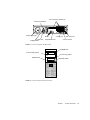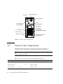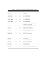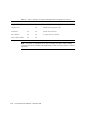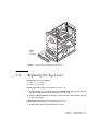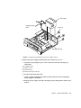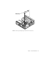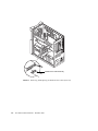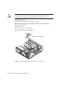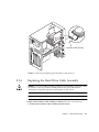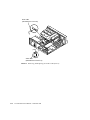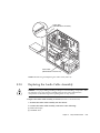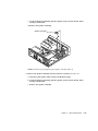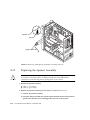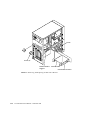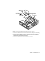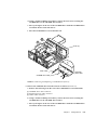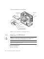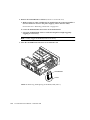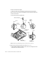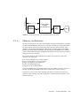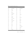
1
Sun™ Ultra™ 5/10 Service
Manual
Sun Microsystems, Inc.
901 San Antonio Road
Palo Alto, CA 94303-4900 USA
650 960-1300
Fax 650 969-9131
Part No.: 805-0423-11
November 1998, Revision A
1998 Sun Microsystems, Inc., 901 San Antonio Road, Palo Alto, California 94303-4900 U.S.A.
All rights reserved.
This product or document is protected by copyright and distributed under licenses restricting its use, copying, distribution, and decompilation.
No part of this product or document may be reproduced in any form by any means without prior written authorization of Sun and its licensors,
if any.
Portions of this product may be derived from the UNIX® system, licensed from Novell, Inc., and from the Berkeley 4.3 BSD system, licensed
from the University of California. UNIX is a registered trademark in the United States and in other countries and is exclusively licensed by
X/Open Company Ltd. Third-party software, including font technology in this product, is protected by copyright and licensed from Sun’s
suppliers. RESTRICTED RIGHTS: Use, duplication, or disclosure by the U.S. Government is subject to restrictions of FAR 52.227-14(g)(2)(6/87)
and FAR 52.227-19(6/87), or DFAR 252.227-7015(b)(6/95) and DFAR 227.7202-3(a).
Sun, Sun Microsystems, the Sun logo, AnswerBook, SunDocs, Solaris, The Network Is the Computer, Ultra, Ultra Port Architecture,
SunMicrophone, SunVTS, UltraSPARC, OpenBoot, and SunOS are trademarks or registered trademarks of Sun Microsystems, Inc. in the
United States and in other countries. All SPARC trademarks are used under license and are trademarks or registered trademarks of SPARC
International, Inc. in the United States and in other countries. Products bearing SPARC trademarks are based upon an architecture developed by
Sun Microsystems, Inc.
The OPEN LOOK® and Sun™ Graphical User Interfaces were developed by Sun Microsystems, Inc. for its users and licensees. Sun
acknowledges the pioneering efforts of Xerox Corporation in researching and developing the concept of visual or graphical user interfaces for
the computer industry. Sun holds a nonexclusive license from Xerox to the Xerox Graphical User Interface, which license also covers Sun’s
licensees who implement OPEN LOOK GUIs and otherwise comply with Sun’s written license agreements.
THIS PUBLICATION IS PROVIDED “AS IS” WITHOUT WARRANTY OF ANY KIND, EITHER EXPRESS OR IMPLIED, INCLUDING, BUT
NOT LIMITED TO, THE IMPLIED WARRANTIES OF MERCHANTABILITY, FITNESS FOR A PARTICULAR PURPOSE, OR NONINFRINGEMENT.
Copyright 1998 Sun Microsystems, Inc., 901 San Antonio Road, Palo Alto, Californie 94303-4900 U.S.A. Tous droits réservés.
Ce produit ou document est protégé par un copyright et distribué avec des licences qui en restreignent l’utilisation, la copie et la décompilation.
Aucune partie de ce produit ou de sa documentation associée ne peut être reproduite sous aucune forme, par quelque moyen que ce soit, sans
l’autorisation préalable et écrite de Sun et de ses bailleurs de licence, s’il y en a.
Des parties de ce produit pourront être derivées du système UNIX® licencié par Novell, Inc. et du système Berkeley 4.3 BSD licencié par
l’Université de Californie. UNIX est une marque enregistrée aux Etats-Unis et dans d’autres pays, et licenciée exclusivement par X/Open
Company Ltd. Le logiciel détenu par des tiers, et qui comprend la technologie relative aux polices de caractères, est protégé par un copyright et
licencié par des fournisseurs de Sun.
Sun, Sun Microsystems, the Sun logo, AnswerBook, SunDocs, Solaris, The Network Is the Computer, Ultra, Ultra Port Architecture,
SunMicrophone, SunVTS, UltraSPARC, OpenBoot, and SunOS sont des marques déposées ou enregistrées de Sun Microsystems, Inc. aux
Etats-Unis et dans d’autres pays. Toutes les marques SPARC, utilisées sous licence, sont des marques déposées ou enregistrées de SPARC
International, Inc. aux Etats-Unis et dans d’autres pays. Les produits portant les marques SPARC sont basés sur une architecture développée par
Sun Microsystems, Inc.
Les utilisateurs d’interfaces graphiques OPEN LOOK® et Sun™ ont été développés de Sun Microsystems, Inc. pour ses utilisateurs et licenciés.
Sun reconnaît les efforts de pionniers de Xerox Corporation pour la recherche et le développement du concept des interfaces d’utilisation
visuelle ou graphique pour l’industrie de l’informatique. Sun détient une licence non exclusive de Xerox sur l’interface d’utilisation graphique,
cette licence couvrant aussi les licenciés de Sun qui mettent en place les utilisateurs d’interfaces graphiques OPEN LOOK et qui en outre se
conforment aux licences écrites de Sun.
CETTE PUBLICATION EST FOURNIE "EN L’ETAT" SANS GARANTIE D’AUCUNE SORTE, NI EXPRESSE NI IMPLICITE, Y COMPRIS, ET
SANS QUE CETTE LISTE NE SOIT LIMITATIVE, DES GARANTIES CONCERNANT LA VALEUR MARCHANDE, L’APTITUDE DES
PRODUITS A REPONDRE A UNE UTILISATION PARTICULIERE OU LE FAIT QU’ILS NE SOIENT PAS CONTREFAISANTS DE PRODUITS
DE TIERS.
Please
Recycle
Contents
Preface
xxiii
How This Book Is Organized xxiv
Using UNIX Commands xxv
Typographic Conventions xxvi
Shell Prompts xxvi
Related Documents xxvii
Ordering Sun Documents xxviii
Sun Welcomes Your Comments xxviii
1.
2.
Product Description
1-1
1.1
Common Features
1.2
Ultra 5 Features
1.3
Ultra 10 Features
1.4
I/O Devices
1.5
System Unit Features
1.6
System Unit Components
SunVTS Overview
1-3
1-4
1-4
1-5
1-6
1-8
2-1
2.1
SunVTS Description
2.2
SunVTS Operation
2-1
2-2
Contents
iii
3.
4.
Power-On Self-Test
3.1
POST Overview
3.2
Pre-POST Preparation
3-1
3-2
3.2.1
Setting Up a Tip Connection
3.2.2
Verifying the Baud Rate
3-2
3-4
3.3
Initializing POST
3.4
Maximum and Minimum Levels of POST
3-6
3.4.1
diag-level Variable Set to max
3-6
3.4.2
diag-level Variable Set to min
3-15
3.4.3
POST Progress and Error Reporting
3-5
3.5
Bypassing POST
3.6
Additional Keyboard Control Commands
3.7
System and Keyboard LEDs
3.8
Initializing Motherboard POST
3-19
3-23
Troubleshooting Procedures
3-23
3-24
3-24
4-1
4.1
Power-On Failure
4.2
Video Output Failure
4.3
Hard Drive or CD-ROM Drive Failure
4.4
Power Supply Test
4.5
DIMM Failure
4.6
OpenBoot PROM On-Board Diagnostics
4.7
iv
3-1
4-1
4-2
4-3
4-4
4-7
4-7
4.6.1
Watch-Clock Diagnostic
4.6.2
Watch-Net and Watch-Net-All Diagnostics
4.6.3
Probe-IDE Diagnostic
4.6.4
Test alias name, device path, -All Diagnostic
4.6.5
UPA Graphics Card (Ultra 10 Only)
OpenBoot Diagnostics
4-7
4-9
4-12
4.7.1
Starting the OBDiag Menu
4.7.2
OBDiags
4-16
Sun Ultra 5/10 Service Manual • November 1998
4-8
4-12
4-11
4-10
4.7.3
5.
PCI/PCIO
4.7.2.2
EBus DMA/TCR Registers
4.7.2.3
Ethernet
4.7.2.4
Keyboard
4.7.2.5
Mouse
4-21
4.7.2.6
Floppy
4-21
4.7.2.7
Parallel Port
4-22
4.7.2.8
Serial Port A
4-22
4.7.2.9
Serial Port B
4-24
4.7.2.10
NVRAM
4.7.2.11
Audio
4.7.2.12
EIDE
4-26
4.7.2.13
Video
4-26
4.7.2.14
All Above
4-17
5.1
Safety Requirements
5.2
Symbols
5.3
Safety Precautions
4-19
4-19
4-20
4-25
4-25
4-27
Ending the OBDiag Menu
Safety and Tool Requirements
5.4
6.
4.7.2.1
4-30
5-1
5-1
5-2
5-2
5.3.1
Modification to Equipment
5-2
5.3.2
Placement of a Sun Product
5-2
5.3.3
Power Cord Connection
5.3.4
Electrostatic Discharge
5.3.5
Lithium Battery
Tools Required
Power On and Off
5-3
5-3
5-4
5-4
6-1
6.1
Powering On the System Unit
6-1
6.2
Powering Off the System Unit
6-4
Contents
v
7.
8.
Internal Access
7.1
Removing the Top Cover
7-1
7.2
Attaching the Wrist Strap
7-4
7.3
Removing the Metal Filler Panel
(Ultra 10) 7-5
7.4
Replacing the Top Cover
Major Subassemblies
8.1
8.2
8.3
8.4
8.5
vi
7-1
Power Supply
7-7
8-1
8-1
8.1.1
Removing the Power Supply
8-1
8.1.2
Replacing the Power Supply
8-4
Cable Assemblies
8-6
8.2.1
Removing the Diskette Drive Cable Assembly
8-6
8.2.2
Replacing the Diskette Drive Cable Assembly
8-9
8.2.3
Removing the Hard Drive Cable Assembly
8-9
8.2.4
Replacing the Hard Drive Cable Assembly
8-11
8.2.5
Removing the Serial/Parallel Cable Assembly
8-12
8.2.6
Replacing the Serial/Parallel Cable Assembly
8-14
8.2.7
Removing the Audio Cable Assembly
8-15
8.2.8
Replacing the Audio Cable Assembly
8-17
Speaker Assembly
8-18
8.3.1
Removing the Speaker Assembly
8-18
8.3.2
Replacing the Speaker Assembly
8-20
CPU Fan Assembly
8-21
8.4.1
Removing the CPU Fan Assembly
8-21
8.4.2
Replacing the CPU Fan Assembly
8-23
Front Bezel
8-25
8.5.1
Removing the Front Bezel
8-25
8.5.2
Replacing the Front Bezel
8-27
Sun Ultra 5/10 Service Manual • November 1998
8.6
9.
9.2
9.3
8-28
8.6.1
Removing the Drive Bracket
8-28
8.6.2
Replacing the Drive Bracket
8-31
Storage Devices
9.1
10.
Rear Drive Bracket (Ultra 10 Only)
9-1
Diskette Drive
9-1
9.1.1
Removing the Diskette Drive
9-1
9.1.2
Replacing the Diskette Drive
9-5
Hard Drive
9-7
9.2.1
Removing a Hard Drive
9-7
9.2.2
Replacing a Hard Drive
9-12
CD-ROM Drive
9-14
9.3.1
Removing a CD-ROM Drive
9-14
9.3.2
Replacing a CD-ROM Drive
9-16
Motherboard and Component Replacement
10.1
10.2
10.3
10.4
CPU Module
10-1
10-2
10.1.1
Removing the CPU Module
10-2
10.1.2
Replacing the CPU Module
10-4
NVRAM/TOD
10-5
10.2.1
Removing the NVRAM/TOD
10-5
10.2.2
Replacing the NVRAM/TOD
10-7
PCI Card
10-8
10.3.1
Removing a PCI Card
10-8
10.3.2
Replacing a PCI Card
10-12
UPA Graphics Card (Ultra 10)
10-14
10.4.1
Removing a UPA Graphics Card
10-14
10.4.2
Replacing a UPA Graphics Card
10-16
10.4.3
Elite3D m3 UPA Graphics Card Patch Information
10-17
Contents
vii
10.5
10.6
10.7
11.
DIMM
10-18
10.5.1
Removing a DIMM
10-18
10.5.2
Replacing a DIMM
10-20
Riser Board
10-22
10.6.1
Removing the Riser Board
10-22
10.6.2
Replacing the Riser Board
10-24
Motherboard
10-25
10.7.1
Removing the Motherboard
10-26
10.7.2
Replacing the Motherboard
10-31
Illustrated Parts List
A. Product Specifications
A.1
A.2
A.3
viii
11-1
A-1
Physical Specifications
A-1
A.1.1
Ultra 5 Physical Specifications
A.1.2
Ultra 10 Physical Specifications
Electrical Specifications
A-2
A-2
A-2
A.2.1
Ultra 5 Electrical Specifications
A.2.2
Ultra 10 Electrical Specifications
Modem Setup Specifications
A-3
A-3
A-4
A.3.1
Setting Up the Modem
A-4
A.3.2
Serial Port Speed Change
A.3.3
Recommendations
A-5
A-5
A.3.3.1
Cable
A-5
A.3.3.2
Modem Switch Settings (AT Commands)
A.4
Environmental Requirements
A.5
Reference Information
A-6
A-7
A.5.1
CD-ROM Drive Cabling Configuration
A.5.2
Ultra 5 Hard Drive Cabling Configuration
A.5.3
Ultra 10 Hard Drive Cabling Configuration
A.5.4
Jumper Settings
Sun Ultra 5/10 Service Manual • November 1998
A-9
A-7
A-8
A-8
A-6
A.5.5
CD Handling and Use
A-9
A.5.5.1
Inserting a CD into the CD-ROM Drive
A-9
A.5.5.2
Ejecting a CD From the CD-ROM Drive
A-9
A.5.5.3
Cleaning the CD-ROM Drive
A.5.5.4
Handling and Storing CDs
B. Signal Descriptions
Power Supply Connectors
B.2
Keyboard/Mouse Connector
B.3
Twisted-Pair Ethernet Connector
B-1
B-3
B-4
B.3.1
TPE Cable-Type Connectivity
B.3.2
External UTP-5 Cable Lengths
B.4
Serial Port A Connector
B-6
B.5
Serial Port B Connector
B-7
B.6
Parallel Port Connector
B-8
B.7
Audio Connectors
B.8
UPA Graphics Card Connector
(Ultra 10 Only) B-11
B.9
Video Connector
B-12
C. Functional Description
C-1
System Unit
C.1.1
A-10
B-1
B.1
C.1
A-10
B-5
B-6
B-10
C-1
CPU Module
C-3
C.1.1.1
CPU Module (Ultra 5)
C.1.1.2
CPU Module (Ultra 10)
C.1.2
UPA
C.1.3
PCI-IDE Interface
C-4
C-4
C-4
C-5
C.1.3.1
Primary PCI Bus
C-5
C.1.3.2
Secondary PCI Buses
C.1.3.3
APB ASIC
C.1.3.4
PCIO ASIC
C.1.3.5
10-/100-Mbit Ethernet
C-6
C-6
C-6
C-6
Contents
ix
C.1.4
C.1.5
C.1.6
C.1.7
C.1.8
C.2
C.3
x
C.1.3.6
EBus2 Interface
C.1.3.7
EIDE Interface
C.1.3.8
PCI-Based Graphics
Memory Architecture
C-7
C-8
C-10
C-11
C.1.4.1
DIMM Memory Configuration
C.1.4.2
DIMM Characteristics
C.1.4.3
Memory Address Assignment
C.1.4.4
Transceivers
Riser Board
C-13
C-14
C-15
C-15
C.1.5.1
Connector Definition
C.1.5.2
Riser Board Pin Assignment
ASICs
C-13
C-16
C-16
C-20
C.1.6.1
APB
C.1.6.2
PCIO
C-20
C.1.6.3
RISC
C-21
EBus2 Devices
C-20
C-22
C.1.7.1
SuperIO
C-23
C.1.7.2
Serial Communications Controller
C.1.7.3
Flash PROM
C.1.7.4
NVRAM/TOD
C.1.7.5
Audio
C-24
C-25
C-25
Power and Standby Switching
C-27
C.1.8.1
Power Supply On/Off Switch
C.1.8.2
Keyboard Standby Key
C.1.8.3
Front Panel Standby Switch
Clocking
C-27
C-27
C-27
C-28
C.2.1
CPU and UPA Clocking
C.2.2
PCI Clock Generation
Address Mapping
C-28
C-28
C-30
C.3.1
Port Allocations
C.3.2
UPA Graphics Address Assignments
Sun Ultra 5/10 Service Manual • November 1998
C-24
C-30
C-31
C.3.3
PCI Address Assignments
C.3.3.1
PCI Bus A Address Assignments
C-32
C.3.3.2
PCI Bus B Address Assignments
C-32
C.4
Interrupts
C.5
Power
C-33
C-36
C.5.1
On-Board Voltage Regulator
C.5.2
Power Supply Memory
C.5.3
Power Management
C.6
Motherboard
C.7
Jumper Descriptions
C.8
C-32
C-37
C-37
C-37
C-39
C.7.1
Serial Port Jumpers
C.7.2
Flash PROM Jumpers
Enclosure
C-40
C-41
C-42
C.8.1
Ultra 5 Enclosure Basics
C.8.2
Ultra 10 Enclosure Basics
D. Conformity
C-42
C-43
D-1
D.1
Declaration of Conformity
D.2
Regulatory Compliance Statement
D.3
Agency Compliance
D.4
German Acoustic Compliance
D-1
F. Software Notes
D-5
D-9
D-9
E. Safety Agency Compliance Statement
F.1
C-37
E-1
F-1
PGX24 8- or 24-Bit Graphics
F-1
F.1.1
What Does 8-Bit or 24-Bit Frame Buffer Refer To?
F-1
F.1.2
The Difference Between 8-Bit Mode and 24-Bit Mode on Ultra 5/10
On-Board Graphics F-2
F.1.3
How to Install PGX24 Graphics Software on Solaris 2.5.1 HW:11/
97 F-2
F.1.4
How to Install PGX24 Graphics Software on Solaris 2.6 5/98
F-3
Contents
xi
F.1.5
Which Mode is Running
F.1.6
Changing From One Mode to the Other
Glossary
xii
Glossary-1
Sun Ultra 5/10 Service Manual • November 1998
F-4
F-4
Figures
FIGURE 1-1
Ultra 5 Desktop Workstation 1-2
FIGURE 1-2
Ultra 10 Minitower Workstation
FIGURE 1-3
Ultra 5 System Unit Front View 1-6
FIGURE 1-4
Ultra 5 System Unit Rear View
FIGURE 1-5
Ultra 10 System Unit Front View 1-7
FIGURE 1-6
Ultra 10 System Unit Rear View 1-8
FIGURE 3-1
Setting Up a TIP Connection
FIGURE 3-2
Sun Type-5 Keyboard 3-5
FIGURE 4-1
Power Supply Connector J17 Pin Configuration 4-5
FIGURE 4-2
Power Supply Connector J20 Pin Configuration (Ultra 10 only)
FIGURE 6-1
System Unit Power On/Off Switch 6-2
FIGURE 6-2
System Unit Standby Switch
FIGURE 6-3
Sun Type-5 Keyboard 6-3
FIGURE 7-1
Removing and Replacing the Top Cover (Ultra 5)
FIGURE 7-2
Removing and Replacing the Top Cover (Ultra 10) 7-3
FIGURE 7-3
Attaching the Wrist Strap to the Chassis (Ultra 5)
FIGURE 7-4
Attaching the Wrist Strap to the Chassis (Ultra 10) 7-5
FIGURE 7-5
Removing and Replacing the Plastic Filler Panel (Ultra 10) 7-6
FIGURE 7-6
Removing the Metal Filler Panel (Ultra 10) 7-7
1-3
1-7
3-3
4-6
6-3
7-2
7-4
Figures
xiii
xiv
FIGURE 8-1
Removing and Replacing the Power Supply (Ultra 5)
FIGURE 8-2
Removing and Replacing the Power Supply (Ultra 10))
FIGURE 8-3
Removing and Replacing the Diskette Drive Cable (Ultra 5) 8-7
FIGURE 8-4
Removing and Replacing the Diskette Drive Cable (Ultra 10)
FIGURE 8-5
Removing and Replacing the Hard Drive Cable (Ultra 5)
FIGURE 8-6
Removing and Replacing the Hard Drive Cable (Ultra 10) 8-11
FIGURE 8-7
Removing and Replacing the Serial/Parallel Cable (Ultra 5)
FIGURE 8-8
Removing and Replacing the Serial/Parallel Cable (Ultra 10) 8-14
FIGURE 8-9
Removing and Replacing the Audio Cable (Ultra 5)
FIGURE 8-10
Removing and Replacing the Audio Cable (Ultra 10) 8-17
FIGURE 8-11
Removing and Replacing the Speaker Assembly (Ultra 5)
FIGURE 8-12
Removing and Replacing the Speaker Assembly (Ultra 10) 8-20
FIGURE 8-13
Removing and Replacing the CPU Fan Assembly (Ultra 5) 8-22
FIGURE 8-14
Removing and Replacing the CPU Fan Assembly (Ultra 10) 8-23
FIGURE 8-15
Removing and Replacing the Front Bezel (Ultra 5) 8-26
FIGURE 8-16
Removing and Replacing the Front Bezel (Ultra 10)
FIGURE 8-17
Removing and Replacing the Rear Drive Bracket
FIGURE 9-1
Removing and Replacing the Diskette Drive Part 1 (Ultra 5)
9-3
FIGURE 9-2
Removing and Replacing the Diskette Drive Part 2 (Ultra 5)
9-4
FIGURE 9-3
Removing and Replacing the Diskette Drive (Ultra 10)
FIGURE 9-4
Removing and Replacing a Hard Drive (Ultra 5) 9-8
FIGURE 9-5
Removing and Replacing a Hard Drive (Ultra 5) 9-9
FIGURE 9-6
Removing and Replacing a Hard Drive (Ultra 10 Chassis Rear)
9-10
FIGURE 9-7
Removing and Replacing a Hard Drive (Ultra 10 Chassis Front)
9-11
FIGURE 9-8
Removing and Replacing a CD-ROM Drive (Ultra 5)
FIGURE 9-9
Removing and Replacing a CD-ROM Drive (Ultra 10) 9-16
FIGURE 10-1
Removing and Replacing the CPU Module (Ultra 5)
FIGURE 10-2
Removing and Replacing the CPU Module (Ultra 10) 10-4
Sun Ultra 5/10 Service Manual • November 1998
8-3
8-4
8-8
8-10
8-13
8-16
8-19
8-27
8-30
9-5
9-15
10-3
FIGURE 10-3
Removing and Replacing the NVRAM/TOD (Ultra 5) 10-6
FIGURE 10-4
Removing and Replacing the NVRAM/TOD (Ultra 10)
FIGURE 10-5
Removing and Replacing a PCI Card From PCI Slot 1 and/or 3 (Ultra 5)
FIGURE 10-6
Removing and Replacing the PCI Card From PCI Slot 2 (Ultra 5) 10-10
FIGURE 10-7
Removing and Replacing the PCI Card (Ultra 10)
FIGURE 10-8
Removing and Replacing the UPA Graphics Card (Ultra 10)
FIGURE 10-9
Removing and Replacing a DIMM (Ultra 5) 10-19
FIGURE 10-10
Removing and Replacing a DIMM (Ultra 10)
FIGURE 10-11
Removing and Replacing the Riser Board (Ultra 5)
FIGURE 10-12
Removing and Replacing the Riser Board (Ultra 10)
10-24
FIGURE 10-13
Removing and Replacing the Motherboard (Ultra 5)
10-28
FIGURE 10-14
Removing and Replacing the Motherboard (Ultra 5)
10-29
FIGURE 10-15
Removing and Replacing the Motherboard (Ultra 10)
FIGURE 10-16
Identifying Jumper Pins
FIGURE 11-1
Ultra 5 Computer System Unit Exploded View
FIGURE 11-2
Ultra 10 Computer System Unit Exploded View 11-4
FIGURE A-1
CD-ROM Drive Cabling Configuration
FIGURE A-2
Ultra 5 Hard Drive Cabling Configuration
FIGURE A-3
Ultra 10 Hard Drive Cabling Configuration A-8
FIGURE B-1
Power Supply Connector J12 Pin Configuration B-2
FIGURE B-2
Power Supply Connector J13 Pin Configuration B-2
FIGURE B-3
Keyboard/Mouse Connector Pin Configuration B-4
FIGURE B-4
TPE Connector Pin Configuration
FIGURE B-5
Serial Port A Connector Pin Configuration
B-6
FIGURE B-6
Serial Port B Connector Pin Configuration
B-8
FIGURE B-7
Parallel Port Connector Pin Configuration
B-9
FIGURE B-8
Audio Connector Configuration
FIGURE B-9
UPA Graphics Card Connector Pin Configuration B-12
10-7
10-9
10-11
10-15
10-20
10-23
10-31
10-32
11-2
A-7
A-8
B-5
B-11
Figures
xv
xvi
FIGURE B-10
Video Connector Pin Configuration B-13
FIGURE C-1
System Unit Functional Block Diagram C-2
FIGURE C-2
UPA Graphics Functional Block Diagram
FIGURE C-3
10-/100-Mbit Ethernet Functional Block Diagram
FIGURE C-4
EIDE Interface Functional Block Diagram
FIGURE C-5
EIDE Cable Labeling
FIGURE C-6
Supported Ultra 5 Configuration
FIGURE C-7
Supported Ultra 10 Configuration C-10
FIGURE C-8
PCI-Based Graphics Functional Block Diagram (PGX) C-10
FIGURE C-9
PCI-Based Graphics Functional Block Diagram (PGX24)
FIGURE C-10
Memory Interface Functional Block Diagram C-12
FIGURE C-11
System Reset Functional Block Diagram
FIGURE C-12
Standard Serial Port Functional Block Diagram
FIGURE C-13
Communications Controller Serial Ports Functional Block Diagram
FIGURE C-14
NVRAM/TOD Functional Block Diagram
FIGURE C-15
Audio Circuit Functional Block Diagram C-26
FIGURE C-16
Interrupt Scheme Block Diagram C-34
FIGURE C-17
Motherboard Block Diagram C-38
FIGURE C-18
Selected Jumper Settings
FIGURE C-19
Identifying Jumper Pins
FIGURE C-20
JP3/JP4 Jumper Settings for RS-423 Interface C-40
FIGURE C-21
JP1/JP2 Jumper Settings for the Flash PROM
C-5
C-7
C-8
C-9
C-9
C-22
C-23
C-25
C-39
C-39
Sun Ultra 5/10 Service Manual • November 1998
C-11
C-42
C-24
Tables
TABLE P-1
Document Organization
TABLE P-2
Typographic Conventions xxvi
TABLE P-3
Shell Prompts
TABLE P-4
Related Documents
TABLE 1-1
Supported I/O Devices
TABLE 1-2
Ultra 5 and Ultra 10 Physical Dimensions
TABLE 1-3
Ultra 5 and Ultra 10 System Unit Replaceable Components
TABLE 2-1
SunVTS Documentation
TABLE 3-1
Diag-Level Switch Settings
TABLE 3-2
Keyboard LED Patterns
TABLE 4-1
Internal Drives Identification 4-3
TABLE 4-2
Power Supply Connector J17 Pin Assignments
4-5
TABLE 4-3
Power Supply Connector J20 Pin Assignments
4-6
TABLE 4-4
DIMM Physical Memory Address
TABLE 4-5
Selected OBP On-Board Diagnostic Tests
TABLE 10-1
Sun Ultra 5/10 Software Note CD Selection 10-17
TABLE 10-2
DIMM Group and Slot Pairs 10-18
TABLE 10-3
Serial Port Jumper Settings
TABLE 11-1
Ultra 5 System Unit Replaceable Components
TABLE 11-2
Ultra 10 Computer Replaceable Components
xxiv
xxvi
xxvii
1-5
1-6
1-8
2-2
3-2
3-21
4-7
4-10
10-32
11-3
11-5
Tables
xvii
xviii
TABLE A-1
Ultra 5 Physical Specifications
TABLE A-2
Ultra 10 Physical Specifications A-2
TABLE A-3
Ultra 5 Electrical Specifications A-3
TABLE A-4
Ultra 10 Electrical Specifications
TABLE A-5
Environmental Requirements
TABLE B-1
Power Supply Connector J13 Pin Assignments
B-2
TABLE B-2
Power Supply Connector J12 Pin Assignments
B-2
TABLE B-3
Keyboard/Mouse Connector Pin Assignments
TABLE B-4
TPE Connector Pin Assignments
TABLE B-5
TPE UTP-5 Cables
TABLE B-6
Serial Port A Connector Pin Assignments
B-6
TABLE B-7
Serial Port B Connector Pin Assignments
B-8
TABLE B-8
Parallel Port Connector Pin Assignments
B-9
TABLE B-9
Audio Connector Line Assignment B-11
TABLE B-10
UPA Graphics Card Connector Pin Assignments
TABLE B-11
Video Connector Pin Assignments
TABLE C-1
Ultra 5 CPU Module Cache and SRAM
C-4
TABLE C-2
Ultra 10CPU Module Cache and SRAM
C-4
TABLE C-3
Memory DIMM Configuration
C-13
TABLE C-4
PA Map Into RASx_L Signals
C-14
TABLE C-5
Memory Address Range Based on Installed DIMMs
TABLE C-6
Riser Board Pin Summary
TABLE C-7
Riser Board Pin Assignment
TABLE C-8
Audio Input Electrical Specification
TABLE C-9
Audio Output Electrical Specification
TABLE C-10
PCI Clocks
TABLE C-11
PCI Clock Generator Frequency Select (ICW48C60-422G) C-29
TABLE C-12
PCI Clock Generator Frequency Select (CY2254A-2) C-29
TABLE C-13
Port Allocations C-30
TABLE C-14
UPA Address Space
A-2
A-3
A-6
B-4
B-5
B-6
B-12
B-13
C-14
C-16
C-16
C-26
C-26
C-28
C-31
Sun Ultra 5/10 Service Manual • November 1998
TABLE C-15
CPU Module Internal CSR Space
TABLE C-16
PCI Address Assignments
TABLE C-17
Boot PROM/Flash PROM Address Assignments
TABLE C-18
Interrupt Routing
TABLE C-19
Serial Port Jumper Settings
TABLE C-20
Flash PROM Jumper Settings C-42
C-31
C-32
C-33
C-34
C-41
Tables
xix
xx
Sun Ultra 5/10 Service Manual • November 1998
Code Samples
CODE EXAMPLE 3-1
diag-level Variable Set to max
3-7
CODE EXAMPLE 3-2
diag-level Variable Set to min
3-15
CODE EXAMPLE 3-3
Typical Error Code Failure Message
CODE EXAMPLE 4-1
Watch-Clock Diagnostic Output Message
CODE EXAMPLE 4-2
Watch-Net Diagnostic Output Message
CODE EXAMPLE 4-3
Watch-Net-All Diagnostic Output Message
CODE EXAMPLE 4-4
Probe-IDE Diagnostic Output Message 4-9
CODE EXAMPLE 4-5
Test Diagnostic Output Message
CODE EXAMPLE 4-6
Reset Verification
CODE EXAMPLE 4-7
OBDiag Menu
CODE EXAMPLE 4-8
PCI/PCIO Output Message
CODE EXAMPLE 4-9
EBus DMA/TCR Registers Output Message
3-19
4-8
4-8
4-9
4-10
4-13
4-15
4-17
4-19
CODE EXAMPLE 4-10
Ethernet Output Message
CODE EXAMPLE 4-11
Keyboard Output Message
CODE EXAMPLE 4-12
Mouse Output Message
4-21
CODE EXAMPLE 4-13
Floppy Output Message
4-21
CODE EXAMPLE 4-14
Parallel Port Output Message
4-22
CODE EXAMPLE 4-15
Serial Port A Output Message
4-22
CODE EXAMPLE 4-16
Serial Port A Output Message With TIP Line Installed
4-20
4-20
4-23
Code Samples
xxi
CODE EXAMPLE 4-17
Serial Port B Output Message
CODE EXAMPLE 4-18
NVRAM Output Message
CODE EXAMPLE 4-19
Audio Output Message
CODE EXAMPLE 4-20
EIDE Output Message 4-26
CODE EXAMPLE 4-21
Video Output Message
CODE EXAMPLE 4-22
All Above Output Message
xxii
4-24
4-25
4-25
4-26
4-27
Sun Ultra 5/10 Service Manual • November 1998
Preface
The Sun Ultra 5/10 Service Manual provides detailed procedures that describe the
removal and replacement of replaceable parts in the Sun™ Ultra™ 5 and the Ultra 10
computers (system units). The service manual also includes information about the
use and maintenance of the system units. This book is written for technicians,
system administrators, authorized service providers (ASPs), and advanced computer
system end users who have experience troubleshooting and replacing hardware.
Note – Removal and replacement of selected system unit components are also
illustrated with photographs and audio/visual instructions on the Sun Ultra 5
ShowMe How Multimedia Documentation, part number 704-5753 and the Sun Ultra 10
ShowMe How Multimedia Documentation, part number 704-5983.
Preface
xxiii
How This Book Is Organized
This document is organized into chapters and appendixes as listed in the following
table. A glossary is also included.
TABLE P-1
xxiv
Document Organization
Chapter
Content Description
Chapter 1, “Product Description”
Describes the major components of the
system units.
Chapter 2, “SunVTS Overview”
Describes the execution of individual tests
for verifying hardware configuration and
functionality.
Chapter 3, “Power-On Self-Test”
Describes the execution of POST and
provides examples of POST output patterns.
Chapter 4, “Troubleshooting Procedures”
Provides troubleshooting advice and
suggested corrective actions for hardware
problems.
Chapter 5, “Safety and Tool Requirements”
Explains how to work safely when servicing
the system units.
Chapter 6, “Power On and Off”
Provides step-by-step procedures to power
on and power off the system units.
Chapter 7, “Internal Access”
Provides step-by-step procedures to remove
the cover, attach the wrist strap, and replace
the cover.
Chapter 8, “Major Subassemblies”
Provides step-by-step procedures to remove
and replace major subassemblies.
Chapter 9, “Storage Devices”
Provides step-by-step procedures to remove
and replace storage devices.
Chapter 10, “Motherboard and Component
Replacement”
Provides step-by-step procedures to remove
and replace the motherboard and various
components associated with motherboard
operation.
Chapter 11, “Illustrated Parts List”
Lists replaceable parts for the system units.
Appendix A, “Product Specifications”
Provides product specifications, system
requirements about power and environment,
system unit dimensions, weight, memory
mapping, and peripheral component
interconnect (PCI) card slot specifications.
Sun Ultra 5/10 Service Manual • November 1998
TABLE P-1
Document Organization (Continued)
Chapter
Content Description
Appendix B, “Signal Descriptions”
Provides signal descriptions, instructions for
connecting the system unit to a 10BASE-T/
100BASE-T twisted-pair Ethernet (TPE) local
area network (LAN), and modem settings
for system units used in specific network
telecommunication applications.
Appendix C, “Functional Description”
Provides functional descriptions for the
system units.
Appendix D, “Regulatory Compliance
Statements”
Provides regulatory compliance statements.
Appendix E, “Safety Agency Compliance
Statements”
Provides safety agency compliance
statements.
Appendix F, “Software Notes”
Identifies software issues.
Using UNIX Commands
This document may not contain information on basic UNIX commands and
procedures such as shutting down the system, booting the system, and configuring
devices.
See one or more of the following for this information:
■
Solaris Handbook for Sun Peripherals
■
AnswerBook online documentation for the Solaris software environment
■
Other software documentation that you received with your system
Preface
xxv
Typographic Conventions
Typographic conventions used in this service manual are listed in the following
table.
TABLE P-2
Typographic Conventions
Typeface or
Symbol
Meaning
Examples
AaBbCc123
The names of commands, files,
and directories; on-screen
computer output.
Edit your .login file.
Use ls -a to list all files.
% You have mail.
AaBbCc123
What you type, when
contrasted with on-screen
computer output.
% su
Password:
AaBbCc123
Book titles, new words or
terms, words to be emphasized.
Command-line variable;
replace with a real name or
value.
Read Chapter 6 in the User’s Guide.
These are called class options.
You must be root to do this.
To delete a file, type rm filename.
Shell Prompts
The following table lists the default system prompt and superuser prompt for the C
shell, Bourne shell, and Korn shell.
TABLE P-3
xxvi
Shell Prompts
Shell
Prompt
C shell
machine_name%
C shell superuser
machine_name#
Bourne shell and Korn shell
$
Bourne shell and Korn shell
superuser
#
Sun Ultra 5/10 Service Manual • November 1998
Related Documents
Additional information for servicing the system unit are listed in the following table.
These documents are also available online on the Sun Ultra 5/10 Hardware
AnswerBook or on the Solaris on Sun Hardware AnswerBook.
TABLE P-4
Related Documents
Application
Title
Part Number
Configuration
Solaris Handbook for Sun Peripherals
805-4440
Configuration
Solaris Handbook for Sun Frame Buffers
805-4441
Diagnostics
SunVTS 2.0 User’s Guide
802-5331
Diagnostics
SunVTS 2.0 Test Reference Manual
802-5330
Diagnostics
SunVTS 2.0 Quick Reference Card
802-5329
Installation
Creator Installation Guide
802-7731
Installation
Sun Ultra 5/10 CD-ROM Drive and Hard Disk
Drive Installation Guide
805-7115
Software notes
Sun Ultra 5/10 Preinstalled Software Notes
805-4971
805-6962
805-6963
805-5590
Specification
17-Inch Entry, 17-Inch Premium, and
20-Inch Premium Color Monitors Specifications
802-6178
Specification
4.2-Gbyte 7200-RPM Disk Drive Specifications
802-7744
Specification
Diskette Drive Specification
802-6285
User
SunVTS 2.0 User’s Guide
802-5331
Preface
xxvii
Ordering Sun Documents
The docs.sun.com web site enables you to access Sun technical documentation on
the web. You can browse the docs.sun.com archive or search for a specific book title
or subject at:
http://docs.sun.com
Sun Welcomes Your Comments
We are interested in improving our documentation and welcome your comments
and suggestions. You can email your comments to us at:
[email protected]
Please include the part number of your document in the subject line of your email.
xxviii
Sun Ultra 5/10 Service Manual • November 1998
CHAPTER
1
Product Description
The Ultra 5 and Ultra 10 workstations are uniprocessor devices that use the family of
UltraSPARC™ processors. They support high-performance CPU module
(UltraSPARC-IIi) processing and high-performance graphics (Ultra 10 only).
FIGURE 1-1 illustrates the Ultra 5 desktop workstation and FIGURE 1-2 illustrates the
Ultra 10 minitower workstation.
This chapter contains the following topics:
■
Section 1.1 “Common Features” on page 1-3
■
Section 1.2 “Ultra 5 Features” on page 1-4
■
Section 1.3 “Ultra 10 Features” on page 1-4
■
Section 1.4 “I/O Devices” on page 1-5
■
Section 1.5 “System Unit Features” on page 1-6
■
Section 1.6 “System Unit Components” on page 1-8
1-1
Monitor
System unit
Keyboard
Mouse
FIGURE 1-1
1-2
Ultra 5 Desktop Workstation
Sun Ultra 5/10 Service Manual • November 1998
Keyboard
Monitor
Mouse
System unit
FIGURE 1-2
1.1
Ultra 10 Minitower Workstation
Common Features
The Ultra 5 and Ultra 10 workstations provide the following common features:
■
UltraSPARC-IIi processor module (CPU module)/advanced PCI bridge (APB)
application-specific integrated circuit (ASIC)
■
33-megahertz (MHz), 32-bit peripheral component interconnect (PCI)
■
Enhanced integrated drive electronic (IDE) hard drive
■
CD-ROM drive
■
PGX on-board graphics
■
PGX24 PCI on-board graphics
■
Two serial ports
■
One parallel port
■
10-/100-megabit per second Ethernet
■
CD quality audio
Chapter 1
Product Description
1-3
■
1.44-megabyte (Mbyte) manual eject diskette drive
■
Front access Personal Computer Memory Card International Association
(PCMCIA) bay (two Type II or one Type III slot(s))
Note – Systems with PGX24 graphics have "PGX24" printed on the serial number
label that is affixed to the system cover.
1.2
Ultra 5 Features
The Ultra 5 workstation provides the following unique features:
1.3
■
333-MHz, 2-Mbyte cache CPU module or 270-MHz, 256-kilobyte (Kbyte) cache
CPU module
■
Three PCI slots (riser card expansion with two long PCI cards and one short
PCI card)
■
One hard drive bay
■
One front-access 5.25-inch bay
■
Desktop enclosure
■
200-watt power supply
Ultra 10 Features
The Ultra 10 workstation provides the following unique features:
1-4
■
360-MHz, 2-Mbyte cache CPU module; or 333-MHz, 2-Mbyte cache CPU module;
or 300-MHz, 512-Kbyte cache CPU module
■
1-gigabyte (Gbyte) memory (maximum)
■
Four PCI slots (riser card expansion with four long PCI cards)
■
One UltraSPARC port architecture (UPA) graphics slot
■
One internal hard drive bay
■
One dedicated front-access 5.25-inch bay
■
One optional front-access 5.25-inch bay
■
Minitower enclosure
■
250-watt power supply
Sun Ultra 5/10 Service Manual • November 1998
1.4
I/O Devices
The Ultra 5 and Ultra 10 workstations use the I/O devices listed in TABLE 1-1.
TABLE 1-1
Supported I/O Devices
I/O Device
Description
17-inch (43-cm)
color monitor
1280 x 1024 resolution, 76- or 66-Hz refresh rate, 110 dots per inch
(dpi)
20-inch (51-cm)
color monitor
1152 x 900 resolution, 76- or 66-Hz refresh rate, 84 dpi
1280 x 1024 resolution, 76- or 66-Hz refresh rate, 93 dpi
960 x 680 resolution, 112-Hz refresh rate, 70 dpi
24-inch (61-cm)
color monitor
1920 x 1200 resolution, 70-Hz refresh rate, 103 dpi
1600 x 1000 resolution, 76- or 66-Hz refresh rate, 86 dpi
1400 x 900 resolution, 76-Hz refresh rate, 77 dpi
1280 x 800 resolution, 76-Hz refresh rate, 69 dpi
Microphone
SunMicrophone™ II (optional)
Keyboard
Sun Type-5; AT 101 or UNIX layout available
Mouse
Sun Type-5; optomechanical, 3-button
Chapter 1
Product Description
1-5
1.5
System Unit Features
System unit components are housed in either a desktop enclosure (Ultra 5), or a
minitower enclosure (Ultra 10). Overall chassis dimensions for the Ultra 5 and
Ultra 10 are listed in the following table.
TABLE 1-2
Ultra 5 and Ultra 10 Physical Dimensions
Unit
Width
Height
Depth
Ultra 5
Desktop Enclosure
17.17 inches (43.60 cm)
4.31 inches (10.95 cm)
16.69 inches (42.40 cm)
Ultra 10
Minitower Enclosure
6.93 inches (17.60 cm)
15.75 inches (40.00 cm)
16.54 inches (42.00 cm)
System unit electronics are contained on a single printed circuit board
(motherboard). The motherboard contains the CPU module, memory, system control
ASICs, and I/O ASICs.
The following figures illustrate the Ultra 5 and Ultra 10 system unit front and rear
views.
System unit
3.5-inch bay (spare)
Diskette drive
FIGURE 1-3
1-6
Ultra 5 System Unit Front View
Sun Ultra 5/10 Service Manual • November 1998
CD-ROM drive
Standby switch
PCI connector, 33-MHz (3)
Power on/off switch
Power supply fan
Power inlet
Voltage select
FIGURE 1-4
Audio
Keyboard/mouse
Serial port
TPE connector
VGA connector
Ultra 5 System Unit Rear View
CD-ROM drive
5.25-inch bay (spare)
3.5-inch bay (spare)
Diskette drive
FIGURE 1-5
Standby switch
Ultra 10 System Unit Front View
Chapter 1
Product Description
1-7
Power on/off switch
Power inlet
Power supply fan
Audio
Voltage select
(not illustrated)
Keyboard/mouse
UPA graphics
Serial port B
(not illustrated)
PCI connector, 33-MHz (4)
Serial port A
Video connector
TPE connector
FIGURE 1-6
1.6
Parallel port connector
(not illustrated)
Ultra 10 System Unit Rear View
System Unit Components
The following table lists the Ultra 5 and Ultra 10 system unit replaceable
components. A brief description of each listed component is also provided.
Note – Consult your authorized Sun sales representative or service provider prior to
ordering a replacement part.
TABLE 1-3
Ultra 5 and Ultra 10 System Unit Replaceable Components
Component
Ultra 5
Ultra 10
Description
Manual eject floppy
Yes
Yes
Diskette drive
Yes
Speaker assembly
Speaker assembly
Fan assembly
1-8
Yes
Sun Ultra 5/10 Service Manual • November 1998
CPU fan, 80-mm
TABLE 1-3
Component
Ultra 5 and Ultra 10 System Unit Replaceable Components (Continued)
Ultra 5
Fan assembly
Ultra 10
Description
Yes
CPU fan, 92-mm
CD-ROM drive
Yes
Yes
CD-ROM drive
16-Mbyte DIMM
Yes
Yes
60-ns, 16-Mbyte DIMM
32-Mbyte DIMM
Yes
Yes
60-ns, 32-Mbyte DIMM
64-Mbyte DIMM
Yes
Yes
60-ns, 64-Mbyte DIMM
128-Mbyte DIMM
Yes
Yes
60-ns, 128-Mbyte DIMM
256-Mbyte DIMM
Yes
Yes
60-ns, 256-Mbyte DIMM
Service kit
Yes
Yes
Includes diskette drive cable assembly, hard drive
cable assembly, serial/parallel cable assembly, and
CD-ROM drive cable assembly
CPU module
Yes
CPU module
CPU module
Yes
CPU module
270-MHz, 256-kilobyte (Kbyte) external cache
Yes
360-MHz, 2-Mbyte external cache
Yes
333-MHz, 2-Mbyte external cache
Yes
300-MHz, 512-Kbyte external cache
Motherboard
Yes
Yes
System board
NVRAM/TOD
Yes
Yes
Time of day, 48T59, with carrier
PCI card
Yes
Yes
Generic
Riser board
Yes
Riser board
3-slot riser board
Yes
Hard drive
Yes
Hard drive
Yes
Power supply
Yes
4-slot riser board
Disk drive, 4.3-Gbyte, 5400 RPM
Yes
Disk drive, 9.1-Gbyte, 7200 RPM
Power supply, 200 watts
Power supply
Yes
Power supply, 250 watts
Graphics card
Yes
Vertical, double buffer plus Z (DBZ) UPA graphics
card
Chapter 1
Product Description
1-9
TABLE 1-3
Component
Ultra 5 and Ultra 10 System Unit Replaceable Components (Continued)
Ultra 5
Ultra 10
Description
Graphics card
Yes
Vertical, single buffer UPA graphics card
Graphics card
Yes
Elite3D m3 UPA graphics card
Front bezel
Yes
Yes
System unit front bezel
Drive bracket
No
Yes
9.1-Gbyte rear drive bracket
Audio cable assembly
Yes
Yes
Note – The Ultra 5/10 diskette drive cable assembly, hard drive cable assembly,
serial/parallel cable assembly, and CD-ROM drive cable assembly cannot be ordered
separately.
1-10
Sun Ultra 5/10 Service Manual • November 1998
CHAPTER
2
SunVTS Overview
This chapter contains an overview of the SunVTS™ diagnostic tool.
This chapter contains the following topics:
■
■
2.1
Section 2.1 “SunVTS Description” on page 2-1
Section 2.2 “SunVTS Operation” on page 2-2
SunVTS Description
The SunVTS software executes multiple diagnostic hardware tests from a single user
interface. SunVTS verifies the configuration, functionality, and reliability of most
hardware controllers and devices.
The SunVTS software can be used in both the Common Desktop Environment (CDE)
and the OPEN LOOK graphical user interface (GUI) environments, or from a TTY
interface.
Within the CDE and OPEN LOOK GUI environments, test parameters can be set
quickly and easily by pointing and clicking a mouse button.
With a TTY interface, the SunVTS software can be used from a terminal or modem
attached to a serial port. Data is input through the keyboard, rather than with a
mouse, and only one screen of information is displayed at a time.
2-1
2.2
SunVTS Operation
The following table lists the documentation for the SunVTS software. These
documents are available on the Solaris on Sun Hardware Collection.
TABLE 2-1
SunVTS Documentation
Title
Description
SunVTS User’s Guide
802-7299
Describes the SunVTS environment;
starting and controlling various user
interfaces; feature descriptions
SunVTS Test Reference Manual
802-7300
Describes each SunVTS test; provides
various test options and command line
arguments
SunVTS Quick Reference Card
2-2
Part Number
Sun Ultra 5/10 Service Manual • November 1998
802-7301
Provides overview of vtsui interface
features
CHAPTER
3
Power-On Self-Test
This chapter describes how to initiate power-on self-test (POST) diagnostics.
This chapter contains the following topics:
■
■
■
■
■
■
■
■
3.1
Section 3.1
Section 3.2
Section 3.3
Section 3.4
Section 3.5
Section 3.6
Section 3.7
Section 3.8
“POST Overview” on page 3-1
“Pre-POST Preparation” on page 3-2
“Initializing POST” on page 3-5
“Maximum and Minimum Levels of POST” on page 3-6
“Bypassing POST” on page 3-23
“Additional Keyboard Control Commands” on page 3-23
“System and Keyboard LEDs” on page 3-24
“Initializing Motherboard POST” on page 3-24
POST Overview
POST is useful in determining if a portion of the system unit has failed and should
be replaced. POST detects approximately 95 percent of system unit faults and is
located in the system board OpenBoot™ PROM (OBP). The setting of two NVRAM
variables, the diag-switch? and the diag-level flag, determine if POST is
executed (see Section 3.3 “Initializing POST” on page 3-5).. The following table lists
the diag-switch? and diag-level flag settings for disabling POST (off),
enabling POST maximum (max), or enabling POST minimum (min).
3-1
TABLE 3-1
Diag-Level Switch Settings
Diag-Level Setting
POST
Initialization
Serial Port A
I/O
Serial Port A
Error Output
Diag-Switch?
Setting
Off
No
N/A
N/A
N/A
Max
Yes (power-on)
Enabled
Enabled
True
Min
Yes (power-on)
Disabled
Enabled
True
3.2
Pre-POST Preparation
Pre-POST preparation includes:
■
Setting up a tip connection to another workstation or terminal to view POST
progress and error messages. See Section 3.2.1 “Setting Up a Tip Connection” on
page 3-2.
■
Verifying baud rates between a workstation and a monitor or a workstation and a
terminal. See Section 3.2.2 “Verifying the Baud Rate” on page 3-4.
If a terminal or a monitor is not connected to serial port A (default port) of a
workstation or server to be tested, the keyboard LEDs are used to determine error
conditions. See Section 3.7 “System and Keyboard LEDs” on page 3-24.
3.2.1
Setting Up a Tip Connection
A tip connection enables a remote shell window to be used as a terminal to display
test data of a system being tested. Serial port A or serial port B of a tested system
unit is used to establish the tip connection between the system unit being tested and
another Sun workstation monitor or TTY-type terminal. The tip connection is used in
a SunOS™ window and provides features to help with the OBP.
To set up a tip connection, refer to the following figure and proceed as follows:
3-2
Sun Ultra 5/10 Service Manual • November 1998
2
2
3
3
7
7
20
20
FIGURE 3-1
Setting Up a TIP Connection
1. Connect serial port A of the system being tested to serial port B of another Sun
workstation using a serial null modem cable (connect cable pins 2-3, 3-2, 7-20, and
20-7).
2. At the other Sun workstation, check the /etc/remote file by changing to the
/etc directory and then editing the remote file:
hardwire: /dv=/dev/term/b:br#9600:el=^C^S^Q^U^D:ie=%$:oe=^D:
Note – The example shows connection to serial port B.
3. To use serial port A:
a. Copy and paste the serial port B remote file.
b. Modify the serial port B remote file as follows:
hardwire: /dv=/dev/term/a:br#9600:el=^C^S^Q^U^D:ie=%$:oe=^D:
4. In a shell window on the Sun workstation, type tip hardwire.
% tip hardwire
connected
Note – The shell window is now a tip window directed to the serial port of the
system unit being tested. When power is applied to the system unit being tested,
POST messages will be displayed in this window.
Chapter 3
Power-On Self-Test
3-3
5. When POST is completed, disconnect the tip window as follows:
a. Open a shell window.
b. Type ps -a to view the active tip line and process ID (PID) number.
c. Type the following to kill the tip hardwire process.
% kill -9 PID#
3.2.2
Verifying the Baud Rate
To verify the baud rate between the system unit being tested and a terminal or
another Sun workstation monitor:
1. Open a shell window.
2. Type eeprom.
3. Verify the following serial port default settings as follows:
ttyb-mode = 9600,8,n,1
ttya-mode = 9600,8,n,1
Note – Ensure that the settings are consistent with TTY-type terminal or
workstation monitor settings.
3-4
Sun Ultra 5/10 Service Manual • November 1998
3.3
Initializing POST
POST is initilized in two ways:
■
■
By setting the diag-switch? to true and the diag-level to max or min,
followed by power cycling the system unit
By simultaneously pressing the keyboard Stop and D keys while power is applied
to the system unit.
To set the diag-switch? to true and power cycle the system unit:
1. At the system prompt, type:
ok% setenv diag-switch? true
2. At the keyboard, power cycle the system unit by simultaneously pressing the
Shift key and the Standby key. After a few seconds, press the
Standby key again. See the following figure
Stop
key
Caps Lock
Shift key
key indicator
FIGURE 3-2
D key
Scroll Lock
key indicator
Standby key
Compose
key indicator
Num Lock
key indicator
Sun Type-5 Keyboard
3. Verify the following:
■
■
■
The display prompt is no longer displayed.
The monitor power-on indicator flashes on and off.
The keyboard Caps Lock key indicator flashes on and off.
Chapter 3
Power-On Self-Test
3-5
4. When the POST is complete, type the following at the system prompt:
ok% setenv diag-switch? false
3.4
Maximum and Minimum Levels of
POST
Two levels of POST are available: maximum (max) level and minimum (min) level.
The system initiates the selected level of POST based upon the setting of
diag-level, a NVRAM variable.
The default setting for diag-level is max. An example of a max level POST output
on serial port A is provided in Section 3.4.1, “diag-level Variable Set to max An
example of a min level POST output on serial port A is provided in Section 3.4.2
“diag-level Variable Set to min” on page 3-15.
To set the diag-level variable to min, type:
ok% setenv diag-level min
To return to the default setting:
ok% setenv diag-level max
3.4.1
diag-level Variable Set to max
When the diag-level variable is set to max, POST enables an extended set of
diagnostic-level tests. This mode requires approximately 2 minutes to complete
(with 128 Mbytes of DIMM installed). The following code example identifies a
typical serial port A POST output with the diag-level variable set to max.
3-6
Sun Ultra 5/10 Service Manual • November 1998
Note – Video output is disabled while POST is initialized.
CODE EXAMPLE 3-1
diag-level Variable Set to max
Power On Selftest Completed
Software Power ON0.0000.0000.0000 ffff.ffff.f00b.4100
0002.3333.0200.001b
@(#) Sun Ultra 5/10 UPA/PCI 3.9 P2.1 Version 9 created 1997/08/
05 16:24
Clearing E$ Tags Done
Clearing I/D TLBs Done
Probing Memory Done
MEM BASE = 0000.0000.0000.0000
MEM SIZE = 0000.0000.1000.0000
11-Column Mode Enabled
MMUs ON
Copy Done
PC = 0000.01ff.f000.20ec
PC = 0000.0000.0000.2130
Decompressing into Memory Done
Size = 0000.0000.0007.5300
ttya initialized
Reset Control: BXIR:0 BPOR:0 SXIR:0 SPOR:1 POR:0
UltraSPARC-IIi 2-2 module
Probing Memory Bank #0 128 + 128 : 256 Megabytes
Probing Memory Bank #2
0 +
0 :
0 Megabytes
Probing Floppy: drive detected on ID0
Probing EBUS SUNW,CS4231
Probing UPA Slot at 1e,0 SUNW,ffb
Probing /pci@1f,0/pci@1,1 at Device 2 SUNW,m64B
Probing /pci@1f,0/pci@1,1 at Device 3 ide disk cdrom
Probing /pci@1f,0/pci@1 at Device 1 Nothing there
Probing /pci@1f,0/pci@1 at Device 2 Nothing there
Probing /pci@1f,0/pci@1 at Device 3 Nothing there
Probing /pci@1f,0/pci@1 at Device 4 Nothing there
Reset Control: BXIR:0 BPOR:0 SXIR:0 SPOR:1 POR:0
UltraSPARC-IIi 2-2 module
Probing Memory Bank #0 128 + 128 : 256 Megabytes
Probing Memory Bank #2
0 +
0 :
0 Megabytes
Probing Floppy: drive detected on ID0
Probing EBUS SUNW,CS4231
Probing UPA Slot at 1e,0 SUNW,ffb
Probing /pci@1f,0/pci@1,1 at Device 2 SUNW,m64B
Probing /pci@1f,0/pci@1,1 at Device 3 ide disk cdrom
Probing /pci@1f,0/pci@1 at Device 1 Nothing there
Probing /pci@1f,0/pci@1 at Device 2 Nothing there
Chapter 3
Power-On Self-Test
3-7
CODE EXAMPLE 3-1
diag-level Variable Set to max (Continued)
Power On Selftest Completed
Probing /pci@1f,0/pci@1 at Device 3
Probing /pci@1f,0/pci@1 at Device 4
Nothing there
Nothing there
Sun Ultra 5/10 UPA/PCI (UltraSPARC-IIi 300MHz), No Keyboard
OpenBoot 3.9 P2.1 , 256 MB memory installed, Serial #9337477.
Ethernet address 8:0:20:8e:7a:85, Host ID: 808e7a85.
ok Hardware Power ON
@(#) Sun Ultra 5/10 UPA/PCI
05 16:24
Probing keyboard Done
%o0 = 0000.0000.0000.4001
3.9 P2.1
Version 9 created 1997/08/
Executing Power On SelfTest
@(#) Sun Ultra 5/10 (Darwin) POST 2.1.1 (Build No. 293) 08/21/97:
15:59
CPU: UltraSPARC-LC (MHz: 301 Ecache Size:
Init POST BSS
Init System BSS
NVRAM
NVRAM Battery Detect Test
NVRAM Scratch Addr Test
NVRAM Scratch Data Test
DMMU TLB Tags
DMMU TLB Tag Access Test
DMMU TLB RAM
DMMU TLB RAM Access Test
Probe Ecache
Probe Ecache
Ecache Tests
Ecache RAM Addr Test
Ecache Tag Addr Test
Ecache RAM Test
Ecache Tag Test
All CPU Basic Tests
V9 Instruction Test
CPU Tick and Tick Compare Reg Test
CPU Soft Trap Test
3-8
Sun Ultra 5/10 Service Manual • November 1998
512KB)
CODE EXAMPLE 3-1
diag-level Variable Set to max (Continued)
Power On Selftest Completed
CPU Softint Reg and Int Test
All Basic MMU Tests
DMMU Primary Context Reg Test
DMMU Secondary Context Reg Test
DMMU TSB Reg Test
DMMU Tag Access Reg Test
DMMU VA Watchpoint Reg Test
DMMU PA Watchpoint Reg Test
IMMU TSB Reg Test
IMMU Tag Access Reg Test
All Basic Cache Tests
Dcache RAM Test
Dcache Tag Test
Icache RAM Test
Icache Tag Test
Icache Next Test
Icache Predecode Test
Sabre MCU Control & Status Regs Init and Tests
Init Sabre MCU Control & Status Regs
Initializing SC registers in SabreIO
Memory Probe and Init
Probe Memory
INFO:
256MB Bank 0
bank 2: 0MB
frequency = 301, refvalue = 146, no_of_banks = 1
INFO: MC0 = 0x00000000.80001192, MC1 = 0x00000000.0c4aab14
Malloc Post Memory
Memory Addr w/ Ecache
Load Post In Memory
Run POST from MEM
.........
loaded POST in memory
Map PROM/STACK/NVRAM in DMMU
Update Master Stack/Frame Pointers
All FPU Basic Tests
FPU Regs Test
FPU Move Regs Test
FPU State Reg Test
FPU Functional Test
FPU Trap Test
UPA Data Bus Line Test
Memory Tests
Init Memory
INFO:
256MB at bank 0 stack 0 (2 dimms per bank)
Chapter 3
Power-On Self-Test
3-9
CODE EXAMPLE 3-1
diag-level Variable Set to max (Continued)
Power On Selftest Completed
................................................................
................................................................
................................................................
........................................................
INFO:
0MB at bank 0 stack 1
INFO:
0MB at bank 2 stack 0
INFO:
0MB at bank 2 stack 1
Memory Addr w/ Ecache Test
INFO:
256MB at bank 0 stack 0 (2 dimms per bank)
INFO:
0MB at bank 0 stack 1
INFO:
0MB at bank 2 stack 0
INFO:
0MB at bank 2 stack 1
ECC Memory Addr Test
INFO:
256MB at bank 0 stack 0 (2 dimms per bank)
INFO:
0MB at bank 0 stack 1
INFO:
0MB at bank 2 stack 0
INFO:
0MB at bank 2 stack 1
Block Memory Addr Test
INFO:
256MB at bank 0 stack 0 (2 dimms per bank)
INFO:
0MB at bank 0 stack 1
INFO:
0MB at bank 2 stack 0
INFO:
0MB at bank 2 stack 1
Block Memory Test
INFO:
256MB at bank 0 stack 0 (2 dimms per bank)
Write 0x33333333.33333333
................................................................
................................................................
................................................................
........................................................
Read
................................................................
................................................................
................................................................
........................................................
Write 0x55555555.55555555
................................................................
................................................................
................................................................
........................................................
Read
................................................................
................................................................
................................................................
........................................................
3-10
Sun Ultra 5/10 Service Manual • November 1998
CODE EXAMPLE 3-1
diag-level Variable Set to max (Continued)
Power On Selftest Completed
Write 0xcccccccc.cccccccc
................................................................
................................................................
................................................................
........................................................
Read
................................................................
................................................................
................................................................
........................................................
Write 0xaaaaaaaa.aaaaaaaa
................................................................
................................................................
................................................................
........................................................
Read
................................................................
................................................................
................................................................
........................................................
INFO:
0MB at bank 0 stack 1
INFO:
0MB at bank 2 stack 0
INFO:
0MB at bank 2 stack 1
ECC Blk Memory Test
INFO:
256MB at bank 0 stack 0 (2 dimms per bank)
Write 0xa5a5a5a5.a5a5a5a5
................................................................
................................................................
................................................................
........................................................
Read
................................................................
................................................................
................................................................
........................................................
Write 0x96969696.96969696
................................................................
................................................................
................................................................
........................................................
Chapter 3
Power-On Self-Test
3-11
CODE EXAMPLE 3-1
diag-level Variable Set to max (Continued)
Power On Selftest Completed
Read
................................................................
................................................................
................................................................
........................................................
Write 0xbbbbbbbb.bbbbbbbb
................................................................
................................................................
................................................................
........................................................
Read
................................................................
................................................................
................................................................
........................................................
Write 0xdddddddd.dddddddd
................................................................
................................................................
................................................................
........................................................
Read
................................................................
................................................................
................................................................
........................................................
INFO:
0MB at bank 0 stack 1
INFO:
0MB at bank 2 stack 0
INFO:
0MB at bank 2 stack 1
All Basic Sabre MMU Tests
Init Sabre
PIO Decoder and BCT Test
PCI Byte Enable Test
Interrupt Map (short) Reg Test
Interrupt Set/Clr Reg Test
Sabre IOMMU Regs Test
Sabre IOMMU RAM Address Test
Sabre IOMMU CAM Address Test
IOMMU TLB Compare Test
IOMMU TLB Flush Test
PBMA PCI Config Space Regs Test
PBMA Control/Status Reg Test
PBMA Diag Reg Test
Sabre IO Regs Test
All Advanced CPU Tests
3-12
Sun Ultra 5/10 Service Manual • November 1998
CODE EXAMPLE 3-1
diag-level Variable Set to max (Continued)
Power On Selftest Completed
DMMU Hit/Miss Test
IMMU Hit/Miss Test
DMMU Little Endian Test
IU ASI Access Test
FPU ASI Access Test
Ecache Thrash Test
All CPU Error Reporting Tests
CPU Data Access Trap Test
CPU Addr Align Trap Test
DMMU Access Priv Page Test
DMMU Write Protected Page Test
All Advanced Sabre IOMMU Tests
Init Sabre
Consist DMA Rd, IOMMU miss Ebus Test
Consist DMA Rd, IOMMU hit Ebus Test
Consist DMA Wr, IOMMU miss Ebus Test
Consist DMA Wr, IOMMU hit Ebus Test
Pass-Thru DMA Rd, Ebus device Test
Pass-Thru DMA Wr, Ebus device Test
Consist DMA Rd, IOMMU LRU Lock Ebus Test
Consist DMA Wr, IOMMU LRU Locked Ebus Test
All Basic Cheerio Tests
Cheerio Ebus PCI Config Space Test
Cheerio Ethernet PCI Config Space Test
Cheerio Init
All Sabre IOMMU Error Reporting Tests
Init Sabre
PIO Read, Master Abort Test
PIO Read, Target Abort Test
Status of this POST run:PASS
manfacturing mode=OFF
Time Stamp [hour:min:sec] 00:02:01
[month/date year] 08/22 1997
Power On Selftest Completed
Software Power ON0.0000.0000.0000 ffff.ffff.f00b.4100
0002.3333.0200.001b
@(#) Sun Ultra 5/10 UPA/PCI
05 16:24
Clearing E$ Tags Done
Clearing I/D TLBs Done
3.9 P2.1
Version 9 created 1997/08/
Chapter 3
Power-On Self-Test
3-13
CODE EXAMPLE 3-1
diag-level Variable Set to max (Continued)
Power On Selftest Completed
Probing Memory Done
MEM BASE = 0000.0000.0000.0000
MEM SIZE = 0000.0000.1000.0000
11-Column Mode Enabled
MMUs ON
Copy Done
PC = 0000.01ff.f000.20ec
PC = 0000.0000.0000.2130
Decompressing into Memory Done
Size = 0000.0000.0007.5300
ttya initialized
Reset Control: BXIR:0 BPOR:0 SXIR:0 SPOR:1 POR:0
UltraSPARC-IIi 2-2 module
Probing Memory Bank #0 128 + 128 : 256 Megabytes
Probing Memory Bank #2
0 +
0 :
0 Megabytes
Probing Floppy: drive detected on ID0
Probing EBUS SUNW,CS4231
Probing UPA Slot at 1e,0 SUNW,ffb
Probing /pci@1f,0/pci@1,1 at Device 2 SUNW,m64B
Probing /pci@1f,0/pci@1,1 at Device 3 ide disk cdrom
Probing /pci@1f,0/pci@1 at Device 1 Nothing there
Probing /pci@1f,0/pci@1 at Device 2 Nothing there
Probing /pci@1f,0/pci@1 at Device 3 Nothing there
Probing /pci@1f,0/pci@1 at Device 4 Nothing there
Reset Control: BXIR:0 BPOR:0 SXIR:0 SPOR:1 POR:0
UltraSPARC-IIi 2-2 module
Probing Memory Bank #0 128 + 128 : 256 Megabytes
Probing Memory Bank #2
0 +
0 :
0 Megabytes
Probing Floppy: drive detected on ID0
Probing EBUS SUNW,CS4231
Probing UPA Slot at 1e,0 SUNW,ffb
Probing /pci@1f,0/pci@1,1 at Device 2 SUNW,m64B
Probing /pci@1f,0/pci@1,1 at Device 3 ide disk cdrom
Probing /pci@1f,0/pci@1 at Device 1 Nothing there
Probing /pci@1f,0/pci@1 at Device 2 Nothing there
Probing /pci@1f,0/pci@1 at Device 3 Nothing there
Probing /pci@1f,0/pci@1 at Device 4 Nothing there
Sun Ultra 5/10 UPA/PCI (UltraSPARC-IIi 300MHz), No Keyboard
OpenBoot 3.9 P2.1 , 256 MB memory installed, Serial #9337477.
Ethernet address 8:0:20:8e:7a:85, Host ID: 808e7a85.
3-14
Sun Ultra 5/10 Service Manual • November 1998
CODE EXAMPLE 3-1
diag-level Variable Set to max (Continued)
Power On Selftest Completed
ok
3.4.2
diag-level Variable Set to min
When the diag-level variable is set to min, POST enables an abbreviated set of
diagnostic-level tests. This mode requires approximately 1 minute to complete (with
128 Mbytes of DIMM installed). The following code example identifies a serial port
A POST output with the diag-level NVRAM variable set to min.
Note – Video output is disabled while POST is initialized.
CODE EXAMPLE 3-2
diag-level Variable Set to min
@(#) Sun Ultra 5/10 UPA/PCI
05 16:24
Probing keyboard Done
%o0 = 0000.0000.0000.2001
3.9 P2.1
Version 9 created 1997/08/
Executing Power On SelfTest
@(#) Sun Ultra 5/10 (Darwin) POST 2.1.1 (Build No. 293) 08/21/97:
15:59
CPU: UltraSPARC-LC (MHz: 301 Ecache Size:
512KB)
Init POST BSS
Init System BSS
NVRAM
NVRAM Battery Detect Test
NVRAM Scratch Addr Test
NVRAM Scratch Data Test
DMMU TLB Tags
DMMU TLB Tag Access Test
DMMU TLB RAM
DMMU TLB RAM Access Test
Probe Ecache
Probe Ecache
Ecache Tests
Ecache RAM Addr Test
Chapter 3
Power-On Self-Test
3-15
CODE EXAMPLE 3-2
diag-level Variable Set to min (Continued)
@(#) Sun Ultra 5/10 UPA/PCI 3.9 P2.1 Version 9 created 1997/08/
05 16:24
Ecache Tag Addr Test
All CPU Basic Tests
V9 Instruction Test
CPU Soft Trap Test
CPU Softint Reg and Int Test
All Basic MMU Tests
DMMU Primary Context Reg Test
DMMU Secondary Context Reg Test
DMMU TSB Reg Test
DMMU Tag Access Reg Test
IMMU TSB Reg Test
IMMU Tag Access Reg Test
All Basic Cache Tests
Dcache RAM Test
Icache RAM Test
Sabre MCU Control & Status Regs Init and Tests
Init Sabre MCU Control & Status Regs
Initializing SC registers in SabreIO
Memory Probe and Init
Probe Memory
INFO:
256MB Bank 0
bank 2: 0MB
frequency = 301, refvalue = 146, no_of_banks = 1
INFO: MC0 = 0x00000000.80001192, MC1 = 0x00000000.0c4aab14
Malloc Post Memory
Memory Addr w/ Ecache
Load Post In Memory
Run POST from MEM
.........
loaded POST in memory
Map PROM/STACK/NVRAM in DMMU
Update Master Stack/Frame Pointers
All FPU Basic Tests
FPU Regs Test
FPU Move Regs Test
UPA Data Bus Line Test
Memory Tests
Init Memory
INFO:
256MB at bank 0 stack 0 (2 dimms per bank)
................................................................
................................................................
................................................................
........................................................
INFO:
0MB at bank 0 stack 1
INFO:
0MB at bank 2 stack 0
3-16
Sun Ultra 5/10 Service Manual • November 1998
CODE EXAMPLE 3-2
diag-level Variable Set to min (Continued)
@(#) Sun Ultra 5/10 UPA/PCI 3.9 P2.1 Version 9 created 1997/08/
05 16:24
INFO:
0MB at bank 2 stack 1
ECC Memory Addr Test
INFO:
256MB at bank 0 stack 0 (2 dimms per bank)
INFO:
0MB at bank 0 stack 1
INFO:
0MB at bank 2 stack 0
INFO:
0MB at bank 2 stack 1
All Basic Sabre MMU Tests
Init Sabre
Interrupt Map (short) Reg Test
Interrupt Set/Clr Reg Test
Sabre IOMMU Regs Test
Sabre IOMMU RAM Address Test
Sabre IOMMU CAM Address Test
PBMA PCI Config Space Regs Test
PBMA Control/Status Reg Test
PBMA Diag Reg Test
Sabre IO Regs Test
All Advanced CPU Tests
IU ASI Access Test
FPU ASI Access Test
All CPU Error Reporting Tests
CPU Data Access Trap Test
CPU Addr Align Trap Test
DMMU Access Priv Page Test
DMMU Write Protected Page Test
All Advanced Sabre IOMMU Tests
Init Sabre
Consist DMA Rd, IOMMU miss Ebus Test
All Basic Cheerio Tests
Cheerio Ebus PCI Config Space Test
Cheerio Ethernet PCI Config Space Test
Cheerio Init
All Sabre IOMMU Error Reporting Tests
Init Sabre
PIO Read, Master Abort Test
PIO Read, Target Abort Test
Status of this POST run:PASS
manfacturing mode=OFF
Time Stamp [hour:min:sec] 00:10:33
[month/date year] 08/22 1997
Chapter 3
Power-On Self-Test
3-17
CODE EXAMPLE 3-2
diag-level Variable Set to min (Continued)
@(#) Sun Ultra 5/10 UPA/PCI 3.9 P2.1 Version 9 created 1997/08/
05 16:24
Power On Selftest Completed
Software Power ON0.0000.0000.0000 ffff.ffff.f00b.4100
0002.3333.0200.001b
@(#) Sun Ultra 5/10 UPA/PCI 3.9 P2.1 Version 9 created 1997/08/
05 16:24
Clearing E$ Tags Done
Clearing I/D TLBs Done
Probing Memory Done
MEM BASE = 0000.0000.0000.0000
MEM SIZE = 0000.0000.1000.0000
11-Column Mode Enabled
MMUs ON
Copy Done
PC = 0000.01ff.f000.20ec
PC = 0000.0000.0000.2130
Decompressing into Memory Done
Size = 0000.0000.0007.5300
ttya initialized
Reset Control: BXIR:0 BPOR:0 SXIR:0 SPOR:1 POR:0
UltraSPARC-IIi 2-2 module
Probing Memory Bank #0 128 + 128 : 256 Megabytes
Probing Memory Bank #2
0 +
0 :
0 Megabytes
Probing Floppy: drive detected on ID0
Probing EBUS SUNW,CS4231
Probing UPA Slot at 1e,0 SUNW,ffb
Probing /pci@1f,0/pci@1,1 at Device 2 SUNW,m64B
Probing /pci@1f,0/pci@1,1 at Device 3 ide disk cdrom
Probing /pci@1f,0/pci@1 at Device 1 Nothing there
Probing /pci@1f,0/pci@1 at Device 2 Nothing there
Probing /pci@1f,0/pci@1 at Device 3 Nothing there
Probing /pci@1f,0/pci@1 at Device 4 Nothing there
Reset Control: BXIR:0 BPOR:0 SXIR:0 SPOR:1 POR:0
UltraSPARC-IIi 2-2 module
Probing Memory Bank #0 128 + 128 : 256 Megabytes
Probing Memory Bank #2
0 +
0 :
0 Megabytes
Probing Floppy: drive detected on ID0
Probing EBUS SUNW,CS4231
Probing UPA Slot at 1e,0 SUNW,ffb
Probing /pci@1f,0/pci@1,1 at Device 2 SUNW,m64B
Probing /pci@1f,0/pci@1,1 at Device 3 ide disk cdrom
Probing /pci@1f,0/pci@1 at Device 1 Nothing there
Probing /pci@1f,0/pci@1 at Device 2 Nothing there
Probing /pci@1f,0/pci@1 at Device 3 Nothing there
Probing /pci@1f,0/pci@1 at Device 4 Nothing there
3-18
Sun Ultra 5/10 Service Manual • November 1998
CODE EXAMPLE 3-2
diag-level Variable Set to min (Continued)
@(#) Sun Ultra 5/10 UPA/PCI
05 16:24
3.9 P2.1
Version 9 created 1997/08/
Sun Ultra 5/10 UPA/PCI (UltraSPARC-IIi 300MHz), No Keyboard
OpenBoot 3.9 P2.1 , 256 MB memory installed, Serial #9337477.
Ethernet address 8:0:20:8e:7a:85, Host ID: 808e7a85.
ok
3.4.3
POST Progress and Error Reporting
While POST is initialized, the Caps Lock key on the Sun type-5 keyboard flashes on
and off to indicate that POST tests are being executed. Additional POST progress
indications are also visible when a TTY-type terminal or a tip line is connected
between serial port A (default port) of the system being tested and a POST
monitoring system.
If an error occurs during the POST execution, the keyboard Caps Lock key indicator
stops flashing and an error code is displayed using the Caps Lock, Compose, Scroll
Lock, and Num Lock key indicators. The error code indicates a particular system
hardware failure.
Note – An error code may only be visible for a few seconds. Observe the Caps Lock,
Compose, Scroll Lock, and Num Lock key indicators closely while POST is active.
In most cases, POST also attempts to send a failure message to the POST monitoring
system. The following code example identifies the typical appearance of a error
message. If a keyboard error code is displayed, determine the meaning of the error
code by using TABLE 3-2 on page 21.
Note – The system does not automatically boot if a POST error occurs; it halts at the
ok prompt to indicate a failure.
CODE EXAMPLE 3-3
Typical Error Code Failure Message
@(#) Sun Ultra 5/10 UPA/PCI
05 16:24
Probing keyboard Done
%o0 = 0000.0000.0000.2001
3.9 P2.1
Version 9 created 1997/08/
Chapter 3
Power-On Self-Test
3-19
CODE EXAMPLE 3-3
Typical Error Code Failure Message (Continued)
@(#) Sun Ultra 5/10 UPA/PCI
05 16:24
Executing Power On SelfTest
3.9 P2.1
Version 9 created 1997/08/
@(#) Sun Ultra 5/10 (Darwin) POST 2.1.1 (Build No. 293) 08/21/97:
15:59
CPU: UltraSPARC-LC (MHz: 301 Ecache Size:
512KB)
Init POST BSS
Init System BSS
NVRAM
NVRAM Battery Detect Test
NVRAM Scratch Addr Test
NVRAM Scratch Data Test
DMMU TLB Tags
DMMU TLB Tag Access Test
DMMU TLB RAM
DMMU TLB RAM Access Test
Probe Ecache
Probe Ecache
Ecache Tests
Ecache RAM Addr Test
Ecache Tag Addr Test
All CPU Basic Tests
V9 Instruction Test
CPU Soft Trap Test
CPU Softint Reg and Int Test
All Basic MMU Tests
DMMU Primary Context Reg Test
DMMU Secondary Context Reg Test
DMMU TSB Reg Test
DMMU Tag Access Reg Test
IMMU TSB Reg Test
IMMU Tag Access Reg Test
All Basic Cache Tests
Dcache RAM Test
Icache RAM Test
Sabre MCU Control & Status Regs Init and Tests
Init Sabre MCU Control & Status Regs
Initializing SC registers in SabreIO
Memory Probe and Init
Probe Memory
INFO: All the memory banks in 10 bit column mode
INFO:
32MB Bank 0
frequency = 301, refvalue = 73, no_of_banks = 2
3-20
Sun Ultra 5/10 Service Manual • November 1998
CODE EXAMPLE 3-3
Typical Error Code Failure Message (Continued)
@(#) Sun Ultra 5/10 UPA/PCI 3.9 P2.1 Version 9 created 1997/08/
05 16:24
INFO: MC0 = 0x00000000.80000549, MC1 = 0x00000000.0c4aab14
Malloc Post Memory
Memory Addr w/ Ecache
Load Post In Memory
Run POST from MEM
.........
loaded POST in memory
Map PROM/STACK/NVRAM in DMMU
Update Master Stack/Frame Pointers
All FPU Basic Tests
FPU Regs Test
FPU Move Regs Test
UPA Data Bus Line Test
Memory Tests
Init Memory
INFO:
32MB at bank 0 stack 0 (2 dimms per bank)
........................
INFO:
0MB at bank 0 stack 1
ERROR:
DIMM Undetected on some sockets on the board!
ERROR:
DIMM Undetected on some sockets on the board!
ECC Memory Addr Test
INFO:
32MB at bank 0 stack 0 (2 dimms per bank)
INFO:
0MB at bank 0 stack 1
ERROR:
DIMM Undetected on some sockets on the board!
ERROR:
DIMM Undetected on some sockets on the board!
TABLE 3-2
Keyboard LED Patterns
Caps Lock
Compose
Scroll Lock
Num Lock
Bit Value
Meaning of Pattern
Blink
Off
Off
Off
x000(2)
POST in progress
Off
Off
Off
Off
0000(2)
POST successfully completed
On
Off
Off
On
1001(2)
System board failed
On
Off
On
Off
1010(2)
No memory found
On
Off
On
On
1011(2)
Reserved
On
On
Off
Off
1100(2)
Reserved
Chapter 3
Power-On Self-Test
3-21
TABLE 3-2
Keyboard LED Patterns (Continued)
Caps Lock
Compose
Scroll Lock
Num Lock
Bit Value
Meaning of Pattern
On
On
Off
On
1101(2)
Reserved
On
On
On
Off
1110(2)
Bad CPU
On
On
On
On
1111(2)
Reserved
3-22
Sun Ultra 5/10 Service Manual • November 1998
3.5
Bypassing POST
POST can be disabled and thereby bypassed. To bypass POST:
1. Prior to powering on the system, press and hold the Stop key on the keyboard
(FIGURE 3-2 on page 5).
2. With the Stop key pressed, turn on the system by pressing the Standby key.
3.6
Additional Keyboard Control
Commands
Stop Key
If the diag-level is set to either max or min and the diag-level switch? variable
is set to true and POST is not to be executed when the system is powered on, press
and hold the keyboard Stop key and press the keyboard Power-on key.
Note – Press and hold the Stop key for approximately 5 seconds.
Stop and N Keys
To set the system NVRAM parameters to the original default settings, press and hold
the Stop and N keys before powering on the system. Continue to hold the Stop and
N keys until the system banner displays on the monitor.
Chapter 3
Power-On Self-Test
3-23
3.7
System and Keyboard LEDs
The power light-emitting diode (LED), located at the chassis front, remains lighted
when the system is operating normally. FIGURE 1-3 or FIGURE 1-5 shows the location
of the power LED.
While POST is executing and making progress, the Caps Lock key LED blinks while
the rest of the LEDs are off. If POST finds an error, a pattern is encoded in the LEDs
to indicate the defective part. If POST completes with no errors, all LEDs will be off
and the system will return to the OpenBoot PROM (OBP). TABLE 3-2 on page 21
defines the keyboard LED patterns. FIGURE 3-2 on page 5 shows the location of the
LED keys on the keyboard.
3.8
Initializing Motherboard POST
To initialize the motherboard POST:
1. Power off the system unit.
2. At the keyboard, simultaneously press and hold the Stop and D keys and press
the Standby key.
Note – Video output is disabled while POST is initialized.
Note – To view the POST output results, a tip connection must be set up. See
Section 3.2.1 “Setting Up a Tip Connection” on page 3-2.
3. Verify the keyboard LEDs light to confirm the system is in the POST mode and
the keyboard Caps Lock key LED flashes on and off to indicate the system has
enabled POST.
4. If a failure occurs during POST, a keyboard key LED other than the Caps Lock
key LED may light, indicating a failed system component.
See Section 3.7 “System and Keyboard LEDs” on page 3-24.
5. If the Caps Lock key LED fails to flash after the Stop and D keys are pressed,
POST has failed.
See Section 3.7 “System and Keyboard LEDs” on page 3-24.
3-24
Sun Ultra 5/10 Service Manual • November 1998
Note – The most probable cause of this type of failure is the motherboard. However,
optional system components could also cause POST to fail.
6. Before replacing the motherboard, remove any optional components, such as PCI
cards and memory, and repeat the POST.
Note – Non-optional components such as DIMMs, the motherboard, the power
supply, and the keyboard must be installed for POST to execute properly. Removing
the optional system components and retesting the system isolates the possibility that
those components are the cause of the failure.
7. To receive additional POST failure information, establish a tip connection.
See Section 3.2.1 “Setting Up a Tip Connection” on page 3-2
Chapter 3
Power-On Self-Test
3-25
3-26
Sun Ultra 5/10 Service Manual • November 1998
CHAPTER
4
Troubleshooting Procedures
This chapter describes how to troubleshoot possible hardware problems and
includes suggested corrective actions.
This chapter contains the following topics:
■
■
■
■
■
■
■
4.1
Section 4.1
Section 4.2
Section 4.3
Section 4.4
Section 4.5
Section 4.6
Section 4.7
“Power-On Failure” on page 4-1
“Video Output Failure” on page 4-2
“Hard Drive or CD-ROM Drive Failure” on page 4-3
“Power Supply Test” on page 4-4
“DIMM Failure” on page 4-7
“OpenBoot PROM On-Board Diagnostics” on page 4-7
“OpenBoot Diagnostics” on page 4-12
Power-On Failure
This section provides examples of power-on failure symptoms and suggested
actions.
Symptom
The system unit does not power up when the keyboard standby key is pressed.
Action
Check the keyboard connection. Ensure that the keyboard is properly connected
to the system unit. Check the AC power cord. Ensure that the AC power cord is
properly connected to the system unit and to the wall receptacle. Verify that the
4-1
power on/off switch is set to on.Verify that the wall receptacle is supplying AC
power to the system unit. Check the voltage select switch. Verify that the voltage
select switch is set properly.
Press the front panel standby switch. If the system unit powers on, the keyboard
may be defective or the system unit is unable to accept the keyboard power-on
signal. Power off the system unit and press the keyboard standby key again. If the
system unit powers on, no further action is required. If the system unit does not
power on, the CPU module may not be properly seated. Inspect the CPU module
for proper seating. If the system unit powers on, no further action is required. If
the system unit does not power on, the keyboard may be defective. Connect a
spare Sun Type-5 keyboard to the system unit and press the standby key.
If the wall receptacle AC power has been verified, the CPU module is properly
seated, and a spare Sun Type-5 keyboard has been connected to the system unit
and the standby key has been pressed but the system unit does not power up, the
system unit power supply may be defective. See Section 4.4 “Power Supply Test”
on page 4-4.
Symptom
The system unit attempts to power on but does not boot or initialize the monitor.
Action
Press the keyboard standby key and watch the keyboard. The keyboard LEDs
should light briefly and a tone from the keyboard should be heard. If a tone is not
heard or if the keyboard LEDs do not light briefly, the system unit power supply
may be defective. See Section 4.4 “Power Supply Test” on page 4-4. If a keyboard
tone is heard and the keyboard LEDs light briefly but the system unit still fails to
initialize, see Section 3.8 “Initializing Motherboard POST” on page 3-24.
4.2
Video Output Failure
This section provides video output failure symptoms and suggested action.
Symptom
The video does not display at the system monitor.
Action
Check the monitor AC power cord. Ensure that the AC power cord is connected
to the monitor and to the wall receptacle. Verify that the wall receptacle is
supplying AC power to the monitor. Check the video cable connection between
the monitor and the UPA graphics card output port (Ultra 10 only) or the video
4-2
Sun Ultra 5/10 Service Manual • November 1998
output connector at the rear of the system unit. Check that the CPU module is
properly seated. If the AC connection to the monitor is correct, the video cable is
correctly connected, and the CPU module is properly seated, the system monitor,
UPA graphics card, or motherboard video chip may be defective.
4.3
Hard Drive or CD-ROM Drive Failure
This section provides hard drive and CD-ROM drive failure symptoms and
suggested actions.
Symptom
A hard drive read, write, or parity error is reported by the operating system or
customer application.
A CD-ROM drive read error or parity error is reported by the operating system or
customer application.
Action
Replace the drive indicated by the failure message. The operating system
identifies the internal drives as identified in the following table.
TABLE 4-1
Internal Drives Identification
Operating System Address
Drive Physical Location and Target
c0t0d0s#
Hard drive (Ultra 5) or rear hard drive (Ultra 10),
target 0
c0t1d0s#
Front hard disk (Ultra 10), target 1
c0t6d0s#
CD-ROM drive, target 6 (optional)
Note – The # symbol in the operating system address examples may be a numeral
between 0 and 7 that describes the slice or partition on the drive.
Symptom
Hard drive or CD-ROM drive fails to respond to commands.
Action
Test the drive response to the probe-ide command as follows:
Chapter 4
Troubleshooting Procedures
4-3
Note – To bypass POST, type setenv diag-switch? false at the ok prompt.
At the system ok prompt:
ok% reset-all
ok% probe-ide
If the hard drive responds correctly to probe-ide command, the message identified
in CODE EXAMPLE 4-4 is displayed. If the drive responds and a message is displayed,
the system EIDE controller has successfully probed the device. This is an indication
that the motherboard is operating correctly. If an optional hard drive is installed
(Ultra 10 only) and one drive does not respond to the EIDE controller probe but the
other does, replace the unresponsive drive. If the probe-ide test fails to show the
device in the message, replace the drive (see Section 9.1 “Diskette Drive” on
page 9-1). If replacing the hard drive does not correct the problem, replace the
motherboard.
4.4
Power Supply Test
The section describes how to test the power supply. FIGURE 4-1 and TABLE 4-2 identify
power supply connector J17. FIGURE 4-2 and TABLE 4-3 identify power supply
connector J20.
1. Power off the system unit.
See Section 6.2 “Powering Off the System Unit” on page 6-4.
2. Remove the top cover.
See Section 7.1 “Removing the Top Cover” on page 7-1.
3. Remove the PCI card from riser board connector 2 (adjacent to power supply), if
necessary. Disconnect the ribbon cables from motherboard to expose connectors
J17 and J20 (J20 is used in Ultra 10 only).
4. Power on the system unit.
5. Using a digital voltage meter (DVM), check the power supply output voltages as
follows:
Note – Power supply connectors J17 and J20 must remain connected to the
motherboard.
4-4
Sun Ultra 5/10 Service Manual • November 1998
a. With the negative probe of the DVM placed on a connector ground (Gnd) pin,
position the positive probe on each power pin.
b. Verify voltage and signal availability as listed in TABLE 4-2 and TABLE 4-3.
6. If any power pin signal is not present with the power supply active and properly
connected to the motherboard, replace the power supply.
10
1
20
11
FIGURE 4-1
Power Supply Connector J17 Pin Configuration
TABLE 4-2
Power Supply Connector J17 Pin Assignments
Pin
Signal
Description
1
+3.3V
+3.3 VDC
2
+3.3V
+3.3 VDC
3
Gnd
Chassis ground
4
+5V
+5 VDC
5
Gnd
Chassis ground
6
+5V
+5 VDC
7
Gnd
Chassis ground
8
PWR_OK
Power okay
9
5VSB
10
+12V
+12 VDC
11
+3.3V
+3.3 VDC
12
-12V
-12 VDC
13
Gnd
Chassis ground
14
PS_ON
Power supply on
Chapter 4
Troubleshooting Procedures
4-5
Power Supply Connector J17 Pin Assignments (Continued)
TABLE 4-2
Pin
Signal
Description
15
Gnd
Chassis ground
16
Gnd
Chassis ground
17
Gnd
Chassis ground
18
-5V
-5 VDC
19
+5V
+5 VDC
20
+5V
+5 VDC
6
4-6
1
FIGURE 4-2
Power Supply Connector J20 Pin Configuration (Ultra 10 only)
TABLE 4-3
Power Supply Connector J20 Pin Assignments
Pin
Signal
Description
1
Gnd
Chassis ground
2
Gnd
Chassis ground
3
SEN_COM
Sense common
4
SEN_+3.3V
Sense 3.3 VDC
5
+3.3V
+3.3 VDC
6
+3.3V
+3.3 VDC
Sun Ultra 5/10 Service Manual • November 1998
4.5
DIMM Failure
At times, the operating system, diagnostic program, or POST may not display a
DIMM location (U number) as part of a memory error message. In this situation, the
only available information is a physical memory address and failing byte (or bit).
The following table lists physical memory addresses to locate a defective DIMM.
TABLE 4-4
DIMM Physical Memory Address
DIMM Slot
4.6
DIMM Pair
(non-interleave)
DIMM0
DIMM1
00000000 - 0fffffff
DIMM2
DIMM3
10000000 - 1fffffff
OpenBoot PROM On-Board Diagnostics
The following sections describe the OpenBoot PROM (OBP) on-board diagnostics. To
execute the OBP on-board diagnostics, the system must be at the ok prompt. The
OBP on-board diagnostics are listed as follows:
■
■
■
■
■
4.6.1
Section 4.6.1
Section 4.6.2
Section 4.6.3
Section 4.6.4
Section 4.6.5
“Watch-Clock Diagnostic” on page 4-7
“Watch-Net and Watch-Net-All Diagnostics” on page 4-8
“Probe-IDE Diagnostic” on page 4-9
“Test alias name, device path, -All Diagnostic” on page 4-10
“UPA Graphics Card (Ultra 10 Only)” on page 4-11
Watch-Clock Diagnostic
The watch-clock diagnostic reads a register in the NVRAM/TOD chip and displays
the result as a seconds counter. During normal operation, the seconds counter
repeatedly increments from 0 to 59 until interrupted by pressing any key on the Sun
Chapter 4
Troubleshooting Procedures
4-7
Type-5 keyboard. The watch-clock diagnostic is initialized by typing the
watch-clock command at the ok prompt. The following code example identifies
the watch-clock diagnostic output message.
CODE EXAMPLE 4-1
Watch-Clock Diagnostic Output Message
ok watch-clock
Watching the 'seconds' register of the real time clock chip.
It should be 'ticking' once a second.
Type any key to stop.
49
ok
4.6.2
Watch-Net and Watch-Net-All Diagnostics
The watch-net and watch-net-all diagnostics monitor Ethernet packets on the
Ethernet interfaces connected to the system. Good packets received by the system
are indicated by a period (.). Errors such as the framing error and the cyclic
redundancy check (CRC) error are indicated with an X and an associated error
description. The watch-net diagnostic is initialized by typing the watch-net
command at the ok prompt and the watch-net-all diagnostic is initialized by typing
the watch-net-all command at the ok prompt. The following code example
identifies the watch-net diagnostic output message. CODE EXAMPLE 4-3 identifies the
watch-net-all diagnostic output message.
CODE EXAMPLE 4-2
Watch-Net Diagnostic Output Message
ok watch-net
Hme register test --- succeeded.
Internal loopback test -- succeeded.
Transceiver check -- Using Onboard Transceiver - Link Up.
passed
Using Onboard Transceiver - Link Up.
Looking for Ethernet Packets.
'.' is a Good Packet. 'X' is a Bad Packet.
Type any key to stop.
..................................................
................................................................
................................................................
........................................................
ok
4-8
Sun Ultra 5/10 Service Manual • November 1998
CODE EXAMPLE 4-3
Watch-Net-All Diagnostic Output Message
ok watch-net-all
/pci@1f,0/pci@1,1/network@1,1
Hme register test --- succeeded.
Internal loopback test -- succeeded.
Transceiver check -- Using Onboard Transceiver - Link Up.
passed
Using Onboard Transceiver - Link Up.
Looking for Ethernet Packets.
'.' is a Good Packet. 'X' is a Bad Packet.
Type any key to stop.
........
................................................................
................................................................
................................................................
....................................
ok
4.6.3
Probe-IDE Diagnostic
The probe-ide diagnostic transmits an inquiry command to internal and external IDE
devices connected to the system unit on-board IDE interface. If the EIDE device is
connected and active, the target address, unit number, device type, and
manufacturer name is displayed. The probe-ide diagnostic is initialized by typing
the probe-ide command at the ok prompt. The following code example identifies
the probe-ide diagnostic output message.
CODE EXAMPLE 4-4
Probe-IDE Diagnostic Output Message
ok probe-ide
Device 0 ( Primary Master )
ATA Model: ST34342A
Device 1
( Primary Slave )
ATA Model: ST34342A
Device 2 ( Secondary Master )
Removable ATAPI Model: CRD-8160B
Device 3 ( Secondary Slave )
Removable ATAPI Model:
ok
Chapter 4
Troubleshooting Procedures
4-9
4.6.4
Test alias name, device path, -All Diagnostic
The test diagnostic, when combined with a device alias or device path, enables a
device self-test diagnostic program. If a device has no self-test program, the
message: No selftest method for device name is displayed. To enable
the self-test program for a device, type the test command followed by the device
alias or device path name.
The following code example identifies the test diagnostic output message. Test
diagnostics are initialized by typing the test alias name or device path command at
the ok prompt. TABLE 4-5 lists the types of tests that can be used, a brief description
of each test, and preparation.
Note – The diskette drive (floppy) is selected as the test alias name example.
CODE EXAMPLE 4-5
Test Diagnostic Output Message
ok test floppy
Testing floppy disk system. A formatted disk should be in the
drive.
Test succeeded.
ok
TABLE 4-5
Selected OBP On-Board Diagnostic Tests
Type of Test
Description
Preparation
test screen
Tests system video graphics hardware and
monitor
Diag-switch? NVRAM parameter must
be true for the test to execute.
test floppy
Tests diskette drive response to commands
A formatted diskette must be inserted into
the diskette drive.
test net
Performs internal/external loopback test of
the system auto-selected Ethernet interface
An Ethernet cable must be attached to the
system and to an Ethernet tap or hub or the
external loopback test fails.
4-10
Sun Ultra 5/10 Service Manual • November 1998
TABLE 4-5
Selected OBP On-Board Diagnostic Tests (Continued)
Type of Test
Description
Preparation
test ttya
test ttyb
Outputs an alphanumeric test pattern on
the system serial ports: ttya, serial port A;
ttyb, serial port B
A terminal must be connected to the port
being tested to observe the output.
test
keyboard
Executes the keyboard selftest.
Four keyboard LEDs should flash once and
a message is displayed: Keyboard
Present.
test -all
Sequentially test system-configured devices
containing selftest.
Tests are sequentially executed in devicetree order (viewed with the show-devs
command).
4.6.5
UPA Graphics Card (Ultra 10 Only)
The UPA graphics card contains a built-in diagnostic test that is enabled through the
OBP. The UPA graphics card built-in diagnostic test verifies basic graphics
functionality without rebooting the operating system software.
To execute the built-in diagnostic test, the system must be at the ok prompt.
To initilize the UPA graphics card diagnostic:
1. At the ok prompt, type:
ok% setenv diag-switch? true
diag-switch? = true
ok% setenv diag-switch? true
2. At the ok prompt, type:
ok% test screen
Verifying Console Mode for Frame Buffer Board
This will take a few minutes
Verifying Frame Buffer Memory used for console mode
This will take about two minutes
FFB Frame Buffer functional test passed
ok%
Chapter 4
Troubleshooting Procedures
4-11
3. When the UPA graphics card on-board diagnostics are completed, type:
ok% setenv diag-switch? false
diag-switch? = false
4.7
OpenBoot Diagnostics
The OpenBoot diagnostic (OBDiag) is a menu-driven diagnostic tool that verifies:
■
■
■
■
■
■
■
■
■
■
■
Internal I/O system
Ethernet
Keyboard
Mouse
Diskette drive (floppy)
Parallel port
Serial ports
NVRAM
Audio
EIDE
Video
OBDiag performs root-cause failure analysis on the referenced devices by testing
internal registers, confirming subsystem integrity, and verifying device functionality.
Note – The OBDiag test result data captured in the following code examples
represent the test result data that is output when the system being tested is
connected to a remote shell window through a tip connection. When the system
being tested is tested in a stand-alone configuration, the test result data may differ.
4.7.1
Starting the OBDiag Menu
1. At the ok prompt, type:
ok% setenv mfg-mode on
mfg-mode = on
4-12
Sun Ultra 5/10 Service Manual • November 1998
2. At the ok prompt, type:
ok% setenv diag-switch? true
diag-switch? = true
3. At the ok prompt, type:
ok% setenv auto-boot? false
auto-boot? = false
4. At the ok prompt, type:
ok% reset-all
5. Verify that the platform resets (CODE EXAMPLE 4-6).
CODE EXAMPLE 4-6
Reset Verification
ok setenv mfg-mode on
mfg-mode =
on
ok setenv diag-switch? true
diag-switch? =
true
ok setenv auto-boot? false
auto-boot? =
false
ok reset-all
Resetting...
Software Power ON
@(#) Sun Ultra 5/10 UPA/PCI 3.11 Version 9 created 1998/03/06
10:31
Clearing E$ Tags Done
Clearing I/D TLBs Done
Probing Memory Done
MEM BASE = 0000.0000.2000.0000
MEM SIZE = 0000.0000.1000.0000
11-Column Mode Enabled
MMUs ON
Copy Done
PC = 0000.01ff.f000.1ffc
PC = 0000.0000.0000.2040
Decompressing into Memory Done
Size = 0000.0000.0006.e160
Chapter 4
Troubleshooting Procedures
4-13
CODE EXAMPLE 4-6
Reset Verification (Continued)
ttya initialized
Reset Control: BXIR:0 BPOR:0 SXIR:0 SPOR:1 POR:0
UltraSPARC-IIi 2-2 module
Probing Memory Bank #0 256 + 256: 512 Megabytes
Probing Memory Bank #2
0 +
0:
0 Megabytes
Probing UPA Slot at 1e,0 SUNW,ffb
Probing
Probing
Probing
Probing
Probing
Probing
Probing
Probing
Probing
Probing
Probing
Probing
/pci@1f,0/pci@1,1 at Device 1 pci108e,1000 network
/pci@1f,0/pci@1,1 at Device 2 SUNW,m64B
/pci@1f,0/pci@1,1 at Device 3 ide disk cdrom
/pci@1f,0/pci@1 at Device 1 pci
/pci@1f,0/pci@1/pci@1 at Device 0 pci108e,1000 SUNW,hme
/pci@1f,0/pci@1/pci@1 at Device 1 Nothing there
/pci@1f,0/pci@1/pci@1 at Device 2 Nothing there
/pci@1f,0/pci@1/pci@1 at Device 3 Nothing there
/pci@1f,0/pci@1/pci@1 at Device 4 SUNW,isptwo sd st
/pci@1f,0/pci@1/pci@1 at Device 5 Nothing there
/pci@1f,0/pci@1/pci@1 at Device 6 Nothing there
/pci@1f,0/pci@1/pci@1 at Device 7 Nothing there
Probing
Probing
Probing
Probing
Probing
Probing
Probing
Probing
/pci@1f,0/pci@1/pci@1
/pci@1f,0/pci@1/pci@1
/pci@1f,0/pci@1/pci@1
/pci@1f,0/pci@1/pci@1
/pci@1f,0/pci@1/pci@1
/pci@1f,0/pci@1/pci@1
/pci@1f,0/pci@1/pci@1
/pci@1f,0/pci@1/pci@1
at
at
at
at
at
at
at
at
Device
Device
Device
Device
Device
Device
Device
Device
8
9
a
b
c
d
e
f
Nothing
Nothing
Nothing
Nothing
Nothing
Nothing
Nothing
Nothing
there
there
there
there
there
there
there
there
Probing /pci@1f,0/pci@1 at Device 2 Nothing there
Probing /pci@1f,0/pci@1 at Device 3 Nothing there
Probing /pci@1f,0/pci@1 at Device 4 Nothing there
Reset Control: BXIR:0 BPOR:0 SXIR:0 SPOR:1 POR:0
UltraSPARC-IIi 2-2 module
Probing Memory Bank #0 256 + 256: 512 Megabytes
Probing Memory Bank #2
0 +
0:
0 Megabytes
Probing UPA Slot at 1e,0 SUNW,ffb
Probing /pci@1f,0/pci@1,1 at Device 1 pci108e,1000 network
Probing /pci@1f,0/pci@1,1 at Device 2 SUNW,m64B
Probing /pci@1f,0/pci@1,1 at Device 3 ide disk cdrom
Probing /pci@1f,0/pci@1 at Device 1 pci
Probing /pci@1f,0/pci@1/pci@1 at Device 0 pci108e,1000 SUNW,hme
Probing /pci@1f,0/pci@1/pci@1 at Device 1 Nothing there
Probing /pci@1f,0/pci@1/pci@1 at Device 2 Nothing there
Probing /pci@1f,0/pci@1/pci@1 at Device 3 Nothing there
Probing /pci@1f,0/pci@1/pci@1 at Device 4 SUNW,isptwo sd st
Probing /pci@1f,0/pci@1/pci@1 at Device 5 Nothing there
4-14
Sun Ultra 5/10 Service Manual • November 1998
CODE EXAMPLE 4-6
Reset Verification (Continued)
Probing
Probing
Probing
Probing
Probing
Probing
/pci@1f,0/pci@1/pci@1
/pci@1f,0/pci@1/pci@1
/pci@1f,0/pci@1/pci@1
/pci@1f,0/pci@1/pci@1
/pci@1f,0/pci@1/pci@1
/pci@1f,0/pci@1/pci@1
at
at
at
at
at
at
Device
Device
Device
Device
Device
Device
6
7
8
9
a
b
Nothing
Nothing
Nothing
Nothing
Nothing
Nothing
there
there
there
there
there
there
Probing
Probing
Probing
Probing
/pci@1f,0/pci@1/pci@1
/pci@1f,0/pci@1/pci@1
/pci@1f,0/pci@1/pci@1
/pci@1f,0/pci@1/pci@1
at
at
at
at
Device
Device
Device
Device
c
d
e
f
Nothing
Nothing
Nothing
Nothing
there
there
there
there
Probing /pci@1f,0/pci@1 at Device 2 Nothing there
Probing /pci@1f,0/pci@1 at Device 3 Nothing there
Probing /pci@1f,0/pci@1 at Device 4 Nothing there
Sun Ultra 5/10 UPA/PCI (UltraSPARC-IIi 300MHz), No Keyboard
OpenBoot 3.11, 512 MB memory installed, Serial #9337777.
Ethernet address 8:0:20:8e:7b:b1, Host ID: 808e7bb1.
ok
6. At the ok prompt, type obdiag. Verify that the OBDiag menu is displayed
(CODE EXAMPLE 4-7).
7. At the OBDiag menu prompt, type 16 to enable toggle script-debug messages.
Note – Enabling the toggle script-debug messages allow verbose test message
displays.
8. At the OBDiag menu prompt, type 18 to disable external loopback test.
CODE EXAMPLE 4-7
OBDiag Menu
ok obdiag
stdin: fffe2008
stdout: fffe2010
loading code into:
loading code into:
loading code into:
loading code into:
loading code into:
loading code into:
loading code into:
/pci@1f,0/pci@1,1/ebus@1
/pci@1f,0/pci@1,1/ebus@1/eeprom@14,0
/pci@1f,0/pci@1,1/ebus@1/ecpp@14,3043bc
/pci@1f,0/pci@1,1/ebus@1/su@14,3062f8
/pci@1f,0/pci@1,1/ebus@1/se@14,400000
/pci@1f,0/pci@1,1/network@1,1
/pci@1f,0/pci@1,1/ebus@1/fdthree@14,3023f0
Chapter 4
Troubleshooting Procedures
4-15
CODE EXAMPLE 4-7
OBDiag Menu (Continued)
loading code into: /pci@1f,0/pci@1,1/ebus@1/
SUNW,CS4231@14,200000
loading code into: /pci@1f,0/pci@1,1/ide@3
loading code into: /pci@1f,0/pci@1,1/ide@3/disk
loading code into: /pci@1f,0/pci@1,1/ide@3/cdrom
loading code into: /pci@1f,0/pci@1,1/SUNW,m64B@2
Debugging enabled
OBDiag Menu
0..... PCI/Cheerio
1..... EBUS DMA/TCR Registers
2..... Ethernet
3..... Keyboard
4..... Mouse
5..... Floppy
6..... Parallel Port
7..... Serial Port A
8..... Serial Port B
9..... NVRAM
10..... Audio
11..... EIDE
12..... Video
13..... All Above
14..... Quit
15..... Display this Menu
16..... Toggle script-debug
17..... Enable External Loopback Tests
18..... Disable External Loopback Tests
Enter (0-13 tests, 14 -Quit, 15 -Menu) ===>
4.7.2
OBDiags
The OBDiags are described in the following sections:
■
■
■
■
■
■
■
■
■
4-16
Section 4.7.2.1
Section 4.7.2.2
Section 4.7.2.3
Section 4.7.2.4
Section 4.7.2.5
Section 4.7.2.6
Section 4.7.2.7
Section 4.7.2.8
Section 4.7.2.9
“PCI/PCIO” on page 4-17
“EBus DMA/TCR Registers” on page 4-19
“Ethernet” on page 4-19
“Keyboard” on page 4-20
“Mouse” on page 4-21
“Floppy” on page 4-21
“Parallel Port” on page 4-22
“Serial Port A” on page 4-22
“Serial Port B” on page 4-24
Sun Ultra 5/10 Service Manual • November 1998
■
■
■
■
■
4.7.2.1
Section 4.7.2.10 “NVRAM” on page 4-25
Section 4.7.2.11 “Audio” on page 4-25
Section 4.7.2.12 “EIDE” on page 4-26
Section 4.7.2.13 “Video” on page 4-26
Section 4.7.2.14 “All Above” on page 4-27
PCI/PCIO
The PCI/PCIO diagnostic performs the following:
1. vendor_ID_test – Verifies the PCIO ASIC vender ID is 108e.
2. device_ID_test – Verifies the PCIO ASIC device ID is 1000.
3. mixmode_read – Verifies the PCI configuration space is accessible as
half-word bytes by reading the EBus2 vender ID address.
4. e2_class_test – Verifies the address class code. Address class codes include
bridge device (0 x B, 0 x 6), other bridge device (0 x A and 0 x 80), and
programmable interface (0 x 9 and 0 x 0).
5. status_reg_walk1 – Performs walk-one test on status register with mask
0 x 280 (PCIO ASIC is accepting fast back-to-back transactions, DEVSEL timing is
0 x 1).
6. line_size_walk1 – Performs tests a through e. latency_walk1 – Performs
walk one test on latency timer.
7. line_walk1 – Performs walk one test on interrupt line.
8. pin_test – Verifies interrupt pin is logic-level high (1) after reset.
The following code example identifies the PCI/PCIO output message.
CODE EXAMPLE 4-8
PCI/PCIO Output Message
Enter (0-12 tests, 13 -Quit, 14 -Menu) ===> 0
TEST='all_pci/PCIO_test'
SUBTEST='vendor_id_test'
SUBTEST='device_id_test'
SUBTEST='mixmode_read'
SUBTEST='e2_class_test'
SUBTEST='status_reg_walk1'
SUBTEST='line_size_walk1'
SUBTEST='latency_walk1'
SUBTEST='line_walk1'
Chapter 4
Troubleshooting Procedures
4-17
CODE EXAMPLE 4-8
PCI/PCIO Output Message (Continued)
SUBTEST='pin_test'
Enter (0-12 tests, 13 -Quit, 14 -Menu) ===>
4-18
Sun Ultra 5/10 Service Manual • November 1998
4.7.2.2
EBus DMA/TCR Registers
The EBus DMA/TCR registers diagnostic performs the following:
1. dma_reg_test – Performs a walking ones bit test for control status register,
address register, and byte count register of each channel. Verifies that the control
status register is set properly.
2. dma_func-test – Validates the DMA capabilities and FIFOs. Test is executed in
a DMA diagnostic loopback mode. Initializes the data of transmitting memory
with its address, performs a DMA read and write, and verifies that the data
received is correct. Repeats for four channels.
The following code example identifies the EBus DMA/TCR registers output
message.
CODE EXAMPLE 4-9
EBus DMA/TCR Registers Output Message
Enter (0-12 tests, 13 -Quit, 14 -Menu) ===> 1
TEST='all_dma/ebus_test'
SUBTEST='dma_reg_test'
SUBTEST='dma_func_test'
Enter (0-12 tests, 13 -Quit, 14 -Menu) ===>
4.7.2.3
Ethernet
The Ethernet diagnostic performs the following:
1. my_channel_reset – Resets the Ethernet channel.
2. hme_reg_test – Performs Walk1 on the following registers set: global register 1,
global register 2, bmac xif register, bmac tx register, and the mif register.
3. MAC_internal_loopback_test – Performs Ethernet channel engine internal
loopback.
4. 10_mb_xcvr_loopback_test – Enables the 10Base-T data present at the
transmit MII data inputs to be routed back to the receive MII data outputs.
5. 100_mb_phy_loopback_test – Enables MII transmit data to be routed to the
MII receive data path.
6. 100_mb_twister_loopback_test – Forces the twisted-pair transceiver into
loopback mode.
Chapter 4
Troubleshooting Procedures
4-19
The following code example identifies the Ethernet output message.
CODE EXAMPLE 4-10
Ethernet Output Message
Enter (0-13 tests, 14 -Quit, 15 -Menu) ===> 2
TEST=’ethernet_test’
Using Onboard Transceiver - Link Up.
SUBTEST=’my_channel_reset’
SUBTEST=’hme_reg_test’
SUBTEST=’global_reg1_test’
SUBTEST=’global_reg2_test’
SUBTEST=’bmac_xif_reg_test’
SUBTEST=’bmac_tx_reg_test’
SUBTEST=’mif_reg_test’
SUBTEST=’mac_internal_loopback_test’
SUBTEST=’10mb_xcvr_loopback_test’
SUBTEST=’100mb_phy_loopback_test’
SUBTEST=’100mb_twister_loopback_test’
Enter (0-13 tests, 14 -Quit, 15 -Menu) ===>
4.7.2.4
Keyboard
The keyboard diagnostic consists of an external and internal loopback. The external
loopback requires a passive loopback connector. The internal loopback verifies the
keyboard port by transmitting and receiving 128 characters.
The following code example identifies the keyboard output message.
CODE EXAMPLE 4-11
Keyboard Output Message
setenv Enter (0-13 tests, 14 -Quit, 15 -Menu) ===> 3
TEST=’keyboard_test’
SUBTEST=’internal_loopback’
Enter (0-13 tests, 14 -Quit, 15 -Menu) ===>
4-20
Sun Ultra 5/10 Service Manual • November 1998
4.7.2.5
Mouse
The mouse diagnostic performs a keyboard-to-mouse loopback.
The following code example identifies the mouse output message.
CODE EXAMPLE 4-12
Mouse Output Message
Enter (0-12 tests, 13 -Quit, 14 -Menu) ===> 4
TEST=’mouse_test’
SUBTEST=’mouse_loopback’
###OBDIAG_MFG_START###
TEST=’mouse_test’
STATUS=’FAILED’
SUBTEST=’mouse_loopback’
ERRORS=’1 ‘
TTF=’1656 ‘
SPEED=’295.99 MHz’
PASSES=’1 ‘
MESSAGE=’Error: Timeout receiving a character’
Enter (0-12 tests, 13 -Quit, 14 -Menu) ===>
4.7.2.6
Floppy
The floppy diagnostic verifies the diskette drive controller initialization. It also
validates the status of a selected disk drive and reads the diskette drive header.
The following code example identifies the floppy output message.
CODE EXAMPLE 4-13
Floppy Output Message
Enter (0-12 tests, 13 -Quit, 14 -Menu) ===> 5
TEST='floppy_test'
SUBTEST='floppy_id0_read_test'
Enter (0-12 tests, 13 -Quit, 14 -Menu) ===>
Chapter 4
Troubleshooting Procedures
4-21
4.7.2.7
Parallel Port
The parallel port diagnostic performs the following:
1. sio-passive-lb – Sets up the SuperIO configuration register to enable
extended/compatible parallel port select, then does a write 0, walk one, write 0 x
ff to the data register. It verifies the results by reading the status register.
2. dma_read – Enables ECP mode and ECP DMA configuration, and FIFO test
mode. Transfers 16 bytes of data from memory to the parallel port device and
then verifies the data is in TFIFO.
The following code example identifies the parallel port output message.
CODE EXAMPLE 4-14
Parallel Port Output Message
Enter (0-12 tests, 13 -Quit, 14 -Menu) ===> 6
TEST='parallel_port_test'
SUBTEST='dma_read'
Enter (0-12 tests, 13 -Quit, 14 -Menu) ===>
4.7.2.8
Serial Port A
The serial port A diagnostic invokes the uart_loopback test. This test transmits
and receives 128 characters and checks serial port A transaction validity.
The following code example identifies the serial port A output message.
CODE EXAMPLE 4-15
Serial Port A Output Message
Enter (0-12 tests, 13 -Quit, 14 -Menu) ===> 7
TEST='uarta_test'
BAUDRATE='1200'
SUBTEST='internal_loopback'
BAUDRATE='1800'
SUBTEST='internal_loopback'
BAUDRATE='2400'
SUBTEST='internal_loopback'
BAUDRATE='4800'
SUBTEST='internal_loopback'
BAUDRATE='9600'
SUBTEST='internal_loopback'
4-22
Sun Ultra 5/10 Service Manual • November 1998
CODE EXAMPLE 4-15
Serial Port A Output Message (Continued)
BAUDRATE='19200'
SUBTEST='internal_loopback'
BAUDRATE='38400'
SUBTEST='internal_loopback'
BAUDRATE='57600'
SUBTEST='internal_loopback'
BAUDRATE='76800'
SUBTEST='internal_loopback'
BAUDRATE='115200'
SUBTEST='internal_loopback'
BAUDRATE='153600'
SUBTEST='internal_loopback'
BAUDRATE='230400'
SUBTEST='internal_loopback'
BAUDRATE='307200'
SUBTEST='internal_loopback'
BAUDRATE='460800'
SUBTEST='internal_loopback'
Enter (0-12 tests, 13 -Quit, 14 -Menu) ===>
Note – The serial port A diagnostic will stall if the TIP line is installed on serial
port A. The following code example identifies the serial port A output message
when the TIP line is installed on serial port A.
CODE EXAMPLE 4-16
Serial Port A Output Message With TIP Line Installed
Enter (0-12 tests, 13 -Quit, 14 -Menu) ===> 7
TEST='uarta_test'
'UART A in use as console - Test not run.'
Enter (0-12 tests, 13 -Quit, 14 -Menu) ===>
Chapter 4
Troubleshooting Procedures
4-23
4.7.2.9
Serial Port B
The serial port B diagnostic is identical to the serial port A diagnostic.
The following code example identifies the serial port B output message.
Note – The serial port B diagnostic will stall if the TIP line is installed on serial
port B.
CODE EXAMPLE 4-17
Serial Port B Output Message
Enter (0-12 tests, 13 -Quit, 14 -Menu) ===> 8
TEST='uartb_test'
BAUDRATE='1200'
SUBTEST='internal_loopback'
BAUDRATE='1800'
SUBTEST='internal_loopback'
BAUDRATE='2400'
SUBTEST='internal_loopback'
BAUDRATE='4800'
SUBTEST='internal_loopback'
BAUDRATE='9600'
SUBTEST='internal_loopback'
BAUDRATE='19200'
SUBTEST='internal_loopback'
BAUDRATE='38400'
SUBTEST='internal_loopback'
BAUDRATE='57600'
SUBTEST='internal_loopback'
BAUDRATE='76800'
SUBTEST='internal_loopback'
BAUDRATE='115200'
SUBTEST='internal_loopback'
BAUDRATE='153600'
SUBTEST='internal_loopback'
BAUDRATE='230400'
SUBTEST='internal_loopback'
BAUDRATE='307200'
SUBTEST='internal_loopback'
BAUDRATE='460800'
SUBTEST='internal_loopback'
Enter (0-12 tests, 13 -Quit, 14 -Menu) ===>
4-24
Sun Ultra 5/10 Service Manual • November 1998
4.7.2.10
NVRAM
The NVRAM diagnostic verifies the NVRAM operation by performing a write and
read to the NVRAM.
The following code example identifies the NVRAM output message.
CODE EXAMPLE 4-18
NVRAM Output Message
Enter (0-12 tests, 13 -Quit, 14 -Menu) ===> 9
TEST='nvram_test'
SUBTEST='write/read_patterns'
SUBTEST='write/read_inverted_patterns'
Enter (0-12 tests, 13 -Quit, 14 -Menu) ===>
4.7.2.11
Audio
The audio diagnostic performs the following:
1. cs4231_test – Verifies the cs4231 internal registers.
2. Line-in to line-out external loopback.
3. Microphone to headphone external loopback.
The following code example identifies the audio output message.
CODE EXAMPLE 4-19
Audio Output Message
Enter (0-13 tests, 14 -Quit, 15 -Menu) ===> 10
TEST=’audio_test’
SUBTEST=’cs4231_test’
Codec_ID=’8a’
Version_ID=’a0’
SUBTEST=’external_lpbk’
###OBDIAG_MFG_START###
TEST=’audio_test’
STATUS=’FAILED’
SUBTEST=’external_lpbk’
ERRORS=’1 ‘
TTF=’505 ‘
SPEED=’299.80 MHz’
Chapter 4
Troubleshooting Procedures
4-25
CODE EXAMPLE 4-19
Audio Output Message (Continued)
PASSES=’1 ‘
MESSAGE=’Error: External Audio Test not run: Please set the mfgmode to sys-ext.’
Enter (0-13 tests, 14 -Quit, 15 -Menu) ===>
4.7.2.12
EIDE
The EIDE diagnostic validates both the EIDE chip and the IDE bus subsystem.
The following code example identifies the EIDE output message.
CODE EXAMPLE 4-20
EIDE Output Message
Enter (0-13 tests, 14 -Quit, 15 -Menu) ===> 11
TEST=’ide_test’
SUBTEST=’probe-cmd-device’
SUBTEST=’hd-and-cd-check’
Enter (0-13 tests, 14 -Quit, 15 -Menu) ===>
4.7.2.13
Video
The video diagnostic validates the UPA graphics.
The following code example identifies the video output message.
CODE EXAMPLE 4-21
Video Output Message
Enter (0-13 tests, 14 -Quit, 15 -Menu) ===> 12
TEST=’video_test’
Please connect the monitor and use ttya/ttyb when running this test
if you are using the screen it may be become unreadable
SUBTEST=’mach64-chip-id-vendor-id-check’
SUBTEST=’video-frame-buffer-test’
SUBTEST=’mach64-walk-one-test’
SUBTEST=’mach64-walk-zero-test’
Enter (0-13 tests, 14 -Quit, 15 -Menu) ===>
4-26
Sun Ultra 5/10 Service Manual • November 1998
4.7.2.14
All Above
The all above diagnostic validates the system unit.
The following code example identifies the all above output message.
Note – The all above diagnostic will stall if the TIP line is installed on serial port A
or serial port B.
CODE EXAMPLE 4-22
All Above Output Message
Enter (0-13 tests, 14 -Quit, 15 -Menu) ===> 13
TEST=’all_pci/cheerio_test’
SUBTEST=’vendor_id_test’
SUBTEST=’device_id_test’
SUBTEST=’mixmode_read’
SUBTEST=’e2_class_test’
SUBTEST=’status_reg_walk1’
SUBTEST=’line_size_walk1’
SUBTEST=’latency_walk1’
SUBTEST=’line_walk1’
SUBTEST=’pin_test’
TEST=’all_dma/ebus_test’
SUBTEST=’dma_reg_test’
SUBTEST=’dma_func_test’
TEST=’ethernet_test’
Using Onboard Transceiver - Link Up.
SUBTEST=’my_channel_reset’
SUBTEST=’hme_reg_test’
SUBTEST=’global_reg1_test’
SUBTEST=’global_reg2_test’
SUBTEST=’bmac_xif_reg_test’
SUBTEST=’bmac_tx_reg_test’
SUBTEST=’mif_reg_test’
SUBTEST=’mac_internal_loopback_test’
SUBTEST=’10mb_xcvr_loopback_test’
SUBTEST=’100mb_phy_loopback_test’
SUBTEST=’100mb_twister_loopback_test’
TEST=’keyboard_test’
SUBTEST=’internal_loopback’
TEST=’mouse_test’
Chapter 4
Troubleshooting Procedures
4-27
CODE EXAMPLE 4-22
All Above Output Message (Continued)
SUBTEST=’mouse_loopback’
###OBDIAG_MFG_START###
TEST=’mouse_test’
STATUS=’FAILED’
SUBTEST=’mouse_loopback’
ERRORS=’1 ‘
TTF=’1011 ‘
SPEED=’299.80 MHz’
PASSES=’1 ‘
MESSAGE=’Error: Timeout receiving a character’
TEST=’floppy_test’
SUBTEST=’floppy_id0_read_test’
TEST=’parallel_port_test’
SUBTEST=’dma_read’
TEST=’uarta_test’
‘UART A in use as console - Test not run.’
TEST=’uartb_test’
BAUDRATE=’1200’
SUBTEST=’internal_loopback’
BAUDRATE=’1800’
SUBTEST=’internal_loopback’
BAUDRATE=’2400’
SUBTEST=’internal_loopback’
BAUDRATE=’4800’
SUBTEST=’internal_loopback’
BAUDRATE=’9600’
SUBTEST=’internal_loopback’
BAUDRATE=’19200’
SUBTEST=’internal_loopback’
BAUDRATE=’38400’
SUBTEST=’internal_loopback’
BAUDRATE=’57600’
SUBTEST=’internal_loopback’
BAUDRATE=’76800’
SUBTEST=’internal_loopback’
BAUDRATE=’115200’
SUBTEST=’internal_loopback’
BAUDRATE=’153600’
SUBTEST=’internal_loopback’
BAUDRATE=’230400’
SUBTEST=’internal_loopback’
4-28
Sun Ultra 5/10 Service Manual • November 1998
CODE EXAMPLE 4-22
All Above Output Message (Continued)
BAUDRATE=’307200’
SUBTEST=’internal_loopback’
BAUDRATE=’460800’
SUBTEST=’internal_loopback’
TEST=’nvram_test’
SUBTEST=’write/read_patterns’
SUBTEST=’write/read_inverted_patterns’
TEST=’audio_test’
SUBTEST=’cs4231_test’
Codec_ID=’8a’
Version_ID=’a0’
SUBTEST=’external_lpbk’
###OBDIAG_MFG_START###
TEST=’audio_test’
STATUS=’FAILED’
SUBTEST=’external_lpbk’
ERRORS=’1 ‘
TTF=’1030 ‘
SPEED=’299.80 MHz’
PASSES=’1 ‘
MESSAGE=’Error: External Audio Test not run: Please set the mfgmode to sys-ext.’
TEST=’ide_test’
SUBTEST=’probe-cmd-device’
SUBTEST=’hd-and-cd-check’
TEST=’video_test’
Please connect the monitor and use ttya/ttyb when running this test
if you are using the screen it may be become unreadable
SUBTEST=’mach64-chip-id-vendor-id-check’
SUBTEST=’video-frame-buffer-test’
SUBTEST=’mach64-walk-one-test’
SUBTEST=’mach64-walk-zero-test’
Enter (0-13 tests, 14 -Quit, 15 -Menu) ===>
Chapter 4
Troubleshooting Procedures
4-29
4.7.3
Ending the OBDiag Menu
1. At the ok prompt, type:
ok% setenv mfg-mode off
mfg-mode = off
2. At the ok prompt, type:
ok% setenv diag-switch? false
diag-switch? = false
3. At the ok prompt, type:
ok% setenv auto-boot? true
auto-boot? = true
4. At the ok prompt, type:
ok% reset-all
4-30
Sun Ultra 5/10 Service Manual • November 1998
CHAPTER
5
Safety and Tool Requirements
This chapter describes the safety requirements, symbols, safety precautions, and
tools required.
This chapter contains the following topics:
■
■
■
■
5.1
Section 5.1
Section 5.2
Section 5.3
Section 5.4
“Safety Requirements” on page 5-1
“Symbols” on page 5-2
“Safety Precautions” on page 5-2
“Tools Required” on page 5-4
Safety Requirements
For protection, observe the following safety precautions when setting up the
equipment:
■
■
■
■
Follow all cautions, warnings, and instructions marked on the equipment.
Ensure that the voltages and frequency rating of the power receptacle match the
electrical rating label on the equipment.
Never push objects of any kind through openings in the equipment. They may
touch dangerous voltage points or short components resulting in fire or electric
shock.
Refer servicing of equipment to qualified personnel.
5-1
5.2
Symbols
The following symbols mean:
Caution – Risk of personal injury and equipment damage. Follow the instructions.
Caution – Hazardous voltages are present. To reduce the risk of electric shock and
danger to personal health, follow the instructions.
Caution – Hot surfaces. Avoid contact. Surfaces are hot and may cause personal
injury if touched.
5.3
Safety Precautions
Follow all safety precautions.
5.3.1
Modification to Equipment
Caution – Do not make mechanical or electrical modifications to the equipment.
Sun Microsystems is not responsible for regulatory compliance of a modified Sun
product.
5.3.2
Placement of a Sun Product
Caution – To ensure reliable operation of the Sun product and to protect it from
overheating, ensure equipment openings are not blocked or covered. Never place a
Sun product near a radiator or hot air register.
5-2
Sun Ultra 5/10 Service Manual • November 1998
5.3.3
Power Cord Connection
Caution – Not all power cords have the same current ratings. Household extension
cords do not have overload protection. Do not use household extension cords with a
Sun product.
Caution – The power switch on this product functions as a standby type device
only. The power cord serves as the primary disconnect device for the system. Be sure
to connect the power cord into a grounded electrical receptacle that is nearby the
system and is readily accessible. Do not connect the power cord when the power
supply has been removed from the system chassis.
Caution – The power supply of this product is not an autoranging power supply.
You must set the power supply voltage setting to either 115V or 230V on the voltage
select switch. Failure to correctly set this switch may result in damage to the
equipment.
5.3.4
Electrostatic Discharge
Caution – The boards and hard disk drives contain electronic components that are
extremely sensitive to static electricity. Ordinary amounts of static electricity from
clothing or the work environment can destroy components. Do not touch the
components themselves or any metal parts. Wear a wrist strap when handling the
drive assemblies, boards, or cards.
Caution – Wear an antistatic wrist strap and use an ESD-protected mat when
handling components. When servicing or removing system unit components, attach
an ESD strap to your wrist, then to a metal area on the chassis, and then disconnect
the power cord from the system unit and the wall receptacle. Following this caution
equalizes all electrical potentials with the system unit.
Chapter 5
Safety and Tool Requirements
5-3
5.3.5
Lithium Battery
Caution – On Sun system boards, a lithium battery is molded into the real-time
clock, SDS No. M48T59Y,MK48TXXB-XX, M48T18-XXXPCZ, or M48T59W-XXXPCZ.
Batteries are not customer-replaceable parts. They may explode if mistreated. Do not
dispose of the battery in fire. Do not disassemble it or attempt to recharge it.
5.4
Tools Required
The following tools are required to service the Ultra 5 and Ultra 10 computers.
■
■
■
■
■
Number 2 Phillips screwdriver (magnetized tip suggested)
Needle-nose pliers
Grounding wrist strap
Digital voltage meter (DVM)
Antistatic mat
Place ESD-sensitive components such as the motherboard, circuit cards, hard drives,
and NVRAM/TOD on an antistatic mat. The following items can be used as an
antistatic mat:
■
■
■
■
■
5-4
Bag used to wrap a Sun replacement part
Shipping container used to package a Sun replacement part
Inner side (metal part) of the system unit cover
Sun ESD mat, part number 250-1088 (available through your Sun sales
representative)
Disposable ESD mat; shipped with replacement parts or optional system features
Sun Ultra 5/10 Service Manual • November 1998
CHAPTER
6
Power On and Off
This chapter describes how to power on and power off the Ultra 5 and Ultra 10. This
chapter also explains how to externally control standby operation.
This chapter contains the following topics:
■
■
Section 6.1 “Powering On the System Unit” on page 6-1
Section 6.2 “Powering Off the System Unit” on page 6-4
Note – Power on and power off procedures are also illustrated with photographs
and audio/visual instructions on the Sun Ultra 5 ShowMe How Multimedia
Documentation, part number 704-5753 and the Sun Ultra 10 ShowMe How Multimedia
Documentation, part number 704-5983.
6.1
Powering On the System Unit
To power on the system unit:
1. Turn on power to all connected peripherals.
Note – Peripheral power is activated prior to system power so the system can
recognize the peripherals when it is activated.
Caution – Plugging a 115V power cord into a 230V connector will severely damage
the system.
2. Verify that the voltage selector switch is set to the appropriate setting: 115V or
230V.
6-1
3. Connect the AC power cord.
4. If necessary, set the power on/off switch to the on position (FIGURE 6-1).
5. Press the standby switch (FIGURE 6-2) or press the Sun Type-5 keyboard
standby key (FIGURE 6-3).
6. Verify the following:
a. The front panel LED is on.
b. The system fans are spinning.
Voltage selector switch
(not illustrated)
Power on/off switch
Power on/off switch
Voltage selector switch
FIGURE 6-1
6-2
System Unit Power On/Off Switch
Sun Ultra 5/10 Service Manual • November 1998
Standby switch
Standby switch
FIGURE 6-2
System Unit Standby Switch
Standby key
FIGURE 6-3
Sun Type-5 Keyboard
Chapter 6
Power On and Off
6-3
6.2
Powering Off the System Unit
Caution – Exit from the operating system before turning off system unit power.
Failure to do so may result in data loss.
Caution – Wear an antistatic wrist strap and use an ESD-protected mat when
handling components. When servicing or removing system unit components, attach
an ESD strap to your wrist, then to a metal area on the chassis, and then disconnect
the power cord from the system unit and the wall receptacle. Following this caution
equalizes all electrical potentials with the system unit.
To power off the system unit:
1. Back up system files as necessary.
See Solaris Handbook for SMCC Peripherals, part number 802-7675.
Note – For a typical system unit shutdown, it is not necessary to set the
power on/off switch to the off position.
Caution – Pressing the standby switch or pressing the Sun Type-5 keyboard
standby key does not remove all power from the system unit; a trickle voltage
remains in the power supply. To remove all power from the system unit, set the
power on/off switch to the off position.
2. Press the system unit standby switch (FIGURE 6-2) or press the Sun Type-5
keyboard standby key (FIGURE 6-3).
Note – For the system unit to gracefully shut down by the standby switch or the
Sun Type-5 keyboard standby key, UNIX must be operating. If the system unit is in
POST, the standby switch or the standby key are inoperative.
3. Set the system unit power on/off switch to the off position (FIGURE 6-1).
4. Verify the following:
a. The front panel LED is off.
b. The system fans are not spinning.
6-4
Sun Ultra 5/10 Service Manual • November 1998
Caution – Disconnect the AC power cord prior to servicing system unit
components.
5. Turn off the power to the monitor and any peripheral equipment.
6. Disconnect cables to any peripheral equipment.
Chapter 6
Power On and Off
6-5
6-6
Sun Ultra 5/10 Service Manual • November 1998
CHAPTER
7
Internal Access
This chapter describes how to access the Ultra 5 and Ultra 10 computers for service.
This chapter contains the following topics:
■
■
■
■
Section 7.1
Section 7.2
Section 7.3
Section 7.4
“Removing the Top Cover” on page 7-1
“Attaching the Wrist Strap” on page 7-4
“Removing the Metal Filler Panel (Ultra 10)” on page 7-5
“Replacing the Top Cover” on page 7-7
Note – Removal and replacement of selected system unit components are also
illustrated with photographs and audio/visual instructions on the Sun Ultra 5
ShowMe How Multimedia Documentation, part number 704-5753 and the Sun Ultra 10
ShowMe How Multimedia Documentation, part number 704-5983.
7.1
Removing the Top Cover
1. Power off the system unit.
See Section 6.2 “Powering Off the System Unit” on page 6-4
2. Remove the top cover.
■
■
Ultra 5—go to Step 3
Ultra 10—go to Step 4
3. Remove the Ultra 5 top cover as follows (FIGURE 7-1):
a. Using a number 2 Phillips screwdriver, remove the two screws securing the top
cover to the chassis.
b. Grasp the center front edge of the top cover. Slide the top cover toward the rear
of the system unit until the top cover tabs release.
7-1
c. Lift the top cover straight up. Set it aside in a safe place.
4. Remove the Ultra 10 top cover as follows (FIGURE 7-2):
a. Position the system unit upside down on its top.
b. Using a number 2 Phillips screwdriver, remove the four screws securing the top
cover to the chassis.
c. Disengage the top cover from the top cover tabs.
d. Lift the top cover straight up. Set it aside in a safe place.
Screw (2)
Top cover
Top cover tab
FIGURE 7-1
7-2
Removing and Replacing the Top Cover (Ultra 5)
Sun Ultra 5/10 Service Manual • November 1998
Top cover
Screw (4)
Top cover tab
FIGURE 7-2
Removing and Replacing the Top Cover (Ultra 10)
Chapter 7
Internal Access
7-3
7.2
Attaching the Wrist Strap
Caution – Wear an antistatic wrist strap and use an ESD-protected mat when
handling components. When servicing or removing system unit components, attach
an ESD strap to your wrist, then to a metal area on the chassis, and then disconnect
the power cord from the system unit and the wall receptacle. Following this caution
equalizes all electrical potentials with the system unit.
1. Unwrap the first two folds of the wrist strap; wrap the adhesive side firmly
against the wrist.
2. Peel the liner from the copper foil at the opposite end of the wrist strap.
3. Attach the copper end of the wrist strap to the chassis (FIGURE 7-3 or FIGURE 7-4).
4. Disconnect the AC power cord from the system unit.
Copper end
FIGURE 7-3
7-4
Attaching the Wrist Strap to the Chassis (Ultra 5)
Sun Ultra 5/10 Service Manual • November 1998
Copper end
FIGURE 7-4
7.3
Attaching the Wrist Strap to the Chassis (Ultra 10)
Removing the Metal Filler Panel
(Ultra 10)
1. Remove the top cover.
See Section 7.1 “Removing the Top Cover” on page 7-1.
2. Remove the CD-ROM drive.
See Section 9.3.1 “Removing a CD-ROM Drive” on page 9-14.
Chapter 7
Internal Access
7-5
3. Remove a filler panel as follows (FIGURE 7-5 and FIGURE 7-6):
a. Using a number 2 Phillips screwdriver, remove the two screws (located at the
unit base) securing the bottom bezel to the chassis.
b. Remove the bottom bezel from the system unit.
c. Locate the two tabs securing the upper bezel to the chassis. Remove the upper
bezel from the chassis by pressing the tabs outward while lifting the bottom of
the bezel upward and out.
d. Remove the plastic filler panel.
e. Using a screwdriver, break the metal filler panel from the chassis.
Screw (2)
Lower bezel
Upper bezel
Plastic filler panel
Tab (2)
FIGURE 7-5
7-6
Removing and Replacing the Plastic Filler Panel (Ultra 10)
Sun Ultra 5/10 Service Manual • November 1998
Metal
filler
panel
FIGURE 7-6
7.4
Removing the Metal Filler Panel (Ultra 10)
Replacing the Top Cover
1. Replace the top cover assembly.
■
■
Ultra 5—go to Step 2
Ultra 10—go to Step 3
2. Replace the Ultra 5 top cover as follows: (FIGURE 7-1):
a. Position the top cover onto the system unit chassis. Slide the top cover toward
the front of the system unit until the top cover tabs lock.
b. Using a number 2 Phillips screwdriver, replace the two screws securing the top
cover to the chassis.
3. Replace the Ultra 10 top cover as follows: (FIGURE 7-2):
a. Position the system unit upside down on its top.
Chapter 7
Internal Access
7-7
b. Position the top cover onto the system unit chassis. Press the top cover onto the
chassis until the top cover tabs lock.
c. Using a number 2 Phillips screwdriver, replace the four screws securing the top
cover to the chassis.
d. Position the system unit upright.
4. Replace the CD-ROM drive.
See Section 9.3.2 “Replacing a CD-ROM Drive” on page 9-16.
5. Power on the system unit.
See Section 6.1 “Powering On the System Unit” on page 6-1.
7-8
Sun Ultra 5/10 Service Manual • November 1998
CHAPTER
8
Major Subassemblies
This chapter describes how to remove and replace the major subassemblies.
This chapter contains the following topics:
■
■
■
■
■
■
Section 8.1
Section 8.2
Section 8.3
Section 8.4
Section 8.5
Section 8.6
“Power Supply” on page 8-1
“Cable Assemblies” on page 8-6
“Speaker Assembly” on page 8-18
“CPU Fan Assembly” on page 8-21
“Front Bezel” on page 8-25
“Rear Drive Bracket (Ultra 10 Only)” on page 8-28
Note – Removal and replacement of selected system unit components are also
illustrated with photographs and audio/visual instructions on the Sun Ultra 5
ShowMe How Multimedia Documentation, part number 704-5753 and the Sun Ultra 10
ShowMe How Multimedia Documentation, part number 704-5983.
8.1
Power Supply
To remove and replace the power supply, proceed as follows.
8.1.1
Removing the Power Supply
1. Power off the system unit.
See Section 6.2 “Powering Off the System Unit” on page 6-4.
2. Remove the top cover.
See Section 7.1 “Removing the Top Cover” on page 7-1.
8-1
Caution – Use proper ESD grounding techniques when handling components. Wear
an antistatic wrist strap and use an ESD-protected mat. Store ESD-sensitive
components in antistatic bags before placing them on any surface.
Caution – When removing the power supply, attach the copper end of the wrist
strap to the system unit chassis, not the power supply.
3. Attach the wrist strap.
See Section 7.2 “Attaching the Wrist Strap” on page 7-4.
4. Remove the power supply.
■
■
Ultra 5—go to Step 5
Ultra 10—go to Step 6
5. Remove the power supply from the Ultra 5 as follows (FIGURE 8-1):
a. Disconnect the peripheral power cable connectors from the following (not
illustrated):
■
■
■
■
CD-ROM drive
Diskette drive
Hard drive
Motherboard (J12)
b. Using a number 2 Phillips screwdriver, remove the four screws securing the
power supply to the back panel.
c. Push the power supply toward the chassis front to disengage the power supply
from the chassis floor mounting hooks.
d. Lift the power supply from the chassis.
8-2
Sun Ultra 5/10 Service Manual • November 1998
Power supply
Peripheral power
cable
Screw (4)
Mounting hook (2)
FIGURE 8-1
Removing and Replacing the Power Supply (Ultra 5)
6. Remove the power supply from the Ultra 10 as follows (FIGURE 8-2):
a. Disconnect the peripheral power cable connectors from the following (not
illustrated):
■
■
■
■
CD-ROM drive
Diskette drive
Hard drive(s)
Motherboard (J12 and J13)
b. Set the system unit on its side.
c. Using a number 2 Phillips screwdriver, remove the four screws securing the
power supply to the chassis.
d. Push the power supply forward to disengage the mounting hooks and lift from
chassis.
Chapter 8
Major Subassemblies
8-3
Peripheral power
cable
Power supply
Screw (4)
FIGURE 8-2
8.1.2
Removing and Replacing the Power Supply (Ultra 10))
Replacing the Power Supply
Caution – Use proper ESD grounding techniques when handling components. Wear
an antistatic wrist strap and use an ESD-protected mat. Store ESD-sensitive
components in antistatic bags before placing them on any surface.
1. Replace the power supply.
■
■
Ultra 5—go to Step 2
Ultra 10—go to Step 3
2. Replace the power supply into the Ultra 5 as follows (FIGURE 8-1):
a. Tilt the power supply slightly toward the motherboard; position the power
supply into the chassis.
b. Push the power supply toward the chassis rear to engage the mounting hooks.
c. Using a number 2 Phillips screwdriver, replace the four screws securing the
power supply to the chassis.
8-4
Sun Ultra 5/10 Service Manual • November 1998
d. Connect the peripheral power cable connectors to the following (not
illustrated):
■
■
■
■
CD-ROM drive
Diskette drive
Hard drive
Motherboard (J12)
3. Replace the power supply into the Ultra 10 as follows (FIGURE 8-2):
a. Position the power supply into the chassis.
b. Push the power supply toward the chassis rear, ensuring that the power supply
mounting hooks engage into the chassis mounting slots.
c. Using a number 2 Phillips screwdriver, replace the four screws securing the
power supply to the chassis.
d. Connect the peripheral power cable connectors to the following (not
illustrated):
■
■
■
■
CD-ROM drive
Diskette drive
Hard drive(s)
Motherboard (J12 and J13)
4. Connect the AC power cord to the system unit.
5. Detach the wrist strap.
6. Replace the top cover.
See Section 7.4 “Replacing the Top Cover” on page 7-7.
7. Power on the system unit.
See Section 6.1 “Powering On the System Unit” on page 6-1.
Chapter 8
Major Subassemblies
8-5
8.2
Cable Assemblies
To remove and replace the diskette drive cable assembly, the hard drive cable
assembly, the serial/parallel cable assembly, and the audio cable assembly, proceed
as follows.
Note – The Ultra 5/10 diskette drive cable assembly (370-3164), hard drive cable
assembly (370-3163), serial/parallel cable assembly (370-3165), and CD-ROM drive
cable assembly (370-3276) are part of service kit 370-3266 and cannot be ordered
separately.
8.2.1
Removing the Diskette Drive Cable Assembly
1. Power off the system unit.
See Section 6.2 “Powering Off the System Unit” on page 6-4.
2. Remove the top cover.
See Section 7.1 “Removing the Top Cover” on page 7-1.
Caution – Use proper ESD grounding techniques when handling components. Wear
an antistatic wrist strap and use an ESD-protected mat. Store ESD-sensitive
components in antistatic bags before placing them on any surface.
3. Attach the wrist strap.
See Section 7.2 “Attaching the Wrist Strap” on page 7-4.
4. Remove the diskette drive cable assembly connectors from the following
(FIGURE 8-3 or FIGURE 8-4):
■
■
Diskette drive
Motherboard (J16) (not illustrated)
5. Remove the diskette drive cable assembly.
8-6
Sun Ultra 5/10 Service Manual • November 1998
Diskette drive
cable assembly
FIGURE 8-3
Removing and Replacing the Diskette Drive Cable (Ultra 5)
Chapter 8
Major Subassemblies
8-7
Diskette drive cable assembly
FIGURE 8-4
8-8
Removing and Replacing the Diskette Drive Cable (Ultra 10)
Sun Ultra 5/10 Service Manual • November 1998
8.2.2
Replacing the Diskette Drive Cable Assembly
Caution – Use proper ESD grounding techniques when handling components. Wear
an antistatic wrist strap and use an ESD-protected mat. Store ESD-sensitive
components in antistatic bags before placing them on any surface.
Caution – The diskette drive cable assembly connector labeled “A” connects to the
diskette drive only.
Note – Diskette drive cable assembly should be oriented properly by aligning keys.
1. Replace the diskette drive cable assembly as follows (FIGURE 8-3 or FIGURE 8-4):
a. Position the diskette drive cable assembly into the chassis.
b. Connect the diskette drive cable assembly connectors to the following:
■
■
Motherboard (J16)
Diskette drive (“A” connector only)
2. Connect the AC power cord to the system unit.
3. Detach the wrist strap.
4. Replace the top cover.
See Section 7.4 “Replacing the Top Cover” on page 7-7.
5. Power on the system unit.
See Section 6.1 “Powering On the System Unit” on page 6-1.
8.2.3
Removing the Hard Drive Cable Assembly
1. Power off the system unit.
See Section 6.2 “Powering Off the System Unit” on page 6-4.
2. Remove the top cover.
See Section 7.1 “Removing the Top Cover” on page 7-1.
Chapter 8
Major Subassemblies
8-9
Caution – Use proper ESD grounding techniques when handling components. Wear
an antistatic wrist strap and use an ESD-protected mat. Store ESD-sensitive
components in antistatic bags before placing them on any surface.
3. Attach the wrist strap.
See Section 7.2 “Attaching the Wrist Strap” on page 7-4.
4. Disconnect the hard drive cable assembly connectors from the following
(FIGURE 8-5 or FIGURE 8-6):
■
■
Hard drive(s)
Motherboard (J15, not illustrated)
5. Remove the hard drive cable assembly.
Hard drive cable assembly
FIGURE 8-5
8-10
Removing and Replacing the Hard Drive Cable (Ultra 5)
Sun Ultra 5/10 Service Manual • November 1998
Hard drive cable assembly
FIGURE 8-6
8.2.4
Removing and Replacing the Hard Drive Cable (Ultra 10)
Replacing the Hard Drive Cable Assembly
Caution – Use proper ESD grounding techniques when handling components. Wear
an antistatic wrist strap and use an ESD-protected mat. Store ESD-sensitive
components in antistatic bags before placing them on any surface.
Note – Hard drive cable assembly should be oriented properly by aligning keys.
1. Replace the hard drive cable assembly as follows (FIGURE 8-5 or FIGURE 8-6):
a. Position the hard drive cable assembly into the chassis.
Chapter 8
Major Subassemblies
8-11
Caution – Hard drive will not operate if hard drive cable assembly is connected to
the wrong motherboard connector.
b. Connect the hard drive cable assembly connectors to the following:
■
■
Hard drive(s)
Motherboard (J15)
2. Connect the AC power cord to the system unit.
3. Detach the wrist strap.
4. Replace the top cover.
See Section 7.4 “Replacing the Top Cover” on page 7-7.
5. Power on the system unit.
See Section 6.1 “Powering On the System Unit” on page 6-1.
8.2.5
Removing the Serial/Parallel Cable Assembly
1. Power off the system unit.
See Section 6.2 “Powering Off the System Unit” on page 6-4.
2. Remove the top cover.
See Section 7.1 “Removing the Top Cover” on page 7-1.
Caution – Use proper ESD grounding techniques when handling components. Wear
an antistatic wrist strap and use an ESD-protected mat. Store ESD-sensitive
components in antistatic bags before placing them on any surface.
3. Attach the wrist strap.
See Section 7.2 “Attaching the Wrist Strap” on page 7-4.
4. Remove the serial/parallel cable assembly as follows (FIGURE 8-7 or FIGURE 8-8):
a. Disconnect the serial/parallel cable assembly connector from the motherboard
(J7/J8).
b. Using a number two Phillips screwdriver, remove the screw securing the serial/
parallel cable assembly connector panel to the chassis. Remove the connector
assembly from the chassis cutout.
c. Remove the serial/parallel cable assembly.
8-12
Sun Ultra 5/10 Service Manual • November 1998
Serial/parallel
cable assembly
FIGURE 8-7
Removing and Replacing the Serial/Parallel Cable (Ultra 5)
Chapter 8
Major Subassemblies
8-13
FIGURE 8-8
8.2.6
Removing and Replacing the Serial/Parallel Cable (Ultra 10)
Replacing the Serial/Parallel Cable Assembly
Caution – Use proper ESD grounding techniques when handling components. Wear
an antistatic wrist strap and use an ESD-protected mat. Store ESD-sensitive
components in antistatic bags before placing them on any surface.
1. Replace the serial/parallel cable assembly as follows (FIGURE 8-7 or FIGURE 8-8):
a. Position the serial/parallel cable assembly into the chassis.
b. Position the connector assembly into the chassis cutout. Using a number two
Phillips screwdriver, replace the screw securing the serial/parallel cable
assembly connector panel to the chassis.
8-14
Sun Ultra 5/10 Service Manual • November 1998
c. Connect the serial/parallel cable assembly connector to the motherboard (J7/J8).
2. Connect the AC power cord to the system unit.
3. Detach the wrist strap.
4. Replace the top cover.
See Section 7.4 “Replacing the Top Cover” on page 7-7.
5. Power on the system unit.
See Section 6.1 “Powering On the System Unit” on page 6-1.
8.2.7
Removing the Audio Cable Assembly
1. Power off the system unit.
See Section 6.2 “Powering Off the System Unit” on page 6-4.
2. Remove the top cover.
See Section 7.1 “Removing the Top Cover” on page 7-1.
Caution – Use proper ESD grounding techniques when handling components. Wear
an antistatic wrist strap and use an ESD-protected mat. Store ESD-sensitive
components in antistatic bags before placing them on any surface.
3. Attach the wrist strap.
See Section 7.2 “Attaching the Wrist Strap” on page 7-4.
4. Remove the audio cable assembly as follows:
a. Remove the audio cable assembly connectors from the following ( FIGURE 8-9 or
FIGURE 8-10):
■
■
CD-ROM drive
Motherboard (J5)
b. Remove the audio cable assembly.
Chapter 8
Major Subassemblies
8-15
Audio cable
(CD-ROM drive connector)
Audio cable
(Motherboard connector J5)
FIGURE 8-9
8-16
Removing and Replacing the Audio Cable (Ultra 5)
Sun Ultra 5/10 Service Manual • November 1998
Audio cable
(CD-ROM drive connector)
Audio cable
(Motherboard connector J5)
FIGURE 8-10
8.2.8
Removing and Replacing the Audio Cable (Ultra 10)
Replacing the Audio Cable Assembly
Caution – Use proper ESD grounding techniques when handling components. Wear
an antistatic wrist strap and use an ESD-protected mat. Store ESD-sensitive
components in antistatic bags before placing them on any surface.
1. Replace the audio cable assembly as follows (FIGURE 8-9 or FIGURE 8-10):
a. Position the audio cable assembly into the chassis.
b. Connect the audio cable assembly connectors to the following:
■
■
Motherboard (J5)
CD-ROM drive
Chapter 8
Major Subassemblies
8-17
2. Connect the AC power cord to the system unit.
3. Detach the wrist strap.
4. Replace the top cover.
See Section 7.4 “Replacing the Top Cover” on page 7-7.
5. Power on the system unit.
See Section 6.1 “Powering On the System Unit” on page 6-1.
8.3
Speaker Assembly
To remove and replace the speaker assembly, proceed as follows.
8.3.1
Removing the Speaker Assembly
1. Power off the system unit.
See Section 6.2 “Powering Off the System Unit” on page 6-4.
2. Remove the top cover.
See Section 7.1 “Removing the Top Cover” on page 7-1.
Caution – Use proper ESD grounding techniques when handling components. Wear
an antistatic wrist strap and use an ESD-protected mat. Store ESD-sensitive
components in antistatic bags before placing them on any surface.
3. Attach the wrist strap.
See Section 7.2 “Attaching the Wrist Strap” on page 7-4.
4. Remove the speaker assembly.
■
■
Ultra 5—go to Step 5
Ultra 10—go to Step 6
5. Remove the speaker assembly from the Ultra 5 as follows (FIGURE 8-11):
a. Disconnect the speaker cable from the motherboard (J18).
b. Remove the diskette drive assembly.
See Section 9.1.1 “Removing the Diskette Drive” on page 9-1.
8-18
Sun Ultra 5/10 Service Manual • November 1998
c. Grasp the magnet and firmly pull the speaker away from the chassis while
moving it downward.
d. Remove the speaker assembly.
Speaker assembly
FIGURE 8-11
Removing and Replacing the Speaker Assembly (Ultra 5)
6. Remove the speaker assembly from the Ultra 10 as follows (FIGURE 8-12):
a. Disconnect the speaker cable from the motherboard (J18).
b. Grasp the magnet and firmly pull the speaker away from the chassis while
moving it downward.
c. Remove the speaker assembly.
Chapter 8
Major Subassemblies
8-19
Speaker rim
Tab (3)
Speaker assembly
FIGURE 8-12
8.3.2
Removing and Replacing the Speaker Assembly (Ultra 10)
Replacing the Speaker Assembly
Caution – Use proper ESD grounding techniques when handling components. Wear
an antistatic wrist strap and use an ESD-protected mat. Store ESD-sensitive
components in antistatic bags before placing them on any surface.
1. Replace the speaker assembly.
■
■
Ultra 5—go to Step 2
Ultra 10—go to Step 3
2. Replace the speaker assembly into the Ultra 5 as follows (FIGURE 8-11):
a. Position the speaker assembly.
b. Grasp the magnet and slide the speaker upwards under the three metal chassis
speaker tabs until the lower tab engages the outer rim of the speaker.
8-20
Sun Ultra 5/10 Service Manual • November 1998
c. Replace the diskette drive assembly.
See Section 9.1.2 “Replacing the Diskette Drive” on page 9-5.
d. Connect the speaker cable to the motherboard (J18).
3. Replace the speaker assembly into the Ultra 10 as follows (FIGURE 8-12):
a. Position the speaker assembly.
b. Grasp the magnet and slide the speaker upwards under the three metal chassis
speaker tabs until the lower tab engages the outer rim of the speaker.
c. Connect the speaker cable to the motherboard (J18).
4. Connect the AC power cord to the system unit.
5. Detach the wrist strap.
6. Replace the top cover.
See Section 7.4 “Replacing the Top Cover” on page 7-7.
7. Power on the system unit.
See Section 6.1 “Powering On the System Unit” on page 6-1.
8.4
CPU Fan Assembly
To remove and replace the CPU fan assembly, proceed as follows.
8.4.1
Removing the CPU Fan Assembly
1. Power off the system unit.
See Section 6.2 “Powering Off the System Unit” on page 6-4.
2. Remove the top cover.
See Section 7.1 “Removing the Top Cover” on page 7-1.
Caution – Use proper ESD grounding techniques when handling components. Wear
an antistatic wrist strap and use an ESD-protected mat. Store ESD-sensitive
components in antistatic bags before placing them on any surface.
Chapter 8
Major Subassemblies
8-21
3. Attach the wrist strap.
See Section 7.2 “Attaching the Wrist Strap” on page 7-4.
4. Remove the CPU fan assembly.
■
■
Ultra 5—go to Step 5
Ultra 10—go to Step 6
5. Remove the CPU fan assembly from the Ultra 5 as follows (FIGURE 8-13):
a. Remove the PCI cards from riser board connectors 1 and 3.
See Section 10.3.1 “Removing a PCI Card” on page 10-8.
b. Disconnect the CPU fan assembly power cable connector from the motherboard
(J19).
c. Press the retaining clip and separate the CPU fan assembly from the chassis.
CPU fan assembly
FIGURE 8-13
Retaining
clip
Removing and Replacing the CPU Fan Assembly (Ultra 5)
6. Remove the CPU fan assembly from the Ultra 10 as follows (FIGURE 8-14):
a. Remove all PCI cards.
See Section 10.3.1 “Removing a PCI Card” on page 10-8.
8-22
Sun Ultra 5/10 Service Manual • November 1998
b. Remove the UPA graphics card.
See Section 10.4.1 “Removing a UPA Graphics Card” on page 10-14.
c. Disconnect the CPU fan assembly power cable connector from the motherboard
(J19).
d. Press the retaining clip and separate the CPU fan assembly from the chassis.
CPU fan assembly
Retaining
clip
FIGURE 8-14
8.4.2
Removing and Replacing the CPU Fan Assembly (Ultra 10)
Replacing the CPU Fan Assembly
Caution – Use proper ESD grounding techniques when handling components. Wear
an antistatic wrist strap and use an ESD-protected mat. Store ESD-sensitive
components in antistatic bags before placing them on any surface.
1. Join the CPU fan assembly to the motherboard.
Chapter 8
Major Subassemblies
8-23
2. Replace the CPU fan assembly.
■
■
Ultra 5—go to Step 3
Ultra 10—go to Step 4
3. Replace the CPU fan assembly into the Ultra 5 as follows (FIGURE 8-13):
a. Position the CPU fan assembly, ensuring that the CPU fan assembly retaining
clip is aligned with the chassis retaining clip hole.
b. Secure the CPU fan assembly retaining clip to the chassis.
c. Connect the CPU fan assembly power cable connector to the motherboard (J19).
d. Replace the PCI card(s) to the riser board connectors 1 and 3.
See Section 10.3.2 “Replacing a PCI Card” on page 10-12.
4. Replace the CPU fan assembly into the Ultra 10 as follows (FIGURE 8-14):
a. Position the CPU fan assembly, ensuring that the CPU fan assembly retaining
clip is aligned with the chassis retaining clip hole.
b. Secure the CPU fan assembly retaining clip to the chassis.
c. Connect the CPU fan assembly power cable connector to the motherboard (J19).
d. Replace the UPA graphics card.
See Section 10.4.2 “Replacing a UPA Graphics Card” on page 10-16.
e. Replace all PCI cards.
See Section 10.3.2 “Replacing a PCI Card” on page 10-12.
5. Connect the AC power cord to the system unit.
6. Detach the wrist strap.
7. Replace the top cover.
See Section 7.4 “Replacing the Top Cover” on page 7-7.
8. Power on the system unit.
See Section 6.1 “Powering On the System Unit” on page 6-1.
8-24
Sun Ultra 5/10 Service Manual • November 1998
8.5
Front Bezel
To remove and replace the front bezel, proceed as follows.
8.5.1
Removing the Front Bezel
1. Power off the system unit.
See Section 6.2 “Powering Off the System Unit” on page 6-4.
2. Remove the top cover.
See Section 7.1 “Removing the Top Cover” on page 7-1.
Caution – Use proper ESD grounding techniques when handling components. Wear
an antistatic wrist strap and use an ESD-protected mat. Store ESD-sensitive
components in antistatic bags before placing them on any surface.
3. Attach the wrist strap.
See Section 7.2 “Attaching the Wrist Strap” on page 7-4.
4. Remove the front bezel.
■
■
Ultra 5—go to Step 5
Ultra 10—go to Step 6
5. Remove the front bezel from the Ultra 5 as follows (FIGURE 8-15):
a. Remove the diskette drive bracket.
See Section 9.1.1 “Removing the Diskette Drive” on page 9-1.
b. Remove the CD-ROM drive.
See Section 9.3.1 “Removing a CD-ROM Drive” on page 9-14.
c. Disconnect the standby switch connector from the motherboard.
d. Using a number two Phillips screwdriver, remove the two screws securing the
front bezel to the chassis.
e. Using thumbs, press down on the front bezel retaining clips, detach the front
bezel from the chassis.
f. Remove the front bezel from the Ultra 5.
Chapter 8
Major Subassemblies
8-25
Standby switch
connector
Retaining clip (2)
Screw (2)
(located on either side)
Front
bezel
FIGURE 8-15
Removing and Replacing the Front Bezel (Ultra 5)
6. Remove the front bezel from the Ultra 10 as follows (FIGURE 8-16):
a. Disconnect the standby switch connector from the motherboard.
b. Remove the lower front bezel and detach the upper front bezel from the chassis
as described in Section 7.3 “Removing the Metal Filler Panel (Ultra 10)” on
page 7-5.
c. Remove the front upper bezel from the Ultra 10.
8-26
Sun Ultra 5/10 Service Manual • November 1998
Standby switch
connector
Lower bezel
Upper bezel
FIGURE 8-16
8.5.2
Removing and Replacing the Front Bezel (Ultra 10)
Replacing the Front Bezel
Caution – Use proper ESD grounding techniques when handling components. Wear
an antistatic wrist strap and use an ESD-protected mat. Store ESD-sensitive
components in antistatic bags before placing them on any surface.
1. Replace the front bezel.
■
■
Ultra 5—go to Step 2
Ultra 10—go to Step 3
2. Replace the Ultra 5 front bezel as follows (FIGURE 8-15):
a. Position the front bezel on the chassis.
b. Using thumbs, press up on the front bezel retaining clips, attach the front bezel
to the chassis.
Chapter 8
Major Subassemblies
8-27
c. Using a number two Phillips screwdriver, replace the two screws securing the
front bezel to the chassis.
d. Thread the standby switch connector and wires through the chassis access hole
and connect the standby switch connector to the motherboard.
e. Replace the CD-ROM drive.
See Section 9.3.2 “Replacing a CD-ROM Drive” on page 9-16.
f. Replace the diskette drive bracket.
See Section 9.1.2 “Replacing the Diskette Drive” on page 9-5.
3. Replace the Ultra 10 front bezel as follows (FIGURE 8-16):
a. Replace the lower front bezel and attach the upper front bezel to the chassis.
b. Using a number 2 Phillips screwdriver, replace the two screws (located at the
unit base) securing the lower front bezel to the chassis.
c. Thread the standby switch connector and wires through the chassis access hole
and connect the standby switch connector to the motherboard.
d. Attach the upper front bezel to the chassis by pressing the upper bezel tabs in
while lifting the bottom of the bezel down and in.
e. Replace the lower front bezel.
4. Detach the wrist strap.
5. Replace the top cover.
See Section 7.4 “Replacing the Top Cover” on page 7-7.
6. Power 0n the system unit.
See Section 6.1 “Powering On the System Unit” on page 6-1.
8.6
Rear Drive Bracket (Ultra 10 Only)
To remove and replace the drive bracket, proceed as follows.
8.6.1
Removing the Drive Bracket
1. Power off the system unit.
See Section 6.2 “Powering Off the System Unit” on page 6-4.
8-28
Sun Ultra 5/10 Service Manual • November 1998
2. Remove the top cover.
See Section 7.1 “Removing the Top Cover” on page 7-1.
Caution – Use proper ESD grounding techniques when handling components. Wear
an antistatic wrist strap and use an ESD-protected mat. Store ESD-sensitive
components in antistatic bags before placing them on any surface.
3. Attach the wrist strap.
See Section 7.2 “Attaching the Wrist Strap” on page 7-4.
4. Remove the rear hard drive.
See Section 9.2.1 “Removing a Hard Drive” on page 9-7.
5. Remove the rear drive bracket from the Ultra 10 as follows (FIGURE 8-17):
a. Using a number 2 Phillips screwdriver, remove the two screws securing the
rear drive bracket to the chassis.
b. While placing hand under rear drive bracket for support, use a number 2
Phillips screwdriver to remove the screw securing the rear drive bracket to the
chassis bracket support.
c. Remove the rear drive bracket.
Chapter 8
Major Subassemblies
8-29
Screw
Screw (2)
Chassis bracket
support
FIGURE 8-17
8-30
Drive bracket
Removing and Replacing the Rear Drive Bracket
Sun Ultra 5/10 Service Manual • November 1998
Part number location
8.6.2
Replacing the Drive Bracket
Caution – Use proper ESD grounding techniques when handling components. Wear
an antistatic wrist strap and use an ESD-protected mat. Store ESD-sensitive
components in antistatic bags before placing them on any surface.
Note – If you are installing a 9.1-GByte or larger capacity replacement or upgrade
hard drive in the rear position, a special bracket is required to ensure cooling. This
bracket is already installed in new Ultra 10 systems and can be identified by the
manufacturing part number, F370-3721, stamped on the side of the bracket.
1. Replace the rear drive bracket into the Ultra 10 as follows (FIGURE 8-17):
a. Position the rear drive bracket.
b. While placing hand under rear drive bracket for support, use a number 2
Phillips screwdriver to replace the screw securing the rear drive bracket to the
chassis bracket support.
c. Using a number 2 Phillips screwdriver, replace the two screws securing the
rear drive bracket to the chassis.
2. Connect the AC power cord to the system unit.
3. Detach the wrist strap.
4. Replace the top cover.
See Section 7.4 “Replacing the Top Cover” on page 7-7.
5. Power on the system unit.
See Section 6.1 “Powering On the System Unit” on page 6-1.
Chapter 8
Major Subassemblies
8-31
8-32
Sun Ultra 5/10 Service Manual • November 1998
CHAPTER
9
Storage Devices
This chapter describes how to remove and replace the Ultra 5 and Ultra 10 storage
devices.
This chapter contains the following topics:
■
■
■
Section 9.1 “Diskette Drive” on page 9-1
Section 9.2 “Hard Drive” on page 9-7
Section 9.3 “CD-ROM Drive” on page 9-14
Note – Removal and replacement of selected system unit components are also
illustrated with photographs and audio/visual instructions on the Sun Ultra 5
ShowMe How Multimedia Documentation, part number 704-5753 and the Sun Ultra 10
ShowMe How Multimedia Documentation, part number 704-5983.
9.1
Diskette Drive
To remove and replace the diskette drive, proceed as follows.
9.1.1
Removing the Diskette Drive
1. Power off the system unit.
See Section 6.2 “Powering Off the System Unit” on page 6-4.
2. Remove the top cover.
See Section 7.1 “Removing the Top Cover” on page 7-1.
9-1
Caution – Use proper ESD grounding techniques when handling components. Wear
an antistatic wrist strap and use an ESD-protected mat. Store ESD-sensitive
components in antistatic bags before placing them on any surface.
3. Attach the wrist strap.
See Section 7.2 “Attaching the Wrist Strap” on page 7-4.
4. Remove the diskette drive.
■
■
Ultra 5—go to Step 5
Ultra 10—go to Step 6
5. Remove the diskette drive from the Ultra 5 as follows (FIGURE 9-1 and FIGURE 9-2):
a. Disconnect the following:
■
■
■
Diskette drive cable assembly from the diskette drive.
Peripheral power cable connector from the diskette drive.
Cables connected to other 3.5-inch (8.89-cm) form-factor device (if installed).
b. Using a number 2 Phillips screwdriver, loosen the three screws securing the
diskette drive bracket to the chassis.
Note – Do not remove the three screws securing the diskette drive bracket to the
chassis.
9-2
Sun Ultra 5/10 Service Manual • November 1998
Diskette drive
(rear)
Peripheral
power cable
Diskette drive bracket
Diskette drive cable
FIGURE 9-1
Screw (3)
Removing and Replacing the Diskette Drive Part 1 (Ultra 5)
c. Remove the diskette drive bracket from the chassis by sliding back and lifting.
d. Using a number 2 Phillips screwdriver, remove the four screws securing the
diskette drive to the diskette drive bracket.
e. Remove the diskette drive from the diskette drive bracket.
Chapter 9
Storage Devices
9-3
Screw (4)
Diskette drive bracket
Diskette drive
FIGURE 9-2
Removing and Replacing the Diskette Drive Part 2 (Ultra 5)
6. Remove the diskette drive from the Ultra 10 as follows (FIGURE 9-3):
a. Disconnect the following:
■
■
■
Diskette drive cable assembly from the diskette drive.
Peripheral power cable from the diskette drive.
Cables connected to other 3.5-inch (8.89-cm) form-factor device (if installed).
b. Using a number 2 Phillips screwdriver, remove the screw securing the diskette
drive to the diskette drive bracket.
c. Remove the diskette drive through the chassis rear.
9-4
Sun Ultra 5/10 Service Manual • November 1998
Diskette drive
Screw
FIGURE 9-3
9.1.2
Removing and Replacing the Diskette Drive (Ultra 10)
Replacing the Diskette Drive
Caution – Use proper ESD grounding techniques when handling components. Wear
an antistatic wrist strap and use an ESD-protected mat. Store ESD-sensitive
components in antistatic bags before placing them on any surface.
Note – Read the diskette drive product guide for information about jumpers, switch
settings, or other installation tasks.
1. Replace the diskette drive assembly.
■
■
Ultra 5—go to Step 2
Ultra 10—go to Step 3
2. Replace the diskette drive into the Ultra 5 as follows (FIGURE 9-1 and FIGURE 9-2):
Chapter 9
Storage Devices
9-5
a. Position the diskette drive into the diskette drive bracket.
b. Using a number 2 Phillips screwdriver, replace the four screws securing the
diskette drive to the diskette drive bracket.
c. Position the diskette drive bracket into the chassis.
d. Using a number 2 Phillips screwdriver, tighten the three screws securing the
diskette drive bracket to the chassis.
e. Connect the following:
■
■
■
Diskette drive cable assembly to the diskette drive.
Peripheral power cable to the diskette drive.
Cables connected to other 3.5-inch (8.89-cm) form-factor device (if installed).
3. Replace the diskette drive into the Ultra 10 as follows (FIGURE 9-3):
a. Position the diskette drive into the diskette drive bracket.
b. Using your fingers, push the diskette drive toward the chassis front.
c. Using a number 2 Phillips screwdriver, replace the screw securing the diskette
drive to the diskette drive bracket.
d. Connect the following:
■
■
■
Diskette drive cable assembly to the diskette drive.
Peripheral power cable to the diskette drive.
Cables connected to other 3.5-inch (8.89-cm) form-factor device (if installed).
4. Connect the AC power cord to the system unit.
5. Detach the wrist strap.
6. Replace the top cover.
See Section 7.4 “Replacing the Top Cover” on page 7-7.
7. Power on the system unit.
See Section 6.1 “Powering On the System Unit” on page 6-1.
9-6
Sun Ultra 5/10 Service Manual • November 1998
9.2
Hard Drive
To remove and replace a hard drive, proceed as follows.
Note – If the existing Ultra 10 rear hard drive is being replaced with a 9.1-Gbyte or
larger capacity hard drive, ensure that the existing rear drive bracket is removed and
the replacement drive bracket (part number 370-3721) is installed. This bracket is
already installed in new Ultra 10 system units and can be identified by the
manufacturing part number, F370-3721, stamped on the side of the bracket. See
Section 8.6 “Rear Drive Bracket (Ultra 10 Only)” on page 8-28.
9.2.1
Removing a Hard Drive
1. Power off the system unit.
See Section 6.2 “Powering Off the System Unit” on page 6-4.
2. Remove the top cover.
See Section 7.1 “Removing the Top Cover” on page 7-1.
Caution – Use proper ESD grounding techniques when handling components. Wear
an antistatic wrist strap and use an ESD-protected mat. Store ESD-sensitive
components in antistatic bags before placing them on any surface.
3. Attach the wrist strap.
See Section 7.2 “Attaching the Wrist Strap” on page 7-4.
4. Remove the hard drive.
■
■
■
Ultra 5—go to Step 5
Ultra 10 chassis rear—go to Step 6
Ultra 10 chassis front—go to Step 7
5. Remove the hard drive from the Ultra 5 as follows (FIGURE 9-4 and FIGURE 9-5):
a. Disconnect the peripheral power cable connector and the CD-ROM drive cable
connector from the rear of the CD-ROM drive. Move the peripheral power and
CD-ROM drive cables out of the way.
b. Disconnect the hard drive cable connector and the peripheral power cable
connector from the hard drive. Move the hard drive and peripheral power
cables out of the way.
Chapter 9
Storage Devices
9-7
c. Using a number 2 Phillips screwdriver, remove the two screws securing the
hard drive bracket to the chassis. Lift the hard drive and hard drive bracket
from the chassis.
d. Using a number 2 Phillips screwdriver, remove the four screws securing the
hard drive to the hard drive bracket. Remove the hard drive.
e. Place the hard drive on an antistatic mat.
Hard drive (rear)
Peripheral power cable
Hard drive
cable assembly
FIGURE 9-4
9-8
Removing and Replacing a Hard Drive (Ultra 5)
Sun Ultra 5/10 Service Manual • November 1998
Screw (2)
Hard drive
Screw (4)
FIGURE 9-5
Hard drive bracket
Removing and Replacing a Hard Drive (Ultra 5)
6. Remove the hard drive from the Ultra 10 chassis rear as follows (FIGURE 9-6):
a. Disconnect the peripheral power cable connector and the hard drive cable
connector from the hard drive. Move the peripheral power and hard drive
cables out of the way.
b. Using a number 2 Phillips screwdriver, remove the two screws securing the
hard drive to the chassis.
c. Using a number 2 Phillips screwdriver, remove the four screws securing the
hard drive to the hard drive bracket.
d. Remove the hard drive from the hard drive bracket.
e. Place the hard drive on an antistatic mat.
Chapter 9
Storage Devices
9-9
Hard drive
FIGURE 9-6
Screw (4)
Removing and Replacing a Hard Drive (Ultra 10 Chassis Rear)
7. Remove the hard drive from the Ultra 10 chassis front as follows ( FIGURE 9-7):
a. Disconnect the peripheral power cable connector and the hard drive cable
connector from the hard drive. Move the peripheral power and hard drive
cables out of the way.
b. Using a number 2 Phillips screwdriver, remove the two screws securing the
hard drive bracket to the chassis.
c. Slide the hard drive and the hard drive bracket toward the chassis rear until it
clears the chassis.
d. Remove the hard drive and hard drive bracket.
e. Using a number 2 Phillips screwdriver, remove the four screws securing the
hard drive to the hard drive bracket. Remove the hard drive.
9-10
Sun Ultra 5/10 Service Manual • November 1998
Screw (2)
Hard drive
Hard drive bracket
Screw (4)
Hard drive
cable assembly
FIGURE 9-7
Peripheral power cable
Removing and Replacing a Hard Drive (Ultra 10 Chassis Front)
Chapter 9
Storage Devices
9-11
9.2.2
Replacing a Hard Drive
Caution – Use proper ESD grounding techniques when handling components. Wear
an antistatic wrist strap and use an ESD-protected mat. Store ESD-sensitive
components in antistatic bags before placing them on any surface.
Note – Read the hard drive product guide for information about jumpers, switch
settings, or other installation tasks.
Note – Prior to replacing a hard drive, verify that the back panel mode select
jumper is set to CS.
1. Replace the hard drive.
■
■
■
Ultra 5—go to Step 2
Ultra 10 chassis rear—go to Step 3
Ultra 10 chassis front—go to Step 4
2. Replace the hard drive into the Ultra 5 as follows (FIGURE 9-4 and FIGURE 9-5):
a. Position the hard drive into the hard drive bracket.
b. Using a number 2 Phillips screwdriver, replace the four screws securing the
hard drive to the hard drive bracket.
c. Position the hard drive and hard drive bracket into the chassis.
d. Using a number 2 Phillips screwdriver, replace the two screws securing the
hard drive bracket to the chassis.
e. Connect the hard drive cable connector and the peripheral power cable
connector to the hard drive. Dress cables.
f. Connect the peripheral power cable connector and the CD-ROM drive cable
connector to the rear of the CD-ROM drive. Dress cables.
9-12
Sun Ultra 5/10 Service Manual • November 1998
3. Replace the hard drive into the Ultra 10 chassis rear as follows ( FIGURE 9-6):
Note – If the existing rear hard drive is being replaced with a 9.1-Gbyte or larger
capacity hard drive, ensure that the existing rear drive bracket is removed and the
replacement drive bracket (part number 370-3721) is installed. See Section 8.6 “Rear
Drive Bracket (Ultra 10 Only)” on page 8-28.
a. Position the hard drive into the hard drive bracket.
Note – Ensure the correct hard drive orientation.
b. Using a number 2 Phillips screwdriver, replace the four screws securing the
hard drive to the hard drive bracket.
c. Position the peripheral power cable and the hard drive cable.
d. Connect the peripheral power cable connector and the hard drive cable
connector to the hard drive. Dress cables.
4. Replace the hard drive into the Ultra 10 chassis front as follows ( FIGURE 9-7):
a. Position the hard drive into the hard drive bracket.
b. Using a number 2 Phillips screwdriver, replace the four screws securing the
hard drive to the hard drive bracket.
c. Position the hard drive and hard drive bracket into the chassis.
d. Slide the hard drive and hard drive bracket toward the chassis front.
e. Using a number 2 Phillips screwdriver, replace the two screws securing the
hard drive bracket to the chassis.
f. Connect the peripheral power and hard drive cable connectors to the hard
drive. Dress cables
5. Connect the AC power cord to the system unit.
6. Detach the wrist strap.
7. Replace the top cover.
See Section 7.4 “Replacing the Top Cover” on page 7-7.
8. Power-on the system unit.
See Section 6.1 “Powering On the System Unit” on page 6-1.
Chapter 9
Storage Devices
9-13
9.3
CD-ROM Drive
To remove and replace a CD-ROM drive, proceed as follows.
9.3.1
Removing a CD-ROM Drive
1. Power off the system unit.
See Section 6.2 “Powering Off the System Unit” on page 6-4.
2. Remove the top cover.
See Section 7.1 “Removing the Top Cover” on page 7-1.
Caution – Use proper ESD grounding techniques when handling components. Wear
an antistatic wrist strap and use an ESD-protected mat. Store ESD-sensitive
components in antistatic bags before placing them on any surface.
3. Attach the wrist strap.
See Section 7.2 “Attaching the Wrist Strap” on page 7-4.
4. Remove the CD-ROM drive.
■
■
Ultra 5—go to Step 5
Ultra 10—go to Step 6
5. Remove the CD-ROM drive from the Ultra 5 as follows (FIGURE 9-8):
a. Remove the diskette drive.
See Section 9.1.1 “Removing the Diskette Drive” on page 9-1.
b. Remove the CPU fan assembly
See Section 8.4.1 “Removing the CPU Fan Assembly” on page 8-21.
Note – The CPU fan assembly removal is optional. Remove the CPU fan assembly
only if the screws securing the CD-ROM drive to the CD-ROM drive bracket can not
be reached.
c. Remove the following from the rear of the CD-ROM drive:
■
■
■
9-14
CD-ROM drive cable connector
Peripheral power cable connector
Audio cable connector
Sun Ultra 5/10 Service Manual • November 1998
d. Using a number 2 Phillips screwdriver, remove the four screws securing the
CD-ROM drive to the CD-ROM drive bracket.
e. Place your fingers on the rear of the CD-ROM drive. Push the CD-ROM drive
toward the chassis front and remove.
f. Place the CD-ROM drive on an antistatic mat.
Screw (4)
Audio cable
Peripheral
power cable
CD-ROM drive cable
FIGURE 9-8
Removing and Replacing a CD-ROM Drive (Ultra 5)
6. Remove the CD-ROM drive from the Ultra 10 as follows (FIGURE 9-9):
a. Remove the following from the rear of the CD-ROM drive (not illustrated):
■
■
■
CD-ROM drive cable connector
Peripheral power cable connector
Audio cable connector
b. Using a number 2 Phillips screwdriver, remove the four screws securing the
CD-ROM drive to the CD-ROM drive bracket.
c. Place your fingers on the rear of the CD-ROM drive. Push the CD-ROM drive
toward the chassis front and remove.
Chapter 9
Storage Devices
9-15
d. Place the CD-ROM drive on an antistatic mat.
CD-ROM drive
Screw (4)
Audio cable
CD-ROM drive cable
Peripheral power cable
FIGURE 9-9
9.3.2
Removing and Replacing a CD-ROM Drive (Ultra 10)
Replacing a CD-ROM Drive
Caution – Use proper ESD grounding techniques when handling components. Wear
an antistatic wrist strap and use an ESD-protected mat. Store ESD-sensitive
components in antistatic bags before placing them on any surface.
Note – Prior to replacing the CD-ROM drive, verify that the CD-ROM drive back
panel mode select jumper is set to MA.
1. Replace the CD-ROM drive.
■
■
9-16
Ultra 5—go to Step 2
Ultra 10—go to Step 3
Sun Ultra 5/10 Service Manual • November 1998
2. Replace the CD-ROM drive into the Ultra 5 as follows (FIGURE 9-8):
a. Position the CD-ROM drive into the CD-ROM drive bracket. Push the
CD-ROM drive toward the chassis rear.
b. Using a number 2 Phillips screwdriver, replace the four screws securing the
CD-ROM drive to the bracket.
c. Replace the CPU fan assembly.
See Section 8.4.2 “Replacing the CPU Fan Assembly” on page 8-23.
d. Replace the diskette drive.
See Section 9.1.2 “Replacing the Diskette Drive” on page 9-5.
e. Connect the following to the rear of the CD-ROM drive:
■
■
■
CD-ROM drive cable connector
Peripheral power cable connector
Audio cable connector
3. Replace the CD-ROM drive into the Ultra 10 as follows (FIGURE 9-9):
a. Position the CD-ROM drive into the CD-ROM drive bracket. Push the
CD-ROM drive toward the chassis rear.
b. Using a number 2 Phillips screwdriver, replace the four screws securing the
CD-ROM drive to the bracket.
c. Connect the following to the rear of the CD-ROM drive (not illustrated):
■
■
■
CD-ROM drive cable connector
Peripheral power cable connector
Audio cable connector
4. Connect the AC power cord to the system unit.
5. Detach the wrist strap.
6. Replace the top cover.
See Section 7.4 “Replacing the Top Cover” on page 7-7.
7. Power-on the system unit.
See Section 6.1 “Powering On the System Unit” on page 6-1.
Chapter 9
Storage Devices
9-17
9-18
Sun Ultra 5/10 Service Manual • November 1998
CHAPTER
10
Motherboard and Component
Replacement
This chapter describes how to remove and replace the Ultra 5 and Ultra 10
motherboard and motherboard components.
This chapter contains the following topics:
■
■
■
■
■
■
■
Section 10.1
Section 10.2
Section 10.3
Section 10.4
Section 10.5
Section 10.6
Section 10.7
“CPU Module” on page 10-2
“NVRAM/TOD” on page 10-5
“PCI Card” on page 10-8
“UPA Graphics Card (Ultra 10)” on page 10-14
“DIMM” on page 10-18
“Riser Board” on page 10-22
“Motherboard” on page 10-25
Note – Removal and replacement of selected system unit components are also
illustrated with photographs and audio/visual instructions on the Sun Ultra 5
ShowMe How Multimedia Documentation, part number 704-5753, and the
Sun Ultra 10 ShowMe How Multimedia Documentation, part number 704-5983.
10-1
10.1
CPU Module
To remove and replace the CPU module, proceed as follows.
10.1.1
Removing the CPU Module
1. Power off the system unit.
See Section 6.2 “Powering Off the System Unit” on page 6-4.
2. Remove the top cover.
See Section 7.1 “Removing the Top Cover” on page 7-1.
Caution – Use proper ESD grounding techniques when handling components. Wear
an antistatic wrist strap and use an ESD-protected mat. Store ESD-sensitive
components in antistatic bags before placing them on any surface.
3. Attach a wrist strap.
See Section 7.2 “Attaching the Wrist Strap” on page 7-4.
Caution – The static random access memory (SRAM) heatsinks are extremely
fragile. Do not touch the SRAM heatsinks.
4. Remove the CPU module as follows (FIGURE 10-1 or FIGURE 10-2):
a. Using a number 2 Phillips screwdriver, remove the screw securing the holddown brace to the riser. Remove the hold-down brace.
b. Using a number 2 Phillips screwdriver, remove the screw securing the CPU
module hold-down clip to the motherboard. Remove the CPU module holddown clip.
c. Using your fingers, gently lift the front edges of the CPU module, wiggling as
necessary, to loosen it from the motherboard CPU connectors MJ1 and MJ2.
d. Lift the CPU module upward from the motherboard CPU connectors until it
clears the system unit chassis.
e. Place the CPU module on an antistatic mat.
10-2
Sun Ultra 5/10 Service Manual • November 1998
Screw
Hold-down brace
CPU module
Front edges
Hold-down clip
Riser
FIGURE 10-1
Motherboard CPU connector (2)
Removing and Replacing the CPU Module (Ultra 5)
Chapter 10
Motherboard and Component Replacement
10-3
Hold-down brace
Screw
CPU module
Front edges
Hold-down clip
Motherboard CPU connector (2)
Riser
FIGURE 10-2
10.1.2
Removing and Replacing the CPU Module (Ultra 10)
Replacing the CPU Module
Caution – Use proper ESD grounding techniques when handling components. Wear
an antistatic wrist strap and use an ESD-protected mat. Store ESD-sensitive
components in antistatic bags before placing them on any surface.
1. Replace the CPU module as follows (FIGURE 10-1 or FIGURE 10-2):
a. Position the CPU module onto the motherboard CPU connectors.
b. Grasping the CPU module, gently press on the CPU module rear edges and
then the front edges until the CPU module begins to seat.
10-4
Sun Ultra 5/10 Service Manual • November 1998
c. Using both hands, press the CPU module downward until the CPU module is
properly seated to the motherboard CPU connectors.
d. Push the hold-down clip forward over the edge of the CPU module.
e. Replace the hold-down clip. Using a number two Phillips screwdriver, replace
the screw securing the CPU module hold-down clip to the motherboard.
f. Replace the hold-down brace. Using a number 2 Phillips screwdriver, replace
the screw securing the hold-down brace to the riser.
2. Connect the AC power cord to the system unit.
3. Detach the wrist strap.
4. Replace the top cover.
See Section 7.4 “Replacing the Top Cover” on page 7-7.
5. Power on the system unit.
See Section 6.1 “Powering On the System Unit” on page 6-1.
10.2
NVRAM/TOD
To remove and replace the NVRAM/TOD, proceed as follows.
10.2.1
Removing the NVRAM/TOD
1. Power off the system unit.
See Section 6.2 “Powering Off the System Unit” on page 6-4.
2. Remove the top cover.
See Section 7.1 “Removing the Top Cover” on page 7-1.
Caution – Use proper ESD grounding techniques when handling components. Wear
an antistatic wrist strap and use an ESD-protected mat. Store ESD-sensitive
components in antistatic bags before placing them on any surface.
3. Attach a wrist strap.
See Section 7.2 “Attaching the Wrist Strap” on page 7-4.
Chapter 10
Motherboard and Component Replacement
10-5
4. Remove the NVRAM/TOD as follows (FIGURE 10-3 or FIGURE 10-4):
a. With exception to a PCI card that may be installed into PCI connector number 2
(the PCI connector closest to the power supply), remove the PCI card(s).
See Section 10.3.1 “Removing a PCI Card” on page 10-8.
b. Locate the NVRAM/TOD and carrier on the motherboard.
c. Grasp the NVRAM/TOD carrier at each end and pull it straight up gently
wiggling it as necessary.
Note – Gently wiggle the NVRAM/TOD as necessary.
5. Place the NVRAM/TOD and carrier on an antistatic mat.
NVRAM/TOD
Carrier
FIGURE 10-3
10-6
Removing and Replacing the NVRAM/TOD (Ultra 5)
Sun Ultra 5/10 Service Manual • November 1998
NVRAM/TOD
Carrier
FIGURE 10-4
10.2.2
Removing and Replacing the NVRAM/TOD (Ultra 10)
Replacing the NVRAM/TOD
Caution – Use proper ESD grounding techniques when handling components. Wear
an antistatic wrist strap and use an ESD-protected mat. Store ESD-sensitive
components in antistatic bags before placing them on any surface.
1. Replace the NVRAM/TOD as follows (FIGURE 10-3 or FIGURE 10-4):
a. Position the NVRAM/TOD and carrier on the motherboard.
b. Carefully insert the NVRAM/TOD and carrier into the socket.
Note – The carrier is keyed so the NVRAM/TOD can be installed only one way.
c. Push the NVRAM/TOD into the carrier until properly seated.
Chapter 10
Motherboard and Component Replacement
10-7
2. Replace the PCI card(s).
See Section 10.3.2 “Replacing a PCI Card” on page 10-12.
3. Connect the AC power cord to the system unit.
4. Detach the wrist strap.
5. Replace the top cover.
See Section 7.4 “Replacing the Top Cover” on page 7-7.
6. Power on the system unit.
See Section 6.1 “Powering On the System Unit” on page 6-1.
10.3
PCI Card
To remove and replace a PCI card, proceed as follows.
10.3.1
Removing a PCI Card
1. Power off the system unit.
See Section 6.2 “Powering Off the System Unit” on page 6-4.
2. Disconnect all cables from the PCI card.
Caution – Use proper ESD grounding techniques when handling components. Wear
an antistatic wrist strap and use an ESD-protected mat. Store ESD-sensitive
components in antistatic bags before placing them on any surface.
3. Remove the top cover.
See Section 7.1 “Removing the Top Cover” on page 7-1.
4. Attach the wrist strap.
See Section 7.2 “Attaching the Wrist Strap” on page 7-4.
5. Remove the PCI card.
■
■
10-8
Ultra 5—go to Step 6 (slots 1 or 3) or Step 7 (slot 2)
Ultra 10—go to Step 8
Sun Ultra 5/10 Service Manual • November 1998
6. Remove the PCI card from PCI slots 1 or 3 as follows (FIGURE 10-5):
a. Using a number 2 Phillips screwdriver, remove the screw securing the PCI card
bracket tab to the system unit chassis.
Caution – Avoid damaging the connector by not applying force to one end or one
side of the board.
b. Grasp the two corners of the PCI card and pull the card straight out from the
connector.
Note – Use a number 2 Phillips screwdriver to remove the bracket tab adapter from
the PCI card prior to placing the PCI card on an antistatic mat.
c. Place the PCI card on an antistatic mat.
Riser board
PCI card
Bracket tab
PCI slot 2
Screw
PCI slot 3
PCI slot 1
FIGURE 10-5
Removing and Replacing a PCI Card From PCI Slot 1 and/or 3 (Ultra 5)
7. Remove the PCI card from slot 2 as follows (FIGURE 10-6):
a. Using a number 2 Phillips screwdriver, remove the screw securing the bracket
tab adapter to the chassis.
Chapter 10
Motherboard and Component Replacement
10-9
b. Remove the bracket tab adapter.
c. At the two corners of the card, pull the card from the riser board connector.
d. Move the PCI card so that the card backplate clears the chassis back panel slot.
e. Remove the PCI card.
f. Place the PCI card on an antistatic mat.
Bracket tab adapter
Raised
retaining
tab
Chassis
Screw
Slots 1
and 3
Bracket
tab adapter
Chassis back
panel slot
Screw
PCI card
Riser board
PCI connector 2
FIGURE 10-6
PCI card
backplate end
Removing and Replacing the PCI Card From PCI Slot 2 (Ultra 5)
8. Remove the PCI card from the Ultra 10 as follows (FIGURE 10-7):
a. Using a number 2 Phillips screwdriver, remove the screw securing the PCI card
bracket tab to the system unit chassis.
10-10
Sun Ultra 5/10 Service Manual • November 1998
Caution – Avoid damaging the connector by not applying force to one end or one
side of the board.
b. Grasp the two corners of the PCI card and pull the card straight out from the
connector.
Note – Use a number 2 Phillips screwdriver to remove the bracket tab adapter from
the PCI card prior to placing the PCI card on an antistatic mat.
c. Place the PCI card on an antistatic mat.
PCI card
Screw
Bracket tab
FIGURE 10-7
Removing and Replacing the PCI Card (Ultra 10)
Chapter 10
Motherboard and Component Replacement
10-11
10.3.2
Replacing a PCI Card
Caution – Use proper ESD grounding techniques when handling components. Wear
an antistatic wrist strap and use an ESD-protected mat. Store ESD-sensitive
components in antistatic bags before placing them on any surface.
Note – Read the PCI card product guide for information about jumper or switch
settings, slot requirements, and required tools.
1. Replace the PCI card.
■
■
Ultra 5—go to Step 2 (slots 1 or 3) or Step 3 (slot 2)
Ultra 10—go to Step 4
2. Replace the PCI card into PCI slot 1 or 3, proceed as follows (FIGURE 10-5):
a. Position the PCI card into the chassis.
Caution – The PCI card backplate end must be inserted between the back panel in
slot 2 (opposite side of riser board) and the back of the system chassis.
b. Insert the PCI card connector so that it touches the associated riser board PCI
connector.
Caution – Support the riser card with the fingers of one hand, to insure full
insertion of the PCI card into the riser board.
c. Guide the PCI card back panel into the chassis back panel slot.
Caution – Insure the backplate does not snag the shielding fingers on the system
back panel.
d. At the two corners of the card, push the card into the riser board connector
until the card is fully seated.
e. Using a number 2 Phillips screwdriver, replace the screw securing the PCI card
bracket tab to the system unit chassis.
3. Replace the PCI card into PCI slot 2, proceed as follows (FIGURE 10-6):
a. Position the PCI card into the chassis.
10-12
Sun Ultra 5/10 Service Manual • November 1998
Caution – The PCI card backplate end must be inserted between the back panels in
slots 1 and 3 (opposite side of riser card) and the raised retaining tab on the back of
the system chassis.
b. Insert the PCI card connector so that it touches the associated riser board PCI
connector.
Caution – Insure the backplate does not snag the shielding fingers on the system
back panel.
c. Guide the PCI card backplate into the chassis back panel slot.
Caution – Support the riser card with the fingers of one hand, to insure full
insertion of the PCI card into the riser board.
d. At the two corners of the card, push the card into the riser board connector
until the card is fully seated.
e. Position the PCI card bracket tab.
f. Using a number 2 Phillips screwdriver, replace the screw securing the PCI card
bracket tab to the system unit chassis.
4. Replace the PCI card into the Ultra 10, proceed as follows (FIGURE 10-7):
a. Position the PCI card into the chassis.
b. Insert the PCI card connector so that it touches the associated riser board PCI
connector.
Caution – Support the riser card with the fingers of one hand to insure full
insertion of the PCI card into the riser board.
c. Guide the PCI card backplate into the chassis back panel slot.
Caution – Insure the backplate does not snag the shielding fingers on the system
back panel.
d. At the two corners of the card, push the card into the riser board connector
until the card is fully seated.
e. Using a number 2 Phillips screwdriver, replace the screw securing the PCI card
bracket tab to the system unit chassis.
Chapter 10
Motherboard and Component Replacement
10-13
5. Connect the AC power cord to the system unit.
6. Detach the wrist strap.
7. Replace the top cover.
See Section 7.4 “Replacing the Top Cover” on page 7-7.
8. Connect all cables to the PCI card.
9. Power on the system unit.
See Section 6.1 “Powering On the System Unit” on page 6-1.
10.4
UPA Graphics Card (Ultra 10)
To remove and replace a UPA graphics card, and to install UPA graphics card patch
software, proceed as follows.
10.4.1
Removing a UPA Graphics Card
1. Power off the system unit.
See Section 6.2 “Powering Off the System Unit” on page 6-4.
2. Disconnect the video cable from the graphics card video connector.
3. Remove the top cover.
See Section 7.1 “Removing the Top Cover” on page 7-1.
Caution – Use proper ESD grounding techniques when handling components. Wear
an antistatic wrist strap and use an ESD-protected mat. Store ESD-sensitive
components in antistatic bags before placing them on any surface.
4. Attach the wrist strap.
See Section 7.2 “Attaching the Wrist Strap” on page 7-4.
5. Remove a UPA graphics card as follows (FIGURE 10-8):
a. Using a Phillips screwdriver, remove the screw securing the graphics card
bracket tab to the system unit chassis.
10-14
Sun Ultra 5/10 Service Manual • November 1998
Caution – Avoid applying force to one end or one side of the board or connector
damage may occur.
b. At the two nearest corners of the graphics card, pull the card straight away from
the connector (UPA1).
6. Place the UPA graphics card on an antistatic mat.
UPA graphics card
Screw
Bracket tab
FIGURE 10-8
Removing and Replacing the UPA Graphics Card (Ultra 10)
Chapter 10
Motherboard and Component Replacement
10-15
10.4.2
Replacing a UPA Graphics Card
Note – If you are installing are using the Solaris 2.5.1 HW:11/97 or the
Solaris 2.6 5/98 operating environments, and you are installing an Elite3D UPA
graphics card, see Section 10.4.3 “Elite3D m3 UPA Graphics Card Patch Information”
on page 10-17.
Caution – Use proper ESD grounding techniques when handling components. Wear
an antistatic wrist strap and use an ESD-protected mat. Store ESD-sensitive
components in antistatic bags before placing them on any surface.
1. Replace the UPA graphics card as follows (FIGURE 10-8):
a. Position the UPA graphics card into the chassis.
b. Guide the UPA graphics card back panel into the chassis back panel.
c. Push the UPA graphics card connector so that it touches its associated UPA card
connector on the motherboard.
Caution – Avoid damaging the connector by not applying force to one end or one
side of the board.
Note – The UPA graphics card connector is a double-row connector that requires
two levels of insertion. When installing the graphics card, ensure that the connector
is fully seated into the slot.
d. At the two nearest corners of the card, push the card straight into the connector
until the card is fully seated.
e. Using a Phillips screwdriver, replace the screw securing the card bracket tab to
the system unit chassis.
2. Replace the top cover.
See Section 7.4 “Replacing the Top Cover” on page 7-7.
3. Connect the video cable to the graphics card video connector.
4. Connect the AC power cord to the system unit.
5. Detach the wrist strap.
10-16
Sun Ultra 5/10 Service Manual • November 1998
6. Power on the system unit.
See Section 6.1 “Powering On the System Unit” on page 6-1.
10.4.3
Elite3D m3 UPA Graphics Card Patch Information
If you are installing or using the Solaris 2.5.1 HW:11/97 or the Solaris 2.6 5/98
operating environment, and you are also installing an Elite3D UPA graphics card,
you must install the respective software patch(es):
■
■
Solaris 2.5.1 HW:11/97 - Patch 105789-01 is automatically installed when the
Elite3D UPA graphics card software is installed. It is recommend that software
patch 105791-05 (or a more curret version of the patch, if available) also be
installed.
Solaris 2.6 5/98 - After installing the Elite 3D UPA graphics card, software patch
105363-06 (or a more curret version of the patch, if available) should be installed.
These patches are available through the Sun Ultra 5/10 Software Note CD (see table),
or through the SunSolve Online website at http://www.sun.com/service/online/
index.html, or by contacting Enterprise Service.
TABLE 10-1
Sun Ultra 5/10 Software Note CD Selection
CD Part Number
Audience
805-4971
Northern Europe
805-6962
Southern Europe
805-6963
Asia
805-5590
Japan
Chapter 10
Motherboard and Component Replacement
10-17
10.5
DIMM
To remove and replace a DIMM, proceed as follows.
Caution – DIMMs consist of electronic components that are extremely sensitive to
static electricity. Ordinary amounts of static electricity from clothing or work
environment can destroy the DIMM.
Caution – When removing a DIMM, an identical replacement is required. The
replacement DIMM must be inserted into the same socket as the removed DIMM.
Caution – Each DIMM group must contain two DIMMs of equal density (for
example: two 32-Mbyte DIMMs) to function properly. Do not mix DIMM capacities
in any group.
Note – The system unit must have two identical DIMMs installed in a DIMM group.
For best system performance, install four identical DIMMs in the two groups. The
following table identifies DIMM installation locations.
TABLE 10-2
10.5.1
DIMM Group and Slot Pairs
Group
Pairs
0
DIMM1 and DIMM2
1
DIMM3 and DIMM4
Removing a DIMM
Caution – Handle DIMMs only by the edges. Do not touch the DIMM components
or metal parts. Always wear a grounding strap when handling a DIMM.
1. Power off the system unit.
See Section 6.2 “Powering Off the System Unit” on page 6-4.
10-18
Sun Ultra 5/10 Service Manual • November 1998
2. Remove the top cover.
See Section 7.1 “Removing the Top Cover” on page 7-1.
Caution – Use proper ESD grounding techniques when handling components. Wear
an antistatic wrist strap and use an ESD-protected mat. Store ESD-sensitive
components in antistatic bags before placing them on any surface.
3. Attach the wrist strap.
See Section 7.2 “Attaching the Wrist Strap” on page 7-4.
4. Remove the diskette drive (Ultra 5 only).
See Section 9.1.1 “Removing the Diskette Drive” on page 9-1
5. Locate the DIMM to be removed.
6. Push the ejection levers away from the DIMM (FIGURE 10-9 or FIGURE 10-10).
DIMM
Ejection lever (2)
FIGURE 10-9
Removing and Replacing a DIMM (Ultra 5)
Chapter 10
Motherboard and Component Replacement
10-19
DIMM
Ejection lever (2)
FIGURE 10-10
Removing and Replacing a DIMM (Ultra 10)
7. Remove the DIMM from the connector.
8. Place the DIMM on an antistatic mat.
10.5.2
Replacing a DIMM
Caution – DIMMs are made of electronic components that are extremely sensitive
to static electricity. Ordinary amounts of static electricity from clothing or work
environment can destroy the DIMM.
Caution – Do not remove any DIMM from the antistatic container until you are
ready to install it on the motherboard. Handle DIMMs only by their edges. Do not
touch DIMM components or metal parts. Always wear a grounding strap when
handling DIMMs.
10-20
Sun Ultra 5/10 Service Manual • November 1998
Caution – A DIMM group must contain two DIMMs of equal density (for example,
two 32-Mbyte DIMMs) to function properly. Do not mix DIMM density in any
group.
Caution – Use proper ESD grounding techniques when handling components. Wear
an antistatic wrist strap and use an ESD-protected mat. Store ESD-sensitive
components in antistatic bags before placing them on any surface.
Caution – Hold DIMMs only by the edges.
Caution – If the system unit memory is configured with 16-Mbyte DIMMs and the
system unit memory is being upgraded with anything other than 16-Mbyte DIMMs,
then it is necessary to remove the 16-Mbyte DIMMs and replace them with the
memory upgrade.
Caution – If the DIMM is not seated into its slot evenly, it can cause shorts that will
damage the system. Ensure that all contacts engage at the same time by pressing
evenly on the top corners of the DIMM--do not rock the DIMM into place. A clicking
sound will be heard when the DIMM is properly seated.
Caution – The system unit must have two identical DIMMs installed a group. For
best system performance, install four identical DIMMs in the two groups. TABLE 10-2
identifies DIMM installation locations.
1. Remove the DIMM from the antistatic container.
2. Install the DIMM as follows: (FIGURE 10-9 or FIGURE 10-10)
a. Position the DIMM in the connector, ensuring that the notches on the bottom
of the DIMM are aligned with the connector alignment bumps.
Note – Bottom DIMM notches and connector alignment bumps are keyed to ensure
proper DIMM orientation.
b. Press firmly on the DIMM top until the DIMM is properly seated.
Chapter 10
Motherboard and Component Replacement
10-21
Note – Proper DIMM seating is verified by a clicking sound. Ensure proper seating
occurs.
3. Verify the ejection levers are positioned toward the DIMM.
4. Connect the AC power cord to the system unit.
5. Detach the wrist strap.
6. Replace the top cover.
See Section 7.4 “Replacing the Top Cover” on page 7-7.
7. Power on the system unit.
See Section 6.1 “Powering On the System Unit” on page 6-1.
10.6
Riser Board
To remove and replace a riser board, proceed as follows.
10.6.1
Removing the Riser Board
1. Power off the system unit.
See Section 6.2 “Powering Off the System Unit” on page 6-4.
2. Remove the top cover.
See Section 7.1 “Removing the Top Cover” on page 7-1.
Caution – Use proper ESD grounding techniques when handling components. Wear
an antistatic wrist strap and use an ESD-protected mat. Store ESD-sensitive
components in antistatic bags before placing them on any surface.
3. Attach a wrist strap.
See Section 7.2 “Attaching the Wrist Strap” on page 7-4.
4. Remove the PCI card(s).
See Section 10.3.1 “Removing a PCI Card” on page 10-8.
5. Remove the riser board as follows (FIGURE 10-11 or FIGURE 10-12):
10-22
Sun Ultra 5/10 Service Manual • November 1998
a. Using a Phillips screwdriver, remove the two screws securing the riser board to
the system unit chassis.
Caution – Avoid damaging the connector by not applying force to one end or one
side of the board.
b. At the two upper corners of the riser board, pull the board straight upward
from the connector.
c. Remove the riser board.
Riser board
Screw (2)
FIGURE 10-11
Removing and Replacing the Riser Board (Ultra 5)
Chapter 10
Motherboard and Component Replacement
10-23
Screw (2)
Riser board
FIGURE 10-12
10.6.2
Removing and Replacing the Riser Board (Ultra 10)
Replacing the Riser Board
Caution – Use proper ESD grounding techniques when handling components. Wear
an antistatic wrist strap and use an ESD-protected mat. Store ESD-sensitive
components in antistatic bags before placing them on any surface.
1. Replace the riser board as follows (FIGURE 10-11 or FIGURE 10-12):
a. Position the riser board into the chassis.
10-24
Sun Ultra 5/10 Service Manual • November 1998
b. Lower the riser board connector so that it touches its associated card connector
on the motherboard.
c. At the two upper corners of the board, push the board straight downward into
the connector until the card is fully seated.
d. Using a Phillips screwdriver, replace the two screw securing the riser card to
the system unit chassis.
2. Replace the PCI card(s).
See Section 10.3.2 “Replacing a PCI Card” on page 10-12.
3. Connect the AC power cord to the system unit.
4. Detach the wrist strap.
5. Replace the top cover.
See Section 7.4 “Replacing the Top Cover” on page 7-7.
6. Power on the system unit.
See Section 6.1 “Powering On the System Unit” on page 6-1.
10.7
Motherboard
To remove and replace a motherboard, proceed as follows.
Caution – Use an antistatic mat when working with the motherboard. An antistatic
mat contains the cushioning needed to protect the underside components, to prevent
motherboard flexing, and to provide antistatic protection.
Note – If the motherboard is being replaced, remove all DIMMs, UPA graphics card,
PCI card(s), and the CPU module prior to removing the motherboard. Note the
chassis connector location for each DIMM, UPA graphics card, and PCI card prior to
removal.
Note – The NVRAM/TOD contains the system host identification (ID) and Ethernet
address. If the same ID and Ethernet address are to be used on the replacement
motherboard, remove the NVRAM/TOD from the motherboard and install the
removed NVRAM/TOD on the replacement motherboard after motherboard
installation.
Chapter 10
Motherboard and Component Replacement
10-25
10.7.1
Removing the Motherboard
1. Power off the system unit.
See Section 6.2 “Powering Off the System Unit” on page 6-4.
2. Remove the top cover.
See Section 7.1 “Removing the Top Cover” on page 7-1.
Caution – Use proper ESD grounding techniques when handling components. Wear
an antistatic wrist strap and use an ESD-protected mat. Store ESD-sensitive
components in antistatic bags before placing them on any surface.
3. Attach a wrist strap.
See Section 7.2 “Attaching the Wrist Strap” on page 7-4.
4. Remove the motherboard.
■
■
Ultra 5—go to Step 5
Ultra 10—go to Step 6
5. Remove the motherboard from the Ultra 5 as follows (FIGURE 10-13 and
FIGURE 10-14):
a. Remove the power supply.
See Section 8.1.1 “Removing the Power Supply” on page 8-1.
b. Remove the diskette drive.
See Section 9.1.1 “Removing the Diskette Drive” on page 9-1.
c. Disconnect the following from the motherboard:
■
■
■
■
■
■
■
■
Speaker cable connector (J18)
CPU fan cable connector (J19)
Power-on LED/software power on cable connector (J17)
Diskette drive cable assembly (J16)
CD-ROM drive cable connector (J14)
Hard drive cable connector (J15)
Audio cable assembly (J9)
Serial/parallel cable assembly (J7/J8)
d. Remove the following:
i. CPU module
See Section 10.1.1 “Removing the CPU Module” on page 10-2.
ii. CPU fan assembly
See Section 8.4.1 “Removing the CPU Fan Assembly” on page 8-21.
10-26
Sun Ultra 5/10 Service Manual • November 1998
iii. PCI card(s)
See Section 10.3.1 “Removing a PCI Card” on page 10-8.
iv. Riser board
See Section 10.6.1 “Removing the Riser Board” on page 10-22.
v. Riser board support
vi. NVRAM/TOD with carrier
See Section 10.2.1 “Removing the NVRAM/TOD” on page 10-5.
vii. DIMMs
See Section 10.5.1 “Removing a DIMM” on page 10-18.
e. Remove the motherboard as follows:
i. Disconnect the external cables.
ii. Using a number 2 Phillips screwdriver, remove the seven screws securing the
motherboard to the chassis standoffs.
Caution – Handle the motherboard by the back panel or by the edges only.
iii. Lift the motherboard from the chassis.
iv. Place the motherboard on an antistatic mat.
Note – It may be necessary to slide the motherboard toward the chassis front before
lifting from chassis.
Chapter 10
Motherboard and Component Replacement
10-27
Riser support screw
Riser support
Riser board
Screw (8)
(Including riser support screw)
FIGURE 10-13
10-28
Removing and Replacing the Motherboard (Ultra 5)
Sun Ultra 5/10 Service Manual • November 1998
Chassis standoffs
(not illustrated)
FIGURE 10-14
Removing and Replacing the Motherboard (Ultra 5)
6. Remove the motherboard from the Ultra 10 as follows (FIGURE 10-15):
a. Place the system unit on its side.
b. Disconnect the following from the motherboard:
■
■
■
■
■
■
■
■
Speaker cable connector (J18)
CPU fan cable connector (J19)
Power-on LED/software power on cable connector (J17)
Diskette drive cable assembly (J16)
CD-ROM drive cable connector (J14)
Hard drive cable connector (J15)
Audio cable assembly (J9)
Serial/parallel cable assembly (J7/J8)
c. Remove the following:
i. CPU module
See Section 10.1.1 “Removing the CPU Module” on page 10-2.
ii. CPU fan assembly
Chapter 10
Motherboard and Component Replacement
10-29
See Section 8.4.1 “Removing the CPU Fan Assembly” on page 8-21.
iii. PCI card(s)
See Section 10.3.1 “Removing a PCI Card” on page 10-8.
iv. Riser board
See Section 10.6.1 “Removing the Riser Board” on page 10-22.
v. UPA graphics card(s)
See Section 10.4.1 “Removing a UPA Graphics Card” on page 10-14.
vi. NVRAM/TOD with carrier
See Section 10.2.1 “Removing the NVRAM/TOD” on page 10-5.
vii. DIMMs
See Section 10.5.1 “Removing a DIMM” on page 10-18.
d. Remove the motherboard as follows:
■
■
Disconnect the external cables.
Using a number 2 Phillips screwdriver, remove the eight screws securing the
motherboard to the chassis standoffs.
Caution – Handle the motherboard by the back panel or by the edges only.
■
Lift the motherboard from the chassis.
Note – It may be necessary to slide the motherboard toward the chassis front before
lifting from chassis.
■
10-30
Place the motherboard on an antistatic mat.
Sun Ultra 5/10 Service Manual • November 1998
Screw (8)
Chassis standoffs
(not illustrated)
FIGURE 10-15
10.7.2
Removing and Replacing the Motherboard (Ultra 10)
Replacing the Motherboard
Caution – Use proper ESD grounding techniques when handling components. Wear
an antistatic wrist strap and use an ESD-protected mat. Store ESD-sensitive
components in antistatic bags before placing them on any surface.
Note – Jumpers JP3 and JP4 can be set to either RS-423 or RS-232 serial interface.
The jumpers are preset for RS-423. RS-232 is required for digital telecommunication
within the European Community.
Chapter 10
Motherboard and Component Replacement
10-31
1. Using long-nose pliers, set the motherboard serial port jumpers JP3 and JP4 (refer
to the following table).
Serial Port Jumper Settings
TABLE 10-3
Jumper
Pins 1 + 2 Select
Pins 2 + 3 Select
Default Shunt
on Pins
JP3
RS-232
RS-423
2-3
JP4
RS-232
RS-423
2-3
Note – Motherboard jumpers are identified as JP. Jumper pins are located
immediately adjacent to the part number. Pin 1 is marked with an asterisk in any of
the positions shown in the following illustration. Ensure that the serial port jumpers
are set correctly.
Open
Closed
1
1
1-2
FIGURE 10-16
2-3
Identifying Jumper Pins
2. Replace the motherboard.
■
■
Ultra 5—go to Step 3
Ultra 10—go to Step 4
3. Replace the motherboard into the Ultra 5 as follows (FIGURE 10-13 and FIGURE 10-14):
a. Replace the motherboard as follows:
Caution – Handle the motherboard by the back panel or the edges only.
■
■
10-32
Position the motherboard into the chassis.
Using a number 2 Phillips screwdriver, replace the seven screws securing the
motherboard to the chassis.
Sun Ultra 5/10 Service Manual • November 1998
■
Connect the external cables.
b. Replace the following:
i. Riser board and support
See Section 10.6.2 “Replacing the Riser Board” on page 10-24.
ii. DIMMs
See Section 10.5.2 “Replacing a DIMM” on page 10-20.
iii. NVRAM/TOD with carrier
See Section 10.2.2 “Replacing the NVRAM/TOD” on page 10-7.
iv. PCI card(s)
See Section 10.3.2 “Replacing a PCI Card” on page 10-12.
v. CPU fan assembly
See Section 8.4.2 “Replacing the CPU Fan Assembly” on page 8-23.
vi. CPU module
See Section 10.1.2 “Replacing the CPU Module” on page 10-4.
c. Connect the following to the motherboard:
■
■
■
■
■
■
■
■
Speaker cable connector (J18)
CPU fan cable connector (J19)
Power-on LED/software power on cable connector (J17)
Diskette drive cable assembly (J16)
CD-ROM drive cable connector (J14)
Hard drive cable connector (J15)
Audio cable assembly (J9)
Serial/parallel cable assembly (J7/J8)
4. Replace the motherboard into the Ultra 10 as follows (FIGURE 10-15):
a. Replace the motherboard as follows:
Caution – Handle the motherboard by the back panel or by the edges only.
■
■
■
Position the motherboard into the chassis.
Using a number 2 Phillips screwdriver, replace the eight screws securing the
motherboard to the chassis.
Connect the external cables.
b. Replace the following:
i. DIMMs
See Section 10.5.2 “Replacing a DIMM” on page 10-20.
Chapter 10
Motherboard and Component Replacement
10-33
ii. NVRAM/TOD with carrier
See Section 10.2.2 “Replacing the NVRAM/TOD” on page 10-7.
iii. UPA graphics card(s)
See Section 10.4.2 “Replacing a UPA Graphics Card” on page 10-16.
iv. Riser board
See Section 10.6.2 “Replacing the Riser Board” on page 10-24.
v. PCI card(s)
See Section 10.3.2 “Replacing a PCI Card” on page 10-12.
vi. CPU fan assembly
See Section 8.4.2 “Replacing the CPU Fan Assembly” on page 8-23.
vii. CPU module
See Section 10.1.2 “Replacing the CPU Module” on page 10-4.
c. Connect the following to the motherboard:
■
■
■
■
■
■
■
■
Speaker cable connector (J18)
CPU fan cable connector (J19)
Power-on LED/software power on cable connector (J17)
Diskette drive cable assembly (J16)
CD-ROM drive cable connector (J14)
Hard drive cable connector (J15)
Audio cable assembly (J9)
Serial/parallel cable assembly (J7/J8)
5. Connect the AC power cord to the system unit.
6. Detach the wrist strap.
7. Replace the top cover.
See Section 7.4 “Replacing the Top Cover” on page 7-7.
8. Reset the #power-cycles NVRAM variable to zero as follows:
a. Set the system unit power to on.
See Section 6.1 “Powering On the System Unit” on page 6-1.
b. Press the keyboard Stop and A keys after the system banner appears on the
monitor.
c. At the ok prompt, type:
ok% setenv #power-cycles 0
10-34
Sun Ultra 5/10 Service Manual • November 1998
d. Verify the #power-cycles NVRAM variable increments each time the system
unit is power cycled.
Note – The Solaris operating environment Power Management software uses the
#power-cycles NVRAMvariable to control the frequency of automatic system
shutdown if automatic shutdown is enabled.
Chapter 10
Motherboard and Component Replacement
10-35
10-36
Sun Ultra 5/10 Service Manual • November 1998
CHAPTER
11
Illustrated Parts List
This chapter lists the authorized replaceable parts for the Ultra 5 and Ultra 10
computers. FIGURE 11-1 illustrates an exploded view of the Ultra 5 computer and
TABLE 11-2 illustrates an exploded view of the Ultra 10 computer. TABLE 11-1 and
TABLE 11-2 list the replaceable components, respectively.
Note – Removal and replacement of selected system unit components are also
illustrated with photographs and audio/visual instructions on the Sun Ultra 5
ShowMe How Multimedia Documentation, part number 704-5753, and the Sun Ultra 10
ShowMe How Multimedia Documentation, part number 704-5983.
Numerical references illustrated in Figure 11-1 and Figure 11-2 correlate to the
numerical references listed in Table 11-1 and Table 11-2, respectively. Consult your
authorized Sun sales representative or service provider to confirm a part number
prior to ordering a replacement part.
11-1
1
17
2
16
3
15
4
5
6
14
7
8
9
13
12
10
11
FIGURE 11-1
11-2
Ultra 5 Computer System Unit Exploded View
Sun Ultra 5/10 Service Manual • November 1998
TABLE 11-1
Ultra 5 System Unit Replaceable Components
Numerical
Reference
Component
Description
1
Manual eject floppy
Diskette drive
2
Speaker assembly
Speaker assembly
3
CPU fan assembly
CPU fan
4
CD-ROM drive
CD-ROM drive
5
16-Mbyte DIMM
60-ns, 16-Mbyte DSIMM
5
32-Mbyte DIMM
60-ns, 32-Mbyte DSIMM
5
64-Mbyte DIMM
60-ns, 64-Mbyte DSIMM
5
128-Mbyte DIMM
60-ns, 128-Mbyte DSIMM
6
Diskette drive cable assembly
Diskette drive cable. Part of
service kit 370-3266
7
Hard drive cable assembly
Hard drive cable. Part of service
kit 370-3266
8
Serial/parallel cable assembly
Serial/parallel cable. Part of
service kit 370-3266
9
CPU module
270-MHz, 256-Kbyte external
cache
9
CPU module
333-MHz, 2-Mbyte external cache
10
Motherboard
Motherboard
11
NVRAM/TOD
Time of day, 48T59, with carrier
12
PCI card
Generic
13
Riser board
Riser board
14
Hard drive
Disk drive, 4.3-Gbyte, 5400 RPM
14
Hard drive
Disk drive, 9.1-Gbyte, 7200 RPM
15
Power supply
Power supply, 200 watts
16
CD-ROM drive cable assembly
CD-ROM drive cable. Part of
service kit 370-3266
17
Audio cable assembly
Audio cable
N/A
Front bezel
System unit front bezel
Chapter 11
Illustrated Parts List
11-3
1
19
2
4
3
18
5
6
7
17
8
9
10
16
15
14
13
11
12
FIGURE 11-2
11-4
Ultra 10 Computer System Unit Exploded View
Sun Ultra 5/10 Service Manual • November 1998
TABLE 11-2
Ultra 10 Computer Replaceable Components
Numerical
Reference
Component
Description
1
Manual eject floppy
Manual eject floppy
2
Audio cable assembly
Audio cable.
3
Diskette drive cable assembly
Diskette drive cable. Part of
service kit 370-3267
4
Serial/parallel cable assembly
Serial/parallel cable. Part of
service kit 370-3267
5
CD-ROM drive cable assembly
CD-ROM drive cable. Part of
service kit 370-3267
6
Fan assembly
CPU fan, 92-mm
7
Speaker assembly
Speaker
8
16-Mbyte DIMM
60-ns, 16-Mbyte DIMM
8
32-Mbyte DIMM
60-ns, 32-Mbyte DIMM
8
64-Mbyte DIMM
60-ns, 64-Mbyte DSIMM
8
128-Mbyte DIMM
60-ns, 128-Mbyte DSIMM
8
256-Mbyte DIMM
60-ns, 256-Mbyte DSIMM
9
CPU module
300-MHz, 512-Kbyte external
cache
9
CPU module
333-MHz, 2-Mbyte external cache
9
CPU module
360-MHz, 2-Mbyte external cache
10
Motherboard
Motherboard
11
NVRAM/TOD
Time of day, 48T59, with carrier
12
Hard drive cable assembly
Hard drive cable. Part of service
kit 370-3267
13
PCI card
Generic
14
Riser board
Riser board
15
Graphics card
Vertical, double buffer plus Z
(DBZ) UPA graphics card
15
Graphics card
Vertical, single buffer UPA
graphics card
15
Graphics card
Elite3D UPA graphics card
Chapter 11
Illustrated Parts List
11-5
TABLE 11-2
11-6
Ultra 10 Computer Replaceable Components (Continued)
Numerical
Reference
Component
Description
16
Hard drive
Disk drive, 9.1-Gbyte, 7200 RPM
17
Power supply
Power supply, 250 watts
18
CD-ROM drive
CD-ROM drive
N/A
Front bezel
System unit front bezel
N/A
Drive bracket
9.1-Gbyte rear drive bracket (rear
position only(
Sun Ultra 5/10 Service Manual • November 1998
APPENDIX
A
Product Specifications
This appendix provides product specifications for the Ultra 5 and Ultra 10
computers.
■
■
■
■
■
A.1
Section A.1
Section A.2
Section A.3
Section A.4
Section A.5
“Physical Specifications” on page A-1
“Electrical Specifications” on page A-2
“Modem Setup Specifications” on page A-4
“Environmental Requirements” on page A-6
“Reference Information” on page A-7
Physical Specifications
■
■
Section A.1.1 “Ultra 5 Physical Specifications” on page A-2
Section A.1.2 “Ultra 10 Physical Specifications” on page A-2
A-1
A.1.1
Ultra 5 Physical Specifications
The following table list the Ultra 5 physical specifications.
TABLE A-1
A.1.2
Ultra 5 Physical Specifications
Specification
U.S.A.
Metric
Height
4.31 in.
Width
17.17 in.
43.60 cm
Depth
16.69 in.
42.40 cm
Weight (approximate)
39.70 lb.
18.00 kg
10.95 cm
Ultra 10 Physical Specifications
The following table lists the Ultra 10 physical specifications.
TABLE A-2
A.2
Specification
U.S.A.
Height
15.75 in.
Width
6.93 in.
16.60 cm
Depth
16.54 in.
42.00 cm
Weight (approximate)
44.00 lb.
20.00 kg
Electrical Specifications
■
■
A-2
Ultra 10 Physical Specifications
Section A.2.1 “Ultra 5 Electrical Specifications” on page A-3
Section A.2.2 “Ultra 10 Electrical Specifications” on page A-3
Sun Ultra 5/10 Service Manual • November 1998
Metric
40.00 cm
A.2.1
Ultra 5 Electrical Specifications
The following table lists the Ultra 5 electrical specifications.
TABLE A-3
A.2.2
Ultra 5 Electrical Specifications
Parameter
Value
AC input
47 to 63 Hz, 90 to 132 Vac or 180 to 264 Vac,
switch selectable
DC output
200W (maximum)
Output 1
+3.3 VDC, 14.0A
Output 2
+5.0 VDC, 22.0A
Output 3
+12.0 VDC, 6.0A
Output 4
-5.0 VDC, 0.5A
Output 5
-12.0 VDC, 0.8A
Output 6
(Standby)
+5.0 VDC, 0.2A
Ultra 10 Electrical Specifications
The following table lists the Ultra 10 electrical specifications.
TABLE A-4
Ultra 10 Electrical Specifications
Parameter
Value
AC input
47 to 63 Hz, 90 to 132 Vac or 180 to 264 Vac,
switch selectable
DC output
250W (maximum)
Output 1
+3.3 VDC, 21A
Output 2
+5.0 VDC, 22A
Output 3
+12.0 VDC, 5.0A
Appendix A
Product Specifications
A-3
TABLE A-4
A.3
Parameter
Value
Output 4
-12.0 VDC, 0.3A
Output 5
-12.0 VDC, 0.3A
Output 6
(Standby)
+5.0 VDC, 0.2A
Modem Setup Specifications
■
■
■
A.3.1
Ultra 10 Electrical Specifications (Continued)
Section A.3.1 “Setting Up the Modem” on page A-4
Section A.3.2 “Serial Port Speed Change” on page A-5
Section A.3.3 “Recommendations” on page A-5
Setting Up the Modem
Any modem that is compatible with CCITT V.24 can be connected to the system unit
serial port. Modems can be set up to function in one of three ways:
■
■
■
Dial out only
Dial in only
Bidirectional
To set up a modem:
1. Become superuser and type admintool.
% su
Password:#
admintool
2. Click Serial Port Manager.
3. Select Port a or Port b for your modem connection.
4. Click Edit.
The Serial Port Manager: Modify Service window is displayed.
5. Choose the Expert level of detail.
A-4
Sun Ultra 5/10 Service Manual • November 1998
6. From the Use Template menu, choose one of the following:
■
■
■
Modem - Dial-out only
Modem - Dial-in only
Modem - Bidirectional
7. Click Apply.
8. Set your modem auto-answer switch to one of the following:
■
■
■
A.3.2
Off – Dial-out only
On – dial-in only
On – Bidirectional
Serial Port Speed Change
To change the speed of a serial port, edit the /etc/remote file as follows:
1. Become superuser, and type cd /etc.
% su
Password:#
cd /etc
2. Type vi remote.
3. Type tip speed device-name.
Typical speeds are 9600, 19200 to 38400 bps.
The device name is the serial port name — for example,
/dev/tty[a,b] or /dev/term/[a,b].
4. Press Esc and type:wq to save your file change(s) and to exit from the vi text
editor.
A.3.3
Recommendations
A.3.3.1
Cable
For a modem-to-host (system unit) connection, use an RS-423/RS-232
straight-through cable with DB-25 male connectors at both ends.
Appendix A
Product Specifications
A-5
A.3.3.2
Modem Switch Settings (AT Commands)
■
■
■
■
■
■
Enable transmit flow control (AT&H1) [suggested setting]
(Required for sending binary/8-bit data.)
Set link rate to fixed
(Will not track modem data rate, AT&Bn; n = menu choice in modem manual.)
Set display result codes (ATQ0)
Set verbal result codes (ATV1)
Set result code subset (ATXn; n = option choice)
Save settings in NVRAM (AT&W)
Note – The above settings are meant as helpful guidelines only. These guidelines
may change depending on site requirements and the chosen modem.
For additional information about modem switch settings, see the manual that came
with the modem.
A.4
Environmental Requirements
The following table lists environmental requirements for the Ultra 5 and Ultra 10
system units.
TABLE A-5
Environmental Requirements
Environmental
Operating
Non-operating
Temperature
4 to 95 degrees F (5 to 35 degrees C)
-4 to 140 degrees F (-20 to 60
degrees C)
Humidity
80% (max) noncondensing
at 95 degrees F (35 degrees C)
95% noncondensing
at 140 degrees F (60 degrees C)
Altitude
10,000 ft (3 km)
40,000 ft (12 km)
A-6
Sun Ultra 5/10 Service Manual • November 1998
A.5
Reference Information
This section contains the following reference information:
■
■
■
■
■
A.5.1
Section A.5.1
Section A.5.2
Section A.5.3
Section A.5.4
Section A.5.5
“CD-ROM Drive Cabling Configuration” on page A-7
“Ultra 5 Hard Drive Cabling Configuration” on page A-8
“Ultra 10 Hard Drive Cabling Configuration” on page A-8
“Jumper Settings” on page A-9
“CD Handling and Use” on page A-9
CD-ROM Drive Cabling Configuration
The CD-ROM drive cabling is the same for both the Ultra 5 and the Ultra 10 system
units. The following block diagram shows the cabling for the CD-ROM drive.
■
■
CD-ROM data cable: connects to motherboard connector J14
CD-ROM audio cable: connects to motherboard connector J9
Ultra 5 and Ultra 10 CD-ROM drive data cable
CD-ROM drive
(device 2)
Motherboard J14
(secondary channel)
Ultra 5 and Ultra 10 CD-ROM drive audio cable
CD-ROM drive
FIGURE A-1
Motherboard J9
CD-ROM Drive Cabling Configuration
Appendix A
Product Specifications
A-7
A.5.2
Ultra 5 Hard Drive Cabling Configuration
The Ultra 5 hard drive cabling connects to motherboard connector J15. The following
block diagram shows the cabling for CD-ROM drives.
Ultra 5 hard drive cable
Motherboard J15
(primary channel)
Hard drive
(device 0)
FIGURE A-2
A.5.3
Ultra 5 Hard Drive Cabling Configuration
Ultra 10 Hard Drive Cabling Configuration
The Ultra 10 hard drive cabling differs, depending on whether there are one or two
hard hard drives configured. Hard drive cable:
■
■
Hard drive cable: connects to motherboard connector J15
If two hard drives are installed, the cable assembly connection is as shown in the
following block diagram
Ultra 10 Hard Drive cable
Front hard drive
(slave-device 1)
FIGURE A-3
A-8
Rear hard drive
(master-device 0)
Ultra 10 Hard Drive Cabling Configuration
Sun Ultra 5/10 Service Manual • November 1998
Motherboard J15
(primary channel)
A.5.4
Jumper Settings
Prior to installing a CD-ROM or hard disk drive in an Ultra 5 or Ultra 10, verify that
the drive’s back panel mode-select jumper is set as follows:
■
■
A.5.5
Set the CD-ROM drive jumper (located on the CD-ROM drive back panel) to MA
Set a hard drive jumper to CS
CD Handling and Use
The following sections are discussed.
■
■
■
■
A.5.5.1
Inserting a CD into the CD-Rom drive
Ejecting a CD from the CD-ROM drive
Cleaning the CD-ROM drive
Handling and storing CDs
Inserting a CD into the CD-ROM Drive
1. After the system is powered on, push the eject button to open the drive tray.
It may be necessary to unmount the CD before manually ejecting it. The CD can also
be ejected by using software commands. Refer to the peripherals handbook that
corresponds with your operating system.
2. Place the CD (label side up) into the tray.
Ensure that the CD is properly set into the recessed area of the tray.
3. If the drive is being installed in a vertical position, slide the two bottom tabs on
the tray toward each other to hold the CD.
A.5.5.2
Ejecting a CD From the CD-ROM Drive
To eject a CD, press the eject button on the front of the CD-ROM drive.
If the motorized eject mechanism does not operate, insert a thin, stiff wire (such as a
paper clip) into the hole next to the eject button to eject the CD.
Appendix A
Product Specifications
A-9
A.5.5.3
Cleaning the CD-ROM Drive
If the CD-ROM drive cannot read a CD, the cause may be a dirty CD. Follow these
guidelines to clean a CD:
Caution – Do not user solvents such as benzine, paint thinner, antistatic aerosol
spray, or abrasive cleaners to clean CDs.
■
■
■
■
A.5.5.4
Use a soft, clean, lint-free, dry cloth
Clean the non-labeled side of the CD
Wipe the CD radially from the center to the outside
Use professional cleaning kits
Handling and Storing CDs
Follow these guidelines when handling and storing CDs:
■
■
■
■
■
■
A-10
Handle CDs only by their edges; avoid touching CD surfaces.
Do not write on CDs with permanent marking pens.
Do not use CDs in high-dust environments.
Keep CDs out of direct sunlight, extreme sources of heat or cold, and away from
dust and moisture.
Make sure CDs are at room temperature before using them.
Store CDs in storage boxes so that they remain clean and free of dust.
Sun Ultra 5/10 Service Manual • November 1998
APPENDIX
B
Signal Descriptions
This appendix describes the Ultra 5 and Ultra 10 motherboard connector signals and
pin assignments.
■
■
■
■
■
■
■
■
■
B.1
Section B.1
Section B.2
Section B.3
Section B.4
Section B.5
Section B.6
Section B.7
Section B.8
Section B.9
“Power Supply Connectors” on page B-1
“Keyboard/Mouse Connector” on page B-3
“Twisted-Pair Ethernet Connector” on page B-4
“Serial Port A Connector” on page B-6
“Serial Port B Connector” on page B-7
“Parallel Port Connector” on page B-8
“Audio Connectors” on page B-10
“UPA Graphics Card Connector (Ultra 10 Only)” on page B-11
“Video Connector” on page B-12
Power Supply Connectors
There are two power supply connectors on the motherboard. The Ultra 5
motherboard uses a standard ATX style connector (J12). The Ultra 10 motherboard
use connectors J12 and J13 to connect to the power supply. The following figure
illustrates the J12 connector configuration and the following table lists the pin
assignments. FIGURE B-2 illustrates the J13 connector configuration and TABLE B-2 lists
the pin assignments.
B-1
B-2
10
1
20
11
FIGURE B-1
Power Supply Connector J12 Pin Configuration
TABLE B-1
Power Supply Connector J13 Pin Assignments
Pin
Signal
Description
1
Gnd
Chassis ground
2
Gnd
Chassis ground
3
SEN_COM
Sense common
4
SEN_+3.3V
Sense 3.3 Vdc
5
+3.3V
+3.3 Vdc
6
+3.3V
+3.3 Vdc
FIGURE B-2
Power Supply Connector J13 Pin Configuration
TABLE B-2
Power Supply Connector J12 Pin Assignments
Pin
Signal
Description
1
+3.3V
+3.3 Vdc
2
+3.3V
+3.3 Vdc
3
Gnd
Chassis ground
4
+5V
+5 Vdc
Sun Ultra 5/10 Service Manual • November 1998
TABLE B-2
B.2
Power Supply Connector J12 Pin Assignments (Continued)
Pin
Signal
Description
5
Gnd
Chassis ground
6
+5V
+5 Vdc
7
Gnd
Chassis ground
8
PWR_OK
Power okay
9
5VSB
10
+12V
+12 Vdc
11
+3.3V
+3.3 Vdc
12
-12V
-12 Vdc
13
Gnd
Chassis ground
14
PS_ON
Power supply on
15
Gnd
Chassis ground
16
Gnd
Chassis ground
17
Gnd
Chassis ground
18
-5V
-5 Vdc
19
+5V
+5 Vdc
20
+5V
+5 Vdc
Keyboard/Mouse Connector
The keyboard/mouse connector is a DIN-8 type connector located on the
motherboard back panel. The following figure illustrates the keyboard/mouse
connector configuration and the following table lists the pin assignments.
Appendix B
Signal Descriptions
B-3
8
7
5
4
2
B.3
6
3
1
FIGURE B-3
Keyboard/Mouse Connector Pin Configuration
TABLE B-3
Keyboard/Mouse Connector Pin Assignments
Pin
Signal
Description
1
Gnd
Chassis ground
2
Gnd
Chassis ground
3
+5V
+5 Vdc
4
Mse-rxd
Mouse receive data
5
Kbd-txd
Keyboard out
6
Kbd-rxd
Keyboard in
7
Kbd-pwk
Keyboard power on
8
+5V
+5 Vdc
Twisted-Pair Ethernet Connector
The twisted-pair Ethernet (TPE) connector is an RJ-45 type connector located on the
motherboard back panel. The following figure illustrates the TPE connector
configuration and the following table lists the pin assignments.
Caution – Connect only TPE-type cable into the TPE connector.
B-4
Sun Ultra 5/10 Service Manual • November 1998
8
B.3.1
1
FIGURE B-4
TPE Connector Pin Configuration
TABLE B-4
TPE Connector Pin Assignments
Pin
Signal
Description
1
tpe0
Transmit data +
2
tpe1
Transmit data -
3
tpe2
Receive data +
4
Common mode termination
Termination
5
Common mode termination
Termination
6
tpe3
Receive data -
7
Common mode termination
Termination
8
Common mode termination
Termination
TPE Cable-Type Connectivity
The following types of TPE cables can be connected to the TPE connector.
■
For 10BASE-T applications, unshielded twisted-pair (UTP) cable:
Category 3 (UTP-3, “voice grade”)
Category 4 (UTP-4)
■ Category 5 (UTP-5, “data grade”)
For 100BASE-T applications, UTP cable, UTP-5, “data grade”
■
■
■
Appendix B
Signal Descriptions
B-5
B.3.2
External UTP-5 Cable Lengths
The following table lists TPE UTP-5 types, application, and maximum lengths.
TABLE B-5
B.4
TPE UTP-5 Cables
Cable Type
Application(s)
UTP-5, “data grade”
10BASE-T or
100BASE-T
Maximum Length
(Metric)
Maximum Length (US)
100 meters
109 yards
Serial Port A Connector
The serial port A connector is a DB-25 type connector located on the motherboard
back panel. The serial port A connector provides both synchronous and
asynchronous serial communications. The following figure illustrates the serial port
A connector configuration and the following table lists the pin assignments.
13
1
25
B-6
A
14
FIGURE B-5
Serial Port A Connector Pin Configuration
TABLE B-6
Serial Port A Connector Pin Assignments
Pin
Signal
Description
1
NC
Not connected
2
TXD_A
Transmit data A
3
RXD_A
Receive data A
4
RTS_A
Read to send A
5
CTS_A
Clear to send A
6
DSR_A
Data set ready A
7
Gnd
Signal ground
Sun Ultra 5/10 Service Manual • November 1998
TABLE B-6
B.5
Serial Port A Connector Pin Assignments (Continued)
Pin
Signal
Description
8
DCD_A
Data carrier detect A
9
NC
Not connected
10
NC
Not connected
11
NC
Not connected
12
NC
Not connected
13
NC
Not connected
14
NC
Not connected
15
RTXC_A
Transmit clock A
16
NC
Not connected
17
RXC_A
Receive clock A
18
NC
Not connected
19
NC
Not connected
20
DTR_A
Data terminal ready A
21
NC
Not connected
22
NC
Not connected
23
NC
Not connected
24
TXCA
Data terminal ready A
25
NC
Not connected
Serial Port B Connector
The serial port B connector is a DB-9 type connector located on the serial/parallel
connector back panel. The serial port B connector provides asynchronous serial
communications. The following figure illustrates the serial port A connector
configuration and the following table lists the pin assignments.
Appendix B
Signal Descriptions
B-7
1
5
6
B.6
9
B
FIGURE B-6
Serial Port B Connector Pin Configuration
TABLE B-7
Serial Port B Connector Pin Assignments
Pin
Signal
Description
1
CD
Carrier detect
2
RD
Receive data
3
TD
Transmit data
4
DTR
Data terminal ready
5
GND
Ground
6
DSR
Data set ready
7
RTS
Request to send
8
CTS
Clear to send
9
RI
Ring indicator
Parallel Port Connector
The parallel port connector is a DB-25 type connector located on the serial/parallel
connector back panel. The following figure illustrates the parallel port connector
configuration and the following table lists the connector pin assignments.
B-8
Sun Ultra 5/10 Service Manual • November 1998
13
1
25
14
FIGURE B-7
Parallel Port Connector Pin Configuration
TABLE B-8
Parallel Port Connector Pin Assignments
Pin
Signal
Description
1
Data_Strobe_L
Set low during forward channel
transfers to latch data into peripheral
device. Set high during reverse channel
transfers.
2 to 9
Data[0..7]
The main data bus for the parallel port.
Data0 is the least significant bit (LSB).
Are not used during reverse channel
transfers.
10
ACK_L
Driven low by the peripheral device to
acknowledge data byte transfer from
host during forward channel transfer.
Qualifies data being transferred to host
in reverse channel transfer.
11
BUSY
Driven high to indicate the peripheral
device is not ready to receive data
during forward channel transfer. Used
to send Data3 and Data7 during
reverse channel transfer.
12
PERROR
Driven high by peripheral device to
indicate an error in the paper path
during forward channel transfer. Used
to send Data2 and Data6 during
reverse channel transfer.
13
SELECT_L
Indicates the peripheral device is online during forward channel transfer.
Used to send Data1 and Data5 during
reverse channel transfer.
14
AFXN_L
Set low by the host to drive the
peripheral into auto-line feed mode
during forward channel transfer.
During reverse channel transfer, set
low to indicate host can receive
peripheral device data and then set
high to acknowledge receipt of
peripheral data.
Appendix B
Signal Descriptions
B-9
TABLE B-8
B.7
Parallel Port Connector Pin Assignments (Continued)
Pin
Signal
Description
15
ERROR_L
Set low by the peripheral device to
indicate an error during forward
channel transfer. In reverse channel
transfer, set low to indicate peripheral
device has data ready to send to the
host. Used to send Data0 and Data4.
16
INIT_L
Driven low by the host to reset
peripheral.
17
PAR_IN_L
Set low by the host to select peripheral
device for forward channel transfer. Set
high to indicate bus direction is from
peripheral to host.
18
Signal ground
Signal ground
19
Signal ground
Signal ground
20
Signal ground
Signal ground
21
Signal ground
Signal ground
22
Signal ground
Signal ground
23
Signal ground
Signal ground
24
Signal ground
Signal ground
25
Signal ground
Signal ground
Audio Connectors
The audio connectors are located on the motherboard. These connectors use EIA
standard 0.125-inch (3.5-mm) jacks. The following figure illustrates each audio
connector configuration and the following table lists each connector line assignment.
B-10
Sun Ultra 5/10 Service Manual • November 1998
Headphones
B.8
Line-out
Line-in
Microphone
FIGURE B-8
Audio Connector Configuration
TABLE B-9
Audio Connector Line Assignment
Component
Headphones
Line-Out
Line-In
Microphone
Tip
Left channel
Left channel
Left channel
Left channel
Ring (center)
Right channel
Right channel
Right channel
Right channel
Shield
Ground
Ground
Ground
Ground
UPA Graphics Card Connector
(Ultra 10 Only)
The UPA graphics card connector is a 13W3 type connector located on the UPA
graphics card. The following figure illustrates the UPA graphics card connector
configuration and the following table lists the connector pin assignments.
Appendix B
Signal Descriptions
B-11
1
A1 6
B.9
5
10 A2 A3
FIGURE B-9
UPA Graphics Card Connector Pin Configuration
TABLE B-10
UPA Graphics Card Connector Pin Assignments
Pin
Signal Name
Description
A1
R
Red
A2
G
Green
A3
B
Blue
1
Serial Read
Serial read
2
Vert Sync
Vertical synchronization
3
Sense <0>
Sense <0>
4
Gnd
Ground
5
Comp Sync
Composite synchronization
6
Horiz Sync
Horizontal synchronization
7
Serial Write
Serial write
8
Sense <1>
Sense <1>
9
Sense <2>
Sense <2>
10
Gnd
Ground
Video Connector
The video connector is a 15-pin mini D-sub connector located on the motherboard.
The following figure illustrates the video connector configuration and the following
table lists the video connector pin assignment.
B-12
Sun Ultra 5/10 Service Manual • November 1998
5
10
15
1
6
11
FIGURE B-10
Video Connector Pin Configuration
TABLE B-11
Video Connector Pin Assignments
Pin
Signal
Description
1
Red
Red video signal
2
Green
Green video signal
3
Blue
Blue video signal
4
Gnd
Ground
5
NC
Not connected
6
Gnd
Ground for red video signal
7
Gnd
Ground for green video signal
8
Gnd
Ground for green video signal
9
NC
Not connected
10
Gnd
Ground
11
Gnd
Ground
12
SDA
Bidirectional data
13
Horizontal sync
Horizontal synchronizing signal
14
Vertical sync
V. clock
15
SCL
Data clock
Appendix B
Signal Descriptions
B-13
B-14
Sun Ultra 5/10 Service Manual • November 1998
APPENDIX
C
Functional Description
This appendix provides a functional description of the Ultra 5 and Ultra 10
computers.
■
■
■
■
■
■
■
■
C.1
Section C.1
Section C.2
Section C.3
Section C.4
Section C.5
Section C.6
Section C.7
Section C.8
“System Unit” on page C-1
“Clocking” on page C-28
“Address Mapping” on page C-30
“Interrupts” on page C-33
“Power” on page C-36
“Motherboard” on page C-37
“Jumper Descriptions” on page C-39
“Enclosure” on page C-42
System Unit
The Ultra 5 and Ultra 10 system units are UltraSPARC port architecture (UPA)-based
uniprocessor machines that use peripheral component interconnect (PCI) as the I/O
bus. The CPU module, APB ASIC (advanced PCI bridge), and UPA graphics
communicate with each other using the UPA64S and PCI protocols. The UPA
graphics card is a UPA slave-only device. The RISC ASIC routes interrupts to the
CPU module. The following figure shows a functional block diagram of the system
unit.
This section discusses the following topics:
C-1
Memory control
Buffer
33-MHz PCI Clk
XCVR control
72-bit data
int_num[5:0]
CPU module
g
r
a
p
h
i
c
s
Transceivers (6)
Control
64-bit UPA data
PCI-B bus
32-bit, 33-MHz
x72 DIMM
RISC
ASIC
Primary PCI bus
32-bit, 66-MHz
Memory control
U
P
A
64-bit
UPA data
Reg
APB
ASIC
Interrupts
PCI
slots
PCI-A bus
32-bit, 33-MHz
x72 DIMM
PHY
RJ45
MAG
PCIO
ASIC
PCI-IDE
interface
EBus (2)
IDE channel 2
Audio
CODEC
IDE channel 1
Serial
communications
controller
1-Mbyte
Flash
PROM
Graphics
controller
SuperIO
DB15
Audio
SGRAM
Keyboard/mouse/parallel/diskette
Note: Dash lines denote Ultra 10 only
FIGURE C-1
C-2
Async
(DB9)
Sync/Async
DB25
System Unit Functional Block Diagram
Sun Ultra 5/10 Service Manual • November 1998
NVRAM/TOD
■
■
■
■
■
■
■
■
C.1.1
Section C.1.1
Section C.1.2
Section C.1.3
Section C.1.4
Section C.1.5
Section C.1.6
Section C.1.7
Section C.1.8
“CPU Module” on page C-3
“UPA” on page C-4
“PCI-IDE Interface” on page C-5
“Memory Architecture” on page C-11
“Riser Board” on page C-15
“ASICs” on page C-20
“EBus2 Devices” on page C-22
“Power and Standby Switching” on page C-27
CPU Module
The system unit CPU module is the UltraSPARC-IIi processor. The CPU module is a
high-performance, highly-integrated superscalar processor implementing the
SPARC-V9 64-bit RISC architecture. The CPU module is capable of sustaining the
execution of up to four instructions per cycle even in the presence of conditional
branches and cache misses. This sustained performance is supported by a decoupled
prefetch and dispatch unit with instruction buffer. The CPU module supports both
2D and 3D graphics, as well as image processing, video compression and
decompression, and video effects through the sophisticated visual instruction set
(VIS). VIS provides high levels of multimedia performance, including real-time
video compression/decompression and two streams of MPEG-2 decompression at
full broadcast quality with no additional hardware support. The CPU module
characteristics and associated features include:
■
■
■
■
SPARC-V9 architecture compliant
Binary compatible with all SPARC application code
Snooping or directory based protocol support
Four-way superscalar design with nine execution units
Four integer execution units
Three floating-point execution units
■ Two graphics execution units
Selectable little-endian or big-endian byte ordering
64-bit address pointers
16-Kbyte non-blocking data cache
16-Kbyte instruction cache with single cycle branch following
Power management
Software prefetch instruction support
Multiple outstanding requests
■
■
■
■
■
■
■
■
■
Appendix C
Functional Description
C-3
C.1.1.1
CPU Module (Ultra 5)
The Ultra 5 CPU module may contain either a 270-MHz CPU module or a 333-MHz
CPU module. The following table identifies the cache and SRAM for each module.
TABLE C-1
Ultra 5 CPU Module Cache and SRAM
Module
Second-Level Cache
Data SRAMs
TAG SRAMs
270-Mhz
256-KByte
2 - 32K x 36
1 - 32K x 36k
333-Mhz
2-Mbyte
4 - 256K x 18
1 - 64K x 18
C.1.1.2
CPU Module (Ultra 10)
The Ultra 10 may contain either a 300-MHz CPU module, a 333-MHz CPU module,
or a 360-MHz CPU module. The following table identifies the cache and SRAM for
each module.
TABLE C-2
Ultra 10CPU Module Cache and SRAM
Module
Second-Level Cache
Data SRAMs
TAG SRAMs
300-Mhz
500-Kbyte
4 - 64K x 18
1 - 64K x 18
333-Mhz
2-Mbyte
4 - 256K x 18
1 - 64K x 18
360-Mhz
2-Mbyte
4 - 256K x 18
1 - 64K x 18
C.1.2
UPA
The system unit supports one slave-only UPA slot for a UPA-based graphics device.
The UPA 64-bit data bus provides the connection between the CPU module and the
UPA graphics. The 64-bit UPA data shares the data bus with memory through six
transceiver chips.
The UPA graphics slot receives a differential signal (UPA_CLK +/-) from the CPU
module which is in synchronization with the CPU module clock. UPA_CLK +/clocks at one third the frequency as the CPU module frequency. All transfers to and
from the graphics connector are fully synchronous. The CPU module transfers UPA
data to the graphics connector on leading clock edges that correspond to the UPA
clock edges. The maximum interface rate is 120 MHz.
The following figure is a functional block diagram of the UPA graphics.
C-4
Sun Ultra 5/10 Service Manual • November 1998
UPA_CLK +/CPU module
SYSADR[28:0]/Control
Graphics
connector
UPA data
64-bit
Memory data
72-bit
Transceivers
(6)
144-bit Memory data
FIGURE C-2
C.1.3
Memory
UPA Graphics Functional Block Diagram
PCI-IDE Interface
The 32-bit, 66-MHz PCI bus is interfaced through a connector to the motherboard.
This interface operates at 66 MHz and interfaces to the APB ASIC. There are three
PCI buses: primary PCI bus, secondary PCI bus A, and secondary PCI bus B.
■
■
■
■
■
■
■
■
C.1.3.1
Section C.1.3.1
Section C.1.3.2
Section C.1.3.3
Section C.1.3.4
Section C.1.3.5
Section C.1.3.6
Section C.1.3.7
Section C.1.3.8
“Primary PCI Bus” on page C-5
“Secondary PCI Buses” on page C-6
“APB ASIC” on page C-6
“PCIO ASIC” on page C-6
“10-/100-Mbit Ethernet” on page C-6
“EBus2 Interface” on page C-7
“EIDE Interface” on page C-8
“PCI-Based Graphics” on page C-10
Primary PCI Bus
The CPU module interfaces to the APB ASIC through the primary PCI bus. The
primary PCI bus is a 32-bit, 66-MHz bus. The primary PCI bus is 3.3-VDC bus only,
and there cannot be a 5-VDC device residing on this bus. In the Ultra 5 and Ultra 10
system units, the primary PCI bus is a point-to-point bus between the CPU module
and the APB ASIC. There are no other devices or slots on the primary PCI bus.
Appendix C
Functional Description
C-5
C.1.3.2
Secondary PCI Buses
The secondary PCI buses are designated as PCI bus A and PCI bus B.
Bus A is a 33-MHz, 32-bit bus that interfaces between the APB ASIC and the PCI
slots, there is no motherboard device communications. PCI bus A is a 5-VDC-only
bus and the only supported boards are 5-VDC type.
PCI bus B is also a 33-MHz, 32-bit bus. Unlike PCI bus A, PCI bus B does not
interface to any PCI slots, however, does communicate with motherboard devices.
The motherboard devices residing on PCI bus B include:
■
■
■
■
C.1.3.3
APB ASIC
PCIO ASIC
PCI-based graphics controller
PCI-IDE interface
APB ASIC
Refer to Section C.1.6.1 “APB” on page C-20.
C.1.3.4
PCIO ASIC
Refer to Section C.1.6.2 “PCIO” on page C-20.
C.1.3.5
10-/100-Mbit Ethernet
The Ethernet channel engine within the PCIO ASIC provides a buffered full-duplex
DMA engine and a media access controller (MAC) function. The descriptor-based
DMA engine contains independent transmit and receive channels, each with 2
Kbytes of on-chip buffering. The MAC provides a 10-Mbps or a 100-Mbps
CSMA/CD protocol based upon a network interface conforming to IEEE 802.3,
proposed IEEE 802.30 and Ethernet specifications. The following figure shows a
functional block diagram of the 10-/100-Mbit Ethernet.
C-6
Sun Ultra 5/10 Service Manual • November 1998
10BASE T Rcv
Rcv MII
10BASE T Xmit
Serial MII
100BASE T
PHY
Twisted
pair
C.1.3.6
100BASE T
Rcv
Rcv
50 MHz
PCI
Twister
100BASE T
Xmit MII
FIGURE C-3
Xmit
100BASE T
Xmit
PCIO
ASIC
Common
Magnetics
RJ45
10-/100-Mbit Ethernet Functional Block Diagram
EBus2 Interface
The PCIO ASIC provides the EBus2 interface to connect as many as eight 8-bit
devices. The following devices reside on the EBus2:
■
■
■
■
■
Audio CODEC
SuperIO
Serial communications controller
TOD/NVRAM
Flash PROM
Up to eight single or multi-function Intel-style 8-bit devices can be accommodated.
Four internal DMA engines can be attached to any of the 8-bit devices, buffering
data streams in 128-byte FIFOs for each channel.
The EBus2 channel engine provides access to several general purpose AUXIO
(auxiliary IO) lines used to control miscellaneous system unit functions.
Appendix C
Functional Description
C-7
C.1.3.7
EIDE Interface
The enhanced intergrated drive electronics (EIDE) interface is a hard drive interface
that is also termed ATA bus interface. With the advent of faster hard drives, the
definition of the EIDE interface has been expanded to include new operating PIO
and DMA modes. The five PIO modes, numbered zero through four, offer
increasingly faster interface speeds, with the higher number mode being the faster.
PIO modes 0, 1, and 2 correspond to the EIDE interface as originally defined. PIO
mode 3 defines a maximum transfer rate 11.1 Mbytes per second and PIO mode 4
defines a maximum transfer rate of 16.67 Mbytes per second. Additional DMA
modes have also been defined with Multiword DMA wired 0 corresponding to the
original DMA interface and DMA modes 1 and 2 being faster transfer rates.
Multiword DMA mode 2 is the same speed as the new PIO mode 4.
The following figure shows the EIDE interface functional block diagram.
CH2_CS1, 3#
CH2_INTQ
CH2_DMARQ, DMACK
DIRQ#/DIOW#, DRST#
40-pin
connector
IDE
connector
(channel 2)
40-pin
connector
IDE
connector
(channel 1)
DA[2:0]
PCI
PCI-EIDE
interface
CH1_CS1,3#
CH1_INTRQ
CH1_DMARQ, DMACK
DD[15:0]
FIGURE C-4
EIDE Interface Functional Block Diagram
Cable Electrical Requirements
To allow automatic cable selection of a master and a slave hard drive without the
need to change drive jumper selection, an ATA cable is used to interface the host
with the hard drives. Device 0 must be installed on the connector nearest on the
cable to the host and device 1 must be installed on the connector farthest from the
host.
C-8
Sun Ultra 5/10 Service Manual • November 1998
Cable Labeling
The ATA cable and/or connectors on the cable are clearly marked to indicate which
connector should be connected to the slave device, master device, and motherboard
(following figure).
Slave
Master
Motherboard
FIGURE C-5
EIDE Cable Labeling
Configuration Support
The following figure shows the Ultra 5 ATA cable configuration and FIGURE C-7
shows the Ultra 10 ATA cable configurations.
Primary
connector
FIGURE C-6
Master
Secondary
connector
Device 2
CD-ROM drive
Supported Ultra 5 Configuration
Appendix C
Functional Description
C-9
Primary
connector
Secondary
connector
Master
Slave
Rear hard drive
Front hard drive
Device 2
CD-ROM drive
FIGURE C-7
C.1.3.8
Supported Ultra 10 Configuration
PCI-Based Graphics
The system unit has an on-board PCI-based graphics controller. The graphics
controller uses either 2-Mbytes SGRAM or 4-Mbytes SGRAM as the graphics
memory. The on-board graphics connector is a standard DB15 VGA connector. The
PGX graphics controller provides 8-bit graphics with 2-Mbytes SGRAM. The PGX24
graphic controller provides 24-bit graphics with 4-Mbytes SGRAM.
PCI-B Bus
The following two figures show a functional block diagram of the PGX and the
PGX24 PCI-based graphics.
PGX graphics
controller
(ATI Rage II+DVD)
2-Mbyte
SGRAM
FIGURE C-8
C-10
EMI
filters
PCI-Based Graphics Functional Block Diagram (PGX)
Sun Ultra 5/10 Service Manual • November 1998
DB15
PCI-B Bus
PGX24 graphics
controller
(ATI 3D Rage Pro)
4-Mbyte
SGRAM
FIGURE C-9
C.1.4
EMI
filters
DB15
PCI-Based Graphics Functional Block Diagram (PGX24)
Memory Architecture
The memory architecture uses the 168-pin JEDEC standard extended data out (EDO)
3.3-VDC buffered DIMMs. The memory controller unit (MCU) is embedded within
the CPU module. All memory addressing and control are driven from the CPU
module to the motherboard and then buffered prior to being gated to the DIMM
DRAMs (assuming buffered DIMMs). The data path on the DRAM side is 144 bits
(2-bit x 72-bit) wide, and data is multiplexed to 72 bits wide on the processor side by
using the transceiver switches.
The interface between CPU module MCU and the system memory subsystem
consists of the following:
■
■
■
■
■
A 12-bit multiplexed row-column address
Two column address select (CAS) lines
Eight row address select (RAS) lines
One write enable (WE) lines
Support for 60-ns EDO DRAMs
Up to four DIMMs can be installed. Having only four DIMM connectors requires a
stacked and dual-bank DIMM architecture to achieve the 1-Gbyte capacity.
All memory transfers have error checking code (ECC). The MCU performs ECC
generation and checking. The following figure is a functional block diagram of the
memory interface.
Appendix C
Functional Description
C-11
Group 0
DIMM1
MCU
P/O Mem_Add[12:0]
RAST_L[2,0] 2
RAST2_L[3:0]
RAST0_L[0]
RAST0_L[1]
RAST0_L[2]
RAST0_L[3]
CAS0_L[3:0]
WE_[1:0]
RAST_L[3,1]
RASB0_L[0]
RASB0_L[1]
RASB0_L[2]
RASB0_L[3]
RASB_L[2,0] 2
RASB_L[3,1]
SSC48
1
CAS0_L
CAS1_L
LVT16244
1
RASB2_L[3:0]
RAS1_L
RAS0_L
RAS1_L
CAS_L
[0,1,4,5]
WE[0,2]
CAS_L
[0,1,4,5]
WE[0,2]
RAS2_L
RAS3_L
RAS2_L
RAS3_L
Data
Data
72 bit
72 bit
72 bit
72 bit
CAS0_L[3:0]
WE0_L[1:0]
1
Data
4 CAS0_L[3:0]
MEM_WE_L
RAS0_L
RAST2_L[0]
RAST2_L[1]
RAST2_L[2]
RAST2_L[3]
1
SSC48
2 WE1_L[1:0]
P/O Mem_Add[12:0]
RASB2_L[0]
RASB2_L[1]
RASB2_L[2]
RASB2_L[3]
Data
CAS_L
[0,1,4,5]
RAS0_L
RAS0_L
WE[0,2]
RAS0_L
RAS1_L
CAS_L
[0,1,4,5]
WE[0,2]
RAS2_L
RAS3_L
RAS2_L
RAS3_L
DIMM3
DIMM4
Group 1
FIGURE C-10
C-12
Memory Interface Functional Block Diagram
Sun Ultra 5/10 Service Manual • November 1998
UPA64S
XCVR Interface
LVT16244
DIMM2
64-bit
72-bit
CPU
C.1.4.1
DIMM Memory Configuration
Caution – If the system unit memory is configured with 16-Mbyte DIMMs, and the
system unit memory is being upgraded with anything other than 16-Mbyte DIMMs,
you must remove the 16-Mbyte DIMMs and replace them with the memory upgrade.
An additional mode in the MCU supports 11-bit column addressing. Since the total
available address bits in the MCU is constant (1-Gbyte maximum addressable), the
maximum number of DIMM pairs in this mode is halved in 11-bit column address
mode (4 DIMMs). The MCU can only be programmed in 11-bit column address or
10-bit column address mode (16-Mbyte DIMM memory size), therefore the two types
of DIMMs can not be mixed. If 16-Mbyte DIMMS (10-bit column address) are
installed and you wish to upgrade with 11-bit column address DIMMs, then the
10-bit DIMMs need to be removed and then repopulated with 11-bit column address
DIMMs. The following table lists memory DIMM configurations.
TABLE C-3
Memory DIMM Configuration
Sun Part
Number
DIMM
Configuration
Number of
DRAMs
on Module
DIMM Memory
Size
Bank Memory
Size (2 DIMMs)
Fully Loaded
(2 banks, 4
DIMMs)
Column
Address Bits
370-3211
2-Mbyte x 72
9
16-Mbyte*
32-Mbyte
64-Mbyte
10
370-3198
4-Mbyte x 72
18
32-Mbyte
64-Mbyte
128-Mbyte
11
370-3199
8-Mbyte x 72
9
64-Mbyte
128-Mbyte
256-Mbyte
11
370-3200
16-Mbyte x 72
18
128-Mbyte
256-Mbyte
512-Mbyte
11
370-3201
32M x 72
36
256-Mbyte
512-Mbyte
1 Gbyte
11
*. Do not mix with other DIMM memory size.
C.1.4.2
DIMM Characteristics
The DIMMs used in the system unit have the following characteristics:
■
■
■
■
■
■
JEDEC standard in 168-pin DIMM
Support ECC (x72)
Single 3.3-VDC +/- 0.3-VDC power supply
LVTTL-compatible input and outputs
All inputs are buffered with exception of RAS_L
CAS_L before RAS_L refresh capability
Appendix C
Functional Description
C-13
C.1.4.3
Memory Address Assignment
The system unit main memory spans a 1-Gbyte region starting at physical address
0x000.0000.0000. The system unit has four DIMM sockets that accept from
16-Mbyte to 256-Mbyte DIMMs. DIMMs must be installed in pairs. If the same size
pair of DIMMs are not installed, software configures them to the lower size DIMM.
Address mapped to memory must be cacheable. Transfers between any port and
memory is done in 64-byte cache line size. Non-cacheable accesses to memory are
not supported and is treated as an error. Parameters which effect the address
assignment of each DIMM module are DIMM size and which group (group 0 or
group 1) the DIMM is installed.
PA[28:27] are used as the DIMM-pair select. PA[29] is used as a upper stack or a
lower stack select; 0 is bottom stack and 1 is the upper stack. DIMMs that contain a
single bottom stack must have PA[29] set to 0 (lo) to be accessed. The way that
PA[29:27] maps into RASx_L is listed in the following table. TABLE C-5 lists the
memory address range based on installed DIMMs.
TABLE C-4
PA[29:27]
RASx_L Asserted
PA[29:27]
RASx_L Asserted
000
RASB_L[0]
100
RAST_L[0]
010
RASB)L[2]
110
RAST_L[2]
TABLE C-5
C-14
PA Map Into RASx_L Signals
Memory Address Range Based on Installed DIMMs
DIMM Pair Number
DIMM Size
DIMM Pair Size
Address Range
0
16 Mbyte
32 Mbyte
0x0000.0000 0x01FF.FFFF
0
32 Mbyte
64 Mbyte
0x0000.0000 0x03FF.FFFF
0
64 Mbyte
128 Mbyte
0x0000.0000 0x07FF.FFFF
0
128 Mbyte
256 Mbyte
0x0000.0000
0x0FFF.FFFF
0
256 Mbyte
512 Mbyte
0x0000.0000 0x1FFF.FFFF
1
16 Mbyte
32 Mbyte
0x2000.0000 0x21FF.FFFF
1
32 Mbyte
64 Mbyte
0x2000.0000 0x23FF.FFFF
Sun Ultra 5/10 Service Manual • November 1998
Notes
Stacked or Dual
banks
TABLE C-5
Memory Address Range Based on Installed DIMMs (Continued)
DIMM Pair Number
DIMM Size
DIMM Pair Size
Address Range
1
64 Mbyte
128 Mbyte
0x2000.0000 0x27FF.FFFF
1
128 Mbyte
256 Mbyte
0x2000.0000 0x2FFF.FFFF
1
256 Mbyte
512 Mbyte
0x2000.0000 0x3FFF.FFFF
Notes
Stacked or Dual
banks
Note – When upgrading system unit memory, 16-Mbyte DIMMs must be configured
only with 16-Mbyte DIMMs.
C.1.4.4
Transceivers
The system unit motherboard transceivers are a hub of all data transfers among
memory, CPU module, and the UPA graphics. The transceivers are bit-sliced so that
six parts are required to implement the system unit memory subsystem.
C.1.5
Riser Board
Because of the limitations to the system unit enclosures, a riser board is present in
the system units. The riser board supports a maximum of four PCI cards.
Appendix C
Functional Description
C-15
C.1.5.1
Connector Definition
The riser board uses the PCI 64-bit standard connector with revised pinout for
additional power needed to support four PCI cards. The following table lists the
riser board pin summary.
TABLE C-6
■
■
■
C.1.5.2
Riser Board Pin Summary
Pin Type
Number of Pins
Current Rating
Gnd
38
N/A
+5V
18 + 4 + 3= 25
26 amp (max)
+12V
1+2=3
2 amp (max)
-12V
1
1 amp (max)
Current rating is 1 ampere at 30˚C for each pin.
Pinout follows the 64-bit 5-VDC PCI specification (with modifications for
additional power).
The IDSEL pin for each PCI slot is reserved.
Riser Board Pin Assignment
The following table lists the riser board pin assignments.
TABLE C-7
C-16
Riser Board Pin Assignment
Pin Number
Signal
Pin Number
Signal
A1
TRST_L
A9
Reserved
A2
+12V
A10
+5V
A3
TMS
A11
Reserved
A4
TDI
A12
Gnd
A5
+5V
A13
Gnd
A6
INTA1_L
A14
Reserved
A7
INTC1_L
A15
RST_L
A8
+5V
A16
+5V
A17
GNT1_L
A43
PAR
Sun Ultra 5/10 Service Manual • November 1998
TABLE C-7
Riser Board Pin Assignment (Continued)
Pin Number
Signal
Pin Number
Signal
A18
Gnd
A44
AD15
A19
Reserved
A45
Not connected
A20
AD30
A46
AD13
A21
Not connected
A47
AD11
A22
AD28
A48
Gnd
A23
AD26
A49
AD9
A24
Gnd
A50
Key
A25
AD24
A51
Key
A26
IDSEL1
A52
C/BE0_L
A27
Not connected
A53
Not connected
A28
Gnd
A54
AD6
A29
AD20
A55
AD4
A30
Gnd
A56
Gnd
A31
AD18
A57
AD2
A32
AD16
A58
AD0
A33
Not connected
A59
+5V
A34
FRAME_L
A60
REQ64_L
A35
Gnd
A61
+5V
A36
TRDY_L
A62
+5V
A37
Gnd
A63
Gnd
A38
STOP_L
A64
+5V
A39
Not connected
A65
+12V
A40
SDONE
A66
+5V
A41
SBO_L
A67
+12V
A42
Gnd
A68
Not connected
A69
Gnd
B2
TCK
Appendix C
Functional Description
C-17
TABLE C-7
C-18
Riser Board Pin Assignment (Continued)
Pin Number
Signal
Pin Number
Signal
A70
INTA2_L
B3
Gnd
A71
REQ2_L
B4
TDO
A72
Gnd
B5
+5V
A73
REQ3_L
B6
+5V
A74
INTA3_L
B7
INTB1_L
A75
+5V
B8
INTD1_L
A76
INTA4_L
B9
PRSNT1_L
A77
REQ4_L
B10
Reserved
A78
Gnd
B11
PRSNT2_L
A79
Not connected
B12
Gnd
A80
INTC2_L
B13
Gnd
A81
Gnd
B14
Reserved
A82
INTC3_L
B15
Gnd
A83
GNT2_L
B16
CLK1
A84
+5V
B17
Gnd
A85
GNT3_L
B18
REQ1_L
A86
INTC4_L
B19
+5V
A87
Gnd
B20
AD31
A88
+5V
B21
AD29
A89
GNT4_L
B22
Gnd
A90
Gnd
B23
AD27
A91
+5V
B24
AD25
A92
Reserved
B25
Not connected
A93
Gnd
B26
C/BE3_L
A94
Reserved
B27
AD23
B1
-12V
B28
Gnd
B29
AD21
B52
AD8
Sun Ultra 5/10 Service Manual • November 1998
TABLE C-7
Riser Board Pin Assignment (Continued)
Pin Number
Signal
Pin Number
Signal
B30
AD19
B53
AD7
B31
Not connected
B54
Not connected
B32
AD17
B55
AD5
B33
C/BE2_L
B56
AD3
B34
Gnd
B57
Gnd
B35
IRDY_L
B58
AD1
B36
Not connected
B59
+5V
B37
DEVSEL_L
B60
ACK64_L
B38
Gnd
B61
+5V
B39
LOCK_L
B62
+5V
B40
PERR_L
B63
Reserved
B41
Not connected
B64
Gnd
B42
SERR_L
B65
IDSEL4
B43
Not connected
B66
IDSEL2
B44
C/BE1_L
B67
Gnd
B45
AD14
B68
IDSEL3
B46
Gnd
B69
+5V
B47
AD12
B70
+5V
B48
AD10
B71
INTD2_L
B49
Gnd
B72
Not connected
B50
Key
B73
INTD3_L
B51
Key
B74
Gnd
B75
INTD4_L
B85
Gnd
Appendix C
Functional Description
C-19
TABLE C-7
C.1.6
Riser Board Pin Assignment (Continued)
Pin Number
Signal
Pin Number
Signal
B76
CLK2
B86
Gnd
B77
INTB2_L
B87
+5V
B78
Gnd
B88
+5V
B79
+5V
B89
+5V
B80
CLK3
B90
+5V
B81
INTB3_L
B91
Gnd
B82
Gnd
B92
Reserved
B83
INTB4_L
B93
Reserved
B84
CLK4
B94
Gnd
ASICs
System unit ASICs include APB, PCIO, and RISC.
C.1.6.1
APB
The advanced PCI bridge (APB) ASIC provides a connection path between the
primary PCI bus and the two secondary PCI buses. APB features include:
■
■
■
■
■
■
C.1.6.2
32-bit memory addressing for PIO, 64-bit memory addressing (DACs) for DMA
16-bit I/O addressing
Full concurrences for primary and secondary PCI interfaces
72-byte FIFO data buffering on each of the DMA and PIO paths
Arbitration/prioritization
PIO reads and writes are in non-cacheable memory space
PCIO
The PCI-to-EBus/Ethernet controller (PCIO) ASIC interfaces to the PCI bus and
implements three major functions:
■
■
C-20
10-/100-Mbit Ethernet media access controller (MAC)
Asynchronous 8-bit EBus2 interface
Sun Ultra 5/10 Service Manual • November 1998
■
Four dedicated DMA channels:
■
■
■
■
Parallel port
Audio capture/record
Audio playback
Diskette
A PCIO ASIC interrupt router directs the channel engine interrupts to the
appropriate device. EBus2 interrupts (only those associated with a DMA channel)
are assigned to INTA# and Ethernet interrupts are assigned to INTB#. In PC card
mode, this is in add-in mode. The PCIO ASIC has separate interrupt lines for each
internal device. INTA# becomes ent_irq_1, INTB# is unused, INTC# becomes
pport_irq_1 and INTD# becomes fpy_irq_1. Interrupts from the audio capture
are routed to audio_cap_irq_1 while interrupts from audio playback are routed to
audio_pb_irq_1.
In the main logic board mode, interrupts from external EBus2 devices not associated
with DMA channels (for example, keyboard and mouse) are connected directly to
the system interrupt controller (RISC) ASIC.
C.1.6.3
RISC
The reset, interrupt, scan, and clock (RISC) ASIC combines the five reset conditions
into three signals to the CPU module. Based on these signals, the CPU module sets
the proper control register bit to enable the software to identify the source of reset.
The following figure shows the system reset functional block diagram. The five reset
conditions include:
■
■
■
■
■
POWER_GOOD from power supply
Scan control
Button POR
Button XIR
Scan XIR.
Appendix C
Functional Description
C-21
Power
supply
Power_GOOD
Scan
interface
SCAN control
SYS_RESET_L
P_RESET_L
X_RESET_L
CPU
module
RST_L
RISC
ASIC
BUTTON_POR
Pushbutton
UPA
graphics
BUTTON_XIR
PCI_RESET_A
PCI slots
APB
ASIC
PCI_RESET_B
Enet
EIDE
PCI_RESET_B
PCI_RESET_B
GFX
EBus2
devices
PCI_RESET_B
Note: Dash lines denote Ultra 10 only
FIGURE C-11
C.1.7
System Reset Functional Block Diagram
EBus2 Devices
The devices described in the sections below interface to the EBus2 within PCIO
ASIC. The EBus2 is a slave interface that provides slave cycles on the EBus2. The
EBus2 slave interface provides eight chip selects. The slave cycle timing(s) on the
EBus2 is programmable. Timing control is provided for 7 address ranges that
correspond to the EB_CS1 through EB_CS7 address ranges.
■
■
■
■
■
C-22
Section C.1.7.1
Section C.1.7.2
Section C.1.7.3
Section C.1.7.4
Section C.1.7.5
“SuperIO” on page C-23
“Serial Communications Controller” on page C-24
“Flash PROM” on page C-24
“NVRAM/TOD” on page C-25
“Audio” on page C-25
Sun Ultra 5/10 Service Manual • November 1998
SuperIO
The SuperIO is a chip device that provides the following functions:
■
■
■
■
■
On-chip diskette controller
Two standard 16550 UARTs used for the serial mouse and keyboard
Parallel port
Mixed voltage support
100-pin PQFP
Serial Ports/Keyboard and Mouse
The on-chip serial ports are used as the mouse and keyboard devices due to the
system unit not having fast and synchronous serial ports. The following figure is a
functional block diagram of the serial port.
KBD_IN
KBD_IN
SIN0
SP0
SOUT0
KBD_OUT
SuperIO
SIN1
SP1
SOUT1
To power supply
FIGURE C-12
MOUSE_IN
RC (EMI) NETWORK
C.1.7.1
KBD_OUT
Keyboard/
mouse connector
MOUSE_IN
POWERON_L
POWERON_L
Standard Serial Port Functional Block Diagram
Parallel Port
■
IEEE 1284-compatible parallel port
All five modes supported:
■
Compatible mode
Nibble mode
Byte mode
ECP
EPP
■
One legacy DMA channel supported
■
■
■
■
Appendix C
Functional Description
C-23
C.1.7.2
Serial Communications Controller
The Siemens serial communications controller enables a two-channel increased
throughput because of 32-byte first-in-first-out (FIFO) architecture. Serial port A
(DB25 connector) is fully synchronous/asynchronous, while serial port B
(DB9 connector) is asynchronous only. The serial communications controller has
64-byte buffering on both input and output, hence the serial ports take less CPU
bandwidth. Interrupts are driven when the buffer is half full. The controller has a
dedicated crystal that enables using integer dividers to achieve exact baud rates in
most cases. The serial communications controller supports rates up to 921.6 Kbaud.
The limitation is the line drivers which support up to 460.8 Kbaud.
The serial communications controller operates up to 430 Kbaud in asynchronous
mode. Synchronous mode operation is up to 460 Kbaud with external clocks.
The line drivers used are compatible with RS232 and RS423 protocols and are set
with a jumper on the motherboard. The slew rate of the line drivers is
programmable. The system unit slew rates is set at 10 VDC per microsecond for
baud rates greater than 100 Kbaud, and at 5 VDC per microsecond for baud rates
less than 100 Kbaud. The following figure is a functional block diagram of the
communications controller serial ports.
DB25
DB9
Network
A
Serial
B
communications
controller
A
B
RC
XTAL
EBus2
UC5170
UC5180
FIGURE C-13
C.1.7.3
Communications Controller Serial Ports Functional Block Diagram
Flash PROM
The flash PROM is an 8-Mbit, 5.0 VDC, 1-Mbyte by 8-bit flash memory. The 1 Mbyte
of data is divided into 16 sectors of 64 Kbytes of flexible erase capability. This device
is designed to be programmed in-system with the standard system 5.0 VDC VCC
supply. 12.0 VDC Vpp is not required for program or erase operations. The flash
PROM is also programmed in a standard EPROM programmer. The flash PROM has
an access time of approximately 120 nanoseconds.
C-24
Sun Ultra 5/10 Service Manual • November 1998
The flash PROM is divided into two halves, the open boot PROM (OBP) half, and
the power-on self-test (POST)/open boot diagnostic (OBDiag) half. There are two
physical jumpers on the motherboard. One jumper is used to enable either ROMBO
or the on-board flash. The second jumper protects the flash prom from accidental
writes to flash PROM.
C.1.7.4
NVRAM/TOD
The non-volatile RAM/time of day (NVRAM/TOD), is an 8K x 8 nonvolatile static
RAM and real time clock. The programmable alarm output is used for turning the
system unit on when Energy Star is enabled and the system unit has turned itself off.
The following figure shows the NVRAM/TOD functional block diagram.
A[12:0]
ED[7:0]
NVRAM/TOD
To
power supply
POWERON_L
IRQ
W
E
FIGURE C-14
C.1.7.5
TOD_WE_L
TOD_CS_L
NVRAM/TOD Functional Block Diagram
Audio
The system unit audio consists of a single-chip CODEC, integrated amplifier, and
supporting analog circuitry.
The CODEC is a single-chip stereo, analog-to-digital and digital-to-analog converter
based on delta-sigma conversion technique. The microphone input specifications are
designed for the SunMicrophone II or equivalent. The following figure shows a
functional block diagram of system unit audio circuit. The following table lists the
audio input electrical specifications and TABLE C-9 lists the audio output electrical
specifications.
Appendix C
Functional Description
C-25
EBus2
Line
level
input
(stereo)
LIN_L
A
Microphone
level
input
(stereo)
Mono
_Out
LIN_R
D
MIN_L
B
MIN_R
E
CODEC
AUX1_L
CD
input
C
FIGURE C-15
Audio Circuit Functional Block Diagram
TABLE C-8
Audio Input Electrical Specification
Line
level
output
(stereo)
Headphone
output
(stereo)
F
AUX1_R
Internal
mono
speaker
Parameter (Rec=50, Mon, Play=100)
Min
Nom
Max
Unit
Input voltage at microphone jack input that results in
full scale digital output
66.9
70.4
77.4
mV (p-p)
Input voltage at line in jack that results in full scale
digital output
6.00
6.54
6.99
V (p-p)
Microphone input impedance
1.5
2.21
2.5
Kohm
Microphone input capacitance
200
220
240
pF
Line-in input impedance
8.7
9.16
9.62
Kohm
Line-in input capacitance
200
220
240
pF
TABLE C-9
Audio Output Electrical Specification
Parameter OLB= 1 (Rec=50, Mon, Play=100)
Min
Nom
Max
Unit
Output voltage at line out that results from a full
scale digital signal (ATTN= 0dB)
2.60
2.8
3.20
V (p-p)
C-26
Sun Ultra 5/10 Service Manual • November 1998
TABLE C-9
Audio Output Electrical Specification (Continued)
Parameter OLB= 1 (Rec=50, Mon, Play=100)
Min
Nom
Max
Unit
Output voltage at headphone out that results from a
full scale digital signal (ATTN= 10.5 dB)
1.55
1.67
1.91
V (p-p)
Headphone output impedance
15
16
1.0K
ohm
Line-out output Impedance
207
220
233
ohm
C.1.8
Power and Standby Switching
The system unit has one power switch and two standby switches. These switches
include the power supply on/off switch, the keyboard standby key, and the front
panel standby switch.
C.1.8.1
Power Supply On/Off Switch
The power supply on/off switch is located on the system unit rear on the power
supply. When set to off, the system unit is completely off with no power.
C.1.8.2
Keyboard Standby Key
The keyboard standby key turns on the system unit if the power supply on/off
switch is set to on and the system unit has been previously placed in the standby
mode.
The keyboard standby key can also be used to suspend the operating system and
place the system unit in the standby mode if the Energy Star power management
software (dtpower) has been installed.
C.1.8.3
Front Panel Standby Switch
The front panel standby switch turns on the system unit if the power supply on/off
switch is set to on and the system unit has been previously placed in the standby
mode.
The front panel standby switch can also be used to halt the operating system and
place the system unit in standby mode.
Appendix C
Functional Description
C-27
C.2
Clocking
There are five system unit clock domains; CPU, second level cache SRAMs, UPA,
PCI, and miscellaneous clocks for the various IO devices.
C.2.1
CPU and UPA Clocking
The CPU and UPA clocks are generated using a frequency synthesizer on the CPU
module. The synthesizer output frequency is divided by four prior to being driven
to the CPU and SRAMs. In addition, one synthesizer output frequency is divided by
six and is gated to the CPU module and to the UPA graphics slot as the UPA clock.
C.2.2
PCI Clock Generation
All PCI clocks are generated on the motherboard. Additionally, two 66-MHz PCI
clocks are gated to the CPU module through the module connector. The following
table lists the generated PCI clocks.
The motherboard supports two different PCI clock generators; the ICW48C60-422G
clock generator or the CY2254A-2 clock generator. TABLE C-11 and TABLE C-12 list the
PCI clock generator frequency select bits for the ICW48C60-422G and the
CY2254A-2 PCI clock generators, respectively.
TABLE C-10
C-28
PCI Clocks
Component
66 MHz
CPU module
2
APB
1
33 MHz
1
PCI expansion slots
2
RISC
1
PCIO
1
Sun Ultra 5/10 Service Manual • November 1998
PCI Clocks (Continued)
TABLE C-10
Component
66 MHz
33 MHz
IDE
1
ATI PCI based VGA
1
Total number of PCI clocks
3
7
PCI Clock Generator Frequency Select (ICW48C60-422G)
TABLE C-11
SEL0
SEL1
SEL2
R%EF1:2
CPUx
(60/66 MHz)
PCIx (30/33)
0
0
0
14.318 MHz
50 MHz
25 MHz
0
1
0
14.318 MHz
60 MHz
30 MHz
1
0
0
14.318 MHz
66 MHz
33 MHz
1
1
0
14.318 MHz
66 MHz
33 MHz
PCI Clock Generator Frequency Select (CY2254A-2)
TABLE C-12
SEL0
SEL1
OE
R%EF1:2
CPUx
(60/66 MHz)
PCIx (30/33)
0
0
1
14.318 MHz
50 MHz
25 MHz
0
1
1
14.318 MHz
60 MHz
30 MHz
1
0
1
14.318 MHz
66 MHz
33 MHz
1
1
1
14.318 MHz
55 MHz
27.5 MHz
Appendix C
Functional Description
C-29
C.3
Address Mapping
This section provides the overview of address partitioning and software visible
registers and their respective functionality. The physical address associated with
each of these registers is listed along with a brief description of the register. For
further details on the description of the registers and chips functionality refer to the
respective chip specification.
■
■
■
C.3.1
Section C.3.1 “Port Allocations” on page C-30
Section C.3.2 “UPA Graphics Address Assignments” on page C-31
Section C.3.3 “PCI Address Assignments” on page C-32
Port Allocations
The following table lists the system unit port allocations. The CPU module divides
the physical address space among:
■
■
■
Main memory (DRAM)
UPA graphics
PCI (which is further subdivided into the primary PCI bus (PCI-A) and the
secondary PCI bus (PCI-B bus) when the APB ASIC is used).
TABLE C-13
Port Allocations
Address Range in
PA<40:0>
C-30
Size
Port Access
Access Type
0x000.0000.0000 0x000.3FFF.FFFF
1 Gbyte
Main memory
Cacheable
0x000.4000.0000 0x1FF.FFFF.FFFF
Do not use
Undefined
Cacheable
0x1FC.0000.0000 0x1FD.FFFF.FFFF
8 Gbytes
UPA graphics
Non-cacheable
0x1FE.0000.0000 0x1FF.FFFF.FFFF
8 Gbytes
CPU IO
Non-cacheable
Sun Ultra 5/10 Service Manual • November 1998
C.3.2
UPA Graphics Address Assignments
The following table lists the UPA graphics address assignments. TABLE C-15 lists
additional CPU module internal CSR space (non-cacheable).
TABLE C-14
UPA Address Space
UPA Address
Space
PA[40:0]
Size
CPU Commands Supported
PCI Commands Generated
PCI Config.
Space
0x1FE.0100.0000 0x1FE.01FF.FFFF
16 Mbytes
NC read (max 4 bytes)
NC write (max 4 bytes)
Configuration read,
configuration write (may
also be Special cycle)
PCI bus IO
space
0x1FE.0200.0000 0x1FE.02FF.FFFF
16 Mbytes
NC Read (any), NC
Write (any)
IO read
IO write
Don’t use
0x1FE.0300.0000 0x1FE.FFFF.FFFF
PCI bus
memory
space
0x1FF.0000.0000 0x1FF.FFFF.FFFF
TABLE C-15
May wrap to
configuration or IO
Space behavior
4 Gbytes
NC
NC
NC
NC
NC
NC
read (4 byte)
read (8 byte)
block read
write
block write
Instruction fetch
Memory
Memory
Memory
Memory
Memory
Read
read
read multiple
read line
write
write memory
CPU Module Internal CSR Space
PA[40:0]
Owner
0x1FE.0000.0000 - 0x1FE.0000.01FF
MCU
0x1FE.0000.0200 - 0x1FE.0000.03FF
IOM
0x1FE.0000.0400 - 0x1FE.0000.1FFF
PIE
0x1FE.0000.2000 - 0x1FE.0000.5FFF
PBM
0x1FE.0000.6000 - 0x1FE.0000.9FFF
PIE
0x1FE.0000.A000 - 0x1FE.0000.A7FF
IOM
0x1FE.0000.A800 - 0x1FE.0000.EFFF
PIE
0x1FE.0000.F000 - 0x1FE.00FF.FFFF
MCU
Appendix C
Functional Description
C-31
C.3.3
PCI Address Assignments
The following table lists the PCI address assignments.
TABLE C-16
PCI Address Assignments
Address Range in PCI Address
Size
PCI Space Addressed
Notes
0x8000.0000 - 0xBFFF.FFFF
1 Gbyte
Primary PCI DVMA space
CPU module DVMA register
(equals 0x30)
0x4000.0000 - 0x7FFF.FFFF
1 Gbyte
PCI bus A memory space
PCI slots APB ASIC register
(equals 0xc)
0x40.0000 - 0x7f.ffff
4 Mbytes
PCI bus A I/O space
PCI slots
0x0000.0000 - 0x3FFF.FFFF
0xC000.0000 - 0xFFFF.FFFF
2 Gbytes
PCI bus B memory space
On-board PCI bus
APB ASIC B register
(equals 0xc3)
0x00.0000 - 0x3f.FFFF
0xC0.0000 - 0xFF.FFF
8 Mbytes
PCI bus B I/O space
C.3.3.1
PCI Bus A Address Assignments
PCI bus A has all the PCI slots and the address is programmable by the OpenBoot™
Prom (OBP).
C.3.3.2
PCI Bus B Address Assignments
The PCI bus B address assignments are as follows:
PCIO ASIC Registers
The PCIO ASIC is a PCI client and the address can be re-programmed by software
during boot only. Therefore, instead of providing absolute addresses for each of the
registers, only offset addresses, relative to a base address, are given.
The PCIO ASIC is a multi-function PCI device and its configuration space has three
base address pointers:
■
■
■
C-32
Boot Prom
EBus2 (function 0)
Ethernet (function 1)
Sun Ultra 5/10 Service Manual • November 1998
Boot PROM
The PCIO ASIC is strapped so that the red mode trap address is:
UPA: 0x1FF.F000.0000
PCI: 0xF000.0000
EBus2: 0x00.0000
The following table list the boot and flash PROM address assignments.
TABLE C-17
C.4
Boot PROM/Flash PROM Address Assignments
Offset
Register Description
Type
Size
0x00.0000 - 0xFF.FFFF
Flash Prom/EPROM
R
1 or 4 bytes
Interrupts
Interrupts utilize a UPA-provided interrupt vector mechanism. All interrupts are
delivered to the CPU module through a packet-write scheme which provides 24
bytes of data to the CPU module. Level sensitive software-acknowledge interrupts,
which would typically be communicated through dedicated interrupt lines, are
converted into interrupt packets and delivered to the CPU module.
The output of INT_NUM is registered externally and synchronized to the PCI clock
before being transferred to the CPU module. The following figure shows the
interrupt scheme block diagram and the following table summarizes the interrupt
routing.
Appendix C
Functional Description
C-33
INT_NUM[5:0]
374
UPA_Int
PCI A Int
PCI B Int
RISC
ASIC
CLK
EBus2 Int
CLK
Reg_INT_NUM[5:0]
CPU
module
PCI_CLK
(33-MHz)
FIGURE C-16
Interrupt Scheme Block Diagram
TABLE C-18
Interrupt Routing
RISC Pin
Interrupt
Int/Ext
Source
INT_NUM
(from RISC)
Type
Offset
Priority
SB0_INTREQ7
Not used
Ext
PCI
0x07
Level
0x00
7
SB0_INTREQ5
Not used
Ext
PCI
0x05
Level
0x01
5
SB2_INTREQ5
Not used
Ext
PCI
0x05
Level
0x02
5
SB0_INTREQ2
Not used
Ext
PCI
0x02
Level
0x03
2
SB1_INTREQ7
Not used
Ext
PCI
0x0F
Level
0x04
7
SB1_INTREQ5
Not used
Ext
PCI
0x0D
Level
0x05
5
SB3_INTREQ5
Not used
Ext
PCI
0x1D
Level
0x06
5
SB1_INTREQ2
Not used
Ext
PCI
0x0A
Level
0x07
2
SB2_INTREQ7
Not used
Ext
PCI
0x17
Level
0x08
6
NO RISC PIN
Not used
Ext
PCI
0x38
Level
0x09
5
NO RISC PIN
Not used
Ext
PCI
0x10
Level
0x0A
2
SB1_INTREQ2
Not used
Ext
PCI
0x12
Level
0x0B
1
NO RISC PIN
Not used
Ext
PCI
0x18
Level
0x0C
6
NO RISC PIN
Not used
Ext
PCI
0x39
Level
0x0D
5
C-34
Sun Ultra 5/10 Service Manual • November 1998
TABLE C-18
Interrupt Routing (Continued)
RISC Pin
Interrupt
Int/Ext
Source
INT_NUM
(from RISC)
Type
Offset
Priority
NO RISC PIN
Not used
Ext
PCI
0x00
Level
0x0E
2
SB3_INTREQ2
On Board PCI GFX
Ext
PCI
0x1A
Level
0x0F
1
SB0_INTREQ6
PCI A slot 0, INTA#
Ext
PCI
0x06
Level
0x10
6
SB0_INTREQ4
PCI A slot 0, INTB#
Ext
PCI
0x04
Level
0x11
4
SB0_INTREQ3
PCI A slot 0, INTC#
Ext
PCI
0x03
Level
0x12
3
SB0_INTREQ1
PCI A slot 0, INTD#
Ext
PCI
0x01
Level
0x13
1
SB1_INTREQ6
PCI A Slot 1, INTA#
Ext
PCI
0x0E
Level
0x14
6
SB1_INTREQ4
PCI A slot 1, INTB#
Ext
PCI
0x0C
Level
0x15
4
SB1_INTREQ3
PCI A slot 1, INTC#
Ext
PCI
0x0B
Level
0x16
3
SB1_INTREQ1
PCI A slot 1, INTD#
Ext
PCI
0x09
Level
0x17
1
SB2_INTREQ6
PCI A Slot 2, INTA#
Ext
PCI
0x16
Level
0x18
6
SB2_INTREQ4
PCI A slot 2, INTB#
Ext
PCI
0x14
Level
0x19
4
SB2_INTREQ3
PCI A slot 2, INTC#
Ext
PCI
0x13
Level
0x1A
3
SB2_INTREQ1
PCI A slot 2, INTD#
Ext
PCI
0x11
Level
0x1B
1
SB3_INTREQ6
PCI A Slot 3, INTA#
Ext
PCI
0x1E
Level
0x1C
6
SB3_INTREQ4
PCI A slot 3, INTB#
Ext
PCI
0x1C
Level
0x1D
4
SB3_INTREQ3
PCI A slot 3, INTC#
Ext
PCI
0x1B
Level
0x1E
3
SB3_INTREQ1
PCI A slot 3, INTD#
Ext
PCI
0x19
Level
0x1F
1
SCSI_INT
IDE
Ext
OBIO
0x20
Level
0x20
3
ETHERNET_INT
Ethernet
Ext
OBIO
0x21
Level
0x21
3
PARALLEL_INT
Parallel Port
Ext
OBIO
0x22
Level
0x22
2
AUDIO_INT
Audio Capture/Rec
Ext
OBIO
0x24
Level
0x23
8
SB3_INTREQ7
Audio Playback
Ext
OBIO
0x1F
Level
0x24
7
Appendix C
Functional Description
C-35
TABLE C-18
Interrupt Routing (Continued)
RISC Pin
Interrupt
Int/Ext
Source
INT_NUM
(from RISC)
Type
Offset
Priority
Power_FAIL_I NT
Power Fail
Ext
OBIO
0x25
Level
0x25
8
KEYBOARD_INT
IDE Channel 2
(Not used)
Ext
OBIO
0x28
Level
0x26
7
FLOPPY_INT
Diskette
Ext
OBIO
0x29
Level
0x27
8
SPARE_INT
Spare hardware
Ext
OBIO
0x2A
Level
0x28
2
SKEY_INT
Keyboard
Ext
OBIO
0x2B
Level
0x29
4
SMOU_INT
Mouse
Ext
OBIO
0x2C
Level
0x2A
4
SSER_INT
Serial Ports
Ext
OBIO
0x2D
Level
0x2B
7
Reserved
0x2C 0x2D
Uncorrectable ECC
Int
ECC
Level
0x2E
8
Correctable ECC
Int
ECC
Level
0x2F
8
PCI Bus Error
Int
PBM
Level
0x30
8
Reserved
Int
Graphics1_INT
Graphics
Ext
UPA64
0x23
Pulse
FROM
INR
5
Graphics1_INT
Graphics (Not used)
Ext
UPA64
0x26
Pulse
FROM
INR
5
No Interrupt
Ext
NONE
0x3F
N/A
N/A
N/A
C.5
Power
■
■
C-36
0x31 0x32
Section C.5.1 “On-Board Voltage Regulator” on page C-37
Section C.5.2 “Power Supply Memory” on page C-37
Sun Ultra 5/10 Service Manual • November 1998
C.5.1
On-Board Voltage Regulator
The on-board voltage regulator meets VRM8.1 specification. The output of the
voltage regulator is programmed by the module. The module drives VID[3:0], which
asks the regulator to generate the correct core voltage for the CPU module core
voltage and SRAM IO.
C.5.2
Power Supply Memory
The system unit remembers the state that it was in before a power failure or
accidental power cord removal. This circuit is implemented on the motherboard. A
latching relay circuit on the motherboard performs this function.
C.5.3
Power Management
To meet EPA Energy Star requirements, the system unit power consumption is lower
than 30 watts.
In system unit software monitors system unit activity and based on the system unit
control settings, system unit software saves the machine state (including the
memory) onto the hard drive and halts the operation system. The system unit
software then turns off the power supply.
Based on the setting of the NVRAM/TOD, which has an alarm clock, the system
unit is turned on automatically if the alarm is set. This is done by having the
interrupt out of the NVRAM/TOD directly connected to the power supply. The
power supply requires a power_off signal for the system unit software to be able to
write to a bit within a register and have the power supply shut down.
C.6
Motherboard
The following figure illustrates a block diagram of the system unit motherboard.
Appendix C
Functional Description
C-37
System Top
Audio
J5
GP0
J9
Pwr J12
Pwr J13
GP1
J14
Audio
J6
DIMM1
DIMM2
DIMM3
DIMM4
J15
J16
Keyboard/
Mouse
J1
JP2
UPA graphics connector UPA1
JP1
Rear
A94
Riser board connector
J11
B94
J18
J17
B1
J19
JP3
JP4
J10
A1
U13
Video
J4
JP8 JP9
Serial port B
CPU module connector MJ1
J8
Parallel port
Serial
port A
J3
J7
NVRAM/
TOD
TPE
J2
CPU module connector MJ2
System Bottom
FIGURE C-17
C-38
Motherboard Block Diagram
Sun Ultra 5/10 Service Manual • November 1998
C.7
Jumper Descriptions
Jumper configurations can be changed by setting jumper switches on the
motherboard. The motherboard’s jumpers are preset at the factory.
A jumper switch is closed (sometimes referred to as shorted) with the plastic cap
inserted over two pins of the jumper. A jumper is open with the plastic cap inserted
over one or no pin(s) of the jumper. The following figure shows the different jumper
settings that are used on the motherboard.
Open
Closed
1
1
1-2
FIGURE C-18
2-3
Selected Jumper Settings
Jumper descriptions include brief overviews of serial port jumpers, flash PROM
jumpers, and additional system board jumper and connector blocks.
Jumpers are identified on the system board by J designations. Jumper pins are
located immediately adjacent to the J designator. Pin 1 is marked with an asterisk in
any of the positions shown in the following figure. Ensure that the serial port
jumpers are set correctly.
J PX X
Part number
Pins
*
*
*
*
*
FIGURE C-19
*
Identifying Jumper Pins
Appendix C
Functional Description
C-39
C.7.1
Serial Port Jumpers
Serial port jumpers JP3 and JP4 can be set to either RS-423 or RS-232 serial interface.
The jumpers are preset for RS-423. RS-232 is required for digital telecommunication
within the European Community. The following table identifies serial port jumper
settings. If the system is being connected to a public X.25 network, the serial port
mode jumper setting may need to change from RS-423 to RS-232 mode. The
following figure illustrates the JP3/JP4 jumper settings for RS-423 (default) interface.
1
1
2
2
3
3
JP3
FIGURE C-20
JP4
JP3/JP4 Jumper Settings for RS-423 Interface
To change the serial port jumper setting from RS-423 (default) to RS-232:
1. Power off the system.
See Section 6.2 “Powering Off the System Unit” on page 6-4.
2. Remove the access cover.
See Section 7.1 “Removing the Top Cover” on page 7-1.
Caution – Use proper ESD grounding techniques when handling components. Wear
an antistatic wriststrap and use an ESD-protected mat. Store ESD-sensitive
components in antistatic bags before placing them on any surface.
3. Attach the wrist strap.
See Section 7.2 “Attaching the Wrist Strap” on page 7-4.
4. Disconnect the AC power cord from the system unit.
5. Locate the jumpers on the system board and change the selection of jumpers JP3
and JP4 from 2-3 to 1-2.
6. Connect the AC power cord to the system unit.
7. Detach the wrist strap.
C-40
Sun Ultra 5/10 Service Manual • November 1998
8. Replace the side access cover.
See Section 7.4 “Replacing the Top Cover” on page 7-7.
9. Power on the system.
See Section 6.1 “Powering On the System Unit” on page 6-1
TABLE C-19
Serial Port Jumper Settings
Jumper
Pins 1-2
Select
Pins 2-3
Select
Default Jumper on Pins
JP3
RS-232
RS-423
2-3
JP4
RS-232
RS-423
2-3
.
C.7.2
Flash PROM Jumpers
Flash PROM jumpers JP1 and JP2 are for reprogramming specific code blocks and
remote programming of the flash PROM. The following figure illustrates the JP1/JP2
jumper settings (default) for the flash PROM and the following table identifies the
flash PROM jumper settings. The default shunt settings of jumpers JP1 and JP2 are 12. Placing the shunt on pins 2 and 3 enables reprogramming of the flash PROM.
Appendix C
Functional Description
C-41
1
1
2
2
3
3
JP1
C.8
JP2
FIGURE C-21
JP1/JP2 Jumper Settings for the Flash PROM
TABLE C-20
Flash PROM Jumper Settings
Jumper
Pins 1-2 Select
Pins 2-3 Select
Default Jumper on Pins
JP1
To onboard PROM
To ROMBO
1-2
JP2
Disable (default)
Enable
1-2
Enclosure
The system unit uses an enclosure that reflects style, ergonomics, serviceability,
functionality, versatility, and quality. Physical orientation allows for a rack-mount,
desktop, or under desk installation. The enclosure design complies with all
necessary environmental and regulatory specifications.
C.8.1
Ultra 5 Enclosure Basics
The Ultra 5 enclosure houses:
■
■
■
■
■
■
C-42
One 3.5-inch (8.89-cm) diskette drive
One 1.6-inch (4.064-cm) CD-ROM drive
One 3.5-inch (8.89-cm) hard drive bay
One plug-in UltraSPARC module
Four DIMMs
Three PCI slots
Sun Ultra 5/10 Service Manual • November 1998
C.8.2
Ultra 10 Enclosure Basics
The Ultra 10 enclosure houses:
■
■
■
■
■
■
■
One 3.5-inch (8.89-cm) diskette drive
One 1.6-inch (4.064-cm) CD-ROM drive
One 3.5-inch (8.89-cm) hard drive bay
One plug-in UltraSPARC module
Four DIMMs
Four PCI slots
One UPA64S module
Appendix C
Functional Description
C-43
C-44
Sun Ultra 5/10 Service Manual • November 1998
Appendix C
Functional Description
C-45
C-46
Sun Ultra 5/10 Service Manual • November 1998
APPENDIX
D
Conformity
D.1
Declaration of Conformity
The following pages provide the decalration of conformity for the SunUltra 5 and
Ultra 10 computers.
D-1
Declaration of Conformity
Compliance ID: 200
Product Name: Sun Ultra 5 Family
This product has been tested and complies with:
EMC
USA —FCC Class B
This device complies with Part 15 of the FCC Rules. Operation is subject to the following two conditions:
1. This device may not cause harmful interference.
2. This device must accept any interference received, including interference that may cause undesired operation.
European Union—EC
This equipment complies with the following requirements of the EMC Directive 89/336/EEC
EN55022 / CISPR22 (1985)
Class B
EN50082-1
IEC801-2 (1991)
4 kV (Direct), 8 kV (Air)
IEC801-3 (1984)
3 V/m
IEC801-4 (1988)
EN61000-3-2/IEC1000-3-2(1994)
1.0 kV Power Lines, 0.5 kV Signal Lines
Pass
Safety
This equipment complies with the following requirements of the Low Voltage Directive 73/23/EEC:
EC Type Examination Certificates:
EN60950/IEC950 (1993)
EN60950 w/ Nordic Deviations
Supplementary Information
This product was tested and complies with all the requirements for the CE Mark.
/S/
Dennis P. Symanski
/S/
DATE
Manager, Product Compliance
John Shades
Sun Microsystems, Inc.
Sun Microsystems Scotland, Limited
901 San Antonio Road, M/S UMPK15-102
Springfield, Linlithgow
Palo Alto, CA 94303, USA
West Lothian, EH49 7LR
Tel: 650-786-3255
Scotland, United Kingdom
Fax: 650-786-3723
Tel: 0506 670000
Fax: 0506 760011
D-2
DATE
Quality Assurance Manager
Sun Ultra 5/10 Service Manual • November 1998
Declaration of Conformity
Compliance ID: 201
Product Name:
Sun Ultra 10 Family
This product has been tested and complies with:
EMC
USA —FCC Class B
This device complies with Part 15 of the FCC Rules. Operation is subject to the following two conditions:
1. This device may not cause harmful interference.
2. This device must accept any interference received, including interference that may cause undesired operation.
European Union—EC
This equipment complies with the following requirements of the EMC Directive 89/336/EEC
EN55022 / CISPR22 (1985)
Class B
EN50082-1
IEC801-2 (1991)
4 kV (Direct), 8 kV (Air)
IEC801-3 (1984)
3 V/m
IEC801-4 (1988)
1.0 kV Power Lines, 0.5 kV Signal Lines
EN61000-3-2/IEC1000-3-2(1994)
Pass
Safety
This equipment complies with the following requirements of the Low Voltage Directive 73/23/EEC:
EC Type Examination Certificates:
EN60950/IEC950 (1993)
EN60950 w/ Nordic Deviations
Supplementary Information
This product was tested and complies with all the requirements for the CE Mark.
/S/
Dennis P. Symanski
/S/
DATE
John Shades
DATE
Manager, Product Compliance
Quality Assurance Manager
Sun Microsystems, Inc.
Sun Microsystems Scotland, Limited
901 San Antonio Road, M/S UMPK15-102
Springfield, Linlithgow
Palo Alto, CA 94303, USA
West Lothian, EH49 7LR
Tel: 650-786-3255
Scotland, United Kingdom
Fax: 650-786-3723
Tel: 0506 670000
Fax: 0506 760011
Appendix D
Conformity
D-3
D.2
Regulatory Compliance Statement
The following pages provide the regulatory compliance statements for the SunUltra
5 and Ultra 10 computers.
D-4
Sun Ultra 5/10 Service Manual • November 1998
Regulatory Compliance Statements
Your Sun product is marked to indicate its compliance class:
•
•
•
Federal Communications Commission (FCC) — USA
Department of Communications (DOC) — Canada
Voluntary Control Council for Interference (VCCI) — Japan
Please read the appropriate section that corresponds to the marking on your Sun product before attempting to install the product.
FCC Class A Notice
This device complies with Part 15 of the FCC Rules. Operation is subject to the following two conditions:
1. This device may not cause harmful interference.
2. This device must accept any interference received, including interference that may cause undesired operation.
Note: This equipment has been tested and found to comply with the limits for a Class A digital device, pursuant to Part 15 of the FCC
Rules. These limits are designed to provide reasonable protection against harmful interference when the equipment is operated in a
commercial environment. This equipment generates, uses and can radiate radio frequency energy and, if not installed and used in
accordance with the instruction manual, may cause harmful interference to radio communications. Operation of this equipment in a
residential area is likely to cause harmful interference in which case the user will be required to correct the interference at his own
expense.
Shielded Cables: Connections between the workstation and peripherals must be made using shielded cables in order to maintain
compliance with FCC radio frequency emission limits. Networking connections can be made using unshielded twisted-pair (UTP)
cables.
Modifications: Any modifications made to this device that are not approved by Sun Microsystems, Inc. may void the authority
granted to the user by the FCC to operate this equipment.
FCC Class B Notice
This device complies with Part 15 of the FCC Rules. Operation is subject to the following two conditions:
1. This device may not cause harmful interference.
2. This device must accept any interference received, including interference that may cause undesired operation.
Note: This equipment has been tested and found to comply with the limits for a Class B digital device, pursuant to Part 15 of the FCC
Rules. These limits are designed to provide reasonable protection against harmful interference in a residential installation. This
equipment generates, uses and can radiate radio frequency energy and, if not installed and used in accordance with the instructions,
may cause harmful interference to radio communications. However, there is no guarantee that interference will not occur in a
particular installation. If this equipment does cause harmful interference to radio or television reception, which can be determined by
turning the equipment off and on, the user is encouraged to try to correct the interference by one or more of the following measures:
•
•
•
•
Reorient or relocate the receiving antenna.
Increase the separation between the equipment and receiver.
Connect the equipment into an outlet on a circuit different from that to which the receiver is connected.
Consult the dealer or an experienced radio/television technician for help.
Shielded Cables: Connections between the workstation and peripherals must be made using shielded cables in order to maintain
compliance with FCC radio frequency emission limits. Networking connections can be made using unshielded twisted pair (UTP)
cables.
Modifications: Any modifications made to this device that are not approved by Sun Microsystems, Inc. may void the authority
granted to the user by the FCC to operate this equipment.
Appendix D
Conformity
D-5
DOC Class A Notice - Avis DOC, Classe A
This Class A digital apparatus meets all requirements of the Canadian Interference-Causing Equipment Regulations.
Cet appareil numérique de la classe A respecte toutes les exigences du Règlement sur le matériel brouilleur du Canada.
DOC Class B Notice - Avis DOC, Classe B
This Class B digital apparatus meets all requirements of the Canadian Interference-Causing Equipment Regulations.
Cet appareil numérique de la classe B respecte toutes les exigences du Règlement sur le matériel brouilleur du Canada.
D-6
Sun Ultra 5/10 Service Manual • November 1998
D.3
Agency Compliance
The system unit complies with international and domestic regulatory requirements
for safety, ergonomics, and electromagnetic compatibility. When installed and
operated in accordance with this service manual, the EMC class marked on your
system unit label remains the same.
D.4
German Acoustic Compliance
ACHTUNG: Der arbeitsplatzbezogenr Schalldruckpegel nach DIN 45 635.
Teil 1000 beträgt 70 Db(A) order weniger.
Appendix D
Conformity
D-7
D-8
Sun Ultra 5/10 Service Manual • November 1998
Appendix D
Conformity
D-9
D-10
Sun Ultra 5/10 Service Manual • November 1998
APPENDIX
E
Safety Agency Compliance
Statement
E-1
Safety Agency Compliance Statements
Read this section before beginning any procedure. The
following text provides safety precautions to follow when
installing a Sun Microsystems product.
Safety Precautions
For your protection, observe the following safety precautions
when setting up your equipment:
• Follow all cautions and instructions marked on the
equipment.
• Ensure that the voltage and frequency of your power
source match the voltage and frequency inscribed on the
equipment’s electrical rating label.
• Never push objects of any kind through openings in the
equipment. Dangerous voltages may be present.
Conductive foreign objects could produce a short circuit
that could cause fire, electric shock, or damage to your
equipment.
Symbols
Placement of a Sun Product
!
Caution – Do not block or cover the openings of your
Sun product. Never place a Sun product near a
radiator or heat register. Failure to follow these
guidelines can cause overheating and affect the
reliability of your Sun product.
SELV Compliance
Safety status of I/O connections comply to SELV
requirements.
Power Cord Connection
Caution – Sun products are designed to work with
single-phase power systems having a grounded
neutral conductor. To reduce the risk of electric
shock, do not plug Sun products into any other type
of power system. Contact your facilities manager or a
qualified electrician if you are not sure what type of
power is supplied to your building.
The following symbols may appear in this book:
!
Caution – There is risk of personal injury and
equipment damage. Follow the instructions.
Caution – Hot surface. Avoid contact. Surfaces are
hot and may cause personal injury if touched.
Caution – Hazardous voltages are present. To reduce
the risk of electric shock and danger to personal
health, follow the instructions.
On – Applies AC power to the system.
Depending on the type of power switch your device has, one
of the following symbols may be used:
Off – Removes AC power from the system.
Standby – The On/Standby switch is in the standby
position.
Modifications to Equipment
Do not make mechanical or electrical modifications to the
equipment. Sun Microsystems is not responsible for
regulatory compliance of a modified Sun product.
E-2
Sun Ultra 5/10 Service Manual • November 1998
Caution – Not all power cords have the same current
ratings. Household extension cords do not have
overload protection and are not meant for use with
computer systems. Do not use household extension
cords with your Sun product.
Caution – Your Sun product is shipped with a
grounding type (three-wire) power cord. To reduce
the risk of electric shock, always plug the cord into a
grounded power outlet.
The following caution applies only to devices with a
Standby power switch:
Caution – The power switch of this product functions
as a standby type device only. The power cord serves
as the primary disconnect device for the system. Be
sure to plug the power cord into a grounded power
outlet that is nearby the system and is readily
accessible. Do not connect the power cord when the
power supply has been removed from the system
chassis.
Lithium Battery
!
Caution – On Sun CPU boards, there is a lithium
battery molded into the real-time clock, SGS No.
MK48T59Y, MK48TXXB-XX, MK48T18-XXXPCZ,
M48T59W-XXXPCZ, or MK48T08. Batteries are not
customer replaceable parts. They may explode if
mishandled. Do not dispose of the battery in fire. Do
not disassemble it or attempt to recharge it.
• Vergewissern Sie sich, daß Spannung und Frequenz Ihrer
Stromquelle mit der Spannung und Frequenz
übereinstimmen, die auf dem Etikett mit den elektrischen
Nennwerten des Geräts angegeben sind.
• Stecken Sie auf keinen Fall irgendwelche Gegenstände in
Öffnungen in den Geräten. Leitfähige Gegenstände
könnten aufgrund der möglicherweise vorliegenden
gefährlichen Spannungen einen Kurzschluß verursachen,
der einen Brand, Stromschlag oder Geräteschaden
herbeiführen kann.
System Unit Cover
Symbole
You must remove the cover of your Sun computer system
unit in order to add cards, memory, or internal storage
devices. Be sure to replace the top cover before powering up
your computer system.
Die Symbole in diesem Handbuch haben folgende
Bedeutung:
!
Caution – Do not operate Sun products without the
top cover in place. Failure to take this precaution
may result in personal injury and system damage.
!
Achtung – Gefahr von Verletzung und
Geräteschaden. Befolgen Sie die Anweisungen.
Achtung – Hohe Temperatur. Nicht berühren, da
Verletzungsgefahr durch heiße Oberfläche besteht.
Laser Compliance Notice
Sun products that use laser technology comply with
Class 1 laser requirements.
Class 1 Laser Product
Luokan 1 Laserlaite
Klasse 1 Laser Apparat
Laser Klasse 1
CD-ROM
!
Caution – Use of controls, adjustments, or the
performance of procedures other than those specified
herein may result in hazardous radiation exposure.
Einhaltung sicherheitsbehördlicher
Vorschriften
Auf dieser Seite werden Sicherheitsrichtlinien beschrieben,
die bei der Installation von Sun-Produkten zu beachten sind.
Achtung – Gefährliche Spannungen. Anweisungen
befolgen, um Stromschläge und Verletzungen zu
vermeiden.
Ein – Setzt das System unter Wechselstrom.
Je nach Netzschaltertyp an Ihrem Gerät kann eines der
folgenden Symbole benutzt werden:
Aus – Unterbricht die Wechselstromzufuhr zum
Gerät.
Wartezustand (Stand-by-Position) - Der Ein-/
Wartezustand-Schalter steht auf Wartezustand.
Änderungen an Sun-Geräten.
Nehmen Sie keine mechanischen oder elektrischen
Änderungen an den Geräten vor. Sun Microsystems,
übernimmt bei einem Sun-Produkt, das geändert wurde,
keine Verantwortung für die Einhaltung behördlicher
Vorschriften
Sicherheitsvorkehrungen
Treffen Sie zu Ihrem eigenen Schutz die folgenden
Sicherheitsvorkehrungen, wenn Sie Ihr Gerät installieren:
• Beachten Sie alle auf den Geräten angebrachten
Warnhinweise und Anweisungen.
vi
Sun Ultra 5/10 Service Manual • July 1998
Appendix E
Safety Agency Compliance Statement
E-3
Aufstellung von Sun-Geräten
!
Die folgende Warnung gilt nur für Geräte mit WartezustandNetzschalter:
Achtung – Um den zuverlässigen Betrieb Ihres SunGeräts zu gewährleisten und es vor Überhitzung zu
schützen, dürfen die Öffnungen im Gerät nicht
blockiert oder verdeckt werden. Sun-Produkte sollten
niemals in der Nähe von Heizkörpern oder
Heizluftklappen aufgestellt werden.
Achtung – Der Ein/Aus-Schalter dieses Geräts
schaltet nur auf Wartezustand (Stand-By-Modus).
Um die Stromzufuhr zum Gerät vollständig zu
unterbrechen, müssen Sie das Netzkabel von der
Steckdose abziehen. Schließen Sie den Stecker des
Netzkabels an eine in der Nähe befindliche, frei
zugängliche, geerdete Netzsteckdose an. Schließen
Sie das Netzkabel nicht an, wenn das Netzteil aus der
Systemeinheit entfernt wurde.
Einhaltung der SELV-Richtlinien
Die Sicherung der I/O-Verbindungen entspricht den
Anforderungen der SELV-Spezifikation.
Anschluß des Netzkabels
Achtung – Sun-Produkte sind für den Betrieb an
Einphasen-Stromnetzen mit geerdetem Nulleiter
vorgesehen. Um die Stromschlaggefahr zu
reduzieren, schließen Sie Sun-Produkte nicht an
andere Stromquellen an. Ihr Betriebsleiter oder ein
qualifizierter Elektriker kann Ihnen die Daten zur
Stromversorgung in Ihrem Gebäude geben.
Achtung – Nicht alle Netzkabel haben die gleichen
Nennwerte. Herkömmliche, im Haushalt verwendete
Verlängerungskabel besitzen keinen
Überlastungsschutz und sind daher für
Computersysteme nicht geeignet.
Achtung – Ihr Sun-Gerät wird mit einem dreiadrigen
Netzkabel für geerdete Netzsteckdosen geliefert. Um
die Gefahr eines Stromschlags zu reduzieren,
schließen Sie das Kabel nur an eine fachgerecht
verlegte, geerdete Steckdose an.
Lithiumbatterie
!
Achtung – CPU-Karten von Sun verfügen über eine
Echtzeituhr mit integrierter Lithiumbatterie (Teile-Nr.
MK48T59Y, MK48TXXB-XX, MK48T18-XXXPCZ,
M48T59W-XXXPCZ, oder MK48T08). Diese Batterie
darf nur von einem qualifizierten Servicetechniker
ausgewechselt werden, da sie bei falscher
Handhabung explodieren kann. Werfen Sie die
Batterie nicht ins Feuer. Versuchen Sie auf keinen
Fall, die Batterie auszubauen oder wiederaufzuladen.
Gehäuseabdeckung
Sie müssen die obere Abdeckung Ihres Sun-Systems
entfernen, um interne Komponenten wie Karten,
Speicherchips oder Massenspeicher hinzuzufügen. Bringen
Sie die obere Gehäuseabdeckung wieder an, bevor Sie Ihr
System einschalten.
!
Achtung – Bei Betrieb des Systems ohne obere
Abdeckung besteht die Gefahr von Stromschlag und
Systemschäden.
Einhaltung der Richtlinien für Laser
Sun-Produkte, die mit Laser-Technologie arbeiten,
entsprechen den Anforderungen der Laser Klasse 1.
Class 1 Laser Product
Luokan 1 Laserlaite
Klasse 1 Laser Apparat
Laser Klasse 1
E-4
Sun Ultra 5/10 Service Manual • November 1998
CD-ROM
!
ARRET – Votre système est hors tension (courant
alternatif).
Warnung – Die Verwendung von anderen
Steuerungen und Einstellungen oder die
Durchfhrung von Prozeduren, die von den hier
beschriebenen abweichen, knnen gefhrliche
Strahlungen zur Folge haben.
Conformité aux normes de sécurité
VEILLEUSE – L'interrupteur Marche/Veilleuse est
en position « Veilleuse ».
Modification du matériel
Ce texte traite des mesures de sécurité qu’il convient de
prendre pour l’installation d’un produit Sun Microsystems.
Ne pas apporter de modification mécanique ou électrique au
matériel. Sun Microsystems n’est pas responsable de la
conformité réglementaire d’un produit Sun qui a été modifié.
Mesures de sécurité
Positionnement d’un produit Sun
Pour votre protection, veuillez prendre les précautions
suivantes pendant l’installation du matériel :
• Suivre tous les avertissements et toutes les instructions
inscrites sur le matériel.
• Vérifier que la tension et la fréquence de la source
d’alimentation électrique correspondent à la tension et à la
fréquence indiquées sur l’étiquette de classification de
l’appareil.
• Ne jamais introduire d’objets quels qu’ils soient dans une
des ouvertures de l’appareil. Vous pourriez vous trouver
en présence de hautes tensions dangereuses. Tout objet
conducteur introduit de la sorte pourrait produire un
court-circuit qui entraînerait des flammes, des risques
d’électrocution ou des dégâts matériels.
Symboles
Vous trouverez ci-dessous la signification des différents
symboles utilisés :
!
Attention : risques de blessures corporelles et de
dégâts matériels. Veuillez suivre les instructions.
Attention : surface à température élevée. Evitez le
contact. La température des surfaces est élevée et leur
contact peut provoquer des blessures corporelles.
Attention : présence de tensions dangereuses. Pour
éviter les risques d’électrocution et de danger pour la
santé physique, veuillez suivre les instructions.
MARCHE – Votre système est sous tension (courant
alternatif).
!
Attention : pour assurer le bon fonctionnement de
votre produit Sun et pour l’empêcher de surchauffer,
il convient de ne pas obstruer ni recouvrir les
ouvertures prévues dans l’appareil. Un produit Sun
ne doit jamais être placé à proximité d’un radiateur
ou d’une source de chaleur.
Conformité SELV
Sécurité : les raccordements E/S sont conformes aux normes
SELV.
Connexion du cordon d’alimentation
Attention : les produits Sun sont conçus pour
fonctionner avec des alimentations monophasées
munies d’un conducteur neutre mis à la terre. Pour
écarter les risques d’électrocution, ne pas brancher de
produit Sun dans un autre type d’alimentation
secteur. En cas de doute quant au type d’alimentation
électrique du local, veuillez vous adresser au
directeur de l’exploitation ou à un électricien qualifié.
Attention : tous les cordons d’alimentation n’ont pas
forcément la même puissance nominale en matière de
courant. Les rallonges d’usage domestique n’offrent
pas de protection contre les surcharges et ne sont pas
prévues pour les systèmes d’ordinateurs. Ne pas
utiliser de rallonge d’usage domestique avec votre
produit Sun.
Attention : votre produit Sun a été livré équipé d’un
cordon d’alimentation à trois fils (avec prise de terre).
Pour écarter tout risque d’électrocution, branchez
toujours ce cordon dans une prise mise à la terre.
Un des symboles suivants sera peut-être utilisé en fonction
du type d'interrupteur de votre système:
Appendix E
Safety Agency Compliance Statement
E-5
L'avertissement suivant s'applique uniquement aux systèmes
équipés d'un interrupteur VEILLEUSE:
Attention : le commutateur d’alimentation de ce
produit fonctionne comme un dispositif de mise en
veille uniquement. C’est la prise d’alimentation qui
sert à mettre le produit hors tension. Veillez donc à
installer le produit à proximité d’une prise murale
facilement accessible. Ne connectez pas la prise
d’alimentation lorsque le châssis du système n’est
plus alimenté.
Batterie au lithium
!
Attention : sur les cartes CPU Sun, une batterie au
lithium (référence MK48T59Y, MK48TXXB-XX,
MK48T18-XXXPCZ, M48T59W-XXXPCZ, ou
MK48T08.) a été moulée dans l’horloge temps réel
SGS. Les batteries ne sont pas des pièces
remplaçables par le client. Elles risquent d’exploser
en cas de mauvais traitement. Ne pas jeter la batterie
au feu. Ne pas la démonter ni tenter de la recharger.
Couvercle
Pour ajouter des cartes, de la mémoire, ou des unités de
stockage internes, vous devrez démonter le couvercle de
l’unité système Sun. Ne pas oublier de remettre ce couvercle
en place avant de mettre le système sous tension.
CD-ROM
!
Attention – L’utilisation de contrôles, de réglages ou
de performances de procédures autre que celle
spécifiée dans le présent document peut provoquer
une exposition à des radiations dangereuses.
Normativas de seguridad
El siguiente texto incluye las medidas de seguridad que se
deben seguir cuando se instale algún producto de Sun
Microsystems.
Precauciones de seguridad
Para su protección observe las siguientes medidas de
seguridad cuando manipule su equipo:
• Siga todas los avisos e instrucciones marcados en el
equipo.
• Asegúrese de que el voltaje y la frecuencia de la red
eléctrica concuerdan con las descritas en las etiquetas de
especificaciones eléctricas del equipo.
• No introduzca nunca objetos de ningún tipo a través de los
orificios del equipo. Pueden haber voltajes peligrosos.
Los objetos extraños conductores de la electricidad pueden
producir cortocircuitos que provoquen un incendio,
descargas eléctricas o daños en el equipo.
Símbolos
En este libro aparecen los siguientes símbolos:
!
Attention : il est dangereux de faire fonctionner un
produit Sun sans le couvercle en place. Si l’on néglige
cette précaution, on encourt des risques de blessures
corporelles et de dégâts matériels.
Conformité aux certifications Laser
Les produits Sun qui font appel aux technologies lasers sont
conformes aux normes de la classe 1 en la matière.
Class 1 Laser Product
Luokan 1 Laserlaite
Klasse 1 Laser Apparat
Laser Klasse 1
!
Precaución – Existe el riesgo de lesiones personales y
daños al equipo. Siga las instrucciones.
Precaución – Superficie caliente. Evite el contacto.
Las superficies están calientes y pueden causar daños
personales si se tocan.
Precaución – Voltaje peligroso presente. Para reducir
el riesgo de descarga y daños para la salud siga las
instrucciones.
Encendido – Aplica la alimentación de CA al sistema.
Según el tipo de interruptor de encendido que su equipo
tenga, es posible que se utilice uno de los siguientes
símbolos:
E-6
Sun Ultra 5/10 Service Manual • November 1998
Apagado – Elimina la alimentación de CA del
sistema.
Precaución – No todos los cables de alimentación
eléctrica tienen la misma capacidad. Los cables de
tipo doméstico no están provistos de protecciones
contra sobrecargas y por tanto no son apropiados
para su uso con computadores. No utilice
alargadores de tipo doméstico para conectar sus
productos Sun.
En espera – El interruptor de Encendido/En espera
se ha colocado en la posición de En espera.
Modificaciones en el equipo
No realice modificaciones de tipo mecánico o eléctrico en el
equipo. Sun Microsystems no se hace responsable del
cumplimiento de las normativas de seguridad en los equipos
Sun modificados.
Ubicación de un producto Sun
!
Precaución – Para asegurar la fiabilidad de
funcionamiento de su producto Sun y para protegerlo
de sobrecalentamien-tos no deben obstruirse o
taparse las rejillas del equipo. Los productos Sun
nunca deben situarse cerca de radiadores o de
fuentes de calor.
Precaución – Con el producto Sun se proporciona un
cable de alimentación con toma de tierra. Para
reducir el riesgo de descargas eléctricas conéctelo
siempre a un enchufe con toma de tierra.
La siguiente advertencia se aplica solamente a equipos con
un interruptor de encendido que tenga una posición "En
espera":
Precaución – El interruptor de encendido de este
producto funciona exclusivamente como un
dispositivo de puesta en espera. El enchufe de la
fuente de alimentación está diseñado para ser el
elemento primario de desconexión del equipo. El
equipo debe instalarse cerca del enchufe de forma
que este último pueda ser fácil y rápidamente
accesible. No conecte el cable de alimentación cuando
se ha retirado la fuente de alimentación del chasis del
sistema.
Cumplimiento de la normativa SELV
El estado de la seguridad de las conexiones de entrada/
salida cumple los requisitos de la normativa SELV.
Conexión del cable de alimentación eléctrica
Precaución – Los productos Sun están diseñados
para
trabajar en una red eléctrica monofásica con toma de
tierra. Para reducir el riesgo de descarga eléctrica, no
conecte los productos Sun a otro tipo de sistema de
alimentación eléctrica. Póngase en contacto con el
responsable de mantenimiento o con un electricista
cualificado si no está seguro del sistema de
alimentación eléctrica del que se dispone en su
edificio.
Batería de litio
!
Precaución – En las placas de CPU Sun hay una
batería de litio insertada en el reloj de tiempo real,
tipo SGS Núm. MK48T59Y, MK48TXXB-XX,
MK48T18-XXXPCZ, M48T59W-XXXPCZ, o MK48T08.
Las baterías no son elementos reemplazables por el
propio cliente. Pueden explotar si se manipulan de
forma errónea. No arroje las baterías al fuego. No las
abra o intente recargarlas.
Tapa de la unidad del sistema
Debe quitar la tapa del sistema cuando sea necesario añadir
tarjetas, memoria o dispositivos de almacenamiento internos.
Asegúrese de cerrar la tapa superior antes de volver a
encender el equipo.
!
x
Precaución – Es peligroso hacer funcionar los
productos Sun sin la tapa superior colocada. El hecho
de no tener en cuenta esta precaución puede
ocasionar daños personales o perjudicar el
funcionamiento del equipo.
Sun Ultra 5/10 Service Manual • July 1998
Appendix E
Safety Agency Compliance Statement
E-7
Aviso de cumplimiento con requisitos de láser
Los productos Sun que utilizan la tecnología de láser
cumplen con los requisitos de láser de Clase 1.
Class 1 Laser Product
Luokan 1 Laserlaite
Klasse 1 Laser Apparat
Laser Klasse 1
CD-ROM
!
Precaución – El manejo de los controles, los ajustes o
la ejecución de procedimientos distintos a los aquí
especificados pueden exponer al usuario a
radiaciones peligrosas.
GOST-R Certification Mark
Nordic Lithium Battery Cautions
Norge
!
A D V A R S E L – Litiumbatteri — Eksplosjonsfare.
Ved utskifting benyttes kun batteri som anbefalt av
apparatfabrikanten. Brukt batteri returneres
apparatleverandøren.
Sverige
!
VARNING – Explosionsfara vid felaktigt batteribyte.
Använd samma batterityp eller en ekvivalent typ
som rekommenderas av apparattillverkaren. Kassera
använt batteri enligt fabrikantens instruktion.
Danmark
E-8
Sun Ultra 5/10 Service Manual • November 1998
!
ADVARSEL! – Litiumbatteri — Eksplosionsfare ved
fejlagtig håndtering. Udskiftning må kun ske med
batteri af samme fabrikat og type. Levér det brugte
batteri tilbage til leverandøren.
Suomi
!
VAROITUS – Paristo voi räjähtää, jos se on
virheellisesti asennettu. Vaihda paristo ainoastaan
laitevalmistajan suosittelemaan tyyppiin. Hävitä
käytetty paristo valmistajan ohjeiden mukaisesti.
APPENDIX
F
Software Notes
Note – Systems with PGX24 graphics have "PGX24" printed on the serial number
label that is affixed to the system cover.
F.1
PGX24 8- or 24-Bit Graphics
The PGX24 offers PCI-based onboard 8-bit or 24-bit graphics. Selected features of the
PCI-based onboard 8-bit or 24-bit graphics are described in the following
paragraphs. (Also included is an m64 driver installation procedure that is required
for systems running either Solaris 2.5.1 HW:11/97 or Solaris 2.6 5/98.) Software
support for PGX24 is included with Solaris 7. Software support for 2.5.1 HW:11/97
or 2.6 5/98 requires an update which is included on the Sun Ultra 5/10 Software
Supplement CD.
F.1.1
What Does 8-Bit or 24-Bit Frame Buffer Refer To?
The 8-bit or 24-bit graphics describes the number of graphics bits available to store
the information for each pixel on the screen. The Ultra 5/10 on-board PGX24
graphics supports 8-bit or24-bit colormapping. In contrast, the earlier Ultra 5/10 onboard PGX graphics only supports 8-bit colormapping.
F-1
F.1.2
The Difference Between 8-Bit Mode and 24-Bit
Mode on Ultra 5/10 On-Board Graphics
When in 8-bit mode, an 8-bit colormap is available. A main drawback of the 8-bit
mode is colormap flashing. Because of the low number of colors, each application
typically uses all the colors in the map. If two applications assigned different colors
to the map, when one application is pulled into the foreground, the color map is
changed and the colors of all the other open application windows change (i.e., flash)
to use those in the map of the application just pulled into the foreground. The visual
classes available for the 8-bit mode are; PseudoColor, StaticGray, StaticColor,
GrayScale, TrueColor, and DirectColor. The 8-bit mode provides 256-different-colors
availability at one time. All of the applications that run on previous Ultra 5/10 onboard frame buffers (PGX) are available.
When in 24-bit mode, a 24-bit colormap is available. The visual class available is
TrueColor. The 24-bit mode provides up to 16.7 million different colors available at
one time. The large number of colors available eliminate the colormap flashing.
However, some of the applications that assume an 8-bit colormap do not initialize in
24-bit mode.
F.1.3
How to Install PGX24 Graphics Software on
Solaris 2.5.1 HW:11/97
To load the Solaris 2.5.1 HW:11/97 PGX24 graphics software patch, patch 103792-14,
proceed as follows:
1. Become super-user on the system.
2. Go to the directory that contains the patch by typing
# ./cdrom/sun_ultra_5_10_series_hw_ab/Patches/103792-14
3. Install the patch by typing
# ./installpatch .
4. Reboot the system.
5. Become super-user on the system.
F-2
Sun Ultra 5/10 Service Manual • November 1998
6. Set the PGX24.graphics mode to 24-bit by typing
# m64config -depth 24 -res 1152x900x66
7. Either log out or exit the windowing system, then restart the windowing system.
When the windowing system starts up, the display the display will be in 24-bit
mode.
Note – Software patches may be updated after the release of this product. You may
contact Sun Enterprise Services, or go to the Sun Online Support Tools webpage,
http://www.sun.com/service/online/, to obtain the latest software patch.
F.1.4
How to Install PGX24 Graphics Software on
Solaris 2.6 5/98
To load the Solaris 2.6 5/98 PGX24 graphics software patch, patch 105362-13,
proceed as follows:
1. Become super-user on the system.
2. Go to the directory that contains the patch by typing
# ./cdrom/sun_ultra_5_10_series_hw_ab/Patches/105362-13
3. Install the patch by typing
# ./installpatch .
4. Reboot the system.
5. Become super-user on the system.
6. Set the PGX24.graphics mode to 24-bit by typing
# m64config -depth 24 -res 1152x900x66
Appendix F
Software Notes
F-3
7. Either log out or exit the windowing system, then restart the windowing system.
When the windowing system starts up, the display the display will be in 24-bit
mode.
Note – Software patches may be updated after the release of this product. You may
contact Sun Enterprise Services, or go to the Sun Online Support Tools webpage,
http://www.sun.com/service/online/, to obtain the latest software patch.
F.1.5
Which Mode is Running
The output of the command:
% /usr/sbin/m64config -propt
tells you this information. depth 8 means that 8-bit mode is initialized. Likewise,
depth 24 means that the 24-bit mode is active. The default setting is 8-bit mode.
F.1.6
Changing From One Mode to the Other
1. Exit the window system.
2. Enter the command:
% /usr/sbin/m64config -res <current resolution> -depth <8/24>
3. Check the current resolution by entering:
% /usr/sbin/m64config -prconf
4. Example 1 - To change from 8-bit to 24-bit mode:
% /usr/sbin/m64config -res 1152x900x66 -depth 24
F-4
Sun Ultra 5/10 Service Manual • November 1998
5. Example 2 - To change from 24-bit to 8-bit mode:
% /usr/sbin/m64config -res 1152x900x66 -depth 8
Note – The -res option needs to be specified although the resolution is not
changing.
Note – The maximum resolution supported by the 24-bit mode is 1152x900x76.
6. Restart the window system or reboot the machine.
Appendix F
Software Notes
F-5
F-6
Sun Ultra 5/10 Service Manual • November 1998
Glossary
address
APB
ASIC
ASP
AUXIO
boot
boot PROM
A unique location within computer or peripheral memory. Reference made to
an address is usually for retrieving or storing data.
Advanced PCI bridge. A PCI-to-PCI bridge ASIC that features a connection
path between a 32-bit bus operating at speeds up to 66 MHz on the primary
interface and two 32-bit, 5 Vdc or 3.3 Vdc, PCI buses (each operating at 33
MHz), on the secondary interface.
Application-specific integrated circuit.
Authorized service provider.
Auxiliary IO. General purpose lines used to control miscellaneous system unit
functions.
A term used to identify the process of reading initial software into the
computer.
In Sun workstations, contains the PROM monitor program, a command
interpreter used for booting, resetting, low-level configuration, and simple test
procedures.
CAS
Column address select.
CDE
Common Desktop Environment.
CD-ROM
DBZ
DCE
Compact disc read-only memory.
Double buffer with Z.
Data communication equipment. An external modem.
default
A preset value that is assumed to be correct unless changed by the user.
DIMM
Dual in-line memory module. A small printed circuit card that contains
dynamic random access memory chips.
DMA
Direct memory address.
Glossary-1
DOC
dpi
DRAM
DTAG
DTE
Dots per inch.
Dynamic random-access memory. A read/write dynamic memory in which the
data can be read or written in approximately the same amount of time for any
memory location.
Dual tag or data tag.
Data terminal equipment.
EBus
Extension bus.
ECC
Error checking code.
EDO
Extended data out.
EIDE
Enhanced IDE.
EMI
Electrostatic magnetic interference. Electrical phenomena that directly or
indirectly contributes to a degradation in performance of an electronic system.
Ethernet
A type of network hardware that provides communication between systems
connected directly together by transceiver taps, transceiver cables, and various
cable types such as coaxial, twisted-pair, and fiber-optic.
FBC
Frame buffer controller. An ASIC responsible for the interface between the
UPA and the 3DRAM. Also controls graphic draw acceleration.
FCC
Federal communications commission.
FIFO
flash PROM
Gbyte
First-in-first-out.
Flash programmable read-only memory.
Gigabyte.
GUI
Graphical user interface.
IDC
Insulation displacement connector.
IDE
Intergrated drive electronics.
I/O
Input/output.
JTAG
IEEE standard 1149.1.
Kbyte
Kilobyte.
LAN
Local area network.
LED
Light-emitting diode.
MAC
Glossary-2
Department of communications.
Media access controller.
Sun Ultra 5/10 Service Manual • November 1998
Mbyte
Megabyte.
MBps
Megabyte per second.
Mbps
Megabit per second.
MCU
Memory controller unit.
MHz
Megahertz.
MII
ns
NVRAM
OBP
Media independent interface.
Nanosecond.
Non-volatile random access memory. Stores system variables used by the boot
PROM. Contains the system hostID number and Ethernet address.
OpenBoot PROM. A routine that tests the network controller, diskette drive
system, memory, cache, system clock, network monitoring, and control
registers.
PCI
Peripheral component interconnect. A high-performance 32- or 64-bit-wide bus
with multiplexed address and data lines.
PCIO
PCI-to-EBus/Ethernet controller. An ASIC that bridges the PCI bus to the
EBus, enabling communication between the PCI bus and all miscellaneous I/O
functions, as well as the connection to slower on-board functions.
PCMCIA
PID
POR
Personal Computer Memory Card International Association.
Process ID.
Power-on reset.
POST
Power-on self-test. A series of tests that verify motherboard components are
operating properly. Initialized at system power-on or when the system is
rebooted.
RAMDAC
RAM digital-to-analog converter. An ASIC responsible for direct interface to
3DRAM. Also provides onboard phase-lock loop (PLL) and clock generator
circuitry for the pixel clock.
RAS
Row address select.
RC
Resistive-capacitive.
RISC
SB
Reset, interrupt, scan, and clock. An ASIC responsible for reset, interrupt, scan,
and clock.
Single buffer.
SDRAM
Synchronous DRAM.
SGRAM
Synchronous graphics RAM.
Glossary-3
SRAM
Standby switch
STP
SunVTS
TPE
TOD
Controls the standby state of the system unit.
Shielded twisted-pair.
A diagnostic application designed to test hardware.
Twisted-pair Ethernet.
Time of day. A timekeeping intergrated circuit.
TTL
Transistor-transistor logic.
UPA
UltraSPARC port architecture. Provides processor-to-memory interconnection.
UTP
Unshielded twisted-pair.
VCCI
VIS
Vrms
Glossary-4
Static random access memory.
Voluntary control council for interference.
Visual instruction set.
Volts root-mean-square.
Sun Ultra 5/10 Service Manual • November 1998
Index
NUMERICS
bypassing POST, 3-23
10-/100-Mbit Ethernet, C-6
functional block diagram, C-7
C
A
all above output message, 4-27
APB ASIC, C-6, C-20
ASIC
APB, C-6, C-20
PCIO, C-6, C-20
RISC, C-21
attaching wrist strap
to chassis (Ultra 10), 7-5
to chassis (Ultra 5), 7-4
audio, 4-25, C-25
cable assembly
removing, 8-15
replacing, 8-17
circuit functional block diagram, C-26
connector
line assignments, B-11
pin configuration, B-11
input electrical specification, C-26
output electrical specification, C-26
audio output message, 4-25
B
baud rate, verifying, 3-4
block diagram
motherboard, C-38
cabling configuration
CD-ROM drive, A-7
cabling configuration, Ultra 10 hard drive, A-8
cabling configuration, Ultra 5 hard drive, A-8
CD-ROM drive
failure, 4-3
removing, 9-14
replacing, 9-16
CD-ROM drive cabling configuration, A-7
commands, keyboard control, 3-23
common features, 1-3
communications controller serial ports functional
block diagram, C-24
compliance
German acoustic, D-9
components, system unit, 1-8
cover, top
removing, 7-1
replacing, 7-7
CPU
fan assembly
removing, 8-21
replacing, 8-23
module, C-3
(Ultra 10), C-4
(Ultra 5), C-4
removing, 10-2
replacing, 10-4
Index-1
D
declaration of conformity, D-1
description
functional, C-1
product, 1-1
signal, B-1
SunVTS, 2-1
desktop workstation, Ultra 5, 1-2
diag-level
switch settings, 3-2
variable
set to max, 3-6
set to min, 3-15
diagnostics, OBP on-board, 4-7
DIMM
bank location, 10-18
characteristics, C-13
failure, 4-7
physical memory address, 4-7
removing, 10-18
replacing, 10-20
slot pair location, 10-18
diskette drive
cable assembly
removing, 8-6
replacing, 8-9
removing, 9-1
replacing, 9-5
drive bracket
removing, 8-28
E
EBus
DMA registers, 4-19
TCR registers, 4-19
EBus2
devices, C-22
interface, C-7
EIDE
cable
configuration support, C-9
electrical requirements, C-8
labeling, C-9
interface, C-8
functional block diagram, C-8
electrical specification
audio input, C-26
Index-2
Sun Ultra 5/10 Service Manual • November 1998
audio output, C-26
electrical specifications, A-2
Ultra 10, A-3
Ultra 5, A-3
electrostatic discharge, 5-3
Elite3D m3 Lite
patch information, 10-17
enclosure, C-42
enclosure basics
Ultra 10, C-43
Ultra 5, C-42
environmental
requirements, A-6
error reporting, POST, 3-19
Ethernet, 4-19
output message, 4-20
external UTP-5 cable lengths, B-6
F
failure
CD-ROM drive, 4-3
DIMM, 4-7
hard drive, 4-3
power-on, 4-1
video output, 4-2
features
common, 1-3
flash PROM, C-24
jumper settings, C-42
jumpers, C-41
floppy, 4-21
output message, 4-21
front
panel on/off switch, C-27
view
Ultra 10 system unit, 1-7
Ultra 5 system unit, 1-6
functional block diagram
10-/100-Mbit Ethernet, C-7
audio circuit, C-26
communications controller serial ports, C-24
EIDE interface, C-8
memory interface, C-12
NVRAN/TOD, C-25
PCI-based graphics (PGX), C-10
PCI-based graphics (PGX24), C-11
standard serial port, C-23
German acoustic compliance, D-9
pins
identifying, C-39
settings
flash PROM, C-42
RS-423 interface, C-40
serial port, 10-32, C-41
jumpers
flash PROM, C-41
serial port, C-40
H
K
hard drive
cable assembly
removing, 8-9
replacing, 8-11
failure, 4-3
removing, 9-7
replacing, 9-12
how this book is organized, xxiv
keyboard, 4-20
LED patterns, 3-21
output message, 4-20
Sun Type-5, 6-3
keyboard standby key, C-27
keyboard/mouse
connector
pin assignments, B-4
pin configuration, B-4
system reset, C-22
system unit, C-2
UPA graphics, C-5
functional description, C-1
G
I
I/O devices, 1-5
ide output message, 4-26
identifying jumper pins, 10-32, C-39
illustrated parts list, 11-1
information, reference, A-7
initializing POST, 3-5
internal drives identification, 4-3
L
J
M
J12 connector
pin assignments, B-2
pin configuration, B-2
J13 connector
pin assignments, B-2
pin configuration, B-2
J17 connector
pin assignments, 4-5
pin configuration, 4-5
J20 connector
pin assignments, 4-6
pin configuration, 4-6
jumper
descriptions, C-39
major subassemblies, 8-1
maximum level of POST, 3-6
memory
address assignments, C-14
architecture, C-11
DIMM configuration, C-13
interface
functional block diagram, C-12
minimum level of POST, 3-6
minitower workstation, Ultra 10, 1-3
modem
setting up, A-4
setup specifications, A-4
LEDs, 3-5
keyboard, 3-24
patterns, keyboard, 3-21
system, 3-24
line assignments, audio connector, B-11
lithium battery, 5-4
Index-3
modification to equipment, 5-2
motherboard
block diagram, C-38
component replacement, 10-1
initializing POST, 3-24
removing, 10-26
replacement, 10-1
replacing, 10-31
mouse, 4-21
output message, 4-21
N
NVRAM, 4-25
output message, 4-25
NVRAM/TOD, C-25
functional block diagram, C-25
removing, 10-5
replacing, 10-7
O
OBDiags, 4-12
all above, 4-27
audio, 4-25
EBus
DMA registers, 4-19
TCR registers, 4-19
Ethernet, 4-19
floppy, 4-21
IDE, 4-26
keyboard, 4-20
mouse, 4-21
NVRAM, 4-25
parallel port, 4-22
PCI/PCIO, 4-17
serial port A, 4-22
serial port B, 4-24
OBP on-board diagnostics, 4-7
probe-ide, 4-9
selected tests, 4-10
watch-clock, 4-7
watch-net, 4-8
watch-net-all, 4-8
on/off switch
front panel, C-27
power supply, C-27
Index-4
Sun Ultra 5/10 Service Manual • November 1998
on-board voltage regulator, C-37
OpenBoot diagnostics, 4-12
operation, SunVTS, 2-2
output message
all above, 4-27
audio, 4-25
Ethernet, 4-20
floppy, 4-21
ide, 4-26
keyboard, 4-20
mouse, 4-21
NVRAM, 4-25
parallel port, 4-22
PCI/PCIO, 4-17
probe-ide, 4-9
serial port A, 4-22
serial port A with TIP line, 4-23
serial port B, 4-24
test, 4-10
watch-clock, 4-8
watch-net, 4-8
watch-net-all, 4-9
overview
POST, 3-1
SunVTS, 2-1
P
parallel port, 4-22, C-23
connector
pin assignments, B-9
pin configuration, B-9
output message, 4-22
parts list, illustrated, 11-1
patch information, Elite3D m3 Lite, 10-17
PCI
bus
primary, C-5
secondary, C-6
card
removing, 10-8
replacing, 10-12
PCI/PCIO, 4-17
PCI/PCIO output message, 4-17
PCI-based graphics, C-10
PCI-based graphics (PGX)
functional block diagram, C-10
PCI-based graphics (PGX24)
functional block diagram, C-11
PCI-IDE
interface, C-5
PCIO ASIC, C-6, C-20
physical dimensions
Ultra 10, 1-6
Ultra 5, 1-6
physical specifications, A-1
Ultra 10, A-2
Ultra 5, A-2
pin assignments
connector J12, B-2
J13 connector, B-2
J17 connector, 4-5
J20 connector, 4-6
keyboard/mouse connector, B-4
parallel port connector, B-9
riser board, C-16
serial port B connector, B-8
TPE connector, B-5
UPA graphics card, B-12
video connector, B-13
pin configuration
audio connector, B-11
connector J12, B-2
connector J13, B-2
J17 connector, 4-5
J20 connector, 4-6
keyboard/mouse connector, B-4
parallel port connector, B-9
serial port A connector, B-6
serial port B connector, B-8
TPE connector, B-5
UPA graphics card, B-12
video connector, B-13
placement of Sun product, 5-2
POST
bypassing, 3-23
error reporting, 3-19
initializing, 3-5
maximum level, 3-6
minimum level, 3-6
motherboard, initializing, 3-24
overview, 3-1
progress reporting, 3-19
power, C-36
cord connection, 5-3
management, C-37
on/off switch, system unit, 6-2
supply on/off switch, C-27
supply, test, 4-4
switching, C-27
power supply
removing, 8-1
replacing, 8-4, 8-31
power supply (Ultra 10)
removing and replacing, 8-4
power supply (Ultra 5)
removing and replacing, 8-3
powering
off the system unit, 6-4
on the system unit, 6-1
power-on
failure, 4-1
self-test, 3-1
preface, xxiii
pre-POST preparation, 3-2
primary PCI bus, C-5
probe-ide diagnostic output message, 4-9
procedures, troubleshooting, 4-1
product
description, 1-1
specifications, A-1
progress reporting, POST, 3-19
R
rear view
Ultra 10 system unit, 1-8
Ultra 5 system unit, 1-7
reference information, A-7
related documents, xxvii
removing
audio cable assembly, 8-15
CD-ROM drive, 9-14
CPU fan assembly, 8-21
CPU module, 10-2
DIMM, 10-18
diskette drive, 9-1
cable assembly, 8-6
drive bracket, 8-28
front bezel (Ultra 10), 8-27
front bezel (Ultra 5), 8-26
hard drive, 9-7
cable assembly, 8-9
motherboard, 10-26
NVRAM/TOD, 10-5
Index-5
PCI card, 10-8
power supply, 8-1
rear drive bracket (Ultra 10), 8-30
riser board, 10-22
serial/parallel cable assembly, 8-12
speaker assembly, 8-18
top cover, 7-1
UPA graphics card, 10-14
removing and replacing
audio cable (Ultra 10), 8-17
audio cable (Ultra 5), 8-16
CD-ROM drive (Ultra 10), 9-16
CD-ROM drive (Ultra 5), 9-15
CPU fan assembly (Ultra 10), 8-23
CPU fan assembly (Ultra 5), 8-22
CPU module (Ultra 10), 10-4
CPU module (Ultra 5), 10-3
DIMM (Ultra 10), 10-20
DIMM (Ultra 5), 10-19
diskette drive (Ultra 10), 9-5
diskette drive (Ultra 5), 9-3, 9-4
diskette drive cable (Ultra 10), 8-8
diskette drive cable (Ultra 5), 8-7
hard drive (Ultra 10 chassis front), 9-11
hard drive (Ultra 10 chassis rear), 9-10
hard drive (Ultra 5), 9-8, 9-9
hard drive cable (Ultra 10), 8-11
hard drive cable (Ultra 5), 8-10
motherboard (Ultra 10), 10-31
motherboard (Ultra 5), 10-28, 10-29
NVRAM/TOD (Ultra 10), 10-7
NVRAM/TOD (Ultra 5), 10-6
PCI card
slot 1 and/or 3 (Ultra 5), 10-9
slot 2 (Ultra 5), 10-10
PCI card (Ultra 10), 10-11
power
supply (Ultra 10), 8-4
supply (Ultra 5), 8-3
riser board (Ultra 10), 10-24
riser board (Ultra 5), 10-23
serial/parallel cable (Ultra 10), 8-14
serial/parallel cable (Ultra 5), 8-13
speaker assembly (Ultra 10), 8-20
speaker assembly (Ultra 5), 8-19
UPA graphics card (Ultra 10), 10-15
upper and lower bezels (Ultra 10), 7-6
replaceable components
Ultra 10, 1-8
Index-6
Sun Ultra 5/10 Service Manual • November 1998
Ultra 5, 1-8, 11-3
replacing
audio cable assembly, 8-17
CD-ROM drive, 9-16
CPU fan assembly, 8-23
CPU module, 10-4
DIMM, 10-20
diskette drive, 9-5
cable assembly, 8-9
front bezel (Ultra 10), 8-27
front bezel (Ultra 5), 8-26
hard drive, 9-12
cable assembly, 8-11
motherboard, 10-31
NVRAM/TOD, 10-7
PCI card, 10-12
power supply, 8-4, 8-31
rear drive bracket (Ultra 10), 8-30
riser board, 10-24
serial/parallel cable assembly, 8-14
speaker assembly, 8-20
top cover, 7-7
UPA graphics card, 10-16
requirements, environmental, A-6
RISC ASIC, C-21
riser board
connector definition, C-16
pin assignment, C-16
pin summary, C-16
removing, 10-22
replacing, 10-24
S
safety
precautions
electrostatic discharge, 5-3
lithium battery, 5-4
modification to equipment, 5-2
placement of Sun product, 5-2
power cord connection, 5-3
requirements, 5-1
secondary PCI bus, C-6
selected jumper settings, C-39
serial
communications controller, C-24
port
A connector, B-6
B connector, B-7
jumper settings, 10-32, C-41
jumpers, C-40
speed change, A-5
port A, 4-22
connector
pin assignments, B-6
pin configuration, B-6
output message, 4-22
output message with TIP line, 4-23
port B, 4-24
connector
pin assignments, B-8
pin configuration, B-8
output message, 4-24
serial ports/keyboard and mouse, C-23
serial/parallel
cable assembly
removing, 8-12
replacing, 8-14
setting up
modem, A-4
tip connection, 3-2
shell prompts, xxvi
signal descriptions, B-1
speaker assembly
removing, 8-18
replacing, 8-20
specifications
electrical, A-2
physical, A-1
product, A-1
standard serial port functional block diagram, C-23
standby
switch, system unit, 6-3
standby switching, C-27
storage devices, 9-1
Sun
Type-5 keyboard, 6-3
type-5 keyboard, 3-5
type-5 keyboard LEDs, 3-5
SunVTS
description, 2-1
documentation, 2-2
operation, 2-2
overview, 2-1
SuperIO, C-23
supported
Ultra 10 configuration, C-10
ultra 5 configuration, C-9
switch settings, diag-level, 3-2
symbols, 5-2
system
reset functional block diagram, C-22
unit, C-1
components, 1-8
features, 1-6
functional block diagram, C-2
power on/off switch, 6-2
standby switch, 6-3
system unit
exploded view, 11-2, 11-5
replaceable components, 11-5
T
test
power supply, 4-4
test diagnostic output message, 4-10
tip connection, setting up, 3-2
tools required, 5-4
TPE
cable-type connectivity, B-5
connector
pin assignments, B-5
pin configuration, B-5
transceivers, C-15
troubleshooting procedures, 4-1
typical error code failure message, 3-19
typographic conventions, xxvi
U
Ultra 10
electrical specifications, A-3
enclosure basics, C-43
minitower workstation, 1-3
physical dimensions, 1-6
physical specifications, A-2
replaceable components, 1-8
system unit
front view, 1-7
rear view, 1-8
Ultra 10 hard drive cabling configuration, A-8
Ultra 5
Index-7
desktop workstation, 1-2
electrical specifications, A-3
enclosure basics, C-42
physical dimensions, 1-6
physical specifications, A-2
replaceable components, 1-8, 11-3
system unit
front view, 1-6
rear view, 1-7
Ultra 5 hard drive cabling configuration, A-8
UPA, C-4
graphics card
removing, 10-14
replacing, 10-16
graphics card (Ultra 10 only), 4-11
graphics card (Ultra 10), 10-14
graphics card connector
pin assignments, B-12
pin configuration, B-12
UPA graphics
functional block diagram, C-5
V
verifying baud rate, 3-4
video connector
pin assignments, B-13
pin configuration, B-13
video output failure, 4-2
W
watch-clock diagnostic, 4-7
watch-clock diagnostic output message, 4-8
watch-net diagnostic, 4-8
watch-net diagnostic output message, 4-8
watch-net-all diagnostic, 4-8
watch-net-all diagnostic output message, 4-9
wrist strap, attaching
to chassis (Ultra 10), 7-5
to chassis (Ultra 5), 7-4
Index-8
Sun Ultra 5/10 Service Manual • November 1998