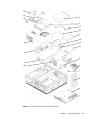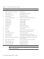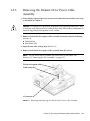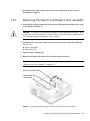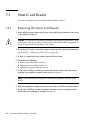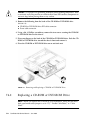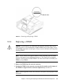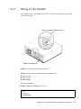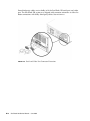
1
Sun Blade™ 150 Service Manual
Sun Microsystems, Inc.
4150 Network Circle
Santa Clara, CA 95054 U.S.A.
650-960-1300
Part No. 816-4379-10
June 2002, Revision A
Send comments about this document to: [email protected]
Copyright 2002 Sun Microsystems, Inc., 4150 Network Circle, Santa Clara, California 95054, U.S.A. All rights reserved.
Sun Microsystems, Inc. has intellectual property rights relating to technology embodied in the product that is described in this document. In
particular, and without limitation, these intellectual property rights may include one or more of the U.S. patents listed at
http://www.sun.com/patents and one or more additional patents or pending patent applications in the U.S. and in other countries.
This document and the product to which it pertains are distributed under licenses restricting their use, copying, distribution, and
decompilation. No part of the product or of this document may be reproduced in any form by any means without prior written authorization of
Sun and its licensors, if any.
Third-party software, including font technology, is copyrighted and licensed from Sun suppliers.
Parts of the product may be derived from Berkeley BSD systems, licensed from the University of California. UNIX is a registered trademark in
the U.S. and in other countries, exclusively licensed through X/Open Company, Ltd.
Sun, Sun Microsystems, the Sun logo, Sun Blade, SunMicrophone, SunVTS, AnswerBook2, docs.sun.com, OpenBoot, Power Management,
ShowMe How, UltraSPARC, and Solaris are trademarks or registered trademarks of Sun Microsystems, Inc. in the U.S. and in other countries.
All SPARC trademarks are used under license and are trademarks or registered trademarks of SPARC International, Inc. in the U.S. and in other
countries. Products bearing SPARC trademarks are based upon an architecture developed by Sun Microsystems, Inc.
The Energy Star logo is a registered trademark of EPA.
The OPEN LOOK and Sun™ Graphical User Interface was developed by Sun Microsystems, Inc. for its users and licensees. Sun acknowledges
the pioneering efforts of Xerox in researching and developing the concept of visual or graphical user interfaces for the computer industry. Sun
holds a non-exclusive license from Xerox to the Xerox Graphical User Interface, which license also covers Sun’s licensees who implement OPEN
LOOK GUIs and otherwise comply with Sun’s written license agreements.
As an Energy Star partner, Sun Microsystems, Inc. has determined that configurations of this
product that bear the Energy Star Logo meet the Energy Star guidelines for energy efficiency.
Use, duplication, or disclosure by the U.S. Government is subject to restrictions set forth in the Sun Microsystems, Inc. license agreements and as
provided in DFARS 227.7202-1(a) and 227.7202-3(a) (1995), DFARS 252.227-7013(c)(1)(ii) (Oct. 1998), FAR 12.212(a) (1995), FAR 52.227-19, or
FAR 52.227-14 (ALT III), as applicable.
DOCUMENTATION IS PROVIDED "AS IS" AND ALL EXPRESS OR IMPLIED CONDITIONS, REPRESENTATIONS AND WARRANTIES,
INCLUDING ANY IMPLIED WARRANTY OF MERCHANTABILITY, FITNESS FOR A PARTICULAR PURPOSE OR NON-INFRINGEMENT,
ARE DISCLAIMED, EXCEPT TO THE EXTENT THAT SUCH DISCLAIMERS ARE HELD TO BE LEGALLY INVALID.
Copyright 2002 Sun Microsystems, Inc., 4150 Network Circle, Santa Clara, California 95054, Etats-Unis. Tous droits réservés.
Sun Microsystems, Inc. a les droits de propriété intellectuels relatants à la technologie incorporée dans le produit qui est décrit dans ce
document. En particulier, et sans la limitation, ces droits de propriété intellectuels peuvent inclure un ou plus des brevets américains énumérés
à http://www.sun.com/patents et un ou les brevets plus supplémentaires ou les applications de brevet en attente dans les Etats-Unis et dans
les autres pays.
Ce produit ou document est protégé par un copyright et distribué avec des licences qui en restreignent l’utilisation, la copie, la distribution, et la
décompilation. Aucune partie de ce produit ou document ne peut être reproduite sous aucune forme, parquelque moyen que ce soit, sans
l’autorisation préalable et écrite de Sun et de ses bailleurs de licence, s’il y ena.
Le logiciel détenu par des tiers, et qui comprend la technologie relative aux polices de caractères, est protégé par un copyright et licencié par des
fournisseurs de Sun.
Des parties de ce produit pourront être dérivées des systèmes Berkeley BSD licenciés par l’Université de Californie. UNIX est une marque
déposée aux Etats-Unis et dans d’autres pays et licenciée exclusivement par X/Open Company, Ltd.
Sun, Sun Microsystems, le logo Sun, Sun Blade, SunMicrophone, SunVTS, AnswerBook2, docs.sun.com, OpenBoot, Power Management,
ShowMe How, UltraSPARC, et Solaris sont des marques de fabrique ou des marques déposées de Sun Microsystems, Inc. aux Etats-Unis et dans
d’autres pays.
Toutes les marques SPARC sont utilisées sous licence et sont des marques de fabrique ou des marques déposées de SPARC International, Inc.
aux Etats-Unis et dans d’autres pays. Les produits protant les marques SPARC sont basés sur une architecture développée par Sun
Microsystems, Inc.
L’interface d’utilisation graphique OPEN LOOK et Sun™ a été développée par Sun Microsystems, Inc. pour ses utilisateurs et licenciés. Sun
reconnaît les efforts de pionniers de Xerox pour la recherche et le développment du concept des interfaces d’utilisation visuelle ou graphique
pour l’industrie de l’informatique. Sun détient une license non exclusive do Xerox sur l’interface d’utilisation graphique Xerox, cette licence
couvrant également les licenciées de Sun qui mettent en place l’interface d ’utilisation graphique OPEN LOOK et qui en outre se conforment
aux licences écrites de Sun.
LA DOCUMENTATION EST FOURNIE "EN L’ÉTAT" ET TOUTES AUTRES CONDITIONS, DECLARATIONS ET GARANTIES EXPRESSES
OU TACITES SONT FORMELLEMENT EXCLUES, DANS LA MESURE AUTORISEE PAR LA LOI APPLICABLE, Y COMPRIS NOTAMMENT
TOUTE GARANTIE IMPLICITE RELATIVE A LA QUALITE MARCHANDE, A L’APTITUDE A UNE UTILISATION PARTICULIERE OU A
L’ABSENCE DE CONTREFAÇON.
Please
Recycle
Contents
Preface
1.
2.
3.
xxi
Product Description
1–1
1.1
Product Overview
1.2
Supported Sun Monitors
1.3
System Description
1.4
Replaceable Components
SunVTS Overview
1–3
1–4
SunVTS Description
2.2
SunVTS Requirements
2.3
SunVTS References
2–1
2–2
2–2
3–1
3.1
POST Overview
3.2
How to Use POST
3.3
Pre-POST Preparation
3.4
1–6
2–1
2.1
Power-On Self-Test
1–4
3–1
3–2
3–2
3.3.1
Setting Up a TIP Connection
3.3.2
Disconnecting a TIP Connection
3.3.3
Verifying the Baud Rate
Viewing the POST Menus
3–3
3–4
3–4
3–5
iii
4.
3.5
Initializing POST
3.6
Maximum and Minimum POST Levels
3–6
3.6.1
diag-level Variable Set to max
3–6
3.6.2
diag-level Variable Set to min
3–18
3.7
POST Progress and Error Reporting
3.8
Bypassing POST
3.9
Resetting Variables to Default Settings
3–27
3.10
Viewing the Default NVRAM Settings
3–28
3.11
Initializing Motherboard POST
3–25
3–27
Troubleshooting Procedures
3–28
4–1
4.1
Power-On Failure
4.2
Video Output Failure
4.3
Hard Drive, CD-ROM, or DVD-ROM Drive Failure
4.4
Power Supply Test
4.5
DIMM Failure
4.6
OpenBoot PROM On-Board Diagnostics
4.7
4–1
4–2
4–5
4–5
Watch-Clock Diagnostic
4.6.2
Watch-Net and Watch-Net-All Diagnostics
4.6.3
Probe-IDE Diagnostic
OpenBoot Diagnostics
4–5
4–8
OpenBoot Diagnostics Menu Overview
4.7.2
Starting the OpenBoot Diagnostics Menu
4.7.3
OpenBoot Diagnostics Help
Help Command
4–8
4–12
4–12
Specific OpenBoot Diagnostics Tests
4.7.4.1
Test Command
4.7.4.2
Test-all Command
4.7.4.3
Except Command
Sun Blade 150 Service Manual • June 2002
4–6
4–7
4.7.1
4.7.4
4–2
4–4
4.6.1
4.7.3.1
iv
3–5
4–13
4–13
4–14
4–14
4–9
5.
6.
4.7.4.4
Versions Command
4.7.4.5
What Command
4.7.4.6
Printenvs Command
4.7.4.7
Setenv Command
4.7.4.8
Exit Command
4–14
4–15
4–15
4–16
4–16
4.7.5
Error Reporting in OpenBoot Diagnostics
4.7.6
Exiting OpenBoot Diagnostics and Resetting the OpenBoot PROM
settings 4–17
Preparing for Component Removal and Replacement
5.1
Safety Requirements
5.2
Safety Symbols
5.3
Safety Precautions
5–2
5–2
5.3.1
Modification to Equipment
5–2
5.3.2
Placement of a Sun Product
5–3
5.3.3
Power Cord Connection
5.3.4
Electrostatic Discharge
5.3.5
Lithium Battery
5–3
5–3
5–4
Tools Required
5.5
Powering Off the System
5.6
Removing the System Cover
5.7
Attaching the Antistatic Wrist Strap
5–4
5–4
5–6
5–6
Removing and Replacing Major Subassemblies
6.2
Power Supply
5–1
5–1
5.4
6.1
4–16
6–1
6–1
6.1.1
Removing the Power Supply
6–1
6.1.2
Replacing the Power Supply
6–2
Cable Assemblies
6–3
6.2.1
Removing the Diskette Drive Data Cable Assembly
6–3
6.2.2
Replacing the Diskette Drive Data Cable Assembly
6–4
Contents
v
6.3
6.4
7.
Removing the Diskette Drive Power Cable Assembly
6–5
6.2.4
Replacing the Diskette Drive Power Cable Assembly
6–6
6.2.5
Removing the Primary IDE Cable Assembly
6–6
6.2.6
Replacing the Primary IDE Cable Assembly
6–7
6.2.7
Removing the Secondary IDE Cable Assembly
6–7
6.2.8
Replacing the Secondary IDE Cable Assembly
6–8
6.2.9
Removing the Smart Card Reader Cable Assembly
6–9
6.2.10
Replacing the Smart Card Reader Cable Assembly
6–10
6.2.11
Removing the Power Switch/LED Assembly
6–10
6.2.12
Replacing the Power Switch/LED Assembly
6–12
Speaker Assembly
6–13
6.3.1
Removing the Speaker Assembly
6–13
6.3.2
Replacing the Speaker Assembly
6–15
Fan Assembly
6–15
6.4.1
Removing the Fan Assembly
6–15
6.4.2
Replacing the Fan Assembly
6–16
Removing and Replacing Storage Devices
7.1
7.2
7.3
7.4
vi
6.2.3
Diskette Drive
7–1
7–1
7.1.1
Removing the Diskette Drive
7–1
7.1.2
Replacing the Diskette Drive
7–3
Smart Card Reader
7–4
7.2.1
Removing the Smart Card Reader
7–4
7.2.2
Replacing the Smart Card Reader
7–5
Hard Drives
7–6
7.3.1
Removing a Primary Hard Drive
7–6
7.3.2
Replacing a Primary Hard Drive
7–7
7.3.3
Installing a Secondary Hard Drive
CD-ROM or DVD-ROM Drive
Sun Blade 150 Service Manual • June 2002
7–11
7–8
8.
8.2
8.3
8.4
8.5
8.6
10.
Removing a CD-ROM or DVD-ROM Drive
7–11
7.4.2
Replacing a CD-ROM or DVD-ROM Drive
7–12
Removing and Replacing the Motherboard and Related Components
8.1
9.
7.4.1
CPU
8–1
8.1.1
Removing the CPU
8–1
8.1.2
Replacing the CPU
8–3
NVRAM/TOD
8–5
8.2.1
Removing the NVRAM/TOD
8–5
8.2.2
Replacing the NVRAM/TOD
8–6
DIMMs
8–7
8.3.1
Removing a DIMM
8–7
8.3.2
Replacing a DIMM
8–9
PCI Card
8–10
8.4.1
Removing a PCI Card
8–10
8.4.2
Replacing a PCI Card
8–11
Motherboard
8–12
8.5.1
Removing the Motherboard
8–12
8.5.2
Replacing the Motherboard
8–14
Riser Board
8–16
8.6.1
Removing the Riser Board
8–16
8.6.2
Replacing the Riser Board
8–17
Finishing Component Replacement
9.1
Replacing the System Cover
9.2
Powering On the System
9–1
9–1
9–2
OpenBoot Emergency Procedures
10.1
8–1
10–1
OpenBoot Emergency Procedures for Systems With Standard (Non-USB)
Keyboards 10–1
Contents
vii
10.2
OpenBoot Emergency Procedures for Systems With USB Keyboards
10.2.1
Stop-A Functionality
10.2.2
Stop-N Equivalent Functionality
10.2.3
Stop-F Functionality
10–3
10.2.4
Stop-D Functionality
10–4
10–2
10–2
A. Product Specifications and Reference Information
A.1
Physical Specifications
A.2
Electrical Specifications
A–2
A.3
Acoustic Specifications
A–2
A.4
Environmental Requirements
A.4.1
A.5
A.6
A–1
A–3
A–3
A–4
A.5.1
IDE Cabling Configuration
A.5.2
CD-ROM and DVD-ROM Jumper Settings
A.5.3
CD Handling and Use
A–4
A–5
A–5
A.5.3.1
Inserting a CD Into the CD-ROM or DVD-ROM Drive
A–5
A.5.3.2
Ejecting a CD From the CD-ROM or DVD-ROM Drive
A–6
A.5.3.3
Cleaning the CD-ROM or DVD-ROM Drive
A.5.3.4
Handling and Storing CDs
Modem Setup Specifications
Setting Up the Modem
A.6.2
Changing the Serial Port Speed
A.6.3
Modem Recommendations
A–6
A–7
A–8
A–9
A.6.3.1
Cable
A.6.3.2
Modem Switch Settings (AT Commands)
B–1
Sun Blade 150 Service Manual • June 2002
A–6
A–6
A.6.1
B. Signal Descriptions
viii
A–1
Clearance Requirements for Proper Cooling
Reference Information
10–2
A–9
A–9
B.1
Power Supply Connectors
B–2
B.2
Universal Serial Bus Connector
B.3
IEEE 1394 Connector
B.4
Twisted-Pair Ethernet Connector
B–4
B–5
B–6
B.4.1
TPE Cable-Type Connectivity
B.4.2
External UTP-5 Cable Lengths
B.5
Serial Port Connector
B.6
Parallel Port Connector
B.7
Audio Connectors
B.8
Video Connector
B–15
C. Functional Description
C–1
B–12
B–14
System
C.2
Motherboard
C.3
Riser Board
C.4
Jumper Descriptions
C.5
Motherboard Components
C–1
C–3
C–4
C–5
C.5.1
CPU
C.5.2
IChip2 ASIC
C.5.3
SouthBridge ASIC
C.5.5
B–7
B–8
C.1
C.5.4
B–7
C–6
C–6
C–7
C–7
C.5.3.1
Super I/O Functions
C.5.3.2
PCI IDE Controller
C.5.3.3
AC97 Compliant Audio Interface
C.5.3.4
SMBus Interface
PCI Graphics
C–7
C–9
C–10
C–10
C.5.4.1
ATI Rage XL ASIC
C–10
C.5.4.2
Graphics Memory
C–10
PCIO-2.x ASIC
C.5.5.1
C–9
C–10
Ethernet
C–10
Contents
ix
C.5.5.2
USB
C.5.5.3
IEEE 1394
PCI to PCI Bridge ASIC
C.5.7
Flash PROM
C.5.8
Smart Card Interface
C.5.9
NVRAM/TOD
Reset Types
C.7
Clocking
C–11
C–12
C–13
C–13
C–13
Clock Generation
C.7.2
OpenBoot PROM Jumpers
Power Control
C.8.2
C.8.3
C.8.4
C–13
CPU Speed Selection
C–15
C.8.1.1
Powering on the System
C–15
C.8.1.2
Interrupting the system
C–15
C.8.1.3
Forcing the System to Power-Off During Software
Hang C–16
Power-On and Power-Off Circuitry
C.8.2.1
Power-On
C–16
C.8.2.2
Power-Off
C–16
On-Board VRM
C–16
C–16
C.8.3.1
On-Board VRM requirements
C.8.3.2
Power-On Beep
C.8.3.3
Power-On LED Control
C–17
Optional Secondary Hard Drive
Memory Architecture
SDRAM Address Multiplexing
C.9.2
DIMMs
C–17
C–20
C–21
Speed and Timing
SDRAM DIMM Configuration
Sun Blade 150 Service Manual • June 2002
C–17
C–18
C.9.1
C.9.3
C–14
C–15
Power Switch
C.9.2.1
x
C–11
C.7.1
C.8.1
C.9
C–11
C.5.6
C.6
C.8
C–11
C–21
C–21
C–17
C.9.3.1
C.10
DIMM Memory Addressing
Address Mapping
C–22
C.10.1 Port Allocations
C–22
C.10.2 PCI Address Assignments
C.11
PCI Bus A Address Assignments
C–23
C.10.2.2
PCI Bus B Address Assignments
C–24
Interrupts
Power
C–25
Energy Star Power Consumption Tier 1
C.12.1.2
Energy Star Tier 2, Guideline B
C–26
D. Special Procedures
D–1
Disabling Power Management
E.2
C–26
C–26
D–1
D.1.1
Disabling Hard Drive Power Management
D.1.2
Disabling all System Power Management
Setting the Default Console Display
E. Using USB Devices
E.1
C–25
C.12.1.1
C.12.2 USB
D.2
C–25
C–25
C.12.1 Energy Star
D.1
C–23
C.10.2.1
C.11.1 Interrupt Interface
C.12
C–22
D–1
D–2
D–2
E–1
USB Keyboard and Mouse
E–1
E.1.0.1
Keyboards
E.1.0.2
Mouse Devices
USB Power Management
E–2
E.2.1
Storage Devices
E–3
E.2.2
Printer Devices
E–3
E.2.3
Audio Devices
E–3
E.2.4
Hot Plugging
E–1
E–2
E–3
Contents
xi
E.2.5
Cabling
E.2.6
Devices Supported
E.2.7
Man Pages Available
Glossary
Index
xii
Glossary–1
Index–1
Sun Blade 150 Service Manual • June 2002
E–4
E–4
E–4
Figures
FIGURE P-1
Link to Multimedia Instructions xxi
FIGURE 1-1
Sun Blade 150 System
FIGURE 1-2
Front Panel Overview
1–5
FIGURE 1-3
Back Panel Overview
1–5
FIGURE 1-4
Sun Blade 150 System Replaceable Parts
FIGURE 3-1
Setting Up a TIP Connection
FIGURE 5-1
Front Panel Power Switch
FIGURE 5-2
Removing the System Cover 5–6
FIGURE 5-3
Attaching the Wrist Strap to the Chassis
FIGURE 6-1
Removing and Replacing the Power Supply 6–2
FIGURE 6-2
Removing and Replacing the Diskette Drive Data Cable Assembly
FIGURE 6-3
Removing and Replacing the Diskette Drive Power Cable Assembly
FIGURE 6-4
Removing and Replacing the Primary IDE Cable Assembly 6–7
FIGURE 6-5
Removing and Replacing the Secondary IDE Cable Assembly
FIGURE 6-6
Removing and Replacing the Smart Card Reader Cable Assembly 6–9
FIGURE 6-7
Removing the Front Bezel
FIGURE 6-8
Removing and Replacing the Power Switch/LED Assembly 6–12
FIGURE 6-9
Removing and Replacing the Speaker Assembly
FIGURE 6-10
Removing and Replacing the Fan Assembly
FIGURE 7-1
Removing and Replacing the Peripheral Assembly 7–2
1–2
1–7
3–3
5–5
5–7
6–4
6–5
6–8
6–11
6–14
6–16
xiii
xiv
7–3
FIGURE 7-2
Removing the Diskette Drive
FIGURE 7-3
Removing and Replacing the Smart Card Reader 7–5
FIGURE 7-4
Removing and Replacing a Primary Hard Drive
FIGURE 7-5
Installing a Secondary Hard Drive
FIGURE 7-6
Secondary Hard Drive Cabling Configuration 7–11
FIGURE 7-7
Removing and Replacing a CD-ROM or DVD-ROM Drive 7–12
FIGURE 8-1
Removing and Replacing the CPU 8–3
FIGURE 8-2
JP3 OpenBoot PROM Jumper Settings for 650 MHz and 550 MHz CPUs
FIGURE 8-3
Removing and Replacing the NVRAM/TOD 8–6
FIGURE 8-4
DIMM Installation Order 8–8
FIGURE 8-5
Removing and Replacing a DIMM 8–9
FIGURE 8-6
Removing and Replacing a PCI Card 8–11
FIGURE 8-7
Removing and Replacing the Motherboard 8–14
FIGURE 8-8
JP1/JP2 Jumper Settings for the Flash PROM
FIGURE 8-9
Removing and Replacing the Riser Board 8–17
FIGURE 9-1
Replacing the System Cover
FIGURE 9-2
System Power Switch 9–2
FIGURE A-1
Minimum Clearance for System Cooling
FIGURE A-2
IDE Cabling Configuration
FIGURE A-3
External and Internal Serial Ports
FIGURE B-1
Power Supply Connector J501 Pin Configuration
FIGURE B-2
Secondary Power Supply Connector J505 Pin Configuration
FIGURE B-3
USB Connector J17, J18 Pin Configuration
FIGURE B-4
IEEE 1394 Connector J20, J30 Pin Configuration B–5
FIGURE B-5
TPE Connector J19 Pin Configuration
FIGURE B-6
Serial Port Connector J36 Pin Configuration B–8
FIGURE B-7
Riser Board Serial Port Pinouts (J13)
FIGURE B-8
Accessing the Second Serial Port Through a PCI Card Slot B–10
FIGURE B-9
Serial and Video Port Connector Extensions B–11
FIGURE B-10
Parallel Port Connector J9 Pin Configuration B–12
Sun Blade 150 Service Manual • June 2002
7–7
7–10
8–15
9–2
A–4
A–5
A–7
B–2
B–3
B–4
B–6
B–9
8–4
B–14
FIGURE B-11
Audio Connector Configuration
FIGURE B-12
Video Connector J37 Pin Configuration B–15
FIGURE B-13
Serial and Video Port Connector Extensions B–16
FIGURE C-1
Sun Blade 150 System Functional Block Diagram
FIGURE C-2
Motherboard Layout Diagram
FIGURE C-3
Riser Board Layout Diagram, Side 1 C–4
FIGURE C-4
Riser Board Layout Diagram, Side 2 C–5
FIGURE C-5
External and Internal Serial Ports
FIGURE C-6
Audio Circuit Functional Block Diagram C–9
FIGURE C-7
PROM Interface C–12
FIGURE C-8
Smart Card Interface Header C–12
FIGURE C-9
JP3 OpenBoot PROM Jumper Settings for 550 MHz and 650 MHz CPUs
FIGURE C-10
Secondary Hard Drive Cabling Configuration C–17
FIGURE C-11
Sun Blade 150 Memory Block Diagram C–19
FIGURE C-12
SDRAM Address Multiplexing
C–2
C–3
C–8
C–15
C–20
Figures
xv
xvi
Sun Blade 150 Service Manual • June 2002
Tables
1–4
TABLE 1-1
Supported Sun Monitors
TABLE 1-2
Sun Blade 150 System Physical Dimensions
TABLE 1-3
Back Panel Description and Connector Symbols 1–6
TABLE 1-4
Sun Blade 150 Replaceable Components
TABLE 4-1
Internal Drives Identification 4–3
TABLE 4-2
DIMM Physical Memory Address
TABLE 8-1
Flash PROM Jumper Settings 8–15
TABLE A-1
Sun Blade 150 Physical Specifications A–1
TABLE A-2
Sun Blade 150 System Electrical Specifications
TABLE A-3
Acoustic Specifications A–2
TABLE A-4
Sun Blade 150 System Environmental Requirements
TABLE B-1
Power Supply Connector J501 Pin Assignments
B–2
TABLE B-2
Power Supply Connector J505 Pin Assignments
B–3
TABLE B-3
USB Connector J17, J18 Pin Assignments B–4
TABLE B-4
IEEE 1394 Connector J20, J30 Pin Assignments
TABLE B-5
TPE Connector J19 Pin Assignments
TABLE B-6
TPE UTP-5 Cables
TABLE B-7
Serial Port Connector J36 Pin Assignments
TABLE B-8
Riser Board Serial Port Connector J13 Pin Assignments
TABLE B-9
Parallel Port Connector J9 Pin Assignments B–12
1–4
1–8
4–5
A–2
A–3
B–5
B–6
B–7
B–8
B–9
xvii
xviii
TABLE B-10
Audio Connector Line Assignment B–14
TABLE B-11
Video Connector J37 Pin Assignments
TABLE C-1
Riser Board Connectors, Side 1
C–4
TABLE C-2
Riser Board Connectors, Side 2
C–5
TABLE C-3
Clock Frequencies
TABLE C-4
DIMMs Performance Range
TABLE C-5
SDRAM size options (DIMMs only)
TABLE C-6
DIMM Physical Memory Address
TABLE C-7
Port Allocations C–23
TABLE C-8
PCI Address Assignments
TABLE C-9
Openboot PROM/Flash PROM Address Assignments C–24
TABLE C-10
Maximum Sleep Mode Power C–26
B–15
C–14
Sun Blade 150 Service Manual • June 2002
C–21
C–21
C–22
C–23
Code Examples
3-7
CODE EXAMPLE 3-1
diag-level Variable Set to max
CODE EXAMPLE 3-2
diag-level Variable Set to min 3-19
CODE EXAMPLE 3-3
Typical POST Error Message: DIMM Failure 3-25
CODE EXAMPLE 4-1
Watch-clock Diagnostic 4-6
CODE EXAMPLE 4-2
Watch-Net Diagnostic Output Message
CODE EXAMPLE 4-3
Watch-Net-All Diagnostic Output Message 4-7
CODE EXAMPLE 4-4
Probe-IDE Diagnostic Output Message 4-7
CODE EXAMPLE 4-5
OpenBoot Diagnostics Menu 4-9
CODE EXAMPLE 4-6
Reset Verification 4-10
CODE EXAMPLE 4-7
OpenBoot Diagnostics Menu 4-12
CODE EXAMPLE 4-8
OpenBoot Diagnostics Help Commands
CODE EXAMPLE 4-9
Test Command
CODE EXAMPLE 4-10
Except Command
CODE EXAMPLE 4-11
Versions Command
CODE EXAMPLE 4-12
What Command
CODE EXAMPLE 4-13
Printenvs Command
CODE EXAMPLE 4-14
Setenv Command
CODE EXAMPLE 4-15
Exit Command
CODE EXAMPLE 4-16
Example of Error Testing Output 4-16
CODE EXAMPLE 10-1
Resetting Default NVRAM Variables 10-2
4-6
4-13
4-13
4-14
4-14
4-15
4-15
4-16
4-16
xix
xx
Sun Blade 150 Service Manual • June 2002
Preface
The Sun Blade 150 Service Manual provides detailed procedures that describe the
removal and replacement of replaceable parts in the Sun Blade™ 150 computer
system. The service manual also includes information about the use and
maintenance of the system. This book is written for technicians, system
administrators, authorized service providers (ASPs), and advanced computer system
end users who have experience troubleshooting and replacing hardware.
About the Multimedia Links in This
Manual
Removal and replacement procedures for selected system components are also
illustrated with interactive multimedia audio and video instructions in the
Sun Blade 150 Hardware Documentation CD-ROM, which is linked to the online
version of this manual. These multimedia links can be accessed wherever you see
the film-clip icon Shown in FIGURE P-1 .
FIGURE P-1
Link to Multimedia Instructions
xxi
How This Book Is Organized
Chapter 1 describes the major components of the system.
Chapter 2 describes the execution of individual tests for verifying hardware
configuration and functionality.
Chapter 3 describes the execution of Power-on Self-test (POST) and provides
examples of POST output patterns.
Chapter 4 provides troubleshooting advice and suggested corrective actions for
hardware problems.
Chapter 5 explains how to work safely when replacing system components. This
Chapter provides procedures for powering off the system, removing the system
cover, and attaching the wrist strap.
Chapter 6 provides procedures for removing and replacing major subassemblies.
Chapter 7 provides procedures for removing and replacing storage devices.
Chapter 8 provides procedures for removing and replacing the motherboard and
related components.
Chapter 9 provides procedures for replacing the system cover and powering on the
system.
Chapter 10 provides OpenBoot™ Emergency procedures specific to the USB
keyboard.
Appendix A provides specifications on power and environment, system dimensions,
weight, memory mapping, and peripheral component interconnect (PCI) card slots.
Appendix B provides signal descriptions, instructions for connecting the system unit
to a 10BASE-T/100BASE-T twisted-pair Ethernet (TPE) local area network (LAN),
and modem settings for systems used in specific network telecommunication
applications.
Appendix C provides functional descriptions of the system and components.
Appendix D provides procedures for setting the defualt console display and for
disabling power management.
Appendix E provides information on USB devices, special key commands, related
power management information, and USB man pages.
xxii Sun Blade 150 Service Manual • June 2002
Using UNIX Commands
This document may not contain information on basic UNIX® commands and
procedures such as shutting down the system, booting the system, and configuring
devices.
See one or more of the following for this information:
■
Solaris Handbook for Sun Peripherals
■
AnswerBook2™ online documentation for the Solaris™ software environment
■
Other software documentation that you received with your system
The Sun Blade 150 Getting Started Guide gives more information on how to use these
documents.
Typographic Conventions
Typeface
Meaning
Examples
AaBbCc123
The names of commands, files,
and directories; on-screen
computer output
Edit your .login file.
Use ls -a to list all files.
% You have mail.
AaBbCc123
Text that you type (when
contrasted with the on-screen
computer output)
% su
Password:
AaBbCc123
Book titles, new words or terms,
words to be emphasized
Read Chapter 6 in the User’s Guide.
These are called class options.
You must be superuser to do this.
Command-line variable; replace
with a real name or value
To delete a file, type rm filename.
Preface
xxiii
Shell Prompts
Shell
Prompt
C shell
machine_name%
C shell superuser
machine_name#
Bourne shell and Korn shell
$
Bourne shell and Korn shell superuser
#
Accessing Sun Documentation Online
You can obtain copies of Sun Blade 150 documents at the following URL:
http://www.sun.com/products-n-solutions/hardware/docs/
Workstation_Products/Workstations/Sun_Blade_Workstations/
index.html
The docs.sun.comSM web site enables you to access Sun technical documentation
on the Web. You can browse the docs.sun.com archive or search for a specific book
title or subject at:
http://docs.sun.com
SunService Solution Center
For answers to your technical questions, contact your nearest SunServiceSM Solution
Center. Phone numbers and contact information for SunService Centers can be found
at this web site:
http://www.sun.com/service/contacting/solution.html
xxiv
Sun Blade 150 Service Manual • June 2002
Sun Welcomes Your Comments
We are interested in improving our documentation and welcome your comments
and suggestions. You can email your comments to us at:
[email protected]
Please include the part number (816-4379-10) of your document in the subject line of
your email.
Preface
xxv
xxvi
Sun Blade 150 Service Manual • June 2002
CHAPTER
1
Product Description
The Sun Blade 150 workstation is a uniprocessor system that uses the UltraSPARCIIi processor. FIGURE 1-1 shows the Sun Blade 150 workstation.
This chapter contains the following topics:
■
■
■
■
Section 1.1,
Section 1.2,
Section 1.3,
Section 1.4,
“Product Overview” on page 1-3
“Supported Sun Monitors” on page 1-4
“System Description” on page 1-4
“Replaceable Components” on page 1-6
1-1
FIGURE 1-1
1-2
Sun Blade 150 System
Sun Blade 150 Service Manual • June 2002
1.1
Product Overview
The Sun Blade 150 system provides the following features:
■
Desktop-style system enclosure
■
Power supply: 250-watt
■
CPU options: 550-MHz or 650-MHz UltraSPARC-IIi processor with 512-Kbyte
internal cache, heatsink, and fan
■
Hard drives:
■
One 40 gigabyte, 7,200 RPM hard drive with ATA66 interface
■
Additional hard drive available as an optional component
■
Diskette drive: 1.44-megabyte (Mbyte) manual eject
■
Smart card reader
■
One optical drive: CD-ROM drive or DVD-ROM drive
■
Audio: CD-quality
■
PCI connectors:
■
33-MHz, 32-bit peripheral component interconnect (PCI)
■
Three long PCI connectors accept both long and short PCI cards
■
ATI Rage XL on-board graphics, 8 Mbyte RAM
■
Two serial ports
■
One serial port on the chassis back panel
■
One serial port on the riser card (requires one PCI slot to access the connector)
■
One parallel port
■
Ethernet: 10-megabit/100-megabit per second
■
Two IEEE 1394 ports (Firewire)
■
Four USB ports, (two are required for keyboard and mouse)
■
Keyboard: SunTM USB Type-6 AT 101 layout
■
Mouse: Sun USB 3-button, crossbow mouse
Chapter 1
Product Description
1-3
1.2
Supported Sun Monitors
The monitors listed in TABLE 1-1 can be used with the Sun Blade 150 system.
For more detailed information on these monitors contact your Sun representative or
see the following web site:
http://www.sun.com/products-n-solutions/hw/peripherals/
TABLE 1-1
1.3
Supported Sun Monitors
I/O Device
Description
17-inch color CRT monitor
Supports resolutions up to 1152x900
18.1-inch TFT LCD color monitor
1280x1024 resolution
21-inch CRT color monitor, flat
display
Supports resolutions up to 1600x1200
24.1-inch LCD flat panel monitor
Supports resolutions up to 1920x1200
System Description
System components are housed in a desktop-style enclosure. Overall chassis
dimensions for the Sun Blade 150 system are listed in TABLE 1-2.
TABLE 1-2
Sun Blade 150 System Physical Dimensions
Width
Height
Depth
17.52 inches
(44.5 cm)
4.65 inches
(11.8 cm)
18.00 inches
(45.7 cm)
System electronics are contained on a single plug-in printed circuit board
(motherboard). The motherboard contains the CPU, memory modules, system
control application-specific integrated circuits (ASIC), and I/O ASICs. The
motherboard plugs into a riser board that provides the system power and integrated
drive electronics (IDE) hard drive data interface. FIGURE 1-2 and FIGURE 1-3 show the
Sun Blade 150 system front and back panels.
1-4
Sun Blade 150 Service Manual • June 2002
2
3
5
4
1
FIGURE 1-2
Front Panel Overview
1. Power switch
2. Power-indicator LED
3. Smart card reader
4. 3.5-inch diskette drive
5. 5.25-inch optical drive bay (CD-ROM or DVD-ROM)
1
FIGURE 1-3
2
3
4
5
6
7
8
9
Back Panel Overview
Chapter 1
Product Description
1-5
TABLE 1-3
Back Panel Description and Connector Symbols
Item in
Figure 1-3
Explanation
1
Power connector
None
2
PCI card slot 3 (33 MHz)
PCI-3
2
PCI card slot 2 (33 MHz)
PCI-2
2
PCI card slot 1 (33 MHz)
PCI-1
3
Universal serial bus (USB) connectors (four)
4
Twisted-pair Ethernet (TPE) connector
5
IEEE 1394 connectors (two)
6
VGA video connector
7
Parallel connector, DB-25
8
Serial connector (RS-232)
9
Audio module headphones connector
9
Audio module line-out connector
9
Audio module line-in connector
9
Audio module microphone connector
Back Panel Symbol
SERIAL
.
1.4
Replaceable Components
This section lists the replaceable components for the Sun Blade 150 system. The
numbered components in FIGURE 1-4 correlate to the numbered components listed in
TABLE 1-4. Consult your authorized Sun sales representative or service provider to
confirm a part number before ordering a replacement part.
1-6
Sun Blade 150 Service Manual • June 2002
15*
14*
1
16*
2
17*
18*
3
19*
13
20*
4
12
5
11
10
6
7
8
9
FIGURE 1-4
Sun Blade 150 System Replaceable Parts
Chapter 1
Product Description
1-7
TABLE 1-4
Sun Blade 150 Replaceable Components
Item
Component
Description
1
CD-ROM drive
CD-ROM drive or DVD-ROM drive
2
Hard drive (second drive is optional)
Hard disk drive
3
Smart card reader
Smart card reader with enclosure
4
Manual eject diskette drive
Internal diskette drive
5
Speaker assembly
System speaker with cable
6
Central processing unit (CPU)
550 MHz or 650 MHz, 512-Kbyte internal cache
7
NVARAM/TOD
Nonvolatile RAM/Time of day
8
128-Mbyte DIMM
128-Mbyte DIMM
8
256-Mbyte DIMM
256-Mbyte DIMM
8
512-Mbyte DIMM
512-Mbyte DIMM
9
Motherboard
System main logic board
10
Fan assembly
System cooling fan with cable
11
PCI card
Generic PCI card
12
Riser board
3-slot PCI expansion and power interface card
13
Power supply
250-watt power supply with power cable
*
Cable kit (items with asterisk)
Cables for major components
14*
Secondary IDE cable
Secondary HDD and riser board IDE2 cable
15*
Primary IDE cable
Primary HDD, CD/DVD-ROM, riser board IDE1 cable
16*
Hard drive and optical drive power cable
CD/DVD-ROM, primary hard drive, secondary hard
drive power cable
17*
Power switch and LED cable
Power switch, LED, and power cable assembly
18*
Smart card reader cable
Smart card reader cable
19*
Diskette drive power cable
Diskette drive power cable
20*
Diskette drive data cable
diskette drive data cable
Note – Consult your authorized Sun sales representative or service provider before
ordering a replacement part.
1-8
Sun Blade 150 Service Manual • June 2002
CHAPTER
2
SunVTS Overview
This chapter contains an overview of the SunVTS™ diagnostic tool.
This chapter contains the following topics:
■
■
■
2.1
Section 2.1, “SunVTS Description” on page 2-1
Section 2.2, “SunVTS Requirements” on page 2-2
Section 2.3, “SunVTS References” on page 2-2
SunVTS Description
SunVTS is an online Validation Test Suite. SunVTS is a comprehensive software
diagnostic package that tests and validates hardware by verifying the connectivity
and functionality of most hardware controllers, devices, and platforms.
SunVTS can be tailored to run on various types of systems ranging from desktops to
servers with customizable features to meet the varying requirements of many
diagnostic situations.
Use SunVTS to validate a system during development, production, receiving
inspection, troubleshooting, periodic maintenance, and system or subsystem
stressing.
SunVTS executes multiple diagnostic tests from one graphical user interface (GUI)
that provides test configuration and status monitoring. The user interface can run in
the Common Desktop Environment (CDE) or OPEN LOOK environments or through
a TTY-mode interface for situations when running a GUI is not possible.
The SunVTS interface can run on one system to display the SunVTS test session of
another system on the network.
SunVTS is distributed with each SPARC™ Solaris operating environment release. It
is located on the Sun Computer Systems Supplement CD.
2-1
2.2
SunVTS Requirements
Your system must meet the following requirements to run SunVTS:
2.3
■
The SunVTS packages must be installed. The main package is SUNWvtx for 64-bit
systems. There are additional supporting packages that differ based on the
version of the Solaris operating environment that is installed. For specific details,
refer to the corresponding SunVTS documentation (described below).
■
The system must be booted to the multiuser level (level 3).
■
To run SunVTS with a GUI, that GUI must be installed. Otherwise, run SunVTS
with the TTY-mode interface.
SunVTS References
To find out more information about the use of SunVTS, refer to the SunVTS
documentation that corresponds to the Solaris software version that you are
running.
The following list describes the contents of each SunVTS document:
■
SunVTS 4.x User’s Guide describes how to install, configure, and run the SunVTS
diagnostic software.
■
SunVTS 4.x Quick Reference Card provides an overview of how to use the SunVTS
CDE interface.
■
SunVTS 4.x Test Reference Manual provides details about each individual SunVTS
test.
These documents are part of the Solaris on Sun Hardware AnswerBook2 collection.
The part number for each document is different for each version of Solaris: check the
version of Solaris that you are using and find the appropriate part number for the
document. This collection is distributed on the Sun Computer Systems Supplement CD
with each SPARC Solaris release and is also accessible at http://docs.sun.com.
2-2
Sun Blade 150 Service Manual • June 2002
CHAPTER
3
Power-On Self-Test
This chapter describes how to initiate power-on self-test (POST) diagnostics. POST is
a firmware program that can help determine if a portion of the system has failed.
POST verifies the core functionality of the system, including operation the CPU,
motherboard, memory, and some on-board I/O devices. POST can be run even if the
system is unable to boot.
This chapter contains the following topics:
■
■
■
■
■
■
■
■
■
■
■
3.1
Section 3.1, “POST Overview” on page 3-1
Section 3.2, “How to Use POST” on page 3-2
Section 3.3, “Pre-POST Preparation” on page 3-2
Section 3.4, “Viewing the POST Menus” on page 3-5
Section 3.5, “Initializing POST” on page 3-5
Section 3.6, “Maximum and Minimum POST Levels” on page 3-6
Section 3.7, “POST Progress and Error Reporting” on page 3-25
Section 3.8, “Bypassing POST” on page 3-27
Section 3.9, “Resetting Variables to Default Settings” on page 3-27
Section 3.10, “Viewing the Default NVRAM Settings” on page 3-28
Section 3.11, “Initializing Motherboard POST” on page 3-28
POST Overview
POST detects most system faults and is located in the system board OpenBoot™
PROM. POST can be invoked at power up by the OpenBoot program, depending on
the setting of two environment variables, the diag-switch? and the diag-level
flag. The diag-switch? and the diag-level flag are stored in nonvolatile RAM
(NVRAM).
POST diagnostic and error message reports are displayed on a console terminal.
3-1
Note – Both POST and OpenBOOT PROM on Sun Blade 150 systems report the CPU
as an UltraSPARC IIe processor. The CPU in your system is an UltraSPARC IIi
processor.
3.2
How to Use POST
When the workstation power is applied, POST runs automatically if both of the
following conditions apply:
■
The diag-switch? NVRAM parameter is set to true.
■
The diag-level is set to either min or max.
In the event of an automatic workstation reset, POST runs if the diag-switch?
NVRAM parameter is set to true and the diag-level flag is set to either max or
min.
Note – If diag-switch = false, POST is disabled. If diag-switch = true and
diag-level = max, then POST runs in max mode. If diag-switch = true and
diag-level = min, then POST runs in min mode.
3.3
Pre-POST Preparation
To Prepare for POST you should:
3-2
■
Set up a terminal interface processor (TIP) connection to another workstation or
terminal to view POST progress and error messages. See Section 3.3.1, “Setting Up
a TIP Connection” on page 3-3.
■
Verify the baud rates between the tested workstation and another workstation
with a monitor, or a terminal display. See Section 3.3.3, “Verifying the Baud Rate”
on page 3-4.
Sun Blade 150 Service Manual • June 2002
3.3.1
Setting Up a TIP Connection
A TIP connection enables a remote shell window to be used as a terminal to display
test data from the system you are testing. The easiest method is to connect serial port
A of the system you plan to test to another Sun workstation monitor or a TTY-type
terminal.
Note – There is a second serial port (serial port B) on the Sun Blade 150 system riser
card. However, you will need a special connector and cable, and you will need an
empty PCI card slot to access the serial port. See Appendix C, FIGURE C-5.
To set up a TIP connection, proceed as follows:
1. Connect the serial port of the tested system to the serial port of a second Sun
workstation using a serial null modem cable.
Connect cable pins 2-3, 3-2, 7-20, and 20-7), as shown in FIGURE 3-1.
2
2
3
3
7
7
20
20
FIGURE 3-1
Setting Up a TIP Connection
2. At the second Sun workstation, check the /etc/remote file by changing to the
/etc directory and editing the remote file.
The sample remote file text below shows connection to serial port B of the second
Sun workstation:
hardwire:\
/dv=/dev/term/a:br#9600:el=^C^S^Q^U^D:ie=%$:oe=^D:
Chapter 3
Power-On Self-Test
3-3
3. In a shell window on the second Sun workstation, type tip hardwire.
% tip hardwire
connected
The terminal (shell) window on the second workstation becomes a TIP window
directed to the serial port of the workstation under test. When power is applied to
the workstation under test, POST messages are displayed in this shell window.
3.3.2
Disconnecting a TIP Connection
When POST is completed, disconnect the TIP connection as follows:
1. Open another shell window at the second workstation.
2. Type ps -a to view the active TIP line and process ID (PID) number.
3. Type the following to disconnect the TIP hardwire process.
% kill -9 PID#
3.3.3
Verifying the Baud Rate
To verify the baud rate between the tested system and a terminal or another Sun
workstation monitor:
1. Open a terminal (shell) window.
2. Type eeprom.
3. Verify the following serial port default settings:
tty-mode = 9600,8,n,1
Note – Ensure that the settings are consistent with TTY-type terminal or
workstation monitor settings.
3-4
Sun Blade 150 Service Manual • June 2002
3.4
Viewing the POST Menus
To use the POST menus:
1. At the system prompt, type:
ok% setenv diag-switch? true
ok% setenv diag-level = menus
3.5
Initializing POST
POST can be initialized in two ways:
■
maximum POST reporting, or max
■
minimum POST reporting, or min
Note – The default POST setting is max.
To run POST you must:
■
Set diag-switch? to true.
■
Set the diag-level to either max or min.
■
Power-cycle the system.
To set the diag-switch? to true and power-cycle the system:
1. At the system prompt, type:
ok% setenv diag-switch? true
ok% setenv diag-level = min
Note – Type either min or max, depending on the functions you need to test.
2. Power-cycle the system by pressing and releasing the power switch on the front
panel.
3. Observe the terminal monitor to verify that POST is executing.
Chapter 3
Power-On Self-Test
3-5
4. When POST is complete, type the following at the system prompt:
ok% setenv diag-switch? false
Note – You should always reset the diag-switch to false when you are finished.
If you do not reset the diag-switch, the system will run POST every time that the
system is power-cycled, which delays system boot-up.
3.6
Maximum and Minimum POST Levels
Two levels of POST are available: maximum (max) level and minimum (min) level.
The system initiates the selected level of POST based upon the setting of
diag-level, an NVRAM variable. The default setting for diag-level is max.
To set the diag-level variable to min before power-cycling the system, type:
ok% setenv diag-level min
To return to the default setting:
ok% setenv diag-level max
An example of a max-level POST output at the serial port is provided in
Section 3.6.1, “diag-level Variable Set to max” on page 3-6. An example of a minlevel POST output at the serial port is provided in Section 3.6.2, “diag-level
Variable Set to min” on page 3-18.
3.6.1
diag-level Variable Set to max
When you set the diag-level variable to max, POST enables an extended set of
diagnostic-level tests. This mode requires approximately two minutes to complete
(with 128 Mbytes of DIMM installed). CODE EXAMPLE 3-1 shows a typical serial port
POST output with diag-level set to max and a single 512 Mbyte DIMM installed.
3-6
Sun Blade 150 Service Manual • June 2002
Note – Both POST and OpenBoot PROM report the CPU as an UltraSPARC IIe
processor. The CPU in your system is an UltraSPARC IIi processor.
Note – Video output is disabled while POST is initialized.
CODE EXAMPLE 3-1
diag-level Variable Set to max
Speed Jumper is set to 0000.0000.0000.0008
Hardware Power ON
@(#)OBP 4.6.0 2002/04/03 12:28
Executing Power On SelfTest
@(#) Sun (Grover) POST 2.0.1 05:13 PM on 04/23/02
Processor Module Identification
UltraSPARC-IIe+ (Phantom) Version 1.3
Init POST BSS
Init System BSS
NVRAM Tests
NVRAM Battery Detect Test
NVRAM Scratch Addr Test
NVRAM Scratch Data Test
DMMU TLB Tags
DMMU TLB Tag Access Test
DMMU TLB RAM
DMMU TLB RAM Access Test
Probe Ecache
Probe Ecache
Ecache Size = 0x00080000 bytes = 512 KBytes
Measure CPU Clock
Initializing Southbridge
Nominal CPU speed is 650 MHz
All CPU Basic Tests
V9 Instruction Test
CPU Tick and Tick Compare Reg Test
CPU Soft Trap Test
CPU Softint Reg and Int Test
All Basic MMU Tests
Chapter 3
Power-On Self-Test
3-7
CODE EXAMPLE 3-1
diag-level Variable Set to max
(Continued)
DMMU Primary Context Reg Test
DMMU Secondary Context Reg Test
DMMU TSB Reg Test
DMMU Tag Access Reg Test
DMMU VA Watchpoint Reg Test
DMMU PA Watchpoint Reg Test
IMMU TSB Reg Test
IMMU Tag Access Reg Test
All Basic Cache Tests
Dcache RAM Test
Dcache Tag Test
Icache RAM Test
Icache Tag Test
Icache Next Test
Icache Predecode Test
MCU Control & Status Regs Init
Initializing Memory and MC registers
DIMM 0: 256 MBytes = 0x10000000 bytes
DIMM 1: 256 MBytes = 0x10000000 bytes
DIMM 2: 256 MBytes = 0x10000000 bytes
DIMM 3: 256 MBytes = 0x10000000 bytes
Found 4 DIMMs in bank 0
Bank 0: 1024 MBytes
DIMM0 is a 32M x 8 device
DIMM1 is a 32M x 8 device
DIMM2 is a 32M x 8 device
DIMM3 is a 32M x 8 device
MC0 = 0x00000000.96a0cf06
MC1 = 0x00000000.80008000
MC2 = 0x00000000.cff0eeee
MC3 = 0x00000000.00600b5f
CPU MODULE upa_config is 0x0000003a.00000000
Ecache Tests
Displacement Flush Ecache
Ecache RAM Addr Test
Ecache Tag Addr Test
Ecache RAM Test
Ecache Tag Test
Memory Init
Malloc Post Memory
Memory Addr Check w/o Ecache
Load Post In Memory
Run POST from MEM
3-8
Sun Blade 150 Service Manual • June 2002
CODE EXAMPLE 3-1
diag-level Variable Set to max
(Continued)
.........
Map PROM/STACK/NVRAM in DMMU
Update Master Stack/Frame Pointers
All FPU Basic Tests
FPU Regs Test
FPU Move Regs Test
FPU State Reg Test
FPU Functional Test
FPU Trap Test
All Basic IOMMU Tests
PIO Decoder and BCT Test
PCI Byte Enable Test
CPU’s IOMMU Regs Test
CPU’s IOMMU RAM Addr Test
CPU’s IOMMU CAM Address Test
IOMMU TLB Compare Test
IOMMU TLB Flush Test
PBMA PCI Config Space Regs Test
PBMA Control/Status Reg Test
PBMA Diag Reg Test
CPU’s IO Regs Test
All Advanced CPU Tests
DMMU Hit/Miss Test
IMMU Hit/Miss Test
DMMU Little Endian Test
IU ASI Access Test
FPU ASI Access Test
Ecache Thrash Test
All CPU Error Reporting Tests
CPU Data Access Trap Test
CPU Addr Align Trap Test
DMMU Access Priv Page Test
DMMU Write Protected Page Test
Audio Tests
Map Audio Device PCI Config Registers Test
Audio Device ID and Vendor ID (0x545110b9) Test
Init Audio Device IO Registers Test
Audio Device Memory Registers Test
Memory Tests
Init Memory
Info : 256MB at Dimm Slot 0
Start Addr: 0x00000000.00800000 Size: 248 MBytes
Init with 0x00000000.00000000:
Chapter 3
Power-On Self-Test
3-9
CODE EXAMPLE 3-1
diag-level Variable Set to max
(Continued)
................................................................
................
Info : 256MB at Dimm Slot 1
Start Addr: 0x00000000.40000000 Size: 256 MBytes
Init with 0x00000000.00000000:
................................................................
................
Info : 256MB at Dimm Slot 2
Start Addr: 0x00000000.80000000 Size: 256 MBytes
Init with 0x00000000.00000000:
................................................................
................
Info : 256MB at Dimm Slot 3
Start Addr: 0x00000000.c0000000 Size: 256 MBytes
Init with 0x00000000.00000000:
................................................................
................
Memory Addr Check with Ecache Test
Info : 256MB at Dimm Slot 0
Start Addr: 0x00000000.00800000 Size: 248 MBytes
Write 0xffffffff.ffffffff:
................................................................
Read:
................................................................
Write 0xaaaaaaaa.aaaaaaaa:
................................................................
Read:
................................................................
Write 0x55555555.55555555:
................................................................
Read:
................................................................
Write 0x00000000.00000000:
................................................................
Read:
................................................................
Info : 256MB at Dimm Slot 1
Start Addr: 0x00000000.40000000 Size: 256 MBytes
Write 0xffffffff.ffffffff:
................................................................
Read:
................................................................
Write 0xaaaaaaaa.aaaaaaaa:
................................................................
3-10
Sun Blade 150 Service Manual • June 2002
CODE EXAMPLE 3-1
diag-level Variable Set to max
(Continued)
Read:
................................................................
Write 0x55555555.55555555:
................................................................
Read:
................................................................
Write 0x00000000.00000000:
................................................................
Read:
................................................................
Info : 256MB at Dimm Slot 2
Start Addr: 0x00000000.80000000 Size: 256 MBytes
Write 0xffffffff.ffffffff:
................................................................
Read:
................................................................
Write 0xaaaaaaaa.aaaaaaaa:
................................................................
Read:
................................................................
................
Write 0x55555555.55555555:
................................................................
Read:
................................................................
Write 0x00000000.00000000:
................................................................
Read:
................................................................
Info : 256MB at Dimm Slot 3
Start Addr: 0x00000000.c0000000 Size: 256 MBytes
Write 0xffffffff.ffffffff:
................................................................
Read:
................................................................
Write 0xaaaaaaaa.aaaaaaaa:
................................................................
Read:
................................................................
Write 0x55555555.55555555:
................................................................
Read:
................................................................
Chapter 3
Power-On Self-Test
3-11
CODE EXAMPLE 3-1
diag-level Variable Set to max
(Continued)
Write 0x00000000.00000000:
................................................................
Read:
................................................................
Block Memory Addr Test
Info : 256MB at Dimm Slot 0
Start Addr: 0x00000000.00800000 Size: 248 MBytes
Info : 256MB at Dimm Slot 1
Start Addr: 0x00000000.40000000 Size: 256 MBytes
Info : 256MB at Dimm Slot 2
Start Addr: 0x00000000.80000000 Size: 256 MBytes
Info : 256MB at Dimm Slot 3
Start Addr: 0x00000000.c0000000 Size: 256 MBytes
Block Memory Check Test
Info : 256MB at Dimm Slot 0
Start Addr: 0x00000000.00800000 Size: 248 MBytes
Write 0x33333333.33333333
................................................................
Read
................................................................
Write 0x55555555.55555555
................................................................
Read
................................................................
Write 0xcccccccc.cccccccc
................................................................
Read
................................................................
Write 0xaaaaaaaa.aaaaaaaa
................................................................
Read
................................................................
Info : 256MB at Dimm Slot 1
Start Addr: 0x00000000.40000000 Size: 256 MBytes
Write 0x33333333.33333333
................................................................
Read
................................................................
Write 0x55555555.55555555
................................................................
Read
................................................................
3-12
Sun Blade 150 Service Manual • June 2002
CODE EXAMPLE 3-1
diag-level Variable Set to max
(Continued)
Write 0xcccccccc.cccccccc
................................................................
Read
................................................................
Write 0xaaaaaaaa.aaaaaaaa
................................................................
Read
................................................................
Info : 256MB at Dimm Slot 2
Start Addr: 0x00000000.80000000 Size: 256 MBytes
Write 0x33333333.33333333
................................................................
Read
................................................................
Write 0x55555555.55555555
................................................................
Read
................................................................
Write 0xcccccccc.cccccccc
................................................................
Read
................................................................
Write 0xaaaaaaaa.aaaaaaaa
................................................................
Read
................................................................
Info : 256MB at Dimm Slot 3
Start Addr: 0x00000000.c0000000 Size: 256 MBytes
Write 0x33333333.33333333
................................................................
Read
................................................................
Write 0x55555555.55555555
................................................................
Read
................................................................
Write 0xcccccccc.cccccccc
................................................................
Read
................................................................
Write 0xaaaaaaaa.aaaaaaaa
Chapter 3
Power-On Self-Test
3-13
CODE EXAMPLE 3-1
diag-level Variable Set to max
(Continued)
................................................................
Read
................................................................
ECC Memory Addr Test
Info : 256MB at Dimm Slot 0
Start Addr: 0x00000000.00800000 Size: 248 MBytes
Info : 256MB at Dimm Slot 1
Start Addr: 0x00000000.40000000 Size: 256 MBytes
Info : 256MB at Dimm Slot 2
Start Addr: 0x00000000.80000000 Size: 256 MBytes
Info : 256MB at Dimm Slot 3
Start Addr: 0x00000000.c0000000 Size: 256 MBytes
ECC Blk Memory Test
Info : 256MB at Dimm Slot 0
Start Addr: 0x00000000.00800000 Size: 248 MBytes
Write 0xa5a5a5a5.a5a5a5a5
................................................................
Read
................................................................
Write 0x96969696.96969696
................................................................
................
Read
................................................................
Write 0xbbbbbbbb.bbbbbbbb
................................................................
Read
................................................................
Write 0xdddddddd.dddddddd
................................................................
Read
................................................................
Info : 256MB at Dimm Slot 1
Start Addr: 0x00000000.40000000 Size: 256 MBytes
Write 0xa5a5a5a5.a5a5a5a5
................................................................
Read
................................................................
Write 0x96969696.96969696
................................................................
Read
................................................................
Write 0xbbbbbbbb.bbbbbbbb
3-14
Sun Blade 150 Service Manual • June 2002
CODE EXAMPLE 3-1
diag-level Variable Set to max
(Continued)
................................................................
Read
................................................................
Write 0xdddddddd.dddddddd
................................................................
Read
................................................................
Info : 256MB at Dimm Slot 2
Start Addr: 0x00000000.80000000 Size: 256 MBytes
Write 0xa5a5a5a5.a5a5a5a5
................................................................
Read
................................................................
Write 0x96969696.96969696
................................................................
Read
................................................................
Write 0xbbbbbbbb.bbbbbbbb
................................................................
Read
................................................................
................................................................
Write 0xdddddddd.dddddddd
................................................................
Read
................................................................
Info : 256MB at Dimm Slot 3
Start Addr: 0x00000000.c0000000 Size: 256 MBytes
Write 0xa5a5a5a5.a5a5a5a5
................................................................
Read
................................................................
Write 0x96969696.96969696
................................................................
Read
................................................................
Write 0xbbbbbbbb.bbbbbbbb
................................................................
Read
................................................................
Write 0xdddddddd.dddddddd
................................................................
Read
Chapter 3
Power-On Self-Test
3-15
CODE EXAMPLE 3-1
diag-level Variable Set to max
(Continued)
................................................................
Status of this POST run:
PASS
diag-script=none
Time Stamp [hour:min:sec] 15:20:37 [month/date year] 04/23 2002
Power On Selftest Completed
Status = 0000.0000.0000.0000
0002.3333.0200.001b
ffff.ffff.f00b.63f0
Speed Jumper is set to 0000.0000.0000.0008
Software Power ON
@(#)OBP 4.6.0 2002/04/03 12:28
CPU SPEED 0x0000.0000.26be.3680
Initializing Memory Controller
MCR0 0000.0000.76a0.cf04
MCR1 0000.0000.8000.8000
MCR2 0000.0000.cff0.eeee
MCR3 0000.0000.0060.0052
Clearing E$ Tags Done
Clearing I/D TLBs Done
Probing Memory Done
Clearing Memory Done
MEM BASE = 0000.0000.c000.0000
MEM SIZE = 0000.0000.1000.0000
MMUs ON
Copy Done
PC = 0000.01ff.f000.297c
PC = 0000.0000.0000.29c0
Decompressing into Memory Done
Size = 0000.0000.0006.1780
ttya initialized
Reset Control: BXIR:0 BPOR:0 SXIR:0 SPOR:1 POR:0
Probing upa at 1f,0 pci
Probing upa at 0,0 SUNW,UltraSPARC-IIe (512 KB)
Loading Support Packages: kbd-translator
Loading onboard drivers: ebus flashprom eeprom idprom
Probing Memory Bank #0 256 Megabytes
Probing Memory Bank #1 256 Megabytes
Probing Memory Bank #2 256 Megabytes
Probing Memory Bank #3 256 Megabytes
3-16
Sun Blade 150 Service Manual • June 2002
CODE EXAMPLE 3-1
diag-level Variable Set to max
(Continued)
Probing /pci@1f,0 Device 7 isa dma floppy parallel power serial
serial
Probing /pci@1f,0 Device c network firewire usb hub keyboard mouse
storage
Probing /pci@1f,0 Device 3 pmu i2c temperature card-reader dimm
dimm
dimm dimm ppm beep fan-control
Probing /pci@1f,0 Device 8 sound
Probing /pci@1f,0 Device d ide disk cdrom
Probing /pci@1f,0 Device 13 SUNW,m64B
Probing /pci@1f,0 Device 5 pci
Probing /pci@1f,0/pci@5 Device 0 Nothing there
Probing /pci@1f,0/pci@5 Device 1 Nothing there
Probing /pci@1f,0/pci@5 Device 2 Nothing there
Sun Blade 150 (UltraSPARC-IIe 650MHz), Keyboard Present
Copyright 1998-2002 Sun Microsystems, Inc. All rights reserved.
OpenBoot 4.6, 1024 MB memory installed, Serial #51602330.
Ethernet address 0:3:ba:13:63:9a, Host ID: 8313639a.
Skipping diagnostic script because diag-script = none
Resetting ...
Speed Jumper is set to 0000.0000.0000.0008
Software Power ON
@(#)OBP 4.6.0 2002/04/03 12:28
CPU SPEED 0x0000.0000.26be.3680
Initializing Memory Controller
MCR0 0000.0000.76a0.cf04
MCR1 0000.0000.8000.8000
MCR2 0000.0000.cff0.eeee
MCR3 0000.0000.0060.0052
Clearing E$ Tags Done
Clearing I/D TLBs Done
Probing Memory Done
Clearing Memory Done
MEM BASE = 0000.0000.c000.0000
MEM SIZE = 0000.0000.1000.0000
MMUs ON
Copy Done
Chapter 3
Power-On Self-Test
3-17
CODE EXAMPLE 3-1
diag-level Variable Set to max
(Continued)
PC = 0000.01ff.f000.297c
PC = 0000.0000.0000.29c0
Decompressing into Memory Done
Size = 0000.0000.0006.1780
ttya initialized
Reset Control: BXIR:0 BPOR:0 SXIR:0 SPOR:0 POR:1
Probing upa at 1f,0 pci
Probing upa at 0,0 SUNW,UltraSPARC-IIe (512 KB)
Loading Support Packages: kbd-translator
Loading onboard drivers: ebus flashprom eeprom idprom
Probing Memory Bank #0 256 Megabytes
Probing Memory Bank #1 256 Megabytes
Probing Memory Bank #2 256 Megabytes
Probing Memory Bank #3 256 Megabytes
Probing /pci@1f,0 Device 7 isa dma floppy parallel power serial
serial
Probing /pci@1f,0 Device c network firewire usb hub keyboard mouse
storage
Probing /pci@1f,0 Device 3 pmu i2c temperature card-reader dimm
dimm
dimm dimm ppm beep fan-control
Probing /pci@1f,0 Device 8 sound
Probing /pci@1f,0 Device d ide disk cdrom
Probing /pci@1f,0 Device 13 SUNW,m64B
Probing /pci@1f,0 Device 5 pci
Probing /pci@1f,0/pci@5 Device 0 Nothing there
Probing /pci@1f,0/pci@5 Device 1 Nothing there
Probing /pci@1f,0/pci@5 Device 2 Nothing there
Sun Blade 150 (UltraSPARC-IIe 650MHz), Keyboard Present
Copyright 1998-2002 Sun Microsystems, Inc. All rights reserved.
OpenBoot 4.6, 1024 MB memory installed, Serial #51602330.
Ethernet address 0:3:ba:13:63:9a, Host ID: 8313639a.
3.6.2
diag-level Variable Set to min
When you set the diag-level variable to min, POST enables an abbreviated set of
diagnostic-level tests. This mode requires approximately one minute to complete
(with 128 Mbytes of DIMM installed). CODE EXAMPLE 3-2 shows a serial port POST
output with diag-level set to min and a single 512 Mbyte DIMM installed.
3-18
Sun Blade 150 Service Manual • June 2002
Note – Both POST and OpenBoot PROM report the CPU as an UltraSPARC IIe
processor. The CPU in your system is an UltraSPARC IIi processor.
Note – Video output is disabled while POST is initialized.
CODE EXAMPLE 3-2
diag-level Variable Set to min
Speed Jumper is set to 0000.0000.0000.0008
Hardware Power ON
@(#)OBP 4.6.0 2002/04/03 12:28
Executing Power On SelfTest
@(#) Sun Blade 150 POST 2.0.1 05:13 PM on 04/23/02
Processor Module Identification
UltraSPARC-IIe Version 1.3
Init POST BSS
Init System BSS
NVRAM Tests
NVRAM Battery Detect Test
NVRAM Scratch Addr Test
NVRAM Scratch Data Test
DMMU TLB Tags
DMMU TLB Tag Access Test
DMMU TLB RAM
DMMU TLB RAM Access Test
Probe Ecache
Probe Ecache
Ecache Size = 0x00080000 bytes = 512 KBytes
Measure CPU Clock
Initializing Southbridge
Nominal CPU speed is 650 MHz
All CPU Basic Tests
V9 Instruction Test
CPU Soft Trap Test
CPU Softint Reg and Int Test
All Basic MMU Tests
DMMU Primary Context Reg Test
DMMU Secondary Context Reg Test
Chapter 3
Power-On Self-Test
3-19
CODE EXAMPLE 3-2
diag-level Variable Set to min
(Continued)
DMMU TSB Reg Test
DMMU Tag Access Reg Test
IMMU TSB Reg Test
IMMU Tag Access Reg Test
All Basic Cache Tests
Dcache RAM Test
Icache RAM Test
MCU Control & Status Regs Init
Initializing Memory and MC registers
DIMM 0: 256 MBytes = 0x10000000 bytes
DIMM 1: 256 MBytes = 0x10000000 bytes
DIMM 2: 256 MBytes = 0x10000000 bytes
DIMM 3: 256 MBytes = 0x10000000 bytes
Found 4 DIMMs in bank 0
Bank 0: 1024 MBytes
DIMM0 is a 32M x 8 device
DIMM1 is a 32M x 8 device
DIMM2 is a 32M x 8 device
DIMM3 is a 32M x 8 device
MC0 = 0x00000000.96a0cf06
MC1 = 0x00000000.80008000
MC2 = 0x00000000.cff0eeee
MC3 = 0x00000000.00600b5f
CPU MODULE upa_config is 0x0000003a.00000000
Ecache Tests
Displacement Flush Ecache
Ecache RAM Addr Test
Ecache Tag Addr Test
Memory Init
Malloc Post Memory
Memory Addr Check w/o Ecache
Load Post In Memory
Run POST from MEM
.........
Map PROM/STACK/NVRAM in DMMU
Update Master Stack/Frame Pointers
All FPU Basic Tests
FPU Regs Test
FPU Move Regs Test
All Basic IOMMU Tests
CPU’s IOMMU Regs Test
CPU’s IOMMU RAM Addr Test
CPU’s IOMMU CAM Address Test
3-20
Sun Blade 150 Service Manual • June 2002
CODE EXAMPLE 3-2
diag-level Variable Set to min
(Continued)
PBMA PCI Config Space Regs Test
PBMA Control/Status Reg Test
PBMA Diag Reg Test
CPU’s IO Regs Test
All Advanced CPU Tests
IU ASI Access Test
FPU ASI Access Test
All CPU Error Reporting Tests
CPU Data Access Trap Test
CPU Addr Align Trap Test
DMMU Access Priv Page Test
DMMU Write Protected Page Test
Audio Tests
Memory Tests
Init Memory
Info : 256MB at Dimm Slot 0
Start Addr: 0x00000000.00800000 Size: 248 MBytes
Init with 0x00000000.00000000:
................................................................
................
Info : 256MB at Dimm Slot 1
Start Addr: 0x00000000.40000000 Size: 256 MBytes
Init with 0x00000000.00000000:
................................................................
Info : 256MB at Dimm Slot 2
Start Addr: 0x00000000.80000000 Size: 256 MBytes
Init with 0x00000000.00000000:
................................................................
Info : 256MB at Dimm Slot 3
Start Addr: 0x00000000.c0000000 Size: 256 MBytes
Init with 0x00000000.00000000:
................................................................
Memory Addr Check with Ecache Test
Info : 256MB at Dimm Slot 0
Start Addr: 0x00000000.00800000 Size: 248 MBytes
Write 0xffffffff.ffffffff:
................................................................
Read:
................................................................
Write 0xaaaaaaaa.aaaaaaaa:
................................................................
Read:
................................................................
Chapter 3
Power-On Self-Test
3-21
CODE EXAMPLE 3-2
diag-level Variable Set to min
(Continued)
Write 0x55555555.55555555:
................................................................
Read:
................................................................
Write 0x00000000.00000000:
................................................................
Read:
................................................................
Info : 256MB at Dimm Slot 1
Start Addr: 0x00000000.40000000 Size: 256 MBytes
Write 0xffffffff.ffffffff:
................................................................
Read:
................................................................
Write 0xaaaaaaaa.aaaaaaaa:
................................................................
Read:
................................................................
Write 0x55555555.55555555:
................................................................
Read:
................................................................
Write 0x00000000.00000000:
................................................................
Read:
................................................................
Info : 256MB at Dimm Slot 2
Start Addr: 0x00000000.80000000 Size: 256 MBytes
Write 0xffffffff.ffffffff:
................................................................
Read:
................................................................
Write 0xaaaaaaaa.aaaaaaaa:
................................................................
Read:
................................................................
Write 0x55555555.55555555:
................................................................
Read:
................................................................
Write 0x00000000.00000000:
................................................................
Read:
3-22
Sun Blade 150 Service Manual • June 2002
CODE EXAMPLE 3-2
diag-level Variable Set to min
(Continued)
................................................................
Info : 256MB at Dimm Slot 3
Start Addr: 0x00000000.c0000000 Size: 256 MBytes
Write 0xffffffff.ffffffff:
................................................................
Read:
................................................................
Write 0xaaaaaaaa.aaaaaaaa:
................................................................
Read:
................................................................
Write 0x55555555.55555555:
................................................................
Read:
................................................................
Write 0x00000000.00000000:
................................................................
Read:
................................................................
ECC Memory Addr Test
Info : 256MB at Dimm Slot 0
Start Addr: 0x00000000.00800000 Size: 248 MBytes
Info : 256MB at Dimm Slot 1
Start Addr: 0x00000000.40000000 Size: 256 MBytes
Info : 256MB at Dimm Slot 2
Start Addr: 0x00000000.80000000 Size: 256 MBytes
Info : 256MB at Dimm Slot 3
Start Addr: 0x00000000.c0000000 Size: 256 MBytes
Status of this POST run:
PASS
diag-script=none
Time Stamp [hour:min:sec] 23:26:10 [month/date year] 04/15 2002
Power On Selftest Completed
Status = 0000.0000.0000.0000
0002.3333.0200.001b
ffff.ffff.f00b.63f0
Speed Jumper is set to 0000.0000.0000.0008
Software Power ON
@(#)OBP 4.6.0 2002/04/03 12:28
CPU SPEED 0x0000.0000.26be.3680
Initializing Memory Controller
Chapter 3
Power-On Self-Test
3-23
CODE EXAMPLE 3-2
MCR0
MCR1
MCR2
MCR3
diag-level Variable Set to min
(Continued)
0000.0000.76a0.cf04
0000.0000.8000.8000
0000.0000.cff0.eeee
0000.0000.0060.0052
Clearing E$ Tags Done
Clearing I/D TLBs Done
Probing Memory Done
Clearing Memory Done
MEM BASE = 0000.0000.c000.0000
MEM SIZE = 0000.0000.1000.0000
MMUs ON
Copy Done
PC = 0000.01ff.f000.297c
PC = 0000.0000.0000.29c0
Decompressing into Memory Done
Size = 0000.0000.0006.1780
ttya initialized
Reset Control: BXIR:0 BPOR:0 SXIR:0 SPOR:1 POR:0
Probing upa at 1f,0 pci
Probing upa at 0,0 SUNW,UltraSPARC-IIe (512 KB)
Loading Support Packages: kbd-translator
Loading onboard drivers: ebus flashprom eeprom idprom
Probing Memory Bank #0 256 Megabytes
Probing Memory Bank #1 256 Megabytes
Probing Memory Bank #2 256 Megabytes
Probing Memory Bank #3 256 Megabytes
Probing /pci@1f,0 Device 7 isa dma floppy parallel power serial
serial
Probing /pci@1f,0 Device c network firewire usb hub keyboard mouse
storage
Probing /pci@1f,0 Device 3 pmu i2c temperature card-reader dimm
dimm
dimm dimm ppm beep fan-control
Probing /pci@1f,0 Device 8 sound
Probing /pci@1f,0 Device d ide disk cdrom
Probing /pci@1f,0 Device 13 SUNW,m64B
Probing /pci@1f,0 Device 5 pci
Probing /pci@1f,0/pci@5 Device 0 Nothing there
Probing /pci@1f,0/pci@5 Device 1 Nothing there
Probing /pci@1f,0/pci@5 Device 2 Nothing there
Sun Blade 150 (UltraSPARC-IIe 650MHz), Keyboard Present
3-24
Sun Blade 150 Service Manual • June 2002
CODE EXAMPLE 3-2
diag-level Variable Set to min
(Continued)
Copyright 1998-2002 Sun Microsystems, Inc. All rights reserved.
OpenBoot 4.6, 1024 MB memory installed, Serial #51602330.
Ethernet address 0:3:ba:13:63:9a, Host ID: 8313639a.
3.7
POST Progress and Error Reporting
POST progress indications are visible when a TTY-type terminal or a TIP line is
connected between the serial port of the tested system and a second Sun
workstation.
In most cases, POST also attempts to send a failure message to the POST monitoring
system. CODE EXAMPLE 3-3 shows the typical appearance of an error message.
Note – The system does not automatically boot if a critical component fails the
POST test. The system will halt at the system prompt to alert the user to a failure.
CODE EXAMPLE 3-3
Typical POST Error Message: DIMM Failure
Processor Module Identification
UltraSPARC-IIe Version 1.1
Init POST BSS
Init System BSS
NVRAM Tests
NVRAM Battery Detect Test
NVRAM Scratch Addr Test
NVRAM Scratch Data Test
DMMU TLB Tags
DMMU TLB Tag Access Test
DMMU TLB RAM
DMMU TLB RAM Access Test
Probe Ecache
Probe Ecache
Ecache Size = 0x00080000 bytes = 512 KBytes
Measure CPU Clock
Initializing Southbridge
Nominal CPU speed is 650 MHz
All CPU Basic Tests
Chapter 3
Power-On Self-Test
3-25
CODE EXAMPLE 3-3
Typical POST Error Message: DIMM Failure (Continued)
V9 Instruction Test
CPU Tick and Tick Compare Reg Test
CPU Soft Trap Test
CPU Softint Reg and Int Test
All Basic MMU Tests
DMMU Primary Context Reg Test
DMMU Secondary Context Reg Test
DMMU TSB Reg Test
DMMU Tag Access Reg Test
DMMU VA Watchpoint Reg Test
DMMU PA Watchpoint Reg Test
IMMU TSB Reg Test
IMMU Tag Access Reg Test
All Basic Cache Tests
Dcache RAM Test
Dcache Tag Test
Icache RAM Test
Icache Tag Test
Icache Next Test
Icache Predecode Test
MCU Control & Status Regs Init
Initializing Memory and MC registers
DIMM 0: 128 MBytes = 0x08000000 bytes
DIMM 1: 0 MBytes = 0x00000000 bytes
DIMM 2: 0 MBytes = 0x00000000 bytes
DIMM 3: 0 MBytes = 0x00000000 bytes
Found 1 DIMMs in bank 0
Bank 0: 128 MBytes
DIMM0 is a 16M x 8 device
MC0 = 0x00000000.96a0cf06
MC1 = 0x00000000.80008000
MC2 = 0x00000000.c110000a
MC3 = 0x00000000.a0000804
CPU MODULE upa_config is 0x0000003a.00000000
Ecache Tests
Displacement Flush Ecache
Ecache RAM Addr Test
Ecache Tag Addr Test
Ecache RAM Test
Ecache Tag Test
Memory Init
Malloc Post Memory
3-26
Sun Blade 150 Service Manual • June 2002
CODE EXAMPLE 3-3
Typical POST Error Message: DIMM Failure (Continued)
Memory Addr Check w/o Ecache
***********************
STATUS =FAILED
TEST
=Memory Addr Check w/o Ecache
SUSPECT=DIMM1
MESSAGE=Mem Addr line compare error
addr 00000000.00000000
exp 00000000.00000000
obs 88880000.08000000
3.8
Bypassing POST
At the system prompt, type:
ok% setenv diag-level? off
ok% setenv diag-switch? false
3.9
Resetting Variables to Default Settings
The NVRAM permanently stores the default OpenBoot PROM settings for the latest
OpenBoot PROM version on your system.
Caution – Before you reset to the default parameters, you should review the
OpenBoot PROM settings to ensure that there are no changes that you need to save.
Once the defaults are reset, all other OpenBoot PROM settings are permanently
erased from the NVRAM. If you are unsure if you need your old settings, you may
want to save your OpenBoot PROM settings to a file.
To set the system NVRAM parameters to the original default settings:
Chapter 3
Power-On Self-Test
3-27
● At the system prompt, type:
ok% set-defaults
Note – The default POST setting is max.
3.10
Viewing the Default NVRAM Settings
You can view both the current NVRAM settings and the default settings
simultaneously.
At the system prompt, type:
ok% printenv
3.11
Initializing Motherboard POST
Removing the optional system components and retesting the system isolates the
possibility that those components are the cause of the failure.
1. Power off the system.
2. Before replacing the motherboard, remove any optional components, such as PCI
cards, then repeat the POST.
Note – Nonoptional components such as DIMMs, the motherboard, the power
supply, and the keyboard must be installed for POST to execute properly.
3-28
Sun Blade 150 Service Manual • June 2002
CHAPTER
4
Troubleshooting Procedures
This chapter describes how to troubleshoot possible hardware problems and
suggests corrective actions.
This chapter contains the following topics:
■
■
■
■
■
■
■
4.1
Section 4.1,
Section 4.2,
Section 4.3,
Section 4.4,
Section 4.5,
Section 4.6,
Section 4.7,
“Power-On Failure” on page 4-1
“Video Output Failure” on page 4-2
“Hard Drive, CD-ROM, or DVD-ROM Drive Failure” on page 4-2
“Power Supply Test” on page 4-4
“DIMM Failure” on page 4-5
“OpenBoot PROM On-Board Diagnostics” on page 4-5
“OpenBoot Diagnostics” on page 4-8
Power-On Failure
This section provides examples of power-on failure symptoms and suggested
actions.
Symptom
The system does not power up when you press the power switch.
Actions
1. Ensure that the AC power cord is properly connected to the system and to the wall
receptacle. Verify that the wall receptacle is supplying AC power to the system.
2. If the wall receptacle AC power has been verified, but the system does not power
on, the system power supply may be defective. See Section 4.4, “Power Supply
Test” on page 4-4.
4-1
4.2
Video Output Failure
This section provides video output failure symptoms and suggested actions. Perform
the suggested actions until you isolate the problem.
Symptom
The video does not display on the system monitor.
Actions
1. Check the monitor power cord to ensure that the cord is connected to the monitor
and to the wall receptacle.
2. Verify that the wall receptacle is supplying power to the monitor.
3. Check the video cable connection between the monitor and the video output
connector on the system back panel
4. Check that the CPU is properly seated.
5. If video still does not display on the monitor, the monitor, graphics card, or
motherboard video chip may be defective.
4.3
Hard Drive, CD-ROM, or DVD-ROM
Drive Failure
This section provides hard drive, CD-ROM drive, or DVD-ROM drive failure
symptoms and suggested actions. Perform the suggested actions until you isolate the
problem.
Symptoms
4-2
■
A hard drive read, write, or parity error is reported by the operating system or a
customer application.
■
A CD-ROM or DVD-ROM drive read error or parity error is reported by the
operating system or a customer application.
Sun Blade 150 Service Manual • June 2002
Action
● Replace the drive indicated by the failure message. The operating system
identifies the internal drives as shown in TABLE 4-1.
TABLE 4-1
Operating
Environment
Address
Internal Drives Identification
Drive Physical Location and
Target
Cable Labels
Required Riser Board
Connection
c0t0d0s#
Primary hard drive,
target 0
Primary HDD
IDE1, J504*
c0t6d0s#
CD-ROM or DVD-ROM
drive, target 1
CD/DVD
IDE1, J504*
c0t1d0s#
Secondary hard drive,
target 2(optional)
Secondary HDD
IDE2, J503
* A three-way cable connects the Primary Hard Drive, and the CD-ROM or DVD-ROM to the riser board at
connector IDE1, (J504). See the illustrations in Section 7.3, “Hard Drives” on page 7-6.
Note – The # symbol in the operating environment address examples can be a
numeral between 0 and 7 and describes the slice or partition on the drive.
Symptom
Hard drive, CD-ROM, or DVD-ROM drive fails to respond to commands.
Action
Test the drive response to the probe-ide command as follows:
1. To bypass POST, type setenv diag-switch? false at the system ok prompt.
2. At the system ok prompt, type:
ok% reset-all
ok% probe-ide
■
If the hard drive responds correctly to the probe-ide command, the message
shown in CODE EXAMPLE 4-4 on page 4-7 is displayed, which means that the
system EIDE controller has successfully probed the device. This is an indication
that the motherboard is operating correctly.
■
If an optional hard drive is installed and one drive does not respond to the EIDE
controller probe but the other does, replace the unresponsive drive.
Chapter 4
Troubleshooting Procedures
4-3
■
4.4
If the probe-ide test fails to show the device in the message, replace the drive
(see Section 7.3, “Hard Drives” on page 7-6). If replacing the hard drive does not
correct the problem, replace the motherboard.
Power Supply Test
This section describes how to test the power supply. Appendix B shows and
describes the power supply connectors J501.
1. Power off the system, remove the system cover, and attach an antistatic wrist strap
as described in Chapter 5 “Preparing for Component Removal and Replacement.”
2. Disconnect the IDE ribbon cables from the riser board so that you can access
connector J501.
3. Power on the system.
See “Finishing Component Replacement” on page 9-1.
Caution – With the system cover removed and the system powered on, there is
unprotected access to voltage and energy levels that are potentially hazardous to
equipment and personnel. If you are unsure how to safely proceed, please seek the
assistance of qualified service personnel.
4. Using a digital voltage meter (DVM), check the power supply output voltages as
follows:
Note – Power supply connector J501 must remain connected to the riser board.
a. With the negative probe of the DVM placed on a connector ground (Gnd) pin,
position the positive probe on each power pin.
See Section B.1, “Power Supply Connectors” on page B-2.
b. Verify voltage and signal availability as listed in Appendix B.
5. After you finish testing the power supply, remove the wrist strap, replace the
system cover, and power on the system as described in Chapter 9 “Finishing
Component Replacement.”
4-4
Sun Blade 150 Service Manual • June 2002
4.5
DIMM Failure
At times, the operating environment, diagnostic program, or POST might not
display a DIMM location (U number) as part of a memory error message. In this
situation, the only available information is a physical memory address and failing
byte (or bit). The following table lists physical memory addresses that can be used to
locate a defective DIMM. For more information on POST diagnostics, see Section 3.1,
“POST Overview” on page 3-1.
TABLE 4-2
4.6
DIMM Physical Memory Address
DIMM Slot
Physical Address Range
DIMM Starting Address (Hex)
DIMM0 (U2)
DIMM1 (U3)
0 to 512MB (0 to 0.5GB)
512MB to 1024MB (0.5GB to 1GB)
0X00000000
0X40000000
DIMM2 (U4)
DIMM3 (U5)
1024MB to 1536MB (1GB to 1.5GB)
1536MB to 2048MB (1.5GB to 2GB)
0X80000000
0XC0000000
OpenBoot PROM On-Board Diagnostics
The following sections describe the OpenBoot PROM on-board diagnostics. To
execute the OpenBoot PROM on-board diagnostics, the system must be at the ok
prompt. The OpenBoot PROM on-board diagnostics are described as follows:
■
■
■
4.6.1
Section 4.6.1, “Watch-Clock Diagnostic” on page 4-5
Section 4.6.2, “Watch-Net and Watch-Net-All Diagnostics” on page 4-6
Section 4.6.3, “Probe-IDE Diagnostic” on page 4-7
Watch-Clock Diagnostic
The watch-clock diagnostic reads a register in the NVRAM/TOD chip and displays
the result as a seconds counter. During normal operation, the seconds counter
repeatedly increments from 0 to 59 until interrupted by pressing any key on the Sun
Chapter 4
Troubleshooting Procedures
4-5
keyboard. The watch-clock diagnostic is initialized by typing the
watch-clock command at the ok prompt. The following code example shows the
watch-clock diagnostic output message.
CODE EXAMPLE 4-1
Watch-clock Diagnostic
ok watch-clock
Watching the 'seconds' register of the real time clock chip.
It should be 'ticking' once a second.
Type any key to stop.
49
ok
4.6.2
Watch-Net and Watch-Net-All Diagnostics
The watch-net and watch-net-all diagnostics monitor Ethernet packets on the
Ethernet interfaces connected to the system. Good packets received by the system
are indicated by a period (.). Errors such as the framing error and the cyclic
redundancy check (CRC) error are indicated with an “X” and an associated error
description. The watch-net diagnostic is initialized by typing the watch-net
command at the ok prompt and the watch-net-all diagnostic is initialized by typing
the watch-net-all command at the ok prompt. The following code example
shows the watch-net diagnostic output message. CODE EXAMPLE 4-2 shows the
watch-net-all diagnostic output message.
CODE EXAMPLE 4-2
Watch-Net Diagnostic Output Message
ok watch-net
Internal loopback test -- succeeded.
Link is -- up
Looking for Ethernet Packets.
‘.’ is a Good Packet. ‘X’ is a Bad Packet.
Type any key to stop.
............................................................
ok
4-6
Sun Blade 150 Service Manual • June 2002
CODE EXAMPLE 4-3
Watch-Net-All Diagnostic Output Message
ok watch-net-all
/pci@1f,0/network@c,1
Internal loopback test -- succeeded.
Link is -- up
Looking for Ethernet Packets.
‘.’ is a Good Packet. ‘X’ is a Bad Packet.
Type any key to stop.
............................................................
ok
4.6.3
Probe-IDE Diagnostic
The probe-IDE diagnostic transmits an inquiry command to internal and external
IDE devices connected to the system’s on-board IDE interface. If the IDE device is
connected and active, the target address, unit number, device type, and
manufacturer name are displayed. Initialize the probe-IDE diagnostic by typing the
probe-ide command at the ok prompt. The following code example shows the
probe-IDE diagnostic output message.
CODE EXAMPLE 4-4
Probe-IDE Diagnostic Output Message
ok probe-ide
Device 0 ( Primary Master )
ATA Model: IC35L040AVER07-0
Device 1 ( Primary Slave )
Removable ATAPI Model: LTN486S
Device 2 ( Secondary Master )
Not Present
Device 3 ( Secondary Slave )
Not Present
ok
Chapter 4
Troubleshooting Procedures
4-7
4.7
OpenBoot Diagnostics
OpenBoot Diagnostics is a menu-driven diagnostic tool that verifies:
■
■
■
■
■
■
■
■
■
■
■
■
■
Internal I/O system
Ethernet
Keyboard
Firewire 1394
Diskette drive (floppy)
Flash PROM
Parallel port
Serial ports
NVRAM
PMU
USB
EIDE
Video
The OpenBoot Diagnostics program performs root-cause failure analysis on the
referenced devices by testing internal registers, confirming subsystem integrity, and
verifying device functionality.
Note – The OpenBoot Diagnostic test result data captured in the following code
examples represent the test result data that is output when the system being tested is
connected to a remote shell window through a TIP connection. When the system
being tested is in a stand-alone configuration, the test result data may differ.
4.7.1
OpenBoot Diagnostics Menu Overview
Upon startup, the OpenBoot Diagnostics program performs a hierarchical census of
all device nodes in the system device tree. The OpenBoot Diagnostics menu interface
is dynamically generated. The menu will appear different depending on how your
Sun Blade 150 system is configured (CODE EXAMPLE 4-5).
4-8
Sun Blade 150 Service Manual • June 2002
For example, if a keyboard is plugged into any of the four USB ports, the OpenBoot
Diagnostics menu will display a test for that keyboard. If the system does not have a
USB keyboard, no keyboard test will be available from the menu.
CODE EXAMPLE 4-5
OpenBoot Diagnostics Menu
_____________________________________________________________________________
|
o b d i a g
|
|_________________________ ___________________________________________________|
|
|
|
|
| 1 SUNW,m64B@0
| 2 SUNW,m64B@13
| 3 ebus@c
|
| 4 firewire@c,2
| 5 flashprom@0,0
| 6 floppy@0,3f0
|
| 7 ide@d
| 8 keyboard@3
| 9 network@0
|
| 10 network@1
| 11 network@c,1
| 12 parallel@0,378
|
| 13 pmu@3
| 14 serial@0,2e8
| 15 serial@0,3f8
|
| 16 usb@c,3
|
|
|
|_________________________|________________________|__________________________|
|
Commands: test test-all except help what setenv exit
|
|_____________________________________________________________________________|
|
diag-passes=1 diag-level=max test-args=
|
|_____________________________________________________________________________|
4.7.2
Starting the OpenBoot Diagnostics Menu
1. At the ok prompt, type:
ok% setenv auto-boot? false
auto-boot? = false
2. At the ok prompt, type:
ok% reset-all
3. Verify that the system resets, as shown in CODE EXAMPLE 4-6.
Note – Both POST and OpenBoot PROM report the CPU as an UltraSPARC IIe
processor. The CPU in your system is an UltraSPARC IIi processor.
Chapter 4
Troubleshooting Procedures
4-9
CODE EXAMPLE 4-6
Reset Verification
ok reset-all
Resetting ...
Speed Jumper is set to 0000.0000.0000.0008
Software Power ON
@(#)OBP 4.6.0 2002/03/20 17:52 build_10
CPU SPEED 0x0000.0000.26be.3680
Initializing Memory Controller
MCR0 0000.0000.76a0.cf04
MCR1 0000.0000.8000.8000
MCR2 0000.0000.c333.00ee
MCR3 0000.0000.0060.04ce
Clearing E$ Tags Done
Clearing I/D TLBs Done
Probing Memory Done
Clearing Memory Done
MEM BASE = 0000.0000.4000.0000
MEM SIZE = 0000.0000.2000.0000
MMUs ON
Copy Done
PC = 0000.01ff.f000.298c
PC = 0000.0000.0000.29d0
Decompressing into Memory Done
Size = 0000.0000.0006.1780
ttya initialized
Reset Control: BXIR:0 BPOR:0 SXIR:0 SPOR:0 POR:1
Probing upa at 1f,0 pci
Probing upa at 0,0 SUNW,UltraSPARC-IIe (512 KB)
Loading Support Packages: kbd-translator
Loading onboard drivers: ebus flashprom eeprom idprom
Probing Memory Bank #0 512 Megabytes
Probing Memory Bank #1 512 Megabytes
Probing Memory Bank #2
0 Megabytes
Probing Memory Bank #3
0 Megabytes
Probing /pci@1f,0 Device 7 isa dma floppy parallel power serial
serial
Probing /pci@1f,0 Device c network firewire usb hub keyboard mouse
storage storage
Probing /pci@1f,0 Device 3 pmu i2c temperature card-reader dimm
dimm
4-10
Sun Blade 150 Service Manual • June 2002
CODE EXAMPLE 4-6
Reset Verification (Continued)
ppm beep fan-control
Probing /pci@1f,0 Device 8 sound
Probing /pci@1f,0 Device d ide disk cdrom
Probing /pci@1f,0 Device 5 pci
Probing /pci@1f,0/pci@5 Device 0 SUNW,m64B
Probing /pci@1f,0/pci@5 Device 1 pci
Probing /pci@1f,0/pci@5/pci@1 Device 0 network
Probing /pci@1f,0/pci@5/pci@1 Device 1 network
Probing /pci@1f,0/pci@5/pci@1 Device 2 scsi disk tape scsi disk
tape
Probing /pci@1f,0/pci@5/pci@1 Device 3 Nothing there
Probing /pci@1f,0/pci@5/pci@1 Device 4 Nothing there
Probing /pci@1f,0/pci@5/pci@1 Device 5 Nothing there
Probing /pci@1f,0/pci@5/pci@1 Device 6 Nothing there
Probing /pci@1f,0/pci@5/pci@1 Device 7 Nothing there
Probing /pci@1f,0/pci@5/pci@1 Device 8 Nothing there
Probing /pci@1f,0/pci@5/pci@1 Device 9 Nothing there
Probing /pci@1f,0/pci@5/pci@1 Device a Nothing there
Probing /pci@1f,0/pci@5/pci@1 Device b Nothing there
Probing /pci@1f,0/pci@5/pci@1 Device c Nothing there
Probing /pci@1f,0/pci@5/pci@1 Device d Nothing there
Probing /pci@1f,0/pci@5/pci@1 Device e Nothing there
Probing /pci@1f,0/pci@5/pci@1 Device f Nothing there
Probing /pci@1f,0/pci@5 Device 2 Nothing there
Probing /pci@1f,0 Device 13 SUNW,m64B
Sun Blade 150 (UltraSPARC-IIe 650MHz), Keyboard Present
Copyright 1998-2002 Sun Microsystems, Inc. All rights reserved.
OpenBoot 4.6 build_10, 1024 MB memory installed, Serial #51271539.
Ethernet address 0:3:ba:e:57:73, Host ID: 830e5773.
4. At the ok prompt, type:
ok% obdiag
Searching for selftest methods: ebus flashprom floppy parallel
serial serial network firewire usb keyboard pmu ide SUNW,m64B
network network SUNW,m64B
Chapter 4
Troubleshooting Procedures
4-11
The OpenBoot Diagnostics menu should appear on screen. See CODE EXAMPLE 4-7.
OpenBoot Diagnostics Menu
CODE EXAMPLE 4-7
______________________________________________________________________________
|
o b d i a g
|
|_________________________ ___________________________________________________|
|
|
|
|
| 1 SUNW,m64B@0
| 2 SUNW,m64B@13
| 3 ebus@c
|
| 4 firewire@c,2
| 5 flashprom@0,0
| 6 floppy@0,3f0
|
| 7 ide@d
| 8 keyboard@3
| 9 network@0
|
| 10 network@1
| 11 network@c,1
| 12 parallel@0,378
|
| 13 pmu@3
| 14 serial@0,2e8
| 15 serial@0,3f8
|
| 16 usb@c,3
|
|
|
|_________________________|________________________|__________________________|
|
Commands: test test-all except help what setenv exit
|
|_____________________________________________________________________________|
|
diag-passes=1 diag-level=max test-args=
|
|_____________________________________________________________________________|
4.7.3
OpenBoot Diagnostics Help
Various levels of help commands can assist you in determine how to perform
diagnostics.
4.7.3.1
Help Command
The help screen provides brief descriptions of each OpenBoot Diagnostics menu tool
command as well as a listing of all NVRAM Configuration Variables which relate to
OpenBoot Diagnostics.
■
To view the help menu at the ok prompt, type:
obdiag> help
4-12
Sun Blade 150 Service Manual • June 2002
CODE EXAMPLE 4-8
OpenBoot Diagnostics Help Commands
obdiag> help
obdiag commands
exit
Exit obdiag tool
help
Print this help information
setenv
Set diagnostic configuration variable to new value
printenvs
Print values for diagnostic configuration variables
versions
Print selftests, library and obdiag tool versions
test-all
Test all devices displayed in the menu
test 1,2,5
Test devices 1, 2 and 5
except 2,5
Test all devices except devices 2 and 5
what 1,2,5
Print selected properties for devices 1, 2 and 5
Hit spacebar for diag control information, other key to return to
the main menu.
Note – If you press the spacebar, more information about Diagnostic Control
variables is displayed.
4.7.4
Specific OpenBoot Diagnostics Tests
The following sections describe common OpenBoot Diagnostics Tests
4.7.4.1
Test Command
The test command allows the user to execute the selftests based on the
corresponding numbers in the OpenBoot Diagnostics menu. Tests can be executed
one at a time, or separated with a comma (CODE EXAMPLE 4-9).
CODE EXAMPLE 4-9
obdiag>
Hit the
Testing
Testing
Test Command
test 1,3,4
spacebar to interrupt testing
/pci@1f,0/ebus@c ............................ passed
/pci@1f,0/firewire@c,2 ...................... passed
Chapter 4
Troubleshooting Procedures
4-13
CODE EXAMPLE 4-9
Test Command (Continued)
Testing /pci@1f,0/isa@7/dma@0,0/floppy@0,3f0 ........ passed
Hit any key to return to the main menu
4.7.4.2
Test-all Command
The test-all command executes the selftest of every device in the OpenBoot
Diagnostics menu.
Note – The OpenBoot Diagnostics test-all command is different than the POST
test-all command (used at the ok prompt). In OpenBoot Diagnostics, you cannot
specify a particular device path name and test all the children of that device.
4.7.4.3
Except Command
The except command allows the user to execute all tests except those tests which
the user specifies. The user specifies the device number of the test to be excluded.
Use commas to exclude more than one test.
CODE EXAMPLE 4-10
obdiag>
Hit the
Testing
Testing
Testing
Testing
Hit any
4-14
Except Command
except 1,4,5,6,8,10
spacebar to interrupt testing
/pci@1f,0/ebus@c ..... ......................
/pci@1f,0/firewire@c,2 ......................
/pci@1f,0/network@c,1 .......................
/pci@1f,0/isa@7/serial@0,3f8 ................
key to return to the main menu
Sun Blade 150 Service Manual • June 2002
passed
passed
passed
passed
4.7.4.4
Versions Command
The versions command displays the version of each selftest, the date it was most
recently modified, and the manufacturer of the selftest. This information is also
displayed for the OpenBoot Diagnostics menutool and library.
CODE EXAMPLE 4-11
Versions Command
obdiag> versions
1 SUNW,m64B@13 No version is specified.
2 ebus@c 1.9 xx/xx/xx Copyright (c) Sun Micro-systems, Inc.
3 firewire@c,2 1.23 xx/xx/xx Copyright (c) Sun Micro-systems, Inc.
4 flashprom@0,0 1.12 xx/xx/xx Copyright (c) Sun Micro-systems,
Inc.
5 floppy@0,3f0 1.10 xx/xx/xx Copyright (c) Sun Microsystems, Inc.
6 ide@d 1.0 xx/xx/xx Copyright (c) Sun Micro-systems, Inc.
7 network@c,1 1.12 xx/xx/xx Copyright (c) Sun Micro-systems, Inc.
8 serial@0,2e8 1.11 xx/xx/xx Copyright (c) Sun Micro-systems, Inc.
9 serial@0,3f8 1.11 xx/xx/xx Copyright (c) Sun Micro-systems, Inc.
10 usb@c,3 1.9 xx/xx/xx Copyright (c) Sun Micro-systems, Inc.
OBDIAG LIBRARY 1.3 xx/xx/xx Copyright (c) Sun Micro-systems, Inc.
OBDIAG MENUTOOL 1.2 00/01/19 Copyright (c) Sun Micro-systems, Inc.
Hit any key to return to the main menu
4.7.4.5
What Command
The what command prints more detailed information on any device. Type the
number of the device shown in the OpenBoot Diagnostics menu. The information is
derived from OpenBoot Diagnostics device node properties. If there are no
properties in a given device node, OpenBoot Diagnostics will list no property
instead.
CODE EXAMPLE 4-12
What Command
obdiag> what 3
Device 3 is /pci@1f,0/firewire@c,2
version : 1.23 xx/xx/xx Copyright (c) Sun Microsystems, Inc.
name : firewire
compatible : pci108e,1102.1001
Hit any key to return to the main menu
Chapter 4
Troubleshooting Procedures
4-15
4.7.4.6
Printenvs Command
The printenvs command prints the current value of each OpenBoot Diagnostics
configuration variable.
CODE EXAMPLE 4-13
Printenvs Command
obdiag> printenvs
test-args = null
diag-switch? = false
diag-passes = 1
diag-level = max
Hit any key to return to the main menu
4.7.4.7
Setenv Command
The setenv command allows the user to change the variable settings of OpenBoot
Diagnostics. The OpenBoot Diagnostics then verifies that the new value is valid and
echoes the new value to the user.
CODE EXAMPLE 4-14
Setenv Command
obdiag> setenv diag-switch? true
diag-switch? = true
Hit any key to return to the main menu
4.7.4.8
Exit Command
The exit command returns the user to the ok prompt and relinquishes control
back to OpenBoot PROM.
CODE EXAMPLE 4-15
Exit Command
obdiag> exit
ok
4-16
Sun Blade 150 Service Manual • June 2002
4.7.5
Error Reporting in OpenBoot Diagnostics
When OpenBoot Diagnostics encounters an error, a set of standard information is
displayed to the user:
■
■
■
■
■
■
ERROR: error message detailing the cause of failure
DEVICE: the device path name from the OpenBoot Diagnostics device tree
SUBTEST: name of the subtest that caused the error
MACHINE: name of the machine upon which the error occurred
SERIAL#: serial number of the machine upon which the error occurred
DATE: date and time when the error occurred.
CODE EXAMPLE 4-16
Example of Error Testing Output
Testing /pci@1f,0/ebus@c/flashprom@0,0
ERROR : FLASHPROM CRC-32 is incorrect
DEVICE : /pci@1f,0/ebus@c/flashprom@0,0
SUBTEST: selftest
MACHINE: Sun Blade 150 (UltraSPARC-IIe)
SERIAL#: 11910854
DATE : 04/10/2002 02:32:16 GMT
/pci@1f,0/ebus@c/flashprom@0,0 selftest failed, return code
= 1
ok
4.7.6
Exiting OpenBoot Diagnostics and Resetting the
OpenBoot PROM settings
After you exit OpenBoot Diagnostics, you may want to reset the OpenBoot PROM
parameters so that the system automatically boots at power-on.
1. To exit OpenBoot Diagnostics, type exit at the obdiag prompt.
obdiag exit
ok%
The system will return to the OpenBoot PROM ok prompt.
To set the system to automatically boot after POST, you must reset the auto-boot?
parameter to true, and invoke reset-all.
Chapter 4
Troubleshooting Procedures
4-17
Caution – Before you reset to the default parameters, you should review the
OpenBoot PROM settings to ensure that there are no changes that you need to save.
Once the defaults are reset, all other OpenBoot PROM settings are permanently
erased from the NVRAM. If you are unsure if you need your old settings, you may
want to save your OpenBoot PROM settings to a file.
Note – The default setting for OpenBoot Diagnostics is max.
2. At the ok prompt, type:
ok% setenv auto-boot? true
auto-boot? = true
You must always invoke the reset-all parameter to change any OpenBoot PROM
parameters
3. At the ok prompt, type:
ok% reset-all
Note – If you do not need to save any custom changes to OpenBoot PROM, you
could use the set-defaults parameter instead of the reset-all parameter. See
Section 3.9, “Resetting Variables to Default Settings” on page 3-27.)
4-18
Sun Blade 150 Service Manual • June 2002
CHAPTER
5
Preparing for Component Removal
and Replacement
This chapter describes the activities you must do to prepare for removal and
replacement of internal system components.
Note – It is very important that you review the safety requirements, symbols, and
precautions in this chapter before you begin to remove or replace system
components.
This chapter contains the following topics:
■
■
■
■
■
■
■
5.1
Section 5.1,
Section 5.2,
Section 5.3,
Section 5.4,
Section 5.5,
Section 5.6,
Section 5.7,
“Safety Requirements” on page 5-1
“Safety Symbols” on page 5-2
“Safety Precautions” on page 5-2
“Tools Required” on page 5-4
“Powering Off the System” on page 5-4
“Removing the System Cover” on page 5-6
“Attaching the Antistatic Wrist Strap” on page 5-6
Safety Requirements
For protection, observe the following safety precautions when setting up the
equipment:
■
Follow all cautions, warnings, and instructions marked on the equipment.
■
Ensure that the voltages and frequency rating of the power receptacle match the
electrical rating label on the equipment.
5-1
5.2
■
Never push objects of any kind through openings in equipment. Objects might
touch dangerous voltage points or short components, resulting in fire or electric
shock.
■
Refer servicing of equipment to qualified personnel.
Safety Symbols
The following symbols mean:
Caution – Risk of personal injury and equipment damage. Follow the instructions.
Caution – Hazardous voltages are present. To reduce the risk of electric shock and
danger to personal health, follow the instructions.
Caution – Hot surfaces. Avoid contact. Surfaces are hot and may cause personal
injury if touched.
5.3
Safety Precautions
Follow all safety precautions.
5.3.1
Modification to Equipment
Caution – Do not make mechanical or electrical modifications to the equipment.
Sun Microsystems is not responsible for regulatory compliance of a modified Sun
product.
5-2
Sun Blade 150 Service Manual • June 2002
5.3.2
Placement of a Sun Product
Caution – To ensure reliable operation of the Sun product and to protect it from
overheating, ensure equipment openings are not blocked or covered. Never place a
Sun product near a radiator or hot air register.
5.3.3
Power Cord Connection
Caution – Not all power cords have the same current ratings. Household extension
cords do not have overload protection. Do not use household extension cords with a
Sun product.
Caution – The power cord serves as the primary disconnect device for the system.
Be sure to connect the power cord into a grounded electrical receptacle that is nearby
the system and is readily accessible. Do not connect the power cord when the power
supply has been removed from the system chassis.
5.3.4
Electrostatic Discharge
Caution – The boards and hard drives contain electronic components that are
extremely sensitive to static electricity. Ordinary amounts of static electricity from
clothing or the work environment can destroy components. Do not touch the
components themselves or any metal parts.
Caution – Wear an antistatic wrist strap and use an antistatic mat when handling
components. When servicing or removing system components, attach an ESD strap
to your wrist, then to a metal area on the chassis. Then disconnect the power cord
from the system and the wall receptacle. Following this caution equalizes all
electrical potentials with the system.
Chapter 5
Preparing for Component Removal and Replacement
5-3
5.3.5
Lithium Battery
Caution – This system contains a lithium battery. Lithium batteries may explode if
mishandled. Do not dispose of a battery in fire. Do not disassemble a battery or
attempt to recharge it.
5.4
Tools Required
The following tools are required to service the Sun Blade 150 system.
■
■
■
■
■
No. 2 Phillips screwdriver (magnetized tip suggested)
Needle-nose pliers
Grounding wrist strap
Digital voltage meter (DVM) (optional)
Antistatic mat
Place ESD-sensitive components such as the motherboard, circuit cards, hard drives,
and NVRAM/TOD on an antistatic mat. The following items can be used as an
antistatic mat:
■
■
■
■
■
5.5
Bag used to wrap a Sun replacement part
Shipping container used to package a Sun replacement part
Inner side (metal part) of the system cover
Sun antistatic mat, part no. 250-1088 (available through your Sun sales
representative)
Disposable antistatic mat; shipped with replacement parts or optional system
features
Powering Off the System
Caution – Exit from the operating system before turning off system power. Failure
to do so may result in data loss.
1. Back up system files and data.
■
5-4
If Solaris is running in a windowing environment:
Sun Blade 150 Service Manual • June 2002
Momentarily press and release the front panel power switch (FIGURE 5-1) to
automatically shut down all programs, the operating system, and power off the
system.
From the system shutdown menu displayed on the monitor, select “Shutdown.”
■
If Solaris is not running in a windowing environment:
Press and hold the front panel power switch (FIGURE 5-1) for four seconds to
power off the system.
Caution – This action forces an immediate power off of the system and unsaved
data is lost.
Power switch
FIGURE 5-1
Front Panel Power Switch
2. Verify the following:
a. The front panel power-indicator LED is off.
b. The system fans are not spinning.
3. Turn off the power to the monitor and any peripheral equipment.
4. Disconnect cables to any peripheral equipment.
Caution – Pressing the power switch does not remove all power from the system; a
trickle current remains in the power supply. To remove all power from the system,
disconnect the power cord.
Chapter 5
Preparing for Component Removal and Replacement
5-5
5.6
Removing the System Cover
1. Using a No. 2 Phillips screwdriver, remove the two screws securing the system
cover to the chassis. (FIGURE 5-2)
2. Slide the system cover toward the rear of the system until the cover tabs release.
3. Lift the system cover straight up and set the cover aside in a safe place.
FIGURE 5-2
5.7
Removing the System Cover
Attaching the Antistatic Wrist Strap
1. Unwrap the first two folds of the wrist strap; wrap the adhesive side firmly
against your wrist.
2. Peel the liner from the copper foil at the opposite end of the wrist strap.
3. Attach the copper end of the wrist strap to the chassis (FIGURE 5-3).
5-6
Sun Blade 150 Service Manual • June 2002
4. Disconnect the AC power cord from the system.
Copper end
FIGURE 5-3
Attaching the Wrist Strap to the Chassis
Chapter 5
Preparing for Component Removal and Replacement
5-7
5-8
Sun Blade 150 Service Manual • June 2002
CHAPTER
6
Removing and Replacing Major
Subassemblies
This chapter describes how to remove and replace the major subassemblies.
This chapter contains the following topics:
■
■
■
■
6.1
Section 6.1,
Section 6.2,
Section 6.3,
Section 6.4,
“Power Supply” on page 6-1
“Cable Assemblies” on page 6-3
“Speaker Assembly” on page 6-13
“Fan Assembly” on page 6-15
Power Supply
To remove and replace the power supply, proceed as follows.
6.1.1
Removing the Power Supply
1. Power off the system, remove the system cover, and attach an antistatic wrist strap
as described in Chapter 5.
Caution – Use proper ESD grounding techniques when handling components. Wear
an antistatic wrist strap and use an antistatic mat. Store ESD-sensitive components in
antistatic bags before placing them on any surface.
2. Disconnect the power cable connector from riser board connector J501 (FIGURE 6-1).
3. Disconnect the power cable connector from riser board connector J505.
6-1
4. Using a No. 2 Phillips screwdriver, remove the three screws securing the power
supply to the back panel.
5. Push the power supply toward the chassis front to disengage the power supply
from the chassis mounting hooks on the bottom of the chassis.
6. Lift the power supply from the chassis.
J501
J505
screws (3)
FIGURE 6-1
6.1.2
Removing and Replacing the Power Supply
Replacing the Power Supply
1. Position the power supply into the chassis, tilting it slightly toward the back of
the chassis (FIGURE 6-1).
2. Push the power supply toward the chassis rear to engage the mounting hooks.
3. Using a No. 2 Phillips screwdriver, replace the three screws securing the power
supply to the back panel.
4. Connect the power cable connector to the riser board connector J501.
5. Connect the power cable connector from riser board connector J505.
6. Detach the wrist strap, replace the system cover, and power on the system as
described in Chapter 9.
6-2
Sun Blade 150 Service Manual • June 2002
6.2
Cable Assemblies
The following cable assemblies can be removed and replaced:
■
■
■
■
■
■
Diskette drive cable assembly
Diskette drive power cable assembly
Primary IDE cable assembly
Secondary IDE cable assembly
Smart card reader cable assembly
Power switch/LED assembly
Note – All system cable assemblies are part of a cable kit; they cannot be ordered
separately.
6.2.1
Removing the Diskette Drive Data Cable
Assembly
1. Power off the system, remove the system cover, and attach an antistatic wrist strap
as described in Chapter 5.
Caution – Use proper ESD grounding techniques when handling components. Wear
an antistatic wrist strap and use an antistatic mat. Store ESD-sensitive components in
antistatic bags before placing them on any surface.
2. Remove the diskette drive data cable assembly connectors from the following
(FIGURE 6-2):
■
■
Diskette drive
Riser board (J9)
3. Open the two cable routing clips (FIGURE 6-2).
Note – You can move the fan assembly for easier access to the cables. See
Section 6.4.1, “Removing the Fan Assembly” on page 6-15.
4. Remove the diskette drive data cable assembly from the chassis.
Chapter 6
Removing and Replacing Major Subassemblies
6-3
Cable routing clip
Diskette drive data cable
J9 connector
FIGURE 6-2
6.2.2
Removing and Replacing the Diskette Drive Data Cable Assembly
Replacing the Diskette Drive Data Cable
Assembly
1. Position the diskette drive data cable assembly into the chassis (FIGURE 6-2).
2. Close the two cable routing clips (FIGURE 6-2).
3. Connect the diskette drive data cable assembly connectors to the following:
■
■
Riser board (J9)
Diskette drive
Note – Ensure that the cable assembly connectors are properly oriented by aligning
the connector keys.
4. If you moved the fan assembly, replace it.
See “Replacing the Fan Assembly” on page 6-16.
5. Detach the wrist strap, replace the system cover, and power on the system as
described in Chapter 9.
6-4
Sun Blade 150 Service Manual • June 2002
6.2.3
Removing the Diskette Drive Power Cable
Assembly
1. Power off the system, remove the system cover, and attach an antistatic wrist strap
as described in Chapter 5.
Caution – Use proper ESD grounding techniques when handling components. Wear
an antistatic wrist strap and use an antistatic mat. Store ESD-sensitive components in
antistatic bags before placing them on any surface.
2. Remove the diskette drive power cable assembly connectors from the following
(FIGURE 6-3):
■
■
Diskette drive
Riser board (J10)
3. Open the two cable routing clips (FIGURE 6-3).
4. Remove the diskette drive power cable assembly from the chassis.
Note – You can move the fan assembly for easier access to the cables. See
Section 6.4.1, “Removing the Fan Assembly” on page 6-15.
Diskette drive power cable
Cable routing clip
J10 connector
FIGURE 6-3
Removing and Replacing the Diskette Drive Power Cable Assembly
Chapter 6
Removing and Replacing Major Subassemblies
6-5
6.2.4
Replacing the Diskette Drive Power Cable
Assembly
1. Position the diskette drive power cable assembly into the chassis (FIGURE 6-3).
2. Close the two cable routing clips (FIGURE 6-3).
3. Connect the diskette drive power cable assembly connectors to the following:
■
■
Riser board (J10)
Diskette drive
Note – Ensure that the cable assembly connectors are properly oriented by aligning
the connector keys.
4. If you moved the fan assembly, replace it.
See “Replacing the Fan Assembly” on page 6-16.
5. Detach the wrist strap, replace the system cover, and power on the system as
described in Chapter 9.
6.2.5
Removing the Primary IDE Cable Assembly
The primary IDE cable assembly connects the primary hard drive and the
CD-ROM or DVD-ROM drive to the system.
1. Power off the system, remove the system cover, and attach an antistatic wrist strap
as described in Chapter 5.
Caution – Use proper ESD grounding techniques when handling components. Wear
an antistatic wrist strap and use an antistatic mat. Store ESD-sensitive components in
antistatic bags before placing them on any surface.
2. Disconnect the primary IDE cable assembly connectors from the following
(FIGURE 6-4):
■
■
■
CD-ROM or DVD-ROM drive
Primary hard drive
Riser board (J504 is also labeled IDE1)
3. Remove the primary IDE cable assembly from the chassis.
6-6
Sun Blade 150 Service Manual • June 2002
CD-DVD-ROM connector
FIGURE 6-4
6.2.6
IDE 1 (J504)
Removing and Replacing the Primary IDE Cable Assembly
Replacing the Primary IDE Cable Assembly
1. Position the primary IDE cable assembly into the chassis (FIGURE 6-4).
2. Connect the primary IDE cable assembly connectors to the following:
■
■
■
Primary hard drive
CD-ROM or DVD-ROM drive
Riser board (J504 is also labeled IDE1)
Note – Ensure that the cable assembly connectors are properly oriented by aligning
the connector keys.
3. Detach the wrist strap, replace the system cover, and power on the system as
described in Chapter 9.
6.2.7
Removing the Secondary IDE Cable Assembly
The secondary IDE cable assembly connects the optional secondary hard drive to the
system.
1. Power off the system, remove the system cover, and attach an antistatic wrist strap
as described in “Preparing for Component Removal and Replacement” on
page 5-1.
Chapter 6
Removing and Replacing Major Subassemblies
6-7
Caution – Use proper ESD grounding techniques when handling components. Wear
an antistatic wrist strap and use an antistatic mat. Store ESD-sensitive components in
antistatic bags before placing them on any surface.
2. Disconnect the secondary IDE cable assembly connector from the following
(FIGURE 6-5):
■
■
Secondary hard drive
Riser board (J503 is also labeled IDE2)
3. Remove the secondary IDE cable assembly from the chassis.
IDE2 (J503)
FIGURE 6-5
6.2.8
Removing and Replacing the Secondary IDE Cable Assembly
Replacing the Secondary IDE Cable Assembly
1. Position the secondary IDE cable assembly into the chassis (FIGURE 6-5).
2. Connect the secondary IDE cable assembly connectors to the following:
■
■
Secondary hard drive
Riser board (J503 is also labeled IDE2)
Note – Ensure that the cable assembly connectors are properly oriented by aligning
the connector keys.
6-8
Sun Blade 150 Service Manual • June 2002
3. Detach the wrist strap, replace the system cover, and power on the system as
described in Chapter 9.
6.2.9
Removing the Smart Card Reader Cable Assembly
1. Power off the system, remove the system cover, and attach an antistatic wrist strap
as described in Chapter 5.
Caution – Use proper ESD grounding techniques when handling components. Wear
an antistatic wrist strap and use an antistatic mat. Store ESD-sensitive components in
antistatic bags before placing them on any surface.
2. Disconnect the smart card reader cable assembly connectors from the following
(FIGURE 6-6):
■
■
Smart card reader
Riser board (J8)
3. Open the cable routing clip.
4. Remove the smart card reader cable assembly from the chassis.
Note – You can move the fan assembly for easier access to the cables. See
“Removing the Fan Assembly” on page 6-15.
Smart card reader cable
Cable routing clip
J8 connector
FIGURE 6-6
Removing and Replacing the Smart Card Reader Cable Assembly
Chapter 6
Removing and Replacing Major Subassemblies
6-9
6.2.10
Replacing the Smart Card Reader Cable Assembly
1. Replace the smart card reader cable assembly as follows (FIGURE 6-6):
a. Position the smart card reader cable assembly into the chassis.
b. Close the cable routing clip.
c. Connect the smart card reader cable assembly connectors to the following:
■
■
Riser board (J8)
Smart card reader
Note – Ensure that the cable assembly connectors are properly oriented by aligning
the connector keys.
2. If you moved the fan assembly, replace it.
See “Replacing the Fan Assembly” on page 6-16.
3. Detach the wrist strap, replace the system cover, and power on the system as
described in Chapter 9.
6.2.11
Removing the Power Switch/LED Assembly
1. Power off the system, remove the system cover, and attach an antistatic wrist strap
as described in Chapter 5.
Caution – Use proper ESD grounding techniques when handling components. Wear
an antistatic wrist strap and use an antistatic mat. Store ESD-sensitive components in
antistatic bags before placing them on any surface.
2. Remove the front panel bezel by lifting the three tabs and gently lifting the bezel
from the system (FIGURE 6-7).
6-10
Sun Blade 150 Service Manual • June 2002
FIGURE 6-7
Removing the Front Bezel
3. If any long PCI cards are installed, remove them.
See Section 8.4.1, “Removing a PCI Card” on page 8-10.
4. Move the peripheral assembly aside to provide clearance:
a. Open the cable routing clip below the peripheral assembly.
This will release the tension from the smart card and diskette drive cables. You do
not have to disconnect the cables.
b. Using a No. 2 Phillips screwdriver, loosen (but do not remove) the three screws
securing the peripheral assembly to the chassis (see FIGURE 7-1, in Section 7.1,
“Diskette Drive” on page 7-1).
c. Slide the peripheral assembly back and lift it from the chassis.
Do not remove any of the cables attached to the peripheral assembly.
d. Set the peripheral assembly on an antistatic mat.
5. Disconnect the power switch/LED cable from the riser board connector J2
(FIGURE 6-8).
Chapter 6
Removing and Replacing Major Subassemblies
6-11
J2 connector
FIGURE 6-8
Removing and Replacing the Power Switch/LED Assembly
6. Open the two cable routing clips on the chassis.
Note – You can move the fan assembly for easier access to the cables. See
Section 6.4.1, “Removing the Fan Assembly” on page 6-15.
7. Remove the nut and washer retaining the power switch to the chassis.
8. Press the LED out of the chassis from the front panel side.
9. Remove the power switch/LED assembly from the chassis.
6.2.12
Replacing the Power Switch/LED Assembly
1. Position the power switch/LED assembly into the chassis (FIGURE 6-8).
2. Attach the power switch to the chassis with the washer and nut.
3. Press the LED into the chassis from the rear of the front panel.
4. Route the cable along the chassis.
6-12
Sun Blade 150 Service Manual • June 2002
5. Close the cable routing clips.
6. Connect the cable connector to riser board connector J2.
7. If you moved the fan assembly, replace it.
See Section 6.4.2, “Replacing the Fan Assembly” on page 6-16.
8. Replace the peripheral assembly:
a. Place the peripheral assembly back in position, aligning the three holes in the
peripheral assembly with the three securing screws on the chassis (see
FIGURE 7-1).
b. Slide the peripheral assembly forward until it stops.
c. Using a No. 2 Phillips screwdriver, tighten the three securing screws.
d. Replace all of the cables into the cable retaining clip and secure the clip.
9. Replace the PCI cards.
See Section 8.4.2, “Replacing a PCI Card” on page 8-11.
10. Replace the front bezel.
11. Detach the wrist strap, replace the system cover, and power on the system as
described in Chapter 9.
6.3
Speaker Assembly
To remove and replace the speaker assembly, proceed as follows.
6.3.1
Removing the Speaker Assembly
1. Power off the system, remove the system cover, and attach an antistatic wrist strap
as described in Chapter 5.
Caution – Use proper ESD grounding techniques when handling components. Wear
an antistatic wrist strap and use an antistatic mat. Store ESD-sensitive components in
antistatic bags before placing them on any surface.
2. Remove the front panel bezel by lifting the three tabs and gently lifting the bezel
from the system (FIGURE 6-7).
Chapter 6
Removing and Replacing Major Subassemblies
6-13
3. If necessary to provide clearance, remove any long PCI cards from the riser board
connectors.
See Section 8.4.1, “Removing a PCI Card” on page 8-10.
4. Move the peripheral assembly aside to provide clearance:
a. Open the cable routing clip below the peripheral assembly.
This will release the tension from the smart card and diskette drive cables. You do
not have to disconnect the cables.
b. Using a No. 2 Phillips screwdriver, loosen (but do not remove) the three screws
securing the peripheral assembly to the chassis (see FIGURE 7-1).
c. Slide the peripheral assembly back and lift it from the chassis.
Do not remove any of the cables attached to the peripheral assembly.
d. Set the peripheral assembly on an antistatic mat.
5. Disconnect the speaker cable from connector J12 on the riser board.
6. Press the speaker retaining tab on the chassis front panel.
7. Remove the speaker assembly from the chassis.
J12 connector
FIGURE 6-9
6-14
Removing and Replacing the Speaker Assembly
Sun Blade 150 Service Manual • June 2002
6.3.2
Replacing the Speaker Assembly
1. Position the speaker assembly into the chassis (FIGURE 6-9).
2. Grasp the speaker and press the speaker into the three chassis speaker slots.
3. Route the speaker cable and any other loose cables through the cable retaining
clip.
4. Connect the speaker cable to connector J12 on the riser board.
5. Replace the peripheral assembly:
a. Place the peripheral assembly back in position, aligning the three holes in the
peripheral assembly with the three securing screws on the chassis (see
FIGURE 7-1).
b. Slide the peripheral assembly forward until it stops.
c. Using a No. 2 Phillips screwdriver, tighten the three securing screws.
d. Replace all of the cables into the cable retaining clip and secure the clip.
6. If you removed any long PCI cards, replace them.
See Section 8.4.2, “Replacing a PCI Card” on page 8-11.
7. Replace the front panel bezel.
8. Detach the wrist strap, replace the system cover, and power on the system as
described in Chapter 9.
6.4
Fan Assembly
To remove and replace the fan assembly, proceed as follows.
6.4.1
Removing the Fan Assembly
1. Power off the system, remove the system cover, and attach an antistatic wrist strap
as described in Chapter 5.
Chapter 6
Removing and Replacing Major Subassemblies
6-15
Caution – Use proper ESD grounding techniques when handling components. Wear
an antistatic wrist strap and use an antistatic mat. Store ESD-sensitive components in
antistatic bags before placing them on any surface.
2. If necessary to provide clearance, remove any long PCI cards from the riser board
connectors.
See Section 8.4.1, “Removing a PCI Card” on page 8-10.
3. Disconnect the fan assembly power cable connector from riser board connector J4
(FIGURE 6-10).
4. Open the cable retaining clip and remove the fan cable.
5. Press the fan assembly retaining tabs and remove the fan assembly from the
chassis.
Fan retainer tab
J4 connector
FIGURE 6-10
6.4.2
Removing and Replacing the Fan Assembly
Replacing the Fan Assembly
1. Position the fan assembly, ensuring that the fan retaining tabs are aligned with
the chassis retaining slots (FIGURE 6-10).
2. Press the fan assembly into the chassis slots.
6-16
Sun Blade 150 Service Manual • June 2002
3. Connect the fan assembly power cable connector to the riser board (J4).
4. Route the cables through the cable retaining clip and close the clip.
5. If you removed any long PCI cards, replace the PCI cards into the riser board.
See Section 8.4.2, “Replacing a PCI Card” on page 8-11.
6. Detach the wrist strap, replace the system cover, and power on the system as
described in Chapter 9.
Chapter 6
Removing and Replacing Major Subassemblies
6-17
6-18
Sun Blade 150 Service Manual • June 2002
CHAPTER
7
Removing and Replacing Storage
Devices
This chapter describes how to remove and replace the Sun Blade 150 storage devices.
This chapter contains the following topics:
■
■
■
■
7.1
Section 7.1,
Section 7.2,
Section 7.3,
Section 7.4,
“Diskette Drive” on page 7-1
“Smart Card Reader” on page 7-4
“Hard Drives” on page 7-6
“CD-ROM or DVD-ROM Drive” on page 7-11
Diskette Drive
To remove and replace the diskette drive, proceed as follows.
7.1.1
Removing the Diskette Drive
1. Power off the system, remove the system cover, and attach an antistatic wrist strap
as described in Chapter 5.
Caution – Use proper ESD grounding techniques when handling components. Wear
an antistatic wrist strap and use an antistatic mat. Store ESD-sensitive components in
antistatic bags before placing them on any surface.
2. If any long PCI cards are installed, remove them from the riser board connectors.
See Section 8.4.1, “Removing a PCI Card” on page 8-10.
3. If required, remove a diskette from the drive.
7-1
4. Disconnect the following:
■
■
■
Smart card reader power cable
Diskette drive power cable
Diskette drive data cable
5. Using a No. 2 Phillips screwdriver, loosen (but do not remove) the three screws
securing the peripheral assembly to the chassis (FIGURE 7-1).
Note – Do not remove the three screws securing the peripheral assembly to the
chassis.
Peripheral assembly
FIGURE 7-1
Removing and Replacing the Peripheral Assembly
6. Slide the peripheral assembly to the rear of the chassis and lift it from the chassis.
7. Using a No. 2 Phillips screwdriver, remove the three screws securing the diskette
drive to the peripheral assembly.
8. Remove the diskette drive from the peripheral assembly (FIGURE 7-2).
7-2
Sun Blade 150 Service Manual • June 2002
FIGURE 7-2
7.1.2
Removing the Diskette Drive
Replacing the Diskette Drive
1. Position the diskette drive into the peripheral assembly (FIGURE 7-2).
2. Using a No. 2 Phillips screwdriver, replace the three screws securing the diskette
drive to the peripheral assembly.
3. Position the peripheral assembly into the chassis, aligning the three holes on the
assembly with the three screws on the chassis (FIGURE 7-1)
4. Slide the peripheral assembly forward until it stops.
5. Using a No. 2 Phillips screwdriver, tighten the three screws securing the
peripheral assembly to the chassis.
6. Connect the following:
■
■
■
Diskette drive data cable
Diskette drive power cable
Smart card reader power cable
Note – Ensure that the cable assembly connectors are properly oriented by aligning
the connector keys.
7. If you removed any PCI cards, reinstall them on the riser board.
See Section 8.4.2, “Replacing a PCI Card” on page 8-11.
8. Detach the wrist strap, replace the system cover, and power on the system as
described in Chapter 9.
Chapter 7
Removing and Replacing Storage Devices
7-3
7.2
Smart Card Reader
To remove and replace the smart card reader, proceed as follows.
7.2.1
Removing the Smart Card Reader
1. Power off the system, remove the system cover, and attach an antistatic wrist strap
as described in Chapter 5.
Caution – Use proper ESD grounding techniques when handling components. Wear
an antistatic wrist strap and use an antistatic mat. Store ESD-sensitive components in
antistatic bags before placing them on any surface.
2. If any long PCI cards are installed, remove them from the riser board connectors.
See Section 8.4.1, “Removing a PCI Card” on page 8-10.
3. If there is a smart card in the reader, remove the smart card.
4. Disconnect the following:
■
■
■
Smart card reader cable (FIGURE 6-6)
Diskette drive data cable (FIGURE 6-2)
Diskette drive power cable (FIGURE 6-3)
5. Using a No. 2 Phillips screwdriver, loosen (but do not remove) the three screws
securing the peripheral assembly to the chassis (FIGURE 7-1).
Note – Do not remove the three screws securing the peripheral assembly to the
chassis.
6. Slide the peripheral assembly to the rear of the chassis and lift it from the chassis.
7. Using a No. 2 Phillips screwdriver, remove the three screws securing the smart
card reader to the peripheral assembly (FIGURE 7-3).
7-4
Sun Blade 150 Service Manual • June 2002
FIGURE 7-3
Removing and Replacing the Smart Card Reader
8. Remove the smart card reader from the peripheral assembly.
7.2.2
Replacing the Smart Card Reader
1. Slide the smart card reader into the peripheral assembly.
2. Using a No. 2 Phillips screwdriver, replace the three screws securing the smart
card reader to the peripheral assembly (FIGURE 7-3).
3. Position the peripheral assembly into the chassis, aligning the three holes on the
assembly with the three screws on the chassis (FIGURE 7-1).
4. Slide the assembly forward until it stops.
5. Using a No. 2 Phillips screwdriver, tighten the three screws securing the
peripheral assembly to the chassis.
6. Connect the following:
■
■
■
Diskette drive data cable
Diskette drive power cable
Smart card reader cable
Note – Ensure that the cable assembly connectors are properly oriented by aligning
the connector keys.
7. If you removed any PCI cards, reinstall them on the riser board.
See Section 8.4.2, “Replacing a PCI Card” on page 8-11.
Chapter 7
Removing and Replacing Storage Devices
7-5
8. Detach the wrist strap, replace the system cover, and power on the system as
described in Chapter 9.
7.3
Hard Drives
To remove and replace a primary (master) hard drive, proceed as follows.
7.3.1
Removing a Primary Hard Drive
1. Power off the system, remove the system cover, and attach an antistatic wrist strap
as described in Chapter 5.
Caution – Use proper ESD grounding techniques when handling components. Wear
an antistatic wrist strap and use an antistatic mat. Store ESD-sensitive components in
antistatic bags before placing them on any surface.
2. Lift the spring-loaded latch upward to release the hard drive tray from the chassis
(FIGURE 7-4).
3. Pull the hard drive tray ejection lever away from the chassis.
4. Disconnect the hard drive IDE cable and the power cable connectors from both
hard drives (if two drives are installed).
Move the cables out of the way (FIGURE 7-4).
5. Slide the hard drive tray out of the chassis.
6. Turn the hard drive tray over and place it on an antistatic mat.
7. Using a No. 2 Phillips screwdriver, remove the four screws securing the hard drive
to the hard drive tray.
8. Lift the hard drive tray from the hard drive.
7-6
Sun Blade 150 Service Manual • June 2002
CD/DVD-ROM drive
IDE cable connector
IDE 1
1
2
3
4
FIGURE 7-4
7.3.2
Removing and Replacing a Primary Hard Drive
Replacing a Primary Hard Drive
Note – Read the hard drive product guide for information about jumpers, switch
settings, or other installation tasks.
Note – Before you replace any hard drive, verify that the hard drive mode-select
jumper is set to “CS,” “Enable Cable Select,” or “Cable Select.”
1. Position the hard drive into the hard drive tray (FIGURE 7-4).
Chapter 7
Removing and Replacing Storage Devices
7-7
2. Turn the tray upside down on an antistatic mat.
3. Using a No. 2 Phillips screwdriver, replace the four screws securing the hard drive
to the hard drive tray.
4. Position the hard drive tray into the chassis.
5. While ensuring that the cables are not damaged, slide the hard drive tray into the
chassis until the spring-loaded latch clicks into place.
6. Connect the hard drive IDE cable connector labeled “Primary HDD” to the
primary hard drive.
Note – Ensure that the cables are properly oriented by aligning the connector keys.
7. Connect the power cable to the hard drive.
Caution – Ensure that the cables will not be damaged when you replace the system
cover.
8. Detach the wrist strap, replace the system cover, and power on the system as
described in Chapter 9.
7.3.3
Installing a Secondary Hard Drive
The optional secondary hard drive mounts next to the primary hard drive on the
hard drive tray (FIGURE 7-5). The secondary IDE cable assembly is used with the
secondary hard drive. Use the following procedure to install the optional secondary
hard drive.
1. Power off the system, remove the system cover, and attach an antistatic wrist strap
as described in Chapter 5.
Caution – Use proper ESD grounding techniques when handling components. Wear
an antistatic wrist strap and use an antistatic mat. Store ESD-sensitive components in
antistatic bags before placing them on any surface.
2. Lift the spring-loaded latch upward to release the hard drive tray from the chassis
(FIGURE 7-5).
3. Pull the hard drive tray ejection lever away from the chassis.
4. Disconnect the existing hard drive IDE and power cables from the primary hard
drive.
7-8
Sun Blade 150 Service Manual • June 2002
5. Slide the hard drive tray out of the chassis.
6. Place the new secondary hard drive onto the hard drive tray.
7. Turn the tray upside down on an antistatic mat.
Note – Before installing the hard drive into the system, verify that the drive’s backpanel mode-select jumper is set to “CS,” “Enable Cable Select,” or “Cable Select.”
8. Using a No. 2 Phillips screwdriver, install the four screws that secure the drive to
the hard drive tray.
9. While ensuring that the cables are not damaged, slide the hard drive tray into the
chassis until the spring-loaded latch clicks into place.
Chapter 7
Removing and Replacing Storage Devices
7-9
CD/DVD-ROM drive
IDE cable connector
2
1
IDE 1
4
3
FIGURE 7-5
Secondary hard drive
Installing a Secondary Hard Drive
10. Verify that the secondary IDE cable connector is connected to riser board
connector IDE2 (J503). See FIGURE 7-6.
Note – Ensure that the cables are properly oriented by aligning the connector keys.
11. Verify that the CD-ROM or DVD-ROM cable is connected to the primary (IDE1)
cable connector labeled CD/DVD (FIGURE 7-5).
12. Connect the hard drive IDE cable connector labeled Primary HDD to the primary
hard drive.
13. Connect the power cable to the secondary hard drive (FIGURE 7-6).
7-10
Sun Blade 150 Service Manual • June 2002
14. Connect the power cable to the primary hard drive.
15. Connect the secondary hard drive to the cable connector labeled Secondary HDD.
The following diagram shows the cabling for the secondary hard drive.
IDE2 (J503)
Secondary HDD
Power cable
FIGURE 7-6
Secondary Hard Drive Cabling Configuration
Caution – Ensure that the cables will not be damaged when you replace the system
cover.
16. Detach the wrist strap, replace the system cover, and power on the system as
described in Chapter 9.
7.4
CD-ROM or DVD-ROM Drive
To remove and replace a CD-ROM drive, proceed as follows.
7.4.1
Removing a CD-ROM or DVD-ROM Drive
1. Remove any CD or DVD from the drive.
2. Power off the system, remove the system cover, and attach an antistatic wrist strap
as described in Chapter 5.
Chapter 7
Removing and Replacing Storage Devices
7-11
Caution – Use proper ESD grounding techniques when handling components. Wear
an antistatic wrist strap and use an antistatic mat. Store ESD-sensitive components in
antistatic bags before placing them on any surface.
3. Remove the following from the back of the CD-ROM or DVD-ROM drive
(FIGURE 7-7):
■
■
CD-ROM or DVD-ROM drive IDE cable connector
Power cable connector
4. Using a No. 2 Phillips screwdriver, remove the two screws securing the CD-ROM
or DVD-ROM drive to the chassis.
5. Place your fingers on the back of the CD-ROM or DVD-ROM drive. Push the CDROM or DVD-ROM drive toward the chassis front and remove it.
6. Place the CD-ROM or DVD-ROM drive on an antistatic mat.
FIGURE 7-7
7.4.2
Removing and Replacing a CD-ROM or DVD-ROM Drive
Replacing a CD-ROM or DVD-ROM Drive
Note – Before you replace the CD-ROM or DVD-ROM drive, verify that the drive
back panel mode-select jumper is set to “CS,” “Enable Cable Select,” or “Cable
Select.”
7-12
Sun Blade 150 Service Manual • June 2002
1. Position the CD-ROM or DVD-ROM drive in the chassis (FIGURE 7-7).
2. Push the CD-ROM or DVD-ROM drive toward the chassis rear.
3. Connect the following to the rear of the CD-ROM or DVD-ROM drive:
■ CD-ROM or DVD-ROM drive cable connector
■ Power cable connector
Note – Ensure that the cable assembly connectors are properly oriented by aligning
the connector keys.
4. Using a No. 2 Phillips screwdriver, replace the two screws securing the CD-ROM
or DVD-ROM drive to the chassis.
5. Detach the wrist strap, replace the system cover, and power on the system as
described in Chapter 9.
Chapter 7
Removing and Replacing Storage Devices
7-13
7-14
Sun Blade 150 Service Manual • June 2002
CHAPTER
8
Removing and Replacing the
Motherboard and Related
Components
This chapter describes how to remove and replace the Sun Blade 150 motherboard
and motherboard components.
This chapter contains the following topics:
■
■
■
■
■
■
8.1
Section 8.1,
Section 8.2,
Section 8.3,
Section 8.4,
Section 8.5,
Section 8.6,
“CPU” on page 8-1
“NVRAM/TOD” on page 8-5
“DIMMs” on page 8-7
“PCI Card” on page 8-10
“Motherboard” on page 8-12
“Riser Board” on page 8-16
CPU
To remove and replace the CPU, proceed as follows.
8.1.1
Removing the CPU
1. Power off the system, remove the system cover, and attach an antistatic wrist strap
as described in Chapter 5.
8-1
Caution – Use proper ESD grounding techniques when handling components. Wear
an antistatic wrist strap and use an antistatic mat. Store ESD-sensitive components in
antistatic bags before placing them on any surface.
2. If necessary, remove any installed PCI cards to provide space to work.
See Section 8.4.1, “Removing a PCI Card” on page 8-10.
Caution – The CPU will be damaged if you replace it incorrectly. Before you
remove the CPU, look at the CPU and observe where the diagonally cut corner
(“key”) of the CPU fits onto the socket. Viewed from the front of the system chassis,
the key is at the left rear corner of CPU (FIGURE 8-1).
3. Disconnect the fan power connector at J-22 on the motherboard (FIGURE 8-1).
4. Press the tab on the front of the heatsink retaining clip.
5. Release the tab on the back of the heatsink retaining clip.
6. Gently remove the heat sink and fan from the CPU.
7. Gently remove the EMI grounding ring.
The grounding ring connects to the motherboard with four inserts or “legs”.
8. Lift the CPU locking lever to free the CPU from the socket.
Caution – Be sure that you lift the locking lever all the way back until it is vertical.
The CPU could be damaged if the lever is not fully released.
Caution – The CPU socket is permanently attached to the motherboard: do not
attempt to lift the socket off the motherboard.
9. Gently lift the CPU from the socket.
If the CPU does not lift off easily, ensure that the locking lever is fully released.
10. Place the CPU on an antistatic mat with the pins facing up.
8-2
Sun Blade 150 Service Manual • June 2002
CPU locking lever
Heatsink
Fan power
cable
CPU Key
CPU
Grounding
ring legs
Heatsink retaining clip
CPU socket*
*The CPU socket is permanently attached to the motherboard
FIGURE 8-1
8.1.2
Removing and Replacing the CPU
Replacing the CPU
1. Position the CPU over the motherboard CPU socket (FIGURE 8-1).
Caution – The CPU will be damaged if you replace it incorrectly. Ensure that the
CPU key is correctly positioned before you attempt to press the CPU into the socket.
Viewed from the front of the system chassis, the key is at the left rear corner of CPU.
The key is the diagonal corner cut on the CPU (FIGURE 8-1).
2. Ensure that the CPU locking lever is in the full upright position as shown in
FIGURE 8-1.
Chapter 8
Removing and Replacing the Motherboard and Related Components
8-3
3. Gently place the CPU onto the socket and ensure that the pins are correctly
aligned.
4. Push the CPU locking lever down to lock the CPU in place.
Caution – The grounding ring is precisely formed to fit the CPU. If you bend the
grounding ring, it may not properly ground the EMI. Additionally, a bent grounding
ring can interfere with CPU cooling. Be sure to position the grounding ring correctly.
See FIGURE 8-1.
5. Gently place the EMI grounding ring over the CPU.
Ensure that the grounding ring seats correctly on the CPU.
6. Gently press the grounding ring legs into the motherboard
7. Place the heatsink and fan assembly over the CPU and grounding ring.
8. Attach the heatsink retaining clip:
a. Press the back of the heatsink retaining clip over the plastic tabs on the back of
the CPU socket.
b. Press front of the clip over the front plastic tab on the CPU socket.
9. Reconnect the fan power connector at J-22 on the motherboard (FIGURE 8-1).
Note – Read the documentation that is provided with the new CPU to determine
the correct jumper settings.
10. Verify that the motherboard CPU mode detect jumper, JP3, is set correctly.
Note – A jumper switch is closed (sometimes referred to as shorted) with the plastic
cap inserted over two pins of the jumper. A jumper is open with the plastic cap
inserted over one, or none of the jumper pins.
FIGURE 8-2 shows the jumper settings for the 650 MHz and 550 MHz CPUs.
Motherboard jumper JP3
3
2
1
650 MHz CPU
FIGURE 8-2
8-4
3
2
1
550 MHz CPU
JP3 OpenBoot PROM Jumper Settings for 650 MHz and 550 MHz CPUs
Sun Blade 150 Service Manual • June 2002
Caution – Be sure that you set the jumpers correctly before powering-on the
system. A 550 MHz CPU can not operate if the jumpers are set for 650 MHz. A 650
MHz CPU will operate at 550 MHz if the jumpers are set for 550 MHz.
11. If you removed any PCI cards, replace them.
See Section 8.4.2, “Replacing a PCI Card” on page 8-11.
12. Detach the wrist strap, replace the system cover, and power on the system as
described in Chapter 9.
8.2
NVRAM/TOD
To remove and replace the NVRAM/TOD, proceed as follows.
8.2.1
Removing the NVRAM/TOD
1. Power off the system, remove the system cover, and attach an antistatic wrist strap
as described in Chapter 5.
Caution – Use proper ESD grounding techniques when handling components. Wear
an antistatic wrist strap and use an antistatic mat. Store ESD-sensitive components in
antistatic bags before placing them on any surface.
2. Remove any PCI cards installed in PCI slots 1 and 3.
See Section 8.4.1, “Removing a PCI Card” on page 8-10.
3. Locate the NVRAM/TOD and carrier on the motherboard (FIGURE 8-3).
Caution – Do not remove the NVRAM/TOD from the carrier.
4. Grasp the NVRAM/TOD carrier at each end and pull it straight up, gently
wiggling it as necessary.
5. Place the NVRAM/TOD and carrier on an antistatic mat.
Chapter 8
Removing and Replacing the Motherboard and Related Components
8-5
NVRAM/TOD
Carrier
Socket keys
FIGURE 8-3
8.2.2
Removing and Replacing the NVRAM/TOD
Replacing the NVRAM/TOD
1. Replace the NVRAM/TOD as follows (FIGURE 8-3):
a. Position the NVRAM/TOD carrier on the motherboard.
For another view of the NVRAM/TOD, see FIGURE C-2 in Appendix C.
b. Carefully insert the NVRAM/TOD carrier into the motherboard socket.
Note – The carrier is keyed so that the NVRAM/TOD can be installed only one way.
c. Push the NVRAM/TOD carrier into the socket until it is properly seated.
2. Replace any PCI card(s) removed from slots 1 and 3.
See Section 8.4.2, “Replacing a PCI Card” on page 8-11.
3. Detach the wrist strap, replace the system cover, and power on the system as
described in Chapter 9.
8-6
Sun Blade 150 Service Manual • June 2002
8.3
DIMMs
Caution – For maximum performance, the DIMMs in this system have been
specifically designed for it. Do not use DIMMs from a different system to upgrade or
replace the DIMMs in this system. Verify with your Sun sales or service
representative that the DIMMs you order have been Sun-certified for this system.
A failed DIMM can be identified by the address displayed in a memory failure error
message, or in POST. To identify a failed DIMM, see TABLE 4-2.
Caution – DIMMs consist of electronic components that are extremely sensitive to
static electricity. Ordinary amounts of static electricity from clothing or work
environment can destroy the DIMM.
8.3.1
Removing a DIMM
Caution – Handle DIMMs only by the edges. Do not touch the DIMM components
or metal parts. Always wear an antistatic wrist strap when handling a DIMM.
1. Power off the system, remove the system cover, and attach an antistatic wrist strap
as described in Chapter 5.
Caution – Use proper ESD grounding techniques when handling components. Wear
an antistatic wrist strap and use an antistatic mat. Store ESD-sensitive components in
antistatic bags before placing them on any surface.
Note – Always remove and replace DIMMs in order, beginning with the DIMM
closest to the edge of the motherboard. See the physical connectors shown in
(FIGURE 8-4).
Chapter 8
Removing and Replacing the Motherboard and Related Components
8-7
CPU
Physical
Connector
4
3
2
1
FIGURE 8-4
Logical
Memory Address
DIMM3 (U5)
DIMM2 (U4)
DIMM1 (U3)
DIMM0 (U2)
DIMM Installation Order
2. Locate the DIMM to be removed.
3. Push the ejection levers at each end of the DIMM connector away from the DIMM
(FIGURE 8-5).
4. Lift the DIMM straight up from the motherboard connector.
5. Place the DIMM on an antistatic mat.
8-8
Sun Blade 150 Service Manual • June 2002
Ejection lever
FIGURE 8-5
8.3.2
Removing and Replacing a DIMM
Replacing a DIMM
Caution – Do not remove any DIMM from the antistatic container until you are
ready to install it on the motherboard. Handle DIMMs only by their edges. Do not
touch DIMM components or metal parts. Always wear an antistatic wrist strap when
handling DIMMs.
Note – Always remove and replace DIMMs in order, beginning with the DIMM
closest to the edge of the motherboard (FIGURE 8-4). The system will not function
properly with only three installed DIMMS. You must install either one DIMM, two
DIMMs, or four DIMMs.
1. Remove the DIMM from the antistatic container.
2. Position the DIMM in the connector, ensuring that the notches on the bottom of
the DIMM are aligned with the connector alignment keys (FIGURE 8-5).
Note – DIMM alignment notches and connectors are keyed to ensure proper DIMM
orientation.
Chapter 8
Removing and Replacing the Motherboard and Related Components
8-9
Caution – If the DIMM is not seated into its slot evenly, it can cause electrical short
circuits that will damage the system. Ensure that all contacts engage at the same
time by pressing evenly on both ends of the DIMM—do not rock the DIMM into
place. When the DIMM is properly seated, you should hear a click.
3. Press firmly on the top ends of the DIMM at the same time until the DIMM is
properly seated.
4. Verify that the ejection levers are closed toward the DIMM.
5. Detach the wrist strap, replace the system cover, and power on the system as
described in Chapter 9.
8.4
PCI Card
To remove and replace a PCI card, proceed as follows.
8.4.1
Removing a PCI Card
1. Power off the system, remove the system cover, and attach an antistatic wrist strap
as described in Chapter 5.
Caution – Use proper ESD grounding techniques when handling components. Wear
an antistatic wrist strap and use an antistatic mat. Store ESD-sensitive components in
antistatic bags before placing them on any surface.
2. Disconnect all external cables from the PCI card (FIGURE 8-6).
3. Using a No. 2 Phillips screwdriver, remove the screw securing the PCI card
bracket retainer to the chassis.
4. Remove the PCI bracket retainer from the system.
5. If you are removing a long PCI card, slide back the retractable card guide to
release the card.
Caution – To avoid damaging the card’s connector, do not apply force to only one
end or one side of the card.
8-10
Sun Blade 150 Service Manual • June 2002
6. Grasp the two corners of the PCI card and pull the card straight out from the riser
board connector.
7. Place the PCI card on an antistatic mat.
PCI card bracket retainer
Detent
Retractable card guide
FIGURE 8-6
8.4.2
Removing and Replacing a PCI Card
Replacing a PCI Card
Note – Read the PCI card product guide for information about jumper or switch
settings, slot requirements, and required tools.
Note – Maximum power consumption for all three PCI connectors is 50 watts. Do
not install a combination of PCI cards and/or graphic accelerators that exceed a
power consumption of 50 watts.
1. Ensure that there is no back plate in the PCI slot that you intend to use.
2. Position the PCI card into the chassis (FIGURE 8-6).
3. Insert the PCI card connector so that it touches the associated riser board
connector.
Chapter 8
Removing and Replacing the Motherboard and Related Components
8-11
4. Guide the PCI card bracket tab into the back panel slot of the chassis: ensure that
the card bracket tab fits under the retaining tab on the back of the chassis.
5. At the two corners of the card, push the card into the riser board connector until
the card is fully seated.
6. If you are installing a long PCI card, depress the detent and slide the retractable
card guide forward to secure the rear of the PCI card.
7. Position the PCI card bracket retainer onto the chassis.
8. Using a No. 2 Phillips screwdriver, replace the screw securing the PCI card bracket
retainer to the system chassis.
9. Connect all external cables to the PCI card.
10. Detach the wrist strap, replace the system cover, and power on the system as
described in Chapter 9.
8.5
Motherboard
To remove and replace a motherboard, proceed as follows.
Caution – Use an antistatic mat when working with the motherboard. An antistatic
mat contains the cushioning needed to protect the underside components, to prevent
motherboard flexing, and to provide antistatic protection.
8.5.1
Removing the Motherboard
1. Power off the system, remove the system cover, and attach an antistatic wrist strap
as described in Chapter 5.
Caution – Use proper ESD grounding techniques when handling components. Wear
an antistatic wrist strap and use an antistatic mat. Store ESD-sensitive components in
antistatic bags before placing them on any surface.
2. Pull the motherboard ejection lever away from the chassis to release the
motherboard from the riser board connector (FIGURE 8-7).
3. Slide the motherboard out of the chassis.
8-12
Sun Blade 150 Service Manual • June 2002
4. Place the motherboard on an antistatic mat.
5. Remove the following from the motherboard:
■
CPU module
See Section 8.1.1, “Removing the CPU” on page 8-1.
■
NVRAM/TOD with carrier
See Section 8.2.1, “Removing the NVRAM/TOD” on page 8-5.
■ DIMMs
See Section 8.3.1, “Removing a DIMM” on page 8-7.
Note – The NVRAM/TOD contains the system host identification (ID) and Ethernet
address. If the same ID and Ethernet address will be used on the replacement
motherboard, remove the NVRAM/TOD carrier from the motherboard and install it
on the new motherboard. See Section 8.2.2, “Replacing the NVRAM/TOD” on
page 8-6.
Chapter 8
Removing and Replacing the Motherboard and Related Components
8-13
FIGURE 8-7
8.5.2
Removing and Replacing the Motherboard
Replacing the Motherboard
Replace the motherboard as follows (FIGURE 8-7).
Caution – Handle the motherboard by the back panel or the edges only.
Note – If you will re-install the same motherboard you do not need to change the
CPU speed setting jumpers or the Flash PROM jumpers.
8-14
Sun Blade 150 Service Manual • June 2002
1. Using needle-nosed pliers, set the Flash PROM Jumpers, JP1 and JP2.
Flash PROM jumpers JP1 and JP2 are used for reprogramming specific code blocks
and remote programming of the flash PROM. FIGURE 8-8 illustrates the default
JP1/JP2 jumper settings for the flash PROM. TABLE 8-1 identifies the flash PROM
jumper settings. The default shunt settings of jumpers JP1 and JP2 are 1-2. Placing
the shunt on pins 2 and 3 enables the flash PROM for reprogramming.
1
1
2
2
3
3
JP2
JP1
FIGURE 8-8
JP1/JP2 Jumper Settings for the Flash PROM
TABLE 8-1
Flash PROM Jumper Settings
Jumper
Pins 1-2 Select
Pins 2-3 Select
Default Jumper on Pins
JP1
To onboard PROM (default)
To ROMBO
1-2
JP2
Disable
Enable
1-2
2. Replace the DIMMs.
See Section 8.3.2, “Replacing a DIMM” on page 8-9.
3. Replace the NVRAM/TOD with carrier.
See Section 8.2.2, “Replacing the NVRAM/TOD” on page 8-6.
4. If you removed the CPU or will install a new CPU, see Section 8.1.2, “Replacing
the CPU” on page 8-3.
5. Carefully slide the motherboard tray into the chassis.
6. Position the motherboard connector against the riser board connector and ensure
that the connector keys are properly aligned.
a. Push the motherboard ejection lever toward the chassis to lock the
motherboard into the riser board connector.
Chapter 8
Removing and Replacing the Motherboard and Related Components
8-15
b. Verify that the motherboard is firmly locked into the riser board by gently
pressing the motherboard tray into the riser board connector.
7. Replace the PCI card(s).
See Section 8.4.2, “Replacing a PCI Card” on page 8-11.
8. Detach the wrist strap, replace the system cover, and power on the system as
described in Chapter 9.
8.6
Riser Board
To remove and replace the riser board, proceed as follows.
8.6.1
Removing the Riser Board
1. Power off the system, remove the system cover, and attach an antistatic wrist strap
as described in Chapter 5.
Caution – Use proper ESD grounding techniques when handling components. Wear
an antistatic wrist strap and use an antistatic mat. Store ESD-sensitive components in
antistatic bags before placing them on any surface.
2. Remove the PCI card(s) from the riser board.
See Section 8.4.1, “Removing a PCI Card” on page 8-10.
3. Remove all the cables connected to both sides of the riser board.
4. Remove the motherboard.
See Section 8.5.1, “Removing the Motherboard” on page 8-12.
5. Using a No. 2 Phillips screwdriver, remove the three screws securing the riser
board to the system chassis (FIGURE 8-9).
6. Remove the riser board from the chassis.
8-16
Sun Blade 150 Service Manual • June 2002
Screws (3)
FIGURE 8-9
8.6.2
Removing and Replacing the Riser Board
Replacing the Riser Board
1. Position the riser board into the chassis (FIGURE 8-9).
The riser board fits between the staggered tabs on the chassis.
2. Using a No. 2 Phillips screwdriver, replace the three screws securing the riser
board to the system chassis.
3. Replace the motherboard.
See Section 8.5.2, “Replacing the Motherboard” on page 8-14.
4. Reconnect all the cables to both sides of the riser board.
5. Replace the PCI card(s) into the riser board.
See Section 8.4.2, “Replacing a PCI Card” on page 8-11.
6. Detach the wrist strap, replace the system cover, and power on the system as
described in Chapter 9.
Chapter 8
Removing and Replacing the Motherboard and Related Components
8-17
8-18
Sun Blade 150 Service Manual • June 2002
CHAPTER
9
Finishing Component Replacement
This chapter contains the following topics:
■
■
9.1
Section 9.1, “Replacing the System Cover” on page 9-1
Section 9.2, “Powering On the System” on page 9-2
Replacing the System Cover
1. Remove the wrist strap from the system chassis and from your wrist.
2. Position the system cover onto the system chassis.
Caution – Ensure that the hard drive cables will not be damaged when you replace
the system cover.
3. Slide the system cover toward the front of the system until the cover tabs lock
(FIGURE 9-1).
4. Using a No. 2 Phillips screwdriver, replace the two screws securing the system
cover to the chassis.
9-1
FIGURE 9-1
9.2
Replacing the System Cover
Powering On the System
To power on the system:
1. Connect the system power cord to the system and to an AC power outlet.
2. Reconnect and turn on power to any peripherals (so that the system can recognize
the peripherals when it is powered on).
3. Press the front panel power switch (FIGURE 9-2).
Power switch
FIGURE 9-2
System Power Switch
4. Verify the following:
9-2
Sun Blade 150 Service Manual • June 2002
a. The front panel power indicator LED is on.
b. The system fans are spinning.
5. If the system does not power on, see the Troubleshooting section in the Getting
Started Guide.
Chapter 9
Finishing Component Replacement
9-3
9-4
Sun Blade 150 Service Manual • June 2002
CHAPTER
10
OpenBoot Emergency Procedures
The introduction of USB keyboards has made it necessary to change the Stop-N,
Stop-D, and Stop-F commands. The following sections describe the OpenBoot
emergency procedures for systems with standard keyboards and for newer systems
with USB keyboards.
10.1
OpenBoot Emergency Procedures for
Systems With Standard (Non-USB)
Keyboards
When issuing any of these commands, hold down the keys immediately after
turning on the power to your system, and keep them pressed for a few seconds until
the keyboard LEDs flash.
Command
Description
Stop
Bypass POST. This command does not depend on security-mode.
(Note: Some systems bypass POST as a default; in such cases, use
Stop-D to start POST).
Stop-A
Abort.
Stop-D
Enter the diagnostic mode (set diag-switch? to true).
Stop-F
Enter Forth on TTYA instead of probing. Use fexit to continue
with the initialization sequence. Useful if hardware is broken.
Stop-N
Reset NVRAM contents to default values.
10-1
10.2
OpenBoot Emergency Procedures for
Systems With USB Keyboards
The following sections describe how to perform the functions of the Stopcommands on systems that have USB keyboards.
10.2.1
Stop-A Functionality
Stop-A (Abort) works the same as it does on systems with standard keyboards,
except that it does not work during the first few seconds after the machine is reset.
10.2.2
Stop-N Equivalent Functionality
1. After turning on the power to your system, wait until the front panel powerindicator LED begins to blink and you hear an audible beep.
2. Quickly press the front panel power switch twice (similar to the way you would
double-click a mouse).
A screen similar to the following is displayed to indicate that you have successfully
reset the NVRAM contents to the default values. If a screen similar to the following
is not displayed, repeat Steps 1 and 2.
Note – Both POST and OpenBOOT PROM on Sun Blade 150 systems report the CPU
as an UltraSPARC IIe processor. The CPU in your system is an UltraSPARC IIi
processor.
CODE EXAMPLE 10-1
Resetting Default NVRAM Variables
Sun Blade 150 (UltraSPARC-IIe 650MHz), Keyboard Present
Copyright 1998-2002 Sun Microsystems, Inc. All rights reserved.
OpenBoot 4.6 build_10, 1024 MB memory installed, Serial #51271539.
Ethernet address 0:3:ba:e:57:73, Host ID: 830e5773.
Safe NVRAM mode, the following nvram configuration variables have
been overridden:
’diag-switch?’ is true
10-2
Sun Blade 150 Service Manual • June 2002
CODE EXAMPLE 10-1
Resetting Default NVRAM Variables (Continued)
’use-nvramrc?’ is false
’input-device’, ’output-device’ are defaulted
’ttya-mode’, ’ttyb-mode’ are defaulted
These changes are temporary and the original values will be
restored after the next hardware or software reset.
ok
Some NVRAM configuration parameters are reset to their defaults. The defaults
include parameters that are more likely to cause problems, such as TTYA settings.
■
These NVRAM settings are only reset to their defaults for this power cycle. If you
do nothing other than reset the system at this point, the values are not
permanently changed.
■
Only settings that you change manually at this point become permanent. All
other customized NVRAM settings are retained.
■
Typing set-defaults discards any customized NVRAM values and
permanently restores the default settings for all NVRAM configuration
parameters.
Note – After the power-indicator LED stops blinking and stays lit, you can press the
power switch to power off the system.
For more information, see Section 3.9, “Resetting Variables to Default Settings” on
page 3-27.
10.2.3
Stop-F Functionality
The Stop-F functionality is not available in systems with USB keyboards.
Chapter 10
OpenBoot Emergency Procedures
10-3
10.2.4
Stop-D Functionality
The Stop-D (diags) key sequence is not supported on systems with USB keyboards.
However, the Stop-D functionality can be closely emulated by using the power
button double-tap (see Section 10.2.2, “Stop-N Equivalent Functionality” on
page 10-2), since this temporarily sets diag-switch? to true. If you want to turn
on the diagnostic mode permanently, type:
ok setenv diag-switch? true
10-4
Sun Blade 150 Service Manual • June 2002
APPENDIX
A
Product Specifications and
Reference Information
This appendix provides product specifications for the Sun Blade 150 system.
■
■
■
■
■
A.1
Section A.1,
Section A.2,
Section A.6,
Section A.4,
Section A.5,
“Physical Specifications” on page A-1
“Electrical Specifications” on page A-2
“Modem Setup Specifications” on page A-6
“Environmental Requirements” on page A-3
“Reference Information” on page A-4
Physical Specifications
The following table lists the Sun Blade 150 physical specifications.
TABLE A-1
Sun Blade 150 Physical Specifications
Specification
U.S.A.
Metric
Height
4.6 in.
11.8 cm
Width
18.0 in.
44.70 cm
Depth
17.6 in.
44.6 cm
Weight (approximate)
34.2 lb
15.5 kg
A-1
A.2
Electrical Specifications
TABLE A-2 lists the electrical specifications for the Sun Blade 150 system.
TABLE A-2
Sun Blade 150 System Electrical Specifications
Input/Output
Regulation
Minimum Current
Maximum Current
AC Input
-
47 to 63 Hz, 90 to 132 VAC or 180 to 264 VAC
(5.0 Amps (rms) Maximum)
DC Output
-
250 Watts (maximum)
+12 VDC
±5%
0.2
7.7
+5 VDC
+5%, -3%
1.0
16.5
+3.3 VDC
+5%, -3%
0.0
20.7
-12 VDC
±10%
0.0
0.6
+5 VSB
±5%
0.0
0.1
+5 VSB is a standby voltage that is always present when AC line voltage is present.
A.3
Acoustic Specifications
Table lists the acoustic specifications for the Sun Blade 150 system.
TABLE A-3
A-2
Acoustic Specifications
System Status
Acoustic Range
Operating
<42 dba to 55 dba
Idle
<37 dba to 48 dba
Sun Blade 150 Service Manual • June 2002
A.4
Environmental Requirements
The following table lists environmental requirements for the Sun Blade 150 system.
TABLE A-4
A.4.1
Sun Blade 150 System Environmental Requirements
Environmental
Operating
Nonoperating
Temperature
41 to 95 degrees F
(5 to 35 degrees C)
-4 to 140 degrees F
(-20 to 60 degrees C)
Humidity
40% to 80% noncondensing
at 95 degrees F (35 degrees C)
30% to 90% noncondensing
at 140 degrees F (60 degrees C)
Altitude
10,000 ft (3 km)
40,000 ft (12 km)
Clearance Requirements for Proper Cooling
FIGURE A-1 lists clearance requirements for proper cooling of the Sun Blade 150
system.
Appendix A
Product Specifications and Reference Information
A-3
0.0 in.
2.5 in.
6.35 cm
4.0 in.
10.16 cm
0.0 in.
FIGURE A-1
A.5
Minimum Clearance for System Cooling
Reference Information
This section contains the following reference information:
■
■
■
A.5.1
Section A.5.1, “IDE Cabling Configuration” on page A-4
Section A.5.2, “CD-ROM and DVD-ROM Jumper Settings” on page A-5
Section A.5.3, “CD Handling and Use” on page A-5
IDE Cabling Configuration
FIGURE A-2 shows the IDE cabling. The Sun Blade 150 system can support an
optional secondary hard drive. An optional cable with two connectors is shipped
with the secondary drive and is connected as shown in FIGURE A-2.
A-4
Sun Blade 150 Service Manual • June 2002
Optional second hard drive
(Secondary HDD)
Riser board (J503)
IDE 2
Riser board (J504)
IDE 1
FIGURE A-2
CD-ROM or DVD-ROM drive
(CD/DVD)
Primary hard drive
(Primary HDD)
IDE Cabling Configuration
FIGURE 1-4 in Chapter 1 shows the cables separate from the system.
Section 7.3, “Hard Drives” on page 7-6 contains illustrations that illustrates the
cables connected to the hard drives.
A.5.2
CD-ROM and DVD-ROM Jumper Settings
Before you install a CD-ROM or DVD-ROM drive or a hard drive in a Sun Blade 150
system, verify that the drive’s back panel mode-select jumper is set as follows:
Set the CD-ROM drive jumper (located on the CD-ROM drive back panel) to either
“CS,” “Enable Cable Select,” or “Cable Select.”
A.5.3
CD Handling and Use
The following topics are discussed in this section:
■
■
■
■
A.5.3.1
“Inserting a CD Into the CD-ROM or DVD-ROM Drive” on page A-5
“Ejecting a CD From the CD-ROM or DVD-ROM Drive” on page A-6
“Cleaning the CD-ROM or DVD-ROM Drive” on page A-6
“Handling and Storing CDs” on page A-6
Inserting a CD Into the CD-ROM or DVD-ROM Drive
1. After the system is powered on, push the eject button on the CD-ROM or DVDROM drive to open the drive tray.
2. Place the CD (label side up) into the drive tray.
Ensure that the CD is properly set into the recessed area of the drive tray.
Appendix A
Product Specifications and Reference Information
A-5
A.5.3.2
Ejecting a CD From the CD-ROM or DVD-ROM Drive
To eject a CD, press the eject button on the front of the drive.
It may be necessary to unmount the CD before manually ejecting it. You can also
eject the CD by using software commands. Refer to the peripherals handbook that
corresponds with your operating environment.
If the motorized eject mechanism does not operate, insert a thin, stiff wire (such as a
paper clip) into the hole next to the eject button to manually eject the CD.
A.5.3.3
Cleaning the CD-ROM or DVD-ROM Drive
If the CD-ROM or DVD-ROM drive cannot read a CD, the cause might be a dirty
CD. Follow these guidelines to clean a CD:
Caution – Do not use solvents such as benzine, paint thinner, antistatic aerosol
spray, or abrasive cleaners to clean CDs.
■
■
■
■
A.5.3.4
Use a professional CD cleaning kit.
Use a soft, clean, lint-free, dry cloth.
Clean the unlabeled side of the CD.
Wipe the CD radially from the center to the outside.
Handling and Storing CDs
Follow these guidelines when handling and storing CDs:
■
■
■
■
■
■
A.6
Modem Setup Specifications
■
■
■
A-6
Handle CDs only by their edges; avoid touching CD surfaces.
Do not write on CDs with permanent marking pens.
Do not use CDs in high-dust environments.
Keep CDs out of direct sunlight, away from extreme sources of heat or cold, and
away from dust and moisture.
Make sure CDs are at room temperature before using them.
Store CDs in storage boxes so that they remain clean and free of dust.
Section A.6.1, “Setting Up the Modem” on page A-7
Section A.6.2, “Changing the Serial Port Speed” on page A-8
Section A.6.3, “Modem Recommendations” on page A-9
Sun Blade 150 Service Manual • June 2002
A.6.1
Setting Up the Modem
Any modem that is compatible with CCITT V.24 can be connected to one of the
system serial ports.
Internal serial port: Riser board J13
External serial port
FIGURE A-3
External and Internal Serial Ports
Modems can be set up to function in one of three ways:
■
■
■
Dial-out only
Dial-in only
Bidirectional
To set up a modem:
1. Become superuser and type admintool.
% su
Password:
# admintool
Appendix A
Product Specifications and Reference Information
A-7
2. In the Admintool window, select Serial Port Manager.
3. Choose Edit.
The Serial Port Manager Modify Service window is displayed.
4. Choose the Expert level of detail.
5. From the Use Template menu, choose one of the following:
■
■
■
Modem - Dial-out only
Modem - Dial-in only
Modem - Bidirectional
6. Choose Apply.
7. Set your modem auto-answer switch to one of the following:
■
■
■
A.6.2
Off – Dial-out only
On – Dial-in only
On – Bidirectional
Changing the Serial Port Speed
To change the speed of a serial port, edit the /etc/remote file as follows:
1. Become superuser and type cd /etc.
% su
Password:
# cd /etc
2. Type vi remote to open the remote file in a vi text editor.
3. Type tip speed device-name.
Typical speeds are 9600, 19200 to 38400 bps.
The device name is the serial port name—for example, /dev/tty[a,b] or
/dev/term/[a,b].
4. Press Esc and Shift-colon, then type wq to save your file change(s) and to exit from
the vi text editor.
A-8
Sun Blade 150 Service Manual • June 2002
A.6.3
Modem Recommendations
A.6.3.1
Cable
For a modem-to-host (system) connection, use an RS-423/RS-232 straight-through
cable with DB-25 male connectors at both ends.
A.6.3.2
Modem Switch Settings (AT Commands)
Note – These settings are guidelines only. These guidelines might change
depending on site requirements and the chosen modem.
■
Enable transmit flow control (AT&H1) [suggested setting]
Required for sending binary/8-bit data.
■
Set link rate to fixed
Will not track modem data rate, AT&Bn; n = menu choice in modem manual
■
■
■
■
Set display result codes (ATQ0)
Set verbal result codes (ATV1)
Set result code subset (ATXn; n = option choice)
Save settings in NVRAM (AT&W)
For additional information about modem switch settings, see the documentation that
came with the modem.
Appendix A
Product Specifications and Reference Information
A-9
A-10
Sun Blade 150 Service Manual • June 2002
APPENDIX
B
Signal Descriptions
This appendix describes the Sun Blade 150 motherboard connector signals and pin
assignments.
■
■
■
■
■
■
■
■
Section B.1,
Section B.2,
Section B.3,
Section B.4,
Section B.5,
Section B.6,
Section B.7,
Section B.8,
“Power Supply Connectors” on page B-2
“Universal Serial Bus Connector” on page B-4
“IEEE 1394 Connector” on page B-5
“Twisted-Pair Ethernet Connector” on page B-6
“Serial Port Connector” on page B-8
“Parallel Port Connector” on page B-12
“Audio Connectors” on page B-14
“Video Connector” on page B-15
B-1
B.1
Power Supply Connectors
There are two power supply connectors on the riser board. The Sun Blade 150 riser
board uses a standard ATX style connector at (J501) and a connector at J505.
B-2
10
1
20
11
FIGURE B-1
Power Supply Connector J501 Pin Configuration
TABLE B-1
Power Supply Connector J501 Pin Assignments
Pin
Signal
Description
1
+3.3V
+3.3 VDC
2
+3.3V
+3.3 VDC
3
Gnd
Chassis ground
4
+5V
+5 VDC
5
Gnd
Chassis ground
6
+5V
+5 VDC
7
Gnd
Chassis ground
8
PWR_OK
Power okay
9
5VSB
10
+12V
+12 VDC
11
+3.3V
+3.3 VDC
12
-12V
-12 VDC
13
Gnd
Chassis ground
14
PS_ON
Power supply on
15
Gnd
Chassis ground
16
Gnd
Chassis ground
17
Gnd
Chassis ground
Sun Blade 150 Service Manual • June 2002
TABLE B-1
Pin
Power Supply Connector J501 Pin Assignments (Continued)
Signal
Description
18
Open
19
+5V
+5 VDC
20
+5V
+5 VDC / sense
Pin 8
Pin 1
FIGURE B-2
Secondary Power Supply Connector J505 Pin Configuration
TABLE B-2
Power Supply Connector J505 Pin Assignments
Pin
Signal
Description
1
+3.3V
+3.3 VDC
2
+3.3V
+3.3 VDC
3
+3.3V
+3.3 VDC
4
+3.3V
+3.3 VDC
5
Gnd
Chassis ground
6
Gnd
Chassis ground
7
Gnd
Chassis ground
8
+12V
+12 VDC
Appendix B
Signal Descriptions
B-3
B.2
Universal Serial Bus Connector
Four universal serial bus (USB) connectors are located on the back panel. Two are
used for the Sun USB Type-6 keyboard and the USB mouse.
B-4
1
2
1
2
3
3
4
4
FIGURE B-3
USB Connector J17, J18 Pin Configuration
TABLE B-3
USB Connector J17, J18 Pin Assignments
Pin
Signal Name
A1
USB0_VCC
A2
CM_USB_D0_N
A3
CM_USB_D0_P
A4
Gnd
B1
USB1_VCC
B2
CM_USB_D1_N
B3
CM_USB_D1_P
B4
Gnd
Sun Blade 150 Service Manual • June 2002
B.3
IEEE 1394 Connector
Two IEEE 1394 connectors are located on the back panel.
1
2
3
4
5
6
FIGURE B-4
IEEE 1394 Connector J20, J30 Pin Configuration
TABLE B-4
IEEE 1394 Connector J20, J30 Pin Assignments
Pin
Signal Name
Description
1
P1394_EX_BUSPOWER
Bus power
2
Gnd
Ground
3
CM_P1394_TPB1_OUT_N
4
CM_P1394_TPB1_OUT_P
5
CM_P1394_TPA1_OUT_N
6
CM_P1394_TPA1_OUT_P
Appendix B
Signal Descriptions
B-5
B.4
Twisted-Pair Ethernet Connector
The twisted-pair Ethernet (TPE) connector is an RJ-45 type connector located on the
back panel.
Caution – Connect only TPE-type cables into the TPE connector.
8
B-6
1
FIGURE B-5
TPE Connector J19 Pin Configuration
TABLE B-5
TPE Connector J19 Pin Assignments
Pin
Signal
Description
1
tpe0
Transmit data +
2
tpe1
Transmit data -
3
tpe2
Receive data +
4
Common mode termination
Termination
5
Common mode termination
Termination
6
tpe3
Receive data -
7
Common mode termination
Termination
8
Common mode termination
Termination
Sun Blade 150 Service Manual • June 2002
B.4.1
TPE Cable-Type Connectivity
The following types of TPE cables can be connected to the TPE connector:
■
For 10BASE-T applications, unshielded twisted-pair (UTP) cable:
■
■
■
■
B.4.2
Category 3 (UTP-3, “voice grade”)
Category 4 (UTP-4)
Category 5 (UTP-5, “data grade”)
For 100BASE-T applications, UTP cable, UTP-5, “data grade”
External UTP-5 Cable Lengths
TABLE B-6
TPE UTP-5 Cables
Cable Type
Application
UTP-5, “data grade”
10BASE-T or
100BASE-T
Maximum Length
(Metric)
Maximum Length (US)
100 meters
109 yards
Appendix B
Signal Descriptions
B-7
B.5
Serial Port Connector
The serial port connector is a DB-9 type connector located on the back panel. The
serial port connector provides asynchronous serial communications.
1
5
6
9
FIGURE B-6
Serial Port Connector J36 Pin Configuration
TABLE B-7
Serial Port Connector J36 Pin Assignments
Pin
Signal
Description
1
CD
Carrier detect
2
RD
Receive data
3
TD
Transmit data
4
DTR
Data terminal ready
5
GND
Ground
6
DSR
Data set ready
7
RTS
Request to send
8
CTS
Clear to send
9
RI
Ring indicator
There is also a second serial port connector at J13 on the riser card (FIGURE B-7). A
cable adapter is required. You also need to use a PCI card slot to access the serial
port connector on the riser board. FIGURE B-8 shows how you can access the riser
card serial port through a PCI card slot.
B-8
Sun Blade 150 Service Manual • June 2002
PCI
J1
J2
PCI
J3
J4
PCI
J5
(Pin 2)
J10
J6
J13
(Pin 9)
J7
J8
J9
J12
J11
(Pin 1)
FIGURE B-7
Riser Board Serial Port Pinouts (J13)
TABLE B-8
Riser Board Serial Port Connector J13 Pin Assignments
Pin
Signal
Description
1
DCD
Carrier detect
2
DSR
Data set ready
3
RXD
Receive Data
4
RTS
Request to send
5
TXD
Transmit data
6
CTS
Clear to send
7
DTR
Data terminal ready
8
RI
Ring indicator
9
Gnd
Ground
(10)
-
No Connection
Appendix B
Signal Descriptions
B-9
Internal serial port: Riser board J13
External serial port
FIGURE B-8
Accessing the Second Serial Port Through a PCI Card Slot
Some third-party cables are too bulky to fit the Sun Blade 150 serial port and video
port. The Sun Blade 150 system was shipped with connector extensions to allow for
better connections with bulky third-party cables (FIGURE B-9).
B-10
Sun Blade 150 Service Manual • June 2002
FIGURE B-9
Serial and Video Port Connector Extensions
Appendix B
Signal Descriptions
B-11
B.6
Parallel Port Connector
The parallel port connector is a DB-25 type connector located on the back panel.
13
1
25
B-12
14
FIGURE B-10
Parallel Port Connector J9 Pin Configuration
TABLE B-9
Parallel Port Connector J9 Pin Assignments
Pin
Signal
Description
1
Data_Strobe_L
Set low during forward channel transfers to latch data into
peripheral device. Set high during reverse channel transfers.
2 to 9
Data[0.7]
The main data bus for the parallel port. Data0 is the
least-significant bit (LSB). Not used during reverse channel
transfers.
10
ACK_L
Driven low by the peripheral device to acknowledge data
byte transfer from host during forward channel transfer.
Qualifies data being transferred to host in reverse channel
transfer.
11
BUSY
Driven high to indicate the peripheral device is not ready to
receive data during forward channel transfer. Used to send
Data3 and Data7 during reverse channel transfer.
12
PERROR
Driven high by peripheral device to indicate an error in the
paper path during forward channel transfer. Used to send
Data2 and Data6 during reverse channel transfer.
13
SELECT_L
Indicates the peripheral device is on-line during forward
channel transfer. Used to send Data1 and Data5 during
reverse channel transfer.
14
AFXN_L
Set low by the host to drive the peripheral into auto-line
feed mode during forward channel transfer. During reverse
channel transfer, set low to indicate host can receive
peripheral device data and then set high to acknowledge
receipt of peripheral data.
15
ERROR_L
Set low by the peripheral device to indicate an error during
forward channel transfer. In reverse channel transfer, set low
to indicate peripheral device has data ready to send to the
host. Used to send Data0 and Data4.
Sun Blade 150 Service Manual • June 2002
TABLE B-9
Parallel Port Connector J9 Pin Assignments (Continued)
Pin
Signal
Description
16
INIT_L
Driven low by the host to reset peripheral.
17
PAR_IN_L
Set low by the host to select peripheral device for forward
channel transfer. Set high to indicate bus direction is from
peripheral to host.
18
Signal ground
Signal ground
19
Signal ground
Signal ground
20
Signal ground
Signal ground
21
Signal ground
Signal ground
22
Signal ground
Signal ground
23
Signal ground
Signal ground
24
Signal ground
Signal ground
25
Signal ground
Signal ground
Appendix B
Signal Descriptions
B-13
B.7
Audio Connectors
The audio connectors are located on the back panel. These connectors use EIA
standard 0.125-inch (3.5-mm) jacks.
Headphones
B-14
Line-out
Line-in
Microphone
FIGURE B-11
Audio Connector Configuration
TABLE B-10
Audio Connector Line Assignment
Component
Headphones
Line-Out
Line-In
Microphone
Tip
Left channel
Left channel
Left channel
Left channel
Ring (center)
Right channel
Right channel
Right channel
Right channel
Shield
Ground
Ground
Ground
Ground
Sun Blade 150 Service Manual • June 2002
B.8
Video Connector
The video connector is a 15-pin mini D-sub connector located on the back panel.
5
10
15
1
6
11
FIGURE B-12
Video Connector J37 Pin Configuration
TABLE B-11
Video Connector J37 Pin Assignments
Pin
Signal
Description
1
Red
Red video signal
2
Green
Green video signal
3
Blue
Blue video signal
4
Gnd
Ground
5
NC
Not connected
6
Gnd
Ground for red video signal
7
Gnd
Ground for green video signal
8
Gnd
Ground for green video signal
9
NC
Not connected
10
Gnd
Ground
11
Gnd
Ground
12
SDA
Bidirectional data
13
Horizontal sync
Horizontal synchronizing signal
14
Vertical sync
Vertical sync clock
15
SCL
Data clock
Appendix B
Signal Descriptions
B-15
Some third-party cables are too bulky to fit the Sun Blade 150 serial port and video
port. The Sun Blade 150 system was shipped with connector extensions to allow for
better connections with bulky third-party cables. See FIGURE B-13.
FIGURE B-13
B-16
Serial and Video Port Connector Extensions
Sun Blade 150 Service Manual • June 2002
APPENDIX
C
Functional Description
This appendix provides a functional description of the Sun Blade 150 system.
■
■
■
■
■
■
■
■
■
■
■
■
C.1
Section C.1, “System” on page C-1
Section C.2, “Motherboard” on page C-3
Section C.3, “Riser Board” on page C-4
Section C.4, “Jumper Descriptions” on page C-5
Section C.5, “Motherboard Components” on page C-6
Section C.6, “Reset Types” on page C-13
Section C.7, “Clocking” on page C-13
Section C.8, “Power Control” on page C-15
Section C.9, “Memory Architecture” on page C-18
Section C.10, “Address Mapping” on page C-22
Section C.11, “Interrupts” on page C-25
Section C.12, “Power” on page C-25
System
The Sun Blade 150 system is an UltraSPARC port architecture-based uniprocessor
machine that uses the peripheral component interconnect (PCI) as the I/O bus. The
CPU and ATI graphics ASIC communicate with each other using the PCI protocol.
The following figure shows a functional block diagram of the system.
C-1
Clock
Control
DATA 72
PCI Sockets
ADDR[12:0]
CPU
SDRAM_CLKs
PCI Ints
PME#
DIMM
Encoded
Interrupts
I-Chip2
5V, 33MHz PCI
SM Bus
(I2C)
Smart
Card
Reader
PCI
Bridge
Decoded IRQs
SouthBridge SuperI/O
3.3V, 33 MHz PCI
ASIC
TOD
EBus
Graphics
Interface
SVGA
SDRAM
Parallel
Port
1394 Ethernet USB
(2)
(4)
10/100
RJ-45
Serial Diskette HDD
Port
Drive
(2)
Flash
PROM
OpenBoot
PROM
Sun Blade 150 System Functional Block Diagram
Sun Blade 150 Service Manual • June 2002
AC97
Audio
PCIO-2 ASIC
FIGURE C-1
C-2
ATA66
IDE
Line out
Line in
Headphone
Mic
C.2
Motherboard
The following figure illustrates a layout diagram of the system motherboard.
J16
JP1
JP2
Logical Connect
3 2 1 0
J22 J25
J24
JP3
JP9
JP4
JP5
DIMM installation
order 4 3
2 1
Ethernet LED
Flashing = 100 Mbps
Not flashing = 10 Mbps
FIGURE C-2
Motherboard Layout Diagram
Appendix C
Functional Description
C-3
C.3
Riser Board
The following figures illustrate the layout diagram of the riser board.
PCI
J1
J2
PCI
J3
J4
PCI
J5
J10
J6
J13
J11
C-4
FIGURE C-3
Riser Board Layout Diagram, Side 1
TABLE C-1
Riser Board Connectors, Side 1
Connector
Description
J1
PCI connector
J2
Power/LED connector
J3
PCI connector
J4
Fan connector
J5
PCI connector
J6
Debug connector
J7
Debug connector
J8
Smart card connector
J9
Diskette drive data connector
J10
Diskette drive power connector
J12
Speaker connector
13
(Second) Serial Port Connector
Sun Blade 150 Service Manual • June 2002
J7
J8
J9
J12
J502
C.4
J501
J504
J505
IDE 1
J503
IDE 2
FIGURE C-4
Riser Board Layout Diagram, Side 2
TABLE C-2
Riser Board Connectors, Side 2
Connector
Description
J501
Power supply connector
J502
IDE drive power connector
J503
Secondary IDE channel connector
J504
Primary IDE channel connector
Jumper Descriptions
There are two jumpers that can be configured, the CPU speed jumper J3, and the
PROM jumper J2. See “OpenBoot PROM Jumpers CPU Speed Selection” on
page C-14, or Section 8.5.2, “Replacing the Motherboard” on page 8-14.
Jumper configurations can be changed by setting jumper switches on the
motherboard. The motherboard jumpers are preset at the factory. For more
information on CPU jumper settings, see Section 8.1.2, “Replacing the CPU” on
page 8-3.
A jumper switch is closed (sometimes referred to as shorted) with the plastic cap
inserted over two pins of the jumper. A jumper is open with the plastic cap inserted
over one or no pin(s) of the jumper.
Appendix C
Functional Description
C-5
C.5
Motherboard Components
This section describes all the Sun Blade 150 system components. Most of the devices
are connected through the PCI interface that is supported by the CPU. The CPU has
one 32-bit 33 MHz PCI bus. The PCI bus from the CPU is 3.3V. All the PCI devices
on the motherboard are 3.3V devices. The 5 V and 3.3 VPCI cards are supported
through plug-in slots on the secondary bus of the PCI to PCI bridge. The PCI bus
runs at 33 Mhz.
This section discusses the following topics:
■
■
■
■
■
■
■
■
■
C.5.1
Section C.5.1,
Section C.5.2,
Section C.5.3,
Section C.5.4,
Section C.5.5,
Section C.5.6,
Section C.5.7,
Section C.5.8,
Section C.5.9,
“CPU” on page C-6
“IChip2 ASIC” on page C-7
“SouthBridge ASIC” on page C-7
“PCI Graphics” on page C-10
“PCIO-2.x ASIC” on page C-10
“PCI to PCI Bridge ASIC” on page C-11
“Flash PROM” on page C-11
“Smart Card Interface” on page C-12
“NVRAM/TOD” on page C-13
CPU
The system CPU is the UltraSPARC IIi processor. The CPU is a high-performance,
highly-integrated superscalar processor implementing the SPARC-V9 64-bit RISC V9
architecture. A PCI bus controller (rev. 2.1 compatible) and a memory management
unit that supports synchronous DRAM are integrated into the unit. The CPU
integrates the L2 cache megacell, which contains a total of 512 Kbytes of L2 cache.
The CPU uses a pipelined L2 cache which requires the L2 cache to sustain the
bandwidth of two-cycle throughput.
The CPU characteristics and associated features include:
■
■
■
■
■
■
■
SPARC-V9 architecture compliant
Binary compatibility with all SPARC application code
16 Kbyte nonblocking data cache
16 Kbyte instruction cache with single cycle branch following
Power management
PCI interface
Memory management unit (MMU) 4 Gigabyte addressable
Note – Both POST and OpenBoot PROM report the CPU as an UltraSPARC IIe
processor. The CPU in your system is an UltraSPARC IIi processor.
C-6
Sun Blade 150 Service Manual • June 2002
C.5.2
IChip2 ASIC
IChip2 is a 128-pin thin quad flat package (TQFP) ASIC that functions as an
interrupt concentrator. The interrupt concentrator is capable of processing 11 major
groups of interrupts comprising a total of 48 different interrupt signals at the same
time. The result is a 6-bit encoding, which designates the source of the interrupt. The
IChip2 can prioritize the interrupts based on the round-robin scheduling scheme.
The ASIC also supports three types of interrupts: level high, level low, and pulse
low.
C.5.3
SouthBridge ASIC
The Sun Blade 150 system uses the SouthBridge ASIC, which is a highly integrated
system I/O chip set in a 328-pin, ball grid array (BGA) package. It has the following
integrations:
■
■
■
■
■
C.5.3.1
PCI-to-ISA bridge
SuperI/O interface
PCI IDE controller (UltraDMA 66)
AC97-compliant audio interface
SMBus (I2C) interface
Super I/O Functions
Serial Ports
The serial ports are 16450/16550-compatible UAR with 16-byte FIFOs. The serial
ports have a programmable baud rate generator. See Section A.6, “Modem Setup
Specifications” on page A-6. There is a serial port on the system backpanel. The
second serial port is on the riser card and requires an open PCI card slot for
connection and a custom connector. See FIGURE C-5.
Appendix C
Functional Description
C-7
J13
FIGURE C-5
External and Internal Serial Ports
Parallel Port
The parallel port supports ECP/EPP/PS/2/SPP and IEEE 1284 compliance.
Floppy Drive Controller
The floppy drive controller (FDC) is software compatible with 82077 and supports
16-byte data FIFOs. The interface supports standard 1 Mbit/sec, 500 Kbit/sec, 300
Kbit/sec, 250 Kbit/sec data transfer rates.
C-8
Sun Blade 150 Service Manual • June 2002
C.5.3.2
PCI IDE Controller
There are two IDE channels within the IDE controller to support up to four devices.
Each channel can operate at DMA mode 4 speed independently. The target devices
are one or two UltraDMA/66 capable hard drives and a DVD-ROM or CD-ROM
drive. The PCI IDE controller:
■
■
■
C.5.3.3
Supports PCI bus mastering at 132 Mbyte/sec transfer rate
Includes two separate IDE channels that support ultra 66 high performance ATA
bus for 66-Mbyte transfer rate and concurrent operation
Includes dedicated ATA bus pins and buffers for each channel
AC97 Compliant Audio Interface
The system audio consists of a single-chip CODEC, integrated amplifier, and
supporting analog circuitry.
The CODEC is a single-chip stereo, analog-to-digital and digital-to-analog converter
based on delta-sigma conversion technique. The microphone input specifications are
designed for the SunMicrophone II or equivalent. The following figure shows a
functional block diagram of the system audio circuit.
AC 97
Line
level
input
(stereo)
Microphone
level
input
(mono)
FIGURE C-6
LIN_L
A
Mono
_Out
LIN_R
D
Internal
mono
speaker
E
Line
level
output
(stereo)
F
Headphone
output
(stereo)
MIN_L
B
MIN_R
CODEC
Audio Circuit Functional Block Diagram
An internal speaker is connected to the motherboard through the riser card and used
by SW to make “beep” sounds as well as audio sound output.
Appendix C
Functional Description
C-9
C.5.3.4
SMBus Interface
The SMBus host controller provides the communication channel with other serial
devices through SMBus protocol. In the Sun Blade 150 system, this SMBus is
connected to the four SDRAM DIMM modules, so that on system power-up
OpenBoot PROM can access the information regarding each DIMM type and
configuration stored inside the serial EEPROM on each DIMM module.
C.5.4
PCI Graphics
C.5.4.1
ATI Rage XL ASIC
ATI Rage XL is the graphics controller in a 256-pin Ball grid array (BGA) package.
The controller provides PCI based graphics with a 64 bit memory path supporting
SGRAM.
C.5.4.2
Graphics Memory
The ATI Rage Pro memory interface supports a 64-bit memory path. The system has
8 Mbytes of SGRAM on the motherboard. The system uses two chips, based on a 32
Mbit SDRAM (512k x 32 x 4 banks).
C.5.5
PCIO-2.x ASIC
The PCIO-2.x ASIC is a 256-pin BGA package. This ASIC contains the following
interfaces:
■
■
■
■
C.5.5.1
EBus Channel Engine, which can interface standard off-the-shelf ISA devices
Full-duplex Ethernet Engine with Media Access Control function, providing a
10/100 Mbps network interface
IEEE-1394 standard interface capable of 100, 200, 400 Mbit/sec transfers
Open HCI compliant USB host controller capable of supporting 1.5, 12 Mbit/sec
transfer rate
Ethernet
The PCIO-2.x ASIC includes a 10/100Mbps ethernet MAC. The Sun Blade 150
system uses the Lucent LU3X31T PHY chip attached to the PCIO-2.x MII interface.
C-10
Sun Blade 150 Service Manual • June 2002
The motherboard has an LED which shows the ethernet mode (FIGURE C-2). If the
LED is flashing, the ethernet is operating at 100 Mbps. If the LED is not flashing, the
ethernet is operating at 10 Mbps.
C.5.5.2
USB
The PCIO-2.x USB interface is an industry standard low-cost serial bus intended for
slower peripheral devices such as keyboard and mouse. The protocol on the USB is
of a master/slave polling nature with the following features:
■
■
■
OpenHCI host controller
1.5 and 12 Mb/s transfer rate
Four host ports
The Sun Blade 150 uses two USB ports for the keyboard and mouse. See Appendix E
for details.
C.5.5.3
IEEE 1394
The Sun Blade 150 provides a dual IEEE-1394 interface for faster asynchronous
peripheral devices of transfer rate up to 400Mb/s.
Note – Only one Sun Visual Collaboration Kit (1394 camera) is supported at one
time due to system bandwidth limitations. The minimum DIMM configuration for
using the Sun Visual Collaboration Kit is 256 Megabytes.
C.5.6
PCI to PCI Bridge ASIC
This ASIC provides the PCI bus extension for plug-in PCI devices and is compliant
with PCI Specification 2.1 and PCI Power Management Specification 1.0.
C.5.7
Flash PROM
The Sun Blade 150 motherboard contains 1 Mbyte of flash memory, which is
connected to the EBus of the PCIO-2.x ASIC. The flash PROM is an 8 Mbit, 5.0 volt
flash memory with faster than 120ns access time.
The 1 Mbyte of the PROM is divided into two halves, the OpenBoot PROM and the
Power-On Self-Test (POST). The OpenBoot PROM and POST image reside in a
separate address space off of the EBus space. There is a ROMBO connector for
Appendix C
Functional Description
C-11
OpenBoot PROM and POST software development during initial bringup phase and
two jumpers, one for enabling the use of connector ROMBO, the other for flash
PROM write-protect.
EBUS ADR[7:0]
373
LEBUS ADR[19:8]
Address
Flash
Memory
EBUS DATA[7:0]
PCIO-2
Data
WE*
CS*
CE*
VCC
ROMBO_CS
FIGURE C-7
C.5.8
PROM Interface
Smart Card Interface
The smart card reader interface conforms to ISO 7816.3. The smart card reader is
mounted to the peripheral assembly at the front of the system chassis. A 10-pin
ribbon cable connects the smart card PCB to the connector of the riser board. The
smart card connects to the on-board I2C (SMBus) interface on the SouthBridge ASIC.
+12V
+5V
SC_INT_L
FIGURE C-8
C-12
1
2
3
4
I2C_CLK_L
5
6
I2C_DATA_L
7
8
9
10
Smart Card Interface Header
Sun Blade 150 Service Manual • June 2002
C.5.9
NVRAM/TOD
The system requires at least 8 Kbytes of nonvolatile static RAM to store the variables
for the operating system and a real time clock to do timekeeping. The device also
has both functions integrated plus the self-contained battery. It also has a
programmable alarm interrupt output that can be used by the software to enable
auto-shutdown (auto suspend/resume) as a power management choice.
C.6
Reset Types
The CPU has several types of resets. The resets affect different levels of the system
devices and the processor. As an example, a Power-on Reset (POR) resets all devices
on the motherboard as well as any PCI card that is plugged in. A soft reset is under
software control and is used to reset particular registers that reside in the devices on
the motherboard.
C.7
Clocking
C.7.1
Clock Generation
The four clock domains in the Sun Blade 150 system. The domains are the CPU,
SDRAM, PCI, and miscellaneous clocks.
All the clocks in those four domains are generated from clock synthesizers or
dedicated crystals on the motherboard except SDRAM clocks, which are generated
by the CPU.
Appendix C
Functional Description
C-13
TABLE C-3 lists all the clocks present on the system. Each of the clocks listed is
generated by the clock generator or a dedicated crystal.
TABLE C-3
Clock Frequencies
Component
Clock
Frequency (MHz)
Source
CPU
CLKA
125 ~ 350
Clock generator
LVPECL
CPU
CLKB
125 ~ 350
Clock generator
LVPECL
CPU
PCI_REF_
CLK
Clock generator
Core PCI clock
CPU
PCI_CLK
33.33
Clock generator
PCI clock
SouthBridge
PCI_CLK
33.33
Clock generator
PCI clock
SouthBridge
OSC32KI/
32.768KHz
Dedicated crystal
Real-time clock
SouthBridge
USB_CLK
48.00
Clock generator
USB clock
SouthBridge
OSC14M
14.3182
Clock generator
Reference clock
Graphics chip
Clk
29.499
Dedicated crystal
Video clock
Graphics chip
PCICLK
33.33
Clock generator
PCI clock
PCIO-2.x
PCICLK
33.33
Clock generator
PCI clock
PCIO-2.x
USBCLK
48.00
Clock generator
USB clock
IChip2
PCICLK
33.33
Clock generator
PCI clock
PCI bridge
PCICLK
33.33
Clock generator
PCI clock
AC97
XIN
24.576
Dedicated crystal
CS4297 clock
1394 PHY
XIN
24.576
Dedicated crystal
FW802 clock
C.7.2
66.66
OpenBoot PROM Jumpers
Description
CPU Speed Selection
When the system is powered on, the CPU clock speed is determined by the default
hardware settings (200MHz) of the MC12429. The OpenBoot PROM firmware then
needs to know the exact CPU speed so that the OpenBoot PROM can reprogram the
MC12429 accordingly through the OpenBoot PROM serial programming interface.
The CPU speeds and jumper settings are provided in the CPU release notes.
FIGURE C-9 shows the jumper settings for the 550 MHz and 650 MHz CPUs.
C-14
Sun Blade 150 Service Manual • June 2002
Caution – Be sure that you set the jumpers correctly before powering-on the
system. A 550 MHz CPU can not operate if the jumpers are set for 650 MHz. A 650
MHz CPU will operate at 550 MHz if the jumpers are set for 550 MHz.
Motherboard jumper JP3
3
2
1
3
550 MHz CPU
FIGURE C-9
2
1
650 MHz CPU
JP3 OpenBoot PROM Jumper Settings for 550 MHz and 650 MHz CPUs
C.8
Power Control
C.8.1
Power Switch
The Sun Blade 150 system power on/off switch is on the front panel.
For more information see the sections below and Chapter 10, “OpenBoot Emergency
Procedures” on page 10-1.
C.8.1.1
Powering on the System
When the system is off, you can power on the system by pushing the power switch.
C.8.1.2
Interrupting the system
When the system is already powered on, you can press the power switch to send an
interrupt to the system software. The software gracefully shuts the system down
(The system confirms shut down with the user, syncs the hard drives, and turns off
power supply).
Appendix C
Functional Description
C-15
C.8.1.3
Forcing the System to Power-Off During Software Hang
If the software is hung, the switch has a second mode. If the switch is held down for
4 seconds, the switch will turn the power supply off directly (independent of
software).
C.8.2
Power-On and Power-Off Circuitry
C.8.2.1
Power-On
Two conditions turn the system power on through the power on/off control circuitry
on the Sun Blade 150 motherboard:
■
■
C.8.2.2
The system was originally turned off and the front panel power on/off button is
pushed.
The system was gracefully shutdown, and the alarm inside TOD M48T59 went
off.
Power-Off
Two conditions turn off the system power through the power on/off control
circuitry on the Sun Blade 150 motherboard:
■
■
C.8.3
The system shuts down through the operating system: one general purpose
output pin of the SouthBridge is activated to shut down the power supply.
When the system power was on, and front panel power on/off button is pressed
for more than 4 seconds.
On-Board VRM
The CPU requires two different voltage sources, 3.3V with 5% tolerance and 1.7V
with 3% tolerance. The total estimated power consumption is around 19 Watts at 650
MHz speed. The 3.3V source for the processor is provided by the power supply and
the 1.7V source of the processor comes from an on-board voltage regulator. The
Raytheon RC5057 is the switcher control chip.
VRM ID codes from the CPU are not used. The 1.7 V code required for the processor
is hard set. Voltage changes are possible but require installation of special
header/jumper connections.
C-16
Sun Blade 150 Service Manual • June 2002
C.8.3.1
On-Board VRM requirements
The overall solution for the system on-board VRM should be based on the following
requirements:
■
■
■
C.8.3.2
Programmable output from 1.3V to 3.5V
5V input source
At least 12.5 amps driving capability
Power-On Beep
The M1535D SouthBridge provides a speaker output to the audio codec for output to
an internal speaker. This speaker output has two different beep functions, one is
write-beep function that beeps one to three beeps depending on the number of
writes to the register and the other is a periodic four-beep function. This is all
controlled by the software. The OpenBoot PROM must program the M1535D to send
a “beep” sound at power on.
C.8.3.3
Power-On LED Control
The M1535D provides a software-controllable LED output to turn on or turn off the
LED and causes the LED to blink at the rate of 1Hz or 2Hz.
C.8.4
Optional Secondary Hard Drive
The Sun Blade 150 system has a provision for a second hard drive on the hard drive
tray (FIGURE C-10).
Riser Board (J503)
IDE 2
FIGURE C-10
Optional Second Hard Drive
(Secondary HDD)
Secondary Hard Drive Cabling Configuration
Appendix C
Functional Description
C-17
C.9
Memory Architecture
The Sun Blade 150 system uses a 168-pin, JEDEC standard, dual-in-line, 3.3V,
unbuffered, synchronous DRAM module. The memory control unit (MCU) is
embedded within the CPU. All address signals, control signals, and clocks are
driven off of the processor and directly drive the memory subsystem on the
motherboard.
The CPU L2 cache megacell reserves a 4 Gbyte region for cacheable main memory.
The memory controller only supports 4 Gbytes of space.
Note – Although the cache and memory controller support up to 4 Gbytes, only
512 MB DIMMS are supported on the Sun Blade 150 system. This limits the
maximum DIMM configuration to 2 Gbytes.
The system has four DIMM slots on the motherboard. Because the memory data bus
width is equal to the DIMMs (64-bit data, plus 8-bit ECC) they can be installed one
at a time and with mixed sizes. The interface between processor and memory subsystem on the motherboard consists of:
■
■
■
■
■
■
■
Two sets of multiplexed row-column address bank select address.
Two sets of bank address
Four RAS
Four CAS
Four WE
Eight clocks
Eight CS
FIGURE C-11 describes the system memory interface.
C-18
Sun Blade 150 Service Manual • June 2002
MAA[0:12],BA[0:1]
CLK[0:3]
RAS[0,1]
CAS[0,1]
MAA[0:12],BA[0:1]
MAA[0:12],BA[0:1]
CLK[0,1]
CLK[2,3]
RAS0
RAS1
CAS0
DIMM0
CAS1
CS{0,1]
CS[2,3]
CKE[0,1]
CKE0
CKE1
WE[0,1]
WE0
WE1
CS{0:3]
DIMM1
SCLK_OUT
IO_SCLK
MD[],ECC[],
ECC[0:7]
MD[0:63]
WE[2,3]
WE2
WE3
CKE[2,3]
CKE2
CKE3
CS[4,5]
CS[6,7]
CS[4:7]
CAS[2,3]
RAS[2,3]
CLK[4:7]
MAB[0:12],BB[0:1]
FIGURE C-11
CAS2
RAS2
CLK[4,5]
MAB[0:12],BB[0:1]
DIMM2
CAS3
DIMM3
RAS3
CLK[6,7]
MAB[0:12],BB[0:1]
Sun Blade 150 Memory Block Diagram
Appendix C
Functional Description
C-19
C.9.1
SDRAM Address Multiplexing
16 Mbit
x16
x8
64 Mbit
x4
x16 x8
128 Mbit
x4
x16 x8
256 Mbit
x4
x16
x8
x4
Row Col Col Col Row Col Col Col Row Col Col Col Row Col Col Col
BA1
BA0
A22 A23 A24
A24 A25 A26
A25 A26 A27
A26 A27
A28
A23 A24 A25
A24 A25 A26
A25 A26
A27
MA12
MA11
A22
MA10
A21
MA9
0
0
0
A21
A20
A23
MA8
A19
A22 A22
MA7
A18 A10 A10 A10
MA6
A17 A9
A9
MA5
A16 A8
A8
MA4
0
A23
A22
A22
0
A21
A20
A24
A19
A23 A23
0
0
0
A21
A20
A25
A20
A19
A26
0
0
0
A25
A25
A24 A24
A19 A24 A24
A24
A18 A10 A10 A10
A18 A10 A10 A10
A18 A10 A10
A10
A9
A17 A9
A9
A9
A17 A9
A9
A9
A17 A9
A9
A9
A8
A16 A8
A8
A8
A16 A8
A8
A8
A16 A8
A8
A8
A15 A7
A7 A7
A15 A7
A7
A7
A15 A7
A7
A7
A15 A7
A7
A7
MA3
A14 A6
A6 A6
A14 A6
A6
A6
A14 A6
A6
A6
A14 A6
A6
MA2
A13 A5
A5 A5
A13 A5
A5
A5
A13 A5
A5
A5
A13 A5
MA1
A12 A4
A4 A4
A12 A4
A4
A4
A4
A4
A4
A12 A4
A4
A4
MA0
A11 A3
A11 A3
A3
A3
A11 A3
A3
A3
A11 A3
A3
A3
A3
FIGURE C-12
C-20
0
A23
A3
A12
SDRAM Address Multiplexing
Sun Blade 150 Service Manual • June 2002
A5
A6
A5
C.9.2
DIMMs
C.9.2.1
Speed and Timing
The Sun Blade 150 system uses PC100 compliant SDRAM DIMMs. The motherboard
can support up to 4 Gbytes with four DIMM slots. The CPU can address 4 Gbytes of
memory.
Note – Always remove and replace DIMMs in order, beginning with the DIMM
closest to the edge of the motherboard (FIGURE C-2). The system will not function
properly with only three installed DIMMS. You must install either one DIMM, two
DIMMs, or four DIMMs.
Note – The maximum main memory is 512 Mbyte per slot.
The DIMMs comply with the following parameters:
TABLE C-4
C.9.3
DIMMs Performance Range
Frequency
tRC
tRAS
tRP
tclk
133 Mhz (10ns)
67.5 ns
45 ns
20ns
7.5ns
SDRAM DIMM Configuration
The table below shows the different SDRAM DIMMs that can be used in the Sun
Blade 150 system.
TABLE C-5
SDRAM size options (DIMMs only)
DIMM
Mem Size
Configuration
Technology
No. of chips
on DIMM
2-DIMM
Mem Size
4-DIMM
Mem Size
128 Mbyte
16Mx72
128 Mbit
9
256 Mbyte
512 Mbyte
256 Mbyte
2 * 16Mx72
128 Mbit
18
512 Mbyte
1 Gbyte
512 Mbyte
2 * 32Mx72
256 Mbit
18
1 Gbyte
2 Gbyte
Appendix C
Functional Description
C-21
SDRAM DIMM modules implement the serial presence detect (SPD) mechanism. A
serial EEPROM on the DIMM module contains data programmed by the DIMM
manufacturers that identifies the module type and various SDRAM organization and
timing parameters. This information can be accessed through the system
management bus (I2C bus).
C.9.3.1
DIMM Memory Addressing
TABLE C-6 shows the DIMM Addressing.
For troublehooting information see Section 4.5, “DIMM Failure” on page 4-5.
TABLE C-6
C.10
DIMM Physical Memory Address
DIMM Slot
Physical Address Range
DIMM Starting Address (Hex)
DIMM0 (U2)
DIMM1 (U3)
0 to 512MB (0 to 0.5GB)
512MB to 1024MB (0.5GB to 1GB)
0X00000000
0X40000000
DIMM2 (U4)
DIMM3 (U5)
1024MB to 1536MB (1GB to 1.5GB)
1536MB to 2048MB (1.5GB to 2GB)
0X80000000
0XC0000000
Address Mapping
This section provides the overview of address partitioning and software-visible
registers and their respective functionality. The physical address associated with
each of these registers is listed, along with a brief description of the register. For
further details on the description and functionality of the registers and chips, refer to
the respective chip specification.
■
■
C.10.1
Section C.10.1, “Port Allocations” on page C-22
Section C.10.2, “PCI Address Assignments” on page C-23
Port Allocations
The following table lists the system port allocations. The CPU divides the physical
address space among:
■
C-22
Main memory (DRAM)
Sun Blade 150 Service Manual • June 2002
■
PCI (which is further subdivided into the primary PCI bus (PCI-A) and the
secondary PCI bus (PCI-B bus) when the APB ASIC is used
TABLE C-7
Port Allocations
Address Range in
PA<40:0>
C.10.2
Size
Port Access
Access Type
0x000.0000.0000 FFFF.FFFF
4 Gbyte
Main memory
Cacheable
0x001.0000.000 0x1FF.FFFF.FFFF
Do not use
Undefined
Cacheable
0x1FC.0000.0000 0x1FD.FFFF.FFFF
8 Gbytes
UPA graphics
Noncacheable
0x1FE.0000.0000 0x1FF.FFFF.FFFF
8 Gbytes
CPU IO
Noncacheable
PCI Address Assignments
The following table lists the PCI address assignments.
TABLE C-8
PCI Address Assignments
Address Range in PCI Address
Size
PCI Space Addressed
Notes
0x8000.0000 - 0xBFFF.FFFF
1 Gbyte
Primary PCI DVMA
space
CPU DVMA register (equals 0x30)
0x4000.0000 - 0x7FFF.FFFF
1 Gbyte
PCI bus A memory
space
PCI slots APB ASIC register (equals 0xc)
0x40.0000 - 0x7f.ffff
4 Mbytes
PCI bus A I/O space
PCI slots
0x0000.0000 - 0x3FFF.FFFF
0xC000.0000 - 0xFFFF.FFFF
2 Gbytes
PCI bus B memory
space
On-board PCI bus
APB ASIC B register
(equals 0xc3)
0x00.0000 - 0x3f.FFFF
0xC0.0000 - 0xFF.FFF
8 Mbytes
PCI bus B I/O space
C.10.2.1
PCI Bus A Address Assignments
PCI bus A has all the PCI slots and the address is programmable by the OpenBoot
PROM.
Appendix C
Functional Description
C-23
C.10.2.2
PCI Bus B Address Assignments
The PCI bus B address assignments are as follows:
■
■
PCIO ASIC registers
OpenBoot PROM
PCIO ASIC Registers
The PCIO ASIC is a PCI client. The address can be reprogrammed by software
during boot only. Therefore, instead of providing absolute addresses for each of the
registers, only offset addresses that are relative to a base address are given.
The PCIO ASIC is a multifunction PCI device and its configuration space has three
base address pointers:
■
■
■
Openboot PROM
EBus2 (function 0)
Ethernet (function 1)
Boot PROM
The PCIO ASIC is strapped so that the red mode trap address is:
■
■
■
UPA: 0x1FF.F000.0000
PCI: 0xF000.0000
EBus2: 0x00.0000
The following table lists the Openboot and flash PROM address assignments.
TABLE C-9
C-24
Openboot PROM/Flash PROM Address Assignments
Offset
Register Description
Type
Size
0x00.0000 - 0xFF.FFFF
Flash PROM/EPROM
R
1 or 4 bytes
Sun Blade 150 Service Manual • June 2002
C.11
Interrupts
C.11.1
Interrupt Interface
The CPU uses a 6-bit encoded interrupt vector mechanism. An IChip2 is used as an
interrupt concentrator, which receives all the system interrupts and encodes the
interrupts into a 6-bit interrupt vector. The interrupt vector is then registered and
synchronized externally with PCI clock before sending to the processor. The
difference between the IChip and IChip2 is the package. IChip is a 120p-pin MQFP
and IChip2 is a 128-pin TQFP.
C.12
Power
The Sun Blade 150 system is Energy Star compliant.
The Sun Blade 150 uses the Tier2, Guideline B of the EPA 3.0 MOU. This means that
when Sun Blade 150 is in a power managed state the maximum power consumption
is 37.5 Watts or less.
When put into Energy Star mode, the UltraSPARC IIi processor reduces the core
clock speed by dividing the input clock by a factor of six internally. The PCI clocks
to the PCI slots are stopped. The peripheral compliance I/O-2 (PCIO-2.x) keeps
running at full PCI speed to support “network awareness.” The SDRAM is put into
the self-refresh mode and will only come out to complete a transaction. If the
SDRAM is in self-refresh mode and there is a pending transaction, the CPU takes the
SDRAM out of self-refresh mode. Upon completion of the transaction and if the
software has not changed the SDRAM self-refresh bit, the CPU (hardware) puts the
SDRAM back into self refresh.
C.12.1
Energy Star
The Sun Blade 150 motherboard follows the guidelines set up by the U.S. EPA’s
Energy Star program. The current MOU is revision 3.0. Refer to:
http://www.epa.gov/appdstar/esoe/moureq.html
The current Energy Star requirement for computers with power supplies that are
from 0 to 250W is 37.5W when in power-saving mode.
Appendix C
Functional Description
C-25
C.12.1.1
Energy Star Power Consumption Tier 1
The table below lists the Energy Star low-power/sleep mode power requirements.
TABLE C-10
C.12.1.2
Maximum Sleep Mode Power
Max Continuous Power
rating of PS
Watts allowed in Low
Power mode
≤ 200W
≤ 30W
> 200W
15% of max power
Energy Star Tier 2, Guideline B
Since the system uses a 250 W power supply, the power budget for the system in
sleep mode is 37.5 W. The following are the requirements of Guideline B:
■
■
■
■
C.12.2
The computer shall enter a sleep mode after a period of inactivity.
If the computer is shipped with the capability to be on a network, it shall have the
ability to enter a sleep mode irrespective of the network technology.
The computer shall retain in sleep mode its ability to respond to all types of
network requests. There shall be no loss in network functionality available to the
user (e.g., the network functionality available to the user during the sleep mode
shall be the same as that was available before the computer entered the sleep
mode.)
The computer shall consume in the sleep mode, no more than 15% of the
maximum continuous power rating of its power supply.
USB
USB framework power manages all USB devices. If a USB device is inactive for a
period of time, USB framework puts the device into low power mode. The device is
again brought into full power mode by the USB framework when a user attempts to
use a device or when an application on the host starts an input or output to or from
the device.
All HID (Human Interface Device) hub and storage devices (for example: keyboard
or mouse) are power managed by default if they support wake up. Printers are
power managed only between job outputs.
Note – Activity on the USB keyboard or mouse indicates user intervention, causing
USB framework power to remove the system from low power mode.
C-26
Sun Blade 150 Service Manual • June 2002
APPENDIX
D
Special Procedures
This appendix provides a functional description of the Sun Blade 150 system.
■
■
D.1
Section D.1, “Disabling Power Management” on page D-1
Section D.2, “Setting the Default Console Display” on page D-2
Disabling Power Management
This section describes how to disable hard drive power management and system
power management.
D.1.1
Disabling Hard Drive Power Management
When the system is in low-power mode, the hard drive eventually stops rotating to
conserve power. Later, when you perform a task that accesses the hard drive, the
hard drive spins up again. You might have to wait a few seconds for the hard drive
to spin up to full speed.
If you find that the delay is inconvenient, you can turn off Energy Star hard drive
power management to prevent the hard drive from entering the low-power mode.
1. Become superuser.
a. Using any file editor, type the following line in your /etc/power.conf file:
device-thresholds
/dev/dsk/c0t0d0s0
always-on
b. Save the /etc/power.conf file.
2. Run the command:
/usr/sbin/pmconfig
D-1
These commands tell the power management framework to keep the hard drive
powered up all the time, regardless of drive usage. You can completely turn off all
power-saving features of the workstation using the following procedure.
D.1.2
Disabling all System Power Management
You can disable the power management feature by using the Dtpower graphical user
interface.
1. At the system prompt type:
/usr/dt/bin/dtpower
The Dtpower window appears on your screen.
2. Under the Current power saving scheme menu, select Disabled.
3. Press the OK button.
D.2
Setting the Default Console Display
If a PCI graphics card, such as the Sun Expert 3D-Lite graphics accelerator, is
installed, the default monitor console switches to the installed PCI card. You can set
the on-board M64 graphics device as the default monitor console.
1. At the ok prompt, type the following to display a list of the installed graphics
devices:
ok show-displays
a) /pci@1f,0/SUNW,m64B@13
b) /pci@1f,0/pci@5/SUNW,Expert3D-Lite@1
q) NO SELECTION
Enter Selection, q to quit:
D-2
Sun Blade 150 Service Manual • June 2002
2. Type a letter at the prompt to select the graphics card you want to be the default
console display.
In this example, type a to select the on-board M64 graphics device.
Enter Selection, q to quit: a
/pci@1f,0/SUNW,m64B@13 has been selected.
Type ^Y ( Control-Y ) to insert it in the command line.
e.g. ok nvalias mydev ^Y
3. Set the selected device as the console device by typing:
ok setenv output-device
4. Press “Control-Y”.
5. Power off the system.
See Section 5.5, “Powering Off the System” on page 5-4.
6. Connect your monitor cable to the on-board VGA connector on your system back
panel.
See FIGURE 1-3, in Section 1.3, “System Description” on page 1-4.
7. Power on the system.
See Section 9.2, “Powering On the System” on page 9-2.
Appendix D
Special Procedures
D-3
D-4
Sun Blade 150 Service Manual • June 2002
APPENDIX
E
Using USB Devices
This appendix contains information on the following topics:
■
■
Section E.1, “USB Keyboard and Mouse” on page E-1.
Section E.2, “USB Power Management” on page E-2.
For more information on USB products, see this web site:
http://www.sun.com/io/usb.html
E.1
USB Keyboard and Mouse
The following USB keyboard and mouse information is provided for your Type-6
USB keyboard and USB mouse:
E.1.0.1
Keyboards
■
The Sleep key on the USB keyboard behaves differently than the power key on
Type-5 or Type-6 keyboards. On a USB keyboard, you can suspend or shutdown
the system using the sleep key, but you cannot power-on the system.
■
If you are using a USB keyboard that is not from Sun, the functionality that you
get with a left-side keypad is unavailable.
Note – The keys that are standard on the left side of other keyboards are not present
on the USB keyboard.
■
Multiple keyboards are not supported. The keyboards enumerate and are usable
but do not operate as a console keyboard.
E-1
E.1.0.2
■
The first keyboard that gets probed at boot time becomes the console keyboard. If
multiple keyboards plugged in when the system is booted, it can be difficult to
determine which keyboard is the console keyboard.
■
On a system with multiple USB keyboards, if you unplug the console keyboard,
the next available USB keyboard does not become the console keyboard. The next
hot plugged keyboard will become the console keyboard.
Mouse Devices
■
Only a 2- or 3-button mouse is supported. A wheel-on-wheel mouse acts like a
plain button mouse. A mouse with more than 3 button functions like a 3-button
mouse.
■
Multiple mice are not supported. Additional mouse devices enumerate and are
usable, but do not operate as a console mouse.
■
The first mouse probed at boot time becomes the console mouse. This can
potentially cause confusion if there are multiple mouse devices plugged in at boot
time.
■
If you have a third-party composite keyboard with PS/2 mouse, and it is the first
one to be probed, it will become the console keyboard/mouse even if the PS/2
mouse is not plugged in.
Note – If another USB mouse is plugged into the system, it will not work because
the second mouse is not configured as the console mouse.
■
E.2
On a system with more than one USB mouse, if you unplug the console mouse,
the next available USB mouse doesn’t become the console mouse. The next hot
plugged mouse will become the console mouse.
USB Power Management
USB power management is leaf first and then bottoms-up. This means that all leaf
devices go into low-power mode first. Following that, the lowest hub goes into lowpower mode first, followed by hubs in the next upper level. This follows all the way
to the top root hub.
Note – As a rule of thumb, the deeper the USB device tree, the poorer USB power
management becomes.
E-2
Sun Blade 150 Service Manual • June 2002
E.2.1
E.2.2
E.2.3
E.2.4
Storage Devices
■
Use pcfs(7fs) and udfs(7fs) with USB mass storage devices. These file systems
are platform neutral and data can be easily shared between platforms. UFS is also
supported, but requires syncing on panic. The driver currently supports syncing.
■
Each mass storage device has a device node called disk. Each node receives a
unique controller number. A device with multiple LUNs will get the same
controller number but different d number (/dev/[r]dsk/cXtYdZsN)
■
On hot remove mass storage drives, /dev/[r]dsk links remain persistent. Type
devfsadm -C to remove stale links.
■
System Checkpoint/Resume will fail if a file system is mounted.
Printer Devices
■
After plugging in the printer, type lpadmin or printmgr to configure printer.
■
To find out which of /dev/printers/N is a USB printer, type ls -l on
/dev/printers and find out which symbolic links point to the usbprn device.
■
For LexmarkTM printers choose HP as the printer type in printmgr.
Audio Devices
■
Plug in a USB audio device such as a speaker or microphone. The link should
appear as /dev/sound/<n>
■
Use the appropriate link through the AUDIODEV variable or /dev/audio link
from the application.
■
Sometimes the speaker may not produce any sound. If this occurs, you should
shut your applications down safely and power-cycle the system.
Hot Plugging
■
OpenBoot PROM at present doesn’t support hot plugging of USB devices. If a
user removes the USB keyboard when the system is at the ok prompt, the system
will become wedged. If the USB keyboard is plugged into the system again,
OpenBoot PROM will not recognize the keyboard. You will have to power cycle
the system.
■
As a general rule, no USB device should be hotplugged when the system is at the
OK prompt in OpenBoot PROM and during booting of the system until a UNIX
login prompt is displayed.
Appendix E
Using USB Devices
E-3
E.2.5
E.2.6
■
Unplugging open or busy device will not remove the entries in the prtconf file.
The system prompts to plug in the original device. To clear the prtconf entries,
the original device needs to be plugged into the same port, the application
terminated, and then the device removed. Until then, the port remains unusable.
■
After plugging in a device, check prtconf or /dev/usb before hot removing.
Cabling
■
Never use USB cable extenders that are available on the market. Always use a
hub with longer cables to connect devices.
■
Always use fully rated (12 Mbps) 20/28 AWG cables for connecting devices.
Devices Supported
For current information on supported USB devices, see this web site:
http://www.sun.com/io/usb.html
E.2.7
Man Pages Available
■
■
■
■
■
■
■
■
■
■
■
■
E-4
ohci(7D),
uhci(7D),
hubd(7D),
usb_mid(7D),
hid(7D),
scsa2usb(7D),
usbprn(7D),
usbkb(7M),
usbms(7M)
usb_ah (7M)
usb_ac(7D)
usb_as(7D
Sun Blade 150 Service Manual • June 2002
Glossary
address
APB
ASIC
ASP
AUXIO
A unique location within a computer or peripheral memory. Reference made to
an address is usually for retrieving or storing data.
Advanced PCI bridge. A PCI-to-PCI bridge ASIC that features a connection
path between a 32-bit bus operating at speeds up to 66 MHz on the primary
interface and two 32-bit, 5 VDC or 3.3 VDC, PCI buses (each operating at 33
MHz), on the secondary interface.
Application-specific integrated circuit.
Authorized service provider.
Auxiliary I/O. General purpose lines used to control miscellaneous system
functions.
BGA
Ball grid array
boot
A term used to identify the process of reading initial software into the
computer.
boot PROM
In Sun workstations, contains the PROM monitor program, a command
interpreter used for booting, resetting, low-level configuration, and simple test
procedures.
CAS
Column address select.
CDE
Common Desktop Environment.
CD-ROM
Compact disc read-only memory.
DBZ
Double buffer with Z.
DCE
Data communication equipment. An external modem.
default
A preset value that is assumed to be correct unless changed by the user.
DIMM
Dual in-line memory module. A small printed circuit card that contains
dynamic random access memory chips.
Glossary-1
DMA
Direct memory address.
DOC
Department of Communications.
dpi
DRAM
DTAG
DTE
DVD-ROM
Dynamic random-access memory. A read/write dynamic memory in which the
data can be read or written in approximately the same amount of time for any
memory location.
Dual tag or data tag.
Data terminal equipment.
Digital versatile disc
EBus
Extension bus.
ECC
Error checking code.
EDO
Extended data out.
EIDE
Enhanced integrated drive electronics.
EMI
Electrostatic magnetic interference. Electrical phenomena that directly or
indirectly contribute to a degradation in performance of an electronic system.
ESD
Electrostatic discharge
Ethernet
A type of network hardware that provides communication between systems
connected directly together by transceiver taps, transceiver cables, and various
cable types such as coaxial, twisted-pair, and fiber-optic.
FBC
Frame buffer controller. An ASIC responsible for the interface between the
UPA and the 3DRAM. Also controls graphic draw acceleration.
FCC
Federal Communications Commission.
FIFO
flash PROM
Gbyte
First-in-first-out.
Flash programmable read-only memory.
Gigabyte.
GUI
Graphical user interface.
IDC
Insulation displacement connector.
IDE
Integrated drive electronics.
I/O
Glossary-2
Dots per inch.
Input/output.
JTAG
IEEE standard 1149.1.
Kbyte
Kilobyte.
Sun Blade 150 Service Manual • June 2002
LAN
Local area network.
LED
Light-emitting diode.
MAC
Media access controller.
Mbyte
Megabyte.
MBps
Megabytes per second.
Mbps
Megabits per second.
MCU
Memory controller unit.
MHz
Megahertz.
MII
MQFP
ns
NVRAM
OpenBoot PROM
Media independent interface.
Metric quad flat package
Nanosecond.
Nonvolatile random access memory. Stores system variables used by the boot
PROM. Contains the system host ID number and Ethernet address.
A routine that tests the network controller, diskette drive system, memory,
cache, system clock, network monitoring, and control registers.
PCI
Peripheral component interconnect. A high-performance 32- or 64-bit-wide bus
with multiplexed address and data lines.
PCIO
PCI-to-EBus/Ethernet controller. An ASIC that bridges the PCI bus to the
EBus, enabling communication between the PCI bus and all miscellaneous I/O
functions, as well as the connection to slower on-board functions.
PCMCIA
PID
POR
Personal Computer Memory Card International Association.
Process ID.
Power-on reset.
POST
Power-on self-test. A series of tests that verify motherboard components are
operating properly. Initialized at system power-on or when the system is
rebooted.
RAMDAC
RAM digital-to-analog converter. An ASIC responsible for direct interface to
3DRAM. Also provides on-board phase-lock loop (PLL) and clock generator
circuitry for the pixel clock.
RAS
Row address select.
RC
Resistive-capacitive.
RISC
Reset, interrupt, scan, and clock. An ASIC responsible for reset, interrupt, scan,
and clock.
Glossary-3
SB
SDRAM
Synchronous DRAM.
SGRAM
Synchronous graphics RAM.
Smart card
SRAM
Standby switch
STP
SunVTS
TIP connection
TPE
TOD
TQFP
A card used for user authentication or storing individual user preferences.
Static random access memory.
Controls the standby state of the system.
Shielded twisted-pair.
A diagnostic application designed to test hardware.
A connection that enables a remote shell window to be used as a terminal to
display test data from a system.
Twisted-pair Ethernet.
Time of day. A timekeeping integrated circuit.
Thin quad flat package.
TTL
Transistor-transistor logic.
UPA
UltraSPARC port architecture. Provides processor-to-memory interconnection.
UTP
Unshielded twisted-pair.
VCCI
VIS
Vrms
Glossary-4
Single buffer.
Voluntary Control Council for Interference.
Visual instruction set.
Volts root-mean-square.
Sun Blade 150 Service Manual • June 2002
Index
NUMERICS
1394 camera
minimum requirements, C–11
A
addressing
DIMM hex addresses, C–22
antistatic wrist strap, attaching, 5–7
AT commands
modem switch settings, A–9
audio
cable assembly
replacing, 6–10
circuit block diagram, C–9
functional description, C–9
audio connector
signal descriptions, B–14
B
battery safety, 5–4
baud rate, verifying, 3–4
bypassing POST, 3–27
C
cables
configuration, CD/DVD-ROM and hard
drives, A–5
diskette drive data, 6–4
primary hard drive data, 6–6
secondary hard drive, 6–7
speaker assembly, 6–13
camera
minimum requirements, C–11
CD/DVD-ROM drive cabling configuration, A–4
CD-ROM
address, 4–3
identifying model, 4–7
jumper settings, A–5
CD-ROM drive
removal, 7–11
troubleshooting, 4–2
chassis dimensions, 1–4
clock
functional descriptions, C–13
watch-clock diagnostic, 4–5
components
replaceable, diagram, 1–6
connector
symbols, 1–6
connector signal descriptions, B–1, B–4
connectors
power supply, B–2
USB, B–4
console display
setting default, D–2
cover
system, removing, 5–6
CPU
functional description, C–6
interrupts, C–25
removal, 8–1
reset descriptions, C–13
Index-1
D
E
default console, setting, D–2
default NVRAM settings, displaying, 3–28
defaults
saving OpenBoot PROM settings, 4–17
description
functional, D–1
SunVTS, 2–1
system, 1–1
diag-level
set off, 3–27
set to min, 3–18
diag-level settings, 3–2
diag-level, set to max, 3–6
diagnostic tests
with Sun VTS, 2–1
diagnostics
OpenBoot PROM, 4–5
probe-IDE, 4–7
watch-net-all, 4–6
diagnostics, POST, 3–1
diag-switch
set false, 3–27
diag-switch?
set true, 3–2
DIMM
addresses, 4–5
addressing, C–22
physical memory address, C–22
POST error message, 3–25
removal, 8–7
troubleshooting, 4–5
DIMM, addresses, 4–5
disabling power management, D–1
diskette drive
controller protocols, C–8
data cable assembly, 6–4
data cable removal, 6–3
power cable removal, 6–5
removal, 7–1
display
setting default console, D–2
DVD-ROM
address, 4–3
identifying model, 4–7
jumper settings, A–5
probe IDE diagnostic, 4–7
DVD-ROM drive
removal, 7–11
electrical specifications, A–2
electrostatic discharge and safety, 5–3
Energy Star
compliance and specifications, C–25
Energy Star descriptions, C–25
environmental requirements, A–3
error reporting, POST, 3–25
ethernet
cable compatibility, B–7
connector signal descriptions, B–6
PCIO-2 ASIC functional description, C–10
ethernet diagnostics, 4–6
ethernet LED
motherboard diagram, C–3
Index-2
Sun Blade 150 Service Manual • June 2002
F
failure
power-on, 4–1
fan assembly
removal, 6–15
fan, CPU
removal, 8–1
fault isolation, POST, 3–28
firewire
functional description, C–11
flash PROM
functional description, C–11
jumper settings, 8–15
floppy drive
controller protocols, C–8
functional description, D–1
functional description, system, C–1
G
graphics
ASIC descriptions, C–10
setting default display, D–2
graphics accelerator
maximum power consumption, 8–11
removing and replacing, 8–10
graphics, default display, D–2
grounding ring
removal, 8–1
motherboard diagram, C–3
H
hard drive
disabling power management, D–1
identifying model, 4–7
primary data cable, 6–6
primary, removal, 7–6
probe-IDE diagnostic
CD-ROM
probe-IDE diagnostic,
K
4–7
secondary IDE cable, 6–7
secondary, installing, 7–8
troubleshooting, 4–2
hard drive address, 4–3
Hard drive cabling configuration, A–4
heatsink
removal, 8–1
how this book is organized, 1–xxi
key commands
and non-USB keyboards, 10–1
and USB keyboards, 10–2
keyboard
and power levels, C–26
USB connector signal descriptions, B–4
USB information, E–1
L
lithium battery safety, 5–4
loopback test
watch-net, 4–6
I
I/O
connector, 1–6
functional descriptions, C–7
OpenBoot diagnostics, 4–8
supported monitors, 1–4
Ichip2 ASIC
functional description, C–7
IDE
PCI IDE controller functional description, C–9
IDE cable
primary hard drive, 6–6
secondary hard drive, 6–7
IDE diagnostics, 4–7
IEEE 1394
functional description, C–11
initializing POST, 3–5
internal drives identification, 4–3
interrupt interface
CPU, C–25
M
microphone
functional description, C–9
signal descriptions, B–14
modem set-up, A–7
modem switch settings, A–9
modifying system and safety, 5–2
monitor
setting default display, D–2
monitors, supported, 1–4
motherboard
block diagram, C–3
initializing POST, 3–28
removal, 8–12
motherboard POST, 3–28
mouse
and power levels, C–26
USB connector signal descriptions, B–4
USB information, E–2
multiple and USB, E–1
multiple mouse devices and USB, E–2
J
jumper settings
CD-ROM and DVD-ROM, A–5
flash PROM, 8–15
jumpers
configurable, C–5
N
network diagnostics, 4–6
non-USB keyboards
and OpenBoot commands, 10–1
Index-3
NVRAM
display settings, 3–28
reset defaults, USB keyboard, 10–2
saving OpenBoot PROM parameters, 4–17
NVRAM variables
resetting and USB keyboard, 10–3
NVRAM, resetting variables, 3–27
NVRAM/TOD
functional description, C–13
jumper settings, 8–15
removal, 8–5
O
OBDiag
see OpenBoot Diagnostics, 4–8
OpenBoot diagnostics, 4–8
help, 4–12
test command, 4–13
OpenBoot emergency procedures
and USB keyboards, 10–2
non-USB keyboards, 10–1
OpenBoot PROM
functional diagram, C–12
resetting variables, 3–27
saving parameters, 4–17
OpenBoot PROM diagnostics, 4–5
operation
SunVTS, 2–2
optical drive
removing and replacing, 7–11
P
parallel port
connector pin assignments, B–12
supported protocols, C–8
PCI
IDE controller functional description, C–9
PCI card
maximum power consumption, 8–11
removal, 8–10
PCI graphics
functional description, C–10
PCI to PCI bridge ASIC, C–11
PCIO-2
and power levels, C–25
Index-4
Sun Blade 150 Service Manual • June 2002
PCIO-2 ASIC
functional description, C–10
physical specifications, A–1
pinout signal descriptions, B–1
POST, 3–1
bypassing, 3–27
error reporting, 3–25
initializing, 3–5
isolating I/O devices, 3–28
motherboard, initializing, 3–28
OpenBoot PROM functional description, C–11
operational overview, 3–1
override, 3–27
progress reporting, 3–25
setting min and max, 3–6
power
and USB devices, C–26
power consumption
maximum, PCI cards and graphics
accelerators, 8–11
power cord safety, 5–3
power management
disabling, D–1
power supply
connector signal descriptions, B–2
removing, 6–1
replacing, 6–2
power supply test, 4–4
power switch, system, 9–2
power, system
functional description, C–25
powering on, 9–2
power-on
failure, 4–1
power-on self-test (POST), 3–1
pre-POST preparation, 3–2
primary hard drive
removal, 7–6
product
system description, 1–1
product specifications, A–1
progress reporting, POST, 3–25
R
RAM
NVRAM functional description, C–13
removing and replacing
CD-ROM drive, 7–11
CPU, 8–1
CPU heatsink and fan, 8–1
DIMMs, 8–7
diskette drive, 7–1
diskette drive data cable, 6–3, 6–4
diskette drive power cable, 6–5
DVD-ROM drive, 7–11
graphics accelerator, 8–10
grounding ring, CPU, 8–1
hard drive cable, 6–11
major subassemblies, 6–1
motherboard, 8–12
NVRAM/TOD, 8–5
PCI card, 8–10
power supply, 6–1
primary hard drive, 7–6
primary hard drive data cable, 6–6
riser board, 8–16
secondary hard drive, 7–8
secondary hard drive data cable, 6–7
smart card cable assembly, 6–9
smart card reader, 7–4
speaker assembly, 6–13
storage devices, 7–1
system fan assembly, 6–15
replaceable components, 1–6
replacing
audio cable assembly, 6–10
system cover, 9–1
reset-all, 4–10
resets, CPU, C–13
resetting NVRAM variables, 3–27
USB keyboard, 10–3
riser board
removal, 8–16
serial port signal descriptions, B–9
S
safety
electrostatic discharge, 5–3
lithium battery, 5–4
power cord connection, 5–3
requirements, 5–1
symbols, 5–2
system modifications, 5–2
system placement, 5–3
secondary hard drive
installing, 7–8
serial port
accessing second connector, B–8
cable extensions, B–10
changing speed, A–8
connector signal descriptions, B–8
functional descriptions, C–7
Service, phone support, 1–xxiv
setting up
TIP connection, 3–3
signal descriptions, B–1
size, system, 1–4
sleep mode and power, C–26
SM bus interface, C–10
smart card cable
removing and replacing, 6–9
smart card reader
functional description, C–12
removal, 7–4
Southbridge ASIC
functional description, C–7
speaker assembly
removal, 6–13
specifications, A–1
electrical, A–2
environmental requirements, A–3
physical, A–1
stop commands
and USB keyboards, 10–2
stop- commands
non-USB keyboards, 10–1
storage devices
removing and replacing, 7–1
Sun USB web site, E–1
Sun Visual Collaboration Kit
minimum requirements, C–11
SunVTS, 2–1
description, 2–1
operation, 2–2
symbol
back panel connectors, 1–6
system
environmental requirements, A–3
power switch, 5–5
powering on, 9–2
replaceable components diagram, 1–6
sleep mode and power, C–26
system cover
Index-5
removal, 5–6
replacing, 9–1
system dimensions, 1–4
system functional block diagram, C–2
system functional descriptions, C–1
system power switch, 9–2
system reset, 4–10
system specifications, A–1
T
telephone support, 1–xxiv
temperature requirements, A–3
test command
OpenBoot diagnostics, 4–13
timing
clock descriptions, C–13
TIP connection, setting up, 3–3
tools required, 5–4
TPE
cable compatibility, B–7
connector signal descriptions, B–6
troubleshooting
power-on failure, 4–1
troubleshooting procedures, 4–1
U
UNIX commands
list of documents, 1–xxiii
USB, B–4
and power levels, C–26
PCIO-2 ASIC functional description, C–11
Sun USB web site, E–1
using devices, E–1
USB keyboard
stop- commands, 10–2
UTP-5 cable lengths, B–7
V
validation test suite
operation, 2–2
validation test suite (SunVTS), 2–1
verifying baud rate, 3–4
video connector
Index-6
Sun Blade 150 Service Manual • June 2002
signal descriptions, B–15
video output failure, 4–2
W
watch-clock diagnostic, 4–5
watch-net diagnostic, 4–6
watch-net-all diagnostic, 4–6
wrist strap
attachment, 5–7