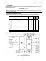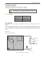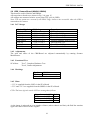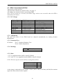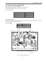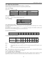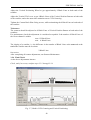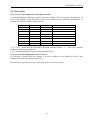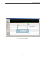
1
TITLE:
FSH Technical Service Guide
HA68A, HB68A, HC68A
DOC. NO.:
FSH/TSG/001
PREPARED BY:
LM
AUTHORIZED:
JR
DISTRIBUTION:
Tegningsarkiv, Svendborg
DD
ISSUE REVISION:
DATE:
(1)
(1)
1.0
2006-07-10
This document is the property of Contex A/S. The data contained herein, in whole or in
part, may not be duplicated, used or disclosed outside the Recipient for any purpose other
than to conduct technical evaluation. This restriction does not limit the Recipients right to
use information contained in the data if it is obtained from another source without
restriction.
FSH/TSG/001
Document Revision Record
REV.
DATE
CHANGED
BY
PAGES
AFFECTED
1.0
060710
LM
All
2
DRR
BRIEF DESCRIPTION OF CHANGE
Original issue of document
This document replaces FSH/TSM/001
FSH/TSG/001 060710
Table of Contents
1.
1.1
1.2
Introduction...................................................................................................................................................... 6
PRINTED CIRCUIT BOARD OVERVIEW ................................................................................................................. 6
BLOCK DIAGRAM................................................................................................................................................ 6
2.
2.1
2.2
2.2.1
2.3
2.3.1
2.3.2
2.3.3
2.4
2.4.1
2.4.2
2.4.3
2.5
2.5.1
2.5.2
2.5.3
2.5.4
2.5.5
2.5.6
2.5.7
2.5.8
2.6
2.6.1
2.6.2
2.6.3
2.6.4
2.6.5
2.7
2.7.1
2.7.2
2.7.3
2.7.4
2.7.5
2.8
2.8.1
2.8.2
2.8.3
2.8.4
2.8.5
2.8.6
2.9
2.9.1
2.9.2
2.9.3
2.9.4
2.9.5
2.10
2.10.1
2.10.2
2.10.3
2.11
2.11.1
2.11.2
2.11.3
Electrical Tests and Adjustments ................................................................................................................... 7
MARKING CODES FOR CIRCUIT BOARDS AND PROGRAMMED DEVICES .............................................................. 7
DOWNLOADING SCANNER FIRMWARE ................................................................................................................ 7
Erase and Restore Parameter Blocks........................................................................................................... 8
SMPS TYPE 1 (HA68A AND HB68A) ................................................................................................................ 9
DC Voltages ................................................................................................................................................. 9
Adjustments .................................................................................................................................................. 9
Fuses ............................................................................................................................................................ 9
SMPS TYPE 2 (HC68A) ................................................................................................................................... 10
DC Voltages ............................................................................................................................................... 10
Adjustments ................................................................................................................................................ 10
Fuses .......................................................................................................................................................... 10
LMF, LAMP AND MOTOR DRIVER BOARD ........................................................................................................ 11
DC Voltages ............................................................................................................................................... 11
Lamp Driver ............................................................................................................................................... 11
Stepper Motor Reference Voltages............................................................................................................. 11
Functional Test........................................................................................................................................... 11
Fuses .......................................................................................................................................................... 11
Markings .................................................................................................................................................... 11
Jumper Settings .......................................................................................................................................... 12
Hints ........................................................................................................................................................... 12
CBK, CAMERA BOARD (HA68A, HB68A)....................................................................................................... 14
DC Voltages ............................................................................................................................................... 14
Adjustments ................................................................................................................................................ 14
Functional Test........................................................................................................................................... 14
Markings .................................................................................................................................................... 14
Hints ........................................................................................................................................................... 14
CBM, CAMERA BOARD (HC68A) .................................................................................................................... 16
DC Voltages ............................................................................................................................................... 16
Adjustments ................................................................................................................................................ 16
Functional Test........................................................................................................................................... 16
Markings .................................................................................................................................................... 16
Hints ........................................................................................................................................................... 16
SUC, SCANNER CONTROLLER BOARD (HA68A, HB68B)................................................................................ 18
DC Voltages ............................................................................................................................................... 18
Functional Test........................................................................................................................................... 18
Markings .................................................................................................................................................... 18
Switch Settings (Download Control Switches) ........................................................................................... 18
Signal LEDs on the SUC-Board................................................................................................................. 18
Hints ........................................................................................................................................................... 18
SUF, SCANNER CONTROLLER BOARD (HC68A) .............................................................................................. 20
DC Voltages ............................................................................................................................................... 20
Functional Test........................................................................................................................................... 20
Markings .................................................................................................................................................... 20
Signal LEDs on the SUF Board ................................................................................................................. 20
Hints ........................................................................................................................................................... 20
IME, INTERFACE BOARD (HA68A, HB68A).................................................................................................... 22
DC Voltages ............................................................................................................................................... 22
Functional Test........................................................................................................................................... 22
Markings .................................................................................................................................................... 22
IMG, INTERFACE BOARD (HC68A).................................................................................................................. 23
DC Voltages ............................................................................................................................................... 23
Functional Test........................................................................................................................................... 23
Markings .................................................................................................................................................... 23
3
FSH/TSG/001 060710
2.12
2.12.1
2.12.2
2.12.3
2.12.4
2.13
2.13.1
2.13.2
2.13.3
2.13.4
2.13.5
2.14
2.15
SKD, OPERATOR PANEL ................................................................................................................................... 24
DC Voltages ............................................................................................................................................... 24
Functional Test........................................................................................................................................... 24
Markings .................................................................................................................................................... 24
Switch Setting (Scanner ID) ....................................................................................................................... 24
CRB, SMART CARD READER ............................................................................................................................ 26
DC Voltages ............................................................................................................................................... 26
Functional Test........................................................................................................................................... 26
Markings .................................................................................................................................................... 26
DIP Switch Setting ..................................................................................................................................... 26
Signal LED on the CRB Board................................................................................................................... 26
PAPER SENSORS ................................................................................................................................................ 28
CHECK AND ADJUSTMENT OF EXTENDED THICKNESS SENSOR ......................................................................... 28
3.
3.1
3.2
3.2.1
3.2.2
3.2.3
3.2.4
3.2.5
3.2.6
CCD Camera .................................................................................................................................................. 30
DESCRIPTION OF CCD CAMERA ....................................................................................................................... 30
CCD CAMERA CHECK AND ADJUSTMENT ........................................................................................................ 34
Check of Light Profiles............................................................................................................................... 34
Check and Adjustment of Focus ................................................................................................................. 36
Check and Adjustment of Scan-Width ........................................................................................................ 38
Check and Adjustment of CCD-Centering ................................................................................................. 40
Check and Adjustment of Vertical Positioning........................................................................................... 41
Final Check ................................................................................................................................................ 42
4.
4.1
4.1.1
4.1.2
4.1.3
General Maintenance .................................................................................................................................... 46
STEP BY STEP PROCEDURE FOR GENERAL MAINTENANCE ................................................................................ 46
Clean the Scanning Area............................................................................................................................ 46
Check CCD Camera Adjustment................................................................................................................ 46
Run Scanner Maintenance. ........................................................................................................................ 46
5.
5.1
5.2
5.3
5.3.1
5.3.2
5.4
Troubleshooting ............................................................................................................................................. 48
POWER-ON SELF-TEST ..................................................................................................................................... 48
LED INDICATORS ON OPERATOR PANEL .......................................................................................................... 49
ERROR CODES................................................................................................................................................... 50
Error Codes displayed on the Operator Panel .......................................................................................... 50
Error Codes displayed on the PC Screen................................................................................................... 50
TROUBLESHOOTING HINTS ............................................................................................................................... 51
6.
6.1
6.2
6.3
6.4
6.5
Disassembly and Assembly............................................................................................................................ 54
LID COVER ....................................................................................................................................................... 54
TOP COVER ....................................................................................................................................................... 54
ELECTRONICS BOX ........................................................................................................................................... 55
SCANNER CHASSIS ............................................................................................................................................ 55
MIRROR CHASSIS .............................................................................................................................................. 55
7.
7.1
7.2
7.3
7.4
7.5
7.6
7.7
7.8
7.9
Replacement of Parts..................................................................................................................................... 58
SUX- BOARD AND IMX-BOARD ........................................................................................................................ 58
LMF-BOARD, SMPS (PSU), RFI FILTER, AND FAN ......................................................................................... 58
CBX-BOARD ..................................................................................................................................................... 59
STEPPER MOTOR ............................................................................................................................................... 59
PAPER ENTRY SENSOR ...................................................................................................................................... 60
PAPER EXIT SENSOR ......................................................................................................................................... 60
IDLER ROLLERS ................................................................................................................................................ 60
DRIVE ROLLERS ................................................................................................................................................ 61
LAMP CARTRIDGE, LCAA ................................................................................................................................ 62
8.
8.1
8.1.1
8.1.2
8.1.3
8.1.4
8.1.5
8.1.6
8.1.7
SCANtest ........................................................................................................................................................ 70
DESCRIPTION OF SCANTEST ............................................................................................................................ 71
Test 1, Scanner Information ....................................................................................................................... 71
Test 2, LED Test......................................................................................................................................... 71
Test 3, Key Test .......................................................................................................................................... 71
Test 4, Original-Sensor Test....................................................................................................................... 71
Test 5, Lamp Test ....................................................................................................................................... 72
Test 6, Motor Test ...................................................................................................................................... 72
Test 7, Complete Hardware Test................................................................................................................ 72
4
FSH/TSG/001 060710
8.1.8
8.1.9
8.1.10
8.1.11
8.1.12
Test 9, Camera Adjustment ........................................................................................................................ 72
Test 12, Adjustment of Y-Axis Scaling........................................................................................................ 72
Test 13, Switch Scanner to Test Mode........................................................................................................ 72
Test 20, Noise Test ..................................................................................................................................... 73
Test 21, SCANdump ................................................................................................................................... 73
9.
Wiring Diagram ............................................................................................................................................. 75
10.
Special Service Tools...................................................................................................................................... 77
11.
Appendix A, Error Codes ............................................................................................................................. 78
List of Figures
Fig. 1-1, Hx68A Block Diagram...................................................................................................................................... 6
Fig. 2-1, SMPS Type 1 Test Points.................................................................................................................................. 9
Fig. 2-2, SMPS Type 2 Test Points................................................................................................................................ 10
Fig. 2-3, LMF Component Layout................................................................................................................................. 13
Fig. 2-4, CBK Component Layout................................................................................................................................. 15
Fig. 2-5, CBM Component Layout ................................................................................................................................ 17
Fig. 2-6, SUC Component Layout ................................................................................................................................. 19
Fig. 2-7, SUF Component Layout.................................................................................................................................. 21
Fig. 2-8, IME Component Layout.................................................................................................................................. 22
Fig. 2-9, IMG Component Layout ................................................................................................................................. 23
Fig. 2-10, SKDH Component Layout ............................................................................................................................ 25
Fig. 2-11, CRB Component Layout ............................................................................................................................... 27
Fig. 2-12, Adjustment of Extended Thickness Sensor................................................................................................... 29
Fig. 3-1, CCD Camera ................................................................................................................................................... 32
Fig. 3-2, Relations between Optical Adjustment Pattern and Screen Images ................................................................ 33
Fig. 3-3, Hx68A Uncorrected Light Profiles ................................................................................................................. 35
Fig. 3-4, Hx68A Corrected Light Profiles ..................................................................................................................... 35
Fig. 3-5, Hx68A Focus Signals...................................................................................................................................... 37
Fig. 3-6, Hx68A Scan-Width ......................................................................................................................................... 39
Fig. 3-7, Hx68A CCD-Centering and Vertical Positioning ........................................................................................... 42
Fig. 3-8, CCD Camera Overview (Adjustments)........................................................................................................... 43
Fig. 3-9, Optical Adjustment Pattern, 36” ..................................................................................................................... 44
Fig. 3-10, Focus Pattern, 40” ......................................................................................................................................... 45
Fig. 4-1, SM Calibration Sheet, 42”............................................................................................................................... 47
Fig. 6-1, Lid Cover ........................................................................................................................................................ 56
Fig. 6-2, Disassembly .................................................................................................................................................... 57
Fig. 7-1, Cable Routing.................................................................................................................................................. 63
Fig. 7-2, Inside Electronics Box .................................................................................................................................... 64
Fig. 7-3, Stepper Motor.................................................................................................................................................. 65
Fig. 7-4, Drive-Belt Tightener Adjustment.................................................................................................................... 66
Fig. 7-5, Paper Sensors .................................................................................................................................................. 67
Fig. 7-6, Drive System ................................................................................................................................................... 68
Fig. 7-7, Scanner Cross Section..................................................................................................................................... 69
Fig. 8-1, Noise Test, Example........................................................................................................................................ 74
Fig. 9-1, Hx68A Wiring Diagram.................................................................................................................................. 76
5
FSH/TSG/001 060710
1. Introduction
The purpose of this Technical Service Guide is to supply the information necessary to service the
following scanner models
HA68A, HB68A, HC68A
Note: Throughout this TSG the abbreviation Hx68A will be used when referring to all of the
above listed scanner models
1.2 Block Diagram
Fig. 1-1, Hx68A Block Diagram
6
x
x
HA68A
Reference
Section 2.3
Section 2.4
Section 2.5
Section 2.6
Section 2.7
Section 2.8
Section 2.9
Section 2.10
Section 2.11
Section 2.12
Section 2.13
HB68A
Printed Circuit Board
Switch Mode Power Supply Type 1
Switch Mode Power Supply Type 2
LMF, Lamp and Motor Driver Board
CBK, Camera Board
CBM, Camera Board
SUC, Controller Board
SUF, Controller Board
IME, Interface Module, IEEE 1394 and USB2.0
IMG, Interface Module, IEEE 1394 and USB2.0
SKD, Operator Panel
CRB, Smart Card Reader
HC68A
1.1 Printed Circuit Board Overview
The table below gives an overview of the printed circuit boards used in the different models.
x
x
x
x
x
x
x
x
x
x
x
x
x
x
x
x
x
x
x
FSH/TSG/001 060710
2. Electrical Tests and Adjustments
Required Test Equipment:
Multimeter, Ri > 10 Mohm.
PC with the following installed:
• SCANtest
• Scanner Maintenance
• USB and/or IEEE 1394 interface
• Scanner Maintenance
SCANtest is described in Chapter 8, page 70.
Scanner Maintenance is described in Section 4.1.3, page 46.
2.1 Marking Codes for Circuit Boards and Programmed Devices
All circuit boards are identified by a 4-letter code, where the fourth letter designates a specific
variant of the board. The board identification code is followed by a board revision number
(functional level) and for newer boards also an extra letter in parenthesis. This extra letter is
unimportant in this connection.
The marking of all printed circuit boards may be exemplified by the marking of the SUF Board:
SUFA02(B)
which designates SUF Board, variant A, revision 02. The (B) is of no importance and should be
neglected.
The revision number is updated only if the functionality of the board has been changed. Updated
boards will always be backwards compatible.
2.2 Downloading Scanner Firmware
The scanner firmware is stored in Flash Memory on the SUx Board.
Firmware is downloaded to the scanner through the IEEE 1394 or USB2.0 interface. Please refer
to any readme.txt on the firmware disk for download instructions.
The download program is started by double-clicking the self extracting firmware file.
It is recommended to disable WIDEsystem before upgrading the firmware to prevent any possible
problems caused by this program accessing the scanner during the upgrade.
Scanner firmware is available on the support home page.
If the scanner does not go into Boot Mode when the download program is started, the scanner can
be forced into Boot Mode by turning it OFF, setting SW7 on the CRB board switch to ON (see
page 27), and turn the scanner back ON. The scanner will now be in Boot Mode and new firmware
can be downloaded as described above. When the new firmware has been successfully
downloaded, turn the scanner OFF, set SW7 back to OFF, and turn the scanner ON for normal
operation.
7
FSH/TSG/001 060710
2.2.1 Erase and Restore Parameter Blocks
When trouble shooting it may be advisable to clear the parameter blocks in the scanner to reset
these to default values.
The parameter blocks can be erased from Scanner Maintenance by right-click on the Title Bar and
select Erase Parameter Blocks from the pull-down menu.
Note: Always run Scanner Maintenance after Erasing Parameter Blocks.
8
FSH/TSG/001 060710
2.3 SMPS Type 1 (HA68A and HB68A)
This SMPS is used in HA68A and HB68A
All test points referred to below are shown in Fig. 2-1 page 9.
All DC voltages are measured relative to CON2, pin 4,5,8 (GND).
The connector CON1 is connected directly to the line voltage
and constitute a risk of electric shock, or injury to persons
2.3.1 DC Voltages
Ref. on
Fig. 2-1
CON2, pin1
CON2,pin2,3
CON2, pin4,5,8
CON2, pin6
CON2, pin7
DC Voltage
+12 V +1/-0 V
+5.3 V +0/-0.1 V
GND
N.C.
+24 V ± 2 V
2.3.2 Adjustments
IMPORTANT: The output voltages of the SMPS are all factory set and should normally not be
adjusted.
The (5V) output voltage should be no more than 5.3 V measured between GND and CON2, pin
2,3 on the SMPS, and no less than 5.1 V measured between GND and D3, bottom on the CBxBoard.
If the voltage is not within these limits, it may be adjusted by potentiometer VR1 on the SMPS,
see
Fig. 2-1, page 9.
2.3.3 Fuses
No service replaceable fuses
CON2
CON2, pin 1
+12V+1/-0
12V
5.3V
CON2, pin 2,3
5.3V
+5.3V+0/-0.1
GND
CON2, pin 4,5
GND
CON1
PG
CON2, pin 6
24V
NC
GND
AC/N
GND
NC
CON2, pin 7
24V±2V
CON2, pin 8
AC/L
GND
Potentiometer VR1
Fig. 2-1, SMPS Type 1 Test Points
9
FSH/TSG/001 060710
2.4 SMPS Type 2 (HC68A)
This SMPS is used in HC68A
All test points referred to below are shown in Fig. 2-2 page 10.
All DC voltages are measured relative to TB2, pin 1,2 (GND).
The connector CON1 is connected directly to the line voltage
and constitute a risk of electric shock, or injury to persons
2.4.1 DC Voltages
Ref. on Fig. 2-2
TB2, pin 1,2
TB2, pin 3,4,5,6
TB2, pin 7
TB2, pin 8
DC Voltage
+5.3 V +0/-0.1 V
GND
+12.5 V ± 0.5 V
+24 V ± 1 V
2.4.2 Adjustments
IMPORTANT: The output voltages of the SMPS are all factory set and should normally not be
adjusted.
The 5.3V output voltage should be no more than 5.3 V measured between GND and TB2, pin 1,2
(5.3V) on the SMPS, and no less than 5.1 V measured between GND and D3, bottom on the CBK
board. If the voltage is not within these limits, it may be adjusted by potentiometer VR1 on the
SMPS.
2.4.3 Fuses
No service replaceable fuses
L
N
5.3V
TB2, pin 1-2
5.3V
+5.3V +0/-0.1
GND
GND
TB2, pin 3-6
GND
GND
GND
TB2, pin 7
12.5V
+12.5V±0.5
24V
TB2, pin 8
+24V±1
VR1
+5.3V Adjust
Fig. 2-2, SMPS Type 2 Test Points
10
FSH/TSG/001 060710
2.5 LMF, Lamp and Motor Driver Board
All test points referred to below are shown in Fig. 2-3, page 13.
All DC voltages are measured relative to test points, TP4, 12, 13, 17 (GND).
CAUTION:
Connectors J1, J7 and all the components in the hatched area are connected to the line voltage
and constitute a risk of electric shock, or injury to persons.
2.5.1 DC Voltages
Ref. on Fig. 2-3
Test point 4, 12, 13, 17
TP8 - GND
TP9 - GND
TP10 - GND
TP18 - GND
TP16 - GND
TP15 - GND
TP5 - TP7 *
TP7 - TP6*
DC Voltage
GND
+3.3 V ± 0.1 V
+5.3 V +0/-0.2 V
+12.0 V + 1/-0 V
+24.0 V ± 2 V
+5.0 V ± 0.15 V
+12.0 V ± 0.3 V
+200 V ± 20 V
−200 V ± 20 V
* Caution: These test points are at high voltage level and
constitute a risk of electric shock, or injury to persons.
2.5.2 Lamp Driver
The LMF board is designed to work with a calibrated Lamp Cartridge, which means that there is
no adjustment of the lamp driver.
2.5.3 Stepper Motor Reference Voltages
No adjustment of Stepper Motor Reference Voltage on LMF-Board.
2.5.4 Functional Test
SCANtest:
Test 5, Lamp Test
Test 6, Motor Test
2.5.5 Fuses
The type and rating of the fuse on the LMFA-Board is:
F1:
T2.0AH/250V, type IEC 127- 2/5, UL R/C
IMPORTANT: For continued protection against risk of fire, replace
only with same type and rating of fuse.
2.5.6 Markings
LMFAdd
HA68A
LMFAdd
HB68A
LMFAdd
HC68A
where dd = board revision number
11
FSH/TSG/001 060710
2.5.7 Jumper Settings
Jumper:
JP1
not installed
2.5.8 Hints
Jumper on JP1:
Not installed: Lamp controlled by SUx
Installed:
Lamp constant ON
Control signals on J11:
pin 2: Lamp ON/OFF, LOW = ON
pin 8: Feed-Motor Step Pulse
pin 11: Feed-Motor Direction, LOW = FORWARD
12
FSH/TSG/001 060710
+5.3V+0/-0.2V
TP9
+12V+1/-0V
TP10
+3.3V±0.1V
TP8
JP1
GND
TP4,12,13,17
+5V±0.15V
TP16
+24V±2V
TP18
+12V±0.3V
TP15
TP5
200V
±20V
TP7
200V
±20V
TP6
Fig. 2-3, LMF Component Layout
13
FSH/TSG/001 060710
2.6 CBK, Camera Board (HA68A, HB68A)
This board is used in HA68A and HB68A.
All test points referred to are shown in Fig. 2-4, page 15.
All voltages are measured relative to test point J701, pin3,4 (GND).
Note: The test points are covered by the EMC Cage, and are not accessible when the CKB is
mounted on the camera.
2.6.1 DC Voltages
Ref. on Fig. 2-4
J701, pin3,4
D3, bottom
D3, top
D2, top
D4, bottom
D4, top
C301, bottom
D308, bottom
DC Voltage
GND
+5.3 V +0/-0.2 V
+5.0 V ± 0.15 V
+5.0 V ± 0.15 V
+12.0 V +1/-0 V
+11.6 V ± 0.6 V
+3.3 V ± 0.1 V
+1.8 V ± 0.1 V
Remarks
GND reference
From SUx/SMPS
Derived from +5.3V
Derived from +5.3V
From SUx/SMPS, used for CCD
Derived from +12V
From SUx / LMF
Derived from +3.3V
2.6.2 Adjustments
The gain and offset of the CBK-Board are adjusted automatically by running Scanner
Maintenance.
2.6.3 Functional Test
SCANtest:
Test 7, Complete Hardware Test.
Test 9, Camera Adjustment.
2.6.4 Markings
CBKBdd
HA68A
CBKBdd
HB68A
where dd = board revision number
2.6.5 Hints
+3.3 V is supplied from the LMF via the SUx-Board.
+5.3 V and +12 V are supplied from the SMPS via the SUx-Board.
CCD: The lines of pixels on the CCD are arranged as follows:
Upper line on the CCD
2nd line on the CCD
3rd line on the CCD
Lower line on the CCD
Red
Green
Blue
B/W
As the image is mirrored an even number of times (mirror chassis and lens), the Red line remains
upper line when referred to the original.
14
FSH/TSG/001 060710
After replacement of CBK-Board, do:
• CCD-Centering, Section 3.2.4, page 40.
• Vertical Positioning, Section 3.2.5, page 41.
• Check Scan-Width. If it is within the limits given in Section 3.2.3, page 38, Focus will also be
OK, and no further adjustments are required.
• Run Scanner Maintenance, Section 4.1.3, page 46.
These adjustments can be made without loosening the Camera Fixing Screws and without
loosening the Focus Lock Screw.
+5.0V±0.15V
D3,top
+5.3V+0/-0.2V
D3,bottom
+11.6V±0.6V
D4,top
+12V+1/-0V
D4,bottom
Camera Motor
Output
+5.0V±0.15V
+1.8V±0.1V
D2,top
C308,bottom
GND
+3.3V±0.1V
J701,pin3,4
C301,bottom
Fig. 2-4, CBK Component Layout
15
FSH/TSG/001 060710
2.7 CBM, Camera Board (HC68A)
This board is used in HC68A.
All test points referred to are shown in Fig. 2-4, page 15.
All voltages are measured relative to test point GND.
Note: The test points are covered by the EMC Cage, and are not accessible when the CKB is
mounted on the camera.
2.7.1 DC Voltages
Ref. on Fig. 2-4
J701, pin3,4
D3, bottom
D3, top
D2, top
D4, bottom
D4, top
C301, bottom
D308, bottom
DC Voltage
GND
+5.3 V +0/-0.2 V
+5.0 V ± 0.2 V
+5.0 V ± 0.2 V
+12.0 V +1/-0 V
+11.6 V ± 0.6 V
+3.3 V ± 0.1 V
+1.8 V ± 0.1 V
Remarks
GND reference
From SUx/SMPS
Derived from +5.3V
Derived from +5.3V
From SUx/SMPS, used for CCD
Derived from +12V
From SUF / LMF
Derived from +3.3V
2.7.2 Adjustments
The gain and offset of the CBM board are adjusted automatically by running Scanner
Maintenance.
2.7.3 Functional Test
SCANtest:
Test 7, Complete Hardware Test
Test 9, Camera Adjustment.
2.7.4 Markings
HC68A CBMAdd
where dd = board revision number
2.7.5 Hints
+3.3 V is supplied from the LMF via the SUx Board.
+5.3 V and +12 V are supplied from the SMPS via the SUx Board.
CCD: The lines of pixels on the CCD are arranged as follows:
Upper line on the CCD
2nd line on the CCD
3rd line on the CCD
Lower line on the CCD
Red
Green
Blue
B/W
As the image is mirrored an even number of times (mirror chassis and lens), the Red line remains
upper line when referred to the original.
16
FSH/TSG/001 060710
After replacement of CBM Board, do:
• CCD-Centering, Section 3.2.4, page 40.
• Vertical Positioning, Section 3.2.5, page 41.
• Check Scan-Width. If it is within the limits given in Section 3.2.3, page 38, Focus will also be
OK, and no further adjustments are required.
• Run Scanner Maintenance, Section 4.1.3, page 46.
These adjustments can be made without loosening the Camera Fixing Screws and without
loosening the Focus Lock Ring / Lock Screw.
+5.0V±0.15V
D3,top
+5.3V+0/-0.2V
D3,bottom
+11.6V±0.6V
D4,top
+12V+1/-0V
D4,bottom
Camera Motor
Output
+5.0V±0.15V
+1.8V±0.1V
D2,top
C308,bottom
GND
+3.3V±0.1V
J701,pin3,4
C301,bottom
Fig. 2-5, CBM Component Layout
17
FSH/TSG/001 060710
2.8 SUC, Scanner Controller Board (HA68A, HB68B)
This board is used in HA68A and HB68A.
All test points referred to below are shown in Fig. 2-6, page 19.
All voltages are measured relative to test point GND2.
2.8.1 DC Voltages
Ref. on Fig. 2-6
GND2
12V_CAM
5V_CAM
+3
+5V
APEX_SUP
APEX_PLL
DC Voltage
GND
+12 V + 1/-0V
+5.3 V +0/-0.2 V
+3.3 V ± 0.1 V
+5.1 V +0.1/-0.2 V
+1.8 V ± 0.1 V
+1.8 V ± 0.05 V
Remarks
GND reference
Supply for Camera Board
Supply for Camera Board
Supplied from LMF
Derived from 5.3V on SUC
Derived from 3.3V on SUC
Derived from 3.3V on SUC
2.8.2 Functional Test
SCANtest:
Test 1 Scanner Information
Test 7, Complete Hardware Test
2.8.3 Markings
SUCLdd
HA68A
SUCNdd
HB68A
where dd = board revision number
2.8.4 Switch Settings (Download Control Switches)
The download program reads the Download Control Switches, SW1 and SW2, on the SUC-Board
to check if the actual firmware and the SUC hardware are compatible.
The Download Control Switches are factory set, and the setting must not be changed.
2.8.5 Signal LEDs on the SUC-Board
The three signal LEDs on the SUC-Board are for debugging purposes only. The ON/OFF pattern
displayed by these LEDs is not intended for general troubleshooting.
2.8.6 Hints
After replacement of SUC-Board:
As all scanner parameters are stored in the Flash Memory on the SUC-Board, the following steps
should be carried out after replacement of the SUC-Board:
• Download Firmware
• Enter Serial Number of scanner into Flash Memory (SCANtest, Test 1). The serial number of
the scanner is found on the marking label on back of the scanner
• Run Scanner Maintenance
18
FSH/TSG/001 060710
+3.3V±0.1V
"+3"
+5.1V+0.1/-0.2V
"+5"
+5.3V+0/-0.2V
"5V_CAM"
+1.8±0.1V
"APEX_SUP"
+12V+1/-0V
+1.8V±0.05V
"12V_CAM"
"APEX_PLL"
GND
"GND2"
Fig. 2-6, SUC Component Layout
19
FSH/TSG/001 060710
2.9 SUF, Scanner Controller Board (HC68A)
This board is used in HC68A.
All test points referred to below are shown in Fig. 2-7, page 21.
All voltages are measured relative to test point GND2.
2.9.1 DC Voltages
Ref. on Fig. 2-7
GND2
12V_CAM
DC Voltage
GND
+12 V + 1/-0V
5V_CAM
+5.3 V +0/-0.2 V
+3
+5V
APEX_SUP
APEX_PLL
+3.3 V ± 0.1 V
+5.1 V +0.1/-0.2 V
+1.8 V ± 0.1 V
+1.8 V ± 0.05 V
Remarks
GND reference
Supply for Camera Board,
Elevation Motor (ATAC)
Supply for Camera Board,
MDA Board (ATAC)
Derived from 5.3V on SUF
2.9.2 Functional Test
SCANtest:
Test 1 Scanner Information
Test 7, Complete Hardware Test
2.9.3 Markings
HC68A SUFBdd
where dd = board revision number
2.9.4 Signal LEDs on the SUF Board
The three signal LEDs on the SUF board are for debugging purposes only. The ON/OFF pattern
displayed by these LEDs is not intended for general troubleshooting.
2.9.5 Hints
After replacement of SUF board:
As all scanner parameters are stored in the Flash Memory on the SUF board, the following steps
should be carried out after replacement of the SUF board:
• Download Firmware
• Run Scanner Maintenance
• Enter Serial Number of scanner into Flash Memory (SCANtest, Test 1). The serial number of
the scanner is found on the marking label on back of the scanner
20
FSH/TSG/001 060710
+3.3V±0.1V
"+3"
+5.1V+0.1/-0.2V
"+5"
+5.3V+0/-0.2V
"5V_CAM"
+12V+1/-0V
+1.8V±0.05V
"12V_CAM"
"APEX_PLL"
+1.8±0.1V
GND
"APEX_SUP"
"GND2"
Fig. 2-7, SUF Component Layout
21
FSH/TSG/001 060710
2.10 IME, Interface Board (HA68A, HB68A)
This board is used in HA68A and HB68A.
All test points referred to below are shown in Fig. 2-8 page 22.
All voltages are measured relative to test points GND_T1.
2.10.1 DC Voltages
Ref. on Fig. 2-8
GND_T1
R34, top
+5V0_D1
+3V3_D1
DC Voltage
GND
+5.3 V +0/-0.2 V
+5.2 V +0/-0.2 V
+3.3 V ± 0.1 V
2.10.2 Functional Test
Connect the computer to each separate port in turn and start SCANtest or WIDEsystem to check if
the scanner connects with all ports available.
2.10.3 Markings
IMEAdd
HA68A
IMEAdd
HB68A
where dd = board revision number
+3.3V±0.1V
"+3V3_D1"
GND
+5.2V+0/-0.2V
"+5V0_D1"
"GND_T1"
+5.3V+0/-0.2V
R34,Top
Fig. 2-8, IME Component Layout
22
FSH/TSG/001 060710
2.11 IMG, Interface Board (HC68A)
This board is used in HC68A.
All test points referred to below are shown in Fig. 2-9 page 23.
All voltages are measured relative to test points GND_T1.
2.11.1 DC Voltages
Ref. on Fig. 2-10
GND_T1
R34, top
+5V0_D1
+3V3_D1
DC Voltage
GND
+5.3 V +0/-0.2 V
+5.2 V +0/-0.2 V
+3.3 V ± 0.1 V
2.11.2 Functional Test
Connect the computer to each separate port in turn and start SCANtest or WIDEsystem to check if
the scanner connects with all ports available.
2.11.3 Markings
IMGAdd
HC68A
where dd = board revision number
+3.3V±0.1V
"+3V3_D1"
GND
+5.2V+0/-0.2V
"+5V0_D1"
"GND_T1"
+5.3V+0/-0.2V
R34,Top
Fig. 2-9, IMG Component Layout
23
FSH/TSG/001 060710
2.12 SKD, Operator Panel
All test points referred to are shown in Fig. 2-10, page 25.
All voltages are measured relative to PCB Ground Plane.
2.12.1 DC Voltages
Ref. on Fig. 2-10
J2, pin 3
C1, top
DC Voltage
+3.3 V ± 0.1 V
+5.1 V +0.1/-0.2 V
2.12.2 Functional Test
SCANtest:
Test 1, Scanner ID Switch
Test 2, LED test
Test 3, Key test
2.12.3 Markings
SKDHdd
HA68A
SKDHdd
HB68A
SKDHdd
HC68A
where dd = board revision number
2.12.4 Switch Setting (Scanner ID)
DIP Switch Setting:
HA68A
HB68A
HC68A
SW1
SW2
SW3
SW4
SW5
SW6
SW7
SW8
HEX
OFF
OFF
OFF
OFF
OFF
OFF
ON
ON
ON
OFF
ON
ON
ON
OFF
OFF
ON
ON
ON
ON
ON
ON
OFF
OFF
OFF
0x2E
0x36
0x36
An undefined switch setting may cause the ‘Invalid Scanner ID’ Error Code to be displayed on the
Operator Panel.
CAUTION:
The Scanner ID Switch setting is stored in the Flash Memory on the SUx-Board. Every time the
scanner is switched ON, it reads the switch setting and if it is different from the stored value, the
new setting will be stored and all other stored scanner parameters (including Stitching, Basic
Calibration and Color Calibration) will be cleared to default values.
This means that the scanner must be calibrated using Scanner Maintenance afterwards to restore
the actual values.
24
FSH/TSG/001 060710
Power LED
Red/Green
Power
Diagnostics LED
Red
Switch 8
Scanner ID Switch
ON <-> OFF
Switch 1
Wait LED
Yellow
3.3V
J2,pin3
Forward
Ready LED
Red/Green
Appl. 1
5.1V
C1,top
Appl. 2
Stop/Reverse
Appl. 3
GND
Fig. 2-10, SKDH Component Layout
25
Bottom View
FSH/TSG/001 060710
2.13 CRB, Smart Card Reader
All test points referred to below are shown in Fig. 2-11, page 27.
All DC voltages are measured relative to test point J4, pin10 (GND).
2.13.1 DC Voltages
NOTE: Does not apply to CRBC
Ref. on Fig. 2-11
J4, pin10
VR1, pin3
VR1, tap
DC Voltage
GND
+5.3 V +0/-0.2 V
+3.3 V ±0.1V
Remarks
GND reference
From SUx / LMF
Derived from +5.3V
2.13.2 Functional Test
SCANtest:
Test 1, Scanner Model (Smart Card)
2.13.3 Markings
HA68A CRBAdd
CRBAdd
HB68A
HC68A CRBCdd
where dd = board revision number
2.13.4 DIP Switch Setting
The DIP Switch may be accessed through the slot in the right hand side of the Top Cover, see Fig.
2-11, page 27.
SCSI related switch settings (SW No. 1, 2, 3, 4, and 5) do not apply to the Hx68A scanners, but
should be set to the default settings shown in the table below.
Default DIP Switch Setting:
Switch No:
1
ON
2
OFF
3
ON
4
ON
5
OFF
6
OFF
7
OFF
8
OFF
7
ON
OFF
8
Troubleshooting and Test Switches:
Function
Boot start-up
Factory testing
Switch No:
Forced:
Normal:
Self-test:
Normal:
1
ON
2
OFF
3
ON
4
ON
5
6
OFF OFF
ON
OFF
ON
ON
OFF OFF
ON
OFF
SW1-6
Do not apply to Hx68A, set to default.
SW7:
If download fails, try to set SW7 to ON. For normal operation SW7 must be set to
OFF.
Reserved for factory testing and must be set to OFF.
SW8:
NB! The switches are read at power-on only, and the scanner must be switched OFF and back
ON for a changed switch setting to become effective.
2.13.5 Signal LED on the CRB Board
The signal LED (LED1) on the CRB Board turns ON when a Smart Card is inserted. It only
signals, that a Smart Card has been inserted, it does not show whether the card is valid or not.
26
FSH/TSG/001 060710
GND
+3.3V±0.1V
J4,pin10
VR1,tab
Above picture only refers to CRBA
Not mounted
on CRBC
LED1
Switch no. 8
S1
(SCSI ID Switch)
Switch no. 1
Fig. 2-11, CRB Component Layout
27
+5.3V+0/-0.2V
VR1,pin3
FSH/TSG/001 060710
2.14 Paper Sensors
See Fig. 7-5, page 67.
Note: The Original Entry and Original Exit Sensors are not adjustable.
2.15 Check and Adjustment of Extended Thickness Sensor
See Fig. 2-12, page 29.
Adjustment:
Turn power OFF.
Remove Top Cover.
Locate the lock bracket on the left side of the Electronics Box.
Loosen the one T10 lock screw located in the bracket.
Open up the Electronics Box.
Turn power ON.
WARNING: The connector of the Lamp Cartridge is
connected directly to the line voltage and constitute a
risk of electric shock, or injury to persons.
Start SCANtest, Test 4
Open the Lid
Remove the Lid Cover
Remove Pressure Platen
1. Loosen the three fixing screws (two T20 and one T10) for the sensor bracket just enough to
allow the bracket to be moved.
2. Set Thickness Adjustment Sliders to pos. 6 (step 2) at both sides, see Fig. 2-12.
3. Close Lid to lower the Idler Rollers to pos. 6.
4. Adjust the sensor bracket to position the sensor lever as close as possible to - but not
touching - the pulley.
5. Tighten the three fixing screws (be careful to maintain the position of the bracket while
tightening the fixing screws).
6. Check that the WAIT LED remains ON when opening and closing the Lid.
7. Set Thickness Adjustment Sliders to pos. 3 (step 1), see Fig. 2-12..
8. Close Lid while watching the Wait LED.
9. Check that the spacing between the Idler and Drive rollers is at least 1 mm when the WAIT
LED turns OFF.
It may be necessary to repeat step 1 through 9 to obtain correct adjustment.
Check:
Start SCANtest, Test 4
Set Thickness Adjustment Sliders to pos. 6 (step 2).
Close Lid to lower the Idler Rollers.
Check that the WAIT LED remains ON.
Set Thickness Adjustment Sliders to pos. 3 (step 1).
Close Lid while watching the Wait LED.
Check that the spacing between the Idler and Drive rollers is at least 1 mm when the WAIT LED
turns OFF.
28
FSH/TSG/001 060710
0.1-0.2mm
Step 1
Step 2
Fixing Screws for
Extended Thickness
Sensor Bracket
Fig. 2-12, Adjustment of Extended Thickness Sensor
29
FSH/TSG/001 060710
3. CCD Camera
The adjustment procedures presented in this chapter cover all adjustments needed for replacing the
complete CCD Camera.
It will hardly ever be necessary to replace mechanical parts such as Lens, Camera Housing, etc.,
and in most cases, the only adjustments necessary after replacement of the CBx-Board are:
• Check Scan-Width. If it is within the limits given in Section
3.2.3, page 38, then Focus will also be OK.
• CCD-Centering, Section 3.2.4, page 40.
• Vertical Positioning, Section 3.2.5, page 40.
• Run Scanner Maintenance, Section 4.1.3, page 46.
These adjustments can be made without loosening the Camera Fixing Screws and without
loosening the Focus Lock Screw.
3.1 Description of CCD Camera
See Fig. 3-1, CCD Camera, page 32.
The CCD Camera basically consist of:
•
•
•
•
•
•
•
•
•
Lens
Lens Adapter
Camera Housing
Camera Back-Plate
CCD Mounting Plate
CBx-Camera Board
Camera Base Plate
Camera Guide Bracket
EMC Cage
The parts of the CCD Camera are mounted on the Camera Base Plate, and the complete CCD
Camera is mounted on a Mounting Platform, which is part the Mirror Chassis. The camera is
positioned with the optical axis perpendicular to the scan-area by means of the Camera Guide
Bracket placed at the left side of the camera.
The distance between the scanning area and the camera can be adjusted by loosening the three T20
Camera Fixing Screws and turning the Scan Width Adjustment Screw on the Guide Bracket.
Note: The Camera Base Plate and the Guide Bracket are connected by means of two screws with
self-locking nuts. These two screws have been factory set to provide accurate and smooth
guidance of the camera, and they should not be touched.
The Lens itself is mounted in the Lens Adapter, and three T6 screws secure its position in the
adapter.
Slots in the Camera Housing allow the tube of the Camera Housing to be tightened around the
Lens Adapter by means of a Focus Lock Screw, see Fig. 3-8, page 43. The slots are covered by a
flexible Covering Tape to prevent stray light from entering the camera.
The Camera Housing can be tilted slightly up and down to position the scanline in the “vertical”
direction by turning the Vertical Positioning Wheel.
30
FSH/TSG/001 060710
Focus
The CCD Camera is focused by loosening the Focus Lock Screw and turning the Lens Adapter to
get the maximal amplitude of the image of the Focus Pattern.
The Lens itself is mounted in the Lens Adapter, and three T6 screws secure its position in the
adapter. When these screws are loosened, the lens can be rotated to have the dot on the lens
pointing upwards. This is the “best position” as determined by the lens manufacturer.
This “best position” is not critical, and when doing field adjustments it will hardly ever be
necessary to change the factory set position of the Lens.
Scan-Width
The Scan-Width depends on the distance between the CCD Camera and the scan-area. It can be
adjusted by loosening the three T20 Camera Fixing Screws and turning the Scan Width
Adjustment Screw to slide the CCD Camera back and forth to get the required number of ScanWidth Units within the field of vision, see Scan-Width Pattern, Fig. 3-9, page 44.
The scaling accuracy of the scanner depends directly on the accuracy of the Scan-Width
adjustment.
Vertical Positioning and Centering of CCD Camera
To set the basic Vertical Position of the camera, adjust the Vertical Positioning Wheel to get 8
Black Lines of the Vertical Position Pattern, see Fig. 3-9, page 44.
The final positioning of the scanline within the scan-area is done by shifting the CCD Mounting
Plate relative to the Camera Housing using the Vertical Tilt and CCD-Centering levers, see Fig.
3-8, page 43.
Fig. 3-2, page 33 shows the relation between the patterns on the Optical Adjustment Pattern and
the waveforms seen on the screen of SCANtest, Test 9 during Camera Adjustment.
31
FSH/TSG/001 060710
Lens
Lens Adapter
Lens Fixing Screws (3 pcs.)
Camera Guide
Bracket
Camera Housing
Camera Base Plate
Fixing Nut for
CCD Mounting Plate
Camera Back-Plate
DO NOT loosen
these
Screws/Nuts
EMC Cage
Bottom Part
Clamp for
Flat Cable Braiding
Fixing Screws (2 pcs.)
for Flat Cable Braiding
Fixing Nut for
CCD Mounting Plate
CCD Mounting Plate
Fixing Nuts (long) for
CCD Mounting Plate (2 pcs.)
Fig. 3-1, CCD Camera
32
EMC Cage
Top Part
FSH/TSG/001 060710
Optical Adjustment Pattern
CAMERA A
Scan Width
Green Scanline
Adjustment Patterns
Fig. 3-2, Relations between Optical Adjustment Pattern and Screen Images
33
FSH/TSG/001 060710
3.2 CCD Camera Check and Adjustment
Remove the Top Cover to get access to the CCD Camera.
Equipment needed:
• PC with SCANtest and Scanner Maintenance installed. IEEE 1394 or USB2.0 interface
• Optical Adjustment Pattern (6879A107)
• Focus Pattern (6779D216)
CCD Camera and adjustment tools are shown in:
Fig. 3-8, CCD Camera Overview (Adjustments), page 43
Fig. 3-9, Optical Adjustment Pattern, 36”, page 44
Fig. 3-10, Focus Pattern, 40”, page 45
In the description of the adjustment procedures, references are made to sub-patterns A, B, and C of
the Optical Adjustment Pattern. These sub-patterns are shown in Fig. 3-9, page 44.
3.2.1 Check of Light Profiles
Images of the Light Profiles are shown in:
Fig. 3-3, Hx68A Uncorrected Light Profiles, page 35
Fig. 3-4, Hx68A Corrected Light Profiles, page 35
Procedure for check of Light Profiles
Place the Scan-area Lid in pos. 3 (Normal Media Thickness).
Start
SCANtest
Select
Test 9
Select
Uncorrected or Corrected Light Profile
Press
Execute
Select
Green (Default for Uncorrected)
Select
Detail View: Light Profile
Compare the image of the Software Oscilloscope with the relevant sample image listed above.
If the signal levels of the uncorrected Light Profiles differ much from the sample images, the
scanner might need to be calibrated by Scanner Maintenance.
34
FSH/TSG/001 060710
Fig. 3-3, Hx68A Uncorrected Light Profiles
Fig. 3-4, Hx68A Corrected Light Profiles
35
FSH/TSG/001 060710
3.2.2 Check and Adjustment of Focus
Images of the Focus adjustments are shown in:
Fig. 3-5, Hx68A Focus Signals, page 37.
Note: When replacing the Camera Board, it is normally not necessary to re-adjustment Focus.
First check the Scan Width, and if it is OK, the Focus will also be OK.
Adjustment Procedure
Do not loosen the camera. The construction of the camera ensures that the optical axis of the lens
is perpendicular to the scanning area and hence no alignment of the camera housing is necessary.
Always perform the Focus adjustment before adjusting the Scan-Width, see “Interaction” below.
Start
SCANtest
Select
Test 9
Select
Corrected Light Profile*)
Press
Execute
*) Note: If the camera is completely out of adjustment it may not be possible to run Test 9
in ‘Corrected’ mode. In that case, select ‘Uncorrected’ and with the Optical Adjustment
Pattern placed in the scan-area make a coarse adjustment of Focus and Scan-Width before
continuing.
Select
Select
Blue (Default)
Detail View: Light Profile
Insert the Focus Pattern and feed it by using the Forward Key until the image of the pattern with
the resolution listed below is seen on the upper image on the screen:
Model
HA68A
HB68A
Focus Pattern
6779D216
6779D216
Resolution
1.5 lp/mm
1.5 lp/mm
Loosen the Focus Lock Screw (see Fig. 3-8, page 43) and turn the Lens Adapter to get maximum
amplitude of the Focus signal (approximately 6 division peak-to-peak).
The amplitude of the Focus signal (Corrected) should be even within:
Min/Max > 0.7
Tighten the Focus Lock Screw to secure the Focus setting.
Interaction
The Focus adjustment has a big influence on the Scan-Width adjustment. Therefore the ScanWidth must be checked and readjusted if necessary when the Focus adjustment has been changed.
On the other hand, the Focus adjustment is relative tolerant to changes in the Scan-Width
adjustment and as a rule of thumb, the Scan-Width adjustment can be changed ±1 SWU without
the need for re-focusing.
When all camera adjustments have been completed, run Scanner Maintenance.
36
FSH/TSG/001 060710
Fig. 3-5, Hx68A Focus Signals
37
FSH/TSG/001 060710
3.2.3 Check and Adjustment of Scan-Width
Images of the Scan-Width adjustments are shown in:
Fig. 3-6, Hx68A Scan-Width, page 39
The aim of this adjustment is to obtain a camera Scan-Width of:
HA68A:
HB68A:
914.4 mm
914.4 mm
The Scan-Width is correct if the total sum of Scan-Width Units (SWU) at the start and at the end
of the scanline is as shown in the table below (1 SWU is either 1 Black Line or 1 White Space of
the Scan-Width Pattern (A)).
Model
Optical Adjustment Pattern
HA68A
HB68A
6879A107, sub-pattern A
6879A107, sub-pattern A
Total sum of
Scan-Width
Units
6
6
Tolerance
± 1 SWU
± 1 SWU
The tolerance corresponds to approximately 0.10% on the Scan-Width (scaling error).
Adjustment Procedure
Always do the Focus adjustment before adjusting the Scan-Width, see “Interaction” below.
Place the Optical Adjustment Pattern (see table above) in the scan-area.
Align the Adjustment Pattern by pushing it sideways towards the Operator Panel and towards the
front of the scanner.
Start
Select
Select
Press
Select
Select
SCANtest
Test 9
Uncorrected Light Profile
Execute
Green (Default)
Detail View: Scan Width
Loosen the three T20 Camera fixing screws and the three T20 Camera Back-Plate fixing screws
(use special key, p/n 0008V354), see Fig. 3-8, page 43. The screws should be loosened just enough
to allow the Camera and the Camera Back-Plate to be moved.
Adjust the Scan-Width by turning the Scan-Width Adjustment Screw (which moves the Camera
back and forth) to get the correct total sum of Scan-Width Units, see the table above (at least 1
black line must be clearly visible at the start as well as at the end of the scanline).
One full turn of the Scan-Width Adjustment Screw changes the Scan-Width approximately 0.7
SWU.
Interaction
Check Focus and readjust if necessary.
38
FSH/TSG/001 060710
The Focus adjustment has a big influence on the Scan-Width adjustment. Therefore the ScanWidth must be checked and, if necessary, readjusted when the Focus adjustment has been
changed. On the other hand, the Focus adjustment is relative tolerant to changes in the Scan-Width
adjustment and as a rule of thumb, the Scan-Width adjustment can be changed ±1 SWU without
the need for re-focusing.
When all camera adjustments have been completed, run Scanner Maintenance.
Note
The horizontal (X-axis) accuracy of the scanner depends on the distance between camera and
scan-area.
Scaling errors may be corrected as follows:
If the scanned image is too big:
Turn the Scan-Width Adjustment Screw CCW (increase the Scan-Width).
If the scanned image is too small:
Turn the Scan-Width Adjustment Screw CW (decrease the Scan-Width).
The Scan-Width Adjustment Screw should be turned approx. 1 turn per 0.1% error.
Fig. 3-6, Hx68A Scan-Width
39
FSH/TSG/001 060710
3.2.4 Check and Adjustment of CCD-Centering
Images of the CCD-Centering adjustments are shown in:
Fig. 3-7, Hx68A CCD-Centering and Vertical Positioning, page 42.
The aim of this adjustment is to position the field of vision of the CCD Camera symmetrically
with respect to the Scan-Width Adjustment Patterns.
The Black Lines and White Spaces of the Scan-Width Patterns should be distributed
symmetrically with the following number of Scan-Width Units at both ends of the scanline:
Model
Optical
Adjustment Pattern
HA68A
6879A107, sub-pattern A
HB68A
6879A107, sub-pattern A
No of
Scan-Width
Units, start
No of
Scan-Width
Units, end
Toleranc
e
3
3
± 2 SWU
3
3
± 2 SWU
The tolerance on the CCD-Centering means that the image may be shifted ± 2 SWU.
Note: The total number of Scan Width Units must be 6 ± 1, see Section 3.2.3, page 38.
Adjustment Procedure
Place the Optical Adjustment Pattern (see table above) in the scan-area.
Align the Adjustment Pattern by pushing it sideways towards the Operator Panel and towards the
front of the scanner.
Start
Select
Select
Press
Select
Select
SCANtest
Test 9
Uncorrected Light Profile
Execute
Green (Default)
Detail View: Scan Width
Loosen the three T20 Camera Back-Plate fixing screws (use special key, p/n 0008V354), see Fig.
3-8, page 43, the screws should be loosened just enough to allow the Camera Back-Plate to be
moved.
Adjust the horizontal position of the Camera Back-Plate by means of the CCD Centering Lever
until the oscilloscope image shows the correct number of Scan-Width Units of the actual subpattern at the start and at the end of the scanline.
Tighten the Camera Back-Plate fixing screws.
Interaction
Check Vertical Position.
After completing all camera adjustments, run Scanner Maintenance.
40
FSH/TSG/001 060710
3.2.5 Check and Adjustment of Vertical Positioning
Images of the Vertical Positioning adjustments are shown in:
Fig. 3-7, Hx68A CCD-Centering and Vertical Positioning, page 42.
The aim of this adjustment is to place the scanline in the correct “Vertical Position” within the
scan-area, and to ensure that the scanline is “horizontal”.
The Vertical Positioning of the CCD Cameras is based on the number of black lines of the Vertical
Position Pattern that crosses the scanline (the Vertical Position Pattern is sub-pattern B of Fig. 3-9,
page 44). The step height of the Black Lines in the Vertical Position Pattern is shown in the table
following:
Model
Optical Adjustment
Pattern
Step Height
of
Black Lines
Step Height
0 through
16
Black Lines
HA68A
HB68A
HC68A
6879A107, sub-pattern B
6879A107, sub-pattern B
6879A107, sub-pattern B
0.15 mm
0.15 mm
0.15 mm
2.25 mm
2.25 mm
2.25 mm
The cameras are adjusted to 8 Black Lines of the Vertical Position Pattern at both ends of the
scanlines.
Adjustment Procedure
Place the Optical Adjustment Pattern (see table above) in the scan-area.
Align the Adjustment Pattern by pushing it sideways towards the Operator Panel and towards the
front of the scanner.
Start
Select
Select
Press
Select
Select
SCANtest
Test 9
Uncorrected Light Profile
Execute
Green (Default)
Detail View: Vertical Positioning
Loosen the three T20 Camera Back-Plate fixing screws (use special key, p/n 0008V354). The
screws should be loosened just enough to allow the Camera Back-Plate to be moved.
Adjust the Vertical Tilt Levers to get 8 Black Lines of the Vertical Position Patterns at both ends
of the scanline, and at the same time maintain correct CCD-Centering.
If 8 Black Lines at both ends can not be obtained:
Set the Vertical Tilt Levers to their nominal positions, that is, horizontal position for the lever near
the “connector end” of the camera board and vertical position for the other lever.
41
FSH/TSG/001 060710
Adjust the Vertical Positioning Wheel to get approximately 8 Black Lines at both ends of the
scanline.
Adjust the Vertical Tilt Levers to get 8 Black Lines of the Vertical Position Patterns at both ends
of the scanline, and at the same time maintain correct CCD-Centering.
Tighten the Camera Back-Plate fixing screws, while maintaining the 8 Black Lines at both ends of
the scanline.
Tolerances:
The cameras should be adjusted to 8 Black Lines of Vertical Position Pattern at both ends of the
scanlines.
For maintenance check the adjustment is considered acceptable if the number of Black Lines of
the Green channel is within:
max. 12 Black Lines
min. 4 Black Lines
The sloping of a scanline, i.e. the difference in the number of Black Lines at the start and at the
end of the scanline must be less than:
2 Black Lines
Interaction
After completing all camera adjustments, run Scanner Maintenance.
3.2.6 Final Check
As the above adjustments interact:
Check, and if necessary readjust steps 3.2.2 through 3.2.6
Fig. 3-7, Hx68A CCD-Centering and Vertical Positioning
42
FSH/TSG/001 060710
Camera Fixing Screw
Vertical Positioning Wheel
Dot pointing upwards
Focus Lock Screw
Vertical Tilt**
Camera Fixing Screw
Camera Fixing Screw
Camera Back-Plate Fixing Screw*
Scan-Width
Adjustment Screw
Vertical Tilt**
CCD Centering**
DO NOT loosen
these Screws/Nuts
Camera Back-Plate
Fixing Screw*
Camera Back-Plate
Fixing Screw*
IMPORTANT:
In most cases it is only necessary to loosen the three Camera
Back-Plate fixing screws marked * and adjust the levers ** in
order to adjust the camera. Do not loosen any other screws or
nuts unless it is absolutely necessary.
Fig. 3-8, CCD Camera Overview (Adjustments)
43
FSH/TSG/001 060710
CAMERA A
Sub-pattern A:
Sub-pattern B:
Sub-pattern C:
C
Scan-Width Patterns
Vertical Position Patterns
Focus Pattern (used for coarse Focus adjustment)
B
A
Detail A-A
Fig. 3-9, Optical Adjustment Pattern, 36”
44
FSH/TSG/001 060710
5 lp/mm
3.33 lp/mm
1.5 lp/mm
5 l p/mm
3.33 l p/mm
1 .5 l p/mm
Upper Pattern:
0.1mm black lines with 0.1mm spacing (5 lp/mm)
Center Pattern:
0.15mm black lines with 0.15mm spacing (3.33 lp/mm)
Lower Pattern:
0.4mm black lines with 0.4mm spacing (1.5 lp/mm)
Fig. 3-10, Focus Pattern, 40”
45
FSH/TSG/001 060710
4. General Maintenance
General Maintenance consists of the following steps:
• Clean the scanning area.
• Check Camera Adjustment.
• Run Scanner Maintenance.
For special service tools for General Maintenance, please refer to Chapter 10, page 77.
4.1 Step by Step Procedure for General Maintenance
4.1.1 Clean the Scanning Area
• Turn the scanner power OFF and disconnect the power plug.
• Remove Top Cover.
• Clean the White Background Pressure Platen.
• Clean both sides of the Glass Plate.
• Clean the Mirrors.
• The location of the mirrors is shown in Fig. 7-7, page 69.
The above parts are cleaned using a soft lint-free cloth wetted with a mild cleaning
detergent. Alternatively, the parts may be cleaned without the use of cleaning detergents by
using a damp microfibre cleaning cloth (wet the cloth with water and wring until damp).
•
Clean the Feed Rollers. May be cleaned with a damp microfibre cleaning cloth.
4.1.2 Check CCD Camera Adjustment
Procedure for Check and Adjustment, see Section 3.2, page 34.
If necessary re-adjust the camera.
Caution: Before loosening any Camera Fixing screws or Focus Lock screw, make sure that all
necessary Adjustment Patterns are available.
Replace Top Cover.
4.1.3 Run Scanner Maintenance.
The SM Calibration Sheet is shown in:
Fig. 4-1, SM Calibration Sheet, 42”, page 47
To avoid vertical lines in the scanned image, the Glass Plate and the White Background (Pressure
Platen) must be thoroughly cleaned before running Scanner Maintenance, see SCANtest, Test 20,
Noise Test on page 73.
Procedure:
Start
Insert
Scanner Maintenance
SM Calibration Sheet
Follow the instructions given on the screen.
46
FSH/TSG/001 060710
Down
W: x x.x : -x .x:x.x B x: x.x: -x.x :x .x
C9 070 1x x.i t8
IT8
AGFA COLOR
White Calibration Area
Must not contain dirt or scra tches
Black Ca libration Area
Must not contain dirt or scra tches
Gray Ca libration Area
Must not contain dirt or scra tches
Gray Ca libration Area
Must not contain dirt or scra tches
Gray Ca libration Area
Must not contain dirt or scra tches
Fig. 4-1, SM Calibration Sheet, 42”
47
IT8-Sheet and
patterns faces
outwards when
folded
FSH/TSG/001 060710
5. Troubleshooting
If contacting Contex for support always supply the following information:
Scanner Model
Serial Number
Firmware revision
Description of the problem
ScanDump of Light Profiles
5.1 Power-On Self-Test
The following operations are executed when the scanner is switched ON:
Operation
Check Scanner ID
Hardware Self-Test
Start stepper motor to position
Original
Warm Up
Light Profile Correction
Description
Checks if the setting of the DIP switch on the
Operator Panel is valid.
Check if Smart Card is valid for the scanner type.
All Indicators are ON.
Checks LMx, SUx-, CBx -, and IMx -Boards.
All Indicators are ON
Tries to position the Original if one of the Original
Sensors is activated and not in Extended Thickness
mode.
If Entry and Exit sensors both are activated or the
Scan-area Lid is in Extended Thickness mode
paper is not moved.
Power and Wait Indicators are ON.
Normally the Warm-Up time is app. 3 minutes.
The Warm-Up time can be skipped by pressing the
Forward and Reverse keys simultaneously.
Power and Wait Indicators are ON.
The Light Profile is Corrected at power-on, Power
and Wait Indicators are ON.
Thereafter the Light Profile is Corrected whenever
the scanner is idle and the Scan-area Lid is down in
Normal position.
If a required Light Profile Correction is suspended
(Extended Thickness ) the Wait Indicator flashes.
48
FSH/TSG/001 060710
5.2 LED Indicators on Operator Panel
Power LED (Green and Red)
Booting
Power-On-Self-Test
Warm Up
Power ON (Operating mode)
Low Power mode (Sleep mode)
Scanner in Test mode (SCANtest)
Green
Yellow (Green & Red ON)
Green
Green
Red
OFF
Diagnostic LED (Red)
Booting and Power-On-Self-Test:
Warm Up
Normal Operation
Scanner in Test mode (SCANtest)
Error Condition, see Section 5.3.2 below.
Red
OFF
OFF
Red
Flashing
Wait LED (Yellow)
Booting and Power-On-Self-Test:
Warm Up
Normal Operation:
Automatic update of Light Profile
Correction has been suspended for
a period exceeding the built-in
update-timer or the scanner has
been switched ON with the Scanarea Lid set for Extended
Thickness.
Error Condition, Diagnostic is
flashing, see Section 5.3.2 below.
Media Thickness Setting
Extended Thickness
Yellow
Yellow
OFF
Flashing
Normal
Yellow
Yellow
OFF
Flashing
Hint: May also occur during
intensive scanning in batch mode
or if original Exit and Entry
Sensors are both activated during
power on.
Flashing
Ready LED (Green and Red)
Booting and Power-On-Self-Test:
Warm Up
No media
Media inserted
Scanning
Error Condition: Diagnostic LED is
flashing, see Section 5.3.2 below.
Hint: Lower Scan-area Lid to
Normal position to allow Light
Profile Correction to be done.
Flashing
Media Thickness Setting
Extended Thickness
Yellow
(Red & Green ON)
OFF
Red
Yellow
(Red & Green ON)
Flashing
Yellow / Red
Flashing
Green / OFF or Yellow/Red
Normal
Yellow
(Red & Green ON)
OFF
OFF
Green
Flashing
Green / OFF
Flashing
Green / OFF
49
FSH/TSG/001 060710
5.3 Error Codes
5.3.1 Error Codes displayed on the Operator Panel
A flashing Diagnostic Indicator indicates an error condition. The error may be identified by an
Error Code Number being displayed on the screen and/or by the following combinations of
flashing (F) indicators on the Operator Panel:
Diagnostic
Wait
Ready
Error Description
F
1xF
OFF
Correction of Camera A failed
F
OFF
1xF
Error on SUx-Board
F
OFF
2xF
Error on CBx -Board
F
OFF
3xF
Invalid Scanner ID setting
F
OFF
4xF
Error on IMx-Board
F
OFF
5xF
Invalid Smart Card
F
F
F
F
OFF
OFF
Scanner is in Boot Mode
Refer to the Section below
1 x F, 2 x F, ... means that the Wait and/or the Ready Indicator flashs 1, 2, ... times every time the
Diagnostic Indicator is turned ON.
F, F, F means that all three indicators flash simultaneously.
5.3.2 Error Codes displayed on the PC Screen
If SCANtest is started when the scanner is in Error condition it will display the Error Code
Number and a short description of the error.
Please refer to Appendix A, Error Codes page 78 for a list of error codes
50
FSH/TSG/001 060710
5.4 Troubleshooting Hints
The scanner does not power-up
• Check the power supply connections.
• Check that all cable connectors are properly inserted into their sockets.
• Check voltages on the SMPS.
• Check the supply voltages on the LMF-, CBx-, IMx, and SUx-Boards.
Error 100-8147, ‘Invalid Scanner ID’
• Error 08-147 indicates that the DIP Switch (pos. 4, 5, 6, 7, and 8) on the Operator Panel is
set to an undefined scanner type or inconsistency between the detected scanner hardware
and the Scanner ID switch setting, see Section 2.12.4, page 24.
• Error 08-147 may also indicate a bad connection between the SUx-Board and the Operator
Panel.
Error 100-8149, Invalid Smart Card
• The Smart Card is not valid for this scanner type.
• Error 08-149 may also indicate a bad connection between the SUx-Board and the Smart
Card Reader.
Error 100-8208, Keyboard check failed
• Check cable to Operator Panel.
• Replace Operator Panel.
Error 100-8220, Lamp Cartridge Detached
• Push the Lamp Cartridge back into its socket.
Error 100-128, Paper Jam
Error 100-1006, Paper Jam
When scanning at max speed (10 inch/sec) the stepper motor is running beyond its "pull -in rate"
and it may not be able to restart if it for some reason stops. This situation will be detected by the
tacho device, and the motor will be turned OFF.
• Remove the jammed original.
• If the original is not jammed, lower the scan speed (WIDEimage) and start a new scanning.
Error 100-30140, Light Profile Correction Failed (Color Channels)
Error 100-30240, Light Profile Correction Failed (B/W Channel)
Error 30 is displayed if a larger number of pixels cannot be adjusted up to the required WhiteSignal Level.
• Error 30 is most often caused by dirt on the Glass Plate or the White Background Plate and
the first step should be to make sure that these parts are clean.
Next, use SCANtest, Test 9, to check the Light Profiles, see Section 3.2.1, page 34.
If the Light Profile is distorted, the cause may be:
• Incorrect Vertical Positioning, see Section 3.2.5, page 41.
• Lamp does not turn ON.
• Corrupted Basic Calibration.
Try to Erase Parameter Blocks, see Section 2.2.1, page 7. Remember to run Scanner
Maintenance after Erase Parameter Blocks.
• Defective CBx-Board.
51
FSH/TSG/001 060710
It is possible to override Error 30 from WIDEimage and go through with the scanning. Whether
the result will be useful or not depends on the actual cause of Error 30.
Error 100-40035, 40039, 40043, 40047, 40075, 40076, 40084, CBx-Board Errors
• Check that the Lamp is lit.
• Run SCANtest, Test 7 to verify the error.
• Check that all cable connectors are properly seated into their sockets.
• Check that no cables have been interchanged.
• Check the supply voltages on the boards.
• Replace CBx-Board.
Error100- 400134 to 400139, 400170,400174, 400178, 400182, 400186, CBx-Board Errors
• Run SCANtest, Test 7 to verify the error.
• Check that all cable connectors are properly seated into their sockets.
• Check the supply voltages on the boards.
• Check Light Profiles with SCANtest, Test 9, see Section 3.2.1, page 34.
• Erase Parameter Blocks, see Section 2.2.1, page 7.
• Run Scanner Maintenance.
• Replace Lamp Cartridge.
• Replace CBx-Board.
Error 100-50017 to 50028, 50051 to 50081 and 50090 to 50099, SUx-Board Errors
• Run SCANtest, Test 7 to verify the error.
• Check that all cable connectors are properly seated into their sockets.
• Check the supply voltages on the board.
• Replace SUx-Board.
• Run Scanner Maintenance.
Error 100-50100 to 50217, Firmware related errors
• Upgrade firmware.
• Erase Parameter Blocks, see Section 2.2.1, page 7.
• Run Scanner Maintenance.
Error 100-60029 to 60034, 60082 to 60085, IMx-Board Errors
• Run SCANtest, Test 7 to verify the error.
• Check the supply voltages on the IMx-Board.
• Replace IMx-Board.
Error 100-3062, Fan Error
• Check that fan cable is connected and that the fan is not blocked.
• Check supply voltage on the LMF-Board, Section, 2.4, page 10.
• Replace Fan.
• Replace LMF-Board.
Note: If the Fan has been disconnected or temporarily blocked, the scanner must be switched
OFF/ON to restart the Fan.
52
FSH/TSG/001 060710
Error 100-20221, LMx Board Error
• Check supply voltage on the LMF-Board, Section, 2.4, page 10.
• Check flat cable between SUx- and LMF-Boards
• Replace LMF-Board.
Note: Checks communication link between SUx- and LMF- Boards
Original Feed Problems
If the Stepper Motor does not run:
• Check supply voltage on the SMPS and LMF-Board, Section 2.3, page 8 and Section, 2.4,
page 10.
• Replace LMF-Board.
• Remove the Stepper Motor cable connector from J10 on the LMF-Board and check the
resistance of the two windings of the Stepper Motor:
Winding 1: Blue – Brown (Green)
Winding 2: Yellow - Red
The resistance should be approximately 3.7 ohms.
• Replace Motor.
Streaking (Vertical Lines)
Vertical Lines running from top to bottom of the scanned image are often caused by dust or dirt on
the Glass Plate.
A description of how to locate the cause of vertical lines in the scanned image is given in:
Section 8.1.11, Test 20, Noise Test, page 73.
If it has been necessary to remove a CBx-Board for cleaning of the CCD-chip, refer to Chapter 3,
page 30 for adjustment instructions.
53
FSH/TSG/001 060710
6. Disassembly and Assembly
Refer to the following figures:
Fig. 6-1, Lid Cover, page 56.
Fig. 6-2, Disassembly, page 57.
Fig. 7-1, Cable Routing, page 63.
CAUTION:
Before removing any covers, turn the power switch OFF and disconnect the power cord.
Note:
All screws are Torx, the following sizes are used:
T6 (set screws in pulleys)
T10 (general)
T20 (general)
T30 (Fixing screws for Mirror Chassis)
The following Sections describe disassembly. For assembly, use the same procedures in reverse
order.
6.1 Lid Cover
Fig. 6-1, page 56.
Open up the Scanning Area Lid and remove the four T20 fixing scews.
Remove the Lid Cover.
6.2 Top Cover
Fig. 6-2, page 57.
Remove the Lid Cover.
Pull out the Smart Card.
Remove the two Thickness Adjustment Sliders.
Remove the six fixing T20 screws located in raised holes from the Bottom Cover.
NB! Do not touch the four screws flush with the Bottom Cover (they are for the scanner chassis).
Click the Top Cover off the spring locks along the edge of the cover.
Lift off the Top Cover.
54
FSH/TSG/001 060710
6.3 Electronics Box
Fig. 6-2, page 57.
Remove Top Cover.
Locate the lock bracket on the left side of the Electronics Box.
Loosen and remove the T10 lock screw located in the bracket.
Open up the Electronics Box.
Remove the clamp for the camera cable.
Remove the one T20 fixing screw for the EMC Ferrite (Lamp Cartridge cables).
Remove the three T20 fixing screws for the EMC connection bracket.
Remove the eighteen T10 fixing screws for the bottom cover plate.
Note the routing of the cables for later re-installation, see Fig. 7-1, page 63.
Pull the cables out of the cable clips / clamp.
Remove the bottom cover plate.
Unplug all cables leaving the Electronics Box.
Remove four T20 fixing screws for Electronics Box from the Bottom Cover.
Lift out the Electronics Box.
6.4 Scanner Chassis
Fig. 6-2, page 57.
To remove the Scanner Chassis from the Bottom Cover:
Remove Top Cover.
Open Electronics Box and remove bottom cover plate.
Unplug all cables leaving the Electronics Box.
Remove four T20 fixing screws (all except the two at the ends) of the spring lock rail along the
front edge of the Bottom Cover.
Remove the four T20 fixing screws for the Scanner Chassis (flush with the Bottom Cover.
Lift out the Scanner Chassis.
6.5 Mirror Chassis
Fig. 7-7, page 69.
Remove Scanner Chassis from Bottom Cover.
Remove clamps for camera cable.
Remove the three T20 fixing screws for the Camera assembly.
Remove the two T20 fixing screws for the Camera Guide Bracket.
Remove the Camera assembly with Guide Bracket.
Remove the three T30 fixing screws for the Mirror Chassis, two at the left side and one at the right
side (motor side) of the chassis.
Pull out the Mirror Chassis.
55
FSH/TSG/001 060710
Lid Cover
Top Cover
Sliders for Extended
Thickness Adjustment
Fixing Screws
for Lid Cover
Fig. 6-1, Lid Cover
56
FSH/TSG/001 060710
Lid Cover
Top Cover
Bottom Cover
Lamp
Cartridge
Cover
Fixing Screws for
Scanner Chassis
Fixing Screws for Top Cover
(in raised holes)
Fixing Screws for
Electronics Box
Fig. 6-2, Disassembly
57
FSH/TSG/001 060710
7. Replacement of Parts
Refer to the following figures:
Fig. 7-1, Cable Routing, page 63.
Fig. 7-2, Inside Electronics Box, page 64.
Fig. 7-3, Stepper Motor, page 65.
Fig. 7-4, Drive-Belt Tightener Adjustment, page66.
Fig. 7-5, Paper Sensors, page 67.
Fig. 7-6, Drive System, page 68.
Fig. 7-7, Scanner Cross Section, page 69.
CAUTION:
Before removing any covers, turn the power switch OFF and disconnect the power cord.
The following Sections describe removal of parts. For replacement, use the same procedures in
reverse order.
7.1 SUx- Board and IMx-Board
The SUx-Board and IMx-Board are located in the upper part of the Electronics Box, see Fig. 7-2,
page 64.
Remove Top Cover.
Locate the lock bracket on the left side of the Electronics Box.
Loosen and remove the T10 lock screw in the bracket.
Open up the Electronics Box.
Note the routing of the cables for later re-installation, see Fig. 7-1, page 63.
Pull the cables out of the cable clips.
Remove the seven T10 fixing screws for the upper cover plate.
Remove the upper cover plate to get access to the boards.
Note: When closing the Electronics Box, be careful to arrange all cables correctly and make sure
that no cables get jammed, see Fig. 7-1, page 63.
7.2 LMF-Board, SMPS (PSU), RFI Filter, and Fan
The LMF-Board, SMPS (PSU), RFI Filter, and Fan are located in the lower part of the
Electronics Box, see Fig. 7-2, page 64.
Remove Top Cover.
Locate the lock bracket on the left side of the Electronics Box.
Loosen and remove the T10 lock screw located in the bracket.
Open up the Electronics Box.
58
FSH/TSG/001 060710
Remove the clamp for the camera cable.
Remove the one T20 fixing screw for the EMC Ferrite (Lamp Cartridge cables).
Remove the three T20 fixing screws for the EMC connection bracket, see Fig. 7-1, page 63.
Remove the eighteen T10 fixing screws for the bottom cover plate.
Note the routing of the cables for later re-installation, see Fig. 7-1, page 63.
Pull the cables out of the cable clips / clamp.
Remove the bottom cover plate to get access to the boards and components.
Note: When closing the Electronics Box, be careful to arrange all cables correctly and make sure
that no cables get jammed, see Fig. 7-1, page 63.
7.3 CBx-Board
Note: As a spare part, the Camera Board includes bottom part of EMC Cage, Mounting Plate and
CCD, see Fig. 3-1, page 32.
Remove the Top Cover.
Remove the four fixing nuts for the CCD Mounting Plate.
The Camera Board (with EMC Cage and Mounting Plate) is now free to be removed.
Remove one fixing screw for lid of the EMC Cage.
Pull off the lid.
Remove the clamp for the flat cable brading.
Disconnect the camera cable.
After replacement of CBx-Board, do:
• CCD-Centering, Section 3.2.4, page 40.
• Vertical Positioning, Section 3.2.5, page 41.
• Check Scan-Width, if it is within the limits given in Section 3.2.3, page, 38.
• Focus will also be OK, and no further adjustments are required.
• Run Scanner Maintenance, Section 4.1.3, page 46.
These adjustments can be made without loosening the Camera Fixing Screws and without
loosening the Focus Lock Screw.
7.4 Stepper Motor
Fig. 7-3, page 65.
Remove Electronics Box, see 6.3, page 55.
Loosen Belt Tightener.
For re-installation, see Fig. 7-4, Drive-Belt Tightener Adjustment, page 66.
Remove four T10 fixing screws.
Pull out Stepper Motor.
Move pulley from old motor to new motor.
59
FSH/TSG/001 060710
7.5 Paper Entry Sensor
Fig. 7-5, page 67.
Remove Top Cover.
Locate the bracket for the Paper Entry Sensor.
Remove the two T10 fixing screws.
With a firm grip, pull and twist the bracket to pull out the Paper Entry Sensor (it may be necessary
to force the sensor arm to flex a little to get the sensor out).
7.6 Paper Exit Sensor
Fig. 7-5, page 67.
Remove scanner chassis from Bottom Cover, see 6.4, page 55.
Locate the bracket for the Paper Exit Sensor.
Remove the two T10 fixing screws.
Pull out the Paper Exit Sensor.
7.7 Idler Rollers
Fig. 7-6, page 68.
Remove Scanner Chassis from Bottom Cover, see 6.4, page 55.
At left side of Scanner Chassis:
Remove Finger Guard (two M3 nuts) over the drive belt.
Remove the Guard for Gears (two T20 screws) over the pulley of the front Drive Roller.
Note: These two T20 screws also serve as fixing screws for the lamp reflector. To reinstall the
Guard for Gears, guide the reflector bar by hand from below the reflector bar to align the holes of
the bar with the holes of the side plate and the guard. See Fig. 7-7, page 69.
Rotate roller to get access to the set screws of the pulleys (leaving the belt on the pulleys).
Loosen the two T6 set screws in the pulley on the rear Idler Roller.
Loosen the two T6 set screws in the pulley on the front Drive Roller.
Pull off the Idle Roller Drive assembly.
Remove the Star Lock disc from the front Drive Roller.
Pull off the Bearing Bar.
At right side of the Scanner Chassis (motor side):
Remove the Extended Thickness Sensor.
Loosen the T6 set screws in the pulleys on the front and rear Idler Rollers (two screws in each
pulley).
Pull off pulleys and drive belt.
Pull off Bearing Bar.
Remove Lid Link for Bearing Bar.
Lift up and pull out the Idler Rollers.
60
FSH/TSG/001 060710
7.8 Drive Rollers
Fig. 7-6, page 68.
Remove Scanner Chassis from Bottom Cover, see 6.4, page 55.
Remove Paper Entry Sensor (the sensor arm bends slightly when the unit is pulled out).
Remove Paper Exit Sensor.
At left side of Scanner Chassis:
Remove Finger Guard (two M3 nuts) over the drive belt.
Remove the Guard for Gears (two T20 screws) over the pulley of the front Drive Roller.
Note: These two T20 screws also serve as fixing screws for the lamp reflector. To reinstall the
Guard for Gears, guide the reflector bar by hand from below to align the holes of the reflector bar
with the holes of the side plate and the guard. See Fig. 7-7, page 69.
Rotate the rollers to get access to the set screws of the pulleys.
Loosen the two T6 set screws in the pulley on the rear Drive Roller.
Loosen the two T6 set screws in the pulley on the front Drive Roller.
Pull off the Idler Roller Drive assembly.
Remove the Star Lock disc from the front Drive Roller.
Loosen the T6 set screw of the Tacho Disc.
Remove the bracket with Tacho Sensor and Disc.
Remove the Index Plunger and Bearing Plate from the front Drive Roller.
Remove the Bearing Plate for the rear Drive Roller.
At right side of Scanner Chassis (motor side):
Loosen the Belt Tightener.
For re-installation, see Fig. 7-4, Drive-Belt Tightener Adjustment, page 66.
Remove drive belt.
Loosen the T6 set screws in the pulleys on the front and rear Drive Rollers (two set screws in
each).
Pull off the pulleys (mind the jointing tongues).
Remove the Index Plunger and Bearing Plate from the front Drive Roller.
Remove the Bearing Plate for the rear Drive Roller.
Pull out the Drive Rollers.
61
FSH/TSG/001 060710
7.9 Lamp Cartridge, LCAA
In the HA68A scanners the lamp tube has been replaced by a Lamp Cartridge, which consists of a
lamp tube and a light sensor.
Each Lamp Cartridge is factory calibrated, which means that the Lamp Cartridge can be replaced
without the need for adjustment.
IMPORTANT: Do not attempt to disassemble the Lamp Cartridge in order to replace the lamp.
This will ruin the calibration resulting in either reduced scanning quality or reduced lamp life.
WARNING:
Attempt to replace the lamp tube will violate safety and
constitute a risk of electric shock, or injury to person
62
FSH/TSG/001 060710
Bottom Cover Plate
EMI Ferrite for
Sensor Cables *
EMI Ferrite for Lamp
Cartridge Cables *
Clamp for
Camera Cable
Fixing screws for EMC
Connection Bracket (3 pcs.)
IMPORTANT:
When closing the Electronics
Box make sure that these cables
are not getting caught between
upper and lower part of the box
* Make sure that ferrites are properly closed
Fig. 7-1, Cable Routing
63
Upper Cover Plate
FSH/TSG/001 060710
Note the routing
of this cable
(behind the SMPS
U-profile)
Note the routing of this
cable (under the SMPS)
RFI Filter
IMx Board
SMPS
Stepper
Motor
Fan
LMF Board
Fig. 7-2, Inside Electronics Box
64
SUx Board
FSH/TSG/001 060710
Drive Pulley
Vibration Grommet
Mounting Bracket
Fig. 7-3, Stepper Motor
65
Stepper
Motor
FSH/TSG/001 060710
Drive Belt
Tightener
Stay
Drive Belt
Tightener
fixing screws
Tension Spring
IMPORTANT: Remove after
adjustment
Fig. 7-4, Drive-Belt Tightener Adjustment
66
FSH/TSG/001 060710
Paper Entry Sensor
Paper Exit Sensor
Fixing Screws for
Paper Entry Sensor
Fixing Screws for
Paper Exit Sensor
Fig. 7-5, Paper Sensors
67
FSH/TSG/001 060710
Bearing Plates
Tacho Bracket
Bearing Bar
Tacho Disc
Finger Guard
Star Lock Disc
Index Plunger
Drive Assy
Guard for Gears
Idler Rollers
Lid Link
Extended Thickness Sensor
Drive Rollers
Bearing Plates
Bearing Bar
Jointing Tongues
Drive Belt Tightener
Index Plunger
Fig. 7-6, Drive System
68
FSH/TSG/001 060710
Idler Rollers
Drive Rollers
Mirror
CCD Camera
Mirror Chassis
Lamp Reflector
Lamp Cartridge
(LCA)
Pressure Platen
Fig. 7-7, Scanner Cross Section
69
FSH/TSG/001 060710
8. SCANtest
The purpose of the scanner test program, SCANtest, is to support troubleshooting and adjustment
of the scanners.
When SCANtest has been started, the scanner is switched into Test Mode, and the Diagnostic LED
Indicator on the Operator Panel is turned ON.
Scanner Test Program Menu
Test 1:
Test 2:
Test 3:
Test 4:
Test 5:
Test 6:
Test 7:
Test 9:
Test 12:
Test 13:
Test 20:
Test 21:
Scanner Information
LED Test
Key Test
Original-Sensor Test
Lamp Test
Motor Test
Complete Hardware Test
Camera Adjustment
Adjust Y-Axis Scaling
Switch Scanner to Test Mode
Noise Test
Scan Dump
If SCANtest is started when the scanner is in Error Mode, the Error Code Number and a short
description of the error will be displayed on the screen.
70
FSH/TSG/001 060710
8.1 Description of SCANtest
8.1.1 Test 1, Scanner Information
Purpose: To display scanner data and to enter or change the serial number of the scanner. The
serial number is stored in Flash memory on the SUx-Board.
The following is displayed:
Scanner Model:
Firmware Release:
Firmware Release Date:
Firmware Build:
FPGA Revision:
FPGA Release Date:
Boot Code Revision:
Boot Code Release Date:
Scanner ID Switch:
SCSI ID:
Serial Number:
Lamp Light On: *)
*) Password for reset of counter is “xetnoc”
8.1.2 Test 2, LED Test
Purpose: To test the LED Indicators on the Operator Panel.
Description:
All LEDs are sequentially switched ON/OFF until Test 2 is terminated.
8.1.3 Test 3, Key Test
Purpose: To test the Keys on the Operator Panel.
Description
Each key on the Operator Panel will turn a LED ON when pressed.
Key
Forward and Reverse
Appl. (E-mail, Scan, and Copy)
Power
LED
Ready (Green)
Wait
Wait
8.1.4 Test 4, Original-Sensor Test
Purpose: To test the Original Sensors and the Extended Thickness Detector.
Description:
The following LEDs turn ON when one of the Original-Sensors is activated:
Actuator
Original Entry Sensor
Original Exit Sensor
Media Thickness Sensor *)
LED
Ready (Green)
Ready (Green)
Wait
*) Start SCANtest, Test 4
71
FSH/TSG/001 060710
Set Thickness Adjustment Sliders to pos. 6 (second step).
Close Lid to lower the Idler Rollers.
Check that the WAIT LED remains ON.
Set Thickness Adjustment Sliders to pos. 3 (first step).
Close Lid to lower the Idler Rollers.
Check that the spacing between the Idler and Drive rollers is at least 1 mm
when the WAIT LED turns OFF.
8.1.5 Test 5, Lamp Test
Purpose: To test the Lamp and associated electronics.
Description: A message on the screen will inform whether the Lamp is turned ON or OFF (Lamp
power is turned ON/OFF) and whether the Light is ON/OFF (Light is detected or not).
The Lamp is delayed approx. 2 seconds when switched ON.
8.1.6 Test 6, Motor Test
Purpose: To test the Stepper Motor and associated electronics.
Description: From the menu the motor speed and the direction of rotation can be selected.
8.1.7 Test 7, Complete Hardware Test
Purpose: To test various functions on the SUx and CBx -Boards.
8.1.8 Test 9, Camera Adjustment
Purpose: To support CCD Camera evaluation and adjustments.
Description: Test 9 contains a “Software Oscilloscope” for check and adjustment of the cameras.
The following functions can be selected from the Test Program Menu.
•
•
•
•
•
•
Uncorrected or Corrected Light Profile
Red, Green, Blue, or Gray Color Channel (Selections depend on scanner model)
Special Detail Views for Light Profile, Scan Width, and Vertical Positioning
Save screen images
Print screen images
Load saved images
The contents of Detail Views is marked on the upper overview window by red vertical lines. The
continuous lines refer to the left Detail View and the dashed lines to the right Detail View.
8.1.9 Test 12, Adjustment of Y-Axis Scaling
Purpose: To adjust the Y-Axis Scaling.
Description: The scaling (dpi) in the mechanical scan direction (Y-Axis) depends on the speed of
the stepper motor relative to the scanline Exposure Time. The default motor speed can be changed
± 1%, either from Test 12 or by using the ‘Scanner Setup/Correction factor …’ option of
WIDEimage.
The correction factor is stored in the Flash Memory on the SUx-Board.
8.1.10 Test 13, Switch Scanner to Test Mode
Purpose: To switch the scanner back to Test Mode. Useful if the scanner gets out of Test Mode,
e.g. if it has to be turned OFF/ON during troubleshooting.
72
FSH/TSG/001 060710
8.1.11 Test 20, Noise Test
Purpose: To detect and locate the possible cause (dust, dirt, scratches,..) of vertical lines running
from top to bottom of the scanned image.
Description: Test 20 scans the White Calibration Area of the SM Calibration Sheet and displays,
for each color channel, the graytone values of each separate pixel averaged over the scanned band.
The displayed image of the SM Calibration Sheet will be superimposed by low level noise caused
by the CCD chip, and larger spikes most likely caused by dust, dirt, scratches, or similar defects on
the Glass Plate. In rare cases, larger spikes may be caused by dust, dirt, or pixel faults on the CCD
chip.
The positions of larger spikes are shown by the numbers (cm or inch units) opposite to the spikes.
The numbers refer to the distance measured from the left side of the scan-area.
Larger spikes going downwards are often caused by dust, dirt, scratches, or similar defects on the
Glass Plate and may be remove by cleaning the Glass Plate.
Downward spikes often show up as darker vertical lines in the scanned image, see Fig. 8-1, page
74.
Larger spikes going upwards are often caused by dust or dirt present on the Glass Plate during the
last calibration with Scanner Maintenance. These defects are memorized by the Light Profiles
stored in Flash Memory and can only be removed by cleaning of the Glass Plate followed by
running Scanner Maintenance again.
Upward spikes show up as very bright vertical lines in the scanned image, see Fig. 8-1, page 74.
White vertical lines in the scanned image may be found even if Noise Test shows a perfectly
‘clean’ scanner. In this case, the cause may be white dust or particles on the backside of the Glass
Plate having the same color as the white background.
In this case, the Light Profiles of SCANtest, Test 9 may show upwards going spikes when a dark
original is placed in the scan-area.
8.1.12 Test 21, SCANdump
Purpose: To create a file, SCANdump.con, which contains Light Profiles and other scanner data
for diagnostics purposes.
Description: The file SCANdump.con will be placed in the directory pointed to by the SET TEMP
environment variable.
The files contained in SCANdump.con may be unpacked by SCANview by double clicking on
SCANdump.con.
The unpacked Light Profiles may be viewed by SCANview. If other files are included use an
appropriate reader or viewer.
73
FSH/TSG/001 060710
Dirt present during scanning
Scanned Image
Fig. 8-1, Noise Test, Example
74
Dirt present during
Basic Calibration
FSH/TSG/001 060710
9. Wiring Diagram
Fig. 9-1, Hx68A Wiring Diagram ...........................................................................................page 76
75
FSH/TSG/001 060710
Fig. 9-1, Hx68A Wiring Diagram
76
FSH/TSG/001 060710
10. Special Service Tools
Adjustment and Test Patterns:
HB68A
Optical Adjustment Pattern, 36”, 1 Cam.
p/n 6879A107R01
Focus Pattern, 40”
p/n 6779D216R01
SM Calibration Sheet, 42”
p/n 6799D171
HA68A
Scanner Model:
×
×
×
×
×
×
Special Tools:
HB68A
Adjustment Spring for Belt Tension
Key for Camera Adjustment (Torx 20)
HA68A
Scanner Model:
6775A252
0008V354
6775A252
0008V354
For cleaning of the Glass Plate and the Pressure Platen use:
Ordinary window-cleaning detergent
Soft lint-free cloth
Microfibre Cleaning Cloth (as the cloth supplied with scanner)
For cleaning of the CCD use:
A soft lint-free cloth and ethyl alcohol be careful not to scratch the glass.
77
FSH/TSG/001 060710
11. Appendix A, Error Codes
As we continuously try to improve the error system, error codes and/or corrective actions may
differ from the list below. You can get the latest error list by typing WS /errorlist from a command
prompt in the WIDEsystem install folder (C:\Program Files\Contex\WIDEsystem) or find the
latest error lists on the support home page.
Please note that not all errors may apply to the actual scanner.
Error List
WIDEsystemApplication 3.4, Build 03233.
Wed May 03 15:39:15 2006
Error Code
Corrective Action
Legend
(U) = UserCorrectable
(S) = Support Correctable
(R) = R&D Correctable
(W) = Warnings
Description
Scanner API (ctx_scan_2000)
51-1
(U)
Incorrect scanner status. Please check the paper path and reload the media.
51-2
(R)
Check Sense Info
51-3
(R)
Unknown ASPI error
51-4
(R)
Unexpected number of byte received from scanner
51-5
(R)
ASPI call never completed
51-6
(R)
WaitForObject failed
51-7
(R)
ASPI abandoned
51-8
(R)
It was not possible to allocate a sync object
51-9
(R)
It was not possible to get/set the timeout inside the ASPI driver
51-10
(R)
Parameter error in CTX_SCAN call
51-11
(R)
CTX_SCAN could not find a SCSI interface board
51-12
(U)
The driver for the scanner can not be found. Please reinstall the software to correct
the issue.
51-13
(R)
A SCSI protocol error was detected
51-14
(R)
An operating system error was detected
51-15
(R)
The IO command has not yet completed
51-16
(R)
An internal CTX_xxx driver error occured
51-17
(R)
The driver specified was to old
51-18
(U)
No supported scanner was found. Please verify that your scanner is properly
connected, and then retry the operation.
51-19
(U)
The driver for the scanner can not be found. Please reinstall the software to correct
the issue.
51-20
(R)
It was not possible to close the library, because a scanner is not closed
51-21
(R)
The calling program tried to open an already open scanner
51-22
(R)
The calling program tried to do I/O on a closed scanner
51-23
(R)
The calling program tried to close an already closed scanner
51-24
(R)
The calling program tried to open an unknown handle
51-25
(R)
The STI thread failed to return within 30 secs
78
Error Code
Corrective Action
FSH/TSG/001 060710
Description
51-26
(U)
Internal command error in driver. Please restart application or system.
51-27
(U)
Windows failed to lock STI/WIA device. Please reboot your system.
51-28
(U)
Windows failed to unlock STI/WIA device. Please reboot your system.
51-29
(U)
The connection to the scanner have been lost. Please restart the application.
51-30
(U)
Unable to find scanner. Please check cabling between scanner and PC and restart
the application. Alternatively restart your system.
51-31
(U)
The scanner is currently reserved by another application or user. Please wait for the
reservation to expire.
51-32
(U)
The operation was aborted due to an internal Windows Error. Please restart the
application.
(U)
Unable to read the timer settings in the scanner. Please remove any loaded media
from the scanner, and switch back and forth between this tab and another tab.
WIDEsystem (WS)
57-1
57-2
(R)
Cannot read timer settings.
57-3
(U)
The current timer values stored in the scanner are invalid. Please select new values
and press the Apply button.
57-4
(U)
The On time must be before the Off time. Please make a new selection.
57-5
(R)
Scanner timer write operation failed.
57-6
(R)
Scanner timer read operation failed.
57-7
(R)
Scanner timer write operation failed.
57-8
(R)
The scanner does not support software controlled powering up/down.
57-9
(U)
Unable to read the time from the scanner. Please remove any loaded media from
the scanner.
57-10
(U)
Unable to write the time to the scanner. Please remove any loaded media from the
scanner.
57-11
(U)
ASPI must be installed for %s to work on NT
57-12
(U)
The driver for the scanner can not be found. Please reinstall the software to correct
the issue.
57-13
(W)
The language file is not the correct version. Please reinstall the software to correct
the issue.
(U)
Unable to communcate with the scanner. Please check the connection to the
scanner.
Scanner
100-118
Troubleshooting sequence:
1. User interaction.
2. PC (cable, PC hardware/software etc.)
3. Interface board (IMx).
100-119
(R)
Invalid SCSI command
Troubleshooting sequence:
1. PC (cable, PC hardware/software etc.)
2. Firmware.
100-120
(R)
Invalid value in SCSI CDB
Troubleshooting sequence:
1. PC (cable, PC hardware/software etc.)
2. Firmware.
100-121
(R)
Invalid SCSI parameter list length
Troubleshooting sequence:
79
Error Code
Corrective Action
FSH/TSG/001 060710
Description
1. PC (cable, PC hardware/software etc.)
2. Firmware.
100-122
(R)
Invalid SCSI parameter field
Troubleshooting sequence:
1. PC (cable, PC hardware/software etc.)
2. Firmware.
100-123
(R)
Unsupported SCSI parameter
Troubleshooting sequence:
1. PC (cable, PC hardware/software etc.)
2. Firmware.
100-124
(R)
Invalid SCSI parameter value
Troubleshooting sequence:
1. PC (cable, PC hardware/software etc.)
2. Firmware.
100-125
(U)
Incorrect scanner status. Please check the paper path and reload the media.
Troubleshooting sequence:
1. PC (cable, PC hardware/software etc.)
2. Firmware.
100-126
(R)
SCSI time-out
Troubleshooting sequence:
1. PC (cable, PC hardware/software etc.)
2. Firmware.
100-127
(U)
The scanner keyboard was used during communication with the scanner.
Troubleshooting sequence:
1. User interaction.
100-128
(U)
The scanner has paper jam. Please reload the media.
Troubleshooting sequence:
1. User interaction.
2. Related mechanical parts.
3. Lamp and Motor driver board (LMx)
4. Switch Mode Power Supply (SMPS)
5. Main controller board (SUx).
100-129
(U)
The scanner does not support this test command in normal mode. Please restart
test program.
Troubleshooting sequence:
1. User interaction.
100-130
(U)
The scanner does not support this command in test mode. Please turn off the
scanner, and turn it on again.
Troubleshooting sequence:
1. User interaction.
100-131
(U)
The scanner is initializing. Please retry the operation when the scanner has finished
initializing.
Troubleshooting sequence:
1. User interaction.
100-132
(U)
The scanner is warming up. Please retry the operation when the scanner has
finished warming up.
Troubleshooting sequence:
80
Error Code
Corrective Action
FSH/TSG/001 060710
Description
1. User interaction.
100-133
(U)
The scanner cannot reverse the media while the paper guide is in extended
position. Please reload the media manually.
Troubleshooting sequence:
1. User interaction.
100-134
(U)
The scanner is calibrating. Please retry the operation when the scanner has finished
calibrating.
Troubleshooting sequence:
1. User interaction.
100-135
(R)
Invalid firmware CRC
Troubleshooting sequence:
1. User interaction.
2. Main controller board (SUx).
100-136
(U)
The scanner is on standby. Please turn on the scanner and retry the operation
when the scanner is ready.
Troubleshooting sequence:
1. User interaction.
100-137
(R)
Invalid identify message
Troubleshooting sequence:
1. Firmware.
100-138
(R)
Logical unit not supported
Troubleshooting sequence:
1. PC (cable, PC hardware/software etc.)
2. Firmware.
100-139
(R)
PROCESSOR EXCEPTION 0, divide by zero
Troubleshooting sequence:
1. Firmware.
100-140
(R)
PROCESSOR EXCEPTION 1, debug
Troubleshooting sequence:
1. Firmware.
100-141
(R)
PROCESSOR EXCEPTION 2, non-maskable interrupt
Troubleshooting sequence:
1. Firmware.
100-142
(R)
PROCESSOR EXCEPTION 3, break point
Troubleshooting sequence:
1. Firmware.
100-143
(R)
PROCESSOR EXCEPTION 4, overflow
Troubleshooting sequence:
1. Firmware.
100-144
(R)
PROCESSOR EXCEPTION 5, bound
Troubleshooting sequence:
1. Firmware.
100-145
(R)
PROCESSOR EXCEPTION 6, invalid opcode
Troubleshooting sequence:
1. Firmware.
100-146
(R)
PROCESSOR EXCEPTION 7, device not available
Troubleshooting sequence:
81
Error Code
Corrective Action
FSH/TSG/001 060710
100-147
(R)
Description
1. Firmware.
PROCESSOR EXCEPTION 8, double fault
Troubleshooting sequence:
1. Firmware.
100-148
(R)
PROCESSOR EXCEPTION 9, coprocessor segment overrun
Troubleshooting sequence:
1. Firmware.
100-149
(R)
PROCESSOR EXCEPTION 10, invalid TSS
Troubleshooting sequence:
1. Firmware.
100-150
(R)
PROCESSOR EXCEPTION 11, segment not present
Troubleshooting sequence:
1. Firmware.
100-151
(R)
PROCESSOR EXCEPTION 12, stack fault
Troubleshooting sequence:
1. Firmware.
100-152
(R)
PROCESSOR EXCEPTION 13, protection fault
Troubleshooting sequence:
1. Firmware.
100-153
(R)
PROCESSOR EXCEPTION 14, page fault
Troubleshooting sequence:
1. Firmware.
100-214
(U)
The scanner's smart card is either invalid or missing. Check that the smart card has
been correctly inserted into the card slot, and that it is a valid type for the scanner.
Troubleshooting sequence:
1. User interaction.
2. Smart Card Reader board (CRx).
3. Main controller board (SUx).
4. Related cabling.
100-1000
(R)
No sense information
100-1001
(U)
Please insert media in the scanner.
Troubleshooting sequence:
1. User interaction.
100-1002
(U)
Please reload the media.
Troubleshooting sequence:
1. User interaction.
100-1003
(U)
The scanner operation was interrupted by a user.
Troubleshooting sequence:
1. User interaction.
100-1004
(U)
Media is currently being loaded by the scanner. Please retry the operation when the
media has been loaded.
Troubleshooting sequence:
1. User interaction.
100-1005
(U)
Media is currently being positioned by the scanner. Please retry the operation when
the media has been positioned.
Troubleshooting sequence:
1. User interaction.
82
Error Code
Corrective Action
FSH/TSG/001 060710
100-1006
(U)
Description
The scanner has paper jam. Please reload the media.
Troubleshooting sequence:
1. User interaction.
100-1007
(U)
The scanner cannot reverse the media while the paper guide is in extended
position. Please reload the media manually.
Troubleshooting sequence:
1. User interaction.
100-1008
(U)
The scanner is calibrating. Please retry the operation when the scanner has finished
calibrating.
Troubleshooting sequence:
1. User interaction.
100-1009
(U)
The scanner's reject bin is either full or closed. Please inspect it before retrying the
operation.
Troubleshooting sequence:
1. User interaction.
100-1010
(R)
Read past end of medium
Troubleshooting sequence:
1. User interaction.
100-1011
(R)
Read past beginning of medium
Troubleshooting sequence:
1. User interaction.
100-2000
(U)
The scanner is powering up. Please wait until the scanner is ready and retry the
operation.
Troubleshooting sequence:
1. User interaction.
100-2001
(U)
Incorrect scanner status. Please check the paper path and reload the media.
Troubleshooting sequence:
1. User interaction.
100-2002
(U)
The scanner does not support this test command in normal mode. Please restart
test program.
Troubleshooting sequence:
1. User interaction.
100-2003
(U)
The scanner does not support this command in test mode. Please turn off the
scanner, and turn it on again.
Troubleshooting sequence:
1. User interaction.
100-2004
(R)
Read past end of tile
100-2005
(R)
Time-out on request
Troubleshooting sequence:
1. PC (cable, PC hardware/software etc.)
2. Firmware.
100-2006
(R)
SOEM time-out
100-2007
(R)
No active PCEPC mode
100-2008
(R)
Error in PCEPC communication
100-2009
(R)
Fatal error in OS
Troubleshooting sequence:
1. Firmware.
100-2010
(R)
Fatal error in SCSI-system
83
Error Code
Corrective Action
FSH/TSG/001 060710
100-2011
(R)
Description
Fatal Error in firmware
Troubleshooting sequence:
1. Firmware.
100-2012
(U)
The scanner's smart card is either invalid or missing. Check that the smart card has
been correctly inserted into the card slot, and that it is a valid type for the scanner.
Troubleshooting sequence:
1. User interaction.
100-2013
(U)
The scanner's smart card is not a valid type for this scanner. Please replace it with
a valid card.
Troubleshooting sequence:
1. User interaction.
100-2014
(U)
The scanner is on standby. Please turn on the scanner and retry the operation
when the scanner is ready.
Troubleshooting sequence:
1. User interaction.
100-2015
(U)
The scanner did not find any Hollerith data on the aperture card. Please check that
the card is valid and correctly inserted.
Troubleshooting sequence:
1. User interaction.
100-2016
(U)
The scanner cover is open. Close it before retrying the operation.
Troubleshooting sequence:
1. User interaction.
100-3000
(U)
The firmware was not downloaded properly. Please try to download the firmware
again.
Troubleshooting sequence:
1. User interaction.
2. Main controller board (SUx).
100-3001
(U)
Unknown firmware error
Troubleshooting sequence:
1. User interaction.
100-3002
(U)
Unable to adjust camera A up. Please clean the white background and the glass
plate. Then run your maintenance software.
Troubleshooting sequence:
1. User interaction.
100-3003
(U)
Unable to adjust camera B up. Please clean the white background and the glass
plate. Then run your maintenance software.
Troubleshooting sequence:
1. User interaction.
100-3004
(U)
Unable to adjust camera C up. Please clean the white background and the glass
plate. Then run your maintenance software.
Troubleshooting sequence:
1. User interaction.
100-3005
(U)
Unable to adjust camera D up. Please clean the white background and the glass
plate. Then run your maintenance software.
Troubleshooting sequence:
1. User interaction.
100-3006
(U)
Unable to adjust camera E up. Please clean the white background and the glass
plate. Then run your maintenance software.
84
Error Code
Corrective Action
FSH/TSG/001 060710
Description
Troubleshooting sequence:
1. User interaction.
100-3007
(U)
Unable to adjust camera F up. Please clean the white background and the glass
plate. Then run your maintenance software.
Troubleshooting sequence:
1. User interaction.
100-3008
(U)
Unable to adjust camera A down. Please clean the white background and the glass
plate. Then run your maintenance software.
Troubleshooting sequence:
1. User interaction.
100-3009
(U)
Unable to adjust camera B down. Please clean the white background and the glass
plate. Then run your maintenance software.
Troubleshooting sequence:
1. User interaction.
100-3010
(U)
Unable to adjust camera C down. Please clean the white background and the glass
plate. Then run your maintenance software.
Troubleshooting sequence:
1. User interaction.
100-3011
(U)
Unable to adjust camera D down. Please clean the white background and the glass
plate. Then run your maintenance software.
Troubleshooting sequence:
1. User interaction.
100-3012
(U)
Unable to adjust camera E down. Please clean the white background and the glass
plate. Then run your maintenance software.
Troubleshooting sequence:
1. User interaction.
100-3013
(U)
Unable to adjust camera F down. Please clean the white background and the glass
plate. Then run your maintenance software.
Troubleshooting sequence:
1. User interaction.
100-3014
(U)
Unable to stitch cameras A and B. Please clean the white background and the glass
plate. Then run your maintenance software.
Troubleshooting sequence:
1. User interaction.
100-3015
(U)
Unable to stitch cameras B and C. Please clean the white background and the glass
plate. Then run your maintenance software.
Troubleshooting sequence:
1. User interaction.
100-3016
(U)
Unable to stitch cameras C and D. Please clean the white background and the
glass plate. Then run your maintenance software.
Troubleshooting sequence:
1. User interaction.
100-3017
(U)
Unable to stitch cameras D and E. Please clean the white background and the glass
plate. Then run your maintenance software.
Troubleshooting sequence:
1. User interaction.
100-3018
(U)
Unable to stitch cameras E and F. Please clean the white background and the glass
plate. Then run your maintenance software.
Troubleshooting sequence:
85
Error Code
Corrective Action
FSH/TSG/001 060710
Description
1. User interaction.
100-3019
(U)
Error calibrating. Please clean the white background and the glass plate. Then run
your maintenance software.
Troubleshooting sequence:
1. User interaction.
100-3020
(U)
Error calibrating camera A, red. Please clean the white background and the glass
plate. Then run your maintenance software.
Troubleshooting sequence:
1. User interaction.
100-3021
(U)
Error calibrating camera A, green. Please clean the white background and the glass
plate. Then run your maintenance software.
Troubleshooting sequence:
1. User interaction.
100-3022
(U)
Error calibrating camera A, blue. Please clean the white background and the glass
plate. Then run your maintenance software.
Troubleshooting sequence:
1. User interaction.
100-3023
(U)
Error calibrating camera B, red. Please clean the white background and the glass
plate. Then run your maintenance software.
Troubleshooting sequence:
1. User interaction.
100-3024
(U)
Error calibrating camera B, green. Please clean the white background and the glass
plate. Then run your maintenance software.
Troubleshooting sequence:
1. User interaction.
100-3025
(U)
Error calibrating camera B, blue. Please clean the white background and the glass
plate. Then run your maintenance software.
Troubleshooting sequence:
1. User interaction.
100-3026
(U)
Error calibrating camera C, red. Please clean the white background and the glass
plate. Then run your maintenance software.
Troubleshooting sequence:
1. User interaction.
100-3027
(U)
Error calibrating camera C, green. Please clean the white background and the glass
plate. Then run your maintenance software.
Troubleshooting sequence:
1. User interaction.
100-3028
(U)
Error calibrating camera C, blue. Please clean the white background and the glass
plate. Then run your maintenance software.
Troubleshooting sequence:
1. User interaction.
100-3029
(U)
Error calibrating camera D, red. Please clean the white background and the glass
plate. Then run your maintenance software.
Troubleshooting sequence:
1. User interaction.
100-3030
(U)
Error calibrating camera D, green. Please clean the white background and the glass
plate. Then run your maintenance software.
Troubleshooting sequence:
1. User interaction.
86
Error Code
Corrective Action
FSH/TSG/001 060710
100-3031
(U)
Description
Error calibrating camera D, blue. Please clean the white background and the glass
plate. Then run your maintenance software.
Troubleshooting sequence:
1. User interaction.
100-3032
(U)
Error calibrating camera E, red. Please clean the white background and the glass
plate. Then run your maintenance software.
Troubleshooting sequence:
1. User interaction.
100-3033
(U)
Error calibrating camera E, green. Please clean the white background and the glass
plate. Then run your maintenance software.
Troubleshooting sequence:
1. User interaction.
100-3034
(U)
Error calibrating camera E, blue. Please clean the white background and the glass
plate. Then run your maintenance software.
Troubleshooting sequence:
1. User interaction.
100-3035
(U)
Error calibrating camera F, red. Please clean the white background and the glass
plate. Then run your maintenance software.
Troubleshooting sequence:
1. User interaction.
100-3036
(U)
Error calibrating camera F, green. Please clean the white background and the glass
plate. Then run your maintenance software.
Troubleshooting sequence:
1. User interaction.
100-3037
(U)
Error calibrating camera F, blue. Please clean the white background and the glass
plate. Then run your maintenance software.
Troubleshooting sequence:
1. User interaction.
100-3038
(R)
Error programming multiplier FLASH
100-3039
(R)
Controller error: Dither RAM R/W error
100-3040
(R)
Controller error: Amp. RAM R/W error
100-3041
(R)
Controller error: Unexpected external int
100-3042
(R)
Controller error: Unexpected serial port int
100-3043
(R)
Controller error: Unexpected software timer int
100-3044
(R)
Controller error: Unexpected HSO int
100-3045
(R)
Controller error: Unexpected HSI DATA int
100-3046
(R)
Controller error: Unexpected ad int
100-3047
(R)
Controller error: Unexpected timer overflow int
100-3048
(R)
Controller error: Unexpected shftfull int
100-3049
(R)
Controller error: Program terminated
100-3050
(R)
Controller error: In main state machine
100-3051
(S)
The scanner's ID switch has been set to an invalid value. Please change switch
setting.
Troubleshooting sequence:
1. Smart Card Reader board (CRx).
2. Main controller board (SUx).
3. Related cabling.
100-3052
(S)
SCB board error
87
Error Code
Corrective Action
FSH/TSG/001 060710
Description
100-3053
(S)
CCB/CCE board error
100-3054
(S)
Unable to write to EEPROM/FLASH
Troubleshooting sequence:
1. Main controller board (SUx).
100-3055
(S)
Flash error: Vpp low
100-3056
(S)
Flash error: Unable to erase
100-3057
(S)
Flash error: Unable to program
100-3058
(S)
SCU board error
Troubleshooting sequence:
1. Main controller board (SUx).
100-3059
(S)
CBx board error
Troubleshooting sequence:
1. Camera board (CBx).
2. Main controller board (SUx).
3. Related cabling.
100-3060
(S)
PPU board error
100-3061
(S)
IMx board error
Troubleshooting sequence:
1. Interface board (IMx).
100-3062
(U)
Fan error
Troubleshooting sequence:
1. User interaction.
2. Related mechanical parts.
3. Lamp and Motor driver board (LMx)
100-3063
(U)
The scanner's replacable lamp cartridge is detached. Check that it is intact and
correctly inserted.
Troubleshooting sequence:
1. User interaction.
2. Related mechanical parts.
100-3064
(R)
LMx board error
Troubleshooting sequence:
1. Lamp and Motor driver board (LMx)
2. Main controller board (SUx).
3. Related cabling.
100-3065
(R)
Unable to communicate with MDx board.
Troubleshooting sequence:
1. ATAC controller board (MDx).
2. Main controller board (SUx).
3. Related cabling.
100-3066
(R)
Unable to use DSP
100-3067
(R)
DSP hardware error
100-3068
(S)
SKx, SKx board error
Troubleshooting sequence:
1. Operator Panel board (SKx).
100-3069
(U)
The scanner lamp cover is open. Please close it and retry the operation.
Troubleshooting sequence:
1. User interaction.
88
Error Code
Corrective Action
FSH/TSG/001 060710
100-4001
(U)
Description
No supported scanner could be found. Check that the scanner is turned on and
connected.
Troubleshooting sequence:
1. User interaction.
100-4002
(R)
Parameter list length error
Troubleshooting sequence:
1. PC (cable, PC hardware/software etc.)
2. Firmware.
100-4003
(R)
Invalid command operation code
Troubleshooting sequence:
1. PC (cable, PC hardware/software etc.)
2. Firmware.
100-4004
(R)
Logical unit not supported
Troubleshooting sequence:
1. PC (cable, PC hardware/software etc.)
100-4005
(R)
Invalid value in CDB
Troubleshooting sequence:
1. PC (cable, PC hardware/software etc.)
100-4006
(R)
An invalid field in the parameter list was set to a value
Troubleshooting sequence:
1. PC (cable, PC hardware/software etc.)
100-4007
(R)
An unsupported field in the parameter list was set to a value
Troubleshooting sequence:
1. PC (cable, PC hardware/software etc.)
100-4008
(R)
A field in the parameter list was set to an invalid value
Troubleshooting sequence:
1. PC (cable, PC hardware/software etc.)
100-4009
(R)
Invalid bits in identify message
Troubleshooting sequence:
1. Firmware.
100-5000
(R)
Command phase error
Troubleshooting sequence:
1. Firmware.
2. PC (cable, PC hardware/software etc.)
3. Interface board (IMx).
100-5001
(R)
Overlapped commands attempted
Troubleshooting sequence:
1. Firmware.
2. PC (cable, PC hardware/software etc.)
3. Interface board (IMx).
100-5002
(U)
The scanner operation was interrupted by a user.
Troubleshooting sequence:
1. User interaction.
100-8147
(U)
The scanner's ID switch has been set to an invalid value. Please change switch
setting.
Troubleshooting sequence:
1. Smart Card Reader board (CRx).
89
Error Code
Corrective Action
FSH/TSG/001 060710
Description
2. Main controller board (SUx).
3. Related cabling.
100-8149
(U)
The scanner's smart card is not a valid type for this scanner. Please replace it with
a valid card.
Troubleshooting sequence:
1. User interaction.
100-8208
(U)
Keyboard check failed.
Troubleshooting sequence:
1. User interaction.
100-8220
(U)
The scanner's replacable lamp cartridge is detached. Check that it is intact and
correctly inserted.
Troubleshooting sequence:
1. User interaction.
2. Related mechanical parts.
100-8223
(U)
The scanner lamp cover is open. Please close it and retry the operation.
Troubleshooting sequence:
1. User interaction.
2. Related mechanical parts.
100-20086
(S)
Unable to communicate with MDx board.
Troubleshooting sequence:
1. ATAC controller board (MDx).
2. Main controller board (SUx).
3. Related cabling.
100-20087
(U)
Unable to perform paper guide movement (ATAC). Please turn scanner off and on.
Troubleshooting sequence:
1. User interaction.
2. ATAC controller board (MDx).
3. Main controller board (SUx).
100-20219
(S)
Fan error.
Troubleshooting sequence:
1. Related mechanical parts.
2. Lamp and Motor driver board (LMx)
100-20221
(S)
LMx, board error.
Troubleshooting sequence:
1. Lamp and Motor driver board (LMx)
2. Main controller board (SUx).
3. Related cabling.
100-30140
(U)
Correction of Camera A failed. Please clean the white background and the glass
plate. Then run your maintenance software.
Troubleshooting sequence:
1. User interaction.
2. Related mechanical parts.
3. Camera board (CBx).
4. Main controller board (SUx).
100-30141
(U)
Correction of Camera B failed. Please clean the white background and the glass
plate. Then run your maintenance software.
Troubleshooting sequence:
90
Error Code
Corrective Action
FSH/TSG/001 060710
Description
1. User interaction.
2. Related mechanical parts.
3. Camera board (CBx).
4. Main controller board (SUx).
100-30142
(U)
Correction of Camera C failed. Please clean the white background and the glass
plate. Then run your maintenance software.
Troubleshooting sequence:
1. User interaction.
2. Related mechanical parts.
3. Camera board (CBx).
4. Main controller board (SUx).
100-30143
(U)
Correction of Camera D failed. Please clean the white background and the glass
plate. Then run your maintenance software.
Troubleshooting sequence:
1. User interaction.
2. Related mechanical parts.
3. Camera board (CBx).
4. Main controller board (SUx).
100-30222
(U)
The scanner lamp needs replacement.
Troubleshooting sequence:
1. User interaction.
2. Related mechanical parts.
100-30240
(U)
Correction of Camera A failed. Please clean the white background and the glass
plate. Then run your maintenance software.
Troubleshooting sequence:
1. User interaction.
2. Related mechanical parts.
3. Camera board (CBx).
4. Main controller board (SUx).
100-30241
(U)
Correction of Camera B failed. Please clean the white background and the glass
plate. Then run your maintenance software.
Troubleshooting sequence:
1. User interaction.
2. Related mechanical parts.
3. Camera board (CBx).
4. Main controller board (SUx).
100-30242
(U)
Correction of Camera C failed. Please clean the white background and the glass
plate. Then run your maintenance software.
Troubleshooting sequence:
1. User interaction.
2. Related mechanical parts.
3. Camera board (CBx).
4. Main controller board (SUx).
100-30243
(U)
Correction of Camera D failed. Please clean the white background and the glass
plate. Then run your maintenance software.
Troubleshooting sequence:
1. User interaction.
2. Related mechanical parts.
91
Error Code
Corrective Action
FSH/TSG/001 060710
Description
3. Camera board (CBx).
4. Main controller board (SUx).
100-32144
(U)
Stitching between Camera A and B failed. Please clean the white background and
the glass plate. Then run your maintenance software.
Troubleshooting sequence:
1. User interaction.
2. Related mechanical parts.
3. Camera board (CBx).
4. Main controller board (SUx).
100-32145
(U)
Stitching between Camera B and C failed. Please clean the white background and
the glass plate. Then run your maintenance software.
Troubleshooting sequence:
1. User interaction.
2. Related mechanical parts.
3. Camera board (CBx).
4. Main controller board (SUx).
100-32146
(U)
Stitching between Camera C and D failed. Please clean the white background and
the glass plate. Then run your maintenance software.
Troubleshooting sequence:
1. User interaction.
2. Related mechanical parts.
3. Camera board (CBx).
4. Main controller board (SUx).
100-32244
(U)
Stitching between Camera A and B failed. Please clean the white background and
the glass plate. Then run your maintenance software.
Troubleshooting sequence:
1. User interaction.
2. Related mechanical parts.
3. Camera board (CBx).
4. Main controller board (SUx).
100-32245
(U)
Stitching between Camera B and C failed. Please clean the white background and
the glass plate. Then run your maintenance software.
Troubleshooting sequence:
1. User interaction.
2. Related mechanical parts.
3. Camera board (CBx).
4. Main controller board (SUx).
100-32246
(U)
Stitching between Camera C and D failed. Please clean the white background and
the glass plate. Then run your maintenance software.
Troubleshooting sequence:
1. User interaction.
2. Related mechanical parts.
3. Camera board (CBx).
4. Main controller board (SUx).
100-40035
(S)
CBx, Camera A not found
Troubleshooting sequence:
1. Camera board (CBx).
2. Main controller board (SUx).
92
Error Code
Corrective Action
FSH/TSG/001 060710
Description
3. Related cabling.
100-40036
(S)
CBx, Camera B not found
Troubleshooting sequence:
1. Camera board (CBx).
2. Main controller board (SUx).
3. Related cabling.
100-40037
(S)
CBx, Camera C not found
Troubleshooting sequence:
1. Camera board (CBx).
2. Main controller board (SUx).
3. Related cabling.
100-40038
(S)
CBx, Camera D not found
Troubleshooting sequence:
1. Camera board (CBx).
2. Main controller board (SUx).
3. Related cabling.
100-40039
(S)
CBx, Camera A AMP RAM error
Troubleshooting sequence:
1. Camera board (CBx).
2. Main controller board (SUx).
3. Related cabling.
100-40040
(S)
CBx, Camera B AMP RAM error
Troubleshooting sequence:
1. Camera board (CBx).
2. Main controller board (SUx).
3. Related cabling.
100-40041
(S)
CBx, Camera C AMP RAM error
Troubleshooting sequence:
1. Camera board (CBx).
2. Main controller board (SUx).
3. Related cabling.
100-40042
(S)
CBx, Camera D AMP RAM error
Troubleshooting sequence:
1. Camera board (CBx).
2. Main controller board (SUx).
3. Related cabling.
100-40043
(S)
CBx, Camera A EVEN LINE RAM error
Troubleshooting sequence:
1. Camera board (CBx).
2. Main controller board (SUx).
3. Related cabling.
100-40044
(S)
CBx, Camera B EVEN LINE RAM error
Troubleshooting sequence:
1. Camera board (CBx).
2. Main controller board (SUx).
3. Related cabling.
100-40045
(S)
CBx, Camera C EVEN LINE RAM error
93
Error Code
Corrective Action
FSH/TSG/001 060710
Description
Troubleshooting sequence:
1. Camera board (CBx).
2. Main controller board (SUx).
3. Related cabling.
100-40046
(S)
CBx, Camera D EVEN LINE RAM error
Troubleshooting sequence:
1. Camera board (CBx).
2. Main controller board (SUx).
3. Related cabling.
100-40047
(S)
CBx, Camera A ODD LINE RAM error
Troubleshooting sequence:
1. Camera board (CBx).
2. Main controller board (SUx).
3. Related cabling.
100-40048
(S)
CBx, Camera B ODD LINE RAM error
Troubleshooting sequence:
1. Camera board (CBx).
2. Main controller board (SUx).
3. Related cabling.
100-40049
(S)
CBx, Camera C ODD LINE RAM error
Troubleshooting sequence:
1. Camera board (CBx).
2. Main controller board (SUx).
3. Related cabling.
100-40050
(S)
CBx, Camera D ODD LINE RAM error
Troubleshooting sequence:
1. Camera board (CBx).
2. Main controller board (SUx).
3. Related cabling.
100-40075
(S)
CBx, FPGA CB status error
Troubleshooting sequence:
1. Camera board (CBx).
2. Main controller board (SUx).
3. Related cabling.
100-40076
(S)
CBx, FPGA CB done error
Troubleshooting sequence:
1. Camera board (CBx).
2. Main controller board (SUx).
3. Related cabling.
100-40084
(S)
CBx, Camera cables misplaced
Troubleshooting sequence:
1. Camera board (CBx).
2. Main controller board (SUx).
3. Related cabling.
100-40134
(S)
Unable to basic calibrate
Troubleshooting sequence:
1. Switch Mode Power Supply (SMPS)
94
Error Code
Corrective Action
FSH/TSG/001 060710
Description
2. Camera board (CBx).
3. Main controller board (SUx).
4. Related cabling.
100-40135
(S)
Unable to calibrate analog offset
Troubleshooting sequence:
1. Switch Mode Power Supply (SMPS)
2. Camera board (CBx).
3. Main controller board (SUx).
4. Related cabling.
100-40136
(S)
Unable to calibrate analog gain
Troubleshooting sequence:
1. Switch Mode Power Supply (SMPS)
2. Camera board (CBx).
3. Main controller board (SUx).
4. Related cabling.
100-40137
(S)
Unable to calibrate pixel offset
Troubleshooting sequence:
1. Switch Mode Power Supply (SMPS)
2. Camera board (CBx).
3. Main controller board (SUx).
4. Related cabling.
100-40138
(S)
Timed-out on calibrating analog part
Troubleshooting sequence:
1. Switch Mode Power Supply (SMPS)
2. Camera board (CBx).
3. Main controller board (SUx).
4. Related cabling.
100-40139
(S)
An IT8 white patch was 0
Troubleshooting sequence:
1. Switch Mode Power Supply (SMPS)
2. Camera board (CBx).
3. Main controller board (SUx).
4. Related cabling.
100-40170
(S)
Camera A, Unable to calibrate analog offset
Troubleshooting sequence:
1. Switch Mode Power Supply (SMPS)
2. Camera board (CBx).
3. Main controller board (SUx).
4. Related cabling.
100-40171
(S)
Camera B, Unable to calibrate analog offset
Troubleshooting sequence:
1. Switch Mode Power Supply (SMPS)
2. Camera board (CBx).
3. Main controller board (SUx).
4. Related cabling.
100-40172
(S)
Camera C, Unable to calibrate analog offset
Troubleshooting sequence:
95
Error Code
Corrective Action
FSH/TSG/001 060710
Description
1. Switch Mode Power Supply (SMPS)
2. Camera board (CBx).
3. Main controller board (SUx).
4. Related cabling.
100-40173
(S)
Camera D, Unable to calibrate analog offset
Troubleshooting sequence:
1. Switch Mode Power Supply (SMPS)
2. Camera board (CBx).
3. Main controller board (SUx).
4. Related cabling.
100-40174
(S)
Camera A, Unable to calibrate analog gain
Troubleshooting sequence:
1. Switch Mode Power Supply (SMPS)
2. Camera board (CBx).
3. Main controller board (SUx).
4. Related cabling.
100-40175
(S)
Camera B, Unable to calibrate analog gain
Troubleshooting sequence:
1. Switch Mode Power Supply (SMPS)
2. Camera board (CBx).
3. Main controller board (SUx).
4. Related cabling.
100-40176
(S)
Camera C, Unable to calibrate analog gain
Troubleshooting sequence:
1. Switch Mode Power Supply (SMPS)
2. Camera board (CBx).
3. Main controller board (SUx).
4. Related cabling.
100-40177
(S)
Camera D, Unable to calibrate analog gain
Troubleshooting sequence:
1. Switch Mode Power Supply (SMPS)
2. Camera board (CBx).
3. Main controller board (SUx).
4. Related cabling.
100-40178
(S)
Camera A, Unable to calibrate pixel offset
Troubleshooting sequence:
1. Switch Mode Power Supply (SMPS)
2. Camera board (CBx).
3. Main controller board (SUx).
4. Related cabling.
100-40179
(S)
Camera B, Unable to calibrate pixel offset
Troubleshooting sequence:
1. Switch Mode Power Supply (SMPS)
2. Camera board (CBx).
3. Main controller board (SUx).
4. Related cabling.
100-40180
(S)
Camera C, Unable to calibrate pixel offset
96
Error Code
Corrective Action
FSH/TSG/001 060710
Description
Troubleshooting sequence:
1. Switch Mode Power Supply (SMPS)
2. Camera board (CBx).
3. Main controller board (SUx).
4. Related cabling.
100-40181
(S)
Camera D, Unable to calibrate pixel offset
Troubleshooting sequence:
1. Switch Mode Power Supply (SMPS)
2. Camera board (CBx).
3. Main controller board (SUx).
4. Related cabling.
100-40182
(S)
Camera A, Timed-out, calibrating analog part
Troubleshooting sequence:
1. Switch Mode Power Supply (SMPS)
2. Camera board (CBx).
3. Main controller board (SUx).
4. Related cabling.
100-40183
(S)
Camera B, Timed-out, calibrating analog part
Troubleshooting sequence:
1. Switch Mode Power Supply (SMPS)
2. Camera board (CBx).
3. Main controller board (SUx).
4. Related cabling.
100-40184
(S)
Camera C, Timed-out, calibrating analog part
Troubleshooting sequence:
1. Switch Mode Power Supply (SMPS)
2. Camera board (CBx).
3. Main controller board (SUx).
4. Related cabling.
100-40185
(S)
Camera D, Timed-out, calibrating analog part
Troubleshooting sequence:
1. Switch Mode Power Supply (SMPS)
2. Camera board (CBx).
3. Main controller board (SUx).
4. Related cabling.
100-40186
(S)
Camera A, Unable to calibrate ext. DAC
Troubleshooting sequence:
1. Switch Mode Power Supply (SMPS)
2. Camera board (CBx).
3. Main controller board (SUx).
4. Related cabling.
100-40187
(S)
Camera B, Unable to calibrate ext. DAC
Troubleshooting sequence:
1. Switch Mode Power Supply (SMPS)
2. Camera board (CBx).
3. Main controller board (SUx).
4. Related cabling.
97
Error Code
Corrective Action
FSH/TSG/001 060710
100-40188
(S)
Description
Camera C, Unable to calibrate ext. DAC
Troubleshooting sequence:
1. Switch Mode Power Supply (SMPS)
2. Camera board (CBx).
3. Main controller board (SUx).
4. Related cabling.
100-40189
(S)
Camera D, Unable to calibrate ext. DAC
Troubleshooting sequence:
1. Switch Mode Power Supply (SMPS)
2. Camera board (CBx).
3. Main controller board (SUx).
4. Related cabling.
100-50017
(S)
SUx, Register 1 error
Troubleshooting sequence:
1. Main controller board (SUx).
100-50018
(S)
SUx, Register 2 error
Troubleshooting sequence:
1. Main controller board (SUx).
100-50019
(S)
SUx, Register 3 error
Troubleshooting sequence:
1. Main controller board (SUx).
100-50020
(S)
SUx, Register 6 error
Troubleshooting sequence:
1. Main controller board (SUx).
100-50021
(S)
SUx, Register 8 error
Troubleshooting sequence:
1. Main controller board (SUx).
100-50022
(S)
SUx, FPGA01 register error
Troubleshooting sequence:
1. Main controller board (SUx).
100-50023
(S)
SUx, FPGA03 register error
Troubleshooting sequence:
1. Main controller board (SUx).
100-50024
(S)
SUx, FPGA04 register error
Troubleshooting sequence:
1. Main controller board (SUx).
100-50025
(S)
SUx, FPGA05 register error
Troubleshooting sequence:
1. Main controller board (SUx).
100-50026
(S)
SUx, FPGA06 register error
Troubleshooting sequence:
1. Main controller board (SUx).
100-50027
(S)
SUx, FPGA07 register error
Troubleshooting sequence:
1. Main controller board (SUx).
100-50028
(S)
SUx, FPGA08 register error
Troubleshooting sequence:
98
Error Code
Corrective Action
FSH/TSG/001 060710
Description
1. Main controller board (SUx).
100-50051
(S)
SUx, DB 0 reset error
Troubleshooting sequence:
1. Main controller board (SUx).
100-50052
(S)
SUx, DB 0 count error
Troubleshooting sequence:
1. Main controller board (SUx).
100-50053
(S)
SUx, DB 0 data error
Troubleshooting sequence:
1. Main controller board (SUx).
100-50054
(S)
SUx, DB 1 reset error
Troubleshooting sequence:
1. Main controller board (SUx).
100-50055
(S)
SUx, DB 1 count error
Troubleshooting sequence:
1. Main controller board (SUx).
100-50056
(S)
SUx, DB 1 data error
Troubleshooting sequence:
1. Main controller board (SUx).
100-50057
(S)
SUx, CNTL RAM error
Troubleshooting sequence:
1. Main controller board (SUx).
100-50058
(S)
SUx, LIN RAM error
Troubleshooting sequence:
1. Main controller board (SUx).
100-50059
(S)
SUx, GAMMA RAM error
Troubleshooting sequence:
1. Main controller board (SUx).
100-50060
(S)
SUx, INDEX RAM error
Troubleshooting sequence:
1. Main controller board (SUx).
100-50061
(S)
SUx, LUT ATBS error
Troubleshooting sequence:
1. Main controller board (SUx).
100-50062
(S)
SUx, LUT A error
Troubleshooting sequence:
1. Main controller board (SUx).
100-50063
(S)
SUx, LUT B error
Troubleshooting sequence:
1. Main controller board (SUx).
100-50064
(S)
SUx, LUT C error
Troubleshooting sequence:
1. Main controller board (SUx).
100-50065
(S)
SUx, Color space converter data error
Troubleshooting sequence:
1. Main controller board (SUx).
100-50066
(S)
SUx, Color space converter coefficient error
99
Error Code
Corrective Action
FSH/TSG/001 060710
Description
Troubleshooting sequence:
1. Main controller board (SUx).
100-50067
(S)
SUx, Position counter reset error
Troubleshooting sequence:
1. Main controller board (SUx).
100-50068
(S)
SUx, Position counter count error
Troubleshooting sequence:
1. Main controller board (SUx).
100-50069
(S)
SUx, Data path error
Troubleshooting sequence:
1. Main controller board (SUx).
100-50070
(S)
SUx, Data path length error
Troubleshooting sequence:
1. Main controller board (SUx).
100-50071
(S)
SUx, FPGA 8k status error
Troubleshooting sequence:
1. Main controller board (SUx).
100-50072
(S)
SUx, FPGA 8k done error
Troubleshooting sequence:
1. Main controller board (SUx).
100-50073
(S)
SUx, FPGA 10k status error
Troubleshooting sequence:
1. Main controller board (SUx).
100-50074
(S)
SUx, FPGA 10k done error
Troubleshooting sequence:
1. Main controller board (SUx).
100-50077
(S)
SUx, FPGA 6k status error
Troubleshooting sequence:
1. Main controller board (SUx).
100-50078
(S)
SUx, FPGA 6k done error
Troubleshooting sequence:
1. Main controller board (SUx).
100-50079
(S)
SUx, FPGA 20k status error
Troubleshooting sequence:
1. Main controller board (SUx).
100-50080
(S)
SUx, FPGA 20k done error
Troubleshooting sequence:
1. Main controller board (SUx).
100-50081
(S)
SUx, FPGA03 function error
Troubleshooting sequence:
1. Main controller board (SUx).
100-50088
(S)
Hardware identification error.
Troubleshooting sequence:
1. Main controller board (SUx).
100-50089
(U)
Invalid firmware for this type of scanner. Please download new firmware
Troubleshooting sequence:
1. User interaction.
100
Error Code
Corrective Action
FSH/TSG/001 060710
100-50090
(S)
Description
SUx, Sector in writeable area of FLASH locked
Troubleshooting sequence:
1. Main controller board (SUx).
100-50091
(S)
SUx, Parameter block erasure failed
Troubleshooting sequence:
1. Main controller board (SUx).
100-50092
(S)
SUx, Parameter block write failed
Troubleshooting sequence:
1. Main controller board (SUx).
100-50093
(S)
SUx, Profile block erasure failed
Troubleshooting sequence:
1. Main controller board (SUx).
100-50094
(S)
SUx, Profile block write failed
Troubleshooting sequence:
1. Main controller board (SUx).
100-50095
(S)
SUx, Flash block erasure failed
Troubleshooting sequence:
1. Main controller board (SUx).
100-50096
(S)
SUx, Flash block write failed
Troubleshooting sequence:
1. Main controller board (SUx).
100-50099
(S)
SUx, Unknown flash device type
Troubleshooting sequence:
1. Main controller board (SUx).
100-50100
(R)
pad task creation failed
Troubleshooting sequence:
1. Firmware.
100-50101
(R)
pcd task creation failed
Troubleshooting sequence:
1. Firmware.
100-50102
(R)
pbl task creation failed
Troubleshooting sequence:
1. Firmware.
100-50103
(R)
err task creation failed
Troubleshooting sequence:
1. Firmware.
100-50104
(R)
pio task creation failed
Troubleshooting sequence:
1. Firmware.
100-50105
(R)
pop task creation failed
Troubleshooting sequence:
1. Firmware.
100-50106
(R)
psn task creation failed
Troubleshooting sequence:
1. Firmware.
100-50107
(R)
psc task creation failed
Troubleshooting sequence:
101
Error Code
Corrective Action
FSH/TSG/001 060710
100-50108
(R)
Description
1. Firmware.
psi task creation failed
Troubleshooting sequence:
1. Firmware.
100-50109
(R)
psp task creation failed
Troubleshooting sequence:
1. Firmware.
100-50110
(R)
pts task creation failed
Troubleshooting sequence:
1. Firmware.
100-50111
(R)
pto task creation failed
Troubleshooting sequence:
1. Firmware.
100-50112
(R)
mbPad creation failed
Troubleshooting sequence:
1. Firmware.
100-50113
(R)
mbPbl creation failed
Troubleshooting sequence:
1. Firmware.
100-50114
(R)
mbPcd creation failed
Troubleshooting sequence:
1. Firmware.
100-50115
(R)
mbPio creation failed
Troubleshooting sequence:
1. Firmware.
100-50116
(R)
mbPsi creation failed
Troubleshooting sequence:
1. Firmware.
100-50117
(R)
mbPsp creation failed
Troubleshooting sequence:
1. Firmware.
100-50118
(R)
mbPts creation failed
Troubleshooting sequence:
1. Firmware.
100-50119
(R)
mbPio pending
Troubleshooting sequence:
1. Firmware.
100-50120
(R)
hmm out of memory
Troubleshooting sequence:
1. Firmware.
100-50121
(R)
hmm un-allocated memory block
Troubleshooting sequence:
1. Firmware.
100-50122
(R)
pop request failed, position unknown
Troubleshooting sequence:
1. PC (cable, PC hardware/software etc.)
2. Firmware.
102
Error Code
Corrective Action
FSH/TSG/001 060710
100-50123
(R)
Description
pop request failed, invalid command
Troubleshooting sequence:
1. PC (cable, PC hardware/software etc.)
2. Firmware.
100-50124
(R)
pio event
Troubleshooting sequence:
1. Firmware.
2. Related mechanical parts.
100-50125
(R)
psi event
Troubleshooting sequence:
1. PC (cable, PC hardware/software etc.)
2. Firmware.
3. Interface board (IMx).
100-50126
(R)
pcd event
Troubleshooting sequence:
1. Firmware.
100-50127
(R)
psc event
Troubleshooting sequence:
1. Firmware.
100-50128
(R)
psi message event
Troubleshooting sequence:
1. PC (cable, PC hardware/software etc.)
2. Firmware.
3. Interface board (IMx).
100-50130
(R)
semPsp posted more than once
Troubleshooting sequence:
1. Firmware.
100-50131
(R)
psp received unknown mail
Troubleshooting sequence:
1. Firmware.
100-50132
(R)
mrsErrorTbl missing entry
Troubleshooting sequence:
1. Firmware.
100-50133
(R)
unknown reboot command
Troubleshooting sequence:
1. Firmware.
100-50190
(R)
pbl received invalid mail
Troubleshooting sequence:
1. Firmware.
100-50191
(R)
mbPss creation failed
Troubleshooting sequence:
1. Firmware.
100-50192
(R)
pss task creation failed
Troubleshooting sequence:
1. Firmware.
100-50193
(R)
mbPss pending
Troubleshooting sequence:
103
Error Code
Corrective Action
FSH/TSG/001 060710
100-50194
(R)
Description
1. Firmware.
pss event
Troubleshooting sequence:
1. Firmware.
100-50195
(R)
stitch write failed
Troubleshooting sequence:
1. Main controller board (SUx).
100-50196
(R)
pmb validation failed
Troubleshooting sequence:
1. Main controller board (SUx).
100-50197
(R)
pointer out of range
Troubleshooting sequence:
1. Firmware.
100-50198
(R)
Incorrect camera board. Please check all camera board types.
Troubleshooting sequence:
1. Firmware.
100-50199
(S)
Incorrect SUx/CBx combination. Please validate the combination for this scanner.
Troubleshooting sequence:
1. Camera board (CBx).
2. Main controller board (SUx).
3. Related cabling.
4. Firmware.
100-50200
(R)
invalid timeout task
Troubleshooting sequence:
1. Firmware.
100-50201
(R)
invalid data length
Troubleshooting sequence:
1. PC (cable, PC hardware/software etc.)
2. Firmware.
100-50202
(R)
semPsp already owned by this SCSI unit
Troubleshooting sequence:
1. Firmware.
100-50203
(R)
semPsp not released
Troubleshooting sequence:
1. Firmware.
100-50204
(R)
new failed, out of memory
Troubleshooting sequence:
1. Firmware.
100-50206
(R)
Light profile flash space overrun
Troubleshooting sequence:
1. Firmware.
100-50207
(R)
pkb task creation failed
Troubleshooting sequence:
1. Firmware.
100-50209
(R)
ppw task creation failed
Troubleshooting sequence:
1. Firmware.
104
Error Code
Corrective Action
FSH/TSG/001 060710
100-50210
(R)
Description
mbPpw creation failed
Troubleshooting sequence:
1. Firmware.
100-50211
(R)
pus task creation failed
Troubleshooting sequence:
1. Firmware.
100-50212
(R)
mbPus creation failed
Troubleshooting sequence:
1. User interaction.
2. PC (cable, PC hardware/software etc.)
3. Firmware.
4. Interface board (IMx).
100-50213
(R)
pus event
Troubleshooting sequence:
1. Firmware.
100-50214
(R)
psp task delete failed
Troubleshooting sequence:
1. Firmware.
100-50215
(R)
pfi task creation failed
Troubleshooting sequence:
1. Firmware.
100-50216
(R)
mbPfi creation failed
Troubleshooting sequence:
1. User interaction.
2. PC (cable, PC hardware/software etc.)
3. Firmware.
4. Interface board (IMx).
100-50217
(R)
pfi event
Troubleshooting sequence:
1. User interaction.
2. Related mechanical parts.
3. Camera board (CBx).
4. Main controller board (SUx).
100-50300
(R)
Unable to set scanner model
Troubleshooting sequence:
1. Firmware.
100-50301
(R)
Unable to set lost pixels
Troubleshooting sequence:
1. Firmware.
100-50302
(U)
Invalid FRAM contents. Try downloading new firmware.
Troubleshooting sequence:
1. User interaction.
100-50303
(U)
Scanner has no serial number.
Troubleshooting sequence:
1. User interaction.
100-50500
(S)
SUx, 386 CPU error
Troubleshooting sequence:
105
Error Code
Corrective Action
FSH/TSG/001 060710
Description
1. Main controller board (SUx).
100-50501
(S)
SUx, CPU FIFO error
Troubleshooting sequence:
1. Main controller board (SUx).
100-50502
(S)
SUx, Ethernet PHY chip error
Troubleshooting sequence:
1. Main controller board (SUx).
100-50503
(S)
SUx, USB2 chip error
Troubleshooting sequence:
1. Main controller board (SUx).
100-50504
(S)
SKx, SKx board error
Troubleshooting sequence:
1. Operator Panel board (SKx).
100-50505
(S)
SUx. FRAM Error. Try downloading new firmware.
Troubleshooting sequence:
1. User interaction.
2. Main controller board (SUx).
100-50506
(S)
SUx, DoubleBuffer DMA Error
Troubleshooting sequence:
1. Main controller board (SUx).
100-50507
(S)
SUx, Main FPGA load failed
Troubleshooting sequence:
1. Main controller board (SUx).
100-50508
(S)
SUx, Camera FPGA load failed
Troubleshooting sequence:
1. Main controller board (SUx).
100-50509
(S)
SUx, Main FPGA register error
Troubleshooting sequence:
1. Main controller board (SUx).
100-50510
(S)
SUx, Invalid Ethernet MAC address
Troubleshooting sequence:
1. Main controller board (SUx).
100-50511
(S)
SUx, Ethernet PHY connector error or missing loopback plug
Troubleshooting sequence:
1. Main controller board (SUx).
100-50512
(S)
SUx, Ethernet MAC-PHY interface error
Troubleshooting sequence:
1. Main controller board (SUx).
100-60029
(S)
IMx, SCSI 0 reset error
Troubleshooting sequence:
1. Interface board (IMx).
2. Main controller board (SUx).
100-60030
(S)
IMx, SCSI 0 register error
Troubleshooting sequence:
1. Interface board (IMx).
2. Main controller board (SUx).
100-60031
(S)
IMx, SCSI 0 FIFO error
106
Error Code
Corrective Action
FSH/TSG/001 060710
Description
Troubleshooting sequence:
1. Interface board (IMx).
2. Main controller board (SUx).
100-60032
(S)
IMx, SCSI 1 reset error
Troubleshooting sequence:
1. Interface board (IMx).
2. Main controller board (SUx).
100-60033
(S)
IMx, SCSI 1 register error
Troubleshooting sequence:
1. Interface board (IMx).
2. Main controller board (SUx).
100-60034
(S)
IMx, SCSI 1 FIFO error
Troubleshooting sequence:
1. Interface board (IMx).
2. Main controller board (SUx).
100-60082
(S)
IMx, USB chip error
Troubleshooting sequence:
1. Interface board (IMx).
2. Main controller board (SUx).
100-60083
(S)
IMx, wrong board version installed
Troubleshooting sequence:
1. Interface board (IMx).
2. Main controller board (SUx).
100-60085
(S)
IMx, 1394 chip error
Troubleshooting sequence:
1. Interface board (IMx).
2. Main controller board (SUx).
s
107