1
AN 9.6
SMSC LAN91C111 32/16/8-Bit Three-InOne Fast Ethernet Controller Technical Reference Manual
1 Overview
This Technical Reference Manual provides detailed part-specific information and general system
design guidelines for the SMSC LAN91C111. Hardware engineers and software engineers should be
familiar with this material before interfacing the SMSC LAN91C111 to a microprocessor or
microcontroller.
This Manual is an active document and will be updated as required. The most recent version is
available from the SMSC Web site (www.smsc.com).
1.1
Audience
This manual assumes that the users have some familiarity with hardware design; Ethernet protocols,
and various bus architectures. The audience of this technical reference manual is design engineers
familiar with the microprocessor / microcontroller architecture of their choice, and is not intended to
steer a customer towards any particular architecture. In contrast, the goal of this application note is to
provide information pertaining to the LAN91C111 to allow a design engineer to be able to connect the
device to any architecture.
2 Introduction
The SMSC LAN91C111 is a 32/16/8-bit Non-PCI Fast Ethernet controller that integrates on one chip
a Media Access Control (MAC) Layer, a Physical Layer (PHY), 8K Byte internal Dynamically
Configurable TX/RX FIFO SRAM.
The LAN91C111 supports dual speed 100Mbps or 10Mbps and the AutoNegotiation algorithm. By
turning on the AutoNegotiation mode, the chip automatically configures itself for either 10 or 100Mbps
modes, and either Full-Duplex or Half-Duplex mode; the results depend on the outcome of the
negotiation process.
The LAN91C111 is a 3.3V device; but its inputs and output of the host interface are 5V tolerant and
can directly interface to other 5V devices.
This 32-bit device can interface with multiple Embedded Microprocessor Host Interfaces due to its
flexible Bus Interface Unit (BIU). It can handle both asynchronous and synchronous transfers as long
as they are not simultaneously active. The synchronous bus clock can be supported up to 50Mhz.
There are two selectable LED's, they can be programmed to the following functions: Link, Activity,
Transmit, Receive, Full Duplex, and 10/100Mbps.
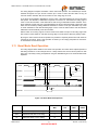
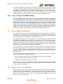
The SMSC LAN91C111 silicon has the following main sections:
SMSC AN 9.6
Bus Interface Unit
Arbiter
Memory Management Unit
8Kbytes Internal SRAM
CSMA/CD
APPLICATION NOTE
Revision 1.0 (08-14-08)
SMSC LAN91C111 32/16/8-Bit Three-In-One Fast Ethernet Controller
Collision Detection
Encoder
Decoder
Scrambler
De-scrambler
Squelch Circuits
Clock & Data Recovery
AutoNegotiation & Link
Twisted Pair Transmitter
Twisted Pair Receiver
EEPROM
INTERFACE
MII
Control
Control
Control
Arbiter
Control
Address
8-32 bit
Bus
Interface
Unit
Control
Control
TPO
Control
WR
FIFO
Data
RD
FIFO
MMU
Ethernet
Protocol
Handler
(EPH)
DMA
TX/RX
FIFO
Pointer
TX Data
8K Byte
Dynamically
Allocated
SRAM
10/100
PHY
TXD[0-3]
32-bit Data
32-bit Data
TPI
RX Data
RXD[0-3]
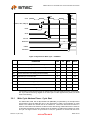
Figure 2.1 Detailed Internal Block Diagram
Revision 1.0 (08-14-08)
2
APPLICATION NOTE
SMSC AN 9.6
SMSC LAN91C111 32/16/8-Bit Three-In-One Fast Ethernet Controller
3 Description Of Bus Interface Unit (BIU)
This section is intended to aid design engineers connecting the SMSC LAN91C111 device to a
microprocessor or microcontroller. This section will discuss in detail the functional block, and the
individual control signals of the LAN91C111 involved in the connection between the device and an
associated microprocessor / microcontroller.
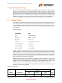
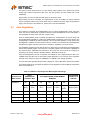
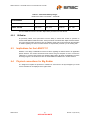
3.1
Pin Function Listing
The LAN91C111 consist of the following major pin groups:
PIN DESCRIPTION
NUMBER OF PINS USED
System Address Pins
20
System Data Pins
32
System Control Pins
14
Serial EEPROM Pins
8
LED Pins
2
PHY Pins
8
Crystal Oscillator
2
Power Pins
10
Ground Pins
12
MII Connection Pins
18
Misc. Pins
2
The interfacing of the LAN91C111 is based on the use of the control lines to control the flow of
information to and from the controller. The LAN91C111 is designed with the flexibility required to allow
a design engineer to connect the LAN91C111 to just about any standard microprocessor architecture.
This document should provide a design engineer the information needed to connect the LAN91C111
to the microprocessor or microcontroller of their choice.
SMSC AN 9.6
3
APPLICATION NOTE
Revision 1.0 (08-14-08)
SMSC LAN91C111 32/16/8-Bit Three-In-One Fast Ethernet Controller
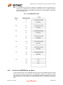
Figure 3.1 BIU Section of functional Block Diagram
For those interested in designing connected to an ISA bus, SMSC provides both a reference design
and evaluation board. Please contact your SMSC Sales Representative or Distributor for information
regarding either of these products. The Data Sheet also contains block diagrams of a typical ISA, EISA,
and VL-Bus based designs.
3.2
ISA Bus
The LAN91C111 supports both an asynchronous and a synchronous bus interface. The industry
standard ISA bus is one of the typical asynchronous buses. This bus interface is well defined and
documented and as previously mentioned, details are available from SMSC regarding interfacing the
LAN91C111 to an asynchronous ISA type interface.
3.3
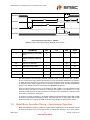
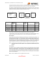
8-Bit Bus
The LAN91C111 supports 8-bit bus interface. Please see the following signal connection table.
Table 3.1 Single Connection Table
8-BIT BUS (HOST)
LAN91C111
A1-A15
A1-A15
Address Bus
D0-D7
D0-D7
D0-D7
D8-D15
Data pins D0-D7 and D8-D15 of the
LAN91C111 both connect to D0-D7 of the
8-bit bus
nBE0
nBE0
Assert nBE0 to enable the lowest byte
nBE1
nBE1
Assert nBE1 to enable the second lowest
byte
Revision 1.0 (08-14-08)
4
APPLICATION NOTE
NOTES
SMSC AN 9.6
SMSC LAN91C111 32/16/8-Bit Three-In-One Fast Ethernet Controller
3.3.1
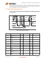
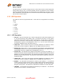
Address Decoding Example
A3
A2
A1
IO-ADDRESS
BYTE
ENABLE
0
0
0
300
nBE0
Assert nBE0 to enable the lowest byte
0
0
0
301
nBE1
Assert nBE1 to enable the second lowest byte
0
0
1
302
nBE0
Assert nBE0 to enable the lowest byte
0
0
1
303
nBE1
Assert nBE1 to enable the second lowest byte
0
1
0
304
nBE0
Assert nBE0 to enable the lowest byte
0
1
0
305
nBE1
Assert nBE1 to enable the second lowest byte
0
1
1
306
nBE0
Assert nBE0 to enable the lowest byte
0
1
1
307
nBE1
Assert nBE1 to enable the second lowest byte
3.3.2
NOTES
I/O Base Address 300h Decoding
The chart below shows the decoding of I/O Base Address 300h:
A15
0
3.4
A14
A13
A12
A11
A10
A9
A8
A7
A6
A5
A4
A3
A2
A1
A0
0
0
0
0
0
1
1
0
0
0
0
0
0
0
0
Asynchronous Interface
When the LAN91C111 working with an asynchronous bus, the read and write operation are controlled
by the edges of nRD and nWR. ARDY is used for notifying the system that it should extend the access
cycle. The leading edge of ARDY is generated by the leading edge of nRD or nWR while the trailing
edge of ARDY is controlled by the internal LAN91C111 clock and, therefore, asynchronous to the bus.
SMSC AN 9.6
5
APPLICATION NOTE
Revision 1.0 (08-14-08)
SMSC LAN91C111 32/16/8-Bit Three-In-One Fast Ethernet Controller
3.4.1
Typical Signal Connection with Asynchronous Buses
HOST SIGNALS
LAN91C111
SIGNALS
A1-A15
A1-A15
Address
D0-D31
D0-D31
Data
nBE [0-3]
nBE[0-3]
Byte Enable
AEN/CS
AEN
Active low address enable. It can be connected to ship select if the
chip select timing matches to AEN
Reset
Reset
Reset
nADS/Ground
nADS
Active low address latch signal. It can be tied low, please see the
timing diagrams figure 24 to 26 of the database.
IOCHRDY/Wait
ARDY
Asynchronous Ready Signal
INT
INTRO
Interrupt
nRD
nRD
Asynchronous read strobe
nWR
nWR
Asynchronous write strobe
CS
nDATACS
nEX32/nIOCS16
nLDEV
NOTES
Use only for direct access to data register
Active low local device signal. It must be buffered using an open
collector driver is ISA bus.
Unused Pins (Use only for Synchronous bus interface)
nCYCLE
Pull up externally (May through 10KΩ resistor)
W/nR
Pull up externally (May through 10KΩ resistor)
nVLBUS
LCLK
nSRDY
nRDYRTN
Revision 1.0 (08-14-08)
Leave open or Pull up externally
Pull up externally (May through 10KΩ
Leave open
Pull up externally (May through 10KΩ resistor
6
APPLICATION NOTE
SMSC AN 9.6
SMSC LAN91C111 32/16/8-Bit Three-In-One Fast Ethernet Controller
3.4.2
Signal Connection with Asynchronous Interfacing
Figure 3.2 Asynchronous Interface Connection
3.5
Synchronous Interface (VL-Bus)
The LAN91C111 also supports a 32-bit synchronous interface. This interface is intended to duplicate
the VESA standard (www.vesa.org), otherwise known as the VL-Bus. Since this interface is not as
widely understood as the ISA bus we will go over this interface in some detail in this document. The
purpose of this discussion is not to necessarily duplicate a VL-Bus but to better explain the use of the
control signals and requirements to support a synchronous interface. With this information a design
engineer should be able to successfully interface the LAN91C111 to any generic synchronous bus
interface. All registers except the DATA REGISTER will be accessed using byte or word instructions.
Accesses to the DATA REGISTER could use byte, word, or double word (dword) instructions.
SMSC AN 9.6
7
APPLICATION NOTE
Revision 1.0 (08-14-08)
SMSC LAN91C111 32/16/8-Bit Three-In-One Fast Ethernet Controller
3.5.1
Typical Connection with Synchronous Interface (VL-Bus)
HOST (VL BUS)
SIGNAL
LAN91C111
SIGNAL
A2-A15
A2-A15
M/nIO
AEN
Qualifies valid I/O decoding - enabled access
when low. This signal is latched by nADS rising
edge and transparent on nADS low time.
W/nR
W/nR
Direction of access. Sampled by the
LAN91C111 on first rising clock that has
nCYCLE active. High on writes, low on reads.
nRDYRTN
nRDYRTN
nLRDY
nSRDY and some
logic
LCLK
LCLK
nRESET
RESET
nBE0 nBE1 nBE2 nBE3
nBE0 nBE1 nBE2
nBE3
Byte enables. Latched transparently by nADS
rising edge.
nADS
nADS, nCYCLE
Address Strobe is connected directly to the VL
bus. nCYCLE is created typically by using
nADS delayed by one LCLK.
IRQn
INTR0
Typically uses the interrupt lines on the ISA
edge connector of VL bus
D0-D31
D0-D31
32 bit data bus. The bus byte(s) used to access
NOTES
Address bus used for I/O space and register
decoding, latched by nADS rising edgeand
transparent on nADS low time.
Ready return. Direct connection to VL bus.
nSRDY has the appropriate functionality and
timing to create the VL nLRDY except that
nLRDY behaves like an open drain output most
of the time.
Local Bus Clock. Rising edges used for
synchronous bus interface transactions.
Connected via inverter to the LAN91C111.
the device are a function of nBE0-nBE3:
nBE0
0
0
1
0
1
1
1
nBE1
0
0
1
1
0
1
1
nBE2
nBE3
0
1
0
1
1
0
1
0
1
0
1
1
1
0
Double word access
Low word access
High word access
Byte 0 access
Byte 1 access
Byte 2 access
Byte 3 access
Not used = tri-state on reads, ignored on writes.
Note that nBE2 and nBE3 override the value of
A1, which is tied low in this application.
nLDEV
nLDEV
nLDEV is a totem pole output. nLDEV is active
on valid decodes of A15-A4 and AEN=0.
UNUSED PINS
VCC
nRD nWR
GND
A1 nVLBUS
OPEN
nDATACS
Revision 1.0 (08-14-08)
8
Pull up externally (May through 10KΩ resistor)
Pull down externally (May through 10KΩ
resistor)
Leave Open
APPLICATION NOTE
SMSC AN 9.6
SMSC LAN91C111 32/16/8-Bit Three-In-One Fast Ethernet Controller
3.5.2
Signal Connection with Synchronous Interfacing
+VCC
W/nR
W/nR
A2-A15
A2-A15
LCLK
LCLK
M/nIO
AEN
nR
D
nWR
A1
nVLBUS
nDATACS
LAN91C111
IRQn
INTR0
D0-D31
D0-D31
nRDYRTN
nRDYRTN
nBE0-nBE3
nBE0-nBE3
nADS
nADS
nCYCLE
delay1
nLRDY
(Open)
RESET
nRESET
nSRDY
O.C.
simulated
O.C.
nLDEV
nLDEV
Figure 3.3 Synchronous Interface (VL-Bus) Connection
3.5.3
Address Bus
The 13 address lines form the address bus. It is presented to the LAN91C111 in these pins. The
address remains transparent until it is latched on the rising edge of the nADS signal. Each VL-Bus
operation starts with an address phase during which the pins A15-A2 transfer an address. Since the
LAN91C111 is considered an I/O device, there is no need for additional address lines.
3.5.4
AEN
AEN – Address Enable is an input to the LAN91C111. AEN is an address qualifier used to indicate
that the address presented to LAN91C111 is valid. AEN is active low. Address decoding on the
LAN91C111 is only enabled when AEN is active. This active low signal is typically connected to a nCS
signal of the microprocessor or microcontroller.
3.5.5
W/NR
W/nR indicates whether the cycle is to be a Read or a Write cycle. A high indicates Write and
subsequently a low indicates a Read cycle. This signal pin is used during synchronous bus operations
and can be either connected directly to the CPU or to tri-state buffers. The W/nR is sampled on the
rising edge of the LCLK signal. For asynchronous bus operations, this signal pin should be pulled high
for proper operation.
SMSC AN 9.6
9
APPLICATION NOTE
Revision 1.0 (08-14-08)
SMSC LAN91C111 32/16/8-Bit Three-In-One Fast Ethernet Controller
3.5.6
NRDYRTN
Ready Return is an input signal generated by the host controller to establish a handshake signal to
inform the LAN91C111 that the cycle has ended. For LCLK speeds up to 33Mhz, nRDYRTN is typically
asserted in the same LCLK cycle as nSRDY is asserted. For higher LCLK speed, nRDYRTN may trail
nSRDY by one LCLK cycle due to signal resynchronization.
In Non-VL-Bus mode, Ready Return is an input signal generated by the host controller to indicate that
the cycle is not completed and that the next cycle needs to be delayed. nRDYRTN is used to insert
wait states during burst operations. A wait state will be inserted if nRDYRTN is asserted and
subsequently for each clock period that nRDYRTN is held. nRDYRTN is sampled on the falling edge
of LCLK and will insert a wait state on each subsequent falling edge of LCLK that nRDYRTN is held.
3.5.7
NSRDY
nSRDY is an output signal from the LAN91C111 to inform the CPU that it has completed the data
transfer and the CPU can terminate the current active bus cycle. When the bus controller detects the
nSRDY asserted, it may immediately assert nRDYRTN or, at speed greater than 33Mhz, it may
resynchronize nSRDY and assert nRDYRTN on the next LCLK cycle. If the current transfer is a read,
the LAN91C111 holds the read data on the data bus until the LCLK which nRDYRTN is sampled
asserted. nSRDY is asserted low for one LCLK period.
3.5.8
LCLK – Clock Input
LCLK is the system bus clock required for synchronous operation. The clock is input on the LCLK pin
and can be a maximum of 50MHz in operation. The duty cycle of the clock should be 50/50 with the
least amount of jitter as possible well. Typically the clock will be the same clock used on the
microprocessor or microcontroller of the design. The LCLK pin is 5V tolerant. All timings specified in
synchronous or VL-Bus will be in respect to the LCLK. This pin should be tied high or clocked if the
LAN91C111 operates in Asynchronous mode.
3.5.9
Reset
RESET causes the LAN91C111 to go to its default states. RESET must be held for 100nS in order to
force the LAN91C111 into it’s reset state. This is to avoid potential problems with glitches. Once the
100nS-time parameter has been met, the device will remain in reset as long as RESET is held high.
3.5.10 NBE0-NBE3
Byte Enable lines 0 through 3 indicate what type of transfer is occurring, byte, word, or double word.
The LAN91C111 does support all modes of operation. Below is a chart of how transfers are decoded
using the Byte Enable lines:
NBE0
NBE1
NBE2
NBE3
0
0
0
0
Double word access
0
0
1
1
Low word access
1
1
0
0
High word access
0
1
1
1
Byte 0 access
1
0
1
1
Btye 1 access
1
1
0
1
Btye 2 access
1
1
1
0
Byte 3 access
Revision 1.0 (08-14-08)
10
APPLICATION NOTE
SMSC AN 9.6
SMSC LAN91C111 32/16/8-Bit Three-In-One Fast Ethernet Controller
3.5.11
32-Bit Access and nBE0-nBE3
The LAN91C111 can operate in 32, 16, or 8-bit mode. Since the registers are assigned to different
banks, changing bank is required if accessing to registers at other bank. Changing bank can be done
by writing to Offset E – Bank Select Register, however offset C, D, E, F are in the same double word
(32-bit) alignment, writing a double word to offset C, will only write to offset E, and will not write to
Offset C, D, and F, because the chip only decodes the bank select register bits. Thus when writing to
Offset C, D, it must be 8 or 16-bit mode. In 8 or 16-bit access, nBE pins have to be asserted
appropriately. For example, if Low word is accessed, nBE[0-1] pins has to be asserted, and nBE[2-3]
must be pulled high.
For read, all registers can be read in 32, 16, or 8-bit mode.
3.5.12 NADS and NCYCLE
nADS (Address Strobe) and nCYCLE indicate that the address is valid to the LAN91C111. The
nCYCLE signal is created externally by delaying the ADS signal by one LCLK cycle. The processor or
bus master must drive valid data on the bus prior to asserting nCYCLE. The nCYCLE pin is discussed
in detail under the nDATACS mode of operations.
The LAN91C111 does not support burst mode operations on the VL-Bus interface in VL-Bus mode.
There is burst type capabilities using nDATACS mode, please see nDATACS mode of operations
described in detail later on in this document.
3.5.13 INTR0
This pin operates as a level-triggered interrupt pin with an active high level. It is typically connected to
IRQ9 but can be connected to whatever interrupt input pin is suitable for your design.
3.5.14 Data Bus
32-bit Data Bus of the LAN91C111. Byte steering is controlled using the BE0-BE3 pins.
3.5.15 NLDEV
nLDEV is used to indicate that the cycle being presented has been claimed by an external device, in
this case the LAN91C111 is claiming the cycle once a valid qualified address decode is accomplished.
The LAN91C111 will assert nLDEV to acknowledge the cycle being presented to it. The timing required
for nLDEV to be asserted is processor specific. Please review the timing requirements for your
particular design. On the LAN91C111 nLDEV is designed to assert in a minimum of 20nS after a valid
address decode. It must be buffered using an open collector driver in ISA bus.
3.6
Timing Analysis
One way to better understand how this interface works is to examine the timing diagrams presented
in the Data Sheet in some details. This is the goal of this section. Below are a timing diagram and the
parameter table for a write cycle presented to the LAN91C111 device.
SMSC AN 9.6
11
APPLICATION NOTE
Revision 1.0 (08-14-08)
SMSC LAN91C111 32/16/8-Bit Three-In-One Fast Ethernet Controller
t23
t20
t24
t10
Clock
t9
Address, AEN, nBE[3:0]
Valid
t8
nADS
t16
W/nR
t11
nCYCLE
Read Data
Valid
t21
t21
nSRDY
nRDYRTN
Figure 3.4 Synchronous Write Cycle - nVLBUS=0
PARAMETER
MIN
TYP
MAX
UNITS
t8
A1-A15, AEN, nBE[3:0] Setup to nADS Rising
8
ns
t9
A1-A15, AEN, nBE[3:0] Hold After nADS Rising
5
ns
t10
nCYCLE Setup to LCLK Rising
5
ns
t11
nCYCLE Hold after LCLK Rising (Non-Burst Mode)
3
ns
t16
W/nR Setup to nCYCLE Active
0
ns
W/nR Hold after LCLK Rising with nSRDY Active
3
ns
t18
Data Setup to LCLK Rising (Write)
15
ns
t20
Data Hold from LCLK Rising (Write)
4
ns
t21
nSRDY Delay from LCLK Rising
t17A
7
ns
It is important to remember that timings are determined by the LCLK signal since this is a synchronous
bus. If you examine the timing diagram for the write cycle in VL-Bus (Synchronous) mode you should
observe the following:
3.6.1
Write Cycle Address Phase - Cycle Start
The Address Bus, AEN, and the Byte Enable lines (BE0-BE3), as presented by the microprocessor/
microcontroller, should be stable 8nS prior to the de-assertion of nADS. The de-assertion of nADS
latches in the address and transfer size to the LAN91C111. These lines should also be held for a
minimum of 5nS after the de-assertion of nADS to ensure this latching. nLDEV will assert at a minimum
of 30nS after the address has been decoded by the de-assertion of nADS and the LAN91C111 claims
the cycle. The signal nCYCLE is synchronous to LCLK, the generation of nCYCLE will need to be
Revision 1.0 (08-14-08)
12
APPLICATION NOTE
SMSC AN 9.6
SMSC LAN91C111 32/16/8-Bit Three-In-One Fast Ethernet Controller
accomplished through external circuitry. Signal W/nR has to be asserted high no later than nCYCLE
assertion.
3.6.2
Write Cycle Data Phase - Cycle End
During next rising edge after de-assertion of nCYCLE, write data has to be presented to the
LAN91C111. The data bus will need to be stable at least 15nS prior to the rising edge of LCLK and
are required to hold 4nS, as specified by timing parameter t18 and t20. nSRDY (translated to nLRDY
for the VL-Bus) is asserted during data latching for one cycle. Data input latch is transparent during
nSRDY is low, data is being written to internal registers. nSRDY will de-assert indicating that the data
was written to the LAN91C111 successfully. The W/nR signal can be released 3nS after the rising edge
of LCLK during the data phase of the cycle.
3.6.3
Read Cycle
We will now examine a Read Cycle using the VL-Bus on the LAN91C111. Below is the timing diagram
and parameter listing from the Data Sheet. As you can see the Read cycle requires one more clock
cycle than the Write cycle. This extra time is required for the LAN91C111 to fetch the data internally
prior to presenting it on the Data Bus.
t23
t20
t24
t10
Clock
t9
Address, AEN, nBE[3:0]
Valid
t8
nADS
t16
W/nR
t11
nCYCLE
Read Data
Valid
t21
t21
nSRDY
nRDYRTN
Figure 3.5 Synchronous Read Cycle - NVLBUS=0
PARAMETER
MIN
t8
A1-A15, AEN, nBE [3:0] Setup to
nADS Rising
8
ns
t9
A1-A15, AEN, nBE[3:0] Hold After
nADS Rising
5
ns
t10
nCYCLE Setup to LCLK Rising
5
ns
SMSC AN 9.6
13
APPLICATION NOTE
TYP
MAX
UNITS
Revision 1.0 (08-14-08)
SMSC LAN91C111 32/16/8-Bit Three-In-One Fast Ethernet Controller
3.6.4
PARAMETER
MIN
TYP
MAX
t11
nCYCLE Hold after LCLK Rising
(Non-Burst Mode)
3
ns
t16
W/nR Setup to nCYCLE Active
0
ns
t20
Data Hold from LCLK Rising
(Read)
4
ns
t21
nSRDY Delay from LCLK Rising
t23
nRDYRTN Setup to LCLK Rising
3
ns
t24
nRDYRTN Hold after LCLK Rising
3
ns
7
UNITS
ns
Read Cycle Address Phase – Cycle Start
As with the Write Cycle, the Address Bus, AEN, and the Byte Enable lines (nBE0-nBE3) are required
to be stable 8nS prior to the de-assertion of nADS and 5nS after this rising edge to guarantee a valid
address latching. nLDEV is asserted within 30nS to indicate that the LAN91C111 has claimed this
cycle. The nCYCLE signal will also again need to be generated externally and asserted after address
latching. W/nR should be stable at a low logic level after nCYCLE assertion.
3.6.5
Read Cycle Delay Phase
Unlike the Write Cycle, there is a delay required during read operations to allow the LAN91C111 to
fetch the required data. This phase occurs immediately after the address phase and is completed in
one LCLK cycle. During this time the Data Bus is not required to be stable, nor is the address bus.
3.6.6
Read Cycle Data Phase – Cycle End
As the timing diagram represents, the read data is presented from the LAN91C111 on the data bus
and it is guaranteed to be stable at the rising edge when nSRDY (translated to nLRDY for the VL-Bus)
is asserted. nSRDY and data remain stable until the LAN91C111 receives nRDYRTN asserted on the
rising edge of LCLK plus hold time as specified by t20. The nRDYRTN and nSRDY signals indicate
that the LAN91C111 has completed the cycle successfully. W/nR signal should be de-asserted only
after nSRDY is de-asserted, therefore 7nS after LCLK rising with nSRDY active.
3.6.7
VL-Burst Mode Operation
Burst Mode operations as defined by the VESA standard are not supported by the LAN91C111 device
in VL-Bus mode.
3.7
Direct Data Register Access interface (nDATACS)
Another option available for design engineers to connect to the LAN91C111 is through a direct
interface. This interface is controlled using the nDATACS pin and allows a designer to connect a
controller directly to the LAN91C111 Data Register by bypassing the internal BIU decoders. This
section will discuss in some detail the information necessary to accomplish this interface. This interface
is always 32-bits in nature and therefore the use of the BE0-BE3 pins are ignored.
The LAN91C111 offers the design engineer several options as to how this mode of operation can be
implemented. The choices are between synchronous and asynchronous, burst and non-burst modes.
Each of these options will be discussed in detail below.
Revision 1.0 (08-14-08)
14
APPLICATION NOTE
SMSC AN 9.6
SMSC LAN91C111 32/16/8-Bit Three-In-One Fast Ethernet Controller
3.7.1
The Use of NDATACS
Direct access to the Data Register is controlled via the nDATACS pin. This is can be accomplished
whether the LAN91C111 is configured for synchronous or asynchronous operations. Accessing the
LAN91C111 via the nDATACS pin bypasses the internal Bus Interface Unit (BIU) decoders and
accesses designated by the nDATACS are steered towards the Data Register only. All accesses are
32-bits in nature and used to read or write directly to the internal data register memory of the
LAN91C111 device.
In addition to direct access to the Data Register via the nDATACS signal, there is also an additional
feature available, Burst Mode operation. Burst mode operations can be accomplished in synchronous
mode. By using the nCYCLE pin in conjunction with the nDATACS, the design engineer is capable of
direct data register access in a burst style operation. Control of the speed of bursting to the
LAN91C111 can be accomplished via the nRDYRTN signal. The nRDYRTN signal is used to insert
wait states in a burst type cycle. By combining these signals, multiple speeds of memory can be
controlled. We will examine both a burst and non-burst mode (asynchronous) transfers later on in this
document.
The proper use of this type of accesses does require that the LAN91C111 be configured correctly. The
entire setup of the LAN91C111 is beyond the scope of this document and a design engineer should
review the LAN91C111 Data Sheet. One area of significance that will be covered and is common
among all caveats of nDATACS operation is the use of the Pointer Register.
3.7.2
Pointer Register
The Pointer Register is an internal register where the control of the internal Data Register(s) (FIFO’s)
is done. This register defines where the cycle is being presented to the Data Register and also other
control information and options.
The Pointer Register also controls the Auto-Increment feature of the FIFO. This will be discussed in
detail as well. Control as to whether to information is read or written is done by the READ bit within
this register. The RCV bit controls the area written to or read from. If this bit is set, the receive area
of the FIFO is accessed, if cleared the transmit area of the FIFO is accessed. The contents and
settings of this register will be discussed next.
OFFSET
6
HIGH
BYTE
NAME
POINTER REGISTER
RCV
0
AUTO
INCR.
0
TYPE
READ/WRITE
READ
Reserved
0
0
LOW
BYTE
NOT
EMPTY
0
SYMBOL
PTR
POINTER HIGH
0
0
0
0
0
0
POINTER LOW
0
0
0
0
0
Figure 3.6 Pointer Register
RCV
The RCV bit being set indicates that the operation is to access the receive area and accesses the RX
FIFO as the packet number. When this bit is cleared, the write area of the TX FIFO is being accessed.
AUTOINCR
The AUTOINCR bit indicates whether the internal MMU is to automatically change the address for the
next Data Register accesses. Note: If AUTOINCR is not set, the pointer must be loaded with a dwordaligned value prior to the next access of the Data Register.
SMSC AN 9.6
15
APPLICATION NOTE
Revision 1.0 (08-14-08)
SMSC LAN91C111 32/16/8-Bit Three-In-One Fast Ethernet Controller
READ
When set (1) the operation is a read; when cleared (0) the operation is a write.
NOT EMPTY
This read-only bit indicates whether the Write Data FIFO is empty or not. The FIFO is not empty when
this bit is set.
POINTER HIGH
These bits comprise the upper three bits of the address.
POINTER LOW
These bits comprise the lower 8-bits of the address. Remember that all access is 32-bits in nature and
therefore the lower two bits are ignored thus allowing all 8K bytes to be accessed.
Reserved
Must be 0.
3.7.3
Data Register
The Data Register comprises the FIFO’s for both transmit and receive side of the Ethernet port. This
FIFO is unidirectional in nature and can normally be read or written in byte, word, or dword aligned
accesses. These accesses can be mixed or matched on the fly. The ability to do byte, word, or dword
access is controlled via the address line A1 and the BE0-BE3 control lines during normal mode of
operation.
If using the nDATACS line to accomplish direct access then all transfers are 32-bits in nature and the
use of A1 and BE0-BE3 is ignored.
The Data Register is mapped into two consecutive word locations for double word operations
regardless of the bus width of the target device (16 or 32 bit). The FIFO depth is 12 bytes each.
For the purpose of this discussion all accesses will be 32-bits in nature because we are using
nDATACS to access the Data Register.
OFFSET
8 THROUGH Bh
X
X
X
X
NAME
TYPE
DATA REGISTER
READ/WRITE
DATA HIGH
X
X
X
X
DATA LOW
X
X
X
X
SYMBOL
DATA
X
X
X
X
Figure 3.7 Data Register
3.7.4
Timing Analysis Of Direct Access
In this section we will examine the timing diagrams using the nDATACS line to control direct access.
3.8
Asynchronous Read or Write Operation – Non Burst
This section will discuss the asynchronous Read or Write operations using the nDATACS signal in a
non-Burst mode.
The timing diagram below details a typical cycle, this could be either a read or write cycle. The use of
the nRD and nWR signals controls the data flow to and from the Data Register. The asynchronous
nature of the nRD or nWR signals along with the absence of an LCLK is why this is referred to as an
asynchronous mode of operation.
Revision 1.0 (08-14-08)
16
APPLICATION NOTE
SMSC AN 9.6
SMSC LAN91C111 32/16/8-Bit Three-In-One Fast Ethernet Controller
t2
nDATACS
t3A
t4
Read Data
Valid
t6A
t1
t5
nRD, nWR
t5A
Write Data
D0-D31 Valid
Figure 3.8 Asynchronous Cycle - nADS=0
(nDATACS Used to Select Data Register; Must Be 32 Bit Access)
PARAMETER
MIN
TYP
MAX
UNITS
t1
nDATACS Setup to nRD, nWR
Active
2
ns
t2
nDATACS Hold After nRD, nWR
Inactive (Assuming nADS Tied
Low)
5
ns
t3A
nRD Low to Valid Data
30
ns
15
ns
t4
nRD High to Data Invalid
2
t5
Data Setup to nWR Inactive
10
ns
t5A
Data Hold After nWR Inactive
5
ns
t6A
nRD Strobe Width
30
ns
This timing diagram and subsequent parameter information detail a typical reads or write operation.
As you can see by the timing diagram the first step is to have the address qualified with the assertion
of nADS. Since this discussion is focused on the use of the nDATACS signal, this step is accomplished
by programming the pointer register to where the access is going to occur. By using nDATACS the
values on the address bus and the byte enable lines (BE0-BE3) are ignored.
There is a minimum delay of 2nS prior to the assertion of nRD or nWR. For a read operation the data
becomes valid on the data bus a maximum of 30nS after the assertion of the nRD line. For a write
operation the data needs to be valid for a minimum of 10nS prior to the de-assertion of nWR and needs
to be held for 5nS after this de-assertion.
In asynchronous mode of operation, to accomplish multiple back-to-back transfers (either nWR or nRD)
the minimum time between transactions is 80nS. This means that you can pulse either nWR or nRD
at 80nS intervals. In the case of full duplex mode the timing changes to 100nS between pulses.
3.9
Burst Mode Operation Timing – Synchronous Operation
Burst mode operations using the LAN91C111 require that the nVLBUS pin to be de-asserted and that
an LCLK be provided. The nCYCLE pin is used to indicate that bursting is to be done and the
SMSC AN 9.6
17
APPLICATION NOTE
Revision 1.0 (08-14-08)
SMSC LAN91C111 32/16/8-Bit Three-In-One Fast Ethernet Controller
nRDYRTN can be used to insert wait states. In Synchronous mode back to back time between read
or write is limited by access times. From timing diagram, it is 3 clocks for read and 2 clocks for write,
but it has to be bigger than 100ns for read and 80ns for write.
3.10 Burst Mode Write Operation
The timing diagram below details a burst mode write operation and shows three separate packets of
data being transferred. The first two packets occur sequentially and the third packet is held off using
the nRDYRTN signal.
t17
t12
t22
t18
t14
t18
Clock
t12A
nDATACS
t17A
W/nR
t22A
nCYCLE
t20
Write Data
t20
a
t20
b
c
t15
nRDYRTN
Figure 3.9 Burst Mode Write Operation
PARAMETER
t12
MIN
TYP
MAX
UNITS
nDATACS Setup to LCLK
Rising
20
ns
t12A
nDATACS Hold After LCLK
Rising
0
ns
t14
nRDYRTN Setup to LCLK
Falling
10
ns
t15
nRDYRTN Hold after LCLK
Falling
10
ns
t17
W/nR Setup to LCLK Falling
15
ns
t17A
W/nR Hold After LCLK Falling
3
ns
t18
Data Setup to LCLK Rising
(Write)
15
ns
t20
Data Hold from LCLK Rising
(White
4
ns
t22
nCYCLE Setup to LCLK
Rising
5
ns
nCYCLE Hold After LCLK
Rising
10
ns
t22A
Revision 1.0 (08-14-08)
18
APPLICATION NOTE
SMSC AN 9.6
SMSC LAN91C111 32/16/8-Bit Three-In-One Fast Ethernet Controller
This timing diagram examples and details a burst mode write operation. The nDATACS pin remains
asserted throughout the cycle and the nCYCLE pin is used to control the burst data. As long as
nCYCLE remains asserted, data can be written on each rising edge of LCLK.
In the above timing diagram nRDYRTN is used to insert a wait state between the second and third
data packet. The assertion of nRDYRTN is required at a minimum of 10nS before the falling edge of
LCLK to insert the wait state. A wait state will be held as long as nRDYRTN remains asserted. In the
above example a single wait cycle is inserted between the second and third packet of data. More wait
states can be inserted by holding nRDYRTN asserted for another LCLK cycle. nRDYRTN only needs
to remain asserted for 10nS after the falling edge of LCLK. Once the state machine sees the asserted
nRDYRTN it will automatically insert the wait state.
Data is written on the rising edge of LCLK and needs to be stable 15nS prior to this rising edge. Data
also needs to remain stable for 4nS after the rising edge to ensure that the data was properly written.
By using the Auto-Increment mode of operation it is possible to completely fill the FIFO’s with minimum
overhead to the system. Once a write operation is started you can simply pump data into the FIFO’s
for transmission out the Ethernet port.
3.11 Burst Mode Read Operation
The timing diagram below details a burst mode read operation and shows three separate packets of
data being transferred. In this example there is a delay between the first and second packet of data
being read. This delay is being accomplished using the nRDYRTN signal as in the Burst Mode Write
Operation.
t17
t12
t14
Clock
t12A
nDATACS
t17A
W /nR
nC YCLE
t19
Read Data
t19
a
b
c
t15
nRDYRTN
Figure 3.10 Burst Mode Read Operation
PARAMETER
MIN
TYP
MAX
UNITS
t12
nDATACS Setup to LCLK Rising
20
ns
t12A
nDATACS Hold after LCLK Rising
0
ns
t14
nRDYRTN Setup to LCLK Falling
10
ns
SMSC AN 9.6
19
APPLICATION NOTE
Revision 1.0 (08-14-08)
SMSC LAN91C111 32/16/8-Bit Three-In-One Fast Ethernet Controller
PARAMETER
MIN
TYP
MAX
UNITS
t15
nRDYRTN Hold after LCLK Falling
10
ns
t17
W/nR Setup to LCLK Falling
15
ns
t17A
W/nr Hold After LCLK Falling
3
ns
Data Delay from LCLK Rising (Read)
5
t19
15
ns
As you can see by the timing diagram and subsequent timing parameter table the nDATACS signal is
used to indicate that the cycle is a burst mode direct operation. As long as nDATACS remains asserted
the LAN91C111 will continue to read data from the FIFO’s using the Auto-Increment feature. Each
packet of data is available for the host on the rising edge of LCLK and will remain on the bus for a
minimum of 5nS. In read operations, nCYCLE needs to remain high for burst mode operations.
In the above timing diagram nRDYRTN again is used to insert a wait state. In this example a wait is
inserted between the first and second data packet. Again nRDYRTN is sampled on the falling edge of
LCLK and is required to be asserted 10nS prior to this falling edge and remain asserted for 10nS after
the falling edge. As long as nRDYRTN remains asserted wait states will be inserted into the cycle. In
the example above a single LCLK cycle is inserted.
The timing parameter states that the data is available a minimum of 5nS before the rising edge of
LCLK and held a maximum of 15nS after this rising edge. This gives the hold time for the data to be
available from the LAN91C111.
3.12 LAN91C111 Bus Interface
The Bus Interface Unit on the LAN91C111 is flexible and configurable to support multiple types of
processor architectures and configurations. A designer has the choice of either synchronous or
asynchronous and can support burst or non-burst modes of operations. The ability to change
configuration types to accommodate different configurations for different modes of operations is flexible
enough handle different modes of operations dependent upon what needs to be done. For example,
a standard asynchronous transfer can be done to configure the LAN91C111 and then the interface
switched into burst mode using the nDATACS pin to fill the transmit buffer or empty the receive buffer.
This kind of flexibility allows the LAN91C111 to be configured for any number of processor families or
architectures that you may need.
The following pins are used in asynchronous operations:
SIGNAL NAME
BRIEF DESCRIPTION
nADS
Address Qualifier
nRD
Read operation, active low
nWR
Write operation, active low
OPTIONAL SIGNALS
nDATACS
Direct access 32-bit mode operation
The following pins are used in synchronous modes of operations:
Revision 1.0 (08-14-08)
20
APPLICATION NOTE
SMSC AN 9.6
SMSC LAN91C111 32/16/8-Bit Three-In-One Fast Ethernet Controller
SIGNAL NAME
BRIEF DESCRIPTION
LCLK
Clock Input
W/nR
Read or Write operation, Read active low
nRDYRTN
Used to insert wait states
OPTIONAL SIGNALS
nDATACS
Direct access 32-bit mode operation
nCYCLE
Used to indicate Burst operation
From the table listed above, the interface is capable of multiple types of connections. The ability to
have different types of interface connected simultaneously if a very powerful feature for a design
engineer.
3.13 Sample Routine of Performance Measurement and Tuning
It is important for system designers to design their system efficiently to reduce system latencies and
enhance overall performance. Low latency is the key to increase the system performance.
The below flow chart shows a ping operation from a remote machine to the LAN91C111; there are 14
major steps in the routine. We recommend system engineers to measure the timing taken for each
single procedure of the routine in their system, then find out where the delay is generated to tune up
the system performance.
SMSC AN 9.6
21
APPLICATION NOTE
Revision 1.0 (08-14-08)
SMSC LAN91C111 32/16/8-Bit Three-In-One Fast Ethernet Controller
Remote End Ping to LAN91C111 Routine
P ing th e LA N91 C11 1
Fro m Remo te En d
Ho st P roce ssed Data & Se nt Tran smit
Req ue st to Dri ve r
1
10
LA N91 C111 Receive d the
First Fram e
Driver A llo cated o ne P ag e of the
LA N91C1 11 B uffer for Tr ansm it
2
11
Star te d to Tran smit Data
fro m Host M em o ry to th e
L AN9 1C1 11 Inte rna l Bu ffer
LA N91 C11 1 Ge ne rates a n In terru pt
Requ est to Ho st
3
12
Com ple tely Tran smitted O ne Da ta
Fram e to LA N91C1 11 B uffer a nd
E nqu eu ed it
Drive r En te rs Interru pt Se rvice Ro utine
4
13
Ye s
Host Dete rmin es Wh ethe r
to Tra nsmit M or e Fram es
Th e LA N91 C11 1 Ge ner ated a
Tr ansm it In te rru pt
Dr iver En ters Inter rup t Ha ndl er Rou ti ne
5
14
Ho st Re ad s Da ta in the
LA N91 C111 buffer to its
Mem ory B uffe r
No
Exit
Rele ased th e Tran smitted Fr am e
6
Host Com ple te ly Re ad O ne Data
Fra me i n th e LA N91 C11 1 Bu ffe r to its
Mem ory B uffe r
7
Rem ote E nd Re ceived th e
En tire P acket
Re lea se d the Re ceive d Fram e
8
Re mote E nd System Ca lcula te d Tota l
Tim e of the Ro utine and Di spla ye d it
Read REMP TY bi t to Deter min e if
More Fr ame s Ha s Be en Rece ived
Y es
9
No
F lo w C hart
Figure 3.11 - Remote End Ping to LAN91C111 Routine
Revision 1.0 (08-14-08)
22
APPLICATION NOTE
SMSC AN 9.6
SMSC LAN91C111 32/16/8-Bit Three-In-One Fast Ethernet Controller
4 System Hardware Design
The LAN91C111 fully integrates the MAC, PHY, and SRAM into a single chip. It requires a minimum
number of external components to complete the system design. For example, it requires only a
transformer, an oscillator, some resistors, capacitors, and an optional EEPROM to complete a standard
ISA system design. For other embedded processor systems, some processors have address decode
generation logic internal to the microcontroller; the system designer should do a complete timing
analysis and add external logic between the host and the Bus Interface Unit of the LAN91C111 as
necessary. As outlined in previous sections of this manual, external logic is system dependant.
4.1
Quartz Crystal
The LAN91C111 contains on-chip oscillator circuitry. The on-chip portion is not itself an oscillator, but
an inverting amplifier. The external components that are needed to complete the oscillator circuitry are
a parallel resonant 25 MHz crystal and two capacitors (Cx1 and Cx2). When designing with a crystal,
connect the crystal to XTAL1 and XTAL2. XTAL1 is the input of the amplifier and XTAL2 is the output
of the amplifier.
Crystal Specifications
PARAMETER
SPEC
Type
Parallel Resonant
Frequency
25MHz
Duty Cycle
45% to 55%
Equivalent
Series Resistance 40Ω max
Load Capacitance
20pF typical
Case Capacitance
7 pf maximum
Power Dissipation
1 mW maximum
±
50 ppm
Crystal components should be mounted as close to the chip and have short, direct traces to XTAL1,
XTAL2, and VSS pins. Noise arriving at XTAL1 or XTAL2 pins can cause a miscount in the internal
clock-generating circuitry. These kinds of glitches can be produced through capacitive coupling
between the oscillator components and PCB traces carrying digital signals with fast rise and fall times.
It is also recommended not to run any high-speed signals below the area of the crystal circuitry. Hand
layout for this area of the board is recommended.
A serial resistor with value of 10W~30W may be suggested to add in serial with the XTAL2 pin of
LAN91C111 as shown in Figure 3.2, which can guarantee ( and may reduce) the maximum input
voltage not exceed the recommended level; This may also reduce the EMI affection on the Crystal
oscillator circuitry. The value of this serial resistor must be verified through Lab experiments.
A 1M Ohm resistor is recommended to be connected between XTAL1 and XTAL2 to improve the
startup link for some crystal oscillators.
25Mhz Clock Xtal1 Signal:
LIMIT
SYMBOL
t1
SMSC AN 9.6
PARAMETER
Clock cycle period
MIN.
TYPICAL
MAX.
UNIT
39,998
40
40.002
ns
23
APPLICATION NOTE
Revision 1.0 (08-14-08)
SMSC LAN91C111 32/16/8-Bit Three-In-One Fast Ethernet Controller
LIMIT
SYMBOL
PARAMETER
MIN.
TYPICAL
MAX.
UNIT
t2
Xtal1 High Time
18
ns
t3
Xtal1 Low time
18
ns
It‘s not recommend to implement PLL clock parts with LAN91C111. The device is very sensitive to PLL
clock jitters, which may cause startup and link problems.
4.2
Clock Oscillator
If an external clock is used, it should be connected to the input of the amplifier (XTAL1). If an oscillator
is to be used, leave XTAL2 floating. Driving XTAL2 could cause problems due to high gain and high
current.
Oscillator Specifications
Parameter
Spec
Frequency
25 Mhz ± 50 ppm
Duty Cycle
Output Load
45% to 55%
10 TTL Max.
Oscillator components should be mounted as close to the chip and have short, direct traces to XTAL1,
XTAL2, and VSS pins. Noise arriving at XTAL1 or XTAL2 pins can cause a miscount in the internal
clock-generating circuitry. These kinds of glitches can be produced through capacitive coupling
between the oscillator components and PCB traces carrying digital signals with fast rise and fall times.
It is also recommended not to run any high-speed signals below the area of the crystal circuitry. Hand
layout for this area of the board is recommended.
4.3
X25OUT
X25OUT is 25Mhz-clock source provided by the LAN91C111 for an external PHY to eliminate the need
for an extra crystal or oscillator. This pin can be directly connected the clock oscillator input of the
external PHY. This clock source pin is active during reset.
4.4
Serial EEPROM Operation
The LAN91C111 supports a serial EEPROM interface. The EEPROM holds the following parameters:
1. Ethernet Individual Address
2. I/O Base Address
3. MII Interface
All of the above mentioned values are read from the EEPROM upon hardware reset. Except for the
INDIVIDUAL ADDRESS, the value of the IOS switches determines the offset within the EEPROM for
Revision 1.0 (08-14-08)
24
APPLICATION NOTE
SMSC AN 9.6
SMSC LAN91C111 32/16/8-Bit Three-In-One Fast Ethernet Controller
these parameters. In this way, many identical boards can be plugged into the same system by simply
changing the IOS strapping.
An additional feature of the LAN91C111 is the ability to change the EEPROM data while in circuit. Even
if the EEPROM was not programmed initially you still have the ability to program the EEPROM via
software. This feature also allows the reprogramming of a previously programmed EEPROM as well.
RELOAD and STORE are set by the user to initiate read and write operations respectively. Polling the
value until read low is used to determine completion. When an EEPROM access is in progress the
STORE and RELOAD bits of CTR will read back as both bits high. No other bits of the LAN91C111
can be read or written until the EEPROM operation completes and both bits are clear. This mechanism
is also valid for reset initiated reloads.
One of the IOS combinations is associated with a fixed default value for the key parameters (I/O BASE)
that can always be used regardless of the EEPROM based value being programmed. This value will
be used if all IOS pins are left open or pulled high.
The EEPROM is arranged as a 64 x 16 array. The specific target device is the 9346 1024-bit Serial
EEPROM. All EEPROM accesses are done in words. All EEPROM addresses in the spec are specified
as word addresses.
REGISTER
Configuration Register
Base Register
EEPROM WORD ADDRESS
IOS Value * 4
(IOS Value * 4) + 1
4.4.1
INDIVIDUAL ADDRESS 20-22 hex
If IOS2-IOS0 = 7, only the INDIVIDUAL ADDRESS is read from the EEPROM. Currently assigned
values are assumed for the other registers. These values are default if the EEPROM read operation
follows hardware reset.
The EEPROM SELECT bit is used to determine the type of EEPROM operation:
a. Normal
b. General Purpose register
a. NORMAL EEPROM OPERATION - EEPROM SELECT bit = 0
On EEPROM read operations (after reset or after setting RELOAD high) the CONFIGURATION
REGISTER and BASE REGISTER are updated with the EEPROM values at locations defined by the
IOS2-0 pins. The INDIVIDUAL ADDRESS registers are updated with the values stored in the
INDIVIDUAL ADDRESS area of the EEPROM.
On EEPROM write operations (after setting the STORE bit) the values of the CONFIGURATION
REGISTER and BASE REGISTER are written in the EEPROM locations defined by the IOS2-IOS0
pins.
The three least significant bits of the CONTROL REGISTER (EEPROM SELECT, RELOAD and
STORE) are used to control the EEPROM. Their values are not stored nor loaded from the EEPROM.
b. GENERAL PURPOSE REGISTER - EEPROM SELECT bit = 1
On EEPROM read operations (after setting RELOAD high) the EEPROM word address defined by the
POINTER REGISTER 6 least significant bits is read into the GENERAL PURPOSE REGISTER.
On EEPROM write operations (after setting the STORE bit) the value of the GENERAL PURPOSE
REGISTER is written at the EEPROM word address defined by the POINTER REGISTER 6 least
significant bits.
SMSC AN 9.6
25
APPLICATION NOTE
Revision 1.0 (08-14-08)
SMSC LAN91C111 32/16/8-Bit Three-In-One Fast Ethernet Controller
Note: If no EEPROM is connected to the LAN91C111 the ENEEP pin should be grounded and no
accesses to the EEPROM will be attempted. Configuration, Base, and Individual Address
assume their default values upon hardware reset and the CPU is responsible for programming
them for their final value.
Table 4.1 EEPROM MEMORY MAP
4.4.2
Use the Serial EEPROM as an Option
If system designers prefer to use an EEPROM, the minimum size of the EEPROM required is as small
as 1K (64 x 16) to store the above information. If an EEPROM is not present, the LAN91C111 initiates
using 300h as the I/O Base Address. The individual address registers will default to all zeros, but
individual addresses can be programmed by writing a MAC address to the individual address registers
(IAR).
Revision 1.0 (08-14-08)
26
APPLICATION NOTE
SMSC AN 9.6
SMSC LAN91C111 32/16/8-Bit Three-In-One Fast Ethernet Controller
In an ISA like application, system designers can have the choices of always using the chip at 300h,
or having the controlling software access the base address registers at 300h and change it to other
I/O address after accessing the chip at that address. Similarly for the other values usually stored in
the EEPROM, the driver will have to load them at software initialization. For the case of the node
address, given that it is unique and different for each system, it will have to be stored in some other
external storage place and will be loaded by the driver or firmware at initialization time.
4.4.3
How to Change the IOBASE Address
The default IOBASE Address of the LAN91C111 is 0x0300h. If the system designers try to design one
of the LAN9000 chips in the system, where some other device already has taken the IOBASE address
300, they may first disable or unplug that device, then install the LAN91C111 into the system using the
default IOBASE address 300. Once everything setup properly, they can change the Ethernet IOBASE
address to other values by writing to BASE ADDRESS Register with different and available IOBASE
address, then store these values to the serial EEPROM by writing 1 to the STORE bit in the CONTROL
Register. After all these steps completed successfully, the system designer may power-down the
system and re-enable the device that was originally assigned to IOBASE address 300. The
LAN91C111 will load the proper IOBASE address from the serial EEPROM at power up.
4.5
Power Supply Decoupling
The analog power plane AVDD and the digital power plane are recommended to be separated to
eliminate noise. All the VDD pins should be connected together as closely as possible to the device
with a large VDD plane. If the VDD pins vary in potential by even a small amount, noise and latch up
can result. The VDD pins should be kept to within 50MV of each other.
All the GND pins should also be connected together as closely as possible to the device with a large
ground plane. If the GND pins vary in potential by even a small amount, noise and latch up can result.
The GND pins should be kept to within 50MV of each other. A 0.01–0.1 mF decoupling capacitor
should be connected between each VDD /GND set as closely as possible to the device pins, preferably
within 0.5 inches. The value should be chosen based on whether the noise from VDD -GND is high or
low frequency. This will need to be determined on a design basis.
The VDD connection to the transmit transformer center tap has to be well decoupled to minimize
common mode noise injection from the supply into the twisted-pair cable. It is recommended that a
0.01 mF decoupling capacitor is placed between the center-tap VDD and the GND plane. This
decoupling capacitor should be physically placed as close as possible to the transformer center tap,
preferably within 0.5".
The PCB layout and power supply decoupling discussed above should provide sufficient decoupling to
achieve the following when measured at the device:
AC noise voltage measured across each VDD /GND set should be less than 100mVp-p
All VDD pins should be within 50mVp-p of each other
All GND pins should be within 50mVp-p of each other.
Noise considerations need to be analyzed on a design-by-design basis. The measurements provided
above are only recommendations and standard engineering practices need to be adhered too in order
to have a reliably functional system.
4.6
System Power Consumption
With internal PHY enabled, the typical power supply current drawn by all VDD pins of the LAN91C111
is about 100mA, and the additional power supply current drawn by the external magnetic circuitry of
SMSC’s reference design is about 100mA. Using SMSC’s reference design the Ethernet solution
draws a total of about 200mA current. When the internal PHY enters powerdown mode, the total
Ethernet system drops to about 15mA.
SMSC AN 9.6
27
APPLICATION NOTE
Revision 1.0 (08-14-08)
SMSC LAN91C111 32/16/8-Bit Three-In-One Fast Ethernet Controller
The typical currents measured at the Vcc pins without pullup resistors on the transmit and receive
circuits (Idle condition is defined as state of the chip after powerup (no reset issued), with no link
established):
Approximately 73 mA in the idle state after power up and before reset;
Approximately 100 mA at 100 Mbps, and, approximately 73 mA at 10 Mbps, the typical measured
current was approximately 8 mA in Power down mode, For details of the active supply and powerdown
supply current ranges of the LAN91C111, please refer to the latest datasheet.
4.7
Auto Negotiation
The LAN91C111 integrates the AutoNegotiation Logic to support AutoNegotiation mode. Using this
mode, the chip can automatically configure the device for both 10/100Mbps and Full or Half Duplex. It
also establishes an active link to and from a remote device.
Once the AutoNegotiation mode is initiated, the LAN91C111 will determine if the remote device has
the AutoNegotiation Capability by reading the AutoNegotiation Capable bit of the remote device. (The
AutoNegotiation Capable bit is located in Register 1 bit 3 by the IEEE Standard). If both devices have
AutoNegotiation capability, then both devices uses the contents of the MI Serial Port AutoNegotiation
Advertisement register and Fast Link Pulse's to advertise it capabilities to a remote device.
The capabilities read back from the remote device are stored in the PHY MI Serial port AutoNegotiation
Remote End Capability register. The LAN91C111 negotiation algorithm then matches its capabilities to
the remote device's capabilities and determines what mode the device should be configured to
according to the priority resolution algorithm defined in IEEE 802.3 Clause 28.
Once the AutoNegotiation process is completed, the LAN91C111 then configures itself for either 10 or
100Mbps mode and either Full or Half Duplex modes (depending on the outcome of the negotiation
process), and it switches to either the 100BASETX or 10BASE-T link integrity algorithms.
For more information regarding this procedure or algorithms, refer to IEEE 802.3 Clause 28 for details.
The following tables show the register bit settings for Auto-Negotiation mode and Manual configuration
mode of the LAN91C111:
Table 4.2 LAN91C111 Auto-Negotiation Mode Register Bit Settings
WHAT DO YOU
WANT TO DO?
AUTONEGOTIATION
CONTROL BITS
AUTO-NEGOTIATION ADVERTISEMENT
REGISTER
DUPLEX MODE
CONTROL FOR
THE MAC
ANEG
Bit
ANEG_EN
Bit
TX_FDX
Bit
TX_HDX
Bit
10_FDX
Bit
10_HDX
Bit
SWFDUP Bit
RPCR
(MAC)
Register 0
(PHY)
Register 4
(PHY)
Register
4 (PHY)
Register
4 (PHY)
Register
4
(PHY)
Transmit Control
Register (MAC)
100 Full Duplex
1
1
1
1
1
1
1
100 Half Duplex
1
1
0
1
1
1
0
10 Full Duplex
1
1
0
0
1
1
1
10 Half Duplex
1
1
0
0
0
1
0
Try to AutoNegotiate to......
Revision 1.0 (08-14-08)
28
APPLICATION NOTE
SMSC AN 9.6
SMSC LAN91C111 32/16/8-Bit Three-In-One Fast Ethernet Controller
Table 4.3 - LAN91C111 Manual Configuration Mode Register Bill Settings
AUTONEGOTIATION
CONTROL BITS
WHAT DO YOU
WANT TO DO?
Try to Manually
Set to......
100 Full Duplex
100 Half Duplex
10 Full Duplex
10 Half Duplex
4.7.1
SPEED AND DUPLEX MODE CONTROL FOR THE
PHY
DUPLEX
MODE
CONTROL
FOR THE
MAC
ANEG
Bit
ANEG_EN
Bit
SPEED
Bit
DPLX
Bit
SPEED
Bit
DPLX
Bit
SWFDUP
Bit
RPCR
(MAC
Bank 0
Offset
A)
Register 0
(PHY)
RPCR (MAC
Bank 0
Offset A)
RPCR
(MAC
Bank 0
Offset A)
Register 0
(PHY)
Register 0
(PHY)
Transmit
Control
Register
(MAC)
0
0
1
1
X
X
1
0
1
1
1
X
X
1
1
0
X
X
1
1
1
0
0
1
0
X
X
0
0
1
1
0
X
X
0
1
0
X
X
1
0
0
0
0
0
1
X
X
1
0
1
0
1
X
X
1
1
0
X
X
0
1
1
0
0
0
0
X
X
0
0
1
0
0
X
X
0
1
0
X
X
0
0
0
Initialization Sequence Steps
The Auto-Negotiation mode can be turned on/off by setting or clearing the ANEG bit in the MAC
Receive/PHY Control Register. Note that ANEG bit defaults low, the chip powers up with the
AutoNegotiation mode off.
The AutoNegotiation algorithm can be initiated by the following events:
SMSC AN 9.6
The device enters a Link Fail state
AutoNegotiation Reset or enabled
29
APPLICATION NOTE
Revision 1.0 (08-14-08)
SMSC LAN91C111 32/16/8-Bit Three-In-One Fast Ethernet Controller
A power up Auto-Negotiation enable initialization sequence is provided below for your reference:
1. Power up the chip.
2. Wait for 50ms.
3. Reset the chip by setting and clearing the SOFT_RST bit in the Receive Control Register. (Write
0x8000, then write 0x0000)
4. Wait for 50ms.
5. Set the ANEG bit to 1 in the Receive/PHY Control Register (MAC Register, Bank 0, Offset A) to
enable the Auto_Negotiation mode.
6. Reset PHY by set the RST bit of PHY Register 0 (0x8000);
7. Turn off the isolation mode of the internal PHY by writing x1000 to the PHY Register 0 – Control
Register. The PHY will start the Auto_Negotiation Process.
8. The PHY should complete the Auto_Negotiation process within 1.5 second, thus the driver should
wait for 1.5 second, then read the ANEG_ACK bit and the LINK bit in the PHY Register 1 – Status
Register to check whether the Auto_Negotiation Process is completed and Link is established.
Case 1:
1. If Auto_Negotiation Process is completed and it successfully established LINK, the ANEG_ACK bit
and the LINK bit will be read as “1”
2. Read the SPDDET bit and the DPLXDET bit in the PHY Register 18 – Status Output Register to
check the outcome of Auto_Negotiation Process.
3. If the DPLXDET bit is read as “1”, that means that the PHY is placed in Full Duplex mode, the
driver will need to write “1” to the SWFDUP bit in the MAC Register Bank 0 Offset 0 --Transmit
Control Register to enable Full Duplex mode for the MAC. If the DPLXDET bit is read as “0”, that
means that the PHY is placed in Half Duplex mode, the driver will need to write “0” to the SWFDUP
bit in the MAC Register Bank 0 Offset 0 --Transmit Control Register to switch the MAC to Half
Duplex mode
Case 2:
1. If either the ANEG_ACK bit or the LINK bit is read as “0”, you may restart the Auto_Negotiation
Process for X times until the process is completed and successful. The Auto_Negotiation Process
can be restarted by the ANEG_RST bit (Write 0x3200 to PHY Register 0 – Control Register).
2. Wait for 1.5 second, and then follow the steps 1 to 3 indicated in Case 1.
Case 3:
1. If cable is unplugged or disconnected, the PHY enters Link fail state. The LNKFAIL bit in the PHY
Register 18 –Status Output Register is set, but user has to make sure that the appropriate MASK
bits (the MINT bit and the MLNKFAIL bit in PHY Register 19 – MASK Register) are cleared to
enable interrupt. Also, user has to make sure that the MDINT MASK bit in the MAC BANK 2 offset
D – Interrupt MASK Register is set to enable interrupt. Thus whenever the PHY enters Link fail
state, the host or the OS will be notified. Meanwhile Auto_Negotiation Process will restart again,
the driver should wait for 1.5 second, then follow the steps 1 to 3 indicated in Case 1 or Case 2
to complete the Auto_Negotiation Process.
2. Whenever the device enters the Link Fail State (LINK bit is read as “0”) after having had a valid
10Mbps link (indicated by LINK bit=1, ANEG_ACK=1 and SPDDET=0), steps 6 to 8 above should
be applied to complete the auto-negotiation steps.
Case 4:
1. If hardware reset or the PHY reset is performed, user should follow steps 4 to 8 to complete the
auto-negotiation steps.
Revision 1.0 (08-14-08)
30
APPLICATION NOTE
SMSC AN 9.6
SMSC LAN91C111 32/16/8-Bit Three-In-One Fast Ethernet Controller
4.8
Power up / Initialization and Powerdown Mode
When the LAN91C111 powers up or resets, the internal PHY enters the following modes.
1. Isolation Mode
2. Manual Mode (AutoNegotiation Off)
3. 10Mbps
4. Half Duplex
When the internal PHY is placed in isolation mode, the internal PHY is able to respond to management
transactions, such as reading / writing the PHY registers. But the internal MII will not respond to the
transmit signals and presents a high impedance on the receive data signals to the MAC, and will not
send link pulses to the remote device to establish link. The internal PHY can leave isolation mode by
simply clear the MII_DIS bit in the PHY MI Serial Port Control Register. After the MII_DIS bit is
cleared, the internal MII is able to respond to transmit, and receive signals, and the internal PHY will
immediately send out link pulses to the remote device to establish link.
The LAN91C111 supports vary power-down states. The internal PHY can be placed in a low-power
consumption state by setting the PDN bit in the PHY MI Serial Port Control Register. Clearing this bit
to zero allows normal operation. The EPH POWER EN bit in the MAC Configuration Register is used
to selectively power transition the EPH to a low power mode. When this bit is cleared (0), the Host will
place the EPH into a low power mode. The Ethernet MAC will gate the 25Mhz TX and RX clock so
that the Ethernet MAC will no longer be able to receive and transmit packets. The Host interface
however, will still be active allowing the Host accesses to the device through Standard IO access. All
LAN91C111 registers will still be accessible. However, status and control will not be allowed until the
EPH POWEREN bit is set and a RESET MMU command is initiated. Please use the power
management algorithm described in section 8.1 in the LAN91C111 datasheet to handle power
management.
4.9
Loopback
Loopback mode is intended for system diagnostics. The controller must enable transmit and receive
to allow the controller to receive its own packets. The LAN91C111 supports three types of loopback
modes.
4.9.1
EPH Internal Loopback (MAC)
The internal MAC supports EPH internal loopback. Serial data is internally looped back at EPH block
when EPH _LOOP bit is set in the Transmit Control Register, it also disable transmit output and receive
input of the Media Independent Interface. The management interface of the MII is still active for
accessing the PHY registers.
SMSC AN 9.6
31
APPLICATION NOTE
Revision 1.0 (08-14-08)
SMSC LAN91C111 32/16/8-Bit Three-In-One Fast Ethernet Controller
4.9.2
Diagnostic Loopback
Setting the LPBK bit in the internal PHY MI serial port Control Register can enable diagnostic loopback
mode. When diagnostic loopback is enabled, transmitted data at the internal MII is looped back into
receive data output of the internal MII. The transmit enable signal is looped back into carrier sense
output at the internal MII level. The TP receive and transmit paths are disabled. The transmit link
pulses are halted, and the Half/Full Duplex modes do not change.
In order to have diagnostic loopback working properly and the MAC receive a packet with its own
source address, Full Duplex operation must be enabled. Setting the FDUPLX bit in the Transmit
Control Register will enable it.
Enabling Full Duplex operation will cause frames to be received if they pass the address filter
regardless of the source for the frame, so the LAN91C111 can receive a frame sourced by its self.
4.9.3
External Loopback
External Loopback can be accomplished by shorting the TX and RX Signals, the transmit signals are
looped back after leaving the PHY and the external magnetic. Again, the FDUPLX bit must be set, in
order to have the MAC to receive a frame sourced by the LAN91C111 itself.
The diagram below represents a simple diagram of the LAN91C111, plus external magnetics and RJ45
jack. The loopback at point A is an EPH loopback, which loops the packet back at the EPH block,
never leaving the MAC. The loopback at point B is a PHY loopback, which loops the packet back after
Revision 1.0 (08-14-08)
32
APPLICATION NOTE
SMSC AN 9.6
SMSC LAN91C111 32/16/8-Bit Three-In-One Fast Ethernet Controller
crossing the MII interface (internal to the 91C111). The loopback at point C is referred to as an external
loopback, which loops the packet back after leaving the PHY and the external magnetics.
This final type of loopback testing allows the design engineer to complete the circuit to ensure proper
operation of their design. While the internal loopback tests provide excellent functional testing, external
loopback also tests the components outside the LAN91C111 as well.
A
B
C
Ethernet Protocol
Handler
TX
(EPH)
RX
MAC
MII
PHY
MAGNETICS
RJ45
FDUPLX BIT IN TCR
DPLX
BIT IN
RPCR*
EHPLOOP BIT IN TCR
LPBK BIT
IN PHY
X
X
X
1
X
PHY Half
0
1
0
0
1
PHY Full
1
X
1
0
1
External
1
X
1
0
0
LOOPBACK TYPE
SWFDUP
BIT IN
TCR
EPH
*When using an external PHY replace the RPCR’s DPLX bit with the PHY’s DPLX bit.
Loopback testing is used to isolate certain blocks of the LAN91C111 by transmitting a packet, looping
it back to the receiver and checking for errors. There are three different types of loopback:
EPH Loopback:
Here the packet is looped back immediately after the EPH block, or Ethernet Protocol Handler. The
packet never reaches the MII bus or the internal PHY. Therefore, the PHY register settings are don’t
care (RPCR DPLX, PHY LPBK). Also, in EPH loopback mode the transmitted packet is delayed before
being presented to the receiver so the MAC will not see collisions. In other words, the receiver will
not see the packet as it is still being transmitted which would require the MAC to be in Switched Full
Duplex mode (ignores collisions). So in EPH Loopback the MAC can stay in half duplex mode.
Note: The DPLX bit in the TCR register is a don’t care. This bit is set so the MAC can receive an
external packet with its own source address. Since the packet never leaves the MAC, this bit
is ignored.
PHY Loopback:
The packet is sent out of the MAC, through the internal PHY and looped back at the PHY’s digital
block, before it is decoded and converted to analog. In this mode the MAC and PHY must be matched
for half or full duplex operation. This means the DPLX bit in the RPCR register (or the PHY’s DPLX
bit for external PHYs) must match the SWFDUP bit in the MAC’s TCR register. Note that the FDUPLX
bit in the TCR register must be set when in half duplex mode, to allow the MAC to receive a packet
with its own source address.
Note: When the SWFDUP bit is set, the FDUPLX bit has no effect.
SMSC AN 9.6
33
APPLICATION NOTE
Revision 1.0 (08-14-08)
SMSC LAN91C111 32/16/8-Bit Three-In-One Fast Ethernet Controller
External Loopback:
The packet is sent out of the MAC, through the PHY, out of the RJ45 connector and then looped back
through external wiring or relay. In this mode the MAC and PHY must always be set for full duplex,
since the transmitted packet will start to be received before it is completely out on the wire. For this
test the SWFDUP bit in the TCR register is set, as well as the DPLX bit in the RPCR register (or DPLX
bit in the PHY for external PHYs).
4.10 LED Operation
The LAN91C111 offers two programmable LEDs. These LEDs can be programmed to the following
outputs:
1. Link
2. 10Mbps
3. Duplex
4. Activity
5. 100Mbps
6. Receive
7. Transmit
4.10.1 LED Description
1. LINK LED -- When the chip powers up or resets, the MII_DIS bit in the MI Control Register is set
to 1 and the internal PHY enters isolation mode. The transmit Link pulse is not sent until the
internal PHY leaves isolation mode by clearing the MII_DIS bit. The chip will try to establish an
active link to and from a remote device by using either the standard link integrity or the
AutoNegotiation algorithm (if AutoNegotiation mode is on). Once an active link has been
successfully established, the link LED will be turned on.
2. 10Mbps LED – After an active link has been successfully established, the LAN91C111 and the
remote device are both configured to 10Mbps mode, the 10Mbps LED will be turned on.
3. DUPLEX LED – Duplex LED is on when 1) the DPLX bit in Receive/PHY Control Register is set
if AutoNegotiation mode is off, or 2) the chip sensed and placed itself into full duplex mode after
AutoNegotiation process is completed when AutoNegotiation mode is on.
4. ACTIVITY LED – The LED blinks when packets are transmitted or received by the LAN91C111. If
the Ethernet controller receives the packets that don’t match to it’s MAC address (Except broadcast
packets) or can not pass address filtering, the controller will disregard the packets. But the LED
still blinks during the receive process. This LED does not blink when the LAN91C111 transmits or
receives link pulses.
5. 100Mbps LED -- After an active link has been successfully established, the LAN91C111 and the
remote device are both configured to 100Mbps mode, the 100Mbps LED will be turned on.
6. RECEIVE -- The LED blinks when packets are received by the LAN91C111. If the Ethernet
controller receives the packets that don’t match to it’s MAC address (Except broadcast packets) or
can not pass address filtering, the controller will disregard the packets. But the LED still blinks
during the receive process. This LED does not blink when the LAN91C111 receives link pulses.
7. TRANSMIT -- The LED blinks when packets are transmitted by the LAN91C111. This LED does
not blink when the LAN91C111 transmits link pulses.
Revision 1.0 (08-14-08)
34
APPLICATION NOTE
SMSC AN 9.6
SMSC LAN91C111 32/16/8-Bit Three-In-One Fast Ethernet Controller
4.11 Thermal Information
For the LAN91C111, 128pin TQFP, the related thermal info can be refer to the below:
Operating Temperature Range
0°C to +70°C for LAN91C111
(The Industrial Temperature Range from -40°C to 85°C for LAN91C111i)
Storage Temperature Range
-55°C to + 150°C
Lead Temperature Range (soldering, 10 seconds)
+325°C
Junction Temperature
Tj = 82°C
Case Temperature
Tc = 78°C
Ambient Temperature
Ta = 70°C
5 Memory Management Unit - Features and Benefits
The SMSC LAN91C111 has an overwhelming advantage over its competition in terms of memory
architecture. The SMSC LAN91C111 has a patented Memory Management Architecture allowing full
dynamic memory allocation for both receive and transmit buffers.
Memory management is handled using a patented, optimized MMU (Memory Management Unit)
architecture and a 32-bit wide internal data path. This I/O mapped architecture can sustain back-toback frame transmission and reception for superior data throughput and optimal performance. It also
dynamically allocates buffer memory in an efficient buffer utilization scheme, reducing software tasks
and relieving the host CPU from performing these housekeeping functions.
Since the LAN91C111 implements a patented MMU to control allocation and de-allocation of each RX
and TX buffer autonomously, the full extent of the 8Kbytes of shared RX and TX buffers are available
providing a much more flexible memory utilization scheme. As a result, the LAN91C111 solution allows
more memory to be available to the driver and LAN. Also, the LAN91C111’s memory architecture
reduces overrun conditions typical in high latency “real time” operating systems. In embedded
environments, the ability to alleviate overrun conditions improves performance and reduces CPU
overhead.
The patented MMU features the following functions: 1) No Operation, 2) Allocate Memory, 3) Reset
MMU to Initial State, 4) Remove and Release Packets, 5) Enqueue Packets, 6) Reset TX FIFO.
It is recommended that the transmitted and received packets be released immediately after updating
any statistics, to free up buffer memory. If Auto Release feature is used, the MAC automatically
releases the packets after transmission.
5.1
Memory Partitioning
Unlike other controllers, the LAN91C111 does not require a fixed memory partitioning between transmit
and receive resources. The MMU allocates and de-allocates memory upon different events. An
additional mechanism allows the CPU to prevent the receive process from starving the transmit
memory allocation.
The side that needs it always request memory, for example: the CPU for transmit or the MAC for
receive. The CPU can control the number of bytes it requests for transmit but it cannot determine the
number of bytes the receive process is going to demand. Furthermore, the receive process requests
will be dependent on network traffic, in particular on the arrival of broadcast and multicast packets that
might not be for the node, and that are not subject to upper layer software flow control.
SMSC AN 9.6
35
APPLICATION NOTE
Revision 1.0 (08-14-08)
SMSC LAN91C111 32/16/8-Bit Three-In-One Fast Ethernet Controller
6 Big and Little Endian Issues on the LAN91C111
6.1
Introduction
The LAN91C111 is designed as a Little Endian architecture device. In order to accommodate the use
of this device on Big Endian architectures there needs to be an understanding of these implications.
This application note is intended to discuss the use of the LAN91C111 on Big Endian type architecture
and the requirements that they may pose.
6.2
Definition
What constitutes Big Endian versus Little Endian? The reference to the endian of architecture implies
how this architecture references memory. In the early days of computing most computers (mainframes)
referenced memory with the Most Significant Bit (MSB) being to the left, just as you read, from left to
right. Little Endian on the contrary the MSB is on the right reading from right to left format. While this
may seem insignificant at first, the confusion comes into play when dealing with words and double
words.
6.2.1
Big Endian
In Big Endian format the high bytes of a multi-byte quantity are stored at lower address, and the low
bytes are stored at higher addresses. Motorola’s 68000 families use the Big Endian format. As an
example, in a Big Endian architecture the hexadecimal word 1234h would be stored with it’s MSB
byte value 12h in byte address location 0h, and its LSB byte value 34h stored in byte address location
1h. In a word memory configuration (double byte), the memory value would be 3412h at a word
address of 0h. The hexadecimal double word 12345678h would be stored as 78563412h at a double
word address of 0h.
Table 6.1 Little Endian Memory Images
Double Word Value to be Stored = 12345678h
BYTE ADDRESS
3
2
1
0
DATA VALUES (H)
78
56
34
12
BINARY VALUES
0001 0010
0011 0100
0101 0110
0111 1000
Motorola 680x0 microprocessors, IBM PowerPC, Hewlett-Packard PA-RISC, and Sun SuperSPARC
processors are Big Endian. A number of Big Endian processors, such as the PowerPC, support Little
Endian devices internally through a technique known as swizzling. These types of processors can be
known as Bi-Endian. Besides the PowerPC, the MIPS processors and DEC Alpha processors support
some subset of Bi-Endian operations. For more information regarding whether or not your processor
of choice supports Little Endian devices, please refer to your processors documentation.
6.2.2
Little Endian
In the Little Endian format the high-bytes of a multiple byte quantity are stored at the higher addresses,
and the low-bytes are stored at lower addresses. Intel’s 80x86 family uses the Little Endian format..
As an example, in a Little Endian architecture, the hexadecimal word 1234h would be stored the LSB
byte value 34h in byte address location 0h, and it’s MSB byte value 12h stored in byte address location
1h. In a word memory configuration (double byte), the memory value would be 1234h at a word
address of 0h. The hexadecimal double word 12345678h would be stored as 12345678h at a double
word address of 0h.
Revision 1.0 (08-14-08)
36
APPLICATION NOTE
SMSC AN 9.6
SMSC LAN91C111 32/16/8-Bit Three-In-One Fast Ethernet Controller
Table 6.2 Little Endian Memory Images
Double Word Value to be Stored = 12345678h
BYTE ADDRESS
3
2
1
0
DATA VALUES (H)
12
34
56
78
BINARY VALUES
0001 0010
0011 0100
01010110
0111 1000
The Intel 80X86 and Pentium and DEC Alpha RISC processors are Little Endian.
6.2.3
Bi-Endian
As previously stated, some processors have the ability to switch their modes of operation to
accommodate different endian structures. These processors include the DEC Alpha and the PowerPC.
The control of their endian structure is done via software; please refer to the processors documentation
for details regarding use of the bi-endian features of the particular processor you are working with.
6.3
Implications for the LAN91C111
Whether or not design considerations need to be taken regarding the endian issues is an application
specific decision. This section will discuss these issues and give examples of how to connect the
LAN91C111 to a device that requires byte swapping (Big Endian). By better understanding the issue
the design engineer can decide if and how to accommodate the differences in endian structure.
6.4
Physical connections for Big Endian
In a design that requires the processor to LAN91C111 connections to be byte swapped you would
connect the data bus as displayed in the figure below.
SMSC AN 9.6
37
APPLICATION NOTE
Revision 1.0 (08-14-08)
SMSC LAN91C111 32/16/8-Bit Three-In-One Fast Ethernet Controller
Figure 6.1 Byte Lane Configuration
Revision 1.0 (08-14-08)
38
APPLICATION NOTE
SMSC AN 9.6
SMSC LAN91C111 32/16/8-Bit Three-In-One Fast Ethernet Controller
Figure 6.2 16-bit Byte Lane Configuration
As you can see the lower byte lane (Byte Lane 0) on the LAN91C111 becomes the upper byte lane
on the processor. The second byte lane (Byte Lane 1) becomes the lower byte of the upper word on
a 32bit interface. The third byte lane (Byte Lane 2) becomes the upper byte of the lower word on a
32bit interface and the upper byte on a 16bit interface. The third byte lane (Byte Lane 3) becomes the
lower byte of low word on a 32bit interface and the low byte of the low word on a 16bit interface.
6.5
Software Considerations for Big Endian
Converting data between the two systems is sometimes referred to as the NUXI problem. Imagine the
word UNIX stored in two 2-byte words. In Big Endian systems, it would be stored as UNIX. In a LittleEndian system, it would be stored as NUXI. As previously described, this is only an issue on 16/32bit
architectures and is not a problem if using an 8bit endian style microcontroller.
The way data is read and written to the Ethernet port does not require software to do byte swapping
BUT for configuration of the internal data registers the software will be required to byte swap
information to accommodate the physical connection. When you initialize the LAN91C111 from a
endian architecture machine you will need to take into consideration the differences in endianness
when writing your initialization routines and the way that the host processor is connected to the
LAN91C111 device. This is where the software comes into play. Through software you can
accommodate the differences in endianness.
SMSC AN 9.6
39
APPLICATION NOTE
Revision 1.0 (08-14-08)
SMSC LAN91C111 32/16/8-Bit Three-In-One Fast Ethernet Controller
As with any software problem, there are many ways to accomplish this task. One method would be to
have a routine that swaps the bytes around prior to outputting them to the LAN91C111. Another
method might be too use a simple #define statement for each byte within a header file with the
understanding of how they are configured and how the output needs to be accomplished. There also
may be provisions for accomplishing this already available with the language, compiler, and processor
you are using. Please refer to your documentation for more details regarding any of these options.
Byte swapping is like parity. An even number of byte swaps produces the original ordering.
6.6
Source Code Example
As an example of some of the things that can be done in source code, please review the following
examples.
Here's a simple runtime check for endianness of your machine.
is_little_endian()
{
int i=0;
((char *)(&i))[0] = 1;
return i == 1;
}
Here's the source to a generic endian swapper.
#define ENDIAN_SWAP(a) endian_swap(&(a), sizeof(a))
void
endian_swap(void *v, int size)
{
int i;
unsigned char *p = (unsigned char *) v, q;
}
for(i=0; i<size/2; i++) {
q = p[i];
p[i] = p[(size-1)-i];
p[(size-1)-i] = q;
}
Another example of source code to do byte swapping was obtained from the following website:
http://www.phish.net/ftpspace/GSW/Sounds/Software/mozilla/lxr/1998-03-31/ns/dbm/include/mcom_db.h
Revision 1.0 (08-14-08)
40
APPLICATION NOTE
SMSC AN 9.6
SMSC LAN91C111 32/16/8-Bit Three-In-One Fast Ethernet Controller
This example has extra stuff for defining the different architectures, but the key example is the byte
swapping part at the bottom:
/*
* Little endian <==> big endian 32-bit swap macros.
* M_32_SWAP swap a memory location
* P_32_SWAP swap a referenced memory location
* P_32_COPY swap from one location to another
*/
#define M_32_SWAP(a) {
uint32 _tmp = a;
((char *)&a)[0] = ((char *)&_tmp)[3];
((char *)&a)[1] = ((char *)&_tmp)[2];
((char *)&a)[2] = ((char *)&_tmp)[1];
((char *)&a)[3] = ((char *)&_tmp)[0];
}
#define P_32_SWAP(a) {
uint32 _tmp = *(uint32 *)a;
((char *)a)[0] = ((char *)&_tmp)[3];
((char *)a)[1] = ((char *)&_tmp)[2];
((char *)a)[2] = ((char *)&_tmp)[1];
((char *)a)[3] = ((char *)&_tmp)[0];
}
#define P_32_COPY(a, b) {
((char *)&(b))[0] = ((char *)&(a))[3];
((char *)&(b))[1] = ((char *)&(a))[2];
((char *)&(b))[2] = ((char *)&(a))[1];
((char *)&(b))[3] = ((char *)&(a))[0];
}
/*
* Little endian <==> big endian 16-bit swap macros.
* M_16_SWAP swap a memory location
* P_16_SWAP swap a referenced memory location
* P_16_COPY swap from one location to another
*/
#define M_16_SWAP(a) {
uint16 _tmp = a;
((char *)&a)[0] = ((char *)&_tmp)[1];
((char *)&a)[1] = ((char *)&_tmp)[0];
}
#define P_16_SWAP(a) {
uint16 _tmp = *(uint16 *)a;
((char *)a)[0] = ((char *)&_tmp)[1];
((char *)a)[1] = ((char *)&_tmp)[0];
}
#define P_16_COPY(a, b) {
((char *)&(b))[0] = ((char *)&(a))[1];
((char *)&(b))[1] = ((char *)&(a))[0];
}
This example is nothing more than swapping bytes. Most Unix machines include routines to do this,
and they are generally called: hton, htons, htonl, ntohs, ntohl, and are generally found in the header
<net/hton.h>
SMSC AN 9.6
41
APPLICATION NOTE
Revision 1.0 (08-14-08)
SMSC LAN91C111 32/16/8-Bit Three-In-One Fast Ethernet Controller
6.6.1
Conclusion
Given the flexibility of the LAN91C111 and with some creative software, the LAN91C111 can be
connected to controllers other than Little Endian types.
7 Physical Layer and Magnetics
7.1
Transmit / Receive Interface
The interface between the Twisted Pair outputs & the Twist Pair inputs on the LAN91C111 and the
twisted pair cable is typically transformer coupled and terminated with the appropriate resistors.
7.1.1
Transmit Interface
The transformer for the transmitter should have a winding ratio of 1:1 with a center tap on the primary
winding tied to VDD. The specifications for the transformer are shown in Table ý7.1 - TP Transformer
Specification.
The transmit output must be terminated with two external termination resistors to meet the output
impedance and return loss requirements of IEEE 802.3. These two external resistors must be
connected between VDD and each of the TPO± outputs. Their value should be chosen to provide the
correct termination impedance for the transmitter inside the LAN91C111. The value of the two external
termination resistors depends on the type of cable the device drives. Refer to Section ý7.2.3 - Cable
Selection for more details.
Table 7.1 - TP Transformer Specification
PARAMETER
SPECIFICATION
TRANSMIT
RECEIVE
TURNS RATIO
1:1 CT
1:1
Inductance, ( HMin)
350
350
Leakage Inductance, (H)
0.05–0.15
0.0–0.2
Capacitance, (pF Max)
15
15
DC Resistance, (Ω Max)
0.4
0.4
To minimize common mode output noise and to aid in meeting radiated emissions requirements, it may
be necessary to add a common mode choke on the transmit outputs. Common mode bundle
termination may required and can be achieved by connecting the unused pairs in the RJ45 connector
to chassis ground through 75-ohm resistors and a 1000 pF capacitor. A common mode AC ground
return path can be designed by connecting the center tap with a 75W resistor and capacitor to chassis
ground.
To minimize noise pickup into the transmit path in a system or on a PCB, the loading on TPO± should
be minimized and both outputs should always be loaded equally.
7.1.2
Receive Interface
Receive data is typically transformer coupled into the receive inputs on TPI± and terminated with
external resistors.
The transformer for the receiver should have a winding ratio of 1:1. The specifications for this
transformer are shown in Table 7.1.
Revision 1.0 (08-14-08)
42
APPLICATION NOTE
SMSC AN 9.6
SMSC LAN91C111 32/16/8-Bit Three-In-One Fast Ethernet Controller
The receive input must be terminated with the correct termination resistance to meet the input
impedance and return loss requirements of IEEE 802.3. In addition, the receive TP inputs must be
attenuated. Both the termination and attenuation is accomplished with four external resistors in series
across the TPI± inputs. Each resistor should be 25% of the total series resistance, and the total series
resistance should be equal to the characteristic impedance of the cable (100 W for UTP, 150 W for
STP). It is also recommended that a 0.01 F capacitor be placed between the center of the series
resistor string and VDD to provide an AC ground for attenuating common mode signal at the input.
To minimize common mode input noise and to aid in meeting susceptibility requirements, it may be
necessary to add a common mode choke on the receive input. Common mode bundle termination may
be required and can be achieved by connecting the unused pairs in the RJ45 connector are connected
to chassis ground through 75 W resistors and a 1000 pF capacitor. A common mode AC ground return
path can be designed by connecting the center tap with a 75W resistor and capacitor to chassis
ground.
To minimize noise pickup into the receive path in a system or on a PCB, loading on TPI should be
minimized and both inputs should be loaded equally.
7.1.3
Magnetics
For the suggested Magnetics for the Twisted Pair interface refer to Application Note 8.13, “Suggested
Magnetics”. The latest revision is available on the SMSC web site , or contact your SMSC
representative.
7.2
7.2.1
RBIAS
RBIAS pin
The LAN91C111 RBIAS pin is used to set transmit current level. An external resistor connected
between this pin and ground will set the output current for the TP transmits outputs.
An 11Kohm resistor should be connected between the RBIAS pin and ground.
7.2.2
TP Transmit Output Current Set
The TPO± output current level is set with an external resistor connected between the RBIAS pin and
GND. This output current is determined from the following equation, where R is the value of RBIAS:
Iout = (11K/R) Iref
Where
Iref = 40mA (100Mbps, UTP)
= 32.6mA (100Mbps, STP)
= 100mA (10Mbps, UTP)
= 81.6mA (10Mbps, STP)
RBIAS should typically be an 11 kW 1% resistor to meet IEEE 802.3 specified levels. Once RBIAS is
set for the 100Mbps and UTP modes as shown by the equation above, Iref is then automatically
changed inside the device when the 10Mbps mode or UTP120/STP150 modes are selected.
Keep the RBIAS resistor as close to the RBIAS and GND pins as possible to reduce noise pickup into
the transmitter. Because the TP output is a current source, capacitive and inductive loading can reduce
the output voltage from the ideal level. Thus, in actual application, it might be necessary to adjust the
value of the output current to compensate for external loading. One way to adjust the TP output level
is to change the value of the external resistor connected to RBIAS. This value is PCB design
dependant, most be verified by designer.
SMSC AN 9.6
43
APPLICATION NOTE
Revision 1.0 (08-14-08)
SMSC LAN91C111 32/16/8-Bit Three-In-One Fast Ethernet Controller
A better way to adjust the TP output level is to use the Transmit Level Adjust register bits (TLVL [3:0])
accessed through the MI serial port Configuration 1 register. These four bits can adjust the output level
by -14% to +16% in 2% steps.
7.2.3
Cable Selection
The LAN91C111 can drive two different cable types:
100 Ohm unshielded twisted-pair, Category 5, or
150 Ohm shielded twisted-pair.
The LAN91C111 must be properly configured for the type of cable to meet the return loss specifications
in IEEE 802.3. This configuration requires appropriately setting the Cable Type Select (CABLE) bit in
the MI serial port Configuration 1 register and setting the value of some external resistors, as described
in Table 7.2.
Table 7.2 - Table 7.2 - Cable Configurations
RTERM (OHMS)
CABLE TYPE
CABLE BIT
TPO
TPI
100 Ohm UTP, Cat. 5
UTP
50
100
150 Ohm STP
STP
75
150
The CABLE bit sets the output current level for the cable type. RTERM in Table ý7.2 is the value of
the termination resistors needed to meet the level and return loss requirements. The value for RTERM
on the TPO outputs is for the two external termination resistors connected from VDD to TPO. Each
value for RTERM on the TPI inputs is for the sum of the four series resistors across TPI.
These resistors should be 1% tolerance. Also note that some output level adjustment may be
necessary due to parasitic as described in Section 7.2.2 - TP Transmit Output Current Set.
IEEE 802.3 specifies that 10BASE-T and 100BASE-TX operate over twisted-pair cable lengths of
between 0–100 meters. The squelch levels can be reduced by 4.5 dB if the Receive Input Level Adjust
bit (RLVL0) is set in the MI serial port Configuration 1 register. This allows the LAN91C111 to operate
with up to 150 meters of twisted-pair cable. The equalizer is designed to accommodate between 0–125
meters of cable.
7.2.4
Transmitter Droop
The IEEE 802.3 specification has a transmit output droop requirement for 100BASE-TX. Because the
LAN91C111 TP output is a current source, it has no perceptible droop by itself. However, the
inductance of the transformer added to the device transmitter output causes droop to appear at the
transmit interface to the TP wire. If the transformer connected to the LAN91C111 outputs meets the
requirements of Table 7.1 - TP Transformer Specification the transmit interface to the TP cable then
meets the IEEE 802.3 droop requirements.
7.3
MII Management Functions
The MII is a nibble-wide packet data interface defined in the IEEE Specification 802.3. The MII
interface encompasses the signals that physically transport the management information across the
MII, a frame format, and a protocol specification for exchanging management frames, and a register
set that can be read and written using these frames. MII management refers to the ability of a
management entity to communicate with PHY via the MII serial management interface (MI) for the
purpose of displaying, selecting, and/or controlling different PHY options. The host manipulates the
MAC to drive the MII management serial interface. By manipulating the MAC's registers (MDOE,
MCLK, MDI, and MDO bits in the Management Interface Register), MII management frames are
generated on the management interface for reading or writing information from/to the PHY registers.
Revision 1.0 (08-14-08)
44
APPLICATION NOTE
SMSC AN 9.6
SMSC LAN91C111 32/16/8-Bit Three-In-One Fast Ethernet Controller
Timing and framing for each management command is to be generated by the CPU (host). For the MII
Serial Frame Structure, please see 7.5.3 of the LAN91C111 datasheet.
The PHY register set consists of eleven registers. The Control Register and the Status Register are
the Basic Registers defined in the IEEE specification. The basic and fundamental control and status
functions are defined in these two registers. The PHY has six extended registers for providing PHY
Identifier to layer management, providing control and monitoring for Auto-Negotiation Process,
configuration, status output, and Interrupt mask.
REGISTER ADDRESS
7.3.1
REGISTER NAME
BASIC/EXTENDED
0
Control
B
1
Status
B
2
PHY Identifier
E
3
PHY Identifier
E
4
Auto-Negotiation Advertisement
E
5
Auto-Negotiation Remote End Capability
E
16
Configuration 1
E
17
Configuration 2
E
18
Status Output
E
19
Mask
E
20
Reserved
E
Example Routines To Read and Write the PHY Registers
* Description
* This is to demonstrate the Read and Write procedures for the LAN91C111's
* Internal PHY over the MII.
* To compile this you will need a C/C++ Compiler and LAN91C111 Evaluation
* Evaluation Board.
#include <Stdio.h>
#include <DOS.h>
#define IOP 0x300// LAN91C111 IO Base address
#define BankSelect(x) outport(0x30E,x)
#define WriteZeroToPhy \
outport(0x308, 0x3338);\
outport(0x308, 0x333C);\
outport(0x308, 0x3338);
#define WriteOneToPhy \
outport(0x308, 0x3339);\
SMSC AN 9.6
45
APPLICATION NOTE
Revision 1.0 (08-14-08)
SMSC LAN91C111 32/16/8-Bit Three-In-One Fast Ethernet Controller
outport(0x308, 0x333D);\
outport(0x308, 0x3339);
#define WriteZToPhy \
outport(0x308, 0x3330);\
outport(0x308, 0x3334);\
outport(0x308, 0x3330);
void WriteToPhyReg(char RegNo, int Data)
{
BankSelect(3);
//Write atleast 32 1's to Synchronize the interface.
for (int i=0; i<=31; i++)
{
outport(0x308, 0x3339);
outport(0x308, 0x333D);
}
//Start bits <01>
WriteZeroToPhy;
WriteOneToPhy;
//Command bits <Write=01>
WriteZeroToPhy;
WriteOneToPhy;
//Phy Address, which is 00000 for LAN91C111's internal PHY
WriteZeroToPhy;
WriteZeroToPhy;
WriteZeroToPhy;
WriteZeroToPhy;
WriteZeroToPhy;
//PHY reg to write.. 5 bits.. (MSBit goes first)
for (i=0; i<5; i++)
{
if (RegNo & 0x10)
{ WriteOneToPhy;}
else
{ WriteZeroToPhy;}
RegNo <<= 1;
}
//Send the turnaround bit <10>
WriteOneToPhy;
WriteOneToPhy;
for (i=0; i<16; i++)
Revision 1.0 (08-14-08)
46
APPLICATION NOTE
SMSC AN 9.6
SMSC LAN91C111 32/16/8-Bit Three-In-One Fast Ethernet Controller
{
if (Data & 0x8000)
{ WriteOneToPhy;}
else
{ WriteZeroToPhy;}
Data <<= 1;
}
outport(0x308, 0x3330);
return;
}
int ReadMDI()
{
int i;
BankSelect(3);
outport(0x308, 0x3330);
outport(0x308, 0x3334);
i = inport(0x308);
outport(0x308, 0x3330);
if (i & 0x0002)
{ return 1; }
else
{ return 0; }
}
int ReadFromPhyReg(char RegNo)
{
int Data=0, binvalue, j;
BankSelect(3);
//Write atleast 32 1's to Synchronize the interface.
for (int i=0; i<=31; i++)
{
outport(0x308, 0x3339);
outport(0x308, 0x333D);
}
//Start bits <01>
WriteZeroToPhy
WriteOneToPhy
//Read command bits <10>
WriteOneToPhy
WriteZeroToPhy
//Phy Address, which is 00000 (MSBit first)
WriteZeroToPhy
WriteZeroToPhy
SMSC AN 9.6
47
APPLICATION NOTE
Revision 1.0 (08-14-08)
SMSC LAN91C111 32/16/8-Bit Three-In-One Fast Ethernet Controller
WriteZeroToPhy
WriteZeroToPhy
WriteZeroToPhy
//phy reg to read.. 5 bits..MSB First
for (i=0; i<5; i++)
{
if (RegNo & 0x10)
{WriteOneToPhy;}
else
{WriteZeroToPhy;}
RegNo <<= 1;
}
//Send the turnaround bit <Z>
WriteZToPhy;
Data = 0;
for (i=0; i<=15; i++)
{
Data <<= 1;
if (ReadMDI())
Data |= 0x0001;
}
//Send the turnaround bit. <Z>
WriteZToPhy;
return Data;
}
main()
{
BankSelect(0);
printf("\n\n\nResetting...");
outport(0x304, 0x8000);
outport(0x304, 0);
sleep(5);//5 Seconds delay (Just to be on the safer side)
/*
Please refer to the data sheet and/or application note for the exact
delay required here. */
printf("\nReady");
BankSelect(1);
Revision 1.0 (08-14-08)
48
APPLICATION NOTE
SMSC AN 9.6
SMSC LAN91C111 32/16/8-Bit Three-In-One Fast Ethernet Controller
outport(0x300, 0xA0B1); //Make sure the internal phy is selected
//Now read the first register of the PHY
BankSelect(3);
for (int i=0; i<=5; i++)
{
printf("\nPHY Reg %d = 0x%04x", i, ReadFromPhyReg(i));
}
//Write and read back different values.. to a PHY register...
//We chose to R/W the ANEG advertisement register.. almost all the
//bits are R/W
WriteToPhyReg(4, 0X000F);
printf("\nPHY Reg = 0x%04x", ReadFromPhyReg(4));
WriteToPhyReg(4, 0X00F0);
printf("\nPHY Reg = 0x%04x", ReadFromPhyReg(4));
WriteToPhyReg(4, 0X0F00);
printf("\nPHY Reg = 0x%04x", ReadFromPhyReg(4));
WriteToPhyReg(4, 0Xb000);
printf("\nPHY Reg = 0x%04x", ReadFromPhyReg(4));
WriteToPhyReg(4, 0XBF00);
printf("\nPHY Reg = 0x%04x", ReadFromPhyReg(4));
WriteToPhyReg(4, 0X00FF);
printf("\nPHY Reg = 0x%04x", ReadFromPhyReg(4));
WriteToPhyReg(4, 0XBFFF);
printf("\nPHY Reg = 0x%04x", ReadFromPhyReg(4));
}
7.4
Multiple Register Access
If the MI serial port needs to be constantly polled in order to monitor changes in status output bits, or
if it is desired that all registers be read or written in a single serial port access cycle, multiple register
access mode can be used.
Multiple register access allows access to all registers in a single MI serial port access cycle. When
multiple register access is enabled, all the registers are read or written when the register address
REGAD[4:0] = 0b11111. This eliminates the need to read or write registers individually. Multiple register
access modes is normally disabled. To enable it, set the Multiple Register Access Enable (MREG) bit
in the MI serial port Configuration 2 register.
SMSC AN 9.6
49
APPLICATION NOTE
Revision 1.0 (08-14-08)
SMSC LAN91C111 32/16/8-Bit Three-In-One Fast Ethernet Controller
8 Reset Operation
The LAN91C111 can be reset by either hardware or software. A hardware reset can be accomplished
by asserting the RESET pin during normal operation, or upon powering up the device. This input is
not considered active unless it is active for at least 100ns to filter narrow glitches.
Both the MAC and the internal PHY are reset if a hardware reset is performed. All registers will be
reset to the default values and the hardware configuration values will be re-latched into the device.
The positive Reset pulse applied to RESET pin must remain asserted with a duration period of at least
100ns.
Software reset can be accomplished by setting the SOFT_RST bit in the MAC Receive Control
Register. Setting the SOFT_RST bit high, and terminated by writing the bit low performs the internal
system reset. Data in the EEPROM is not loaded after software reset. For the internal PHY, writing
1 to RST bit will reset the registers of the internal PHY to default values. This reset bit is a self-clearing
and it returns a value of 1 until the reset process is completed. The internal PHY is guaranteed to be
ready 50ms after the reset is initiated. Software drive should wait for 50ms after setting the RST bit
high prior to access to the internal PHY registers. Writes to the control register bits, other than RST
bit, have no effect until the reset process has been completed.
9 Functional Test and Diagnostic
The section provides routines can be used for functionally testing the 91C111. These tests will exercise
the major blocks of the MAC and PHY.
9.1
MAC Register Test
Checks the I/O registers in 16-bit mode.
Loop for I = 0 to 3
(for banks 0 to 3)
Write the Bank Select Register (offset 0x0E = I) to select current bank
Loop for J = 0 to C, step 2 (for offset 0x00 to 0x0C)
Read the current register (offset J) and store the current data in a temp variable
Write the current register (offset J) with the data pattern
Read the current register (offset J) and compare data bit-by-bit
Restore the saved variable back to the current register
End Loop J
End Loop I
9.2
RAM Buffer Test
Performs a 16-bit write/read on the internal 8K RAM buffer. The ram is accessed through the DATA
register, which is mapped through two FIFO's and is addressed by the POINTER register. The data
values written should be patterns with alternating bit or random values for maximum effectiveness.
Loop for I = 0 to 3
(4 packets of memory @ 2048 bytes per packet)
Allocate packet memory
Write 0x0020 to the MMUCOM register (bank 2, offset 0)
Poll for Alloc INT bit
Read the INTERRUPT register (bank 2, offset C) until bit 3 (ALLOC INT) is set
Read allocated packet number from ALLOCATION RESULT register (bank 2, offset 3)
Write this packet # into the PACKET NUMBER register (bank 2, offset 2)
Loop for J = 0 to 1023 (total of 1024 words of data)
Revision 1.0 (08-14-08)
50
APPLICATION NOTE
SMSC AN 9.6
SMSC LAN91C111 32/16/8-Bit Three-In-One Fast Ethernet Controller
Write the pointer register (bank 2, offset 6) = 0x0000 + J * 2 (RCV=0, AUTOINC=0, Read=0,
Reserved=0, pointer=0x0000+J * 2)
Write DATA register (bank 2 offset 8) = data word
End Loop J
Loop for J = 0 to 1023 (total of 1024 words of data)
Write the pointer register (bank 2, offset 6) = 0x2000+ J * 2 (RCV=0, AUTOINC=0, Read=1,
Reserved=0, pointer=0x20000+J * 2)
Read DATA register (bank 2 offset 8) = data word
Compare data word read with previously written value for that address bit-by-bit for errors
End Loop J
End Loop I
9.3
Transmitting A Packet
These steps will allocate packet memory, write the packet buffer, queue the packet and send it out.
The transmitted packet will be a 64-byte packet, with source address = 0x000000000000 and
destination address = 0xFFFFFFFFFFF.
Allocate a packet
Write 0x0020 to the MMUCOM register (bank 2, offset 0)
Poll for Alloc INT bit
Read the INTERRUPT register (bank 2, offset C) until bit 3 (ALLOC INT) is set
Read allocated packet # from the ALLOCATION RESULT register (bank 2, offset 3)
Write this packet # into the PACKET NUMBER register (bank 2, offset 2)
Write the POINTER register for TX, WR, and AUTOINC
Write (bank 2, offset 6) = 0x4000
Write to the packet buffer
Write the following words to the DATA register (bank 2, offset 8):
Write 0x0000 (this is the status word; it will be written by the MAC with the transmit status word after the transmission is complete)
Write 0x0046 (this is the byte count; includes the packet size (64 bytes), plus the status word, byte count, control
byte, and last data byte = 70 bytes, or the packet size + 6 bytes)
Write the destination address (three successive writes: bytes 10, bytes 32, bytes 54)
Write 0xFFFF, 0xFFFF, 0xFFFF
Write the source address (three successive writes: bytes 10, bytes32, bytes 54)
Write 0x0000, 0x0000, 0x0000
Write 0x0040 (this is the packet size = 64 bytes)
Write the packet data (46 bytes of data, or 23 words if the LAN91C111 is configured to calculate and send the
CRC). If the CRC is to be included with the packet data and the 91C111 is configured not to send the CRC(bit
NOCRC is set in the Transmit Control Register (bank 0, offset 0)), then write 50 bytes or 25 words of data)
Write the control word (set CRC and/or ODD bits as necessary). If packet is odd, the extra data byte would be the
least significant byte of the control word.
Turn on the transmitter
Write 0x0001 to set the TXENA bit in the TRANSMIT CONTROL register (bank 0, offset 0)
Queue the packet
Write 0x00C0 to the MMUCOM register
SMSC AN 9.6
51
APPLICATION NOTE
Revision 1.0 (08-14-08)
SMSC LAN91C111 32/16/8-Bit Three-In-One Fast Ethernet Controller
** The packet will now be sent on the wire when the line is clear **
Poll for completion (<= 100ms)
Read the INTERRUPT register until bit 1 (TX INT) is set (bank 2, offset C)
Read the status word of the packet
Write 0x6000 to the POINTER register (TX, RD, AUTOINC), (bank 2, offset 6)
Read the DATA register (bank 2, offset 8) to get the Status Word of the packet
The Status Word will show any errors in transmission; it mirrors the EPH STATUS register (bank 0, offset 2)
9.4
Releasing The Transmitted Packet
Write 0x00A0 to the MMUCOM register (bank 2, offset 0) to release the packet and its associated
memory. Poll the BUSY bit (bit 0) of the MMUCOM register until it is clear to verify the operation is
complete
It is recommended that the transmitted packet be released immediately after updating any statistics,
to free up buffer memory. If the auto release feature is used, the MAC automatically releases the
packet after transmission.
9.5
Receiving A Packet
The following steps show the sequence to receive a packet.
Turn on the receiver
Write 0x0100 in the RCR register (bank 0, offset 4)
Loop on RX INT until a packet is received
Read the INTERRUPT register (bank 2 , offset C) until bit 0 (RCV INT) is set
Read the receive packet
The receive packet # will be at the top of the RX FIFO (bank 2, offset 4, high byte) if no previous
packet was received
Set the POINTER register (bank 2, offset 6) for RCV, RD, AUTOINC
Write 0xE000
Read the DATA register (bank 2, offset 8), successive word reads:
Read the status word
Read the byte count
Read the destination address (bytes 10)
Read the destination address (bytes 32)
Read the destination address (bytes 54)
Read the source address (bytes 10)
Read the source address (bytes 32)
Read the source address (bytes 54)
Read the packet size
Read the control word
9.6
Releasing A Received Packet
Write 0x0080 to the MMUCOM register (bank 2, offset 0). This releases the packet number present in
the RX FIFO register (the last packet received)
It is recommended that the received packet be released immediately after updating any statistics, to
free up buffer memory.
Revision 1.0 (08-14-08)
52
APPLICATION NOTE
SMSC AN 9.6
SMSC LAN91C111 32/16/8-Bit Three-In-One Fast Ethernet Controller
9.7
EPH Loopback Test
The following steps will transmit a packet and loop it back through the EPH (Ethernet Protocol Handler)
block and back to the MAC.
Set the transmitter (EPH LOOP, TXENA)
Write 0x2001 to the TRANSMIT CONTROL register (bank 0, offset 0)
Set the receiver (RXEN)
Write 0x0100 to the RECEIVE CONTROL register (bank 0, offset 4)
Set the CONTROL register to receive bad packets
Set the RCV_BAD bit (bit 14) in the CONTROL register (bank 1, offset C)
Transmit a packet (perform Section ý9.3 - Transmitting A Packet, page 59, but omit “Turn on transmitter”)
Receive the packet (perform Section ý9.5 - Receiving A Packet, page 60, but omit “Turn on receiver”)
If the packet is not received within 100ms after transmission or the packet is received with errors, the
EPH loopback failed.
9.8
PHY Loopback Test
The following steps will transmit a packet out of the MAC, into the PHY, looped through the PHY and
back to the MAC (it does not leave the PHY or go out on the wire).
Set the transmitter (FDUPLX, TXENA)
Write 0x0801 to the TRANSMIT CONTROL register (bank 0, offset 0)
Set the receiver (RXEN)
Write 0x0100 to the RECEIVE CONTROL register (bank 0, offset 4)
Set the CONTROL register to receive bad packets
Set the RCV_BAD bit (bit 14) in the CONTROL register (bank 1, offset C)
Set the internal PHY
Set the LPBK bit (bit 14) in the PHY CONTROL register (offset 0)
Transmit a packet (perform Section ý9.3 - Transmitting A Packet, page 59, but omit “Turn on transmitter”)
Receive the packet (perform Section ý9.5 - Receiving A Packet, page 60, but omit “Turn on receiver”)
If the packet is not received within 100ms after transmission or the packet is received with errors, the PHY
loopback failed.
9.9
External Loopback Test
This test transmits a packet out the MAC, through the PHY, out on the wire, looped back through the
PHY and MAC.
Create a loopback plug by wiring a RJ45 plug as follows:
Pin 1 to pin 3
Pin 2 to pin 6
Pin 3 to pin 1
Pin 6 to pin 2
Insert the RJ45 loopback plug onto the board under test (if equipped). Repeat Section
Loopback Test, page 62, but omit “Set the internal PHY.”
SMSC AN 9.6
53
APPLICATION NOTE
ý9.8
- PHY
Revision 1.0 (08-14-08)
SMSC LAN91C111 32/16/8-Bit Three-In-One Fast Ethernet Controller
9.10 MMU Test
The MMU test is broken down into a series of tests that check each command of the MMU.
1. ALLOCATE MEMORY FOR TX
Loop for I = 0 to 3
Write 0x0020 to the MMUCOM register (bank 2, offset 0)
Poll for Alloc INT
Read the INTERRUPT register (bank 2, offset C) until bit 3 (ALLOC INT) is set
Read packet # from ALLOCATION RESULT register
Read (bank 2, offset 3)
Packet # should = I
Read the MEMORY INFORMATION register (MIR)
Read (bank 0, offset 8)
MIR should = 0x0Z04, where Z = 4 – (I+1)
End loop I
Test fails if allocation fails, packet # does not equal I, or MIR register is incorrect.
2. RESET MMU TO INITIAL STATE
Perform step 1 (Allocate memory for TX)
Write 0x0040 to the MMUCOM register (bank 2, offset 0)
Read the MIR register (bank 0, offset 8), should equal 0x0404
Read the FIFO PORTS register (bank 2, offset 4), should equal 8080
Test fails if the MIR or FIFO registers are incorrect.
3. REMOVE FRAME FROM TOP OF RX FIFO
Perform Section 9.7 - EPH Loopback Test, page 62 a total of 2 times
The FIFO register (bank 2, offset 4) should now equal 0x0100
The MIR register (bank 0, offset 8) should now equal 0x0004
Write a 0x0060 to the MMUCOM register (bank 2, offset 0)
The FIFO register should equal 0x0300
The MIR register should equal 0x0004
Write a 0x0060 to the MMUCOM register
The FIFO register should equal 0x8300
The MIR register should equal 0x0004
The test fails if the EPH Loopback fails or the MIR or FIFO registers are incorrect.
4. REMOVE AND RELEASE TOP OF RX FIFO
Perform Section 9.7 - EPH Loopback Test, page 61 a total of 2 times
The FIFO register (bank 2, offset 4) should now equal 0x0100
The MIR register (bank 0, offset 8) should now equal 0x0004
Revision 1.0 (08-14-08)
54
APPLICATION NOTE
SMSC AN 9.6
SMSC LAN91C111 32/16/8-Bit Three-In-One Fast Ethernet Controller
Write a 0x0080 to the MMUCOM register (bank 2, offset 0)
The FIFO register should equal 0x0300
The MIR register should equal 0x0104
Write a 0x0080 to the MMUCOM register
The FIFO register should equal 0x8300
The MIR register should equal 0x0204
The test fails if the EPH Loopback fails or the MIR or FIFO registers are incorrect.
5. RELEASE SPECIFIC PACKET
Loop for I = 0 to 3
Write 0x0020 to the MMUCOM register (bank 2, offset 0)
Poll for Alloc INT
Read the INTERRUPT register (bank 2, offset C) until bit 3 (ALLOC INT) is set
Read packet # from ALLOCATION RESULT register
Read (bank 2, offset 3)
Packet # should = I
Read the MEMORY INFORMATION register (MIR)
Read (bank 0, offset 8)
MIR should = 0x0Z04, where Z = 4 – (I+1)
End loop I
Read the MIR register (bank 0, offset 8), should equal 0x0004
Read the FIFO PORTS register (bank 2, offset 4), should equal 0x8083
Loop for I = 0 to 3
Write the PACKET NUMBER register (bank 2, offset 2) = I
Write 0x00A0 to the MMUCOM register (bank 2, offset 0)
Read the MIR register, should equal 0x0Z04, where Z = I+1
End loop I
The test fails if the allocation fails, or the MIR or FIFO registers are incorrect.
6. ENQUEUE PACKET INTO TX FIFO
Loop for I = 0 to 3
Write 0x0020 to the MMUCOM register (bank 2, offset 0)
Poll for Alloc INT
Read the INTERRUPT register (bank 2, offset C) until bit 3 (ALLOC INT) is set
Read packet # from ALLOCATION RESULT register
Read (bank 2, offset 3)
Packet # should = I
Read the MEMORY INFORMATION register (MIR)
Read (bank 0, offset 8)
MIR should = 0x0Z04, where Z = 4 – (I+1)
End loop I
Turn on the transmitter
Write 0x0001 to the TRANSMIT CONTROL register (bank 0, offset 0)
Loop for I = 0 to 3
Write I to the PACKET NUMBER register (bank 2, offset 2)
Write 0x00C0 to the MMUCOM register
SMSC AN 9.6
55
APPLICATION NOTE
Revision 1.0 (08-14-08)
SMSC LAN91C111 32/16/8-Bit Three-In-One Fast Ethernet Controller
Poll for TX INT
Read the INTERRUPT register (bank 2, offset C) until bit 1 (TX INT) is set (< 100ms)
End loop I
The test fails if the allocation fails, the MIR register is incorrect, or the TX INT bit was not set for any
packet within 100ms.
7. RESET TX FIFO’s
Perform Section 9.7 - EPH Loopback Test, page 62 one time
Write 0x0020 to the MMUCOM register (bank 2, offset 0)
Poll for Alloc INT
Read the INTERRUPT register (bank 2, offset C) until bit 3 (ALLOC INT) is set
Turn off transmitter
Write 0x0000 to the TRANSMIT CONTROL register (bank 0, offset 0)
Write 0x00C0 to the MMUCOM register
Read the MIR register (bank 0, offset 8), should equal 0x0104
Read the FIFO PORTS register (bank 2, offset 4), should equal 0x0100
Write 0x00E0 to the MMUCOM register
Read the MIR register, should equal 0x0104
Read the FIFO register, should equal 0x0182
The test fails if the EPH loopback fails, the allocation fails, or the MIR or FIFO registers are incorrect.
If any of above tests fails, please check your hardware and software to debug the chip again.
10 Migrating From LAN91C100FD and LAN83C183 to LAN91C111
This section provides guidelines for migrating from SMSC’s discrete MAC+PHY solution
(LAN91C100+LAN83C183) to SMSC’s integrated MAC+PHY solution the LAN91C111. While portions
of this material is repetitive with other sections above, it has been consolidated here to aid design
engineers with the specific task of migrating from an existing LAN91C100FD design to the SMSC
LAN91C111.
10.1 91C111 Overview
The LAN91C111 is a non-PCI 10/100Mbps Ethernet Controller that integrates the Media Access
Control (MAC), the Physical Layer Device (PHY) and an 8K Byte packet buffer SRAM on a single chip.
The MAC includes a dual speed (10/100) CSMA/CD engine and supports both synchronous and
asynchronous buses. SMSC’s patented Memory Management Unit (MMU) dynamically and efficiently
manages buffer memory with minimal host CPU overhead. The PHY contains the functions that
transmit, receive, and manage the encoded signals that are impressed on and recovered from the
physical medium.
Revision 1.0 (08-14-08)
56
APPLICATION NOTE
SMSC AN 9.6
SMSC LAN91C111 32/16/8-Bit Three-In-One Fast Ethernet Controller
10.2 New Features and Modification
The BIU of the LAN91C111 remains the same as the original Feast (LAN91C100FD). It can handle
both synchronous and asynchronous transfers. The cycle types can be mixed as long as they are not
active simultaneously.
10.2.1 Receive/PHY Control Register
The Memory Configuration Register of the LAN91C100FD has been eliminated and the address used
for a new Receive/PHY Control Register in the LAN91C111. The Memory Reserved for Transmit
function was formerly used to allow the host CPU to reserve memory to be used later for transmits,
thereby limiting the amount of memory available for received packets. The 91C111 dynamically
allocates its internal 8K memory between transmitted and received packets. The Memory Reserved for
Transmit function in Memory Configuration Register is no longer defined in LAN91C111.
The new Receive/PHY Control Register has been added to control the internal PHY. It contains the
following bits: SPEED, DPLX, ANEG, and LED’s select bits.
SPEED
Speed selects Input. This bit selects 10/100 PHY operation when the ANEG Bit = 0. When the ANEG
bit = 1, this bit is ignored and 10/100 operation is determined by the PHY control register 0.13 or the
outcome of the Auto-negotiation. When this bit is set (1), the Internal PHY will operate at 100Mbps.
When this bit is cleared (0), the Internal PHY will operate at 10Mbps.
DPLX
Duplex Select - This bit selects Full/Half Duplex operation. This bit is valid only when the ANEG Bit,
defined in this section is cleared (0). When ANEG is set (1), this bit has no effect. When this bit is set
(1), the PHY is placed in Full Duplex Mode. When this bit is cleared (0), the PHY is placed in Half
Duplex mode.
ANEG
Auto-negotiation mode select - When this bit is set (1), the PHY is placed in Auto-negotiation mode.
When this bit is cleared (0), the PHY is placed in manual mode and 10/100 and the SPEED and
nDPLX bits determine Half/Full Duplex respectively. Default 0. For more information about
AutoNegotiation algorithm, please see datasheet section 5.7.12.
Note: that, setting these bits (SPEED, DPLX and ANEG) can override the bits (SPEED, DPLX and
ANEG_EN) in the internal PHY MI Control Register.
LED
LED’s function select - The LS[0-2]A and LS[0-2]B bit define what LED control signals are routed to
the nLEDA and nLEDB output pins. Please see the LED selection table for detail.
10.2.2
Memory Information Register
In the LAN91C111, MEMORY SIZE in the Memory Information Register has the default value of 4 as
required for the internal 8K SRAM.
10.2.3 RX_OVRN bit
In the LAN91C100, RX_OVRN bit in the EPH Status register is set high (1) when a memory allocation
in the external SRAM buffer fails upon receipt of a frame. Because of the receive allocation failure,
FIFO entries for the current frame are discarded. The receiver remains enabled and will receive
subsequent frames if memory is available. In the LAN91C111, this bit is no longer defined and it has
been replaced by RESERVED. The RX_OVRN bit of the Interrupt Status Register serves the same
purpose as the RX_OVRN bit of the EPH Status Register and should be used as an indicator of a
receiver overrun.
SMSC AN 9.6
57
APPLICATION NOTE
Revision 1.0 (08-14-08)
SMSC LAN91C111 32/16/8-Bit Three-In-One Fast Ethernet Controller
10.2.4 MDINT Interrupt bit
MDINT bit replaced the RX_DISC INT bit in the Interrupt Status Registers. nRXDISC PIN COUNTER
bits in the RCV Register are also no longer defined, since the nRXDISC pin is removed. The MDINT
bit is set if any of the following bits in the internal PHY MI Serial Port Status Output Register (Register
18) change state.
1. LNKFAIL (link fail detect),
2. LOSSSYNC (de-scramble loss of synchronization detect),
3. CWRD (Invalid 4B5B code detected on receive data),
4. SSD (no start of stream delimiter detected on received data),
5. ESD (no end of stream delimiter detected on receive data),
6. PROL (reverse polarity detected),
7. JAB (jabber detected),
8. SPDDET (Device in 10/100Mbps mode),
9. nDPLXDET (full/half duplex detected).
10.2.5 Internal PHY Registers
The MII cleanly separates the Data Link Layer and Physical Layer. The PHY MI Serial Port Register
controls the internal PHY, and reading or writing the MAC’s Management Interface Register can access
this Register. All the internal PHY register bits in the LAN91C111 remain same as the SMSC
LAN83C183.
10.2.6
Media Independent Interface (MII)
The LAN91C111 supports only the MII interface for connection of external PHY’s. There is no support
for legacy serial transceivers since the pins that offered that support in the LAN91C100FD have been
removed in the LAN91C111. The AUI SELECT bit in LAN91C100FD Configuration Register has been
changed to RESERVED in the LAN91C111. In order for any software to work properly with the
LAN91C111 this RESERVED bit in Configuration Register (bank 1) should always be set to 0. The
LAN91C100FD MII SELECT bit has been changed to the EPH POWER EN bit in the LAN91C111.
(See Power Management.)
10.2.7 Power Management
The LAN91C111 Configuration Register EPH POWER EN bit for power management has replaced
the LAN91C100FD MII SELECT bit . When EPH POWER EN is cleared (0), the Host will place the
EPH in a low power mode. The Ethernet MAC will gate off the 25Mhz TX and RX clock and the MAC
will no longer be able to receive and transmit packets. The Host interfaces however will still be active
allowing the Host to access the LAN91C111 through Standard I/O accesses. All LAN91C111 registers
will still be accessible. Status and control will not be allowed until the EPH POWER EN bit is set and
a RESET MMU command is initiated. For further information about Power Management, please see
section 8.1 of the datasheet -- Software Driver and Hardware Sequence Flow for Power Management.
10.2.8
Internal PHY and External PHY Selection
The LAN91C111 integrates the Physical Layer (PHY). The data path connection between the MAC and
the internal PHY is provided by the internal MII. The internal PHY address is 00000, the driver must
use this address to talk to the internal PHY. The LAN91C111 also supports the EXT_PHY mode for
the use of an external PHY, such as HPNA. This mode isolates the internal PHY to allow interface with
an external PHY through the MII pins. To enter this mode, set the EXT PHY bit to 1 in the Configuration
Register. Otherwise, clear this bit to enable the internal PHY.
Revision 1.0 (08-14-08)
58
APPLICATION NOTE
SMSC AN 9.6
SMSC LAN91C111 32/16/8-Bit Three-In-One Fast Ethernet Controller
10.2.9 General Purpose Output
The General Purpose Control pin (nCNTRL) and the General Purpose Control bit (GPCNTRL) have
been added to the LAN91C111. The GPCNTRL bit has been replaced the FULL STEP bit in the
LAN91C100FD Configuration Register. It can be used to select the signaling mode for the external
PHY or as a general-purpose non-volatile configuration pin. Its inverse value drives the nCNTRL output
pin, which is typically connected to a SELECT pin of the external PHY device such as a power enable.
The GPCNTRL bit defaults low at power up.
10.2.10 Reset
When the Reset pin is asserted, the LAN91C111 performs an internal system reset. It resets both the
MAC and the internal PHY and programs all the registers to their default value. The LAN91C111 will
then read the EEPROM device through the EEPROM interface if enabled and the EEPROM is present.
10.2.11 Interrupt Pin (INTR0)
The LAN91C111 has only one interrupt pin (INTR0). The LAN91C100FD INT SEL 0-1 bits in the
Configuration Register (bank 1) were changed to RESERVED. In order for software that uses interrupts
to work properly with the LAN91C111, both RESERVED bits in the Configuration register must be 0
regardless of the interrupt number (IRQ) used in the host. INTR0 can be connected through hardware
jumpers to select different IRQ’s.
10.2.12 SRAM Interface
Since the LAN91C111 SRAM is internal, the following pins for SRAM interface have been removed.
RD[0-31], RA[2-16], nROE, nRWE[0-3], RDMAH, RCVDMA. The LAN91C111 has a built-in 8K byte
internal SRAM with a page size of 2k. The storage capacity of the chip is 4 packets (total of transmit
+ receive). The MMU automatically, and dynamically, allocates the internal 8K internal SRAM is
between transmitted and received packets.
10.2.13 X25OUT Clock Output Pin
This LAN91C111 output pin is added to allow an external PHY to utilize this clock signal. This
eliminates any requirement for an additional crystal oscillator if the customer uses an external PHY
(such as an external fiber or Home PNA PHY).
10.2.14 Programmable LED’s
The two LAN91C111 LED outputs can be programmed by setting LS[0-2]A and LS[0-2]B to select any
two of the following function: Link, Activity, Transmit, Receive, Duplex, 10/100Mbps. Please the LED
selection table of the datasheet for details.
10.2.15 TP Interface
The LAN91C111 integrates the PHY and contains the TP interface for transmitting and receiving. The
TP input and output pins (TPO+, TPO-, TPI+, TPI-) can be connected to a transformer (magnetic) for
100BASE-TX or 10BASE-T applications.
10.2.16 RBIAS pin
The LAN91C111 RBIAS pin is used to set transmit current level. An external resistor connected
between this pin and ground will set the output current for the TP transmits outputs.
SMSC AN 9.6
59
APPLICATION NOTE
Revision 1.0 (08-14-08)
SMSC LAN91C111 32/16/8-Bit Three-In-One Fast Ethernet Controller
10.2.17 Revision Register
The LAN91C111 chip ID and Revision register located in bank 3 at IO SPACE address 0x0A. The
chip ID is '9' and the revision is '1' for the LAN91C111. The software driver can read the Chip ID and
Revision Register to identify the 91C111 and enable the appropriate software support within the driver.
10.2.18 Physical Layer Address
The LAN91C111 internal Physical Layer (PHY) address is 00000. When the chip powers up, the
internal MII is disabled. Clearing the MII disable bit in the internal PHY Control Register can enable
the internal MII.
11 Design and Layout Check Guidelines
It is recommended to download and always refer to the latest updated LAN91C111 Data Sheet, the
SMSC reference design schematics, and other useful referring information which has all been posted
on the SMSC web site.
Please refer to SMSC web site---Ethernet Products---LAN Check Services, download the related
update guidelines of design and layout checking information for your general checking guidelines:
1. Schematics Checking List;
2. Layout Component Placement Check List;
3. Routing Check List;
4. Test Procedures;
5. EMI/ FCC Reduction Doc
Revision 1.0 (08-14-08)
60
APPLICATION NOTE
SMSC AN 9.6