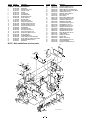
1
FILE NO.
SERVICE MANUAL
Color Digital Camera
VPC-SX560EX
(Product Code : 126 279 01)
(Europe)
(PAL Genenral)
VPC-SX560E
(Product Code : 126 279 03)
(U.K.)
VPC-SX560
Contents
1. OUTLINE OF CIRCUIT DESCRIPTION .................... 2
2. DISASSEMBLY ........................................................ 13
3. ELECTRICAL ADJUSTMENT .................................. 16
4. USB STORAGE INFORMATION
REGISTRATION ...................................................... 21
5. TROUBLESHOOTING GUIDE ................................. 22
6. PARTS LIST ............................................................. 23
CABINET AND CHASSIS PARTS 1 ........................ 23
CABINET AND CHASSIS PARTS 2 ........................ 24
ELECTRICAL PARTS .............................................. 25
ACCESSORIES ....................................................... 32
PACKING MATERIALS ............................................ 32
CIRCUIT DIAGRAM (Refer to the separate volume)
(Product Code : 126 279 02)
(U.S.A.)
(Canada)
PRODUCT SAFETY NOTICE
The components designated by a symbol ( ! ) in this schematic diagram designates components whose value are of
special significance to product safety. Should any component designated by a symbol need to be replaced, use only the part
designated in the Parts List. Do not deviate from the resistance, wattage, and voltage ratings shown.
CAUTION : Danger of explosion if battery is incorrectly replaced.
Replace only with the same or equivalent type recommended by the manufacturer.
Discard used batteries according to the manufacturer’s instructions.
NOTE : 1. Parts order must contain model number, part number, and description.
2. Substitute parts may be supplied as the service parts.
3. N. S. P. : Not available as service parts.
Design and specification are subject to change without notice.
SX114/EX, E, U
REFERENCE No. SM5310249
1. OUTLINE OF CIRCUIT DESCRIPTION
NC
GND
NC
NC
Vø3
Vø2B
Vø2A
Vø1
10
9
8
7
6
5
4
3
2
1
Vertical register
IC903 (ICX267)
CCD imager
IC902, IC904, IC908 (74ACT04MTC)
H driver
IC907 (CXD3400N)
V driver
IC905 (AD9840)
CDS, AGC, A/D converter
GND
1. IC Configuration
VOUT
1-1. CA1 CIRCUIT DESCRIPTION
Around CCD block
2. IC903 (CCD)
[Structure]
Interline type CCD image sensor
Optical size
Diagonal 8 mm (1/2 type)
Effective pixels
1392 (H) × 1040 (V)
Pixels in total
1434 (H) × 1050 (V)
Actual pixels
1360 (H) × 1024 (V)
Optical black
Horizontal (H) direction: Front 2 pixels, Rear 40 pixels
Vertical (V) direction:
Front 8 pixels, Rear 2 pixels
Dummy bit number
Horizontal : 20 Vertical : 3
G
R
B
G
G
R
B
G
G
R
G
R
B
G
B
G
G
R
G
R
B
G
B
G Note
15
16
17
18
øSUB
NC
CSUB
NC
VL
øRG
Note:
Pin 1
19
20
Hø2
14
Hø1
13
GND
11 12
VDD
Horizontal register
Photo sensor
2
Fig. 1-2. CCD Block Diagram
V
8
2
Pin 11
H
40
Fig. 1-1.Optical Black Location (Top View)
Pin No.
Symbol
Pin Description
1
V φ1
Vertical register transfer clock
2, 3
Waveform
-8.0 V, 0 V
V φ 2A, V φ 2B Vertical register transfer clock
4
V φ3
5, 6, 8,
14, 16
NC
Voltage
-8.0 V, 0 V, 15 V
Vertical register transfer clock
-8.0 V, 0 V
7, 9, 12
10
GND
GND
VOUT
Signal output
11
VDD
Circuit power
DC
15 V
13
φ SUB
Substrate clock
DC
Different from every CCD
15
CSUB
Substrate bias
17
VL
18
φ RG
Reset gate clock
12 V, 17 V
19
H φ1
Horizontal register transfer clock
0 V, 5 V
20
H φ2
Horizontal register transfer clock
0 V, 5 V
GND
0V
Aprox. 7 V
Different from every CCD
DC
Protection transistor bias
Table 1-1. CCD Pin Description
–2–
-8 V
When sensor read-out
3. IC902, IC904, IC908 (H Driver) and IC907 (V Driver)
4. IC905 (CDS, AGC Circuit and A/D Converter)
An H driver and V driver are necessary in order to generate
the clocks (vertical transfer clock, horizontal transfer clock
and electronic shutter clock) which driver the CCD.
IC902, IC904 and IC908 are inverter IC which drives the horizontal CCDs (H1 and H2). In addition the XV1-XV3 signals
which are output from IC102 are the vertical transfer clocks,
and the XSG1 and XSG signal which is output from IC102 is
superimposed onto XV2A and XV2B at IC907 in order to generate a ternary pulse. In addition, the XSUB signal which is
output from IC102 is used as the sweep pulse for the electronic shutter, and the RG signal which is output from IC102
is the reset gate clock.
The video signal which is output from the CCD is input to Pin
(30) of IC905. There are S/H blocks inside IC905 generated
from the XSHP and XSHD pulses, and it is here that CDS
(correlated double sampling) is carried out.
After passing through the CDS circuit, the signal passes
through the AGC amplifier. It is A/C converted internally into
a 10-bit signal, and is then input to IC102 of the CA2 circuit
board. The gain of the AGC amplifier is controlled by serial
data which is output from IC102 of the CA2 circuit board.
PBLK AVDD
AVSS
CLPOB
AD9840
DRVDD
CLP
4 dB
1A 1
14 VCC
1Y 2
13 6A
2:1
MUX
11 5A
3A 5
10 5Y
3Y 6
9 4A
GND 7
8 4Y
CLPDM
Offset
DAC
BUF
VRT
INTERNAL
BIAS
CML
CONTROL
REGISTERS
2:1
MUX
AUX1IN
DIGITAL
INTERFACE
CLP
SL SCK SDATA
SEN
Fig. 1-3. IC902, IC904 and IC908 Block Diagram
VDD
SHT
Input
Buffer
3
4
5
6
7
8
9
10
XSHT
V3B
XV3
VL
20
19
18
XSG3B
V3A
17
XSG3A
V1B
16
XV1
VH
XSG1B
V1A
XSG1A
V4
XV4
V2
XV2
GND
Fig. 1-4. IC907 Block Diagram
–3–
15
14
13
12
11
VRB
DVDD
INTERNAL
TIMING
SHP SHD DATA
CLK
Fig. 1-5. IC905 Block Diagram
2
DOUT
BANDGAP
REFERENCE
8
AUX2IN
1
10
CLP
12 6Y
2Y 4
10-BIT
ADC
VGA
10
2A 3
DRVSS
2~36 dB
CDS
CCDIN
DVSS
5. Transfer of Electric Charge by the Horizontal CCD
The transfer system for the horizontal CCD emplays a 2-phase drive method.
The electric charges sent to the final stage of the horizontal CCD are transferred to the floating diffusion, as shown in Fig. 1-6.
RG is turned on by the timing in (1), and the floating diffusion is charged to the potential of PD. The RG is turned off by the timing
in (2). In this condition, the floating diffusion is floated at high impedance. The H1 potential becomes shallow by the timing in (3),
and the electric charge now moves to the floating diffusion.
Here, the electric charges are converted into voltages at the rate of V = Q/C by the equivalent capacitance C of the floating
diffusion. RG is then turned on again by the timing in (1) when the H1 potential becomes deep.
Thus, the potential of the floating diffusion changes in proportion to the quantity of transferred electric charge, and becomes
CCD output after being received by the source follower. The equivalent circuit for the output circuit is shown in Fig. 1-7.
(1)
H1
H2
H1
H2
H1 HOG
RG
CCD OUT
PD
(1) (2) (3)
Floating diffusion
3.5V
H1
0V
(2)
H1
H2
H1
H2
H1 HOG
RG
3.5V
H2
0V
CCD OUT
PD
15.5V
RG
(3)
H1
H2
H1
H2
H1 HOG
12V
RG
CCD OUT
CCD OUT
RG pulse peak signal
Black level
Signal voltage
Fig. 1-6. Horizontal Transfer of CCD Imager and Extraction of Signal Voltage
6. Lens drive block
Reset gate pulse
6-1. Shutter drive
The two control signals (SIN1, SIN2) which are output from
the ASIC expansion port (IC106) are converted into drive
pulses(SOUT1, SOUT2) by the motor drive (IC951), and the
shutter is opened and closed by regular current drive.
12V Pre-charge drain bias(PD)
6-2. Iris drive
The two control signals (IIN1, IIN2) which are output from the
ASIC expansion port (IC106) are converted into drive pulses
(IOUT1, IOUT2) by the motor drive (IC952), and the iris is
opened and closed.
Direction of transfer
H Register
Voltage output
Electric
charge
6-3. Focus drive
The focusing motor drive clock (FCLK) which are output from
the ASIC makes drive signal (FA1, FA2, FB1 and FB2) from
drive drection signal (FCW) by driver (IC951) and is then used
to drive the micro stepping motor for focusing motor. Detection of the standard focusing positions is carried out by means
of the photointerruptor (FOCUS PI) inside the lens block.
Floating diffusion gate is
floated at a high impedance.
C is charged
equivalently
Fig. 1-7. Theory of Signal Extraction Operation
–4–
1-2. CA2 CIRCUIT DESCRIPTION
1. Circuit Description
1-1. Scannning converter (Interlace converter)
1-8. 8-bit D/A circuit (Audio)
This circuit converts the audio signals (analog signals) from
the microphone to 8-bit digital signals.
This circuit uses the function of a 64-Mbit SDRAMs to convert the non-interlaced signal which is output from the CCD
into an interlaced signal for the video monitor.
1-9. 8-bit A/D circuit (Audio)
The audio signals which were converted to digial form by the
8-bit A/D circuit are temporarily to a sound buffer and then
recorded in the SSFDC card. During playback, the 8-bit D/A
circuit converts these signals into analog audio signals.
1-2. Camera signal processor
This comprises circuits such as the digial clamp circuit, white
balance circuit, γcircuit, color signal generation circuit, matrix circuit and horizontal aperture circuit.
1-10. Sound buffer
1. Digital clamp circuit
The optical black section of the CCD extracts 16-pixel averaged values from the subsequent data to make the black level
of the CCD output data uniform for each line. The 16-pixel
averaged value for each line is taken as the sum of the value
for the previous line multiplied by the coefficient k and the
value for the current line multiplied by the coefficient 1-k.
Audio memory
2. White balance circuit
This circuit controls the white balance by using the AWB judgement value computed by the CPU to control the gain for each
R, G and B pixel based on the CCD data which has been
read.
1-12. LCD monitor
1-11. LCD driver
The Y/C signals which are input to the LCD driver are converted to RGB signals, and the timing signal which is necessary for LCD monitor display and the RGB signals are then
supplied to the LCD monitor.
This is the image display device which displays the image
signals supplied from the LCD driver.
1-13. UART
This circuit is used for transmitting serial data to a PC. The
interface is RS-232C-compatible.
3. γ circuit
This circuit performs (gamma) correction in order to maintain
a linear relationship between the light input to the camera
and the light output from the picture screen.
1-14. Memory card control
This reads data from the memory card and stores it in SDRAM,
and writes out the image data stored in SDRAM. In addition,
error correction is carried out when the data is read.
4. Color generation circuit
This circuit converts the CCD data into RGB signals.
1-15. MJPEG compression
5. Matrix circuit
This circuit generates the Y signals, R-Y signals and B-Y signals from the RGB signals.
Still and continuous frame data is converted to JPEG format,
and movie images are compressed and expanded in MJPEG
format.
6. Horizontal aperture circuit
This circuit is used generate the aperture signal.
2. Outline of Operation
When the shutter opens, the reset signals, TEST0, TEST1
and the serial signals (“take a picture” commands) from the
8-bit microprocessor are input and record operation starts.
When the TG drives the CCD, picture data passes through
the A/D and is then input to the ASIC as 10-bit data. This data
then passes through the DCLP, AWB, shutter and γ circuit,
after which it is input to the SDRAM. The AWB, shutter, γ ,
and AGC value are computed from this data, and two exposures are made to obtain the optimum picture. The data which
has already been stored in the SDRAM is read by the CPU
and color generation is carried out. Each pixel is interpolated
from the surrounding data as being either R, G or B primary
color data to produce R, G and B data. At this time, correction
of the lens distortion which is a characteristic of wide-angle
lenses is carried out. Aperture correction is carried out, and
in case of still picture the data is then compressed by the
JPEG method and in case of picture it is compressed by
MJPEG method and is written to compact flash card. When
the data is to be output to an external device, it is read JPEG
picture data from the compact flash card and output to PC via
the UART.
1-3. SDRAM controller
This circuit outputs address, RAS, CAS and AS data for controlling the SDRAM. It also refreshes the SDRAM.
1-4. PIO
The expansion parallel port can be used for functions such
as stroboscope control and LCD driver control.
1-5. SIO (Serial control)
This is the interface for the 4-bit microprocessor.
1-6. USB control
This is comunicated PC with 12 Mbps.
1-7. TG, SG block
This is the timing generation circuit which generates the clocks
(vertical transfer clock and electronic shutter clock) which drive
the CCD.
–5–
3. LCD Block
During EE, gamma conversion is carried out for the 10-bit
RGB data which is input from the A/D conversion block of the
CCD to the ASIC in order that the γ revised can be displayed
on the video. The YUV of 640 x 480 is then transferred to the
SVRAM.
The data which has accumulated in the SDRAM is after D/A
conversion is carried out by SDRAM control circuit inside the
ASIC, makes Y/C signal, the data is sent to the LCD panel
and displayed.
If the shutter button is pressed in this condition, the 10-bit
data which is output from the A/D conversion block of the
CCD is sent to the SDRAM (DMA transfer), and is displayed
on the LCD as a freeze-frame image.
During playback, the JPEG image data which has accumulated in the compact flash card is converted to RGB signals.
In the same way as for EE, the data is then sent to the SDRAM,
after which D/A conversion is carried out inside the ASIC,
and then the data is sent to the LCD panel and displayed.
The LCD driver is converted Y/C signals to RGB signals from
ASIC, and these RGB signals and the control signal which is
output by the LCD driver are used to drive the LCD panel.
The RGB signals are 1H transposed so that no DC component is present in the LCD element, and the two horizontal
shift register clocks drive the horizontal shift registers inside
the LCD panel so that the 1H transposed RGB signals are
applied to the LCD panel.
Because the LCD closes more as the difference in potential
between the VCOM (common polar voltage: fixed at DC) and
the R, G and B signals becomes greater, the display becomes
darker; if the difference in potential is smaller, the element
opens and the LCD become brighter. In addition, the brightness and contrast settings for the LCD can be varied by means
of the serial data from the ASIC.
–6–
1-3. CA3 CIRCUIT DESCRIPTION
1. Outline
4. Analog system 5.0 V Power Output
This is the main CA3 power block, and is comprised of the
following blocks.
Switching controller (IC521)
Analog system 5.0 V power output (L5201, Q5203, D5201,
C5206)
Backlight power output (L5101, Q5102, D5101, C5106)
5 V (A) is output. Feedback is provided to the swiching controller (Pin (1) of IC521) so that PWM control can be carried
out.
5. Backlight Power Output
10 mA (L) is output. The backlighting turns on when current
flows in the direction from pin (1) to pin (2) of CN512. At this
time, a feedback signal is sent from pin (2) of CN512 to pin
(1) of IC511 so that PWM control is carried out to keep the
current at a constant level (10 mA).
2. Switching Controller (IC521)
This is the basic circuit which is necessary for controlling the
power supply for a PWM-type switching regulator, and is provided with one built-in channel. Feedback from 5 V (A) power
supply output is received, and the PWM duty is varied so that
each one is maintained at the correct voltage setting level.
2-1. Short-circuit protection circuit
If output is short-circuited for the length of time determined
by the condenser which is connected to Pin (2) of IC521, all
output is turned off. The control signal (P ON, P(A) ON and
LCD ON) are recontrolled to restore output.
3. Switching Controller (IC511)
This is the basic circuit which is necessary for controlling the
power supply for a PWM-type switching regulator, and is provided with one built-in channel. Feedback from 10 mA (L)
power supply output is received, and the PWM duty is varied
so that each one is maintained at the correct current setting
level.
3-1. Protection circuit
If output is short-circuited for the length of time determined
by the condenser which is connected to Pin (2) of IC511 the
output is shorted out or the backlighting is open (there is no
connection between CN512 and the backlight unit), output
will turn off. all output is turned off. The control signal (P ON,
P(A) ON and LCD ON) are recontrolled to restore output.
–7–
1-4. PW1 POWER CIRCUIT DESCRIPTION
1. Outline
3. Digital 3.3 V Power Output
This is the main PW1 power circuit, and is comprised of the
following blocks.
Switching controller (IC501)
Digital and LCD system and 5.0 V system power output
(L5010, Q5002, D5013, C5061, C5015)
Digital 3.3 V system power supply (L5017, Q5009, D5007,
C5062)
Digital 3.4 V system power supply (L5001, Q5006, D5004,
C5060)
Analog and LCD system power supply (Q5007, T5001)
Series regulator (IC502)
Digital 2.5 V system power supply (Q5008, C5076, C5077)
3.3 V (D) is output. Feedback for the 3.3 V (D) is provided to
the switching controller (Pins (1) of IC501) so that PWM control can be carried out.
4. Digital 3.4 V System Power Output
3.4 V (D) is output. Feedback is provided to the swiching controller (Pin (12) of IC501) so that PWM control can be carried
out.
5. 5 V System Power Output
5 V (D) and 5 V (L) are output. Feedback for the 5 V (D) is
provided to the switching controller (Pin (25) of IC501) so
that PWM control can be carried out.
2. Switching Controller (IC501)
This is the basic circuit which is necessary for controlling the
power supply for a PWM-type switching regulator, and is provided with four built-in channels, only CH1 (digital 3.3 V), CH3
(5 V system), CH2 (digital 3.4 V) and CH4 (analog and LCD
system) are used. Feedback from 3.3 V (D) (CH1), 3.4 V (D)
(CH2) , 5.0 V (D) (CH3) and +15.0 V (A) or +12.4 V (L) (CH4)
power supply outputs are received, and the PWM duty is varied so that each one is maintained at the correct voltage setting level.
6. Analog and LCD System Power Output
2-1. Short-circuit protection circuit
8. Digital 2.5 V System Power Output
If output is short-circuited for the length of time determined
by the condenser which is connected to Pin (17) of IC501, all
output is turned off. The control signal (P ON, P(A) ON and
LCD ON) are recontrolled to restore output.
2.5 V (D) is output. Feedback for the 2.5 V (D) is provided to
the Pin (7) of IC502. The current of Q5008 base is controled
so that the voltage of Q5008 collector is 2.5 V.
15.0 V (A), -8.0 V (A), 12.4 V (L) and 15 V (L) are output.
Feedback for the 15.0 V (A) with view mode and 12.4 V (L)
with play mode is provided to the switching controller (Pin
(36) of IC501) so that PWM control can be carried out.
7. Series Regulator (IC502)
This is provided with one built-in channel. Digital 3.4 V is input, and digital 2.5 V is output.
–8–
1-5. PW1 STROBE CIRCUIT DESCRIPTION
1. Charging Circuit
2. Light Emission Circuit
When UNREG power is supplied to the charge circuit and the
CHG signal becomes High (3.3 V), the charging circuit starts
operating and the main electorolytic capacitor is charged with
high-voltage direct current.
However, when the CHG signal is Low (0 V), the charging
circuit does not operate.
When RDY and TRIG signals are input from the ASIC expansion port, the stroboscope emits light.
2-1. Emission control circuit
1-1. Power switch
When the RDY signal is input to the emission control circuit,
Q5409 switches on and preparation is made to let current
flow to the light emitting element. Moreover, when a STOP
signal is input, the stroboscope stops emitting light.
When the CHG signal switches to Hi, Q5406 turns ON and
the charging circuit starts operating.
2-2. Trigger circuit
When a TRIG signal is input to the trigger circuit, D5405
switches on, a high-voltage pulse of several kilovolts is generated inside the trigger circuit, and this pulse is then applied
to the light emitting part.
1-2. Power supply filter
L5401 and C5401 constitute the power supply filter. They
smooth out ripples in the current which accompany the switching of the oscillation transformer.
2-3. Light emitting element
1-3. Oscillation circuit
When the high-voltage pulse form the trigger circuit is applied to the light emitting part, currnet flows to the light emitting element and light is emitted.
This circuit generates an AC voltage (pulse) in order to increase the UNREG power supply voltage when drops in current occur. This circuit generates a drive pulse with a frequency
of approximately 50-100 kHz. Because self-excited light omission is used, the oscillation frequency changes according to
the drive conditions.
※ Beware of electric shocks.
1-4. Oscillation transformer
The low-voltage alternating current which is generated by the
oscillation control circuit is converted to a high-voltage alternating current by the oscillation transformer.
1-5. Rectifier circuit
The high-voltage alternating current which is generated at
the secondary side of T5401 is rectified to produce a highvoltage direct current and is accumulated at electrolytic capacitor C5412 on the main circuit board.
1-6. Voltage monitoring circuit
This circuit is used to maintain the voltage accumulated at
C5412 at a constance level.
After the charging voltage is divided and converted to a lower
voltage by R5417 and R5419, it is output to the SY1 circuit
board as the monitoring voltage VMONIT. When this VMONIT
voltage reaches a specified level at the SY1 circuit board, the
CHG signal is switched to Low and charging is interrupted.
–9–
1-6. SY1 CIRCUIT DESCRIPTION
1. Configuration and Functions
For the overall configuration of the SY1 circuit board, refer to the block diagram. The configuration of the SY1 circuit board
centers around a 8-bit microprocessor (IC301).
The 8-bit microprocessor handles the following functions.
1. Operation key input, 2. Mode LCD display, 3. Clock control, 4. Power ON/OFF, 5. Storobe charge control
Outline
Pin
Signal
I/O
1
CHG VOL
I
2~7
SCAN IN
I
Key matrix input
8
AVDD
-
A/D converter analog power terminal
Strobe charge voltage input (analog input)
9
VREF
I
A/D converter standard voltage input terminal
10
STBY (R) LED
I
Standby LED (red) ON/OFF signal
L : LED light
11
STBY (G) LED
L : LED light
VSS
O
-
Standby LED (green) ON/OFF signal
12
GND
13
SELF LED
O
Self-timer LED ON/OFF signal
14~19
NOT USED
-
-
20
AVREF ON
O
A/D standard power ON/OFF signal
21
BUZZER
O
Buzzer output
L : LED light
L : ON
22
CHG ON
O
Flash charge ON/OFF signal
23~30
NOT USED
-
-
31
VSS
-
GND
32~69
NOT USED
P (A) ON
O
-
70
DC/DC converter (analog) ON/OFF signal
H : ON
71
P ON
O
DC/DC converter (digital) ON/OFF signal
H : ON
72
DIN CONNECT
I
DIN jack connect detection signal
H : Connection
H : ON
73
CARD
I
Memory card attachment detection signal
L : Attachment
74
AV JACK
I
AV output cable connection detection signal
H : Connection
75
SI
I
Serial communication data input (←ASIC)
76
SO
O
Serial communication data output (→ASIC)
77
SCK
IC
O
-
Serial communication clock output (→ASIC)
78
79
XOUT
O
Main clock oscillation terminal
80
XIN
I
Main clock oscillation terminal (4 MHz)
81
VDD
-
VDD
Connect to GND
82
XCIN
I
Sub clock oscillation terminal
83
XCOUT
O
Sub clock oscillation terminal (32.768 kHz)
84
RESET
I
Reset input
85
BAT OFF
I
Battery OFF detection signal
86
87
RXD
I
RS-232C RXD input terminal
S. REQ
I
Serial communication request signal
88~90
NOT USED
SCAN OUT0~2
O
-
91~93
94
WAKE UP
O
Wake up signal
H : WAKE UP
95
LCD ON
O
LCD monitor power ON/OFF signal
H : ON
96
ASIC TEST 0
O
ASIC reset control signal
97
ASIC RESET
O
ASIC reset signal
L : Reset output
98
ASIC TEST 2
O
ASIC reset control signal
L : Reset control
99
AVSS
-
Analog GND
100
BATTERY
I
Battery voltage input (analog input)
L : OFF
L : Request
Key matrix output
Table 4-1. 8-bit Microprocessor Port Specification
– 10 –
2. Internal Communication Bus
The SY1 circuit board carries out overall control of camera operation by detecting the input from the keyboard and the condition
of the camera circuits. The 8-bit microprocessor reads the signals from each sensor element as input data and outputs this data
to the camera circuits (ASIC) or to the LCD display device as operation mode setting data. Fig. 4-1 shows the internal communication between the 8-bit microprocessor and ASIC.
ASIC RESET
S. REQ
ASIC SO
8-bit
microprocessor
ASIC
ASIC SI
ASIC SCK
ASIC TEST 0
ASIC TEST 2
Fig. 4-1 Internal Bus Communication System
3. Key Operaiton
For details of the key operation, refer to the instruction manual.
SCAN
IN
0
1
2
3
4
5
0
LEFT
UP
RIGHT
DOWN
MODE
SET
1
SEQUENTIAL
SHOT
SHOOTING
VIDEO CLIPS
OPTION
STILL IMAGE
SHUTTER 1st
SHUTTER 2nd
2
POWER
INFO
IMAGE
PLAY
TEST
SCAN
OUT
Table 4-2. Key Operation
– 11 –
4. Power Supply Control
The 8-bit microprocessor controls the power supply for the overall system.
The following is a description of how the power supply is turned on and off. When the battery is attached, a regulated 3.2 V
voltage is normally input to the 8-bit microprocessor (IC301) by IC302, so that clock counting and key scanning is carried out
even when the power switch is turned off, so that the camera can start up again. When the battery is removed, the 8-bit microprocessor operates in sleep mode using the backup capacitor. At this time, the 8-bit microprocessor only carries out clock
counting, and waits in standby for the battery to be attached again. When a switch is operated, the 8-bit microprocessor supplies
power to the system as required.
The 8-bit microprocessor first sets both the P (A) ON signal at pin (70) and the P ON signal at pin (71) to high, and then turns on
the DC/DC converter. After this, low signals are output from pins (96), (97) and (98) so that the ASIC is set to the active condition.
If the LCD monitor is on, the LCD ON signal at pin (95) set to high, and the DC/DC converter for the LCD monitor is turned on.
Once it is completed, the ASIC returns to the reset condition, all DC/DC converters are turned off and the power supply to the
whole system is halted.
ASIC,
memory
CAM
8 bit
CCD
CPU
MODE
LCD
LCD
MONITOR
5 V (A)
3.2 V
3.2 V
5V (L)
+12 V etc.
(ALWAYS)
(ALWAYS)
+12V etc.
OFF
OFF
32KHz
OFF
OFF
Power switch ONAuto power down
OFF
OFF
4 MHz
ON
OFF
Shutter switch ON
ON
ON → OFF
4 MHz
ON
OFF
OFF
OFF
4 MHz
ON
OFF
LCD finder
ON
ON
4 MHz
ON
ON
Play back
ON
OFF
4 MHz
ON
ON
Supply voltage
3.3 V
Power OFF
Resolution, Flash,
Self timer switch ON
Table 4-3. Camera Mode (Battery Operation)
Note) P. SAVE = 4 MHz = Main clock operation, 32 kHz = Sub clock operation
– 12 –
2. DISASSEMBLY
2-1. REMOVAL OF CABINET ASSEMBLY (FRONT) AND CABINET ASSEMBLY (BACK)
8. Button info
9. Screw 1.7 x 2.5
1. Five screws
1.7 x 3.0
7. Screw
1.7 x 4.0
10. Cabinet top
2. Cabinet
back
12. Screw 1.7 x 2.5
13. FPC
23. Dec cabinet L
11. Spacer holder F2
15. Holder
bracket R
14. Dec cabinet R
3. Three screws
1.7 x 3.0
4. Connector
20. Cover
battery
18. Holder
terminal
17. Two screws
1.7 x 3.0
19. Two
screws
1.7 x 4.0
16. Slide the cover jack.
22. Holder card
21. Two screws 1.7 x 2.5
5. Cabinet
front
6. Cover card
1. Three screws
1.7 x 3.0
2-2. REMOVAL OF SY1 BOARD
1. Two screws 1.7 x 2.5
5. SY1 board
2. Connector
3. Remove the solders.
8. Heat sink A
4. Connector
6. Speaker
7. Heat sink rubber A
– 13 –
2-3. REMOVAL OF HOLDER BATTERY AND PW1 BOARD
4. Holder battery
2. Two screws
1.7 x 3.0
3. Remove the solders.
2. Two screws
1.7 x 3.0
5. Three screws
1.7 x 2.5
1. Screw
1.7 x 2.5
1. Screw
1.7 x 2.5
6. PW1 board
8. Spacer PW1 side A
7. Holder
chassis F
2-4. REMOVAL OF LCD, LENS ASSEMBLY AND CA1 BOARD
4. LCD
2. Connector11. CA1 board
12. Three screws
1.7 x 2.5
3. FPC
5. Holder chassis B
1. Two screws
1.7 x 2.5
6. FPC
10. Connector
7. Two screws
2.0 x 6.0
8. Screw
2.0 x 2.5
9. FPC
– 14 –
2-5. REMOVAL OF CA3 BOARD AND CA2 BOARD
4. Two screws
1.7 x 2.5
2. Two screws
1.7 x 4.0
5. Two connectors
3. Lens VF
4. Screw 1.7 x 2.5
6. CA3 board
8. Holder chassis M
1. Three screws
1.7 x 2.5
7. CA2 board
2-6. BOARD LOCATION
SY1 board
CA1 board
PW1 board
CA3 board
CA2 board
– 15 –
3. ELECTRICAL ADJUSTMENT
3-1. Table for Servicing Tools
Name
Ref. No.
Part code
J-1
Color viewer 5,100 K
J-2
Siemens star chart
J-3
J-4
Calibration software
Chart for color adjustment
VJ8-0155
J-5
Extension cord
VJ8-0164
VJ8-0007
Note: J-1 color viewer is 100 - 110 VAC only.
J-1
J-2
VJ8-0175
5. 12.4 V (L) Voltage Adjustment 1
6. 12.4 V (L) Voltage Adjustment 2
7. AWB Adjustment
8. Lens Adjustment
9. CCD Defect Detect Adjustment
10. LCD Panel Adjustment
10-1. LCD H AFC Adjustment
10-2. LCD RGB Offset Adjustment
10-3. LCD Gain Adjustment
10-4. LCD Blue Brightness Adjustment
10-5. LCD Red Brightness Adjustment
Note: If the lens, CCD and board in item 7-9, it is necessary
to adjust again. Adjustments other than these should
be carried out in sequence. For 9, carry out adjustment
after sufficient charging has taken place.
3-4. Setup
J-3
J-4
J-5
1. System requirements
Windows 98 or Me
IBM R -compatible PC with Pentium processor
CD-ROM drive
3.5-inch high-density diskette drive
Serial port with standard RS-232C interface or USB port
8 MB RAM
Hard disk drive with at least 15 MB available
VGA or SVGA monitor with at least 256-color display
2. Installing calibration software
1. Insert the calibration software installation diskette into your
diskette drive.
2. Open the explorer.
3. Copy the DSC Cal folder on the floppy disk in the FD drive
to a folder on the hard disk.
3. Installing USB drive
Install the USB drive with camera or connection kit for PC.
4. Color Viewer
Turn on the switch and wait for 30 minutes for aging to take
place before using Color Pure.
5. Computer screen during adjustment
Calibration
AWB
3-2. Equipment
Firmware
Focus
1. Oscilloscope
2. Digital voltmeter
3. AC adaptor
4. IBM R -compatible PC
5. DC regulated power supply
Upload
Image
LCD
R Bright
B Bright
VCOMDC
RGB Offset
Gain
VCOMPP
Tint
Phase
H AFC
Test
UV Matrix
Cal Mode
Initialize
OK
Cal Data
EVF
LCD Type
OK
Setting
Language
USB strage
Get VID
Set PID
3-3. Adjustment Items and Order
1. IC501 Oscillation Frequency Adjustment
2. 5.0 V (D) Voltage Adjustment
3. 3.3 V (D) A Voltage Adjustment
4. 3.4 V (D) B Voltage Adjustment
– 16 –
Set Serial
Set Rev.
Set
Set
Video Mode
3-5. Connecting the camera to the computer
1. Turn off both camera and computer.
2. Line up the arrow on the serial cable connector with the notch on the camera's serial port. Insert the connector.
In case of USB cable, line up the arrow on the USB cable connector with the notch on the camera's USB port. Insert the
connector.
3. Line up the serial connector on the serial cable with the serial port on your computer, and insert the connector.
In case of USB cable, line up the USB connector on the USB cable with the USB port on your computer, and insert the
connector.
4. Turn on the camera and your computer system.
To serial port or USB port
Serial cable
USB cable
AC adaptor
– 17 –
4. 3.4 V (D) B Voltage Adjustment
3-6. Adjust Specifications
Measuring Point
[PW1 board (Side B)]
Measuring Equipment
ADJ. Location
L5009 ST side
Digital voltmeter
VR504
3.40 ± 0.03 V
ADJ. Value
Q5006-1,2,5,6
VR504
VR507
Adjustment method:
1. Adjust with VR504 to 3.40 ± 0.03 V.
D5012-2
5. 12.4 V (L) Voltage Adjustment 1
VR506
L5009 (ST)
R5056
Measuring Point
VR503
CL539
VR501
VR505
Digital voltmeter
ADJ. Location
VR507
12.40 ± 0.05 V
ADJ. Value
Note:
1. Voltage adjustment is necessary to repair in the PW1 board
and replace the parts.
2. Power voltage set about +3.0 V.
Preparation:
1. Connect CN104 on the CA2 board and CN502 on the PW1
board with extension cord.
2. Open the barrier switch.
3. Slide the slide switch to camera, and turn on the LCD.
1. IC501 Oscillation Frequency Adjustment
Measuring Point
Measuring Equipment
ADJ. Location
ADJ. Value
Q5006-1, 2, 5, 6
D5012-2
Measuring Equipment
Adjustment method:
1. Set the play mode.
2. Adjust with VR507 to 12.40 ± 0.05 V.
6. 12.4 V (L) Voltage Adjustment 2
Measuring Point
D5012-2
Measuring Equipment
Digital voltmeter
ADJ. Location
VR506
12.40 ± 0.05 V
ADJ. Value
Adjustment method:
1. Set the view mode, and turn on the LCD.
2. Adjust with VR506 to 12.40 ± 0.05 V.
Frequency counter
VR501
7. AWB Adjustment
200 ± 1 kHz
Adjustment method:
1. Adjust with VR501 to 200 ± 1 kHz.
2. 5.0 V (D) Voltage Adjustment
Measuring Point
Measuring Equipment
ADJ. Location
ADJ. Value
CL539
Serial cable
Digital voltmeter
VR505
5.10 ± 0.05 V
Adjustment method:
1. Adjust with VR505 to 5.10 ± 0.05 V.
Camera
0 - 18 cm
3. 3.3 V (D) A Voltage Adjustment
Measuring Point
Measuring Equipment
ADJ. Location
ADJ. Value
All white pattern
Color viewer (5,100K)
R5056 below
Digital voltmeter
VR503
3.30 ± 0.02 V
Adjustment method:
1.Adjust with VR503 to 3.30 ± 0.02 V
Preparation:
POWER switch: ON
Adjusting method:
1. When setting the camera in place, set it to an angle so that
nothing appears in any part of the color viewer except the
white section. (Do not enter any light.)
2. Double-click on the DscCalDi126.
3. Click the AWB, and click the Yes.
– 18 –
10. LCD Panel Adjustment
4. AWB adjustment value will appear on the screen.
5. Click the OK.
[CA3 board (Side A)]
8. Lens Adjustment
VR171
CL170
CL173
Serial cable
CL171 CL172
10-1. LCD H AFC Adjustment
A
○
○
○
Preparation:
POWER switch: ON
Adjustment condition:
More than A3 size siemens star chart
Fluorescent light illumination with no flicker
Illumination above the subject should be 400 lux ± 10 %.
Adjustment method:
1. Set the siemens star chart 95 cm ± 3 cm so that it becomes center of the screen.
2. Double-click on the DscCalDi126.
3. Click the Focus, and click the Yes.
4. Lens adjustment value will appear on the screen.
5. Click the OK.
○
Siemens
star chart
○
Preparation:
POWER switch: ON
Adjusting method:
1. Double-click on the DscCalDi126.
2. Select 0 on the LCD “H AFC”.
3. Apply the trigger at CL173, and adjust VR171 so that the
time A from the point where the pulse at CL170 rises until
the position where the video signal at CL173 starts in 0.82
± 0.1 µsec (for VPC-SX560EX and VPC-SX560E) or 1.5
± 0.1 µsec (for VPC-SX560).
Approx.
95 cm ± 3 cm
○
○
CL170
○
Camera
CL173
enlargement
– 19 –
○
○
A
CL173
○
○
CL170
○
○
○
Preparation:
POWER switch: ON (Set the camera mode.)
Adjustment method:
1. Double-click on the DscCalDi126.
2. Select CCD Defect Detection on the LCD “Test”, and click
the “Yes”.
3. After the adjustment is completed, OK will display.
4. Click the OK.
○
9. CCD Defect Detect Adjustment
10-2. LCD RGB Offset Adjustment
Adjusting method:
1. Adjust LCD “RGB offset” so that the amplitude of the CL173
waveform is 7.3 V ± 0.3 Vp-p.
VG
7.3 V
± 0.3 Vp-p
CL173 waveform
CL173 waveform
VG + 0.2
± 0.05 Vp-p
10-3. LCD Gain Adjustment
Adjusting method:
1. Adjust LCD “Gain” so that the amplitude of the CL173 waveform is 4.0 V ± 0.1 Vp-p.
Note:
10-2. LCD RGB Offset adjustment should always be carried
out first.
CL171 waveform
10-5. LCD Red Brightness Adjustment
Adjusting method:
1. Adjust LCD “R Bright” so that the amplitude of the CL172
waveform is VG – 0.1 ± 0.05 Vp-p with respect to the CL173
(VG) waveform.
Note:
10-2. LCD RGB Offset adjustment and 10-3. LCD Gain adjustment should always be carried out first.
4.0 V
± 0.1Vp-p
CL173 waveform
VG
10-4. LCD Blue Brightness Adjustment
Adjusting method:
1. Adjust LCD “B Bright” so that the amplitude of the CL171
waveform is VG + 0.2 ± 0.05 Vp-p with respect to the CL173
(VG) waveform.
Note:
10-2. LCD RGB Offset adjustment and 10-3. LCD Gain adjustment should always be carried out first.
CL173 waveform
VG – 0.1
± 0.05 Vp-p
CL172 waveform
– 20 –
4. USB STORAGE INFORMATION
REGISTRATION
USB storage data is important for when the camera is connected to a computer via a USB connection.
If there are any errors in the USB storage data, or if it has not
been saved, the USB specification conditions will not be satisfied, so always check and save the USB storage data.
Preparation:
POWER switch: ON
Adjustment method:
1. Connect the camera to a computer. (Refer to 3-5. Connecting the camera to the computer on the page 17.)
2. Double-click on the DscCalDi126.
3. Click on the Get button in the USB storage window and
check the USB storage data.
VID: SANYO
PID: VPC-SX560EX or VPC-SX560E or VPC-SX560
Serial:
Rev. : 1.00
4. Check the “Serial” in the above USB storage data. If the
displayed value is different from the serial number printed
on the base of the camera, enter the number on the base
of the camera. Then click the Set button.
5. Next, check VID, PID and Rev. entries in the USB storage
data. If any of them are different from the values in 3. above,
make the changes and then click the corresponding Set
button.
Calibration
AWB
Upload
Firmware
Focus
Image
LCD
R Bright
B Bright
VCOMDC
RGB Offset
Gain
VCOMPP
Tint
Phase
H AFC
Test
UV Matrix
Cal Mode
Initialize
OK
Cal Data
EVF
LCD Type
OK
Setting
Language
USB strage
Get VID
Set PID
Set Serial
Set Rev.
Set
Set
Video Mode
– 21 –
5. TROUBLESHOOTING GUIDE
POWER LOSS INOPERTIVE
TAKING INOPERATIVE
OFF
MAIN SW
MAIN SW ON
PUSH SUTTER
BUTTON
NORMAL
ON
NO
IC301-4 (SCAN IN 0)
PULSE INPUT
IC301-2, 3
(SCAN IN 4, 5)
PULSE INPUT
CHECK
S3062, R3021
LOW
CN301-7, 8
(P ON, P(A) ON)
CHECK PW1, CA2
LOW
IC301-6, 21, 25
HIGH
CHECK IC302
LOW
SERIAL
CHECK IC302, R3051
COMMUNICATION
OK
HIGH
IC301-85
(BAT OFF)
LOW
CHECK CA1
CHECK R3052
HIGH
IC301-80
OSCILLATION
NO
CHECK X3001
YES
IC301-82
OSCILLATION
NO
CHECK X3002
YES
CHECK IC301
NO PICTURE
CLK (114MHz)
OSCILLATION
CHECK IC111-9, L1106
NO
MAIN CLOCK FOR SYSTEM OPERATION
NO OPERATION IF ABSENT
CHECK X1101 OSCILLATOR, L1106 AND IC111
YES
SD CLK (57 MHz)
OSCILLATION
IC106, 107-38
NG
SD RAM (IC106, IC107) MOVEMENT CLOCK
NO READ PROGRAM FROM IC121 IF ABSENT
CHECK IC102, IC106, IC107
NG
INCORRECT HANDSHAKING BETWEEN 8-BIT
CPU AND RS-232C
CHECK EACH INTERFACE
OK
IC102-140, 141
IC301-75, 76
CHECK IC301,
R3005, R3006, PW1
NO
CHECK
IC301, CA1, PW1
NG
CHECK
IC301, CA1
YES
HIGH
IC301-84
(RESET)
LOW
HIGH
HIGH
IC301-81
(VDD)
CHECK R3025,
R3026, D3067, D3068
YES
YES
IC302-7 (UNREG)
NO
OK
CHECK SOLDERING OF
MEMORY PIN
– 22 –
6. PARTS LIST
LOCATION PARTS NO.
DESCRIPTION
CABINET & CHASSIS PARTS 1
1
2
3
4
5
6
7
8
9
10
11
12
13
14
15
16
17
18
19
20
21
22
636 059 9901
636 057 8296
411 018 2304
636 057 8456
636 059 4760
636 057 8524
636 056 2639
636 057 8500
411 177 6502
645 024 7613
636 057 2843
636 054 6820
636 054 6912
636 058 7595
636 054 7056
412 060 7101
636 056 5357
636 059 9932
636 057 8982
636 059 8447
636 057 8494
636 056 0505
ASSY,COVER LENS A-SX114EX
ASSY,CABI FRONT-SX113/J
SCR PAN PCS
1.7X3
CABINET FRONT-SX113/J
SPACER POWER SW-SX113/J
DEC FLASH-SX113/J
DEC VF-SX112/J
DEC LENS-SX113/J
SCR S-TPG PAN PCS 1.7X4
SWITCH,LEAF 1P-1T
SPACER POWER SW-SX112/J
CABINET INNER-SX112/J
DEC SELF-SX112/J
SPRING COVER LENS-SX112/J
HOLDER COVER LENS-SX112/J
SPECIAL SCREW-1.4X2.0
SPACER MONITOR-SX112/J
CABINET BACK-SX114/EX
DEC MONITOR-SX113/U
HOLDER VF-SX114/J
COVER CARD-SX113/J
LABEL COVER CARD-SX112/J
LOCATION PARTS NO.
DESCRIPTION
23
24
25
26
27
28
29
30
31
32
33
34
35
36
37
38
39
40
41
42
43
44
45
46
SCR PAN PCS 1.7X2.5
HOLDER CARD-SX113/J
COMPL,COVER BATT-SX113/J
SPRING P COVER-SX112/J
SCR S-TPG PAN PCS 1.7X3
SHIELD TAPE
SHIELD TAPE
SPACER HOLDER F2-SX112/J
HEAT SINK RUBBER A-SX112J
SHAFT STRAP-SX112/J
DEC CABINET L-SX114/J
COVER JACK-SX113/J
HOLDER TERMINAL-SX113/J
HOLDER BRKT R-SX112/J
DEC CABINET R-SX114/J
UNIT,CONTROL PANEL-SX114
HEAT SINK RUBBER B-SX112J
SCR S-TPG PAN PCS 1.7X2.5
SLIDE KNOB POWER-SX112/J
CABINET TOP-SX114/J
SCR PAN PCS 1.7X4
BUTTON INFO-SX112/J
KNOB POWER-SX114/J
ASSY,WIRE POWER SW (N.S.P.)
411 018 1802
636 057 5233
636 057 8371
636 054 7216
411 177 8407
636 058 2378
636 058 7762
636 058 1180
636 056 2523
636 054 7186
636 057 8531
636 057 8487
636 057 5226
636 054 6998
636 057 8548
645 043 5836
636 056 2530
411 179 0300
636 054 7209
636 059 8386
411 018 3707
636 054 6790
636 059 8454
636 056 0239
N.S.P.: Not available as service parts.
45
23
43
44
43
42
33
41
32
39
40
23
40
38
37
36
30
19
3
31
27
26
9
35
28
3
34
29
25
18
23
3
22
24
23
21
20
15
46(N.S.P.)
14
2
11
5
10
16 3
9
3
3
3
13
6
12
7
8
17
4
3
3
1
3
SX114/U Parts List-1
23
LOCATION PARTS NO.
DESCRIPTION
CABINET & CHASSIS PARTS 2
1
2
3
4
5
6
7
8
9
10
11
12
13
14
15
16
17
18
19
20
21
22
22
23
24
645 035 4458
411 018 1802
645 038 1751
636 053 9181
409 471 7202
636 053 9174
636 053 9198
636 059 7662
411 038 9000
411 022 7807
636 057 7817
636 057 1686
636 056 4930
636 056 1953
645 040 5976
645 036 6680
636 057 5202
411 177 8407
636 057 1679
636 059 7709
636 055 3286
636 059 7655
636 059 7686
636 056 0277
645 036 6277
LENS(ASSY)
SCR PAN PCS 1.7X2.5
OPTICAL FILTER
SPACER
IC ICX267AK-B
MOUNTING,LENS
SPACER INSULATOR
COMPL PWB,CA-1
SCR PAN 2X2.5
SCR S-TPG PAN 2X6
SPACER FLASH-SX112/J
SPACER HOLDER F1-SX112/J
HOLDER CHASSIS F-SX112/J
SPACER HOLDER F4-SX112/J
MICROPHONE
ASSY,LAMP,SX112/J
HOLDER FLASH-SX113/J
SCR S-TPG PAN PCS 1.7X3
SPACER PW1 SIDE A-SX112/J
COMPL PWB,PW-1
FLEXIBLE PWB,SX112
COMPL PWB,CA-2,VPC-SX560 ONLY
COMPL PWB,CA-2,EXCEPT VPC-SX560
SPACER SPEAKER B-SX112/J
SPEAKER,8
N.S.P.: Not available as service parts.
LOCATION PARTS NO.
DESCRIPTION
25
26
27
27
28
29
30
31
32
33
34
35
36
37
38
39
40
41
42
43
44
45
46
47
48
49
50
HOLDER CHASSIS M-SX112/J
SPACER CHASSIS M-SX112/J
COMPL PWB,CA-3,VPC-SX560 ONLY
COMPL PWB,CA-3,EXCEPT VPC-SX560
SPACER LENS-SX112/J
ADHESIVE TAPE VF-SR661/J
SCR PAN PCS 1.7X4
ASSY,LENS,VF
REFLECTOR POWER-SX112/J
LABEL CAUTION BATT-SX112J
HOLDER SP HOOK-SX112/J
SPRING BATTERY-SR6/J
HOLDER BATTERY R-SX113/J
HOLDER BRKT L-SX112/J
HOLDER BATTERY L-SX112/J
TERMINAL BATT B-SX113/J
TERMINAL BATT A-SX113/J
HOLDER TERMINAL-SX112/E
HOLDER P BATT A-SX112/J
ASSY,HOLDER P BATT B-112J
COMPL PWB,SY-1
SPACER SY1-SX112/J
SHIELD TAPE
SHIELD TAPE-SX113/J
HOLDER CHASSIS B-SX112/J
LCD(ALP228CGXB0)
SPACER LCD HOLDER-SX114/J
636 054 7025
636 056 2646
636 059 2322
636 059 7631
636 056 2653
636 056 2615
411 018 3707
645 028 1457
636 054 7155
636 055 4658
636 054 6974
636 049 6026
636 057 5219
636 054 6981
636 054 7100
636 058 6611
636 058 6598
636 055 5211
636 056 5494
636 054 8367
636 059 2315
636 057 1020
636 058 2576
636 058 9650
636 054 7032
645 040 3392
636 060 4599
49
50
47
45
2
44
18
2
48
43
42
18
41
18
40
46
39
38
37
2
18
32
2
36 35
2
31
30
2
26
25
18
29
17
34
27
33 2
2
16
18
14
28
24
22
2
10
23
2
2
15
2
2
18
2
2
19
21
9
14
20
11
12
2
7
13
5
3
2
1
24
8
6
4
SX114/J Parts List-2
ELECTRICAL PARTS
Note:
1. Materials of Capacitors and Resistors are abbreviated as follows ;
Resistors
Capacitors
MT-FILM
Metallized Film Resistor
MT-POLYEST
MT-GLAZE
Metallized Glaze Resistor
MT-COMPO
OXIDE-MT
Oxide Metallized Film Resistor
TA-SOLD
AL-SOLID
NP-ELECT
OS-SOLID
2.
3.
4.
5.
Metallized Polyester Capacitor
Metallized Composite Capacitor
Tantalum Solid Capacitor
Aluminum Solid Capacitor
Non-Polarized Electrolytic Capacitor
Aluminum Solid Capacitors with Organic
Semiconductive Electrolytic Capacitor
DL-ELECT
Double Layered Electrolytic Capacitor
Tolerance of Capacitor (10pF over) and Resistor are noted with follow symboles.
F ............1%
G ............2%
J ............5%
K ............10%
M ..........20%
N ..........30%
Z ..........+80% ~ -20%
Capacitors
P : pF
U : µF
Inductors
MH : mH
UH : µH
N.S.P. : Not available as service parts.
LOCATION PARTS NO.
DESCRIPTION
COMPL PWB,CA-1
636 059 7662
Q9001
Q9002
OR
Q9003
OR
Q9004
Q9041
Q9501
Q9503
IC902
IC904
IC905
IC907
IC908
IC909
IC951
IC952
IC953
D9001
D9002
OR
C9020
C9021
C9022
C9105
C9106
C9107
C9108
C9109
C9110
C9111
C9112
C9113
C9114
C9115
C9116
C9117
C9118
C9119
C9120
C9121
C9122
C9123
C9124
C9125
C9126
(SEMICONDUCTORS)
405 153 6709
TR 2SC3931-D
405 102 5609
TR 2SD1819A-R
405 092 4101
TR 2SC4081-R
405 102 5609
TR 2SD1819A-R
405 092 4101
TR 2SC4081-R
405 115 5108
TR 2SA1774 R
405 133 8907
TR DTC114EUA
405 131 3607
TR DTA144EUA
405 129 3107
TR UMD3N
(INTEGRATED CIRCUITS)
409 428 1901
IC TC74ACT04FT
409 428 1901
IC TC74ACT04FT
409 471 1507
IC AD9840JST
409 446 8708
IC CXD3400N
409 428 1901
IC TC74ACT04FT
409 407 0505
IC TK11331BM
409 286 9309
IC LB1843V
409 215 6805
IC LB1638M
409 451 8700
IC MPC17AT85MTA
(DIODES)
407 198 9905
DIODE MA727
407 113 5609
DIODE DSH015
407 134 7200
DIODE MA141K
(CAPACITORS)
403 276 1007
CERAMIC 0.01U K 16V
403 283 6309
CERAMIC
1U Z 10V
403 322 1005
CERAMIC 0.1U Z 16V
403 310 0201
CERAMIC 180P J 25V
403 310 0201
CERAMIC 180P J 25V
403 310 0201
CERAMIC 180P J 25V
403 310 0201
CERAMIC 180P J 25V
403 310 0201
CERAMIC 180P J 25V
403 310 0201
CERAMIC 180P J 25V
403 310 0201
CERAMIC 180P J 25V
403 322 1005
CERAMIC 0.1U Z 16V
403 276 1007
CERAMIC 0.01U K 16V
403 276 1007
CERAMIC 0.01U K 16V
403 283 6309
CERAMIC
1U Z 10V
403 322 1005
CERAMIC 0.1U Z 16V
403 283 6309
CERAMIC
1U Z 10V
403 322 1005
CERAMIC 0.1U Z 16V
403 283 5708
CERAMIC 2200P K 50V
403 283 6309
CERAMIC
1U Z 10V
403 296 1308
TA-SOLID
10U M 20V
403 322 1005
CERAMIC 0.1U Z 16V
403 345 4304
TA-SOLID 22U M 10V
403 283 6309
CERAMIC
1U Z 10V
403 283 6309
CERAMIC
1U Z 10V
403 283 6309
CERAMIC
1U Z 10V
LOCATION PARTS NO.
DESCRIPTION
C9127
C9130
C9131
C9132
C9133
C9134
C9135
C9136
C9137
C9139
C9140
C9141
C9142
C9143
C9144
C9146
C9147
C9148
C9149
C9150
C9151
C9152
C9153
C9154
C9155
C9156
C9157
C9158
C9159
C9160
C9161
C9687
C9688
C9689
C9690
C9691
C9692
C9693
C9694
C9695
C9696
C9697
C9698
C9699
CERAMIC 0.01U K 16V
CERAMIC 0.1U Z 16V
CERAMIC
1U Z 10V
CERAMIC 0.01U K 16V
CERAMIC
1U Z 10V
CERAMIC 0.01U K 16V
CERAMIC 0.01U K 16V
CERAMIC 0.1U Z 16V
CERAMIC 0.01U K 16V
CERAMIC 0.1U Z 16V
CERAMIC 0.01U K 16V
CERAMIC
1U Z 10V
CERAMIC 0.1U Z 16V
CERAMIC 0.01U K 16V
TA-SOLID 22U M 10V
CERAMIC
1U Z 10V
CERAMIC
1U Z 10V
CERAMIC 0.01U K 16V
CERAMIC 0.15U K 25V
TA-SOLID
10U M 20V
CERAMIC 0.1U Z 16V
CERAMIC 0.1U Z 16V
CERAMIC 0.1U Z 16V
CERAMIC 0.1U Z 16V
CERAMIC 0.1U Z 16V
CERAMIC 0.01U K 16V
CERAMIC
1U Z 10V
CERAMIC 0.01U K 16V
CERAMIC 0.01U K 16V
TA-SOLID 10U M 6.3V
CERAMIC
1U K 6.3V
CERAMIC 0.1U Z 16V
CERAMIC 0.1U Z 16V
CERAMIC 0.047U Z 16V
CERAMIC 0.1U Z 16V
CERAMIC 0.1U Z 16V
TA-SOLID 22U M 10V
CERAMIC 0.1U Z 16V
CERAMIC 3300P K 50V
CERAMIC 0.01U K 16V
CERAMIC 0.01U K 16V
CERAMIC 0.01U K 16V
CERAMIC 0.1U Z 16V
CERAMIC 0.1U Z 16V
R9002
R9003
R9005
R9006
R9010
R9011
R9012
R9013
25
403 276 1007
403 322 1005
403 283 6309
403 276 1007
403 283 6309
403 276 1007
403 276 1007
403 322 1005
403 276 1007
403 322 1005
403 276 1007
403 283 6309
403 322 1005
403 276 1007
403 345 4304
403 283 6309
403 283 6309
403 276 1007
403 320 5302
403 296 1308
403 322 1005
403 322 1005
403 322 1005
403 322 1005
403 322 1005
403 276 1007
403 283 6309
403 276 1007
403 276 1007
403 329 6508
403 343 3101
403 322 1005
403 322 1005
403 284 7800
403 322 1005
403 322 1005
403 345 4304
403 322 1005
403 279 5101
403 276 1007
403 276 1007
403 276 1007
403 322 1005
403 322 1005
(RESISTORS)
401 226 1503
401 225 1801
401 226 1503
401 240 9004
401 226 1503
401 224 9709
401 224 9709
401 224 8900
MT-GLAZE
MT-GLAZE
MT-GLAZE
MT-GLAZE
MT-GLAZE
MT-GLAZE
MT-GLAZE
MT-GLAZE
0.000 ZA 1/16W
47 JA 1/16W
0.000 ZA 1/16W
3.9 JA 1/16W
0.000 ZA 1/16W
22 JA 1/16W
22 JA 1/16W
100K JA 1/16W
LOCATION PARTS NO.
DESCRIPTION
R9014
R9015
R9016
R9017
R9018
R9019
R9020
R9021
R9022
R9023
R9024
R9025
R9026
R9028
R9029
R9039
R9040
R9041
R9042
R9043
R9500
R9501
R9502
R9503
R9504
R9505
R9506
R9507
R9508
R9510
R9511
R9512
R9513
R9514
MT-GLAZE
MT-GLAZE
MT-GLAZE
MT-GLAZE
MT-GLAZE
MT-GLAZE
MT-GLAZE
MT-GLAZE
MT-GLAZE
MT-GLAZE
MT-GLAZE
MT-GLAZE
MT-GLAZE
MT-GLAZE
MT-GLAZE
MT-GLAZE
MT-GLAZE
MT-GLAZE
MT-GLAZE
MT-GLAZE
MT-GLAZE
MT-GLAZE
MT-GLAZE
MT-GLAZE
MT-GLAZE
MT-GLAZE
MT-GLAZE
MT-GLAZE
MT-GLAZE
MT-GLAZE
MT-GLAZE
MT-GLAZE
MT-GLAZE
MT-GLAZE
CN901
CN902
CN951
401 224 9402
401 225 0903
401 224 8801
401 224 8801
401 225 0200
401 224 9006
401 226 1503
401 224 9006
401 224 8900
401 224 9006
401 225 0309
401 224 9006
401 225 0903
401 263 6905
401 225 0606
401 226 1503
401 267 3207
401 262 1604
401 224 9006
401 105 7909
401 224 8900
401 224 8900
401 158 4009
401 225 1207
401 225 0606
401 158 4009
401 224 9006
401 226 1503
401 225 1405
401 224 9006
401 275 7402
401 263 1900
401 262 1604
401 275 8607
(CONNECTORS)
645 034 8150
645 021 5131
645 032 9067
LOCATION PARTS NO.
IC147
IC148
IC149
IC152
IC154
IC161
IC162
1.0M JA 1/16W
82K JA 1/16W
100 JA 1/16W
100 JA 1/16W
3.3K JA 1/16W
10K JA 1/16W
0.000 ZA 1/16W
10K JA 1/16W
100K JA 1/16W
10K JA 1/16W
33 JA 1/16W
10K JA 1/16W
82K JA 1/16W
2K JA 1/16W
5.6K JA 1/16W
0.000 ZA 1/16W
330 DC 1/16W
2.2K DC 1/16W
10K JA 1/16W
0.000 ZA 1/16W
100K JA 1/16W
100K JA 1/16W
3.3 JA 1/16W
4.7K JA 1/16W
5.6K JA 1/16W
3.3 JA 1/16W
10K JA 1/16W
0.000 ZA 1/16W
47K JA 1/16W
10K JA 1/16W
1.0 GA 1/10W
3.3K DC 1/16W
2.2K DC 1/16W
13 GA 1/4W
D1301
D1501
D1601
OR
D1602
X1101
X1101
OR
L1083
L1085
L1102
L1106
L1107
L1501
L1502
L1601
L1603
L1604
C1001
C1005
C1007
C1008
C1011
C1012
C1014
C1031
C1032
C1033
C1034
C1035
C1036
C1037
C1038
C1039
C1040
C1041
C1042
C1043
C1044
C1045
C1046
C1047
C1048
C1049
C1051
C1052
C1057
C1061
C1062
C1063
C1064
C1065
C1066
C1067
C1071
C1072
C1073
C1074
C1075
C1076
C1077
C1081
C1082
C1083
C1086
SOCKET,FFC 39P (N.S.P)
PLUG,PWB-PWB 30P (N.S.P)
SOCKET,FPC 11P (N.S.P)
COMPL PWB,CA-2
636 059 7655
636 059 7686
Q1011
Q1012
Q1041
Q1301
Q1421
Q1422
Q1501
Q1502
OR
Q1503
OR
Q1601
OR
OR
Q1602
OR
Q1621
OR
Q1622
IC102
IC106
IC106
IC107
IC107
IC111
IC121
IC121
IC131
OR
IC138
IC139
IC146
(VPC-SX560 ONLY)
(EXCEPT VPC-SX560)
(SEMICONDUCTORS)
405 115 7201
TR DTC144EE
405 129 3107
TR UMD3N
405 115 7201
TR DTC144EE
405 115 7201
TR DTC144EE
405 115 5702
TR DTA144EE
405 115 7201
TR DTC144EE
405 129 2100
TR UMT1N
405 129 2308
TR UMZ1N
405 106 4806
TR XP4601
405 129 2308
TR UMZ1N
405 106 4806
TR XP4601
405 133 8907
TR DTC114EUA
405 102 5005
TR UN5213
405 078 6709
TR 2SC4396
405 102 6705
TR 2SA1745-7
405 102 8303
TR 2SA1745-6
405 102 5609
TR 2SD1819A-R
405 092 4101
TR 2SC4081-R
405 115 5702
TR DTA144EE
(INTEGRATED CIRCUITS)
410 381 9200
IC LC27306AJ-TE5 (N.S.P.)
409 472 5900
IC M2V64S40DTP-7
409 482 0506
IC HY57V651620BTC-10S
409 472 5900
IC M2V64S40DTP-7
409 482 0506
IC HY57V651620BTC-10S
409 426 7707
IC W48C53-08H
409 497 4001
IC 27901114D,EXCEPT VPC-SX560
409 498 4703
IC 279000114F,VPC-SX560 ONLY
409 412 4109
IC ADM3202ARU
409 495 2504
IC SP3232ECY
409 466 6104
IC TC7W32FK
409 149 5301
IC TC7S00F
409 435 6906
IC SN74LV245AP
26
DESCRIPTION
409 435 6906
IC SN74LV245AP
409 435 6807
IC SN74LV244AP
409 435 6807
IC SN74LV244AP
409 427 4101
IC TK15405M
409 363 3206
IC TC7SH32FU
409 395 5902
IC TC7SH00FU
409 432 2505
IC LMV321M7X
(DIODES)
407 149 0807
DIODE 1SS355
407 109 4609
DIODE MA728
407 134 7408
DIODE MA141WK
407 130 4401
DIODE DAN202U
407 149 0807
DIODE 1SS355
(CRYSTAL DEVICES)
645 024 0461
OSC,CRYSTAL 17.734476MHZ,
EXCEPT VPC-SX560
645 023 3951
OSC,CRYSTAL 14.31818MHZ,VPC-SX560 ONLY
645 040 0049
OSC,CRYSTAL 14.31818MHZ,VPC-SX560 ONLY
(INDUCTORS)
645 020 1912
INDUCTOR,240 OHM
645 020 1912
INDUCTOR,240 OHM
645 020 1912
INDUCTOR,240 OHM
645 020 1899
INDUCTOR,68 OHM
645 020 1899
INDUCTOR,68 OHM
645 021 1737
INDUCTOR,47U J
645 035 7190
INDUCTOR,33U J
645 016 0349
INDUCTOR,600 OHM
645 016 0349
INDUCTOR,600 OHM
645 016 0349
INDUCTOR,600 OHM
(CAPACITORS)
403 348 1300
CERAMIC 0.047U K 10V
403 343 8700
CERAMIC
1U M 12V
403 343 8700
CERAMIC
1U M 12V
403 323 6306
CERAMIC 0.1U K 16V
403 323 6306
CERAMIC 0.1U K 16V
403 323 6306
CERAMIC 0.1U K 16V
403 283 6309
CERAMIC
1U Z 10V
403 312 6805
CERAMIC 0.1U Z 16V
403 312 6805
CERAMIC 0.1U Z 16V
403 312 6805
CERAMIC 0.1U Z 16V
403 312 6805
CERAMIC 0.1U Z 16V
403 312 6805
CERAMIC 0.1U Z 16V
403 312 6805
CERAMIC 0.1U Z 16V
403 312 6805
CERAMIC 0.1U Z 16V
403 312 6805
CERAMIC 0.1U Z 16V
403 312 6805
CERAMIC 0.1U Z 16V
403 312 6805
CERAMIC 0.1U Z 16V
403 329 6508
TA-SOLID 10U M 6.3V
403 312 6805
CERAMIC 0.1U Z 16V
403 312 6805
CERAMIC 0.1U Z 16V
403 312 6805
CERAMIC 0.1U Z 16V
403 312 6805
CERAMIC 0.1U Z 16V
403 312 6805
CERAMIC 0.1U Z 16V
403 312 6805
CERAMIC 0.1U Z 16V
403 312 6805
CERAMIC 0.1U Z 16V
403 343 8700
CERAMIC
1U M 12V
403 329 6508
TA-SOLID 10U M 6.3V
403 329 6508
TA-SOLID 10U M 6.3V
403 329 6508
TA-SOLID 10U M 6.3V
403 346 2309
CERAMIC 0.1U K 10V
403 346 2309
CERAMIC 0.1U K 10V
403 346 2309
CERAMIC 0.1U K 10V
403 346 2309
CERAMIC 0.1U K 10V
403 346 2309
CERAMIC 0.1U K 10V
403 346 2309
CERAMIC 0.1U K 10V
403 346 2309
CERAMIC 0.1U K 10V
403 346 2309
CERAMIC 0.1U K 10V
403 346 2309
CERAMIC 0.1U K 10V
403 346 2309
CERAMIC 0.1U K 10V
403 346 2309
CERAMIC 0.1U K 10V
403 346 2309
CERAMIC 0.1U K 10V
403 346 2309
CERAMIC 0.1U K 10V
403 346 2309
CERAMIC 0.1U K 10V
403 329 6508
TA-SOLID 10U M 6.3V
403 329 6508
TA-SOLID 10U M 6.3V
403 312 6805
CERAMIC 0.1U Z 16V
403 329 6508
TA-SOLID 10U M 6.3V
LOCATION PARTS NO.
DESCRIPTION
C1090
C1091
C1093
C1101
C1102
C1112
C1201
C1320
C1321
C1322
C1323
C1324
C1421
C1422
C1423
C1424
C1501
C1508
C1508
C1510
C1511
C1512
C1513
C1517
C1519
C1521
C1602
C1603
C1604
C1621
C1622
C1623
C1625
C1626
CERAMIC
CERAMIC
CERAMIC
TA-SOLID
CERAMIC
CERAMIC
CERAMIC
CERAMIC
CERAMIC
CERAMIC
CERAMIC
CERAMIC
CERAMIC
TA-SOLID
CERAMIC
CERAMIC
CERAMIC
CERAMIC
CERAMIC
CERAMIC
CERAMIC
TA-SOLID
TA-SOLID
CERAMIC
TA-SOLID
CERAMIC
TA-SOLID
TA-SOLID
TA-SOLID
CERAMIC
CERAMIC
CERAMIC
CERAMIC
CERAMIC
R1007
R1008
R1011
R1012
R1021
R1022
R1023
R1024
R1025
R1031
R1032
R1033
R1034
R1035
R1036
R1037
R1038
R1039
R1040
R1041
R1042
R1043
R1044
R1045
R1046
R1049
R1050
R1051
R1053
R1055
R1056
R1057
R1058
R1061
R1069
R1070
R1071
R1090
R1091
R1092
R1093
R1103
R1104
403 311 4505
403 311 4505
403 311 4505
403 329 6508
403 343 8700
403 346 2309
403 207 0307
403 312 6805
403 164 0204
403 164 0204
403 164 0204
403 164 0204
403 312 6805
403 329 6508
403 312 6805
403 312 6805
403 334 3806
403 311 5007
403 312 6508
403 312 6805
403 343 8700
403 345 3802
403 345 4205
403 312 6805
403 329 6508
403 312 6805
403 345 4304
403 329 6508
403 345 4205
403 283 6309
403 346 2309
403 283 6309
403 319 3609
403 343 8700
(RESISTORS)
401 261 4903
401 261 6402
401 261 5108
401 261 4507
401 224 9006
401 262 3905
401 225 1405
401 262 3905
401 166 2905
401 225 7902
401 225 7902
401 225 7902
401 226 1503
401 226 1503
401 226 1503
401 225 7902
401 225 7902
401 225 7902
401 225 7902
401 225 7902
401 225 7902
401 226 1503
401 225 1801
401 225 7902
401 226 1503
401 224 8900
401 224 9006
401 224 9006
401 226 1503
401 224 9006
401 224 9006
401 224 9006
401 224 9006
401 226 1503
401 226 1503
401 226 1503
401 226 1503
401 224 9006
401 224 9006
401 224 9006
401 224 9006
401 226 1503
401 226 1503
LOCATION PARTS NO.
R1108
R1110
R1201
R1202
R1322
R1323
R1324
R1325
R1326
R1327
R1328
R1329
R1419
R1420
R1425
R1426
R1427
R1428
R1429
R1430
R1432
R1433
R1434
R1507
R1508
R1509
R1510
R1511
R1512
R1513
R1514
R1515
R1516
R1519
R1522
R1523
R1525
R1526
R1527
R1530
R1531
R1533
R1534
R1602
R1604
R1605
R1606
R1607
R1610
R1621
R1622
R1623
R1624
R1625
R1626
R1627
1000P K 50V
1000P K 50V
1000P K 50V
10U M 6.3V
1U M 12V
0.1U K 10V
1U Z 16V
0.1U Z 16V
0.1U Z 25V
0.1U Z 25V
0.1U Z 25V
0.1U Z 25V
0.1U Z 16V
10U M 6.3V
0.1U Z 16V
0.1U Z 16V
10U K 6.3V
33P J 50V,EXCEPT VPC-SX560
56P J 50V,VPC-SX560 ONLY
0.1U Z 16V
1U M 12V
22U M 4V
47U M 6.3V
0.1U Z 16V
10U M 6.3V
0.1U Z 16V
22U M 10V
10U M 6.3V
47U M 6.3V
1U Z 10V
0.1U K 10V
1U Z 10V
330P K 50V
1U M 12V
MT-FILM 820 DU 1/16W
MT-FILM 200 DU 1/16W
MT-FILM 1.0K DU 1/16W
MT-FILM 1.5K DU 1/16W
MT-GLAZE 10K JA 1/16W
MT-FILM
24 DD 1/16W
MT-GLAZE 47K JA 1/16W
MT-FILM
24 DD 1/16W
MT-FILM 1.5K DU 1/16W
MT-GLAZE 220 JA 1/16W
MT-GLAZE 220 JA 1/16W
MT-GLAZE 220 JA 1/16W
MT-GLAZE 0.000 ZA 1/16W
MT-GLAZE 0.000 ZA 1/16W
MT-GLAZE 0.000 ZA 1/16W
MT-GLAZE 220 JA 1/16W
MT-GLAZE 220 JA 1/16W
MT-GLAZE 220 JA 1/16W
MT-GLAZE 220 JA 1/16W
MT-GLAZE 220 JA 1/16W
MT-GLAZE 220 JA 1/16W
MT-GLAZE 0.000 ZA 1/16W
MT-GLAZE 47 JA 1/16W
MT-GLAZE 220 JA 1/16W
MT-GLAZE 0.000 ZA 1/16W
MT-GLAZE 100K JA 1/16W
MT-GLAZE 10K JA 1/16W
MT-GLAZE 10K JA 1/16W
MT-GLAZE 0.000 ZA 1/16W
MT-GLAZE 10K JA 1/16W
MT-GLAZE 10K JA 1/16W
MT-GLAZE 10K JA 1/16W
MT-GLAZE 10K JA 1/16W
MT-GLAZE 0.000 ZA 1/16W
MT-GLAZE 0.000 ZA 1/16W
MT-GLAZE 0.000 ZA 1/16W
MT-GLAZE 0.000 ZA 1/16W
MT-GLAZE 10K JA 1/16W
MT-GLAZE 10K JA 1/16W
MT-GLAZE 10K JA 1/16W
MT-GLAZE 10K JA 1/16W
MT-GLAZE 0.000 ZA 1/16W,VPC-SX560 ONLY
MT-GLAZE 0.000 ZA 1/16W,EXCEPT VPC-SX560
CN101
CN103
CN104
CN105
CN106
CN141
Y1001
Y1201
Y1202
DESCRIPTION
401 105 7909
MT-GLAZE 0.000 ZA 1/16W
401 225 2006
MT-GLAZE 680 JA 1/16W
401 225 8107
MT-GLAZE 10 JA 1/16W
401 037 5004
MT-GLAZE 0.000 ZA 1/10W
401 226 1503
MT-GLAZE 0.000 ZA 1/16W
401 226 1503
MT-GLAZE 0.000 ZA 1/16W
401 226 1503
MT-GLAZE 0.000 ZA 1/16W
401 226 1503
MT-GLAZE 0.000 ZA 1/16W
401 224 9006
MT-GLAZE 10K JA 1/16W
401 226 1503
MT-GLAZE 0.000 ZA 1/16W
401 226 1503
MT-GLAZE 0.000 ZA 1/16W
401 225 1405
MT-GLAZE 47K JA 1/16W
401 105 7909
MT-GLAZE 0.000 ZA 1/16W
401 226 1503
MT-GLAZE 0.000 ZA 1/16W
401 224 9006
MT-GLAZE 10K JA 1/16W
401 224 8900
MT-GLAZE 100K JA 1/16W
401 225 1405
MT-GLAZE 47K JA 1/16W
401 224 9006
MT-GLAZE 10K JA 1/16W
401 224 9006
MT-GLAZE 10K JA 1/16W
401 224 9006
MT-GLAZE 10K JA 1/16W
401 224 9006
MT-GLAZE 10K JA 1/16W
401 224 9006
MT-GLAZE 10K JA 1/16W
401 224 9006
MT-GLAZE 10K JA 1/16W
401 261 9908
MT-FILM
91 DD 1/16W
401 261 9908
MT-FILM
91 DD 1/16W
401 261 6402
MT-FILM 200 DU 1/16W
401 226 2401
MT-GLAZE 560 JA 1/16W
401 226 1503
MT-GLAZE 0.000 ZA 1/16W
401 225 3805
MT-GLAZE 1.5K JA 1/16W
401 261 6105
MT-FILM 390 DU 1/16W
401 261 5108
MT-FILM 1.0K DU 1/16W
401 261 5108
MT-FILM 1.0K DU 1/16W
401 261 3807
MT-FILM 2.0K DU 1/16W
401 225 2006
MT-GLAZE 680 JA 1/16W
401 225 3805
MT-GLAZE 1.5K JA 1/16W
401 226 5402
MT-GLAZE 56 JA 1/16W
401 226 1503
MT-GLAZE 0.000 ZA 1/16W
401 261 9601
MT-FILM
68 DD 1/16W
401 226 1503
MT-GLAZE 0.000 ZA 1/16W
401 226 2401
MT-GLAZE 560 JA 1/16W
401 226 2401
MT-GLAZE 560 JA 1/16W
401 226 1503
MT-GLAZE 0.000 ZA 1/16W
401 224 8900
MT-GLAZE 100K JA 1/16W
401 226 1503
MT-GLAZE 0.000 ZA 1/16W
401 225 1207
MT-GLAZE 4.7K JA 1/16W
401 225 1207
MT-GLAZE 4.7K JA 1/16W
401 226 1503
MT-GLAZE 0.000 ZA 1/16W
401 224 9303
MT-GLAZE 1K JA 1/16W
401 037 5004
MT-GLAZE 0.000 ZA 1/10W
401 224 9006
MT-GLAZE 10K JA 1/16W
401 224 9006
MT-GLAZE 10K JA 1/16W
401 224 9006
MT-GLAZE 10K JA 1/16W
401 224 9204
MT-GLAZE 15K JA 1/16W
401 224 9501
MT-GLAZE 2.2K JA 1/16W
401 224 9006
MT-GLAZE 10K JA 1/16W
401 225 0408
MT-GLAZE 330K JA 1/16W
(CONNECTORS)
645 034 8150
SOCKET,FFC 39P (N.S.P)
645 035 5455
SOCKET,26P
(N.S.P)
645 035 5455
SOCKET,26P
(N.S.P)
645 035 5387
PLUG,PWB-PWB 30P (N.S.P)
645 035 5400
PLUG,PWB-PWB 30P (N.S.P)
645 035 8869
PLUG,TYPE2 50P (N.S.P)
(MISCELLANEOUS)
636 056 5050
SPACER CF-SX112/J
645 035 8852
HOLDER,CF TYPE2
636 056 2554
SPACER CA2 SIDE-B SX112
636 056 2547
HEAT SINK RUBBER C-SX112J
636 056 2516
HEAT SINK A-SX112/J
COMPL PWB,CA-3
636 059 2322
636 059 7631
Q1701
OR
Q1702
27
(VPC-SX560 ONLY)
(EXCEPT VPC-SX560)
(SEMICONDUCTORS)
405 102 5609
TR 2SD1819A-R
405 092 4101
TR 2SC4081-R
405 115 7201
TR DTC144EE
LOCATION PARTS NO.
Q1707
OR
Q5101
Q5102
Q5103
OR
Q5103
Q5104
Q5201
Q5203
Q5208
OR
OR
Q5209
IC171
IC174
IC511
IC521
D1701
D5101
D5102
D5201
X1701
X1701
VR171
L1701
L1702
L1703
L1704
L1707
L1708
L1709
L1710
L5101
L5102
L5201
L5202
C1700
C1702
C1703
C1705
C1706
C1707
C1708
C1709
C1710
C1711
C1712
C1714
C1715
C1717
C1718
C1719
C1720
C1721
C1722
C1723
C1724
C1724
C1726
C1727
C1729
C1730
C1731
C1739
C1741
C1742
C1775
C1776
C1777
C1778
DESCRIPTION
405 102 5500
TR 2SB1218A-R
405 092 4200
TR 2SA1576-R
405 115 6907
TR DTC114EE
405 153 3302
TR SSM3K01F(BRA)
405 092 1100
TR 2SA1577-P
405 092 1209
TR 2SA1577-Q
405 092 1407
TR 2SA1577-R
405 115 6907
TR DTC114EE
405 115 7201
TR DTC144EE
405 148 7100
TR CPH6401
405 092 1100
TR 2SA1577-P
405 092 1209
TR 2SA1577-Q
405 092 1407
TR 2SA1577-R
405 115 7201
TR DTC144EE
(INTEGRATED CIRCUITS)
409 452 4206
IC LV4127W
409 423 6802
IC TK11245BM
409 384 5807
IC MB3800PNF—G
409 384 5807
IC MB3800PNF—G
(DIODES)
407 166 0606
DIODE MA365
407 210 5403
DIODE RB551V-30
407 203 5601
DIODE RB461F
407 203 5601
DIODE RB461F
(OSCILLATOR)
645 025 6004
OSC,CRYSTAL 3.579545MHZ,VPC-SX560 ONLY
645 030 0431
OSC,CRYSTAL 4.433619MHZ,
EXCEPT VPC-SX560
(VARIABLE RESISTOR)
645 028 2294
VR,SEMI,47K S
(INDUCTORS)
645 035 7183
INDUCTOR,10U J
645 035 7183
INDUCTOR,10U J
645 020 1875
INDUCTOR,1500 OHM
645 020 1875
INDUCTOR,1500 OHM
645 020 1875
INDUCTOR,1500 OHM
645 020 1875
INDUCTOR,1500 OHM
645 020 1875
INDUCTOR,1500 OHM
645 036 5393
INDUCTOR,1000 OHM
645 035 9453
INDUCTOR,5.6U M
645 033 8762
INDUCTOR,47U K
645 035 9453
INDUCTOR,5.6U M
645 033 8663
INDUCTOR,10U K
(CAPACITORS)
403 164 0204
CERAMIC 0.1U Z 25V
403 332 9503
CERAMIC
1U M 6.3V
403 113 3805
CERAMIC 1000P K 50V
403 139 7504
CERAMIC
39P J 50V
403 157 4202
CERAMIC 220P J 50V
403 155 1807
CERAMIC 0.01U K 25V
403 332 9503
CERAMIC
1U M 6.3V
403 157 7302
CERAMIC 6800P K 50V
403 332 9503
CERAMIC
1U M 6.3V
403 283 6309
CERAMIC
1U Z 10V
403 332 9503
CERAMIC
1U M 6.3V
403 155 1807
CERAMIC 0.01U K 25V
403 309 1301
CERAMIC 0.068U K 16V
403 333 3708
CERAMIC
10U M 10V
403 338 0405
CERAMIC 0.47U K 25V
403 338 0405
CERAMIC 0.47U K 25V
403 338 0405
CERAMIC 0.47U K 25V
403 338 0405
CERAMIC 0.47U K 25V
403 283 6309
CERAMIC
1U Z 10V
403 332 9503
CERAMIC
1U M 6.3V
403 113 3805
CERAMIC 1000P K 50V,VPC-SX560 ONLY
403 139 7306
CERAMIC
18P J 50V,EXCEPT VPC-SX560
403 207 0307
CERAMIC
1U Z 16V
403 332 9503
CERAMIC
1U M 6.3V
403 155 1807
CERAMIC 0.01U K 25V
403 164 0204
CERAMIC 0.1U Z 25V
403 281 5205
CERAMIC 0.22U Z 16V
403 327 0300
CERAMIC
10U Z 25V
403 164 0006
CERAMIC 0.068U Z 25V
403 281 5205
CERAMIC 0.22U Z 16V
403 207 0307
CERAMIC
1U Z 16V
403 332 9503
CERAMIC
1U M 6.3V
403 334 3806
CERAMIC
10U K 6.3V
403 332 8209
CERAMIC
10U M 16V
LOCATION PARTS NO.
DESCRIPTION
C1779
C5101
C5102
C5103
C5104
C5105
C5106
C5108
C5109
C5201
C5202
C5203
C5204
C5206
C5207
C5208
C5210
C5211
C5212
C5215
CERAMIC
CERAMIC
CERAMIC
CERAMIC
CERAMIC
CERAMIC
CERAMIC
CERAMIC
CERAMIC
CERAMIC
CERAMIC
CERAMIC
CERAMIC
CERAMIC
CERAMIC
CERAMIC
CERAMIC
CERAMIC
CERAMIC
CERAMIC
R1701
R1702
R1703
R1704
R1705
R1706
R1707
R1708
R1709
R1710
R1711
R1712
R1713
R1714
R1715
R1718
R1720
R1721
R1722
R1725
R1726
R1727
R1732
R1761
R1762
R1763
R1764
R1766
R1767
R1768
R1772
R1775
R5101
R5103
R5104
R5105
R5106
R5107
R5108
R5144
R5200
R5201
R5205
R5206
R5207
R5213
R5214
R5215
R5216
R5217
R5218
CN171
CN172
CN173
CN174
CN175
28
403 332 9503
403 332 9503
403 333 3708
403 338 4403
403 316 1400
403 333 3708
403 340 1803
403 327 0300
403 157 3601
403 338 4403
403 338 4403
403 338 4403
403 316 1400
403 333 3708
403 113 3805
403 333 3708
403 333 3708
403 332 9503
403 333 3708
403 283 6309
(RESISTORS)
401 105 1600
401 167 0702
401 166 9409
401 105 1600
401 105 0603
401 167 1204
401 167 1709
401 166 8105
401 037 5004
401 105 7909
401 105 0603
401 105 0603
401 105 0603
401 166 9904
401 167 1907
401 148 6006
401 105 5905
401 105 5905
401 105 5905
401 105 4205
401 105 0504
401 105 0603
401 105 0603
401 105 7909
401 105 7909
401 105 7909
401 105 7909
401 105 0603
401 167 1303
401 166 3100
401 105 7909
401 166 8303
401 105 7909
401 105 0702
401 105 5400
401 166 3308
401 105 7909
401 166 5302
401 166 5708
401 166 9409
401 037 5004
401 105 1006
401 105 0504
401 167 1402
401 166 3001
401 105 0702
401 105 2805
401 105 7909
401 166 7306
401 166 7108
401 166 9409
(CONNECTORS)
645 004 7183
645 024 8184
645 009 9892
645 024 8184
645 027 7085
1U M 6.3V
1U M 6.3V
10U M 10V
0.1U K 16V
560P J 25V
10U M 10V
1U M 25V
10U Z 25V
100P J 50V
0.1U K 16V
0.1U K 16V
0.1U K 16V
560P J 25V
10U M 10V
1000P K 50V
10U M 10V
10U M 10V
1U M 6.3V
10U M 10V
1U Z 10V
MT-GLAZE 15K JA 1/16W
MT-FILM 15K DU 1/16W
MT-FILM 4.3K DU 1/16W
MT-GLAZE 15K JA 1/16W
MT-GLAZE 10K JA 1/16W
MT-FILM 27K DU 1/16W
MT-FILM 47K DD 1/16W
MT-FILM
1K DU 1/16W
MT-GLAZE 0.000 ZA 1/10W
MT-GLAZE 0.000 ZA 1/16W
MT-GLAZE 10K JA 1/16W
MT-GLAZE 10K JA 1/16W
MT-GLAZE 10K JA 1/16W
MT-FILM 6.8K DU 1/16W
MT-FILM 56K DD 1/16W
MT-GLAZE 2.2 JA 1/16W
MT-GLAZE 560 JA 1/16W
MT-GLAZE 560 JA 1/16W
MT-GLAZE 560 JA 1/16W
MT-GLAZE 33K JA 1/16W
MT-GLAZE 1K JA 1/16W
MT-GLAZE 10K JA 1/16W
MT-GLAZE 10K JA 1/16W
MT-GLAZE 0.000 ZA 1/16W
MT-GLAZE 0.000 ZA 1/16W
MT-GLAZE 0.000 ZA 1/16W
MT-GLAZE 0.000 ZA 1/16W
MT-GLAZE 10K JA 1/16W
MT-FILM 30K DU 1/16W
MT-FILM 22K DU 1/16W
MT-GLAZE 0.000 ZA 1/16W
MT-FILM 1.2K DU 1/16W
MT-GLAZE 0.000 ZA 1/16W
MT-GLAZE 100K JA 1/16W
MT-GLAZE 47K JA 1/16W
MT-FILM
10 DC 1/16W
MT-GLAZE 0.000 ZA 1/16W
MT-FILM
68 DC 1/16W
MT-FILM 100 DU 1/16W
MT-FILM 4.3K DU 1/16W
MT-GLAZE 0.000 ZA 1/10W
MT-GLAZE 1.2K JA 1/16W
MT-GLAZE 1K JA 1/16W
MT-FILM 33K DU 1/16W
MT-FILM 2.7K DU 1/16W
MT-GLAZE 100K JA 1/16W
MT-GLAZE 2.2K JA 1/16W
MT-GLAZE 0.000 ZA 1/16W
MT-FILM 470 DU 1/16W
MT-FILM 390 DU 1/16W
MT-FILM 4.3K DU 1/16W
SOCKET,FPC 24P (N.S.P)
PLUG,26P
(N.S.P)
SOCKET,PWB-PWB 30(N.S.P)
PLUG,26P
(N.S.P)
PLUG,8P
(N.S.P)
LOCATION PARTS NO.
CN176
CN512
Y1702
Y1703
Y1704
DESCRIPTION
LOCATION PARTS NO.
VR503
VR504
VR505
VR506
VR507
645 038 1843
PULG,4P
(N.S.P)
645 005 6901
PLUG,SIDE-ZR-SM3 (N.S.P)
(MISCELLANEOUS)
636 055 2982
SPACER SHIELD CA3,SIDE-B
636 058 2576
SHIELD TAPE
636 058 2019
SHIELD TAPE
L5001
L5002
L5003
L5004
L5006
L5007
L5009
L5010
L5011
L5012
L5014
L5015
L5017
L5018
L5401
COMPL PWB,PW-1
636 059 7709
Q5001
Q5002
Q5003
OR
OR
Q5004
OR
OR
Q5005
OR
OR
Q5006
Q5007
Q5008
Q5009
Q5010
Q5011
Q5013
Q5014
Q5018
Q5020
Q5021
Q5022
Q5023
Q5024
Q5025
Q5026
Q5027
Q5028
Q5029
Q5030
Q5031
Q5032
Q5401
Q5402
Q5405
Q5406
Q5407
Q5409
IC501
IC502
IC504
D5001
D5002
D5003
D5004
D5005
D5006
D5007
D5008
D5009
D5010
D5011
D5012
D5013
D5015
D5402
D5403
D5404
D5405
D5407
D5410
VR501
(SEMICONDUCTORS)
405 115 5207
TR 2SC4617 R
405 148 3904
TR CPH3209
405 092 1100
TR 2SA1577-P
405 092 1209
TR 2SA1577-Q
405 092 1407
TR 2SA1577-R
405 092 1100
TR 2SA1577-P
405 092 1209
TR 2SA1577-Q
405 092 1407
TR 2SA1577-R
405 092 1100
TR 2SA1577-P
405 092 1209
TR 2SA1577-Q
405 092 1407
TR 2SA1577-R
405 148 7100
TR CPH6401
405 148 3904
TR CPH3209
405 150 5002
TR CPH3109
405 148 7100
TR CPH6401
405 115 5207
TR 2SC4617 R
405 129 3008
TR UMD2N
405 129 2902
TR UMH11N
405 115 7201
TR DTC144EE
405 148 6905
TR CPH3303
405 148 6905
TR CPH3303
405 129 2308
TR UMZ1N
405 129 2704
TR UMH9N
405 129 2308
TR UMZ1N
405 129 2308
TR UMZ1N
405 115 6907
TR DTC114EE
405 129 2308
TR UMZ1N
405 129 3008
TR UMD2N
405 129 8409
TR UMC2N
405 129 3008
TR UMD2N
405 129 3008
TR UMD2N
405 129 2308
TR UMZ1N
405 129 3008
TR UMD2N
405 115 7508
TR DTC123JE
405 115 6907
TR DTC114EE
405 150 6603
TR CPH3210
405 150 5002
TR CPH3109
405 115 5207
TR 2SC4617 R
405 158 0306
TR CY25AAJ-8
(INTEGRATED CIRCUITS)
409 417 8300
IC LA5627W
409 466 6203
IC TK73200
409 301 5507
IC TC7S08FU
(DIODES)
407 203 5809
DIODE F02J9
407 203 5809
DIODE F02J9
407 201 2701
DIODE RB051L-40
407 201 2701
DIODE RB051L-40
407 149 0807
DIODE 1SS355
407 203 5809
DIODE F02J9
407 201 2701
DIODE RB051L-40
407 205 5203
DIODE RB521S-30
407 205 5203
DIODE RB521S-30
407 201 2701
DIODE RB051L-40
407 162 8507
DIODE DAN222
407 162 8507
DIODE DAN222
407 210 9401
DIODE RB491D
407 210 5403
DIODE RB551V-30
407 202 0300
DIODE F1F16
407 122 2606
DIODE SFPM-64
407 202 0102
DIODE F1SN4
407 199 4503
DIODE CR08AS-8-T1
407 162 8507
DIODE DAN222
407 162 8507
DIODE DAN222
(VARIABLE RESISTORS)
645 028 2249
VR,SEMI,3.3K S
T5001
T5401
T5402
C5001
C5002
C5003
C5004
C5009
C5010
C5011
C5012
C5013
C5014
C5015
C5017
C5018
C5019
C5022
C5027
C5028
C5029
C5031
C5032
C5033
C5034
C5038
C5039
C5041
C5042
C5043
C5044
C5045
C5046
C5047
C5048
C5049
C5050
C5051
C5052
C5053
C5054
C5055
C5059
C5060
C5061
C5062
C5063
C5064
C5069
C5070
C5071
C5072
C5073
C5074
C5075
29
DESCRIPTION
645 028 2201
VR,SEMI,2.2K S
645 028 2201
VR,SEMI,2.2K S
645 028 2201
VR,SEMI,2.2K S
645 019 5143
VR,SEMI,1K S
645 019 5143
VR,SEMI,1K S
(INDUCTORS)
645 036 5362
INDUCTOR,6.2U M
645 033 8762
INDUCTOR,47U K
645 033 8762
INDUCTOR,47U K
645 033 8762
INDUCTOR,47U K
645 021 5315
INDUCTOR,110 OHM
645 030 5887
INDUCTOR,1000 OHM
645 033 7918
INDUCTOR,10U M
645 036 5362
INDUCTOR,6.2U M
645 033 8663
INDUCTOR,10U K
645 033 8663
INDUCTOR,10U K
645 033 8663
INDUCTOR,10U K
645 033 8762
INDUCTOR,47U K
645 036 7496
INDUCTOR,4.7U M
645 033 8762
INDUCTOR,47U K
645 036 4938
INDUCTOR,10U M
(TRANSFORMERS)
645 040 0070
TRANS,POWER,PULSE
645 032 8831
TRANS,STEP UP
645 031 6951
TRANS,STEP UP
(CAPACITORS)
403 325 7608
CERAMIC
1U K 16V
403 325 7608
CERAMIC
1U K 16V
403 323 6009
CERAMIC
10U M 16V
403 333 3708
CERAMIC
10U M 10V
403 335 1405
CERAMIC
10U K 6.3V
403 325 7608
CERAMIC
1U K 16V
403 323 6009
CERAMIC
10U M 16V
403 325 7608
CERAMIC
1U K 16V
403 325 7608
CERAMIC
1U K 16V
403 343 3101
CERAMIC
1U K 6.3V
403 335 1405
CERAMIC
10U K 6.3V
403 320 0604
CERAMIC 220P J 25V
403 335 1405
CERAMIC
10U K 6.3V
403 335 1405
CERAMIC
10U K 6.3V
403 335 1405
CERAMIC
10U K 6.3V
403 343 3101
CERAMIC
1U K 6.3V
403 320 0604
CERAMIC 220P J 25V
403 335 1405
CERAMIC
10U K 6.3V
403 343 3101
CERAMIC
1U K 6.3V
403 309 2407
CERAMIC
82P J 50V
403 279 5002
CERAMIC 4700P K 25V
403 276 1304
CERAMIC 1000P K 50V
403 283 5708
CERAMIC 2200P K 50V
403 320 0604
CERAMIC 220P J 25V
403 155 1807
CERAMIC 0.01U K 25V
403 155 1807
CERAMIC 0.01U K 25V
403 342 7506
CERAMIC 1000P J 50V
403 342 7506
CERAMIC 1000P J 50V
403 155 1807
CERAMIC 0.01U K 25V
403 343 3101
CERAMIC
1U K 6.3V
403 335 4703
CERAMIC 0.22U K 6.3V
403 155 1807
CERAMIC 0.01U K 25V
403 338 4403
CERAMIC 0.1U K 16V
403 155 2309
CERAMIC 4700P K 50V
403 275 3002
CERAMIC 0.047U K 16V
403 275 3002
CERAMIC 0.047U K 16V
403 169 2807
CERAMIC 330P J 50V
403 343 3101
CERAMIC
1U K 6.3V
403 343 3101
CERAMIC
1U K 6.3V
403 345 3000
POS-SOLID 47U M 6.3V
403 345 3000
POS-SOLID 47U M 6.3V
403 335 1405
CERAMIC
10U K 6.3V
403 345 3000
POS-SOLID 47U M 6.3V
403 338 2904
CERAMIC 0.47U K 10V
403 343 3101
CERAMIC
1U K 6.3V
403 345 3901
CERAMIC 3.3U M 6.3V
403 338 2904
CERAMIC 0.47U K 10V
403 345 3901
CERAMIC 3.3U M 6.3V
403 345 3000
POS-SOLID 47U M 6.3V
403 335 1405
CERAMIC
10U K 6.3V
403 338 4403
CERAMIC 0.1U K 16V
403 276 1304
CERAMIC 1000P K 50V
LOCATION PARTS NO.
DESCRIPTION
LOCATION PARTS NO.
DESCRIPTION
C5076
C5077
C5081
C5401
C5403
C5404
C5406
C5407
C5409
C5410
C5411
C5412
C5414
CERAMIC
10U K 6.3V
CERAMIC
10U K 6.3V
POS-SOLID 47U M 6.3V
POS-SOLID 47U M 6.3V
CERAMIC 0.15U K 10V
CERAMIC 1000P K 50V
CERAMIC
1U K 6.3V
CERAMIC 0.01U K 16V
CERAMIC 0.033U Z 16V
CERAMIC 0.047U K 350V
CERAMIC 0.01U K 500V
ELECT
60U A 330V
CERAMIC 4700P K 25V
R5069
R5070
R5071
R5072
R5073
R5074
R5075
R5076
R5077
R5080
R5084
R5085
R5086
R5087
R5088
R5089
R5090
R5092
R5093
R5094
R5095
R5096
R5097
R5098
R5401
R5408
R5409
R5410
R5411
R5412
R5413
R5414
R5417
R5418
R5419
R5422
R5423
R5424
R5425
R5426
R5429
R5470
MT-GLAZE
MT-GLAZE
MT-GLAZE
MT-GLAZE
MT-GLAZE
MT-GLAZE
MT-GLAZE
MT-GLAZE
MT-GLAZE
MT-GLAZE
MT-GLAZE
MT-GLAZE
MT-GLAZE
MT-GLAZE
MT-GLAZE
MT-GLAZE
MT-GLAZE
MT-GLAZE
MT-GLAZE
MT-GLAZE
MT-GLAZE
MT-GLAZE
MT-GLAZE
MT-GLAZE
MT-GLAZE
MT-GLAZE
MT-GLAZE
MT-GLAZE
MT-GLAZE
MT-GLAZE
MT-GLAZE
MT-GLAZE
MT-GLAZE
MT-GLAZE
MT-GLAZE
MT-GLAZE
MT-GLAZE
MT-GLAZE
MT-GLAZE
MT-GLAZE
MT-GLAZE
MT-GLAZE
R5001
R5002
R5003
R5004
R5005
R5006
R5007
R5010
R5011
R5012
R5013
R5014
R5015
R5016
R5017
R5018
R5019
R5020
R5021
R5022
R5023
R5024
R5025
R5026
R5027
R5028
R5029
R5030
R5031
R5033
R5034
R5035
R5036
R5038
R5039
R5040
R5041
R5042
R5043
R5044
R5045
R5046
R5047
R5048
R5049
R5050
R5051
R5052
R5053
R5054
R5055
R5056
R5057
R5058
R5059
R5060
R5061
R5062
R5063
R5064
R5065
R5066
R5067
R5068
403 335 1405
403 335 1405
403 345 3000
403 345 3000
403 350 2005
403 276 1304
403 343 3101
403 276 1007
403 284 7701
403 341 4407
403 330 5903
404 077 5805
403 279 5002
(RESISTORS)
401 269 3908
401 262 1000
401 224 9006
401 262 5602
401 263 2006
401 226 1503
401 226 1503
401 037 9101
401 224 9006
401 235 1402
401 235 1402
401 261 1508
401 224 9006
401 038 8400
401 262 1000
401 262 1703
401 262 1307
401 262 1000
401 262 1000
401 263 1900
401 038 8400
401 224 9006
401 235 1402
401 225 1405
401 225 1405
401 225 1405
401 226 1503
401 226 1503
401 225 1405
401 224 9501
401 224 8900
401 261 1508
401 224 9303
401 257 4009
401 235 1402
401 224 9006
401 037 9101
401 262 1000
401 269 3908
401 224 8900
401 224 8900
401 224 8900
401 037 5400
401 225 0200
401 224 8900
401 224 8900
401 224 9501
401 225 0705
401 261 1508
401 224 9303
401 224 9303
401 283 8903
401 224 9303
401 261 1508
401 037 5400
401 224 8900
401 262 2304
401 224 9402
401 224 9402
401 262 5206
401 258 9102
401 258 9300
401 258 0406
401 224 9402
MT-GLAZE 4.7K DC 1/16W
MT-GLAZE 33K DC 1/16W
MT-GLAZE 10K JA 1/16W
MT-GLAZE 56K DC 1/16W
MT-GLAZE 8.2K DC 1/16W
MT-GLAZE 0.000 ZA 1/16W
MT-GLAZE 0.000 ZA 1/16W
MT-GLAZE 180 JA 1/10W
MT-GLAZE 10K JA 1/16W
MT-GALZE 1.2K JA 1/16W
MT-GALZE 1.2K JA 1/16W
MT-GLAZE 4.3K JA 1/16W
MT-GLAZE 10K JA 1/16W
MT-GLAZE 62 JA 1/10W
MT-GLAZE 33K DC 1/16W
MT-GLAZE 2.7K DC 1/16W
MT-GLAZE 2.4K DC 1/16W
MT-GLAZE 33K DC 1/16W
MT-GLAZE 33K DC 1/16W
MT-GLAZE 3.3K DC 1/16W
MT-GLAZE 62 JA 1/10W
MT-GLAZE 10K JA 1/16W
MT-GALZE 1.2K JA 1/16W
MT-GLAZE 47K JA 1/16W
MT-GLAZE 47K JA 1/16W
MT-GLAZE 47K JA 1/16W
MT-GLAZE 0.000 ZA 1/16W
MT-GLAZE 0.000 ZA 1/16W
MT-GLAZE 47K JA 1/16W
MT-GLAZE 2.2K JA 1/16W
MT-GLAZE 100K JA 1/16W
MT-GLAZE 4.3K JA 1/16W
MT-GLAZE 1K JA 1/16W
MT-GLAZE 68K DC 1/16W
MT-GALZE 1.2K JA 1/16W
MT-GLAZE 10K JA 1/16W
MT-GLAZE 180 JA 1/10W
MT-GLAZE 33K DC 1/16W
MT-GLAZE 4.7K DC 1/16W
MT-GLAZE 100K JA 1/16W
MT-GLAZE 100K JA 1/16W
MT-GLAZE 100K JA 1/16W
MT-GLAZE 1K JA 1/10W
MT-GLAZE 3.3K JA 1/16W
MT-GLAZE 100K JA 1/16W
MT-GLAZE 100K JA 1/16W
MT-GLAZE 2.2K JA 1/16W
MT-GLAZE 56K JA 1/16W
MT-GLAZE 4.3K JA 1/16W
MT-GLAZE 1K JA 1/16W
MT-GLAZE 1K JA 1/16W
MT-FILM 0.22 FA 1/4W
MT-GLAZE 1K JA 1/16W
MT-GLAZE 4.3K JA 1/16W
MT-GLAZE 1K JA 1/10W
MT-GLAZE 100K JA 1/16W
MT-GLAZE 1.0K DC 1/16W
MT-GLAZE 1.0M JA 1/16W
MT-GLAZE 1.0M JA 1/16W
MT-GLAZE 1.5K DC 1/16W
MT-GLAZE 5.6K DC 1/16W
MT-GLAZE 220K DC 1/16W
MT-GLAZE 120K DC 1/16W
MT-GLAZE 1.0M JA 1/16W
PR501
PR502
PR503
PR504
PR505
PR506
JK501
CN501
CN502
401 274 9704
401 258 0406
401 258 9300
401 224 9402
401 258 0406
401 258 9300
401 258 0406
401 258 9300
401 263 1702
401 225 1702
401 225 1306
401 225 1306
401 226 1503
401 226 1503
401 225 1405
401 226 1503
401 224 9006
401 225 0507
401 224 9006
401 240 9509
401 240 9509
401 224 8900
401 225 1405
401 224 9600
401 224 9303
401 229 3900
401 224 9105
401 037 5202
401 224 9006
401 227 2400
401 224 9006
401 224 9303
402 078 4407
401 226 5402
401 262 1208
402 079 0200
401 225 0309
401 226 5402
402 077 7409
401 225 9005
401 224 9006
401 224 9303
(PROTECTORS)
645 029 2408
645 029 2408
645 029 2378
645 029 2378
645 029 2378
645 029 2415
(JACK)
645 027 7030
(CONNECTORS)
645 035 5424
636 055 9929
24K DC 1/16W
120K DC 1/16W
220K DC 1/16W
1.0M JA 1/16W
120K DC 1/16W
220K DC 1/16W
120K DC 1/16W
220K DC 1/16W
1.2K DC 1/16W
39K JA 1/16W
470 JA 1/16W
470 JA 1/16W
0.000 ZA 1/16W
0.000 ZA 1/16W
47K JA 1/16W
0.000 ZA 1/16W
10K JA 1/16W
33K JA 1/16W
10K JA 1/16W
820 JA 1/16W
820 JA 1/16W
100K JA 1/16W
47K JA 1/16W
2.7K JA 1/16W
1K JA 1/16W
180 JA 1/16W
150 JA 1/16W
100 JA 1/10W
10K JA 1/16W
15 JA 1/16W
10K JA 1/16W
1K JA 1/16W
10M FKG 1/8W
56 JA 1/16W
82K DC 1/16W
220K JKG 1/8W
33 JA 1/16W
56 JA 1/16W
100K JKG 1/8W
470K JA 1/16W
10K JA 1/16W
1K JA 1/16W
PROTECTOR,IC 2A 24V
PROTECTOR,IC 2A 24V
PROTECTOR,IC 1.5A 32V
PROTECTOR,IC 1.5A 32V
PROTECTOR,IC 1.5A 32V
PROTECTOR,IC 2.5A 16V
SOCKET,DC
SOCKET,PWB-PWB 30(N.S.P)
ASSY,WIRE BAT&PW1-SX112 (N.S.P.)
COMPL PWB,SY-1
636 059 2315
Q3001
OR
OR
Q3002
OR
OR
Q3003
OR
OR
Q3004
Q3071
OR
Q3072
OR
Q3073
OR
Q3076
IC301
30
(SEMICONDUCTORS)
405 078 6105
TR 2SA1677
405 096 1205
TR DTA124EU
405 119 1007
TR UN5112
405 078 6105
TR 2SA1677
405 096 1205
TR DTA124EU
405 119 1007
TR UN5112
405 078 6709
TR 2SC4396
405 096 2400
TR DTC144EU
405 102 5005
TR UN5213
405 115 6907
TR DTC114EE
405 129 2209
TR UMX1N
405 106 4707
TR XP4501
405 129 2209
TR UMX1N
405 106 4707
TR XP4501
405 102 5609
TR 2SD1819A-R
405 092 4101
TR 2SC4081-R
405 115 5702
TR DTA144EE
(INTEGRATED CIRCUITS)
410 370 8900
IC UPD78062GC-A27-8EU
LOCATION PARTS NO.
DESCRIPTION
LOCATION PARTS NO.
DESCRIPTION
IC302
IC303
IC311
IC312
IC313
IC314
IC315
IC316
S-8423NFS
IC S-8324A50MC-EPE
IC TK11331BM
IC LMV321M7X
IC LMV321M7X
IC TPA301D-SOL008-P-0150
IC LMV321M7X
IC TC7S32FU
R3006
R3007
R3010
R3011
R3012
R3014
R3015
R3016
R3017
R3018
R3021
R3022
R3023
R3024
R3025
R3026
R3041
R3042
R3043
R3051
R3052
R3053
R3056
R3101
R3102
R3103
R3104
R3105
R3106
R3107
R3108
R3109
R3120
R3121
R3122
R3123
R3136
R3137
R3138
R3139
R3141
R3142
R3143
R3144
R3145
R3146
R3147
R3149
R3150
R3151
R3152
R3153
R3154
R3155
R3157
R3161
R3162
R3163
R3164
R3166
R3167
R3168
R3170
R3171
MT-GLAZE 47K JA 1/16W
MT-GLAZE 10K JA 1/16W
MT-GLAZE 47K JA 1/16W
MT-FILM 100K DD 1/16W
MT-FILM 100K DD 1/16W
MT-GLAZE 100K JA 1/16W
MT-GLAZE 47K JA 1/16W
MT-GLAZE 10K JA 1/16W
MT-GLAZE 100K JA 1/16W
MT-GLAZE 1K JA 1/16W
MT-GLAZE 33K JA 1/16W
MT-GLAZE 33K JA 1/16W
MT-GLAZE 33K JA 1/16W
MT-GLAZE 33K JA 1/16W
MT-GLAZE 33K JA 1/16W
MT-GLAZE 33K JA 1/16W
MT-GLAZE 470 JA 1/16W
MT-GLAZE 220 JA 1/16W
MT-GLAZE 470 JA 1/16W
MT-GLAZE 100K JA 1/16W
MT-GLAZE 100K JA 1/16W
MT-GLAZE 1K JA 1/16W
MT-GLAZE 1K JA 1/16W
MT-GLAZE 0.000 ZA 1/16W
MT-GLAZE 2.2K JA 1/16W
MT-GLAZE 10K JA 1/16W
MT-GLAZE 100 JA 1/16W
MT-GLAZE 4.7K JA 1/16W
MT-GLAZE 1K JA 1/16W
MT-GLAZE 27K JA 1/16W
MT-GLAZE 2.2K JA 1/16W
MT-GLAZE 100K JA 1/16W
MT-GLAZE 1K JA 1/16W
MT-GLAZE 0.000 ZA 1/16W
MT-GLAZE 0.000 ZA 1/16W
MT-GLAZE 0.000 ZA 1/16W
MT-GLAZE 330K JA 1/16W
MT-GALZE 3.3K JA 1/16W
MT-GLAZE 330K JA 1/16W
MT-GALZE 3.3K JA 1/16W
MT-GLAZE 0.000 ZA 1/16W
MT-GLAZE 1.2K JA 1/16W
MT-GLAZE 0.000 ZA 1/16W
MT-GLAZE 10K JA 1/16W
MT-GLAZE 10K JA 1/16W
MT-GLAZE 0.000 ZA 1/16W
MT-GLAZE 0.000 ZA 1/16W
MT-GLAZE 18K JA 1/16W
MT-GLAZE 12K JA 1/16W
MT-GLAZE 0.000 ZA 1/16W
MT-GLAZE 100K JA 1/16W
MT-GLAZE 6.8K JA 1/16W
MT-GLAZE 3.6K JA 1/16W
MT-GLAZE 12K JA 1/16W
MT-GLAZE 47K JA 1/16W
MT-GLAZE 390K JA 1/16W
MT-GLAZE 10K JA 1/16W
MT-GLAZE 0.000 ZA 1/16W
MT-GLAZE 9.1K JA 1/16W
MT-GLAZE 1.8K JA 1/16W
MT-GLAZE 1.2K JA 1/16W
MT-GLAZE 330K JA 1/16W
MT-GLAZE 470 JA 1/16W
MT-GLAZE 330K JA 1/16W
D3024
D3041
D3042
D3051
D3061
D3062
D3063
D3064
D3065
D3066
D3067
D3068
D3069
D3070
D3073
X3001
X3002
L3061
C3001
C3002
C3003
C3004
C3005
C3006
C3008
C3009
C3051
C3053
C3054
C3055
C3056
C3057
C3058
C3061
C3062
C3101
C3102
C3103
C3104
C3105
C3106
C3107
C3108
C3109
C3111
C3112
C3113
C3115
C3116
C3118
C3119
C3120
C3121
C3122
C3123
C3124
C3125
C3127
C3128
C3129
R3001
R3002
R3003
R3004
R3005
409 383 1008
410 298 3605
409 407 0505
409 432 2505
409 432 2505
409 446 7305
409 432 2505
409 301 5309
(DIODES)
407 162 8507
407 199 1809
407 187 6304
407 149 0807
407 210 5403
407 188 9809
407 179 1805
407 179 1805
407 179 1805
407 179 1805
407 179 1805
407 179 1805
407 149 0807
407 149 0807
407 149 0807
(OSCILLATORS)
645 034 8006
645 034 7993
(INDUCTOR)
645 010 0987
(CAPACITORS)
403 145 9905
403 145 9905
403 338 4403
403 113 3805
403 155 1807
403 338 4403
403 316 1400
403 338 4403
403 274 0903
403 338 4403
403 332 9503
403 338 4403
403 338 4403
403 324 3502
403 332 9503
403 322 3504
403 332 8209
403 073 4409
403 334 3806
403 155 1807
403 155 1807
403 073 1200
403 332 9503
403 338 4403
403 155 1807
403 332 9503
403 281 2402
403 332 9503
403 332 9503
403 281 5007
403 332 9503
403 332 9503
403 332 9503
403 332 9503
403 334 3806
403 281 5007
403 332 9503
403 332 9503
403 332 9503
403 332 9503
403 332 9503
403 332 9503
(RESISTORS)
401 105 4106
401 105 5400
401 105 0603
401 105 4304
401 105 5400
DIODE DAN222
LED SML-020MLT, VF LED
LED SML-110VT, SELF TIMER LED
DIODE 1SS355
DIODE RB551V-30
DIODE MA742
DIODE DAP222
DIODE DAP222
DIODE DAP222
DIODE DAP222
DIODE DAP222
DIODE DAP222
DIODE 1SS355
DIODE 1SS355
DIODE 1SS355
OSC,CERAMIC 4.00MHZ
OSC,CRYSTAL 32.768KHZ
INDUCTOR,100U K
CERAMIC
CERAMIC
CERAMIC
CERAMIC
CERAMIC
CERAMIC
CERAMIC
CERAMIC
TA-SOLID
CERAMIC
CERAMIC
CERAMIC
CERAMIC
DL-ELECT
CERAMIC
CERAMIC
CERAMIC
CERAMIC
CERAMIC
CERAMIC
CERAMIC
CERAMIC
CERAMIC
CERAMIC
CERAMIC
CERAMIC
CERAMIC
CERAMIC
CERAMIC
CERAMIC
CERAMIC
CERAMIC
CERAMIC
CERAMIC
CERAMIC
CERAMIC
CERAMIC
CERAMIC
CERAMIC
CERAMIC
CERAMIC
CERAMIC
22P J 50V
22P J 50V
0.1U K 16V
1000P K 50V
0.01U K 25V
0.1U K 16V
560P J 25V
0.1U K 16V
22U M 6.3V
0.1U K 16V
1U M 6.3V
0.1U K 16V
0.1U K 16V
0.1F Z 5.5V
1U M 6.3V
22U Z 10V
10U M 16V
0.039U K 50V
10U K 6.3V
0.01U K 25V
0.01U K 25V
0.033U K 50V
1U M 6.3V
0.1U K 16V
0.01U K 25V
1U M 6.3V
0.22U K 16V
1U M 6.3V
1U M 6.3V
0.033U K 25V
1U M 6.3V
1U M 6.3V
1U M 6.3V
1U M 6.3V
10U K 6.3V
0.033U K 25V
1U M 6.3V
1U M 6.3V
1U M 6.3V
1U M 6.3V
1U M 6.3V
1U M 6.3V
S3001
S3002
CN301
CN302
CN303
CN310
MT-GALZE 3.3K JA 1/16W
MT-GLAZE 47K JA 1/16W
MT-GLAZE 10K JA 1/16W
MT-GLAZE 330K JA 1/16W
MT-GLAZE 47K JA 1/16W
31
401 105 5400
401 105 0603
401 105 5400
401 167 2508
401 167 2508
401 105 0702
401 105 5400
401 105 0603
401 105 0702
401 105 0504
401 105 4205
401 105 4205
401 105 4205
401 105 4205
401 105 4205
401 105 4205
401 105 5202
401 105 2706
401 105 5202
401 105 0702
401 105 0702
401 105 0504
401 105 0504
401 105 7909
401 105 2805
401 105 0603
401 105 0405
401 105 5301
401 105 0504
401 105 3406
401 105 2805
401 105 0702
401 105 0504
401 105 7909
401 105 7909
401 105 7909
401 105 4304
401 105 4106
401 105 4304
401 105 4106
401 105 7909
401 105 1006
401 105 7909
401 105 0603
401 105 0603
401 105 7909
401 105 7909
401 105 2102
401 105 1105
401 105 7909
401 105 0702
401 105 6605
401 113 6208
401 105 1105
401 105 5400
401 105 4809
401 105 0603
401 105 7909
401 113 6703
401 105 2003
401 105 1006
401 105 4304
401 105 5202
401 105 4304
(SWITCHES)
645 029 5911
645 035 6599
(CONNECTORS)
645 035 5424
645 037 7778
645 035 8425
645 002 2876
SWITCH,SLIDE 1P-3T,
SWITCH,PUSH, INFO
SOCKET,PWB-PWB 30(N.S.P)
PLUG,2P
(N.S.P)
SOCKET,FPC 16P (N.S.P)
PLUG,2P
(N.S.P)
LOCATION PARTS NO.
DESCRIPTION
ACCESSORIES
645 043 5492
645 044 8249
645 037 0205
645 036 4129
645 036 7434
645 036 9896
645 028 8944
645 028 8951
645 028 8920
645 028 8937
645 017 7200
645 020 3718
645 020 3725
645 020 7129
645 040 2807
636 057 8968
636 056 1007
645 037 2322
645 037 2339
645 043 5553
9112
645 043 5546
636 060 0270
9113
636 060 0287
9114
636 059 1073
9115
636 060 0294
9118
636 060 0300
BATTERY CHARGER,VPC-SX560E ONLY
BATTERY CHARGER,EXCEPT VPC-SX560E
BATTERY,RECHARGE,COMP. (1.2V,NI-MH)
CORD,POWER-1.2MK,VPC-SX560EX ONLY
CORD,POWER-1.2MK,VPC-SX560E ONLY
CORD,POWER-1.8MK,VPC-SX560 ONLY
CABLE,DSC A/V [(1) AV cable]
CABLE,DSC A/V [(1) AV cable]
CABLE,DSC DOS/V
[(2) Computer serial port interface cable]
CABLE,DSC DOS/V
[(2) Computer serial port interface cable]
CABLE,MINI 8P&D-SUB 9P,EXCEPT
VPC-SX560E[(3) Adapter for Macintosh computer]
CABLE,MINI 8P&D-SUB 9P,EXCEPT
VPC-SX560E[(3) Adapter for Macintosh computer]
CABLE,MINI 8P&D-SUB 9P,EXCEPT
VPC-SX560E[(3) Adapter for Macintosh computer]
CABLE,MINI 8P&D-SUB 9P,EXCEPT
VPC-SX560E[(3) Adapter for Macintosh computer]
CABLE,DSC USB [(4) USB interface cable]
CASE SOFT-SX113/J
STRAP HAND-SR662/J
CARD,CF (CompactFlash),EXCEPT VPC-SX560E
CARD,CF (CompactFlash),EXCEPT VPC-SX560E
DISC,CD-ROM CEL SUSP52 E
[Sanyo Software Pack 5.2]
DISC,CD-ROM MGI [MGI PhotoSuite 3]
INSTRUCTION MANUAL [CAMERA]
(English, French, Spanish)
INSTRUCTION MANUAL
[Sanyo Software Pack 5.2] (English)
INSTRUCTION MANUAL PDF
(English, French, German, Spanish)
INSTRUCTION MANUAL [MGI PhotoSuite 3]
(English, French, German, Spanish)
INSTRUCTION MANUAL [CAMERA]
(German),EXCEPT VPC-SX560
PACKING MATERIALS
636 060 4353
636 059 8706
636 059 8690
636 060 6036
636 060 4377
636 060 4384
CARTON CASE INNER-SX114/E,
VPC-SX560E ONLY
CARTON CASE INNER-SX114/U,
VPC-SX560 ONLY
CARTON CASE INNER-SX114EX,
VPC-SX560EX ONLY
CUSHION SHEET-SX354/JO
REINFORCEMENT PAD,A-114EX (BOTTOM)
REINFORCEMENT PAD,B-114EX (TOP)
Nov/ '00 / 4760 MI Printed in Japan
32
SANYO Electric Co.,Ltd.
Osaka, Japan
OVERALL WIRING