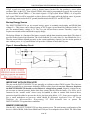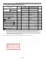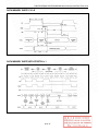
1
.
WW 00Y.CO .TW
W.1 Y.COM W
WW 00Y.CO .TW
W
W
W
W
M
.1
.T
00
W.1 Y.COM W
WW 00Y.CO .TW
W.1 Y.COM W
W
W
W
W
.T
00
W
W.1 Y.COM W
M.T
.100
W.1 Y.COM W
O
W
W
W
C
.
W
.T
W
00
W
WW .100Y
M.T
.100
W.1 Y.COM W
M.T
O
W
O
W
W
C
.
W
W
WW .100Y
WW .100Y.C M.TW
M.T
.100
M.T
O
W
O
W
C
.
O
W
W
W
Y
W
WW .100Y.C M.TW DS87C530/DS83C530
WW .100Y.C M.TW
M.T
.100
O
W
O
W
C
O
W
.C
WW .100Y.
.TW
WW EPROM/ROM
.TW Microcontrollers
00Y
with
WW .100Y.C M.TW
M
1
M
.
O
W
O
W
.C
O
W
W
W
W
00Y Clock
WW .100Y.C M.TW
1
WW .100Y.C M.TW
M.T
.
Real-Time
O
W
O
W
C
O
W
WW .100Y.
.TW
WW .100Y.C M.TW
WW .100Y.C M.TW
M
www.maxim-ic.com
O
W
O
W
O
W
WW .100Y.C M.TW
WW .100Y.C M.TW
WW .100Y.C M.TW
FEATURES W
O
WW 00Y.CO .TW
CO
.CONFIGURATIONS
WW PIN
C
W
.
Y
W
W
W
0
Y
W
T
.
0
W
M
.1
.T
00
§ 80C52 Compatible
W.1 Y.COM W
WW 00Y.CO .TW
W.1 Y.COM W
W
W
W
TOP
VIEW
W
.T
0
W
8051 Instruction-Set
.100
W.1 Y.COM W
M.T
.10Compatible
OM
W
O
W
W
C
.
W
C
W
.
Four 8-BitW
I/OWPorts 0Y
Y
W
7 .T
1
47 00
.T
W
W
M
.100
W.1 Y.COM W
M.T
.10
O
W
Three 16-Bit Timer/Counters
O
W
W
C
.
W
.C
W
W
WW .100Y
WW .1RAM
M.T
.10460
8
00Y
256 Bytes Scratchpad
M.T
O
W
M.T
O
W
C
.
O
W
W
W
Y
.C
W
WW .100Y.C M.TW
WW
M.T
.100
.TW
00Y
§ Large On-Chip
Memory
O
1
W
M
.
O
W
C
WW .100Y.
WW 00Y.CO .TW
.TW
16kB EPROM W
(OTP)
WW .100Y.C M.TW
M
O
1
W
M
.
O
W
W forYMOVX
1kB Extra On-ChipW
SRAM
.CO .TW
WW .100Y.C M.TW
WW .100Y.C M.TW
0
W
0
§ ROMSIZE FeaturesWW.1
OM
WW 00Y.CO .TW
WW 00Y.CO .TW
C
.
W
W
Y
W
W
Selects Effective On-Chip
from
W.1 Y.COM W
M.T
.100 Size O
DALLAS
W.1 Y.COM
W
WROM
W
C
W
.
W
W
W
0 to 16kB
.T
W
DS87C530
M.T
.100
.TW
100
00Y
M
.
O
1
W
M
.
O
W
C
.
O
W
Allows Access to EntireW
External
Memory
WW .100Y
.T
Y.C Map
WW .100Y.C DS83C530
.TW
W
.TW
M
OM
M
.100
Dynamically Adjustable by W
Software
O
20W
34WW
C
.
O
C
.
Y
W
WW .100Y
.TW
0Y.C M.TW
WW
Useful as Boot Block for
External
M.
.100
0Flash
M
O
1
W
.
O
W
C
.
O
W
W
Y
.C
WW 21.100Y.C M.TW 33 W
§ Nonvolatile Functions WW
M
.100
.TW
00Y
1
W
M
.
O
W
PLCC, WINDOWED
CLCC
.CO
O
W
WAlarm Y
C
.
Y
W
C
On-Chip Real-Time Clock with
Interrupt
W
.
0
Y
W
W
W
0
W
.T
00
W
.T
W.1 Y.COM
.100
Battery Backup Support of 1kB W
SRAM
W.1 Y.COM W
OM
W
W
C
.
W
W
W
.T
W
.100
.TW
100
00Y
M
.
O
1
W
M
.
§ High-Speed Architecture
O
W
W
.CO .TW
WW .100Y.C
WW 39.100Y.C M.27
TW
WW
4 Clocks/Machine Cycle (8051
= 12) .100Y
W
O
W
OM
W
WW .100Y.C
Runs DC to 33MHz Clock Rates
WW .100Y.C M.TW
WW .100Y.C M.TW
W
40
Single-Cycle Instruction in 121ns WW
WW 00Y.CO .TW26
.CO .TW
WW .100Y.
Y
W
0
W
1
0
M
.
Dual Data Pointer
WW 00Y
W.1 Y.COM W
.CO .TW
WW DALLAS
Y
W
0
W
Optional Variable Length MOVX
0
0
WtoWAccess
T
.1
W.1
M.
.10
OM
W
O
W
W
C
DS87C530
.
Fast/Slow RAM /Peripherals
W
C
W
.
Y
W
W
00
W
WW .100Y
M.T
.100
DS83C530
W.1
M.T
O
W
O
W
W
C
§ Power Management Mode
.
W
W
W
W
0
Y.C
WW .100Y
M.T
Programmable Clock Source Saves W
PowerW.100
W.1
M.T
O
W
O
W
C
.
W
C
52
14
W
.
Y
W
W
W
Runs from (crystal/64) or (crystal/1024)
WW .100Y
.1
M.T
.100
M.T
O
W
O
WW
W
C
.
W
Provides Automatic Hardware and Software
Exit Y.C
W
Y
W
W
W
0
W
.T
0
W
.T
00
W.1 13Y.COM W
1
WW
W.1 Y.COM W
§ EMI Reduction Mode Disables ALE
W
W
W
0
W
T
.
0
0
W
TQFP .1
.T
M
10
OM
§ Two Full-Duplex Hardware Serial Ports WW.
WW 00Y.CO .TW
C
.
W
Y
W
W
.T
00
W.1 Y.COM
§ High Integration Controller Includes:
W.1 Y.COM W
W
W
W
W
.100
Power-Fail Reset
M.T
.100
W
O
W
W
C
Y. High-Speed
W User’s Guide must
Early-Warning Power-Fail Interrupt
WW .100The
.TWMicrocontroller
M
O
W
Programmable Watchdog Timer
.C in conjunction
WW .10be0Yused
.TW with this data sheet.. Download it
M
at:
www.maxim-ic.com/microcontrollers
O
§ 14 Total Interrupt Sources with Six External WW
.C
W
00Y
1
.
W
WW
Note: Some revisions of this device may incorporate deviations from published specifications known as errata. Multiple revisions of any device
may be simultaneously available through various sales channels. For information about device errata, click here: www.maxim-ic.com/errata.
1 of 47
REV: 070505
.
WW 00Y.CO .TW
W.1 Y.COM W
WW 00Y.CO .TW
W
W
W
W
M
.1
.T
00
W.1 Y.COM W
WW 00Y.CO .TW
W.1 Y.COM W
W
W
W
W
.T
00
W
M
OReal-Time
W.1 Ywith
M.T
.100
W.1 Y.COMEPROM/ROM
C
.
O
W
W
DS87C530/DS83C530
Microcontrollers
W Clock
W
C
W
.
W
W
.T
WW .100Y
M.T
.100
.TW
100
M
.
O
W
M
O
W
O
W
WW .100Y.C M.TW
Y.C
WW .100Y.C M.TW
WW .100INFORMATION
.TW
ORDERING
M
O
WW 00Y.CO .TW
W
WW 00Y.CO .TW
C
.
W
W
W
Y
W
W
M
.1
.T
00
MAX
OM
W.1CLOCK
WW 00Y.CO .TW
W.1 Y.COM W
C
.
W
W
Y
W
W
0
T
.PIN-PACKAGE
TEMP
0
WPART.100
.T RANGE W SPEED
W.1 Y.COM W
W.1 Y.COM W
OM
W
W
W
C
(MHz)
.
W
W
W
.T
W
M.T
.100
.TW
100
00Y
M
.
O
1
W
M
.
O
W
C
O
W
DS87C530-QCL
PLCC
WW .100Y.
.TW
W
WW 33 .100Y.C 52 M
.TW
WW .100Y.C 0°CMto.T+70°C
M
O
W
O
W
O +70°C
W
DS87C530-QCL+
WW .100Y.C M.TW
W
WW33 .100Y.C52 PLCC
TW
.
WW .100Y.C0°C to
T
.
M
W
OM
WW 00Y.CO .TW
W
COPLCCTW
.52
W
C
DS87C530-QNL
33
.
-40°C
to
+85°C
Y
W
W
W
0
Y
W
.
0
W
.T
00
W.1 Y.COM W
OM
W.1 Y
OtoM+85°C
W
W.1 -40°C
C
.
W
C
DS87C530-QNL+
33
52
PLCC
W
.
W
W
W
.T
W
M.T
.100
.TW
100
00Y
M
.
O
1
W
M
.
O
W
C
.
O
W
C
W
DS87C530-KCL*
33W
52
CLCC
Y.Windowed
WW .100Y
Y.Cto +70°C
W
.TW
WW .1000°C
M.T
.TW
100
M
.
O
W
M
O
W
W
.C
.toCO
DS87C530-ECL
33
WW .100Y.C M.TW
+70°C.TW
WW .10520YTQFP
.TW
WW .10°C
00Y
M
M
O
WW 00Y.CO .TW
W 0°C Y
.CO .TW
WW 5200TQFP
C
.
Y
DS87C530-ECL+
33
W
W
to
+70°C
W
W
W
M
.1
.T
M
.1
.100
OM
WW 00Y.CO .TW
.CO .TW
WW 52 0TQFP
.C
Y
W
DS87C530-ENL WWW-40°C0to
33
+85°C
W
0
Y
W
W.1 Y.COM W
M.T
.10
W.1 Y.COM W
O
W
W
C
.
W
DS87C530-ENL+ WWW
33
52
TQFP
-40°C to
W
.T
M.T
.100
100
00Y+85°C M.TW
M
.
O
1
W
.
O
W
C
O
.C
WW .100Y.
DS83C530-QCL WWW
0°C to0+70°C
.TW
WW 52 PLCC
.TW
00Y
0Y.C M.TW 33
M
1
M
.
O
1
W
.
O
W
W
.CO .TW 33
WW .100Y.C M.TW
DS83C530-QCL+
0Y.C M.TW
WW52 PLCC
0
WW0°C to.1+70°C
1
00Y
.
W
OM
WW 00Y.CO .T
Wto +85°C
.CO .TW
W
C
.
Y
W
W
DS83C530-QNL
33
52
PLCC
-40°C
W
0
Y
W
0
W
.T
W.1 Y.COM
.100
W.1 Y.COM W
OM
W
W
W
C
.
W
W
DS83C530-QNL+
33
52
PLCC
-40°C
W
.T
W to +85°C
M.
.100
.TW
100
00Y
M
.
O
1
W
M
.
O
W
C
.
O
W
W
Y
.C
W
DS83C530-ECL
52
TQFP 100Y.C
W
0°C
WW
.TW
WWto +70°C
M
.100
.T33
00Y
M
.
1
W
M
.
O
W
.CO
O
W
W
C
.
Y
W
C
W
.
0
Y
W
W
W
DS83C530-ECL+
33
52
TQFP
0
0°C
Y
W
.T
00
Wto +70°C
.T
W.1 Y.COM
.100
W.1 Y.COM W
OM
W
W
W
C
.
W
W
DS83C530-ENL
33
52 TQFP
W
-40°C
.T
Wto +85°C
.100
.TW
100
00Y
M
.
O
1
W
M
.
O
W
O
W
WW .100Y.C
DS83C530-ENL+
52 TQFP
WW .100Y.C M.TW
-40°CW
toW
+85°C 00Y.C 33 .TW
W
O
W
OM
W.1
WW .100Y.C
WW .100Y.C M.TW
+ Denotes a Pb-free/RoHS-compliant device.
WW .100Y.C M.TW
W
O
W
O
W
* The windowed ceramic LCC package isW
intrinsically
.Cfree.
WW .100Y.
W
YPb
WW .100Y.C M.TW
0
W
T
.
0
W
O
W
OM
W.1
WW .100Y
WW .100Y.C M.TW
WW .100Y.C M.TW
O
WW 00
W
WW 00Y.CO .TW
C
.
W
W
W
Y
W
W
.1
.T
00
W.1 Y.COM W
WW 0
W.1 Y.COM W
W
W
W
W
.T
00
W
W.1
M.T
.100
W.1 Y.COM W
O
W
W
W
C
.
W
W
W
WW .100Y
.1
M.T
.100
M.T
O
W
O
WW
W
C
.
W
C
W
.
Y
W
W
W
0
Y
W
.T
0
W
.T
00
W.1 Y.COM W
WW
W.1 Y.COM W
W
W
W
0
W
T
.
0
0
W
.T
0
M
.1
W.1 Y.COM W
WW 00Y.CO .TW
W
W
W
.T
00
W.1 Y.COM
W.1 Y.COM W
W
W
W
W
.100
M.T
.100
W
O
W
W
C
W
W
WW .100Y.
M.T
O
W
WW .100Y.C M.TW
O
W
WW .100Y.C
W
WW
2 of 47
.
WW 00Y.CO .TW
W.1 Y.COM W
WW 00Y.CO .TW
W
W
W
W
M
.1
.T
00
W.1 Y.COM W
WW 00Y.CO .TW
W.1 Y.COM W
W
W
W
W
.T
00
W
M
OReal-Time
W.1 Ywith
M.T
.100
W.1 Y.COMEPROM/ROM
C
.
O
W
W
DS87C530/DS83C530
Microcontrollers
W Clock
W
C
W
.
W
W
.T
WW .100Y
M.T
.100
.TW
100
M
.
O
W
M
O
W
O
W
WW .100Y.C M.TW
WW .100Y.C M.TW
WW .100Y.C M.TW
DETAILED
O
WW 00Y.CO .TW
W DESCRIPTION
WW 00Y.CO .TW
C
.
W
W
W
Y
W
W
M
.T
00
W.1 (RTC)
W.1 Y.COM with
The DS87C530/DS83C530
microcontrollers
a real-time
.CO are .T8051Wclock
W.1 Y.COM EPROM/ROM
W
Y
W
W
0
W
W
W
0
0
.T high-speed core. W
1 use 4 Oclocks
0
W
M
.
.Tbased on theWDallas
1
00
M
.
compatible
microcontrollers
Semiconductor
They
per
1
M
.
O
W
W
W
Y.C
WW 00Y.CO .TW
C
.
0
W
T
W
.
W
0
Y
W
1
instruction
cycle
instead
of
the
12
used
by
the
standard
8051.
They
also
provide
a
unique
mix
0
W
.1
OM of
W.
M.T
.10
OM
W
C
.
O
W
W
C
.
Y
W
C
.
0
peripherals
on other processors.
an on-chipWRTC and
backup
.TW
0Y include
W
.TW
10battery
0They
WWnot widely
M
.
.TW
1
00Y available
M
.
O
1
W
M
.
.C
support for W
anWon-chip
1kO x 8 SRAM.
TheWnew
W
.CO .TW Mode allows
WWPower
WW software
W
00Y to select
0YManagement
Y.C
1
0
0
W
T
M.T
.
.
1
0
M
.
O
1
W
M
.
reduced power operation
while
still
processing.
O
W
C
.
O
W
WW .100Y
.TW
WW .100Y.C M.TW
WW .100Y.C M.TW
M
O
W
O
W
O
W
A combinationWW
of high-performance
RTC, battery-backed
0Y.Cpower
WSRAM,
.TW
W microcontroller
0and
0Y.C
Y.C
WW .core,
TW
.
1
0
0
W
T
M
.
.
1
0
M
O
1
W
management makes
idealWfor
They
O and portable applications.
W instruments
.C also
OM
W
W.the DS87C530/DS83C530
WThese
W other Dallas
00Y twoM.TW
0Y.C microcontrollers.
Y.Cfound.Ton
W high-speed
TW
.
1
0
0
WWperipherals
.
provide several
include
1
0
M
.
W
.CO .TW
W.1 Y.COM W
.CO .with
WW
W brownout
0Yand
Ymonitor
WW
0
0
W
T
independent serial
two
data
pointers,
on-chip
power
detection
aM
1
0
0
WW ports,
T
.
.
W
.10
W.1 Y.COM W
.CO .TW
OM
W
Y
W
C
watchdog timer. WW
.
0
W
W
0
Y
W
.T
W
.100
W.1 Y.COM W
M.T
.100
OM
W
O
W
W
C
.
W
C
.T
W
Y. allows
TW While W
Power Management
Mode (PMM)
software toWselect a.1slower
default operation
00Y CPU
WW
.100
M.clock.
OM
W
M.T
.100
O
W
C
.
O
W
W
C
W
W
uses four clocks per machine
PMM
runs the W
processor
at Y
64. or 1024
per cycle.
isYa
W
W There
.Tclocks
0Y.C theM
WW .10cycle,
M.T
.100
.TW
100
M
.
O
W
O
W
C
corresponding drop in W
power
consumption
when
the
processor
slows.
W
.CO .TW
WW .100Y.
.TW
WW .100Y.C M.TW
W
M
00Y
O
1
W
M
.
O
W
.C
W
W
CO
The EMI reduction feature
to
This disables
WWthe ALE
Wselect a reduced
00Y
0Y.C mode.
Y.software
WW .emission
TW
.
1
0
0
WW allows
T
M.T
.
.
1
0
M
O
1
W
M
.
O
W
C
signal when it is unneeded.
.
O
W
WW .100Y
.T
WW .100Y.C M.TW
WW .100Y.C M.TW
OM
W
O
W
C
.
O
W
W
C
.
Y
W
The DS83C530 is a factory
ROM
of the W
DS87C530
.C version
Y
W cost0designed
Y
TWhigh-volume,
.for
WW mask
M.
.100
.TW
10except
00in
M
.
O
1
W
M
.
O
W
C
sensitive applications. It is identical
all
respects
to
the
DS87C530,
that
the
16kB
of
EPROM
is
.
O
W
W
Y
.C
Y.C
W
W
WW
.TW
WW
M
.100
.TAll
100 of the
00Yprogram.
M
.
replaced by a user-supplied
application
references
to
features
DS87C530
will
apply
to
1
W
M
.
O
W
.CO
O
W
W
C
.
Y
W
C
W
.
0
Y
W
W
W
0
0
Y
W where.10noted.
.T
W
the DS83C530, with the exception
features
Please
00EPROM-specific
W.1 Y.COM
M.T
.1of
OM contact your local
W
O
W
W
C
.
W
C
W
.
Y
W
W
Dallas Semiconductor sales W
representative
W
.T
.100
.TW information.
100
00Yfor ordering
M
.
O
1
W
M
.
O
W
O
W
.C
W
W
Yan
WW .100Y.C
W A user W
0
Y.C devices.
T
.
0
0
WW are .monolithic
T
Note: The DS87C530/DS83C530
must
supply
external
battery
or
super
.
1
0
M
.
M
WW 00Y.C
W 1 toYhave
.COor nonvolatile
WW
W
.CO permanently
Y
W
cap and a 32.768kHz timekeeping
powered
timekeeping
RAM.
W
0
W
T
.
1
0
0
WWcrystal
T
.1
M. and switching W
.10the support
OMto manage these WW.
W
O
W
C
The DS87C530/DS83C530 provide
all
circuitry
needed
.
C
W
0Y.
Y
W
W
W
0
0
Y.
W
T
.
1
0
0
W
T
.
.
1
0
W
resources.
OM
W.
OM
W.1
WW .100Y
WW .100Y.C M.TW
WW .100Y.C M.TW
O
WW 00
W
WW 00Y.CO .TW
C
.
W
W
W
Y
W
W
.1
.T
00
W.1 Y.COM W
WW 0
W.1 Y.COM W
W
W
W
W
.T
00
W
W.1
M.T
.100
W.1 Y.COM W
O
W
W
W
C
.
W
W
W
WW .100Y
.1
M.T
.100
M.T
O
W
O
WW
W
C
.
W
C
W
.
Y
W
W
W
0
Y
W
.T
0
W
.T
00
W.1 Y.COM W
WW
W.1 Y.COM W
W
W
W
0
W
T
.
0
0
W
.T
0
M
.1
W.1 Y.COM W
WW 00Y.CO .TW
W
W
W
.T
00
W.1 Y.COM
W.1 Y.COM W
W
W
W
W
.100
M.T
.100
W
O
W
W
C
W
W
WW .100Y.
M.T
O
W
WW .100Y.C M.TW
O
W
WW .100Y.C
W
WW
3 of 47
.
WW 00Y.CO .TW
W.1 Y.COM W
WW 00Y.CO .TW
W
W
W
W
M
.1
.T
00
W.1 Y.COM W
WW 00Y.CO .TW
W.1 Y.COM W
W
W
W
W
.T
00
W
M
OReal-Time
W.1 Ywith
M.T
.100
W.1 Y.COMEPROM/ROM
C
.
O
W
W
DS87C530/DS83C530
Microcontrollers
W Clock
W
C
W
.
W
W
.T
WW .100Y
M.T
.100
.TW
100
M
.
O
W
M
O
W
W
.CO .TW
WW .100Y.C M.TW
WW .100Y.C M.TW
WW 1. .Block
Figure
00Y Diagram
1
M
O
WW 00Y.CO .TW
W
WW 00Y.CO .TW
C
.
W
W
W
Y
W
W
M
.1
.T
00
W.1 Y.COM W
WW 00Y.CO .TW
W.1 Y.COM W
W
W
W
0
W
.T
0
W
M
.1
.T
00
W.1 Y.COM W
WW 00Y.CO .TW
W.1 Y.COM W
W
W
W
W
.T
W
.100
W.1 Y.COM W
M.T
.100
OM
W
O
W
W
C
.
W
C
W
Y
W
.T
W
W
WW .100Y.
.100
M.T
.100
OM
W
M.T
O
W
C
.
O
W
W
C
W
Y
W
WW .100Y.
.TW
WW .100Y.C M.TW
M.T
.100
M
O
W
O
W
C
.
O
W
WW .100Y
.TW
WW .100Y.C M.TW
WW .100Y.C M.TW
M
O
W
O
W
O
W
WW .100Y.C M.TW
WW .100Y.C M.TW
WW .100Y.C M.TW
O
WW 00Y.CO .TW
W
WW 00Y.CO .TW
C
.
W
W
W
Y
W
W
M
.1
.T
00
W.1 Y.COM W
WW 00Y.CO .TW
W.1 Y.COM W
W
W
W
W
.T
00
W
W.1 Y.COM W
M.T
.100
W.1 Y.COM W
O
W
W
W
C
.
W
W
.T
WW .100Y
M.T
.100
.TW
100
M
.
O
W
M
O
W
C
O
W
WW .100Y.
.TW
WW .100Y.C M.TW
WW .100Y.C M.TW
M
O
W
O
W
O
W
WW .100Y.C M.TW
WW .100Y.C M.TW
WW .100Y.C M.TW
O
WW 00Y.CO .TW
W
WW 00Y.CO .TW
C
.
W
W
W
Y
W
W
M
.1
.T
00
W.1 Y.COM W
WW 00Y.CO .TW
W.1 Y.COM W
W
W
W
0
W
.T
W
W.1 Y.COM
M.T DS87C530/ WW.10
.100
OM
O
W
W
C
.
C
W
W
.T
W
00
0Y
W
WW .100Y.
M.T
W.1 Y.COM
M.T DS83C530 WW.10
O
O
W
W
C
.
Y
W
W
.TW
WW .100Y.C M.TW
M.
.100
100
M
.
O
W
O
W
C
.
O
W
W
Y
W
WW .100Y.C M.TW
WW .100Y.C M.TW
M
.100
W
O
W
.CO
O
W
W
C
.
Y
W
C
W
.
0
Y
W
W
W
0
W
.T
00
W
M
.1
.T
00Y
W.1 Y.COM W
WW 00Y.CO
W.1 Y.COM W
W
W
W
W
.T
W
.100
W.1 Y.CO
M.T
.100
OM
W
O
W
W
C
.
W
C
W
Y
W
W
W
WW .100Y.
.100
M.T
.100
W
M.T
O
W
.C
O
W
W
C
W
00Y
WW .100Y.
.TW
1
WW .100Y.C M.TW
.
M
W
O
W
O
W
WW .100Y.
WW .100Y.C M.TW
WW .100Y.C M.TW
W
O
W
O
W
WW .100Y
WW .100Y.C M.TW
WW .100Y.C M.TW
O
WW 00
W
PIN DESCRIPTION
WW 00Y.CO .TW
C
.
W
W
W
Y
W
W
.1
.T
00
W.1 Y.COM W
WW 0
W.1 Y.COM W
PIN
W
W
W
0
W
.T
NAME
W
W.1
M.T FUNCTION WW.10
.100
OM
PLCC
TQFP
O
W
W
C
.
C
W
.
Y
W
W
W
WW .1Power
.1
00Y Supply
M.T
.100
M.T
52
45
VCC
+5V Processor
O
W
O
WW
W
C
.
W
C
W
.
Y
W
W
W
0
Y
W
.T
0
W Digital
.T
00
1, 25
18, 46
GND
Processor
Ground
W.1 Y.COM W
OM
WW
W.1 Circuit
W
C
.
W
W
W
0
Y
W
T
.
0
0
W Supply..1V0CC2 is isolated
.Tfrom VCC to isolate theW
29
22
VCC2
+5V RTC
RTC
Mnoise.
.1 from digital
OM
W
.CO .TW
W
C
.
Y
W
W
0
Y
W
0
W Ground
26
19
GND2
RTC Circuit
.T
00
W.1 Y.COM
W.1 Y.COM W
W
W
Reset Input.
a Schmitt
voltage inputW
to recognize
WThis pin.1contains
00
.100external active
M.Tan internal pulldown
W
O
W
high reset inputs.
The
pin
also
employs
resistor
to allow for a
W
C
W
W
W
12
5
RST
0Y. reset
.T
0external
combinationW
of wired OR
sources.
An
RC
is
not
required
for power-up,
1
M
.
W function
.COinternally.
W
as the device provides
Y
0
WW this
T
.
0
OM
W.1XTAL1
C
.
W
Crystal Oscillator
Pins.
and
XTAL2
provide support for parallel-resonant,
Y
23
16
XTAL2
W
.100also as an input if there is an external clock source in
AT-cut crystals. XTAL1
acts
W
W
place of a crystal.W
XTAL2 is the output of the crystal amplifier.
24
17
XTAL1
4 of 47
.
WW 00Y.CO .TW
W.1 Y.COM W
WW 00Y.CO .TW
W
W
W
W
M
.1
.T
00
W.1 Y.COM W
WW 00Y.CO .TW
W.1 Y.COM W
W
W
W
W
.T
00
W
M
OReal-Time
W.1 Ywith
M.T
.100
W.1 Y.COMEPROM/ROM
C
.
O
W
W
DS87C530/DS83C530
Microcontrollers
W Clock
W
C
W
.
W
W
.T
WW .100Y
M.T
.100
.TW
100
M
.
O
W
M
O
W
W
.C
W
W
.CO .TW
WW .100Y.C M.TW
WW
PIN
DESCRIPTION
(continued)W W.100Y OM.T
00Y
1
M
.
O
WW 00Y.CO .TW
W
.C
W
C
W
.
Y
W
W
W
0
Y
W
T
.
0
W PIN .100
M
.1
M.T
W.1 Y.COM FUNCTION
ONAME
WW 00Y.CO .TW
W
W
C
W
.
W
W
W
0
Y
W
.T
0
PLCC
TQFP
W
M
.1
.T
00
W.1 Y.COM W
WW 00Y.CO .TW
W.1 Y.COM W
W
W
W
W
Program Store-Enable
a chip
enable for optional
W
M.Tactive-low signal isW
.100Output.OThis
OMwhen
W.1is driven
M.T external ROM W
.100
W
.Chigh
O
W
38
31
PSEN
PSEN
provides
an
active-low
pulse
and
memory.
C
.
Y
C
W
.
0
Y
W
W
.TW
W
0
0
Y
W
T
.
1
W
M
.
.T external ROM is notWbeing
10 accessed.
00
M
.
O
1
W
M
.
O
W
.CO .TW
Y.C
WWaddress
TW
W
00LSB
WW .1Output.
1
00Y ThisM
WW .100Y.C M.TAddress
M
.
Latch-Enable
pin
latches
the
external
from
the.
O
W
O
W
C
.
O
W
C 0. This
Y
multiplexed
address/data
signal is commonly
Y.Port
WW connected
.TW
W
WW .bus
.TW
100 to the
00on
WW .100Y.C M.T
M
.
1
M
O
W
O
latch
enable
of
an
external
373
family
transparent
latch.
ALE
has
a
pulse
width
of
.C
O
W
WW 00Y.C
WW 00ALE
.TW
W
00Y
Y.C
Wand
TWcycles. ALEWis forced.high
.
1
W32
T
39
1.5
XTAL1
cycles
a
period
of
four
XTAL1
when
the
M
.
1
M
.
O
1
W
W
.C
OMdevice is in a Reset condition.
W writing
W.
CObe disabled
W
W
00Y
0Y.can
WW .1ALE
.TW and forcedWhigh by
1
0
WW .100Y.C M
T
M.T
.
.
M
O
W
ALEOFF
=
1
(PMR.2).
ALE
operates
independently
of
ALEOFF
during
external
O
W
O
W
.C
W
WW .100Y.C M.TW
WW .100Y.C memory
.TWaccesses. W W.100Y OM.TW
M
O
WW 00Y.CO .TW
W
.C
W
C
W
.
Y
W
W
0
50
43WW P0.0 (AD0)
Y
W
T
.
.T
00
M
.10
W.1 Y.COM W
OM0 (AD0–AD7), I/O. Port
W
W.1(AD1)Y.CPort
.CO 8-bit,
WW0 is an
W
Y
W
49
42 WWP0.1
open-drain,
bidirectional
I/O
port.
.T
W
00 an
0
W
T
.1As
M.
.10 as the multiplexed
OM
W
M.Tfunction Port 0 canW
.100 alternate
O
W
C
function
address/data
bus
to
access
.
O
W
W
C
W
Y
48
41
P0.2 (AD2) Y.C
W
Y.
W
.Tthe
WW
TW DuringW
M.T
.100
.memory.
the time when
LSB of a memoryW
address
100 ALE isOhigh,
00 off-chip
M
.
O
1
M
.
W
C
O
.Cport transitions
47
40
P0.3W
(AD3)
Y.
When ALE falls
to a logic00,
WW data
.TW
0Ythe
WW
.TW to a bidirectional
100
WW .100Yis.Cpresented.
TW
M
.
.
1
M
.
O
W
M
O
bus.CThis
and
external RAMW
memory
W ROM Y
O bus is used to read external
W
46
39
P0.4 (AD4)
.Cread/ write
W drivers..100Y.C M.TW
W
0 the
Y.peripherals.
Wa W
TW active high
.
0
WW .100or
T
When
used
as
memory
bus,
port
provides
.
1
M
.
45
38
P0.5 (AD5)
OM
WW 00Y.CO .T
W The
CO are
.resistors
WW Pullup
C
reset
condition
of Port 0 is
tri-state.
required
when
using
W
.
Y
W
W
W
0
Y
W
T
.
0
W
.Tport.
00 as anMI/O
W.1 Y.COM
44
37
P0.6 (AD6)
W.1 Y.COM W
O
W
W.1 PortY0.C
W
W
W
W
.T
W(AD7) .100
M.
.100
.TW
100
M
.
O
W
43
36
P0.7
M
O
W
C
.
O
W
W
Y
W
WW .100Y.C M.TW
WW .100Y.C M.TW
M
.100
W
O
W
3
48
P1.0
.CO
O
W
W
C
.
Y
W
C
W
.
0
Y
W
W
W
0
YI/O. Port 1.T
Wan 8-bit,.1bidirectional
Port01,
functions as both
I/O
.Tport and an alternate W.1
00
W
M
.1 0 interface
OM and new Serial Port 1.
W
.CO
OM for Timer 2 I/O, new
W
W
C
functional
External
Interrupts,
.
Y
W
C
W
.
0
Y
W
W
W 1 is withW
.T
10
00 1. In this
.TPort
00Ycondition
4
49
P1.1W
The.1reset
all bits W
at .a1logic
O
Mof
OM state, a weak pullup WW.
O
W
C
.
W
C
W any external
0Y.C
Y mode, .since
W
W
condition also
0
0input
Y. high. This
Wserves as.1an
T
1
0
WWholds.1the
T
.
.
00port
M
M
Wweak pullup.
.C
circuit
will overcomeW
the
writesW
a WW
W that writes
.COWhen.Tsoftware
COto the Tport
W
.
Y
W
W
00Y
0
Y
W
1
0
0
W
5
50
P1.2
.
.
1
0
0 to any
port
pin,
the
device
will
activate
a
strong
pulldown
that
remains
on
until
M
.
1
W
.
W
OM
COhas been
Wat 0 will WW .100Y.
Y.port
WWa 1 is00written
the
Woccurs. Writing
0
Y.C or a reset
WWa 1 after
T
.
0
Weither
T
.
1
M
.
M
.1 transition
causeW
a strong
to turn on, followed
pullup.
WW 00Y
.COsustaining
WW by 0a 0weaker
W
.CO driver
Y
W
W
6
51
P1.3
W
Y
W
T
.
0
W
T
Once the momentary
strong
port .again
1 becomes
W.1
M. driver turns off, theW
.10
OMthe output high
W
O
W
W
C
.
C
W
.
(and
input) state.
modes of PortW1 are outlined
Yas follows..T
W
00
YThe alternate
WW
.TW
M
.100
100
W.1
M
.
O
W
O
W
W
C
.
7
52
P1.4
W
W
0
WW .100Y
WW .100Y.C M.TW
M.T
W.1
O
Port
Alternate
Function
W
O
W
W
C
.
W
C
W
.
Y
W
W
W
P1.0WW
T2 100Y
External
.1
M.T
.1200
M.T I/O for Timer/Counter
.
O
W
O
WW
W
C
.
W
P1.1
T2EX
Timer/Counter
2 Capture/Reload
Trigger
C
8
4
P1.5
W
.
Y
W
W
W
0
Y
W
.T
0
WRXD1 .100
.T
P1.2
Serial
W.1 Y.COM W
OM Port 1 Input
WW
W
W
C
.
W
W
W
0
Y
W
T
.
P1.3 W
TXD1
Serial
Port
1
Output
0
0
.T
0
M
W.1Detect)
OM Interrupt 2 (PositiveWEdge
9
2
P1.6
W.1 Y.External
.CO .TW
P1.4
INT2
C
Y
W
W
0
W
0
W
.T
00
M
INT3
Edge
P1.5
W.1Detect)
OMInterrupt 3 (NegativeW
W.1 YExternal
.CO
C
.
Y
W
W
0
W
P1.6
INT4
External
Interrupt
4
(Positive
Edge
Detect)
0
0
W
T
.
.1
10 External
10
3
P1.7
OM
INT5 WW.
Interrupt 5 (Negative Edge
P1.7
WWDetect)
C
.
W
Y
W
W
.T
00
W.1 Y.COM W
W
W
M.T
.100
O
W
C
.
WW .100Y
W
WW
5 of 47
.
WW 00Y.CO .TW
W.1 Y.COM W
WW 00Y.CO .TW
W
W
W
W
M
.1
.T
00
W.1 Y.COM W
WW 00Y.CO .TW
W.1 Y.COM W
W
W
W
W
.T
00
W
M
OReal-Time
W.1 Ywith
M.T
.100
W.1 Y.COMEPROM/ROM
C
.
O
W
W
DS87C530/DS83C530
Microcontrollers
W Clock
W
C
W
.
W
W
.T
WW .100Y
M.T
.100
.TW
100
M
.
O
W
M
O
W
W
.C
W
W
.CO .TW
WW .100Y.C M.TW
WW
PIN
DESCRIPTION
(continued)W W.100Y OM.T
00Y
1
M
.
O
WW 00Y.CO .TW
W
.C
W
C
W
.
Y
W
W
W
0
Y
W
T
.
0
W PIN .100
M
.1
.T
W.1 Y.COM FUNCTION
OM
WW 00Y.CO .TW
W
NAME
W
C
W
.
W
W
W
0
Y
W
.T
0
PLCC
TQFP
W
M
.1
.T
00
W.1 Y.COM W
WW 00Y.CO .TW
W.1 Y.COM W
W
W
W
W
30 W
23 00
P2.0 (AD8)
.T
1 condition
Port 2 (A8–A15),
is M
a bidirectional
I/O port. The
Mof
100 Port 2 O
.I/O.
W.reset
M.T
.1
W
.CO
O
W
W
C
.
Y
W
C
Port
2
is
logic
high.
In
this
state,
a
weak
pullup
holds
the
port
high.
This
condition
W
0
Y
W
.TW
W
0
0
31 WW 24 00Y.P2.1 (AD9)
W
T
.
1 to the port
M
.
.T also serves as an W
10mode, since
M
.
O
1
W
M
.
input
any
external
circuit
that
writes
will
.C
W
W
W
.CO .TW
W pullup.
.CO
Wany
32
P2.2
(AD10)
Wovercome the
00Y
0YWhen
Wweak
software
writes a 0 to
port.1
pin,
the device
0
WW 25 .100Y
T
M.T
.
1
M
.
O
W
M
O
W
C
.
O
W
.Cthat remains
will activate W
a strong
on until either
a 1 is written
Yor a reset .TW
W pulldown
WW
33
.TW
100
00Y
0Y.C(AD11)
WW26 .10P2.3
.
.TW
1
M
.
OM
occurs.
Writing
a
1
after
the
port
has
been
at
0
will
cause
a
strong
transition
W
M
O
W
.Cdriver
O
W
W P2.4Y.(AD12)
C
.
Y
W
C
W
34
27
0
Y
W
W
0 strong M.TW
0 sustaining
W by a.weaker
Tpullup. Once the momentary
toW
turn on, followed
.
1
0
0
W
T
.
.
1
0
M
1
W
.
Wagain becomes
COan TW
OM driver turns off, theW
W input state.
port
the
output high
and
.CO both
Y.As
C
35
28WW P2.5 Y
(AD13)
W
.
0
Y
W
W
0
0
W
T
.
1 This OM.
W
T
.10function O
function Port 2W
can
as M
MSB of the external address
W.bus.
M.alternate
.100
O
W
W
C
W
.
Y.C
W external
36
29 W P2.6 (AD14)
.C
Y and read/write
bus
read
memory
W be used toW
.TW externalWRAMW
100 or OM.T
00ROM
W
.
.Tcan
1
00Y
M
.
1
M
.
O
W
O peripherals.
37
30 WW
P2.7 (AD15)
WW .100Y.C M.TW
W
Y.C
WW .100Y.C M.TW
0
W
T
.
0
M
O
WW 00Y.CO .TW
W.1 Y.COPort
WWas both
W
Yan.C8-bit, bi-directional
3,
I/O. Port 3 functions
I/O W
port and an
W
0
W
T
.
15
8 WW
P3.0
1
0
0
T
M
.
1
0
W0.and
M functional interface
OM Serial Port 0, Timer
W
alternate
for. external.Cinterrupts,
1 Y.CO
W
W.1 Y.CO
W
W
W
0
Y
W
W
WRD and WRWstrobes. .The
.T of Port 3 is with all bits
W
M.T
.1at0a
.T
Inputs,
and
100reset condition
00
M
O
1
W
M
.
O
W
C
O 1. In this state, a weakWpullup holdsY.the
W
C port high.
Y.
16
9
also serves
WW
.TW
W
.TWThis condition
100
00
WW P3.1.100Y.Clogic M
TW
M
.
.
1
M
.
O
W
O
as
that writes to the port will overcome
W circuit
.C
O input mode, since any external
W
W
W
.C
W the deviceWwill
.Can
W When software
00Y
0a Y
WW writes
Tpin,
.
1
0
WW .100Ythe
T
weak
pullup.
0
to
any
port
activate
M.T
.
.
1
M
.
O
W
M
O
17
10
P3.2
W
C
.
O
W
.Ca 1 is written
C pulldown
a .strong
on until either
WW .100Y
.T
W that remains
WW
.TWor a reset occurs.
00Ycause
WW .100Y
.T
1
M
.
OM
W
M
Writing
a
1
after
the
port
has
been
at
0
will
a
strong
transition
driver
to turn
O
W
C
.
O
W
W
C
.
Y
C
Y
W
Y.followed
WW pullup.
.TW strongW
a weaker sustaining
momentary
driver .100
WP3.3
TW
M.
.by
18
11
100Once the
00on,
M
.
O
1
W
M
.
O
W
C
.
O
W
W turns
Y
again becomes
input
W the output
C the port
W state. TheW
.off,
Y.Chigh and.T
Wboth
WW .1alternate
M
.100
.TofWPort 3 are outlined
100
00Y modes
M
.
W
below.
M
O
W
.CO
O
W
W
C
.
Y
W
C
W
.
0
Y
W
W
19
12
P3.4
W
0
Y
W
.T
W
Port
Function
.T
.100
100 Alternate
W.1 Y.COM
OM
W
OM
W
W.P3.0
C
.
W
C
RXD0
Serial
Port
0
Input
W
.
Y
W
W
W
.T
W
.100
100
00Y TXD0M.TW Serial Port
M
.
O
1
W
.
P3.1
0
Output
O
W
20
13
P3.5 WW
W 0 00Y.C
W
.CO .TW ExternalW
WW .100Y.C
YINT0
T
.
Interrupt
0
W P3.2
1
0
M
.
W
M
W.1 INT1
WW1 00Y.CO .TW
.CO .TW External Interrupt
WW .100Y.C
WP3.3
Y
W
0
W
0
M
.1
21
14
P3.6
W
P3.4
Input
W.1 T0Y.COM WTimer 0 External
.CO .TW
WW
Y
WW .100Y.
W
0
W
P3.5
T1
Timer
1
External
Input
0
0
W
T
.
1
0
M
.
W
M External Data Memory
.1
P3.6
.CO .TW
WW Write
.CO .TW
YStrobe
WW .100Y
WW WR
0
Y
W
22
15
P3.7
0
0
WP3.7
1 Strobe M
0
.Read
Data Memory
WW 00
W.1RD Y.COM External
WW 00Y.CO .TW
W
W
W
W
W
.1
.T
.1 to use O
100 Input,
External
to W
ground
anM
external ROM.
OMActive Low. ConnectW
WW 0
W.Access
C
.
C
W
.
Y
W
W
W
W by register
.T to V
00settings. Connect
42
35
EA
Internal
RAM00
isYstill accessible
W
.T as determined
W.1
W.1 Y.COM W CC
OM
W
W.1 ROM.
W
to useW
internal
C
.
W
Y
W
W
.1
.TW
M.T
.100
100
Mpower
.Connect
O
W
O
WW
W
C
.
VBAT Input.
to
the
source
that
maintains
SRAM
and
RTC
when
W
C
W
.
Y
W
W
W
0
Y
W
.T to
0 cap. Connect
0 connected
.T
< VBATW
. Can
or .a1super
VCCW
51
44
VBAT
.10be
OM
W
OM to a 3V lithium battery
WW
C
.
W
C
W
.
Y
W
W
W
0
Y
W
T
GNDW
if battery will
not
be
used
with
device.
.
0
0
.T
.10
W.1 Y.COM W
OM
WCrystals.
Wthese
C
.
W
Timekeeping
A
32.768kHz
crystal
between
pins
the time
W
Y
W
W
100 supplies
00 devices support
M.T
.load
27
20
RTCX2
M.T both 6pF and 12.5pF
.1The
O
W
base for the RTC.
capacitance
O
W
C
.
W
.C
W
00Yfrom
Wselected
.TW later). W
crystals as
by00
anYSFR bitM
(described
To prevent.1noise
1
.
W
O
affecting the
be guard-ringed with
WW the 0RTCX2
WW
28
21
RTCX1
0Y.C andMRTCX1
WRTC,
TW pins should
.
1
.
GND2.
O
W
WW .100Y.C M.TW
2, 11, 13,
4, 6, 7,
O
W pins should
Not Connected.W
These
Y.C not be connected. They are reserved for use
14, 40,
33, 34,
N.C.
0
W
0
.1 family.
with future devices inW
the
41
47
WW
6 of 47
.
WW 00Y.CO .TW
W.1 Y.COM W
WW 00Y.CO .TW
W
W
W
W
M
.1
.T
00
W.1 Y.COM W
WW 00Y.CO .TW
W.1 Y.COM W
W
W
W
W
.T
00
W
M
OReal-Time
W.1 Ywith
M.T
.100
W.1 Y.COMEPROM/ROM
C
.
O
W
W
DS87C530/DS83C530
Microcontrollers
W Clock
W
C
W
.
W
W
.T
WW .100Y
M.T
.100
.TW
100
M
.
O
W
M
O
W
O
W
WW .100Y.C M.TW
WW .100Y.C M.TW
WW .100Y.C M.TW
COMPATIBILITY
O
WW 00Y.CO .TW
W
WW 00Y.CO .TW
C
.
W
W
W
Y
W
Mfor high
.1 designed
.Tare fully static, CMOS
00
The W
DS87C530/DS83C530
microcontrollers
OM
W.1 8051-compatible
WW 00Y.CO .TW
W.1 Y.COM W
C
.
W
W
Y
W
W
0
W 8051 .users,
performance.
While
InMgeneral,
.T have many new
1
0 the devices
W
.T familiar to
00 remaining
W.features.
OMworks without Wmodification
W 1 systems
.CO on .TW
OMexisting 8051-based
W.1 Y.for
C
.
Y
W
C
software
written
W
0
Y
W
W
W
.T
W
M the
.10
.TW
100
00
M
.
O
1
W
M
.
O
W
C
O exception is critical
DS87C530/DS83C530.
The
timing since the high-speed microcontrollers
W
W
WW .100Y. perform
.Tits
WW .100Y.C M.TW
0Y.C thanMthe
WWmuch
M
.TWoriginal for
0faster
O
1
instructions
any
given
crystal
selection.
The
DS87C530/DS83C530
run
W
.
O
W
.C
W
W
W
.CO set.
Wdue
W
00Y
0Y.C with
WW
TW
.
1
0
WW8051.1instruction
T
the standard
They
are
not
pin
compatible
other
8051s
to
the
timekeeping
M.T
.
.
1
00Y
M
.
O
W
M
O
W
C
.
WW .100Y
.TW
crystal. WWW 00Y.CO .TW
WW .100Y.C M.TW
M
O
1
W
M
.
O
W
O
W
WW .100Y.C M.TW
WW .100Y.C M.TW
WW .100Y.C M.TW
W 256 Y
O
The DS87C530/DS83C530
provide
three 16-bit timer/counters,
serial portW(2),
bytes
.CO of .TW
O
W
WW 00Y.Cfull-duplex
C
W
.
0
W
W
W
0
Y
W
T
.
M
.1
direct RAM W
plus 1kB.10of0 extraOMOVX
ports
same operation as a W
standard
M.T RAM. I/O W
OM
W.1 haveY.the
CO
.8051
W
W
C
Y
C
W
.
0
W
W
.TW
W
W operation
product. Timers
.T their timing compatible
10 with
00 to keep
W will default
M
.
.T clock-per-cycle
1
00Y to aM12
M
.
O
1
W
.
O
W
.C
O
W 4 clocks
W
original 8051 systems.
run at the W
new
Ware individually
00Y per M.TW
0Y.C M.to
Y.C timers
WW programmable
TW
1
0
0
WW However,
T
.
.
1
0
.
O
W
cycle if desired. TheW
PCA
supported.
OM
W.1is not
WW 00Y.CO .TW
.C
WW .100Y.C M.TW
W
Y
W
0
W
T
.
0
M
.1
WW 00Y.CO .TW
W.1 Y.COM W
WW 00Y.CO .TW
W
W
W
0
W
T
The DS87C530/DS83C530.1provide
several
features
by new SpecialW
Function
M
.1
0
.1 implemented
M. new hardware W
OM
W
.CO .TW
O
W
W
C
.
Y
C
W
.
0
Y
W
W
Registers. A summary
of
these
SFRs
is
provided
below.
W
0
0
Y
W
T
.
0
W
M
.1
.T
00
W.1 Y.COM W
WW 00Y.CO .TW
W.1 Y.COM W
W
W
W
W
.T
W
.100
W.1 Y.COM
M.T
.100
OM
W
PERFORMANCE OVERVIEW
O
W
W
C
.
W
C
W
W
.T
0Y
W
WW .100Y.
.100
.TW
M.T speed comes W
.10core.
OM
Wjust
O
W
C
.
OM
The DS87C530/DS83C530Wfeature
a .C
high-speed,
8051-compatible
Higher
not
W
C
.
Y
W
Y
W
.TW
Wfrequency,
M.
.100
.TWa newer, W
100 design.
00Y
M
.
O
1
from increasing the clock
but
also
from
more
efficient
W
M
.
O
W
C
.
O
W
W
Y
W
WW .100Y.C M.TW
WW .100Y.C M.TW
M
.100
W
O
W
O memory cycles W
W A 00Y.CO
W the Y
C
.
C
W
.
Y
W
W
This updated core does not
have
dummy
that
are
present
in
a
standard
8051.
W
W
W
.T
00
M.T
.100
W.1 Y.COM
O
OM using the clockWW
W
W.1 Y.cycles
C
conventional 8051 generatesWmachine
frequency
divided
by
12.
In
the
.
C
W
Y
W
.T
00
W
.100
.TW4 clocks.W
1fastest
00 cycleM
M
.
O
1
W
.
O
DS87C530/DS83C530, the same machine
takes
Thus
the
instruction,
one
machine
W
W
W
Y.C
WW .100Y.C
WW 00Y.CO .TW
0
W
T
.
0
W
1
cycle, executes three times faster for the
identical
instructions. W
M
M frequency. NoteWthat
.1 same crystal
W. theseYare
.CO speed
W
.CO .TW will see
WW .100Y.C
WWDS87C530/DS83C530
0
Y
W
T
The majority of instructions on
the
full
3-to-1
improvement.
.
0
0
Wthe
1
0
M
.
1
W
M
O
W.
WWinstructions
Some instructions will get between
2.4
improvement.
faster
W than the
.COto 1 .T
Y.C are .T
WW .100Y.
W
0
WAll
0
WW 1.5 .1and
1
00Y
W
OM
W.
original 8051.
OM
W
WW .100Y
WW .100Y.C M.TW
WW .100Y.C M.TW
O
WW 00
W
WW 00Y.CO .TW
C
.
W
W
W
Y
W
W gives.1approximately
The numerical average of all opcodes
Improvement of
.1
.Ta 2.5 to 1 speed improvement.
00
W.1 Y.COM W
OM used. Speed-sensitive
WW 0
W instructions
W
C
.
W
individual programs will depend on W
theWactual
applications
would
make
W
Y
W
00
.T
M.T
W.1
M
.100 faster.
Oto
W.1 Y
O
W
W
C
the most use of instructions that are three
times
However,
the
sheer
number
of
3
1
improved
.
W
C
W
.
W
W
WW .100Y
TW
.1
M.T
.100
M.any
O
opcodes makes dramatic speed improvements
likelyCO
for
code. TheseWarchitecture
improvements
W
WW
W
C
.
W
.
Y
W
W
W
0
Y
W feature
.T
0
W (8.25.1MIPs).
.T Data Pointer
00 TheMDual
produce a peak instruction cycle in 121ns
allows
OM the user
W.1 also
O
WW
W
C
.
W
C
W
.
Y
W
W
W
0
Y
W
T
to eliminate wasted instructions when moving
blocks
of
memory.
.
0
0
W
.T
0
M
.1
W.1 Y.COM W
WW 00Y.CO .TW
W
W
W
.T
00
W.1 Y.COM
W.1 Y.COM W
INSTRUCTION SET SUMMARY
W
W
W
W
.100
M.T
.1008051 counterparts.
W
O
W
All instructions perform the same functions as
their
Their
effect
on bits, flags, and
W
C
W
WW .100Y.
.TW
M
other status functions is identical. However, the timing
of
each
instruction
is
different.
This applies both
WW 00Y.CO .TW
W
in absolute and relative number of clocks.
W.1 Y.COM
W
W
.100
W
For absolute timing of real-time events, the timing
of
software
loops can be calculated using a table in the
W
W
High-Speed Microcontroller User’s Guide. However, counter/timers default to run at the older 12 clocks
per increment. In this way, timer-based events occur at the standard intervals with software executing at
higher speed. Timers optionally can run at 4 clocks per increment to take advantage of faster processor
operation.
7 of 47
.
WW 00Y.CO .TW
W.1 Y.COM W
WW 00Y.CO .TW
W
W
W
W
M
.1
.T
00
W.1 Y.COM W
WW 00Y.CO .TW
W.1 Y.COM W
W
W
W
W
.T
00
W
M
OReal-Time
W.1 Ywith
M.T
.100
W.1 Y.COMEPROM/ROM
C
.
O
W
W
DS87C530/DS83C530
Microcontrollers
W Clock
W
C
W
.
W
W
.T
WW .100Y
M.T
.100
.TW
100
M
.
O
W
M
O
W
.C
Y.C
W architecture
.CO instructions
WW than.1it00was
WW time
.TW For
WW be different
.Tnew
00Y in M
Wrelative
The
might
the
previously.
M
.TW
1
00Y of two
.
O
1
W
M
.
W
.C
O architecture, the “MOVX
W the “MOV
W
CO
W
example,
original
instructionW
and
W
00Y direct,
0Y.@DPTR”
Y.C
WW .10A,
TW
.
1
0
WW in .the
T
M.Tdirect”
.
.
0
M
O
1
W
M
O
W
C
.
O
W
Wused two machine
instruction
cycles or 24
cycles.
they W
required
the Y
same
amount
.C Therefore,
W
.TW of
Woscillator
.TW
100
00Y
WW .100Y.C M.TW
M
.
1
M
.
O
W
Otakes as little as twoWmachine Y
time. In theW
DS87C530/DS83C530,
the MOVX
cycles
Winstruction
.C or .eight
CO
TW
Wdirect, direct”
00 cycles.MWhile
0Y.Cmachine
WW uses
TWcycles or W
.
1
0
0Y.the
WW
T
.
.
1
oscillator
cycles.10but
“MOV
three
12
oscillator
M
.
O
W
M
O
W
C
O
.C different
0Y. is because
WWtimes.
WWthan
.TW
Y.C original
WWthey.1now
both areW
faster
.TW execution
10This
00Yhave M
M
.
.TWcounterparts,
00their
O
1
W
M
.
O
W
.C
O
W
W
the DS87C530/DS83C530
use one instruction
byte.
W
WW The.1user
W
00Y concerned
0Y.Cfor each
WW .1cycle
Tinstruction
.
0
WW .100Y.C usually
T
M.T
.
M
O
W
M
O
W
C
.
with precise W
program
timing
should
examine
the
timing
of
each
instruction
for
familiarity
with
the
O
W
WW .100Y
.TW
WW .100Y.C M.TW
0Y.C M
W that .1a 0machine
M
.TWnow requires
O
changes. Note
cycle
just
4
clocks,
and
provides
one
ALE
pulse
per
cycle.
W
O
W
.C
W
CO
W
Y.C In the.Toriginal
WW .1all
.TW
W but some
00Ywere one
0five.
Y.only
WWrequire
0
0
WW require
T
Many instructions
one
cycle,
architecture,
M
.
1
0
M
.
O
1
W
M
.
O
WW
.CO and
0Y.C forM.TW
WW
WW for
or two cyclesWexcept
DIV. ReferWto
the High-Speed
User’s
W
0Guide
0Y.C MMicrocontroller
YMUL
TW
.
1
0
0
T
.
.
1
0
.
O
1
W
O
W
OM
W.instruction
details and individual
timing.
WW .100Y.C M.TW
WW .100Y.C M.TW
WW .100Y.C M.TW
O
WW 00Y.CO .TW
W
WW 00Y.CO .TW
C
.
W
W
W
Y
W
W
M
.1
.T
00
M
.1
SPECIAL FUNCTION
OM
WW 00Y.CO .TW
W.1 REGISTERS
WW 00Y.CO .TW
C
.
W
W
W
Y
W
M
.T most special W
00
M DS87C530/DS83C530.
.1
Special FunctionWRegisters
control
features
of
W.1 This
Othe
.CO .TW
OM
W
W.1 (SFRs)
C
.
Y
W
C
W
.
0
Y
W
W
W
0
Y new features
W
.T
allows the device W
to incorporate
but remain
instruction-set
M
.100
W.18051.
M.T
.100
OM compatible withWthe
W
.CO .TW
O
W
C
.
Y
W
C
W
.
0
Y
W
W be used
EQUATE statementsWcan
to
define
the
new
SFR
to
an
assembler
or
compiler.
All
SFRs
contained
W
0
0
Y
W
T
.
0
00
W.1 Y.COM W
M.Tdevice. Table 1 W
OM addresses and bitW
W.1 theYregister
W.1 Y.CinOthis
C
in the standard 80C52 are
duplicated
shows
locations.
.
W
W
W
.T
W
M.T
.100
.TWdescribes W
100
00User’s Guide
M
.
O
1
W
M
.
O
The High-Speed Microcontroller
all
SFRs.
W
C
.
O
W
WW .100Y
.T
WW .100Y.C M.TW
WW .100Y.C M.TW
OM
W
O
W
C
.
O
W
W
C
.
Y
W
WW .100Y
.TW
WW .100Y.C M.TW
M.
.100
M
O
W
O
W
C
.
O
W
W
Y
W
WW .100Y.C M.TW
WW .100Y.C M.TW
M
.100
W
O
W
.CO
O
W
W
C
.
Y
W
C
W
.
0
Y
W
W
W
0
W
.T
00
W
M
.1
.T
00Y
W.1 Y.COM W
WW 00Y.CO
W.1 Y.COM W
W
W
W
W
.T
W
.100
W.1 Y.CO
M.T
.100
OM
W
O
W
W
C
.
W
C
W
Y
W
W
W
WW .100Y.
.100
M.T
.100
W
M.T
O
W
.C
O
W
W
C
W
00Y
WW .100Y.
.TW
1
WW .100Y.C M.TW
.
M
W
O
W
O
W
WW .100Y.
WW .100Y.C M.TW
WW .100Y.C M.TW
W
O
W
O
W
WW .100Y
WW .100Y.C M.TW
WW .100Y.C M.TW
O
WW 00
W
WW 00Y.CO .TW
C
.
W
W
W
Y
W
W
.1
.T
00
W.1 Y.COM W
WW 0
W.1 Y.COM W
W
W
W
W
.T
00
W
W.1
M.T
.100
W.1 Y.COM W
O
W
W
W
C
.
W
W
W
WW .100Y
.1
M.T
.100
M.T
O
W
O
WW
W
C
.
W
C
W
.
Y
W
W
W
0
Y
W
.T
0
W
.T
00
W.1 Y.COM W
WW
W.1 Y.COM W
W
W
W
0
W
T
.
0
0
W
.T
0
M
.1
W.1 Y.COM W
WW 00Y.CO .TW
W
W
W
.T
00
W.1 Y.COM
W.1 Y.COM W
W
W
W
W
.100
M.T
.100
W
O
W
W
C
W
W
WW .100Y.
M.T
O
W
WW .100Y.C M.TW
O
W
WW .100Y.C
W
WW
8 of 47
.
WW 00Y.CO .TW
W.1 Y.COM W
WW 00Y.CO .TW
W
W
W
W
M
.1
.T
00
W.1 Y.COM W
WW 00Y.CO .TW
W.1 Y.COM W
W
W
W
W
.T
00
W
M
OReal-Time
W.1 Ywith
M.T
.100
W.1 Y.COMEPROM/ROM
C
.
O
W
W
DS87C530/DS83C530
Microcontrollers
W Clock
W
C
W
.
W
W
.T
WW .100Y
M.T
.100
.TW
100
M
.
O
W
M
O
W
W
.C
.CO .TW Register
WW .100Y.C M.TW
WW
.TW
00Y
WW1. Special
Table
Locations
1
00Y Function
M
.
1
M
.
Othe 80C52 are in bold. WW
WW 00Y.CO .TW
W
.CO .TW
C
.
Y
W
W
* Functions
not
present
in
W
0
Y
W
0
W
M
.1
.T
00
W.1 Y.COM W
.COADDRESS
W1 W BIT
W.1 BITY.7COMBIT 6W BIT 5 WBIT
Y
0
W
W
REGISTER
4
BIT
3
BIT
2
BIT
0
.TW
0
0
W
.T
1
0
W
M
.
.T
1
00
M
.
O
1
W
M
.
W
.C 80h.TW
W
.CO .TP0.2
P0
P0.1
W
.CO P0.6.TW P0.5 WWP0.4
WW .P0.0
00Y
0YP0.3
1
0
WW .1P0.7
M
1
00Y
M
.
OM
WW 00Y.CO81h .TW
W
SP
WW 00Y.CO .TW
C
.
W
W
W
Y
W
W
M
.1
.T
00
W.1 Y.COM W
DPL
82h
WW 00Y.CO
W.1 Y.COM W
W
W
W
W
W
.T
W
M.T
.1
.T
100
00
M
.
O
1
W
M
.
O
DPH
83h
W
C
.
O
W
WW .100Y
.TW
WW .100Y.C M.TW
WW .100Y.C M.TW
M
O
W
84h
DPL1
O
W
O
W
WW .100Y.C M.TW
WW .100Y.C M.TW
WW .100Y.C M.TW
85h
DPH1
.CO .TW
O
WW 00Y
W
WW 00Y.CO .TW
C
.
W
W
W
Y
W
W 0 .100 0
.T0
DPS
0
SEL W.1 86h OM
W.01 Y.CO0M W 0
OM
W
W
W
Y.C
W
C
.
W
W
W
SMOD_0
PCON
—
— W
GF1
IDLE
10087h OM.T
00 GF0M.T STOP
SMOD0
W
.
.T
1
00Y
.
1
W
M
.
O
W
O
0Y.C M.TW
WW .1088h
WW 0TR1
W TR0 WW IE1 .100Y.C
Y.C TF0
TCON
TF1
IT1
IE0
IT0
TW
.
0
W
T
.
M
O
W
O
W
W.1 Y.COM
W
W
0Y.C M.TW
YC/.CT
WW .189h
W
M1
M0
GATE
M1
M0
TMOD
GATE
0
0
W
T
T
.
0
0
WW .C/
T
.
0
O
W
OM
W.1
OM
W1
W
Y.C
0
WW 8Ah
TL0
0
WW .100Y.C M.TW
1
WW .100Y.C M.TW
M.T
.
O
W
O
W
C
O
W
Y.
TL1
WW 8Bh
.TW
WW .100Y.C M.TW
100
WW .100Y.C M.TW
M
.
O
W
O
W
O
W
TH0
WW 8Ch.100Y.C M.TW
WW .100Y.C M.TW
WW .100Y.C M.TW
O
W
O
W8Dh
W
TH1
Y.C
WW 00Y.CO .TW
C
.
0
W
W
.T
W
0
Y
W
W
M
.1
W.1 Y.COM
.100 T2M OM.T
O
W
8Eh
CKCON
WD1
WD0
T1M
T0M
MD2
MD1
MD0
W
W
C
.
W
W
Y.C
WW .100Y
.TW
WP1.6
M.
.100
.TW
00P1.5
M
O
1
W
M
.
P1
P1.7
P1.4
P1.3
P1.2
P1.1
P1.0
90h
O
W
C
.
O
W
Y
W
Y.C
W
WW 00Y.C
.TW
WIE4
M
.100
.TW XT/RGW RGMD
100 RGSL
M
.
91h
1
EXIF
IE5
IE3
IE2
BGS
W
M
.
O
W
.CO
O
W
W
C
.
Y
W
C
W
.
0
Y
W
W
W
0
Y
W
.T
00
W
M
96h WW.1
TRIM
E4K
TRM1
M.T
X12/ 6 WTRM2
.100
TRM2
TRM1
OM TRM0
W.1 TRM0
.CO
O
C
.
Y
W
C
W
.
0
Y
W
W
W
0
Y
W
T
W
.100 TI_0 OM.RI_0
SM0/FE_0
O
SCON0
SM1_0
SM2_0
REN_0
RB8_0
98h WW.1
M.T TB8_0
.100
W
O
W
C
.
W
C
W
.
0Y.C
Y
W
W
W
0
0
Y
W
T
.
1
0
0
W
T
.
.
1
0
SBUF0
99h
M
.
WW 00Y.C
W.1 Y.COM W
WW 00Y.CO .TW
W
W
W
0
W
T
P2
P2.7
P2.6
P2.5.10
P2.4 M. P2.3
P2.2
P2.0
A0h
.1 P2.1 OM
W.1 Y.
W
O
W
W
C
.
W
C
W A8h W
.
W
00
W
IE
EA
ES1 WWET2 00YES0
ET1
EX1
EX0
00Y
M.T
.1ET0
W.1 Y
M.T
.1
O
W
O
W
W
C
.
SADDR0
WW .100Y
.TW A9h W W.100
WW .100Y.C M.TW
M
O
W
O
W
SADDR1
WW .100
WW .100Y.C M.TWAAh
WW .100Y.C M.TW
W
O
W
W P3.4 O P3.3
C
P3
P3.7
P3.6
P3.5
P3.2 WW P3.1 0Y.P3.0
WB0h
WW .10
T
.
0
WW .100Y.C M.TW
M
W.1 YPX0
WW
IP
—
PS1
PT2 WW PS0 .CO PT1
PX1
B8h
.CO .TW
WPT0
W
W
0
Y
W
0
W
.1
.T
00
W.1 Y.COM B9h
SADEN0
WW
W.1 Y.COM W
W
W
W
W
0
W
.T
0
W
.T
00
SADEN1
W.1 Y.COM BAhW
WW
W.1 Y.COM W
W
W
W
0
W
T
.
0
0
.T
0
SM0/FE_1
SCON1
SM1_1
SM2_1W REN_1
TI_1 W.1 RI_1 COMC0h
OM RB8_1
W.1 YTB8_1
C
.
W
W
WW .100Y.
.TW
W
.T
00
C1h
SBUF1
M
1
M
.
O
W
O
W
C
C
Y.
W
WW RMS0
WW— .100Y.—
—
—
—
C2h
ROMSIZE
RMS2
RMS1
.T
100
.
M
W
O
W
W
C
.
W
W
Y
W
ALEOFF
C4h
PMR
CD1
CD0
SWB
DME1
DME0
0
W — .10XTOFF
.T
OM
W
C
.
W
C5h
W SPTA0 SPRA0
STATUS
PIP
HIP
LIP
XTUP
SPTA1
SPRA1
Y
W
M.T
.100
O
W
C
.
TA
C7h
WW .100Y
W
T2CON
TF2
EXF2
RCLK
TCLKW EXEN2
TR2
C8h
C/ T2
CP/ RL2
W
T2MOD
—
—
—
—
—
—
T2OE
DCEN
C9h
RCAP2L
CAh
RCAP2H
CBh
9 of 47
.
WW 00Y.CO .TW
W.1 Y.COM W
WW 00Y.CO .TW
W
W
W
W
M
.1
.T
00
W.1 Y.COM W
WW 00Y.CO .TW
W.1 Y.COM W
W
W
W
W
.T
00
W
M
OReal-Time
W.1 Ywith
M.T
.100
W.1 Y.COMEPROM/ROM
C
.
O
W
W
DS87C530/DS83C530
Microcontrollers
W Clock
W
C
W
.
W
W
.T
WW .100Y
M.T
.100
.TW
100
M
.
O
W
M
O
W
W
.C
.CO .TW Register
WW .100Y.C M.TW
WW
.TW
00Y (continued)
WW1. Special
Table
Locations
1
00Y Function
M
.
1
M
.
Othe 80C52 are in bold. WW
WW 00Y.CO .TW
W
.CO .TW
C
.
Y
W
W
* Functions
not
present
in
W
0
Y
W
0
W
M
.1
.T
00
W.1 Y.COM W
.COADDRESS
W1 W BIT
W.1 BITY.7COMBIT 6W BIT 5 WBIT
Y
0
W
W
REGISTER
4
BIT
3
BIT
2
BIT
0
.TW
0
0
W
.T
1
0
W
M
.
.T
1
00
M
.
O
1
W
M
.
O
W
O
W
W
TL2
WW .100Y.C CCh
WW .100Y.C M.TW
WW .100Y.C M.TW
M.T
O
W
O
W
C
O
W
TH2
WW .100Y. CDh
.TW
WW .100Y.C M.TW
WW .100Y.C M.TW
M
O
W
PSW
F0
RS1W
RS0 O
OV
FL WW P 0Y.C D0h
WCY Y.COAC
W
W
WW .100Y.C M.TW
0
WW SMOD_1
T
M.T
.10
.
0
O
1
W
M
.
O
D8h
WDCON
POR
EPFI
PFI
WDIF
WTRF
EWT
RWT
W
C
.
O
W
WW .100Y
.TW
WW .100Y.C M.TW
WW .100Y.C M.TW
M
O
W
ACC
E0h
O
W
.C
O
W
W
Y.C
WW
.TW EX3 W EX2W.100YE8h OM.TW
WW — .100Y.C
TW
100
— M.ERTCI
M
EIE
EWDI W.EX5
EX4
O
.C
O
W
W
WW .100Y
WW .100Y.C M.TW
WW .100Y.C M.TW
M.T
B
F0h
O
W
O
W
O
W
Y.C
WW .100F2h
.TW
WW .100Y.C M.TW
RTASS
WW .100Y.C M.TW
M
O
W
O
W
O
W
0Y.C M.TW
WW .10F3h
WW .100Y.C M.TW
RTAS
W0W .1000 Y.C M.TW
O
W
O
WW 00Y.CO .TW
0Y.C M.TW
WW .1F4h
0 WW 0 0Y.C
RTAM
W
0
W
W
T
.
M
.1
M
.10
WW F5h00Y.CO .TW
WW 00Y.CO .TW
0 WW 0 Y.CO 0
RTAH
W
W
W
0
W
T
M
.1
.1
WF8h
M. PWDI
.10
OM PX3
W
.CO .TW
O
W
W
C
—
—
EIP
PRTCI
PX5
PX4
PX2
.
Y
W
C
W
.
0
Y
W
W
W
0
0
Y
W
T
W
M
.1
.T
10
00
M.
ORTCIF
W.RTCWE
.CO .TW
OM HCE
F9h
RTCC
SSCE WSCE
RTCRE
RTCE WWW
W.1 YMCE
C
.
Y
W
C
W
.
0
Y
W
0
W
.T
W
.100
W.1 Y.COM
M.T
.100
OM
FAh
W
RTCSS
O
W
W
C
.
W
C
W
Y
W
.T
W
00
W
WW0 .100Y.
M.T
.100
W.1 Y.COM
0
FBh
M.T
RTCS
O
W
O
W
W
C
.
W
00
WW .100Y
.TW
WW0 .100Y.C M.TW
M.
M
0
FCh W.1
RTCM
O
O
W
C
.
O
W
W
0Y
W
WW .100Y.C M.TW
WW .100Y.C M.TW
M
FDh W.10
RTCH
O
W
.CO
O
W
W
C
.
Y
W
C
W
.
0
Y
W
W
W
0
W
.T
FEh
00
RTCD0
W
M
.1
.T
00Y
W.1 Y.COM W
WW 00Y.CO
W.1 Y.COM W
W
W
W
W
FFh
RTCD1
.T
W
.100
W.1 Y.CO
M.T
.100
OM
W
O
W
W
C
.
W
C
W
Y
W
W
W
WW .100Y.
.100
M.T
.100
W
M.T
O
W
.C
O
NONVOLATILE FUNCTIONS
W
W
C
W
00Y
WW .100Y.
.TW
1
WW .100Y.C M.TW
.
M
W
O
W
O
The DS87C530/DS83C530 provide
two functions
are permanently
Wsupplies an
Y.Cif a user
WW .100Y.
WW
W
0
Y.C that
WW powered
T
.
0
0
W
T
.
1
0
M
.
M a nonvolatile SRAM.
external energy source. These are an on-chip
and
chip
all related WW
W.1 RTC
.COcontains
Y
WW The
W
.CO .TW
Y
W
W
0
Y
W
T
.
0
0
W
.100
functions and controls. The user must supply
crystal.
1 timekeeping
0 a backupMsource and a 32.768kHz
M
.
1
W
.
O
W
O
W
WW .100
WW .100Y.C M.TW
WW .100Y.C M.TW
W
O
W
O
W
REAL-TIME CLOCK
WW .10
WW .100Y.C M.TW
WW .100Y.C M.TW
W
O
WW
W
.CO
W
C
W
.
Y
W
W
The on-chip RTC keeps time of day and
calendar
functions.
Its
time
base
is
a
32.768kHz
crystal
between
W
0
Y
W
T
.
W
.1
.T
00
.10
OM
W
OM of a second. It also
WW
W.1time Y
C
pins RTCX1 and RTCX2. The RTC maintains
to.C1/256
allows
a
user
to
read
(and
.
W
W
Y
W
W
W
0
W
.T
0
W week,.1and
.T 2 shows the
00 date. Figure
write) seconds, minutes, hours, day of the
clock
OM
W.1organization.
OM
WW
W
C
.
W
C
W
.
Y
W
W
W
0
Y
W
T
.
0
0
W
.T
0
.1
OM
W.1 Y.COM W
.Csoftware
WW
W
Y
0
W
Timekeeping registers allow easy accessW
toWcommonly
needed
time
values.
For
example,
M.T can
.10
M.T
.100
O
W
O
W
C
simply check the elapsed number of minutes by
one
Alternately,
it can read
.C register.
Y.the complete
WW
WW reading
.TW
100in binary form.
00Y The
.
1
M
.
W
time of day, including subseconds, in only four
registers.
calendar
stores
its
data
W
W
.CO .TW
Wexact
WW complete
00Y flexibility
While this requires software translation, it allows
as
to
the
value. A user can
1
M
.
W
.CO a.T16-bit
W binary number of days. This
start the calendar with a variety of selections
since .it10is0Ysimply
WW
OM
W
number allows a total range of 179 years beginning
0Y.C
WWfrom.100000.
WW
W
The RTC features a programmable alarm condition. A user selects the alarm time. When the RTC reaches
the selected value, it sets a flag. This will cause an interrupt if enabled, even in Stop mode. The alarm
consists of a comparator that matches the user value against the RTC actual value. A user can select a
match for 1 or more of the sub-seconds, seconds, minutes, or hours. This allows an interrupt
10 of 47
.
WW 00Y.CO .TW
W.1 Y.COM W
WW 00Y.CO .TW
W
W
W
W
M
.1
.T
00
W.1 Y.COM W
WW 00Y.CO .TW
W.1 Y.COM W
W
W
W
W
.T
00
W
M
OReal-Time
W.1 Ywith
M.T
.100
W.1 Y.COMEPROM/ROM
C
.
O
W
W
DS87C530/DS83C530
Microcontrollers
W Clock
W
C
W
.
W
W
.T
WW .100Y
M.T
.100
.TW
100
M
.
O
W
M
O
W
O
W
C
Y.C
W per hour,
WWor once
TW
.Enabling
0Y.minute,
WWonce.10per
.Tonce
100 per day.
WW .100toY.C
automatically
occurMonce
M
.
.TW per second,
M
O
W
O
.C
W noY.match
W
WW 0256
CO will
interrupts
generate an
second. WW .100Y
W
0Y.CtimesMper
Winterrupt
TW
.
0
WW with
T
M.T
.
1
0
.
O
1
W
M
.
O
W
C
O
W
WW .100Y.
.TW
WW .100Y.C M.TW
WW .100Y.C M.TW
M
O
W
Software enables
the C
timekeeper oscillator using
bit in the RTC
Control register (F9h).
W the RTC
W
.COenable
. O .TW
WW .100Y.C M.TW
0Ypreserve
WW .1to
TWlife of the
.
0
WW the .1clock.
00Y It can
This starts
disable
the
oscillator
the
backup
energy-source if
M
W
OM
WW 00Y.CO .TW
W
CO
.
W
C
W
.
Y
W
W
W
0
Y
W
T
unneeded.
Control
register are maintained
by the
failure.
. backup source through
W Values.1in
M
.T
00 the RTC
.10
W.1 power
OM
W
.CO .TW
OM
W
W
C
.
Y
W
C
Once enabled,
the
RTC
maintains
time
for
the
life
of
the
backup
source
even
when
V
is
removed.
W
.
0
Y
W
W
CC
W
0
Y
W
.T
W
.100
W.1 Y.COM W
M.T
.100
OM
W
O
W
W
C
.
W
C
Y
W
W
.T
W
00
Y.
W
.TW
100 month
M
.per
W.1 Y.COM
M.T of ±2 minutes
.100 an O
The RTC W
will maintain
accuracy
at
25°C.
Under
no
circumstances
are
O
W
W
W
C
.
W
W
Wdata retention
.TW
W allowed W
00
0Y
Tdevice
.
1
0
0Y.Camplitude,
WW of.10any
T
M
.
.
negative voltages,
on
any
pin
while
the
is
in
mode
1
M
.
O
W
O
W
.C
OM
W
Y.C
WW 00voltages
Wshorten battery
(VCC < VBATW
). Negative
will
corrupting
theW
contents.10of0YinternalM.TW
0possibly
Y.C
WW life,
TW
.
0
T
.
1
M
.
O
W
O
W
OM
W.1
SRAM and the RTC.
WW .100Y.C M.TW
WW .100Y.C M.TW
WW .100Y.C M.TW
O
WW 00Y.CO .TW
W
WW 00Y.CO .TW
C
.
W
W
W
Y
W
W
M
.1
.T
Figure 2. Real-Time
Clock
00
M
.1
WW 00Y.CO .TW
W.1 Y.COM W
WW 00Y.CO .TW
W
W
W
W
M
.1
.T
00
W.1 Y.COM W
WW 00Y.CO .TW
W.1 Y.COM W
W
W
W
W
.T
W
.100
W.1 Y.COM W
M.T
.100
OM
W
O
W
W
C
.
W
C
W
Y
W
.T
W
W
WW .100Y.
.100
M.T
.100
OM
W
M.T
O
W
C
.
O
W
W
C
W
Y
W
WW .100Y.
.TW
WW .100Y.C M.TW
M.T
.100
M
O
W
O
W
C
.
O
W
WW .100Y
.T
WW .100Y.C M.TW
WW .100Y.C M.TW
OM
W
O
W
C
.
O
W
W
C
.
Y
W
WW .100Y
.TW
WW .100Y.C M.TW
M.
.100
M
O
W
O
W
C
.
O
W
W
Y
W
WW .100Y.C M.TW
WW .100Y.C M.TW
M
.100
W
O
W
.CO
O
W
W
C
.
Y
W
C
W
.
0
Y
W
W
W
0
W
.T
00
W
M
.1
.T
00Y
W.1 Y.COM W
WW 00Y.CO
W.1 Y.COM W
W
W
W
W
.T
W
.100
W.1 Y.CO
M.T
.100
OM
W
O
W
W
C
.
W
C
W
Y
W
W
W
WW .100Y.
.100
M.T
.100
W
M.T
O
W
.C
O
W
W
C
W
00Y
WW .100Y.
.TW
1
WW .100Y.C M.TW
.
M
W
O
W
O
W
WW .100Y.
WW .100Y.C M.TW
WW .100Y.C M.TW
W
O
W
O
W
WW .100Y
WW .100Y.C M.TW
WW .100Y.C M.TW
O
WW 00
W
WW 00Y.CO .TW
C
.
W
W
W
Y
W
W
.1
.T
00
W.1 Y.COM W
WW 0
W.1 Y.COM W
W
W
W
W
.T
00
W
W.1
M.T
.100
W.1 Y.COM W
O
W
W
W
C
.
W
W
W
WW .100Y
.1
M.T
.100
M.T
NONVOLATILE RAM
O
W
O
WW
W
C
.
W
C
W
.
Y
W
W
W
0
Y
W
.T
0
W
.T
00
The 1k x 8 on-chip SRAM can be nonvolatile
This
OMallows the
Wis.1used.
OMbackup energy source
WW
Wif.1an external
C
.
W
C
W
.
Y
W
W
W
0
Y
W
T
.
0
0
W settings.
device to log data or to store configuration
switching
circuits will detect
loss
.T
M of VCC
.10 Internal
O
W.1 Ythe
OMpin. The 256 bytes
C
.
W
C
.
WW on 0the
and switch SRAM power to the backup W
source
V
of
direct
RAM
not
W
0
Y
W
BAT .T
.TW
Mare
.10
1 0
M
.
O
W
O
W
C
affected by this circuit and are volatile.
WW .100Y.
WW .100Y.C M.TW
WW
WW 00Y.CO .TW
W
W
CRYSTAL AND BACKUP SOURCES
M
.1
WW 00Y.CO .TW
W
To use the unique functions of the DS87C530/DS83C530,
timekeeping crystal and a backup
OM
W.1 aY32.768kHz
C
.
W
energy source are needed. The following describes
guidelines
for
choosing
these devices.
W
.100
W
WW
Timekeeping Crystal
The DS87C530/DS83C530 can use a standard 32.768kHz crystal as the RTC time base. There are two
versions of standard crystals available, with 6pF and 12.5pF load capacitance. The tradeoff is that the 6pF
uses less power, giving longer life while VCC is off, but is more sensitive to noise and board layout. The
11 of 47
.
WW 00Y.CO .TW
W.1 Y.COM W
WW 00Y.CO .TW
W
W
W
W
M
.1
.T
00
W.1 Y.COM W
WW 00Y.CO .TW
W.1 Y.COM W
W
W
W
W
.T
00
W
M
OReal-Time
W.1 Ywith
M.T
.100
W.1 Y.COMEPROM/ROM
C
.
O
W
W
DS87C530/DS83C530
Microcontrollers
W Clock
W
C
W
.
W
W
.T
WW .100Y
M.T
.100
.TW
100
M
.
O
W
M
O
W
W
W
.C
Y.C
W
.CO .TW
Wbut
.TW
WW a shorter
.Tbacked
100
00Y battery
WW crystal
12.5pF
power, giving
life,
produces
a
more
robust
M
.
1
00Yuses more
M
.
O
1
W
M
.
O
W
C
.
O
W
W
C
W
.
Y
W
C
W
.
0
Y
W to specify
oscillator.
Trim register
be programmed
Y the RTC
W (TRIM;
.T
WW Bit.1060in
M.T type
.10 the Ocrystal
.TW
10096h) must
M
.
W
M
O
W
C
O TRIM.6 = 1, the circuit
W
for the oscillator.
When
crystal. When
=. 0, it expects
.Ca 12.5pF
Y
WWTRIM.6
.TW a
WW expects
.TW
100
00Y
WW .100Y.C M.TW
M
.
1
M
.
O
W
O remain while the backup
6pF crystal.W
This bit will
will
source is present.
W choices
O be nonvolatile so these
WW .100Y.C M.TW
W
W ground)
0Y.C the
Y.C to the
WW
TW and RTCX2
.
0
0
Wring
T
.
1
0
A guard
(connected
RTC
should
encircle
RTCX1
pins.
M
.
O
W
O
W
OM
W.1
WW .100Y.C M.TW
WW .100Y.C M.TW
WW .100Y.C M.TW
O
WW 00Y.CO .TW
WW 00Y.CO .TW
W
WW 0Source
BackupWEnergy
W
Y.C
W
0
T
M
.1
W.1 Y.COM W
M.
.1
O
W
O
W
W
C
.
W
C
The DS87C530/DS83C530
anWexternal W
energy source
and 0SRAM
data
0
Y to maintain
W
.T
TW timekeeping
WW .100Y. use
T
M.and
.100super O
OVM
W.1 toYthe
M.either
W
C
.
O
without VCC. This
source
can
be
a
battery
or
0.47F
cap
should
be
connected
W
W
C
BAT
.
W
.TW
W
00
Y.C
WW .100Y
TW
.
1
0
WW battery
T
M
.
.
0
M
O
1
pin. The nominal
voltage
is
3V.
The
V
pin
will
not
source
current.
Therefore,
a
super
cap
W
M
BAT W
O
W.
CO
WW .100Y.C M.TW
W
Y.and
WW .100Y.C M.TW
0
WW resistor
T
requires an external
diode
to
supply
charge.
.
0
O
W
O
W
OM
W.1
WW .100Y.C M.TW
WW .100Y.C M.TW
WW .100Y.C M.TW
O
The backup lifetime
is
and the Y
data
current drain.
This drain
Oof the battery capacity
WW
Wa function
.COretention
Y.C is .TW
WW
C
W
.
0
W
W
W
0
0
Y
W
T
.
0
W
M
.T
00
M
specified in the electrical
the
when V has fallen
W.1 VY
BAT
W.1VBATYonly
.C.O .TW
OM The circuit loads
Wbelow
W.1specifications.
.CO .TW CC
W
C
.
0
W
W
W
0
0
Y
W
Thus the actual lifetime
depends
only
battery
capacity, but also on theW
portion
of OM
0
W
.1
.T on the current and
00 not M
W.1 Y.COM W
.C
O
W
W.1 small
W
Y
W
C
.
0
W
W
time without power.
A
very
lithium
cell
provides
a
lifetime
of
more
than
10
years.
W
0
0
Y
W
T
.
1
0
0
W
T
M.T
.
.
1
0
M
.
O
1
W
M
.
O
W
C
WW .100Y.
WW 00Y.CO .TW
.TW
WW .100Y.C M.TW
M
Figure 3. InternalW
Backup
Circuit
O
1
W
M
.
O
W
O
W
WW .100Y.C M.TW
WW .100Y.C M.TW
WW .100Y.C M.TW
O
WW 00Y.CO .T
W
WW 00Y.CO .TW
C
.
W
W
W
Y
W
W
M
.1
.T
00
W.1 Y.COM W
WW 00Y.CO .
W.1 Y.COM W
W
W
W
W
.T
00
W
W.1 Y.COM
M.T
.100
W.1 Y.COM W
O
W
W
W
C
.
W
W
00
W
WW .100Y
M.T
.100
W.1 Y.COM
M.T
O
W
O
W
W
C
.
W
W
Y
W
W
WW .100Y.C M.TW
M
.100
M.T
.100
W
O
W
.CO
O
W
W
C
.
Y
W
C
W
.
0
Y
W
W
W
0
Y
W
.T
W
.100
W.1 Y.CO
M.T
.100
OM
W
O
W
W
C
.
W
C
W
Y
W
W
W
WW .100Y.
.100
M.T
.100
W
M.T
O
W
.C
O
W
W
C
W
00Y
WW .100Y.
.TW
1
WW .100Y.C M.TW
.
M
W
O
W
O
W
WW .100Y.
WW .100Y.C M.TW
WW .100Y.C M.TW
W
O
W
O
W
WW .100Y
WW .100Y.C M.TW
WW .100Y.C M.TW
O
WW 00
W
WW 00Y.CO .TW
C
.
W
W
W
Y
W
W
.1
.T
00
W.1 Y.COM W
WW 0
W.1 Y.COM W
W
W
W
W
.T
00
W
W.1
M.T
.100
W.1 Y.COM W
O
W
W
W
C
.
W
W
W
WW .100Y
.1
M.T
.100
M.T
O
W
O
WW
W
C
.
W
C
W
.
Y
W
W
W
0
Y
W
IMPORTANT APPLICATION NOTE
.T
0
W
.T
.100
W.1 Y.COM W
OM
WW
W
W
C
.
W
W
The pins on the DS87C530/DS83C530 W
are generally
as
resilient
as
other
CMOS
circuits.
They
have
no
W
0
Y
W
T
.
0
0
.T
M
.1
.10 or other
OM electrical transients.
W(ESD)
.COno pin
unusual susceptibility to electrostatic discharge
WW However,
C
.
Y
W
W
0
Y
W
.TWon
0
0
W
T
.
1
0
M
.
1
M
.
the DS87C530/DS83C530 should ever be taken
voltage
ground. Negative
W to a Y
.CO on any
WW 0voltages
.CO below
Wfrom the W
0aYdevice
WWdraw.1current
T
.
1
00
.
pin can turn on internal parasitic diodes that
directly
battery.
If
pin is
W
OM
W
W
C
.
W
W
Y
W
connected to the “outside world” where itW
may be 1handled
or come
in contact with electrical noise,
.T
00
OMbelow -0.3V. Some power supplies can
W. fromYgoing
C
.
protection should be added to prevent the device
pin
W
W
.TW
00
OM
give a small undershoot on power-up, whichWshould
prevented.
Application Note 93: Design
W.1 be
C
.
W
00Y RAM discusses how to protect the
1
Guidelines for Microcontrollers Incorporating
NV
.
W
DS87C530/DS83C530 against these conditions. WW
MEMORY RESOURCES
Like the 8051, the DS87C530/DS83C530 use three memory areas. The total memory configuration of the
device is 16kB of ROM, 1kB of data SRAM and 256 bytes of scratchpad or direct RAM. The 1kB of data
12 of 47
.
WW 00Y.CO .TW
W.1 Y.COM W
WW 00Y.CO .TW
W
W
W
W
M
.1
.T
00
W.1 Y.COM W
WW 00Y.CO .TW
W.1 Y.COM W
W
W
W
W
.T
00
W
M
OReal-Time
W.1 Ywith
M.T
.100
W.1 Y.COMEPROM/ROM
C
.
O
W
W
DS87C530/DS83C530
Microcontrollers
W Clock
W
C
W
.
W
W
.T
WW .100Y
M.T
.100
.TW
100
M
.
O
W
M
O
W
W
.C
Y.C
W
.CO .TWaccessibleWand
WW SRAM
.TW
.TW This on-chip
100 is reached
00Y mapped.
WWSRAM
space
is .memory
by the
M
.
1
00isY read/write
M
O
1
W
M
.
O
W
C
.
O
W
W
C
W
.
Y
W
C
W
.
0
Y
MOVX
The
is .1256
of .T
register
0 bytes M
0
W
.T scratchpadWarea W
WWinstruction.
.TWused for executable
10memory.
00Y It isMnot
M
.
O
1
.
O
W
C
O
W andYis.Cidentical
mappedW
RAM
to the RAM
overlap
Y. among
W on00the
W is no conflict
Y.C80C52..TThere
WW or
.TWthe
Wfound
100
0
W
TW
M
.
.
1
0
M
.
O
1
W
M
.
O and separate instructions.
256 bytes and
modes
W
O they use different addressing
W the 1kB as
WW .100Y.C M.TW
WW .100Y.C M.TW
WW .100Y.C M.TW
O
W
O
W
O
W
WW .100Y.C M.TW
W
Y.C
WW .100Y.C M.TW
OPERATIONAL
WW .100CONSIDERATION
T
.
O
M
W
WW regard
W
W
.CO be .Tcovered
Y.C to the
WLCC
W
.CO
0
Y
W
The erasure
of the
windowed
should
without
W
0
0
Y
W
1
0
0
WW window
T
M.T
.
.
1
0
M
.
O
1
W
M
.
O
W
C
.
W the00AC
programmed/unprogrammed
may notWmeet
.C the device
Y and DC
WW 00Y.CO state.Tof
.TW
W the EPROM.
WW Otherwise,
.TW
1
00Y
M
.
1
M
.
O
W
M
parametersW
listedW
in.1the data sheet.
O
W
O
WW .100Y.C M.TW
WW .100Y.C M.TW
WW .100Y.C M.TW
WW 00Y.CO .TW
WW 00Y.CO .TW
CO
W
WW 00Y.ACCESS
W
W
PROGRAMWMEMORY
W.1 Y.COM W
M.T
.1
OM 3FFFh (16kB).WExceeding
W.1 Ythrough
C
.
W
On-chip ROMWbegins
address
and
is
contiguous
the M.T
W
.CO 0000h
W
WW at00Y
W
W
.100
M.T to access off-chip
.100
O
W
M.Twill cause the DS87C530/DS83C530
.1
O
W
C
.
O
maximum addressW
ofWon-chip
ROM
memory.
W
W
.C
Y
W
C
W
.
0
Y
W
W
0
0
Y
W
T
.
W
.1 feature.OM.T
.T address is selectable
10 by software
00
M
.
1
However, the maximum
on-chip
decoded
using
the
ROMSIZE
W
M
.
O
W
C
.
W
.C
W
.CO .TW
WW .1This
00Y is M.TW
.TWon-chip memory.
00Y withMless
WWthe .microcontroller
Software can cause
to behave W
like a device
1
00Y
.
O
1
W
M
W
W
W
.CO .TW
Y.C
WWis used.
.CO memory,
0
Y
W
beneficial when overlapping
such
as
Flash,
W
0
0
Y
W
1
0
0
WW .1external
T
M.T
.
.
1
0
M
.
O
W
M
O
W
C
O
W
WW .100Y.
.TW
WW .100Y.C M.TW
WW .100Y.C M.TW
M
O
W
O
The maximum memory size
is dynamically variable. Thus aWportion
of memory can be removed
W
.C
Wfrom the
W
WW 00Y.CO .TW
00Y
0Y.Cmemory.
Waccess on-chip
TWIn fact, allWthe on-chip
.
1
0
Woff-chip
M.T
.
1
memory map to access
memory,
then
restored
to
M
.
O
1
W
M
.
O
W
C
.
O
W
W
.C
Y
W
.C
.T
memory can be removed
from 1the
memory
space to beWaddressed
.TW
100
00Y memory
WW
TW allowingWthe full.164kB
.
.map
00Y
M
OM
W
M
.
O
W
C
.
O
W
W
C
.
Y
from off-chip memory. W
ROM
are
.C that .T
Y maximum
W
W addresses
W larger than
WWthe selected
.TW are automatically
M.
.100
100
00Y
M
.
O
1
W
M
.
O
W
C
.
fetched from outside the partWvia
Ports
0
and
2.
Figure
4
shows
a
depiction
of
the
ROM
memory
map.
O
W
W
Y
.C
W
WW .100Y.C M.TW
W
M
.100
.TW
00Y
1
W
M
.
O
W
.CO
O
W
W
C
.
Y
W
C
W
.
0
Y
W
W
W
0
Y
W decoded
00address for.TROM. Bits RMS2,
The ROMSIZE register is W
used to .select
on-chip
100 theOmaximum
W.1 Y.COM
M.T
W.1 Y.COM W
W
W
W
C
.
W
W
RMS1, RMS0 have the following
W
.T
W effect:
.100
.TW
100
00Y
M
.
O
1
W
M
.
O
W
O
W
WW .100Y.C
WW .100Y.C M.TW
WW .100Y.C M.TW
RMS2
RMS1WW RMS0.CO MAXIMUM ON-CHIP
ADDRESS
WW 00Y.C
.CO .TW
WWROM
Y
W
W
0
Y
W
0
0
W
T
.1
W.1 Y.
M.
.100
OM
W
0
0
0kB
O
W
W
C
.
W
C
W
Y
W
W
00
W
WW .100Y.
M.T
.100
W.1 Y
M.T
O
0
0
1kB
W
O
W
W
C
.
W
WW .100Y
.TW
WW 0.100Y.C M.TW
.100
M
W
0
1
2kB
O
W
O
W
WW .100
WW .100Y.C M.TW
WW 1 .100Y.C M.TW
W
0
1
4kB
O
W
WW .10
WW 00Y.CO .TW
WW .100Y.C M.TW
W
1
0
0W.1
8kB
OM
WW
WW 00Y.CO .TW
C
.
W
W
W
Y
W
W 1 .100
.1
.T
1
1
0
OM
OM 16kB (default)WW.
WW
W
C
.
C
W
.
Y
W
W
W
0
Y
W
.T
0
W0
.T
00
1
1
W.1 Y.COM W
WW
W.1 Y.COM Invalid—reserved
W
W
W
W
0
W
T
.
0
0
W1
.T
0
M
.1
1
1
W.1 Y.COMInvalid—reserved
WW 00Y.CO .TW
W
W
W
W
.T
00
W.1 Y.COM
W.1 Y.COM W
W
W
W
W
00
.100
M.Tof 16kB. Thus W
.1ROM
W
O
W
The reset default condition is a maximum on-chip
address
no
action
is required if
C
W
WW .100Y.
TW
.
M
this feature is not used. When accessing external program
memory,
the first 16kB would be inaccessible.
W
CO
W
Y.alter
0
WW must
T
.
0
To select a smaller effective ROM size, software
bits
1
M RMS2–RMS0. Altering these bits
.
O
W
C
.
requires a timed-access procedure.
WW .100Y
W
WW
Care should be taken so that changing the ROMSIZE register does not corrupt program execution. For
example, assume that a device is executing instructions from internal program memory near the 12kB
boundary (~3000h) and that the ROMSIZE register is currently configured for a 16kB internal program
space. If software reconfigures the ROMSIZE register to 4kB (0000h–0FFFh) in the current state, the
13 of 47
.
WW 00Y.CO .TW
W.1 Y.COM W
WW 00Y.CO .TW
W
W
W
W
M
.1
.T
00
W.1 Y.COM W
WW 00Y.CO .TW
W.1 Y.COM W
W
W
W
W
.T
00
W
M
OReal-Time
W.1 Ywith
M.T
.100
W.1 Y.COMEPROM/ROM
C
.
O
W
W
DS87C530/DS83C530
Microcontrollers
W Clock
W
C
W
.
W
W
.T
WW .100Y
M.T
.100
.TW
100
M
.
O
W
M
O
W
W
.C
Y.C
.CO .jump
WW code
.TtoW16kB
WWprogram
.TW
100 from O
00Yexecution
WWwill.1immediately
TW to external
device
because
program
4kB
M
.
1
00Y
M
.
W
M
O
W
W
W
COlonger
Wcode misalignment
0Y.C
WW .10and
(1000h–3FFFh)
located on-chip.
could
execution
W
0Y.C result
Y.no
WW This
Tin
.
0
WW .100is
T
M.T of an
.
1
M
.
O
W
M
O
W
C
O recommended method
W
W
invalid W
instruction.
The
the
ROMSIZEWregister
from
.C
Y. a location
.TW in
WW is.10to0Ymodify
.TW
100
0Y.C M.TW
W
M
.
0
M
O
1
W
.
Oafter the operation. InWthe above
memory thatWwill be internal
(or external) both
before and
the
C
.example,
O
WW
.TW
W
00Y boundary,
0Y.Cbe located
Y.C
W
TWbelow theW4kB (1000h)
.
1
0
0
WWwhich
T
M
.
.
1
0
instruction
modifies
the
ROMSIZE
register
should
so
M
.
W
WW 00Y.CO .TW
W.1 Y.COM W
CO
.
W
W
Y
W
W
0
W
T
that it will
by .the
memory modification.
if the
. precaution should
0 The same
W be unaffected
M
00
W.1be applied
MT
OM
W.1 Yfrom
.CO .TW
O
W
W.1memory
C
.
Y
W
C
internal program
size
is
modified
while
executing
external
program
memory.
W
.
0
W
W
W
0
Y
W
.T
W
.100
W.1 Y.COM W
M.T
.100
OM
W
O
W
W
C
.
W
C
W
.
Y
W
.T
W
W
100
WW is.1accessed
00Y
M.Ton P0 and the MSB
.100
OM
Off-chip memory
using
address/data
bus
on
P2.
W.address
M.T the multiplexed
O
W
C
.
O
W
W
C
.
W
W the standard
.TW
W pins are W
00Y 8051
0Y This M
Y.Cbus, these
TW
.
1
0
0
WW
T
While serving
as a memory
not
I/O
ports.
convention
follows
M
.
.
1
0
.
O
1
W
.C
OM
W
W.
.CO occurs
WWaccess
WOff-chip W
method of expanding
ROM
pin is a.1logic
00Y 0. EAM.TW
0Yalso
Y.C memory.
TWif the EA W
.
0
0
WW .on-chip
T
.
1
0
M
.
1
W
O
.CO .TW
OM
WW(low)
overrides all bitWsettings.
active
a chip enable
or output
W
0Yenable
Yto.Cserve as
WW
WW 0The
W will go W
0
0
Y.CPSEN signal
T
.
1
0
0
T
M
.
.
W
W.1 Y.COM W
when Ports 0 and 2W
fetch
external
.CO .TW
OM ROM.
W
W.1 from
Y
W
C
.
0
W
W
0
Y
W
.T
W
.100
W.1 Y.COM W
M.T
.100
OM
W
O
W
W
C
.
W
C
W
Y
W
W
.T
W
W
0Y.
Figure 4. ROM W
Memory
.100
M.T
.100
OM
W
M.T
.10Map
O
W
C
.
O
W
W
C
W
Y
W
WW .100Y.
.TW
WW .100Y.C M.TW
M.T
.100
M
O
W
O
W
C
O
W
WW .100Y.
.TW
WW .100Y.C M.TW
WW .100Y.C M.TW
M
O
W
O
W
O
W
WW .100Y.C M.TW
WW .100Y.C M.TW
WW .100Y.C M.TW
O
WW 00Y.CO .T
W
WW 00Y.CO .TW
C
.
W
W
W
Y
W
W
M
.1
.T
00
W.1 Y.COM W
WW 00Y.CO .
W.1 Y.COM W
W
W
W
W
.T
00
W
W.1 Y.COM
M.T
.100
W.1 Y.COM W
O
W
W
W
C
.
W
W
00
W
WW .100Y
M.T
.100
W.1 Y.COM
M.T
O
W
O
W
W
C
.
W
W
Y
W
W
WW .100Y.C M.TW
M
.100
M.T
.100
W
O
W
.CO
O
W
W
C
.
Y
W
C
W
.
0
Y
W
W
W
0
Y
W
.T
W
.100
W.1 Y.CO
M.T
.100
OM
W
O
W
W
C
.
W
C
W
Y
W
W
W
WW .100Y.
.100
M.T
.100
W
M.T
O
W
.C
O
W
W
C
W
00Y
WW .100Y.
.TW
1
WW .100Y.C M.TW
.
M
W
O
W
WW .100Y.
WW 00Y.CO .TW
WW .100Y.C M.TW
W
W
M
.1
DATA MEMORY ACCESS
O
W
WW .100Y
WW 00Y.CO .TW
WW .100Y.C M.TW
W
Unlike many 8051 derivatives, the DS87C530/DS83C530
on-chipWdata
devices also WW
W memory.
W.1 Y.COM contain
.COThe.T
W
Y
W
W
00
0
W
.T instructions. These
contain the standard 256 bytes of W
RAM accessed
by M
direct
separate. The W
10 areas are
00
M
.
1
W.1
.
O
W
O
W
W
C
.
W
.C Although
Y
W
MOVX instruction accesses the on-chip
0
WW on-chip,
WW data.1memory.
.TW physically
00Y
M.Ttreats this
.100 software
W.1
M
O
W
O
W
W
C
.
area as though it was located off-chip. The
1kB
of
SRAM
is
between
address
0000h
and
03FFh.
W
C
W
.
Y
W
W
W
WW .100Y
.1
M.T
.100
M.T
O
W
O
WW
W
C
.
W
C
W
.
Y
W
W
W
0
Y
W
.T
0
W
.T
Access to the on-chip data RAM is optional
under
.100 software
OM the data
W.1by software,
OMcontrol. When enabled
WW
W
C
.
W
C
W
.
Y
W
W
W
0
Y
W
T
.
SRAM is between 0000h and 03FFh. Any
MOVX
instruction
that
uses
this
area
will
go
to
the
on-chip
0
0
W
.T
M
.10
W.1 memory
OM
Wthan
.CO through
W
C
W
.
RAM while enabled. MOVX addresses greater
03FFh
automatically
go
to
external
Y
W
W
0
Y
W
W
M.T
.10
M.T
.100
O
W
O
W
Ports 0 and 2.
C
WW .100Y.
WW .100Y.C M.TW
O
W
WW
W
Y.C
WAny
0
WW .to
T
.
When disabled, the 1kB memory area is transparent
the
system
memory
map.
MOVX directed to
0
1
OM
W
C
.
W
the space between 0000h and FFFFh goes to W
the expanded
Y bus on Ports
.TW 0 and 2. This also is the default
Minto
.100 to drop
O
W
condition. This default allows the DS87C530/DS83C530
an existing system that uses these
C
.
WW .100Y
addresses for other hardware and still have full compatibility.
W
WW
14 of 47
.
WW 00Y.CO .TW
W.1 Y.COM W
WW 00Y.CO .TW
W
W
W
W
M
.1
.T
00
W.1 Y.COM W
WW 00Y.CO .TW
W.1 Y.COM W
W
W
W
W
.T
00
W
M
OReal-Time
W.1 Ywith
M.T
.100
W.1 Y.COMEPROM/ROM
C
.
O
W
W
DS87C530/DS83C530
Microcontrollers
W Clock
W
C
W
.
W
W
.T
WW .100Y
M.T
.100
.TW
100
M
.
O
W
M
O
W
O
W
.C
Y.C
WW .100Register
WW 0data
.Tlocation
W
WW using
TWPower Management
.the
00Y2 bits M
0Y.Carea M
Won-chip
The
is .T
software
selectable
in
at
M
1
.
O
1
W
.
O
W
.C
O
W to
Wthe on-chip
WW
WWselection
C4h.WThis
programmable.
area becomes
W
00Y transparent
0Y.C access
Y.Cis dynamically
WW .10Thus
Tto
.
1
0
T
M.T
.
.
0
M
O
1
W
M
.
O
W
C
W devicesOat the same addresses.
reach off-chip
DME0
(PMR.0).
.C bits .are
Y.
WW and
.TW
WW The.1control
TWDME1 (PMR.1)
100
00Y
WW .100Y.C M.TW
M
.
M
O
W
O
They have the
W
W followingOoperation:
WW .100Y.C M.TW
WW .100Y.C M.TW
WW .100Y.C M.TW
O
W
O
W
O
WW .100Y.C M.TW
WW Memory
W ControlWW .100Y.C M.TW
Y.C Access
Table 2.
0
WData
T
.
0
WW 00Y.CO .TW
W.1 Y.COM W
WW 00Y.CO .TW
W
W
DME1 WWDME0
DATA
MEMORY
ADDRESS
MEMORY
FUNCTION
0
T
.1
W.1 Y.COM W
M.
.10
OM
W
O
W
W
C
.
W
C
Y
W
.T
W
W
0
0000h–FFFFh
condition)
.TWMemory (default
WW 0 .100Y.
.100
MData
.100 External
OM
W
M.T
O
W
C
.
O
W
W
C
.
Y
W
W
.TW
W
00Y
Y.C
WW .100Internal
TWData Memory
0000h–03FFh
SRAM
.
1
0
W
T
M
.
.
0
M
O
1
W
0
1 W.
O
W
OM
W
WW .100Y.C M.TW
0400h–FFFFh
0Y.C Data
WW .10External
.TMemory
WW .100Y.C M
.TW
M
O
W
W
O
W
.CO .TW
WW .100Y.C M.TW
1
WW .1Reserved
00Y
W0W .100Y.C MReserved
.TW
OM
O0000h–03FFh
WW 00Y.CO .TW
W
.CSRAM
WW Internal
C
W
.
Y
W
W
Data
Memory
W
0
Y
W
T
.
W
M
.1
.T
00
M
.10
OM
WW 00Y.CO .TW
W.1 Y.C0400h–FFFBh
.CO external
WWReserved—no
W
Y
access
W
W
W
0
W
T
.T
00
M.
.10
1
1W
W.1 Y.COM W
O
W
W
W.1 Y.COM
C
.
W
FFFCh
Read
access
to
the
status
of
lock
bits
W
Y
W
W
W
.T
W
M.T
.100
.TW
100
00
M
.
O
1
W
M
.
O
W
C
W
.C
.CO .TW
WW .100Y.
.TW
WWReserved—no
.TWaccess
00Y external
WW .100YFFFDh–FFFh
M
1
M
.
O
W
M
O
W
O
W
WW .100Y.C M.TW
W
0Y.C M.TW
W1,W1: Bits
0
0Y.C with
WWread .at
T
.
1
0FFFCh
.
Notes on the status byte
DME1,
0
=
2-0
reflect
the
programmed
status
1
W of Y.CO
OM
W
W
WW 00Y.CO .TW
C
.
W
W
.T
W
00
Y
W
W
the security lock bits LB2–LB0.
set to a logic
to a security lock
00 are individually
M
.1 1 to correspond
W.1bit Y.COM
M.T
.1They
O
W
O
W
W
C
.
Wbeen locked
W before
that has been programmed.
toW
verify1that
has
.T
00Ythe part
0Y.C bitsMallow
WWThese.10status
M.
.100
.TW softwareW
M
.
O
W
O
W
C
.
O
W
W
running if desired. The bits are
read-only.
Y
W
WW .100Y.C M.TW
WW .100Y.C M.TW
M
.100
W
O
W
.CO
O
W
W
C
.
Y
W
C
W
.
0
Y
W
W
W
0
Y been initialized,
W
.T
W SRAM
.T
Note: After internal MOVX
changing
the
00has
.100DEM0/1
W.1 Y.COM
OMhas no effect on W
Wbits
W.1 Y.COM W
C
.
W
W
Y
W
W
W
contents of the SRAM.
.T
W
.100
.T
100
00
M
.
O
1
W
M
.
O
W
O
W
WW .100Y.C
WW .100Y.C M.TW
WW .100Y.C M.TW
W
O
W
O
STRETCH MEMORY CYCLE
W
WW .100Y.C
WW .100Y.C M.TW
WW .100Y.C M.TW
W
O
W data memory
The DS87C530/DS83C530 allowW
software
to adjust
the speed of off-chip
access. The
O
W
WW .100Y.
W
Y.C
WW .100Y.C M.TW
0
W
T
.
0
microcontrollers can perform the MOVX
few
cycles.
on-chip SRAM uses WW
W The
OMas two instructionW
W.1 in as
.CO .TW
Y
.Cinternally
Y
W
0
Y
W
0
0
WW directed
T
this speed and any MOVX instruction
uses
two
cycles.
However,
the time can beW
.100
.
1
0
M
.
1
W
M
.
O
W
O
W
W memory
W
.C
Y.C
stretched for interface to external devices.
fast
or WW .100
.Tmemory
WW .This
.TW to bothW
100 and Oslow
00YallowsMaccess
M
.
1
W
peripherals with no glue logic. Even W
inWhigh-speed
it may W
notWbe necessary
to WWW 0
W
.COsystems,
Y.C or desirable
W
0
Y
T
.
0
0
W
T
.
0
W.1
M
.1speed.
perform off-chip data memory access at full
In
addition, there are W
a variety
memory-mapped
OM
W.1 of
O
W
W
C
.
C
W
.
Y
W
W
Y
W
WWare slow.
.1
peripherals such as LCDs or UARTs that
M.T
.100
M.T
.100
O
W
O
WW
W
C
.
W
C
W
.
Y
W
W
W
0
Y
W
.T
W
.T
.10
.100
OM below.
W
OM at SFR location
WW
C
.
W
C
The Stretch MOVX is controlled by theW
Clock
Register
8Eh
as
described
W
.
Y
W
WWControl
W
0
Y
W
T
.
0
0
0 and 7.MA.TStretch of 0 will result
.1
OM
It allows the user to select a Stretch value between
a.Ctwo-machine
O
W.1 0 Y
WW 0in
C
W
.
Y
W
W
0
W
W a MOVX
.T
M.T
.1 can dynamically
cycle MOVX. A Stretch of 7 will result in
cycles. Software
Mmachine
.100 of nine
O
W
O
W
C
.C
WW .100Y.
WW
change this value depending on the particular
memory
.TW
00orYperipheral.
1
M
.
W
O
W
WW
WW .100Y.C M.TW
O
On reset, the Stretch value will default to a 1, resulting
WW 0in
W MOVX for any external access.
Ya.Cthree-cycle
0
W
T
.
1
M
.This is a O
Therefore, off-chip RAM access is not at full speed.
convenience
to existing designs that may
WW 0always
Y.C at full speed regardless of the Stretch
0
not have fast RAM in place. Internal SRAMWaccess .is
W1
setting. When desiring maximum speed, software
should select a Stretch value of 0. When using very
WW
slow RAM or peripherals, select a larger Stretch value. Note that this affects data memory only and the
only way to slow program memory (ROM) access is to use a slower crystal.
15 of 47
.
WW 00Y.CO .TW
W.1 Y.COM W
WW 00Y.CO .TW
W
W
W
W
M
.1
.T
00
W.1 Y.COM W
WW 00Y.CO .TW
W.1 Y.COM W
W
W
W
W
.T
00
W
M
OReal-Time
W.1 Ywith
M.T
.100
W.1 Y.COMEPROM/ROM
C
.
O
W
W
DS87C530/DS83C530
Microcontrollers
W Clock
W
C
W
.
W
W
.T
WW .100Y
M.T
.100
.TW
100
M
.
O
W
M
O
W
W
.C
Y.C
W
.CO .TW 1 and 7Wcauses
WW
.TW
.TW to stretch
100
00Y
WWa Stretch
Using
the
microcontroller
the
read/write
strobe
and all
M
.
1
00Yvalue between
M
.
O
1
W
M
.
O
W
C
.
O
W
W
C
W
.
Y
W
C
W
.
0
Y
W any Stretch
related
timing.0Also,
and
greater
W hold times
W are increased
.T when using
0Y setup
WW
M.Tthan 0.
.10
.T
100 byO1Mclock
.
O
1
W
M
.
W
C
.
O read/write strobe
W in a wider
This results
allowing
time
Ymore
WW
.TWfor
0Y.C interface
WW and.10relaxed
.TW timing,
100
WW .100Y.C M.TW
M
.
M
O
W
O
memory/peripherals
toOrespond. The timing
variable
speed MOVX
is in the Electrical
W
WWof 0the
WW .100Y.C M.TW
0Y.C widths
Y.C Table.T3Wshows theWresulting
TWfor each Stretch
.
0
WW section.
1
0
Specifications
strobe
value. The memory
M
.
W
WW 00Y.CO .TW
W.1 Y.COM W
CO
.
W
W
Y
W
W
0
W
T
Stretch W
uses the 1Clock
Control
at M
SFR
value
. location 8Eh. The
M is
.T Special FunctionWRegister
.10
O
W.1Stretch
. 00
Oreferred to as M2 through
.CThe
OM
W
Wbits
C
.
Y
W
C
selected using
CKCON.2–0.
In
the
table,
these
bits
are
M0.
W
.
0
Y
W
W
.TW
W
.T
W
Mfirst
.10
.TW
100
00Y
M
.
O
1
W
M
.
O
W
C
.
Stretch (default)
allows
the
use
of
common
120ns
RAMs
without
dramatically
lengthening
the
memory
WW .100Y
WW 00Y.CO .TW
.TW
WW .100Y.C M.TW
M
O
1
access. W
W
M
.
O
W
O
W
WW .100Y.C M.TW
WW .100Y.C M.TW
WW .100Y.C M.TW
O Stretch Values WW
WW 00Y.CO .TW
W
.CO .TW
C
.
Y
W
W
Table 3. Data
Memory
Cycle
W
0
Y
W
0
W
.T
00
W.1 Y.COM W
W.1 Y.COM W
W
W.1 Y.COM W
W
W
W
CKCON.2–0
STROBE WIDTH
W RD.1OR
00 WR STROBE
W
M.T
.100 TIME
M.T
O
W
M.TCYCLES
.100MEMORY
O
W
C
.
O
W
W
W
Y
.C
Y.C
W AT 33MHz
W
WWWIDTH
.TW
M.T
M2
M1 W
M0
.100
.TW
100IN CLOCKS
00Y
M
.
O
1
W
(ns)
M
.
O
W
C
WW .100Y.
WW 00Y.CO .TW
.TW
WW .1002Y.C M.TW
W
M
0
0
0
2
(forced
internal)
60
O
1
W
M
.
O
W
WW .100Y.C M.TW
WW 00Y.CO .TW
WW .1040Y.C M.TW
0
0
1W
3
(default
external)
121
O
W
W
W.1 Y.COM W
Y.C
WW 00Y.CO .TW
0
W
W
.TW
0
W
1
M
.
1
00 4 M.T
0
1
0W
8
242
M
.
O
1
W
.
O
W
WW .100Y.C M.TW
WW 00Y.CO .TW
0Y.C M.TW
WW 12
0
1
0
1
1 W
5
364 W
.
O
1
OM
W
W.
Y.C
WW 00Y.CO .TW
C
.
0
W
W
.T
W
0
Y
W
W
1
0
0
16.1
485 W.1
M
OM
.100 6 OM.T
O
W
C
.
W
W
C
.
Y
W
WW 20 .100Y
.TW
WW .1007Y.C M.TW
M.
.100
1
0
1
606
M
O
W
O
W
C
.
O
W
W
Y
WW24 .100Y.C M.TW
WW .1080Y.C M.TW
1
1
0
727W
M
.100
W
O
W
.CO
O
W
W
C
.
Y
W
C
W
.
0
Y
W
W
W
0
W 28 .100
.T
1
1
1
900Y
848
W
M
.1
.T
OM
W
WW 00Y.CO
W.1 Y.COM W
C
.
W
W
Y
W
W
W
.T
W
.100
W.1 Y.CO
M.T
.100
OM
W
O
W
W
C
.
W
C
W
Y
W
W
W
Y.
W
.100
M.T
.100
DUAL DATA POINTER W W.100
W
M.T
O
W
.C
O
W
C
W
W
W the Dual
00Y
0Y. (DPTR).
Y.isC faster.Tusing
WW
TWThe standard
.
1
0
0
.
1
0
M
.
The timing of block moves of W
data memory
Data
Pointer
1
W
.
OM
CO
WW RAM
W
Y.or
WW .100Y.
WWis used
W off-chipWdata
0
Y.Cto address
T
.
8051 DPTR is a 16-bit valueWthat
peripherals.
In
the
0
0
T
.
1
0
M
.
OM
WW 00Y
W.1 Y.Cis
.CO .T82h
WW
W
Y
DS87C530/DS83C530, the standard
called
DPTR,
located
at
SFR
addresses
and
83h.
W
W
0
W
0
0
WWdata .pointer
T
.
10 requires
W.1
Mno
OM
W.1 Ycode.
O
W
W
These are the standard locations. Using
DPTR
modification
of
standard
The
new
DPTR
C
.
W
C
W
.
W
00
Y
W
00 pointer.
WWThe DPTR
.TW
M.TIts location
.1active
W.1
Mbit
.100 Select
at SFR 84h and 85h is called DPTR1.
(DPS) choosesWthe
O
W
O
W
W
C
.
W
Y are 0.
W
W other0bits
W
0
Y.C
W
is the lsb of the SFR location 86h.WNo
effect
M.T The user
.100 and O
W.1
M.T 86h have any
.1 0 inOregister
W
W
W
C
.
W
C
W
.
Y
W
W
switches between data pointers by toggling
86h. The increment
W
00 instruction
WW the.1lsb
.1
00Yof register
M.T is the
.1(INC)
M.T use the currently
O
W
O
WW
W
C
.
fastest way to accomplish this. All DPTR-related
instructions
selected
DPTR
for
any
W
C
W
.
Y
W
W
W
0
Y
W
.T
0
0
W
10switch
M.Ta source to a destination
OMUsing the
W.1 address.
activity. Therefore it takes only one instruction
from
O
WW
W.to
C
.
W
C
W
.
Y
W
W
W
0
Y
W
T
.
0
0
W to save
0
M a block
Dual Data Pointer saves code from needing
doing
M.Tdestination addresses
W.1when
Oand
W.1 source
.CO .TW
W
C
.
Y
W
W
0
Y
W
move. The software simply switches between
DPTR
The relevant
0
W
T software loads .them.
00 and 1 .once
W 1 Y.COM
W.1 Y.COM W
W
register locations are as follows.
W
W
W
.100
M.T
.100
W
O
W
W
C
W
W
Y.
W
M.T DPTR
DPL
82h W
Low
original
.100 byte O
W
W
Y.C original
WW High
DPH
83h
00byte
1
M.T DPTR
.
O
W
C
.
DPL1
84h
byte
0Y new DPTR
WW Low
.10byte
W
DPH1
85h
High
new DPTR
WW
DPS
86h
DPTR Select (lsb)
16 of 47
.
WW 00Y.CO .TW
W.1 Y.COM W
WW 00Y.CO .TW
W
W
W
W
M
.1
.T
00
W.1 Y.COM W
WW 00Y.CO .TW
W.1 Y.COM W
W
W
W
W
.T
00
W
M
OReal-Time
W.1 Ywith
M.T
.100
W.1 Y.COMEPROM/ROM
C
.
O
W
W
DS87C530/DS83C530
Microcontrollers
W Clock
W
C
W
.
W
W
.T
WW .100Y
M.T
.100
.TW
100
M
.
O
W
M
O
W
W
.CO .TW
WW .100Y.C M.TW
WW .100Y.C M.TW
WW MANAGEMENT
POWER
00Y
1
M
.
O
WW 00Y.CO .TW
W
WW 00Y.CO .TW
C
.
W
W
W
Y
W
0 standard
W with.10the
M
.1
Along
80C52,
the
.T Idle and power-down
O
Wstandard
OM modes of the
W.1 Y.C(Stop)
.Cprocessor
OM
Wallows
W
W
Y
W
C
W
.
0
W
T
W
.
DS87C530/DS83C530
provide
a
new
Power
Management
Mode.
This
mode
the
to
W
0
0
Y
W
W
.1
.T
M.T
.10
OM
100
W
M
.
O
W
C
.
O
W
W
C
W
. full operation.
continue W
functioning,
power compared
DS87C530/DS83C530
also
Y
.Cyet to .save
WW .1with
.TW The W
00Y
W
TW
M.T
.100
00Y
M
O
1
W
M
.
O
feature several
enhancements
to
Stop
mode
that
make
it
more
useful.
W
C
O
W
WW .100Y.
.TW
WW .100Y.C M.TW
WW .100Y.C M.TW
M
O
W
O
W
WW .100Y.C M.TW
WW 00Y.CO MODE
W (PMM)
WW .100Y.C M.TW
POWERWMANAGEMENT
T
.
1
W
OM
WW 00Y.CO .TW
W.
CO
.
W
C
W
.
Y
W
W
W
0
Y
W
T
Power Management
Mode
a complete scheme of.1reduced
internal
clock speeds that
theOCPU
.
1
0
W
M
.T
00 offers
W.allow
OM
W
.C
OM
W
W.1to use
C
.
Y
W
C
to run software
but
substantially
less
power.
During
default
operation,
the
DS87C530/DS83C530
W
.
0
Y
W
W
.TW
W
0
0
Y
W
T
.
1
0
0
W
T
M
.
.
1
0
M
.
O
1
W
.
W cycle rateOis (Clock/4). At 33MHz
C
.speed,
OM Thus the instruction
use four clocks W
perWmachine
cycle.
W
WW crystal
W
00Y
Y.C
WW .100Y.C M.TW
1
0
W
T
M.T
.
.
0
O
W
the instruction cycleWspeed
(33/4).
In
PMM,
the
microcontroller
continues
to
operate
but
uses
M
.1 is 8.25MHz
O
W
.C
Y.C
.CO .Tclock
WW
.TW
W source.
WW
.TW
100external
00Y a lower
WW version
M
an internally divided
This .creates
power
state
without
.
1
00Y of the
M
O
1
W
M
.
O
W
.C
W
W
COtwo reduced
W clock sources
Y.C (and
WW - .discussed
components. It offers
W instruction
00Y
0speeds
Y.of
WW cycle
Ttwo
.
1
0
0
WW a choice
T
M.T
.
1
0
M
.
O
1
W
M
.
O
W
C
below). The speeds W
areW(Clock/64)
.COand (Clock/1024).
WW .100Y.
.TW
WW .100Y.C M.TW
W
M
.TW
00Y
O
1
W
M
.
O
W
WW .100Y.C M.TW
WW 00Y.CO .TW
0Y.C theMinstruction
WW 4 illustrates
TW
.
0
Wmechanism
1
Software is the only
to
invoke
the
PMM.
Table
cycle
rateW
in PMM.CO
.
W
W
W.1 Y.COM W
CO
.
Y
W
W
Y
W
W
.TW
0
W
T
for several commonW
crystal frequencies.
Since
function
of operatingWspeed,
.
100
0is a direct
M
.
.T power consumption
1
00
M
.
O
1
M
.
O
.C
O
W
W
WW
PMM 1 eliminates most
ofWthe power
allowing
a reasonable
W whileWstill
00Y
0Y.C
Y.C consumption
TW speed ofWprocessing.
.
1
0
0
WW
T
M.T
.
.
1
0
M
.
O
1
W
M
.
O
W
C
.
O
PMM 2 runs very slowlyW
and
provides
the
lowest
power
consumption
without
stopping
the
CPU.
This
is
W
.C
WW .100Y
.T
WW .100Y.C M.TW
.TW
00Y
OM
1
illustrated in Table 5. W
W
M
.
O
W
C
.
O
W
W
C
.
Y
W
WW .100Y
.TW
WW .100Y.C M.TW
M.
.100
M
O
W
O
W
C
.
O
W
W power
W This
.C
Y.C
Note that PMM providesW
aW
lower
in Idle, allWclocked.100Y
.TW
M
.TW than IdleWmode.
100 is because
00Y condition
M
.
1
W
M
.
O
W
.CO
O divided by 4. Since
W
C
functions such as timers run W
at W
a rate ofY.crystal
wake-up
from
PMM
is
as
fast
as
or
.
Y
W
C
W
0
Y
W
W
0
W
.T
00
W
.T
00
W.1 Y.COM
OM
faster than from Idle and PMM allows
CPU
if doing
there is little reasonWto
W.1 NOPs),
OM to operate (even W
W.1 the
C
.
C
W
.
Y
W
W
W
.T
W
.100
.TW
100
00Y
use Idle mode in new designs.
M
.
O
1
W
M
.
O
W
O
W
WW .100Y.C
WW .100Y.C M.TW
WW .100Y.C M.TW
W
O
W
O
W
Table 4. Machine Cycle Rate
WW .100Y.C
WW .100Y.C M.TW
WW .100Y.C M.TW
W
O
W
O
W
WW .100Y.
FULL
W PMM1
Y.C
WW .100Y.C MPMM2
TW
.
0
WWOPERATION
T
.
CRYSTAL SPEED
0
O CLOCKS)
(1024
(64 CLOCKS)
(4 CLOCKS)
WW 00Y
W.1 Y.COM W
WW 00Y.C
W
W
(MHz)
W
T
.
0
WW
T
(kHz)
(kHz)
(MHz).10
W.1
M.
W.1 Y.COM
O
W
W
W
C
W
.
W
W
W 172.8 W
00
Y
W2.765
11.0592
10.8
M.T
.100
W.1
M.T
.100
O
W
O
W
W
C
.
W
W
W
W
0
Y.C
WW .100Y 15.6
W4.00
16
M.T
W.1
M.T 250.0
.100
O
W
O
W
W
C
.
W
C
W
.
Y
W
W
W
Y
W
W
.1
25
6.25
24.4
M.T
.100
M.T 390.6
.100
O
W
O
WW
W
C
.
W
C
W
.
Y
W
W
W
0
Y
W
0
W
33
8.25
32.2 .T
.T515.6
00
W.1 Y.COM W
WW
W.1 Y.COM W
W
W
W
0
W
T
.
0
0
W
.T
0
M
.1
W.1 Y.COM W
Table 5. Typical Operating Current in W
PMM
WW 00Y.CO .TW
W
W
.T
00
M
W.1 PMM2
W.1 Y.COM
.CO
PMM1
FULL OPERATION
W
Y
W
W
0
W
CRYSTAL SPEED
0
0
W
T
M.
(64OCLOCKS)
(4 CLOCKS) W.10
W.1 CLOCKS)
W(1024
C
(MHz)
.
W
W
Y
W
(mA)
(mA)
(mA) W
.T
00
W.1 Y.COM W
W
11.0592
13.1
5.3
4.8
W
M.T
.100
O
W
C
.
16
17.2
5.6
WW .100Y 6.4
W
W
25
25.7
8.1
7.0
W
33
32.8
9.8
17 of 47
8.2
.
WW 00Y.CO .TW
W.1 Y.COM W
WW 00Y.CO .TW
W
W
W
W
M
.1
.T
00
W.1 Y.COM W
WW 00Y.CO .TW
W.1 Y.COM W
W
W
W
W
.T
00
W
M
OReal-Time
W.1 Ywith
M.T
.100
W.1 Y.COMEPROM/ROM
C
.
O
W
W
DS87C530/DS83C530
Microcontrollers
W Clock
W
C
W
.
W
W
.T
WW .100Y
M.T
.100
.TW
100
M
.
O
W
M
O
W
O
W
WW .100Y.C M.TW
WW .100Y.C M.TW
WW .100Y.C PMM
.TW
CRYSTAL-LESS
M
O
WW 00Y.CO .TW
W
WW 00Y.CO .TW
C
.
W
W
W
Y
W
W
M
.1
A major
component
of.T power consumption
PMM
amplifier
circuit.
The
00
M
OM is the crystalWW
W.1 inY.C
.CO
W.1 Y.COallow
W
Y
W
W
0
W
T
W
.
DS87C530/DS83C530
the
user
to
switch
CPU
operation
to
an
internal
ring
oscillator
and
turn
off
W
0
0
W
W
.1
.T
M.T
.10
OM
100
W
M
.
O
W
C
.
O
W
W
C
W
.
the crystalWamplifier.
would thenW
have
ofTapproximately
divided
Y
W a clock
C CPUTW
W 2MHz.1to
004MHz,
0Ysource
Y.The
. W
W
M.T
.ring is not accurate,
10software
001024.
M
.
O
1
W
M
.
O
by either 4, 64,
or
The
so
cannot
perform
precision
timing.
However,
W
C
W
.C
.CO .TW
WW .100Y.
.TW
WW .0.5mA
.TW depending
00Y andM6.0mA,
0Yadditional
WW
M
1
this mode
allows.10an
saving
of
between
on
the
actual
crystal
O
W
M
O
.C
W
WWrunning
.CO is.TofWlittle use W
WW cycle,
WW this
00Yit makes
0Y.Cat 4 M
Ysaving
TW per instruction
frequency.
when
clocks
.
1
0
0
WWhile
M.Ta
.
1
0
.
O
1
W
M
.
O
W
C
.
W
.C
W
CO
major contribution
in PMM1 or W
PMM2.
.running
WW .100Y
.TW
.TW
00Y
WW .when
M
.TW
1
00Y
M
.
O
1
W
M
O
W
WW .100Y.C M.TW
WW 00Y.CO .TW
WW .100Y.C M.TW
W
1
PMM OPERATION
OM
WW 00Y.CO .TW
W.
WW 00Y.CO .TW
C
.
W
W
W
Y
W
W the .PMM
M
.1 divider
00
Software invokes
setting
bits
SFR
M.T the appropriate
OMarea. The basic choices
W.1in the
.CO .TW
O
WW are
W 1 Yby
C
.
Y
W
C
W
.
0
Y
W
W
W
0 ring). M
W64, and
.T
00
0
W source..10There
speed and clock
areMthree
and
.T speeds (4,
W.1 Y
OMtwo clock sourcesW(crystal,
W.1 1024)
.CO .TW
O
W
C
.
W
C
W
.
0
Y
W
W
Both the decisions
and
the
controls
are
separate.
Software
will
typically
select
the
clock
speed
first.
Then,
W
0
0
Y
W
T
.
W
.1
.T
00
M
.10
OM
OM
WW
W.1to ring
.COcan .disable
it will perform the switch
operation
if desired.WLastly,
the crystal
amplifier
Y.Cif
WW software
C
W
.
0
Y
W
W
.TW
W
0
0
Y
T
1
0
0
W
T
M
.
.
1
0
M
.
O
1
W
M
.
O
desired.
W
O
W
WW .100Y.C M.TW
WW .100Y.C M.TW
WW .100Y.C M.TW
W
O
WW 00Y.CO .TW
W
CO
.
W
C
W
.
Y
W
W
W
0
Y
W
T
There are two ways W
of exiting
Software
condition
by reversing
the procedure
.
0
0
.T can remove the
10PMM.
W.1 thatY.COM W
OM at a divide-by-4 W
W.1 operation
OM remove it. To W
W.can
C
.
C
invoked PMM or hardware
(optionally)
resume
rate
under
W
.
Y
W
W
W
.T
W
M.T
.100
.TW
100
00Y
M
.
O
1
W
M
.
O
W
C
.
O
software control, simply W
select
4
clocks
per
cycle,
and
then
crystal-based
operation
if
relevant.
When
W
.C
WW .100Y
.T
W
WW .100Y.C M.TW
.T
00Yin favor
OM
1
disabling the crystal asW
the time
base
of
the
ring
oscillator,
there
are
timing
restrictions
associated
W
M
.
O
W
C
.
O
W
W
C
.
Y
W
W
W
Y.C are.Tdescribed
WW .100Y
.TW
Woperation.
with restarting the crystal
below.
M.
.100
00Details
M
O
1
W
M
.
O
W
C
.
O
W
W
Y
W
WW .100Y.C M.TW
WW .100Y.C M.TW
M
.100
W
O
W
.CO
O
W
W
C
There are three registers containing
bits
that
are
concerned
with
PMM
functions.
They
are
Power
.
Y
W
C
W
.
0
Y
W
W
W
0
W
.T
1
00
W
M
.T C5h), and
00Y (STATUS;
OM
Management Register (PMR; C4h),
External
Flag (EXIF; 91h) WW.
W.1 Interrupt
.CO
OM
W.1Status
C
.
Y
W
C
W
.
0
Y
W
W
W
0
Y
W
.T
W
.100
W.1 Y.CO
M.T
.100
OM
W
O
W
W
C
.
W
C
W
Y
W
W
W
Clock Divider
WW .100Y.
.100
M.T
.100
W
M.T
O
W
.C
O
W
W
C
W (PMR.7)
.C by selecting
W
00Y
0Y. andMCD0
Y
TW (PMR.6)Was
Software can select the instruction
rate
bits W
CD1
.
1
0
0
WW cycle
T
.
.
1
0
.
1
W
O
W
OM
W.
follows:
WW .100Y.
WW .100Y.C M.TW
WW .100Y.C M.TW
W
O
O CYCLE RATE WW
W
CD1
CD0
W
Y.C
WW .100Y
0
W
T
.
0
WW .100Y.C M.TW
M
.1
O
WW 00
W
WW 00Y.CO .TW
C
0
0
Reserved
.
W
W
W
Y
W
W
.1
.T
00
W.1 Y.COM W
WW 0
W.1 Y.CO4M
W
0
1
clocks
(default)
W
W
W
W
.T
00
W
W.1
M.T
.100
W.1 Y.COM W
O
W
W
W
C
.
1
0
64
clocks
W
W
W
WW .100Y
.1
M.T
.100
M.T
O
W
O
WW
W
C
.
W
C
W
.
Y
W
W
1
1
1024
clocks
W
0
Y
W
.T
0
W
.T
00
W.1 Y.COM W
WW
W.1 Y.COM W
W
W
W
0
W
T
.
0
0
W
.T
.1
.10 afterOaMdelay
OM that the
The selection of instruction cycle rate will take
of one instruction
Weffect
.CNote
WW cycle.
C
.
Y
W
W
0
Y
W
.TWbe
W including
Mwill
clock divider choice applies to all functions
are.10altered,
it
M.TSince baud rates
.100 timers.
O
W
O
W
C
.
.C
W in PMM.
W minor restrictions
0Yaccessing
WW .10on
difficult to conduct serial communication W
while
the
.Tare
00Y There
1
M
.
W
O state to select either
W in a 4-clock
W 64 (PMM1) or 1024
C
.
W
clock selection bits. The processor must be running
W
Y
W
W
.T
.100 from
OM
W
(PMM2) clocks. This means software cannot go
directly
PMM1
to PMM2 or visa versa. It must
C
.
W
W
.TW
00Y
1
M
.
return to a 4-clock rate first.
O
W
WW .100Y.C
W
WW
18 of 47
.
WW 00Y.CO .TW
W.1 Y.COM W
WW 00Y.CO .TW
W
W
W
W
M
.1
.T
00
W.1 Y.COM W
WW 00Y.CO .TW
W.1 Y.COM W
W
W
W
W
.T
00
W
M
OReal-Time
W.1 Ywith
M.T
.100
W.1 Y.COMEPROM/ROM
C
.
O
W
W
DS87C530/DS83C530
Microcontrollers
W Clock
W
C
W
.
W
W
.T
WW .100Y
M.T
.100
.TW
100
M
.
O
W
M
O
W
O
W
WW .100Y.C M.TW
WW .100Y.C M.TW
WW .100Y.C M.TW
Switchback
O
WW 00Y.CO .TW
W
WW 00Y.CO .TW
C
.
W
W
W
Y
W
0
W to .a104-clock
M bits to
.1 clock control
To return
rate.T
from PMM, software.1can simply
select the CD1 and CD0
OM
W
.COalternatives
OM
WW hardware
C
.
Y
W
W
0
Y
W
WW per00cycle
.TW
the 4 W
clocks
the
DS87C530/DS83C530
provide
several
W
0
0
Y.C state..THowever,
W
.T
1
0
M
.
1
M
.
O
1
W
M
.
O
W
.C 4-clock
O If Switchback is enabled,
WSwitchback.
for automatic
WW .1return
.TW
00Y to a M
0Y.Cthe device
WW .10then
.TWwill automatically
WW .100Y.C M.TW
M
O
W
O
per cycle speed
when
an
interrupt
occurs
from
an
enabled,
valid
external
interrupt
source.
A
Switchback
W
C
W
Y.
WW 00Y.CO .TW
.TW
WW .10of0Ya.CserialMstart
.TWbit if theW
100 is Oenabled
M
.
will alsoWoccur when
a UART
detects
the
beginning
serial
receiver
1
W
M
.
O
O
W
W
WW
0Y.C Mof.TaW
0reception
0Y.C anMinterrupt;
Y.C
TW
(REN = 1).
Note the
beginning
ofWa start bit W
does
not.1generate
thisW
occursWon
.
1
0
0
WW
T
.
.
0
1
M
.
W detection
.CO
O
Whardware
W
.COof a.Tstart
Yto
Won
C
complete serial
word.
The
automatic
Switchback
bit
allows
correct
W
.
0
Y
W
W
.TW
W
0
0
Y
W
1
0
W
M
.
.T
1
00
M
.
O
1
W
M
.
O
W
O serial reception. A Switchback
baud rates in time
will also occur when W
a byte
W is written
Wfor a proper
Y.C to the.TW
WW .100Y.C M.TW
100
0Y.C M.TW
WW for.10transmission.
.
OM
SBUF0 or SBUF1
W
O
W
C
.
O
W
W
C
W
.
Y
W
C
W
.
Y
W
W
.T
WW .100Y
M.T
.100
.TW
100
M
.
O
W
M
O
W
W
.C
.CO the
0Y.C M.TW
WW by
Switchback is W
enabled
setting
SWB bit (PMR.5)
WW .to
.TW For anWexternal
10interrupt,
00aY1 in software.
.
.TW
1
00Y
M
O
1
W
M
.
O interrupt source could
W example,
W only Yif.Cthe
CO
Switchback will occur
the
interrupt.
For
.generate
Y.C if .TW
WW really
W
0
Y
W
W
W
0
0
W
T
.
W
.1
.T
00 priority
M
.10
OM
INT0 is enabled but has
on INT0
if W
the CPU
OM setting, then Switchback
W
W.1a low
.CO not .occur
Y.Cis
WW 00Ywill
C
W
.
0
W
W
.TW
W
0
Y
W
T
1
W
M
.
.T
1
00
M
.
servicing a high priority
interrupt.
O
1
W
M
.
O
W
O
W
WW .100Y.C M.TW
WW .100Y.C M.TW
WW .100Y.C M.TW
O
WW 00Y.CO .TW
W
WW 00Y.CO .TW
C
.
W
W
Status
W
Y
W
W
.T
W.1 Y.COM W
.100
W.1 Y.COM W
OM decisions about W
W
W
C
.
W
W
Information in the Status
register
assists
switching
into
PMM.
This
register
contains
W
.T
W
M.T
.100
.TW
100
00Y
M
.
O
1
W
M
.
O
W
C
.
O
W
information about the level
of active interrupts and the activity
serial
.C ports..TW
WW .100Y
.T
WWon the
00Y
WW .100Y.C M.TW
1
M
.
OM
W
O
W
C
.
O
W
W
C
.
Y
W
W
W
0Y levels
Y.C levels
.Tare
WWsupport
M.
.100
.TW
The DS87C530/DS83C530
of interruptWpriority.
Power-fail, High,
10These
00three
M
.
O
1
W
M
.
O
W
C
.
O
W
W
W If 0PIP
Y.C
W of each
Y.Cservice.Tstatus
Wlevel.
and Low. Bits STATUS.7–5
Priority;.100Y
.TWInterruptW
WWindicate
M
1 0 (Power-fail
00the
M
.
1
M
.
O
W
O
WW 00Y.CO
W
C
.
W
C
STATUS. 7) is 1, then the W
processor
is
servicing
this
level.
If
either
HIP
(High
Interrupt
Priority;
W
.
Y
W
W
W
.T
W
.T
00Y
.100 the corresponding
W.1 Y.COM
OM
W
STATUS.6) or LIP (Low Interrupt
STATUS.5) is high,
then
levelWisWin
OM
W.1 Priority;
C
.
W
C
W
.
Y
W
W
.T
W
.100
.TW
100
00Y
M
.
service.
O
1
W
M
.
O
W
O
W
WW .100Y.C
WW .100Y.C M.TW
WW .100Y.C M.TW
W
W
.C
W
W
.CO(Switchback)
W
CO interrupt
W
.level
Y
W
Software should not rely on a lower
source
to
remove
PMM
when
a
W
00Y
0
Y
W
T
.
1
0
0
WW priority
T
.
.
1
0
M
.
1
W
M
.
O
higher level is in service. Check the
before
WW entering
Wthe current
.CO .service
Y.C PMM..TIf
WW .100Y.
WWcurrent
W level W
0
Ypriority
0
0
W
T
1
0
M this condition WW
.
M
service level locks out a desired Switchback
then it would be advisable
wait
W.1 source,
.COuntil.T
Y
WW to
W
.CO .TW
Y
W
W
0
Y
W
0
0
W
.100
clears before entering PMM.
1
0
M
.
1
W
M
.
O
W
O
W
WW .100
WW .100Y.C M.TW
WW .100Y.C M.TW
W
O
W
O PMM by enteringW
W
Alternately, software can prevent an undesired
from
Wservice WW .10
W
0Y.C interrupt
W a low.1priority
T
.
0
0Y.C
WW .10exit
T
.
M
OM
level before entering PMM. This will prevent
interrupts from
Opriority
WW
W otherYlow
.aCSwitchback.
WWcausing
C
W
.
Y
W
W
W
0
W
T
.
0
W
.1
.T
00
W.1 Y.COM W
WW
W.1 Y.COM W
W
W
W
0
W
Status also contains information aboutWthe state
Zero
Activity
0 Receive .T
M.T ports. Serial Port
.100of the Oserial
W.1 Y.COM W
WW
W
W
C
.
W
W
(SPRA0; STATUS.0) indicates a serial word
is
being
received
on
Serial
Port
0
when
this
bit
is
set
to
a
1.
W
0
Y
W
T
.
0
0
W
.T
0
OM out a
W.1is still
OM that the serial W
W.1 Yindicates
Serial Port 0 Transmit Activity (SPTA0; STATUS.1)
port
shifting
.C
C
.
Y
W
W
0
W
.TW
0 Serial MPort
0
W
.1for
M
.10provide
serial transmission. STATUS.2 and STATUS.3
the.T same information
1,
O
W
O
W
C
.
W
.C
Y
W
W
0
Y
W
0
0
W
T
.
respectively. These bits should be interrogated before
or PMM2 to W
ensure
0 enteringMPMM1
.1 that no serial
O
W.1divisor
W
C
.
W
W
port operations are in progress. Changing the
clock
rate
during
a
serial
transmission
or reception
Y
W
W
.T
100
M
.
O
W
will corrupt the operation.
WW .100Y.C M.TW
O
W
WW .100Y.C
W
WW
19 of 47
.
WW 00Y.CO .TW
W.1 Y.COM W
WW 00Y.CO .TW
W
W
W
W
M
.1
.T
00
W.1 Y.COM W
WW 00Y.CO .TW
W.1 Y.COM W
W
W
W
W
.T
00
W
M
OReal-Time
W.1 Ywith
M.T
.100
W.1 Y.COMEPROM/ROM
C
.
O
W
W
DS87C530/DS83C530
Microcontrollers
W Clock
W
C
W
.
W
W
.T
WW .100Y
M.T
.100
.TW
100
M
.
O
W
M
O
W
W
.CO .TW
WW .100Y.C M.TW
WW .100Y.C M.TW
WW .100YOperation
Crystal/Ring
M
O
WW 00Y.CO .TW
W
WW 00Y.CO .TW
C
.
W
W
W
Y
W
M from
.1
The W
DS87C530/DS83C530
to choose
selection
00
M source as an independent
M.Tallow software W
Oclock
W.1 Ythe
.CO .Tunder
O
WW 00Y
W.1 cycle
C
W
.
C
W
.
W
W
the instruction
rate.
The
user
can
select
crystal-based
or
ring
oscillator-based
operation
W
0
Y
W
.T
1
0
W
M
.
.T
1
00
M
.
O
1
W
M
.
O external clock) source.
W
.C may.Tsave
O reset default is W
W
W
software W
control.
Power-on
(or
ring
WW The
W
00Y
0Y.C
Y.C
W the crystal
TW
.
1
0
0
W
T
M the
.
.
1
0
M
.
O
1
W
M
.
O
power depending
on
the
actual
crystal
speed.
To
save
still
more
power,
software
can
then
disable
W
C
W
.C
W
.CO .TW
WW .100Y.
.TW
W
.TW also requires
00Y theM
WW .1This
M
1
00Y process
crystal amplifier.
requires
two
steps.
Reversing
process
two
steps.
.
O
W
M
O
W
O
W
WW .100Y.C M.TW
WW .100Y.C M.TW
WW .100Y.C M.TW
W
.CO the
O
WRG
W(EXIF.3)
.CO source.
Y
WWas the
C
W
.
0
Y
W
W
The XT/ RG
bit
selects
the
crystal
or
ring
clock
Setting
XT/
=
1
selects
.TW
W
0
0
Y
W
T
.
1
0
W
M
.
.T
1
00
M
.
O
1
W
M
.
O
O
W RG =Y.0Cselects
crystal. SettingWXT/
the
bit.Tserves
Y.C
WW (EXIF.2)
W as a status
WW bit.1by
.TW
W ring. TheWRGMD
00indicating
0Y.C M
0
0
W
T
M
.
1
0
.
O
1
W
M indicates the CPU
O
the active clock source.
is running
= 1 indicates it
W. RGMD
WW
Wcrystal. RGMD
.CO = 0.T
Y.Cfrom the
WW .100Y.C M.TW
W
0disable
YWhen
Wthe
Tcrystal
.
0
0
WWthe ring.
1
0
M
.
is running from
operating
from
ring,
the
amplifier
by setting
the
O
W
.CO
WW
W.1 Y.COM W
C
.
Y
W
W
0
Y
W
W
.TW
0 = 0. M.T
10
0RG
W
T be done W
XTOFF bit (PMR.3)
to .a101.0 This can
when XT/
M
.
.only
1
.
O
W
M
O
W
O
W
WW .100Y.C M.TW
WW .100Y.C M.TW
WW .100Y.C M.TW
O
W
O
W source,
When changing theW
clock
will W
take
effect 0after
Y.C
WW
W
.COthe selection
0This
Y.C a one-instruction-cycle
WW delay.
.TW
W
0
Y
T
.
1
0
0
W
T
M
.
.
1
0
M
.
O
1
W
M
.
applies to changes fromW
crystal toCring
assumes
that the crystalWamplifierYis
O
W this
.C
O and vise versa. However,
C
W
W
W
W software
00 If
0Y.disabled
Y. ring is active,
WW
Tthe
.
1
0
0
WW when
T
M.T
.
.
1
0
running. In most cases,
the
previously
crystal
to
save
power.
M
.
O
1
W
M
.
O
W
C
W
W
W
.C
Y.
.CO .TWmust switch
WWto crystal
ring operation is being
the crystalWmust first
.TW
100be OM.T
00Yoperation,
WWused.1and
.
1
00Ythe system
M
.
W
M
O
W
.C
W
W
W
enabled. Set the XTOFF
begin.
The
.CO0. .At
Wthis time,
00Y
0Y.C oscillation
WWthe .1crystal
TW will W
.
1
0
0Yto
WW .1bit
T
M.T
.
0
M
O
W
M
O
W
C
DS87C530/DS83C530 then
provide
a
warm-up
delay
to
make
certain
that
the
frequency
is
stable.
.
O
W
W
.C
WW .100Y
.T
0Y.C M.TW
0ready
WW bit.1(STATUS.4)
.TtoW1 when theWcrystal
1
00Y
.
OM
Hardware will set the XTUP
is
for
use.
Then
software
should
W
M
O
W
C
.
O
W
W
C
.
Y
.C
Y writing
WW prevents
.TWXT/ RG toW1 before
WW operating
M.
.100
.TW
write XT/ RG to 1 to begin
crystal. Hardware
100
00Y fromMthe
M
.
O
1
W
.
O
W
C
.
O
W
W
.C
Y.C clocks
W to the.100Y
XTUP = 1. The delay between
be 65,536
WW
.TW in addition
WW XTOFF
TW = 1 will
M
.XTUP
100 crystal
00Y= 0 and
M
.
1
M
.
O
W
O
WW 00Y.CO
C
.
crystal cycle startup time. WW
W
C
W
.
Y
W
W
W
.T
00
W
M
.1
.T
00Y
W.1 Y.COM W
WW 00Y.CO
W.1 Y.COM W
W
W
W
Wa reduced
0
.T
M.T and enables the
.100clockOdivider
Switchback has no affect onW
the clock
IfMsoftware
selects
W.1 Y.CO
.10source.
W
O
W
W
C
.
W
C
W until altered
Y time.Tbase
W
W
W remain
ring, a Switchback will only restore
0Y. speed.
WW the
.100
M
.100as the O
W
M.T The ring will W
.10divider
W
.C
O
W
W
C
. to create
by software. If there is serial activity,
time
W
W occurs with
00Y
0Y
Y.C usually
W enough
TW proper baud
.
1
0
0
WW Switchback
T
.
.
1
0
M
.
1
W the ring.O If sending a serial WW
.
OM
rates. This is not true if the crystal
is. off and
from
W
WW
W is running
00Y
Y.C the CPU
WW .100Y.C M.TW
1
0
W
T
.
.
0
character that wakes the system fromWcrystal-less
PMM, then it shouldWbe a dummy
of no WW
M
.1
.CO character
Y
W
CO
W
.
Y
W
W
W
0
Y
W
T
.
0
0
W
T
.100
importance with a subsequent delay for crystal
1
0 startup.M.
M
.
1
W
.
O
W
O
W
WW .100
WW .100Y.C M.TW
WW .100Y.C M.TW
W
O
W
O its operation. TheWflow chart
Wto PMM and
Table 6 is a summary of the bits relating
below .illustrates
a WW
W
Y.C
0
0
W
T
0
WW .100Y.C M.TW
W.1
W.1 Y.COM W
typical decision set associated with PMM. W
O
W
W
C
.
W
W
W
WW .100Y
.1
M.T
.100
M.T
O
W
O
WW
W
C
.
W
C
W
.
Y
W
W
W
0
Y
W
.T
0
W
.T
00
W.1 Y.COM W
WW
W.1 Y.COM W
W
W
W
0
W
T
.
0
0
W
.T
0
M
.1
W.1 Y.COM W
WW 00Y.CO .TW
W
W
W
.T
00
W.1 Y.COM
W.1 Y.COM W
W
W
W
W
.100
M.T
.100
W
O
W
W
C
W
W
WW .100Y.
M.T
O
W
WW .100Y.C M.TW
O
W
WW .100Y.C
W
WW
20 of 47
.
WW 00Y.CO .TW
W.1 Y.COM W
WW 00Y.CO .TW
W
W
W
W
M
.1
.T
00
W.1 Y.COM W
WW 00Y.CO .TW
W.1 Y.COM W
W
W
W
W
.T
00
W
M
OReal-Time
W.1 Ywith
M.T
.100
W.1 Y.COMEPROM/ROM
C
.
O
W
W
DS87C530/DS83C530
Microcontrollers
W Clock
W
C
W
.
W
W
.T
WW .100Y
M.T
.100
.TW
100
M
.
O
W
M
O
W
W
.C
W
.CO .Tand
WW .100Y.C M.TW
W StatusWBit
.TW
00Y
WW6. PMM
Table
Summary
1
00YControl
M
.
1
M
.
O
WW 00Y.CO .TW
W
WW 00Y.CO .TW
C
.
W
W
W
Y
W
0
W
NAME
FUNCTION
RESET
ACCESS
.1 WRITE M
.T
0LOCATION
W.1 Y.COM W
WW 00Y.CO .TW
W.1 Y.COM W
W
W
W
0
W runs.1from
to 1 only when
.T
0 crystalM
W
M
.T
W.10XTUP
.100
O or external
W
.C1Oand .TW
OM Control. XT/ RG =1,
W
C
X
=
.
Y
XT/ RGWW EXIF.3
W
C
W
.
0
Y
W
0
Y
W runs from
.T
W
TW XT/ RG =0,
.10
ring
Moscillator.
.10internal
0 OM
WXTOFF=
M.clock;
.100
O
W
.C
O
W
W
C
.
Y
W
C
W
.
0
Y
W
W
.TW
W
0
0
Y
W
T
. = 0,
1
0= ring; RGMD
Status.
W
M
.
.T RGMD=1, CPU clock
1
00
M
.
O
1
W
M
.
RGMD
EXIF.2
0
None
O CPU clock = crystal. WW
W
.CO .TW
WW .100Y.C M.TW
W
00Y
WW .100Y.C M.TW
1
M
.
W CD1,Y0.C=O10 or W
W
OControl. CD1, 0 = 01, 4W
WWrite
W
.C=O
C
W
.
0 CD1, M
Y
W
clocks;
CS1,
0
10,
PMM1;
W
.T
W
0
Y
W
T
.10from
CD1, CD0 W PMR7,.1PMR.6
0, 1
11 W
only
00
M.
O0=
M.T0 = 11, PMM2. WW.10
O
CD1,
C
.
O
W
W
C
.
W 01 .100Y
.TW
W
.TW
00Y
WW .100Y.C M.TW
M
1
M
.
O
W
O
W
.C
O
W
W
Control.
SWB = 1, hardware
invokes
switchback
W
W = 0, no hardware
SWB
00Y
0Y.C Mto.T4W 0 WUnrestricted
WW switchback.
1
0
WWPMR.5.100Y.Cclocks,
T
M.T
.
.
1
SWB
.
O
W
M
O
W
W
CO
Y.Cis
WW .100Y.C M.TW
WW after
.TW
00ring
WW .100Y.Control.
TW crystal operation
Disables
.
1
1 only when
XT/ RG
M
.
M
XTOFF
PMR.3
O
WW 00Y.CO .TW
W
WW 00Y.CO .TW 0
C
selected.
.
W
W
=
0
W
Y
W
W
M
.1
.T
00
M
.1
O1M
WW 00Y.CO .TW
W.1 Status.
.CO .TW0
WW in00service.
C
indicates
a power-fail
interrupt
PIP
STATUS.7
None
.
Y
W
W
W
Y
W
W
00
W.1 Y.COM W
M.T high priority interrupt
OM
W.1in service.
Oindicates
W
W.1 Status.
C
.
1
HIP
STATUS.6
0
None
W
C
W
.
Y
W
W
W
.T
W
M.T
.100
.TW
100
00Y
M
.
O
1
W
M
.
O
W
C
W Status. 1 O
indicates low priority interrupt
LIP
STATUS.5
0
None WW
.C
Y.
.TW
WW in.1service.
.TW
100
00Y
WW .100Y.C M.TW
M
.
M
O
W
O
W
indicates
that the crystal hasW
stabilized.
XTUP
STATUS.4 W Status. 1.C
1
None
O
WW .100Y.C M.TW
W
0Y.C M.TW
W
0
WW .100Y
T
.
1
.
O
M
on serial port
SPTA1
STATUS.3 WStatus. SerialOtransmission
W
.CO 0.TW None WWW 00Y.C
W1.
C
.
Y
W
.T
W
0
Y
W
0
W
T
M0
W.1 Y.COM
Status.
on serial portW
1. .1
SPRA1
STATUS.2
None
M.reception
.100Serial word
O
O
W
W
C
.
W
W
0Y
WW
TWNone
0Y.Ctransmission
M.
.100
.TW on serial port
0Serial
M
0. W.10
SPTA0
STATUS.1W Status.
0 .
O
1
W
M
.
O
C
.
O
W
Y
W
W
Y.C
W
WW 00Y.C
M
.100
.TW on serial W
word M
reception
port 0. .100
SPRA0
STATUS.0 W Status..1Serial
0 M.T None
W
O
W
.CO
O
W
W
C
.
Y
W
C
W
.
0
Y
W
W
W
0
W
.T
00
W
M
.1
.T
00Y
W.1 Y.COM W
WW 00Y.CO
W.1 Y.COM W
W
W
W
W
.T
W
.100
W.1 Y.CO
M.T
.100
OM
W
O
W
W
C
.
W
C
W
Y
W
W
W
WW .100Y.
.100
M.T
.100
W
M.T
O
W
.C
O
W
W
C
W
00Y
WW .100Y.
.TW
1
WW .100Y.C M.TW
.
M
W
O
W
O
W
WW .100Y.
WW .100Y.C M.TW
WW .100Y.C M.TW
W
O
W
O
W
WW .100Y
WW .100Y.C M.TW
WW .100Y.C M.TW
O
WW 00
W
WW 00Y.CO .TW
C
.
W
W
W
Y
W
W
.1
.T
00
W.1 Y.COM W
WW 0
W.1 Y.COM W
W
W
W
W
.T
00
W
W.1
M.T
.100
W.1 Y.COM W
O
W
W
W
C
.
W
W
W
WW .100Y
.1
M.T
.100
M.T
O
W
O
WW
W
C
.
W
C
W
.
Y
W
W
W
0
Y
W
.T
0
W
.T
00
W.1 Y.COM W
WW
W.1 Y.COM W
W
W
W
0
W
T
.
0
0
W
.T
0
M
.1
W.1 Y.COM W
WW 00Y.CO .TW
W
W
W
.T
00
W.1 Y.COM
W.1 Y.COM W
W
W
W
W
.100
M.T
.100
W
O
W
W
C
W
W
WW .100Y.
M.T
O
W
WW .100Y.C M.TW
O
W
WW .100Y.C
W
WW
21 of 47
.
WW 00Y.CO .TW
W.1 Y.COM W
WW 00Y.CO .TW
W
W
W
W
M
.1
.T
00
W.1 Y.COM W
WW 00Y.CO .TW
W.1 Y.COM W
W
W
W
W
.T
00
W
M
OReal-Time
W.1 Ywith
M.T
.100
W.1 Y.COMEPROM/ROM
C
.
O
W
W
DS87C530/DS83C530
Microcontrollers
W Clock
W
C
W
.
W
W
.T
WW .100Y
M.T
.100
.TW
100
M
.
O
W
M
O
W
W
.CO and
WW .100Y.C M.TW
W
WW .100Y.C M.TW
WW 5. Invoking
Figure
PMM
.TClearing
00Y
1
M
.
O
WW 00Y.CO .TW
W
WW 00Y.CO .TW
C
.
W
W
W
Y
W
W
M
.1
.T
00
W.1 Y.COM W
WW 00Y.CO .TW
W.1 Y.COM W
W
W
W
0
W
.T
0
W
M
.1
.T
00
W.1 Y.COM W
WW 00Y.CO .TW
W.1 Y.COM W
W
W
W
W
.T
W
.100
W.1 Y.COM W
M.T
.100
OM
W
O
W
W
C
.
W
C
W
Y
W
.T
W
W
WW .100Y.
.100
M.T
.100
OM
W
M.T
O
W
C
.
O
W
W
C
W
Y
W
WW .100Y.
.TW
WW .100Y.C M.TW
M.T
.100
M
O
W
O
W
C
.
O
W
WW .100Y
.TW
WW .100Y.C M.TW
WW .100Y.C M.TW
M
O
W
O
W
O
W
WW .100Y.C M.TW
WW .100Y.C M.TW
WW .100Y.C M.TW
O
WW 00Y.CO .TW
W
WW 00Y.CO .TW
C
.
W
W
W
Y
W
W
M
.1
.T
00
W.1 Y.COM W
WW 00Y.CO .TW
W.1 Y.COM W
W
W
W
W
.T
00
W
W.1 Y.COM W
M.T
.100
W.1 Y.COM W
O
W
W
W
C
.
W
W
.T
WW .100Y
M.T
.100
.TW
100
M
.
O
W
M
O
W
C
O
W
WW .100Y.
.TW
WW .100Y.C M.TW
WW .100Y.C M.TW
M
O
W
O
W
O
W
WW .100Y.C M.TW
WW .100Y.C M.TW
WW .100Y.C M.TW
O
WW 00Y.CO .TW
W
WW 00Y.CO .TW
C
.
W
W
W
Y
W
W
M
.1
.T
00
W.1 Y.COM W
WW 00Y.CO .TW
W.1 Y.COM W
W
W
W
W
.T
W
.100
W.1 Y.COM
M.T
.100
OM
W
O
W
W
C
.
W
C
W
Y
W
.T
W
00
W
WW .100Y.
M.T
.100
W.1 Y.COM
M.T
O
W
O
W
W
C
.
W
WW .100Y
.TW
WW .100Y.C M.TW
M.
.100
M
O
W
O
W
C
.
O
W
W
Y
W
WW .100Y.C M.TW
WW .100Y.C M.TW
M
.100
W
O
W
.CO
O
W
W
C
.
Y
W
C
W
.
0
Y
W
W
W
0
W
.T
00
W
M
.1
.T
00Y
W.1 Y.COM W
WW 00Y.CO
W.1 Y.COM W
W
W
W
W
.T
W
.100
W.1 Y.CO
M.T
.100
OM
W
O
W
W
C
.
W
C
W
Y
W
W
W
WW .100Y.
.100
M.T
.100
W
M.T
O
W
.C
O
W
W
C
W
00Y
WW .100Y.
.TW
1
WW .100Y.C M.TW
.
M
W
O
W
O
W
WW .100Y.
WW .100Y.C M.TW
WW .100Y.C M.TW
W
O
W
O
W
WW .100Y
WW .100Y.C M.TW
WW .100Y.C M.TW
O
WW 00
W
WW 00Y.CO .TW
C
.
W
W
W
Y
W
W
.1
.T
00
W.1 Y.COM W
WW 0
W.1 Y.COM W
W
W
W
W
.T
00
W
W.1
M.T
.100
W.1 Y.COM W
O
W
W
W
C
.
W
W
W
WW .100Y
.1
M.T
.100
M.T
O
W
O
WW
W
C
.
W
C
W
.
Y
W
W
W
0
Y
W
.T
0
W
.T
00
W.1 Y.COM W
WW
W.1 Y.COM W
W
W
W
0
W
T
.
0
0
W
.T
0
M
.1
W.1 Y.COM W
WW 00Y.CO .TW
W
W
W
.T
00
W.1 Y.COM
W.1 Y.COM W
W
W
W
W
.100
M.T
.100
W
O
W
W
C
W
W
WW .100Y.
M.T
O
W
WW .100Y.C M.TW
O
W
WW .100Y.C
W
WW
22 of 47
.
WW 00Y.CO .TW
W.1 Y.COM W
WW 00Y.CO .TW
W
W
W
W
M
.1
.T
00
W.1 Y.COM W
WW 00Y.CO .TW
W.1 Y.COM W
W
W
W
W
.T
00
W
M
OReal-Time
W.1 Ywith
M.T
.100
W.1 Y.COMEPROM/ROM
C
.
O
W
W
DS87C530/DS83C530
Microcontrollers
W Clock
W
C
W
.
W
W
.T
WW .100Y
M.T
.100
.TW
100
M
.
O
W
M
O
W
W
.CO .TW
WW .100Y.C M.TW
WW .100Y.C M.TW
WWMODE
IDLE
00Y
1
M
.
O
WW 00Y.CO .TW
W
CO invokes
.87h)
WW
C
W
.
Y
W
W
W
0
Y
Setting
the
lsb
of
the
Power
Control
register
(PCON;
the
Idle
mode.
Idle will leave internal
W
T
.
W
M
.10
W.1 Y.COM W
M.T
.100
O
W
O
W
W
C
.
W
clocks, W
running. Power
consumption
drops
the CPU 1is00not active..TSince
C timers
Wbecause W
Y
Y.and
W
Wserial .ports
M
.TW
M.T of crystal W
.100is a O
100
W.
MIdle
W
clocks are
running,
the
power
consumption
function
frequency.
be
.ItCOshould
O
W
C
.
Y
W
C
W
.
0
Y
W
W
.TW
W
0 Idle state
0 frequency.
Y the operational
W at a .given
T The CPU can exit.1the
.
0
0
W
T
M
.
1
0
M
approximately
one-half
power
with
W
O
CO
W.1 Y.COM W
WW 0software
W
0Y.now
Y.C compatibility.
WW
.TW
0
0
T
.
any interrupt
is .available
for W
backward
The
system
can
reduce
1
WW or a.1reset.
T
M
.
1
00 Idle M
M
.
O
W
O
W
W
.CO Idle
Y.C
WW .100Y.C M.TW
power consumption
levels by using
PMM2 .and
W
0or
WWPMM1
TWrunning NOPs.
0
0Ybelow
WW .10to
T
.
1
M
.
OM
WW 00Y.CO .TW
W
WW 00Y.CO .TW
C
.
W
W
W
Y
W
W
M
.1
.T
00
STOP MODE ENHANCEMENTS
W.1 Y.COM W
WW 00Y.CO .TW
W.1 Y.COM W
W
W
W
W 87h).1invokes
.T mode. Stop mode
00
Setting bit 1W
of the Power
register (PCON;
theMStop
OM
W.1is theY.lowest
M.T
.100 Control
O
W
C
O
W
W
C
W
.
W
C
W
.
Y all internal
.T
power state since
of00aYstandard
Stop mode isW
approximately
WWit turns
M.T
.100 1 mA
.TWclocking.WThe IW
CC.1
00off
M
O
1
W
M
.
O
W Electrical
.C Stop.T
W from an
.CO .TW
0Y.C M.TW
WW
but is specifiedWinWthe
The
CPU will
exit
mode
external
WW
10interrupt
00Y
.
1
00Y Specifications.
M
.
1
W
M
.
.CO .TW
O
W since
W
or a reset condition.
Internally
generated
interrupts (timer,
port,
are notWuseful
.COwatchdog)
Ythey
WWserial
C
W
.
0
Y
W
W
0
0
Y
W
T
.
0
.1 mode.OM
.T
00
require clockingW
activity.
interrupt
Stop
OM the device to exit
W.1 can
OM is that a RTC W
WW
W.1OneYexception
.Ccause
C
W
.
0Y.C M.TW
Y
W
W
W
0
0
W
T
.
1
0
0
W power
T
.
.
This provides a very
efficient
way
of
performing
infrequent
yet
periodic
tasks.
0
O
W
OM
W.1
OM
W.1
WW .100Y.C M.TW
WW .100Y.C M.TW
WW .100Y.C M.TW
W
.CO .TW
Otwo enhancements to
W
W provide
CO As
.mode.
Y
WW
The DS87C530/DS83C530
the Stop
documented
below,
the
C
W
.
0
Y
W
W
W
0
0
Y
W
T
.
W
M
.1
.T
.10
Wdefault
.100
OM
W
device provides a bandgap
to
determine Power-fail
Interrupt
and
ResetW
thresholds.WThe
.CO .TW
OM
W
Wreference
C
.
Y
W
C
.
0
Y
W
0
Y
W This
.T
10
W reference
M
.TWin Stop mode.
.10allows
state is that the bandgap
while
theMextremely
low-power
W.state
.100 is offOM
O
W
.CO .T
W
W
C
.
Y
W
C
W
.
0
Y
W
W
W
0
0
Y
W
T
. Stop mode. With
mentioned above. A user
choose
1
0enabled during
W can optionally
M
.T to have the bandgap
00
W.the
W.1 Y.COM W
.CO .
OM
W
W.1 andYPower-fail
Y
W
C
.
0
W
bandgap reference enabled,
PFI
Reset
are
functional
and
are
a
valid
means
for
leaving
W
0
W
W
.TW
M.T
.100
W.1 Y.COM
M
.10to0 detect
O
Wbrownout
O
W
W
Stop mode. This allows software
and
compensate
for
a
or
power
supply
sag,
even
C
.
W
C
W
.
Y
W
W
00
W
WW .100Y
M.T
.100
W.1 Y.COM
M.T
when in Stop mode.
O
W
O
W
W
C
.
W
W
Y
W
W
WW .100Y.C M.TW
M
.100
M.T
.100
W
O
W
.CO
O
W
W
C
.
Y
W
C
W
.
0
Y
W
W
YI will beWapproximately
W 50mA
In Stop mode with the bandgap
with 1mA with the .10
W enabled,
M.T
.100compared
O
W
.100 CC OM.T
O
W
W
C
.
W
C
bandgap off. If a user does not
require a0Power-fail
Reset
while
W the bandgap
Yin Stop mode,
WW .100Y.C
W or Interrupt
0
Y.
W
T
.
0
WW
T
.
1
0
M
.
M applications should
.1
can remain disabled. Only the most
as W
thisWW
.C
COthe bandgap,
.off
WW turn
CO
W
.sensitive
Y
WW power
W
00Y
0
Y
W
T
.
1
0
0
W
T
.
.
1
0
M
.
1
results in an uncontrolled power-down
condition.
W
O
W
OM
W.
WW .100Y.
WW .100Y.C M.TW
WW .100Y.C M.TW
WW 00Y
W
CO
.register
WW Flag
W
.COin the
Y
W
The control of the bandgap reference
Extended
Interrupt
(EXIF;
91h).
W
0
Y
W
T
.
1
0
0
WW is .1located
T
0
M.
OMThe default or WW.
W.1StopYmode.
O
W
C
Setting BGS (EXIF.0) to a 1 will keep
the
bandgap
reference
enabled
during
.
W
C
W
.
W
W
00
0
Y
W
WW This
.Tthe
M.Tmode. Note
.10during
W.1
M
.100 results
reset condition is with the bit at a logic 0.
in
bandgap
being
off
Stop
O
W
O
W
W
C
.
W
Y
W
W
0
Y.C
WWmodes.
WW during
that this bit has no control of the reference
M.T
.100
W.1
M.T PMM, or Idle W
.100 full power,
O
W
O
W
W
C
.
C
W
.
Y
W
W
W
WW .100Y
.1
M.T
.100
M.T
O
W
O
WW
W
C
.
W
C
The second feature allows an additionalWpower
option
while
also
making
Stop
easier
to
use.
This
is
W
.
Y
W
W saving
W
0
Y
W
0
.T
00 It isMthe
M.T this
O
W.1 that
the ability to start instantly when exiting W
Stop
internal ring oscillator
provides
O
WW
W.1mode.
C
.
W
C
W
.
Y
W
W
0
Y
W
T
.
0
0
1
M benefit
feature. This ring can be a clock sourceW
when W
exiting
The
M.T in response toWan
.10 StopOmode
W.interrupt.
.CO .TW
C
.
Y
W
W
0
Y
W
0
W
of the ring oscillator is as follows.
.T
00
W.1 Y.COM
W.1 Y.COM W
W
W
W
0
W
T
.100
M.clocks
.10all
W
O
W
Using Stop mode turns off the crystal oscillator
and
internal
to
save
power.
This requires that
W
C
Y.
WW .100Actual
.TW time is W
M
the oscillator be restarted when exiting Stop mode.
startup
crystal-dependent,
but is
WW 00Y.CO .TW
W
normally at least 4ms. A common recommendation is.110ms. In anMapplication that will wake up, perform
W
.CO
Ybe
a short operation, then return to sleep, the crystal
startup can
longer than the real transaction. However,
0
WW
0
.1
W
the ring oscillator will start instantly. Running from
WWthe ring, the user can perform a simple operation and
return to sleep before the crystal has even started. If a user selects the ring to provide the startup clock and
the processor remains running, hardware will automatically switch to the crystal once a power-on reset
interval (65,536 clocks) has expired. Hardware uses this value to assure proper crystal start even though
power is not being cycled.
23 of 47
.
WW 00Y.CO .TW
W.1 Y.COM W
WW 00Y.CO .TW
W
W
W
W
M
.1
.T
00
W.1 Y.COM W
WW 00Y.CO .TW
W.1 Y.COM W
W
W
W
W
.T
00
W
M
OReal-Time
W.1 Ywith
M.T
.100
W.1 Y.COMEPROM/ROM
C
.
O
W
W
DS87C530/DS83C530
Microcontrollers
W Clock
W
C
W
.
W
W
.T
WW .100Y
M.T
.100
.TW
100
M
.
O
W
M
O
W
.C
W
W
.C
W not be W
.CO
WWoscillator
.Tconduct
W
00Y Do M
WW
.Twill
1value.
0to0Y4MHz M
Wring
The
2MHz
but
a
precise
not
.
1
00Y runsMat.Tapproximately
.
O
1
W
.
O
W
.C
O
W
W
W
real-time
serial communication)
W (including
00Y Figure
0Y.C M.TWduring thisWring period.
Y.Coperations
WW
1
0
0
WW precision
T
M6.Tshows
.
.
1
0
.
O
1
W
M
.
O
W
C
O compare when using
W
W
how theW
operation
would
when
The
state
Y. default
.TW
0Y.Cand M
WW the.10ring,
.TWstarting upWnormally.
100
0Y.C M.TW
W
M
.
0
O
1
W
.
O
is to exit Stop
W
O using the ring oscillator.
W mode without
WW .100Y.C M.TW
WW .100Y.C M.TW
WW .100Y.C M.TW
O
O
WW 00Y.CO .TW
W
WWcontrols
W WhenW
Y.Cthis function.
W (EXIF;W91h)
0
Y.C
T
The RGSL
bit
at
EXIF.1
RGSL
CPU
.
0
0
WWring-select
T
M will
.
1
0
.
W=.11, the
OMabove, the processor
W
.CO .TW
OMStop mode quickly.
W
W.1 Yto.Cexit
C
.
Y
W
use the ring
oscillator
As
mentioned
will
automatically
W
0
Y
W
W
W
0
W
.T
W
M
.100 crystal
W.1 crystal,
M.T after a delay W
.100to theOcrystal
OMclocks. For a 3.57MHz
W
.COthis is
switch from the
ring
of
65,536
W
W
C
.
Y
C
W
.
0
Y
W
W
.TW
W
0
0
Y
W
T
. Mode, located at EXIF.2,
1
0
0 processor
W 18ms.
M
.
.T sets a flag called
1
0The
M
.
O
1
approximately
RGMDRing
that
tells
W
M
.
O
W
.C
W
.CO used.
W
WW
.TW
W
00Yno serial
0Y1.CwhenMthe
Y
WW
TW
.
1
0
0
T
software thatWthe
ring
is
being
The
bit
will
be
a
logic
ring
is
in
use.
Attempt
M
.
.
1
0
.
O
1
W
.
O
W
.C
OM while this bit is W
W
Y.Coperating
communication
orW
precision
timing
isW
not precise.
W
00Y
0the
Y.C
W set, since
TWfrequencyW
.
1
0
0
WW
T
M.T
.
.
1
0
M
.
O
1
W
M
.
O
W
W
.CO .TW
WW .100Y.C M.TW
WW .100Y.C M.TW
WW
00Y Exit M
1
Figure 6. Ring
Oscillator
from
Stop
Mode
.
O
WW 00Y.CO .TW
W
WW 00Y.CO .TW
C
.
W
W
W
Y
W
W
M
.1
.T
00
M
.1
WW 00Y.CO .TW
W.1 Y.COM W
WW 00Y.CO .TW
W
W
W
W
M
.1
.T
00
W.1 Y.COM W
WW 00Y.CO .TW
W.1 Y.COM W
W
W
W
W
.T
W
.100
W.1 Y.COM W
M.T
.100
OM
W
O
W
W
C
.
W
C
W
Y
W
.T
W
W
WW .100Y.
.100
M.T
.100
OM
W
M.T
O
W
C
.
O
W
W
C
W
Y
W
WW .100Y.
.TW
WW .100Y.C M.TW
M.T
.100
M
O
W
O
W
C
.
O
W
WW .100Y
.T
WW .100Y.C M.TW
WW .100Y.C M.TW
OM
W
O
W
C
.
O
W
W
C
.
Y
W
WW .100Y
.TW
WW .100Y.C M.TW
M.
.100
M
O
W
O
W
C
.
O
W
W
Y
W
WW .100Y.C M.TW
WW .100Y.C M.TW
M
.100
W
O
W
.CO
O
W
W
C
.
Y
W
C
W
.
0
Y
W
W
W
0
W
.T
00
W
M
.1
.T
00Y
W.1 Y.COM W
WW 00Y.CO
W.1 Y.COM W
W
W
W
W
.T
W
.100
W.1 Y.CO
M.T
.100
OM
W
O
W
W
C
.
W
C
W
Y
W
W
W
WW .100Y.
.100
M.T
.100
W
M.T
O
W
.C
O
W
W
C
W
00Y
WW .100Y.
.TW
1
WW .100Y.C M.TW
.
M
W
O
W
O
W
WW .100Y.
WW .100Y.C M.TW
WW .100Y.C M.TW
W
O
W
O
W
WW .100Y
WW .100Y.C M.TW
WW .100Y.C M.TW
O
WW 00
W
WW 00Y.CO .TW
C
.
W
W
W
Y
W
W
.1
.T
00
W.1 Y.COM W
WW 0
W.1 Y.COM W
W
W
W
W
.T
00
W
W.1
M.T
.100
W.1 Y.COM W
O
W
W
W
C
.
W
W
W
WW .100Y
.1
M.T
.100
M.T
O
W
O
WW
W
C
.
W
C
W
.
Y
W
W
W
0
Y
W 18ms TO.1COMPLETE.
.T
0
NOTE: DIAGRAM ASSUMES THAT THE
STOP.T
REQUIRES LESS THAN
0
WOPERATION
0FOLLOWING
OM
W
WW
W.1 Y.COM W
C
.
W
W
Y
W
W
0
W
T
.
0
0
W
.T
0
M
.1
W.1 Y.COM W
WW 00Y.CO .TW
W
W
W
.T
00
W.1 Y.COM
W.1 Y.COM W
W
W
W
W
.100
M.T
.100
W
O
W
W
C
EMI REDUCTION
W
W
WW .100Y.
M.T
O
W
One of the major contributors to radiated noise
system
is the toggling of ALE. The
W
0Y.C M.T
WWin an.108051-based
O
DS87C530/DS83C530 allow software to disable ALE
not used by setting the ALEOFF (PMR.2) bit
WW when
0Y.C MOVX. However, ALE will remain in
0off-chip
1
.
to 1. When ALEOFF = 1, ALE will still toggleW
during
an
W
WW
a static when performing on-chip memory access.
The default state of ALEOFF = 0 so ALE toggles with
every instruction cycle.
24 of 47
.
WW 00Y.CO .TW
W.1 Y.COM W
WW 00Y.CO .TW
W
W
W
W
M
.1
.T
00
W.1 Y.COM W
WW 00Y.CO .TW
W.1 Y.COM W
W
W
W
W
.T
00
W
M
OReal-Time
W.1 Ywith
M.T
.100
W.1 Y.COMEPROM/ROM
C
.
O
W
W
DS87C530/DS83C530
Microcontrollers
W Clock
W
C
W
.
W
W
.T
WW .100Y
M.T
.100
.TW
100
M
.
O
W
M
O
W
O
W
WW .100Y.C M.TW
WW .100Y.C M.TW
WW .100Y.COVERVIEW
.TW
PERIPHERAL
M
O
WW 00Y.CO .TW
W
WW 00Y.CO .TW
C
.
W
W
W
Y
W
.1
The WDS87C530/DS83C530
of.1 the most
peripheral
functions
in
00
OM
M.T provide several
OMcommonly neededWW
W
.Creset,
W.1 Y.CO
C
W
.
Y
W
W
0
Y
W
T
W
.
microcomputer-based
systems.
These
new
functions
include
a
second
serial
port,
power-fail
PowerW
0
0
W
.T
W
M
.1
.T
00
.10
Wand
OM
W
.CO
OM
W
W.1and aY.programmable
C
W
.
fail interrupt,
watchdog
timer.
These
are
described
below,
more
details
are
Y
W
C
W
0
Y
W
W
W
.T
00
W
M.T
.10
.TW
1Guide.
00
M
.
O
1
W
M
.
O
available in the
High-Speed
Microcontroller
User’s
W
C
O
W
WW .100Y.
.TW
WW .100Y.C M.TW
WW .100Y.C M.TW
M
O
W
O
W
WW .100Y.C M.TW
WW 00Y.CO .TW
WW .100Y.C M.TW
SERIALWPORTS
1
W
OM
WW 00Y.CO .TW
W.
CO
.
W
C
W
.
Y
W
W
W
0
Y
W
T
The DS87C530/DS83C530
provide
a serial port (UART)
isMidentical
to the 80C52.
.
W
M it
.10 that O
W.1In addition
M.T
.100
Wduplicate
.CO .TW
O
W
Whardware
C
.
Y
W
C
includes a second
serial
port
that
is
a
full
of
the
standard
one.
This
port
optionally
W
.
0
Y
W
W
W
0
W
.T
00
W
00Y
OM
W.1in new
M.T (TXD1). It hasWduplicate
OM functions included
W.1 Y.C
C
.
OP1.3
uses pins P1.2 W
(RXD1)
control
SFR
W
W.1 and
W
Y
C
W
.
W
W
.T
M.T
.100
.TW
100
00Y
M
.
O
1
W
locations. W
M
.
O
W
O
W
WW .100Y.C M.TW
WW .100Y.C M.TW
WW .100Y.C M.TW
O
CO
O
WWmodes.
W simultaneously
W
.Crates
Y.The
WW 0baud
C
W
.
0
Y
W
W
Both ports can operate
but
can
be
at
different
or
even
in
different
W
0
0
Y
W
T
.
W
M.T
.1
.T
1
00
M
.
O
1
W
M
.
O
W
C
.
O registers (SCON1;
Wsimilar control
.C
second serial port has
SBUF1;
C1h)
new
Y
WW The
.TW
WW C0h,
.TW to the original.
100
00Y
WW .100Y.C M.TW
M
.
1
M
.
O
W
serial port can only use W
Timer 1 for O
timer-generated baudW
rates.
W
.CO .TW
WW .100Y.C M.TW
W
00Y
WW .100Y.C M.TW
1
M
.
O
WW 00Y.CO .TW
W
WW 00Y.CO .TW
C
.
W
W
W
Y
W
TIMER RATE CONTROL
W
.T
00
W.1 Y.COM W
W.1 Y.COM W
OM the DS87C530/DS83C530
W
W.1 Y.between
W
C
W
W
There is one important
difference
and
8051
regarding
timers.
00
W
.T
W
M.T
.1The
.TW
100
00
M
.
O
1
W
M
.
O
W
C
.
O
C for Tmachine
original 8051 used 12WW
clocks Yper
cycles.
.as
.C cycle
WW The
.T
Wfor timers
00Y
WWas well
. W
1of
00Y cycle.
.
.Tuses
1
00 normally
M
.
OM
1
W
M
.
DS87C530/DS83C530W
architecture
4
clocks
per
machine
However,
in
the
area
O
W
C
.
O
W
W
C
.
Y
.C
Y
W
WW
.TW
WW
M.
.100
.TWwill default
timers and serial ports, the
DS87C530/DS83C530
to 12
clocks
on reset. This allows
100 perOcycle
00Y
M
.
O
1
W
M
.
W
C
.
O
W
W
Y
.C
W
0Y.C M.TW
existing code with real-time
dependencies
as
baud rates W
to W
operate
WW
M
.100
.TW
10properly.
00Y such
.
1
W
M
.
O
W
.CO
O
W
W
C
.
Y
W
C
W
.
0
Y
W
W
W
0
W
00
W
.T
00Y or serial
M.T
W.1 Y.COM
Oindividual
W.1can select
If an application needs higher speed
user
timers W
toW
run
OM baud rates, theW
W.1timers
C
.
C
W
.
Y
W
.Tspeeds. When theW.100
0Y
W Control
.TW 8Eh) W
100these O
0register
M
.
at the 4-clock rate. The Clock
(CKCON;
determines
timer
O
1
M
.
W
Wgenerate timer
.CO .TW
Y.Ccycle .to
WW .100Y.C
WW
0
W4Wclocks
T
0
relevant CKCON bit is logicW1,
the .1DS87C530/DS83C530
use
per
1
00Y
M
M
W.
WW 00Y.C
W
.CO
Wspeeds.
CO 12 T
W
.uses
Y
W
speeds. When the bit is a 0, the
DS87C530
clocks
for
timer
The
reset
condition
is
a
0.
W
0
Y
W
T
.
1
0
0
WW
0
.1
M. selects Timer W
.12.
OM selects Timer 0. WW.
W
O
W
C
CKCON.5 selects the speed of Timer
CKCON.4
1
and
CKCON.3
.
C
W
0Y.
Y
W
W
W
0
0
Y.
W
T
.
1
0
0
W
T
.
.
1
0
M
. that the
1 unnecessary
M to alter these bits.
Unless a user desires very fast timing, W
it .is
Note
controls are WW
.CO timer
Y
WW
W
.CO .TW
Y
W
W
0
Y
W
T
.
0
0
W
.100
independent.
1
0
M
.
1
W
M
.
O
W
O
W
WW .100
WW .100Y.C M.TW
WW .100Y.C M.TW
W
O
W
O
W
POWER-FAIL RESET
WW .10
WW .100Y.C M.TW
WW .100Y.C M.TW
O of tolerance.
O
The DS87C530/DS83C530 use a precision
voltage
reference to decide
is
WW
Wbandgap
.Cout
WWif V0CC
C
W
.
Y
W
W
W
0
Y
W
T
.
W circuit
.1
.T
00
.1 rises above
While powering up, the internal monitor
VCC
OM the VRST
W
OM a reset state until
WW
W.1 maintains
C
.
W
C
W
.
Y
W
W
W
0
Y
.T
0
W enables
level. Once above this level, the monitor
oscillator andWcounts .165,536
clocks.
M.T
.100the crystal
OM It then
W
O
WW
W
C
.
W
C
W
.
Y
W
W
exits the reset state. This power-on reset W
(POR) interval
allows
time
for
the
oscillator
to
stabilize.
W
0
Y
W
T
.
0
0
.T
0
M
.1
W.1 Y.COM W
WW 00Y.CO .TW
W
W
W
.T
00
M
A system needs no external components to generate
reset. Anytime
W.1 VCCY.drops
OM
W.1 aY.power-related
CO below
W
C
W
W
0
W
0
0
W
T
0
VRST, as in power failure or a power drop, the.1monitor
M. generate and hold
W.a1 reset. It occurs
Owill
W
W
C
.
W
W
Y
W
automatically, needing no action from the software.
Refer
Specifications section for the
W
.T
00 to the Electrical
W.1 Y.COM W
exact value of VRST.
W
W
M.T
.100
O
W
C
.
WW .100Y
POWER-FAIL INTERRUPT
W
WW
The voltage reference that sets a precise reset threshold
also generates an optional early warning powerfail interrupt (PFI). When enabled by software, the processor will vector to program memory address
0033h if VCC drops below VPFW. PFI has the highest priority. The PFI enable is in the Watchdog Control
SFR (WDCON–D8h). Setting WDCON.5 to logic 1 will enable the PFI. Application software can also
25 of 47
.
WW 00Y.CO .TW
W.1 Y.COM W
WW 00Y.CO .TW
W
W
W
W
M
.1
.T
00
W.1 Y.COM W
WW 00Y.CO .TW
W.1 Y.COM W
W
W
W
W
.T
00
W
M
OReal-Time
W.1 Ywith
M.T
.100
W.1 Y.COMEPROM/ROM
C
.
O
W
W
DS87C530/DS83C530
Microcontrollers
W Clock
W
C
W
.
W
W
.T
WW .100Y
M.T
.100
.TW
100
M
.
O
W
M
O
W
O
W
.C
Y.C
W to a 1. The
WWflag.1is00independent
.TW
WWcondition
.Tbit
00Ysets this
0Y.Cat WDCON.4.
WW
read
the PFI
A PFI
of the
M
.TW
1
0flag
M
.
O
1
W
M
.
O
W
C
.
O
W
W
C
.
Y
W
C
W
.
0
Y
W and the
interrupt
and software
clear
PFI is enabled
.TW bit
W
.T
WW enable
Mselect
.10 bandgap
.TW must manually
100 it. IfOthe
00Y
M
.
O
1
W
M
.
W
C
W a PFIYwill
(BGS) isWset,
the device out
of Stop mode.
.C
.CObring
WW .100Y.
.TW
WW
.TW
00Y
W
M
.TW
1
00
M
.
O
1
W
M
.
O
W
W
.CO .TW
WW .100Y.C M.TW
WW .100Y.C M.TW
WW .1TIMER
00Y
WATCHDOG
M
O
W
WW 00Y.CO .TW
W
Winclude aWprogrammable
.CO losing
Y.C
Wcontrol, the
0
Yfrom
WW
T
.
To prevent
DS87C530/DS83C530
watchdog
0
0
WWsoftware
T
.
1
0
OM
W.1 Y.C
M
.1
OM
W.
W
C
W
.
W
W
0
Y
W
WW 00Y
timer. TheWWatchdog
is.C
aO
free-running
timer
that
sets
a
flag
if
allowed
to
reach
a
preselected
timeout.
W
.T
M.TIt
.10
.TW
100
M
.
O
1
W
M
.
O
W
C
.
O
Wby software.
can be (re)started
WW .100Y
.TW
WW .100Y.C M.TW
WW .100Y.C M.TW
M
O
W
O
W
C
O
W
0Y.its
Y.C the .Watchdog
WWout it.10sets
.TW
Y.C
WWsource.
TW
00When
WW .1is00to
M
.TW
A typical application
selectMthe
flag as a reset
times
flag,
1
M
.
O
W
O
.C
W
W
WW before
.CO must
Wrestart theWtimer
00Y
0Y.C
which generates
it reaches
isM.TW
TWits timeoutWor the .processor
.
1
0
WWreset..1Software
T
.
1
00Y
M
.
O
W
M
O
W
O
W
reset.
WW .100Y.C M.TW
WW .100Y.C M.TW
WW .100Y.C M.TW
O
WW 00Y.CO .TW
W
WW 00Y.CO .TW
C
.
W
W
W
Y
W
W one .of
.T
00 timeout
M and enables the W
Software can select
timer
reset
OM
W.1function.
W.1 the
OM values. Then, itWrestarts
W 1 four
.CO .TW
Y.C
C
.
0
Y
W
W
.TW
W
0
0
Y
W
After enabling theWreset function,
software
the
its expiration orWhardware
1
0 timer before
M
.
.T must then restart
1
00
M
.
O
1
M
.
O
W
.C
O Reset Enable andWthe
W
WW
will reset the CPU.W
Both
Watchdog
are protected
WWthe 0Watchdog
W
00Y
0Y.C Restart
Y.C
W
TWcontrol bits
.
1
0
0
T
M.T
.
.
1
M
.
O
1
W
M
.
O
W
C
O
W
by a “Timed Access”W
circuit.
This
accidentally
clearing the
Watchdog.
.C
0Y.
WW
.TW
Werrant software
Y.C prevents
WW from
.TW
10For
00Yfrequency
M
.
1
M
.
O
W
M.Ta function of theWcrystal
.100 theyOare
Timeout values are W
preciseWsince
as
shown
in
Table
7.
O
W
WW .100Y.C M.TW
W
0Y.C M.TW
Y.Calso are
W
0
0
WW at 33MHz
T
.
reference, the time periods
shown.
1
0
.
1
OM
WW 00Y.CO .T
W.
WW 00Y.CO .TW
C
.
W
W
W
Y
W
W
.T
.1
W.1 Y.COM
.100
OaMreset circuit. It willWset
Wnot
OM for systems that W
W
C
.
The Watchdog also provides
a usefulY.option
do
require
an00
C
W
Y
W
W
W
W
W
M.
.1
M.T this interrupt source.
.100
O
W
M.Tflag. Software can
.100 theOreset
O
W
C
interrupt flag 512 clocks beforeWsetting
optionally
enable
.
W
Y
W
.C
Y.C
W
.TW debug, W
WW of .the
M
.100
.TW
100
00Y
M
.
The interrupt is independent
reset.
A
common
use
of
the
interrupt
is
during
to
show
1
W
M
O
W
.CO
O
W
W
C
.
Y
W
C
W
.
0
Y
W
W
W
0
0
W the.10Watchdog
.T be restarted by
developers where the Watchdog
times
must
W
.T indicates where
00Yout. This
W.1 Y.COM
OM
W
OM
W
W.1 asYa.Cconvenient
C
.
W
W
software. The interrupt also W
can
time-base
generator
or
can
wake-up
the
processor
Y
W
Wserve
W
.T
.100
.TW
100
00
M
.
O
1
W
M
.
O
W
O
W
from power saving modes.
WW .100Y.C
WW .100Y.C M.TW
WW .100Y.C M.TW
WW 00Y.C
W
WW 00Y.CO .TW
CO
.
W
W
W
Y
W
0
W
T
.
The Watchdog function is controlled
Clock
Control (CKCON–8Eh),
Control W.1
M
.1
.10 by theOM
OWatchdog
W
W
C
.
W
C
W are WD1
Y CKCON.6
WW .100Y.
W
W SFRs.WCKCON.7
(WDCON–D8h), and Extended W
Interrupt
Enable
and
0
Y. (EIE–E8h)
T
.
0
0
T
.
1
0
M
W
.1 Watchdog
W.
OMtimeout period as W
W
.CO 7. .TW
and WD0, respectively, and they select
the
Table
WW .100Y
W shown.1in
00Y
WW .100Y.C M.TW
M
O
WW 00
W
WW 00Y.CO .TW
C
.
W
W
W
Y
W
W
.1
.T
00
Table 7. Watchdog Timeout Values
W.1 Y.COM W
WW 0
W.1 Y.COM W
W
W
W
W
.T
00
INTERRUPTW
W.1
M.T RESET TIMEOUT
.100 (33MHz)
OM(33MHz)
W.1 YTIME
O
W
W
C
WD1
WD0
TIME
.
W
C
W
.
W
W
Y
W
TIMEOUT WW
.1
M.T
.100
M.T
.100
O
W
O
WW
W
C
.
17
17
W
C
W
.
Y
W
W
W
0
Y
0
0
2 clocks
3.9718ms
clocks .10
3.9874ms
.T
W
.T 2 + 512 W
.100
OM
W
OM
WW
W
C
20
20
.
W
C
W
.
Y
W
W
W
0
1
2 clocks
31.77ms
2
+
512
clocks
31.79ms
0
Y
W
T
.
0
0
W
.T
1
M
.10
OM 223 + 512 clocksWW.
W
.CO .TW
C
.
Y
W
1
0
223 clocks
254.20ms
254.21ms
W
0
Y
W
W
.T
10
00
M
W.1 Y.COM 226W+ 512 clocks WW. 2033.62ms
.CO
Y
W
1
1
226 clocks
2033.60ms
0
W
0
0
W
T
.
0
.1
W.1 Y.COM W
WW
W
W
W
.T
00
As shown above, the Watchdog Timer uses theWcrystal
OM as a time base. A user selects one of
W.1 frequency
C
.
Y
.TW are 217 = 131,072 clocks; 220 =
four counter values to determine the timeout. W
TheseW
clock
Mlengths
.100 counter
O
C
23
26
.
0Y
WW .10clocks.
1,048,576; 2 = 8,388,608 clocks; and 2 = 67,108,864
The times shown in Table 7 are with a
W
W
33MHz crystal frequency. Once the counter chain
has
completed
a full interrupt count, hardware will set
W
an interrupt flag. Regardless of whether the user enables this interrupt, there are then 512 clocks left until
the reset flag is set. Software can enable the interrupt and reset individually. Note that the Watchdog is a
free-running timer and does not require an enable.
26 of 47
.
WW 00Y.CO .TW
W.1 Y.COM W
WW 00Y.CO .TW
W
W
W
W
M
.1
.T
00
W.1 Y.COM W
WW 00Y.CO .TW
W.1 Y.COM W
W
W
W
W
.T
00
W
M
OReal-Time
W.1 Ywith
M.T
.100
W.1 Y.COMEPROM/ROM
C
.
O
W
W
DS87C530/DS83C530
Microcontrollers
W Clock
W
C
W
.
W
W
.T
WW .100Y
M.T
.100
.TW
100
M
.
O
W
M
O
W
.C
W
.C
W
W the Watchdog
.CO bits
WW .1Timer
.TWstatus
00Y andMtwo
.Taffect
00Y
WWare five
There
control
in special W
function.1registers
that
.TW
00Y
M
O
1
W
M
.
O
W
.C
O user. WDIF (WDCON.3)
Wat timer
W
Y.Cinterrupt
WW
flagsWthat
report
to
the
flag that isW
set
termination
W
00Y
Y.C
WW .1is00the
TW
.
1
0
T
M.T when
.
.
0
M
O
1
W
M
.
O
W
C
. is set.Twhen
O
W clocks
there areW512
remaining
until the W
reset
set.
is the flag
W
.CWTRF
Ythat
W flag is
W
WW
.T(WDCON.2)
100
00Y
0Y.C M.TW
W
M
.
1
0
M
.
O
1
W
.
O
the timer has
is W
normally.C
associated
reset and allows software
Otimed out. This flagW
Wcompletely
Wwith a CPU
Y
WW .100Y.C M.TW
W
0the
Y.Csource.
W
T
.
0
0
WW the
T
.
1
0
to determine
reset
EWT
(WDCON.1)
is
enable
for
the
Watchdog
Timer reset function.
M
.
W
WW 00Y.CO .TW
W.1 Y.COM W
CO
.
W
W
Y
W
W
0
W
T
RWT (WDCON.0)
is the bit that
restart
Timer. Setting this
.
W
.T software uses toW
.10 the Watchdog
OM the
W.1 bitYrestarts
.100
OMbit before the timeout.
.Cthese
OM Application software
W
C
.
W
C
timer for W
another
interval.
must
set
this
Both
of
W
.
0
Y
W
WW full
.TW
Y
W
.T
Mbits
.10
.TW
100
M
.
O
W
M
.100 Access
O
W
C
.
are protectedW
byWTimed
discussed
below.
As
mentioned
previously,
WD1
and
0
(CKCON
.7
and
O
WW .100Y
.TW
WW .100Y.C M.TW
0Y.CReset
Wtimeout.
M
.TW
0The
O
1
6) select the
Watchdog
Timer
bit
(WDCON.0)
should
be
asserted
prior
to
modifying
W
M
.
O
W
.C
W
.CO .T
WW count.
.TW
W (WD1, WD0)
00Y Finally,
0Y.C
WW to .avoid
TWof the watchdog
.
1
0
WW
the Watchdog
Timer.1Mode
bits
corruption
M
.
1
00Y Select
M
O
W
M
O
W
WW (EIE.4).
.CO Interrupt
WW .100Y.C M.TW
the user can enable
EWDI
W using W
0Y.C M.TW
0
WW the.1Watchdog
T
.
1
00Y
.
O
W
O
W
OM
W
WW .100Y.C M.TW
WW .100Y.C M.TW
WW .100Y.C M.TW
INTERRUPTS WW
O
WW 00Y.CO .TW
WW 00Y.CO .TW
C
.
W
W
Y
W
W
M
.1
.T
00
M
.1
The DS87C530/DS83C530
three
levels. The
Power-Fail
.CO .TW
OM14 interrupt sources
WW
W.1 provide
.CO priority
Y
WW with
C
W
.
0
Y
W
W
W
0
0
Y
W
T
0
W the highest
M
00 priority..TSoftware can assign
Interrupt (PFI) has
low
sources.
M. priority to otherW
W.1 All
O
W.1highYor
.CO .TW
W.1 Y.COM W
C
.
Y
W
W
0
W
W
W the PFI,
interrupts that are W
new to the
8051 family,
except for
.10 the OM
M.T natural priority
.100have aOlower
Wthan
M.T
.100
W
O
W
W
C
.
W
C
originals.
W
0Y.C M.TW
Y
W
W
0
0
W
T
.
1
0
WW .100Y.
T
.
.
1
O
W
M
OM
W.
WW .100Y.C M.TW
WW 00Y.CO .TW
WW .100Y.C M.TW
W
Table 8. Interrupt Sources
OM
WW 00Y.CO .T
W.1andYPriorities
WW 00Y.CO .TW
C
.
W
W
W
W
W
M
.1
.T
1
00
OM
WW 00Y.CO .
W.1 Y.COM W VECTORWW. NATURAL
C
.
NAME
FUNCTION
8051/DALLAS
W
Y
W
W
W
.T
00
W
PRIORITY
W.1 Y.COM
M.T
.100
W.1 Y.COM W
O
W
W
W
C
.
W
W
W 33h W
00
Y
PFI
Power-Fail W
Interrupt
DALLAS
.100 1 OM.T
W.1 Y.COM
M.T
.100
W
O
W
W
C
.
W
W 8051 W
Y
External Interrupt
WW 0 .100Y.C M.TW 03h W
M
INT0
.100
M.T
.1002
W
O
W
.CO
O
W
W
C
.
Y
W
C
W
.
0
Y
W
W
W
0
Y
W
.T
W
TF0
Timer 0
8051
.1030
W.1 Y.CO
M.T 0Bh
.100
OM
W
O
W
W
C
.
W
C
W
Y
W
W
Y.
W
WW
.100
External Interrupt
1
INT1
M.T 8051
.1400
W
M.T 13h
.100
O
W
.C
O
W
W
C
W
00Y
WW 5.100Y.
.TW8051
1
WW .100Y.C M.TW
.
TF1
Timer 1
1Bh
M
W
O
W
O
W
WW .100Y.
W
WW 6 .100Y.C M.TW
WWPort .0100Y.C M.T23h
SCON0
TI0 or RI0 from Serial
8051
W
O
W
O
W
W
WW .100Y
WW 7 .100Y.C M.T8051
WW .100Y.C M.2Bh
TW
TF2
Timer 2
W
O
WW 00
W
.CO .TW
W
C
.
Y
W
W
W
0
Y
W
SCON1
TI1 or RI1 from SerialWPort 1 100
3Bh
8 .10
DALLAS
.1
.T
OM
W
OM
WW 0
W.
C
.
W
C
W
.
Y
W
W
W
Y
W9
.T
INT2
External Interrupt 2 W
43h.T
DALLAS
00
W.1
M
.100
W.1 Y.COM W
O
W
W
W
C
.
W
W
W
External Interrupt 3
10
DALLAS
WW .100Y 4Bh
INT3
.1
M.T
.100
M.T
O
W
O
WW
W
C
.
W
C
W
.
Y
W
W
W
0
Y
W
.T
0
W
INT4
External Interrupt 4
53h .T
11
DALLAS
00
W.1 Y.COM W
WW
W.1 Y.COM W
W
W
W
0
W
T
.
0
0
W
External Interrupt 5
5Bh .T
12
DALLAS
INT5
0
M
.1
W.1 Y.COM W
WW 00Y.CO .TW
W
W
.T
WDTI
Watchdog Timeout Interrupt W
13
00 63h
M
W.1 DALLAS
W.1 Y.COM W
.CO
W
Y
W
0
W
0
0
W
T
RTCI
RTC Interrupt
14
.
0 6Bh
.1 DALLAS
W.1 Y.COM W
WW
W
W
W
.T
00
W.1 Y.COM W
W
W
M.T
.100
O
W
C
.
WW .100Y
W
WW
27 of 47
.
WW 00Y.CO .TW
W.1 Y.COM W
WW 00Y.CO .TW
W
W
W
W
M
.1
.T
00
W.1 Y.COM W
WW 00Y.CO .TW
W.1 Y.COM W
W
W
W
W
.T
00
W
M
OReal-Time
W.1 Ywith
M.T
.100
W.1 Y.COMEPROM/ROM
C
.
O
W
W
DS87C530/DS83C530
Microcontrollers
W Clock
W
C
W
.
W
W
.T
WW .100Y
M.T
.100
.TW
100
M
.
O
W
M
O
W
O
W
WW .100Y.C M.TW
WW .100Y.C M.TW
WW .100Y.C PROTECTION
.TW
TIMED-ACCESS
M
O
WW 00Y.CO .TW
W
WW 00Y.CO .TW
C
.
W
W
W
Y
W
0
It isW
useful to.10protect
certain
procedure
1
M operation. TheWTimed-Access
W.1 Y.COM
M.T SFR bits fromWan
Owrite
W.accidental
O
W CPU
C
.
C
W
.
0
Y
W
.TW
stops W
anWerrant
from
accidentally
changing
these
bits.
It
requires
that
the
following
instructions
W
0
0
Y
W
.T
1
0
M
.
.T
1
00
M
.
O
1
W
M
.
O
W
W of aYprotected
precede aW
write
.CO .Tbit.
WW .100Y.C M.TW
W
WW .100Y.C M.TW
0
W
0
O
W
W
OM
W.1
.CO .TW
WW .100Y.C M.TW
WW .0C7h,
00Y #0AAh
WW .100Y.C MMOV
.TW
1
M
O
WW 00Y.CO .TW
W
.CO .TW
WW0C7h,
Y
W
W
0
W
MOV
#55h
0
WW .100Y.C M
T
.
.1
W.1 Y.COM W
OM
W
O
W
W
C
.
W
C
W
Y
W
.T
00
W
WW .100Y.
.TW
M.T C7h) opens a W
.100 (location
OM
W.1 Y.window
Mto
O
W
C
O
Writing an AAh
and
then
a
55h
the
Timed-Access
register
three-cycle
W
C
.
W
.TW
W
00
WW .100Y
TW
.
1
0Y.C allows
WW The.10window
T
M
.
.
M
O
for write access.
software
to
modify
a
protected
bit(s).
If
these
instructions
do
not
W
.C
OM
W
W
WW 00Y.CO .TW
WW bits.1are:
W then theW
00Y
Y.C operation,
0
WW the
T
immediately precede
write
write
will
not
take
effect.
The
protected
M.T
.
1
0
M
.
O
1
W
M
.
O
W
O
W
WW .100Y.C M.TW
WW .100Y.C M.TW
WW .100Y.C M.TW
O
WW 00Y.CO .TW
W EXIF.0
.CO .TW
WW
C
BGS
Bandgap
Select
.
Y
W
W
W
0
Y
W
0
W
M
.1
.T
00
M
W.1 YReset
OM POR
WW 00Y.CO .TW
W.1WDCON.6
.CO flag.TW
WPower-On
C
.
W
W
W
0
Y
W
0
W
.T
W.1 Y.COM W
.100
OMReset
W.1 Watchdog
OM EWT
Enable
W
WWDCON.1
C
.
W
C
W
.
Y
W
W
W
W
.T
00
W
M.T
.100
.TRWT
1Watchdog
00Y
M
.
O
1
W
M
.
O
W
WDCON.0
Restart
C
W
.CO .TW
WW .100Y.
.TW
WW .100Y.C M.TW
WW WDCON.3
M
00Y
O
1
W
M
.
WDIF
Watchdog
Interrupt
Flag
O
W
O
W
WW .100Y.C M.TW
W
Y.C
WW .100Y.C M.TW
0
WWROMSIZE.2
T
.
0
RMS2
ROM
Size
Select
2
1
OM
WW 00Y.CO .T
W.
WW 00Y.CO .TW
C
.
W
W
W
Y
W
W ROMSIZE.1
M
.1
.T
1
00
RMS1
ROM Size
1 OM
W.Select
WW 00Y.CO .
W.1 Y.COM W
C
.
W
W
Y
W
W
W Size Select
.T
00
WROMSIZE.0
RMS0
ROM
W.1 Y.COM
M.T
.100
W.1 0Y.COM W
O
W
W
W
C
.
W
W
00
Y — .TW
W Trim.1Functions
TRIM.7–0
All RTC
00
W
M.T
W.1 Y.COM
M
.100
O
W
O
W
W
C
.
W
W
Y
W
W RTC Write
W Enable
RTCC.2
WW .100Y.CRTCWE
M
.100
M.T
.100
W
M.T
O
W
CO
.
O
W
W
C
.
Y
W
C
W
.
0
Y
W
W
RTCC.0
Enable
0
YRTCE .TW RTC Oscillator
W
.T
W
.100
W.1 Y.CO
M
.100
OM
W
O
W
W
C
.
W
C
W
Y
W
W
W
WW .100Y.
.100
M.T
.100
W
M.T
O
W
.C
O
W
W
C
W
00Y
WW .100Y.
.TW
1
WW .100Y.C M.TW
.
EPROM PROGRAMMING
M
W
O
W
WW family.
W in a UV
.CO .Tversion
Y.CIt is available
WW .100Y.
W
0
YEPROM
W8051
T
The DS87C530 follows standards
for a 16kB
in the
.
0
0
WW
1
0
M
.
W.1 Y.COMpackages
.CO .TW versions.WWW 00Y
WWuser-programmable
erasable, ceramic windowed package
for one-time
Y
W
0
W
0
WW and.1in00plastic
T
W.1
M. can support itsWspecific
OM options.
W.1 EPROM
The part has unique signature information
so
programmers
O
W
W
C
.
C
W
.
Y
W
W
00
W
WW .100Y
M.T
.100
W.1
M.T
O
W
O
W
W
C
.
W
W
0
WW .100Y
WW .100Y.C M.TW
PROGRAMMING PROCEDURE
M.T
W.1
O
W
O
W
W
C
.
W
C
W
.
Y
W speed
W
Ybetween.T4MHz
The DS87C530 should run from a W
clock
and W
6MHz when
The W
.1
M.T
.100 programmed.
M
.100
O
W
O
WW
W
C
.
W
C
programming fixture should apply address
information
for
each
byte
to
the
address
lines
and
the
data
W
.
Y
W
W
W
0
Y
W
.T
0
W
.T
00
OM
W.1 9.YThe
value to the data lines. The control signals
must
as shown in
Table
diagram
in
OM
WW
W.1 beYmanipulated
C
.
W
C
W
.
W
W
W
0
W
T
.
0
0
.T
0
M must
.1 programmer
Figure 5 shows the expected electricalWconnection
programming.
Note thatWthe
OM
W.1 for
.CO .TW
W
C
.
Y
W
W
0
Y
W
0 and timing are
0 2 with
apply addresses in demultiplexed fashion W
to Ports .110and
data
.T on Port 0. Waveforms
W.1 Y.COM
OM
WProgram
W
C
.
W
provided in the Electrical Specifications section.
the
DS87C530
as
follows:
W
Y
W
W
.100
M.T
.100
W
O
W
W
C
W
W
WW .100Y.
1) Apply the address value,
M.T
O
W
WW .100Y.C M.TW
2) Apply the data value,
W
3) Select the programming option from Table 9 usingW
.CO
Ysignals,
0
W the control
0
.1
4) Increase the voltage on VPP from 5V to 12.75V if writing
WW to the EPROM,
W
5) Pulse the PROG signal five times for EPROM array and 25 times for encryption table, lock bits, and other
EPROM bits,
6) Repeat as many times as necessary.
28 of 47
.
WW 00Y.CO .TW
W.1 Y.COM W
WW 00Y.CO .TW
W
W
W
W
M
.1
.T
00
W.1 Y.COM W
WW 00Y.CO .TW
W.1 Y.COM W
W
W
W
W
.T
00
W
M
OReal-Time
W.1 Ywith
M.T
.100
W.1 Y.COMEPROM/ROM
C
.
O
W
W
DS87C530/DS83C530
Microcontrollers
W Clock
W
C
W
.
W
W
.T
WW .100Y
M.T
.100
.TW
100
M
.
O
W
M
O
W
O
W
WW .100Y.C M.TW
WW .100Y.C M.TW
0Y.C M.TW
WW .10SECURITY
DS87C530
OPTIONS
W
O
WW 00Y.CO .TW
.COrestricts
W
Y
W
WW 00employs
W
0
Y.C
The W
DS87C530
a.Tstandard
three-level
that
viewing
of
the
EPROM
contents. A 64WW lock
T
.
M
.10
W.1 Y.COM W
M
.1
O
W
O
W
W
C
.
W
byte Encryption
the authorized
verify memory
the
data in encrypted
W by presenting
W
.T
W
Y.C allows
W user.1to
00Y
0Array
WW
.100
M.T
OM
W
M.T
O
W
C
form. WW.10
.
O
W
C
W
Y
.C
W
WW .100Y.
.TW
W
M.T
.100
.TW
00Y
M
O
1
W
M
.
O
W
C
O
W
WW .100Y.
.TW
WW .100Y.C M.TW
WW .100Y.C M.TW
M
Lock Bits
O
W
W
W
W
W
.CO .T
.CO
0Y.C levels
Wsecurity.
The security
ofW4 levels of
W bits. These
0Higher
WWbits .1select
1
00Y a total
WWlock.1consists
M.T
.
00Y ofM3.Tlock
M
O
W
O
W
C
.
W securityObut also limit application
.C
provide increasing
Table
the security
Y settings.
WW
.TW
WW .1flexibility.
.TW 10 shows
100
00Y
WW .100Y.C M.TW
M
.
M
O
W
O
Note that the programmer
cannot
directly
read
the
state
of
the
security
lock.
User
software
has
access
to
W
O
W
WW .100Y.C M.TW
W
Y.C in the.TMemory
WW .100Y.C M.TW
0
WWas described
0
this information
section.
1
OM
WW 00Y.CO .TW
W.
WW 00Y.CO .TW
C
.
W
W
W
Y
W
W
M
.1
M.T
.100
W.1 Y.COM W
WW 00Y.CO .TW
W
W
WW 00Y.CO .TW
Encryption W
Array
W
1
100
M.T
OM
W.memory
M
.1
O
W.EPROM
C
.
O
W
W
C
The Encryption Array
allows
an
authorized
user
to
verify
without
allowing
the
true
to
W
.
Y
W
C
W
.
0
Y
W
W
W
.T
WWa verify,
.10 Array.OM.T
.T
100
00Y
M
.
1
W
M
.
be dumped. During
each
byte
is
Exclusive
NORed
(XNOR)
with
a
byte
in
the
Encryption
O
W
C
W
W
.C
Y.
W
.CO .TW
WW(FFh).
WW the.1Encryption
.Tunprogrammed
100Once OM.T
00Y
WWrepresentation
.
This results in a true
of
the EPROM while
is
00Y
M
1
W
M
.
O
.C
O
W
W
W
WW
Y.C will.T
W
00Y
0value
Y.C in a.T
Wthe
the Encryption Array
is programmed
non-FFh
state,
verify
beWencrypted.W
1
0
0
WW
M.T
.
1
0
M
.
O
1
W
M
.
O
W
C
WW .100Y.
WW 00Y.CO .TW
.TW
WW .100Y.C M.TW
M
O
1
W
M
.
For encryption to beW
effective,
the
Encryption
Array
must
be
unknown
to
the
party
that
is
trying
to
verify
O
W
O
W
WW .100Y.C M.TW
W
0Y.C MArray
Y.C be.T
WW
TW can be discovered.
.
0
0
WW also
memory. The entire EPROM
should
a
non-FFh
state
or
the
Encryption
1
0
.
1
OM
WW 00Y.CO .T
W.
WW 00Y.CO .TW
C
.
W
W
W
Y
W
W
M
.1
.T
00
M
O
W.1that Y
The Encryption Array is programmed
shownWin Table 9. W
Note
the
programmer
cannotWread
WWthe00Y.CO .
W.1 Y.CasOM
C
.
W
W
W
.T
00
Wverify .1operation
00
W.1 Y.COM
array. Also note that the
always
The array has no impact
M.T uses the Encryption
OM
W.1 Array.
O
W
W
C
.
W
C
W
.
0
W
0Y encryption
Y
WW the
M
while FFh. Simply programming
will cause
.TW state W
M.T to function. WW.10
.10the
.100array toOaMnon-FFh
O
W
.CO
W
C
.
Y
W
C
W
.
0
Y
W
W
W
0
W
.T
00
W
M
.1
.T
00Y
W.1 Y.COM W
WW 00Y.CO
Other EPROM Options WW.1 Y.COM W
W
W
W
.T
W
.T be set before
.100 software
W.1 Y.CO
M
.100 that
The DS87C530 has user-selectable
options
must
beginning
OM execution. These
W
O
W
W
C
.
W
C
W
Y
W
W SFRs.
W
Y.
W
Wthan
.100
options use EPROM bits rather
M.T
.100
W
M.T
.100
O
W
.C
O
W
W
C
W
00Y
WW .100Y.
.TW
1
WW .100Y.C M.TW
.
M
W
O
W
WW Register
Program the EPROM selectable options
shown
.CO in.TTable
Y.C sets.TorWreads these
WW .100Y.
W 9. TheWOption
0
0
0Y
WW .1as
1
0
W
M the following function:
OM
W.
selections. The bits in the Option Control
have
W Register O
WW .100Y
WW .100Y.C M.TW
WW .100Y.C M.TW
O
WW 00
W
WW 00Y.CO .TW
C
.
W
W
W
Y
W
Bits 7 to 4
Reserved, program
to 1.
W
.1
.T
00
W.1 Y.COM W
WW 0
W.1 Y.COM W
W
W
W
W
.T
00
0
W
W.1
M.T
.10Set
OM
W.1is disabled
O
W
W
C
Bit 3
Watchdog POR default.
=
1;
Watchdog
reset
function
on
power-up.
.
W
C
W
.
Y
W
W
WWreset.1function
.1
.TW automatically.
00Y isM
M.T
.100
Set = 0; Watchdog
enabled
O
W
O
WW
W
C
.
W
C
W
.
Y
W
W
W
0
Y
W
.T
0
W
.T
00
W.1 Y.COM W
WW
W.1 Y.COM W
W
W
W
0
Bits 2 to 0
Reserved. Program
to
1.
W
T
.
0
0
W
.T
0
M
.1
W.1 Y.COM W
WW 00Y.CO .TW
W
W
W
.T
00
W.1 Y.COM
W.1 Y.COM W
W
W
W
W
DS87C530 Signature
.100
M.T
.100
W
O
W
W
C
W programming
The Signature bytes identify the product W
and
revision
programmers. This
W
0Y.
.TW to EPROM
Minformation
.1060h.
O
W
information is at programming addresses 30h, 31h,
and
This
is
as
follows:
WW .100Y.C M.TW
WW 00Y.CO
W
ADDRESS
VALUE
MEANING
.1
WW
W
30h
DAh
Manufacturer
31h
60h
30h
01h
29 of 47
Model
Extension
.
WW 00Y.CO .TW
W.1 Y.COM W
WW 00Y.CO .TW
W
W
W
W
M
.1
.T
00
W.1 Y.COM W
WW 00Y.CO .TW
W.1 Y.COM W
W
W
W
W
.T
00
W
M
OReal-Time
W.1 Ywith
M.T
.100
W.1 Y.COMEPROM/ROM
C
.
O
W
W
DS87C530/DS83C530
Microcontrollers
W Clock
W
C
W
.
W
W
.T
WW .100Y
M.T
.100
.TW
100
M
.
O
W
M
O
W
W
.CO .TW
WW .100Y.C M.TW
WW .100Y.C M.TW
WW9. EPROM
Table
Modes
00Y Programming
1
M
.
O
WW 00Y.CO .TW
W
WW 00Y.CO .TW
C
.
W
W
W
Y
W
W MODE
M P3.7
.T
PSEN
RST
ALE/PROG
EA/VPP
P2.6 P2.7 W.1P3.3 P3.6
00
M
W.1 Y.CO
.CO .TW
W
W.1 Y.COM W
Y
W
W
0
W
W
0
0
W PL.10
.T
W Code.1Data
Program
H
L
12.75V
L
H W.1
H
H M H
.T
00
OM
W
.CO .TW
OM
W
W
C
.
Y
W
C
W
.
0
Y
W
W
0
Y
W H .100
VerifyW
Code Data
H .TW L
H .T
L
L
OM H
WL.1 YH
M
.100
OM
W
C
.
O
W
W
C
W
.
W
C
.
W
W
W
.TW
ProgramWEncryption
100 L OMH.T
00Y 12.75V
.
.TW L
1
00Y
M
.
1
W
M
.
H
PL
L
H
H
O
W
O
W
Array Address
WW .100Y.C M.TW
W
Y.C
WW .100Y.C M.TW
0
WW 0-3Fh
T
.
0
O
1
W
.
OM
.CO .TH
Y.C H .TW
L
PLWW
12.75V
H WWH
H
Program LockWWLB1 Y.CH
W
0
Y
W
0
0
W
0
W
W.1 L Y.COLM W
.100 HOM.T L
Bits
OM H
W.1 12.75V
W
W
C
.
LB2
PL
H
H
W
C
W
.
Y
W
W
W
.T
W
M.T
.100
.TW
100
00Y
M
.
O
1
W
M
.
O
W
C
.
O
W
LB3
H
L
PLWW
12.75V
HTW L
Y.C
WHW .H100Y L M.TW
.
WW .100Y.C M.TW
100
M
.
O
W
O
W
Program Option WW
W 12.75V
.CO L.TW
Y.C L .TW H
WW L.100Y.C
.TW
0
Y
W
H
PL
H
L
0
0
W
M
1
M
.
O
Register Address FChW.10
W
M
WW 00Y.CO .TW
.CO .TW
WW .100Y.C M.TW
W
Y
W
0
W
1
0
M
.
Read Signature or
O
W
OM
W.1
WW H 00Y.COL .TW
WWL .100LY.C M.TW
L
L
Option Registers 30,
WW .1H00Y.C L M.TW H W
O
W
OM
W.1
O
W
31, 60, FCh
WW .100Y.C M.TW
WW .100Y.C M.TW
WW .100Y.C M.TW
O
WW 00Y.CO .TW
W
* PL indicates pulse to a logic
low.
WW 00Y.CO .TW
C
.
W
W
W
Y
W
W
M
.1
.T
00
W.1 Y.COM W
WW 00Y.CO .TW
W.1 Y.COM W
W
W
W
W
.T
W
.100
W.1 Y.COM
M.T
.100
OM
W
O
W
W
C
.
W
C
W
Y
W
.T
W
00
W
WW .100Y.
M.T
.100
W.1 Y.COM
M.T
O
W
O
W
W
C
.
Table 10. EPROM Lock
Bits 0Y.C
W
WW .100Y
.TW
WW
M.
.100
.TW
0
M
O
1
W
M
.
O
W
C
.
O
W
Y
LOCK W
BITS
Y.C
W
WW 00Y.C
WW
.TW
M
.100
.TW
100
LEVEL
PROTECTION
M
.
1
W
M
.
O
W
.CO
W
C
.
Y
W
LB1
LB2 WW
LB3 Y.CO
W
0
Y
W
W
0
W
.T
00
W
.T
00
W.1 Y.COM
OM table was
W.1 if encryption
OM lock. EncryptedW
W
W.1 No
C
.
program
verify
C
W
.
Y
W
W
W
.T
1
U
U W U 100Y
.100
.TW
100
M
.
O
W
M
.
programmed.
O
W
O
W
WW .100Y.C
W
WW .100Y.C M.TW
0Y.C MOVC
WW .10Prevent
T
.
W
M instructions in external
Ofrom reading
W
WW 0memory
W
.CObytes.TinW
Y.C and.Tlatched
WW .100Y.C
0
Y
W
0
WW
2
P
U
U
program
internal
memory.
EA
is
sampled
on
0
M
.1
W
OMno further programming
W.1reset.YAllow
.CO .TW
WWof EPROM.
C
.
Y
WW .100Y.
W
W
0
W
0
0
W
T
.
1
0
M
.
W
M
W.1 2Y.plus
CO instructions
.MOVX
Y
WWprevent
CO no verify
operation.WAlso,
in WW
W
Y
W
0
T
.
0
0
WW Level
T
3
P
P
U
.100
.from reading SRAMW
1
0 memory
M
.
1
W
M
.
O
external
(MOVX)
in
internal
memory.
O
W
WW .100
WW .100Y.C M.TW
WW .100Y.C M.TW
W
O
4
P
P
P
Level
3
plus
no
external
execution.
W
O
W
WW .10
WW .100Y.C M.TW
WW .100Y.C M.TW
O
WW
W
WW 00Y.CO .TW
C
.
W
W
W
Y
W
W
.1
.T
00
W.1 Y.COM W
WW
W.1 Y.COM W
W
W
W
0
W
.T
0
W
.T
00
W.1 Y.COM W
WW
W.1 Y.COM W
W
W
W
0
W
T
.
0
0
W
.T
0
M
.1
W.1 Y.COM W
WW 00Y.CO .TW
W
W
W
.T
00
W.1 Y.COM
W.1 Y.COM W
W
W
W
W
.100
M.T
.100
W
O
W
W
C
W
W
WW .100Y.
M.T
O
W
WW .100Y.C M.TW
O
W
WW .100Y.C
W
WW
30 of 47
.
WW 00Y.CO .TW
W.1 Y.COM W
WW 00Y.CO .TW
W
W
W
W
M
.1
.T
00
W.1 Y.COM W
WW 00Y.CO .TW
W.1 Y.COM W
W
W
W
W
.T
00
W
M
OReal-Time
W.1 Ywith
M.T
.100
W.1 Y.COMEPROM/ROM
C
.
O
W
W
DS87C530/DS83C530
Microcontrollers
W Clock
W
C
W
.
W
W
.T
WW .100Y
M.T
.100
.TW
100
M
.
O
W
M
O
W
W
.CO .TW
WW .100Y.C M.TW
WW .100Y.C M.TW
WW 7. EPROM
Figure
Configuration
00Y Programming
1
M
.
O
WW 00Y.CO .TW
W
WW 00Y.CO .TW
C
.
W
W
W
Y
W
W
M
.1
.T
00
W.1 Y.COM W
WW 00Y.CO .TW
W.1 Y.COM W
W
W
W
0
W
.T
0
W
M
.1
.T
00
W.1 Y.COM W
WW 00Y.CO .TW
W.1 Y.COM W
W
W
W
W
.T
W
.100
W.1 Y.COM W
M.T
.100
OM
W
O
W
W
C
.
W
C
W
Y
W
.T
W
W
WW .100Y.
.100
M.T
.100
OM
W
M.T
O
W
C
.
O
W
W
C
W
Y
W
WW .100Y.
.TW
WW .100Y.C M.TW
M.T
.100
M
O
W
O
W
C
.
O
W
WW .100Y
.TW
WW .100Y.C M.TW
WW .100Y.C M.TW
M
O
W
O
W
O
W
WW .100Y.C M.TW
WW .100Y.C M.TW
WW .100Y.C M.TW
O
WW 00Y.CO .TW
W
WW 00Y.CO .TW
C
.
W
W
W
Y
W
W
M
.1
.T
00
W.1 Y.COM W
WW 00Y.CO .TW
W.1 Y.COM W
W
W
W
W
.T
00
W
W.1 Y.COM W
M.T
.100
W.1 Y.COM W
O
W
W
W
C
.
W
W
.T
WW .100Y
M.T
.100
.TW
100
M
.
O
W
M
O
W
C
O
W
WW .100Y.
.TW
WW .100Y.C M.TW
WW .100Y.C M.TW
M
O
W
O
W
O
W
WW .100Y.C M.TW
WW .100Y.C M.TW
WW .100Y.C M.TW
O
WW 00Y.CO .TW
W
WW 00Y.CO .TW
C
.
W
W
W
Y
W
W
M
.1
.T
00
W.1 Y.COM W
WW 00Y.CO .TW
W.1 Y.COM W
W
W
W
W
.T
W
.100
W.1 Y.COM
M.T
.100
OM
W
O
W
W
C
.
W
C
W
Y
W
.T
W
00
W
WW .100Y.
M.T
.100
W.1 Y.COM
M.T
O
W
O
W
W
C
.
W
WW .100Y
.TW
WW .100Y.C M.TW
M.
.100
M
O
W
O
W
C
.
O
W
W
Y
W
WW .100Y.C M.TW
WW .100Y.C M.TW
M
.100
W
O
W
.CO
O
W
W
C
.
Y
W
C
W
.
0
Y
W
W
W
0
Y
W
.T
00
W
.T
ROM-SPECIFIC FEATURES
100
W.1 Y.COM
W.1 Y.COM W
OM
W
W.(DS83C530)
W
C
.
W
W
Y
.T
The DS83C530 supports a subset
features
on the DS87C530.
W of the
.100
.TW found W
100
00EPROM
M
.
O
1
W
M
.
O
W
O
W
WW .100Y.C
WW .100Y.C M.TW
WW .100Y.C M.TW
W
O
W
O
W
SECURITY OPTIONS
WW .100Y.C
WW .100Y.C M.TW
WW .100Y.C M.TW
W
O
W
O
W
WW .100Y.
WW .100Y.C M.TW
WW .100Y.C M.TW
Lock Bits
WW 00Y
.CO set,.Tthe
WW 00When
CO
W
.viewing
Y
W
WW
W
The DS83C530 employs a lock W
that
restricts
of
the
ROM
contents.
lock
will
Y
W
0
T
.
W.1
Mreading
.10
OM
W.1in internal
O
W
W
C
.
prevent MOVC instructions in external
memory
from
program
bytes
memory.
When
W
C
W
.
Y
W
00
W
WW .100Y
.TW
M.T when the
.100 or disabled
W.1
M
O
W
locked, the EA pin is sampled and latched
on
reset.
The
lock
setting
is
enabled
O
W
W
C
.
Y
W
W
W
0
Y.C
WW cannot
.TW
Min
.100 be read
devices are manufactured accordingW
to customer
The lock bit W
software,
W.1
M.T
.100 specifications.
O
O
W
W
C
.
W
C
W
.
Y
W
W
0
Y
W
WW
and its status can only be determined by
observing
.1
M.T
M.T of the device.WW.10
.100 the operation
O
O
WW
W
C
.
C
W
.
Y
W
W
W
0
Y
W
.T
0
W
.T
00
W.1 Y.COM W
WW
W.1 Y.COM W
Encryption Array
W
W
W
0
W
T
.
0
0
W
.T
M true
.1
.10
The DS83C530 Encryption Array allows an W
authorized
user
OM to verify ROM without
.CO the
WW 0allowing
C
.
Y
W
W
0
Y
W
.TWin
.T
.1
memory contents to be dumped. During aWverify,
NORed (XNOR)
withOaMbyte
100 byteOisMExclusive
.each
W
W
C
W
.C
Y.
W representation
the Encryption Array. This results in aWtrue
TWthe ROMWwhile .the
.of
100 Encryption is
00Y
1
M
.
W
O
unprogrammed (FFh). Once the EncryptionWArray
in a non-FFh
WW is00programmed
Y.C
WWstate, the Encryption
.TW
1
M
.
Othe devices are manufactured according to
Array is programmed (or optionally left unprogrammed)
WW 00when
W
Y.C
W
1
customer specifications.
M.T
.
O
W
C
.
WW .100Y
W
WW
31 of 47
.
WW 00Y.CO .TW
W.1 Y.COM W
WW 00Y.CO .TW
W
W
W
W
M
.1
.T
00
W.1 Y.COM W
WW 00Y.CO .TW
W.1 Y.COM W
W
W
W
W
.T
00
W
M
OReal-Time
W.1 Ywith
M.T
.100
W.1 Y.COMEPROM/ROM
C
.
O
W
W
DS87C530/DS83C530
Microcontrollers
W Clock
W
C
W
.
W
W
.T
WW .100Y
M.T
.100
.TW
100
M
.
O
W
M
O
W
O
W
WW .100Y.C M.TW
WW .100Y.C M.TW
0Y.C Verification
WW .10ROM
.TW
DS83C530
M
W
WW 00Y.CO .TW
.COa standard
W
W
.CO contents
Y
W
WW 00Y
W
0
The W
DS83C530
memory
can
be
verified
using
EPROM
programmer.
The memory
W
T
.
M
.10
W.1 Y.COM W
M.T
.1
O
W
O
W
W
C
.
W
address W
on the pins
7, and
the programming
control
are.Tset to
W
.Cis placed
0 pins M
Y
W
Wshown.1in00Figure
W to be verified
.TW
00YTableM
M.T on port 0. WW.10
O
O
W
C
the levelsW
shown
9.
The
data
at
that
location
is
then
asserted
.
O
W.1 in Y
C
W
Y
.C
W
WW .100Y.
.TW
W
M.T
.100
.TW
00
M
O
1
W
M
.
O
W
C
O
W
WW .100Y.
.TW
WW .100Y.C M.TW
WW .100Y.C M.TW
M
O
W
O
W
O
W
WW .100Y.C M.TW
DS83C530
W
Y.C
WW .100Y.C M.TW
0
WWSignature
T
.
0
1
.
W EPROM
.COis at
OM the DS83C530Wto
WW
Wbytes
W
.CO programmers.
The Signature
identify
This
information
Y
C
W
.
0
Y
W
W
W
0
0
Y
W
T
.
W
M.T
.1
.Tand 60h. BecauseWMask
10 ROM
00 30h, 31h,
M
.
O
1
W
M
.
O
programming addresses
devices
are
not
programmed
in
device
O
W
W
W
WW .100Y.C M.TW
W little useW
0Y.Cand M
Y.C will .find
Tincluded
.
0
0
WW
T
1
0
programmers,
most designers
for
the
feature,
it
is
only
for W
compatibility.
.
O
1
OM
W
W.
W
Y.C
WW 00Y.CO .TW
C
.
0
W
W
W
0
Y
W
W
M.T
.1
.T
1
00
M
.
O
1
W
M
.
O
W
O
W
.C
WW .100Y.C M.TW
VALUE
MEANING
WW .100Y
.TW
WW .100Y.CADDRESS
.TW
M
M
O 30h
WW 00Y.CO .TW
W
.CO .TW
WW 0Manufacturer
C
.
Y
W
W
DAh
W
0
Y
W
W
M
.1
00
M
.1
M.T
WW 00Y.CO .TW
W.1 Y.CO31h
31h
Model
.CO .TW
WW 00Y
W
W
W
W
W
.T
00
W.1 Y.COM W
OM
01h WW.1 Extension
OM
W
W.1 Y.C60h
C
.
W
Y
W
W
W
.T
W
M.T
.100
.TW
100
00
M
.
O
1
W
M
.
O
W
C
O
W
WW .100Y.
.TW
WW .100Y.C M.TW
WW .100Y.C M.TW
M
O
W
O
W
O
W
WW .100Y.C M.TW
WW .100Y.C M.TW
WW .100Y.C M.TW
O
WW 00Y.CO .T
W
WW 00Y.CO .TW
C
.
W
W
W
Y
W
W
M
.1
.T
00
W.1 Y.COM W
WW 00Y.CO .
W.1 Y.COM W
W
W
W
W
.T
00
W
W.1 Y.COM
M.T
.100
W.1 Y.COM W
O
W
W
W
C
.
W
W
00
W
WW .100Y
M.T
.100
W.1 Y.COM
M.T
O
W
O
W
W
C
.
W
W
Y
W
W
WW .100Y.C M.TW
M
.100
M.T
.100
W
O
W
.CO
O
W
W
C
.
Y
W
C
W
.
0
Y
W
W
W
0
Y
W
.T
W
.100
W.1 Y.CO
M.T
.100
OM
W
O
W
W
C
.
W
C
W
Y
W
W
W
WW .100Y.
.100
M.T
.100
W
M.T
O
W
.C
O
W
W
C
W
00Y
WW .100Y.
.TW
1
WW .100Y.C M.TW
.
M
W
O
W
O
W
WW .100Y.
WW .100Y.C M.TW
WW .100Y.C M.TW
W
O
W
O
W
WW .100Y
WW .100Y.C M.TW
WW .100Y.C M.TW
O
WW 00
W
WW 00Y.CO .TW
C
.
W
W
W
Y
W
W
.1
.T
00
W.1 Y.COM W
WW 0
W.1 Y.COM W
W
W
W
W
.T
00
W
W.1
M.T
.100
W.1 Y.COM W
O
W
W
W
C
.
W
W
W
WW .100Y
.1
M.T
.100
M.T
O
W
O
WW
W
C
.
W
C
W
.
Y
W
W
W
0
Y
W
.T
0
W
.T
00
W.1 Y.COM W
WW
W.1 Y.COM W
W
W
W
0
W
T
.
0
0
W
.T
0
M
.1
W.1 Y.COM W
WW 00Y.CO .TW
W
W
W
.T
00
W.1 Y.COM
W.1 Y.COM W
W
W
W
W
.100
M.T
.100
W
O
W
W
C
W
W
WW .100Y.
M.T
O
W
WW .100Y.C M.TW
O
W
WW .100Y.C
W
WW
32 of 47
.
WW 00Y.CO .TW
W.1 Y.COM W
WW 00Y.CO .TW
W
W
W
W
M
.1
.T
00
W.1 Y.COM W
WW 00Y.CO .TW
W.1 Y.COM W
W
W
W
W
.T
00
W
M
OReal-Time
W.1 Ywith
M.T
.100
W.1 Y.COMEPROM/ROM
C
.
O
W
W
DS87C530/DS83C530
Microcontrollers
W Clock
W
C
W
.
W
W
.T
WW .100Y
M.T
.100
.TW
100
M
.
O
W
M
O
W
W
.CO .TW
WW .100Y.C M.TW
WW .100Y.C M.TW
WW .100Y
ABSOLUTE
MAXIMUM
RATINGS
O
M
OPin Relative to Ground……………………………………………….………-0.3V
WW 00Y.Cto
W on Y
WW 00Y.CO .TW
C
.
W
W
Voltage
Range
Any
(VM
+W
0.5V)
W
CC.T
W
0
W
.1
.T
1
0
M
.
O
1
W
M
.
O
W
C
to Ground…………………………………………………………………..-0.3V
to
+6.0V
Voltage Range
on VCCCRelative
.
O
W
W
C
.
Y
W
.
W
TW
.+70°C
W
.TW
100
00Y
WWTemperature
M
.
.TW
Operating
to
1
00Y Range………………………………………………………………………………….0°C
M
.
O
1
W
M
.
O
W
W
Y.C (Note
.CO .TW
StorageW
Temperature
WW .1to
WW 00YRange……………………………………………………………………...-55°C
00+125°C
WW .100Y.C M.TW
M.T 1)
O
1
W
M
.
O
Soldering Temperature.…………………………………………………………See
IPD/JEDEC
J-STD-020
Specification
W
C
O
W
WW .100Y.
.TW
WW .100Y.C M.TW
WW .100Y.C M.TW
M
O
W
Oother conditions above those
Wat these Y
This is a stress rating
operation of the device
or any
in.C
the operationW
O
Y
W
.Cfunctional
WW indicated
WW only00isand
W to absolute
00affect
0 .C
Ynot
WW
T
.
1
0
sections of this
implied. .Exposure
maximum
rating
conditions
for extended periods of time may
reliability.
Wspecification
T
M.T
.
1
M
.
O
1
W
M
.
O
W
C
.
O
W
WW .100Y
.TW
WW .100Y.C M.TW
WW .100Y.C M.TW
M
O
W
O
W
O
DC ELECTRICAL
WW .100Y.C M.TW
WW 0CHARACTERISTICS
W
WW .100Y.C M.TW
0Y.C to +85°C.)
T
.
(VCC = 4.5V toW5.5V,W
TA.1= -40°C
(Note
2)
OM
WW 00Y.CO .TW
WW 00Y.CO .TW
C
.
W
W
W
Y
W
WPARAMETER
M
.1
.T
00
W.1 MINY.COMTYP W MAX UNITS
.CO .TW
WW 0NOTES
W.1 Y.COM W SYMBOL
Y
W
0
W
W
W
.T
00
Supply Voltage W
VCC
5.0
5.5
V W.1
3 OM
M.T
.100
W.1 4.5 Y.COM
.C
O
W
W
W
Y
W
C
W
.
0
W
W
0
T
.
0
WW .100Y
T
Power-Fail Warning
VPFWW
4.25
4.38
4.5
V W.10 3
M.T
.
1
M
.
O
M
O
W
C
.C
WVW .1003Y.
WW 00Y.CO .TW VRST WW 4.0
.TW
Minimum OperatingW
Voltage
00Y 4.13M.TW4.25
M
1
.
O
1
W
M
.
.C
O
W
W
W
WW2.5 00Y.CO
W
W
Backup Battery Voltage
3.0 .TV
V
00Y
CC-0.7
1
WW .100Y.C M.TW VBAT W
M.T
.
1
M
.
O
W
O
W
C
.CO .TW ICC
Supply Current Active W
Mode
at 33MHz
WW .14 00Y.
46
mA
WW
.TW
WW .100Y.C30 M.TW
M
00Y
O
1
W
M
.
O
W
O
W
C
W
Supply Current Idle Mode at
mAWW 5 00Y.C
W IIdle
Y.C
WW .100Y.15
T25W
.
0
WW33MHz
T
M.T
.1
.
0
M
O
1
W
M
.
O
W
C
.
O
W
W Disabled
Supply Current Stop Mode, Bandgap
Y
.T
WW .100Y1.C M100
6 .100
mA W
.TW
WW .100Y.C M.TW
(0°C to +70°C)
OM
W
O
W
C
.
O
W
W
C
.
Y
IStop
.C
W
W
WW .100Y
.TW
M.
.100
.TW
00Y
Supply Current Stop Mode,W
Bandgap Disabled
M
O
1
W
M
.
O
W
C
1
150
6
.
m
A
O
W
W
Y
W
(-40°C to +85°C)
WW .100Y.C M.TW
WW .100Y.C M.TW
M
.100
W
O
W
.CO
W
W
C
.
Y
W
Supply Current Stop Mode, Bandgap
Enabled Y.CO
W
0
Y
W
W
W
0
W
5000
170 .T mA
6 W.1
W
M
.T
00
(0°C to +70°C)
W.1 Y.COM W
.CO
W
W.1 Y.COMISPBG W
Y
W
0
W
W
0
W
.T
W Enabled
.100
Supply Current Stop Mode, Bandgap
W.1 Y.CO
M.T
.100
OM
W
O
W
W
C
50
195
6
m
A
.
W
C
W
Y
W
W
(-40°C to +85°C)
W
WW .100Y.
.100
M.T
.100
W
M.T
O
W
.C
O
W
W
C
.
W
W
Backup Supply Current, Data-Retention
00Y
1
00Y0.5 M.TmW
WWMode.100Y.C M.TW 0 W
.
7
1
A
.
W
O
W
(0°C to +70°C)
WW .100Y.
WW 00Y.CIO
W
WW .100Y.C M.TW
BAT
W
T
.
W
Backup Supply Current, Data-Retention Mode
O mA
W
OM
W.1
0
7
WW .100Y
WW .1001Y.C M
.TW
(-40°C to +85°C)
WW .100Y.C M.TW
W
O
WW 00
W
.CO V .TW 3
W
C
.
Y
W
W
W
0
Input Low Level
V
-0.3
+0.8
Y
W
0
W
.T
00 IL
W.1
W.1 Y.COM W
W
W.1 VYIH.COM W
W
W
W
3
Input High Level
2.0
V
+0.3
V
CC 00
0
W
.T
W
.1
W.1
M.T
.100
OVM
W
O
W
W
C
.
W
C
3
Input High Level XTAL1 and RST
V
3.5
V
+0.3
W
.
Y
W
CC
W
Y
W
WW .100IH2
.1
M.T
.100
M.T
O
W
O
WW
W
C
3
Output Low Voltage at IOL = 1.6mA
V
0.15
0.45
V
.
W
OL1 .C
W
Y
W
W
W
0
Y
W
.T
0
W
.T
00
W.1 Y.COM W
Output Low Voltage Ports 0, 2, ALE, and PSEN
WW
W.1V Y.COM W 0.15
W
W
W
3
0.45
V
0
W
T
OL2
.
0
0
W
.T
0
at IOL = 3.2mA
M
.1
W.1 Y.COM W
WW 00Y.CO .TW
W
W
Output High Voltage Ports 1, 2, 3, ALE, PSEN atW
M.T
.100
VOH1
W.1 VY.COM3, 8
O2.4
W
W
C
IOH = -50mA
.
W
W
Y
W
W
.100
M.T
.100
W
O
W
Output High Voltage Ports 1, 2, 3
W
C
W
V
3, 9
WWVOH2 .100Y. 2.4 M.TW
at IOH = -1.5mA
O
W
C
.
W
W
Y
W
Output High Voltage Port 0 in Bus Mode
.100 2.4 OM.T
V
3, 10
VW
OH3W
C
.
IOH = -8mA
Y
0
W
0
.1
Input Low Current Ports 1, 2, 3 at 0.45V
-70
IILWW
11
mA
W
Transition Current from 1 to 0 Ports 1, 2, 3 at 2V
ITL
33 of 47
-800
mA
12
.
WW 00Y.CO .TW
W.1 Y.COM W
WW 00Y.CO .TW
W
W
W
W
M
.1
.T
00
W.1 Y.COM W
WW 00Y.CO .TW
W.1 Y.COM W
W
W
W
W
.T
00
W
M
OReal-Time
W.1 Ywith
M.T
.100
W.1 Y.COMEPROM/ROM
C
.
O
W
W
DS87C530/DS83C530
Microcontrollers
W Clock
W
C
W
.
W
W
.T
WW .100Y
M.T
.100
.TW
100
M
.
O
W
M
O
W
WW .100Y.C M.TW
WW 00Y.CO CHARACTERISTICS
0Y.C M.TW
WW .10(continued)
.TW
DCWELECTRICAL
1
M
.
O= -40°C to +85°C.) WW
WW 00Y.CO .TW
.CO .TW
C
.
Y
W
WWto 5.5V,
(VCCW
= 4.5V
T
W
0
Y
A
W
0
M
.T
00
W.1 UNITS
W.1 Y.COM
.CO NOTES
OM
W.1 PARAMETER
SYMBOL
MIN W TYP WW
MAX
Y
W
C
.
0
W
.TW
W
0
0
Y
W
.T
1
0
0
W
M
.
.T
1
0
M
.
O
1
W
M
.
O-10
WI
Input Leakage
Pins, I/O Mode
13
mA.C
W
WPort 0, EA, O
W+10
.TW
00Y
WW L.100Y.C M.TW
1
WW .100Y.C M.TW
M
.
O
W
O
W
Input LeakageW
Port 0, Bus C
Mode
C
I
-300
+300
14
m
A
O
L
WW .100Y.
.TW
WW .100Y.C M.TW
WW .100Y.
M
.TW
O
W
M
RST Pulldown Resistance
O
50
200W
RRST
kW Y.C
W
O
W
W
W
00
WW .100Y.C M.TW
1
WW .100Y.C M.TW
M.T
.
O
W
O
W
C
.
O
W
W
WV = 0V. InW
0Y of M.TW
Y.CV = 0V.T
WofWthe device
Note 1:
Storage
asW
the temperature
and
this state, the
10contents
00when
0Y.Cis defined
WW temperature
.
.T
1
0
M
.
O
1
W
M
.
O
SRAM are
backed
O and are undefined. WW
W
Wnot battery
.C
Y.C
C
W
.
0
Y
W
W
.TW
W
0
0
Y
W
T
.
1
0
0
W
T
M
.
.
Note 2:
All parameters.1apply
and
industrial
temperature
operation
unless
otherwise
noted.
1
0 to both commercial
M
.
O
W
O
W
OM
W
Note 3:
All voltages
WW .100Y.C M.TW
W
Y.C to ground.
WW .100Y.C M.TW
0
WW are.referenced
T
.
0
O
1
M
O other pins disconnected. WW
Note 4:
Active current
source on XTAL1,
V = RST =.C
5.5V,
Wmeasured
Y.C
WW
CO33MHzTclock
W
.with
0
Y
W
W
.TW
W
0
0
Y
W
T
.
1
0
0
W
M
.
.
Note 5:
at ground, other pins disconnected.
Idle mode current.1
measured
withM
33MHz clock source on XTAL1, .V1 = 5.5V, RSTM
0
O
W
O
W
O
W
W
WW .100Y.C M.TW
W
Note 6:
Stop mode
current measured
and RST grounded,
0Yall.Cother pins
Y.Cwith XTAL1
WWV =.5.5V,
Tdisconnected.
.
0
0
WW
T
.
1
0
M
O
W
M
.1
O
Note 7:
=W
3.3V. 32.768kHz
12.5pF load capacitance
RTCX2 pins. RTCE
V = 0V, V W
WW between
W
.COcrystal.Twith
Y.CRTCX1 and
WWbit set.1to01.0Y.C M.TW
W
0
Y
W
T
.
0
0
W
0
Note 8:
RST = V . This condition
operation
Port
in M
reset and when at a logic highW
state during O
M of pins in I/O mode.W
O
W0.1is tri-stated
W.1 mimics O
W
Y.C
WW .100Y.C M.TW
I/O mode.
0
W
T
.
0
WW .100Y.C M.TW
1
M
W
Note 9:
During a 0-to-1 transition,
clock
This
measurement
reflects port in W
transition
W.cycles.
.CO .TW
Odrives the ports hard for twoW
W a one-shot
.CO
Y
C
W
.
0
Y
W
W
W
0
0
Y
W
T
mode.
.
W
.T
10
00
W.1 Y.COM W
OM
W.first
OM
W.1memory.
C
Note 10:
When addressing W
external
This
specification only applies W
to the
clock
cycle
followingW
the transition.WW
.
C
.
Y
T corresponding port latch bit
.the
W required.1from
M.T
.10is0
.TWto hold a logicWlow level
10an0 I/O pinO
00Y
Note 11:
This is the current
an external
circuit
on
while
M
.
O
W
M
W
C
.
O
W the00Y
.Can I/O pin
set to 1. This is onlyW
theW
current required
0 on
overcome
Walso have toW
.C to hold.TtheWlow level; transitions
.T
WW from.110to0Y
.Twill
00Y
M
transition current.W
1
W.1 Y.COM
M
.
O
W
O
W
W
C
.
W It reaches
W
0
Y
W
Note 12:
Ports 1, 2, and 3 source
externally.
Wpulled down W
Y.C when being
0current
WWtransition
M.
M.T at approximately 2V.WW.10
.100 its maximum
O
M.Toperation of pins in I/O
.10condition
O
W
C
Note 13:
.
0.45 < V < V . RST = V W
. This
mimics
mode.
O
.C
W
.C
W
W
00Y
WWholding.1latch
.TPeak
00Yin Bus Mode.
TWis a weak address
M
.port
Note 14:
0.45 < V < V . NotW
a high-impedance
current occurs nearW.1
00Yinput. This
M
1
M
.
O
W
.CO
O 2V.
W
Wlatch, approximately
C
.
the input transition point of
the
Y
W
C
W
.
0
Y
W
W
W
0
W
.T
00
W
M
.1
.T
00Y
W.1 Y.COM W
WW 00Y.CO
W.1 Y.COM W
W
W
W
W
.T
W
.100
W.1 Y.CO
M.T
.100
OM
W
O
W
W
C
.
W
C
W
Y
W
W
W
TYPICAL ICC vs. FREQUENCY
WW .100Y.
.100
M.T
.100
W
M.T
O
W
.C
O
W
W
C
W
00Y
WW .100Y.
.TW
1
WW .100Y.C M.TW
.
M
W
O
W
O
W
WW .100Y.
WW .100Y.C M.TW
WW .100Y.C M.TW
W
O
W
O
W
WW .100Y
WW .100Y.C M.TW
WW .100Y.C M.TW
O
WW 00
W
WW 00Y.CO .TW
C
.
W
W
W
Y
W
W
.1
.T
00
W.1 Y.COM W
WW 0
W.1 Y.COM W
W
W
W
W
.T
00
W
W.1
M.T
.100
W.1 Y.COM W
O
W
W
W
C
.
W
W
W
WW .100Y
.1
M.T
.100
M.T
O
W
O
WW
W
C
.
W
C
W
.
Y
W
W
W
0
Y
W
.T
0
W
.T
00
W.1 Y.COM W
WW
W.1 Y.COM W
W
W
W
0
W
T
.
0
0
W
.T
0
M
.1
W.1 Y.COM W
WW 00Y.CO .TW
W
W
W
.T
00
W.1 Y.COM
W.1 Y.COM W
W
W
W
W
.100
M.T
.100
W
O
W
W
C
W
W
WW .100Y.
M.T
O
W
WW .100Y.C M.TW
O
W
WW .100Y.C
W
WW
CC
CC
CC
CC
CC
BAT
CC
IN
CC
IN
CC
CC
34 of 47
BAT
.
WW 00Y.CO .TW
W.1 Y.COM W
WW 00Y.CO .TW
W
W
W
W
M
.1
.T
00
W.1 Y.COM W
WW 00Y.CO .TW
W.1 Y.COM W
W
W
W
W
.T
00
W
M
OReal-Time
W.1 Ywith
M.T
.100
W.1 Y.COMEPROM/ROM
C
.
O
W
W
DS87C530/DS83C530
Microcontrollers
W Clock
W
C
W
.
W
W
.T
WW .100Y
M.T
.100
.TW
100
M
.
O
W
M
O
W
WW .100Y.C M.TW
WW 00Y.CO CHARACTERISTICS
0Y.C 1)M.TW
WW .10(Note
.TW
ACWELECTRICAL
1
M
.
O
WW 00Y.CO .TW
W
WW 00Y.CO .TW
C
.
W
W
W
Y
W
W
M
.1
.T
33MHz
VARIABLE
.100
OM
W.1 Y.C
.CO UNITS
OM
WW CLOCK
W
W
Y
W
C
W
.
PARAMETER
SYMBOL
0
W
W
W
0
0
Y
W
.T
1MAX OM.T
0MIN
W
.
.T
1
00
M
.
MAX
MIN
1
W
M
.
O
W
WW .100Y.C M.TW
WW 00Y.CO .TW
WW .1000Y.C M33
TW
.
W
External
Oscillator
0
Oscillator W.1
OM
WW 3300Y.CO MHz
WW 00Y.CO .TW
1/tCLCL
C
.
W
W
.TW
W
Y
W
133
0
W
Frequency
M
.
.T
1
0External
Crystal
1
33
1
M
.
O
1
W
M
.
O
W
.C
W
W
WW 00Y.CO .TW
00Y
0Y.C M.TW1.5t -5W
WW .40
1
0
WWidth
M.T
.
1
ALE Pulse
t
ns
O
1
LHLL
CLCL
W
M
.
O
W
C
.
O
W
W
W
W
Y.C
Y.C
.TW0.5t -5 W W.100Y ns
WWValid.1to
M.T
.TW tAVLL W W
100
00ALE
M
.
O
Port 0 Address
Low
10
M
CLCL
O
WW .100Y.C M.TW
WW 00Y.CO .TW
WW .100Y.C M.TW
W
1
. Low OM
Address Hold afterW
ALE
tLLAX1
(Note
2)
nsO
WW 00Y.C
W
WW 2) 00Y.CO .T(Note
C
W
.
W
W
W
Y
W
0
W
T
M.T
.1
.
1
0
M
.
O
1
W
M
.
O
W
ALE low to Valid Instruction
In O
tLLIV
43
2.5tCLCL
.C
W
WW -33.100Yns
.TW
WW .100Y.C M.TW
WW .100Y.C M.TW
M
O
W
O 0.5t -11
O
4 W
tLLPL
W
ALE Low to PSENWLow
W
Y.C
W
WW .100ns
W
Y.C
WW .100Y.C M.TCLCL
0
W
T
M.T
.
0
O
1
W
M
.
O
W
C
.C 2tCLCL
55W
-5
PSEN Pulse Width WW
PLPH
.CO .TtW
0Y.
WW .10ns
.TW
W
.TW
00Y
W
M
1
00Y
M
.
O
1
W
M
.
O
W
.C
W
W
2tCLCLW
-24
ns
PSEN Low to Valid
WW 00InY.CO .tTPLIV
W
00Y
0Y.C M.TW
WW .137
1
0
WInstruction
M.T
.
O
1
W
M
.
O
W
C
.C 0 .TW
Y.
.CO tPXIX
WW .ns
WWPSEN
0 WW
.TW
Input Instruction Hold
100
00Y
Wafter
M
.TW
1
00Y
M
.
O
1
W
M
.
O
W
.C
W
W
CO tPXIZTW
WW
WW 26.100Y.C M.TW tCLCL-5W
ns.100Y
Input Instruction FloatW
after
PSEN00Y.
M.T
.
O
1
W
M
.
O
W
C
.
O
W
WW 0In0Y.C tAVIV1.TW
.T
WW 59 .100Y.C M.TW3tCLCL-32 W ns .100Y
Port 0 Address to ValidW
Instruction
OM
1
W
M
.
O
W
C
.
O
W
W
C
.
W ns .100Y
WW68 .100Y
.TW
WW .1In00Y.C tAVIV2
M.
.TW
Port 2 Address to Valid Instruction
3.5tCLCL-38
M
O
W
M
O
W
C
.
O
W
W
0Y
W
WW 2) .100Y.C M.TW
WW .100Y.CtPLAZM.TW
M
(Note
(Note 2)
ns W.10
PSEN Low to Address Float
O
W
.CO
O
W
W
C
.
Y
W
C
W
.
0
Y
W
W
W
0
W
.T
W
.T
00Y
.100
W.1 Y.COM
OM
Wunless
OMtemperature range operation
W
W.1 andYindustrial
C
Note 1: All parameters apply to both commercial
otherwise
noted. Specifications
to
.
W
C
W
.
Y
W
W
T but are
.tested,
W and are
.100
.TWAC electricalW
-40°C are guaranteed by design
characteristics
100are not 100%
0not0 productionMtested.
M
.
O
1
W
.
O
W
W
W All signals
.C except.Port
W
characterized and guaranteed byW
design.
with load capacitance
of
W0, ALE, PSEN,WRD
.COare characterized
0Y.C
Y80pF
W
0
0
Y
W
T
1
0
0
W
T
.
.
1
0
. may cause
and WR with 100pF. Interfacing to memory
with M
float times (turn off times) overW
25ns
contention. This will not
W
OM
.C
W.1 devices
.Ccycle
W a 50%
damage the parts, but will cause an
in operating
SpecificationsW
assume
duty
for the
oscillator. PortW
2W
W
.CO current.
Y
Wincrease
W
00Y
0
Y
T
.
1
0
0
W
T
.
.
1
0
M
.
and ALE timing will change in relation to duty
cycle
variation.
1
W
M
.
WW 00Y.CO .TW
WW .100Y.
WW 00Y.CO .TW
W
W
1
.
Note 2: Address is driven strongly until ALE falls, and
a weak latch until overdriven W
externally.
W
OM
W.1is then heldOinM
WW .100Y
WW .100Y.C M.TW
WW .100Y.C M.TW
O
WW 00
W
WW 00Y.CO .TW
C
.
W
W
W
Y
W
W
.1
.T
00
W.1 Y.COM W
WW 0
W.1 Y.COM W
W
W
W
W
.T
00
W
W.1
M.T
.100
W.1 Y.COM W
O
W
W
W
C
.
W
W
W
WW .100Y
.1
M.T
.100
M.T
O
W
O
WW
W
C
.
W
C
W
.
Y
W
W
W
0
Y
W
.T
0
W
.T
00
W.1 Y.COM W
WW
W.1 Y.COM W
W
W
W
0
W
T
.
0
0
W
.T
0
M
.1
W.1 Y.COM W
WW 00Y.CO .TW
W
W
W
.T
00
W.1 Y.COM
W.1 Y.COM W
W
W
W
W
.100
M.T
.100
W
O
W
W
C
W
W
WW .100Y.
M.T
O
W
WW .100Y.C M.TW
O
W
WW .100Y.C
W
WW
35 of 47
.
WW 00Y.CO .TW
W.1 Y.COM W
WW 00Y.CO .TW
W
W
W
W
M
.1
.T
00
W.1 Y.COM W
WW 00Y.CO .TW
W.1 Y.COM W
W
W
W
W
.T
00
W
M
OReal-Time
W.1 Ywith
M.T
.100
W.1 Y.COMEPROM/ROM
C
.
O
W
W
DS87C530/DS83C530
Microcontrollers
W Clock
W
C
W
.
W
W
.T
WW .100Y
M.T
.100
.TW
100
M
.
O
W
M
O
W
W
.C
.CO .TW
WW .100Y.C M.TW
WW STRETCH
.TW
00Y
WW CHARACTERISTICS
MOVX
USING
MEMORY
CYCLES
1
00Y
M
.
1
M
.
O
WW 00Y.CO .TW
W
WW 00Y.CO .TW
C
.
W
W
W
Y
W
W
M
.1
.T
VARIABLE
CLOCK
.100
OM
W.1 Y.C
.COSTRETCH
OM
WW UNITS
W
PARAMETER
SYMBOL
Y
W
C
W
.
0
W
W
.TW
W
0
0
Y
W
1
0 MIN M.T
MAX
W
M
.
.T
1
00
.
O
1
W
M
.
W
.CO
WW .100Y.C tMCS
WW 00Y.CO .TW
.TW
0YCLCL
WW .101.5t
TW
-5
.
W
M=0
M
O
1
W
M
.
Data Access ALE
Pulse
Width
t
ns
O
W
C
LHLL2
O
W
WW .100Y. tMCSM
-5
>0.TW
0Y.C
WW .12t0CLCL
.TW
WW .100Y.C M.TW
M
O
W
O
W
O
W
WW .100Y.CtMCS=0M.TW
CLCL
0Y.-5C M.TW
Y.CLow .TW t
WW 0.5t
0
WWValid.1to00ALE
1
Port 0 Address
ns
.
AVLL2
CO>0 TW
OM
WW 00Yt.MCS
W
-5Y.CO
WW tCLCL
C
W
.
W
W
.
W
0
Y
W
T
W
M.
.10
OM
W.1 Y
M.T
.100
O
W
C
.
O
W
W
C
0.5t
-10
t
=0
.
Address Hold After
C
W ns .100 MCS M.TW
W ALE 0Low
W tLLAX2 WW CLCL
0Y
Y.for
TW
.
0
0
W
T
.
1
M
.
1
MOVX Write
CO
tCLCL-7
OM
WW 0t0MCS
W.
W
.CO .TW
Y.>0
WW
C
.
Y
W
W
W
0
Y
W
W
.1 t =0 OM.T
.T
1-50
00
M
.
1
W
M
.
O
W
2t
CLCL
MCS
W
W
Y.C
.CO .TW
W
.TW
tRLRH
ns
WW .100Y.C M.TW
RD Pulse WidthWW
100
M
.
00Y
O
1
W
M
.
tMCSW
-10
t >0
O
.C
O
W
W
WW .1MCS
00Y
WW .100Y.C M.TW
WW .100Y.C M.TW
M.T
O
W
2t
-5
t
=0
O
CLCL
MCS
W
C
.C
W
nsWW
.CO t.WLWH
0Y.
WR Pulse Width WWW
.TW
W
.TW
10>0
00Y
TW
M
.
1
00Y
M
.
t
t
O
1
W
M
MCS-10
MCS
.
O
W
.C
O
W
W
WW t .1=0
00Y
WW .100Y.C2tCLCLM-22
.TW
WW .100Y.C M.TW
M.T
MCS
O
W
O
W
C
ns WW
RD Low Valid Data In WW
Y.
.CO tRLDV
.TW
WW .100Y.CtMCS-24
.TW
100
W
tMCS
>0
M
.
.TW
00Y
M
O
1
W
M
.
O
W
O
W
WW — .100Y.C M.TW
0Y.C M.TW ns
Y.C tRHDX.TW
Data Hold After Read WW
0WW
0
0
1
0
.
1
.CO .T
OM
WW
W.
.CO
Y
WW 00Y
C
W
.
0
W
W
t
-5
ns
t
=0
W
0
Y
W
T
CLCL
MCS
.
W
.T
00
Data Float After Read
W.1 Y.COM
W.1 2tY.C-5OM W
OM
W
W.1 Y.CtRHDZ
W
t
>0
W
W
CLCL
MCS
W
.T
W
M.
.100
.TW
100
00
M
.
O
1
W
M
.
O
W
C
.
O
W
-31
tMCS
CLCL
Y.C
W =0 .100Y
WW 00Y.tC
W
WW 2.5t
.TWns
M
ALE Low to Valid Data In W
100
LLDV M.T
M
.
1
.
O
W
O
WW 00Y.CO
tMCS+tCLCL
-26
tMCS
>0
W
C
.
W
C
W
.
Y
W
W
W
Y
W
.T
00
W
M
.1
.T
.100
OM
W3t.1CLCL-29
tMCS=0 WW
.CO
OM
W
C
.
Y
W
C
W
.
0
Y
W
W
W
Port 0 Address to Valid Data In W
tAVDV1
ns
Y
W
10
00 -29 M.T
.1CLCL
O
M.T
.100
tMCS
+2
tMCS>0 WW.
O
W
O
W
C
.
W
C
W
0Y.C
W
W
0
0Y
W 3.5t .10-37
T
.
1
WW .100Y.
T
.
.
M
t =0
W
.C
W t Y.COM W
WWCLCL 00Y.CO ns.TW MCS WW
Port 2 Address to Valid Data In
00Y
W
1
0
WW .1AVDV2
T
.
.
1
t
+2.5
-37
t
>0
0
M
.
MCS
LCL
MCS
W
OM
W
WW 00Y.CO .TW
WW .100Y.
W
W0.5t
WW .100Y.C M
0.5t.T
t
=0
1
CLCL-10
CLCL.+5
MCS
M
O
WW 00Y
WtLLWL
ALE Low to RD or WR Low
.COns .TW
WW
Y
W
W
0
W
tCLCL
-5
t
+5
t
>0
0
WW .100Y.C M
T
CLCL
.
W.1
W.1 Y.COM WMCS
O
W
W
W
C
.
W
00
tCLCL.T
-9W
W
WWt .100Y
.100 nsOM.T tMCS=0
W.1
M
Port 0 Address to RD or WR Low
AVWL1
W
O
W
W
C
.
W
-7 W
tW >0
0
WW .100Y
WW .100Y.C 2tCLCL
M.T MCS
W.1
M.T
O
W
O
W
W
C
.
W
C
1.5t
-17
t
=0
W
.
Y
W
W
MCS
Y CLCL .TW
W
WtAVWL2
.1
.100 ns OM.T
Port 2 Address to RD or WR Low
.100 2.5t OM-16
W
WW
W
C
t
>0
.
W
C
CLCL
MCSW
.
Y
W
W
W
0
Y
W
.T
0
W
.T
00
W.1 nsY.COM W
WW
W.1 Y.C-6OM W
tQVWX
W
Data Valid to WR Transition
W
W
0
W
T
.
0
0
W
.T
0
M
.1
OM
W.1 tY
-5
WW 00Y.CO tMCS.=0
C
CLCL
W
.
W
W
W
W
Data Hold After Write
tWHQX
MT
.1ns
.1002tCLCL-6OM.T
O
W
W
t
>0
C
WW .100Y. MCS
WW .100Y.C M.TW
W
O
tRLAZ WW
RD Low to Address Float
W(Note 1) WW ns
Y.C
0
W
T
.
0
tMCS=0
W.1 -4 Y.COM W 10
tWHLH WW
ns
RD or WR High to ALE High
0
T
.
0
1
tMCS>0
W.tCLCL-5 OM tCLCL+5
WW .100Y.C
W
Note 1:
is a time period related to the Stretch memory cycle
t
WWselection. The following table shows the value of t for each Stretch
selection.
MCS
MCS
36 of 47
.
WW 00Y.CO .TW
W.1 Y.COM W
WW 00Y.CO .TW
W
W
W
W
M
.1
.T
00
W.1 Y.COM W
WW 00Y.CO .TW
W.1 Y.COM W
W
W
W
W
.T
00
W
M
OReal-Time
W.1 Ywith
M.T
.100
W.1 Y.COMEPROM/ROM
C
.
O
W
W
DS87C530/DS83C530
Microcontrollers
W Clock
W
C
W
.
W
W
.T
WW .100Y
M.T
.100
.TW
100
M
.
O
W
M
O
W
W
.C
Y.C
.CO .TW
WW .(continued)
.TW
WW STRETCH
.TW
100
00Y
WW CHARACTERISTICS
M
MOVX
USING
MEMORY
CYCLES
1
00Y
M
.
O
1
W
M
.
WW 00Y.CO .TW
WW .100Y.C M.TW
WW 00Y.CO .TW
W
WM2
1
M
.
M1 M
M0
MOVX CYCLES
O
W tMCS
.1
WW 00Y.CO .TW
WW .100Y.C M.TW
WW 00Y.CO .TW
W
W
0
0
0
M
.12 machine cycles
WW 0 00Y.CO .TW
W.1 Y.COM W
WW 00Y.CO .TW
W
W
W
0
M
.1
0W
3 machine
(default)
4WtCLCL
.1 cycles
.10 0 OM.T 1
OM
W
.CO .TW
W
W
C
.
Y
W
C
W
.
0
Y
W
W
W
0
0
Y
W
T
.
M
.1
.T 0
0W
4 .machine
cycles
8 tCLCL
10
001
OM
W
.CO .TW
WW
W.1 Y.COM W
C
.
Y
W
W
0
Y
W
W
0
W 5 machine
.T
0 W
12 tCLCL
.100 cycles
W.1 Y.COM W
M.T1
.1010
OM
W
O
W
W
C
.
W
C
W
Y
W16 t .100
.T
Y.
W 6 machine
1 WW
0W
CLCL
M.T
.100 cycles
OM
W
M.T
.1000
O
W
C
.
O
W
W
C
.
W tCLCL .100Y
.TW
WW
00Y
1
7 machine
cycles M.TW
20
WW 0.100Y.C M1.TW
M
1
.
O
W
O
W
O
W
W
W
Y.C
0Y.C M.TW
W8W
1
0 .TW
machine
24WtCLCL W.100
0cycles
WW 1 .100Y.C M
M.T
1
.
O
O
W
O
W
W
.C
Y.C
W
.TW
W
1
9 machine
cycles
28 W
tCLCL
.TW
100
00Y
WW 1 .100Y.C 1M.TW
M
.
1
M
.
O
W
O
W
O
W
WW .100Y.C M.TW
WW .100Y.C M.TW
WW .100Y.C M.TW
O
W
WW 00Y.CO .TW
WW .100Y.C M.TW
WW 00Y.CO .TW
W
W
M
.1
EXTERNAL CLOCKWCHARACTERISTICS
O
W
M
.1
WW 00Y.CO .TW
.CO .TW
WW .100Y.C M.TW
W
Y
W
0
W
0
O
PARAMETER
MIN.1
TYP M MAX
UNITS WW
W.1 Y.COM SYMBOL
Y.C
WW 00Y.CO .TW
0
W
W
.TW
W
0
W
1
M
.
.T tCHCX
1
00
M
.
Clock High Time W
10
ns
O
1
W
M
.
O
W
O
W
Y.C
WW .100Y.C M.TW
WW
.TW
WW .100Y.C M.TWtCLCX
Clock Low Time
10 W.100
ns
M
O
WW 00Y.CO .T
W
.CO .TW
W
C
.
Y
W
W
W
0
Y
W
0
W
.Tt
00
Clock Rise Time
W.1 Y.COM
W.1 Y.COM5 W ns
W
W.1 Y.COM CLCL
W
W
W
W
W
W
M.
.100
.T
Clock Fall Time
tCHCL
5 .T
ns
100
00
M
.
O
1
W
M
.
O
W
C
.
O
W
W
Y
W
WW .100Y.C M.TW
WW .100Y.C M.TW
M
.100
W
O
W
.CO
O
W
W
C
.
Y
W
C
W
.
0
Y
W
W
W
0
W
.T
00
.T
00Y
W.1 Y.COM
SERIAL PORT MODEW
0 TIMING
W.1 Y.COM W
OM
W
W.1 CHARACTERISTICS
W
C
.
W
W
W
.T
W
.100
.TW
100
00Y
M
.
O
1
W
M
.
O
W
O
W
C
PARAMETER
SYMBOL
CONDITIONS
MAX
UNITS
W
Y.TYP
WW .100Y.C
0
WW MIN
T
.
0
WW .100Y.C M.TW
1
M
.
WW 00Y.C
W
WW 00Y.CO .TW
.CO .TW
W
Y
W
0
WW .SM2
clocks per cycle
.1 12tCLCLOM
10 = 0, 12
W.1 Y.
M
W
Serial Port Clock Cycle
O
W
W
C
.
W
C
W
Y
ns W
tXLXL
W
00
W
WW .100Y.
Time
M.T
.100
W.1 Y
M.Tper cycle
O
W
O
W
W
C
SM2
=
1,
4
clocks
4t
.
Y
W
WW .100CLCL
.TW
WW .100Y.C M.TW
.100
M
W
O
W
O
W
.Cclocks.T
WW .100
Wcycle
0Y.C M.TW
WW 10t
0Y12
WWSM2.1=00,
per
10CLCL
.
M
O
Output Data Setup to
W
WW 0
.C
W
W ns
.CO .TW
tQVXH WWW
Y
W
0
Y
W
T
.
0
0
Clock Rising
0
W.1
M
.11,
W3t.1CLCL Y.COM W
SM2
=
4
clocks
per
cycle
O
W
W
W
C
.
W
W
W
WW .100Y
.1
M.T
.100
M.T
O
W
O
WW
W
C
.
W
C
W
.
Y
W
W
W
0
Y
W 2tCLCL
SM2 = 0,112
.T
0
W
T
.cycle
00clocks per
Output Data Hold from
W.1 Y.COM ns
OM
WW
W.
W
tXHQX
C
W
.
W
W
W
0
Y
W
T
.
0
0
W
Clock Rising
.T
0
W.1 Y.COM W
SM2 = 1,
per
cycle
tCLCL
OM
W4.1clocks
W
C
.
W
W
Y
W
W
M.T
.100
M.T
.100
O
W
O
W
C
W
.C
Y.
SM2W=W
0, 12 clocks
WtCLCL
.TW
100
00Y per cycle
.
Input Data Hold after
1
M
.
W
O
W
ns
tXHDX
Y.C
WW
Clock Rising
WW .100per
.TW
M
SM2 = 1, 4 clocks
cycle
t
CLCL
O
W
WW .100Y.C M.TW
W perY.cycle
CO
Wclocks
SM2 = 0,
11tCLCL
0
W12
0
Clock Rising Edge to
.1
tXHDV
ns
W
W
Input Data Valid
SM2 = 1, W
4 clocks per cycle
3tCLCL
37 of 47
.
WW 00Y.CO .TW
W.1 Y.COM W
WW 00Y.CO .TW
W
W
W
W
M
.1
.T
00
W.1 Y.COM W
WW 00Y.CO .TW
W.1 Y.COM W
W
W
W
W
.T
00
W
M
OReal-Time
W.1 Ywith
M.T
.100
W.1 Y.COMEPROM/ROM
C
.
O
W
W
DS87C530/DS83C530
Microcontrollers
W Clock
W
C
W
.
W
W
.T
WW .100Y
M.T
.100
.TW
100
M
.
O
W
M
O
W
O
W
WW .100Y.C M.TW
WW .100Y.C M.TW
WW .100Y.C OFMAC
.TWSYMBOLS
EXPLANATION
W
O
WW 00Y.CO .TW
.CO
W
C
W
.
Y
W
WW to 0remain
W
0
Y
In anWeffort
compatible
with
the
original
8051
family,
this
device
specifies
the same parameters
W
T
.
M
.10
W.1 Y.COM W
M.T
.1 0
O
W
O
W
W
C
.
W
as suchW
using
the
W following
.C the.Tsame
W is an.1explanation
T the
.of
W symbols.
00
W For .1completeness,
00Y
W devices,0Y
M.T
OM
W
M
O
W
C
symbols. WW.10
.
O
W
C
W
Y
.C
W
WW .100Y.
.TW
W
M.T
.100
.TW
00Y
M
O
1
W
M
.
O
W
C
O
W
W
Y.
.TW
WW .100Y.C M.TW
W WWR signal
Instruction
t Time
100
WW .100Y.C M.TW I
M
.
O
W
O
W
Y.C logic .TW
NoWlonger a00valid
PSEN
A Address
WW 00Y.CO .TW P
WW .100Y.C M.TW X W
1
W
.
OM
1
C Clock
levelWW
Q
OutputWdata
W
OM
W.
.CO .TW
Y.C
C
.
0
Y
W
W
.TW
W
0
0
Y
W
M
.T R
Z
Tri-StateW.1
RD signal .10
D Input W
data
00
M
O
1
M
.
O
W
O
W
.C
WW .100Y.C M.TW
H Logic level
ValidWW
.TW
00Y
WWhigh.100Y.C M.TWV
1
M
.
O
L Logic levelW
low
WW 00Y.CO .TW
W
WW 00Y.CO .TW
C
.
W
W
Y
W
W
M
.1
.T
00
W.1 Y.COM W
WW 00Y.CO .TW
W.1 Y.COM W
W
W
W
W
.T
00
W
W.1 Y.COM W
M.T
.100
W.1 Y.COM W
O
W
W
W
C
.
W
POWER-CYCLE
W
.T
WWTIMING
M.T
.100
.TW
100
00Y CHARACTERISTICS
M
.
O
1
W
M
.
O
W
C
O
W
Y.
W
Y.C
WW NOTES
.TW
W
WMIN
TW
PARAMETER
UNITS
.MAX
100
00TYP
WW .100Y.C M.TSYMBOL
M
.
1
M
.
O
W
O
W
.C
O
W
W
W
Y.C
W
Y.C
Cycle Startup TimeWW
tCSU
msW
100Y
WW .1001.8
TW
.
1
0
T
M.T
.
.
0
M
O
1
W
M
.
O
W
C
O
W 2 00Y.
W
.TW
Power-On Reset Delay
tCLCLW
WW .100Y.C 65,536
POR
.TW
1
WW .100Y.C M.TtW
M
.
M
O
W
O
W
W
.CO .TW
WW .100Y.C M.TW
0Yis.C
WWTime shown
TW crystal manufactured
.
0
WWvaries.1with
1
00Y
Note 1:
Startup time for crystals
load capacitance
and
manufacturer.
for
an
11.0592MHz
by
M
.
OM
WW 00Y.CO .T
W
WW 00Y.CO .TW
Fox.
C
.
W
W
W
Y
W
W
.T
M is 1.99ms.
W.1 Y.COM
.100 of crystal
Note 2:
Reset delay is a synchronous
oscillations after crystal startup.
this
Otime
W.At1 33MHz,
OM
W
Wcounter
C
.
W
C
W
.
Y
W
W
W
.T
W
M.
.100
.TW
100
00Y
M
.
O
1
W
M
.
O
W
C
.
O
W
W
Y
W
WW .100Y.C M.TW
WW .100Y.C M.TW
M
.100
W
O
W
.CO
O
W
W
C
EPROM PROGRAMMING
AND VERIFICATION
.
Y
W
C
W
.
0
Y
W
W
W
0
W
.T
00
W to +27°C.)
M
.1
.T
00Y
(VCC = 4.5V to 5.5V, TA = +21°C
W.1 Y.COM W
WW 00Y.CO
W.1 Y.COM W
W
W
W
WTYP .100MAX M.UNITS
T
PARAMETER W
NOTES W.1
O
M.T MIN
.100SYMBOL
O
W
O
W
C
.
W
C
W
.
Y
WW .100Y.C
W
W
0
Y
W
T
.
0
0
W
T
.
1
0
Programming Voltage
VPP M
12.5
1
M V
. 13.0
O
WW 00Y.C
W.1 Y.C
WW 00Y.CO .TW
W
W
W
W
0
W
T
Programming Supply Current
.1 50
W.1 Y.
.10 IPP OM.
OMmA
W
W
W
C
.
W
C
W
.
Y
W
W
00
W
0Y
WW .101/t
Oscillator Frequency
MHz
CLCL
M.T
.1060
W.1 Y
M.T 4
O
W
O
W
W
C
.
W
W
WW .100Y
.TW
0Y.C M
WW .1t0AVGL
48t
.100
.TCLCL
Address Setup to PROG Low
M
W
O
W
O
W
.C
WW .100
WW .100Y.C M.TW
WW .t1GHAX
TW
.CLCL
00Y
48t
Address Hold after PROG
W
M
O
W
WW .10
WW 00Y.CO .TW
WW .100Y.C M.TW
W
tDVGL
48tM
.1
CLCL
Data Setup to PROG Low
O
WW
W
WW 00Y.CO .TW
C
.
W
W
W
Y
W
W t .100
.1
M.T
48t
W.1 Y.COM W
GHDX
Data Hold after PROG
OCLCL
WW
W
W
C
.
W
W
W
0
Y
W
.T
0
W
00
M.T
W.1 Y.COM W
Enable High to VPP
tEHSH
O
WW
W.1 Y48t
CLCL
W
C
.
W
W
W
0
W
T
.
0
0
W
.T
0
M
.1
tSHGL
10OM
VPP Setup to PROG Low
W.1 Y.C
.CO .TW
WW 0ms
Y
W
W
0
W
W
.T
00
W.1 ms Y.COM
OM
tGHSL
W.1 Y10
VPP Hold after PROG
W
C
.
W
W
W
W
.100
.100 90 OM.T
W
W
t
110
W
ms
C
GLGH
PROG Width
W
WW .100Y.
.TW
M
O
W
Address to Data Valid
tAVQV
WW .100Y.C M.TW 48tCLCL
O
Enable Low to Data Valid
tELQV WW
48tCLCL
Y.C
0
W
0
1
.
Data Float after Enable
tEHQZ WW 0
48tCLCL
W
PROG High to PROG Low
tGHGL
10
Note 1: All voltages are referenced to ground.
38 of 47
ms
.
WW 00Y.CO .TW
W.1 Y.COM W
WW 00Y.CO .TW
W
W
W
W
M
.1
.T
00
W.1 Y.COM W
WW 00Y.CO .TW
W.1 Y.COM W
W
W
W
W
.T
00
W
M
OReal-Time
W.1 Ywith
M.T
.100
W.1 Y.COMEPROM/ROM
C
.
O
W
W
DS87C530/DS83C530
Microcontrollers
W Clock
W
C
W
.
W
W
.T
WW .100Y
M.T
.100
.TW
100
M
.
O
W
M
O
W
O
W
.C
W
WW .100Y.C M.TW
.TW
00Y
0Y.C M.TW
WW .10PROGRAM
EXTERNAL
MEMORYWREAD.1CYCLE
M
O
WW 00Y.CO .TW
W
WW 00Y.CO .TW
C
.
W
W
W
Y
W
W
M
.1
.T
00
W.1 Y.COM W
WW 00Y.CO .TW
W.1 Y.COM W
W
W
W
0
W
.T
0
W
M
.1
.T
00
W.1 Y.COM W
WW 00Y.CO .TW
W.1 Y.COM W
W
W
W
W
.T
W
.100
W.1 Y.COM W
M.T
.100
OM
W
O
W
W
C
.
W
C
W
Y
W
.T
W
W
WW .100Y.
.100
M.T
.100
OM
W
M.T
O
W
C
.
O
W
W
C
W
Y
W
WW .100Y.
.TW
WW .100Y.C M.TW
M.T
.100
M
O
W
O
W
C
.
O
W
WW .100Y
.TW
WW .100Y.C M.TW
WW .100Y.C M.TW
M
O
W
O
W
O
W
WW .100Y.C M.TW
WW .100Y.C M.TW
WW .100Y.C M.TW
O
WW 00Y.CO .TW
W
WW 00Y.CO .TW
C
.
W
W
W
Y
W
W
M
.1
.T
00
W.1 Y.COM W
WW 00Y.CO .TW
W.1 Y.COM W
W
W
W
W
.T
00
W
W.1 Y.COM W
M.T
.100
W.1 Y.COM W
O
W
W
W
C
.
W
W
.T
WW .100Y
M.T
.100
.TW
100
M
.
O
W
M
O
W
C
O
W
WW .100Y.
.TW
WW .100Y.C M.TW
WW .100Y.C M.TW
M
O
W
O
W
O
W
WW .100Y.C M.TW
WW .100Y.C M.TW
WW .100Y.C M.TW
O
WW 00Y.CO .TW
W
WW 00Y.CO .TW
C
.
W
W
W
Y
W
W
M
.1
.T
00
W.1 Y.COM W
WW 00Y.CO .TW
W.1 Y.COM W
W
W
W
W
.T
W
.100
W.1 Y.COM
M.T
.100
OM
W
O
W
W
C
.
W
C
W
Y
W
.T
W
00
W
WW .100Y.
M.T
.100
W.1 Y.COM
M.T
O
W
O
W
W
C
.
W
WW .100Y
.TW
WW .100Y.C M.TW
M.
.100
M
O
W
O
EXTERNAL DATA MEMORY
READ
CYCLE
W
C
.
O
W
W
Y
W
WW .100Y.C M.TW
WW .100Y.C M.TW
M
.100
W
O
W
.CO
O
W
W
C
.
Y
W
C
W
.
0
Y
W
W
W
0
W
.T
00
W
M
.1
.T
00Y
W.1 Y.COM W
WW 00Y.CO
W.1 Y.COM W
W
W
W
W
.T
W
.100
W.1 Y.CO
M.T
.100
OM
W
O
W
W
C
.
W
C
W
Y
W
W
W
WW .100Y.
.100
M.T
.100
W
M.T
O
W
.C
O
W
W
C
W
00Y
WW .100Y.
.TW
1
WW .100Y.C M.TW
.
M
W
O
W
O
W
WW .100Y.
WW .100Y.C M.TW
WW .100Y.C M.TW
W
W
WW 00Y.CO .TW
.CO .TW
WW .100Y
Y
W
0
WW
0
M
.1
t
WW 00
W.1 Y.COM W
WW 00Y.CO .TW
W
W
W
W
.1
.T
00
W.1 Y.COM W
WW 0
W.1 Y.COM W
W
W
W
W
.T
00
W
W.1
M.T
.100
W.1 Y.COM W
O
W
W
W
C
.
W
W
W
WW .100Y
.1
M.T
.100
M.T
O
W
O
WW
W
C
.
W
C
W
.
Y
W
W
W
0
Y
W
.T
0
W
.T
00
W.1 Y.COM W
WW
W.1 Y.COM W
W
W
W
0
W
T
.
0
0
W
.T
0
M
.1
W.1 Y.COM W
WW 00Y.CO .TW
W
W
W
.T
00
W.1 Y.COM
W.1 Y.COM W
W
W
W
W
.100
M.T
.100
W
O
W
W
C
W
W
WW .100Y.
M.T
O
W
WW .100Y.C M.TW
O
W
WW .100Y.C
W
WW
VALL2
39 of 47
.
WW 00Y.CO .TW
W.1 Y.COM W
WW 00Y.CO .TW
W
W
W
W
M
.1
.T
00
W.1 Y.COM W
WW 00Y.CO .TW
W.1 Y.COM W
W
W
W
W
.T
00
W
M
OReal-Time
W.1 Ywith
M.T
.100
W.1 Y.COMEPROM/ROM
C
.
O
W
W
DS87C530/DS83C530
Microcontrollers
W Clock
W
C
W
.
W
W
.T
WW .100Y
M.T
.100
.TW
100
M
.
O
W
M
O
W
W
.C
W
.CO .TW
WW .100Y.C M.TW
.TW
00Y
WWMEMORY
DATA
CYCLE W
1
00Y WRITE
M
.
1
M
.
O
WW 00Y.CO .TW
W
WW 00Y.CO .TW
C
.
W
W
W
Y
W
W
M
.1
.T
00
W.1 Y.COM W
WW 00Y.CO .TW
W.1 Y.COM W
W
W
W
0
W
.T
0
W
M
.1
.T
00
W.1 Y.COM W
WW 00Y.CO .TW
W.1 Y.COM W
W
W
W
W
.T
W
.100
W.1 Y.COM W
M.T
.100
OM
W
O
W
W
C
.
W
C
W
Y
W
.T
W
W
WW .100Y.
.100
M.T
.100
OM
W
M.T
O
W
C
.
O
W
W
C
W
Y
W
WW .100Y.
.TW
WW .100Y.C M.TW
M.T
.100
M
O
W
O
W
C
.
O
W
WW .100Y
.TW
WW .100Y.C M.TW
WW .100Y.C M.TW
M
O
W
O
W
O
W
WW .100Y.C M.TW
WW .100Y.C M.TW
WW .100Y.C M.Tt W
O
WW 00Y.CO .TW
W
WW 00Y.CO .TW
C
.
W
W
W
Y
W
W
M
.1
.T
00
W.1 Y.COM W
WW 00Y.CO .TW
W.1 Y.COM W
W
W
W
W
.T
00
W
W.1 Y.COM W
M.T
.100
W.1 Y.COM W
O
W
W
W
C
.
W
W
.T
WW .100Y
M.T
.100
.TW
100
M
.
O
W
M
O
W
C
O
W
WW .100Y.
.TW
WW .100Y.C M.TW
WW .100Y.C M.TW
M
O
W
O
W
O
W
WW .100Y.C M.TW
WW .100Y.C M.TW
WW .100Y.C M.TW
O
WW 00Y.CO .TW
W
WW 00Y.CO .TW
C
.
W
W
W
Y
W
W
M
.1
.T
00
W.1 Y.COM W
WW 00Y.CO .TW
W.1 Y.COM W
W
W
W
W
.T
W
.100
W.1 Y.COM
M.T
.100
OM
W
O
W
W
C
.
W
C
W
Y
W
.T
W
00
W
WW .100Y.
M.T
.100
W.1 Y.COM
M.T
O
W
O
W
W
C
.
W
WW .100Y
.TW
WW .100Y.C M.TW
M.
.100
M
O
W
O
W
C
.
O
W
W
Y
W
WW .100Y.C M.TW
WW .100Y.C M.TW
M
.100
W
O
W
DATA MEMORY WRITE WITH
.CO
O =1
W
W STRETCH
C
.
Y
W
C
W
.
0
Y
W
W
W
0
W
.T
00
W
M
.1
.T
00Y
W.1 Y.COM W
WW 00Y.CO
W.1 Y.COM W
W
W
W
W
.T
W
.100
W.1 Y.CO
M.T
.100
OM
W
O
W
W
C
.
W
C
W
Y
W
W
W
WW .100Y.
.100
M.T
.100
W
M.T
O
W
.C
O
W
W
C
W
00Y
WW .100Y.
.TW
1
WW .100Y.C M.TW
.
M
W
O
W
O
W
WW .100Y.
WW .100Y.C M.TW
WW .100Y.C M.TW
W
O
W
O
W
WW .100Y
WW .100Y.C M.TW
WW .100Y.C M.TW
O
WW 00
W
WW 00Y.CO .TW
C
.
W
W
W
Y
W
W
.1
.T
00
W.1 Y.COM W
WW 0
W.1 Y.COM W
W
W
W
W
.T
00
W
W.1
M.T
.100
W.1 Y.COM W
O
W
W
W
C
.
W
W
W
WW .100Y
.1
M.T
.100
M.T
O
W
O
WW
W
C
.
W
C
W
.
Y
W
W
W
0
Y
W
.T
0
W
.T
00
W.1 Y.COM W
WW
W.1 Y.COM W
W
W
W
0
W
T
.
0
0
W
.T
0
M
.1
W.1 Y.COM W
WW 00Y.CO .TW
W
W
W
.T
00
W.1 Y.COM
W.1 Y.COM W
W
W
W
W
.100
M.T
.100
W
O
W
W
C
W
W
WW .100Y.
M.T
O
W
WW .100Y.C M.TW
O
W
WW .100Y.C
W
WW
AVLL2
40 of 47
.
WW 00Y.CO .TW
W.1 Y.COM W
WW 00Y.CO .TW
W
W
W
W
M
.1
.T
00
W.1 Y.COM W
WW 00Y.CO .TW
W.1 Y.COM W
W
W
W
W
.T
00
W
M
OReal-Time
W.1 Ywith
M.T
.100
W.1 Y.COMEPROM/ROM
C
.
O
W
W
DS87C530/DS83C530
Microcontrollers
W Clock
W
C
W
.
W
W
.T
WW .100Y
M.T
.100
.TW
100
M
.
O
W
M
O
W
W
.CO .TW
WW .100Y.C M.TW
WW .1=002Y.C M.TW
WWMEMORY
DATA
WITH STRETCH
00Y WRITE
1
M
.
O
WW 00Y.CO .TW
W
WW 00Y.CO .TW
C
.
W
W
W
Y
W
W
M
.1
.T
00
W.1 Y.COM W
WW 00Y.CO .TW
W.1 Y.COM W
W
W
W
0
W
.T
0
W
M
.1
.T
00
W.1 Y.COM W
WW 00Y.CO .TW
W.1 Y.COM W
W
W
W
W
.T
W
.100
W.1 Y.COM W
M.T
.100
OM
W
O
W
W
C
.
W
C
W
Y
W
.T
W
W
WW .100Y.
.100
M.T
.100
OM
W
M.T
O
W
C
.
O
W
W
C
W
Y
W
WW .100Y.
.TW
WW .100Y.C M.TW
M.T
.100
M
O
W
O
W
C
.
O
W
WW .100Y
.TW
WW .100Y.C M.TW
WW .100Y.C M.TW
M
O
W
O
W
O
W
WW .100Y.C M.TW
WW .100Y.C M.TW
WW .100Y.C M.TW
O
WW 00Y.CO .TW
W
WW 00Y.CO .TW
C
.
W
W
W
Y
W
W
M
.1
.T
00
W.1 Y.COM W
WW 00Y.CO .TW
W.1 Y.COM W
W
W
W
W
.T
00
W
W.1 Y.COM W
M.T
.100
W.1 Y.COM W
O
W
W
W
C
.
W
W
.T
WW .100Y
M.T
.100
.TW
100
M
.
O
W
M
O
W
C
O
W
WW .100Y.
.TW
WW .100Y.C M.TW
WW .100Y.C M.TW
M
O
W
O
W
O
W
WW .100Y.C M.TW
WW .100Y.C M.TW
WW .100Y.C M.TW
O
WW 00Y.CO .TW
W
WW 00Y.CO .TW
C
.
W
W
W
Y
W
W
M
.1
.T
00
W.1 Y.COM W
WW 00Y.CO .TW
W.1 Y.COM W
W
W
W
W
.T
W
.100
W.1 Y.COM
M.T
.100
OM
W
O
W
W
C
.
W
C
W
Y
W
.T
W
00
W
WW .100Y.
M.T
.100
W.1 Y.COM
M.T
O
W
O
W
W
C
.
W
WW .100Y
.TW
WW .100Y.C M.TW
M.
.100
M
O
W
O
W
C
.
O
W
W
Y
W
WW .100Y.C M.TW
WW .100Y.C M.TW
M
.100
W
O
W
.CO
O
W
W
C
.
Y
W
C
W
.
0
Y
W
W
W
0
Y
W
.T
00
W
.T
100
W.1 Y.COM
W.1 Y.COM W
OM
W
EXTERNAL CLOCK DRIVEWW.
W
C
.
W
W
.T
W
.100
.TW
100
00Y
M
.
O
1
W
M
.
O
W
O
W
WW .100Y.C
WW .100Y.C M.TW
WW .100Y.C M.TW
W
O
W
O
W
WW .100Y.C
WW .100Y.C M.TW
WW .100Y.C M.TW
W
O
W
O
W
WW .100Y.
WW .100Y.C M.TW
WW .100Y.C M.TW
W
O
W
O
W
WW .100Y
WW .100Y.C M.TW
WW .100Y.C M.TW
O
WW 00
W
WW 00Y.CO .TW
C
.
W
W
W
Y
W
W
.1
.T
00
W.1 Y.COM W
WW 0
W.1 Y.COM W
W
W
W
W
.T
00
W
W.1
M.T
.100
W.1 Y.COM W
O
W
W
W
C
.
W
W
W
WW .100Y
.1
M.T
.100
M.T
O
W
O
WW
W
C
.
W
C
W
.
Y
W
W
W
0
Y
W
.T
0
W
.T
00
W.1 Y.COM W
WW
W.1 Y.COM W
W
W
W
0
W
T
.
0
0
W
.T
0
M
.1
W.1 Y.COM W
WW 00Y.CO .TW
W
W
W
.T
00
W.1 Y.COM
W.1 Y.COM W
W
W
W
W
.100
M.T
.100
W
O
W
W
C
W
W
WW .100Y.
M.T
O
W
WW .100Y.C M.TW
O
W
WW .100Y.C
W
WW
41 of 47
.
WW 00Y.CO .TW
W.1 Y.COM W
WW 00Y.CO .TW
W
W
W
W
M
.1
.T
00
W.1 Y.COM W
WW 00Y.CO .TW
W.1 Y.COM W
W
W
W
W
.T
00
W
M
OReal-Time
W.1 Ywith
M.T
.100
W.1 Y.COMEPROM/ROM
C
.
O
W
W
DS87C530/DS83C530
Microcontrollers
W Clock
W
C
W
.
W
W
.T
WW .100Y
M.T
.100
.TW
100
M
.
O
W
M
O
W
W
.C
W
.CO .T
WW .100Y.C M.TW
.TW
00Y
WW PORT
SERIAL
0W
TIMING W
1
00Y MODE
M
.
1
M
.
O
WW 00Y.CO .TW
W
WW 00Y.CO .TW
C
.
W
W
W
Y
W
W
M
.1
.T
00
W.1 Y.COM W
WW 00Y.CO .TW
W.1 Y.COM W
W
W
W
0
W
.T
0
W
M
.1
.T
00
W.1 Y.COM W
WW 00Y.CO .TW
W.1 Y.COM W
W
W
W
W
.T
W
.100
W.1 Y.COM W
M.T
.100
OM
W
O
W
W
C
.
W
C
W
Y
W
.T
W
W
WW .100Y.
.100
M.T
.100
OM
W
M.T
O
W
C
.
O
W
W
C
W
Y
W
WW .100Y.
.TW
WW .100Y.C M.TW
M.T
.100
M
O
W
O
W
C
.
O
W
WW .100Y
.TW
WW .100Y.C M.TW
WW .100Y.C M.TW
M
O
W
O
W
O
W
WW .100Y.C M.TW
WW .100Y.C M.TW
WW .100Y.C M.TW
O
WW 00Y.CO .TW
W
WW 00Y.CO .TW
C
.
W
W
W
Y
W
W
M
.1
.T
00
W.1 Y.COM W
WW 00Y.CO .TW
W.1 Y.COM W
W
W
W
W
.T
00
W
W.1 Y.COM W
M.T
.100
W.1 Y.COM W
O
W
W
W
C
.
W
W
.T
WW .100Y
M.T
.100
.TW
100
M
.
O
W
M
O
W
C
O
W
WW .100Y.
.TW
WW .100Y.C M.TW
WW .100Y.C M.TW
M
O
W
O
W
O
W
WW .100Y.C M.TW
WW .100Y.C M.TW
WW .100Y.C M.TW
O
WW 00Y.CO .TW
W
WW 00Y.CO .TW
C
.
W
W
W
Y
W
W
M
.1
.T
00
W.1 Y.COM W
WW 00Y.CO .TW
W.1 Y.COM W
W
W
W
W
.T
W
.100
W.1 Y.COM
M.T
.100
OM
W
O
W
W
C
.
W
C
W
Y
W
.T
W
00
W
WW .100Y.
M.T
.100
W.1 Y.COM
M.T
O
W
O
W
W
C
.
W
WW .100Y
.TW
WW .100Y.C M.TW
M.
.100
M
O
W
O
W
C
.
O
W
W
Y
W
WW .100Y.C M.TW
WW .100Y.C M.TW
M
.100
W
O
W
.CO
O
W
W
C
.
Y
W
C
W
.
0
Y
W
W
W
0
W
.T
00
W
M
.1
.T
00Y
W.1 Y.COM W
WW 00Y.CO
W.1 Y.COM W
W
W
W
W
.T
W
.100
W.1 Y.CO
M.T
.100
OM
W
O
W
W
C
.
W
C
W
Y
W
W
W
WW .100Y.
.100
M.T
.100
W
M.T
O
W
.C
O
W
W
C
W
00Y
WW .100Y.
.TW
1
WW .100Y.C M.TW
.
M
W
O
W
O
W
WW .100Y.
WW .100Y.C M.TW
WW .100Y.C M.TW
W
O
W
O
W
WW .100Y
WW .100Y.C M.TW
WW .100Y.C M.TW
O
WW 00
W
WW 00Y.CO .TW
C
.
W
W
W
Y
W
W
.1
.T
00
W.1 Y.COM W
WW 0
W.1 Y.COM W
W
W
W
W
.T
00
W
W.1
M.T
.100
W.1 Y.COM W
O
W
W
W
C
.
W
W
W
WW .100Y
.1
M.T
.100
M.T
O
W
O
WW
W
C
.
W
C
W
.
Y
W
W
W
0
Y
W
.T
0
W
.T
00
W.1 Y.COM W
WW
W.1 Y.COM W
W
W
W
0
W
T
.
0
0
W
.T
0
M
.1
W.1 Y.COM W
WW 00Y.CO .TW
W
W
W
.T
00
W.1 Y.COM
W.1 Y.COM W
W
W
W
W
.100
M.T
.100
W
O
W
W
C
W
W
WW .100Y.
M.T
O
W
WW .100Y.C M.TW
O
W
WW .100Y.C
W
WW
42 of 47
.
WW 00Y.CO .TW
W.1 Y.COM W
WW 00Y.CO .TW
W
W
W
W
M
.1
.T
00
W.1 Y.COM W
WW 00Y.CO .TW
W.1 Y.COM W
W
W
W
W
.T
00
W
M
OReal-Time
W.1 Ywith
M.T
.100
W.1 Y.COMEPROM/ROM
C
.
O
W
W
DS87C530/DS83C530
Microcontrollers
W Clock
W
C
W
.
W
W
.T
WW .100Y
M.T
.100
.TW
100
M
.
O
W
M
O
W
O
W
WW .100Y.C M.TW
WW .100Y.C M.TW
WW .100Y.CTIMING
POWER-CYCLE
.TW
M
O
WW 00Y.CO .TW
W
WW 00Y.CO .TW
C
.
W
W
W
Y
W
W
M
.1
.T
00
W.1 Y.COM W
WW 00Y.CO .TW
W.1 Y.COM W
W
W
W
0
W
.T
0
W
M
.1
.T
00
W.1 Y.COM W
WW 00Y.CO .TW
W.1 Y.COM W
W
W
W
W
.T
W
.100
W.1 Y.COM W
M.T
.100
OM
W
O
W
W
C
.
W
C
W
Y
W
.T
W
W
WW .100Y.
.100
M.T
.100
OM
W
M.T
O
W
C
.
O
W
W
C
W
Y
W
WW .100Y.
.TW
WW .100Y.C M.TW
M.T
.100
M
O
W
O
W
C
.
O
W
WW .100Y
.TW
WW .100Y.C M.TW
WW .100Y.C M.TW
M
O
W
O
W
O
W
WW .100Y.C M.TW
WW .100Y.C M.TW
WW .100Y.C M.TW
O
WW 00Y.CO .TW
W
WW 00Y.CO .TW
C
.
W
W
W
Y
W
W
M
.1
.T
00
W.1 Y.COM W
WW 00Y.CO .TW
W.1 Y.COM W
W
W
W
W
.T
00
W
W.1 Y.COM W
M.T
.100
W.1 Y.COM W
O
W
W
W
C
.
W
W
.T
WW .100Y
M.T
.100
.TW
100
M
.
O
W
M
O
W
C
O
W
WW .100Y.
.TW
WW .100Y.C M.TW
WW .100Y.C M.TW
M
O
W
O
W
O
W
WW .100Y.C M.TW
WW .100Y.C M.TW
WW .100Y.C M.TW
O
WW 00Y.CO .TW
W
WW 00Y.CO .TW
C
.
W
W
W
Y
W
W
M
.1
.T
00
W.1 Y.COM W
WW 00Y.CO .TW
W.1 Y.COM W
W
W
W
W
.T
W
.100
W.1 Y.COM
M.T
.100
OM
W
O
W
W
C
.
W
C
W
.
Y
W
.T
W
00
YVERIFICATION
W
EPROM PROGRAMMING
WAVEFORMS
WW AND
M.T
.100
W.1 Y.COM
M.T
.100
O
W
O
W
W
C
.
W
WW .100Y
.TW
WW .100Y.C M.TW
M.
.100
M
O
W
O
W
C
.
O
W
W
Y
W
WW .100Y.C M.TW
WW .100Y.C M.TW
M
.100
W
O
W
.CO
O
W
W
C
.
Y
W
C
W
.
0
Y
W
W
W
0
W
.T
00
W
M
.1
.T
00Y
W.1 Y.COM W
WW 00Y.CO
W.1 Y.COM W
W
W
W
W
.T
W
.100
W.1 Y.CO
M.T
.100
OM
W
O
W
W
C
.
W
C
W
Y
W
W
W
WW .100Y.
.100
M.T
.100
W
M.T
O
W
.C
O
W
W
C
W
00Y
WW .100Y.
.TW
1
WW .100Y.C M.TW
.
M
W
O
W
O
W
WW .100Y.
WW .100Y.C M.TW
WW .100Y.C M.TW
W
O
W
O
W
WW .100Y
WW .100Y.C M.TW
WW .100Y.C M.TW
O
WW 00
W
WW 00Y.CO .TW
C
.
W
W
W
Y
W
W
.1
.T
00
W.1 Y.COM W
WW 0
W.1 Y.COM W
W
W
W
W
.T
00
W
W.1
M.T
.100
W.1 Y.COM W
O
W
W
W
C
.
W
W
W
WW .100Y
.1
M.T
.100
M.T
O
W
O
WW
W
C
.
W
C
W
.
Y
W
W
W
0
Y
W
.T
0
W
.T
00
W.1 Y.COM W
WW
W.1 Y.COM W
W
W
W
0
W
T
.
0
0
W
.T
0
M
.1
W.1 Y.COM W
WW 00Y.CO .TW
W
W
W
.T
00
W.1 Y.COM
W.1 Y.COM W
W
W
W
W
.100
M.T
.100
W
O
W
W
C
W
W
WW .100Y.
M.T
O
W
WW .100Y.C M.TW
O
W
WW .100Y.C
W
WW
43 of 47
.
WW 00Y.CO .TW
W.1 Y.COM W
WW 00Y.CO .TW
W
W
W
W
M
.1
.T
00
W.1 Y.COM W
WW 00Y.CO .TW
W.1 Y.COM W
W
W
W
W
.T
00
W
M
OReal-Time
W.1 Ywith
M.T
.100
W.1 Y.COMEPROM/ROM
C
.
O
W
W
DS87C530/DS83C530
Microcontrollers
W Clock
W
C
W
.
W
W
.T
WW .100Y
M.T
.100
.TW
100
M
.
O
W
M
O
W
O
W
WW .100Y.C M.TW
Y.C
WW .100Y.C M.TW
WW .100INFORMATION
.TW
PACKAGE
O
W
M
O
W the most
O
W
W drawing(s)
W
.Ccurrent
Y.C outline
W
C
W
.
(The package
in
this
data
sheet
may
not
reflect
specifications.
For
the
latest
package
0
Y
W
W
W
0
0
Y
W
T
.
0
W go .to
M.T
.1
.T
10
M
.
O
10www.maxim-ic.com/DallasPackInfo.)
W
M
information, W
O
W
C
O
WW .100Y.
.TW
WW .100Y.C M.TW
WW .100Y.C M.TW
M
O
W
O
W
O
W
WW .100Y.C M.TW
WW .100Y.C M.TW
WW .100Y.C M.TW
O
W
O
W
O
W
WW .100Y.C M.TW
WW .100Y.C M.TW
WW .100Y.C M.TW
O
W
O
W
O
W
WW .100Y.C M.TW
WW .100Y.C M.TW
WW .100Y.C M.TW
O
WW 00Y.CO .TW
W
WW 00Y.CO .TW
C
.
W
W
W
Y
W
W
M
.1
.T
00
W.1 Y.COM W
WW 00Y.CO .TW
W.1 Y.COM W
W
W
W
W
.T
00
W
W.1 Y.COM W
M.T
.100
W.1 Y.COM W
O
W
W
W
C
.
W
.T
W
00
W
WW .100Y
M.T
.100
W.1 Y.COM W
M.T
O
W
O
W
W
C
.
W
W
WW .100Y
WW .100Y.C M.TW
M.T
.100
M.T
O
W
O
W
C
.
O
W
W
W
Y
W
WW .100Y.C M.TW
WW .100Y.C M.TW
M.T
.100
O
W
O
W
C
O
W
WW .100Y.
.TW
WW .100Y.C M.TW
WW .100Y.C M.TW
M
O
W
O
W
O
W
WW .100Y.C M.TW
WW .100Y.C M.TW
WW .100Y.C M.TW
O
WW 00Y.CO .TW
W
WW 00Y.CO .TW
C
.
W
W
W
Y
W
W
M
.1
.T
00
W.1 Y.COM W
WW 00Y.CO .TW
W.1 Y.COM W
W
W
W
W
.T
W
.100
W.1 Y.COM
M.T
.100
OM
W
O
W
W
C
.
W
C
W
Y
W
.T
W
00
W
WW .100Y.
M.T
.100
W.1 Y.COM
M.T
O
W
O
W
W
C
.
W
WW .100Y
.TW
WW .100Y.C M.TW
M.
.100
M
O
W
O
W
C
.
O
W
W
Y
W
WW .100Y.C M.TW
WW .100Y.C M.TW
M
.100
W
O
W
.CO
O
W
W
C
.
Y
W
C
W
.
0
Y
W
W
W
0
W
.T
00
W
M
.1
.T
00Y
W.1 Y.COM W
WW 00Y.CO
W.1 Y.COM W
W
W
W
W
.T
W
.100
W.1 Y.CO
M.T
.100
OM
W
O
W
W
C
.
W
C
W
Y
W
W
W
WW .100Y.
.100
M.T
.100
W
M.T
O
W
.C
O
W
W
C
W
00Y
WW .100Y.
.TW
1
WW .100Y.C M.TW
.
M
W
O
W
O
W
WW .100Y.
WW .100Y.C M.TW
WW .100Y.C M.TW
W
O
W
O
W
WW .100Y
WW .100Y.C M.TW
WW .100Y.C M.TW
O
WW 00
W
WW 00Y.CO .TW
C
.
W
W
W
Y
W
W
.1
.T
00
W.1 Y.COM W
WW 0
W.1 Y.COM W
W
W
W
W
.T
00
W
W.1
M.T
.100
W.1 Y.COM W
O
W
W
W
C
.
W
W
W
WW .100Y
.1
M.T
.100
M.T
O
W
O
WW
W
C
.
W
C
W
.
Y
W
W
W
0
Y
W
.T
0
W
.T
00
W.1 Y.COM W
WW
W.1 Y.COM W
W
W
W
0
W
T
.
0
0
W
.T
0
M
.1
W.1 Y.COM W
WW 00Y.CO .TW
W
W
W
.T
00
W.1 Y.COM
W.1 Y.COM W
W
W
W
W
.100
M.T
.100
W
O
W
W
C
W
W
WW .100Y.
M.T
O
W
WW .100Y.C M.TW
O
W
WW .100Y.C
W
WW
44 of 47
.
WW 00Y.CO .TW
W.1 Y.COM W
WW 00Y.CO .TW
W
W
W
W
M
.1
.T
00
W.1 Y.COM W
WW 00Y.CO .TW
W.1 Y.COM W
W
W
W
W
.T
00
W
M
OReal-Time
W.1 Ywith
M.T
.100
W.1 Y.COMEPROM/ROM
C
.
O
W
W
DS87C530/DS83C530
Microcontrollers
W Clock
W
C
W
.
W
W
.T
WW .100Y
M.T
.100
.TW
100
M
.
O
W
M
O
W
O
W
WW .100Y.C M.TW
Y.C
WW .100Y.C M.TW
WW .100INFORMATION
.TW
PACKAGE
(continued)
O
W
M
O
W the most
O
W
W drawing(s)
W
.Ccurrent
Y.C outline
W
C
W
.
(The package
in
this
data
sheet
may
not
reflect
specifications.
For
the
latest
package
0
Y
W
W
W
0
0
Y
W
T
.
0
W go .to
M.T
.1
.T
10
M
.
O
10www.maxim-ic.com/DallasPackInfo.)
W
M
information, W
O
W
C
O
WW .100Y.
.TW
WW .100Y.C M.TW
WW .100Y.C M.TW
M
O
W
O
W
O
W
WW .100Y.C M.TW
WW .100Y.C M.TW
WW .100Y.C M.TW
O
W
O
W
O
W
WW .100Y.C M.TW
WW .100Y.C M.TW
WW .100Y.C M.TW
O
W
O
W
O
W
WW .100Y.C M.TW
WW .100Y.C M.TW
WW .100Y.C M.TW
O
WW 00Y.CO .TW
W
WW 00Y.CO .TW
C
.
W
W
W
Y
W
W
M
.1
.T
00
W.1 Y.COM W
WW 00Y.CO .TW
W.1 Y.COM W
W
W
W
W
.T
00
W
W.1 Y.COM W
M.T
.100
W.1 Y.COM W
O
W
W
W
C
.
W
.T
W
00
W
WW .100Y
M.T
.100
W.1 Y.COM W
M.T
O
W
O
W
W
C
.
W
W
WW .100Y
WW .100Y.C M.TW
M.T
.100
M.T
O
W
O
W
C
.
O
W
W
W
Y
W
WW .100Y.C M.TW
WW .100Y.C M.TW
M.T
.100
O
W
O
W
C
O
W
WW .100Y.
.TW
WW .100Y.C M.TW
WW .100Y.C M.TW
M
O
W
O
W
O
W
WW .100Y.C M.TW
WW .100Y.C M.TW
WW .100Y.C M.TW
O
WW 00Y.CO .TW
W
WW 00Y.CO .TW
C
.
W
W
W
Y
W
W
M
.1
.T
00
W.1 Y.COM W
WW 00Y.CO .TW
W.1 Y.COM W
W
W
W
W
.T
W
.100
W.1 Y.COM
M.T
.100
OM
W
O
W
W
C
.
W
C
W
Y
W
.T
W
00
W
WW .100Y.
M.T
.100
W.1 Y.COM
M.T
O
W
O
W
W
C
.
W
WW .100Y
.TW
WW .100Y.C M.TW
M.
.100
M
O
W
O
W
C
.
O
W
W
Y
W
WW .100Y.C M.TW
WW .100Y.C M.TW
M
.100
W
O
W
.CO
O
W
W
C
.
Y
W
C
W
.
0
Y
W
W
W
0
W
.T
00
W
M
.1
.T
00Y
W.1 Y.COM W
WW 00Y.CO
W.1 Y.COM W
W
W
W
W
.T
W
.100
W.1 Y.CO
M.T
.100
OM
W
O
W
W
C
.
W
C
W
Y
W
W
W
WW .100Y.
.100
M.T
.100
W
M.T
O
W
.C
O
W
W
C
W
00Y
WW .100Y.
.TW
1
WW .100Y.C M.TW
.
M
W
O
W
O
W
WW .100Y.
WW .100Y.C M.TW
WW .100Y.C M.TW
W
O
W
O
W
WW .100Y
WW .100Y.C M.TW
WW .100Y.C M.TW
O
WW 00
W
WW 00Y.CO .TW
C
.
W
W
W
Y
W
W
.1
.T
00
W.1 Y.COM W
WW 0
W.1 Y.COM W
W
W
W
W
.T
00
W
W.1
M.T
.100
W.1 Y.COM W
O
W
W
W
C
.
W
W
W
WW .100Y
.1
M.T
.100
M.T
O
W
O
WW
W
C
.
W
C
W
.
Y
W
W
W
0
Y
W
.T
0
W
.T
00
W.1 Y.COM W
WW
W.1 Y.COM W
W
W
W
0
W
T
.
0
0
W
.T
0
M
.1
W.1 Y.COM W
WW 00Y.CO .TW
W
W
W
.T
00
W.1 Y.COM
W.1 Y.COM W
W
W
W
W
.100
M.T
.100
W
O
W
W
C
W
W
WW .100Y.
M.T
O
W
WW .100Y.C M.TW
O
W
WW .100Y.C
W
WW
45 of 47
.
WW 00Y.CO .TW
W.1 Y.COM W
WW 00Y.CO .TW
W
W
W
W
M
.1
.T
00
W.1 Y.COM W
WW 00Y.CO .TW
W.1 Y.COM W
W
W
W
W
.T
00
W
M
OReal-Time
W.1 Ywith
M.T
.100
W.1 Y.COMEPROM/ROM
C
.
O
W
W
DS87C530/DS83C530
Microcontrollers
W Clock
W
C
W
.
W
W
.T
WW .100Y
M.T
.100
.TW
100
M
.
O
W
M
O
W
O
W
WW .100Y.C M.TW
Y.C
WW .100Y.C M.TW
WW .100INFORMATION
.TW
PACKAGE
(continued)
O
M
W
O in this data sheet may
WW For0the
.COmost.current
Y.C
Wnot
C
W
.
0
Y
W
WW drawing(s)
(TheW
package
reflect
the
specifications.
latest
package
.TW
W
0
Y
W
T
0
0
M
.1
.T
1
0
M
.
O
1
W
M
.
O
W
C
outline information,
go toOwww.maxim-ic.com/DallasPackInfo.)
W
WW .100Y.
.TW
WW .100Y.C M.TW
WW .100Y.C M.TW
M
O
W
O
W
O
W
WW .100Y.C M.TW
WW .100Y.C M.TW
WW .100Y.C M.TW
O
W
O
W
O
W
WW .100Y.C M.TW
WW .100Y.C M.TW
WW .100Y.C M.TW
O
W
O
W
O
W
WW .100Y.C M.TW
WW .100Y.C M.TW
WW .100Y.C M.TW
O
WW 00Y.CO .TW
W
WW 00Y.CO .TW
C
.
W
W
W
Y
W
W
M
.1
.T
00
W.1 Y.COM W
WW 00Y.CO .TW
W.1 Y.COM W
W
W
W
W
.T
00
W
W.1 Y.COM W
M.T
.100
W.1 Y.COM W
O
W
W
W
C
.
W
.T
W
00
W
WW .100Y
M.T
.100
W.1 Y.COM W
M.T
O
W
O
W
W
C
.
W
W
WW .100Y
WW .100Y.C M.TW
M.T
.100
M.T
O
W
O
W
C
.
O
W
W
W
Y
W
WW .100Y.C M.TW
WW .100Y.C M.TW
M.T
.100
O
W
O
W
C
O
W
WW .100Y.
.TW
WW .100Y.C M.TW
WW .100Y.C M.TW
M
O
W
O
W
O
W
WW .100Y.C M.TW
WW .100Y.C M.TW
WW .100Y.C M.TW
O
WW 00Y.CO .TW
W
WW 00Y.CO .TW
C
.
W
W
W
Y
W
W
M
.1
.T
00
W.1 Y.COM W
WW 00Y.CO .TW
W.1 Y.COM W
W
W
W
W
.T
W
.100
W.1 Y.COM
M.T
.100
OM
W
O
W
W
C
.
W
C
W
Y
W
.T
W
00
W
WW .100Y.
M.T
.100
W.1 Y.COM
M.T
O
W
O
W
W
C
.
W
WW .100Y
.TW
WW .100Y.C M.TW
M.
.100
M
O
W
O
W
C
.
O
W
W
Y
W
WW .100Y.C M.TW
WW .100Y.C M.TW
M
.100
W
O
W
.CO
O
W
W
C
.
Y
W
C
W
.
0
Y
W
W
W
0
W
.T
00
W
M
.1
.T
00Y
W.1 Y.COM W
WW 00Y.CO
W.1 Y.COM W
W
W
W
W
.T
W
.100
W.1 Y.CO
M.T
.100
OM
W
O
W
W
C
.
W
C
W
Y
W
W
W
WW .100Y.
.100
M.T
.100
W
M.T
O
W
.C
O
W
W
C
W
00Y
WW .100Y.
.TW
1
WW .100Y.C M.TW
.
M
W
O
W
WW .100Y.
WW 00Y.CO .TW
WW .100Y.C M.TW
PKG
52-PINW
W
M
.1
O
W
WW .100Y
WW 00Y.CO .TW
DIM
MIN
NOM WMAX
WW .100Y.C M.TW
WW 00
W.1 Y.COM W
WW 00Y.CO .TW
A
—
—
1.20
W
W
W
W
.1
.T
00
W.1 Y.COM W
A1
0.05
0.10
0.15 W.1
OM
WW 0
W
C
.
W
W
W
Y
W
.T
00
W
A2
0.95
1.00
1.05
W.1
M.T
.100
W.1 Y.COM W
O
W
W
W
C
.
W
W
W
b
0.25
0.32
0.40
WW .100Y
.1
M.T
.100
M.T
O
W
O
WW
W
C
.
W
C
W
.
c
0.09
—
0.20
Y
W
W
W
0
Y
W
.T
0
W
.T
00
W.1 Y.COM W
D
11.80
12.00
12.20
WW
W.1 Y.COM W
W
W
W
0
W
T
.
0
0
W
.T
0
M
.1
D1
10.00 BSC
W.1 Y.COM W
WW 00Y.CO .TW
W
W
E
11.80
12.00
12.20 W
M.T
.100
W.1 Y.COM
O
W
W
C
.
W
E1
10.00 BSC
W
Y
W
W
.100
M.T
.100
W
O
W
e
0.65 BSC
W
C
W
W
WW .100Y.
M.T
L
0.45
0.60
0.75
O
W
WW .100Y.C M.TW
O
W
WW .100Y.C
W
WW
46 of 47
.
WW 00Y.CO .TW
W.1 Y.COM W
WW 00Y.CO .TW
W
W
W
W
M
.1
.T
00
W.1 Y.COM W
WW 00Y.CO .TW
W.1 Y.COM W
W
W
W
W
.T
00
W
M
OReal-Time
W.1 Ywith
M.T
.100
W.1 Y.COMEPROM/ROM
C
.
O
W
W
DS87C530/DS83C530
Microcontrollers
W Clock
W
C
W
.
W
W
.T
WW .100Y
M.T
.100
.TW
100
M
.
O
W
M
O
W
W
.CO .TW
WW .100Y.C M.TW
WW .100Y.C M.TW
WW SHEET
DATA
SUMMARY
00Y REVISION
1
M
.
O
WW 00Y.CO .TW
W
WW 00Y.CO .TW
C
.
W
W
W
Y
W
W
M
.1
.T
REVISION
00
OM
W.1 DESCRIPTION
WW 00Y.CO .TW
W.1 Y.COM W
C
.
W
W
Y
W
W
0
1)
to Ordering
W part .numbers
0
W
.1
.T
00 Added Pb-free/RoHS-compliant
M.T Information table.
070505
OM
WMaximum
Ospecification
W 1J-STD-020
.CRatings.
OM
W
W.12) Deleted
the “A” from the IPC/JEDEC
in the Absolute
C
W
.
Y
W
C
W
.
0
Y
W
W
Y
W
.T
W
M.T
.10
.TW
100
00Removed
M
.
3)
“Preliminary”
status.
O
1
W
M
.
O
W
C
O
W
.C
WW .100Y.
.TW
now references
WW
TW
.specification.
00Y JEDEC
0Y.C temperature
WW 4).10Soldering
M
.TW parameter
1
M
.
O
W
M
O referenced to ground and
W
.C
O to absolute maximumsW
5) Added.C
note
clarifying
voltages
Wstorage temperature.
W
0Y.C Merrata
.TWconditions.W W.100Y OM.TW
WW 6) .1Updated
.T,W
00Y ICC,M
IIDLE
ISTOP, ISPBG, IW
ITL.1
to0incorporate
IL, and W
O
W AddedYnote
W
.COclarifying
Y.C
WW .100Y.C M.TW
test conditions.
040104 WW7)
WDC electrical
0
WW
T
.
0
0
T
.
1
0
M cycle following theWtransition.
.
O
W
M
.1 note O
8) WAdded
VOH3 specification
applies
to first
.COclock.T
Y.C
WW
W
.C clarifying
0
Y
W
.TW
W
0
0
Y
W
1
0
0
WW
T
M
.
.
9) Updated
AC
and
MOVX
electrical
characteristics
with
final
characterization
values.
1
0
M
.
O
1
W
.
O
W timing
OM
W of 0tAVLL
Added t0AVLL2
to show tAVLL2
0Y..C M.TW
Winstead
WW
W and corrected
0Y.C diagrams
Y.C specification
WWMOVX
TW
.
1
0
W10)
T
.
.
1
0
M
.
O
W
M
O
11) Updated
errata conditions.
W
W.1 IBAT toOincorporate
WW .100Y.C M.TW
WW .100Y.C M.TW
WW .100Y.C M.TW
112299
ContactW
factory forC
details.
O
WW 00Y.CO .TW
WW 00Y.CO .TW
.
W
W
W
Y
W
W
M
.1
.T
M
.1
100
O
1) Added
toM
data sheet.
WW 00Y.CO .TW
W.DS83C530
WW 00Y.CO .TW
C
.
W
W
W
Y
W
T
2) WUpdated.PMM
estimates.
100 operating
W.1 Y.COM W
M.current
W.1 Y.COM W
O
W
W
W
C
.
W
W
3) W
Added note to0clarify
Y IIL specification.
W
.T
M.T
.100
.TW
100 Timer O
0 prevent
M
.
O
1
W
M
.
W
C
4) Added note
to
accidental
corruption
of
Watchdog
count
while
changing
counter
length.
O
W
.C
WW .100Y.
.TW
WWtemperature
00Y range.M.TW
0Y.C Mto.T1W
WW IBAT
M
1
0specification
070798
5) Changed
mA over extended
.
O
1
W
.
O
W
W
.C crystal.
.CO frequency
WW .100Y.C M.TW
6) Changed
to 1MHz
when using
W
0Yexternal
Yoscillator
WW
TW
.
0
0
WW minimum
T
.
1
0
M
.
1
WW maximum.
7) Changed RST
resistance
from 170kW to W
200k
OM
WW 00Y.CO .T
W. pulldown
.CO .TW
C
.
Y
W
W
W
0
Y
W
0
W “Data.1memory
T stretch” diagrams to show
.with
8) Corrected
write
00
M of ALE coincident with
W.1 Y.COM
Oedge
W.1 falling
OM
W
C
.
W
C
W
.
Y
W
rising W
edge
WofWC3 clock.
W
W
M.
.100
00Y
M.T
.100
O
W
M.T
.1description.
O
W
C
1) Updated ALEW
pin
.
O
W
Y
C
W
Y.erasure
WW .100Y.C M.TW
WW
M
.100
.TW
2) Added note
pertaining
window.
00to
1
W
M
.
O
W
.CO
O MOVX SRAM.
W
W toYinternal
C
.
Y
W
C
W
.
3) Added note
pertaining
0
Y
W
W
W
0
W
.T
00
W
.T
00
W.1 Y.COM
022097
4) Changed Note 6 from
to RST=VCC.
W.1 Y.COM W
OM
W
W.1 RST=5.5V
W
C
.
W
W
W
.T
0Y
W 10 from
5) Changed Note
to
RST=V
.100
.TW CC.
100
0RST=5.5V
M
.
O
1
W
M
.
O
W
Wto tQVXH0.0Y.C
6) Changed serial port
timing
W
.CO diagram
WW .100Y.C
QVXL
WWmode000Y
Wlabel from tW
T
.
W
T
.
1
W
M TQFP package. WW.
.1
7) Added information pertaining
to 52-pin
OM
W
Y.C
WW .100Y.C
WW 00Y.CO .TW
0
W
T
.
0
W
060895
Initial release.
M
.1
W
W.1 Y.COM W
WW 00Y.CO .TW
WW .100Y.
W
W
0
W
T
.
1
0
W
OM
W.
OM
W.1
WW .100Y
WW .100Y.C M.TW
WW .100Y.C M.TW
O
WW 00
W
WW 00Y.CO .TW
C
.
W
W
W
Y
W
W
.1
.T
00
W.1 Y.COM W
WW 0
W.1 Y.COM W
W
W
W
W
.T
00
W
W.1
M.T
.100
W.1 Y.COM W
O
W
W
W
C
.
W
W
W
WW .100Y
.1
M.T
.100
M.T
O
W
O
WW
W
C
.
W
C
W
.
Y
W
W
W
0
Y
W
.T
0
W
.T
00
W.1 Y.COM W
WW
W.1 Y.COM W
W
W
W
0
W
T
.
0
0
W
.T
0
M
.1
W.1 Y.COM W
WW 00Y.CO .TW
W
W
W
.T
00
W.1 Y.COM
W.1 Y.COM W
W
W
W
W
.100
M.T
.100
W
O
W
W
C
W
W
WW .100Y.
M.T
O
W
WW .100Y.C M.TW
O
W
WW .100Y.C
W
WW
47 of 47
Maxim/Dallas Semiconductor cannot assume responsibility for use of any circuitry other than circuitry entirely embodied in a Maxim/Dallas Semiconductor product.
No circuit patent licenses are implied. Maxim/Dallas Semiconductor reserves the right to change the circuitry and specifications without notice at any time.
Maxim Integrated Products, 120 San Gabriel Drive, Sunnyvale, CA 94086 408-737-7600
© 2005 Maxim Integrated Products · Printed USA
The Maxim logo is a registered trademark of Maxim Integrated Products, Inc. The Dallas logo is a registered trademark of Dallas Semiconductor Corporation.