1
RTE-VR4310-PC
User's Manual (Rev. 1.02)
Midas lab
RTE-VR4310-PC
User's Manual (Rev. 1.02)
REVISION HISTORY
Date
Rev
Explanation of revision
July 4, 1998
1.00
First edition (preliminary)
September 4, 1998
1.01
First edition
April 10, 1999
1.02
Riviced
*Section 5.2 INTERRUPT…. INT2<-> INT3
ii
RTE-VR4310-PC
User's Manual (Rev. 1.02)
CONTENTS
1. INTRODUCTION ................................................................................................................1
1.1.
NUMERIC NOTATION ................................................................................................1
2. FEATURES AND FUNCTIONS ..........................................................................................2
3. BOARD CONFIGURATION................................................................................................3
3.1.
3.2.
3.3.
3.4.
3.5.
3.6.
3.7.
3.8.
3.9.
3.10.
3.11.
3.12.
3.13.
RESET SWITCH (SW RST)........................................................................................3
POWER SUPPLY CONNECTOR (JPOWER) .............................................................3
LED LAMPS................................................................................................................4
DIVMODE SWITCH (SW1) .........................................................................................4
ROM-BANK SWITCH (SW3).......................................................................................4
GENERAL-PURPOSE INPUT SWITCH (SW4) ...........................................................5
USER-CONTROLLED PIN (JUSR)..............................................................................5
CPU TEST CONNECTORS (JC1, JC2).......................................................................5
SERIAL CONNECTORS (JSIO1, JSIO2) ....................................................................6
PARALLEL CONNECTOR (JPRT) ..............................................................................6
OSCILLATOR SOCKET (OSC1) .................................................................................7
DRAM-SIMM SOCKETS .............................................................................................7
ROM SOCKET............................................................................................................7
4. CONNECTION TO THE HOST PC.....................................................................................9
4.1.1. Standalone Use of the Board (RS-232C Connection)..............................................9
4.1.2. Insertion into the PCI Slot (PCI Bus Connection).....................................................9
5. HARDWARE REFERENCES............................................................................................10
5.1. RESET......................................................................................................................10
5.2. INTERRUPT .............................................................................................................10
5.3. ADDRESS MAP ........................................................................................................11
5.3.1. SRAM Space (0000-0000H to 07FF-FFFFH)........................................................11
5.3.2. DRAM Space (0800-0000H to 0FFF-FFFFH, x800-0000H-xFFF-FFFFH).............11
5.3.3. MEM-CNT Space (1000-0000H to 17FF-FFFFH) .................................................11
5.3.4. Not Used (1800-0000H to 19FF-FFFFH) ..............................................................12
5.3.5. EXT-BUS Space (1A00-0000H to 1BFF-FFFFH) ..................................................12
5.3.6. I/O Space (1C00-0000H to 1EFF-FFFFH) ............................................................12
5.3.7. ROM Space (1F00-0000H to 1FFF-FFFFH) .........................................................12
5.4. I/O DETAILS .............................................................................................................12
5.4.1. SRAM Controller (SRAMC)...................................................................................13
5.4.2. DRAM Controller (DRAMC) ..................................................................................13
5.4.3. General-Purpose I/O Port (SWLED) .....................................................................15
5.4.4. Serial/Parallel I/O (SCC0/1, LPT)..........................................................................16
5.4.5. Timers..................................................................................................................16
iii
RTE-VR4310-PC
5.4.6.
5.4.7.
User's Manual (Rev. 1.02)
Interrupt Controller (PIC).......................................................................................17
PCI Controller.......................................................................................................18
6. BUS CYCLE TIMING .......................................................................................................19
6.1.
6.2.
6.3.
6.4.
SRAM ACCESS ........................................................................................................19
DRAM ACCESS........................................................................................................21
LOCAL BUS ACCESS...............................................................................................25
MEMORY CONTROLLER REGISTER ACCESS.......................................................29
7. EXT-BUS SPECIFICATION..............................................................................................30
7.1.
7.2.
7.3.
CONNECTOR SPECIFICATION ...............................................................................30
SIGNALS ..................................................................................................................31
EXT-BUS TIMING .....................................................................................................32
8. SOFTWARE .....................................................................................................................33
8.1. INTERRUPT PROGRAMMING .................................................................................33
8.1.1. Interrupt Library ....................................................................................................33
8.1.2. Interrupt Routine...................................................................................................34
8.1.3. Sample Program ..................................................................................................34
8.2. ROM PROGRAMMING .............................................................................................35
8.2.1. Initialization...........................................................................................................35
8.2.2. Interrupt................................................................................................................35
8.2.3. ROM Data Allocation ............................................................................................36
9. APPENDIX A MULTI MONITOR ....................................................................................37
9.1. RTE for Win32 INSTALLATION ................................................................................37
9.2. BOARD SETTING.....................................................................................................37
9.2.1. Switch Setting ......................................................................................................37
9.2.2. Connection between the Host PC and Board ........................................................38
9.3. MULTI MONITOR .....................................................................................................39
9.3.1. Monitor Work RAM ...............................................................................................39
9.3.2. Interrupt................................................................................................................39
9.3.3. Interrupt for Forced Break.....................................................................................39
9.3.4. Stack Setting ........................................................................................................39
9.3.5. Special Instruction ................................................................................................39
9.4. RTE COMMANDS.....................................................................................................39
9.4.1. HELP (?) ..............................................................................................................40
9.4.2. INIT ......................................................................................................................40
9.4.3. VER .....................................................................................................................40
9.4.4. CACHEFLUSH .....................................................................................................40
9.4.5. SHOWTLB ...........................................................................................................40
9.4.6. IOREAD ...............................................................................................................40
9.4.7. IOWRITE..............................................................................................................40
iv
RTE-VR4310-PC
User's Manual (Rev. 1.02)
10. APPENDIX B PARTNER MONITOR ..............................................................................41
10.1. BOARD SETTING.....................................................................................................41
10.1.1. Switch Setting ...................................................................................................41
10.1.2. Connection between the Host PC and Board.....................................................42
10.2. PARTNER MONITOR ...............................................................................................42
10.2.1. Monitor Work RAM............................................................................................42
10.2.2. Interrupt ............................................................................................................42
10.2.3. Interrupt for Forced Break .................................................................................42
10.2.4. Stack Setting.....................................................................................................42
10.2.5. Special Instruction .............................................................................................43
11. APPENDIX C JC1 AND JC2 CONNECTORS.................................................................44
v
RTE-VR4310-PC
1.
User's Manual (Rev. 1.02)
INTRODUCTION
This manual describes the RTE-VR4310-PC, which is an evaluation board for the VR4310, NEC's
RISC-CPU.
The board features a VR4310 CPU capable of operating at a maximum speed of 166
MHz, SRAM, DRAM, ROM, serial (2 ch) and parallel (1 ch) interfaces, and inputs/outputs such as
timers.
These functions enable the RTE-VR4310-PC to be used for a wide variety of applications including
processor performance evaluation and application program development, and to also be used as an
engine for demonstration and simulation.
The GHS MULTI or Midas PARTNER source-level debugger can be used as a development software
tool with the RTE-VR4310-PC.
The type of monitor to be stored in ROM depends on the debugger
type.
In ROM, the monitor specified at the time of purchase is stored.
Even when neither of the debuggers
is purchased together with the RTE-VR4310-PC, they can be purchased at any time subsequently.
1.1.
NUMERIC NOTATION
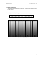
This manual represents numbers according to the notation described in the following table.
Hexadecimal and binary numbers are hyphenated at every four digits, if they are difficult to read
because of many digits being in each number. Letter x is used to represent an arbitrary numeral in
a number, like "1FxxH."
Number
Decimal
Notation rule
Example
Only numerals are indicated.
"10" represents number 10 in decimal.
A number is suffixed with letter H.
"10H" represents number 16 in decimal.
A number is suffixed with letter B.
"10B" represents number 2 in decimal.
number
Hexadecimal
number
Binary number
Number Notation Rules
MULTI is a trademark of Green Hills Software, Inc. in the US.
1
RTE-VR4310-PC
2.
User's Manual (Rev. 1.02)
FEATURES AND FUNCTIONS
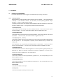
The overview of each function block of the RTE-VR4310-PC is shown below.
DC/DC
OSC
66.6 MHz
3.3 V
DC-JACK
5V
Mode
PROM-SW
RESET
SW
VR4310
166 MHz
CPU CONE
CPU board
32-bit bus
(SYSAD-bus)
SYSAD I/F
BUS
CONT
SRAM
DRAM
CONT
DRAM
TIMOUT
IRQ
CONT
64-bit bus
(Memory-bus)
LBUS
CONT
ROM
16-bit bus
(Local-bus)
TIM
EXT BUS
DB9
SCC
DB9
SCC
CN26
PRT
PORT
7SEG-LED
PORT
DIP-SW
C D A
IRQ
PORT
PCI I/F
PCI BUS
Block Diagram
Features
l ROM :
256 Kbytes (128K × 16 bits × 1)
l SRAM :
512 Kbytes (64K × 16 bits × 4)
l DRAM :
8, 16, or 32 Mbytes (standard of 8 Mbytes) installed in two 72-pin SIMM sockets
l RS-232C port (9-pin D-SUB connector): 2 channels
l Connection pins for ROM in-circuit debugger
2
RTE-VR4310-PC
3.
User's Manual (Rev. 1.02)
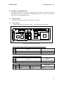
BOARD CONFIGURATION
The physical layout of the major components on the RTE-VR4310-PC board is shown below.
This
chapter explains each component.
JPOWER
JUSR
JEXT
DRAM SIMM x2
7SEG-LED
OSC1
SW4
LED
ROM
8254
SW-RST
SW3
SRAM
CH1
JPRN
PLD
SRAM
PLD
JC1
PLD
JSIO2
SRAM
16C552
PCI9060ES
PLD
CH0
SRAM
PLD
JSIO1
JC2
VR4310
CPU board
VR4310
SW1
Board Top View
3.1.
RESET SWITCH (SW RST)
SW RST is a reset switch. Pressing this switch causes the entire RTE-VR4310-PC board to be
reset.
3.2.
POWER SUPPLY CONNECTOR (JPOWER)
This is a DC jack used to receive power from an external supply.
The external power to be supplied to JPOWER should be one rated as listed below.
Voltage: 5 V
Current:
Maximum of 3.5 A
Mating connector: Type A (5.5 mm in diameter)
Polarity:
+5 V
GND
GND
+5 V
[Caution] When attaching an external power supply to the board, be careful about its connector
polarity.
3
RTE-VR4310-PC
3.3.
User's Manual (Rev. 1.02)
LED LAMPS
The table below indicates the states indicated by the LEDs.
LED
Name
Meaning
Remarks
LED1
TOVER
Bus time-out occurrence
LED2
POWER
Lights when the power is turned on
U36
-
Local bus only
7-segment LED (port output)
The 7-segment LED can be turned on or off by control from a general-purpose output port. For
details, see Section 5.4.3.
3.4.
DIVMODE SWITCH (SW1)
SW1 is used to specify the level of the DIVMODE[2..0] pins of the CPU. OFF represents 1, and
ON represents 0.
SW3 SW3 SW3
DIV
DIV
DIV
1
2
3
0
1
2
OFF
OFF
OFF
1
1
1
1:3
ON
OFF
OFF
0
1
1
1:2
OFF
ON
OFF
1
0
1
1:1.5
Remarks
Dividing ratio (Mclk/Pclk)
ON
ON
OFF
0
0
1
1:4
OFF
OFF
ON
1
1
0
1:3
ON
OFF
ON
0
1
0
1:2.5
OFF
ON
ON
1
0
0
1:6
ON
ON
ON
0
0
0
1:5
[Caution]
3.5.
(* represents a factory setting.)
*
Ensure that PCLK does not exceed the frequency guaranteed for VR4310 operation.
ROM-BANK SWITCH (SW3)
SW3 is used for ROM bank setting. Up to four banks, each consisting of 64K bytes, can be
allocated by manipulating the two high-order address bits of the ROM with this switch.
SW3
Remarks
32/64-bit operation (MD32/64)
(* represents the factory setting.)
1
ON
0: 64-bit mode
OFF 1: 32-bit mode
*
SW3
2
ROM address
3
ROM-A15
CPU-A16
Bank selection
ROM-A16
(* represents the factory setting.)
ON
ON
CPU-A17
With no bank
ON
OFF CPU-A16
ENDIAN
Endianess only
OFF
ON
MD32/64
Operation bit mode only
OFF
OFF ENDIAN
MD32/64
Full bank *
CPU-A16
4
RTE-VR4310-PC
User's Manual (Rev. 1.02)
SW3
Remarks
Endianess specification
(* represents the factory setting.)
4
ON
0: Little-endian
OFF 1: Big-endian
*
The installed monitor uses the banks as follows:
ROM address (16 bits)
Bank
For the MULTI monitor
0x00000-0x07FFF
Bank 0
For little-endian/64 bits
0x08000-0x0FFFF
Bank 1
For big-endian/64 bits
0x10000-0x17FFF
Bank 2
For little-endian/32 bits
0x18000-0x1FFFF
Bank 3
For big-endian/32 bits
Note
Note With PARTNER, only banks 2 and 3 are used.
3.6.
GENERAL-PURPOSE INPUT SWITCH (SW4)
SW4 is a data switch for general-purpose input ports.
corresponds to 1. When it is closed, it corresponds to 0.
When a switch contact is open, it
See Section 9.2.1 or 10.1.1 and Section
5.4.3 for details.
3.7.
USER-CONTROLLED PIN (JUSR)
The JUSR connector is a set of control pins which are set to use mainly the ROM in-circuit debugger.
It enables a reset and an interrupt from the ROM in-circuit debugger.
3.8.
JROMEM
Name
1
RST
RESET input (active-low)
Function
10 kΩ pull-up resistor
Remarks
2
NMI
NMI input (active-low)
10 kΩ pull-up resistor
3
IRQ
INT3 input (active-low)
10 kΩ pull-up resistor
4
GND
Ground
CPU TEST CONNECTORS (JC1, JC2)
The JC1 and JC2 connectors are connected to the CPU pins. These connectors are used for tests
such as signal measurement and for CPU board connection. For information about the connector
pin arrangement, see Chapter 11.
5
RTE-VR4310-PC
3.9.
User's Manual (Rev. 1.02)
SERIAL CONNECTORS (JSIO1, JSIO2)
JSIO1 and JSIO2 are connectors for the RS-232C interface controlled by the serial/parallel
controller (TL16C552A).
These are 9-pin D-SUB male connectors (D-SUB9) generally used with
the PC/AT. All signals at the connectors are at RS-232C level. The pin arrangement and signal
assignment are shown and listed below. For connection signals connected to the host PC, the
table gives the wirings for both the D-SUB9 pins and D-SUB25 pins on the host PC. (These are
general cross-cable wirings.)
1
2
6
3
7
4
8
5
9
JSIO1 and JSIO2 Pin Arrangement
Connector pin number on the host PC
JSIOx pin
Signal name
Input/output
D-SUB9
D-SUB25
1
DCD
Input
2
RxD (RD)
Input
3
2
3
TxD (SD)
Output
2
3
4
DTR (DR)
Output
1, 6
6, 8
5
GND
5
7
6
DSR (ER)
Input
4
20
7
RTS (RS)
Output
8
5
8
CTS (CS)
Input
7
4
9
RI
Input
JSIO 1 and JSIO2
[Memo]
On the panel, "CH0" is indicated for JSIO1, while "CH1" is indicated for JSIO2.
3.10. PARALLEL CONNECTOR (JPRT)
The JPRT connector is a printer connector controlled by the serial/parallel controller (TL16C552A).
The connector is a 26-pin header pin connector, so that a conversion cable is required to use the
connector as a general printer connector.
The figure below shows the pin arrangement and pin
number assignment of the connector.
2
4
6
8
10 12 14 16 18 20 22 24 26
1
3
5
7
9
11 13 15 17 19 21 23 25
JPRT Pin Arrangement
6
RTE-VR4310-PC
User's Manual (Rev. 1.02)
JPRT pin
Signal name
Input/output
1
STB-
Output
10 kΩ pull-up resistor
2
AUTO_FD-
Output
10 kΩ pull-up resistor
3
D0
Output
10 kΩ pull-up resistor
4
ERROR-
Input
10 kΩ pull-up resistor
5
D1
Output
10 kΩ pull-up resistor
6
INIT-
Output
10 kΩ pull-up resistor
7
D2
Output
10 kΩ pull-up resistor
8
SELECT_IN-
Output
10 kΩ pull-up resistor
9
D3
Output
10 kΩ pull-up resistor
11
D4
Output
10 kΩ pull-up resistor
13
D5
Output
10 kΩ pull-up resistor
15
D6
Output
10 kΩ pull-up resistor
17
D7
Output
10 kΩ pull-up resistor
19
ACK-
Input
10 kΩ pull-up resistor
21
BUSY
Input
10 kΩ pull-up resistor
23
PE
Input
10 kΩ pull-up resistor
Input
10 kΩ pull-up resistor
25SELEC
Remarks
T
26
NC
Not used
10, 12, 14,
16, 18, 20,
GND
22, 24
JPRT Connector Signal Table
3.11. OSCILLATOR SOCKET (OSC1)
OSC1 is a socket for an oscillator to generate clock pulses supplied to the CPU.
The socket is
factory-equipped with a 66.6-MHz oscillator.
[Caution] When you have to cut an oscillator pin for convenience, be careful not to cut it too
short, or otherwise the frame (housing) of the oscillator may touch a tine in the socket, resulting in a
short-circuit occurring.
3.12. DRAM-SIMM SOCKETS
The RTE-VR4310-PC has DRAM-SIMM sockets used to install 4 Mbytes (standard) of SIMM.
Each socket can hold a 72-pin 4-, 8-, or 16-Mbyte SIMM (known as a module for DOS/V machines),
so it is easy to expand the capacity of DRAM.
using an I/O port.
The capacity of installed SIMMs can be detected
(See Section 5.4.2.)
3.13. ROM SOCKET
The RTE-VR4310-PC has ROM sockets. Of these sockets, one is used to hold a 40-pin ROM chip
to provide standard 256 Kbytes (128K × 16 bits).
should be 150 ns or less.
The access time of the ROM chip used here
The ROM has four banks that can be selected switching addresses to
7
RTE-VR4310-PC
User's Manual (Rev. 1.02)
allow for selection of endian and operation mode. See Sections 3.4 and 9.2.1 for bank setting.
8
RTE-VR4310-PC
4.
User's Manual (Rev. 1.02)
CONNECTION TO THE HOST PC
4.1.1.
Standalone Use of the Board (RS-232C Connection)
The RTE-VR4310-PC can be connected to the host PC according to the following procedure.
<1> Get an RS-232C cable for connection with the host PC and an external power supply (+5 V, 4
A) on hand. Especially for the power supply, watch for its voltage and connector polarity.
See Sections 3.9 and 3.2 for RS-232C cable connection and the power supply connector,
respectively.
<2> Connect the board to the host PC via an RS-232C cable, using the JSIO1 (CH0) connector.
Also connect an external power supply to the JPOWER connector, then check that the
POWER-LED on the board lights.
If the LED does not light, turn off the power
immediately, and check the connection.
<3> Start the MULTI debugger on the host PC, and make a connection via the RS-232C interface.
If an error occurs, check that the serial cable and switch (baud rate, especially) are set
correctly.
[Cautions]
1. When the power is turned on, the CPU and heat sink become very hot.
After the power is
turned off, these devices remain hot for a while. Be careful not to touch them.
2. Place the board on insulating surface. If you place the board on a conductive surface while it
is turned on, the board may fail.
3. When the board is not inserted into the PCI slot, you must install the supplied PCI bus
terminator board.
4.1.2.
Insertion into the PCI Slot (PCI Bus Connection)
Insert the board into the PCI slot of the host PC by following the procedure below.
<1> Open the host PC cabinet, then insert the board into a PCI slot. Ensure that the board is
inserted securely, then fasten the board inplace with the fixing screw.
<2> Turn on the power to the host PC, and check that the POWER-LED on the board lights. If
the LED does not light, turn off the power to the host PC immediately and make a
check. Also check whether the host PC starts normally.
<3> Start the debugger on the host PC, and make a connection via the PCI bus. If an error
occurs, check that the board and software are installed correctly.
9
RTE-VR4310-PC
5.
User's Manual (Rev. 1.02)
HARDWARE REFERENCES
This chapter describes the hardware functions of the RTE-VR4310-PC.
5.1.
RESET
The factors listed below trigger a reset.
These factors cold-reset the CPU.
They also system-
reset the board control circuit.
5.2.
•
Power-on reset:
•
Reset switch: Generated by the reset switch (SW RST) on the board.
•
Reset from the host: Sent via the PCI bus controller at the request of the host PC.
•
JUSR-1:
Occurs when the power to the board is switched on.
Input at pin 1 (RST) of the JUSR connector.
INTERRUPT
The interrupt sources outside the CPU are listed below.
Interrupt
Source
Related section
NMI-
JUSR-2 (NMI)
Section 3.7
INT0-
Interrupt controller INT0M
Section 5.4.6
INT1-
Interrupt controller INT1M
Section 5.4.6
INT2-
EXT-BUS
Chapter 7
INT3-
JUSR-3 (IRQ)
Section 3.7
INT4-
Not used (fixed to 1)
External interrupts can be masked by hardware. (See Section 5.4.6.)
10
RTE-VR4310-PC
5.3.
User's Manual (Rev. 1.02)
ADDRESS MAP
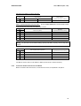
The address assignment of the board is shown below.
Virtual address
Physical address
0xFFFF FFFF
0xC000 0000
ROM
+0x1FFF
+0x1F00 0000
I/O
+0x1C00 0000
EXT-BUS +0x1A00 0000
kseg1
Not used
0xA000 0000
kseg0
+0x1800 0000
MEMCNT +0x1000 0000
0x8000 0000
DRAM
+0x0800 0000
0x4000 0000
SRAM
kseg0/1
0x0000 0000
+0x0000 0000
Address Map
When the MULTI monitor is used, programs are executed in the kernel space (8000-0000H to
BFFF-FFFFH) where a TLB map is not used. When a cache is used, 8000-0000H is added to
physical addresses to determine logical addresses. When cache is not used, A000-0000H is
added.
5.3.1.
SRAM Space (0000-0000H to 07FF-FFFFH)
The SRAM installed on the board has a real space of 512K bytes; the remaining area is the image
space.
To access the SRAM, set one or more wait cycles with the SRAM controller (SRAMC)
when the external bus clock speed is 40 MHz or higher. (See Section 5.4.1.) This space can be
accessed as a cache or noncache space.
5.3.2.
DRAM Space (0800-0000H to 0FFF-FFFFH, x800-0000H-xFFF-FFFFH)
The DRAM space is provided by a 72-pin DRAM-SIMM installed on the board. A 4M-byte SIMM
is installed as standard.
However, the memory size can be expanded by replacing this with an
8M-byte or 16M-byte SIMM. In an area other than the real space of DRAM-SIMM × 2 installed, it
is used as an image area. Set the DRAM access timing with the DRAM controller (DRAMC).
(See Section 5.4.2.) This space can be accessed as either a cache or non-cache space.
5.3.3.
MEM-CNT Space (1000-0000H to 17FF-FFFFH)
In this space, those registers that are used to exercise control on SRAM and DRAM memory
access are mapped. For details, see Section 5.4.1 and Section 5.4.2.
This space can be
accessed as a non-cache space.
11
RTE-VR4310-PC
5.3.4.
User's Manual (Rev. 1.02)
Not Used (1800-0000H to 19FF-FFFFH)
When this space is accessed, the bus cycle is forcibly terminated by the time-over ready signal to
generate a time-over interrupt, provided the time-over function is supported.
5.3.5.
EXT-BUS Space (1A00-0000H to 1BFF-FFFFH)
This space is used for the EXT-BUS external extension bus, and includes a 1M-byte real space:
the other area is an image space. This space can be accessed as a non-cache space.
5.3.6.
I/O Space (1C00-0000H to 1EFF-FFFFH)
This space is a memory-mapped I/O space where I/O devices for controlling each function on the
board are mapped. For details of I/O mapping, see Section 5.4.
This space is accessed as a
non-cache space.
5.3.7.
ROM Space (1F00-0000H to 1FFF-FFFFH)
The ROM installed on the board has a real space of 256K bytes (272048); the remaining area is
the image space.
The MULTI monitor is built into the installed ROM.
This space can be
accessed only as a non-cache space.
5.4.
I/O DETAILS
The I/O devices mapped onto the memory space include the memory access controller,
DUART/LPT, timer, interrupt controller, and PCI (I/O for communication) controller.
The figure
below shows the board I/O map.
Virtual address
PIC
reserved
reserved
TIMER
PRT
SCC1
SCC0
SWLED
0xBEFF FFFF
0xBE00 0000
PCI-CNT
I/O
0xBC00 0000
+0x07 0000
+0x06 0000
+0x05 0000
+0x04 0000
+0x03 0000
+0x02 0000
+0x01 0000
+0x00 0000
0xB800 0000
+0x00 07FF
DRAMC
+0x00 0400
0xB000 0000
MEM-CNT
SRAMC
+0x00 0000
I/O Map
These I/O devices assume access in the kernel noncache space, so that the description below uses
logical addresses.
[Memo]
The data bus connected to an I/O device is connected to D[7..0] unless otherwise
specified. This means that endianess needs to be considered when performing byte access. For
byte access in big-endian mode, 7 is added to the byte offset (because the bus internally handles
12
RTE-VR4310-PC
User's Manual (Rev. 1.02)
data as 64 bits).
5.4.1.
SRAM Controller (SRAMC)
The SWAIT register exercises wait control on the SRAM space. Using this register, 0 to 3 wait
cycles can be set in a read cycle. The table below indicates the register assignment.
Logical address
B000-0000H
Data bus
Register
SRAMC
SWAIT
D3
D2
D1
D0
0
0
SWAIT1
SWAIT0
SWAIT[1..0]: Sets the number of wait cycles for SRAM read.
SWAIT
Number of SRAM read wait cycles
1
0
0
0
0
0
1
1
1
0
2
1
1
3
[Memo]
(Reset value)
Zero can be set as the number of SRAM read wait cycles when the external bus clock
(SysClock) speed is 40 MHz or less (with the clock width being 25 ns or more). This can be
found from the following formula:
Address delay + SRAM access time + data setup=
5 ns
5.4.2.
+
17 ns
+
3 ns
= 25 ns
DRAM Controller (DRAMC)
DRAMC exercises DRAM access control.
DRAMC sets an RAS/CAS width as well as the
operation modes. The table below indicates the register assignment.
Logical address
Data bus
Register
D3
D2
D1
D0
B000-0400H
DRAMC
RCAS
0
0
RCAS1
RCAS0
-0500H
DRAMC
MRAS
0
MRAS2
MRAS1
MRAS0
-0600H
DRAMC
PRAS
0
PRAS2
PRAS1
PRAS0
-0700H
DRAMC
DMODE
PD1
PD2
EDOEN
HITEN
RCAS[1..0]: Sets the number of CAS clock cycles for DRAM read. The number of clock cycles
used is the specified value (0 to 3), plus 1.
RCAS
Number of CAS read clock cycles
1
0
0
0
1 SYSCLK
0
1
2 SYSCLKs
1
0
3 SYSCLKs
1
1
4 SYSCLKs
(Reset value)
[Memo] The number of CAS precharge clock cycles is fixed to one clock cycle.
13
RTE-VR4310-PC
User's Manual (Rev. 1.02)
MRAS[2..0]:
Sets the number of DRAM RAS access clock cycles. The number of clock cycles
used is the specified value (0 to 7), plus 1.
MRAS
Number of RAS access clock cycles
2
1
0
0
0
0
1 SYSCLK
0
0
1
2 SYSCLKs
0
1
0
3 SYSCLKs
0
1
1
4 SYSCLKs
1
0
0
5 SYSCLKs
1
0
1
6 SYSCLKs
1
1
0
7 SYSCLKs
1
1
1
8 SYSCLKs
PRAS[2..0]: Sets the number of DRAM RAS precharge clock cycles.
(Reset value)
The number of clock
cycles used is the specified value (0 to 7), plus 1.
PRAS
Number of RAS precharge clock cycles
2
1
0
0
0
0
1 SYSCLK
0
0
1
2 SYSCLKs
0
1
0
3 SYSCLKs
0
1
1
4 SYSCLKs
1
0
0
5 SYSCLKs
1
0
1
6 SYSCLKs
1
1
0
7 SYSCLKs
1
1
1
8 SYSCLKs
HITEN:
(Reset value)
Sets whether to use the page hit access function of the DRAM controller. If HITEN = 1,
high-speed page access is performed when RAS is held after DRAM access completion, and a
match is found with the load address for the next DRAM access (DRAM page address). However,
the RAS cycle hold is released by a refresh request.
If there is no hit, normal access is
performed after a precharge cycle.
HITEN
DRAM page hit
0
Not used
1
Used
EDOEN:
(Reset value)
Sets whether the type of DRAM is FPM or EDO. When EDOEN = 1, the data ready
signal at burst read time represents the CAS precharge period. So, the CAS width can be
reduced by one clock cycle.
EDOEN
DRAM type
0
FPM-DRAM
1
EDO-DRAM
(Reset value)
14
RTE-VR4310-PC
User's Manual (Rev. 1.02)
PD[1..2]: Allows the type pins PD[1..2] of DRAM-SIMM to be read (read only).
5.4.3.
PD1
PD2
DRAM-SIMM size
0
0
4M bytes
0
1
16M bytes
1
0
(Reserved)
1
1
8M bytes
(Standard)
General-Purpose I/O Port (SWLED)
The general-purpose I/O port exercises on/off control on the 7-segment LED and reads the setting
of the DIP switch (SW4) on the board,
Logical address
Data bus
Description
D7
D6
D5
D4
D3
D2
D1
D0
BC00-0000H
Input
SW4
-8
SW4
-7
SW4
-6
SW4
-5
SW4
-4
SW4
-3
SW4
-2
SW4
-1
0 = ON
1 = OFF
BC00-0000H
Output
7SEG
-DP
7SEG
-G
7SEG
-F
7SEG
-E
7SEG
-D
7SEG
-C
7SEG
-B
7SEG
-A
0 = Turned on
1 = Turned off
The figure below shows the bit correspondence of the 7-segment LED.
A
F
B
G
E
C
D
DP
[Caution]
Data output to the 7-segment LED cannot be read.
15
RTE-VR4310-PC
5.4.4.
User's Manual (Rev. 1.02)
Serial/Parallel I/O (SCC0/1, LPT)
As the serial/parallel I/O, the TL16C552A manufactured by TI is used. This device includes two
serial controllers compatible with NS16550 and a parallel port compatible with the PC/AT (PS2)
standard. The table below indicates the assignment of each TL16C552A register.
Logical address
Register
BC01-0000H
Supplement
RBR/THR/DLL
-0100H
IER/DLM
-0200H
IIR/FCR
-0300H
LCR
-0400H
MCR
-0500H
LSR
-0600H
MSR
-0700H
SCC0
SCR
BC02-0000H
RBR/THR/DLL
-0100H
IER/DLM
-0200H
IIR/FCR
-0300H
LCR
-0400H
MCR
-0500H
LSR
-0600H
MSR
-0700H
SCR
BC03-0000H
LPD
-0100H
LPS
-0200H
LPC
-0300H
-
SCC1
LPT
The frequency of the clock applied to the serial controller is 16 MHz. For the function of each
register, refer to the manual provided with the TL16C552A.
5.4.5.
Timers
The uPD71054 produced by NEC is installed as a timer. The uPD71054 is compatible with the
i8254 produced by Intel. It has three timer counters. These timers are used for various types of
control.
Each register of the uPD71054 is assigned as listed below.
Logical address
Register
Remarks
BC04-0000H
PCNT0
Timer 0
-0100H
PCNT1
Timer 1
-0200H
PCNT2
Timer 2
-0300H
PCNTL
Control
For the function of each register, refer to the manual provided with the uPD71054 (i8254).
The
timers are used as indicated below.
Timer
Clock
Mode
0
2 MHz
2
Timer interrupt 0.
Application
Used by the monitor.
1
2 MHz
2
Timer interrupt 1.
Usable by the user.
2
2 MHz
2
DRAM refresh
16
RTE-VR4310-PC
5.4.6.
User's Manual (Rev. 1.02)
Interrupt Controller (PIC)
The PIC mainly exercises interrupt-related control. The table below indicates the assignment of
registers.
Logical address
Data bus
Register
D7
D6
D5
D4
D3
D2
D1
D0
BC07-0000H
PIC
INT0M
IM07
IM06
IM05
IM04
IM03
IM02
IM01
IM00
-0100H
PIC
INT1M
IM17
IM16
IM15
IM14
IM13
IM12
IM11
IM10
-0200H
PIC
INTR
IR7
IR6
IR5
IR4
IR3
IR2
IR1
IR0
-0300H
PIC
INTEN
0
0
0
0
TOVEN
0
INTEN NMIEN
The INT0M and INT1M registers mask interrupts applied to INT0 and INT1, respectively. When
the IM0x or IM1x bit is set to 1, the interrupt is enabled. When multiple bits are selected, each
OR value activates an interrupt.
The INTR register is an interrupt status register, for which 1 is read whenever there is an interrupt
request. This does not depend on the state of masking. To clear an edge interrupt request, the
corresponding bit of this register must be set to 1.
The table below indicates the interrupt source assigned to each bit of IM0[0..7], IM1[0..7], and
IR[0..7].
IM0, IM1, IR
Interrupt source
Request level
0
Timer 0 (mode 2)
Edge (rising)
1
Serial 0
Level (low)
2
Host PC (PCI communication)
Level (low)
3
Time-over
Level (low)
4
Timer 1 (mode 2)
Edge (rising)
5
Serial 1
Level (low)
6
Parallel (printer)
Level (low)
7
Not used (fixed to 0)
-
The INTEN register enables or disables each type of interrupt.
NMIEN:
Sets a mask for the non-maskable interrupt (NMI).
By masking with this bit, NMI can
be disabled by hardware. At this time, the NMI pin is high.
NMIEN
NMI
0
Sets a mask.
1
Does not set a mask.
INTEN:
(Reset value)
Sets a mask for the external interrupts (INT0-3) used on the board. By masking with
this bit, INT0-3 can be disabled by hardware. At this time, the INTx pin is high.
INTEN
INT0 to INT5
0
Sets a mask.
1
Sets no mask.
(Reset value)
17
RTE-VR4310-PC
TOVEN:
User's Manual (Rev. 1.02)
Sets whether to use the timer-over function. The time-over function is applied to local
bus access only. If a bus cycle lasts for about 8us, the cycle is terminated forcibly.
TOVEN
5.4.7.
Time-over
0
Does not use the time-over function.
1
Uses the time-over function.
(Reset value)
PCI Controller
For PCI bus communication, the PCI9060ES manufactured by PLX Technology is used. The
PCI9060ES uses endianess control pins, so that the internal registers support both big-endian
and little-endian modes.
18
RTE-VR4310-PC
6.
User's Manual (Rev. 1.02)
BUS CYCLE TIMING
The RTE-VR4310-PC controls the bus cycle according to the type of device used (such as SRAM,
DRAM, ROM, or I/O). This section describes the timing of each access cycle.
6.1.
SRAM ACCESS
In the SRAM read cycle, access is performed with 0 to 3 wait cycles inserted according to the setting
of the SRAM-SWAIT register (see Section 5.4.1). Access with no wait cycle inserted is possible
only when the bus clock (SYSCLK) speed is 40 MHz or less.
0
1
2
3
4
5
6
7
8
9
10 11 12 13 14 15 16 17 18 19
SYSCLK
SYSAD
SYSCMD
A
EOD
READ
PVALIDEOKPMASTEREVALIDSRAM-ADDR
A0
A1
A2
A3
SRAM-DATA
Ws Ws
Ws Ws
Ws Ws
Ws Ws
SRAM CSSRAM OE-
Read (burst 4 words)
SRAM Read Cycle (SWAIT[ ] = 2)
The states are explained below in the order of clock cycle numbers.
0
: An external CPU read cycle starts. Usually, EOK- is inactive.
1-3 : EOK- is activated.
3-4 : The wait cycles (two wait cycles in this example) set with SWAIT are inserted.
5
: SRAM data is determined. The SRAM address is changed in the next cycle (sub-address).
5-6 : The data is latched and held, then EVALID- is returned after two clock cycles.
7-15 : This cycle is repeated until the end of the data (EOD) is reached.
19
RTE-VR4310-PC
User's Manual (Rev. 1.02)
An SRAM write cycle follows the output data rate of the CPU. For SRAM, a cycle is started by
returning EOK- one clock cycle after address determination.
0
1
2
3
4
5
6
7
8
9
10 11 12 13 14 15 16 17 18 19
SYSCLK
A
SYSAD
SYSCMD
D xx
D xx
D xx
Write
D xx
E OD
PVALIDEOKSRAM-ADDR
A0
A1
A2
A3
SRAM-DATA
SRAM CSSRAM WE-
Write (burst 4 words)
SRAM Write Cycle (DataRate = DxxDxxDxxDxx)
The states are explained below, in the order of clock cycle numbers.
0-1 : Usually, EOK- is inactive.
2-3 : An SRAM write cycle is determined.
4
: First data output.
This data is latched and held, then the EOK- is deactivated and SRAM
WE is activated, starting from the next cycle.
5-6 : SRAM write cycle. (The Dxx data rate is fixed, so that the write pulse width is 2 clock
cycles.) WE- is deactivated before the next data is latched, then the SRAM address is
changed in the next cycle (sequential address).
7-15 : The write cycle is repeated.
16
: In the cycle after the last data (EOD) is written, RDRDY is activated.
20
RTE-VR4310-PC
6.2.
User's Manual (Rev. 1.02)
DRAM ACCESS
For the DRAM, the RAS/CAS width can be controlled according to the setting of the DRAM
controller. (See Section 5.4.2.)
The figure below shows a DRAM read cycle when EDOEN = 0 (FPM-DRAM).
The figure below
shows the highest-speed cycle where the DRAM read cycle does not overlap a refresh cycle or RAS
precharge of the previous DRAM access.
0
1
2
3
4
5
6
7
8
9
10 11 12 13 14 15 16 17 18 19 20
SYSCLK
A
SYSAD
SYSCMD
READ
EOD
PVALIDEOKPMASTEREVALIDDRAM-ADDR
RA
CA0
CA1
CA2
CA3
DRAM-DATA
PRAS
DRAM RAS-
MRAS
RCAS
RCAS
RCAS
DRAM CASDRAM WE-
Read (burst 4 words)
DRAM Read Cycle (RCAS[ ] = 1, MRAS[ ] = 4, PRAS[ ] = 3, EDOEN = 0)
The states are explained below in the order of clock cycle numbers.
0
: EOK- is activated.
1
: A DRAM read cycle starts.
2-3
: RAS is activated as soon as the row address is determined.
4-5
: Upon switching to a column address, CAS is activated two clock cycles after RAS.
7
: The first read data is determined. At this time, CAS is held until cycle DRAMC-MRAS+1.
8-9
: Data is latched and held, then EVALID- is returned after two clock cycles.
10-18 : The cycle is repeated until the last data (EOD) is reached. When HITEN = 1, RAS
remains active.
21
RTE-VR4310-PC
User's Manual (Rev. 1.02)
When EDOEN = 1, a CAS precharge cycle occurs with the determination of the read data delayed
by one clock cycle.
In this case, the values of DRAMC-MRAS and DRAMC-RCAS may be
decremented by 1, depending on the SYSCLK width. With EDO-DRAM, data is held until RAS is
deactivated, so control is exercised to turn off the data output in the last cycle according to the WEsignal.
0
1
2
3
4
5
6
7
8
9
10 11 12 13 14 15 16 17 18 19 20
SYSCLK
SYSAD
SYSCMD
A
READ
EOD
PVALIDEOKPMASTEREVALIDDRAM-ADDR
RA
CA0
CA1
CA2
CA3
DRAM-DATA
DRAM RASDRAM CASDRAM WE-
Read (burst 4 words)
DRAM Read Cycle (RCAS[ ] = 0, MRAS[ ] = 3, PRAS[ ] = 3, EDOEN = 1)
The states are explained below in the order of clock cycle numbers.
0
: EOK- is activated.
1
: A DRAM read cycle starts.
2-3
: RAS is activated as soon as the row address is determined.
4-5
: Upon switching to a column address, CAS is activated two clock cycles after RAS.
6-7
: The first read data is determined.
8-9
: Data is latched and held, then VALIDIN is returned after two clock cycles. During the two
At this time, CAS is held until the cycle DRAMC-
MRAS+1.
clock cycles, data parity calculation is performed for the SYSADC bus.
10-15 : The cycle is repeated until the last data (EOD) is reached. When HITEN = 1 or 14, RAS is
held active. By activating WE-, the data is placed in the high-impedance state.
22
RTE-VR4310-PC
User's Manual (Rev. 1.02)
A DRAM write cycle follows the output data rate of the CPU. For DRAM, a cycle is started by
returning EOK- one clock cycle after RAS is activated. For DRAM write, an early write cycle is
used.
0
1
2
3
4
5
6
7
8
9
10 11 12 13 14 15 16 17 18 19
SYSCLK
SYSAD
SYSCMD
A
D xx
D xx
D xx
Write
D xx
EOD
PVALIDEOKDRAM-ADDR
RA
CA0
CA1
CA2
CA3
DRAM-DATA
DRAM RASDRAM CASDRAM WE-
Write (burst 4 words)
DRAM Write Cycle (DataRate = DxxDxxDxxDxx)
The states are explained below in the order of clock cycle numbers.
0
: Usually, EOK- is inactive.
1-2 : A DRAM write cycle is determined, and the row address and RAS are activated.
3-4 : EOK- is activated one clock cycle after RAS is activated, and a CPU external write cycle
starts two clock cycles after EOK-.
5
: First data output. This data is latched and held, after which the EOK- is deactivated.
7-8 : DRAM CAS write cycle. (The Dxx data rate is fixed, so that the CAS write pulse width is 2
clock cycles.)
WE is deactivated before the next data is latched, then the DRAM address is
changed in the next cycle (sequential address).
9-16 : The write cycle is repeated.
The last data is written to 15, then RAS and WE are
deactivated after two clock cycles. When HITEN = 1, RAS is held active.
23
RTE-VR4310-PC
User's Manual (Rev. 1.02)
When HITEN = 1, RAS is held after DRAM access. If a row address match (hit) occurs in the next
access, a CAS cycle is executed immediately, reducing the number of access clock cycles.
However, this is effective only in a read cycle. In a write cycle, even if a match occurs, EOK- is
delayed by one clock cycle because of address comparison. If a mismatch (unhit) occurs, access
based on a normal RAS/CAS cycle is performed after RAS precharge, resulting in an increased
overhead.
0
1
2
3
4
5
6
7
8
9
10 11 12 13 14 15 16 17 18 19
SYSCLK
SYSAD
A
A
SYSCMD
DRAM-ADDR
A
A
RCAS
DRAM RASDRAM CAS-
RCAS
Page Hit
PRAS
MRAS
DRAM RASDRAM CAS-
RCAS
Page UnHit
DRAM Page Hit/UnHit Access Cycle (HITEN = 1)
The states are explained below in the order of clock cycle numbers.
0-4 : Normal DRAM access cycle
5 : The next DRAM write access starts.
6 : A comparison is made with the previous row address.
7-8 : If a match is found, read CAS is activated starting with the next cycle.
If a mismatch is found,
RAS is deactivated, after which RAS precharge is performed.
9 : If a match is found, read CAS enables page mode access starting with the first cycle.
14 : If a mismatch is found, read CAS enables a normal RAS access cycle.
When the DRAM is refreshed, a CAS before an RAS refresh cycle is performed at intervals of about
15 us (according to the setting of timer 2).
SYSCLK
MRAS
PRAS
PRAS
MRAS
DRAM RASDRAM CAS15 us
DRAM Refresh Cycle (MRAS[ ] = 4, PRAS[ ] = 3)
24
RTE-VR4310-PC
6.3.
User's Manual (Rev. 1.02)
LOCAL BUS ACCESS
The local bus has a 16-bit data width. A cycle is generated by the local bus controller from a clock
(fixed at 32 MHz) that is not synchronous with the CPU. The local bus allows single access only.
(A burst cycle is handled as a bus error upon a read, but is ignored upon a write.)
The control
circuit of the CPU issues a request to the local bus controller, and bus arbitration is performed
based on the acknowledgement signal returned from the controller.
In a read cycle on the local bus, a request is issued to the local bus controller, and an
acknowledgement signal is returned to the controller upon data read completion.
0
1
2
3
4
5
6
7
8
9
10 11 12 13 14 15 16 17 18 19
SYSCLK
SYSAD
A
SYSADC
SYSCMD
READ
EOD
PVALIDEOKPMASTEREVALIDLOCAL ADDR
A
LOCAL DATA
LOCALREQLOCALACK-
Read (Single)
Local Read Cycle
The states are explained below in the order of clock cycle numbers.
0-3
: Access to the local bus starts.
4 and up : After checking that the acknowledgement signal (LOCALACK) is inactive, an access
request (LOCALREQ) is issued to the local bus.
8
: The local bus controller recognizes the occurrence of a request, then latches the
address, and starts a read cycle.
11
: Upon the completion of a read from the local bus, an acknowledgement signal is
returned.
13
: The request is released by synchronizing the acknowledgement signal for two clock
cycles, after which the data is latched and held, then EVALID- is returned after two
clock cycles.
17
: The local bus controller recognizes the release of the request, then deactivates the
acknowledgement signal.
25
RTE-VR4310-PC
User's Manual (Rev. 1.02)
A write to the local bus is performed similarly according to request/acknowledgement arbitration.
However, an acknowledgement signal returned from the local bus controller is handled as a write
permission, and data is written in an acknowledge cycle after the request is released. At this time,
the CPU can execute a second cycle other than a local bus cycle.
0
1
2
3
4
5
6
7
8
9
10 11 12 13 14 15 16 17 18 19
SYSCLK
SYSAD
SYSCMD
A
D
Write
E OD
PVALIDEOKLOCAL ADDR
A
LOCAL DATA
DATA WRLOCALREQLOCALACK-
Write (Single)
Local Write Cycle (DataRate = Dxx)
The states are explained below in the order of clock cycle numbers.
0-1
: A write access to the local bus starts.
2
: After checking that the acknowledgement signal (LOCALACK) is inactive, an access
request (LOCALREQ) is issued to the local bus.
5
: The local bus controller recognizes the occurrence of a request, then latches the address
and returns an acknowledgement signal.
7
: A write cycle is executed by activating EOK- for the CPU and synchronizing the
acknowledgement signal for two clock cycles.
12-13 : After write data has been written to the local bus, the request is deactivated.
14-15 : The local bus controller recognizes the release of the request, then deactivates the
acknowledgement signal, and writes data.
26
RTE-VR4310-PC
User's Manual (Rev. 1.02)
Upon single access from the CPU, the local bus controller accesses the local bus.
data access from the CPU is 64 bits maximum, and the local bus is 16 bits wide.
The width of
So, bus sizing is
performed, and up to four bus cycles are generated.
The figure below shows the timing chart of a read cycle.
0
1
2
3
4
5
6
7
8
9
10 11 12 13 14 15 16 17 18 19 20
LCLK (32 MHz)
LOCALREQLOCALACKCPU DATA
LOCAL ADDR
LOCAL DATA
LW/RLDSTBLRDY
Read
Local Bus Read Cycle
The states are explained below in the order of clock cycle numbers.
0-1 : A read request to the local bus starts.
2
: The local bus controller latches the address and read status (LW/R-).
4
: Access is started by activating the data strobe (LDSTB) two LCLKs after the address is
latched.
6-7 : When the local bus ready signal (LRDY) is returned, the data strobe is deactivated, and the
CPU data is latched.
8-14 : If the CPU data size is greater than 16 bits, the read cycle is repeated by switching to the
next address.
15
: Once all the read cycles have been completed and the CPU data has been determined, an
acknowledgement signal is returned.
27
RTE-VR4310-PC
User's Manual (Rev. 1.02)
The figure below shows the timing chart for a write cycle.
0
1
2
3
4
5
6
7
8
9
10 11 12 13 14 15 16 17 18 19 20
LCLK (32 MHz)
LOCALREQLOCALACKCPU DATA
LOCAL ADDR
LOCAL DATA
LW/RLDSTBLRDY
Write
Local Bus Write Cycle
The states are explained below in the order of clock cycle numbers.
0-1
: A write request to the local bus starts.
2
: The local bus controller returns an acknowledgement signal, and latches the address and
write status (LW/R-).
3-5
: Data is determined two LCLKs after the request is deactivated, then access is started by
8-9
: When the local bus ready signal (LRDY) is returned, the data strobe is deactivated, and the
activating the data strobe (LDSTB) in the next cycle.
write cycle is terminated.
10-15 : If the CPU data size is greater than 16 bits, the write cycle is repeated by switching to the
next address and data.
17
: Once all the write cycles have been completed, the next request is accepted.
28
RTE-VR4310-PC
User's Manual (Rev. 1.02)
The local bus ready signal (LRDY) depends on the space allocated to the local bus space.
The
table below lists the local bus ready signals.
Local bus space
ROM
Ready signal
Local bus clock 32 MHz
Remarks
5 LCLKs (About 150 ns)
Fixed
Note 1
7 LCLKs (About 210 ns)
Fixed
EXT-BUS
ERDY (EXT-BUS ready)
I/O
PCI controller
Not allocated
Note 2
PCI controller ready signal
Time-over ready (About 8 us)
Fixed
Notes 1. With an I/O device, the inactive period of the RD/WR signal in successive accesses is
predetermined.
So, by hardware, the local bus controller supports the I/O access
disable period of 7 LCLKs (about 210 ns) after an I/O access.
Thus, wait cycles need
not be inserted by software after an I/O access.
2. When the time-over function is enabled (See Section 5.4.6.)
6.4.
MEMORY CONTROLLER REGISTER ACCESS
Access to SRAM and DRAM memory controller registers is allowed using only a single cycle. (A
burst cycle is handled as a bus error in a read, and is ignored in a write.) The timing of access to
this space is the same as the SRAM access timing with one wait cycle. (See Section 6.1.)
29
RTE-VR4310-PC
7.
User's Manual (Rev. 1.02)
EXT-BUS SPECIFICATION
The EXT-BUS is used to expand memory and I/O units. The local bus on this board is connected to
the JEXT connector.
7.1.
CONNECTOR SPECIFICATION
The appearance and the pin arrangement of the JEXT connector are shown below.
59 57 55 53 51 49 47 45 43 41 39 37 35 33 31 29 27 25 23 21 19 17 15 13 11 9
7
5
3
1
60 58 56 54 52 50 48 46 44 42 40 38 36 34 32 30 28 26 24 22 20 18 16 14 12 10 8
6
4
2
JEXT Connector Pin Arrangement
No.
Signal name
No.
Signal name
No.
Signal name
No.
Signal name
1
+5V
2
+5V
31
GND
32
GND
3
D0
4
D1
33
A8
34
A9
5
D2
6
D3
35
A10
36
A11
7
D4
8
D5
37
A12
38
A13
9
D6
10
D7
39
A14
40
A15
11
GND
12
GND
41
+5V
42
+5V
13
D8
14
D9
43
A16
44
A17
15
D10
16
D11
45
A18
46
A19
17
D12
18
D13
47
BHE-
48
GND
19
D14
20
D15
49
GND
50
RD-
21
+5V
22
+5V
51
WR-
52
RESET-
23
A0
24
A1
53
GND
54
GND
25
A2
26
A3
55
READY
56
INT-
27
A4
28
A5
57
GND
58
GND
29
A6
30
A7
59
LBCLK
60
GND
JEXT Connector Signal Arrangement
30
RTE-VR4310-PC
7.2.
User's Manual (Rev. 1.02)
SIGNALS
Signal name
Input/
Function
output
Remarks
+5V
-
Supply voltage of +5 V
GND
-
Ground
A[1..19]
Output
Address bus signal
A0
Output
Byte low enable signal. When this signal is low, D[0..7] is enabled.
BHE-
Output
Byte high enable signal. When this signal is low, D[8..15] is enabled.
Input/
Data bus signal used for CPU data bus buffering
D[0..15]
Note 3
output
RD-
Output
Read cycle timing signal, which becomes active only when the EXT-BUS
space is accessed.
WR-
Output
READY
Input
Write cycle timing signal, which becomes active only when the EXT-BUS
space is accessed.
Positive-logic ready signal indicating the end of a cycle. It is valid only for the
Note 1
EXT-BUS space. It is pulled up with a 1 kΩ resistor on the board.
INT-
Input
Active-low interrupt request signal, which is connected to the INT2- pin of
the CPU via a buffer. It is pulled up with a 1 kΩ resistor on the board.
RESET-
Output
Active-low system reset signal
LCLK
Output
Bus clock signal (fixed at 32 MHz)
Note 2
EXT-BUS Signals
Notes 1. To ensure that the CPU recognizes READY, READY must be held active until RD- or WRis deactivated.
2. This clock signal differs on other RTE series evaluation boards. When compatibility is
important, this clock signal should not be used for circuit design.
3. Note that the address/data bus correspondence varies according to the VR4310 endian
mode.
VR4310 ADDR/DATA
A+0
D31-24
D23-16
D15-08
D07-00
EXT-BUS ADDR/DATA
A19-A1
A+0
A+2
BHE-
A0
A19-A1
BHE-
A0
D31-24
D23-16
A+0
D15-08
D08-00
D15-08
D08-00
A+2
D31-24
D23-16
BIG-ENDIAN
LITTLE-ENDIAN
31
RTE-VR4310-PC
7.3.
User's Manual (Rev. 1.02)
EXT-BUS TIMING
The timing of the EXT-BUS is shown below.
A[0..19]
BHE-
A[0..19]
BHET1
T3
T2
T10
RD-
T11
RDT4
T12
WR-
T13
WRT5
T6
T14
Din
D[0..15]
T7
D[0..15]
T8
T9
T16
READY
T15
Dout
T17
T18
READY
Read cycle
Write cycle
EXT-BUS Bus Cycle
Symbol
Description
MIN. (ns)
T1
RD address setup time
T2
RD address hold-up time
0
T3
RD cycle time
50
T4
RD cycle interval
20
T5
RD data setup time
15
T6
RD data hold time
0
T7
RD READY WAIT setup time
0
T8
RD READY setup time
0
T9
RD READY hold time
0
T10
WR address setup time
0
T11
WR address hold time
20
T12
WR cycle time
50
T13
WR cycle interval
20
T14
WR data delay time
0
T15
WR data hold time
20
T16
WR READY WAIT setup time
0
T17
WR READY setup time
0
T18
WR READY hold time
0
MAX. (ns)
0
20
EXT-BUS AC Specifications
32
RTE-VR4310-PC
8.
User's Manual (Rev. 1.02)
SOFTWARE
8.1.
INTERRUPT PROGRAMMING
This section describes how a user program can handle interrupts by using the monitor.
8.1.1.
Interrupt Library
With the VR4310, a set of general exception interrupt vectors is allocated. The monitor also uses
interrupts.
So, the vectors are shared. For this reason, an interrupt library (attached sample
programs:
Intvect.c, IntHdr.s/mip) is provided.
The library hooks vectors and exercises table management for each exception to execute the
exception handling routine. The eight library functions are described below.
int InitIrqVect(void):
This function hooks an interrupt vector and initializes the table. This function returns 0 upon
normal termination.
If an error occurs, this function returns a negative error code.
int TermIrqVect(void):
This function returns an interrupt vector to the original state. This function returns 0 upon normal
termination.
If an error occurs, this function returns a negative error code.
int SetIrqVect(int no, int func):
This function registers function func (by casting to int type) in the interrupt handling table specified
by the argument no. For the argument no, specify a macro defined in INT_xxx format in the
intvect.h file.
If 0 is specified in func, the previously set handling routine can be disabled. This function returns
0 upon normal termination.
If an error occurs, this function returns a negative error code.
int GetIrqVect(int no):
This function returns a function address registered in the interrupt handling table specified by the
argument no.
When 0 is returned, it means that no function is registered.
If an error occurs,
this function returns a negative error code (odd number).
void SetIPnBit(int IPn):
This function enables an interrupt specified by argument IPn. (The corresponding bit of the
status register is set to 1.)
void ResIPnBit(int IPn):
This function disables an interrupt specified by argument IPn. (The corresponding bit of the
status register is set to 0.)
void ei(void):
This function enables all interrupts.
void di(void):
This function disables all interrupts other than NMI.
33
RTE-VR4310-PC
8.1.2.
User's Manual (Rev. 1.02)
Interrupt Routine
A user-coded interrupt handling routine assumes the use of a C function of type int (without the
_interrupt qualifier).
For correct debugging of an interrupt handling routine, disable the
corresponding interrupt at the start of the interrupt handling routine, and enable the interrupt
before the end of the interrupt handling routine.
Once handling has been completed, 0 is
returned. When control is returned to the monitor, a value of other than 0 is returned.
8.1.3.
Sample Program
A sample program for interrupt handling using the user control pin IRQ (INT-3) is provided below.
#include "intvect.h"
int main( void )
{
.
.
/* --- can not Break & Step --- */
di();
/* disable all interrupt */
InitIrqVect();
/* save original vector code & set new vector */
SetIrqVect( VECT_IP4, (int)IrqJusr ); /* set function vector table */
SetIPnBit( SR_IP4 );
/* set IP4 bit */
ei();
/* enable all interrupt */
/* --- --- */
.
.
/* process */
.
/* --- can not Break & Step --- */
di();
/* disable all interrupt */
ResIPnBit( SR_IP4 );
/* reset IP4 bit */
SetIrqVect( VECT_IP4, 0);
/* remove vector */
TermIrqVect();
/* restore original vector code */
ei();
/* enable all interrupt */
/* --- --- */
.
.
exit;
}
/*** irqJusr ***/
int IrqHusr( struct _irq_stack *istack )
{
int to_monitor;
/*
/* --- can not Break & Step --- */
ResIPnBit( SR_IP4 );
/*
ei();
/*
/* --- --- */
.
.
/*
.
/* --- can not Break & Step --- */
di();
SetIPnBit( SR_IP4 );
/*
If( to_monitor != 0 ) {
return 1;
/*
}
return 0;
/*
}
flag */
Disable JUSR-IRQ interrupt */
Enable multiple interrupt */
interrupt operation */
Enable JUSR-IRQ interrupt */
request monitor handler */
normal end */
34
RTE-VR4310-PC
8.2.
User's Manual (Rev. 1.02)
ROM PROGRAMMING
When creating user programs in the ROM on this board, use the information provided in this
section.
8.2.1.
Initialization
After initializing the processor registers, the reset processing routine sets the required wait cycles
with the memory access controller. When using DRAM, refresh it by setting timer 2.
<Internal initialization of the processor>
(Use 0 for offset in little-endian mode. Use 7 for offset in big-endian mode.)
8.2.2.
[0xB8000000+offset].b <= 1
... SRAM: 1 wait cycle
[0xB8000400+offset].b <= 1
... DRAM CAS width: 2 clock cycles
[0xB8000500+offset].b <= 4
... DRAM RAS access: 5 clock cycles
[0xB8000600+offset].b <= 3
... DRAM RAS precharge: 4 clock cycles
[0xB8000700+offset].b <= 0
...
[0xBC040300+offset].b <= 0xb4
... Timer 2 mode 2 (set at intervals of about 15 us)
[0xBC040200+offset].b <= 0x1f
... Timer 2 low-order count
[0xBC040200+offset].b <= 0x00
... Timer 2 high-order count
EDO/HIT disable
Interrupt
When using interrupts, initialize the peripheral I/O, then assign the required interrupts with the
interrupt mask register. Moreover, enable all of INT/NMI.
Example of using timer interrupt 1:
<Disable processor interrupts>
(Use 0 for offset in little-endian mode. Use 7 for offset in big-endian mode.)
[0xBC040300+offset].b <= 0x74
... Timer 1 mode 2 (set at intervals of 10 ms)
[0xBC040200+offset].b <= 0x20
... Timer 1 low-order count
[0xBC040200+offset].b <= 0x4e
... Timer 1 high-order count
[0xBC070100+offset].b <= 0x10
... Enable INT1M timer 1
[0xBC070200+offset].b <= 0x10
...
[0xBC070300+offset].b <= 0x02
... Enable INT
Clear INTR timer 1 interrupt
<Enable processor interrupts>
[Memo]
Before NMI can be used to control (break) the connected ROM emulator, NMI must be
enabled with the monitor program of the emulator.
35
RTE-VR4310-PC
8.2.3.
User's Manual (Rev. 1.02)
ROM Data Allocation
When ROM data is written, the correspondence between the ROM address bank and data bus
must be considered. With the 272,048 type (128K × 16 bits), a bank occurs for every 64K bytes
with the switch as standard.
When using no bank, set SW3-2 and SW3-3 to 0.
For information
about ROM banks, see Section 3.4.
In ROM write with a 16-bit data bus, the data byte arrangement may differ from the ROM writer
format, depending on the endianess (for example, when big-endian mode is used for program
code, and the ROM writer supports little-endian mode). In such a case, write data with a ROM
writer that has a function for swapping the low-order 8 bits and high-order 8 bits of 16-bit data.
[Memo] When the ROM emulator is used, disable the ROM banks. Otherwise, the monitor
program of the emulator may not operate normally.
36
RTE-VR4310-PC
9.
User's Manual (Rev. 1.02)
APPENDIX A MULTI MONITOR
This chapter describes how to make the settings required to establish a connection between the
MULTI monitor stored in ROM and the MULTI debugger on the host PC. It also provides notes on the
use of the MULTI monitor.
9.1.
RTE for Win32 INSTALLATION
When the board is used with the MULTI debugger, communication software called RTE for Win32
must be installed in the host PC.
Refer to the RTE for Win32 Installation Manual (supplied with
this product) for installation and test methods.
When installing the MULTI debugger, refer to the manual provided with the debugger.
9.2.
BOARD SETTING
This section describes the settings of the switches on the board.
9.2.1.
Switch Setting
The RTE-VR4310-PC board has DIP switches. The switch layout is shown below.
JPOWER
JUSR
JEXT
DRAM SIMM x2
7SEG-LED
OSC1
SW4
LED
ROM
SW3
8254
SW-RST
JC1
SRAM
JPRN
PLD
PLD
SRAM
JSIO2
VR4310
SRAM
16C552
PCI9060ES
PLD
SRAM
JSIO1
JC2
Switches on the RTE-VR4310-PC Board
Select a monitor type with SW3-1 and SW3-4.
SW3
Remarks
32/64 bit operation (MD32/64)
1
ON
0: 64-bit mode
OFF
1: 32-bit mode
SW3
(* represents the factory setting.)
*
Remarks
Endianess specification
4
ON
0: Little-endian
OFF
1: Big-endian
(* represents the factory setting.)
*
37
RTE-VR4310-PC
User's Manual (Rev. 1.02)
Set SW3-2 and SW3-3 to OFF at all times.
SW3
ROM address
2
3
OFF
OFF
Bank selection
ROM-A15
(* represents a factory setting.)
ROM-A16
ENDIAN
MD32/64
SW4 is a general-purpose input port switch.
Full bank *
On the installed ROM MULTI monitor, SW4 is used
to set the RS-232C baud rate and profiler timer interval
SW4
2
ON
ON
0: 115,200 bps
OFF
ON
1: 38,400 bps
ON
OFF
2: 19,200 bps
OFF
OFF
3: 9,600 bps
[Memo]
Remarks
Baud rate (JSIO1)
1
(* represents the factory setting.)
*
For the other communication settings, specify 8-bit data, no parity, and one stop bit at
all times.
SW4
Remarks
MULTI profiler interval (timer 0)
3
4
ON
ON
0: Does not use the profiler.
OFF
ON
1: 200 Hz
5.0 ms
ON
OFF
2: 100 Hz
10.0 ms
OFF
OFF
3: 60 Hz
16.67 ms
(* represents the factory setting.)
No timer interrupt
*
The MULTI monitor does not use SW4-5 to SW4-8 (must be set to OFF at all times.)
9.2.2.
Connection between the Host PC and Board
Make a connection with the host PC, via the serial or PCI bus, as explained in Chapter 4.
38
RTE-VR4310-PC
9.3.
9.3.1.
User's Manual (Rev. 1.02)
MULTI MONITOR
Monitor Work RAM
The monitor uses (reserves) the SRAM area between the start address and 10000H (64 KB) as
work RAM. In other words, user programs are not allowed to use logical addresses 8000-0000H
to 8000-FFFFH and A000-0000H to A000-FFFFH. This also applies to these image areas.
9.3.2.
Interrupt
When using an interrupt with a user program, see Section 8.1.
9.3.3.
Interrupt for Forced Break
The monitor uses the INT0 interrupt for a forced break or interrupt for communication.
9.3.4.
Stack Setting
The initial value of the stack pointer is set to 8007-FFFCH (highest SRAM address) by the monitor.
This value can be changed in the MULTI environment using the _INIT_SP command.
9.3.5.
Special Instruction
The monitor uses the following instruction for single step, breakpoint, and system call functions.
BREAK instruction (Breakpoint)
This instruction cannot be used with user programs.
9.4.
RTE COMMANDS
When the monitor and MIDAS server (RTESERV) are connected with the MULTI debugger, the
TARGET window is opened.
The RTE commands can be issued in this window.
The following
table lists the RTE commands.
Command
HELP, ?
Description
Displays help messages.
INIT
Initializes.
VER
Displays the version number.
CACHEFLUSH
SHOWTLB
Flushes the cache.
Displays the contents of the TLB.
IOREAD
Reads I/O data (with a size specified).
IOWRITE
Writes I/O data (with a size specified).
RTE Commands
Some commands require parameters.
All numeric parameters such as addresses and data are
assumed to be hexadecimal numbers. The following numeric representations are invalid:
0x1234, 1234H, $1234
39
RTE-VR4310-PC
9.4.1.
User's Manual (Rev. 1.02)
HELP (?)
<Format>
HELP [command-name]
The HELP command displays a list of RTE commands and their formats.
can also be used in place of the character string HELP.
A question mark (?)
If no command name is specified in the
parameter part, the HELP command lists all usable commands.
<Example>
HELP INIT
Displays help messages for the INIT command.
9.4.2.
INIT
<Format>
INIT
The INIT command Initializes the RTE environment. Usually, this command should not be used.
9.4.3.
VER
<Format>
VER
The VER command displays the version number of the current RTE environment.
9.4.4.
CACHEFLUSH
<Format>
CACHEFLUSH
The CACHEFLUSH command flushes the contents of the cache in the CPU.
9.4.5.
SHOWTLB
<Format>
SHOWTLB
The SHOWTLB command lists the contents of the TLB in the CPU.
9.4.6.
IOREAD
<Format>
IOREAD
[BYTESHORTLONG]
[address]
The IOREAD command reads memory at the specified address according to the specified size,
and displays the data. Select BYTE, SHORT, or LONG to specify 8, 16, or 32 bits. Use this
command to access memory mapped I/O.
<Example>
IOREAD
BYTE
BC000100
BC000100: 1A
9.4.7.
IOWRITE
<Format>
IOWRITE
[BYTESHORTLONG]
[data]
[address]
The IOWRITE command writes the specified data to memory at the specified address according
to the specified size. Select BYTE, SHORT, or LONG to specify 8, 16, or 32 bits. Use this
command to access memory mapped I/O.
<Example>
IOWRITE
SHORT
30F0
BC00F000
40
RTE-VR4310-PC
User's Manual (Rev. 1.02)
10. APPENDIX B PARTNER MONITOR
This chapter describes how to make the settings required to establish a connection between the
PARTNER monitor stored in ROM and the PARTNER debugger on the host PC. It also provides
notes on the use of the PARTNER monitor.
10.1. BOARD SETTING
This section describes the settings of the switches on the board.
10.1.1. Switch Setting
The RTE-VR4310-PC board has DIP switches. The switch layout is shown below.
JPOWER
JUSR
JEXT
DRAM SIMM x2
7SEG-LED
OSC1
SW4
LED
ROM
8254
SW-RST
SW3
JC1
SRAM
JPRN
PLD
SRAM
PLD
JSIO2
VR4310
SRAM
16C552
PCI9060ES
SRAM
PLD
JSIO1
JC2
Switches on the RTE-VR4310-PC board
SW3-4 is used to specify a ROM monitor type (endianess specification only)
SW3
Remarks
Monitor
4
(* represents the factory setting.)
ON
0: 32-bit monitor for little-endian mode
OFF
1: 32-bit monitor for big-endian mode
*
Set SW3-1, SW3-2, and SW3-3 to the following values at all times.
SW3
OFF
Remarks
Not used
1
(* represents the factory setting.)
This state must be used at all times (32-bit mode).
SW3
ROM address
2
3
OFF
OFF
ROM-A15
ENDIAN
*
Bank selection
ROM-A16
MD32/64
(* represents the factory setting.)
Full bank *
41
RTE-VR4310-PC
User's Manual (Rev. 1.02)
SW4 is a general-purpose input port switch.
On the installed ROM monitor, SW4 is used to set
the RS-232C baud rate.
SW4
2
ON
ON
0: 115,200 bps
OFF
ON
1: 38,400 bps
ON
OFF
2: 19,200 bps
OFF
OFF
3: 9,600 bps
[Memo]
Remarks
Baud rate (JSIO1)
1
(* represents the factory setting.)
*
For the other communication settings, specify 8-bit data, no parity, and one stop bit at
all times.
SW4
Remarks
(* represents the factory setting.)
3
4
ON
ON
These states must be used at all times
OFF
ON
Not to be set
ON
OFF
Not to be set
OFF
OFF
Not to be set
*
The monitor does not use SW4-5 to SW4-8 (which are to be set to OFF at all times.)
10.1.2. Connection between the Host PC and Board
Make a connection with the host PC, via the serial or PCI bus, as explained in Chapter 4.
10.2. PARTNER MONITOR
10.2.1. Monitor Work RAM
The monitor uses (reserves) the SRAM area between the start address and 10000H (64 KB) as
work RAM. In other words, user programs are not allowed to use logical addresses 8000-0000H
to 8000-FFFFH and A000-0000H to A000-FFFFH. This also applies to these image areas.
10.2.2. Interrupt
When using an interrupt with a user program, see Section 8.1.
10.2.3. Interrupt for Forced Break
The monitor uses the INT0 interrupt for a forced break or interrupt for communication.
10.2.4. Stack Setting
The initial value of the stack pointer is set to 8007-FFFCH (highest SRAM address) by the
monitor.
42
RTE-VR4310-PC
User's Manual (Rev. 1.02)
10.2.5. Special Instruction
The monitor uses the following instruction for single step, breakpoint, and system call functions.
BREAK instruction (Breakpoint)
This instruction cannot be used with user programs.
43
RTE-VR4310-PC
User's Manual (Rev. 1.02)
11. APPENDIX C JC1 AND JC2 CONNECTORS
JC1 pin
Signal name
JC1 pin
Signal name
A1
SYSADC4 (N.C)
B1
SYSADC5 (N.C)
A2
SYSAD32
B2
SYSAD33
A3
SYSAD34
B3
SYSAD35
A4
SYSAD36
B4
SYSAD37
A5
SYSAD38
B5
SYSAD39
A6
GND
B6
GND
A7
SYSAD40
B7
SYSAD41
A8
SYSAD42
B8
SYSAD43
A9
SYSAD44
B9
SYSAD45
A10
SYSAD46
B10
SYSAD47
A11
+3.3V
B11
+3.3V
A12
SYSADC6 (N.C)
B12
SYSADC7 (N.C)
A13
SYSAD48
B13
SYSAD49
A14
SYSAD50
B14
SYSAD51
A15
SYSAD52
B15
SYSAD53
A16
SYSAD54
B16
SYSAD55
A17
GND
B17
GND
A18
SYSAD56
B18
SYSAD57
A19
SYSAD58
B19
SYSAD59
A20
SYSAD60
B20
SYSAD61
A21
SYSAD62
B21
SYSAD63
A22
SCVALID (N.C)
B22
SCMATCH (N.C)
A23
GND
B23
GND
A24
SYSCLK0
B24
SYSCLK1(MODECLK)
A25
GND
B25
GND
A26
/WRRDY (/EOK)
B26
/RDRDY (N.C)
A27
/VALIDOUT (/PVALID)
B27
/VALIDIN (/EVALID)
A28
/EXTREQ (/EREQ)
B28
/RELEASE (/PMASTER)
A29
+3.3V
B29
+3.3V
A30
/INT0
B30
/INT1
A31
/INT2
B31
/INT3
A32
/INT4
B32
/INT5 (N.C)
A33
/RESET
B33
/NMI
A34
GND
B34
GND
A35
/SCCWE0 (N.C)
B35
/SCCWE1 (N.C)
A36
/SCDCE0 (N.C)
B36
/SCDCE1 (N.C)
A37
/SCTCE (N.C)
B37
/SCCLR (N.C)
A38
/SCTDE (N.C)
B38
(N.C)
A39
/SCTOE (N.C)
B39
/SCDOE (N.C)
A40
+5V
B40
+5V
JC1 Pin Arrangement
44
RTE-VR4310-PC
User's Manual (Rev. 1.02)
JC2 pin
Signal name
JC2 pin
Signal name
A1
A2
A3
A4
A5
A6
A7
A8
A9
A10
(N.C)
(SCSIZE0)
(N.C)
+3.3V
SYSCMD0
SYSCMD2
SYSCMD4
SYSCMD6 (/UEN)
SYSCMD8 (N.C)
GND
B1
B2
B3
B4
B5
B6
B7
B8
B9
B10
(SCENABLE)
(SCSIZE1)
(N.C)
+3.3V
SYSCMD1
SYSCMD3
SYSCMD5 (/LEN)
SYSCMD7 (N.C)
SYSCMDP
GND
A11
A12
A13
A14
A15
A16
A17
A18
A19
A20
SYSADC0 (N.C)
SYSAD0
SYSAD2
SYSAD4
SYSAD6
GND
SYSAD8
SYSAD10
SYSAD12
SYSAD14
B11
B12
B13
B14
B15
B16
B17
B18
B19
B20
SYSADC1 (N.C)
SYSAD1
SYSAD3
SYSAD5
SYSAD7
GND
SYSAD9
SYSAD11
SYSAD13
SYSAD15
A21
A22
A23
A24
A25
A26
A27
A28
A29
A30
+3.3V
SYSADC2 (N.C)
SYSAD16
SYSAD18
SYSAD20
SYSAD22
GND
SYSAD24
SYSAD26
SYSAD28
B21
B22
B23
B24
B25
B26
B27
B28
B29
B30
+3.3V
SYSADC3 (N.C)
SYSAD17
SYSAD19
SYSAD21
SYSAD23
GND
SYSAD25
SYSAD27
SYSAD29
A31
A32
A33
A34
A35
A36
A37
A38
A39
A40
SYSAD30
GND
SCWORD0 (N.C)
SCLINE0 (N.C)
SCLINE2 (N.C)
SCLINE4 (N.C)
SCLINE6 (N.C)
+3.3V
SCLINE8 (N.C)
SCLINE10 (N.C)
B31
B32
B33
B34
B35
B36
B37
B38
B39
B40
SYSAD31
GND
SCWORD1 (N.C)
SCLINE1 (N.C)
SCLINE3 (N.C)
SCLINE5 (N.C)
SCLINE7 (N.C)
+3.3V
SCLINE9 (N.C)
SCLINE11 (N.C)
A41
A42
A43
A44
A45
A46
A47
A48
A49
A50
SCLINE12 (N.C)
SCLINE14 (N.C)
GND
/COLDRESET
MODEIN
(N.C)
JTDI
JTMS
(N.C)
+5V
B41
B42
B43
B44
B45
B46
B47
B48
B49
B50
SCLINE13 (N.C)
SCLINE15 (N.C)
GND
VCCOK (N.C)
MODECLK (SYSCLK1)
ENDIAN
JTDO
JTCK
(N.C)
+5V
JC2 Pin Arrangement
45
RTE-VR4310-PC
User's Manual (Rev. 1.02)
- Memo -
RTE-VR4310-PC
User's Manual
M762MNL02
Midas lab
46