1
Low Cost
Penguin RFID Reader
with GSM Uplink
by
Jason Ryan Manley
Submitted to the Department of Electrical Engineering
in partial fulfillment of the requirements for the degree of
Bachelor of Science in Electrical Engineering
at the
University of Cape Town
October 2006
Advisor: Dr. Andrew Wilkinson
Abstract
This project designs and implements an electronic system for automatically
logging the movements of penguins on Robben Island using RFID and GSM
technologies. The design is systematic, from ground-level upwards.
We discuss the shortfalls of an existing system which is in place on the
island for this purpose and propose possible solutions. The selected modular
solution features an uplink device with a generic interface for logging data
from multiple connected peripherals, and two interconnected RFID readers.
A low-cost prototype system is constructed and its performance is evaluated
for installation on the island as a replacement for the existing system.
We conclude that RFID is a technology offering many benefits, but careful
system implementation is necessary if the full benefit of the technology is to
be extracted. Recommendations are made as to how the replacement system
may be further improved by using additional antennas or a different RFID
interface.
Acknowledgements
The author would like to acknowledge contributions from the following individuals:
Dr Andrew Wilkinson as supervisor, for always taking the time to address
the author’s concerns and for providing the required equipment to
design, construct and evaluate the system;
Mr Andrew Markham for his guidance through this project. His remarkable
insight through the design phases and assistance during the documentation
phases were of great value to the author. The author also wishes to
extend his thanks for initiating the meetings and acting as intermediary
with the ADU;
Mr Mark Brooker for providing the author with a LATEX template for this
document;
Devin Day for his advice and aid in compiling this report;
Mssrs Dean Bodenham,
Yu-Ming Chang,
Peter McMahon,
Kushwant Mussai
& Michael Schaefer for their support and encouragement throughout the
project.
Declaration
This document and all of its contents represent my own work unless otherwise
stated. I acknowledge that all contributions made by others have been cited
and referenced using the IEEE referencing convention.
I have not, and will never allow this work to be copied by anyone with
the intention of submitting it as their own work.
Furthermore, I acknowledge that plagiarism is wrong and declare that
this project represents my own work.
Jason Manley
23rd of October 2006
Contents
1 Introduction
1.1 Terms of Reference . . . . . . . . . .
1.2 Objectives and Deliverables . . . . .
1.3 Project Timeframe . . . . . . . . . .
1.4 Project Background and Justification
1.5 Project Challenges . . . . . . . . . .
1.6 Report Structure . . . . . . . . . . .
2 Analysis of Existing Solution
2.1 Animal Detection and Identification
2.2 Power Supply . . . . . . . . . . . .
2.3 Data Processing and Storage . . . .
2.4 Data Delivery . . . . . . . . . . . .
.
.
.
.
.
.
.
.
.
.
.
.
.
.
.
.
.
.
.
.
.
.
.
.
.
.
.
.
.
.
.
.
.
.
.
.
.
.
.
.
.
.
.
.
.
.
.
.
.
.
.
.
.
.
.
.
.
.
.
.
.
.
.
.
.
.
.
.
.
.
.
.
.
.
.
.
.
.
.
.
.
.
.
.
.
.
.
.
.
.
.
.
.
.
.
.
.
.
.
.
.
.
.
.
.
.
.
.
.
.
.
.
.
.
.
.
.
.
.
.
.
.
.
.
.
.
.
.
.
.
.
.
.
.
.
.
.
.
.
.
2
2
3
3
4
5
7
.
.
.
.
8
8
10
11
12
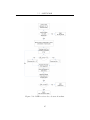
3 Device Specification
13
4 Overview of Proposed Solution
4.1 Introduction . . . . . . . . . . . . . . . . . .
4.2 RFID Detector, Identifier and Co-ordinator .
4.3 Uplink Module . . . . . . . . . . . . . . . .
4.4 Interconnections . . . . . . . . . . . . . . . .
4.5 Power Supply . . . . . . . . . . . . . . . . .
16
16
17
18
19
19
.
.
.
.
.
.
.
.
.
.
.
.
.
.
.
.
.
.
.
.
.
.
.
.
.
.
.
.
.
.
.
.
.
.
.
.
.
.
.
.
.
.
.
.
.
.
.
.
.
.
5 RFID Reader Design
20
5.1 Introduction . . . . . . . . . . . . . . . . . . . . . . . . . . . . 20
5.1.1 Operational Components . . . . . . . . . . . . . . . . . 20
v
CONTENTS
5.2
5.3
5.4
5.5
5.6
5.7
5.8
5.1.2 Active versus Passive Systems . . . . . . . . .
5.1.3 Operating Frequency . . . . . . . . . . . . . .
5.1.4 Modulation and Encoding Schemes . . . . . .
Selection of the RFID system . . . . . . . . . . . . .
Transponder Data Format and Protocol . . . . . . .
5.3.1 64 Data Bits . . . . . . . . . . . . . . . . . . .
5.3.2 CRC Verification . . . . . . . . . . . . . . . .
Hardware . . . . . . . . . . . . . . . . . . . . . . . .
5.4.1 Initial Considerations and Design Options . .
5.4.2 Antenna Driving Circuitry . . . . . . . . . . .
5.4.3 Analogue Receiver Circuitry . . . . . . . . . .
5.4.4 Antenna Design and Transponder Orientation
5.4.5 Processor . . . . . . . . . . . . . . . . . . . .
5.4.6 Interface . . . . . . . . . . . . . . . . . . . . .
5.4.7 PCB Layout . . . . . . . . . . . . . . . . . . .
Software . . . . . . . . . . . . . . . . . . . . . . . . .
5.5.1 Transmit Stage . . . . . . . . . . . . . . . . .
5.5.2 Capture Stage . . . . . . . . . . . . . . . . . .
5.5.3 Decode Stage . . . . . . . . . . . . . . . . . .
Design Evaluation . . . . . . . . . . . . . . . . . . . .
5.6.1 Transmitter . . . . . . . . . . . . . . . . . . .
5.6.2 Antenna and Tag Orientation . . . . . . . . .
5.6.3 Reader Range and Optimisation . . . . . . . .
5.6.4 Power Consumption . . . . . . . . . . . . . .
Conclusion and Recommendations . . . . . . . . . . .
Improvements and Further Work . . . . . . . . . . .
6 RFID Co-ordinator
6.1 Hardware . . . . . . . . . . . . . .
6.2 Software . . . . . . . . . . . . . . .
6.2.1 Timers . . . . . . . . . . . .
6.2.2 RFID Reader Request FSM
6.2.3 Received Data Processing .
6.2.4 The upload FSM . . . . . .
vi
.
.
.
.
.
.
.
.
.
.
.
.
.
.
.
.
.
.
.
.
.
.
.
.
.
.
.
.
.
.
.
.
.
.
.
.
.
.
.
.
.
.
.
.
.
.
.
.
.
.
.
.
.
.
.
.
.
.
.
.
.
.
.
.
.
.
.
.
.
.
.
.
.
.
.
.
.
.
.
.
.
.
.
.
.
.
.
.
.
.
.
.
.
.
.
.
.
.
.
.
.
.
.
.
.
.
.
.
.
.
.
.
.
.
.
.
.
.
.
.
.
.
.
.
.
.
.
.
.
.
.
.
.
.
.
.
.
.
.
.
.
.
.
.
.
.
.
.
.
.
.
.
.
.
.
.
.
.
.
.
.
.
.
.
.
.
.
.
.
.
.
.
.
.
.
.
.
.
.
.
.
.
.
.
.
.
.
.
.
.
.
.
.
.
.
.
.
.
.
.
.
.
.
.
.
.
.
.
.
.
.
.
.
.
22
24
25
26
27
29
29
30
30
31
33
35
40
43
43
44
44
45
48
50
50
50
53
54
54
55
.
.
.
.
.
.
57
57
58
59
59
60
62
CONTENTS
6.3
Evaluation . . . . . . . . . . . . . . . . . . . . . . . . . . . . . 62
7 Uplink Design
7.1 Introduction . . . . . . . . . . . . . . . . . . . . . . . .
7.2 Design Options . . . . . . . . . . . . . . . . . . . . . .
7.2.1 Uplink Options . . . . . . . . . . . . . . . . . .
7.2.2 Peripheral Interconnect Options . . . . . . . . .
7.3 Hardware Design . . . . . . . . . . . . . . . . . . . . .
7.3.1 GSM Module . . . . . . . . . . . . . . . . . . .
7.3.2 Processor . . . . . . . . . . . . . . . . . . . . .
7.3.3 User Interface . . . . . . . . . . . . . . . . . . .
7.3.4 Power Supply . . . . . . . . . . . . . . . . . . .
7.3.5 Peripheral Communication Bus . . . . . . . . .
7.4 Software Design . . . . . . . . . . . . . . . . . . . . . .
7.4.1 Initialisation and Restoration of Configuration .
7.4.2 Real Time Clock . . . . . . . . . . . . . . . . .
7.4.3 User interface . . . . . . . . . . . . . . . . . . .
7.4.4 Peripheral Poll FSM . . . . . . . . . . . . . . .
7.4.5 I 2 C FSM . . . . . . . . . . . . . . . . . . . . .
7.4.6 Timer FSM . . . . . . . . . . . . . . . . . . . .
7.4.7 GSM FSM . . . . . . . . . . . . . . . . . . . . .
7.4.8 Report Generation FSM . . . . . . . . . . . . .
7.4.9 Command Processing and Device Configuration
7.5 Reliability . . . . . . . . . . . . . . . . . . . . . . . . .
7.5.1 Software . . . . . . . . . . . . . . . . . . . . . .
7.5.2 Hardware . . . . . . . . . . . . . . . . . . . . .
7.6 Conclusions and Possible Improvements . . . . . . . . .
8 Power Supply
8.1 Introduction . . . . . . . . . . . . .
8.2 Power Requirements . . . . . . . .
8.3 Regulator Selection . . . . . . . . .
8.3.1 Linear Technology’s LT1765
8.3.2 ST Microelectronics’s L4976
vii
.
.
.
.
.
.
.
.
.
.
.
.
.
.
.
.
.
.
.
.
.
.
.
.
.
.
.
.
.
.
.
.
.
.
.
.
.
.
.
.
.
.
.
.
.
.
.
.
.
.
.
.
.
.
.
.
.
.
.
.
.
.
.
.
.
.
.
.
.
.
.
.
.
.
.
.
.
.
.
.
.
.
.
.
.
.
.
.
.
.
.
.
.
.
.
.
.
.
.
.
.
.
.
.
.
.
.
.
.
.
.
.
.
.
.
.
.
.
.
.
.
.
.
.
.
.
.
.
.
.
.
.
.
.
.
.
.
.
.
.
.
.
.
.
.
.
.
.
.
.
.
.
.
.
.
.
.
.
.
.
.
.
.
.
.
.
63
63
63
63
65
67
67
70
71
72
73
75
76
77
77
78
79
80
81
84
85
85
86
87
88
.
.
.
.
.
89
89
89
90
91
92
CONTENTS
8.4
Battery Selection and Charging
8.4.1 Hardware . . . . . . . .
8.4.2 Software . . . . . . . . .
8.5 Measurements . . . . . . . . . .
8.5.1 Power Supply Efficiency
8.5.2 Calculated Backup Time
8.6 Conclusion . . . . . . . . . . . .
.
.
.
.
.
.
.
.
.
.
.
.
.
.
.
.
.
.
.
.
.
.
.
.
.
.
.
.
.
.
.
.
.
.
.
.
.
.
.
.
.
.
.
.
.
.
.
.
.
.
.
.
.
.
.
.
.
.
.
.
.
.
.
.
.
.
.
.
.
.
.
.
.
.
.
.
.
.
.
.
.
.
.
.
.
.
.
.
.
.
.
.
.
.
.
.
.
.
.
.
.
.
.
.
.
.
.
.
.
.
.
.
.
.
.
.
.
.
.
94
94
98
100
100
100
101
9 Enclosure Selection and Mounting Methods
102
9.1 Initial Considerations . . . . . . . . . . . . . . . . . . . . . . . 102
9.2 Recommendations . . . . . . . . . . . . . . . . . . . . . . . . . 103
10 South African Regulations
105
10.1 GSM Module . . . . . . . . . . . . . . . . . . . . . . . . . . . 106
10.2 RFID Readers . . . . . . . . . . . . . . . . . . . . . . . . . . . 106
11 Conclusion and System Evaluation
107
A Appendix: RFID Receiver
A-1
A.1 PCB Layout of Push-pull Output Reader with Single-channel
Receiver . . . . . . . . . . . . . . . . . . . . . . . . . . . . . . A-1
A.2 PCB Layout of Single-ended Output Reader with Dual-channel
Receiver . . . . . . . . . . . . . . . . . . . . . . . . . . . . . . A-1
B Appendix: RFID Co-ordinator
B-1
B.1 Circuit Diagram . . . . . . . . . . . . . . . . . . . . . . . . . . B-1
B.2 PCB Layout . . . . . . . . . . . . . . . . . . . . . . . . . . . . B-1
C Appendix: Uplink Module Design
C.1 EEPROM Data Storage . . . . . . . . . . . . . . . . . . . .
C.2 List of Uplink Commands . . . . . . . . . . . . . . . . . . .
C.3 PCB Design . . . . . . . . . . . . . . . . . . . . . . . . . . .
C-2
. C-2
. C-3
. C-3
D Appendix: Power Supply
D-1
E Appendix: Software
E-2
viii
List of Figures
1.1 Penguins’ moulting season on Robben Island . . . . . . . . . .
1.2 Penguin nest on Robben Island . . . . . . . . . . . . . . . . .
1.3 Penguins at SANCCOB showing steel identifier tags. . . . . .
2.1
2.2
2.3
4
5
6
Existing system: Overview . . . . . . . . . . . . . . . . . . . . 9
Existing system: close-up of the gate . . . . . . . . . . . . . . 10
Existing system: Power supply and backup system . . . . . . . 11
4.1 Overview of proposed replacement system . . . . . . . . . . . 17
4.2 System overview: Logical connections . . . . . . . . . . . . . . 18
5.1
5.2
5.3
5.4
5.5
5.6
5.7
5.8
5.9
5.10
5.11
5.12
5.13
Popular Texas Instruments Series 2000 Antennas . . . . . . .
32mm glass encapsulated transponder . . . . . . . . . . . . . .
64bit Read-Only transponder data format, from [1] . . . . . .
Overview of proposed microprocessor-based RFID reader . . .
RFID antenna driver circuitry for single ended output . . . . .
RFID antenna driver circuitry using push-pull output stage . .
RFID receiver circuit showing amplifier stages and tuned circuit
Antenna field patterns . . . . . . . . . . . . . . . . . . . . . .
Detection of penguins with various antennae. . . . . . . . . . .
RFID receiver decode state flowchart . . . . . . . . . . . . . .
CRC verification flowchart . . . . . . . . . . . . . . . . . . . .
FFT of the 134.2kHz transmitted waveform. . . . . . . . . . .
Received waveform from an RFID transponder . . . . . . . . .
6.1
Global timer flowchart . . . . . . . . . . . . . . . . . . . . . . 60
ix
23
27
28
32
33
34
36
37
38
47
49
51
52
LIST OF FIGURES
7.1
7.2
7.3
7.4
Block diagram of uplink module’s hardware interconnect
I 2 C master to slave multi-byte data exchange . . . . . .
I 2 C slave to master multi-byte data exchange . . . . . .
I 2 C protocol used in uplink module . . . . . . . . . . . .
.
.
.
.
.
.
.
.
.
.
.
.
68
74
74
75
8.1
8.2
8.3
8.4
8.5
8.6
8.7
DC rail output of SMPS. . . . . . . . . . . . . . . .
Circuit diagram of switching DC-DC converter . . .
Battery SOC vs Open circuit voltage. . . . . . . . .
SLA battery target charge voltage vs temperature. .
Battery charging circuit and main supply input. . .
finite state machine of charging algorithm. . . . . .
Discharge periods vs. discharge rates . . . . . . . .
.
.
.
.
.
.
.
.
.
.
.
.
.
.
.
.
.
.
.
.
.
93
94
95
96
97
99
101
A.1
A.2
A.3
A.4
Schematic of push-pull output single channel
PCB Layout: push-pull output . . . . . . .
PCB Layout: single-ended output . . . . . .
Populated dual channel receiver board . . .
receiver reader
. . . . . . . . .
. . . . . . . . .
. . . . . . . . .
.
.
.
.
A-2
A-3
A-4
A-5
.
.
.
.
.
.
.
.
.
.
.
.
.
.
.
.
.
.
.
.
.
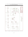
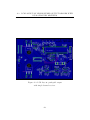
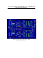
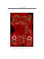
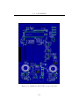
B.1 RFID co-ordinator circuit diagram . . . . . . . . . . . . . . . B-2
B.2 RFID co-ordinator PCB top solder side . . . . . . . . . . . . . C-1
B.3 RFID co-ordinator PCB bottom solder side . . . . . . . . . . . C-1
C.1
C.2
C.3
C.4
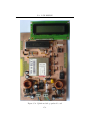
Uplink
Uplink
Uplink
Uplink
module
module
module
module
PCB top solder side . .
PCB bottom solder side
full circuit diagram . .
populated board . . . .
x
.
.
.
.
.
.
.
.
.
.
.
.
.
.
.
.
.
.
.
.
.
.
.
.
.
.
.
.
.
.
.
.
.
.
.
.
.
.
.
.
.
.
.
.
.
.
.
.
.
.
.
.
C-5
C-6
C-7
C-8
List of Tables
5.1
5.2
5.3
5.4
5.5
Active vs Passive Tags . . . . . . . . . . . . . . . . . . . . . .
ISO 11784 64bit Transponder ID data fields. . . . . . . . . . .
CRC-16: Probabilities of errors occurring and being detected.
Summary of considered microprocessors’ features . . . . . . .
Microprocessor peripheral allocations during capture . . . . .
25
29
30
41
46
6.1
RFID co-ordinator: record storage . . . . . . . . . . . . . . . . 61
8.1 Power requirements of the uplink module. . . . . . . . . . . . 90
8.2 Power requirements of the RFID subsystem. . . . . . . . . . . 91
C.1 EEPROM non-volatile data storage . . . . . . . . . . . . . . . C-2
C.2 List of all supported commands for uplink module . . . . . . . C-4
D.1 Devices considered for DC-DC switching power supply . . . . E-1
xi
Glossary
ADC Analogue to Digital Converter. In the context of this project, one of
the microprocessor’s on-board peripherals.
APN Access Point Name. Required for GPRS PDP context configuration.
ASCII American Standard Code for Information Interchange. Standard
referring to the binary representation of alphanumerical characters and
control codes for the purposes of electronic communication.
ASIC Application Specific Integrated Circuit. A device whose hardware is
specifically engineered to perform a single function.
AT command A standardised command issued to a modem. Short for
“attention.”
BCC Block Check Character. Texas Instruments term for CRC checksum.
CRC Checksum Cyclic Redundancy Check Checksum. A code used to
verify the integrity of exchanged data.
EEPROM Electrically Erasable Programmable Read Only Memory. A
form of non-volatile memory which can be re-written electrically.
EM wave Electromagnetic Wave. Term used to describe a self-propagating
wave with electric and magnetic components.
FFT Fast Fourier Transform. Technique for obtaining the discreet Fourier
transform efficiently.
xii
LIST OF TABLES
FIFO First In, First Out. Term used to describe a buffering technique
whereby the data which was first buffered is also the first to be replaced
by fresh data.
GPRS General Packet Radio Service. 2.5G GSM mobile phone technology
allowing packet-based data communication.
GSM Global System for Mobile Communications. International standard
for mobile telecommunications. This is the standard for cell-phones in
South Africa.
Interrogator Term used interchangeably with “reader” to describe a device
which is able to read/write to an RFID transponder.
ISR Interrupt Service Routine. Refers to a piece of software which is designed
to be executed when an interrupt is generated.
LCD Liquid Crystal Display. Display technology relying on the physical
properties of crystals under the influence of an electric field. Popular
in digital wrist-watches and pocket calculators.
LOS Line of Sight. Term used in radio-frequency communication to refer to
an unobstructed signal path between transmitter and receiver.
Non-volatile memory Memory technology which does not lose its contents
upon loss of power.
PIN Personal Identification Number. Numerical code used to identify the
user.
PSU Power Supply Unit. Short-hand term used to refer to the power supply
module of a device.
PWM Pulse Width Modulation. Scheme used to control the amount of
power in a waveform by varying the ratio of the “on” time to the “off”
time.
RAM Random Access Memory. Term used to describe memory in a computer
which can be accessed randomly (rather than sequentially). Typically
xiii
LIST OF TABLES
used to as a temporary store for variables. It is usually volatile in
nature.
Reader Term used to describe a device which is able to read/write to an
RFID transponder. Used interchangeably with the term “interrogator.”
RFID Radio Frequency Identification. A technology allowing objects to
be marked (or tagged ) with small electronic identifiers which can be
detected wirelessly using radio-frequency waves.
SIM card Subscriber Identity Module. Component of a GSM system provided
by the Mobile Operator which identifies the mobile device to the network.
SMPS Switched-mode Power Supply. A technique for converting DC voltages
by switching them into AC at high frequencies and then back to DC
again. High conversion efficiencies are possible with such designs.
SMS Short Message Service. A text-based message of up to 160 characters
which can be sent across GSM networks.
SOC State of Charge. Term used to describe the capacity remaining in a
battery. Usually measured in percentage of total capacity.
Tag RFID device which emits an EM wave for identification purposes after
being interrogated by an RFID reader. The term is used interchangeably
with “transponder.”
Transponder RFID device which emits an EM wave for identification purposes
after being interrogated by an RFID reader. The term is used interchangeably
with “tag.”
Volatile memory Memory which does not hold its state after power is
removed. Typically, working RAM in a microprocessor uses memory
of this form.
1
Chapter 1
Introduction
This project discusses the design and construction of a device for logging the
times and movements of the Robben Island penguin colony. It is completed
in partial fulfilment of a Bachelor of Science degree in Electrical Engineering
at the University of Cape Town during the second half of 2006.
1.1
Terms of Reference
This project is an evolution of an existing system in place on Robben Island
to track the penguin population’s movements to and from the island. It was
initiated by the University of Cape Town’s Avian Demography Unit (the
ADU is a division of the Statistics department in the Faculty of Science).
The ADU has a need to determine the times at which the birds arrive and
leave the island as part of a scientific study into the birds’ nesting, feeding
and moulting patterns.
Although there is an existing system in place performing this function,
the device is not able to reliably detect if the birds are coming or going
from the island and it requires frequent visitation to download the collected
data. Furthermore, the system cost in excess of ZAR30 000, which prohibits
system expansion through the installation of additional devices. The ADU
has requested that the system be redesigned to more accurately, reliably, costeffectively and conveniently determine the time and direction of the birds’
movements. The ADU would like to be able to install multiple such readers
2
1.2. OBJECTIVES AND DELIVERABLES
along various paths on the island to better track their comings and goings
on the island.
1.2
Objectives and Deliverables
The objectives of this project are to design, construct and evaluate a replacement
system capable of detecting the movements of penguins on Robben Island.
The following goals are expected to be achieved:
• Critically review the existing solution and identify all of its shortcomings.
• Suggest a device specification which solves these problems.
• Design a low-cost replacement system which solves the identified problems
and meets the proposed specification.
• Construct a prototype device according to the proposed design.
• Evaluate the prototype for possible installation.
• Suggest improvements and future work.
A working prototype will be constructed for delivery with this report.
1.3
Project Timeframe
The final year project commenced on the 23rd of July 2006 and ran until
the 23rd of October 2006. Students are expected to complete all required
research, perform the required work (in this case construct a working prototype)
during this period, and deliver this, a report detailing the project, by the 23rd
of October.
3
1.4. PROJECT BACKGROUND AND JUSTIFICATION
1.4
Project Background and Justification
Once a year (between November and December), penguins come to Robben
Island1 to moult. They move in groups numbering in the hundreds around
the beaches (as shown in Figure 1.1), with the entire colony numbering in
the thousands. Robben Island is also a nesting home for many of these birds.
Nests are established off the beach, under trees and shrubs as shown in Figure
1.2. When moving from their nests to the water to go fishing, they tend to
walk in groups of about half a dozen. Furthermore, they follow the same
paths every time.
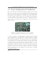
Figure 1.1: Penguins’ moulting season on Robben Island
sees many birds return to the island. Picture courtesy [2].
In order to improve our understanding of penguin movements, survival
rates and nesting habits – and thus improve avian conservation – penguins
must be marked so that individuals may be identified. This has traditionally
been achieved through the use of steel bands around the tops of their flippers
as shown in Figure 1.3. Identifying these birds then requires a human watcher
to manually read the stamp-printed numbers (which are difficult to see in the
field). During moulting season, this becomes all but impossible because of the
vast numbers of birds. In recent times, it has also been suggested that these
bands may adversely affect the birds’ swimming capabilities by disturbing
the hydrodynamic flow across their flippers [2]. A better method of marking
the penguins is required.
1
A small island famous for its high security prison in the bay of Cape Town, South
Africa.
4
1.5. PROJECT CHALLENGES
Figure 1.2: Penguin nest on Robben Island
We believe that a solution can be found using RFID technology. Identification
tags are small enough to be embedded under the birds’ skins and are light
enough not to hamper movements. A system is then required which automates
the monitoring process. This project aims to fulfil that need. Since the birds
tend to follow the same paths, it is possible to place a device along one of
the paths to detect the passage of the birds and so log their movements
on the island. This will ultimately lower monitoring costs, improve reading
reliability and thus better our understanding of these birds.
1.5
Project Challenges
The design will require a multi-disciplinary approach, drawing knowledge
from the fields of power engineering, analogue circuit design, digital circuit
design, digital signal processing, low power techniques, telecommunications
and software programming.
Furthermore, the system will be implemented in a remote, harsh environment.
Reliable system operation in these conditions poses particular technical challenges
as outlined below:
5
1.5. PROJECT CHALLENGES
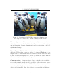
Figure 1.3: Penguins at SANCCOB showing steel identifier tags.
These tags are non-electronic. Picture courtesy of Simon Katz.
Remote Operation It is inconvenient and costly to have to visit the
device for maintenance. It should thus be fully autonomous: self-sustaining
and self-diagnosing. Remote administration and reconfiguration would be a
significant advantage.
Power Supply The island does not feature mains AC power outlets in
all locations where these loggers are likely to be installed. Furthermore, the
supplies that do exist are unreliable. For this reason, the device will need
to have a battery backup with the option of powering the system from an
alternate energy source, such as a solar panel.
Communications It is inconvenient to have to visit the device regularly to
recover the captured data. It should be possible to deliver this data to a more
convenient location for collection. Robben Island does not, however, have
a traditional wired telecommunications network infrastructure where the
devices will be installed. Thus, data delivery poses an additional challenge.
6
1.6. REPORT STRUCTURE
Environmental considerations The environment where the devices will
operate is harsh; physical construction requires special attention to corrosionresistant materials and weather-proof enclosures. The devices will operate in
the presence of sea air, rain, sun and thunderstorms. Ambient temperatures
can range from less than 10◦ C at night to over 35◦ C in the shade during the
day and wind speeds can be in excess of 50km/h.
1.6
Report Structure
Having discussed the project background, this document will continue to
discuss the existing system and analyse it’s shortfalls. Thereafter, a specification
will be proposed for a replacement device which addresses these shortcomings.
A brief overview of the proposed system and its operation will be presented
before in-depth design and operational specifics of each system component
are discussed. At the end of each design section, the prototype will be
evaluated against the specification, results presented and conclusions drawn.
Recommendations, along with possible improvements, will then be made
where necessary. Before concluding on the project as a whole, regulations
applicable to radio frequency operation in South Africa will be discussed.
Detailed design information, such as circuit schematics and PCB layouts,
is included in the appendices.
Attached to this report is a data CD containing all relevant datasheets,
quotes and costings, a soft-copy of this document, MPLAB project files,
firmware for the various microprocessors, EAGLE CAD PCB designs and
Gerber outputs.
7
Chapter 2
Analysis of Existing Solution
There is already a system in place which logs the birds’ movements, however,
there are problems associated with its implementation. The existing installation
on Robben Island was inspected in July 2006 in order for us to obtain a
better understanding of the conditions under which the device must operate.
This chapter will discuss the existing system and examine its strengths and
weaknesses with the goal of improving its design.
It is in the nature of penguins to walk along the same paths every day. A
gate has been established along one of these paths through which the birds
are funnelled. This gate is situated toward the southern end of the island,
near a mains AC power outlet. Figure 2.1 shows the operational components
of the existing system. The birds are detected and then identified as they
pass through this gate. This is done using a combination of infra-red and
low frequency RFID technologies. RFID transponders are implanted in the
birds’ backs, at shoulder height, with a vertical orientation. Approximately
200 birds have already been tagged. The system cost in excess of ZAR30 000
to implement.
2.1
Animal Detection and Identification
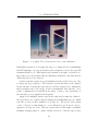
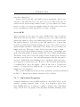
Figure 2.2 is a close-up of the gate through which the penguins walk. As a
bird enters the gate, it interrupts an infra-red light beam. This triggers the
RFID reader which then identifies the bird while it is within the gateway.
8
2.1. ANIMAL DETECTION AND IDENTIFICATION
Figure 2.1: Existing system: Overview
The second infra-red beam is interrupted as the bird leaves the gate. This
second trigger resets the system ready to scan for the next bird. Based on
the order of the beam triggering, the system can determine the direction that
the bird was moving (landwards or seawards).
The following problem has been identified on this system: if a second
bird enters the gate before the first one has exited, the system assumes it is
a double-trigger of the first bird and ignores the trigger. Thus, the second
bird’s movement is not recorded. When the first bird leaves the gate, it
is correctly recorded. However, when that second bird then exits the gate,
the system erroneously records a new animal entering the gate in the wrong
direction. The situation is only rectified after a timeout resets the system.
This condition undermines the purpose of the system: to accurately track
the times and directions of the birds’ movements.
9
2.2. POWER SUPPLY
Figure 2.2: Existing system: close-up of the gate
showing the Texas Instruments Series 2000 “small” loop antenna and the
two infra-red beam detectors.
2.2
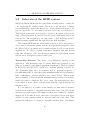
Power Supply
The unit is powered from the 230V AC mains generator which is located
on the island. Battery backup is in the form of a commercial 230V AC
Uninterruptable Power Supply (UPS) which is housed in a separate enclosure
from the RFID reader due to its size.
The following problems have been identified:
• This system is highly inefficient as mains power is stepped down and
stored in a battery. During a power failure, this voltage is stepped back
up to 230V AC and then back down to 12V DC again. These processes
are all lossy which has the end result of a very short backup period (in
the order of a few hours).
10
2.3. DATA PROCESSING AND STORAGE
Figure 2.3: Existing system: Power supply and backup system
• The backup system consumes much more space than it needs to.
• Excessive heat is generated in the non-ventilated enclosure.
• Reliance on the mains AC power source has prevented the system from
being moved to a more useful location where there is no power outlet.
• The backup system is expensive to purchase and operate.
2.3
Data Processing and Storage
Originally, the system was based on a desktop-type personal computer which
stored all records in volatile memory. Due to the system’s short backup
period, the frequency of power-outages, and instability caused by heat generation
within the enclosure, this was quickly identified as problem. Mr Andrew
11
2.4. DATA DELIVERY
Markham modified this original system by replacing the desktop computer
with a microprocessor which logs the data in the its on-board non-volatile
“flash” memory. Unfortunately, due to limited capacity, the birds’ entire
identification number is not stored, but rather only an eight bit identifier
and a lookup table. The total number of birds is thus limited to 256. The
time at which the bird passed through the gate is stored as the number
of seconds that has elapsed since the last upload in 16 bit integer format.
Another byte is used for status and direction storage. Thus, a total of four
bytes are required per data record.
2.4
Data Delivery
There is currently no remote uplink facility. Operators must periodically
physically connect to the device using an RS232 serial connection. This
data is downloaded to a portable computer and removed for analysis. The
memory is then erased and system time reset. The date and time at which the
system was reset must be recorded since the timestamps are relative, being
the number of seconds which have elapsed since the last upload. The system
is capable of storing approximately 13 000 such records (approximately one
month’s data).
The data is delivered in raw format in three columns: the time in seconds
which have elapsed since the last upload, ID of the bird and a status/direction
indication. It is delivered in raw hex format, requiring a trained operator to
import this data and convert it to a human-readable form.
12
Chapter 3
Device Specification
Having reviewed the operation of the existing solution and identified its
shortcomings, this chapter aims to produce a design specification for the
replacement system. The following are desirable features for the replacement:
Reliable The system should consistently detect and record the passing of
animals.
Autonomous User intervention should not be required on a day-to-day
basis.
Low maintenance The devices will operate remotely and it is costly and
time consuming to have to return to the site to maintain the device.
Accurate time keeping In order for the collected data to be meaningful, it
is important that the records are stamped from a reliable time source.
This is especially important if more than one logger device will be
used at a time and the data is cross-checked. For example, consider a
penguin passing one checkpoint at 13h10 (which is correctly stamped),
and then passing another checkpoint which is incorrectly stamped as
13h08. Clearly, when processing the data, it will appear as if the animal
walked in the wrong direction.
Cost-effective operation The device will operate for extended periods and
collecting data over this time should not be excessively costly.
13
Low cost hardware It would be advantageous to install additional devices
on the island to better track the animals’ movements. This will not be
possible if the device is expensive to construct.
User-friendly The end-users will not be electrical engineers and so the
operation of the device should not require in-depth understanding of
the technologies employed. The device should have a familiar feel with
collected data presented logically.
User-reconfigurable For example, it should be possible to alter the destination
for data delivery and set the time and date easily. It would be advantageous
to be able to perform these functions remotely.
Flexible Flexibility is necessary to prevent the device from becoming obsolete
prematurely. For example, it should be possible to power the system
from multiple energy sources.
Modular design The design approach should be modular: it should be
possible to extend the device’s functionality by adding additional modules
(for example, a temperature sensor or wind speed monitor).
Infrastructure-less The device should not depend on an existing wired
infrastructure as none exists. The island does, however, have GSM
coverage.
Robust It is essential that the enclosure is watertight, constructed from
rust proof material (to prevent corrosion at the coast) and the software
reliable (to ensure that captured data is not lost). Battery backup
should also be provided.
Power-efficient In an effort to maximise battery-backup operation time,
the device should consume as little power as possible.
Self-diagnosing Should a fault occur, the device should be able to identify
the problem and either notify the operator or, if possible, attempt to
correct the fault automatically.
14
Unobtrusive The device will be installed in a national heritage site. It
should not damage the aesthetics of the environment, nor should it
intrude on the penguins’ daily lives.
Safe The device should be safe for the animals and human operators.
License-free In order to keep costs down and simplify installations, operation
of the device should not require special permits or licenses.
15
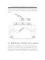
Chapter 4
Overview of Proposed Solution
4.1
Introduction
This chapter discusses the overall design methodology and illustrates the
operation of the proposed system as a whole.
Although RFID systems have been used to track animals before [3], this
particular application is somewhat different as it is required to be fully
autonomous and low-cost. For this reason, the system is designed from
the ground-up, using generic, off-the-shelf components as far as possible.
The solution is highly modular. Each component is a stand-alone unit
which interfaces with the other modules through communication buses. This
ensures that the custom modules can be replaced by commercial units at a
later date (should the system integrator deem it necessary), without significant
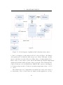
system modification. Figure 4.1 illustrates the proposed interconnections
between the three sections of this project:
1. A module which is able to detect and identify an animal at each gate;
2. A module which controls two of these readers, co-ordinating their readings
and interpreting the results;
3. A module which buffers this information before sending it to the user.
Naturally, a power supply and an interconnection are also required. Figure
4.2 shows the logical connections between the modules and indicates the
16
4.2. RFID DETECTOR, IDENTIFIER AND CO-ORDINATOR
sections in this report where the design detail for that component may
be found. A brief overview of the modules is presented in the following
subsections.
Figure 4.1: Overview of proposed replacement system
4.2
RFID Detector, Identifier and Co-ordinator
The existing detection technique does not produce reliable data due to the
double-trigger effect outlined in Section 2.1. The proposed solution is to
replace the two optical sensors with two independent RFID readers. These
readers are placed along the same penguin path, separated by a few metres as
shown in Figure 4.1. Both readers will continuously look for RFID transponders.
17
4.3. UPLINK MODULE
Figure 4.2: System overview: Logical connections
Including the chapters where the component design is discussed.
Based on the ordering of the detection, the system is able to determine the
direction of movement (gate one to gate two, or gate two to gate one). For
every such “double detection” (where the ID was detected at both gates),
the co-ordinator creates a data record, storing the ID of the transponder and
the direction of movement. These are presented to an uplink module upon
request. Details of the RFID system selection and design can be found in
Section 5.
4.3
Uplink Module
The uplink module’s primary purpose is to collect data from connected
devices and periodically upload this data to the operator. This module is
made to be as generic as possible, enabling many different peripheral devices
to be connected and data from each logged at user-definable intervals. It
polls each connected device to check for data. If new data is found, the
module records the data. This continues until its buffer is full. At this point,
the device uploads all collected records.
It is possible to create a permanent communication link between the
user and the remote device for real-time data collection, however, this would
require additional power resources and is not required for this application.
Thus, a buffered technique is preferred. Detailed design considerations can
18
4.4. INTERCONNECTIONS
be found in Section 7.
4.4
Interconnections
The RFID and uplink modules will need to communicate with each other.
As they will not be far from each other and data rates are low, but power
consumption and system costs are concerns, a simple wired communication
bus is suitable. There are two primary communication zones:
1. Between the RFID co-ordinator and the two RFID modules; and
2. Between the uplink module and any connected peripherals (such as the
RFID co-ordinator)
These are discussed in further detail in their respective sections.
4.5
Power Supply
The unit should be able to operate from various power sources as mains AC
power is not reliably available across the entire island. Alternative power
sources could include solar, wind and primary cells. The system will have a
battery backup and thus a charging system must be developed.
This proposal recommends a single power supply unit to supply the entire
system, including the uplink module, RFID co-ordinator, RFID readers and
any other peripherals which may be added. Bearing this in mind, it is logical
to co-locate the PSU with the uplink module as this is both a physical and a
logical connection hub for all other devices. A power source will exist at the
uplink module from which all connected peripherals can extract their power
requirements. Details of the power supply design can be found in Section 8.
19
Chapter 5
RFID Reader Design
The following subsections give a brief overview of RFID systems, their strengths
and weaknesses and suitability for this project. Thereafter, the design of an
independent RFID reader is discussed. Recall that two such units and a coordinator are required for the penguin detection and identification subsystem.
The design of the co-ordinator is discussed in Chapter 6.
5.1
Introduction
Radio Frequency Identification (RFID) is a technology which allows objects
to be marked (or tagged ) with small electronic identifiers which can be
detected wirelessly using radio-frequency waves. These tags (or transponders)
carry information in the form of an identification number and possibly userdefined data as well. Readers (or interrogators) consist of antennas and
receiver circuitry which can retrieve the data from the tags for processing.
5.1.1
Operational Components
An RFID installation typically comprises:
1. RFID transponders
• Antenna
• Controller IC
20
5.1. INTRODUCTION
• ROM memory, often EEPROM
• Power supply (in the case of active tags);
2. Receiver
• Antenna
• Analogue interface circuitry
• Digital controlling circuitry
• Power supply;
3. User-application, data handling hardware and software.
Transponders
Tags are available “off-the-shelf” in many shapes and sizes to fit most applications,
including application-specific, specialist tags from electronic companies such
as Texas Instruments for automotive use and for animal tagging. Generally,
the application of the RFID system determines the size and shape of the
tags required. They are available from many manufacturers, conforming
to different specifications, with unit prices below 1 US dollar [4] for shortrange, read-only (RO) passive tags and as low as US 5c for “dumb”1 tags.
Naturally, tags with on-board user-writeable EEPROM data space are more
expensive, as are tags with specialist casings (for example, medically bioinert, hermetically-sealed, glass-encased tags which can be safely implanted
into humans or animals).
Typically, the tags are supplied fully-assembled and sealed, ready for
installation. They house an on-board antenna, controller and memory. In
the case of active tags, a disposable primary Lithium cell is often included.
When this is exhausted, the tag is usually discarded.
Reader
The form of the reader varies greatly depending on the application. Small,
hand-held readers are available for programming read-write (RW) tags which
1
Dumb tags do not carry any ID information - readers can only determine whether a
tag is present in the read field or not.
21
5.1. INTRODUCTION
have short read ranges of only a few centimetres [5]. Fixed installations often
have higher power outputs and larger antennae with increased field sizes
for improved reliability and range. More exotic solutions include multiple
antennae for reading specific areas or dedicated, independent transmit/receive
antennae.
Antennae
Different antennae provide different read-field shapes. These can be tailored
to suit the application. For example, a strongly directional antenna can be
constructed which provides a long read range in one direction only. This is
useful if there are multiple tags in the vicinity and the operator would like to
single out one tag by pointing the reader at it. A common means of achieving
such a field in low frequency systems is by creating a winding on ferrite rods.
The other popular antenna structure is simply a coil of wire (known as a
gate antenna). The fields produced by both antenna types are illustrated
in Figure 5.8, reproduced from Texas Instruments’s technical handbook on
their Series 2000 antennae. The physical units in varying sizes are shown in
Figure 5.1. Note that the existing system on the island used the small gate
antenna depicted in the lower left of Figure 5.1.
5.1.2
Active versus Passive Systems
RFID systems are often categorised according to the tag’s power supply active or passive.
Passive RFID
Passive tags do not have on-board power supplies and need to be powered
by the EM wave from the reader. Two systems are in operation: full-duplex
and half-duplex. In half-duplex systems, the tags need to be charged before
they can transmit their data. The reader emits an EM wave at the tag’s
operation frequency and the tag stores the received RF energy in a small,
integrated capacitor. Once fully charged, the reader stops emitting the
charging waveform and this stored energy is used to transmit the tag’s data.
22
5.1. INTRODUCTION
Figure 5.1: Popular Texas Instruments Series 2000 Antennas
Full duplex systems do not require the tags to be charged before transmitting
their ID signature. As long as an interrogation signal is received, the tags will
transmit their ID code. Full duplex tags can thus be thought of as reflectors they reflect a received signal while modulating it with their own data stream.
This is known as backscattering.
Passive systems require strong transmitters in the reader device in order
to charge the tag’s capacitor. The system’s operational range is also limited
by the amount of energy the tags can store in their capacitors as, ultimately,
this determines the total energy in the retransmitted data stream. As a
result, communication is usually in the range of 2cm to 3m, depending on
the antennae, power supplies and frequency.
Support for multiple passive tags in the same field is thus also limited the tags all need to remain charged during the handshaking process, which
can take as long as three minutes for 20 tags [6]. The speed of movement
of the collection is thus limited to a few kilometres per hour in order to
guarantee all tags are read. This also means that readers must continually
transmit charging pulses to ensure reliable detection of mobile tags as they
23
5.1. INTRODUCTION
enter the reading field.
Passive devices typically offer limited user-programmable data storage
capacity of less than 128 bytes, and often none at all. This is the case for
several reasons, but most importantly because of power restrictions. Passive
tags do not have on-board power supplies and most of the power collected is
used for transmission rather than memory reading or writing.
Active RFID
Active tags have an on-board power source, usually in the form of a battery.
This means that the tags have a continuous power source rather than the
passive tags which are only powered while in the presence of the reader’s field.
The primary function of an active reader’s RF emission is to request data
from the tag rather than actually charging the device. The reader’s received
signal strength can thus be easily improved by using a more powerful power
supply in the tag. The range of these devices can easily extend to 100m.
Active devices offer a further advantage of being able to read multiple tags
in the same field quickly as all tags remain self-powered during handshaking.
Thousands of tags can be read from a single reader at high speeds. Readers
can thus power down more often and still guarantee that the tags will be
detected. Additionally, data handling is more intelligent, with tags able to
store upwards of 128 kilobytes each. However, active tags have the drawback
of requiring their own power supply - either in the form of a replaceable
battery or a disposable tag which needs to be replaced once the on-board
supply has been exhausted.
The operational differences between active and passive systems are illustrated
in Table 5.1. Hybrid active-passive schemes are also available.
5.1.3
Operating Frequency
A further distinction between RFID systems is often made based on the
system’s operating frequency (high or low). Low frequency devices (less
than 500kHz) make use of inductive coupling to transfer data. This limits
range, but allows for propagation through many mediums, including water
24
5.1. INTRODUCTION
Tag power source
Memory capacity
Cost
Range
RF field power
Efficiency
Read speed
Multiple tags
Lifespan
Tag size
Passive
External RF field
Less than 128B
Low
Short (up to 3m)
High
Low
Slow
Poor, slow, unreliable
Long
Active
Self-contained(battery)
Over 128kB
High
Long (up to 100m)
Low
High
Fast
Fast, reliable
Limited by power supply
Limited by antenna
Limited by antenna size
and power source
Table 5.1: Active vs Passive Tags
and flesh. It is thus ideally suited to animal tracking as tags can be embedded
under the animal’s skin.
High frequency devices offer improved efficiency and performance in openair environments. Standards include frequencies of 13.5MHz, 433MHz, 868MHz,
915MHz and 2.4GHz. Higher frequencies (2.4GHz and above) require lineof-sight links between the tags and the readers. This drawback has limited
these systems’ penetration into the RFID market.
5.1.4
Modulation and Encoding Schemes
Early tags adopted amplitude shift keying (ASK) as it was simple to implement
and resulted in cheaper tags. However, noise-immunity is poor and most
low frequency tags now use frequency- (FSK) or phase shift keying (PSK).
Encoding techniques (such as NRZ or Manchester encoding) are sometimes
used, however, to keep complexity of the tags at a minimum, many low-cost
FSK devices simply transmit the raw bit stream using two frequencies - one
to represent a logic “1” and another to represent a logic “0”. ASK is still
common in high-frequency transponders.[7]
25
5.2. SELECTION OF THE RFID SYSTEM
5.2
Selection of the RFID system
When selecting the RFID system for the island, it is important to consider the
cost of replacing the existing system. The choice to use an active or passive
system ultimately requires the integrator to decide what the lifespans of the
tags are expected to be: how many read/write cycles and over what period.
This lifespan along with lower tag prices, is traded off against reduced readrange, reduced tag memory, increased reader power requirements and slower
read speeds. The frequency is also important — high frequency devices’
signals attenuate significantly through water and flesh mediums.
The existing RFID system on the island is based on Texas Instruments’s
Series 2000 low frequency passive system. It is specifically designed to meet
the ISO 11784/85 specifications for animal tagging as well as automotive
applications. In order to remain backwards-compatible with this system
(and take advantage of the already-tagged birds), the replacement system
will also use low frequency passive technologies.
Transponder Selection The choice of tag ultimately depends on the
application. ISO standards exist for passive RFID tags designed for the
purposes of animal or agricultural equipment identification. These are defined
in ISO 11784 and ISO 11785 which were originally published in 1996 [8].
The documents define the code structure and an operating frequency of
134.2kHz using FSK. Not specified is the minimum transponder performance,
half- or full-duplex operation and ID codes of these devices. This prevents
inter-operability of devices from various manufacturers and, more worryingly,
makes it possible for duplicate ID codes to exist. The standards have since
been revised, however, many of the problems with the original standard are
still unresolved.
For our purposes, we require an unobtrusive tag that will not interfere
with the birds’ daily lives. Originally, this was in the form of a non-electronic
external tags with engraved ID numbers which were clamped to animals’
flippers. More recently, however, these have been replaced by modern glassencased, bio-safe capsules which are injected under the birds’ skin. This
system will form part of a study to determine whether these older flipper
26
5.3. TRANSPONDER DATA FORMAT AND PROTOCOL
bands are detrimental to the penguins. The newwer electronic system already
in place is ISO 11784/85 compliant and the replacement system needs to be
backward-compatible with existing tags. Since these tags are sealed passive
units, they are expected to outlast the lifetimes of the birds.
The devices on offer in TI’s Series 2000 for animal tagging includes 24mm
and 32mm glass capsules. These tags are available in Read-Write or ReadOnly models. Figure 5.2 shows the 32mm Read-Only passive glass tags in
use on the island.
Figure 5.2: 32mm glass encapsulated transponder
5.3
Transponder Data Format and Protocol
As mentioned previously, the read-only transponders in use conform to ISO11784/85
standards. A read from one of these transponders is a two step process:
1. Charge tag; and
2. Read response
The tags are charged for approximately 50ms and then a read is initiated
which requires a maximum time of 20ms to complete. The tag do not
begin transmitting until it has detected that the charge signal has ended.
The charge time can thus be adjusted depending upon factors such as the
application, transponder and antenna type and regulatory issues. A longer
charge time provides more energy for the tag and thus results in a more
powerful signal. Because the tags wait for the charge pulse to complete
before transmitting, they are considered half-duplex devices.
27
5.3. TRANSPONDER DATA FORMAT AND PROTOCOL
If the transponder’s capacitor has been sufficiently charged, it immediately
begins transmitting after detecting the termination of the charge signal.
This signal is in the form of non-encoded (raw) binary frequency shift keyed
(BFSK) sequence of 128bits. Figure 5.3 illustrates the data frame format.
Figure 5.3: 64bit Read-Only transponder data format, from [1]
The start byte is used to identify the type of transponder. For example,
RO tags have a start byte of 0x7E whereas RW tags have a start byte of
0xFE [1].
The tag stores 64 bits of identification data and a further 16 bits for CRC
integrity checking. Each bit consists of 16 cycles at the given frequency:
• Logic low is given by a 134.2kHz signal;
• Logic high is given by a 123.2kHz signal.
Because each bit is represented by a constant 16 cycles at different frequencies,
the bit periods differ. A low bit period typically takes 119µs and a high bit
130µs. Irrespective of the bit sequence transmitted, the entire message is
guaranteed to have completed within 20ms.
The system does not support reading multiple tags in a single reader
field as the transponders begin transmitting their data immediately after
the termination of the charge pulse. If multiple tags were to be present
in the same reader field, all transponders would thus begin transmitting
simultaneously. Although the reader would receive multiple signals, it would
be impossible to differentiate between the signals and the CRC check fails.
A successful read is impossible until the surplus tags are removed from the
reader’s field. The implication is that if two penguins are allowed to enter
the read field simultaneously, neither will be identified, although the system
28
5.3. TRANSPONDER DATA FORMAT AND PROTOCOL
will be able to determine that at least one penguin was within range. The
antennas and gates thus need to be carefully designed to ensure that only
one penguin is within range at a time.
5.3.1
64 Data Bits
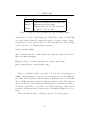
The 64 identification bits are subdivided into five fields to identify the type
of tagged item. These data fields are also defined in ISO11784/85 as shown
in Table 5.2 [9]:
Number of Bits
Field Allocation
1
Animal or Industrial classification
14
Reserved
1
Additional Data Flag
10
ISO 3166 numeric-3 Country Code
38
National Identification Code
Table 5.2: ISO 11784 64bit Transponder ID data fields.
5.3.2
CRC Verification
In order to verify the integrity of the received data, a CRC check must be
performed for each read. The CRC check employed in TI ’s Series 2000
is CRC-16-CCITT format and the checksum is housed in the two Block
Check Character (BCC) bytes of the received data [1]. The CRC-16-CCITT
polynomial is a popular specification (used in Bluetooth, PPP, IrDA and
many other communication standards) with a 16 bit generator polynomial
of x16 + x12 + x5 + 1 [10]. The CRC checksum generation operation can be
modelled as a serial shift through a 16bit register, multiplied by x16 , followed
by a division by the generating polynomial. The remainder of this operation
is the CRC checksum [11].
The CRC integrity check is fallible. Table 5.3 shows the probability of an
error occurring and the CRC-16 algorithm detecting the error.
The probability of an error occurring and the CRC check not flagging it
is so small as to be inconsequential for the purposes of this project.
29
5.4. HARDWARE
Error Type
Single bit errors
Double bit errors
Odd-numbered errors
Burst errors (<16bits)
Burst errors of exactly 17bits
All other burst errors
Errors Detected
100%
100%
100%
100%
99.9969%
99.9984%
Table 5.3: CRC-16: Probabilities of errors occurring and being detected.
Data from [12].
5.4
Hardware
Various designs were considered for the RFID readers, with details provided
in the sections below. All designs were constructed on “bread-board” type
prototyping platforms for evaluation. After finalising the designs, prototype
printed circuit boards (PCBs) were laid-out and the boards cut to evaluate
the readers’ performance.
5.4.1
Initial Considerations and Design Options
Many manufacturers provide low-cost application specific (ASIC) RFID reader
ICs2 , however, devices which operate at the required frequencies were not
locally available for evaluation at the time of this project. Furthermore,
an article in the October 2005 edition of Elektor Electronics by Martin
Ossmann provided a base design for a microprocessor-based RFID reader[13].
Unfortunately, it was designed around an Atmel AT90S1200 microprocessor
which did not have local support. The ideas were well explained in the
article, however, and a similar system based on Microchip’s PIC 18F series
of processors was successfully constructed.
The RFID readers need to force as much power into the antenna as
possible during the charging phase. Thus, it is desirable to have a high
drive voltage. 12V Sealed Lead Acid (SLA) batteries are popular choices for
battery backup, and this has been chosen as the primary system voltage to
2
Including Texas Instruments, Philips, Atmel, Microchip and ID MOS.
30
5.4. HARDWARE
accommodate the RFID readers (all other system components require 5V or
less). The potential differences across the antenna terminals are expected to
reach into the hundreds of volts due to the high Q tuned antenna design.
This a safety concern and requires careful circuit planning and component
selection.
When considering the detector for the RFID reader, it is important to
remember that the bit length of the received signal is only 16 cycles long. This
all but eliminates the possibility for tone decoders (which lock onto received
frequencies and are capable of detecting signals in high noise conditions) as
the lock-on times are usually longer3 . Filtering of the received signal also
presents a challenge: the filters must respond within the 16 cycles to prevent
signal smearing.
As mentioned in Section 4.2, the RFID peripheral will consist of a coordinator and two readers. Each RFID reader can be sub-divided into
operational components as follows:
• Microprocessor
• Antenna driving circuitry
• Analogue receiver circuitry
• Antenna
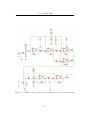
The configuration is illustrated in Figure 5.4.
Two of these reader devices will be connected to a co-ordinator which
calculates the direction of tag movements (from reader 1 to 2 or vice-versa).
5.4.2
Antenna Driving Circuitry
The purpose of the antenna driving circuitry is to provide the antenna with
a high driving current to charge the transponder.
Ideally, the antenna should be driven by a pure sine wave at exactly
134.2kHz. However, driving the antenna with a sine wave would mean that
3
For example, a pair of National ’s LM567 s will require over 50 cycles to differentiate
reliably between 123kHz and 134kHz[14]
31
5.4. HARDWARE
Figure 5.4: Overview of proposed microprocessor-based RFID reader
heat would be dissipated in the power output devices as they linearly convert
the 12V supply into a sine wave (a class A or B amplifier). Furthermore,
generation of a pure tone is difficult and requires additional components.
Since the reader already requires a microprocessor for decoding the received
signal, we decided to generate the charging pulse using one of the processor’s
on-board timer peripherals. This would provide a square wave output of 50%
duty cycle at 134.2kHz.
The design of the output stage is critical to good performance. Voltages
on these output terminals can be as high as 200V and thus high voltage
output devices are required. The only device at our university electronics
store capable of such potentials with a low on resistance (required for a highQ tuned antenna) and reasonable drive current capability is IR’s IRFP250
N-channel power MOSFET. It requires over 10V gate drive to ensure it is
fully on. The low voltage digital waveform from the microprocessor must
thus be level shifted and amplified to drive the power MOSFET. Although
ICs are available to perform this function, they are still costly and this result
can be easily achieved by using discrete components as follows: An LM311
comparator level-crossing detector (with positive feedback for a “snap-snap”
Schmitt trigger response) drives a pair of push-pull signal transistors (to
increase the current drive for the capacitive load of the MOSFET gate) which
32
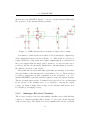
5.4. HARDWARE
in turn drive the MOSFET. Figure 5.5 shows a circuit diagram illustrating
the operation of the antenna driving circuitry:
Figure 5.5: RFID antenna driver circuitry for single ended output
Performance of this circuit can be improved by replacing the output stage
with a push-pull design as shown in Figure 5.6. This design does, however,
require additional components and requires significantly more current from
the power supply than the single ended output (to be expected since more
power is going into the antenna!). Furthermore, antenna tuning is critical to
the efficient operation of the circuit.
The transformer is self-wound using eight turns per winding on the driver
side and 16 turns on the antenna side on an 18mm toroid core. The motivation
for using a transformer in this configuration is the prohibitive cost of Pchannel MOSFETs (especially with the required voltage and current ratings).
The use of transformers and two N-channel devices provide a low cost alternative.
It also allows for the winding ratios to be changed to step-up the output
voltage, providing a higher drive voltage for the antenna without the need
for a higher power supply voltage.
5.4.3
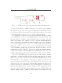
Analogue Receiver Circuitry
The receiver circuit is based around multiple amplifier stages with filtering
courtesy of a high-Q bandpass filter. Figure 5.7 shows the circuit diagram
of the receiver stage. The signal is received, amplified and fed into a parallel
33
5.4. HARDWARE
Figure 5.6: RFID antenna driver circuitry using push-pull output stage
resonant circuit, tuned to 130kHz. Thereafter, the signal is again amplified
into saturation to provide a 5V logic level square-wave representation of the
received signal. Based on the width of the pulses, the frequency of the signal
can be determined (see Section 5.5 for details of this calculation).
Recall that the potential across the antenna terminals is likely to be in the
order of hundreds of volts due to the high-Q nature of the tuned circuit. It is
thus impossible to feed this voltage directly into any low voltage component
such as an opamp. The solution is to AC couple the antenna through a
resistor and then diode-clamp the signal at supply levels before feeding it
into the first amplifier stage. Due to the relatively high input impedance
(1kΩ), the operation of the receiver does not significantly impact the tuning
of the transmitter output stage, and the same antenna can thus be used for
sending and receiving. This does, however, mean that the antenna must be
capable of receiving both the 123.4kHz and 134.2kHz signals. The “Q” of the
circuit is thus limited by the required bandwidth of approximately 10kHz.
The LF353 dual FET input op-amp was chosen as the primary amplifier
mainly due to its high bandwidth product and high input impedances coupled
with its low cost. Two of these devices form the first amplifier stages, before
the tuned filter. The total gain of this stage is 1000. Both LF353 s are
powered directly from the 12V battery rather than the 5V logic rail to provide
additional headroom for the signal. Although this supply is unregulated, the
battery represents a low-impedance source and during the receive phase, the
high-current transmitters are disabled. Thus, the 12V remains smooth (as
opposed to the 5V rail which powers digital logic from a SMPS). The noninverting inputs of these op-amps are biased at half of the supply and each
34
5.4. HARDWARE
stage is AC coupled to the previous one to prevent DC bias offsets from
being amplified. Low value resistors are used to prevent noise from being
captured and amplified and to limit the possibility of the circuit breaking
into oscillation. The op-amps are thus not operated at high gains. The
initial design places the first two op-amps in series to provide a combined
gain of 100 times (10 times each). The final two amplifiers in the receive
chain are connected in parallel in order to provide a higher drive current to
the passive parallel tuned filter.4
The reader’s filtering is based around a passive parallel resonant circuit
consisting of a custom wound inductor and a capacitor bank. The filter is
tuned to 130kHz with a bandwidth of approximately 20kHz.
The final amplification stage is formed around an MCP602, which is a
rail-to-rail output 5V op-amp. This stage has a gain of 100 and is enough to
saturate the amplifiers, resulting in a 5V output square wave. These op-amps
are costly devices, however, it was not possible to replace them with LF353 s
as their output voltage swing was not sufficiently close to the supply rails to
trigger the 5V CMOS level digital logic. Furthermore, all attempts to use
a level crossing detector based on the LM311 comparator were unsuccessful
- the device would either break into oscillation (using low levels of positive
feedback), or would not trigger reliably (using too much positive feedback to
curb oscillations). We believe that the oscillation problem was due in part
to the switch-mode power supply’s rail noise (see section 8 for PSU details).
5.4.4
Antenna Design and Transponder Orientation
Antenna Selection
The antenna for this project should have a uniform read field, rather than
a strongly directional one. This will ensure that the birds are detected as
they pass the gate. Figure 5.8 illustrates the read field generated by the
two popular low frequency antenna designs (ferrite stick and gate antennae).
Recall that the transponders in use are of the 32mm glass variety with ferrite
4
One of these parallel stages was disconnected in the final circuit design as it caused
the system to break into oscillation. Although range was affected slightly by the reduced
drive current to the resonant circuit, the reader operated more reliably.
35
5.4. HARDWARE
Figure 5.7: RFID receiver circuit showing amplifier stages and tuned circuit
36
5.4. HARDWARE
stick antennae placed in a vertical orientation. Figure 5.9 illustrates the read
fields generated by the two antenna designs in both horizontal and vertical
orientations, with the transponders assumed to be vertical. It represents a
top-down view of a typical penguin path. The coloured zones represent the
read fields assuming that the transponders are of the 32mm glass variety (ie
with ferrite stick antennae) and pass the receiver in a vertical orientation.
Figure 5.8: Antenna field patterns
for ferrite rod (“stick”) and gate antennae, from [15]
In case one, the reader’s stick antenna is oriented vertically. In this
configuration, there is a dead zone at azimuth angles of approximately 45degrees
from the horizontal (referenced to the centre of the reader stick as indicated
by the field patterns in Figure 5.8). Thus, if the transponder is not at
the same height as the receiver, the read fails. Furthermore, even if both
antennae are at similar heights, the read range is short in this orientation.
Ultimately, stick antennae are designed to be oriented end-to-end. If a stick
antenna could be buried in the ground under the path, it is possible that the
system would work. However, in order to achieve the necessary read range
(approximately half a metre), a narrow, focused, highly directional beam
will be required. This narrow beam width could result in penguins passing
undetected between scan cycles.
In the second case, the dual read zones of the stick reader in a horizontal
orientation could result in two penguins being in the read zones simultaneously.
37
5.4. HARDWARE
Figure 5.9: Detection of penguins with various antennae.
Horizontal and vertical orientations are considered.
38
5.4. HARDWARE
Since the Series 2000 tags do not allow for the reading of multiple tags
simultaneously, both reads will fail and no penguin will be detected.
Case three illustrates a gate antenna in a vertical orientation. The read
is successful provided that the tags are at a similar height to one of the
horizontal members of the antenna (ie the top or bottom edge). A dead zone
exists in the centre of the antenna.
The final case illustrates a gate antenna placed horizontally. If placed
alongside the path, the read is successful provided that the receiving antenna
is at a similar height to the transponder. If placed on the ground beneath
the penguins, the required read range would need to be approximately half
a metre. In order to achieve this range using a gate antenna, a high power
transmitter and highly sensitive receiver would be required. Such a system
would be costly to construct and have a high power consumption and is thus
not suitable for a low-cost battery powered device (should the mains fail).
After considering these options, it was decided to use an inductive loop
(gate) antenna rather than a ferrite stick antenna with the intention of placing
it alongside the penguin path, either in a horizontal or a vertical position.
The ideal orientation will be determined experimentally.
The commercial unit used in the existing system cost in excess of ZAR1200
(depending on the size). Since the aim of this project is to produce a low
cost device, the use of a commercial antenna is not possible. Sizing of
the replacement custom unit will be similar to the existing antenna (Texas
Instruments’s “small” Series 2000 gate antenna). Please see Figure 5.1 for
a diagram of the various Series 2000 antennae.
Antenna Operation and Design
The antennae of the transmitter and receiver of low frequency RFID systems
form inductive couplings. Our initial consideration was that the the windings
on the antennae of the reader and the transponder can be thought of as
forming a transformer. Given that the number of turns on the transponder’s
antenna is fixed (since these are purchased, commercial units), we considered
using a large number of turns on the receiving antenna to result in a high
received voltage and a small number of turns on the charging antenna to
39
5.4. HARDWARE
result in a high received voltage at the transponder. As outlined in Section
5.6, the number of turns on the antenna had very little influence on the
receiver’s performance: if a receiving antenna with a few turns is used, the
receiver chain’s gain is simply increased to compensate and produce similar
results.
What is of consequence is the transmitter’s inductance: it should remain
low enough to pass a significant current at 132.4kHz during the charging
phase from a 12V supply. As more turns are added to the transmitting
antenna, the inductance of the loop increases and since the supply voltage
and operation frequency remains constant, the current through the inductor
decreases. The undesirable consequence of such an action is a decrease
in transmitter power. The Texas Instruments Series 2000 antennae have
inductances of approximately 27µH [15].
Many antennae were constructed and evaluated. Ultimately, it was decided
to use a single antenna for receiving and transmitting with a designed inductance
of 50µH. The number of turns on the antenna would ultimately depend on
the physical size, shape and diameter of the wire used. The proposed final
design uses a rectangular antenna measuring 260mm × 230mm.
5.4.5
Processor
Prior to this project, the only experience we had with microprocessors was
with Freescale’s HC08 series. After finding an 68HC908JK3 inadequate for
the task, Microchip’s PIC 18F452 and later a PIC 18F4620 were considered.
The details of the design as well as the benefits and shortcomings of each
device are outlined in the sections which follow.
The microprocessor must be capable of:
• Generating a logic-level square wave at 134.2kHz
• Determining the frequency of a received square-wave
• Reporting the data to the RFID co-ordinator
The initial solution is to use two timer modules, one to generate the
transmitting pulse and the second to determine the elapsed time between
40
5.4. HARDWARE
square-wave edges. An on-board RS232 interface will be used to transmit
the decoded data to the RFID co-ordinator.
Included in all designs is an In-Circuit Debugging (ICD) interface for
in-field debugging and reprogramming.
Property
FLASH (Kbytes)
RAM (bytes)
Max speed (MIPS)
Timer peripherals
Timer channels
Additional features
68HC908JK3
4
128
8
1
2
Low cost
Low pin count
PIC 18F452
PIC 18F4620
32
64
1536
3986
10
10
4
4
2
2
HW multiply
HW multiply
USART
USART
4 x PLL
4 x PLL
Divide-by-fourDivide-by-fourcapture prescaler capture prescaler
HW comparator
Table 5.4: Summary of considered microprocessors’ features
relevant to the RFID reader
Initial design based on 68HC908JK3
Freescale’s 68HC908JK3 was initially chosen as the development platform
as it appeared to have all the required components. However, the device was
too slow to decode the incoming bit stream on-the-fly and had insufficient
RAM for capturing all the raw data for off-line processing. In an attempt
to remedy the situation, a hardware divide-by-four (binary counter) was
inserted before the JK3. Recall that each transmitted bit is 16 cycles long.
After the hardware divider, each bit would now effectively consist of four
edges. This sampling rate is sufficient to allow for digital filtering of the
received signal. Unfortunately, even with the device running at full speed
(8MHz), it was not possible to decode the data as it was received. And
the processor’s 128bytes of RAM is still not able to accommodate all 512
41
5.4. HARDWARE
samples5 .
Thus, a faster device, or one with more memory was required. Mr Andrew
Markham recommended Microchip’s PIC 18F series and although we had no
experience with these devices, they had been successfully used in upgrading
the existing system on the island.
Second design based on PIC 18F452
The PIC 18F452 has an on-board divide by four counter as part of its
Capture, Compare, PWM (CCP) peripheral. With 1.5kB of RAM it should
be possible to capture all data and perform decoding and CRC checking offline. Furthermore, the device has an on-board 4x PLL for increasing the bus
frequency. An 8MHz crystal was used, which gave the option of clocking the
device up to 32MHz simply by enabling the PLL.
Unfortunately, 134.2kHz is not directly obtainable from the 8MHz crystal.
Thus, a form of direct digital synthesis is used. By changing the timer
modulus from 60 (giving a 133.33kHz signal) to 59 (giving a 135.59kHz signal)
on every third cycle, an average frequency of 134.09kHz is achieved. Figure
5.12 in the measurements section shows an FFT plot of the positive half of
the spectrum of the resulting transmitted signal.
Possible Optimisation on PIC 18F4620
After completing experimental measurements (see Section 5.6 for further
details), it became clear that it was not possible to reliably detect the
transponder in all orientations using a single antenna. The proposed solution
is thus to use additional receiving antennae, placed in different orientations.
A single transmitter pulse will be sent and both antennae will listen for a
response from the transponder. The charge pulses to both antennae will be
synchronised and then the received signal from each decoded independently.
Ideally, a single processor could be used to decode the received signals
from both antennae. Thus, double the RAM would be required to store the
captured data from the extra channel for off-line decoding. Furthermore,
if both CCP modules are clocked from the same timer3 module (one CCP
5
128bits, 4 edges per bit gives 512 samples
42
5.4. HARDWARE
channel cannot be allowed to reset the timer upon receipt of an edge as it
would interfere with the results of the second channel), each read will need to
be 16bits long rather than 8bits in order to accommodate a 20ms capture with
sufficient resolution for reliable bit differentiation. Thus, in total four times
the RAM is required to add an additional channel. The PIC 18F452 only has
1.5kB of RAM, which is insufficient. Thus, the PIC 18F4620 which is pincompatible and has 4kB of RAM was chosen as a replacement. Unfortunately,
even operating at 32MHz, it was not fast enough to reliably capture the full
16bit timer value between every four edges on both channels simultaneously.
A further option is to clock the two CCP modules from separate timers,
however, this solution has not yet been implemented or evaluated.
5.4.6
Interface
In keeping with Texas Instruments’s Series 2000 system, RS232 was chosen
as the communication method between the RFID readers and the host system.
This ensures that should these reader devices need to be replaced at a later
date by commercial units, no hardware changes to the rest of the system will
be required.
No direct physical user interface is required, apart from a means to trigger
a read cycle (although this too could be a soft command across RS232) it was
decided to use one of the reader microprocessor’s pins as a trigger. When
this pin is pulled high, a read is triggered. Four LEDs have been added
to the reader devices to display the status (Idle, Transmitting, Receiving 1,
Receiving 2).
5.4.7
PCB Layout
The printed circuit board layout is very important as the total gain of the
final analogue receiver design is approximately 3.2 million times (65dB). This
is sufficient for received noise to be amplified into saturation.
For the reader circuit, the digital section was isolated from the analogue
receiver circuitry by using separate supply tracks and ground planes. Every
attempt was made to keep tracks as short as possible and decoupling capacitors
added wherever space permitted.
43
5.5. SOFTWARE
Please see appendix A.1 for a complete circuit diagram and PCB layout
of a push-pull output, single receiver channel interrogator (with no tuned
receiver filter) and appendix A.1 for a single-ended output, dual-channel
receiver interrogator.
5.5
Software
The development environment used for the PIC 18F series is provided by the
manufacturer, Microchip’s MPLAB v7.4 with the C18 C-compiler. Included
with this package are interfaces to the processor’s onboard peripherals (such
as timers, communication buses and ADCs) and methods for controlling
popular attached hardware devices (such as I 2 C EEPROM devices and intelligent
LCD displays). All code, however, was custom written unless otherwise
stated.
After device initialisation, the reader waits for a trigger input before
sequentially executing the following stages of its software:
1. Transmit a charging pulse.
2. Capture all edges on receiving channels.
3. Look for a start byte.
4. Decode received data into a bit stream and perform bit-by-bit CRC
checking.
5. Transmit result via RS232.
5.5.1
Transmit Stage
Although originally planned to use a PWM peripheral pin, both of these
modules were now occupied for receiving purposes and thus a general purpose
pin was required to drive the output stage. In fact, when a push-pull design
was employed (see Section 5.4.2), two general purpose pins were occupied
which were 180 degrees out of phase (with dead-time introduced between
changes). Although it would be convenient to use the CCP peripherals for
44
5.5. SOFTWARE
generation of these signals (since they can be muxed together to produce outof-phase waveforms), they were reserved for receive channels. Furthermore,
it is trivial to implement the transmit waveform generation in software.
In order to achieve the required charging period (50ms or even 100ms),
one of the microprocessor’s timer peripherals were used. Timer0 was chosen
as it is independent from any other device operation (such as the capture
peripheral which uses Timer3 - see Section 5.5.2). Timer0 is started with
a time-out set to the desired period and a loop started which generates a
134.2kHz square wave.
Timing for the 134.2kHz generation was achieved by using “no operation”
(NOP) commands to generate the required delays. The pins were then
manually pulled high or low as required. As mentioned in Section 5.4.5,
a perfect 134.2kHz signal is not possible from the 8MHz crystal. Each loop
consists of three cycles: two with a period of 60 cycles (giving a 133.3kHz
clock) and one with a period of 59 cycles (giving a 135.6kHz clock). This
gives an average frequency of 134.08kHz. The spectral efficiency of this
configuration is sufficiently close to 134.2kHz to charge the tag (see Figure
5.12).
This loop of three cycles continues to execute until Timer0 times-out.
Thereafter, there is a 1ms guard period to allow the analogue circuitry to
recover and stabilise before the capturing begins.
5.5.2
Capture Stage
The PIC18F452 features two Capture, Compare, PWM (CCP) peripherals
which are capable of identifying edges and generating interrupts when these
occur. Furthermore, they include a hardware divide by four function which
allows for the elapsed time between four edges to be measured without
introducing additional processor overheads. The CCP modules operate in
conjunction with Timer3. Table 5.5 shows the allocation of the various
microprocessor peripherals used during the capture stage.
Timer0 is again used to implement a time-out of the receive period. It is
limited to 20ms (recall that a receive cycle is guaranteed to complete within
this time – see Section 5.3 for details). A CCP unit is configured to generate
45
5.5. SOFTWARE
Peripheral
CCP1
Timer0
Timer3
Function
Generate interrupt on every fourth edge
Implement timeout (20ms)
Elapsed time between CCP interrupts
(coupled to CCP module)
Table 5.5: Microprocessor peripheral allocations during capture
an interrupt on every fourth rising edge. When this occurs, the CCP ISR
stores the value in Timer3’s counter in an array for later processing. Timer3
is then reset in order to time the period to the next fourth edge. The following
section of pseudo code illustrates this operation:
Preset Timer0 (20ms)
while (Timer0 has not overflowed) and (receive buffer not full)
Wait for CCP interrupt
{
Capture value in Timer3 register on every fourth edge
Reset Timer3 after every fourth edge
}
Timer3 is initialised with a prescaler of 4 from the bus frequency of
8MHz 6 . Recall that the two expected received frequencies are 123.4kHz and
134.2kHz. The frequencies of the interrupts are thus expected to be 30.85kHz
and 33.55kHz respectively (after the hardware divide by four). The values in
the stored array for each channel are thus expected to increment in values of
57 (2M Hz ÷30.85kHz) or 65 (2M Hz ÷33.55kHz) depending on the received
frequency. In this way the bit stream can be determined during the decode
stage.
When the buffer is filled, or Timer0 overflows, decoding is started.
46
5.5. SOFTWARE
Figure 5.10: RFID receiver decode state flowchart
47
5.5. SOFTWARE
5.5.3
Decode Stage
Figure 5.10 shows a simplified flowchart of the decoding stage. Decoding
begins by looking for a start byte. The Read-Only tags employed in this
system have a start byte of 0x7E, or binary 01111110. All bits prior to the
start byte are 0. If it is known that all tags are of this RO variety, it is a simple
case to look for the first occurrence of a “1” bit in the incoming stream. This
system proved sufficiently reliable to forestall the use of more complicated
searches involving correlation of the received bits with the expected start
byte. If no start byte is found within the first 200 samples, then a “no tag
found” report is generated and no further decoding takes place. If a start
byte is found within the first 200 samples, decoding continues.
Assuming a start byte is found, decoding takes place as follows: a loop
executes which averages every four entries in the buffered array beginning
directly after the start byte. This averaged value is compared to a predefined
= 61 (recall that the differences
bit-threshold which is set by default to 57+65
2
are expected to be either 57 or 65 depending on the bit received). This bit
stream is stored in two arrays of 8 bytes and 2 bytes representing the ID of
the tag and the BCC (CRC checksum) respectively.
CRC Check The CRC checking is performed on-the-fly during decoding
on a bit-by-bit basis on the incoming bit stream as illustrated in Figure 5.11.
Recall that the CRC-16-CCITT checksum polynomial is x16 + x12 + x5 + 1.
This is stored in a 16 bit integer variable with the value of 0x1021.
The CRC shift register is initialised to zero before each read. If the check
was successful, the final result will also be zero. Any other value in the shift
register indicates a verification failure. Please refer to Section 5.3.2 for CRC
operation details.
Result Reporting One of three possible responses will be returned:
1. Tag successfully decoded
2. CRC check failed
6
32M Hz ÷ 4
48
5.5. SOFTWARE
Figure 5.11: CRC verification flowchart
3. No tag detected within read range
All responses are sent across RS232 in plain ASCII followed by a carriage
return character.
In the first case, the response is of the form:
OK: XX XX XX XX XX XX XX XX CRC: YY YY
where
XX represents the tag ID in hexadecimal from MSB to LSB and
YY represents the BCC also in hexadecimal form, MSB first.
In the second case, data was received, but it could not be verified. The
following line is generated:
CRC fail: XX XX XX XX XX XX XX XX CRC: YY YY.
This is an indication of excessive noise or a poorly tuned antenna.
In the third case, the buffer was not filled within the 20ms time-out and
it is then assumed that no tag was present. The response is in the form
49
5.6. DESIGN EVALUATION
No tag found.
This response is also possible if the antenna becomes open loop or an internal
circuit fault exists.
5.6
5.6.1
Design Evaluation
Transmitter
Recall that 134.2kHz is not directly obtainable from the 8MHz crystal employed.
Thus, a form of direct digital synthesis (DDS) is used. By generating a
133.33kHz signal for two cycles followed by a 135.59kHz signal on every third
cycle, an average frequency of 134.09kHz is achieved. Figure 5.12 shows an
FFT plot of the positive half of the spectrum of the transmitted signal. The
spectral purity of this signal coupled with the resonant antenna ensures that
the system only responds to the fundamental frequency of the square wave.
Figure 5.12 shows a screen capture on an Agilent oscilloscope performing an
FFT plot of the antenna waveform signal using a Hanning window. This was
generated using the DDS technique outlined above, using the push-pull type
transmitter discussed in Section 5.4.2.
The power output devices in the single-ended design did not require
heatsinks at all — the cases of the IRFP250 s are sufficient to dissipate all
produced heat at room temperatures (even when operated continuously).
The devices used in the push-pull design, however, do require heatsinks if
operated at high duty cycles. Small aluminium plates will serve as heatsinks
with temperature coefficients of approximately 10 degrees C per watt.
5.6.2
Antenna and Tag Orientation
Various antenna designs were considered with mixed results. Antenna tuning
proved to be critical. If the antenna was tuned to 134.2kHz then it resulted
in a very strong transmitted pulse. The tags, however, emit both 123.2kHz
and 134.2kHz signals. The consequence of such a set up is that the 123.2kHz
signal is not received at a similar amplitude and the receiver is unable to
decode the data stream. The antennae were thus tuned to approximately
50
5.6. DESIGN EVALUATION
Figure 5.12: FFT of the 134.2kHz transmitted waveform.
Centre frequency of the image is 127kHz with a span of 50kHz. Notice the
strong peak at 134.2kHz
129kHz. This limits the maximum “Q” to approximately 117 . Figure 5.13
shows the received waveform from a tag with a well-tuned antenna. Notice,
however, that one of the received frequencies is still favoured. Temperature
changes greatly affected the tuned centre frequency. This drift can be attributed
to the capacitance and resistance of the tuning circuit changing with temperature.
The following antennae were evaluated for performance gains. All measurements
were made using a regulated 12V supply with the antennae tuned to 129kHz
using the push-pull output stage design discussed in Section 5.4.2. The
receiver chain was as shown in Section 5.4.3 (Figure 5.7).
Small Single Round 100µH Loop Based on the antenna recommended
in [13], a small circular antenna with a diameter of approximately 100mm and
an inductance of 100µH was constructed. Performance of the device matched
7
11kHz bandwidth with a centre at 129kHz:
51
129
11
= 11.73
5.6. DESIGN EVALUATION
Figure 5.13: Received waveform from an RFID transponder
the claims made in the article. Maximum read range was approximately
100mm when using a single antenna as a transmitter and a receiver.
Large Single Square 400µH Loop The performance of this antenna
( 280mm x 240mm) was similar to the small round loop mentioned above,
with one exception: although the maximum read range remained at approximately
100mm, the area over which the system worked was greatly improved. Reliable
reception was possible over the full area of the antenna as well as a surrounding
radius of approximately 100mm, provided the orientation of the transponder
remained correct relative to the antenna.
Large Square 27µH Loop Transmitter and Large Square 400µH
Loop Receiver In this test, separate antennae were used for transmitting
and receiving. Power requirements for the transmitter increased (as expected
with a reduced inductance and constant switching voltage), but range and
operating area increased. The primary reason for the increased range was
the additional number of turns on the receiving antenna. It thus became
52
5.6. DESIGN EVALUATION
clear that in order to achieve additional range, the receiver chain must be
optimised.
5.6.3
Reader Range and Optimisation
With the single-ended output stage, the range is limited by the charging
phase. At further distances, the tag does not become sufficiently charged
to fully transmit all 64 data bits and 16 BCC bits. This is easily verified
by using two independent antennae (for transmitting and for receiving) and
then varying the distance between the tag and the antennae individually.
Changing to the push-pull output stage rectifies this problem, and the
range is then limited by the SNR of the received signal. It was found
that range could either be increased by increasing the receiver chain’s total
gain or adding additional turns to the receiver antenna (thereby collecting
more of the transponder’s transmitted signal). This is because the receiver
only operates correctly when the output from the final amplifier stage has a
peak-peak amplitude of close to 5V (in order to trigger the digital circuitry
correctly). Increasing the chain’s total gain to 64 million times (156dB)
tripled read range to approximately 300mm. This gain is sufficient to amplify
the ambient noise in the laboratory to saturation, however, it still provided
the best read range.
It was noted that the majority of this noise was generated by surrounding
computer monitors and devices using switched-mode DC-DC converters. In
an effort to reduce noise, various filters were evaluated. First-order buffered
passive bandpass filters exhibited poor results and were dismissed. Secondorder active filters produced somewhat better results, but the roll-off was
still not as sharp as we would have liked. The solution was in the form of a
tuned filter, centred at 129kHz with a bandwidth of approximately 10kHz.
A gain of 156dB, is, however, still sufficient to amplify the ambient noise to
saturation of the final output op-amp. A tuned filter coupled with such high
gains resulted in a circuit which tended to break into oscillations. Two PCBs
were thus designed. One contained a high-gain amplifier without any filtering
for use in low-noise environments (such as Robben Island) and another with
reduced gain and aggressive filtering.
53
5.7. CONCLUSION AND RECOMMENDATIONS
5.6.4
Power Consumption
The push-pull RFID reader consumes 420mA (at 12.5V) when transmitting
and the logic consumes 50mA (at 5V) when transmitting, receiving or idling.
Thus, transmitting requires approximately 5.5 Watts and the device consumes
a quiescent power of 0.25 Watts. Tuning of the antenna is crucial to efficient
power usage. The device consumes excessive amounts of power if the antenna
or transformer are incorrectly tuned.
Decoding can require up to 250ms. It will be lower if no tag is detected, as
no further decoding will then take place (see Section 5.5.3 for further details
on the decoding algorithm). In this case, it is possible to trigger another
read almost directly after the previous one and up to four reads per second
can be performed. Thus, if the device is placed in continuous scanning mode
(by holding the trigger pin high), the overall power consumption will be
higher if there are no tags present. If there is a tag in range, a full decode is
attempted. The read rate decreases to 2.5 reads per second and the average
power consumption is thus decreased.
For the purposes of this project, the RFID co-ordinator will expressly
trigger reads on either reader. The average power consumption of the reader
is thus determined by the frequency of the read requests.
5.7
Conclusion and Recommendations
The following conclusions and recommendations are drawn from the above
findings:
• Read range is limited by receiver sensitivity. Range improved with
additional receiver gain, even when total gain was high enough to
saturate the amplifiers. It is thus recommended that the highest possible
gain is used (while ensuring that the circuit remains stable and does
not break into oscillation).
• The reader does not perform well in the presence of popular switchedmode power supplies which operate at frequencies of 33kHz, 65kHz or
130kHz as the harmonics which they produce cause significant interference.
54
5.8. IMPROVEMENTS AND FURTHER WORK
The reader should be well shielded and the area of operation should
not contain switching devices in these frequency bands.
• Transponder and antenna relative orientations are critical. All transponders
should be installed in a uniform direction. When installing the readers,
it is important to consider the chosen transponder orientation and
mount the antenna accordingly. Further details can be found in Sections
5.4.4 and 5.6.2.
• Maximum read range is approximately 30cm in the presence of no
noise, with the receiver’s antenna and transponder in ideal orientations.
Deviations from this configuration often result in unpredictable performance.
• The antenna can be wound to almost any size which suits the application
without significantly affecting performance, provided that the inductance
is kept constant, the receiver’s gain adjusted according to the total
number of coils and the transponder re-oriented to suit new antenna
configuration.
• Low temperature co-efficient capacitors should be used for tuning of
the antennae to limit the effect of temperature drift on the resonant
circuit’s centre frequency.
• Reader performance can be improved by replacing the LF353 op-amps
with NE5532 low noise op-amps.
• Power consumption ultimately depends on the frequency of read requests.
5.8
Improvements and Further Work
It was not possible to implement a dual channel receiver on a single PIC
18F4620 when capturing 16 bit timer values. This microprocessor has the
ability to use independent timers for the two CCP modules. This will enable
eight bit capturing. Initial calculations indicate that the microprocessor
should be capable of capturing both channels when operating the CCP
modules in polled mode. This would enable an additional receive antenna
55
5.8. IMPROVEMENTS AND FURTHER WORK
to be connected, either in a different orientation or in another location.
This has the potential to decrease system costs (by using only one processor
where two were previously required), improve reliability (by orienting the two
receivers differently in the same location, additional transponder orientations
are accommodated) and improve efficiency (a single charge pulse can be
used for both receivers at a reader station whereas otherwise, two would be
required).
A further proposed optimisation is to remove the expensive MCP602 opamp and feed the signal after the tuned filter directly into a PIC 18F4620
processor’s on-board comparator peripheral. Such a system would reduce
the noise introduced by the additional op-amp amplifiers and decrease device
costs.
Overall device performance could be increased by using two independent
high-Q antennae: one for receiving 123.2kHz and another for receiving and
transmitting 134.2kHz. This would reduce received noise and improve receiver
sensitivity while enabling very high transmitter efficiencies. A modification
of this is to use a single antenna which is highly tuned to 134.2kHz. The
receiver would receive the 134.2kHz signal, but not the 123.2kHz signal from
the transponder. Thus, the presence of a signal would indicate a “0” and the
lack of signal for one bit period indicates that “1” was transmitted.
Ultimately, however, Application Specific IC (ASIC)-based RFID devices
may prove to be a cheaper alternative to a purely microprocessor-based
reader. The PIC 18F452 used in this reader,or PIC 18F4520 equivalent
replacement, costs approximately ZAR65.008 whereas the Texas Instruments
RI-TMS3705ADR is available in unit prices of less than ZAR61.00 for single
items, or ZAR37.00 for purchases of over 100 units9 . One of these ICs would
still require a microprocessor controller, however, it will not need the large
volumes of RAM or additional peripherals that the current design does. A
reader employing a small processor, ASIC RFID device and push-pull output
stage may prove to be a cheaper design.
8
Avnett Kopp, September 2006
6.43 Euros singly and 3.90 Euros for order over 100. Assuming an exchange rate of
ZAR9.50 to 1 Euro
9
56
Chapter 6
RFID Co-ordinator
The co-ordinator device acts as an intermediary between the RFID readers
and the uplink module. It must thus be able to communicate on two different
buses. The following sections discuss the hardware and software design of
this component.
6.1
Hardware
The hardware consists of a single microprocessor with interconnects to the
adjacent devices (RFID readers and uplink module). Power is supplied
through the uplink module connection and both supply rails (12V and 5V)
must be supplied to the RFID readers.
The RFID readers use a standard RS232 interface. Two readers will
be connected to a single co-ordinator and the co-ordinator thus requires
two RS232 interfaces. The PIC 18F452 only has one USART peripheral,
however. Two possible solutions exist: construct a software USART using
two of the microprocessor’s general purpose peripheral pins, or, multiplex
the two devices into the single receiver. Since the readers will be triggered
sequentially, rather than in parallel, the two readers will not submit a response
to the co-ordinator simultaneously. Thus, a simple “OR” multiplexed bus
on the single receiver suffices. The co-ordinator’s RX line is normally held
high by a pull-up resistor, and either reader may pull it low through a signal
diode. When idling, this arrangement consumes no power. Communication
57
6.2. SOFTWARE
does not need to be fast and an RS232 standardised communication speed
of 9600bps with eight data bits, no parity and one stop bit is used.
The link from the co-ordinator to the uplink module is in the form of
an I 2 C bus as outlined in Section 7.2.2. The reasons for this decision were
largely motivated by device flexibility and simplicity. Please see that section
for further motivation. Fortunately, the PIC 18F452 features an on-board
Master Synchronous Serial Port (MSSP) which is I 2 C compatible.
The device is constructed on a compact printed circuit board (PCB) for
housing within the uplink module’s enclosure. Fuses were added to both rails
as a protection mechanism should one of the readers fail. Appendix B shows
the PCB layout and full circuit schematic.
6.2
Software
The purpose of this module is to collect the data from the two RFID readers
and determine the direction of animal movement through the gates.
Upon startup, the co-ordinator’s microprocessor initialises all peripherals
and resets all variables to zero. The software polls each connected RFID
reader in turn to check for transponders within range. All successful reads
(from any reader) are compared to a list of records of the tag ID and the
RFID reader where the tag was read. If no match was found in the list of
records, a new entry is generated, with a state variable set to the reader
where the tag was detected. If a match is found in the table, the stored state
member of that record is consulted to see what action is necessary. If it is a
duplicate entry, the read is ignored. Otherwise, the stored state variable is
altered to reflect the direction of the animal.
This list is constantly consulted for changes of this state variable. If it
reflects that an entry is an animal that has moved from one gate to another,
the entry is buffered in a transmission buffer which is then uploaded when
the uplink module polls the co-ordinator.
This process is achieved by cycling through the following four finite state
machines (FSMs) indefinitely:
1. Timer
58
6.2. SOFTWARE
2. RFID reader
3. Received data processor
4. Upload data preparation
6.2.1
Timers
The Timer FSM can be in one of three states: either “stopped”, “running” or
“timed out”. The on-board peripheral Timer0 features an eight bit prescaler
(maximum of 256) and operates from the bus clock (in this case the 8MHz
crystal ÷ 4 giving a 2MHz clock). Thus, a maximum period of a little over
eight seconds is achievable when using the timer in 16 bit mode.
In order to obtain longer timing periods, Timer0 is used as a global system
timer which runs continuously with fixed interrupts every 250ms. A separate
software variable is created which contains a timer counter. This counter is
decremented every time Timer0 creates an interrupt (ie every 250ms). When
this software counter reaches zero, the timer state changes to “timed out”.
Thus, any delay greater than 250ms can be created, in multiples of 250ms.
Figure 6.1 illustrates the operation of this system.
A general function was written to initialise the timer counter variable
to the desired timer period: the user passes the required time interval (in
milliseconds) as an argument to the function and simply polls the timer state
to see when the period has expired.
The Timer0 interrupts are also used to increment the “elapsed time”
member of each record (details of this operation in the following sections).
6.2.2
RFID Reader Request FSM
The RFID reader FSM cycles through four states:
1. Trigger RFID reader0
2. Await RFID reader0 response or a time-out
3. Trigger RFID reader1
4. Await RFID reader1 response or a time-out
59
6.2. SOFTWARE
Figure 6.1: Global timer flowchart
In one of the two trigger states, a general purpose IO pin is pulled high to
trigger the connected RFID reader. The system timer is then started (based
around Timer0) and the reader FSM’s state changed to “Awaiting”. It is
then up to the received data processor to capture the response from the
reader and change the FSM to the next state. Should no data be received,
the timer state will change to “timed out”, and the reader FSM state will
cancel the trigger request for this module, flag an error and try the next
reader.
6.2.3
Received Data Processing
waits for a line of data to be received via the USART (ie it waits for a carriage
return character). After this has been received, the USART state variable
changes from “idle” to “decoding” with captured data in a temporary buffer.
If a transponder ID was successfully received, the data is extracted from
60
6.2. SOFTWARE
the buffer and compared to entries in an array of records with the data
components as outlined in table 6.1.
Size (bits)
Name
8
Status
16
64
Elapsed time
Data
Contents
Record State: Clear; Record timed out;
Requested RFID 0 or 1;
Tag moved in direction 0-1, or 1-0
Stores time elapsed since initial trigger
Stores the 8 ID bytes of the tag
Table 6.1: RFID co-ordinator: record storage
If the response was that of a successful tag read, this table is consulted
and a match sought for the tag ID. If no match is found, a new entry is
generated with the time elapsed set to zero and the status set to “requested
RFID 0” or “requested RFID 1”, depending on which module returned the
successful read (as given by the RFID reader request FSM). If, on the other
hand, a match was found in the table, the status byte for that record is
checked to see what action must be taken. There are three possibilities:
1. This is a duplicate read (the RFID reader which generated this read is
the same as the one which generated the record entry) — it is ignored
and no changes to the record is made.
2. The tag was previously read at the other RFID reader gate. In this
case, the direction is determined and the status byte changed to reflect
the direction.
3. This is a duplicate read (the RFID reader which caused the status byte
to be changed as mentioned in “2” has generated another read from
the same tag) — it is ignored and no changes to the record is made.
Care must be taken, however, to ensure that the table does not overflow
– only a finite number of records can be accommodated at a time. A counter
keeps track of the next record to be written-to. Records are entered in a FIFO
style into the next available slot. It is also possible that an animal will be
read successfully at one gate, but not the next. To prevent the system waiting
61
6.3. EVALUATION
indefinitely for this animal at the second gate, a time-out is implemented.
If the animal does not trigger both gates within approximately 1 minute,
the record is flushed and an error counter incremented for status reporting
purposes. It is thus possible to determine how many penguins have not been
successfully tracked.
6.2.4
The upload FSM
Once this table has been established, it is a simple process to look through
all the entries and prepare the ones which have their status bytes set to “tag
moved in direction X-Y” for upload when the co-ordinator is polled. An
“upload state” variable stores the current state of the upload. It is either
idle, data waiting for upload, or, data sent. After the upload was successful,
the record is cleared, ready for a new entry. Details of the bus protocol can
be found in Section 7.3.5.
6.3
Evaluation
The device operates successfully; readers are polled sequentially, the times
between gate reads correctly determined and the resulting data is delivered
to an I 2 C master device upon request.
The co-ordinator operates the readers at near full speed: as soon as one
reader has completed a read cycle, the next one is triggered. The readers
require additional processing time to decode the data received from the tags
should these be present. Thus, fewer reads per second are performed when
there is a tag in one or both of the readers’ fields. This results in a lower
transmission duty cycle and thus reduced average power consumption figures.
Average quiescent current for the entire RFID subsystem was measured
at 150mA for two single channel push-pull receivers and the co-ordinator.
Most of this power can be attributed to the status LEDs (which were of the
standard 20mA variety for this prototype). Recall that the readers required
5.5W for transmission. This results in a total average power consumption
for the entire RFID subsystem of 2.95W when no tags are present and
approximately 2.1W when there are tags within read range.
62
Chapter 7
Uplink Design
7.1
Introduction
Having reviewed the system specification in Section 3, and considered the
implementation of the proposed solution in Section 4, this chapter will discuss
the design of the uplink module.
The uplink module’s purpose is to collect the data from the tags and
provide a means of uploading the data to the system operator. It was
decided early in the project that this module should be made as generic
as possible, with the option of adding additional peripherals (apart from the
RFID prerequisite) should they be required at a later date.
7.2
7.2.1
Design Options
Uplink Options
Various options were considered for the uplink. Due to the lack of any
existing wired network infrastructure, however, all options are limited to
the use of RF links. Although many proprietary RF solutions exist, high
frequency solutions would require line-of-sight (LOS) links between stations
on the island and the mainland and low frequency links have excessive power
requirements. Use of these proprietary links would thus limit the system’s
flexibility as the stations cannot be conveniently relocated. The island has
63
7.2. DESIGN OPTIONS
GSM and GPRS network coverage. Combined with TCP/IP, such a system
offers the ability to upload the data to any device with internet connectivity.
This attractive attribute makes it an ideal solution for the data link. Possible
methods of delivering the captured data include:
• Dial-up modem link
• Periodic updates via SMS
• Central web-server to which nodes upload their data with customised
user-interface
• Central FTP-server to which nodes upload their data
• Periodic updates via e-mail
Key elements to consider for each solution are:
• Power consumption
• Cost and infrastructure requirements
• Feasibility
• Ease of use
• Flexibility
Bearing these constraints in mind, the following argument follows:
Dial-up modem links are slow, power-hungry and require a server with
connected modem and installed server software. This will need to be administered
by the user which would require them to be proficient with such systems.
Ultimately, circuit-switched-data (CSD) is an outdated, overly-complicated,
inefficient and expensive technology which is not suited to this application
(which periodically uploads small packets of data).
After consulting the four network service providers’ (Vodacom, MTN,
Cell-C and Virgin Mobile) data options, it was found that SMSs would cost
significantly more than a GPRS connection in the long term. If we assume
an average of 100 tag reads per day with each record consisting of 16bytes,
64
7.2. DESIGN OPTIONS
at 50c per SMS, this would result in a monthly cost of R150 per month per
station1 . Also, since this data would be in raw hex format, the SMSs would
need to be interpreted by a receiver device to extract the data for processing.
The cheapest GPRS data rate on a non-contract package is currently
offered by Virgin Mobile at 50c per MB. Assuming the same conditions as
the scenario outlined above, monthly data cost per node is less than R1.002 .
When considering web or ftp clients implemented on top of GPRS, it was
decided that it would overly complicate the design (by requiring a central
server) and require users to be familiar with such systems. These configurations
would, however, have the advantage of allowing two-way communication:
device reconfiguration and setup can be performed automatically during
uploading. SMS and e-mail provide one-way communication and so another
scheme would be required to reconfigure the devices if one of these options
were to be chosen. Email delivery is the simplest of the options; users can
choose to which email address the device should deliver its data. Furthermore,
the email can be sent over GPRS, thereby taking advantage of the low data
costs.
Email was thus considered to be the most cost-effective and user-friendly
option. The device will periodically send an email to a user-definable address
with data presented in ASCII comma-delimited or fixed-column format. For
communication from the operator to the device, SMS was chosen as the data
medium. Data in this direction is likely to be sparse — once configured, the
device will operate autonomously.
7.2.2
Peripheral Interconnect Options
When considering how to interconnect the RFID co-ordinator (or any other
peripheral device) and the Uplink module, the following attributes must be
considered:
1
Assuming 30 days in a month. A single SMS can store 160bytes. 100 records per day
is an estimate based on readings from the existing system.
2
Data connection overhead is ignored. Assuming minimum charge per GPRS attach is
1.6KB
1c with a single bulk-upload per day: 1.6KB costs 1024KB
× 50c = 0.078c per day. Billing
is rounded to the nearest cent, thus monthly cost of ≈ 30c.
65
7.2. DESIGN OPTIONS
Low power Communication should consume as little energy as possible to
conserve battery life in backup conditions.
Flexible It should be possible to add additional peripherals to the logger
without requiring any hardware or software modifications.
Simple protocol A simple protocol will ensure that it will be convenient to
add additional peripherals. This will also aid debugging and ultimately
make the system more reliable.
Reliable Data transfer should not corrupt the transported data.
Duplex communication The Logger should be able to send and receive
data over the link to send commands to- and receive data from attached
peripherals.
Communication range It is presumed that any additional peripherals will
be located either within the same enclosure, or in close proximity to the
logger module. Thus, communication range is not a significant factor.
Communication speed The bus speed is not a significant factor as very
low volumes of data are expected to be exchanged.
The simplest solution for this type of system is thus a bus type interconnect
as it allows additional modules to be added easily. The following systems were
considered:
• Custom design, possibly based around a modified RS232 system.
• RS485
• CAN bus
• SPI bus
• I 2 C (or I2C or IIC) bus
When considering a custom bus design, it is important to consider the
ease of future expansion. Such a bus would make it more difficult for future
designers to extend the system by adding additional peripherals as no official
66
7.3. HARDWARE DESIGN
standard for the bus would exist. A custom design was thus not an ideal
solution.
A CAN or RS485 system would require additional line driving circuitry
or specialised microprocessors with on-board support. We would like to save
costs and simplify the design wherever possible, so this is again not ideal.
SPI is a simple full duplex protocol requiring three bus lines. No additional
hardware is required as most microprocessors include an SPI-compatible
peripheral. Unfortunately, an additional “chip select” hardware line is required
per device attached. This would thus limit the expansion possibilities of the
uplink module and could require hardware and/or software changes when a
new peripheral is added.
I 2 C is a two wire, half-duplex protocol with a well-documented specification.
The system was developed by Philips in the 1980’s for interconnecting integrated
circuits (hence the name IIC or I2C for Inter Integrated Circuit)[16]. The bus
is constructed in a wired-AND configuration and requires a master device to
initiate communication. Additional peripherals are easily added by simply
connecting them in parallel to existing peripherals. No additional hardware is
required as most microprocessors now incorporate hardware I 2 C peripherals.
Furthermore, the communication speed is scalable to suit the application.
I 2 C was thus selected as the optimal interconnect option.
7.3
Hardware Design
Figure 7.1 illustrates the proposed system component interconnection for the
uplink module. The power supply is discussed in Section 8 and the enclosure
and physical requirements in Section 9. All other hardware design relevant
to the uplink subsystem is discussed in the proceeding sections.
7.3.1
GSM Module
The GSM module should be compact, power efficient and be compatible with
South Africa’s GSM network. Various embedded devices were considered,
including the Sony Ericsson (now Wavecom) GR64 and GM47/48, Siemens
MC35 and MC39i, Motorola G18 and G20 and Telit GM862. It was important
67
7.3. HARDWARE DESIGN
Figure 7.1: Block diagram of uplink module’s hardware interconnect
to have local support for the unit as well as local stock (due to the limited
development period which the final year project offers). Although our first
choice would have been the Wavecom GR64 (due to it using standard 0.2”
IDC board-to-board connector), the only module which was available immediately
which used standard surface-mount connectors was the Telit GM862QUADPython. It has an on-board SIM holder, MMC-X RF connector and support
for Python script execution. It has an operating temperature range of -30◦ C
to +80◦ C.
The GM862 uses a 0.1” 50pin surface-mount Molex board-board connector
for interfacing. Most of these lines are unused in this application, as they
68
7.3. HARDWARE DESIGN
perform audio functions (such as microphone and hands-free connections)
and links to peripherals such as cameras or additional SIM card holders.
Of interest to us is the command interface, which is in the form of 2.8Vlevel RS232 signals. Thus, level shifters will be required on both serial lines to
communicate with standard 5V logic. Although commercial ICs are available
to perform this function, it can also be simply achieved by a pair of discrete
transistors for each line. A recommended circuit is provided in the module’s
datasheet. The circuit was modified slightly to accept components which
were in surplus at the University’s electronics store.
Power requirements for the GM862 are non-standard: 3.6V to 4.2V
supply with current peaks of 1.9A. Average current (while connected) is
approximately 350mA.[17] These peaks are very short-lived (in the order of
microseconds) and have a recurring frequency of approximately 216Hz. The
datasheet recommends a 100µF tantalum decoupling capacitor be used close
to the module. Although linear regulators are recommended, if a switching
supply is to be used, then the switching frequency should be in excess of
500kHz to improve transient response.
Apart from the power connections and RS232 communication lines, the
module also requires a “switch-on” signal which is performed by an opencollector transistor on pin 17 of the 50pin Molex board-board connector.
Power status indication is provided by another line which is held high by
the GM862 when it is powered-up. Also used is a hardware reset which can
be asserted should the device stop responding to commands. However, this
should be only be used as part of an emergency recovery procedure because it
is contrary to the GSM specification (which requires all devices to deregister
from the connected base-station before shutting down or restarting) [17].
The module is a quad-band unit (800MHz, 900MHz, 1800MHz and 1900MHz),
of which two are used in this country (900MHz & 1800MHz). The antenna
should thus be capable of receiving both frequencies. The suppliers of the
GM862 module recommended a low-cost, +2dBi, tri-band PCB antenna
which is designed to be housed within the system enclosure at a cost of
ZAR40.00. The connector would add a cost of ZAR15.00. This cost is
negligible when compared the cost of the GSM module and the rest of the
system. Furthermore, the antenna is small (80mm × 20mm × 1mm). When
69
7.3. HARDWARE DESIGN
considering these attributes, it was considered it the ideal solution. The
antenna is attached to the sides of the enclosure with double-sided tape.
7.3.2
Processor
Selection Criteria
When considering the system processor, the following features should be
considered:
Power Consumption In order to maximise battery life under mains power
failure conditions, the chosen processor should support power saving
modes and generally have a low power consumption.
Operating Voltage This determines the level shifters which will be required
(if at all) to interface to other digital devices.
Operating Speed The device needs to be sufficiently fast to process, store
and upload the data faster than real-time to ensure that no data is lost.
RAM Capacity There should be sufficient work-space for all required variables,
data record arrays and system states storage.
Program Storage Capacity The program will include human-readable status
messages which must be stored along with the executing program.
Thus, sufficient space should be allowed for all these messages, the
program itself and space for future expansion.
Non-Volatile Storage System settings and recorded data should be stored
in non-volatile memory to ensure system recovery from a power outage.
If the chosen processor does not provide non-volatile storage, an external
memory should be added.
on-board Peripherals Timers are required for creation of delays, analogue
to digital converters for system health monitoring and communication
ports for use with the GSM module, system status reporting and connection
to other modules.
70
7.3. HARDWARE DESIGN
Real Time Clock There should be some means of timekeeping – be this
in the form of a local real time clock or a dedicated IC to which the
microprocessor interfaces.
Processor Selection
After completing the RFID subsystem, the author had experience with Microchip’s
PIC 18F series of 8 bit microprocessors. Also considered were Freescale’s
HCS08 range (which were eliminated in favour of the PIC 18F series due to
the lack of 5V support) and Atmel ’s 8 bit microprocessor range (which were
eliminated due to the lack of local support and availability). It was thus
decided to continue on the PIC 18F development platform as the devices
fulfilled all the expected memory and processor requirements. These devices
are low power, high speed (10MIPS at 40MHz) microprocessors with onboard self-programmable FLASH and EEPROM. Furthermore, the family
offers an extensive set of hardware timers and an optimised C compiler.
Additional features which are used include the 10bit ADC (for battery and
temperature monitoring), programmable USART (for communications with
the GSM module) and an SPI & I 2 C compatible Master Synchronous Serial
Port (MSSP).
The PIC 18F range is available to operate from any voltage between 2.0V
and 5.5V, making them ideal for interfacing to standard logic components
such as LCD displays (many competitors’ similarly performing processors
only operate at 3.3V, thereby requiring level shifters on all 5V interfaces).
The devices are also available in PDIP packages, which eases prototyping.
The PIC 18F4620 was selected as the primary system processor.
The PIC 18F4620 features two oscillators: one is the main system clock
and the second is a low power, low frequency design which is used for the real
time clock. It will be clocked from a 32.768kHz crystal. This crystal should
be a low tolerance device specified over an extended temperature range. An
I 2 C EEPROM device is included for additional non-volatile storage.
7.3.3
User Interface
The user interface should be:
71
7.3. HARDWARE DESIGN
Simple The operator should be presented with a clear, simple interface with
the minimum number of buttons and displays.
Easily understood Status indication should be intuitive, for example: a
descriptive error message is more useful than a flashing general error
light.
Power efficient In order to maximise battery life, it is important that the
status display not consume excessive power.
Viewable in sunlight The device will be operating outdoors. Many displays
(for example, LEDs) are often difficult to read in sunlight. Such displays
will not be useful in this application.
Bearing these considerations in mind, a reflective LCD module was chosen
as the primary display. These units are very power-efficient (3mA peak
consumption), are visible in direct sunlight (reflective, rather than transmissive
type) and operate at standard 5V logic levels[18].
The Powertip PC10602 unit does not feature a back-light and is thus only
visible when the ambient light level is sufficient. This was done to save on the
power consumption and device cost. It is not considered a problem as it is
unlikely that an operator will need to read the display in low-light conditions.
This module is intelligent, featuring the industry standard Hitachi HD44780
interface.
All device settings can be adjusted remotely via SMS. The logger checks
for SMS setting updates before sending each email. A single button was
added to the device which forces the unit to upload all gathered data and
check for any setup commands immediately.
7.3.4
Power Supply
The system’s power supply is global – the GSM logger module shares its
power rails with the RFID module and any other connected peripherals.
This power supply will be co-located with the uplink module and the battery
charging code will be executed on the same microprocessor as the uplink
logger. Details of the power supply design can be found in Section 8.
72
7.3. HARDWARE DESIGN
7.3.5
Peripheral Communication Bus
The choice to use I 2 C as an interface bus to the uplink module greatly
simplifies the hardware design. This bus is wired in a simple “AND” configuration
with each peripheral implementing an open collector interface on each of the
two lines – one for data (SDA) and another for clock (SCL). Each of the
lines are held high by a pull-up resistor. Any device may thus pull either line
low at any time. The I 2 C protocol requires one or more master devices and
allows for up to 1023 slave devices. There are various modes of operation,
including 7 bit or 10 bit addressing and high or low speed modes. For the
purposes of this project, high speed is also not a concern and the bus operates
at 100kHz, or low speed mode. It is unlikely that more than 128 devices will
ever be attached to the uplink module and so seven bit addressing is used.
Although eight bits are sent in the address field, the LSb of this byte is used
to indicate whether the following transfer is a read or a write operation,
resulting in an effective seven bit address.
Slaves may not initiate a data transfer; the master must address the slave
first. Transmissions always begin with a “start” bit and terminate with a
“stop” bit. These are special bus events defined in the I 2 C specification and
can be seen in Figure 7.2. A start bit consists of the SDA line changing state
from high to low and then the SCL line following suit. A stop bit consists of
the SDA line changing from low to high after the SCL line. Under no other
circumstance may the SDA line change state while the SCL line is still high.
A stop bit resets all attached slaves’ I 2 C interfaces. It is common practice
to have repeated start conditions during a single exchange (used to change
between read and write mode). Only the master may clock the system, but
any slave may hold this line low to prevent clocking if it is not yet ready to
transmit or receive.
A typical data exchange of multiple bytes from master to slave is illustrated
in Figure 7.2. After each byte transmitted, the master releases the data bus,
and the slave device pulls it low to acknowledge the exchange. If the line
remains high, it is interpreted by the master as a unacknowledged. This
could, for example, be due to the slave device’s receive buffer overflowing. At
this point, the master will terminate the exchange by issuing a stop condition.
73
7.3. HARDWARE DESIGN
Figure 7.2: I 2 C master to slave multi-byte data exchange
Diagram based on illustration from [19]
An exchange from slave to master is similar, as illustrated in Figure 7.3.
The I 2 C specification does not permit a slave to initiate a transfer 3 , and
thus the master must request data from the slave device. The only difference
between this scenario and the previous one, is that the master now asserts
the SDA line during the LSb of the address byte, thereby requesting data
from (rather than writing data to) the slave. The master will release the
SCL line at this stage, but the slave will hold it low while it prepares
data for transmission. When released, the master clocks all 8 bits and
then acknowledges receipt by pulling the SDL line low for a ninth bit cycle.
Following this byte exchange, another byte is transmitted and this continues
until the master has received all it requires. At this point, the master does
not send an acknowledge bit, but rather a NACK followed by a stop bit. The
slave’s I 2 C interface is then reset and it awaits another start bit followed by
its address.
Figure 7.3: I 2 C slave to master multi-byte data exchange
Diagram based on illustration from [19]
The protocol used in this project consists of a single byte request from
3
unless it is a multi-master bus and the slave switches to master mode. But this
configuration is outside the scope of this document as it is not used in this project
74
7.4. SOFTWARE DESIGN
the master (the uplink module) to a slave (any attached peripheral), followed
by nine data bytes from the slave to the master. It is assumed that the MSB
will be a status indication and the remaining eight bytes are data. For the
purposes of the RFID peripheral, the status byte represents the direction and
speed of the bird and the remaining eight bytes will be used for the 64 bit
ID. This exchange makes use of I 2 C’s repeated start facility and Figure 7.4
illustrates a typical exchange with a peripheral.
Figure 7.4: I 2 C protocol used in uplink module
Diagram based on illustration from [19].
The byte sent to the slave before retrieving the data is used to send
commands to the device (for example, power down, power up or sleep) and
is also useful if the peripheral device supplies more than one data type (for
example, the same weather monitoring peripheral can supply temperature,
wind speed and direction or atmospheric pressure). This initial master-slave
byte allows for the master to select one of the peripheral’s different responses.
7.4
Software Design
The firmware runs on a microprocessor with limited processing power and
memory resources. It is thus important that the programming model be
fast, able to handle multiple processes and have a compact memory footprint.
Bearing this in mind, it was decided to use communicating finite state machines
(FSMs). Communication takes place via shared memory.
The development environment is provided by the manufacturer of the
chosen processor, Microchip’s MPLAB v7.4 with the C18 C-compiler. Included
with this package are interfaces to the processor’s on-board peripherals (such
as timers, communication busses, ADCs) and methods for controlling popular
attached hardware devices (such as I 2 C EEPROM devices and intelligent
LCD displays).
75
7.4. SOFTWARE DESIGN
The processor executes the following FSMs, where each FSM is stepped
once per main loop cycle4 :
1. Status display update
2. Poll peripherals
3. Battery charging & system health monitoring(see Section 8.4.2)
4. I 2 C communication
5. Timer
6. Report generation
7. GSM, SMS & Email communication
8. Command & settings processing
Prioritised interrupts are also used. Microchip’s 18F series has support
for two priority levels, with the higher priority ISR able to interrupt the lower
priority ISR. The low priority ISR services incoming RS232 data (storing it
in an array until a carriage return character is received and then releasing the
data for processing by the relevant FSM) and also the single push-button.
The high priority ISR is used for the real time clock (RTC), with an interrupt
occurring every second.
7.4.1
Initialisation and Restoration of Configuration
Upon turn-on, the microprocessor initialises all internal peripherals as required,
including port direction registers, interrupts, the USART and I 2 C bus for
communication. Thereafter, the LCD is started and a welcome message
displayed. All state variables are reset to idle conditions and the real time
clock is started.
The PIC 18F series has the ability to self-write to Flash memory as
well as on-board EEPROM. The EEPROM memory is used to store device
4
Except for the I 2 C FSM which executes to completion – it is blocking once initiated.
Details in Section 7.4.5.
76
7.4. SOFTWARE DESIGN
configuration, including GSM SIM card PIN number, the address of the
SMTP server, GPRS configuration and details of attached peripherals. Refer
to Appendix C for a complete list of stored data, their types, sizes and
locations. These settings are restored upon initialisation and checked for
consistency before the configuration is accepted. See Section 7.5 on reliability
for further details.
7.4.2
Real Time Clock
The PIC 18F series has a second low power oscillator based around Timer1.
This is clocked at 32.768kHz and divided down by counting 32768 cycles
using Timer1 to produce a high priority interrupt every second. The ISR then
increments a “seconds” global variable, overflowing into minutes, hours, days,
months and years. Leap years are not presently catered-for. This interrupt
must be at the highest priority as the timer counter value must be reset to
32768 as soon as the counter overflows to create a one second delay. If the
timer were not preloaded as soon as the interrupt were generated, the system
would lose time. To account for tolerances in the RTC crystal, a timing
correction factor is implemented. This value may be set by the operator and
is added to, or subtracted from the preload value (32768) at every interrupt.
In this way, the clock can be manually sped-up or slowed-down should it be
necessary.
7.4.3
User interface
The display consists of a two line LCD display with 16 characters per line.
This display ordinarily displays the current time on line one and the system
temperature and battery status on line two. When another event occurs
(such as a peripheral poll or GSM uplink activation), the display changes
to reflect the progress of these activities. The GSM FSM has the highest
priority and will display its connection status irrespective of other FSMs’
states. Assuming the GSM connection is idle, the peripheral polling FSM has
the second highest priority and it will display the status of polled peripherals
on line two only (keeping the current data/time display on line one).
77
7.4. SOFTWARE DESIGN
Although a library is provided with Microchip’s C18 compiler for controlling
such LCD displays, we opted to write our own functions in order to include
additional functionality.
Input is in the form of a single push button. Pressing this button invokes
the low priority ISR which registers the button press and begins the upload
procedure. The GSM module is initialised as part of this process and SMS
settings collected. Thus, along with a facility to SMS the unit, it is the only
input required to change any setting immediately. The device automatically
checks for received SMSed configuration changes every time it uploads an
email. Only one SMS is interpreted per GSM connection. This interface is
not intended for initial system configuration, but rather small adjustments
such as time setting or to add a peripheral. Alternatively, there is the option
to reconfigure the device locally using an RS232 link to a host computer
or PDA via a terminal application. This interface is better suited to initial
system configuration.
7.4.4
Peripheral Poll FSM
The peripheral poll FSM employs four global arrays to perform the function
of polling each peripheral with a custom, individually defined period. Each
element of these arrays represents one of the attached peripherals. Another
eight bit global variable keeps track of the number of installed peripherals.
1. Peripheral poll period
2. Peripheral timer
3. Peripheral poll request status
4. Peripheral address
The “peripheral poll period” array is a pre-set array housing the periods
(in seconds) which must elapse between polls for that peripheral. This value
is used to initialise the peripheral timer array which stores the remaining
time (in seconds) which must elapse before that peripheral is polled. Every
element of this timer array is automatically decremented during an RTC
78
7.4. SOFTWARE DESIGN
interrupt, thereby providing exactly one second delay between decrements.
Once the timer value has decremented down to zero, it is time to poll that
peripheral. This timer array is a 16 bit number and the maximum polling
period is thus 65535 seconds (approximately 18 hours). The status array is
checked to ensure that a poll is not currently already under way. If not, the
status byte is changed to “request peripheral poll” and the peripheral’s timer
is reset to the value stored in the peripheral poll period array. This occurs
during the following timer decrement procedure.
An FSM in the main system loop constantly checks the status bytes of
all installed peripherals. If one of them is found to be “request peripheral
poll” and the I 2 C bus is available, then the I 2 C bus is initialised with a data
request using that peripheral’s address (as extracted from the peripheral
address array). That peripheral’s poll request status is then changed to
“request issued, awaiting response”. The peripheral poll FSM now waits for
the I 2 C FSM to complete the exchange. If the I 2 C returns a “successful”
result, then the exchange is complete; the peripheral’s poll status is changed
back to idle and the received data is stored for reporting to the device
operator. If not, an error message is displayed on the LCD display and
the poll request is cancelled.
If a peripheral requires polling, but the I 2 C bus is occupied, then the
request is queued until the bus is free. This is simply achieved by ignoring the
poll request until the I 2 C bus is available. Its request to be polled is stored in
its status byte and remains pending until the I 2 C bus is available. Priorities
are inherently catered for: if two peripherals require polling simultaneously,
then peripheral with a lower value is polled first as it’s status byte is checked
first. The second request will be ignored until the first one has completed or
has returned an error.
7.4.5
I 2 C FSM
The choice to use I 2 C simplifies software development as the generation of
bus events is catered for by on-board hardware. The Microchip C18 Ccompiler package includes I 2 C functions, however, we were unable to use
them reliably. Thus, custom libraries were written which invoke the hardware
79
7.4. SOFTWARE DESIGN
functions. As outlined in the hardware design section (Section 7.3.5), an
exchange consists of one byte transmitted to the slave followed by nine bytes
received.
The I 2 C communication process has 24 possible states and is blocking.5
Once initiated (by changing into the “send start” state), the FSM runs to
completion, be that because of a successful exchange or because of a time-out
due to an error. This is the only blocking FSM in the uplink module. The
reason why it is possible to create a blocking FSM for this component and
not any of the others is that the entire I 2 C exchange is expected to complete
within 250ms. The GSM module, for example, can require over 90 seconds
to complete an upload. If a process were to block the processor for close to
one second or more, it would most importantly preventing reliable peripheral
polling.
To initiate an I 2 C exchange, the address of the target slave device must
be stored in a global variable “I 2 C slave address” and the data byte which
is transmitted before receiving data must be placed into “I 2 C TX data”.
The starting state then sends the first start bit and sets a time-out period of
250ms. If communication does not complete before this time-out, then the
state changes to “timed out” and the FSM exists. If communication failed
because of an error (such as handshaking error) then the I 2 C state changes to
“communication error”. If communication was successful, the nine received
data bytes are placed into the global data array “I 2 C RX buffer” and the
I 2 C state changed to “communication ok”. These I 2 C state and the received
data array keep their states for the requesting application to take appropriate
action.
7.4.6
Timer FSM
The processor runs two timers in addition to the RTC outlined above. One
is used to create delays or measure times in the range of 0 - 255 milliseconds
and is based around the hardware Timer3 module (“timer ms”). The second
is used to create delays or measure times in the order of seconds and uses
5
A blocking process is one which prevents any other process from executing (in this
case any other FSMs from stepping) while it is running.
80
7.4. SOFTWARE DESIGN
the RTC’s interrupts (“timer s”). It uses an eight bit counter and thus
has a maximum period of 256 seconds. Also provided is the ability to
create blocking delays in the order of milliseconds, in the range of 0 - 65.5
seconds (“delay ms”). This uses hardware Timer0. All three timers operate
independently and can be used in conjunction with one another.
Timer ms is purely hardware based. A function was developed which
calculates the required modulus value to provide the required period. An
inline definitiion allows the programmer to call “timer ms expired()” which
checks the interrupt flag and returns true when the requested time has
expired. This is built on top of the timer functions provided by Microchip’s
C18 libraries.
To start timer s, a function is called with the required time period in
the argument. This changes the timer s state to “running” and preloads
the given argument into a timer variable. An FSM in the RTC ISR. Every
second, the timer variable is decremented until it reaches zero. At this point,
the FSM changes state to “timed out”. The application which initiated the
timer polls this state variable for the timed-out condition.
Delay ms is a blocking function taking an unsigned 16 bit integer argument
of the required delay in milliseconds. The delay loops hardware Timer0 as
many times as necessary to create the required delay.
These functions are used by various FSMs to implement time-out functions.
For example, “timer ms” is used by the I 2 C FSM to create a 250ms timeout and “timer s” is used by the GSM FSM for startup and email sending
timeouts.
7.4.7
GSM FSM
The Telit GM862QUAD employs standard GSM AT commands. Communication
takes place via standard RS232 serial lines. The module has an on-board
TCP/IP stack, FTP client and Email client and support for python scripting.
As mentioned in Section 7.2.1, we have decided to use email as the primary
data delivery method. It was initially assumed that the GM862 ’s on-board
email client would be used, however, this was later changed to use a custom
SMTP client due to limitations of the Telit module. The GSM FSM consists
81
7.4. SOFTWARE DESIGN
of approximately 50 possible states.
Initialisation
Ordinarily, the GSM state is “powered down”. Any software component may
invoke the GSM unit by changing this state to “powering up”. At this point,
the GSM FSM pulls the hardware power line high and continually sends the
module a software reset command (“ATZ”) while waiting for a response. If
no response is received within four seconds, then the power down sequence
is begun. If, however, the unit is correctly functioning, an “OK” response is
received and device initialisation follows. Extended error reporting is enabled
to aid troubleshooting and the status is displayed on the LCD screen on line
two. The reporting mode is also changed from the default “verbose” to
“numeric” which results in less processing overhead.
If the module accepts the SIM PIN number (as restored from the EEPROM
backup), responds to all initialisation commands with an “OK” and connects
successfully to either the home network or another network with which the
operator has an agreement, then the state changes to “GSM idling”. At this
point the application which started the GSM module may request an SMS
check, initiate GPRS attach procedure or shut down.
GPRS Attach
The GM862 features an on-board TCP/IP stack. If the software requests
a GPRS attach, then the module attempts to attach to the GPRS APN as
specified by the user in the EEPROM setting and obtain an IP address. If
this was successful, the obtained IP address is reported to the user via the
LCD display and the GSM state changes to “GSM idling, GPRS attached”.
Once in this state, the host application may initiate an email send. If the
attach was not successful, the FSM will retry the connection. The requesting
application may set the number of retries by pre-setting the global variable
“retry counter” with the maximum number of permitted retries. With every
retry, this counter is decremented until it reaches zero at which point the
GSM FSM cancels the request. A time-out is also implemented to ensure
that the module does not wait indefinitely for a successful attach.
82
7.4. SOFTWARE DESIGN
Email
In order to initiate an email send, the module must have successfully attached
to the GPRS APN and obtained an IP address. Originally, it was proposed
that the module’s on-board email client would be used for sending emails.
This client works by buffering the entire email locally and then attempts the
connection to the server to upload the mail. Unfortunately, the GM862 has
limited buffering capacity and is not able to buffer more than a few hundred
characters locally. The size of the email is thus limited and unsuitable for
this application which requires delivery of many records (where each record
requires approximately 50 characters).
Our solution is to implement a custom SMTP client. Once initiated, the
GSM module looks up the email hostname as specified by the user in the
EEPROM backup and opens a TCP socket on port 25 using the module’s
on-board TCP/IP stack. An extended time-out of 60 seconds is allowed to
establish this connection. This value was determined experimentally and is
required to cater for congested network conditions. Also, if the connection
fails, it is retried “retry counter” number of times. If it fails, the GSM state
changes to the “email send fail” state and awaits further instruction from the
requesting application.
Once a connection has been established to the email server, the FSM
performs a handshaking and begins a new email. This is a standard SMTP
client-server interaction which will not be discussed here. Once the mail is
opened and ready for contents, the GSM state changes to “sending email
body”. The application which requested the email transmission must now
pipe its contents across the same data channel (RS232 USART) as the GSM
module uses for commands. When the email has been composed, the host
application changes the GSM state to “deliver email”. The GSM FSM now
completes the email and awaits confirmation of successful delivery. In this
case, the GSM state changes to “email sent”. If an error occurred, however,
the GSM FSM retries the transmission by disconnecting from the email server
and re-establishing the connection. Should this fail “retry counter” number
of times, the state changes to “email send fail”. In either case, the GSM
FSM will remain in either of these states (success or fail) indefinitely and
83
7.4. SOFTWARE DESIGN
will await further instruction from the host application.
SMS
If the application requests an SMS check, the GSM FSM extracts a list of
received SMSs from the module and stores the contents of the first SMS in
a global array for processing by the host application. All received SMSs are
then deleted from the module’s memory. Thus, if multiple SMSs are sent
between checks, only the first one is read and processed. All subsequent
SMSs are ignored.
7.4.8
Report Generation FSM
The system operator can decide how often they would like the device to
upload captured data by setting a threshold on the number of records which
must be captured before the device begins the upload process. This value is
stored in a global variable. Up to 256 records are allowed (it is an eight bit
number). Whenever a new record is stored, a record index is incremented.
This index value is constantly compared to the upload threshold. If it is
equal-to, or exceeds the threshold (and no upload is currently in progress),
then the upload FSM is initiated.
While in the “sending data” state, this FSM constantly checks the GSM
FSM for status changes in order to initiate a GPRS attach and the email
transmission. When the GSM FSM reports that it is ready to compose
the email, all data records are delivered across the USART, including a
system status and settings report. This ensures that if any SMS configuration
changes were processed, that the results are reported to the operator. The
format of this data is human-readable ASCII values in fixed-width columns.
If the GSM FSM reports that the email was delivered successfully, all
records are cleared. Otherwise the system shuts down the GSM connection
and waits five minutes before retrying. It retries indefinitely until the report
is successfully delivered.
84
7.5. RELIABILITY
7.4.9
Command Processing and Device Configuration
The command interface is in the form of a terminal window across RS232, or
via a combination of SMS and email. The operator can configure the system
by issuing commands such as
set time 16:29:49 23/10/06, or,
set email receiver joe [email protected].
Appendix C.2 lists all available commands. To perform these configuration
changes on the prototype using a serial connection, a 5V – RS232 level
translator is necessary as this interface is not included with PCB v1.0. For
this purpose a MAX232 IC suffices. Future PCB versions will include this
interface and a standard DB9 serial connector. Upon successful receipt of
a command, the module responds with status report listing the new device
configuration.
It is necessary to program the initial configuration using the serial connection
as the GSM module is unable to start at this point due to a lack of the
SIM PIN configuration. SIM authentication is thus not possible until the
EEPROM device settings have been saved. Once configured, however, all
commands may be SMSed to the unit as if it were connected directly via
serial cable. The command is processed when the unit next initiates a GSM
connection (either because the upload threshold was reached or because the
operator invoked an upload manually by pressing the upload button).
7.5
Reliability
It is very important that the device be reliable. Because the unit will be
installed in the field and administered remotely, the device needs to be selfdiagnosing and should be able to remotely restart itself automatically should
a fault occur. To this end, full use of the microprocessor’s reliability features
have been made. Also, the hardware has been carefully designed to ensure
that the device will recover from a depleted backup battery when mains
power is restored. The software is modular which allows for simple troubleshooting, code correction or expansion.
85
7.5. RELIABILITY
7.5.1
Software
Watchdog timer A watchdog timer resets the device should a software
error occur, or the program get stuck in a loop. This operates as follows:
the watchdog peripheral runs an independent timer which (under normal
operating conditions) is periodically reset by software. If the timer were to
overflow (for whatever reason) it automatically performs a hardware reset of
the microprocessor. Thus, should the software fail at any stage, or the device
become stuck in an ISR or other loop, the timer will not be reset and it will
overflow, thereby resetting the device.
The watchdog reset statement has been placed at the beginning of the
main loop and the timer is set for approximately 1 second, which is enough
time to ensure that there is truly a fault condition and that we are not simply
waiting for a peripheral to respond.
Brown out reset The brown out reset (or BOR)’s function is to reset
the microprocessor should the supply voltage drop below a pre-set threshold.
This is performed autonomously by a dedicated hardware peripheral in the
microprocessor. Microchip’s PIC 18F series offer selectable threshold levels
of 2.0V, 2.7V, 4.2V or 4.5V. The BOR has been set to 2.7V since all digital
logic is still able to operate reliably at this voltage, with the exception of
the I 2 C EEPROM. However, communication failures with the I 2 C bus are
managed by that FSM.
Power On Self Test Upon power-up, the system checks all settings and
voltage levels for sensible values. Should these fail, appropriate action is
taken.
For example, if the peripheral settings are found to be corrupt or illogical
(for instance, 12 devices installed when there is a possible maximum of only
8), then the system will default to zero peripherals installed and signal the
user of the error so that it may be corrected. Peripherals are also polled to
check for their presence and correct operation. Should they fail to respond
or return incorrect values, they are disabled and the user notified. Normal
device operation continues thereafter.
86
7.5. RELIABILITY
The presence and status of the power supply is also checked. If the battery
is low and there is no mains power supply, the peripherals are not be started
until the battery has sufficiently recharged to supply the required power (for
example, the high current requirements of the GSM and RFID modules).
Illegal FSM states If, for whatever reason, one of the afore-mentioned
FSMs’ states should change to an illegal value, the fault would be caught
and the state changed to its initial “idle” condition.
Time-outs Time-outs are implemented for all software and hardware actions.
If a request does not complete within a predefined period (which is adjusted
according to the action to be performed), the request is cancelled and the
operator notified so that the fault may be corrected.
7.5.2
Hardware
Device recovery in the case of a fault is performed mostly in software. Pure
hardware reliability support is the bare minimum to ensure a successful
system recovery in the event that the microprocessor cannot start (ie it has
no power supply due to a flat battery). The detail of this operation can be
found in Section 8.4.1. Included is a system temperature sensor (which is
also used as part of the battery charging algorithm) and voltage monitoring
of the battery and main power supply.
Also provided is the ability to hard reset the GSM module, either by
pulling a reset line low or by removing its power supply completely. This is
especially useful as the module has “hung” (the device stops responding to
commands, including the software escape sequence “+++”) multiple times
during the testing of the unit.
An on-board in-circuit debugger (ICD) interface is provided to allow infield reprogramming and debugging.
87
7.6. CONCLUSIONS AND POSSIBLE IMPROVEMENTS
7.6
Conclusions and Possible Improvements
The uplink module performs as expected, meeting all device specifications
and fulfilling all requirements.
• Due to the modular software approach, it is possible to add or modify
the system without a redesign.
• Possible improvements include the ability to configure the device locally
(without a computer or mobile phone) through an interactive menu
system.
• It may be useful to be able to bulk SMS configuration changes remotely
and have the module bulk-execute these commands upon uplink establishment.
• The software to communicate with the I 2 C EEPROM device has not
been completed, however, interface libraries are available and the hardware
is in place. The addition of this IC ensures that the captured data will
not be lost even if the main power supply, the battery backup and the
GSM uplink fail. It is thus another step in ensuring reliable device
operation.
88
Chapter 8
Power Supply
8.1
Introduction
Battery backup is required because of the poor reliability of the main power
supply on the island. Furthermore, if the device is to be powered from a solar
panel or wind generator, then the battery is required to sustain the device
when these are unable to supply power (i.e. at night or in calm conditions).
The battery backup is in the form of a 12V Sealed Lead Acid (SLA) battery.
This is chosen in favour of a lower voltage battery (3v6 LION or 6V SLA) as
a high voltage is required by the RFID module. The logic operates at 5V and
the GSM module at 3.8V. Thus, two independent power rails are required.
8.2
Power Requirements
Power requirements for the various modules of the GSM uplink circuit is
given in Table 8.1. Table 8.2 shows the power requirements for the RFID
system. It is important to bear in mind that the GSM module requires peak
currents of 1.9A (lasting a few microseconds and recurring with a frequency of
216Hz) and the power regulator should be specified accordingly (see Section
7.3.1 for further details of the GSM module).
89
8.3. REGULATOR SELECTION
Device
Voltage
GSM Module
3.8V
Microprocessor
5.0V
LEDs
5.0V
LCD display
5.0V
LM35 Temp sensor
5.0V
TOTAL POWER
Ave Current
0.2% × 850mA
12mA b
1mA c
3mA max
130µA
a
Ave Power
1.7mW
60mW
5mW
15mW d
0.65mW
85mW
Table 8.1: Power requirements of the uplink module.
All values measured unless otherwise stated.
a
GSM module is usually idle. Assuming power-up time of two and a half minutes per
day.
b
PIC 18F4620 5.0V operation at 8MHz HS oscillator enabled.
Red High Efficiency (1mA) LEDs driven by 5.0V logic outputs through a suitable
resistor with average 50% duty cycle.
d
Worst-case scenario from device datasheet.
c
8.3
Regulator Selection
In order to extract the maximum useful life from the battery and prevent
overheating in the sealed enclosure, the converters should be highly efficient.
Linear regulators, when dropping from 12V to 3.8V, have a conversion efficiency
of less than 32%. Matters do not improve much at 5V with less than 42%
of consumed energy being useful. Linear regulators are thus immediately
dismissed due to their inefficiency in this application.
Switched-mode converters exhibit much higher efficiencies — over 95%
is possible with commercial, off-the-shelf buck converters1 . The primary
drawback of these circuits is the switching noise which is produced on the
supply rails. A further concern is the typical operating frequency of 100kHz
to 200kHz. This is precisely the operating frequency of the RFID reader
and will inevitably result in interference. Many devices were considered with
mixed results. Consult Appendix D for a full list of all devices considered.
Oulined below are details of two evaluated buck switching converters.
1
e.g. Maxim’s range of switched mode DC-DC buck converters at www.maxim-ic.com.
90
8.3. REGULATOR SELECTION
Device
RFID Co-ordinator
Microprocessors & misc Logic
Output antenna drivers
TOTAL POWER
Voltage
5.0V
5.0V
12.8V c
Ave Current
50mA a
2×50mA b
2 × 20% × 420mA
d
Ave Power
250mW
500mW
2.2W
3W
Table 8.2: Power requirements of the RFID subsystem.
All values measured on prototype push-pull device.
a
Single PIC18F452 operating at 8MHz with HS oscillator enabled with two highefficiency LEDs.
b
Two independent PIC 18F452s operating at 32MHz (8MHz with 4x PLL enabled)
running continuously with four low-duty cycle high efficiency LEDs.
c
Power supply voltage will vary with battery level. 12.8V represents a worst-case
condition when the battery is fully-charged and the voltage is at a maximum.
d
Two reader modules operating at two reads per second each, with 100ms charge pulses.
8.3.1
Linear Technology’s LT1765
Initially, Linear Technology’s L1765 was chosen due to its high switching
frequency of 1.25MHz which promised low interference in the RFID band
and small inductor requirements. Furthermore, it claimed switching currents
of 3A with efficiencies in excess of 90%. The devices are only available in
surface mount packages, which are awkward for prototyping purposes.
When benchmarking the modules using the manufacturer’s recommended
application circuit [20], it was found that they produced significant amounts
of heat and were not as efficient as claimed. Furthermore, the stability at the
operating frequency was questionable. Both problems could be attributed to
poor PCB layout and/or poor thermal coupling of the device to the PCB.
Experimentation revealed that we could only reliably extract approximately
1.5A. The datasheet claims to incorporate thermal shutdown and full cycleby-cycle current control, however, after destroying two devices while drawing
1.5A, it was decided that they would not meet the requirements of the GSM
module (which draws peaks of 2A).
91
8.3. REGULATOR SELECTION
8.3.2
ST Microelectronics’s L4976
ST Microelectronics’s L4976 devices operate at frequencies up to 300kHz
and are capable of delivering currents in excess of 1A [21]. Also included are
protection mechanisms for thermal overload, current limiting and protection
against feedback disconnection. A further advantage is that they are offered
in standard DIP8 packages, which aids prototyping in that they can be
housed on standard breadboards. An initial concern was the limited current
of 1A. ST provide a pin-compatible upgrade in the form of the L4978 which
specifies 2A continuous current [22]. This provides a safety upgrade path
should the L4976 prove insufficient. The L4978 was not available from local
suppliers at the time of authoring, but it could be ordered with a projected
lead-time of 3 weeks.
However, our concerns were unfounded — the L4978 has been tested
to reliably deliver 2A over a short period of time. The limiting factor is
the power dissipation in the plastic package, rather than a peak current
limitation. Thus, the device operates reliably provided the total average
current remains below 1A and the power dissipated in the package below
1W. This is more than acceptable as the GSM module only draws these
peaks every 5ms with pulse lengths in the order of microseconds. Average
consumption guaranteed to be less than 850mA [17]. Furthermore, the use
of large tantalum capacitors on the output rail smooth the load of these
transients on the switching converter. The operation at 300kHz requires an
inductor of approximately 80µH for sufficiently low noise on the output to
guarantee reliable operation of the digital circuitry. A high speed, low loss
Schottky recovery diode was used (with a 0.3V forward drop) rather than a
standard silicone diode (with a 0.7V forward drop) in an effort to improve
efficiency. Figure 8.1 shows the DC rail output of the switching converter
under light-load conditions (only uplink module operating).
The recommended circuit outlined in the L4976 datasheet proved to be
sufficient. The following alterations were made:
• The capacitor and resistor which set the switching frequency were
changed to produce 300kHz instead of 100kHz to better respond to
the GSM module’s transient loads.
92
8.3. REGULATOR SELECTION
Figure 8.1: DC rail output of SMPS.
• Adjustment in the size of the inductor - decrease from 260µH to 80µH
to suit the new higher operating frequency.
• Feedback resistor network was adjusted to provide the correct output
voltages of 3.8V and 5.0V.
Figure 8.2 is the schematic of the final DC-DC converter to power the
logic circuits. Note that two such circuits are required: one 3.8V unit for the
GSM module as outlined in Section 7.3.1 and a second for the 5V logic. To
further improve the device’s overall efficiency, it was decided to provide a soft
switch to disable the 3.8V regulator entirely when the GSM module is not
required. This is prudent, because the GSM unit is not required frequently
and the L4976 draws a quiescent current of 4mA under no-load conditions.
The 5V converter does not have a soft-switch and automatically powers-up
when the battery has sufficient voltage.
93
8.4. BATTERY SELECTION AND CHARGING
Figure 8.2: Circuit diagram of switching DC-DC converter
for the GSM module (3.8V).
8.4
8.4.1
Battery Selection and Charging
Hardware
Many secondary power sources were considered for the backup battery. The
decision to use a sealed lead acid (SLA) battery is based on economic factors.
As mentioned in Section 5.4, the RFID modules require a high voltage.
Although LION and Ni-MH batteries have higher energy-per-mass and energyper-volume figures, it is significantly more costly to construct a 12V pack from
these cells than to purchase a single SLA battery. Since space and mass are
not a primary concerns, but cost is, we opt for the older SLA technology.
SLA batteries have a typical lifespan of five years, but this can decrease to as
low as two years depending on the levels of charge and discharge, operating
temperatures and rates of charging and discharging [23]. Long-life batteries
are also available which have service lifespans of over 10 years under ideal
conditions.
The approximate remaining capacity of the battery can be accurately
94
8.4. BATTERY SELECTION AND CHARGING
determined based on the open circuit (or very light load) potential difference.
This relationship is not linear, however and the measurements are temperature
dependant. Higher temperatures give higher potentials for the same state of
charge (SOC). Lower temperatures result in lower voltage readings and a
decreased storage capacity [23]. At 0◦ C, only 85% of the battery’s rated
capacity is available [24]. Figure 8.3 shows the battery’s state of charge for
given open circuit voltages at 25◦ C. Although this relationship is non-linear,
the temperature-SOC relationship is approximately linear and the interaction
of these two variables can be linearly approximated as
SOC = 92Voc − 14T − 750,
where Voc is the open-circuit voltage and T is the temperature in
◦
C.
Figure 8.3: Battery SOC vs Open circuit voltage.
Showing actual SOC and estimated SOC at 25◦ C. Data from [23] and [25].
95
8.4. BATTERY SELECTION AND CHARGING
The charging of SLA batteries is well-understood and relatively simple:
the battery should be charged with a constant voltage of 13.8V with current
limiting of approximately 40% of the rated capacity in Amp. hours (Ah)[23].
Ideally, this threshold should be temperature compensated — lower temperatures
require higher charge voltages. For example, Panasonic recommends that
at 0◦ C, the battery is charged at 14.1V, but at 40◦ C, only 13.4V. This
relationship is approximately linear. It is important not to overcharge the
battery as this severely diminishes capacity. Figure 8.4 shows the results of
the calculations employed where Vtarg = 14.0 − 0.015T .
Figure 8.4: SLA battery target charge voltage vs temperature.
In order to achieve a standby backup time in the order of days, a large
battery is required (based on estimated consumption figures in Section 8.2).
Popular sizes include 1.2AH, 2.2AH, 4AH and 7.2AH. Price differences between
the sizes are slight and it was thus decided to use the larger 7.2AH unit. Also
96
8.4. BATTERY SELECTION AND CHARGING
considered is paralleling two or more such batteries to further boost backup
time. Refer to Section 8.5 for power consumption figures and estimated
battery lifetime.
Figure 8.5 shows the circuit diagram of the battery charger. It consists of
a full-bridge AC rectifier which is switched by a Darlington transistor, Q4, to
charge the battery. This switching is performed by the same microprocessor
that controls the GSM module. This circuit is highly flexible, able to accept
power from almost any supply (for example, wind turbine or solar panel).
Note that no current limiting is provided for charging the battery. The
device’s primary power supply will in all likelihood be from a solar panel or
mains AC transformer. These devices have limited power outputs anyway,
but should current need to be expressly limited to ensure that we do not
exceed the battery’s maximum of 3A2 or damage the supply transformer, a
large series power resistor or a simple linear regulator can be inserted inline. Experimentation, however, revealed that this was unnecessary and so
provision for one is not made in the circuit diagram.
Figure 8.5: Battery charging circuit and main supply input.
The device should be capable of automatically re-starting itself should
the battery run completely flat. This is ensured by the addition of resistor
R45 which biases transistor T9 “on” by default as soon as main power is
re-connected. The battery thus begins charging immediately upon power
connect, irrespective of the any other circuitry. The base of T9 is then also
2
40% of 7.5Ah.
97
8.4. BATTERY SELECTION AND CHARGING
connected to PortA.RA4 on the GSM Logger’s Microprocessor. This is an
open collector output with FET output. It is thus able to turn T9 off by
pulling the base low when the battery is fully charged. Thus, should the
battery be completely depleted, it would immediately begin charging until it
is sufficiently charged for the microprocessor to power-up and regain charging
control. Should the power be connected when the battery is already fully
charged, the microprocessor would detect this and stop charging to prevent
a harmful over-charging condition.
Provision has also been made for the microprocessor to sense the presence
or failure of the supply by sampling the voltage using an ADC channel.
8.4.2
Software
An additional FSM is added to the PIC 18F452 Microcontroller on the uplink
logger for battery charging and power management. Figure 8.6 illustrates
the operation of the charging algorithm. Under normal operating conditions
(25◦ C with mains power supplied), the battery charges to 13.8V and then
stops. When the voltage drops to 12.8V, charging resumes to the 13.8V
threshold. This cycle continues indefinitely or until mains power fails. If
a power failure is detected, the state changes to Power battery. Normal
operation continues until a low power condition is detected. At this point, the
GSM module is started and all collected data transmitted. When the battery
is depleted, all activity is stopped. Only the Real Time Clock continues to
operate. This is done to conserve power. If the device is allowed to continue
to operate in this condition, the battery will be damaged. SLA batteries
should not be allowed to deeply discharge. However, this situation should
not arise often; battery backup is in the order of many hours and it is highly
unlikely that the unit will be without mains power for this length of time.
When the power is restored, a report is delivered to notify the operator before
normal operation is resumed. If power is restored at any point before a low
battery condition, no report is sent and operation will continue transparently.
98
8.4. BATTERY SELECTION AND CHARGING
Figure 8.6: finite state machine of charging algorithm.
99
8.5. MEASUREMENTS
8.5
8.5.1
Measurements
Power Supply Efficiency
The total efficiency of the converters is measured to be approximately 85%
when the GSM module is powered. There is a further loss in the form of
the 0.6V drop across the Darlington which switches the 12V battery supply
to the 3.8V switching regulator. Recall that this is necessary to provide a
soft-switching ability to the 3.8V line (which is only required when the GSM
unit is to be powered).
When the GSM unit is not powered, and no LEDs are illuminated (i.e.
under light-load conditions — only the processor running, drawing approximately
12mA) efficiency drops to 60%. This is mainly attributed to the nowsignificant switching regulator’s quiescent current of 4mA.
8.5.2
Calculated Backup Time
Under normal operating conditions, the uplink module requires 85mW from
the 5V rail and the RFID subsystem 750mW on the 5V rail and 2.2W on
the 12V rail. The only losses on the 12V rail are due to the resistive losses in
the connecting cables. If we consider these to be negligible and the efficiency
of the SMPS to be approximately 80%, the total average power drawn from
the battery will be 3.5W.
This equates to an average discharge current of 292mA. Figure 8.7 illustrates
the discharge period versus the discharge current for a Panasonic SLA 7.2Ah
12V battery [24]. At higher discharge currents, the battery capacity is
decreased. In the field, the system device will regularly require peak currents
in excess of 500mA (due to the RFID readers), which will sporadically
increase to over 1.2A when the GSM unit is in use. The backup time is
thus unlikely to be as high as the 30 hours which the average discharge rate
of 292mA implies. However, considering how short these pulses are likely to
be, and the infrequency with which they will occur, it is safe to extrapolate
that the backup time afforded by a single 7.2Ah battery is likely to be in
excess of 24 hours.
100
8.6. CONCLUSION
Figure 8.7: Discharge periods vs. discharge rates
at various temperatures for a Panasonic LC-R127R2P 12V 7.2Ah SLA
battery. Diagram from [24].
8.6
Conclusion
The power supply is highly efficient under normal operating conditions and is
able to power the uplink module and RFID readers while still having reserve
capacity to power additional peripherals should these wish to be added at a
later date. The battery standby time is in the order of 24 hours with a single
7.2Ah 12V sealed lead acid battery.
101
Chapter 9
Enclosure Selection and
Mounting Methods
This chapter will discuss the recommended methods for mounting the RFID
antennae and housing the system components.
9.1
Initial Considerations
• The device will operate outdoors, fully exposed to the elements. It is
expected to operate in these conditions for extended periods of time,
without maintenance.
• Wind will affect the vertically positioned antennae if they are not
sturdily mounted.
• Rain and sea air will cause corrosion to any exposed metal components.
• Prolonged exposure to the sun causes many plastics to become brittle.
• Sealed, dark enclosures will heat up to high temperatures if exposed
to the sun. Such high temperatures may adversely affect digital clock
circuits and resonant circuit tuning.
• The uplink module uses an internal antenna. Reception is poor if the
device is placed on the ground.
102
9.2. RECOMMENDATIONS
9.2
Recommendations
Based on the aforementioned considerations, and the device specification as
outlined in Section 3, the following recommendations are made in respect of
device enclosures and antennae mounting methods:
• The circuit-boards and batteries should be mounted in watertight, ABS
plastic enclosures. Cables should enter the enclosure through holes
cut just large enough for this purpose, and these should be sealed
with a waterproofing sealant such as silicone. It is important to keep
moisture and sea-air out of these enclosures as the copper PCB tracks
are prone to corrosion in exposed coastal environments. Ideally, the
uplink enclosure should have a clear window allowing the LCD display
to be read without opening the case. Holes should be made in the lid of
the enclosures to allow the plastic parts of the status LEDs to protrude.
These, too, should be sealed with silicone;
• The plastic enclosures should be a light colour to reflect sunlight and
should be placed in shady areas if possible. This will prevent high
temperatures in the sealed boxes;
• The antennae should be mounted on aluminium masts or sealed wooden
support struts. Iron or steel structures should be avoided at all costs.
Not only are they likely to corrode (rust) quickly, but they will interfere
with the tuning of the antennae;
• The uplink module’s enclosure should be kept above ground-level to
ensure good GSM signal reception. It is suggested that the device be
mounted above an RFID antenna, on the same mast. Not only does this
ensure good GSM reception, but it will keep the interconnecting cables
between the RFID antenna, reader and co-ordinator short, saving space
and costs;
• RFID antenna mountings should not have any sharp edges to prevent
injuring the penguins as they walk through the gates, and these should
only be large enough to accommodate a single penguin at a time;
103
9.2. RECOMMENDATIONS
• The antennae windings can be sealed in epoxy to prevent corrosion
of the copper wire. Careful attention must be paid to the connector
between the antennae and the RF signal cables to ensure that they are
watertight. Moisture entering at this point will quickly corrode both
the copper antenna windings and the copper centre conductor in the
RF cable;
• Power and signal cables which are laid between the RFID readers and
co-ordinator and uplink modules should be sheathed in plastic and/or
laid in watertight conduits to prevent corrosion of the inner copper
conductors.
104
Chapter 10
South African Regulations
The Telecommunications Act of 1996 stipulates “regulations in respect of use
or possession of certain radio apparatus without a radio frequency spectrum
licence, certificate, authority or permit.” These regulations were proposed
by the Independent Communications Authority of South Africa (ICASA)
in 1996, and to best of our knowledge, have not changed significantly since
then. The act defines the circumstances in which a radio licence shall not be
required. This is determined, most importantly by:
1. Frequency band
2. Maximum radiated power or field strength and channel spacing
3. Relevant standard
4. Duty cycles and antennas as contained in CEPT/ERC/REC 70-03
The act also stipulates restrictions on the height of the antenna (which
should be as low as possible while still enabling effective operation), interference
with licensed telecommunication or broadcasting services (this should not
occur) and the purpose of the device (telecommunications are not permitted
without a licence).
105
10.1. GSM MODULE
10.1
GSM Module
The GSM module used in this project is purchased fully assembled, with all
radio-frequency stages and the controlling firmware hidden from the system
integrator. The modules are FCC, GE, GCF, PCTRB and IC approved and
fully conform to the GSM specification, being “fully Type Approved and do
not require any additional test, as far as the GSM RF and Protocol part of
99/5/EC is concerned” [26]. Thus, this device is categorised as a standard
mobile telephony device and requires no further license.
10.2
RFID Readers
The RFID readers in this project operate in the 119 - 135kHz band (“Inductive
loop system including RFID’s”[27]) which has a stipulated maximum power
output of 72dBµA/m at 10m as defined in EN 300 330 and EN 301 4891,3. Although as yet untested, it is believed that this project is well within
these limits as the 644cm2 antenna has only 8 turns and the reader device
consumes only 450mA when transmitting.
The remaining concerns are related to channel spacing and interference.
As shown in Figure 5.12, the emitted signal is very poor and little of the
higher-order harmonics are emitted. It is thus unlikely that interference will
be a problem or channels overlap.
106
Chapter 11
Conclusion and System
Evaluation
Over five thousand lines of code were written for the four microprocessors
employed in the system. The prototype operates as expected: it is possible
to track the movements of a tag between RFID readers. Results are buffered
before being delivered via email. The system is stand-alone, not requiring
any existing infrastructure bar GSM network coverage.
The modular design enables simple upgrading of any component without
requiring a system redesign.
Battery backup enables the device to function normally for over a day in
the event of a power outage. This is extendible by adding additional battery
packs. The device is able to operate from a variety of power sources and so
can be placed anywhere on the island.
In order for the system to perform reliably, it was important to implement
extensive recovery methods in software — the GSM/GPRS network and
RFID systems are particularly error prone.
It was found that it is very difficult to achieve long read ranges with
passive RFID technologies and that these systems are not very reliable – tag
orientation was a particular problem. For installation on the island, it is
thus critical that the antennae are installed at the correct height and with
the correct orientation. Opportunities exist to further optimise the RFID
portion of the project as detailed in Section 5.8.
107
The system has an expected lifespan of three years, limited by the leadacid battery. All other components are solid-state and, bar corrosion or
mechanical degradation, will be obsolete before they fail. Replacement of the
standby battery will thus enable operation well beyond the design lifetime,
should this become necessary.
The cost for low-volume production is expected to be in the order of
ZAR2500 per system, which is less than one tenth the cost of the existing
solution. Furthermore, this replacement has many benefits over the original
system, including automatic data delivery and fully autonomous operation.
We thus conclude that the project’s objectives have all been met and that
all challenges have been overcome.
108
Appendix A
Appendix: RFID Receiver
A.1
PCB Layout of Push-pull Output Reader
with Single-channel Receiver
Figure A.1 shows a reduced circuit diagram for a push-pull output reader with
one receiver channel. A full-size schematic can be found on the attached CD.
Figure A.2 shows the PCB layout. The design of this reader is discussed in
Section 5.4.
A.2
PCB Layout of Single-ended Output Reader
with Dual-channel Receiver
Figure A.3 shows the PCB circuit layout of a dual-channel receiver with
single-ended outputs. The circuit diagram can be found on the attached CD.
Figure A.4 shows a populated board, without a top silkscreen or tuned filters.
The details of this design can be found in Section 5.4.
A-1
A.2. PCB LAYOUT OF SINGLE-ENDED OUTPUT READER WITH
DUAL-CHANNEL RECEIVER
Figure A.1: Schematic of push-pull output single channel receiver reader
A-2
A.2. PCB LAYOUT OF SINGLE-ENDED OUTPUT READER WITH
DUAL-CHANNEL RECEIVER
Figure A.2: PCB Layout: push-pull output
with single channel receiver
A-3
A.2. PCB LAYOUT OF SINGLE-ENDED OUTPUT READER WITH
DUAL-CHANNEL RECEIVER
Figure A.3: PCB Layout: single-ended output
with dual channel receiver
A-4
A.2. PCB LAYOUT OF SINGLE-ENDED OUTPUT READER WITH
DUAL-CHANNEL RECEIVER
Figure A.4: Populated dual channel receiver board
with no top silkscreen
A-5
Appendix B
Appendix: RFID Co-ordinator
B.1
Circuit Diagram
Figure B.1 shows the complete circuit diagram for the RFID co-ordinator as
discussed in Section 6.
B.2
PCB Layout
Figures B.2 and B.3 show the PCB layout of the RFID co-ordinator.
B-1
B.2. PCB LAYOUT
Figure B.1: RFID co-ordinator circuit diagram
B-2
B.2. PCB LAYOUT
Figure B.2: RFID co-ordinator PCB top solder side
Figure B.3: RFID co-ordinator PCB bottom solder side
C-1
Appendix C
Appendix: Uplink Module
Design
C.1
EEPROM Data Storage
The data backed-up in the uplink module’s onboard EEPROM is listed in
table C.1. The table lists the name of the variable, its type, size and location.
Name
GSM SIM PIN
Number of installed peripherals
Email server address
Email sender address
Email receiver address
GPRS APN
Peripheral addresses
Peripheral poll time
Email subject line
Buffer upload threshold
Timing correction factor
Type
String
Number
String
String
String
String
Array: 8bit num
Array: 16bit num
String
8bit number
signed 8bit num
Size (bytes)
7
1
30
30
30
30
8
16
30
1
1
Table C.1: EEPROM non-volatile data storage
C-2
Offset
0
7
8
38
68
98
128
144
188
218
219
C.2. LIST OF UPLINK COMMANDS
C.2
List of Uplink Commands
All commands are issued in the form
COMMAND “space” ARGUMENT 1 “space” ARGUMENT 2 ... “CR”.
Commands requiring numeric arguments must be zero padded. For example,
to request record number eight, the command:
get record 08
must be issued, rather than get record 8. Table C.2 shows the complete list
of accepted commands and the arguments that they require.
C.3
PCB Design
Figure C.1 shows the top solder side and Figure C.2 shows the bottom solder
side. Figure C.3 shows a reduced circuit schematic. The full-size schematic
is available on the attached CD in A3 size. Figure C.4 shows the partiallypopulated prototype board used throughout this project for evaluation.
C-3
C.3. PCB DESIGN
Command
start gsm
set time
get status
get record
get all records
get number of records
add record
Argument(s)
none
HH:mm:ss DD/MM/YY
none
record number (decimal, two digits)
none
none
peripheral number (decimal, two digits),
data (nine hex bytes seperated by spaces)
clear all records
none
set email server
email server address (string, max 30 chars)
set email receiver
email delivery address (string, max 30 chars)
set email sender
“From” field in sent emails (string, max 30 chars)
set email subject
“Subject” field in sent emails
(string, max 30 chars)
set APN
GPRS access point name (string, max 30 chars)
set sim pin
SIM card PIN number (string, max 7 chars)
set number of peripherals
number of installed peripherals (single digit)
set peripheral address
peripheral number (single digit),
peripheral’s address (2 digit hex)
set peripheral poll time
peripheral number (single digit),
poll time (5 digit decimal)
set buffer upload threshold number of records to buffer
before automatic upload (2 digits decimal)
set timing correction factor “+” or “-” (two decimal digits)
number of seconds out of every 32768
to speed-up or slow-down the RTC
eg set timing correction factor +12
Table C.2: List of all supported commands for uplink module
C-4
C.3. PCB DESIGN
Figure C.1: Uplink module PCB top solder side
C-5
C.3. PCB DESIGN
Figure C.2: Uplink module PCB bottom solder side
C-6
C.3. PCB DESIGN
Figure C.3: Uplink module full circuit diagram
C-7
C.3. PCB DESIGN
Figure C.4: Uplink module populated board
C-8
Appendix D
Appendix: Power Supply
The devices shown in table D.1 were all considered for use in the system’s
power supply, however, due to a lack of local availability, high cost or unsuitable
operating frequency, they were dismissed in favour of the L4976 from ST
Microelectronics.
D-1
Device
MAX5072/3
MAX5082/3
MAX5088/9
L296
L5988
L4976
L4978
ST1S03
MC34063A/E
L4973
L5970A/D
L5972D
L5973A/D
L6902D
L5972D
L4971
LT1765ES8
LT1374
LT3412A
LT1936
Manufacturer
Maxim
Maxim
Maxim
ST Micro.
ST Micro.
ST Micro.
ST Micro.
ST Micro.
ST Micro.
ST Micro.
ST Micro.
ST Micro.
ST Micro.
ST Micro.
ST Micro.
ST Micro.
Linear Tech.
Linear Tech.
Linear Tech.
Linear Tech.
Max Freq
2.2MHz
250kHz
2.2MHz
200kHz
400kHz
300kHz
300kHz
1.5MHz
100kHz
300kHz
500kHz
250kHz
500kHz
250kHz
250kHz
300kHz
1.25MHz
500kHz
4MHz
500kHz
Max I
2A +1A
Special Features
Dual channel
2A
4A
4A
1A
2A
1.5A
1.5A
3.5
1.5A
2A
2A
1A
2A
1.5A
3A
4.5A
3A
1.4A
Thin QFN
Min. Vout 5.1V
DIP8 Available
DIP8 Available
SO-8 or DFN6
DIP8 Available
PDIP Available
SO-8
HSOP8
SO-8
SO-8
DIP8 Available
TSSOP16
MSOP 8
Table D.1: Devices considered for DC-DC switching power supply
E-1
Appendix E
Appendix: Software
The following software was used to complete the project design:
• Microchip’s MPLAB v7.4 with C18 compiler
• Eagle CAD v4.11
• Pentalogix’s Viewmate 9.4.73
The following software was used in the generation of this document:
• LATEX 2ε and pdfLATEX
• TeXnicCenter 1 Beta 7.01
• Microsoft Office Visio 2003
• Jasc Paint Shop Pro 7
• The Mathworks MATLAB 7.0.1
E-2
References
[1] Texas Instruments, Series 2000 RFM Sequence Control Reference
Manual, first ed., October 1999.
[2] U. o. C. T. Avian Demography Unit, “Earthwatch Project - South
African Penguins,” 2006.
[3] M. Songini, “RFID Stops Elks Wasting Away,” www.techworld.com,
February 2006.
[4] GAO RFID, “RFID Tags - Low Frequency Product List.”
[5] GAO RFID, “RFID Low Frequency Readers Product List.”
[6] Autoid.org, “Active and Passive RFID: Two Distinct, But
Complementary Technologies for Real-Time Supply Chain Visibility,”
2002.
[7] P. Sorrelis, “Passive RFID basics,” Application Note AN680, Microchip
Technology Inc, 1998.
[8] International Standards Organisation, “ISO11784/85 Radio-frequency
identification of animals. Code structure.”
[9] Texas Instruments, Series 2000 Reader System ASCII Protocol
Reference Guide Edition One, May 2000.
[10] P. Koopman and T. Chakravarty, “Cyclic Redundancy Code (CRC)
Polynomial Selection For Embedded Networks,” The International
Conference on Dependable Systems and Networks, 2004.
E-3
REFERENCES
[11] Various Authors, “Cyclic redundancy check,” Wikipedia, 2006.
[12] A. S. Tanenbaum, Computer Networks. Prentice-Hall, 1981.
[13] M. Ossmann, “TIRIS RFID Reader,” Elektor Electronics, October 2005.
[14] National Semiconductor, LM567 Tone Decoder Datasheet, February
2003.
[15] Texas Instruments, Series 2000 Antennas, March 2002.
[16] E. S. Academy, “I2C (Inter-Integrated Circuit) Bus Technical Overview
and Frequently Asked Questions (FAQ).”
[17] Telit Communications S.p.A, GM862-QUAD,GM862-QUAD-PY
Hardware User Guide, March 2006.
[18] Powertip, Powertip PC1062-F Datasheet.
[19] Microchip Technology Inc, Microchip PIC18FXX2 Data Sheet, 2002.
[20] Linear Technology, LT1765 Monolithic 3A, 1.25MHz Step-Down
Switching Regulator, May 2005.
[21] ST Microelectronics, L4976 1A step down switching regulator, August
2001.
[22] ST Microelectronics, L4978 1A step down switching regulator, May 2005.
[23] Matshushita Battery Industrial Co., Ltd, Panasonic Sealed Lead-Acid
Batteries Technical Handbook, 1999.
[24] Matsushita Battery Industrial Co.,Ltd., Valve-Regulated Lead Acid
Batteries: Individual Data Sheet LC-R127R2P, August 2005.
[25] R. Perez, “Lead-acid battery state of charge vs. voltage,” Home Power,
August 1993.
[26] “GM862 Frequently Asked Questions,” October 2006.
[27] Minister of Communications, “Telecommunications Act, 1996, (act 103
of 1996),” 1996.
E-4