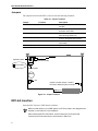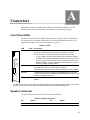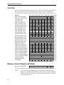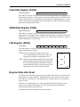
1
EPC - 6A Hardware Reference RadiSys Corporation 5445 NE Dawson Creek Drive Hillsboro, OR 97124 (503) 615-1100 FAX: (503) 615-1150 www.radisys.com 07-0082-05 October 1998 EPC - 6A Hardware Reference EPC, iRMX, INtime, Inside Advantage and RadiSys are registered trademarks of RadiSys Corporation. Spirit, DAI, DAQ, ASM, Brahma and SAIB are trademarks of RadiSys Corporation. † All other trademarks, registered trademarks, service marks, and trade names are the property of their respective owners. October 1998 Copyright 1998 by RadiSys Corporation All rights reserved. ii Contents Chapter 1: Product Description Specifications.................................................................................................................................................... EPC-6A Hardware Features.............................................................................................................................. Differences between the EPC-6 and the EPC-6A............................................................................................. Additional References....................................................................................................................................... 2 2 3 4 Chapter 2: Installation Determine whether to use the EPC-6A as a system controller ......................................................................... Jumpers ...................................................................................................................................................... EPC-6A Insertion.............................................................................................................................................. EXM Module Insertion.............................................................................................................................. VME Backplane Jumpers .......................................................................................................................... Serial Port Cap........................................................................................................................................... Connecting Peripherals to the EPC-8 ....................................................................................................... 5 6 6 7 7 8 8 Chapter 3: Operation Initialization Sequence...................................................................................................................................... ROM DOS Interaction ...................................................................................................................................... System Reset..................................................................................................................................................... Generating VMEbus SYSRESET.............................................................................................................. Responding to VMEbus SYSRESET ........................................................................................................ Front Panel Indicators ....................................................................................................................................... Toggle Switch ................................................................................................................................................... Setup Utilities ................................................................................................................................................... Remote Setup Utility ........................................................................................................................................ Remote Setup Utility Screens (RSU)................................................................................................................ Main RSU Screen ..................................................................................................................................... Clock/Calendar ................................................................................................................................... Drive Configuration................................................................................................................................... VME Control ............................................................................................................................................ EXM Bus ................................................................................................................................................... Exit Menu .................................................................................................................................................. 9 11 12 12 12 12 13 13 13 13 14 14 15 16 17 17 Chapter 4: Programming Interface Memory Map .................................................................................................................................................... I/O Map............................................................................................................................................................. EPC-6A Registers ............................................................................................................................................. VMEbus Accesses ............................................................................................................................................ D32 Accesses............................................................................................................................................. Byte Ordering ............................................................................................................................................ Read-Modify-Write Operations................................................................................................................. Slave Accesses from the VMEbus.................................................................................................................... Self Accesses Across the VMEbus............................................................................................................ 19 19 23 23 24 24 25 25 25 iii EPC-6A Hardware Reference Read-Modify-Write Operations................................................................................................................. VMEbus Interrupt Handler ............................................................................................................................... VMEbus Interrupt Response............................................................................................................................. VMEbus Mapped Registers .............................................................................................................................. 25 26 27 28 Chapter 5: Theory of Operation Processor, Coprocessor, and Memory .............................................................................................................. Application Flash Memory or RFA .................................................................................................................. Flash Boot Device............................................................................................................................................. Nonvolatile SRAM Memory ............................................................................................................................ Battery............................................................................................................................................................... Interrupts ........................................................................................................................................................... Watchdog Timer ............................................................................................................................................... EXMbus ............................................................................................................................................................ VMEbus Interface............................................................................................................................................. VMEbus System Controller Functions ............................................................................................................. VMEbus Timing ............................................................................................................................................... 29 29 30 30 30 31 31 31 32 32 33 Chapter 6: Error Messages Seven-Segment Display Codes ......................................................................................................................... Phoenix NuBIOS Checkpoints ......................................................................................................................... Support Software .............................................................................................................................................. 35 36 39 Chapter 7: Support and Service In North America .............................................................................................................................................. Technical Support...................................................................................................................................... World Wide Web....................................................................................................................................... Repair Services .......................................................................................................................................... Warranty Repairs................................................................................................................................ Non-Warranty Services ...................................................................................................................... Arranging Service............................................................................................................................... Other Countries.......................................................................................................................................... 41 41 41 41 42 42 42 43 Appendix A: Connectors Front Panel LEDs.............................................................................................................................................. Speaker Connector ............................................................................................................................................ Keyboard Connector ......................................................................................................................................... Serial port connectors ....................................................................................................................................... VMEbus Connectors......................................................................................................................................... 45 45 46 46 46 Appendix B: About the Flash Boot Device Forced recovery ................................................................................................................................................ When to Reflash the FBD.......................................................................................................................... Before You Begin............................................................................................................................... Reflashing Processes .......................................................................................................................... Force Update ...................................................................................................................................... 48 49 49 49 49 Appendix C: Registers Overview........................................................................................................................................................... Memory Control Register (81004h) ................................................................................................................. VME A21–16 Address Register (8130h).......................................................................................................... ID Registers (8140h and 8141h) ....................................................................................................................... Device Type Registers (8142h and 8143h)....................................................................................................... Status/Control Registers (8144h and 8145h) .................................................................................................... Slave Offset Registers (8146h and 9147H) ...................................................................................................... Protocol Registers (8148h and 8149h).............................................................................................................. iv 54 54 55 55 55 55 56 57 Contents Response Registers (814Ah and 814Bh) .......................................................................................................... Message High Registers (814Ch and 814Dh)................................................................................................... Message Low Registers 814Eh and 814Fh) ..................................................................................................... VME Modifier Register (8151h) ...................................................................................................................... VME Interrupt State Register (8152h).............................................................................................................. VME Interrupt Enable Register (8153h) .......................................................................................................... VME Event State Register (8154h) .................................................................................................................. VME Event Enable Register (8155h) ............................................................................................................... Module Status/Control Register (8156h) .......................................................................................................... Interrupt Generator Register (815Fh) ............................................................................................................... FSA Address Registers 8380h)......................................................................................................................... Flash Data Register (8383h) ............................................................................................................................. SRAM Data Register 8384h) ............................................................................................................................ LED Register (8385h)....................................................................................................................................... Register State after Reset .................................................................................................................................. 57 58 58 58 59 59 59 59 60 60 60 61 61 61 61 Index .......................................................................................................................................................................... 63 v EPC-6A Hardware Reference Figures Figure 2-1. Figure 3-1. Figure 5-1. Figure B-1. Figure B-2. Jumper locations ..................................................................................................................................................... 6 Boot Process. .......................................................................................................................................................... 9 Block Diagram........................................................................................................................................................ 29 EPC-6A FBD Memory Map ................................................................................................................................... 47 Null Modem Cable Connection .............................................................................................................................. 50 Tables Table 1-1. Table 2-1. Table 3-1. Table 3-2. Table 3-3. Table 3-4. Table 3-5. Table 3-6. Table 3-7. Table 3-8. Table 3-9. Table 4-1. Table 4-2. Table 5-1. Table 5-2. Table 6-1. Table 6-2. Table 6-3. Table 6-4. Table A-1. Table A-2. Table A-3. Table A-4. Table A-5. Table B-1. vi Specifications.......................................................................................................................................................... Jumper locations ..................................................................................................................................................... Main Menu Selections ............................................................................................................................................ Clock/Calendar ....................................................................................................................................................... Drive Configuration................................................................................................................................................ Configure Floppy Drive A and B ........................................................................................................................... Configure Fixed Disk C and D ............................................................................................................................... Edit Subtype............................................................................................................................................................ VME Control .......................................................................................................................................................... ULA Setup .............................................................................................................................................................. Slave Memory Base ................................................................................................................................................ I/O Map.................................................................................................................................................................. VME mapped registers .......................................................................................................................................... Interrupts................................................................................................................................................................. VMEbus timing...................................................................................................................................................... Seven-segment display failure codes...................................................................................................................... Phoenix‘ NuBIOS Auxiliary Checkpoint Codes .................................................................................................... Phoenix‘ NuBIOS Checkpoint Codes..................................................................................................................... Phoenix‘ NuBIOS Boot Block Checkpoint Codes ................................................................................................. LEDs ....................................................................................................................................................................... Speaker Connector.................................................................................................................................................. Keyboard Pin-out.................................................................................................................................................... COM1 Connector.................................................................................................................................................... COM2 Connector.................................................................................................................................................... FBD object placement ............................................................................................................................................ 2 6 14 14 15 15 15 16 16 17 17 19 28 31 33 35 36 38 39 45 45 46 46 46 48 Chapter 1 Product Description 1 This manual contains the information you need to install and use the EPC-6A VMEbus controller. Additional user and programmer manuals discuss the use of software packages available with the EPC-6A. The EPC-6A, a high-speed VMEbus module based on the Intel 80486DX2 processor, is a redesign of the EPC6 VMEbus module which is based on Intel 80386SX processor. You can use the EPC-6A to: • Perform VMEbus master accesses. • Act as a VMEbus slave (by having its dual-port DRAM mapped onto the VMEbus). • Configure as the VMEbus SLOT-1 system controller. • Act as an interrupter and interrupt handler. The EPC-6A computer is also compatible with the IBM PC hardware architecture. The standard version of the EPC-6A contains, in ROM, a PC-compatible BIOS and a ROM-based version of Datalight ROM-DOS. The EPC-6A also includes on-board nonvolatile flash memory supported as a DOS-compatible solid-state disk and file system. You can store one or more embedded applications on the processor board and automatically invoke them at system start-up. The EPC-6A also includes one slot for an EXM expansion module. This allows some of the I/O of the EPC-6A to be customized for a particular application. 1 EPC-6A Hardware Reference Specifications This table defines the power and environmental specifications of the EPC-6A. Table 1-1. Specifications Characteristic Temperature Humidity Altitude Vibration Shock Current VME VXI Value operating 0 – 60°C ambient storage –40 – 125°C (without battery; 85°C max with battery operating 0 – 90% noncondensing storage 0 – 95% noncondensing operating 0 – 10,000 ft. (3000 m) storage 0 – 50,000 ft. (15,000 m) operating 0.015 inch (0.38 mm) P-P displacement with 2.5 g peak (max) acceleration over 5–2000 Hz storage 0.030 inch (0.76 mm) P-P displacement with 5.0 g peak (max) acceleration over 5–2000 Hz operating 30 g, 11 ms duration, half-sine shock pulse storage 50 g, 11 ms duration, half-sine shock pulse typical 5V @ 3.4A, 12V @ 5 mA, –12V @ 10 mA master address A16, A24 master transfer D08(EO), D16, RMW slave address A16, A24 slave transfer D08(EO),D16,RMW interrupter (1–7) interrupt handler D08(O),D16 IH(1–7) requester ROR,RONR arbiter RRS,PRI system controller SYSCLK, IACK daisy chain, bus timer device type message based protocols cmdr/master/interrupter EPC-6A Hardware Features 2 • Intel 486DX2 CPU at 66MHZ (internal clock speed); external bus speed at 33MHz. • 8KB On-Chip Cache • Integrated Floating Point Unit (DX2 option only) • RadiSys R400EX highly integrated single chip system controller • 4 MB dual ported DRAM on board • Two PC compatible serial ports with 16-Byte FIFO (only one is brought out to the faceplate) • 1MB of application flash memory • 128K x 8Bit of battery-backed SRAM • Keyboard port • Seven-segment display Chapter 1: Product Description • A24/A16/D16/D08 VME master/slave support • Slot 1 system controller functions • One EXM expansion slot It should be noted that, due to mechanical limitations, the EPC-6A cannot support EXMs such as EXM-9, EXM-MX, EXM-16, EXM-23, EXM-19, EXM20, EXM-17. Differences between the EPC-6 and the EPC-6A The EPC-6A differs from the EPC-6 in the following ways: EPC-6 20Mhz 80386SX PCAT design External 16K byte 2 way set-associative cache External cache controller External co-processor option AT chip set [ATU + DPU] and separate memory controller MB dual ported DRAM Two serial ports Up to 512K bytes of programmable flash memory (for DOS/user applications). Up to 512K EPROM (for BIOS, ROM). Award BIOS 32 KB of battery-backed SRAM EPC-6A 486DX2 [66Mhz internal speed] with 33Mhz external bus speed PCAT design 8K- Byte On-Chip Cache Integrated floating-point unit RadiSys R400 highly integrated single chip system controller [low cost 208 pin PQFP] 4 Megabytes dual ported DRAM on board Two PC compatible serial ports with 16-Byte FIFO 1MB of application flash memory contains Datalight ROM-DOS 6.22 [rev2] Separate boot device with reflash option The System BIOS is based on Phoenix Technologies NuBIOS revision 4.05. The Flash File System can be installed as a DOS device driver. Flash File System (FFS) support for flash is based on Phoenix Technologies PicoFlash and includes read/write capability. The Xformat based FFS is no longer supported for Flash. IRQ12 is not available on EXM bus VMEbus and Memory Controller Configuration register (8104h) semantics changed. System BIOS does not share space in the FBD with ROMDOS. DOS now resides in the RFA. EXM-2 and EXM-2A are no longer supported. 128KX8Bit of battery backed SRAM with software supports only 32KB SRAM. 3 EPC-6A Hardware Reference Additional References PhoenixBIOS† 4.05 Developer’s Reference, Phoenix Technologies, Ltd., 5/22/95 (NOTE: This document cannot be distributed to customers). PhoenixBIOS 4.0 Technical Reference, Phoenix Technologies, Ltd., 3/15/94 (NOTE: This document can be distributed to customers only upon receipt of written permission from Phoenix Technologies, Ltd.). PhoenixBIOS PICO OAK Porting Guide, Phoenix Technologies, Ltd., 9/95 (NOTE: This document can be distributed to customers only upon receipt of written permission from Phoenix Technologies, Ltd.). Plug and Play BIOS Specification 1.0A, Compaq Computer Corp., Phoenix Technologies Ltd., Intel Corp., May 5, 1994. Memory Products Data Manual, Intel Corporation, 1993. Intel486† Microprocessor Family Programmer’s Reference Manual, Intel Corporation, 1992. R400EX Development Specification, Version 3.23, RadiSys Corporation, 1996. EPC-6A Hardware Specification, RadiSys Corporation, 1997. Technical Reference, Personal Computer AT, International Business Machines Corporation, 1985. 4 Chapter 2 Installation 2 Before installing your EPC-6A, you should unpack and inspect it for shipping damage. Avoid causing ESD damage: • Remove modules from their antistatic bags only in a static-free environment. • Perform the installation process (described later in this chapter) only in a static-free environment. EPC-6A modules, like most other electronic devices, are susceptible to ESD damage. ESD damage can cause a partial breakdown in semiconductor devices that might not immediately result in a failure. Determine whether to use the EPC-6A as a system controller Before installing the EPC-6A in a VMEbus chassis, you need to decide whether the EPC6A will be the VMEbus Slot 1 System controller. Every VMEbus system needs a module that performs the system controller functions, including generation of the 16 MHz SYSCLK signal, arbitration of the bus, detection of Bus time-out conditions, and initiation of the interrupt-acknowledge daisy chain. The EPC-6A can serve as the system controller. To use the EPC-6A as the system controller: • Make sure the jumper labelled SLOT1 is installed on the EPC-6A processor board to connect the two pins. For information about jumper locations, see Figure 2-1, Jumper locations on page 6. • Install the EPC-6A in the leftmost slot on the chassis. If you do not plan to use the EPC-6A as the system controller: • Make sure the jumper labelled SLOT1 on the EPC-6A processor board is removed. • Install EPC-6A in a slot other than slot 1 in the chassis. Other jumpers and headers on the board are shown in the next table. 5 EPC-6A Hardware Reference Jumpers The jumpers located on the EPC-6A are used for the following functions: Table 2-1. Jumper locations Jumper Function FLASHWE (JP2(1-2)) FBD write-enable Description Install this jumper to enable writes to the FBD. BB_ENB (JP2(3–4)) FBD boot block write enable Install this jumper to enable writes to the boot block of the FBD. POSTLP (JP2(5–6)) Manufacturing loop enable Install this jumper to enter the manufacturing POST loop. FRCUPDT (JP2(7–8)) Force BIOS recovery Install this jumper to force a BIOS recovery during the boot process. SLOT1 (H2) Slot 1 Functionality Install this jumper to enable Slot 1 functionality SPEAKER (JP3) Speaker Speaker header Speaker header RFA write enable write enabled 1 COM2 header Battery JP2 1 System controller jumper—Install if EPC-6A is VMEbus system controller VMEbus P1 Figure 2-1. Jumper locations EPC-6A Insertion Insert the EPC-6A into a VME chassis as follows: Make sure that power to your VME system is off. The module is not designed to be inserted or removed from a live backplane. When inserting the EPC-6A module, avoid touching the circuit board and connector pins, and make sure the environment is static-free. 6 Chapter 2: Installation 1. Make sure the ejector handles are in the normal non-eject position. (Push the top handle down and the bottom handle up so that the handles are not tilted.) 2. Slide the EPC-6A module into the VME chassis, making sure the top and bottom board edges are in the chassis’ card guides. Use thumb pressure on the handles to mate the module firmly with the VME backplane connector. 3. Tighten the two screws in the top and bottom of the front panel to ensure proper connector mating and prevent loosening of the module via vibration. EXM Module Insertion You can optionally install one EXM through the front panel of the EPC-6A. To install an EXM: Make sure that power to your VME system is off. EXMs are not designed to be inserted or removed from live systems. When inserting an EXM, avoid touching the circuit board, and make sure the environment is static-free. 1. Remove and save the blank face plate from the EXM slot in the EPC-6A face plate. 2. Slide the EXM into place in the card guides. Push firmly on the EXM front panel to insert its rear connector. 3. Tighten the thumb screws on the EXM’s face plate. The EPC-6A can accept most EXM types excluding those that either require a disk BIOS in the EPC or do not fit by form factor. Once an EXM is installed, you must to run the BIOS setup program to describe how the specific EXM should be dynamically configured upon power-up. This is described in 3, Operation. VME Backplane Jumpers The VMEbus contains several daisy-chained control signals. Almost all VMEbus backplanes contain jumpers for these control signals to allow systems to operate with empty slots. Failing to install these jumpers properly is a common source of problems in building a new VMEbus system. There are five jumpers per VME slot, one for each of the four bus-grant arbitration levels and one for the interrupt-acknowledge daisy chain. Depending on the backplane manufacture, the jumpers may be on the rear pins of the J1 connector, or may be alongside it on the front or rear side of the backplane. For the slot that contains the EPC-6A, remove the jumpers. Leave the jumpers inserted for all empty slots. For slots otherwise occupied, consult the documentation from the manufacturers of the modules. 7 EPC-6A Hardware Reference Serial Port Cap Your EPC-6A may have been shipped with a plastic cap over the serial port connector. This cap is a conductive cap that shields the exposed pins in the connector from ESD (electrostatic discharge). You should leave it installed when nothing is connected to the serial port. Connecting Peripherals to the EPC-8 Do not: • Plug any cable or connector into the front panel connectors while the system is powered up. • Plug in a serial or parallel device, keyboard, transceiver, monitor, or other component while the system is ON. In general, electronics equipment are not designed to withstand damage that may arise from fluctuations in power. The next step of installation is connecting peripherals, typically a video display and keyboard, but also perhaps a mouse, modem, printer, etc. Pin-outs for the EPC-6A front-panel connectors are specified in Appendix A, Connectors. 8 Chapter 3 3 Operation This chapter contains information about user operation and BIOS setup of the EPC-6A. Initialization Sequence The EPC-6A and its BIOS go through these major initialization steps: The seven-segment display shows information about the EPC-6A’s initialization state. Reset 1. Display 2. Run selftests; display number of test 3. Shadow PicoFlash RFA BIOS extension Catastrophic Errors? Yes Display failure number No Config errors? No Yes Log EXM errors to SRAM 4. Attempt to boot from RFA Done Figure 3-1. Boot Process. 9 EPC-6A Hardware Reference The EPC-6A performs these major initialization steps: 1. Display At power-up, this display reads 8. When the system begins the POST (Power On Self Test), this number changes. 2. Run selftests; display At various times during the POST, a new code displays in the 7-segment display. For detailed information about displayed codes, see the POST code description. To see a list and explanation of these codes, see Chapter 6, Error Messages. 3. Shadow PicoFlash RFA BIOS extension To access the RFA (Resident Flash Array) as a DOS disk, you must shadow a BIOS extension that chains the INT13 disk interface. This checkpoint essentially starts a flash disk driver. a. Check for catastrophic errors Any error that prevents the system from reaching INT 19 (which attempts to boot the OS) halts the system. The 7-segment LED displays the last completed POST task and the initialization sequence terminates. If the EPC-6A has a problem that prevents the POST program from running, the 7-segment LED displays the number “8”. b. Check for configuration errors Errors that do not prevent the system from booting that the CMOS configuration can correct are considered configuration errors. An example of a configuration error is an incorrect EXM ID entered for an EXM card. If the selftest completes successfully, the system is configured using configuration information maintained by the BIOS in a small battery-backed CMOS RAM. If a problem is encountered, it causes the BIOS to load MS-DOS from RFA and then give DOS control. This allows the user to alter the boot process. MS-DOS always loads from flash, which is a read-write file system. It is recommended that you embed ABORTSWI.EXE your AUTOEXEC.BAT file to allow users to alter the machine’s boot process. During development, users may find it convenient to expose the keyboard connector so they can press the F8 key to step through the CONFIG.SYS and AUTOEXEC.BAT files. The method for interacting with DOS is described in the next section. Problems at this point are regarded as non-catastrophic, and include loss of the configuration information due to a battery failure or change, and a mismatch between the type of installed EXM versus the type expected. Information about non-catastrophic errors is saved in the upper 2K bytes of the SRAM for use by the setup program. If there are no errors, the BIOS looks for a boot device with a valid boot image. The boot device can be the on-board flash memory or a source specified in the CMOS configuration information (using the setup program) If a boot device is not present, the BIOS invokes the ROM DOS. 10 Chapter 3: Operation 4. Attempt to boot from RFA If the BIOS proceeds down the flash memory path, the flash memory is viewed as a bootable disk device and the BIOS starts the bootstrap process by loading the first 512 bytes into memory location 07C0:0000 and passing control to it. The display blanks before the bootstrap process begins. Once the system completes POST, an INT19 is attempted. This attempts to read the boot sector from the disk. In the EPC-6A’s case, this is routed through an INT13 handler which reads the boot sector from the RFA. For more information about the bootstrap process and how to create a bootable image in the flash memory, see the EPControl Programmer’s Guide. In the event that an invalid CMOS setup is saved or the disk image becomes un-bootable it will be necessary to go into forced recovery. From forced recovery, it is possible to restore CMOS values to there factory defaults. It is also possible to reload the factory default bootable DOS image into the RFA should it become corrupt or mis-configured. For more on these items, see Forced recovery section on page 48. ROM DOS Interaction Although you can use a standard PC-compatible keyboard, the EPC-6A is used more as a dedicated controller than an embedded PC-compatible computer. When using the EPC-6A without a keyboard, you can interact with the ROM DOS on the EPC-6A in these ways: • Connect a standard ASCII terminal with an RS-232 interface to the serial port connector on the front panel. The EPC-6A’s customized CONFIG.SYS and AUTOEXEC.BAT files redirect the command input and output streams to the COM1 serial port. Connecting a terminal and invoking ROM DOS displays the standard DOS prompt on the terminal. By typing the DOS DIR command, you can see available programs. You can use the SETUP program in ROM to display and change the configuration information maintained by the BIOS. • Use a separate full EPC (having keyboard and monitor) on the same VMEbus with supplied software that uses this EPC as a virtual console to the EPC-6A(s). The software needed to use another EPC as the human interface for an EPC-6A is part of the EPControl software product. For detailed information about this software, see the EPControl software’s documentation. 11 EPC-6A Hardware Reference System Reset The reset switch performs a hardware reset of the EPC-6A and any EXM module, and then invokes the BIOS initialization process discussed in the previous sections. Removing and reapplying power to the EPC-6A also causes a hardware reset. Note that if the dot, or decimal point, in the lower right corner of the 7-segment LED display is illuminated, an EPC-6A program disabled the reset toggle switch. To reset the EPC-6A in this case, you must externally signal the VMEbus SYSRESET (unless the EPC-6A program has disabled this also) or by a power-off/on cycle. Generating VMEbus SYSRESET Upon power on, the EPC-6A drives the VMEbus SYSRESET signal in accordance with the VMEbus specification. Resetting the EPC-6A via the reset switch does not cause the EPC-6A to assert SYSRESET. The EPC-6A does contain a software-controllable register bit to allow software to assert SYSRESET. Responding to VMEbus SYSRESET A software-controllable register bit in the EPC-6A controls whether or not a hardware reset of the EPC-6A occurs when the VMEbus SYSRESET signal is asserted. Front Panel Indicators The front panel contains a seven-segment LED display. The front-panel display has these purposes: 1. During BIOS initialization it describes the current stage of the initialization. If a test fails in the selftest phase, it displays a code indicating the test that caused the BIOS to abort the normal initialization flow. These codes are described in Chapter 6, Error Messages. 2. After initialization, the display is available for use by the application program. 3. The display shows whether software disabled the reset function of the front-panel switch. If the decimal point in the lower right corner of the display is lit, the reset function of the switch is disabled. The EPC-6A also contains the following LEDs: • RUN • SYSFAIL • MASTER • SLAVE For detailed information about the LEDs, see Front Panel LEDs on page 45. 12 Chapter 3: Operation Toggle Switch The front-panel toggle switch has these positions: • Inactive (normal position): • Reset: Suspends the EPC-6A; releasing the switch causes a hardware reset. • Abort: Generates the IRQ11 interrupt. The interrupt position has two purposes. An application program can install an IRQ11 interrupt handler and thus define the switch in an application-specific fashion. The second purpose is a special interpretation of the switch during BIOS initialization after a reset. Moving the switch to the interrupt position during the five-second operator-override period (when the display shows a circling light), causes the BIOS to load MS-DOS from ROM and give control to DOS. Setup Utilities Unlike other RadiSys products, the EPC-6A uses, as its primary CMOS setup utility, a remote setup utility (either serial or across the VMEbus) rather than a monitor/keyboard based approach. This is due to the EPC-6A’s default configuration, where no keyboard or video is available. For debug purposes, an EXM video card is installed and the PS/2 keyboard port is available. This means you can use the standard Phoenix CMOS setup utility. Remote Setup Utility The EPC-6A has DOS, remote setup, and other utilities located in a read/write flash disk which (however unlikely) can be corrupted. If the RFA can no longer boot DOS, the DOS-based setup program is not available. The remote setup controls a subset of all the possible Phoenix Setup options. Only those CMOS tokens absolutely necessary for booting are manipulated by the setup utility. The number of tokens modified are limited to reduce the FFF impact of the EPC-6A versus EPC-6. Remote Setup Utility Screens (RSU) The Remote Setup Utility Screens appear the same, whenever possible, as those of the EPC-6. Menu selections are driven by typing the character listed in the key column. Pressing the ESC key from a sub-menu returns to the previous menu. Pressing the ESC key from the Main Screen starts the exits procedure. 13 EPC-6A Hardware Reference Main RSU Screen The next figure shows the layout of the main remote setup screen; the following tables describes menus and their options. +----------------------------------------------------------------------------+ ¦ RadiSys Controller Setup Program, Version 2.01 ¦ ¦ Copyright 1997 by RadiSys Corporation. All rights reserved. ¦ +----------------------------------------------------------------------------¦ ¦ SYS EPC: 6A CPU: 486DX2 Mem: 640K ¦ ¦ Info BIOS: 4.05 Mhz: 66 Ext-Mem: 3072K ¦ ¦ ¦ ¦ Clock Time: 00:05:08 Date: 01/01/97 ¦ ¦ ¦ ¦ Disks Floppy A: None Floppy B: None ¦ ¦ Fixed C: IDE AUTO Subtype C: 541MB 1049C, 16H, 63S ¦ ¦ Fixed D: None Subtype D: None ¦ ¦ ¦ ¦ VME Release mode: RONR (VXI) Arb Mode: Round Robin ¦ ¦ Bus Arb Priority: 0 Module ULA: F8 (FE00) ¦ ¦ Slave Mem: 400000 (A24) ¦ ¦ ¦ ¦ EXM ID: None OB1: 0x00 OB2: 0x00 ¦ +----------------------------------------------------------------------------+ Main Menu: 1) Clock 2) Disk 3) VME 4) EXM 5) eXit Choice: Table 3-1. Main Menu Selections Function Clock Disks VMEBus EXMBus eXit Key C V D E X Description Set Date and Time Enter the VMEBus configuration menu Enter the Drive Configuration menu Enter the EXMBus configuration menu Exit the Remote Setup program Clock/Calendar Clock Edit Menu: 1) Date Choice: 1 Format: <mm/dd/yy> Enter New Value: 2) Time Table 3-2. Clock/Calendar Function Date Time 14 Key D T Description Enter new date (mm/dd/yy) Enter new time (hh:mm:ss) Chapter 3: Operation Drive Configuration Edit Drive Menu: 1) Floppy A Choice: 2) Floppy B 3) Fixed C 4) Fixed D Table 3-3. Drive Configuration Function Floppy A: Floppy B: Fixed Disk C: Fixed Disk D: Key A B C D Description Configure Floppy Drive A: (sub-menu) Configure Floppy Drive B: (sub-menu) Configure Fixed Disk C: (sub-menu) Configure Fixed Disk D: (sub-menu) Table 3-4. Configure Floppy Drive A and B Function 360K (5.25) 1.2M (5.25) 720K (3.5) 1.44M (3.5) None Key 1 2 3 4 N Description Configure floppy for 360K Configure floppy for 1.2M Configure floppy for 720K Configure floppy for 1.44M Disable floppy Edit Fixed Drive Menu: 1) IDE 2) Flash 5) None 6) Edit Subtype Choice: 3) VME 4) EXM Flash Table 3-5. Configure Fixed Disk C and D Function IDE Flash VME EXM Flash None Edit Subtype Key A F V E N U Description Configure Fixed Disk for AT (IDE) Configure Fixed Disk for Flash Configure Fixed Disk for VMEbus Configure Disk for EXM Flash Disable Drive Edit User Hard Drive Parameters (sub-menu) 15 EPC-6A Hardware Reference Edit Subtype Menu: 1) Autodetect Choice: 2) Edit Table 3-6. Edit Subtype Function Autodetect Key A Edit E Description Autodetect drive parameters. Selecting this option means the Remote Setup queries the disk drive for its internal parameters on every bootup. Configure Fixed Disk for Flash (sub-menu). Selecting this option displays these prompts which must be completed with the proper parameters: • # of Heads: Enter the number of heads on the drive • # of Cylinders: Enter the number of cylinders per head • # of Sectors: Enter the number of sectors per cylinder VME Control VME Bus Menu: 1) Release Mode 5) Slave Mem Choice: 2) Arb Mode 3) Arb Priority 4) Module ULA Table 3-7. VME Control Function Release mode Arbitration mode Arbitration Priority Module ULA Slave Mem 16 Key R A P U S Description Bus release mode, a) ROR or b) RONR (AB)? Bus arbitration mode, Priority or Round robin (PR)? Bus arbitration priority, (0123)? Module ULA (sub-menu) Slave base address Chapter 3: Operation ULA Menu: 1) F8 (FE00) 5) FC (FF00) Choice: 2) F9 (FE40) 6) FD (FF40) 3) FA (FE80) 7) FE (FF80) 4) FB (FEC0) 8) FF (FFC0) Table 3-8. ULA Setup Function F8 (FE00) F9 (FE40) FA (FE80) FB (FEC0) FC (FF00) FD (FF40) FE (FF80) FF (FFC0) Key 0 1 2 3 4 5 6 7 Slave Base Memory Menu: 1) Disabled 2) 000000 5) C00000 Choice: Description Set ULA to FE00 Set ULA to FE40 Set ULA to FE80 Set ULA to FEC0 Set ULA to FF00 Set ULA to FF40 Set ULA to FF80 Set ULA to FFC0 3) 400000 4) 800000 Table 3-9. Slave Memory Base Function Disabled 000000 (A24) 400000 (A24) 800000 (A24) C00000 (A24) Key 0 1 2 3 4 Description Disable Slave Memory Access Set Slave Base Address to 0 Set Slave Base Address to 400000 Set Slave Base Address to 800000 Set Slave Base Address to C00000 EXM Bus Since there is only one EXM slot available, only one can be configured. When you select EXM from the main menu, the following prompts display: Enter the EXM ID = a hex value or ‘none’ Enter the EXM OB1 = a hex value Enter the EXM OB2 = a hex value Exit Menu If you select ‘X’ at the main menu, the exit procedure starts. Changes take effect only after a reboot. 17 EPC-6A Hardware Reference 18 Chapter 4 Programming Interface 4 This chapter describes the EPC-6A as seen by a program. Wherever possible, users should avoid direct use of most of these facilities. Hardware features in common with standard PCs should be accessed by standard BIOS calls. Hardware unique to EPC-6A, such as the VMEbus interface should be accessed through a variety of software packages and drivers available with the EPC-6A. Memory Map Memory at addresses between 0 and 4 MB (0FFFFFh) are mapped as follows: Range 000000h 0A0000h 0C0000h 0C8000h 0E0000h 0F0000h 100000h 400000h F80000h – – – – – – – – – 09FFFFh 0BFFFFh 0C7FFFh 0DFFFFh 0EFFFFh 0FFFFFh 3FFFFFh F7FFFFh FFFFFFh Content DRAM Uncommitted, EXM bus or VIDBIOS Uncommitted, DRAM, EXM bus or VIDBIOS Uncommitted, mapped to EXM bus Mappable window onto VMEbus System BIOS DRAM Uncommitted, EXM bus BIOS ROM I/O Map The following defines the I/O addresses decoded by the EPC-6A. It does not define addresses that might be decoded by the installed EXM. Table 4-1. I/O Map Port 00 01 02 03 04 05 06 07 08 09 Functional group DMA Usage Channel 0 address Channel 0 count Channel 1 address Channel 1 count Channel 2 address Channel 2 count Channel 3 address Channel 3 count Command/status DMA request 17 EPC-6A Hardware Reference Port 0A Functional group 0B 0C 0D 0E 0F 20 21 24 26 40 41 42 43 60 61 64 70 71 80 81 82 83 87 89 18 Interrupt controller 1 83000 Controller Timer Keyboard controller NMI status Keyboard controller Real-time clock BIOS debug port DMA Usage Command register (R) Single-bit DMA request mask(W) Mode Set byte pointer (R) Clear byte pointer (W) Temporary register (R) Master clear (W) Clear mode reg counter (R) Clear all DMA req mask(W) All DMA request mask Port 0 Port 1 Data register Index register Counter 0 Counter 1 Counter 2 Control (W) Data I/O register NMI status Command/status register RTC index reg / NMI enable RTC data register 0 1 2 3 4 5 6 7 8 9 A B C D E ... 3F Channel 2 page register Channel 3 page register Channel 1 page register Channel 0 page register Channel 6 page register seconds seconds alarm minutes minutes alarm hours hours alarm day of week date of month month year status A status B status C status D RAM RAM Chapter 4: Programming Interface Port 8A 8B 8F A0 Port A1 C0 C2 C4 C6 C8 CA CC CE D0 D2 D4 Functional group Interrupt controller 2 Functional group DMA D6 D8 DA DC DE F0 F1 2F8 Coprocessor COM2 serial port 2F9 2FA 2FB 2FC 2FD 2FE 378 379 37A 3F8 3F9 3FA 3FB LPT1 parallel port COM1 serial port Usage Channel 7 page register Channel 5 page register Refresh page register Port 0 Usage Port 1 Channel 4 address Channel 4 count Channel 5 address Channel 5 count Channel 6 address Channel 6 count Channel 7 address Channel 7 count Command/status DMA request Command register (R) Single-bit DMA req mask(W) Mode Set byte pointer (R) Clear byte pointer (W) Temporary register (R) Master clear (W) Clear mode reg counter (R) Clear all DMA req mask (W) All DMA request mask Clear coprocessor busy Reset coprocessor Receiver/transmitter buffer Baud rate divisor latch (LSB) Interrupt enable register Baud rate divisor latch (MSB) Interrupt ID register Line control register Modem control register Line status register Modem status register Printer data register Printer status register Printer control register Receiver/transmitter buffer Baud rate divisor latch (LSB) Interrupt enable register Baud rate divisor latch (MSB) Interrupt ID register Line control register 19 EPC-6A Hardware Reference Port 3FC 3FD 3FE 8104 8130 8132 8134 8136 8140 8141 8142 8143 8144 8145 8146 8147 8148 8149 814A 814B 814C 814D 814E 814F 8151 8152 8153 8154 8155 8156 8157 8159 815A 815B 815C 815D 815E 815F 8380 8381 8382 8383 8384 20 Functional group VME and misc control Usage Modem control register Line status register Modem status register Memory control VME A21–16 address alias address of 8130 alias address of 8130 alias address of 8130 ID low ID high Device type low Device type high Status/control low Status/control high Slave offset low Slave offset high Protocol low Protocol high Response low Response high Message high low Message high high Message low low Message low high VME modifier VME interrupt state VME interrupt enable VME event state VME event enable Module status/control alias address of 815F alias address of 8151 alias address of 8152 alias address of 8153 alias address of 8154 alias address of 8155 alias address of 8156 VME interrupt generator Flash/SRAM address Flash/SRAM address Flash/SRAM address Flash data SRAM data Chapter 4: Programming Interface EPC-6A Registers The next table lists registers in the I/O space specific to the EPC-6A. For detailed information about each register, see Appendix C, Registers. EPC-6A Registers Memory Control Register (81004h) VME A21–16 Address Register (8130h) ID Registers (8140h and 8141h) Device Type Registers (8142h and 8143h) Status/Control Registers (8144h and 8145h) Slave Offset Registers (8146h and 9147H) Protocol Registers (8148h and 8149h) Response Registers (814Ah and 814Bh) Message High Registers (814Ch and 814Dh) Message Low Registers 814Eh and 814Fh) VME Modifier Register (8151h) VME Interrupt State Register (8152h) VME Interrupt Enable Register (8153h) VME Event State Register (8154h) VME Event Enable Register (8155h) Module Status/Control Register (8156h) Interrupt Generator Register (815Fh) FSA Address Registers 8380h) Flash Data Register (8383h) SRAM Data Register 8384h) LED Register (8385h) Register State after Reset VMEbus Accesses Two C-language examples are given here for performing VMEbus accesses through the E page. Example 1: 16-bit read from the VMEbus A16 space This example performs a 16-bit read from the VMEbus A16 space. It requires setting the address modifier, relocating the A16 address into the E page (address range E0000– EFFFF), and then accessing the value pointed to by a C pointer variable. #define WORD unsigned short #define LWORD unsigned long WORD addr; /* 16-bit A16 address */ WORD data; WORD far * wptr; outp(0x8151,0x0A); /* Set address modifier to A16 supervisory access */ wptr = (WORD far *) (0xE0000000L + addr); data = *wptr; /* Read through window */ Example 2: Byte write into the VMEbus A24 space This next example does a byte write into the VMEbus A24 space. Here the upper 8 bits of the VME address need to be stored in the appropriate registers. LWORD addr; /* 32-bit A24 address */ BYTE data; BYTE far * wptr; outp(0x8151,6 | (((addr << 8) >> 30) << 6)); /* A23–A22 and address modifier for A24 supervisory data access 21 EPC-6A Hardware Reference */ outp(0x8130,(WORD)((addr << 10) >> 24); /* A21–A16 */ wptr = (BYTE far *) (0xE0000000L + (addr & 0X0000FFFFL)); *wptr = data; /* Write through window */ The success of the access can be checked either by enabling BERR as an interrupt or by looking at the BERR bit in the event state register after each access. Since writes are pipelined, software that looks at the BERR bit should first wait until the DONE bit is set. It is recommended that rather than performing accesses in this low-level, hardware-dependent form, the Bus Manager component of the EPConnect software package be used instead. The following summarizes the source of the VMEbus address lines for accesses through the E page. 23 22 A24 From port 8151 21 16 15 From port 8130 0 From 486DX2 address bits 15–0 15 A16 0 From 486DX2 address bits 15–0 D32 Accesses Although the 386SX, used in the original EPC6, is a 32-bit processor (for example, 32-bit registers and operations), its external data bus is 16 bits wide. Any memory operation with an operand width of 32 bits is broken apart by logic in the processor to two 16-bit operations. As a result the EPC-6A, using the same VME interface and being a replacement for the EP6, never performs a VMEbus D32 access. Byte Ordering Unlike EPCs that have 32-bit buses, EPC-6A does not contain software-controlled byte-ordering hardware. The principal reason is that, as described in the previous section, EPC-6A never performs VMEbus D32 accesses, and therefore there is no feasible way in hardware to support both forms of byte ordering on what a program would see as a 32-bit access. EPC-6A accesses the VMEbus in little-endian (Intel) byte ordering, meaning that, for a 16-bit numerical value, the least-significant byte is assumed to be at the lowest memory address. This means, for instance, that if a big-endian processor (for example, Motorola 680x0) stored the 16-bit value 0102h, the EPC-6A would interpret its value as 0201h. If a big-endian processor stored the 32-bit value 01020304h and it were fetched by a program on the EPC-6A as a 32-bit operand (meaning, as explained above, the EPC-6A would perform two 16-bit accesses), the EPC-6A program would see the value as 04030201h. The EPConnect Bus Manager software provides functions for swapping byte ordering during memory-copy operations. 22 Chapter 4: Programming Interface Read-Modify-Write Operations VMEbus RMW (read-modify-write) cycles can be performed through use of the 486DX2’s LOCK instruction prefix with certain instructions along with BS16# being asserted. All of these instructions perform a read followed by a write. When such a read occurs that is mapped to the VMEbus, the EPC-6A treats it as the start of a VME RMW cycle. The next VME access from the 486DX2 is treated as the write that terminates the RMW cycle. For this reason, RMW accesses that cross a 16-bit boundary will not behave as expected (because the 486DX2 issues two read accesses). Slave Accesses from the VMEbus When SLE in the status/control register is set, the EPC-6A responds to accesses in a 4 MB range of the A24 space. All types of VME accesses (reads, writes, and read-modify-writes of all lengths) are supported, except for block transfer cycles and D32 accesses, as a result of EPC6 compatibility. The address modifier can specify supervisory, nonprivileged, program, or data. The 4 MB space occupied by the EPC-6A in the VMEbus A24 space has the same view of EPC-6A memory as the 486DX2, except that only those accesses that map to EPC-6A DRAM memory are valid; all others respond with BERR. Self Accesses Across the VMEbus Since the EPC-6A’s DRAM can be mapped into the VMEbus A24 address space, the EPC-6A can access its DRAM in an alternate way—by generating VMEbus accesses to the appropriate addresses. This can be of use in multiple-processor systems where some of the EPC-6A’s DRAM is used as shared global memory; it means that the EPC-6A can access the global memory with the same addresses as used by other processors without needing to understand that the memory is actually on-board. This ability is also useful in system checkout (for example, checking operation of the backplane). A24 slave accesses result in accesses to the on-board DRAM and never to the cache. Because the EPC-6A’s cache is a write-through cache, there is never a discrepancy between data in the cache and the DRAM. When a slave access results in a write into the DRAM, the EPC-6A automatically purges the cached entry, via cache invalidation operation. Read-Modify-Write Operations The EPC-6A provides synchronization integrity in its local DRAM between accesses from the 486DX2 into the DRAM and RMW VME accesses from other masters into the DRAM. When a VMEbus slave read access occurs to the local DRAM, the EPC-6A watches the VMEbus data and address strobes to determine if the cycle is an RMW cycle. If it is, accesses by the 486DX2 are held up until the terminating access of the RMW cycle occurs. 23 EPC-6A Hardware Reference When the 486DX2 performs a locked access (for example, via an instruction using the LOCK instruction prefix) to the local DRAM, VMEbus slave accesses are held up until the last locked access completes. VMEbus Interrupt Handler Although software available for the EPC-6A shields the user from the details of interrupt handling, the following information is provided for the reader who needs further detail. The relationship between VME interrupts (and other interrupt-causing events) and an interrupt as seen by a program is shown in the following diagram. VME interrupt state register RRDY WRDY IRQ1 M IRQ2 VMEbus interrupts VME interrupt enable register A IRQ3 IRQ4 S IRQ5 K IRQ6 IRQ7 SYSFAIL M A S K BERR (sticky) ACFAIL PC architecture IRQ10 WDT VME event state register VME event enable register Interrupts and events are visible in two state registers. These are unlatched, meaning that a read of the state register shows the actual state of the signals at the instant of the read. The exception is BERR, which is a “sticky” bit, meaning that the bit signifies whether BERR had ever been asserted. The convention used is that a 0 bit signifies an asserted (interrupting) state. The primary purpose of the state registers is to let the interrupt handler software determine which interrupts and events generated the IRQ10 interrupt to the processor. The state registers can also be read by non-interrupt-handler software to poll for the state of these signals. The enable registers allow one to mask selectively these 12 states. A 0 state bit and a corresponding 1 enable bit causes the PC architecture IRQ10 interrupt to be asserted. 24 Chapter 4: Programming Interface Unlike the 12 input conditions, which are level sensitive inputs, the PC architecture defines the PC interrupts, such as IRQ10, as edge sensitive. This requires special attention if you are writing your own interrupt handlers (for example, if you are not using the functions in the Bus Manager software). Because IRQ10 is edge triggered, you could miss an incoming interrupt/event that occurs when IRQ10 is disabled, meaning that your software needs to test for and handle all pending interrupts/events before you leave from the IRQ10 interrupt handler. To do this correctly, follow the following steps. These steps assume the reader is familiar with the programming of the 8259 interrupt controller in the PC architecture. 1. When the IRQ10 interrupt occurs, acknowledge the interrupt by sending end-of-interrupt to both 8259 interrupt controllers. 2. Depending on your environment, you may wish to switch to another stack (a must under DOS), and may wish to save the state of the VME modifier and address registers if you will be using them. 3. To prevent reentry to the interrupt handler, mask off all the interrupts/events or mask off the IRQ10 interrupt. (Reenable what you have masked off at the end of the interrupt handler.) 4. Find an enabled pending interrupt/event. 5. If an enabled pending VMEbus interrupt is found, do an interrupt-acknowledge cycle by setting the IACK bit in the VME modifier register and performing a VMEbus read, setting address bits A3–A1 to denote the interrupt number. This returns the status/ID value from the interrupter. For the other controllable conditions (message, sticky BERR, watchdog timer), you may follow the instructions earlier in this chapter to remove these interrupting conditions. 6. Perform application-dependent handling of the interrupt/event. 7. If there are still enabled pending interrupts/events, go to step 4. If not, return from the IRQ10 interrupt handler. VMEbus Interrupt Response When the EPC-6A’s interrupt generator register is used to assert an interrupt, the EPC-6A formulates a status/ID value that is transmitted on the bus as the response to a matching interrupt acknowledgeInterrupt:acknowledgement cycle. The EPC-6A acts as both a D08(O) and D16 interrupter. For D08 interrupt acknowledge cycles, the status/ID value is the EPC-6A’s logical address (11111aaa, where aaa is the value of ULA as defined in port 814A). For D16 interrupt-acknowledge cycles, the status/ID value consists of 16 bits. The upper eight bits are the upper half of the response register (the value in I/O port 814B) and the lower eight bits are the logical address. 25 EPC-6A Hardware Reference VMEbus Mapped Registers EPC-6A follows the lead of the VXIbus specification in defining a standard set of configuration registers that are mapped into the VMEbus A16 space and thus accessible by other VMEbus modules. These registers are 16-bit registers occupying 64 bytes of A16 space at a base address defined by the EPC-6A’s logical address. The base address is: 1111 111a aa00 0000 where aaa is the value of the ULA field in the response register at I/O port 814A. The VME-mapped registers are a subset of those defined previously as I/O ports in the EPC-6A. The registers are dual-ported in that they are accessible both from VME and from within the EPC-6A as ports in its I/O space. The VME mapped registers are defined in the next table. Table 4-2. VME mapped registers Offset 0 2 4 6 8 A C E Upper byte ID (8141) Device type (8143) Status/control (8145) Slave offset (8147) Protocol (8149) Response (814B) Message high (814D) Message low (814F) Lower byte ID (8140) Device type (8142) Status/control (8144) Slave offset (8146) Protocol (8148) Response (814A) Message high (814C) Message low (814E) The registers occupy the first 16 bytes of the 64-byte space; the remainder of the space is undefined. (Actually, the registers are mapped into each 16-byte chunk of the 64-byte space.) Reads and writes of the registers from VME and as I/O ports have identical results and effects except for the following: 1. Changing the RELM, ARBPRI, and ARBM fields of the status/control register from VME will appear to have changed the fields (for example, if the register is then read), but the new values will not effect the EPC-6A’s bus-control logic. To use these fields for their intended purpose, they must be set by I/O port accesses. 2. A read of the response register from VME clears the LOCK bit (immediately after the current value of the response register is returned). 26 Chapter 5 5 Theory of Operation This chapter specifies other information about EPC-6A operation useful to the system designer. The following diagram shows the major elements of the EPC-6A and data paths among them. RadiSys datapath switch gate array 486DX2 8K cache; Integrated FPU DØ ... 31 A2 ... 31 Reset/abort switch R400 RadiSys highly integrated system controller MDØ ... 4 MB DRAM MAØ ... 9 VME gate arrays and control logic Battery Speaker VMEbus Slot-1 jumper LED display 8-bit local bus Keyboard connector SRAM Flash memory Serial port control Figure 5-1. Block Diagram Processor, Coprocessor, and Memory The processor is an Intel 486DX2 in a 168 pin PGA package, with 32-bit architecture. The Intel 486DX2 processor has an internal 8KB on-chip cache and an integrated floating point unit.There is one factory-installed 4MB DRAM option. Application Flash Memory or RFA A 1MB array of nonvolatile flash memory is provided in the form of an E280085A component. The flash memory is mapped into its own address space beginning at address 0. This address space is accessible through address and data registers in the I/O space. It 29 EPC-6A Hardware Reference also contains Datalight ROM-DOS (version 6.22, revision 2.1) as a 250KB portion of the memory space. The intent of the flash memory is to hold application programs in a standard file-system format, as opposed to being directly user accessible. Software drivers are provided with the EPC-6A for this purpose. Flash Boot Device The 28F004BV-T contains two 8KB parameter blocks. Block 1 is used for System BIOS code storage and is not available for application use. Nonvolatile SRAM Memory A 128K x 8 bit array of nonvolatile SRAM memory is provided. The software supports only 32KB of SRAM. The SRAM address space is accessible through I/O registers where 8380h, 8381h, and 8382h control the address and 8384h provides data access. The BIOS and ROM DOS use the upper 2 KB of the SRAM array to communicate error messages to the setup program. Thus the user should consider the SRAM as a 30 KB array. Information in the upper 2 KB of the SRAM memory runs the risk of getting destroyed by the BIOS after a reset. Writing into the upper 2 KB of SRAM memory runs the risk of destroying error messages saved for the setup program. Battery The battery powers the CMOS RAM and TOD clock when system power is not present. At 60×C, the battery should have a shelf life of over four years. In a system that is powered on much of the time and where the ambient power-off temperature is less than 60×C, the battery is estimated to have a life of 10 years. The battery holder is for a 23 mm coin cell, such as a Panasonic BR2330 or Rayovac BR2335. To remove or replace the battery, first remove the EXM card guide above the battery by removing its three mounting screws. The battery cell is held in place by a spring lever. To remove the battery, apply downward pressure to the cell in the vicinity of the base of the spring (a small screwdriver may be used), while at the same time applying lateral pressure to the cell in the direction away from the spring base. A new cell is installed by sliding it beneath the spring until it snaps into the holder. Ensure that the spring has not been damaged and that it is in firm contact with, and applying downward pressure on, the battery cell. 30 Chapter 5: Theory of Operation Interrupts The following table shows interrupt assignment. Table 5-1. Interrupts Interrupt NMI IRQ0 IRQ1 IRQ2 IRQ3 IRQ4 IRQ5 IRQ6 IRQ7 IRQ8 IRQ9 IRQ10 IRQ11 IRQ12 IRQ13 IRQ14 IRQ15 Source DRAM parity error, EXMbus I/O channel check Timer (connected to R400 internal 8254 count 0 out) Keyboard controller (R400 internal) Cascade interrupt input COM2 serial port COM1 serial port unassigned unassigned/floppy disk unassigned Real-Time clock unassigned VME interrupt/event front-panel toggle switch not available coprocessor (FERR) unassigned/IDE unassigned Watchdog Timer EPC-6A contains a continually running timer having a period of approximately either 8 seconds or 250 milliseconds (software selectable). The watchdog timer event is generated whenever the period expires. This event may be enabled as a source of the IRQ10 interrupt or as a complete reset. The timer is reset to its maximum value by an I/O write to the module status/control register. EXMbus The EXM bus, an I/O expansion bus, is provided on a connector to allow the user to insert one EXMbus module. The EXMbus is very similar to the PC/AT ISA I/O bus. In addition, it contains a signal -EXMID used for dynamic recognition and configuration of EXMs. EXMs respond to one or more I/O addresses in the range 100h–107h only when their –EXMID line is asserted. EXMs are required to return a unique EXM-type identification byte in response to a read from I/O address 100h. Since the EPC-6A has only a single EXM slot, its –EXMID line is wired as asserted. Although IRQ11 is on the EXMbus, IRQ11 is also used by the reset/abort toggle switch and is driven by a totem-pole driver that has no tristate. Thus the IRQ11 interruptIRQ11 interrupt is not available to EXM modules. Further information on the EXMbus, its connectors, and standards for building EXMs is available upon request. 31 EPC-6A Hardware Reference VMEbus Interface The EPC-6A connects to the VMEbus J1 connector. All of the VMEbus signals and voltages on this connector are used except for SERCLK, SERDAT, and +5V STDBY. The EPC-6A, when configured as an A24 slave, responds with BERR if another bus master attempts a D32 access into the EPC-6A’s memory. It also responds with BERR if another master does an access that would map to other than DRAM within the EPC-6A. The EPC-6A does address pipelining in one circumstance—when the EPC-6A has been granted the bus while some other master is performing a bus cycle. In this circumstance the EPC-6A will start its cycle (for example, drive AS* low) before the other master has removed its data strobes (for example, before DS0* and DS1* are driven high). The EPC-6A performs write pipelining of 486 write cycles to the VMEbus. The VME control logic signals completion to the 486 of a write cycle that is mapped to the VMEbus as soon as the VMEbus AS* signal has been driven low and the data from the 486 has been latched. VMEbus System Controller Functions When the EPC-6A is configured as the VMEbus system controller, it performs the standard VMEbus system controller functions. It serves as the bus arbiter (priority or round robin), drives the 16 MHz SYSCLK signal, and starts the IACK daisy chain. The SYSFAIL LED is operable only when the EPC-6A is configured as the system controller. When configured as the system controller, the EPC-6A also detects and terminates bus timeouts. Once it sees either of the DS0 and DS1 lines asserted, a counter is started. If the counter expires before both DS0 and DS1 are deasserted, the EPC-6A asserts the VMEbus BERRsignal until both data strobes are deasserted. The duration of the counter is approximately 100 microseconds. 32 Chapter 5: Theory of Operation VMEbus Timing The following table contains some illustrations of the duration of VMEbus operations. The times were measured with the EPC-6A in the ROR bus-release mode. Table 5-2. VMEbus timing Operation Fill VMEbus slave memory, each iteration of REP,STOSW instructions Move block of local memory to VMEbus slave memory, each iteration of REP,MOVSW instructions Move block of VMEbus slave memory to local memory, each iteration of REP,MOVSW instructions Write access from another master to the EPC-6A’s DRAM Read access from another master to the EPC-6A’s DRAM Time 300 ns + DS-DTACK slave’s write access time 400 ns + the greater of: 50 ns slave’s DS-DTACK write access time 650 ns + DS-DTACK slave’s read access time DS-DTACK time = 325 ns+ HI HI is hold-interference time, can range from 0 to 15000 ns, typically is 150 ns DS-DTACK time = 450 ns + HI HI as defined above 33 EPC-6A Hardware Reference 34 Chapter 6 6 Error Messages This chapter lists error and warning messages, alphabetized by message text. These are messages generated by the BIOS and MS-DOS that may be related to your hardware configuration. CMOS checksum invalid Something in the nonvolatile CMOS RAM is incorrect. Run the BIOS setup program to determine what is wrong, and correct it. If the error occurs repeatedly, the EPC-6A’s battery has failed. This error is available only on a VGA screen. CMOS RAM error, check battery / run setup Something in the nonvolatile CMOS RAM is incorrect. Run the BIOS setup program to determine what is wrong, and correct it. If the error occurs repeatedly, first try reinitializing all CMOS RAM parameters. If the problem still occurs, the EPC-6A’s battery has failed. This error is available only on a VGA screen. EXM configuration error The EXM installed (or not installed) does not match the configuration information in the novolatile CMOS RAM. Hitting any key will allow you to continue, but doing so may cause problems later if software tries to use the EXM. To correct the problem, enter the remote setup program, change the information on the setup screen and reboot. This message is logged to the NVRAM. Real time clock error - run setup The battery-backed TOD clock is incorrect. Run the BIOS setup program to determine what is wrong, and correct it. If the error occurs repeatedly, the EPC-6A’s battery has failed. This error is available only on a VGA screen. Seven-Segment Display Codes The following list shows the two-digit codes displayed in the seven-segment display when a catastrophic selftest failure is detected. The two digits display repeatedly in the following way: first digit, pause, second digit, long pause. Table 6-1. Seven-segment display failure codes Code 01 02 03 04 Description Selftest initiation Chipset initialization Chipset initialization DRAM controller initialization Code 18 19 1A 1B Description Memory refresh test Interrupt vector table initialization does not occur does not occur 35 EPC-6A Hardware Reference Code 05 06 07 08 09 0A 0B 0C 0D 0E 0F 10 11 12 13 14 15 16 17 Description DRAM initialization DRAM 0- and F-page test DRAM byte enable logic test Copy ROM Copy ROM Copy ROM Copy ROM Copy ROM Copy ROM Clear 8042 interface Reset 8042 interface PC hardware initialization Video interface initialization Timer test CMOS shutdown test DMA test DMA test DMA page registers test does not occur Code Description 1C 1D 1E 1F 20 21 22 23 24 25 26 27 28 29 2A 2B 2C Interrupt controller test Interrupt controller test Battery level test CMOS checksum test Configuration byte initialization Size system memory System memory test Stuck interrupt test Stuck NMI (parity/IOCHK) bit test Interrupt controller test Size extended memory Extended memory test VME interface test VXI register test COM1 serial port test COM2 serial port test Cache test Phoenix NuBIOS Checkpoints The Phoenix NuBIOS writes a number of checkpoints to I/O port 80h just before they are executed. Note that the execution order of the POST tests generally follows the order listed in the tables below, but not exactly. Table 6-2. Phoenix NuBIOS Auxiliary Checkpoint Codes Beep code 1-2-2-3 1-3-1-1 36 Post code 02h 04h 06h 08h 09h 0Ah 0Bh 0Ch 0Eh 0Fh 11h 12h 14h 16h 18h 1Ah 1Ch 20h Checkpoint description Verify Real Mode Get CPU type Initialize system hardware Initialize system controller registers with initial POST values Set in POST flag Initialize CPU registers Enable CPU cache Initialize cache to initial POST values Initialize I/O Initialize localbus IDE Load alternate registers with initial POST values Jump to UserPatch0 Initialize keyboard controller BIOS ROM checksum 8254 timer initialization 8237 DMA controller initialization Reset Programmable Interrupt Controller Test DRAM refresh Chapter 6: Error Messages Beep code 1-3-1-3 1-3-4-1 1-3-4-3 1-4-1-1 2-1-2-3 2-2-3-1 Post code 22h 24h 28h 2Ah 2Ch 2Eh 30h 32h 34h 35h 36h 37h 38h 39h 3Ah 3Ch 3Dh 40h 42h 44h 46h 47h 48h 49h 4Ah 4Bh 4Ch 4Eh 50h 51h 52h 54h 56h 58h 5Ah 5Ch 60h 62h 64h 66h 68h 6Ah 6Ch 6Eh 70h 72h Checkpoint description Test 8742 Keyboard Controller Set ES segment to register to 4GB Autosize DRAM Clear 512KB base RAM Test 512KB base address lines Test low byte of 512KB base memory Test high byte of 512KB base memory Test CPU bus-clock frequency Test CMOS RAM Initialize alternate system controller registers Warmstart shutdown entry point Reinitialize the system controller Shadow system BIOS ROM Reinitialize the cache Autosize cache Configure advanced system controller registers Load alternate registers with CMOS values Set Initial CPU speed Initialize interrupt vectors Initialize BIOS interrupts Check ROM copyright notice Initialize manager for PCI Option ROMs Check video configuration against CMOS Initialize PCI bus and devices Initialize all video adapters in system Display QuietBoot screen Shadow video BIOS ROM Display copyright notice Display CPU type and speed Initialize EISA board Test keyboard Set key click if enabled Enable keyboard Test for unexpected interrupts Display prompt “Press F2 to enter SETUP” Test RAM between 512KB and 640KB Test extended memory Test extended memory address lines Jump to UserPatch1 Configure advanced cache registers Enable external and CPU caches Display external cache size Display shadow message Display non-disposable segments Display error messages Check for configuration errors 37 EPC-6A Hardware Reference Beep code 1-2 Post code 74h 76h 7Ah 7Ch 7Eh 80h 82h 84h 85h 86h 88h 8Ah 8Ch 90h 91h 92h 93h 94h 95h 96h 98h 9Ah 9Ch 9Eh A0h A2h A4h A8h AAh ACh AEh B0h B2h B4h B5h B6h B8h BCh BEh BFh C0h Checkpoint description Test real-time clock Check for keyboard errors Test for key lock on Set up hardware interrupts vectors Test coprocessor if present Disable onboard I/O ports Detect and install external RS232 ports Detect and install external parallel ports Initialize PNP ISA devices Re-initialize onboard I/O ports Initialize BIOS Data Area Initialize Extended BIOS Data Area Initialize floppy controller Initialize hard disk controller Initialize localbus hard disk controller Jump to UserPatch2 Build MPTABLE for multiprocessor boards Disable A20 address line Install CDROM for boot Clear huge ES segment register Search for option ROMs (beep for bad checksum) Shadow option ROMs Set up Power Management Enable hardware interrupts Set time of day Check keylock Initialize typematic rate Erase F2 prompt Scan for F2 keystroke Enter SETUP Clear in-POST flag Check for errors POST done—prepare to boot operating system One beep Display MultiBoot menu Check password (optional) Clear global descriptor table Clear parity checkers Clear screen (optional) Check virus and backup reminders Try to boot with INT19 Table 6-3. Phoenix NuBIOS Checkpoint Codes. Beep code 38 Post code D0h Checkpoint description Interrupt handler error Chapter 6: Error Messages Beep code Post code D2h D4h D6h D8h DAh DCh Checkpoint description Unknown interrupt error Pending interrupt error Initialize option ROM error Shutdown error Extended Block Move Shutdown 10 error Table 6-4. Phoenix NuBIOS Boot Block Checkpoint Codes Beep code Post code E2h E3h E4h E5h E6h E7h E8h E9h EAh EBh ECh EDh EEh Checkpoint description Initialize the system controller Initialize refresh counter Check for Forced Flash Check HW status of ROM BIOS ROM is OK Do a complete RAM test Do OEM initialization Initialize interrupt controller Read in bootstrap code Initialize all vectors Boot the Flash program Initialize the boot device Boot code was read OK Support Software The following programs are available for the EPC-6A: Item RadiSys BIOS reflash tools and images BIOS directory Sample directory Filename Description ABORTSWI.EXE When placed in the AUTOEXEC.BAT program, this file alters the EPC-6A’s boot behavior via the toggle switch. FLSHDUMP.EXE Dumps the contents of the EPC-6A’s RFA to a 1MB file. This utility can be used to create “Gold Disks” for the RFA. UTILS.TXT Describes the contents of the UTILS directory. BIOS512K.ROM 512K bios image (used with the FBD command in forced recovery). BIOS.ROM 256K bios image (used with the BIOS command in forced recovery). BIOS.TXT Describes BIOS images. AUTOEXEC.BAT Sample AUTOEXEC.BAT file which you can use as a template for the user AUTOEXEC.BAT file. 39 EPC-6A Hardware Reference Item FLASH directory Filename README.TXT 6A_V102.ZIP ROMDOS disk EPCONTRL disk 40 ROMDOS Description Text file that describes the RFA image and recovery procedures A factory default zipped (archived) RFA image that you must unzip before use. The readme file explains how to extract this file. Once unzipped, you can upload this file to the RFA via forced recovery. A collection of utilities, drivers, system files, and documentation that make up the ROMDOS operating system. See the EPCONTRL documentation for more information. Chapter 7 Support and Service 7 In North America Technical Support RadiSys maintains a technical support phone line at (503) 615-1100 that is staffed weekdays (except holidays) between 8 AM and 5 PM Pacific time. If you have a problem outside these hours, you can leave a message on voice-mail using the same phone number. You can also request help via electronic mail or by FAX addressed to RadiSys Technical Support. The RadiSys FAX number is (503) 615-1150. The RadiSys E-mail address is [email protected]. If you are sending E-mail or a FAX, please include information on both the hardware and software being used and a detailed description of the problem, specifically, how the problem can be reproduced. We will respond by E-mail, phone or FAX by the next business day. Technical Support Services are designed for customers who have purchased their products from RadiSys or a sales representative. If your RadiSys product is part of a piece of OEM equipment, or was integrated by someone else as part of a system, support will be better provided by the OEM or system vendor that did the integration and understands the final product and environment. World Wide Web RadiSys maintains an active site on the Technical Support:world wide web access. The home-page URL is: http://www.radisys.com The site contains current information about the company and locations of sales offices, describes new and existing products, provides contacts for sales, service, and technical support information, and offers news about the company. You can also send E-mail to RadiSys using the web site. All requests for sales, service, and technical support information receive a prompt response. Repair Services Factory Repair Service is provided for all RadiSys products. Standard service for all RadiSys products covers factory repair with customers paying shipping to the factory and RadiSys paying for return shipment. Overnight return shipment is available at customer expense. Normal turn-around time for repair and re-certification is five working days. 41 EPC-6A Hardware Reference Quick Exchange services (immediate shipment of a loaner unit while the failed product is being repaired) or other extra-cost services can be arranged, but need to be negotiated in advance to allow RadiSys to pool the correct product configurations. RadiSys does not maintain a general “loaner” pool. Units are available only for customers that have negotiated this service in advance. RadiSys does not provide a fixed-price “swap-out” repair service, as customers have indicated that issues of serial number tracking and version control make it more convenient to receive their original products back after repair. Warranty Repairs Products under warranty (see warranty information in the front of this manual) will have manufacturing defects repaired at no charge. Products sent in for warranty repair that have no faults will be subject to a recertification charge. Extended Warranties are available and can be purchased at a standard price for any product still under warranty. RadiSys will gladly quote prices for Extended Warranties on products whose warranties have lapsed; contact the factory if this applies. Customer induced damage (resulting from misuse, abuse, or exceeding the product specifications) is not covered by the standard product warranty. Non-Warranty Services There are several classes of non-warranty service. These include repair of customer induced problems, repairs of failures for products outside the warranty period, recertification (functional testing) of a product either in or out of warranty, and procurement of spare parts. All non-warranty repairs are subject to service charges. RadiSys has determined that pricing repairs based on time and materials is more cost-effective for the customer than a flat-rate repair charge. When product is received, it will be analyzed and, if appropriate, a cost estimate will be communicated to the customer for authorization. After the customer authorizes the repair and billing arrangements have been made, the product will be repaired and returned to the customer. A recertification service is provided for products either in or out of warranty. This service will verify correct operation of a product by inspection and testing of the product with standard manufacturing tests. There is a product-dependent charge for recertification. There are only a few components that are generally considered field-repairable, but, because RadiSys understands that some customers want or need the option of repairing their own equipment, all components are available in a spares program. There is a minimum billing charge associated with this program. Arranging Service To schedule service for a product, please call RadiSys RMA Dispatcher directly at (800) 256-5917. Have the product model and serial numbers available, along with a description of the problem. An RMA Dispatcher will issue a Returned Materials Authorization (RMA) number, a code number by which we track the product while it is being processed. Once you have received the RMA number, follow the instructions of the RMA Dispatcher 42 Chapter 7: Support and Service and return the product to us, freight prepaid, with the RMA number clearly marked on the exterior of the package. If possible re-use the original shipping containers and packaging. In any case, be sure you follow good ESD-control practices when handling the product, and ensure that anti-static bags and packing materials with adequate padding and shock-absorbing properties are used. Ship the product, freight prepaid, to: Product Service Center RadiSys Corporation 5445 NE Dawson Creek Drive Hillsboro, Oregon 97124 When shipping the product, include the following information: return address, contact names and phone numbers in purchasing and engineering, and a description of the suspected problem. Any ancillary information that might be helpful with the debugging process will be appreciated. Other Countries Contact the sales organization from whom you purchased your RadiSys product for service and support. 43 EPC-6A Hardware Reference 44 Appendix A A Connectors This chapter specifies the details of the connectors and headers on the EPC-6A The EXMbus connector is not defined here; its definition is available upon request. Front Panel LEDs The EPC-6A has four discreet LEDs in the front panel’s top left corner. The front panel also contains a seven-segment LED display. For detailed information about the sevensegment LED display, see Front Panel Indicators on page 12. Table A-1. LEDs LED RUN Color Description Green Indicates that the EPC-6A’s memory is accessed. It first comes on at power-up and should remain lit as long as the system is running. If the LED is off, the most probable causes include both of these: • A “hung” condition occurred in the operating system or application software. • A VMEbus access is being attempted but the EPC-6A has not received a bus grant. Typical reasons include: an error in setting the jumpers on the VMEbus backplane, not being fully seated in the backplane, or a failure in the SLOT 1 system controller module. RESET ABORT RUN SYSFAIL MASTER SLAVE SYSFAIL Red Indicates a hardware reset or assertion of the VMEbus line. If a hardware reset, the LED remains lit until the POST completes. The LED is active only when the EPC-6A is jumpered as the SLOT 1 controller. MASTER Indicates that the EPC-6A is performing a VMEbus access. The LED remains lit from the time the 486DX2 processor initiates a read until the bus operation completes or times out. SLAVE Indicates another module performing a memory access into the EPC-6A’s DRAM. COM * The Master LED on and the Run LED off indicates that the EPC-6A stopped because either it can’t access the bus, or because no module responded to the access and the access has not timed out. Speaker Connector The speaker header on the EPC-6A circuit board is defined as: Table A-2. Speaker Connector Pin 1 Signal Pin Signal Reference voltage 2 Speaker tone 45 EPC-6A Hardware Reference Keyboard Connector The standard PS2 keyboard connector, available in the front panel, is a 6-pin mini-DIN connector defined as follows: Table A-3. Keyboard Pin-out Pin 1 2 3 Signal Data Not used Ground Pin 4 5 6 Signal +5V Clock Not used Serial port connectors The next table defines the DB-9 COM1serial port connector. Table A-4. COM1 Connector 1 6 5 9 Pin 1 2 3 4 5 Signal Carrier detect Receive data Transmit data Data terminal ready Signal ground Pin 6 7 8 9 Signal Data set ready Request to send Clear to send Ring indicator A second serial port, addressable at PC serial port COM2, COM2 exists in the form of a 10-pin header on the printed-circuit board near the bottom of the front panel. Pin 2 is the pin closest to the front panel and the bottom. The header is defined as: Table A-5. COM2 Connector 1 6 5 10 Pin 1 2 3 4 5 Signal Carrier detect Data set ready Receive data Request to send Transmit data Pin 6 7 8 9 Signal Clear to send Data terminal ready Ring indicator Signal ground unconnected VMEbus Connectors EPC-6A has a standard VMEbus P1 connector. It does not access the P1 pins +5VSTDBY, SERCLK, and SERDAT. 46 Appendix B About the Flash Boot Device B This appendix describes how to reflash the Flash Boot Device (FBD) which contains the EPC-6A System BIOS and the picoFlash BIOS extension.The FBD’s memory map is shown below: 3FFFFFFh 7FFFFh (FFFFFh) 16KB boot block 3FFC000h 7C000h (FC000h) 3FFBFFFh (FBFFFh) 7BFFFh 8KB parameter block 2 3FFA000h 7A000h (FA000h) 3FF9FFFh (F9FFFh) 3FF8000h 79FFFh 8KB parameter block 1 (F8000h) 7A000h 3FF7FFFh 79FFFh (F7FFFh) 96KB Main block 4 System BIOS 3FE0000h 60000h (FE000h) 3FDFFFFh (N/A) 128KB main block 3 5FFFFh BIOS extensions 4E000h Pico Flash BIOS extension MFG BIOS 3FC0000h (N/A) Reserved 4A000h 48000h 40000h 3FBFFFFh (N/A) 128KB main block 2 CMOS save and restore 3FA0000h (N/A) 20000h 3F9FFFFh (N/A) 1FFFFh 128KB main block 1 Reserved 3F80000h (N/A) 00000h Figure B-1. EPC-6A FBD Memory Map 47 EPC-6A Hardware Reference Main Block #1 and #2 are reserved. The EPC-6A employs Phoenix PicoBIOS version 4.05, implemented as a flash BIOS using the 4 Mb (512 KB) Intel 28F004 SmartVoltage Boot Block. The Flash Boot Device (FBD) contains a 16 KB boot block which holds the BIOS initializing and recovery code Main block #3 contains an 8KB RadiSys manufacturing BIOS and the PicoFlash BIOS extension. The system BIOS code image resides in main block 4. Parameter blocks 1 & 2 contain the System BIOS code. The FBD is memory addressed and resides in the last 512KB of physical address space at addresses 3F80000h through 3FFFFFFh. The System BIOS is shadowed and writeprotected at 0E0000h through 0FFFFFh (128KB) upon any system reset (warm boot, shutdown, power-up or “reset button” reset). The boot block, main blocks, and parameter blocks are protected against accidental writes. Three register bits in the R400’s BIOS Control Register gate the WE# signal into the flash parts, and the boot block is further protected by a jumper which must also be in place before writes to the boot block can take place. Forced recovery A “force recovery” jumper is provided which is readable by the boot block and can force the boot block to initiate a BIOS recovery sequence. This jumper is readable by the boot block and can force the boot block to initiate a recovery sequence should the other methods of initiating the sequence become inaccessible (for example, the System BIOS becomes corrupted such that the system cannot boot to the OS). The following table describes the exact sizes and placement of the various code and data objects present in the FBD: Table B-1. FBD object placement Object Name Boot and recovery code System BIOS PicoFlash BIOS extension FBD Offset 7C000h 60000h 4A000h Object Size 16KB 96KB 16KB Write Enable BB write-enable jumper In chipset In chipset The recovery process occurs because the boot block detects corrupt a BIOS or the force recovery jumper is installed. System BIOS corruption is detected by calculating an 8-bit checksum over the area occupied by System BIOS code. The recovery is performed by using any Serial Communication Package (SCP) which supports the XModem/CRC protocol. The SCP speed is determined automatically. To determine the baud rate at which the SCP is running, the user repeatedly presses the space bar. The autobaud mechanism should determine the baud rate that the SCP is running at. If the baud rate is not determined before a predetermined timeout value, the baud rate is defaulted to 9600 baud. The recovery module autobaud mechanism then detects one of the following supported baud rates: 9600, 19200, 38400, 56800 or 115200. The SCP executes on an external host computer and establishes a communication link with the EPC-6A via the recovery serial port. The recovery mechanism supports the recovery of: 48 Appendix B: About the Flash Boot Device • Bootblock • System BIOS and BIOS extensions, Main Blocks 3-4, Parameter block 1 & 2 • FBD, the entire 512K (minus the 16K bootblock) device is reflash, no attempt is made to reprogram the bootblock. • RFA • CMOS Images suitable for update or recovery use absolute binary format (8-bit data, little endian byte ordering). The EPC-6A boot block XModem serial communication requires a straight-through serial connection to the external host computer and operates at the auto-detected baud rate with no parity, eight data bits, and 1 stop bit. Cabling between the host and the EPC-6A may be dictated by the SCP. However, the only RS-232 signals required by the EPC-6A are Tx, Rx, and Gnd. When to Reflash the FBD Install the boot block enable jumper only when updating the bootblock. Update your bootblock only when instructed to by RadiSys. Before You Begin Before you begin an FBD force update flash recovery, have the following items ready for use: • External host computer with an installed Xmodem serial communication program, such as PROCOMM. • Null modem cable. • The new images for the FBD which are contained on the utilities diskette provided with the EPC-6A. Reflashing Processes You must install the following jumpers to start the reflash process: JP2 FLASH WE JP2 FORCE RECOVERY JP1 WREN Force Update The force update process occurs because the boot block detects a corrupt system BIOS image (for example, a bad checksum for main block 2) or because you installed the force update jumper (JP2) at power up. A force update is necessary only to: • Replace a system BIOS image damaged by power failure during an earlier flash update process. • Recover from accidental writes to the FBD. 49 EPC-6A Hardware Reference • Enable FBD recovery when the system cannot boot to a DOS-compatible operating system. Perform the force update flash recovery process by connecting a null modem serial cable between the EPC-6A’s COM1 port and a source computer on which is installed an SCP that supports the Xmodem protocol. The SCP should also support terminal emulation, as the source computer serves only as a remote console during the flash recovery process. The SCP dictates necessary cabling between the source computer and the EPC-6A, however, the only RS-232 signals required by the EPC-6A are Tx, Rx, and GND. EPC-6A COM1 Source computer serial port TXD TXD RXD RXD GND GND Figure B-2. Null Modem Cable Connection Power up the EPC-6A and execute the SCP on the source computer. Press the space bar repeatedly to invoke the autobaud capability, which automatically sets the baud rate for you. Set up the SCP to communicate with no parity, eight data bits, and 1 stop bit. The SCP should establish a straight-through serial communication link with the EPC-6A COM1 port. The EPC-6A boot block contains resident Xmodem code necessary to establish communication with the SCP, serially download the images to flash, and re-program the FBD. Once the BIOS configures the communication port, the EPC-6A is ready to synchronize with the source computer through Xmodem. The EPC-6A receives no data from the source computer via the serial port until synchronization is complete. When synchronization is complete and the force update flash recovery process is ready to begin, you must enter one of the following commands to define how the process occurs: FBD Reflashes the entire FBD (except the boot block). BB Reflashes the FBD boot block. BIOS Reflashes the system and video BIOS images. EXIT Ignores the force recovery jumper and continues booting the system BIOS. HELP Prints help messages that explain the FBD, BB, and BIOS commands. RFA Reflashes the RFA. CMOS Restores factory default values to CMOS. Use this command if a non-bootable CMOS configuration has been saved. The force update flash recovery process will not begin unless you enter a command. When you enter the FBD, BB, or BIOS commands, code in the boot block automatically initiates the reflashing process. The SCP indicates the status of the recovery process while it occurs, displaying the activities of erasing and rewriting each image. When the force update flash recovery process is complete and the FBD is recovered, the program issues the statement “flash recovery successful.” Power down the EPC-6A and remove the serial interface cable. Also remove the force update jumper at JP2 if the force update process was not initiated by a corrupt image. Remove the write-enable jumpers if 50 Appendix B: About the Flash Boot Device you reflashed the FBD boot block. When you power up the system, it boots with the recovered BIOS images. Note that the message: “Image has exceeded target size, Image is being truncated” is normal; this alerts the user that the bootblock was not reflashed. 51 EPC-6A Hardware Reference 52 Appendix C Registers C Use this table to locate information about EPC-6A registers in the I/O space. Register Page Overview .................................................................................................................................. 54 Memory Control Register (81004h).......................................................................................... 54 VME A21–16 Address Register (8130h).................................................................................. 55 ID Registers (8140h and 8141h).............................................................................................. 55 Device Type Registers (8142h and 8143h).............................................................................. 55 Status/Control Registers (8144h and 8145h)........................................................................... 55 Slave Offset Registers (8146h and 9147H) ............................................................................. 56 Protocol Registers (8148h and 8149h) .................................................................................... 57 Response Registers (814Ah and 814Bh) ................................................................................ 57 Message High Registers (814Ch and 814Dh) ......................................................................... 58 Message Low Registers 814Eh and 814Fh)............................................................................ 58 VME Modifier Register (8151h)................................................................................................ 58 VME Interrupt State Register (8152h)...................................................................................... 59 VME Interrupt Enable Register (8153h)................................................................................... 59 VME Event State Register (8154h).......................................................................................... 59 VME Event Enable Register (8155h) ....................................................................................... 59 Module Status/Control Register (8156h).................................................................................. 60 Interrupt Generator Register (815Fh) ...................................................................................... 60 FSA Address Registers 8380h) ............................................................................................... 60 Flash Data Register (8383h).................................................................................................... 61 SRAM Data Register 8384h) ................................................................................................... 61 LED Register (8385h) .............................................................................................................. 61 Register State after Reset........................................................................................................ 61 53 EPC-6A Hardware Reference Overview Where a bit position has been described by a 0 or 1, the bit is a ROM bit, and writing to it has no effect. Unless otherwise noted, all registers and bit values are readable and writeable. TSEN, when set, inhibits the front panel toggle switch from generating a reset Register Bit 7 Memory Control Register VME A21–16 Address Reg ID Register, lower ID Register, upper Device Type Reg, lower Device Type Reg, upper Status/Control Reg, lower Status/Control Reg, upper Slave Offset Reg, lower Slave Offset Reg, upper Protocol Register, lower Protocol Register, upper Response Register, lower Response Register, upper Message High Reg, lower Message High Reg, upper Message Low Reg, lower Message Low Reg, upper VME Modifier Register VME Interrupt State Reg VME Interrupt Enable Reg VME Event State Register VME Event Enable Register Module Status/Control Reg Interrupt Generator Register FSA7–0 Address Register FS A15–8 Address Register FS A19–16 Address Register Flash Data Register SRAM Data Register LED Register Bit 6 Bit 5 Bit 4 Bit 3 Bit 2 reserved Bit 1 Bit 0 I/O port EVME CDEN VMEbus address bits 21–16 8104h res res 8130h 1 1 1 0 1 1 0 0 8140h 1 0 0 0 1 1 1 1 8141h 1 1 0 0 1 1 0 0 8142h 0 0 0 1 1 1 1 1 8143h SRIE RELM SLE 1 1 1 1 1 1 1 0 0 0 1 1 1 1 1 1 1 1 1 1 ARBPRI RDY SYSR SYSF ARBM 0 1 0 1 1 LOCK 1 ABMH 1 1 0 0 0 0 1 1 PASS NOSF 8144h 1 1 8145h 1 1 8146h SLAVE BASE 1 1 1 1 ULA RRDY WRDY 8147h 8148h 8149h 814Ah 1 814Bh 814Ch 814Dh 814Eh 814Fh VME WA23–22 res IACK res AM4 AM2 AM1 8151h IRQ7 IRQ6 IRQ5 IRQ4 IRQ3 IRQ2 IRQ1 MSGR 8152h IRQ7 IRQ6 IRQ5 IRQ4 IRQ3 IRQ2 IRQ1 MSGR 8153h 1 1 1 1 WDT ACFA BERR SYSF 8154h ACFA BERR SYSF 8155h 1 1 1 1 WDT DONE AS DS0 DS1 res 1 1 1 1 0 res FWDT ENRE INTERRUPT-OUT 8156h 815Fh Flash/SRAM address bits 7–0 8380h Flash/SRAM address bits 15–8 8381h Flash/SRAM address bits 19–16 reserved 8382h 8383h 8384h TSEN LED6 LED5 LED4 LED3 LED2 LED1 LED0 8385h Memory Control Register (81004h) Memory Control Register reserved EVME CDEN This register contains two control bits that pertain to the DRAM and the flash memory: EVME 54 If set, allows E page (0E0000h) access to and from the VMEbus. This is necessary because the Phoenix BIOS occupies the memory region 0E0000h ~ 0FFFFF at POST. When POST is complete and just before INT 19, this bit is set to allow VME access. Appendix C: Registers CDEN If set, the flash memory is accessible. If clear, writes to the flash data register have no effect and reads from it return an unpredictable value. VME A21–16 Address Register (8130h) VME A21–16 Address Reg VMEbus address bits 21–16 res res When an access is performed by the EPC-6A in its “E page” (address range 0E0000– 0EFFFF), the access is mapped onto the VMEbus. The least-significant sixteen of the VME address bits are provided directly (from the 486DX2), and the remaining 8 (for an A24 access) bits must come from somewhere else. Six of them come from this register. Bit 7 of this register is used as VME address bit 21, bit 6 as VME address bit 20, ..., and bit 2 as VME address bit 16. The two low-order bits are reserved RAM bits. On writes, assign them the value 0. For compatibility with EPC-1, this register is aliased at I/O port addresses 8132, 8134, and 8136. ID Registers (8140h and 8141h) ID Register, lower 1 1 1 0 1 1 0 0 ID Register, upper 1 0 0 0 1 1 1 1 This read-only register adheres to the VXIbus specification. It defines the EPC-6A as a message-based device and the manufacturer as RadiSys Corporation. Device Type Registers (8142h and 8143h) Device Type Reg, lower 1 1 0 0 1 1 0 0 Device Type Reg, upper 0 0 0 1 1 1 1 1 This register adheres to the VXIbus specification. The first four bits of the upper half denote that the EPC-6A maps into a 4 MB range in the A24 space when used as a slave. The remaining ROM bits define the EPC-6A as having a model code of 4044. Status/Control Registers (8144h and 8145h) Status/Control Reg, lower SRIE RELM Status/Control Reg, upper SLE 1 ARBPRI RDY SYSR SYSF ARBM PASS NOSF 1 1 RSTP 1 This register adheres to the VXIbus specification and also contains EPC-6A specific bits. SRIE SYSRESET input enable. If set, assertion of VME SYSRESET generates a reset of the EPC-6A. One use of this bit is having EPC-6A software reset other VME devices (via bit SYSR) without resetting the EPC-6A. RELM Bus release mode. If set, the bus release mode is ROR (release on request); otherwise it is the VXI RONR “fair requester” mode (request on no request). Altering this bit via the VME-mapped location of this register has no effect. 55 EPC-6A Hardware Reference ARBPRI Arbitration priority. This defines the level at which theEPC-6A arbitrates for the VMEbus. This value... 11 10 01 00 Means... 3 2 1 0 Like for RELM, altering this field via the VME-mapped location of this register has no effect. RDY This is a RAM bit defined by the VXI specification. In a VXIbus software environment, if RDY=1 and PASS=1, the EPC-6A is ready to accept VXIdefined messages. The VMEbus user needn’t be concerned with this and the next bit. PASS This is a RAM bit defined by the VXI specification. If set (1), the EPC-6A completed its selftest successfully. NOSF SYSFAIL inhibit. If set, the EPC-6A cannot assert the VME SYSFAIL line. RSTP Reset EPC. Setting this bit resets the EPC-6A. SLE Slave enable. If set, the EPC-6A responds to certain A24 accesses on the VMEbus. SYSR SYSRESET. The EPC-6A asserts the VME SYSRESET line while this bit is 1. When using this bit, it is software’s responsibility to ensure that the VME specified minimum assertion time of SYSRESET is met. SYSF SYSFAIL. The EPC-6A asserts the VME SYSFAIL line while this bit is 0 (zero). (The polarity of the bit is reversed from that of SYSRESET so that an EPC-6A reset—which clears this bit—causes SYSFAIL to be asserted until the BIOS stores a 1 in this bit.) ARBM Arbitration mode. This bit is pertinent only if the EPC-6A is jumpered to be the VMEbus system controller. If set, the EPC-6A is a priority arbiter; otherwise it is a round-robin arbiter. Like for RELM, altering this field via the VMEmapped location of this register has no effect. Slave Offset Registers (8146h and 9147H) Slave Offset Reg, lower 1 1 1 1 1 1 Slave Offset Reg, upper 0 0 0 1 1 1 1 1 SLAVE BASE SLAVE BASE defines the base address of the EPC-6A’s memory in the VMEbus A24 address space as follows: 00 – 000000, 01 – 400000, 10 – 800000, 11 – C00000. 56 Appendix C: Registers Protocol Registers (8148h and 8149h) Protocol Register, lower 1 1 1 1 1 1 1 1 Protocol Register, upper 0 1 0 1 1 1 1 1 This read-only register is defined by the VXIbus specification. In VXI systems, it defines the EPC-6A as being a servant and commander, having no signal register, being a bus master, and not providing fast handshake mode. Response Registers (814Ah and 814Bh) Response Register, lower LOCK 1 ABMH 1 1 Response Register, upper 0 0 0 0 1 ULA RRDY WRDY 1 With the exception of LOCK, this register is defined by the VXIbus specification. It contains control bits associated with the message registers. LOCK If set, the message register can be locked for the sending of a message. If clear, the message register is locked. ABMH This bit is cleared when the message high register is read or written. It serves as a location monitor for determining whether a message is 16 or 32 bits in length. ULAULA Unique logical address. This determines the base of the registers in the VMEbus A16 space. 0 denotes FE00, 1 denotes FE40, 2 denotes FE80, 3 denotes FEC0, 4 denotes FF00, 5 denotes FF40, 6 denotes FF80, and 7 denotes FFC0. RRDY Read ready. As defined by VXI, a 1 denotes that the message registers contain outgoing data to be read by another device. RRDY is cleared when the message low register is read. WRDY Write ready. If set, the message registers are armed for an incoming message. When a write occurs into the message-low register, WRDY is cleared and the MSGR interrupt condition is asserted. Although the intention is that the message register reads and writes that clear WRDY and RRDY come from another VMEbus processor, accesses to the message register as mapped into the EPC-6A’s I/O space also have the same effect. When the response register is read from the VMEbus, the current value of the register is read, and then LOCK is cleared. The protocol for sending a message to the EPC-6A, if there are multiple potential senders, is the following. The sender first reads the response register. If both WRDY and LOCK are 1, he may then proceed to send the message. For a 16-bit message, the sender writes into the message-low register. For a 32-bit message, he writes first into the message-high register and then the message-low register. 57 EPC-6A Hardware Reference Message High Registers (814Ch and 814Dh) Message High Reg, lower Message High Reg, upper This register is an extension of the following register for 32-bit messages. An access to this register clears flag ABMH in the response register. Message Low Registers 814Eh and 814Fh) Message Low Reg, lower Message Low Reg, upper This register is typically used as an incoming message register by doing a D16 write into it from the VMEbus (this register, as are many others, are mapped into the VMEbus A16 address space, as discussed later). VME Modifier Register (8151h) VME Modifier Register VME WA23–22 res IACK res AM4 AM2 AM1 This register is also used when the EPC-6A makes an access through its E page to the VMEbus. Bits 7 and 6 provide VME address bits A23 and A22, respectively. Bits 2–0 define the value placed on the associated VMEbus address-modifier lines. Register bits are not defined for the VMEbus address-modifier AM3 and AM0 lines since, for all defined address-modifier values in the VMEbus specification, AM3 is 1 and AM0 is the inverse of AM1. Therefore these two bit values are generated by hardware. AMx These bits drive the VME address-modifier lines AM4, AM2, and AM1. The other three VME address-modifier lines are generated automatically: AM5 and AM3 are always 1 and AM0 is always the inverse of AM1. Thus these three register bits correspond to the following VMEbus functions: 000 A16 non-privileged access 001 reserved 010 A16 supervisory access 011 reserved 100 A24 non-privileged data access 101 A24 non-privileged program access 110 A24 supervisory data access 111 A24 supervisory program access IACK This bit, when set, is used to define the VMEbus access as an interrupt acknowledge cycle. The interrupt being acknowledged must be encoded by software as a value on VME address lines A1–A3. 58 Appendix C: Registers For compatibility with other EPCs, when writing to this register assign 0 to reserved bit 5 and 1 to reserved bit 3. VME Interrupt State Register (8152h) VME Interrupt State Reg IRQ7 IRQ6 IRQ5 IRQ4 IRQ3 IRQ2 IRQ1 MSGR This read-only register defines the state of the VMEbus and message interrupts. IRQx If clear (0), the associated VMEbus interrupt line is asserted. MSGR If clear (0), a message interrupt is being signalled. MSGR is clear if both of bits RRDY and WRDY in the response register are clear. VME Interrupt Enable Register (8153h) VME Interrupt Enable Reg IRQ7 IRQ6 IRQ5 IRQ4 IRQ3 IRQ2 IRQ1 MSGR This is a mask of the interrupt conditions in the interrupt state register. A 1 denotes that the corresponding interrupt is enabled. If any bit in this register is a 1 and the corresponding bit in the interrupt state register is a 0, the EPC-6A IRQ10 interrupt is asserted. Software may then examine the interrupt and event state registers to determine the cause. VME Event State Register (8154h) VME Event State Register 1 1 1 1 WDT ACFA BERR SYSF Similar to the interrupt state register, this register defines additional conditions that may result in an IRQ10 interrupt. If the bit is 0, the condition is present. WDT The EPC-6A’s watchdog timer’s period has expired. ACFA VMEbus ACFAIL is asserted. BERR An access from the EPC-6A to the VMEbus was terminated with a BERR (bus error). SYSF VMEbus SYSFAIL is asserted. All bits are read-only except BERR. BERR is a sticky bit that is cleared whenever an access from the EPC-6A is terminated by a bus error, and remains clear (0) unless changed by software (by writing any value to this register). VME Event Enable Register (8155h) VME Event Enable Register 1 1 1 1 WDT ACFA BERR SYSF This is a mask of the interrupt conditions in the event state register. A 1 denotes that the corresponding event is enabled as an interrupt. If any bit in this register is a 1 and the corresponding bit in the event state register is a 0, the EPC-6A IRQ10 interrupt is asserted. Software may then examine the interrupt and event state registers to determine the cause. 59 EPC-6A Hardware Reference Module Status/Control Register (8156h) Module Status/Control Reg DONE AS DS0 DS1 res res FWDT ENRE This register contains miscellaneous status and control bits. DONE This read-only bit is 0 whenever the EPC-6A has a VMEbus access outstanding. It is used for determining when a pipelined VMEbus write is complete. AS This read-only bit is 1 whenever the VMEbus AS (address strobe) signal is asserted. It may be used for bus monitoring. DS0 This read-only bit is 1 whenever the VMEbus DS0 (data strobe) signal is asserted. It may be used for bus monitoring. DS1 This read-only bit is 1 whenever the VMEbus DS1 (data strobe) signal is asserted. It may be used for bus monitoring. FWDT Fast watchdog timer. If clear, the period of the watchdog timer is approximately 8 seconds. If set, the period is approximately 250 ms. A write to the module status/control register also has a side effect of resetting the watchdog timer. Therefore, if you are using the watchdog timer, the intention is that you are required to write to this register within the defined period of the timer to prevent its generating an interrupt or reset. Interrupt Generator Register (815Fh) Interrupt Generator Register 1 1 1 1 0 INTERRUPT-OUT This register is used to assert one of the VMEbus interrupt signals. If the INTERRUPT-OUT bits are zero, no interrupt line is asserted by the EPC-6A. If set to 001, IRQ1 is asserted. If set to 010, IRQ2 is asserted, and so on. If and when an interrupt acknowledge is sent to the EPC-6A, the INTERRUPT-OUT bits are cleared. You can also deassert a previously asserted interrupt by writing 0 into the register. FSA Address Registers 8380h) FSA7–0 Address Register Flash/SRAM address bits 7–0 FS A15–8 Address Register Flash/SRAM address bits 15–8 FS A19–16 Address Register reserved Flash/SRAM address bits 19–16 These read/write registers specify the address of the byte to be accessed within the flash or SRAM array when the data register is accessed. Since the SRAM has software support for only 32 KB, the 15 low-order address bits are pertinent to it. 60 Appendix C: Registers Flash Data Register (8383h) Flash Data Register This read/write register is used to access the byte in the flash memory array addressed by the FS address registers. A read returns the value of the addressed byte if bit CDEN in the memory control register is set; otherwise the read returns an unpredictable value. A write to this register writes to the addressed byte if bit CDEN is set and if the flash write-protect jumper is not installed on the board. SRAM Data Register 8384h) SRAM Data Register This read/write register is used to access the byte in the nonvolatile SRAM array addressed by the FS address register. The BIOS and ROM DOS use the upper 2 KB of the SRAM array to communicate error messages to the setup program. Thus the user should consider the SRAM as a 30 KB array. LED Register (8385h) LED Register TSEN LED6 LED5 LED4 LED3 LED2 LED1 LED0 The LED register is a read/write register that controls the seven-segment display and reset toggle switch on the front panel. LED1 LED5 LED6 LED2 TSEN This bit controls both the decimal point on the LED display and the front-panel toggle switch. When the bit is 0, the decimal point is lit and the front-panel switch is disabled. This bit can be used to prevent an inadvertent reset from the front-panel switch. LED0 LED4 TLEDx These bits control the segments of the LED seven-segment display as shown to the right. The segment is lit when the corresponding bit is 0. LED3 TSEN Register State after Reset A hardware reset of the EPC-6A (not a keyboard CTRL+ALT+DEL reset) clears all of the register bits to 0, except for RELM, ARBM, ARBPRI, TSEN, and the registers at ports 8130 and 8151, which may be in an undefined state. (All bits, however, are cleared by a power-on reset.) The above is not apparent, however, because the BIOS initialization sequence stores values in these register fields, largely as a result of the nonvolatile configuration information specified in the setup screen. The BIOS clears the interrupt and event enable registers. 61 EPC-6A Hardware Reference 62 Index A C A16 28 A24 23, 55 ACFAIL 26, 59 Address modifier 23, 25, 58 Address strobe 60 Altitude 1 Arbitration mode 56 Arbitration priority 56 Cache 25 CMOS RAM 10, 30 error 35 COM1 31, 46 COM2 31, 46 Commander 57 Configuration information 10 Configuration registers 28 Coprocessor 29 Current 1 B Backplane jumpers 7 Battery cell type 30 failure 35 header 5 holder 30 life 30 removal 30 replacement 30 BERR 24, 25, 26, 32, 59 Big endian 24 BIOS force update flash recovery process defined 49 initialization 9–?? use of SRAM 30, 61 Block transfer cycles 25 Boot Block description of the FBD 47 reflashing the 50 Boot device 10 Bus arbiter 32 Bus error 59 Bus grant 45 Bus Manager 24, 27 Bus monitoring 60 Bus release 55 Bus timeout 32, 45 bus timeout 5 Byte ordering 24 D D32 access 24, 32 Daisy chain 7 Data strobe 60 Device type register 55 Disk 10 DRAM parity error 31 E E page 23, 55, 58 EPC-1 24, 55 EPControl 11 EXM bus 31 configuration error 35 insertion 7 types 7 EXM configuration error 9 EXM-3 7 EXM-9 7 EXMbus 31 EXMID signal 31 F Fast handshake mode 57 Flash Boot Device boot block description 47 flash recovery commands defined 50 functional description 47 recovery process defined 49 63 EPC-6A Hardware Reference reflashing processes defined 49 reflashing the 47 Flash memory access protection 61 address registers 60 booting from 10 components 30 data register 61 jumper 5 write protection 5 write-protect jumper 61 Front-panel indicators 12 Front-panel switch 12, 13 FS address registers 60 H Hardware reset 12, 61 Humidity 1 Lock 57 LOCK instruction prefix 25, 26 loop. See internal loop. M Master LED 45 Memory control register 54, 61 Message high register 57, 58 Message interrupt 59 Message low register 57, 58 Message protocol 57 Message register 57 Message-based device 55 Model code 55 Module status/control register 60 Module status/control register 31 mouse 8 MS-DOS 10, 13 MSGR interrupt 57, 59 I I/O space map 19 IACK daisy chain 32 ID register 55 Initialization sequence 9 internal loop. See loop. Interrupt acknowledge 7, 27, 60 acknowledge 58 assignments 31 handler 26–?? IRQ10 31, 59 IRQ11 13, 31 message 57, 59 MSGR 57, 59 register 59, 60 Interrupt generator register 27 IRQ10 interrupt 26, 59 IRQ11 interrupt 13, 31 J J1 connector 32 Jumpers 5, 7, 45 K keyboard 8 keyboard connector 46 L LED register 61 LEDs 12, 32 Little endian 24 Location monitor 57 64 N NMI 31 non-warranty service 42 P P1 connector 46 PC/AT I/O bus 31 peripherals 8 Pipelined write 24, 60 Power 1 Priority arbiter 56 Protocol register 57 R Read ready 57 Real time clock error 35 Reflashing flash recovery commands defined 50 flash recovery process defined 49 flash recovery serial connection 49 Release on request 55 repair 41 Request on no request 55 Reset 56 Reset disabled indicator 12 Reset switch 12, 13, 61 Response register 28, 57, 59 RMA number 43 RMW cycle 25 ROM DOS interaction 11 RONR 55 ROR 55 Index Round-robin arbitration 56 TOD clock 30, 35 Toggle switch 13, 31, 61 S Self accesses 25 Selftest codes displayed 35 failure codes 12 PASS LED 56 Serial port cap 8 ESD shield 8 header 46 terminal 11 Serial port connector 46 Servant 57 Setup program 7, 10, 11, 30 Seven-segment display decimal point 12, 61 failure codes 35 register 61 usage during initialization 9 Seven-segment display purposes 12 Shock 1 Signal register 57 Slave 25, 32 Slave access 45 Slave enable 56 Slave LED 45 Slave offset register 56 Slot 1 5 Speaker header 5, 45 SRAM address registers 60 BIOS usage of 30 data register 61 memory 30 SRAM BIOS usage of 61 Status/control register 55 Status/ID value 27 SYSCLK 5, 32 SYSFAIL 26, 32, 56, 59 SYSFAIL 45 SYSFAIL inhibit 56 SYSRESET 12, 56 SYSRESET input enable 55 System controller 5, 32, 45, 56 T Technical Support world wide web access 41 Temperature 1 U ULA 28, 57 V Vibration 1 video 8 VME A21-16 address register 55 VME event enable register 26, 59 VME event state register 59 VME event state register 26 VME interrupt enable register 26, 59 VME interrupt generator register 60 VME interrupt state register 26, 59 VME mapped registers 28 VME modifier register 27, 58 VMEbus accesses 23 address modifier 58 address pipelining 32 addressing 1 arbiter 1 connector 32, 46 interrupt handler 1, 26–?? interrupte 1 interrupter 27 jumpers 7 master data transfer 1 monitoring 60 pipelined write 60 requester 1 RMW 25 slave access 25 slave data transfer 1 specifications 1 system controller 1, 32 timing 33 write 24, 60 VXI register 28, 55, 57 W warranty repair 42 Watchdog timer 27, 31, 59, 60 WPRT bit 25 Write pipelining 32 Write ready 57 X Xmodem 65 EPC-6A Hardware Reference use of for self-hosted reflashing 50 66