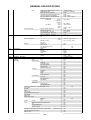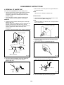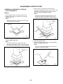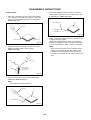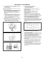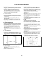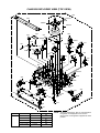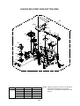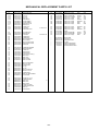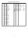
1
CLASS 1
LASER PRODUCT
MVDT2402
SERVICE MANUAL
COLOR TELEVISION/VIDEO CASSETTE RECORDER/
DVD VIDEO PLAYER
ORIGINAL
MFR’S VERSION A
Design and specifications are subject to change without notice.
IMPORTANT WARNING
CAUTION:
DVD PLAYER IS A CLASS 1 LASER PRODUCT. HOWEVER THIS PLAYER USES A VISIBLE LASER
BEAM WHICH COULD CAUSE HAZARDOUS RADIATION EXPOSURE IF DIRECTED. BE SURE TO
OPERATE THE PLAYER CORRECTLY AS INSTRUCTED.
THE FOLLOWING CAUTION LABEL IS LOCATED ON THE REAR PANEL OF THE PLAYER.
CLASS 1
LASER PRODUCT
(Printed on the Rear Panel)
WHEN THIS PLAYER IS PLUGGED TO THE WALL OUTLET, DO NOT PLACE YOUR EYES CLOSE
TO THE OPENING OF THE DISC TRAY AND OTHER OPENINGS TO LOOK INTO THE INSIDE OF
THIS PLAYER.
USE OF CONTROLS OR ADJUSTMENTS OR PERFORMANCE OF PROCEDURES OTHER THAN
THOSE SPECIFIED HEREIN MAY RESULT IN HAZARDOUS RADIATION EXPOSURE.
DO NOT OPEN COVERS AND DO NOT REPAIR YOURSELF. REFER SERVICING TO QUALIFIED
PERSONNEL.
A1-1
SERVICING NOTICES ON CHECKING
1. KEEP THE NOTICES
6. AVOID AN X-RAY
As for the places which need special attentions,
they are indicated with the labels or seals on the
cabinet, chassis and parts. Make sure to keep the
indications and notices in the operation manual.
2. AVOID AN ELECTRIC SHOCK
There is a high voltage part inside. Avoid an
electric shock while the electric current is
flowing.
3. USE THE DESIGNATED PARTS
Safety is secured against an X-ray by considering about the cathode-ray tube and the high
voltage peripheral circuit, etc.
Therefore, when repairing the high voltage peripheral circuit, use the designated parts and
make sure not modify the circuit.
Repairing except indicates causes rising of high
voltage, and it emits an X-ray from the cathoderay tube.
7. PERFORM A SAFETY CHECK AFTER
SERVICING
The parts in this equipment have the specific
characters of incombustibility and withstand
voltage for safety. Therefore, the part which is
replaced should be used the part which has
the same character.
Especially as to the important parts for safety
which is indicated in the circuit diagram or the
table of parts as a
mark, the designated
parts must be used.
Confirm that the screws, parts and wiring which
were removed in order to service are put in the
original positions, or whether there are the
portions which are deteriorated around the
serviced places serviced or not. Check the
insulation between the antenna terminal or
external metal and the AC cord plug blades.
And be sure the safety of that.
4. PUT PARTS AND WIRES IN THE
ORIGINAL POSITION AFTER
ASSEMBLING OR WIRING
(INSULATION CHECK PROCEDURE)
1. Unplug the plug from the AC outlet.
2. Remove the antenna terminal on TV and turn
on the TV.
3. Insulation resistance between the cord plug
terminals and the eternal exposure metal
[Note 2] should be more than 1M ohm by
using the 500V insulation resistance meter
[Note 1].
4. If the insulation resistance is less than 1M
ohm, the inspection repair should be
required.
There are parts which use the insulation
material such as a tube or tape for safety, or
which are assembled in the condition that
these do not contact with the printed board.
The inside wiring is designed not to get closer
to the pyrogenic parts and high voltage parts.
Therefore, put these parts in the original
positions.
5. TAKE CARE TO DEAL WITH THE
CATHODE-RAY TUBE
[Note 1]
In the condition that an explosion-proof
cathode-ray tube is set in this equipment, safety
is secured against implosion. However, when
removing it or serving from backward, it is
dangerous to give a shock. Take enough care
to deal with it.
If you have not the 500V insulation
resistance meter, use a Tester.
[Note 2]
External exposure metal: Antenna terminal
Earphone jack
HOW TO ORDER PARTS
Please include the following informations when you order parts. (Particularly the VERSION LETTER.)
1. MODEL NUMBER and VERSION LETTER.
The MODEL NUMBER can be found on the back of each product and the VERSION LETTER can be
found at the end of the SERIAL NUMBER.
2. PART NO. and DESCRIPTION
You can find it in your SERVICE MANUAL.
A1-2
WHEN REPLACING DVD DECK
[ When the removal of the DVD Deck ]
Before removing Pick Up PCB and DVD PCB connector, make the short circuit on the position as
shown Fig. 1 using a soldering. If you remove the DVD Deck with no soldering, the Laser may be
damaged.
[ When the installation of the DVD Deck ]
Remove all the soldering on the short circuit position after the connection of Pick Up PCB and DVD
PCB connector.
Pick Up PCB
Make the sort circuit
using a soldering.
Fig. 1
TAPE REMOVAL METHOD AT NO POWER SUPPLY
1. Remove the TV/DVD/VCR block from the main unit and the Fig. 1 below can be seen.
(Refer to item 1 of the DISASSEMBLY INSTRUCTIONS.)
2. Remove one screw of the Loading Motor from the insert hole for screw driver and remove the Loading
Motor.
3. Rotate the Pinch Roller Cam in the direction of the arrow by hand to slacken the Video Tape.
(Refer to Fig. 2)
4. Rotate the Clutch Ass'y either of the directions to wind the Video Tape in the Cassette Case.
5. Repeat the above step 3~4. Then take out the Video Cassette from the Deck Chassis. Be careful not to
scratch on the tape.
Loading Motor
Screw
Capstan DD Unit
Pinch Roller Cam
Main Cam
Clutch Ass'y
Main Chassis (Front Side)
Fig. 1
Fig. 2
A1-3
DISC REMOVAL METHOD AT NO POWER SUPPLY
1. Remove the Back Cabinet and AV PCB/DVD Block. (Refer to item 1 of the DISASSEMBLY
INSTRUCTIONS.)
2. Rotate the Main Gear in the direction of the arrow by hand.
(Refer to Fig. 1)
3. Draw the Tray.
Main Gear
Deck CD
Fig. 1
PARENTAL CONTROL - RATING LEVEL
4 DIGIT PASSWORD CANCELLATION
If the stored 4 digit password in the Rating Level menu needs to be cancelled, please follow the steps below.
1.
2.
3.
4.
5.
6.
Turn Unit ON.
Press and hold the 'STOP' key on the front panel.
Simultaneously press and hold the '7' key on the remote control unit.
Hold both keys for more than 3 seconds.
The On Screen Display message 'PASSWORD CLEAR' will appear.
The 4 digit password has now been cleared.
NB: The above procedure will reset ALL of the player's settings to the default factory state.
A1-4
TABLE OF CONTENTS
IMPORTANT WARNING .........................................................................................................
SERVICING NOTICES ON CHECKING ..................................................................................
HOW TO ORDER PARTS .......................................................................................................
WHEN REPLACING DVD DECK...........................................................................................
TAPE REMOVAL METHOD AT NO POWER SUPPLY .........................................................
DISC REMOVAL METHOD AT NO POWER SUPPLY ..........................................................
PARENTAL CONTROL-RATING LEVEL ...............................................................................
TABLE OF CONTENTS ...........................................................................................................
GENERAL SPECIFICATIONS .................................................................................................
DISASSEMBLY INSTRUCTIONS
1. REMOVAL OF MECHANICAL PARTS AND P. C. BOARDS .........................................
2. REMOVAL OF VCR DECK PARTS ................................................................................
3. REMOVAL OF DVD DECK PARTS ................................................................................
4. REMOVAL OF ANODE CAP ...........................................................................................
5. REMOVAL AND INSTALLATION OF FLAT PACKAGE IC ............................................
KEY TO ABBREVIATIONS .....................................................................................................
SERVICE MODE LIST .............................................................................................................
PREVENTIVE CHECKS AND SERVICE INTERVALS ...........................................................
WHEN REPLACING EEPROM (MEMORY) IC ......................................................................
SERVICING FIXTURES AND TOOLS ....................................................................................
PREPARATION FOR SERVICING ..........................................................................................
MECHANICAL ADJUSTMENTS .............................................................................................
ELECTRICAL ADJUSTMENTS ...............................................................................................
BLOCK DIAGRAMS
DVD .......................................................................................................................................
Y/C/AUDIO/HEAD AMP.....................................................................................................
MICON.................................................................................. .............................................
IN/OUT ..................................................................................................................................
CHROMA/IF ..........................................................................................................................
SOUND AMP/SURROUND ..................................................................................................
Hi-Fi/DEMODULATRO .........................................................................................................
DIGITAL COMB FILTER...................................................................................................
DVD IN/OUT......................................................................................................................
REGULATOR......................................................................................................................
TV.......................................................................................................................................
A1-1
A1-2
A1-2
A1-3
A1-3
A1-4
A1-4
A2-1
A3-1~A3-6
B1-1~B1-2
B2-1~B2-6
B3-1~B3-3
B4-1
B5-1, B5-2
C1-1, C1-2
C2-1
C3-1, C3-2
C4-1
D1-1
D1-1
D2-1~D2-4
D3-1~D3-6
E-1, E-2
E-3, E-4
E-5, E-6
E-7, E-8
E-9, E-10
E-11, E-12
E-13,E-14
E-15,E-16
E-17,E-18
E-19,E-20
E-21,E-22
PRINTED CIRCUIT BOARDS
DVD ....................................................................................................................................... F-1, F-2
VCR ....................................................................................................................................... F-3~F-6
DEFLECTION/CRT/OPERATION...................................................................................... F-7, F-8
SCHEMATIC DIAGRAMS
MPEG/MICON/DSP ..............................................................................................................
MEMORY ..............................................................................................................................
RF AMP/DSP ........................................................................................................................
AUDIO/VIDEO ......................................................................................................................
Y/C/AUDIO/HEAD AMP .......................................................................................................
MICON ..................................................................................................................................
IN/OUT ..................................................................................................................................
CHROMA/IF .........................................................................................................................
SOUND AMP/SURROUND ..................................................................................................
Hi-Fi/DEMODULATOR .........................................................................................................
DIGITAL COMB FILTER ......................................................................................................
DVD IN/OUT .........................................................................................................................
REGULATOR1 ......................................................................................................................
TV POWER ...........................................................................................................................
DEFLECTION....................................................................................................................
CRT/OPERATION...............................................................................................................
INTERCONNECTION DIAGRAM ........................................................................................
WAVEFORMS ..........................................................................................................................
MECHANICAL EXPLODED VIEWS ....................................................................................
CHASSIS EXPLODED VIEWS ................................................................................................
DVD DECK EXPLODED VIEWS .............................................................................................
MECHANICAL REPLACEMENT PARTS LIST ......................................................................
CHASSIS REPLACEMENT PARTS LIST ...............................................................................
DVD DECK REPLACEMENT PARTS LIST ............................................................................
ELECTRICAL REPLACEMENT PARTS LIST ........................................................................
A2-1
G-1, G-2
G-3, G-4
G-5, G-6
G-7, G-8
G-9, G-10
G-11, G-12
G-13, G-14
G-15, G-16
G-17, G-18
G-19, G-20
G-21, G-22
G-23, G-24
G-25, G-26
G-27, G-28
G-29, G-30
G-31, G-32
G-33, G-34
H-1~H-3
I1-1, I1-2
I2-1, I2-2
I3-1
J1-1
J2-1
J3-1
J4-1~J4-3
GENERAL SPECIFICATIONS
G-1
TV
System
CRT
CRT Size / Visual Size
CRT Type
Deflection
Magnetic Field
BV/BH
Video Head
24 inch / 600mmV
Flat
101
degree
+ 0.45 G
/ 0.18 G
NTSC
2 Speaker
Front
1.8 x 3.9 Inch
8
ohm
1.5W + 1.5W
1.5W + 1.5W
VHS Player / Recorder
NTSC
Yes
OVD-7
Front
3
4 Heads
FM Audio Head
2 Heads
Color System
Speaker
Position
Size
Impedance
MAX
10%(Typical)
Sound Output
G-2
VCR
System
System
Video System
Hi-Fi STEREO
NTSC PB
Deck
Heads
DECK
Loading System
Motor
Audio /Control
Erase(Full Track Erase)
Tape
Rec
PAL
Speed
NTSC
Play
PAL
NTSC
Fast Forward / Rewind Time (Approx.) at 25oC
with Cassette
G-3
DVD System
Forward/Reverse
Picture Search
Frame Advance
Slow Speed
Color System
Disc
Disc Diameter
Deck
NTSC or PAL-M
Disc Loading System
Motor
Pick up
Playback time(Max)
Search speed
DVD 1-LDVD 1-Layer
DVD 2-Layer
CD
Video CD
Fwd
Actual
Rev
Actual
Slow speed
Actual
Actual
G-4
T u n in g
System
Broadcasting System
Tuner and
Receive CH
System
Destination
Tuning System
Input Impedance
CH Coverage
Intermediate
Frequency
G-5
Sig n al
Picture(FP)
Sound(FS)
FP-FS
Preset CH
Stereo/Dual TV Sound
Tuner Sound Muting
Video Signal
RGB Signal
Audio Signal
VCR
Input Level
Output Level
S/N Ratio (Weighted) at DVD Mode
S/N Ratio (Weighted) at VCR Mode
Horizontal Resolution at DVD Mode
Horizontal Resolution at VCR(SP)Mode
Output Level
Input Level
Output Level(0dB=0.775Vrms)
A3-1
Mono
/Yes
Yes
SP/SLP(EP)
SP/SLP(EP)
FF:1'48"/REW:1'48"
T-120
SP/SLP(EP)=3x,5x / 9x,15x
Yes
1/10
NTSC
DVD, CD-DA, CD-R/RW
DVD-R/RW (Video Format Only)
120 mm , 80 mm
Front Loading
3 Motors
1-Lens 2-Beams System
135min (4.7GB)
245min (8.5GB)
74min
4 step
2-45 times (DVD)
4-40 times (CD)
4 step
2-45 times (DVD)
4-40 times (CD)
Fwd
1/7 - 1/2 times
-Rev
--US System M
1 Tuner
US(w/CATV)
F-Synth
VHF/UHF 75 ohm
2~69, 4A,A-5~A-1, A~I,
J~W,W+1~W+84
45.75MHz
41.25MHz
4.5MHz
No
US-Stereo
Yes
1 V p-p/75 ohm
1 V p-p/75 ohm
65dB
50dB
400 Lines
220 Lines
-8.0dBm/50k ohm
-8.0dBm/1k ohm
GENERAL SPECIFICATIONS
DVD
Hi-Fi Audio Signal
G-6
Power
Power Source
Power Consumption
Protector
G-7
Regulation
G-8
Temperature
G-9
G-10
Operating Humidity
On Screen
Display
(TV/VCR)
Menu
Menu
System Setup
Output Level(-20dBFs 0dBFs=2.0Vrms)
Digital Output Level
S/N Ratio at DVD (Weighted)
S/N Ratio at VCR (SP)(CCIR Filter:ON)
Harmonic Distortion at DVD Mode
Harmonic Distortion at VCR(SP) Mode
Frequency Response :
DVD Mode
at DVD
at Video CD
at SVCD
at CD
VCR Mode
at SP
at LP
at SLP
Dynamic Range : More than
Frequency Response :
Wow And Flutter : Less than
Channel Separation : More than
Harmonic Distortion : Less than
AC
DC
at AC
at DC
Stand by (at AC)
Per Year
Power Fuse
Safety Circuit
IC Protector(Micro Fuse)
Dew Sensor
Safety
Radiation
X-Radiation
Laser
Operation
Storage
Type
Clock Set
On/Off Timer Set
Auto Clock On/Off
Standard Time
Daylight Saving Time
TV Setup
Language
Picture
Audio
Picture Preference
Channel Setup
TV/CATV
Auto CH Memory
Add/ Delete
V-chip Setup
Tape Setup
Timer Rec Set
Auto Repeat On/Off
G-CODE(or SHOWVIEW or PLUSCODE)No. Entry
Clock / Date
TV/VCR
DVD
CH/AV(LINE)
Tape Counter(Linear Counter)
Tape Speed
Sleep Time
Stereo/Audio Output
Bilingual
SAP
Control
Volume
Level
Brightness/Contrast/Sharpness/Color
Tint
Bass/Treble/Balance
Manual Tracking
Play/Stop/FF/Rew/Rec/OTR/T-Rec/Pause/Eject/Tape In
Auto Tracking/Manual Tracking
Caption / Text
(Symbol Mark)
-12.0dBm/1k ohm
0.5 V p-p/75 ohm(DVD)
90 dB
38 dB
0.06% (1kHz)
1.5% (1kHz) Typical
4Hz - 22kHz
4Hz - 20kHz
100Hz - 10kHz
100Hz - 4kHz
90 dB
20Hz - 20kHz
0.01 %Wrms
60 dB
1.0 %
120V,60Hz
135 W at 120 V 60 Hz
4 W at 120 V 60 Hz
Yes
Yes
No
No
UL
FCC
DHHS
DHHS
+5oC ~ +40oC
-20oC ~ +60oC
Less than 80% RH
Yes
Icon
Yes
Yes
Yes
Yes
Yes
Yes
Yes
Yes
Yes
Yes
Yes
Yes
Yes
Yes
Yes
Yes
Yes
Yes
Yes
No
Yes
Yes
Yes
Yes
Yes
Yes
Yes
Yes
No
Yes
Yes
Yes
Yes
Yes
Yes
Yes
Yes
Yes
A3-2
GENERAL SPECIFICATIONS
G-11
On Screen
Display
(DVD)
Index
Mute
Hi-Fi
Repeat
Zero Return
DEW
Menu (DVD)
Yes
Yes
Yes
Yes
Yes
No
Menu Type
Language
Menu
Subtitle
Audio
Picture
TV Screen Size(4:3)
OSD Display On/Off
JPEG Interval
Select Files
Sound
DRC (Dynamic Range Control)
dts Decode
Output(5.1ch/ 2ch)
Surround On/Off
Center On/Off
Sub Woofer On/Off
Parental
Password Lock/ Un Lock
Rating Level
Other
OSD Language(Set up Language)
Output(RGB/Composite)
Open
Close
No disc
Reading
Play
Still/Pause
Stop
Prohibit Mark
Step
Skip(>>|)
Skip(|<<)
Random
Repeat
Slow+ ##
Slow- ##
Search+ ##
Search- ##
Jump
Resume
Title No.
Chapter No.
Track No.
Time
Sub Title No.
Angle No.
Vocal On/Off
Audio No.
Audio Stereo L/R
Zoom
Marker No.
Program Play Back
Surround On/Off
Screen Saver
MP3, WMA, JPEG
G-12
OSD Language
G-13
Clock,Timer
and Timer
Back-up
Folder Name
File Name
File No
Time
Track No
TV/VCR
DVD
Calendar
Timer Events
One Touch Recording Max Time
OTPB Valid Time
Sleep Timer
Max Time
Step
On/Off Timer
Program(On Timer / Off Timer)
A3-3
Yes
Character
Yes
Yes
Yes
Yes
Yes
Yes
Yes
Yes
Yes
Yes
Yes
No
No
No
No
No
Yes
Yes
Yes
Yes
Yes
No
Yes
Yes
Yes
Yes
Yes
Yes
Yes
Yes
Yes
Yes
Yes
Yes (CD, MP3, WMA, JPEG )
Yes
Yes
No
Yes
Yes
Yes
Yes
Yes
Yes
Yes
Yes
Yes
Yes
Yes
Yes
No
Yes
No
Yes (CD, MP3, WMA, JPEG )
No
No
Yes
Yes
Yes
Yes (MP3, WMA Only)
Yes
English French Spanish
English French Spanish
1990/1/1 ~ 2081/12/31
8 Program/ 1 Month
6 Hours
120
Min
10
Min
1
Program
GENERAL SPECIFICATIONS
Auto Shut Off
G-14
Remote
Control
Unit
No Signal
No Operation
Timer Back-up (at Power Off Mode)
Unit
Glow in Dark Remocon
Format
Custom Code
Power Source
Voltage(D.C)
UM size x pcs
Total Keys
Keys
TV/VCR
DVD
Power
1
2
3
4
5
6
7
8
9
0
ChannelChannel+
VolumeVolume+
Display (Call)
Sleep
Audio Select
Mute
Index- / SkipIndex+ / Skip+
T-REC
Rec/OTR
Slow+
Play
Stop
Rew / SearchF. Fwd / Search+
Pause / Still
CM Skip
Speed / Return
Counter Reset / Angle
Zero Return / Subtitle
Input Select / Zoom
Menu /Set Up
Program / Repeat A-B
ATR / Top Menu
Tracking+ / DVD Menu
Tracking- / Play Mode
Cancel
3D Surround
Cursor Up
Cursor Down
Cursor Left
Cursor Right
Enter
Eject
Open/Close
TV Monitor
Closed Caption
Quick View / Jump
CATV
Position
Wide
G-15
Features
Auto Head Cleaning
Auto Tracking
HQ (VHS Standard High Quality)
Auto Power On, Auto Play, Auto Rewind, Auto Eject
VIDEO PLUS+(SHOWVIEW,G-CODE)
Auto Clock
Forward / Reverse Picture Search
Auto CH Memory
Surround
Stable Sound
Closed Caption
A3-4
15
5
RC-HH
Min
Min
Sec
No
NEC
71-8E
3V
UM-4 x 2 pcs
52
Yes
Yes
Yes
Yes
Yes
Yes
Yes
Yes
Yes
Yes
Yes
Yes
Yes
Yes
Yes
Yes
Yes
Yes
Yes
Yes
Yes
Yes
Yes
Yes
Yes
Yes
Yes
Yes
Yes
Yes
Yes
Yes
Yes
Yes
Yes
Yes
Yes
Yes
Yes
Yes
Yes
Yes
No
Yes
Yes
Yes
Yes
Yes
Yes
Yes
Yes
Yes
Yes
No
No
No
Yes
Yes
Yes
Yes
No
Yes
Yes
Yes
Yes
Yes
Yes
GENERAL SPECIFICATIONS
TV Auto Shut off Function
End Call
Index Search
SQPB
CATV
CM Skip(30sec x 6 Times)
Comb Filter (2Lines)
VM Circuit
TV Monitor
Program Extend
Choke Coil
Energy Star
Protect of FBT Leak Circuit
Zero Return
Power On Memory
Dirty Head
V-chip
USA V-chip
CANADA V-chip
Parental Lock
(DVD Only)
Auto Stop
(Pause, and Resume Stop after 5min.)
Video CD Playback
SVCD Playback
Overlay Graphics And Text
Command List
Entry Point Jump
MP3 Playback
WMA Playback
JPEG Playback
Digital Out
(Dolby Digital)
(MPEG)
(PCM)
(DTS)
Down Mix Out
(Dolby Digital)
(DTS)
G-16
Accessories
TruSurround
Screen Saver
Picture Preference
Auto Setup
Audio DAC
Copy (Disc to Tape)
Owner's Manual
Yes
No
Yes
No
Yes
Yes
Yes
No
Yes
No
No
Yes
Yes
Yes
No
No
Yes
No
Yes
Yes
No
No
No
No
No
Yes
Yes
Yes
Yes
Yes
Yes
Yes
Yes
No
No
No
Yes
No
192kHz / 24bit
No
Language
w/Guarantee Card
English / French
Yes
Yes
UM size x pcs
OEM Brand
-
Poles
Terminal
-
Terminal
-
Remote Control Unit
Battery
No
Rod Antenna
No
Loop Antenna
G-17
Interface
No
U/V Mixer
300 ohm to 75 ohm Antenna Adapter
Antenna Change Plug
DC Car Cord (Center+)
AC Plug Adapter
AC Cord
AV Cord (2Pin-1Pin)
Guarantee Card
Registration Card
ESP Card
Warning Sheet
Dew/AHC Caution Sheet
Quick Set-up Sheet
Circuit Diagram
Service Facility List
Important Safeguard
Warranty Sheet
Switch
Front
Power (Tact)
Channel Up
Channel Down
Volume Up
Volume Down
Play (VCR)
Stop / Eject (VCR)
F.FWD/Cue (VCR)
Rew/Rev (VCR)
A3-5
No
No
No
No
No
No
No
No
No
No
No
No
No
No
No
No
No
Yes
Yes
Yes
Yes
Yes
Yes
Yes
Yes
Yes
GENERAL SPECIFICATIONS
Indicator
Terminals
Front
Rear
G-18
G-19
Set Size
Weight
G-20
Carton
REC/OTR (VCR)
Play (DVD)
Stop (DVD)
Skip+ /Search+ (DVD)
Skip- /Search- (DVD)
Open/Close (DVD)
Input Select
Main Power SW
Power
REC/OTR
T-REC
TV/VCR
DVD
Video Input
Audio Input
Other Terminal
Video Input
Audio Input
Video Output
Audio Output
Digital Audio Output
VHF/UHF Antenna Input
AC Inlet
Approx.
W x D x H (mm)
Net (Approx.)
Gross (Approx.)
Master Carton
Content
Material
Dimensions
W x D x H(mm)
Description of Origin
Gift Box
G-21
Material
G-22
Environment
Material
W/Color Photo Label
Dimensions
W x D x H(mm)
Design
Description of Origin
Drop Test
Natural Dropping At
Height (cm)
Container Stuffing(40' container)
Cabinet
Front
Rear
Jack Panel
PCB
Non-Halogen
Eyelet
Pb Free
Lead-free Solder
Other
Cd Free
A3-6
Yes
Yes
Yes
Yes
Yes
Yes
No
No
Yes(Red)
Yes(Red)
Yes(Red)
No
No
RCA x 1
RCA x 2(Stereo)
HeadPhone (Stereo & Mono, 3.5mm)
RCA x 1
RCA x 2(Stereo)
RCA x1
RCA x 2(Stereo)
Coaxial (DVD Only)
F Type
No
655 x 477 x 580
36.0kg (79.4lbs)
40.0kg (88.2lbs)
No
Yes
Double/Brown
No
766 x 579.5 x 711
As per Buyer's
Yes
1 Corner / 3 Edges / 6 Surfaces
31
180
Sets
PS
94V0 DECABROM
PS
94V0 DECABROM
No
Yes
No
No
No
DISASSEMBLY INSTRUCTIONS
1-3: TV/DVD/VCR BLOCK (Refer to Fig. 1-3)
1. REMOVAL OF MECHANICAL PARTS
AND P.C. BOARDS
1. Remove the 2 screws (1).
2. Disconnect the following connectors:
(CP303, CP404 and CP1704).
3. Remove the TV/DVD/VCR Block in the direction of
arrow.
1-1: BACK CABINET (Refer to Fig. 1-1)
1. Remove the 6 screws (1).
2. Remove the 2 screws (2).
3. Remove the Back Cabinet in the direction of arrow.
(1)
Front Cabinet
(1)
Front Cabinet
(1)
(1)
(1)
TV/DVD/VCR Block
(1)
Fig. 1-3
(1)
(2)
1-4: VCR DECK (Refer to Fig. 1-4)
(2)
NOTE
Back Cabinet
(1)
Do not remove the cable at the FE Head section. The FE
Head may be damaged if you remove the cable by force.
Fig. 1-1
1.
2.
3.
4.
5.
6.
7.
8.
9.
Remove the 2 screws (1).
Remove the VCR Top.
Move the Cassette Holder Ass'y to the back side.
Remove the 3 screws (2).
Remove the 2 screws (3).
Remove the Deck Shield Cover.
Remove the screw (4).
Remove the FE Head.
Disconnect the following connectors:
(CP101, CP4501, CP4502 and CP4503).
10. Remove the VCR Deck in the direction of arrow.
1-2: CRT PCB (Refer to Fig. 1-2)
CAUTION: BEFORE REMOVING THE ANODE CAP,
DISCHARGE ELECTRICITY BECAUSE IT
CONTAINS HIGH VOLTAGE.
BEFORE ATTEMPTING TO REMOVE OR
REPAIR ANY PCB, UNPLUG THE POWER
CORD FROM THE AC SOURCE.
1. Remove the Anode Cap.
(Refer to REMOVAL OF ANODE CAP)
2. Disconnect the following connectors:
(CP603B, CP803 and CP805).
3. Remove the CRT PCB in the direction of arrow.
(2)
CRT PCB
Front Cabinet
(3)
(2)
Deck Shield Cover
(3)
(4)
(2)
FE Head
VCR Deck
(1)
(1)
VCR Top
Bottom Plate
Fig. 1-2
Fig. 1-4
B1-1
DISASSEMBLY INSTRUCTIONS
1-5: VCR PCB (Refer to Fig. 1-5)
1-7: DVD PCB/DVD DECK (Refer to Fig. 1-7)
1. Remove the 6 screws (1).
2. Remove the screw (2).
3. Remove the AV Jack Shield.
4. Disconnect the following connectors:
(CP001, CP602B, CP604, CP2201, CP8001 and CP8002).
5. Remove the VCR PCB in the direction of arrow.
1. Make the short circuit on the position as shown Fig.
1-7 using a soldering. If you remove the DVD Deck
with no soldering, the Laser may be damaged.
2. Remove the 4 screws (1).
3. Remove the DVD Top in the direction of arrow (A).
4. Remove the 2 screws (2).
5. Remove the DVD PCB in the direction of arrow (B).
6. Disconnect the following connectors:
(CP2601, CP2602 and CP2603).
7. Remove the 4 screws (3).
8. Remove the DVD Deck in the direction of arrow (C).
(1)
(1)
(1)
(1)
AV Jack Shield
VCR PCB
NOTE
When the installation of the DVD Deck, remove all the
soldering on the short circuit position after the connection
of Pick Up PCB and DVD PCB connector.
(1)
(1)
(2)
(1)
DVD Top
(1)
(1)
(1)
Bottom Plate
Fig. 1-5
(2)
(A)
(2)
1-6: VCR DECK (Refer to Fig. 1-6)
1. Remove the 4 screws (1).
2. Remove the DVD Block in the direction of arrow (A).
3. Remove the 2 screws (2).
4. Remove the Operation PCB in the direction of arrow (B).
Pick Up PCB
(B)
(3)
(3)
(3)
DVD Deck
(3)
(1)
(1)
Angle Deck
(C)
Make the short circuit
using a soldering.
(1)
DVD Block
(1)
Fig. 1-7
(A)
1-8: DEFLECTION PCB (Refer to Fig. 1-8)
1. Remove the 2 screws (1).
2. Remove the 3 screws (2).
3. Remove the Deflection PCB in the direction of arrow.
(2)
(2)
(2)
(B)
Operation PCB
Bottom Plate
(2)
(1)
(1)
(2)
Fig. 1-6
Deflection PCB
Bottom Plate
Fig. 1-8
B1-2
DISASSEMBLY INSTRUCTIONS
2. REMOVAL OF VCR DECK PARTS
NOTE
2-1: TOP BRACKET (Refer to Fig. 2-1)
1. In case of the Locker R installation, check if the one
position of Fig.2-3-B are correctly locked.
2. When you install the Cassette Side R, be sure to move
the Locker R after installing.
1. Extend the 2 supports 1.
2. Slide the 2 supports 2 and remove the Top Bracket.
NOTE
1. After the installation of the Top Bracket, bend the
support 1 so that the Top Bracket is fixed.
Locker R
Top Bracket
Check if this position
is locked.
Cassette Side R
1
1
Top Bracket
2
Fig. 2-3-B
2
Main Chassis
2-4: LINK UNIT (Refer to Fig. 2-4)
Main Chassis
1. Set the Link Unit to the Eject position.
2. Unlock the support 1.
3. Remove the (A) side of the Link Unit first, then remove
the (B) side.
Fig. 2-1
2-2: CASSETTE HOLDER ASS'Y (Refer to Fig. 2-2)
1. Move the Cassette Holder Ass'y to the front side.
2. Push the Locker R to remove the Cassette Side R.
3. Remove the Cassette Side L.
Main Chassis
Link Unit
Cassette Side R
Locker R
Main Chassis
(A)
(B)
Link Unit
1
Main Chassis
Fig. 2-4
Link Unit
2-5: LINK LEVER/FLAP LEVER (Refer to Fig. 2-5)
Main Chassis
Cassette Side L
1. Extend the support 1.
2. Remove the Link Lever.
3. Remove the Flap Lever.
Fig. 2-2
2-3: CASSETTE SIDE L/R (Refer to Fig. 2-3-A)
1. Remove the Locker Spring.
2. Unlock the 4 supports 1 and then remove the Cassette
Side L/R.
3. Unlock the support 2 and then remove the Locker R.
Flap Lever
Locker Spring
1
1
1
Cassette Holder
Link Lever
2
Fig. 2-5
Locker R
1
1
Cassette Side R
Cassette Side L
Fig. 2-3-A
B2-1
DISASSEMBLY INSTRUCTIONS
2-6: LOADING MOTOR/WORM (Refer to Fig. 2-6-A)
2-7: TENSION ASS'Y (Refer to Fig. 2-7-B)
1. Remove the screw 1.
2. Remove the Loading Motor.
3. Remove the Worm.
1. Turn the Pinch Roller Cam clockwise so that the
Tension Holder hook is set to the position of Fig. 2-7-A
to move the Tension Arm Ass'y.
2. Remove the Tension Spring.
3. Unlock the 2 supports 1 and remove the Tension
Band.
4. Unlock the support 2 and remove the Tension Arm
Ass'y.
5. Unlock the support 3 and remove the Tension
Connect.
6. Float the hook 4 and turn it clockwise then remove the
Tension Holder.
Loading Motor
Worm
Main Chassis
Tension Arm Ass'y
• Screw Torque: 3 ± 0.5kgf•cm
1
Fig. 2-6-A
Fig. 2-7-A
NOTE
1
1. In case of the Worm installation, check if the value of
the Fig. 2-6-B is correct.
2. In case of the Loading Motor installation, slacken the
wire as shown Fig. 2-6-C.
3. When installing the wires between Capstan DD Unit
and Loading Motor, connect them correctly as shown
Fig. 2-6-D.
Tension Connect
Tension Band
1
3
Tension Spring
Tension Arm Ass'y
Tension Holder
2
4
19.2 ± 0.1mm
Fig. 2-7-B
NOTE
Safety surface for pressing
of the insert.
1. In case of the Tension Band installation, note the
direction of the installation. (Refer to Fig. 2-7-C)
2. In case of the Tension Band installation, install correctly
as Fig. 2-7-D.
3. In case of the Tension Connect installation, install as
the circled section of Fig. 2-7-E.
Fig. 2-6-B
Slacken the wire.
Tension Band
Tension Connect
Loading Motor
Fig. 2-7-C
Fig. 2-6-C
[OK]
Tension Connect
Tension Band
Pink
Loading Motor
Capstan DD Unit
-
L2
[NG]
Tension Connect
Tension Band
Fig. 2-7-D
+
L1
White
Tension Connect
Fig. 2-6-D
Main Chassis
B2-2
Fig. 2-7-E
DISASSEMBLY INSTRUCTIONS
2-8: T BRAKE ARM/T BRAKE BAND (Refer to Fig. 2-8-A)
1. Remove the T Brake Spring.
2. Turn the T Brake Arm clockwise and bend the hook
section to remove it.
3. Unlock the 2 supports 1 and remove the T Brake
Band.
Idler Gear
Idler Arm Ass'y
(B)
S Reel
T Brake Band
(A)
1
Hook section
1
T Reel
(A)
T Brake Arm
1
T Brake Spring
1
Fig. 2-8-A
Fig. 2-9-A
NOTE
NOTE
1. In case of the S Reel and T Reel installation, check if the
correct parts are installed. (Refer to Fig. 2-9-B)
2. In case of the Idler Arm Ass'y installation, install correctly
as Fig. 2-9-C. And also set it so that the section "B" of
Fig. 2-9-A is placed under the Main Chassis tab.
1. In case of the T Brake Band installation, install correctly
as Fig. 2-8-B.
[OK]
T Brake Arm
T Brake Band
T Brake Arm
[NG]
T Brake Band
Fig. 2-8-B
2-9: S REEL/T REEL/IDLER ARM ASS'Y/IDLER GEAR
(Refer to Fig. 2-9-A)
Big Hole
(S Reel)
1. Remove the S Reel and T Reel.
2. Remove the 2 Polyslider Washers 1.
3. Remove the Idler Arm Ass'y and Idler Gear.
Small Hole
(T Reel)
Fig. 2-9-B
[OK]
Clutch Gear
Idler Arm Ass'y
NOTE
1. Take care not to damage the gears of the S Reel and T
Reel.
2. The Polyslider Washer may be remained on the back of
the reel.
3. Take care not to damage the shaft.
4. Do not touch the section "A" of S Reel and T Reel. (Use
gloves.) (Refer to Fig. 2-9-A) Do not adhere the stains
on it.
5. When you install the reel, clean the shaft and grease it
(FG-84M). (If you do not grease, noise may be heard in
FF/REW mode.)
6. After installing the reel, adjust the height of the reel.
(Refer to MECHANICAL ADJUSTMENT)
[NG]
Idler Arm Ass'y
Clutch Gear
Fig. 2-9-C
B2-3
DISASSEMBLY INSTRUCTIONS
2-10: CASSETTE OPENER/PINCH ROLLER BLOCK/
P5 ARM ASS'Y (Refer to Fig. 2-10-A)
1. Unlock the support 1 and remove the Cassette
Opener.
2. Remove the Pinch Roller Block and P5 Arm Ass'y.
Cassette Opener
1
Spring Position
Fig. 2-11-B
2-12: FE HEAD (RECORDER ONLY) (Refer to Fig. 2-12)
Pinch Roller Block
1. Remove the screw 1.
2. Remove the FE Head.
P5 Arm Ass'y
1
Main Chassis
FE Head
Fig. 2-10-A
NOTE
1. Do not touch the Pinch Roller. (Use gloves.)
2. In case of the Pinch Roller Block and the Pinch Roller
Cam installation, install correctly as Fig. 2-10-B.
Pinch Roller Block
• Screw Torque: 5 ± 0.5kgf•cm
• The FE Head is not installed on the Video Cassette Player.
Can be seen the hole of
the Pinch Roller Cam.
2-13: AHC ASS'Y/CYLINDER UNIT ASS'Y
(Refer to Fig. 2-13)
P5 Arm Ass'y
Can be seen the hole of the
Main Cam.
1. Unlock the support 1 and remove the AHC Ass'y.
2. Disconnect the following connector:
(CD2001)
3. Remove the 3 screws 2.
4. Remove the Cylinder Unit Ass'y.
Fig. 2-10-B
2-11: A/C HEAD (Refer to Fig. 2-11-A)
1.
2.
3.
4.
Fig. 2-12
NOTE
Remove the screw 1.
Remove the A/C Head Base.
Remove the 3 screws 2.
Remove the A/C Head and A/C Head Spring.
1. When you install the Cylinder Unit Ass'y, tighten the
screws from (1) to (3) in order while pulling the Ass'y
toward the left front direction.
NOTE
1. Do not touch the A/C Head. (Use gloves.)
2. When you install the A/C Head Spring, install as shown in
Fig. 2-11-B.
3. When you install the A/C Head, tighten the screw (1) first,
then tighten the screw (2), finally tighten the screw (3).
(1)
2
Cylinder Unit Ass'y
AHC Ass'y
1
(3)
2
2
(2)
A/C Head
(3)
2
(2)
2
(1)
A/C Head Spring
2
• Screw Torque: 3 ± 0.5kgf•cm
1
A/C Head Base
• Screw Torque: 5 ± 0.5kgf•cm
Fig. 2-11-A
B2-4
Fig. 2-13
DISASSEMBLY INSTRUCTIONS
2-14: CAPSTAN DD UNIT (Refer to Fig. 2-14)
NOTE
1.
2.
3.
4.
5.
1. In case of the Pinch Roller Cam and Main Cam
installation, install them as the circled section of Fig. 215-B so that the each markers are met. (Refer to Fig.
2-15-B)
Remove the Capstan Belt.
Remove the screw 1.
Remove the Capstan Holder.
Remove the 3 screws 2.
Remove the Capstan DD Unit.
Pinch Roller Cam
Marker
Capstan Belt
1
Capstan Holder
Capstan DD Unit
Main Cam
Fig. 2-15-B
2-16: LOADING GEAR S/T UNIT (Refer to Fig. 2-16-A)
2
1. Remove the E-Ring 1 and remove the Main Loading
Gear.
2. Remove the Main Rod, Tension Lever, Loading Arm S
Unit and Loading Arm T Unit.
22
• Screw Torque: 4 ± 0.5kgf•cm
1
Fig. 2-14
Main Loading Gear
Main Rod
2-15: MAIN CAM/PINCH ROLLER CAM/JOINT GEAR
(Refer to Fig. 2-15-A)
Loading Arm T Unit
1. Remove the E-Ring 1, then remove the Main Cam.
2. Remove the E-Ring 2, then remove the Pinch Roller
Cam and Joint Gear.
Tension Lever
Loading Arm S Unit
1
Main Cam
2
Fig. 2-16-A
Pinch Roller Cam
NOTE
Joint Gear
1. When you install the Loading Arm S Unit, Loading Arm
T Unit and Main Loading Gear, align each marker.
(Refer to Fig. 2-16-B)
Marker
Fig. 2-15-A
Main Loading Gear
Marker
Loading Arm T Unit
Loading Arm S Unit
Fig. 2-16-B
B2-5
DISASSEMBLY INSTRUCTIONS
2-17: CLUTCH ASS'Y/RING SPRING/CLUTCH LEVER/
CLUTCH GEAR (Refer to Fig. 2-17-A)
1.
2.
3.
4.
Cassette Guide Post
1
Remove the Polyslider Washer 1.
Remove the Clutch Ass'y and Ring Spring.
Remove the Clutch Lever.
Remove the Coupling Gear, Coupling Spring and
Clutch Gear.
Inclined Base S
Unit
Inclined Base T
Unit
P4 Cap
1
Clutch Ass'y
Ring Spring
Coupling Gear
Clutch Lever
LED Reflector
Coupling Spring
Clutch Gear
• Screw Torque: 5 ± 0.5kgf•cm
2
Fig. 2-18-A
NOTE
1. Do not touch the roller of Guide Roller.
2. In case of the P4 Cap installation, install it with parallel
for "A" and "B" of Fig. 2-18-B.
3. In case of the Cassette Guide Post installation, install
correctly as the circled section of Fig. 2-18-C.
Fig. 2-17-A
NOTE
"A"
1. In case of the Clutch Ass'y installation, install it with
inserting the spring of the Clutch Ass'y into the dent of
the Coupling Gear. (Refer to Fig. 2-17-B)
Clutch Ass'y
P4 Cap
"B"
Cassette Opener
Fig. 2-18-B
Coupling Gear
Fig. 2-17-B
[OK]
Cassette Guide Post
2-18: CASSETTE GUIDE POST/INCLINED BASE S/T
UNIT/P4 CAP/LED REFLECTOR
(Refer to Fig. 2-18-A)
1. Remove the P4 Cap.
2. Unlock the support 1 and remove the Cassette Guide
Post.
3. Remove the Inclined Base S/T Unit.
4. Remove the screw 2.
5. Remove the LED Reflector.
[NG]
Cassette Guide Post
Fig. 2-18-C
B2-6
DISASSEMBLY INSTRUCTIONS
3. REMOVAL OF DVD DECK PARTS
NOTE
NOTE
1. In case of the Main Chassis Ass'y, install it from (1) to
(4) in order. (Refer to Fig. 3-2-B)
2. In case of the Main Chassis Ass'y installation, hook the
wire on the Main Frame Ass'y as shown Fig. 3-2-C.
1. Do not disassemble the DVD DECK PARTS except
listed parts here. Minute adjustments are needed if the
disassemble is done. If the repair is needed except
listed parts, replace the DVD MECHA ASS'Y.
Main Frame Ass'y (Bottom Side)
3-1: TRAY (Refer to Fig. 3-1-A)
1. Set the Tray opened. (Refer to the DISC REMOVAL
METHOD AT NO POWER SUPPLY)
2. Unlock the 2 supports 1 and remove the Tray.
(3)
Rack Loading
(3)
(3)
Main Frame Ass'y
Traverse Holder
(2)
(1)
Main Chassis Ass'y
1
Tray
1
(4)
(4)
Fig. 3-1-A
Check Lock
Fig. 3-2-B
NOTE
Main Frame Ass'y
1. In case of the Tray installation, install them as the
circled section of Fig. 3-1-B so that the each markers
are met.
Main Frame Ass'y
Check Hook
Fig. 3-2-C
3-3: LOADING MOTOR PCB ASS'Y/ LOADING BELT
(Refer to Fig. 3-3-A)
1.
2.
3.
4.
5.
Tray
Fig. 3-1-B
3-2: MAIN CHASSIS ASS'Y (Refer to Fig. 3-2-A)
1.
2.
3.
4.
Remove the Loading Belt.
Remove the screw 1.
Remove the 2 screws 2.
Remove the Loading Motor PCB Ass'y.
Remove the Pulley Gear.
Loading Belt
2
Remove the screw 1.
Unlock the 2 supports 2.
Remove the Insulator (R) from the Main Frame Ass'y.
Remove the Main Chassis Ass'y.
2
Main Frame Ass’y
1
2
Pulley Gear
2
1
Main Frame Ass'y
Loading Motor PCB Ass’y
• Screw Torque: 2.5 ± 0.3kgf•cm (Screw 1)
• Screw Torque: 1.0 ± 0.3kgf•cm (Screw 2)
Insulator (R)
Main Chassis Ass'y
• Screw Torque: 2.0 ± 0.5kgf•cm
Fig. 3-2-A
B3-1
Fig. 3-3-A
DISASSEMBLY INSTRUCTIONS
NOTE
3-5: CLAMPER ASS'Y (Refer to Fig. 3-5-A)
1. In case of the Pulley Motor installation, check if the
value of the Fig. 3-3-B is correct.
2. When installing the Loading Motor PCB Ass'y, install it
correctly as Fig. 3-3-C.
3. In case of the Loading Motor PCB Ass'y installation,
hook the wire on the Main Frame Ass'y as shown Fig.
3-3-C.
1. Press the Clamper and rotate the Clamper Plate
clockwise, then unlock the 3 supports 1.
2. Remove the Clamper Plate, Clamper Magnet and
Clamper.
Pulley Motor
Clamper Plate
Clamper Magnet
7.0 ± 0.1mm
Main Frame
Loading Motor
1
1
Clamper
1
Safety surface for pressing
of the insert.
Fig. 3-5-A
Fig. 3-3-B
NOTE
1. In case of the Clamper Ass'y installation, install
correctly as Fig. 3-5-B.
The Lever should be position
between A and B.
A
Rack Loading
B
Clamper Plate
Clamper
No gap
Fig. 3-5-B
Check Hook
Loading Motor PCB Ass’y
Fig. 3-3-C
3-6: TRAVERSE HOLDER/INSULATOR (F)/INSULATOR
(R) (Refer to Fig. 3-6-A)
3-4: RACK LOADING/MAIN GEAR/PULLEY GEAR
(Refer to Fig. 3-4-A)
1. Remove the Traverse Holder.
2. Remove the 2 Insulator (F).
3. Remove the Insulator (R).
1. Press down the catcher 1 and slide the Rack Loading.
2. Unlock the support 2 and remove the Pulley Gear.
3. Remove the Main Gear.
Insulator (R)
Main Chassis Ass'y
Pulley Gear
Rack Loading
Insulator (F)
Main Gear
Traverse Holder
Main Frame Ass’y
Insulator (F)
2
1
Fig. 3-4-A
Fig. 3-6-A
NOTE
NOTE
1. In case of the Rack Loading installation, do not mesh it
to the Main Gear as shown the Fig. 3-4-B.
Rack Loading
1. In case of the Insulator (F) installation, install correctly
as Fig. 3-6-B.
2. In case of the Insulator (R) installation, install correctly
as Fig. 3-6-C.
Check Hook
Insulator (F)
Traverse Holder
Main Gear
Fig. 3-6-B
Fig. 3-4-B
B3-2
DISASSEMBLY INSTRUCTIONS
Insulator (R)
~ FEED MOTOR ~
Main Chassis Ass'y (Top Side)
BLUE (4)
ORANGE (3)
Switch PCB Ass'y
Fig. 3-6-C
~ SPINDLE MOTOR ~
BLACK (2)
3-7: RACK FEED ASS'Y/SWITCH PCB ASS'Y/FEED
MOTOR (Refer to Fig. 3-7-A)
RED (1)
• Install wire from (1) to (4) in order.
1.
2.
3.
4.
5.
6.
7.
Remove the screw 1.
Remove the Rack Feed Ass'y.
Remove the screw 2.
Remove the Switch PCB Ass'y.
Remove the 2 screw 3.
Remove the Feed Motor.
Remove the Motor Gear.
Fig. 3-7-D
Main Chassis Ass'y (Bottom Side)
Check Hook
Check Hook
1
2
Rack Feed Ass'y
3
3
Switch PCB Ass'y
Check Hook
• Loosen the wire in the direction of the arrow.
Motor Gear
Main Chassis Ass'y
Feed Motor
•
•
•
•
Screw
Screw
Screw
Screw
Torque:
Torque:
Torque:
Torque:
5.0 ±
3.0 ±
1.0 ±
3.5 ±
Check Hook
0.3kgf•cm
0.3kgf•cm
0.3kgf•cm
0.3kgf•cm
(Screw
(Screw
(Screw
(Screw
1)
2)
3)
4)
Fig. 3-7-A
NOTE
1. When pushing the Rack Feed in the direction of the
arrow, it should be restored to the original position by
the spring force. (Refer to Fig. 3-7-B)
2. In case of the Motor Gear installation, check if the value
of the Fig. 3-7-C is correct.
3. When installing the wire of the Switch PCB Ass'y, install
it correctly as Fig. 3-7-D.
4. After the assembly of the Main Chassis Ass'y, hook the
wire on the Main Chassis Ass'y as shown Fig. 3-7-E.
Push
Rack Feed Ass'y
Fig. 3-7-B
Motor Gear
6.0 ± 0.2mm
Feed Motor
Safety surface for pressing
of the insert.
Fig. 3-7-C
B3-3
Fig. 3-7-E
DISASSEMBLY INSTRUCTIONS
3. After one side is removed, pull in the opposite direction
to remove the other.
4. REMOVAL OF ANODE CAP
Read the following NOTED items before starting work.
NOTE
* After turning the power off there might still be a potential
voltage that is very dangerous. When removing the
Anode Cap, make sure to discharge the Anode Cap's
potential voltage.
* Do not use pliers to loosen or tighten the Anode Cap
terminal, this may cause the spring to be damaged.
Take care not to damage the Rubber Cap.
INSTALLATION
1. Clean the spot where the cap was located with a small
amount of alcohol. (Refer to Fig. 4-3.)
REMOVAL
1. Follow the steps as follows to discharge the Anode Cap.
(Refer to Fig. 4-1.)
Connect one end of an Alligator Clip to the metal part of a
flat-blade screwdriver and the other end to ground.
While holding the plastic part of the insulated Screwdriver,
touch the support of the Anode with the tip of the
Screwdriver.
A cracking noise will be heard as the voltage is discharged.
NOTE
Confirm that there is no dirt, dust, etc. at the spot where
the cap was located.
Location of Anode Cap
GND on the CRT
Fig. 4-3
2. Arrange the wire of the Anode Cap and make sure the
wire is not twisted.
3. Turn over the Rubber Cap. (Refer to Fig. 4-4.)
Screwdriver
Support
CRT
Alligator Clip
GND on the CRT
Fig. 4-4
Fig. 4-1
4. Insert one end of the Anode Support into the anode
button, then the other as shown in Fig. 4-5.
2. Flip up the sides of the Rubber Cap in the direction of
the arrow and remove one side of the support.
(Refer to Fig. 4-2.)
Rubber Cap
CRT
CRT
Support
Support
Fig. 4-5
Fig. 4-2
5. Confirm that the Support is securely connected.
6. Put on the Rubber Cap without moving any parts.
B4-1
DISASSEMBLY INSTRUCTIONS
3. When IC starts moving back and forth easily after
desoldering completely, pickup the corner of the IC using
a tweezers and remove the IC by moving with the IC
desoldering machine. (Refer to Fig. 5-3.)
5. REMOVAL AND INSTALLATION OF
FLAT PACKAGE IC
REMOVAL
NOTE
1. Put the Masking Tape (cotton tape) around the Flat
Package IC to protect other parts from any damage.
(Refer to Fig. 5-1.)
Some ICs on the PCB are affixed with glue, so be
careful not to break or damage the foil of each IC
leads or solder lands under the IC when removing it.
NOTE
Masking is carried out on all the parts located within
10 mm distance from IC leads.
Masking Tape
(Cotton Tape)
Blower type IC
desoldering
machine
IC
Tweezers
Fig. 5-1
IC
Fig. 5-3
2. Heat the IC leads using a blower type IC desoldering
machine. (Refer to Fig. 5-2.)
4. Peel off the Masking Tape.
5. Absorb the solder left on the pattern using the Braided
Shield Wire. (Refer to Fig. 5-4.)
NOTE
Do not add the rotating and the back and forth
directions force on the IC, until IC can move back and
forth easily after desoldering the IC leads completely.
NOTE
Do not move the Braided Shield Wire in the vertical
direction towards the IC pattern.
Blower type IC
desoldering machine
Braided Shield Wire
Soldering Iron
IC pattern
IC
Fig. 5-2
B5-1
Fig. 5-4
DISASSEMBLY INSTRUCTIONS
INSTALLATION
4. When bridge-soldering between terminals and/or the
soldering amount are not enough, resolder using a Thintip Soldering Iron. (Refer to Fig. 5-8.)
1. Take care of the polarity of new IC and then install the
new IC fitting on the printed circuit pattern. Then solder
each lead on the diagonal positions of IC temporarily.
(Refer to Fig. 5-5.)
Thin-tip Soldering Iron
IC
Soldering Iron
Fig. 5-8
5. Finally, confirm the soldering status on four sides of the
IC using a magnifying glass.
Confirm that no abnormality is found on the soldering
position and installation position of the parts around the
IC. If some abnormality is found, correct by resoldering.
Solder temporarily
Solder temporarily
Fig. 5-5
2. Supply the solder from the upper position of IC leads
sliding to the lower position of the IC leads.
(Refer to Fig. 5-6.)
Solder
IC
NOTE
When the IC leads are bent during soldering and/or
repairing, do not repair the bending of leads. If the
bending of leads are repaired, the pattern may be
damaged. So, be always sure to replace the IC in this
case.
Soldering Iron
Supply soldering
from upper position
to lower position
Fig. 5-6
3. Absorb the solder left on the lead using the Braided
Shield Wire. (Refer to Fig. 5-7.)
NOTE
Do not absorb the solder to excess.
Soldering Iron
IC
Braided Shield Wire
Fig. 5-7
B5-2
KEY TO ABBREVIATIONS
A A/C
ACC
AE
AFC
AFT
AFT DET
AGC
AMP
ANT
A.PB
APC
ASS’Y
AT
AUTO
A/V
B BGP
BOT
BPF
BRAKE SOL
BUFF
B/W
C C
CASE
CAP
CARR
CH
CLK
CLOCK (SY-SE)
COMB
CONV
CPM
CTL
CYL
CYL-M
CYL SENS
D DATA (SY-CE)
dB
DC
DD Unit
DEMOD
DET
DEV
E E
EF
EMPH
ENC
ENV
EOT
EQ
EXT
F F
FBC
FE
FF
FG
FL SW
FM
FSC
FWD
G GEN
GND
H H.P.F
:
:
:
:
:
:
:
:
:
:
:
:
:
:
:
:
:
:
:
:
:
:
:
:
:
:
:
:
:
:
:
:
:
:
:
:
:
:
:
:
:
:
:
:
:
:
:
:
:
:
:
:
:
:
:
:
:
:
:
:
:
:
Audio/Control
Automatic Color Control
Audio Erase
Automatic Frequency Control
Automatic Fine Tuning
Automatic Fine Tuning Detect
Automatic Gain Control
Amplifier
Antenna
Audio Playback
Automatic Phase Control
Assembly
All Time
Automatic
Audio/Video
Burst Gate Pulse
Beginning of Tape
Bandpass Filter
Brake Solenoid
Buffer
Black and White
Capacitance, Collector
Cassette
Capstan
Carrier
Channel
Clock
Clock (Syscon to Servo)
Combination, Comb Filter
Converter
Capstan Motor
Control
Cylinder
Cylinder-Motor
Cylinder-Sensor
Data (Syscon to Servo)
Decibel
Direct Current
Direct Drive Motor Unit
Demodulator
Detector
Deviation
Emitter
Emitter Follower
Emphasis
Encoder
Envelope
End of Tape
Equalizer
External
Fuse
Feed Back Clamp
Full Erase
Fast Forward, Flipflop
Frequency Generator
Front Loading Switch
Frequency Modulation
Frequency Sub Carrier
Forward
Generator
Ground
High Pass Filter
I
K
L
M
N
O
P
R
S
C1-1
H.SW
Hz
IC
IF
IND
INV
KIL
L
LED
LIMIT AMP
LM, LDM
LP
L.P.F
LUMI.
M
MAX
MINI
MIX
MM
MOD
MPX
MS SW
NC
NR
OSC
OPE
PB
PB CTL
PB-C
PB-Y
PCB
P. CON
PD
PG
P-P
R
REC
REC-C
REC-Y
REEL BRK
REEL S
REF
REG
REW
REV, RVS
RF
RMC
RY
S. CLK
S. COM
S. DATA
SEG
SEL
SENS
SER
SI
SIF
SO
SOL
SP
STB
SW
:
:
:
:
:
:
:
:
:
:
:
:
:
:
:
:
:
:
:
:
:
:
:
:
:
:
:
:
:
:
:
:
:
:
:
:
:
:
:
:
:
:
:
:
:
:
:
:
:
:
:
:
:
:
:
:
:
:
:
:
:
:
Head Switch
Hertz
Integrated Circuit
Intermediate Frequency
Indicator
Inverter
Killer
Left
Light Emitting Diode
Limiter Amplifier
Loading Motor
Long Play
Low Pass Filter
Luminance
Motor
Maximum
Minimum
Mixer, mixing
Monostable Multivibrator
Modulator, Modulation
Multiplexer, Multiplex
Mecha State Switch
Non Connection
Noise Reduction
Oscillator
Operation
Playback
Playback Control
Playback-Chrominance
Playback-Luminance
Printed Circuit Board
Power Control
Phase Detector
Pulse Generator
Peak-to Peak
Right
Recording
Recording-Chrominance
Recording-Luminance
Reel Brake
Reel Sensor
Reference
Regulated, Regulator
Rewind
Reverse
Radio Frequency
Remote Control
Relay
Serial Clock
Sensor Common
Serial Data
Segment
Select, Selector
Sensor
Search Mode
Serial Input
Sound Intermediate Frequency
Serial Output
Solenoid
Standard Play
Serial Strobe
Switch
KEY TO ABBREVIATIONS
S SYNC
SYNC SEP
T TR
TRAC
TRICK PB
TP
U UNREG
V V
VCO
VIF
VP
V.PB
VR
V.REC
VSF
VSR
VSS
V-SYNC
VT
X X’TAL
Y Y/C
:
:
:
:
:
:
:
:
:
:
:
:
:
:
:
:
:
:
:
:
:
Synchronization
Sync Separator, Separation
Transistor
Tracking
Trick Playback
Test Point
Unregulated
Volt
Voltage Controlled Oscillator
Video Intermediate Frequency
Vertical Pulse, Voltage Display
Video Playback
Variable Resistor
Video Recording
Visual Search Fast Forward
Visual Search Rewind
Voltage Super Source
Vertical-Synchronization
Voltage Tuning
Crystal
Luminance/Chrominance
C1-2
SERVICE MODE LIST
This unit provided with the following SERVICE MODES so you can repair, examine and adjust easily.
To enter SERVICE MODE, unplug AC cord till lost actual clock time. Then press and hold Vol (-) button of main unit and
remocon key simultaneously.
The both pressing of set key and remote control key will not be possible if clock has been set. To reset clock, either unplug
AC cord and allow at least 5 seconds before Power On.
Set Key
Remocon Key
Standard Time
(seconds)
VOL. (-) MIN
0
2
Releasing of V-CHIP PASSWORD.
Operations
VOL. (-) MIN
1
2
Initialization of the factory.
NOTE: Do not use this for the normal servicing.
If you set a factory initialization, the memories are reset such
as the clock setting, the channel setting, the POWER ON total
hours, and PLAY/REC total hours.
VOL. (-) MIN
2
2
Horizontal position adjustment of OSD.
NOTE: Also can be adjusted by using the Adjustment MENU.
Refer to the "ELECTRICAL ADJUSTMENT" (OSD HORIZONTAL).
VOL. (-) MIN
3
2
Adjust the PG SHIFTER automatically.
Refer to the "ELECTRICAL ADJUSTMENT" (PG SHIFTER).
VOL. (-) MIN
4
2
Adjust the PG SHIFTER manually.
Refer to the "ELECTRICAL ADJUSTMENT" (PG SHIFTER).
VOL. (-) MIN
5
2
Adjusting of the Tracking to the center position.
NOTE: Also can be adjusted by pressing the ATR button for more than
2 seconds during PLAY.
VOL. (-) MIN
6
2
POWER ON total hours and PLAY/REC total hours are displayed on
the screen.
Refer to the "PREVENTIVE CHECKS AND SERVICE INTERVALS"
(CONFIRMATION OF HOURS USED).
Can be checked of the INITIAL DATA of MEMORY IC.
Refer to the "WHEN REPLACING EEPROM (MEMORY) IC".
VOL. (-) MIN
9
REC/OTR
4
2
Display of the Adjustment MENU on the screen.
Refer to the "ELECTRICAL ADJUSTMENT" (On-Screen Display
Adjustment).
2
Initialization of the factory on DVD.
NOTE: Do not use this for the normal servicing.
The function will only work without the setting of DVD disc at
DVD mode.
While pressing the Remocon Key for more than the Standard
Time, press the Set Key simultaneously.
Releasing of PARENTAL LOCK.
Refer to the “PARENTAL CONTROL - RATING LEVEL”.
NOTE: The function will only work without the setting of DVD disc at
DVD mode.
STOP (DVD)
7
3
Set Key
Set Key
Standard Time
(seconds)
VOL. (-) MIN
FF
2
Operations
The BOT, EOT, and the Reel Sensor do not work and the VCR deck
can be operated without a cassette tape.
Refer to the "PREPARATION FOR SERVICING"
Method
Press the ATR button on the
remote control for more than
2 seconds during PLAY.
Operations
Adjusting of the Tracking to the center position.
Refer to the “MECHANICAL ADJUSTMENT” (GUIDE ROLLER) and “ELECTRICAL
ADJUSTMENT” (PG SHIFTER).
C2-1
PREVENTIVE CHECKS AND SERVICE INTERVALS
The following standard table depends on environmental conditions and usage.
Parts replacing time does not mean the life span for individual parts.
Also, long term storage or misuse may cause transformation and aging of rubber parts.
The following list means standard hours, so the checking hours depends on the conditions.
Time
Parts Name
500
hours
1,000
hours
1,500
hours
2,000
hours
2,500
hours
Audio Control Head
Notes
Clean those parts in
contact with the tape.
Full Erase Head
(Recorder only)
Capstan Belt
Clean the rubber, and parts
which the rubber touches.
Pinch Roller
Capstan DD Unit
Loading Motor
Tension Band
T Brake Band
Clutch Ass’y
Idler Arm Ass’y
Capstan Shaft
Tape Running
Guide Post
Replace when rolling
becomes abnormal.
Cylinder Unit
Clean the Head
: Clean
: Check it and if necessary, replace it.
CONFIRMATION OF HOURS USED
POWER ON total hours and PLAY/REC total hours can be checked on the screen.
Total hours are displayed in 16 system of notation.
NOTE: If you set a factory initialization, the total hours is reset to "0".
The confirmation of using hours will not be possible if clock has been set. To reset clock, either unplug AC
cord and allow at least 5 seconds before Power On.
1. Set the VOLUME to minimum.
2. Press both VOL. DOWN button on the set and the Channel button (6) on the remote control for more than 2 seconds.
3. After the confirmation of using hours, turn off the power.
INIT 00 0F
POWER ON 0010
PLAY/REC 0003
Initial setting content of MEMORY IC.
POWER ON total hours.
PLAY/REC total hours.
(16 x 16 x 16 x thousands digit value) + (16 x 16 x hundreds digit value) + (16 x tens digit value) + (ones digit value)
C3-1
PREVENTIVE CHECKS AND SERVICE INTERVALS
2. TAPE RUNNING SYSTEM
CLEANING
When cleaning the tape transport system, use the
gauze moistened with isopropyl alcohol.
NOTE
After cleaning the heads with isopropyl alcohol, do not
run a tape until the heads dry completely. If the heads
are not completely dry and alcohol gets on the tape,
damage may occur.
3. CYLINDER
Wrap a piece of chamois around your finger. Dip it in
isopropyl alcohol. Hold it to the cylinder head softly.
Turn the cylinder head counterclockwise to clean it (in
the direction of the arrow). (Refer to the figure below.)
1. AUDIO CONTROL HEAD
Clean the Audio Control Head with the cotton stick
soaked by alcohol. Clean the full erase head in the
same manner. (Refer to the figure below.)
NOTE
Do not exert force against the cylinder head. Do not move
the chamois upward or downward on the head.
Use the chamois one by one.
Cylinder Head
Audio Control Head
C3-2
WHEN REPLACING EEPROM (MEMORY) IC
If a service repair is undertaken where it has been required to change the MEMORY IC, the following steps should be taken to
ensure correct data settings while making reference to TABLE 1.
NOTE: Initial Data setting will not be possible if clock has been set. To reset clock, either unplug AC cord and allow at
least 5 seconds before Power On.
• No need setting for the position of the mark @ due to the adjustment value.
• No need setting for after INI 44 due to the adjustment value.
INI
+0
+1
+2
+3
+4
+5
+6
+7
+8
+9
+A
+B
+C
+D
+E
+F
00
0F
00
F3
02
C4
AD
20
22
86
C1
F0
08
A6
A1
8F
45
10
32
64
E3
52
03
87
00
48
00
F4
13
4B
17
54
83
B2
20
9A
97
8C
9F
B7
85
91
B6
1A
0B
3C
14
36
16
26
30
30
05
31
19
40
00
@
@
0F
00
23
FF
FF
FF
80
88
83
40
88
89
88
00
00
---
---
---
---
---
---
---
---
---
---
---
Table 1
1. Enter DATA SET mode by setting VOLUME to minimum.
2. Press both VOL. DOWN button on the set and the Channel button (6) on the remote control for more than 2 seconds.
ADDRESS and DATA should appear as FIG 1.
ADDRESS DATA
INIT
00
0F
POWER ON 0010
PLAY/REC 0003
Fig. 1
3. ADDRESS is now selected and should "blink". Using the UP or DOWN button on the remote, step through the ADDRESS
until required ADDRESS to be changed is reached.
4. Press ENTER to select DATA. When DATA is selected, it will "blink".
5. Again, step through the DATA using UP or DOWN button until required DATA value has been selected.
6. Pressing ENTER will take you back to ADDRESS for further selection if necessary.
7. Repeat steps 3 to 6 until all data has been checked.
8. When satisfied correct DATA has been entered, turn POWER off (return to STANDBY MODE) to finish DATA input.
After the data input, set to the initializing of shipping.
9. Turn POWER on.
10. Press both VOL. DOWN button on the set and the Channel button (1) on the remote control for more than 2 seconds.
11. After the finishing of the initializing of shipping, the unit will turn off automatically.
The unit will now have the correct DATA for the new MEMORY IC.
C4-1
SERVICING FIXTURES AND TOOLS
(For 2 heads model)
VHS Alignment Tape
JG001 (VN2S-LI63)
JG001A (VN2S-CO13)
JG001Q (VN2S-LI63H)
JG001T (VN2S-X63)
(For 4 heads model)
VHS Alignment Tape
JG001B (VN1S-LI63)
JG001I (VN1S-CO13)
JG001P (VN1S-LI63H)
JG001S (VN1S-X63)
JG002B Adapter
JG002E Dial Torque Gauge
(10~90gf•cm)
JG002F (60~600gf•cm)
JG005 Post Adjustment
Screwdriver
Part No. SV-TG0-030-000
(small)
JG153 X Value Adjustment
Screwdriver
JG022 Master Plane
JG024A Reel Disk Height
Adjustment Jig
JG100A Torque Tape
(VHT-063)
JG185 Tentelometer
Ref. No.
Part No.
Parts Name
Remarks
JG001
APJG001000
VHS Alignment Tape
Monoscope, 6KHz (For 2 heads model)
JG001A
APJG001A00
VHS Alignment Tape
Color Bar, 1KHz (For 2 heads model)
JG001Q
APJG001Q00
VHS Alignment Tape
Hi-Fi Audio (For 2 heads model)
JG001T
APJG001T00
VHS Alignment Tape
X Value Adjustment (For 2 heads model)
JG001B
APJG001B00
VHS Alignment Tape
Monoscope, 6KHz (For 4 heads model)
JG001I
APJG001I00
VHS Alignment Tape
Color Bar, 1KHz (For 4 heads model)
JG001P
APJG001P00
VHS Alignment Tape
Hi-Fi Audio (For 4 heads model)
JG001S
APJG001S00
VHS Alignment Tape
X Value Adjustment (For 4 heads model)
JG002B
APJG002B00
Adapter
VSR Torque, Brake Torque (S Reel/T Reel Ass'y)
JG002E
APJG002E00
Dial Torque Gauge (10~90gf•cm)
Brake Torque (T Reel Ass'y)
JG002F
APJG002F00
Dial Torque Gauge (60~600gf•cm)
VSR Torque, Brake Torque (S Reel)
JG005
APJG005000
Post Adjustment Screwdriver
Guide Roller Adjustment
JG153
APJG153000
X Value Adjustment Screwdriver
X Value Adjustment
JG022
APJG022000
Master Plane
Reel Disk Height Adjustment
JG024A
APJG024A00
Reel Disk Height Adjustment Jig
Reel Disk Height Adjustment
JG100A
APJG100A00
Torque Tape (VHT-063)
Playback Torque, Back Tension Torque During Playback
APJG185000
Tentelometer
Confirmation of Tape Tension on Playback
JG185
PREPARATION FOR SERVICING
NOTE: The both pressing of set key and remote control key will not be possible if clock has been set. To reset clock,
either unplug AC cord and allow at least 5 seconds before Power On.
1. Set the VOLUME to minimum.
2. Press both VOL. DOWN button on the set and the FF button on the set for more than 2 seconds.
(The BOT, EOT, and the Reel Sensor do not work and the VCR deck can be operated without a cassette tape.)
3. In case of using a cassette tape, press the STOP/EJECT button to insert or eject a cassette tape.
Turn on the power and re-check the cable before checking the trouble points.
D1-1
MECHANICAL ADJUSTMENTS
1-2: CONFIRMATION AND ADJUSTMENT OF TENSION
POST POSITION
1. CONFIRMATION AND ADJUSTMENT
Read the following NOTES before starting work.
•
1. Set to the PLAY mode.
2. Adjust the adjusting section for the Tension Arm
position so that the Tension Arm top is within the
standard line of Main Chassis.
3. While turning the S Reel clockwise, confirm that the
edge of the Tension Arm is located in the position
described above.
Place an object which weighs between 450g~500g on
the Cassette Tape to keep it steady when you want to
make the tape run without the Cassette Holder. (Do not
place an object which weighs over 500g.)
1-1: CONFIRMATION AND ADJUSTMENT OF REEL
DISK HEIGHT
1. Turn on the power and set to the STOP mode.
2. Set the master plane (JG022) and reel disk height
adjustment jig (JG024A) on the mechanism framework,
taking care not to scratch the drum, as shown in
Fig. 1-1-A.
3. While turning the reel and confirm the following points.
Check if the surface “A” of reel disk is lower than the
surface “B” of reel disk height adjustment jig (JG024A)
and is higher than the surface “C”. If it is not passed,
place the height adjustment washers and adjust to
10(+2, -0)mm.
4. Adjust the other reel in the same way.
Standard line of Main Chassis
Tension Arm
0.5mm (Adjusting range)
Fig. 1-2-A
Adjusting section for the
Tension Arm position
Master Plane (JG022)
Reel Disk Height Adjustment Jig
(JG024A)
Tension Band
The Tension Arm top will
move to the outside direction
of the Main Chassis.
The Tension Arm top will
move to the inside direction
of the Main Chassis.
Bend
1-3: CONFIRMATION OF PLAYBACK TORQUE AND
BACK TENSION TORQUE DURING PLAYBACK
Fig. 1-1-A
Master Plane (JG022)
1. Load a video tape (T-120) recorded in standard speed
mode. Set the unit to the PLAY mode.
2. Install the tentelometer (JG185) as shown in Fig. 1-3.
Confirm that the meter indicates 20 ± 2gf in the beginning
of playback.
Reel Disk Height
Adjustment Jig
(JG024A)
Reel Disk
Fig. 1-2-B
(B)
• USING A CASSETTE TYPE TORQUE TAPE (JG100A)
10(+0.2, -0)mm
1. After confirmation and adjustment of Tension Post
position (Refer to item 1-2), load the cassette type
torque tape (JG100A) and set to the PLAY mode.
2. Confirm that the right meter of the torque tape indicates
50~90gf•cm during playback in SP mode.
3. Confirm that the left meter of the torque tape indicates
25~40gf•cm during playback in SP mode.
(C)
(A)
Height Adjustment Washer
2.6x4.7xT0.13
2.6X4.7xT0.25
Tentelometer
(JG185)
Fig. 1-1-B
Video Tape
P1 Post
D2-1
Guide Roller
Fig. 1-3
MECHANICAL ADJUSTMENTS
1-4: CONFIRMATION OF VSR TORQUE
NOTE
1. Install the Torque Gauge (JG002F) and Adapter (JG002B)
on the S Reel. Set to the Picture Search (Rewind) mode.
(Refer to Fig.1-4-B)
2. Then, confirm that it indicates 120~180gf•cm.
If the torque is out of the range, replace the following parts.
NOTE
Check item
Replacement Part
1-4
Idler Ass’y/Clutch Ass’y
1-5
S Reel side: S Reel/Tension Band/Tension
Connect/Tension Arm Ass’y
T Reel side: T Reel/T Brake Band//T Brake
Spring/T Brake Arm
Install the Torque Gauge on the reel disk firmly. Press the
REW button to turn the reel disk.
1-5: CONFIRMATION OF REEL BRAKE TORQUE
2. CONFIRMATION AND ADJUSTMENT
OF TAPE RUNNING MECHANISM
(S Reel Brake) (Refer to Fig. 1-4-B)
1. Once set to the Fast Forward mode then set to the Stop
mode. While, unplug the AC cord when the Pinch Roller
Block is on the position of Fig. 1-4-A.
2. Move the Idler Ass’y from the S Reel.
3. Install the Torque Gauge (JG002F) and Adapter
(JG002B) on the S Reel. Turn the Torque Gauge
(JG002F) clockwise.
4. Then, confirm that it indicates 60~100gf•cm.
Tape Running Mechanism is adjusted precisely at the
factory. Adjustment is not necessary as usual. When you
replace the parts of the tape running mechanism because
of long term usage or failure, the confirmation and adjustment are necessary.
2-1: GUIDE ROLLER
1. Playback the VHS Alignment Tape (JG001 or JG001B).
(Refer to SERVICING FIXTURE AND TOOLS)
2. Connect CH-1 of the oscilloscope to TP4501 (Envelope)
and CH-2 to TP102 (SW Pulse).
3. Press and hold the ATR button on the remote control
more than 2 seconds to set tracking to center.
4. Trigger with SW Pulse and observe the envelope.
(Refer to Fig. 2-1-A)
5. When observing the envelope, adjust the Adjusting
Driver (JG005) slightly until the envelope will be flat.
Even if you press the Tracking Button, adjust so that
flatness is not moved so much.
6. Adjust so that the A : B ratio is better than 3 : 2 as shown
in Fig. 2-1-B, even if you press the Tracking Button to
move the envelope (The envelope waveform will begin to
decrease when you press the Tracking Button).
7. Adjust the PG shifter during playback.
(Refer to the ELECTRICAL ADJUSTMENTS)
(T Reel Brake) (Refer to Fig. 1-4-B)
1. Once set to the Fast Forward mode then set to the Stop
mode. While, unplug the AC cord when the Pinch Roller
Block is on the position of Fig. 1-4-A.
2. Move the Idler Ass’y from the T Reel.
3. Install the Torque Gauge (JG002E) and Adapter
(JG002B) on the T reel. Turn the Torque Gauge
(JG002E) counterclockwise.
4. Then, confirm that it indicates 30~50gf•cm.
The position at FF mode.
Pinch Roller Block
Stop at this position.
Cassette Opener
The position at
STOP mode.
NOTE
Capstan DD Unit
Cassette Holder Ass’y
After adjustment, confirm and adjust A/C head.
(Refer to item 2-2)
Fig. 1-4-A
CH-1
Envelope
(TP4501)
Torque Gauge/Adapter
(JG002F/JG002B)
CH-1
Track
Torque Gauge/Adapter
(JG002E/JG002B)
CH-2
Track
CH-2
SW Pulse (TP102)
Fig. 2-1-A
Entrance
Exit
S Reel
Max
T Reel
A
B
A:B≥3:2
Fig. 1-4-B
D2-2
Max
Fig. 2-1-B
MECHANICAL ADJUSTMENTS
2-2: CONFIRMATION AND ADJUSTMENT OF AUDIO/
CONTROL HEAD
2-3: TAPE RUNNING ADJUSTMENT
(X VALUE ADJUSTMENT)
When the Tape Running Mechanism does not work well,
adjust the following items.
1. Confirm and adjust the height of the Reel Disk.
(Refer to item 1-1)
2. Confirm and adjust the position of the Tension Post.
(Refer to item 1-2)
3. Adjust the Guide Roller. (Refer to item 2-1)
4. Confirm and adjust the Audio/Control Head.
(Refer to item 2-2)
5. Connect CH-1 of the oscilloscope to TP102, CH-2 to
TP4501 and CH-3 to HOT side of Audio Out Jack.
6. Playback the VHS Alignment Tape (JG001S or JG001T).
(Refer to SERVICING FIXTURE AND TOOLS)
7. Press and hold the ATR button on the remote control
more than 2 seconds to set tracking to center.
8. Set the X Value adjustment driver (JG153) to the 4 of
Fig. 2-2-B. Adjust X value so that the envelope waveform
output becomes maximum. Check if the relation between
Audio and Envelope waveform becomes (1) or (2) of
Fig. 2-3.
1. Playback the VHS Alignment Tape (JG001 or JG001B).
(Refer to SERVICING FIXTURE AND TOOLS)
2. Confirm that the reflected picture of stamp mark is
appeared on the tape prior to P4 Post as shown in
Fig. 2-2-A.
a) When the reflected picture is distorted, turn the screw
1 clockwise until the distortion is disappeared.
b) When the reflected picture is not distorted, turn the
screw 1 counterclockwise until little distortion is
appeared, then adjust the a).
3. Turn the screw 2 to set the audio level to maximum.
4. Confirm that the bottom of the Audio/ Control Head and
the bottom of the tape is shown in Fig. 2-2-C.
c) When the height is not correct, turn the screw 3 to
adjust the height. Then, adjust the 1~3 again.
Audio/Control Head
Reflected picture of
Stamp Mark
Envelope
P4 Cap
(1)
CH-3
Audio
(2)
Fig. 2-3
Stamp Mark
2-4: CONFIRM HI-FI AUDIO (Hi-Fi model only)
Fig. 2-2-A
1. Connect CH-1 of the oscilloscope to TP4501 and CH-2 to
the Hi-Fi Audio Out Jack.
2. Playback the VHS Alignment Tape (JG001P or JG001Q).
(Refer to SERVICING FIXTURE AND TOOLS)
3. Press and hold the ATR button on the remote control
more than 2 seconds to set tracking to center.
4. Press the Tracking Up button and count number of steps
which the audio output is changed from Hi-Fi (10KHz) to
MONO (6KHz).
5. Press and hold the Tracking-Auto button on the remote
control more than 2 seconds to set tracking to center.
6. Press the Tracking Down button and count number of
steps which the audio output is changed from Hi-Fi
(10KHz) to MONO (6KHz).
7. If the difference are more than 3 steps, set the X Value
adjustment driver (JG153) to 4 of Fig. 2-2-B. Change
the X Value and adjust it so that the value becomes
within 2 steps.
Audio/Control Head
3
1
2
4
Fig. 2-2-B
Audio/Control Head
Tape
0.25±0.05mm
Fig. 2-2-C
D2-3
MECHANICAL ADJUSTMENTS
3. MECHANISM ADJUSTMENT PARTS LOCATION GUIDE
4
5
6
3
2
7
1
10
9
1. Tension Connect
2. Tension Arm
3. Guide Roller
4. Audio/Control Head
5. X value adjustment driver hole
8
6. P4 Post
7. T Brake Spring
8. T Reel
9. S Reel
10. Adjusting section for the Tension Arm position
D2-4
ELECTRICAL ADJUSTMENTS
1. BEFORE MAKING ELECTRICAL
ADJUSTMENTS
Read and perform these adjustments when repairing the
circuits or replacing electrical parts or PCB assemblies.
CAUTION
• Use an isolation transformer when performing any service
on this chassis.
• Before removing the anode cap, discharge electricity
because it contains high voltage.
• When removing a PCB or related component, after
unfastening or changing a wire, be sure to put the wire
back in its original position.
• When you exchange IC and Transistor for a heat sink,
apply the silicon grease on the contact section of the heat
sink. Before applying new silicon grease, remove all the old
silicon grease. (Old grease may cause damages to the IC
and Transistor).
Prepare the following measurement tools for electrical
adjustments.
NO.
18
19
20
21
22
23
24
25
26
27
28
29
30
31
32
33
34
35
FUNCTION
OSD H
OSD C
CUT OFF
H.POSI
H.BLK L
H.BLK R
V.SIZE
V.POSI
V.LIN
VS.CORR
V.COMP
R.BIAS
G.BIAS
B.BIAS
R.DRV
G.DRV
B.DRV
BRI CENT
FUNCTION
BRI MAX
BRI MIN
CONT CENT
CONT MAX
CONT MIN
COL CENT
COL MAX
COL MIN
TINT
SHARP
SUB BIAS
H.SIZE
PARABOLA
TRAPEZIUM
COR TOP
COR BTM
H.COMP
T.STE
Fig. 1-2
2. BASIC ADJUSTMENTS
(VCR SECTION)
2-1: PG SHIFTER
1. Oscilloscope
2. Digital Voltmeter
3. Multi-sound Generator
4. Pattern Generator
On-Screen Display Adjustment
1. Unplug the AC plug for more than 5 seconds to set the
clock to the non-setting state. Then, set the volume level
to minimum.
2. Press the VOL. DOWN button on the set and the
Channel button (9) on the remote control for more than 2
seconds to appear the adjustment mode on the screen as
shown in Fig. 1-1.
TV
00 OSD H
NO.
00
01
02
03
04
05
06
07
08
09
10
11
12
13
14
15
16
17
08
1. Connect CH-1 on the oscilloscope to TP102 and CH-2 to
TP4201.
2. Playback the alignment tape.
3. Press both VOL. DOWN button on the set and the
Channel button (5) on the remote control for more than 2
seconds to set tracking to center.
4. Press the VOL. DOWN button on the set and the channel
button (3) on the remote control for more than 2 seconds
until the indicator REC disappears. If the indicator REC
disappears, adjustment is completed.
(If the above adjustments doesn't work well:)
5. Press the VOL. DOWN button on the set and the channel
button (3) on the remote control for more than 2 seconds
until the indicator REC disappears.
6. When the REC indicator is blinking, press both VOL.
DOWN button on the set and the channel button (4) on
the remote control for more than 2 seconds and adjust
the Tracking +/- button until the arising to the down of
Head Switching Pulse becomes 6.5 ± 0.5H.
(Refer to Fig. 2-1-A, B)
Fig. 1-1
CH-2
3. Use the Channel UP/DOWN button or Channel button
(0-9) on the remote control to select the options shown
in Fig. 1-2.
4. Press the MENU button on the remote control to end the
adjustments.
6.5H
CH-1
Fig. 2-1-A
CH-2
CH-1
6.5H
Fig. 2-1-B
D3-1
ELECTRICAL ADJUSTMENTS
(TV SECTION)
2-7: HORIZONTAL SIZE
2-2: CONSTANT VOLTAGE
1. Receive the monoscope pattern.
2. Using the remote control, set the brightness and contrast
to normal position.
3. Activate the adjustment mode display of Fig. 1-1 and
press the channel button (29) on the remote control to
select “H. SIZE”.
4. Press the VOL. UP/DOWN button on the remote control
until the SHIFT quantity of the OVER SCAN on right and
left becomes 10 ± 4%.
1. Set condition is AV MODE without signal.
2. Using the remote control, set the brightness and contrast
to normal position.
3. Connect the digital voltmeter to TP401.
4. Adjust the VR1701 until the digital voltmeter is 116 ± 0.5V.
2-3: CUT OFF
1. Adjust the unit to the following settings.
R.BIAS=127, G.BIAS=127, B.BIAS=127, R.DRV=63,
G.DRV=07, B.DRV=63.
2. Place the set with Aging Test for more than 15 minutes.
3. Set condition is AV MODE without signal.
4. Using the remote control, set the brightness and contrast
to normal position.
5. Activate the adjustment mode display of Fig. 1-1 and
press the channel button (02) on the remote control to
select "CUT OFF".
6. Adjust the Screen Volume until a dim raster is obtained.
2-8: VERTICAL POSITION
1. Receive the monoscope pattern.
2. Using the remote control, set the brightness and contrast
to normal position.
3. Activate the adjustment mode display of Fig. 1-1 and
press the channel button (07) on the remote control to
select "V.POSI".
4. Check if the step No. V.POSI is "00".
5. Adjust the VR404 until the horizontal line becomes fit to
the notch of the shadow mask.
2-4: WHITE BALANCE
2-9: VERTICAL SIZE
NOTE: Adjust after performing CUT OFF adjustment.
1. Place the set with Aging Test for more than 15 minutes.
2. Receive the gray scale pattern from the Pattern
Generator.
3. Using the remote control, set the brightness and contrast
to normal position.
4. Activate the adjustment mode display of Fig. 1-1 and
press the channel button (11) on the remote control to
select "R.BIAS".
5. Press the CH. UP/DOWN button on the remote control to
select the "R.BIAS", "G.BIAS", "B.BIAS", "R.DRV",
"B.DRV" or "G.DRV".
6. Adjust the VOL. UP/DOWN button on the remote control
to whiten the R.BIAS, G.BIAS, B.BIAS, R.DRV, B.DRV,
and G.DRV at each step tone sections equally.
7. Perform the above adjustments 5 and 6 until the white
color is looked like a white.
2-5: FOCUS
1. Receive the monoscope pattern.
2. Turn the Focus Volume fully counterclockwise once.
3. Adjust the Focus Volume until picture is distinct.
2-6: HORIZONTAL POSITION
1. Receive the monoscope pattern.
2. Using the remote control, set the brightness and contrast
to normal position.
3. Activate the adjustment mode display of Fig. 1-1 and
press the channel button (03) on the remote control to
select "H.POSI".
4. Press the VOL. UP/DOWN button on the remote control
until the SHIFT quantity of the OVER SCAN on right and
left becomes minimum.
1. Receive the monoscope pattern.
2. Using the remote control, set the brightness and contrast
to normal position.
3. Activate the adjustment mode display of Fig. 1-1 and
press the channel button (06) on the remote control to
select "V.SIZE".
4. Press the VOL. UP/DOWN button on the remote control
until the Up/Down OVER SCAN Quantity becomes equal
to the Right/Left OVER SCAN Quantity.
2-10: VERTICAL LINEARITY
NOTE: Adjust after performing adjustments in section 2-9.
After the adjustment of Vertical Linearity, reconfirm
the Vertical Position and Vertical Size adjustments.
1. Receive the monoscope pattern.
2. Using the remote control, set the brightness and contrast
to normal position.
3. Activate the adjustment mode display of Fig. 1-1 and
press the channel button (08) on the remote control to
select "V.LIN".
4. Press the VOL. UP/DOWN button on the remote control
until the SHIFT quantity of the OVER SCAN on upside
and downside becomes minimum.
2-11: TRAPEZIUM
1. Receive the crosshatch signal from the Pattern Generator.
2. Using the remote control, set the brightness and contrast
to normal position.
3. Activate the adjustment mode display of Fig. 1-1 and
press the channel button (31) on the remote control to
select “TRAPEZIUM”.
4. Press the VOL. UP/DOWN button on the remote control
until the both vertical lines of the screen become parallel.
D3-2
ELECTRICAL ADJUSTMENTS
2-12: PARABOLA
2-17: BRIGHT CENTER
1. Receive the crosshatch signal from the Pattern Generator.
2. Using the remote control, set the brightness and contrast
to normal position.
3. Activate the adjustment mode display of Fig. 1-1 and
press the channel button (30) on the remote control to
select “PARABOLA”.
4. Press the VOL. UP/DOWN button on the remote control
until the right and left vertical lines are straight.
1. Activate the adjustment mode display of Fig. 1-1 and
press the channel button (17) on the remote control to
select "BRI CENT".
2. Press the VOL. UP/DOWN button on the remote control
until the white 10% is starting to be visible.
3. Press the INPUT SELECT button on the remoted control
to set to the AV mode. Then perform the above
adjustments 1, 2.
4. Press the DVD button on the remote control to set to the
DVD mode.
Activate the adjustment mode display of Fig. 1-1 and
5. press the channel button (17) on the remote control to
select "BRI CENT".
6. Press the VOL. UP/DOWN button on the remote control
to set the same step numbers as the AV mode "+" 10
step up from AV mode.
2-13: CORNER CORR TOP
1. Receive the crosshatch signal from the Pattern Generator.
2. Using the remote control, set the brightness and contrast
to normal position.
3. Activate the adjustment mode display of Fig. 1-1 and
press the channel button (32) on the remote control to
select “COR TOP”.
4. Press the VOL. UP/DOWN button on the remote control
until the upper section of the both ends vertical lines are
straight.
2-18: TINT
1. Receive the color bar pattern. (RF Input)
2. Using the remote control, set the brightness, contrast,
color and tint to normal position.
3. Connect the oscilloscope to TP803.
4. Activate the adjustment mode display of Fig. 1-1 and
press the channel button (26) on the remote control to
select "TINT".
5. Press the VOL. UP/DOWN button on the remote control
until the section "A" becomes a straight line
(Refer to Fig. 2-3).
6. Receive the color bar pattern. (Audio Video Input)
7. Press the INPUT SELECT button on the remote control
to set to the AV mode. Then perform the above
adjustments 2~5.
8. Press the DVD button on the remote control to set to the
DVD mode.
9. Activate the adjustment mode display of Fig. 1-1 and
press the channel button (26) on the remote control to
select "TINT".
10. Press the VOL. UP/DOWN button on the remote control
to set the same step number as the AV mode.
2-14: CORNER CORR BOTTOM
1. Receive the crosshatch signal from the Pattern Generator.
2. Using the remote control, set the brightness and contrast
to normal position.
3. Activate the adjustment mode display of Fig. 1-1 and
press the channel button (33) on the remote control to
select “COR BTM”.
4. Press the VOL. UP/DOWN button on the remote control
until the bottom section of the both ends vertical lines are
straight.
2-15: OSD HORIZONTAL
1. Activate the adjustment mode display of Fig. 1-1.
2. Press the VOL. UP/DOWN button on the remote control
until the difference of A and B becomes minimum. (Refer
to Fig. 2-2)
TV
00 OSD H
A
08
B
Fig. 2-2
"A"
2-16: OSD CONTRAST
Fig. 2-3
1. Activate the adjustment mode display of Fig. 1-1 and
press the channel button (01) on the remote control to
select “OSD C”.
2. Check if the step No. OSD C is "3".
D3-3
ELECTRICAL ADJUSTMENTS
2-19: COLOR CENTER
2-21: SUB CONTRAST MAX
1. Receive the color bar pattern. (RF Input)
2. Using the remote control, set the brightness, contrast,
color and tint to normal position.
3. Connect the oscilloscope to TP802.
4. Activate the adjustment mode display of Fig. 1-1 and
press the channel button (23) on the remote control to
select "COL CENT".
5. Adjust the VOLTS RANGE VARIABLE knob of the
oscilloscope until the range between white 100% and 0%
is set to 4 scales on the screen of the oscilloscope.
6. Press the VOL. UP/DOWN button on the remote control
until the red color level is adjusted to 120 ± 10% of the
white level. (Refer to Fig. 2-5)
7. Receive the color bar pattern. (Audio Video Input)
8. Press the INPUT SELECT button on the remote control
to set to the AV mode. Then perform the above
adjustments 2~6.
9. Press the DVD button on the remote control to set to the
DVD mode.
10. Activate the adjustment mode display of Fig. 1-1 and
press the channel button (23) on the remote control to
select "COL CENT".
11. Press the VOL. UP/DOWN button on the remote control
to set the same step numbers as the AV mode.
1. Activate the adjustment mode display of Fig. 1-1 and
press the channel button (21) on the remote control to
select "CONT MAX".
2. Press the VOL. UP/DOWN button on the remote control
until the contrast step No. becomes "110".
3. Receive a broadcast and check if the picture is normal.
4. Press the INPUT SELECT button on the remote control
to set to the AV mode.
5. Activate the adjustment mode display of Fig. 1-1 and
press the channel button (21) on the remote control to
select "CONT MAX".
6. Press the VOL. UP/DOWN button on the remote control
until the contrast step No. becomes "110".
7. Receive a broadcast and check if the picture is normal.
8. Press the DVD button on the remote control to set to the
DVD mode.
9. Activate the adjustment mode display of Fig. 1-1 and
press the channel button (21) on the remote control to
select "CONT MAX".
10. Press the VOL. UP/DOWN button on the remote control
to set the same step numbers as the AV mode.
White 0%
2-22: Confirmation of Fixed Value (step No.)
Please check if the fixed values of the each adjustment
items are set correctly referring below.
NO.
04
05
09
10
15
18
19
20
22
24
25
28
34
35
100%
White 100% Red Level
Fig. 2-5
2-20: SHARPNESS
1. Activate the adjustment mode display of Fig. 1-1 and
press the channel button (27) on the remote control to
select "SHARP".
2. Check if the step No. SHARP is "30".
3. Press the INPUT SELECT button on the remoted control
to set to the AV mode. Then perform the above
adjustments 1, 2.
4. Press the DVD button on the remote control to set to the
DVD mode.
5. Activate the adjustment mode display of Fig. 1-1 and
press the channel button (27) on the remote control to
select "SHARP".
6. Check if the step No. SHARP is "15".
D3-4
FUNCTION
H.BLK L
H.BLK R
VS.CORR
V.COMP
G DRIVE
BRI MAX
BRI MIN
CONT CENT
CONT MIN
COL MAX
COL MIN
SUB BIAS
H.COMP
T.STE
RF
04
02
05
03
07
75
10
80
30
127
00
24
00
00
AV
04
02
05
03
07
75
10
80
30
127
00
24
00
00
DVD
04
02
05
03
07
75
10
80
30
127
00
24
00
00
ELECTRICAL ADJUSTMENTS
3-3: STATIC CONVERGENCE
3. PURITY AND CONVERGENCE
ADJUSTMENTS
NOTE
Adjust after performing adjustments in section 3-2.
NOTE
1. Receive the crosshatch pattern from the color bar
generator.
2. Combine red and blue of the 3 color crosshatch
pattern on the center of the screen by adjusting the pair
of 4 pole magnets.
3. Combine red/blue (magenta) and green by adjusting the
pair of 6 pole magnets.
1. Turn the unit on and let it warm up for at least 30
minutes before performing the following adjustments.
2. Place the CRT surface facing east or west to reduce the
terrestrial magnetism.
3. Turn ON the unit and demagnetize with a Degauss Coil.
3-1: STATIC CONVERGENCE (ROUGH ADJUSTMENT)
1. Tighten the screw for the magnet. Refer to the adjusted
CRT for the position. (Refer to Fig. 3-1)
If the deflection yoke and magnet are in one body,
untighten the screw for the body.
2. Receive the green raster pattern from the color bar
generator.
3. Slide the deflection yoke until it touches the funnel side
of the CRT.
4. Adjust center of screen to green, with red and blue on
the sides, using the pair of purity magnets.
5. Switch the color bar generator from the green raster
pattern to the crosshatch pattern.
6. Combine red and blue of the 3 color crosshatch
pattern on the center of the screen by adjusting the
pair of 4 pole magnets.
7. Combine red/blue (magenta) and green by adjusting
the pair of 6 pole magnets.
8. Adjust the crosshatch pattern to change to white by
repeating steps 6 and 7.
3-4: DYNAMIC CONVERGENCE
NOTE
Adjust after performing adjustments in section 3-3.
1. Adjust the differences around the screen by moving the
deflection yoke upward/downward and right/left.
(Refer to Fig. 3-2-a)
2. Insert three wedges between the deflection yoke and
CRT funnel to fix the deflection yoke.
(Refer to Fig. 3-2-b)
RGB
R
G
B
3-2: PURITY
RGB
R
G
B
UPWARD/DOWNWARD SLANT RIGHT/LEFT SLANT
Fig. 3-2-a
NOTE
Adjust after performing adjustments in section 3-1.
1. Receive the green raster pattern from color bar
generator.
2. Adjust the pair of purity magnets to center the color on
the screen.
Adjust the pair of purity magnets so the color at the
ends are equally wide.
3. Move the deflection yoke backward (to neck side)
slowly, and stop it at the position when the whole screen
is green.
4. Confirm red and blue color.
5. Adjust the slant of the deflection yoke while watching
the screen, then tighten the fixing screw.
WEDGE
WEDGE
WEDGE
DEFLECTION YOKE
DEFLECTION YOKE SCREW
MAGNET SCREW
6 POLE MAGNETS
4 POLE MAGNETS
PURITY MAGNETS
Fig. 3-1
D3-5
WEDGE POSITION
Fig. 3-2-b
ELECTRICAL ADJUSTMENTS
4. ELECTRICAL ADJUSTMENT PARTS LOCATION GUIDE (WIRING CONNECTION)
CD002
AC IN
J8007
J4202
J4201
DEFLECTION PCB
CD1704
TU001
TP4201
CRT
CP1704
CP601
VCR DECK TP401
FB401
CD1703
DVD DECK
CD604
CP604
CP8001
DVD DECK
CD303
02
CD6
CP4502
CD802
CD805
CRT
CRT PCB
CP805
J801
TP803
CP603B
TP802
CP802B
CD8101
AC HEAD
FE HEAD
CRT
CP8002
CP4503
CP404
CP001
CD603
CP602
SPEAKER
VR1701
VR404
CP602B
CP1702
CP303
CP802A
CP803
CD803
TP4501
CRT
TP102
J2203
J2204
J2202
J2201
CP2201
CD2251
OPERATION PCB
VCR PCB
DVD DECK
CP2603
CP8101
CP2602
CD4002
CP2601
DVD PCB
CD2001
CD2301
CD2302
D3-6
DVD BLOCK DIAGRAM
HA0~HA20,
HD0~HD15
DVD LOADER
DM III
A, B, C, D, E, F
Pick up
RF
64M SDRAM
IC4005
HY57V641620
HGT-7
SDD0~SDD15
FLASH 8M
IC4007
SST39VF800A70-4C-EK-D
SDA0~SDA11
VCR BLOCK
CD4002
RFA_SDEN, DATA, SCLK
READ CHANNEL
IC2601
ZR36708TQC
CD, DVD, LD
AAF_CE, FE, TE, PI
TX
RX
FNN, FNP
UNREG+3.8V
VBIASS0, S1
P.CON+5V
DEFECT, LINK, MIRR, LDON
Loading
Motor
P.CON+9V
MPEG/MICON/DSP
IC4001
ZR36762PQCG_V
REG+1.9V
IC4006
SIP1117L-ADJ-TP
SPDIF
OPEN, CLOSE
Spindle/
Sled
Motor
CP8101
DVD RESET
SPDL_SEND
I 2 CDAT
I 2 CCLK
SPINDLE, SLED_PWM
TR+/–, FO+/–
SPDL+/–, SLED+/–
Motor Driver
IC2301
LA6565-TE-L-E
TRACK, FOCUS_DAC
ADC IN 5, 6, 7
S MUTE
DAC B, C, D
EEPROM
IC4002
S-24C02BFJ-TB
DVD VIDEO
VIDEO BUFFER
Q8102 ~ Q8104
Y
C
DVD AUDIO L
DVD AUDIO R
LD+/–
ZERO
ASDATA0
AMCLK
ABCLK
ALRCLK
STEREO DAC
IC8102
PCM1753DBQR
E-1
DVD AUDIO L
DVD AUDIO R
E-2
Y/C/AUDIO/HEAD AMP BLOCK DIAGRAM
X4501
3.579545MHz
Q4507
50
39
PULL
OUT
DRIVER
TIMMING
L
H.SW
REC
FM-EQ
66
CYL
3
EP/LP-CH1 (R)
65
4
SP-CH2 (L)
72
5
SP_COM
6
SP-CH1 (R)
7
HF2 (L)
8
HF_COM
9
HF1 (R)
H
H.AMP
SW
L
R
Main
CONV
P
H
FM
DEM
REC AMP
8
EQ
AMP
6
Y/C_DATA
53
Y/C_CLK
VCA
36
CLAMP
34
H. AMP_SW1
C. ROTARY
C ROT 57
RF SW IN
H. SW
VCR_A_MUTE
MICON
R
V-AGC
ENV DET 59
P
R
Chara
INS.
ALC
ENV. DET
VIDEO OUT
COMP 60
OUT
24
COMP
DUMMY_V. SYNC
Y/C_VIDEO
MUTE
SYNC
SEP
6dB
26
Q4511
BUFFER
AMP
11
6
AUDIO REC
COIL, BIAS OSC
L4502
Q4505
5
AUDIO PB
5
4
CTL+
3
CTL-
2
AE HEAD(+)
2
3
4
5
4
3
2
10
80 78 76
Y/C_VIDEO
32 30 28
AUX_V[F/R]
DIGITAL
COMB FILTER
TUNER_VIDEO
BIAS CTL
V SYNC
CHROMA/IF
NORMAL_A
Q4504
BIAS OSC
Y/C_AUDIO
Hi-Fi/
DEMODULATOR
FSC
1
DVD_VIDEO
Q4501, Q4502
AUDIO PB SW
MICON
22
FBC
PB.EE
Q4506
1 AE HEAD(-)
P
SUB
LPF
R
ALC
DET
54
H.AMP SW/
AUDIO 58
MUTE
NC1
LPF
P
Y/C_CS
N.L.
DEEM
PB
AMP
LINE
AMP
AUTO BIAS
HEAD
AUDIO
CONTROL
YNR/
COMB
3.58M
BPF2
Y/C MIX 1/2
DOUBLE
LIM
55
21
PB
FM-EQ
H.SW
CP4503
1 FE HEAD (HOT)
CP4502
R
3.58M
BPF1
KIL
B.D.
PB
PHASE-EQ
2 FE HEAD (GND)
R
P
ACC
AMP
7
FE HEAD
P
R
R
9
CLAMP
P
Y-LPF
DELAY
L
DETAL
ENH
V/I
CONV
B-UP
AMP
GCA
73
HF1
HF_COM
HF2
HI-FI/
DEMODULATOR
P
NL
EMPHA
WC
DC
FM
MOD
C-LPF
FM
AGC
74
SERIAL
CLAMP
CCD
KIL
AGC
AMP
CP4501
1 EP/LP-CH2 (L)
EP/LP_COM
37
DECODER
H
2
BUFFER
41
49
VX01
67
Q4509
BUFFER
Y/C/AUDIO/HEAD AMP IC
IC4501
LA71205M-MPB
DVD IN/OUT
Q4503
SW
V.REC_ST_H
CTL+
MICON
CTL-
E-3
E-4
MICON BLOCK DIAGRAM
TV_POWER_H
VCR_A_MUTE
SYSCON/TIMER/SERVO IC
IC101 OEC8076A
VCR_POWER_H
REGULATOR
92 VCR_POWER_ON-H
Q114
POWER_FAIL
TV
Q116
AV_SW1
COMB FILTER
1 POWER FAIL
BUFFER
7 AV_SW1
AV_SW
AV_SW2
DVD IN/OUT
X101
32.768KHz
TX
DVD RESET
EXT_A_MUTE
EXT_MUTE
IN/OUT
HIFI ENV 88
HIFI_H.SW
ST_SELECT
15 RX
OSC0
37
16 TX
OSCI
38
41 X0
CVN2
50
VIDEO OUT
Y/C VIDEO
40 XI
DUMMY.V.SYNC
24
DUMMY_V.SYNC
H.SW
23
H.SW
X102
14.31818MHz
C_ROTARY
98
C.ROTARY
91 REC/OTR LED
Y/C CS
12
Y/C_CS
9 EXT_A_MUTE
VCR.A.MUTE
54
VCR_A_MUTE
H.AMP SW1
99
H.AMP_SW1
93
V.REC_ST-H
KEY-B
81 KEY-B
V.REC START-H
KEY-A
80 KEY-A
ENV.DET
89
ENV.DET
CTL(+)
74
CTL+
CTL(-)
75
CTL-
Y/C DATA
13
Y/C_DATA
Y/C CLK
11
Y/C_CLK
5 REMOCON IN
AT+5V
REGULATOR
79 BOT
CENT LED
D101
84 EOT
CENT LED SW
BOT SENSOR
Q101
2
COMP 100
TV_POWER_H
P.CON+5V_C
1
2
1
EMERGENCY 86
EMERGENCY
DEGAUSS 60
DEGAUSS_H
REEL SENS
Q107
REEL SENS
Q108
4
3
4
CP101
11 CYL FG/PG
12 CYL DRIVE
10 LDM CTL
5 I LIMIT
TV
SCL
SDA
3
4
REEL-S
AFT
3
REEL-T
PROTECT 94
58 CYL SPEED UP
SCL
18
65 CYL_FG/PG
SDA
17
78 LDM CTL
PROTECT
SCL
97
SDA
TAB SW
32 CAP FULL
IC103
XC61CN3102SR
33 CAP PWM
CHROMA/IF
EEP ROM IC
IC199
AT24C04N-10SI-2.7
SW101
TAB SW
DIGITAL
COMB FILTER
AFT
85
34 DRUM PWM
9 CAP CTL
1 CAP FG
4 CAP.M F/R
2 CAP VCO
8 LD/CY_VCO
Y/C/AUDIO/
HEAD AMP
COMP
29 CENT_LED_CTL
Q102
EOT SENSOR
Q103
Hi-Fi/
DEMODULATOR
HIFI_ENV
26
6 EXT_MUTE
REMOCON_IN
CAPSTAN
DD UNIT
49
87
90 T-REC LED
REC_LED
CVIN
HIFI H.SW
95 DVD RESET
T-REC_LED
TV_POWER_ON-H 56
ST SELECT
35 AV_SW2
AV_SW1
RX
V.REC_ST_H
VCR_A_MUTE
SCL
SDA
IN/OUT
6 SCL
5 SDA
21 CAP LIMIT
67 FGF
RESET 25
1
SYSTEM
RESET IC
64 CAP_F/R
AT+12V
27 DVD_H
DVD_H
P.CON+5V_C
2
REGULATOR
1
2
1
MS_SEN B
Q104
MS_SEN A
Q105
3
4
3
4
R 61
OSD_R
G
62
OSD_G
83 MS SEN-A
B
63
OSD_B
82 MS SEN-B
BLK
59
OSD_Y
HSYNC
46
H.SYNC
VSYNC
45
V.SYNC
TV_MUTE
20
TV_POWER_H
AT+5V
E-5
CHROMA/IF
TV_A_MUTE
SCL
SDA
SOUND AMP/
SURROUND
E-6
IN/OUT BLOCK DIAGRAM
Q4202
REW
OPEN/CLOSE
STOP/EJECT
VOL DOWN
PLAY
MUTE SW
MUTE SW
REC/OTR
STOP
CH.DOWN
PLAY
SW_AUDIO_OUT_R
5
CH MUTE
SW_AUDIO_OUT_L
3
SOUND AMP/
SURROUND
4
CH.UP
KEY_A
SKIP
KEY_B
POWER
MICON
Q4211
3
HEADPHONE JACK
J2201
EXT_A_MUTE
VCR_A_MUTE
Q4203
2
SKIP
MUTE SW
EXT_MUTE
REAR OUT JACK
J4202
VOL UP
FF
Q4201
2
SOUND_R+
6
SOUND_L+
5
SP_OUT_R
7
SP_OUT_L
Q4210
LED
D2205
REC/OTR
LED
D2206
T-REC
MICON
LED
D2207
POWER
Q2201
MUTE SW
REC LED SW
Q4212
BUFFER
Q2203
T-REC LED
SW
Q2202
POWER LED
SW
JACK_OUT
REAR_V_IN
DIGITAL
COMB FILTER
FRONT_V_IN
REAR IN JACK
J4201
OS2201
6
REMOCON_IN
4
1
3
3
REAR_A_IN_L
2
REAR_A_IN_R
TV_POWER_H
T-REC_LED
FRONT VIDEO JACK
J2202
REC_LED
2
Hi-Fi/DEMODULATOR
Q4204
ZERO
DVD IN/OUT
SPDIF_134
ZERO SW
Q8002
D AUDIO
DRIVER
COAXIAL
J8007
FRONT AUDIO L JACK
J2203
2
FRONT_A_IN_L
2
FRONT AUDIO R JACK
J2204
2
FRONT_A_IN_R
P.CON+5V
REGULATOR
AT+5V
P.CON+8V
E-7
E-8
CHROMA/IF BLOCK DIAGRAM
CHROMA/IF_ IC
IC601
LA76324NM-MPB-E
Y/C/AUDIO/
HEAD AMP
36
60
V_SYNC
OSD_R
57
OSD_G
56
OSD_B
55
OSD_Y
54
35
50
59
H.SYNC
PROTECT
AT+5.7V REG
REGULATOR
10V_REG.
IC602 KIA78L10F-RTF
6
51
Q602
5
V_SYNC
SCL
P.CON+5V
X601
3.579545MHz
MICON
SDA
MICON
PROTECT
1
3
MOTOR+12V
11
8.5V REG
13
P.CON+8V
21
DIGITAL
COMB FILTER
SW_C
40
COMB FSC
32
Y/C_VIDEO_Y
DVD IN/OUT
7
DVD_Y/C_Y
25
FROM TO TV
CP603
16
CUT OFF
14
R.OUT
3
15
G.OUT
4
B.OUT
5
CLAMP OFF
6
30
1
19
10
23
12
TV_POWER_H
MICON
EMERGENCY
Q606
SW
E-9
FROM TO TV
CP602
V.OUT
1
TV_POWER_H
2
AFC
3
ACL
4
H.OUT
6
P.CON+5V
7
EMERGENCY
8
+B DOWN
9
EW OUT
5
E-10
SOUND AMP/SURROUND BLOCK DIAGRAM
SOUND AMP IC
IC352 AN7522N
1
TV
5
9
6
8
2
12 4 10
SOUND +B
SOUND_R+
SOUND_L+
IN/OUT
SP_OUT_L
SP_OUT_R
SPEAKER
SP351
SPEAKER
SP352
TV_POWER_H
TV_A_MUTE
MICON
SCL
SDA
18 17
16 19
SURROUND-IC
IC302
AN5891SA-E1V
31
REGULATOR
P.CON+8V
30 3
SW_AUDIO_OUT_R
IN/OUT
SW_AUDIO_OUT_L
SW_AUDIO_OUT_L
DVD IN/OUT
SW_AUDIO_OUT_R
E-11
E-12
Hi-Fi/DEMODULATOR BLOCK DIAGRAM
HI-FI/AUDIO/H.AMP/DEM IC
IC5501
AN3663FBP
L/R
MIX
AGC
HF1
22
REC
LPF
AMP
VCO
AUDIO_OUT_R
1
AUDIO_OUT_L
2
DVD_A_OUT_R
4
DVD_A_OUT_L
DVD IN/OUT
3
INPUT SW
HF2
HF_COM
24
AMP
21
OUTPUT
SW
10
FRONT_A_IN_R
15
FRONT_A_IN_L
9
REAR_A_IN_R
14
REAR_A_IN_L
AMP
53
AMP
57
IN/OUT
Y/C/AUDIO/
HEAD AMP
PNR
VCO-FO
ADJ
LOGIC
BPF
48
FSC
45
Y/C_AUDIO
62
NORMAL_A
61
FM LIM
DBX
NOISE
REDUCTION
DEM
BLOCK
29
V. REC_ST-H
28
HIFI_ENV
27
HIFI_H.SW
36
VCR_A_MUTE
42
SCL
REGULATOR
P.CON+12V
51
43
SDA
58
56
ST_SELECT
E-13
40
DIGITAL
COMB FILTER
30
25
P.CON+5V_A
TUNER_AUDIO
LOGIC
MICON
E-14
DIGITAL COMB FILTER BLOCK DIAGRAM
P.CON+5V
REGULATOR
P.CON+12V
10
16
8
AT+30V
COMB_FSC
Q1502
P.CON+8V
BUFFER
Y/C_VIDEO_Y
DIGITAL COMB FILTER IC
IC1501
TC90A45F
13
4
CHROMA/IF
SW_C
15
DVD_Y/C-C
Q1501
BUFFER
AV SW IC
IC1502 MM1501XNRE
6
DVD IN/OUT
DVD_VIDEO
2
1
3
4
Q1503
BUFFER
AV SW IC
IC1504 MM1501XNRE
Y/C_VIDEO
Y/C/AUDIO/
HEAD AMP TUNER VIDEO
6
AV_SW2
AUX_V[F/R]
1
3
AV_SW1
MICON
2
Y/C/AUDIO/
HEAD AMP
4
SCL
SDA
TU001
115-V-K015AR_B
AFT
3
10
11 12
14
15
17
VIDEO OUT SW IC
IC1505 MM1504XNRE
REAR_V_IN
FRONT_V_IN
6
2
IN/OUT
JACK_OUT
1
3
4
TUNER_AUDIO
E-15
Hi-Fi/
DEMODULATOR
E-16
DVD IN/OUT BLOCK DIAGRAM
AV SW1
DVD_RESET
CP8001
3
MICON
TX
TX
RX
4
RX
6
P.CON+9V
P.CON+9V_D
7
P.CON+D5V
P.CON+5V_D
8
P.CON+3.3V
P.CON+3.3V
9
P.CON+3.3V
P.CON+12V
11
SPDIF-134
ZERO
SPDIF-134
REGULATOR
IN/OUT
AUDIO SW IC
IC8001 MM1501XNRE
1
Q8006, Q8007
ZERO MUTE
SW
4
6
AUDIO_OUT_L
2
AUDIO_OUT_R
3
DVD_A_OUT_L
DVD_A_OUT_R
CP8002
2
DVD_RESET
3
ZERO
4
AUDIO-R
6
AUDIO-L
8
Y
10
C (CVBS)
12
CVBS
MIXER IC
IC8004 NJM4580M(TE1)
AUDIO SW IC
IC8002 MM1501XNRE
1
5
7
2
4
3
6
3
1
DVD_Y/C_Y
DVD_VIDEO
DVD_Y/C_C
DVD_VIDEO
SW_AUDIO_OUT_L
SW_AUDIO_OUT_R
E-17
Hi-Fi/
DEMODULATOR
CHROMA/IF
DIGITAL
COMB FILTER
Y/C/AUDIO/
HEAD AMP
SOUND AMP/
SURROUND
E-18
REGULATOR BLOCK DIAGRAM
Q3003
AT+5V OUT
AT+5V
Q3014
BACKUP+5V
BACKUP+5V
DVD_H
MICON
AT+12V
VCR_POWER_H
P.CON+5V_A
P.CON+5V_A OUT IC
IC3003
KIA278R05PI
P.CON+5V OUT IC
IC3004
KIA278R05PI
P.CON+5V_D OUT IC
IC3001
KIA278R05PI
P.CON+5V_C
P.CON+9V_D OUT IC
IC3002
KIA278R09PI
P.CON+5V
AT+5V
1
2
4
1
2
4
1
2
1
4
2
4
P.CON+8V
Q3001
UNREG+8V
TV
BUFFER
P.CON+5V_A
MOTOR+12V
UNREG+5V
+B
P.CON+12V
Q3008,
Q3009
Q3015
IN/OUT
Hi-Fi/DEMODULATOR
SW
BUFFER
P.CON+5V_A
Q3002
Y/C/AUDIO/
HEAD AMP
P.CON+8V SW
Q3010
P.CON+5V_C
SW
P.CON+5V
Q3005
P.CON+12V
3.3V OUT
Q3007
P.CON+12V
SW
P.CON+8V
P.CON+8V
Q3011
Q3004
SW
3.3V CTL
DIGITAL
COMB FILTER
+30V
Q3006
3.3V CTL
P.CON+12V
P.CON+5V_D
DVD IN/OUT
P.CON+9V_D
P.CON+3.3V
AT+5V
P.CON+12V
P.CON+5V
8.5V REG
CHROMA/IF
AT5.7V REG
P.CON+8V
P.CON+8V
E-19
SOUND AMP/SURROUND
E-20
TV BLOCK DIAGRAM
MOTOR+12V
Q1702
RELAY
DRIVER
2
+B
REGULATOR
UNREG+8V
1
UNREG+5V
DEGAUSS RELAY
RY1701
3
DEGAUSS_H
MICON
4
L1703
DEGAUSS COIL
D1705, D1706,
D1710, D1711
Q406
CURRENT
DET
AC IN
TRANSFORMER
SWITCHING
T1701
F1701
18
FEED BACK
SWITCHING
IC1702
TL431AILP
3
2
3
1
14
6
10
7
11
Q1705, Q1706
SWITCHING
VR1701
+B ADJ.
1
17
FEED BACK
IC1701
PS2561AL1-1-V(W)
SOUND AMP
SOUND +B
CP603
Q802, Q803
V.OUTPUT IC
IC401 LA78041
RED AMP
Q408
Q804, Q805
SW
GREEN AMP
7
Q806, Q807
1
5
2
BLUE AMP
CUT OFF
1
R.OUT
3
G.OUT
4
B.OUT
5
CLAMP OFF
6
DY
J801
11
CP602B
1
T401
Q401
V.OUT
6
H.OUT
7
P.CON+5V
2
TV_POWER_H
3
AFC
4
ACL
8
EMERGENCY
9
+B DOWN
5
EW OUT
H.DRIVE
Q407
H_VOLT_SW
Q403
5
Q409
2
FL OUT
V801
CRT
8
1
3
H_VOLT_SW
6
FB401
FBT
F
F
S
7
3
2
5
HV
9
7
PIN OUT
Q410, Q404,
Q405, Q402
E-21
E-22
F-1
C4042
Q4004
CD4002
R8114
R8115
C8122
W824
Q8102
W826
C4065
C4072
R4064
C4018
R4008
C4014
C4019
C4020
C4004
C4013
C4010
W806
B4001
C4005
C4033
C4076
C4027
C4089
C4029 C4090
C4030
C4028
C4088
R4012
B4003
C4075
C2618
C2627
C2647
C2642
C2617
C2623
R2605
R2610
R2320
R2602
R2603
C2615
C2311
C2639
C2638
C2611
C2307
B2602
C2658
C2637
C2657
C2308
C2659
C2660
C2635
C2312
C2626
C2609
R2611 C2632
C2645
B2603
C2304
R2312_1
C2313
R2635
R2649
B2601
C2636
R2329
C2314_1
R2323
C2301
R2313_1 R2315 R2322
R2314_1
R2335
W864
R2309
C4085
C4073
C4001
C4086
C4074
B4004
C4006
R4002
C4034
R2604
C4012
C4052
B4008
C4099
R4059
R4018
C4032
C4035
C2305
R2652
R2301
R2338
R2310_1
R2318
R2653
R2308
R2305
R2331
C4097
C4066
W825
R4036
C4023
C4024
R4058
B8103
IC4002
C4025
R4045
C4096
C4081
VMD328A
R8109
D8112
C8120
C4026
R4019
R4042
R8120
C4038
C8111
R4021
C4079
R4016
C8106
C4094
C4093
R4022
R2306
R2307
R2339
R2330 R2304 C2303
R2337
R2325
R2328
C2306
C2310_1
IC2301
R8108
C8104
C8108
C8110
D8111
C8107
L8103
R4043
R4044
R2316
R2317
W863
C8105
C8121_1
C8109
R4025
C4098
R4020
C4069_1
R2319
R2326
R2321
C2309
R2327
R2334
R2624
C2643_1
HS2301
R8119
L8104
R2651
R2650
R8118
C8112
L8102
NR4004
Q8103
NR4008
NR4005NR4006
NR4007
R4071
B4010
105
CP2603
C4092
C8113
C8126
R8112
R8113
X4001
157
R4027
R4026
R4035
C4037R4031
53
C4007 R4005
R4004
C4031
R4024
IC4007
IC8102
C4016
C4017
R4014
R4061
R4068
R4003
R4017
R4001
R2336
B2604
C2302
DVD (TOP SIDE)
C4080
IC4006
R2324
Q8104
IC4005
C4045 C4050
1
C8119_1
R4038
R4039
IC4001
C2604
C2603 C2634
CP2602
R8107
C4036
C8114
C8125
NR4001
NR4002 NR4003
C4040
B4006
C4046
C4022
R4050 R4052
R4057 R4049
C4002
R4060
R4072
C4003
C2616
R4051
IC2601
C4041
R4048
C4008
49
R2613
1
Q2604Q2603
Q2605
R2647
R2623
R2620
R2622
R2614
C2633
C2629
R2612
C2644_1
C2628 C2624 R2621 R2303
C2625 R2619
C2646_1
B2605
R2643
R2644
C2654
D2601
C4078_1
C4039
R4041
R4046
C2607
C2606
C2605
C2648
C2641_1
CP2601
C4047
C4095
C4083_1
C4064
R2618
Q2601
C2614 R2601
33
C4082
C4077
R4054R4053
C4067_1
C2640_1
17
R4034
R4033R4032 L4001
C4021_1
R2646
C2655
C2621
R2608
R2607
C2620
C4068_1
C2619
C4070_1
C2608_1
C2610
C2612
R2609
C2613
C2622
R2645
R4013
R4011
C4062
B4002
B4007
C4071_1
R2617
B4005
W854
R4040
R2615
R2616
C4084_1
C4053_1
C4063_1
Q2602
W821
C4091 W823
D4001
C4011_1
VMD328A
C4043
PRINTED CIRCUIT BOARDS
DVD (BOTTOM SIDE)
R2648
R4056
R4069
R4037
CP8101_3
F-2
L001
J8007
C4206_1
R4209
C4220
C8094_1
L8002
C4205_1
R4220
C4211
C4212_1
R4239
C3009
J4201
W026
C3002_1
C3007
C3004_1
C3005
R3004
FH1702
F1701
CD1702
RY1701
FH1701
D3008
R1702
CP1704
L1701
C1727
C4558
CP1707
D1730
W092
D1731
W150
C4543
C4547
W251
C5542
D1711
C1710
C1708
D1735
D1724
D1706
D1736
D1721
W146
C5528
C5540_1
C5551
W148
W250
L5504
C5564
C5523
C5545_2
C5555_2
D1713
C5554
C5559
W891
C4550
X4501
W151
C4508
W153
W152
CP4501
W877
C1728
B1703_1
C1705
C172
9
C1725
D1704
D1707
C1732_1
C4565_1
C4518
C4529
C1717
C1720
D1722
C1716
W021
Q3005
W089
W085
C1733
R1703
C4527
C4532_1
C4523_1
C4576
C4564_1
C4567
R4557
C4566
R4559
C4574
1
C005
C331
23
C3008
C3012
C4540
C4539_1
C4548
C4568
C4581
W137
C4570
C4572
W208
170
W007
C357
C4204_1
L4205
30
C
C3011
C3006
S808Y
W065
C3025
D3003
C3028
L3001_2
W062
C4511
W143
C4544_1
C4571
W141
W234
C126
C5536
W145
C5543
R5512
C5533
8
71
R1
R1722
W155
C313
W154
C332
R1714
W260
C8001_1
C1534_1
R1519
B2201
W813
C2212
C1520
R1721
D1717
C1714
C1712
W031
R1717
D1715
C8013
L8001
C324
R1706
W094
D1716
R1724
D1718
C1715
W159
R5524
D5501
W269
W266
W158 C8006_1
R5501
D3007
W272
W261
C3016
W270
W262
W265
W275
W276
W271
C1536
C2210
TP102
TP4501
L1506 TP5501
W263
W264
W268
W336
W157
C5525_1
C5530
C5531
C5508
C8015
C5524_1
C5520_1
C5526_1
C5519
C5502
C5515
C5512
C8009_1
C104_1
W834
C5514
C5507
C5505_1
D1726
C8007_1
W322
R8022
W850
C8003
C8102
C2208
C2206
Q1706
D1709
C3022
W018
W340
W069
W341
W120
W121
D4204
R4522
W846
W183
W874
D5502
W238
W181
W192
W187
W188
C102
W253
W325
W326
W327
C8022
C8002
R128
C8004
C8005
R8024
R8025
C8023
C8065
W330
W329
W254
W841
W842
W331
W332
W333
W335
R144
J2204
W323
R1720
W002
W001
W019
W004
D3009
W003
W135
W339
W809
W896
W127
W123
W124
C603
W126
R605
R614
R613
C609
L601
W197
W117
R4238
W201
D601
D602
W122
W129
W133
W130
D605
W830
W205
W359
C624
C612
W128
W132
W042 W073
W043
W036
W044
W037
W045
W039
W040
W074
W071
W072
W078
W075
W080
W076
W077
D3005
W041
W096
L602_1
R616
W161
W164
W819
W810
R131
W338
W206
R114
W352
W320
W313
W314
C1701
SW2202
W028
D1734
R308
C321
W098
L1502 W097
W104
W103
C103
W099
W102
W047
W051
W052
W048
W053
W034
W035
C128
C1516
W893
L1504
TU001
W827
W166
W165
R602
W169
W171
W167
W833
W170
R632
C146
SW2203
1
C328
C350 W005
R309
C308
C327_1
R310
C329_1
C306_1
W054
W057
W055
R623
W176
W172
D103
W302
W315
SW2204
D1723
J4202
C141
W312
W316
W318
W319
SW2205
W020
CD1704
D1702
CP601
C326_1
C323_1
C315
C309
C311_1
C305_1
C310
R1727
D4207
W059
W060
W108
W109
W110
C1521
L1501
W106
C1518
C1528
W174
W350
W175
W178
W179
W180
W289
05
Q1
D105
W011
C139
D4201
D4205
SW2206
CP4503
W111
C113_1
C119_1
C122_1
W292
W293
W286
W285
W288
W287
D102
SW2207
C320
HS1701
07_
C17
Q103
CP303
W259
W880
W294
W291
W290
OS2201
R2225
Q1705
W894
R1731
IC1701
D1703
C1713_1
C1724
R3020
B1701
21
J2201
IC1702
Q3010
W357
R1712
L5502_1
T1701
W864
L5501
VR1701
R5516
D1705
D1728
W243
W242
R1710
W273
D1720
W244
C1711
R30
R2226
W245
R5511
W277
R1728
W246
C1721_1
W345
W888
719
D1710
D1729
D1712
CP1708
D1
L5503
W854
W029
L4505
C5544
W248
W247
R122
L4506
W149
W845
Q107
W328
C1718
R4537
W256
C4545
W249
W030
S101Y
W252
X102
W207
W257
W258
X101
W334
W209
R1701
W218
R1725
S807X
W211
W212
R153
W848
W219
S101X
D3002
J2202
W213
W825
CD1703
Q4505
W870
W215
W214
R4528
W305
W304
W303
R4512
S808X
L4509_1
W221
W222
W308
W217
W220
W307
W306
W083
W084
W856
W226
6.3A125VOR250V
W082
W081
W223
Q1702
W236
L4504
W224
W225
W806
Q3003
CP1702
CP4502
W139
W138
W136
W311
D101
W309
W310
R3001
W025
R1516
W088
D2201
W227
0
TP4201
IC3003
W144
W086
W230
W229
W228
C4506_1
Q3014
W344
W142
D3004
HS3001 Q3007
C3
W090
R4562
L4502
W232
W233
01
W027
W342
W859
R4563
W182
W239
W237
W235
W321
C3013
Q3002
CD002
W063
W112
Q4504
W010
W191
R3015
IC3004
W009
W008
W185
W241
SW101
08
R3003
D3001
R3008
W193
W190
W194
Q1
W296
W186
W184
CP8001
W297
IC3001
R3002
W114
W113
W189
D3011
W014
R3009
W343
W118
W116
W115
IC3002
S801X
R125
R4205
D108
W119
W200
W202
W199
W016
S807Y
F-4
F-3
R113
W198
W195
W196
W017
L3002
W203
W299
W358
L8003
W337
J2203
W295
D2205
D2207
W301
S814X
R3006
S809Y
R3010
W300
W838
02
W843
D2206
R2212
C632
W278
W038
R627
D1732
W050
W049
R622
R1726
R635
B8001
CD603_1
W162
D603
R2211
W033
C
X601
R2227
W255
SW2201
W282
1
W046
R173
Q104
W281
0
P1
W163
W279
W056
W280
R2223
W105
W173
CP6
W284
R2224
W006 S814Y
R311
L301_1
L1505
CP8002
R356
W058
R8012
IC352
W820
HS351
S809X
Q101
W844
CP2201
W816
R353
R359
S801Y
TH
PRINTED CIRCUIT BOARDS
VCR (INSERTED PATRS)
SOLDER SIDE
S810
D106
R304
Q4204
Q1503
Q8007
Q8006
IC1501
R1501
IC1502
R101
R166
R1502
R165
Q606
R2208
C2205
R2206
R111
R152
C143
IC103
1
R2201
R8027
26
R139
76
Q2201
R2205
R8056
C8014
C2202
C8077
R8050
R8052
R8053
R2202
C5503
C5517
R5506
C5521
C5527
R5507
R5509
C107
W881
C2209
W863
R105
IC1504
C2213
C1535
C8012
C1709
C1532
C2207
W872
Q106
C2203
R8021
R8023
R8047 R8020
C136
C8090
C5522
R5504
C5511
R5523 C5506
C8079
R8048
R8026
C8025
C8081
C8064
C8070
R8054
R8049
W851
C151
C5504 R5522
C5529
R5518
R1715
C1722
R5508
R2203
R1716
R1709
C1703
R1707
C1702
C5518
C5534
C5501
C5510
C5562
C148
C145
R8051
R2204
R4530
C4535
C5556
R5519
R5514
C5513
C5509
R5503
IC8004
R137
51
R143
R140
R107
C154
C5550
C5563
IC199_1
C120
R4204
C111
R132
R135
C131
C132
C130 R129
C135 C133
R4523
R4525
R4506
R4541
R4545
C5565
C5557
C5566
R4524
R4539 R4534
C4546
C4549
C4521 C4505
W902
R1713
R5515
R5513
C5541
C5538 C5535
C5552
R5510
B1704
IC8002
C2201
C140
R177
C125 C152
C127
C116
C121
C156
R112
C123
R118
C114
C5558
C5560
C4538
W831
C5553
C5549
C4514_1
C4522_1
R176
C144
IC1505
R149
R171
C4579
C4561 R4544
C4556
C4559
C4555
R4560
C4569
Q112
C124
R117
R109
C115
49
R164
R150
R103
R104
R630
R148
C1537
R141
C4517
C4536 C4533
C4524
W804
Q4507
Q4509
W883
33
C604
1
R108
C110
R160
C137
R636
R147
C1538 C4580
R1515
W887
R4509
R4505
R4521 R4519
C4534_1 C4573
R4502
C4553
C4552
R4546
C4503
C4557
C4551
R4520
C4542 C4541
R4532 R4533
C4537
Q102
R106
C109
C138
R134
R110
C118
R115
R116
C616
C646
C645
R1520 R1509 C644
R625
R626
C627 C625
R620 C631
C628
C630
C629
R624
C626
C608
R633
R612 R634
C4501
R4508
C4512
C4513
R4510
R4501
R4511
Q116
C106
Q601_1
17
Q1501
R1504 C1502 C1513
R1506
R1503
C1512
C164
R617
R619
C601_1
C621
C622
C611
R608
C1531
C1501 C1510
Q605
C1530
C613
R607
Q602
R609
C606
R610
C8017
W349
R3026
R3025 R3013R3012
R3027
C3003
R3007
R3005
R3024
Q4503
C618
R615
C619
R603
C3024
R3019
C8019
C3027
W886
C1517
R618
C617 C614
C634
R611
W353
R3016
R3017
W900
C4203
C4214
Q4506
Q4502 Q4501
C1506
R4212
R628
W360
R4232
R4503
C1519 C1515
C1509
Q8002
W361
C3014 C3001
C4202
C4209
R4540
R4536
R1508
C1514
R1505
C1508
W815
R4231
R4507
R4553 Q4511
R124
C101
Q1502
R1513C1523
R1512
R1510
W351
R1507
R1511
C1511
C1507
C1505
C1504
C006
C4208
C8095
R8013 R4203
C8008
C4213
R1708
R4219
R4215
C8020
C8044
R306
C1525
R1517
R1518
R305
R303
C314 C312
C325
C319
C316
C001
W837
W811
W829
R8007
C004
R8006
IC602
R4550
R4504
C117
C307
C304
IC302
R302
C317
R307
C302
C358
R312
R301
C318
R357
Q350
R4216
21
1
R4214
R4218
R4526
R4529
41
60
R8004
Q4201
Q3001
61
IC
Q4202
R3011
W835
Q3006
33
1
Q4203
R4207
Q4210
Q4211
Q3011
Q3009
R4513
49
R5502
10
Q4212
Q3008
1
IC8001
IC
Q3015
Q3004
01
R4217
R3023
1
45
F-5
R1705
IC
R4527
01
R4531
17
55
C4210
W346
W347
IC
R8003 C8010
R8005
PRINTED CIRCUIT BOARDS
VCR (CHIP MOUNTED PARTS
SOLDER SIDE
W858
R123
R159
R133
R8001
R136
Q110
R119
Q2202
Q114
Q2203
F-6
PRINTED CIRCUIT BOARDS
DEFLECTION/CRT/OPERATION
SOLDER SIDE
HS401
Q403
W818
D415
0
W804
R414
SW2258
W017
B403
C408
R2257
C418_2
D405
C417_1
R412_1
C402_1
R819 W831
D804
Q805
FB401
CP603B
W018
D805
W838
W833
C412
C816
CC801
W836
D806
C818
CP802B
SW2257
R807
R817
C815
R818
C817
C819
W837
D406
L401
L402
W832
R2256
R810
Q803
R808
W834
R454
W805
SW2256
D801
L403
C449_1
Q807
R806
R2255
R805
R809
J8
6
01
R43
C403
R423
D419
W852
D408
R440
TP401
C426
W014
C429
D418
D417
R417 W009
R430
R431
C427
D413
D410
CD2251
C434
C404
C421
W807
R403
W830
R443
W812
R438
W002
W003
W004
D402
C430
R453
C445
R415
R424
R447
CP001
R401
W011
CP604
CP602B
R405
D414
W015
R418
S803
R434
HS402
D404
2A
80
CP
C423
C432_2
W007
IC401
R441
C820
CP804
W008
W023
Q401
R437
SW2251
Q409
R442
R406
D403
C438_2
C407
CP803
CP805
W806
Q407
R428
C436
R429
R421
C443
R450
W021
T401
S001
R413
R432
R449
R444
C414
R411
C405_1
D420
R408
SW2252
R2252
R2251
R404
W020
D416
W013
W012
VR404
R439
Q402
R422
R2253
R409
R446
R4
R419
D411
D407
Q404
Q410
W022
SW2253
R820
Q405
R410
Q806
R816
_1
45
R427
W006
D803
R822
CP404_1
R416
TP802
Q802
R448
SW2254
HS403
R814
TP803
R2254
C406 R407
R435
D802
C446
C409
R821
R452
TP801
D412
SW2255
C435
Q804
R815
Q406
R425
Q408
S804
F-7
F-8
A
B
C
D
E
F
G
H
MPEG/MICON/DSP SCHEMATIC DIAGRAM
(DVD PCB)
55 RAMADD(5)
103 RAMDAT(15)
56 RAMADD(2)
104 RAMDAT(0)
0.1 F
C4076
R4045
4.7K
R4018
4.7K
C4035
16P CH
R4016
HOME
LDON
R4019
R4020
R4021
R4069
DJTDO
DJTDI
DJTMS
ICETCK
ICETDO
ICETDI
SYS_MUTE
33
33
33
4.7K
TP4006
ML
TP4004 MC
MD
TP4005
TP4007
TP4008
I2CCLK
R4024
4.7K
C4031
0.01 B
IAMCLK
IABCLK
IALRCLK
STBY_L
R4025
R4026
R4027
TP4015
TP4016
AMCLK
220 ABCLK
220 ALRCLK
JG066
R4058
ASDATA1
ASDATA2
220
220 ASDATA0
5
SDA
6
3.2
SCL
7
0
WP
8
VCC
NC
NC
NC
4
3
2
1
0
0
0
B4010
R4071
FCM2012H-102T04
150
0.01 B
100P CH
0.1 B
L4001
JG017
JG014
P.CON+A5V
P.CON+5V 2.2uH
0
0305
C4066
JG010
1
GND(D)
2
TX
3
RX
4
GND(M)
5
P.CON+9V
6
P.CON+A5V
7
(P.CON+3.3V)
8
UNREG+3.8V
1 B
(P.CON+3.3V)
JG016
UNREG+3.8V
SPDIF
UNREG+3.8V
9
GND(A)
10
SPDIF-134
11
3
2
REG+1.9V IC
IC4006
4.7K
0.1 F
SIP1117L-ADJ-TP
VIN
1
R4033
R4032
100 KA
R4034
C4053_1
F
0.1
JG051
6.3V
0.1 F
C4012
C4052
100 KA
C4011_1
UNREG+3.8V
6.3V
2
3.8
W823
100 KA
C4083_1
6.3V
F
C4082
ADJ
3
47
0.1
VOUT
1.9
2.0
W821
P.CON+3.3V
TP4003
SD_D0
R4068
GND(D)
JG059
JG012
VCC+9V
JG050
C4025
JG015
M_GND
4
DVD COMBO 330mm
CD4002 (CP8001)
CU2B3301
JG011
FCM2012H-102T04
47 NR4008
CAY16-470-J-4R
SD_D2
SD_D14
SD_D1
SD_D15
W5T29X7.5X19
JG018
RX
GND
L4002
DUPRD1
SPDIF
R4014
C4026
2
PCB130
VMD328
1
NOTE: THIS SCHEMATIC DIAGRAM IS THE LATEST AT THE TIME
OF PRINTING AND SUBJECT TO CHANGE WITHOUT NOTICE
NOTE:THE DC VOLTAGE EACH PART WAS
MEASURED WITH THE DIGITAL TESTER
DURING PLAYBACK.
D
47 KA
3.3
5
FROM/TO DVD IN/OUT
C4092
3.2
C4065
F
C4097
0.1
6.3V
4.7K
I2CDAT
C4030
0.1 F
0.1 F
C4024
47 NR4007
CAY16-470-J-4R
SD_D4
SD_D12
SD_D3
SD_D13
0.1 F
C4023
47 NR4006
CAY16-470-J-4R
SD_D6
SD_D10
SD_D5
SD_D11
100
0.1 F
47
R4008
C4022
R4064
RAMCLK
47 NR4005
CAY16-470-J-4R
RAMCAS#
RAMWE#
SD_D7
SD_D9
RAMDQM
R4059
C
SD_D8
47
0.1 F
C4020
47 NR4004
CAY16-470-J-4R
RAMCS0#
SD_BA0
RAMCS1#
RAMRAS#
47 NR4003
CAY16-470-J-4R
SD_A8
SD_A10
SD_A9
SD_A11
C4019
0.1 F
0.1 F
C4018
47 NR4002
CAY16-470-J-4R
SD_A6
SD_A1
SD_A7
SD_A0
6.3V 100 KA
0.1 F
C4078_1
47 NR4001
CAY16-470-J-4R
SD_A4
SD_A3
SD_A5
SD_A2
B
4.7K
R4035
C4036
R4031
I2CCLK
I2CDAT
C4084_1
0.1 F
0.01 B
TP4009
C4029
TP4010
61 62 63 64 65 66 67 68 69 70 71 72 73 74 75 76 77 78 79 80 81 82 83 84 85 86 87 88 89 90 91 92 93 94 95 96 97 98 99 100 101 102 103 104
DIGITAL AUDIO SIGNAL(PB)
A
RX
C4091
C4081 0.1 F
HOME
BOOTSEL1
BOOTSEL2
100P CH
P.CON+3.3V
47K
R4013
C4043
RESET
100
C4080
102 RAMDAT(1)
5P CH
0.01 B
54 RAMADD(3)
X4001
100BT02701
27MHz
C4028
0.1 F
18
101 GNDP
R4042
100
56 +-1%
53 RAMADD(4)
C4034
1
6
39 +-1%
100 RAMDAT(14)
0.001 B
F
C4037
ZR36762PQCG_V
C4096
VR_SEL
TRAY_OPEN
TOUT_SW
TRAY_CLOSE
TIN_SW P-H/I-L
SMUTE
EEPROM IC
IC4002
S-24C02BFJ-TB
IC4001
0.1
0.001 B
CH
MPEG/MICON/DSP IC
C4027
C4032
100P
157 GNDDACD
DUPTD0
DUPRD0
100P CH
158 CVBS/G/Y
205 SLEDPULSE
DUPTD1
DUPRD1
C4079
159 CVBS/C
206 SPINDLEPULSE
TRAY_OPEN
TRAY_CLOSE
HOME
SPDL_SENS
TOUT_SW
TIN_SW
RFA_SDEN
RFA_DATA
RFA_SCLK
AAF_CE
AAF_FE
AAF_TE
AAF_PI
VR_SEL
FNN
FNP
VBIASS0
VBIASS1
DEFECT
LINK
MIRR
LDON
SMUTE
TRACK_DAC
FOCUS_DAC
SPINDLE_PWM
SLED_PWM
P.CON+A5V
P.CON+3.3V
VCC+9V
P.CON+5V
ADCIN_7
ADCIN_6
ADCIN_5
M_GND
D
GND
GND
FCM2012H-102T04
F
1M
207 SSCCLK
0.1
R4012
160 VDDDAC
C4033
47P CH
4.7K
R4011
C4042
0.1 F
0.1 F
C4075
0.1 F
C4074
C4073
47 KA
0.1 F
6.3V
C4072
6.3V 47 KA
C4071_1
6.3V 47 KA
C4070_1
6.3V 47 KA
C4069_1
C4067_1
6.3V 47 KA
C4068_1
0.1 F
C4007
0.1 F
208 SSCTXD
3.3
5.1
3.3
3.3
5.0
0
3.3
0
3.3
0
0
3.1
3.3
0
0
0
1.8
3.3
0
3.3
3.3
3.3
3.3
0
0
0
3.3
3.3
3.3
3.3
3.3
0
3.3
1.6
3.3
0
3.3
3.3
1.7
0
1.7
1.6
0
NC
0
0
0
1.6
0
NC
0
NC
0
0
3.3
FROM/TO RF AMP/DSP
FCM2012H-102T04
B4005
0.1 F
R4061
C4006
RFINN
RFINP
C4005
0.1 F
0.1 F
C4004
AFE GND
3.3K
0.1 F
1K
C4003
R4060
10P CH
DAC_VIDEO_C
DAC_VIDEO_B
+-1%
47K
R4001
R4017
FOCUS_DAC
TRACK_DAC
FNN
FNP
VBIASS1
VBIASS0
AAF_PI
AAF_TE
AAF_FE
AAF_CE
LINK
10K ADCIN_5
10K ADCIN_6
10K ADCIN_7
SLED_PWM
RFA_SCLK
C4002
IRRCV
B4004
FCM2012H-102T04
+1.8V
+3.3V
B4006
1
G-1
FCM2012H-102T04
0.9
0.3
1.0
0
1.0
3.3
0
1.0
0.2
0
0.2
1.8
1.9
0
0.2
3.3
0
3.1
0.5
0
3.1
0.2
3.2
3.3
3.2
0
0
1.6
3.3
2.1
0
1.3
0.8
0.8
3.3
1.7
1.3
0.5
0
0.9
1.8
1.4
0
0.5
3.3
2.0
0.4
1.5
0
0.8
1.2
1.5
1K
1K
C4016 0.1 F
C4017 0.1 F
B4003
B4001
DUPTD1
DUPRD1
VDD-IP
DUPTD0
DUPRD0
GNDP
IDGPCI/O(3)
GPCI/O(34)
ICGPCI/O(5)
GPCI/O(33)
ICGPCI/O(4)
GPCI/O(32)
VDDP
GCLKA
GCLKP
XO
VDDA
RESET#
GNDA
IDGPCI/O(2)
GPCI/O(31)
VID(0)
VID(1)
VID(2)
VID(3)
V SW
D1 2
D1 1
VID(7)
VDDP
STBY-L
GNDP
HSYNC
VDDC
VSYNC
GNDC
AIN
VDDP-A2
AMCLK
GNDP-A2
ABCLK
ALRCLK
GPAI/O
AOUT(0)
AOUT(1)
AOUT(2)
SPDIF
IDGPCI/O(0)
ICGPCI/O(0)
GNDP
GPCI/O(20)
VDDP
7
B4002
C4093
HD0
HA4
RD
HA3
HA2
MEMCS0
HA1
HA0
5.2
LEVEL_CONVERT
Q4004
KTC3875S_Y_RTK
2.9
SYS_MUTE
DAC_VIDEO_D
DAC_VIDEO_C
DAC_VIDEO_B
ASDATA0
ABCLK
ALRCLK
AMCLK
MD
MC
ML
P-H/I-L
RESET
P.CON+A5V
P.CON+5V
GND
GND
100P CH
C4014
0.1 F
SSCRXD
MEMCS(1)
VDDP
MEMAD(15)
MEMAD(16)
MEMAD(14)
MEMAD(13)
MEMAD(12)
MEMDA(15)
MEMAD(11)
MEMDA(7)
GNDP
MEMAD(10)
MEMDA(14)
MEMAD(9)
MEMDA(6)
MEMAD(8)
MEMDA(13)
MEMDA(5)
MEMAD(20)
VDDP
MEMDA(12)
MEMWR#
MEMDA(4)
VDDC
MEMDA(11)
MEMDA(3)
MEMAD(19)
GNDC
MEMDA(10)
MEMAD(18)
GNDP
MEMDA(2)
MEMAD(17)
MEMDA(9)
MEMAD(7)
MEMDA(1)
MEMAD(6)
MEMDA(8)
MEMAD(5)
VDDP
MEMDA(0)
MEMAD(4)
MEMRD#
MEMAD(3)
MEMAD(2)
MEMCS(0)#
MEMAD(1)
MEMAD(0)
GNDP
VDD-IP
VDDP
53 54 55 56 57 58 59 60
MCL4148
FCM2012H-102T04
C4094
HD2
HA17
HD9
HA7
HD1
HA6
HD8
HA5
75 +-1%
10P CH
MEMCS0
RD
WR
SD_A0
SD_A1
SD_A2
SD_A3
SD_A4
SD_A5
SD_A6
SD_A7
SD_A8
SD_A9
SD_A10
SD_A11
SD_D0
SD_D1
SD_D2
SD_D3
SD_D4
SD_D5
SD_D6
SD_D7
SD_D8
SD_D9
SD_D10
SD_D11
SD_D12
SD_D13
SD_D14
SD_D15
RAMCS0#
RAMCS1#
RAMRAS#
RAMCAS#
SD_BA0
RAMDQM
RAMWE#
RAMCLK
R4005
C4098
HD10
HA18
R4004
75 +-1%
75 +-1%
105 106 107 108 109 110 111 112 113 114 115 116 117 118 119 120 121 122 123 124 125 126 127 128 129 130 131 132 133 134 135 136 137 138 139 140 141 142 143 144 145 146 147 148 149 150 151 152 153 154 155 156
HD11
HD3
HA19
75 +-1%
R4003
GND
RAMADD(6)
VDDP
RAMADD(1)
RAMADD(7)
RAMADD(0)
GNDP
RAMADD(8)
VDDC
RAMADD(10)
GNDC
RAMADD(9)
VDDP
RAMADD(11)
RAMCS(0)# RAMBA(1)
RAMBA(0)
GNDP
RAMCS(1)#
RAMRAS#
RAMCAS#
VDDP
RAMWE#
RAMDQM
GNDPCLK
PCLK
VDDPCLK
RAMDAT(8)
GNDP
RAMDAT(7)
RAMDAT(9)
RAMDAT(6)
VDDP
RAMDAT(10)
RAMDAT(5)
RAMDAT(11)
GNDP
RAMDAT(4)
VDDC
RAMDAT(12)
GNDC
RAMDAAT(3)
VDDP
RAMDAT(13)
RAMDAT(2)
C4013
0.1 F
3.3
3.3
3.3
3.0
3.0
3.0
3.3
3.3
0
0.5
2.6
0
0
1.9
0
0
0
2.1
2.0
0
3.3
0.6
3.3
2.6
1.8
2.7
2.9
0
0
0.5
0
0
0.6
0
0.6
2.7
2.7
0.6
0.4
5.5
3.3
0.4
3.3
0
0
0
3.1
3.1
3.2
0
3.3
3.3
R4002
208 207 206 205 204 203 202 201 200 199 198 197 196 195 194 193 192 191 190 189 188 187 186 185 184 183 182 181 180 179 178 177 176 175 174 173 172 171 170 169 168 167 166 165 164 163 162 161 160 159 158 157
52 51 50 49 48 47 46 45 44 43 42 41 40 39 38 37 36 35 34 33 32 31 30 29 28 27 26 25 24 23 22 21 20 19 18 17 16 15 14 13 12 11 10 9 8 7 6 5 4 3 2 1
C4010
0.1 F
HD12
WR
HD4
C4077
2
HA10
HD14
HA9
HD6
HA8
HD13
HD5
HA20
R4053
3
HA15
HA16
HA14
HA13
HA12
HD15
HA11
HD7
R4054
4
NC
C4008
0.1 F
8
D4001
3.3
3.3
3.3
4.3
0.7
3.3
VDDP
3.3
ICGPCI/O(7)
0
GNDP
3.3
ICGPCI/O(6)
0
DEFECT
0
PWMCO(6)
0
PWMCO(5)
3.3
VDDPWM
3.3
PWMCO(4)
0
GNDPWM
2.9
PWMCO(3)
NC
2.9
PWMCO(2)
NC
1.8
VDDC
1.5
PWMCO(1)
0
GNDC
0.7
PWMCO(0)
0
PWMACT(1)
NC
0
PWMACT(0)
NC
0
GNDAFES
1.1
VBIASS1
1.7
VBIASS0
1.6
ADCIN(0)
1.8
ADCIN(1)
1.7
ADCIN(2)
0
ADCIN(3)
0
ADCIN(4)
1.6
ADCIN(5)
1.5
ADCIN(6)
1.7
ADCIN(7)
3.3
VDDAFES
0
GNDAFERF
1.2
RFINN
1.2
RFINP
3.3
VDDAFERF
0
GNDDACDS
0.8
DACDRIVE(1)
3.3
VDDDACS
0.9
DACDRIVE(0)
0
GNDDACPS
0
GNDDACBS2
0
GNDDACP
1.2
RSET
1.2
C/B/U
1.1
Y/R/V
3.3
1.2
1.1
0
GND
P.CON+3.3V
5
S GND
0.1
C4001
FROM/TO MEMORY
FPCSTRB
4.7K
4.7K
HA0
HA1
HA2
HA3
HA4
HA5
HA6
HA7
HA8
HA9
HA10
HA11
HA12
HA13
HA14
HA15
HA16
HA17
HA18
HA19
HA20
HD0
HD1
HD2
HD3
HD4
HD5
HD6
HD7
HD8
HD9
HD10
HD11
HD12
HD13
HD14
HD15
0.1 F
8.2K
F
4.7K
4.7K
R4039
4.7K
R4049
FROM/TO AUDIO/VIDEO
DUPTD1
B
R4050
4.7K
R4037
4.7K
R4038
R4036
0.01
R4046
6
C4089
0.01 B
C4090
4.7K
P.CON+5V
R4072
JG009
7
R4051
C4088
0.01 B
C4085 0.001 B
DUPRD0
C4086
0.001 B
JG008
R4044
R4043
R4022
DUPTD0
SPINDLE_PWM
4.7K
JG007
100
R4052
DUPRD1
R4056
DUPTD1
JG006
R4057
JG005
JG029
DEFECT
RFA_SDEN
100 RFA_DATA
BOOT1
IRRCV
BOOT2
JG004
FPCRX
JG003
FPCSTRB JG028
UNREG+3.8V
JG002
FPCTX
FPCCLK
JG064
JG001
JG065
JG027
SPDL_SENS
MIRR
0.01 B
820
8
DAC_VIDEO_D
C4038
E
F
G
H
G-2
A
B
C
D
E
F
G
H
MEMORY SCHEMATIC DIAGRAM
(DVD PCB)
8
A19
DQ2
A18
15
1.2
34
HD2
0
DQ10
R4041
1.5
RAMCLK
3
HA19
R4048 3.3
1.6
2.6
RD
DQ8
A6
DQ0
A5
DE#
A4
16
17
18
19
HD0
A7
20
0.9
DQ1
21
HD8
32
1.4
A17
30
HD1
DQ9
29
1.4
28
HD9
31
47K
1.6
HA18
SD_A11
0.7
HA17
1.4
HA7
1.6
HA6
1.6
HA5
1.3
0
NC
0
SD_A9
0.2
SD_A8
0.2
SD_A7
1.0
SD_A6
1.0
SD_A5
1.0
SD_A4
0.9
0
HA4
VDD
NC
LDQM
UDQM
CLK
CKE
NC
CS
A11
BA0
A9
BA1
A8
A10/AP
A7
A0
A6
A1
A5
A2
A4
A3
VSS
WE
CAS
RAS
VDD
1
2
3
4
5
6
7
8
0.9
C4045
9
3.3
1.3
0.1 F
13
12
11
10
0.5
14
VSS
0
15
54
53
52
51
50
49
48
47
46
45
44
DQ7
0.4
16
0
RAMDQM
DQ8
DQ6
VSSQ
0.8
17
0.1 F
VDDQ
3.3
18
0
NC
DQ9
1.5
19
C4039
DQ5
3.3
20
0.1
33
1.3
2.1
0
4.7K
HD10
0.1 F
RESET
DQ10
43
SD_D8
3.3
VDDQ
42
C4041
WR
0.1
WP#
0.8
VSSQ
41
3.3
0
DQ3
1.7
DQ4
40
VPP
SD_D10
SD_D9
HA20
DQ11
39
DQ11
0
DQ3
38
RP#
0
HA19
VSSQ
DQ12
37
VDD
0.5
SD_D11
VDDQ
36
WE#
0.4
DQ2
35
DQ4
0.1 F
DQ13
34
5
6
7
8
46
45
44
43
A20
3.3
DQ1
33
HD3
DQ12
C4040
VDDQ
DQ14
32
1.6
A19
2.0
SD_D12
0
DQ5
SD_D13
VSSQ
31
1.6
HD11
HA8
1.5
DQ0
30
3.3
1.5
SD_D14
VDD
DQ15
29
C4062
0.1 F
A8
HA9
0
VSS
28
1.6
HD4
DQ13
1.6
9
0.8
A9
HA10
10
HD12
DQ6
1.3
11
0.7
A10
HA11
12
HD5
DQ14
2.5
13
0.6
A11
0
1.2
SD_D15
21
HA12
22
1.5
14
HD13
42
1.2
41
HD6
DQ7
40
1.3
A12
39
HD14
DQ15
38
1.9
A13
37
HD7
VSS
36
0.7
HD15
7
64M SDRAM IC
IC4005
HY57V641620HGT-7
23
HA13
24
0.8
25
HA14
26
2
1.0
27
1
HA15
3
48
A14
35
0
SD_D0
C4050
0.1 F
SD_D1
SD_D2
0.8
SD_D3
SD_D4
6
SD_D5
SD_D6
0
1.3
SD_D7
3.3
C4046
0
0.1 F
RAMDQM
3.2
RAMWE#
3.2
RAMCAS#
0.2
RAMRAS#
3.1
RAMCS1#
0.5
SD_BA0
3.1
RAMCS0#
1.9
SD_A10
0.2
SD_A0
0
SD_A1
0
SD_A2
0.3
SD_A3
3.3
5
4
C4047
CE#
A2
A0
A1
22
A3
23
2.6
W854
27
MEMCS0
VSS
26
0
25
0.1 F
1.7
HA3
2.5
HA2
1.6
HA1
2.5
HA0
B4007
FCM2012H-102T04
24
STANDARD
MEMCS0
RD
WR
B4008
FCM2012H-102T04
GND
C4021_1
3
6.3V 220 KA
C4063_1
C4099
0.01 B
C4095
0.01 B
P.CON+3.3V
3
VCCQ
1.7
4.7K
4
3.3
A15
0.1 F
R4040
5
C4064
A16
6.3V 220 KA
6
1.2
HA16
47
SD_A0
SD_A1
SD_A2
SD_A3
SD_A4
SD_A5
SD_A6
SD_A7
SD_A8
SD_A9
SD_A10
SD_A11
SD_D0
SD_D1
SD_D2
SD_D3
SD_D4
SD_D5
SD_D6
SD_D7
SD_D8
SD_D9
SD_D10
SD_D11
SD_D12
SD_D13
SD_D14
SD_D15
RAMCS0#
RAMCS1#
RAMRAS#
RAMCAS#
SD_BA0
RAMDQM
RAMWE#
RAMCLK
HA0
HA1
HA2
HA3
HA4
HA5
HA6
HA7
HA8
HA9
HA10
HA11
HA12
HA13
HA14
HA15
HA16
HA17
HA18
HA19
HA20
HD0
HD1
HD2
HD3
HD4
HD5
HD6
HD7
HD8
HD9
HD10
HD11
HD12
HD13
HD14
HD15
4
FLASH 8M IC
IC4007
SST39VF800A-70-4C-EK-D
FROM/TO MPEG/MICON/DSP
7
8
FROM AUDIO/VIDEO
RESET
2
2
PCB130
VMD328
NOTE: THIS SCHEMATIC DIAGRAM IS THE LATEST AT THE TIME
OF PRINTING AND SUBJECT TO CHANGE WITHOUT NOTICE
1
A
G-3
B
C
D
NOTE:THE DC VOLTAGE EACH PART WAS
MEASURED WITH THE DIGITAL TESTER
DURING PLAYBACK.
E
F
1
G
H
G-4
A
B
C
D
E
F
G
H
RF AMP/DSP SCHEMATIC DIAGRAM
(DVD PCB)
8
8
FNN
FNP
F
B
12K +-1%
F
0.1
47 KA
0.1 F
C2645
6.3V
6.3V
47 KA
C2644_1
0.1 F
C2643_1
C2642
R2336
5.6K
R2318
220P CH
C2304
C2312
0.001 B
0.001 B
C2309
220P CH
C2305
TP45
10K
R2334
TRAY_CLOSE
TP2
1K
27K
R2326
R2324
W864
R2319
27K
1.5K
R2316
470 +-1%
TRAY_OPEN
4
4.7K
R2327
TP140 3.9K
TP139
1M R2321
R2339
HS76
HS2301
763WSA0026
4.1
TP68
TP64
0 8.8 0.8 0.9 4.1 4.1 4.1
TP69
0
15
16
17
18
0 5.1 3.0 4.0 4.1
8.8 8.8 1.5 1.5 1.5
10K
14
1K
13
3
TP24
VIN 1
12
R2337
VIN1-A
11
R2330
VIN2+
VIN1+A
10
TP141
VCCS
VIN2-
VCC1
VIN2
VD1+
VIN3
VIN3-
VO_OP
VD1-
37
VIN-OP
VIN+OP
9
VD2-
8
R2325
3.3K
TP66
7
REG-IN
6
0 1.5 1.5 1.7 1.5 1.5
24 23 22 21 20 19
VD2+
REG-OUT
VD3-
5
TP55
VREF-OUT
VD3+
4
TP56
VREF-IN
VD4-
3
+-1%
470
R2331
0.1
C2311
B
4.7K
10V 100 KA
C2314_1
C2306
C2310_1
F
F
0.1
0.1 B
0.1
C2313
C2301
10
R2616
10V 100 KA
R2328
2
0.1 B
C2308
0.1 B
1.2
JG057
JG058
MOT_SLED-
PCB130
VMD328
MOT_SLED+
MOT_SPDL-
TP42
10
MOT_SPDL+
R2618
FO-
1K
FO+
JG020
2.2
MOT_LD+
4.5
R2304
R2617
MOT_LD-
3.9
2.2
0.1 B
C2307
R2329
6.3V 100 KA
R2303
C2303
R2323
C2641_1
0.1 B
1.2
C2302
TR-
1
F
4.7K
C2647
R2314_1
R2309
27K
2
TR+
0.1
27K
1
3
F
C2638
R2305
VIN4
VD4+
NC NC
NC
0 4.0 2.6 2.6 1.5 1.5 1.5 1.5
0 0 1.0 2.5 4.2
36 35 34 33 32 31 30 29 28 38 27 26 25
C2640_1
1.0
GND
SPDL_SENS
TP1
6.3V 100 KA
FCM2012H-102T04
CD LD CTL
Q2602
2SA2048
VCC+9V
M_GND
22K
VIN4-
GND
0.1
B2602
C2639
F
0.1
C2637
CDLD
R2317
TP40
D2601
KDS120RTK
2
F
0.1
C2636
FCM2012H-102T04
10K
1
1
NOTE: THIS SCHEMATIC DIAGRAM IS THE LATEST AT THE TIME
OF PRINTING AND SUBJECT TO CHANGE WITHOUT NOTICE
A
G-5
5
ADCIN_6
12K
1K
1.0
B2601
DVDLD
2
3.9
ADCIN_7
0.01 B
JG022
4.5
R2313_1
W863
TP138
R2338
R2615
DVD LD CTL
Q2601
2SA1036KT146
5.6K +-1% 5.6K +-1%
R2312_1
2.2K
C2655
TP65
JG019
5.6K +-1%
LINK
R2646
MOT_SPDLMOT_SPDL+
6.3V 47 KA
C2646_1
DEFECT
R2315
R2307
TP33
VBIASS1
F
C2611
MIRR
LDON
1.5K
VLD+
1.8M
5.6K +-1%
R2310_1
TP35
0.1 F
R2645
1K
SLED_PWM
ADCIN_5
MUTE1
C2610
TP36
TP37
TP25
TP31
TP30
TP29
TP34
TP28
TP27
C2660
100P CH
47
KA
CDPD
SP1+
DVDPD
1
0.1 F
OPU_VREF
MOT_SLED+
SP1-
C2609
SLD+
2
HOME
OPU_E
3
OPU_F
100 MOT_SLED-
6.3V
SLD-
TP38
0.1 B
3.3
0
SPINDLE_PWM
R2335
4.7K
VBIASS0
13K
C2608_1
4
R2649
100P CH
C2658
100P CH
C2659 100P CH
C2657
R2635
4.7K
TP2601
SW(GND)
LIMIT SW
TP26
B
C2615
MOT_SPDL-
R2322
4.7K
C2617
27
28
29
30
31
32
0 2.7 2.2 2.3 2.9 0.2 R2602
R2648
AAF_PI
R2320
MOT_SPDL+
MUTE234
25
26
0 3.3
AAF_TE
FOCUS_DAC
VLD-
17
18
19
20
21
22
23
24
2.6 2.6 5.1 5.1 3.7 5.1 0.2 0.2
R2601
5
0
AAF_FE
TRACK_DAC
5.6K
VCC2
2.6
DFT
4.7K
6
R2605
10K+-1%
1.7
13K +-1%
R2604
JG054
CD_B
34
2.7
P.CON+3.3V
FROM/TO LODER
37
TPH
3.3
C2620
0.0056 B
C2621
0.0056 B
C2622
0.0056 B
C2623
0.1 F
R2610
5.1K +-1%
C2618
SMUTE
R2306
1K
R2609
AAF_CE
R2308
1.6
0.1
JG053
2.2K
C2619
560P CH
R2301 10K
1.2K
1.8 R2608
B
VCONT
43
42
41
40
1.7
6
FCM2012H-102T04
S-GND
RX
CD_C
33
4.7K
4.7K
R2651
R2650
V125
V25
LINK
36
2.7
TIN_SW
CD_D
33
16 CD_A
35
100
R2652
A
TP18
REV
MEV
PI
P.CON+3.3V
B2604
FCM2012H-102T04
FWD
VNA
48
47
46
45
44
C2633
FNN
FNP
DIP
DIN
BYP
0.001
R2614
0.001 B
C2629
0.001 B
C2627
0.033 B
C2628
RFAC
RFAC
AIN
ATON
ATOP
RFSIN
RFDC
0.1
C2632
F
0.1
C2626
4.7K
R2624
VR_SEL
P.CON+5V
R2622
2.6
OPU_A
2.7
4
3
R2607
1.2K
MOT_LD+
R2653 TOUT_SW
100
CP2603
00_6232_006_006_800
1.8
NC
R2603
CLOSE
B
MEVO
GND(D)
1
R2643
TP22
MOT_LD-
C2654
0.01
R2644
4.1
0
P.CON+5V
P.CON+A5V
FCM2012H-102T04
B2603
4.2 C2616
B
2
2.7
OPU_B
TP17
TP46
JG052
4.7K
7
GND
TP5
B2605
RFA_SCLK
1.2K
0.1
OPEN
TE
C2614
3
C
MIN
LD+
FE
220P CH
LD-
4
2.7
DVD/CD
3.3
TP21
CP2602
00_6232_005_006_800
5
D
TP20
OPU_C
F
R2613
MOTOR DRIVE IC
IC2301
LA6565
JG063
2.7
OPU_D
4.7K
3.3
27K +-1%
TO LODER
1
TP19
CE
39
0.1
READ CHANNEL IC
IC2601
ZR36708TQC
38
5
CN
MNTR
R2612
TP16
RFA_DATA
470P CH
CP
4.7K
1K
3.7
0.1 F
C2648
RFA_SDEN
R2611
1.5
33P CH
OPU_VREF
C2634
GND(PDIC)
LCN
MLPF
24
3.7
D2
MB
Vref
2.5
MP
23
0.0022 B
C2607
0.0068 B
C2612
0.033 B
C2613
VCC
OPU_E
LCP
SCLK
SDEN
0
0.1
22
0.0022 B
C2606
OPU_F
C2
MIRR
E
V33
LDON
F
21
2.5
B2
48
VNB
20
OPU_D
0
0.0022 B
C2605
DVDLD
D
0.0022 B
C2604
VC
A
19
OPU_A
VPB
18
OPU_B
DVDRFP
GND
RF_A5V
A2
1
W806
RF GND
TP15
SDATA
CD_E
B
2.5
C2603
OPU_C
0
49
DVDRFN
CD_F
C
OPU_RF
0
50
2
RF
NC
0
51
3
15
DVD/CD
0
52
4
DVD/CD
0
0 3.1 3.1 4.3 4.3 5.1 2.4 2.6 3.5 3.5 2.3
63
62
61
60
59
58
57
56
55
54
53
5
14
NC
CDPD
FNP
6
MON(COM)
0
7
GND(CD)
13
17
100
GND
12
16
1.5
64
VR_CD
8
VOL(CD)
9
11
DVDLD
CDLD
10
LD(CD)
11
LD(DVD)
FNN
12
9
10
JG056
JG062
CDPD
GND(DVD)
TP10
0.001 B
4
C2625 0.001 B
8
VR_DVD
TP6
VPA
VOL(DVD)
JG021 TP4
C2635
DVDPD
7
JG055
OPU_RF
NC
B
NC(SW)
0.001
6
DVDPD
CDLD
MON(DVD)
JG061
AIP
FO+
F+
5
JG023 JG024
C2624
FO-
F-
4
6
TR+
13
3
TR-
TOUT_SW
TIN_SW
RFA_SDEN
RFA_DATA
RFA_SCLK
AAF_CE
AAF_FE
AAF_TE
AAF_PI
VR_SEL
FNN
FNP
VBIASS0
VBIASS1
DEFECT
LINK
MIRR
LDON
HOME
GND
5
14
T+
15
T-
2
R2620
G
0.5
0.7 4.7K
D
R2647
G
VR CD CTL
Q2604
0 4.7K
D 0
R2623
S
2SK3018
VR SEL CTL
G 0.7
0
Q2605
4.7K
2SK3018 S 0
16
1
VR DVD CTL
Q2603
2SK3018 S
0
4.7K
D 0
CP2601
09-5000-024-001-001
R2621
VR_DVD
FROM/TO LODER
100
R2619
DM3
7
VR_CD
FROM/TO MPEG/MICON/DSP
B
C
NOTE:THE DC VOLTAGE EACH PART WAS
MEASURED WITH THE DIGITAL TESTER
DURING PLAYBACK.
D
E
F
G
H
G-6
A
B
C
D
E
F
G
H
AUDIO/VIDEO SCHEMATIC DIAGRAM
(DVD PCB)
8
8
470
R8109
470
470
470 R8119
R8108
470
470 R8120
R8107
R8118
P.CON+A5V
DAC_C_VIDEO
10
DAC_B_VIDEO
7
7
9
FROM/TO MPEG/MICON/DSP
DAC_D_DVD_VIDEO
P.CON+A5V
1.4
VIDEO_BUFFER
Q8102
KTA1504S_Y_RTK
P.CON+5V
RESET
MC
MD
ML
AMCLK
ABCLK
ALRCLK
ASDATA0
C8106
L8102
150P CH
C8104
150P CH
DAC_VIDEO_D
1uH 0305
C8109
L8103
0
150P CH
C8107
1.3
0.5
12P CH
150P CH
0
VIDEO_BUFFER
Q8103
KTA1504S_Y_RTK
C8108
DAC_VIDEO_B
8
0.6
12P CH
DAC_VIDEO_B
1uH 0305
6
1.3
P-H/I-L
C8111
SYS_MUTE
GND
0.5
12P CH
L8104
1uH
0305
VIDEO_BUFFER
Q8104
KTA1504S_Y_RTK
150P CH
C8110
150P CH
DAC_VIDEO_D
C8112
6
C8105
DAC_VIDEO_C
DAC_VIDEO_C
0
JG013
JG025
P-H/I-L
FROM/TO DVD IN/OUT
JG026
5
JG033
GND
IMSA-9604S-12Z13
W825
JG031
RESET
ZERO
R_AUDIO
D8111
JG036
MCL4148
JG034
W826
W824
JG035
L_AUDIO
100K
R8114
100K
B8103
R8115
100 KA
C8119_1
6.3V
DAC_B_VIDEO
JG042
DAC_C_VIDEO
JG040
JG038
R8113
1 B
C8125
470
SYS_MUTE
6
D8112
MCL4148
C8122
C8114
12
11
ZERO
10
AUDIO-R
9
GND
8
AUDIO-L
7
GND
6
Y
5
FFC(1mmP)
CD8101
2F0C1602
4
GND
3
C
DAC_D_DVD_VIDEO
FCM2012H-102T04
JG037
GND
DVD RESET
GND
2
CVBS
1
4
0.001 B
4
F
C8120
RESET
0.1
TO MEMORY
JG048
5
DVD COMBO 180mm
CP8101_3 (CP8002)
JG030
1 B
C8113
R8112
1 B
C8126
470
7
1 B
3
3
NC
13
0
BCK
STEREO DAC IC
IC8102
PCM1753DBQR
SCK
1
DATA
2
1.6
ML
3
1.1
LRCK
DGND
4
1.6
MC
ZEROL/NA
12
0
0
MD
VCC
11
3.3
14
15
16
0
3.3
1.7
ALRCLK
ABCLK
AMCLK
ML
MC
MD
ASDATA0
2
ZERO
C8121_1
2
5
ZEROR/ZEROA
10
2.4
NC
3.3
VDD
6
VCOM
AGND
9
0
7
4.9
VOUTL
VOUTR
8
2.5
25V 10 KA
2.4
PCB130
VMD328
PLAYBACK COLOR SIGNAL
PLAYBACK LUMINANCE SIGNAL
PLAYBACK VIDEO SIGNAL
G.SIGNAL
B.SIGNAL
1
A
G-7
B
COMPONENT SIGNAL(U)
COMPONENT SIGNAL(V)
AUDIO SIGNAL(PB)
C
NOTE:THE DC VOLTAGE EACH PART WAS
MEASURED WITH THE DIGITAL TESTER
DURING PLAYBACK.
D
E
NOTE: THIS SCHEMATIC DIAGRAM IS THE LATEST AT THE TIME
OF PRINTING AND SUBJECT TO CHANGE WITHOUT NOTICE
F
1
G
H
G-8
A
B
C
D
E
F
G
H
Y/C/AUDIO/HEAD AMP SCHEMATIC DIAGRAM
(VCR PCB)
69
CP4503
B2013H02-2P
1
FE HEAD(HOT)
AUDIO PB SW
Q4502
KTC3875S_Y_RTK
0
0.7 R4503
10K
C4511
C4506_1
10K
R4511
0
0.01 B
R4519
4.7K
HOT
R4545
1K
L4506
C4556
0.01 B
40
39
R4559
2.2K 1/4W
37
36
35
34
V.SYNC
B
W870
AUX_V[F/R]
FROM DVD IN/OUT
0.22
KA
C4576
DVD_VIDEO
50V
C4564_1
R
P
1
KA
4
10V 33 KA
26
V.SYNC
SEP
FROM/TO DIGITAL COMB FILTER
3.6
NC
0
Y/C_VIDEO
R
Y-VCC
L4509_1
11
R4550
100uH
P.CON+8V_B
9A06B
Y/C_VIDEO
1.7
1.4
0
18
0 NC 1.5
19
0.1
20
2.2
13
C4551
2.2M
BUFFER
Q4511
2SA1037AK
5.0
0
5.0
100
TP4501
R4540
KA
17
50V 0.33 KA
R4562
16
B
180 1/4W
1.0
15
14
1.8 C4568
MAIN
EMPHA S
DET
FIL
R4563
13
Y-GND
TUNER_VIDEO
P.CON+5V_A
2.8
FM
AGC
FIL
AUX_V[F/R]
DUMMY_V.SYNC
180 1/4W
1.0
4.7
W874
3
FROM/TO TV POWER
VIDEO_OUT
390P CH
C4552
P.CON+8V
GND
C4580
C4579
0.1
0.1
B
B
0.1 B
NC
C4581
16V 100 KA
0.1 B
220 KA
8.2K
C4544_1
C4567
50V
C4573
C4537
P
FROM CHROMA/IF
KA
C4571
5.0
12
330K
0
AMP
Q4506
2SC2412K
0.1
1.6
SOPB
4.8
0
2.0
1
22
11
820
2.4
820P CH
R4527
BIAS OSC
C4527
Q4504
KTC3203_Y
6.3V 47 KA
0
W856
10
50V
C4542
B
22K
0
R4533
R4529
C4541
0.1 B
1K
C4536
R4520
22K
TUNER_VIDEO
C4569
P.CON+8V_B
2
14
Y/C_AUDIO
PCB010
VMC293
V.SYNC
FE HEAD(GND)
GND
R4502
0
0
TO FULL ERASE HEAD
2
0.7
100V 0.022 MMTS
AUDIO PB SW
Q4501
KTC3875S_Y_RTK
2.3
C4572
50V
4.9
PB
FM EQ S-EQ
FM
AGC
W804
0
2
4.9
MAIN
DE-EM
VHS
9
R4532
C4540
100uH 0305
2.2
50V 3.3 KA
3
2.3
25V 10 KA
2
4
SYNC
SEP
AUTO PHASE PHASE
EQ
EQ
BIAS
fo-ADJ Q-ADJ
8
KA
180
5
L4504
2.5
7
6.8K
C4539_1
560
1
2.2
R4531
15
6
R4526
B
AE HEAD(-)
R4501
0.01
BIAS CTL
Q4505
KTA1266
0
4.9
2.2
6
R
6DB
QV/QH
SUB
LPF
MUTE
REC:LP<EP
PB:EP
5
4
0.001
AE HEAD(+)
1
CTL-
10V 33 KA
C4533
2.3
10M
2
680
2.2
CTL-
C4532_1
R4509
CTL+
3.3K
3
C4529
6.3V 470 YK
COIL,BIAS OSC
L4502
5.3 1626009
R4510
CTL+
1/4W
5.2
0
0.01 B
R4508
AUDIO PB
4
W846
0.015 B
5
V.REC_ST_H
220 YK
C4512
AUDIO REC
10
W877
6.3V
C4513
6
220 KA
2.2
C4501
CP4502
IMSA-9604S-06Z14
6.3V
2.2
R4512
3
220K 1/4W
P.CON+5V_A
2
R4521
SW
Q4503
DTA124EKA
FROM/TO HEAD AUDIO CONTROL
1
B
R4522
8.2K
0.1
B
12K
C4518
C4534_1
R4505
0.0047
R4504
1M
NORMAL_A
Vref
2.3V
0.0022 B
80
2.0
R4507
3
FM
DEM
REC
FM-EQ
P
REC
AMP
PB,EE
10K
22 KA
50V 1 KA
DOUBBLE
LIM
R4536
PB,EE
EQ
AMP
SP,LP
5
1 KA
4.7 KA
6.3V
VREF
0
C4524
AGC
TC2
25
76
77
78
ALC
DET
79
16V
P
NORMAL
A-VCC
2.3
B
LINE
AMP
LPF
P
1
100
73
74
75
A-GND
R
50V
4.0
2.9
2.2
ALC
50V
C4566
2.3
R
FM
MOD
R-EQ
TEST
4.9
C4574
50V
C4570
2.3
P
P
0
0.1
BAL
TC1
R
Y/C
MIX
NC1
R
1/2
FBC
PB-C
Y-LPF
NL
EMPHA
2.0
C4517
47uH
0305
B
C4549
P
NL
EMPHA
R
N.L.
DEEM
CLAMP
L
1
2
3
100K
R4553
72
P
R
DETAIL
ENH
R
R
P
H
P
REG
4V
VIDEO
AGC
YNR/COMB
Sub
CONV
2.0
KA
22P CH
HA
PRE GND
25V 10
30
71
4.21M
BPF
2.0
C4523_1
1
2
3
PB-C
ACC
DET
COMP
R4560
Y/C_VIDEO
3.1
2.0
3.58M
BPF1
R
H.AMP_SW1
82K 1/4W
C4565_1
28
70
R4513
C4550
VCP
ACC
AMP
2.8
2.6
P
P
V.REC_ST_H
R4557
3.1
CLAMP
+
0
4
VCA
VCA
B.D
B-UP
AMP
DUMMY_V.SYNC
3.0
33
Main
CONV
C-LPF
1.8
1.2K
+-1%
0.022
R4539
3.58M
BPF2
C_ROTARY
32
67
68
47 KA
P
PB
AMP
1.7
6.3V
B
C4508
0.33
C4505
HA VCC
R
L
5.0
W891
P.CON+5V_A
P
H
P
CTL-
31
0.7
CTL+
29
66
R
R
VCR_A_MUTE
24
EP/LP-CH2 (L)
CNC
BGA
2.7K
1
P
0.7
150P CH
EP/LP COM
AFTER
4.7K
EP/LP-CH1 (R)
2
0.7
IN
BGA
BGA
R4546
3
B
CLAMP
CCD
BEFORE
P
R
ENV_DET
2.3
0
6
VIDEO_OUT
1.7
0
VSS
ACC
DET
65
0.047
OUT
C4557
SP-CH2 (L)
4
1.8
OUT
AUTO-BIAS
DRIVER
39P CH
SP COM
B
VSS
PLL
TIMMING
REC
AFC
PB
APC
BUFFER
Q4509
2SA1037AK
CLOCK 0
4Fsc
1.7
C4553
5
0.047
C4514_1
REC
APC
B
R
P
CHROMA
DET
SLD
C4548
SP-CH1 (R)
64
6
HA
GND
4.0
63
HF2 (L)
7
320FH
VCO
VX01
0 2.2 0.8
43
42
41
ALWAYS VDD
5V
C-VCC
SERAIL
DECODER
50V 0.33 KA
C4522_1
0 4.8 4.8 4.8 5.0 1.9 2.6 4.0 3.3 3.3 2.3
5.0 5.0
56
55
54
53
52
51
50
49
48
47
46
45
44
AUDIO C-ROT C-GND
MUTE RF-SW
HA SW IN
H.SW
0.1 B
V.ENV
HF COM
Y/C_CS
27
62
0
59
COMPOUT ENV
DET
KILL
DET
Y/C_DATA
0.01 B
C4559
NC
0
57
Y/C_CLK
C4561
23
61
0.068 B
HF1 (R)
8
5
2.2
C4521
0
58
0.1 B
680K
38
60
CP4501
TOC-C09X-A1
9
2.8
7
FROM/TO MICON
21
0.5
NC
C4558
C4503
FROM/TO CYL
W880
1.8K
R4541
C4547
B
0.022
C4546
6
X4501
Y/C/AUDIO/HEAD AMP IC
IC4501
LA71205M-MPB
S808Y
6.3V 47 KA
C4555
R4544
100CT3R502
3.579545MHz
HF2
HF_COM
HF1
FSC
P.CON+5V_A
3.4
50V 1 KA
C4543
8.2K
R4534
FSC
5.0
1.8K
1/4W
S808X
50V
NORMAL_A
Y/C_AUDIO
R45374.0
1.5K
47uH 0305
C4545
B
0.1
C4538
B
BUFFER
Q4507
2SC2412K
1 KA 6.3V 47 KA
L4505
R4506
12K
R4530
3.3K
Y/C_CLK
P.CON+5V_A
Y/C_DATA
H.SW
Y/C_CS
C_ROTARY
22K 1/4W
R4528
22K
R4525
FROM/TO Hi-Fi/DEMODULATOR
8
12
0.1
C4535
P.CON+8V
P.CON+5V_A
47K
R4524
W864
12K
COMP
H.AMP_SW1
R4523
ENV_DET
W854
FROM REGULATOR1
7
VCR_A_MUTE
8
CAUTION: DIGITAL TRANSISTOR
NOTE: THIS SCHEMATIC DIAGRAM IS THE LATEST AT THE TIME
OF PRINTING AND SUBJECT TO CHANGE WITHOUT NOTICE
1
A
G-9
B
C
1
NOTE:THE DC VOLTAGE EACH PART WAS
MEASURED WITH THE DIGITAL TESTER
DURING PLAYBACK.
D
E
F
G
H
G-10
A
B
C
D
E
F
MICON SCHEMATIC DIAGRAM
G
H
(VCR PCB)
BACKUP+5V
8
8
SDA
VCC
TEST
SCL
SDA
VSS
A2
A1
A0
EEP ROM IC
IC199_1
AT24C04N-10SI-2.7
3
4
0
0
7
0
C154
0.001 B
0
4.8
4.7K
AV_SW1
GND
FROM/TO IN/OUT
IIC_OFF
KEY_A
TV_A_MUTE
T-REC_LED
4.8
W841
SCL
W842
SDA
REMOCON_IN
EXT_A_MUTE
VCR_A_MUTE
0
TX
0
RX
EXT_MUTE
TV_POWER_H
0
NC
5.0
0.1
OSD_G
Y/C_CLK
OSD_B
OSD_Y
9
0
8
4.9
7
0
6
0.4
5
5.0
4
NC
2.4
2.4
0
5.0
TV_POWER_H
EXT_A_MUTE
5.1
0
V.SYNC
AV_SW
Q116
2SC2412K
H_CONTROL
H.SYNC
AV_SW1
0
SDA
EXT_MUTE
R152
REEL-S
REEL-T
SCL
REMOCON_IN
VCR_POWER_H
22K
PROTECT
W806
EMERGENCY
FROM/TO Hi-Fi/DEMODULATOR
22P CH
2.2K
R119
0
5.0
0
VCR_A_MUTE
D106
POWER_FAIL
SW
Q110
DTC114EKA
FROM/TO SOUND AMP/SURROUND
R165
0
4
3
NOTE: THIS SCHEMATIC DIAGRAM IS THE LATEST AT THE TIME
OF PRINTING AND SUBJECT TO CHANGE WITHOUT NOTICE
B
C
D
OSDB
OSDG
OSDR
470 YK
6.3V
C141
6.8K
D102
5.1
5
NC
0
4
NC
0
4.7K
R164
4.7K
OSD_B
2.7K
NC
OUT
IN
GND
1
2
3
5.2
R160
R150
5.1
TV_A_MUTE
SCL
SDA
FROM/TO DIGITAL COMB FILTER
AV_SW1
AV_SW2
SDA
SCL
AFT
2
FROM/TO TV POWER
GND
DEGAUSS_H
POWER_FAIL
MOTOR_GND
0
25V 47 YK
3
5.1
REEL SENSOR
Q107
RPI-303
2
R136
2.4
1
1SS133
47K 1/4W
0
1.2
D105
4
0
2
1SS133
4
1.4
0.5
1
C139
R109
1.4
2.4
3
1
4
1
5.1
2
C136
0.9
3
0.1 B
5.1
2
OSD_G
2.7K
NC
27K
REEL SENSOR
Q108
RPI-303
MTZJ5.6B
5.1
MS_SEN B
Q104
RPI-352C40N
1
A
TV_POWER_H
R133
D103
C106
CYL_DRIVE
R125
CYL CTL
MS_SEN A
Q105
RPI-352C40N
47K
12
R122
CYL_FG/PG
120 1/4W
R123
LDM_CTL
CYL FG/PG
C124
LDM CTL
11
4.7K
R149
AT+5V
100P CH
10
R159
1SS133
CONTROL_IN
TV_POWER_H
OSD_R
2.7K
SYSTEM RESET IC
IC103
XC61CN3102SR
CAP CTL
0.1 F
LD/CY VCO
9
C140
8
MOTOR_GND
D108
3
ST_SELECT
BUFFER
Q114
2SA1037AK
R148
SDA
SCL
MTZJ12B
5.1 4.4
HIFI_ENV
HIFI_H.SW
10K
5.1
W883
C146
0.1 B
C144
COMP
H.AMP_SW1
C_ROTARY
TAB_SW
DVD_RESET
PROTECT
V.REC_ST_H
VCR_POWER_H
REC_LED
T-REC_LED
ENV_DET
4.7K
6.3V 220 YK
C143
W845
AT+5V
R166
R137
RESET
GND
4
IIC_OFF
V.REC_ST_H
REEL-T
MOTOR GND
7
REEL-S
6
CAP_LIMIT
5
OSD_R
Y/C_CS
5.0
0
FROM/TO CHROMA/IF
Y/C_DATA
BACKUP+5V
MS_SEN-A
3.3K
6
KEY_B
REC_LED
S101Y
4.7K
R107
4.7K
R143
0
H.SW
TP102
NC
CAP_LIMIT
1K 1/4W
1K
HIFI_ENV
AFT
SCL
SCL
SDA
C145
R147
R144
R140
22
21
20
19
18
17
16
15
14
13
12
11
3.6
C164
10K 1/4W
R128
EOT
MS_SEN-A
MS_SEN-B
KEY_B
KEY_A
H.SW
5.0
3
10
R153
R171
10K
R124
LDM_CTL
2
DVD_RESET
16
DUMMY_V.SYNC
4.9
BOT
C120
1
RX
1K 1/4W
2
POWER_FAIL
5
RESET
3.5
1
TAB_SW
DVD_RESET
CHROMA_POWER_ON_H
REEL-T
47K
R141
23
24
25
DVD_H
NC
CENT_LED_CTL
NC
NC
CAP_FULL
PROTECT
V.REC.START-H
VCR_POWER_ON-H
REC/OTR_LED
T-REC_LED
REEL-S
4.8
6
10K
R139
56K
10K
CAP_PWM
AV_SW2
DRUM_PWM
VDD
OSCO
XI
VSS
OSCI
HIFI_ENV
CTL(-)
68P CH
AT+5V
P.CON+5V_A
DVD_H
HIFI_H.SW
CENT_LED_CTL
C138
0.022 B
10K
R134
5.6K
0.18 B
R131
1/4W
CYL_DRIVE
CONTROL_IN
AV_SW2
C137
CH
C132
X102
100CT01403
14.31818MHz
R132
R176
XO
NC
SXI
NC
VSYNC
HSYNC
NC
VSS2
CVIN
CVIN2
54
55
56
57
58
59
CTL(+)
REMOCON IN
4.8
7
TX
0.1
B
C118
0.001 B
R110
10K
16V 22 KA
C104_1
47 YK
AVDD
CAP_F/R
0.9
G-11
EXT_MUTE
77: NC
16V
C103
R104
33K
I LIMIT
100:COMP
76:CO
CTLA
0
4.7K
100 1/4W
R117
5
AV_SW1
5.0
76 77 78 79 80 81 82 83 84 85 86 87 88 89 90 91 92 93 94 95 96 97 98 99 100
2.5
0 2.6 0.1 5.1 5.1 4.9 4.9
0 2.6 2.4
0 3.4 3.6
0
0 5.0
0 0.1
0
0
0 3.5 4.9
0
NC
0
SW
Q106
DTC124EKA
0
100P CH
R113
CAP.M F/R
FF/REW_L
98:C_ROTARY
99:H.AMP.SW1
R173
MS_SEN-B
4
AVSS
560
33K
C115
VCC
2.4
VRI
R116
CTL-
1K 1/2W
0.022 B
2
CAP VCO
3
2.4
560
LSA-1144EAU
16V 220 YK
2
R115
EXT_A_MUTE
VRO
5.0
FROM/TO DVD IN/OUT
1
C128
CAP FG
10V 33 KA
CTL+
TAB SW
SW101
TAB_SW
1
B
2.5
FGF
ST_SELECT
0.1 B
C111
0.01
0
C122_1
C117
RENT_H
EMERGENCY
1K
R106
270K
R105
270
R103
4.9
CP101
TMC-J12P-B2
2.5
5.0
0
FROM/TO CAPSTAN DD UNIT
25V 10 KA
C113_1
25V 10 KA
CENT LED SW
Q102
DTC124EKA
0.2
2.5
Y/C_CLK
H_CTL
ENV.DET
C119_1
BOT
CYL_FG/PG
ST_SELECT
0
TV/DVD_LED
Y/C_CS
EMERGENCY
0.0039 B
EOT
CAP_F/R
RX
Y/C_DATA
AFT
3.3
B
MSSEN_A
17
C109
CENT_LED_CTL
3
0
H_CONTROL
G
MSSEN_B
1K
TX
SYSCON/TIMER/SERVO IC
IC101
OEC8076A
KEY_B
CYL_FG/PG
1.9
R
KEY_A
0
R108
DEGAUSS
72
C107
5.0
0.001 B
D101
LTE-3271T-012A-O
6.3V 100 KA
4
270K
R101
C102
C101
0.001 B
0
0
CAP_F/R
EOT SENSOR
Q103
ST-304L
SCL
BOT
0
TV_MUTE
TUNER_H
LDM_CTL
OSDB
C110
BOT SENSOR 5.0
Q101
ST-304L
52
0
0.0047 B
5
53
OSDG
60
0
24:DUMMY.V.SYNC
SDA
61
OSDR
52: AFCC
CAP_LIMIT
BLK
62
DEGAUSS_H
CYL_SPEED_UP
63
0
TV_POWER_ON-H
VM_OSD_SW
64
0
IIC_OFF
25:RESET
51: VDD2
65
2.2M 1/4W
OSD_Y
COMP
FSCLPF
66
R114
CYL_DRIVE
H.AMP_SW1
5.0
0
NC
1.3
VCR.A.MUTE
H.SW
67
TV_POWER_H
100
NC
68
0.01 B
0
69
CTL-
0
R112
70
C114
NC
AFCLPF
71
VCR_A_MUTE
CTL+
C_ROTARY
DUMMY_V.SYNC
V.REC_ST_H
F 2.6
2.2K
0.027 B
6
R118 1
73
0.0022 B
ENV_DET
VCR_A_MUTE
74
VIDEO_OUT
C123 2.5
75
C116
H.SW
51
5.1
NC
C151
0
NC
NC NC
2.2 1.6
0
0 4.7 4.9
0
0 5.0 3.3 1.0
0
0
0 5.0 4.9 3.6 3.6 2.7
0
0 5.0 5.0
0 3.5
50 49 48 47 46 45 44 43 42 41 40 39 38 37 36 35 34 33 32 31 30 29 28 27 26
Y/C_CLK
Y/C_CS
1M
C148
68P CH 0.1 F
8
47K
B
R129
R135
0.1
Y/C_DATA
27
C125
10V 100 KA
Y/C_VIDEO
1
C126
FROM/TO Y/C/AUDIO/HEAD AMP
S101X
1.6
B
C127
7
10P CH
C135 10P CH
0
15P
C130
SW
Q112
2SC2412K
0
330K
C152
B
C156
5.6K
1
P.CON+5V_A
150P CH
R177
0.1 B
X101
100DA32R01
32.768KHz
28
EOT
AT+12V
P.CON+5V_C
15P CH
C131
V.SYNC
H.SYNC
VIDEO_OUT
C121
100P CH
4.7K
C133
W859
BACKUP+5V
AT+5V
DVD_H
VCR_POWER_H
R111
Y/C_VIDEO
FROM/TO REGULATOR1
PCB010
VMC293
CAUTION: DIGITAL TRANSISTOR
1
NOTE:THE DC VOLTAGE EACH PART WAS
MEASURED WITH THE DIGITAL TESTER
DURING PLAYBACK.
E
F
G
H
G-12
A
B
C
D
E
F
G
H
IN/OUT SCHEMATIC DIAGRAM
(VCR PCB)
8
8
FROM CRT/OPERATION
CP2201 (CD2251)
A2001WV2-2P
2
GND
1
KEY-B
KEY_B
7
220
CH
H
2
E
1.5
68
6
2.2K
1.5K
5.1
R8013
R8003
D AUDIO DRIVER
Q8002
2SC2412K
100K
1
3.3K
R8006
22P
LTL-1CHEE-002A
R8004
F
R8007
P.CON+5V
0.1
1.7
COAXIAL
J8007
MSP-251V-05NI-FE-LF
270 1/4W
R2223
TV_POWER_H
AT+5V
C8010
B8001
W4BRH3.5X6X1.0X2
R2227
FROM REGULATOR1
270 1/4W
T-REC_LED
R2224
0
T-REC
D2206
LTL-1CHEE-002A
REC_LED
REC/OTR
D2205
6
0
3.9
0
REC LED SW
Q2201
DTC114EKA
POWER
D2207
4.7
SP_OUT_L
LTL-1CHEE-002A
SP_OUT_R
1/4W
SOUND_L+
270
T-REC LED SW
Q2203
DTC114EKA
0
3.9
SOUND_R+
C8008
POWER_LED_SW
Q2202
DTC114EKA
0
0
FROM/TO SOUND AMP/SURROUND
R8005
7
P.CON+8V
C8095
0.022
FROM/TO MICON
C8094_1
R2204
R2206
R2212
R2208
4.7K 1/4W
VCR_A_MUTE
EXT_MUTE
Vout
C2205
1
W838
B+ 3
E
5
REAR IN JACK
J4201
MSP-213V2-432_NI_LF
E
1
E
4
0
FRONT_A_IN_R
16V
C2206
100 YK
FRONT_A_IN_L
FRONT_V_IN
SPDIF-134
P.CON+5V
(W093)
W4BRH3.5X6X1.0
SP_OUT_R
W894 SOUND_GND
W813
SOUND_R+
16V 100 YK
B2201
C2212
220 1/4W
HEADPHONE_JACK
J2201
MSJ-2000_AG
1
E
YELLOW
REAR OUT JACK
J4202
MSP-213V1-432_NI_LF
2
1
3
E
WHITE
H
2
1
NC
3
CH
NC
C2203
NC
H
CH
C2207
75
100P CH
CH
470P
C2213
1
5
4
6
R4239
7
R4238
2.5
H1
3
470P
5
NC
C2202
H2
2
470P
3
NC
H
FRONT AUDIO R JACK
J2204
MTJ-032-05A-31-FE
1
H1
2
3
FRONT AUDIO L JACK
J2203
MTJ-032-05A-32-FE
6
BUFFER
Q4212
2SA1037AK
FRONT VIDEO JACK
J2202
MTJ-032-05A-30-FE
E
3
1.9
R2202
2
470 YK
33P CH
H2 H1 NC H1
470P CH
C4202
4
220 1/2W
75 1/4W
16V
1/2W
470P B
MTZJ5.6B
4
150
R2225
C2208
3
680
SOUND_L+
1K
R4204
C2210
SP_OUT_L
JACK_OUT
EXT_MUTE
100uH 0305
L4205
NC
TP4201
C4211
C4220
0
D4201
8.1
C2209
C4214
0
CH MUTE
Q4211
2SC2412K
MUTE SW
Q4203
2SC2412K
10K
8.8
470P CH
0
C4210
5.6K
R4231
5.6K
8.9
W900
R4220
0
0
0
W886
REAR_V_IN
C4212_1
R4203
R4232
MUTE SW
Q4210
2SA1037AK
10 KA
25V 10 KA
470
FROM/TO TV POWER
2
25V
100P CH
R4207
330 1/4W
SOUND_GND
GND
220
R4218
R4209
10 KA
REAR_A_IN_L
470
C4203
C4204_1
SPDIF-134
25V
330 1/4W
R4216
10 KA
R4217
CH
25V
P.CON+5V_E
ZERO
R4205
470P
SW_AUDIO_OUT_R
SW_AUDIO_OUT_L
C4206_1
470P CH
0
C4205_1
0
MUTE SW
Q4201
2SC2412K
C4213
0.1
C4209
FROM DVD IN/OUT
MUTE SW
Q4202
DTA124EKA
5.2
CH
3
C4208
REAR_A_IN_L
5.2
5.2
470P
1SS133
1K
REAR_A_IN_R
4.7K
FRONT_A_IN_L
R4214
D4205
1SS133
D4204
VCR_A_MUTE
R4212
FRONT_A_IN_R
REAR_A_IN_R
AT+5V
EXT_A_MUTE
0.022 B
TO Hi-Fi/DEMODULATOR
P.CON+5V_E
16V 100 YK
JACK_OUT
P.CON+8V
FRONT_V_IN
KEY_B
0
REAR_V_IN
REMOCON_IN
KEY_A
0
D4207
ZERO_SW
Q4204
DTC124EKA
1SS133
1K
ZERO
4
5
100P CH
GND 2
R4219
4.7K
R4215
TV_POWER_H
FROM/TO DIGITAL COMB FILTER
4.7K 1/4W
MTZJ6.8B
OS2201
RPM7138-WH10
5.0
100uH
10V 100 YK
D2201
0.01 B
CH.UP
SW2207
EVQ21505R
C2201
SW2206
EVQ21505R
560
CH.DOWN
SW2205
EVQ21505R
820
REC/OTR
SW2204
EVQ21505R
1.2K
FF
SW2203
EVQ21505R
PLAY
1.8K
AT+5V
EXT_A_MUTE
STOP/EJECT
REW
SW2201
EVQ21505R
T-REC_LED
REMOCON_IN
3.9K
SW2202
EVQ21505R
4.7K
KEY_A
REC_LED
L8002
R2211
16V 100 YK
R2203
R2226 150 1/2W
R2201
2
R2205
KEY_B
5
B
2
E
RED
PCB010
VMC293
CAUTION: DIGITAL TRANSISTOR
1
THESE PARTS MARKED BY
CAUTION:SINCE
CRITICAL FOR SAFETY,USE ONES
ARE
DESCRIBED IN PARTS LIST ONLY
A
G-13
PIECES REPAREES PAR UN
ETANT
ATTENTION:LES
DANGEREUSES AN POINT DE VUE SECURITE
N’UTILISER QUE CELLS DECRITES
DANS LA NOMENCLATURE DES PIECES
B
C
NOTE:THE DC VOLTAGE EACH PART WAS
MEASURED WITH THE DIGITAL TESTER
DURING PLAYBACK.
D
CAUTION: DIGITAL TRANSISTOR
1
NOTE: THIS SCHEMATIC DIAGRAM IS THE LATEST AT THE TIME
OF PRINTING AND SUBJECT TO CHANGE WITHOUT NOTICE
E
F
G
H
G-14
A
B
C
D
E
F
G
H
CHROMA/IF SCHEMATIC DIAGRAM
(VCR PCB)
AT5.7VREG
8.5VREG
COMB_FSC
P.CON+5V_B
25
W893
P.CON+8V
P.CON+5V
P.CON+5V
8
(W101)
FROM/TO REGULATOR1
SW_C
P.CON+5V_C
VCR_POWER_H
8
X601
100CT3R532
3.579545MHz
22K
0.1 B
C625
6.3V
0.047
R626
B
220 KA
C627
0.1
C621
C629
C630
4.7M
B
34
8P CH
1B
C626
680K
R624
22K
8P CH
C624
0.1 B
C632
0.1 F
C631
0.1
B
7
R625
R620
0.1
C646
B
C644
0.1
DVD_Y/C-Y
C616
B
SW_C
FROM DVD IN/OUT
100uH
9A06B
W833
B
C645
COMB_FSC
0.1
R636
Y/C_VIDEO-Y
5.6K
FROM/TO DIGITAL COMB FILTER
7
L602_1
P.CON+5V_C
TO Y/C/AUDIO/HEAD AMP
32
31
30
29
28
W827
26
25
AFC
330 1/4W
2.2K
R627
23
R617
10K
R613
100
C617
2.4
1/2W
ABL/ACL
0.33
0
19
B
4.4
5
2.2
0 5.2 5.8
NC
NC NC NC
6
8.6
7
8
2.5
3.4
2.5
NC
9
10
4.3
11
8.5
12
2.6
13
7.8
MOTOR+12V
MOTOR_GND
10V_REG IC
IC602
KIA78L10F-RTF
GND
3.4
15
16
S807X
3.5
3.4
S807Y
4
4.4
9.0
SW
Q605
DTA114EKA
B
FROM TV POWER
14
68 1/4W
4
R614
0
W830
3
5.0
0.1 B
0
16V 100 KA
5V/8V-REG
10K
HOR
OUT
3.1
2
P.CON+8V
BUFFER
Q601_1
DTC114EKA
5.0
H_CONTROL
21
B
3.1
RST
39
22
R615
5
H.OUT
R628
CLMP
1
5.2
REG-SW
1
EW_OUT
PHASE
SHIFTER
C613
0
NC
VER
C/D
0.0056 B
C619
1/4W
C612
0
IIC_OFF
IIC_OFF
SW
Q606
2SC2412K
R616
330
2.6
C614
4.7K 1/4W
AFC2
0.33 B
0
5.0
VER
SEP
HOR
VCC
C618
MTZJ12B
SDA
1/4W
NC
20
59
R623
R632
0
D605
4
TV_POWER_H
AFC1
VER
RAMP
40
R618
B
3
SCL
SDA
ORIVE/OUT-OFF
+-1%
220
1.5
OSD
SW
OSD
CONTRAST
60
0
NC
2.53
NC
3.3
NC
4.7K
5.1
FBP
SYNC
SEP
F
R619
1.7
HOR
C/D
0.47
SCL
COLOP
CLAMP
C611
GND
2
LPF
BS
SG
DC REST CONTRAST
BRIGHT
5.0
3.3K
RGB
MATRIX
X-RAY
27
54
56
57
1K 1/4W
R635
4
1
CL
SHARP
ATT
5.0
TEST POINT
VCR_POWER_H
AF
SW
0
NC
V.SYNC
CP601
A2001WR2-4P
V/Y
SW
TRAP
3.3
OSD_R
H.SYNC
CEMO
18
CD602
CU291701
ACC
1/256
BUS
3.3
OSD_G
5
YC SN
3.3
OSD_B
55
EMERGENCY
BPF
C601_1
0.1
17
+B_DOWN
1K
DVD_Y/C-Y
390 1/4W
0
100
EMERGENCY
9
OSD_Y
33
R622
B
0
HOR
VCO
R611
8
P.CON+5V
5.0
CLMP
TINT
AUDIO
SW
100
P.CON+5V
R630
VIDEO
SW
R610
7
H.OUT
6
C622
1
2.5
100
H.OUT
5.0
NC
FSC
APC1
R609
6
EW_OUT
1
EW OUT
0
NC
C604
ACL
5
49
51
ACL
4
VXD
52
AFC
R602
1K 1/4W
2.7
CLMP
24
5.0
50
W819
53
AFC
SDA
58
3
TV_POWER_H
B
0
REG
SW
61
TV_POWER_H
0.47
3.9
62
V.OUT
V.OUT
2
5.0
63
SCL
W810
NC
NC
NC
NC
0 4.9
0 4.8 2.6 2.5 4.3 3.9
2.6 3.6
5.0 3.1 3.5 2.7
46
45
39
38
37
36
35
34
33
44
43
42
41
40
0
47
64
CP602 (CP602B)
B2013H02-9P
1
0
48
0
FROM/TO DEFLECTION
6
C628
CHROMA/IF IC
IC601
LA76324NM-MPB-E
V.SYNC
36
37
38
V.OUT
R608
FROM/TO MICON
L601
100uH 0305
P.CON+5V_B
P.CON+8V
8.5VREG
2.2K
100
PROTECT
Q602
2SC2412K
ACL
Y/C_VIDEO-Y
MOTOR+12V
AT5.7VREG
SDA
C609
C608
0.1
CD603_1
16V 100 KA
OSD_R
B
TO CRT/OPERATION
8.2K
OSD_G
0
12.0
B
OSD_B
10K
R633
OSD_Y
0
R605
10K 1/4W
1
5.0
1K
3
R607
IIC_OFF
IN
2
10.0
0
R634
VCR_POWER_H
GND
1
C606
H.SYNC
OUT
C603
V.SYNC
1K
R612
EMERGENCY
2
3
P.CON+5V_B
R603
PROTECT
16V 100 KA
3
35
C634
1
B
SCL
H_CONTROL
TV_POWER_H
W896
D601
MTZJ12B
(CP603B)
CU285001
CUT_OFF
1
GND
2
R.OUT
3
G.OUT
4
B.OUT
5
CLAMP_OFF
6
VM_OUT
7
NC
L603
W5T29X7.5X19
2
8
D602
MTZJ12B
D603
PCB010
VMC293
MTZJ12B
CAUTION: DIGITAL TRANSISTOR
CAUTION: DIGITAL TRANSISTOR
1
A
G-15
B
NOTE:THE DC VOLTAGE EACH PART WAS
MEASURED WITH THE DIGITAL TESTER
DURING PLAYBACK.
C
D
NOTE: THE RESISTOR MARKED F IS FUSE RESISTOR.
THE ALUMI ELECTROLYTIC CAPACITOR MARKED NP
IS NON POLAR ONE.
NOTE: THIS SCHEMATIC DIAGRAM IS THE LATEST AT THE TIME
OF PRINTING AND SUBJECT TO CHANGE WITHOUT NOTICE
E
F
G
1
H
G-16
A
B
C
D
E
F
G
H
SOUND AMP/SURROUND SCHEMATIC DIAGRAM
(VCR PCB)
8
8
SOUND AMP IC
IC352 AN7522N
2
3
4
3.5
0
5
3.5
6
7
3.9
8
1.3
9
0
HS351
763WAA0255
7
-
R
+
10
1.3
C328
6.6
L
11
6.6
3.5
12
0
R357
1K
7
C358
0.0056 B
C331
C302
0.0056
B
FROM/TO IN/OUT
16V 10 KANP
W843
FROM TV POWER
3.5
50V 22 YK
1
-
16V 10 KANP
C350
+
SOUND_R+
SOUND_L+
R356
SOUND+B
C321
25V
SP_OUT_R
SP_OUT_L
100K 1/4W
2200 YK
SOUND_GND
R301
6
5.6K
6
C324
GND
R308
10K 1/4W
R353
TV_POWER_H
56K 1/4W
R359
0
0
C320
47K 1/4W
CD303
CU149001
CP303
A2502WV2-4P
C332
470P B
TV_A_MUTE
5
18
W881
R312
6.3
68K
50V
FROM/TO MICON
MUTE SW
Q350
2SC2412K
4.7K
10 YK
C357
R307
W858
470P B
C313
470P B
470P B
SOUND R+
1
SOUND R-
2
2
SOUND L-
3
3
SOUND L+
4
4
1
SPEAKER
SP351
SG04H02BRA
8 OHM
SPEAKER
5
SP352
SG04H02BRA
8 OHM
SDA
0
0
NC
27
0
RB
25
4.0
RT
24
4.2
BLD
23
3.4
NC
13
NC
2.3
14
R311
4.0
15
BD
0
NC
20
0
NC
16
VD L ONT
Balance
/MUTE
NC
21
NC
4.5
10K 1/4W
25V 10 KA
25V 10 KA
C327_1
0
+
TD
22
2.3
NC
12
NC
+
Volume 2.2K
Control
BB
26
3.9
0
R OUT
19
4.5
SDA
18
5.02
3
SCL
17
5.02
NC
KA
R309
25V 10
C323_1
KA
NC
0.22 B
4.4
4.0
9
10
11
GND
LT
LB
Tone
NC
28
C329_1
C319
C316
0.033 B
8
PF4
0.01 B
C325
0.015 B
PF3
C317
KA
C310
C307
PF2
4.2
7
C326_1
100uH 9A06B
0.01 B
P.CON+8V
2
4.2
Control
3.9
C311_1
C305_1
25V 10 KA
L301_1
6
25V 10
4.6
4.1
0.01 B
29
3.3K
FROM REGULATOR1
C312
Vref
30
C309
R302
220K
16V 10 KANP
R IN
31
7.8
NC
5
NC
0.22 B
C318
2.5
0
SURR
+
MODE
control VCC
32
2.2K
R304
L IN
AGC
SW_AUDIO_OUT_R
4
NC
KA
2.2K
NC
0
4
100 1/4W
R310
2
100 1/4W
50V 1
R303
SW_AUDIO_OUT_L
AGC
3
C315
3.3K
4.6
2
0.033
B
25V 10
SURROUND_IC
IC302
AN5891SA-E1V
PF1
FROM DVD IN/OUT
R306
C308
1.9
C314
16V 10 KANP
1
16V 220 YK
4.2
R305
25V 10
C306_1
C304
0.033 B
4
3
KA
SCL
PCB010
VMC293
PIECES REPAREES PAR UN
ETANT
ATTENTION:LES
DANGEREUSES AN POINT DE VUE SECURITE
1
N’UTILISER QUE CELLS DECRITES
DANS LA NOMENCLATURE DES PIECES
A
G-17
B
THESE PARTS MARKED BY
CAUTION:SINCE
CRITICAL FOR SAFETY,USE ONES
ARE
NOTE: THIS SCHEMATIC DIAGRAM IS THE LATEST AT THE TIME
OF PRINTING AND SUBJECT TO CHANGE WITHOUT NOTICE
DESCRIBED IN PARTS LIST ONLY
C
D
E
F
NOTE:THE DC VOLTAGE EACH PART WAS
MEASURED WITH THE DIGITAL TESTER
DURING PLAYBACK.
G
1
H
G-18
A
B
C
D
E
F
G
H
Hi-Fi/DEMODULATOR SCHEMATIC DIAGRAM
(VCR PCB)
VCR_A_MUTE
P.CON+5V_A
C5564
22K
R5519
10 YK
33 KA
50V
C5544
10V
C5540_1
32
31
30
29
1.8
D5502
1.8
V.REC_ST_H
28
27
26
25
24
HA1
23
22
21
HA2
20
18
1.8
HIFI_ENV
C5556
0.01 B
20
2.5
0
HIFI_H.SW
C5549
0.1 F
C5557
0.1 B
P.CON+5V_A
C5559
6.3V 47 KA
0.6
0
0.7
5
L5503
4.9
C5566
82P CH
C5565
82P CH
FROM/TO Y/C/AUDIO/HEAD AMP
22uH 0305
HF2
C5560
0.01 F
C5558
0.01 F
HF1
0
HF_COM
0
C5552
0.1 B
2.4
C5553
0.015 B
FSC
Y/C_AUDIO
2.4
C5554
50V
NORMAL_A
10 YK
4
P.CON+5V_A
17
P.CON+12V
KA
FROM/TO MICON
V.REC_ST_H
HIFI_ENV
C5543
1 YK
HIFI_H.SW
3
VCR_A_MUTE
SCL
50V
B
C5536
1
C5535
10 KA
16
2.4
B
1
C5541
15
0
FROM REGULATOR1
0.7
10V 33
14
0
C5545_2
13
2.2
C5538
SDA
ST_SELECT
R5518
1/4W
56K
R5512
FRONT_A_IN_R
FROM/TO DVD IN/OUT
DVD_A_OUT_L
DVD_A_OUT_R
1/4W
R5516
8.2K
R5513
1/4W
R5511
REAR_A_IN_R
8.2K
KA
12
2.0
50V 4.7
3.3K
DVD_A_OUT_L
DVD_A_OUT_R
C
11
0
8.2K
R5510
B
C5531
0
3.3K
R5509
10
9
0
B
8
0.5
1
7
2.1
0.1
C5529
C5527
680P
CH
390
680P CH
R5508
C5521
390
R5507
R5506
B
HIFI ENV.
TP5501
NC
25V
6
2.4
56K
2.2
C5534
0
5
50V 10 KA
2.3
C5525_1
25V 10 KA
C5524_1
4
3
AUDIO_OUT_L
AUDIO_OUT_R
2
FROM/TO TV POWER
GND
PCB010
VMC293
1
NOTE:THE DC VOLTAGE EACH PART WAS
MEASURED WITH THE DIGITAL TESTER
DURING PLAYBACK.
A
G-19
19
60
C5520_1
YK
50V 3.3
B
0.022
C5519
C5518
0
3
1
L
VREF1
2
2.3
2
TUNER_AUDIO
50V 0.22 YK
C5555_2
1
0.047 B
SW11
INPUT_SW(R)
C5533
0.6
SW15
H
LCH VCO
R
C5530
330
C5503
DET
AGC
INPUT_SW(L)
50V 10 KA
2.2
+
REC LPF
L
25V 10 KA
B
SW NOISE
MIX
25V 10 KA
0.1
2.3
-
S/N
R
C5517
R5502
PNR LCH
SW4
MIX
C5526_1
4
1/4W
YK
CURR
AMP
-
SW14
25V 10 KA
1.2K
10
PB LPF
AUDIO
LIMIT
62
50V
LINER
SW
SW10
HOLD
TIMING
PC
SW2
SW22 L
NOISE
DET
BS
61
C5508
R5501
Y/C_AUDIO
1.0
NC
2.4
50V 10 YK
C5542
53
RFC
DET
63
47 YK
27K
R5514
L
FROM 3PIN
64
16V
6.3V
B
0.1
LCH BPF
MIX
HIFI
C5502
NORMAL_A
47 KA
22uH
0305
4.7
C5528
50V
RCH BPF
FM UM
56K
4.3
NC
0.1 B
SW17
R
AMP
HPF
MIX
SW16
L
PB LPF
R5524
100uH
4.3
11.0
MUTE
PC
HIFI
SW13
C5501
J
AN3672FBP
L
REC LPF
B
C5515
35V 22 YK
AUDIO
LIMIT
MUTE FROM 1PIN
R SW18 BS
SW19
R
2.1 C5551
1SS133
RCH
VCO
SW9
MATRIX
OUTPUT SW
R
L
AMP
AMP
REC
1
0
1.2
AUDIO_OUT_L
SUB DEEN
LOG
AMP
PB
FROM DIGITAL COMB FILTER
0.015 B
8.2K
2.3
1K
ST_SELECT
11EQS04N
SW12
SW NOISE
SW21
50V 4.7 YK
R5522
50V 2.2 YK
P.CON+12V
S/N
COMP
LOGIC
R5515
C5512
54
22 YK
55
35V
L5501
49
C5514
4.2
D5501
3.5M
VCO
FM
DEMOD
NORMAL
B
MAIN
DEEN
52
2.5
AUDIO_OUT_R
5
SUB
DET
PNR RCH
C5510
0.1
SUB
BPF
MUTE VCO-F0
CTL
ADJ
LOGIC
AM
95HMz
DEMOD BPF
56
0.1 B
CUE
BPF
6
2.4 C5550
56K 1/4W
4.9
C5506
4.5M
TRAP
0 2.4 0.7 2.4
36
35
34
33
ZZ-PROM
LOGIC
B
P.CON+5V_A
FRONT_A_IN_L
W872
0.1
2.7
FRONT_A_IN_R
FRONT_A_IN_L
C5513
0 1.6
38
37
REAR_A_IN_L
F
L5502_1
22uH 0305
L5504
1
KA
F
C5522
C5523
0.1
KA
57
47
0 NC
39
0 4.9
41
40
DEM_BLK
58
16V
3.4
FROM IN/OUT
REAR_A_IN_L
50
C5505_1
3.9M
C5509
7
REAR_A_IN_R
0 3.5
2.1 2.3 4.7 4.7
47
46
45
44
43
42
51
R5503
59
6
HI-FI/AUDIO/HEAD AMP/DEM IC
IC5501
AN3663FBP
2.2
48
1M
0.1 B
SCL
3.3K
YK
R5523
C5504
C5563
R5504
50V 0.22
50V 4.7 YK
7
C5562
W834
0.1 B
0.001 B
C5511
C5507
SDA
8
FSC
TUNER_AUDIO
8
NOTE: THIS SCHEMATIC DIAGRAM IS THE LATEST AT THE TIME
OF PRINTING AND SUBJECT TO CHANGE WITHOUT NOTICE
D
E
F
G
H
G-20
A
B
C
D
E
F
G
H
DIGITAL COMB FILTER SCHEMATIC DIAGRAM
(VCR PCB)
8
8
C1511
C1506
27P CH
0.47
B
W820
3.0
C1509
2.4
TO Hi-Fi/DEMODULATOR
470 YK
TUNER_AUDIO
0.01 B
0.01 B
C1505
0.01 B
C1507
6.3V
7
P.CON+5V
C1518
7
C1519
0.1 B
7
0
KILLER
DVDD
BIAS3
VFIL
CKIN
DVSS
14
13
12
11
10
9
C1512
27K
2.5
R1510
COMB_FSC
C1521
50V
3.3
R1513
Y/C_VIDEO
1K
KANP
Y/C_VIDEO-Y
CH
6
39P
560
C1523
R1512
24K
1K
R1511
1.9
100P CH
5.4
0
2.5
R1507
C1513
0.01 B
C1510
0.01 B
C1508
0.01 B
2.2
BUFFER
Q1503
KTC3875S_Y_RTK
180P CH
R1506
3.6
820
C1515
4.2
1.4
FROM/TO CHROMA/IF
COMB_FSC
0.01 B
3.8
ADIN
COUT
15
AVSS
BIAS2
8
5.5
SW_C
C1504
FROM/TO Y/C/AUDIO/HEAD AMP
180
R1501
6
TEST
5
0
YOUT
VRT
4
BIAS1
3
2.6
16
5.4
6
2
2.6
AVDD
DIGITAL COMB FILTER IC
IC1501
TC90A45F
1
VRB
0
Y/C_VIDEO
AUX_V[F/R]
TUNER_VIDEO
L1504
1
2
V OUT
Vcc
FROM/TO MICON
C1530
R1517
AV_SW1
AV_SW2
L1506
12.5
2.1
C1532
7.8
P.CON+12V
3
AFT
FROM REGULATOR1
47P CH
3
SDA
SCL
100uH
AT+30V
P.CON+5V
R1515
1K
C1520
REAR_V_IN
FRONT_V_IN
2
JACK_OUT
AUX_V[F/R]
W863
REAR_V_IN
AV_SW1
P.CON+8V_B
JACK_OUT
DVD_VIDEO
Y/C_VIDEO
SCL
P.CON+5V
L001
W811
SDA
AFT
TUNER_AUDIO
100uH
2
B
YK
C1537
1000
1
6.3V
1K 1/4W
C005
F
32
FROM/TO IN/OUT
KA
F
1
0.1
C001
AT+30V
0.1 B
AV_SW2
50V
W829
0.001 B
C006
W815
DVD_Y/C-C
P.CON+12V
P.CON+8V
C004
0.1
R1518
FRONT_V_IN
R1516
31
DVD_Y/C-C
1K
B
Vin2
7.3
SW1
3
6
5
4
390
1/4W
R1519
8.0
GND
5.0
4
FROM DVD IN/OUT
DVD_VIDEO
MM1501XNRE
0.1
Vcc
C1534_1
Vin1
P.CON+8V
3
B
AV SW IC
C1535
Vin2
Vcc
2.7K
5
4
GND
6dB
V OUT
1.8
0
NC
0
NC
NC
0
NC
4.8
0
0
NC
0
NC
0
NC
0
NC
4.2
3.9
0
NC
2.1
0
31.5
Vin2
25V 10 KA
1
0
SW_C
L1505
W837
NC
0
V OUT
2
6
B
5
1
4
1 NC
+B
2 NC
3
4 NC
5 NC
6 NC
7 NC
9 NC
8 NC
C1538
18
1.4
GND
7.8
1
C1525
1K
TO DVD DECK
R1504
10 CLOCK
11 DATA
12 AFT OUT
19
21
TUNER_VIDEO
4.2
IC1504
VIDEO OUT SW IC
IC1505 MM1504XNRE
1.0
4.4
Vin1
SW1
AV_SW1
SW1
100uH
S810
13 AUDIO
OUT
14 SIF OUT
15 AT+30V
16 NC
17 VIDEO
OUT
3
Vin1
0
0
20
4.4
6
4.7
B
16V 100 YK
C1531
1
115-V-K015AR_B
220 YK
C1528
1.2K
4.9
TU001
GND
AV SW IC
IC1502
MM1501XNRE
3.3K
R1503
56P CH
C1501
Y/C_VIDEO-Y
8.0
MONITOR TUNER
FROM/TO TV POWER
1K
R1508
15uH 0305
100
R1509
1
GND
S814Y
4
CD002 (CP001)
CU011902
FROM/TO DEFLECTION
R1505
180
C1536
L1502
2.1 R1520
BUFFER
Q1502
2.4
KTC3875S_Y_RTK
1
1.1
4.4
0.01 B
2
B
120P CH
0.1
1.7
47 KA
C1517
BUFFER
Q1501
2SC2412K
C1514
6.8K
R1502
C1502
5.0
16V
C1516
16V
5
P.CON+8V_B
150uH
10uH 0305
L1501
5
PCB010
VMC293
THESE PARTS MARKED BY
CAUTION:SINCE
CRITICAL FOR SAFETY,USE ONES
1
PIECES REPAREES PAR UN
ETANT
ATTENTION:LES
DANGEREUSES AN POINT DE VUE SECURITE
ARE
N’UTILISER QUE CELLS DECRITES
DANS LA NOMENCLATURE DES PIECES
DESCRIBED IN PARTS LIST ONLY
A
G-21
B
C
D
NOTE:THE DC VOLTAGE EACH PART WAS
MEASURED WITH THE DIGITAL TESTER
DURING PLAYBACK.
NOTE: THIS SCHEMATIC DIAGRAM IS THE LATEST AT THE TIME
OF PRINTING AND SUBJECT TO CHANGE WITHOUT NOTICE
E
F
G
1
H
G-22
A
B
C
D
E
F
G
H
DVD IN/OUT SCHEMATIC DIAGRAM
(VCR PCB)
8
8
TO SOUND AMP/SURROUND
FROM/TO MPEG/MICON/DSP
CP8001 (CD4002)
A2001WV2-11P
1
GND
RX
5
GND(M)
6
P.CON+9V
7
P.CON+D5V
8
P.CON+3.3V
9
P.CON+3.3V
10
GND
AUDIO_OUT_L
25V
C8019
56P CH
10
KA
P.CON+9V_DH
P.CON+5V_D
AUDIO SW IC
IC8001
MM1501XNRE
S801Y
C8017
SPDIF-134
Vin1
GND
SW_AUDIO_OUT_L
4.4
8.6
SW1
SW_AUDIO_OUT_R
ZERO
0
Vin2
Vcc
SW_AUDIO_OUT_L
12.4
C8006_1
25V 10 KA
6
P.CON+5V_E
P.CON+12V
C8012
4.7K
SPDIF-134
L8001
B
4
9.3
R8001
V OUT
3
0.01 B
7
TO IN/OUT
1
S801X
2
P.CON+3.3V
7.8
SPDIF-134
SW_AUDIO_OUT_R
C8001_1
TX
RX
6
11
W844
W816
C8013
TX
4
100uH 0305
16V 100 YK
3
0.1
GND
5
7
2
SW_AUDIO_OUT_L
AV_SW1
TO DIGITAL COMB FILTER
6
DVD_Y/C-C
DVD_VIDEO
C8009_1
AUDIO_OUT_R
4
CVBS
11
GND
10
C(CVBS)
9
GND
8
Y
7
GND
6
AUDIO-L
5
GND
4
AUDIO-R
3
ZERO
1
4.37
2
6
SW1
8.6
10
TO CHROMA/IF
KA
DVD_Y/C-Y
AV_SW1
Vin2
Vcc
3
9.3
V OUT
SW_AUDIO_OUT_R
FROM/TO MICON
L8003
12.35
P.CON+12V
TX
B
0.1
C8014
W887 DVD_VIDEO
C8015
25V 10 KA
100uH 0305
5
RX
16V 100 KA
12
GND
4
0
FROM/TO AUDIO/VIDEO
CP8002 (CP8101_3)
IMSA-9604S-12Z14
Vin1
25V
0
C8007_1
5
7.8
5
AUDIO SW IC
IC8002 MM1501XNRE
0
ZERO MUTE SW
Q8007
DTC124EKA
0
ZERO MUTE SW
0.7
0.7
Q8006
2SC2412K
0
DVD_RESET
AV_SW1
GND
DVD_Y/C-C
R8012
4.7K
DVD_Y/C-Y
FROM/TO TV POWER
AT+5V
1/4W
GND
P.CON+5V_E
S809X
S809Y
FROM REGULATOR1
4
ZERO
2
DVD RESET
1
GND
DVD_RESET
P.CON+3.3V
P.CON+5V_D
P.CON+12V
P.CON+9V_DH
AT+5V
R8022
P.CON+12V
2.2 KA
C8005
0.1
B
C8002
0.1
C8090
100P CH
DVD_A_OUT_R
TO Y/C/AUDIO/HEAD AMP
50V
C8044
F
C8020
16V 220 YK
DVD_A_OUT_L
DVD_VIDEO
10 1/4W
10K
10K
R8054
R8056
8.2K
3.9K
12K
R8051
R8049
C8081
820P CH
R8023
100P CH
C8070
C8004
+
5
6
6.1
AUDIO_OUT_L
AUDIO_OUT_R
7
6.1
30
8
12.3
C8003
16V
R8050
820P CH
R8048
C8079
10K
100P CH
R8047
10K
C8065
820P
R8026
C8077
10V 33 KA
820P CH
C8064
CH
2
1K
6.1
DVD_A_OUT_R
1
+
R8025
C8025
2
100K 1/4W
NA
DVD_A_OUT_L
6.1
R8052
8.2K
R8053
3.9K
2
W850
22 KA
KA
C8022
50V 2.2
29
50V 2.2
4.7K
MIXER IC
IC8004
NJM4580M(TE1)
100K 1/4W
50V 2.2 NA
3
W851
22 KA
VCC
R8021
4
R8024
6.1
12K
4.7K
C8023
6.1
A_GND
R8020
16V
1K
R8027
S814X
0
3
FROM/TO Hi-Fi/DEMODULATOR
C8102
3
PCB010
VMC293
CAUTION: DIGITAL TRANSISTOR
1
A
G-23
B
NOTE: THE RESISTOR MARKED F IS FUSE RESISTOR.
THE ALUMI ELECTROLYTIC CAPACITOR MARKED NP
IS NON POLAR ONE.
C
D
NOTE:THE DC VOLTAGE EACH PART WAS
MEASURED WITH THE DIGITAL TESTER
DURING PLAYBACK.
E
NOTE: THIS SCHEMATIC DIAGRAM IS THE LATEST AT THE TIME
OF PRINTING AND SUBJECT TO CHANGE WITHOUT NOTICE
F
G
1
H
G-24
A
B
C
D
E
F
G
H
REGULATOR1 SCHEMATIC DIAGRAM
FROM/TO TV POWER
(VCR PCB)
8
8
P.CON+12V
MOTOR+12V
UNREG+8V
UNREG+5V
OUT
GND
SW
1
2
3
4
100
YK
W809
5.0
5.0
5.0
VCR_POWER_H
P.CON+8V
7
AT+30V
5.0
180
1/4W
R3024
C3002_1
10V
GND
P.CON+12V
BUFFER
Q3015
2SC2412K
10
YK
R3015 0
R3023
470
5.0
6.3V 1000 YK
6.3V
7.5
C3001
5.0
+B
AT5.7VREG
P.CON+5V
IN
C3005
5.6
D3005
11EQS04N
TO DIGITAL COMB FILTER
0.1 B
C3009
7
D3008
7.0
BACKUP+5V
Q3014
KTC3209_Y
R3001
100 1/4W
P.CON+5V_A OUT IC
IC3003
KIA278R05PI
21DQ09N
C3004_1
5.0
25V 10 KA
D3004
SB140-EIC
5.7
TO Y/C/AUDIO/HEAD AMP
1K
8.0
AT+5V OUT
Q3003
KTC3209_Y
AT+12V
P.CON+5V_A
P.CON+5V_A
P.CON+8V
UNREG+5V
BACKUP+5V
AT+5V
7.8
1W
C3022
18
6
12.0
P.CON+8V SW
Q3002
KTC3209_Y R3006
8.5
100
P.CON+8V
10V 470 YK
R3010
FROM/TO MICON
6
VCR_POWER_H
8.5VREG
AT+12V
P.CON+5V_C
DVD_H
1/4W
P.CON+5V OUT IC
IC3004
KIA278R05PI
P.CON+9V_D OUT IC
IC3002
KIA278R09PI
P.CON+5V_D OUT IC
IC3001
KIA278R05PI
AT+5V
BACKUP+5V
P.CON+5V_A
4
8.0
5.0
0
IN
OUT
GND
SW
IN
OUT
1
2
3
4
1
2
8.0
5.0
5.0
0
5.0
12.0
SW
3
9.0
TO IN/OUT
4
5.0
P.CON+5V
P.CON+9V_DH
10uHTSL0808
W835
B
5
AT+5V
L3002
0.1
C3024
C3025
10
R3011
10
R3017
D3011
220
1/4W
6.3V 470 YK
560
1/4W
R3008
21DQ09N
D3009
R3009
GND
0
P.CON+8V
P.CON+5V_D
16V 470 YK
SW
3
C3027
GND
2
0.1 B
C3028
OUT
1
11E1-B-EIC
IN
5
TO SOUND AMP/SURROUND
P.CON+8V
P.CON+5V
4
4
L3001_2
FROM/TO CHROMA/IF
2200 YK
6.3V
12.0
0
0
5.0
P.CON+8V
P.CON+5V
P.CON+5V_C
C3013
50V 1 KA
P.CON+5V
5.0
0
SW
Q3009
DTC114EKA 0
50V 4.7 KA
SW
Q3011
2SC2412K
1K
220
DVD_H
15K
0
R3019
R3025
330
MTZJ5.6B
D3002
50V
1 KA
C3016
C3006
0
8.5VREG
AT5.7VREG
R3007
TO Hi-Fi/DEMODULATOR
5.0
R3016
3
P.CON+5V_A
P.CON+12V
TO DVD IN/OUT
VCR_POWER_H
AT+5V
10K
P.CON+12V
4.7K
56K 1/2W
2
50V 10 YK
C3008
C3010
6.3V 470 YK
C3014
1 KA
R3005
1/4W
5.0
R3026
R3020
220 YK
10K
5.0
C3011
D3003
+-1%
68
R3012
R3013
1.5K +-1%
CH
C3003
C3012
R3004
R3003
BUFFER
Q3001
2SC2412K
5.0
100 1/4W
16V
56K 1/2W
5.0
SW
Q3008
DTA143EKA
50V
R3002
C3007
D3001
+B
MTZJ33B
HS3001
763WAA0184
3
R3027
3.8
100P
3.6
100
4.0
3.3V OUT
Q3005
3.3V CTL
KTB1366
Q3006
2SC2412K
5.0
3.6
3.3V CTL
Q3004
2SC2412K 3.8
35V 22 YK
3.3
4.0
0.1 B
C3023
5.0
MTZJ4.7B
P.CON+3.3V
22uH
10.0
P.CON+5V_C SW
5.6 Q3010
KTC3209_Y
P.CON+3.3V
P.CON+5V_D
P.CON+9V_DH
P.CON+5V_C
5.0
2
12.0
R3021
D3007
P.CON+12V SW
Q3007
KTA1281_Y
22
11E1-EIC
1W
P.CON+12V
AT+30V
A
G-25
NOTE: THIS SCHEMATIC DIAGRAM IS THE LATEST AT THE TIME
OF PRINTING AND SUBJECT TO CHANGE WITHOUT NOTICE
NOTE:THE DC VOLTAGE EACH PART WAS
MEASURED WITH THE DIGITAL TESTER
DURING PLAYBACK.
1
PIECES REPAREES PAR UN
ETANT
ATTENTION:LES
DANGEREUSES AN POINT DE VUE SECURITE
N’UTILISER QUE CELLS DECRITES
DANS LA NOMENCLATURE DES PIECES
B
C
D
THESE PARTS MARKED BY
CAUTION:SINCE
CRITICAL FOR SAFETY,USE ONES
PCB010
VMC293
CAUTION: DIGITAL TRANSISTOR
CAUTION: DIGITAL TRANSISTOR
ARE
1
DESCRIBED IN PARTS LIST ONLY
E
F
G
H
G-26
A
B
C
D
E
F
G
H
TV POWER SCHEMATIC DIAGRAM
(VCR PCB)
8
8
FROM/TO MICON
POWER_FAIL
DEGAUSS_H
C1717
GND
1/2W 2.7M +-10%
R1702
C1729
2KV 390P R
TO CHROMA/IF
MOTOR+12V
MOTOR_GND
GND
14
R1720
+B ADJ
R1725
56K 1/2W
C1720
160V 220 YXF
0.0012
FROM/TO DVD IN/OUT
12.0
18
6.5
500V 0.0033
B
D1712
D1704
D1722
R1728
R1703
R1727
1K
100 1/2W
1/4W
NC
+B
1
+B
2
NC
3
GND
4
GND
5
GND
6
P.CON+12V
7
H VOLT
8
CD604
CU282401
3
25V
W825
C1733
1N4937
2200 YK
100
1/4W
1N4937
C1716
D1718
1K 1/4W
25V 10 KA
C1715
TO DEFLECTION
CP1702
(CP604)
B2013H02-8P
RGP15J
C1718
R1724
4
GND
RGP15J
W848
C1721_1
D1731
1SS133
D1720
D1724
IS THE LIVE CONNECTION
2
1SS133
C1725
D1729
D1721
CAUTION:
1SS133
1N4937
B
100V 100 YK
GND1
C1711
FROM/TO Y/C/AUDIO/HEAD AMP
FE201-6L49
0.0033 B
1/4W
R1721
B
W902
GND
50V 4.7 YK
C1724
MMTS
500V 0.001 B
0.0027 B
D1707
0.0027
1SS133
D1735
P.CON+12V
C1727
P1
1
GND
UNREG+8V
VR1701
10K
METAL
D1736
2
17
MOTOR+12V
1N4937
MTZJ4.3B
470
3
4.0
2
0
D1716
D1715
9.7
3.9K
1SS133
2
0
0
100V 0.047
MTZJ18B
R1716
R1713
1
2.5
CATHOOLE
ANODE
REFERENCE
R1709
R1710
R1706
2.7K 1/4W
56K 1/4W 4.7K
R1712
MTZJ2.7B
FEED BACK
SWITCHING IC
IC1702
TL431AILP
10.3
R1715
C1722
10.7
D1726
0.0056 B
2
330 2W
0.033
1
D1703
10.3
R1731
560 1/4W
150
0.01 B
C1703
3
100 1/4W
10K
3
1.5
16
21DQ09N
250V 0.0047 KX
16.3
1SS133
SWITCHING
Q1706
KTC3203_Y
3
D1734
0
C1713_1
4.7K
R1714
R1717
0.0047
B
S
P2
21DQ09N
D1730
G 10.2
0.2
168
HS1701
763WAA0238
C1712
165.8
D
D1709
0.12 1W
0.22 1W
SWITCHING
Q1705
2SK3326(2)
C1709
C1707_1
4
2KV 0.001 RR
W4BRH3.5X6X1.0X2
168
15
UNREG+5V
115
D1728
B1701
4
5
+B
D1713
MTZJ2.2B
13
FROM/TO REGULATOR1
0
C1732_1
6
GND
25V 1000 MHE
16.0
8.0
NC
2200 YK
12
C1728
7
10.0
6.3V
11
0
168
C1702
C1705
R
8
FROM/TO DIGITAL COMB FILTER
W888
MTZJ18B
C1714
16.0
D1717
D1711
200V 680 USR
2KV 0.0022 B
168
R1707
2KV
W831
R1722
2.2M 1/2W
D1710
2KV 0.0022 B
6.3A 125V
4
GND
10
L1704
W5T_20*10*10A
FEED BACK
IC1701
PS2561AL1-1-V(W)
FROM/TO Hi-Fi/DEMODULATOR
1N4937
FH1702
EYF-52BCY
GND
1SS133
FH1701
EYF-52BCY
COIL,LINE FILTER
L1701
2R2A752F28
C1710
RM11C-EIC
5
2
D1706
BLACK
RM11C-EIC
D1705
1
C1708
RM11C-EIC
ECQUL
0.22
C1701
F1701
6.3A125V
6.3V125V
WHITE
T1701
81420694
6
FROM/TO IN/OUT
SOUND_GND
4.0
4
275V
CD1704
R1701
BLACK
1.5M 1/2W
CD1703
3
1.2 7W
RM11C-EIC
1
CP1707
003P-2100
WHITE
FE201-6L49
R1718
AC120V_60Hz
CD1702
09415910
BLADE
WIDE
7
SOUND+B
D1723
CP1708
003P-2100
2
TH1701
ZPB45BL3R0A
1
1
2
CP1704
A1561WV2-2P
1
6
4
GND
TO SOUND AMP/SURROUND
SOUND_GND
1
3
DEGAUSS COIL
L1703
8R250014
10K
B1704
FCM2012H-102T04
RY1701 2
ALKS321
R1708
MTZJ12B
1K
1/4W
0
0
10K
7
R1705
RELAY DRIVE
Q1702
KTC3198
10.9
W4BRH3.5X6X1.0X2
SB340L-6737
R1726 D1732
D1702
1SS133
MOTOR_GND
B1703_1
35V 1000 MHE
D1719
PCB010
VMC293
6.3A 125V
1
CAUTION:FOR CONTINUED PROTECTION AGAINST FIRE HAZARD,
UNE PROTECTION CONTINUE LES RISQUES D’INCEIE
ATTENTION:POUR
N’UTILISER QUE DES FUSIBLE DE MEME TYPE
6.3A 125V (F1701)
A
G-27
THESE PARTS MARKED BY
CAUTION:SINCE
CRITICAL FOR SAFETY,USE ONES
NOTE: THIS SCHEMATIC DIAGRAM IS THE LATEST AT THE TIME
OF PRINTING AND SUBJECT TO CHANGE WITHOUT NOTICE
B
ARE
NOTE: THE RESISTOR MARKED F IS FUSE RESISTOR.
THE ALUMI ELECTROLYTIC CAPACITOR MARKED NP
IS NON POLAR ONE.
DESCRIBED IN PARTS LIST ONLY
REPLACE ONLY WITH THE SAME TYPE FUSE
6.3A 125V (F1701)
NOTE:THE DC VOLTAGE AT EACH PART WAS MEASURED
WITH THE DIGITAL TESTER WHEN THE COLOR BROADCAST
WAS RECEIVED IN GOOD CONDITION AND PICTURE IS NORMAL.
C
D
PIECES REPAREES PAR UN
ETANT
ATTENTION:LES
DANGEREUSES AN POINT DE VUE SECURITE
1
N’UTILISER QUE CELLS DECRITES
DANS LA NOMENCLATURE DES PIECES
E
F
G
H
G-28
A
B
C
D
E
F
G
H
DEFLECTION SCHEMATIC DIAGRAM
8
8
(DEFLECTION PCB)
V.OUTPUT IC
IC401
LA78041
THERMAL PROTECTION
-
AMP
+
1
PUMP UP
VCC
GND
2
3
4
4.0
25.0
2.0
0
5
6
7
7
25.0
12.0
4.0
R418
C438_2
680 1/2W
680 1/2W
R450
R437
100V 0.22 MKT
C443
VR404
2.2K METAL
R415
560 1/2W
V801
A60LVY196X11(OL)
CP404_1
A1561WV2-A6P
L402
NC
ELH5L4113
R454
NC
9
10
8
6
11
4
3
2
1
5 7 1
TO VCR DECK
R423
R417
1SS133
220 2W
R430
2.7 10W C
0
SW
Q408
KTC3207
1
GND
0
160V
4.7mH
3.3 MHE 0909
1W
R412_1 C402_1
TO CRT
2
CD803 (CP803)
CH823004
5
2
9
10
8
2.0
3
AU02A-EIC
8
C436
500V 0.0022
HV
100V 0.1 MKT
B+
4
R452
AFC
68K 1/2W
HEA
TER
F
FOCUS
GND
S
SCREEN
E12
GND 0
11
E27
ABL
GND
0 E8
5
0.1
B
ANORD
C445
E180
7
8.1
TO CRT
TO CRT/OPERATION
3
C446
AU02A-EIC
AU02A-EIC
3W
D407
D415
250V 22
CP802A (CP802B)
B2013H02-5P
MHE
180V
1
180V
2
NC
NC
GND
2.7
0.6
PIN DRIVE
Q402
2SC4159
1
33
PMS
C412
D412
1
C409
14.0
C435
R416
5.6K
1/4W
250V 0.47
1.5KV 0.0033 MPP
3
NC
L401
ELC16B501EN
R448
0
0
R445_1
2.2K 1/4W
R410
2
1/2W
4.0
3.3
PIN DRIVE
Q405
KTA1266
1
2
FSU24A001_M
COL
6
NC 4
50V 6.8 UHT
H.VOLT_SW
Q407
KRC102MAT
PIN DRIVE
Q404
KTA1266
0.9
18K +-1% 15K +-1% AU02A-EIC
0
PINDRIVE
Q410
KTC3198
1
BXA
R435
100 1W
0.6
0
R438
8.2K 1/2W
160V 47
35V 100 YK
114.0
R440
10W C
3.3K
1
HEATER
3
GND
4
HEATER
5
HS403
763WAA0222
C406
0
CP001
(CD002)
003P-2100
68K 10K
1/2W 1/2W
R427 R419
4
NC
FROM/TO DIGITAL COMB FILTER
4.9
4
R436
1.5K 1/4W
TP401
2
3
4.0
R409
0
1.5
D402
39K 1/4W
R422
+B_DOWN
W830
R405
R411
EMERGENCY
9
C434
C404
3.4
1K 1/4W
3.4
R403
1SS133
R408
100V 22 YK
8
R404
MTZJ5.6B
P.CON+5V
56K 1/4W
D403
1SS133
680 1/4W
C403
P.CON+5V
4.7K +-1%
H.OUT
7
D420
100K
1/4W
H.OUT
6
R446
56K 1/4W
D408
EW OUT
0
15K
1/4W
1SS133
ACL
10K
1/4W
AFC
390 2W
H.VOLT_SW
Q409
2SA1624
W807
ACL
R442
AFC
4
R406
12.0
R401
3
D419
TV_POWER_H
3
5
12.0
V.OUT
V.OUT
105.0
35V 1000 MHE
R441
2
108.0
2W
CP602B (CP602)
A2001WV2-9P
1
C408
13.1
FROM/TO CHROMA/IF
0.47
FB401
2.8
2
H.VOLT
D404
1
CD805 (CP805)
CH823004
D411
MTZJ5.6B
3
0
1.5KV 0.015
C418_2
RU-4AM
C417_1
RS-4FS
D405
W818
D406
2
0.4
NC
8
HS401
763WAA0212
630V 0.033 PP
22K 1/4W
FL OUT
Q403
0 2SD2638(OEC)
1
GND
7
1
5
3
R425
100 1/4W
GND
H.DRIVE
Q401
KTC3227_Y
17.3
YK
R414
GND
6
NC
2.2
0.1
50V 22 MHE
5
100V
C407
GND
C426
115.0
C405_1
4
100V 0.01 MMTS
NC
+B
R407
3
2.8
W804
24
470 1/2W
+B
R431
+B
2
115.0
2.2K
1
NC
1/4W
(CP1702)
CP604
A2001WV2-8P
W5RH3.5X5X1.0
4
W852
MPP
T401
ETH19Y203AY
23
4
26
B403
5
L403
2KV 0.001 RR
CURRENT
DET.
Q406
0
2SA1624
R
G
B
1K 1W
C449_1
S803
FROM TV POWER
6
6
1.2K 1/2W
R447
560 1/2W
R444
MTZJ6.8B
D417
MTZJ30B
560 1/2W
1.2K 1/2W
R453
W812
FROM/TO DY
5
R439
HS402
763WAA0181
C432_2
1/4W
1K
R443
MTZJ33B
D418
C429
35V 100 YK
S804
22
MTZJ30B
R434
1.5 1/2W
TO DVD DECK
D413
C430
25V 2200 MHE
18K 1/4W
D414
680
1/4W
R428
C421
1/2W
2.2
R429
R421
10K +-1%
6
R432
50V 1 YK
18K
+-1%
21
560 1/2W
R449
R424
35V 100 YK
11E1-EIC
C427
C423
500V 10P SL
D410
0.022 B
C414
6.8K 1/4W
16V 47 MS7
1K 1/4W
19
R413
10V 100 YK
7
16V
10
KANP
D416
2
2
1N4005-EIC
PCB080
TMC564
1
NOTE:THE DC VOLTAGE AT EACH PART WAS MEASURED
WITH THE DIGITAL TESTER WHEN THE COLOR BROADCAST
WAS RECEIVED IN GOOD CONDITION AND PICTURE IS NORMAL.
A
G-29
B
THESE PARTS MARKED BY
CAUTION:SINCE
CRITICAL FOR SAFETY,USE ONES
NOTE: THIS SCHEMATIC DIAGRAM IS THE LATEST AT THE TIME
OF PRINTING AND SUBJECT TO CHANGE WITHOUT NOTICE
C
ARE
DESCRIBED IN PARTS LIST ONLY
D
CAUTION: DIGITAL TRANSISTOR
PIECES REPAREES PAR UN
ETANT
ATTENTION:LES
DANGEREUSES AN POINT DE VUE SECURITE
1
N’UTILISER QUE CELLS DECRITES
DANS LA NOMENCLATURE DES PIECES
E
F
G
H
G-30
A
B
C
D
E
F
G
H
CRT/OPERATION SCHEMATIC DIAGRAM
(CRT PCB)
8
8
TP802
CRT BLOCK
R814
12K 2W
41
R822
2.7K 1/4W
RED AMP
Q802
2SC4217
R805
7
123.5
7
7.8
560 1/4W
7.3
D802
1SS133
7.3
W832 3.0
R806
1
6
D805
GND
3
R.OUT
4
G.OUT
5
C815
W831
CUT OFF
2
R817
CP603B
(CP603)
A2001WV2-8P
W838
2.4
1K 1/4W
180
1/4W
FROM CROMA/IF
RED AMP
Q803
KTC3199_Y
470P CH
1SS133
R815
TP801
B.OUT
6
6
12K 2W
42
R821
CLAMP_OFF
7
NC
8
NC
R810
2.7K 1/4W
GREEN AMP
Q804
2SC4217
560 1/4W
121.0
123.9
0
7.8
7.3
117.0
D801
0
7.3
3.0
5
12
0
1
0
5
D806
W837
180
1/4W
R818
NC
CRT SOCKET
J801
ISHS62S
2.4
1SS133
119.0
F
R807
1K 1/4W
6.2
11
4
GREEN AMP
Q805
KTC3199_Y
0
9
10
6
5
1SS133
W833
7
8
C817
470P CH
R816
TP803
W805
12K 2W
43
7.3
1
C820
YK
2KV 0.001 B
R820
2.7K 1/4W
C819
7.8
560 1/4W
4
119.7
250V
R809
BLUE AMP
Q806
2SC4217
4
D803
1SS133
W834
7.3
3.1
BLUE AMP
Q807
KTC3199_Y
W836
D804
W806
470P CH
R819
1K 1/4W
C816
2.5
R808
180
1/4W
CC801
TP-1S-05
1SS133
330P B
CP802B (CP802A)
B2013H02-5P
005P-2100
GND
3
TM101
R56-0487
1
SCREEN
GND
PCB110
TCC426
2
180V
1
1
GND
GND
NC
180V
2
NC
2
1
3
CP805 (CD805)
A2361WV2-2P
GND
FOCUS
GND
CP804
HEATER
4
CP803 (CD803)
TO BRAIDED WIRE
A2361WV2-2P
S001
5
HEATER
FROM DEFLECTION
3
ACCESSORY
C818
FROM DEFLECTION
R2251
R2252
R2253
R2254
15K 1/4W
4.7K 1/4W
3.3K 1/4W
1.8K 1/4W
R2255
1K 1/4W
1
PCB270
TECB10
R2256
R2257
820 1/4W
560 1/4W
EVQ21505R
POWER
SW2258
EVQ21505R
SKIP
SW2257
EVQ21505R
2
PLAY
SW2256
EVQ21505R
STOP
SW2255
EVQ21505R
EVQ21505R
VOL UP
SW2253
EVQ21505R
VOL DOWN
SW2252
EVQ21505R
OPEN/CLOSE
SW2251
SKIP
SW2254
(OPERATION PCB)
2
NOTE:THE DC VOLTAGE AT EACH PART WAS MEASURED
WITH THE DIGITAL TESTER WHEN THE COLOR BROADCAST
WAS RECEIVED IN GOOD CONDITION AND PICTURE IS NORMAL.
TO IN/OUT
THESE PARTS MARKED BY
CAUTION:SINCE
CRITICAL FOR SAFETY,USE ONES
ARE
DESCRIBED IN PARTS LIST ONLY
CD2251 (CP2201)
CU220701
GND
2
KEY-B
1
1
NOTE: THIS SCHEMATIC DIAGRAM IS THE LATEST AT THE TIME
OF PRINTING AND SUBJECT TO CHANGE WITHOUT NOTICE
PIECES REPAREES PAR UN
ETANT
ATTENTION:LES
DANGEREUSES AN POINT DE VUE SECURITE
N’UTILISER QUE CELLS DECRITES
DANS LA NOMENCLATURE DES PIECES
A
G-31
B
C
D
E
F
G
H
G-32
B
1
1
1
T-
GND
1
1
GND
T+
2
2
2
T+
GND
2
2
GND
F-
3
3
3
F-
TX
3
3
TX
F+
4
4
4
F+
RX
4
4
RX
MON(DVD)
5
5
5
GND(M)
5
5
GND(M)
P.CON+9V
NC(SW)
6
6
6
6
6
P.CON+9V
VOL(DVD)
7
7
7
VOL(DVD)
P.CON+5V
7
7
P.CON+D5V
8
8
8
GND(DVD)
(P.CON+3.3V)
8
8
P.CON+3.3V
LD(DVD)
9
9
9
LD(DVD)
9
9
P.CON+3.3V
LD(CD)
10
10
10
LD(CD)
GND
10
10
VOL(CD)
11
11
11
VOL(CD)
SPDIF-134
11
11
CD8101
FFC
GND
GND(CD)
12
12
12
GND(CD)
MON(COM)
13
13
13
MON(COM)
CVBS
1
1
12
12
DVD/CD
14
14
14
DVD/CD
GND
2
2
11
11
GND
RF
15
15
15
RF
C(CVBS)
3
3
10
10
C(CVBS)
C
16
16
16
C
GND
4
4
9
9
GND
B
17
17
17
B
Y
5
5
8
8
A
18
18
18
A
GND
6
6
7
7
GND
D
19
19
19
D
AUDIO-L
7
7
6
6
AUDIO-L
F
20
20
20
F
GND
8
8
5
5
GND
E
21
21
21
E
AUDIO-R
9
9
4
4
AUDIO-R
VCC
22
22
22
VCC
ZERO
10
10
3
3
ZERO
Vref
23
23
23
Vref
DVD RESET
11
11
2
2
DVD RESET
GND(PDIC)
24
24
24
GND(PDIC)
GND
12
12
1
1
GND
FULL ERASE HEAD ASS’Y
SLD-
LIMIT SW
5
LIMIT SW
SW(GND)
6
SW(GND)
G
O
VCC
FE HEAD (GND)
2
H5002
FE HEAD (HOT)
1
2
FE HEAD(GND)
1
CP4503
1
1
FROM
TM101
FE HEAD(HOT)
COMMAND TRANSMITTER
TM101
TO
OS2201
SP352
8 OHM
2
2
SOUND R+
3
3
SOUND L-
SOUND R-
2
CAP VCO
2
3
VCC
3
4
CAP.M F/R
4
I LIMIT
5
5
6
MOTOR GND
6
7
GND
7
DVD MT PCB
PCB130
VMD328
LD/CY VCO
9
CAP CTL
9
10
LDM CTL
10
11
CYL FG/PG
11
12
CYL CTL
12
8
CAPSTAN DD UNIT ASS’Y
M2001
5
1
5
8
7
4
1
6
SLD-
CAP FG
5
SLD+
6
1
4
3
MR
FG SENSOR
ROTOR
MAGNET
CP101
3
SLD+
MAIN
COIL
OUT
HALL HALL
SWITCH
VCC
IN
LOGIC
2
SP1-
HALL
SENSOR
Vout
2
7
1
SP1-
2 B+
SP1+
3 GND
1
REMOCON SENSOR
OS2201
SP1+
SPEAKER
SP351
8 OHM
CP2603
4
LD-
4
LD+
5
SOUND L+
4
5
CP303
4
5
4
4
LD-
3
LD+
IIC_OFF
OPEN
2
GND(D)
3
SDA
2
3
1
2
3
SCL
2
OPEN
CP601
GND(D)
GND
CLOSE
2
1
CP2201
1
GND
FFC
1
FG SENSER
SPEAKER
Y
CP2602
CLOSE
SLED,LOADING MOTOR
CVBS
1
SPINDLE MOTOR
CP8002
KEY-B
OPTICAL PICK-UP
CP8101_3
H
SPDIF-134
CD303
UNREG+3.8V
OPERATION PCB
PCB270
TECB10
(P.CON+3.3V)
G
8
GND
UNREG+3.8V
F
INTERCONNECTION DIAGRAM
KEY-B
NC(SW)
E
2
MON(DVD)
GND(DVD)
7
6
D
CP8001
T-
8
DVD
DRIVE
DM-3
C
CD4002
L4002
1
CP2601
CD2601
CD2251
A
7
7
P.CON+5V
EMERGENCY
8
8
EMERGENCY
+B_DOWN
9
1
+B
2
2
+B
3
3
NC
+B
1
+B
NC
GND
4
4
GND
GND
5
5
GND
GND
6
6
GND
P.CON+12V
7
7
P.CON+12V
H.VOLT
8
8
H VOLT
G-33
GND
GND
SP-CH1 (R)
14 SIF OUT
SP_COM
7
6
5
4
FPC
9
9
9
8
8
8
7
7
7
6
6
6
5
5
5
SP-CH2 (L)
4
4
4
EP/LP-CH1 (R)
3
3
3
2
2
2
1
1
1
EP/LP_COM
EP/LP-CH2 (L)
HI-FI HEAD
SP HEAD
3
CP1704
8 NC
CD1703
BLACK
CD1704
COAXIAL
J8007
FRONT VIDEO
JACK
J2202
FRONT AUDIO L
JACK
J2203
FRONT AUDIO R
JACK
J2204
E
E
E
1
WHITE
BLACK
AC120V_60Hz
CD1702
1
H
2
NC
3
YELLOW
L1704
1
REAR IN JACK
5
NC
4 NC
REAR OUT JAK
J4201
E
5 NC
1
3
H2
5
H
2
NC
3
3
NC
2
H
6
3
2
H1 NC H1 H2
4
E
1
E
6
6
6
6
AUDIO REC
AUDIO PB
5
5
5
5
AUDIO PB
CTL+
4
4
4
4
CTL+
CTL-
3
3
3
3
CTL-
AE HEAD(+)
2
2
2
2
AE HEAD(+)
AE HEAD(-)
1
1
1
1
AE HEAD(-)
AUDIO
CONTROL
2
AE
3 +B
J4202
H1
2
E
AUDIO REC
H1
NC
2 NC
NC
1 NC
VCR MT PCB
PCB010
VMC293
4
19
WHITE
HEADPHONE_JACK
J2201
6 NC
18
2
NC
NC
HEAD AUDIO CONTROL ASS’Y
H5001
CD4501
FFC
CP4502
7 NC
7
CRT
1
6
7
9 NC
NC
NC
2
6
VM_OUT
VM_OUT
3
CLAMP_OFF
CLAMP_OFF
7
4
5
6
5
B.OUT
B.OUT
1
4
G.OUT
NC
H
3
4
10 CLOCK
L603
2
R.OUT
G.OUT
R.OUT
E
2
GND
3
1
GND
11 DATA
2
2
1
BLADE
WIDE
CUT_OFF
8
2
AUDIO
13
OUT
NC
THESE PARTS MARKED BY
CAUTION:SINCE
CRITICAL FOR SAFETY,USE ONES
1
HF2 (L)
15 AT+30V
1
2
1
3
H.V
HEATER
GND
1
F
CP603B
4
HF_COM
8
DEGAUSS COIL
L1703
5
GND
CP4501
HF1_(R)
VIDEO
OUT
16 NC
CUT_OFF
5
5
4
3
2
1
CP802B
ANODE
A
CP803
2
1
GND
6
7
CRT SOCKET
12
J801
11
10
9
8
CP805
CD805
NC
CP603_1
1
NC
4
5
NC
CD603
FFC
V801
180V
FOCUS
CP804
SCREEN
CRT PCB
PCB110
TCC426
1
17
EP/LP HEAD
FOCUS SCREEN
2
+B_DOWN
CP1702
4
UN4001
12 AFT OUT
6
CP404_1
4
3
5
HEATER
CP802A
180V
GND
2
1
FBT
FB401
3
9
CD604
FFC
CP604
CYLINDER UNIT ASS’Y
MONITOR TUNER
TU001
20
TV MT PCB
PCB080
TMC564
7
H.OUT
P.CON+5V
D-U OUT
EW OUT
6
6
5
6
D-V OUT
5
H.OUT
5
EW OUT
LOADING MOTOR
M101
V.OUT
TV_POWER_H
21
4
D-W OUT
AFC
ACL
4
4
D-COM
3
4
3
3
M-GND
AFC
ACL
2
2
1
1
2
D-PG OUT
1
V.OUT
TV_POWER_H
3
GND
CP602
D-PG GND
CD602
FFC
2
1
1
CP602B
WHITE
LM
1
GND
FFC
RED
CD002
CP001
RED
WHITE
ARE
DESCRIBED IN PARTS LIST ONLY
PIECES REPAREES PAR UN
ETANT
ATTENTION:LES
DANGEREUSES AN POINT DE VUE SECURITE
N’UTILISER QUE CELLS DECRITES
DANS LA NOMENCLATURE DES PIECES
1
NOTE: THIS INTERCONNECTION DIAGRAM IS THE LATEST AT THE TIME
OF PRINTING AND SUBJECT TO CHANGE WITHOUT NOTICE
CD803
B
C
D
E
F
G
H
G-34
WAVEFORMS
MPEG/MICON/DSP
AUDIO/VIDEO
Y/C/AUDIO/HEAD AMP
10ns
500µs
20µs
100mV
500mV
1.0V
1
6
11
100ns
500µs
2µs
100mV
500mV
1.0V
7
2
12
MEMORY
5ns
200mV
10µs
200mV
3
8
1ms
1.0V
13
RF AMP/DSP
200ns
500mV
100µs
200mV
5ms
2.0V
4
9
14
200ns
100mV
10µs
100mV
20µs
20V
5
10
15
NOTE: The following waveforms were measured at the point of the corresponding
balloon number in the schematic diagram.
H-1
WAVEFORMS
MICON
20ms
20µs
200V
10ms
10V
2.0V
DEFLECTION
DEFLECTION
16
26
21
MICON
1ms
10ms
2.0V
10V
50µs
2.0V
17
22
27
SOUND AMP/SURROUND
1ms
50µs
10ms
200mV
10V
2.0V
28
23
18
DVD IN/OUT
DEFLECTION
10ms
50µs
0.5V
5.0V
19
1.0V
2.0V
29
24
Hi-Fi/DEMODULATOR
1ms
1ms
CHROMA/IF
1ms
20µs
0.5V
2.0V
30
20
25
NOTE: The following waveforms were measured at the point of the corresponding
balloon number in the schematic diagram.
H-2
WAVEFORMS
DIGITAL COMB FILTER
20µs
0.5V
CRT/OPERATION
20µs
1.0V
20µs
50V
36
41
31
0.5ms
20µs
20µs
0.5V
1.0V
50V
32
42
37
CHROMA/IF
20µs
10ms
0.5V
1.0V
33
0.5µs
100mV
34
20µs
1.0V
35
20µs
50V
43
38
50µs
0.5V
39
50µs
2.0V
40
NOTE: The following waveforms were measured at the point of the corresponding
balloon number in the schematic diagram.
H-3
MECHANICAL EXPLODED VIEW
214
128
118
214
214
102B
214
208
102B
201
134
214
134
102A
130
214
102
102B
201
113
PCB110
(CRT PCB ASS'Y)
129
111
215
130
201
131
SP351
129
212
130
131
215
201
130
111
215
131
SP352
129
212
111
101K
131
212
215
129
101K
101B
111
212
101I
212
101H
101D
212
101K
212
101L
212
101F
101J
101E
212
202
101C
202
212
202
212
212
212
101K
101G
101J
202
A
133
101L
101A
101
I1-1
MECHANICAL EXPLODED VIEW
208
126
208
204
208
123
208
126
119
204
120
208
208
204
208
115
208
208
208
209
114
216
209
114
PCB130
(DVD PCB ASS'Y)
124
216
213
125
208
213
108
105
PCB010
(VCR PCB ASS'Y)
104
104
213
106
208
110
210
205
213
208
207
207
205
110
103
107
207
116
109
121
137
136
208
208
126
203
117
211
208
132
PCB270
(OPERATION PCB ASS'Y)
135
206
208
208
208
206
210
208
132
205
127
207
208
207
208
203
122
I1-2
A
207
112
PCB080
(DEFLECTION PCB ASS'Y)
CHASSIS EXPLODED VIEW (TOP VIEW)
300
505
CD1501
349
M2003
UN4001
333
334
504
501
335
H5002
342
H5001
336
314
324
341
347
503
315
306
323
331
508
322
508
305
301
302
312
AA
313
AA
332
AA
AB
AB
AA
AB
CD1502
M101
318
304
325
309
AC
AB 307
AD 319
AA
AC
AB
345
320
AE
506
346
AE
507
AB
316
317
AB
348
321
510
AB
AE
AE
CLASS
GREASE
PART NO.
PART NAME
MARK
AA
Y315061000
G-555G
Y315071000
MG-33
Y31D011000
FG-84M
AB
AC
Y315041000
Y315141000
FL-721
G-313Y
AD
AE
I2-1
NOTE: Applying positions AA, AB, AC, AD and AE for
the grease are displayed for this section.
Check if the correct grease is applied for each
position.
CHASSIS EXPLODED VIEW (BOTTOM VIEW)
303
300
501
M2001
350
CD1501
AA
CD1502
339
338
AA
502
AA
502
AA
329
337
AD
AA
AA
509
AA
340
AA
311
310
AB
308
AB
344
327
343
AA
326
AB
328
AA
505
330
CLASS
GREASE
PART NO.
PART NAME
NOTE: Applying positions AA, AB, AC, AD and AE for
the grease are displayed for this section.
Check if the correct grease is applied for each
position.
MARK
AA
Y315061000
G-555G
Y315071000
MG-33
Y31D011000
FG-84M
AB
AC
Y315041000
Y315141000
FL-721
G-313Y
AD
AE
I2-2
DVD DECK EXPLODED VIEW
611
600
608
612
AA
Cannot supply
by a unit.
704
610
614
AA
AA
AA
AA
AA
613
AB
602
AA
AA
609
AA
615
M2603
607
SW1
AB
PCB610
(LOADING MOTOR PCB ASS'Y)
705
617
CD2301
701
SW2
CD2302
604
616
705
618
PCB640
(SW PCB ASS'Y)
702
CD2001
703
606
605
Do not replace the parts. Because,
minute adjustments are needed if
this condition is disassembled
further more.
If the repair is needed, replace the
DVD MECHA ASS'Y.
603
M2602
605
601
CLASS
PART NO.
PART NAME
GREASE
Y315061000
G-555G
MARK
AA
Y315131000
SF-112
AB
I3-1
NOTE: Applying positions AA and AB for the grease
are displayed for this section.
Check if the correct grease is applied for each
position.
MECHANICAL REPLACEMENT PARTS LIST
REF. NO. PART NO.
DESCRIPTION
101
101A
101B
101C
101D
101E
101F
101G
101H
101I
101J
101K
101L
7A701A161A
701WPJC735
712WPJC036
712WPJC037
713WPA0292
711WPCA043
735WPBB173
735WPBB174
742WKA0001
743WKA0037
761WPA0283
800WQ0A052
735WPAA748
FRONT CABI ASS'Y
CABINET,FRONT
FLAT,FLAP
FLAP,DVD
GLASS,LED
BADGE,BRAND
BUTTON,FRAME 1
BUTTON,FRAME 2
SPRING,DVD-FLAP
SPRING,FLAP
HOLDER,FLAP
FELT,SHEET
STOPPER,BUTTON
102
102A
102B
103
104
105
106
107
108
109
7A702A049A
702WPAA746
800WQ0A071
701WPA0686
701WPA0751
752WSA0230
752WSA0290
752WSA0308
753WUAA006
755WPA0035
BACK,CABI ASS'Y
CABINET,BACK
FELT,SHEET
HOLDER,DECK
HOLDER,DECK
SHIELD,CASE H/AMP
SHIELD,COMPO
SHIELD,COVER H/AMP
SPRING,EARTH H/AMP
COVER,PCB
110
111
112
113
114
115
116
117
118
119
85OP700038
801WR00001
761WPA0223
741WUA0021
753WUA0069
755WPAA012
761WSAA023
7230007691
722A08A150
7230006755
HOLDER,END SENSOR
DAMPER,SPEAKER
HOLDER,FBT
SPRING,EARTH
SPRING,EARTH
PLATE,COVER LIGHT (L)
ANGLE,DECK
SHEET,JACK
SHEET,RATING
SHEET,CAUTION
120
121
122
123
124
125
126
127
128
129
752WSA0331
752WSA0292
752WSAA067
752WSAA091
752WSA0324
752WSA0327
8995034000
774WPA0005
726000A069
82A40B0104
SHIELD,COVER DECK
SHIELD,AV JACK
PLATE,BOTTOM
DVD,TOP
VCR,TOP
SHIELD,COVER FPC
CORD CLIP UL CO.
HOLDER,WIRE-2
SHEET,CRT SERVICEMAN
FLAT,WASHER
130
131
132
769WSA0016
761WPAA090
899EFBA001
899EFBA002
752WSA0288
762WPA0011
899HV3T000
724WNA0009
744WUA0013
WASHER CRT T=0.5
HOLDER,SPEAKER
WIRING CLIP
WIRING-CLIP
ANGLE,FRONT
HOLDER,CRT WIRE
HOLDER,ANODE WIRE
SHEET,PVC
SPRING,EARTH
133
134
135
136
137
REF. NO. PART NO.
5x150xT=0.3
390x18xT=0.5
8141H60D54
8110E30804
8117540804
8109130B94
8109I30A04
8107630A84
8109630802
8109230804
8110226804
SCREW,TAP TITE(P)
SCREW,TAP TITE(P)
SCREW,TAPPING(B0)
SCREW,TAP TITE(B)R
SCREW,TAP TITE(B)
SCREW TAP TITE (S)
SCREW,TAP TITE(B)
SCREW,TAP TITE(B)
SCREW,TAP TITE(P)
GW2
WH10
TRUSS
TRUSS
WH7
BRAZIE
BRAZIER
BIND
BIND
6x45
3X8
4x8
3x29
3x10
3x18
3x8
3x8
2.6x8
210
211
212
213
214
215
216
8107630804
8107230404
8110630804
810F130804
8117540B04
8117540A64
8107230604
SCREW,TAP TITE(S)
SCREW,TAP TITE(S j
SCREW,TAP TITE(P)
SEMS(F)
SCREW,TAPPING(B0)
SCREW,TAPPING(B0)
SCREW,TAP TITE(S)
BRAZIER
BIND
BRAZIER
3x8
3x4
3x8
3x8
4x20
4x16
3x6
---------------
or
J1-1
DESCRIPTION
201
202
203
204
205
206
207
208
209
791WHA0026
792WHAA128
792WHAA129
793WCDC317
J5Q00401A
J5Q00410A
JA5U0200
LAMIFILM BAG
PACKAGE,TOP
PACKAGE,BOTTOM
GIFT BOX
INSTRUCTION BOOK(E)
INSTRUCTION BOOK(F)
POLYBAG,INSTRUCTION
TRUSS
TRUSS
BIND
CHASSIS REPLACEMENT PARTS LIST
REF. NO. PART NO.
DESCRIPTION
300
A5L1046420A DECK ASSY
301
302
303
304
305
306
307
308
309
85OA400240
85OA500026
85OP200290
85OP600581
85OP500083
85OP800324
85OA000459
85OA200089
85OA200090
PINCH ROLLER BLOCK (VA)
AHC ASS'Y
BELT,CAPSTAN (S)
WORM
BASE,AC HEAD
SPRING,AC HEAD
MAIN CHASSIS ASS'Y
CLUTCH ASS'Y
ARM IDLER ASS'Y
310
311
312
313
314
315
316
317
318
319
85OA300065
85OA300066
85OA400223
85OA400232
85OA400235
85OA400231
85OP800367
85OP900736
85OP900748
85OP900749
LOADING ARM S UNIT
LOADING ARM T UNIT
INCLINED BASE T UINT 3S
P5 ARM ASS'Y 2
TENSION ARM ASS'Y 2
INCLINED BASE S UNIT
SPRING LOCKER
CASS,HOLDER
CASS,SIDE L
CASS,SIDE R
320
321
322
323
324
325
326
327
328
329
85OP900739
85OA900228
85OP000496
85OP200316
85OP200317
85OP200308
85OP200311
85OP200312
85OP200313
85OP300194
LOCKER,R
LINK UNIT
POST,CASS GUIDE
REEL,S (S)
REEL,T (S)
GEAR,IDLER
GEAR,CLUTCH
GEAR,COUPLING
LEVER,CLUTCH
GEAR,MAIN LOADING
330
331
332
333
334
335
336
337
338
339
85OP400490
85OP400492
85OP400520
85OP400542
85OP400533
85OP600573
85OP600584
85OP600577
85OP600578
85OP600579
LEVER,TENSION
HOLDER,TENSION
CAP.P4
BAND,TENSION
CONNECT,TENSION
ARM,BRAKE T
BAND,BRAKE T
CAM,PINCH ROLLER
CAM,MAIN
ROD,MAIN
340
341
342
343
344
345
346
347
348
349
85OP600582
85OP800322
85OP800360
85OP800355
85OP800356
85OP900743
85OP900744
85OP900745
85OP700035
85OP900746
GEAR,JOINT
SPRING,TENSION
SPRING,BRAKE T
SPRING,COUPLING
SPRING,RING
LEVER,LINK
LEVER,FLAP
CASS,OPENER
REFLECTOR,LED
BRACKET,TOP 3V
350
85OP400549
HOILDER,CAPSTAN
REF. NO. PART NO.
A5L1046420A
8107226804
83ETW30000
8107226404
8102120604
8109126604
810A130404
810A126504
82Q264713N
82P184505N
SCREW,TAP TITE(S) BIND
E-RING
SCREW,TAP TITE(S) BIND
SCREW,PAN
SCREW,TAP TITE(B) PAN
SCREW/WASHER(A)
SCREW/WASHER(A)
POLYSLIDER WASHER
POLYSLIDER WASHER(CUT)
2.6x8
3
2.6x4
M2x6
2.6x6
M3x4
M2.6x5
2.6x4.7xT0.13
1.8x4.5xT0.5
510
8107226604
SCREW,TAP TITE(S) BIND
2.6x6
122H071704
122Y021002
1523Q91003
1543Q02014
1596S98001
1510S98042
1589S11020
A5L1046500
CORD JUMPER
CORD JUMPER
HEAD (AUDIO CONTROL)
HEAD (FULL ERASE)
MOTOR (LOADING)
CAPSTAN DD UNIT
MICRO MOTOR
CYLINDER UNIT ASS'Y
2H071704
2Y021002
CD1501
CD1502
H5001
H5002
! M101
! M2001
M2003
! UN4001
J2-1
DESCRIPTION
501
502
503
504
505
506
507
508
509
VTR-1X2RPE22-756
VTR-1X2ERS11-154
MDB2B66
F2QVB73
I2OAL34
A5L1046500
DVD DECK REPLACEMENT PARTS LIST
REF. NO. PART NO.
DESCRIPTION
600
A5M4016650
DVD MECHA ASS'Y
601
602
603
604
605
606
607
608
609
92P100098A
92P100094A
92P100088A
92AAA0013A
92P200013A
92P200014A
92SBB0019A
92P100095A
92P100097A
HOLDER,TRAVERSE
CLAMPER
GEAR,MOTOR
FEED RACK ASS'Y
INSULATOR(F)
INSULATOR(R)
LOADER SUB ASS'Y
GEAR,PULLEY
PULLEY,MOTOR
610
611
612
613
614
615
616
617
618
92P100096A
92P200012A
92P000014A
92P100093A
92P100091A
92P100092A
92P100089A
92P100090A
92P300020A
GEAR,MAIN
BELT,LOADING
PLATE,CLAMPER
RACK,LOADING
FRAME,MAIN
TRAY
RACK,FEED 1
RACK,FEED 2
SPRING,RACK FEED
701
702
703
704
705
811022680U
814011723U
816112080U
814011730U
811022080U
SCREW,TAP TITE(P)BIND
SCREW,PAN
SEMS.TAP TITE(P)PAN
SCREW,PAN
SCREW,TAP TITE(P)
2.6x8
M1.7x2.3 P3
W10 2x8
M1.7x3 P3
2x8
122H0O1901
122H062102
122H052601
1515S98002
A5M4016610
A5M4016640
0515S32002
0500101037
CORD JUMPER
CORD JUMPER
CORD JUMPER
FEED MOTOR
PCB
PCB
SWITCH
PUSH SWITCH
2H0O1901
2H062102
2H052601
BCZ3B03
DED003A
DED002A
SSS-13-2
ESE22MH24
CD2001
CD2301
CD2302
! M2602
PCB610
PCB640
SW1
SW2
J3-1
ELECTRICAL REPLACEMENT PARTS LIST
REF. NO. PART NO.
!
!
!
!
!
!
!
!
!
!
!
!
!
!
!
!
!
!
!
!
!
!
!
!
!
!
!
DESCRIPTION
RESISTORS
R401
R403
R405
R406
R412
R417
R423
R429
R430
R434
R435
R436
R440
R445
R449
R454
R814
R815
R816
R1701
R1702
R1706
R1714
R1717
R1718
R1720
R3010
R3021
R4X5T6472F
R4X5T6183F
R4X5T6153F
R3X28A391J
R63581330J
R3X28A221J
R3X18AR47J
R002T22R2J
R5X34F2R7J
R002T21R5J
R65582010J
R3X181101J
R5X34F332J
R3X28B2R7J
R00202561J
R3K181102J
R3X18A123J
R3X18A123J
R3X18A123J
R002T2155J
R0G3K2275K
R002T4272J
R3X181R12J
R3X28A331J
R5Y2CE1R2J
R63581R22J
R3X181180J
R3X181220J
R,METAL
R,METAL
R,METAL
R.METAL
R,FUSE
R.METAL
R,METAL
RC
R,CEMENT
RC
R,FUSE
R,METAL
R,CEMENT
R,METAL
RC
R'METAL
R,METAL
R,METAL
R,METAL
RC
RC
RC
R,METAL
R,METAL
R,CEMENT
R,FUSE
R,METAL
R,METAL
C005
C321
C403
C404
C408
C412
C417
C418
C429
C430
C432
C434
C435
C446
C449
C820
C1701
C1705
C1707
C1708
C1710
C1711
C1714
C1716
C1717
C1720
C1725
C1728
C1729
C1732
C3009
C3010
E02L00102M
E02LF3222M
E02LU8220M
E62DFB470M
P4N8FK332H
P4J7F3474J
P3N1F5333J
P4N8FK153H
E02LU4101M
E5EZF3222M
E52H02470M
E5EZF4102M
E53FF56R8K
E5EZFD220M
C0PLRR713K
C0JBB0713K
P2122B224M
C03L0R7B3K
C0PLRR713K
C0JBB07H3K
C0JBB07H3K
CD39E0MQ3M
E52DHC681M
E02L03222M
E5EZF4102M
E62NFB221M
E02L08101M
E02LT0222M
C03L0R7N2K
E5EZF3102M
E02L00102M
E02L00222M
CE
CE
CE
CE
CMPP
CMPP
CPP
CMPP
CE
CE
CE
CE 35
CE
CE
CC
CC
CMP
CC
CC
CC
CC
CC
CE
CE
CE
CE
CE
CE
CC
CE 25
CE
CE
D101
D102
D103
D105
D106
D108
D402
D403
D404
D405
D406
D407
D408
D410
D411
0010E00330
D1VT001330
D97U05R61B
D1VT001330
D97U01201B
D1VT001330
D2WTAU02A0
D1VT001330
D1VT001330
D2BFRS4FS0
D2BFRU4AM0
D2WTAU02A0
D97U05R61B
D2WT011E10
D97U05R61B
INFRARED LED
DIODE,SILICON
DIODE,ZENER
DIODE,SILICON
DIODE,ZENER
DIODE,SILICON
DIODE SILICON
DIODE,SILICON
DIODE,SILICON
DIODE,SILICON
DIODE,SILICON
DIODE SILICON
DIODE,ZENER
DIODE SILICON
DIODE,ZENER
REF. NO. PART NO.
4.7K OHM 1/6W
18K OHM 1/6W
15K OHM 1/6W
390 OHM 2W
33 OHM 1W
220 OHM 2W
0.47 OHM 2W
2.2 OHM 1/2W
2.7 OHM 10W
1.5 OHM 1/2W
1 OHM 1/2W
100 OHM 1W
3.3K OHM 10W
2.7 OHM 3W
560 OHM 1/2W
1K OHM 1W
12K OHM 2W
12K OHM 2W
12K OHM 2W
1.5M OHM 1/2W
2.7M OHM 1/2W
2.7K OHM 1/4W
0.12 OHM 1W
330 OHM 2W
1.2 OHM 7W
0.22 OHM 1W
18 OHM 1W
22 OHM 1W
CAPACITORS
!
!
!
!
!
!
!
!
!
!
!
!
!
!
!
!
!
1000 UF 6.3V
2200 UF 25V
22 UF 100V
47 UF 160V
0.0033UF 1.5KV
0.47 UF 250V PMS
0.033 UF 630V
0.015 UF 1.5KV
100 UF 35V
2200 UF 25V
47 UF 16V
1000 UF 35V
6.8 UF 50V
22 UF 250V
0.001 UF 2KV R
0.001 UF 2KV B
0.22 UF 275V
0.0012UF 2KV R
0.001 UF 2KV R
0.0022UF 2KV B
0.0022UF 2KV B
0.0047UF 250V
680 UF 200V
2200 UF 25V
1000 UF 35V
220 UF 160V
100 UF 100V
2200 UF 6.3V
390 PF 2KV R
1000 UF 25V
1000 UF 6.3V
2200 UF 6.3V
DIODES
!
!
!
!
LTE-3271T-012A-O
1SS133T-77
MTZJ5.6B T-77
1SS133T-77
MTZJ12B T-77
1SS133T-77
AU02A-EIC
1SS133T-77
1SS133T-77
RS-4FS
RU-4AM
AU02A-EIC
MTZJ5.6B T-77
11E1-EIC
MTZJ5.6B T-77
! D412
D413
D414
! D415
D416
D417
D418
D419
D420
D601
D602
D603
D605
D801
D802
D803
D804
D805
D806
D1702
D1703
! D1704
! D1705
! D1706
! D1707
D1709
! D1710
! D1711
D1712
D1713
D1715
D1716
D1717
! D1718
D1719
D1720
D1721
D1722
! D1723
D1724
D1726
D1728
D1729
D1730
D1731
D1732
D1734
D1735
D1736
D2201
D2205
D2206
D2207
D2601
D3001
D3002
D3003
D3004
D3005
D3007
D3008
D3009
D3011
D4001
D4201
D4204
D4205
D4207
D5501
D5502
D8111
D8112
D2WTAU02A0
D97U03001B
D97U03001B
D2WTAU02A0
D2WXN40050
D97U06R81B
D97U03301B
D1VT001330
D1VT001330
D97U01201B
D97U01201B
D97U01201B
D97U01201B
D1VT001330
D1VT001330
D1VT001330
D1VT001330
D1VT001330
D1VT001330
D1VT001330
D97U02R71B
D23TGP15J0
D2WTRM11C0
D2WTRM11C0
D23TGP15J0
D1VT001330
D2WTRM11C0
D2WTRM11C0
D97U02R21B
D28T21DQN9
D97U01801B
D2WXN49370
D97U01801B
D2WXN49370
D2LKB340L0
D1VT001330
D1VT001330
D2WXN49370
D2CF2016L0
D1VT001330
D1VT001330
D1VT001330
D2WXN49370
D2CF2016L0
D2WXN49370
D97U01201B
D28T21DQN9
D1VT001330
D97U04R31B
D97U06R81B
0021E2Q140
0021E2Q140
0021E2Q140
DDARDS1200
D97U03301B
D97U05R61B
D97U04R71B
D2WXSB1400
D28TQS04N0
D2WT011E10
D28T21DQN9
D2W0011E10
D28T21DQN9
DDDRL41480
D97U05R61B
D1VT001330
D1VT001330
D1VT001330
D28TQS04N0
D1VT001330
DDDRL41480
DDDRL41480
DESCRIPTION
DIODES
DIODE SILICON
DIODE,ZENER
DIODE,ZENER
DIODE SILICON
DIODE SILICON
DIODE,ZENER
DIODE,ZENER
DIODE,SILICON
DIODE,SILICON
DIODE,ZENER
DIODE,ZENER
DIODE,ZENER
DIODE,ZENER
DIODE,SILICON
DIODE,SILICON
DIODE,SILICON
DIODE,SILICON
DIODE,SILICON
DIODE,SILICON
DIODE,SILICON
DIODE,ZENER
DIODE SILICON
DIODE SILICON
DIODE SILICON
DIODE SILICON
DIODE,SILICON
DIODE SILICON
DIODE SILICON
DIODE,ZENER
DIODE SCHOTTKY
DIODE,ZENER
DIODE SILICON
DIODE,ZENER
DIODE SILICON
DIODE SCHOTTKY
DIODE,SILICON
DIODE,SILICON
DIODE SILICON
DIODE SILICON
DIODE,SILICON
DIODE,SILICON
DIODE,SILICON
DIODE SILICON
DIODE SILICON
DIODE SILICON
DIODE,ZENER
DIODE SCHOTTKY
DIODE,SILICON
DIODE,ZENER
DIODE,ZENER
LED
LED
LED
DIODE SILICON
DIODE,ZENER
DIODE,ZENER
DIODE,ZENER
DIODE SCHOTTKY
DIODE SCHOTTKY
DIODE SILICON
DIODE SCHOTTKY
DIODE SILICON
DIODE SCHOTTKY
DIODE SILICON
DIODE,ZENER
DIODE,SILICON
DIODE,SILICON
DIODE,SILICON
DIODE SCHOTTKY
DIODE,SILICON
DIODE SILICON
DIODE SILICON
AU02A-EIC
MTZJ30B T-77
MTZJ30B T-77
AU02A-EIC
1N4005-EIC
MTZJ6.8B T-77
MTZJ33B T-77
1SS133T-77
1SS133T-77
MTZJ12B T-77
MTZJ12B T-77
MTZJ12B T-77
MTZJ12B T-77
1SS133T-77
1SS133T-77
1SS133T-77
1SS133T-77
1SS133T-77
1SS133T-77
1SS133T-77
MTZJ2.7B T-77
RGP15J-G23
RM11C-EIC
RM11C-EIC
RGP15J-G23
1SS133T-77
RM11C-EIC
RM11C-EIC
MTZJ2.2B T-77
21DQ09N-TA2B1
MTZJ18B T-77
1N4937
MTZJ18B T-77
1N4937
SB340L-6737
1SS133T-77
1SS133T-77
1N4937
FE201-6L49
1SS133T-77
1SS133T-77
1SS133T-77
1N4937
FE201-6L49
1N4937
MTZJ12B T-77
21DQ09N-TA2B1
1SS133T-77
MTZJ4.3B T-77
MTZJ6.8B T-77
LTL-1CHEE-002A
LTL-1CHEE-002A
LTL-1CHEE-002A
KDS120RTK
MTZJ33B T-77
MTZJ5.6B T-77
MTZJ4.7B T-77
SB140-EIC
11EQS04N-TA1B2
11E1-EIC
21DQ09N-TA2B1
11E1-B-EIC
21DQ09N-TA2B1
MCL4148
MTZJ5.6B T-77
1SS133T-77
1SS133T-77
1SS133T-77
11EQS04N-TA1B2
1SS133T-77
MCL4148
MCL4148
ICS
IC101
IC103
IC199
J4-1
I51F58076A
IE2F031020
I9UF032310
A5Q0046015
IC
IC
IC
INIT DATA
OEC8076A
XC61CN3102SR
PST3231NR
or
ELECTRICAL REPLACEMENT PARTS LIST
REF. NO. PART NO.
DESCRIPTION
REF. NO. PART NO.
ICS
IC302
IC352
! IC401
IC601
IC602
IC1501
IC1502
IC1504
IC1505
! IC1701
IC4501
IC5501
IC8001
IC8002
IC8004
IC8102
I01FF58910
I0FSP7522N
I03TD80410
I03FC324N0
I1KF98L100
I05FE90A45
I0UF015010
I0UF015010
I0UF015040
000220002W
000220001W
I0CJ9AILP0
I03F065650
ICQK067080
I1KA78R050
I1KA78R090
I1KA78R050
I1KA78R050
ICQK06762V
I5HJ002BF0
IF3J00HGT7
I1HF9117L0
ICMJ0800A8
ICMJ0F8009
I03F3205M0
I01F63FBP0
I0UF015010
I0UF015010
I0QJ045800
I17F017530
IC
IC
IC
IC
IC
IC
IC
IC
IC
PHOTO COUPLER
PHOTO COUPLER
IC
IC
IC
IC
IC
IC
IC
IC
IC
IC
IC
IC
IC
IC
IC
IC
IC
IC
IC
Q101
Q102
Q103
Q104
Q105
Q106
Q107
Q108
Q110
Q112
Q114
Q116
Q350
Q401
Q402
Q403
Q404
Q405
Q406
Q407
Q408
Q409
Q410
Q601
Q602
Q605
Q606
Q802
Q803
Q804
Q805
Q806
Q807
Q1501
Q1502
Q1503
Q1702
Q1705
Q1706
Q2201
Q2202
Q2203
Q2601
Q2602
Q2603
Q2604
0000M00390
TNYJC05001
0000M00390
0002700680
0002700680
TNYJC05001
0002700690
0002700690
TNYJB05001
T8YJ2412K0
T6YJ1037K0
T8YJ2412K0
T8YJ2412K0
TCAT03227Y
TC30041590
TD50026380
TAATA12660
TAATA12660
TA3T016240
TNATB03005
TCAT032070
TA3T016240
TCATC31980
TNYJB05001
T8YJ2412K0
TPYJB05001
T8YJ2412K0
TC3F042170
TCATC3199Y
TC3F042170
TCATC3199Y
TC3F042170
TCATC3199Y
T8YJ2412K0
TCAA3875SY
TCAA3875SY
TCATC31980
T220033260
TCAT032034
TNYJB05001
TNYJB05001
TNYJB05001
T67J1036K0
T67J048TL0
T27T030180
T27T030180
PHOTO TRANSISTOR
COMPOUND TRANSISTOR
PHOTO TRANSISTOR
PHOTO COUPLER
PHOTO COUPLER
COMPOUND TRANSISTOR
PHOTO COUPLER
PHOTO COUPLER
COMPOUND TRANSISTOR
TRANSISTOR SILICON
TRANSISTOR,SILICON
TRANSISTOR SILICON
TRANSISTOR SILICON
TRANSISTOR SILICON
TRANSISTOR,SILICON
TRANSISTOR SILICON
TRANSISTOR,SILICON
TRANSISTOR,SILICON
TRANSISTOR,SILICON
COMPOUND TRANSISTOR
TRANSISTOR SILICON
TRANSISTOR,SILICON
TRANSISTOR,SILICON
COMPOUND TRANSISTOR
TRANSISTOR SILICON
COMPOUND TRANSISTOR
TRANSISTOR SILICON
TRANSISTOR,SILICON
TRANSISTOR SILICON
TRANSISTOR,SILICON
TRANSISTOR SILICON
TRANSISTOR,SILICON
TRANSISTOR SILICON
TRANSISTOR SILICON
TRANSISTOR SILICON
TRANSISTOR SILICON
TRANSISTOR,SILICON
FET
TRANSISTOR, SILICON
COMPOUND TRANSISTOR
COMPOUND TRANSISTOR
COMPOUND TRANSISTOR
TRANSISTOR SILICON
TRANSISTOR SILICON
FET
FET
! IC1702
IC2301
IC2601
! IC3001
IC3002
IC3003
IC3004
IC4001
IC4002
IC4005
IC4006
IC4007
AN5891SA-E1V
AN7522N
LA78041
LA76324NM-MPB-E
KIA78L10F-RTF
TC90A45F
MM1501XNRE
MM1501XNRE
MM1504XNRE
PS2561AL1-1-V(W or
PS2561L1-1-V(W)
TL431AILP
LA6565-TE-L-E
ZR36708TQC
KIA278R05PI
KIA278R09PI
KIA278R05PI
KIA278R05PI
ZR36762PQCG_V
S-24C02BFJ-TB
HY57V641620HGT-7
SIP1117L-ADJ-TP
SST39VF800A-70- or
SST39VF800-70-4C-EK
LA71205M-MPB
AN3663FBP
MM1501XNRE
MM1501XNRE
NJM4580M(TE1)
PCM1753DBQR
TRANSISTORS
!
!
!
!
!
!
!
!
!
!
ST-304L
DTC124EKAT146
ST-304L
RPI-352C40N
RPI-352C40N
DTC124EKAT146
RPI-303
RPI-303
DTC114EKAT146
2SC2412KT146 R,S
2SA1037AKT146R,S
2SC2412KT146 R,S
2SC2412KT146 R,S
KTC3227_Y-AT
2SC4159(D,E)
2SD2638(OEC)
KTA1266-AT(Y,GR)
KTA1266-AT(Y,GR)
2SA1624-AA
KRC102MAT
KTC3207-AT
2SA1624-AA
KTC3198-AT(Y,GR)
DTC114EKAT146
2SC2412KT146 R,S
DTA114EKAT146
2SC2412KT146 R,S
2SC4217(D,E)-RAC
KTC3199_Y-AT
2SC4217(D,E)-RAC
KTC3199_Y-AT
2SC4217(D,E)-RAC
KTC3199_Y-AT
2SC2412KT146 R,S
KTC3875S_Y_RTK
KTC3875S_Y_RTK
KTC3198-AT(Y,GR)
2SK3326(2)
KTC3203_Y-AT
DTC114EKAT146
DTC114EKAT146
DTC114EKAT146
2SA1036KT146
2SA2048TL
2SK3018
2SK3018
Q2605
Q3001
! Q3002
Q3003
Q3004
! Q3005
! Q3006
Q3007
Q3008
Q3009
Q3010
Q3011
Q3014
Q3015
Q4004
Q4201
Q4202
Q4203
Q4204
Q4210
Q4211
Q4212
Q4501
Q4502
Q4503
Q4504
Q4505
Q4506
Q4507
Q4509
Q4511
Q8002
Q8006
Q8007
Q8102
Q8103
Q8104
T27T030180
T8YJ2412K0
TCAT03209Y
TCAT03209Y
T8YJ2412K0
TBA0013660
T8YJ2412K0
TAAT01281Y
TPYJA05001
TNYJB05001
TCAT03209Y
T8YJ2412K0
TCAT03209Y
T8YJ2412K0
TCAA3875SY
T8YJ2412K0
TPYJC05001
T8YJ2412K0
TNYJC05001
T6YJ1037K0
T8YJ2412K0
T6YJ1037K0
TCAA3875SY
TCAA3875SY
TPYJC05001
TCAT032034
TAATA12660
T8YJ2412K0
T8YJ2412K0
T6YJ1037K0
T6YJ1037K0
T8YJ2412K0
T8YJ2412K0
TNYJC05001
TAAA1504SY
TAAA1504SY
TAAA1504SY
L001
L301
L401
L402
L403
L601
L602
L603
L1501
L1502
L1504
L1505
L1506
! L1701
! L1703
L1704
L3001
L3002
L4001
L4002
L4205
L4502
L4504
L4505
L4506
L4509
L5501
L5502
L5503
L5504
L8001
L8002
L8003
L8102
L8103
L8104
T401
! T1701
021673101K
021375101K
02D1000001
022100027A
021L75472J
02167F101J
021375101K
02AHB9A972
02167F100J
02167F150J
021673151K
021LA6101J
021LA6101J
029T000105
028R250014
02AHB0A0A4
021W7A220K
02167E100K
02167F2R2J
02AHB9A972
02167F101J
031626009R
02167F101J
02167F470J
02167F470J
021375101K
021LA6101J
02167F220J
02167F220J
02167F220J
02167F101J
021LA6101J
02167F101J
02167F1R0K
02167F1R0K
02167F1R0K
0450190161
0481420694
DESCRIPTION
TRANSISTORS
FET
TRANSISTOR SILICON
TRANSISTOR SILICON
TRANSISTOR SILICON
TRANSISTOR SILICON
TRANSISTOR SILICON
TRANSISTOR SILICON
TRANSISTOR SILICON
COMPOUND TRANSISTOR
COMPOUND TRANSISTOR
TRANSISTOR SILICON
TRANSISTOR SILICON
TRANSISTOR SILICON
TRANSISTOR SILICON
TRANSISTOR SILICON
TRANSISTOR SILICON
COMPOUND TRANSISTOR
TRANSISTOR SILICON
COMPOUND TRANSISTOR
TRANSISTOR,SILICON
TRANSISTOR SILICON
TRANSISTOR,SILICON
TRANSISTOR SILICON
TRANSISTOR SILICON
COMPOUND TRANSISTOR
TRANSISTOR, SILICON
TRANSISTOR,SILICON
TRANSISTOR SILICON
TRANSISTOR SILICON
TRANSISTOR,SILICON
TRANSISTOR,SILICON
TRANSISTOR SILICON
TRANSISTOR SILICON
COMPOUND TRANSISTOR
TRANSISTOR SILICON
TRANSISTOR SILICON
TRANSISTOR SILICON
2SK3018
2SC2412KT146 R,S
KTC3209_Y-AT
KTC3209_Y-AT
2SC2412KT146 R,S
KTB1366(O,Y)
2SC2412KT146 R,S
KTA1281_Y
DTA143EKAT146
DTC114EKAT146
KTC3209_Y-AT
2SC2412KT146 R,S
KTC3209_Y-AT
2SC2412KT146 R,S
KTC3875S_Y_RTK
2SC2412KT146 R,S
DTA124EKAT146
2SC2412KT146 R,S
DTC124EKAT146
2SA1037AKT146R,S
2SC2412KT146 R,S
2SA1037AKT146R,S
KTC3875S_Y_RTK
KTC3875S_Y_RTK
DTA124EKAT146
KTC3203_Y-AT
KTA1266-AT(Y,GR)
2SC2412KT146 R,S
2SC2412KT146 R,S
2SA1037AKT146R,S
2SA1037AKT146R,S
2SC2412KT146 R,S
2SC2412KT146 R,S
DTC124EKAT146
KTA1504S_Y_RTK
KTA1504S_Y_RTK
KTA1504S_Y_RTK
COILS &TRANSFORMERS
J4-2
COIL
COIL
COIL
COIL,LINEARITY
COIL
COIL
COIL
CORE,FERRITE
COIL
COIL
COIL
COIL
COIL
COIL,
COIL,
CORE,
COIL
COIL
COIL
CORE,FERRITE
COIL
COIL,BIAS OSC
COIL
COIL
COIL
COIL
COIL
COIL
COIL
COIL
COIL
COIL
COIL
COIL
COIL
COIL
TRANS,HORIZONTAL DRIVE
TRANSFORMER,SWITCHING
100 UH
100 UH
ELC16B501EN
ELH5L4113
4.7 MH
100 UH
100 UH
W5T29X7.5X19
10 UH
15 UH
150 UH
100 UH
100 UH
2R2A752F28
8R250014
W5T_20*10*10A
22 UH
10 UH
2.2 UH
W5T29X7.5X19
100 UH
1626009
100 UH
47 UH
47 UH
100 UH
100 UH
22 UH
22 UH
22 UH
100 UH
100 UH
100 UH
1 UH
1 UH
1 UH
ETH19Y203AY
81420694
ELECTRICAL REPLACEMENT PARTS LIST
REF. NO. PART NO.
***
! J801
! J2201
J2202
J2203
J2204
J4201
J4202
J8007
066F130021
060J131016
060J421036
060J421037
060J421030
060J431020
060J411031
060J401102
060J401082
DESCRIPTION
RESISTORS ***
JACKS
SOCKET,CATHODE RAY,TUBE
HEADPHONE JACK
RCA JACK
RCA JACK
RCA JACK
RCA JACK
RCA JACK
RCA JACK
RCA JACK
REF. NO. PART NO.
ISHS62S
MSJ-2000_AG
MTJ-032-05A-30-FE
MTJ-032-05A-32-FE
MTJ-032-05A-31-FE
!
MSP-213V2-432_NI_LF
MSP-213V1-432_NI_LF
MSP-251V-05NI-FEor
MSP-251V-05PBSN
SWITCHES
SW101
SW2201
SW2202
SW2203
SW2204
SW2205
SW2206
SW2207
SW2251
SW2252
SW2253
SW2254
SW2255
SW2256
SW2257
SW2258
0508S11001
0504101T34
0504101T34
0504101T34
0504101T34
0504101T34
0504101T34
0504101T34
0504101T34
0504101T34
0504101T34
0504101T34
0504101T34
0504101T34
0504101T34
0504101T34
SWITCH (LEAF)
SWITCH,TACT
SWITCH,TACT
SWITCH,TACT
SWITCH,TACT
SWITCH,TACT
SWITCH,TACT
SWITCH,TACT
SWITCH,TACT
SWITCH,TACT
SWITCH,TACT
SWITCH,TACT
SWITCH,TACT
SWITCH,TACT
SWITCH,TACT
SWITCH,TACT
LSA-1144EAU
EVQ21505R
EVQ21505R
EVQ21505R
EVQ21505R
EVQ21505R
EVQ21505R
EVQ21505R
EVQ21505R
EVQ21505R
EVQ21505R
EVQ21505R
EVQ21505R
EVQ21505R
EVQ21505R
EVQ21505R
VARIABLE RESISTORS
VR404
! VR1701
V1K63H3BTE VOLUME,SEMI FIXED
V1K6314BTE VOLUME,SEMI FIXED
NVG6TLTAB222
NVG6TLTAB103
!
!
P.C.BOARD ASSEMBLIES
PCB010
PCB080
PCB110
PCB130
PCB270
A5Q0046010
A5Q0046080
A5Q0046110
A5Q0046130
A5Q0046270
B403
B1701
B1703
B1704
B2201
B2601
B2602
B2603
B2604
B2605
B4001
B4002
B4003
B4004
B4005
B4006
B4007
B4008
B4010
B8001
B8103
CD002
CD303
CD602
CD603
CD604
CD802
CD803
CD805
CP001
CP101
CP303
! CP404
CP601
CP602
CP604
CP803
CP804
CP805
! CD1702
024HT03553
024HT03563
024HT03563
024HC31022
024HT03564
024HC31022
024HC31022
024HC31022
024HC31022
024HC31022
024HC31022
024HC31022
024HC31022
024HC31022
024HC31022
024HC31022
024HC31022
024HC31022
024HC31022
024HT03563
024HC31022
06CU011902
06CU149001
06CU291701
06CU285001
06CU282401
WCL6848038
06CH823004
06CH823004
069D01001A
06972C0010
069S140419
069S460089
069S240639
067U009039
069S280629
069S320010
069W010010
069S320010
1209415910
PCB
PCB
PCB
PCB
PCB
ASS'Y
ASS'Y
ASS'Y
ASS'Y
ASS'Y
VMC293B
TMC564B
TCC426B
VMD328A
TECB10B
MISCELLANEOUS
CORE,BEADS
CORE,BEADS
CORE,BEADS
CORE,BEADS
CORE,BEADS
CORE,BEADS
CORE,BEADS
CORE,BEADS
CORE,BEADS
CORE,BEADS
CORE,BEADS
CORE,BEADS
CORE,BEADS
CORE,BEADS
CORE,BEADS
CORE,BEADS
CORE,BEADS
CORE,BEADS
CORE,BEADS
CORE,BEADS
CORE,BEADS
CORD CONNECTOR
CORD CONNECTOR
CORD CONNECTOR
CORD CONNECTOR
CORD CONNECTOR
FLAT CABLE AWM2468
CORD CONNECTOR
CORD CONNECTOR
CONNECTOR PCB SIDE
CONNECTOR PCB SIDE
CONNECTOR PCB SIDE
CORD UX CONNECTOR
CONNECTOR PCB SIDE
WIRE HOLDER
CONNECTOR PCB SIDE
CONNECTOR PCB SIDE
CONNECTOR PCB SIDE
CONNECTOR PCB SIDE
CORD AC BUSH
W5RH3.5X5X1.0
W4BRH3.5X6X1.0X2
W4BRH3.5X6X1.0X2
FCM2012H-102T04
W4BRH3.5X6X1.0
FCM2012H-102T04
FCM2012H-102T04
FCM2012H-102T04
FCM2012H-102T04
FCM2012H-102T04
FCM2012H-102T04
FCM2012H-102T04
FCM2012H-102T04
FCM2012H-102T04
FCM2012H-102T04
FCM2012H-102T04
FCM2012H-102T04
FCM2012H-102T04
FCM2012H-102T04
W4BRH3.5X6X1.0X2
FCM2012H-102T04
CU011902
CU149001
CU291701
CU285001
CU282401
!
!
!
!
!
!
AWG26 5C GRAY 480MM
CH823004
CH823004
003P-2100
TMC-J12P-B2
A2502WV2-4P
A1561WV2-A6P
A2001WR2-4P
B2013H02-9P
A2001WV2-8P
A2361WV2-2P
005P-2100
A2361WV2-2P
9415910
J4-3
CD2251
CD4002
CD4501
CD8101
CP1702
CP1704
CP1707
CP1708
CP2201
CP2601
CP2602
CP2603
CP4501
CP4502
CP4503
CP602B
CP603B
CP8001
CP8002
CP802A
CP802B
CP8101
CUS011
CUS013
EL001
EL002
EL003
EL004
F1701
FB401
FH1701
FH1702
NR4001
NR4002
NR4003
NR4004
NR4005
NR4006
NR4007
NR4008
OS2201
RY1701
SP351
SP352
TM101
TU001
TH1701
V801
X101
X102
X601
X4001
X4501
06CU220701
06CU2B3301
122F061502
122F0C1602
067U008029
069S420110
069D01001A
069D01001A
069S220629
069GYOT119
069EV53010
069EV63010
0697290620
069J760029
067U002019
069S290629
069S280629
069S2B0629
069J7C0029
067U005049
067U005049
069J7C0019
800WFAA007
800WFAA008
124120301A
124116281A
124120301A
124116281A
081PC6R305
043224007F
06710T0009
06710T0009
110N4470M3
110N4470M3
110N4470M3
110N4470M3
110N4470M3
110N4470M3
110N4470M3
110N4470M3
0773071003
0560V20115
070C546004
070C546004
076R0HH01B
0163300005
DF5EL3R0A0
098W250402
100DA32R01
100CT01403
100CT3R532
100BT02701
100CT3R502
DESCRIPTION
MISCELLANEOUS
CORD CONNECTOR
CORD CONNECTOR
CORD JUMPER
CORD JUMPER
WIRE HOLDER
CONNECTOR PCB SIDE
CONNECTOR PCB SIDE
CONNECTOR PCB SIDE
CONNECTOR PCB SIDE
CONNECTOR PCB SIDE
CONNECTOR PCB SIDE
CONNECTOR PCB SIDE
CONNECTOR PCB SIDE
CONNECTOR PCB SIDE
WIRE HOLDER
CONNECTOR PCB SIDE
CONNECTOR PCB SIDE
CONNECTOR PCB SIDE
CONNECTOR PCB SIDE
WIRE HOLDER
WIRE HOLDER
CONNECTOR PCB SIDE
CUSHION B
CUSHION C
EYE LET
EYE LET
EYE LET
EYE LET
FUSE
TRANSFORMER,FLYBACK
HOLDER,FUSE
HOLDER,FUSE
R,NETWORK
R,NETWORK
R,NETWORK
R,NETWORK
R,NETWORK
R,NETWORK
R,NETWORK
R,NETWORK
REMOTE RECEIVER
RELAY
SPEAKER
SPEAKER
TRANSMITTER
RF UNIT
DEGAUSS ELEMENT
CRT W/DY
CRYSTAL
CRYSTAL
CRYSTAL
CRYSTAL
CRYSTAL
CU220701
CU2B3301
2F061502
2F0C1602
B2013H02-8P
A1561WV2-2P
003P-2100
003P-2100
A2001WV2-2P
09-5000-024-001-001
00_6232_005_006_800
00_6232_006_006_800
TOC-C09X-A1
IMSA-9604S-06Z14
B2013H02-2P
A2001WV2-9P
A2001WV2-8P
A2001WV2-11P
IMSA-9604S-12Z14
B2013H02-5P
B2013H02-5P
IMSA-9604S-12Z13
XRY20X30BD
XRY16X28BD
XRY20X30BD
XRY16X28BD
51MS063L
FSU24A001_M
EYF-52BCY
EYF-52BCY
CAY16-470-J-4R
CAY16-470-J-4R
CAY16-470-J-4R
CAY16-470-J-4R
CAY16-470-J-4R
CAY16-470-J-4R
CAY16-470-J-4R
CAY16-470-J-4R
RPM7138-WH10
ALKS321
SG04H02BRA
SG04H02BRA
R56-0487
115-V-K015AR_B
ZPB45BL3R0A
A60LVY196X11(OL)
DT-26
HC-49/U-S
HC-49/U-S
HC-49U/S
HC-49/U
RESISTOR
RC................... CARBON RESISTOR
CAPACITORS
CC................... CERAMIC CAPACITOR
CE................... ALUMI ELECTROLYTIC CAPACITOR
CP................... POLYESTER CAPACITOR
CPP.................. POLYPROPYLENE CAPACITOR
CPL.................. PLASTIC CAPACITOR
CMP................... METAL POLYESTER CAPACITOR
CMPL................ METAL PLASTIC CAPACITOR
CMPP................ METAL POLYPROPYLENE CAPACITOR
SPEC.NO.
M5Q0-046
O/R NO.
W465002