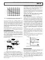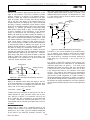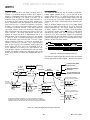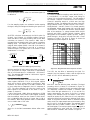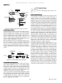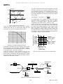
1
PRELIMINARY TECHNICAL DATA Active and Apparent Energy Metering IC with di/dt sensor interface Preliminary Technical Data ADE7753* FEATURES High Accuracy, supports IEC 61036 and IEC61268 On-Chip Digital Integrator enables direct interface with current sensors with di/dt output The ADE7753 supplies Active, Reactive and Apparent Energy, Sampled Waveform, Current and Voltage RMS Less than 0.1% error over a dynamic range of 1000 to 1 Positive only energy accumulation mode available An On-Chip user Programmable threshold for line voltage surge and SAG, and PSU supervisory Digital Power, Phase & Input Offset Calibration An On-Chip temperature sensor (±3°C typical) A SPI compatible Serial Interface A pulse output with programmable frequency An Interrupt Request pin (IRQ) and Status register Proprietary ADCs and DSP provide high accuracy data over large variations in environmental conditions and time Reference 2.4V±8% (20 ppm/°C typical) with external overdrive capability Single 5V Supply, Low power (25mW typical) GENERAL DESCRIPTION The ADE7753 is an accurate active and apparent energy measurements IC with a serial interface and a pulse output. The ADE7753 incorporates two second order sigma delta ADCs, a digital integrator (on CH1), reference circuitry, temperature sensor, and all the signal processing required to perform RMS calculation on the voltage and current, active, reactive, and apparent energy measurement. An on-chip digital integrator provides direct interface to di/ dt current sensors such as Rogowski coils. The digital integrator eliminates the need for external analog integrator, and this solution provides excellent long-term stability and precise phase matching between the current and voltage channels. The integrator can be switched on and off based on the current sensor selected. The ADE7753 contains an Active Energy register, an Apparent Energy register capable of holding at least TBD seconds of accumulated power at full load and rms calculation for both inputs. Data is read from the ADE7753 via the serial interface. The ADE7753 also provides a pulse output (CF) with output frequency is proportional to the active power. In addition to rms calculation and active and apparent power information, the ADE7753 also accumulates the signed reactive energy. The ADE7753 also provides various system calibration features, i.e., channel offset correction, phase calibration and power calibration. The part also incorporates a detection circuit for short duration low or high voltage variations. The ADE7753 has a positive only accumulation mode which gives the option to accumulate energy only when positive power is detected. An internal no-load threshold ensures that the part does not exhibit any creep when there is no load. A zero crossing output (ZX) produces an output which is synchronized to the zero crossing point of the line voltage. This information is used in the ADE7753 to measure the line's period. The signal is also used internally to the chip in the line cycle Active and Apparent energy accumulation mode. This enables a faster and more precise energy accumulation and is useful during calibration. This signal is also useful for synchronization of relay switching with a voltage zero crossing. The interrupt request output is an open drain, active low logic output. The Interrupt Status Register indicates the nature of the interrupt, and the Interrupt Enable Register controls which event produces an output on the IRQ pin. The ADE7753 is available in 20-lead SSOP package. FUNCTIONAL BLOCK DIAGRAM PGA V1P V1N + - DVDD RESET AVDD DGND ADE7753 WGAIN[11:0] INTEGRATOR MULTIPLIER LPF2 Σ 冮dt ADC HPF CFNUM[11:0] TEMP SENSOR APOS[15:0] PHCAL[5:0] DFC Φ CFDEN[11:0] IRMSOS[11:0] Σ : + - VRMSOS[11:0] ADC : AGND SAG Σ VADIV[7:0] LPF1 2.4V REFERENCE VAGAIN[11:0] ZX PGA V2P V2N CF WDIV[7:0] 4kΩ ADE7753 REGISTERS & SERIAL INTERFACE REF IN/OUT CLKIN CLKOUT DIN DOUT SCLK CS IRQ *U.S. Patents 5,745,323; 5,760,617; 5,862,069; 5,872,469; others Pending. REV. PrC 1/02 Information furnished by Analog Devices is believed to be accurate and reliable. However, no responsibility is assumed by Analog Devices for its use, nor for any infringements of patents or other rights of third parties which may result from its use. No license is granted by implication or otherwise under any patent or patent rights of Analog Devices. One Technology Way, P.O. Box 9106, Norwood. MA 02062-9106, U.S.A. Tel: 781/329-4700 www.analog.com Fax: 781/326-8703 © Analog Devices, Inc., 2002 PRELIMINARY TECHNICAL DATA ADE7753–SPECIFICATIONS1,3 Parameter ENERGY MEASUREMENT ACCURACY Measurement Bandwidth Measurement Error1 on Channel 1 Channel 1 Range = 0.5V full-scale Gain = 1 Gain = 2 Gain = 4 Gain = 8 Gain = 16 Channel 1 Range = 0.25V full-scale Gain = 1 Gain = 2 Gain = 4 Gain = 8 Gain = 16 Channel 1 Range = 0.125V full-scale Gain = 1 Gain = 2 Gain = 4 Gain = 8 Gain = 16 Phase Error1 Between Channels AC Power Supply Rejection1 Output Frequency Variation (CF) DC Power Supply Rejection1 Output Frequency Variation (CF) ANALOG INPUTS Maximum Signal Levels Input Impedance (dc) Bandwidth Gain Error1,4 Channel 1 Range = 0.5V full-scale Range = 0.25V full-scale Range = 0.125V full-scale Channel 2 Gain Error Match1 Channel 1 Range = 0.5V full-scale Range = 0.25V full-scale Range = 0.125V full-scale Channel 2 Offset Error1 Channel 1 Channel 2 WAVEFORM SAMPLING Channel 1 Signal-to-Noise plus distortion Bandwidth (-3dB) Channel 2 Signal-to-Noise plus distortion Bandwidth (-3dB) (AVDD = DVDD = 5V ± 5%, AGND = DGND = 0V, On-Chip Reference, CLKIN = 3.579545MHz XTAL, TMIN to TMAX = -40°C to +85°C) Spec Units 14 kHz CLKIN = 3.579545 MHz Channel 2 = 300mV rms/60Hz, Gain = 2 0.1 0.1 0.1 0.1 0.2 % typ % typ % typ % typ % typ Over a dynamic range Over a dynamic range Over a dynamic range Over a dynamic range Over a dynamic range 1000 to 1 1000 to 1 1000 to 1 1000 to 1 1000 to 1 0.1 0.1 0.1 0.2 0.2 % typ % typ % typ % typ % typ Over a dynamic range Over a dynamic range Over a dynamic range Over a dynamic range Over a dynamic range 1000 to 1 1000 to 1 1000 to 1 1000 to 1 1000 to 1 0.1 0.1 0.2 0.2 0.4 ±0.05 % typ % typ % typ % typ % typ ° max 0.2 % typ ±0.3 % typ Over a dynamic range 1000 to 1 Over a dynamic range 1000 to 1 Over a dynamic range 1000 to 1 Over a dynamic range 1000 to 1 Over a dynamic range 1000 to 1 Line Frequency = 45Hz to 65Hz, HPF on AVDD = DVDD = 5V+175mV rms/ 120Hz Channel 1 = 20mV rms, Gain = 16, Range = 0.5V Channel 2 = 300mV rms/60Hz, Gain = 1 AVDD = DVDD = 5V ± 250mV dc Channel 1 = 20mV rms/60Hz, Gain = 16, Range = 0.5V Channel 2 = 300mV rms/60Hz, Gain = 1 ±0.5 390 14 V max kΩ min kHz ±4 ±4 ±4 ±4 % typ % typ % typ % typ V1 = 0.5V dc V1 = 0.25V dc V1 = 0.125V dc V2 = 0.5V dc External 2.5V reference ±0.3 ±0.3 ±0.3 ±0.3 % typ % typ % typ % typ Gain = 1, 2, 4, 8, 16 Gain = 1, 2, 4, 8, 16 Gain = 1, 2, 4, 8, 16 Gain = 1, 2, 4, 8, 16 ±10 ±10 mV max mV max Channel 1 Range = 0.5V Channel 2 Range = 0.5V 62 14 dB typ kHz 52 140 dB typ Hz Test Conditions/Comments See Analog Inputs Section V1P, V1N, V2N and V2P to AGND CLKIN/256, CLKIN = 3.579545MHz External 2.5V reference, Gain = 1 on Channel 1 & 2 Sampling CLKIN/128, 3.579545MHz/128 = 27.9kSPS See Channel 1 Sampling 150mV rms/60Hz, Range = 0.5V, Gain = 2 CLKIN = 3.579545MHz See Channel 2 Sampling 150mV rms/60Hz, Gain = 2 CLKIN = 3.579545MHz -2- REV. PrC 01/02 PRELIMINARY TECHNICAL DATA ADE7753 Parameter REFERENCE INPUT REFIN/OUT Input Voltage Range Input Capacitance ON-CHIP REFERENCE Reference Error Current source Output Impedance Temperature Coefficient Spec Units Test Conditions/Comments 2.6 2.2 10 V max V min pF max ±200 10 4 20 mV max µA max kΩ min ppm/°C typ 4 1 MHz max MHz min 2.4 V +8% 2.4V -8% Nominal 2.4V at REFIN/OUT pin CLKIN Input Clock Frequency Note all specifications CLKIN of 3.579545MHz LOGIC INPUTS RESET, DIN, SCLK, CLKIN and CS 2.4 Input High Voltage, VINH 0.8 Input Low Voltage, VINL Input Current, IIN ±3 Input Capacitance, CIN 10 LOGIC OUTPUTS3 SAG & IRQ Output High Voltage, VOH Output Low Voltage, VOL ZX & DOUT Output High Voltage, VOH Output Low Voltage, VOL CF Output High Voltage, VOH Output Low Voltage, VOL POWER SUPPLY AV DD DVDD AIDD DIDD V min V max µA max pF max DVDD = 5 V ± 10% DVDD = 5 V ± 10% Typically 10nA, VIN = 0V to DVDD 4 0.4 V min V max Open Drain outputs, 10kΩ pull up resistor ISOURCE = 5mA ISINK = 0.8mA 4 0.4 V min V max ISOURCE = 5mA ISINK = 0.8mA 4 1 V min V max ISOURCE = 5mA ISINK = 7mA 4.75 5.25 4.75 5.25 3 4 V min V max V min V max mA max mA max For specified Performance 5V - 5% 5V +5% 5V - 5% 5V + 5% Typically 2.0 mA Typically 3.0 mA NOTES: 1 See Terminology Section for explanation of Specifications 2 See Plots in Typical Performance Graphs 3 Specifications subject to change without notice 4 See Analog Inputs Section ORDERING GUIDE IOL 200 µA TO OUTPUT PIN +2.1V CL 50pF Package Option* ADE7753ARS ADE7753ARSRL EVAL-ADE7753EB RS-20 RS-20 ADE7753 evaluation board * RS = Shrink Small Outline Package in tubes; RSRL = Shrink Small Outline Package in reel. 1.6 mA IOH Load Circuit for Timing Specifications REV. PrC 01/02 MODEL –3– PRELIMINARY TECHNICAL DATA ADE7753 ADE7753 TIMING CHARACTERISTICS1,2 Parameter A,B Versions (AVDD = DVDD = 5V ± 5%, AGND = DGND = 0V, On-Chip Reference, CLKIN = 3.579545MHz XTAL, TMIN to TMAX = -40°C to +85°C) Units Test Conditions/Comments 20 150 150 10 5 TBD TBD 100 ns ns ns ns ns ns ns ns CS falling edge to first SCLK falling edge SCLK logic high pulse width SCLK logic low pulse width Valid Data Set up time before falling edge of SCLK Data Hold time after SCLK falling edge Minimum time between the end of data byte transfers. Minimum time between byte transfers during a serial write. CS Hold time after SCLK falling edge. TBD ns (min) t10 t113 TBD 30 ns (min) ns (min) t124 100 10 100 10 ns ns ns ns Write timing t1 t2 t3 t4 t5 t6 t7 t8 Read timing t9 t 13 4 (min) (min) (min) (min) (min) (min) (min) (min) (max) (min) (max) (min) Minimum time between read command (i.e. a write to Communication Reigster) and data read. Minimum time between data byte transfers during a multibyte read. Data access time after SCLK rising edge following a write to the Communications Register Bus relinquish time after falling edge of SCLK. Bus relinquish time after rising edge of CS. NOTES Sample tested during initial release and after any redesign or process change that may affect this parameter. All input signals are specified with tr = tf = 5ns (10% to 90%) and timed from a voltage level of 1.6V. 2 See timing diagram below and Serial Interface section of this data sheet. 3 Measured with the load circuit in Figure 1 and defined as the time required for the output to cross 0.8V or 2.4V. 4 Derived from the measured time taken by the data outputs to change 0.5V when loaded with the circuit in Figure 1. The measured number is then extrapolated back to remove the effects of charging or discharging the 50pF capacitor. This means that the time quoted in the timing characteristics is the true bus relinquish time of the part and is independent of the bus loading. 1 Serial Write Timing t8 CS t1 t2 t3 t6 t7 SCLK t4 1 DIN 0 0 t7 t5 A4 A3 A2 A1 A0 DB7 DB0 DB7 Most Significant Byte Command Byte DB0 Least Significant Byte Serial Read Timing CS t1 t9 t13 t10 SCLK DIN 0 0 0 A4 A3 A2 A1 A0 DOUT DB7 DB0 Most Significant Byte Command Byte –4– t12 t11 t11 DB7 DB0 Least Significant Byte REV. PrC 01/02 PRELIMINARY TECHNICAL DATA ADE7753 ABSOLUTE MAXIMUM RATINGS* (TA = +25°C unless otherwise noted) AVDD to AGND . . . . . . . . . . . . . . . . . . . . . –0.3 V to +7 V DVDD to DGND . . . . . . . . . . . . . . . . . . . . –0.3 V to +7 V DVDD toAVDD . . . . . . . . . . . . . . . . . . . . . –0.3 V to +0.3 V Analog Input Voltage to AGND V1P, V1N, V2P and V2N . . . . . . . . . . . . . . . . . . -6V to +6V Reference Input Voltage to AGND . . . . –0.3 V to AVDD + 0.3 V Digital Input Voltage to DGND –0.3 V to DVDD + 0.3 V Digital Output Voltage to DGND –0.3 V to DVDD + 0.3 V Operating Temperature Range Industrial . . . . . . . . . . . . . . . . . . . . . . . . –40°C to +85°C Storage Temperature Range . . . . . . . . –65°C to +150°C Junction Temperature . . . . . . . . . . . . . . . . . . . . . . . +150°C 20 Pin SSOP, Power Dissipation . . . . . . . . . . . . 450 mW θJA Thermal Impedance . . . . . . . . . . . . . . . . . . . 112°C/W Lead Temperature, Soldering Vapor Phase (60 sec) . . . . . . . . . . . . . . . . . . . +215°C Infrared (15 sec) . . . . . . . . . . . . . . . . . . . . . . +220°C * Stresses above those listed under “Absolute Maximum Ratings” may cause permanent damage to the device. This is a stress rating only and functional operation of the device at these or any other conditions above those listed in the operational sections of this specification is not implied. Exposure to absolute maximum rating conditions for extended periods may affect device reliability. CAUTION ESD (electrostatic discharge) sensitive device. Electrostatic charges as high as 4000 V readily accumulate on the human body and test equipment and can discharge without detection. Although the ADE7753 features proprietary ESD protection circuitry, permanent damage may occur on devices subjected to high energy electrostatic discharges. Therefore, proper ESD precautions are recommended to avoid performance degradation or loss of functionality. WARNING! ESD SENSITIVE DEVICE Terminology MEASUREMENT ERROR The error associated with the energy measurement made by the ADE7753 is defined by the following formula: input signal levels when the supplies are varied ±5%. Any error introduced is again expressed as a percentage of reading. Percentage Error = æ Energy registered by ADE 7753 - True Energy ö ÷÷ ´ 100 % çç True Energy ø è ADC OFFSET ERROR This refers to the DC offset associated with the analog inputs to the ADCs. It means that with the analog inputs connected to AGND the ADCs still see a dc analog input signal. The magnitude of the offset depends on the gain and input range selection - see characteristic curves. However, when HPF1 is switched on the offset is removed from Channel 1 (current) and the power calculation is not affected by this offset. The offsets may be removed by performing an offset calibration see Analog Inputs. PHASE ERROR BETWEEN CHANNELS The digital integrator and the HPF (High Pass Filter) in Channel 1 have non-ideal phase response. To offset this phase response and equalize the phase response between channels, two phase correction network is placed in Channel 1: one for the digital integrator and the other for the HPF. Each phase correction network corrects the phase response of the corresponding component and ensures a phase match between Channel 1 (current) and Channel 2 (voltage) to within ±0.1° over a range of 45Hz to 65Hz and ±0.2° over a range 40Hz to 1kHz. GAIN ERROR The gain error in the ADE7753 ADCs is defined as the difference between the measured ADC output code (minus the offset) and the ideal output code - see Channel 1 ADC & Channel 2 ADC. It is measured for each of the input ranges on Channel 1 (0.5V, 0.25V and 0.125V). The difference is expressed as a percentage of the ideal code. POWER SUPPLY REJECTION This quantifies the ADE7753 measurement error as a percentage of reading when the power supplies are varied. For the AC PSR measurement a reading at nominal supplies (5V) is taken. A second reading is obtained with the same input signal levels when an ac (175mV rms/120Hz) signal is introduced onto the supplies. Any error introduced by this AC signal is expressed as a percentage of reading—see Measurement Error definition above. For the DC PSR measurement a reading at nominal supplies (5V) is taken. A second reading is obtained with the same REV. PrC 01/02 GAIN ERROR MATCH The Gain Error Match is defined as the gain error (minus the offset) obtained when switching between a gain of 1 (for each of the input ranges) and a gain of 2, 4, 8, or 16. It is expressed as a percentage of the output ADC code obtained under a gain of 1. This gives the gain error observed when the gain selection is changed from 1 to 2, 4, 8 or 16. –5– PRELIMINARY TECHNICAL DATA ADE7753 PIN FUNCTION DESCRIPTION Pin No. MNEMONIC DESCRIPTION 1 RESET Reset pin for the ADE7753. A logic low on this pin will hold the ADCs and digital circuitry (including the Serial Interface) in a reset condition. 2 DVDD Digital power supply. This pin provides the supply voltage for the digital circuitry in the ADE7753. The supply voltage should be maintained at 5V ± 5% for specified operation. This pin should be decoupled to DGND with a 10µF capacitor in parallel with a ceramic 100nF capacitor. 3 AVDD Analog power supply. This pin provides the supply voltage for the analog circuitry in the ADE7753. The supply should be maintained at 5V ± 5% for specified operation. Every effort should be made to minimize power supply ripple and noise at this pin by the use of proper decoupling. The typical performance graphs in this data sheet show the power supply rejection performance. This pin should be decoupled to AGND with a 10µF capacitor in parallel with a ceramic 100nF capacitor. 4,5 V1P, V1N Analog inputs for Channel 1. This channel is intended for use with the di/dt current transducer such as Rogowski coil or other current sensor such as shunt or current transformer (CT). These inputs are fully differential voltage inputs with maximum differential input signal levels of ±0.5V, ±0.25V and ±0.125V, depending on the full scale selection - See Analog Inputs. Channel 1 also has a PGA with gain selections of 1, 2, 4, 8 or 16. The maximum signal level at these pins with respect to AGND is ±0.5V. Both inputs have internal ESD protection circuitry and in addition an overvoltage of ±6V can be sustained on these inputs without risk of permanent damage. 6,7 V2N, V2P Analog inputs for Channel 2. This channel is intended for use with the voltage transducer. These inputs are fully differential voltage inputs with a maximum differential signal level of ±0.5V. Channel 2 also has a PGA with gain selections of 1, 2, 4, 8 or 16. The maximum signal level at these pins with respect to AGND is ±0.5V. Both inputs have internal ESD protection circuitry, and an overvoltage of ±6V can be sustained on these inputs without risk of permanent damage. 8 AGND This pin provides the ground reference for the analog circuitry in the ADE7753, i.e. ADCs and reference. This pin should be tied to the analog ground plane or the quietest ground reference in the system. This quiet ground reference should be used for all analog circuitry, e.g. anti-aliasing filters, current and voltage transducers etc. In order to keep ground noise around the ADE7753 to a minimum, the quiet ground plane should only connected to the digital ground plane at one point. It is acceptable to place the entire device on the analog ground plane - see Applications Information. 9 REFIN/OUT This pin provides access to the on-chip voltage reference. The on-chip reference has a nominal value of 2.4V ± 8% and a typical temperature coefficient of 20ppm/°C. An external reference source may also be connected at this pin. In either case this pin should be decoupled to AGND with a 1µF ceramic capacitor. 10 DGND This provides the ground reference for the digital circuitry in the ADE7753, i.e. multiplier, filters and digital-to-frequency converter. Because the digital return currents in the ADE7753 are small, it is acceptable to connect this pin to the analog ground plane of the system - see Applications Information. However, high bus capacitance on the DOUT pin may result in noisy digital current which could affect performance. 11 CF Calibration Frequency logic output. The CF logic output gives Active Power information. This output is intended to be used for operational and calibration purposes. The full-scale output frequency can be adjusted by writing to the CFDEN and CFNUM Register—see Energy To Frequency Conversion. 12 ZX Voltage waveform (Channel 2) zero crossing output. This output toggles logic high and low at the zero crossing of the differential signal on Channel 2—see Zero Crossing Detection. 13 SAG This open drain logic output goes active low when either no zero crossings are detected or a low voltage threshold (Channel 2) is crossed for a specified duration. See Line Voltage Sag Detection. 14 IRQ Interrupt Request Output. This is an active low open drain logic output. Maskable interrupts include: Active Energy Register roll-over, Active Energy Register at half level, and arrivals of new waveform samples. See ADE7753 Interrupts. –6– REV. PrC 01/02 PRELIMINARY TECHNICAL DATA ADE7753 Pin No. MNEMONIC DESCRIPTION 15 CLKIN Master clock for ADCs and digital signal processing. An external clock can be provided at this logic input. Alternatively, a parallel resonant AT crystal can be connected across CLKIN and CLKOUT to provide a clock source for the ADE7753. The clock frequency for specified operation is 3.579545MHz. Ceramic load capacitors of between 22pF and 33pF should be used with the gate oscillator circuit. Refer to crystal manufacturers data sheet for load capacitance requirements. 16 CLKOUT A crystal can be connected across this pin and CLKIN as described above to provide a clock source for the ADE7753. The CLKOUT pin can drive one CMOS load when either an external clock is supplied at CLKIN or a crystal is being used. 17 CS Chip Select. Part of the four wire SPI Serial Interface. This active low logic input allows the ADE7753 to share the serial bus with several other devices. See ADE7753 Serial Interface. 18 SCLK Serial Clock Input for the synchronous serial interface. All Serial data transfers are synchronized to this clock—see ADE7753 Serial Interface. The SCLK has a schmitt-trigger input for use with a clock source which has a slow edge transition time, e.g., optoisolator outputs. 19 DOUT Data Output for the Serial Interface. Data is shifted out at this pin on the rising edge of SCLK. This logic output is normally in a high impedance state unless it is driving data onto the serial data bus—see ADE7753 Serial Interface.. 20 DIN Data Input for the Serial Interface. Data is shifted in at this pin on the falling edge of SCLK—see ADE7753 Serial Interface.. PIN CONFIGURATION SSOP Packages RESET 1 20 DIN DVDD 2 19 DOUT AVDD 3 V1P V1N 5 TOP VIEW 17 CS 16 (Not to Scale) CLKOUT 6 15 CLKIN V2P 7 14 IRQ AGND 8 13 SAG 9 12 ZX 10 11 CF V2N REFIN/OUT DGND REV. PrC 01/02 4 18 SCLK ADE7753 –7– PRELIMINARY TECHNICAL DATA ADE7753 Typical Performance Characteristics-ADE7753 –8– REV. PrC 01/02 PRELIMINARY TECHNICAL DATA ADE7753 ANALOG INPUTS The ADE7753 has two fully differential voltage input channels. The maximum differential input voltage for input pairs V1P/V1N and V2P/V2N are ±0.5V. In addition, the maximum signal level on analog inputs for V1P/V1N and V2P/ V2N are ±0.5V with respect to AGND. Each analog input channel has a PGA (Programmable Gain Amplifier) with possible gain selections of 1, 2, 4, 8 and 16. The gain selections are made by writing to the Gain register—see Figure 2. Bits 0 to 2 select the gain for the PGA in Channel 1 and the gain selection for the PGA in Channel 2 is made via bits 5 to 7. Figure 1 shows how a gain selection for Channel 1 is made using the Gain register. GAIN REGISTER* Channel 1 and Channel 2 PGA Control 7 6 5 4 3 2 1 0 0 0 0 0 0 0 0 0 ADDR: 0FH PGA 1 Gain Select 000 = x1 001 = x2 010 = x4 011 = x8 100 = x16 PGA 2 Gain Select 000 = x1 001 = x2 010 = x4 011 = x8 100 = x16 *Register contents show power on defaults Channel 1 Full Scale Select 00 = 0.5V 01 = 0.25V 10 = 0.125V Figure 2— ADE7753 Analog Gain register GAIN[7:0] Gain (k) selection V1P + - Vin It is also possible to adjust offset errors on Channel 1 and Channel 2 by writing to the Offset Correction Registers (CH1OS and CH2OS respectively). These registers allow channel offsets in the range ±20mV to ±50mV (depending on the gain setting) to be removed. Note that it is not necessary to perform an offset correction in an Energy measurement application if HPF in Channel 1 is switched on. Figure 3 shows the effect of offsets on the real power calculation. As can be seen from Figure 3, an offset on Channel 1 and Channel 2 will contribute a dc component after multiplication. Since this dc component is extracted by LPF2 to generate the Active (Real) Power information, the offsets will have contributed an error to the Active Power calculation. This problem is easily avoided by enabling HPF in Channel 1. By removing the offset from at least one channel, no error component is generated at dc by the multiplication. Error terms at Cos(w.t) are removed by LPF2 and by integration of the Active Power signal in the Active Energy register (AENERGY[23:0]) – see Energy Calculation. k.Vin Σ V1N + Offset Adjust (±50mV) CH1OS[7:0] Bit 0 to 5: Sign magnitude coded offset correction Bit 6: Not used Bit 7: Digital Integrator (On=1, Off=0; default ON) Figure 1— PGA in Channel 1 In addition to the PGA, Channel 1 also has a full scale input range selection for the ADC. The ADC analog input range selection is also made using the Gain register—see Figure 2. As mentioned previously the maximum differential input voltage is 1V. However, by using bits 3 and 4 in the Gain register, the maximum ADC input voltage can be set to 0.5V, 0.25V or 0.125V. This is achieved by adjusting the ADC reference—see ADE7753 Reference Circuit. Table I below summarizes the maximum differential input signal level on Channel 1 for the various ADC range and gain selections. DC component (including error term) is extracted by the LPF for real power calculation VOS.IOS V.I 2 IOS.V VOS.I 0 ω 2ω frequency (rad/s) Figure 3— Effect of channel offsets on the real power calculation Table I The contents of the Offset Correction registers are 6-Bit, sign and magnitude coded. The weighting of the LSB size depends on the gain setting, i.e., 1, 2, 4, 8 or 16. Table II below shows the correctable offset span for each of the gain settings and the LSB weight (mV) for the Offset Correction registers. The maximum value which can be written to the offset correction registers is ±31 decimal —see Figure 4. Figure 4 shows the relationship between the Offset Correction register contents and the offset (mV) on the analog inputs for a gain setting of one. In order to perform an offset adjustment, The analog inputs should be first connected to AGND, and there should be no signal on either Channel 1 or Channel 2. A read from Channel 1 or Channel 2 using the Maximum input signal levels for Channel 1 Max Signal Channel 1 ADC Input Range Selection 0.5V 0.25V 0.125V 0.5V 0.25V 0.125V 0.0625V 0.0313V 0.0156V 0.00781V Gain Gain Gain Gain Gain — — REV. PrC 01/02 = = = = = 1 2 4 8 16 — Gain Gain Gain Gain Gain — = = = = = 1 2 4 8 16 — — Gain Gain Gain Gain Gain = = = = = 1 2 4 8 16 –9– PRELIMINARY TECHNICAL DATA ADE7753 The current signal needs to be recovered from the di/dt signal before it can be used. An integrator is therefore necessary to restore the signal to its original form. The ADE7753 has a built-in digital integrator to recover the current signal from the di/dt sensor. The digital integrator on Channel 1 is switched on by default when the ADE7753 is powered up. Setting the MSB of CH1OS register will turn on the integrator. Figures 6 to 9 show the magnitude and phase response of the digital integrator. Table II Offset Correction range Gain 1 2 4 8 16 Correctable Span LSB Size ±50mV ±37mV ±30mV ±26mV ±24mV 1.61mV/LSB 1.19mV/LSB 0.97mV/LSB 0.84mV/LSB 0.77mV/LSB 30 Waveform register will give an indication of the offset in the channel. This offset can be canceled by writing an equal and opposite offset value to the relevant offset register. The offset correction can be confirmed by performing another read. Note when adjusting the offset of Channel 1, one should disable the digital integrator and the HPF. 20 10 GAIN-dB 0 -10 -20 -30 CH1OS[5:0] -40 1Fh 01, 1111b Sign + 5 Bits -50 -60 10 1 10 2 10 3 10 4 FREQUENCY-Hz 00h 0mV -50mV 3Fh Figure 6– Combined gain response of the digital integrator and phase compensator +50mV Offset Adjust -88 11, 1111b Sign + 5 Bits -88.5 -89 PHASE-DEGREES Figure 4– Channel Offset Correction Range (Gain = 1) -89.5 -90 -90.5 di/dt CURRENT SENSOR AND DIGITAL INTEGRATOR -91 di/dt sensor detects changes in magetic field caused by ac current. Figure 5 shows the principle of a di/dt current sensor. -91.5 -92 1 10 10 2 10 3 10 4 FREQUENCY-Hz Figure 7– Combined phase response of the digital integrator and phase compensator Magnetic field created by current (directly propor tional to current) 0 + EMF (electromotive force) - induced by changes in magnetic flux density (d/dt) -1 -2 GAIN-dB Figure 5– Principle of a di/dt current sensor The flux density of a magnetic field induced by a current is directly proportional to the magnitude of the current. The changes in the magnetic flux density passing through a conductor loop generates an electromotive force (EMF) between the two ends of the loop. The EMF is a voltage signal which is proportional to the di/dt of the current. The voltage output from the di/dt current sensor is determined by the mutual inductance between the current carrying conductor and the di/dt sensor. -3 -4 -5 -6 40 45 50 55 FREQUENCY-Hz 60 65 70 Figure 8– Combined gain response of the digital integrator and phase compensator (40Hz to 70Hz) –10– REV. PrC 01/02 PRELIMINARY TECHNICAL DATA ADE7753 The phase response of this filter is shown in the Channel 2 Sampling section of this data sheet. The phase lag response of LPF1 results in a time delay of approximately 0.97ms (@ 60Hz) between the zero crossing on the analog inputs of Channel 2 and the rising or falling edge of ZX. The zero-crossing detection also drives one flag bit in the interrupt status register. An active low in the IRQ output will also appear if the corresponding bit in the Interrupt Enable register is set to logic one. The flag in the Interrupt status register as well as the IRQ output are reset to their default value when the Interrupt Status register with reset (RSTSTATUS) is read. -89.985 PHASE-DEGREES -89.99 -89.995 -90 -90.005 -90.01 -90.015 -90.02 40 45 50 55 FREQUENCY-Hz 60 65 70 Figure 9– Combined phase response of the digital integrator and phase compensator (40Hz to 70Hz) Note that the integrator has a -20dB/dec attenuation and approximately -90° phase shift. When combined with a di/dt sensor, the resulting magnitude and phase response should be a flat gain over the frequency band of interest. However, the di/dt sensor has a 20dB/dec gain associated with it, and generates significant high frequency noise, a more effective anti-aliasing filter is needed to avoid noise due to aliasing— see Antialias Filter. When the digital integrator is switched off, the ADE7753 can be used directly with a conventional current sensor such as current transformer (CT) or a low resistance current shunt. ZERO CROSSING DETECTION The ADE7753 has a zero crossing detection circuit on Channel 2. This zero crossing is used to produce an external zero cross signal (ZX) and it is also used in the calibration mode - see Energy Calibration. The zero crossing signal is also used to initiate a temperature measurement on the ADE7753 - see Temperature Measurement. Figure 10 shows how the zero cross signal is generated from the output of LPF1. V2P x1, x2, x4, x8, x16 GAIN[7:5] The zero crossing detection also has an associated time-out register ZXTOUT. This unsigned, 12-bit register is decremented (1 LSB) every 128/CLKIN seconds. The register is reset to its user programmed full scale value every time a zero crossing on Channel 2 is detected. The default power on value in this register is FFFh. If the register decrements to zero before a zero crossing is detected and the DISSAG bit in the Mode register is logic zero, the 5)/ pin will go active low. The absence of a zero crossing is also indicated on the 143 pin if the SAG enable bit in the Interrupt Enable register is set to logic one. Irrespective of the enable bit setting, the SAG flag in the Interrupt Status register is always set when the ZXTOUT register is decremented to zero - see ADE7753 Interrupts. The Zerocross Time-out register can be written/read by the user and has an address of 1Dh - see Serial Interface section. The resolution of the register is 128/CLKIN seconds per LSB. Thus the maximum delay for an interrupt is 0.15 second (128/CLKIN × 212). Figure 11 shows the mechanism of the zero crossing time out detection when the line voltage stays at a fixed DC level for more than CLKIN/128 x ZXTOUT seconds. 16-bit internal register value ZXTOUT REFERENCE 1 V2 Zero crossing Time out TO MULTIPLIER -63% to + 63% FS Channel 2 ADC 2 PGA2 V2N ZERO CROSS 23.2 ⬚ @ 60Hz 1.0 0.92 ZX ZXTO detection bit LPF1 f-3dB = 140Hz ZX Figure 11 - Zero crossing Time out detection PERIOD MEASUREMENT V2 LPF1 The ADE7753 provides also the period measurement of the line. The period register is an unsigned 15-bit register and is updated every period of the selected phase. Figure 10– Zero cross detection on Channel 2 The ZX signal will go logic high on a positive going zero The resolution of this register is 2.2ms/LSB when crossing and logic low on a negative going zero crossing on CLKIN=3.579545MHz, which represents 0.013% when the Channel 2. The zero crossing signal ZX is generated from the line frequency is 60Hz. When the line frequency is 60Hz, the output of LPF1. LPF1 has a single pole at 156Hz (at CLKIN value of the Period register is approximately 7576d. The = 3.579545MHz). As a result there will be a phase lag length of the register enables the measurement of line between the analog input signal V2 and the output of LPF1. frequencies as low as 13.9Hz. –11– REV. PrC 01/02 PRELIMINARY TECHNICAL DATA ADE7753 POWER SUPPLY MONITOR The ADE7753 also contains an on-chip power supply monitor. The Analog Supply (AVDD) is continuously monitored by the ADE7753. If the supply is less than 4V ± 5% then the ADE7753 will go into an inactive state, i.e. no energy will be accumulated when the supply voltage is below 4V. This is useful to ensure correct device operation at power up and during power down. The power supply monitor has built-in hysteresis and filtering. This gives a high degree of immunity to false triggering due to noisy supplies. half cycle for which the line voltage falls below the threshold, if the DISSAG bit in the Mode register is logic zero. As is the case when zero-crossings are no longer detected, the sag event is also recorded by setting the SAG flag in the Interrupt Status register. If the SAG enable bit is set to logic one, the IRQ logic output will go active low - see ADE7753 Interrupts. The SAG pin will go logic high again when the absolute value of the signal on Channel 2 exceeds the sag level set in the Sag Level register. This is shown in Figure 13 when the SAG pin goes high during the tenth half cycle from the time when the signal on Channel 2 first dropped below the threshold level. Sag Level Set AVDD The contents of the Sag Level register (1 byte) are compared to the absolute value of the most significant byte output from LPF1, after it is shifted left by one bit. Thus for example the nominal maximum code from LPF1 with a full scale signal on Channel 2 is 1C396h or (0001, 1100, 0011, 1001, 0110b)—see Channel 2 sampling. Shifting one bit left will give 0011,1000,0111,0010,1100b or 3872Ch. Therefore writing 38h to the Sag Level register will put the sag detection level at full scale. Writing 00h will put the sag detection level at zero. The Sag Level register is compared to the most significant byte of a waveform sample after the shift left and detection is made when the contents of the sag level register are greater. 5V 4V 0V Time ADE7753 Power-on Inactive Reset Active Inactive SAG Figure 12 - On-Chip power supply monitor PEAK DETECTION As can be seen from Figure 12 the trigger level is nominally set at 4V. The tolerance on this trigger level is about ±5%. The SAG pin can also be used as a power supply monitor input to the MCU. The SAG pin will go logic low when the ADE7753 is reset. The power supply and decoupling for the part should be such that the ripple at AVDD does not exceed 5V±5% as specified for normal operation. The ADE7753 can also be programmed to detect when the absolute value of the voltage or the current channel of one phase exceeds a certain peak value. Figure 14 illustrates the behavior of the peak detection for the voltage channel. V2 VPKLVL[7:0] LINE VOLTAGE SAG DETECTION In addition to the detection of the loss of the line voltage signal (zero crossing), the ADE7753 can also be programmed to detect when the absolute value of the line voltage drops below a certain peak value, for a number of half cycles. This condition is illustrated in Figure 13 below. PKV reset low when RSTSTATUS register is read PKV Interrupt Flag (Bit C of STATUS register) Channel 2 Read RSTSTATUS register Full Scale Figure 14 - ADE7753 Peak detection SAGLVL[7:0] SAGCYC[7:0] = 06H 6 half cycles Both channel 1 and channel 2 can be monitored at the same time. Figure 14 shows a line voltage exceeding a threshold which is set in the Voltage peak register (VPKLVL[7:0]). The Voltage Peak event is recorded by setting the PKV flag in the Interrupt Status register. If the PKV enable bit is set to logic one in the Interrupt Mask register, the IRQ logic output will go active low - see ADE7753 Interrupts. SAG reset high when Channel 2 exceeds SAGLVL[7:0] SAG Peak Level Set Figure 13– ADE7753 Sag detection Figure 13 shows the line voltage fall below a threshold which is set in the Sag Level register (SAGLVL[7:0]) for nine half cycles. Since the Sag Cycle register (SAGCYC[7:0]) contains 06h the SAG pin will go active low at the end of the sixth The contents of the VPKLVL and IPKLVL registers are respectively compared to the absolute value of channel 1 and channel 2, after they are multiplied by 2. Thus, for example, the nominal maximum code from the channel 1 ADC with a full scale signal is 1C396h —see Channel 1 Sampling. Multiplying by 2 will give 3872Ch. –12– REV. PrC 01/02 PRELIMINARY TECHNICAL DATA ADE7753 with reset, the ADE7753 is designed to ensure that no interrupt events are missed. If an interrupt event occurs just as the Status register is being read, the event will not be lost and the IRQ logic output is guaranteed to go high for the duration of the Interrupt Status register data transfer before going logic low again to indicate the pending interrupt. See the next section for a more detailed description. Therefore, writing 38h to the IPKLVL register will put the channel 1 peak detection level at full scale and set the current peak detection to its least sensitive value. Writing 00h will put the channel 1 detection level at zero. The detection is done when the content of the IPKLVL register is smaller than the incoming channel 1 sample. Peak Level Record The ADE7753 records the maximum absolute value reached by channel 1 and channel 2 in two different registers - IPEAK and VPEAK respectively. VPEAK and IPEAK are 24-bit unsigned registers. These registers are updated each time the absolute value of the respective Waveform sample is above the value stored in the VPEAK or IPEAK register. The updated value corresponds to the last maximum absolute value observed on the channel input. The RSTVPEAK and RSTIPEAK registers also recorded the maximum absolute value reached by channel 1 and channel 2 . RSTVPEAK and RSTIPEAK registers value are respectively reset to zero when the register is read. Using the ADE7753 Interrupts with an MCU Shown in Figure 15 is a timing diagram which shows a suggested implementation of ADE7753 interrupt management using an MCU. At time t1 the IRQ line will go active low indicating that one or more interrupt events have occurred in the ADE7753. The IRQ logic output should be tied to a negative edge triggered external interrupt on the MCU. On detection of the negative edge, the MCU should be configured to start executing its Interrupt Service Routine (ISR). On entering the ISR, all interrupts should be disabled using the global interrupt enable bit. At this point the MCU external interrupt flag can be cleared in order to capture interrupt events which occur during the current ISR. When the MCU interrupt flag is cleared a read from the Status register with reset is carried out. This will cause the IRQ line to be reset logic high (t2)—see Interrupt timing. The Status register contents are used to determine the source of the interrupt(s) and hence the appropriate action to be taken. If a subsequent interrupt event occurs during the ISR, that event will be recorded by the MCU external interrupt flag being set again (t3). On returning from the ISR, the global interrupt mask will be cleared (same instruction cycle) and the external interrupt flag will cause the MCU to jump to its ISR once again. This will ensure that the MCU does not miss any external interrupts. ADE7753 INTERRUPTS ADE7753 Interrupts are managed through the Interrupt Status register (STATUS[15:0]) and the Interrupt Enable register (IRQEN[15:0]). When an interrupt event occurs in the ADE7753, the corresponding flag in the Status register is set to a logic one - see Interrupt Status register. If the enable bit for this interrupt in the Interrupt Enable register is logic one, then the IRQ logic output goes active low. The flag bits in the Status register are set irrespective of the state of the enable bits. In order to determine the source of the interrupt, the system master (MCU) should perform a read from the Status register with reset (RSTSTATUS[15:0]). This is achieved by carrying out a read from address 0Ch. The IRQ output will go logic high on completion of the Interrupt Status register read command—see Interrupt timing. When carrying out a read Interrupt timing The ADE7753 Serial Interface section should be reviewed first before reviewing the interrupt timing. As previously deMCU int. flag set t3 t2 t1 IRQ MCU Program Sequence Jump to ISR Global int. Clear MCU Mask Set int. flag Read Status with Reset (05h) ISR Action (Based on Status contents) ISR Return Global int. Mask Reset Figure 15– ADE7753 interrupt management CS t1 t9 SCLK DIN 0 0 0 0 0 1 0 1 t11 t11 DOUT DB7 Read Status Register Command DB0 DB7 Status Register Contents IRQ REV. PrC 01/02 Figure 16– ADE7753 interrupt timing –13– DB0 Jump to ISR PRELIMINARY TECHNICAL DATA ADE7753 scribed, when the IRQ output goes low the MCU ISR must read the Interrupt Status register in order to determine the source of the interrupt. When reading the Status register contents, the IRQ output is set high on the last falling edge of SCLK of the first byte transfer (read Interrupt Status register command). The IRQ output is held high until the last bit of the next 15-bit transfer is shifted out (Interrupt Status register contents)— see Figure 16. If an interrupt is pending at this time, the IRQ output will go low again. If no interrupt is pending the IRQ output will stay high. TEMPERATURE MEASUREMENT ADE7753 also includes an on-chip temperature sensor. A temperature measurement can be made by setting bit 5 in the Mode register. When bit 5 is set logic high in the Mode register, the ADE7753 will initiate a temperature measurement on the next zero crossing. When the zero crossing on Channel 2 is detected the voltage output from the temperature sensing circuit is connected to ADC1 (Channel 1) for digitizing. The resultant code is processed and placed in the Temperature register (TEMP[7:0]) approximately 26µs later (24 CLKIN cycles). If enabled in the Interrupt Enable register (bit 5), the IRQ output will go active low when the temperature conversion is finished. Please note that temperature conversion will introduce a small amount of noise in the energy calculation. If temperature conversion is performed frequently (e.g. multiple times per second), a noticeable error will accumulate in the resulting energy calculation over time. The contents of the Temperature register are signed (2's complement) with a resolution of approximately 1 LSB/°C. The temperature register will produce a code of 00h when the ambient temperature is approximately 70°C. The temperature measurement is uncalibrated in the ADE7753 and has an offset tolerance that could be as high as ±20°C. the 1-bit ADC is virtually meaningless. Only when a large number of samples are averaged will a meaningful result be obtained. This averaging is carried out in the second part of the ADC, the digital low pass filter. By averaging a large number of bits from the modulator the low pass filter can produce 24-bit data words which are proportional to the input signal level. The sigma-delta converter uses two techniques to achieve high resolution from what is essentially a 1-bit conversion technique. The first is over-sampling. By over sampling we mean that the signal is sampled at a rate (frequency) which is many times higher than the bandwidth of interest. For example the sampling rate in the ADE7753 is CLKIN/4 (894kHz) and the band of interest is 40Hz to 2kHz. Oversampling has the effect of spreading the quantization noise (noise due to sampling) over a wider bandwidth. With the noise spread more thinly over a wider bandwidth, the quantization noise in the band of interest is lowered—see Figure 18. However, oversampling alone is not an efficient enough method to improve the signal to noise ratio (SNR) in the band of interest. For example, an oversampling ratio of 4 is required just to increase the SNR by only 6dB (1-Bit). To keep the oversampling ratio at a reasonable level, it is possible to shape the quantization noise so that the majority of the noise lies at the higher frequencies. This is what happens in the sigma-delta modulator, the noise is shaped by the integrator which has a high pass type response for the quantization noise. The result is that most of the noise is at the higher frequencies where it can be removed by the digital low pass filter. This noise shaping is also shown in Figure 18. Antialias filter (RC) Digital filter Shaped Signal Noise Sampling Frequency ADE7753 ANALOG TO DIGITAL CONVERSION The analog-to-digital conversion in the ADE7753 is carried out using two second order sigma-delta ADCs. For simplicity reason, the block diagram in Figure 17 shows a first order sigma-delta ADC. The converter is made up of two parts: the sigma-delta modulator and the digital low pass filter. MCLK/4 Analog Low Pass Filter R Σ - 0 2kHz 兰 + VREF 447kHz 894kHz Frequency (Hz) High resolution output from Digital LPF Signal Digital Low Pass Filter INTEGRATOR + Noise LATCHED COMPARATOR - Noise 24 C ....10100101...... 1-Bit DAC Figure 17– First Order Sigma-Delta (Σ−∆) ADC A sigma-delta modulator converts the input signal into a continuous serial stream of 1's and 0's at a rate determined by the sampling clock. In the ADE7753 the sampling clock is equal to CLKIN/4. The 1-bit DAC in the feedback loop is driven by the serial data stream. The DAC output is subtracted from the input signal. If the loop gain is high enough the average value of the DAC output (and therefore the bit stream) will approach that of the input signal level. For any given input value in a single sampling interval, the data from –14– 0 2kHz 447kHz 894kHz Frequency (Hz) Figure 18– Noise reduction due to Oversampling & Noise shaping in the analog modulator REV. PrC 01/02 PRELIMINARY TECHNICAL DATA ADE7753 Antialias Filter Figure 17 also shows an analog low pass filter (RC) on the input to the modulator. This filter is present to prevent aliasing. Aliasing is an artifact of all sampled systems. Basically it means that frequency components in the input signal to the ADC which are higher than half the sampling rate of the ADC will appear in the sampled signal at a frequency below half the sampling rate. Figure 19 illustrates the effect. Frequency components (arrows shown in black) above half the sampling frequency (also know as the Nyquist frequency, i.e., 447kHz) get imaged or folded back down below 447kHz (arrows shown in grey). This will happen with all ADCs regardless of the architecture. In the example shown, only frequencies near the sampling frequency, i.e., 894kHz, will move into the band of interest for metering, i.e, 40Hz - 2kHz. This allows the usage of very simple LPF (Low Pass Filter) to attenuate high frequency (near 900kHz) noise and prevents distortion in the band of interest. For conventional current sensor, a simple RC filter (single pole LPF) with a corner frequency of 10kHz will produce an attenuation of approximately 40dBs at 894kHz—see Figure 18. The 20dB per decade attenuation is usually sufficient to eliminate the effects of aliasing for conventional current sensor. For di/dt sensor such as Rogowski coil, however, the sensor has 20dB per decade gain. This will neutralize the -20dB per decade attenuation produced by the simple LPF. Therefore, when using a di/dt sensor, care should be taken to offset the 20dB per decade gain coming from the di/dt sensor. One simple approach is to cascade two RC filters to produce the -40dB per decade attenuation needed. Aliasing Effects Sampling Frequency image frequencies 0 2kHz 447kHz 894kHz Frequency (Hz) Figure 19 —ADC and signal processing in Channel 1 ADC transfer function Below is an expression which relates the output of the LPF in the sigma-delta ADC to the analog input signal level. Both ADCs in the ADE7753 are designed to produce the same output code for the same input signal level. Code ( ADC ) = 3.0492 × three input range selections which are selected by dividing down the reference value used for the ADC in Channel 1. The reference value used for Channel 1 is divided down to ½ and ¼ of the nominal value by using an internal resistor divider as shown in Figure 20. Maximum Load = 10µA PTAT REFIN/OUT 2.42V 60µA 2.5V 1.7kΩ 12.5kΩ 12.5kΩ 12.5kΩ Reference input to ADC Channel 1 (Range Select) 2.42V, 1.21V, 0.6V 12.5kΩ Figure 20 —ADE7753 Reference Circuit Ouput The REFIN/OUT pin can be overdriven by an external source, e.g., an external 2.5V reference. Note that the nominal reference value supplied to the ADCs is now 2.5V not 2.42V. This has the effect of increasing the nominal analog input signal range by 2.5/2.42×100% = 3% or from 0.5V to 0.5165V. The voltage of ADE7753 reference drifts slightly with temperature—see ADE7753 Specifications for the temperature coefficient specification (in ppm/°C) . The value of the temperature drift varies from part to part. Since the reference is used for the ADCs in both Channel 1 and 2, any x% drift in the reference will result in 2x% deviation of the meter accuracy. The reference drift resulting from temperature changes is usually very small and it is typically much smaller than the drift of other components on a meter. However, if guaranteed temperature performance is needed, one needs to use an external voltage reference. Alternatively, the meter can be calibrated at multiple temperatures. Real time compensation can be easily achieved using the on the on-chip temperature sensor. Vin × 262,144 Vout Therefore with a full scale signal on the input of 0.5V and an internal reference of 2.42V, the ADC output code is nominally 165,151 or 2851Fh. The maximum code from the ADC is ±262,144, this is equivalent to an input signal level of ±0.794V. However for specified performance it is not recommended that the full-scale input signal level of 0.5V be exceeded. ADE7753 Reference circuit Shown below in Figure 20 is a simplified version of the reference output circuitry. The nominal reference voltage at the REFIN/OUT pin is 2.42V. This is the reference voltage used for the ADCs in the ADE7753. However, Channel 1 has REV. PrC 01/02 Output Impedance 6kΩ –15– PRELIMINARY TECHNICAL DATA ADE7753 CHANNEL 1 ADC Channel 1 Sampling Figure 21 shows the ADC and signal processing chain for Channel 1. In waveform sampling mode the ADC outputs a signed 2’s Complement 24-bit data word at a maximum of 27.9kSPS (CLKIN/128). The output of the ADC can be scaled by ±50% to perform an overall power calibration or to calibrate the ADC output. While the ADC outputs a 24bit 2's complement value the maximum full-scale positive value from the ADC is limited to 400000h (+4,194,304 Decimal). The maximum full-scale negative value is limited to C00000h (-4,194,304 Decimal). If the analog inputs are over-ranged, the ADC output code will clamp at these values. With the specified full scale analog input signal of 0.5V (or 0.25V or 0.125V – see Analog Inputs section) the ADC will produce an output code which is approximately 63% of its full-scale value. This is illustrated in Figure 21. The diagram in Figure 21 shows a full-scale voltage signal being applied to the differential inputs V1P and V1N. The ADC output swings between D7AE14h (-2,642,412 Decimal) and 2851ECh (+2,642,412 Decimal). This is approximately 63% of the full-scale value 400000h. Over-ranging the analog inputs with more than 0.5V differential (0.25 or 0.125, depending on Channel 1 full scale selection) will cause the ADC output to increase towards its full scale value. However, for specified operation the differential signal on the analog inputs should not exceed the recommended value of 0.5V. The waveform samples may also be routed to the WAVEFORM register (MODE[14:13] = 1,0) to be read by the system master (MCU). In waveform sampling mode the WSMP bit (bit 3) in the Interrupt Enable register must also be set to logic one. The Active, Apparent Power and Energy calculation will remain uninterrupted during waveform sampling. When in waveform sample mode, one of four output sample rates may be chosen by using bits 11 and 12 of the Mode register (WAVSEL1,0). The output sample rate may be 27.9kSPS, 14kSPS, 7kSPS or 3.5kSPS—see Mode Register. The interrupt request output IRQ signals a new sample availability by going active low. The timing is shown in Figure 22. The 24-bit waveform samples are transferred from the ADE7753 one byte (8-bits) at a time, with the most significant byte shifted out first. The 24-bit data word is right justified - see ADE7753 Serial Interface. IRQ SCLK Read from WAVEFORM DIN 0 0 0 01 Hex Sign DOUT Channel 1 DATA - 24 bits Figure 22 – Waveform sampling Channel 1 The interrupt request output IRQ stays low until the interrupt routine reads the Reset Status register - see ADE7753 Interrupt. 2.42V, 1.21V, 0.6V x1, x2, x4, x8, x16 V1P V1 REFERENCE GAIN[2:0] ADC 1 PGA1 CURRENT RMS (IRMS) CALCULATION GAIN[4:3] Digital LPF DIGITAL INTEGRATOR* Sinc3 ∫ WAVEFORM SAMPLE REGISTER HPF ACTIVE AND REACTIVE POWER CALCULATION V1N 50Hz Channel 1 (Current Waveform) Data Range After integrator (50Hz) V1 1EF73Ch 0.5V, 0.25V, 0.125V, 62.5mV, 31.3mV, 15.6mV, 0V 400000h + FS 2851ECh + 63% FS 000000h + 63% FS E108C4h 2851ECh 000000h Analog Input Range Channel 1 (Current Waveform) Data Range D7AE14h - 63% FS C00000h - FS ADC Output word Range + 48% FS - 48% FS 000000h 60Hz D7AE14h - 63% FS Channel 1 (Current Waveform) Data Range After Integrator (60Hz) 19CE08h + 40% FS 000000h *WHEN DIGITAL INTEGRATOR IS ENABLED, FULL-SCALE OUTPUT DATA IS ATTENUATED DEPENDING ON THE SIGNAL FREQUENCY BECAUSE THE INTEGRATOR HAS A -20dB/DECADE FREQUENCY RESPONSE. WHEN DISABLED, THE OUTPUT WILL NOT BE FURTHER ATTENUATED. E631F8h - 40% FS Figure 21 —ADC and signal processing in Channel 1 –16– REV. PrC 01/02 PRELIMINARY TECHNICAL DATA ADE7753 Channel 1 RMS calculation CHANNEL 2 ADC Root Mean Square (RMS) value of a continuous signal V(t) is defined as: Channel 2 Sampling T 1 ⋅ V 2 (t )dt (1) T ∫0 For time sampling signals, rms calculation involves squaring the signal, taking the average and obtaining the square root: Vrms = 1 N 2 ⋅ ∑V (i ) N i =1 (2) Current Signal - i(t) -63% to +63% FS 0 10 SIGN 2 2 9 2 8 2 2 2 1 2 0 -6 60 Hz, -23.2° 1C82B3h -40 -8 -50 -10 -60 -12 -70 -14 -80 -16 + LPF3 24 -4 -30 00h HPF Channel 1 -2 50 Hz, -19.7° IRMSOS[11:0] 00h D7AE14h 50 Hz, -0.52dB -20 Irms(t) ~45% FS 2851ECh 0 60 Hz, -0.73dB -10 Phase (°) ADE7753 calculates simultaneously the RMS values for Channel 1 and Channel 2 in different register. Figure 23 shows the detail of the signal processing chain for the RMS calculation on channel 1. The channel 1 RMS value is processed from the samples used in the channel 1 waveform sampling mode. The channel 1 RMS value is stored in an unsigned 24-bit register (IRMS). One LSB of the channel 1 RMS register is equivalent to one LSB of a channel 1 waveform sample. The update rate of the channel 1 RMS measurement is CLKIN/4. Σ 24 IRMS -90 1 10 10 2 Gain (dBs) Vrms = In Channel 2 waveform sampling mode (MODE[14:13] = 1,1 and WSMP = 1) the ADC output code scaling for Channel 2 is not the same as Channel 1. The LSB weight of the Channel 2 samples is 16 times that of the Channel 1. Channel 2 waveform sample is a 16-bit word and sign extended to 24 bits. The absolute full-scale value of the ADC swings between 4000h (16,384 Decimal) and C000h (16,384 Decimal) – see ADC Channel 1. For normal operation, the differential voltage signal between V2P and V2N should not exceed 0.5V. The outputs from the ADC should be within 63% of the maximum, i.e. swings between 2852h (10,322 Decimal) and D7AEh (-10,322 Decimal). However, before being passed to the Waveform register, the ADC output is passed through a single pole, low pass filter with a cutoff frequency of 140Hz. The plots in Figure 24 shows the magnitude and phase response of this filter. -18 10 3 Frequency (Hz) Figure 23 - Channel 1 RMS signal processing With the specified full scale analog input signal of 0.5V, the ADC will produce an output code which is approximately 63% of its full-scale value (i.e. ±2,642,412d) - see Channel 1 ADC. The equivalent RMS values of a full-scale AC signal is 1,868,467d (1C82B3h). Figure 24 – Magnitude & Phase response of LPF1 The LPF1 has the effect of attenuating the signal. For example if the line frequency is 60Hz, then the signal at the output of LPF1 will be attenuated by about 8%. Channel 1 RMS offset compensation The ADE7753 incorporates a channel 1 RMS offset compensation register (IRMSOS). This is 12-bit signed registers which can be used to remove offset in the channel 1 RMS calculation. An offset may exist in the RMS calculation due to input noises that are integrated in the DC component of V2 (t). The offset calibration will allow the content of the IRMS register to be maintained at zero when no input is present on channel 1. 1 LSB of the Channel 1 RMS offset are equivalent to 32,768 LSB of the square of the Channel 1 RMS register. Assuming that the maximum value from the Channel 1 RMS calculation is 1,868,467d with full scale AC inputs, then 1 LSB of the channel 1 RMS offset represents 0.46% of measurement error at -60dB down of full scale. 2 I rms = I rms 0 + IRMSOS × 32768 where Irmso is the RMS measurement without offset correction. REV. PrC 01/02 H( f ) = 1 2 1+ 60Hz140Hz = 0.919= -0.73dB Note LPF1 does not affect the power calculation. The signal processing chain in Channel 2 is illustrated in Figure 25. Unlike Channel 1, Channel 2 has only one analog input range (1V differential). However like Channel 1, Channel 2 does have a PGA with gain selections of 1, 2, 4, 8 and 16. For energy measurement, the output of the ADC is passed directly to the multiplier and is not filtered. A HPF is not required to remove any DC offset since it is only required to remove the offset from one channel to eliminate errors due to offsets in the power calculation. When in waveform sample mode, one of four output sample rates can be chosen by using bits 11 and 12 of the Mode register. The available output sample rates are 27.9kSPS, 14kSPS, 7kSPS or 3.5kSPS— see Mode Register. The interrupt request output IRQ signals a sample availability by going active low. The timing is the same as that for Channel 1 and is shown in Figure 22. –17– PRELIMINARY TECHNICAL DATA ADE7753 V2P x1, x2, x4, x8, x16 GAIN[7:5] Vrms = Vrmso2 + VRMSOS ´ 3600 2.42V REFERENCE 1 V2 PGA2 -63% to + 63% FS ADC 2 LPF1 TO WAVEFORM REGISTER 20 V2N V1 0.5V, 0.25V, 0.125V, 62.5mV, 31.25mV PHASE COMPENSATION LPF Output word Range 4000h 2852h 2518h 0V where Vrmso is the RMS measurement without offset correction. TO MULTIPLIER + FS + 63% FS + 59% FS 0000h Analog Input Range - 59% FS - 63% FS DAE8h D7AEh C000h - FS Figure 25 – ADC and Signal Processing in Channel 2 Channel 2 RMS calculation Figure 26 shows the details of the signal processing chain for the RMS calculation on Channel 2. The channel 2 RMS value is processed from the samples used in the channel 2 waveform sampling mode. The channel 2 RMS value is stored in unsigned 24-bit registers (VRMS). 256 LSB of the channel 2 RMS register is approximately equivalent to one LSB of a channel 2 waveform sample. The update rate of the channel 2 RMS measurement is CLKIN/4. With the specified full scale AC analog input signal of 0.5V, the LPF1 produces an output code which is approximately 62% of its full-scale value (i.e. ±10,212d) at 60 Hz- see Channel 2 ADC. The equivalent RMS value of a full-scale AC signal is approximately 7,221d (1C35h), which gives a channel 2 RMS value of 1,848,772 (1C35C4h) in the VRMS register. Voltage Signal - V(t) -63% to +63% FS VRMSOS[11:0] 2852h 0h SGN 29 28 2 2 2 1 2 0 VRMS[23:0] D7AEh Channel 2 + LPF3 LPF1 16 S 24 175964h 00h Figure 26 - Channel 2 RMS signal processing Channel 2 RMS offset compensation The ADE7753 incorporates a channel 2 RMS offset compensation register (VRMSOS). This is a 12-bit signed registers which can be used to remove offset in the channel 2 RMS calculation. An offset may exist in the RMS calculation due to input noises and dc offset in the input samples. The offset calibration allows the contents of the VRMS register to be maintained at zero when no voltage is applied. 1 LSB of the channel 2 RMS offset are equivalent to 3,600 LSB of the square of the channel 2 RMS register. Assuming that the maximum value from the channel 2 RMS calculation is 1,898,124d with full scale AC inputs, then 1 LSB of the channel 2 RMS offset represents 0.05% of measurement error at -60dB down of full scale. When the HPF is disabled the phase error between Channel 1 and Channel 2 is zero from DC to 3.5kHz. When HPF is enabled, Channel 1 has a phase response illustrated in Figures 28 & 29. Also shown in Figure 30 is the magnitude response of the filter. As can be seen from the plots, the phase response is almost zero from 45Hz to 1kHz, This is all that is required in typical energy measurement applications. However, despite being internally phase compensated the ADE7753 must work with transducers which may have inherent phase errors. For example a phase error of 0.1° to 0.3° is not uncommon for a CT (Current Transformer). These phase errors can vary from part to part and they must be corrected in order to perform accurate power calculations. The errors associated with phase mismatch are particularly noticeable at low power factors. The ADE7753 provides a means of digitally calibrating these small phase errors. The ADE7753 allows a small time delay or time advance to be introduced into the signal processing chain in order to compensate for small phase errors. Because the compensation is in time, this technique should only be used for small phase errors in the range of 0.1° to 0.5°. Correcting large phase errors using a time shift technique can introduce significant phase errors at higher harmonics. The Phase Calibration register (PHCAL[5:0]) is a 2’s complement signed signal byte register which has values ranging from 21h (-31 in Decimal) to 1Fh (31 in Decimal). By changing the PHCAL register, the time delay in the Channel 2 signal path can change from –34.7µs to +34.7µs (CLKIN = 3.579545MHz). One LSB is equivalent to 1.12µs time delay or advance. With a line frequency of 60Hz this gives a phase resolution of 0.024° at the fundamental (i.e., 360° × 1.12µs × 60Hz). Figure 27 illustrates how the phase compensation is used to remove a 0.1° phase lead in Channel 1 due to the external transducer. In order to cancel the lead (0.1°) in Channel 1, a phase lead must also be introduced into Channel 2. The resolution of the phase adjustment allows the introduction of a phase lead in increment of 0.024°. The phase lead is achieved by introducing a time advance into Channel 2. A time advance of 4.48µs is made by writing -4 (3Ch) to the time delay block, thus reducing the amount of time delay by 4.48µs, or equivalently, a phase lead of approximately 0.1° at line frequency of 60Hz. –18– REV. PrC 01/02 PRELIMINARY TECHNICAL DATA ADE7753 HPF V1P V1 0.4 24 ADC 1 PGA1 0.3 LPF2 V1N 24 Error [percent] 0.2 V2P 1 V2 Delay Block 1.12µs / LSB ADC 2 PGA2 Channel 2 delay reduced by 4.48µs (0.1⬚ lead at 60Hz) FCh in PHCAL[5:0] V2 V1 V2N 0 5 V2 0.1⬚ 0.1 0 1 1 1 1 0 0 –0.1 PHCAL[5:0] -35µs to +35µs –0.2 V1 –0.3 60Hz –0.4 54 60Hz 56 58 60 62 64 66 Frequency [Hz] Figure 27 – Phase Calibration Figure 30 – Combined Gain Response of the HPF & Phase Compensation (Deviation of Gain in % from Gain at 60Hz) 0.3 ACTIVE POWER CALCULATION Power is defined as the rate of energy flow from source to load. It is defined as the product of the voltage and current waveforms. The resulting waveform is called the instantaneous power signal and it is equal to the rate of energy flow at every instant of time. The unit of power is the watt or joules/ sec. Equation 3 gives an expression for the instantaneous power signal in an ac system. 0.25 Phase [Degrees] 0.2 0.15 0.1 0.05 0 -0.05 -0.1 100 200 300 400 500 600 700 800 900 1000 Frequency [Hz] L (J ) = 28 sin (MJ ) E (J ) = where 2 1 sin (MJ ) V = rms voltage, I = rms current. Figure 28 – Combined Phase Response of the HPF & Phase Compensation (10Hz to 1kHz) () () () F (J ) = VI − VI cos (M J ) (3) The average power over an integral number of line cycles (n) is given by the expression in Equation 4. 0.25 0.2 Phase [Degrees] (2) F J = L J × E J 0.3 0.15 nT P = 0.1 0.05 0 -0.05 -0.1 (1) 40 45 50 55 60 65 70 Frequency [Hz] Figure 29 – Combined Phase Response of the HPF & Phase Compensation (40Hz to 70Hz) REV. PrC 01/02 1 nT z p(t)dt = VI (4) 0 here T is the line cycle period. P is referred to as the Active or Real Power. Note that the active power is equal to the dc component of the instantaneous power signal p(t) in Equation 3 , i.e., VI. This is the relationship used to calculate active power in the ADE7753. The instantaneous power signal p(t) is generated by multiplying the current and voltage signals. The dc component of the instantaneous power signal is then extracted by LPF2 (Low Pass Filter) to obtain the active power information. This process is illustrated graphically in Figure 31. –19– PRELIMINARY TECHNICAL DATA ADE7753 19999Ah Instantaneous Power Signal The gain of the Active Energy can be adjusted by using the multiplier and Watt Gain register (WGAIN[11:0]). The gain is adjusted by writing a 2’s complement 12-bit word to the Watt Gain register. Below is the expression that shows how the gain adjustment is related to the contents of the Watt Gain register. p(t) = V×I-V×I×cos(2ωt) Active Real Power Signal = V x I V. I. CCCCDh WGAIN Output WGAIN = Active Power × 1 + 212 00000h Current i(t) = √2×I×sin(ωt) Voltage v(t) = √2×V×sin(ωt) Figure 31– Active Power Calculation Since LPF2 does not have an ideal “brick wall” frequency response—see Figure 32, the Active Power signal will have some ripple due to the instantaneous power signal. 0 For example when 7FFh is written to the Watt Gain register the Power output is scaled up by 50%. 7FFh = 2047d, 2047/212 = 0.5. Similarly, 800h = -2048 Dec (signed 2’s Complement) and power output is scaled by –50%. Shown in Figure 34 is the maximum code (Hexadecimal) output range for the Active Power signal (LPF2). Note that the output range changes depending on the contents of the Watt Gain register. The minimum output range is given when the Watt Gain register contents are equal to 800h, and the maximum range is given by writing 7FFh to the Watt Gain register. This can be used to calibrate the Active Power (or Energy) calculation in the ADE7753. -4 Active Power Output dBs -8 -12 -16 -20 -24 1.0Hz 3.0Hz 10Hz 30Hz 100Hz Frequency Figure 32 —Frequency Response of LPF2 This ripple is sinusoidal and has a frequency equal to twice the line frequency. Since the ripple is sinusoidal in nature it will be removed when the Active Power signal is integrated to calculate Energy – see Energy Calculation. Figure 33 shows the signal processing chain for the ActivePower calculation in the ADE7753. As explained, the Active Power is calculated by low pass filtering the instantaneous power signal. Note that for when reading the waveform samples from the output of LPF2, HPF 133333h CCCCDh 66666h 00000h F9999Ah F33333h ECCCCDh 000h 7FFh Positive Power - 20% FS - 40% FS Negative Power - 60% FS 800h WGAIN[11:0] Active Power Calibration Range Figure 34 – Active Power Calculation Output Range APOS[15:0] sgn 26 25 I + 60% FS + 40% FS + 20% FS -6 2 -7 2 -8 2 24 For Waveform Sampling 19999h Current Signal - i(t) LPF2 24 + MULTIPLIER Instantaneous Power Signal - p(t) V + 32 S For Energy Accumulation Active Power Signal - P WGAIN[11:0] 19999Ah CCCCDh Voltage Signal - v(t) 000000h Figure 33– Active Power Signal Processing –20– REV. PrC 01/02 PRELIMINARY TECHNICAL DATA ADE7753 ENERGY CALCULATION As stated earlier, power is defined as the rate of energy flow. This relationship can be expressed mathematically as Equation 5. P= dE dt (5) Where P = Power and E = Energy. Conversely Energy is given as the integral of Power. z E = Pdt (6) The ADE7753 achieves the integration of the Active Power signal by continuously accumulating the Active Power signal in an internal non-readable 56-bit Energy register. The Active Energy register (AENERGY[23:0]) represents the upper 24 bits of this internal register. This discrete time accumulation or summation is equivalent to integration in continuous time. Equation 7 below expresses the relationship E= z APOS [15:0] 25 LPF2 UPPER 24 BITS ARE ACCESSIBLE THROUGH AENERGY[23:0] REGISTER 0 2-6 2-7 2-8 + + WGAIN = 000h 00,0000h 23 AENERGY[23:0] 0 sgn 26 WGAIN = 7FFh (7) Where n is the discrete time sample number and T is the sample period. The discrete time sample period (T) for the accumulation register in the ADE7753 is 1.1µs (4/CLKIN). As well as calculating the Energy this integration removes any sinusoidal components which may be in the Active Power signal. Figure 35 shows a graphical representation of this discrete time integration or accumulation. The Active Power signal in the Waveform register is continuously added to the internal Active Energy register. This addition is a signed addition, therefore negative energy will be subtracted from the Active Energy contents. 15 7F,FFFFh 3F,FFFFh n =0 Current Channel AENERGY[23:0] WGAIN = 800h R| U| p(t)dt = Lim S∑ p( nT ) × T V T| W| ∞ T →0 The Active Power signal can be read from the Waveform register by setting MODE[14:13] = 0,0 and setting the WSMP bit (bit 3) in the Interrupt Enable register to 1. Like the Channel 1 and Channel 2 waveform sampling modes the waveform date is available at sample rates of 27.9kSPS, 14kSPS, 7kSPS or 3.5kSPS—see Figure 22. Figure 36 shows this energy accumulation for full scale signals (sinusoidal) on the analog inputs. The three curves displayed, illustrate the minimum period of time it takes the energy register to roll-over when the Active Power Gain register contents are 7FFh, 000h and 800h. The Watt Gain register is used to carry out power calibration in the ADE7753. As shown, the fastest integration time will occur when the Watt Gain register is set to maximum full scale, i.e., 7FFh. 52 Σ 0 67 100 133 200 Time (minutes) 40,0000h 80,0000h Figure 36 - Energy register roll-over time for full-scale power (Minimum & Maximum Power Gain) Note that the energy register contents will roll over to fullscale negative (800000h) and continue increasing in value when the power or energy flow is positive - see Figure 36. Conversely if the power is negative the energy register would under flow to full scale positive (7FFFFFh) and continue decreasing in value. By using the Interrupt Enable register, the ADE7753 can be configured to issue an interrupt (IRQ) when the Active Energy register is half-full (positive or negative) or when an over/under flow occurs. WDIV[0:7] OUTPUT LPF2 Voltage Channel Active Power Signal - P* T 4 CLKIN WAVEFORM REGISTER VALUES Integration time under steady load OUTPUTS FROM THE LPF2 ARE ACCUMULATED (INTEGRATED) IN THE INTERNAL ACTIVE ENERGY REGISTER time (nT) Figure 35 – ADE7753 Active Energy Calculation As mentioned in the last section, the discrete time sample period (T) for the accumulation register is 1.1µs (4/CLKIN). With full-scale sinusoidal signals on the analog inputs and the WGAIN register set to 000h, the average word value from each LPF2 is CCCCDh - see Figure 31. The maximum positive value which can be stored in the internal 53-bit register is 252 - 1 or F,FFFF,FFFF,FFFFh before it overflows, the integration time under these conditions with WDIV=0 is calculated as follows: The output of the multiplier is divided by WDIV. If the value in the WDIV register is equal to 0 then the internal Active Energy register is divided by 1. WDIV is an 8-bit unsigned F , FFFF, FFFF, FFFFh ´ 1.12ms = 6000s = 100 min s Time = register. After dividing by WDIV, the active energy is CCCCDh accumulated in a 53-bit internal energy accumulation register. The upper 24 bit of this register is accessible through a When WDIV is set to a value different from 0, the integration read to the Active Energy register (AENERGY[23:0]). A time varies as shown on Equation 8. read to the RAENERGY register will return the content of (8) Time = TimeWDIV=0 x WDIV the AENERGY register and the upper 24-bit of the internal register is clear after a read to AENERGY register. As shown in Figure 35, the Active Power signal is accumulated in an internal 53-bit signed register. –21– REV. PrC 01/02 PRELIMINARY TECHNICAL DATA ADE7753 POWER OFFSET CALIBRATION The ADE7753 also incorporates an Active Power Offset register (APOS[15:0]). This is a signed 2’s complement 16bit register which can be used to remove offsets in the active power calculation—see Figure 33. An offset may exist in the power calculation due to cross talk between channels on the PCB or in the IC itself. The offset calibration will allow the contents of the Active Power register to be maintained at zero when no power is being consumed. Two hundred fifty six LSBs (APOS=0100h) written to the Active Power Offset register are equivalent to 1 LSB in the Waveform Sample register. Assuming the average value outputs from LPF2 is CCCCDh (838,861 in Decimal) when inputs on Channels 1 and 2 are both at full-scale. At -60dB down on Channel 1 (1/1000 of the Channel 1 full-scale input), the average word value outputs from LPF2 is 838.861 (838,861/1,000). 1 LSB in the LPF2 output has a measurement error of 1/838.861 × 100% = 0.119% of the average value. The Active Power Offset register has a resolution equal to 1/256 LSB of the Waveform register, hence the power offset correction resolution is 0.00047%/LSB (0.119%/ 256) at -60dB. ENERGY TO FREQUENCY CONVERSION ADE7753 also provides energy to frequency conversion for calibration purposes. After initial calibration at manufacturing, the manufacturer or end customer will often verify the energy meter calibration. One convenient way to verify the meter calibration is for the manufacturer to provide an output frequency which is proportional to the energy or active power under steady load conditions. This output frequency can provide a simple, single wire, optically isolated interface to external calibration equipment. Figure 37 illustrates the Energy-to-Frequency conversion in the ADE7753. 11 Energy CFNUM[11:0] The output frequency will have a slight ripple at a frequency equal to twice the line frequency. This is due to imperfect filtering of the instantaneous power signal to generate the Active Power signal – see Active Power Calculation. Equation 3 gives an expression for the instantaneous power signal. This is filtered by LPF2 which has a magnitude response given by Equation 9. 1+ (9) VI p(t ) = VI − ⋅ cos(4π fl t ) 2 2 f l 1 + 8.9 (10) where fl is the line frequency (e.g., 60Hz) From Equation 6 VI E (t ) = VIt − ⋅ sin(4π fl t ) 2 2fl 4π fl 1 + 8.9 0 CFDEN[11:0] f2 8. 9 2 The Active Power signal (output of LPF2) can be rewritten as. CF 11 1 H (f ) = 0 DFC 23 AENERGY[23:0] If the value zero is written to any of these registers, the value one would be applied to the register. The ratio (CFNUM+1)/ (CFDEN+1) should be smaller than one to assure proper operation. If the ratio of the registers (CFNUM+1)/ (CFDEN+1) is greater than one, the register values would be adjust to a ratio (CFNUM+1)/(CFDEN+1) of one. For example if the output frequency is 1.562kHz while the contents of CFDIV are zero (000h), then the output frequency can be set to 6.1Hz by writing FFh to the CFDEN register. (11) 0 Figure 37– ADE7753 Energy to Frequency Conversion A Digital to Frequency Converter (DFC) is used to generate the CF pulsed output. The DFC generates a pulse each time one LSB in the Active Energy register is accumulated. An output pulse is generated when (CFDEN+1)/(CFNUM+1) number of pulses are generated at the DFC output. Under steady load conditions the output frequency is proportional to the Active Power. The maximum output frequency, with AC input signals at full-scale and CFNUM=00h & CFDEN=00h, is approximately 5.8 kHz. The ADE7753 incorporates two registers, CFNUM[11:0] and CFDEN[11:0], to set the CF frequency. These are unsigned 12-bit registers which can be used to adjust the CF frequency to a wide range of values. These frequency scaling registers are 12-bit registers which can scale the output frequency by 1/212 to 1 with a step of 1/212. From Equation 11 it can be seen that there is a small ripple in the energy calculation due to a sin(2ωt) component. This is shown graphically in Figure 38. The Active Energy calculation is shown by the dashed straight line and is equal to V x I x t. The sinusoidal ripple in the Active Energy calculation is also shown. Since the average value of a sinusoid is zero, this ripple will not contribute to the energy calculation over time. However, the ripple can be observed in the frequency output, especially at higher output frequencies. The ripple will get larger as a percentage of the frequency at larger loads and higher output frequencies. The reason is simply that at higher output frequencies the integration or averaging time in the Energy-to-Frequency conversion process is shorter. As a consequence some of the sinusoidal ripple is observable in the frequency output. Choosing a lower output frequency at CF for calibration can significantly reduce the ripple. Also averaging the output frequency by using a longer gate time for the counter will achieve the same results. –22– REV. PrC 01/02 PRELIMINARY TECHNICAL DATA ADE7753 Therefore: nT E(t) E(t) = VIt z VI dt + 0 (13) 0 E(t) = VInT (14) LAENERGY[23:0] 23 R UVsin(4. F. f . t) VI −S f f F 4. (1+ 2. / 8.9Hz) . T W l l 0 55 0 l ACCUMULATE ACTIVE POWER DURING LINCYC ZERO-CROSSINGS t WDIV Figure 38 – Output frequency ripple Power Phase B In Line Cycle Energy Accumulation mode, the energy accumulation of the ADE7753 can be synchronized to the Channel 2 zero crossing so that active energy can be accumulated over an integral number of half line cycles. The advantage of summing the active energy over an integer number of half line cycles is that the sinusoidal component in the active energy is reduced to zero. This eliminates any ripple in the energy calculation. Energy is calculated more accurately and in a shorter time because integration period can be shortened. By using the line cycle energy accumulation mode, the energy calibration can be greatly simplified and the time required to calibrate the meter can be significantly reduced. The ADE7753 is placed in line cycle energy accumulation mode by setting bit 7 (CYCMODE) in the Mode register. In Line Cycle Energy Accumulation Mode the ADE7753 accumulates the active power signal in the LAENERGY register (Address 04h) for an integral number of half cycles, as shown in Figure 39. The number of half line cycles is specified in the LINECYC register (Address 1Ch). The ADE7753 can accumulate active power for up to 65,535 half cycles. Because the active power is integrated on an integral number of half line cycles, at the end of an line cycle energy accumulation cycle the CYCEND flag in the Interrupt Status register is set (bit 2). If the CYCEND enable bit in the Interrupt Enable register is enabled, the IRQ output will also go active low. Thus the IRQ line can also be used to signal the completion of the line cycle energy accumulation. Another calibration cycle will start as long as the CYCMODE bit in the Mode register is set. Note that the result of the first calibration is invalid and should be ignored. The result of all subsequent line cycle accumulation is correct. 0 LPF1 FROM CHANNEL 2 ADC ZEROCROSS DETECT CALIBRATION CONTROL LINCYC[15:0] Figure 39 – Energy Calculation in Line Cycle Energy Accumulation Mode Note that in this mode, the 16-bit LINECYC register can hold a maximum value of 65,535. In other words, the line energy accumulation mode can be used to accumulate active energy for a maximum duration over 65,535 half line cycles. At 60Hz line frequency, it translates to a total duration of 65,535 / 120Hz = 546 seconds. POSITIVE ONLY ACCUMULATION MODE In Positive Only Accumulation mode, the energy accumulation is done only for positive power, ignoring any occurrence of negative power above or below the no load threshold as shown in Figure 40. The ADE7753 is placed in positive only accumulation mode by setting the MSB of the MODE register (MODE[15]). The default setting for this mode is off. Transitions in power going negative to positive or positive to negative set the IRQ pin to active low if the Interrupt Enable register is enabled. The Interrupt Status Registers, PPOS and PNEG, show which transition has occurred. See ADE7753 Register Descriptions. From Equations 6 and 10. Active Energy No-load threshold nT Active Power (12) No-load threshold where n is a integer and T is the line cycle period. Since the sinusoidal component is integrated over a integer number of line cycles its value is always zero. REV. PrC 01/02 55 Σ + LINE CYCLE ENERGY ACCUMULATION MODE nT VI E (t ) = ∫ VI dt − ⋅ ∫ cos(2π f t ) dt 2 0 f 0 1 + 8.9 + –23– IRQ PPOS PNEG PPOS PNEG PPOS PNEG Interrupt Status Registers Figure 40 – Energy Accumulation in Positive Only Accumulation Mode PRELIMINARY TECHNICAL DATA ADE7753 NO LOAD THRESHOLD The ADE7753 includes a "no load threshold" feature that will eliminate any creep effects in the meter. The ADE7753 accomplishes this by not accumulating energy if the multiplier output is below the "no load threshold". This threshold is 0.001% of the full-scale output frequency of the multiplier. Compare this value to the IEC1036 specification which states that the meter must start up with a load equal to or less than 0.4% Ib. This standard translates to .0167% of the full-scale output frequency of the multiplier. v (t ) = 2 V sin(ωt + θ ) i(t ) = 2 I sin(wt ) p i'( t ) = 2 I sin(wt + ) 2 (15) (16) Where θ is the phase difference between the voltage and current channel, V = rms voltage and I = rms current. Rp(t ) = v (t ) × i ' (t ) Rp(t ) = VI sin( θ ) + VI sin( 2ωt + θ ) (17) The average power over an integral number of line cycles (n) is given by the expression in Equation 18. RP = 1 nT nT ∫ Rp(t )dt = VI sin(θ ) 0 (18) where T is the line cycle period. RP is referred to as the Reactive Power. Note that the reactive power is equal to the DC component of the instantaneous reactive power signal Rp(t) in Equation 17. This is the relationship used to calculate reactive power in the ADE7753. The instantaneous reactive power signal Rp(t) is generated by multiplying the channel 1 and channel 2. In this case, the phase of the channel 1 is shifted by +90º. The DC component of the instantaneous reactive power signal is then extracted by a low pass filter to obtain the reactive power information. Figure 41 shows the signal processing in the Reactive Power calculation in the ADE7753. Π 2 I MULTIPLIER + + Σ 53 0 23 ACCUMULATE ACTIVE ENERGY IN INTERNAL REGISTER AND UPDATE THE LVARENERGY REGISTER AT THE END OF LINECYC HALF-CYCLES V LPF1 FROM CHANNEL 2 ADC REACTIVE POWER CALCULATION Reactive power is defined as the product of the voltage and current waveforms when one of this signal is phase shifted by 90º. The resulting waveform is called the instantaneous reactive power signal. Equation 17 gives an expression for the instantaneous reactive power signal in an ac system when the phase of the current channel is shifted by +90º. Instantaneous Reactive Power Signal - Rp(t) 90 DEGREE PHASE SHIFT ZERO CROSS DETECTION 0 LVARENERGY[23:0] CALIBRATION CONTROL LINECYC[15:0] Figure 41 - Reactive Power Signal Processing The features of the Reactive Energy accumulation are the same as the Line Active Energy accumulation. The number of half line cycles is specified in the LINECYC register. LINECYC is an unsigned 16-bit register. The ADE7754 can accumulate Reactive Power for up to 65535 combined half cycles. At the end of an energy calibration cycle the LINCYC flag in the Interrupt Status register is set. If the LINCYC mask bit in the Interrupt Mask register is enabled, the IRQ output will also go active low. Thus the IRQ line can also be used to signal the end of a calibration. The ADE7753 accumulates the Reactive Power signal in the LVARENERGY register for an integer number of half cycles, as shown in Figure 41. The Reactive Energy accumulation in the ADE7753 not only provides the reactive energy calculated using the phase shift method, it is also useful to provide the sign of the reactive power if it is desirable to use triangular method to calculate reactive power. The ADE7753 also provides an accurate measurement of the apparent power. The user can choose to determine reactive energy through the mathematical relationship between apparent, active and reactive power. The sign of the reactive energy can be found by reading the result from the LVARENERGY register at the end of a reactive energy accumulation cycle. Re active Energy = sign(Re active Energy ) × Apparent Energy 2 − Active Energy 2 APPARENT POWER CALCULATION Apparent power is defined as the amplitude of the vector sum of the Active and Reactive powers -see Figure 42. The angle θ between the Active Power and the Apparent Power generally represents the phase shift due to non-resistive loads. For single phase applications, θ represents the angle between the voltage and the current signals. Equation 20 gives an expression of the instantaneous power signal in an ac system with a phase shift. –24– REV. PrC 01/02 PRELIMINARY TECHNICAL DATA ADE7753 writing 7FFh to the Apparent Power Gain register. This can be used to calibrate the Apparent Power (or Energy) calculation in the ADE7753 -see Apparent Power calculation. Apparent Power Reactive Power Apparent Power ± 100% FS Apparent Power ± 150% FS Apparent Power ± 50% FS θ Active Power 13A929h D1B71h Figure 42 - Power triangle + 75% FS + 50% FS + 25% FS 68DB9h v (t ) = 2 Vrms sin(ωt ) i (t ) = 2 Irms sin(ωt + θ ) (20) The Apparent Power (AP) is defined as Vrms x Irms. This expression is independent from the phase angle between the current and the voltage. Figure 43 illustrates graphically the signal processing in each phase for the calculation of the Apparent Power in the ADE7753. 24 Apparent Power Signal - P Current RMS Signal - i(t) 0.5V / GAIN1 1CF68Ch D1B71h 24 00h MULTIPLIER 12 24 Vrms 7FFh 800h Figure 44- Apparent Power Calculation Output range Apparent Power Offset Calibration Each RMS measurement includes an offset compensation register to calibrate and eliminate the DC component in the RMS value -see Channel 1 RMS calculation and Channel 2 RMS calculation. The channel 1 and channel 2 RMS values are then multiplied together in the Apparent Power signal processing. As no additional offsets are created in the multiplication of the RMS values, there is no specific offset compensation in the Apparent Power signal processing. The offset compensation of the Apparent Power measurement is done by calibrating each individual RMS measurements. APPARENT ENERGY CALCULATION VAGAIN The Apparent Energy is given as the integral of the Apparent Power. Voltage RMS Signal - v(t) 0.5V / GAIN2 Apparent Energy = ∫ Apparent Power (t ) dt 1CF68Ch 00h Figure 43 - Apparent Power Signal Processing The gain of the Apparent Energy can be adjusted by using the multiplier and VA Gain register (VAGAIN[11:0]). The gain is adjusted by writing a 2’s complement, 12-bit word to the VAGAIN register. Below is the expression that shows how the gain adjustment is related to the contents of the VA Gain register. VAGAIN Output VAGAIN = Apparent Power × 1 + 212 For example when 7FFh is written to the VA Gain register the Power output is scaled up by 50%. 7FFh = 2047d, 2047/2 12 = 0.5. Similarly, 800h = -2047 Dec (signed 2’s Complement) and power output is scaled by –50%. The Apparent Power is calculated with the Current and Voltage RMS values obtained in the RMS blocks of the ADE7753. Shown in Figure 44 is the maximum code (Hexadecimal) output range of the Apparent Power signal. Note that the output range changes depending on the contents of the Apparent Power Gain registers. The minimum output range is given when the Apparent Power Gain register content is equal to 800h and the maximum range is given by REV. PrC 01/02 000h VAGAIN[11:0] Apparent Power Calibration Range Voltage and Current channel inputs: 0.5V / GAIN p( t ) = v (t ) × i ( t ) p( t ) = Vrms Irms cos(θ ) − Vrms Irms cos( 2ωt + θ ) Irms 00000h (19) (21) The ADE7753 achieves the integration of the Apparent Power signal by continuously accumulating the Apparent Power signal in an internal 52-bit register. The Apparent Energy register (VAENERGY[23:0]) represents the upper 24 bits of this internal register. This discrete time accumulation or summation is equivalent to integration in continuous time. Equation 23 below expresses the relationship ∞ Apparent Energy = Lim∑ Apparent Power (nT ) × T (22) T →0 n=0 Where n is the discrete time sample number and T is the sample period. The discrete time sample period (T) for the accumulation register in the ADE7753 is 1.1µs (4/CLKIN). Figure 44 shows a graphical representation of this discrete time integration or accumulation. The Apparent Power signal is continuously added to the internal register. This addition is a signed addition even if the Apparent Energy remains theoretically always positive. –25– PRELIMINARY TECHNICAL DATA ADE7753 Integration times under steady load VAENERGY[23:0] 23 0 51 0 VADIV APPARENT POWER 51 T + 0 Σ + Apparent Power Signal - P T APPARENT POWER ARE ACCUMULATED (INTEGRATED) IN THE APPARENT ENERGY REGISTER D1B71h As mentioned in the last section, the discrete time sample period (T) for the accumulation register is 1.1µs (4/CLKIN). With full-scale sinusoidal signals on the analog inputs and the VAGAIN register set to 000h, the average word value from Apparent Power stage is D1B71h - see Apparent Power output range. The maximum value which can be stored in the Apparent Energy register before it over-flows is 223 -1 or FF,FFFFh. As the average word value is added to the internal register which can store 2 51 - 1 or 7,FFFF,FFFF,FFFFh before it overflows, the integration time under these conditions with VADIV=0 is calculated as follows: Time = 00000h time (nT) Figure 45- ADE7753 Apparent Energy calculation The upper 52-bit of the internal register are divided by VADIV. If the value in the VADIV register is equal to 0 then the internal active Energy register is divided by 1. VADIV is an 8-bit unsigned register. The upper 24-bit are then written in the 24-bit Apparent Energy register (VAENERGY[23:0]). RVAENERGY register (24 bits long) is provided to read the Apparent Energy. This register is reset to zero after a read operation. Figure 45 shows this Apparent Energy accumulation for full scale signals (sinusoidal) on the analog inputs. The three curves displayed, illustrate the minimum time it takes the energy register to roll-over when the VA Gain registers content is equal to 7FFh, 000h and 800h. The VA Gain register is used to carry out an apparent power calibration in the ADE7753. As shown, the fastest integration time will occur when the VA Gain register is set to maximum full scale, i.e., 7FFh. VAENERGY[23:0] FF,FFFFh VAGAIN = 7FFh VAGAIN = 000h VAGAIN = 800h 80,0000h 7, FFFF, FFFF,FFFFh × 1.2 µs = 3144 s = 52 min 24 s D1B71h When VADIV is set to a value different from 0, the integration time varies as shown on Equation 23. Time = TimeWDIV=0 x VADIV (23) LINE APPARENT ENERGY ACCUMULATION The ADE7753 is designed with a special Apparent Energy accumulation mode which simplifies the calibration process. By using the on-chip zero-crossing detection, the ADE7753 accumulates the Apparent Power signal in the LVAENERGY register for an integral number of half cycles, as shown in Figure 47. The line Apparent energy accumulation mode is always active. The number of half line cycles is specified in the LINCYC register. LINCYC is an unsigned 16-bit register. The ADE7753 can accumulate Apparent Power for up to 65535 combined half cycles. Because the Apparent Power is integrated on the same integral number of line cycles as the Line Active Energy register, these two values can be compared easily. The active and apparent Energy are calculated more accurately because of this precise timing control and provide all the information needed for Reactive Power and Power Factor calculation. At the end of an energy calibration cycle the LINCYC flag in the Interrupt Status register is set. If the LINCYC mask bit in the Interrupt Mask register is enabled, the IRQ output will also go active low. Thus the IRQ line can also be used to signal the end of a calibration. The Line Apparent Energy accumulation uses the same signal path as the Apparent Energy accumulation. The LSB size of these two registers is equivalent. 40,0000h 20,0000h + + Apparent Power 00,0000h 133 200 267 300 Time (minutes) Σ 0 51 LVAENERGY REGISTER IS UPDATED EVERY LINECYC ZERO-CROSSINGS WITH THE TOTAL APPARENT ENERGY DURING THAT DURATION VADIV[7:0] LPF1 Figure 46- Energy register roll-over time for full-scale power (Minimum & Maximum Power Gain) FROM CHANNEL 2 ADC Note that the Apparent Energy register contents roll-over to full-scale negative (80,0000h) and continue increasing in value when the power or energy flow is positive - see Figure 46. By using the Interrupt Enable register, the ADE7754 can be configured to issue an interrupt (IRQ) when the Apparent Energy register is half full (positive or negative) or when an over/under flow occurs. –26– ZERO CROSSING DETECTION CALIBRATION CONTROL 23 0 LVAENERGY[23:0] LINECYC[15:0] Figure 47 - ADE7753 Apparent Energy Calibration REV. PrC 01/02 PRELIMINARY TECHNICAL DATA ADE7753 CALIBRATING THE ENERGY METER Frequency ( CF ) = Calculating the Average Active Power When calibrating the ADE7753, the first step is to calibrate the frequency on CF to some required meter constant, e.g., 3200 imp/kWh. In order to determine the output frequency on CF, the average value of the Active Power signal (output of LPF2) must first be determined. One convenient way to do this is to use the line cycle energy accumulation mode. When the CYCMODE (bit 7) bit in the Mode register is set to a logic one, energy is accumulated over an integer number of half line cycles as described in the last section. Since the line frequency is fixed at, say 60Hz, and the number of half cycles of integration is specified, the total integration time is given as : 1 × no. of half cycles 2 × 60 Hz For 255 half cycles this would give a total integration time of 2.125 seconds. This would mean the energy register was updated 2.125 / 1.1175µs (4/CLKIN) times. The average output value of LPF2 is given as : Content of LAENERGY at the end Number of times LEAENERGY was updated LAENERGY × 8 × fl LINECYC [15 : 0 ] × CLKIN (24) where fl is the line frequency. Calibrating the Frequency at CF Once the average Active Power signal is calculated it can be used to determine the frequency at CF before calibration. When the frequency before calibration is known, the pair of CF Frequency Divider registers (CFNUM and CFDEN) can be adjusted so as to produce the required frequency on CF. In this example a meter constant of 3200 imp/kWh is chosen as an appropriate constant. This means that under a steady load of 1kW, the output frequency on CF would be, 3200 imp / kWh 3200 = = 0 .8888 Hz 60 min × 60 sec 3600 Assuming the meter is set up with a test current (basic current) of 20A and a line voltage of 220V for calibration, the load is calculated as 220V × 20A = 4.4kW. Therefore the expected output frequency on CF under this steady load condition would be 4.4 × 0.8888Hz = 3.9111Hz. Under these load conditions the transducers on Channel 1 and Channel 2 should be selected such that the signal on the voltage channel should see approximately half scale and the signal on the current channel about 1/8 of full scale (assuming a maximum current of 80A). The average value from LPF2 is calculated as 52,428.81 decimal using the calibration mode as described above. Then using Digital to Frequency Conversion, the frequency under this load is calculated as: Frequency (CF ) = REV. PrC 01/02 229 = 349.566 Hz This is the frequency with the contents of the CFNUM and CFDEN registers equal to 000h. The desired frequency out is 3.9111Hz. Therefore, the CF frequency must be divided by 349.566/3.9111Hz or 89.3779 decimal. This is achieved by loading the pair of CF Divider registers with the closest rational number. In this case, the closest rational number is found to be 25/2234 (or 19h/8BAh). Therefore, 18h and 8B9h should be written to the CFNUM and CFDEN registers respectively. Note that the CF frequency is divided by the contents of (CFNUM + 1) / (CFDEN + 1). With the CF Divide registers contents equal to 18h/8B9h, the output frequency is given as 349.566Hz / 89.36 = 3.91188Hz. This setting has an error of +0.02%. Calibrating CF is made easy by using the Calibration mode on the ADE7753. The only critical part of the set up is that the line frequency be exactly known. If this is not possible if could be measured by using the ZX output of the ADE7753. Note that changing WGAIN[11:0] register will also affect the output frequency from CF. The WGAIN register has a gain adjustment of 0.0244% / LSB. Energy Meter Display Or equivalently, in terms of contents of various ADE7753 registers and CLKIN and line frequencies (fl): Average Word (LPF 2 ) = 52428.81 ´ 3.579545 MHz Besides the pulse output which is used to verify calibration, a solid state energy meter will very often require some form of display. The display should display the amount of energy consumed in kWh (Kilo-Watt Hours). One convenient and simple way to interface the ADE7753 to a display or energy register (e.g., MCU with nonvolatile memory) is to use CF. For example the CF frequency could be calibrated to 1,000 imp/kWhr. The MCU would count pulses from CF. Every pulse would be equivalent to 1 watt-hour. If more resolution is required the CF frequency could be set to, say 10,000 imp/ kWh. If more flexibility is required when monitoring energy usage the Active Energy register (AENERGY) can be used to calculate energy. A full description of this register can be found in the Energy Calculation section. The AENERGY register gives the user both sign and magnitude information regarding energy consumption. On completion of the CF frequency output calibration, i.e., after the Active Power Gain (APGAIN) register has been adjusted a second calibration sequence can be initiated. The purpose of this second calibration routine is to determine a kWh/LSB coefficient for the AENERGY register. Once the coefficient has been calculated the MCU can determine the energy consumption at any time by reading the AENERGY contents and multiplying by the coefficient to calculate kWh. –27– PRELIMINARY TECHNICAL DATA ADE7753 CLKIN FREQUENCY CHECKSUM REGISTER In this datasheet, the characteristics of the ADE7753 is shown with CLKIN frequency equals 3.579545 MHz. However, the ADE7753 is designed to have the same accuracy at any CLKIN frequency within the specified range. If the CLKIN frequency is not 3.579545MHz, various timing and filter characteristics will need to be redefined with the new CLKIN frequency. For example, the cut-off frequencies of all digital filters (LPF1, LPF2, HPF1, etc.) will shift in proportion to the change in CLKIN frequency according to the following equation: The ADE7753 has a Checksum register (CHECKSUM[5:0]) to ensure the data bits received in the last serial read operation are not corrupted. The 6-bit Checksum register is reset before the first bit (MSB of the register to be read) is put on the DOUT pin. During a serial read operation, when each data bit becomes available on the rising edge of SCLK, the bit will be added to the Checksum register. In the end of the serial read operation, the content of the Checksum register will equal to the sum of all ones in the register previously read. Using the Checksum register, the user can determine if an error has occured during the last read operation. Note that a read to the Checksum register will also generate a checksum of the Checksum register itself. New Frequency = Original Frequency × CLKIN Frequency 3 .579545 MHz (25) DOUT The change of CLKIN frequency does not affect the timing characteristics of the serial interface because the data transfer is synchronized with serial clock signal (SCLK). But one needs to observe the read/write timing of the serial data transfer-see ADE7753 Timing Characteristics. Table III lists various timing changes that are affected by CLKIN frequency. CONTENT OF REGISTER (n-bytes) + Σ CHECKSUM REGISTER ADDR: 3Eh + Figure 48– Checksum register for Serial Interface Read Table III Frequency dependencies of the ADE7753 parameters Parameter CLKIN dependency Nyquist frequency for CH 1&2 ADCs CLKIN/8 PHCAL resolution (seconds per LSB) 4/CLKIN Active Energy register update rate (Hz) CLKIN/4 Waveform sampling rate (Number of samples per second) WAVSEL 1,0 = 0 0 CLKIN/128 0 1 CLKIN/256 1 0 CLKIN/512 1 1 CLKIN/1024 Maximum ZXTOUT period 524,288/CLKIN SUSPENDING THE ADE7753 FUNCTIONALITY The analog and the digital circuit can be suspended separately. The analog portion of the ADE7753 can be suspended by setting the ASUSPEND bit (bit 4) of the Mode register to logic high See Mode Register. In suspend mode, all waveform samples from the ADCs will be set to zeros. The digital circuitry can be halted by stopping the CLKIN input and maintaining a logic high or low on CLKIN pin. The ADE7753 can be reactivated by restoring the CLKIN input and setting the ASUSPEND bit to logic low. –28– REV. PrC 01/02 PRELIMINARY TECHNICAL DATA ADE7753 ADE7753 SERIAL INTERFACE All ADE7753 functionality is accessible via several on-chip registers – see Figure 49. The contents of these registers can be updated or read using the on-chip serial interface. After power-on or toggling the RESET pin low or a falling edge on CS, the ADE7753 is placed in communications mode. In communications mode the ADE7753 expects a write to its Communications register. The data written to the communications register determines whether the next data transfer operation will be read or a write and also which register is accessed. Therefore all data transfer operations with the ADE7753, whether a read or a write, must begin with a write to the Communications register. DIN DOUT REGISTER # 1 IN OUT REGISTER # 2 IN OUT REGISTER # 3 IN OUT REGISTER # n-1 IN OUT REGISTER # n IN OUT REGISTER ADDRESS DECODE COMMUNICATIONS REGISTER Figure 49– Addressing ADE7753 Registers via the Communications Register The Communications register is an eight bit wide register. The MSB determines whether the next data transfer operation is a read or a write. The 5 LSBs contain the address of the register to be accessed. See ADE7753 Communications Register for a more detailed description. Figure 50 and 51 show the data transfer sequences for a read and write operation respectively. On completion of a data transfer (read or write) the ADE7753 once again enters communications mode. CS SCLK DIN COMMUNICATIONS REGISTER WRITE 0 0 0 ADDRESS MULTIBYTE READ DATA DOUT Figure 50– Reading data from the ADE7753 via the serial interface CS SCLK COMMUNICATIONS REGISTER WRITE DIN 1 0 0 ADDRESS MULTIBYTE WRITE DATA The Serial Interface of the ADE7753 is made up of four signals SCLK, DIN, DOUT and CS. The serial clock for a data transfer is applied at the SCLK logic input. This logic input has a schmitt-trigger input structure, which allows slow rising (and falling) clock edges to be used. All data transfer operations are synchronized to the serial clock. Data is shifted into the ADE7753 at the DIN logic input on the falling edge of SCLK. Data is shifted out of the ADE7753 at the DOUT logic output on a rising edge of SCLK. The CS logic input is the chip select input. This input is used when multiple devices share the serial bus. A falling edge on CS also resets the serial interface and places the ADE7753 in communications mode. The CS input should be driven low for the entire data transfer operation. Bringing CS high during a data transfer operation will abort the transfer and place the serial bus in a high impedance state. The CS logic input may be tied low if the ADE7753 is the only device on the serial bus. However with CS tied low, all initiated data transfer operations must be fully completed, i.e., the LSB of each register must be transferred as there is no other way of bringing the ADE7753 back into communications mode without resetting the entire device, i.e., using RESET. ADE7753 Serial Write Operation The serial write sequence takes place as follows. With the ADE7753 in communications mode (i.e. the CS input logic low), a write to the communications register first takes place. The MSB of this byte transfer is a 1, indicating that the data transfer operation is a write. The LSBs of this byte contain the address of the register to be written to. The ADE7753 starts shifting in the register data on the next falling edge of SCLK. All remaining bits of register data are shifted in on the falling edge of subsequent SCLK pulses – see Figure 51. As explained earlier the data write is initiated by a write to the communications register followed by the data. During a data write operation to the ADE7753, data is transferred to all onchip registers one byte at a time. After a byte is transferred into the serial port, there is a finite time before it is transferred to one of the ADE7753 on-chip registers. Although another byte transfer to the serial port can start while the previous byte is being transferred to an on-chip register, this second byte transfer should not finish until at least 4µs after the end of the previous byte transfer. This functionality is expressed in the timing specification t6 - see Figure 51. If a write operation is aborted during a byte transfer (CS brought high), then that byte will not be written to the destination register. Destination registers may be up to 3 bytes wide – see ADE7753 Register Descriptions. Hence the first byte shifted into the serial port at DIN is transferred to the MSB (Most significant Byte) of the destination register. If the addressed register is 12 bits wide, for example, a two-byte data transfer must take place. The data is always assumed to be right justified, therefore in this case, the four MSBs of the first byte would be ignored and the 4 LSBs of the first byte written to the ADE7753 would be the 4MSBs of the 12-bit word. Figure 52 illustrates this example. Figure 51– Writing data to the ADE7753 via the serial interface A data transfer is complete when the LSB of the ADE7753 register being addressed (for a write or a read) is transferred to or from the ADE7753. REV. PrC 01/02 –29– PRELIMINARY TECHNICAL DATA ADE7753 t8 CS t1 t6 t2 t3 t7 t7 SCLK t4 DIN 1 0 0 t5 A4 A3 A2 A1 A0 DB0 DB7 DB7 Least Significant Byte Most Significant Byte Command Byte DB0 Figure 52 – Serial Interface Write Timing Diagram SCLK DIN X X X X DB11 DB10 DB9 DB8 DB7 Most Significant Byte DB6 DB5 DB4 DB3 DB2 DB1 DB0 Least Significant Byte Figure 53—12 bit Serial Write Operation ADE7753 Serial Read Operation output enters a high impedance state on the falling edge of the last SCLK pulse. The read operation may be aborted by bringing the CS logic input high before the data transfer is complete. The DOUT output enters a high impedance state on the rising edge of CS. When an ADE7753 register is addressed for a read operation, the entire contents of that register are transferred to the serial port. This allows the ADE7753 to modify its on-chip registers without the risk of corrupting data during a multi byte transfer. Note when a read operation follows a write operation, the read command (i.e., write to communications register) should not happen for at least 4µs after the end of the write operation. If the read command is sent within 4µs of the write operation, the last byte of the write operation may be lost. The is given as timing specification t9. During a data read operation from the ADE7753 data is shifted out at the DOUT logic output on the rising edge of SCLK. As was the case with the data write operation, a data read must be preceded with a write to the Communications register. With the ADE7753 in communications mode (i.e. CS logic low) an eight bit write to the Communications register first takes place. The MSB of this byte transfer is a 0, indicating that the next data transfer operation is a read. The LSBs of this byte contain the address of the register which is to be read. The ADE7753 starts shifting out of the register data on the next rising edge of SCLK – see Figure 54. At this point the DOUT logic output leaves its high impedance state and starts driving the data bus. All remaining bits of register data are shifted out on subsequent SCLK rising edges. The serial interface also enters communications mode again as soon as the read has been completed. At this point the DOUT logic CS t1 t9 t13 t10 SCLK DIN 0 0 0 A4 A3 A2 A1 A0 DOUT DB7 DB0 Most Significant Byte Command Byte t12 t11 t11 DB7 DB0 Least Significant Byte Figure 54– Serial Interface Read Timing Diagram –30– REV. PrC 01/02 PRELIMINARY TECHNICAL DATA A d d r e s s Name R/W # of Bits ADE7753 REGISTER LIST Default Description ADE7753 01h WAVEFORM R 24 bits 0h The Waveform register is a read-only register. This register contains the sampled waveform data from either Channel 1, Channel 2 or the Active Power signal. The data source and the length of the waveform registers are selected by data bits 14 and 13 in the Mode Register - see Channel 1 & 2 Sampling. 02h AENERGY R 24 bits 0h The Active Energy register. Active Power is accumulated (Integrated) over time in this 24-bit, read-only register. The energy register can hold a minimum of 6 seconds of Active Energy information with full scale analog inputs before it overflows - see Energy Calculation. 03h RAENERGY R 24 bits 0h Same as the Active Energy register except that the register is reset to zero following a read operation 04h LAENERGY R 24 bits 0h Line Accumulation Active Energy register. The instantaneous active power is accumulated in this read-only register over the LINCYC number of half line cycles. 05h VAENERGY R 24 bits 0h Apparent Energy register. Apparent power is accumulated over time in this read-only register. 06h RVAENERGY R 24 bits 0h Same as the VAENERGY register except that the register is reset to zero following a read operation. 07h LVAENERGY R 24 bits 0h Apparent Energy register. The instantaneous real power is accumulated in this read-only register over the LINECYC number of half line cycles 08h LVARENERGY R 24 bits 0h Reactive Energy register. The instantaneous reactive power is accumulated in this read-only register over the LINECYC number of half line cycles. 09h MODE R/W 16 bits 000Ch The Mode register. This is a 16-bit register through which most of the ADE7753 functionality is accessed. Signal sample rates, filter enabling and calibration modes are selected by writing to this register. The contents may be read at any time—see Mode Register. 0Ah IRQEN R/W 16 bits 0h Interrupt Enable register. ADE7753 interrupts may be deactivated at any time by setting the corresponding bit in this 8bit Enable register to logic zero. The Status register will continue to register an interrupt event even if disabled. However, the IRQ output will not be activated—see ADE7753 Interrupts. 0Bh STATUS R 16 bits 0h The Interrupt Status register. This is an 8-bit read-only register. The Status Register contains information regarding the source of ADE7753 interrupts - see ADE7753 Interrupts. 0Ch RSTSTATUS R 16 bits 0h Same as the Interrupt Status register except that the register contents are reset to zero (all flags cleared) after a read operation. 0Dh CH1OS R/W 8 bits 00h Channel 1 Offset Adjust. Bit 6 is not used. Writing to bits 0 to 5 allows offsets on Channel 1 to be removed – see Analog Inputs and CH1OS Register. Writing a logic one to the MSB of this register enables the digital integrator on Channel 1, a zero disables the integrator. The default value of this bit is zero. 0Eh CH2OS R/W 8 bits 0h Channel 2 Offset Adjust. Bit 6 and 7 not used. Writing to bits 0 to 5 of this register allows any offsets on Channel 2 to be removed - see Analog Inputs. 0Fh GAIN R/W 8 bits 0h PGA Gain Adjust. This 8-bit register is used to adjust the gain selection for the PGA in Channel 1 and 2 - see Analog Inputs. REV. PrC 01/02 –31– PRELIMINARY TECHNICAL DATA ADE7753 A d d r e s s Name R/W # of Bits Default Description 10h PHCAL R/W 6 bits 0h Phase Calibration register. The phase relationship between Channel 1 and 2 can be adjusted by writing to this 6-bit register. The valid content of this 2's compliment register is between 1Fh to 20h, which a phase difference of -0.748° to +0.748° at 60Hz in 0.0241° steps—see Phase Compensation. 11h APOS R/W 16 bits 0h Active Power Offset Correction. This 16-bit register allows small offsets in the Active Power Calculation to be removed – see Active Power Calculation. 12h WGAIN R/W 12 bits 0h Power Gain Adjust. This is a 12-bit register. The Active Power calculation can be calibrated by writing to this register. The calibration range is ±50% of the nominal full scale active power. The resolution of the gain adjust is 0.0244% / LSB—see Channel 1 ADC Gain Adjust. 13h WDIV R/W 8 bits 0h Active Energy divider register. The internal active energy register is divided by the value of this register before being stored in the AENERGY register. 14h CFNUM R/W 12 bits 3Fh CF Frequency Divider Numerator register. The output frequency on the CF pin is adjusted by writing to this 12-bit read/write register – see Energy to Frequency Conversion. 15h CFDEN R/W 12 bits 3Fh CF Frequency Divider Denominator register. The output frequency on the CF pin is adjusted by writing to this 12-bit read/write register – see Energy to Frequency Conversion. 16h IRMS R 24 bits 0h Channel 1 RMS value (current channel). 17h VRMS R 24 bits 0h Channel 2 RMS value (voltage channel). 18h IRMSOS R/W 12 bits 0h Channel 1 RMS offset correction register 19h VRMSOS R/W 12 bits 0h Channel 2 RMS offset correction register 1Ah VAGAIN R/W 12 bits 0h Apparent Gain register. Apparent power calculation can be calibrated by writing this register. The calibration range is 50% of the nominal full scale real power. The resolution of the gain adjust is 0.02444% / LSB. 1Bh VADIV R/W 8 bits 0h Apparent Energy divider register. The internal apparent energy register is divided by the value of this register before being stored in the VAENERGY register. 1Ch LINECYC R/W 16 bits F F F F h Line Cycle Energy Accumulation Mode Half-Cycle register. This 16-bit register is used during line cycle energy accumulation mode to set the number of half line cycles active energy is accumulated-see Line Cycle Energy Accumulation Mode. 1Dh ZXTOUT R/W 12 bits FFFh Zero-cross Time Out. If no zero crossings are detected on Channel 2 within a time period specified by this 12-bit register, the interrupt request line (IRQ) will be activated. The maximum time-out period is 0.15 second - see Zero Crossing Detection. 1Eh SAGCYC R/W 8 bits FFh Sag line Cycle register. This 8-bit register specifies the number of consecutive half line cycles the signal on Channel 2 must be below SAGLVL before the SAG output is activated - see Voltage Sag Detection 1Fh SAGLVL R/W 8 bits 0h Sag Voltage Level. An 8-bit write to this register determines at what peak signal level on Channel 2 the SAG pin will become active. The signal must remain low for the number of cycles specified in the SAGCYC register before the SAG pin is activated—see Line Voltage Sag Detection. 20h IPKLVL R/W 8 bits FFh Channel 1 Peak Level threshold (current channel). This register sets the level of the current peak detection. If the channel 1 input exceeds this level, the PKI flag in the status register is set. –32– REV. PrC 01/02 PRELIMINARY TECHNICAL DATA ADE7753 A d d r e s s Name R/W # of Bits Default Description 21h VPKLVL R/W 8 bits FFh Channel 2 Peak Level threshold (voltage channel). This register sets the level of the voltage peak detection. If the channel 2 input exceeds this level, the PKV flag in the status register is set. 22h IPEAK R 24 bits 0h Channel 1 peak register. The maximum input value of the Voltage channel since the last read of this register is stored in this register. 23h RSTIPEAK R 24 bits 0h Same as Channel 1 peak register except that the register contents are reset to 0 after read. 24h VPEAK R 24 bits 0h Channel 2 peak register. The maximum input value of the Current channel since the last read of this register is stored in this register. 25h RSTVPEAK R 24 bits 0h Same as Channel 2 peak register except that the register contents are reset to 0 after a read. 26h TEMP R 8 bits 0h Temperature register. This is an 8-bit register which contains the result of the latest temperature conversion – see Temperature Measurement. 27h PERIOD R 15 bits 0h Period of the channel 2 (volatge channel) input estimated by Zero-crossing processing. 28h3Ch Reserved 3Dh TMODE R/W 8 bits Test mode register 3Eh CHKSUM R 6 bits 0h Checksum Register. This 6-bit read only register is equal to the sum of all the ones in the previous read – see ADE7753 Serial Read Operation. 3Fh DIEREV R 8 bits 01h Die Revision Register. This 8-bit read only register contains the revision number of the silicon. ADE7753 REGISTER DESCRIPTIONS All ADE7753 functionality is accessed via the on-chip registers. Each register is accessed by first writing to the communications register and then transferring the register data. A full description of the serial interface protocol is given in the Serial Interface section of this data sheet. Communications Register The Communications register is an 8-bit, write-only register which controls the serial data transfer between the ADE7753 and the host processor. All data transfer operations must begin with a write to the communications register. The data written to the communications register determines whether the next operation is a read or a write and which register is being accessed. Table IV below outlines the bit designations for the Communications register. Table V. Communications Register Bit Location DB7 DB6 DB5 DB4 DB3 DB2 DB1 DB0 W/R 0 A5 A4 A3 A2 A1 A0 Bit Mnemonic Description 0 to 5 A0 to A5 The six LSBs of the Communications register specify the register for the data transfer operation. Table III lists the address of each ADE7753 on-chip register. 6 RESERVED This bit is unused and should be set to zero. 7 W/ R When this bit is a logic one the data transfer operation immediately following the write to the Communications register will be interpreted as a write to the ADE7753. When this bit is a logic zero the data transfer operation immediately following the write to the Communications register will be interpreted as a read operation. REV. PrC 01/02 –33– PRELIMINARY TECHNICAL DATA ADE7753 Mode Register (09H) The ADE7753 functionality is configured by writing to the MODE register. Table VI below summarizes the functionality of each bit in the MODE register . Table VI : Mode Register Bit Location Bit Mnemonic 0 DISHPF 0 The HPF (High Pass Filter) in Channel 1 is disabled when this bit is set. 1 DISLPF2 0 The LPF (Low Pass Filter) after the multiplier (LPF2) is disabled when this bit is set. 2 DISCF 1 The Frequency output CF is disabled when this bit is set 3 DISSAG 1 The line voltage Sag detection is disabled when this bit is set 4 ASUSPEND 0 By setting this bit to logic one, both ADE7753's A/D converters can be turned off. In normal operation, this bit should be left at logic zero. All digital functionality can be stopped by suspending the clock signal at CLKIN pin. 5 TEMPSEL 0 The Temperature conversion starts when this bit is set to one. This bit is automatically reset to zero when the Temperature conversion is finished. 6 SWRST 0 Software chip reset. A data transfer should not take place to the ADE7753 for at least 18µs after a software reset. 7 CYCMODE 0 Setting this bit to a logic one places the chip in line cycle energy accumulation mode. 8 DISCH1 0 ADC 1 (Channel 1) inputs are internally shorted together. 9 DISCH2 0 ADC 2 (Channel 2) inputs are internally shorted together. 10 SWAP 0 By setting this bit to logic 1 the analog inputs V2P and V2N are connected to ADC 1 and the analog inputs V1P and V1N are connected to ADC 2. 12, 11 DTRT1,0 00 These bits are used to select the Waveform Register update rate 14, 13 15 Default Value Description WAVSEL1,0 00 POAM 0 DTRT 1 DTRT0 Update Rate 0 0 27.9kSPS (CLKIN/128) 0 1 14kSPS (CLKIN/256) 1 0 7kSPS (CLKIN/512) 1 1 3.5kSPS (CLKIN/1024) These bits are used to select the source of the sampled data for the Waveform Register WAVSEL1,0 Length Source 0 0 24 bits Active Power signal (output of LPF2) 0 1 Reserved 1 0 24 bits Channel 1 1 1 24 bits Channel 2 Writing a logic one to this bit will allow only positive power to be accumulated in the ADE7753. The default value of this bit is 0. MODE REGISTER* 15 14 13 12 11 10 9 8 7 6 5 4 3 2 1 0 0 0 0 0 0 0 0 0 0 0 0 0 1 1 0 0 POAM (Positive Only Accumulation) ADDR: 09H DISHPF (Disable HPF in Channel 1) DISLPF2 (Disable LPF2 after multiplier) WAVSEL (Wave form selection for sample mode) 00 = LPF2 01= Reserved 10 = CH1 11 = CH2 DISCF (Disable Frequency output CF) DISSAG (Disable SAG output) DTRT (Waveform samples output data rate) 00 = 27.9kSPS (CLKIN/128) 01 = 14.4 kSPS (CLKIN/256) 10 = 7.2 kSPS (CLKIN/512) 11 = 3.6 kSPS (CLKIN/1024) ASUSPEND (Suspend CH1&CH2 ADC’s) STEMP (Start temperature sensing) SWRST (Software chip reset) SWAP (Swap CH1 & CH2 ADCs) CYCMODE (Line Cycle Energy Accumulation Mode) DISCH2 (Short the analog inputs on Channel 2) DISCH1 (Short the analog inputs on Channel 1) *Register contents show power on defaults –34– REV. PrC 01/02 PRELIMINARY TECHNICAL DATA ADE7753 Interrupt Status Register (0BH) / Reset Interrupt Status Register (0CH) /Interrupt Enable Register (0Ah) The Status Register is used by the MCU to determine the source of an interrupt request (IRQ). When an interrupt event occurs in the ADE7753, the corresponding flag in the Interrupt Status register is set logic high. If the enable bit for this flag is logic one in the Interrupt Enable register, the IRQ logic output goes active low. When the MCU services the interrupt it must first carry out a read from the Interrupt Status Register to determine the source of the interrupt. Table VII: Interrupt Status Register, Reset Interrupt Status Register & Interrupt Enable Register Bit Location Interrupt Flag 0h AEHF Indicates that an interrupt was caused by the 0 to 1 transition of the MSB of the Active Energy register (i.e. the AENERGY register is half full) 1h SAG Indicates that an interrupt was caused by a SAG on the line voltage or no zero crossings were detected. 2h CYCEND Indicates the end of energy accumulation over an integer number of half line cycles as defined by the content of the LINECYC Register—see Line Cycle Energy Accumulation Mode 3h WSMP Indicates that new data is present in the Waveform Register. 4h ZX This status bit reflects the status of the ZX logic ouput—see Zero Crossing Detection 5h TEMP Indicates that a temperature conversion result is available in the Temperature Register. 6h RESET Indicates the end of a reset (for both software or hardware reset). The corresponding enable bit has no function in the Interrupt Enable Register, i.e. this status bit is set at the end of a reset, but it cannot be enabled to cause an interrupt. 7h AEOF Indicates that the Active Energy register has overflowed. 8h PKV Indicates that waveform sample from Channel2 has exceeded the VPKLVL value. 9h PKI Indicates that waveform sample from Channel1 has exceeded the IPKLVL value. Ah VAEHF Indicates that an interrupt was caused by the 0 to 1 transition of the MSB of the Apparent Energy register (i.e. the VAENERGY register is half full) Bh VAEOF Indicates that the Apparent Enrgy register has overflowed. Ch ZXTO Dh Eh Fh PPOS PNEG RESERVED Indicates that an interrupt was caused by a missing zero crossing on the line voltage for the specified number of line cycles—see Zero Crossing Time Out Indicates that the power has gone from negative to positive. Indicates that the power has gone from positive to negative. Reserved REV. PrC 01/02 Description –35– PRELIMINARY TECHNICAL DATA ADE7753 OUTLINE DIMENSIONS Dimensions shown in inches and (mm) 20-S hrink Small Outline Package 20-Shrink (RS-20) 0.295 (7.50) 11 1 10 0.078 (1.98) PIN 1 0.068 (1.73) 0.008 (0.203) 0.002 (0.050) 0.0256 (0.65) BSC 0.205 (5.21) 20 0.212 (5.38) 0.311 (7.9) 0.301 (7.64) 0.271 (6.90) 0.07 (1.78) 0.066 (1.67) SEATING 0.009 (0.229) PLANE 0.005 (0.127) –36– 8° 0° 0.037 (0.94) 0.022 (0.559) REV. PrC 01/02 PRELIMINARY TECHNICAL DATA ADE7753 ADE7753 ERRATA (REV 1.0) The following is a list of known issues with the first revision of the ADE7753 silicon (rev 1.0). These issues will be solved in the next version. Samples of this version of the silicon can be identified from the branding on the top face of the package. The branding is shown below: 20 11 AD7753 XRS 0150 J81046 1 10 ERRATA 1. On-Chip Voltage Reference Currently the on-chip voltage reference has a nominal voltage of 2.2V. The temperature drift has a large drift at approximately 900ppm/°C. 2. VAEHF and VAEOF of the Interrupt Status Register The VAEHF and VAEOF bits are set when the content of the VAENERGY register reaches a quarter and half of its maximum value. VAENERGY is an unsigned, 24-bit register. 3. IRMS At low current, if the value of IRMSOS is set to a large negative value, the output of the IRMS register can become unstable. REV. PrC 01/02 –37–