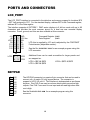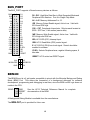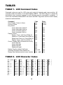
1
CME-12D60 Development Board for Motorola 68HC912D60 Microcontroller xiom anufacturing 2000 2813 Industrial Ln. • Garland, TX 75041 • (972) 926-9303 FAX (972) 926-6063 email: [email protected] • web: http://www.axman.com CONTENTS GETTING STARTED ............................................................................................3 Installing the Software..................................................................... 3 Board Startup .................................................................................. 3 Support Software ............................................................................ 4 Software Development .................................................................... 4 TUTORIAL............................................................................................................5 Creating source code ...................................................................... 5 Assembling source code ................................................................. 6 Running your application ................................................................ 7 Programming Flash EEPROM......................................................... 8 MEMORY MAP .....................................................................................................9 CONFIG SWITCH...............................................................................................10 JUMPERS...........................................................................................................11 MON-SEL JUMPER ...................................................................... 11 PG_PULL / PH_PULL JUMPERS ................................................. 11 JP1 Oscillator Select JUMPER ..................................................... 11 PORTS AND CONNECTORS ............................................................................12 LCD_PORT ................................................................................... 12 KEYPAD........................................................................................ 12 MCU_PORT .................................................................................. 13 CAN_PORT................................................................................... 13 COM1............................................................................................ 14 COM2............................................................................................ 14 ANALOG PORT ............................................................................ 14 BUS_PORT................................................................................... 15 BDM-IN ......................................................................................... 15 TROUBLESHOOTING .......................................................................................16 TABLES..............................................................................................................18 TABLE 1. LCD Command Codes ................................................. 18 TABLE 2. LCD Character Codes.................................................. 18 TABLE 3. Mon12 Monitor Commands.......................................... 19 2 GETTING STARTED The Axiom CME-12D60 single board computer is a fully assembled, fully functional development system for the Motorola 68HC912D60 microcontroller, complete with wall plug power supply and serial cable. Support software for this development board is provided for Windows 95/98 and NT operating systems. Follow the steps in this section to get started quickly and verify everything is working correctly. Installing the Software 1. Insert the Axiom 68HC12 support CD in your PC. If the setup program does not start, run the file called "SETUP.EXE" on the disk. 2. Follow the instructions on screen to install the support software onto your PC. You should at minimum install the AxIDE for Windows software. 3. The programming utility “AxIDE” requires you to specify your board. You should select "CME12D60" for this board. Board Startup Follow these steps to connect and power on the board. This assumes you're using the provided AxIDE utility (installed in the previous section) or a similar communications terminal program on your PC. If you're using a different terminal program than the one provided, set it's parameters to 9600 baud, N,8,1. 1. Make certain the CONFIG SWITCH is set as follows: 1 ON 2 ON 3 ON 4 ON 5 OFF 6 ON 7 OFF 8 OFF 2. Connect one end of the supplied 9-pin serial cable to a free COM port on your PC. Connect the other end of the cable to the COM1 port on the CME-12D60 board. 3. Apply power to the board by plugging in the power adapter that came with the system. 4. If everything is working properly, you should see a message to “PRESS KEY TO START MONITOR…” in your terminal window. Press the ENTER key and you should see: Axiom MON12 - HC12 Monitor / Debugger > _ 5. Your board is now ready to use! If you do not see this message prompt, or if the text is garbage, see the TROUBLESHOOTING section at the end of this manual. 3 Support Software There are many useful programs and documents on the included HC12 support CD that can make developing projects on the CME-12D60 easier. You should browse the disk and copy anything you want to your hard drive. The flash programming utility (AxIDE) communicates with the board via its COM1 port and the supplied cable. This program also includes a simple terminal for interfacing with other programs running on the CME-12D60, such as Mon12, and information from your own programs that send output to the serial port. Also on the disk is a free assembler, example source code, and other tools to get you started. Software Development Software development on the CME12B32 can be performed using either the Mon12 monitor utility installed in EPROM (sockets U6/U7), a third party debugger (NoICE, CodeWarrior, etc.) or a Background Debug Module (BDM) connected to the BDM-IN connector. Any of these tools can be used to assist in creating and debugging your program stored in RAM (see Memory Map). After satisfactory operation running under a debugger, your program can be written to Internal Flash Memory by changing the CONFIG SWITCH settings and programming it using one of the included programming utilities. Your program will then run automatically whenever the board is powered on or RESET is applied. Option jumpers and switches on the board allow for easy transition from one memory type to another and restoring an operating monitor or debugger. 4 TUTORIAL This section was written to help you get started developing software with the CME-12D60 board. Be sure to read the rest of this manual as well as the documentation on the disk if you need further information. The following sections take you through the complete development cycle of a simple "hello world" program, which sends the string "Hello World" to the serial port. Creating source code You can write source code for the CME-12D60 board using any language that compiles to Motorola 68HC12 instructions. Included on the software disk is a free Assembler. You can write your source code using any ASCII text editor. You can use the free EDIT or NOTEPAD programs that come with your computer. Once your source code is written and saved to a file, you can assemble or compile it to a Motorola S-Record (hex) format. This type of output file usually has a .MOT, .HEX or .S19 file extension and is in a format that can be read by the programming utilities and programmed into the CME-12D60 board. It's important to understand your development board's use of Memory and Addressing when writing source code so you can locate your code at valid addresses. For example, when in debug mode, you should put your program CODE in External RAM. In assembly language, you do this with ORG statements in your source code. Any lines following an ORG statement will begin at that ORG location, which is the first number following the word ORG, for example: ORG $1000. You must start your DATA (or variables) in a RAM location unused by your program, for example: ORG $0000. In “debug mode” you’ll be using a debugger utility (Mon12, NoICE, etc) which will handle both interrupts (reset, timers, etc) and the STACK. When finished debugging, you must add code to your application to handle the STACK and Interrupt vector initialization. Set the stack somewhere at the top of your available RAM, for example $7FE, in assembly this would be LDS #$7FE. Also define the RESET vector address, $FFFE, at the end of your program. For example: ORG $FFFE FDB START ; where START is the beginning label of your program A look at the example programs on the disk can make all of this clearer. If you're using a compiler instead of an assembler, consult the compiler documentation for methods used to locate your code, data and stack. 5 Assembling source code An example program called “HELLO.ASM” is provided under the \EXAMPLES\D60 directory of the CD and if you installed AxIDE, under that programs \EXAMPLE\HC12D60 directory. You can assemble your source code using command line tools under a DOS prompt by typing: AS12 HELLO.ASM –LHELLO Most compilers and assemblers allow many command line options so using a MAKE utility or batch file is recommended if you use this method. Run AS12 without any arguments to see all the options, or see the AS12.TXT file on the disk. The programming utility AxIDE provided with this board contains a simple interface to this assembler. Use it by selecting "Build" from its menu. This will prompt you for the file to be assembled. NOTE: You must select your board from the pull down menu first, or it may not build correctly. DO NOT use long path names (> 8 characters). The free assembler is an old DOS tool that does not recognize them. If there are no errors in your source code, 2 output files will be created: HELLO.S19 HELLO.LST a Motorola S-Record file that can be programmed into memory a common listing file which shows the relationship between source and output The listing file is especially helpful to look at when debugging your program. If your program has errors, they will be displayed and no output will be generated, otherwise the listing file will be displayed. If you prefer a windows integrated programming environment, try the Motorola MCU-EZ tools. Refer to the MCU-EZ documentation on the disk for more information. Also, a port for the free GNU C compiler and tools for the HC12 is available on the CD under \Shareware and also online at www.gnu-m68hc11.org. 6 Running your application After creating a Motorola S-Record file you can "upload" it to the development board for a test run. The provided example “HELLO.ASM” was created to run from RAM so you can use the Mon12 Monitor to test it without programming it into Flash. If you haven’t done so already, verify that the CME-12D60 board is connected and operating properly by following the steps under “GETTING STARTED” until you see the Mon12 prompt, then follow these steps to run your program: 1. Press and release the RESET button on the CME-12D60 board. You should see the PRESS ANY KEY message. Hit the return key ↵ to get the monitor prompt. 2. Type LOAD ↵ This will prepare Mon12 to receive a program. 3. Select Upload and when prompted for a file name select your assembled program file in srecord format that was created in the previous section called: HELLO.S19 Your program will be sent to the board thru the serial port. 4. When finished loading you will see the > prompt again. Type GO 1000 ↵ This tells Mon12 to execute the program at address $1000, which is the start of our test program. 5. If everything is working properly you should see the message “Hello World” echoed back to your terminal screen. Press RESET to return to the monitor. 6. If you do not get this message, see the TROUBLESHOOTING section in this manual You can modify the hello program to display other strings or do anything you want. The procedures for assembling your code, uploading it to the board and executing it remain the same. Mon12 has many features such as breakpoints, assembly/disassembly, memory dump and modify and program trace. Type HELP at the Mon12 prompt for a listing of commands or consult the Mon12 documentation on the disk for more information. For a more powerful debugger with many advanced features such as source level debugging, you can use the NoICE debugger software. A full featured demo version is provided on the CD, which you can use to get started. NOTE: To use this program instead of Mon12 you must simply remove the MON-SEL jumper and run the NoICE software. See the help documentation in this program for more information. 7 Programming Flash EEPROM After debugging, you can program your application into Flash Memory so it executes automatically when you apply power to the board as follows: 1. Make a backup copy of HELLO.ASM then use a text editor to modify it. Remove the comment ; character before the following line to initialize the stack pointer which is necessary when running outside of a debugger: LDS #$7FE ; initialize the stack pointer 2. Remove the comment ; character from before the following 2 lines at the end, to set the reset vector to go to the beginning of the program (the label START) when powered on: org $fffe fdb reset vector START 3. Re-Assemble HELLO.ASM as described in the "Assembling Source Code" section. 4. Select Program from the AxIDE menu and follow the message prompts. When prompted for a file name, enter the new HELLO.S19 file. 5. Set the CONFIG SWITCH positions 1-5 all ON. The red VPP light should come on. 6. Press the RESET button on the board before clicking OK. When prompted to Erase, choose Yes. 7. When finished programming, REMOVE POWER then set the CONFIG SWITCH positions 1-5 all OFF. The VPP light should turn off. 8. Re-Apply Power to the board. Your new program should start automatically and the “Hello World” prompt should be displayed in the terminal window. To return to the Mon12 monitor program, set the CONFIG SWITCH positions 1-4 all back ON then press RESET. 8 MEMORY MAP Following is the memory map for this development board. Consult the 68HC912D60 technical reference manual on the CD for internal memory map details for this processor. FFFF CONFIG 1 ON 2 ON 3 ON 4 ON CONFIG 1 ON 2 ON 3 ON 4 OFF CONFIG 1 2 3 4 OFF OFF OFF OFF External EPROM U6/7 (Mon12) C000 BFFF External RAM U4/5 Internal Flash Memory On-Chip External RAM U4/5 1000 FFF HC12 Internal EEPROM On-Chip C00 BFF Peripheral Area - see note 2 below Unused = A00-B7F LCD / CS7 = BF0-BFF CS6 = BE0-BEF A00 9FF CS5 = BD0-BDF CS4 = BC0-BCF CS3 = BB0-BBF CS2 = BA0-BAF CS1 = B90-B9F CS0 = B80-B8F Internal Registers - see note 1 below See 68HC912D60 Technical Reference Manual 800 7FF Internal RAM On-Chip 000 1. The Internal Register base address is relocated from $000 to $800 on startup by the debug utilities (Mon12 and NoICE). To preserve this memory map, you must also do this in your software when booting from flash. To do this, load register $11 with $08 for example: MOVB #08,$11 ; post-reset location of INITRG 2. The Peripheral Area (A00-BFF) is set to Narrow (8-bit) data width by the debug utilities. If using this memory, you must also do this in your software when booting from flash as follows: MOVW MOVB #$0CF0,PEAR #$73,MISC ; Flash on, p-sel stretch = 3 9 CONFIG SWITCH The CME-12D60 board is shipped from the manufacturer with the following default CONFIG SWITCH settings: 1 ON 2 ON 3 ON 4 ON 5 OFF 6 ON 7 OFF 8 OFF The 8 position CONFIG SWITCH provides an easy method of configuring the CME-12D60 board operation. Following are the configuration switch descriptions and HC12 I/O port usage: CONFIG SWITCH 1 2 3 4 5 6 7 8 OPERATION when in ON position MODE A selection (see Mode chart below) MODE B selection (see Mode chart below) EXT – External Memory enable (1) MON – Monitor Memory enable (2) VPP - Flash VPP voltage enable RXD0 – COM1 Serial Port RXD0 input enable RXD1 – COM2 Serial Port RXD1 input enable CAN Port RX enable I/O PORT USED MODA / PE5 MODB / PE6 PORT A, B, Ext. Bus N/A N/A PS0 / RXD0 PS3 / RXD1 PCAN0 (1) Enables memory bus operation for access to board memory. Expanded bus must be on for proper operation. (2) Enables monitor EPROM’s in memory map at 0xC000 – FFFF hex if CONFIG SWITCH position 3 is also on. When in off position memory space is SRAM for BDM use. MODE CHART Single Chip Mode MOD A and B = OFF Boot from Internal Flash Expanded Wide Mode MOD A and B = ON Boot from External Memory NOTE: Expanded Narrow Mode is not available on this board. 10 JUMPERS MON-SEL JUMPER Selects which firmware monitor in External EPROM (U6/7) the board will execute upon reset in expanded mode with monitor enabled by CONFIG SWITCH position 4. ON OFF Mon12 Debug Monitor Third party firmware support (NoICE, Metrowerks, etc.) PG_PULL / PH_PULL JUMPERS Pull up or Pull down I/O line bias resistor option jumpers. When port G or Port H are configured as inputs these options select which way the internal pull resistor’s operate. Port H should be in the pull down state if KEYPAD is used. GND +5V Pull Down active (default) Pull Up active JP1 Oscillator Select JUMPER Provides enabling and Disabling of the internal PLL and external clock oscillator X1. Default configuration is XCLK position. The PLL is disabled in this position and the oscillator is provided by X1 external clock. PLL XCLK Enables PLL crystal oscillator (see below) Disables PLL crystal oscillator (R1 should be installed) default To enable PLL clock do the following: 1. Remove R1 on the bottom of the board to isolate the X1 external clock input to the PLL oscillator. 2. Install user selected Y1, C1 and C2 to provide new oscillator clock. 3. Install RX1, CX1 and CX2 to provide correct XFC conditioning for the frequency of operation desired. NOTE: see MC68HC912D60 user manual for more information. 4. Move JP1 to the PLL position. 5. Note that the provided firmware utilities (Mon12, NoICE, etc) in External EPROM will not operate with PLL enabled. 11 PORTS AND CONNECTORS LCD_PORT The LCD_PORT interface is connected to the data bus and memory mapped to locations BF0 – BFF hex assigned to CS7. For the standard display, address BF0 is the Command register, address BF1 is the Data register. The interface supports all OPTREX DMC series displays in 8 bit bus mode with up to 80 characters and provides the most common pinout for a dual row rear mounted display connector. Power, ground, and Vee are also available at this connector. +5V A0 LCD1 D9 D11 D13 D15 2 1 GND Command Register: $BF0 4 3 LCD-Vee Data Register: $BF1 6 5 /RW 8 7 D8 LCD-Vee is supplied by U13 and is adjusted by the CONTRAST 10 9 D10 Potentiometer (adjustable resistor). 12 11 D12 See the file KLCD12D6.ASM for an example program using this 14 13 D14 LCD connector. J3 LCD3 2 4 1 LCD2 3 LCD4 Additional lines can be used as enables for larger panels and are mapped as: LCD2 = $BF4 & $BF5 LCD3 = $BF8 & $BF9 LCD4 = $BFC & $BFD KEYPAD 1 2 3 4 5 6 7 8 PH0 PH1 PH2 PH3 PH4 PH5 PH6 PH7 The KEYPAD connector is a passive 8-pin connector that can be used to connect a 4 x 4 matrix (16 key) keypad device. The connector is mapped to HC12 I/O port H. This interface is implemented as a software keyscan. Pins PH0-3 are used as column drivers which are active high outputs. Pins PH4-7 are used for row input and will read high when their row is high. See the file KLCD12D6.ASM for an example program using this connector. 12 MCU_PORT The MCU_PORT provides access to the peripheral features and I/O lines of the HC12 as follows: D0 D2 D4 D6 /XIRQ, PE0 VFP PG6 PG4 PG2 PG0 PH6 PH4 PH2 PH0 PS0 / RXD0 PS2 / RXD1 PS4 PS6 PCAN6 PCAN4 PCAN2 PCAN0 PT0 PT2 PT4 PT6 PP6 PP4 PP2 PP0 1 3 5 7 9 11 13 15 17 19 21 23 25 27 29 31 33 35 37 39 41 43 45 47 49 51 53 55 57 59 2 4 6 8 10 12 14 16 18 20 22 24 26 28 30 32 34 36 38 40 42 44 46 48 50 52 54 56 58 60 D1 D3 D5 D7 /DBE, PE7 /LSTRB PG7 PG5 PG3 PG1 PH7 PH5 PH3 PH1 PS1 / TXD0 PS3 / TXD1 PS5 PS7 PCAN7 PCAN5 PCAN3 PCAN1 PT1 PT3 PT5 PT7 PP7 PP5 PP3 PP1 D0 – D7 Low Byte of the Data Bus in Wide Expanded Mode. Port B in Single Chip Mode. /XIRQ XIRQ interrupt input . VFP Programming voltage, 12v, when CONFIG switch position 5 is on. /LSTRB LSTRB (PE3) output indicates 8 bit bus access. Should be enabled in software for bus use. PP0 – PP7 Port P I/O or PWM port. PT0 – PT7 Port T I/O or Timer port. PS0 – PS7 Port S I/O or Serial Port lines. PG0 – PG7 Port G I/O or Key wakeup pins. PH0 – PH7 Port H I/O or Key wakeup pins. Also used by the KEYPAD Port. RXD / TXD Serial Port (SCI) receive and transmit pins. PCAN0 – PCAN7 CAN I/O lines. CAN_PORT 1 2 3 4 GND CAN-H CAN-L +5V The CAN_PORT connector provides an interface to the MSCAN12 on the microcontroller. This port provides a CAN transceiver device. See the schematic drawing and the MC68HC912D60 data sheet for information on using this peripheral. RxCAN1-3 can be added to supply CAN port bus terminations as required (see schematic). 13 COM1 1 TXD0 2 RXD0 3 4 GND 5 The COM-1 port has a Female DB9 connector that interfaces to the HC12 internal SCI0 serial port. It uses a simple 2 wire asynchronous serial interface and is translated to RS232 signaling levels. 6 7 8 9 Pins 1, 4, and 6 are connected for default handshake standards. Pins 7 and 8 are connected for default handshake standards. Handshake pins can be easily isolated and connected to I/O ports if necessary. COM2 1 2 TXD1 3 4 RXD1 5 6 7 8 GND 9 10 The COM-2 connector interfaces to the HC12 internal SCI1 serial port. It uses a simple 2 wire asynchronous serial interface and is translated to RS232 signaling levels. This connector supports a standard IDC ribbon cable to DB9 socket. Pins 1, 2, and 7 are connected for default handshake standards. Pins 4 and 6 are connected for default handshake standards. ANALOG PORT The ANALOG port provides access to the Port AD0 and Port AD1 Analog-to-Digital input lines of the HC912D60 as follows: PAD0 PAD1 PAD2 PAD3 PAD4 PAD5 PAD6 PAD7 VRL0 VRL1 VSSA GND GND 1 3 5 7 9 11 13 15 17 19 21 23 25 2 4 6 8 10 12 14 16 18 20 22 24 26 PAD10 PAD11 PAD12 PAD13 PAD14 PAD15 PAD16 PAD17 VRH0 VRH1 VDDA +5V +5V PAD0 – PAD7 HC12 Port AD0 is an input port or A/D Converter inputs. PAD10 – PAD17 HC12 Port AD1 is an input port or A/D Converter inputs. VRH / VRL HC12 A/D Converter Reference Pins. See A/D Reference Section. To provide an external reference voltage, R3,4,10 and 32 may need to be removed. See schematic. 14 BUS_PORT The BUS_PORT supports off-board memory devices as follows: GND D10 D9 D8 A0 A1 A10 / OE A11 A9 A8 A12 / WE CS1 CS3 CS5 +5V /RW E GND 1 3 5 7 9 11 13 15 17 19 21 23 25 27 29 31 33 35 37 39 D11 D12 D13 D14 D15 A2 A3 A4 A5 A6 A7 A13 CS0 CS2 CS4 IRQ /P-SEL CS6 CS7 / RESET 2 4 6 8 10 12 14 16 18 20 22 24 26 28 30 32 34 36 38 40 D8 - D15 High Byte Data Bus in Wide Expanded Mode and Peripheral 8 bit data bus. Port A in Single Chip Mode. A0 – A15 Memory Addresses 0 to 15. /OE Memory Output Enable signal, Active Low. Valid with ECLK and R/W high. CS0 – CS7 Peripheral chip selects, 16 bytes each located at $200 - $27F hex, 8 bit access (narrow bus). /WE Memory Write Enable signal, Active Low. Valid with ECLK high and R/W low. IRQ HC12 IRQ (PE1) Interrupt Input. /RW HC12 Read/Write (PE2) control signal. E HC12 ECLK (PE4) bus clock signal. Stretch should be enabled in software. /P-SEL Selects Peripheral area, register following space, 8 bits wide. /RESET HC12 active low RESET signal. J2 A14 1 2 A15 MODA/PE5 3 4 MODB/PE6 GND 5 6 +5V BDM-IN The BDM-IN port is a 6 pin header compatible in pinout with the Motorola Background Debug Mode (BDM) Pod. This allows the connection of a background debugger for software development, programming and debugging in real-time, since the BDM control logic does not reside in the CPU. BGND 1 2 GND 3 4 /RESET 5 6 +5V See the HC12 Technical Reference Manual for complete documentation of the BDM. A Background Debug Module is available from the manufacturer. The BDM-OUT port is provided for future use. 15 TROUBLESHOOTING The CME-12D60 board is fully tested and operational before shipping. If it fails to function properly, inspect the board for obvious physical damage first. Ensure that all IC devices in sockets are properly seated. Verify the communications setup as described under GETTING STARTED and see the Tips and Suggestions sections following for more information. The most common problems are improperly configured communications parameters, and attempting to use the wrong COM port. 1. Verify that your communications port is working by substituting a known good serial device or by doing a loop back diagnostic. 2. Verify the jumpers on the board and the CONFIG switch settings are correct. 3. Verify the power source. You should measure approximately 9 volts between the GND and +9V test point pads on the board. 4. If no voltage is found, verify the wall plug connections to 115VAC outlet and the power connector. 5. Disconnect all external connections to the board except for COM1 to the PC and the wall plug. 6. Make sure that the RESET line is not being held low. Check for this by measuring the RESET pin on P4 for +5V. 7. Verify the presence of a 16MHz square wave at the EXTAL pin or 8MHz E clock signal if possible. 16 Tips and Suggestions Following are a number of tips, suggestions and answers to common questions that will solve many problems users have with the CME-12D60 development system. You can download the latest software from the Support section of our web page at: www.axman.com Utilities • If you’re trying to program memory or start the utilities, make sure all jumpers and CONFIG SWITCH settings are correct. • Be certain that the data cable you’re using is bi-directional and is connected securely to both the PC and the board. Also, make sure you are using the correct serial port. • Make sure the correct power is supplied to the board. You should only use a 9 volt, 300 mA adapter or power supply. If you’re using a power strip, make sure it is turned on. • Make sure you load your code to an address space that actually exists. See the Memory Map if you’re not sure. The CONFIG switch changes the memory map. • If debugging under Mon12, make sure you're not over-writing RAM used by it. • If you’re running in a multi-tasking environment (such as Windows™) close all programs in the background to be certain no serial conflict occurs. Code Execution • Make sure the CONFIG SWITCH is set for the proper mode. • CONFIG switch 3 must be ON to access the external bus (LCD display, etc) even if executing code from Internal Flash memory. • Under Mon12, breakpoints may not be acknowledged if you use the CALL command. You should use one of the GO command instead. • Check the HC12 reset vector located at FFFE - FFFF. These 2 bytes contain the address where execution will begin when the unit is powered on. • When running your code stand-alone, you must initialize ALL peripherals used by the micro, including the Stack, Serial Port, Reset and Interrupt vectors etc. • You must either reset the COP watchdog timer in the main loop of your code or disable it when not running under Mon12 or BDM mode. The micro enables this by default and if you don't handle it your code will reset every couple of ms. 17 TABLES TABLE 1. LCD Command Codes Command codes are used for LCD setup and control of character and cursor position. All command codes are written to LCD panel address $B5F0. The BUSY flag (bit 7) should be tested before any command updates to verify that any previous command is completed. A read of the command address $B5F0 will return the BUSY flag status and the current display character location address. Command Clear Display, Cursor to Home Cursor to Home Entry Mode: Cursor Decrement, Shift off Cursor Decrement, Shift on Cursor Increment, Shift off Cursor Increment, Shift on Display Control: Display, Cursor, and Cursor Blink off Display on, Cursor and Cursor Blink off Display and Cursor on, Cursor Blink off Display, Cursor, and Cursor Blink on Cursor / Display Shift: (nondestructive move) Cursor shift left Cursor shift right Display shift left Display shift right Display Function (default 2x40 size) Character Generator Ram Address set Display Ram Address and set cursor location Code $01 $02 Delay 1.65ms 1.65ms $04 $05 $06 $07 40us 40us 40us 40us $08 $0C $0E $0F 40us 40us 40us 40us $10 $14 $18 $1C $3C $40-$7F $80- $FF 40us 40us 40us 40us 40us 40us 40us TABLE 2. LCD Character Codes $20 $21 $22 $23 $24 $25 $26 $27 $28 $29 $2A $2B $2C Space ! “ # $ % & ‘ ( ) * + , $2D $2E $2F $30 $31 $32 $33 $34 $35 $36 $37 $38 $39 . / 0 1 2 3 4 5 6 7 8 9 $3A $3B $3C $3D $3E $3F $40 $41 $42 $43 $44 $45 $46 : ; { = } ? Time A B C D E F $47 $48 $49 $4A $4B $4C $4D $4E $4F $50 $51 $52 $53 G H I J K L M N O P Q R S $54 $55 $56 $57 $58 $59 $5A $5B $5C $5D $5E $5F $60 18 T U V W X Y Z [ Yen ] ^ _ ` $61 $62 $63 $64 $65 $66 $67 $68 $69 $6A $6B $6C $6D a b c d e f g h i j k l m $6E $6F $70 $71 $72 $73 $74 $75 $76 $77 $78 $79 $7A n o p q r s t u v w x y z $7B $7C $7D $7E $7F { | } > < TABLE 3. Mon12 Monitor Commands BF <StartAddress> <EndAddress> [<data>] BR [<Address>] BULK CALL [<Address>] G [<Address>] HELP LOAD [<AddressOffset>] MD <StartAddress> [<EndAddress>] MM <StartAddress> <CR> </> or <=> <^> or <-> <.> MOVE <StartAddress> <EndAddress> <DestAddress> RD RM STOPAT <Address> T [<count>] Fill memory with data Set/Display user breakpoints Erase entire on-chip EEPROM contents Call user subroutine at <Address> Begin/continue execution of user code Display the Mon12 command summary Load S-Records into memory Memory Display Bytes Modify Memory Bytes Examine/Modify next location Examine/Modify same location Examine/Modify previous location Exit Modify Memory command Move a block of memory Display all CPU registers Modify CPU Register Contents Trace until address Trace <count> instructions 1. Mon12 uses internal RAM space from $600 - $700. DO NOT use this space in your program if debugging under Mon12. 2. Register space is located starting at $800. 3. Mon12 will not trace into interrupts. To trace an interrupt service set a breakpoint in the service routine and then trace. 19