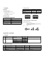
1
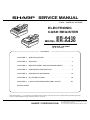
q SERVICE MANUAL
CODE : 00ZERA410USME
ELECTRONIC
CASH REGISTER
ER-A410
MODEL ER-A420
ER-A410
SRV KEY : LKGIM7113RCZZ
PRINTER : PR-45M II
(U, A version)
ER-A420
CONTENTS
CHAPTER 1. SPECIFICATIONS . . . . . . . . . . . . . . . . . . . . . . . . . . . . 1
CHAPTER 2. OPTIONS . . . . . . . . . . . . . . . . . . . . . . . . . . . . . . . . . . . 5
CHAPTER 3. MASTER RESET AND PROGRAM RESET. . . . . . . . . 6
CHAPTER 4. HARDWARE DESCRIPTION . . . . . . . . . . . . . . . . . . . . 7
CHAPTER 5. DIAGNOSTIC PROGRAM . . . . . . . . . . . . . . . . . . . . . 14
CHAPTER 6. IPL FROM EP-ROM . . . . . . . . . . . . . . . . . . . . . . . . . . 19
CHAPTER 7. CIRCUIT DIAGRAM AND PWB LAYOUT . . . . . . . . . 20
PARTS GUIDE
Parts marked with "!" are important for maintaining the safety of the set. Be sure to replace these parts with specified
ones for maintaining the safety and performance of the set.
SHARP CORPORATION
This document has been published to be used
for after sales service only.
The contents are subject to change without notice.
CAUTIONS
THERE IS A RISK OF EXPLOSION IF THE BATTERY
IS REPLACED BY AN INCORRECT TYPE.
PROPERLY DISPOSE OF USED BATTERIES ACCORDING
TO THE INSTRUCTIONS.
WHEN CONNECTING THE 40PIN FLAT CABLE
BETWEEN THE MAIN PWB
AND THE KEY PWB, CAREFULLY INSERT THE
CABLE INTO CONNECTOR OPENING.
ER-A410U/ER-A420U
CHAPTER 1. SPECIFICATIONS
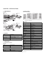
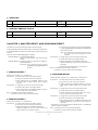
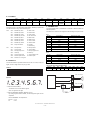
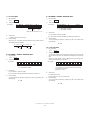
1. APPEARANCE
3-2. KEY LAYOUT
ER-A410 KEYLAYOUT
ER-A410
Front view
Rear view
Customer display
(Pop-up type)
Printer cover
RECEIPT JOURNAL
Operator
display
Receipt paper
Journal window
CL
5
10
15
20
FS
TAX SHIFT
CONV TEND
FOR
PLU/SUB
SCALE TARE
FS
#
7
8
9
4
9
14
19
RA
RCPT
/PO
4
5
6
3
8
13
18
%
VOID RFND
TAX CASH
SHIFT
#
NC
SLIP
Keyboard
Mode switch
OPEN
FINAL PBLU
@
2
1
0
3
2
7
12
17
00
1
6
11
16
CHK
CH
MDSE
SBTL
SBTL
CA/AT/NS
CH1
Drawer lock
CH2
Drawer
Note: All the keys except the receipt paper feed and journal paper feed
keys can be re-positioned.
RS-232C connectors
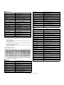
■ Key names
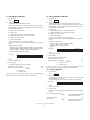
ER-A420
Front view
Rear view
Customer display
(Pop-up type)
Printer cover
Operator
display
Receipt paper
Journal window
Keyboard
Mode switch
CH1
Drawer lock
CH2
Drawer
RS-232C connector
2. RATING
2 RECEIPT
Receipt paper feed key
2 JOURNAL
Journal paper feed key
0 ~ 9, 00
Numeric keys
•
Decimal point key
@/FOR
Multiplication key
CL
Clear key
1 ~ 20
Department keys
PLU/SUB
Price lookup/subdepartment key
SCALE
Scale key
OPEN TARE
Open tare key
CASH #
Cashier code entry key
-
Discount 1 key
%
Percent 1 key
TAX
Tax key
Model
ER-A410/420
TAX SHIFT
Tax 1 shift key
Weight
13.2kg (29.1lbs)
FS SHIFT
Food stamp shift key
Dimensions
420 (W) x 427 (D) x 297 (H) mm
16.5 (W) x 16.8 (D) x 11.7 (H) inch
FS TEND
Food stamp tendered key
Power source
120V m10%, AC 60Hz
CHK
Check 1 key
Power consumption
Stand-by 9W, Operating 46.5W (max.)
CH
Charge 1 key
Working temperature
0°C~40°C (32°F to 104°F)
3. KEYBOARD
3-1. KEYBOARD LAYOUT
ER-A410
Type
Normal keyboard
Key stroke
3.5 m 0.5 mm
Key pitch
19 (W) x 19 (H) mm
ER-A420
Type
Flat key
Key stroke
0.8 m 0.2 mm
Key pitch
18 (W) x 15 (H) mm
ER-A410U/ER-A420U
SBTL
Subtotal key
CA/AT/NS
Cash/Amount tendered and No-sale key
VOID
Void key
RFND
Refund key
RA
Received-on-account 1 key
RCPT/PO
Receipt print/copy and Paid-out 1 key
MDSE SBTL
Merchandise subtotal key
#
Non-add code key
NC
New charge account balance key
PBLU
Previous balance key
FINAL
Final key
CONV
Conversion 1 key
SLIP
Slip print key
SPECIFICATIONS
–1–
■ Optional keys
CASH#
Chasier code entry key
SRVC
Service key
-
Discount 1 key
%2 ~ %4
Percent 2 thru 4 keys
#
Non-add code key
AUTO ~ AUTO 5
Automatic sequencing 1 thru 5 keys
%
Percent 1 key
CA2
Cash total 2 key
L1 ~ L3
PLU level shift 1 thru 3 keys
BIRTH
Birthday date entry key
CH1, CH2
Charge 1 and 2 keys
DEPT #
Department code entry key
CHK
Check 1 key
RA2
Received-on-account 2 key
VOID
Void key
PO2
Paid-out 2 key
RFND
Refund key
CONV2 ~ CONV4
Conversion 2 thru 4 keys
RA
Received-on-account 1 key
CH2 ~ CH5
Charge 2 thru 5 keys
RCPT/PO
Receipt and Paid-out 1 key
CHK2
Check 2 key
PRICE SHIFT
Price level shift key
DEPO
Deposit entry key
AUTO
Automatic sequencing 1 key
DEPO RFND
Deposit refund key
1 ~ 82
Direct price lookup keys
TRAY SBTL
Tray subtotal key
RFUND SALE
Refund sale key
PRINT
Validation print key
L1 ~ L3
■ Optional keys
SRVC
PLU level shift 1 thru 3 keys
PRICE SHIFT
Price level shift key
-2 ~ -4
Discount 2 thru 4 keys
000
Triple zero entry key
TAX2 SHIFT ~ TAX4 SHIFT Tax 2 thru 4 shift keys
NS
No sale key
Caution:
Service key
%2 ~ %4
Percent 2 thru 4 keys
AUTO 2 ~ AUTO 5
Automatic sequencing 2 thru 5 keys
CA2
Cash total 2 key
BIRTH
Birthday date entry key
DEPT#
Department code entry key
RA2
Received-on-account 2 key
PO2
Paid-out 2 key
NS
No sale key
• The [RCPT/PO] is a double-function key ([Receipt function] and
[Paid-out function]).
Press the [RCPT/PO] key for either the [RCPT] or [PO] key in the
described operations.
OPEN TARE
Open tare key
CONV ~ CONV4
Conversion 1 thru 4 keys
CH3 ~ CH5
Charge 3 thru 5 keys
CHK2
Check 2 key
• The [CA/AT/NS] is a double-function key ([Cash/Amount tendered
function] and [No Sale function]).
Press the [CA/AT/NS] key for either the [CA/AT] or [NS] key in the
described operations.
DEPO
Deposit entry key
DEPO RFND
Deposit refund key
TRAY SBTL
Tray subtotal key
ER-A420 KEYLAYOUT
RECEIPT JOURNAL
61
62
AUTO CASH
#
L1
L2
L3
PRICE
#
SCALE
RCPT
/PO
CL
%
73
74
75
76
77
78
79
80
81
82
63
64
65
66
67
68
69
70
71
72 SHIFT
@
RA
49
50
51
52
53
54
55
56
57
58
59
60
FOR
37
38
39
40
41
42
43
44
45
46
47
48
7
8
9
RFND VOID
25
26
27
28
29
30
31
32
33
34
35
36
4
5
6
CH2 SHIFT
13
14
15
16
17
18
19
20
21
22
23
24
1
2
3
CH1 CHK
1
2
3
4
5
6
7
8
9
10
11
12
0
00
MDSE
SBTL
SBTL CA/AT
TAX
RFND SALE
Refund sale key
PRINT
Validation print key
PLU/SUB
Price lookup/subdepartment key
FINAL
Final key
SLIP
Slip print key
TAX
Tax key
FS SHIFT
Food stamp shift key
FS TEND
Food stamp tendered key
-2 ~ -4
Discount 2 thru 4 keys
000
Triple zero entry key
Note: All the keys except the receipt paper feed and journal paper feed
keys can be re-positioned.
TAX2 SHIFT ~ TAX4 SHIFT Tax 2 thru 4 shift keys
PBLU
Previous balance key
■ Key names
NC
New charge account balance key
2 RECEIPT
Receipt paper feed key
2 JOURNAL
Journal paper feed key
0 ~ 9, 00
Numeric keys
•
Decimal point key
@/FOR
Multiplication key
CL
Clear key
SCALE
Scale key
TAX SHIFT
Tax 1 shift key
CA/AT
Cash/Amount tendered key
SBTL
Subtotal key
MDSE SBTL
Merchandise subtotal key
Note: The direct department and/or PLU keys can be expanded.
ER-A410U/ER-A420U
SPECIFICATIONS
–2–
4. MODE SWITCH
5. DISPLAY
4-1. MODE SWITCH AND MODE KEYS
5-1. OPERATOR DISPLAY
Operative range
Display device:
LCD
Number of lines:
2 lines
Number of positions: 16 positions
MA
SM
Color of display:
Yellow / Green
Character font:
5 x 7 dot
Character size:
4.84 (W) x 8.06 (H) mm
Layout:
REG
OP X / Z
OFF
PGM1
MGR
X1 /Z1
X2/Z2
PGM2
• Manager key (MA)
• Submanager key (SM)
5-2. CUSTOMER DISPLAY
SM
MA
Display device:
LED
Number of lines:
1 line
Number of positions: 7 positions
• Operator key (OP)
OP
Color of display:
Yellow / Green
Style:
Pop up type
Character form:
7 segment + Dp
Character size:
14.2mm (H) x 7.9mm (W)
Layout:
The mode switch has these settings:
OFF:
This mode locks all register operations.
No changes may occur to register data.
OP X/Z: This setting allows cashiers to take an X or Z reports for their
sales information. This mode can also be used for displaying
the date/time and printing the employee's arrival/departure
times. This mode can be also used to toggle receipt state "ON"
and "OFF" by pressing the [RCPT] key. (To utilize this function, the register must be programmed for "OP X/Z mode available" in the PGM2 mode.)
REG:
For entering sales
PGM1: To program those items that need to be changed often: e.g.,
unit prices of departments or PLUs, and percentages.
PGM2: To program all PGM1 programs and those items that do not
require frequent changes: e.g., date, time, or a variety of register functions.
MGR:
For manager’s and submanager’s entries
The manager can use this mode to make entries that are not
permitted to be made by cashiers in the REG mode.
– for example, after-transaction voiding and override entries.
X1/Z1:
To take the X/Z reports for various daily totals.
X2/Z2:
To take the X/Z reports for various periodic (weekly or monthly)
consolidation of totals.
ER-A410U/ER-A420U
SPECIFICATIONS
–3–
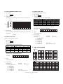
■ Operator display
6. PRINTER
The operator display consists of a two-line dot-matrix display (16 characters/line).
6-1. PRINTER
Price level / PLU level Dept. name / PLU name /
function text
(e.g. P2L3)
Cashier code or
mode name
• Part number:
PR-45M II (PR-45M compatible)
• NO. of stations:
2 (Receipt and journal)
Function message
display area
• Validation:
No
Numeric entry
display area
• Printing system:
Line thermal
• No. of dots:
Receipt
288 dots
Horizontal
0.125mm
Vertical
0.125mm
Receipt OFF indicator ("_") / Stock alarm indicator (" ")
Repeat / Sentinel mark / Power save mark
• Journal
• Dot pitch:
• Cashier code or mode displayed
The mode that the key is placed in is displayed. When a cashier is
assigned, the cashier code is displayed in the REG or OP X/Z
mode. For example, “0001” is displayed when the cashier 0001 is
assigned.
• Font:
288 dots
font A: 12 dots x 24 dots
font B: 9 dots x 24dots
• Printing capacity:
• Repeat
• Character size:
The number of repeats is displayed, starting at "2" and increments
with each repeat. When you have registered ten times, the display
will show "0". (2 3 3......9 3 0 3 1 3 2...)
Receipt
max. 24 characters
Journal
max. 24 characters
1.5mm (W) x 3.0mm (H) at 12 x 24 dots
1.125mm (W) x 3.0mm (H) at 9 x 24 dots
• Print pitch:
Column distance 1.5mm at 12 dots
1.125mm at 9 dots
• Sentinel mark
Row distance
When amounts in the drawer reaches the amount you preprogrammed, the sentinel mark "X" is displayed to advice you to
remove the money and take it to a safe place.
• Print speed:
Approximate 50mm/s
• Paper feed speed: Approximate 40mm/s
(Manual feed)
• Power save mark
• Reliability:
When the cash register goes into the power save mode, the power
save mark (decimal point) is displayed.
Mechanism MCBF 5 million lines
• Paper end sensor: Optional (Receipt and journal)
• Stock alarm indicator
When the stock of the PLU which has been entered is zero or negative, the alarm indicator (decimal point) is displayed.
• Cutter:
Manual
• Near end sensor:
No
Note : The PR-45MII has a minor change over the model of the PR-45M.
This printer does not include the gear cover (GCOVH7146BHZZ)
which is for the PR-45M only.
• Function message display area
Item labels of Departments PLU/subdepartments and function text
you use, such as %1, (–) and CASH are displayed here. For the
details of function texts, please refer to pages 112 and 113.
When an amount entry is required, “- - - - - - -” is displayed in the
numeric entry display area with "AMOUNT". When a preset price
has been set, the price is displayed in the numeric entry display
area as the "AMOUNT".
6-2. PAPER
• Paper roll dimension: 44.5 m 0.5mm in width
Max. 83mm in diameter
• Paper quality:
• Numeric entry display area
Numbers entered using numeric keys are displayed here.
(Journal/Receipt)
High-quality paper
paper thickness: 0.06 to 0.08mm
6-3. LOGO STAMP
Date and time display
• The Graphic type Logo is used
The Date and time appear on the display in the OP X/Z, REG, or
MGR mode. In the REG or MGR mode, press the [#] key to display
the date and time.
6-4. CUTTER
• Method: Manual
Error messages
When an error occurs, the corresponding error message is displayed
in the function message display area.
■ Customer display (Pop-up type)
$
3.75mm
( : Appears right below the seventh place when
the item amount is displayed at scale entry.)
ER-A410U/ER-A420U
SPECIFICATIONS
–4–
7. DRAWER
7-2. MONEY CASE
For U version
[OUTLINE]
Separation from the drawer
• Standard equipment: Yes
Separation of the coin compartments from the money case
• Max. number of additional drawers: 1
Allowed
Disallowed
Allowed
Bill separator
• The drawer consists of:
For A version
Allowed
Number of compartments
No
No
5B/5C
5B/6C
1) Drawer box (outer case) and drawer
2) Money case
3) Lock (attached to the drawer)
For U version
For A version
5B/5C
5B/6C
[SPECIFICATION]
7-1. DRAWER BOX AND DRAWER
Model name of the drawer
box
SK423
Size
420 (W) x 427 (D) x 112 (H) mm
color
Gray 368
Material
Metal
Bell
–
• Location of the lock: Front
Release lever
Standard equipment: attached to the
bottom
• Method of locking and unlocking:
Drawer open sensor
YES
7-3. LOCK (LOCK KEY: LKGIM7331BHZZ)
To lock, insert the drawer lock key into the lock and turn
it 90 degrees counter clockwise.
To unlock, insert the drawer lock key and turn it 90
degrees clockwise.
ck
unlo
Lo
SK1-1
SK1-1
Key No:
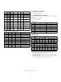
CHAPTER 2. OPTIONS
1. OPTIONS
NO
CLASSIFICATION
COMPONENT NAME
MODEL NAME
1
Drawer
Remote drawer
ER-03DW
2
Key kit
1 x 1 key top kit
ER-11KT7
1 x 2 key top kit
ER-12KT7
2 x 2 key top kit
ER-22KT7
REMARK
ER-04DW
1 x 1 dummy key kit
ER-11DK7G
5 x 1 dummy key kit
ER-51DK7G
2. SERVICE OPTIONS
NO
PARTS CODE
PRICE RANK
1
SRV key
NAME
LKGIM7113RCZZ
AK
2
Water proof switch cover
GCOVH2541BHZB
AY
3
Water proof keyboard cover
GCOVH2541BHZA
BC
4
Text preset key cover
GCOVH2541BHSB
BD
For ER-A410
5
Blank sheet
PSHEK3008BHZZ
AL
For ER-A420
ER-A410U/ER-A420U
–5–
OPTIONS
REMARK
For ER-A410
ck
3. SUPPLIES
NO
1
PARTS CODE
PRICE
RANK
TPAPR6645RC05
BA
PARTS CODE
PRICE
RANK
UKOG-6705RCZZ
BU
NAME
Thermal roll paper
DESCRIPTION
5 ROLLS/PACK
4. SPECIAL SERVICE TOOLS
NO
1
NAME
RS-232 Loop-back connector
DESCRIPTION
CHAPTER 3. MASTER RESET AND PROGRAM RESET
The SRV key is used for performing entries in the SRV mode.
4) Program the [0] [1] [2] [3] [4] [5] [6] [7] [8] [9] [00] [000]
[.] [CL] [@/FOR] [SBTL] [CA/AT] keys by depressing
the keys in this order.
A MASTER RESET clears the entire memory and resumes initial values.
A PROGRAM RESET resumes the initial program without clearing the
memory.
Note: If the [000] key is not required, press the same
key in the next step, and [000] key will be
inhibited.
There are 2 kinds of MASTER RESET operations.
MASTER RESET 1: Normal MASTER RESET
Clears the entire memory and resumes initial
values.
Procedure B: 1) Unplug the AC power cord from the wall outlet.
2) Set the mode switch to the (SRV) position.
MASTER RESET 2: It enables the layout of fixed keys in addition to
MASTER RESET 1.
3) While holding down the JOURNAL FEED & the
RECEIPT FEED key, plug in the AC power cord to the
wall outlet.
Fixed keys: [0] [1] [2] [3] [4] [5] [6] [7] [8] [9]
[00] [000] [.] [CL] [@/FOR] [SBTL]
[CA/AT]
4) Repeat the same sequence as in “Procedure A”
Note: Procedure B cannot reset the hardware.
Procedure A must be used to reset the hardware.
1. MASTER RESET 1
Please use “Procedure A” or “Procedure B”
3. PROGRAM RESET
Procedure A: 1) Set the mode switch to the (SRV’) position.
Please use either “Procedure A”, “Procedure B” or “Procedure C”
2) Plug in the AC power cord to the wall outlet.
Procedure A: 1) Set the mode switch to the (SRV’) position.
3) While holding down the JOURNAL FEED key, turn
the mode switch to (SRV) position from the (SRV’)
position.
2) Plug in the AC power cord to the wall outlet.
3) Without pressing the JOURNAL FEED key, turn the
mode switch to (SRV) position from the (SRV’) position.
Procedure B: 1) Unplug the AC power cord from the wall outlet.
2) Set the mode switch to the (SRV) position.
Procedure B: 1) Unplug the AC power cord from the wall outlet.
3) While holding down the JOURNAL FEED key, plug in
the AC power cord to the wall outlet.
2) Set the mode switch to the (SRV) position.
Note: Procedure B cannot reset the hardware.
Procedure A must be used to reset the hardware.
3) Without pressing the JOURNAL FEED key, plug in
the AC power cord from the wall outlet.
Procedure C: 1) Unplug the AC power cord from the wall outlet.
2) Set the mode switch to the PGM2 position.
2. MASTER RESET 2
3) While holding down the JOURNAL FEED key & the
RECEIPT FEED key, plug in the AC power cord to the
wall outlet.
Please use “Procedure A” or “Procedure B”
Procedure A: 1) Set the mode switch to the (SRV’) position.
*“Procedure C” can be executed when SRV#916-B is +4: PROGRAM
RESET in PGM2 = ENABLE.
2) Plug in the AC power cord to the wall outlet.
3) While holding down the JOURNAL FEED & the
RECEIPT FEED keys, turn the mode switch to the
(SRV) position from the (SRV’) position.
ER-A410U/ER-A420U
Note: Procedure B and C cannot reset the hardware.
Procedure A must be used to reset the hardware.
MASTER RESET AND PROGRAM RESET
–6–
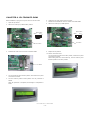
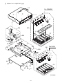
CHAPTER 4. HARDWARE DESCRIPTION
1. BLOCK DIAGRAM
2. MEMORY MAP
ER-A410 and ER-A420
2-1. ADDRESS MAP
DRAWER 1
POWER
SUPPLY
/CS0
BR0
BR1
00000h
DRAWER 2
RAM
BANK 0
0
0
0
BANK 1
0
1
0
Internal RAM area
10KB
02C00h
Internal reserved area
04000h
512KB 1MB
DRIVER, SENSOR
LCD
16 DIGITS
x 2 LINES
08000h
External I/O
/CS3
External SRAM 1
128KB
/CS2
28000h
30000h
SEG DRIVER
DIG DRIVER
POPUP
7-DIGIT
LED
40000h
50000h
4 to 16
DECODER
EFT I/F BOARD
(option)
80000h
External SRAM 2
External SRAM 3
32KB
32KB
External SRAM 4
64KB
CG ROM
External SRAM 5
CG ROM
512KB
256KB
512KB
(Lower level) (Upper level)
IPL SW
IPL SW
OFF: Flash ROM OFF: EP ROM
ON: EP ROM ON: Flash RPM
KEY SCAN
KEY RETURN
BANK 3
0
1
1
00400h
CPU
RAM 10KB
PRINTER
BANK 2
0
0
1
/CS0
C0000h
FLASH ROM
Lower 256KB
KEY & SW
RS232C CH1
FLASH ROM
Lower 256KB
FFFFFh
Even if the bank is changed, the same
address can be accessed.
MUX
RS232C CH2
Only the /CS0, /CS1 area (28000h~FFFFFh) in the bank is valid.
CPU
2-2. EXTERNAL BUS
MITSUBISHI M30620SAFP 12MHz
(INTERNAL RAM 10KB)
EXTERNAL BUS ACCSESS SPEED
SRAM/EPROM/FLASH ROM; 2 BCLK
EXTERNAL MEMORY
RAM
512KB
FLASH ROM
512KB
EXTERNAL I/O; 2 BCLK
*1BCLK = 83.3ns (at 12MHz)
SRAM
SHARP LH28F004BVT
/CS2 area
address 08000h~27FFFh 128KB
PRINTER
PR45MII
/CS1 area BANK 0,2
address 28000h~2FFFFh 32KB x 2
/CS0 area BANK 0
address 30000h~7FFFFh 320KB
FLASH ROM /CS0 area BANK 0
address 80000h~FFFFFh 258KB
(Moves to Bank 1 when rewriting using EPROM.)
ER-A410U/ER-A420U
HARDWARE DESCRIPTION
–7–
/CS1
3. CPU PIN TABLE
M16C/24 PORT MEMORY SPACE: NORMAL MODE
PROCESSOR MODE: MICRO PROCESSOR MODE
It is used by a separate BUS (8bit width).
PORT
PIN
I/O Pin
No.
name
Signal
name
Initial OFF
value MODE
PORT PIN I/O Pin
No.
name
Function
Signal
name
Initial OFF
value MODE
P00
88 I/O
D0
D0
Out L
P50
46
O
/WR
/WR
Out L
P01
87 I/O
D1
D1
Out L
P51
45
O
/BHE
(NU)
Out L
P02
86 I/O
D2
D2
Out L
P52
44
O
/RD
/RD
Out L
P03
85 I/O
D3
D3
Out L
P53
43
O
BCLK
BCLK
Out L
P04
84 I/O
D4
D4
Out L
P54
42
O /HLDA
P05
83 I/O
D5
D5
Out L
P55
41
I
P06
82 I/O
D6
D6
Out L
P56
40
O
P07
81 I/O
D7
D7
Out L
P57
39
I
P10
80
P10
RAS
/RS2
O
L
Out L
RECEIPT
PAPER FEED A
(NU)
Out L
/HOLD
In
ALE
(NU)
Out L
/RDY
/RDY
In
/HOLD
P60
38
O
/RTS0
P61
37
O
CLK0 DRAWER1
P11
79
O
P11
RBS
L
Out L
RECEIPT
PAPER FEED B
P62
36
I
RXD0
RD2
P12
78
O
P12
RCS
L
Out L
RECEIPT
PAPER FEED C
P63
35
O
TXD0
SD2
P13
77
O
P13
RDS
L
Out L
RECEIPT
PAPER FEED D
P64
34
O
/RTS1
/RS1
P65
33
O
P65
/EFTRES
P14
76
O
P14
JAS
L
Out L
JOURNAL
PAPER FEED A
P15
75
O
P15
JBS
L
Out L
JOURNAL
PAPER FEED B
P16
74
O
P16
JCS
L
Out L
JOURNAL
PAPER FEED C
P17
73
O
P17
JDS
L
Out L
JOURNAL
PAPER FEED D
P20
72
O
A0
A0
Out L
P21
71
O
A1
A1
Out L
P22
70
O
A2
A2
Out L
P23
69
O
A3
A3
H
In
L
Out L
Function
RS-232 /RS2
DRAWER 1
DRIVE SIGNAL
In
RS-232 RD2
In
RS-232 SD2
H
In
RS-232 /RS1
H
Out L
EFT RESET
SIGNAL
H
P66
32
I
RXD1
RD1
In
RS-232 RD1
P67
31
O
TXD1
SD1
H
In
RS-232 SD1
P70
30
O
TXD2
SO
L
Out L
PRINTER DATA
OUT
P71
29
I
RXD2
SI
In
PRINTER DATA
IN
P72
28
O
CLK2
PCLK
L
Out L
PRINTER
CLOCK
P73
27
O
P73
DRAWER2
L
Out L
DRAWER 2
DRIVE SIGNAL
Out L
P74
26
O
P74
/ER1
H
25
I
P75
/CD1
In
RS-232 /ER1
In
RS-232 /CD1
P24
68
O
A4
A4
Out L
P75
P25
67
O
A5
A5
Out L
P76
24
I
P76
/CS1
In
RS-232 /CS1
23
I
P77
/DR1
In
RS-232 /DR1
P26
66
O
A6
A6
Out L
P77
P27
65
O
A7
A7
Out L
P80
22
O
P80
BUZZER
L
Out L
P81
21
O
P81
VHCOM
L
In
P82
20
I
/NIT0
POFF
In
P83
19
I
P83
/EFTC
In
EFT PWB connect
In
RS-232 /ER2
P30
63
O
A8
A8
Out L
P31
61
O
A9
A9
Out L
P32
60
O
A10
A10
Out L
P33
59
O
A11
A11
Out L
P34
58
O
A12
A12
Out L
P35
57
O
A13
A13
Out L
P36
56
O
A14
A14
Out L
P37
55
O
A15
A15
Out L
P40
54
O
A16
A16
Out L
P41
53
O
A17
A17
Out L
P42
52
O
A18
A18
Out L
P43
51
O
A19
A19
Out L
P44
50
O
/CS0
/CS0
Out L
P45
49
O
/CS1
/CS1
Out H
P46
48
O
/CS2
/CS2
Out H
P47
47
O
/CS3
/CS3
Out L
ER-A410U/ER-A420U
P84
18
O
P84
/ER2
P85
17
I
/NMI
/NMI (NU)
In
P86
11
O XCOUT
XCOUT
32.768kHz
P87
10
I
XCIN
XCIN
32.768kHz
P90
7
I
P90
MODE
In
MODE KEY
SENSE
P91
6
I
P91
MSENS
In
MISCELLANEOUS SENSE
P92
5
O
P92
BA1
L
Out L
BANK 1 SIGNAL
P93
4
O
P93
BA0
L
Out L
BANK 0 SIGNAL
P94
3
O
P94
DATA/CE
L
Out L
LCD DATA
LATCH SIGNAL
P95
2
O
P95
BLON
L
Out L
BACK LIGHT ON
HARDWARE DESCRIPTION
–8–
H
PRINTER HEAD
CONTROL
PORT
PIN
I/O Pin
No.
name
P96
1
Signal
name
Initial OFF
value MODE
O
P96
LCDON
P97 100
I
P97
P100 97
I
P101 95
The PR-45M II printer is used.
Out L
LCD POWER ON
IPLON
In
IPL ON SIGNAL
AN0
TM
In
HEAD TEMPERATURE MONITOR
I
AN1
VPTEST
In
HEAD VOLTAGE MONITOR
P102 94
I
AN2
VREF
In
REFERENCE
VOLTAGE
P103 93
O
AN3
/STRB1
H
In
PRINTER STORE
SIGNAL 1
P104 92
O
AN4
/STRB2
H
In
PRINTER STORE
SIGNAL 2
No.
CPU PORT
Signal to be used
80
P10
RAS
P105 91
O
P105
/STRB3
H
In
PRINTER STORE
SIGNAL 3
79
P11
RBS
P106 90
O
P106
/STRB4
H
In
PRINTER STORE
SIGNAL 4
78
P12
RCS
77
P13
RDS
76
P14
JAS
75
P15
JBS
74
P16
JCS
73
P17
JDS
P107 89
O
P107
L
4. PRINTER CONTROL
Function
LATCH
L
In
4-1. STEPPING MOTOR CONTROL
The stepping motor is driven at a constant voltage by the Sanken
STA471A.
1step: 0.125mm, 1dot: 1step
Printing speed: 50mm/s
<CPU’s PORT>
PRINTER
LATCH SIGNAL
POWER SUPPLY/CONTROL PINS
PORT
PIN No.
I/O
PIN NAME
BYTE
8
I
BYTE
Connected to VDD
CNVSS
9
I
CNVSS
Connected to GND
/RESET
12
I
/RESET
XOUT
13
O
XOUT
VSS
14
XIN
15
VCC
16
VSS
I
FUNCTION
<DRIVING STEP>
RECEIPT MOTOR
Driver IC input (CPU output)
OPEN
Connected to GND
Motor drive signal
STEP
RAS
RBS
RCS
RDS
H
L
L
H
/RPFA /RPFB /RPFC /RPFD
L
H
H
XIN
Connected to Spectram
1
VCC
Connected to VDD
2
L
H
L
H
H
L
H
L
L
H
H
L
H
L
L
H
H
L
H
L
L
H
L
H
VCC
62
VCC
Connected to VDD
3
VSS
64
VSS
Connected to GND
4
AVSS
96
AVSS
Connected to GND
VREF
98
VREF
Connected to VDD
AVCC
99
AVCC
Connected to VDD
Driver IC input (CPU output)
L
Motor drive signal
STEP
JAS
JBS
JCS
JDS
/JPFA
/JPFB
/JPFC
/JPFD
1
L
H
H
L
H
L
L
H
2
L
H
L
H
H
L
H
L
3
H
L
L
H
L
H
H
L
4
H
L
H
L
L
H
L
H
*When the motor is at rest, the same phase as the final excitation
phase is RUSH-energized for 10 ms to turn off all phases.
3 Turn all AS~RDS and JAS~JDS into L.
No energizing should be allowed at least 30 ms after stopping the
motor before restarting.
When starting the motor, the first excitation phase is RUSH energized
for 10 ms to start the motor by acceleration control.
ER-A410U/ER-A420U
HARDWARE DESCRIPTION
–9–
5. A/D CONVERSION
4-2. HEAD CONTROL
HEAD: 864 dots in all Printable range
The following three kinds of signals are inputted to the A/D conversion
port of the ER-A410/ER-A420.
RECEIPT side 384 dots
JOURNAL side 384 dots
<CPU’s PORT>
Related PORT
No.
No.
CPU PORT
Signal to
be used
97
AN0
TM
PRINTER HEAD TEMPERATURE
MONITOR
95
AN1
VPTEST
PRINTER HEAD VOLTAGE MONITOR
94
AN2
VREF
Function
CPU PORT
Signal to be used
30
TXD2
SO
29
RXD2
SI
28
CLK2
PCLK
93
P103
/STRB1
92
P104
/STRB2
91
P105
/STRB3
5-1. PRINTER HEAD TEMPERATURE MONITOR
90
P106
/STRB4
89
P107
LATCH
21
P81
VHCOM
The voltage divided by the resistor and the thermistor for detecting the
temperature of the printer head is inputted to the AN0 pin. As shown
below, the printer head energizing is controlled.
REFERENCE VOLTAGE
HEAD
A/D CONVERSION
TEMPERATURE
VALUE (DEC)
/STB1: 1~288dot: 288 dots in all
/STB2: 289~432dot: 144 dots in all
Total 864 dots
/STB3: 433~576dot: 144 dots in all
-10°C or below
929~1023
MOTOR LOCK
-10°C ~ 0°C
869~928
PRINT IN ENERGIZING
TIME AT 0°C
0°C ~ 70°C
232~868
PRINT IN ENERGIZING
TIME SHOWN IN PR-45
CONTROL SPEC
/STB4: 577~864dot: 288 dots in all
*When turning off the printer power supply, make sure to turn
/STB1,2,3,4 to “H.”
70°C or above
*Do not turn on without paper.
*THERMAL HEAD power supply control: Turn ON when P81 = ”H”;
turn OFF when at “L.” (The power supply for HEAD and STEPPING
MOTOR is shared.) When printing is finished, (when the motor is
stopped), the power should be turned off.
*Before printing or feeding paper, the A/D conversion is performed in
10ms after the printer head is turned on to make sure the voltage is
stable.
OPERATION
0~231
MOTOR LOCK
5-2. PRINTER HEAD VOLTAGE MONITOR
A voltage is supplied by the printer head power supply, passed through
the printer, divided by the resistor, and inputted to AN1 pin. Before
reading the A/D conversion value, turn the VHCOM signal (CPU P81) to
“H” and make sure the voltage is stable. Then read the A/D conversion
value.
The printable voltage range for the printer is 15V~26V. The voltage is
calculated from the AN1 value and the A/D conversion value of the reference voltage of AN2.
5-3. REFERENCE VOLTAGE
The reference voltage (2.495Vm0.085V) generated by KIA431F is inputted to AN2 pin.
469 (DEC) t VREF t 557 (DEC)
VREF 469 (DEC) corresponds to VREF = 2.41V at VCC = 5.25V
VREF 557 (DEC) corresponds to VREF = 2.58V at VCC = 4.75V
ER-A410U/ER-A420U
HARDWARE DESCRIPTION
– 10 –
6. KEY/DISPLAY
6-2. KEY/DISPLAY SCAN
On the ER-A410/ER-A420, the key and display scan signal is common.
6-1. LCD CONTROL
Key/display scan and key read are performed at the following timing.
The LCD control is the same for the ER-A410/ER-A420.
1 Key/display scan cycle: 10ms
2 Blanking time: 50us
LCD-related Register
Function
Address
R/W
LCD Write Data
04001h
W
LCD Read Data
04002h
R
LCD Control Signal / Key Strobe Signal
04003h
W
CPU port P94
W
Data Latch Signal
3 KEY DATA READ timing: 10 ~100us before turning off the strobe
signal
KEY DATA are read in two divisions by switching the exchange signal.
Key/Display-related Register
Function
<LCD Control Signal/Key Strobe Signal>
Address
04003h
Bit7
Bit6
Bit5
Bit4
Bit3
Bit2
Bit1
Bit0
–
E
R/W
RS
KS3
KS2
KS1
KS0
R/W
LED Segment Signal
04000h
W
LCD Control Signal / Key Strobe Signal
04003h
W
Key Return Signal
Key Exchange Signal
Key Select Signal
Bit7:
Not used
Bit6:
E
Enable Signal
Bit5:
R/W
H: Data read L: Data Write
Bit4:
Address
Enable
04003h
R
04003h Bit7
W
CPU port P90
R
<LED Segment Signal> Write
Address
Bit7
Bit6
Bit5
Bit4
Bit3
Bit2
Bit1
Bit0
04000h
dp
g
f
e
d
c
B
a
RS
H: Data input L: Instruction Input
<LCD Control Signal/Key Strobe Signal> Write
Address
<Data Latch Signal> P94
04003h
Bit7
Bit6
Bit5
Bit4
Bit3
Bit2
Bit1
Bit0
X
E
R/W
RS
KS3
KS2
KS1
KS0
L: LCD write data latch
Bit3~0: KS3~0
DATA WRITE (CPU 3 LCD)
At KS3~0, the strobe signals of KEY and POP UP Display are generated.
RS
<Key Return Signal, Key Exchange Signal> Read Flat Keyboard
R/W
Address
E
DB0-7
Bit7
Bit6
Bit5
Bit4
04001h
X
X
X
X
04003h
KR7
KR6
KR5
KR4
Bit3
Bit2
Bit1
Bit0
KR11 KR10
KR9
KR8
KR3
KR1
KR0
KR2
Valid Data
<Key Return Signal> Read Normal Keyboard
P94
4003h
4001h
4003h
4003h
4003h
000xxxxx DATA 010xxxxx 000xxxxx 001xxxxx
WRITE WRITE WRITE WRITE WRITE
Address
Bit7
Bit6
Bit5
Bit4
Bit3
Bit2
Bit1
Bit0
04003h
KR7
KR6
KR5
KR4
KR3
KR2
KR1
KR0
<Key Select Signal>
READ is performed at the timing of ST9 of CPU port P90 (Refer to 6-3.)
DATA READ (CPU 1 LCD)
1: NORMAL KEY
RS
0: FLAT KEY
R/W
The flat keyboard switches the key exchange signal and takes key data
in two times. For the reading timing, refer to the timing chart below.
E
The normal keyboard reads key data 10~100us before turning off the
strobe signal of the keyboard.
950m25us
Valid Data
DB0-7
KS0~3
0
50m5us
Fh
1
Fh
9
Fh
0
Max. 10us
P94
LED Segment
Signal
4003h
001xxxxx
WRITE
CPU
4003h
4002h
P94 011xxxxx DATA
HIGH WRITE READ
4003h
001xxxxx
WRITE
CPU
P94
LOW
4003h
001xxxxx
WRITE
ER-A410U/ER-A420U
Key Return
Signal
HARDWARE DESCRIPTION
– 11 –
1ST DIGIT
2ND DIGIT
DISPLAY DATA BLANK DISPLAY DATA BLANK
10~100us
DIGIT
BLANK 1ST
DISPLAY DATA
6-3. OTHERS
CPU
STO
ST1
ST2
ST3
ST4
ST5
MGR
MODE
P90
SRV
PGM
VOID
OP X/Z
REG
OTHERS
P91
PF-R
PF-J
RPE
HEAD UP
JPE
The MODE key switch and other sensor signals are read with the CPU
port P90 and 91 at the keyboard strobe timing. Reading is performed
10~100us before turning off the strobe signal.
P90
P91
ST6
ST7
ST8
X1/Z1
X2/Z2
ST9
Key Select
DRAWER
OPEN
RS1_CI
7. SERIAL I/O
The ER-A410/ER-A420 is provided with 2 channels of RS-232 PORTs as
standard provision.
ST0 : MODE Key SRV
“0” SRV mode
ST1 : MODE Key PGM
“0” PGM mode
ST2 : MODE Key VOID
“0” VOID mode
ST3 : MODE Key OP X/Z
“0” OP X/Z mode
Pin No.
CPU PORT
Signal to be used
ST4 : MODE Key REG
“0” REG mode
34
/RTS1
/RS1
ST5 : MODE Key MGR
“0” MGR mode
32
RXD1
RD1
ST6 : MODE Key X1/Z1
“0” X1/Z1 mode
31
TXD1
SD1
ST7 : MODE Key X2/Z2
“0” X2/Z2 mode
26
P74
/ER1
ST9 : Keyboard select
“0” Flat key
25
P75
/CD1
“1” Normal key
24
P76
/CS1
ST0 : Receipt feed
“0” Receipt feed
23
P77
/DR1
ST1 : Journal feed
“0” Journal feed
6
P91 (Refer to 6-3.)
/CI1
Pin No.
CPU PORT
Signal to be used
38
/RTS0
/RS2
36
RXD0
RD2
35
TXD0
SD2
18
P84
/ER2
The RS-232 ch1 and ch2 are assigned to the following CPU port and I/O.
Ch1
ST2 : Receipt paper end
“1” Receipt paper end
ST3 : Head up
“0” Head up
ST4 : Journal paper end
“1” Journal paper end
ST6 : Drawer open sensor
“0” Drawer open
Ch2
ST9 : RS-232 ch1 CI signal
6-4. DISPLAY
The ER-A410/A420 is provided with the front LCD of 5 x 7dot, 2 lines 16
digits, and the 7-digit LED on the pop up side.
<Serial I/O ch2 receive signal> Read
Address
FRONT:
04000h
Bit7
Bit6
Bit5
Bit4
Bit3
Bit2
Bir1
Bit0
X
X
X
X
/CD2
/DR2
/CS2
/CI2
RS-232 I/F BLOCK DIAGRAM
Ch1 connector
CPU
POP UP:
Ch2 connector
MUX
B
Y
A A/B
• DISPLAY DIGIT SIGNAL
The above ST0~ST6 are DIGIT signals.
ST0: 1st digit~ST6:7th digit
+5V
• DISPLAY SEGMENT SIGNAL (REFER TO 6-2.)
By writing segment data to 4000h, the LED segment signal can be
outputted.
DATA~SEGMENT correspondence
D0~D6 3 a~g
D7
3 DP
ER-A410U/ER-A420U
HARDWARE DESCRIPTION
– 12 –
8. POWER
POFF, RESET TIMING CHART
+5V
Service interruption should be performed
within 10ms after generation of /POFF.
24V
LM2574 + TR
TRANS.
20.8V
+24V
/RESET
DRAWER
PRINTER
/POFF
/EFTRES
POWER ON
PQ1CG2032
Instant service
interruption
VLED 5.7V
MODE
SRV'
MODE
POWER OFF
Other than
SRV'
VCC 5.0V
VDD 5.0V
/POFF detection point
15. I/O
BATTERY
<LED Segment Signal> Write
9. FLASH MEMORY REWRITE PROCEDURE
Address
Bit7
Bit6
Bit5
Bit4
Bit3
Bit2
Bit1
Bit0
04000h
dp
g
f
e
d
c
B
a
<Serial I/O ch2 receive signal> Read
IPL from EP-ROM: Set the IPL SW to ON and turn on the power, and
the EP-ROM will be boosted.
Address
04000h
The bank of the EP-ROM program is switched
through S-RAM to transfer the program to the
FLASH ROM.
Bit7
Bit6
Bit5
Bit4
Bit3
Bit2
Bit1
Bit0
X
X
X
X
/CD2
/DR2
/CS2
/CI2
<LCD Write Data> Write
10. DRAWER
Address
Bit7
Bit6
Bit5
Bit4
Bit3
Bit2
Bit1
Bit0
04001h
DB7
DB6
DB5
DB4
DB3
DB2
DB1
DB0
Bit1
Bit0
KR9
KR8
<Key Return Signal, Key Exchange Signal> Read
The ER-A410/ER-A420 is provided with 2 separate DRAWER ports.
Address
The DRAWER solenoid energizing time is as shown below.
04001h
50ms (max) 45ms(min)
Bit7
Bit6
Bit5
Bit4
X
X
X
X
Bit3
Bit2
KR11 KR10
<LCD Read Data> Read
11. PRINT RATIO LIMITATION
Address
Bit7
Bit6
Bit5
Bit4
Bit3
Bit2
Bit1
Bit0
04002h
DB7
DB6
DB5
DB4
DB3
DB2
DB1
DB0
Max. 288dot/1line x 140line (Corresponds to black background LOGO
print.)
<LCD Control Signal/Key Strobe Signal> Write
Ave. 108dot/1line or less (Corresponds to 12.5% of all dots.)
Address
04003h
12. BUZZER
Bit7
Bit6
Bit5
Bit4
Bit3
Bit2
Bit1
Bit0
X
E
R/W
RS
KS3
KS2
KS1
KS0
<Key Return Signal> Read
A piezo type buzzer is used.
Address
Bit7
Bit6
Bit5
Bit4
Bit3
Bit2
Bit1
Bit0
The oscillation frequency is 2.048kHz m 0.5kHz.
04003h
KR7
KR6
KR5
KR4
KR3
KR2
KR1
KR0
<LCD Control Signal/Key Strobe Signal> Write
13. RESET
Address
The RESET signal is generated under the following condition.
04003h
1) When the MODE KEY SWITCH is moved from SRV’ to another
position (except for OFF).
Bit7
Bit6
Bit5
Bit4
Bit3
Bit2
Bit1
Bit0
X
E
R/W
RS
KS3
KS2
KS1
KS0
<EFT Data> Write/Read
Address
Bit7
Bit6
Bit5
Bit4
Bit3
Bit2
Bit1
Bit0
0400Eh
D7
D6
D5
D4
D3
D2
D1
D0
Bit7
Bit6
Bit5
Bit4
Bit3
Bit2
Bit1
Bit0
X
X
X
X
X
CLM
IBF
OBF
14. POFF
The POFF signal is changed from 0 to 1 when the 5V system power
and the 24V system power reach the operating voltage. When they fall
below the operating voltage, the signal is changed from 1 to 0.
ER-A410U/ER-A420U
<EFT Status> Read
Address
0400Fh
HARDWARE DESCRIPTION
– 13 –
CHAPTER 5. DIAGNOSTIC PROGRAM
1. TEST ITEMS
2. DESCRIPTION OF EACH DIAG PROGRAM
The test items are as follows:
Code
1) DISPLAY BUZZER TEST
Description
1)
100
Display buzzer test
2)
101
Key code
3)
102
Printer test
4)
104
Keyboard test
5)
105
Mode switch test
6)
106
Printer sensor test
7)
107
Clock test
8)
110
Drawer 1 open & sensor test
9)
111
Drawer 2 open & sensor test
10)
116
LCD CG test
11)
120
External RAM test
12)
121
CPU internal RAM test
13)
130
FLASH ROM test
14)
160
AD conversion port test
15)
500
RS232 ch1 test
16)
501
RS232 ch2 test
1 Key operation
100 3
CA/AT
2 Test procedure
OP display
D I S P BUZZER SRV
0 1 2 3 4 5 6 7 8 9ABCDEF
4.5.6.7.8.9.0.
Rear display
The decimal point on the LED and the cursor on the LCD will shift
from the lower digit to the upper digit in steps of 1 digit (every 200
msec)
After that, all segments will turn on (about 1 sec)
These two modes are repeated.
At the same time, the buzzer sounds continuously.
3 Check that:
A) Each position is correctly displayed.
*Starting DIAG.
B) The brightness of each number is uniform.
Mode switch: SRV
key operation: Above code + “CA/AT” key
C) The buzzer sound is normal.
4 End of testing
You can exit the test mode by pressing any key. The following is
printed.
1 0 0
2) KEY CODE
1 Key operation
101 3
CA/AT
2 Test procedure
OP display
KEY
CODE
KEYBOARD
SRV
KEY CODE
3 Check that:
KEYBOARD: 1: Normal type 0: Flat type
KEY code:
Every time a key is pressed, the hard code of that key
is displayed as a decimal number.
When a key is pressed twice or pressed in an incorrect manner, --- will be displayed.
4 End of testing
You can exit the test mode by turning the mode switch to a position
other than the PGM mode. The printer prints as follows:
1 0 1
ER-A410U/ER-A420U
DIAGNOSTIC PROGRAM
– 14 –
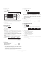
3) PRINTER TEST
5) MODE SWITCH TEST
1 Key operation
1 Key operation
102 3
105 3
CA/AT
2 Test procedure
2 Test procedure
OP display
CA/AT
R / J
SRV
P R I N T E R
OP display
MODE
1 0 5
SRV
SW
X
Enlargement
MODE: SRV_PGM2_PGM1_OFF_OP X/Z_REG_MGR_X1/Z1_X2/Z2__SRV
1
2
9
3
4
5
6
7
0
X : 0
The above X must be read in the correct order. (If the contact is
open, 9 will be displayed.)
3 Check:
5 lines of 24 digits are printed.
The display during testing and the content of the completion print.
At the receipt side, the logo is also printed and the receipt is issued.
4 End of testing
1 0 5
When the test ends normally
3 Check that:
When an error occurs:
The print is free from contamination, blur, and uneven density.
4 End of testing
E–~–
1 0 5
6) PRINTER SENSOR TEST
The test will end automatically.
1 Key operation
106 3
4) KEYBOARD TEST
CA/AT
2 Test procedure
1 Key operation
Check the status of the paper end sensor and head up sensor.
_ _ _ _104 3 CA/AT
2
KEY check sum code
OP display
2 Test procedure
The keyboard is checked using the sum check code of the key
code.
O - No paper at the receipt side
Y: 1 - Paper present at the journal side
O - No paper at the journal side
4 End of testing
You can exit the test mode by pressing any key and the printer
prints the following.
If both data are different, the printer prints the error message.
KEY
1 0 4
SRV
BOARD
1 0 6
KEY CODE
3 Check:
A) The content of completion print
4 End of testing
1 0 4
When the test ends normally:
When an error occurs:
E–~–
1 0 4
Note: Calculation of key sum check data
Hard codes (hexadecimal number) at the position (excluding
feed key) where there is an input data contact are added.
However, the end key (TL) is not added.
This data to which hard codes have been added is converted into
a decimal number value, which will become the sum check data
that will be entered when DIAG is started.
ER-A410U/ER-A420U
SRV
X Y
X: 1 - Paper present at the receipt side
The sum check data for each model is entered to the front 4 digits
of the DIAG code, and that data is compared with the key data
added until the final key (CA/AT) is pressed.
OP display
SENSOR
3 Check the following.
If the sum check code is not entered, the check is made using the
sum check code of the default keyboard arrangement
Both data are the same, the test ends, printing the number given
below.
R / J
1 0 6
DIAGNOSTIC PROGRAM
– 15 –
7) CLOCK TEST
9) DRAWER 2 OPEN & SENSOR TEST
1 Key operation
1 Key operation
107 3
111 3
CA/AT
2 Test procedure
OP display
CA/AT
2 Test procedure
T I ME R
1 0 7
OP display
SRV
CHECK
DRAWER
2
SRV
X
X : O = DRAWER OPENED
Hour
Min.
Sec.
C = DRAWER CLOSED
Blinks at an interval of 0.5 sec.
3 Check that:
A) The drawer 2 opens normally.
3 Check that:
B) The sensor correctly indicates the status of the drawer 2.
“–“ blinks and the clock counts up.
4 End of testing
4 End of testing
You can exit the test mode by pressing any key. The printer prints
the following.
When any key is pressed, the date and time are printed and the
test mode will be terminated.
1 1 1
X X X X X X
X X X X X X
year
month
hour
107
10) LCD CG TEST
min.
day
1 Key operation
sec.
116 3
CA/AT
2 Test procedure
8) DRAWER 1 OPEN & SENSOR TEST
To check the display CG, 256 pieces of built-in CG's are grouped
into 16 blocks and each 16 characters is displayed on the dot display.
At first, CG code of 00H ~ 0FH is displayed. By pressing any key,
each block is displayed in sequence.
1 Key operation
110 3
CA/AT
2 Test procedure
OP display
DRAWER
1
OP display
SRV
SRV
XY
X
"O" indicates the CG display position.
X : O = DRAWER OPENED
"XY" indicates the code at the head of each block
in hexadecimal number.
(Example: 10, A0)
C = DRAWER CLOSED
3 Check that:
A) The drawer 1 opens normally.
3 Check that:
B) The sensor correctly indicates the status of the drawer 1.
A) Displays are clear.
4 End of testing
B) Free from blur, chip-off, unevenness.
You can exit the test mode by pressing any key. The printer prints
the following.
4 End of testing
You can exit the test mode by pressing any key. The printer prints
the following.
1 1 0
1 1 6
ER-A410U/ER-A420U
DIAGNOSTIC PROGRAM
– 16 –
11) EXTERNAL RAM TEST
12) CPU INTERNAL RAM TEST
1 Key operation
1 Key operation
120 3
121 3
CA/AT
2 Test procedure
CA/AT
2 Test procedure
The test program tests internal RAM (10 Kbytes) of the CPU.
The contents of memory must be stored before and after this test.
RAM (00400H ~ 02BFFH area) is tested in the following procedure.
The standard 256 Kbyte RAM is checked.
The contents of memory must be stored before and after this test.
RAM (08000H~7FFFFH area and 28000H~2FFFFH area) is tested
in the following procedure:
a) Store data in the test area.
a) Store data in the test areas
c) Read and compare “00H” and then write “55H”
b) Write “00H”
d) Read and compare “55H” and then write “AAH”
c) Read and compare “00H” and then write”55H”
e) Read and compare “AAH”
d) Read and compare “55H” and then write “AAH”
f)
b) Write “00H”
e) Read and compare “AAH”
f)
Restore stored data
If an error occurs at a step, the error is printed.
If any error does not occur, the following addresses are checked
in turns.
Restore stored data
If an error occurs at a step, the error is printed.
If any error does not occur, the following addresses are checked in
turns.
Addresses to be checked:
01000H, 01001H, 01002H, 01004H, 01008H
01010H, 01020H, 01040H, 01080H,
01100H, 01200H, 01400H, 01800H,
02000H
Addresses to be checked:
08000H, 08001H, 08002H, 08004H, 08008H, 08010H, 08020H,
08040H, 08080H, 08100H, 08200H, 08400H, 08800H, 09000H,
0A000H, 0C000H, 10000H, 18000H, 28000H (BANK 0),
28000H (BANK 3), 30000H, 40000H
OP display
CPU
1 2 1
SRV
RAM
3 Check:
OP display
The completion print.
SRV
RAM
1 2 0
4 End of testing
The test program ends after printing.
When the test ends normally:
When the test ends abnormally: Ex – ~ –
*****
x = 1: Data error
x = 2: Address error
3 Check:
A) The completion print.
4 End of testing
The program ends after printing as follows:
When the test ends normally:
When the test end abnormally:
120
Ex – ~ –
121
121
If an error occurs, the printer outputs the error message and the
address where the error has occurred in the area *****.
120
*****
x = 1: Data error
13) FLASH ROM TEST
x = 2: Address error
1 Key operation
When an error occurs, the printer outputs the error message and the
address where the error has occurred in the area *****.
130 3
CA/AT
2 Test procedure
The test program checks that the checksum of the flash ROM
(BANK0F80000H ~ FFFFFH).
The lower two digits of the checksum should be 10H. (pending)
OP display
F L A S H
1 3 0
ROM
SRV
3 Check:
The completion print.
4 End of testing
The test will automatically be terminated and the printer prints as
follows:
When the test ends normally:
ROM
130
******** (Model name)
******** (Version)
When the test ends
abnormally:
E––~––
ROM
130
******** (Model name)
******** (Version)
ER-A410U/ER-A420U
DIAGNOSTIC PROGRAM
– 17 –
14) AD CONVERSION PORT TEST
16) RS232 CH2 TEST
1 Key operation
Install the RS232 loopback connector.
160 3
1 Key operation
CA/AT
501 3
2 Test procedure
CA/AT
2 Test procedure
The test program displays the voltage of each AD conversion port.
The test program checks the control signals.
OUTPUT
Display
OP display
Repeat
OP display
OP display
T M
1 6 0
=
VRF
1 6 0
=
SRV
SRV
/RS2
/DR2
/CI2
/CD2
/CS2
OFF
OFF
OFF
OFF
OFF
OFF
OFF
ON
OFF
OFF
ON
ON
ON
OFF
ON
ON
OFF
OFF
ON
ON
ON
ON
ON
ON
Data communication check
V P T E S T=
1 6 0
SRV
A loopback test of 256-byte data between is performed.
DATA: $00 - $FF BAUD RATE: 9600 BPS
OP display
RS 2 3 2
5 0 1
3 End of testing
You can exit the test mode by pressing any key. The printer prints
the following.
1 6 0
The completion print.
Completion print
RS TEST
OK
Error print
RS TEST
**NG**ERxx
1 Key operation
CA/AT
2 Test procedure
The test program checks the control signals.
/DR1
OFF
OFF
ON
ON
INPUT
/CI1
/CD1
OFF
OFF
OFF
ON
ON
OFF
ON
ON
/CS1
OFF
ON
OFF
ON
RS 2 3 2
5 0 0
T E S T
xx
Contents of error
01
ER DR error
02
ER CI error
03
RS CD error
04
RS CD error
05
SD RD error
DATA error
06
SD RD error
DATA error/framing error
3. KEY CODE TABLE
ER A410U
051 131 115
Data communication check
A loopback test of 256-byte data between is performed.
DATA: $00 - $FF BAUD RATE:9600 BPS
OP display
147 148
003 004
052 132 116
084 068 146 018
002 005
033 037
050 130 114
082 066 149 145
017 001
032 048
053 133 117
085 069 065 064
016 000
038 054
128 129 113
081 080 086 070
022 006
102 103 087 071
007
RF JF
SRV
039 055
3 Check:
118
112
067
CHECK SUM : 4 2 8 9
The completion print.
ER A420U
4 End of testing
Completion print
Error print
xx Contents of error
01 ER DR error
02 ER CI error
03 RS CD error
04 RS CD error
05 SD RD error
06 SD RD error
SRV
4 End of testing
Install the RS232 loopback connector.
OUTPUT
/ER1
/RS1
OFF
OFF
OFF
ON
ON
OFF
ON
ON
T E S T
3 Check:
15) RS232 CH1 TEST
500 3
INPUT
/ER2
RF JF
RS TEST
RS TEST
OK
**NG**ERxx
032 048 055 039 033 049 065 035 067 099 133 120 121 138 155
128 112 096 103 113 097 115 051 084 100 102 101 117 089 105 106 107
064 119 135 130 129 131 116 132 118 134 085 104 136 073 122 090 123
080 087 082 066 081 083 068 086 150 070 069 072 088 153 154 074 139
144 071 146 050 145 147 148 054 038 053 149 152 056 057 058 075 091
016 151 034 017 001 019 052 036 022 021 037 040 025 041 042 059 027
000 007 023 018 002 003 020 004 006 005 024 008 009 010 026 043 011
DATA error
DATA error/framing error
CHECK SUM : 8 9 4 0
ER-A410U/ER-A420U
DIAGNOSTIC PROGRAM
– 18 –
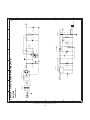
CHAPTER 6. IPL FROM EP-ROM
Before installation, unplug the AC power cord from the AC outlet.
6. Unplug the AC power cord from the AC outlet.
1. Open the top cabinet.
7. Remove the IPL ROM from to the IC socket of the MAIN PWB.
2. Set the IPL switch (S1) to ROM COPY position.
8. Set the IPL switch (S1) to GND position.
ROM COPY
ROM COPY
GND
GND
VCC
VCC
S1
S1
S1
S1
IPL switch
IPL switch
9. Replace the top cabinet.
3. Install the IPL ROM in the IC socket of the MAIN PWB.
10. Perform the master reset.
Turn the mode key switch to the SRV’ position, insert the AC power
cord into the AC outlet.
While holding down the Journal feed key, turn the mode key from
the SRV position to the SRV’ position.
IPL ROM
pin-1
4. Turn the mode key switch to SRV’ position, and insert the AC power
cord into the AC outlet.
5. Turn the mode key switch to SRV position. The IPL procedure is
started.
When the procedure is completed, the message of “Completed” is
shown.
ER-A410U/ER-A420U
IPL FROM EP-ROM
– 19 –
A
B
C
D
6
5
8
1
2
CN1
7
PS CN(2Pin)5273-02A
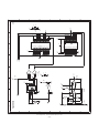
POWER TRANS1
120V
POWER SUPPLY
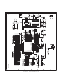
MAIN PWB
C2
220uF/50V
F1
T1.0A/250V
+24V
C1
MYLOR
0.033uF
(WITH HOLDER)
6
-
F2
UL,CSA T3.15AL/125 V
+
1
IC1
CP301
+
C6
4700uF/50 V
F3
T2.0A/25 0V
C3
0.01uF
5
2
PQ1CG2032 FZ
IC1:HEAT SINK
BD1
5
+
RB060 L40
D1
C10
TP2
VO
0.1uF
180uH Chock
L1
C11
100uF/50V
+
1
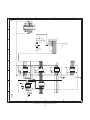
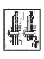
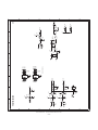
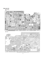
CHAPTER 7. CIRCUIT DIAGRAM AND PWB LAYOUT
7
5
4
1
C4
4
IC2
7
Q1
KTD998
Q1:HEAT SINK
PTZ6. 2A
ZD1
1SR159 -200
D5
6,8pin:N.C
LM2574HVN
1000uF
/16V
+
4
2
3
8
4
– 20 –
3
CIRCUIT DIAGRAM AND PWB LAYOUT
VLED
R4
1KF
3KF
R3
R8
10(FUSE R)
with FUSE
3
3
+ C5
330uF
/16V
R2
1.2KF
C9
C7
2200uF/50V
R1
22KF
2
2
C8
0.1uF
R7
150
R6
180
TP1
VBAT
VCC +5V
VLED +5.8V
47uF
/16V
+
RB160L- 60
D2
1SR159- 200
D4
L2
180uH Chock
1
ER-A410U/ER-A420U
1
2
CN2
1/7
1
BT CN(2Pin)5267-02A(BL UE)
VDD
VCC
+
+24V
VH +24V
1
A
B
C
D
A
B
C
D
/RESET
100pF*8(C20-C27)
R76
8
330pF
CST12.0MTW
470
C48
2
C23
10K
R20
R68
1
X2
3
VCC
C24
10K
R21
C25
10K
R22
10
9
74LV00A
IC14C
1
2
3
4
IC4
FS781
XIN
XOUT
S1
LF
C27
10K
R24
8
VDD
7
S0
6
FSOUT
5
VSS
8
/POFF
C26
10K
R23
7
150pF*8(C12-C19)
2.2K
2.2K
2.2K
2.2K
2.2K
2.2K
2.2K
2.2K
PLACE NEAR CPU!!!
330pFx5
3.3K
C68
0.1uF
R77
10K
VDD
C22
10K
R19
R54
R55
R56
R57
R58
R59
R60
R61
R70 R69 R71 R72 R73
C21
10Kx5
C20
10K
10K
/LATCH
/STRB4
/STRB3
/STRB2
/STRB1
C53
C54
C55
C56
C57
D7
D6
D5
D4
D3
D2
D1
D0
R18
R17
VCC
A7
A6
A5
A4
A3
A2
A1
A0
JDS
JCS
JBS
JAS
RDS
RCS
RBS
RAS
CPU CG
7
5
4
0.1uF
C47
74LV00A
IC14B
C13
10K
10K
C12
R10
VCC
R9
(0)
R147
6
/CS0
10uF/10V,OS
C59
+
VCC
/RES
0
R148
IPLON
C17
10K
R14
VDD
100
100
100
100
100
100
100
100
C16
10K
R13
VREF
VPTEST
C15
10K
R12
TM
R52
R53
R26
R25
R27
R28
R29
R30
C14
10K
R11
IC3
C19
10K
R16
13
12
D7
D6
D5
D4
D3
D2
D1
D0
AN7
AN6
AN5
AN4
AN3
AN2
AN1
AVSS
AN0
VREF
AVCC
SIN4
6
74LV00A
IC14D
P96
P95
P94
BA0
BA1
P91
P90
81
82
83
84
85
86
87
88
89
90
91
92
93
94
95
96
97
98
99
100
M30620SAFP
C18
10K
R15
6
5
BA23
11
BA1
A18
A19
*IC14 14pin:VDD
7pin:GND
18pF
C28
1
2
3
4
5
6
7
8
R75
(0)
VCC
Y0
Y1
Y2
Y3
Y4
Y5
Y6
5
16
15
14
13
12
11
10
9
VCC
(CST12.0MT
W)
X3
74LV138A
A
B
C
G2A
G2B
G1
Y7
GND
IC10
32.768KHz
27pF
C29
X1
R31
330
3
8
C30
10K
R74
33
C33
10K
R35
C34
10K
R36
10uF/10V,OS
C60
50
49
48
47
46
45
44
43
42
41
40
39
38
37
36
35
34
33
32
31
150pF
C44
+
C41
C67
10K
VDD
4
R64
10K
R43
C38
10K
R40
C39
10K
R41
2.2K
R149
47K
R46
47K
R80
2.2K
47K
R45
100pF
VDD
C37
10K
R39
4
R78
C36
10K
R38
100pF
C66
10K
R42
C35
10K
R37
0.1uF
100pF
C58
VDD
10K
R67
150pF
C45
150pF*10(C30-C39)
C32
10K
R34
CS0
CS1
CS2
CS3
WR
BHE
RD
CBCLK
HLDA
HOLD
ALE
CLKOUT
RTS0
CLK0
RXD0
TXD0
CLKS1
CLK1
RXD1
TXD1
C31
10K
R33
VCC
R32
80
79
78
77
76
75
74
73
72
71
70
69
68
67
66
65
64
63
62
61
60
59
58
57
56
55
54
53
52
51
D8
D9
D10
D11
D12
D13
D14
D15
A0
A1
A2
A3
A4
A5
A6
A7
VSS
A8
VCC
A9
A10
A11
A12
A13
A14
A15
A16
A17
A18
A19
SOUT4
CLK4
TB4IN
TB3IN
SOUT3
SIN3
CLK3
BYTE
CNVSS
XCIN
XCOUT
RESET
XOUT
VSS
XIN
VCC
NMI
INT2
INT1
INT0
TA4IN/U
TA4OUT/U
TB3IN
TBEOUT
TA2INW
TA2OUTW
TA1IN/V
TA1OUT/V
TB5IN
TB5OUT
1
CIRCUIT DIAGRAM AND PWB LAYOUT
2
– 21 –
1
2
3
4
5
6
7
8
9
10
11
12
13
14
15
16
17
18
19
20
21
22
23
24
25
26
27
28
29
30
ER-A410U/ER-A420U
R150
12K
47K
R47
47K
R79
VCC
VCC
C2412K
Q12
D15
+
2048BH
B
3
SO
SI
PCLK
/LE0W
(330pF)
C71
VCC
(0.1uF)
C131
C72
VCC
D[0..7]
A[0..19]
/EFTRES
/CS3
A15
BA1
/CS1
R48
10K
330pF
C70
R65
10K
330pF
R66
10K
R143
(10k)
VCC
30pF
C40
R44
10k
VCC
A18
A19
BZ2
1SS355
VHCOM
/POFF
/EFTC
/ER2
DRAWER
2
/ER1
/CD1
/CTS1
/DR1
RXD1
TXD1
/RDY
/RS2
DRAWER
1
RXD2
TXD2
/RS1
/RD
/WR
/CS0
/CS1
/CS2
10K
R63
VCC
BCLK
10K
R62
A8
A9
A10
A11
A12
A13
A14
A15
A16
A17
3
/CS2
/CS1
74LV00A
IC12A
A18
/CS0
A19
BA1
2
1
D0
D1
D2
A18
A16
A14
A12
A7
A6
A5
A4
A3
A2
A1
A0
R144
10K
3
4
5
1
2
13
2
1
VCC
D0
D1
D2
D3
D4
D5
D6
D7
3
74LV00A
IC12D
74LV00A
IC12B
1SS355
32
31
30
29
28
27
26
25
D7
D6
D5
D4
D3
74LV27A
74LV27A
IC8B
74LV00A
IC8A
2
6
12
3
D7
D6
D5
D4
D3
A10
A13
A8
A9
A11
74LV27A
IC8C
VDD
74LV00A
IC12C
*IC8 14pin:VDD
7pin:GND
9
10
11
21
20
19
18
17
24
RD
23
A10
22
CS
VCC
A15
A17
WR
A13
A8
A9
A11
/RES
4MRAM HY628400ALLT2-70
GND
D0
D1
D2
A18
A16
A14
A12
A7
A6
A5
A4
A3
A2
A1
A0
9
10
*IC6
VCC:20pin
GND:10pin
/POFF
Q1
Q2
Q3
Q4
Q5
Q6
Q7
Q8
C42
0.1uF
2
5
6
9
12
15
16
19
11
6
VCC
74HC273
CLK
CLR
D1
D2
D3
D4
D5
D6
D7
D8
IC6
1SS355
IC16
IC14A
16
13
14
15
1
2
3
4
5
6
7
8
9
10
11
12
D6
D14
11
1
3
4
7
8
13
14
17
18
*IC12 14pin:VDD
7pin:GND
13
12
5
4
2
8
8
12
1
2
13
+
VDD
VCC
(30pF)
C64
10K
R51
(30pF)
C63
VCC
1
C62
(10uF/50V)
C43
0.1uF
100pF
C69
R50
10K
74LV11A
IC9A
a
b
c
d
e
f
g
dp
R81
10k
VDD
a
b
c
d
e
f
g
dp
C65
+
VDD
2/7
(10uF/50V)
C46
0.1uF
1
/RD
/WR
A17
/CS2
A
B
C
D
– 22 –
A
B
C
D
8
R86
3.9K
C78
ZD2
UDZ5.1B
(1uF/50V)
+24V
IPLON
R145
47K
BA1
BA0
FLASH ROM
R88
6.2KF
+
R85
9.1KF
R146
47K
6
5
7
IC17B
BA10393F
R84
10KF
A19
/CS0
BA23
7
-
+
IC19
VCC
Y0
Y1
Y2
Y3
Y4
Y5
Y6
3
VLED
2
3
6
IC17A
BA10393F
R83
2.7K
VCC
16
15
14
13
12
11
10
9
R87
10K
VCC
1 ROM COPY
IPL SW SSS 312
S1
74LV138A
A
B
C
G2A
G2B
G1
Y7
GND
2
P-OFF
7
56K
R82
0.1uF
C79
1
2
3
4
5
6
7
8
VDD
6
-
+
8
8
8
4
CIRCUIT DIAGRAM AND PWB LAYOUT
4
ER-A410U/ER-A420U
1
VCC
9
10
11
3
4
5
74LV11A
IC9C
74LV11A
IC9B
/POFF
C76
1000pF
C75
0.1uF
VDD
5
*IC9 14Pin:VDD
7Pin:GND
VCC
R89
10K
5
8
6
4
A[0..19]
D[0..7]
4
/WR
/RES
1
2
3
4
5
6
7
8
9
10
11
12
13
14
15
16
17
18
19
20
A16
A15
A14
A13
A12
A11
A9
A8
WE#
RP#
VPP
WP#
A18
A7
A6
A5
A4
A3
A2
A1
IC18
A16
A15
A12
A7
A6
A5
A4
A3
A2
A1
A0
D0
D1
D2
VCC
1
2
3
4
5
6
7
8
9
10
11
12
13
14
15
16
3
VCC
A18/PGM
A17
A14
A13
A8
A9
A11
OE
A10
CE
D7
D6
D5
D4
D3
0.1uF
C73
A17
GND
NC
NC
A10
DQ7
DQ6
DQ5
DQ4
VCC
VCC
NC
DQ3
DQ2
DQ1
DQ0
OE#
GND
CE#
A0
40
39
38
37
36
35
34
33
32
31
30
29
28
27
26
25
24
23
22
21
32
31
30
29
28
27
26
25
24
23
22
21
20
19
18
17
ROM IC SOCKET(32Pin )
VPP
A16
A15
A12
A7
A6
A5
A4
A3
A2
A1
A0
D0
D1
D2
GND
IC20
4M FLASH ROM LH28F004BVT
A18
A7
A6
A5
A4
A3
A2
A1
A16
A15
A14
A13
A12
A11
A9
A8
VCC
3
VCC
VCC
2
D7
D6
D5
D4
D3
A10
A18
A17
A14
A13
A8
A9
A11
A0
D3
D2
D1
D0
A10
D7
D6
D5
D4
A17
2
/RD
10uF/50V
C77
/RD
+
VCC
1
0.1uF
C74
1
3/7
A
B
C
D
ER-A410U/ER-A420U
CIRCUIT DIAGRAM AND PWB LAYOUT
– 23 –
A
B
C
D
/RD
/WR
8
10
9
/CI2
/CTS2
/DR2
/CD2
KR8
KR9
KR10
KR11
A3
/CS3
KS3
KS1
KS2
KS0
A3
/CS3
8
/LE0W
74LV00A
IC13C
LCD I/F
8
KS3
KS1
KS2
KS0
A0
A1
/WR
A0
A1
C90
0.1uF
VCC
Y0
Y1
Y2
Y3
Y4
Y5
Y6
1
19
2
4
6
8
11
13
15
17
74HC244
1G
2G
1A1
1A2
1A3
1A4
2A1
2A2
2A3
2A4
IC27
74HC138
A
B
C
G2A
G2B
G1
Y7
GND
IC22
16
15
14
13
12
11
10
9
7
*IC27 20Pin:VCC
10Pin:GND
1
2
3
4
5
6
7
8
+ C81
10uF/50V
7
/LE3W
/LE0R
/LE1R
/LE0W
/LE1W
1Y1
1Y2
1Y3
1Y4
2Y1
2Y2
2Y3
2Y4
18
16
14
12
9
7
5
3
/LE2W
VCC
C91
100pF
C88
100pF
VCC
VCC
C93
100pF
R98
10K
VCC
C94
100pF
R92
10K
VCC
R93
10K
R95
10K
D0
D1
D2
D3
D0
D1
D2
D3
DB3
DB1
DB2
DB0
D[0..7]
6
6
D0
D1
D2
D3
D4
D5
D6
D7
0.1uF
C89
D2
D3
D0
D1
C86
0.1uF
D0
D1
D2
D3
D4
D5
D6
D7
C84
0.1uF
D2
D3
D0
D1
P94
C82
0.1uF
1
2
3
4
5
6
7
8
9
10
1
2
3
4
5
6
7
8
9
10
1
2
3
4
5
6
7
8
9
10
1
2
3
4
5
6
7
8
9
10
VCC
Q7
D7
D6
Q6
Q5
D5
D4
Q4
LE
VCC
1G
B1
B2
B3
B4
B5
B6
B7
B8
74HC245
DIR
A1
A2
A3
A4
A5
A6
A7
A8
GND
IC26
74HC374
QE
Q0
D0
D1
Q1
Q2
D2
D3
Q3
GND
IC25
VCC
1G
B1
B2
B3
B4
B5
B6
B7
B8
VCC
Q7
D7
D6
Q6
Q5
D5
D4
Q4
LE
+ C87
10uF/50V
74HC245
DIR
A1
A2
A3
A4
A5
A6
A7
A8
GND
IC24
+ C85
10uF/50V
74HC374
QE
Q0
D0
D1
Q1
Q2
D2
D3
Q3
GND
IC23
+ C83
10uF/50V
D[0..7]
20
19
18
17
16
15
14
13
12
11
20
19
18
17
16
15
14
13
12
11
20
19
18
17
16
15
14
13
12
11
D5
D4
D7
D6
D7
D6
D5
D4
/LE3R
VCC
VCC
/LE2W
VCC
/LE1W
20
19
18
17
16
15
14
13
12
11
VCC
5
5
KR0
KR1
KR2
KR3
KR4
KR5
KR6
KR7
RS
E
R/W
DB0
DB1
DB2
DB3
DB4
DB5
DB6
DB7
DB4
DB6
DB5
DB7
KR0
KR1
KR2
KR3
KR4
KR5
KR6
KR7
DB[0..7]
4
4
P95
P95
VLED
P96
R97
10K
1
2
P96
RS
R/W
E
VCC
IC21
BA00ASFP
3
5
4
3
R94
12K
GND
VCC
V0
RS
R/W
E
DB0
DB1
DB2
DB3
DB4
DB5
DB6
DB7
K
C80
+ 22uF/16V
3
+
C92
22uF/10V,OS
LCD CN(16Pin)5483-16X
1
2
3
4
5
6
7
8
9
10
11
12
13
14
15
16
CN4
R96
2.4KF
R90
5.6K
/RD
/CS3
A0
A2
A4
2
/CD2
EFTSD
/DR2
/CTS2
/POFF
2
D0
D2
D4
D6
CN5
2
4
6
8
10
12
14
16
18
20
22
24
26
28
30
32
34
36
38
40
1
3
5
7
9
11
13
15
17
19
21
23
25
27
29
31
33
35
37
39
1)
(EFT CN(40Pin) XF2H-4015-
VCC
VCC
D1
D3
D5
D7
1
4/7
/EFTRES
RXD2
/EFTER
/EFTRS
/CI2
/EFTC
/WR
A1
A3
A5
1
A
B
C
D
CIRCUIT DIAGRAM AND PWB LAYOUT
A
B
C
D
/EFTRS
/RS2
/EFTER
/ER2
EFTSD
TXD2
8
D13
10K
(10K)
VCC
10K
/EFTC
10K
R132
(10K)
10K
(10K)
7
10K
1
15
2
3
5
6
11
10
14
13
1SS355
R125
7
R133 R134 R135 R136 R137 R138
VCC
P91
/S9
/CTS1
/DR1
/CD1
RXD1
TXD1
/ER1
/RS1
RS232C DRIVER
8
4Y
3Y
2Y
1Y
74HC157DR
A/B
G
1A
1B
2A
2B
3A
3B
4A
4B
IC34
/CTS2
/DR2
/CI2
/CD2
C110
0.1uF
C122
0.1uF
C121
0.1uF
C111
0.1uF
12
9
7
4
6
*IC34 VCC:16Pin
GND:8Pin
(47K) (47K) (47K) (47K)
R142 R141 R139 R140
VCC
Q11
KRC111 S
10K
R124
RXD2
10K
R126
VCC
6
24
19
22
26
5
8
21
20
6
7
16
15
14
12
24
19
22
26
5
8
21
20
6
7
16
15
14
12
IC33
HIN211
/EN
R5OUT
R4OUT
R3OUT
R2OUT
R1OUT
T4IN
T3IN
T2IN
T1IN
C2-
C2+
C1-
C1+
0.1uF
C120
IC32
HIN211
/EN
R5OUT
R4OUT
R3OUT
R2OUT
R1OUT
T4IN
T3IN
T2IN
T1IN
C2-
C2+
C1-
C1+
0.1uF
C109
VCC
11
VCC
10
VCC
10
11
VCC
10
– 24 –
10
ER-A410U/ER-A420U
5
/SHDN
R5IN
R4IN
R3IN
R2IN
R1IN
T4OUT
T3OUT
T2OUT
T1OUT
V-
V+
/SHDN
R5IN
R4IN
R3IN
R2IN
R1IN
T4OUT
T3OUT
T2OUT
T1OUT
V-
V+
5
25
18
23
27
4
9
28
1
3
2
17
13
25
18
23
27
4
9
28
1
3
2
17
13
C116
C127
1000pF*5
C126
0.1uF
C125
C123
0.1uF
1000pF*5
C115
0.1uF
C114
C112
0.1uF
C129
C124
10uF/50V
C118
C113
10uF/50V
4
C128
+
VCC
C117
+
VCC
4
C130
C119
FB31
FB32
FB33
R121
R122
R123
F6
FB30
R120
FB38
FB39
FB40
FB41
R128
R129
R130
R131
3
FB37
FB36
FB35
FB34
R127
100ohm*5
SP1
EFCB322513TS X 8
T500mA/ 250V
VCC
100ohm*5
FB29
R119
FB28
FB27
FB26
EFCB322513TS X 8
3
SHORT PIN
SHORT SOCKET(CI)
CI1
2
2
DR2
RS2
CS2
CI2
CD2
RD2
SD2
ER2
1
2
3
4
5
6
7
8
9
CN12
RS232C CN(D-SUB 9Pin)87203-606 6
1
2
3
4
5
6
7
8
9
CN11
5/7
1
RS232C CN(D-SUB 9Pin)87203-606 6
CI/+5V
DR1
RS1
CS1
CD1
RD1
SD1
ER1
1
A
B
C
D
CIRCUIT DIAGRAM AND PWB LAYOUT
A
B
C
/S2
P91
/S4
P91
8
1SS355
D10
1SS355
D9
C103
330pF
Q6
KRC111 S
C102
330pF
Q5
KRC111 S
4.7K
R100
R99
18KF
VCC
2
3
240
7
C99
1000pF
R103
BA10393F
IC28A
1
5
+24V
6
+24V
BA10393F
R111
4.7K
VCC
IC28B
7
R102
4.7K
VCC
TM1
EFCB32 2513TS
C97
100pF
FB1
100K
R107
100K
R106
3
1
IC29
KIA431F
0.1uF
C98
FB10
RAS
RBS
RCS
RDS
FB11
2
0.1uF
6
C96 EFCB322 513TS
0.1uF
/RPES
/JPES
VREF
STA471A
STA471A
C95 EFCB322 513TS
TM
JAS
JBS
JCS
JDS
6
2
4
6
8
2
4
6
8
IC30
IC31
1
1
VCC
8
4
8
4
10
10
D
+
PRINTER DRIVER
7
-
8
+
– 25 –
-
ER-A410U/ER-A420U
FB6
FB7
FB8
FB9
FB2
FB3
FB4
FB5
/RPFA
/RPFB
/RPFC
/RPFD
/JPFA
/JPFB
/JPFC
/JPFD
5
EFCB322513TS(FB2-FB9)
3
5
7
9
3
5
7
9
5
VHCOM
/RES
4
4
R110
10K
R112
(47K)
R104
5.6K
Q3
C2412K
+24V
/S3
P91
D8
3
G
D
S
KRC111 S
Q7
Q4
MTD2955V
10K
R105
1SS355
3
T1.6A/25 0V
F4
C104
2200uF/35 V
1000pF
C100
R108
1K
2
2
VCC
+24V
C101
10uF/50V
PHUPS
FB13
VJCOM
1
VRCOM
EFCB322 513TS
FB15
6/7
EFCB32 2513TS
R101
20K
EFCB322 513TS
FB14
EFCB322 513TS
FB12
R109
1K
1
VH
A
B
C
D
ER-A410U/ER-A420U
CIRCUIT DIAGRAM AND PWB LAYOUT
– 26 –
A
B
C
D
1
2
3
4
5
6
7
8
9
10
11
12
13
14
15
16
17
18
19
20
21
22
23
24
25
26
27
28
29
30
31
32
33
34
35
36
37
38
39
40
VCC
KR8
KR9
/S2
/S3
/S4
KR10
/S6
KR11
/RESET
P90
P91
KR0
KR1
KR2
KR3
KR4
KR5
KR6
KR7
/S9
a
b
c
d
e
f
g
dp
8
KEY I/F RELAY CN(40Pin)52045-4045
1
2
3
4
5
6
7
8
9
10
11
12
13
14
15
16
17
18
19
20
21
22
23
24
25
26
27
28
29
30
31
32
33
34
35
36
37
38
39
40
CN7
FOR KEY I/F
DRIVER
8
40
39
38
37
36
35
34
33
32
31
30
29
28
27
26
25
24
23
22
21
20
19
18
17
16
15
14
13
12
11
10
9
8
7
6
5
4
3
2
1
CN6
40
39
38
37
36
35
34
33
32
31
30
29
28
27
26
25
24
23
22
21
20
19
18
17
16
15
14
13
12
11
10
9
8
7
6
5
4
3
2
1
7
VPTEST
T_PRINT CN(40Pin)00 6229 640 003 800
KR8
KR9
/S2
/S3
/S4
KR10
/S6
KR11
KS3
KS2
KS1
KS0
/RESET
P90
P91
KR0
KR1
KR2
KR3
KR4
KR5
KR6
KR7
/S9
a
b
c
d
e
f
g
dp
C105
0.1uF
VLED
7
VCC
6
CUTM+
CUTMCUTS
6
D11
1SS355
VCC
R115
3.6KF
R114
16KF
/RPFA
/RPFB
/RPFC
/RPFD
PHUPS
/RPES
VRCOM
SI
PCLK
/LATCH
/STRB2
/STRB1
/STRB4
/STRB3
SO
VH
TM1
/JPFA
/JPFB
/JPFC
/JPFD
/JPES
VJCOM
VH
CIM31J601NE
CIM31J601NE
FB20
FB21
5
CIM31J601NE
CIM31J601NE
CIM31J601NE
CIM31J601NE
FB19
FB17
FB16
FB18
5
P91
D12
F5
Q10
1SS355
KRC111 S
1K
R113
/S6
+24V
T400mA/ 250V
4
DRAWER2
1K
R116
FB22,23,24,25:JUMPER WIRE
-->PATTERN SHART
P91
/S6
DRAWER1
4
Q9
2SD2170
2SD21 70
Q8
3
R118
4.7K
R117
22K
(JUMPER)
FB23
3
C108
0.1uF
C106
0.1uF
C107
0.1uF
FB22
2
(JUMPER)
FB25
(JUMPER)
FB24
(JUMPER)
2
DRAWER2
DRAWER1
1
RIGHT-ANGLE CON
DR CN(2Pin)5046-03A
OPTION
3
2
1
CN10
STANDARD
7/7
RIGHT-ANGLE CON
DR CN(2Pin)5046-03A
3
2
1
CN9
1
A
B
C
D
PWB LAYOUT
MAIN PWB
TOP
BOTTOM
ER-A410U/ER-A420U
CIRCUIT DIAGRAM AND PWB LAYOUT
– 27 –
q PARTS GUIDE
ER-A410
MODEL ER-A420
PRINTER : PR-45MII
(U,A version)
CONTENTS
1
Exteriors.
2
Keyboard unit[ER-A410]
3
Keyboard unit[ER-A420
4
Drawer box unit(SK-423 type)
5
Packing material & Accessories
6
Main PWB unit
7
Key I/F PWB unit
8
Pop UP PWB unit
9
Articles for consumtion
F
Service options & Special service tools
■
index
Parts marked with "!" are important for maintaining the safety of the set. be sure to replace these parts with specified
ones for maintaining the safety and performance of the set.
SHARP CORPORATION
This document has been published to be used
for after sales service only.
The contents are subject to change without notice.
1 Exteriors
NO.
1
2
3
4
5
6
7
8
9
10
11
12
13
14
!
!
!
15
16
17
18
19
20
21
22
23
24
25
26
27
28
29
31
32
33
35
37
38
39
40
41
42
48
49
50
52
54
55
56
57
58
59
60
61
PARTS CODE
GCOVB2525BH02
DUNTK4098BHZZ
QCNW-3185BHZZ
XJPSD30P08000
CCABB2571BHZB
GCABB2571BHZF
CCABB7861BHSB
CPWBF2928BH01
PFILW6961BHSI
HPNLH2484BHSB
GCOVB2526BHSA
HDECP2004BHSH
HDECP2004BHSI
XBBSC30P06000
QCNW-3189BHZZ
CPWBF2959BH01
CPWBF2959BH02
XEBSD30P08000
QCNW-3186BHZZ
QCNW-3188BHZZ
RCORF2343BHZZ
LANGT2935BHZA
CPWBN2958BH02
XHBSD30P12000
KI-OB2017BHZZ
GDAI-2347BHSA
QACCD2002BHZZ
XHBSD40P18000
XUBSD40P08000
RCORF6695BHZZ
LBNDJ2003SCZZ
RTRNP2436BHZZ
UBATZ6661BHZZ
QCNW-3187BHZZ
QTANZ6661BHZZ
NROLP6651BHSC
XHBSD30P04000
XEBSD30P12000
XJPSD30P06000
QCNW-3202BHZZ
RCORF6699BHZZ
QCNW-3184BHZZ
GCABA2572BHZL
GCOVH2530BHSA
QCNW-7121RCZZ
RCORF2347BHZZ
GCOVH2544BHZZ
LCHSM2009BHZA
PSHEP3006BHZZ
XBPBZ40P06K00
TCAUZ2002BHZZ
XBPSD30P06K00
QTANP0004BHZA
VHIHD66710B06
PRICE NEW
RANK MARK
AX
BR
AW
AA
BD
BD
N
AS
BC
AQ
AY
AT
AL
N
AL
N
AA
AK
BE
BE
AA
AL
AR
AR
AL
N
CB
N
AA
CA
AW
AT
AB
AA
AK
AA
BE
BA
AE
AE
AE
AA
AA
AA
AE
AU
AS
BD
N
AE
AD
AL
AE
AX
N
AT
AA
AF
AA
AE
AW
PART
RANK
D
E
C
C
D
D
D
E
D
D
D
D
D
C
C
E
E
C
C
C
C
C
E
C
E
D
B
C
C
C
C
B
B
C
C
C
C
C
C
C
C
C
D
D
C
C
D
C
C
C
D
C
C
B
DESCRIPTION
Printer cover unit
LCD unit
LCD cable
Screw(3×8)
Top cabinet
Top cabinet
Pop up cabinet
Pop up PWB unit
Pop up filter
Display panel
Display cover
Deco panel
Deco panel
Screw(3×6)
PS cable
Key I/F PWB unit
Key I/F PWB unit
Screw(3×8)
Pop up cable
Flat cable(40P,1.25mmPitch,MAIN∼KEY)
Core(HFP-49.6-6.5-12)
RS232C angle
Main PWB unit
Screw(3×12)
Printer unit(PR-45MII)
Printer stand
AC cord(SP-035)(YELLOW-GREEN)
Screw(4×18)
Screw(4×8)
Core(OP14A)
Cable band(80M/M)
Power transformer
Battery(Ni-MH)
Battery cable
Faston terminal
Paper plate roller
Screw(3×4)
Screw(3×12)
Screw(3×6)
GND wire(TOP∼BOTTOM)
Core(BNF28)
Printer flat cable(40P)
Bottom cabinet
RS232C cover
Printer GND wire
Core(HFP-33)
RS232C cover B
Main chassis
Display sheet
Screw(M4×6K)
Caution label
Screw(M3×6K)
Earth terminal(GP20076-U)
IC(HD66710B06)
–1–
(include No.61)
[ER-A410]
[ER-A420]
[ER-A410]
[ER-A420]
[ER-A410]
[ER-A420]
1 Exteriors
6
1
7
8
58
12
10
9
12
61
5
2
4
3
4
11
A
56
C B
15
14
15
22
57
59
35
52
26
60
25
59
50 37
28
27
15
16
17
C
28
18
50
37
15
13
32
21
15
41
D
39
D
A
24
29
28
B
40
E
19
38
31
38
37
42
20
23
49
54
37
E
48
33
15
55
RCP00453
–2–
2 Keyboard unit[ER-A410]
NO.
1
2
3
4
5
6
7
8
9
10
11
12
13
14
15
16
17
18
101
501
PARTS CODE
JKNBZ6897BHSA
JKNBZ6899BHSA
LHLDZ6837BHZZ
LHLDZ6836BHZZ
LFRM-2366BHZZ
JKNBZ6905BHZZ
JKNBZ6908BHZZ
JKNBZ6911BHZZ
JKNBZ6912BHZZ
JKNBZ6913BHZZ
JKNBZ6914BHZZ
JKNBZ6915BHZZ
JKNBZ6916BHZZ
JKNBZ6917BHZZ
JKNBZ6918BHZZ
JKNBZ6919BHZZ
JKNBZ6920BHZZ
JKNBZ6907BHZZ
JKNBZ6904BHZZ
PGUMM2447BHZZ
CSHEP2943BHSA
LPLTM2368BHZZ
XJPSD30P06000
XEBSD30P08000
LANGQ7604BHZZ
LKGIW0001BHZZ
QCNCM7136BHZZ
JKNBZ6896BHZA
JKNBZ6898BHZZ
PSHEP3045BHZZ
PSHEP3046BHZZ
TLABH2601BHZZ
KI-OK2021BH01
PRICE NEW
RANK MARK
AH
AK
AE
AE
BC
AF
AK
AK
AK
AK
AK
AK
AK
AK
AK
AK
AK
AK
AK
BA
BD
AY
AA
AA
AG
AS
AB
AG
AH
AE
N
AE
N
AY
N
BP
N
PART
RANK
C
C
C
C
D
C
C
C
C
C
C
C
C
C
C
C
C
C
C
C
B
C
C
C
C
B
C
C
C
C
C
D
E
Key cap(1×1)
Key cap(1×2)
Holder L(YELLOW)
Holder R(WHITE)
Key frame
Key top(0)
Key top(.)
Key top(1)
Key top(2)
Key top(3)
Key top(4)
Key top(5)
Key top(6)
Key top(7)
Key top(8)
Key top(9)
Key top(00)
Key top(CL)
Key top(@/FOR)
Key rubber
Key sheet assy'
Keyboard plate
Screw(3×6)
Screw(3×8)
Mode sw angle
Mode switch(Body)
Connector(MLX 5229-13APB)
Key top(1×1)
Key top(1×2)
mode s/w sheet A
mode s/w sheet B
Key label
Keyboard unit(NORMAL)
PART
RANK
D
C
C
D
D
C
C
C
C
C
C
B
C
C
C
C
C
E
Keycover A
Standard key sheet
Text program key sheet
Key cover B
Key frame
Key rubber
Key sheet assy'
Keyboard plate
Screw(3×6)
Screw(3×8)
Mode sw angle
Mode switch(Body)
Connector(MLX 5229-13APB)
Keycover plate
Keyboard plate
mode s/w sheet A
mode s/w sheet B
Keyboard unit(FLAT)
DESCRIPTION
[include No.1∼10,15,16,101]
3 Keyboard unit[ER-A420]
NO.
1
2
3
4
5
7
8
9
10
11
12
13
14
15
16
17
18
501
PARTS CODE
GCOVB2545BHZZ
PSHEK3015BHZZ
PSHEK3028BHZZ
GCOVB2558BHZZ
LFRM-2369BHZZ
PGUMM2486BHZZ
CSHEP2996BHZZ
LPLTM2377BHZZ
XJPSD30P06000
XEBSD30P08000
LANGQ7604BHZZ
LKGIW0001BHZZ
QCNCM7136BHZZ
LPLTP2392BHZZ
LPLTP2378BHZZ
PSHEP3045BHZZ
PSHEP3046BHZZ
KI-OK2022BHZZ
PRICE NEW
RANK MARK
BD
AR
N
AV
N
AY
AY
BB
N
BB
AU
AA
AA
AG
AS
AB
AY
N
AG
N
AE
N
AE
N
BH
DESCRIPTION
–3–
[include No.5,7∼10]
2 Keyboard unit[ER-A410]
1
2
7
15
16
6
4
3
A
4
3
11
18
5
8
17
9
A
12
11
13
11
10
501
10
14
10
10
RCP0045
3 Keyboard unit[ER-A420]
1
15
2
3
4
16
11
18
17
7
5
A
8
9
16
11
12
A
11
13
10
501
10
10
RCP00455
14
–4–
10
4 Drawer box unit(SK-423 type)
NO.
PARTS CODE
CCABM2597BH01
PGUMM6695BHZZ
NROLP6650BHZZ
XUPSD30P08000
LBRC-6666BHZZ
MSPRT6714BHZZ
MLEVF6695BHZZ
PSKR-6628BHZZ
GCAS-6682BHZZ
LX-BZ6776BHZZ
QSW-M6872BHZZ
CPLU-1004BHZZ
CFRM-6683BH01
LX-BZ6775BHZZ
MSPRT6713BHZZ
XRESJ50-06000
MCAMM6633BHZA
LFRM-6682BHZZ
XWSSD40-10000
XNESD40-32000
PGUMM6696BHZZ
XHBSD30P12000
MSPRC6712BHZZ
NROLP6650BHZZ
XNESD60-50000
XWSSD60-15000
GDRW-6680BHZZ
GCOVA7146BHZZ
LKGIW7330BHZZ
PRNGT6637BHZZ
LKGIM7331BHZZ
MSPRK6718BHZZ
LPLTM6674BH01
SPAKA8255BHZZ
XHBSD40P15000
MSPRB6711BHZZ
XHPSC30P08000
DUNT-1306BHZA
GCAS-6691BHZZ
PGUMM6696BHZZ
GCAS-6690BHZZ
CCAS-6682BH01
GDRW-6682BHZZ
CLOK-6683BH10
CFRM-6682BH02
CCAS-6690BH02
CCABM2597BHZZ
(Unit)
GBOXD2333BHZZ
901
GBOXD2334BHZZ
1
3
4
5
6
7
8
11
12
13
14
15
16
17
18
20
21
22
23
24
25
26
27
28
29
30
31
32
33
34
35
36
37
38
39
40
41
42
43
44
57
501
502
503
504
505
506
PRICE NEW
RANK MARK
BM
N
AE
AL
AA
AQ
AE
AK
AG
AZ
AA
AR
AZ
AW
AA
AD
AA
AE
AN
AA
AA
AE
AA
AF
AL
AA
AA
BE
AV
AY
AA
AE
AF
AX
AC
AA
AD
AA
AX
AT
AE
BA
BF
BH
BM
N
AQ
BK
BQ
N
BZ
BZ
N
N
PART
RANK
D
C
C
C
C
C
C
C
D
C
B
B
D
C
C
C
C
D
C
C
C
C
C
C
C
C
D
D
B
C
B
C
C
D
C
C
C
E
D
C
D
E
E
E
E
E
D
E
E
DESCRIPTION
Cabinet frame unit
Stopper gum
Roller
Screw(3×8)
Bracket(for 5B)
Bill spring
Bill lever
Separator
Money case(5B/5C)
Screw
Micro switch
Solenoid + Drawer cable
Lock frame unit
Screw(3×5)
Open lever spring
E type ring(5mm)
Lock cam
Bell frame
Washer
Nut(M4)
Gum leg
Screw(3×12)
Push out spring
Roller
Nut(M6)
Washer(6mm)
Drawer case frame unit
Front cover
Lock key (body)
Key ring
Lock key(1pc)
Lock key spring
Bottom plate
Paper pad
Screw(4×15)
Earth spring
Screw(3×8)
Lock key unit
Coin case
Gum leg
Money case
Money case unit(5B/5C)
Drawer case unit(for 5B/5C)
Lock unit
Bell frame unit
Money case unit(5B/6C)
Cabinet unit
Drawer box unit
Drawer box unit
–5–
[A]
[U]
[FOR MICRO S/W]
[FOR SOLENOID]
[A]
[A]
[U]
[A]
(include No.1,3,4)
[U]
[A]
4 Drawer box unit(SK-423 type)
15
For CANADA
5
1
7
5
3
3
4
8
5
6
504
22
43
505
11
27
25
26
16
17
18
23
24
28
57
15
13
14
503
28
29
30
31
29
30
32
20
For U.S.A.
501
21
502
33
34
5
38
42
36
35
5
5
6
7
5
8
5
44
39
44
37
38
12
39
44
40
39
41
RCP00456
–6–
5 Packing material & Accessories
NO.
1
2
3
4
5
6
7
8
10
11
12
14
20
25
PARTS CODE
SPAKC3268BHZZ
SPAKC3268BHSA
SPAKA3187BHZL
NGERH2317BHZZ
PSHEP6681BHZZ
SPAKA3187BHZR
SSAKH4231CCZZ
SSAKH3015CCZZ
TINSE2484BHZZ
SSAKH3012CCZZ
LKGIM7331BHZZ
LKGIM7110BHZZ
LKGIM7111BHZZ
LKGIM7129BHZZ
PGIDM2393BHZZ
TCADH6788BHZA
UBNDA6630BHZZ
PRICE NEW
RANK MARK
BA
N
BA
N
AS
AR
AF
AS
AA
AA
AZ
N
AA
AE
AE
AE
AE
AF
AC
AK
PART
RANK
D
D
D
C
C
D
D
D
D
D
B
B
B
B
C
D
C
DESCRIPTION
Packing case
Packing case
Lacking add L
Spool
Packing sheet
Packing add R
Vinyl bag(140×500mm)
Vinyl bag(200×300mm)
Instruction book
Vinyl bag(80×120mm)
Lock key(1pc)
MA key(MA)
OP key(OP)
SM key(SM)
Feed roller
Caution card(Black)
AC cord band(4mm×200mm)(Green)
[ER-A410]
[ER-A420]
5 Packing material & Accessories
7
11
12
6
5
25
20
10
8
4
3
2
14
1
RCP0045
6 Main PWB unit
NO.
1
2
3
4
5
6
7
8
9
10
11
PARTS CODE
LX-BZ2189BHZZ
PRDAF2374BHZZ
PRDAF2381BHZZ
QCNCM1060AC03
QCNCM1101BHZZ
QCNCM5278NCZZ
QCNCM6879RC1F
QCNCM7125BH0I
QCNCM7207BH4J
QCNCW1057ACZZ
QCNCW2946BHZZ
PRICE NEW
RANK MARK
AA
AM
AK
AB
AC
AC
AD
AN
AQ
AB
AL
PART
RANK
C
C
C
C
C
C
C
C
C
C
C
DESCRIPTION
Screw
Heat sink
Heat sink(PQ1CG2032FZ)
Connector(Short Pin 3P)
Connector(5273-2)(2P)
Connector(3pin)(5046-03A)
Connector(16pin)
Connector((9P) MLX 87023-6066))
Connector(40P)(6229ZiF DIP)
Connector(Short socket)
Key relay connector(40p)(52045-4045)
–7–
[Q1(TR Q1 HEAT SINK)]
[Q1(KTD998)]
[IC1]
[SP1]
[CN1]
[CN9,CN10]
[CN4]
[CN11,CN12]
[CN6]
[SP1]
[CN7]
6 Main PWB unit
NO.
!
!
!
!
!
!
12
13
14
15
16
17
18
19
20
21
22
23
24
25
26
27
28
29
30
31
32
33
34
35
36
37
38
39
40
41
42
43
44
45
46
47
48
49
50
51
52
53
54
55
56
57
58
59
60
61
62
63
64
65
66
67
68
69
70
71
72
73
74
75
76
77
78
79
PARTS CODE
QCNCW7081BHZZ
QFS-B0322QCZZ
QFSHD2109AFZZ
QFS-K2005BHZZ
QFS-K2007BHZZ
QFS-K2008BHZZ
QFS-K2009BHZZ
QFS-K2315BHZZ
QSOCZ2042SC32
QSW-S0744AFZZ
RALMB6646BHZZ
RC-EZ106ARC1A
RC-EZ2262RC1A
RCILC6653BHZZ
RCORF2345BHZZ
RCORF7002BHZZ
RCORF7002BHZZ
RCORF7002BHZZ
RCORF7002BHZZ
RCRSP6676RCZZ
RCRSZ2400RCZZ
VCCCCY1HH101J
VCCCCY1HH101J
VCCCCY1HH151J
VCCCCY1HH151J
VCCCCY1HH151J
VCCCCY1HH180J
VCCCCY1HH270J
VCCCCY1HH300J
VCCCCY1HH331J
VCCCCY1HH331J
VCEAGA1CW226M
VCEAGA1CW337M
VCEAGA1CW476M
VCEAGA1HW106M
VCEAGA1HW107M
VCEAGA1HW228M
VCEAGA1VW228M
VCEAGD1CW108M
VCEAGU1HW227M
VCEAGU1HW478M
VCKYCY1HB102K
VCKYCY1HB102K
VCKYCY1HB103K
VCKYCY1HF104Z
VCKYCY1HF104Z
VCKYCY1HF104Z
VCKYCY1HF104Z
VCQYNA1HM333K
VHD1SR159//-1
VHD1SS355//-1
VHD1SS355//-1
VHDCP301///-1
VHDRB060L//-1
VHDRB160L60-1
VHEPTZ6.2A/-1
VHEUDZ5.1B/-1
VHI28F004BV-1
VHI30620SAF-1
VHI6284LLT7-1
VHI74HC138DR/
VHIBA00ASFP-1
VHIBA10393F-1
VHIFS781BZB-1
VHIHC244DWR-1
VHIHIN211CA-1
VHIKIA431F/-1
VHILM2574-ADJ
VHILV11ANSR-1
VHILV138ANS-1
VHIPQ1CG2032F
VHISN74HC245D
VHISN74HC273D
VHISN74HC374D
VHISNHC157D-1
VHISNLV00AS-1
VHISNLV27AD-1
VHISTA471A/-1
VRG-ST2EJ100J
VRS-CY1JD000J
PRICE NEW
RANK MARK
AB
AC
AC
AF
AF
AF
AF
AF
AE
AG
AQ
AD
AG
AS
AD
AE
AE
AE
AE
AG
AH
AA
AA
AA
AA
AA
AA
AA
AB
AB
AB
AB
AB
AB
AA
AA
AB
AK
AE
AC
AL
AA
AA
AA
AA
AA
AA
AA
AA
AF
AB
AB
AL
AK
AF
AH
AC
AV
BF
BN
AK
AR
AC
AP
AK
AN
AK
AU
AN
AL
AL
AL
AN
AL
AK
AK
AK
AK
AC
AA
PART
RANK
C
A
C
A
A
A
A
A
C
B
B
C
C
C
C
C
C
C
C
B
B
C
C
C
C
C
C
C
C
C
C
C
C
C
C
C
C
C
C
C
C
C
C
C
C
C
C
C
C
B
B
B
B
B
B
B
B
B
B
B
B
B
B
B
B
B
B
B
B
B
B
B
B
B
B
B
B
B
B
C
DESCRIPTION
Connector(2P)(5267-02A)(Blue)
[CN2]
Fuse(UL125V 3.15A)
[F2]
Fuse holder(HD2109AF)
[F2]
Fuse(LT-5 T400mAL/250V)
[F5]
Fuse(LT-5,T500mA/250V)
[F6]
Fuse(LT-5,T2.0A/250V)
[F3]
Fuse(T1.6A/250V(LT-5)
[F4]
Fuse(LT5 T1.0AL/250V)
[F1]
IC socket(32pin)
[IC20]
Reset switch(SSS312)
[S1]
Buzzer(RALMB6646BHZA)
[BZ2]
Capacitor(10WV 10µF)
[C59,C60]
Capacitor(22µF/10V)
[C92]
Choke coil(180µH)
[L1,L2]
Chip coil(CIM31J601NE)
[FB16,FB17,FB18,FB19,FB20,FB21]
Chip core(EFCB322513TS)
[FB11,FB12,FB13,FB14,FB15]
Chip core(EFCB322513TS)
[FB26,FB27,FB28,FB29,FB30,FB31,FB32,FB33]
Chip core(EFCB322513TS)
[FB34,FB35,FB36,FB37,FB38,FB39,FB40,FB41]
Chip core(EFCB322513TS)
[FB1,FB2,FB3,FB4,FB5,FB6,FB7,FB8,FB9,FB10]
X-TAL(32.768KHz)
[X1]
X-TAL(12MHz)
[X2]
Capacitor(50WV 100pF/1608Type/CH)
[C20,C21,C22,C23,C24,C25,C26,C27,C69,C97]
Capacitor(50WV 100pF/1608Type/CH)
[C58,C66,C67,C88,C91,C93,C94]
Capacitor(50WV 150pF/1608Type/CH)
[C12,C13,C14,C15,C16,C17]
Capacitor(50WV 150pF/1608Type/CH)
[C18,C19,C30,C31,C32]
Capacitor(50WV 150pF/1608Type/CH)
[C33,C34,C35,C36,C37,C38,C39,C44,C45]
Capacitor(50WV 18pF)
[C28]
Capacitor(50WV 27PF)
[C29]
Capacitor(50WV 30PF)
[C40]
Capacitor(50WV 330pF)
[C53,C54,C55,C56,C57]
Capacitor(50WV 330pF)
[C70,C72,C102,C103,C48]
Capacitor(22µF/16V)
[C80]
Capacitor(16WV 330µF)
[C5]
Capacitor(16WV 47µF)
[C9]
Capacitor(50WV 10µF)
[C77,C81,C83,C85,C87,C101,C113,C124]
Capacitor(50WV 100µF)
[C11]
Capacitor(50WV 2200µF)
[C7]
Capacitor(2200µF/35V)
[C104]
Capacitor(16WV 1000µF)
[C4]
Capacitor(50WV 220µF)
[C2]
Capacitor(50WV 4700µF)
[C6]
Capacitor(50WV 1000pF)
[C99,C100,C126,C127,C128,C76]
Capacitor(50WV 1000pF)
[C115,C116,C117,C118,C119,C129,C130]
Capacitor(50WV 0.01µF/1608Type/B)
[C3]
Capacitor(50WV 0.10µF)
[C8,C42,C43,C46,C73,C95,C96,C98,C105,C109]
Capacitor(50WV 0.10µF)
[C10,C41,C68,C74,C75,C79,C82,C84,C86,C89,C90]
Capacitor(50WV 0.10µF)
[C106,C107,C108,C47]
Capacitor(50WV 0.10µF)
[C110,C111,C112,C114,C120,C121,C122,C123,C125]
Capacitor(50WV 0.033µF)
[C1]
Chip diode(1SR159-200)
[D4,D5]
Diode(1SS355)
[D11,D14,D15]
Diode(1SS355)
[D6,D8,D9,D10,D12,D13]
Diode(CP301)
[BD1]
Diode(RB060L40)
[D1]
Diode(RB160L-60)
[D2]
Zener diode(PTZ6.2A)
[ZD1]
Zener diode(UDZ5.1B)
[ZD2]
4M Flash(LH28F004BVT-TL85)
[IC18]
CPU(M30620SAFP)
[IC3]
4M S-RAM(HY628400ALLT2-70)
[IC16]
IC(SN74HC138DR)
[IC22]
IC(BA00ASFP)
[IC21]
IC(BA10393F)
[IC17,IC28]
IC(FS781BZB)
[IC4]
IC(SN74HC244DR)
[IC27]
IC(HIN211CA)
[IC32,IC33]
IC(KIA431F)
[IC29]
IC(LM2574HVN-ADJ)
[IC2]
IC(74LV11)
[IC9]
IC(74LV138A)
[IC19,IC10]
IC(PQ1CG2032FZ)
[IC1]
IC(SN74HC245D)
[IC24,IC26]
IC(74HC273DW)
[IC6]
IC(SN74HC374D)
[IC23,IC25]
IC(SN74HC157DR
[IC34]
IC(74LV00A)
[IC12,IC14,IC13]
IC(SN74LV27ADR)
[IC8]
IC(STA471A)
[IC30,IC31]
Fuse resistor(1/4W 10Ω ±5%)
[R8]
Resistor(1/16W 0Ω ±5%)(Jumper/1608Type)
[R148]
–8–
6 Main PWB unit
NO.
80
81
82
83
84
85
86
87
88
89
90
91
92
93
94
95
96
97
98
99
100
101
102
103
104
105
106
107
108
109
110
111
112
113
114
115
116
117
901
PARTS CODE
VRS-CY1JD101J
VRS-CY1JD101J
VRS-CY1JD102F
VRS-CY1JD102J
VRS-CY1JD103F
VRS-CY1JD103J
VRS-CY1JD103J
VRS-CY1JD103J
VRS-CY1JD103J
VRS-CY1JD103J
VRS-CY1JD103J
VRS-CY1JD104J
VRS-CY1JD122F
VRS-CY1JD123J
VRS-CY1JD151J
VRS-CY1JD163F
VRS-CY1JD181J
VRS-CY1JD183F
VRS-CY1JD203J
VRS-CY1JD222J
VRS-CY1JD222J
VRS-CY1JD223F
VRS-CY1JD223J
VRS-CY1JD241J
VRS-CY1JD242F
VRS-CY1JD272J
VRS-CY1JD302F
VRS-CY1JD330J
VRS-CY1JD331J
VRS-CY1JD332J
VRS-CY1JD362F
VRS-CY1JD471J
VRS-CY1JD472J
VRS-CY1JD473J
VRS-CY1JD473J
VRS-CY1JD562J
VRS-CY1JD563J
VRS-CY1JD622F
VRS-CY1JD912F
VRS-CY2AY392J
VS2SC2412K/-1
VS2SC2412K/-1
VS2SD2170//-1
VSKRC111S//-1
VSKTD998///-1
VSMTD2955V+-1
XBPSD30P06000
(Unit)
CPWBN2958BH02
PRICE NEW
RANK MARK
AA
AA
AA
AA
AB
AA
AA
AA
AA
AA
AA
AA
AB
AA
AA
AA
AA
AA
AA
AA
AA
AA
AA
AA
AA
AA
AA
AA
AA
AA
AA
AA
AA
AA
AA
AA
AA
AA
AA
AA
AB
AB
AH
AD
AS
AQ
AA
CB
N
PART
RANK
C
C
C
C
C
C
C
C
C
C
C
C
C
C
C
C
C
C
C
C
C
C
C
C
C
C
C
C
C
C
C
C
C
C
C
C
C
C
C
C
B
B
B
B
B
B
C
E
DESCRIPTION
Resistor(1/16W 100Ω ±5%)
Resistor(1/16W 100Ω ±5%)
Resistor(1/16W 1KΩ ±1%)
Resistor(1/16W 1.0KΩ ±5%)
Resistor(1/16W 10KΩ ±1%)
Resistor(1/16W 10KΩ ±5%)
Resistor(1/16W 10KΩ ±5%)
Resistor(1/16W 10KΩ ±5%)
Resistor(1/16W 10KΩ ±5%)
Resistor(1/16W 10KΩ ±5%)
Resistor(1/16W 10KΩ ±5%)
Resistor(1/16W 100KΩ ±5%)
Resistor(1/16W 1.2KΩ ±1%)
Resistor(1/16W 12KΩ ±5%)
Resistor(1/16W 150Ω ±5%)
Resistor(1/16W 16KΩ ±1%)
Resister(1/16W 180Ω ±5%)
Resistor(1/16W 18KΩ ±1%)
Resistor(1/16W 20KΩ ±5%)
Resistor(1/16W 2.2KΩ ±5%)
Resistor(1/16W 2.2KΩ ±5%)
Resistor(1/16W 22KΩ ±1%)
Resistor(1/16W 22KΩ ±5%)
Resistor(1/16W 240KΩ ±5%)
Resistor(1/16W 2.4KΩ ±1%)
Resistor(1/16W 2.7KΩ ±5%)
Resistor(1/16W 3KΩ ±1%)
Resistor(1/16W 33Ω ±5%)
Resistor(1/16W 330Ω ±5%)
Resistor(1/16W 3.3KΩ ±5%)
Resistor(1/16W 3.6KΩ ±1%)
Resistor(1/16W 470Ω ±5%)
Resistor(1/16W 4.7KΩ ±5%)
Resistor(1/16W 47KΩ ±5%)
Resistor(1/16W 47KΩ ±5%)
Resistor(1/16W 5.6KΩ ±5%)
Resistor(1/16W 56KΩ ±5%)
Resistor(1/16W 6.2KΩ ±1%)
Resistor(1/16W 9.1KΩ ±1%)
Resistor(1/10W 3.9KΩ ±5% 1608)
Transistor(2SC2412K)
Transistor(2SC2412K)
Transistor(2SD2170)
Transistor(KRC111S)
Transistor(2SD998)
Transistor(MTD2955V)
Screw(3×6)
[R25,R26,R27,R28,R29,R30,R52,R53,R127,R128,R129]
[R119,R120,R121,R122,R123,R130,R131]
[R4]
[R108,R109,R113,R116]
[R84]
[R21,R22,R23,R24,R32,R33,R34,R35,R36,R37,R38,R39]
[R126,R132,R134,R136,R138]
[R71,R72,R73,R78,R81,R97,R105,R110,R124,R125]
[R48,R65,R66,R77,R87,R89,R92,R93,R95,R98,R144]
[R40,R41,R42,R43,R44,R50,R51,R62,R63,R67,R69,R70]
[R9,R10,R11,R12,R13,R14,R15,R16,R17,R18,R19,R20]
[R106,R107]
[R2]
[R94,R150]
[R7]
[R114]
[R6]
[R99]
[R101]
[R54,R55,R56,R57,R58,R59,R60,R61,R64]
[R149]
[R1]
[R117]
[R103]
[R96]
[R83]
[R3]
[R74]
[R31]
[R68]
[R115]
[R76]
[R100,R102,R111,R118]
[R145,R146]
[R45,R46,R47,R79,R80]
[R90,R104]
[R82]
[R88]
[R85]
[R86]
[Q3]
[Q12]
[Q8,Q9]
[Q5,Q6,Q7,Q10,Q11]
[Q1]
[Q4]
[IC1,Q1 (IC1,TR Q1 ???)]
Main PWB unit
7 Key I/F PWB unit
NO.
1
2
3
4
5
6
7
8
9
10
11
12
13
14
15
16
17
901
PARTS CODE
QCNCW2946BHZZ
QCNCW2957BHZZ
QCNCW2958BHZZ
QCNCW7201BH1E
QCNCW7283BH2F
RC-KZ1054CCZZ
VCEAGA1CW106M
VCEAGA1CW107M
VCKYPU1HB101K
VHDDSS133HV-1
VHDDSS133HV-1
VHIKID65083AP
VHISN74HC138N
VRD-RC2EY121J
VRD-RC2EY123J
VRD-RC2EY473J
VSKRA101M//-1
VSKTA1271//-1
VSKTA1271//-1
(Unit)
CPWBF2959BH01
CPWBF2959BH02
PRICE NEW
RANK MARK
AL
AL
AQ
AK
AS
AB
AA
AC
AA
AA
AA
AM
AL
AA
AA
AA
AD
AE
AE
BE
BE
PART
RANK
C
C
C
C
C
C
C
C
C
B
B
B
B
C
C
C
B
B
B
E
E
DESCRIPTION
Key relay connector(40p)(52045-4045)
Connector(KEYBOARD)(12Pin 5597-12CPB)
Connector(KEYBOARD)(22Pin 5597-22CPB)
Connector(15P)(52806-1510)
Connector(5597-26CPB)
Capacitor(50WV 0.1µF)
Capacitor(16WV 10µF)
Capacitor(100µF/16V)
Capacitor(50WV 100PF)(VCKYPA1HB101K)
Diode(DSS133HV)
Diode(DSS133HV)
IC(KID65083AP)
IC(74HC138)
Resistor(1/4W 120Ω ±5%)
Resistor(1/4W 12KΩ ±5%)
Resistor(1/4W 47KΩ ±5%)
Transistor(KRA101M)
Transistor(KTA1271)(VS2SA1271-/-1)
Transistor(KTA1271)(VS2SA1271-/-1)
Key I/F PWB unit
Key I/F PWB unit
–9–
[CN1]
[CN3]
[CN4 ER-A410? ??]
[CN2]
[CN5 ER-A420? ??]
[C1,C3,C5]
[C2]
[C4]
[C6]
[D1,D2,D3,D4,D5,D6,D7,D8,D9,D10,D11,D12]
[D13,JMP(C6?) ER-A420? ??]
[IC3]
[IC1,IC2]
[R8,R9,R10,R11,R12,R13,R14]
[R1,R2,R3,R4,R5,R6,R7]
[R15,R16,R17,R18,R19,R20,R21,R22,R23,R24]
[Q8,Q9,Q10,Q11,Q12,Q13,Q14]
[Q1,Q2,Q3,Q4,Q5,Q6,Q7]
[R25,R26,R27,R28]
[ER-A410]
[ER-A420]
8 Pop UP PWB unit
NO.
PARTS CODE
QCNCW7202BH1E
VHPD5680GL2-1
VHPS5680GL2-1
VRD-RC2EY270J
(Unit)
901 C P W B F 2 9 2 8 B H 0 1
1
2
3
4
PRICE NEW
RANK MARK
AK
AQ
AP
AA
BC
PART
RANK
C
B
B
C
E
DESCRIPTION
Connector(52807-1510)
LED(2 SEGMENT)(D568GWA)
LED(1 SEGMENT)(S568GWA)
Resistor(1/4W 27Ω ±5%)
[CN1]
[LED6,LED7,LED8]
[LED9]
[R1,R2,R3,R4,R5,R6,R7,R8]
Pop up PWB unit
9 Articles for consumtion
NO.
1
PARTS CODE
TPAPR6645RC05
PRICE NEW
RANK MARK
AY
PART
RANK
S
Roll paper(5rolls/pack)
DESCRIPTION
F Service options & Special service tools
NO.
1
2
3
4
5
6
7
8
9
10
11
101
102
103
201
202
203
204
205
301
302
303
304
PARTS CODE
LKGIM7113BHZZ
GCOVH2541BHZB
GCOVH2541BHZA
GCOVH2541BHSB
PSHEK3008BHZZ
JKNBZ6902BHSB
JKNBZ6903BHSB
DKIT-8661BHZZ
DKIT-8662BHZZ
DKIT-8663BHZZ
UKOG-6705RCZZ
TLABH7003BHZZ
JKNBZ6897BHSA
JKNBZ6896BHZA
LHLDZ6836BHZZ
LHLDZ6837BHZZ
TLABH6999BHZZ
JKNBZ6899BHSA
JKNBZ6898BHZZ
TLABH7000BHZZ
LHLDZ6836BHZZ
JKNBZ6901BHSA
JKNBZ6900BHZA
PRICE NEW
RANK MARK
AF
AY
BC
BD
N
AL
AH
AR
BS
BZ
BU
BC
AV
AH
AG
AE
AE
AV
AK
AH
AV
AE
AN
AN
PART
RANK
S
S
S
S
S
C
C
S
S
S
S
D
C
C
C
C
D
C
C
D
C
C
C
DESCRIPTION
Service key
Water proof switch cover
Water proof keyboard cover
Text preset key cover
Blank sheet
Dummy key(1×1)
Dummy key(1×5)
Key kit(1×1)(Qty:30)
Key kit(1×2)(Qty:30)
Key kit(2×2)(Qty:10)
RS-232 loop back connector
Key label(1×1)
Key cap(1×1)
Key top(1×1)
Holder R(WHITE)
Holder L(YELLOW)
Key label(1×2)
Key cap(1×2)
Key top(1×2)
Key label(2×2)
Holder R(WHITE)
Key cap(2×2)
Key top(2×2)
– 10 –
[ER-A420]
[ER-A410]
[ER-A410]
[ER-A420]
[ER-A410]
[ER-A410]
(include No101∼103)[ER-A410]
(include No.201∼204)[ER-A410]
(include No.301∼304)[ER-A410]
[ER-A410]
[ER-A410]
[ER-A410]
[ER-A410]
[ER-A410]
[ER-A410]
[ER-A410]
[ER-A410]
[ER-A410]
[ER-A410]
[ER-A410]
[ER-A410]
■
Index
PARTS CODE
[C]
CCABB2571BHZB
CCABB7861BHSB
CCABM2597BH01
CCABM2597BHZZ
CCAS-6682BH01
CCAS-6690BH02
CFRM-6682BH02
CFRM-6683BH01
CLOK-6683BH10
CPLU-1004BHZZ
CPWBF2928BH01
"
CPWBF2959BH01
"
CPWBF2959BH02
"
CPWBN2958BH02
"
CSHEP2943BHSA
CSHEP2996BHZZ
[D]
DKIT-8661BHZZ
DKIT-8662BHZZ
DKIT-8663BHZZ
DUNT-1306BHZA
DUNTK4098BHZZ
[G]
GBOXD2333BHZZ
GBOXD2334BHZZ
GCABA2572BHZL
GCABB2571BHZF
GCAS-6682BHZZ
GCAS-6690BHZZ
GCAS-6691BHZZ
GCOVA7146BHZZ
GCOVB2525BH02
GCOVB2526BHSA
GCOVB2545BHZZ
GCOVB2558BHZZ
GCOVH2530BHSA
GCOVH2541BHSB
GCOVH2541BHZA
GCOVH2541BHZB
GCOVH2544BHZZ
GDAI-2347BHSA
GDRW-6680BHZZ
GDRW-6682BHZZ
[H]
HDECP2004BHSH
HDECP2004BHSI
HPNLH2484BHSB
[J]
JKNBZ6896BHZA
"
JKNBZ6897BHSA
"
JKNBZ6898BHZZ
"
JKNBZ6899BHSA
"
JKNBZ6900BHZA
JKNBZ6901BHSA
JKNBZ6902BHSB
JKNBZ6903BHSB
JKNBZ6904BHZZ
JKNBZ6905BHZZ
JKNBZ6907BHZZ
JKNBZ6908BHZZ
JKNBZ6911BHZZ
JKNBZ6912BHZZ
JKNBZ6913BHZZ
JKNBZ6914BHZZ
JKNBZ6915BHZZ
JKNBZ6916BHZZ
JKNBZ6917BHZZ
JKNBZ6918BHZZ
JKNBZ6919BHZZ
JKNBZ6920BHZZ
PARTS CODE
NO.
PRICE NEW PART
RANK MARK RANK
1- 5
1- 6
4- 1
4- 506
4- 501
4- 505
4- 504
4- 16
4- 503
4- 15
1- 7
8- 901
1- 14
7- 901
1- 14
7- 901
1- 20
6- 901
2- 8
3- 8
BD
AS
BM
BQ
BF
BK
AQ
AW
BM
AZ
BC
BC
BE
BE
BE
BE
CB
CB
BD
BB
10- 8
10- 9
10- 10
4- 42
1- 2
BS
BZ
BU
AX
BR
4- 901
4- 901
1- 48
1- 5
4- 12
4- 57
4- 43
4- 32
1- 1
1- 10
3- 1
3- 4
1- 49
10- 4
10- 3
10- 2
1- 54
1- 23
4- 31
4- 502
BZ
BZ
BD
BD
AZ
BA
AT
AV
AX
AT
BD
AY
AE
BD
BC
AY
AE
AW
BE
BH
N
N
N
N
1- 11
1- 11
1- 9
AL
AL
AY
N
N
10- 103
2- 15
10- 102
2- 1
10- 205
2- 16
10- 204
2- 2
10- 304
10- 303
10- 6
10- 7
2- 6
2- 6
2- 6
2- 6
2- 6
2- 6
2- 6
2- 6
2- 6
2- 6
2- 6
2- 6
2- 6
2- 6
AG
AG
AH
AH
AH
AH
AK
AK
AN
AN
AH
AR
AK
AF
AK
AK
AK
AK
AK
AK
AK
AK
AK
AK
AK
AK
N
N
N
N
N
D
D
D
D
E
E
E
D
E
B
E
E
E
E
E
E
E
E
B
C
S
S
S
E
E
N
E
E
D
D
D
D
D
D
D
D
D
D
D
S
S
S
D
D
D
E
D
D
D
C
C
C
C
C
C
C
C
C
C
C
C
C
C
C
C
C
C
C
C
C
C
C
C
C
C
[K]
KI-OB2017BHZZ
KI-OK2021BH01
KI-OK2022BHZZ
[L]
LANGQ7604BHZZ
"
LANGT2935BHZA
LBNDJ2003SCZZ
LBRC-6666BHZZ
LCHSM2009BHZA
LFRM-2366BHZZ
LFRM-2369BHZZ
LFRM-6682BHZZ
LHLDZ6836BHZZ
"
"
LHLDZ6837BHZZ
"
LKGIM7110BHZZ
LKGIM7111BHZZ
LKGIM7113BHZZ
LKGIM7129BHZZ
LKGIM7331BHZZ
"
LKGIW0001BHZZ
"
LKGIW7330BHZZ
LPLTM2368BHZZ
LPLTM2377BHZZ
LPLTM6674BH01
LPLTP2378BHZZ
LPLTP2392BHZZ
LX-BZ2189BHZZ
LX-BZ6775BHZZ
LX-BZ6776BHZZ
[M]
MCAMM6633BHZA
MLEVF6695BHZZ
MSPRB6711BHZZ
MSPRC6712BHZZ
MSPRK6718BHZZ
MSPRT6713BHZZ
MSPRT6714BHZZ
[N]
NGERH2317BHZZ
NROLP6650BHZZ
"
NROLP6651BHSC
[P]
PFILW6961BHSI
PGIDM2393BHZZ
PGUMM2447BHZZ
PGUMM2486BHZZ
PGUMM6695BHZZ
PGUMM6696BHZZ
"
PRDAF2374BHZZ
PRDAF2381BHZZ
PRNGT6637BHZZ
PSHEK3008BHZZ
PSHEK3015BHZZ
PSHEK3028BHZZ
PSHEP3006BHZZ
PSHEP3045BHZZ
"
PSHEP3046BHZZ
"
PSHEP6681BHZZ
PSKR-6628BHZZ
[Q]
QACCD2002BHZZ
QCNCM1060AC03
QCNCM1101BHZZ
QCNCM5278NCZZ
QCNCM6879RC1F
QCNCM7125BH0I
QCNCM7136BHZZ
"
QCNCM7207BH4J
QCNCW1057ACZZ
– 11 –
NO.
PRICE NEW PART
RANK MARK RANK
1- 22
2- 501
3- 501
CA
BP
BH
2- 12
3- 12
1- 19
1- 28
4- 6
1- 55
2- 5
3- 5
4- 22
10- 201
10- 302
2- 4
10- 202
2- 3
5- 12
5- 12
10- 1
5- 12
4- 35
5- 11
2- 13
3- 13
4- 33
2- 9
3- 9
4- 37
3- 16
3- 15
6- 1
4- 17
4- 13
AG
AG
AL
AA
AQ
AX
BC
AY
AN
AE
AE
AE
AE
AE
AE
AE
AF
AE
AE
AE
AS
AS
AY
AY
AU
AX
AG
AY
AA
AA
AA
4444444-
N
N
N
N
N
E
E
E
C
C
C
C
C
C
D
D
D
C
C
C
C
C
B
B
S
B
B
B
B
B
B
C
C
C
C
C
C
C
C
21
8
40
27
36
18
7
AE
AK
AD
AF
AF
AD
AE
C
C
C
C
C
C
C
5- 3
4- 28
4- 4
1- 35
AR
AL
AL
AE
C
C
C
C
D
C
C
C
C
C
C
C
C
C
S
C
C
C
C
C
C
C
C
C
152344466410331232354-
8
14
7
7
3
25
44
2
3
34
5
2
3
56
17
17
18
18
4
11
AQ
AF
BA
BB
AE
AE
AE
AM
AK
AA
AL
AR
AV
AT
AE
AE
AE
AE
AF
AG
1666662366-
24
4
5
6
7
8
14
14
9
10
AT
AB
AC
AC
AD
AN
AB
AB
AQ
AB
N
N
N
N
N
N
N
B
C
C
C
C
C
C
C
C
C
PARTS CODE
QCNCW2946BHZZ
"
QCNCW2957BHZZ
QCNCW2958BHZZ
QCNCW7081BHZZ
QCNCW7201BH1E
QCNCW7202BH1E
QCNCW7283BH2F
QCNW-3184BHZZ
QCNW-3185BHZZ
QCNW-3186BHZZ
QCNW-3187BHZZ
QCNW-3188BHZZ
QCNW-3189BHZZ
QCNW-3202BHZZ
QCNW-7121RCZZ
QFS-B0322QCZZ
QFSHD2109AFZZ
QFS-K2005BHZZ
QFS-K2007BHZZ
QFS-K2008BHZZ
QFS-K2009BHZZ
QFS-K2315BHZZ
QSOCZ2042SC32
QSW-M6872BHZZ
QSW-S0744AFZZ
QTANP0004BHZA
QTANZ6661BHZZ
[R]
RALMB6646BHZZ
RC-EZ106ARC1A
RC-EZ2262RC1A
RCILC6653BHZZ
RC-KZ1054CCZZ
RCORF2343BHZZ
RCORF2345BHZZ
RCORF2347BHZZ
RCORF6695BHZZ
RCORF6699BHZZ
RCORF7002BHZZ
RCRSP6676RCZZ
RCRSZ2400RCZZ
RTRNP2436BHZZ
[S]
SPAKA3187BHZL
SPAKA3187BHZR
SPAKA8255BHZZ
SPAKC3268BHSA
SPAKC3268BHZZ
SSAKH3012CCZZ
SSAKH3015CCZZ
SSAKH4231CCZZ
[T]
TCADH6788BHZA
TCAUZ2002BHZZ
TINSE2484BHZZ
TLABH2601BHZZ
TLABH6999BHZZ
TLABH7000BHZZ
TLABH7003BHZZ
TPAPR6645RC05
[U]
UBATZ6661BHZZ
UBNDA6630BHZZ
UKOG-6705RCZZ
[V]
VCCCCY1HH101J
VCCCCY1HH151J
VCCCCY1HH180J
VCCCCY1HH270J
VCCCCY1HH300J
VCCCCY1HH331J
VCEAGA1CW106M
VCEAGA1CW107M
VCEAGA1CW226M
VCEAGA1CW337M
VCEAGA1CW476M
VCEAGA1HW106M
VCEAGA1HW107M
VCEAGA1HW228M
VCEAGA1VW228M
NO.
PRICE NEW PART
RANK MARK RANK
6777678711111111666666664611-
11
1
2
3
12
4
1
5
42
3
16
32
17
13
40
50
13
14
15
16
17
18
19
20
14
21
60
33
AL
AL
AL
AQ
AB
AK
AK
AS
AS
AW
AL
AE
AR
AK
AE
AD
AC
AC
AF
AF
AF
AF
AF
AE
AR
AG
AE
AE
C
C
C
C
C
C
C
C
C
C
C
C
C
C
C
C
A
C
A
A
A
A
A
C
B
B
C
C
66667161116661-
22
23
24
25
6
18
26
52
27
41
27
28
29
29
AQ
AD
AG
AS
AB
AR
AD
AL
AK
AU
AE
AG
AH
BE
B
C
C
C
C
C
C
C
C
C
C
B
B
B
5- 2
5- 5
4- 38
5- 1
5- 1
5- 10
5- 7
5- 6
AS
AS
AC
BA
BA
AA
AA
AA
D
D
D
D
D
D
D
D
5- 20
1- 58
5- 8
2- 101
10- 203
10- 301
10- 101
9- 1
AC
AF
AZ
AY
AV
AV
AV
AY
1- 31
5- 25
10- 11
BA
AK
BC
B
C
S
AA
AA
AA
AA
AB
AB
AA
AC
AB
AB
AB
AA
AA
AB
AK
C
C
C
C
C
C
C
C
C
C
C
C
C
C
C
666666776666666-
30
31
32
33
34
35
7
8
36
37
38
39
40
41
42
N
N
N
N
D
D
D
D
D
D
D
S
PARTS CODE
VCEAGD1CW108M
VCEAGU1HW227M
VCEAGU1HW478M
VCKYCY1HB102K
VCKYCY1HB103K
VCKYCY1HF104Z
VCKYPU1HB101K
VCQYNA1HM333K
VHD1SR159//-1
VHD1SS355//-1
VHDCP301///-1
VHDDSS133HV-1
VHDRB060L//-1
VHDRB160L60-1
VHEPTZ6.2A/-1
VHEUDZ5.1B/-1
VHI28F004BV-1
VHI30620SAF-1
VHI6284LLT7-1
VHI74HC138DR/
VHIBA00ASFP-1
VHIBA10393F-1
VHIFS781BZB-1
VHIHC244DWR-1
VHIHD66710B06
VHIHIN211CA-1
VHIKIA431F/-1
VHIKID65083AP
VHILM2574-ADJ
VHILV11ANSR-1
VHILV138ANS-1
VHIPQ1CG2032F
VHISN74HC138N
VHISN74HC245D
VHISN74HC273D
VHISN74HC374D
VHISNHC157D-1
VHISNLV00AS-1
VHISNLV27AD-1
VHISTA471A/-1
VHPD5680GL2-1
VHPS5680GL2-1
VRD-RC2EY121J
VRD-RC2EY123J
VRD-RC2EY270J
VRD-RC2EY473J
VRG-ST2EJ100J
VRS-CY1JD000J
VRS-CY1JD101J
VRS-CY1JD102F
VRS-CY1JD102J
VRS-CY1JD103F
VRS-CY1JD103J
VRS-CY1JD104J
VRS-CY1JD122F
VRS-CY1JD123J
VRS-CY1JD151J
VRS-CY1JD163F
VRS-CY1JD181J
VRS-CY1JD183F
VRS-CY1JD203J
VRS-CY1JD222J
VRS-CY1JD223F
VRS-CY1JD223J
VRS-CY1JD241J
VRS-CY1JD242F
VRS-CY1JD272J
VRS-CY1JD302F
VRS-CY1JD330J
VRS-CY1JD331J
VRS-CY1JD332J
VRS-CY1JD362F
VRS-CY1JD471J
VRS-CY1JD472J
VRS-CY1JD473J
VRS-CY1JD562J
VRS-CY1JD563J
VRS-CY1JD622F
VRS-CY1JD912F
VRS-CY2AY392J
VS2SC2412K/-1
– 12 –
NO.
6- 43
6- 44
6- 45
6- 46
6- 47
6- 48
7- 9
6- 49
6- 50
6- 51
6- 52
7- 10
6- 53
6- 54
6- 55
6- 56
6- 57
6- 58
6- 59
6- 60
6- 61
6- 62
6- 63
6- 64
1- 61
6- 65
6- 66
7- 11
6- 67
6- 68
6- 69
6- 70
7- 12
6- 71
6- 72
6- 73
6- 74
6- 75
6- 76
6- 77
8- 2
8- 3
7- 13
7- 14
8- 4
7- 15
6- 78
6- 79
6- 80
6- 81
6- 82
6- 83
6- 84
6- 85
6- 86
6- 87
6- 88
6- 89
6- 90
6- 91
6- 92
6- 93
6- 94
6- 95
6- 96
6- 97
6- 98
6- 99
6- 100
6- 101
6- 102
6- 103
6- 104
6- 105
6- 106
6- 107
6- 108
6- 109
6- 110
6- 111
6- 112
PRICE NEW PART
RANK MARK RANK
AE
AC
AL
AA
AA
AA
AA
AA
AF
AB
AL
AA
AK
AF
AH
AC
AV
BF
BN
AK
AR
AC
AP
AK
AW
AN
AK
AM
AU
AN
AL
AL
AL
AL
AN
AL
AK
AK
AK
AK
AQ
AP
AA
AA
AA
AA
AC
AA
AA
AA
AA
AB
AA
AA
AB
AA
AA
AA
AA
AA
AA
AA
AA
AA
AA
AA
AA
AA
AA
AA
AA
AA
AA
AA
AA
AA
AA
AA
AA
AA
AB
C
C
C
C
C
C
C
C
B
B
B
B
B
B
B
B
B
B
B
B
B
B
B
B
B
B
B
B
B
B
B
B
B
B
B
B
B
B
B
B
B
B
C
C
C
C
B
C
C
C
C
C
C
C
C
C
C
C
C
C
C
C
C
C
C
C
C
C
C
C
C
C
C
C
C
C
C
C
C
C
B
PARTS CODE
VS2SD2170//-1
VSKRA101M//-1
VSKRC111S//-1
VSKTA1271//-1
VSKTD998///-1
VSMTD2955V+-1
[X]
XBBSC30P06000
XBPBZ40P06K00
XBPSD30P06000
XBPSD30P06K00
XEBSD30P08000
"
"
XEBSD30P12000
XHBSD30P04000
XHBSD30P12000
"
XHBSD40P15000
XHBSD40P18000
XHPSC30P08000
XJPSD30P06000
"
"
XJPSD30P08000
XNESD40-32000
XNESD60-50000
XRESJ50-06000
XUBSD40P08000
XUPSD30P08000
XWSSD40-10000
XWSSD60-15000
NO.
PRICE NEW PART
RANK MARK RANK
6- 113
7- 16
6- 114
7- 17
6- 115
6- 116
AH
AD
AD
AE
AS
AQ
B
B
B
B
B
B
1- 12
1- 57
6- 117
1- 59
1- 15
2- 11
3- 11
1- 38
1- 37
1- 21
4- 26
4- 39
1- 25
4- 41
1- 39
2- 10
3- 10
1- 4
4- 24
4- 29
4- 20
1- 26
4- 5
4- 23
4- 30
AA
AA
AA
AA
AA
AA
AA
AA
AA
AA
AA
AA
AB
AA
AA
AA
AA
AA
AA
AA
AA
AA
AA
AA
AA
C
C
C
C
C
C
C
C
C
C
C
C
C
C
C
C
C
C
C
C
C
C
C
C
C
PARTS CODE
– 13 –
NO.
PRICE NEW PART
RANK MARK RANK
q
COPYRIGHT 2002 BY SHARP CORPORATION
All rights reserved.
Printed in Japan.
No part of this publication may be reproduced,
stored in a retrieval system, or transmitted.
In any form or by any means,
electronic, mechanical, photocopying, recording, or otherwise,
without prior written permission of the publisher.
SHARP CORPORATION
Digital Document Systems Group
Products Quality Assurance Department
Yamatokoriyama, Nara 639-1186, Japan
2002 August Printed in Japan t