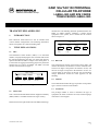
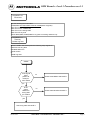
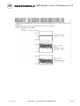
1
StarTAC130 (GSM)
The World’s Leading Cellular
Telephone Manufacturer
Service Manual
GSM StarTAC130 PERSONAL
CELLULAR TELEPHONE
Service Manual
Ver 1.0
StarTAC130 CELLULAR TELEPHONE
COMPUTER SOFTWARE COPYRIGHTS
The Motorola products described in this instruction manual may include copyrighted Motorola computer programs stored in semiconductor memories
or other media. Laws in the United States and other countries preserve for Motorola certain exclusive rights for copyrighted computer programs,
including the exclusive right to copy or reproduce in any form the copyrighted computer program. Accordingly, any copyrighted Motorola computer
programs contained in the Motorola products described in this instruction manual may not be copied or reproduced in any manner without the express
written permission of Motorola. Furthermore, the purchase of Motorola products shall not be deemed to grant either directly or by implication, estoppel,
or otherwise, any license under the copyrights, patents or patent applications of Motorola, except for the normal non-exclusive, royalty free license to
use that arises by operation of law in the sale of a product.
PERFORMANCE SPECIFICATIONS - StarTAC130 (GSM)
GENERAL
Frequency Range
Channel Spacing
Number of Channels
Modulation
Transmitter Phase Accuracy
Duplex Spacing
Frequency Stability
Voltage Operation
Transmit Current
Dimensions
Size (Volume)
Weight
Temperature Range
890-915 MHz Tx
935-960 MHz Rx
200 kHz
124 carriers with 8 channels per carrier
GMSK at BT = 0.3
5 Degrees RMS, 20 Degrees peak
45 MHz
+/- 0.10 ppm of the downlink frequency (Rx)
+3.9 to +6.0V dc (battery)
<225 mA typical (DTX on at 50%)
140 mm (L) x 50 mm(W) x 27 mm(D) with battery
157 cubic cc
Approximately 170g; includes 650mAh NiMH battery
-20°C to +55°×C
TRANSMITTER
RF Power Output
Output Impedance
Spurious Emissions
33 dBm +/- 2dB
50 ohms (nominal)
-36 dBm up to 1 GHz, (<-30 dBm > 1 GHz)
RECEIVER
RF Level
RX bit error rate (100 kbits)
Channel Hop Time
Time to Camp
-102 dBm
< 2%
500 microseconds
Approximately 10 seconds
SPEECH CODING
Speech Coding Type
Regular Pulse Excitation / Linear Predictive Coding with Long Term Prediction. (RPE
LPC with LTP.
Bit Rate
Frame Duration
Block Length
Classes
Bit Rate with FEC Encoding
13.0 kbps
20 ms
260 bits
Class 1 bits = 182 bits. Class 2 bits = 78 bits
22.8 kbps
Specifications subject to change without notice
CAUTION
Do not jump start vehicle or use an automotive battery charger while the vehicle adapter
option and the portable radiotelephone are connected to the vehicle electrical system as this
may cause serious damage to the radio. Disconnect the radio by removing the cable kit fuses.
© Motorola ECSG 1998
ii
Service Manual
2/3/99
Cellular Subscriber Group
GSM StarTAC130 PERSONAL
CELLULAR TELEPHONE
SECTION 1 - GENERAL
FOREWORD
MOTOROLA SERVICE POLICY
GENERAL SAFETY INFORMATION
CONTENTS LIST
PAGE NUMBER
xii
xii
xiii
SECTION 2 - LABELLING & SIM CARDS
TRANSCEIVER LABELLING
INTRODUCTION
TITLE EXPLANATIONS
SIM CARDS
INTRODUCTION
SIM CARD INSERTION/REMOVAL
SECURITY INFORMATION
1
1
1
3
3
3
3
SECTION 3 - MANUAL - TEST MODE & VERIFICATION
MANUAL-TEST MODE
INTRODUCTION
TEST SIM INSERTION/REMOVAL
ACCESSING THE MANUAL-TEST MODE
VERIFICATION
INTRODUCTION
EQUIPMENT CONFIGURATION
TESTING PROCEDURE
5
5
5
5
7
7
7
8
SECTION 4 - PERSONALITY TRANSFER
PERSONALITY TRANSFER
INTRODUCTION
NORMAL TRANSFER
MASTER TRANSFER
9
9
9
10
© Motorola ECSG 1998
2/3/99
iii
StarTAC130 CELLULAR TELEPHONE
MASTER SIM CARD CREATION
10
SECTION 5 - DISASSEMBLY
DISASSEMBLY INSTRUCTIONS
INTRODUCTION
RECOMMENDED TOOLS
DISASSEMBLY PROCEDURE
ASSEMBLY PROCEDURE
EXPLODED DIAGRAM
MECHANICAL PART LIST
11
11
11
11
11
18
19
Service Manual
iv
2/3/99
StarTAC130 CELLULAR TELEPHONE
FOREWORD
1. SCOPE OF MANUAL
2. MODEL AND KIT IDENTIFICATION
This manual is intended for use by experienced technicians
familiar with similar types of equipment. It contains all
service information required for the equipment described and
is current as of the printing date. Major changes which occur
after the printing date are incorporated by Cellular Manual
Revisions (CMR). These CMR’s are added to the manuals
as the engineering change is incorporated into the equipment.
Motorola equipments are specifically identified by an overall
model number on the nameplate. In most cases, assemblies
and kits which make up the equipment also have kit model
numbers stamped on them. When a production or
engineering change is incorporated, the applicable schematic
diagrams are updated.
MOTOROLA SERVICE POLICY (StarTAC130)
Warranty:
Product will be sold with the standard 12 months warranty terms and conditions. Accidental damage, misuse, retailers
extended warranties will not be supported under warranty. Non warranty repairs will be available at agreed fixed repair
prices. Proof of purchase will be required to validate warranty claims.
Core Product:
A low cost service strategy (To be agreed with the European Customer Service Managers now called the “Lo tier Loaner
program”) will be available. The customers original telephones will be repaired but not refurbished as standard.
Alternatively the product may be supported under the current Express Exchange program as operated by local Service
Organisations.
Appointed Motorola Service Hubs will perform warranty and non warranty field service for level 2 (assemblies) and level
3 (limited pcb component). The Motorola HTC centres will perform level 4 (full component) repairs.
Customer support (End User):
Customer support (End User) will be available through dedicated Call Centres and In Country Help Desks.
Product Service training should be arranged through the local Motorola National Support Centre.
REPLACEMENT PARTS ORDERING
ORDERING INFORMATION
Only centres authorized by Motorola to carry out repairs will be able to purchase spare parts. Orders for spare parts from
HUB’s, Motorola National Support Centres and Hi-Tech Centres, should be placed with the appropriate Motorola Parts
Distribution Centre.
BOARD REPAIRS
All centres authorized to carry out module level repairs, must return faulty boards to the appropriate HUB or Motorola
Hi-Tech Centre for repair to component level.
Service Manual
v
2/3/99
CONTENTS
GENERAL SAFETY INFORMATION
PORTABLE OPERATION:
DO NOT hold the radio so that the aerial is very close to, or touching, exposed parts of the body, especially the
face or eyes whilst transmitting. The radio will perform best if it is held in the same manner as you would hold
a ‘land’telephone handset, with the aerial angled up and over your shoulder.
DO NOT operate the portable phone in an aircraft. Switch off your telephone. The use of a cellular telephone
in an aircraft may be dangerous to the operation of the aircraft, disrupt the Cellular Network, and is illegal.
Failure to observe this instruction may lead to a suspension or denial of Cellular Telephone Service to the
offender, or legal action, or both.
MOBILE/PORTABLE OPERATION - Telephone use in Vehicles:
All equipment must be properly grounded according to installation instructions for safe operation.
Users are advised to turn off their equipment when at a refuelling point.
Safety is every drivers business. Cellular telephones should only be used in situations in which the driver
considers it safe to do so.
GENERAL:
DO NOT allow children to play with any radio equipment containing a transmitter.
DO NOT operate this equipment near electrical blasting caps or in an explosive atmosphere. Mobile telephones
are, under certain conditions, capable of interfering with blasting operations. When you are in the vicinity of such
work, look out for and observe signs cautioning against mobile radio transmission. If transmission is prohibited,
you must turn off your mobile telephone to prevent any transmission.
In standby mode the mobile telephone will automatically transmit to acknowledge a call if it is not turned off.
Refer to the appropriate section of the product user manual for additional pertinent safety information
All equipment should be serviced only by a qualified technician.
Service Manual
2/3/99
vi
Cellular Subscriber Group
GSM StarTAC130 PERSONAL
CELLULAR TELEPHONE
TRANSCEIVER LABELLING
1.
INTRODUCTION
LABELLING AND SIM CARDS
TRANSCEIVER LABELLING
therefore the units labelling should be updated with the new
IMEI. An IMEI uniquely identifies a mobile station
equipment to the system, and is divided into the sections
shown in Figure 2.
Each Motorola GSM transceiver will be labelled with
various number configurations. The following information
shows and explains the common labelling titles
2.
2.3
IMEI 15 digits
TITLE EXPLANATIONS
The Mechanical Serial Number (MSN) is an individual
number, uniquely identifying the unit. The MSN will remain
the same throughout the units life, even if the main board is
replaced. Because the MSN is unique to the whole phone, it
is often used for logging and tracking purposes by Motorola
National Service Centres on EPPRS. The MSN is divided
into the sections shown in Figure 1.
MSN 10 digits
MC
Model
Code
1 digit
OC
Origin
Code
2 digits
DC
Date
Code
4 digits
6 digits
FAC
SNR
SP
Serial
Number
Spare
Final
Assembly
Code
1 digit
Figure 2. IMEI Configuration
2.5
REV S/H
This configuration consists of two blocks of two digits, and
denotes the software and hardware versions within the unit.
The first two digits correspond to the software version, and
the last two digits correspond to the hardware version. If a
version update is carried out on the unit, the corresponding
change information should be made apparent on the
labelling.
SNR
Serial
Number
Figure 1. MSN Configuration
2.6
MODEL
The model number defines the type of product. Each product
type is issued a common model number.
2.7
2.4
2 digits
TAC
Type
Approval
Code
MSN
3 digits
6 digits
PACKAGE
CEPT GSM
This is the International Mobile Station Equipment Identity
(IMEI) number. The IMEI is held in the logic circuitry.
The package number is used to determine the type of
equipment, the mode in which it was sold, and the language
with which it was shipped.
If the main board is replaced then the units IMEI will change,
© Motorola ECSG 1998
2/3/99
1
StarTAC130 CELLULAR TELEPHONE
*
PAGE INTENTIONALLY BLANK
Service Manual
2
2/3/99
Cellular Subscriber Group
SIM CARDS
1.
INTRODUCTION
The Motorola StarTAC130 personal cellular telephones are
designed to work with the mini Subscriber Identity Module
(SIM). The SIM card contains all the personal data required
to access GSM services. Data held by the SIM card
includes:•
•
•
•
•
•
International Mobile Subscriber Identity
Temporary Mobile Subscriber Identity
Home system
Services subscribed to
PIN and unblocking codes
Call barring codes
The SIM card may also be capable of storing phone
numbers, names, and messages.
2.
SIM CARD INSERTION/REMOVAL
The SIM card must be inserted into the unit correctly so that
the card can be read, and the data checked for validity,
before operation on the system will be enabled. The card
contains all of the user’s personal identification numbers
and details of the system the phone operates on.
GSM StarTAC130 PERSONAL
CELLULAR TELEPHONE
LABELLING AND SIM CARDS
side of the phone.. To remove the SIM card from the unit,
pull the sliding mini SIM tray sideways away from the
phone. The User Guide contains full information about
inserting and removing the mini SIM card.
3.
SECURITY INFORMATION
To stop unauthorized personnel using your SIM card, the
option of using a Personal Identity Number (PIN) is
available. When enabled the option requires (on power up) a
verification number to be entered via the unit’s keypad,
before the card can be used. Three attempts to enter the
correct PIN may be made. If after the three entries the correct
PIN has not been entered, the card becomes blocked. To
unblock the card an unblocking/super PIN code must be
entered. Ten attempts to enter the correct unblocking code
are permitted, if after ten attempts the correct code has not
been entered, the SIM card is corrupted and becomes useless.
Another option available for the SIM card is call barring. If
subscribed to, the call barring of incoming and/or outgoing
calls may be accomplished by entering a special key
sequence. The key sequence includes a “barring code”,
which determines the type of restriction incorporated, and a
password to validate the request. The initial password is
provided when you subscribe to the service. The password
can be changed by entering a set key sequence.
A valid miniature sized SIM card can be used in any working
GSM transceiver, regardless of the manufacturer, which is
compatible with the miniature size SIM card. To protect the
actual unit from unauthorized use, a lock function on the
hardware is available. When enabled, this function requires
that a three or four digit unlock code be entered, via the unit’s
keypad, before normal operation of the transceiver can take
place. The lock code can be changed by entering a set key
sequence.
Note: Further information on set key sequences can be
derived from the unit’s user guide.
Figure 1. Inserting the Test SIM card
The miniature SIM card is placed in the tray and the tray slide
into the side of the phone. There is only one way for the
miniature SIM to fit because of the .shape of it. The tray
should be completely and secuerly seated in the slot on the
© Motorola ECSG 1998
2/3/99
3
StarTAC130 CELLULAR TELEPHONE
*
PAGE INTENTIONALLY BLANK
Service Manual
4
2/3/99
Cellular Subscriber Group
GSM StarTAC130 PERSONAL
CELLULAR TELEPHONE
MANUAL-TEST MODE
and removing the SIM card
MANUAL-TEST MODE
1.
INTRODUCTION
The Motorola StarTAC130 personal cellular telephones are
equipped with a manual-test mode capability. This
capability allows service personnel to take control of the
telephone, and by entering certain keypad sequences, make
the telephone perform desired functions. To enter the
manual-test mode, a Test SIM card (Part No 8102430Z02,
punchout centre)) is required.
2.
TEST SIM CARD INSERTION
REMOVAL
The Test SIM card must be inserted into the unit correctly to
access manual-test mode; this should not be a problem
because the card can only fit in one way. Place the mini SIM
card in the tray and slid it into the phone.
3. ACCESSING THE MANUAL-TEST
MODE
When the Test SIM card is in place, power up the telephone.
Once the initial automatic ‘wake up’ sequence has taken
place correctly, depress the # key (on the units keypad) for
three seconds. After three seconds ‘TEST’should appear in
the display, indicating that the unit is now in the manual-test
mode. Table 1 below shows the available manual-test
commands and their corresponding results.
Command
Table 1
Result
01#
Exit manual-test mode
19#
Display call processor s/w version
20#
Display modem s/w version
22#
Display speech coder s/w version
57#
Initialize non-volatile memory
58#
Display security code
58xxxxxx#
Change security code
59#
Display lock code
59xxx#
Change lock code
60#
Display International Mobile station
Equipment Identity (I.M.E.I.)
Note: If a customer should forget the security code in their
unit, it can only be read or changed by using a Test SIM card.
Figure 1. Inserting the Test SIM card
To remove the SIM card from the unit, pull the mini SIM
tray sideways away from the phone.
The User Guide contains full information about inserting
© Motorola ECSG 1998
2/3/99
5
StarTAC130 CELLULAR TELEPHONE
*
PAGE INTENTIONALLY BLANK
Service Manual
6
2/3/99
Cellular Subscriber Group
GSM StarTAC130 PERSONAL
CELLULAR TELEPHONE
VERIFICATION
G.S.M. COMPATIBLE
COMMUNICATIONS ANALYSER
StarTAC
c
MENU
ok
1
2
3
4
5
6
7
8
9
RF IN/OUT
PORT
0
MR
M+
Figure 1: Testing Configuration
VERIFICATION
1.
INTRODUCTION
To test an StarTAC130 cellular telephone, to verify whether
or not the unit is functioning correctly, the following equipment will be required:• G.S.M. compatible communications analyser.
• Test adaptor (Part No SKN4858A), and appropriate
cable/connectors.
• Test SIM card (Part No 8102430Z02).
2.
EQUIPMENT CONFIGURATION
Initially insert the test SIM card into the tray of the personal
cellular telephone. If required, further information on SIM
card insertion is available on page 13. Attach the antenna
adaptor to the botton connector of the phone. Slide a charged
battery on to the back of the personal telephone, so that the
telephone can be powered up. Finally, connect a cable from
the test adaptor to the RF in/out port of the communications
analyser, and power both the analyser and personal
telephone on. The equipment set up shown in Figure 1
should now be in place.
• Charged battery pack.
© Motorola ECSG 1998
2/3/99
7
StarTAC130 CELLULAR TELEPHONE
3.
TESTING PROCEDURE
All information required to perform the desired tests and measurements should be obtained from the communication analyser’s
user manual.
Ensure that the unit being tested is capable of both initiating a call to the analyser, and receiving a call from the analyser.
Confirm that the displayed Temporary Mobile Subscriber Identity (TMSI), International Mobile Equipment Identity (IMEI),
and dialled number are correct. When a call is in progress the following tests should be carried out on channels 1, 62 and
124. The recorded results must be within the acceptable stated limits, if the unit being tested passes all the tests it should be
taken as functioning correctly. If the unit being tested fails to conform with any of the expected measurements, it should be
taken as faulty and repaired accordingly. The following table states the required tests and tolerances.
TEST TO BE PERFORMED
LOWER LIMIT
UPPER LIMIT
Transmit average phase error (RMS) at peak power
5
Transmit average phase error (Peak) at peak power
20
Transmit average frequency error at peak power
-90 Hz
+90 Hz
Transmit power error at level 5 (33 dBm)
-2 dB
+2 dB
Transmit power error at level 7 (29 dBm)
-2 dB
+2 dB
Transmit power error at level 10 (23 dBm)
-3 dB
+3 dB
Transmit power error at level 15 (13 dBm)
-3 dB
+3 dB
Transmit amplitude negative peak flatness
-1 dB
Transmit amplitude positive peak flatness
+1 dB
Transmit amplitude envelope at -28 us
-70 dB
Transmit amplitude envelope at -18 us
-30 dB
Transmit amplitude envelope at -10 us
-6 dB
Transmit amplitude envelope at 556 us
-6 dB
Transmit amplitude envelope at 564 us
-30 dB
Transmit amplitude envelope at 574 us
-70 dB
Receive Bit Error Test for Class II Residual (at -102 dBm)4
2%
Receive Frame Erasure Rate for RES II (at -102 dBm)4
0.12%
Note: 1. The transmit average test values should be derived from 10 separate readings.
2. The receive signal strength for transmit measurements should be -85 dBm.
3. The receive test values should be derived from the reception of 20K bits of data.
4. There is approximately 1.8dB loss between the antenna port and the RF SMA connector on the test adaptor. The test
specifications are written for the power levels AT THE ANTENNA.
Service Manual
8
2/3/99
Cellular Subscriber Group
PERSONALITY TRANSFER
1.
GSM StarTAC130 PORTABLE
CELLULAR TELEPHONE
PERSONALITY TRANSFER
Step 4.
While data transfer is taking place between the
unit and the card, ‘Please Wait’ will be
displayed. After a short period of time, if the
data transfer has been completed correctly,
‘Clone’ will re-appear in the donor unit’s
display.
Step 5.
When the first data block has been successfully
uploaded, remove the card from the donor.
Step 6.
Insert the Transfer card into the slot located on
the back of the recipient unit. Turn the recipient
unit on, the display should show ‘Clone’.
Step 7.
The recipient unit is now in the cloning mode,
and ready to receive the first block of data.
Step 8.
Enter 03# via the unit’s keypad. This command
will cause the recipient unit to download the first
data block from the Transfer card.
Step 9.
While data transfer is taking place between the
card and the unit, ‘Please Wait’ will be
displayed. After a short period of time, if the
data transfer has been completed correctly,
‘Clone’ will re-appear in the recipient unit’s
display.
Step 10.
The second data block must now be transferred.
Repeat steps 1 to 9, but enter 022# to program
the second data block into the Transfer card.
Step 11.
The third data block must now be transferred.
Repeat steps 1 to 9, but enter 025# to program
the third data block into the Transfer card.
Step 12.
When the third block of data has been
transferred successfully, remove the Transfer
card and check the repaired radio functions
correctly. See page 19 for further information.
INTRODUCTION
Personality Transfers are required when a phone is Express
Exchanged or when the main board is replaced. The
different variations (languages, features) of the StarTAC130
personal cellular telephones requires that each main board
must be configured correctly to ensure that the unit takes on
the correct personality required. Therefore, when a main
board is replaced its personality must be transferred into the
new board, so that it functions correctly in the customers
unit. There are two possible methods of transfer.
• Normal Transfer, and;
• Master Transfer
If the defective unit powers up, then the Normal Transfer
method should be followed. If the faulty unit will not power
up, then a Master transfer will be required to configure the
replacement board, once installed.
2. NORMAL TRANSFER
This method allows the personality, selected features and
stored phone numbers of a defective radio, to be transferred
into a repaired radio. Data is transferred from the donor unit
into the recipient unit using a Transfer card (Part No
5104025D03). The instruction steps should be followed in
order.
Step 1.
Insert the Transfer card into the slot located on
the back of the donor unit. Turn the donor unit
on, the display should show ‘Clone’.
Step 2.
The donor unit is now in the cloning mode, and
ready to transfer the first block of data.
Step 3.
Enter 021# via the unit’s keypad. This command
will cause the first block of information to be
uploaded into the Transfer card.
© Motorola ECSG 1998
2/3/99
9
StarTAC130 CELLULAR TELEPHONE
3.
MASTER TRANSFER
This method of transfer should only be followed when the
defective unit will not power up, or complete a Normal
Transfer. As mentioned earlier, there may be different
variations (OEM looks for example) of the Motorola
StarTAC130 cellular telephone, each model requiring the
main board to be configured differently for correct
operation. When carrying out a Master Transfer it is not
possible to transfer the customers selected features or stored
phone numbers, only the model personality can be
programmed into the repaired unit.
Each different version of the StarTAC130 cellular
telephone, requires its own Master Transfer card which
contains essential set up information. Master SIM cards may
be ordered pre-programmed, or created from a Normal
Transfer card. The instruction steps should be followed in
order.
Step 1.
Select the required Master SIM card.
Step 2.
Insert the Master Transfer card into the slot
located on the back of the repaired unit. Turn the
unit on, the display should show ‘Clone’.
Step 3.
Enter 03# via the unit’s keypad. This command
will cause the configuration data to be
downloaded from the Master Transfer card.
Step 4.
Step 5.
While data transfer is taking place between the
card and the unit ‘Please Wait’ will be
displayed. After a short period of time, if the
data transfer has been completed correctly,
‘Clone’ will re-appear in the recipient unit’s
display.
At no point should either 021#, 022# or 025# be entered
while a Master Transfer card is in the radio. If either of the
stated commands are entered, the master information on the
card will be erased. To prevent the above happening the card
can be locked by entering 06# via the unit’s keypad, with the
card inserted. Unlock the card by entering 07#.
Note:
4.
MASTER SIM CARD CREATION
When required a Master SIM card can be created by:Step 1.
Insert a Transfer card into a unit which is
already configured in the desired way. Turn the
unit on, the display should show ‘Clone’.
Step 2.
Enter 024# via the unit’s keypad. This command
copies the personality information in the unit
onto the Transfer card to create a Master
Transfer card.
Step 3.
While data transfer is taking place between the
unit and the card ‘Please Wait’ will be
displayed. After a short period of time, if the
data transfer has been completed correctly,
‘Clone’ will re-appear in the recipient unit’s
display.
Step 4.
A Master Transfer card has now been created.
Lock the card to prevent accidental information
erasure (see previous section). Remove the card
from the unit, and store until required.
When the data block has been transferred
successfully, remove the Master Transfer card
and check the radio functions correctly. See
page 18 for details.
68P09304A82-O
Service Manual
10
If during either transfer process a problem arises, an
error message will be displayed. If the Transfer card
is removed before the data transfer is completed
‘Bad Data on Card’ will appear in the display. If
either situation arises, the process should be
repeated.
st130trans.fm
1/9/97
2/3/99
Cellular Subscriber Group
GSM StarTAC130 PORTABLE
CELLULAR TELEPHONE
DISASSEMBLY
DISASSEMBLY INSTRUCTIONS
1.
INTRODUCTION
Reasonable care should be taken during the disassembly and
reassembly of the unit in order to avoid damaging or stressing
the housing and internal components. Ensure that a properly
grounded high impedance conductive wrist strap is used
while performing these procedures on electronic units.
• Dental pick
• Tweezers
3.
The following information describes the procedure for
removing and accessing various parts of the StarTAC130
NOTE
CAUTION
Many of the integrated circuit devices used in this
equipment are vulnerable to damage from static
charges. Ensure that adequate static protection is
in place when handling, shipping, and servicing
the internal components of this equipment.
2.
RECOMMENDED TOOLS
The following tools are recommended for use during the
assembly/disassembly of the StarTAC130.
DISASSEMBLY PROCEDURE
Refer to the mechanical exploded view on page
18, as necessary, while performing the
disassembly/assembly procedures.
4.
ASSEMBLY PROCEDURE
Once the unit is disassembled and the repair is carried out it
then becomes obvious that to assemble the unit, the
procedure is the reverse of that previously completed for
disassembly.
• Anti-Static Mat Kit 0180386A82; includes:
— Anti-Static Mat 66-80387A95
— Ground Cord 66-80334B36
— Wrist Band 42-80385A59
• Plastic Bladed Tool SLN7223A
• Housing prying tool SYN5367A
• Antenna tool SYN5179A
© Motorola ECSG 1998
2/3/99
11
StarTAC130 CELLULAR TELEPHONE
1
2
Figure 1 .
Use the antenna tool to remove the antenna.
Turn counterclockwise until the antenna is free
from the housing.
With flat surface of tool facing up, insert
housing opener at 45 angle. Make sure you can
see top of tool in seam.
GSM StarTAC130 Cellular Personal Telephone Disassembly Procedure
Service Manual
12
2/3/99
DISASSEMBLY
3
4
Figure 2 .
Press and push corner outwards with left thumb
while right hand twists phone lika a rag..
After phone has started to open, lift antenna well to
release entire side..
GSM StarTAC130 Cellular Personal Telephone Disassembly Procedure
Service Manual
2/3/99
13
StarTAC130 CELLULAR TELEPHONE
5
6
Figure 3 .
Using the plastic prying tool, slide under
housing all the way to corner and lift housing
With flat surface of tool facing up, insert
housing opener at 45 angle. Make sure you can
see top of tool in seam.
GSM StarTAC130 Cellular Personal Telephone Disassembly Procedure
Service Manual
14
2/3/99
DISASSEMBLY
7
8
Figure 4 .
Use index finger, pull housing off going
straight across the phone.
Open the flex connector and pull out the flex.
GSM StarTAC130 Cellular Personal Telephone Disassembly Procedure
Service Manual
2/3/99
15
StarTAC130 CELLULAR TELEPHONE
9
With your thumbs, pry the side tabs away from board assembly
to allow it to be easily removed. Staring at the top of the board,
lift the board assembly out of the front housing.
10
Figure 4 .
Remove the display board from the main PCB.
GSM StarTAC130 Cellular Personal Telephone Disassembly Procedure
Service Manual
16
2/3/99
DISASSEMBLY
11
12
Figure 5 .
Using a dental pick, remove the adhesive strip
of the base of the phone
Using tweezers, press the hinge pin button in and over towards the
middle of the flip. Also, move the hinge pin section above the button
towards the middle of the flip. Remove the flip by pulling up on the
hinge pin side and out on the other side.
GSM StarTAC130 Cellular Personal Telephone Disassembly Procedure
Service Manual
2/3/99
17
StarTAC130 CELLULAR TELEPHONE
3
4
9
1
10
6
7
5
8
2
11
Service Manual
18
2/3/99
DISASSEMBLY
REPLACEMENT PARTS LIST
REF.
NUMBER
1
2
3
4
5
6
7
8
9
10
11
PART No.
S8332A
SYN6812A
0109279U03
0109280U02
0104866Z03
6104522Z02
4003745K01
3803882K01
7209257T02
8509098E01
4709050R01
5509242E01
3709068T01
0509440M01
5009135L07
0509133T01
0509441M01
DESCRIPTION
Spare Xcvr Number (SWF2952)
Display Board
Front Housing
Rear Housing
Assy Flip
Lens
Keypad Mylar
Keypad Plastic
LCD Display
Antenna
Shaft Right
Hinge
Tube Antenna
Mic Grommet (Not shown)
Microphone (Not shown)
Display Grommet (Not shown)
Alert Grommet
Service Manual
2/3/99
19
StarTAC130 CELLULAR TELEPHONE
*
PAGE INTENTIONALLY BLANK
Service Manual
20
2/3/99
Accessory Product Information
Standard DSP Handsfree Car Kit
for StarTAC™
P/N:
HFK9200
EAN Code :
5025322019542
Content :
(1) SYN4974
TRN5502
SYN6900
(2) SYN6348
(3) SSN4018
(4) SMN4097
SKN4834
SKN4937
SYN6967
SJN8205
StarTAC Hang Up Cup
Bracket for HUC
HUC Adapter for StarTAC 130
Hands Free Electronic Box
External Speaker
Directional Mic w/Angle
Power Cable 6 PIN
Cable Fuse & Mounting Hardware
Ferrite Bead Kit
Multilingual Install & User Manual
Description:
The HFK9200 is a professional install handsfree car kit for the StarTAC models with improved full duplex
performances. The HFK9200 uses the latest Digital Signal Processor (DSP) technology for high quality audio,
and includes all basic handsfree components, hang up cup, DSP HF box, speaker, directional microphone, and
cables.
Key DSP Features:
- Superb full digital audio quality and clarity even at high driving speeds
- Improved full duplex audio allowing genuine two-way conversation
- Digital noise cancellation filtering out background noise
- Digital echo cancellation eliminating local and network echo es
Standard Features:
- Full hands-free capability for comfort and safety communication while driving
- Direct RF connection to external antenna, for better coverage
_______________________________________________________________________________________________
- Directional microphone
HFK9300.DOC
August 98
- Intelligent rapid charge
- Programmable safety timer
StarTAC DSP Car Kit - Installation Diagram
_______________________________________________________________________________________________
HFK9300.DOC
August 98
GSM Krunch - Level 3 Procedure vers.1.1
NOTE 1=Check that the mentioned
componets are not physically
damaged, have no dry joints, and are
positioned correctly or missing, if none
of the mentioned problems are
apparent, replace the defective
componets.
If the problem is still apparent send the
PCB to HTC
START
Does the
phone pwr
up from
main
battery?
no
Go to supplement 1
page 4
no
yes
remove main batt. and insert aux batt.
Does the
phone pwr
up from aux
battery?
no
Go to supplement 1
page 4
yes
no
reinsert main battery
no
Does the
phone is
properly
communicating
with SIM card?
Go to supplement 21
page 21
yes
Is the battery
selection ok
(press the
keys:arrow,4)?
Priority aux
no
Go to supplement 2
page 4
no
yes
Does the phone
draw current
from
main/aux/ext b+
when is off?
yes
no
Remenber to read ERROR
CODE 7100# in test mode
Go to supplement 22 page 26
TOOLS
1) Main battery or dummy
2) Aux battery or dummy
3) Ext.B+ 5V
4) Test card
5) Test set analyser
6) GOOD PCB RF/LOG, PCB
DISPLAY, FLIP ASSY to comparison
7) GSMKEY SOFTWARE
8) ERSA station solder
03/05/1999
Does the
phone pwr
up and stay
on with ext
B+ only?
yes
no
Go to supplement 3
page 5
yes
no
Does the
phone pwr
dw when
twisted?
yes
Go to supplement 4
page 4
1
- MOTOROLA CONFIDENTIAL PROPRIETARY -
Page 1
GSM Krunch - Level 3 Procedure vers.1.1
1
Does phone
pwr up with
PCB display
and stay on?
no
Go to supplement 5
page 27
yes
Does the
display show
phone failure
see supplier?
yes
Go to supplement 6
page 28
no
Do the keys
of the
keypad
work?
no
Go to supplement 7
page 9
Remenber to
CHECK CR432
yes
Does the phone
go into service
at -102dBm/ NO
AGC, BER2
GATE 22?
yes
Does the phone
initiate a call to
the analyser/
NO TX GATE
22?
no
Go to supplement 8
page 10
Main VCO repair page 13
Go to supplement 9
page 14
no
Go to supplement
12/BIS page 18
yes
Terminate the call
Does the
led service
work?
no
Go to supplement 10
page 17
yes
Call PCB from analyser
yes
Is ring
tone/vib
rator
audible?
Answer call
no
Go to supplement 11
page 17
no
Go to supplement 23
page 27
vibrator
2
03/05/1999
- MOTOROLA CONFIDENTIAL PROPRIETARY -
Page 2
GSM Krunch - Level 3 Procedure vers.1.1
2
Is the frequency
error/ NO AFC
GATE 22 within
specification?
no
Go to supplement
12/12BIS page 18
yes
Is theTX
phase error
within
specification?
no
Go to supplement 13
page 29
yes
Is the tx
power,burst
within
specification?
no
Go to supplement 14
page 30
yes
no
Is the tx
audio(mike)
path ok?
yes
Go to supplement 15
page 19
no
Is the rx
audio path
ok?
Go to supplement 16
page 20
yes
Terminate the call
Does the
radio show
invalid
battery?
no
Is the low
battery
indication
correct?
yes
Problem/update with
this document
should be directed
to
donato.reguzzoni@
motorola.com
Is the
battery
charger ok?
yes
Go to supplement 17
page 38
no
Go to supplement 18
page 21
no
Go to supplement 19
page 22
yes
Does the
display/Real
time clk work
no
Go to supplement 20
page 21
yes
The end
03/05/1999
- MOTOROLA CONFIDENTIAL PROPRIETARY -
Page 3
GSM Krunch - Level 3 Procedure vers.1.1
Supplement 1
No pwr up main/aux
batt.
1) Check the main battery contact flip, B+ no shorting to vibrator, the flex and J601
2) Check the aux battery contact on the PCB and on the rear h.
NO SHORT
Supplement 2
Battery selection
1) It's important to use the paint battery select schematics enclosed on page 24-25.
2) It is recommended to start from the gates of Q999,Q1008 and go back to the inputs.
3) It's likely to the faulty components are NOR logic ports (U904,908,909),NOT(U907),Dual diode Schottky
(CR607,608,606).
4) Attention at WATER DAMAGE problem.
5) Attention at Zener diode burned as VR901(8.2V), CR904-CR1001-CR999(6.8V)
Supplement 4
PCB only
Pwr dwn/twisted
Check Y201 main cristal and NOTE 1
(Check 13MHz with osc.scope probe U703 BIC at pin 17 ifit pwr dw hitting )
03/05/1999
- MOTOROLA CONFIDENTIAL PROPRIETARY -
Page 4
GSM Krunch - Level 3 Procedure vers.1.1
Supplement 3
PCB only
No pwr up
Set the voltage of power supply 5V
Supply the PCB via ext.conn J600
See diagrams on GSM
Startac/COSMO Lev.4 procedure
No PWR UP
START
Does the
PCB draw a
lot of current
and also
does the
alert buzz?
Is L275 short
to ground(Use
an "Ohm"
meter to
measuare the
terminal of
C902 or 903)
yes
no
yes
Use a power
supply (2.75V,
150mA).
Supply C902 at
terminals and
check the hot
component.
It's likely to micro
DCA or
C751-753-754-755
(0.047uF)
no
Try to connect
the PCB on
to emmibox
if the
See diagrams
GSM
PCB
reblow the appropiate
SW from it
Startac/COSMO
Lev.4 procedure
(see the
status
No led
PWR
UP only)
no
Is 4.73V
voltage DC
present at
U900
GCAP pin
40
no
Check the PCB ext.conn.J600 socket CR903 and NOTE 1
yes
Pull up the w.dog by shorting the pads TP10 - TP1
Are U900 GCAP voltage ok(use Osc.scope)?
Attention at the tantalio capacitor(orange) polarity.
1) Vswitch at C915= 5.6V (NO RIPPLE, it cause the alert
buzz if it's present replace C915)
2) R475 at C906= 4.75V
3) L500 at C901= 5V
4) Vref at C803= 2.75V( it isn't present in the figure)
5) L275 at C902/903= 2.75V
6) R275 at C908= 2.75V
no
Check U900 GCAP and
NOTE 1
3
03/05/1999
- MOTOROLA CONFIDENTIAL PROPRIETARY -
Page 5
GSM Krunch - Level 3 Procedure vers.1.1
3
Is 13MHz
master clk
present at
U703 BIC pin
17?
(see page 32)
no
Check in order Y201, CR201,
U201 and NOTE 1
yes
Is 13MHz
master clk
present at
U703 BIC pin
37 (see page
32)
no
See the 13MHz path logic block
diagram
yes
no
Is 2.75V
present at pull
up resistors
terminals
R702-706-701
Check the resistors and note 1
yes
Does TP4
reset line go
high and Is
the reset
sequence ok?
(see page 23)
no
Check L275 at pull up resistor R920 terminals.
If the reset is about 200mV lifted in order the following pin:
1) GCAP pin 30 (it's likely to faulty IC)
2) SMOC pin 98
3) BIC pin 35
4) J101 display conn.
If the reset line is alays low send the PCB in HTC
yes
4
03/05/1999
- MOTOROLA CONFIDENTIAL PROPRIETARY -
Page 6
GSM Krunch - Level 3 Procedure vers.1.1
4
Is CE
signalling(one
clk cycle
1/13MHz=77nS)
present at TP11
U702
Falshprom?
(see page 32)
no
Check U702 and NOTE 1.
If there isn' t L275 voltage send
the PCB to HTC
yes
Is CE
signalling
present at
U703 BIC
pin 19?
no
Micro DCA or U702 problem.
If there isn' t L275 voltage send
the PCB to HTC
yes
Are the signal below present at U705 EEPROM?
no
1) pin 7 L275 opereting voltage
2)pin 27 CE (active low) see page 33
3) pin 6 WR (active low)
4) pin 1 OE ( active low)
5) Access time 300nS
Check U704 and NOTE 1.
If there isn' t L275 voltage send
the PCB to HTC
yes
Is DATA BUS
D0:D15 logic
signalling
correct?
( e.i. Quick check
at U705
EEPROM pin 26
D15, see page
33)
no
You can usually have twice problems:
1) BUS Conflict ( when two peripheral stay in low
impedence in the same time)
2) The wrong Falling Edge transition CMOS level
(See the example in attached on page 21-22)
3) Check the J101display connector for any short circuit.
yes
5
03/05/1999
- MOTOROLA CONFIDENTIAL PROPRIETARY -
Page 7
GSM Krunch - Level 3 Procedure vers.1.1
6
Are the
MDM_WR and
_RD signalling
present at U500
SMOC pin 100,
4?
(see page 33)
no
During initial radio power-up the SMOC IC performs
power on self test diagnostic to confirm that the
HW is operational.
If any of the diagnostic tests fail, an error code will
be sent in the first reply message sent to call
processor.
Check in order the following signals :
MDM_WR,SPI CLK, SPI MOSI(micro DCA problem)
MDM_RD, SPI CLK, SPI MISO( SMOC problem).
(See the example in attached on page 33)
yes
1) If all the above looks good, and the PCB is still not
turning on, try to resolder U702,U704,U705 with ERSA
station, if the PCB turns on, then shut down, go to
immediately in test mode to read the error code and
subcode.
2) Try to lift the EEPROM U705 and check if the PCB
(pwr up) communicate with emmibox.
If so, you read the internal info(sw,modem, speech) from
the RAM with GMSKEY.
(e.i. If the error code is 7100#02=Ext ram error,there
were some dry joint at Sram pins )
03/05/1999
- MOTOROLA CONFIDENTIAL PROPRIETARY -
Page 8
GSM Krunch - Level 3 Procedure vers.1.1
Supplement 7
PCB only
No keypad operation
START
no
Is 2.75V
voltage
present at
S3 buttom
volume
pin2
yes
It is likely that there is a short circuit
under the J101 and NOTE 1
no
pin 2
Press the buttom volume
(don't realese it)
Is present
now one
pulse low
at S3
pin 2
no
If there are two pulses low there is a
short circuit under J101 and NOTE 1
yes
Release the buttom volume
Is still present
one pulse low
or 2.75V
voltage only
at S3 pin 2
yes
Check J101NOTE1 after
Sent to HTC
It's likely to DCA micro problem
no
Check J101 and NOTE 1
03/05/1999
- MOTOROLA CONFIDENTIAL PROPRIETARY -
Page 9
GSM Krunch - Level 3 Procedure vers.1.1
Supplement 8
PCB only
No rx
1) Innject into ext.antenna port of the PCB a 947.4MHz signal at -20dBm
2) With the PCB in test mode press the following keys sequence 45062#
3) Use the PCB TEST to comparison
4) ATTENTION : The mesaures of the signal can be change with
differents PROBES and CABLES.
START
Remenber to check ANT. SW. components for bad positoined or
missing:
CR432 diode pin, R1128, C1043
Poor RX= reduce the battery stand by
Does the
BER,
RX_Quality
-Level fail on
CH1-62-124?
no
Attention:
The root cause could be the strong interferencies
due to the closeness to the BS (base station) .
yes
Is the IF
signal
215MHz
-8dBm ok at
L401 terminal
(see page 36)
no
Go to A
page11
yes
Are the
signals ok
RXI,RXQ at
U201 pin
46,48
Is the
signal
IQREF
1.38V at
U201pin 47
no
no
Check U500 pin 21 and
NOTE 1
yes
yes
Is the signal
ok at
L.O.430MHz
at U201 pin
40
(see page 36)
Check U201(pin
43=2.25V)
CR431.L433 and
NOTE 1.
no
no
yes
Check bias Q203,Q202, GIFSYN
U201 and NOTE 1.
5
03/05/1999
- MOTOROLA CONFIDENTIAL PROPRIETARY -
Page 10
GSM Krunch - Level 3 Procedure vers.1.1
5
Change the signal
generator at
-100dBm, press
25000#(AGC),
240#(step att.).
Are the signals
RXI,RXQ ok at
U201 pin 46,48(see
diagramm page 39)
no
Check L431,C432(filter matching)
and U201 GIFSYN and NOTE 1
yes
Are data
activity
present (NO
TEST MODE)
at U500 pin
1,3,11 SPI
BUS
no
Check bias U500 and NOTE 1
If the spi bus is ok, reset the radio and try to
rephase via GATE 22 .
If it's still no service replace U500 SMOC
yes
From A
page10
Is the
signal
947.4MHz
ok at U401
pin 4
no
Check C442 and J600
and NOTE 1
yes
Is the
signal
947.4MHz
ok at U401
pin 5
no
Is
RX275=2.75V
ok at Q446
emitter
yes
Check U401and NOTE 1
no
yes
Is
RX275=2.75V
ok at Q446
emitter
no
Check bias Q203,Q202 and
GIFSYN U201pin and NOTE
6
03/05/1999
- MOTOROLA CONFIDENTIAL PROPRIETARY -
Page 11
GSM Krunch - Level 3 Procedure vers.1.1
6
no
Is the
signal
947.4MHz
ok at C407
terminals
Check FL452 and NOTE 1
yes
Is the
signal
947.4MHz
ok at Q418
collector
Check bias Q418 and
NOTE 1 .
no If the collector of Q418
B=1.33V
isn't supplied by
RX275 check L412, if
the base of Q418 isn't
E=0.6V
supplied by RX_EN
check L413
Q418
LNA
C=2.7V
yes
no
Is the main
VCO signal
732.4MHz
ok at C411
terminals
Main VCO repairs page 13
yes
Is the IF
signal
215MHz ok
at Q420
collector
yes
Check bias Q420
and NOTE 1 .
no If the collector of
Q420 isn't supplied
by RX275 check
L414, if the base of
Q420 isn't supplied
by RX_EN check
L410
Is the IF
signal
215MHz ok
at C421
terminals
yes
Q420
mixer
E=0.6V
C=2.7V
no
Check FL420 and NOTE 1
yes
Is the IF
signal
215MHz ok
at Q421
collector
B=1.3V
no
Check bias
Q421 and
NOTE 1.
If the collector
of Q421 isn't
supplied by
SW_VCC check
at U201 pin 33
B=0.7V
E=0V
Q420
iso
amp.
C=2V
Go to start RX page10
03/05/1999
- MOTOROLA CONFIDENTIAL PROPRIETARY -
Page 12
GSM Krunch - Level 3 Procedure vers.1.1
Main VCO repair
START
Is
superfilter
voltage
2.55V ok at
U201 pin
21
no
Check
C211,C212,Vref=2.75V,Q202,Q203,R475=4.75V
at U201 pin 11,44 and NOTE 1
yes
Is charge
pump
voltage
2.38V at
U201 pin
23
no
1)Check the CP_OUT voltage range at GIFSYN pin 23.
CH001= about 2.19V
CH062= about 2.64V
CH124= about 3.08V
2) If the voltage is alawys low check C208,C237 and
after resolder the Main VCO.
3) If the voltage is always high(CH1,062,124) try to
resolder the Main VCO if the problem still the same
could be the coil layer.
yes
Is prsc_in
voltage
1.4V at
U201 pin
26
no
Check U201 and NOTE 1
yes
Resolder Main VCO
03/05/1999
- MOTOROLA CONFIDENTIAL PROPRIETARY -
Page 13
GSM Krunch - Level 3 Procedure vers.1.1
supplement 9
PCB only
No tx
With the PCB in test mode press the following keys sequence:
11062# CH or 110062#CH PHASE II,1215#PWR CONTINUOS,40#SENDING ONLY 1
See page 37
START
Does the
PCB power
down in tx
with test
comand
yes
Is the
signal ok
902.4MHz
ok at Q303
base
Remove R1126:
NO B+ IPA
NO B+ Q303
no
Go to A
page15
yes
Replace IPA
no
Is the
signal ok
902.4MHz
ok at U401
pin 4
yes
Check C442, J600and NOTE 1
no
Is the
signal ok
902.4MHz
ok at U401
pin 2
yes
Is the
TX_EN
2.6V
voltage at
Q442 pin 2
ok
no
Check bias Q501 only
yes
no
Check U401and NOTE 1
Is the
signal ok
902.4MHz
ok at U301
pin 7
yes
Is B+
present at
Q301 pin
5,6,7,8
yes
Check bias IPA (pin
15,14,13,12,4= B+, after
replace IPA
no
no
Check Q301,Q1019 and
NOTE 1
7
03/05/1999
- MOTOROLA CONFIDENTIAL PROPRIETARY -
Page 14
GSM Krunch - Level 3 Procedure vers.1.1
7
Is the
signal ok
902.4MHz
ok at Q303
base
yes
Check bias Q303 DRIVER and
NOTE 1
B=0.6V
no
Q303
driver
from A
page14
Is the
signal ok
902.4MHz
ok at C304
terminals
no
C=B+
E=0V
Check TX_Attenuator and CR390 and bias of the PAC IC
and NOTE 1
Remenber you can check the signals below with:
11062#, 1205, 310#(time slot random)
( see page 34 35)
yes
GND
14
1
237mV
RF feedback
SAT_DECT 2.68V
feedback to SMOC
GND
PAC IC
U310
TX_EN 2.65V
from Q501
DET_DECT 923mV
PWR step 12-15= 1V
PWR step 11-05= 0V
Check
236mV
R354(dry joint or missing)
Check
R354
TX_EN 2.65V
from Q501
TX_KEY 2.75
239mV
0.012V
( NO TX= about 2.2V)
7
8
EXC. 920mV
(NO TX = about 1.9V)
AOC 240mV
from SMOC
check L501
on this line
( NO TX= about 850 mV)
8
03/05/1999
- MOTOROLA CONFIDENTIAL PROPRIETARY -
Page 15
GSM Krunch - Level 3 Procedure vers.1.1
8
Is the signal
170MHz at
U300 pin 4
ok
(see page
35)
no
Check:
1) Bias U300 TIC
2) TX_VCO( CR300, C306)voltage range as above and NOTE 1.
If the volage is always high the problem could be the coil layer.
Remenber you can check the signals below with:
11062#, 1205, 310#
yes
MAIN VCO
732_4MHz
14
1
R275=2.75V
from C908
GND
GND
R275=2.75V
from C908
TIC IC
U300
170MHz
Is
L.O.340MHz
signal at
U201 pin 8
ok
(see page
35)
yes
Are the
TXI(pin
63,64) and
TXQ(pin
61,62)signals
into U201
correct?
TX_ VCO
902.4MHz
GND
GND
R475=4.75V
from C906
GND
R475=4.75V
from C906
DMCS=2.7V
from Q502
7
no
Check pin 10=1.9V of U201and
CR203,L203 and NOTE 1
8
CP_OUT 2.6V
to CR300
CH001= about 1.76V
CH062= about 2.20V
CH124= about 2.72V
yes
Check U201, IQ_filter L440-C221
and NOTE 1
no
Check U500 and NOTE 1
03/05/1999
- MOTOROLA CONFIDENTIAL PROPRIETARY -
Page 16
GSM Krunch - Level 3 Procedure vers.1.1
supplement 10
led service
Use the following test command:
ATTENTION: the reed switch must be closed(with a magnetic)
541# Turn on the RED led
542# Turn on the GREEN led
543# Turn on the orange leds
540# Turn off any leds
Check Q903,Q904, R909,R908 for dry joints or missing resistors only
supplement 11
PCB only
No/low ring alert
With the PCB in test mode press the following keys seguence:
432# tone into ring alert
481000# 1KHz tone
4707# volume
or
1539# ring alert
START
Is the signal
1KHz
present at
U500 pin
49 or C825
no
Check U500 SMOC and NOTE 1
yes
Is the
signal
1KHz tone
at ring alert
pin Vswitch
no
Check U900 GCAP and NOTE 1
yes
Check ring alert and NOTE 1
03/05/1999
- MOTOROLA CONFIDENTIAL PROPRIETARY -
Page 17
GSM Krunch - Level 3 Procedure vers.1.1
supplement 12
PCB only
Freq. error out spec.
Replace in order Y201 Main cristal, CR201 varicap
Remenber: you can check the AFC DAC line range with the test comand 260000# 568mV 264095# 2.6V at
U500 SMOC pin 38 or 11062#CH 26xxxx# 0000-4095 AFC 1215#PW 41#sending 1(no work Krunch
platform) o 40#sending 0 )
supplement 12
NO AFC - NO TX GATE 22
Check the shape of GSMK ( Gaussian Minimum Shift Keying )
11062# CH
1205# MAX PW
310# TIME SLOT RANDOM
GOOD MODULATION
BAD MODULATION
Possibile root cause:
1) Bad TX_VCO spurios(dry joint, bad coil layer)
2) Bad R475 voltage( C906 broken, bad polarity,
unsoldered)
3) Bad R275 voltage(C908 broken, unsolder)
4) Bad DM_CS from Q502( bad bias, track
damage)
5) Bad Q303 amplifier(bad bias, bad coil layer)
03/05/1999
- MOTOROLA CONFIDENTIAL PROPRIETARY -
Page 18
GSM Krunch - Level 3 Procedure vers.1.1
supplement 15
PCB only
No mike
With the PCB in test mode press the following keys seguence:
434# Audio into speaker
36# loop back
4707# volume
Audio distorted: check the components missing(R802,C815) around GCAP
START
Is signal
ok at
U900 pin
10
no
Check in order :
1 Mike
2 The solder of J802
3 C810 (may be broken)
4 Check mic_bias= 2.17V at C812
5 Check GCAP and NOTE 1
yes
Is the
signal
present
at U500
pin 45
no
Check C816
yes
Check U500 and NOTE 1
03/05/1999
- MOTOROLA CONFIDENTIAL PROPRIETARY -
Page 19
GSM Krunch - Level 3 Procedure vers.1.1
supplement 16
PCB only
No/low audio
from U500 SMOC to GCAP
START
Is the audio
present at
J600 pin 9
Audio_out(
press volume
buttom)?
no
yes
Is the
DW_LINK
voltage
4.55V
present at
J600 pin 12?
Check DW_link Bus( sense level of ext. accessory) at J600 pin 12:
1) None 4.55V ( if it's low 4.2-4V check DW_link line, possibile
faulty comp. C762 0.010uF)
2) Headset 1.5V OK
no
yes
With the PCB in TEST MODE press the following keys seguence:
434# tone into speaker
or
430# tone handsfree external speaker, mike - analog audio(J600)
481000# 1KHz tone
4707# volume
Audio distorted: check the components missing(R802,C815) around GCAP
Is the
signal
1KHz
present at
U500 pin
49
no
Check the voltage VAG-ref 1.38V at C1030 - C560
Check U500 SMOC and NOTE 1
yes
no
Is signal
1KHz tone
present at
J601pin7,8
Check U900 GCAP and NOTE 1
yes
Check the FLEX of the flip
03/05/1999
- MOTOROLA CONFIDENTIAL PROPRIETARY -
Page 20
GSM Krunch - Level 3 Procedure vers.1.1
supplement 18
Incorrect low
batt.indication
Quick check
Staus phone Supply(V) Batt.icon
Root case
Pwr up
The thermistor is Check therm. Line
Main batt. Always full
Remedy
discharger charger indicatornot connect
Check in order:
1) Flex the radio via Emmictrl or or master card
2) Rephase the Main battery and Aux batt. via GATE 22
3) Use the dummy battery to check the battery indicator
4) If the problem remains check U703( reliable IC) and NOTE 1
5) Check the ANT.SW. components(CR432, R1128, C1043) for missing bad positioned( Poor Rx )
6) Check the Cell Broadcast -Frequency of Serch (Reduce the stand by battery).
7) Check for no B+ contact shorting to vibrator.
8) Does the phone draw current when is off?
supplement 20
RTC
Check in order:
1) In test mode press 88# (display current time and date) after repress 88# and check if the seconds are
increase
2) Ckeck the flip flex
3) If the problem remains check Y701 32KHz xtal and NOTE 1
supplement 21
SIM card
Check in order:
1) The SIM card J900 unsolder or bent pins.
2) The present detect switch by shorting the pin 1, 8 of the J900 if the display show "Check Card" the
problem is the card read circuit.
3) In test mode press 38#(activate sim) and check the signal SIM_VCC 5V (from U902) , SIM_CLK
3.25MHz,SIM_I_O
4) 39# Deactivate sim
03/05/1999
- MOTOROLA CONFIDENTIAL PROPRIETARY -
Page 21
GSM Krunch - Level 3 Procedure vers.1.1
supplement 19
No/Incorrect internal battery
charging
Quick check
Status phone
Supply(V) Problem
Batt. Icon
In charger mode Ext.b+
The display doesn't Not appear
Main batt. show charging batt.
Pwr up
Ext.b+
Disappear
Main batt.
With the PCB in test mode press the following keys:
500128# Driver internal charger MAIN BATTERY
501128# Driver internal charger AUX BATTERY
50000# OFF
If the current stay in 0 or maximum check R602
Root case
Remedy
The thermistor is Check therm.line
not connected
The thermistor is Check therm.line
not connected
This is a 8700 example
START
Is there the
voltage
present at
U900
pin17
no
Did the
voltage go
low at
Q601 pin
4
no
Check U703 BIC and NOTE 1
yes
yes
Does B+
present at
Q1002 pin 1
Q1005 pin 1
Check U900 GCAP and NOTE 1
no
Check Q601,CR605 and NOTE 1
yes
See diagram of battery internal
charger to debug the problems
03/05/1999
- MOTOROLA CONFIDENTIAL PROPRIETARY -
Page 22
GSM Krunch - Level 3 Procedure vers.1.1
RESET SEQUENCE AT POWER ON
The power up RESET sequence is described in the following diagram. Following the activation of the
+2.75V Regulator, the GCAP LITE IC and the 68338 begin a seven state power sequence involving the
*RESET line and the GCAP Lite’s Watchdog input. The figure below depicts the sequence of the states.
The figure is not drawn to scale.
State 1
When the GCAP LITE IC detects a power on request (ON/OFF Line ”LOW”), the GCAP LITE will drive
the system *RESET line low. The 68338 Clock line will take approximately 100mS to stabilize after power
is applied.
State 2
The 68338, SMoC, and BIC in the radio are connected to the *RESET line. The nominal time *RESET is
held low by the GCAP LITE is 250 milliseconds +/- 50 ms.
State 3
When the GCAP LITE releases *RESET, it is pulled high by an internal resistor. There isa period of
approximately 500 nanoseconds when neither the GCAP LITE or 68338 is asserting *RESET.
State 4
When the 68338 reset control logic detects that the system *RESET line is no longer being driven, it drives
it low for an additional 512 cycles (39.6 microseconds). This assertion of *RESET by the 68338 is a feature
of the IC and cannot be modified.
State 5
When the 68338 releases *RESET, it is pulled high by the internal resistor. The 68338 be-gins executing its
Boot Code. If valid code is present, the RESET vector in the radio code is then executed. The Boot Code
runs for about 512 cycles (39.6usec) before this new vector is executed.
State 6
The 68338 holds *RESET low for 50usec during this state (an internally generated RE-SET).
State 7
When the 68338 releases *RESET, it is again pulled high by the internal resistor. All the processors in the
system, including the 68338, then begin execution. During this state, the 68338 must drive the GCAP Lite’s
03/05/1999
- MOTOROLA CONFIDENTIAL PROPRIETARY -
Page 23
GSM Krunch - Level 3 Procedure vers.1.1
Input: EXT_B+
Input: L_BATT (main battery)
Input: AUX_BATT (auxiliary battery)
03/05/1999
- MOTOROLA CONFIDENTIAL PROPRIETARY -
Page 24
GSM Krunch - Level 3 Procedure vers.1.1
Input: L_BATT + AUX_BATT + EXT_B+
Input: L_BATT + AUX_BATT
03/05/1999
- MOTOROLA CONFIDENTIAL PROPRIETARY -
Page 25
GSM Krunch - Level 3 Procedure vers.1.1
supplement 22
Display internal info
In Test Mode press:
7100# = Error Code
7101# = Subcode
In Test Mode read:
01= CPU EXCPTION ERROR (upgrade last vers. sw+flex+57#)
00 =
02 = EXT. RAM ERROR ( check for dry joints )
03 = MODEM ERROR
01 = BAD MODEM ID ( check for dry joints 13MHz,SPI BUS )
03 = MODEM ERROR
04 = RUN TIME BAD ID
04 = MODEM ERROR ( replace it)
05 = SPEECH CODER PWR FAILURE
01 = SPCH TIMED OUT
05 = SPEECH CODER PWR FAILURE
02 = SPEECH BAD ID ( check for dry joints )
06 = EXEC ERROR DETECT(upgrade last vers. sw+ flex+57#)
01 = OUT OF MEMORY
07 = EEPROM ERROR(flex+57#)
01 = CHECKSUM ERROR
07 = EEPROM ERROR
02 = SUBSIDY LOCK
07 = EEPROM ERROR
03 = DALLAS PART ERROR
07 = EEPROM ERROR
05= SIM RESET FAILURE
08 = MMI PWR DOWN
03 = PWR BUTTOM HIT
08 = MMI PWR DOWN
04 = LOW BATTERY
03/05/1999
- MOTOROLA CONFIDENTIAL PROPRIETARY -
Page 26
GSM Krunch - Level 3 Procedure vers.1.1
supplement 23
No/weak vibrator
In test mode press the following keys 1590# activity vibrator.
Check in order:
1 The improper assembly vibrator
2 The flip flex
3 The J601 conn. pin 9
4 Use a test pcb display(vib_driver is on pcb display)
START
yes
Is the
voltage
2.75V
present at
J101 pin
28
no
Check VIB_EN at J101 pin 26,
PCB DISPLAY and note 1
Check J601 for dry joint or missing resistors
Supplement 5
PCB only
No display
Before to start check, via emmibox with GSMKEY simulator or Emmictrl programms, the correct matching
between the SW and the PCB Display ( Grafic / Two Line) and reflex the PCB
Missing line use 993# turn on all pixel in display
Does the wake tone audible? If yes this means that the PCB is on and trouble is located at comunications
display
START
yes
Is -5V
at U901
pin 3
Check the J101 connector and NOTE 1
Check Q104, Q102 for dry joints only
no
Check U901 and polarity of C921,C920 and NOTE 1
03/05/1999
- MOTOROLA CONFIDENTIAL PROPRIETARY -
Page 27
GSM Krunch - Level 3 Procedure vers.1.1
Supplement 6
Phone fail see
supplier
Go to in test mode and press 7100# to read the error code or use GSMKEY simulator or Emmictrl
programms via emmibox .
Error code
05=Speech coder failure
03=Modem error
20#=00.00(no SMOC version)
Before replace the Modem verify the points below:
1 No dry joints
2 13 MHz clk input at terminals of U500 pin 40
3 RF_V1 at U500 pin 35 (from Q203)
4 All pins of U500 connect to L275
5 Verify activity at SMOC U500 SPI BUS,MDM RD WR
Error code
07=Eeprom error
Reflex the PCB via emmibox or master
card, 57#.
If the problem persist send to HTC
Error code
07=Eeprom error
Subcode
03=Fail code if Dallas part PRESENT on the PCB
Place the unit in test mode and enter 57#
If the problem persist the unit is valid failure.(sent to HTC)
03/05/1999
- MOTOROLA CONFIDENTIAL PROPRIETARY -
Page 28
GSM Krunch - Level 3 Procedure vers.1.1
supplement 13
PCB only
Phase error out
spec.
ATTENTION: It's necessary to reproduce the exactly conditions
between the GATE 22 and yours working bench.
(e.i. Voltage power supply 3.6V ,cable loss etc..)
START
Answer the following questions:
1) Did the phase fail on CH001, CH062, CH124?
2) Did the phase fail at low or max PWR?
3) Did the phase fail at 4.4V or 3.5V?
4) Did the frequency error within specification?
Are the
TXI(pin
63,64) and
TXQ(pin
61,62)signals
into U201
correct?
yes
Check U201 and NOTE 1
no
Check U500 and NOTE 1
03/05/1999
- MOTOROLA CONFIDENTIAL PROPRIETARY -
Page 29
GSM Krunch - Level 3 Procedure vers.1.1
supplement 14
Tx pwr burst out
spec.
ATTENTION: It's necessary to reproduce the exactly conditions between the GATE 22
and yours working bench.
(e.i. Voltage power supply 3.6V ,cable loss etc..)
Answer the following questions:
1) Did the TMK fail on CH001, CH062, CH124?
2) Did the TMK fail at low or max PWR?
3) Did the TMK fail at 4.4V or 3.5V?
4) Did the frequency error within specification?
Before to comparison, set the cable loss to 0dBm of GATE 22, rephase the power PA DAC
only and after try to do a call processing.
Compare the signals of IPA, PAC( components missing around PAC), MODEM ( AOC line
U310 pin 8 R501, L501 ) with a GOOD PCB and NOTE 1
03/05/1999
- MOTOROLA CONFIDENTIAL PROPRIETARY -
Page 30
GSM Krunch - Level 3 Procedure vers.1.1
03/05/1999
- MOTOROLA CONFIDENTIAL PROPRIETARY -
Page 31
GSM Krunch - Level 3 Procedure vers.1.1
13MHz IN BIC IC pin 17
13MHz OUT BIC IC pin 37
CE U702 TP11
03/05/1999
- MOTOROLA CONFIDENTIAL PROPRIETARY -
Page 32
GSM Krunch - Level 3 Procedure vers.1.1
CE U705 pin27
DATA BUS D15 U705 pin 26
MDM_WR SMOC pin 100
MDM_RD SMOC pin 4
First reply sent to Micro
03/05/1999
- MOTOROLA CONFIDENTIAL PROPRIETARY -
Page 33
GSM Krunch - Level 3 Procedure vers.1.1
AOC PAC IC pin 8
from SMOC.
BURST
SAT_DET PAC IC pin 12
feedback to SMOC
MAX PWR STEP 05
SAT_DET( saturation detect)
AOC( automatic output control)
MIN PWR STEP 15
SAT_DET( saturation detect)
AOC( automatic output control)
03/05/1999
- MOTOROLA CONFIDENTIAL PROPRIETARY -
Page 34
GSM Krunch - Level 3 Procedure vers.1.1
MAX PWR STEP 05
ACT(active loop) PAC IC pin 9
AOC( automatic output control)
L.O. 340MHz
U201 pin 8
170MHz
U300 pin 4
03/05/1999
- MOTOROLA CONFIDENTIAL PROPRIETARY -
Page 35
GSM Krunch - Level 3 Procedure vers.1.1
IF 215MHz
U201 pin 31
L.O. 430MHz
U201 pin 40
03/05/1999
- MOTOROLA CONFIDENTIAL PROPRIETARY -
Page 36
GSM Krunch - Level 3 Procedure vers.1.1
TX 110062# 1215# 40#
TX 110062# 1205# 310#
03/05/1999
- MOTOROLA CONFIDENTIAL PROPRIETARY -
Page 37
GSM Krunch - Level 3 Procedure vers.1.1
supplement 17
Invalid battery
Check in order:
0) Does the radio show invalid battery with both batteries?
1) The flip flex and the rear h.contacts (batt. serial data)
2) 49x# x=0-3 data main battery
3) 49x# x=4-7 data aux battery
4) J601 pin 11 main battery
5) J60 aux battery
6) Remove Q609 (from GSM STARTAC85 experience) and reanswer 0 question, after remove Q610.
7) See the diagram Initialization Procedure " Reset and Presence Pulse" page 31
Initialization Procedure"Reset and Presence Pulse"
490#
SCI_TX Q607 pin
1
Master TX "Reset Pulse"
500uS
03/05/1999
Master RX "Presence Pulse"
Main battery
100uS
- MOTOROLA CONFIDENTIAL PROPRIETARY -
Page 38
GSM Krunch - Level 3 Procedure vers.1.1
RX_Q GIFSYN IC pin 48
CH 62 -100dBm
Q_signal U201pin 48
I_signal U201pin 46
90°
03/05/1999
- MOTOROLA CONFIDENTIAL PROPRIETARY -
Page 39
GSM Krunch - Level 3 Procedure vers.1.1
03/05/1999
- MOTOROLA CONFIDENTIAL PROPRIETARY -
Page 40
GSM Krunch - Level 3 Procedure vers.1.1
03/05/1999
- MOTOROLA CONFIDENTIAL PROPRIETARY -
Page 41
GSM Krunch - Level 3 Procedure vers.1.1
03/05/1999
- MOTOROLA CONFIDENTIAL PROPRIETARY -
Page 42
M. Denzin
February 26 1998
Version 1.2
GSM KRUNCH RF BLOCK DIAGRAM
Motorola Confidential Proprietary
RX: 935 - 960 MHz
TX:890 - 915 Mhz
RX SENS: -102 dBm
TX Power: +33dBm
DUAL ANT
MATCH
T/R & RF SWITCH
ANT->TX = -0.6 dB
ANT->RX =-0.6 dB
SW_RF->TX = -1.7dB
SW_RF->RX = -1.7 dB
ISOLATION:
TX- > RX: 25 dB
RX -> TX: 25 dB
TX
MATCHING
NETWORK
SAW RX FILTER 1
925-960MHz -3.5dB
915MHz -25dB
980MHz -29dB
630MHz -65dB
2SC4784
BIPOLAR MIXER
G = 12 dB
NF = 4.0 dB
IP3 = -2 dBm
I=5.0mA
2SC4784
BIPOLAR LNA
G = 13 dB
NF = 1.8 dB
I = 5.5 mA
GIFSYN_IC
5109632D92
215 MHz
ISOLATION AMP
SAW FILTER G = 7 dB
BW(2dB)
NF = 5 dB
= 200 kHz
IP3 = -20 dB
G = -6 dB
PRE-AMP
RX
T/R Switch
5109572E04
NF = 17 dB
IP3 = -27 dBm
SW_RF
B
STRIPLINE
IL= 1.2dB
NF = 13 dB
I3 = 10 dBm
A
-5V
AGC PROCESSOR
3 POLE
1
TX EN
RF START
BW CTRL
QUAD
GEN
GATE
RX2.75V
Pout = -3 dBm
SBN = -140 dBc/Hz @ 800kHz offset
DISCRETE LO
INJECTION FILTER
720 - 745 Mhz
G = -3.5 dB
GIMAGE = -20 dBm
IQ REF
ADAPT
TIMING
25 dB
STEP
SW_VCC=2.55V
T/R & RF SWITCH
CONTROL CIRCUITRY
RXI 0.83Vp-p
1.38 Vdc
4 POLE
REG 1
BAT
SAV
REG 2
TEST
PHASE
DET
÷2
÷N
÷8/9
÷2
÷A
CHARGE
PUMP
LOOP
FILTER
LATCH
PLL VCC
430 MHz
TANK
CKT
SFOUT=2.55V
RX EN
SUPER
FILTER
-10V
CHARGE
PUMP
20 dB coupler
IL = 0.2 dB
720 - 745 MHz
@ -24dBm
890-915MHz
@ -24dBm
TX KEY
DET
ACT
PHASE
DET
LOOP
FILTER
DET SW
÷16/17
170 MHz
@-24dBm
LOOP
FILTER
÷A
ACCUM 2
EXC
AOC DRIVE
0 - 1.9
V_REF=2.75V
13 MHz
TEMP COMP
DAC
REF OSC
DCLK
AFC DAC
0 55 2 475
13 MHz
÷13
DELAY
ACCUM 1
CHARGE
PUMP
TANK
CKT
8 dB
PAD
÷5
N
ADDER
1 BIT
ADDER
340 MHz
CHARGE
PUMP
PHASE
DET
÷N
A
ADDER
Translational IC
5109632D90
PAC IC
5109632D91
SAT DET
LOOP
MAIN VCO
AND BUFFER AMP FILTER
720 - 745 Mhz
I = 13 mA
RXQ 0.83Vp-p
1.38Vdc
PHASE
DET
NUMERATOR
& OFFSET MPX
÷2
SPI RF CLK
SHIFT REGISTER
SPI RF DATA
÷N
÷N
330mVp
1.38 Vdc
QUAD
GEN
TXI
TXIX
IQ LPF
ENABLE
TXQX
ENABLE
TXQ
R2.75
V
PA_B+
MOD ENB
3 POLE HARMONIC
FILTER
IL= 0.2dB
-5 to -1.5v NEG LEVEL
SHIFTER FOR
PA CONTROL
2 STAGE
GaAs IPA
G = 21 dB
Eff = 55%
MRF949
DRIVER
Po=12dBm
I=40mA
IQ FILT2
4dB PAD
ENABLE
DMCS
TX VCO
890 - 915 MHz
Po = 12 dBm
I= 25 mA peak
nDMCS
+4.80V
TX_EN
FLASH
8M (512Kx16)
48-CSP
L275
Call Processor 68338
196 BGA
L275
RAM
1M (64Kx16)
48-CSP
EEPROM
64K (8Kx8)
28 TSOP
SIM
CPU32
L275
BIC 4.1
(64 TQFP)
ROM_CS
RAM_CS
BIC_CS
R/W
ROM2_CS
BIC_CS
R/W
Address (20)/Data (16) buses
DP_EN
DP_ON_OFF
SC_CS
LED_RED/LED_GREEN (2)
Display/Keypad
DB7-DB4
-10V
KEYPAD (8)
Port
E/F
uProcessor
Interface
SIM SCI
Interface
L500
*PWR_SENSE
217HZ
D/A
SFS
SCK
TXAUD
RXAUD
Timer
Clock
Control
Audio
Interface
L275
BComp
RxDn
RxDp
TxD
DOWNLINK
DSC bus
drive
L500
UPLINK
L500
SIM_RST
SIM_DATA_OUT
SIM_DATA_IN
SIM_CLK
SIM_PD
SIM_VCC
Buffer
13_DCLK
13MHZ
SIM
card
reader
A/D
8 Channels
DSC_EN_B
UPLINK
DOWNLINK
DM_CS
SC_INT
TX_KEY
RXACQ
MDM_INT
CH_FRM
MSTR_FRM
RF_START
TR_SW
RF_MUTE
TX_ON_OFF
217HZ
RTC RAM
SCK
MOSI
MISO
QSPI
MDM_RD
MDM_WR
RF_CS
SCI
LOC
*RESET
AUD_EN1
AUD_EN2
BL_CNTL
AUDIO_IN_BIAS
*RESET
CTM6
TXD
RXD
SIM Control
BIC_IRQ
MF_IRQ
WDOG_CP
13_DCLK
QSM
(Level Shift)
ON/OFF_SENSE
-10 V Reg.
DSC_EN
Mode1
DSC bus
interface
DACOUT
L275
L275
AUDIO_IN
MAN_TEST
EXT_B+
BATT_FDBK
AUDIO_OUT/ON_OFF
*RESET
ON/OFF_SENSE
*PWR_SENSE
R/W
SC_CS
ON/OFF
SC_INT
GSM_DCS
SMOC CONTROL (10)
RF CONTROL (5)
DACOUT
THERMISTOR
B+_SENSE
BATT_SENSE
BATT_FDBK
PNP
Pass
13MHZ
ON/OFF
R475
GCAP
48 TQFP
Osc
B+
Nominal
3.6V
Battery
Bias, Ref
BATT+
Charger
Control
Circuitry
Lithium
Compatible
EXT_B+
DS2401
Serial
ROM
Vswitch
Ear
piece
L2.75
Vswitch
Regulator
VREF
R475
VL
L500
V1
Ext_audio
Rx_audio
Mic
Audio_In
Record
VA_CS
SPI_SCK
VA_MI
VA_MO
(From CP)
VAG
Aud
Cntl.
VA
28 TSOP
R275
Neg
Bias
SMOC
100 TQFP
CPU
PTD
Volume
Control
Viterbi HW
Co-processor
Echo
Cancellor
ROM
&
RAM
VSELP
Support HW
GMSK
Call Processor
Interface
(QSPI)
Audio Control
Mic
Aux Mic
Ext Mic
Spkr (Rx_audio)
Var.
Gain
Codec
Var.
Gain
Ext_audio
VAG
GSM ZAP Digital Block Diagram
Motorola Confidential Proprietary
13MHz_Ref
RXACQ
MDM_INT
Playback
PLL
TXKey
*DM_CS
MISO
MOSI
SCK
RF_CS
MDM_WR
MDM_RD
VAG
MIC
DM_CS
VCTRL 1-3
(From CP)
Alert
Ref
RSSI
L275
L275
Logic
To RF Section
13_DCLK
B+
Logic
RxI
A/D
TxI
D/A
RxI
TxQ
D/A
TxQ
RxQ
A/D
RxQ
AFC
D/A
AGC
D/A
AFC
Ref
Transmit
Power Control
D/A
Tone
Generator
DLC 8/10/95
12 May 97
TxI
RF_SPI
RF_SCK
AGC
Step_AGC
IQRef
AOC_In
AOC_Out
Sat_Det
Det_Sw
EXT Connector
GSM KRUNCH AUDIO LOGIC BLOCK DIAGRAM
SPI_RFCS
SPI_MOSI
EEPROM
U705
to U710
RAM2_CS
DAC_OUT
THERM
BATT_SENSE
to U710
*RESET
ADDRESSS / DATA BUS
External
Bus
Interface
SCI_TX
SCI_RX
FLASH
U702
uBGA
Q602
RS232_TX
RS232_RX
RS232
SWITCH MATRIX
MDM_WR
MDM_RD
BATT_SER_DATA
B+
MDM_WR
DM_CS
SPI_RFCS
SPI_MISO
SPI_MOSI
SPI_SCK
SPI_DATA
SPI_CLK
AFC
CLK13_IN
AOC
DET_SW
SAT_DET
64
63
98
38
40
39
14
15
17
CPU
Interface
45
CODEC
MIC_AUD_IN
21
Transmit
Power
Control
D/A
2
-
RS232_TX
7
RS232_RX
2
SW_RF ( EXT ANT )
AUDIO_IN
9
AUDIO_OUT
4
BATT_FDBAK
14
EXT_B+
49
Buffer
Ampl.
RX_AUDIO
L_BATT+
Audio
Filter
GMSK
2.8Vpp
100ns / cm
RAM1_CS
2.8Vpp
100ns / cm
RAM2_CS
2.8Vpp
100ns / cm
ROM1_CS
2.8Vpp
100ns / cm
THERM
BATT_GND
23
21
TXQ_P
TXQ_M
TXI_P
TXI_M
RXI
IQ_REF
22
RXQ
Vswitch DC/DC
40
28
RF
AL
22
RF
32, 41
AL
Part
Number
# press 2 sec.
Enter Manual Test Mode
01 #
Exit Manual Test Mode
AL800
Alert
5009473S01
Q501
Transistor TX_EN
4809607E05
07 #
Mute Rx Audio Path
08 #
Unmute Rx Audio Path
Q601
Power Transistor Chrg Line
4809579E17
Transistor BATT_FDBACK
LINE
4809939C04
09 #
Mute Tx Audio Path
10 #
Unmute Tx Audio Path
11 #
Program Main Local Osc. to Channelbb
J101
Display Connector
2809454C02
R602
Resistor for ISENSE
0680195M64
12 #
Set Tx Power level to fixed valure
J600
EXT/Butt Plug Connector
0909449B04
T902
Choke / Switched Supply
2503788S08
19 #
Display SW Version Number of Call Processor
J601
Flexprint Connector
0909059E01
U500
SMOC IC
5199332C04
20 #
Display SW Version Number of Modem
22 #
Display SW Version Number of Speech Coder
25 #
Set Continuous AGC
J802
MIC Connector
0909195E01
U703
BIC IC
51097463E13
MIC
Microphone
5009135L07
U900
GCap IC
5109632D75
From CPU (U701) to display, via connector J101.
1. Processor selects to enable display. When high, the display is enabled and low disabled.
2.8Vpp
100ns / cm
SMOC Interface. This is a signal from uP (U701) to SMOC (U500).
1) This is a 20ms timing signal from U701 which times the decoding and encoding function of the SMOC
U500.
From BIC to uP. This signal interrupts the uP for a number of reasons.
1. Keypad detection
2. Power Sense
3. SIM Functions
4. DSC Bus Status Indicators
UPLINK
2.8Vpp
10us / cm
From butt plug (J600) to BIC chip (U703).. This is a comms link from an external peripherale and the phone,
and could be either data information or speech information. It is also used to sense the presence of a DHFA and
the ignition status of the DHFA with DC levels
DOWNLINK
5Vpp
10us / cm
From BIC chip (U703) to butt plug (J600).. This is a comms link from an external peripherale and the phone,
and could be either data information or speech information. It is also used to sense the presence of a DHFA and
the ignition status of the DHFA with DC levels
CLK_13_IN
1.6Vpp
50ns / cm
AUDIO OUT
press a key
From GIF Syn to BIC IC - 13MHz clock..
This is the master clock reference required for the radio
test mode
08#, 10#, 36#
434#, 477#
2.7Vpp
5us / cm
External audio from butt plug, directly to SMOC IC
test mode
08#, 10#, 36#
434#, 477#
2.8Vpp
5us / cm
External audio from SMOC via FCAP to butt plug
RX SIGNAL PATH
L275
TX SIGNAL PATH
R475
2.8Vpp
5us / cm
CLK_AUD
MAIN VCO SIGNAL PATH
This signal is from the BIC to the SMOC
It is a timing signal and runs at 512KHz, and times the transfer of speech information on the DSC
Bus between BIC and SMOC.
TUNING VOLTAGES
VREF
5.6V
26xxxx #
Set Continuous AFC
31x #
Initiate Pseudo-Random Sequence with Midamble
33xxx #
Synchronize to BCH Carrier
36 #
Initiate Acoustic Loopback
37 #
Stop Test
45xxx #
Serving Cell Power Level
46 #
Display Current Valure od AFC DAC
47x #
Set Audio Volume
58 / xxxxxx #
Display / Modify Security Code
59 / xxx #
Display / Modify Lock Code
60 #
Display IMEI
7100 #
Display Error Code
2.8Vpp
5us / cm
FS_AUD
Orderable Part
CR910
TEST COMMANDS
Part
Description
Q602
1. Chip Enable controlling read/write access to and from Eprom (U702).
Measured in test mode
VSWITCH
Part
Designator
4809653F03
From CPU (U701) to Eprom.
2.8Vpp
50us / cm
BIC_INT
REFERENCE CLOCK
Part
Number
4809653F02
1. Chip Enable controlling read/write access to and from 2nd half of SRAM (U704).
37
Part
Description
Diode Charger Line
From CPU (U701) to SRAM.
From BIC to uP.
This signal periodically interrupts the uP at 217Hz. During Power Saving mode this signal is set
to DC.
from
MAIN Battery
R275
11
SW
39
Part
Designator
Diode VSwitch Line
1. Chip Enable controlling read/write access to and from 1st half of SRAM (U704).
2.8Vpp
1ms / cm
AUDIO IN
L500
VSWITCH
CR605
From CPU (U701) to SRAM.
start up or
press key 2.8Vpp
2ns / cm
RTC_BATT
3
VSWITCH
CR910
1. Chip Enable controlling read/write access to and from Eprom (U702).
14
Boost Mode Circuitry
AL LAYER - ORDERABLE SPARES
start up or
press key
MF_INT
B+
Multiplexer
26
27
29
28
7
Controlled at power up by FCAP (U900) & CPU (U701).
1. Connected to CPU (U701), BIC (U703), SMOC (U500)
After power up sequence, any chip can hold RESET low to power phone off if there is a problem.
VIB_DRIVE
MIC
5
From CPU (U701), but inverted by Q501. High when
1. Enable the Rf switch for transmit mode & also the GIFSYN for transmit mode.
2. Supply Voltage for the PAC IC.
3. Isolates RF, by switching the PA Bias Circuitry ( Not shown).
DUAL_CS
L_BATT+
J802
8
7Vpp
10ms / cm
BATT_SER_DATA
1-5
+ 19
From the CPU (U701). When high, Rx path enabled and low muted.
1. Enables the Rf switch (U401) for receive mode.
2. Biases the mixer Q420, and low noise amp (Q418).
2,8Vrms
200ms / cm
power on
DP_EN
J601
Flexprint Conn.
11
6
Battery
Select Circuit
2.8mVpp
10ms / cm
From CPU (U701) to Eprom.
8
20
+
B+ DC/DC
U500
SMOC IC
DCS_EN_B
6
MIC Conn.
-1
SPI
PLL
13
9
+
6
AFC
D/A
RESET
CHARGER
-
A/D
D/A
GND
SC_INT
16 15
10
Audio
Filter
11
10
U900
GCAP
30
12
3
9
13 47
1
2
1
EXT_AUD
Tone
Generator
4
99
47
50
100
TX_EN
10
CPU
16
MAN_TEST
ALERT
MDM_RD
62
AUX_BATT+
Charge
Select Circuit
T902
TX_KEY
12
Signal
Processing
MDM_INT
65
5
RX_EN
12-16
EXT_MIC
*RESET
20
Q601
CR605
FS_AUD
CLK_AUD
DWNLINK_AUD
UPLINK_AUD
CHG
ADDRESSS / DATA BUS
13MHz CLOCK
ADDRESSS / DATA BUS
ISENSE
RX_ACQ
to GIFSYN
FS_AUD
RAM1_CS
Queued
Serial
Module
SPI_CLK
to U705
UPLINK
1, 3
10, 15
16, 17
18, 19
58
1
11
EARPIECE
(Only available with
a complete flip assembly)
MDM_INT
SPI_MISO
ROM2_CS
33
EXT_B+
to PAC / SMOC
to U702
34
32
12
DWNLINK
B+_SENSE
4
D/A
R602
TX_KEY
SRAM
U704
uBGA
23
ROM1_CS
Chip
Select
DISPLAY
CLK_AUD
to SMOC
SP_INT
RF_START
RX_ACQ
*DM_CS
U701
Call Processor
DCA
to SMOC
BLK_CNTL
Time
Processing
Unit
to GIFSYN
31
21
MAN_TEST
3
48
DWNLINK_AUD
DP_EN
UPLINK
46
Measured in standby mode
from GIFSYN
DWNLINK
2
A/D
BIC_INT
to BIC
35
L275
BTX_ON_OFF
RX_EN
to SMOC
*RESET
BIC
U703
UPLINK_AUD
Q500
Q501
DISPLAY
CONNECTOR
J101
*RESET
TX_ENC
217Hz
L275
E
CLK_13IN
17
37
38
20
40
BIC_INT
R275
MF_INT
13 MHz Clock
LOGIC BOARD SIGNALS
J600
EXT / Butt Plug Conn.
This signal is from the BIC to the SMOC
It is a timing signal at 8KHz and provides for frame synchronisation during speech transfer on
the DSC bus.
Non - Orderable Part
COMMON PROBLEMS
POWER UP DEBUG
Tie watchdog as shown in Signal Flow diagram, and supply power to radio:
- Check that there is B+ present at input to FCAP on pin 40. If not, could be problem with Battery Charger Circuitry (Q901)
Follows soon
- FCAP should then drive R275, L275 and VRef. If these are not present, could be a problem with FCAP itself.
- Verify collectors of regulators Q221 and Q222 are both around 2.75V.
- If ok, then check that the SMOC drives he Xtal Varactor Diode CR201 on the AFC line with a DC Voltage.
- If ok, then follow 13MHz path through GIF SYN & BIC and then to uP and SMOC.
- If ok, then check chip enables on Eprom, and SRams.
- If ok, then verify Reset Line.
FREQUENCIES
CHANNEL
Tx
Rx
MAIN
VCO
Rx I.F
REVISIONS
Rx I.F
L.O
Tx I.F
Tx I.F
L.O
Europe Middle East & Africa Customer Services
11.08.98
LEVEL 3 COLOUR DIAGRAMS
Rev. 1.0
GSM KRUNCH Block Diagram
Colin Jack, Michael Hansen, Billy Jenkins, Ralf Lorenzen
1-Low
890.2
935.2
720.2
215
430
170
340
62-Middle
902.4
947.4
732.4
215
430
170
340
124-High
914.8
959.8
744.8
215
430
170
340
Motorola Confidential Proprietary
Page 1 of 2
RF BOARD SIGNALS
GSM KRUNCH RF BLOCK DIAGRAM
Tx SIGNALS - 11062#, 1215#, 310#
ANT
43
RX
LOCAL
OSCILLATOR
Osc.
discrete
circuty
RX275
f
B
4
B
Q442
from J600
Pin 2
Q443
a
SW_RF
FL420
b
2
2
46
C
Q421
31 ATT.
25dB
SW_VCC 33
12
d
D
RF_V1
G
Q202
S
S
Q203
B+
RX275
D
13
RXI
IQ REF
RXQ
47
48
DEMODULATION
C
215 MHz
RX_EN
3
6
C
B
732,4 MHz
E
B
8
Signal from PAC to SMOC.
When PA is at or near saturation signal is low, telling SMOC to reduce AOC drive
When the PA is not near saturation this is high, telling SMOC to increase AOC drive.
3Vpp
SAT_DET
DET_SW
Power Step:
04-11 - 50mVpp
12-15 - 900mVpp
TX_KEY
2,75Vpp
Signal from the SMOC to the PAC
When this signal is low, the internal gain in the PAC is unity.
When this signal is high, the internal gain in the PAC is 1.
42
(+ 12 dB)
C
947,4 MHz
Q418
FL452
1
(- 6,5 dB)
R475
PLL
SWITCH
5
(+ 10 dB)
Q420
(+ 11 dB)
C
41
430MHz
Frequency 217Hz - 1ms/cm
11
to SMOC
From uP to PAC.
This is a timing signal to the PAC to provide the current path for the initial loop precharge
Power Step:
04 - 520mVpp
15 - 280mVpp
AOC
Signal from SMOC to PAC.
This is a linear control voltage for ramp up and ramp down of the PA output level.
This controls the voltage on the exciter control output (EXC) from the PAC.
VRef
16
3Vpp
Signal from uP but inverted via Q501 and used to time:1. GIF SYN 2. TX VCO 3. PAC 4. RF Switch
Enables Tx Path when high
2,8Vpp
Signal from uP inverted via Q502.
Enables TIC, PA and TX VCO.
When high, this enables Tx path.
TXI
2.1Vpp
From SMOC IC to GIF SYN
This signal is the in-phase input to the I-Q Modulator of the GIF SYN.
TXQ
2.1Vpp
TX_EN
17
RF_START
51
G
DM_CS
18
RX_EN TX_EN
19
from U701 from U701
via Q501/C
d
inverted
21
SUPER
FILTER
(- 3,5 dB)
U401
U201
GIFSYN
CR431
CLK_OUT
59
c
MAIN VCO
782 - 807 MHz
26
-24dBm
e
23
Q250
4
DM_CS
U301
CH. 001 = 2,02 Vdc
CH. 062 = 2,55 Vdc
CH. 124 = 1.81 Vdc
R275
902,4 MHz
5-8
U301
(+15dB)
Q303 CR390
B
Q300
8
E
EXITER
7
U300 / TIC
TX VCO
C
PHASE
DET.
CHARGE
PUMP
9,10
2 ,12
CR300
B
IPA
EXC
5
DM_CS
R275
BIAS
g
170 MHz
DM_CS
CH. 001 = 1.50 Vdc
CH. 062 = 1.74 Vdc
CH. 124 = 1.87 Vdc
Osc.
discrete
circuty
DET
TX_EN
4
7
1, 3
SAT.
MODULATION
61
62
63
64
TXQ_P
TXQ_M
TXI_P
TXI_M
from SMOC
From uP to SMOC.
This signal indicates when the uP is writing data to the SMOC. High when enabled.
From uP to SMOC
This is an interrupt from the uP to the SMOC. When high this indicates to the SMOC the
beginning of the receive burst.
2,8Vpp
500us/cm
From uP to GIF SYN
Signal to drive the GIFSYN IC. This is a pulsed signal which controls the sending of SPI data
to the GIFSYN for all RF functions.-
2,8Vpp
20us/cm
RF_START
Rx SIGNALS - 110062#, 262000#, 25013#, 241#
Frequency 217Hz - 1ms/cm
PLL
RXI
1.8Vpp
500us/cm
From GIF Syn to SMOC IC.
This is a baseband analogue signal to A/D convertors of SMOC
RXQ
1.8Vpp
500us/cm
From GIF Syn to SMOC IC.
This is a baseband analogue signal to A/D convertors of SMOC
RX SIGNAL PATH
10
TX SIGNAL PATH
11
CR 203
MAIN VCO SIGNAL PATH
DET_SW
SAT_DET
TX_KEY
8
2,8Vpp
500us/cm
R475V
TX
LOCAL
OSCILLATOR
12
MDM_WR
6
340MHz
4, 14
10
SPI_CLK
From uP to SMOC.
This signal indicates when the uP is reading data from the SMOC. High when enabled.
RX_ACQ
U390 / PAC
from U701
53
11, 22, 44
4
7
2
SPI_DATA
2,8Vpp
500us/cm
Rx SIGNALS - In Standby Mode
CONTROL
RF_IN
52
MDM_RD
R475
2, 8
U302
4
7
(+15dB)
12-15
C
SPI SERIAL
DATA BUS
INTERFACE
1
14
4 12-15
Modem Callprocessor Interface
CR201
CR250
732,4 MHz
1-3
902,4 MHz
Y201
LOOP FILTER
Q251
Q252
B+
AFC
57
PLL
From SMOC IC to GIF SYN
This signal is the quadrature input to the I-Q Modulator of the GIF SYN.
From SMOC to GIF Syn.
1.38Vrms
500us/cm
IQ_REF
TUNING VOLTAGES
This is a DC level from SMOC for the RXI and Q signals to ride on.
REFERENCE CLOCK
AOC_DRIVE
Orderable Part
Non - Orderable Part
RF LAYER - ORDERABLE SPARES
Part
Designator
Part
Description
Part
Number
Part
Designator
Part
Description
Part
Number
A1
Antenna Connector
3909101E01
Q442
Transistor Switch Ant.
Matrix
4809939C08
Transistor Switch Ant.
Matrix
4809939C08
CR201
Master Xtal Varactor
4809641F04
Q443
TEST COMMANDS
# press 2 sec.
Enter Manual Test Mode
01 #
Exit Manual Test Mode
07 #
Mute Rx Audio Path
08 #
Unmute Rx Audio Path
09 #
Mute Tx Audio Path
10 #
Unmute Tx Audio Path
Program Main Local Osc. to Channel
CR203
Tx Local VCO Varactor
4809877C10
SH 201
Main VCO Can
2609053T01
11 #
CR250
Main VCO Varactor
4809877C09
SH 202
GIF SYN Can
2609058T01
12 #
Set Tx Power level to fixed valure
CR300
Tx VCO Varactor
4809877C09
SH 203
Master Xtal Can
2609059T01
19 #
Display SW Version Number of Call Processor
20 #
Display SW Version Number of Modem
CR390
TX Isolation
4809948D13
SH 301
TIC Can
2609054T01
22 #
Display SW Version Number of Speech Coder
CR431
Rx Local VCO Varactor
4809877C10
SH 302
IPA Can
2609055T01
25 #
Set Continuous AGC
FL420
1st Rx Filter
9109035M01
SH 401
Iso.Amp. Can
2609056T01
26xxxx #
Set Continuous AFC
FL452
IF Saw Filter
9109247M01
SH 402
Mixer Can
2609060T01
31x #
Initiate Pseudo-Random Sequence with Midamble
33xxx #
Synchronize to BCH Carrier
36 #
Initiate Acoustic Loopback
J600
EXT Antenna Connector
0909449B04
SH 501
Smoc IC Can
2609057T01
Q202
GIF SYN Power Transistor
4809579E18
U201
GIFSYN IC
5109632D92
37 #
Stop Test
Q203
Receive Power Transistor
4809579E18
U300
TIC IC
5109632D90
45xxx #
Serving Cell Power Level
46 #
Display Current Valure od AFC DAC
Q300
Tx VCO Transistor
4809527E24
U301
Switch Control IC
5109908K25
Q301
PA Power Transistor
4809807C24
U302
IC
5109817F11
Q303
Exiter Transistor
4809527E24
U310
PA Control IC
Q418
Rx Amplifier Transistor
4809527E20
U401
Antenna Switch IC
Q420
Mixer Transistor
4809527E20
Y201
Master Xtal - 13MHz
Q421
Iso.Amp. Transistor
4809527E24
47x #
Set Audio Volume
58 / xxxxxx #
Display / Modify Security Code
5109632D91
59 / xxx #
Display / Modify Lock Code
5109572E04
60 #
Display IMEI
4809612J20
7100 #
Display Error Code
TRANSMIT DEBUG
RECEIVE DEBUG
a compensate
Put the phone in test mode and key in commands: 110062#, 262000#, 25013#, 241#. Test for a set level eg. (-30dB’s) at point ____to
cable losses.
The
: only real short-cut we can take is by probing the 215MHz test point (pin 31of GIF or point_____b .)
- If the 215 is OK then we can assume problem lies around GIF, either 430MHz Local Oscillator or in generation of RXI and RXQ. The peel off can
SH202 should then be removed. Check that IQ Ref from the SMOC is around 1.38Vdc and then the RXI and Q outputs from the GIF to check which is
d and _____.
f
faulty. Before actually removing any cans it may be worth checking the RX_EN and RX275 lines at points _____
- If, as in most cases the 215Mhz is low there is no choice but to remove the LNA/MIXER can ( SH402) and probe the R.F inputs to the Mixer to see
which RF path (947.4 or 732,.4) the fault lies on.
- If 732.4 is low, and 947.4 is OK, the main suspicions are with the main VCO and this can should be removed ( SH201)
- If 947.4 is low, and the 732.4 OK, the main suspicions are with the input filter FL452 and this can (
at the input to these, it could be losses caused by the Rf Switch (U401).
SH402) should be removed, and if low
b then we must also remove can covering filters ( SH401) as SAW filter
- If 947.4 and 732.4 RF values are fine but 215MHz into GIF is low ____
(FL420) and IF Pre AMP (Q421) is located under here.
Put the phone into test mode and key in the commands:
both 2.7V. If still no problems found, remove SH301 & measure DM_CS on U300 Pin7. Could also be SMOC problem.
- If 340 is ok but 170 not, remove SH301 and look for problems around U300. Could be problems with TIC,
GIF SYN or SMOC.
- If 732.4 is missing but 170 is fine remove SH201 and look for faults. Could be a problem with CR250, GIF SYN
or SMOC. Check collectors of Q202 and Q203 for 2.7V.
- If both 732.4 and 170 are missing then check the collectors of Q202 and Q203 for 2.7V. If ok, then remove
SH301 and probe DM_CS on pin 7 of U300. Possible GIF SYN or SMOC problem.
- If 902.4 is generated but is low then we look for problems under SH301 and SH302 and follow path
through to antenna
- If 902.4 looks OK but fails in wingate check at the T/R switching circuitry (Q442, Q443, U401 ) switching RF to J600
or with the J600 connector itself. Use rf lead connected to J600
.
FREQUENCIES
CHANNEL
Tx
Rx
MAIN
VCO
Rx I.F
REVISIONS
Rx I.F
L.O
Tx I.F
Tx I.F
L.O
1-Low
890.2
935.2
720.2
215
430
170
340
62-Middle
902.4
947.4
732.4
215
430
170
340
124-High
914.8
959.8
744.8
215
430
170
340
Motorola Confidential Proprietary
110062#, 1200#, 310#
e to establish
g
Firstly if no 902.4 is generated we should check for 170 at point ____and
the 732.4 at point _____
which of the signals are missing or if both the signals are missing.
- If 170 is missing and 732.4 is fine then remove SH 202 and check for the 340 Mhz at GIF SYN.
- If we have no 340 and therefore no 170 then could be CR203 or GIFSYN problem. Check Q202 and Q203 have
Europe Middle East & Africa Customer Services
11.08.98
LEVEL 3 COLOUR DIAGRAMS
Rev. 1.0
GSM KRUNCH Block Diagram
Colin Jack, Michael Hansen, Billy Jenkins
Page 2 of 2
.
GSM Krunch - BATTERY CHARGER CIRCUIT
L275
R650
4.7K
SCI_TX
MAIN BATTERY
AUX BATTERY
The AUX battery always has the first priority
in discharging
The MAIN battery always has the first priority
in charging
L275
L275
Q607
RS232_EN
DATA
THERM.
R1011
10K
DATA
THERM.
R611
10K
BATT_SER_DATA
Q608
VR609
6.8v
RV607
18V
VR607
6.8V
SCI_RX
AD_THERM2
RV608
18V
62
GCAP
U900
1
AD_THERM
U703
4
B+_SENSE
46
40
B+
from BATTERY SELECT CIRCUIT
B+_SENSE
U701
CPU
61
AUX_SENSE
from BATTERY SELECT CIRCUIT / Q999
BIC
DATA LINES
64
BATT_SENSE 47
58
17
BATT_SENSE
DAC_OUT
14
L_BATT from BATTERY SELECT CIRCUIT
DAC_IN
EXT_B+ 18
MOBPORTB
EXT_B+
BATT_CNTL
15
BATT_SELECT
+
R604
0
J600
3
2
1
4
5
Q601
R603
8
7
6
5
DNP
Q602
1
2
3
4
R602
14
ISENSE
EXT_B+
0.24
BATT_FDBAK
+
CHRGC
16
CR605
4
C600
GND
1, 3, 10, 15
22pf
Q1002
Q1005
1
8
7
2
2
7
8
1
AUX_BATT+
L_BATT+
Q1005
LPWR
Q1002
3
6
6
3
4
5
5
4
LPWR
Q1001
BATT_SELECT:
When this line is high, the aux. battery is being chared
4
5
3
R1014
100K
2
1
R1010
100K
REVISIONS
Europe Middle East & Africa Customer Services
10.08.98
LEVEL 3 COLOUR DIAGRAMS
Rev. 1.1
GSM Krunch Battery Select Circuit
Colin Jack, Michael Hansen, Billy Jenkins, Ralf Lorenzen
Page 1 of 1
GSM KRUNCH _P14
EUROPE MIDDLE EAST & AFRICA
15.07.98
CUSTOMER SERVICES
LEVEL 3 COLOUR SIGNAL FLOW
Rev. 1.1
DCS c460 ,c470 - 3Volt Flare
Ralf Lorenzen, Michael Hansen, Colin Jack, Billy Jenkins Page1
GSM KRUNCH_P12 / Boa
Startac 130
3V, 900Mhz
GSM CELLULAR PHONE
Europe, Middle East & Africa Customer Service Policy
Issue 1.2
12th Jun 98
Motorola Inc.
Cellular Subscriber Sector
European Cellular Subscriber Group
Easter Inch, Bathgate
West Lothian EH48 2EH, Scotland
MOTOROLA CONFIDENTIAL PROPRIETARY
This document and the information contained is CONFIDENTIAL INFORMATION of Motorola and shall not
be used, published, disclosed, or disseminated outside of Motorola in whole or in part without Motorola’s
written consent. This document contains trade secrets of Motorola. Reverse engineering of any or all of the
information in this document is prohibited.
Copyright 1998, Motorola Inc.
Page 2 of 9
SECTION 1.0 - SERVICE POLICY
1.1
Warranty:
Product will be sold with the standard 12 months warranty terms and conditions. Accidental
damage misuse, retailers extended warranties will not be supported under warranty. Non
warranty repairs will be available at agreed fixed repair prices.
Proof of purchase will be required to validate warranty claims.
1.2
Out Of Box Failure Policy:
The standard OOB Failure criteria will apply. Early life customer units which fail within less
than 30 minutes as measured by the Life Time Call Timer, to be returned to Manufacturing
for root cause analysis, to guard against epidemic criteria. Manufacturing to bear the costs of
early life failure.
1.3
Product Support:
The product will be supported under a mid/high tier Loaner program or alternative low cost
service strategy (To be agreed with European Customer Service Manager). Exchange units
will not be available. Customers original telephones will be repaired but not refurbished as
standard.
The first 100 fails found in the EMEA Region should be reported to the European Technical
Support Group and the faulty units sent for their attention.
For the first 3 to 6 months in field, Motorola Hi-Tech Centres only will perform all repairs
(Level 1, 2, 3 and 4) in order to give accurate and detailed feedback to engineering.
After this period appointed Motorola Service Hubs will perform warranty and non warranty
field service for level 2 (assemblies) and level 3 (limited pcb component). The Motorola
HTC centres will perform level 4 (full component) repairs.
1.4
Customer Support:
Customer support (End user) will be available through dedicated Call Centres and In Country
Help desks.
Motorola Confidential Proprietary
Page 3 of 9
SECTION 2.0 - SERVICE REQUIRMENTS
2.1 Training and Documentation
Level 1 Service will be replace for new & Level 2 Service will include the repair of main
mechanical parts only.
Documentation Available:
* User Manual
* Accessories Manual
* Level 1 and 2 Service Manual
* Photographics Parts List and Variances for mechanical Parts Only
* Marketing Information Pack
Training:
Training will be carried out if necessary, by local training representative.
Level 3 Service will consist of repair of all main mechanical parts and also top 30-40
electrical parts, by external Motorola Authorised Repair Centres only.
Documentation Available:
* Product Service Preview
* Level 3 Colour Diagrams and Board Layouts
* Troubleshooting Guide
* Top Failures List
* Level 3 Limited Parts List
* Full Board Overlays
Training
Level 4 training will be given to all Regional Technical Trainers who will in turn provide
training for all Level 3 hubs in their regions.
Motorola Confidential Proprietary
Mechanical Spare Parts Listing
Version 1.2
4th Nov 1998
StarTAC 130 - Krunch
Xcvr Item Number
SWF2952J
SWF3266AA
Product
-
Krunch
Krunch
Additional Info
Colour
-
Phase 1
Black
Phase 2
Black
Make
System
-
Motorola
GSM
Motorola
GSM
Spare Xcvr Number
Spare PCB Number
-
S8308A
Not Available
S8309A
Not Available
Frnt Hsng Assy
..Assy Flip
..Frnt Hsng Assy
..Shaft GSM Right
..Hinge GSM
..Rear Hsng Assy
..Holder SIM Card
-
CCLN4540A
0104866Z03
0109279U03
4709050R01
5509242E01
0109280U05
1509117T03
CCLN4540A
0104866Z03
0109279U03
4709050R01
5509242E01
0109280U05
1509117T03
..Lens
-
6104522Z02
6104522Z02
H&H StartTAC 160 Common
..Grommet Display
..Grommet Mic
..Grommet Alert
..Adhesive DCA Cover
..Hsng Flex Cover
..Tube Antenna
..Kypd Hardtop 19 Pos
..Sleeve Interboard Connector
..Mic Elect 6mm
..Label Power Audio Flex
..Antenna
-
SHN6658A
0509133T01
0509440M01
0509441M01
1109155J01
1509237S02
3709068T01
3803882K01
4309293K01
5009135L07
5403801S01
8509098E01
SHN6658A
0509133T01
0509440M01
0509441M01
1109155J01
1509237S02
3709068T01
3803882K01
4309293K01
5009135L07
5403801S01
8509098E01
..Keyboard
..Sw Array Kypd
..LCD Display
-
SYN6812A
4003745K01
7209257T03
SYN6812A
4003745K01
7209257T03
Parts Not Available
Part Number Change
Eschuteon
Inside Flip
StarTAC
TIM
Airtel
SYN5662A
5409363M85
5409363M87
Updated 07th Oct. ’98
Ver 1.2
GSM Krunch Level 3 Parts
AL LAYER / ORDERABLE SPARES
Part
Designator
Part
Description
Part
Number
Part
Designator
Part
Description
Part
Number
4809607E05
AL800
Alert
5009473S01
Q501
Transistor TX_EN
CR605
Diode Charger Line
4809653F03
Q601
Power Transistor Chrg Line
4809579E17
CR910
Diode VSwitch Line
4809653F02
Q602
Transistor BATT_FDBACK
LINE
4809939C04
0680195M64
J101
Display Connector
2809454C02
R602
Resistor for ISENSE
J600
EXT/Butt Plug Connector
0909449B04
T902
Choke / Switched Supply
2503788S08
J601
Flexprint Connector
0909059E01
U500
SMOC IC
5199332C04
J802
MIC Connector
0909195E01
U703
BIC IC
5109743E13
MIC
Microphone
5009135L07
U900
GCap IC
5109632D75
RF LAYER / ORDERABLE SPARES
Part
Designator
Part
Description
Part
Number
Part
Designator
Part
Description
Part
Number
A1
Antenna Connector
3909101E01
Q442
Transistor Switch Matrix
4809939C08
CR201
Master Xtal Varactor
4809641F04
Q443
Transistor Switch Matrix
4809939C08
CR203
Tx Local VCO Varactor
4809877C10
SH 201
Main VCO Can
2609053T01
CR250
Main VCO Varactor
4809877C09
SH 202
GIF SYN Can
2609058T01
CR300
Tx VCO Varactor
4809877C09
SH 203
Master Xtal Can
2609059T01
CR390
TX Isolation
4809948D13
SH 301
TIC Can
2609054T01
CR431
Rx Local VCO Varactor
4809877C10
SH 302
IPA Can
2609055T01
FL420
1st Rx Filter
9109035M01
SH 401
Iso.Amp. Can
2609056T01
FL452
IF Saw Filter
9109247M01
SH 402
Mixer Can
2609060T01
J600
EXT Antenna Connector
0909449B04
SH 501
Smoc IC Can
2609057T01
Q202
GIF SYN Power Transistor
4809579E18
U201
GIFSYN IC
5109632D92
Q203
Receive Power Transistor
4809579E18
U300
TIC IC
5109632D90
Q300
Tx VCO Transistor
4809527E24
U301
Switch Control IC
5109908K25
Q301
PA Power Transistor
4809807C24
U302
IC
5109817F11
Q303
Exiter Transistor
4809527E24
U310
PA Control IC
5109632D91
Q418
Rx Amplifier Transistor
4809527E20
U401
Antenna Switch IC
5109572E04
Q420
Mixer Transistor
4809527E20
Y201
Master Xtal - 13MHz
4809612J20
Q421
Iso.Amp. Transistor
4809527E24
Motorola Confidential Propriety