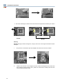
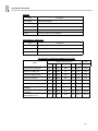
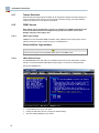
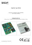
1
Endura KP915GV
Product Manual
www.radisys.com
007-01542-0002 • March 2006
KP915GV Product Manual
Copyright © 2005, 2006 by RadiSys Technology (Ireland) Ltd.
All rights reserved.
EPC and RadiSys are registered trademarks of RadiSys Corporation. ASM, Brahma, DAI, DAQ, MultiPro, SAIB, Spirit,
and ValuePro are trademarks of RadiSys Corporation.
DAVID, MAUI, OS-9, OS-9000, and SoftStax are registered trademarks of RadiSys Microware Communications
Software Division, Inc. FasTrak, Hawk, and UpLink are trademarks of RadiSys Microware Communications Software
Division, Inc.
†
All other trademarks, registered trademarks, service marks, and trade names are the property of their respective
owners.
2
KP915GV Product Manual
Preface
Revision History
Revision history
No.
Date
Description
1.0
September 2005
•
2.0
December 2005
•
Updates to clarify jumper default positioning, non-support
for S/PDIF In and Out on board, BIOS update to P28 version,
and editorial changes to some tables. Added details to OEM
Features section. No functional changes.
3.0
March 2006
•
Revised silk screen content for product designation and UL
approval type (listed).
•
First Release
Updated for DDR-II DIMM connector PN change.
•
Changed BIOS default setting to have all SATA ports
enabled.
•
All content now RoHS regulation compliant with modified
product codes to provide awareness.
•
New stepping level of SIO chip set is now included
(PC8374L0IBW/VLA A4). Removed reference to “K” or “L”
versions from manual.
•
Clarified PCI support provided by the ICH6 subsystem (no
PCI-X support).
Notational Conventions
Notes indicate important information
about the product.
Tips indicate alternate techniques or
procedures that you can use to save
time or better understand the product.
Cautions indicate potentially hazardous
situations which, if not avoided, may result
in minor or moderate injury or damage to
data or hardware. It may also alert you
about unsafe practices.
The globe indicates a World Wide
Web address.
Warnings indicate potentially hazardous
situations which, if not avoided, can result
in death or serious injury.
The book indicates a book or file.
Danger indicates imminently hazardous
situations which, if not avoided, will result
in death or serious injury.
ESD cautions indicate situations that
may cause damage to hardware via
electro-static discharge (ESD).
Installation Notes
When installing this motherboard into a suitable chassis, refer to the following notes:
• Read and save all instructions.
•
•
•
•
•
Always disconnect Cord/Plug before installation or upgrade. Parts of the motherboard can
remain powered even when the power supply is switched off unless the cord is disconnected.
Pay attention to the safety warnings included in this document.
When installing expansion cards, pay attention to the maximum loads detailed in this
document. Use only UL approved peripheral cards.
Route wiring away from sharp edges, heat sources and cooling fans.
Pay attention to the thermal issues described in this document. The motherboard requires
suitable airflow to maintain an ambient temperature within its operating range.
3
KP915GV Product Manual
Safety and Approval Notices
Safety and approval notices
Item
Battery
LAN (Local Area
Network) Connector
Description
This product contains a lithium cell.
•
When removing or replacing the lithium cell, do not use a
conductive instrument as a short-circuit may cause the cell
to explode. Always replace the cell with one of the same
type. This product uses a CR2032 cell. Dispose of a spent
cell promptly – do not recharge, disassemble or incinerate.
Keep cells away from children.
•
CAUTION! Danger of explosion if battery is incorrectly
replaced. Replace only with the same or equivalent type
recommended by the manufacturer. Dispose of batteries
according to the manufacturer's instructions.
This product may include an RJ45 LAN connector (see
product options). Do not connect to anything other than an
Ethernet LAN.
Thermal Interface
Material
This product may contain thermal interface material between
devices and heatsinks. This can cause irritation and can stain
clothing. Avoid prolonged or repeated contact with the skin
and wash thoroughly with soap and water after handling. Avoid
contact with eyes and inhalation of fumes. Do not ingest.
Anti-static
Precautions
This product contains static-sensitive components and should
be handled with care. It is recommended that the product be
handled in a Special Handling Area (SHA) as defined in
EN100015-1:1992. Such an area has working surfaces, floor
coverings and chairs connected to a common earth reference
point. An earthed wrist strap should be worn whilst handling.
Other examples of static-sensitive devices are the memory
modules and the processor. Failure to employ adequate antistatic measures can cause irreparable damage to components
on the motherboard.
Electromagnetic
Compatibility
This product is designed to meet the following EMC standards
when installed in a suitable chassis.
•
Safety
Legal Directives
4
FCC Class B (Title 47 of Code of Federal Regulations,
parts 2 & 15, subpart B)
•
EN55022 Class B
•
EN55024
This product complies with the American Safety Standard
UL60950 when installed in a suitable chassis.
This product complies with the relevant clauses of the
following European Directives.
Low Voltage Directive
73/23/EEC
EMC Directive
89/336/EEC
KP915GV Product Manual
Contents
1
OVERVIEW ................................................................................................................ 10
1.1
1.2
1.3
1.4
1.4.1
1.4.2
1.4.3
1.4.4
1.4.5
1.5
Accessories ………………………………………………………………………………………….. 11
Motherboard Layout ................................................................................................................12
Block Diagram.........................................................................................................................14
Configuration ………………………………………………………………………………………….15
Operation Mode Selection Jumper (JP3) ................................................................................15
BIOS Boot Block Write Protection Jumper (JP2).....................................................................16
Clear CMOS Jumper (JP1) .....................................................................................................16
Front Panel Connections.........................................................................................................16
Alternate Power LED...............................................................................................................17
Installation of CPU ..................................................................................................................17
2
MOTHERBOARD DESCRIPTION ............................................................................. 24
2.1
2.2
2.3
2.4
2.5
2.6
2.7
2.8
2.9
2.10
2.11
2.12
2.13
2.14
2.15
2.16
2.17
2.18
2.19
2.20
2.21
2.22
Processor Support ..................................................................................................................24
System Clocks ........................................................................................................................24
On board Clocking Block Diagram ..........................................................................................25
Mechanical ……………………………………………………………………………………………25
Expansion Slot Types .............................................................................................................25
915GV Chipset Feature ..........................................................................................................26
Video .………………………………………………………………………………………………….27
Disks …………………………………………………………………………………………………..28
Audio …………………………………………………………………………………………………..28
Network ……………………………………………………………………………………………….29
I/O ……………………………………………………………………………………………………...30
Power Management ................................................................................................................30
System management ..............................................................................................................30
Security ………………………………………………………………………………………………..30
Programmable Controller (PLD)..............................................................................................31
CMOS RAM and RTC .............................................................................................................31
Configuration ………………………………………………………………………………………….31
BIOS …………………………………………………………………………………………………..31
Operating Systems Support ....................................................................................................32
Power Supplies .......................................................................................................................32
Reliability and Environmental ..................................................................................................33
Regulatory Compliance...........................................................................................................34
3
SPECIFICATIONS ..................................................................................................... 35
3.1
3.2
3.2.1
3.2.2
3.3
3.3.1
3.3.2
3.3.3
3.3.4
3.4
Product Basis …………………………………………………………………………………………35
Non-Core Integrated Sub-systems..........................................................................................35
I/O Controller Hub 6 (ICH6).....................................................................................................35
Flash BIOS..............................................................................................................................38
Major Sub-systems .................................................................................................................39
Audio Interface ........................................................................................................................39
Hardware Management Interface............................................................................................41
Ethernet Interface....................................................................................................................42
Super I/O Interface..................................................................................................................43
Motherboard Power Consumption...........................................................................................48
5
KP915GV Product Manual
4
MOTHERBOARD BIOS ............................................................................................. 51
4.1
BIOS Features ........................................................................................................................51
4.2
Post and Boot ………………………………………………………………………………………..51
4.2.1 Hotkeys ...................................................................................................................................52
4.3
Setup Utility ………………………………………………………………………………………….. 52
4.3.1 Enter Setup .............................................................................................................................52
4.3.2 Configuration Reset ................................................................................................................52
4.3.3 Keyboard Command ...............................................................................................................52
4.3.4 Setup Configuration ................................................................................................................53
4.4
Power Management ................................................................................................................93
4.4.1 ACPI Wake-up Support...........................................................................................................93
4.5
Hardware Monitor and Auto Fan Control.................................................................................93
4.5.1 Hardware Monitor....................................................................................................................93
4.5.2 Automatic Fan Control ............................................................................................................93
4.6
Power LED ……………………………………………………………………………………………93
4.7
CPLD …………………………………………………………………………………………………. 94
4.7.1 POST Code Display ................................................................................................................94
4.7.2 BIOS Protection ......................................................................................................................94
4.7.3 LAN Controller.........................................................................................................................94
4.8
TPM ……………………………………………………………………………………………………94
4.9
Normal, Configure and Recovery Mode ..................................................................................94
4.9.1 Normal Mode ..........................................................................................................................95
4.9.2 Configure Mode.......................................................................................................................95
4.9.3 Recovery Mode .......................................................................................................................95
4.10 Update and Recovery Diskette ...............................................................................................95
4.10.1 Update Diskette.......................................................................................................................95
4.10.2 Recovery Diskette ...................................................................................................................95
4.11 Tamper Detection....................................................................................................................96
4.12 OEM Features.........................................................................................................................96
4.12.1 POST Logo Change................................................................................................................96
4.12.2 CMOS Default Change ...........................................................................................................96
4.13 PXE ……………………………………………………………………………………………………97
4.14 BIOS Flash Usage Map ..........................................................................................................97
4.15 Processor Microcode Support .................................................................................................97
4.16 SMBIOS ……………………………………………………………………………………………… 97
4.17 Post Code Technical Description ..........................................................................................102
4.18 POST Beep ………………………………………………………………………………………….104
4.19 SMBus Device Configuration ................................................................................................104
6
5
CUSTOMER SUPPORT........................................................................................... 105
A
TECHNICAL REFERENCE...................................................................................... 106
A.1
A.2
A.3
A.4
A.5
A.6
A.7
I/O Map ………………………………………………………………………………………………106
PCI Interrupt Allocation ......................................................................................................... 107
PCI Device Assignments.......................................................................................................108
SMBus Resource Allocation..................................................................................................108
ISA Interrupt Allocation ......................................................................................................... 109
ISA DMA Channel Allocation ................................................................................................109
BIOS Organization ................................................................................................................ 110
KP915GV Product Manual
B
CONTROL REGISTERS .......................................................................................... 111
B.1
B.2
B.3
B.4
B.5
B.6
B.7
B.8
B.9
B.10
Index Register ....................................................................................................................... 111
Watchdog Control ................................................................................................................. 111
Watchdog Kick ...................................................................................................................... 112
Watchdog Status................................................................................................................... 112
Watchdog Timeout Period.....................................................................................................113
General Purpose I/O Port 1...................................................................................................113
General Purpose I/O Port 2 and Control ...............................................................................113
PWM Control ………………………………………………………………………………………..114
Processor Identification......................................................................................................... 114
Controller Part Number .........................................................................................................115
C
CONNECTOR DESCRIPTIONS .............................................................................. 116
C.1
C.2
C.3
C.4
Connector Part Numbers ......................................................................................................116
PCI-E Expansion Slot (ADD2 card mode).............................................................................117
PCI Expansion Slot ............................................................................................................... 118
PCI Express x1 Slot .............................................................................................................. 119
7
KP915GV Product Manual
Figures
Figure 1.
Figure 2.
Figure 3.
Figure 4.
Figure 5.
Figure 6.
Figure 7.
Figure 8.
Figure 9.
Figure 10.
Figure 11.
KP915GV Board Layout.............................................................................................12
KP915GV Block diagram ...........................................................................................14
Jumpers .....................................................................................................................15
Clocking Block Diagram .............................................................................................25
KP915GV Board Slot Layout......................................................................................28
Audio Jack Socket and ATAPI Connectors ................................................................29
SST 49LF004B Functional Block Diagram .................................................................38
SigmaTel STAC9200 High Definition Block Diagram .................................................40
NS LM96000CIM Block Diagram ...............................................................................41
PC8374K Block Diagram ...........................................................................................43
BIOS ROM Addresses .............................................................................................110
Tables
Revision history .................................................................................................................................3
Safety and approval notices ..............................................................................................................4
Product Specification Overview .......................................................................................................10
Table 1. KP915GV Motherboard ...................................................................................................26
Table 3. ACPI Power States ..........................................................................................................30
Table 4. Power Supply Connector .................................................................................................32
Table 5. Environmental Specifications...........................................................................................33
Table 6. Regulatory Testing* .........................................................................................................34
Table 7. References ....................................................................................................................105
Table 8. I/O Map..........................................................................................................................106
Table 9. PCI Interrupt Allocation..................................................................................................107
Table 10. PCI Device Assignments .............................................................................................108
Table 11. SMBus Resource Allocation ........................................................................................108
Table 12. ISA Interrupt Allocation ................................................................................................109
Table 13. ISA DMA Channel Allocation .......................................................................................109
Table 14. Connector part numbers ..............................................................................................116
Table 15. ADD2 Expansion Slot ..................................................................................................117
Table 16. PCI Expansion Slot......................................................................................................118
Table 17. PCI Express x1 Slot (PCI-E x1) ...................................................................................119
Table 18. P/S2 Mouse and P/S2 Keyboard .................................................................................119
Table 20. Serial Port....................................................................................................................120
Table 21. VGA Port .....................................................................................................................120
Table 22. 2 x Dual Stack USB Ports............................................................................................120
Table 24. 3 x Audio Jack .............................................................................................................121
Table 25. 1394 Header ................................................................................................................121
Table 26. Front Panel Header .....................................................................................................121
Table 27. General Purpose I/O Headers ......................................................................................122
Table 28. Power Supply Connector .............................................................................................122
Table 29. Floppy Disk Connector ................................................................................................122
Table 30. ATA/100 Hard Drive Disk Connector ...........................................................................123
Table 32. 3X Internal Audio Headers...........................................................................................123
Table 33. TPM Header ...............................................................................................................124
8
KP915GV Product Manual
Table 34.
Table 35.
Table 36.
Table 37.
Table 38.
Table 39.
Table 40.
Table 41.
Complex Programmable Logic Device (CPLD) JTAG Header ....................................124
Serial Port 2 Header ...................................................................................................124
4 X Internal USB Headers ...........................................................................................124
Remote Thermal Sensor..............................................................................................125
3 X Fan Connector.......................................................................................................125
SMBus Connector........................................................................................................125
PS/2 Keyboard Header................................................................................................125
PS/2 Mouse Header ....................................................................................................125
9
KP915GV Product Manual
1
Overview
Target applications are transaction terminals, medical, test & measurement, gaming, industrial
automation applications and other enterprise systems. This motherboard is part of the RadiSys
Endura product line, which is specifically targeted at embedded applications with a lifetime of 5
years. Products are fully revision controlled and any change to form, fit or function will be notified to
customers in advance via a Product Change Notification procedure.
Product Specification Overview
Item
Description
Form Factor
ATX
Processor
Support for an Intel® Pentium® 4 or Celeron D processor in a LGA775 socket
with an 800MHz or 533MHz FSB
12” x 9.6”, 6 expansion slots
Embedded processor requirements:
Intel® Pentium® 4 Processor 551 (3.4GHz 800MHz FSB 1MB L2)
Intel® Celeron™ D Processor 341 (2.93GHz 533MHz FSB 256KB L2)
Chipset
Intel 915GV GMCH and Intel ICH6 I/O hub
Memory
Four DIMM sockets for DDR2 400/533 modules
Video
Intel® GMA900 video controller integrated within chipset
Audio
Two channel stereo audio using the Sigmatel STAC9200 audio controller with
Intel HD Audio interface operation option
Two plug and play jacks on I/O panel (default MIC, line-out)
Three ATAPI connectors – line input, line output, and microphone input
On-board PC speaker (beep)
Expansion
Capabilities
915GV ATX
Three PCI, two x1 PCI-E, one ADD2 slots
(No PCI riser extension connector)
Power
Management
ACPI 2.0 supporting states S0, S3, S4, S5, and C0, C1, C2, C3
System
Management
Voltage, temperature and fan monitoring (3 fans)
Lithium cell voltage monitoring
Automatic fan speed control (3 fans)
Programmable watchdog timer
SMBus header
Security
Header for TPM 1.1 compliant module
BIOS
Phoenix Award BIOS for the Intel 915G/GV chipset
Includes video BIOS and network boot
4Mbit Firmware Hub
Build option for socketed BIOS with write-protect jumper (enabled by the PLD
logic)
User defined BIOS default settings
I/O
Eight USB 2.0 ports - four on I/O panel and four on locking headers
General purpose I/O lines (13) with LCD character display support
Firewire
10
Available with IEEE 1394b function with single port via an on-board header
connector (based on TI TSB82AA2 controller and TSB81BA3 transceiver)
KP915GV Product Manual
Product Specification Overview
Item
Description
Network
Intel 82573V (or ‘L) PCI-E Gbit Ethernet controller, co-lay with Intel 82562GZ
10/100 PHY (using the integrated MAC)
Available with second Intel 82573V (or ‘L) Gbit Ethernet controller
Disks
Four SATA ports with locking headers
Single Ultra ATA/100 interface supporting hard disks and ATAPI drives
One FDD interface
Super I/O &
H/W Monitor
Winbond PC8374 Super I/O and Nat Semiconductor LM9600 hardware
monitoring device
Automatic fan speed control based on thermal monitoring (note that the BIOS
Setup is used for configuration and status information)
Header
Connectors
I/O Panel
GPIO
2 x 10 pin with housing
SMbus
1 x 4 pin with housing
COM2
2 x 5 pin with housing
Kbd/Mouse
1 x 4 pin with housing
Remote thermal sensor
1 x 2 pin with housing
FDD
1 x FDD connector
1394b
2 x 5 pin connector
PS/2 keyboard and mouse
Analog VGA
Bi-directional/EPP/ECP parallel port
COM1 RS232
One or two dual USB + RJ45 stacks
Audio jack stack (2 jacks)
RadiSys PLD
1.1
Lattice LC4128ZC-75TN100C PLD for watchdog, GPIO, BIOS write-protect
support
Accessories
There are two I/O shields, one for a single Ethernet configuration and one for a dual Ethernet
configuration, and an available fan heat sink for the processor. These are separately orderable
product codes. There are currently no dual Ethernet versions of the KP915GV board. Note that
the order codes directly below do not comply with RoHS regulations.
ATX-L KP IOSHLD
ATX-2L BLK IOSHLD
FNSNK P4-775
ATX I/O Shield for Single Ethernet
ATX I/O Shield for Dual Ethernet
Fan Sink for LGA775 Pentium 4 Processors
RoHS regulation-compliant product code versions of these items are as follows.
ATX-2L BLK IOSHLDR
ATX-L KP IOSHLDR
FNSNK P4-775 R
IO Shield - Dual Ethernet ROHS
IO Shield – Single Ethernet ROHS
Fan Sink - LGA775 P4, ATX ROHS
11
KP915GV Product Manual
1.2
Motherboard Layout
Figure 1 shows the layout of the KP915GV motherboard with the major components identified.
Figure 1.
59
58
KP915GV Board Layout
57
56 55 54 53 52 51 50 49 48 47
46
1
45
2
44
3
43
4
42
41
5
40
6
39
7
38
8
37
9
36
10
35
11
34
12
33
32
(Optional)
13 14 15 16 17 18 19 20 21 22 23 24 25 26 27 28 29 30
12
31
KP915GV Product Manual
Component Identification
Description
1
Super IO
21
Description
Ethernet port 1
(option)
Description
2
Memory sockets
22
I/O panel USB port 7
42
USB port 3 header
3
Serial port 2 header
23
I/O panel USB port 8
43
USB port 4 header
4
Remote thermal sensor
24
Microphone input jack
44
SMBus header
5
CPU FAN power
connector
25
Audio line output jack
45
BIOS ROM writeprotect jumper
6
Chipset GMCH
26
Ethernet controller 1
(option)
46
Clear CMOS Jumper
7
775-pin socket for
processor
27
ADD2 slot
47
GPIO header
8
Clock generator
28
Ethernet controller 2
48
BIOS ROM (FWH)
9
System fan power
connector
29
PCI Express x1 slot
49
CPLD control logic
10
PS/2 mouse header
30
PCI slot 2.3
50
JTAG header
11
PS/2 keyboard header
31
HD Audio CODEC
51
I/O controller hub
(ICH6)
12
12V power connector
32
Stereo audio (CD) line
input header
52
Operation Mode
Jumper
13
PS/2 mouse (green)
33
Stereo audio
(microphone) input
header
53
Front panel header
14
PS/2 keyboard (purple)
34
Stereo audio line
output header
54
SATA connectors
15
Serial port
35
Buzzer
55
Chassis fan power
connector
16
Parallel port
36
1394 controller
56
Primary power supply
connector
17
VGA monitor
37
RTC battery
57
IDE connector
18
Ethernet port 2
38
1394 PHY
(TSB81BA3I)
58
TPM header
19
I/O panel USB port 5
39
1394 header
59
FDD connector
20
I/O panel USB port 6
40
USB port 1 header
41
USB port 2 header
13
KP915GV Product Manual
1.3
Block Diagram
Figure 2 shows the block diagram of the KP915GV motherboard.
Figure 2.
KP915GV Block diagram
Prescott, Tejas
Pentium 4 EE
LGA775 processor
Socket T
VRD 10.1
4 Phase PWM
CK-410 Clock
800/533 FSB
CRT
400/533MHz
Channel A DDR-2
DIMM1
400/533MHz
Channel A DDR-2
DIMM2
Channel B DDR-2
DIMM3
VGA
PCIEx16 Port
Intel SDVO Card
GMCH
Grantsdale
I/O Panel
USB2.0 Port5
USB2.0 Port6
USB2.0 Port7
USB2.0 Port8
Channel B DDR-2
DIMM4
4 Lanes
Direct Media Interface (DMI)
USB2.0 Port2
USB2.0 Port3
USB2.0 Port4
PCIE x1 Interface
Intel 82573E
USB2.0
LAN-Link
Intel 82562GZ
PCI Interface
ATX Form Factor
PCI Slot 1,2&3
PCI Interface
1394
TSB82AA2I
ATA
ATA100
IDE CONN 1
Mouse
PCI-E Slot 1
PCI-E Slot 2
USB2.0
Header
USB2.0 Port1
Keyboard
PCIE x1 Interface
SUPER I/O
PC8374
LPC
ICH6
SATA
Serial ATA
SATA
Serial ATA
SATA
Serial ATA
SATA
Serial ATA
Port 1
Port 2
Serial Port1
Serial Port2
Port 3
Port 4
Parallel
FWH Flash
BIOS
4Mb
Floppy
14
High Definition Audio Azalia Codec
STAC9200
KP915GV Product Manual
1.4
Configuration
The majority of the configuration of the motherboard is done through the Setup utility built into the
BIOS – discussed later in this document. There are, however, a number of jumpers that control the
operation of the motherboard as described below. Some jumpers are not fitted to certain products.
Figure 3.
1 (No jumper = Recover) JP3
Normal
Jumpers
(No jumper = Protected)
CPLD Write Enable
JP2
Configure
CPLD Write
Protected
BIOS Unlock
1
BIOS Lock
(No jumper = Unlock)
1
JP1
Clear CMOS
Normal
(No jumper = Normal)
1.4.1
Operation Mode Selection Jumper (JP3)
This jumper selects one of the following operating modes for the motherboard (pins 1, 3, 5) and
controls write capability for the CPLD content (pins 2, 4, 6).
Normal Mode
(Jumper between pins 1 & 3) This is the factory default position the jumper
should be in for normal operation of the motherboard.
Configure Mode
(Jumper between pins 3 & 5) With the jumper in this position the motherboard
automatically runs the BIOS Setup utility regardless of the state of the Setup
disable flag that can be set in the BIOS defaults. In this mode, the CMOS RAM
contents are ignored and the defaults are used to configure the motherboard.
15
KP915GV Product Manual
Recover Mode (No jumper) With no jumper installed on pins 1, 3, and 5 recovery mode is entered.
The motherboard does not boot and waits until a valid recovery diskette is
detected and then copies new BIOS into the ROM. The motherboard must be
powered down and then re-powered with the jumper in the normal position before
normal operation can resume.
CPLD Write Enabled (Jumper between pins 2 & 4) In this position the contents of the CPLD can
be reprogrammed.
CPLD Write Protected (Jumper between pins 4 & 6) This is the factory default position. In this
position, or with no jumper on pins 2, 4, and 6, the contents of the CPLD are
protected from reprogramming.
1.4.2
BIOS Boot Block Write Protection Jumper (JP2)
(Jumper between pins 1 & 2) This is the factory default position. A jumper installed in this position.
or no jumper installed, enables changes to contents of BIOS ROM boot block (unlocked position).
Some motherboard applications may want to have boot block write-protected BIOS. This can be
provided via the BIOS boot block write protection jumper. If a jumper is installed between pins 2 &
3 (locked position), the contents of BIOS ROM boot block cannot be changed in any way.
1.4.3
Clear CMOS Jumper (JP1)
(Jumper between pins 2 & 3) This is the factory default position. Either this position or no jumper
installed, is the normal operating configuration. Installing a jumper between pins 1 & 2 clears
(resets) the CMOS.
1.4.4
Front Panel Connections
The primary controls and indicators for the motherboard are connected via the front panel
connector using either a single ribbon cable to a ‘front panel’ assembly, or using a number of small
PC-standard connectors. The functions are described below. See appendix B for the connector pinout information.
Power LED
Connects either a single-color LED (usually green) or a two-terminal bi-color LED (usually
green/yellow) to indicate the powered status of the motherboard. In both cases, the ‘green’ anode
should be attached to pin 2 of the front panel connector. Refer to the Enhanced Power
Management LED portion in section 3.3.4.4 of this document for further information.
Power Switch
If the motherboard is used with a soft-switch power supply, a momentary switch should be
connected between pins 6 and 8 of the power switch connections on the front panel connector. If
the switch is closed for greater than approximately 4 seconds, the motherboard powers off
immediately, regardless of the state of the operating system, losing any system context information.
This input is redundant when using a hard-switch power supply.
Reset Switch
If used, a momentary switch connected between pins 5 and 7 will cause the motherboard to restart
when closed.
Hard Disk LED
To indicate hard disk activity on either of the two ATA channels, a single color LED should be
connected between pins 1 (anode) and 3.
Speaker
Connect an external speaker between pins 10 and 12 or 10 and 16. This is used only for the PC
‘beep’ functions. The speaker should typically be 8Ω.
16
KP915GV Product Manual
Tamper Switch
To make use of the tamper detection logic of the motherboard, connect a momentary switch
between pins 18 and 20. The switch should be open when the chassis is closed.
1.4.5
Alternate Power LED
The power LED function on the front panel connector is duplicated on the Alternate Power LED
connector for use with LEDs cabled to a 3-pin connector. Do not use both the primary (front panel)
and alternate connectors simultaneously.
1.5
Installation of CPU
1.5.1
Installation of CPU
Below is the CPU socket illustration. Follow these procedures to install a CPU.
Load lever
Load plate
Load cap
Load Stiffener
1. Use thumb & forefinger to hold the lifted tab of the cap.
Lifted tab
2. Lift the cap up and pick to upload the cap completely from the socket.
17
KP915GV Product Manual
3. Use thumb & forefinger to hold the hook of the load lever and pull the lever sideways to unlock it.
Correct
Wrong
Warning:
DO NOT use finger to lift the locking lever, as injury could occur to the finger and the SKT could be
damaged.
4.
5.
18
Lift up the lever. Use thumb to open the load plate. Be careful not to touch the contacts.
Hold the CPU and tilt it to some degree since the contacts are designed to be hooked, and
then match the triangle marker to Pin 1 position as shown below. Carefully insert the CPU
into the socket until it fits in place.
KP915GV Product Manual
Alignment key
Pin 1 indicator
19
KP915GV Product Manual
6.
Close the load plate, and slightly push down the tongue side.
Slightly push down
the tongue side
7. Lower the lever and lock it to the load plate, then the CPU is locked in place.
CAUTION
Excessive temperatures will severely damage the CPU and system. Therefore, you should install
CPU cooling fan and make sure that the cooling fan works normally at all times in order to prevent
overheating and damaging to the CPU. Please refer to your CPU fan user guide to install it
properly.
1.5.2
Installation of Memory
This motherboard includes four 240-pin slots with 1.8V for DDR2. You must install at least one
memory bank to ensure normal operation.
Installation of DDR2 Memory
1.
There is only one gap in the middle of the DIMM slot, and the memory module can be fixed in
one direction only. Unlock a DIMM slot by pressing the module clips outward.
2.
20
Align the memory module to the DIMM slot, and insert the module vertically into the DIMM slot.
KP915GV Product Manual
DDR2 Memory bank
128 Pins
112 Pins
3. The plastic clips at both sides of the DIMM slot will lock automatically.
CAUTION
Be sure to unplug the AC power supply before adding or removing expansion cards or other
system peripherals, especially the memory devices, otherwise the motherboard or the system
memory might be seriously damaged.
21
KP915GV Product Manual
1.5.3
Power Supply
In order to avoid damaging any devices, make sure that they have been installed properly prior to
connecting the power supply.
It is recommended that the board be used with a power supply that supports a minimum
current load of 0.3A or less on the 5V supply rail and 2A or less on the 3.3V supply rail.
This board with CPU and memory may draw as little as 400mA of 5V and 2A of 3.3V during
start-up (increases depend on installed devices). The power supply under consideration must
be verified as compatible with the projected total system start-up loads for these supply rails.
If the power supply minimum current level requirements are not at or below the level of
current loads that are actually drawn, unpredictable start-up operation may result, such as the
power supply latching off. If this occurs, the AC input to the power supply must be removed
and re-attached or the power supply switch cycled off and on, in order to turn the system
back on.
4-pin ATX 12V Power Connector:
The ATX power supply connects here and provides power to the CPU.
GND GND
3
1
4
2
12V 12V
4-pin ATX 12V power connector
22
KP915GV Product Manual
KP915GV 20-pin ATX power connector:
Below is the ATX power supply connector. Make sure that the power supply cable and pins are
properly aligned with the connector on the motherboard. Firmly plug the power supply cable into
the connector and make sure it is secure.
GND
PS-ON
5V
-5V
5V
GND
GND GND
5V
12V
5VSB
Pw-OK
3.3V
-12V
+5V
GND
3.3V
GND
3.3V
GND
20-pin ATX power connector
23
KP915GV Product Manual
2
Motherboard Description
2.1
Processor Support
•
•
•
•
•
•
•
2.2
Single processor support
Intel® Pentium® 4 Processor 550/551 (3.4GHz 800MHz FSB 1MB L2)
Intel® Celeron™ D Processor 340/341 (2.93GHz 533MHz FSB 256Kb L2)
Follow the Design Guide in the Intel(R) Pentium(R) 4 Processor in the 775-land Package on 90
nm Process EMTS REV. NO. 1.1 and Grantsdale Chipset (915-GV) Platform Design Guide
REV NO. 1.2
Supports Pentium® 4 Processor Front Side Bus (FSB) at 533MHz (133MHz bus clock) and
800MHz (200MHz bus clock)
Supports Hyper-Threading Technology and FSB Dynamic Bus Inversion (DBI)
Supports 32-bit host bus addressing, allowing the CPU to access the entire 4 GB of the
GMCH’s memory address space
System Clocks
All clocks must comply with CK410 specifications. System clocks include as below:
•
•
•
•
•
•
•
•
•
•
•
•
24
Host system (FSB 533/800MHz)
DMI (Direct Media Interface)
Memory system DDR2 SDRAM
CPU/MCH/ITP CONNECTOR
MCH/ICH6/LAN/SATA/PCI-E slot
DOTCLK
PCI slot/SIO/FWH/ICH6/TPM/CPLD
USB/ICH6
HD Audio
ICH6/SIO
RTC (OSC)
LAN (OSC)
133/200MHz
100 MHz
400/533MHz
200MHz
100MHz
96 MHz
33 MHz
48 MHz
24.576 MHz
14 MHz
32.768 KHz
25 MHz
KP915GV Product Manual
2.3
On board Clocking Block Diagram
14.318MHz
CPU
CPU 133/200 MHz Diff Pair
MCH 133/200 MHz Diff Pair
DDR 4 Slots 12 Diff Pair CLKs
PCI Express 100 MHz Diff Pair
PCI Express x16 SDVO
DOT 96 MHz Diff Pair
Channel A DDR2
DIMM1
GMCH
PCI Express/DMI 100 MHz Diff Pair
DIMM2
Grantsdale
Channel B DDR2
DIMM1
PCI Express/DMI 100 MHz Diff Pair
DIMM2
USB/SIO 48 MHz
CK-410
ICH 33 MHz
REF 14 MHz
FWH 33 MHz
FWH
Azalia
ICH6
24.576MHz
PCI 33 MHz
PCI Slot
1,2&3
PCI Express 100 MHz Diff Pair
Azalia Bit Clock
PCI-E SLOT
1,2
PCI Express 100 MHz Diff Pair
LAN
1394 33 MHz
32.768KHz
1394
SATA 100 MHz Diff Pair
Super I/O
SIO 33 MHz
Figure 4.
2.4
2.5
Clocking Block Diagram
Mechanical
•
Compliant with the ATX 2.03 specification
•
Lead-free design
•
4-layer PCB, components top side only, immersion silver surface finish
•
Screen printing includes RadiSys product code, RadiSys part number, RadiSys branding,
selected component reference designators, and UL and WEEE directive logos.
Expansion Slot Types
25
KP915GV Product Manual
Table 1. KP915GV Motherboard
2.6
Chipset
Form
Factor
PCI-E x16
or ADD2
PCI-E
x1
PCI
PCI Riser
Extension
915GV
ATX
1
2
3
N/A
•
See Figure 5 for slot configurations
•
ADD2 will be a green connector
915GV Chipset Feature
The 915GV is a Memory Controller Hub (MCH) designed for use with the Prescott processors in
desktop platforms. The role of a MCH is a system is to manage the flow of information between its
four interfaces: the CPU interface (FSB), the DDR/DDR2 System Memory interface (DRAM
controller), the External Graphics interface (PCI Express-G), and the I/O Controller through Direct
Media Interface (DMI). It’s 1210 Flip Chip Ball Grid Array (FCBGA) package.
Processor/Host interface (FSB)
•
•
•
•
•
•
•
•
•
•
•
•
Supports a single Pentium 4 processor with 1-MB L2 cache in the 90 nm process, in an
LGA775 package.
The primary enhancements over the Compatible Mode P6 bus protocol are:
1- Source synchronous double-pumped (2x) Address
2- Source synchronous quad-pumped (4x) Data
Supports Pentium 4 processor FSB interrupt delivery.
Supports Pentium 4 processor Front Side Bus (FSB) at the following Frequency Ranges:
533/800MT/s (133/200MHz)
Supports Hyper-Threading Technology (HT Technology)
Supports FSB Dynamic Bus Inversion (DBI)
Supports 36-bit host bus addressing, allowing the CPU to access the entire 4GB of the MCH’s
memory address space.
12-deep In-Order Queue to support up to twelve outstanding pipelined address requests on
the host bus.
1-deep Defer Queue.
Utilizes GTL+ bus driver with integrated GTL termination resistors.
Supports a Cache Line Size of 64 bytes.
At 133/200MHz bus clock the address signals run at 266/400MT/s, the data is quad pumped
and an entire 64B cache line can be transferred in two bus clocks. At 133/200MHz bus clock
the data signals run at 533/800MT/s for a maximum bandwidth of 4.3GB/s.
System Memory Controller
•
•
26
The MCH System Memory Controller directly supports dual channel of memory (each channel
consisting of 64 data lines)
1- The memory channels are asymmetric: “Stacked” channels are assigned address serially.
Channel B addresses are assigned after all Channel A addresses.
2- The memory channels are interleaved: Addresses are ping-ponged between the channels
after each cache line (64-B boundary).
Supports DDR2 memory DIMM frequencies of 400 and 533MHz. The speed used in all
channels is the speed of the slowest DIMM in the system.
KP915GV Product Manual
•
•
•
•
•
•
•
•
•
•
•
•
•
•
•
Support for non-ECC memory, unbuffered DIMMs only, in 256MB, 512MB, 1GB, and 2GB
sizes, which may be installed as single DIMMs if desired. If a total of 4GB of DIMMs is
installed, the maximum available memory will be approximately 3.24GB, with the balance of
the address space being consumed by other resources in the system.
I/O Voltage of 1.8V for DDR2.
Directly support only two channels of non-ECC DDR2 DIMMs.
Supports maximum memory bandwidth of 4.2GB/s in single-channel or dual channel
asymmetric mode, or 8.5GB/s in dual-channel interleaved mode assuming DDR2 533MHz.
For dual interleaved mode, DIMMs must be installed in matched pairs, installed in DIMM
sockets with identical color (e.g. locations DIMM1 and DIMM3, then DIMM2 and DIMM4).
Supports 256Mb, 512Mb, and 1Gb technologies for x8 and x16 non-ECC DDR2 devices.
Supports four banks for all DDR2 devices up to 512Mb densities. Supports eight banks for 1Gb
DDR2 devices.
Maximum DRAM address decode space of 4GB. (Assuming 32-bit addressing)
Supports opportunistic refresh scheme.
Supports page sizes of 4KB, 8KB, 16KB and 32 KB. Note 32KB is for dual-channel operation
only.
Supports up to 16 simultaneous open pages per channel
Serial Presence Detect (SPD) scheme for DIMM detection support.
Dual channel DDR2 for 4 X 240 pin DIMM connectors
Support for Serial Presence Detect (SPD)
Support for Suspend to RAM (STR) using CKE, S3 ACPI state
PCI Express Graphics Interface
•
•
•
•
•
•
•
One, 16-lane PCI Express port intended for Graphics Attach, fully compliant to the PCI
Express Base Specification revision 1.0a
A base PCI Express frequency of 2.5Gb/s only.
Raw bit-rate on the data pins of 2.5Gb/s, resulting in the real bandwidth per pair of 250MB/s
given the 8b/10b encoding used to transmit data across this interface.
Maximum theoretical realized bandwidth on the interface of 4GB/s in each direction
simultaneously, for an aggregate of 8GB/s when x16.
PCI Express Enhanced Addressing Mechanism. Accessing the device configuration space in
the flat memory mapped fashion.
Automatic discovery, negotiation, and training of link out of reset.
Supports traditional PCI style traffic (asynchronous snooped, PCI ordering).
DMI
•
•
•
•
2.7
A chip-to-chip connection interface to Intel ICH6.
2GB/s point-to-point DMI to ICH6 (1GB/s each direction).
100MHz reference clock (shared with PCI Express Graphics Attach).
32-bit downstream addressing.
Video
•
Integrated Intel® GMA900 video controller
1.
•
Intel Infrastructure Processor Division (IPD) group Embedded Graphics or Graphics Media
Accelerator (GMA) (Extreme) drivers and video BIOS
Analog RGB output with DDC2B
1.
2.
Graphics resolution up to 2048 x 1536 pixels with 32-bit color support at 75Hz
15-pin D-sub connector
27
KP915GV Product Manual
Processor
ADD2
Figure 5.
2.8
2.9
x1
PCI-E
x1
PCI-E
PCI
PCI
PCI
KP915GV Board Slot Layout
Disks
•
Four 150MB/s SATA ports with locking headers
•
One Ultra ATA/100 interface via on-board 40-way boxed header
•
40/80-pin cable host-side detection or forced in BIOS
•
Support for hard disks and ATAPI drives
•
BIOS support for 48-bit LBA (ATA drives >137GB)
•
Support for USB drives including boot
Audio
SigmaTel STAC9200 audio controller with Intel High Definition Audio (HDA) compatible mode
•
•
On-board ATAPI connectors
•
ATAPI 1: Line input connector (black)
•
ATAPI 2: Stereo AUX/MIC input connector (white)
•
ATAPI 3: Stereo Line output connector (yellow)
Two I/O panel 3.5mm plug and play audio jacks – default connections:
•
Stereo microphone input (with support for microphone bias)
•
Stereo line output with headphone drive capability
(Note: an option exists for a three jack connector – refer to Table 2 and comments below.)
•
28
On-board PC beeper
KP915GV Product Manual
External
Internal
Optional*
Line in
ATAPI 1
Line out
ATAPI 3
Line out
MIC in
ATAPI 2
MIC in
Figure 6.
Audio Jack Socket and ATAPI Connectors
Table 2: Audio Channel Allocation
I/O panel jack
I/O panel jack color
Pink
Lime
ATAPI header color
Nominal function
Microphone
Line In capability
X
Headphone Out Capability
Blue*
Black*
White
Yellow
Line In*
Microphone
Line Out
X
X
Line Out capability
Microphone capability
Line Out
Internal header
X
X
X
X
* If a 3 jack external connector is needed, an option could be made available, for which the
added blue jack would be Line In, displacing the Line In black internal header (deleted) on
the standard configuration.
2.10
Network
•
One Ethernet controller configured as either 10/100 or 10/100/Gbit at build-time
•
Available with a second Ethernet controller configured as 10/100/Gbit
•
10/100Mbps Ethernet solution IEEE 802.3 10Base-T and 100Base-TX compatible
•
MAC integrated into ICH with Intel 82562GZ transceiver
•
Remote boot, PXE and Wake-On-LAN support
•
Gbit Ethernet solutions IEEE 802.3 10Base-T, 100Base-TX, 1000Base-T compatible
•
Intel 82573V (or ‘L) PCI Express Ethernet controller connected via I/O hub x1 lane
•
Full line-speed operation
•
Remote boot, PXE and Wake-On-LAN support
•
On-board RJ45 connector (RJ45 over dual USB connector) with two integral LEDs showing
combined link integrity and activity (yellow) plus line speed (green/amber)
•
Available with a second RJ45 over dual USB connector
29
KP915GV Product Manual
2.11
2.12
I/O
•
Four USB 2.0 ports on I/O panel via two dual stacked USB over RJ45 connectors
•
Four USB 2.0 ports on internal locking headers
•
Available with IEEE 1394b controller with support for 1394a
•
Single port via a header connector
•
Based on Texas Instruments TSB82AA2 controller and TSB81BA3 transceiver
Power Management
•
Supports ACPI 2.0 with power states S0, S3, S4 (not S4BIOS), S5 and C0, C1, C2, C3
•
Supports PCI PME and PCI Express power management event signaling
Table 3. ACPI Power States
2.13
2.14
30
G0/S0/C0
Full on
G0/S0/C1
Processor is halted
G0/S0/C2
Processor stops internal clocks
G0/S0/C3
Processor clocks are disabled and processor in sleep state
G1/S3
System context is saved to RAM and power removed from all circuits
except that required to maintain system RAM and resume
G1/S4
System context is saved to disk and power removed from all circuits
except that required to resume
G2/S5
Soft off, only resume logic and RTC remain powered
System management
•
System monitoring of voltage, temperature, fans
•
Temperature monitoring of processor die, board and remote sensor
•
Direct monitoring of lithium cell voltage
•
Automatic fan control for 3 fans - CPU, System 1, System 2
•
Fan configuration held in BIOS customization block
•
Fans can be assigned to any of three thermal zones for automatic control - each zone
•
monitored by one of the three thermal sensors
•
450mA drive capability for each system fan, 2.2A for the CPU fan
•
Anti-tamper security (trigger for chassis intrusion detect)
•
Programmable watchdog timer with range of 1 second to 1 hour
•
Access to SMBus via 4-pin 2mm header
Security
•
Header for Trusted Platform Module (TPM)
•
TCG 1.1 compliant
KP915GV Product Manual
2.15
Programmable Controller (PLD)
•
•
•
Programmable logic device to support configurable system functions
•
Supports software-based updates (including field updates)
•
Supports customizable logic (by RadiSys, not user customizable)
•
Option of 128 or 256 macrocell device (256 for enhanced controller)
Controls product write-protect features for BIOS ROM
•
Allows write-protection via software or permanent protection via controller logic
•
Supports write-protect jumper covering update of controller logic (override via ICT)
Total of 13 General purpose I/O lines
•
10 signals that can be programmed as inputs and outputs
•
2.16
2.17
•
Two signals that are input-only
•
One signal that is output-only
•
Support for character-based LCD panel to display BIOS POST messages and other
information. Displays have an 8-bit parallel interface. Displayed text is the BIOS Port 80
codes in the format: “BIOS Code xx”
CMOS RAM and RTC
•
256 bytes of CMOS RAM
•
Lithium cell with >5 years operating life
Configuration
•
Majority of configuration is jumper-less and done through BIOS settings
•
Customer can specify BIOS defaults at manufacture
•
Operating mode jumper selects normal, configure and recovery modes
•
Power supply jumper configures the product to operate with a hard-switched power supply that
must be used when the PSU does not provide 5V on the 5V standby pin
•
2.18
Direction control in three groups with 2, 3 and 5 bits (20:21, 15:17, 10:14)
Target: jumper-less operation for power supply type
BIOS
•
Based on Phoenix Award BIOS
•
4Mbit firmware hub BIOS ROM
•
•
System and (Intel) video BIOS
•
Intel Ethernet remote boot and PXE code
•
Fully customizable including video BIOS
•
ROM can be optionally socketed with write-protect support
Silent boot (boot message hiding, logo visible), headless operation support
31
KP915GV Product Manual
2.19
2.20
•
All configuration is automatic - no stopping on configuration change
•
Resources freed when unused
Operating Systems Support
•
Windows XP Professional SP2
•
Embedded Windows XP Server SP2
•
Red Hat Enterprise Linux 4.0 AS
•
Knoppix Linux 3.7 (selected drivers only)
•
Windows 2000 Server SP4
•
SUSE Linux Enterprise Server 9.0 (selected drivers only)
Power Supplies
•
Support for ATX12V power supplies (see Note below)
•
Supports hard- and soft-switched power supplies with jumper-less configuration
•
See table 4 for required power supply connector.
Table 4. Power Supply Connector
Board
Connector Type
KP915GV
2 x 10 pin
It is recommended that the board be used with a power supply that supports a
minimum current load of 0.3A or less on the 5V supply rail and 2A or less on the
3.3V supply rail (see note below).
Note: This board with CPU and memory may draw as little as 400mA of 5V and 2A
of 3.3V during start-up (increases depend on installed devices). The power supply
under consideration must be verified as compatible with the projected total system
start-up loads for these supply rails. If the power supply minimum current level
requirements are not at or below the level of current loads that are actually drawn,
unpredictable start-up operation may result, such as the power supply latching off.
If this occurs, the AC input to the power supply must be removed and re-attached
or the power supply switch cycled off and on, in order to turn the system back on.
32
KP915GV Product Manual
2.21
Reliability and Environmental
Table 5. Environmental Specifications
Characteristic
State
Value
Temperature
(ambient)
Operating
0oC to +55oC
Relative
humidity
Vibration
Operation above +30° C reduces the maximum operational
relative humidity.
Operating
gradient
±5°C per minute
Storage
-40oC to +85oC, 5°C per minute maximum excursion
gradient.
Operating
10% to 85% RH non-condensing at +30oC, linearly
o
decreasing to 5% to 15.5% RH non-condensing at +65 C.
Storage
o
5% to 90% RH non-condensing at +40 C.
Operating
Random 5Hz to 2kHz, 7.7grms, 10 mins in each of 3 axes
5Hz to 20Hz: 0.004g2/Hz ramping up to 0.04g2/Hz;
20Hz to 1000Hz: 0.04g2/Hz;
1000Hz to 2000Hz: 0.04g2/Hz ramping down to
0.01g2/Hz
Packaged
Random 5Hz to 2kHz, 9.7grms, 10 min. in each of 3 axes
5Hz to 20Hz: 0.006g2/Hz ramping up to 0.06g2/Hz;
20Hz to 1000Hz: 0.06g2/Hz;
1000Hz to 2000Hz: 0.06g2/Hz ramping down to
0.02g2/Hz
Sine 5Hz to 500Hz, 0.15 octave/min up and back, 10 min.
dwell at 3 resonances in each of 3 axes
5 to 50Hz swept – 0.1g; 50 to 500Hz swept – 0.25g
Shock
Altitude
MTBF
Nonoperating
30g 11ms, half-sine
Packaged
Drop test, 10-up bulk packaging, 30 inches free-fall, 152
inches/s velocity change
Operating
To 15000 ft. (4500m)
Storage
To 40000 ft. (12000m)
The table below summarizes the MTBF (hr) predictions for
the listed products, without the main processor, memory, or
battery installed.
SKU
35°C
55°C
KPGV1W00[03]
298,735
141,946
KPGV1G00[03]
295,736
156,014
KPGVFG00[03]
280,528
147,801
Airflow
Base on standard Intel guidelines
Fuses
Self-resetting PTC fuse (fuses automatically reset without
user intervention once the load had been removed)
33
KP915GV Product Manual
2.22
Regulatory Compliance
Table 6. Regulatory Testing*
Characteristic
State
Value
ESD
Operating
Designed and tested to pass (not certified):
To IEC 1000-4-2 / EN61000-4-2: 1995
4kV direct contact, performance criteria B
6kV direct contact, performance criteria C
4kV air discharge, performance criteria B
8kV air discharge, performance criteria C
Fast transient/burst
Operating
Designed and tested to pass (not certified):
IEC 1000-4-4/EN61000-4-4: 1995, performance criteria B
Surge voltages
Operating
Designed and tested to pass (not certified):
IEC 1000-4-5 / EN61000-4-5: 1995, performance criteria B
Conducted
Operating
Designed and tested to pass (not certified):
IEC 1000-4-6 / EN61000-4-6: 1995, performance criteria B
Radiated emissions
Operating
Designed and tested to pass (not certified):
CISPR 22: 1998, Class B
EN55022, EN55024
FCC Class B
Radiated immunity
Operating
EN61000-4-3, performance criteria A
Conducted
immunity
Operating
EN61000-4-6, performance criteria A
AC power dips and
interrupts
Operating
EN61000-4-11performance criteria B and C
Safety
UL60950-1, CSA60950-1, EN60950-1, IEC60950-1
CB report to IEC60950-1
Recognized component to UL60950-1
UL60950-1 approval changed to accessory listing in Q106
* EMC and immunity testing performed in an example standard desktop chassis.
34
KP915GV Product Manual
3
Specifications
3.1
Product Basis
This product based on the Intel® 915GV Express chipset, designed for the Intel® Pentium® 4
processor with Hyper-Threading (HT) Technology in the LGA775 package, and is flexible for
specific customer needs.
3.2
Non-Core Integrated Sub-systems
3.2.1
I/O Controller Hub 6 (ICH6)
The sixth generation I/O Controller Hub (Intel ICH6) component provides data buffering and
interface arbitration required to ensure that system interfaces operate efficiently and provides the
bandwidth necessary to enable the system to obtain peak performance. The ICH6 supports
connection to the MCH via the Direct Media Interface. The ICH6 provides up to 4 PCI Express root
ports, which are compliant to the PCI Express Base Specification revision 1.0a. The ICH6 is
capable of supporting four SATA ports at generation 1 speeds, eight USB2.0 ports, and up to IDE
devices. The ICH6 additionally features an integrated High Definition Audio controller to support
extreme multimedia applications and differentiation through the use of a variety of third party audio
codecs. The ICH6 features on the KP915GV board include:
•
•
•
•
•
•
Direct Media Interface
•
10Gb/s each direction, full duplex
•
Transparent to software
PCI Express
•
4 PCI Express root ports
•
Fully PCI Express 1.0a compliant
•
Ports 1-4 can be statically configured as 4x1, or 1x4 (Enterprise applications only)
•
Support for full 2.5Gb/s bandwidth in each direction per x1 lane
PCI Bus Interface
•
Supports PCI Rev 2.3 specification at 33 MHz
•
Seven available PCI REQ/GNT pairs
Integrated Serial ATA Host Controllers
•
Two ports on board
•
Data transfer rates up to 1.5Gb/s (150 MB/s)
•
Integrated AHCI controller (ICH6R/ICH6RW Only)
Integrated IDE Controller
•
Independent timing of up to two drives
•
Ultra ATA/100/66/33, BMIDE and PIO modes
•
Tri-state modes to enable swap bay
Intel High Definition Audio Interface
•
PCI Express endpoint
35
KP915GV Product Manual
•
•
•
•
36
•
Independent Bus Master logic for eight general purpose streams: Four input and four
output
•
Support three external Codecs
•
Supports variable length stream slots
•
Supports multimedia channel, 32-bit sample depth, 192kHz sample rate output
•
Provides Mic array support
•
Supports memory-based command/response transport
•
Allows for non-48kHz sampling output
•
Support for ACPI Devices States
AC-Link for Audio and Telephony codecs
•
Support for three AC’97 2.3 codecs.
•
Independent bus master logic for 8 channels (PCM In/Out, PCM2 In, Mic 1 Input, Mic 2
Input, Modem In/Out, S/PDIF Out)
•
Support for up to six channels of PCM audio output (full AC3 decode)
•
Supports wake-up events
USB 2.0
•
Includes four UHCI Host Controllers, supporting eight external ports
•
Includes one EHCI Host Controller that supports all eight ports
•
Includes one USB2.0 High-Speed Debug Port
•
Supports wake-up from sleeping states S1-S5
•
Supports legacy Keyboard/Mouse software
•
Maximum total current for all USB devices is 3A
Integrated LAN Controller
•
Integrated ASF Management Controller
•
WfM2.0 and IEEE802.3 Compliant
•
LAN Connect Interface (LCI)
•
10/100Mb/s Ethernet Support
Power Management Logic
•
ACPI 2.0 compliant
•
ACPI-defined power states (C1, S1, S3-S5 for Desktop)
•
ACPI Power Management Timer
•
PCI CLKRUN# and PME# support
•
SMI# generation
•
All registers readable/restorable for proper resume from 0V suspend states
•
Support for APM-based legacy power management for non-ACPID Desktop
implementation
KP915GV Product Manual
•
•
•
•
External Glue Integration
•
Integrated Pull-op, Pull down and Series Termination resistors on IDE, processor I/F
•
Integrated Pull-down and Series resistors on USB
Enhanced DMA Controller
•
Two cascaded 8237 DMA controller
•
Supports LPC DMA
SMBus
•
Flexible SMBus/SMLink architecture to optimize for ASF
•
Provides independent manageability bus through SMLink interface
•
Supports SMBus 2.0 Specification
•
Host interface allows processor to communicate via SMBus
•
Compatible with most two-wire components that are also I2C compatible
•
Slave interface allows an internal or external Microcontroller to access system
resources
High Precision Event Timers
•
•
Timers Based on 82C54
•
•
•
•
•
System timer, Refresh request, Speaker tone output
Real-Time Clock
•
256-byte battery-backed CMOS RAM
•
Integrated oscillator components
•
Lower Power DC/DC Converter implementation
System TCO Reduction Circuits
•
Timers to generate SMI# and Reset upon detection of system hang
•
Timer to detect improper processor reset
•
Integrated processor frequency strap logic
•
Supports ability to disable external devices
Interrupt Controller
•
Supports up to eight interrupt pins
•
Supports PCI 2.3 Message Signaled Interrupts
•
Two cascaded 82C59 with 15 interrupts
•
Integrated I/O APIC capability with 24 interrupts
•
Supports Processor System Bus interrupt delivery
1.5V operation with 3.3V I/O
•
•
Advanced operation system interrupt scheduling
5V tolerant buffers on IDE, PCI, and Legacy signals
Integrated 1.5V Voltage Regulator (INTVR) for the Suspend and LAN wells
37
KP915GV Product Manual
3.2.2
•
Firmware Hub I/F supports BIOS Memory size up to 8 MBytes
•
Low Pin Count (LPC) I/F
•
Supports two Master/DMA devices
•
Support for Security Device (Trusted Platform Module) connected to LPC
•
GPIO, TTL, Open-Drain, Inversion
•
Package 31x31 mm 609 pin mBGA
Flash BIOS
The SST 49LF004B (512K x 8) 4Mb Flash EEPROM, This flash memory device is designed to
interface with host controllers (chipsets) that support a Low Pin Count (LPC) interface for BIOS
applications. The SST49LF004B devices comply with Intel’s LPC Interface Specification 1.1,
supporting single-byte Firmware Memory and LPC Memory cycle types. It as a flash BIOS and it
will be implemented via the Winbond PC8374 Super I/O.
Superflash
Memory
X-Decoder
LAD[3:0]
INIT#
WP#
TBL#
LCLK
LFRAME#
ID[3:0]
GPI[4:0]
FWH/LPC
Interface
Address Buffers & Latches
Y-Decoder
MODE
R/C#
A[10:0]
DQ[7:0]
QE#
WE#
Programmer
Interface
Control Logic
I/O Buffers and Data Latche
RST#
FUNCTIONAL BLOCK DIAGRAM
Figure 7.
•
Conforms to Intel LPC Interface Specification 1.1
•
•
Supports Single-Byte LPC Memory and Firmware Memory Cycle Types
Flexible Erase Capability
•
Uniform 64 KByte overlay blocks for SST49LF004B
•
Chip-Erase for PP Mode Only
•
Single 3.0-3.6V Read and Write Operations
•
Superior Reliability
•
38
SST 49LF004B Functional Block Diagram
•
Endurance: 100,000 Cycles (typical)
•
Greater than 100 years Data Retention
Low Power Consumption
KP915GV Product Manual
•
•
•
•
•
•
Active Read Current: 6 mA (typical)
•
Standby Current: 10 µA (typical)
Fast Sector-Erase/Byte-Program Operation
•
Sector-Erase Time: 18 ms (typical)
•
Block-Erase Time: 18 ms (typical)
•
Chip-Erase Time: 70 ms (typical)
•
Byte-Program Time: 14 µs (typical)
•
Chip Rewrite Time: SST49LF004B: 8 seconds (typical)
•
Single-pulse Program or Erase
•
Internal timing generation
Two Operational Modes
•
Low Pin Count (LPC) interface mode for in-system operation
•
Parallel Programming (PP) mode for fast production programming
LPC Interface Mode
•
LPC bus interface supporting byte Read and Write
•
33 MHz clock frequency operation
•
WP# and TBL# pins provide hardware write protect for entire chip and/or top Boot
Block
•
Block Locking Registers for individual block write-lock and lock-down protection
•
JEDEC Standard SDP Command Set
•
Data# Polling and Toggle Bit for End-of-Write detection
•
5 GPI pins for system design flexibility
•
4 ID pins for multi-chip selection
Parallel Programming (PP) Mode
•
11-pin multiplexed address and 8-pin data I/O interface
•
Supports fast In-System or PROM programming for manufacturing
Packages 32 pin lead PLCC (10mm x 20mm)
3.3
Major Sub-systems
3.3.1
Audio Interface
The motherboard includes High Definition integrated audio function support, using the ICH6
integrated audio controller and a SigmaTel STAC9200. The STAC9200 is a high quality, 2-channel
audio codec compatible with the Intel High Definition (HD) Audio Interface. The STAC9200 provides
Stereo 24-Bit resolution with sample rates up to 192kHz. The STAC9200 incorporates SigmaTel's
proprietary SD technology to achieve an estimated DAC SNR in excess of 100dB. See Figure 8.
39
KP915GV Product Manual
STAC9200 Block Diagram
SPDIF INPin47
SPDIF
Receiver
BIT_CLKPin6
SDI Pin8
SYNCPin10
Reset#Pin11
Stream/
Channel
Select
Stream/
Channel
Select
Stream/
Channel
Select
-6dB
Digital
PC Beep
SPDIF Pin48
W
SD0 Pin5
AZALIA LINK LOGIC
Stream/
Channel
Select
PCM to
SPDIF
OUT
MUX
Stream/
Channel
Select
Single Bit Loopback (Loop 3)
Stream/
Channel
Select
Stream/
Channel
Select
DAC BYPASS MODE
Stream/
Channel
Select
MUX
Digital Analog
vol
mute
Loop 1
W
STEREO
ADC
Figure 8.
vol
mute
+0dB
Port A
HP
Out
Port B
Line
Out
Port C
MIC
Boost
SigmaTel STAC9200 High Definition Block Diagram
The audio Codec includes:
•
High performance Σ∆ technology
•
100dB DAC SNR
•
Intel HD Audio Interface
•
Two Channel DACs and ADCs with 24-bit resolution Sample rates up to 192kHz
•
Mixer-less design
•
Low-latency Karaoke Mode Supported
•
•
40
MONO_OUT
Pin 37
HP
Out
Line
Out
Analog
PC Beep
+22dB
vol
mute
Integrated Headphone Amps
Stereo Microphone
•
Supports Stereo Mic
•
Microphone Boost 0, 10, 20, 30, 40dB
•
Direct CDROM Recording Mixerless Design
•
Universal Jacks (TM) Functionality for jack retasking
•
Adjustable VREF Out
•
Digital PC Beep to all outputs • +3.3V and +5V analog power supply options
•
32-pad QFN (5mm x 5mm) and 48-pin LQFP package options
Pin Complex
Pins 39/41
Pin Complex
Pins 35/36
Pin Complex
Pins 23/24
Port D
Pin Complex
Pins 21/22
MIC In
Pin Complex
Pins 18/20
KP915GV Product Manual
•
3.3.2
Package 48-pin Lead Free LQFP
Hardware Management Interface
The LM96000, hardware monitor, has a two wire digital interface compatible with SMBus 2.0. Using
an 8-bit Σ∆ ADC, the LM96000 measures:
•
The temperature of two remote diode connected transistors as well as its own die
•
The VCCP, 2.5V, 3.3VSBY, 5.0V, and 12V supply (internal scaling resistors).
VID[4:0]
REGISTER
SERIAL BUS
INTERFACE
VOLTAGE. FAN
SPEED.
TEMPREATURE. AND
LIMIT VALUE
REGISTERS
FAN SPEED
COUNTER
TACH[4:1]
SMBDAT
SMBCLK
PWM1
LIMIT
COMPARATORS
3.3SBY
5VIN
12VIN
2.5VIN
VCCP_IN
INPUT
ATTENUATORS
E XTERNAL
DIODE SIGNAL
CONDITIONING
AND
ANALOG
MUTIPLEXER
REMOTE1+
REMOTE1 -
FAN PWM CONTROL
&PWM VALUE
REGISTERS
8- BIT
ADC
PWM3/
ADDRESS
ENABLE
INTERNAL
TEMP
SENSOR
REMOTE2+
REMOTE2 -
Figure 9.
PWM2
NS LM96000CIM Block Diagram
•
2-wire, SMBus 2.0 compliant, serial digital interface
•
8-bit Σ∆ ADC
•
Monitors VCCP, VRTC battery, 3.3 VSBY, 5.0V, and 12V motherboard/processor supplies
•
Monitors 2 remote thermal diodes
•
Programmable autonomous fan control based on temperature readings
•
Noise filtering of temperature reading for fan control
•
1.0°C digital temperature sensor resolution
•
3 PWM fan speed control outputs
•
Provides high and low PWM frequency ranges
•
4 fan tachometer inputs
•
Monitors 5 Voltage Identification (VID) control lines
41
KP915GV Product Manual
3.3.3
•
XOR-tree test mode
•
Package 24-pin Lead TSSOP
Ethernet Interface
Either one or two IEEE 802.3 compatible Ethernet ports are available as build options that are
based around Intel controllers (82562GZ and 82573V or ‘L) to provide 10/100Mbps and/or
10/100/1000Mbps configuration. Connection to the network is achieved through two RJ45
connectors, available on the I/O (Input/Output) panel, which have integral LED’s to provide Link
status information.
•
•
42
Intel 82562GZ 10/100BASE-TX Fast Ethernet Controller
•
IEEE 802.3 10BASE-T/100BASE-TX compliant physical layer interface
•
IEEE 802.3u Auto-Negotiation support
•
Digital Adaptive Equalization control
•
Link status interrupt capability
•
XOR tree mode support
•
3-port LED support (speed, link and activity)
•
10BASE-T auto-polarity correction
•
LAN Connect interface
•
Alert on LAN Functionality, ASF 1.0 alerting
•
Diagnostic loop-back mode
•
1:1 transmit transformer ratio support
•
Low power (less than 300 mW in active transmit mode)
•
Reduced power in “unplugged mode” (less than 50 mW)
•
Automatic detection of “unplugged mode”
•
3.3 V device
•
Package 15x15 mm 196 pin BGA
Intel 82573V (or ‘L) 10/100/1000BASE-T Gigabit Ethernet Controller
•
Uses x1 PCI-E on ICH6
•
Peak bandwidth 2Gb/s per direction
•
PCI-E power management
•
Optimized transmit and receive queues
•
IEEE802.x compliant flow control support with software controllable pause times and
threshold values
•
Integrated PHY for 10/100/1000 Mbps full and half duplex operation
•
DSP architecture implements digital adaptive equalization, echo cancellation, and crosstalk cancellation
•
Advanced packet filtering
•
Intel Active Management Technology
KP915GV Product Manual
3.3.4
•
Support ASF1.0 and 2.0 alerting
•
Support Wake On LAN (WOL) and ACPI
•
Programmable LED functionality
•
On-chip power control circuitry
•
Loop-back capabilities
•
IEEE 802.3ab Auto-Negotiation support and PHY compliance with compatibility
•
Package 15x15 mm 196 pin TF-BGA
Super I/O Interface
The motherboard is designed to support the Winbond PC8374 controller. The Super I/O provides
support that includes floppy, PS/2, serial port, and parallel port to rest of platform through the ICH6
via the Low Pin Count (LPC) interface.
Power Management
System
BIOS
South Bridge
LPC Bus
FLOCK
Serial Interfaces
Parallel Port Interface
Floppy Drive Interface
PS/2 Interfaces
KBC Ports
Infrared Interface
GPIO Ports
PC8374K
SMBus I/F
SMI
Vbat
Tacho
PWM
Power
Supply
Reset
Logic
LEDS
Figure 10.
3.3.4.1
Drv(3)
FAN(3)
PC8374 Block Diagram
System Health Support
•
Fan Monitor and Control
•
Three PWM-based fan controls
•
Four 16-bit resolution tachometer inputs
•
Software or local temperature feedback control
43
KP915GV Product Manual
•
Heceta6-compatible register set accessible via the LPC interface and SMBus
•
•
•
3.3.4.2
LM41 and optional LM30
•
LM32
•
LM40
Simultaneous read support via LPC interface and SMBus
Generates SMI on critical temperature event
•
Flash Write Protect control (using GPIO) with optional SMI generation when
cleared
•
Floppy Disk Drive Write Protect (WGATE) lockable control (cleared only by
hardware reset)
•
Generates the power-related signals:
•
•
Main Power good
•
Power distribution control (for switching between Main and Standby
regulators)
•
Resume reset (Master Reset) according to the 5V standby supply status
•
Main power supply turn on (PS_ON)
Voltage translation between 2.5V or 3.3V levels (DDC) and 5V levels (VGA) for
the SMBus serial clock and data signals
•
Isolation circuitry for the SMBus serial clock and data signals
•
Buffers PCI_RESET to generate three reset output signals
•
Buffers PWRGD_PS to generate IDE reset output.
Generates “highest active supply” reference voltage
•
Based on 3.3V and 5V Main supplies
•
Based on 3.3V and 5V Standby supplies
•
High-current LED driver control for Hard Disk Drive activity indication
•
Software selectable alternative functionality, through pin multiplexing
General-Purpose I/O (GPIO) Ports
•
All 16 GPIO ports powered by Voltage Standby 3V (VSB3)
•
Each pin individually configured as input or output
•
Programmable features for each output pin:
•
44
•
Glue Functions
•
3.3.4.3
Supports the following combinations of LMxx devices:
•
Drive type (open-drain, push-pull or TRI-STATE)
•
TRI-STATE on detection of falling VDD3 for VSB3-powered pins driving
VDD-supplied devices
Programmable option for internal pull-up resistor on each input pin (some with
internal pull-down resistor option)
KP915GV Product Manual
3.3.4.4
•
Lock option for the configuration and data of each output pin
•
15 GPIO ports generate IRQ/SMI/SIOPME# for wake-up events; each GPIO has
separate:
•
Enable control of event status routing to IRQ
•
Enable control of event status routing to SMI
•
Enable control of event status routing to SIOPME# (via SWC)
•
Polarity and edge/level selection
•
Programmable de-bouncing
Power Management
•
Supports ACPI Specification Revision 2.0b, July 27, 2000
•
System Wake-Up Control (SWC)
•
•
•
Optional routing of events to generate SCI (SIOPME#) on detection of:
•
Keyboard or Mouse events
•
Ring Indication RI on each of the two serial ports
•
General-Purpose Input Events from 15 GPIO pins
•
IRQs of the Keyboard and Mouse Controller
•
IRQs of the other internal modules
•
Optional routing of the SCI (SIO PME#) to generate IRQ (SERIRQ)
•
Implements the GPE1_BLK of the ACPI General Purpose (Generic)
Register blocks with child” events
•
VSB3-powered event detection and event-logic configuration
Enhanced Power Management (PM), including:
•
Special configuration registers for power down
•
Low-leakage pins
•
Low-power CMOS technology
•
Ability to disable all modules
•
High-current LED drivers control (two LEDs) for power status indication
with:
•
Standard blinking, controlled by software
•
Advanced blinking, controlled by power supply status, sleep state or
software
•
Special blinking, controlled by power supply status, sleep state and
software bit
•
VBAT-powered indication of the Main power supply state before an AC
power failure
Keyboard Events
•
Wake-up on any key
45
KP915GV Product Manual
3.3.4.5
•
Supports programmable 8-byte sequence “Password” or “Special Keys”
for Power Management
•
Simultaneous recognition of three programmable keys (sequences):
“Power”, “Sleep” and “Resume”
•
Wake-up on mouse movement and/or button click
Bus Interface
•
•
LPC Bus Interface
•
Based on Intel’s LPC Interface Specification Revision 1.1, August 2002
•
I/O, Memory and 8-bit Firmware Memory read and write cycles
•
Up to four 8-bit DMA channels
•
Serial IRQ (SERIRQ)
•
Supports registers memory and I/O mapping
Configuration Control
•
PnP Configuration Register structure
•
PC01 Specification Revision 1.0, 1999-2000 compliant
•
Base Address strap (BADDR) to setup the address of the Index-Data
register pair (defaults to 2Eh/2Fh)
•
Flexible resource allocation for all logical devices:
•
3.3.4.6
Re-locatable base address
•
15 IRQ routing options to serial IRQ
•
Up to four optional 8-bit DMA channels
Configurable feature sets:
•
Software selectable
•
VSB3-powered pin multiplexing
Legacy Modules
•
•
46
•
Serial Ports 1 and 2
•
Software-compatible with the NS16550A and NS16450
•
Support shadow register for write-only bit monitoring
•
Data rates up to 1.5 Mbaud
Serial Infrared Port (SIR)
•
Software compatible with the 16550A and the 16450
•
Shadow register support for write-only bit monitoring
•
HP-SIR
•
ASK-IR option of SHARP-IR
•
DASK-IR option of SHARP-IR
KP915GV Product Manual
•
•
•
Consumer Remote Control supports RC-5, RC-6, NEC, RCA and RECS
80
IEEE 1284-compliant Parallel Port
•
ECP, with Level 2 (14 mA sink and source output buffers)
•
Software or hardware control
•
Enhanced Parallel Port (EPP) compatible with EPP 1.7 and EPP 1.9
•
Supports EPP as mode 4 of the Extended Control Register (ECR)
•
Selection of internal pull-up or pull-down resistor for Paper End (PE) pin
•
Supports a demand DMA mode mechanism and a DMA fairness
mechanism for improved bus utilization
•
Protection circuit that prevents damage to the parallel port when a printer
connected to it is powered up or is operated at high voltages (in both
cases, even if the PC8374 is in power-down state)
Floppy Disk Controller (FDC)
•
Software compatible with the PC8477 (the PC8477 contains a superset of
the FDC functions in the μDP8473, NEC μPD765A/B and N82077
devices)
•
Error-free handling of data overrun and underrun
•
Programmable write protect
•
Supports FM and MFM modes
•
Supports Enhanced mode command for three-mode Floppy Disk Drive
(FDD)
•
Perpendicular recording drive support for 2.88 MBytes
•
Burst (16-byte FIFO) and Non-Burst modes
•
Full support for IBM Tape Drive Register (TDR) implementation of AT and
PS/2 drive types
•
High-performance digital separator
•
Supports fast tape drives (2 Mbps) and standard tape drives (1 Mbps, 500
Kbps and 250 Kbps)
•
3.3.4.7
Keyboard and Mouse Controller (KBC)
•
8-bit microcontroller, software compatible with 8042AH and PC87911
•
Standard interface (60h, 64h, IRQ1 and IRQ12)
•
Supports two external swappable PS/2 interfaces for keyboard and mouse
•
Programmable, dedicated quasi-bidirectional I/O lines (GA20/P21,
KBRST/P20)
Clocking, Supply, and Package Information
•
Clocks
•
LPC (PCI) clock input (up to 33 MHz)
47
KP915GV Product Manual
•
•
•
3.4
Generates 48 MHz clock
•
Generates 32.768 KHz internal clock
•
VSB3 powered
•
Based on the 14.31818 MHz clock input
•
All pins are 5V tolerant and back-drive protected (except LPC bus pins)
•
High ESD protection of all the pins
•
Pin multiplexing selection lock
•
Configuration register lock
Testability
•
•
•
Protection
•
•
On-chip Clock Generator:
XOR tree structure
•
Includes all the pins (except supply and analog pins)
•
Selected at power-up by strap input (TEST)
TRI-STATE pins, selected at power-up by strap input (TRIS)
Power Supply
•
3.3V supply operation
•
Separate pin pairs for main (VDD3) and standby (VSB3) power supplies
•
Backup battery input (VBAT) for SWC indications
•
Low standby power consumption
•
Very low power consumption from backup battery (less than 0.5 μA)
Package 128-pin PQFP
Motherboard Power Consumption
The motherboard power consumption is highly dependent on the processor, memory and devices
attached and also on the software that is running and the power state that the board is in. The
figures given below are a guide to the power requirements to expect under selected conditions.
They should not be interpreted as maximum requirements. The figures are based on
measurements of a real system configured as shown in the following table.
It is recommended that the board be used with a power supply that supports a minimum
current load of 0.3A or less on the 5V supply rail and 2A or less on the 3.3V supply rail.
This board with CPU and memory may draw as little as 400mA of 5V and 2A of 3.3V during
start-up (increases depend on installed devices). The power supply under consideration
must be verified as compatible with the projected total system start-up loads for these
supply rails. If the power supply minimum current level requirements are not at or below the
level of current loads that are actually drawn, unpredictable start-up operation may result,
such as the power supply latching off. If this occurs, the AC input to the power supply must
be removed and re-attached or the power supply switch cycled off and on, in order to turn
the system back on.
48
KP915GV Product Manual
KP915GV
Item
Description
Power Supply
FSP350-60PLN/350W
Current Meter
PROVA CM-01 AC/DC Clamp Meter
Drives
Powered independently
Hard Drive Disk
WD Caviar SE 1200/120GB Serial ATA Disk
Network
On-board (single LAN, not operating)
Configuration 1 : Heavy Load
Item
Description
Memory
Apacer ELPIDA chip DDR2-400 1GB X4 (P/N: 78.01066.420)
Video
On-board (8MB shared Memory)
Network
On-board (single 10/100 LAN, not operating)
Intel Pentium 4 at 3.4GHz with 800MHz Processor Bus
Motherboard Current (A)
Mode
+3.3V +5V +12V
Power
+12V(CPU)
-12V
+5Vsby
Total (W)
MS-DOS Prompt
without power management
3.22
1.46
0.32
6.82
0.02
0.05
104.10
Windows XP desktop idle
3.25
1.46
0.32
3.13
0.02
0.04
59.87
Windows XP hibernate (S4)
0.00
0.00
0.00
0.00
0.00
0.41
2.05
Windows XP shutdown
0.00
0.00
0.00
0.00
0.00
0.37
1.85
Windows XP standby (S1)
2.70
1.36
0.30
3.06
0.05
0.02
56.73
Windows XP standby (S3)
0.00
0.00
0.00
0.00
0.00
0.43
2.15
4.29
2.16
0.52
8.43
0.02
0.05
132.85
3.58
1.77
0.52
8.77
0.02
0.04
132.58
3.50
1.67
0.51
10.79
0.03
0.05
156.11
Windows XP stress test
(3DMark03)
Windows XP stress test
(PCMark04)
Windows XP stress test
(Intel Maxpower v1.4.2)
49
KP915GV Product Manual
Configuration 2 : Light Load
Item
Description
Memory
Micron MT8HF3264AY-40EB3 256MB DDR2-400 CL3 X1
Video
On-board (8MB shared Memory)
Network
On-board (single LAN, not operating)
Intel Celeron 4 at 2.93GHz with 533MHz Processor Bus
Motherboard Current (A)
Mode
+3.3V +5V +12V
-12V +5Vsby
Total (W)
MS-DOS Prompt
without power management
2.96
0.74 0.32
4.14
0.02
0.05
67.48
Windows XP desktop idle
3.06
0.75 0.35
4.08
0.02
0.05
67.50
Windows XP hibernate (S4)
0.00
0.00 0.00
0.00
0.00
0.41
2.05
Windows XP shutdown
0.00
0.00 0.00
0.00
0.00
0.38
1.90
Windows XP standby (S1)
2.52
0.65 0.33
1.75
0.02
0.05
37.02
Windows XP standby (S3)
0.00
0.00 0.00
0.00
0.00
0.41
2.05
3.89
1.09 0.35
4.91
0.02
0.05
81.90
3.17
0.84 0.34
5.00
0.02
0.05
79.23
3.09
0.77 0.34
6.48
0.02
0.05
96.38
Windows XP stress test
(3DMark03)
Windows XP stress test
(PCMark04)
Windows XP stress test
(Intel Maxpower v1.4.2)
50
+12V(CPU)
Power
KP915GV Product Manual
4
Motherboard BIOS
4.1
BIOS Features
•
•
•
•
•
•
•
•
•
•
•
•
•
•
•
•
•
•
•
•
•
4.2
Phoenix Award BIOS
Intel® Pentium® 4 "Prescott" processor in an LGA775 socket with an 800MHz or 533MHz
FSB and microcode patch
Intel 915GV chipset initialization modules and Intel memory sizing reference code
Dual channel DDR2 400/533 MHz
• 4 DDR2 DIMMs with 4GB Maximum capacity
• Mixed speed DIMM configuration will default to the slowest speed DIMM installed
Winbond PC8374 initialization module (supports swappable PS/2 interfaces for keyboard and
mouse)
NS LM96000 CIM initialization module and healthy monitor module
4MB FWH flash ROM in PLCC package
PC2001 compliant
PCI bus specification v.2.2 compliant
PCI Express specification Rev. 1.0a compliant
SMBus 2.0 compliant
Plug and play specification version 1.0A compliant
APM 1.2 compliant
ACPI 2.0 compliant
SMBIOS 2.3 compliant
UHCI and EHCI support
• Fully USB legacy boot
• USB keyboard/mouse support
360K, 720K, 1.2M, 1.44M, 2.88M FDD, LS-120, 120Mbyte floptical drive support
Enhanced IDE HDD
• Auto-detect HDD type & access mode (LBA / CHS / Large)
• Auto detect & Up to PIO mode 4 support
• Ultra DMA 33/66/100 support
• INT13 extension support
BIOS Boot Specification 1.0x compliant
• Boot from CD-ROM drive (FDD or HDD image - el Torito)
• Boot from any one of 4 hard drives (C, D, E, F)
• Boot from SCSI (need SCSI option ROM)
• Boot from LS-120, IOMEGA ATAPI ZIP drive
• Boot from network (int18)
SATA interface support for Legacy IDE, Native IDE, and Enhanced non-AHCI modes
Setup utility
Post and Boot
After power-up or reset, the BIOS perform a self-test, POST, that attempts to determine if further
operation is possible and that the detected configuration is expected. This process can complete
normally or result in a warning or an error. The boot process does not stop after a warning but
displays a message on the primary display device. If an error is detected, the boot process is
halted. If possible, a message is displayed but failures early on in the test can only be indicated by
POST codes.
Once the initial part of the self-test process is completed, the display device is initialized and boot
messages can then be sent to the display. By default, the display is in Quietboot mode in which the
customizable logo is visible on screen. If the Quietboot mode is disabled (BIOS Setup) then sign-on
51
KP915GV Product Manual
and test progress messages are visible. Pressing the 'TAB' key on the keyboard during a Quietboot
switches the display to text mode - providing the progress messages.
The BIOS will then search for boot devices in the order configured by the BIOS Setup and load an
operating system from the first boot device found. Control is then passed to the operating system
and the motherboard BIOS plays no further part in the boot except to provide run-time services.
4.2.1
Hotkeys
Key
DEL
TAB
4.3
Function
Enter BIOS Setup
Switch Quietboot to disable
Availability
POST
POST in Quietboot Mode
Setup Utility
The BIOS Setup utility is provided to perform system configuration changes and to display current
settings and environment information. The BIOS Setup utility stores configuration settings in
system non-volatile storage. Changes affected by BIOS Setup will not take effect until the system is
rebooted.
4.3.1
Enter Setup
During the boot, pressing the 'DEL' key on the keyboard requests the Setup utility be launched
once the self-test is complete and before searching for a boot device.
4.3.2
Configuration Reset
Activating the Clear CMOS jumper produces a "reset system configuration" request and the BIOS
loads the default system configuration values during the next POST.
4.3.3
Keyboard Command
The Keyboard Command Bar supports the following keys:
Key
Option
Enter
Execute
ESC
Exit
↑↓↔
+ - PU
PD
F1
F5
F7
Select Item
Description
The Enter key is used to activate sub-menus, pick lists, or to
select a sub-field. If a pick list is displayed, the Enter key will
select the pick list highlighted item, and pass that selection in the
parent menu.
The ESC key provides a mechanism for backing out of any field.
This key will undo the pressing of the Enter key. When the ESC
key is pressed in any major menu, the exit confirmation window is
displayed and the user is asked whether changes can be
discarded.
Used to move between the items.
Change Value
Used to change options or increase/decrease value.
General Help
Previous Values
Default settings
Show the help message box.
Used to return to previous value
Used to load defaults to Setup items
Pressing F10 causes a message to appear:
If “Yes” is selected and the Enter key is pressed, all changes are
saved and setup is exited. If “No” is selected and the Enter key is
pressed, or the ESC key is pressed, the user is returned to where
they were before F10 was pressed without affecting any existing
values.
F10
52
Save Changes
and Exit
KP915GV Product Manual
4.3.4
Setup Configuration
4.3.4.1
Standard CMOS Features
53
KP915GV Product Manual
54
KP915GV Product Manual
55
KP915GV Product Manual
56
KP915GV Product Manual
Note: The Main BIOS level in the figure above is an example only and doesn’t necessarily reflect
the latest BIOS on delivered products or available for downloading.
4.3.4.2
Advanced BIOS Features
57
KP915GV Product Manual
58
KP915GV Product Manual
59
KP915GV Product Manual
60
KP915GV Product Manual
61
KP915GV Product Manual
62
KP915GV Product Manual
4.3.4.3
Advanced Chipset Features
63
KP915GV Product Manual
64
KP915GV Product Manual
4.3.4.4
Integrated Peripherals
65
KP915GV Product Manual
66
KP915GV Product Manual
67
KP915GV Product Manual
68
KP915GV Product Manual
69
KP915GV Product Manual
70
KP915GV Product Manual
71
KP915GV Product Manual
72
KP915GV Product Manual
73
KP915GV Product Manual
74
KP915GV Product Manual
75
KP915GV Product Manual
76
KP915GV Product Manual
4.3.4.5
Power Management Setup
77
KP915GV Product Manual
78
KP915GV Product Manual
79
KP915GV Product Manual
4.3.4.6
80
PnP/PCI Configurations
KP915GV Product Manual
81
KP915GV Product Manual
82
KP915GV Product Manual
4.3.4.7
PC Health Status
83
KP915GV Product Manual
84
KP915GV Product Manual
85
KP915GV Product Manual
86
KP915GV Product Manual
87
KP915GV Product Manual
4.3.4.8
88
Load Default Settings
KP915GV Product Manual
4.3.4.9
Set Supervisor Password
89
KP915GV Product Manual
4.3.4.10 Set User Password
90
KP915GV Product Manual
4.3.4.11 Save & Exit Setup
91
KP915GV Product Manual
4.3.4.12 Exit Without Saving
92
KP915GV Product Manual
4.4
Power Management
Supports APM and ACPI 2.0 with power states S0, S3, S4 (not S4BIOS), S5 and C0, C1, C2, C3.
4.4.1
ACPI Wake-up Support
The next table indicates which events can cause an ACPI wake-up and from which sleep states.
Event
Power Switch
RTC alarm
PS2 Mouse/Keyboard
USB Device
PME
WOL
4.5
S1
v
v
v
v
v
v
S3
v
v
S4
v
v
S5
v
v
v
v
v
v
v
v
v
Hardware Monitor and Auto Fan Control
The hardware monitoring values and auto fan control configure was in 'Setup menu -> System
Monitor' item.
4.5.1
Hardware Monitor
The LM96000 measures:
• Temperature of two remote diodes and its own die.
• VCCP, 3.3VSBY, 5.0V, and 12V.
• 3 fan tachometer inputs.
• Lithium Cell Battery Voltage
4.5.2
Automatic Fan Control
In Auto Fan Mode, the LM96000 will automatically adjust the PWM duty cycle of the PWM outputs.
PWM outputs are assigned to a thermal zone based on the fan configuration registers. It is possible
to have more than one PWM output assigned to a thermal zone. For example, PWM outputs 2 and
3, connected to two chassis fans, may both be controlled by thermal zone 2. At any time, the
temperature of a zone exceeds its absolute limit, all PWM outputs will go to 100% duty cycle to
provide maximum cooling to the system.
4.6
Power LED
LED
State
OFF
Single color
ON
Blinking
Dual Color
(Green /Yellow)
OFF
Green
Yellow
Blinking
green
Indicates
The motherboard is powered down or in one of the
ACPI sleep states (including S1).
The motherboard is fully powered up (S0).
The motherboard is fully powered up (S0) with a
message waiting (as determined by ACPI TAPI).
The motherboard is powered down or in ACPI sleep
states S4 or S5 (no +5V supply available)
The motherboard is fully powered up (S0).
The motherboard is in sleep state S1.
The motherboard is fully powered up (S0) with a
message waiting (as determined by ACPI TAPI).
93
KP915GV Product Manual
LED
4.7
CPLD
4.7.1
POST Code Display
State
Blinking
yellow
Indicates
The motherboard is in sleep state S1 with a message
waiting (as determined by ACPI TAPI).
Support for character-based LCD panel to display BIOS POST messages and other information.
Displays have an 8-bit parallel interface. Text for display is the BIOS Port 80 codes in the format:
"BIOS Code xx".
This section describes how the LCD character display support is implemented. With the exception
of the backlight power pins, the display connector is wired directly to the motherboard port GPIO
pins.
The logic in the CPLD is driven purely by software; there is no automatic generation of the interface
control signals. In this way, the use of the display is controlled exclusively by software (or BIOS).
The PWM signal from the CPLD requires an inverting low-pass filter in order to correctly drive the
contrast voltage to the display.
GPIO Header
4.7.2
BIOS Protection
Support 2 GPIO pins to control the FWH pins TBL# (Top Block Lock) and WP# (Write Protect) to
protect the BIOS code.
4.7.3
LAN Controller
Support 2 GPIO pins to Enable/Disable on-board LAN1/LAN2 controller.
4.8
TPM
Pr-allocate 16 byte size I/O from 4700h for TPM module.
4.9
Normal, Configure and Recovery Mode
The motherboard can operate in one of three modes - Normal, Recovery and Configure by jumper
setting. Refer to section 1.4 (Configuration) for further information.
94
KP915GV Product Manual
4.9.1
Normal Mode
This is the factory default position the jumper should be in for normal operation of the motherboard.
4.9.2
Configure Mode
The Configure mode forces the BIOS into Setup with the manufacturer defaults loaded. The mode
should be returned to normal before re-starting.
4.9.3
Recovery Mode
The Recovery mode expects a recovery disk in floppy disk drive A and will wait until one is found
before performing the recovery operation.
4.10
BIOS Update and Recovery
Note: Always refer to the applicable “read me” file available in the BIOS Configuration Tools
section of the 915 boards Technical Support Library under the Products section of the
RadiSys web page “www.radisys.com.” Also note that some BIOS updates will require that
the BIOS bootblock be unlocked by moving the jumper. Be sure to return the jumper to the
original position when the update is completed.
4.10.1
Update
The update process requires two files:
• The new BIOS file (e.g., newbios.bin)
• The upgrade utility (awdflash.exe).
Although it may be possible to use different media for the files, this manual assumes that you are
using a floppy disk. (The system HDD may need to be used if the file sizes exceed the floppy disk
capacity.) Prepare for the upgrade process as follows:
• Create a bootable floppy disk.
• Transfer the two Award files listed above onto the diskette.
• Check and configure the BIOS write-protection jumper.
You are now ready to start the upgrade process.
• Boot the system to DOS environment.
• Type awdflash newbios.bin /py /sn /wb in DOS Prompt Line and press ENTER
• Wait for upgrade process end, then power off the system.
• Set JP1 to location 1-2 for a few seconds to clear CMOS data and
then set back to normal location 2-3.
• Check and configure the BIOS write-protection jumper.
CAUTION
Do not interrupt the upgrade program while it is running! Interrupting the program leaves the
system without BIOS and renders the system unusable. If the power goes off during the few
seconds that the program is running, the system will be left without a working BIOS and it will be
necessary to install a correctly programmed flash EPROM.
4.10.2
Recovery
The recovery process should be used to recover a system BIOS when the motherboard no longer
operates after a failed BIOS update operation. The process is described below.
• Create a bootable floppy disk as in the Update section.
• Create a AUTOEXEC.BAT and following command included ‘AWDFLASH ****.BIN /py/sn/wb/r’
• Check and configure the operation mode jumper to recovery mode.
95
KP915GV Product Manual
4.11
Tamper Detection
When detecting the tamper signal low, BIOS can be configured to display a warning message or to
require a password at the next boot. Since the lithium cell powers the logic, the tamper detection
continues to operate even if the board is un-powered.
4.12
OEM Features
Note: Always refer to the applicable “read me” file available in the BIOS Configuration Tools
section of the 915 boards Technical Support Library under the Products section of the
RadiSys web page “www.radisys.com.”
4.12.1
POST Logo Change
CBROM.exe is the Award BIOS ROM combination utility. CBROM runs at a DOS prompt. Use the
following command to change a full-screen logo to your BIOS bin file.
Cbrom AAA.bin /logo test.bmp
NOTE
The full-screen logo file must be 640X464 pixels with 16 colors BMP format.
4.12.2
CMOS Default Change
The MODBIN6.EXE is the utility that runs at a DOS prompt for binary code manipulation. It allows
selection of customized default CMOS (BIOS setup) settings. The process is described below:
Execute the MODBIN6.exe
•
•
•
96
Load the BIOS bin file by the ‘File’ option.
Change the ‘Edit Setup Screen’ to change the default settings.
Save the modified BIOS file by ‘File’ option.
KP915GV Product Manual
4.13
PXE
BIOS locate and configure all PXE-capable boot devices (UNDI Option ROMs) in the system follow
the BIOS Boot Specification (BBS) v1.01or later to support network adapters as boot devices.
4.14
BIOS Flash Usage Map
4.15
Processor Microcode Support
IA32 processors have the capability of correcting specific errata through the loading of an Intelsupplied data block (i.e. microcode update). Below table list the microcode that BIOS store in flash,
and will load it into each processor during POST.
Name
M9DF4304
M9DF4112
M0DF3702
M1DF3414
M0DF320A
M10F252C
4.16
Revision
04
12
02
14
0A
2C
CPUID
F43
F41
F37
F34
F32
F25
Stepping
N-0
E-0
C-1
D-0
B-1
M-0
SMBIOS
The BIOS provides support for the SMBIOS specification to create a standardized interface for
manageable attributes that are expected to be supported by DMI-enabled computer systems. The
BIOS provides this interface via data structures through which the system attributes are reported.
Using SMBIOS, a system administrator can obtain the types, capabilities, operational status,
installation date and other information about the system components.
97
KP915GV Product Manual
The following table describes the types of SMBIOS structures supported by the system BIOS.
Item
1
2
3
4
5
6
98
SMBIOS Data
Type 00: BIOS
Information
BIOS Vendor
Phoenix Technologies, LTD
BIOS Version
4C7R2BXX
Starting Addr Seg
E000h
BIOS Release Date
MM/DD/YYYY
BIOS ROM Size
512K
Manufacturer
‘RadiSys‘
Product Name
‘Endura KP915GV‘
Type 01: System Version
Information
Serial Number
Type 02:
Baseboard
Information
Type 07: Cache
Information
‘‘
‘‘
UUID
FFFFFFFF-FFFFFFFF
FFFFFFFF-FFFFFFFF
Manufacturer
‘Foxconn‘
Product
‘Endura KP915GV‘
Version
‘‘
Serial Number
‘50bbcccddddd‘
Manufacturer
‘RadiSys‘
Type
Type 03: System
Version
Enclosure
Serial Number
Type 04:
Processor
Information
Expected Result
Desktop
‘‘
‘‘
Asset Tag Number
‘‘
Socket Designation
LGA 775
Processor Type
Central Processor
Processor Family
Other
Processor Manufacturer
Intel
Processor ID
Depend on CPU
Processor Version
Depend on CPU
Voltage
Depend on CPU
External Clock
Depend on CPU
Max Speed
Depend on CPU
Current Speed
Depend on CPU
Status
Depend on CPU
Processor Upgrade
Other
Socket Designation
L1-Cache
Cache Configuration
Depend on CPU
Maximum Cache Size
Depend on CPU
Installed Size
Depend on CPU
Supported SRAM Type
Depend on CPU
KP915GV Product Manual
Item
7
8
9
10
11
SMBIOS Data
Type 07: Cache
Information
Expected Result
Current SRAM Type
Depend on CPU
Cache Speed
Depend on CPU
Error Correction Type
03h(None)
System Cache Type
Data
Associativity
Depend on CPU
Socket Designation
L2-Cache
Cache Configuration
Depend on CPU
Maximum Cache Size
Depend on CPU
Installed Size
Depend on CPU
Supported SRAM Type
Current SRAM Type
Depend on CPU
Depend on CPU
Cache Speed
Depend on CPU
Error Correction Type
03h(None)
System Cache Type
Unified
Associativity
Depend on CPU
Slot Designation
PCI0
Slot Type:
PCI
Slot Data Bus Width:
32Bit
Type 09: System Current Usage:
Slots
Slot Length:
Available
Short Length
Slot ID:
001
Slot Characteristics:
Provides 3.3V
Slot Characteristics 2:
PME enable
Slot Designation
PCI1
Slot Type:
PCI
Slot Data Bus Width:
32Bit
Type 09: System Current Usage:
Slots
Slot Length:
Available
Short Length
Slot ID:
002
Slot Characteristics:
Provides 3.3V
Slot Characteristics 2:
PME enable
Slot Designation
PCI-E-0
Slot Type:
Other
Slot Data Bus Width:
Other
Type 09: System Current Usage:
Slots
Slot Length:
Available
Other
Slot ID:
0003
Slot Characteristics:
Provides 3.3V
Slot Characteristics 2:
PME enable
Type 09: System Slot Designation
PCI-E-1
99
KP915GV Product Manual
Item
SMBIOS Data
Slots
12
13
14
15
100
Expected Result
Slot Type:
Other
Slot Data Bus Width:
Other
Current Usage:
Available
Slot Length:
Other
Slot ID:
0004
Slot Characteristics:
Provides 3.3V
Slot Characteristics 2:
PME enable
Location
03h(System board or motherboard)
Use
03h(System Memory)
Memory Error Correction
Type 16 Physical
Memory Array Memory Capacity
03h(None)
Depend on MEM
Memory Error Information Handle
Unknown
Number of Memory Devices
0002
Memory Error Information Handle
Unknown
Total Width
Depend on MEM
Data Width
Depend on MEM
Size
Depend on MEM
Type 17 Memory Form Factor
Device
Device Set
09h(DIMM)
00
Device Locator
A0
Bank Locator
Bank 0/1
Memory Type
0Fh(SDRAM)
Type Detail
0080h(Synchronous)
Memory Error Information Handle
Unknown
Total Width
Depend on MEM
Data Width
Depend on MEM
Size
Depend on MEM
Type 17 Memory Form Factor
Device
Device Set
09h(DIMM)
00
Device Locator
B0
Bank Locator
Bank 2/3
Memory Type
0Fh(SDRAM)
Type Detail
0080h(Synchronous)
Type 17 Memory Memory Error Information Handle
Device
Total Width
Unknown
Depend on MEM
Data Width
Depend on MEM
Size
Depend on MEM
KP915GV Product Manual
Item
16
17
18
19
20
SMBIOS Data
Form Factor
09h(DIMM)
Device Set
00
Device Locator
A1
Bank Locator
Bank 4/5
Memory Type
0Fh(SDRAM)
Type Detail
0080h(Synchronous)
Memory Error Information Handle
Unknown
Total Width
Depend on MEM
Data Width
Depend on MEM
Size
Depend on MEM
Type 17 Memory Form Factor
Device
Device Set
09h(DIMM)
00
Device Locator
B1
Bank Locator
Bank 6/7
Memory Type
0Fh(SDRAM)
Type Detail
0080h(Synchronous)
Starting Address
Type 19 Memory
Array Mapped
Ending Address
Address
Partition Width
Depend on MEM
Starting Address
Depend on MEM
Ending Address
Type 20 Memory
Device Mapped Partition Row Position
Address
Interleave Position
Depend on MEM
Depend on MEM
Depend on MEM
Depend on MEM
Depend on MEM
Interleaved Data Depth
Depend on MEM
Starting Address
Depend on MEM
Ending Address
Type 20 Memory
Device Mapped Partition Row Position
Address
Interleave Position
Depend on MEM
Depend on MEM
Depend on MEM
Interleaved Data Depth
Depend on MEM
Starting Address
Depend on MEM
Ending Address
Type 20 Memory
Device Mapped Partition Row Position
Address
Interleave Position
Interleaved Data Depth
21
Expected Result
Starting Address
Type 20 Memory
Device Mapped Ending Address
Address
Partition Row Position
Depend on MEM
Depend on MEM
Depend on MEM
Depend on MEM
Depend on MEM
Depend on MEM
Depend on MEM
Interleave Position
Depend on MEM
Interleaved Data Depth
Depend on MEM
101
KP915GV Product Manual
Item
22
23
4.17
SMBIOS Data
Type 32 System
Boot status
Boot Information
00
Type 127: End-ofTable
Post Code Technical Description
POST Code
CFh
Description
Test CMOS R/W functionality.
C0h
Early chipset initialization:
-Disable shadow RAM
-Disable L2 cache (socket 7 or below)
-Program basic chipset registers
C1h
Detect memory
-Auto-detection of DRAM size, type and ECC.
-Auto-detection of L2 cache (socket 7 or below)
C3h
C5h
01h
03h
Expand compressed BIOS code to DRAM
Call chipset hook to copy BIOS back to E000 & F000 shadow RAM.
Expand the Xgroup codes locating in physical address 1000:0
Initial Superio_Early_Init switch.
05h
1. Blank out screen
2. Clear CMOS error flag
07h
1. Clear 8042 interface
2. Initialize 8042 self-test
08h
Enable keyboard interface.
0Ah
Auto detect ports for keyboard & mouse followed by a port & interface swap
(optional).
0Eh
Test F000h segment shadow to see whether it is R/W-able or not. If test fails,
keep beeping the speaker.
10h
Auto detect flash type to load appropriate flash R/W codes into the run time
area in F000 for ESCD & DMI support.
12h
Use walking 1’s algorithm to check out interface in CMOS circuitry. Also set
real-time clock power status, and then check for override.
14h
Program chipset default values into chipset.
16h
Initial Early_Init_Onboard_Generator switch.
18h
Detect CPU information including brand, SMI type and CPU level.
1Bh
1Dh
1Fh
21h
102
Expected Result
Initial interrupts vector table. If no special specified, all H/W interrupts are
directed to SPURIOUS_INT_HDLR & S/W interrupts to
SPURIOUS_soft_HDLR.
Initial EARLY_PM_INIT switch.
Load keyboard matrix (notebook platform)
HPM initialization (notebook platform)
KP915GV Product Manual
POST Code
23h
27h
29h
2Dh
Description
Check validity of RTC value: e.g. a value of 5Ah is an invalid value for RTC
minute.
Load CMOS settings into BIOS stack. If CMOS checksum fails, use default
value instead.
Prepare BIOS resource map for PCI & PnP use. If ESCD is valid, take into
consideration of the ESCD’s legacy information.
Onboard clock generator initialization.
Disable respective clock resource to empty PCI & DIMM slots.
Early PCI initialization:
-Enumerate PCI bus number
-Assign memory & I/O resource
-Search for a valid VGA device & VGA BIOS, and put it into C000:0.
Initialize INT 09 buffer
Program CPU internal MTRR (P6 & PII) for 0-640K memory address. Initialize
the APIC for Pentium class CPU. Program early chipset according to CMOS
setup. Example: onboard IDE controller. Measure CPU speed. Invoke video
BIOS.
Initialize multi-language Put information on screen display, including Award
title, CPU type, CPU speed
3Ch
3Eh
40h
43h
47h
Test 8254
Test 8259 interrupt mask bits for channel 1.
Test 8259 interrupt mask bits for channel 2.
Test 8259 functionality.
Initialize EISA slot
49h
Calculate total memory by testing the last double word of each 64K page.
Program writes allocation for AMD K5 CPU.
4Eh
Program MTRR of M1 CPU Initialize L2 cache for P6 class CPU & program
CPU with proper cacheable range. Initialize the APIC for P6 class CPU. On MP
platform, adjust the cacheable range to smaller one in case the cacheable
ranges between each CPU are not identical.
50h
52h
55h
57h
59h
5Bh
5Dh
60h
Initialize USB
Test all memory (clear all extended memory to 0)
Display number of processors (multi-processor platform)
Display PnP logo Early ISA PnP initialization -Assign CSN to every ISA PnP
device.
Initialize the combined Trend Anti-Virus code.
(Optional Feature) Show message for entering AWDFLASH.EXE from FDD
(optional)
Initialize Init_Onboard_Super_IO switch.
Initialize Init_Onboard_AUDIO switch.
Okay to enter Setup utility; i.e. not until this POST stage can users enter the
CMOS setup utility.
65h
67h
69h
Initialize PS/2 Mouse
Prepare memory size information for function call: INT 15h ax=E820h
Turn on L2 cache
6Bh
Program chipset registers according to items described in Setup & Autoconfiguration table.
6Dh
Assign resources to all ISA PnP devices.
6Fh
Initialize floppy controller
103
KP915GV Product Manual
POST Code
75h
77h
7Ah
4.18
•
104
7Fh
Switch back to text mode if full screen logo is supported.
82h
Call chipset power management hook. If password is set, ask for password.
83h
84h
Save all data in stack back to CMOS
Initialize ISA PnP boot devices
85h
USB final Initialization.
93h
Read HDD boot sector information for Trend Anti-Virus code
94h
Enable L2 cache Program boot up speed Chipset final initialization. Power
management final initialization Clear screen & display summary table.
95h
Program daylight saving Update keyboard LED & typematic rate
96h
Build MP table Build & update ESCD Set CMOS century to 20h or 19h Load
CMOS time into DOS timer tick Build MSIRQ routing table.
FFh
Boot attempt (INT 19h)
POST Beep
•
4.19
Description
Detect & install all IDE devices: HDD, LS120, ZIP, CDROM…
Detect serial ports & parallel ports.
Detect & install co-processor
A single long beep followed by two short beeps. It indicates that a video error has occurred
and the BIOS cannot initialize the video screen to display any additional information.
A single long beep repeatedly. This indicates that a DRAM error has occurred.
SMBus Device Configuration
Device Name
Address
Description
Channel A DIMM1
A0
DDR2 Memory
Channel A DIMM2
A8
DDR2 Memory
Channel B DIMM1
A4
DDR2 Memory
Channel B DIMM2
AC
DDR2 Memory
ICS 954101AFT
D2 & D3
CK410E
NS LM96000
5C
Hardware Monitor
KP915GV Product Manual
5
Customer Support
RadiSys Online Support can be found at www.radisys.com and includes device drivers, BIOS
updates, support software and documentation. See the Manuals, Drivers & BIOS section.
The next table displays online specifications and reference material:
Table 7. References
Specification
Description
Location
ACPI
Advanced Configuration and
Power Interface specification
www.acpi.info
AGP
Advanced Graphics Port Interface
Specification
www.agpforum.org
APM
Advanced Power Management
specification
www.microsoft.com/hwdev/archive/B
USBIOS/amp_12.asp
Intel 915G Chipset
Intel 915G chipset datasheet
http://developer.intel.com/design/chip
sets/915g/index.htm
Intel 915GV Chipset
Intel 915GV chipset datasheet
http://developer.intel.com/design/chip
sets/915gv/index.htm
Intel Celeron
processor
Intel Celeron processor datasheet
http://developer.intel.com/design/cele
ron
Intel Pentium 4
processor
Intel Pentium 4 processor
datasheet
http://developer.intel.com/design/pent
ium4
ATX, microATX
Form factor specifications
www.formfactors.org
PCI
PCI local bus specification
www.pcisig.com
DDR SDRAM
DIMMs
Memory module specifications
http://developer.intel.com/technology/
memory/
http://www.jedec.org/
SMBus
System management bus
www.smbus.org
USB
Universal Serial Bus specification
www.usb.org/developers
VESA
Video Electronics Standards
Association
www.vesa.org
105
KP915GV Product Manual
A
Technical Reference
A.1
I/O Map
Table 8. I/O Map
106
Address (hex)*
Description
0000 – 000F
DMA controller 1
0020 – 0021
Interrupt controller 1
002E – 002F
SIO control registers
0040 – 0043
Timer counter
0060 – 0064
Keyboard and mouse controller
0062, 0066
Motherboard control registers
0070 – 0071
RTC and CMOS RAM
0080 – 008F
DMA controller page registers (for channels 1 and 2)
0092
PC compatible Port 92 (fast A20 and PIC)
00A0 – 00A1
Interrupt controller 2
00B2 – 00B3
Advanced power management (APM) control registers
00C0 – 00DF
DMA controller 2
00F0
Floating point error control
0170 – 0177
Secondary IDE controller
01F0 – 01F7
Primary IDE controller
0278 –027F
Parallel port, LPT2
02E8 – 02EF
COM4 serial port
02F8 – 02FF
COM2 serial port
0374 – 0376
Secondary IDE controller
0378 –037F
Parallel port, LPT1
x3B0 – x3BB
VGA controller
x3C0 – x3CF
EGA controller registers
x3D4 – x3DA
CGA controller registers
03F0 – 03F5
Flexible diskette controller
03F6 – 03F7
Primary IDE controller
03E8 – 03EF
COM3 serial port
03F8 – 03FF
COM1 serial port
04D0 – 04D1
Interrupt controller
0678 – 067A
ECP registers for parallel port LPT2
0778 – 077A
ECP registers for parallel port LPT1
0CF8 – 0CFF
PCI configuration address and data registers
1000 – 105F
ACPI registers
1060 – 107F
TCO controller
1200 – 12FF
AC97 audio mixer
KP915GV Product Manual
Table 8. I/O Map
Address (hex)*
Description
1300 – 133F
AC97 audio master
1800 – 182F
SIO GPIO and control logic
FFA0 – FFA7
Primary IDE bus master registers
FFA8 – FFAF
Secondary IDE bus master registers
Dynamically assigned
USB controller (four) (32 locations on 32-byte boundary)
Dynamically assigned
SMBus controller (16 locations on 16-byte boundary)
Dynamically assigned
LAN controllers (two) (4096 locations on a 4096-byte boundary)
* An ‘x’ prefix for the address indicates that only the low-order 10 address bits are decoded.
A.2
PCI Interrupt Allocation
In order to share PCI interrupts efficiently, the routing of the PCI interrupts INTA - INTD to the
motherboard PCI interrupts PIRQE – PIRQH are rotated for each slot. Thus the PCI card INTA
signals for the PCI slots are spread across these four motherboard inputs. Interrupt routing for the
riser slots is determined by the riser design.
Table 9. PCI Interrupt Allocation
Device
PIRQA PIRQB PIRQC PIRQD PIRQE PIRQF PIRQG
PIRQH
Slot 1 (AGP4X)
INTA
INTB
–
–
–
–
–
–
Slot 2 (PCI 2.2)
–
–
–
–
INTA
INTB
INTC
INTD
Slot 3 (PCI 2.2)
–
–
–
–
INTD
INTA
INTB
INTC
Slot 4 (PCI 2.2)
–
–
–
–
INTC
INTD
INTA
INTB
VGA controller
INTA
–
–
–
–
–
–
–
Ethernet controller 1
INTA
–
–
–
–
–
–
–
Ethernet controller 2
–
INTA
–
–
–
–
–
–
USB UHCI controller 1
INTA
–
–
–
–
–
–
–
USB UHCI controller 2
–
–
–
INTB
–
–
–
–
USB UHCI controller 3
–
–
INTC
–
–
–
–
–
USB EHCI controller
–
–
–
–
–
–
–
INTD
SMBus controller
–
INTB
–
–
–
–
–
–
AC97 controller
–
INTB
–
–
–
–
–
–
Example. From the previous table, the INTA interrupt from a card plugged into slot 2 would be
routed to the motherboard PIRQE.
107
KP915GV Product Manual
A.3
PCI Device Assignments
Table 10. PCI Device Assignments
Device
IDSEL
Bus
Number
Device
Number
Function
Number
Chipset host bridge and memory
controller
–
0
0
0
AGP bridge
–
0
1
0
Graphics controller
–
0
2
0
PCI bridge
–
0
30
0
LPC bridge
–
0
31
0
IDE controller
–
0
31
1
SMBus controller
–
0
31
3
AC97 audio controller
–
0
31
5
USB UHCI controller 1
–
0
29
0
USB UHCI controller 2
–
0
29
1
USB UHCI controller 3
–
0
29
2
USB EHCI controller
–
0
29
7
Slot 1 (AGP4X)
AD16
2
0
–
Slot 2 (PCI 2.2)
AD17
2
1
–
Slot 3 (PCI 2.2)
AD18
2
2
–
Slot 4 (PCI 2.2)
AD19
2
3
–
Slot 5 (PCI 2.2, via riser only)
AD20
2
4
–
Slot 6 (PCI 2.2, via riser only)
AD21
2
5
–
Ethernet controller 1
AD23
2
7
0
Ethernet controller 2
AD24
2
8
0
(Includes DMA, timers, PIC, APIC, RTC,
power & system management, GPIO)
The PCI slots and the Ethernet controller are behind a virtual bridge to PCI bus 2 implemented by
the chipset ICH4. An AGP card, when present, resides on PCI bus 1.
A.4
SMBus Resource Allocation
Table 11. SMBus Resource Allocation
108
Address
Description
0101 110X
System management controller (LM85)
1010 000X
Memory module 1
1010 001X
Memory module 2
1101 001X
Clock synthesizer
KP915GV Product Manual
A.5
ISA Interrupt Allocation
While the motherboard does not include an ISA bus, it includes an ISA-compatible interrupt
controller (PIC) in order to be compatible with AT standard architecture. The interrupts are
allocated as described in the next table.
Table 12. ISA Interrupt Allocation
A.6
Interrupt
Description
IRQ0
System Timer
IRQ1
Keyboard Controller
IRQ2
Cascade interrupt
IRQ3
COM2, COM1 or unassigned
IRQ4
COM1, COM2 or unassigned
IRQ5
Parallel port or unassigned
IRQ6
Floppy
IRQ7
Printer port or unassigned
IRQ8
Real time clock/CMOS RAM
IRQ9
ACPI SCI (when configured for ACPI operating system)
IRQ10
Unassigned
IRQ11
Unassigned
IRQ12
PS/2 mouse or unassigned
IRQ13
Floating point unit
IRQ14
Primary IDE or unassigned
IRQ15
Secondary IDE or unassigned
NMI
PCI PERR and SERR signals
ISA DMA Channel Allocation
While the motherboard does not support an ISA bus, it includes an ISA-compatible DMA controller
in order to be compatible with AT standard architecture. The DMA channels are allocated as
described in the next table.
Table 13. ISA DMA Channel Allocation
DMA Channel
Description
Channel 0
Unassigned 8-bit channel
Channel 1
Unassigned 8-bit channel
Channel 2
Floppy controller or unassigned 8-bit channel
Channel 3
ECP parallel port or unassigned 8-bit channel
Channel 4
Cascade channel
Channel 5
Unassigned 16-bit channel
Channel 6
Unassigned 16-bit channel
Channel 7
Unassigned 16-bit channel
109
KP915GV Product Manual
A.7
BIOS Organization
The BIOS ROM is a 4or 8Mbit device containing eight or sixteen symmetrical 64KB blocks. The next
figure shows how the ROM stores code and control information. The addresses shown refer to the
ROM image at the top of the 4GB-address space. Note that the system BIOS segment is
compressed in this image. When the BIOS runs, the code is uncompressed in real-time and the
resulting code and data image is found at physical address 0E0000h through 0FFFFFh.
Figure 11.
110
BIOS ROM Addresses
KP915GV Product Manual
B
Control Registers
Notes
•
The following abbreviations are used in register descriptions:
R=Read
•
B.1
RO=Read only
R/W=Read/Write
W=Write only
The MSB (Most Significant Bit) is listed first.
Index Register
7
6
5
4
3
2
Version
RO
B.2
RO
1
0
R/W
R/W
Index
RO
RO
R/W
R/W
I/O location:
Default:
062h
vvvv1010b
Version
A read-only field containing the software version number for the logic.
0001
Version 1
0010
Version 2
Index
Value description.
0000
Watchdog Control
0000
Watchdog Kick
0000
Watchdog Status
0001
Watchdog Timeout Period
0010
General Purpose I/O Port 1
0011
General Purpose I/O Port 2 and Control
1000
PWM Control
1001
Part Number, low digits
1010
Processor Identification
1011
Part Number, high digits
Watchdog Control
7
6
5
4
Prescale
W
I/O location:
Index:
Default:
W
W
W
3
2
1
0
RES
SMI
WEN
0
W
W
W
W
066h
0
00000000b
111
KP915GV Product Manual
Prescale
4-bit value to set the watchdog counter period
0..15
16..1s period (a value of 1010b gives a period of 6 seconds)
1
Description
RES
Reset after second timeout:
0
No reset
1
Force system reset after second watchdog timeout
SMI
Generate SMI after first timeout:8
0
No SMI
1
Generate SMI after first watchdog timeout
WEN
Watchdog enable:
0
Disable watchdog timer
1
Enable and start watchdog timer
8
Use of this feature normally requires a custom BIOS – contact RadiSys for more information. The
standard BIOS does not route the SMI and thus ignores the event – causing a system reset after
the second timeout unless the timer is restarted.
B.3
Watchdog Kick
7
6
5
4
3
2
1
Don’t care
W
I/O location:
Index
Default:
B.4
W
1
W
W
W
W
W
W
5
4
3
2
1
0
TO2
TO1
WEN
0
RO
RO
RO
RO
066h
0
00000000b
Watchdog Status
7
6
Prescale
RO
RO
RO
RO
I/O location:
Index:
Default:
066h
0
N/A
Prescale
4-bit value to set counter period (copy of data written)
TOC1
First timeout:
TOC2
112
0
0
First timeout has not occurred
1
Timer has expired at least once
Second timeout:
0
Second timeout has not occurred
1
Timer has expired at least once
WEN
Timer enable:
0
Timer is disabled
KP915GV Product Manual
1
B.5
Timer is enabled and counting
Watchdog Timeout Period
7
6
5
4
3
2
1
0
R/W
R/W
R/W
Watchdog timeout period
R/W
I/O location:
Index
Default:
R/W
R/W
R/W
R/W
066h
1
11111111b
Timeout period
B.6
0
Do not use (causes immediate timeout)
1–255
Timeout period in units of 1 x prescale value seconds
General Purpose I/O Port 1
7
6
5
4
3
2
1
0
PI7
PI6
PI5
PI4
PI3
PI2
PI1
PI0
R/W
R/W
R/W
R/W
R/W
R/W
R/W
R/W
I/O location:
Index:
Default:
066h
2
00000000b
P17–P10, GPIO Port 1 data:
When programmed as an output, the GPIO port 1 bit follows the value written into this register and
reads reflect the value written.
When programmed as inputs, writes are ignored and a read follows the state of the GPIO port 1
signal. Direction control is via the GPIO port 2 and control register.
B.7
General Purpose I/O Port 2 and Control
7
6
5
D201
D157
R/W
9
R/W
4
3
2
1
0
D104
P24
P23
P22
P21
P20
9
R/W
R/W
R/W
R/W
R/W
R/W
Controller versions up to and including 2 do not support reading this bit
I/O location:
Index:
Default:
066h
3
00000000b
P21 – P20, GPIO Port 2 data:
When programmed as an output, the GPIO port 2 bit follows the value written into this register and
reads reflect the value written. When programmed as inputs, writes are ignored and a read follows
the state of the GPIO port 2 signal. Direction control is via the D201 control.
P22, GPIO Port 2 data:
This bit is output only. GPIO port 2 bit 2 follows the value written into this register and reads reflect
the value written.
P24 - P23, GPIO Port 2 data:
113
KP915GV Product Manual
These bits are input only. Writes to these bits have no effect; reads reflect the state of the GPIO
port 2 bits 4 and 3 respectively.
D104, GPIO Port 1 bits 0 – 4 direction control:
GPIO bits 10 – 14 are inputs
GPIO bits 10 – 14 are outputs
D157, GPIO Port 1 bits 5 – 7 direction control:
GPIO bits 15 – 17 are inputs
GPIO bits 15 – 17 are outputs
D201, GPIO Port 2 bits 0 – 1 direction control:
GPIO bits 20 – 21 are inputs
GPIO bits 20 – 21 are outputs
B.8
PWM Control
7
6
5
4
3
2
Reserved
R/W
B.9
R/W
R/W
1
PWM control
R/W
R/W
I/O location:
Index:
Default:
066h
8
00000000b
PWM Control
Determines the pulse width of the PWM output.
R/W
R/W
R/W
2
1
0
Processor Identification
7
6
CPU mode
RO
5
4
P4M
RO
RO
3
Voltage ID, VID4–VID0
RO
RO
RO
I/O location:
Index:
Default:
066h
10
N/A
CPU Mode
Returns the state of the processor type selection jumper:
01
Pentium 4 or Celeron
10
Pentium 4-M
11
Auto select
P4M
Pentium 4-M detected:
0
Pentium 4-M
1
Pentium 4 or Celeron
VID
Processor voltage ID (selected by processor):
RO
Returns the voltage identification value presented by the processor.
114
0
RO
KP915GV Product Manual
B.10
Controller Part Number
The controller part number format is 97-xxyy-0v where v is version number (top 4 bits of index
register), xx is the byte 2 value and yy is the byte 1 value. BCD encoding is used for all digits.
Byte 1 is 36h
Byte 2 is 42h.
The programmed part number is 97-4236-0v for production motherboards.
Controller Part Number, low digits
7
6
5
4
3
2
1
0
Part number, byte 1
RO
I/O location:
Index:
Default:
RO
RO
RO
RO
RO
RO
RO
4
3
2
1
0
RO
RO
RO
066h
9
N/A
Controller Part Number, high digits
7
6
5
Part number, byte 2
RO
I/O location:
Index:
Default:
RO
RO
RO
RO
066h
11
N/A
115
KP915GV Product Manual
C
Connector Descriptions
Note 1: Connector views in the following sections are shown from the motherboard side.
Note 2: In all tables below the # sign indicates “active low.”
C.1
Connector Part Numbers
The various motherboard connectors are listed in the next table along with the part number of one
of the approved vendors. The list is intended to assist in the selection of mating connectors.
Table 14. Connector part numbers
Connector
I/O panel dual USB
Part Number
Foxconn UB1112C-8MD1
I/O panel 10/100 RJ45 over
dual USB
Foxconn FM25U1B-21U5
I/O panel Gbit RJ45 over
dual USB
Foxconn FM38U1B-21U5
I/O panel PS/2 keyboard
and mouse
I/O panel VGA monitor (DSUB 3 IN 1)
I/O panel Serial port (DSUB 3 IN 1)
I/O panel Parallel port (DSUB 3 IN 1)
I/O panel double stack
audio jacks
ATAPI CD-ROM Audio
Line-In Header
Keyboard and Mouse
headers
ATAPI Audio Line-Out
Header
ATX12V Power Connector
ATAPI Audio Microphone-In
Header
Processor Fan, System
FAN1 and FAN2 Header
Processor Socket
SMBUS Header
x1 PCI-E Slot
Foxconn 2EG0181V-D2D
PCI Slot
Foxconn EH0600V-DAW
ADD2 Slot (Green)
Foxconn 2EG0821V-D2G
USB Port 5,6,7,8 headers
NIKETECH 271S05-A01A
Remote Thermal Sensor
Header
Lithium cell holder
DIMM Sockets (Black)
DIMM Sockets (White)
116
Type
Dual vertically stacked USB
RJ45 with LEDs and
transformer over dual USB,
10/100
RJ45 with LEDs and
transformer over dual USB,
Gbit
Foxconn MH11067-F7D2
Stacked 6-way mini-DIN
Foxconn DM11352-H5V3
15-way high-density female Dsub
Foxconn DM11352-H5V3
9-way male D-sub
Foxconn DM11352-H5V3
25-way female D-sub
Foxconn JA2333L-HA6Q
Double vertically stacked
3.5mm
NIKETECH 271S04-A01A
4-way header with latch, black
Foxconn HF5504E
4-pin 2mm headers
Foxconn HM3502E-P1
4-way header with latch,
yellow
2 by 2-way ATX power header
NIKETECH 271S04-A07A
4-way header with latch, white
Foxconn HF0804E-M2
4-way with locking ramp
Foxconn PE077527-1041
Foxconn HF5504E
775-pin FC-LGA4
4-pin 2mm header
1 Lane differential pairs
signaling
3.5V/5V signaling
8 Lane differential pairs
signaling
5-pin locking ATAPI-style,
black
NIKETECH 271S04-A08A
Foxconn HF5502E-N
2-pin 2mm header
LOTES KB6666BP5L
Foxconn AT2401V-H3B
Foxconn AT2401V-H3W
Top loading, CR2032
240-pin, 1.8V DDR2 SDRAM
240-pin, 1.8V DDR2 SDRAM
KP915GV Product Manual
Table 14. Connector part numbers
C.2
Connector
Front Panel Header
RS232 Serial Port2 Header
SATA Port 1 and Port 2
Header
TPM Header
Part Number
Foxconn HC11101-L6
Foxconn HL20051-D1
Type
2 by 10-way header
2 by 5-way shrouded header
Foxconn LD1807V-S51B
2 differential pairs signaling
Foxconn HL20101-P0
ATX Power Connector
Foxconn HM3510E-P1
GPIO Header
Diskette Connector
Primary IDE Connector
Foxconn HL20101-L7
Foxconn HL20171-P4
Foxconn HL20201-UD2
2 by 10-way header
2 by 10/12-way ATX power
header
2 by 10-way shrouded header
34-pin shrouded header
40-pin shrouded header
PCI-E Expansion Slot (ADD2 card mode)
The PCI-E/ADD2 slot only supports 1.5V signaling.
Table 15. ADD2 Expansion Slot
Pin
Signal
Pin
Signal
Pin
Signal
Pin
Signal
A1
+12V
B1
Not Used
A34
VDDQ1.5
B34
VDDQ1.5
A2
Not Used
B2
+5V
A35
DVOCD3
B35
DVOCD2
A3
Not Used
B3
+5V
A36
DVOCD1
B36
DVOCD0
A4
Not Used
B4
Not Used
A37
GND
B37
GND
A5
GND
B5
GND
A38
DVOCBLANK
#
B38
DVOCHSYNC
A6
Not Used
B6
Not Used
A39
DVOCVSYNC
B39
Not Used
A7
Not Used
B7
Not Used
A40
VDDQ1.5
B40
VDDQ1.5
A8
Not Used
B8
Not Used
A41
MDVIDATA
B41
MI2CCLK
A9
+3.3V
B9
+3.3V
A42
KEY
B42
KEY
A10
Not Used
B10
Not Used
A43
KEY
B43
KEY
A11
Not Used
B11
Not Used
A44
KEY
B44
KEY
A12
Not Used
B12
Not Used
A45
KEY
B45
KEY
A13
GND
B13
GND
A46
MDVICLK
B46
MI2CDATA
A14
Not Used
B14
Not Used
A47
MDDCDATA
B47
VDDQ1.5
A15
ADDID1
B15
ADDID0
A48
Not Used
B48
Not Used
A16
+3.3V
B16
+3.3V
A49
GND
B49
GND
A17
ADDID3
B17
ADDID2
A50
ADDDETECT#
B50
Not Used
A18
Not Used
B18
Not Used
A51
MDDCCLK
B51
DVOBBLANK#
A19
GND
B19
GND
A52
VDDQ1.5
B52
VDDQ1.5
A20
ADDID5
B20
ADDID4
A53
DVOBCLKINT#
B53
DVOBFLDSTL
A21
ADDID7
B21
ADDID6
A54
DVOBD11
B54
DVOBD10
A22
Not Used
B22
Not Used
A55
GND
B55
GND
A23
GND
B23
GND
A56
DVOBD9
B56
DVOBD8
A24
Not Used
B24
+3.3VAUX
A57
DVOBD7
B57
DVOBD6
A25
+3.3V
B25
+3.3V
A58
VDDQ1.5
B58
VDDQ1.5
A26
DVOBCINTR#
B26
DVOCFLDSTL
A59
DVOBCLK#
B59
DVOBCLK
117
KP915GV Product Manual
Table 15. ADD2 Expansion Slot
C.3
Pin
Signal
Pin
Signal
Pin
A27
DVOCD11
B27
DVOCD10
A60
DVOBD5
Signal
B60
Pin
DVOBD4
Signal
A28
+3.3V
B28
+3.3V
A61
GND
B61
GND
A29
DVOCD9
B29
DVOCD8
A62
DVOBD3
B62
DVOBD2
A30
DVOCD7
B30
DVOCD6
A63
DVOBD1
B63
DVOBD0
A31
GND
B31
GND
A64
VDDQ1.5
B64
VDDQ1.5
A32
DVOCCLK#
B32
DVOCCLK
A65
DVOBHSYNC
B65
DVOBVSYNC
A33
DVOCD5
B33
DVOCD4
A66
VREFGC
B66
VREFGC
PCI Expansion Slot12
Table 16. PCI Expansion Slot
Pin
A1
A2
A3
A4
A5
A6
A7
A8
A9
A10
A11
A12
A13
A14
A15
A16
A17
A18
A19
A20
A21
A22
A23
A24
A25
A26
A27
A28
A29
A30
A31
12
118
Signal
TRST#13
+12V
TMS14
TDI14
+5V
INTA#
INTC#
+5V
CLKRUN#15
+5V
Reserved
GND
GND
+3.3V AUX
RST#
+5V
GNT#
GND
PME#
AD30
+3.3V
AD28
AD26
GND
AD24
IDSEL
+3.3V
AD22
AD20
GND
AD18
Pin
Signal
Pin
B1
B2
B3
B4
B5
B6
B7
B8
B9
B10
B11
B12
B13
B14
B15
B16
B17
B18
B19
B20
B21
B22
B23
B24
B25
B26
B27
B28
B29
B30
B31
-12V
TCK13
GND
TDO15
+5V
+5V
INTB#
INTD#
PRSNT1#
Reserved
PRSNT2#
GND
GND
Reserved
GND
CLK
GND
REQ#
+5V
AD31
AD29
GND
AD27
AD25
+3.3V
C/BE3#
AD23
GND
AD21
AD19
+3.3V
A32
A33
A34
A35
A36
A37
A38
A39
A40
A41
A42
A43
A44
A45
A46
A47
A48
A49
A50
A51
A52
A53
A54
A55
A56
A57
A58
A59
A60
A61
A62
Signal
AD16
+3.3V
FRAME#
GND
TRDY#
GND
STOP#
+3.3V
Not Used
Not Used
GND
PAR
AD15
+3.3V
AD13
AD11
GND
AD9
KEY
KEY
C/BE0#
+3.3V
AD6
AD4
GND
AD2
AD0
+5V
REQ64#
+5V
+5V
Pin
Signal
B32
B33
B34
B35
B36
B37
B38
B39
B40
B41
B42
B43
B44
B45
B46
B47
B48
B49
B50
B51
B52
B53
B54
B55
B56
B57
B58
B59
B60
B61
B62
AD17
C/BE2#
GND
IRDY#
+3.3V
DEVSEL#
GND
LOCK#
PERR#
+3.3V
SERR#
+3.3V
C/BE1#
AD14
GND
AD12
AD10
GND
KEY
KEY
AD8
AD7
+3.3V
AD5
AD3
GND
AD1
+5V
ACK64#
+5V
+5V
For ATX riser extension and slot 3 & 4 pin-out deviations, see following sections.
KP915GV Product Manual
13
Not used but pulled low
Not used but pulled high to +5V
15
Not connected
14
C.4
PCI Express x1 Slot
Table 17. PCI Express x1 Slot (PCI-E x1)
Pin
Signal
A1
PRSNT1# 16
A2
12V
A3
12V
A4
GND
A5
JTAG2 16
A6
JTAG3 16
A7
JTAG4 16
A8
JTAG5 16
A9
3.3V
16
Not connected
Pin
B1
B2
B3
B4
B5
B6
B7
B8
B9
Signal
12V
12V
RSVD
GND
SMCLK
SMDAT
GND
3.3V
JTAG1 16
Pin
Signal
Pin
A10
A11
A12
A13
A14
A15
A16
A17
A18
3.3V
PWRGD
GND
REFCLK+
REFCLKGND
HSIP0
HSIN0
GND
B10
B11
B12
B13
B14
B15
B16
B17
B18
Signal
3.3VAUX
WAKE#
RSVD 16
GND
HSOP0
HSON0
GND
PRSNT2# 16
GND
Table 18. P/S2 Mouse and P/S2 Keyboard
Pin
1
2
3
4
5
6
SIGNAL
Mouse DATA / Keyboard DATA
NC
GND
VCC
Mouse Clock / Keyboard Clock
NC
Table 19. Parallel Port
Pin
SIGNAL
Pin
1
STROBE#
14
2
3
4
5
6
7
8
9
10
11
12
13
DATA0
DATA1
DATA2
DATA3
DATA4
DATA5
DATA6
DATA7
ACK#
BUSY
PE
SELECT
15
16
17
18
19
20
21
22
23
24
25
SIGNAL
AUTO
FEED#
ERR#
INIT#
SLIN#
GND
GND
GND
GND
GND
GND
GND
GND
119
KP915GV Product Manual
Table 20. Serial Port
Pin
SIGNAL
1
2
3
4
DCD
SIN
SOUT
DTR
5
GND
Pin
6
7
8
9
SIGNAL
DSR
RTS
CTS
RI
Table 21. VGA Port
Pin
1
2
3
4
5
6
7
8
SIGNAL
RED
GREEN
BLUE
NC
GND
GND
GND
GND
Pin
9
10
11
12
13
14
15
SIGNAL
+5V
GND
NC
SDA
Horizontal Sync
Vertical Sync
SCL
Table 22. 2 x Dual Stack USB Ports
Pin
SIGNAL
Pin
SIGNAL
1
VCC
5
VCC
2
DATA0-
6
DATA1-
3
DATA0+
7
DATA1+
4
GND
8
GND
Table 23. LAN Jack
For 10/100Mbps
Pin
SIGNAL
1
TxD+
2
TxD3
RxD+
4
75R Terminator
For 10/100/1000Mbps
Pin
SIGNAL
1
A+
2
A3
B+
4
C+
120
Pin
5
6
7
8
SIGNAL
75R Terminator
RxD75R Terminator
75R Terminator
Pin
5
6
7
8
CBD+
D-
SIGNAL
KP915GV Product Manual
Table 24. 3 x Audio Jack
Pin
SIGNAL
Tip
Left Audio
Ring
Right Audio
Sleeve
GND
Remark
L- Line (Line In, Line Out)
Table 25. 1394 Header
Pin
SIGNAL
Pin
SIGNAL
1
TA1+
6
TB1-
2
TA1-
7
Power
3
GND
8
Power
4
GND
9
KEY
5
TB1+
10
GND
Table 26. Front Panel Header
Pin
SIGNAL
Pin
1
HDLED+
(Anode)
2
3
HDLED(Cathode)
4
5
GND
6
7
9
RESET#
(Reference to
GND)
+5V
(Fused)
8
10
11
Not Used
12
13
GND
GREEN LED+
and/or
YELLOW LED(same as pin 2)
14
15
SIGNAL
GREEN LED+
and/or
YELLOW LEDGREEN LEDand/or
YELLOW LED+
PWRSW#
(Reference to GND)
GND
+5V(fused, speaker
power)
SPKR#
(Speaker return)
KEY (no pin fitted)
16
SPKR#
(Speaker return)
17
Not Used
18
TAMPER#
(Reference to GND)
19
GREEN LEDand/or
YELLOW LED+
(same as pin 4)
20
GND
121
KP915GV Product Manual
Table 27. General Purpose I/O Headers
Pin
1
3
SIGNAL
GND
PWM
Pin
2
4
SIGNAL
+5V (fused)
GPIO20
5
GPIO21
6
GPIO22
7
GPIO10
8
GPIO11
9
GPIO12
10
GPIO13
11
GPIO14
12
GPIO15
13
GPIO16
14
GPIO17
15
17
19
Reserved
GND
GND
16
18
20
KEY (no pin fitted)
GPI23
GPI24
Table 28. Power Supply Connector
Pin
11
12
13
14
15
16
17
18
19
20
SIGNAL
+3.3V
-12V
GND
PSON#
GND
GND
GND
Not Used
+5V
+5V
Pin
1
2
3
4
5
6
7
8
9
10
SIGNAL
+3.3V
+3.3V
GND
+5V
GND
+5V
GND
PWROK
+5VSB
+12V
Pin
2
4
6
8
10
12
14
16
18
20
22
24
26
28
30
32
34
SIGNAL
DRVDEN0
NC
NC
INDEX#
MOA#
DSB#
DSA#
MOB#
DIP#
STEP#
WD#
WE#
TRAK0#
WP#
RDATA#
HEAD#
DSKCHG
Table 29. Floppy Disk Connector
Pin
1
3
5
7
9
11
13
15
17
19
21
23
25
27
29
31
33
122
SIGNAL
GND
NC
KEY (no pin)
GND
GND
GND
GND
GND
GND
GND
GND
GND
GND
GND
GND
GND
GND
KP915GV Product Manual
Table 30. ATA/100 Hard Drive Disk Connector
Pin
1
3
5
7
9
11
13
15
17
19
21
23
25
SIGNAL
HDRST#
Device data 7
Device data 6
Device data 5
Device data 4
Device data 3
Device data 2
Device data 1
Device data 0
GND
IDE REQ
I/O WRITE
I/O READ
Pin
2
4
6
8
10
12
14
16
18
20
22
24
26
27
I/O RDY
28
29
31
33
35
IDE ACK
IRQ14
Device address 1
Device address 0
Device chip
select S1
HDDLED
30
32
34
36
37
39
38
40
SIGNAL
GND
Device data 8
Device data 9
Device data 10
Device data 11
Device data 12
Device data 13
Device data 14
Device data 15
KEY (no pin)
GND
GND
GND
Pull down for
always master
GND
NC
NC
Device address 2
Device chip
select S3
GND
Table 31. SATA Disk Connector
Pin
1
2
3
4
5
6
7
SIGNAL
GND
A+ transmit
A- transmit
GND
B-receive
B+ receive
GND
Table 32. 3X Internal Audio Headers
Pin
SIGNAL
1
LEFT
2
GND
3
GND
4
RIGHT
123
KP915GV Product Manual
Table 33.
Pin
1
3
5
7
9
11
13
15
17
19
Table 34.
TPM Header
SIGNAL
LCLK
LFRAME#
LRESET#
LAD3
VDD
LAD0
NC1
NC2
GND
LPCPDn
Pin
2
4
6
8
10
12
14
16
18
20
Complex Programmable Logic Device (CPLD) JTAG Header
Pin
1
2
3
4
5
6
7
8
SIGNAL
VCC_STBY
CPLD_TDO
CPLD_TDI
NC
KEY PIN
CPLD_TMS
GND
CPLD_TCK
Table 35.
Serial Port 2 Header
Pin
1
DCD
SIGNAL
2
Pin
SIGNAL
DSR
3
RxD
4
RTS
5
TxD
6
CTS
7
9
DTR
GND
8
10
RING
KEY
Table 36. 4 X Internal USB Headers
Pin
1
124
SIGNAL
GND
KEY PIN
NC3
LAD2
LAD1
GND
NC4
SERIRQ
CLKRUNin
NC5
SIGNAL
+5V (fused)
2
DATA-
3
DATA+
4
5
GND
GND
KP915GV Product Manual
Table 37. Remote Thermal Sensor
Pin
SIGNAL
1
DIODE+
2
DIODE-
Table 38. 3 X Fan Connector
Pin
SIGNAL
1
2
GND
+12V
3
4
TACHO
PWM
Table 39. SMBus Connector
Pin
SIGNAL
1
2
3
4
+3.3V
DATA
CLOCK
GND
Table 40. PS/2 Keyboard Header
Pin
1
2
3
4
SIGNAL
+5V (fused)
DATA
GND
CLOCK
Table 41. PS/2 Mouse Header
Pin
SIGNAL
1
+5V (fused)
2
DATA
3
4
GND
CLOCK
125