1
FM30/FM150/FM300 Broadcast Transmitter
User's Manual
©2007 Crown Broadcast, a division of
International Radio and Electronics Corporation
25166 Leer Drive, Elkhart, Indiana, 46514-5425 U.S.A. (574) 262-8900
Revision Control
Revision
Initial Release
Print Date
March 2007
Important Notices
©2007, Crown Broadcast, a division of International Radio and Electronics Corporation.
Portions of this document were originally copyrighted by Michael P. Axman in 1994.
All rights reserved. No part of this publication may be reproduced, transmitted, transcribed,
stored in a retrieval system, or translated into any language in any form by any means
without the written permission of International Radio and Electronics, Inc.
Printed in U.S.A.
Crown Broadcast attempts to provide information that is accurate, complete, and useful.
Should you find inadequacies in the text, please send your comments to the following
address:
International Radio and Electronics Corporation
P.O. Box 2000
Elkhart, Indiana, 46515-2000 U.S.A.
ii
Contents
Section 1– Getting Acquainted
1-1
1.1
1.2
1.2.1
1.2.2
1.2.3
1.2.4
1.2.5
1.2.6
1.2.7
1.3
1.4
1.5
1.5.1
1.5.2
1.5.3
1-2
1-3
1-4
1-4
1-4
1-4
1-5
1-6
1-6
1-7
1-9
1-10
1-10
1-10
1-10
Your Transmitter
Applications and Options
Stand Alone
Backup
Booster
Exciter
Translator
Satellator
Nearcasting
Transmitter/Exciter Specifications
Receiver Specifications
Safety Considerations
Dangers
Warnings
Cautions
Section 2– Installation
2-1
2.1
2.2
2.2.1
2.2.2
2.2.3
2.3
2.3.1
2.4
2.5
2.6
2.7
2.8
2.9
2.10
2.11
2.12
2-2
2-2
2-2
2-5
2-5
2-5
2-7
2-7
2-10
2-11
2-12
2-12
2-13
2-13
2-14
2-14
Operating Environment
Power Connections
AC Line Voltage Setting
Fuses
Battery Power
Frequency (Channel) Selection
Modulation Compensator
Receiver Frequency Selection
RF Connections
Audio Input Connections
SCA Input Connections
Composite Input Connection
Audio Monitor Connections
Pre-emphasis Selection
Program Input Fault Time-out
Remote I/O Connector
iii
Section 3-Operation
3-1
3.1
3.2
3.2.1
3.2.2
3.2.3
3.3
3.3.1
3.3.2
3.3.3
3.4
3.5
3.6
3.7
3.8
3.9
Initial Power-up Procedures
Power Switches
DC Breaker
Power Switch
Carrier Switch
Front Panel Bar-Dot Displays
Audio Processor Input
Highband and Wideband Display
Modulation Display
Input Gain Switches
Processing Control
Stereo-Mono Switch
RF Output Control
Digital Multimeter
Fault Indicators
3-2
3-4
3-4
3-4
3-4
3-5
3-5
3-5
3-5
3-6
3-6
3-6
3-7
3-7
3-8
Section 4-Principals of Operation
4-1
4.1
4.2
4.3
4.4
4.5
4.6
4.7
4.8
4.9
4.10
4.11
4.12
4.13
4.14
4.15
4-2
4-3
4-4
4-6
4-8
4-9
4-10
4-11
4-12
4-12
4-13
4-13
4-14
4-14
4-15
iv
Part Numbering
Audio Processor Circuit
Stereo Generator Circuit
RF Exciter Circuit Board
Metering Circuit Board
Motherboard
Display Circuit Board
Voltage Regulator Circuit Board
Power Regulator Circuit Board
RF Driver/Amplifier (FM30)
RF Driver (FM150/FM300)
RF Amplifier (FM150/FM300
Chassis
RF Output Filter & Reflectometer
Receiver Circuit Board Option
Section 5-Adjustments and Tests
5-1
5.1
5.1.1
5.1.2
5.2
5.2.1
5.2.2
5-2
5-2
5-2
5-2
5-2
5-2
5-3
5-4
5-4
5-4
5-4
5-4
5-4
5-5
5-5
5-5
5-5
5-5
5-6
5-6
5-6
5-6
5-7
5-7
5-7
5-7
5-8
5-8
5-8
5-8
5-9
5-9
5-9
5-9
5-9
5-9
5-10
5-10
5-10
5-10
Audio Processor Adjustments
Pre-Emphasis Selection
Pre-Emphasis Adjustment
Stereo Generator Adjustments
Separation
Composite Output
Using a Modulation Monitor
5.2.3 19kHz Level
5.2.4 19kHz Phase
5.3
Frequency Synthesizer Adjustments
5.3.1 Frequency (Channel) Selection
5.3.2 Modulation Compensator
5.3.3 Frequency Measurement and Adjustment
5.3.4 FSK Balance Control
5.4
Metering Board Adjustments
5.4.1 Power Calibrate
5.4.2 Power Set
5.4.3 SWR Calibrate
5.4.4 PA Current Limit
5.5
Motherboard Adjustments
5.6
Display Modulation Calibration
5.7
Voltage Regulator Adjustment
5.8
Bias Set (RF Power Amplifier)
5.9
Performance Verification
5.9.1 Audio Proof of Performance Measurements
5.9.2 De-Emphasis Input Network
5.10 Carrier Frequency
5.11 Output Power
5.12 RF Bandwidth and RF Harmonics
5.13 Pilot Frequency
5.14 Audio Frequency Response
5.15 Audio Distortion
5.16 Modulation Percentage
5.17 FM and AM Noise
5.18 Stereo Separation
5.19 Crosstalk
5.19.1 Main Channel Into Sub
5.19.2 Sub Channel Into Main
5.20 38kHz Subcarrier Suppression
5.21 Additional Checks
v
Section 6-Reference Drawings
6-1
6.1
6.2
Views
Board Layouts and Schematics
6-2
6-4
Section 7-Service and Support
7-1
7.1
7.2
7.3
7-2
7-2
7-2
Service
24-Hour Support
Spare Parts
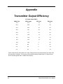
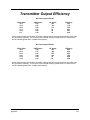
Transmitter Output Efficiency
Glossary
Index
vi
Appendix-1
G-1
Index-1
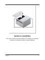
Section 1—Getting Acquainted
This section provides a general description of the FM30, FM150, and
FM300 transmitters and introduces you to safety conventions used
within this document. Review this material before installing or operating
the transmitter.
Getting Acquainted
1-1
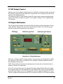
1.1 Your Transmitter
The FM30, FM150, and FM300 are members of a family of FM stereo broadcast
transmitters. Crown transmitters are known for their integration, ease-of-use, and
reliability.
The integration is most apparent in the standard transmitter configuration which
incorporates audio processing, stereo generation, and RF amplification without
compromised signal quality. A single Crown transmitter can replace several pieces of
equipment in a traditional system.
Ease-of-use is apparent in the user-friendly front panel interface and in the installation
procedure. Simply select your operating frequency (using 5 external switches), add an
audio source, attach an antenna, and connect AC or DC power and you're ready to
broadcast. Of course, the FM series of transmitters also feature more sophisticated
inputs and monitoring connections if needed.
Reliability is a Crown tradition. The first Crown transmitters were designed for rigors of
worldwide and potentially portable use. The modular design, quality components,
engineering approach, and high production standards ensure stable performance.
Remote control and metering of the transmitter are made possible through a built-in I/O
port. For more direct monitoring, the front panel includes a digital multimeter display and
status indicators. Automatic control circuitry provides protection for high VSWR as well
as high current, voltage, and temperature conditions.
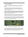
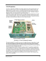
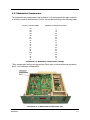
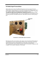
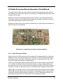
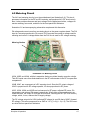
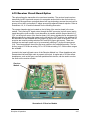
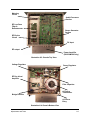
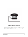
Illustration 1-1 FM150 Stereo Broadcast Transmitter
This manual describes the FM30, FM150, and FM300 because all three transmitters
share common design factors. Specific product differences are noted throughout the
manual. In physical appearance, the FM30 differs from the FM150 and FM300 in that it
lacks the power amplifier and cooling fan assembly on the back panel.
1-2
FM30/FM150/FM300 User’s Manual
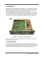
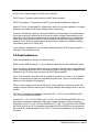
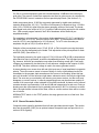
1.2 Applications and Options
Crown transmitters are designed for versatility in applications. They have been used as
stand-alone and backup transmitters and in booster, translator, satellator, and nearcast
applications. The following discussion describes these applications further.
Model numbers describe the configuration of the product (which has to do with its intended
purpose) and the RF output power which you can expect.
The number portion of each name represents the maximum RF output power. The FM300,
for example, can generate up to 300 watts of RF output power.
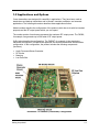
Suffix letters describe the configuration. The FM300T, for example, is the standard or
transmitter configuration. Except where specified, this document describes the transmitter
configuration. In this configuration, the product includes the following components
(functions):
•
•
•
•
Audio Processor/Stereo Generator
RF Exciter
Metering
Low-Pass filter
Illustration 1–2 Standard (Transmitter) Configuration
Getting Acquainted
1-3
1.2.1 Stand-Alone
In the standard configuration, the FM30, FM150, and FM300 are ideal stand-alone
transmitters. When you add an audio source (monaural, L/R stereo, or composite signal),
an antenna, and AC or DC power, the transmitter becomes a complete FM stereo broadcast
station, capable of serving a community.
As stand-alone transmitters, Crown units often replace multiple pieces of equipment in a
traditional setup (exciter, audio processor, RF amplifier).
1.2.2 Backup
In the standard configuration, Crown transmitters are also used in backup applications.
Should your primary transmitter become disabled, you can continue to broadcast while
repairs take place. In addition, the FM transmitters can replace disabled portions of your
existing system including the exciter, audio processor, or amplifier. Transfer switches on
each side of the existing and backup transmitters make the change-over possible with
minimal downtime.
The DC operation option of the FM30, FM150, and FM300 make them attractive backup
units for those times when AC power is lost.
1.2.3 Exciter
In addition to the standard configuration, the FM30, FM150, and FM300 are available in optional configurations to meet a variety of needs.
An "E" suffix, as in the FM30E, for example, represents an exciter-only configuration. In this
configuration, the audio processor and stereo generator boards are replaced with circuitry to
bypass their function. The exciter configurations are the least expensive way to get Crown
quality components into your transmission system.
You might consider the Crown exciter when other portions of your system are performing
satisfactorily and you want to maximize your investment in present equipment.
1-4
FM30/FM150/FM300 User’s Manual
1.2.4 Translator
A receiver configuration (FM150R, for example) replaces the audio processor/stereo generator board with a receiver module. This added feature makes the FM30, FM150, and
FM300 ideal for translator service in terrestrial-fed networks. These networks represent a
popular and effective way to increase your broadcasting coverage. Translators, acting as
repeater emitters, are necessary links in this chain of events.
Traditionally, network engineers have relied on multiple steps and multiple pieces of equipment to accomplish the task. Others have integrated the translator function (receiver and
exciter) to feed an amplifier. Crown, on the other hand, starts with an integrated transmitter
and adds a solid-state Receiver Module to form the ideal translator.
Illustration 1–3 Crown's Integrated Translator
This option enables RF in and RF out on any of Crown’s FM series of transmitters. In addition, the module supplies a composite output to the RF exciter portion of the transmitter.
From here, the signal is brought to full power by the built-in power amplifier for retransmission. The Receiver Module has been specifically designed to handle SCA channel output up
to 100 kHz for audio and high-speed data.
FSK ID programming is built-in to ensure compliance with FCC regulations regarding the
on-air identification of translators. Simply specify the call sign of the repeater station when
ordering. Should you need to change the location of the translator, replacement FSK chips
are available. The Receiver Module option should be ordered at the time of initial transmitter
purchase. However, an option kit is available for field converting existing Crown units.
In the translator configuration there are differences in the function of the front panel, see
Section 3 for a description.
Getting Acquainted
1-5
1.2.5 Satellator
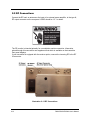
One additional option is available for all configurations—an FSK Identifier (FSK IDer). This
added feature enables the FM30, FM150, and FM300 to transmit its call sign or operating
frequency in a Morse code style. This option is intended for use in satellite-fed networks.
Transmitters equipped in this fashion are often known as "satellators."
Connect the transmitter to your satellite receiver and the pre-programmed FSK IDer does
the rest—shifting the frequency to comply with FCC requirements and in a manner that is
unnoticeable to the listener. The FSK IDer module should be ordered at the time you order
your transmitter, but is available separately (factory programmed for your installation).
Illustration 1–4 Transmitter with FSK IDer Option
Add the FSK IDer option to the exciter configuration for the most economical satellator (a
composite input signal is required).
1.2.6 Nearcasting
The output power of an FM30 transmitter can be reduced to a level that could function as a
near-cast transmitter. Crown transmitters have been used in this way for language translation, for re-broadcasting the audio of sporting events within a stadium, and for specialized
local radio. The FM30 is the only transmitter that is appropriate for this application.
1-6
FM30/FM150/FM300 User’s Manual
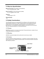
1.3 Transmitter/Exciter Specifications
Frequency Range
87.9 MHz–107.9 MHz (76 MHz–90 MHz
optionally available)
RF Power Output
(VSWR 1.7:1 or better)
FM30
3-33 Watts adjustable
FM150
15-165 Watts adjustable
FM300
30-330 Watts adjustable
RF Output Impedance
50 Ohms
Frequency Stability
Meets FCC specifications from 0-50
degrees C
Audio Input Impedance
50k Ω bridging, balanced, or 600 Ω
Audio Input Level
Selectable for –10 dBm to +10 dBm for
75 kHz deviation at 400 Hz
Pre-emphasis
Selectable for 25, 50, or 75 µsec; or flat
Audio Response
Conforms to 75 µsec pre-emphasis
curve as follows:
Complete Transmitter
±0.30 dB (50 Hz–10 kHz)
±1.0 dB (10 kHz–15 kHz)
Exciter only
±0.25 dB (50 Hz–15 kHz)
Distortion (THD + Noise)
Complete Transmitter
Less than 0.7% (at 15kHz)
Exciter only
Less than 0.3% (50Hz-15kHz)
Stereo Separation
Complete Transmitter
Better than –40dB (50Hz-15kHz)
Exciter only
Better than –40dB (50Hz-15kHz)
Crosstalk
Main into Sub, better than –40dB
Sub into Main, better than –40dB
Stereo Pilot
19 kHz ±2 Hz, 9% modulation
Getting Acquainted
1-7
Subcarrier Suppression
50dB below ±75 kHz deviation
FM S/N Ratio (FM noise)
Complete Transmitter
Better than –60dB
Exciter only
Better than –70dB
AM S/N Ratio
Asynchronous and synchronous noise
better than FCC requirements
RF Bandwidth
±120 kHz, better than –35 dB
±240 kHz, better than –45 dB
RF Spurious Products
Better than –70dB
Operating Environment
Temperature (0°C to 50°C)
Humidity (0 to 80% at 20°C)
Maximum Altitude (3,000 Meters;
9834 Feet
AC Power
100,120, 220, or 240 volts +10%/15%); 50/60Hz
FM30
115VA
FM150
297VA
FM300
550VA
DC Power
1-8
FM30
24-36 volts (36 volts at 3 amps required
for full output power)
FM150
36-72 volts (48 volts @ 7 amps for full
output power)
FM300
36-72 volts (72 volts @ 10 amps for full
output power)
FM30/FM150/FM300 User’s Manual
Note: We set voltage and ampere requirements to assist you in designing your system. Depending on your operating frequency, actual requirements for maximum voltage and current
readings are 10–15% lower than stated.
Regulatory
Type notified FCC parts 73 and 74
Meets FCC, DOC, and CCIR requirements
Dimensions
13.5 x 41.9 x 44.5 cm
5.25 x 16.5 x 17.5 inches
Weight
FM30
10.5 kg (23 lbs)
13.6 kg (30 lbs) shipping weight
FM150
11.4 kg (25 lbs)
14.5 kg (32 lbs) shipping weight
FM300
16.8 kg (37 lbs)
20.0 kg (44 lbs) shipping weight
Getting Acquainted
1-9
1.4 Receiver Specifications
Monaural Sensitivity (demodulated, de-emphasized)
3.5 µ V for signal-to-noise > 50 dB
Stereo Sensitivity (19–kHz pilot frequency added)
31 µ V for signal-to-noise > 50 dB
Connector
Standard type N, 50 Ω
Shipping Weight
1 lb
1.5 Safety Considerations
Crown Broadcast assumes the responsibility for providing you with a safe product and
safety guidelines during its use. “Safety” means protection to all individuals who install,
operate, and service the transmitter as well as protection of the transmitter itself. To
promote safety, we use standard hazard alert labeling on the product and in this manual.
Follow the associated guidelines to avoid potential hazard.
1.5.1 Dangers
DANGER represents the most severe hazard alert. Extreme bodily harm or death will occur
if DANGER guidelines are not followed.
1.5.2 Warnings
WARNING represents hazards which could result in severe injury or death.
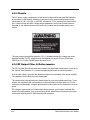
1.5.3 Cautions
CAUTION indicates potential personal injury, or equipment or property damage if the associated guidelines are not followed. Particular cautions in this text also indicate unauthorized
radio-frequency operation.
Illustration 1–5 Sample Hazard Alert
1-10
FM30/FM150/FM300 User’s Manual
Section 2—Installation
This section provides important guidelines for installing your transmitter.
Review this information carefully for proper installation.
Installation
2-1
2.1 Operating Environment
You can install the FM transmitter in a standard component rack or on a suitable surface
such as a bench or desk. In any case, the area should be as clean and well ventilated as
possible. Always allow for at least 2 cm of clearance under the unit for ventilation. If you set
the transmitter on a flat surface, install spacers on the bottom cover plate. If you install the
transmitter in a rack, provide adequate clearance above and below. Do not locate the transmitter directly above a hot piece of equipment.
2.2 Power Connections
The FM30, FM150, and FM300 operate on 100, 120, 220, or 240 volts AC (50 or 60 Hz; single phase). Each transmitter can operate on DC power as well (28 volts for the FM30, 48
volts for the FM150, and 72 volts for the FM300). The transmitter can operate on fewer volts
DC, but with reduced RF output power (see section 1.3). In addition, the transmitter isolates
the AC and DC sources; both can be connected at the same time to provide battery backup
in the event of an AC power failure.
2.2.1 AC Line Voltage Setting
To change the voltage setting, follow these steps:
1. Disconnect the power cord if it is attached.
2. Open the cover of the power connector assembly using a small, flat blade screw
driver. See Illustration 2–1.
3. Insert the screwdriver into the voltage selection slot and remove the drum from the
sembly.
as-
4. Rotate the drum to select the desired voltage. See Illustration 2–2.
5. Replace the drum and cover and check to see that the correct voltage appears in
connector window.
the
6. Connect the AC power cord.
2-2
FM30/FM150/FM300 User’s Manual
Illustration 2–1 Removing the Power Connector Cover
Illustration 2–2 Selecting an AC Line Voltage
Installation
2-3
2.2.2 Fuses
The fuse holders are located in the power connector assembly just below the voltage selector.
Illustration 2–3 Fuse Holder
For 100 to 120 VAC operation, use the fuse installed at the factory. For 220 to 240 VAC operation, use the slow-blow fuse located in a hardware kit within the transmitter packaging.
Consult the following table:
Transmitter
Input Power
Fuse
FM30
100–120 V
220–240 V
3A
1.5 A
FM150
100–120 V
220–240 V
6.3 A
4A
FM300
100–120 V
220–240 V
12.5 A
6.3 A
Illustration 2–4 Fuse Reference Table
2-4
FM30/FM150/FM300 User’s Manual
2.2.3 Battery Power
Your transmitter can operate on a DC power source (such as 4 or 5, 12–volt deep cycle batteries connected in series). The FM30 requires 28 volts DC for full output power, while the
FM150 requires 48 volts, and FM300 requires 72 volts for full output power. Connect the
batteries to the red (+) and black (–) battery input binding posts on the rear panel.
2–5 Illustration DC Input Terminals
2.3 Frequency (Channel) Selection
Your transmitter is capable of operating between 87.9 and 107.9 MHz in the FM band. The
transmitter can also operate between 76 and 90 MHz by shorting pins 9 and 10 of J20 on
the motherboard. (See illustration 2-6)
To adjust the operating frequency, follow these steps:
1. Locate the frequency selector switches on the front panel which will be used to change
the setting. See Illustrations 2–6 and 2–7.
Installation
2-5
2. Use small flat blade screwdriver or another suitable device to rotate the switches to the
desired setting. (The selected number will appear directly above the white indicator dot
on each switch.) See examples of selected frequencies in the illustration below.
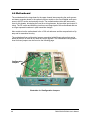
3. To change the operating band from 87.9-107.9MHz to 76-90MHz or vice versa, or to adjust the modulation compensation pot, remove the top cover to gain access to these features. See illustrations 2-6 and 2-10.
Illustration 2–6 Top Cover Removed
Megahertz
.1
.01
Illustration 2–7 Transmitter Front Panel (Frequency Selector Switches)
= 88.10 MHz
= 107.90 MHz
Illustration 2–8 Two Sample Frequency Selections
2-6
FM30/FM150/FM300 User’s Manual
2.3.1 Modulation Compensator
The Modulation trim-potentiometer (see illustration 2–10) compensates for slight variations
in deviation sensitivity with frequency. Set the trim-pot dial according to the following graph:
Frequency of Operation (MHz)
Modulation Compensation Pot Setting
108
106
104
102
100
98
97.1
96
94
92
90
88
86
84
82.4
82
80
78
76
0
10
15
25
35
40
45
55
60
70
75
80
80
80
70
65
55
30
0
Illustration 2–9 Modulation Compensator Settings
These compensator settings are approximate. Each mark on the potentiometer represents
about 1.8% modulation compensation.
Illustration 2–10 Modulation Compensator Pot
Installation
2-7
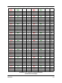
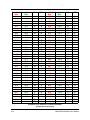
2.4 Receiver Frequency Selection
If you have a transmitter equipped with the receiver option, you will need to set the receiving
or incoming frequency.
1. With the top cover removed, locate the receiver module and the two switches (labeled
SW1 and SW2).
Illustration 2–11 Receiver Module Switches
2. Use the adjacent chart to set the switches for the desired incoming frequency.
3. For frequencies in the Japan FM band, short pins 7&8 on J1 on the receiver card.
4. For 75us pre-emphasis short pins 3&4 and 5&6 on J2 of the Receiver card.
5. For 50us pre-emphasis short pins 1&2 and 7&8 on J2 of the Receiver card.
6. After setting the frequency, replace the top cover and screws.
2-8
FM30/FM150/FM300 User’s Manual
Freq. 74-90 Freq. 88-108
MHz
MHz
74.9
87.9
75.0
88.0
75.1
88.1
75.2
88.2
75.3
88.3
75.4
88.4
75.5
88.5
75.6
88.6
75.7
88.7
75.8
88.8
75.9
88.9
76.0
89.0
76.1
89.1
76.2
89.2
76.3
89.3
76.4
89.4
76.5
89.5
76.6
89.6
76.7
89.7
76.8
89.8
76.9
89.9
77.0
90.0
77.1
90.1
77.2
90.2
77.3
90.3
77.4
90.4
77.5
90.5
77.6
90.6
77.7
90.7
77.8
90.8
77.9
90.9
78.0
91.0
78.1
91.1
78.2
91.2
78.3
91.3
78.4
91.4
78.5
91.5
78.6
91.6
78.7
91.7
78.8
91.8
SW1
SW2
0
8
0
8
0
8
0
8
0
8
0
8
0
8
0
8
0
8
0
8
0
8
0
8
0
8
0
8
0
8
0
8
1
9
1
9
1
9
1
9
0
0
1
1
2
2
3
3
4
4
5
5
6
6
7
7
8
8
9
9
A
A
B
B
C
C
D
D
E
E
F
F
0
0
1
1
2
2
3
3
Freq. 74-90 Freq. 88-108
MHz
MHz
78.9
91.9
79.0
92.0
79.1
92.1
79.2
92.2
79.3
92.3
79.4
92.4
79.5
92.5
79.6
92.6
79.7
92.7
79.8
92.8
79.9
92.9
80.0
93.0
80.1
93.1
80.2
93.2
80.3
93.3
80.4
93.4
80.5
93.5
80.6
93.6
80.7
93.7
80.8
93.8
80.9
93.9
81.0
94.0
81.1
94.1
81.2
94.2
81.3
94.3
81.4
94.4
81.5
94.5
81.6
94.6
81.7
94.7
81.8
94.8
81.9
94.9
82.0
95.0
82.1
95.1
82.2
95.2
82.3
95.3
82.4
95.4
82.5
95.5
82.6
95.6
82.7
95.7
82.8
95.8
SW1
SW2
1
9
1
9
1
9
1
9
1
9
1
9
1
9
1
9
1
9
1
9
1
9
1
9
2
A
2
A
2
A
2
A
2
A
2
A
2
A
2
A
4
4
5
5
6
6
7
7
8
8
9
9
A
A
B
B
C
C
D
D
E
E
F
F
0
0
1
1
2
2
3
3
4
4
5
5
6
6
7
7
Illustration 2–12-1 Receiver Frequency Selection
(Continued on next page)
Installation
2-9
Freq. 74-90 Freq. 88-108
MHz
MHz
82.9
95.9
83.0
96.0
83.1
96.1
83.2
96.2
83.3
96.3
83.4
96.4
83.5
96.5
83.6
96.6
83.7
96.7
83.8
96.8
83.9
96.9
84.0
97.0
84.1
97.1
84.2
97.2
84.3
97.3
84.4
97.4
84.5
97.5
84.6
97.6
84.7
97.7
84.8
97.8
84.9
97.9
85.0
98.0
85.1
98.1
85.2
98.2
85.3
98.3
85.4
98.4
85.5
98.5
85.6
98.6
85.7
98.7
85.8
98.8
85.9
98.9
86.0
99.0
86.1
99.1
86.2
99.2
86.3
99.3
86.4
99.4
86.5
99.5
SW1
SW2
2
A
2
A
2
A
2
A
2
A
2
A
2
A
2
A
3
B
3
B
3
B
3
B
3
B
3
B
3
B
3
B
3
B
3
B
3
8
8
9
9
A
A
B
B
C
C
D
D
E
E
F
F
0
0
1
1
2
2
3
3
4
4
5
5
6
6
7
7
8
8
9
9
A
Freq. 74-90 Freq. 88-108
MHz
MHz
86.6
99.6
86.7
99.7
86.8
99.8
86.9
99.9
87.0
100.0
87.1
100.1
87.2
100.2
87.3
100.3
87.4
100.4
87.5
100.5
87.6
100.6
87.7
100.7
87.8
100.8
87.9
100.9
88.0
101.0
88.1
101.1
88.2
101.2
88.3
101.3
88.4
101.4
88.5
101.5
88.6
101.6
88.7
101.7
88.8
101.8
88.9
101.9
89.0
102.0
89.1
102.1
89.2
102.2
89.3
102.3
89.4
102.4
89.5
102.5
89.6
102.6
89.7
102.7
89.8
102.8
89.9
102.9
90.0
103.0
X
103.1
X
103.2
SW1
SW2
B
3
B
3
B
3
B
3
B
3
B
4
C
4
C
4
C
4
C
4
C
4
C
4
C
4
C
4
C
4
C
4
C
4
C
4
C
A
B
B
C
C
D
D
E
E
F
F
0
0
1
1
2
2
3
3
4
4
5
5
6
6
7
7
8
8
9
9
A
A
B
B
C
C
Illustration 2–12-2 Receiver Frequency Selection
(Continued on next page)
2-10
FM30/FM150/FM300 User’s Manual
Freq. 74-90 Freq. 88-108
MHz
MHz
X
103.3
X
103.4
X
103.5
X
103.6
X
103.7
X
103.8
X
103.9
X
104.0
X
104.1
X
104.2
X
104.3
X
104.4
X
104.5
X
104.6
X
104.7
X
104.8
X
104.9
X
105.0
X
105.1
X
105.2
X
105.3
X
105.4
X
105.5
X
105.6
X
105.7
X
105.8
X
105.9
X
106.0
X
106.1
X
106.2
X
106.3
X
106.4
X
106.5
X
106.6
X
106.7
X
106.8
X
106.9
SW1
SW2
4
C
4
C
4
C
5
D
5
D
5
D
5
D
5
D
5
D
5
D
5
D
5
D
5
D
5
D
5
D
5
D
5
D
5
D
5
D
D
E
E
F
F
0
0
1
1
2
2
3
3
4
4
5
5
6
6
7
7
8
8
9
9
A
A
B
B
C
C
D
D
E
E
F
Freq. 74-90 Freq. 88-108
MHz
MHz
X
107.0
X
107.1
X
107.2
X
107.3
X
107.4
X
107.5
X
107.6
X
107.7
X
107.8
X
107.9
X
108.0
SW1
SW2
D
6
E
6
E
6
E
6
E
6
E
F
0
0
1
1
2
2
3
3
4
4
Illustration 2–12-3 Receiver Frequency Selection
Installation
2-11
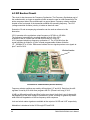
2.5 RF Connections
Connect the RF load, an antenna or the input of an external power amplifier, to the type-N,
RF output connector on the rear panel. VSWR should be 1.5:1 or better.
The RF monitor is intended primarily for a modulation monitor connection. Information
gained through this connection can supplement that which is available on the transmitter
front panel displays.
If your transmitter is equipped with the receiver option, connect the incoming RF to the RF
IN connector.
Illustration 2–13 RF Connections
2-12
FM30/FM150/FM300 User’s Manual
2.6 Audio Input Connections
Attach audio inputs to the Left and Right XLR connectors on the rear panel. (The Left
channel audio is used on Mono.) Pin 1 of the XLR connector goes to chassis ground. Pins 2
and 3 represent a balanced differential input with an impedance of about 50 kΩ . They may
be connected to balanced or unbalanced left and right program sources.
The audio input cables should be shielded pairs, whether the source is balanced or unbalanced. For an unbalanced program source, one line (preferably the one connecting to pin 3)
should be grounded to the shield at the source. Audio will then connect to the line going to
pin 2.
Illustration 2–14 XLR Audio Input Connectors
By bringing the audio return line back to the program source, the balanced differential input
of the transmitter is used to best advantage to minimize noise. This practice is especially
helpful if the program lines are fairly long, but is a good practice for any distance.
If the program source requires a 600 Ω termination, see the motherboard configuration chart
on page 4-9 for the proper configuration of the jumpers.
Installation
2-13
2.7 SCA Input Connections
You can connect external SCA generators to the SCA In connectors (BNC-type) on the rear
panel. The inputs are intended for the 60 kHz to 99 kHz range, but a lower frequency may
be used if the transmitter is operated in Mono mode. (The 23 to 53 kHz band is used for stereo transmission.) For 7.5 kHz deviation (10% modulation), input of approximately 3.5–volts
(peak-to-peak) is required.
Illustration 2–15 SCA Input Connectors
2.8 Composite Input Connection
You may feed composite stereo (or mono audio) directly to the RF exciter bypassing the internal audio processor and stereo generator. To use the Crown transmitter as an RF Exciter
only ("E" version or when using the "T" version with composite input), it is necessary to use
the Composite Input section of the transmitter. This will feed composite stereo (or mono audio) directly to the RF exciter. In the "T" version, this will bypass the internal audio processor and stereo generator.
Input sensitivity is approximately 3.5–volt P-P for 75 kHz deviation.
1.
Enable the Composite Input by grounding pin 14 of the Remote I/O connector
(see Illustration 2–18).
2.
Connect the composite signal using the Composite In BNC connector.
2-14
FM30/FM150/FM300 User’s Manual
Illustration 2–16 Composite In and Audio Monitor Connections
2.9 Audio Monitor Connections
Processed, de-emphasized samples of the left and right audio inputs to the stereo generator are available at the Monitor jacks on the rear panel. The signals are suitable for feeding
a studio monitor and for doing audio testing. De-emphasis is normally set for 75 µsec; set to
50 µsec by moving jumpers, HD201 and HD202, on the Audio Processor/Stereo Generator
board.
2.10 Pre-emphasis Selection
Select the pre-emphasis curve (75 µsec, 50 µsec, 25 µsec, or Flat) by jumpering the appropriate pins of header HD1 on the Audio Processor/Stereo Generator board. If you change
the pre-emphasis, change the de-emphasis jumpers HD201 and HD202 on the Audio Processor/Stereo Generator board to match.
Installation
2-15
2.11 Program Input Fault Time-out
You can enable an automatic turn-off of the carrier in the event of program failure. To enable this option, see illustration 2-18 on page 2-16. The time between program failure and
carrier turn-off is set by a jumper (JP1) on the voltage regulator board (see page 6–14 for
board location). Jumper pins 1 and 2 (the two pins closest to the edge of the board) for a
delay of approximately 30 seconds; pins 3 and 4 for a 2–minute delay; pins 5 and 6 for a 4–
minute delay, and pins 7 and 8 for an 8– minute delay.
2.12 Remote I/O Connector
Remote control and remote metering of the transmitter is made possible through a 25–pin,
D-sub connector on the rear panel. (No connections are required for normal operation.)
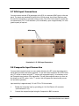
Illustration 2–17 Remote I/O Connector
Illustration 2–18 Remote I/O Connector (DB-25 Female)
2-16
FM30/FM150/FM300 User’s Manual
Pin Number Function
1.
Ground
2.
FMV Control
3.
Composite Out (sample of stereo generator output)
4.
FSK In (Normally high; pull low to shift carrier frequency approximately 7.5 KHz. Connect to open collector or relay contacts
of user-supplied FSK keyer.)
5.
/Auto Carrier Off (Pull low to enable automatic turnoff of carrier
with program failure.)
6.
Meter Battery (Unregulated DC voltage; 5 VDC=50 VDC)
7.
Meter RF Watts (1 VDC = 100 Watts)
8.
Meter PA Volts (5 VDC = 50VDC)
9.
Remote Raise (A momentary switch, holding this pin low will slowly raise the RF output)
10.
Remote Lower (A momentary switch, holding this pin low will slowly lower the RF output)
11.
Remote SWR (A buffered metering output with a calculated reading of standing wave ratio in
VDC.)
12.
External ALC Control
13.
No Connection
14.
/Ext. Enable (Pull low to disable the internal stereo generator and enable External Composite
Input.)
15.
38 KHz Out (From stereo generator for power supply synchronization. For transmitter
equipped with receiver option, this pin becomes the right audio output for an 8ohm monitor speaker. 38 KHz is disabled.)
16.
ALC
17.
/Carrier Off ( Pull low to turn carrier off)
18.
Fault Summary ( line goes high if any fault light is activated.)
19.
Meter PA Temperature (5 VDC=100 degrees C.)
20.
Meter PA Current (1VDC=10 DC Amperes.)
21.
Front Panel Voltmeter Input.
22.
No Connection.
23.
RDS RX
24.
RDS TX
25.
Ground
Installation
2-17
Notes:
2-18
FM30/FM150/FM300 User’s Manual
Section 3—Operation
This section provides general operating parameters of your transmitter
and a detailed description of its front panel display.
Operation
3-1
3.1 Initial Power-up Procedures
These steps summarize the operating procedures you should use for the initial operation of
the transmitter. More detailed information follows.
1. Turn on the DC breaker.
Illustration 3–1 DC Breaker
2. Turn on the main power switch.
Main Power
Switch
Illustration 3–2 Front Panel Power Switch
3-2
FM30/FM150/FM300 User’s Manual
3. Verify the following:
A. The bottom cooling fan runs continuously.
B. The Lock Fault indicator flashes for approximately 5 seconds, then goes off.
4. Set the Input Gain switches for mid-scale wideband gain reduction on an average
program level (see section 3.4).
5. Set the Processing control (see section 3.5; normal setting is “50”).
6. Set the Stereo-Mono switch to Stereo (see section 3.6).
7. Turn on the Carrier switch.
8. Check the following parameters on the front panel multimeter:
A. RF Power should be 29–33 watts for the FM30, 145–165 watts for the FM150, and
300–330 watts for the FM300.
B. SWR should be less than 1.1. (A reading greater than 1.25 indicates an antenna
mismatch.
C. ALC should be between 4.00 and 6.00 volts.
D. PA DC Volts should be 26–30 volts for the FM30, 25–35 volts for the FM150, and
37–52 volts for the FM300. (Varies with antenna match, power, and frequency.)
E. PA DC Amperes should be 1.5–2.5 amps for the FM30, 5.5–7.5 amps for the
FM150, and 7.0–9.0 amps for the FM300. (Varies with antenna match, power, and
frequency.)
F. PA Temperature should initially read 20–35 degrees C (room temperature). After
one hour the reading should be 35–50 degrees C.
G. Supply DC Volts should display a typical reading of 45 V with the carrier on and 50 V
with the carrier off for both the FM30 and FM150 products. For the FM300, the
readings should be 65 V with the carrier on and 75 V with carrier off.
H. Voltmeter should be reading 0.0.
The remainder of this section describes the functions of the front panel indicators
and switches.
Operation
3-3
3.2 Power Switches
3.2.1 DC Breaker
The DC breaker, on the rear panel, must be on (up) for transmitter operation, even when
using AC power. Electrically, the DC breaker is located immediately after diodes which isolate the DC and AC power supplies.
3.2.2 Power Switch
The main on/off power switch controls both the 120/240 VAC and the DC battery power input.
3.2.3 Carrier Switch
This switch controls power to the RF amplifiers and supplies a logic high to the voltage
regulator board, which enables the supply for the RF driver. In addition, the Carrier Switch
controls the operating voltage needed by the switching power regulator.
A "Lock Fault" or a low pin 17 (/Carrier Off) on the Remote I/O connector will hold the carrier
off. (See section 2.12.)
Carrier Switch
Illustration 3–3 Front Panel Carrier Switch
3-4
FM50/FM150/FM300 User’s Manual
3.3 Front Panel Bar-Dot Displays
Bar-dot LEDs show audio input levels, wideband and highband audio gain control, and
modulation percentage. Resolution for the gain control and modulation displays is increased
over a conventional bar-graph display using dither enhancement which modulates the
brightness of the LED to give the effect of a fade from dot to dot. (See section 4.7.)
3.3.1 Audio Processor Input
Two vertical, moving-dot displays for the left and right channels indicate the relative audio
levels, in 3 dB steps, at the input of the audio processor. Under normal operating conditions,
the left and right Audio Processor indicators will be active, indicating the relative audio input
level after the Input Gain switches. During program pauses, the red Low LED will light.
The translator configuration shows relative audio levels from the included receiver.
3.3.2 Highband and Wideband Display
During audio processing, the moving-dot displays indicate the amount of gain control for
broadband (Wide) and pre-emphasized (High) audio.
As long as program material causes activity of the Wideband green indicators, determined
by the program source level and Input Gain switches, the transmitter will be fully modulated.
(See section 3.4.)
The Wideband indicator shows short-term “syllabic-rate” expansion and gain reduction
around a long-term (several seconds) average gain set. In the translator configuration, the
Wideband indicator also shows relative RF signal strength.
Program material and the setting of the Processing control determine the magnitude of the
short-term expansion and compression (the rapid left and right movement of the green
light).
High-frequency program content affects the activity of the Highband indicator. With 75–µsec
pre-emphasis, Highband processing begins at about 2 kHz and increases as the audio frequency increases. Some programs, especially speech, may show no activity while some
music programs may show a great deal of activity.
3.3.3 Modulation Display
A 10–segment, vertical peak-and-hold, bar graph displays the peak modulation percentage.
A reading of “100” coincides with 75 kHz deviation. The display holds briefly (about 0.1 seconds) after the peak. The “Pilot” indicator illuminates when the transmitter is in the stereo
mode.
To verify the actual (or more precise) modulation percentage, connect a certified modulation
monitor to the RF monitor jack on the rear panel.
Operation
3-5
3.4 Input Gain Switches
The “+6 dB” and “+12 dB” slide switches set audio input sensitivity according to the
following table.
Normal Input
Sensitivity
+6dB
+12dB
+10dBm
Down
Down
+4dBm
Up
Down
-2dBm
Down
Up
-8dBm
Up
Up
Switches
Illustration 3–4 Input Gain Switches
Find, experimentally, the combination of Input Gain switch settings that will bring the
Wideband gain-reduction indicator to mid scale for “normal” level program material. The
audio processor will accommodate a fairly wide range of input levels with no degradation
of audio quality.
3.5 Processing Control
Two factors contribute to the setting of the Processing control: program material and
personal taste. For most program material, a setting in the range of 40 to 70 provides good
program density. For the classical music purist, who might prefer preservation of music
dynamics over density, 10 to 40 is a good range. The audio will be heavily processed in
the 70 to 100 range.
If the program source is already well processed, as might be the case with a satellite feed,
set the Processing to “0” or “10”.
3.6 Stereo-Mono Switch
The Stereo-Mono slide switch selects the transmission mode. In Mono, feed audio only to
the left channel. Although right-channel audio will not be heard as audio modulation, it will
affect the audio processing.
3-6
FM30/FM150/FM300 User’s Manual
3.7 RF Output Control
Set this control for the desired output power level. Preferably, set the power with an external
RF wattmeter connected in the coaxial line to the antenna. You may also use the RF power
reading on the digital multimeter.
The control sets the RF output voltage. Actual RF output power varies as the approximate
square of the relative setting of the control. For example, a setting of “50” is approximately
1/4 full power.
3.8 Digital Multimeter
The four-digit numeric display in the center of the front panel provides information on transmitter operation. Use the “Up” and “down” push-buttons to select one of the following parameters. A green LED indicates the one selected.
Illustration 3–5 Digital Multimeter
RF Power—Actually reads RF voltage squared, so the accuracy can be affected by VSWR
(RF voltage-to-current ratio). See section 5.4 for calibration. Requires calibration with the
RF reflectometer being used.
SWR—Direct reading of the antenna standing-wave ratio (the ratio of the desired load impedance, 50 ohms, to actual load).
ALC—DC gain control bias used to regulate PA supply voltage. With the PA power supply
at full output voltage, ALC will read about 6.0 volts. When the RF output is being regulated
by the RF power control circuit, this voltage will be reduced, typically reading 4 to 5.5 volts.
The ALC voltage will be reduced during PA DC overcurrent, SWR, or LOCK fault conditions.
Operation
3-7
PA DC Volts—Supply voltage of the RF power amplifier.
PA DC Amps—Transistor drain current for the RF power amplifier.
PA DC Temperature—Temperature of the RF power amplifier heatsink in degrees C.
Supply DC Volts—Unregulated DC voltage at the input of the voltage regulators. For battery
operation, this reading is the battery voltage minus a diode drop.
Voltmeter—Reads the voltage at a test point located on the front edge of the motherboard.
A test lead connected to this point can be used for making voltage measurements in the
transmitter. The test point is intended as a servicing aid; an alternative to an external test
meter. Remember that the accuracy is only as good as the reference voltage used by the
metering circuit. Servicing a fault affected by the reference affects the Voltmeter reading.
The metering scale is 0 to 199.9 volts.
In the translator configuration, you can read a relative indication of RF signal strength numerically in the Voltmeter setting.
3.9 Fault Indicators
Faults are indicated by a blinking red light as follows:
SWR—Load VSWR exceeds 1.5:1. ALC voltage is reduced to limit the reflected RF power.
Lock—Frequency synthesizer phase-lock loop is unlocked. This indicator normally blinks for
about five seconds at power turn-on. Whenever this light is blinking, supply voltages will be
inhibited for the RF driver stage as well as for the RF power amplifier.
Input—The automatic carrier-off circuit is enabled (see sections 2.11 and 2.12) and the absence of a program input signal has exceeded the preset time. (The circuit treats white or
pink noise as an absence of a program.)
PA DC—Power supply current for the RF power output amplifier is at the preset limit. ALC
voltage has been reduced, reducing the PA supply voltage to hold supply current to the preset limit.
PA Temp—PA heatsink temperature has reached 50° C (122° F) for the FM30 and 80° C
(176° F) for the FM150 and FM300.
At about 55° C (131°F) for the FM30 or 82°C (180° F) for the FM150 and FM300, ALC voltage begins to decrease, reducing the PA supply voltage to prevent a further increase in
temperature. By 60° C (140° F) for the FM50 and 85° C (185° F) for the FM150 and FM300,
the PA will be fully cut off. The heatsink fan (models FM150°and FM300 only) is proportionally controlled to hold the heatsink at 35 C (95° F). Above this temperature, the fan runs at
full speed.
3-8
FM30/FM150/FM300 User’s Manual
Section 4—Principles of Operation
This section discusses the circuit principles upon which the transmitter
functions. This information is not needed for day-to-day operation of the
transmitter but may be useful for advanced users and service personnel.
Principles of Operation
4-1
4.1 Part Numbering
As this section refers to individual components, you should be familiar with the part numbering scheme used.
The circuit boards and component placement drawings use designators such as “R1”, “R2”,
and “C1.” These same designators are used throughout the transmitter on several different
circuit boards and component placement drawings. When referencing a particular component it is necessary to also reference the circuit board that it is associated with.
4-2
FM50/FM150/FM300 User’s Manual
4.2 Audio Processor/Stereo Generator Circuit Board
The audio board provides the control functions of audio processing-compression, limiting,
and expansion, as well as stereo phase-error detection, pre-emphasis and generation of the
composite stereo signal.
Illustration 6-4 and accompanying schematic may be useful to you during this discussion.
The overall schematic for the audio board is divided into two sheets; one each for the processor and stereo generator sections of the board.
Reference numbers are for the left channel. Where there is a right-channel counterpart, reference number are in parenthesis.
Illustration 4–1 Audio Processor/Stereo Generator Board
4.2.1 Audio Processor Section
Audio input from the XLR connector on the rear panel of the transmitter goes to instrument
amplifier, U2 (U8). Two-bit binary data on the +6 dB and +12 dB control lines sets the gain
of U2 (U8) to one of four levels in 6-dB steps. Gain of U2 is determined by R5, R6, or R7
(R45, R46, or R47) as selected by analog switch U1.
U3 (U9) is a THAT2180 voltage-controlled amplifier with a control-voltage-to-gain constant
of 6.1 mV/dB. The 2180 is a current-in/current-out device, so signal voltages at the input
and output will be zero. R11 converts the audio voltage at the output of U2 (U8) to current at
the input of U3 (U9). U3 (U9) output current is converted to audio voltage by U4A (U10A).
U4B (U10B) is a unity-gain inverter. When the positive peaks at the output of U4A (U10A) or
U4B (U10B) exceeds the gain-reduction threshold, U15 generates a 0.25 Volts-per-dB DC
control bias, producing wide-band gain reduction for U3 (U9). The dB-linear allows a frontpanel display of gain control on a linear scale with even distribution of dB.
Principles of Operation
4-3
Q1 (Q2) is a recover/expansion gate with a threshold about 18 dB below the normal program level. The amount of short-term expansion and time for gain recovery is controlled by
the PROCESSING control, located on the front panel display board. (See section 3.5.)
Audio components above 15,200 Hz are greatly attenuated by eighth-order switchedcapacitor elliptical filter, U5 (U11). The filter cut-off frequency is determined by a 1.52-MHz
clock (100 x 15,200 Hz) signal from the stereo generator section of the board. The broadband signal level at the output of U5 (U11) is about 5 dB below that required for full modulation. (With normal program material, the 5 dB of headroom will be filled with preemphasized audio.)
Pre-emphasis in microseconds is the product of the capacitance of C7 (C17), multiplied by
the current-gain of U6 (U12), times the value of R22 (R62). (For description of the device
used for U6 (12), see explanation for U3 (U9) above.) For a 75 micro-seconds preemphasis, the gain of U6 (U12) will be about 1.11.
Selection of the pre-emphasis curve (75 µS, 50 µS, or Flat) is made by moving the jumper
on HD1 to the pins designated on the board. Fine adjustment of the pre-emphasis is made
with R23 (R63). (See section 5.1.)
For high-band processing, the peak output of U7A (U13A) and U7B (U13B) is detected and
gain-reduction bias is generated, as with the broadband processor. The high-band processing, however, shifts the pre-emphasis curve rather than affecting overall gain. Peak audio
voltages are compared to plus and minus 5-volt reference voltages at the outputs of U19A
and U19B. This same reference voltage is used in the stereo generator section.
A stereo phasing error occurs when left and right inputs are of equal amplitude but opposite
polarity. The most common cause is incorrect wiring of a left or right balanced audio line
somewhere in the program chain-sometimes at the source of a recording. When this happens, all the audio is in the left-minus-right stereo subcarrier-none in the left-plus-right baseband. The error can go unnoticed by one listening on a stereo receiver, but the audio may
disappear on a mono receiver. In normal programming there may be short-term polarity reversals of left versus right, either incidental or-for effect-intentional. A phase error of several
seconds duration is processed by U14A and U14B and interpreted as a real error. During a
phasing error the right-channel level is gradually reduced by 6 dB. For a listener to a stereo
radio, the right-channel volume will be lower, while on a mono receiver there will be a reduction of volume.
NORMAL/TEST switch. In the TEST position, the stage gains are set to a fixed level. See
section 6.2
4.2.2 Stereo Generator Section
Composite stereo signal is generated from left and right-channel audio inputs. This section
also has the amplifier (U201) for an optional external composite input and provision for insertion of SCA signal(s).
4-4
FM30/FM150/FM300 User’s Manual
Processed, pre-emphasized left and right audio is passed through third-order lowpass filters
comprised of U202A (203A) and associated circuitry. The filters decrease the level of audio
products below 30 Hz. This low-frequency roll off is necessary to prevent disturbance to the
phase-lock loop in the RF frequency synthesizer by extremely low-frequency audio components. (See caution at section 2.8.)
U204 is a precision, four-quadrant, analog multiplier. The output of U204 is the product of
38 kHz applied to the Y input and the difference of left and right audio (L-R signal) applied
to the X input. The resulting output is a double sideband, suppressed carrier/the L-R subcarrier.
Spectral purity of the stereo subcarrier is dependant on a pure 38-kHz sinewave at the multiplier input.
U207A and Y201 comprise a 7.6-MHz crystal oscillator from which the 19 and 38-kHz subcarriers are digitally synthesized. U207F is a buffer. The 7.6 MHz is divided by 5 in U208A
to provide 1.52 Mhz, used by switched-capacitor filters U5 and U11 in the audio section.
3.8 MHz, 1.9 MHz, and 304 kHz are also derived from dividers in U208. Exclusive-OR
gates, U210C and U210D, provide a stepped approximation of a 38-kHz sine wave. With
the resistor ratios used, the synthesized sine wave has very little harmonic energy below
the 7th harmonic. U210A and B generate the 19-kHz pilot subcarrier. U211 is a dual
switched-capacitor filter, configured as second-order, low-pass filters, each one with a Q of
5. The 38 and 19-kHz outputs of pins 1 and 20, respectively, are fairly pure sine waves.
Harmonic distortion products are better than 66 dB down-with a THD of less than 0.05%.
SEPARATION control R244 sets the 38-kHz level at the Y input of U204.
Resistor matrix R219, R220, R221, and R223 sum the L+R audio with the L-R subcarrier to
produce a current at the junction of R221 and R223 that will be converted to composite stereo (less pilot) at the output of summing amplifier U206A. SCA signal is also injected at the
input of U206A. 19-kHz pilot is combined with composite stereo in summing amplifier
U206B.
Analog switch U205, at the input of U206A, provides switching of left and right audio for stereo and mono modes. In the mono mode, right channel audio is disabled, and the left channel audio is increased from 45% modulation to 100%.
MON L and MON R outputs go to the AF Monitor jacks on the rear panel. R209+R210
(R214+R215) and C207 (C210) is a de-emphasis network. Processed, de-emphasized
samples of the left and right audio are used for a studio monitor and for audio testing.
Jumpers at HD201 (HD202) allow selection of 50-µsec or 75-µsec de-emphasis.
VR212A and B supply +7 volts and -7 volts, respectively. A 5-volt reference from the audio
processor section supplies the subcarrier generators.
For an explanation of on-board adjustments see section 5.2.
Principles of Operation
4-5
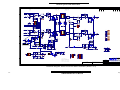
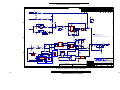
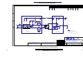
4.3 RF Exciter Circuit
This circuit is also known as the Frequency Synthesizer. The Frequency Synthesizer part of
the motherboard is no longer a separate module as was the case on older transmitters.The
entire component side of the motherboard is a ground plane. Frequency selector switches
located on the front panel of the transmitter establish the operating frequency. The VCO
(voltage-controlled oscillator) circuitry is inside an aluminum case.
Illustration 6-6 and accompanying schematics can be used as reference in this
discussion.
VCO1 operates at the synthesizer output frequency of 87 MHz to 108 MHz.
The frequency is controlled by a voltage applied to pin 8 of the VCO.
A sample of the RF comes from A2 and is fed to the PLL chip U13.
U13 is a phase-locked-loop frequency synthesizer IC. The 10.24 MHz from the
crystal oscillator is divided to 10 kHz. Internal programmable dividers divide the
87 - 108 MHz RF to 10 kHz. Differences between the two signals produce error signals at
pins 7 and 8 of U14.
Exciter Section
Illustration 4–2 Motherboard (Exciter Section)
Frequency selector switches are read by shift registers U17 and U18. Data from the shift
registers is read by U16 which then programs the PLL (Phase Lock Loop) IC U13.
U14B is a differential amplifier and filter for the error signal. Audio that is out of phase with
that appearing on the error voltage is introduced by U14A., allowing for greater loop bandwidth with less degradation of the low frequency audio response.
Lock and unlock status signals are available at the outputs of U15E and U15F respectively.
Modulation is introduced to the VCO though R72 and R122.
4-6
FM30/FM150/FM300 User’s Manual
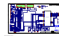
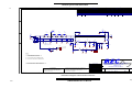
4.5 Metering Circuit
The ALC and metering circuitry is on the motherboard (see Illustration 6–6). This circuit
processes information for the RF and DC metering, and produces ALC (RF level-control)
bias. It also provides reference and input voltages for the digital panel meter, voltages for
remote metering, fan control, and drive for the front-panel fault indicators.
Illustration 6–6 and accompanying schematics complement this discussion.
PA voltage and current come from a metering shunt on the power regulator board. The PAI
input is a current proportional to PA current; R153 converts the current to voltage used for
metering and control. A voltage divider from the PAV line is used for DC voltage metering.
Metering Section
Illustration 4–3 Metering Circuit
U23A, U23B, and U24A, with their respective diodes, are diode linearity correction circuits.
Their DC inputs come from diode detectors in the RF reflectometer in the RF low-pass filter
compartment.
U24B, U24C, are components of a DC squaring circuit. Since the DC output voltage of
U24C is proportional to RF voltage squared, it is also proportional to RF power.
U22C, U22A, U20A, and U22D are level sensors for RF power, reflected RF power, PA
temperature, and external PA current, respectively. When either of these parameters exceeds the limits, the output of U22B will be forced low, reducing the ALC (RF level control)
voltage, which, in turn, reduces the PA supply voltage.
The DC voltage set point for U22A (reflected RF voltage) is one-fifth that of U22C (forward
RF voltage). This ratio corresponds to an SWR of 1.5:1 [(1+.2)/(1– .2)=1.5]. The U25 inverters drive the front panel fault indicators.
Principles of Operation
4-7
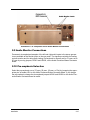
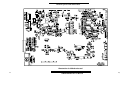
4.6 Motherboard
The motherboard is the large board in the upper chassis interconnecting the audio processor/stereo generator board or the optional receiver module or the Omnia digital audio processor to the RF exciter and metering circuits. The motherboard provides the interconnections for this boards, eliminating the need for a wiring harness, and provides input/output filtering. The RF exciter and Metering circuits are an integral part of the motherboard and are
no longer separate boards as in past transmitter designs.
Also contained on the motherboard is the +5.00 volt reference and the composite drive Op
amp and its associated circuitry.
The motherboard has configuration jumpers associated with different options that can be
added at the time of order or at a later time as an upgrade. The motherboard configuration
chart for these jumpers can be found on the following page.
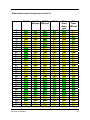
Configuration
Jumpers
Illustration 4–4 Configuration Jumpers
4-8
FM30/FM150/FM300 User’s Manual
Motherboard Jumper Configuration Chart 4.6.1
Jumper
FMA “E”
FMA“T”
50KΩ input
FMA“T”
600Ω input
FMA “R”
Z1
Z2
Z3
Z4
Z5
Z6
Z7
Z8
Z9
Z10
Z11
Z12
Z13
Z14
Z15
Z16
Z17
Z18
Z19
Z20
Z21
Z22
Z23
Z24
Z25
Z26
Z27
Z28
Z29
Z30
Z31
Z32
Z33
JMP1
JMP2
Short
Short
Open
Open
Open
Open
Open
Open
Short
Short
Short
Short
Short
Short
Open
Open
Open
Open
Open
Open
Open
Open
Short
Short
Short
Short
Short
Short
Short
Short
Open
Short
Short
Open
Open
Short
Short
Open
Open
Open
Open
Open
Open
Open
Open
Open
Open
Open
Open
Open
Open
Open
Open
Open
Open
Open
Open
Short
Short
Short
Short
Short
Short
Short
Short
Open
Open
Open
Open
Open
Short
Short
Short
Open
Short
Open
Short
Short
Open
Open
Open
Open
Open
Open
Open
Open
Open
Open
Open
Open
Open
Open
Short
Short
Short
Short
Short
Short
Short
Short
Open
Open
Short
Open
Open
Short
Short
Open
Open
Open
Open
Open
Open
Open
Open
Open
Open
Open
Open
Open
Open
Open
Open
Open
Open
Open
Open
Short
Short
Short
Short
Short
Short
Short
Short
Open
Open
Open
Open
Open
Principles of Operation
FMA
“Omnia”
Analog
input
Short
Short
Open
Open
Open
Open
Open
Open
Open
Open
Open
Open
Open
Open
Open
Open
Open
Open
Open
Open
Open
Open
Short
Short
Short
Short
Short
Short
Short
Short
Open
Open
Open
Open
Open
FMA
“Omnia”
AES input
Open
Open
Open
Short
Open
Short
Open
Open
Open
Open
Open
Open
Open
Open
Open
Open
Open
Open
Open
Open
Open
Open
Short
Short
Short
Short
Short
Short
Short
Short
Open
Open
Open
Open
Open
4-9
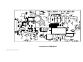
4.7 Display Circuit Board
The front-panel LEDs, the numeric display, the slide switches, and the processing and RF
level controls are mounted on the display circuit board. To access the component side of
the board, remove the front panel by removing 12 screws. The board contains circuits for
the digital panel meter, modulation peak detector, and LED display drivers, as well as indicators and switches mentioned above.
Illustration 6–9 and accompanying schematic complement this discussion.
Left and right audio from input stages of the audio processor board (just after the Input Gain
attenuator) go to the L VU and R VU input on the display board. Peak rectifiers U1A and
U1B drive the left and right Audio Input displays. The LED driver gives a 3–dB per step display. The lowest step of the display driver is not used; rather a red LOW indicator lights
when audio is below the level of the second step. Transistors Q1 and Q2 divert current from
the LOW LEDs when any other LED of the display is lit.
Resolution of the linear displays, High Band, Wide Band, and Modulation, has been improved using dither enhancement. With dither, the brightness of the LED is controlled by
proximity of the input voltage relative to its voltage threshold. The effect is a smooth transition from step to step as input voltage is changed. U6A, U6B, and associated components
comprise the dither generator. Dither output is a triangular wave.
Composite stereo (or mono) is full-wave detected by diodes D5 and D6, U7, U13, Q3, and
Q4 are components of a peak sample-and-hold circuit.
Oscillator, U9F, supplies a low-frequency square wave to the Fault indicators, causing them
to flash on and off.
Digital multimeter inputs are selected with push buttons located to the right of the multimeter
menu. Signals from the push buttons are conditioned by U9A and U9B. U10 is an up/down
counter. Binary input to U11 from U10 selects a green menu indicator light, and lights the
appropriate decimal point on the numeric readout. The binary lines also go to analog data
selectors on the ALC/ metering board.
Processing control, R50, is part of the audio processor. (See section 4.2.)
The DPM IN and DPM REF lines are analog and reference voltage inputs to digital multimeter IC U12. They originate from analog data selectors on the ALC/ metering board.
4-10
FM30/FM150/FM300 User’s Manual
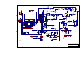
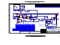
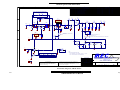
4.8 Voltage Regulator Circuit Board
The voltage regulator board is the longer of two boards mounted under the chassis toward
the front of the unit. It has switch-mode voltage regulators to provide +12, –12, and 20 volts.
It also contains the program detection and automatic carrier control circuits.
Illustration 6–10 and accompanying schematic complement this discussion.
U3E and U3F convert a 38–kHz sine wave from the stereo generator into a synchronization
pulse. In the transmitter, synchronization is not used, thus D9 is omitted.
U4 and U5 form a 20–volt switching regulator running at about 35 kHz. U4 is used as a
pulse-width modulator; U5 is a high-side driver for MOSFET switch Q1. Supply voltage for
the two IC’s (approximately 15.5 volts) comes from linear regulator DZ2/Q5. Bootstrap voltage, provided by D10 and C14, allows the gate voltage of Q1 to swing about 15 volts above
the source when Q1 is turned on. Current through the FET is sensed by R38 and R38A. If
the voltage between pin 5 and 6 of U05 exceeds 0.23 volts on a current fault, drive to Q1 is
turned off. Turn-off happens cycle by cycle. The speed of the turn-off is set by C13.
U6 is a switching regulator for both +12 volts and –12 volts. It runs at about 52 kHz. Energy
for –12 volts is taken from inductor L2 during the off portion of the switching cycle. The –12
volts tracks the +12 volts within a few tenths of a volt. There will be no –12 volts until current
is drawn from the +12 volts.
Q2, Q3, and Q4 form an active filter and switch, supplying DC voltage to the RF driver,
when the Carrier switch is on.
The program detection circuit is made up of U1 and U2. U1A and U1D and associated circuitry discriminate between normal program material and white noise (such as might be present from a studio-transmitter link during program failure) or silence. U1A and surrounding
components form a band-pass filter with a Q of 3 tuned to about 5 kHz. U1D is a first-order
low-pass filter. Red and green LEDs on the board indicate the presence or absence of program determined by the balance of the detected signals from the two filters. U2 and U1C
form a count-down timer. The time between a program fault and shutdown is selected by
jumpering pins on header JP1. For times, see section 5.7. The times are proportional to the
value of R21 (that is, times can be doubled by doubling the value of R21) and are listed in
minutes.
Principles of Operation
4-11
4.9 Power Regulator Circuit Board
The power regulator board is the shorter of two boards mounted under the chassis toward
the front of the unit. The board has the isolating diode for the battery input, the switch-mode
voltage regulator for the RF power amplifier, and circuitry for PA supply current metering.
Illustration 6–10 and accompanying schematic complement this discussion.
Diode D4, in series with the battery input, together with the AC-supply diode bridge, provides diode OR-ing of the AC and DC supplies.
U1 and U2 form a switching regulator running at about 35 kHz. U1 is used as a pulse-width
modulator; U2 is a high-side driver for MOSFET switch Q1. Power for the two IC’s comes
from the 20–volt supply voltage for the RF driver (available when the Carrier switch is on).
The voltage is controlled at 16 volts by zener diode DZ1. Bootstrap voltage provided by D2
and C9 allows the gate voltage of Q1 to swing about 16 volts above the source when Q1 is
turned on. Current through the FET is sensed by R12A and R12B. If the voltage from pin 5
to 6 of U2 exceeds 0.23 volts on a current fault, drive to Q1 is turned off. This happens on a
cycle-by-cycle basis. The speed of the turnoff is set by C5.
U3 and Q2 are used in a circuit to convert the current that flows through metering shunt,
R19, into a current source at the collector of Q3. Forty milli-volts is developed across R19
for each amp of supply current (.04 ohms x 1 amp). Q3 is biased by U3 to produce the
same voltage across R16. The collector current of Q3 is the same (minus base current) as
that flowing through R22 resulting in 40 microamperes per amp of shunt current. R5 on the
metering board converts Q3 collector current to 0.1 volt per amp of shunt current (.04 ma X
2.49 k). (See section 5.4.)
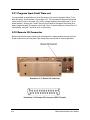
4.10 RF Driver/Amplifier (FM30)
The RF Driver/Amplifier assembly is mounted on a 100 mm x 100 mm plate in the under
side of the chassis.
Illustration 6-14 and accompanying schematic complement this discussion.
The driver amplifies the approximate 20 milliwatts from the frequency synthesizer to 30
watts. An MHW6342T hybrid, high-gain, wideband amplifier, operating at about 20 volts,
provides about one watt of drive to a single BLF246 MOSFET amplifier. The BLF245 stage
operates from a supply voltage of 28 volts in the FM30.
The circuit board has components for input and output coupling and for power supply filtering.
4-12
FM30/FM150/FM300 User’s Manual
4.11 RF Driver (FM150/FM300)
The RF Driver assembly is mounted on a 100 mm x 100 mm plate in the under side of the
chassis.
Illustration 6-14 and accompanying schematic complement this discussion.
The driver amplifies the approximate 20 milliwatts from the frequency synthesizer to about 8
watts to drive the RF power amplifier. An MHW6342T hybrid, high-gain, wideband amplifier,
operating at about 20 volts, provides about one watt of drive to a single BLF245 MOSFET
amplifier. The BLF245 stage operates from a supply voltage of approximately 20 volts.
The circuit board provides for input/output coupling and for power supply filtering.
4.12 RF Amplifier (FM150/FM300)
The RF power amplifier assembly is mounted on back of the chassis with four screws, located behind an outer cover plate. Access the connections to the module by removing the
bottom cover of the unit. The RF connections to the amplifier are BNC for the input and output. Power comes into the module through a 5–pin header connection next to the RF input
jack.
Illustration 6-12 and accompanying schematic complement this discussion.
The amplifier is built around a ST MicroElectronics SD2942, a dual power MOSFET rated
for 50 volts DC and a maximum power of about 350 watts. When biased for class B, the
transistor has a power gain of about 20 dB. (It is biased below class B in the transmitter.)
Input transformer, T11, is made up of two printed circuit boards. The four-turn primary board
is separated from the one-turn secondary by a thin dielectric film. R12–R17 are for damping. Trim pot R11 sets the bias.
Output transformer, T21, has a one-turn primary on top of the circuit board and a two-turn
secondary underneath. Inductors L21 and L22 provide power line filtering.
Principles of Operation
4-13
4.13 Chassis
The AC power supply components, as well as the bridge rectifier and main filter capacitor,
are mounted on the chassis. Switching in the power-entry module configures the power
transformer for 100, 120, 220, or 240 VAC; see section 2.2 for switching and fuse information. A terminal strip with MOV voltage-surge suppressors and in-rush current limiters is
mounted on the chassis between the power entry module and the toroidal power transformer.
The main energy-storage/filter capacitor, C01, is located between the voltage and power
regulator boards. The DC voltage across the capacitor will be 45–55 volts (FM30 and
FM150) or 65–70 volts (FM300) when the carrier is on.
4.14 RF Output Filter & Reflectometer
The RF low-pass filter/reflectometer are located in the right-hand compartment on the top of
the chassis. See Illustration 6–13 and accompanying schematic for more information.
A ninth-order, elliptic, low-pass filter attenuates harmonics generated in the power amplifier.
The capacitors for the filter are circuit board pads.
The reflectometer uses printed circuit board traces for micro-strip transmission lines. Transmission line segments (with an impedance of about 82 ohms) on either side of a 50–ohm
conductor provide sample voltages representative of the square root of forward and reverse
power.
DC voltages, representative of forward and reflected power, go through a bulkhead filter
board to the motherboard, then to the metering board, where they are processed for power
control and metering and for SWR metering and protection.
4-14
FM30/FM150/FM300 User’s Manual
4.15 Receiver Circuit Board Option
This option allows the transmitter to be used as a translator. The receiver board receives
terrestrially fed RF signal and converts it to composite audio which is then fed into the exciter board. Microprocessor controlled phase lock loop technology ensures the received frequency will not drift, and multiple IF stages ensure high adjacent channel rejection. Refer to
illustrations 4–6, 6–16 and its schematic for the following discussion.
The square shaped metal can located on the left side of the receiver board is the tuner
module. The incoming RF signal enters through the BNC connector (top left corner) and is
tuned through the tuner module. Input attenuation is possible with the jumper labeled “LO”
“DX”, on the top left corner of the receiver board. Very strong signals can be attenuated 20
dB automatically by placing the jumper on the left two pins (“LO” position). An additional 20
dB attenuation is also available with the jumpers in the top left corner of the board. The frequencies are tuned by setting switches SW1 and SW2 (upper right corner). These two
switches are read upon power up (or by momentarily shorting J7) by the microprocessor
(U4). The microprocessor then tunes the tuner module to the selected frequency. The frequency range is 87.9 Mhz at setting “00” to 107.9 Mhz at setting “64”. Other custom ranges
are available.
Located in the lower left-hand corner of the Receiver Module is a 3.5mm headphone jack.
Demodulated Left and Right audio is present at this jack. A regular pair of 32 ohm stereo
headphones, such as the types used with portable audio devices, can be used to monitor
the audio on the receiver module.
Receiver
Module
Illustration 4–5 Receiver Module
Principles of Operation
4-15
When a stereo signal is present, LED 3 illuminates which indicates that left and right audio
is available. Then the stereo signals go to gain stages and out to the RCA jacks on the back
of the cabinet. These can be used for off-air monitoring of the audio signal. Incoming frequency can be monitored from the frequency monitor BNC jack on the back. The stereo
buffer, stereo decoder, and gain stages and have no effect on the signal that goes through
the transmitter.
The power supply is fairly straight forward. The incoming 12 volt supply goes to a 7809, 9
volt regulator (VR1) which supplies all 9–volt needs on the board. The 9 volts also supplies
a 7805, 5 volt regulator (VR2) which supplies all 5–volt needs on the board. Plus and minus
12 volts from the motherboard is filtered and supplies various needs on the board. Finally
there is a precision reference voltage. Two 2.5 volt reference shunts act very much like a
very accurate zener diode to provide a precision 5 volt supply to the metering board.
4-16
FM30/FM150/FM300 User’s Manual
Section 5—Adjustments and Tests
This section describes procedures for (1) advanced users who may be
interested in customizing or optimizing the performance of the transmitter and (2) service personnel who want to return the transmitter to operational status following a maintenance procedure.
Adjustments and Tests
5-1
5.1 Audio Processor Adjustments
5.1.1 Pre-Emphasis Selection
Select the pre-emphasis curve (75 µsec, 50 µsec, 25 µsec, or Flat) by jumpering the appropriate pins of header HD1 on the audio processor/stereo generator board. (See section 2.9.)
If you change the pre-emphasis, change the de-emphasis jumpers, HD201 and HD202 on
the audio processor/stereo generator board, to match. (See section 2.8.)
5.1.2 Pre-Emphasis Fine Adjustment
Trim potentiometers, R23 and R63, (for left and right channels, respectively) provide for fine
adjustment of the pre-emphasis. Set the potentiometers to bring the de-emphasized gain at
10 kHz equal to that of 400 Hz. (At the proper setting, 15.0 kHz will be down about 0.7 dB.)
When making these adjustments, it is important that you keep signal levels below the processor gain-control threshold.
A preferred method is to use a precision de-emphasis network in front of the audio input.
Then, use the non-de-emphasized (flat) output from the FM modulation monitor for measurements.
5.2 Stereo Generator Adjustments
5.2.1 Separation
Feed a 400–Hz sine wave into one channel for at least 70% modulation. Observe the classic single-channel composite stereo waveform at TP301 on the RF Exciter circuit board. Adjust the Separation control R244 for a straight centerline.
Since proper adjustment of this control coincides with best stereo separation, use an FM
monitor to make or confirm the adjustment.
5-2
FM30/FM150/FM300 User’s Manual
5.2.2 Composite Output
You can make adjustments to the composite output in the following manner:
Using a Modulation Monitor
1. Set the Stereo-Mono switch to Mono.
2. Check that the setting of the Modulation compensation control (see illustration 2–9) on
the RF Exciter circuit , falls within the range specified for the frequency of operation.
(See section 2.3.1.)
3. Feed a sine wave signal of about 2.5 kHz into the left channel at a level sufficient to put
the wideband gain-reduction indicator somewhere in the middle of its range.
4. Set the Composite level control to produce 90% modulation as indicated on an FM
monitor.
5. Apply pink noise or program material to the audio inputs and confirm, on both Mono and
Stereo, that modulation peaks are between 95% and 100%.
5.2.3 19–kHz Level
Adjust the 19–kHz pilot for 9% modulation as indicated on an FM modulation monitor.
(The composite output should be set first, since it follows the 19–kHz Level control.)
5.2.4 19–kHz Phase
1. Apply a 400–Hz audio signal to the left channel for at least 70% modulation.
2. Look at the composite stereo signal at TP301 on the RF Exciter circuit board with an oscilloscope, expanding the display to view the 19–kHz component on the horizontal centerline.
3. Switch the audio to the right-channel input. When the 19–kHz Phase is properly adjusted, the amplitude of the 19–kHz will remain constant when switching between left
and right.
4. Recheck the separation adjustment as described in section 5.2.1.
5.3 Frequency Synthesizer Adjustments
5.3.1 Frequency (Channel) Selection
Refer to section 2.3.
Adjustments and Tests
5-3
5.3.2 Modulation Compensator
Refer to section 2.3.1
5.3.3 Frequency Measurement and Adjustment
Next to the 10.24–MHz VCXO in the RF Exciter circuit on the motherboard, is a 50K potentiometer (R101). Use R101 to set the frequency of the 10.24–MHz VCXO while observing the
output frequency of the synthesizer.
Use one of two methods for checking frequency:
1. Use an FM frequency monitor.
2. Couple a frequency counter of known accuracy to the output of the synthesizer and observe the operating frequency.
5.3.4 FSK Frequency Offset Control
An FSK signal (used for automatic identification of FM repeaters) shifts the frequencies of
the 10.24–MHz VCXO reference oscillator and the VCO.
Ground pin 4 on the DB25 connector located on the back panel of the transmitter. This will
shift the operating frequency. Adjust R224 for an offset of the operating frequency of about
6 kHz. Un-grounding pin 4 will cause the operating frequency to return to normal.
Use one of two methods for checking frequency:
1. Use an FM frequency monitor.
2. Couple a frequency counter of known accuracy to the output of the synthesizer and observe the operating frequency.
5.4 Metering Adjustments
5.4.1 Power Calibrate
While looking at RF Power on the digital panel meter, set the Power Calibrate trim potentiometer (R215) to agree with an external RF power meter.
5.4.2 Power Set
With the front panel RF Output control fully clockwise, adjust the Power Set trim pot (R55)
to 10% more than the rated power (33 W for FM30, 165 W for FM150, 330 W for FM300) as
indicated on an accurate external watt meter. If the authorized power is less than the maximum watts, you may use the Power Set to limit the range of the RF Output control.
5-4
FM30/FM150/FM300 User’s Manual
5.4.3 SWR Calibrate
When the Carrier switch is off, or the RF power is less than about 5 watts, the SWR circuit
automatically switches to a calibrate-check mode. (See section 4.5 for more information.)
Set the digital panel meter to read SWR. With the Carrier switch off, set the SWR CAL trim
pot (R66) to read 1.03.
5.4.4 PA Current Limit
Since it may not be practical to increase the PA current to set the PA Current Limit control,
you may use this indirect method.
With the carrier turned off, look at the DC voltage at the right end of R186 in the Metering
circuit on the motherboard. The current limit, in amperes, will be 0.35 amps higher than ten
times this voltage. For example, for a current limit of 7.35 amps, adjust the PA Current Limit
control for 0.7 volts at R186 ; or 0.565 volts for 6.0 amps. Set the current limit for 4 amps
(FM50), 7 amps (FM150), or 9.5 amps (FM300).
5.5 Motherboard Configuration
See section 4.6.1 for motherboard jumper configuration.
5.6 Display Modulation Calibration
The Modulation Calibrate trim pot sets the sensitivity of the front panel Modulation bar graph
display.
This adjustment may be made only after the Output trim pot on the Audio Processor/Stereo
Generator board has been set. (See section 5.2.2.)
Set the Stereo-Mono switch to Mono.
Feed a sine wave source of about 2.5 kHz into the left channel at a level sufficient to put the
wideband gain-reduction indicator somewhere in the middle of its range.
Set the Modulation Calibrate trim pot so that the “90” light on the front panel Modulation display just begins to light.
Adjustments and Tests
5-5
5.7 Voltage Regulator Adjustments
JP1, a 10–pin header on the Voltage Regulator board, sets the time between program failure and carrier turnoff. Pins 1 and 2 are the two pins closest to the edge of the board. The
times are approximate. Sections 2.11, 2.12, and 4.8 contain further information.
1. Short pins 1 and 2 for a 30–second delay.
2. Short pins 3 and 4 for a 2–minute delay.
3. Short pins 5 and 6 for a 4–minute delay.
4. Short pins 7 and 8 for an 8–minute delay.
You may select other times by changing the value of R21. The time is proportional to the resistance.
5.8 Bias Set (RF Power Amplifier)
The Bias Set trim pot is located inside the PA module on the input circuit board. Set the trim
pot to its midpoint for near-optimum bias.
5-6
FM30/FM150/FM300 User’s Manual
5.9 Performance Verification
Measure the following parameters to receive a comprehensive characterization of transmitter performance:
•
Carrier frequency
•
RF output power
•
RF bandwidth and RF harmonics (see section 5.12)
•
Pilot frequency, phase, and modulation percentage
•
Audio frequency response
•
Audio distortion
•
Modulation percentage
•
FM and AM noise
•
Stereo separation between left and right
•
Crosstalk between main channel and subcarrier
•
38–kHz subcarrier suppression
•
In addition to the above tests, which pertain to signal quality, a complete check of the
unit will include items listed in section 5.21.
5.9.1 Audio Proof-of-Performance Measurements
References to “100%” modulation assume 9% pilot and 91% for the remainder of the composite stereo signal.
Because the audio processing threshold is at 90% modulation, it is not possible to make
audio proof-of-performance measurements at 100% modulation through the audio processor. Instead, data is taken at a level below the audio processing threshold at 80% modulation.
5.9.2 De-emphasis Input Network
A precision de-emphasis network, connected between the test oscillator and the audio input of the transmitter, can be very helpful when making the audio measurements. Note
that the input impedance of the transmitter or the source impedance of the test oscillator
can affect network accuracy. With the de-emphasis network, oscillator level adjustments
need only accommodate gain errors, instead of the whole pre-emphasis curve.
Adjustments and Tests
5-7
5.10 Carrier Frequency
Carrier frequency is measured at the output frequency with a frequency monitor or suitable
frequency counter.
To adjust frequency, see section 5.3.3. (FCC tolerance +/– 2000 Hz per FCC Part 73.1540
and 73.1545.)
5.11 Output Power
The output power reading on the front panel display should be 90–105% of the actual value.
For a more precise measurement, use a watt meter in the RF output line. See sections
5.4.1 and 5.4.2 for setting power.
5.12 RF Bandwidth and RF Harmonics
You can observe RF bandwidth and spurious emissions with an RF spectrum analyzer.
In the Stereo mode, feed a 15.0–kHz audio signal into one channel to provide 85% modulation as indicated on a monitor. Doing so produces 38% main, 38% stereo subcarrier, and
9% pilot per FCC Part 2.1049. As an alternative, use pink noise into one channel.
Using a spectrum analyzer, verify the following (per FCC 73.317):
1. Emissions more than 600 kHz from the carrier are at least 43 + 10log(power, in watts)
dB down (58 dB for 30 watts, 65 dB for 150 watts, 68 dB for 300 watts). The scan
should include the tenth harmonic.
2. Emissions between 240 kHz and 600 kHz from the carrier are down at least 35 dB.
3. Emissions between 120 kHz and 240 kHz from the carrier are down at least 25 dB.
5.13 Pilot Frequency
The pilot frequency should be within 2 Hz of 19 kHz. (FCC Part 73.322.) Using a frequency
counter, measure 1.9 MHz at pin 13 of U208 on the Audio Processor/Stereo Generator
board. A 200–Hz error here corresponds to a 2–Hz error at 19 kHz. If the frequency is off by
more than 50 Hz, you may change the value of C213. (Changing C213 from 56 pF to 68 pF
lowers the 1.9 MHz by about 35 Hz.)
5.14 Audio Frequency Response
For the response tests, take the readings from an FM modulation monitor.
Make audio frequency response measurements for left and right channels at frequencies of
50 Hz, 100 Hz, 400 Hz, 1 kHz, 5 kHz, 10 kHz, and 15 kHz. See sections 5.9.1 and 5.9.2.
5-8
FM30/FM150/FM300 User’s Manual
5.15 Audio Distortion
Make distortion measurements from the de-emphasized output of an FM modulation monitor.
Make audio distortion measurements for left and right channels at frequencies of 50 Hz, 100
Hz, 400 Hz, 1 kHz, 5 kHz, 10 kHz, and 15 kHz. See sections 5.9.1 and 5.9.2.
5.16 Modulation Percentage
While feeding an audio signal into the left channel only, confirm that the total modulation
percentage remains constant when switching between Mono and Stereo.
Measure modulation percentage with an FM modulation monitor. See section 5.2.2.
19–kHz pilot modulation should be 9%.
5.17 FM and AM Noise
Take noise readings from a de-emphasized output of a modulation monitor.
5.18 Stereo Separation
Make left-into-right and right-into-left stereo separation measurements with an FM modulation monitor for frequencies of 50 Hz, 100 Hz, 400 Hz, 1 kHz, 5 kHz, 10 kHz, and 15 kHz.
5.19 Crosstalk
For stereo crosstalk measurements, both left and right channels are fed at the same time.
For best results, there needs to be a means of correcting small imbalances in levels and
phase. The balance is made at 400 Hz.
5.19.1 Main Channel Into Sub
Feed the left and right channels in phase with audio (L+R) at 50 Hz, 100 Hz, 400 Hz, 1 kHz,
5 kHz, 10 kHz, and 15 kHz at 100% modulation, while observing the stereo subcarrier (L-R)
level on an FM modulation monitor.
5.19.2 Sub Channel Into Main
Feed the audio into the left and right channel as above, with the exception of reversing the
polarity of the audio of one channel (L-R input). Using the frequencies of 5.19.1 above, observe the main channel (L+R) level with a modulation monitor.
Adjustments and Tests
5-9
5.20 38–kHz Subcarrier Suppression
With no modulation, but in the Stereo mode, the 38–kHz subcarrier, as indicated on an FM
modulation monitor, should be down at least 40 dB.
5.21 Additional Checks
In addition to the tests and adjustments mentioned in this section, the following checks ensure a complete performance appraisal of the transmitter:
1. Perform a physical inspection, looking for visible damage and checking that the chassis
hardware and circuit boards are secure.
2. Check the functionality of switches and processing control.
3. Verify that all indicators function.
4. Check the frequency synthesizer lock at 80 MHz and 110 MHz.
5. Measure the AC line current with and without the carrier on.
6. Perform a functional test of the SCA input, Monitor outputs, and the monitor and control
function at the 15–pin, D-sub connector.
7. Test the functionality of the FSK circuit.
8. Check the operation and timing of the automatic carrier-off circuitry associated with program failure.
9. Check all metering functions.
10. Test ALC action with PA current overload, SWR, and PLL lock.
NOTE:
FCC type acceptance procedures call for testing the carrier frequency over the temperature
range of 0–50 degrees centigrade, and at line voltages from 85% to 115% of rating. (See
FCC Part 2.1055.)
5-10
FM30/FM150/FM300 User’s Manual
Section 6—Reference Drawings
The illustrations in this section may be useful for making adjustments,
taking measurements, troubleshooting, or understanding the circuitry of
your transmitter.
Reference Drawings
6-1
6.1 Views
Gain
Reduction/Expansion
Indicators
Audio Processor
Input Level
Indicators
Digital Multimeter
Multimeter Select
Modulation Indicators
Stereo/Mono
Switch
Processing Control
Input Gain
Switches
Carrier Switch
Fault Indicators
Frequency Selector
Switches
Power Switch
RF Output
Control
Illustration 6-1 Front View
RF Output
RF Output Monitor
AC Power Input
Receiver Input
(Optional)
Composite Input
SCA Inputs
Audio Inputs
Audio Monitors
RF Power Amplifier
(FM150/300 Only)
Remote I/O
DC Input
Circuit Breaker
Illustration 6-2 Rear View
6-2
FM30/FM150/FM300 User’s Manual
Metering
Circuit
Audio Processor
Section
RF Low Pass
Filter &
Reflectometer
Stereo Generator
Section
RF Exciter
Circuit
DC Input
RF output
Power Amplifier
(FM150/M300 Only)
Illustration 6-3 Chassis Top View
Voltage Regulator
Power Regulator
RF Pre-driver/
Amplifier
Filter Capacitor
AC Power
Transformer
Bridge Rectifier
AC Power
Entry
Illustration 6-4 Chassis Bottom View
Adjustments and Tests
6-3
Notes:
6-4
FM30/FM150/FM300 User’s Manual
6.2 Board Layout and Schematics
Illustration 6-5 Audio Processor/Stereo Generator Board
FM30/FM150/FM300 User’s Manual
6-5
Board Layouts and Schematics
DWG. NO.
3
REV.
4
5
GAIN R9-14
--------------------------0dB OPEN
+6dB 50.5K
+12dB 16.8K
+18dB 7.21K
C5
6
7
R7
R12
49.9
R6
2.00K
D2
1N6263
R13
49.9
49.9
R5
R14
5.1K
R17
COMP1*
Vout
INV A
NC
1uF
9
R22
8
24.9K
C6A
1
+5V
10
9
A
B
10uF
DS1
DS2
1N5818 1N5818
C29
10uF
510
R68
1.0K
8
6
5
4
3
2
R84
D25
10M
D26
R88
POLY
D13
4
1
R79
TL072
10K
6
5
4
POLY (C8687-3)
U12
THAT2180
TL072
499
+12V
1
IN
R91
R92
49.9K
49.9K
1
OUT
-12V
+7V
+7V
C19
2200pF
-7V
POLY
E
-7V
VDD
D10
1N6263
8
+5V
24.9K
+5.00V
+5V
R97
PROC B
10M
(J3-18)
R63
10K
TL072
R64
30K
R65
49.9
TO R50 ON
DISPLAY BD.
+VT
-VT
-VT
D
C24
-12V
GND
24.9K
.01uF
(J3-20)
GND
R119
-5V
PROC C
-5V
+VT
R118
3.3K
R66
5.1K
-5V
VEE
7
(J3-16)
R96
ZERO
R98
-5V
U13B
POLY
LIGHT
R120
C25
OPEN
OPEN
C26
R94
3
7
U15B
49.9K
-VT
8
1N4148
R113
R114
49.9K
49.9K
4
2
+12V
6
R100
5
10M
D16
D22
C23
1uF
TL072
0.25V/DB
240K
R93
49.9K
R102
1.0K
10.0K
U16B
R116
3
100
R101
1N4148
2
1
TL072
SHORT
49.9K
R115
49.9K
+12V
R95
3.0K
R103
1N4148
100pF
D17
-12V
U16A
R112
HI GR
8
D21
100pF
1N4148
U15A
TL072
C
100K
+12V
-12V
-VT
6
PROC A
R99
D14
-12V
R90
100
R89
D12
1N4148
D9
1N6263
R75
24.9K
CLOCK
+12V
/STEREO FAULT
+12V
BR GR
1.52MHz
RIGHT
C22
4
8
RIGHT LEVEL REDUCED 6dB
DURING POLARITY ERROR.
3
+12V
R77
3.3M
U14A
RIGHT
R76
1N4148 330K
100pF
LEFT-RIGHT PHASING DETECTOR
1uF
LTC1064-1
Q2
2N5087
R60
3.3K
C21
.047uF
STEREO
POLARITY
ERROR
-12V
3
C17
.0027uF
1
5
TL072
2
8
D11
1N4148
-12V
U13A
2
24.9K
HEAVY
C20
1N4148
R62
C16A
+5V
D27
100K
NC
1uF
9
TL072
5
1N6123
INV A
11
10
5
7
R83
NC
Vout
.006V/DB
U14B
6
U10B
6
DL1
RED
R87
10K
1N4148
COMP1*
24.9K
R61
300
R53
49.9
R86
100K
fCLK
AGND
LEFT
RIGHT
+VT
C16
24.9K
7
10K
1N4148
R59
OPEN
R57
V+
V-
R69
12
6
R85
5.1K
1N4148
R81
30K
6
D8
1N6263
R54
5.1K
-12V
D29
1uF
D28
R SAMPLE
5
D7
1N6263
AGND
LEFT
33pF
13
EC+
C30
R80
30K
R56
24.9K
+12V
R52
2.00K
100K
4
TL072
COMP2*
4
3
Vin
14
8
1
7
R VU
R82
3
R58
100K
R(h I)
GND
OUT
U10A
2
INV C
7
4
GND
EC-
2
-12V
8
C18
U11
1
-12V
R44
49.9K
C14
100pF
HEADER 5X2
2
1K
2
4
6
8
10
V+
49.9K
V+
IN
EC+
10.0K
AD622
4
R43
1uF
L SAMPLE
22pF
R15
5
C12
R IN1
D
+12V
V-
1
SYM
R51
6
U8
RG2
+5V
F
1
3
5
7
9
1.0K
7
7
8
3
R26
5.1K
R67
U9
THAT2180
RG1
TL072
-12V
R70 50uS
5.62K 75uS
R10
C15
E
R25
49.9
R28
1.0K
1.52MHz
+12V
2
1
24.9K
U7B
7
HD1
R SAMPLE
1uF
D1
1N6263
8
5
R27
49.9
R42
49.9K
G
POLY
-VT
OUT
30K
49.9
R47
C13
100pF
C9
2200pF
1.0K
49.9
R46
1K
D6
1N4148
D1
1N6263
R35
24.9K
R36
-5V
TANT
LEFT
499
TL072
+12V
6
FLAT
R41
3
R24
R23
10K
TANT
C10
0.1uF
6
INH
C28
R45
R IN2
R37
1
V-
R39
47K
+
R20
1K
-7V
74HC4052
C11
IN
2
1
5
2
4
0Y
1Y
2Y
3Y
Y
+7V
+
12
14
15
11
0X
1X
2X
3X
X
/+12DB
/+6DB
F
U6
THAT2180
D5
1N4148
U7A
2
+12V
POLY (C8687-3)
Q1
2N5087
7
+VT
-12V
TL072
+5V
R38
47K
C7
.0027uF
1uF
LTC1064-1
5
3
4
10
NC
R21
300
U4B
6
U1
13
PE
C6
11
fCLK
AGND
24.9K
24.9K
-12V
49.9
R19
OPEN
V+
R29
12
3
G
APPROVALS
CHK
CM
33pF
13
8
D1
1N6263
V-
V+
8
6
5
4
+12V
5
COMP2*
AGND
5
1uF
R16
24.9K
-12V
R4
49.9K
C4
100pF
4
TL072
Vin
7
3
14
R(h I)
SYM
1K
3
4
L IN1
3
INV C
GND
2
R18
100K
1
L SAMPLE
R3
2
C2
DWN
C8
U5
1
U4A
2
12
DATE
15.2 KHz LOW-PASS FILTER
(8th ORDER ELLIPTICAL)
-12V
8
OUT
5
AD622
IN
11
6
REVISION HISTORY
DESCRIPTION
H
V-
1
10.0K
10
REV
40Hz - 15KHz +/- 0.5dB
40H 7 5KH 0 5% THD
4
V+
R11
6
U2
RG2
GND
RG1
8
3
V-
2
1
SYM
R2
49.9K
EC+
C3
100pF
1uF
49.9K
5
Baseband:
30Hz - 53KHz +/- 0.2dB.
53KHz - 76KHz +/- 0.4dB.
V-peak
.346
1.1
3.46
SYM
U3
THAT2180
7
1K
22pF
R15
V-rms
.245
.774
2.45
EC-
R1
L IN2
+12V
9
E . C . N.
EC-
+12V
EC-
C1
7
L VU
8
TURKEY SPECIFICATIONS:
(INTO 600 ohms)
dbm
-10
0
+10
7
4
H
6
EC+
2
3
1
-VT
6
R121
5
1M
7
C
TL072
+12V
C27
1uF
R117
R122
560
1.0K
R123
+12V
C40
1uF
C42
1uF
C44
1uF
C41
1uF
C43
1uF
C45
1uF
10.0K
-12V
-12V
+VT
R127
3
B
4
Vin
NC
NC
Vout
GND TRIM
R107
4.7K
4
TEST
8
7
2
6
3
-12V
C32
.01uF
U19A
1
VCC
R128
100
NE5532
5
+5.00V
+5V
C33
1uF
+5V
C34
1uF
C35
1uF
SW1
D23
3
2
1
1N4148
NORMAL SIP3
49.9K
1
3
NE5532
5.1K
R106
6
49.9K
5
U17B
7
-VT
J1
NE5532
1
3
5
7
9
11
13
15
17
19
+12V
D24
+12V
+5V
R126
10K
1N4148
R129
6
-12V
U17A
2
R104
8
2
NC
8
+12V
NC
+12V
4
U18
REF02
1
C36
.01uF
U19B
7
5
NE5532
VSS
10.0K
R130
100
R105
10K
L IN1
L IN2
R IN1
R IN2
1
3
5
7
9
11
13
15
17
19
21
23
25
RECEPT 10X2
-5V
C37
1uF
J3
2
4
6
8
10
12
14
16
18
20
C38
1uF
2
4
6
8
10
12
14
16
18
20
22
24
26
+12V
-12V
/+6DB
/+12DB
L VU
R VU
+5.00V
PROC A
PROC B
PROC C
BR GR
HI GR
/STEREO FAULT
B
Copyright (c) 2007 HCJB Global
IREC
RECEPT 13X2
+/- 12V FOR OP-AMPS AND VCA'S.
+/- 7V AT 56mA FOR LTC 1064-1 AND LMF100.
APPROVALS
+/- 5V FOR LOGIC (+5V TAKEN FROM +5.00V BUS
+5.00V REFERENCE VOLTAGE. ALSO USED BY D
A
+/- 4.4 FOR PEAK LEVEL THRESHOLD REFERENC
UNCONTROLLED
UNLESS OTHERWISE MARKED IN RED INK BY CM AS A
CONTROLLED COPY, COPIES OF THESE DOCUMENTS
INCLUDING ASSOCIATED ELECTRONIC REPRODUCTIONS
ARE FOR REFERENCE ONLY.
THESE DRAWINGS AND SPECIFICATIONS ARE THE
PROPERTY OF INTERNATIONAL RADIO AND ELECTRONICS CORP.
AND SHALL NOT BE REPRODUCED, COPIED OR USED AS
THE BASIS FOR THE MANUFACTURE OR SALE OF APPARATUS OR
DEVICES WITHOUT PERMISSION.
DWN
CHK
DW
CM
DW
03-15-07
PE
DP
03-15-07
DISTRIBUTION
K
FILENAME:
1
2
3
4
5
6
7
8
9
10
03-15-07
INTERNATIONAL RADIO AND ELECTRONICS CORP.
25166 LEER DRIVE ELKHART, IN. 46514
574-262-8900
WWW.IREC1.COM
TITLE:
SIZE
A
AUDIO PROCESSOR/STEREO GENERATOR
201409F-SCH
D
SCALE :
REV
DWG . NO .
NONE
11
C
SHEET
PROJ NO.
1 OF 2
12
Schematic Diagram: Audio Processor/ Stereo Generator (Sheet 1 of 2)
6-6
Adjustments and Tests
FM30/150/300 User’s Manual
DWG. NO.
1
2
3
REV.
4
5
6
7
H
0
12
11
6
H
OPEN
C203
100pF
R230
7
2
1
RG1
8
3
RG2
Composite Spec. (Turkey):
30Hz - 53KHz +/- 0.2 dBr
53KHz - 76KHz +/- 0.4dBr
U201
R206
6
AD622
3.9K
4
5
R205
OPEN
R204
49.9K
R201
1K
EXT IN+
10
+12V
C202
100pF
EXTERNAL COMPOSITE
INPUT
5
0
R203
1K
EXT IN-
9
C204
R217
SCA IN
8
-12V
R202
49.9K
C201
100pF
G
G
R207
150K
2
C206
3
+12V
-12V
-12V
+7V
+7V
-7V
-7V
F
.047uF
.047uF
POLY
POLY
R208
300K
TL072
+12V
R209
R210
4.99K
2.49K
HD201
SIP3
5
100
MON L
10.0K
RIGHT 8VPP (AT 2000Hz)
2
C209
3
-VT
.047uF
.047uF
POLY
POLY
GND
R213
300K
+12V
-12V
U203A
1
6
TL072
+12V
R214
R215
4.99K
2.49K
HD202
SIP3
U203B
7
5
TL072
R216
U204
MON R
1
100
C210
.01uF
1
2
3
4
C208
RIGHT
8
-VT
C212
150K
+VT
GND
R221
POLY
50
75
R222
10
9
C211 120pF 200K
56pF
R224
1K
6
12.4K
U205
0X
1X
X
2X
3X
0Y
1Y
2Y
3Y
Y
-12V
U206A
1
+12V
2
13
3
MC34083
3
A
B
R234
1K
INH
D207
14
DD
13
U0 OUT
12
R223
11
9.09K
2
X2
3
4
U1
Z1
5
U2
Z2
6
Y1 REF
9
7
Y2
8
D208
1N4148
10
V-
8
R254 used ONLY with AD633
AD734 has internal 50K
R237
1M
9
V+
V-
6
Z
22pF
AD633JN
3.8MHz
304KHz
C218
12
13
CLR QA
CKA QB
QC
QD
11
10
9
8
5
4
U209B
74HC393
1
U210A
-7V
C216
R252
LPB
LPA
1
1K
5
R232
U206B
7
100
+5.00V
SYNC OUT
MC34083
R233
COMP OUT
D
COMP METER
R253
1K
C219
1000pF
C219
1000pF
POLY
POLY
R264
R261
+7V
R262
+12V
C224
.001
6
0.1uF
R255
R256
R257
1K
1K
43K
0.1uF
C222
1000pF
C223
1000pF
POLY
POLY
+5V
19KHz Level
5
U212B
7
Q202
MPS-A06
TL072
R263
24.9K
R258
1K
-7V
10K
10K
R260
2
10.0K
3
R265
C226
.001
-12V
U212A
1
10
Q201
MPS-A56
TL072
+12V
C
-12V
10
R259
3K
3 R243
49.9K
2
U207B
24K
20
4
2
BPA
BPB
19
5
3
HPA
INV BINV A
HPB
18
6
7
VA+
S1 A
S1 B
AGND SA/B
VA-
U210B
6 R242
120K
74HC86
6
U211
LMF100
C221
1.9MHz
74HC390
3
17
11
10
9
16
2CKA 2QB
2CKB 2QC
2QD
15
11
13
R251 49.9K
15
12
MC74HC04
U208B
2CLR 2QA
14
10
1.52MHz
R250 10.0K
14
6
GND
100
0.1uF
+5V
R238
10K
+7V
8
1CKA 1QB
1CKB 1QC
1QD
5
6
7
13K
R244
5K
9
3
R229
R245
0.1uF
8 R241
10K
74HC86
VD+
U208A
1CLR 1QA
U210C
74HC390
U207C
MON L
MON R
12 HEADER
20K
C216
VD-
1
4
MONO/STEREO
C224
SEPARATION
CLK CLK
B
A
2
5
7
AD633 ALTERNATE TO AD 734
11 R240
24K
74HC86
R247 49.9K
12
NPO
/EXT ENABLE
U204A
-12V
U210D
R246 10.0K
13
10
C
E
J202
1
2
3
4
5
6
7
8
9
10
11
12
R231
12
MC74HC04
C215
33pF
NPO
D
13
50/100 LSH
C213
56pF
R254
49.9K
EXT IN+
EXT INSCA IN
COMP OUT
COMP METER
MONO/STEREO
/EXT ENABLE
GND
R227
1K
COMPOSITE OUTPUT
R228
3K
OUT
J201
1
2
3
4
5
6
7
8
9
10
11
12
12 HEADER
R226
U207F
2
MC74HC04
13
1
C214
5.5-18pF
12
U207A
Y201
7.6 MHz
Y1
Y2
5
1K
X1
X2
3
4
C228
1uF
1N4148
+12V
1
2
+7V
C227
1uF
+5V
AD734
R236
-7V
-5V
43K
E
F
74HC4052
V+
X1
1
5
2
4
4.99K
R220
10.0K
VEE
+VT
12
14
15
11
R219
LEFT 8VPP (AT 2000Hz)
-5V
1N4148
9.09K 1%
+5V
-5V
1N4148
D206
1N4148
R218
POLY
75
R212
-5V
1N4148
D204
1N4148
D205
R225
C207
.01uF
50
VDD
+5.00V
+5V
R211
TL072
1N4148
D203
4
+12V
8
C205
LEFT
U202B
7
8
1.52MHz
6
4
CLOCK
-12V
U202A
1
D202
8
RIGHT
RIGHT
1
2
3
LEFT
4
LEFT
D201
74HC86
4
MC74HC04
R239
10K
J203
10
9
8
7
6
5
4
3
2
1
U207E
U209A
2
1
B
CLR QA
CKA QB
QC
QD
11
3
4
5
6
10
MC74HC04
R266
38KHz
-12V
+12V
OPEN
U207D
74HC393
9
8
R267
MC74HC04
1K
19KHz
DZ1
ICTE-15
SYNC OUT
DZ2
ICTE-15
-12V
+12V
B
RECEPT 5X2
Copyright (c) 2007 HCJB Global
A
TITLE:
Copyright 2006 Michael P. Axman
UNCONTROLLED
UNLESS OTHERWISE MARKED IN RED INK BY CM AS A
CONTROLLED COPY, COPIES OF THESE DOCUMENTS
INCLUDING ASSOCIATED ELECTRONIC REPRODUCTIONS
ARE FOR REFERENCE ONLY.
THESE DRAWINGS AND SPECIFICATIONS ARE THE
PROPERTY OF INTERNATIONAL RADIO AND ELECTRONICS CORP.
AND SHALL NOT BE REPRODUCED, COPIED OR USED AS
THE BASIS FOR THE MANUFACTURE OR SALE OF APPARATUS OR
DEVICES WITHOUT PERMISSION.
SIZE
2
3
4
5
6
7
8
9
10
11
REV
DWG . NO .
201409F-SCH
B
SCALE :
1
A
AUDIO PROCESSOR/STEREO GENERATOR
NONE
PROJ NO.
C
SHEET 2
OF
2
12
Schematic Diagram: Audio Processor/ Stereo Generator (Sheet 2 of 2)
FM30/FM150/FM300 User’s Manual
6-7
Board Layouts and Schematics
Illustration 6-6 Motherboard
6-8
Adjustments and Tests
FM30/150/300 User’s Manual
DWG. NO.
1
2
J16 FAN
A
REV.
5
6
7
8
9
J14
-12V
+12V
RF OUT
ALC
COMPOSITE1
LOCK
/LOCK
RF_LVL
LOC/REMOTE
GND
FSK IN
-12V
NC
Vin
NC
TEMP Vout
GND
TRM
8
7
2
6
3
TL072
1
U3A
-12V
OPEN
100
C28
1.0
TL072
7
U3B
/LOCK
RF_LVL
LOC/REMOTE
ALC
G
COMPOSITE1
LOCK
-12V
RF OUT
E2
E3
E4
J9
RF_LVL
V+
TEMP
GND
1
2
3
TEMP
HEADER 3X1
C159
.001
PAI
PAV
N/C
N/C
/LOCK FAULT
NC
FSK IN
NC
C158
.001
NC
J2
+5.00V
METER PATEMP
FAULT SUM
METER RFW
METER PAI
ALC
METER PAV
L IN1
L IN2
R IN1
TEMP
R IN2
PAI
PAV
LPIN L
NC
NC
R IN1
LPOUT L
DC SUPPLY
38KHZ
/CARR_OFF
LPIN R
LPOUT R
NC
Z23
/AUTO_CARR_OFF
JUMPER
NC
NC
C16
.01
1
2
3
4
5
6
7
8
9
10
11
12
13
14
15
16
17
18
19
20
1
2
3
4
5
6
7
8
9
10
11
12
13
14
15
16
17
18
19
20
J3
J1
NC
HEADER 10 x 2
ALC
JUMPER
C66
OPEN
C67
OPEN
C68
OPEN
C65
.01
C64
.01
JUMPER
JUMPER
/+12DB
L VU
R VU
+5.00V
PROC A
PROC B
PROC C
BR GR
HEADER 10 x 2
HI GR
NC
Z31
Z32
OPEN
OPEN
E
-12V
INSTALLED WHEN USING
AUDIO PROC. SHUNT CKT.
COMP METER
AUDIO PROCESSOR
STEREO GENERATOR
C18
.01
C19
.01
FMV CONTROL
STEREO/MON
+12V
C20
.01
TP4
+12V
COMPOSITE1
C21
.01
Z29
JUMPER
C22
.01
Z30
TP3
-12V
+5.00V
J7
MON L
MON R
C23
.01
NC
LPIN L
LPOUT L
LPIN R
LPOUT R
38KHZ
38KHZ
COMP METER
1
2
3
4
5
6
7
8
9
10
11
12
1
2
3
4
5
6
7
8
9
10
11
12
-12V
+12V
OPEN
Z15
J3
+5V
TP6
+5V
TP7
GND
-12V
1
2
3
4
5
6
7
8
9
10
11
12
REM SWR
RDS RX
COMP METER
STEREO/MON
RDS TX
COMPOSITE1
12
SCA IN
EXT RTN
EXT IN
R IN2
L IN2
L IN1
25
1
2
3
4
5
6
7
8
9
10
11
12
C
J1
INPUT CONFIGURATION CHART
NON-OMNIA BOARD INPUT IMPEDENCE
HEADER 12
COMP METER
REM LOWER
22
1
2
3
4
5
6
7
8
9
10
J6
D1
1N4148
10
1
2
3
4
5
6
7
8
9
10
HEADER 5 x 2
13
11
TP5
+5.00V
J8
/EXT ENABLE
R21 220
OPEN
Z16
R22 220
OPEN
Z17
R23 220
OPEN
Z18
R24 220
OPEN
Z19
R25 220
OPEN
Z20
R26 220
OPEN
Z21
R27 220
OPEN
Z22
ALC
R28 220
38KHZ
D
+5.00V
J2
HEADER 12
/EXT ENABLE
J3
50 KOHM
600 OHM
Z1, Z2 ON
Z3, Z5, Z7, Z8 OFF
Z4, Z6 OFF
Z1, Z2 ON
Z3, Z5, Z7, Z8 ON
Z4, Z6 OFF
OMNIA BOARD AES/EBU INPUT
REM PWR CNTRL
9
Z1, Z2 OFF
Z3, Z5, Z7, Z8 OFF
Z4, Z6 ON
ANALOG LEFT/RIGHT
LEFT IN 1
LEFT IN 2
REM RAISE
-METER PAV
R4
20
-METER PAI
1K
7
-METER RFW
-/CARR OFF
4
_FSK IN
R14 220
16
_ALC
R13 100
3
-COMPOSITE OUT
R12 390
15
38 KHZ OUT
R11 390
2
-FMV CONTROL
R10 1K
14
_/EXT ENABLE
R9
Z5
COMPOSITE METER
OPEN
38KHZ
Z3
FMV CONTROL
FMV CONTROL
220
OPEN
/EXT ENABLE
C14
220pF
C2
220pF
R3
R5
300
300
R7
R1
300
300
Z7
R15
1K
OPEN
R16
1K
DB25_2X
C5
.01
C6
.001
C7
.001
C8
.001
C9
.01
.01
J1
XLR
Z8
10
9
8
7
6
5
4
3
2
1
2
3
J24
1
HI
LO
GND
HD6
OPEN
EXT IN
OPEN
240
R32
R34 24.9K 1%
24.9K
1%
UNLESS OTHERWISE SPECIFIED:
C24
1.0
TL072
1
U1A
2
R35
24.9K
1%
D3
R29
1K
3
-12V
R36
24.9K
1%
R37
2
3
4
5
C25
1.0
UNCONTROLLED
6
IREC
4.02K
1%
R30
6
3.9K
5
TL072
7
U1B
APPROVALS
DWN
CHK
DW
THESE DRAWINGS AND SPECIFICATIONS ARE THE
PROPERTY OF INTERNATIONAL RADIO AND ELECTRONICS CORP.
AND SHALL NOT BE REPRODUCED, COPIED OR USED AS
THE BASIS FOR THE MANUFACTURE OR SALE OF APPARATUS OR
DEVICES WITHOUT PERMISSION.
CM
DW
10-05-06
PE
DP
10-05-06
10-05-06
DISTRIBUTION
K
FILENAME:
1
7
B
2. ALL CAPACITORS ARE IN MICROFARADS.
+12V
UNLESS OTHERWISE MARKED IN RED INK BY CM AS A
CONTROLLED COPY, COPIES OF THESE DOCUMENTS
INCLUDING ASSOCIATED ELECTRONIC REPRODUCTIONS
ARE FOR REFERENCE ONLY.
REF. FOR
XLR CON.
HEADER 5 x 2
R20
1K
R19
OPEN
J2
OPEN
R18
1K
Z10
C10
A
R17
1K
OPEN
OPEN
NOTES:
100
R38 1K
SCA IN
EXT RTN
R33
1. ALL RESISTORS ARE IN OHMS, 1/4W, 5% TOL.
Z14
Z11
C15
220pF
+12V
R222
1
C1
220pF
FSK IN
C4
220pF
MON_R
MON_L
EXT_IN
EXT_RTN
SCA
-/AUTO_CARR_OFF
17
C3
220pF
OPEN
1
2
3
4
5
5
Z2
JUMPER
Z1
JUMPER
R31
100
Z12
C13
220pF
1
2
3
-FAULT SUM
1K
STEREO GENERATOR SHUNT
OPEN
C12
220pF
R8
L IN2
1K
18
Z13
1K
R IN2
-METER BATT
C11
220pF
R6
R IN1
3
2
1
-METER PA TEMP
6
L IN1
OPEN
R2
1K
19
Z4
1N4148
OPEN
8
D2
Z6
21
B
/+6DB
Z28
JUMPER
JUMPER
23
-12V
Z27
D
24
F
1
2
3
4
5
6
7
8
9
10
11
12
13
14
15
16
17
18
19
20
+12V
HEADER 13 x 2
Z26
C
J12
1
2
3
4
5
6
7
8
9
10
11
12
13
14
15
16
17
18
19
20
21
22
23
24
25
26
C17
.01
Z25
NC
C62
.01
C60
.01
C58
.01
C59
.01
C63
.001
C61
.001
1
2
3
4
5
6
7
8
9
10
11
12
13
14
15
16
17
18
19
20
21
22
23
24
25
26
Z24
JUMPER
+12V
J10
J11
INPUT
NC
1
2
3
4
5
6
7
8
9
10
HEADER 5 x 2
C157
.001
METER BATT
DC SUPPLY
38KHZ
N/C
/CARR_OFF
TEMP
/AUTO_CARR_OFF
INPUT
N/C
N/C
N/C
N/C
N/C
N/C
ALC
1
2
3
4
5
6
7
8
9
10
1N4148
E
Z9
R39
1.0
/LOCK FAULT
J15
FM
+5.00V
WR
J28
+12V
HEADER 3X1
1
2
3
4
5
6
7
8
9
10
11
12
13
14
15
16
17
18
19
20
DP
H
C27
.01
C29
1.0
C30
5
5
ALC
1
2
3
4
5
6
7
8
9
10
11
12
13
14
15
16
17
18
19
20
PE
DW
J19
MCX
FM_/LOCK
1
2
3
NC
+12V
6
R177 1K
J13 FM
J29
WR
J18
MCX
+12V
R176 1K
HEADER 5 x 2
F
1
2
3
4
5
6
7
8
9
10
R150 1K
1
2
3
4
5
6
7
8
9
10
DW
REF02
/LOCK FAULT
DC SUPPLY
PAI
PAV
EXT ALC CONTROL
TEMP
FAN
V-METER
RFV
RF FWD
RF REV
INPUT
FM_/LOCK
ALC
METER PAV
METER PAI
METER RFW
METER PATEMP
METER BATT
FAULT SUM
.01
3
4
+12V
+5.00V
C140
J25
2
1.0
HEADER 5 x 2
FSK IN
1K
HEADER 3X1
V+
TEMP
GND
J26
-12V
1
2
3
1
C26
+12V
R216
FM TP1
VOLTMETER
J25
03-08-07
APPROVALS
CHK
CM
R40
4.7K
U2
/LOCK FAULT
DC SUPPLY
PAI
PAV
EXT ALC CONTROL
TEMP
FAN
V-METER
RFV
RF FWD
RF REV
INPUT
.01
GND
.01
+5.00V
.01
C54
1.0
Q3
IRF541
+12V
C57
-12V
C56
FM_/LOCK
ALC
METER PAV
METER PAI
METER RFW
METER PATEMP
METER BATT
FAULT SUM
WR TP1
ANTENNA SWR
C55
PRODUCTION RELEASE
DWN
+12V
RF_LVL
HEADER 6X1 .156
12
DATE
AUDIO PROCESSOR SHUNT
RF EXCITER
H
1
2
3
4
5
6
11
6
REVISION HISTORY
DESCRIPTION
REV
A
ALC/METERING
HEADER 3
G
10
5
E . C . N.
201497F-SCH-SH3.SCH
201497F-SCH-SH2.SCH
1
2
3
FAN+12V
201207F-SCH
4
3
+12V
8
9
10
INTERNATIONAL RADIO AND ELECTRONICS CORP.
25166 LEER DRIVE ELKHART, IN. 46514
574-262-8900
WWW.IREC1.COM
A
TITLE:
SIZE
SCH, UNIVERSAL MOTHER BOARD
DWG . NO .
D
SCALE :
NONE
11
REV
201497F-SCH
A
SHEET 1
PROJ NO.
OF
12
Schematic Diagram: Motherboard (Sheet 1 of 3)
FM30/FM150/FM300 User’s Manual
6-9
Board Layouts and Schematics
4
5
1.00V = 10VDC
C119
.01
R161
100K
1%
1
U19A
3
D29
1N4148
R194
15K
R195
10K
11
50mv per degree C.
R164
1M
100K
R169
10K
R166
220K
U20C
-12V
R181
240K
METER PATEMP
3
R158
100K
R135
100K
1%
D33
1N4148
5
U22B
R184
1K
7
ALC
TL074
E
R155 11K
1%
5
1
2
2
U23C
Q7
1
2
3
4
C135
.01
TL074
8
7
6
5
Q6
1
2
3
4
1
R215
10K
+
R44
51.1K
10
TL074
U24C
TL074
R207
3.3K
R213
49.9K
1%
R66
10K SWR CAL
R67
100
C49
J26
OPEN
POWER CAL
10
8
6
4
2
-12V
+12V
NOTES:
R48
1K
5
C41
.001 D11
C40
8 R47
51.1K
U4C
10
.01
C35
10K
C51
.001
12
11 R54
U6D
13
+
2
C37
.01uF
VR1
LM7905
2
Vin
3
Vout
U24D
R148
100
R147
100
(1.00V at 100W)
METER RFW
J4-5
+12V
-12V
+ C126
47/20V
TL074
R208
10.0K
1%
14
U23D
C130
1.0
+5V
9
R56
100K
U6A
4
3
5
3
C39
.001
-12V
Vin
METER RFW
Vout
VCC
1
D48
+12V
+5V
LM329DZ
C156
1.0
VSS
-12V
C139
1.0
C143
1.0
U8,9 pin 7
R214
3.3K
VEE
-12V
+5.00V
J3-9,10
J4-12
+5.00V
4
5
6
7
8
9
D10
TL074 1N4148
3.32K
1%
+12V
SW8
SWITCH
LOCAL ONLY
POWER SET
-6.9V
TITLE:
SIZE
SCH, UNIVERSAL MOTHER BOARD
201497F-SCH
NONE
A
REV
DWG . NO .
C
10
R51
1
U8A
3
RF_LVL
VR4
78L05
C133
1.0
R210
1.1K
1%
8
B
SCALE :
2
U6C
74HC132
-5V
+12V
TL074
1
10
74HC132
C38
.01uf
74HC132
6
U6B
C52
1.0
3
14
100K
C34
4.7uF
TANT.
2
14
U8D
12
VDD
13
TL074
13
1
100K
74HC132
-12V
C
11
U4D
74HC132
R70
1.15K
1%
8
U8C
D13
1N4148
13
C33
.01uF
1. ALL RESISTORS ARE IN OHMS, 1/4 W, 5% TOL.
13
C43
.001
TL074
9
12
74HC132
C53
1.0
-6.9V
-12V
+12V
D12
1N4148
.01
9
C128
1.0
12
C_L_SHT2_A.DOT REV. A
7
U8B
5
-12V
R69
7
U10B
5
TL072
12
9
7
5
3
1
C42
.001
TL074
6
1N753A
6.2V
20pF
6
UNLESS OTHERWISE SPECIFIED:
2. ALL CAPACITORS ARE IN MICROFARADS.
6
W
R52
8
R209
7.5K
1%
D
74HC4051
74HC132
R65
5.11K
1%
J30-19
GND
6
U4B
5
7
U24B
5
8
4
LM394
6
R204
22K
TANT
9
8
7
6
5
DPM IN
C160
0.1
INH
A
B
C
1
4
R203
100K
D38
1N6263
9
(.135V)
(1.999V reads "1999")
3
X
7
L
GND
6
11
10
9
SEL A
SEL B
SEL C
16
VCC
10
R202
1K
R211
49.9K 1%
LM394
-12V
R205
10K
SW2
SW-PB
2
11
1M
8
1N4148
2
U24A
TL074
C134
+12V.001
8
7
6
5
R201
100K
CS
X0
X1
X2
X3
X4
X5
X6
X7
+12V
LM394
3.32K
1% +5V
10
3K
D39
1N4148
1
2
3
4
R206
39K
.01
R172
U/D
J3-2
J3-4
J3-6
13
14
15
12
1
5
2
4
R49
1K
8
+5V
Q2
R59
-12V
1N4148
D37
Vcc
H
4
C46
Q5
2N5210
D34
3
SW1
SW-PB
GND
3
1
RF FWD
U9B
2
3
U4A
74HC132
INC
DS1804
49.9K
1%
C47
.01
1
+5.00V
LM394
R61
7
U5
.01
2
8
7
6
5
-5V
MC33282
R200
100K
JP5
OPEN FOR FM30 UNITS
3
MC33282
6
R180
J2-9
U9A
R58
10K
R199
22K
R138
10K
3
C32
1
U21
1999 WATTS
19.99
19.99V
199.9V
19.99A
199.9 Deg. C
199.9V
199.9V
11
R60
10K
10K
D36
1N6263
Q1
1
2
3
4
1
.01
R179
7
C131
.001
3.32K
1%
2
10K
R43
51.1K
1%
GND
U23B
5
C123
.01
RF POWER
SWR
ALC
PA DCV
PA DCI
PA TEMPERATURE
SUPPLY DC VOLTS
VOLTMETER
+5V
R57
.01
R63
1
U10A
TL072
8
+12V C48
3
R62
R139
10K
RF POWER (RFV SQUARED)
+5V
REM LOWER
-12V
4
2
TL074
6
C44
.01
REM SWR
10K
+5V
FULL SCALE
below 5W.)
R197
100K
D35
1N6263
TL074
C129
+12V.001
ALC
R156
100K
1%
REM PWR CNTL
C45
+12V
1K
A
R217 100K
R185
200K
REM RAISE
C50
R64 10K
R68
1
R198
22K
C122
10/35V
1N4148
R218 10K
6
.001V per Watt
(Clamp SWR reading
4
C124
.01
B
R219
51K
8
U22C
C153
0.1
R191
51K
LADRVR
(2.5VDC at 100W)
-12V
U23A
3
R212
2.49K
1%
J30-16
F
C155
0.1
R178 1K
2
R140
10K
DPM REF
DPM IN
HEADER 10X2
D40
D41
1N4148
C121
0.1
.01
11
D
R221
10.0K
1%
1
3
5
7
9
11
13
15
17
19
74HC14
J22-12
10mV/Volt
100mV/Amp
1mV/Degree C
10mV/Volt
10mV/Volt
R168
1K
1%
J22-1
/LOCK FAULT
INPUT LAMP
-12V
ALL OTHERS
R174
1.1K
1%
R137
100K
1%
J2-10 RF FWD
1N4148
6
METER BATT
J2-8 VOLTMETER
C
/LOCK FAULT
SW10
SWITCH
R173
10K
1%
J2-11
5
J2-7
TL074
C117
0.1
INPUT
1
2
3
U20B
5
E
LOCK LAMP
D42
2
4
6
8
10
12
14
16
18
20
R151 120K
TL074
3.16K
1%
METER BATT
1N4148
4
U25C
R152
100K
R189
1M
10
U25B
3
D45
INPUT
9
WR
R159 = 200K 1%
R146
100
U22A
SEL A
SEL B
SEL C
RF_LVL
+5.00V
PATEMP LAMP
J30-18 PADC LAMP
INPUT LAMP
LOCK LAMP
SWR LAMP
FM U5
1N4148
1
R188
33K
POWER SET
R192
7
C152
.001
D31
1N4148
TL074
ALL FM
R159 = 187K 1%
6
RF REV
R55
10K
M1/M2
R159 = 19.6K 1%
DC SUPPLY
FM_/LOCK
+12V
R159
*
DC SUPPLY
R220
10K
POWER SET
POWER SET
J1-2
R160
68.1K
1%
+5.00V
J30
J23-1
4
R170
24.9K
1%
G
J30-12
D46
FM_/LOCK
R157
1M
J23-8
FAULT SUM
PATEMP LAMP
J2-7
2
10mV/Deg. C
F
2
74HC14
TL074
J4-6
1N4148
+5V
-12V
30.1K 1%
5.00V = 100 deg. C
TL074
C120
0.1
METER PATEMP
12
R141 100K FAN
14
J30-14
10 FAULT SUM
11
74HC14
C141
1.0
11
R149 100 1%
PADC LAMP
74HC14
1
R154 120K
U20D
J30-20
U25E
D43
D30
1N4148
13
8
1N4148
12
74HC14
U25A
-12V
9
10
U25F
13
R193
100K
R190
100K
+12V
SWR LAMP
+5V
TL074
R167
J2-6 TEMP OUT
U22D
1
U20A
3
R165
100K
R196 10K
1N4148
D44
C154
.001
D32
1N4148
R187
2.2M
14
2
R183
240K
J22-5
74HC14
C132
.001
1%
R136
1K
D47
8
R175 120K
-12V
12
+5V
U25D
9
R186
33K
12
R182
80.6K 1%
11
H
13
R163
1.1K
1%
R171
10
PAI LIMIT
TL074
G
C142
.001
9
METER PAI
TL072
R153
2.49K
1%
C118
.01
7
U19B
5
8
EXT ALC CONTROL
R144
100
6
J2-3 PAI
A
+5.00V
+ C125
47/20V
+
C127
47/20V
TL072
R162
10.0K
1%
R145
100
R142
100
2
4
J1-4
R143
100
PAV
REV.
201497F-SCH
METER PAV
1.00V = 10.0A
H
DWG. NO.
6
1.00V
3
3
2
1
2
4
1
PROJ NO.
11
A
SHEET 2
OF
3
12
Schematic Diagram: Motherboard (Sheet 2 of 3)
6-10
Adjustments and Tests
FM30/150/300 User’s Manual
1
2
3
4
5
DWG. NO.
6
REV.
201497F-SCH
A
8
9
10
11
12
88-108 MHZ
+8V
+12V
R81
150
+12V
2
1
A2
MAR-6
C79
.001
GND
12
C109
1
D19
1N4148
U13
OSC in
1
2
3
Fin 4
5
6
7
8
HEADER 10
C101
100pF
1
2
3
4
5
6
7
8
16
15
14
13
12
11
10
9
16
15
14
13
12
11
10
9
R105
100K
1%
VDD
R106 10
C103
C92
1
MC145170
11
10
U15F
74HC14
LOCK
C75
.001
U15E
74HC14
C108
3900PF
U14C
10
R114
100K
1%
MC33284P
MC33284P
R111
100K
1%
8
13
U14D
12
14
C107
.001 POLY
R80
15
TANT.
C98
.001
C78
.01
G
MAR-6
1
2
A1
RF OUT
C77
.001
C89
33pF NPO
R95
15
R112
100
1%
C112
220pF
R79
100
1%
C90
.001
VCO1
POS-150
R96
150
+5V
D25
1N4148
DATA
C81
.001
D15
R113
10.0K
1%
R115
100K
1%
/ENABLE
+5V
F
R222
1.0K
1%
C111
0.01
R89
100
1%
CLOCK
R87 499K
1%
C104
1 POLY
.001
9
R98
100K
1%
5
10/35V
13
5V_TCXO
1
2
3
4
5
6
7
8
9
10
+8V
+ C91 1N4148
R103
1M
R102
200K
LOCK DET.
U12B
NE5532
VVCO
8
OUTPUT
7
J31
14
+VDD
7
5
3
1
TO
J1 OF 201508F-PWA
FREQUENCY SELECTION PWA
LOCATED ON FRONT PANEL
+ C110
47/20V
F
R129
10.0K
1%
10
9
8
7
6
5
4
3
2
1
10
9
8
7
6
5
4
3
2
1
SW9
RESET
4
C86
0.1
1
U11A
TL072
2
9
VU5
2
D27
1N4148
1
U14A
3
VU5
C106
1
R110
2K
2W
MC33284P
D20
1N5353B
16V
R78
10K
PWR. CNTRL TILT
R92
R85
24.3K 1%
5
4
3
2
1
SW7
OPEN
R127
25K
LF SEP.
OPEN
C102
1
DC SUPPLY
+ C114
R72
1K BECKMAN
-12V
680.0
TP1
10/35V
R93
2K
PWR. CNTRL. OFFSET
D
VR2
LM317
COMPOSITE1
FSK
U15A
74HC14
AMBER
FM
WR
3
R13210.0K 1%
+5V
10/35V
WR
DS2
RED
C
VR3
LM78L05
C95
.001
3
IN
OUT
1
C
FREQ. ADJ. R101
50K
FM
R100
1
3
5
7
9
TANT.
R107
680
3
+5V
C97
.001
100K 1%
C83
1
+ C82
10/35V
FSK-R
2
J20
HEADER 5X2
C73
.001
FSK IN
10/35V
R73
1.27K
1%
2
4
6
8
10
SP4
3
2
U15C
74HC14
+ C71
TANT.
10/35V
62
+8V
R74
237
1%
+ C70
1
WR
5
8.26V
1
FM
U15D
74HC14
1
Frequency Select
OUT
+ C72
R108
680
TANT.
WR
SP2
8
R11710.0K 1%
LOC/REMOTE
IN
2
9
LOC/REMOTE
3
2
DS1
GREEN
SP1
FM
1
SP3
R118 10.0K 1%
C
+12V
C
FM_/LOCK
R133 10.0K 1%
1
1
2
1.0K
1%
2
3
DS3
+5V
R13410.0K 1%
U15B
74HC14
+5V
R120
3
C69
100PF
4
2
D16
6.2V 1N753A
TANT.
COMPOSITE1
C84
0.1
TP2
4.5 - 8.0V
C88 0.1
499 1%
5
4
3
2
1
SW6
OPEN
E
R84
26.7K 1%
R124 1M
R125
68K
R94
5
4
3
2
1
SW5
OPEN
D14
3.9V
+12V
1
11
5
4
3
2
1
5
4
3
2
1
SW4
OPEN
S
G
Q4
IRFD9120 D
7
U11B
TL072
5
C94 0.1
R71
SW3
OPEN
R83
5.11K 1%
6
POLY
RP2
OPEN
D
R77
10.0K
1%
3
Z34
JUMPER
R82
5.11K 1%
-12V
R75
24.3K 1%
D21 1N4148
C113
C85
1000pF
R104
100K
1%
C116
.001 POLY
R116
100K
1%
+8V
C87
0.1
TANT.
U16
PIC16C61
8
10/35V
R123
39
1%
D22
1N4148
+ C105
8
RP1
OPEN
TP
18
17
16
15
14
13
12
11
10
RA1
RA0
OSC1
OSC2
VDD
RB7
RB6
RB5
RB4
5
R122 4.99K
RF_LVL
D26
OPEN
RA2
RA3
RTC
CLR
VSS
RB0
RB1
RB2
RB3
U14B
MC33284P
4
QH
CLK
QH
INH
SH/LD
SER
A
B
C
D
E
F
G
H
1
2
3
4
5
6
7
8
9
R99
100K
1%
R131
150K
R109
100K
1%
D23
1N4148
1
7
VDD
R119
10.0K
1%
LOAD
DATA
CLK
E
6
7
9
+5V
2
15
1
U18
OPEN
10
11
12
13
14
3
4
5
6
9
QH
10
11
12
13
14
3
4
5
6
D28
OPEN
2
15
1
10
8
6
4
2
SER
A
B
C
D
E
F
G
H
9
7
5
3
1
CLK
QH
INH
SH/LD
J20
OPEN
7
TANT.
U17
OPEN
R76
30.1K 1%
G
CV
7
R88
100
1%
C74
.001
Y1
1
3
4
FM_/LOCK
+5V
6
U12A
NE5532
H
C99
1
R86
499K
1%
2
8
6
4
2
FSK-R
3
VU5
FM_/LOCK
+5V
+5V
R97
OPEN 1
VU5
3
H
8
C80
100PF
TANT.
+12V
FSK IN
C76
.001
D24
1N4148
R224
10K
CH. SEL.
B
VU5
OFFSET 1N6263
FREQ. ADJ.
BAND LIMIT
DIRECT FSK
R
NOT USED
D17
AUTO ID
B
ID
RF_LVL
TITLE:
A
SIZE
SCH, UNIVERSAL MOTHER BOARD
201497F-SCH
C
SCALE :
C_L_SHT2_A.DOT REV. A
1
2
3
4
5
6
7
8
9
10
NONE
A
REV
DWG . NO .
PROJ NO.
11
A
SHEET 3
OF
3
12
Schematic Diagram: Motherboard (Sheet 3 of 3)
FM30/FM150/FM300 User’s Manual
6-11
Board Layouts and Schematics
1
E . C . N.
2
3
REVISION HISTORY
DESCRIPTION
REV
PRODUCTION RELEASE
A
4
DATE
DWN
03-08-07
DW
APPROVALS
CHK
CM
DW
PE
DP
F
F
Illustration 6-7 FM Frequency Selection Board (Top-Side)
7
1
2
3
4
5
6
7
8
9
10
RP1
100K RPACK
D
10
9
8
7
6
5
4
3
2
1
REV.
J1
D1
1N4148
DWG. NO.
9
QH
CLK
QH
INH
SH/LD
SER
A
B
C
D
E
F
G
H
10
11
12
13
14
3
4
5
6
+5V
2
15
1
7
CLK
QH
INH
SH/LD
QH
SER
A
B
C
D
E
F
G
H
10
11
12
13
14
3
4
5
6
U2
74HC165
2
15
1
U1
74HC165
9
E
E
D
HEADER 5 x 2
10
9
8
7
6
5
4
3
2
1
RP2
100K RPACK
Illustration 6-8 FM Frequency Selection Board (Bottom-Side)
C
5
4
3
2
1
5
4
3
2
1
5
4
3
2
1
5
4
3
2
1
5
4
3
2
1
C
SW2
SW3
SW4
SW5
SW1
B
UNLESS OTHERWISE MARKED IN RED INK
BY CM AS A CONTROLLED COPY, COPIES
OF THESE DOCUMENTS INCLUDING
ASSOCIATED ELECTRONIC REPRODUCTIONS
ARE FOR REFERENCE ONLY.
A
THESE DRAWINGS AND SPECIFICATIONS
ARE THE PROPERTY OF INTERNATIONAL
RADIO AND ELECTRONICS CORP. AND
SHALL NOT BE REPRODUCED, COPIED OR
USED AS THE BASIS FOR THE
MANUFACTURE OR SALE OF APPARATUS
OR DEVICES WITHOUT PERMISSION.
IREC
APPROVALS
UNCONTROLLED
DWN
CHK
DW
11-14-06
CM
DW
11-14-06
PE
DP
11-14-06
DISTRIBUTION
INTERNATIONAL RADIO AND ELECTRONICS CORP.
25166 LEER DRIVE ELKHART, IN. 46514
574-262-8900
WWW.IREC1.COM
TITLE:
SIZE
1
SCH, FM FREQUENCY SELECTION
DWG . NO .
REV
201508F-SCH
A
A
FILENAME:
SCALE :
A_P_SHT1_A.DOT REV. A
B
2
NONE
PROJ NO. 551
SHEET 1
3
OF
4
Schematic Diagram: FM Frequency Selection
6-12
Adjustments and Tests
FM30/150/300 User’s Manual
A
Illustration 6-9 FM Display Board
FM30/FM150/FM300 User’s Manual
6-13
Board Layouts and Schematics
3
4
5
DWG. NO.
6
REV.
Q43113-2F
H
8
9
9
+12V
4
R1
68K
L VU
U1A
D1
1N4148
R3
1K
1
6
5.00V
5
C2
1.0UF
D2
1N4148
8
+12V
7
4
3
+12V
2
1
RADJ
L9
ROUT
L8
DHI
L7
IN
L6
DLO
L5
V+
L4
V-
L3
L1
L2
10
RED
11
11
YEL
12
GRN
13
GRN
14
GRN
15
GRN
16
GRN
17
GRN
18
GRN
12
+5V
13
DL21-25
14
Y
G
50mA
15
16
G
G
17
18
L10 MODE
L9
RADJ
L8
ROUT
L7
DHI
L6
IN
L5
DLO
L4
V+
L3
V-
L2
L1
12
REV
DATE
DWN
336
G
REDRAWN ON IREC FORMAT AND PWB CHG. TO REV. C
09-20-04
DW
DW
475
H
PWA, PWB CHG'D TO ROHS
07-24-06
DW
DW
APPROVALS
CHK
CM
PE
9
H
8
7
6
R14 1.2K
C5
.001
R13
1K
5.00V
5
HI GR
3
C1
1.0UF
-12V
TL072
2
10
MODE L10
8
R4
1.2K
11
E . C . N.
U4
LM3914
DL1-10
10
REVISION HISTORY
DESCRIPTION
4
3
+5V
R30
150
+12V
2
+5V
C6
0.1
1
20
19
18
17
16
15
14
13
12
11
10
9
8
7
6
5
4
3
2
1
R2
100K
H
U2
LM3915
2
1
JP1
OPEN
16
2
3
1
C3
1.0
R9
1K
TL072
6
U1B
5
7
6
5
F
4
3
+12V
2
ROUT
L8
DHI
L7
IN
L6
DLO
L5
V+
L4
V-
1
GRN
13
GRN
Y
12
G
14
GRN 50mA
15
GRN
16
GRN
13
G
14
G
15
G
16
G
GRN
18
L2
11
YEL
12
17
L3
L1
RED
11
L9
10
RED
17
G
GRN
18
L10 MODE
L9
RADJ
L8
ROUT
L7
DHI
L6
IN
L5
DLO
L4
V+
L3
V-
L2
L1
6
R18 1.2K
R17
1K
5.00V
5
4
3
C8
.001
+12V
1
19.99
ALC
19.99
U12
ICL7107
VEE
GND
7
8
GRN
GRN
F
GRN
GRN
GRN
SUPPLY DC VOLTS 199.9
21
22
23
24
25
26
27
28
29
30
31
32
33
34
35
36
37
38
39
40
Y
GRN
VOLTMETER 19.99
21
22
23
24
25
26
27
28
29
30
31
32
33
34
35
36
37
38
39
40
Q2
MPS-A56
R11
1K
EN
A
B
C
GRN
PA TEMPERATURE 199.9
Y
R12
330
RED
SWR
PA DC AMPS 19.99
+5V
G
GRN
PA DC VOLTS 199.9
2
U11
74HC4051
DECIMAL POINT
DL36-43
F.S.
RF POWER 1999
C7
0.1
8
X
VCC
DP10
DP100
9
7
R56
220
+5V
6
11
10
9
21
22
23
24
25
26
27
28
29
30
31
32
33
34
35
36
37
38
39
40
+5V
BR GR
C4
1.0
D4
1N4148
UNITS
21
22
23
24
25
26
27
28
29
30
31
32
33
34
35
36
37
38
39
40
RADJ
7
5.00V
10
R16
33K
U5
LM3914
DL11-20
MODE L10
8
D3
1N4148
R7
68K
TENS
20
19
18
17
16
15
14
13
12
11
10
9
8
7
6
5
4
3
2
1
9
+12V
R10
1.2K
R VU
100'S
20
19
18
17
16
15
14
13
12
11
10
9
8
7
6
5
4
3
2
1
R8
100K
MOD. CAL.
DL26-35
U3
LM3915
2
1
JP2
OPEN
DITHER
X0
X1
X2
X3
X4
X5
X6
X7
1000
Q1
MPS-A56
R5
1K
13
14
15
12
1
5
2
4
R15
33K
20
19
18
17
16
15
14
13
12
11
10
9
8
7
6
5
4
3
2
1
R6
330
RED
G
DL101
DISPLAY
G
R36
100K
4
C13
.01
-12V
TL072
1
U6A
3
R33
33K
R32
620
8
+12V
6
D16
1N4148
2
E
R31
5.6K
D17
DITHER
10V P-P DITHER
7
U6B
5
R51 DZ1
2.2K 6.2V
TL072
R38
100K
R37
470K
C27
1.0UF
C14
0.1
-12V
C25
0.1
C16
0.1
DOWN
R54
1K
SW6
R26
33K
D5
1N6263
C17
0.1
C18
0.1
C19
100PF
C21
.01
+5V
3
R40
100K
COMPOSITE
R42
10K
C33
.001
4
U9B
U10
74HC14
14
5
4
11
15
1
10
9
+5V
4
C26
1.0UF
R44
33K
1
TL072
9
8
8
R27 2.7K
Q3
2N5210
7
U7B
-12V
2
D7
3
1N4148
C10
0.1
C12
.001
TL072
1
U13A
R47
1K
7
5.00V
6
5
R48 1K
4
+12V
+12V
R25
10K
3
2
1
C
R49
10K
+5V
DL48-58
U8
LM3914
1N4148
TL072
6
5
R24
1M
+12V
-12V
R53
1K
+12V
R43
3.3M
D18
R28
1K
SW5
JUMPER FOR BAR
JP3
4
U7A
3
5
C11
0.1
R46
10M
TL072
7
U13B
8
2
6
2
+12V
D6
1N6263
-12V
UP
Q4
2N5087
R45
100
1
R23
10.0K
1%
D
E
1N4148
R34
5.1K
R22
10.0K
1%
R35
100K
C15
0.1
MODE L10
RADJ
L9
ROUT
L8
DHI
L7
IN
L6
DLO
L5
V+
L4
V-
L3
L1
L2
10
R52 5.6K
2
U9A
R41
10K
C32
.001
DL44-47, 59
PA TEMP
YEL
12
GRN
13
GRN
14
GRN
15
GRN
16
GRN
17
GRN
18
CO
BO
QA
QB
QC
QD
12
13
3
2
6
7
D
74HC193
74HC14
1.0UF
RED
11
1
R39
100K
C28
"110"
C20
.01
CLR
UP
DOWN
LOAD
A
B
C
D
5.00V
5.00V
J2
DL59 RED
SEL A
SEL B
SEL C
RF LEVEL
5.00V
PATEMP LAMP
PADC LAMP
INPUT
LOCK LAMP
SWR LAMP
PA DC
DL47 RED
13
U9F
R19
510
12
DL46 RED
74HC14
R50
100K BECKMAN
GRN
GRN
INPUT
+12V
LOCK
R20
220K
C9
1.0UF
-12V
5.00V
DL45 RED
SW3
DPDT
DPM REF
DPM IN
+12V
-12V
5.00V
Pin 1, upper left from front of unit.
L VU
R VU
DL44 RED
5.00V
PROC A
PROC B
PROC C
BR GR
HI GR
STEREO
+5V
MONO
C
2
4
6
8
10
12
14
16
18
20
1
3
5
7
9
11
13
15
17
19
+12V
-12V
/+12DB
/+6DB
5.00V
COMPOSITE
MON/ST
HEADER 10X2
COMPOSITE
R VU
L VU
B
5.00V
HEADER 10X2
+12V
-12V
SWR
R29
680
"PILOT"
GRN
1
3
5
7
9
11
13
15
17
19
J1
MOD. CAL.
R55
4.7K
2
4
6
8
10
12
14
16
18
20
SW1
DPDT
+12V
/+6DB
B
+12V
5.00V
C31
1.0UF
5
VR1
7805
Vin
GND
1
C24
1.0UF
C29
1.0UF
14
6
U9C
SW2
DPDT
R57
9
U10
U11
1K BECKMAN
8
U9D
R58
0
74HC14
7
VEE
VSS
C30
1.0UF
-12V
11
10
U9E
74HC14
-12V
A
UNCONTROLLED
NOTES : UNLESS OTHERWISE SPECIFIED:
2. ALL CAPACITORS ARE IN MICROFARADS.
1
2
THESE DRAWINGS AND SPECIFICATIONS ARE THE
PROPERTY OF INTERNATIONAL RADIO CORP.
AND SHALL NOT BE REPRODUCED, COPIED OR USED AS
THE BASIS FOR THE MANUFACTURE OR SALE OF APPARATUS OR
DEVICES WITHOUT PERMISSION.
UNLESS OTHERWISE MARKED IN RED INK BY CM AS A
CONTROLLED COPY, COPIES OF THESE DOCUMENTS
INCLUDING ASSOCIATED ELECTRONIC REPRODUCTIONS
ARE FOR REFERENCE ONLY.
1. ALL RESISTORS ARE IN OHMS, 1/4W, 5% TOL.
C_L_SHT1_A.DOT REV. A
3
4
INTERNATIONAL RADIO AND ELECTRONICS CORP.
25166 LEER DRIVE ELKHART, IN. 46514
574-262-8900
WWW.IREC1.COM
APPROVALS
8
C22
1.0UF
IREC
C34
1.0UF
/+12DB
74HC14
16
U9
2
C23
1.0UF
Vout
VDD
VCC
+5V
3
5
6
7
8
DWN
CHK
CM
PE
DW
09-20-04
TITLE:
DISTRIBUTION
SIZE
9
SCALE :
10
A
REV
Q43113-2F
C
K
FILENAME:
SCH, FM/IBOC DISPLAY
DWG . NO .
NONE
PROJ NO.
11
H
OF
SHEET
12
Schematic Diagram: FM Display
6-14
Adjustments and Tests
FM30/150/300 User’s Manual
Illustration 6-10 FM Voltage Regulator
FM30/FM150/FM300 User’s Manual
6-15
Board Layouts and Schematics
1
2
3
4
5
REV.
DWG. NO.
6
8
9
10
11
REVISION HISTORY
DESCRIPTION
12
APPROVALS
CHK
CM
E . C . N.
REV
DATE
DWN
475
AF
REDRAWN ON IREC FORMAT. PWA & PWB NOW RoHS
9-14-06
DW
DW
DP
493
AG
CORRECTED PWB TO CONNECT R29
2-19-07
DW
DW
PE
DP
R1
4.7K
H
CARR SW
H
U3C
R2
10.0K
/CARRIER OFF
5
6
74HC14
R33
4.7K
D1
1N4148
+12V
VDD
R3
4.7K
G
U3A
/AUTO CARRIER
U3B
1
2
R4
10.0K
74HC14
R23
1.0K
D2
1N4148
3
G
+6V
4
VCC
74HC14
DZ1
1N4735
6.2V
+12V
R9
1.0K
16
D3
1N6263
U1A
2
7
TL074
4
TL074
12
R15
2.2K
R14
220.0
+12V
C27
0.1
COMP2
R16
10.0K
RST
5
3
AUDIO or COMPOSITE
D6
1N4148
U1B
6
R8
51K
1
R6
5.1K
R11
100K
14
12
TL074
C4
.001
F
TIME-OUT SELECT
JP1
.5
2
4
8
2
4
6
8
10
9
COUT
D8
1N4148
U3D
9
1
3
5
7
9
8
74HC14
INPUT FAULT
HEADER 5X2
10
COUT
VDD
R18
100K
C5
1.0
POLY
R12
1.0M
PROGRAM DETECT
E
R22
100K
8
13
1%
CIN
7
5
4
6
14
13
15
1
2
3
Q4
Q5
Q6
Q7
Q8
Q9
Q10
Q12
Q13
Q14
DL2
RED
11
D4
1N6263
U1D
U2
74HC4060
R17
10.0K
DL1
GREEN
C1
.01
R10
75K
VSS
VDD
0.1
-12V
VCC
C26
D7
1N4148
R13
100K
GND
F
R7
120K
C3
.001
11
C2
.001
R5
91K
VDD
R19
10.0K
U1C
R21
24.9K
1%
C6
1.0
POLY
E
NOTES:
9
8
UNLESS OTHERWISE SPECIFIED:
1. ALL RESISTORS ARE IN OHMS, 1/4W, 5% TOL.
10
TL074
R20
10.0K
2. ALL CAPACITORS ARE IN MICROFARADS.
3. FOR FM30, 100 & 250 UNITS, R32 VALUE = 82.5K OHM, 1/4W, 1% TOL..
FOR HARRIS UNITS, R32 VALUE = 100K OHM, 1/4W, 1% TOL.
R24
100.0
+UNREG
P1
R34
10.0K
Q5
MPSA06
D
D
U4
LM3578
3
C
R48
10.0K U3E
12
11
R26 74HC14
100K
R49
1.5K
6
5
4
3
2
1
Vin
4
VB
IN
ERR
5
VS
C15
0.1
2.2K
R36
2.0K
+
C18
220/63V
R38
1.0
0.5W
R38A
1.0
0.5W
JP2
-12V
C22
3300/16V
C21
220/63V
L3
960UH
R41
1.0K
C
U6
D13
1N5822
2
3
2
1
1
3
5
7
9
11
13
15
17
19
L2
960UH
C20
1800/35V
DZ4
ICTE-12
+12V
OUT
Vin
ON/OFF
4
R45
10.K
1%
FEEDBACK
GND
B
1
5
IREC
3
LM2576-ADJ
R44
1.1K
1%
INTERNATIONAL RADIO AND ELECTRONICS CORP.
25166 LEER DRIVE ELKHART, IN. 46514
574-262-8900
WWW.IREC1.COM
APPROVALS
UNCONTROLLED
THESE DRAWINGS AND SPECIFICATIONS ARE THE
PROPERTY OF INTERNATIONAL RADIO CORP.
AND SHALL NOT BE REPRODUCED, COPIED OR USED AS
THE BASIS FOR THE MANUFACTURE OR SALE OF APPARATUS OR
DEVICES WITHOUT PERMISSION.
UNLESS OTHERWISE MARKED IN RED INK BY CM AS A
CONTROLLED COPY, COPIES OF THESE DOCUMENTS
INCLUDING ASSOCIATED ELECTRONIC REPRODUCTIONS
ARE FOR REFERENCE ONLY.
4
C25
220/63V
R42
1.0K
1
C24
10/35V
D14
1N5822
L4
960 uH
+12V
3
+
OPEN
FM 30/100/250 = C 7746-8
2
+
1
A
1
R43
220.0
C28
1
C19
1000/35V
FM 30/100/250 = C 8667-5
C_L_SHT1_A.DOT REV. A
L1
380UH
Q3
MPSA56
R40
10.0
Q2
MPSA06
OPEN
OPEN
-12V
HD3
FAN
COMP2
38KHZ
/CARRIER OFF
/AUTO CARRIER
Q1
IRF540
R37
6
CS
ESS
DRVR V+
R35
51.0
7
OUT
C16
2
2
4
6
8
10
12
14
16
18
20
HD2
HEADER 10X2
D15
1N4004
3
C13
100Pf
VCC
2
(TO POWER REG. BOARD)
R51
(JUMPER)
2
+
/LOCK FAULT
Vout
VR1
6
5
4
3
2
1
HEADER 6
+12V
5
D11
MUR120
HD4
SYNC
-12V
DRVR V+
PAV
PAI
ALC
INPUT FAULT
HD1
3
+UNREG
R50
100
B
E
C14
.1
8
R32
SEE NOTE 3
FM 30/100/250 = D 6977-9
CARR SW
DRVR V+
C
GND
1
56Pf
NPO
R27
620.0
METER UNREG
+12V
-12V
OSC
6
R30
2.2K
R28
68K
R29
4.12K
1%
10
74HC14
4
C29
Q4
MJE15028
U5
IR2125
C12
1.0
7
GND
C8
220pF
13
C11
.01
8
+
R25
100K U3F
D9
OPEN
C10
56Pf
NPO
CS
+
C7
.001
C9
2200Pf
POLY
VDD
V+
+IN
+
VDD
-IN
C23
330/100V
R39 510
2
+
DZ2
1N966B
DZ3 1.5KE36A
1
D10
1N4148
5
6
7
8
DWN
CHK
CM
PE
DW
9-14-06
TITLE:
DISTRIBUTION
SIZE
9
SCALE :
10
NONE
PROJ NO.
11
A
REV
Q43229-6F
C
K
FILENAME:
SCH, FM VOLTAGE REGULATOR
DWG . NO .
AG
OF
SHEET
12
Schematic Diagram: FM Voltage Regulator
6-16
Adjustments and Tests
FM30/150/300 User’s Manual
Illustration 6-11 FM Power Regulator
FM30/FM150/FM300 User’s Manual
6-17
Board Layouts and Schematics
1
2
3
4
5
ON CHASSIS
E . C . N.
~
DC INPUT
+
C1001
0.015F
110V
~
REV
8
APPROVALS
CHK
CM
DATE
DWN
10-31-03
DW
DW
DP
01-29-04
DW
DW
DP
08-10-04
DW
DW
DP
DW
DW
DP
PRODUCTION RELEASE
274
B
CORRECTED Z3 AND Z6 UNIT STATUS FOR M2 AND FM100
323
C
SWAPPED Z1, Z2 TO MATCH PWB
475
D
PWA & PWB NOW RoHS. CHG'D P/N
07-25-06
PE
2
-
D804
BYV72EW-150
P802
FASTON TAB
7
A
3
1
P801
FASTON TAB
BATTERY
F
6
REVISION HISTORY
DESCRIPTION
P806
FASTON TAB
F
P803
FASTON TAB
CIRCUIT BREAKER
L801
P804 + UNREG IN
FASTON TAB
C815
330/100V
P805
FASTON TAB
P807
FASTON TAB
HD1
* R827
DZ801
U801
1
2
+IN
CS
OSC
C
GND
8
U2
7
E
6
1
5
2
LM3578AN
R806A
330K
2
* Z7
1
2
R807
2.2K
C805
100PF
4
VB
IN
OUT
ERR
CS
ESS
VS
C809
.1
8
R809
51.0
7
R811
6
C808
5
.0027
IR2125
* DZ807
1N966B 16V
R806B
D803
BYV72EW-150
3
* Z8
B
REF DES
L802
R811
R827
R828
DZ806
DZ807
R805B
200K
D805
1N4148
B_L_SHT1_A.DOT REV. A
R818B
2.0K
2W
R817B 1
2K
2W
* Z5
TP2
C813
.01UF
R815
100.0
R816
1.0K 1%
R813
1.0K
UNIT CONFIGURATION
FM30
FM100
FM250
FM500
EURO
OPEN
SHORT
SHORT
SHORT
OPEN
SHORT
SHORT
OPEN
OPEN
H43395-5
3.3K
OPEN
OPEN
OPEN
OPEN
OPEN
SHORT
SHORT
OPEN
SHORT
OPEN
SHORT
OPEN
SHORT
H43533-1
3.3K
OPEN
OPEN
OPEN
OPEN
OPEN
SHORT
SHORT
OPEN
SHORT
OPEN
SHORT
OPEN
SHORT
H43533-1
3.3K
OPEN
OPEN
OPEN
OPEN
SHORT
OPEN
SHORT
OPEN
SHORT
OPEN
OPEN
SHORT
SHORT
H43533-1
3.3K
OPEN
OPEN
OPEN
OPEN
OPEN
SHORT
SHORT
OPEN
SHORT
OPEN
SHORT
OPEN
SHORT
H43533-1
5.11K 1%
OPEN
OPEN
OPEN
OPEN
2
R818A
2.0K
2W
2
2
P808
PA-DC OUT
C820
0.01UF DISK
TP1
C819
.01UF
U803
OP-27GNB
2
3
DZ802
1N966B 16V
NOTES:
HARRIS M1
OPEN
SHORT
OPEN
OPEN
SHORT
OPEN
SHORT
OPEN
SHORT
H43533-1
3.3K
INSTALLED
INSTALLED
INSTALLED
INSTALLED
C818
.1UF
R822
22.0K
HARRIS M2
UNLESS OTHERWISE SPECIFIED:
SHORT
OPEN
1. ALL RESISTORS ARE IN OHMS,
1/4W, 5% TOL.
OPEN
SHORT
OPEN
OPEN
SHORT
SHORT
H43533-1
3.3K
INSTALLED
INSTALLED
INSTALLED
INSTALLED
Q802
MPSA56
R814
22.0K
INTERNATIONAL RADIO AND ELECTRONICS CORP.
25166 LEER DRIVE ELKHART, IN. 46514
574-262-8900
WWW.IREC1.COM
APPROVALS
DWN
CHK
CM
PE
DW
09-30-03
DW
09-30-03
DP
09-30-03
DISTRIBUTION
FILENAME:
5
TITLE:
SIZE
FM POWER REGULATOR
REV.
DWG . NO .
200915F-SCH
B
200915-SCH
6
B
IREC
2. ALL CAPACITORS ARE IN MICROFARADS.
THESE DRAWINGS AND SPECIFICATIONS ARE THE PROPERTY OF
INTERNATIONAL RADIO AND ELECTRONICS CORP.
AND ARE NOT TO BE REPRODUCED, COPIED OR USED AS THE BASIS
FOR THE MANUFACTURE OR SALE OF APPARATUS OR
DEVICES WITHOUT PERMISSION.
4
C
Q803
2N5087
6
3
UNCONTROLLED
UNLESS OTHERWISE MARKED IN RED INK BY CM AS A
CONTROLLED COPY, COPIES OF THESE DOCUMENTS
INCLUDING ASSOCIATED ELECTRONIC REPRODUCTIONS
ARE FOR REFERENCE ONLY.
1
+
C810
330/100V
* Z4
FASTON TAB
OPEN
FM1
C10582-2
+
*
C811
R819
.04 OHM 15W 3%
4.7UF/63V
R820
100K
OPEN
SHORT
SHORT
SHORT
OPEN
SHORT
SHORT
OPEN
OPEN
H43608-1
3.3K
OPEN
OPEN
OPEN
OPEN
A
DZ803
1N4735 6.2V
L803
30UH
7
2
*
Z1
Z2
Z3
Z8
Z7
Z6
Z4
Z5
Z9
R812B
0.1
5W
C806
R804
10.0K 1%
JUMPER
R812A
0.1
5W
L802
R805A
330K
2
* Z9
*
R810
2.0K
R817A
100
1
+
1
C
Q804
MPSA06
200K
* Z6
1
R821
10.0K
Q801
IRF540
8
1
C814
1/50V
VCC
C 7527-2_6 HDR
* R828
30K
4
1
56PF
V+
3
3
2
4
82K
R802
10K
PA VOLTAGE SET
C804
.01
C803
R803
C801
220PF C802
2200PF POLY
1
3
-IN
1.0K
D802
1N4148
C812
1/50V
REV.
1.0K
330/100V
*DZ806
* Z1
1
2
3
4
5
6
R808
2
1
1
2
2
1N4735 6.2V
D
C817
330/100V
* Z3
1
1N966B 16V
24.9K
+
DWG. NO.
1
* Z2
R801B
+
E
R801A
27.4K 2
E
30UH
C816
330/100V
+
SCALE : NONE
7
PROJ NO. 533
A
D
SHEET
8
Schematic Diagram: FM Power Regulator
6-18
Adjustments and Tests
FM30/150/300 User’s Manual
R19
Illustration 6-12 FM Power Amplifier FM150/FM300
FM30/FM150/FM300 User’s Manual
6-19
Board Layouts and Schematics
1
2
3
4
5
6
E . C . N.
REV
A
7
REVISION HISTORY
DESCRIPTION
PRODUCTION RELEASE
8
DATE
DWN
02-20-07
DW
APPROVALS
CHK
CM
DW
PE
DP
F
F
E
C10
.01
R10
12K
R11
10K
L22
50NH
3
R12
5.6
R16
10, 1/8W
LB01
R13
5.6
C13
.01
C12
.01
J01
BEAD
BNC RECEPT
Q01
SD2942
C16B
6.5-30pF
G2
3W
C01
.01
C16A
10PF
R17
24, 3W
G1
C14
.01
R14
5.6
C
C25
55pF
T21
D2
J02
BNC RECEPT.
S
T11S
T1111P
REV.
2
C11
.01
R19
200
C22
0.1
C21
.01
15K
1
DZ10
6.2V
E
PA DC
DWG. NO.
R18
2.7K
D
L21
50NH
R01
C23
.01
D1
C24
.68
C26
.01
C15
.01
NOTES:
R15
5.6
C
UNLESS OTHERWISE SPECIFIED:
PA INPUT
1. ALL RESISTORS ARE IN OHMS, 1/4W, +/- 5% TOL.
PA OUTPUT
2. ALL CAPACITORS ARE IN MICROFARADS.
3. C10 - C15 = .01 CHIP
4. L21 AND L22 = 8 TURNS CLOSE-WOUND, 3/16 INCH I.D.
B
IREC
INTERNATIONAL RADIO AND ELECTRONICS CORP.
25166 LEER DRIVE ELKHART, IN. 46514
574-262-8900
WWW.IREC1.COM
APPROVALS
UNCONTROLLED
UNLESS OTHERWISE MARKED IN RED INK BY CM AS A
CONTROLLED COPY, COPIES OF THESE DOCUMENTS
INCLUDING ASSOCIATED ELECTRONIC REPRODUCTIONS
ARE FOR REFERENCE ONLY.
A
B_L_SHT1_A.DOT REV. A
1
2
3
THESE DRAWINGS AND SPECIFICATIONS ARE THE PROPERTY OF
INTERNATIONAL RADIO AND ELECTRONICS CORP.
AND ARE NOT TO BE REPRODUCED, COPIED OR USED AS THE BASIS
FOR THE MANUFACTURE OR SALE OF APPARATUS OR
DEVICES WITHOUT PERMISSION.
4
DWN
CHK
CM
PE
DW
02-20-07
DW
02-20-07
DP
02-20-07
DISTRIBUTION
TITLE:
SIZE
FM RF AMPLIFIER
REV.
DWG . NO .
201551F-SCH
B
FILENAME:
5
SCALE : NONE
6
B
7
A
A
SHEET 1
PROJ NO.
8
Schematic Diagram: FM RF Amplifier
6-20
Adjustments and Tests
FM30/150/300 User’s Manual
Illustration 6-13 FM Low Pass Filter #2
FM30/FM150/FM300 User’s Manual
6-21
Board Layouts and Schematics
1
EP
2
3
4
5
6
E . C . N.
7
REVISION HISTORY
DESCRIPTION
REV
REDRAWN
J
8
DATE
DWN
12-05-03
DW
APPROVALS
CHK
CM
PE
DP
F
F
E
E
C11
47pF NPO
SHIELD
C4
7.1pF
C6
9.3pF
C8
5.13pF
R3
10
R2
73.2
REV.
C2
1.35pF
J1
RF IN
RF OUT
L4
87.5nH
L5
77.9nH
J2
BNC
R4
10
D
L1
OPEN
C1A
10pF
C17
3.5pF
C1
15.4pF
C3
40.9pF
C5
38.9pF
C7
37.7pF
C9
14.1pF
C10
2pF
D1
R5
73.2
R6
1K
1N6263
FWD
R9
1K
REFL
C19
47pF
C1-C10 AND C17
ARE PWB COPPER AREAS
C13
0.001uF
C12
47pF NPO
D2
1N6263
DWG. NO.
L3
94.1nH
L2
90.5nH
R7
20K
C14
0.01uF
C15
.01
R8
20K
C16
0.001uF
HD1
R1
100
C18
47pF
Aprox. 7V RMS
with 200w RF in
R10
RF MONITOR
10K
D3
1N6263
C
RFV
R11
100K
C20
.01
5
4
3
2
1
1
2
3
C
HD2
1X5
NOTES:
=======
UNLESS OTHERWISE SPECIFIED
1) ALL RESTORS ARE IN OHMS, 1/4W, 5%
B
2) ALL CAPACITORS ARE IN MICROFARADS
IREC
3) C1-C10 AND C17 ARE CIRCUIT BOARD PADS
4) IF NECESSARY, SELECT R2 FOR SWR READING OF
1.1 OR BETTER WITH 50 OHM LOAD R5 = R2
UNCONTROLLED
UNLESS OTHERWISE MARKED IN RED INK BY CM AS A
CONTROLLED COPY, COPIES OF THESE DOCUMENTS
INCLUDING ASSOCIATED ELECTRONIC REPRODUCTIONS
ARE FOR REFERENCE ONLY.
A
B_L_SHT1_A.DOT REV. A
1
2
INTERNATIONAL RADIO AND ELECTRONICS CORP.
25166 LEER DRIVE ELKHART, IN. 46514
574-262-8900
WWW.IREC1.COM
APPROVALS
3
THESE DRAWINGS AND SPECIFICATIONS ARE THE PROPERTY OF
INTERNATIONAL RADIO AND ELECTRONICS CORP.
AND ARE NOT TO BE REPRODUCED, COPIED OR USED AS THE BASIS
FOR THE MANUFACTURE OR SALE OF APPARATUS OR
DEVICES WITHOUT PERMISSION.
4
DWN
CHK
CM
PE
DW
03-14-02
TITLE:
DISTRIBUTION
SIZE
FM LOW PASS FILTER #2
DWG . NO .
B
FILENAME:
5
REV.
103209-SCH
SCALE : NONE
6
B
7
A
J
PROJ NO.
SHEET
8
Schematic Diagram: FM Low Pass Filter #2
6-22
Adjustments and Tests
FM30/150/300 User’s Manual
Illustration 6-14 FM RF Driver
FM30/FM150/FM300 User’s Manual
6-23
Board Layouts and Schematics
2
3
4
5
C23
REV
DATE
DWN
M
PRODUCTION RELEASE
12-10-03
DW
DW
DP
279
N
XU1 WAS 200479-TERM-10
01-29-04
DW
DW
MH
316
O
PWB CHG'D TO REV. C
06-14-04
DW
DW
DP
361
P
PWB CHG'D TO REV. D
03-22-05
DW
DW
DP
475
Q
PWA & PWB NOW RoHS.
07-28-06
DW
DW
DP
OPEN
XU1
MHW6342T
C4
OPEN
R18
C7
0.01
OPEN
0
D1
OPEN
1
2
3
4
5
6
7
8
9
D2
OPEN
3
2
1
R3
OPEN
R6
OPEN
C3
.01
R17
51
L2
OPEN
VR1
OPEN
1
Vout
GND
Vin
L1
33uH
3 +5V
C10
10pF
L3
C11
36pF
C12
36pF
C13
5pF
C14
27pF
C6
0.01
C22
OPEN
C21
OPEN
C9
OPEN
FOR FM30:
20VDC INPUT APPLIED HERE.
FOR FM100 AND FM250: 18V
C18
OPEN
FOR FM500: 20V
R16
OPEN
2
D
E
3
OPEN
C2
OPEN
D
G
S
R4
OPEN
T1
J2
RF OUT
Q
2
R1
OPEN
C5
22
C15
680pF
L5
23.2uH
REV.
.01
1
R2
L4
10.4uH
Q1
BLF245
Q43310-4F
E
F
C8
OPEN
R7
IN
GND
GND
N/C
VCC
N/C
GND
GND
OUT
L6
OPEN
C1
PE
.01
R5
J1
RF IN
8
APPROVALS
CHK
CM
264
C24
.01
7
E . C . N.
ADDED TO PWB (200922-PWB-D IN LOCATION
SHOWN, AND DEPICTED ON COMPONENT MAP.
F
6
REVISION HISTORY
DESCRIPTION
R8
*
FOR FM30: FEED POINT FROM PWR. REGULATOR PWB.
DWG. NO.
1
+24VDC
J3
1
L7
OPEN
R11
4.7K
R12
R9
51
1/2W
C
D3
1N753A
6.2V
C20
OPEN
RT1
T
2.7K NTC
OPEN
R13
OPEN
C17
0.01
C
8
C16
0.01
OPEN
R10
10K
J4
U2A
3
1
U2B
5
1
2
7
OPEN
OPEN
NOTE:
4
C19
OPEN
6
UNLESS OTHERWISE SPECIFIED:
B
R14
FM30
OPEN
OPEN
FM100
FM250
2. ALL CAPACITORS ARE IN MICROFARADS.
FM500
3 OHM 5W 3 OHM 5W 2.7 OHM 5W
R15
OPEN
INTERNATIONAL RADIO AND ELECTRONICS CORP.
25166 LEER DRIVE ELKHART, IN. 46514
574-262-8900
WWW.IREC1.COM
APPROVALS
DWN
CHK
CM
PE
J5
1
UNCONTROLLED
UNLESS OTHERWISE MARKED IN RED INK BY CM AS A
CONTROLLED COPY, COPIES OF THESE DOCUMENTS
INCLUDING ASSOCIATED ELECTRONIC REPRODUCTIONS
ARE FOR REFERENCE ONLY.
A
B_L_SHT1_A.DOT REV. A
1
2
3
THESE DRAWINGS AND SPECIFICATIONS ARE THE PROPERTY OF
INTERNATIONAL RADIO AND ELECTRONICS CORP.
AND ARE NOT TO BE REPRODUCED, COPIED OR USED AS THE BASIS
FOR THE MANUFACTURE OR SALE OF APPARATUS OR
DEVICES WITHOUT PERMISSION.
4
DW
08-28-03
DW
10-30-03
DP
10-30-03
DISTRIBUTION
TITLE:
SIZE
SCH, FM RF DRIVER
DWG . NO .
B
FILENAME:
5
SCALE : NONE
6
B
IREC
1. ALL RESISTORS ARE IN OHMS, 1/4 WATT +/- 5% TOL.
R8 POWER LEVEL CONFIGURATION
7
REV.
Q43310-4F
PROJ NO. 533
A
Q
SHEET
8
Schematic Diagram: FM RF Driver
6-24
Adjustments and Tests
FM30/150/300 User’s Manual
2
1
3
E . C . N.
REV
160-A
A
4
5
REVISION HISTORY
DESCRIPTION
PRODUCTION RELEASE
6
DATE
DWN
02-19-02
DW
APPROVALS
CHK
CM
PE
D
D
PAD
PAD
PAD
B4
DWG. NO.
PAD
J1
BNC
J2
1
2
3
4
5
6
B3
RF
Illustration 6-15 FM Euroamp DC
Input Feedthru (Top Side)
PAD
GND
PAD
PAD
B2
GND
FAN
TEMP+
SENSE
V1+
V2+
C
HEADER 6
PAD
PAD
REV.
PAD
PAD PAD PAD
PAD
PAD PAD PAD
C2
.01
C1
OPEN
C3
.01
C4
.01
C5
.01
B
Illustration 6-16 FM Euroamp DC
Input Feedthru (Bottom Side)
UNLESS OTHERWISE MARKED IN RED INK BY CM AS A
CONTROLLED COPY, COPIES OF THESE DOCUMENTS
INCLUDING ASSOCIATED ELECTRONIC REPRODUCTIONS
ARE FOR REFERENCE ONLY.
THESE DRAWINGS AND SPECIFICATIONS ARE THE
PROPERTY OF INTERNATIONAL RADIO AND ELECTRONICS CORP.
AND SHALL NOT BE REPRODUCED, COPIED OR USED AS THE BASIS
FOR THE MANUFACTURE OR SALE OF APPARATUS OR
DEVICES WITHOUT PERMISSION.
DWN
CHK
CM
PE
DW
1
2
02-07-02
TITLE:
DISTRIBUTION
K
FILENAME:
A_L_SHT1_A.DOT REV. A
INTERNATIONAL RADIO AND ELECTRONICS CORP.
25166 LEER DRIVE ELKHART, IN. 46514
574-262-8900
WWW.IREC1.COM
APPROVALS
UNCONTROLLED
A
IREC
SIZE
SCH, FM EUROAMP DC INPUT FEED THRU
200419-SCH
A
200419-SCH-2.SCH
3
REV
DWG . NO .
SCALE :
4
NONE
A
PROJ NO.
5
OF
SHEET
6
Schematic Diagram: FM Euroamp DC Input Feedthru
FM30/FM150/FM300 User’s Manual
6-25
A
Board Layouts and Schematics
1
2
3
4
5
DWG. NO.
6
201232-SCH
REV.
A
8
9
E . C . N.
10
11
REVISION HISTORY
DESCRIPTION
REV
A
PRODUCTION RELEASE
12
DATE
DWN
04-04-05
DW
APPROVALS
CHK
CM
PE
DP
H
H
BATTERY IN
CB1001
CIRCUIT BREAKER
ON
MOTHER BOARD
G
9
7
5
3
1
x
x
x
1
2
3
4
5
6
10
8
6
4
2
VOLTAGE REGULATOR
RF DRIVER
HD702
PL1001
BNC
RF IN
RF OUT
M1HD-S RF POWER AMP
RF IN
DRVR V+
DRVR V+
-12V
PL1005
+12V
1
2
3
4
5
J4
FAN
6
5
4
3
2
1
F
HD701
HEADER 6
HD703
HD4
6 C0ND. RIBBONCBL
1
P1
+UNREG
1
2
3
1
x
x
x
F
x
x
x
20 C0ND. RIBBONCBL
PL1004
TEMP SENSE
G
20 C0ND. RIBBONCBL
TO
MOTHER BOARD
HD503
TO
MOTHER BOARD
HD502
HD505
3
2
1
PL1002
PA FAN
3
2
1
TO
MOTHER BOARD
C1001
15,000UF/110V
LP FILTER
RF OUT
RF IN
R1003
2K 3W
E
RF OUT
RF OUT
E
+
x
x
x
HD1
P805
1
P804
1
P803
1
P802
1
P801
1
6 C0ND. RIBBONCBL
1
1
D
1
1
P807
GND
P806
GND
D
Z3-2
P808
PA DC OUT
POWER REGULATOR
6EDL4CM
120
T1001
NTC
F
1
240
100
220
H
NOT USED
NEUTRAL
t
CORCOM
NTC
E
FILTER
C
D1001
MOV
120/240 VAC
50/60HZ
S1002
t
C
MOV
4
D
ON
2
C
CARRIER
HOT
B
3
BRIDGE
OFF
A
G
S1002
*SEE CHART
*
B
VOLTAGE
120V
200V
220V
240V
ON
POWER
FUSE SIZE
B
OFF
6.3A
3A
IREC
SLO-BLO FOR ALL APPLICATIONS
INTERNATIONAL RADIO AND ELECTRONICS CORP.
25166 LEER DRIVE ELKHART, IN. 46514
574-262-8900
WWW.IREC1.COM
APPROVALS
A
UNCONTROLLED
THESE DRAWINGS AND SPECIFICATIONS ARE THE
PROPERTY OF INTERNATIONAL RADIO CORP.
AND SHALL NOT BE REPRODUCED, COPIED OR USED AS
THE BASIS FOR THE MANUFACTURE OR SALE OF APPARATUS OR
DEVICES WITHOUT PERMISSION.
UNLESS OTHERWISE MARKED IN RED INK BY CM AS A
CONTROLLED COPY, COPIES OF THESE DOCUMENTS
INCLUDING ASSOCIATED ELECTRONIC REPRODUCTIONS
ARE FOR REFERENCE ONLY.
C_L_SHT1_A.DOT REV. A
1
2
3
4
5
6
7
8
DWN
CHK
CM
PE
DW
04-04-05
DW
04-04-05
DP
06-24-04
DISTRIBUTION
TITLE:
SCH, FM CHASSIS INTERCONNECT
SIZE
C
K
FILENAME:
9
DWG . NO .
SCALE :
10
NONE
201232-SCH
PROJ NO.
11
533
A
REV
A
OF
SHEET
12
Schematic Diagram: FM Chassis Interconnect
6-26
Adjustments and Tests
FM30/150/300 User’s Manual
Section 7—Service and Support
We understand that you may need various levels of support or that the
product could require servicing at some point in time. This section provides information for both of these scenarios.
Service and Support
7-1
7.1 Service
The product warranty (see opposite page) outlines our responsibility for defective products.
Before returning a product for repair or replacement (our choice), call our Customer Service
department using the following telephone number:
(866) 262-8917
Our Customer Service Representative will give you further instructions regarding the return
of your product. Use the original shipping carton or a new one obtained from Crown. Place
shipping spacers between the slide-out power amplifier assembly and the back panel.
Please fill out the Factory Service Instructions sheet (page 7–5) and include it with your returned product.
7.2 24–Hour Support
In most instances, what you need to know about your product can be found in this manual.
There are times when you may need more in-depth information or even emergency-type information. We provide 24–hour technical assistance on your product via a toll telephone
call. For emergency help or detailed technical assistance, call
(866) 262-8917
You may be required to leave a message at this number but your call will be returned
promptly from our on-call technician.
7.3 Spare Parts
To obtain spare parts, call Crown Broadcast Sales at the following number.
(866) 262-8919
You may also write to the following address:
International Radio and Electronics Corporation
P.O. Box 2000
Elkhart, Indiana, U.S.A. 46515-2000
7-2
FM30/FM150/FM300 User’s Manual
Crown Broadcast Three Year Limited Product Warranty
Summary Of Warranty
Crown Broadcast IREC warrants its broadcast products to the ORIGINAL PURCHASER of a NEW
Crown Broadcast product, for a period of three (3) years after shipment from Crown Broadcast. All
products are warranted to be free of defects in materials and workmanship and meet or exceed all
specifications published by Crown Broadcast. Product nameplate with serial number must be intact
and not altered in any way. This warranty is non - transferable. This warranty in its entirety is the only
warranty offered by Crown Broadcast. No other warranties, expressed or implied, will be enforceable.
Exclusions
Crown Broadcast will not warranty the product due to misuse, accident, neglect and improper installation or operation. Proper installation included A/C line surge suppression, lightning protection and
proper grounding of the entire transmitter, and any other recommendations designated in the Instruction manual. This warranty does not extend to any other products other than those designed and
manufactured by Crown Broadcast. This warranty does not cover any damage to any accessory such
as loads, transmission line or antennas resulting from the use or failure of a Crown Broadcast transmitter. Warranty does not cover any loss of revenue resulting from any failure of a Crown Broadcast
product, act of God, or natural disaster.
Procedure for Obtaining Warranty Service
Crown Broadcast will repair or service, at our discretion, any product failure as a result of normal intended use. Warranty repair can only be performed at our plant facility in Elkhart, Indiana USA or at a
factory authorized service depot. Expenses in remedying the defect will be borne by Crown Broadcast, including two-way ground transportation cost within the continental United States. Prior to returning any product or component to Crown Broadcast for warranty work or repair, a Return Authorization (RA) number must be obtained from the Crown Broadcast Customer Service Department.
Product must be returned in the original factory pack or equivalent. Original factory pack materials
may be obtained at a nominal charge by contacting Crown Broadcast Customer Service. Resolution
of the defective product will be made within a reasonable time from the date of receipt of the defective product.
Warranty Alterations
No person has the authority to enlarge, amend, or modify this warranty, in whole or in part. This warranty is not extended by the length of time for which the owner was deprived the use of the product.
Repairs and replacement parts that are provided under the terms of this warranty shall carry only the
unexpired portion of the warranty.
Product Design Changes
Crown Broadcast reserves the right to change the design and manufacture of any product at any
time without notice and without obligation to make corresponding changes in products previously
manufactured.
Legal Remedies of Purchaser
This written warranty is given in lieu of any oral or implied warranties not covered herein. Crown
Broadcast disclaims all implied warranties including any warranties of merchantability or fitness for a
particular purpose.
Crown Broadcast
25166 Leer Drive Elkhart, Indiana 46514-5425, Phone: (574) 262-8900, Fax: (574) 262-5399
www.crownbroadcast.com
Service and Support
7-3
The following lists describe the spare parts kit available for your transmitter.
For the FM150 and FM300, use part number GFMSPARES.
The following parts are included:
Item
Fuse, 4A Slo-blo 5mmX20mm
Quantity
6
Fuse, 6.3A Slo-blo 5mmX20mm
5
Fuse, 12.5A Slo-blo 5mmX20mm
15A 100V N-CH MOSFET
130V RMS 200V PEAK 6500A
ZENER
35A 400V Bridge Rectifier
5
2
Diode, BYV72E–150 20A 150V
2
2
1
MOS Gate Driver, 500V IR #IR2125 2
MOSFET, RF SD2942
Switching Regulator, 0.75A
LM3578AN 2
NTC, In-rush Current Limiter
1
EMI Filter, 6A 250V with Fuse
14 Stage Bin Cntr/OSC 74HC4060
1
1
2
These parts are included in the FM30 kit (part number GFM30SPARES):
Item
Fuse, 1.5A Slo-blo 5mmX20mm
Quantity
6
Fuse, 3A Slo-blo 5mmX20mm
15A 100V N-CH MOSFET
130V RMS 200V PEAK 6500A
ZENER
35A 400V Bridge Rectifier
5
2
Diode, BYV72E–150 20A 150V
2
2
1
MOS Gate Driver, 500V IR #IR2125 2
7-4
BLF245 FET PWR Transistor
Switching Regulator, 0.75A
LM3578AN
NTC, In-rush Current Limiter
1
EMI Filter, 6A 250V with Fuse
14 Stage Bin Cntr/OSC 74HC4060
1
1
2
2
FM30/FM150/FM300 User’s Manual
Factory Service Instructions
To obtain factory service, complete the bottom half of this page, include it with the unit, and ship to:
International Radio and Electronics Corporation
25166 Leer Drive
Elkhart, Indiana, U.S.A. 46514-5425
For units in warranty (within 3 years of purchase from any authorized Crown Dealer): We pay for
ground UPS shipments from anywhere in the continental U.S. and Federal Express Second Day
service from Hawaii and Alaska to the factory and back to you. Expedited service/shipment is
available for an additional charge. You may forward your receipt for shipping charges which we will
reimburse. We do not cover any charges for shipping outside the U.S. or any of the expenses
involved in clearing customs.
If you have any questions about your Crown Broadcast product, please contact Crown Broadcast
Customer Service at:
Telephone: (866) 262-8917 or (866) 262-8919
Fax: (574) 262-5399
Name:
Company:
Shipping Address:
Phone Number: Fax:
Model:
Serial Number:
Purchase Date:
Nature of the Problem
(Describe the conditions that existed when the problem occurred and what attempts were made to correct it.)
Other equipment in your system:
If warranty has expired, payment will be:
Cash/Check
VISA
Please Quote before servicing
Card Number:
Exp. Date:
Return Shipment Preference if other than UPS Ground:
Mastercard
Signature:
Expedite Shipment
Other
ENCLOSE WITH UNIT—DO NOT MAIL SEPARATELY
Service and Support
7-5
Appendix
Transmitter Output Efficiency
RF Power Output-FM 30
PADC Volts
27.9
PADC Amps
2.16
RF Power
34
Efficiency
56
26.2
2.09
32
58
24.7
2.02
30
60
22.5
1.91
26
60
20.2
1.77
22
62
17.0
1.56
17
64
14.1
1.34
14
74
12.6
1.22
10
65
10.5
1.04
7
64
8.8
.88
5
65
6.6
.65
3
70
5.4
.53
2
70
Power measurements were made at 97.1 MHz. Voltage and current measurements were taken from
the unit’s built-in metering. The accuracy of the internal metering is better than 2%. Return loss of
the RF load was greater than –34 dB at test frequency .
A-1
FM30/FM150/FM300 User’s Manual
Transmitter Output Efficiency
RF Power Output-FM 150
PADC Volts
34.3
32.8
28.4
23.1
16.4
9.4
PADC Amps
6.05
5.87
5.34
4.77
4.09
3.16
RF Power
165
150
113
75
38
15
Efficiency
79.5
77.9
74.5
68.1
56.7
50.5
Power measurements were made at 97.9 MHz. Voltage and current measurements were taken from
the unit’s built-in metering. The accuracy of the internal metering is better than 2%. Return loss of
the RF load was greater than –34 dB at test frequency .
RF Power Output-FM 300
PADC Volts
48.5
46.3
40.2
33.0
23.4
14.5
PADC Amps
7.86
7.57
6.75
5.80
4.70
3.79
RF Power
330
300
225
150
75
30
Efficiency
86.6
85.6
82.9
78.4
68.2
54.6
Power measurements were made at 97.9 MHz. Voltage and current measurements were taken from
the unit’s built-in metering. The accuracy of the internal metering is better than 2%. Return loss of
the RF load was greater than –34 dB at test frequency .
Appendix
A-2
Notes:
A-3
FM30/FM150/FM300 User’s Manual
Glossary
The following pages define terms and abbreviations used throughout
this manual.
Glossary
G-1
AF
Audio Frequency; the frequencies between 20 Hz
and 20 kHz in the electromagnetic spectrum
ALC
Automatic Level Control
AM
Amplitude Modulation; the process of impressing
information on a radio-frequency signal by varying
its amplitude.
Bandwidth
The range of frequencies available for signaling.
BCD
Binary-Coded Decimal; a digital system that uses
binary codes to represent decimal digits.
BFO
Beat Frequency Oscillator
BNC
A bayonet locking connector for miniature coax; said
to be short for Bayonet-Neill-Concelman.
Broadband
As used in the FM transmitter; refers to the entire
audio spectrum as opposed to the spectrum
influenced by the pre-emphasis; also called
“Wideband”.
Carrier
A continuous signal which is modulated with a
second; information– carrying signal.
Crosstalk
In FM broadcasting, the term generally refers to the
interaction between the main (L+R) and the
subcarrier (L_R) signals as opposed to “separation”
which generally refers to leakage between left (L)
and right (R) channels.
Density (program)
A high average of modulation over time.
Deviation
The amount by which the carrier frequency changes
either side of the center frequency.
DIP
Dual In-line Pins; term used to describe a pin
arrangement.
Distortion
The unwanted changes in signal wave shape that
occur during transmission between two points.
DPM
Digital Panel Meter
EPROM
Erasable Programmable Read Only Memory
Exciter
(1) A circuit that supplies the initial oscillator used in
the driver stage.
(2) A transmitter configuration which excludes
stereo generation and audio processing.
G-2
FM30/FM150/FM300 User’s Manual
FET
Field-Effect Transistor
Frequency Synthesizer
A circuit that generates precise frequency signals by
means of a single crystal oscillator in conjunction
with frequency dividers and multipliers.
FM
on
Frequency Modulation; the process of impressing
a radio signal by varying its frequency.
FSK
Frequency Shift Keying; an F technique for shifting
the frequency of the main carrier at a Morse code
rate. Used in the on-air identification of frequencies.
Gain Reduction
The process of reducing the gain of a given
amplifier.
Harmonics
Undesirable energy at integral multiples of a
desired, fundamental frequency.
High Frequency
Frequencies in the 3.0 to 30.0 MHz range.
Highband
Frequencies affected by the pre-emphasis.
I/O
Input/Output
LED
Light Emitting Diode
Modulation
The process by which a carrier is varied to
represent an information-carrying signal.
MOSFET
Metal Oxide Semiconductor Field Effect Transistor;
A voltage-controlled device with high input
impedance due to its electrically isolated gate.
Nearcast
A transmission within a localized geographic area
(ranging from a single room to several kilometers)
PA
Power Amplifier
PAI
Power Amplifier Current
PAV
Power Amplifier Voltage
Pilot
A 19-kHz signal used for stereo transmissions.
Pre-emphasis
The deliberate accentuation of the higher audio
frequencies; made possible by a high-pass filter.
Processing
The procedure and or circuits used to modify
incoming audio to make it suitable for transmission.
Receiver
An option which adds incoming RF capability to an
existing transmitter. See also “Translator.”
Glossary
G-3
RF
Radio Frequency;
(1) A specific portion of the electromagnetic
spectrum between audio-frequency and the infrared
portion.
(2) A frequency useful for radio transmission
(roughly 10 kHz and 100,000 MHz).
SCA
Subsidiary Communications Authorization; see
“subcarrier.”
S/N
Signal to Noise
Spurious products
Unintended signals present on the transmission
output terminal.
Stability
A tolerance or measure of how well a component,
circuit, or system maintains constant operating
conditions over a period of time.
Stereo Pilot
See “Pilot.”
Stereo separation
The amount of left channel information that bleeds
into the right channel (or vice versa).
Subcarrier
A carrier signal which operates at a lower frequency
than the main carrier frequency and which
modulates the main carrier.
Suppression
The process used to hold back or stop certain
frequencies.
SWR
Standing Wave Ratio; on a transmission line, the
ratio of the maximum voltage to the minimum
voltage or maximum current to the minimum current;
also the ratio of load impedance to intended
(50 ohms) load impedance.
THD
Total Harmonic Distortion
Translator
A transmitter designed to internally change an FM
signal from one frequency to another for
retransmission. Used in conjunction with terrestrial
networks.
Satellator
A transmitter equipped with an FSK ID option for
re-broadcasting a satellite fed signal.
VSWR
Voltage Standing Wave Ratio; see “SWR.”
Wideband
See “Broadband.”
VCO
Voltage Controlled Oscillator
G-4
FM30/FM150/FM300 User’s Manual
Symbols
19–kHz
level adjustment 5–3
phase adjustment 5–3
A
AC. See Power: input
ALC 3–3,3–7,4–7
Altitude
operating range 1–8
Amperes PA DC 3–3,3–8
Amplifier
RF 4–13
bias set 5–6
Antenna 2–12
mismatch 3–3
Applications 1–3
Audio
broadband 3-5
distortion 5–9
frequency 5–8
high 3–5
input connectors 2-13, 4–3
input level 1-7, 3–5
monitor connections 2–15,4–5
performance 5–7
pre-emphasis 3–5
processing 3–5,4–10
wide 3–5
Audio processor 4-3
adjustments 5–2
circuit description 4–3
circuit location 6–3
indicators 3–5
input 3–5
reference drawings 6–5
B
Backup
transmitter use 1–4
Bandwidth
RF 5–8
Battery. See power: input
Bias set 5–6
Broadband. See Audio: broadband
Index
Index
C
Cables
audio input 2–13
Carrier 4–12,5–8
automatic turnoff 2–16,3–8,5–6,5–10
frequency 5–8, 5-10
Carrier switch 3–4,5–5
Channel. See Frequency
main 5–10
main into sub 5–10
sub into main 5–10
Chassis
circuit 4–14
Circuit boards
audio processor 4–3,6–5
stereo generator 4–4, 6-5
Circuits
chassis 4–14
display 4–10
metering 4–8
motherboard 4–8
part numbering 4–2
power regulator 4–12
RF exciter 4–6
stereo generator 4–4
voltage regulator 4–11
Components
numbering 4–2
Composite
input 2–14
input connection 2–13
output adjustment 5–3
Connectors
audio input 2–13
audio monitoring 2–15
composite in 2–15
remote I/O 2–16
RF input 2–12
RF output 2–12
RF output monitoring 2–12
SCA In 2–14
XLR 2–13, 4–3
Cooling Fan 3-3, 3-8
control 4-7
Coverage area 1-4
Crosstalk 1-7
measurements 5-9
Current limit
PA 5-5
I-1
D
DC. See Power: input
De-emphasis 2-15, 5-2, 5-7
jumpers 2-15
Delay
program failure to carrier turnoff 2-16, 5-6
Dimensions 1-9
Display
circuit description 4-10
front panel 3-2, 3-5, 3-7
modulation calibration 5-5
Distortion 1-7
audio 5-9
harmonic 4-5
E
Emissions 5-8
Exciter. See RF exciter
configuration 1-4
F
Fan (PA)
control 4-7
cooling 3-8
Fault
indicators 4-10
input 3-8
lock 3-8
power 3-8
servicing 3-8
SWR 3-8
temperature 3-8
FCC guidelines 1-9, 5-8, 5-10
Frequency
carrier 5-8, 5-10
measurement 5-4
pilot 5-8
receiver 2-8
response 5-8
selection 2-5, 5-3
receiver 2-8
samples 2-6
synthesizer 5-10
Frequency synthesizer. See RF exciter
adjustments 5-4
Front panel
display modulation calibration 5-5
FSK 1-5, 1-6
measurements 5-4
Fuses 2-4, 7-4
G
Gain control 3-5
I-2
Gain reduction 4-3
Gain switches
input 3-6
H
Harmonic distortion 4-5
Harmonics 5-8
Heatsink 3-8
Highband 3-5
processing 4-4
Humidity
operating range 1-8
I
I/O connector 1-2, 2-14
pin out 2-16, 2-17
Indicators
audio processor 3-5
fault 3-8, 4-10
highband 3-5
LED 3-5, 3-7, 4-10
pilot 3-5
wideband 3-5, 5-6
Input
audio connectors 2-13
composite 2-14
fault 3-8
gain switches 3-6
program
fault 2-16
SCA connection 2-14
L
Labels 1-10
LEDs 3-5, 4-10
Line voltage 2-2, 2-3
Lock
status 4-6
Lock fault 3-8
M
Metering 1-3
circuit description 4-7
Metering circuit
adjustments 5-4
location 4-7
Modulation 2-12, 3-5, 5-3, 5-7, 5-8
calibration 5-5
compensator 2-7
display 3-5
percentage 3-5, 5-9
Monitor
audio 2-15, 4-5
FM30/FM150/FM300 User’s Manual
operation 2-13, 3-6
Motherboard
circuit description 4-8
Multimeter 3-7
front panel 3-3
Processing
audio 1-2, 3-5
control 3-6
control setting 3-3
highband 3-5, 4-4
Program failure 2-16, 5-10
Program source 2-13, 3-6
N
R
M (continued)
Mono
Nearcast
transmitter use 1-6
Networks
satellite fed 1-6
terrestrial fed 1-5
Noise 1-8, 3-8
measurements 5-9
O
Operating environment 1-8, 2-2
Options 1-3, 1-4, 1-6
Output
power 1-7, 3-7
display 3-7
Output filter 4-14
P
Part numbering 4-2
Parts
spares 7-2
Performance
checklist 5-7
tests 5-10
Pilot frequency 5-8
Pilot indicator 3-5
Power
AC supply 4-14
AC voltage selection 2-2
battery 1-4, 1-8, 2-5
failure 2-2
fault 3-8
input 1-8, 2-2, 2-5
FCC guidelines 5-10
output 1-3, 1-7, 5-8
display 3-7
output filter 4-14
regulator
circuit description 4-12
RF 3-3, 3-7
RF amplifier 4-13
transformer 4-14
Power switch 3-4
Pre-emphasis 1-7, 4-4, 5-2, 5-7
curve 2-15, 4-4
Index
Receiver
frequency selection 2-8
option 1-5
specifications 1-10
Reflectometer 4-14
Regulatory approvals 1-9
Remote control 1-2
Remote I/O
connector 2-16
pin out 2-17
Remote operation 2-16
Repair
warranty 7-3
RF
amplifier 4-13
bias set 5-6
bandwidth 1-8, 5-8
exciter 1-3, 2-12
circuit description 4-6
circuit location 1-3, 4-6
input 1-5, 2-12
output 1-2, 1-5, 1-7, 3-3, 3-7
impedance 1-7
output filter 4-14
S
Safety 1-10
Satellator
transmitter use 1-6
SCA 1-5
input connection 2-14
Sensitivity
monaural 1-10
stereo 1-10
Separation
stereo 1-7
stereo generator 5-2
Service
warranty 7-3
Service instructions 7-5
Spares kit 7-4
Specifications
receiver 1-10
transmitter 1-7
I-3
S (continued)
Stand alone
transmitter use 1-4
Stereo
separation 1-7, 5-9
Stereo generator 1-2, 2-14
adjustments 5-2
bypassing 2-14
circuit description 4-4
circuit location 6-3
Subcarrier 5-10
38kHz 5-10
Suppression
subcarrier 1-8
Switches
carrier 3-3, 3-4, 5-5
input gain 3-5, 3-6
power 3-2, 3-4
receiver 2-8
stereo-mono 3-3, 3-6
SWR 3-7
calibrate 5-5
fault 3-8
Synchronization 4-11
Synthesizer, See RF exciter
VSWR 1-2, 2-12
W
Warranty 7-3
Weight 1-9
Wideband 3-5
X
XLR connectors 2-13
T
Temperature
fault 3-8
operating range 1-8, 5-10
PA 3-3, 3-8
Test point
voltage 3-8
Tests
performance 5-7, 5-10
Time-out
program input failure 2-16
Transformer 4-14
Translator
transmitter use 1-5
V
VCO 4-6
Voltage
AC selection 2-2
Voltage regulator 3-8
adjustments 5-6
circuit description 4-11
Voltage selection 2-2
Voltmeter
display 3-8
Volts
PA DC 3-3, 3-8
I-4
FM30/FM150/FM300 User’s Manual