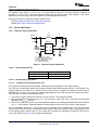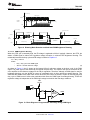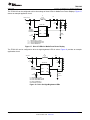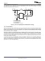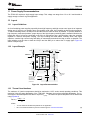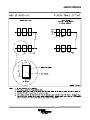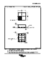
1
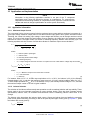
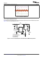
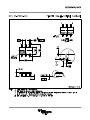
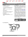
Sample &
Buy
Product
Folder
Support &
Community
Tools &
Software
Technical
Documents
Reference
Design
TPS61165
SLVS790C – NOVEMBER 2007 – REVISED JANUARY 2015
TPS61165 High-Brightness, White LED Driver in 2-mm x 2-mm QFN and SOT-23 Packages
1 Features
3 Description
•
•
•
•
With a 40-V rated integrated switch FET, the
TPS61165 device is a boost converter that drives
LEDs in series. The boost converter runs at a
1.2-MHz fixed switching frequency with 1.2-A switch
current limit, and allows for the use of a highbrightness LED in general lighting.
1
•
•
•
•
3-V to 18-V Input Voltage Range
38-V Open LED Protection
200-mV Reference Voltage With 2% Accuracy
1.2-A Switch FET With 1.2-MHz Switching
Frequency
Flexible 1 Wire Digital and PWM Brightness
Control
Built-in Soft Start
Up to 90% Efficiency
2-mm × 2-mm × 0.8-mm 6-Pin WSON Package
With Thermal Pad, and SOT-23 Package
The default white LED current is set with the external
sensor resistor Rset, and the feedback voltage is
regulated to 200 mV, as shown in Typical Application.
During the operation, the LED current can be
controlled using the 1 wire digital interface
(EasyScale™ protocol) through the CTRL pin.
Alternatively, a pulse-width-modulation (PWM) signal
can be applied to the CTRL pin through which the
duty cycle determines the feedback reference
voltage. In either digital or PWM mode, the
TPS61165 device does not burst the LED current;
therefore, it does not generate audible noises on the
output capacitor. For maximum protection, the device
features integrated open LED protection that disables
the TPS61165 device to prevent the output from
exceeding its absolute maximum voltage ratings
during open LED conditions.
2 Applications
•
•
High-Brightness LED Lighting
White LED Backlighting for Media Form Factor
Display
Device Information(1)
PART NUMBER
TPS61165
PACKAGE
BODY SIZE (NOM)
SOT-23 (6)
2.90 mm × 1.60 mm
WSON (6)
2.00 mm × 2.00 mm
(1) For all available packages, see the orderable addendum at
the end of the data sheet.
4 Typical Application
L1
10 mH
VIN 5V
C1
4.7 mF
TPS61165
ON/OFF
DIMMING
CONTROL
VIN
SW
CTRL
FB
COMP
GND
D1
C2
1 mF
350 mA
220 nF
Rset
0.57 W
L 1 : TOKO #A 915 _Y-100M
C1 : Murata GRM 188R61A475 K
C2 : Murata GRM 188R61E105K
D1 : ONsemi MBR0540T1
LED : OSRAM LW-W 5SM
1
An IMPORTANT NOTICE at the end of this data sheet addresses availability, warranty, changes, use in safety-critical applications,
intellectual property matters and other important disclaimers. PRODUCTION DATA.
TPS61165
SLVS790C – NOVEMBER 2007 – REVISED JANUARY 2015
www.ti.com
Table of Contents
1
2
3
4
5
6
7
8
9
Features ..................................................................
Applications ...........................................................
Description .............................................................
Typical Application ................................................
Revision History.....................................................
Device Options.......................................................
Pin Configuration and Functions .........................
Specifications.........................................................
1
1
1
1
2
3
3
4
8.1
8.2
8.3
8.4
8.5
8.6
4
4
4
5
6
6
Absolute Maximum Ratings ......................................
Recommended Operating Conditions.......................
Thermal Information ..................................................
Electrical Characteristics...........................................
Timing Requirements ................................................
Typical Characteristics ..............................................
Detailed Description .............................................. 8
9.1 Overview ................................................................... 8
9.2 Functional Block Diagram ......................................... 8
9.3 Feature Description................................................... 8
9.4 Device Functional Modes.......................................... 9
10 Application and Implementation........................ 10
10.1 Application Information.......................................... 10
10.2 Typical Applications .............................................. 12
10.3 Do's and Don'ts ..................................................... 20
11 Power Supply Recommendations ..................... 21
12 Layout................................................................... 21
12.1 Layout Guidelines ................................................. 21
12.2 Layout Example .................................................... 21
12.3 Thermal Considerations ........................................ 21
13 Device and Documentation Support ................. 23
13.1
13.2
13.3
13.4
13.5
Device Support......................................................
Documentation Support ........................................
Trademarks ...........................................................
Electrostatic Discharge Caution ............................
Glossary ................................................................
23
23
23
23
23
14 Mechanical, Packaging, and Orderable
Information ........................................................... 23
5 Revision History
Changes from Revision B (July 2011) to Revision C
•
Page
Added Pin Configuration and Functions section, Feature Description section, Device Functional Modes, Application
and Implementation section, Power Supply Recommendations section, Layout section, Device and Documentation
Support section, and Mechanical, Packaging, and Orderable Information section ............................................................... 1
Changes from Revision A (May 2010) to Revision B
Page
•
Replaced the Dissipations Ratings Table with the Thermal Information Table...................................................................... 4
•
Changed Figure 10............................................................................................................................................................... 13
•
Changed Additional Application Circuits and added text "For Assistance..." ....................................................................... 18
Changes from Original (November 2007) to Revision A
Page
•
Added "and SOT-23 Package" to the Title, the last Features item, and the last paragraph of the Description..................... 1
•
Added 6-pin SOT-23 pinout to the Device Information section .............................................................................................. 3
•
Added the DBV package to the Ordering Information table ................................................................................................... 3
•
Changed the Dissipation Rating Table to include the DBV package ..................................................................................... 4
•
Changed two values in the last paragraph of the MAXIMUM OUTPUT CURRENT section - From: 65 mA To: 110
mA in typical condition, and From: 85 mA To: 150 mA in typical condition ......................................................................... 10
2
Submit Documentation Feedback
Copyright © 2007–2015, Texas Instruments Incorporated
Product Folder Links: TPS61165
TPS61165
www.ti.com
SLVS790C – NOVEMBER 2007 – REVISED JANUARY 2015
6 Device Options
TA
OPEN LED PROTECTION
–40°C to 85°C
(1)
38 V (typical)
PACKAGE (1)
PACKAGE MARKING
TPS61165DRV
CCQ
TPS61165DBV
DAK
The DRV package is available in tape and reel. Add R suffix (TPS61165DRVR) to order quantities of 3000 parts per reel or add T suffix
(TPS61165DRVT) to order 250 parts per reel.
7 Pin Configuration and Functions
DRV Package
6-Pin WSON
Top View
DBV Package
6-Pin SOT-23
Top View
Pin Functions
PIN
WSON
NO.
SOT-23
NO.
TYPE
DESCRIPTION
VIN
6
1
I
The input supply pin for the IC. Connect VIN to a supply voltage between 3 V and 18 V.
SW
4
3
I
This is the switching node of the IC. Connect the switched side of the inductor to SW.
This pin is also used to sense the output voltage for open LED protection.
GND
3
4
O
Ground
FB
1
6
I
Feedback pin for current. Connect the sense resistor from FB to GND.
COMP
2
5
O
Output of the transconductance error amplifier. Connect an external capacitor to this pin
to compensate the converter.
CTRL
5
2
I
Control pin of the boost converter. It is a multifunctional pin which can be used for
enable control, PWM and digital dimming.
Thermal
Pad
—
—
—
NAME
The thermal pad should be soldered to the analog ground plane. If possible, use thermal
via to connect to ground plane for ideal power dissipation.
Submit Documentation Feedback
Copyright © 2007–2015, Texas Instruments Incorporated
Product Folder Links: TPS61165
3
TPS61165
SLVS790C – NOVEMBER 2007 – REVISED JANUARY 2015
www.ti.com
8 Specifications
8.1 Absolute Maximum Ratings
over operating free-air temperature range (unless otherwise noted) (1)
Supply voltages on VIN (2)
Voltages on CTRL
VIN
(2)
MIN
MAX
–0.3
20
UNIT
V
–0.3
20
V
Voltage on FB and COMP (2)
–0.3
3
V
Voltage on SW (2)
–0.3
40
V
PD
Continuous power dissipation
TJ
Operating junction temperature
–40
150
°C
Tstg
Storage temperature
–65
150
°C
(1)
(2)
See Thermal Information
Stresses beyond those listed under Absolute Maximum Ratings may cause permanent damage to the device. These are stress ratings
only, and functional operation of the device at these or any other conditions beyond those indicated under Recommended Operating
Conditions is not implied. Exposure to absolute-maximum-rated conditions for extended periods may affect device reliability.
All voltage values are with respect to network ground pin.
8.2 Recommended Operating Conditions
MIN
VI
Input voltage range, VIN
VO
Output voltage range
TYP
MAX
UNIT
3
18
V
VIN
38
V
(1)
L
Inductor
10
22
μH
fdim
PWM dimming frequency
5
100
kHz
CIN
Input capacitor
1
CO
Output capacitor
1
TA
Operating ambient temperature
TJ
Operating junction temperature
(1)
μF
10
μF
–40
85
°C
–40
125
°C
These values are recommended values that have been successfully tested in several applications. Other values may be acceptable in
other applications but should be fully tested by the user.
8.3 Thermal Information
TPS61165
THERMAL METRIC (1) (2)
DRV (WSON)
DBV (SOT-23)
6 PINS
6 PINS
80.7
210.1
RθJA
Junction-to-ambient thermal resistance
RθJC(top)
Junction-to-case(top) thermal resistance
55.4
46.8
RθJB
Junction-to-board thermal resistance
140.2
56.7
ψJT
Junction-to-top characterization parameter
0.3
0.5
ψJB
Junction-to-board characterization parameter
36.5
50.2
RθJC(bottom)
Junction-to-case(bottom) thermal resistance
0.9
—
(1)
(2)
4
UNIT
°C/W
For more information about traditional and new thermal metrics, see the IC Package Thermal Metrics application report, SPRA953.
For thermal estimates of this device based on PCB copper area, see the TI PCB Thermal Calculator.
Submit Documentation Feedback
Copyright © 2007–2015, Texas Instruments Incorporated
Product Folder Links: TPS61165
TPS61165
www.ti.com
SLVS790C – NOVEMBER 2007 – REVISED JANUARY 2015
8.4 Electrical Characteristics
VIN = 3.6 V, CTRL = VIN, TA = –40°C to 85°C, typical values are at TA = 25°C (unless otherwise noted)
PARAMETER
TEST CONDITIONS
MIN
TYP
MAX
UNIT
SUPPLY CURRENT
VI
Input voltage range, VIN
IQ
Operating quiescent current into VIN
Device PWM switching no load
3
ISD
Shutdown current
CRTL=GND, VIN = 4.2 V
UVLO
Under-voltage lockout threshold
VIN falling
Vhys
Under-voltage lockout hysterisis
2.2
18
V
2.3
mA
1
μA
2.5
V
70
mV
ENABLE AND REFERENCE CONTROL
V(CTRLh)
CTRL logic high voltage
VIN = 3 V to 18 V
V(CTRLl)
CTRL logic low voltage
VIN = 3 V to 18 V
1.2
R(CTRL)
CTRL pull down resistor
toff
CTRL pulse width to shutdown
CTRL high to low
2.5
ms
tes_det
Easy Scale detection time (1)
CTRL pin low
260
μs
tes_delay
Easy Scale detection delay
tes_win
Easy Scale detection window time
400
Measured from CTRL high
V
0.4
800
V
1600
kΩ
100
μs
1
ms
VOLTAGE AND CURRENT CONTROL
VREF
Voltage feedback regulation voltage
196
200
204
V(REF_PWM)
Voltage feedback regulation voltage under
brightness control
VFB = 50 mV
47
50
53
VFB = 20 mV
17
20
23
IFB
Voltage feedback input bias current
VFB = 200 mV
fS
Oscillator frequency
1.0
1.2
1.5
Dmax
Maximum duty cycle
90%
93%
tmin_on
Minimum on pulse width
Isink
Comp pin sink current
Isource
Comp pin source current
Gea
Error amplifier transconductance
Rea
Error amplifier output resistance
fea
Error amplifier crossover frequency
VFB = 100 mV
mV
mV
μA
2
MHz
40
ns
100
μA
μA
100
240
320
400
umho
6
MΩ
5 pF connected to COMP
500
kHz
VIN = 3.6 V
0.3
POWER SWITCH
RDS(ON)
N-channel MOSFET on-resistance
ILN_NFET
N-channel leakage current
VSW = 35 V, TA = 25°C
ILIM
N-Channel MOSFET current limit
D = Dmax
ILIM_Start
Start up current limit
D = Dmax
tHalf_LIM
Time step for half current limit
Vovp
Open LED protection threshold
Measured on the SW pin
Open LED protection threshold on FB
Measured on the FB pin, percentage of Vref,
Vref = 200 mV and 20 mV
VIN = 3.0 V
0.6
0.7
Ω
1
μA
1.44
A
OC and OLP
V(FB_OVP)
tREF
VREF ramp up time
1.2
0.7
A
5
VREF filter time constant
tstep
0.96
Each step, Measured as number of cycles of
the 1.2-MHz clock
37
38
ms
39
V
50%
180
μs
213
μs
160
°C
15
°C
THERMAL SHUTDOWN
Tshutdown
Thermal shutdown threshold
Thysteresis
Thermal shutdown threshold hysteresis
(1)
To select EasyScale mode, the CTRL pin has to be low for more than tes_det during tes_win.
Submit Documentation Feedback
Copyright © 2007–2015, Texas Instruments Incorporated
Product Folder Links: TPS61165
5
TPS61165
SLVS790C – NOVEMBER 2007 – REVISED JANUARY 2015
www.ti.com
8.5 Timing Requirements
MIN
NOM
MAX
UNIT
EasyScale TIMING
μs
tstart
Start time of program stream
2
tEOS
End time of program stream
2
360
μs
tH_LB
High time low bit
Logic 0
2
180
μs
tL_LB
Low time low bit
Logic 0
2 × tH_LB
360
μs
tH_HB
High time high bit
Logic 1
2 × tL_HB
360
μs
tL_HB
Low time high bit
Logic 1
2
180
μs
VACKNL
Acknowledge output voltage low
Open drain, Rpullup =15
kΩ to VIN
0.4
V
tvalACKN
Acknowledge valid time
See
(1)
2
μs
See
(1)
512
μs
tACKN
(1)
Duration of acknowledge condition
Acknowledge condition active 0, this condition will only be applied in case the RFA bit is set. Open-drain output, line must be pulled high
by the host with resistor load.
8.6 Typical Characteristics
Table 1. Table of Graphs
FIGURE
Efficiency
3 LEDs (VOUT = 12 V); VIN = 3, 5, 8.5 V; L = 10 μH
Figure 1
Efficiency
6 LEDs (VOUT = 24 V); VIN = 5, 8.5, 12 V; L = 10 μH
Figure 2
Current limit
TA = 25°C
Figure 3
Current limit
Figure 4
Easyscale step
Figure 13
PWM dimming linearity
VIN = 3.6 V; PWM Freq = 10 kHz and 32 kHz
Figure 14
Output ripple at PWM dimming
3 LEDs; VIN = 5 V; ILOAD = 350 mA; PWM = 32 kHz
Figure 15
Switching waveform
3 LEDs; VIN = 5 V; ILOAD = 3500 mA; L = 10 μH
Figure 5
Start-up
3 LEDs; VIN = 5 V; ILOAD = 350 mA; L = 10 μH
Figure 6
Open LED protection
8 LEDs; VIN = 3.6 V; ILOAD = 20 mA
Figure 7
100
100
VIN = 8.5 V
3 LEDs ( VOUT = 12 V )
VIN = 12 V
6 LEDs ( VOUT = 24 V )
90
90
VIN = 8.5 V
VIN = 5 V
VIN = 5 V
VIN = 3 V
Efficiency - %
Efficiency - %
80
70
80
70
60
60
50
50
40
40
0
50
100
150
200
Output Current - mA
250
300
0
Figure 1. Efficiency vs Output Current
6
Submit Documentation Feedback
50
100
150
200
Output Current - mA
250
300
Figure 2. Efficiency Vs Output Current
Copyright © 2007–2015, Texas Instruments Incorporated
Product Folder Links: TPS61165
TPS61165
SLVS790C – NOVEMBER 2007 – REVISED JANUARY 2015
1600
1600
1500
1500
1400
1400
Switch Current Limit - mA
Switch Current Limit - A
www.ti.com
1300
1200
1100
1000
900
800
20
1300
1200
1100
1000
900
30
40
50
60
Duty Cycle - %
70
80
800
-40
90
-20
0
20
40
60
80
Temperature - °C
100
120
140
Figure 4. Switch Current Limit vs Temperature
Figure 3. Switch Current Limit Vs Duty Cycle
CTRL 5 V/div
SW 5 V/div
VOUT 5 V/div
VOUT 200 mV/div AC
COMP 500 mV/div
IL 500 mA/div
IL 500 mA/div
t - 400 ns/div
t - 2 ms/div
Figure 5. Switching Waveform
Figure 6. Start-Up
OPEN LED 5 V/div
FB 200 mV/div
VOUT 10 V/div
IL 200 mA/div
t - 100 ms/div
Figure 7. Open LED Protection
Submit Documentation Feedback
Copyright © 2007–2015, Texas Instruments Incorporated
Product Folder Links: TPS61165
7
TPS61165
SLVS790C – NOVEMBER 2007 – REVISED JANUARY 2015
www.ti.com
9 Detailed Description
9.1 Overview
The TPS61165 is a high-efficiency, high-output-voltage boost converter in small package size. The device is
ideal for driving white LEDs in series. The serial LED connection provides even illumination by sourcing the same
output current through all LEDs, eliminating the need for expensive factory calibration. The device integrates 40V/1.2-A switch FET and operates in pulse width modulation (PWM) with 1.2-MHz fixed switching frequency. For
operation see the block diagram. The duty cycle of the converter is set by the error amplifier output and the
current signal applied to the PWM control comparator. The control architecture is based on traditional currentmode control; therefore, slope compensation is added to the current signal to allow stable operation for duty
cycles larger than 40%. The feedback loop regulates the FB pin to a low reference voltage (200 mV typical),
reducing the power dissipation in the current sense resistor.
9.2 Functional Block Diagram
D1
1
Rset
C2
4
FB
L1
SW
Reference
Control
Error
Amplifer
OLP
Vin
6
COMP
2
C1
PWM Control
C3
5
CTRL
Soft
Start-up
Ramp
Generator
+
Current
Sensor
Oscillator
GND
3
9.3 Feature Description
9.3.1 Soft Start-Up
Soft-start circuitry is integrated into the IC to avoid a high inrush current during start-up. After the device is
enabled, the voltage at FB pin ramps up to the reference voltage in 32 steps, each step takes 213 μs. This
ensures that the output voltage rises slowly to reduce the input current. Additionally, for the first 5 msec after the
COMP voltage ramps, the current limit of the switch is set to half of the normal current limit specification. During
this period, the input current is kept below 700 mA (typical). These two features ensure smooth start-up and
minimize the inrush current. See the start-up waveform of a typical example (Figure 6).
8
Submit Documentation Feedback
Copyright © 2007–2015, Texas Instruments Incorporated
Product Folder Links: TPS61165
TPS61165
www.ti.com
SLVS790C – NOVEMBER 2007 – REVISED JANUARY 2015
Feature Description (continued)
9.3.2 Open LED Protection
Open LED protection circuitry prevents IC damage as the result of white LED disconnection. The TPS61165
monitors the voltage at the SW pin and FB pin during each switching cycle. The circuitry turns off the switch FET
and shuts down the IC when both of the following conditions persist for 8 switching clock cycles: (1) the SW
voltage exceeds the VOVP threshold and (2) the FB voltage is less than half of regulation voltage. As a result, the
output voltage falls to the level of the input supply. The device remains in shutdown mode until it is enabled by
toggling the CTRL pin. The product of the number of external series LEDs and the maximum
forward voltage of each LED plus the 200-mV reference voltage does not exceed the 38-V minimum OVP
threshold
or
(NLEDS × VLED(MAX) + 200 mV ≤ 38 V.
9.3.3 Undervoltage Lockout
An undervoltage lockout prevents operation of the device at input voltages below typical 2.2 V. When the input
voltage is below the undervoltage threshold, the device is shutdown and the internal switch FET is turned off. If
the input voltage rises by undervoltage lockout hysteresis, the IC restarts.
9.3.4 Thermal Shutdown
An internal thermal shutdown turns off the device when the typical junction temperature of 160°C is exceeded.
The device is released from shutdown automatically when the junction temperature decreases by 15°C.
9.4 Device Functional Modes
9.4.1 Shutdown
The TPS61165 device enters shutdown mode when the CTRL voltage is logic low for more than 2.5 ms. During
shutdown, the input supply current for the device is less than 1 μA (max). Although the internal FET does not
switch in shutdown, there is still a dc current path between the input and the LEDs through the inductor and
Schottky diode. The minimum forward voltage of the LED array must exceed the maximum input voltage to
ensure that the LEDs remain off in shutdown.
Submit Documentation Feedback
Copyright © 2007–2015, Texas Instruments Incorporated
Product Folder Links: TPS61165
9
TPS61165
SLVS790C – NOVEMBER 2007 – REVISED JANUARY 2015
www.ti.com
10 Application and Implementation
NOTE
Information in the following applications sections is not part of the TI component
specification, and TI does not warrant its accuracy or completeness. TI’s customers are
responsible for determining suitability of components for their purposes. Customers should
validate and test their design implementation to confirm system functionality.
10.1 Application Information
10.1.1 Maximum Output Current
The overcurrent limit in a boost converter limits the maximum input current and thus maximum input power for a
given input voltage. Maximum output power is less than maximum input power due to power conversion losses.
Therefore, the current limit setting, input voltage, output voltage and efficiency can all change maximum current
output. The current limit clamps the peak inductor current; therefore, the ripple has to be subtracted to derive
maximum dc current. The ripple current is a function of switching frequency, inductor value and duty cycle. The
following equations take into account of all the above factors for maximum output current calculation.
1
IP =
é
1
1 ù
+
)ú
êL ´ Fs ´ (
Vout + Vf - Vin Vin û
ë
where
•
•
•
•
•
Ip = inductor peak to peak ripple
L = inductor value
Vf = Schottky diode forward voltage
Fs = switching frequency
Vout = output voltage of the boost converter. It is equal to the sum of VFB and the voltage drop across LEDs.
(1)
I out _ max =
Vin ´ (I lim - I p / 2) ´h
Vout
where
•
•
•
Iout_max = Maximum output current of the boost converter
Ilim = overcurrent limit
η = efficiency
(2)
For instance, when VIN is 3 V, 8 LEDs output equivalent to VOUT of 26 V, the inductor is 22 μH, the Schottky
forward voltage is 0.2 V; and then the maximum output current is 110 mA in typical condition. When VIN is 5 V,
10 LEDs output equivalent to VOUT of 32 V, the inductor is 22 μH, the Schottky forward voltage is 0.2 V; and then
the maximum output current is 150 mA in typical condition.
10.1.2 Inductor Selection
The selection of the inductor affects steady state operation as well as transient behavior and loop stability. These
factors make it the most important component in power regulator design. There are three important inductor
specifications, inductor value, dc resistance and saturation current. Considering inductor value alone is not
enough.
The inductor value determines the inductor ripple current. Choose an inductor that can handle the necessary
peak current without saturating, according to half of the peak-to-peak ripple current given by Equation 1, pause
the inductor DC current given by:
Vout ´ I out
I in _ DC =
Vin ´ h
(3)
10
Submit Documentation Feedback
Copyright © 2007–2015, Texas Instruments Incorporated
Product Folder Links: TPS61165
TPS61165
www.ti.com
SLVS790C – NOVEMBER 2007 – REVISED JANUARY 2015
Application Information (continued)
Inductor values can have ±20% tolerance with no current bias. When the inductor current approaches saturation
level, its inductance can decrease 20% to 35% from the 0A value depending on how the inductor vendor defines
saturation current. Using an inductor with a smaller inductance value forces discontinuous PWM when the
inductor current ramps down to zero before the end of each switching cycle. This reduces the maximum output
current of the boost convert, causes large input voltage ripple, and reduces efficiency. Large inductance value
provides much more output current and higher conversion efficiency. For these reasons, a 10-μH to 22-μH
inductor value range is recommended. A 22-μH inductor optimized the efficiency for most application while
maintaining low inductor peak to peak ripple. Table 2 lists the recommended inductor for the TPS61165. When
recommending inductor value, the factory has considered –40% and 20% tolerance from its nominal value.
TPS61165 has built-in slope compensation to avoid subharmonic oscillation associated with current mode
control. If the inductor value is lower than 10 μH, the slope compensation may not be adequate, and the loop can
be unstable. Therefore, customers need to verify the inductor in their application if it is different from the
recommended values.
Table 2. Recommended Inductors for TPS61165
PART NUMBER
L
(μH)
DCR MAX
(mΩ)
SATURATION CURRENT (A)
SIZE
(L × W × H mm)
VENDOR
TOKO
A915_Y-100M
10
90
1.3
5.2 × 5.2 × 3.0
VLCF5020T-100M1R1-1
10
237
1.1
5 × 5 × 2.0
TDK
CDRH4D22/HP
10
144
1.2
5 × 5 × 2.4
Sumida
LQH43PN100MR0
10
247
0.84
4.5 × 3.2 × 2.0
Murata
10.1.3 Schottky Diode Selection
The high switching frequency of the TPS61165 demands a high-speed rectification for optimum efficiency.
Ensure that the average and peak current rating of the diode exceeds the average output current and peak
inductor current. In addition, the reverse breakdown voltage of the diode must exceed the open LED protection
voltage. The ONSemi MBR0540 and the ZETEX ZHCS400 are recommended for TPS61165.
10.1.4 Compensation Capacitor Selection
The compensation capacitor C3 (see Functional Block Diagram), connected from COMP pin to GND, is used to
stabilize the feedback loop of the TPS61165. A 220-nF ceramic capacitor is suitable for most applications.
10.1.5 Input and Output Capacitor Selection
The output capacitor is mainly selected to meet the requirements for the output ripple and loop stability. This
ripple voltage is related to the capacitor’s capacitance and its equivalent series resistance (ESR). Assuming a
capacitor with zero ESR, the minimum capacitance needed for a given ripple can be calculated as shown in
Equation 4.
(Vout - Vin ) Iout
Cout =
Vout ´ Fs ´ Vripple
where
•
Vripple = peak-to-peak output ripple
(4)
The additional output ripple component caused by ESR is calculated as shown in Equation 4.
Vripple_ESR= Iout × RESR
(5)
Due to its low ESR, Vripple_ESR can be neglected for ceramic capacitors, but must be considered if tantalum or
electrolytic capacitors are used.
Care must be taken when evaluating a ceramic capacitors derating under dc bias, aging and AC signal. For
example, larger form factor capacitors (in 1206 size) have self-resonant frequencies in the range of the switching
frequency. So the effective capacitance is significantly lower. The dc bias can also significantly reduce
capacitance. Ceramic capacitors can loss as much as 50% of its capacitance at its rated voltage. Therefore,
leave the margin on the voltage rating to ensure adequate capacitance at the required output voltage.
Submit Documentation Feedback
Copyright © 2007–2015, Texas Instruments Incorporated
Product Folder Links: TPS61165
11
TPS61165
SLVS790C – NOVEMBER 2007 – REVISED JANUARY 2015
www.ti.com
The capacitor in the range of 1 μF to 4.7 μF is recommended for input side. The output requires a capacitor in
the range of 1 μF to 10 μF. The output capacitor affects the loop stability of the boost regulator. If the output
capacitor is below the range, the boost regulator can potentially become unstable.
The popular vendors for high value ceramic capacitors are:
TDK (http://www.component.tdk.com/components.php)
Murata (http://www.murata.com/cap/index.html)
10.2 Typical Applications
10.2.1 TPS61165 Typical Application
L1
10 mH
VIN 5V
C1
4.7 mF
D1
C2
1 mF
TPS61165
ON/OFF
DIMMING
CONTROL
VIN
SW
CTRL
FB
COMP
GND
350 mA
Rset
0.57 W
220 nF
L 1 : TOKO #A 915 _Y-100M
C1 : Murata GRM 188R61A475 K
C2 : Murata GRM 188R61E105K
D1 : ONsemi MBR0540T1
LED : OSRAM LW-W 5SM
Figure 8. TPS61165 Typical Application
10.2.1.1 Design Requirements
DESIGN PARAMETERS
EXAMPLE VALUE
Brightness Control
PWM Dimming
LED Current
357 mA
10.2.1.2 Detailed Design Procedure
10.2.1.2.1 LED Brightness Dimming Mode Selection
The TPS61165 features two dimming modes: PWM dimming and EasyScale 1 wire digital dimming.
The CTRL pin is used for the control input for both dimming modes, PWM dimming and the 1 wire dimming. The
dimming mode for the TPS61165 is selected each time the device is enabled. The default dimming mode is
PWM dimming. To enter 1 wire mode, the following digital pattern on the CTRL pin must be recognized by the IC
every time the IC starts from the shutdown mode.
1. Pull CTRL pin high to enable the TPS61165, and to start the 1 wire detection window.
2. After the EasyScale detection delay (tes_delay, 100 μs) expires, drive CTRL low for more than the EasyScale
detection time (tes_detect, 260 μs).
3. The CTRL pin has to be low for more than EasyScale detection time before the EasyScale detection window
(tes_win, 1 msec) expires. EasyScale detection window starts from the first CTRL pin low to high transition.
The IC immediately enters the 1 wire mode once the preceding three conditions are met. The EasyScale
communication can start before the detection window expires. Once the dimming mode is programmed, it can
not be changed without another start up. This means the IC needs to be shutdown by pulling the CTRL low for
2.5 ms and restarts. See Figure 9 for a graphical explanation.
12
Submit Documentation Feedback
Copyright © 2007–2015, Texas Instruments Incorporated
Product Folder Links: TPS61165
TPS61165
www.ti.com
SLVS790C – NOVEMBER 2007 – REVISED JANUARY 2015
Insert battery
PWM signal
high
CTRL
low
PWM
mode
Startup
delay
FB ramp
Shutdown delay
200mV x duty cycle
FB
t
Insert battery
Enter ES mode
Enter ES mode
Timing window
Programming
code
Programming code
high
CTRL
low
ES detect time
ES
mode
ES detect delay
Shutdown
delay
IC
Shutdown
Programmed value
(if not programmed, 200mV default )
50mV
Startup delay
FB
FB ramp
FB ramp
Startup delay
50mV
Figure 9. Dimming Mode Detection and Soft Start PWM Brightness Dimming
10.2.1.2.2 PWM Brightness Dimming
When the CTRL pin is constantly high, the FB voltage is regulated to 200 mV typically. However, the CTRL pin
allows a PWM signal to reduce this regulation voltage; therefore, it achieves LED brightness dimming. The
relationship between the duty cycle and FB voltage is shown in Equation 6.
VFB = Duty × 200 mV
where
•
•
Duty = duty cycle of the PWM signal
200 mV = internal reference voltage
(6)
As shown in Figure 10, the IC chops up the internal 200-mV reference voltage at the duty cycle of the PWM
signal. The pulse signal is then filtered by an internal low pass filter. The output of the filter is connected to the
error amplifier as the reference voltage for the FB pin regulation. Therefore, although a PWM signal is used for
brightness dimming, only the WLED dc current is modulated, which is often referred as analog dimming. This
eliminates the audible noise which often occurs when the LED current is pulsed in replica of the frequency and
duty cycle of PWM control. Unlike other methods which filters the PWM signal for analog dimming, TPS61165
regulation voltage is independent of the PWM logic voltage level which often has large variations.
VBG
200 mV
CTRL
Error
Amplifier
COMP
FB
Figure 10. Block Diagram of Programmable FB Voltage Using PWM Signal
Submit Documentation Feedback
Copyright © 2007–2015, Texas Instruments Incorporated
Product Folder Links: TPS61165
13
TPS61165
SLVS790C – NOVEMBER 2007 – REVISED JANUARY 2015
www.ti.com
For optimum performance, use the PWM dimming frequency in the range of 5 kHz to 100 kHz. The requirement
of minimum dimming frequency comes from the EasyScale detection delay and detection time specification in the
dimming mode selection. Since the CTRL pin is logic only pin, adding an external RC filter applied to the pin
does not work.
To use lower PWM dimming, add external RC network connected to the FB pin as shown in Additional
Application Circuits.
10.2.1.2.3 Digital 1 Wire Brightness Dimming
The CTRL pin features a simple digital interface to allow digital brightness control. The digital dimming can save
the processor power and battery life as it does not require a PWM signal all the time, and the processor can
enter idle mode if available.
The TPS61165 adopts the EasyScale protocol for the digital dimming, which can program the FB voltage to any
of the 32 steps with single command. The step increment increases with the voltage to produce pseudo
logarithmic curve for the brightness step. See Table 3 for the FB pin voltage steps. The default step is full scale
when the device is first enabled (VFB = 200 mV). The programmed reference voltage is stored in an internal
register and will not be changed by pulling CTRL low for 2.5ms and then re-enabling the IC by taking CTRL high.
A power reset clears the register value and reset it to default.
10.2.1.2.4 EasyScale: 1 Wire Digital Dimming
EasyScale is a simple but flexible one-pin interface to configure the FB voltage. The interface is based on a
master-slave structure, where the master is typically a microcontroller or application processor. Figure 11 and
Table 4 give an overview of the protocol. The protocol consists of a device specific address byte and a data byte.
The device specific address byte is fixed to 72 hex. The data byte consists of five bits for information, two
address bits, and the RFA bit. The RFA bit set to high indicates the Request for Acknowledge condition. The
Acknowledge condition is only applied if the protocol was received correctly. The advantage of EasyScale
compared with other on-pin interfaces is that its bit detection is in a large extent independent from the bit
transmission rate. It can automatically detect bit rates between 1.7 kBit/sec and up to 160 kBit/sec.
Table 3. Selectable FB Voltage
14
FB Voltage
(mV)
D4
D3
D2
D1
D0
0
0
0
0
0
0
0
1
5
0
0
0
0
1
2
8
0
0
0
1
0
3
11
0
0
0
1
1
4
14
0
0
1
0
0
5
17
0
0
1
0
1
6
20
0
0
1
1
0
7
23
0
0
1
1
1
8
26
0
1
0
0
0
9
29
0
1
0
0
1
10
32
0
1
0
1
0
11
35
0
1
0
1
1
12
38
0
1
1
0
0
13
44
0
1
1
0
1
14
50
0
1
1
1
0
15
56
0
1
1
1
1
16
62
1
0
0
0
0
17
68
1
0
0
0
1
18
74
1
0
0
1
0
19
80
1
0
0
1
1
20
86
1
0
1
0
0
21
92
1
0
1
0
1
Submit Documentation Feedback
Copyright © 2007–2015, Texas Instruments Incorporated
Product Folder Links: TPS61165
TPS61165
www.ti.com
SLVS790C – NOVEMBER 2007 – REVISED JANUARY 2015
Table 3. Selectable FB Voltage (continued)
FB Voltage
(mV)
D4
D3
D2
D1
D0
22
98
1
0
1
1
0
23
104
1
0
1
1
1
24
116
1
1
0
0
0
25
128
1
1
0
0
1
26
140
1
1
0
1
0
27
152
1
1
0
1
1
28
164
1
1
1
0
0
29
176
1
1
1
0
1
30
188
1
1
1
1
0
31
200
1
1
1
1
1
DATA IN
DATABYTE
Device Address
Start
Start DA7 DA6 DA5 DA4 DA3 DA2 DA1
0
1
1
1
0
0
1
DA0 EOS Start RFA
0
A1
A0
D4
D3
D2
D1
D0
EOS
DATA OUT
ACK
Figure 11. EasyScale Protocol Overview
Table 4. EasyScale Bit Description
BYTE
Device
Address
Byte
72 hex
Data byte
BIT
NUMBER
NAME
TRANSMISSION
DIRECTION
7
DA7
0 MSB device address
6
DA6
1
5
DA5
1
4
DA4
3
DA3
2
DA2
0
1
DA1
1
IN
DESCRIPTION
1
0
0
DA0
0 LSB device address
7 (MSB)
RFA
Request for acknowledge. If high, acknowledge is applied by device
6
A1
0 Address bit 1
5
A0
0 Address bit 0
4
D4
3
D3
2
D2
Data bit 2
1
D1
Data bit 1
0 (LSB)
D0
Data bit 0
ACK
IN
OUT
Data bit 4
Data bit 3
Acknowledge condition active 0, this condition will only be applied in case RFA bit is
set. Open drain output, Line needs to be pulled high by the host with a pullup
resistor. This feature can only be used if the master has an open-drain output
stage. In case of a push-pull output stage Acknowledge condition may not be
requested!
Submit Documentation Feedback
Copyright © 2007–2015, Texas Instruments Incorporated
Product Folder Links: TPS61165
15
TPS61165
SLVS790C – NOVEMBER 2007 – REVISED JANUARY 2015
www.ti.com
Easy Scale Timing, without acknowledge RFA = 0
t Start
DATA IN
t Start
Address Byte
DATA Byte
Static High
Static High
DA7
0
DA0
0
D0
1
RFA
0
TEOS
TEOS
Easy Scale Timing, with acknowledge RFA = 1
t Start
DATA IN
t Start
Address Byte
DATA Byte
Static High
Static High
DA7
0
DA0
0
TEOS
RFA
1
D0
1
t valACK
Controller needs to
Pullup Data Line via a
resistor to detect ACKN
DATA OUT
tLow
t High
Low Bit
(Logic 0)
tLOW
ACKN
t ACKN
Acknowledge
true, Data Line
pulled down by
device
Acknowledge
false, no pull
down
tHigh
High Bit
(Logic 1)
Figure 12. EasyScale — Bit Coding
All bits are transmitted MSB first and LSB last. Figure 12 shows the protocol without acknowledge request (Bit
RFA = 0), Figure 12 with acknowledge (Bit RFA = 1) request. Prior to both bytes, device address byte and data
byte, a start condition must be applied. For this, the CTRL pin must be pulled high for at least tstart (2 μs) before
the bit transmission starts with the falling edge. If the CTRL pin is already at a high level, no start condition is
needed prior to the device address byte. The transmission of each byte is closed with an End of Stream
condition for at least tEOS (2 μs).
The bit detection is based on a Logic Detection scheme, where the criterion is the relation between tLOW and
tHIGH. It can be simplified to:
High Bit: tHIGH > tLOW, but with tHIGH at least 2x tLOW, see Figure 12.
Low Bit: tHIGH < tLOW, but with tLOW at least 2x tHIGH, see Figure 12.
The bit detection starts with a falling edge on the CTRL pin and ends with the next falling edge. Depending on
the relation between tHIGH and tLOW, the logic 0 or 1 is detected.
The acknowledge condition is only applied if:
• Acknowledge is requested by a set RFA bit.
• The transmitted device address matches with the device address of the device.
• 16 bits is received correctly.
16
Submit Documentation Feedback
Copyright © 2007–2015, Texas Instruments Incorporated
Product Folder Links: TPS61165
TPS61165
www.ti.com
SLVS790C – NOVEMBER 2007 – REVISED JANUARY 2015
If the device turns on the internal ACKN-MOSFET and pulls the CTRL pin low for the time tACKN, which is 512 μs
maximum then the Acknowledge condition is valid after an internal delay time tvalACK. This means that the internal
ACKN-MOSFET is turned on after tvalACK, when the last falling edge of the protocol was detected. The master
controller keeps the line low in this period. The master device can detect the acknowledge condition with its input
by releasing the CTRL pin after tvalACK and read back a logic 0. The CTRL pin can be used again after the
acknowledge condition ends.
The acknowledge condition may be requested only if the master device has an open drain output. For a pushpull output stage, the use a series resistor in the CRTL line to limit the current to 500 μA is recommended to for
such cases as:
• accidentally requested acknowledge, or
• to protect the internal ACKN-MOSFET.
10.2.1.2.5 Current Program
The FB voltage is regulated by a low 0.2 V reference voltage. The LED current is programmed externally using a
current-sense resistor in series with the LED string. The value of the RSET is calculated using Equation 7.
V
ILED = FB
RSET
where
•
•
•
ILED = output current of LEDs
VFB = regulated voltage of FB
RSET = current sense resistor
(7)
The output current tolerance depends on the FB accuracy and the current sensor resistor accuracy.
10.2.1.3 Application Curves
200
200
PWM 10 kHz, 32 kHz
180
160
160
FB Voltage - mV
FB Voltage - mV
140
120
100
80
120
80
60
40
40
20
0
0
0
2
4
6
8
10 12 14 16 18 20 22 24 26 28 30 32
Easy Scale Step
Figure 13. FB Voltage vs EasyScale Step
0
20
40
60
PWM Duty Cycle - %
80
100
Figure 14. FB Voltage vs PWM Duty Cycle
Submit Documentation Feedback
Copyright © 2007–2015, Texas Instruments Incorporated
Product Folder Links: TPS61165
17
TPS61165
SLVS790C – NOVEMBER 2007 – REVISED JANUARY 2015
www.ti.com
PWM 5 V/div
VOUT 50 mV/div AC
ILED 200 mA/div
t - 20 ms/div
Figure 15. Output Ripple at PWM Dimming
10.2.2 Additional Application Circuits
The TPS61165 can be configured to drive three high-brightness LEDs using an external PWM dimming network.
Figure 16 shows an example application circuit.
L1
10 mH
D1
D2
C1
1 mF
C2
0.47 mF
TPS61165
ON/OFF
DIMMING
CONTROL
C3
220nF
VIN
SW
CTRL
FB
R3
R2
COMP GND
R1
Rset
10 W
RFLTR
L1: TOKO #A915_Y-100M
C1: Murata GRM188R61A475K
C2: Murata GRM188R61E105K
D1: ONsemi MBR0540T1
D2: ONsemi MMSZ4711
LED: OSRAM LW-W5SM
CFLTR
LED
Figure 16. Drive Three High-Brightness LEDs With External PWM Dimming Network
18
Submit Documentation Feedback
Copyright © 2007–2015, Texas Instruments Incorporated
Product Folder Links: TPS61165
TPS61165
www.ti.com
SLVS790C – NOVEMBER 2007 – REVISED JANUARY 2015
The TPS61165 can be configured to drive nine strings of three LEDs for Media Form Factor Displays. Figure 17
shows an example application circuit.
L1
10 mH
VIN 3 V to 6 V
D1
3s9p
27LEDs
C1
4.7 mF
C2
1 mF
TPS61165
VIN
ON /OFF
DIMMING
CONTROL
SW
CTRL
FB
COMP
GND
Rset
1.1 W
C3
220 nF
L1:
C1:
C2:
D1:
TOKO # A915_ Y-100 M
Murata GRM188 R61A475 K
Murata GRM188 R61E105 K
ONsemi MBR0540T 1
Figure 17. Drive 27 LEDs for Media Form Factor Display
The TPS61165 can be configured to drive six high-brightness LEDs in series. Figure 18 provides an example
applications circuit.
L1
10 mH
VIN 12 V
C1
4.7 mF
D1
C2
1 mF
TPS 61165
ON/OFF
DIMMING
CONTROL
VIN
SW
CTRL
FB
COMP
GND
C3
220 nF
350 mA
Rset
0.57 W
L1: TOKO #A915_Y-100M
C1: Murata GRM188R61A475K
C2: Murata GRM188R61E105K
D1: ONsemi MBR0540T1
LED: OSRAM LW-W5SM
Figure 18. Drive Six High-Brightness LEDs
Submit Documentation Feedback
Copyright © 2007–2015, Texas Instruments Incorporated
Product Folder Links: TPS61165
19
TPS61165
SLVS790C – NOVEMBER 2007 – REVISED JANUARY 2015
www.ti.com
The TPS61165 can be configured to drive four high-brightness LEDs using SEPIC topology. An example
application circuit can be found in Figure 19.
C1
4.7 mF
C4
1 mF
L1
10 mH
VIN 9V to 15V
L2
10 mH
TPS 61165
VIN
ON/OFF
DIMMING
CONTROL
D1
VOUT= 12 V
C2
1 mF
SW
180 mA
CTRL
FB
COMP
GND
C3
220 nF
Rset
1.1 W
L1, L2: TOKO #A915_Y-100M
C1: Murata GRM188 R61A475K
C2: Murata GRM188 R61E105K
C4: Murata GRM188 R61H105K
D1: ONsemi MBR0540T1
*L1,L2 can be replaced by 1:1 transformer
Figure 19. Drive Four High-Brightness LED With SEPIC Topology
10.3 Do's and Don'ts
There is a known issue with the TPS61165 when using the EasyScale interface to increase the feedback voltage.
When VFB is increased from 0 mV to any value above 0 mV, some ICs do not properly soft start during this
transition and the voltage on their SW pin overshoots. If the overshoot exceeds the absolute maximum voltage
rating on the SW pin, the IC is damaged.
With VFB set below 10 mV through EasyScale, the parasitic offsets on the input pins of the internal transconductance amplifier determine the value of output of the amplifier. IC process variations are causing the offset
to be larger and in the opposite polarity than expected. If the amplifier’s output is already high prior to a transition
from VFB = 0 mV to any other voltage, then the modulator turns on full, bypassing soft start, and causes the SW
pin and output voltage to overshoot.
To avoid this issue do not use EasyScale to change the feedback voltage from 0 mV, effectively disabling the
device, to any other voltage. One alternative is to start with VFB = 10 mV and go to a higher voltage. Another
alternative is to disable the IC by taking the CTRL pin low for 2.5 ms and then re-enter EasyScale to force a soft
start from VFB = 0 mV to the default 200 mV.
20
Submit Documentation Feedback
Copyright © 2007–2015, Texas Instruments Incorporated
Product Folder Links: TPS61165
TPS61165
www.ti.com
SLVS790C – NOVEMBER 2007 – REVISED JANUARY 2015
11 Power Supply Recommendations
The TPS61165 requires a single supply input voltage. This voltage can range from 3 V to 18 V and be able to
supply enough current for a given application.
12 Layout
12.1 Layout Guidelines
As for all switching power supplies, especially those high frequency and high current ones, layout is an important
design step. If layout is not carefully done, the regulator could suffer from instability as well as noise problems.
To reduce switching losses, the SW pin rise and fall times are made as short as possible. To prevent radiation of
high frequency resonance problems, proper layout of the high frequency switching path is essential. Minimize the
length and area of all traces connected to the SW pin and always use a ground plane under the switching
regulator to minimize inter-plane coupling. The loop including the PWM switch, Schottky diode, and output
capacitor, contains high current rising and falling in nanosecond and should be kept as short as possible. The
input capacitor must be close to both the VIN pin and the GND pin to reduce the IC supply ripple. Figure 20
shows a sample layout.
12.2 Layout Example
C1
Rset
Vin
LEDs Out
Vin
FB
L1
CTRL
COMP
CTRL
GND
SW
C3
C2
GND
Place enough
VIAs around
thermal pad to
enhance thermal
performance
LEDs IN
Minimize the
area of this
trace
Figure 20. Layout Recommendation
12.3 Thermal Considerations
The maximum IC junction temperature should be restricted to 125°C under normal operating conditions. This
restriction limits the power dissipation of the TPS61165. Calculate the maximum allowable dissipation, PD(max),
and keep the actual dissipation less than or equal to PD(max). The maximum-power-dissipation limit is determined
using Equation 8:
125°C - TA
PD(max) =
RqJA
where
•
•
TA is the maximum ambient temperature for the application
RθJA is the thermal resistance junction-to-ambient given in Thermal Information
Submit Documentation Feedback
Copyright © 2007–2015, Texas Instruments Incorporated
Product Folder Links: TPS61165
(8)
21
TPS61165
SLVS790C – NOVEMBER 2007 – REVISED JANUARY 2015
www.ti.com
Thermal Considerations (continued)
The TPS61165 comes in a thermally enhanced QFN package. This package includes a thermal pad that
improves the thermal capabilities of the package. The RθJA of the QFN package greatly depends on the PCB
layout and thermal pad connection. The thermal pad must be soldered to the analog ground on the PCB. Using
thermal vias underneath the thermal pad as illustrated in the layout example. Also see the QFN/SON PCB
Attachment application report (SLUA271).
22
Submit Documentation Feedback
Copyright © 2007–2015, Texas Instruments Incorporated
Product Folder Links: TPS61165
TPS61165
www.ti.com
SLVS790C – NOVEMBER 2007 – REVISED JANUARY 2015
13 Device and Documentation Support
13.1 Device Support
13.1.1 Third-Party Products Disclaimer
TI'S PUBLICATION OF INFORMATION REGARDING THIRD-PARTY PRODUCTS OR SERVICES DOES NOT
CONSTITUTE AN ENDORSEMENT REGARDING THE SUITABILITY OF SUCH PRODUCTS OR SERVICES
OR A WARRANTY, REPRESENTATION OR ENDORSEMENT OF SUCH PRODUCTS OR SERVICES, EITHER
ALONE OR IN COMBINATION WITH ANY TI PRODUCT OR SERVICE.
13.2 Documentation Support
13.2.1 Related Documentation
For related documentation see the following:
QFN/SON PCB Attachment (SLUA271)
13.3 Trademarks
EasyScale is a trademark of Texas Instruments.
All other trademarks are the property of their respective owners.
13.4 Electrostatic Discharge Caution
These devices have limited built-in ESD protection. The leads should be shorted together or the device placed in conductive foam
during storage or handling to prevent electrostatic damage to the MOS gates.
13.5 Glossary
SLYZ022 — TI Glossary.
This glossary lists and explains terms, acronyms, and definitions.
14 Mechanical, Packaging, and Orderable Information
The following pages include mechanical, packaging, and orderable information. This information is the most
current data available for the designated devices. This data is subject to change without notice and revision of
this document. For browser-based versions of this data sheet, refer to the left-hand navigation.
Submit Documentation Feedback
Copyright © 2007–2015, Texas Instruments Incorporated
Product Folder Links: TPS61165
23
PACKAGE OPTION ADDENDUM
www.ti.com
9-Sep-2014
PACKAGING INFORMATION
Orderable Device
Status
(1)
Package Type Package Pins Package
Drawing
Qty
Eco Plan
Lead/Ball Finish
MSL Peak Temp
(2)
(6)
(3)
Op Temp (°C)
Device Marking
(4/5)
TPS61165DBVR
ACTIVE
SOT-23
DBV
6
3000
Green (RoHS
& no Sb/Br)
CU NIPDAU
Level-1-260C-UNLIM
-40 to 85
DAK
TPS61165DBVT
ACTIVE
SOT-23
DBV
6
250
Green (RoHS
& no Sb/Br)
CU NIPDAU
Level-1-260C-UNLIM
-40 to 85
DAK
TPS61165DRVR
ACTIVE
SON
DRV
6
3000
Green (RoHS
& no Sb/Br)
CU NIPDAU
Level-2-260C-1 YEAR
-40 to 85
CCQ
TPS61165DRVRG4
ACTIVE
SON
DRV
6
3000
Green (RoHS
& no Sb/Br)
CU NIPDAU
Level-2-260C-1 YEAR
-40 to 85
CCQ
TPS61165DRVT
ACTIVE
SON
DRV
6
250
Green (RoHS
& no Sb/Br)
CU NIPDAU
Level-2-260C-1 YEAR
-40 to 85
CCQ
TPS61165DRVTG4
ACTIVE
SON
DRV
6
250
Green (RoHS
& no Sb/Br)
CU NIPDAU
Level-2-260C-1 YEAR
-40 to 85
CCQ
(1)
The marketing status values are defined as follows:
ACTIVE: Product device recommended for new designs.
LIFEBUY: TI has announced that the device will be discontinued, and a lifetime-buy period is in effect.
NRND: Not recommended for new designs. Device is in production to support existing customers, but TI does not recommend using this part in a new design.
PREVIEW: Device has been announced but is not in production. Samples may or may not be available.
OBSOLETE: TI has discontinued the production of the device.
(2)
Eco Plan - The planned eco-friendly classification: Pb-Free (RoHS), Pb-Free (RoHS Exempt), or Green (RoHS & no Sb/Br) - please check http://www.ti.com/productcontent for the latest availability
information and additional product content details.
TBD: The Pb-Free/Green conversion plan has not been defined.
Pb-Free (RoHS): TI's terms "Lead-Free" or "Pb-Free" mean semiconductor products that are compatible with the current RoHS requirements for all 6 substances, including the requirement that
lead not exceed 0.1% by weight in homogeneous materials. Where designed to be soldered at high temperatures, TI Pb-Free products are suitable for use in specified lead-free processes.
Pb-Free (RoHS Exempt): This component has a RoHS exemption for either 1) lead-based flip-chip solder bumps used between the die and package, or 2) lead-based die adhesive used between
the die and leadframe. The component is otherwise considered Pb-Free (RoHS compatible) as defined above.
Green (RoHS & no Sb/Br): TI defines "Green" to mean Pb-Free (RoHS compatible), and free of Bromine (Br) and Antimony (Sb) based flame retardants (Br or Sb do not exceed 0.1% by weight
in homogeneous material)
(3)
MSL, Peak Temp. - The Moisture Sensitivity Level rating according to the JEDEC industry standard classifications, and peak solder temperature.
(4)
There may be additional marking, which relates to the logo, the lot trace code information, or the environmental category on the device.
(5)
Multiple Device Markings will be inside parentheses. Only one Device Marking contained in parentheses and separated by a "~" will appear on a device. If a line is indented then it is a continuation
of the previous line and the two combined represent the entire Device Marking for that device.
Addendum-Page 1
Samples
PACKAGE OPTION ADDENDUM
www.ti.com
9-Sep-2014
(6)
Lead/Ball Finish - Orderable Devices may have multiple material finish options. Finish options are separated by a vertical ruled line. Lead/Ball Finish values may wrap to two lines if the finish
value exceeds the maximum column width.
Important Information and Disclaimer:The information provided on this page represents TI's knowledge and belief as of the date that it is provided. TI bases its knowledge and belief on information
provided by third parties, and makes no representation or warranty as to the accuracy of such information. Efforts are underway to better integrate information from third parties. TI has taken and
continues to take reasonable steps to provide representative and accurate information but may not have conducted destructive testing or chemical analysis on incoming materials and chemicals.
TI and TI suppliers consider certain information to be proprietary, and thus CAS numbers and other limited information may not be available for release.
In no event shall TI's liability arising out of such information exceed the total purchase price of the TI part(s) at issue in this document sold by TI to Customer on an annual basis.
OTHER QUALIFIED VERSIONS OF TPS61165 :
• Automotive: TPS61165-Q1
NOTE: Qualified Version Definitions:
• Automotive - Q100 devices qualified for high-reliability automotive applications targeting zero defects
Addendum-Page 2
PACKAGE MATERIALS INFORMATION
www.ti.com
3-Feb-2015
TAPE AND REEL INFORMATION
*All dimensions are nominal
Device
Package Package Pins
Type Drawing
SPQ
TPS61165DBVR
SOT-23
3000
179.0
8.4
DBV
6
Reel
Reel
A0
Diameter Width (mm)
(mm) W1 (mm)
B0
(mm)
K0
(mm)
P1
(mm)
W
Pin1
(mm) Quadrant
3.2
3.2
1.4
4.0
8.0
Q3
TPS61165DBVT
SOT-23
DBV
6
250
179.0
8.4
3.2
3.2
1.4
4.0
8.0
Q3
TPS61165DRVR
SON
DRV
6
3000
180.0
8.4
2.3
2.3
1.15
4.0
8.0
Q2
TPS61165DRVT
SON
DRV
6
250
180.0
8.4
2.3
2.3
1.15
4.0
8.0
Q2
Pack Materials-Page 1
PACKAGE MATERIALS INFORMATION
www.ti.com
3-Feb-2015
*All dimensions are nominal
Device
Package Type
Package Drawing
Pins
SPQ
Length (mm)
Width (mm)
Height (mm)
TPS61165DBVR
SOT-23
DBV
6
3000
203.0
203.0
35.0
TPS61165DBVT
SOT-23
DBV
6
250
203.0
203.0
35.0
TPS61165DRVR
SON
DRV
6
3000
210.0
185.0
35.0
TPS61165DRVT
SON
DRV
6
250
210.0
185.0
35.0
Pack Materials-Page 2
IMPORTANT NOTICE
Texas Instruments Incorporated and its subsidiaries (TI) reserve the right to make corrections, enhancements, improvements and other
changes to its semiconductor products and services per JESD46, latest issue, and to discontinue any product or service per JESD48, latest
issue. Buyers should obtain the latest relevant information before placing orders and should verify that such information is current and
complete. All semiconductor products (also referred to herein as “components”) are sold subject to TI’s terms and conditions of sale
supplied at the time of order acknowledgment.
TI warrants performance of its components to the specifications applicable at the time of sale, in accordance with the warranty in TI’s terms
and conditions of sale of semiconductor products. Testing and other quality control techniques are used to the extent TI deems necessary
to support this warranty. Except where mandated by applicable law, testing of all parameters of each component is not necessarily
performed.
TI assumes no liability for applications assistance or the design of Buyers’ products. Buyers are responsible for their products and
applications using TI components. To minimize the risks associated with Buyers’ products and applications, Buyers should provide
adequate design and operating safeguards.
TI does not warrant or represent that any license, either express or implied, is granted under any patent right, copyright, mask work right, or
other intellectual property right relating to any combination, machine, or process in which TI components or services are used. Information
published by TI regarding third-party products or services does not constitute a license to use such products or services or a warranty or
endorsement thereof. Use of such information may require a license from a third party under the patents or other intellectual property of the
third party, or a license from TI under the patents or other intellectual property of TI.
Reproduction of significant portions of TI information in TI data books or data sheets is permissible only if reproduction is without alteration
and is accompanied by all associated warranties, conditions, limitations, and notices. TI is not responsible or liable for such altered
documentation. Information of third parties may be subject to additional restrictions.
Resale of TI components or services with statements different from or beyond the parameters stated by TI for that component or service
voids all express and any implied warranties for the associated TI component or service and is an unfair and deceptive business practice.
TI is not responsible or liable for any such statements.
Buyer acknowledges and agrees that it is solely responsible for compliance with all legal, regulatory and safety-related requirements
concerning its products, and any use of TI components in its applications, notwithstanding any applications-related information or support
that may be provided by TI. Buyer represents and agrees that it has all the necessary expertise to create and implement safeguards which
anticipate dangerous consequences of failures, monitor failures and their consequences, lessen the likelihood of failures that might cause
harm and take appropriate remedial actions. Buyer will fully indemnify TI and its representatives against any damages arising out of the use
of any TI components in safety-critical applications.
In some cases, TI components may be promoted specifically to facilitate safety-related applications. With such components, TI’s goal is to
help enable customers to design and create their own end-product solutions that meet applicable functional safety standards and
requirements. Nonetheless, such components are subject to these terms.
No TI components are authorized for use in FDA Class III (or similar life-critical medical equipment) unless authorized officers of the parties
have executed a special agreement specifically governing such use.
Only those TI components which TI has specifically designated as military grade or “enhanced plastic” are designed and intended for use in
military/aerospace applications or environments. Buyer acknowledges and agrees that any military or aerospace use of TI components
which have not been so designated is solely at the Buyer's risk, and that Buyer is solely responsible for compliance with all legal and
regulatory requirements in connection with such use.
TI has specifically designated certain components as meeting ISO/TS16949 requirements, mainly for automotive use. In any case of use of
non-designated products, TI will not be responsible for any failure to meet ISO/TS16949.
Products
Applications
Audio
www.ti.com/audio
Automotive and Transportation
www.ti.com/automotive
Amplifiers
amplifier.ti.com
Communications and Telecom
www.ti.com/communications
Data Converters
dataconverter.ti.com
Computers and Peripherals
www.ti.com/computers
DLP® Products
www.dlp.com
Consumer Electronics
www.ti.com/consumer-apps
DSP
dsp.ti.com
Energy and Lighting
www.ti.com/energy
Clocks and Timers
www.ti.com/clocks
Industrial
www.ti.com/industrial
Interface
interface.ti.com
Medical
www.ti.com/medical
Logic
logic.ti.com
Security
www.ti.com/security
Power Mgmt
power.ti.com
Space, Avionics and Defense
www.ti.com/space-avionics-defense
Microcontrollers
microcontroller.ti.com
Video and Imaging
www.ti.com/video
RFID
www.ti-rfid.com
OMAP Applications Processors
www.ti.com/omap
TI E2E Community
e2e.ti.com
Wireless Connectivity
www.ti.com/wirelessconnectivity
Mailing Address: Texas Instruments, Post Office Box 655303, Dallas, Texas 75265
Copyright © 2015, Texas Instruments Incorporated