1
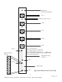
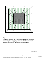
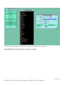
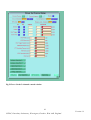
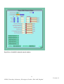
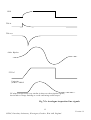
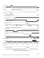
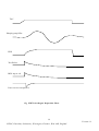
EDOC237
EUROGAM Clover Card User Guide
Version 1.0 July 1994 (updated August 1999)
Author: Ian Lazarus
Introduction
The EUROGAM/EUROBALL Clover card fully instruments a EUROGAM Clover Ge detector and its
associated BGO suppression shield. The inputs come from the Ge and BGO pre-amps and, after analogue
signal processing, the output from the card is a series of energy and timing data words plus a hit pattern.
The analogue signal processing is the same as used in the EUROGAM phase 1 Ge and BGO cards (full
details are given later) except that there is no ballistic deficit correction in the Ge channels. This is not
necessary since the crystals in the Ge detectors are smaller than those used in EUROGAM phase 1 and so
ballistic deficit does not have such a significant effect on their resolution.
For each Ge channel there is a high and a low gain (4MeV and 20MeV) energy measurement and 2 timing
measurements (the peaking time and the difference in time between this channel and a global timing
reference derived from the trigger system). The BGO channel provides a single energy measurement
(typically 8MeV range) and a single timing measurement (the difference in time between this channel and
a global timing reference derived from the trigger system). There is also a hit pattern to show which Ge
detectors and which BGO elements are involved in the event.
There are 4 Ge electronics channels plus an additional spare channel which can be cabled in and then
reconfigured from software to take the place of any of the other 4 channels should a problem arise during
an experiment. The BGO channel accepts signals from the 16 element shield in 8 pairs, each pair of
phototubes driving its own pre-amplifier.
Acknowledgements:
The Clover card is a collaborative project and the following people have been involved:
Engineer responsible for overall design:
VXI interface and Readout design:
CAD work including PCB design:
Assembly work:
Ge/BGO signal processing components:
MIDAS and other software:
Ian Lazarus (Daresbury Lab)
Patrick Coleman-Smith (Daresbury Lab)
Jim Thornhill (Liverpool University)
Manchester University, Dept of Physics Electronics Workshop.
Alphonse Richard, Zdravko Zojceski, M. Engrand (IPN Orsay)
Germain Bosson (ISN Grenoble)
Nabil Karkour (CSNSM Orsay)
Michel Goyot (IPN Lyon)
Charles Ring (CRN Strasbourg)
Vic Pucknell, Simon Letts, Peter Owens (Daresbury Laboratory)
For further help and information please contact Ian Lazarus at Daresbury Laboratory
email [email protected] fax (0)1925 603173
telephone (0)1925 603433
1
Version 1.0
CCLRC, Daresbury Laboratory, Warrington, Cheshire, WA4 4AD, England
Test pulser
Ge Pre-amp signal
4MeV Uni
Shaping amplifier
(Quasi-triangular)
Peak
det &
hold
20MeV Uni
20 MeV Bip
4MeV
ADC
TFA
20MeV
ADC
C/O
Stop
Peak time
TAC
Peak time
TAC ADC
FT TAC
FT TAC
ADC
Start
CFD
Stop
Inspection
Points
ROCI
Channel
Readout
Chip
(4 ADC/chip) To FIFO
Includes
Sliding
Scale
(Card
Readout)
Local Trigger
To VXI
Multiplicity
Current
sources
Fast
Trigger
Validation
BGO Veto
x5 (for 5 Ge channels)
Ge CFD outputs (5)
BGO Veto out
BGO Veto and other control logic
Test pulser
BGO Veto in
Hold Veto pattern
Pattern Unit and
deadtime generator
8
Includes parallel to
serial conversion
4 dual line
receivers
with LE
discriminators
.
8 inputs
from charge
preamps
for each
shield pair
of BGO
elements
(s1-s8)
8
Shaping
Amplifier
(2µs)
sums the
8 inputs
Logical OR of all
LE discriminators
Peak det
& hold
To VXI
Multiplicity
Current
source
Energy
ADC
Channel
Readout
Chip
(4 ADC/chip)
Includes
Sliding
Scale
Start
Stop
Inspection
Points
ROCI
FT TAC
To FIFO
(Card
Readout)
FT TAC
ADC
Local Trigger
Fast
Trigger
Validation
Fig 1 Block diagram of Eurogam Phase 2 Detector Card
2
Version 1.0
CCLRC, Daresbury Laboratory, Warrington, Cheshire, WA4 4AD, England
Ge Signal Processing
Input:
200mV/MeV (±10%) pre-amp signal with 50Ω pre-amp output impedance.
50µs fall time constant (+/- 5%)
1K input impedance (approx.)
Signal Shaping:
Unipolar output from 6th order quasi-triangular filter.
Peaking time of 4.4µs and FWHM 5 µs.
Pulse width at 0.1% is 11µs.
Output amplifier stage generates 4MeV and 20MeV ranges.
Bipolar (differentiated) outputs available for crossover timing.
Timing:
CFD: min threshold 20keV, pulse pair resolution better than 1µs
timing walk 3ns for 200:1 dynamic range, 25ns for 1000:1 (200ns Tr)
(Figures from phase 1 Ge with 50ns delay; need to re-measure using new 27ns CFD)
TFA with 50ns integration and 180ns differentiation. Gain x3 or x10.
TAC 0-2µs, FWHM 0.6ns, INL <5%
Outputs for coding:
4 MeV Unipolar signal
20 MeV Unipolar signal
TAC measuring peaking time (CFD firing to bipolar crossover)
TAC measuring channel firing time before reference pulse (CFD to FT)
ADC:
13 bits resolution (8192 channels)
Sliding scale
Conversion time 4.5µs
DNL <1%
INL < 250ppm
3
Version 1.0
CCLRC, Daresbury Laboratory, Warrington, Cheshire, WA4 4AD, England
BGO Signal Processing:
Input:
1000mV/MeV pre-amp signal with approx. 5Ω pre-amp output impedance.
(Phototube voltage must be adjusted to give 1000mV/MeV level.)
30ns rise time constant (+/- 10%)
10µs fall time constant (+/- 1.5%)
50Ω input impedance
Signal Shaping:
Bipolar output from 4th order semi-gaussian filter. (CR2 RC4, RC=2µs)
Peaking time of 5.2µs and FWHM 5.5 µs.
Pulse width at 0.1% is 12 x τ = 24µs.
Output 8 MeV full scale
Amplifier resolution is 3keV fwhm.
Outputs for coding:
8 MeV Energy signal
TAC measuring channel firing time before reference pulse (disc. to FT)
Also a serial bit stream indicating the hit pattern from BGO and Ge.
ADC:
13 bits resolution (8192 channels)
Sliding scale
Conversion time 4.5µs
DNL <1%
INL < 250ppm
Clover Detector Card Interconnections
* Primary interconnection mechanism is the VXI backplane as for phase 1.
* The inputs from the Ge pre-amps are connected to the front panel by BNC sockets.
* The BGO input is a 20 way IDC using similar LEMO-IDC cards to phase 1 but smaller to prevent misconnection of phase 1 shields to phase 2 electronics and vice versa.
* LEDs are provided to indicate that BGO discriminators and Ge CFDs are firing as used in phase 1. A
further LED is used to record FIFO errors (indicating readout problems).
* Front panel rate monitoring is provided via a 34 way IDC connector. 13 differential ECL signal pairs are
available from 5 CFDs and 8 BGO line receivers.
* Backplane sumbuses and all other VXI connections are retained for full compatibility with phase 1.
When the clover card is adjacent to phase 1 cards, the BGO local bus veto signals will be ignored and the
Ge local bus Veto inputs will not be driven.
* There are no external Veto inputs or outputs or external amplifier inputs.
Pinouts for connectors are given in fig 2 on the next page.
4
Version 1.0
CCLRC, Daresbury Laboratory, Warrington, Cheshire, WA4 4AD, England
FIFO error.
(Readout problem s)
Ge A
LED for CFD on G e A
Ge B
Ge C
Ge D
Ge E
P in 34
Detail of BGO
Pinou t
gn d
20
s8
s7
s6
s5
g nd
19
gn d
Pin 1
g nd
gn d
P in 20
gn d
s4
g nd
s3
gn d
s2
g nd
s1
gn d
g nd
g nd
1
2
P ins 1,2 are ground
P ins 3,5,7,9,11 are +ve Ge A-E
P ins 4,6,8,10,12 are -ve Ge A -E
P ins 14,16,18,20,22,24,26,28 are + ve BGO A-H
P ins 13,15,17,19,21,23,25,27 are -ve BGO A -H
P ins 29-34 are u nused.
Rate monitoring
outputs
BG O input
Pin 1
Fig 2 Front Panel for Clover Card
5
Version 1.0
CCLRC, Daresbury Laboratory, Warrington, Cheshire, WA4 4AD, England
Operating Modes for the Clover Detector
The anti-Compton veto system and sumbuses become more complex with a Clover detector than a
conventional tapered detector in deciding what combination of detector hits comprises a clean hit, whether
only 1 Ge may be hit (i.e. the Ge’s veto each other) or whether a combination of Ge hits is allowed and
which parts of the BGO shield veto which Ge detectors. All possible combinations of Ge/BGO hit pattern
are programmable in an 8kx4 memory using the 13 bit hit pattern as an address, with the 4 data bits
determining which, if any, of the sumbuses (Raw Ge, Clean Ge, BGO) are to be turned on and whether or
not to reject the event in hardware (or to mark it, depending on whether the card is in mark or reject mode).
Three of the most useful modes of operation are available from the MIDAS software in the top level of the
Clover card control menu. These modes are as follows:
Typical Modes of operation (these are all available from MIDAS software):
1) Simple.
In this case, all 5 Ge inputs (4 ‘real’ inputs + 1 spare) are treated as a single detector with a single BGO
shield. When 1 or more Ge element fires, a multiplicity of 1 is indicated on the Raw Ge sumbus regardless
of what happens in the BGO. The Clean Ge sumbus indicates a multiplicity of 1 if no element in the BGO
shield has fired. If 1 or more BGO element does fire, then a multiplicity of 1 is indicated on the BGO
sumbus and the Clean Ge sumbus current driver is inhibited.
2) Exactly One Ge.
In this case exactly 1 of the 4 Ge inputs must fire, with the other 3 Ge inputs being used, along with the
whole BGO shield, as anti-Compton vetos. The Raw Ge sumbus sees a multiplicity of 1 when 1 or more
Ge elements fires (even though the 2nd Ge is part of the veto), but the Clean Ge sumbus indicates a
multiplicity of 1 only if exactly 1 Ge has fired and no BGO element has fired. If 1 or more BGO element
fires, then a multiplicity of 1 is indicated on the BGO sumbus and the Clean Ge sumbus current driver is
inhibited.
3) Ignore Opposite Corner.
This mode is similar to the “Exactly One Ge” mode except that intelligence is applied to the processing of
the BGO shield. The 4 BGO elements in the opposite corner are ignored, for example:
Ge A is “clean” if there are no hits in any of the BGO pairs s1,s2,s3,s4,s7,s8 or Ge B-D.
(i.e. BGO elements i,j,k and l in s5 and s6 are ignored.)
The Raw Ge sumbus sees a multiplicity of 1 when 1 or more Ge elements fires, but the Clean Ge sumbus
indicates a multiplicity of 1 only if exactly 1 Ge has fired and there have been no BGO hits in the 12
relevant elements in the shield. If one or more BGO element (from the whole 16 element shield) fires, then
a multiplicity of 1 is indicated on the BGO sumbus.
Mode
Simple
Exactly 1 Ge
Ignore Opp Corner
Raw Ge Σ= 1
≥ 1 Ge
≥ 1 Ge
≥ 1 Ge
Clean Ge Σ= 1
≥ 1 Ge & not AC
= 1 Ge & not AC
= 1 Ge & not AC
BGO Σ= 1
≥ 1 BGO
≥ 1 BGO
≥ 1 BGO
Anti-Compton
16 BGO + 0 Ge
16 BGO + 3 Ge
12 BGO + 3 Ge
6
Version 1.0
CCLRC, Daresbury Laboratory, Warrington, Cheshire, WA4 4AD, England
s8
o
s7
p
a
b
c
n
m
l
s6
s1
Ge D
Ge A
Ge C
Ge B
d
e
f
k
j
i
h
s2
s3
g
s5
s4
Fig 3
N aming scheme for Clo ver Ge and BGO elements
show ing the mapping from 16 BGO elements to
8 BGO signals for the phase 2 electronics.
Drawn: I.L. Nov 1992
7
Version 1.0
CCLRC, Daresbury Laboratory, Warrington, Cheshire, WA4 4AD, England
MIDAS Software Interface For Clover Card.
The following pages show typical screens from MIDAS software, used in Euroball to control the Clover
Card.
Fig 4 shows the Base Frame, and indicates that you should select the Card Setup menu, where you will
find an entry for the Clover Card. The result of selecting this is shown in the same diagram. The enable
buttons toggle the on/off function for each channel (also available from within the Ge and BGO submenus). This is the point at which the Suppression mode is selected (see page 6) and, in the event of a
malfunction in one of the Ge channels, the spare channel configured . The Clover Card’s “Engineering”
menu and “Readout” button are for use by engineers only and contain no user controllable functions.
The more detailed Ge and BGO menus accessed from the Clover Card Setup menu (or directly from the
Base Frame’s VXI Module Setup menu) are shown in fig 5 and fig 6 respectively. These 2 menus are very
much the same as used for the phase 1 Ge and BGO cards. Note that for each Ge channel the PZ
adjustment must be made for the specific detector/pre-amp attached, and should be checked before an
experiment. Similarly, the FT sample and Val sample points (trigger timing) should be checked before
each experiment. The sample points should be placed in the middle of the FT and Validation pulses
respectively. The Ge channels have a common FT sample control, but the BGO channel has its own
independent control to cope with the different characteristics of the two types of detector.
The user controls which of the parameters are read out using the RO ticks at the top of each screen (fig 5
and fig 6). The sliding scale (SS) item should always be ticked except for the pattern for which the SS
must never be enabled. The pattern includes not only the BGO, but also the Ge hit pattern.
To help in setting up and checking the cards, some typical shapes of the signals on the inspection lines are
shown in fig 7 to 10.
8
Version 1.0
CCLRC, Daresbury Laboratory, Warrington, Cheshire, WA4 4AD, England
From the base frame select the VXI module Setup menu and the Clover Card item
Fig 4 MIDAS Base Frame and Clover card menu selection.
9
Version 1.0
CCLRC, Daresbury Laboratory, Warrington, Cheshire, WA4 4AD, England
Fig 5 Clover Card Ge channel control window
10
Version 1.0
CCLRC, Daresbury Laboratory, Warrington, Cheshire, WA4 4AD, England
Fig 6 Clover Card BGO channel control window
11
Version 1.0
CCLRC, Daresbury Laboratory, Warrington, Cheshire, WA4 4AD, England
PD S
TFA in
TFA ou t
4 Mev Bipolar
FT TA C
Unipolar
(4 MeV/ 20MeV
PZ ad ju st outp ut looks very similar in shap e to the unipolar signals,
but includ es voltage limiting to avoid saturating oscilloscopes .
Fig 7 Ge Analogue ins pection line signals
12
Version 1.0
CCLRC, Daresbury Laboratory, Warrington, Cheshire, WA4 4AD, England
CFD d elayed
Pileup
PD S gate
CFD d irect
FT sam ple (FT exists)
FT sam ple (no FT)
Val sam ple (Val exists)
Val sam ple (no val)
LT reset
reset if no FT
reset if
no val
end
r/ o
AD C Encod e
FT pulse
Val Pu lse
End of Conversion
ROCI data ack
ROCI data available
AD C clock
4MH z
Last P ass
Or of A DC d ead tim es
Fig 8 Ge Logic inspection signals
13
Version 1.0
CCLRC, Daresbury Laboratory, Warrington, Cheshire, WA4 4AD, England
TA C
Shaping amplifier
PD S
Test Pulser
BGO inp ut a-h
Line receiver outp ut a-h
fig 9 BGO A nalogu e In spection Lines
14
Version 1.0
CCLRC, Daresbury Laboratory, Warrington, Cheshire, WA4 4AD, England
BGO disable (high for norm al operation)
BGO Valack
BGO Encode
Validation Pulse
Inhibit
LT reset (assum ing FT and Val sam ple d on't cause res ets)
Start TA C
FT pulse
PD S gate
FT sam ple
Val sam ple
Disc d ead tim e
LT start
BGO Disc a-h
Width of pulse d ep end s on time taken by inpu t to drop below threshold
fig 10 BGO logic ins pection lines
15
Version 1.0
CCLRC, Daresbury Laboratory, Warrington, Cheshire, WA4 4AD, England
Details of registers and Addresses for Software Developers
Address Space (offset into VXI address space)
0x0000 to 0x00fe
0x0100 to 0x01fe
0x0200 to 0x02fe
0x0300 to 0x03fe
0x0400 to 0x04fe
0x0500 to 0x05fe
0x0600 to 0x06fe
0x0700 to 0x07fe
0x2000 to 0x3ffe
Name
Ge Common parameters (“Channel 0”)
Channel 1 Parameters (Ge A)
Channel 2 Parameters (Ge B)
Channel 3 Parameters (Ge C)
Channel 4 Parameters (Ge D)
Channel 5 Parameters (Ge Spare)
Channel 6 Parameters (BGO)
BGO Common parameters (“Channel 7”)
Veto Pattern logic Table
Channel 0 Sub-Address Spaces
0x0000 to 0x002e
0x0030 to 0x00fe
Function
Ge Common Parameters
Module Parameters (common to Ge & BGO)
Ge Common Parameters
Name
CFD Width DAC (8 bits)
FT Sample Point DAC (8 bits)
Validation Sample Point DAC (8 bits)
LT watchdog DAC (8 bits)
Test Generator Amplitude DAC (16 bits)
Offset
0x0000
0x0002
0x0004
0x0006
0x0010
Access
w
w
w
w
w
Old Ge offset
0x0000
0x0002
0x0004
0x0006
0x0010
Access
w
r/w
r/w
r/w
r/w
r/w
w
r
Old Ge/BGO offset
0x0030
0x0032
0x0034
0x0036
0x0038
0x003a
0c003c
0x003e (NB change)
Module Parameters (Common to Ge and BGO parts)
Name
Analogue Multiplexor Selection
Digital Multiplexor Selection
Voltage Inspection Line Selection
Controle des Fenetres
Module Configuration Register
Test Pulse Attenuator on/off (Ge only)
Test Write to Readout Data FIFO
Test Read from Readout Data FIFO
Module Control Register (0x0038)
d15-8 =x d7
d6
d5
0x38
Test Att CDF on not used
on = 1
=1
Offset
0x0030
0x0032
0x0034
0x0038 bit 6
0x0038
0x0038 bit 7
0x003c
0x003c
d4
not used
d3
d2
1 = Reset not used
FIFO
d1
0 = Rej
1 = mark
d0
LastCard
=1
16
Version 1.0
CCLRC, Daresbury Laboratory, Warrington, Cheshire, WA4 4AD, England
Channels 1-6
The addresses within the spaces allocated to channels 2 to 5 (Ge A to Ge E) are the same as on the phase 1
Ge Card. The addresses within channel 6 (BGO) are the same as those within channel 6 of the phase 1
BGO card. This permits the software to treat these channels exactly as at present which means that the
EUROGAM Register Server software and the EG Session Ge and BGO windows can be used with few
changes.
Ge channel Parameters (Channels 1-5)
Name
CFD Threshold (8 bits)
CFD Delay (8 bits)
PZ adjust DAC (8 bits)
PDS gate width DAC (8 bits)
Channel Control Register
Ge Channel control register:
d15-8 =x d7
d6
0x120 etc not used not used
Offset
0x0100 etc.
0x0102 etc.
0x0104 etc.
0x0106 etc.
0x0120 etc.
d5
d4
1 = CFD 1=Test
Disable
Mode
Access
w
w
w
w
r/w
d3
not used
Old Ge offset
0x0000
0x0002
0x0004
0x0006
0x0020
d2
d1
TFA gain
1=low
not used
d0
not used
BGO channel Parameters (Channel 6)
Name
BGO Threshold (12 bits)
BGO Test Pulser (12 bits)
Channel Control Register
Offset
0x0600
0x0602
0x0620
BGO Channel control register (0x620):
d15 d14 d13 d12 d11 d10 d9
n/u n/u n/u n/u n/u 1= Ch n/u
dis.
d8
n/u
Access
w
w
r/w
Old BGO offset
0x0000
0x0002
0x0020
d7
d6
d5
d4
d3
d2
d1
d0
1=TG
ON
1=TG
ON
1=TG
ON
1=TG
ON
1=TG
ON
1=TG
ON
1=TG
ON
1=TG
ON
BGO Common Parameters (Channel 7)
Name
Discriminator DeadTime DAC (8 bits)
FT Sample point DAC (8 bits)
Validation Sample Point DAC (8 bits)
LT Watchdog (8 bits)
PDS Gate Width DAC (8 bits)
Offset
0x0702
0x0706
0x0708
0x070a
0x070c
Access
w
w
w
w
w
Old BGO offset
0x0002
0x0006
0x0008
0x000a
0x000c
17
Version 1.0
CCLRC, Daresbury Laboratory, Warrington, Cheshire, WA4 4AD, England
Inspection Lines
The Ge and BGO inspection lines are combined as follows:
Channel
Channel 0
Channel 1
Channel 2
Channel 3
Channel 4
Channel 5
Channel 6
Channel 7
Function
Disconnect Inspection Line
Ge channel 1
Ge channel 2
Ge channel 3
Ge channel 4
Ge channel 5 (spare)
BGO channel
Ge common parameters (logic only)
Channels 6 and 7 overlap on certain signals such as Fast Triggers and Validations, but since the Ge and
BGO use different FT sample points, it is not unreasonable to keep the two sets of inspection lines entirely
as they are now. This has the advantage also that all the phase 1 inspection line software can be re-used.
The BGO elements s1-s8 map onto the old a-h inspection lines (analogue and digital); the old i and j
inspection lines are not used on phase 2. The address mapping is not exactly as phase 1 and is shown in
detail later along with the Voltage Inspection lines.
Veto Pattern Look-up Table
The pattern for Veto generation is loaded into a 8Kx4 memory array whose inputs are the pattern from the
8 BGO and 5 Ge discriminators and outputs are signals to determine the following:
* Veto the event?
* Drive Raw Ge sumbus?
* Drive Clean Ge sumbus?
* Drive BGO sumbus?
This table is controlled by word access at addresses from offsets 0x4000-0x7ffe, each address
corresponding to one possible pattern of discriminators. The pattern will be:
not
used
not
used
not
used
Ge
Sp
Ge
D
Ge
C
Ge
B
Ge
A
s8
s7
s6
s5
s4
s3
s2
msb
s1
lsb
The data at each location is:
not used
not used
not used
not used
1=
BGO 1= Cl Ge 1=Raw
Ge 1=
sumbus on
sumbus on
sumbus on
event.
d7
d6
d5
d4
d3
d2
d1
Veto
d0
18
Version 1.0
CCLRC, Daresbury Laboratory, Warrington, Cheshire, WA4 4AD, England
Multiplexors and Voltage Inspection Lines
d15
d14
d13
d12
d11
d10
fn 5
fn 4
fn 3
fn 2
fn 1
ch 3
Multiplex (analogue and digital) line 2
d09
ch 2
d08
ch 1
d07
d06
d05
d04
d03
d02
fn 5
fn 4
fn 3
fn 2
fn 1
ch 3
Multiplex (analogue and digital) line 1
Ge (ch1-5) Function field: Analogue Muxes
0
1
2
3
4
5
6
7
Name
PZ Adjust
4 MeV Unipolar
20 MeV Unipolar
FT TAC out
4 MeV Bipolar
TFA Output
TFA Input
4MeV PDS
BGO (ch6) Function field: Analogue Muxes
0
1
2
3
4
5
6
7
8
9
10
11
12
13
14
15
16
17
18
19
20
21
22
23
24
25
26
27
28
29
30
31
Name
TAC output (mtxa110)
Shaping Amp output (mtxa111)
PDS output (mtxa112)
Test Generator output (mtxa113)
Renin* (active L)
Renout* (active L)
FIFOdtack (active H)
Lecture (active H)
BGO Input H (mtxa121)
BGO Input G (mtxa120)
BGO Input F (mtxa119)
BGO Input E (mtxa118)
BGO Input D (mtxa117)
BGO Input C (mtxa116)
BGO Input B (mtxa115)
BGO Input A (mtxa114)
Line Receiver output A (mtxa107)
Line Receiver output B (mtxa106)
Line Receiver output C (mtxa105)
Line Receiver output D (mtxa104)
Line Receiver output E (mtxa103)
Line Receiver output F (mtxa102)
Line Receiver output G (mtxa101)
Line Receiver output H (mtxa100)
BGO Input H (mtxa121)
BGO Input G (mtxa120)
BGO Input F (mtxa119)
BGO Input E (mtxa118)
BGO Input D (mtxa117)
BGO Input C (mtxa116)
BGO Input B (mtxa115)
BGO Input A (mtxa114)
d01
ch 2
d00
ch 1
19
Version 1.0
CCLRC, Daresbury Laboratory, Warrington, Cheshire, WA4 4AD, England
Ge (ch1-5) Logic Inspection Function Select
0
1
2
3
4
5
6
7
Meaning
CFD Delayed Output
Pre-pulse Pileup
PDS Gate
CFD Direct Output
FT Sample Point (W1)
Val Sample Point (W2)
LT reset
ADC Encode Command
BGO (ch 6) Logic Inspection Function Select
0
1
2
3
4
5
6
7
8
9
10
11
12
13
14
15
16
17
18
19
20
21
22
23
Meaning
BGO Disable (mtxd118e)
BGO Valack (mtxd119)
BGO Encode (mtxd120)
Validation Pulse
Inhibit (Active Low)
LT reset
spare
spare
BGO TAC Start Pulse (mtxd110)
Fast Trigger Pulse
BGO PDS Gate (mtxd112)
BGO Fast Trigger Sample Point (mtxd113)
BGO Validation Sample Point (mtxd114)
BGO LT RO gate test point (mtxd115)
BGO Discriminator Deadtime (mtxd116)
BGO LT Start (orcfd-orlrec)
BGO disc h (mtxd100)
BGO disc g (mtxd101)
BGO disc f (mtxd102)
BGO disc e (mtxd103)
BGO disc d (mtxd104)
BGO disc c (mtxd105)
BGO disc b (mtxd106)
BGO disc a (mtxd107)
Common (ch 7) LI line function select
Meaning
0
1
2
3
4
5
6
7
Fast Trigger Pulse
Validation Pulse
End of ADC Conversion
ROCI Data Acknowledge
OR all 6 ROCI Data Available (Active Low)
ADC Clock (4 MHz)
Last Pass
OR of ADC deadtimes
20
Version 1.0
CCLRC, Daresbury Laboratory, Warrington, Cheshire, WA4 4AD, England
Voltage Inspection Lines
d7
d6
d5
d4
d3
d2
d1
not used
V Select 4 V Select 3 V Select 2 V Select 1 Mux Sel 3 Mux Sel 2
Voltage Inspection Lines: Bottom 3 lines select the Mux chip, and next 4 lines address it.
Voltage Inspection Code (Data 7..0)
Meaning
xxxxx 000 (0, 8, 16, 24 etc)
x0000 001 (1)
x0001 001 (9)
x0010 001 (17)
x0011 001 (25)
x0100 001 (33)
x0101 001 (41)
x0110 001 (49)
x0111 001 (57)
x1000 001 (65)
x1001 001 (73)
x1010 001 (81)
x1011 001 (89)
x1100 001 (97)
x1101 001 (105)
x1110 001 (113)
x1111 001 (121)
x0000 010 (2)
x0001 010 (10)
x0010 010 (18)
x0011 010 (26)
x0100 010 (34)
x0101 010 (42)
x0110 010 (50)
x0111 010 (58)
x1000 010 (66)
x1001 010 (74)
x1010 010 (82)
x1011 010 (90)
x1100 010 (98)
x1101 010 (106)
x1110 010 (114)
x1111 010 (122)
x0000 011 (3)
x0001 011 (11)
x0010 011 (19)
x0011 011 (27)
x0100 011 (35)
x0101 011 (43)
x0110 011 (51)
x0111 011 (59)
x1000 011 (67)
x1001 011 (75)
x1010 011 (83)
x1011 011 (91)
x1100 011 (99)
x1101 011 (107)
x1110 011 (115)
x1111 011 (123)
xxxxx 1xx
Not connected to VXI
Ge 1 CFD Threshold (VO1(1))
Ge 1 CFD Output Delay (VO1(2)
Ge 1 PZ Adjust (VO1(3))
Ge 1 PDS gate (VO1(4))
Ge 2 CFD Threshold (VO1(5))
Ge 2 CFD Output Delay (VO1(6))
Ge 2 PZ Adjust (VO1(7))
Ge 2 PDS gate (VO1(8))
Ge 3 CFD Threshold (VO2(1))
Ge 3 CFD Output Delay (VO2(2)
Ge 3 PZ Adjust (VO2(3))
Ge 3 PDS gate (VO2(4))
Ge 4 CFD Threshold (VO2(5))
Ge 4 CFD Output Delay (VO2(6))
Ge 4 PZ Adjust (VO2(7))
Ge 4 PDS gate (VO2(8))
Ge 5 CFD Threshold (VO3(1))
Ge 5 CFD Output Delay (VO3(2)
Ge 5 PZ Adjust (VO3(3))
Ge 5 PDS gate (VO3(4))
Ge Test Pulser Output Level
CFD Width
Ge Fast Trigger Sample Point (DW1)
Ge Validation Sample Point (DW2)
Ge LT timeout (DW3)
BGO Threshold
BGO Test Pulser Output Level (MTXC6)
BGO DAC ref (MTXC13)
BGO Fast Trigger Sample Point (MTXC15)
BGO Validation Sample Point (MTXC16)
BGO LT Timeout (MTXC17)
BGO PDS Gate (MTXC18)
VREFDAC (Ge DAC reference)
Vee24
Vee18
Vee12
Vee6
Vee (-5.2V)
Vee2
+3V regulator (BGO DAC ref)
Ground
Vcc5 Analogue
Vcc5 Digital
Vcc6
Vcc12
Vcc18
Vcc20
Vcc24
Connected to VXI, but not allocated on card
d0
Mux Sel 1
21
Version 1.0
CCLRC, Daresbury Laboratory, Warrington, Cheshire, WA4 4AD, England
Inhibit and Sumbus System description (added April 1996)
The Inhibit system logic applies a card level inhibit (signal name inhibecom) whenever one of these 2
conditions is true using a logic OR (IC 17, 27 and 28 on page 11 of circuits):
1) The system’s Inhibit Action VXI line is true (0v on backplane)
2) The card is set to Reject (not Mark) mode AND either there is pre-pulse pileup in one of the 5 Ge
channels OR there is a Veto from the Sumbus/Veto LookUp Table.
The duration of the card level inhibit is set by:
1) the duration of the system’s Inhibit Action signal (until end of readout in CDT mode)
2) the duration of the pre-pulse pileup (7µs) or the Veto (until LT reset)
If both conditions are true then the duration is set by the longer.
The front edge of the card level inhibit is also used to enable the serialisation of the status of the input
pattern by the pattern unit (M30). This level must be maintained until parallel to serial conversion is
finished.
The inhibit to each of the LT circuits has an inhibit over-ride using that LT’s LtStartN signal which
prevents the application of an inhibit once the LT is busy. (If Inhibit is applied to a busy LT and the LT’s
CFD fires again, then that LT will be reset prematurely.)
The sumbus drivers are controlled by a PAL which gates the LUT output with a delayed version of the OR
of the Ge CFD outputs. Whenever the CFD’s fire, the current pattern of local trigger LtStart signals and
BGO line receivers which is applied to the LUT will determine whether or not the sumbuses are driven. In
the case of the Ge LT’s this will be “stale” latched information if there is a card level inhibit preventing
changes in LT state.
In parallel mode the InhAction signal will be short, but the card level inhibit will be extended to 7µs by the
pre-pulse pileup (amplifier busy) signals if the reject mode is enabled. Check how long it takes to serialise
the LtStart pattern: maybe we need to stretch the InhAction locally to make a proper card deadtime
signal?
Sumbus deadtime (Added August 1999)
The sumbus inhibit problem described above has a second effect which is to disable the sumbus Ge
outputs while Inhibit Action is asserted, regardless of whether this clover is part of the event. The problem
can be overcome for the Raw Ge sumbus only in the LUT by programming the all the RawGe entries to be
always 1 so that the Raw Ge sumbus is driven whenever the OR of the Ge CFDs is true, regardless of the
Ge pattern bits from the LT Start signals. This method can be extended to a simple suppression on the
Clean Ge sumbus too by programming the LUT with a “don’t care” state in all the 5 Ge bits and using the
OR of the Ge CFDs to indicate that one or more of the Ge channels has been hit. The Clean sumbus output
from the LUT would be driven then whenever all 8 BGO bits are 0 and the OR of the Ge CFDs is true,
regardless of the state of the 5 Ge LT start LUT inputs. NB this LUT configuration is incompatible with
the complex Ge pattern based Vetos, but these are rarely/never used anyway so it is not really a problem
that they are unavailable.
22
Version 1.0
CCLRC, Daresbury Laboratory, Warrington, Cheshire, WA4 4AD, England
Data Format Description (Added August 1999)
The data format produced from the Clover card readout is as follows:
Q1
Q0
Qualifiers
See below
D31 D30
I5
I4
I3
I2
I1
I0
Item
Identifies parameter within clover
D29 D28 D27 D26 D25 D24
G7
G6
G5
G4
G3
G2
G1
G0
Group
MIDAS sets this within range allocated to clovers
D23 D22 D21 D20 D19 D18 D17 D16
The top 16 data bits always look like this and are followed by 16 bits of data as follows:
Pattern word:
not
used
D15
not
used
D14
not
used
D13
Ge
E
D12
Ge D Ge C Ge B Ge A s8
s7
s6
s5
s4
s3
s2
s1
D11
D10
D09
D08
D07
D06
D05
D04
D03
D02
D01
D00
E
E
E
E
E
E
E
E
E
E
D10
D09
D08
D07
D06
D05
D04
D03
D02
D01
E
LSB
D00
T
T
T
T
T
T
T
T
T
T
D10
D09
D08
D07
D06
D05
D04
D03
D02
D01
Energy Data Words (all types):
not
used
D15
not
used
D14
not
used
D13
E
E
MSB
D12 D11
TAC Data Words (all types)
not
used
D15
not
used
D14
not
used
D13
T
T
MSB
D12 D11
T
LSB
D00
Qualifiers:
The Ge qualifiers have the following meanings depending on which data word they come with:
Q1, Q0
00
01
10
11
Spectrum
q0
q1
q2
q3
20MeV
4MeV
clean data
clean data
A/C Veto
A/C Veto
Pileup
Pileup
(pre or post)
(pre or post)
Pileup and A/C Pileup and A/C
Veto
Veto
FT TAC
all data
not used
not used
CO TAC
no pileup
post-pulse pileup
pre-pulse pileup
not used
pre
and
pileup
post
The BGO qualifiers are always set to 1,1 for compatibility with the EG 1 BGO cards.
23
Version 1.0
CCLRC, Daresbury Laboratory, Warrington, Cheshire, WA4 4AD, England
Warning
Users must not remove the shields from the cards. There are no user serviceable parts inside. There
are, however, static sensitive components which can be easily damaged by incorrect handling
procedures.
Jumpers.
These adjustments should not be attempted by a user. Please contact an engineer.
ST 1,2,3,4,5 must always be inserted to ground the positive input to the shaping amplifiers.
ST8 controls whether the sliding scale is on or off. Shipped in the “on” position.
Top=On
Bottom = Off
ST20 controls whether the BGO channel is started by just the OR of the 5 Ge CFDs or the OR of the BGO
inputs OR'ed with the 5 Ge CFDs. Shipped in the “BGO or Ge” position.
Top=Ge only
Bottom= Ge OR BGO
Adjustments.
There are no user adjustments on the card itself.
The ADC sliding scale is set during commissioning and should not be changed.
(On the ADC there are 2 pots: 47k sets DC level and 1k sets gain for SS adjustment.)
The sumbus current output levels are set during commissioning and should not be changed.
(R244 sets BGO sumbus, R274 sets Clean Ge sumbus, R300 sets Raw Ge sumbus)
Power supplies.
Voltage
-2V
+5V
-5.2V
+12V
-12V
+24V
-24V
Typical current (amps)
0.5
2.3
6.1
1.9
1.6
0.1
0
Typical Power (Watts)
1
11.5
31.8
22.8
19.2
2.4
0
Total 89 Watts
--- End of document ---
24
Version 1.0
CCLRC, Daresbury Laboratory, Warrington, Cheshire, WA4 4AD, England