1
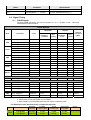
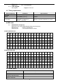
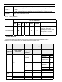
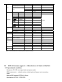
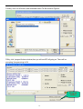
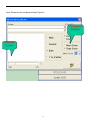
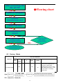
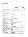
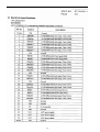
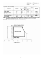
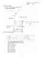
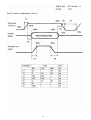
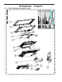
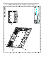
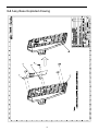
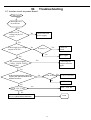
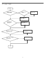
Service Manual LCD Monitor Acer V193W -0- 1 Table of Contents Important Safety Notice .........................................................................................01 01 Product Specification ..........................................................................................03 02 Flat Panel Specification .......................................................................................13 03 Exploded Diagram ..............................................................................................27 04 Troubleshooting ....................................................................................................32 05 Spare Parts List ...................................................................................................35 06 Schematics and Layouts.......................................................................................36 07 Assembly and Disassembly ................................................................................38 Appendix : User’s manual Copyright Copyright 2006 InnoLux Tech. Corp. Ltd All Rights Reserved This manual may not, in whole or in part, be copied, Photocopied, reproduced, translated, or converted to any electronic or machine readable form without prior written permission of InnoLux Tech. Corp. Ltd. Acer V193W Service Manual 1 Important Safety Notice 1. Safety precautions This monitor is manufactured and tested on a ground principle that a user’s safety comes first. However, improper used or installation may cause damage to the monitor as well as to the user. Warning: This monitor should be operated only at the correct power sources indicated on the label on the rear of the monitor. If you’re unsure of the power supply in you residence, consult your local dealer or Power Company. Do not try to repair the monitor by yourself, as it contains no user-serviceable parts. This monitor should only be repaired by a qualified technician. Do not remove the monitor cabinet. There are high-voltage parts inside that may cause electric shock to human bodies. Stop using the monitor if the cabinet is damaged. Have it checked by a service technician. Put your monitor only in a lean, cool, dry environment. If it gets wet, unplug the power cable immediately and consult your closed dealer. Always unplug the monitor before cleaning it. Clean the cabinet with a clean, dry cloth. Apply non-ammonia based cleaner onto the cloth, not directly onto the class screen. Do not place heavy objects on the monitor or power cord. z z z z z z z 2. Product safety notice Many electrical and mechanical parts in this chassis have special safety visual inspections and the protection afforded by them cannot necessarily be obtained by using replacement components rated for higher voltage, wattage, etc. Before replacing any of these components read the parts list in this manual carefully. The use of substitute replacement parts, which do not have the same safety characteristics as specified in the parts list, may create shock, fire, or other hazards. 3. Service notes z When replacing parts or circuit boards, clamp the lead wires around terminals before soldering. z Keep wires away from high voltage, high temperature components and sharp edges. z Keep wires in their original position so as to reduce interference. z Adjustment of this product please refers to the user’ manual. 2 01 Product Specification 1. General: Acer V 193W is designed with LVDS interface and dual (analog and digital signal) input, it featured with embedded universal AC power supplies and audio input. It’s a green product and meets all ROHS standard. The power button and display control buttons are on the front of the monitor. The monitors shall automatically to display lower resolution video modes into 1440x900 full screen display. The image can be adjusted through OSD control. 1.1 Main Features Features Specifications Panel source INL MT190AW01(V-5) Maximum resolution 1440 x 900 Back light system 4 CCFL (top & bottom edge side) Actual Resolution display WXGA+(1440x900) Pixel pitch 0.285(H) x 0.285(V) Display area 410.4 ( H ) x256.5 ( V ) , 19.05” diagonal Contrast ratio 700׃1 (min.), 1000׃1 (typ.) Response time (Tr+Tf) 5ms (typ.), Viewing angle 80°(L)/ 80°(R), 80°(U)/80°(D) typ. CR>=10) Analog(D-sub 15 pin) Digita(DVI-D connector )----option Input interface Audio-In Reserved Earphone Reserved Speakers Reserved Video Signal Inputs D-sub, DVI-D Knobs and Indicators Power switch button, MENU button, Auto button, eColour, Down button, Down button Security Features Kensington® lock port, VESA® Wall-mountable interface, 100 mm Power management Compatible with VESA,EPA,NUTEK,DPMS Plug & Play VESA University AC power supply YES OSD language For Non-EMEA English (US), French, Italian, Finnish, Spanish, German, Dutch, Russian For EMEA English (US), French, Italian, Simplified Chinese, Spanish, German Dutch, Traditional Chinese, Japanese Russia English (US), French, Italian, Finnish, Spanish, German, Dutch, Russian 1.2 Accessories Items VGA cable DVI cable User’s manual Warranty card Description 1.8m 1.8m Multi English ● ● ● ● 3 Quick-start Installation Guide Guide a 2. Operation Specifications The unit should suffer no visible cosmetic damage and should operate with no degradation in display quality during exposure to the operating conditions and after exposure to the non-operating conditions, in any sequence. 2.1 Environmental conditions Operating Specification Temperature range 0°C to 50°C Relative humidity 20% to 80% Altitude 0 to 3048M (10000 ft) Storage Temperature range -25°C to 60°C Relative humidity 5% to 80% Altitude 0 to 9144M (30000 ft) 2.2 Safety, EMC, Ergonomics and Compatibility Requirements Items Description Safety UL/cUL CB TUV/GS CCC ● ● ● ● EMC Ergonomics Compatibility FCC CE CCC VCCI-B ● ● ● ● TCO99 TCO03 ● ● Other Windows 95/98/Me Windows 2000 Windows XP vista ● ● ● ● Energy Star Power Management ● 2.3 Electrostatic Discharge Requirements Item Condition Electrostatic Discharge IEC61000-4-2(EN55024) Spec Contact discharge : +4KV Contact discharge : +8KV ● 2.4 Reliability Items Condition MTBF CCFL Life time Luminance becomes 50% Spec Note ≧ 40,000 Hours Excluding the LCD, CCFL ≧ 40,000 Hours(min) Note1 Note1. Display an all WHITE field at mid Brightness and Contrast settings. 3. Electrical and Optical Characteristics and Performance 3.1 Main Power Supply Items Condition 4 Spec Note Universal input full range 100~240VAC /50~60Hz AC Input Current 100Vac 240Vac 1.2A(max) 0.6A(max) AC Frequency Range 100Vac 240Vac 50Hz – 60Hz Inrush Current 100Vac,cold star,25°C 240Vac,cold star,25°C 40A (max) 60A(max) Regulator Efficiency DC output full loading ≥75% +16V output +5V output <500mv <150mv VCC16V(15.2~18V) VCC5V(4.95~5.45V) with Audio 1.6A(typ.),2.0A(max) 1.1A(typ.),1.5A(max) ≤45W AC Input Voltage Range Ripple and Noise DC Output Voltage and Current Power consumption See Note2 Protection See Table-1 Power management See Table-2 Note2. Before each test, the buck capacitor need to be discharged. Before each test, it must be 10 minutes at least after the latest test. Table-1 Protection OPP(Over power protection) SCP(short circuit protection) Condition Spec nominal AC input 50W ( min ) with auto-recovery function Table-2 Status Power On Power Saving Power Off H-sy nc on V-sy nc on off Video Power LED active ≤ 45W BLUE on blanked < 2W Amber on off blanked < 2W Amber off off blanked < 2W Amber -- -- -- < 1W Off 3.2 Backlight Power Supply Panel: INL MT190AW01 V.5 Items Specification Lamp 4 CCFL Input Voltage 15.2V~18V Input current 1.6A (Typ.), 2.0A (Max.) 5.5V≧Von≧ 2.0 V (on) -0.3v ≤ Voff ≤ 0.8 V (off) On/Off switch level Brightness PWM duty 35%~100% PWM:High=3.3V(3.0~3.6V),Low=0.0V CCFL operating Voltage 680Vrms (Typ.), 2.0 mA (min.)(With PWM Dim) CCFL Current 7.0mA (Typ.) 7.5mA (Max.) 5 CCFL startup voltage ≧1700 Vrms (0˚C) Operating frequency Protect delay time 40~80 KHz > 1 second Efficiency ≥70%(with dummy load) 3.3 Brightness output The test to verify specifications in this section shall be performed under the following standard conditions unless otherwise noted. Temperature Test pattern Video Resolution Video input level Warm-up time : 25 ± 5°C : white : 1440 x 900 : 700 mV ± 2% : 30 minutes LCD Module BL INL MT190AW01(V-5) ≥250 cd/m2 Set brightness control and also contrast control at maximum, to measure the screen center, the light output shall ≥ BL cd/m2 (as panel spec) 3.4 White balance Chromaticity Coordinate Mode x y Cool 9300K 0.283 ± 0.030 0.297 ± 0.030 Warm 6500K 0.313 ± 0.030 0.329 ± 0.030 Panel While x Panel While y User The test standard conditions refer to Sec 3.3. (Brightness and contrast are under default value) 3.5 Brightness uniformity The test standard conditions refer to Sec 3.3. Min. luminance of nine points (backlight) ≥75% Max. luminance of nine points (backlight ) 4. Input / Output Signal Specifications 4.1 Video signals 6 Items Condition Specification Analog RGB signal Input impedance = 75 Ohm 0.7Vp-p Sync Input impedance ≧ 1k Ohm TTL level, Separate H/V-sync(+/-) 4.2 Signal Timing 4.2.1 D-SUB Inputs Through D-SUB connectors, this unit can support FH= 31.5 ~ 80 KHz, Fv=56 ~ 75Hz and SXGA display modes as below: VESA MODES Horizontal Mode Resolution VGA SVGA XGA SXGA WXGA+ Total Nominal Frequency +/-0.5KHz Vertical Nominal Frequency +/-1Hz Sync Polarity Sync Polarity Nominal Pixel Clock (MHz) 640*480@60Hz 800*525 31.469 N 59.941 N 25.175 640*480@72Hz 832*520 37.861 N 72.809 N 31.500 640*480@75Hz 840*500 37.500 N 75.000 N 31.500 800*600@56Hz 1024*625 35.156 P 56.250 P 36.000 800*600@60Hz 1056*628 37.879 P 60.317 P 40.000 800*600@72Hz 1040*666 48.077 P 72.188 P 50.000 800*600@75Hz 1056*625 46.875 P 75.000 P 49.500 1024*768@60Hz 1344*806 48.363 N 60.004 N 65.000 1024*768@70Hz 1328*806 56.476 N 70.069 N 75.000 1024*768@75Hz 1312*800 60.023 P 75.029 P 78.750 1152*864@75Hz 1600*900 67.500 P 75.000 P 108.000 1280*960@60Hz 1800*1000 60.000 P 60.000 P 108.000 1280*1024@60Hz 1688*1066 63.981 P 60.020 P 108.000 1280*1024@75Hz 1688*1066 79.976 P 75.025 P 135.000 1440*900(Red)@60Hz 1600*926 55.469 P 59.901 N 88.75 1440*900@60Hz 1904*934 55.935 P 59.987 N 106.5 1440*900@75Hz 1936*942 70.635 N 74.984 P 136.75 720x400@70Hz 900*449 N 70.087 P 28.322 P 66.667 P 30.240 IBM MODES EGA 31.469 MAC MODES VGA 640*[email protected] 864*525 35.000 SVGA 832*624@75Hz 1152*667 49.725 N 74.550 N 57.283 XGA 1024*768@75Hz 1328*804 60.241 N 74.927 N 80.000 1152*870@75Hz 1456*915 68.681 N 75.062 N 100.00 Other MODES XGA 1024*768@72Hz 1360*800 57.669 N 72.086 N 78.434 SXGA 1280*1024@70Hz 1696*1072 74.882 P 69.853 P 127.000 Note: 1. Non-interlace signals only (An interlace signal cannot be display) 2. Please refer to F/W specification for more detail 3. Each frequency of Power Macintosh and Sun Ultra is a reference value For DVD Player Input, Attached timing is supported: (Optional) Mode Resolution (active dot) Resolution (total dot) Horizontal Frequency (KHz) Vertical Frequency (Hz) Nominal Pixel Clock (MHz) DVD Player 480P@60Hz 576P@50Hz 720P@60Hz 858x525 864x625 1650x750 31.5 31.250 45.000 60.000 50.000 60.000 27.027 27.000 74.250 7 Remark 4.2.2 Digital signals TMDS Signal: 4.2.3 (min) ±200mVpp@24Bit DDC signals DDC signals: 5V@50mA TTL level 4.3 Timing requirements Scan Frequency Condition Specification Horizontal Sync polarity: (+) or (-) 31.5 ~ 80 KHz. Vertical Sync polarity: (+) or (-) 56-75Hz Out of range Excluding Horizontal 31.5~80 KHz or Vertical 56-75 Hz Message “Input Not Supported” on screen 4.4 DDC data 4.4.1 EDID Standard Compliance EDID File Format: VESA’s EDID Standard Version #3, Revision #0, EDID Structure : Version #1, Revision #3. EDID Data Table : See the attached table (for example) V193W VGA EDID table 0 1 2 3 4 5 6 7 8 9 A B C D E F 0 00 FF FF FF FF FF FF 00 04 72 1A 00 00 00 00 00 1 00 00 01 03 08 29 1A 78 EA D7 A5 A2 59 4A 96 24 2 14 50 54 BF EF 90 95 00 95 0F 81 80 81 40 71 4F 3 01 01 01 01 01 01 9A 29 A0 D0 51 84 22 30 50 98 4 36 00 9A 00 11 00 00 1C 00 00 00 FF 00 30 30 30 5 30 30 30 30 30 30 30 30 30 0A 00 00 00 FD 00 32 6 4B 1E 52 0E 00 0A 20 20 20 20 20 20 00 00 00 FC 7 00 56 31 39 33 57 0A 20 20 20 20 20 20 20 00 cs V193W DVI EDID table 0 1 2 3 4 5 6 7 8 9 A B C D E F 0 00 FF FF FF FF FF FF 00 04 72 1A 00 00 00 00 00 1 00 00 01 03 80 29 1A 78 EA D7 A5 A2 59 4A 96 24 2 14 50 54 BF EF 90 95 00 95 0F 81 80 81 40 71 4F 3 01 01 01 01 01 01 9A 29 A0 D0 51 84 22 30 50 98 4 36 00 9A 00 11 00 00 1C 00 00 00 FF 00 30 30 30 5 30 30 30 30 30 30 30 30 30 0A 00 00 00 FD 00 32 6 4B 1E 52 0E 00 0A 20 20 20 20 20 20 00 00 00 FC 7 00 56 31 39 33 57 0A 20 20 20 20 20 20 20 00 cs 4.5 Audio signal Items Specification Input impedance ≧ 10K ohm Frequency response range 200Hz – 10kHz Signal to noise ratio ≧ 40 dB 8 Output power ≧ 1.0 W + 1.0 W ( 10%THD ) 5. Function Specifications All the tests to verify specifications in this section shall be performed under the following standard conditions unless otherwise noted. The standard conditions are: Temperature Warm-up time Checking display modes : 25 ± 5°C : 30 minutes minimum : All the specified modes 5.1 Panel general specifications A General specifications Supplier Model name Display Area Pixel Pitch InnoLux INL MT190AW01(V-5) Display Colors: 16.7 Million (6-bit + HI-- FRC) Number of Pixel Pixel Arrangement Brightness Contrast Ratio 1440x900 pixels RGB vertical stripe 300cd/m2 (Typ.) 250cd/m2 (Min.) 700:1 Typical Hor:160°, Ver: 160° (Typical, CR>10) Normally White 75Hz Tr + Tf = 5ms Typical Anti-glare, Haze = 25%, Hard coating (3H) 4 CCFL 427.2(W)x277.4(H)x16(D) Typ 410.4 ( H ) x256.5 ( V ) 0.285(H) x 0.285(V) Viewing Angle Display Mode Frame rate Response Time Surface Treatment Lamp Outline Dimension 5.2 Keypad Function 5.2.1 Control buttons on the front bezel CONTROL KEY [AUTO] [MENU] [►], [◄] KEYS FUNCTION A. When OSD un-displays, press [AUTO] to perform auto-adjustment B. When OSD displays, press [AUTO] to return to previous level menu C. When “e Color OSD” OSD displays, press [AUTO] to exit the OSD A. When OSD isn’t shown on screen, press [MENU] to enter OSD interface. The OSD interface uses “ACER e Color Management” and “User” to instead “Contrast” and “Brightness” separately. When press “ACER e Color Management” to show “e Color OSD”, and press “User” to show OSD interface before. The translations of “ACER e Color Management” and “User” are always English. B. When OSD displays, press [MENU] to perform function of menu icon that is highlight or enter next level menu A. When “MENU OSD” displays, press these keys to change the contents of an adjustment item, or change an adjustment value B. When “MENU OSD” un-displays, if it is with audio, press [►] to show “Audio” OSD and increase the volume, press [◄] to show “Audio” OSD and decrease the volume; else it has no use to press these keys. 9 [e Color ] A. When OSD un-displays, press [e Color] to show “e Color OSD”, and press again the OSD can not disappear, but the time of “e Color OSD” disappearing is reset 10 second again. B. When OSD disappear not including “e Color OSD”, press [e Color] to show “e Color OSD” OSD, the OSD before disappears, but the parameters of it should be saved [POWER] Power on or power off the monitor 5.2.2 Hot Key Operation HOT KEY OPERATION FUNCTION AUTO e Color ◄ ► MENU ● FACTORY MODE POWER ● ON Press [e Color ] & [MENU] at the same time, and then press [POWER] for DC power on. OSD menu will be shown with “F” on the left top. Select “F” for entering factory mode. 5.3 OSD Structure The On-Screen Display (OSD) shall be an easy to use icon based menu through keypad OSD buttons or remote control unit. The unit shall leave the factory with all OSD controls set to their default values. First Second Brightness ACER e COLOR Management Third Control Range Default Value Empowering Technology Contrast User Brightness User mode 50 Text mode 50 Standard mode 50 Graphics mode 60 Movie mode User mode 56 77 Text mode 44 Standard mode 77 Graphics mode 97 Movie mode 77 ACM Image Position Focus Clock Horizontal Vertical OFF --------10 0 ~ 100 Depend on each timing 0 ~ 100 50 ○1 0 ~ 100 50 0 ~ 100 Depend on each timing ----- ----- Red 0 ~ 100 80 Green 0 ~ 100 80 Blue 0 ~ 100 80 --------------------------- ----------------- English 0 ~ 100 50 0 ~ 100 50 10~ 120 20 ----- DDCCI ON/OFF ----ON DDCCI ON/OFF ON Warm (6500K) Cool (9300K) Color User Language NO-EMEA EMEA English English Deutsch Deutsch Español Español 简体中文 Hollands 繁體中文 Русский Français Français Italiano Italiano 日本語 Suomalain en Hor. Position OSD Ver. Position OSD Timeout Input (Dual) Analog Digital Input (Analg only) Resolution H. Freq Info V. Freq ------- ------- ----- ----- S/N Reset Exit ----- ------ETL000….0000(22) ----- Notes; ○ 1 Clock default 50 is for Visa timing. Others depend on timing. 6.0 SOP of firmware upgrade -----Manufacturer of Scaler is RealTek 6.1 Operational condition Equipment: PC, ISP card, signal cable and power cable. ESD requirements: antistatic wrists, antistatic gloves (fingers), and connecting cable Name of ISP program: RTDTool_4.6.exe Manufacture of FW IC:RTD 2525L 11 6.2 Operational steps: 1. Connection: connect PC to PCBA with signal cable, and then keep AC and DC in open state. One port of ISP program card is connected to PC print port. 2. Adjust ISP programming Firstly, double click RTDTool_4.6.exe and open ISP program, then select “25XXV/2525L”, and RTD 2120 ISP button Click ISP button 12 Secondly﹐ select Bank2 size which is 30. Select Bank2 size: 30 Thirdly, click “64K”button and download FW file as below Figure 3. 13 Fourthly, click “64~96”button, and download extern FW file as below Figure 4 . Fifthly, click “program”button as below,then you will see ISP will going on. There will be prompting if programming is OK. Program button 14 Note: Please see the configure as below Figure 6. Configure Inform Programmi ng speed 15 After connecting, AC ON, DC ON ◆Flowing chart OK Open ISP program OK Choose manufacturer and OK LOAD FW files OK Click program button OK Choose Config and adjust programming Beginning programming NG OK Turn off power if programming is OK 6.3 Factory Mode HOT KEY OPERATION FUNCTION AUTO FACTORY MODE e Color ◄ ► MENU ● ● 16 POWER ON Press [e Color ] & [MENU] at the same time, and then press [POWER] for DC power on. OSD menu will be shown with “F” on the left top. Select “F” for entering factory mode. 02. Flat Panel Specification 17 18 19 20 21 22 23 24 25 26 27 28 29 30 03 Exploded 3.1. LCD Exploded drawing (All) 31 Diagram 3.2 Assy Bezel Exploded drawing 32 3.3 Assy BACK COVER Exploded drawing For VC panel 33 3.4 Assy Base Exploded drawing 34 04 Troubleshooting 4.1 Inverter circuit on power board LED Green? Yes Backlight can’t be turned on. Yes Is there 5Vdc voltage on pin2 of IC501? No Check F803 and power supply Yes Is there high-level voltage on pin8 of IC501? No Is Ok R517? Yes Check I/F board No Yes R517 open No Are connected rightly CN501, CN502, CN503 and CN504? Connecting the output connector again Yes Is there instantaneously pulse wave on pin1, pin3, pin15 of IC501 at the moment of restart? No Is Ok IC501? No Yes U501, U502 fail IC501 fail Yes No T501, T502 fail Is ok T501, T502? Yes Check feedback circuit Isen,Vsen.(D503,D502,D508,D509.) END 35 4.2 power board No power Check primary rectifier voltage Check circuit if short Check F801, P801, D801, R805 Check pin1 of IC802 voltage over 1.3V Check R809 R810, R811, R812 Check R806, R807, R808, D804 Check pin7 of IC802 voltage about 16V Check IC802,Q804 Check Q804 Ds have triangle pulse END 36 Check IC802, C805, T801, Output Voltage Unstable Check reference voltage Check feedback circuit Check Pin R of IC803 voltage Check Vpin3-4 of IC801 about 6V Check Vpin1-2 of IC801 about Check R820,R832 END 37 Check R824,R822,R823,R825, IC801, Check C815, D806, R812 05 Level 1 1 1 1 1 1 1 1 1 1 1 1 1 1 1 1 1 Inl P/N Spare parts List Minimal order Q'ty INL P/N: 8191D161A020R Description PCBA,I/F 791401300600R BOARD(V5,EMEA,W/O),LE19D0PCBA,P/I BOARD,W/O 791401401600R SPK,LE19D1-612 ROHS PCBA,KEYPAD BOARD,LE9D0791401500000R 612 ROHS PWR CORD 16A/250V BLK 6FT 453070800210R VDE H05VV-F 3G CABLE,D-SUB 15P MALE 6FT 453010100380R BLACK/BLUE, ROH CABLE,DVI-D 18+1P MALE 6FT 453030300370R BLACK , ROHS HRN ASSY 2x4P 55mm 430300801670R UL1571#28,ROHS HRN ASSY 2x4P to 8P 215mm 430300801680R UL1571#28,ROHS HRN LVDS FFC 30P 182mm 430303001500R ROHS ASSY, BEZEL,SLIVER,INL 714030015600R V5 LE19D1 714020013100R ASSY,BASE,BLACK,LE19D1 714011202300R ASSY,STAND,BLACK,LE19D1 COVER HINGE,BLACK 501020220020R RIGHT,LE19D1 COVER HINGE,BLACK 501020220021R LEFT LE19D1 BACK COVER,ALL,BLACK,INL 501020220000R V5 ,LE19D1 ASSY,CHASSIS,V,ALL,INL V5 701000007100R ,LE19D1 LCP 19" MT190AW01-V5631102091401R G1,AM1900004511(IN 38 50 1 50 1 50 1 50 1 50 1 50 1 50 1 50 1 50 1 50 1 50 1 50 1 50 1 50 1 50 1 50 1 50 1 06 Schematics and Layouts 6.1 Inverter PWM circuit 39 6.2 Switching Mode Power Supply circuit 40 7.0 Assembly and Disassembly Sequence Item Photo Procedures P/N Description S1 Place panel (1).Take panel out of box and place it on the foam. (2).Tear open the PE bag and put it in the LCP 19" designated carton. MT190AW01-V5(3).Place panel on the foam like the attached 631102091401R G1,AM1900004511( picture. IN Remark:Do not touch the lamp cord and place the surface of panel downsides on the cushion. S2 Insert Keypay's wrie HRN ASSY 2x4P 1.Check if the keypad and relevent wire you to 8P 215mm choose are OK. 430300801680R UL1571#28,ROH 2.Insert the wire into the keypad like the S Picture Fix front bezel 1.Check if there is any lacquer missed or ASSY, sctratch happened to the front bezel. 714030015600R BEZEL,SLIVER,INL 2.Insert the fixed keypad into the front bezel V5,LE19D1 as picture S3 41 Assembly and Disassembly (continue) Assemble front bezel 1.Reverse the panel by 180 degree,put the surface of panel upsides and insert front bezel in the panel. 2.Reverse the panel by 180 degree using both hands,put the surface of panel downsides and make sure FFC interface ASSY, ASSY, is closer to operator. BEZEL,SLIVER BEZEL,SLIVER, 3.Paste tinfoil on the position which refers ,INL V5,LE19D1 INL V5,LE19D1 to attached picture,in order to cover the gap in the panel completely. Remark:Make sure the fixed job is finished properly and lamp wire is closer to right hand;Make the tinfoil smooth in the corner of panel. S5 Insert FFC wire into mainboar d (1).Insert FFC wire into its relevant interface of mainboard properly like attached picture1. (2).Insert the short keypad into its relevant interface like picture (2).Put the fixed mainboard in the right position. HRN LVDS FFC 430303001500 30P 182mm R ROHS S6 Fix chassis &powebo ard Place the chassis on the cushion after check,like the attached Picture ASSY,CHASSIS 701000007100 ,V,ALL,INL V5 R ,LE19D1 S4 42 Assembly and Disassembly (continue) S7 Fix chassis &powebo ard Insert powerboard into the designated location of chassis ,like the attached Picture S8 Connect mainboar d&powerb oard Connent powerboard with the relevant PIN in the mainboard like the attached Picture S9 Twist PCBA screw Handle electric opener and one pcs of M3*6 screw 43 PCBA,P/I 791401401600 BOARD,W/O SPK,LE19D1R 612 ROHS Assembly and Disassembly (continue) 3 S10 4 Twist PCBA screw 2 S11 S12 Fix 6 pcs of screws separately on the poweboard and mainboard like the attached Picture1 5 6 Twist screw for groundwire Paste FFC wire on the disignated location like the attached Picture Twist Hexagonal screws (1). Handle hexagonal screws and electric opener (2). Twist screw in the interface like the attached Picture1. (3). Place cushion on the designated location after iron frame is taken away. 4 3 2 1 44 SCREW ,P,CRO 509146306200 SS,W /W AS,M3* R 6,Zn-Cc Assembly and Disassembly (continue) S13 S14 F ix c h a ssis Th read lam p w ire in to th e relevan t h ole of 7 0 1 0 0 0 0 0 7 1 0 0 c h as s is lik e th e attac h ed P ic tu re R In se rt F F C c a ble 1 .Tear off th e ad h en s ive tap e of F F C w ire; 2 .In s ert F F C w ire in to th e in terfac e of p an el 3 .P u t F F C wire in ord er an d p as te th em on th e p an el 4 .F ix c h as s is on th e b ac k of p an el 1 2 3 4 S15 In se rt ligh t w ire 1 )In s ert 4 p c s lig h t w ire in to th e relevan t p os ition 2 ) p u t th e b alan c e lig h t w ire to th e p os ition as p ic tu re S16 In se rt ke ypa d C a b le 1 )In s ert k eyp ad w ire in to th e relevan t P IN in th e k eyp ad 430300801680 ( 2 )F ix b u tton on th e relevan t p os ition of R as s em b le ( 3 )C on firm if k eyp ad is in s erted p rop erly 45 A S S Y ,C H A S S IS ,V ,A L L ,IN L V 5 ,L E 1 9 D 1 HRN ASSY 2 x4 P to 8 P 215m m U L 1 5 7 1 # 2 8 ,R O HS Assembly and Disassembly (continue) 3 S17 F ix back cover 2 2 1 S18 F ix stand 3 2 BACK C O V E R ,A L L ,B L A C K ,IN L V 5 ,L E 1 9 D 1 U se 4 p cs screw fix stan d on th e b ack of assem b le like attach ed P ictu re 714011202300 R A S S Y,S TA N D ,B L A C K ,L E 1 9 D 1 A S S Y,B A S E ,B L A C K ,L E 1 9 D 1 1 3 1 C h eck if b ack cover is fixed p rop erly 501020220000 R 4 S19 F ix hinge cover& bas e C h eck if b ase is q u alified an d in sert it in to 714020013100 th e relevan t location p rop erly like th e R attach ed P ictu re S20 P acking (1 )R elease m on itor to th e p ackin g lin e (2 )P u t m on itor in to carton like th e attach ed p ictu re 46