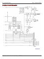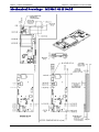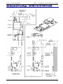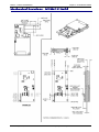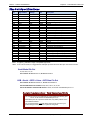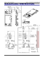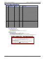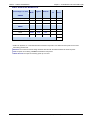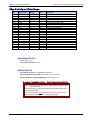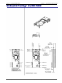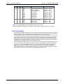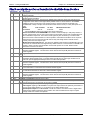
1
Universal Socket Connectivity Embedded Device Networking Solutions Hardware Guide for Developers Copyright and Technical Support Universal Socket Connectivity Hardware Guide for Developers, PN S000342P, Version P For the following products (The list indicates base models for each product. See each product chapter product build options): Cellular SocketModems SocketModem Cell – GPRS (MTSMC-G2, MTSMC-G2-V) SocketModem iCell – GPRS (MTSMC-G2-IP, MTSMC-G2-GP) SocketModem Cell – CDMA 1xRTT (MTSMC-C1, MTSMC-C1-V) SocketModem iCell – CDMA 1xRTT (MTSMC-C1-IP, MTSMC-C1-GP) SocketModem EDGE – (MTSMC-E1) Socket Modem Cell - HSPA (MTSMC-H3-U) Socket Modem iCell - HSPA (MTSMC-H3-IP build options) Socket Modem iCell – HSPA (MTSMC-H4 – IP and GP build options) Socket Modem Cell – EV-DO (MTSMC-EV1 – U) Socket Modem iCell – EV-DO (MTSMC-EV1 – IP build options) Socket Modem iCell – EV-DO (MTSMC-EV2 – IP and GP build options) Analog SocketModems SocketModem – MT9234SMI and other build options SocketModem – MT5692SMI and other build options SocketModem – MT2492SMI and other build options Embedded Device Servers SocketModem IP – MT100SEM-IP and other build options SocketWireless Wi-Fi – MT810SWM-IP and other build options SocketWireless Bluetooth – MTS2BTSMI and other build options Copyright This publication may not be reproduced, in whole or in part, without prior expressed written permission from Multi-Tech Systems, Inc. All rights reserved. Copyright © 2004-2011 by Multi-Tech Systems, Inc. Multi-Tech Systems, Inc. makes no representations or warranties with respect to the contents hereof and specifically disclaim any implied warranties of merchantability or fitness for any particular purpose. Furthermore, Multi-Tech Systems, Inc. reserves the right to revise this publication and to make changes from time to time in the content hereof without obligation of Multi-Tech Systems, Inc. to notify any person or organization of such revisions or changes. Trademarks Trademarks and Registered Trademarks of Multi-Tech Systems, Inc. are SocketModem, SocketWireless, SocketEthernet IP, and the Multi-Tech logo. Microsoft and Windows are trademarks or registered trademarks of Microsoft Corporation in the United States and other countries. Bluetooth is a registered trademark of the Bluetooth SIG, Inc. Wi-Fi is a registered trademark of the Wi-Fi Alliance. Contacting Multi-Tech Support Multi-Tech Online Support Portal https://support.multitech.com In order to better serve our customers, manage support requests and shorten resolution times, we have created the online web portal allowing you to submit questions regarding Multi-Tech products directly to our technical support team. Get answers to your most complex questions, ranging from implementation, troubleshooting, product configuration, firmware upgrades and much more. To create an account and submit a Support Case on the Portal, visit https://support.multitech.com Knowledge Base and Support Services: https://www.multitech.com/support.go The Knowledge Base provides immediate answers to your questions and gives you access to support resolutions for all Multi-Tech products. Visit our support area on the website for other support services. Technical Support Country Europe, Middle East, Africa: U.S., Canada, all others: Warranty Warranty information can found at: By Email [email protected] [email protected] By Phone +(44) 118 959 7774 (800) 972-2439 or (763) 717-5863 http://www.multitech.com/warranty.go World Headquarters Multi-Tech Systems, Inc. 2205 Woodale Drive Mounds View, Minnesota 55112 Phone: 763-785-3500 or 800-328-9717; Fax: 763-785-9874 Internet Address: http://www.multitech.com Multi-Tech Systems, Inc. Universal Socket Hardware Guide for Developers (S000342P) 2 Table of Contents Revision Notes Rev. Date M 08/11/10 M.1 N 08/16/10 11/17/10 O 02/02/11 P 06/22/11 Description ● New products: SocketModem Cell & iCell HSPA and SocketModem Cell & iCell – EV-DO ● In Chapter 1, removed the sentence "In the command state, the modem ignores –RTS" under the description of the –RTS pin ● In Chapter 1, removed the bulleted point from the "Maintenance of Your Cellular Device" section which suggested that the device not be exposed to temperatures above a certain limit. Temperature is covered in each product's technical specifications ● In Chapter 1, for Telecom Approvals for Analog Modems updated the link to the Web site and deleted the table that listed the country approvals since the Web site is always updated ● Added baud rate switches to CDMA-C1 product ● In the MT9234SMI specs table, changed Modes of Operation text from "full duplex over dial-up" to "full duplex over dial-up or 2-wire leased lines" ● In the MT9234SMI specification table, removed the power measurements (they appear in their own section) ● Changed the Mechanical Drawings for MT5693SMI-P and MT9234SMI-P ● Added parallel pin descriptions for MT5693SMI-P and MT9234SMI-P ● Updated some MT5693SMI-P and MT9234SMI-P parallel information ● Updated the Power Measurements for MT2492SMI ● Changed the operating temperature for MT100SEM-IP from 0° C – +70° C to -40° C to +85° C ● Added LED Interface section to MT100SEM-IP ● Updated LED Interface section in MT810SWM-IP chapter ● Updated the Power Measurements for the MT2492SMI Changed pin numbers to be added to next PCB revision (pages 90, 103). Minor edits. ● ● ● ● ● ● ● New Mechanical Drawings for MT5692SMI; now shows tooling holes Changed the sections describing tooling holes For MT5692SMI changed Supported PCM Encoding to 8-bit & 16-bit linear PCM; 4-bit IMA coding Changed operating temperatures for HSPA and EV-DO Changed the Power Draw table for HSPA-IP and HSPA-MI-IP Changed the Reset seconds and added a note about Reset the for MT810SWM-IP Changed the Pin-Out tables for H4 and EV2 ● Added in-rush current to the power draw tables for EV-DO (EV2) and HSPA (H4). Updated the peak transmit power measurements for EV-DO (EV2) and HSPA (H4). ● Added serial DC Electrical Characteristics to SocketModem MT5692SMI. ● Updated the power measurements table for GPRS – G2. ● New products: SocketModem Cell & iCell HSPA (H3), Socket Modem Cell & iCell – EV-DO (EV1) ● Updated Chapter 1 to include references to H3/EV1 where applicable ● Removed information on configuring the HSPA Modem on Linux SLAX 6 from this guide and added it to the new USB Driver Install Guide. ● Add new Canada EMC requirements. 7/11/11 ● Renamed FCC Requirements for the Antenna to FCC Grant Notes. ● Added OEM Integration section, with Grant Limitations, FCC Definitions, and Host Labeling requirements. FCC Grant Notes moved to this section. ● Updated power draw tables for MTSMC-EV2-MI-IP, MTSMC-EV2-IP, MTSMC-EV2-MI-GP, MTSMC-EV2GP, MTSMC-EV1-U, MTSMC-EV1-IP, MTSMC-Ev1-MI-IP, and MTSMC-H2-IP. ● Removed Serial and GPIO from Pin-Out Specifications for MTSMC-H3-IP and MTSMC-EV1-U, MTSMC-EV1-MI-IP-xx, as these are USB only. ● Replaced drawings for the MTSMC-EV1-U, MTSMC-EV1-IP, MTSMC-EV1-MI-IP, MTSMC-H3-IP, MTSMC-H3-MI-IP, and MTSMC-H3-U. Multi-Tech Systems, Inc. Universal Socket Hardware Guide for Developers (S000342P) 3 Table of Contents Table of Contents Part 1 Universal Socket Connectivity .................................................................................................9 Chapter 1 – Universal Socket Connectivity ......................................................................................10 Multi-Tech Embedded Solutions ................................................................................................................ 10 Universal Socket Connectivity Features ................................................................................................. 10 The Universal Socket Design ................................................................................................................. 10 Universal Developer Kit Contents ........................................................................................................... 11 AT Commands for All Embedded Products Are Included on the Developer Kit CD................................ 11 Universal Socket Pin Out ............................................................................................................................ 12 Universal Pin Descriptions ...................................................................................................................... 12 Design Considerations................................................................................................................................ 16 Noise Suppression Design Considerations ............................................................................................ 16 PC Board Layout Guidelines .................................................................................................................. 16 Electromagnetic Interference (EMI) Considerations ............................................................................... 17 Electrostatic Discharge Control .............................................................................................................. 17 Phone Line Warning Statement for the Developer Board ....................................................................... 17 SocketModem Developer Board ................................................................................................................. 18 Board Components................................................................................................................................. 19 Jumpers and Corresponding Signals...................................................................................................... 19 SocketModem Developer Board Block Diagram..................................................................................... 20 Developer Board Schematics ................................................................................................................. 21 Developer Board Schematics ................................................................................................................. 22 Developer Board Schematics ................................................................................................................. 23 Developer Board Schematics ................................................................................................................. 24 Developer Board Schematics ................................................................................................................. 25 Upgrading Firmware .................................................................................................................................... 26 XMODEM Serial Port for Firmware Upgrade .......................................................................................... 27 Multi-Tech Systems, Inc. Flash Programming Protocol .......................................................................... 28 Cellular Information ..................................................................................................................................... 31 Antenna System for Cellular Devices ..................................................................................................... 31 Antenna Specifications ........................................................................................................................... 31 OEM Integration ..................................................................................................................................... 34 Coax Cables Specifications .................................................................................................................... 35 Global Positioning System (GPS) ........................................................................................................... 38 Account Activation for Cellular Devices .................................................................................................. 39 Cellular Approvals and Labeling Requirements ...................................................................................... 39 Analog Information ...................................................................................................................................... 41 Recommended Parts for Analog SocketModems ................................................................................... 41 Analog Labeling Requirements............................................................................................................... 42 Safety Notices and Warnings ..................................................................................................................... 45 Cellular Safety ........................................................................................................................................ 45 Analog Telecom Safety Warnings .......................................................................................................... 46 Telecom Approvals for Analog Modems ................................................................................................. 47 Regulatory Compliance Statements .......................................................................................................... 48 Country/Region-Specific Statements ...................................................................................................... 48 Waste Electrical and Electronic Equipment Statement ........................................................................... 53 Restriction of the Use of Hazardous Substances (RoHS) ...................................................................... 54 Information on HS/TS Substances According to Chinese Standards in English ..................................... 55 Information on HS/TS Substances According to Chinese Standards in Chinese ................................... 56 Part 2 Cellular SocketModems ..........................................................................................................57 Chapter 2 – SocketModem Cell & iCell GPRS (MTSMC-G2) ..........................................................58 Introduction .................................................................................................................................................. 58 Product Build Options and Ordering Information..................................................................................... 58 AT Commands Reference Guides .............................................................................................................. 58 Technical Specifications ............................................................................................................................. 59 Mechanical Drawings – MTSMC-G2 Build ................................................................................................. 61 Mechanical Drawings – MTSMC-G2-Voice Build....................................................................................... 62 Multi-Tech Systems, Inc. Universal Socket Hardware Guide for Developers (S000342P) 4 Table of Contents Mechanical Drawings – MTSMC-G2-IP Build............................................................................................. 63 Mechanical Drawings – MTSMC-G2 GP (GPS) Build ................................................................................ 64 DC Electrical Characteristics ...................................................................................................................... 65 Power Measurements .................................................................................................................................. 65 Application Notes ........................................................................................................................................ 66 LED Interface.......................................................................................................................................... 66 RF Performances ................................................................................................................................... 66 RF Connection and Antenna .................................................................................................................. 66 Microphone Inputs .................................................................................................................................. 66 Changing the Quad Band ....................................................................................................................... 67 Chapter 3 – SocketModem® Cell and iCell CDMA 1xRTT (MTSMC-C1) .........................................68 Introduction .................................................................................................................................................. 68 Product Build Options and Ordering Information..................................................................................... 68 AT Commands Reference Guides .............................................................................................................. 69 Technical Specifications ............................................................................................................................. 70 Mechanical Drawings – MTSMC-C1 Build ................................................................................................. 72 Mechanical Drawings – MTSMC-C1-V (Voice) Build ................................................................................. 73 Mechanical Drawings – MTSMC-C1-IP Build ............................................................................................. 74 Mechanical Drawings – MTSMC-C1-GP (GPS) Build ................................................................................ 75 DC Electrical Characteristics ...................................................................................................................... 76 Power Measurements .................................................................................................................................. 76 Application Notes ........................................................................................................................................ 77 LED Interface.......................................................................................................................................... 77 RF Interface ............................................................................................................................................ 77 RF Connection and Antenna .................................................................................................................. 77 Baud Rate Switches on the SocketModem iCell..................................................................................... 78 Chapter 4 – SocketModem® EDGE (MTSMC-E1) ..............................................................................79 Introduction .................................................................................................................................................. 79 Product Build Options and Ordering Information..................................................................................... 79 AT Commands Reference Guide ................................................................................................................ 79 Technical Specifications ............................................................................................................................. 80 Mechanical Drawings – MTSMC-E1 Build.................................................................................................. 81 Mechanical Drawings – MTSMC-E1-V (Voice) Build ................................................................................. 82 DC Electrical Characteristics ...................................................................................................................... 83 Power Measurements .................................................................................................................................. 83 Application Notes ........................................................................................................................................ 84 RF Performances ................................................................................................................................... 84 RF Connection and Antenna .................................................................................................................. 84 Audio Interface – Electrical Characteristics ............................................................................................ 84 Microphone Inputs .................................................................................................................................. 84 Chapter 5 – SocketModem® iCell HSPA (MTSMC-H4) .....................................................................85 Introduction .................................................................................................................................................. 85 Product Build Options and Ordering Information..................................................................................... 85 AT Commands Reference Guide ................................................................................................................ 85 Technical Specifications ............................................................................................................................. 86 Mechanical Drawings – MTSMC-H4-IP/GP (GPS) Builds .......................................................................... 88 Mechanical Drawings – MTSMC-H4-MI-IP/GP Builds................................................................................ 89 DC Electrical Characteristics ...................................................................................................................... 90 Electrical Specifications ............................................................................................................................. 90 Pin-Out Specifications ................................................................................................................................ 91 Power Measurements .................................................................................................................................. 92 Application Notes ........................................................................................................................................ 93 LED Interface.......................................................................................................................................... 93 RF Performances ................................................................................................................................... 93 Frequency Bands Supported .................................................................................................................. 94 Multi-Tech Systems, Inc. Universal Socket Hardware Guide for Developers (S000342P) 5 Table of Contents RF Connection and Antenna .................................................................................................................. 94 Baud Rate Switches on the SocketModem iCell HSPA .......................................................................... 95 Chapter 6 – SocketModem® iCell EV-DO (MTSMC-EV2) ..................................................................96 Introduction .................................................................................................................................................. 96 Product Build Options and Ordering Information..................................................................................... 96 AT Commands Reference Guide ................................................................................................................ 97 Technical Specifications ............................................................................................................................. 98 Mechanical Drawings – MTSMC-EV2-IP/GP (GPS) Build........................................................................ 100 Mechanical Drawings – MTSMC-EV2-MI-IP/GP Builds ........................................................................... 101 DC Electrical Characteristics .................................................................................................................... 102 Electrical Specifications ........................................................................................................................... 102 Absolute Maximum Rating: ...................................................................................................................... 102 Pin-Out Specifications .............................................................................................................................. 103 Power Measurements ................................................................................................................................ 104 Application Notes ...................................................................................................................................... 106 LED Interface........................................................................................................................................ 106 RF Interface .......................................................................................................................................... 106 RF Connection and Antenna ................................................................................................................ 106 Baud Rate Switches on the SocketModem iCell................................................................................... 107 Chapter 7 – SocketModem® Cell and iCell HSPA (MTSMC-H3) ....................................................108 Introduction ................................................................................................................................................ 108 Product Build Options and Ordering Information................................................................................... 108 AT Commands Reference Guide .............................................................................................................. 108 Technical Specifications ........................................................................................................................... 109 Mechanical Drawings – MTSMC-H3-U Builds .......................................................................................... 111 Mechanical Drawings – MTSMC-H3-IP Builds ......................................................................................... 112 Mechanical Drawings – MTSMC-H3-MI-IP Builds .................................................................................... 113 DC Electrical Characteristics .................................................................................................................... 114 Electrical Specifications ........................................................................................................................... 114 Pin-Out Specifications .............................................................................................................................. 115 Power Measurements ................................................................................................................................ 116 Application Notes ...................................................................................................................................... 118 LED Interface........................................................................................................................................ 118 RF Performances ................................................................................................................................. 118 Frequency Bands Supported ................................................................................................................ 119 RF Connection and Antenna ................................................................................................................ 119 Baud Rate Switches on the SocketModem iCell HSPA ........................................................................ 120 Chapter 8 – SocketModem® Cell and iCell EV-DO (MTSMC-EV1).................................................121 Introduction ................................................................................................................................................ 121 Product Build Options and Ordering Information................................................................................... 121 AT Commands Reference Guide .............................................................................................................. 121 Technical Specifications ........................................................................................................................... 122 Mechanical Drawings – MTSMC-EV1-U Builds ....................................................................................... 124 Mechanical Drawings – MTSMC-EV1-IP Builds ....................................................................................... 125 Mechanical Drawings – MTSMC-EV1-MI-IP Builds.................................................................................. 126 DC Electrical Characteristics .................................................................................................................... 127 Electrical Specifications ........................................................................................................................... 127 Absolute Maximum Rating: ...................................................................................................................... 127 Pin-Out Specifications .............................................................................................................................. 128 Power Measurements ................................................................................................................................ 129 Application Notes ...................................................................................................................................... 130 LED Interface........................................................................................................................................ 130 RF Interface .......................................................................................................................................... 130 RF Connection and Antenna ................................................................................................................ 130 Baud Rate Switches on the SocketModem iCell................................................................................... 131 Multi-Tech Systems, Inc. Universal Socket Hardware Guide for Developers (S000342P) 6 Table of Contents Part 3 Analog SocketModems..........................................................................................................132 Chapter 9 – SocketModem® (MT9234SMI) ......................................................................................133 Introduction ................................................................................................................................................ 133 Product Build Options and Ordering Information................................................................................... 133 AT Commands Reference Guide .............................................................................................................. 133 Technical Specifications ........................................................................................................................... 134 Mechanical Drawings – MT9234SMI-92/L-92/HV-92 Builds .................................................................... 135 Mechanical Drawings – Parallel Builds.................................................................................................... 136 DC Electrical Characteristics .................................................................................................................... 137 Power Measurements ................................................................................................................................ 138 Parallel Timing Requirements .................................................................................................................. 139 Pin Descriptions for a Parallel SocketModem Device ............................................................................ 140 SocketModem Parallel Interface Internal Registers................................................................................ 141 Application Notes ...................................................................................................................................... 147 Tip and Ring Interface .......................................................................................................................... 147 Chapter 10 – SocketModem® (MT5692SMI) ....................................................................................148 Introduction ................................................................................................................................................ 148 Product Build Options and Ordering Information................................................................................... 148 AT Commands Reference Guide .............................................................................................................. 150 Technical Specifications ........................................................................................................................... 151 Mechanical Drawings – MT5692SMI-34/92 Builds ................................................................................... 153 Mechanical Drawings – No LEDS 3.3V Build........................................................................................... 154 Mechanical Drawings – MT5692SMI-V (Voice) Builds ............................................................................ 155 Mechanical Drawings – Parallel Builds.................................................................................................... 156 Operating Conditions ................................................................................................................................ 157 Absolute Maximum Rating ........................................................................................................................ 157 DC Electrical Characteristics .................................................................................................................... 157 Power Measurements ................................................................................................................................ 158 Parallel Host Bus Timing Table ................................................................................................................ 159 Pin Descriptions for a Parallel SocketModem Device ............................................................................ 160 SocketModem Parallel Interface ............................................................................................................... 161 Register Functional Definitions ................................................................................................................ 162 Application Notes ...................................................................................................................................... 171 Tip and Ring Interface .......................................................................................................................... 171 Microphone and Speaker ..................................................................................................................... 172 Chapter 11 – SocketModem® (MT2492SMI) ....................................................................................174 Introduction ................................................................................................................................................ 174 Product Build Options and Ordering Information................................................................................... 174 AT Commands Reference Guide .............................................................................................................. 174 Technical Specifications ........................................................................................................................... 175 Mechanical Drawings – MT2492SMI – All Builds .................................................................................... 176 DC Electrical Characteristics .................................................................................................................... 177 Power Measurements ................................................................................................................................ 177 Application Notes ...................................................................................................................................... 178 Tip and Ring Interface .......................................................................................................................... 178 Part 4 Embedded Device Servers ....................................................................................................179 Chapter 12 – SocketEthernet IP® (MT100SEM-IP) ..........................................................................180 Introduction ................................................................................................................................................ 180 Product Build Options and Ordering Information................................................................................... 180 AT Commands Reference Guide .............................................................................................................. 180 Technical Specifications ........................................................................................................................... 181 Mechanical Drawings – MT100SEM-IP Builds ......................................................................................... 182 Multi-Tech Systems, Inc. Universal Socket Hardware Guide for Developers (S000342P) 7 Table of Contents DC Electrical Characteristics .................................................................................................................... 183 Power Measurements ................................................................................................................................ 183 Application Notes ...................................................................................................................................... 184 LED Interface........................................................................................................................................ 184 Ethernet Interface – Non-Isolated Design............................................................................................. 184 Ethernet Interface – Isolated Design .................................................................................................... 184 Recommended Parts ............................................................................................................................ 185 The Windows-Based Auto-Discovery Manager .................................................................................... 186 Chapter 13 – SocketWireless® Wi-Fi® (MT810SWM-IP)................................................................188 Introduction ................................................................................................................................................ 188 Product Build Options and Ordering Information................................................................................... 188 AT Commands Reference Guide .............................................................................................................. 188 Technical Specifications ........................................................................................................................... 189 Mechanical Drawings – MT810SWM-IP Build .......................................................................................... 190 Mechanical Drawings – MT810SWM-L-IP Build....................................................................................... 191 Operating Conditions ................................................................................................................................ 192 Absolute Maximum Rating........................................................................................................................ 192 DC Electrical Characteristics .................................................................................................................... 192 Power Measurements ................................................................................................................................ 192 Application Notes ...................................................................................................................................... 193 LED Interface........................................................................................................................................ 193 Default Power Up Settings ................................................................................................................... 193 Regulatory Requirements for the Wi-Fi Antenna .................................................................................. 194 Chapter 14 – SocketWireless® Bluetooth® (MTS2BTSMI) ...........................................................195 Introduction ................................................................................................................................................ 195 Notes about Byte Gaps and Data Latency............................................................................................... 195 Product Build Options and Ordering Information................................................................................... 195 AT Commands Reference Guide .............................................................................................................. 195 Technical Specifications ........................................................................................................................... 196 Mechanical Drawing – MTS2BTSMI /-L Builds ........................................................................................ 197 DC Electrical Characteristics .................................................................................................................... 198 Power Measurements ................................................................................................................................ 198 Application Notes ...................................................................................................................................... 199 Default Power Up Settings ................................................................................................................... 199 Example of a Master Discovery/Connection Sequence ........................................................................ 200 Example of a Slave Command Sequence ............................................................................................ 200 Disabling Flow Control Using AT Commands ....................................................................................... 201 Other Examples .................................................................................................................................... 201 Changing Configuration ........................................................................................................................ 201 Index ...................................................................................................................................................202 Multi-Tech Systems, Inc. Universal Socket Hardware Guide for Developers (S000342P) 8 Part 1 - Universal Socket Connectivity Part 1 Universal Socket Connectivity Chapter 1 – Universal Socket Connectivity Multi-Tech Systems, Inc. Universal Socket Hardware Guide for Developers (S000342P) 9 Part 1 - Universal Socket Connectivity Chapter 1 – Universal Socket Connectivity Chapter 1 – Universal Socket Connectivity Multi-Tech Embedded Solutions Multi-Tech’s embedded device networking solutions instantly add communication ability to your existing or new product with minimal engineering effort giving you an edge on your competition while accelerating your time-to-market. Our universal socket family of embedded solutions is designed around a flexible comm-port architecture to provide analog dial-up, cellular, Wi-Fi or Bluetooth cellular, or Ethernet socket connectivity with interchangeable socket devices. This means you can utilize one system design and populate it with your preferred connectivity option giving you flexibility and a seamless migration path to future technologies. Universal Socket Connectivity Features • • • • • Flexible comm-port architecture Interchangeable socket devices Cost-effective system design Easy migration to future technologies Complete global compliance The Universal Socket Design Each pin on a SocketModem corresponds to a particular function. The universal socket design provides a universal location for each function pin. This allows each SocketModem to be used in a common board. Multi-Tech Systems, Inc. Universal Socket Hardware Guide for Developers (S000342P) 10 Part 1 - Universal Socket Connectivity Chapter 1 – Universal Socket Connectivity Universal Developer Kit Contents Products described in this guide can be used to develop and evaluate your products and applications using the MTSMI-UDK (Universal Developer Kit). • Developer Board: One MTSMI-UDK Developer Board • Power Supply: One 100-240V 9V-1.7A power supply with removable blades: ♦ One US blade/plug ♦ One EURO blade/plug ♦ One UK blade/plug • Cables ♦ One RS-232 DB9F-DB25M serial cable ♦ One RJ-11 phone cable ♦ One RJ-45 Ethernet cable ♦ One 1.5 meter USB cable • Antenna Cables ♦ One SMA-to-MMCX antenna cable (for cellular antennas) ♦ Two SMA-to-UFL antenna cables (one for select cellular antennas and one for GPS antennas) ♦ One RSMA-to-MMCX antenna cable (for Bluetooth antennas) ♦ One RSMA-to-UFL antenna cable (for Wi-Fi antennas) • Antennas ♦ One quad band antenna 850/1900/900/1800 (for cellular modems) ♦ One 2.4GHz, ½ WAVE antenna with reverse polarity (for Bluetooth and Wi-Fi devices) ♦ One GPS antenna • Modem Activation Customer Notices ♦ Aeris Communications, Inc. ♦ GSM ♦ Sprint Nextel ♦ Verizon Wireless • One Universal Socket Connectivity Developer CD • One Promotional Screwdriver AT Commands for All Embedded Products Are Included on the Developer Kit CD AT Commands Multi-Tech provides Reference Guides for each SocketModem's AT commands. These reference guides are available on the CD included in the Developer Kit. They are also available by email at mailto: [email protected] or by using the Developer Guide Request Form on Multi-Tech's Web site. Fax Commands for Analog Modems Fax Commands are included in the AT Command Reference Guide when applicable to the product. They are available on the CD included in the Developer Kit. Note: Fax Commands supported by product: • SocketModem MT9234SMI supports all Class 1 and Class 2 commands (Class 1, 1.0, 2, 2.0/2.1) • SocketModem MT5692SMI supports Class 1 & 1.0 Multi-Tech Systems, Inc. Universal Socket Hardware Guide for Developers (S000342P) 11 Part 1 - Universal Socket Connectivity Chapter 1 – Universal Socket Connectivity Universal Socket Pin Out Top View – Universal SocketModem Pin Out Important Note: Not all products include all pins as shown above and listed below. See the Mechanical Drawings section in each product chapter for the pins used by that product. Universal Pin Descriptions Pin Signal Name 1 Tip In/Out Description I/O 2 Ring I/O 3 NA 4 5 6 Safety Void TX+ TXRX- 7 RX+ 8 9 11 12 22 Safety Void Dummy TCLK RCLK MIC+ 23 MIC- O O I I NA O O I I Tip Signal from Telco. Tip connection to the phone line (RJ-11 Pin 4). The SocketModem is Tip/Ring polarity insensitive. Ring Signal from Telco. Ring connection to the phone line (RJ-11 Pin 3). The SocketModem is Tip/Ring polarity insensitive. Safety Clearance. 2.5 mm is required between TNV circuits and SELV circuits. Transmit Outputs (TX+ and TX-). Differential transmit outputs for Ethernet and ISDN. Transmit Outputs (TX+ and TX-). Differential transmit outputs for Ethernet and ISDN. Receive Inputs. Differential receive input pins for Ethernet. Dummy pin for MT810SWM-IP. Receive Inputs. Differential receive input pins for Ethernet. Safety Clearance. 2.5 31mm is required between TNV circuits and SELV circuits. Dummy pin for EDGE. Transmit Data Sync Clock. TX synchronous data clock for ISDN sync data mode. Receive Data Sync Clock. RX synchronous data clock for ISDN sync data mode. Microphone positive input. See microphone sections in GPRS, CDMA, EDGE chapters. Microphone negative input. See microphone sections in GPRS, CDMA, EDGE chapters. Multi-Tech Systems, Inc. Universal Socket Hardware Guide for Developers (S000342P) 12 Part 1 - Universal Socket Connectivity Pin Signal Name 24 –RESET* In/Out I 25 USB_VBUS 26 27 28 29 GND USB_DP USB_DN LED DCD GND I/O I/O O 30 LED RX O 31 LED DTR O 32 LED TX O 33 –RTS I I Chapter 1 – Universal Socket Connectivity Description Device Reset (with pull-up). The active low –RESET input resets the device logic and returns the configuration of the device to the original factory default values or "stored values" in the NVRAM. –RESET is tied to VCC through a time-constant circuit for “Power-on-Reset” functionality. The SocketModem is ready to accept commands after a fixed amount of time (“X” Time) after power-on or reset. Model Time Constant "X" Time Minimum Reset Pulse* MTSMC-G2 250 ms 6 seconds 100us MTSMC-C1 250 ms 3-15 seconds 500us MTSMC-E1 250 ms 3-15 seconds 500us MTSMC-H4/H3 250 ms 10 seconds 200us MTSMC-EV2/EV1 250 ms 10 seconds 200us MT9234SMI 400 ms 6 seconds 100us MT5692SMI 250 ms 6 seconds 100us MT2492SMI 250 ms 6 seconds 100us MT100SEM-IP 250 ms 6 seconds 100us MT810SWM-IP 250 ms 6-45 seconds 100us MTS2BTSMI 250 ms 6 seconds 100us *The SocketModem device may respond to a shorter reset pulse. Reset Line Interface for the MT5692SMI. The modem’s reset line employs a 10K pull up resistor. If an open collector driver is to be used, run that output to the modem only and use a separate driver for other embedded components. The modem’s reset signal may also be driven by a circuit that both sinks and sources current if desired. It is also important to note that these modems do not require an external reset. They have their own internal reset circuitry and voltage monitor and will function correctly even if the reset input is open. Reset GPRS and CDMA (MTSMC-G2 and MTSMC-C1). This signal is used to force a reset procedure by providing low level during reset of at least 500us. The signal is considered an emergency reset only. A reset procedure is already driven by internal hardware during the power-up sequence. If no external reset is necessary, this input can be left open. If used (emergency reset), it has to be driven by an open collector or an open drain. Reset EDGE with pull-up (MTSMC-E1). The active low –RESET input resets the device logic and returns the configuration of the device to the original factory default values of "stored values" in the NVRAM. The SocketModem is ready to accept commands after a fixed amount of time after power-on or reset. Reset for MT810SWM-IP. It can take up to 45 seconds before the MT810SWM-IP is ready to accept AT Commands. When configuring the MT810SWM-IP using security mode WPA or WPA2, the bootup will take longer. USB Voltage Sense. Senses the voltage level of the USB to determine if the bus is available. Logic Ground. USB Data Positive. Positive pin of the USB data pair. USB Data Negative. Negative pin of the USB data pair. DCD (Active High). Output from 74LCX14 with a 1000 Ohms resistor in series. SocketWireless Bluetooth (MTS2BTSMI): When lit, indicates a connection. No series resistor. RX (Active High). Output from 74LCX14 with a 1000 Ohms resistor in series. SocketWireless Bluetooth (MTS2BTSMI): No series resistor. DTR (Active High). Output from 74LCX14 with a 1000 Ohms resistor in series. SocketWireless Bluetooth (MTS2BTSMI): No series resistor. TX (Active High). Output from 74LCX14 with a 1000 Ohms resistor in series. SocketWireless Bluetooth (MTS2BTSMI): No series resistor. Request to Send (Active Low). –RTS is controlled by the DTE to indicate whether or not the DTE is ready to receive data. –RTS ON (low) indicates that the DTE is ready to receive data from the modem on RXD. –RTS OFF indicates to the SocketModem that it should not transfer data on the RXD. Note: When the –RTS pin is not in use, it should be tied low. * RESET – A Design Consideration: Allowing the host processor to control the RESET line of the SocketModem provides the benefit of allowing the host to reset the device in the event of a failure to respond normally. Resetting the SocketModem will return it to a known functional state. Multi-Tech Systems, Inc. Universal Socket Hardware Guide for Developers (S000342P) 13 Part 1 - Universal Socket Connectivity Pin Signal Name 34 –RXD Chapter 1 – Universal Socket Connectivity In/Out Description O 35 –TXD I 36 –RI O 37 –DSR O 38 –CTS O 39 –DCD O 40 –DTR I 41 GND GND 42 SPKO 43 SPK+ O 48 GPIO* I/O 49 GPIO* I/O 50 GPIO* I/O 51 GPIO* I/O 56 –LED FDX O 57 –LED ACT O 58 –LEDLINK O Received Data. The SocketModem uses the RXD line to send data to the DTE and to send SocketModem responses to the DTE. In command mode, –RXD data presents the SocketModem responses to the DTE. SocketModem responses take priority over incoming data when the two signals are in competition for –RXD. When no data is transmitted, the signal is held in mark condition. Transmitted Data. The DTE uses the –TXD line to send data to the SocketModem for transmission or to transmit commands to the SocketModem. The DTE holds this circuit in mark state when no data is being transmitted or during intervals between characters. RING (Active Low). Incoming ring signal from phone. Ring Indicate. –RI output ON (low) indicates the presence of an ON segment of a ring signal on the telephone line. The modem will not go off-hook when –RI is active; the modem waits for –RI to go inactive before going off-hook. SocketWireless Bluetooth (MTS2BTSMI). Strobes 1/sec for slave indication. Data Set Ready (Active Low). –DSR indicates SocketModem status to the DTE. – DSR OFF (high) indicates that the DTE is to disregard all signals appearing on the interchange circuits except Ring Indicator (–RI). It reflects the status of the local data set and does not indicate an actual link with any remote data equipment. Clear to Send (Active Low). –CTS is controlled by the SocketModem to indicate whether or not the SocketModem is ready to transmit data. –CTS ON indicates to the DTE that signals on TXD will be transmitted. –CTS OFF indicates to the DTE that it should not transfer data on TXD. Data Carrier Detect (Active Low). –DCD output is ON (low) when a data connection is established and the SocketModem is ready to send/receive data. Data Terminal Ready (Active Low). The –DTR input is turned ON (low) when the DTE is ready to communicate. –DTR ON prepares the modem to be connected, and, once connected, maintains the connection. –DTR OFF places the modem in the disconnect state under control of the &Dn and &Qn commands. Note: When the –DTR pin is not in use, it should be tied low. Logic Ground. Cellular GPRS, CDMA, and EDGE. Negative analog speaker output. Cellular GPRS, CDMA, and EDGE. Positive analog speaker output. General Purpose Input/Output. User-configurable input or output pin. ** General Purpose Input/Output. User-configurable input or output pin. ** General Purpose Input/Output. User-configurable input or output pin. ** General Purpose Input/Output. User-configurable input or output pin. ** LED Full Duplex (Active Low). LED Output. During normal operation, this pin lights the FDX LED to indicate a full duplex mode. LED Active (Active Low). LED Output. During normal operation, this pin lights the Activity LED when transmitting or receiving. It flashes at a rate of 50ms high and 50ms low when active. LED LINK (Active Low). LED Output. During normal operation, this pin lights the LINK LED to indicate a good link is detected. * GPIO pins can be configured using the Universal IP AT Commands. Refer to the Universal IP AT Commands Reference Guide on the CD included with the Universal Developer Kit. ** For MTSMC-H4-MI-IP, MTSMC-H4-MI-GP, MTSMC-H3-MI-IP, MTSMC-EV1-MI-IP, MTSMC-EV2-MI-IP, MTSMC-EV2-MI-GP only. Pin 58 LED Mode Operating Status Note: Pin 58 may or may not be available on some EDGE/GPRS/CDMA SocketModems currently shipping. Off Subscriber Carrier Mode is OFF or running in SLEEP mode or Alarm mode. 600 ms ON / 600ms OFF No SIM card inserted or no PIN entered, or network search in progress, or ongoing user authentication, or network login in progress. 75 ms ON / 75 ms OFF / 75 ms ON One or more EDGE/GPRS/CDMA contexts activated. 3 s OFF Indicates EDGE/GPRS/CDMA data transfer: When a transfer is in Flashing or Blinking progress, the LED goes on within 1 second after data packets were exchanged. Flash duration is approximately 0.5 s. ON Depending on type of call: Voice Call: Connected to remote party. Data Call: Connected to remote party or exchange of parameters while setting up or disconnecting a call. Multi-Tech Systems, Inc. Universal Socket Hardware Guide for Developers (S000342P) 14 Part 1 - Universal Socket Connectivity Pin In/Out 59 Signal Name –LEDCOL 60 –LEDSPD O 61 62 VCC MICV PWR I 63 AGND GND 64 SPKR O O Chapter 1 – Universal Socket Connectivity Description LED Collision (Active Low). LED Output. During normal operation, this pin lights the COL LED to indicate a collision. It flashes at 50ms high and 50ms low when active. LED Speed (Active Low). LED Output. During normal operation, this pin lights the SPEED LED to indicate 100Mbps is selected. DC Input Power. 3.3V or 5VDC power, depending upon the build. Single-Ended Microphone. Single-ended microphone input for dial-up SocketModem speakerphone and TAM functions. Analog Ground. Analog ground is tied common with DGND on the SocketModem. To minimize potential ground noise issues, connect audio circuit return to AGND. Speaker. Dual purpose output for call progress signals or speakerphone functions. Call Progress signaling on MT5692SMI and MT2492SMI is a square wave output that can be optionally connected to a low-cost single-ended speaker; e.g., a sounducer or an analog speaker circuit. Call progress on the MT9234SMI is an analog output. Speakerphone Output on the MT5692SMI is under the control of +FCLASS. This is a single-ended analog output. SPKR is tied directly to the CODEC. One side of a differential AC output coupled through a 6.8K ohm resistor and capacitor. Multi-Tech Systems, Inc. Universal Socket Hardware Guide for Developers (S000342P) 15 Part 1 - Universal Socket Connectivity Chapter 1 – Universal Socket Connectivity Design Considerations Noise Suppression Design Considerations Engineering noise-suppression practices must be adhered to when designing a printed circuit board (PCB) containing the SocketModem. Suppression of noise is essential to the proper operation and performance of the modem itself and for surrounding equipment. Two aspects of noise in an OEM board design containing the SocketModem must be considered: on-board/offboard generated noise that can affect digital signal processing. Both on-board and off-board generated noise that is coupled on-board can affect interface signal levels and quality. Of particular concern is noise in frequency ranges affecting modem performance. On-board generated electromagnetic interference (EMI) noise that can be radiated or conducted off-board is a separate, but equally important, concern. This type of noise can affect the operation of surrounding equipment. Most local government agencies have stringent certification requirements that must be met for use in specific environments. Proper PC board layout (component placement, signal routing, trace thickness and geometry, etc.) component selection (composition, value, and tolerance), interface connections, and shielding are required for the board design to achieve desired modem performance and to attain EMI certification. Other aspects of proper noise-suppression engineering practices are beyond the scope of this designer guide. The designer should consult noise suppression techniques described in technical publications and journals, electronics and electrical engineering text books, and component supplier application notes. PC Board Layout Guidelines In a 4-layer design, provide adequate ground plane covering the entire board. In 4-layer designs, power and ground are typically on the inner layers. All power and ground traces should be 0.05 inches wide. The recommended hole size for the SocketModem pins is 0.036 in. +/-0.003 in. in diameter. Spacers can be used to hold the SocketModem vertically in place during the wave solder process. All creepages and clearances for the SocketModem have been designed to meet requirements of safety standards EN60950 or EN60601. The requirements are based on a working voltage of 125V or 250V. When the recommended DAA* circuit interface is implemented in a third party design, all creepage and clearance requirements must be strictly followed in order to meet safety standards. The third party safety design must be evaluated by the appropriate national agency per the required specification. User accessible areas: Based on where the third party design is to be marketed, sold, or used, it may be necessary to provide an insulating cover over all TNV exposed areas. Consult with the recognized safety agency to determine the requirements. Note: Even if the recommended design considerations are followed, there are no guarantees that a particular system will comply with all the necessary regulatory requirements. It is imperative that specific designs be completely evaluated by a qualified/recognized agency. *DAA stands for Data Access Arrangement. DAA is the telephone line interface of the SocketModem. Important – Tooling Holes for Mounting Hardware on the Board It is recommended that nylon hardware be used if the SocketModems are to be mounted on the board using the two tooling holes on the board due to possible traces and vias around the tooling holes. For Cellular SocketModems: #4 or M2/M3 hardware should be used for mounting the following cellular SocketModems to the board: SocketModem® Cell & SocketModem® iCell GPRS (MTSMC-G2) SocketModem® Cell and SocketModem® iCell CDMA 1xRTT (MTSMC-C1) SocketModem® Cell & SocketModem® iCell HSPA (MTSMC-H4/H3) SocketModem® Cell & SocketModem® iCell EV-DO (MTSMC-EV2/EV1) For the MT5692SMI Analog SocketModem: #2 or M2 for hardware should be used for mounting the analog modem on the board when the tooling hole diameter on the board is .093. #4 or M3 for hardware should be used for mounting the analog modem on the board when the tooling hole diameter on the board is .128 Multi-Tech Systems, Inc. Universal Socket Hardware Guide for Developers (S000342P) 16 Part 1 - Universal Socket Connectivity Chapter 1 – Universal Socket Connectivity Electromagnetic Interference (EMI) Considerations The following guidelines are offered specifically to help minimize EMI generation. Some of these guidelines are the same as, or similar to, the general guidelines but are mentioned again to reinforce their importance. In order to minimize the contribution of the SocketModem-based design to EMI, the designer must understand the major sources of EMI and how to reduce them to acceptable levels. 1. 2. 3. 4. 5. 6. 7. 8. 9. 10. 11. 12. 13. 14. Keep traces carrying high frequency signals as short as possible. Provide a good ground plane or grid. In some cases, a multilayer board may be required with full layers for ground and power distribution. Decouple power from ground with decoupling capacitors as close to the SocketModem power pins as possible. Eliminate ground loops, which are unexpected current return paths to the power source and ground. Decouple the telephone line cables at the telephone line jacks. Typically, use a combination of series inductors, common mode chokes, and shunt capacitors. Methods to decouple telephone lines are similar to decoupling power lines; however, telephone line decoupling may be more difficult and deserves additional attention. A commonly used design aid is to place footprints for these components and populate as necessary during performance/EMI testing and certification. Decouple the power cord at the power cord interface with decoupling capacitors. Methods to decouple power lines are similar to decoupling telephone lines. Locate high frequency circuits in a separate area to minimize capacitive coupling to other circuits. Locate cables and connectors so as to avoid coupling from high frequency circuits. Lay out the highest frequency signal traces next to the ground grid. If a multilayer board design is used, make no cuts in the ground or power planes and be sure the ground plane covers all traces. Minimize the number of through-hole connections on traces carrying high frequency signals. Avoid right angle turns on high frequency traces. Forty-five degree corners are good; however, radius turns are better. On 2-layer boards with no ground grid, provide a shadow ground trace on the opposite side of the board to traces carrying high frequency signals. This will be effective as a high frequency ground return if it is three times the width of the signal traces. Distribute high frequency signals continuously on a single trace rather than several traces radiating from one point. Electrostatic Discharge Control All electronic devices should be handled with certain precautions to avoid damage due to the accumulation of static charge. See the ANSI/ESD Association Standard (ANSI/ESD S20.20-1999) – a document “for the Development of an Electrostatic Discharge Control for Protection of Electrical and Electronic Parts, Assemblies and Equipment.” This document covers ESD Control Program Administrative Requirements, ESD Training, ESD Control Program Plan Technical Requirements (grounding/bonding systems, personnel grooming, protected areas, packaging, marking, equipment, and handling), and Sensitivity Testing. Multi-Tech Systems, Inc. strives to follow all of these recommendations. Input protection circuitry has been incorporated into the Multi-Tech devices to minimize the effect of this static buildup, proper precautions should be taken to avoid exposure to electrostatic discharge during handling. Multi-Tech uses and recommends that others use anti-static boxes that create a faraday cage (packaging designed to exclude electromagnetic fields). Multi-Tech recommends that you use our packaging when returning a product and when you ship your products to your customers. Phone Line Warning Statement for the Developer Board Use extreme caution when the phone line is installed due to live energized components. In fact, do not touch any components on the board while the phone line is installed. In addition, the phone line should be detached when making modifications to or servicing the developer board. Multi-Tech Systems, Inc. Universal Socket Hardware Guide for Developers (S000342P) 17 Part 1 - Universal Socket Connectivity Chapter 1 – Universal Socket Connectivity SocketModem Developer Board This developer board drawing shows the major board components for all SocketModems. Board Revision B See the next page for description of Board Components Multi-Tech Systems, Inc. Universal Socket Hardware Guide for Developers (S000342P) 18 Part 1 - Universal Socket Connectivity Chapter 1 – Universal Socket Connectivity Board Components Jumper JP1 JP2 Description Mutes the speaker. Default positions are 1 and 2 (speaker is not muted). Ties the TX and RX clock lines together. Default positions are 1 and 2 (transmit and receive clock act independently). Sets the data rate. NORMAL sets the data rate at 250kbps. H.S. (high speed serial communications) sets the data rate at 1Mbps. Testing interface (debugging) for the RS-232 signals. JP5 acts as a replacement for pin 45 when pin 45 is used for another function. Testing interface (debugging) for the serial TTL signals. JP9 is the 5V / 3.3V regulator. The factory default operating voltage is 3.3V. Warning – Be sure that the 5V / 3.3V jumper is set to match the requirements of your SocketModem. If this jumper is set incorrectly, damage to the SocketModem and/or the Test/Demo card could result. Caution – Use only the provided Multi-Tech Systems, Inc. transformer with the Test/Demo board. Use of any other power source will void the warranty and will likely damage the Test/Demo board and the SocketModem. JP12 allows you to select either the internal 5V regulator (INT 5V) or to choose EXT 5V. For the EXT 5V, you can use your own external 5V power source and plug it into J7. Set either 5V or 3.3V for USB_VBUS line (supplied by the VCC of the USB jack). Internal testing. JP15 disconnects pin 45 from SLP with JP5 (the RS-232 driver sleep mode). JTAG header. Mosquito header. If used to debug the SocketModem while using the USB port, then the JP14 would have to be removed to disconnect USB_VBUS. Power feed for area where SocketModems are placed (J24). Debugging probes. Ground lug. Set the switch block to the product being used. Reset JP3 JP4 JP5 JP7 JP9 JP12 JP13 JP14 JP15 JP16 JP17 JP18 JP19 & JP20 JP25 & JP26 S4 S5 Jumpers and Corresponding Signals J4 and J7 10 8 6 4 2 PWR CTS DSR DTR RXD 2 RXC 9 7 5 3 1 RI RTS GND TXD DCD J2 and J13 1 TXC JP10 JP11 TX Term RX Term Multi-Tech Systems, Inc. Universal Socket Hardware Guide for Developers (S000342P) 19 Part 1 - Universal Socket Connectivity Chapter 1 – Universal Socket Connectivity SocketModem Developer Board Block Diagram Multi-Tech Systems, Inc. Universal Socket Hardware Guide for Developers (S000342P) 20 Part 1 - Universal Socket Connectivity Chapter 1 – Universal Socket Connectivity Developer Board Schematics Board Revision B Multi-Tech Systems, Inc. Universal Socket Hardware Guide for Developers (S000342P) 21 Part 1 - Universal Socket Connectivity Chapter 1 – Universal Socket Connectivity Developer Board Schematics Board Revision B Multi-Tech Systems, Inc. Universal Socket Hardware Guide for Developers (S000342P) 22 Part 1 - Universal Socket Connectivity Chapter 1 – Universal Socket Connectivity Developer Board Schematics Board Revision B Multi-Tech Systems, Inc. Universal Socket Hardware Guide for Developers (S000342P) 23 Part 1 - Universal Socket Connectivity Chapter 1 – Universal Socket Connectivity Developer Board Schematics Board Revision B Multi-Tech Systems, Inc. Universal Socket Hardware Guide for Developers (S000342P) 24 Part 1 - Universal Socket Connectivity Chapter 1 – Universal Socket Connectivity Developer Board Schematics Board Revision B Multi-Tech Systems, Inc. Universal Socket Hardware Guide for Developers (S000342P) 25 Part 1 - Universal Socket Connectivity Chapter 1 – Universal Socket Connectivity Upgrading Firmware Your modem is controlled by semi-permanent firmware, which is stored in flash memory. Multi-Tech's firmware is nonvolatile; that is, it remains stored in memory when the modem is turned off and can be upgraded as new features are added. Multi-Tech's Flash Wizard can be downloaded from Multi-Tech’s FTP site. Use this Flash Wizard for upgrading your firmware. The following table shows you which products support the Flash Wizard. The SocketWireless Wi-Fi (MT810SWM-IP) uses the XMODEM Upgrade feature. Directions for using XMODEM are included on the next page. Cellular SocketModems For all Cellular SocketModems Do not use the Flash Wizard for the cellular modems. Contact Multi-Tech for cellular modem firmware upgrade directions. Analog SocketModems SocketModem MT9234SMI SocketModem MT5692SMI and SocketModem MT5692SMI-IP Flash Wizard Software for Windows®, Mac OSX, and Linux can use ASCII upload via terminal emulator. Flash Wizard Software for Windows®, Mac OSX, and Linux can use ASCII upload via terminal emulator. SocketModem MT2492SMI No Flash Upgrade. Embedded Device Servers SocketEthernet IP MT100SEM-IP SocketWireless Wi-Fi MT810SWM-IP SocketWireless Bluetooth MTS2BTSMI Flash Wizard Software for Windows®, Mac OSX, and Linux can use ASCII upload via terminal emulator. XMODEM serial port upgrade. See the next page for information about using the XMODEM upgrade. Do not use the Flash Wizard with the SocketWireless Bluetooth. Contact Multi-Tech for cellular modem firmware upgrade directions. Multi-Tech Systems, Inc. Universal Socket Hardware Guide for Developers (S000342P) 26 Part 1 - Universal Socket Connectivity Chapter 1 – Universal Socket Connectivity XMODEM Serial Port for Firmware Upgrade Note: This upgrade procedure applies only to the MT810SWM-IP and the older product MTXCSEM. The IP communications device, for example, contains a 2 MB flash wherein the boot image, the firmware and configuration files are stored in a compressed format. The flash can easily be upgraded both locally as well as remotely. Serial Port Upgrade The modem can be upgraded locally through the serial port using the upload feature of serial applications. Serial Port Configuration The default serial port parameters should be: Data length – 8 bits Parity – None Stop bits – 1 Baud-rate of the serial port to which the communications device is connected should be set to 115200 bps for proper operation. Example of a Serial Flash Upgrade Following steps explain the procedure to upgrade a flash using the serial COM port (serial flash upgrade). Connect the communications device to a PC COM Port. • • • • • • • Open an application through which we can access the serial device (e.g., Meterm, zoc, hyperterm). Reboot the communications device. Wait for the boot message and prompt “press d to download” to appear. Press d when prompted. Select the XMODEM Protocol from the Terminal application. Choose a file to be uploaded. Perform a file upload. The communications device reboots and will be up after a few seconds (10-15 seconds). Caution: Refrain from powering off the device during flash upgrade. Multi-Tech Systems, Inc. Universal Socket Hardware Guide for Developers (S000342P) 27 Part 1 - Universal Socket Connectivity Chapter 1 – Universal Socket Connectivity Multi-Tech Systems, Inc. Flash Programming Protocol This information is provided exclusively for the users of Multi-Tech Systems, Inc. SocketModems, specifically the MT9234SMI. Multi-Tech Systems, Inc. SocketModem owners have the right to use, modify, and incorporate this code into other products provided they include the Multi-Tech Systems, Inc. notice and the associated copyright notice with any such product. Copyright (C) Multi-Tech Systems, Inc. 1995 All Right Reserved The flash programming protocol is provided "AS IS” without warranty. Important: When interacting with the boot code, it is possible to make the modem inoperable. Use extreme caution. Programming the Modem There are two ways to start flash programming a modem. It can be programmed 1. From “AT” mode 2. When the modem powers up. The following table shows how a modem is programmed. DTE Modem Comments AT*FS\r Handshake Sequence This effectively “restarts” the modem so that it enters the boot code. M’s Many M’s are sent (10 milliseconds apart) at 19200 baud. This is where the handshake starts if the modem is just powered up. U is sent at 19200 baud if M’s are received within 100 milliseconds of power up. If the M’s are not received within 100 milliseconds, then the modem starts up normally. If the AT*FS command is used, then you have 1 second (1000mS) to perform the handshake. Sent at 19200 baud. M if can receive at 9600/19200/38400/57600/115200 I if modem will be programmed at 9600 J if modem will be programmed at 19200 K if modem will be programmed at 38400 L if modem will be programmed at 57600 M if modem will be programmed at 115200 Modem is ready to be programmed U D M I|J|K|L|M \r\nOK\r\n Program Sequence: DTE Modem ATFLP\r G [Length High] [Length Low] [Address High] [Address Middle] [Address Low] [Data Bytes] Low byte of data packet length Packet lengths can be up to 4096 bytes in size for most boot code versions High byte of program address Middle byte of program address [Checksum] \nOK\r\n \nERROR\r\n …. ATFLEND\r Comments Request to the modem to program Modem is ready for next program packet High byte of data packet length …. Low byte of program address Addresses are 3 byte values with a range of 00000h-FFFFFh These are the data bytes to be programmed at the address specified above. They must be the same number of bytes as specified above. This checksum is generated by exclusive ORing together all of the Data Bytes (do not include the Length or Address bytes in that calculation). If bytes are programmed and verified. If verify fails or checksum is bad. Retry the block 3 times on an ERROR. More of the above sequence until all the data bytes have been sent to the modem. This ends programming and restarts the modem. Multi-Tech Systems, Inc. Universal Socket Hardware Guide for Developers (S000342P) 28 Part 1 - Universal Socket Connectivity Chapter 1 – Universal Socket Connectivity Other Supported Boot Code Commands 2.1 2.2 ATI0 ATI1 - ATI4- returns 000 or 247 for ISDN returns boot code version number MM.mmn where MM = unique code for each different platform that has boot code mm = version number of boot code n = version letter of the boot code Examples: 2.05e, 2.12d, 35.15 Boot code date and time. Other Programming Concerns 1. 2. 3. 4. 5. The packets sent to the modem must be presorted by address and aligned on 128 byte boundaries (i.e., each packet must start on an address that is a multiple of 128). The packets should also be a minimum of 128 bytes with the non-programmed bytes set to the hex value of FF. The packets sent to the modem must not span a 4K boundary (i.e., start the packet before it and go over the boundary in the middle of the packet). The 10-millisecond delay between M’s at the beginning of the handshake is so that the modem can sync up to the start bit. If the M’s are sent one right after another, a data bit might be mistaken as a start bit. Multi-Tech firmware files are in Intel Hex Format and must be read in and formatted into 128-4096 byte blocks before being sent to the modem. Information about the Intel Hex Format An Intel Format Hex File is a text file consisting of “records”, one per line, that start with a “:” character and include only digits 0-9 and letters A-F. There are three different record types: Extended Address Records, Data Records, and End of File Records. Data records contain the actual data that is to be programmed into a device. The address contained in the data record needs to be combined with an extended address (by adding the extended address shifted four bits left to the data record address) to determine the actual programming address for the data. If no extended address record is before a given data record in the file, then the extended address value is assumed to be zero. Data Record Char Pos Field Type Value Description 1 Record Start “:” 2-3 Data Byte Count “NN” Maximum value is FF (which is 255 data bytes). Typical is 20h which causes the hex record to fit in 80 columns. 4-7 Address “XXXX” Lower 16 bits of 20 bit address, most significant byte first. This must be added to Extended Address left shifted four bits. 8-9 Record Type “00” Data Record 10+N Data Bytes “YY..YY The data bytes in hex. Each byte is two characters. ” NN+1,2 Checksum “ZZ” Zero minus the two’s complement addition of all data hex values. NN+3,4 End of Line “\r\n” Carriage Return followed by a Line Feed Example Data Record in Intel Format :2000A0005BB66DDBB66CD8B060C183060D1B366DDBB66DDBB76FDFBF7EFDFBF6EDDBB66DD4 Multi-Tech Systems, Inc. Universal Socket Hardware Guide for Developers (S000342P) 29 Part 1 - Universal Socket Connectivity Chapter 1 – Universal Socket Connectivity Extended Address Record Char Field Type Value Description Pos 1 Record Start “:” 2-3 Data Byte Count “02” Always 2 bytes for this record type 4-7 Address “0000” Not used for this record type (must be zero) 8-9 Record Type “02” Extended Address Record 10-13 Extended Address “EEEE” Top 16 bits of 20 bit address, most significant byte first 14-15 Checksum “ZZ” Zero minus the two’s complement addition of all data hex values 16-17 End of Line “\r\n” Carriage Return followed by a Line Feed Example Extended Address Record in Intel Format :020000021000EC End of File Record Char Field Type Value Description Pos 1 Record Start “:” 2-3 Data Byte Count “00” Always 2 bytes for this record type 4-7 Address “0000” Transfer Address (usually be zero) 8-9 Record Type “01” End of File Record 10-11 Checksum “ZZ” Zero minus the two’s complement addition of all data hex values 12-13 End of Line “\r\n” Carriage Return followed by a Line Feed Example End of File in Intel Format :00000001FF Multi-Tech Systems, Inc. Universal Socket Hardware Guide for Developers (S000342P) 30 Part 1 - Universal Socket Connectivity Chapter 1 – Universal Socket Connectivity Cellular Information Antenna System for Cellular Devices The cellular/wireless performance is completely dependent on the implementation and antenna design. The integration of the antenna system into the product is a critical part of the design process; therefore, it is essential to consider it early so the performance is not compromised. If changes are made to the certified antenna system of the SocketModem, then recertification will be required by specific network carriers such as Sprint. The Antenna System is defined as the UFL connection point from the SocketModem to the specified cable specifications and specified antenna specifications. Antenna Specifications CDMA RF Specifications Frequency RX Frequency TX CDMA 800 869 to 894 MHz 824 to 849 MHz CDMA 1900 1930 to 1990 MHz 1850 to 1910 MHz CDMA Antenna Requirements/Specifications Frequency Range Impedance VSWR Typical Radiated Gain Radiation Polarization Antenna Loss TRP/TIS 824 – 894 MHz / 1850 – 1990 MHz 50 Ohms VSWR shall not exceed 2.0:1 at any point across the bands of operation 2 dBi on azimuth plane Omni-directional Vertical Free space not to exceed -3dB The total radiated power (TRP) at the antenna shall be no less than +21/20 dBm for PCS/CELL channels respectively, and the total isotropic sensitivity (TIS) at the antenna shall be no less than -104/104 dBm for PCS/CELL channels respectively. PTCRB Requirements for the Antenna There cannot be any alteration to the authorized antenna system. The antenna system must maintain the same specifications. The antenna must be the same type, with similar in-band and out-of-band radiation patterns. GSM/EGSM RF Specifications Frequency RX Frequency TX GSM 850 869 to 894 MHz 824 to 849 MHz EGSM 900 925 to 960 MHz 880 to 915 MHz GSM 1800 1805 to 1880 MHz 1710 to 1785 MHz Multi-Tech Systems, Inc. Universal Socket Hardware Guide for Developers (S000342P) GSM 1900 1930 to 1990 MHz 1850 to 1910 MHz 31 Part 1 - Universal Socket Connectivity Chapter 1 – Universal Socket Connectivity GSM Antenna Requirements/Specifications Frequency Range Impedance VSWR Typical Radiated Gain Radiation Polarization Antenna Loss TRP/TIS 824 – 960 MHz / 1710 – 1990 MHz 50 Ohms VSWR shall not exceed 2.0:1 at any point across the bands of operation 2 dBi on azimuth plane Omni-directional Vertical Free space not to exceed -3db Including cable loss the total radiate power (TRP) at the antenna shall be no less than +22/24.5 dBm for 850/1900 MHz respectively, and the total isotropic sensitivity (TIS) at the antenna shall be no less than -99/101.5 dBm for 850/1900 MHz respectively. HSPA / UMTS RF Specifications Bands I, II, V UMTS 850 Band V UMTS 1900 Band II UMTS 2100 Band I Frequency RX Frequency TX 869 to 894 MHz 824 to 849 MHz 1930 to 1990 MHz 1850 to 1910 MHz 2110 to 2170 MHZ 1920 to 1980 MHZ HSPA / UMTS Antenna Requirements/Specifications Frequency Range Impedance VSWR Typical Radiated Gain Radiation Polarization Antenna loss TRP/TIS 824 – 960 MHz / 1710 – 1990 MHz / 1920 – 2170 MHz 50 Ohms VSWR shall not exceed 2.0:1 at any point across the bands of operation 2 dBi on azimuth plane Omni-directional Vertical Free space not to exceed -3db Including cable loss the total radiate power (TRP) at the antenna shall be no less than +22/24.5 dBm for 850/1900/ MHz respectively, and the total isotropic sensitivity (TIS) at the antenna shall be no less than -99/101.5 dBm for 850/1900 MHz respectively. Note: 2100MHz is not used by the North America carriers. GPS (Global Positioning) RF Specifications Frequency RX LNA Bias Voltage LNA Current Consumption GPS L1 1575.42 5V 40mA Max GPS Antenna Requirements/Specifications Frequency 1575MHz Impedance 50 Ohms VSWR 1.5db Input voltage 3.0V ± 0.3V The total isotropic sensitivity (TIS) at the antenna shall be no less than -147 dBm GPS TIS Multi-Tech Systems, Inc. Universal Socket Hardware Guide for Developers (S000342P) 32 Part 1 - Universal Socket Connectivity Chapter 1 – Universal Socket Connectivity Wi-Fi RF Specifications Frequency Modulation Receiver Sensitivity Means Transmit Output Power Range IEEE 802.11 b/g 2.4000 to 2.4835 GHz OFDM & DSSS -88dBm @11Mbps -72dBm @54Mbps 14.5dBm for 802.11b 14dBm for 802.11g Up to 100 meters in free space Wi-Fi Antenna Requirements/Specifications Frequency Range Impedance VSWR Typical Radiated Gain Radiation Antenna Loss TRP/TIS 2.4000 to 2.4835 GHz 50 Ohms 1.5dB 5 dBi on azimuth plane Omni-directional Free space not to exceed -3dB The total radiated power (TRP) at the antenna shall be no less than +10 dBm for OFDM/DSSS, 11Mbps, free space and the total isotropic sensitivity (TIS) at the antenna shall be no less than -85dBm for OFDM/DSSS, 11Mbps, free space. Bluetooth RF Specifications Frequency Modulation Number of Channels Channel Intervals Receiver Sensitivity Transmit Rate Means Transmit Output Power Range IEEE 802.11 b/g 2402 to 2480 MHz FHSS & GFSK 79 1MHz -83dBm typical 721kbps 12dBm maximum Up to 100 meters in free space Bluetooth Antenna Requirements/Specifications Frequency Range Impedance VSWR Typical Radiated Gain Radiation Antenna Loss 2402 to 2480 MHz 50 Ohms 1.5dB 2 dBi on azimuth plane Omni-directional Free space not to exceed -3dB Multi-Tech Systems, Inc. Universal Socket Hardware Guide for Developers (S000342P) 33 Part 1 - Universal Socket Connectivity Chapter 1 – Universal Socket Connectivity OEM Integration FCC Grant Notes The OEM should follow all the grant notes listed below. Otherwise, further testing and device approvals may be necessary. The antenna gain, including cable loss, for the radio you are incorporating into your product design must not exceed the requirements at 850 MHz and 1900 MHz as specified by the FCC grant for mobile operations and fixed mounted operations as defined in 2.1091 and 1.1307 of the FCC rules for satisfying RF exposure compliance. Power output listed is conducted. This device is a mobile device with respect to RF exposure compliance. The antenna(s) used for this transmitter must be installed to provide a separation distance of at least 20 cm from all persons, and must not be collocated or operate in conjunction with any other antenna or transmitter except in accordance with FCC multi-transmitter product guidelines. Installers and end-users must be provided with specific information required to satisfy RF exposure compliance for installations and final host devices. (See note under Grant Limitations.) Compliance of this device in all final host configurations is the responsibility of the Grantee. The highest permitted antenna gains including cable losses for use with this device are: Part 22: 10 dBi; Part 24: 8.94 dBi. Grant Limitations This device has been granted modular approval for mobile applications. Portable applications may require further RF exposure (SAR) evaluations. Examples of mobile devices include wireless routers, desktop computers, utility meters, etc. Examples of portable applications include devices such as a laptop, USB dongle, mobile phone, tablet PC, and any device that can be worn on the body during use. Your final product with this embedded device may need to pass FCC Part 15B. This device has not been evaluated or approved for simultaneous transmission. Any simultaneous transmission conditions should be evaluated per the current FCC KDB 447498 requirements. Simultaneous transmission requirements for mobile devices are contained in Section 8. KDB 447498 Section 8 a) Transmitters and modules certified for mobile or portable exposure conditions and categorically excluded by § 2.1091(c) can be incorporated in mobile host devices without further testing or certification when: i) The closest separation among all simultaneous transmitting antennas is ≥ 20 cm; or ii) The antenna separation distance and MPE compliance boundary requirements that enable all simultaneous transmitting antennas incorporated within the host to comply with MPE limits are specified in the application filing of at least one of the certified transmitters incorporated in the host device. In addition, when transmitters certified for portable use are incorporated in a mobile host device the antenna(s) must be ≥ 5 cm from all other simultaneous transmitting antennas. b) All antennas in the final product must be at least 20 cm from users and nearby persons. If the host device requires further authorization, consult an accredited FCC laboratory for guidance. FCC Definitions Portable: (§2.1093) — A portable device is defined as a transmitting device designed to be used so that the radiating structure(s) of the device is/are within 20 centimeters of the body of the user. Mobile: (§2.1091) — A mobile device is defined as a transmitting device designed to be used in other than fixed locations and to generally be used in such a way that a separation distance of at least 20 centimeters is normally maintained between the transmitter’s radiating structure(s) and the body of the user or nearby persons. Host Labeling The following statements are required to be on the host label: This device contains FCC ID: {Add the FCC ID of the specific device} This device contains equipment certified under IC ID: {Add the IC ID of the specific device} For labeling examples, see Cellular Approvals and Labeling Requirements. Multi-Tech Systems, Inc. Universal Socket Hardware Guide for Developers (S000342P) 34 Part 1 - Universal Socket Connectivity Chapter 1 – Universal Socket Connectivity Coax Cables Specifications SMA-to-MMCX and RSMA-to-MMCX Coax Cable The SMA-to-MMCX cable is included in the Developer Kit for use with SocketModem EDGE (MTSMC-E1). The RSMA-to-MMCX cable is included in the Developer Kit for use with SocketWireless Bluetooth (MTS2BTSMI). Coax Cable Specifications Cable Type Attenuation Connector Impedance Maximum Cable Length Coax Cable <1.0db 50 Ohms 16" (40 cm) An optional antenna cable (SMA-to-MMCX) can be ordered from Multi-Tech Systems, Inc. Part Number Description CASMA-MMCX-1 CASMA-MMCX-10 CARSMA-MMCX-1 CARSMA-MMCX-10 SMA-to-MMCX Coax Cable (Single Pack) SMA-to-MMCX Coax cable (Ten Pack) Reverse SMA-to-MMCX Coax Cable (Single Pack) Reverse SMA-to-MMCX Coax Cable (Ten Pack) SMA-to-MMCX Connector An antenna with an SMA connector may be directly connected to a SocketModem GPRS/CDMA through a mating MMCX-to-SMA connector. SMA-to-MMCX Connector Available from Amphenol Amphenol http://www.amphenol.com/ Order No: 908-31100 Multi-Tech Systems, Inc. Universal Socket Hardware Guide for Developers (S000342P) 35 Part 1 - Universal Socket Connectivity Chapter 1 – Universal Socket Connectivity SMA-to-UFL and RSMA-to-UFL Coax Cables One SMA-to-UFL cable is included in the Developer Kit for use with all cellular modems that have a UFL antenna connector. A second SMA-to-UFL cable is included in the Developer Kit for use with products that include an optional GPS receiver. One RSMA-to-UFL cable is included in the Developer Kit for use with the SocketWireless Wi-Fi (MT810SWM-IP). Coax Cable Specifications Cable Type Attenuation Connector Impedance Maximum Cable Length Coaxial Cable <1.0db 50 ohm 16" (40 cm) Optional antenna cables can be ordered from Multi-Tech Systems, Inc. Part Number Description CASMA-UFL-1 SMA-to-UFL Coax Cable (Single Pack) CASMA-UFL-10 SMA-to-UFL Coax Cable (Ten Pack) CARSMA-UFL-1 RSMA-to-UFL Coax Cable (Single Pack) CARSMA-UFL-10 RSMA-to-UFL Coax Cable (Ten Pack) Multi-Tech Systems, Inc. Universal Socket Hardware Guide for Developers (S000342P) 36 Part 1 - Universal Socket Connectivity Chapter 1 – Universal Socket Connectivity Antennas Available from Multi-Tech Quad Band Description Hinged Right Angle 800/900/1800/1900 MHz Cellular Antenna, 7.5" Hinged Right Angle 800/900/1800/1900 MHz Cellular Antenna, 7.5" Hinged Right Angle 800/900/1800/1900 MHz Cellular Antenna, 7.5" Qty 1 10 50 Part Number ANQB-1HRA ANQB-10HRA ANQB-50HRA Dual Band Description Hinged Right Angle 900/1800 MHz Cellular Antenna, 4" Hinged Right Angle 900/1800 MHz Cellular Antenna, 4" Hinged Right Angle 900/1800 MHz Cellular Antenna, 4" Hinged Right Angle 800/1900 MHz Cellular Antenna, 4" Hinged Right Angle 800/1900 MHz Cellular Antenna, 4" Hinged Right Angle 800/1900 MHz Cellular Antenna, 4" Qty 1 10 50 1 10 50 Part Number ANF1-1HRA ANF1-10HRA ANF1-50HRA ANCF2-1HRA ANCF2-10HRA ANCF2-50HRA Bluetooth and Wi-Fi Description Hinged 2.4 MHz Bluetooth / Wi-Fi Antenna, 4" Hinged 2.4 MHz Bluetooth / Wi-Fi Antenna, 4" Qty 1 10 Part Number ANBT-1 ANBT-10 Mag Mount Dual Band Description Mag Mount 900/1800 MHz 1/2 Wave Cellular Antenna, 12.5" Mag Mount 900/1800 MHz 1/2 Wave Cellular Antenna, 12.5" Mag Mount 900/1800 MHz 1/2 Wave Cellular Antenna, 12.5" Mag Mount 900/1800 MHz 1/4 Wave Cellular Antenna, 4" Mag Mount 900/1800 MHz 1/4 Wave Cellular Antenna, 4" Mag Mount 900/1800 MHz 1/4 Wave Cellular Antenna, 4" Mag Mount 850/1900 MHz 1/2 Wave Cellular Antenna, 12.5" Mag Mount 850/1900 MHz 1/2 Wave Cellular Antenna, 12.5" Mag Mount 850/1900 MHz 1/2 Wave Cellular Antenna, 12.5" Mag Mount 850/1900 MHz 1/4 Wave Cellular Antenna, 4" Mag Mount 850/1900 MHz 1/4 Wave Cellular Antenna, 4" Mag Mount 850/1900 MHz 1/4 Wave Cellular Antenna, 4" Qty 1 10 50 1 10 50 1 10 50 1 10 50 Part Number ANF1-1MMHW ANF1-10MMHW ANF1-50MMHW ANF1-1MMQW ANF1-10MMQW ANF1-50MMQW ANCF2-1MMHW ANCF2-10MMHW ANCF2-50MMHW ANCF2-1MMQW ANCF2-10MMQW ANCF2-50MMQW GPS Description Mag Mount GPS Antenna, 5 Meter Cable Mag Mount GPS Antenna, 5 Meter Cable Qty 1 10 Part Number ANGPS-1MM ANGPS-10MM Additional Source of Wi-Fi Antennas Wi-Fi antennas can be ordered from the following manufacturer: Aristotle Enterprises http://www.aristotle.com.tw/ Part Number Description RFA-02-5-F7M3 2.4 GHz 5dBi Swi-Reverse-F Antenna Additional Sources of Bluetooth Antennas Bluetooth antennas can be ordered from the following manufacturers. For the manufacturers listed without specific part numbers, be sure to select the antenna that meets the requirements/specifications. http://www.nearson.com (part number: S131AH-2450S) http://www.ead-ltd.com http://www.lairdtech.com/Products/ http://www.mobilemark.com http://www.woken.com.tw/ Approved Antenna Cable Parts GC Protronics: 20930C Samtec: ASP-116785-01 The Coax Cable is an RG-178/U Multi-Tech Systems, Inc. Universal Socket Hardware Guide for Developers (S000342P) 37 Part 1 - Universal Socket Connectivity Chapter 1 – Universal Socket Connectivity Global Positioning System (GPS) This information applies only to the SocketModem iCell GPRS with the GPS option. Technical Specifications Receiver Type L1 Frequency GPS C/A code SBAS Capable 51 Channel Acquisitions 14 Channel Tracking Accuracy Position 2.5m CEP Velocity 0.1m/sec Timing 300ns Open Sky TTFF Hot start 1 second Cold start 29 seconds average Reacquisition < 1s Sensitivity Tracking -161dBm Update Rate 1Hz standard Dynamics 4G Operational Limits Altitude < 18,000m or Velocity < 515m/s Datum Default WGS-84 Interface UART Protocol NMEA-0183 V3.01, GGA, GLL, GSA, GSV, RMC, VTG Features • Tests 8 million time-frequency hypothesis per sec • Open sky cold start 29 second • Signal detection better than –161dBm • Reacquisition sensitivity –155dBm • Accuracy 2.5m CEP • Multipath detection and suppression • Supports active or passive antenna Underwriters Laboratories Required Global Positioning System (GPS) Statement Note the following information required by Underwriters Laboratories: Underwriters Laboratories, Inc. (“UL”) has not tested the performance or reliability of the Global Positioning System (“GPS”) hardware, operating software or other aspects of this product. UL has only tested for fire, shock or casualties as outlined in UL’s Standard(s) for Safety.UL60950-1 Certification does not cover the performance or reliability of the GPS hardware and GPS operating software. UL MAKES NO REPRESENTATIONS, WARRANTIES OR CERTIFICATIONS WHATSOEVER REGARDING THE PERFORMANCE OR RELIABILITY OF ANY GPS RELATED FUNCTIONS OF THIS PRODUCT. Multi-Tech Systems, Inc. Universal Socket Hardware Guide for Developers (S000342P) 38 Part 1 - Universal Socket Connectivity Chapter 1 – Universal Socket Connectivity Account Activation for Cellular Devices Pre-Configured Multi-Tech Products Some Multi-Tech cellular modems have been pre-configured to operate on a specific cellular network, such as Sprint and Verizon Wireless. However, before you can begin to use the modem, you must set up a cellular data account with your cellular network provider. Please refer to Multi-Tech’s Cellular Activation Web site http://www.multitech.com/activation.go for information on activating your cellular modem. Cellular Approvals and Labeling Requirements Approvals and Certification The Multi-Tech SocketModem is Industry and/or Carrier Approved as an End Product modem. In most cases, when integrated and used with an antenna system that was part of the Multi-Tech modem certification, no additional approvals or certifications are required (however, CDMA has a few exceptions) for the device you develop as long as the following are met: • PTCRB Requirements: The antenna system cannot be altered. • Model Identification: IMPORTANT When the cellular carrier asks you to provide the modem's model identification, give the Multi-Tech cellular model identification, not the identification of the host device model. See the label example below. The Multi-Tech model identification allows the carrier to verify the modem as one of its approved models. This information is located on the modem's label. The Following Is an Example of an End Product GPRS Label: Host Device Model Identification Multi-Tech SocketModem Model Identification IMEI (International Mobile Equipment Identity) Multi-Tech Systems, Inc. Universal Socket Hardware Guide for Developers (S000342P) 39 Part 1 - Universal Socket Connectivity Chapter 1 – Universal Socket Connectivity The Following Is an Example of a CDMA-C1 SocketModem Label: Note: The label is shown larger than actual size. Multi-Tech Model Identification Multi-Tech Ordering Part Number MEID: Mobile Equipment Identifier in Hexadecimal Format • Other Information the Cellular Carrier Asks You to Provide: For CDMA SocketModems: The modem's MEID (Mobile Equipment Identifier) written in hexadecimal format is printed under the barcode on the modem. For GSM SocketModems: The modem's 15-character IMEI (International Mobile Equipment Identity) number is printed on the modem's label. Multi-Tech Systems, Inc. Universal Socket Hardware Guide for Developers (S000342P) 40 Part 1 - Universal Socket Connectivity Chapter 1 – Universal Socket Connectivity Analog Information Recommended Parts for Analog SocketModems Disclaimer: Multi-Tech Systems makes no warranty claims for vendor product recommendations listed below. Other vendor products may or may not operate satisfactorily. Multi-Tech System’s recommended vendor products only indicate that the product has been tested in controlled conditions and were found to perform satisfactorily. Surface mount ferrites are used on T&R (Tip and Ring) to mitigate emission levels out the RJ-11 cable. 220pF capacitors are also used on T&R to reduce the common mode emissions that may be present in certain systems. See the Tip and Ring drawings in each analog SocketModem chapter. The ferrite and capacitors also aid in reducing the effects of transients that may be present on the line. Note: These parts are RoHS compliant. Recommended Ferrite (SMT) Manufacturer – Associated Component Technology (ACT) Part # CBZ1206-202-30-LF Manufacturer – Murata Erie Part # BLM31AJ601SN1L Recommended Ferrite (Thru-Hole) Manufacturer – Associated Component Technology (ACT) Part # WB2-2.OT Recommended Capacitor (SMT) Manufacturer – NOVACAP Manufacturer – Murata Erie Part # ES2211N221K502NXT Part # GA355DR7GC221KY02L Recommended Capacitor (Thru-Hole) Manufacturer – Ever Grace Electronic Industrials Part # YP221K2EA7PS-8.0 Manufacturer – Murata Erie Part # DE2B3KH221KA3B Note: Capacitors used on T&R must have the Y2 safety rating. Recommended RJ-11 Connector Manufacturer – Full Rise Electronic Co. Part # E5964-00P045 Recommended Sidactor Manufacturer – RayChem / Tyco Electronics Manufacturer – ST Microelectronics Part # TVB400MSC-L Part# SMPMC-400 Recommended Poly Switch Thermal Fuse (SMT) Manufacturer – RayChem / Tyco Electronics Part # TS600-170F Recommended Poly Switch Thermal Fuse (Thru-Hole) Manufacturer – RayChem (Tyco Electronics) Part# TRF600-150 Note: The Fuse & Sidactor are required in order to comply with UL60950 for protection against over-voltages from power line cross. Fuse can be reset type. Common Mode Choke Manufacturer – TDK Part # ZJYS51R5-2PT-01 Recommended Transceiver Manufacturer – Analog Devices Part # ADM207EARZ SIP Connector Manufacturer – Neltron Industrial Co. (http://www.neltron.com.tw/) Part #2209S-XXG 4-Pin 2.0mm SIP Socket (2 Each) 10-Pin 2.0mm SIP Socket (2 Each) Telecom The RJ-11 connector must meet FCC Part 68 requirements. Refer to FCC Part 68 section 68.500 subpart F for connector specifications. A self-healing fuse is used in series with line to help prevent damage to the DAA circuit. This fuse is required in order to meet compliance regulations. Note: See Application Notes at the end of each SocketModem chapter. Multi-Tech Systems, Inc. Universal Socket Hardware Guide for Developers (S000342P) 41 Part 1 - Universal Socket Connectivity Chapter 1 – Universal Socket Connectivity Analog Labeling Requirements United States Labeling Requirements (for Dial-Up Modems) Telecom requirements apply to analog products only. Approved terminal equipment and approved protective circuitry shall prominently display the following information using the format shown below: • Responsible party or manufacturer • Product Identification • Equipment Code • Ringer Equivalence • Ringer Type • Indication that the product meets the requirements of FCC Part 68 The information required by the first five items shall correspond to the records in the ACTA (America's Carriers Telecommunications Association) database of approved equipment. The required information shall be encoded in the following format: US: AAAEQ##TXXX Where: US: Is a fixed field that indicates the equipment meets all requirements of 47 CFR Part 68, including the requirements published by ACTA (America's Carriers Telecommunications Association). AAA is the responsible party’s Grantee Code obtained previously from the FCC’s Common Carrier Bureau or currently from ACTA. EQ Is an Equipment Code indicating to the Service Provider any special signal handling or billing requirements. The Equipment codes are listed in Annex A (normative). ## is the Ringer Equivalence Number without a decimal point (e.g. REN of 1.0 = 10, REN of 0.3 = 03). In the case of a “Z” ringer, ZZ shall appear. In the case of approved equipment without a network interface and equipment not connecting to circuits with analog ringing supplied then “NA” shall appear. T is the ringer type letter associated with the Ringer Equivalence Number, in accordance with the technical requirements. In the case of approved equipment without a network interface and equipment not connecting to circuits with analog ringing supplied, the letter “N” shall appear. XXX Is a product identifier, unique when combined with the responsible party’s Grantee Code, of at least one and up to nine alphanumeric characters (including one or more dashes (-) if desired. A dash shall not appear as the first or last character nor shall the identifier consist entirely of dashes). The responsible party shall define this identifier. Label Physical Characteristics The information required above shall be permanently affixed and legible without magnification. It may be etched, engraved, stamped, indelibly printed, or otherwise permanently marked. Alternatively, the required information may be permanently marked on a nameplate of metal, plastic or other material fastened to the enclosure by welding, riveting or with a permanent adhesive. Such a nameplate shall be able to last for the expected lifetime of the equipment and shall not be readily detachable. Labeling Continuity and Changes The labeling content and format requirements in effect when a product was approved shall be effective for the life of the product. The labeling content and format requirements in effect at approval shall also continue to be effective for modified products. However, the responsible party shall have the option of conforming a product's labeling to current content and format requirements at any time. Other Label Requirements The label shall be placed in one of the following locations in a location where it can be found after installation: • on an outside surface • inside a readily available access door or panel • on another readily accessible surface For example, the label should not be placed on the rear of a permanently wall-mounted device in a manner such that it is not readily accessible. Multi-Tech Systems, Inc. Universal Socket Hardware Guide for Developers (S000342P) 42 Part 1 - Universal Socket Connectivity Chapter 1 – Universal Socket Connectivity Canadian Labeling Requirements (for Dial-Up Modems) The following requirements are established under section 69.3 of the Telecommunications Act for purposes of section 5 of the Telecommunications Apparatus Regulations. Registered equipment shall bear the following identifying marks, and the Declaring Party shall ensure that these marks are permanently affixed to the equipment: (a) The registration number — Specifications of this mark are given in the document: Self-Marking of the Certification/Registration Number on Terminal Equipment — Application Procedure and Agreement; and (b) The model identification number under which the product was registered. A statement of compliance with Industry Canada requirements, such as the one given below, shall accompany each unit of equipment whether registered under this procedure or previously certified: "This product meets the applicable Industry Canada technical specifications" For terminal equipment intended for connection to loop-start or ground-start interfaces, the Ringer Equivalence Number (REN) must be calculated as per Section 1.8 of CS-03, Part I. A REN higher than that determined may be assigned by manufacturers to allow for production variations. The REN must be marked on the terminal equipment itself or added to the note below. A note similar to the following shall accompany each unit of equipment whether registered under this procedure or previously certified: "The Ringer Equivalence Number is an indication of the maximum number of devices allowed to be connected to a telephone interface. The termination on an interface may consist of any combination of devices subject only to the requirement that the sum of the RENs of all the devices does not exceed five". Pursuant to section 69.3 of the Telecommunications Act, certified or self-declared TE will bear a valid identifying certification number or registration number. The marking of the certification or registration number on the product shall be as follows: (a) TAC holder/DP will be responsible for permanently affixing the certification/registration number on the TE. The certification/registration number (see example below) identifies Certified or self-declared TE to the public, representatives of the telecommunications common carriers, the Department, and other interested parties. The letter height must be no less than 1.5 mm and the letters must be legible without magnification. (b) For integrated devices, e.g. a modem or one that is intended to become a sub-assembly of host equipment e.g. a data terminal, computer etc. that are designed to interface directly with the network, the certification/registration number shall be affixed to the integrated device itself. (c) The certification/registration number for a packaged TE will denote that the total package has been registered. However, the marking will normally be placed on that unit of the package which connects to the network; e.g., in a PBX the marking will be placed on the common equipment which connects to the network, rather than on plug-in components which may be added later. The Terminal Equipment List will show the common equipment but not the standard station apparatus or any proprietary station apparatus. (d) The marking format of the certification/registration number is as follows: IC: XXXXXX-YYYYYYYY Where: • The letters "IC" have no other meaning or purpose than to identify the Industry Canada certification/registration number, and • “XXXXXX-YYYYYYYY” is the certification/registration number; “XXXXXX” is the Company Number¹ (CN); it consists of up to six alphanumeric characters (A-Z, 0-9) assigned by Industry Canada; and “YYYYYYYY” is the Unique Product Number (UPN); it consists of up to eight alphanumeric characters (AZ, 0-9) assigned by the applicant. Other characters, (such as & # *-) may not be used. Alphabetic characters must be capitalized. ¹ Note: The Company Number of registered equipment ends with an alphabetic character. (e) Certification Numbers granted prior to the implementation of the above marking format are grandfathered. (i) For previously certified TE, the self-marking format shall consist of the old certification number preceded by “IC:” For example, if the certification number is “123 1234 A”, then the self-mark would read “IC: 123 1234 A”. (ii) For a new model that is registered to a family of previously certified TE, the self-marking format shall be: IC: XXXXXX-ZZZZZZZZ Where: • “XXXXXX” is the Company Number, as in (d) above; and • “ZZZZZZZZ” is either the old certification number minus the old company number, or a new Unique Product Number assigned by the applicant. For example, if a new model is registered to the family of products with certification number “123 1234 A”, and that the Company Number for the registration is “123A”, then the self-mark for this new model would read “IC: 123A-1234 A”. If the applicant decides to replace “1234 A” with a new UPN, say “5678", then the self-mark would read “IC: 123A-5678". Multi-Tech Systems, Inc. Universal Socket Hardware Guide for Developers (S000342P) 43 Part 1 - Universal Socket Connectivity Chapter 1 – Universal Socket Connectivity Label Examples for Analog SocketModems Note: These do not apply to the Cellular GPRS and CDMA products. Serial Label This label shows the modem model (M/N), build option (B/O), date of manufacture (DOM), serial number, and North America and European Union regulatory information. This is an example of Regulatory Label which is available from Multi-Tech by request. Multi-Tech Systems, Inc. Universal Socket Hardware Guide for Developers (S000342P) 44 Part 1 - Universal Socket Connectivity Chapter 1 – Universal Socket Connectivity Safety Notices and Warnings Note to OEMs: The following safety statements may be used in the documentation of your final product applications. Cellular Safety RF Safety The remote modems are cellular devices. It is important to follow any special regulations regarding the use of radio equipment due in particular to the possibility of Radio Frequency (RF) interference. Caution: A separation distance of at least 20 cm must be maintained between the modem transmitter’s antenna and the body of the user or nearby persons. The modem is not designed for or intended to be used in portable applications within 20 cm of the body of the user. Check your local standards regarding safe distances, etc. • Operation of a cellular modem close to other electronic equipment may also cause interference if the equipment is inadequately protected. Observe any warning signs and manufacturers’ recommendations. • Different industries and businesses have their own restriction govering the use of cellular devices. Please observe the local restriction of the environment where you intend to operate the cell modem. • Under no circumstances should antenna be placed outdoors. Vehicle Safety • Do not use your cellular device while driving. • Respect national regulations on the use of cellular telephones in vehicles. Road safety always comes first. • If incorrectly installed in a vehicle, the operation of a cellular telephone could interfere with the correct functioning of vehicle electronics. To avoid such problems, be sure that qualified personnel have performed the installation. Verification of the protection of vehicle electronics should be part of the installation. • The use of an alert device to operate a vehicle’s lights or horn on public roads is not permitted. • UL has evaluated this device for use in ordinary locations only. Installation in a vehicle or other outdoor locations has not been evaluated by UL. UL Certification does not apply or extend to use in vehicles or outdoor applications or in ambinent above 40° C. Maintenance of Your Cellular Device Your cellular device is the product of advanced engineering, design, and craftsmanship and should be treated with care. The suggestions below will help you to enjoy this product for many years. • Do not attempt to disassemble the cellular device. There are no user serviceable parts inside. • Do not expose the cellular device to water, rain, or spilled beverages. It is not waterproof. • Do not place the cellular device alongside computer discs, credit or travel cards, or other magnetic media. The phone may affect the information contained on discs or cards. • The use of accessories not authorized by Multi-Tech or not compliant with Multi-Tech's accessory specifications may invalidate the warranty of the cellular device. • In the unlikely event of a fault in the cellular device, contact Multi-Tech Tech Support. Handling Precautions All devices must be handled with certain precautions to avoid damage due to the accumulation of static charge. Although input protection circuitry has been incorporated into the devices to minimize the effect of this static build-up, proper precautions should be taken to avoid exposure to electronic discharge during handling and mounting. Your Responsibility This cellular device is your responsibility. Please treat it with care respecting all local regulations. It is not a toy. Therefore, keep it in a safe place at all times and out of the reach of children. Try to remember your Unlock and PIN codes. Become familiar with and use the security features to block unauthorized use and theft. Multi-Tech Systems, Inc. Universal Socket Hardware Guide for Developers (S000342P) 45 Part 1 - Universal Socket Connectivity Chapter 1 – Universal Socket Connectivity Analog Telecom Safety Warnings 1. 2. 3. 4. 5. 6. 7. 8. 9. Never install telephone wiring during a lightning storm. Never install a telephone jack in wet locations unless the jack is specifically designed for wet locations. This product is to be used with UL and cUL listed computers. Never touch uninsulated telephone wires or terminals unless the telephone line has been disconnected at the network interface. Use caution when installing or modifying telephone lines. Avoid using a telephone during an electrical storm. There may be a remote risk of electrical shock from lightning. Do not use a telephone in the vicinity of a gas leak. To reduce the risk of fire, use only 26 AWG or larger telecommunication line cord. This product must be disconnected from its power source and telephone network interface when servicing. Multi-Tech Systems, Inc. Universal Socket Hardware Guide for Developers (S000342P) 46 Part 1 - Universal Socket Connectivity Chapter 1 – Universal Socket Connectivity Telecom Approvals for Analog Modems Multi-Tech's analog global* SocketModems are designed and approved for connection to the public switched telephone network in more than 50 countries or regions worldwide. Multi-Tech's SocketModems have been approved as host independent, which means our certification efforts can be transferred directly to your end product with proper labeling on the OEM equipment. Multi-Tech supports our approvals by supplying our customers with supporting documentation and offering a compliance label with country or regional approval logos and approval numbers to be attached to an end product. Multi-Tech completes testing and obtains** certification test reports or certificates at or near the initial release of the product. After the initial release, the product may be tested and certified for other countries or regions. Check the Multi-Tech Systems, Inc. Web site at http://www.multitech.com/en_US/PRODUCTS/Categories/Device_Networking/global_modems/approvals.aspx or contact Multi-Tech at [email protected] to obtain a current list of approvals for the SocketModem. Note: Setting Country/Regional Codes – Country or Regional Codes are usually set through AT Commands. See each product’s AT Command guide. * Refer to each chapter for Product Ordering Information identifying the modem as global or regional. ** Some countries or regions have special import requirements that require us to facilitate additional paperwork application in partner with our customers. Contact Multi-Tech at [email protected] for more information. Multi-Tech Systems, Inc. Universal Socket Hardware Guide for Developers (S000342P) 47 Part 1 - Universal Socket Connectivity Chapter 1 – Universal Socket Connectivity Regulatory Compliance Statements Country/Region-Specific Statements EMC, Safety, and R&TTE Directive Compliance The CE mark is affixed to this product to confirm compliance with the following European Community Directives: Council Directive 2004/108/EC of 15 December 2004 on the approximation of the laws of Member States relating to electromagnetic compatibility; and Council Directive 2006/95/EC of 12 December 2006 on the harmonization of the laws of Member States relating to electrical equipment designed for use within certain voltage limits; and Council Directive 1999/5/EC of 9 March 1999 on radio equipment and telecommunications terminal equipment and the mutual recognition of their conformity. International Modem Restrictions Some dialing and answering defaults and restrictions may vary for international modems. Changing settings may cause a modem to become non-compliant with national telecom requirements in specific countries. Also note that some software packages may have features or lack restrictions that may cause the modem to become non-compliant. EMC Requirements for the United States 47 CFR – FCC Part 15 Regulation – Class B This equipment has been tested and found to comply with the limits for a Class B digital device, pursuant to 47 CFR – FCC Part 15 regulations. The stated limits in this regulation are designed to provide reasonable protection against harmful interference in a residential environment. This equipment generates, uses, and can radiate radio frequency energy, and if not installed and used in accordance with the instructions, may cause harmful interference to radio communications. However, there is no guarantee that interference will not occur in a particular installation. If this equipment does cause harmful interference to radio or television reception, which can be determined by turning the equipment off and on, the user is encouraged to try to correct the interference by one or more of the following measures: • • • • Reorient or relocate the receiving antenna. Increase the separation between the equipment and receiver. Plug the equipment into an outlet on a circuit different from that to which the receiver is connected. Consult the dealer or an experienced radio/TV technician for help. This device complies with 47 CFR – FCC Part 15 rules. Operation of this device is subject to the following conditions: (1) This device may not cause harmful interference, and (2) This device must accept any interference that may cause undesired operation. Warning: Changes or modifications to this unit not expressly approved by the party responsible for compliance could void the user’s authority to operate the equipment. EMC Requirements for Industry Canada This Class B digital apparatus meets all requirements of the Canadian Interference-Causing Equipment Regulations. Cet appareil numérique de la classe B respecte toutes les exigences du Reglement Canadien sur le matériel brouilleur. This device complies with Industry Canada RSS Appliance radio exempt from licensing. The operation is permitted for the following two conditions: (1) the device may not cause harmful interference, and (2) the user of the device must accept any interference suffered, even if the interference is likely to jeopardize the operation. Le présent appareil est conforme aux CNR d'Industrie Canada applicables aux appareils radio exempts de licence. L'exploitation est autorisée aux deux conditions suivantes: (1) l'appareil ne doit pas produire de brouillage, et (2) l'utilisateur de l'appareil doit accepter tout brouillage radioélectrique subi, même si le brouillage est susceptible d'en compromettre le fonctionnement. Multi-Tech Systems, Inc. Universal Socket Hardware Guide for Developers (S000342P) 48 Part 1 - Universal Socket Connectivity Chapter 1 – Universal Socket Connectivity 47 CFR Part 68 Telecom 1. 2. 3. 4. 5. 6. 7. 8. 9. 10. 11. 12. This equipment complies with Part 68 of the 47 CFR rules and the requirements adopted by the ACTA. Located on this equipment is a label that contains, among other information, the registration number and ringer equivalence number (REN) for this equipment or a product identifier in the format: For current products is US:AAAEQ##Txxxx. For legacy products is AU7USA-xxxxx-xx-x. If requested, this number must be provided to the telephone company. A plug and jack used to connect this equipment to the premises wiring and telephone network must comply with the applicable 47 CFR Part 68 rules and requirements adopted by the ACTA. It’s designed to be connected to a compatible modular jack that is also compliant. The ringer equivalence number (REN) is used to determine the number of devices that may be connected to a telephone line. Excessive RENs on a telephone line may result in the devices not ringing in response to an incoming call. In most but not all areas, the sum of RENs should not exceed five (5.0). To be certain of the number of devices that may be connected to a line, as determined by the total RENs, contact the local telephone company. For products approved after July 23, 2001, the REN for this product is part of the product identifier that has the format US:AAAEQ##Txxxx. The digits represented by ## are the REN without a decimal point (e.g., 03 is a REN of 0.3). For earlier products, the REN is separately shown on the label. If this equipment causes harm to the telephone network, the telephone company will notify you in advance that temporary discontinuance of service may be required. But if advance notice isn't practical, the telephone company will notify the customer as soon as possible. Also, you will be advised of your right to file a complaint with the FCC if you believe it is necessary. The telephone company may make changes in its facilities, equipment, operations or procedures that could affect the operation of the equipment. If this happens, the telephone company will provide advance notice in order for you to make necessary modifications to maintain uninterrupted service. If trouble is experienced with this equipment, please contact Multi-Tech Systems, Inc. at the address shown below for details of how to have the repairs made. If the equipment is causing harm to the telephone network, the telephone company may request that you disconnect the equipment until the problem is resolved. Connection to party line service is subject to state tariffs. Contact the state public utility commission, public service commission or corporation commission for information. No repairs are to be made by you. Repairs are to be made only by Multi-Tech Systems or its licensees. Unauthorized repairs void registration and warranty. If your home has specially wired alarm equipment connected to the telephone line, ensure the installation of this equipment does not disable your alarm equipment. If you have questions about what will disable alarm equipment, consult your telephone company or a qualified installer. Connection to party line service is subject to state tariffs. Contact the state public utility commission, public service commission or corporation commission for information. This equipment is hearing aid compatible. Manufacturing Information on telecommunications device (modem): Manufacturer: Multi-Tech Systems, Inc. Trade Name: Socket Modem SocketModem SocketModem Model Number: MT9234SMI MT5692SMI MT2492SMI US:AU7MM01BMT9234SMI US:AU7MM01BMT5692SMI US:AU7MM01B2492SMI Registration No: Ringer Equivalence: 0.1B Modular Jack (USOC): RJ11C or RJ11W (single line) Service Center in USA: Multi-Tech Systems, Inc. 2205 Woodale Drive Mounds View, MN 55112 U.S.A. (763) 785-3500 (763) 785-9874 Fax Multi-Tech Systems, Inc. Universal Socket Hardware Guide for Developers (S000342P) 49 Part 1 - Universal Socket Connectivity Chapter 1 – Universal Socket Connectivity New Zealand Telecom Warning Notice 1. 2. 3. 4. 5. 6. 7. 8. The grant of a Telepermit for any item of terminal equipment indicates only that Telecom has accepted that the item complies with minimum conditions for connection to its network. It indicates no endorsement of the product by Telecom, nor does it provide any sort of warranty. Above all, it provides no assurance that any item will work correctly in all respects with another item of Telepermitted equipment of a different make or model, nor does it imply that any product is compatible with all of Telecom’s network services. This equipment is not capable under all operating conditions of correct operating conditions of correct operation at the higher speed which it is designated. 33.6 kbps and 56 kbps connections are likely to be restricted to lower bit rates when connected to some PSTN implementations. Telecom will accept no responsibility should difficulties arise in such circumstances. Immediately disconnect this equipment should it become physically damaged, and arrange for its disposal or repair. This modem shall not be used in any manner which could constitute a nuisance to other Telecom customers. This device is equipped with pulse dialing, while the Telecom standard is DTMF tone dialing. There is no guarantee that Telecom lines will always continue to support pulse dialing. Use of pulse dialing, when this equipment is connected to the same line as other equipment, may give rise to 'bell tinkle' or noise and may also cause a false answer condition. Should such problems occur, the user should NOT contact the Telecom Faults Service. The preferred method of dialing is to use DTMF tones, as this is faster than pulse (decadic) dialing and is readily available on almost all New Zealand telephone exchanges. Warning Notice: No '111' or other calls can be made from this device during a mains power failure. This equipment may not provide for the effective hand-over of a call to another device connected to the same line. Some parameters required for compliance with Telecom’s Telepermit requirements are dependent on the equipment (PC) associated with this device. The associated equipment shall be set to operate within the following limits for compliance with Telecom’s Specifications: For repeat calls to the same number: • There shall be no more than 10 call attempts to the same number within any 30 minute period for any single manual call initiation, and • The equipment shall go on-hook for a period of not less than 30 seconds between the end of one attempt and the beginning of the next attempt. For automatic calls to different numbers: • The equipment shall be set to ensure that automatic calls to different numbers are spaced such that there is no less than 5 seconds between the end of one call attempt and the beginning of another. For correct operation, total of the RN’s of all devices connected to a single line at any time should not exceed 5. South African Statement This modem must be used in conjunction with an approved surge protection device. Thailand Approval for MT9234SMI and the MT5692SMI This telecom device conforms to NTC* requirements. *NTC is the National Telecommunications Commission, Thailand’s telecommunications regulator. “ กทช.” Multi-Tech Systems, Inc. Universal Socket Hardware Guide for Developers (S000342P) 50 Part 1 - Universal Socket Connectivity Chapter 1 – Universal Socket Connectivity Brazil Approval for the MT9234SMI This product has been homologated by ANATEL. This product meets the applied technical requirements in accordance with the procedures regulated by ANATEL. Reference of homologation of this product can be viewed in ANATEL web page: http://www.anatel.gov.br Brazil Bar Code for MT9234SMI Brazil Certification A special phone cable is required for regulatory compliance. Um cabo especial para telefone é requerido para a conformidade regulatória. Korea Class B Statement Equipment (Residential Use) 이 기기는 가정용(B급) 전자파적합기기로서 주로 가정에서 사용하는 것을 목적으로 하며, 모든 지역에서 사용할 수 있습니다. Multi-Tech Systems, Inc. Universal Socket Hardware Guide for Developers (S000342P) 51 Part 1 - Universal Socket Connectivity Chapter 1 – Universal Socket Connectivity Japan Requirements These devices conform to (JATE) Japan Approval Institute for Telecommunications Equipment: MT5692SMI – JATE Approval A09-0123001 MT9234SMI – JATE Approval AD06-0220001 Important Note: SocketModems are approved for product development in Japan only if they are removable from the manufactured product. The SocketModem must not be soldered into place. Japan requires that your manufactured product documentation include SocketModem installation and removal instructions as well as connection to the PSTN network. The following text provides general steps to follow. Installation of the SocketModem into Your Manufactured Product 1. 2. 3. 4. If applicable, disconnect any power cord and peripherals you may have attached to your manufactured product. Place the SocketModem on the board of your product. Be sure to match the pins on the SocketModem with the correct orientation on your board. Be sure that the SocketModem is securely fastened to board so that it cannot come loose while handling or during shipping. Some examples of fasteners include nylon screws, tie wraps, etc. Remember that you cannot solder the SocketModem in place. Put the cover on your product and connect the power and peripherals. Removal of the SocketModem from Your Manufactured Product 1. 2. 3. 4. 5. Back up the current configuration of your manufactured product if you want to save it. Record any information not stored in the configuration that you may want to reference. Disconnect any power cord and peripherals from your manufactured product. Remove the cover from your product. To remove the SocketModem, gently lift the SocketModem upwards while holding the board in place. Connecting to the PSTN Network For connection to a PSTN network, see the Tip and Ring Interface section in each analog SocketModem chapter. Other Countries The above country-specific examples do not cover all countries with specific regulations; they have been included to show you how each country may differ. If you have trouble determining your own country's requirements, check with Multi-Tech's Technical Support for assistance. Multi-Tech Systems, Inc. Universal Socket Hardware Guide for Developers (S000342P) 52 Part 1 - Universal Socket Connectivity Chapter 1 – Universal Socket Connectivity Waste Electrical and Electronic Equipment Statement Note to OEMs: The statement is included for your information and may be used in the documentation of your final product applications. WEEE Directive The WEEE directive places an obligation on EU-based manufacturers, distributors, retailers, and importers to takeback electronics products at the end of their useful life. A sister Directive, ROHS (Restriction of Hazardous Substances) complements the WEEE Directive by banning the presence of specific hazardous substances in the products at the design phase. The WEEE Directive covers all Multi-Tech products imported into the EU as of August 13, 2005. EU-based manufacturers, distributors, retailers and importers are obliged to finance the costs of recovery from municipal collection points, reuse, and recycling of specified percentages per the WEEE requirements. Instructions for Disposal of WEEE by Users in the European Union The symbol shown below is on the product or on its packaging, which indicates that this product must not be disposed of with other waste. Instead, it is the user’s responsibility to dispose of their waste equipment by handing it over to a designated collection point for the recycling of waste electrical and electronic equipment. The separate collection and recycling of your waste equipment at the time of disposal will help to conserve natural resources and ensure that it is recycled in a manner that protects human health and the environment. For more information about where you can drop off your waste equipment for recycling, please contact your local city office, your household waste disposal service or where you purchased the product. July, 2005 Multi-Tech Systems, Inc. Universal Socket Hardware Guide for Developers (S000342P) 53 Part 1 - Universal Socket Connectivity Chapter 1 – Universal Socket Connectivity Restriction of the Use of Hazardous Substances (RoHS) Multi-Tech Systems, Inc. Certificate of Compliance 2002/95/EC Multi-Tech Systems Inc. confirms that its embedded products now comply with the chemical concentration limitations set forth in the directive 2002/95/EC of the European Parliament (Restriction Of the use of certain Hazardous Substances in electrical and electronic equipment - RoHS) These Multi-Tech Systems, Inc. products do not contain the following banned chemicals: Lead, [Pb] < 1000 PPM Mercury, [Hg] < 1000 PPM Hexavalent Chromium, [Cr+6] < 1000 PPM Cadmium, [Cd] < 100 PPM Polybrominated Biphenyl, [PBB] < 1000 PPM Polybrominated Diphenyl Ether, [PBDE] < 1000 PPM Moisture Sensitivity Level (MSL) =1 Maximum Soldering temperature = 260C (wave only) Notes: 1. 2. Lead usage in some components is exempted by the following RoHS annex; therefore, higher lead concentration would be found in some SocketModems (>1000ppm). a. Lead in high melting temperature type solders (i.e., tin-lead solder alloys containing more than 85% lead). b. Lead in electronic ceramic parts (e.g., piezoelectronic devices). Moisture Sensitivity Level (MSL) – Analysis is based on the components/material used on the board. Multi-Tech Systems, Inc. Universal Socket Hardware Guide for Developers (S000342P) 54 Part 1 - Universal Socket Connectivity Chapter 1 – Universal Socket Connectivity Information on HS/TS Substances According to Chinese Standards in English In accordance with China’s Administrative Measures on the Control of Pollution Caused by Electronic Information Products (EIP) # 39, also known as China RoHS, the following information is provided regarding the names and concentration levels of Toxic Substances (TS) or Hazardous Substances (HS) which may be contained in Multi-Tech Systems Inc. products relative to the EIP standards set by China’s Ministry of Information Industry (MII). Hazardous/Toxic Substance/Elements Name of the Component Lead (PB) Mercury (Hg) Cadmium Hexavalent (CD) Chromium (CR6+) Polybrominated Polybrominated Biphenyl (PBB) Diphenyl Ether (PBDE) Printed Circuit Boards O O O O O O Resistors X O O O O O Capacitors X O O O O O Ferrite Beads O O O O O O Relays/Opticals O O O O O O ICs O O O O O O Diodes/ Transistors O O O O O O Oscillators and Crystals X O O O O O Regulator O O O O O O Voltage Sensor O O O O O O Transformer O O O O O O Speaker O O O O O O Connectors O O O O O O LEDs O O O O O O Screws, Nuts, and other Hardware X O O O O O ac-dc Power Supplies O O O O O O Software / Documentation CDs O O O O O O Booklets and Paperwork O O O O O O Chassis O O O O O O X Represents that the concentration of such hazardous/toxic substance in all the units of homogeneous material of such component is higher than the SJ/Txxx2006 Requirements for Concentration Limits. O Represents that no such substances are used or that the concentration is within the aforementioned limits. Multi-Tech Systems, Inc. Universal Socket Hardware Guide for Developers (S000342P) 55 Part 1 - Universal Socket Connectivity Chapter 1 – Universal Socket Connectivity Information on HS/TS Substances According to Chinese Standards in Chinese 依照中国标准的有毒有害物质信息 根据中华人民共和国信息产业部 (MII) 制定的电子信息产品 (EIP) 标准-中华人民共和国《电子信息产品污染控制管理办法》(第 39 号),也称作中国 RoHS,下表列出了 Multi-Tech Systems, Inc. 产品中可能含有的有毒物质 (TS) 或有害物质 (HS) 的名称及含量水平方面的信息。 有害/有毒物质/元素 铅 汞 镉 六价铬 多溴联苯 多溴二苯醚 (PB) (Hg) (CD) (CR6+) (PBB) (PBDE) 印刷电路板 O O O O O O 电阻器 X O O O O O 电容器 X O O O O O 铁氧体磁环 O O O O O O 继电器/光学部件 O O O O O O IC O O O O O O 二极管/晶体管 O O O O O O 振荡器和晶振 X O O O O O 调节器 O O O O O O 电压传感器 O O O O O O 变压器 O O O O O O 扬声器 O O O O O O 连接器 O O O O O O LED O O O O O O 螺丝、螺母以及其它五 金件 X O O O O O 交流-直流电源 O O O O O O 软件/文档 CD O O O O O O 手册和纸页 O O O O O O 底盘 O O O O O O 成分名称 X 表示所有使用类似材料的设备中有害/有毒物质的含量水平高于 SJ/Txxx-2006 限量要求。 O 表示不含该物质或者该物质的含量水平在上述限量要求之内。 Multi-Tech Systems, Inc. Universal Socket Hardware Guide for Developers (S000342P) 56 PART 2 – Cellular SocketModems Part 2 Cellular SocketModems Chapter 2 – SocketModem Cell and iCell (GPRS) Chapter 3 – SocketModem Cell and iCell (CDMA 1xRTT) Chapter 4 – SocketModem EDGE Chapter 5 – SocketModem HSPA (H4) Chapter 6 – SocketModem iCell EV-DO (EV2) Chapter 7 – SocketModem Cell and iCell HSPA (H3) Chapter 8 – SocketModem Cell and iCell EV-DO (EV1) Multi-Tech Systems, Inc. Universal Socket Hardware Guide for Developers (S000342P) 57 PART 2 – Cellular SocketModems Chapter 2 – SocketModem Cell & iCell GPRS Chapter 2 – SocketModem Cell & iCell GPRS (MTSMC-G2) Introduction The MTSMC-G2 is a serial to cellular quad-band GPRS SocketModem. It is a complete, ready-to-integrate SocketModem that offers standards-based multi-band GSM/GPRS Class 10 performance. It is based on industry-standard open interfaces and utilizes Multi-Tech’s universal socket design. The SocketModem is available with the Multi-Tech's Universal IP™ stack to bring embedded Internet connectivity to any device. Notes about Activation: • These units are shipped without network activation. • To connect to the cellular network, you will have to establish a cellular account. See the Cellular Activation procedures on separate sheets included with the Developer Kit and available on the Developer Kit CD. Product Build Options and Ordering Information Product Description Region Order This Product MTSMC-G2 MTSMC-G2-ED MTSMC-G2-V MTSMC-G2-V-ED MTSMC-G2-IP MTSMC-G2-IP-ED MTSMC-G2-GP MTSMC-G2-GP-ED Quad-band SocketModem Cell GPRS Quad-band SocketModem Cell GPRS Quad-band SocketModem Cell GPRS with Voice Quad-band SocketModem Cell GPRS with Voice Quad-band SocketModem iCell GPRS with Universal IP Quad-band SocketModem iCell GPRS with Universal IP Quad-band SocketModem Cell GPRS with GPS with Universal IP Quad-band SocketModem Cell GPRS with GPS with Universal IP Developer Kit US Default EU Default US Default EU Default US Default EU Default US Default EU Default MTSMI-UDK Universal Developer Kit Global How to Read the Product Codes in the Table Above: G2 GPRS GP Dedicated GPS Receiver ED European Default is 900/1800 MHz Note: US Default is 850/1900 MHx V Voice (microphone and speaker) IP Universal IP™ Stack UDK Universal Developer Kit Other Product Codes: The complete product code may end in .Rx. For example, MTSMC-G2.Rx. “R” indicates product revision. “x” is the revision number. Note: All products can be ordered in single packs or 50-packs. Single pack product codes end in SP. AT Commands Reference Guides Products AT Commands Reference Guide Title & Document Number Fax Commands Voice Commands SocketModem Cell (MTSMC-G2 and MTSMC-G2-V ) GPRS AT Commands for Multi-Tech G2 Cellular Modems (S000463x) NA For G2-V (Voice) build only NA For G2-V (Voice) build only AT Commands for Multi-Tech G2 Cellular Modems with IP Connectivity (S000469x) SocketModem iCell GPRS AT Commands for Multi-Tech G2 Cellular Modems (MTSMC-G2-IP & (S000463x) MTSMC-G2-GP) Universal IP Commands (S000457x) Multi-Tech Systems, Inc. Universal Socket Hardware Guide for Developers (S000342P) 58 PART 2 – Cellular SocketModems Chapter 2 – SocketModem Cell & iCell GPRS Technical Specifications The SocketModem Cell and SocketModem iCell (MTSMC-G2 and MTSMC-G2-V) meet the following specifications: Category Description Standards Frequency Bands Serial/Data Speed GPRS Class 10 Quad-band GSM/EGPRS 850/900/1800/1900 MHz Serial interface supports DTE speeds up to 921.6K IP interface supports DTE speeds at the fixed rate of 115.2 Packet data up to 85.6K bps Circuit-switched data (GPRS) up to 14.4K bps transparent and non-transparent Supports data rates of 921600, 460800, 230400, 115200 bps 10 bit Serial Asynchronous MNP2 V.42bis 1 oz. (28 g) 3.15" x 1.375" (80.010 mm x 34.925 mm) -40° C to +85° C -40 °C to +85°C 10% to 90% 5VDC Supply Range: VCC Maximum: 5.5 Minimum: GND Maximum: VCC Surface mount UFL (one for cellular and one for GPS) Standard 1.8V and 3V SIM holder MTSMC-G2, MTSMC-G2-V DNS Resolve, FTP Client, LCP, PPP (dial-out),TCP socket, UDP socket, PAP & CHAP authentication MTSMC-G2-IP, MTSMC-G2-GP DNS Client, FTP Client, ICMP (Ping), POP3 Client, SMTP Client, TCP Client & Server, UDP Client & Server, IP, PPP (dial-out) with PAP & CHAP authentication MTSMC-G2-IP, MTSMC-G2-GP Automatic connect/reconnect, device monitor, modem emulation, Ping & TCP keep alive, wake-up on caller ID, wake-up on ring, GPS tracking (GP model only) EMC Compliance FCC Part 15 EN55022 EN55024 Radio Compliance FCC Part 22 FCC Part 24 RSS 132 RSS 133 EN 301 511 EN 301 489-1 EN 301 489-7 AS/ACIF S042.1 AS/ACIF S042.3 Safety Compliance UL 60950-1 cUL 60950-1 IEC 60950-1 AS/NZS 60950-1 Network Compliance PTCRB Two years Data Format Data Error Correction Data Compression Weight Size Operating Temperature Storage Temperature Humidity Input Power Operating Voltage Voltage at Any Signal Pin Antenna Connector SIM Holder IP Protocols Supported M2M Applications Compliance Warranty Note: The radio's performance may be affected at the temperature extremes. This is considered normal. The radio is designed to automatically fallback in class and reduces transmitter power to avoid damage to the radio. There is no single cause for this function. Rather, it is the result of an interaction of several factors, such as the ambient temperature, the operating mode and the transmit power. Multi-Tech Systems, Inc. Universal Socket Hardware Guide for Developers (S000342P) 59 PART 2 – Cellular SocketModems Chapter 2 – SocketModem Cell & iCell GPRS Important – Tooling Holes for Mounting Hardware on the Board It is recommended that nylon hardware be used if the SocketModem is to be mounted on the board using the two tooling holes on the board due to possible traces and vias around the tooling holes. For Cellular SocketModems: #4 or M2/M3 hardware should be used for mounting this cellular SocketModem to the board. See the Mechanical Drawings for MTSMC-G2 on the following four pages. Multi-Tech Systems, Inc. Universal Socket Hardware Guide for Developers (S000342P) 60 PART 2 – Cellular SocketModems Chapter 2 – SocketModem Cell & iCell GPRS Mechanical Drawings – MTSMC-G2 Build Multi-Tech Systems, Inc. Universal Socket Hardware Guide for Developers (S000342P) 61 PART 2 – Cellular SocketModems Chapter 2 – SocketModem Cell & iCell GPRS Mechanical Drawings – MTSMC-G2-Voice Build Multi-Tech Systems, Inc. Universal Socket Hardware Guide for Developers (S000342P) 62 PART 2 – Cellular SocketModems Chapter 2 – SocketModem Cell & iCell GPRS Mechanical Drawings – MTSMC-G2-IP Build Multi-Tech Systems, Inc. Universal Socket Hardware Guide for Developers (S000342P) 63 PART 2 – Cellular SocketModems Chapter 2 – SocketModem Cell & SocketModem iCell GPRS Mechanical Drawings – MTSMC-G2 GP (GPS) Build Multi-Tech Systems, Inc. Universal Socket Hardware Guide for Developers (S000342P) 64 PART 2 – Cellular SocketModems Chapter 2 – SocketModem Cell & SocketModem iCell GPRS DC Electrical Characteristics Units: Volts 5V DC Characteristics (VDD = 5V ± 0.25V) VDDMAX = 5.25V Parameter Minimum Maximum Digital Signal Input Low Level –DTR (40), –TXD (35), –RTS (33) Digital Signal Input High Level –DTR (40), –TXD (35), –RTS (33) Digital Signal Output Low Level –DCD (39), –CTS (38), –DSR (37), –RI (36), –RXD (34) Digital Signal Output High Level –DCD (39), –CTS (38), –DSR (37), –RI (36), –RXD (34) Reset (Low Active) Input Low Level –Reset (24) Reset (Low Active) Input High Level –Reset (24) Digital Input Capacitance GND 0.8 2 Vcc 0.4 3.84 0.8 2 14pF Power Measurements Basic and Voice Builds, MTSMC-G2 and MTSMC-G2-V, Measured Power* at Input Voltage 5.00 Sleep Mode Typical Maximum Peak TX Peak RST Current (AMPS) 0.015 0.113 0.24 1.40 1.60 Watts 0.074 0.564 1.195 IP Build, MTSMC-G2-IP, Measured Power* at Input Voltage 5.00 Sleep Mode Typical Maximum Peak TX Peak RST Current (AMPS) 0.080 0.135 0.280 1.40 1.70 Watts 0.382 0.664 1.358 GP Build, MTSMC-G2-GP (for GPS,) Measured Power* at Input Voltage 5.00 Sleep Mode Typical Maximum Peak TX Peak RST Current (AMPS) 0.121 0.225 0.370 1.60 1.85 Watts 0.598 1.11 1.81 * Multi-Tech Systems, Inc. recommends that the customer incorporate a 10% buffer into their power source when determining product load. Multi-Tech Systems, Inc. Universal Socket Hardware Guide for Developers (S000342P) 65 PART 2 – Cellular SocketModems Chapter 2 – SocketModem Cell & SocketModem iCell GPRS Application Notes LED Interface The LED signal is used to indicate the working status of the SocketModem. LED 1 – Link Status – Available for G2, G2-V, G2-IP, and G2-GP Builds LED 1 Signal Link Status LED OFF Download mode or switched OFF ON Continuously lit Switched ON (not registered on the network) Blinking Switched ON (registered on the network) LED 2 – Heartbeat LED – Available for G2-IP and G2-GP Builds LED 2 Signal Heartbeat LED OFF No power to the unit Blinking The unit is functioning RF Performances RF performances are compliant with the ETSI recommendation 05.05 and 11.10. Note: The following statistics are subject to change due to pending test results. The main parameters are: Receiver Features • EGSM Sensitivity : < -104 dBm • GSM 1800/GSM 1900 Sensitivity : < -102 dBm • Selectivity @ 200 kHz : > +9 dBc • Selectivity @ 400 kHz : > +41 dBc • Dynamic range : 62 dB • Intermodulation : > -43 dBm • Co-channel rejection : + 9 dBc Transmitter Features • Maximum output power (EGSM) : 33 dBm ± 2 dB • Maximum output power (DCS/PCS) : 30 dBm ± 2 dB • Minimum output power (EGSM): 5 dBm ± 5 dB • Minimum output power (DCS/PCS): 0 dBm ± 5 dB • H2 level : < -30 dBm • H3 level : < -30 dBm • Noise in 925 - 935 MHz : < -67 dBm • Noise in 935 - 960 MHz : < -79 dBm • Noise in 1805 - 1880 MHz : < -71 dBm • Phase error at peak power : < 5 ° RMS • Frequency error : ± 0.1 ppm max RF Connection and Antenna The RF connector on the SocketModem GPRS is a UFL standard type. See Chapter 1 for Antenna System details. Microphone Inputs Note: For Voice Build Only. The MIC inputs are differential ones. They already include the convenient biasing for an electret microphone (0.5 mA and 2 Volts). This electret microphone can be directly connected on these inputs. The impedance of the microphone has to be around 2K. These inputs are the standard ones for a handset design. The gain of the MIC inputs is internally adjusted. The gain can be tuned from 30dB to 51dB. The connection to the microphone is direct. MIC2P C1 = 22pF to 100 pF 33 pF recommended C1 MIC2N Multi-Tech Systems, Inc. Universal Socket Hardware Guide for Developers (S000342P) 66 PART 2 – Cellular SocketModems Chapter 2 – SocketModem Cell & SocketModem iCell GPRS Changing the Quad Band If for any reason, such as moving the modem from one geographical area to another, you want to change the band, you can accomplish this by using the +WMBS AT Command. Steps for Changing the GSM Band Use a terminal application such as HyperTerminal for entering the AT Command. 1. To open HyperTerminal, click Start. Then select Programs > Accessories > Communications. Then click HyperTerminal. 2. When the command window opens, type AT+WMBS=<Band><Param>. Press Enter. • For <Band>, enter the option you desire: 4 = Dual-band mode 850/1900MHz 5 = Dual-band mode 900/1800MHz • For <Param>, enter the option you desire: 0 = Modem must be reset in order to use the specified band(s). This is the default. 1 = Modem restarts immediately using the specified band(s). Example: AT+WMBS=4,0. Press Enter. Multi-Tech Systems, Inc. Universal Socket Hardware Guide for Developers (S000342P) 67 PART 2 – Cellular SocketModems Chapter 3 – SocketModem Cell & iCell CDMA 1xRTT Chapter 3 – SocketModem® Cell and iCell CDMA 1xRTT (MTSMC-C1) Introduction SocketModem Cell – The Multi-Tech SocketModem Cell cellular modem is a complete, ready-to-integrate communications device that offers standards-based dual-band CDMA 1xRTT performance. This quick-to-market communications device allows developers to add cellular communication to products with a minimum of development time and expense. The SocketModem Cell cellular modem is based on industry-standard open interfaces and utilizes Multi-Tech’s Universal Socket design. SocketModem iCell – The Multi-Tech SocketModem iCell intelligent cellular modem is a complete, ready-to-integrate communications device that offers standards-based dual-band CDMA 1xRTT performance. This quick-to-market communications device allows developers to add cellular communication and GPS tracking to products with a minimum of development time and expense. The intelligence of the embedded Universal IP™ stack allows for automatic/persistent connectivity for mission critical applications and enhanced M2M functionality. The SocketModem iCell intelligent cellular modem is based on industry-standard open interfaces and utilizes Multi-Tech’s Universal Socket design. Notes about Activation: • These units are shipped without network activation. • To connect to the cellular network, you will have to establish a cellular account. See the Cellular Activation procedures in a separate document included with your Developer Kit and available on the Developer Kit CD. Product Build Options and Ordering Information Product Description BUILDS FOR SOCKETMODEMS USING SPRINT SERVICES MTSMC-C1-N2 SocketModem Cell 800/1900 MHz CDMA 1xRTT – Sprint – Data only MTSMC-C1-V-N2 SocketModem Cell 800/1900 MHz CDMA 1xRTT – Sprint – Data/Voice MTSMC-C1-GP-N2 SocketModem iCell 800/1900 MHz CDMA 1xRTT – Sprint – with GPS MTSMC-C1-IP-N2 SocketModem iCell 800/1900 MHz CDMA 1xRTT – Sprint – with Universal IP BUILDS FOR SOCKETMODEMS USING VERIZON WIRELESS SERVICES MTSMC-C1-N3 SocketModem Cell 800/1900 MHz CDMA 1xRTT – Verizon – Data Only MTSMC-C1-V-N3 SocketModem Cell 800/1900 MHz CDMA 1xRTT – Verizon – Data/Voice MTSMC-C1-GP-N3 SocketModem iCell 800/1900 MHz CDMA 1xRTT – Verizon – with GPS MTSMC-C1-IP-N3 SocketModem iCell 800/1900 MHz CDMA 1xRTT – Verizon – with Universal IP BUILDS FOR SOCKETMODEMS USING AERIS COMMUNICATION, INC. SERVICES MTSMC-C1-N16 SocketModem Cell 800/1900 MHz CDMA 1xRTT – Aeris – Data Only MTSMC-C1-V-N16 SocketModem Cell 800/1900 MHz CDMA 1xRTT – Aeris – Data/Voice MTSMC-C1-GP-N16 SocketModem iCell 800/1900 MHz CDMA 1xRTT – Aeris – with GPS MTSMC-C1-IP-N16 SocketModem iCell 800/1900 MHz CDMA 1xRTT – Aeris – with Universal IP Developer Kit MTSMI-UDK Universal Developer Kit Region Order This Product USA USA USA USA USA USA USA USA USA USA USA USA Global How to Read the Product Codes in the Table Above: C1 CDMA V Voice (Microphone and Speaker) GP Dedicated GPS Receiver IP Universal IP™ Stack N2 Sprint (USA) N3 Verizon Wireless N16 Aeris Communications, Inc. (USA) UDK Universal Developer Kit Other Product Codes: The complete product code may end in .Rx. For example, MTSMC-C1-N3.Rx. “R” indicates product revision. “x” is the revision number. Multi-Tech Systems, Inc. Universal Socket Hardware Guide for Developers (S000342P) 68 PART 2 – Cellular SocketModems Chapter 3 – SocketModem Cell & iCell CDMA 1xRTT AT Commands Reference Guides Products SocketModem Cell (MTSMC-C1, MTSMC-C1-V) AT Commands Reference Guide Title and Document Product Number CDMA C1 AT Commands Reference Guide (S000478A) SocketModem iCell CDMA C1 AT Commands Reference Guide (MTSMC-C1-IP, MTSMC-C1-GP) (S000478A) Fax Commands Voice Commands NA NA Included in S000478x – Voice commands apply to Voice builds only NA Universal IP Commands (S000457x) Multi-Tech Systems, Inc. Universal Socket Hardware Guide for Developers (S000342P) 69 PART 2 – Cellular SocketModems Chapter 3 – SocketModem Cell & iCell CDMA 1xRTT Technical Specifications The SocketModem Cell and SocketModem iCell MTSMC-C1) meet the following specifications: Category Description Standard CDMA 1xRTT Frequency Bands Dual-band 800/1900 MHz CDMA Serial/Data Speed Serial interface supporting DTE speeds to 230K Packet data up to 153.6K bps forward and reverse Circuit-switched data up to 14.4K bps Data Format Asynchronous, transparent and non-transparent Weight 1.2 oz. (34 g) Dimensions 3.15" (80.010mm) x 1.375 (34.925mm) Operating Temperature -30° to +70° C Storage Temperature -40° to +85° C Humidity 20% to 90% (non-condensing) Operating Voltage 5VDC Antenna Connector Surface mount UFL (one for cellular and one for GPS) MTSMC-C1, MTSMC-C1-V DNS Resolve, FTP client, LCP, PPP (dial-out),TCP socket, UDP socket, PAP & CHAP authentication MTSMC-C1-IP, MTSMC-C1-GP DNS Client, FTP Client, ICMP (Ping), POP3 Client, SMTP Client, TCP Client & Server, UDP Client & Server, IP, PPP (dial-out) with PAP & CHAP authentication MTSMC-C1-IP, MTSMC-C1-GP Automatic connect/reconnect, device monitor, modem emulation, Ping & TCP keep alive, wake-up on caller ID, wake-up on ring, GPS tracking (GP model only) EMC Compliance FCC Part 15 Class B, 22, 24 IC: RSS 129, 132, 133 EN 55022 Safety Compliance UL 60950-1 cUL 60950-1 IEC 60950-1 Network Compliance CDG 1 & 2 IP Protocols Supported M2M Applications Compliance Warranty 2 years Note: The radio's performance may be affected at the temperature extremes. This is considered normal. The radio is designed to automatically fallback in class and reduces transmitter power to avoid damage to the radio. There is no single cause for this function. Rather, it is the result of an interaction of several factors, such as the ambient temperature, the operating mode and the transmit power. Multi-Tech Systems, Inc. Universal Socket Hardware Guide for Developers (S000342P) 70 PART 2 – Cellular SocketModems Chapter 3 – SocketModem Cell & iCell CDMA 1xRTT Important – Tooling Holes for Mounting Hardware on the Board It is recommended that nylon hardware be used if the SocketModem is to be mounted on the board using the two tooling holes on the board due to possible traces and vias around the tooling holes. For Cellular SocketModems: #4 or M2/M3 hardware should be used for mounting this cellular SocketModem to the board. See the Mechanical Drawings for MTSMC-C1 on the following four pages. Multi-Tech Systems, Inc. Universal Socket Hardware Guide for Developers (S000342P) 71 PART 2 – Cellular SocketModems Chapter 3 – SocketModem Cell & iCell CDMA 1xRTT Mechanical Drawings – MTSMC-C1 Build Multi-Tech Systems, Inc. Universal Socket Hardware Guide for Developers (S000342P) 72 PART 2 – Cellular SocketModems Chapter 3 – SocketModem Cell & iCell CDMA 1xRTT Mechanical Drawings – MTSMC-C1-V (Voice) Build Multi-Tech Systems, Inc. Universal Socket Hardware Guide for Developers (S000342P) 73 PART 2 – Cellular SocketModems Chapter 3 – SocketModem Cell & iCell CDMA 1xRTT Mechanical Drawings – MTSMC-C1-IP Build Multi-Tech Systems, Inc. Universal Socket Hardware Guide for Developers (S000342P) 74 PART 2 – Cellular SocketModems Chapter 3 – SocketModem Cell & iCell CDMA 1xRTT Mechanical Drawings – MTSMC-C1-GP (GPS) Build Multi-Tech Systems, Inc. Universal Socket Hardware Guide for Developers (S000342P) 75 PART 2 – Cellular SocketModems Chapter 3 – SocketModem Cell & iCell CDMA 1xRTT DC Electrical Characteristics 5VDC Characteristics (VDD = 5V ± 0.5V) VDDMAX = 5.5V Digital Inputs –DTR (40), –TXD (35), –RTS (33) –RESET Digital Outputs –DCD (39), –CTS (38), –DSR (37), –RI (36), –RXD (34) Digital Input Capacitance Input High Min 2.0V Input High Min 2.0V Output High Min 3.8V Input Low Max 0.8V Input Low Max 0.8V Output Low Max 0.55V Current Drive: 4mA 10 pF Power Measurements Basic Build and Voice Build (MTSMC-C1 and MTSMC-C1-V) Measured Power* at Input Voltage 5.00 Input Voltage = 5.0 Volts Sleep Mode Typical Maximum Current (AMPS) 0.010 0.150 0.585 Watts 0.050 0.747 2.884 IP Build (MTSMC-C1-IP) Measured Power* at Input Voltage 5.00 Input Voltage = 5.0 Volts Sleep Mode Typical Maximum Current (AMPS) 0.040 0.185 0.560 Watts 0.199 0.919 2.766 GPS Build (MTSMC-C1-GP) Measured Power* at Input Voltage 5.00 Input Voltage = 5.0 Volts Sleep Mode Typical Maximum Current (AMPS) 0.130 0.270 0.650 Watts 0.646 1.339 3.205 * Multi-Tech Systems, Inc. recommends that the customer incorporate a 10% buffer into their power source when determining product load. Multi-Tech Systems, Inc. Universal Socket Hardware Guide for Developers (S000342P) 76 PART 2 – Cellular SocketModems Chapter 3 – SocketModem Cell & iCell CDMA 1xRTT Application Notes LED Interface The LED signal is used to indicate the working status of the SocketModem. LED 1 – Link Status – Available for C1, C1-V, C1-IP, and C1-GP Builds LED 1 Signal Link Status LED OFF ON The unit is in download mode or switched OFF Continuously lit Switched ON (not registered on the network) Blinking Switched ON (registered on the network) LED 2 – Heartbeat LED – Available for C1-IP and C1-GP Builds LED 2 Signal Heartbeat LED OFF Blinking No power to the unit or switched OFF The unit is functioning LED 3 – Signal Strength LED – Available for C1-IP and C1-GP Builds LED 3 Signal Signal Strength LED OFF Blinking No signal The faster the LED blinks, the stronger the signal RF Interface Radio Characteristics Frequency RX Frequency TX Impedance VSWR Typical Radiated Gain Output Power CDMA 800 869 to 894 MHz 824 to 849 MHz CDMA 1900 1930 to 1990 MHz 1850 to 1910 MHz 50 ohms <2 0 dBi in at least one direction .35W in CDMA RF Connection and Antenna The RF connector on the SocketModem is an UFL standard type. See Chapter 1 for Antenna System details. Multi-Tech Systems, Inc. Universal Socket Hardware Guide for Developers (S000342P) 77 PART 2 – Cellular SocketModems Chapter 3 – SocketModem Cell & iCell CDMA 1xRTT Baud Rate Switches on the SocketModem iCell Note: For the serial interface. MTSMC-C1 SocketModem Baud Rate Dip Switch Settings ON • 1 • 2 • 3 • 4 921600 • 2 • 3 • 4 460800 • 3 • 4 230400 • 3 • 4 115200 • 4 57600 • 4 38400 • 4 19200 • 4 9600 ON • 1 ON • • 1 2 ON • • 1 2 ON • • 1 • 2 ON • 1 3 • • 2 3 ON • • • 1 2 3 ON • • • 1 2 3 • 2 • 3 ON • • 1 +IPR/USB enable 4 ON • • • • 1 2 3 4 +IPR Default Multi-Tech Systems, Inc. Universal Socket Hardware Guide for Developers (S000342P) 78 PART 2 – Cellular SocketModems Chapter 4 – SocketModem EDGE Chapter 4 – SocketModem® EDGE (MTSMC-E1) Introduction The Multi-Tech SocketModem EDGE embedded cellular modem delivers some of the fastest cellular data speeds by utilizing EDGE technology. It allows users to connect to the Internet and send and receive data up to three times faster than possible with an ordinary GSM/GPRS network making it ideal for highly data-intensive applications. Based on industry-standard open interfaces, the SocketModem EDGE cellular modem is equipped with quad-band GSM, which means it can be used worldwide on all existing GSM networks. Product Build Options and Ordering Information Product Description Region MTSMC-E1 SocketModem Quad Band EDGE Class 12 – 5V Global MTSMC-E1-V SocketModem Quad Band EDGE Class 12 w/Voice – 5V Global MTSMI-UDK Universal Developer Kit Order This Product Global How to Read the Product Codes in the Table Above: E1 EDGE V Voice (Microphone and Speaker) UDK Universal Developer Kit Other Product Codes: The complete product code may end in .Rx. For example, MTSMC-E1.Rx “R” indicates product revision. “x” is the revision number. AT Commands Reference Guide Product SocketModem EDGE (MTSMC-E and E1) Reference Guides Title and Document Product Number SocketModem EDGE AT Commands Reference Guide (S000371x) Fax Commands Voice Commands NA Multi-Tech Systems, Inc. Universal Socket Hardware Guide for Developers (S000342P) Included in S000371x 79 PART 2 – Cellular SocketModems Chapter 4 – SocketModem EDGE Technical Specifications The SocketModem EDGE (MTSMC- E1) cellular modem meets the following specifications: Category Description Standards Serial Speed EDGE: E-GPRS Class 12 GPRS: GPRS Class 12 Packet Data rates up to 240K bps (modulation & coding scheme, MCS 1-9, Mobile station Class B) Circuit-switched data up to 14.4 bps non-transparent mode, asynchronous Serial interface supporting DTE speeds to 460K bps Band Frequency Quad-band 850/900/1800/1900 MHz Connectors Antenna: MMCX SIM: Standard 1.8V or 3V SIM receptacle Data Speed IP Protocols Supported TCP, UDP, DNS, FTP, SMTP, POP3, HTTP Operating Voltage 5VDC Operating Temperature -30° to +70° C Storage Environment -40° to +85° C Humidity 20% to 90% non-condensing Physical Dimensions 2.541" L x 1.375" W 64.541m m L x 34.92 m m W For m ax im um com ponent heights top and bottom , see the Mechanical Drawings on the nex t two pages. Weight 1 oz. (0.028 kg.) Compliance EMC Compliance FCC Part 2, 15, 22, 24 EN 55022 EN 55024 Radio Compliance FCC Part 22 FCC Part 24 RSS 132 RSS 133 EN 301 511 EN 301 489-1 EN 301 489-7 AS/ACIF S042.1 AS/ACIF S042.3 Safety Compliance UL 60950-1 cUL 60950-1 IEC 60950-1 AS/NZS 60950:2000 Network Compliance PTCRB Warranty 2 years Note: The radio's performance may be affected at the temperature extremes. This is considered normal. The radio is designed to automatically fallback in class and reduces transmitter power to avoid damage to the radio. There is no single cause for this function. Rather, it is the result of an interaction of several factors, such as the ambient temperature, the operating mode and the transmit power. Multi-Tech Systems, Inc. Universal Socket Hardware Guide for Developers (S000342P) 80 PART 2 – Cellular SocketModems Chapter 4 – SocketModem EDGE Mechanical Drawings – MTSMC-E1 Build Multi-Tech Systems, Inc. Universal Socket Hardware Guide for Developers (S000342P) 81 PART 2 – Cellular SocketModems Chapter 4 – SocketModem EDGE Mechanical Drawings – MTSMC-E1-V (Voice) Build Multi-Tech Systems, Inc. Universal Socket Hardware Guide for Developers (S000342P) 82 PART 2 – Cellular SocketModems Chapter 4 – SocketModem EDGE DC Electrical Characteristics Operating Conditions 5 Volts Parameter Supply Range - Vcc Minimum 4.75 Maximum 5.25 Absolute Maximum Rating Parameter Minimum Maximum Voltage at Any Signal Pin 0 5 DC Electrical Characteristics Units (Volts) Parameter Digital Signal Input Low Level Minimum 0 Maximum 0.8 Digital Signal Input High Level 2 5 Digital Signal Output Low Level 0 0.33 Digital Signal Output High Level 3.84 5 Reset (Low Active) Input Low 0 1.14 Reset (Low Active) Input High 2.7 5 Digital Input Capacitance 10pF Power Measurements MTSMC-E1 and MTSMC-E1-V Measured Power* at Input Voltage 5.00 Sleep Mode Typical Maximum Peak Current (AMPS) 0.010 0.128 0.675 1.500 Watts 0.050 0.64 3.2 * Multi-Tech Systems, Inc. recommends that the customer incorporate a 10% buffer into their power source when determining product load. Multi-Tech Systems, Inc. Universal Socket Hardware Guide for Developers (S000342P) 83 PART 2 – Cellular SocketModems Chapter 4 – SocketModem EDGE Application Notes RF Performances RF performances are compliant with the ETSI recommendation 05.05 and 11.10. The main parameters are: Receiver Features • • • • • • • EGSM Sensitivity : < -108 dBm GSM 1800/GSM 1900 Sensitivity : < -107 dBm Selectivity @ 200 kHz : > +9 dBc Selectivity @ 400 kHz : > +41 dBc Dynamic range : 62 dB Intermodulation : > -43 dBm Co-channel rejection : + 9 dBc Transmitter Features • • • • • • • • • • • Maximum output power (EGSM) : 24 dBm +/- 2 dB Maximum output power (DCS/PCS) : 30 dBm +/- 2 dB Minimum output power (EGSM): 5 dBm +/- 5 dB Minimum output power (DCS/PCS): 0 dBm +/- 5 dB H2 level : < -30 dBm H3 level : < -30 dBm Noise in 925 - 935 MHz : < -67 dBm Noise in 935 - 960 MHz : < -79 dBm Noise in 1805 - 1880 MHz : < -71 dBm Phase error at peak power : < 5 ° RMS Frequency error : +/- 0.1 ppm max RF Connection and Antenna The RF connector on the SocketModem is an MMCX standard type. See Chapter 1 for Antenna System details. Audio Interface – Electrical Characteristics Speaker Output Differential speaker output capable of driving 8 ohm load. 1.0945 Vpp (differential) typical. Microphone Input Balanced microphone input: full scale input 1.1 Vpp. Microphone Inputs The MIC inputs are differential ones. They already include the convenient biasing for an electret microphone (0,5 mA and 2 Volts). This electret microphone can be directly connected on these inputs. The impedance of the microphone has to be around 2K. These inputs are the standard ones for a handset design. The gain of the MIC inputs is internally adjusted. The gain can be tuned from 30dB to 51dB. The connection to the microphone is direct. MIC2P C1 = 22pF to 100 pF 33 pF recommended C1 MIC2N Multi-Tech Systems, Inc. Universal Socket Hardware Guide for Developers (S000342P) 84 PART 2 – Cellular SocketModems Chapter 5 – SocketModem iCell HSPA Chapter 5 – SocketModem® iCell HSPA (MTSMC-H4) Introduction The Multi-Tech SocketModem iCell HSPA embedded cellular modem delivers some of the fastest cellular data speeds by utilizing HSPA technology. These modems allow users to connect to the Internet and send and receive data faster than possible with an ordinary GSM/GPRS network making it ideal for highly data-intensive applications. Based on industrystandard open interfaces, the SocketModem cellular modem is equipped with quad-band, high-speed RS232 technology, which means it can be used worldwide on all existing GSM networks. In addition, it utilizes Multi-Tech's universal socket design. This SocketModem is for use on GSM/HSPA networks. Product Build Options and Ordering Information Product Description Region MTSMC-H4-IP SocketModem® iCell HSPA 7.2 Down / 5.76 Up – 850/900/1900/2100 Universal IP – Serial SocketModem® iCell HSPA 7.2 Down / 5.76 Up – 850/900/1900/2100 GPS / Universal IP – Serial SocketModem® iCell HSPA 7.2 Down / 5.76 Up – 850/900/1900/2100 Universal IP – USB + Serial + GPIO SocketModem® iCell HSPA 7.2 Down / 5.76 Up – 850/900/1900/2100 GPS / Universal IP – USB + Serial + GPIO Universal Developer Kit Regional MTSMC-H4-GP MTSMC-H4-MI-IP MTSMC-H4-MI-GP MTSMI-UDK Order This Product Regional Regional Regional Global How to Read the Product Codes in the Table Above: H4 IP GP MI UDK HSPA (High-Speed Uplink and Downlink Packet Access) Universal IP™ Stack Dedicated GPS Receiver Multiple Interface Universal Developer Kit Other Product Codes: Px .Rx Carrier-specific model numbers. See Multi-Tech Web site. The complete product code may end in .Rx. For example, in MTSMC-H4-IP.Rx, “R” indicates the product revision. “x” is the revision number. AT Commands Reference Guide For Product SocketModem iCell HSPA (MTSMC-H4) SocketModem iCell HSPA (MTSMC-H4-IP and GP) Reference Guides Title and Document Product Number SocketModem iCell HSPA AT Commands Reference Guide (S000483x) SocketModem iCell HSPA AT Commands Reference Guide (S000483x) and Universal IP Commands (S000457x) Multi-Tech Systems, Inc. Universal Socket Hardware Guide for Developers (S000342P) Fax Commands NA Voice Commands NA NA NA NA NA 85 PART 2 – Cellular SocketModems Chapter 5 – SocketModem iCell HSPA Technical Specifications The SocketModem iCell HSPA (MTSMC- H4) cellular modem meets the following specifications: Category Standards Data Speeds Frequency Bands Operating Voltage Dimensions Weight SMS Description High Speed Packet Access (HSPA) GPRS CS1-CS4 (GPRS is General Packet Radio Service) EDGE MCSI-MCS9 (EDGE is Enhanced Data Rates for Global Evolution) Circuit-Switched (CS) domain data service based on UMTS and GSM (UMTS is Universal Mobile Telecommunications System and GSM is Global System for Mobile Communications) SMS is based on CS/Packet-Switched (PS) domain of GSM and WCDMA USB Interface is CDC-ACM compliant (Models with native USB support are not CDC-ACM compliant) HSDPA data service of up to 7.2 Mbps HSUPA data service of up to 5.76 Mbps UMTS PS domain data service of up to 384 kbps EDGE packet data service of up to 236.8 kbps GPRS packet data service of up to 85.6 kbps GSM/GPRS/EDGE Quad-band: 850/900/1800/1900 HSUPA / HSDPA / UMTS Triple-band: 2100/1900/850 MHz with Rx diversity 5VDC ± 10% 3.15" x 1.375" (80.010 m m x 34.925 m m ) 1.0 oz (28 g) Point-to-Point messaging Mobile-Terminated SMS Mobile-Originated SMS USB Interface USB 2.0 full speed (12Mbit/s) on MI builds only Serial Modem Interface Up to 921.6 Kbps Ports 4 GPIO ports – MI builds only Connectors Antennas: All models have surface mount UFL antenna connectors. Standard and Rx diversity antennas are also supported. GPS models support an additional UFL antenna. SIM: Standard 1.8 / 3V SIM receptacle Operating Temperatures -30° C to +85° C Storage Environment -40° to +85° C Humidity 20% to 90% non-condensing Compliance EMC Compliance FCC Part 15 Class B EN 55022 Class B EN 55024 Radio Compliance FCC Part 22 FCC Part 24 RSS 132 RSS 133 EN 301 511 EN 301 489-1 EN 301 489-3 (GPS model only) EN 301 489-7 EN 301 489-24 AS/ACIF S042.1 AS/ACIF S042.3 Safety Compliance UL 60950-1 cUL 60950-1 IEC 60950-1 AS/NZS 60950:2000 Network Compliance PTCRB Warranty 2 years Note: The radio's performance may be affected at the temperature extremes. This is considered normal. The radio is designed to automatically fallback in class and reduces transmitter power to avoid damage to the radio. There is no single cause for this function. Rather, it is the result of an interaction of several factors, such as the ambient temperature, the operating mode and the transmit power. Multi-Tech Systems, Inc. Universal Socket Hardware Guide for Developers (S000342P) 86 PART 2 – Cellular SocketModems Chapter 5 – SocketModem iCell HSPA Important – Tooling Holes for Mounting Hardware on the Board It is recommended that nylon hardware be used if the SocketModem is to be mounted on the board using the two tooling holes on the board due to possible traces and vias around the tooling holes. For Cellular SocketModems: #4 or M2/M3 hardware should be used for mounting this cellular SocketModem to the board. See the Mechanical Drawings for MTSMC-H4 on the following two pages. Multi-Tech Systems, Inc. Universal Socket Hardware Guide for Developers (S000342P) 87 PART 2 – Cellular SocketModems Chapter 5 – SocketModem iCell HSPA Mechanical Drawings – MTSMC-H4-IP/GP (GPS) Builds Multi-Tech Systems, Inc. Universal Socket Hardware Guide for Developers (S000342P) 88 PART 2 – Cellular SocketModems Chapter 5 – SocketModem iCell HSPA Mechanical Drawings – MTSMC-H4-MI-IP/GP Builds Multi-Tech Systems, Inc. Universal Socket Hardware Guide for Developers (S000342P) 89 PART 2 – Cellular SocketModems Chapter 5 – SocketModem iCell HSPA DC Electrical Characteristics I/O DC Characteristics 5VDC Characteristics VDD = 5V (± 0.5V) Digital Inputs –DTR (40), –TXD (35), –RTS (33) –RESET Digital Outputs –DCD (39), –CTS (38), –DSR (37), –RI (36), –RXD (34) Digital Input Capacitance Input High Min 2.0V Input High Min 2.0V Output High Min 3.8V Input Low Max 0.8V Input Low Max 0.8V Output Low Max 0.55V Current Drive 4mA 10 pF Electrical Specifications Pin Signal Name J18 J19 J20 J21 J24 J25 J26 J27 J28 J33 J34 J35 J36 J37 J38 J39 J40 J41 J48 J49 J50 J51 J55 J58 J61 J63 SPI SPCK SPI MISO SPI MOSI SPI CS -RESET USB VBUS GND USB DP USB DM -RTS -RXD -TXD -RI -DSR -CTS -DCD -DTR GND GPIO0 GPIO1 GPIO2 GPIO3 HEARTBEAT -LED LINK VCC GND Min --0.3 ---0.3 -- -0.3 --0.3 -----0.3 --0.3 -0.3 -0.3 -0.3 ----- VIL Max -0.7 --0.8 0.8 -0.8 0.8 0.8 -0.8 ----0.8 -0.8 0.8 0.8 0.8 ----- Min -2.0 --2.0 2.0 -2 2 2.0 -2.0 ----2.0 -2.0 2.0 2.0 2.0 ----- VIH Max -5.5 --8.7 -- 5.5 -5.5 ----5.5 -5.5 5.5 5.5 5.5 ----- Min -- ---- --- --- 0 --- VOL Max Min 0.3 -0.3 0.3 ---0.3 0.3 -0.26 -0.55 0.26 0.26 0.26 --0.4 0.4 0.4 0.4 0.4 0.45 --- 2.9 -2.9 2.9 ---2.8 2.8 -3.98 -3.8 3.98 3.98 3.98 --2.9 2.9 2.9 2.9 2.9 2.85 --- VOH Max -- ---- --- --- 3.3 --- Absolute Maximum Rating: VCC Voltage (Survival) -0.3V to +5.5V Multi-Tech Systems, Inc. Universal Socket Hardware Guide for Developers (S000342P) 90 PART 2 – Cellular SocketModems Chapter 5 – SocketModem iCell HSPA Pin-Out Specifications Pin Signal Name J15** J16 J17 J24 J25 J26 J27 J28 J33 J34 J35 J36 J37 J38 J39 J40 J41 J48 J49 J50 J51 J58 J61 J63 GPS SDI GPS SDO GPS PPS –RESET USB VBUS GND USB DP USB DM –RTS –RXD –TXD –RI –DSR –CTS –DCD –DTR GND GPIO0 GPIO1 GPIO2 GPIO3 –LED LINK VCC GND Logic Level Voltage* 3.3 v LVTTL 3.3 v LVTTL 3.3 v LVTTL 3.3 – 5.0 3.3 – 5.0 GND 3.3 3.3 5.0 5.0 5.0 5.0 5.0 5.0 5.0 5.0 GND 3.3 3.3 3.3 3.3 3.3 5.0 GND I/O Description I O O I I GND I/O I/O I O I O O O O I GND I/O I/O I/O I/O O PWR GND GPS Data In GPS Data Out GPS Pulse Per Second Device reset (active low) USB power supply input Ground USB data USB data Request to send (active low) Received data (active low) Transmitted data (active low) Ring indicator (active low) Data set ready (active low) Clear to send (active low) Data carrier detect (active low) Data terminal ready (active low) Ground User configurable general purpose I/O User configurable general purpose I/O User configurable general purpose I/O User configurable general purpose I/O Link status (active low, can sink up to 150mA) DC input power Ground *Note: A hyphen (-) indicates a range of acceptable logic levels. **Note: If J15 is to be unused, it is suggested that 100k pull-up resistor be used. Other pins can be No Connects. Serial Model Pin Out For Products: MTSMC-H4-IP, MTSMC-H4-GP Pins Available With Current PCB: 24, 26, 33-41, 61, 63 USB + Serial + GPIO + GPS Data Pin Out For Products: MTSMC-H4-MI-IP, MTSMC-H4-MI-GP Pins Available With Current PCB: 24-28, 33-41, 48-51, 58, 61, 63 Pins to Be Added to the Next PCB Revision: 22-23, 42-43 and new GPS data pins 15-17 Design Consideration – Very Important Note The current revision of the PCB will not accommodate the following pins: 22-23, 42-43 and the new GPS data pins 15-17. While these pins are not present at this time, they will be present on the next hardware release. You, as the developer, must take these new pins into account in your product design even if you have no plans for using them. Multi-Tech Systems, Inc. Universal Socket Hardware Guide for Developers (S000342P) 91 PART 2 – Cellular SocketModems Chapter 5 – SocketModem iCell HSPA Power Measurements Power* Draw for the MTSMC-H4-IP and MTSMC-H4-MI-IP Sleep Mode Typical Maximum Current (AMPS) 0.130 0.220 0.630 Watts 0.64 1.09 3.07 Current (AMPS) 0.130 0.565 0.935 Watts 0.64 2.77 4.53 Input Voltage = 5.0 Volts 1 Peak TX 2 Peak Reset GSM850 2.40 HSPA Inrush Current (AMPS) 3 (approx. 3ms duration) 2.75 Power* Draw for the MTSMC-H4-GP and MTSMC-H4-MI-GP Sleep Mode Typical Maximum Current (AMPS) 0.202 0.310 0.685 Watts 1.00 1.53 3.33 Current (AMPS) 0.205 0.630 0.995 Watts 1.01 3.07 4.79 Input Voltage = 5.0 Volts 1 Peak TX 2 Peak Reset GSM850 2.500 HSPA Inrush Current (AMPS) 3 (approx. 3ms duration) 2.90 * Multi-Tech Systems, Inc. recommends that the customer incorporate a 10% buffer into their power source when determining product load. 1 Maximum: The continuous current during maximum data rate with the radio transmitter at maximum power. 2 Peak: The peak current during a GSM850 transmission burst period. Inrush Current: The input current during power up or a reset. 3 Multi-Tech Systems, Inc. Universal Socket Hardware Guide for Developers (S000342P) 92 PART 2 – Cellular SocketModems Chapter 5 – SocketModem iCell HSPA Application Notes LED Interface The LED signal is used to indicate the working status of the SocketModem. LED 1 – Heartbeat LED – Available for -IP and -GP Builds LED 1 Signal Heartbeat LED OFF No power to the unit Blinking Power on LED 2 – Link Status – Available for All Builds LED 2 Signal Link Status LED OFF No power to the unit Continuously Lit Powered and connected, but not transmitting or receiving Slow Blink (-0.2 Hz) Powered and searching for a connection Faster Blink (-3 Hz) Transmitting or receiving LED 3 – Signal Strength – Available for -IP and -GP Builds LED 3 Signal Signal Strength LED OFF No signal Blinking The faster the LED blinks, the stronger the signal. The range for the blink rate is from -0.5Hz to -10Hz. LED 4 – GPS Status – Available for -GP Build LED 4 Signal GPS Status LED OFF No power to the unit Continuously Lit Satellite not acquired Blinking Satellite acquired RF Performances RF performances are compliant with the ETSI recommendation 05.05 and 11.10. The main parameters are: Receiver Features • • • • • • • EGSM Sensitivity: < -108 dBm GSM 1800/GSM 1900 Sensitivity: < -107 dBm Selectivity @ 200 kHz: > +9 dBc Selectivity @ 400 kHz: > +41 dBc Dynamic range: 62 dB Intermodulation: > -43 dBm Co-channel rejection: + 9 dBc Transmitter Features • • • • • • • • • • • Maximum output power (EGSM): 24 dBm ± 2 dB Maximum output power (DCS/PCS): 30 dBm ± 2 dB Minimum output power (EGSM): 5 dBm ± 5 dB Minimum output power (DCS/PCS): 0 dBm ± 5 dB H2 level: < -30 dBm H3 level: < -30 dBm Noise in 925 - 935 MHz: < -67 dBm Noise in 935 - 960 MHz: < -79 dBm Noise in 1805 - 1880 MHz: < -71 dBm Phase error at peak power: < 5 ° RMS Frequency error: ± 0.1 ppm max Multi-Tech Systems, Inc. Universal Socket Hardware Guide for Developers (S000342P) 93 PART 2 – Cellular SocketModems Chapter 5 – SocketModem iCell HSPA Frequency Bands Supported WCDMA Frequency Band Support Band Band I WCDMA 2100 Frequencies Tx: 1920 – 1980 MHz Rx: 2110 – 2170 MHz Band II WCDMA 1900 Tx: 1850 – 1910 MHz Rx: 1930 – 1990 MHz Band V WCDMA 850 Tx: 824 – 849 MHz Rx: 869 – 894 MHz GSM Frequency Band Support Band GSM 850 Frequencies Tx: 824 – 849 MHz Rx: 869 – 894 MHz EGSM 900 Tx: 800 – 915 MHz Rx: 925 – 960 MHz GSM 1800 Tx: 1700 – 1785 MHz Rx: 1805 – 1880 MHz GSM 1900 Tx: 1850 – 1910 MHz Rx: 1930 – 1990 MHz GPS Frequency Band Support (for GPS model only) Band GPS Frequency 1575.42 MHz RF Connection and Antenna The RF connector on the SocketModem is a UFL standard type. See Chapter 1 for Antenna System details. Multi-Tech Systems, Inc. Universal Socket Hardware Guide for Developers (S000342P) 94 PART 2 – Cellular SocketModems Chapter 5 – SocketModem iCell HSPA Baud Rate Switches on the SocketModem iCell HSPA Note: For the serial interface. ON • 1 • 2 • 3 • 4 921600 • 2 • 3 • 4 460800 • 3 • 4 230400 • 3 • 4 115200 • 4 57600 • 4 38400 • 4 19200 • 4 9600 ON • 1 ON • • 1 2 ON • • 1 2 ON • • 1 • 2 ON • 1 3 • • 2 3 ON • • • 1 2 3 ON • • • 1 2 3 • 2 • 3 ON • • 1 +IPR/USB enable 4 ON • • • • 1 2 3 4 +IPR Default Multi-Tech Systems, Inc. Universal Socket Hardware Guide for Developers (S000342P) 95 PART 2 – Cellular SocketModems Chapter 6 – SocketModem iCell EV-DO Chapter 6 – SocketModem® iCell EV-DO (MTSMC-EV2) Introduction The Multi-Tech SocketModem iCell EV-DO embedded cellular modems are 3G modules supporting CDMA EV-DO Rev A and below. Based on industry-standard open interfaces, the SocketModem cellular modems are equipped with dual-band 800/1900 MHz bands with receive diversity support on both bands. In addition, these SocketModems utilize Multi-Tech's universal socket design. This SocketModem is for use on CDMA networks. Product Build Options and Ordering Information Product Description Region Order this Product MTSMC-EV2-IP-N2 SocketModem® iCell EV-DO Rev. A USA Universal IP – Sprint – Serial MTSMC-EV2-GP-N2 SocketModem® iCell EV-DO Rev. A USA GPS/ Universal IP – Sprint – Serial MTSMC-EV2-MI-IP-N2 SocketModem® iCell EV-DO Rev. A USA Universal IP – Sprint – USB+Serial+GPIO MTSMC-EV2-MI-GP-N2 SocketModem® iCell EV-DO Rev. A USA GPS/ Universal IP – Sprint – USB+Serial+GPIO MTSMC-EV2-IP-N3 SocketModem® iCell EV-DO Rev. A USA Universal IP – Verizon Wireless – Serial MTSMC-EV2-GP-N3 SocketModem® iCell EV-DO Rev. A USA GPS/ Universal IP – Verizon Wireless – Serial MTSMC-EV2-MI-IP-N3 SocketModem® iCell EV-DO Rev. A USA Universal IP – Verizon Wireless – USB+Serial+GPIO MTSMC-EV2-MI-GP-N3 SocketModem® iCell EV-DO Rev. A USA GPS/ Universal IP – Verizon Wireless – USB+Serial+GPIO MTSMC-EV2-IP-N16 SocketModem® iCell EV-DO Rev. A USA Universal IP – Aeris – Serial MTSMC-EV2-GP-N16 SocketModem® iCell EV-DO Rev. A USA GPS/ Universal IP – Aeris – Serial MTSMC-EV2-MI-IP-N16 SocketModem® iCell EV-DO Rev. A USA Universal IP – Aeris – USB+Serial+GPIO MTSMC-EV2-MI-GP-N16 SocketModem® iCell EV-DO Rev. A USA GPS/ Universal IP – Aeris – USB+Serial+GPIO MTSMI-UDK Universal Developer Kit Global How to Read the Product Codes in the Table Above: EV2 CDMA EV-DO Rev. A IP Universal IP™ Stack GP Dedicated GPS Receiver MI Multiple Interface N2 Sprint N3 Verizon Wireless N16 Aeris Communications, Inc. UDK Universal Developer Kit Other Product Codes: The complete product code may end in .Rx. For example, MTSMC-EV2-IP.Rx. “R” indicates product revision. “x” is the revision number. Multi-Tech Systems, Inc. Universal Socket Hardware Guide for Developers (S000342P) 96 PART 2 – Cellular SocketModems Chapter 6 – SocketModem iCell EV-DO AT Commands Reference Guide Product SocketModem iCell EV-DO (MTSMC-EV2) SocketModem iCell EV-DO (MTSMC-EV2-IP, -GP) Reference Guides Title and Document Product Number Fax Commands SocketModem iCell EV-DO Rev. A – AT Commands NA Reference Guide (S000482x) SocketModem iCell EV-DO Rev. A – AT Commands NA Reference Guide (S000482x) and Universal IP Commands (S000457x) Multi-Tech Systems, Inc. Universal Socket Hardware Guide for Developers (S000342P) Voice Commands NA NA 97 PART 2 – Cellular SocketModems Chapter 6 – SocketModem iCell EV-DO Technical Specifications The SocketModem iCell EV-DO (MTSMC-EV2) meets the following specifications: Category Description Standard Data Speed CDMA2000 1xRTT EV-DO Rev. A (backward compatible to EV-DO Rev. 0 and CDMA 1x networks) SMS is based on CS/Packet-Switched (PS) domain of GSM and WCDMA Serial interface supporting DTE speeds to 230K Peak downlink speeds up to 3.1 Mbps Peak uplink speeds up to 1.8 Mbps IS-95 Circuit-switched data up to 14.4K bps Frequency Bands Dual-band 800/1900 MHz bands with Receive Diversity support on both bands Dimensions 3.15" x 1.375" (80.010 mm x 34.925 mm) Weight 1.0 oz (28 g) SMS Point-to-Point messaging Mobile-Terminated SMS Mobile-Originated SMS USB Interface USB 2.0 full speed (12 Mbit/s) – MI builds only Serial Modem Interface Up to 921.6 Kbps Ports 4 GPIO ports – MI builds only Connectors Operating Temperature Antenna: All models have surface mount UFL antenna connectors. Standard and Rx diversity antennas are also supported. GPS models support an additional UFL antenna. -40° to +85° C Storage Temperature -40° to +85° C Humidity 20% to 90% (non-condensing) Operating Voltage 5VDC ± 10% EMC Compliance FCC Part 15 Class B Radio Compliance FCC Part 22 FCC Part 24 Safety Compliance UL 60950-1 IEC 60950-1 Network Compliance CDG 1&2 2 years Compliance Warranty Note: The radio's performance may be affected at the temperature extremes. This is considered normal. The radio is designed to automatically fallback in class and reduces transmitter power to avoid damage to the radio. There is no single cause for this function. Rather, it is the result of an interaction of several factors, such as the ambient temperature, the operating mode and the transmit power. Multi-Tech Systems, Inc. Universal Socket Hardware Guide for Developers (S000342P) 98 PART 2 – Cellular SocketModems Chapter 6 – SocketModem iCell EV-DO Important – Tooling Holes for Mounting Hardware on the Board It is recommended that nylon hardware be used if the SocketModem is to be mounted on the board using the two tooling holes on the board due to possible traces and vias around the tooling holes. For Cellular SocketModems: #4 or M2/M3 hardware should be used for mounting this cellular SocketModem to the board. See the Mechanical Drawings for MTSMC-EV2 on the following two pages. Multi-Tech Systems, Inc. Universal Socket Hardware Guide for Developers (S000342P) 99 PART 2 – Cellular SocketModems Chapter 6 – SocketModem iCell EV-DO Mechanical Drawings – MTSMC-EV2-IP/GP (GPS) Builds Multi-Tech Systems, Inc. Universal Socket Hardware Guide for Developers (S000342P) 100 PART 2 – Cellular SocketModems Chapter 6 – SocketModem iCell EV-DO Mechanical Drawings – MTSMC-EV2-MI-IP/GP Builds Multi-Tech Systems, Inc. Universal Socket Hardware Guide for Developers (S000342P) 101 PART 2 – Cellular SocketModems Chapter 6 – SocketModem iCell EV-DO DC Electrical Characteristics 5VDC Characteristics VDD = 5V (± 0.5V) Digital Inputs –DTR (40), –TXD (35), –RTS (33) –RESET Digital Outputs –DCD (39), –CTS (38), –DSR (37), –RI (36), –RXD (34) Digital Input Capacitance Input High Min 2.0V Input High Min 2.0V Output High Min 3.8V Input Low Max 0.8V Input Low Max 0.8V Output Low Max 0.55V Current Drive: 4mA 10 pF Electrical Specifications Pin Signal Name J18 J19 J20 J21 J24 J25 J26 J27 J28 J33 J34 J35 J36 J37 J38 J39 J40 J41 J44 J45 J46 J47 J48 J49 J50 J51 J55 J58 J61 J63 SPI SPCK SPI MISO SPI MOSI SPI CS –RESET USB VBUS GND USB DP USB DM –RTS –RXD –TXD –RI –DSR –CTS –DCD –DTR GND PCM OUT PCM IN PCM SYNC PCM CLK GPIO0 GPIO1 GPIO2 GPIO3 HEARTBEAT –LED LINK VCC GND VIL Min --0.3 ---0.3 -- -0.3 --0.3 -----0.3 --0 ---0.3 -0.3 -0.3 -0.3 ----- Max -0.7 --0.8 0.8 -0.8 0.8 0.8 -0.8 ----0.8 --0.91 --0.8 0.8 0.8 0.8 ----- Min -2.0 --2.0 2.0 -2 2 2.0 -2.0 ----2.0 --1.7 --2.0 2.0 2.0 2.0 ----- VIH Max -5.5 --8.7 -- 5.5 -5.5 ----5.5 --2.9 --5.5 5.5 5.5 5.5 ----- Min -- ---- --- --0 -0 0 0 --- VOL Max 0.3 -0.3 0.3 ---0.3 0.3 -0.26 -0.55 0.26 0.26 0.26 --0.45 -0.45 0.45 0.4 0.4 0.4 0.4 0.4 0.45 --- Min 2.9 -2.9 2.9 ---2.8 2.8 -3.98 -3.8 3.98 3.98 3.98 --2.2 -2.2 2.2 2.9 2.9 2.9 2.9 2.9 2.85 --- VOH Max -- ---- --- --2.7 -2.7 2.7 3.3 --- Absolute Maximum Rating: VCC Voltage (Survival) -0.3V to +5.5V Multi-Tech Systems, Inc. Universal Socket Hardware Guide for Developers (S000342P) 102 PART 2 – Cellular SocketModems Chapter 6 – SocketModem iCell EV-DO Pin-Out Specifications Pin Signal Name J15** J16 J17 J24 J25 J26 J27 J28 J33 J34 J35 J36 J37 J38 J39 J40 J41 J44 J45 J46 J47 J48 J49 J50 J51 J58 J61 J63 GPS SDI GPS SDO GPS PPS –RESET USB VBUS GND USB DP USB DM –RTS –RXD –TXD –RI –DSR –CTS –DCD –DTR GND PCM OUT PCM IN PCM SYNC PCM CLK GPIO0 GPIO1 GPIO2 GPIO3 –LED LINK VCC GND Logic Level Voltage* 3.3 v LVTTL 3.3 v LVTTL 3.3 v LVTTL 3.3 – 5.0 3.3 – 5.0 GND 3.3 3.3 5.0 5.0 5.0 5.0 5.0 5.0 5.0 5.0 GND 2.6 2.6 2.6 2.6 3.3 3.3 3.3 3.3 3.3 5.0 GND I/O Description I O O I I GND I/O I/O I O I O O O O I GND O I O O I/O I/O I/O I/O O PWR GND GPS Data In GPS Data Out GPS Pulse Per Second Device reset (active low) USB power supply input Ground USB data USB data Request to send (active low) Received data (active low) Transmitted data (active low) Ring indicator (active low) Data set ready (active low) Clear to send (active low) Data carrier detect (active low) Data terminal ready (active low) Ground PCM data output PCM data input PCM frame synchronization PCM clock User configurable general purpose I/O User configurable general purpose I/O User configurable general purpose I/O User configurable general purpose I/O Link status (active low, can sink up to 150mA) DC input power Ground *Note: A hyphen (-) indicates a range of acceptable logic levels. **Note: If J15 is to be unused, it is suggested that 100k pull-up resistor be used. Other pins can be No Connects. Serial Model Pin Out 24, 26, 33-41, 61, 63 For Products: MTSMC-EV2-IP-xx, MTSMC-EV2-GP-xx USB + Serial + GPIO + Voice + GPS Data Pin Out For Products: MTSMC-EV2-MI-IP-xx, MTSMC-EV2-MI-GP-xx Pins Available With Current PCB: 24-28, 33-41, 48-51, 58, 61, 63 Pins to Be Added to the Next PCB Revision: 22-23, 42-43 and new GPS data pins 15-17 Design Consideration – Very Important Note The current revision of the PCB will not accommodate the following pins: 22-23, 42-43 and the new GPS data pins 15-17. While these pins are not present at this time, they will be present on the next hardware release. You, as the developer, must take these new pins into account in your product design even if you have no plans for using them. Multi-Tech Systems, Inc. Universal Socket Hardware Guide for Developers (S000342P) 103 PART 2 – Cellular SocketModems Chapter 6 – SocketModem iCell EV-DO Power Measurements Power Draw* for the MTSMC-EV2-MI-IP Input Voltage = 5.0 Volts Sleep Mode Typical Maximum Current (AMPS) 0.044 0.230 0.785 Watts 0.22 1.14 3.84 Current (AMPS) 0.044 0.245 0.835 Watts 0.218 1.21 4.08 1 Peak Tx 2 In-Rush 3 Current CDMA 2000 800mhz 1.020 CDMA 2000 1900mhz 1.10 In-Rush Current (AMPS) at Reset or power on. (Approx. 3ms duration) 1.71 Power Draw* for the MTSMC-EV2-IP Input Voltage = 5.0 Volts Sleep Mode Typical Maximum Current (AMPS) 0.044 0.225 0.770 Watts 0.22 1.11 3.77 Current (AMPS) 0.044 0.245 0.830 Watts 0.218 1.21 4.06 1 Peak Tx 2 In-Rush 3 Current CDMA 2000 800mhz 1.000 CDMA 2000 1900mhz 1.10 In-Rush Current (AMPS) at Reset or power on. (Approx. 3ms duration) Multi-Tech Systems, Inc. Universal Socket Hardware Guide for Developers (S000342P) 1.75 104 PART 2 – Cellular SocketModems Chapter 6 – SocketModem iCell EV-DO Power Draw* for the MTSMC-EV2-MI-GP Input Voltage = 5.0 Volts Sleep Mode Typical Maximum Current (AMPS) 0.160 0.315 0.855 Watts 0.79 1.55 4.19 Current (AMPS) 0.160 0.335 0.925 Watts 0.79 1.65 4.53 1 Peak Tx In-Rush 3 Current 2 CDMA 2000 800mhz 0.950 CDMA 2000 1900mhz 0.988 In-Rush Current (AMPS) at Reset or power on. (Approx. 3ms duration) 2.45 Power Draw* for the MTSMC-EV2-GP Input Voltage = 5.0 Volts Sleep Mode Typical Maximum Current (AMPS) 0.063 0.225 0.770 Watts 0.312 1.11 3.77 Current (AMPS) 0.063 0.245 0.800 Watts 0.312 1.21 3.88 1 Peak Tx 2 In-Rush 3 Current CDMA 2000 800mhz 1.000 CDMA 2000 1900mhz 1.04 In-Rush Current (AMPS) at Reset or power on. (Approx. 3ms duration) * 1.66 Multi-Tech Systems, Inc. recommends that the customer incorporate a 10% buffer into their power source when determining product load. 1 Maximum: The continuous current during maximum data rate with the radio transmitter at maximum power. Peak: The peak current during a CDMA transmission burst period. 2 3 In-Rush Current: The input current during power up or a reset. Multi-Tech Systems, Inc. Universal Socket Hardware Guide for Developers (S000342P) 105 PART 2 – Cellular SocketModems Chapter 6 – SocketModem iCell EV-DO Application Notes LED Interface The LED signal is used to indicate the working status of the SocketModem. LED 1 – Heartbeat LED – Available for -IP and -GP Builds LED 1 Signal Heartbeat LED OFF No power to the unit Blinking Power on LED 2 – Link Status – Available for All Builds LED 2 Signal Link Status LED OFF No power to the unit Continuously Lit Powered and connected, but not transmitting or receiving Slow Blink (-0.2 Hz) Powered and searching for a connection Faster Blink (-3 Hz) Transmitting or receiving LED 3 – Signal Strength – Available for -IP and -GP Builds LED 3 Signal Signal Strength LED OFF No signal Blinking The faster the LED blinks, the stronger the signal. The range for the blink rate is from -0.5Hz to -10Hz. LED 4 – GPS Status – Available for -GP Build LED 4 Signal GPS Status LED OFF No power to the unit Continuously Lit Satellite not acquired Blinking Satellite acquired RF Interface Radio Characteristics Frequency RX Frequency TX Impedance VSWR Typical Radiated Gain Output Power CDMA 800 869 to 894 MHz 824 to 849 MHz CDMA 1900 1930 to 1990 MHz 1850 to 1910 MHz 50 ohms <2 0 dBi in at least one direction .25W in CDMA RF Connection and Antenna The RF connector on the SocketModem is a UFL standard type. See Chapter 1 for Antenna System details. Multi-Tech Systems, Inc. Universal Socket Hardware Guide for Developers (S000342P) 106 PART 2 – Cellular SocketModems Chapter 6 – SocketModem iCell EV-DO Baud Rate Switches on the SocketModem iCell Note: For the serial interface. ON • 1 • 2 • 3 • 4 921600 • 2 • 3 • 4 460800 • 3 • 4 230400 • 3 • 4 115200 • 4 57600 • 4 38400 • 4 19200 • 4 9600 ON • 1 ON • • 1 2 ON • • 1 2 ON • • 1 • 2 ON • 1 3 • • 2 3 • • ON • 1 2 3 ON • • • 1 2 3 • 2 • 3 ON • • 1 +IPR/USB enable 4 ON • • • • 1 2 3 4 +IPR Default Multi-Tech Systems, Inc. Universal Socket Hardware Guide for Developers (S000342P) 107 PART 2 – Cellular SocketModems Chapter 7 – SocketModem Cell & iCell HSPA (H3) Chapter 7 – SocketModem® Cell and iCell HSPA (MTSMC-H3) Introduction The Multi-Tech SocketModem Cell and iCell HSPA embedded cellular modem delivers some of the fastest cellular data speeds by utilizing HSPA technology. These modems allow users to connect to the Internet and send and receive data faster than possible with an ordinary GSM/GPRS network making it ideal for highly data-intensive applications. Based on industry-standard open interfaces, the SocketModem cellular modem is equipped with quad-band, high-speed RS232 technology, which means it can be used worldwide on all existing GSM networks. In addition, it utilizes Multi-Tech's universal socket design. This SocketModem is for use on GSM/HSPA networks. Product Build Options and Ordering Information Product Description Region MTSMC-H3-U-P1 MTSMC-H3-IP-P1 Quad-Band HSPA 7.2 Modem – AT&T/Euro – 5V - USB Quad-Band HSPA 7.2 Modem with Universal IP – AT&T/Euro – 5V-Serial Quad-Band HSPA 7.2 Modem with Universal IP – AT&T/Euro – 5V – Serial/USB/GPIO Universal Developer Kit Regional Regional MTSMC-H3-MI-IP-P1 MTSMI-UDK Order This Product Regional Global How to Read the Product Codes in the Table Above: H3 IP U MI UDK HSPA (High-Speed Uplink and Downlink Packet Access) / UMTS (Universal Mobile Telecommunications System) Universal IP™ Stack Direct USB connectivity Multiple Interface (Serial+USB+GPIO) Universal Developer Kit Other Product Codes: Px .Rx Carrier-specific model numbers. See Multi-Tech Web site. The complete product code may end in .Rx. For example, in MTSMC-H3-IP.Rx, “R” indicates the product revision. “x” is the revision number. AT Commands Reference Guide For Product SocketModem Cell (MTSMC-H3) SocketModem iCell (MTSMC-H3-IP) Reference Guides Title and Document Product Number AT Commands Reference Guide (S000505x) Fax Commands NA Voice Commands NA AT Commands Reference Guide (S000505x) and Universal IP Commands (S000457x) NA NA NA NA Multi-Tech Systems, Inc. Universal Socket Hardware Guide for Developers (S000342P) 108 PART 2 – Cellular SocketModems Chapter 7 – SocketModem Cell & iCell HSPA (H3) Technical Specifications The SocketModem iCell HSPA (MTSMC-H3) cellular modem meets the following specifications: Category Standards Description High Speed Packet Access (HSPA) GPRS CS1-CS4 (GPRS is General Packet Radio Service) EDGE MCSI-MCS9 (EDGE is Enhanced Data Rates for Global Evolution) Circuit-Switched (CS) domain data service based on UMTS and GSM (UMTS is Universal Mobile Telecommunications System and GSM is Global System for Mobile Communications) SMS is based on CS/Packet-Switched (PS) domain of GSM and WCDMA USB Interface is CDC-ACM compliant (Models with native USB support are not CDC-ACM compliant) Data Speeds HSDPA data service of up to 7.2 Mbps: Category 8 HSUPA data service of up to 5.76 Mbps: Category 6 UMTS PS domain data service of up to 384 kbps EDGE packet data service of up to 236.8 kbps GPRS packet data service of up to 85.6 kbps Frequency Bands GSM/GPRS/EDGE Quad-band: 850/900/1800/1900 MHz HSUPA /HSDPA /UMTS Quad-Band: 2100/1900/900/850 MHz Operating Voltage 5VDC ± 10% Dimensions 3.15" x 1.375" (80.010 mm x 34.925 mm) Weight 1.0 oz (28 g) SMS Point-to-Point messaging Mobile-Terminated SMS Mobile-Originated SMS USB Interface USB 2.0 Serial Modem Interface Up to 921.6 Kbps Ports 4 GPIO ports – MI builds only Connectors Antennas: All models have surface mount UFL antenna connectors. Standard and Rx diversity antennas are also supported. SIM: Standard 1.8 / 3V SIM receptacle Operating Temperatures -10° C to +55° C Storage Environment -40° to +85° C Humidity 20% to 90% non-condensing Compliance EMC Compliance FCC Part 15 Class B EN 55022 Class B EN 55024 Radio Compliance FCC Part 22 FCC Part 24 EN 301 511 EN 301 489-1 EN 301 489-7 EN 301 489-24 Safety Compliance UL 60950-1, 2nd Edition IEC 60950-1:2005 (Second Edition) with EN 60950-1:2006+ A11:2009 Network Compliance PTCRB AT&T Warranty 2 years Note: The radio's performance may be affected at the temperature extremes. This is considered normal. The radio is designed to automatically fallback in class and reduces transmitter power to avoid damage to the radio. There is no single cause for this function. Rather, it is the result of an interaction of several factors, such as the ambient temperature, the operating mode and the transmit power. Multi-Tech Systems, Inc. Universal Socket Hardware Guide for Developers (S000342P) 109 PART 2 – Cellular SocketModems Chapter 7 – SocketModem Cell & iCell HSPA (H3) Important – Tooling Holes for Mounting Hardware on the Board It is recommended that nylon hardware be used if the SocketModem is to be mounted on the board using the two tooling holes on the board due to possible traces and vias around the tooling holes. For Cellular SocketModems: #4 or M2/M3 hardware should be used for mounting this cellular SocketModem to the board. See the Mechanical Drawings for MTSMC-H3 on the following pages. Multi-Tech Systems, Inc. Universal Socket Hardware Guide for Developers (S000342P) 110 PART 2 – Cellular SocketModems Chapter 7 – SocketModem Cell & iCell HSPA (H3) Mechanical Drawings – MTSMC-H3-U Builds Multi-Tech Systems, Inc. Universal Socket Hardware Guide for Developers (S000342P) 111 PART 2 – Cellular SocketModems Chapter 7 – SocketModem Cell & iCell HSPA (H3) Mechanical Drawings – MTSMC-H3-IP Builds Multi-Tech Systems, Inc. Universal Socket Hardware Guide for Developers (S000342P) 112 PART 2 – Cellular SocketModems Chapter 7 – SocketModem Cell & iCell HSPA (H3) Mechanical Drawings – MTSMC-H3-MI-IP Builds Multi-Tech Systems, Inc. Universal Socket Hardware Guide for Developers (S000342P) 113 PART 2 – Cellular SocketModems Chapter 7 – SocketModem Cell & iCell HSPA (H3) DC Electrical Characteristics I/O DC Characteristics 5VDC Characteristics VDD = 5V (± 0.5V) Digital Inputs –DTR (40), –TXD (35), –RTS (33) –RESET Digital Outputs –DCD (39), –CTS (38), –DSR (37), –RI (36), –RXD (34) Digital Input Capacitance Input High Min 2.0V Input High Min 2.0V Output High Min 3.8V Input Low Max 0.8V Input Low Max 0.8V Output Low Max 0.55V Current Drive 4mA 10 pF Electrical Specifications Pin Signal Name J24 J25 J26 J27 J28 J33 J34 J35 J36 J37 J38 J39 J40 J41 J48 J49 J50 J51 J58 J61 J63 -RESET USB VBUS GND USB DP USB DM -RTS -RXD -TXD -RI -DSR -CTS -DCD -DTR GND GPIO0 GPIO1 GPIO2 GPIO3 -LED LINK VCC GND Min -0.3 -- -0.3 --0.3 -----0.3 --0.3 -0.3 -0.3 -0.3 ---- VIL Max 0.8 0.8 -0.8 0.8 0.8 -0.8 ----0.8 -0.8 0.8 0.8 0.8 ---- Min 2.0 2.0 -2 2 2.0 -2.0 ----2.0 -2.0 2.0 2.0 2.0 ---- VIH Max 8.7 -- 5.5 -5.5 ----5.5 -5.5 5.5 5.5 5.5 ---- Min ---- --- --- 0 --- VOL Max Min ---0.3 0.3 -0.26 -0.55 0.26 0.26 0.26 --0.4 0.4 0.4 0.4 0.45 --- ---2.8 2.8 -3.98 -3.8 3.98 3.98 3.98 --2.9 2.9 2.9 2.9 2.85 --- VOH Max ---- --- --- 3.3 --- Absolute Maximum Rating: VCC Voltage (Survival) -0.3V to +6.0V Multi-Tech Systems, Inc. Universal Socket Hardware Guide for Developers (S000342P) 114 PART 2 – Cellular SocketModems Chapter 7 – SocketModem Cell & iCell HSPA (H3) Pin-Out Specifications Pin Signal Name J24 J25 J26 J27 J28 J33 J34 J35 J36 J37 J38 J39 J40 J41 J48 J49 J50 J51 J58 J61 J63 -RESET USB VBUS GND USB DP USB DM -RTS -RXD -TXD -RI -DSR -CTS -DCD -DTR GND GPIO0 GPIO1 GPIO2 GPIO3 -LED LINK VCC GND Logic Level Voltage* 3.3 – 5.0 3.3 – 5.0 GND 3.3 3.3 3.3 – 5.0 (3.3) / 5.0 3.3 – 5.0 (3.3) / 5.0 (3.3) / 5.0 (3.3) / 5.0 (3.3) / 5.0 3.3 – 5.0 GND 3.3 3.3 3.3 3.3 3.3 5.0 GND I/O Description I I GND I/O I/O I O I O O O O I GND I/O I/O I/O I/O O PWR GND Device reset (active low) USB power supply input Ground USB data USB data Request to send (active low) Received data (active low) Transmitted data (active low) Ring indicator (active low) Data set ready (active low) Clear to send (active low) Data carrier detect (active low) Data terminal ready (active low) Ground User configurable general purpose I/O User configurable general purpose I/O User configurable general purpose I/O User configurable general purpose I/O Link status (active low, can sink up to 150mA) DC input power Ground Serial Model Pin Out For Products: MTSMC-H3-IP Pins Available With Current PCB: 24, 26, 33-41, 61, 63 USB Data Pin Out For Products: MTSMC-H3-U, MTSMC-H3-MI-IP Pins Available With Current PCB: 24-28, 33-41, 48-51, 58, 61, 63 Pins to Be Added to the Next PCB Revision: 22-23, 42-43 and new GPS data pins 15-17 Design Consideration – Very Important Note The current revision of the PCB will not accommodate the following pins: 22-23, 42-43 and the new GPS data pins 15-17. While these pins are not present at this time, they will be present on the next hardware release. You, as the developer, must take these new pins into account in your product design even if you have no plans for using them. Multi-Tech Systems, Inc. Universal Socket Hardware Guide for Developers (S000342P) 115 PART 2 – Cellular SocketModems Chapter 7 – SocketModem Cell & iCell HSPA (H3) Power Measurements Power Draw* for the MTSMC-H3-IP Input Voltage = 5.0 Volts Sleep Mode Typical Maximum 1 2 Peak TX In-Rush Current GSM850 800mhz Current (AMPS) 0.140 0.290 0.690 Watts 0.693 1.43 3.36 Current (AMPS) 0.140 0.470 0.735 Watts 0.693 2.31 3.60 2.500 HSDPA 3 In-Rush Current (AMPS) (approx. 3ms duration) 2.80 Power* Draw for the MTSMC-H3-MI-IP Sleep Mode Typical Maximum Current (AMPS) 0.140 0.240 0.700 Watts 0.694 1.19 3.44 Current (AMPS) 0.140 0.480 0.725 Watts 0.694 2.37 3.56 Input Voltage = 5.0 Volts 1 Peak TX 2 Peak Reset GSM850 2.25 HSDPA 3 In-Rush Current (AMPS) (approx. 3ms duration) 0.975 3.00 Multi-Tech Systems, Inc. Universal Socket Hardware Guide for Developers (S000342P) 116 PART 2 – Cellular SocketModems Chapter 7 – SocketModem Cell & iCell HSPA (H3) Power* Draw for the MTSMC-H3-U Sleep Mode Typical Maximum Current (AMPS) 0.110 0.210 0.675 Watts 0.543 1.03 3.23 Current (AMPS) 0.110 0.447 0.700 Watts 0.543 2.19 3.37 Input Voltage = 5.0 Volts 1 Peak TX 2 Peak Reset GSM850 2.650 HSDPA 0.950 3 In-Rush Current (AMPS) (approx. 3ms duration) 1.90 * Multi-Tech Systems, Inc. recommends that the customer incorporate a 10% buffer into their power source when determining product load. 1 Maximum: The continuous current during maximum data rate with the radio transmitter at maximum power. 2 Peak: The peak current during a GSM850 transmission burst period. In-Rush Current: The input current during power up or a reset. 3 Multi-Tech Systems, Inc. Universal Socket Hardware Guide for Developers (S000342P) 117 PART 2 – Cellular SocketModems Chapter 7 – SocketModem Cell & iCell HSPA (H3) Application Notes LED Interface The LED signal is used to indicate the working status of the SocketModem. LED 1 – Heartbeat LED – Available for -IP Builds LED 1 Signal Heartbeat LED OFF No power to the unit Blinking Power on LED 2 – Link Status LED 2 Signal OFF Continuously Lit Link Status LED No power to the unit Radio is enabled RF Performances RF performances are compliant with the ETSI recommendation 05.05 and 11.10. The main parameters are: Receiver Features • • • • • • • EGSM Sensitivity: < -108 dBm GSM 1800/GSM 1900 Sensitivity: < -107 dBm Selectivity @ 200 kHz: > +9 dBc Selectivity @ 400 kHz: > +41 dBc Dynamic range: 62 dB Intermodulation: > -43 dBm Co-channel rejection: + 9 dBc Transmitter Features • • • • • • • • • • • Maximum output power (EGSM): 24 dBm ± 2 dB Maximum output power (DCS/PCS): 30 dBm ± 2 dB Minimum output power (EGSM): 5 dBm ± 5 dB Minimum output power (DCS/PCS): 0 dBm ± 5 dB H2 level: < -30 dBm H3 level: < -30 dBm Noise in 925 - 935 MHz: < -67 dBm Noise in 935 - 960 MHz: < -79 dBm Noise in 1805 - 1880 MHz: < -71 dBm Phase error at peak power: < 5 ° RMS Frequency error: ± 0.1 ppm max Multi-Tech Systems, Inc. Universal Socket Hardware Guide for Developers (S000342P) 118 PART 2 – Cellular SocketModems Chapter 7 – SocketModem Cell & iCell HSPA (H3) Frequency Bands Supported WCDMA Frequency Band Support Band Band I UMTS 2100 Frequencies Tx: 1920 – 1980 MHz Rx: 2110 – 2170 MHz Band II UMTS 1900 Tx: 1850 – 1910 MHz Rx: 1930 – 1990 MHz Band V UMTS 850 Tx: 824 – 849 MHz Rx: 869 – 894 MHz Band VIII UMTS 900 Tx: 880 – 915 MHz Rx: 925 – 960 MHz GSM Frequency Band Support Band GSM 850 Frequencies Tx: 824 – 849 MHz Rx: 869 – 894 MHz GSM 900 Tx: 880 – 915 MHz Rx: 925 – 960 MHz GSM 1800 (DCS) Tx: 1710 – 1785 MHz Rx: 1805 – 1880 MHz GSM 1900 Tx: 1850 – 1910 MHz Rx: 1930 – 1990 MHz RF Connection and Antenna The RF connector on the SocketModem is a UFL standard type. See Chapter 1 for Antenna System details. Multi-Tech Systems, Inc. Universal Socket Hardware Guide for Developers (S000342P) 119 PART 2 – Cellular SocketModems Chapter 7 – SocketModem Cell & iCell HSPA (H3) Baud Rate Switches on the SocketModem iCell HSPA Note: For the serial interface. ON • 1 • 2 • 3 • 4 921600 • 2 • 3 • 4 460800 • 3 • 4 230400 • 3 • 4 115200 • 4 57600 • 4 38400 • 4 19200 • 4 9600 ON • 1 ON • • 1 2 ON • • 1 2 ON • • 1 • 2 ON • 1 3 • • 2 3 • • ON • 1 2 3 ON • • • 1 2 3 • 2 • 3 ON • • 1 +IPR/USB enable 4 ON • • • • 1 2 3 4 +IPR Default Multi-Tech Systems, Inc. Universal Socket Hardware Guide for Developers (S000342P) 120 PART 2 – Cellular SocketModems Chapter 8 – SocketModemCell & iCell EV-DO (EV1) Chapter 8 – SocketModem® Cell and iCell EV-DO (MTSMC-EV1) Introduction The Multi-Tech SocketModem Cell and iCell EV-DO embedded cellular modems are 3G modules supporting CDMA EVDO Rev A and below. Based on industry-standard open interfaces, the SocketModem cellular modems are equipped with dual-band 800/1900 MHz bands with receive diversity support on both bands. In addition, these SocketModems utilize Multi-Tech's universal socket design. This SocketModem is for use on CDMA networks. Product Build Options and Ordering Information Product Description MTSMC-EV1-U-N3 SocketModem® Cell EV-DO Rev. A Verizon Wireless – USB SocketModem® iCell EV-DO Rev. A Universal IP – Verizon Wireless – Serial SocketModem® iCell EV-DO Rev. A Universal IP – Verizon Wireless – USB+Serial+GPIO Universal Developer Kit MTSMC-EV1-IP-N3 MTSMC-EV1-MI-IP-N3 MTSMI-UDK Region Order this Product USA USA USA Global How to Read the Product Codes in the Table Above: EV1 CDMA EV-DO Rev. A U Direct USB connectivity IP Universal IP™ Stack MI Multiple Interfaces (Serial+USB+GPIO) N3 Verizon Wireless UDK Universal Developer Kit Other Product Codes: The complete product code may end in .Rx. For example, MTSMC-EV1-IP.Rx. “R” indicates product revision. “x” is the revision number. AT Commands Reference Guide Product SocketModem Cell EV-DO (MTSMC-EV1-U) SocketModem iCell (MTSMC-EV1-IP & -MI-IP) Reference Guides Title and Document Product Number Fax Voice Commands Commands AT Commands Reference Guide (S000506x) NA NA AT Commands Reference Guide (S000506x) and Universal IP Commands (S000457x) Multi-Tech Systems, Inc. Universal Socket Hardware Guide for Developers (S000342P) NA NA 121 PART 2 – Cellular SocketModems Chapter 8 – SocketModemCell & iCell EV-DO (EV1) Technical Specifications The SocketModem EV-DO (MTSMC-EV1) builds meet the following specifications (when applicable): Category Description Frequency Bands CDMA2000 1xRTT EV-DO Rev. A (backward compatible to EV-DO Rev. 0 and CDMA 1x networks) SMS is based on CS/Packet-Switched (PS) domain of GSM and WCDMA Peak downlink speeds up to 3.1 Mbps Peak uplink speeds up to 1.8 Mbps Dual-band 800/1900 MHz bands with Receive Diversity support on both bands Dimensions 3.15" x 1.375" (80.010 mm x 34.925 mm) Weight 1.0 oz (28 g) SMS Point-to-Point messaging Mobile-Terminated SMS Mobile-Originated SMS USB Interface USB 2.0 Serial Modem Interface Ports Storage Temperature Up to 921.6 Kbps 4 GPIO ports – MI builds only Antenna: All models have surface mount UFL antenna connectors. Standard and Rx diversity antennas are also supported. -10° to +55° C -40° to +85° C Humidity 5% to 95% (non-condensing) Operating Voltage 5 VDC ± 10% EMC Compliance FCC Part 15 Class B Radio Compliance FCC Part 22 FCC Part 24 Safety Compliance UL 60950-1, 2nd Edition IEC 60950-1:2005 (Second Edition) with EN 60950-1:2006+ A11:2009 Network Compliance CDG 1&2 2 years Standard Data Speed Connectors Operating Temperature Compliance Warranty Note: The radio's performance may be affected at the temperature extremes. This is considered normal. The radio is designed to automatically fallback in class and reduces transmitter power to avoid damage to the radio. There is no single cause for this function. Rather, it is the result of an interaction of several factors, such as the ambient temperature, the operating mode and the transmit power. Multi-Tech Systems, Inc. Universal Socket Hardware Guide for Developers (S000342P) 122 PART 2 – Cellular SocketModems Chapter 8 – SocketModemCell & iCell EV-DO (EV1) Important – Tooling Holes for Mounting Hardware on the Board It is recommended that nylon hardware be used if the SocketModem is to be mounted on the board using the two tooling holes on the board due to possible traces and vias around the tooling holes. For Cellular SocketModems: #4 or M2/M3 hardware should be used for mounting this cellular SocketModem to the board. See the Mechanical Drawings for MTSMC-EV1 on the following pages. Multi-Tech Systems, Inc. Universal Socket Hardware Guide for Developers (S000342P) 123 PART 2 – Cellular SocketModems Chapter 8 – SocketModemCell & iCell EV-DO (EV1) Mechanical Drawings – MTSMC-EV1-U Builds Multi-Tech Systems, Inc. Universal Socket Hardware Guide for Developers (S000342P) 124 PART 2 – Cellular SocketModems Chapter 8 – SocketModemCell & iCell EV-DO (EV1) Mechanical Drawings – MTSMC-EV1-IP Builds Multi-Tech Systems, Inc. Universal Socket Hardware Guide for Developers (S000342P) 125 PART 2 – Cellular SocketModems Chapter 8 – SocketModemCell & iCell EV-DO (EV1) Mechanical Drawings – MTSMC-EV1-MI-IP Builds Multi-Tech Systems, Inc. Universal Socket Hardware Guide for Developers (S000342P) 126 PART 2 – Cellular SocketModems Chapter 8 – SocketModemCell & iCell EV-DO (EV1) DC Electrical Characteristics 5VDC Characteristics VDD = 5V (± 0.5V) Digital Inputs –DTR (40), –TXD (35), –RTS (33) –RESET Digital Outputs –DCD (39), –CTS (38), –DSR (37), –RI (36), –RXD (34) Digital Input Capacitance Input High Min 2.0V Input High Min 2.0V Output High Min 2.8V Input Low Max 0.8V Input Low Max 0.8V Output Low Max 0.55V Current Drive: 4mA 10 pF Electrical Specifications Pin Signal Name J24 J25 J26 J27 J28 J33 J34 J35 J36 J37 J38 J39 J40 J41 J44 J45 J46 J47 J48 J49 J50 J51 J58 J61 J63 –RESET USB VBUS GND USB DP USB DM –RTS –RXD –TXD –RI –DSR –CTS –DCD –DTR GND PCM OUT PCM IN PCM SYNC PCM CLK GPIO0 GPIO1 GPIO2 GPIO3 –LED LINK VCC GND VIL Min -0.3 -- -0.3 --0.3 -----0.3 --0 ---0.3 -0.3 -0.3 -0.3 ---- Max 0.8 0.8 -0.8 0.8 0.8 -0.8 ----0.8 --0.91 --0.8 0.8 0.8 0.8 ---- Min 2.0 2.0 -2 2 2.0 -2.0 ----2.0 --1.7 --2.0 2.0 2.0 2.0 ---- VIH Max 8.7 -- 5.5 -5.5 ----5.5 --2.9 --5.5 5.5 5.5 5.5 ---- Min ---- --- --0 -0 0 0 --- VOL Max ---0.3 0.3 -0.26 -0.55 0.26 0.26 0.26 --0.45 -0.45 0.45 0.4 0.4 0.4 0.4 0.45 --- Min ---2.8 2.8 -3.98 -3.8 3.98 3.98 3.98 --2.2 -2.2 2.2 2.9 2.9 2.9 2.9 2.85 --- VOH Max ---- --- --2.7 -2.7 2.7 3.3 --- Absolute Maximum Rating: VCC Voltage (Survival) -0.3V to +5.5V Multi-Tech Systems, Inc. Universal Socket Hardware Guide for Developers (S000342P) 127 PART 2 – Cellular SocketModems Chapter 8 – SocketModemCell & iCell EV-DO (EV1) Pin-Out Specifications Pin Signal Name J24 J25 J26 J27 J28 J33 J34 J35 J36 J37 J38 J39 J40 J41 J48 J49 J50 J51 J58 J61 J63 –RESET USB VBUS GND USB DP USB DM –RTS –RXD –TXD –RI –DSR –CTS –DCD –DTR GND GPIO0 GPIO1 GPIO2 GPIO3 –LED LINK VCC GND *Note: Logic Level Voltage* 3.3 – 5.0 3.3 – 5.0 GND 3.3 3.3 5.0 5.0 5.0 5.0 5.0 5.0 5.0 5.0 GND 3.3 3.3 3.3 3.3 3.3 5.0 GND I/O Description I I GND I/O I/O I O I O O O O I GND I/O I/O I/O I/O O PWR GND Device reset (active low) USB power supply input Ground USB data USB data Request to send (active low) Received data (active low) Transmitted data (active low) Ring indicator (active low) Data set ready (active low) Clear to send (active low) Data carrier detect (active low) Data terminal ready (active low) Ground User configurable general purpose I/O User configurable general purpose I/O User configurable general purpose I/O User configurable general purpose I/O Link status (active low, can sink up to 150mA) DC input power Ground A hyphen (-) indicates a range of acceptable logic levels. Serial Model Pin Out 24, 26, 33-41, 61, 63 For Products: MTSMC-EV1-IP-xx USB Data Pin Out For Products: MTSMC-EV1-U, MTSMC-EV1-MI-IP-xx Pins Available With Current PCB: 24-28, 33-41, 48-51, 58, 61, 63 Pins to Be Added to the Next PCB Revision: 22-23 and 42-43 Design Consideration – Very Important Note The current revision of the PCB will not accommodate the following pins: 22-23 and 42-43. While these pins are not present at this time, they will be present on the next hardware release. You, as the developer, must take these new pins into account in your product design even if you have no plans for using them. Multi-Tech Systems, Inc. Universal Socket Hardware Guide for Developers (S000342P) 128 PART 2 – Cellular SocketModems Chapter 8 – SocketModemCell & iCell EV-DO (EV1) Power Measurements Power Draw* for the MTSMC-EV1-U Input Voltage = 5.0 Volts Sleep Mode Typical Maximum Current (AMPS, US Cellular 800 MHz) 0.070 0.215 0.700 Watts 0.346 1.05 3.35 Current (AMPS, US PCS 1900 MHz) 0.070 0.260 0.715 Watts 0.346 1.27 3.42 1 2 Peak Tx In-Rush Current CDMA2000 0.925 0.975 In-Rush Current (AMPS) at Reset or power on. (Approx. 3ms duration) 1.90 Power Draw* for the MTSMC-EV1-IP Input Voltage = 5.0 Volts Sleep Mode Typical Maximum Current (AMPS, US Cellular 800 MHz) 0.100 0.245 0.735 Watts 0.495 1.21 3.52 Current (AMPS, US PCS 1900 MHz) 0.100 0.295 0.750 Watts 0.495 1.45 3.57 1 2 Peak Tx In-Rush Current CDMA2000 0.975 0.975 In-Rush Current (AMPS) at Reset or power on. (Approx. 3ms duration) 2.98 Power Draw* for the MTSMC-EV1-MI-IP Input Voltage = 5.0 Volts Sleep Mode Typical Maximum Current (AMPS, US Cellular 800 MHz) 0.174 0.325 0.815 Watts 0.861 1.60 3.86 Current (AMPS, US PCS 1900 MHz) 0.174 0.380 0.860 Watts 0.861 1.87 4.06 1 2 Peak Tx In-Rush Current CDMA2000 1.080 1.150 In-Rush Current (AMPS) at Reset or power on. (Approx. 3ms duration) 2.88 * Multi-Tech Systems, Inc. recommends that the customer incorporate a 10% buffer into their power source when determining product load. 1 2 Maximum: The current during maximum data rate with the radio transmitter at maximum power. Peak Tx: The peak current during CDMA transmission period. Multi-Tech Systems, Inc. Universal Socket Hardware Guide for Developers (S000342P) 129 PART 2 – Cellular SocketModems Chapter 8 – SocketModemCell & iCell EV-DO (EV1) Application Notes LED Interface The LED signal is used to indicate the working status of the SocketModem. LED 1 – Heartbeat LED – Available for -IP Builds LED 1 Signal Heartbeat LED OFF No power to the unit Blinking Power on LED 2 – Link Status LED 2 Signal OFF Continuously Lit Link Status LED No power to the unit Powered and connected RF Interface Radio Characteristics Frequency RX Frequency TX Impedance VSWR Typical Radiated Gain Output Power CDMA 800 869 to 894 MHz 824 to 849 MHz CDMA 1900 1930 to 1990 MHz 1850 to 1910 MHz 50 ohms <2 0 dBi in at least one direction .25W in CDMA RF Connection and Antenna The RF connector on the SocketModem is a UFL standard type. See Chapter 1 for Antenna System details. Multi-Tech Systems, Inc. Universal Socket Hardware Guide for Developers (S000342P) 130 PART 2 – Cellular SocketModems Chapter 8 – SocketModemCell & iCell EV-DO (EV1) Baud Rate Switches on the SocketModem iCell Note: For the serial interface. ON • 1 • 2 • 3 • 4 921600 • 2 • 3 • 4 460800 • 3 • 4 230400 • 3 • 4 115200 • 4 57600 • 4 38400 • 4 19200 • 4 9600 ON • 1 ON • • 1 2 ON • • 1 2 ON • • 1 • 2 ON • 1 3 • • 2 3 • • ON • 1 2 3 ON • • • 1 2 3 • 2 • 3 ON • • 1 +IPR/USB enable 4 ON • • • • 1 2 3 4 +IPR Default Multi-Tech Systems, Inc. Universal Socket Hardware Guide for Developers (S000342P) 131 PART 3 – Analog SocketModems Part 3 Analog SocketModems Chapter 9 – SocketModem (MT9234SMI) Chapter 10 – SocketModem (MT5692SMI) Chapter 11 – SocketModem (MT2492SMI) Multi-Tech Systems, Inc. Universal Socket Hardware Guide for Developers (S000342P) 132 PART 3 – Analog SocketModems Chapter 9 – SocketModem (MT9234SMI) Chapter 9 – SocketModem® (MT9234SMI) Introduction Multi-Tech’s SocketModem creates communication-ready devices by integrating data/fax/voice functionality into a single product design. The SocketModem is a space-efficient (1" × 2.5"), embedded modem that provides V.92/56K communication. The complete, ready-to-integrate modem dramatically reduces development time and costs for system designers. The MT9234SMI SocketModems are used for integrating data and fax communications. They are single-port modems that integrate the controller, DSP, and DAA in a 1" x 2.5" form factor and communicate to a host controller via an asynchronous serial interface. Product Build Options and Ordering Information Product Description MT9234SMI-92 MT9234SMI-L-92 MT9234SMI-P-92 MT9234SMI-P-L-92 MT9234SMI-HV-92 MT9234SMI-P-HV-92 MT9234SMI-LS MTSMI-UDK MTSMI-P-UDK MT9234SMI V.92 Serial Data, V.34 Fax, 5V V.92 Serial Data, V.34 Fax, 3.3V V.92 Parallel Data, V.34 Fax, 5V V.92 Parallel Data, V.34 Fax, 3.3V V.92 Serial Data, V.34 Fax, High Voltage, 5V V.92 Parallel Data, V.34 Fax, High Voltage, 5V Telecom Label MT9234SMI – Global Regulatory Label Developer Kits Universal Developer Kit SocketModem Parallel Developer Kit Region Order this Product Global Global Global Global Global Global Global Global Global How to Read the Product Codes in the Table Above: 92 V.92/56K data rate HV High Voltage 2KV Dielectric Isolation (EN60601) L 3.3V P Parallel interface LS Telecom Label UDK Universal Developer Kit Other Product Codes: The complete product code may end in .Rx. For example, MT9234SMI-92.Rx. “R” indicates product revision. “x” is the revision number. AT Commands Reference Guide Product SocketModem (MT9234SMI) Reference Guides Title and Document Fax Commands Product Number MT9234SMI AT Commands Reference See separate Fax Guides: Guide (S000434x) Class 1: S000262x Class 2 S000239x Multi-Tech Systems, Inc. Universal Socket Hardware Guide for Developers (S000342P) Voice Commands Included in S000434x 133 PART 3 – Analog SocketModems Chapter 9 – SocketModem (MT9234SMI) Technical Specifications The SocketModem (MT9234SMI) meets the following specifications: Category Description Data Standards Data Format Character Format Serial/Data Speeds V.92, V.34 enhanced, V.34, V.32bis, V.32, V.22bis, V.22; Bell 212A and Bell 103 Serial, or 8-bit parallel interface, asynchronous 10 bit or 11 bit Serial port data rates adjustable to 300, 1200, 2400, 4800, 9600, 19200, 38400, 57600, 115200, and 230400 bps Client-to-Client Data Rates 33600, 31200, 28800, 26400, 24000, 21600, 19200, 16800, 14400, 12000, 9600, 7200, 4800, 2400, 1200, 0-300 bps Data Error Correction (ECM) Data Compression Fax Compatibility Fax Class Fax Compression V.44; V.42 (LAPM, MNP 2-4) V.42bis, MNP 5 V.17, V.29/V.27/V.21, V.34 Class 1 &1.0 – All builds Class 2, 2.0/2.1 – All builds MH, MR, MMR Fax Error Correction Mode ECM Modes of Operation Fax online modes; full duplex over dial-up or 2-wire leased lines; data mode; command mode; online command mode; V.54 test mode Weight Operating Temperature Storage Temperature Humidity Operating Voltage Transmit Level Receiver Sensitivity DAA Isolation 0.6 oz. (0.017 kg.) -40° to +85° C -40° to +85° C 20% to 90% (non-condensing) 3.3V and 5V - 11 dBm (varies by country setting) - 43 dBm under worst-case conditions 1.5Kv r.m.s. or 2121 VDC at working voltage of 250VAC 2Kv r.m.s. or 2828 VDC at working voltage of 125VAC XON/XOFF (software), RTS/CTS (hardware) 60 characters TAM: S-101 AT+V commands (no CODEC for speakers/microphone interface) EMC Compliance FCC Part 15 Canadian EMC EN 55022 EN 55024 GB4943, GB9254 Safety Compliance UL 60950 cUL 60950 EN 60950 AS/NZS 60950:2000 CCC Safety Compliance for HV Builds UL 60601-1 EN 60601-1 2 years Flow Control Command Buffer Telephony / TAM Compliance Warranty Multi-Tech Systems, Inc. Universal Socket Hardware Guide for Developers (S000342P) 134 PART 3 – Analog SocketModems Chapter 9 – SocketModem (MT9234SMI) Mechanical Drawings – MT9234SMI-92/L- 92/HV-92 Builds Multi-Tech Systems, Inc. Universal Socket Hardware Guide for Developers (S000342P) 135 PART 3 – Analog SocketModems Chapter 9 – SocketModem (MT9234SMI) Mechanical Drawings – Parallel Builds Multi-Tech Systems, Inc. Universal Socket Hardware Guide for Developers (S000342P) 136 PART 3 – Analog SocketModems Chapter 9 – SocketModem (MT9234SMI) DC Electrical Characteristics 5V Serial – Standard (SMI) and Medical Device (SMI-HV) Build Options 5VDC Characteristics (VDD = 5V ± 0.25V) VDDMAX = 5.25V Digital Inputs –DTR (40), –TXD (35), –RTS (33) –Reset (24) Digital Outputs –DCD (39), –CTS (38), –DSR (37), –RI (36), –RXD (34) Digital Input Capacitance Input High Min 2.52V Input High Min 2.52V Output High Min 2.3V Input Low Max .9V Input Low Max 0.3V Output Low Max 0.4V Current Drive 2mA 5 pF 5V Parallel – Standard (SMI) and Medical Device (SMI-HV) Build Options 5VDC Characteristics (VDD = 5V ± 0.25V) VDDMAX = 5.25V Digital Inputs –DS (40) Digital Inputs (hysteresis input buffer) A0 (31), A1 (25), A2 (34), –WR (32), –RD (33) Digital Input / Output Output buffer can source 12 mA at 0.4 V DO (37), D1 (38), D2 (29), D3 (39), D4 (35), D5 (36), D6 (41), D7 (27) Digital Output INT (30) Digital Input Capacitance Input High Min 2.52V Input High Min 2.52V Input Low Max 0.9V Input Low Max 0.9V Input High Min 2.52V Input Low Max 0.9V Output High Min 2.3V Output Low Max 0.4V Current Drive 2mA 5 pF 3.3V Serial – Industrial Temperature (SMI-L) Build Option 3.3VDC Characteristics (VDD = 3.3V ± 0.3V) VDDMAX = 3.6V Digital Inputs –DTR (40), –TXD (35), –RTS (33) –Reset (24) Digital Outputs –DCD (39), –CTS (38), –DSR (37), –RI (36), –RXD (34) Digital Input Capacitance Input High Min 2.52V Input High Min 2.52V Input Low Max 0.9V Input Low Max 0.3V Output High Min. 2.3V Output Low Max 0.4V Current Drive 2mA 5 pF 3.3V Parallel – Industrial Temperature (SMI-L) Build Options 3.3VDC Characteristics (VDD = 3.3V ± 0.3V) VDDMAX = 3.6V Digital Inputs –DS (40) Digital Inputs (hysteresis input buffer) A0 (31), A1 (25), A2 (34), –WR (32), –RD (33) Digital Input/Output Output buffer can source 12 mA at 0.4 V DO (37), D1 (38), D2 (29), D3 (39), D4 (35), D5 (36), D6 (41), D7 (27) Digital Output INT (30) Digital Input Capacitance Input High Min 2.52V Input High Min 2.52V Input High Min 2.52V Input Low Max 0.9V Input Low Max 0.9V Input Low Max 0.9V Output High Min 2.3V Output Low Max 0.4V Multi-Tech Systems, Inc. Universal Socket Hardware Guide for Developers (S000342P) Current Drive 2mA 5 pF 137 PART 3 – Analog SocketModems Chapter 9 – SocketModem (MT9234SMI) Power Measurements MT9234SMI-L 3.3 Volt Power* Measurements: Input Voltage = 3.3 Volts Sleep Mode Typical Maximum Current (AMPS) 0.081 0.114 0.122 Watts 0.264 0.373 0.397 MT9234SMI 5 Volt Power* Measurements: Input Voltage = 5.0 Volts Sleep Mode Typical Maximum Current (AMPS) 0.082 0.116 0.122 Watts 0.409 0.579 0.606 MT9234SMI-P (Parallel Build) 3.3 Volt Power* Measurements: Input Voltage = 3.3 Volts Sleep Mode Typical Maximum Current (AMPS) 0.079 0.112 0.116 Watts 0.260 0.366 0.378 MT9234SMI-P (Parallel Build) 5 Volt Power* Measurements: Input Voltage = 5.0 Volts Sleep Mode Typical Maximum Current (AMPS) 0.079 0.114 0.119 Watts 0.394 0.567 0.589 * Multi-Tech Systems, Inc. recommends that the customer incorporate a 10% buffer into their power source when determining product load. Multi-Tech Systems, Inc. Universal Socket Hardware Guide for Developers (S000342P) 138 PART 3 – Analog SocketModems Chapter 9 – SocketModem (MT9234SMI) Parallel Timing Requirements Timing Requirements for Parallel Write Parameter –DS to –WR Setup (low to low) A0, A1, A2 to –WR Setup (valid to low) –WR Pulse Width (low to high) D0–D7 to –WR Setup (valid to high) –WR to –DS hold (high to high) –WR to A0–A2 Hold (high to invalid) –WR to D0–D7 Hold (high to invalid) –WR interaccess (high to low) Non-MIMIC Accesses MIMIC Accesses Min 10 15 40 30 0 0 0 Max - Unit ns ns ns ns ns ns ns 10 110 - ns ns Min 10 15 40 0 0 Max - Unit ns ns ns ns ns 10 110 - ns ns Timing Requirements for Parallel Read Parameter –DS to –RD Setup (low to low) A0, A1, A2 to –RD Setup (valid to low) –RD Pulse Width (low to high) –RD to –DS hold (high to high) –RD to A0–A2 Hold (high to invalid) –WR interaccess (high to low) Non-MIMIC Accesses MIMIC Accesses Multi-Tech Systems, Inc. Universal Socket Hardware Guide for Developers (S000342P) 139 PART 3 – Analog SocketModems Chapter 9 – SocketModem (MT9234SMI) Pin Descriptions for a Parallel SocketModem Device Pin # Signal 1 Tip 2 24 25 26 30 31 32 33 34 40 61 63 64 I/O I/O Description Tip Signal from Telco. Tip connection to the phone line (RJ-11 Pin 4). The SocketModem is Tip/Ring polarity insensitive. Ring I/O Ring Signal from Telco. Ring connection to the phone line (RJ-11 Pin 3). The SocketModem is Tip/Ring polarity insensitive. Device Reset (with pull-up). The active low –RESET input resets the device logic and returns –RESET I the configuration of the device to the original factory default values or "stored values" in the NVRAM. –RESET is tied to VCC through a time-constant circuit for “Power-on-Reset” functionality. The SocketModem is ready to accept commands after a fixed amount of time (“X” Time) after poweron or reset. Model Time Constant "X" Time Minimum Reset Pulse* MT9234SMI 400 ms 6 seconds 100us *The SocketModem device may respond to a shorter reset pulse. Modem Reset (with weak pull-up). The active low –RESET input resets the SocketModem logic and returns the AT command set to the original factory default values or to "stored values" in NVRAM. The modem is ready to accept commands within 6.5 seconds of power-on or reset. Reset must be asserted for a minimum of 300 ns. Host Bus Address Line 0. During a host read or write operation, A0 selects an internal 16C450 A0 I or 16C550-compatible register. The state of the divisor latch access bit (DLAB) affects the selection of certain registers. DGND GND Digital Ground Host Bus Interrupt. INT output is set high when the receiver error flag, receiver data available, INT O transmitter holding register empty, or modem status interrupt have an active high condition. INT is reset low upon the appropriate interrupt service or master reset operation. Host Bus Address Line 1. During a host read or write operation, A1 selects an internal 16C450 A1 I or 16C550-compatible register. The state of the divisor latch access bit (DLAB) affects the selection of certain registers. Host Bus Write. –WR is an active low, write control input. When –DS is low, –WR low allows –WR I the host to write data or control words into a selected modem register. Host Bus Read. –RD is an active low, read control input. When –DS is low, –RD low allows the –RD I host to read status information or data from a selected modem register. Host Bus Address Line 2. During a host read or write operation, A2 selects an internal 16C450 A2 I or 16C550-compatible register. The state of the divisor latch access bit (DLAB) affects the selection of certain registers. Host Bus Device Select. –DS input low enables the modem for read or write. –DS I VCC PWR +5V or 3.3V Supply (depends upon model). AGND GND Analog Ground. This is tied common with DGND on the SocketModem. To minimize potential ground noise issues, connect audio circuit return to AGND. Speaker. Dual purpose output for call progress signals or speakerphone functions. SPKR O Call Progress on the MT9234SMI is an analog output. Multi-Tech Systems, Inc. Universal Socket Hardware Guide for Developers (S000342P) 140 PART 3 – Analog SocketModems Chapter 9 – SocketModem (MT9234SMI) SocketModem Parallel Interface Internal Registers The SocketModem parallel interface is a mimic of a 16C550A UART. It is similar to the MIMIC interface used in the Zilog Z80189. The SocketModem mimic (MMM) takes advantage of this standard interface while replacing the serial to parallel data transfer with a less complicated parallel to parallel data transfer. The MMM interface controls an 8-bit parallel data transfer which is typically interrupt driven. Interrupts usually indicate one or both of two conditions: (1) the receive (RX) FIFO has either reached a trigger level or time-out condition and needs to be emptied and/or (2) the transmit (TX) FIFO is empty and waiting for more data from the Host. An interrupt can also be triggered by a change in the modem status register (i.e., loss of carrier) or by the occurrence of errors in the line status register (overrun, parity, framing, break detect). In addition to the receive and transmit FIFOs, there are twelve other control/status registers called the MMM register set which can be accessed through this interface. Overview SocketModem MIMIC (MMM) Operation Data flow through MMM is bi-directional. Simultaneously, data can flow from the host through the transmit FIFO to the SocketModem controller, and data can flow from SocketModem controller through the receive FIFO to the Host. In the receive path, 8-bit data is asynchronously received (from the SocketModem controller) by the receive FIFO where it is stored along with associated three error bits. The error bits must arrive (via a SocketModem controller I/O write to MMM shadow line status register) prior to receiving the actual data bits. The error bits are then temporarily stored so they may be written, with associated data bits, to the 11-bit wide RX FIFO. After every data write, the RX FIFO write pointer is incremented. RX FIFO trigger levels, data ready signal, and time-out counter are checked to see if a Host-interrupt needs to be sent. The data ready signal will be activated and MMM sits poised to accept another data word. We highly recommend the host should read the MMM IIR register to determine the type of interrupt. Then it might check bit 7 of the LSR to see if there are any errors in the data currently residing in the receive FIFO. Finally, it will (1) alternately read a data word through the RX FIFO read pointer and the error bits via the MMM LSR until the FIFO is empty, or (2) read successive data words (knowing there were no errors in the FIFO) until the trigger count is met. A similar sequence occurs when data flows in the other direction (from host through transmit FIFO), except there is no error bit manipulation/checking involved. FIFO Operation The 16-byte transmit and receive data FIFOs are enabled by the FIFO Control Register (FCR) bit-0. You can set the receive trigger level via FCR bits 6/7. The receiver FIFO section includes a time-out function to ensure data is delivered to the external host. An interrupt is generated whenever the Receive Holding Register (RHR) has not been read following the loading of a character or the receive trigger level has been reached. Receive (RX) FIFO The RX FIFO can be configured to be 16 words deep and 11 bits wide. Each word in the RX FIFO consists of 8 data bits and 3 error bits. The RX block of the MMM contains read and write pointers and status flag circuitry that need only to be presented with data (for input), reset, read/write control signals, and read/write clock signals. The RX block of the MMM internally manages the FIFO register file and pointers, and it provides simultaneous read/write capability (no contention problems). The RX block of the MMM provides data (for output), FIFO full flag, FIFO empty flag, and an almost full flag which uses an associated predefined trigger level (obtained from the MMM FCR control register) to signal when the trigger level has been met. Four possible trigger levels may be selected by programming bits 6-7 of the FCR control register. A typical (interrupt driven) write to the RX block is a two-step process. The MMM micro-controller must first write the 3 error bits to a shadow MMM LSR status register. Next, the micro-controller writes the data to the RX FIFO and during this write operation, the 3 error bits are directly loaded from the LSR shadow register into the bits 8-10 of the selected (11 bit-wide) FIFO register. These error bits represent the parity error, framing error, and break interrupt signals associated with each data work transmission into the receive FIFO. When the receive FIFO is read, these error bits are loaded directly into bits 2-4 of the MMM LSR register. Multi-Tech Systems, Inc. Universal Socket Hardware Guide for Developers (S000342P) 141 PART 3 – Analog SocketModems A2 0 0 0 0 0 0 1 1 1 1 0 0 1 1 A1 0 0 0 1 1 1 0 0 1 1 0 0 1 0 A0 0 0 1 0 0 1 0 1 0 1 0 1 1 0 Chapter 9 – SocketModem (MT9234SMI) Register Name RBR THR IER IIR FCR LCR MCR LSR MSR SCR DLL DLM DLX MCX Register Description Receive Buffer (RX FIFO) Transmit Holding (TX FIFO) Interrupt Enable Interrupt Identification FIFO Control Line Control Modem Control Line Status Modem Status Scratch pad LSB of Divisor Latch MSB of Divisor Latch Divisor Latch Status/Control Host Access DLAB = 0 R only DLAB = 0 W only DLAB = 0 R/W DLAB = X R only DLAB = X W only DLAB = X R/W DLAB = 0 R/W DLAB = X R only DLAB = X R only DLAB = 0 R/W DLAB = 1 R/W DLAB = 1 R/W DLAB = 1 R/W DLAB = 1 R/W Note 1* The General Register set is accessible only when DS is a logic 0. Note 2* The Baud Rate register set is accessible only when DS is a logic 0 and LCR bit-7 is a logic 1. Time Out Interrupts The interrupts are enabled by IER bits 0-3. Care must be taken when handling these interrupts. Following a reset the transmitter interrupt is enabled, the SocketModem will issue an interrupt to indicate that transmit holding register is empty. This interrupt must be serviced prior to continuing operations. The LSR register provides the current singular highest priority interrupt only. A condition can exist where a higher priority interrupt may mask the lower priority interrupt(s). Only after servicing the higher pending interrupt will the lower priority interrupt(s) be reflected in the status register. Servicing the interrupt without investigating further interrupt conditions can result in data errors. When two interrupt conditions have the same priority, it is important to service these interrupts correctly. Receive Data Ready and Receive Time Out have the same interrupt priority (when enabled by IER bit-3). The receiver issues an interrupt after the number of characters received have reached the programmed trigger level. In this case the MMM FIFO may hold more characters than the programmed trigger level. Following the removal of a data byte, the user should recheck LSR bit-0 for additional characters. A Receive Time Out will not occur if the receive FIFO is empty. The time out counter is reset at the center of each stop bit received or each time the receive holding register (RHR) is read. Multi-Tech Systems, Inc. Universal Socket Hardware Guide for Developers (S000342P) 142 PART 3 – Analog SocketModems Chapter 9 – SocketModem (MT9234SMI) Register Functional Definitions The following table delineates the assigned bit functions for the twelve internal registers. The assigned bit functions are more fully defined in the following paragraphs. Internal Registers A2 A1 A0 Register BIT-7 BIT-6 BIT-5 BIT-4 BIT-3 BIT-2 BIT-1 BIT-0 [Default] Note *3 General Register Set: Note 1* 0 0 0 0 0 0 0 0 1 RBR [XX] THR [XX] IER [00] Bit-7 Bit-7 0 Bit-6 Bit-6 0 Bit-5 Bit-5 0 Bit-4 Bit-4 0 Bit-3 Bit-3 Modem Status Interrupt 0 1 0 IIR [XX] 0 1 0 FCR [00] 1 1 LCR [00] Detect change in FCR Stick parity TX FIFO overrun bit Even parity Interrupt ID 0 0 FIFO enable RX trigger (LSB) Set break 0 0 1 1 0 0 0 1 MCR [00] LSR [60] FIFO enable RX Trigger (MSB) Divisor latch access (DLAB) 0 RX FIFO data error 0 THR Empty 0 Break interrupt 1 1 0 MSR [X0] 0 TX empty THR empty RI DSR CTS Bit-6 Bit-5 Bit-6 Bit-6 Bit-5 Bit-5 CD 1 1 1 SCR [FF] Bit-7 Special Register Set: Note *2 0 0 0 DLL [00] Bit-7 0 0 1 DLM [00] Bit-7 Bit-1 Bit-1 Transmit Holding Register interrupt Interrupt ID RCVR FIFO reset Word length bit-1 Bit-0 Bit-0 Receive Holding Register interrupt Interrupt Pending FIFO enable INT enable OUT 1 Framing Parity error error -RTS Overrun error -DTR Receive data ready Bit-4 Delta -CD Bit-3 Delta -RI Bit-2 Delta -DSR Bit-1 Delta -CTS Bit-0 Bit-4 Bit-4 Bit-3 Bit-3 Bit-2 Bit-2 Bit-1 Bit-1 Bit-0 Bit-0 Parity enable Bit-2 Bit-2 Receive Line Status interrupt Interrupt ID XMIT FIFO reset 0 Word length bit-0 Notes: 1* The General Register set is accessible only when DS is a logic 0. 2* The Baud Rate register set is accessible only when DS is a logic 0 and LCR bit-7 is a logic 1. 3* The value between the square brackets represents the register's initialized HEX value, X = N/A. RBR – Receive Buffer (RX FIFO) All eight bits are used for receive channel data (host read/data in; host write/data out). The three error bits per byte are copied into bits 2, 3, and 4 of the LSR during each host I/O read; therefore, they are available for monitoring on a per-byte basis. THR – Transmit Holding Register (TX FIFO) All eight bits are used for transmit channel data (host write/data out; host read/data in). IER – Interrupt Enable Bits 4–7: Reserved and will always read 0. Bits 0-3: Set by host software only and cleared by software control or host reset. Bit 3: Enables modem status IRQ. If bits 0–3 of the MSR are set and this bit is set to 1 (enabled), a host interrupt is generated. Bit 2: Enables receive line status IRQ. If bits 1–4 (overrun, parity, framing, break errors) of the LSR are set and this bit is set to a logic 1, a host interrupt is generated. Bit 1: Enables transmit holding register IRQ. If bit 5 (transmit holding register empty) of the LSR is set and this bit is set to a 1, a host interrupt is generated. Bit 0: Enables received data available IRQ. If bit 0 (data ready) of the LSR is set and this bit is set to a 1, a host interrupt is generated. Multi-Tech Systems, Inc. Universal Socket Hardware Guide for Developers (S000342P) 143 PART 3 – Analog SocketModems Chapter 9 – SocketModem (MT9234SMI) IIR – Interrupt Identification (Read Only) Bits 6–7: (FIFO enabled bits). These bits will read a 1 if FIFO mode is enabled and the 16450 enable bit is 0 (no force of 16450 mode). Bits 4–5: Reserved and always read a 0. Bits 1–3: Interrupt ID bits. Bit 0: Interrupt pending. If logic 0 (in default mode), an interrupt is pending. When the host accesses IIR, the contents of the register are frozen. Any new interrupts will be recorded, but not acknowledged during the IIR access. This requires buffering bits (0–3, 6–7) during IIR reads. Interrupt Sources and Reset Control Table Bit 3 Bit 2 Bit 1 Priority 0 1 1 Highest nd 0 1 1 1 0 0 2 nd 2 0 0 1 3 rd 0 0 0 4 th Interrupt Source Overrun, parity, framing, error or break detect bits set by SocketModem Controller Received data trigger level Receiver time-out with data in RX FIFO TX holding register empty MODEM status: CTS, DSR, RI or DCD Interrupt Reset Control Reading the LSR RX FIFO drops below trigger level Read RX FIFO Writing to TX holding register or reading IIR when TX holding register is source of error Reading the MSR FCR – FIFO Control Bits 6–7: Bit 5: Bit 4: Bit 3: Bit 2: Bit 1: Bit 0: Used to determine RX FIFO trigger levels. Used to detect a change in the FCR. TX FIFO overrun bit. DMA mode select. Must be set to zero. When bit 3 is a 0, the 16450 mode is enabled which does only single-byte transfers. TX FIFO reset. This will cause TX FIFO pointer logic to be reset (any data in TX FIFO will be lost). This bit is self clearing; however, a shadow bit exists that is cleared only when read by the host, thus allowing the host to monitor a FIFO reset. RX FIFO reset. This will cause RX FIFO pointer logic to be reset (any data in RX FIFO will be lost). This bit is self clearing; however, a shadow bit exists that is cleared only when read by the host, thus allowing the host to monitor a FIFO reset. FIFO enable. The host writes this bit to logic 1 to put the block in FIFO mode. This bit must be a 1 when writing other bits in this register or they will not be programmed. When this bit changes state, any data in the FIFOs or the RBR and THR registers will be lost and any pending interrupts are cleared. Bit 7 Bit 6 0 0 1 1 0 1 0 1 16 Deep FIFO Trigger Levels (# of bytes) Default 1 4 8 14 LCR – Line Control Bit 7: Divisor latch access bit. This bit allows the host, access to the divisor latch. Under normal circumstances, the bit is set to 0 (provides access to the RX and TX FIFOs at address 0). If the bit is set to 1, access to transmitter, receiver, interrupt enable, and modem control registers is disabled. In this case, when an access is made to address 0, the divisor latch least (DLL) significant byte is accessed. Address 1 accesses the most significant byte (DLM). Address 7 accesses the DLX divisor latch register. Address 4 accesses the MCX status/control register. Bit 6: Used to denote a host-generated set break condition. Bits 0,1,3,4,5: Used only in parity bit generation for the 7 bit data byte case. Bits 0 and 1 are used for word length select (b0 = 0 and b1 = 1 is used for 7 bit data). Bit 3 is parity enable. Bit 4 is even parity select. Bit 5 is stick parity. Multi-Tech Systems, Inc. Universal Socket Hardware Guide for Developers (S000342P) 144 PART 3 – Analog SocketModems Chapter 9 – SocketModem (MT9234SMI) MCR – Modem Control Bits 5–7: Reserved, and will always be 0. Bit 3: Controls the signal used to 3-state the host interrupt. If 0, then an active-low L33xV output will be set to 0, and this signal will be used to 3-state the host interrupt output pin. Bits 0–2: Reserved. Bit 2: OUT1. Bit 1: Request to Send (RTS). Bit 0: Data terminal ready (DTR). LSR – Line Status Bit 7: Error in RX FIFO. This bit is always set to 1 if at least one data byte in the RX FIFO has an error. This will clear when there are no more errors in the RX FIFO. Bit 6: Transmitter empty. This bit is the same as LSR bit 5 (THRE) in MMM Bit 5: Transmitter holding register empty. This bit is set to 1 when either the transmitter holding register has been read (emptied) by the micro-controller (16450 mode) or the TX FIFO is empty (16550 mode). This bit is set to 0 when either the THR or the TX FIFO becomes not empty in 16450 mode. In 16550 mode, it is set to 0 only after the trigger level has been met since the last occurrence of TX FIFO empty. If the transmitter timer is enabled, a shadow bit exists which delays the timer setting this bit to 1. When reading this bit, the micro-controller will not see the delay. Both shadow and register bits are cleared when the host writes to the THR or TX FIFO in 16450 mode. The trigger level must be reached to clear the bit in 16550 (FIFO) mode. Bits 2–4: Used for parity error, framing error, and break detect. These bits are written, indirectly, by the micro-controller as follows: The bits are first written to the shadow bit locations when the microcontroller write accesses the LSR. When the next character is written to the receive buffer (RBR) or the RX FIFO, the data in the shadow bits is then copied to the RBR (16450 mode) or RX FIFO (16550 mode). In FIFO mode, bits become available to the host when the data byte associated with the bits is next to be read. In FIFO mode, with successive reads of the receiver, the status bits will be set if an error occurs on any byte. Once the micro-controller writes to the RBR or RX FIFO, the shadow bits are auto cleared. The register bits are updated with each host read. Bit 1: Overrun error. This bit is set if the micro-controller makes a second write to RBR before the host reads data in the buffer (16450 mode) or with a full RX FIFO (16550 mode). No data will be transferred to the RX FIFO under these circumstances. This bit is reset when the host reads the LSR. Bit 0: Data ready bit. This bit is set to 1 when received data is available, either in the RX FIFO (16550 mode) or the RBR (16450 mode). This bit is set immediately upon the micro-controller writing data to the RBR or FIFO if the receive timer is not enabled, but it is delayed by the timer interval if the receive timer is enabled. For micro-controller read access, a shadow bit exists so that the micro-controller does not see the delay that the host sees. Both bits are cleared to logic 0 immediately upon reading all data in either RBR or RX FIFO. MSR – Modem Status Bits 4 through 7 of the MSR can also take on the MCR bits 0 through 3 value when in MCR loop mode (i.e. when MCR b4 = 1). The transfer of bits in loop back has a null modem twist (i.e. MCR b0 goes to MSR b5 and MCR b1goes to MSR b4). Bit 7: Data carrier detect (DCD) bit. Bit 6: Ring indicator (RI) bit. Bit 5: Data set ready (DSR) bit. Bit 4: Clear to send (CTS) bit. Bit 3: Delta data carrier detect pin. This bit is set to a 1 whenever the data carrier detect bit changes state. It is reset when the host reads the modem status register. Bit 2: Trailing edge ring indicator bit. This bit is set to 1 on the falling edge of the ring indicator bit. It is reset when the host reads the modem status register. Bit 1: Delta data set ready bit. This bit is set to 1 whenever the data set ready changes state. It is reset when the host reads the modem status register. Bit 0: Delta clear to send bit. This bit is a one whenever the clear to send bit changes state. It is reset when the host reads the modem status register. Multi-Tech Systems, Inc. Universal Socket Hardware Guide for Developers (S000342P) 145 PART 3 – Analog SocketModems Chapter 9 – SocketModem (MT9234SMI) SCR – Scratch The host programmer uses this register for temporary data storage. DLL – Divisor Latch (LSByte) This register contains low-order byte for the 16-bit clock divider. It is kept to maintain register set compatibility with the 16C550A interface. However, it is not used for clock generation since MMM does not require the generation of a real baud clock. DLM – Divisor Latch (MSByte) This register contains high-order byte for the 16-bit clock divider. It is kept to maintain register set compatibility with the 16C550A interface. However, it is not used for clock generation, since MMM does not require the generation of a real baud clock. Programming the Baud Rate Generator Registers DLM (MSB) and DLL (LSB) provides a user capability for selecting the desired final baud rate. The example in the Table below shows the selectable baud rates available when using a 1.8432 MHz external clock input. Baud Rate Generator Programming Table Baud Rate 16 x Clock DLM Value Divisor (Decimal) (HEX) 110 1047 04 300 384 01 600 192 00 1200 96 00 2400 48 00 4800 24 00 9600 12 00 19.2K 6 00 38.4K 3 00 57.6K 2 00 115.2K 1 00 DLL Value (HEX) 17 80 C0 60 30 18 0C 06 03 02 01 Multi-Tech Systems, Inc. Universal Socket Hardware Guide for Developers (S000342P) 146 PART 3 – Analog SocketModems Chapter 9 – SocketModem (MT9234SMI) Application Notes Tip and Ring Interface OEM Motherboard Filtering and Surge Protection Options See Design Considerations and Recommended Parts in Chapter 1. Recommended Uses for Filtering Options • Enhanced Surge Protection with RJ-11 Filtering Use this option when additional lightning protection may be needed. • Alternate Common Mode with RJ-11 Filtering Use this option when your design has common mode emission issues. Multi-Tech Systems, Inc. Universal Socket Hardware Guide for Developers (S000342P) 147 PART 3 – Analog SocketModems Chapter 10 – SocketModem (MT5692SMI) Chapter 10 – SocketModem® (MT5692SMI) Introduction This chapter covers the SocketModem® MT5692SMI and its various builds: serial, parallel, voice. The serial build option can be ordered with or without IP functionality. The Multi-Tech SocketModem creates communication-ready devices by integrating data/fax/voice functionality into a single product design. The SocketModem is a space-efficient (1" × 2.5"), embedded modem that provides V.92 or V.34/33.6K data communication. The complete, ready-to-integrate modem dramatically reduces development time and costs for system designers. The MT5692SMI SocketModem is a standard 64-pin modem used for integrating data communications. • It is a single-port modem that integrates the controller, DSP, and DAA in a 1" x 2.5" form factor and communicates to a host controller via an asynchronous serial interface. • It is available with an 8-bit parallel interface. The SocketModem IP, MT5692SMI-IP, embedded modem creates Internet-ready devices by integrating modem functionality and a complete TCP/IP protocol stack into a single, universal socket design. This embedded modem sends and receives data via e-mail, HTTP, or socket interfaces. It also complies with telecom requirements globally allowing for worldwide shipments. Product Build Options and Ordering Information Product Description Region Order this Product MT5692SMI Serial Builds MT5692SMI-34 MT5692SMI-L-34 MT5692SMI-92 MT5692SMI-L-92 MT5692SMI-X-L-92 IP Builds MT5692SMI-IP-92 MT5692SMI-IP-L-92 Voice Builds MT5692SMI-V-34 MT5692SMI-V-92 Parallel Builds MT5692SMI-P-34 MT5692SMI-P-L-34 MT5692SMI-P-92 MT5692SMI-P-L-92 MTSMI-UDK MTSMI-P-UDK V.34 Serial Data / V.17 Fax, 5V V.34 Serial Data / V.17 Fax, 3.3V V.92 Serial Data / V.17 Fax, 5V V.92 Serial Data / V.17 Fax, 3.3V V.92 Serial Data / V.17 Fax, 3.3V (excludes LED pins) Global Global Global Global Global V.92 Serial Data-Only 5V V.92 Serial Data-Only, 3.3V Global Global V.34 Serial Data / V.17 Fax / Voice, 5V V.92 Serial Data / V.17 Fax / Voice, 5V Global Global V.34 Parallel Data / V.17 Fax, 5V V.34 Parallel Data / V.17, 3.3V V.92 Parallel Data / V.17 Fax, 5V V.92 Parallel Data / V.17 Fax, 3.3V Developer Kits SocketModem Serial Developer Kit SocketModem Parallel Developer Kit Global Global Global Global Global Global How to Read the Product Codes in the Above Table: 34 V.34 data rate 92 V.92/56K data rate L 3.3V power input (default is 5V) P Parallel interface (default is serial) V Voice (Microphone and Speaker) X Excludes LED pins IP Universal IP™ Stack UDK Universal Developer Kit Other Product Codes: Multi-Tech Systems, Inc. Universal Socket Hardware Guide for Developers (S000342P) 148 PART 3 – Analog SocketModems Chapter 10 – SocketModem (MT5692SMI) The complete product code may end in .Rx. For example, MT5692SMI-V-34.Rx. “R” indicates product revision. “x” is the revision number. Multi-Tech Systems, Inc. Universal Socket Hardware Guide for Developers (S000342P) 149 PART 3 – Analog SocketModems Chapter 10 – SocketModem (MT5692SMI) AT Commands Reference Guide Product SocketModem (MT5692SMI) SocketModem (MT5692SMI-IP) Reference Guides Title and Document Product Number MT5692SMI AT Commands Reference Guide (S000468x) Universal IP AT Commands Reference Guide (S000457x) Fax Commands Voice Commands Included in S000468x Included in S000468x NA Multi-Tech Systems, Inc. Universal Socket Hardware Guide for Developers (S000342P) NA 150 PART 3 – Analog SocketModems Chapter 10 – SocketModem (MT5692SMI) Technical Specifications The MT5692SMI SocketModems meet the following specifications: Category Description Data Standards V.92, V.34, V.32bis, V.32, V.23, V.23 half-duplex, V.23 reverse, V.22bis, V.22bis Fast Connect, V.22, V.21, Bell 212A/Bell 103, V.29 FastPOS, V.80 Synchronous Access Mode (V.80 not for IP build) All Builds: Serial, asynchronous Parallel Build: 8-bit parallel interface 10 bit All Builds Except IP: Supports DTE speeds up to 230.4K bps, autobaud up to 115.2K bps For IP Build: Supports DTE speeds up to 921.6K bps, 33600, 31200, 28800, 26400, 24000, 21600, 19200, 16800, 14400, 12000, 9600, 7200, 4800, 2400, 1200, 0-300 bps V.42 LAPM and MNP 2–4 V.44, V.42bis, MNP 5 All Builds Except IP: V.17, V.29, V.27ter, V.21 channel 2 All Builds Except IP: Class 1, Class 1.0 Full duplex over dial-up lines; data mode, command mode, online command mode 2.54" (64.541 mm) x 1.045" (26.543 mm) 0.6 oz. (0.017 kg.) -40º to +85° C -40º to +85° C 20% to 90% (non-condensing) 3.3V or 5V Note: Voice modules are available with 5V only -12 dBm (varies by country) -43 dBm under worst-case conditions 1.5Kv r.m.s. or 2121 VDC at working voltage of 250VAC All Builds Except IP: XON/XOFF (software), RTS/CTS (hardware) 60 characters All Builds Except Voice: V.253 commands 8 kHz sample rate Concurrent DTMF, distinctive ring, and "Bell Core Type 1" Caller ID 8-bit μ-law and A-law PCM coding Supports PCM Encoding: 8-bit and 16-bit linear PCM; and 4-bit IMA coding Voice Build: Voice build has a microphone for speakerphone function For IP Build Only: Internet Protocols Supported: Dial-in PPP, DNS, FTP, ICMP,IP, LCP, PPP, SMTP, SNTP, TCP, UDP Socket Authentication Protocols: CHAP, Dial-up Script, PAP EMC Compliance FCC Part 15 (Class B) ICES-003 (Class B) EN 55022 (Class B) EN 55024 Safety Compliance UL 60950-1 cUL 60950-1 EN 60950-1 AS/NZS 60950:2000 Telecom Compliance 47 CFR Part 68 CS-03 R&TTE A-Tick (Other countries included per the Modem Globalization Guide) 2 years Data Format Character Format Serial/Data Speeds Client-to-Client Data Rates Data Error Correction Data Compression Fax Compatibility Fax Class Modes of Operation Size Weight Operating Temperature Storage Temperature Humidity Operating Voltage Transmit Level Receiver Sensitivity DAA Isolation Flow Control Command Buffer Telephony/TAM Internet Protocols Compliance Warranty Multi-Tech Systems, Inc. Universal Socket Hardware Guide for Developers (S000342P) 151 PART 3 – Analog SocketModems Chapter 10 – SocketModem (MT5692SMI) Important – Tooling Holes for Mounting Hardware on the Board It is recommended that nylon hardware be used if the SocketModems are to be mounted on the board using the two tooling holes on the board due to possible traces and vias around the tooling holes. For the MT5692SMI Analog SocketModem: #2 or M2 for hardware should be used for mounting the analog modem on the board when the tooling hole diameter on the board is .093. #4 or M3 for hardware should be used for mounting the analog modem on the board when the tooling hole diameter on the board is .128. See the Mechanical Drawings for MT5692SMI on the following four pages. Multi-Tech Systems, Inc. Universal Socket Hardware Guide for Developers (S000342P) 152 PART 3 – Analog SocketModems Chapter 10 – SocketModem (MT5692SMI) Mechanical Drawings – MT5692SMI-34/92 Builds (See List of Builds Below) Multi-Tech Systems, Inc. Universal Socket Hardware Guide for Developers (S000342P) 153 PART 3 – Analog SocketModems Chapter 10 – SocketModem (MT5692SMI) Mechanical Drawings – No LEDS 3.3V Build Multi-Tech Systems, Inc. Universal Socket Hardware Guide for Developers (S000342P) 154 PART 3 – Analog SocketModems Chapter 10 – SocketModem (MT5692SMI) Mechanical Drawings – MT5692SMI-V (Voice) Builds Multi-Tech Systems, Inc. Universal Socket Hardware Guide for Developers (S000342P) 155 PART 3 – Analog SocketModems Chapter 10 – SocketModem (MT5692SMI) Mechanical Drawings – Parallel Builds Multi-Tech Systems, Inc. Universal Socket Hardware Guide for Developers (S000342P) 156 PART 3 – Analog SocketModems Chapter 10 – SocketModem (MT5692SMI) Operating Conditions Parameter 5V Supply Range – Vcc 3.3V Supply Range – Vcc Minimum 4.5V 3.135V Maximum 5.5V 3.465V Absolute Maximum Rating Parameter Voltage at Any Signal Pin Minimum GND -0.3V Maximum Vcc +3.3V DC Electrical Characteristics Serial 5V SocketModem 5VDC Characteristics (VDD = 5V ± 0.25V) VDDMAX = 5.25V Digital Inputs –DTR (40), –TXD (35), –RTS (33) –Reset (24) Digital Outputs –DCD (39), –CTS (38), –DSR (37), –RI (36), –RXD (34) Digital Input Capacitance 50pF Input High Min 2.2V Input High Min 2.2V Output High Min 2.9V Input Low Max 0.8V Input Low Max 0.8V Output Low Max 0.4V Input High Min 2.2V Output High Min 2.4V Input Low Max 0.8V Output Low Max 0.4V Input High Min 2.2V Input High Min 2.2V Output High Min 2.9V Input Low Max 0.8V Input Low Max 0.8V Output Low Max 0.4V Input High Min 2V Output High Min 2V Input Low Max 0.8V Output Low Max 0.4V Parallel 5V SocketModem 5VDC Characteristics (VDD = 5V ± 0.25V) VDDMAX = 5.25V Digital Inputs A0 (31), A1 (25), –WR (32), –RD (33), –DS (40) Digital Outputs DO (37), D1 (38), D2 (29), D3 (39), D4 (35), D5 (36), D6 (41), D7 (27), INT (30) Digital Input Capacitance 50pF Serial 3.3V SocketModem 3.3VDC Characteristics (VDD = 3.3V ± 0.3V) VDDMAX = 3.6V Digital Inputs –DTR (40), –TXD (35), –RTS (33) –Reset (24) Digital Outputs –DCD (39), –CTS (38), –DSR (37), –RI (36), –RXD (34) Digital Input Capacitance 50pF Parallel 3.3 V SocketModem 3.3VDC Characteristics (VDD = 3.3V ± 0.3V) VDDMAX = 3.6V Digital Inputs A0 (31), A1 (25), A2 (34), –WR (32), –RD (33), –DS (40) Digital Outputs DO (37), D1 (38), D2 (29), D3 (39), D4 (35), D5 (36), D6 (41), D7 (27), INT (30) Digital Input Capacitance 50pF Multi-Tech Systems, Inc. Universal Socket Hardware Guide for Developers (S000342P) 157 PART 3 – Analog SocketModems Chapter 10 – SocketModem (MT5692SMI) Power Measurements MT5692SMI (Serial Build) Power Measurements* at 3.3V and 5V Input Voltage: 3.3V Current (AMPS) Watts Sleep Mode 0.014 0.046 Typical 0.069 0.216 Maximum 0.080 0.249 Sleep Mode 0.018 0.089 Typical 0.074 0.359 Maximum 0.088 0.425 Input Voltage: 5V Current (AMPS) Watts MT5692SMI-IP (IP Build) Power Measurements* at 3.3V and 5V Input Voltage: 3.3V Current (AMPS) Watts Sleep Mode 0.047 0.151 Typical 0.101 0.316 Maximum 0.112 0.349 Sleep Mode 0.052 0.256 Typical 0.109 0.528 Maximum 0.121 0.583 Input Voltage: 5V Current (AMPS) Watts MT5692SMI –V (Voice Build) Power Measurements* at 5V Note: The voice build is not available in 3.3V. Input Voltage: 5V Current (AMPS) Watts Sleep Mode 0.016 0.080 Typical 0.076 0.380 Maximum 0.089 0.445 MT5692SMI-P (Parallel Build) Power Measurements* at 3.3V and 5V Input Voltage: 3.3V Measured Voltage Current (AMPS) Watts Sleep Mode 3.30 0.015 0.051 Typical 3.29 0.072 0.236 Maximum 3.29 0.081 0.267 Sleep Mode 4.91 0.014 0.068 Typical 4.86 0.069 0.334 Maximum 4.84 0.079 0.380 Input Voltage: 5V Measured Voltage Current (AMPS) with 5V Watts *Note: Multi-Tech Systems, Inc. recommends that the customer incorporate a 10% buffer into their power source when determining product load. Multi-Tech Systems, Inc. Universal Socket Hardware Guide for Developers (S000342P) 158 PART 3 – Analog SocketModems Chapter 10 – SocketModem (MT5692SMI) Parallel Host Bus Timing Table Symbol t AS AH t CS t CH t RD t DD t DRH t t Parameter Min READ (See Notes) Address Setup 5 Address Hold 5 Chip Select Setup 5 Chip Select Hold 0 RD Strobe Width 77 Read Data Delay 10 Read Data Hold 5 WRITE (See Notes) Address Setup 5 Address Hold 5 Chip Select Setup 0 Chip Select Hold 10 WT Strobe Width 15 Write Data Setup (see Note 4) 15 Write Data Hold (see Note 5) 5 Max Units 25 - ns ns ns ns ns ns ns AS ns AH ns t CS ns t CH ns t WT ns t DS 20 ns t DWH ns Notes: 1. When the host executes consecutive Rx FIFO reads, a minimum delay of 2 times the internal CPU clock cycle plus 15 ns (85.86 ns at 28.224 MHz) is required from the falling edge of RD to the falling edge of the next Host Rx FIFO RD clock. 2. When the host executes consecutive Tx FIFO writes, a minimum delay of 2 times the internal CPU clock cycle plus 15 ns (85.86 ns at 28.224 MHz) is required from the falling edge of WT to the falling edge of the next Host Tx FIFO WT clock. t t =t + 15 ns. 3. RD' WT CYC t 4. DS is measured from the point at which both CS and WT are active. t 5. DWH is measured from the point at which either CS and WT become active. 6. Clock Frequency = 1.8432 MHz clock. t Parallel Host Bus – Read Parallel Host Bus - Write Multi-Tech Systems, Inc. Universal Socket Hardware Guide for Developers (S000342P) 159 PART 3 – Analog SocketModems Chapter 10 – SocketModem (MT5692SMI) Pin Descriptions for a Parallel SocketModem Device Pin # Signal 1 Tip 2 Ring I/O I/O I/O 24 –RESET I 25 A0 26 DGND 30 INT 31 A1 32 –WR 33 –RD 34 A2 40 –DS 61 VCC 63 AGND 64 SPKR I Description Tip Signal from Telco. Tip connection to the phone line (RJ-11 Pin 4). The SocketModem is Tip/Ring polarity insensitive. Ring Signal from Telco. Ring connection to the phone line (RJ-11 Pin 3). The SocketModem is Tip/Ring polarity insensitive. Device Reset (with pull-up). The active low –RESET input resets the device logic and returns the configuration of the device to the original factory default values or "stored values" in the NVRAM. –RESET is tied to VCC through a time-constant circuit for “Power-on-Reset” functionality. The SocketModem is ready to accept commands after a fixed amount of time (“X” Time) after power-on or reset. Model Time Constant "X" Time Minimum Reset Pulse* MT5692SMI 250 ms 6 seconds 100us *The SocketModem device may respond to a shorter reset pulse. Reset Line Interface for the MT5692SMI. The modem’s reset line employs a 10K pull up resistor. If an open collector driver is to be used, run that output to the modem only and use a separate driver for other embedded components. The modem’s reset signal may also be driven by a circuit that both sinks and sources current if desired. It is also important to note that these modems do not require an external reset. They have their own internal reset circuitry and voltage monitor and will function correctly even if the reset input is open. Modem Reset (with weak pull-up). The active low –RESET input resets the SocketModem logic and returns the AT command set to the original factory default values or to "stored values" in NVRAM. The modem is ready to accept commands within 6.5 seconds of power-on or reset. Reset must be asserted for a minimum of 300 ns. Host Bus Address Line 0. During a host read or write operation, A0 selects an internal 16C450 or 16C550-compatible register. The state of the divisor latch access bit (DLAB) affects the selection of certain registers. Digital Ground GND Host Bus Interrupt. INT output is set high when the receiver error flag, receiver data available, O transmitter holding register empty, or modem status interrupt have an active high condition. INT is reset low upon the appropriate interrupt service or master reset operation. Host Bus Address Line 1. During a host read or write operation, A1 selects an internal 16C450 or I 16C550-compatible register. The state of the divisor latch access bit (DLAB) affects the selection of certain registers. Host Bus Write. –WR is an active low, write control input. When –DS is low, –WR low allows the I host to write data or control words into a selected modem register. Host Bus Read. –RD is an active low, read control input. When –DS is low, –RD low allows the host I to read status information or data from a selected modem register. Host Bus Address Line 2. During a host read or write operation, A2 selects an internal 16C450 or I 16C550-compatible register. The state of the divisor latch access bit (DLAB) affects the selection of certain registers. Host Bus Device Select. –DS input low enables the modem for read or write. I PWR +5V or 3.3V Supply (depends upon model). Analog Ground. This is tied common with DGND on the SocketModem. To minimize potential GND ground noise issues, connect audio circuit return to AGND. Speaker. Dual purpose output for call progress signals or speakerphone functions. O Call Progress signaling on MT5692SMI is a square wave output that can be optionally connected to a low-cost single-ended speaker; e.g., a sounducer or an analog speaker circuit. Speakerphone Output on the MT5692SMI is under the control of +FCLASS. This is a single-ended analog output. SPKR is tied directly to the CODEC. One side of a differential AC output coupled through a 6.8K ohm resistor and capacitor. Multi-Tech Systems, Inc. Universal Socket Hardware Guide for Developers (S000342P) 160 PART 3 – Analog SocketModems Chapter 10 – SocketModem (MT5692SMI) SocketModem Parallel Interface The modem supports a 16550A interface in parallel interface versions. The 16550A interface can operate in FIFO mode or non-FIFO mode. Non-FIFO mode is the same as the 16450-interface operation. FIFO mode’s unique operations are described in this chapter. Overview The modem emulates the 16450/16550A interface and includes both a 16-byte receiver data first-in first-out buffer (RX FIFO) and a 16-byte transmit data first-in first-out buffer (TX FIFO). FIFO Mode Selected When FIFO mode is selected in the FIFO Control Register (FCR0 = 1), both FIFOs are operative. FIFO Mode Not Selected When FIFO mode is not selected, operation is restricted to a 16450-interface operation. Receive Data Received Data is read by the host from the Receiver Buffer (RX Buffer). The RX Buffer corresponds to the Receiver Buffer Register in a 16550A device. In FIFO mode, the RX FIFO operates transparently behind the RX Buffer. Interface operation is described with reference to the RX Buffer in FIFO and non-FIFO modes. Transmit Data Transmit Data is loaded by the host into the Transmit Buffer (TX Buffer). The TX Buffer corresponds to the Transmit Holding Register in a 16550A device. In FIFO mode, the TX FIFO operates transparently behind the TX Buffer. Interface operation is described with reference to the TX Buffer in both FIFO and non-FIFO modes. Receiver FIFO Interrupt Operation Receiver Data Available Interrupt When the FIFO mode is enabled (FCR0 = 1) and receiver interrupt (RX Data Available) is enabled (IER0 = 1), receiver interrupt operation is as follows: 1. The Receiver Data Available Flag (LSR0) is set as soon as a received data character is available in the RX FIFO. LSR0 is cleared when RX FIFO is empty. 2. The Receiver Data Available Interrupt code (IIR0-IIR4 = 4h) is set whenever the number of received data bytes in the RX FIFO reaches the trigger level specified by FCR6-FCR7 bits. It is cleared whenever the number of received data bytes in the RX FIFO drops below the trigger level specified by FCR6-FCR7 bits. 3. The HINT interrupt is asserted whenever the number of received data bytes in the RX FIFO reaches the trigger level specified by FCR6-FCR7 bits. HINT interrupt is de-asserted when the number of received data bytes in the RX FIFO drops below the trigger level specified by FCR6-FCR7 bits. Receiver Character Timeout Interrupts When the FIFO mode is enabled (FCR0 = 1) and receiver interrupt (Receiver Data Available) is enabled (IER0 = 1), receiver character timeout interrupt operation is as follows: 1. A Receiver character timeout interrupt code (IIR0-IIR3 = Ch) is set if at least one received character is in the RX FIFO, the most recent received serial character was longer than four continuous character times ago (if 2 stop bits are specified, the second stop bit is included in this time period), and the most recent host read of the RX FIFO was longer than four continuous character times ago. Transmitter FIFO Interrupt Operation Transmitter Empty Interrupt When the FIFO mode is enabled (FCR0 = 1) and transmitter interrupt (TX Buffer Empty) is enabled (IER0 =1), transmitter interrupt operation is as follows: 1. The TX Buffer Empty interrupt code (IIR0-IIR3 = 2h) will occur when the TX Buffer is empty. It is cleared when the TX Buffer is written to (1 to 16 characters) or the IIR is read. 2. The TX Buffer Empty indications will be delayed 1 character time minus the last stop bit time whenever the following occur: THRE = 1 and there have not been at least two bytes at the same time in the TX FIFO Buffer since the last setting of THRE was set. The first transmitter interrupt after setting FCR0 will be immediate. Multi-Tech Systems, Inc. Universal Socket Hardware Guide for Developers (S000342P) 161 PART 3 – Analog SocketModems Chapter 10 – SocketModem (MT5692SMI) Register Functional Definitions The following table delineates the assigned bit functions for the twelve internal registers. The assigned bit functions are more fully defined in the following paragraphs. Internal Registers Register No. 7 6 5 4 3 2 2 1 (DLAB = 0) 0 (DLAB = 0) 0 (DLAB = 0) 1 (DLAB = 1) 0 (DLAB = 1) Register Name Scratch Register (SCR) Modem Status Register (MSR) 7 6 5 BIT No. 4 3 2 1 0 Scratch Register Clear to Delta Data Trailing Delta Data Delta Clear Send to Send Carrier Edge of Ring Set Ready CTS) (DCTS) Detect (DDSR) Indicator (DDCD) (TERI) Line Status Transmitter Transmitter Break Framing Parity Overrun Receiver Register (LSR) Empty Buffer Interrupt Error Error Error Data (TEMT) Register (BI) (OE) Ready (FE) (PE) Empty (DR) (THRE) Modem Control 0 0 0 0 Out 2 Out 1 Request Data Register (MCR) to Send Terminal (RTS) Ready (DTR) Word Number Parity Set Stick Even Line Control Divisor Word Length of Stop Enable Break Parity Parity Register (LCR) Latch Length Select Bits (PEN) Select Access Bit Select Bit 1 (STB) (EPS) (DLAB) Bit 0 (WLS1) (WLSO) Interrupt Identify FIFOs FIFOs 0 0 Pending Pending Pending “0” if Register (IIR) Enabled Enabled Interrupt ID Interrupt ID Interrupt ID Interrupt (Read Only) Bit 2 Bit 1 Bit 0 Pending FIFO Control Receiver Receiver Reserved Reserved 0 TX FIFO RX FIFO FIFO Register (FCR) Trigger Trigger Reset Reset Enable (Write Only) MSB LSB Interrupt Enable 0 0 0 0 Enable Enable Enable Enable Register (IER) Modem Receiver Transmitter Received Status Line Status Holding Data Interrupt Interrupt Register Available (EDSSI) (ELSI) Empty Interrupt Interrupt (ERBFI) (ETBEI) Transmitter Buffer Transmitter FIFO Buffer Register (Write Only) Register (THR) Receiver Buffer Receiver FIFO Buffer Register (Read Only) Register (RBR) Divisor Latch MSB Divisor Latch MSB Register (DLM) Divisor Latch LSB Divisor Latch LSB Register (DLL) Data Carrier Detect (DCD) RX FIFO Error Ring Indicator (RI) Data Set Ready (DSR) Multi-Tech Systems, Inc. Universal Socket Hardware Guide for Developers (S000342P) 162 PART 3 – Analog SocketModems Chapter 10 – SocketModem (MT5692SMI) IER – Interrupt Enable Register (Addr = 1, DLAB = 0) The IER enables five types of interrupts that can separately assert the HINT output signal (See the Interrupt Sources and Reset Control table in the IIR section of this chapter). A selected interrupt can be enabled by setting the corresponding enable bit to a 1, or disabled by setting the corresponding enable bit to a 0. Disabling an interrupt in the IER prohibits setting the corresponding indication in the IIR and assertion of HINT. Disabling all interrupts (resetting IER0 – IER3 to a 0) inhibits setting of any Interrupt Identifier Register (IIR) bits and inhibits assertion of the HINT output. All other system functions operate normally, including the setting of the Line Status Register (LSR) and the Modem Status Register (MSR). The IER enables five types of interrupts that can separately assert the HINT output signal. A selected interrupt can be enabled by setting the corresponding enable bit to a 1, or disabled by setting the corresponding enable bit to a 0. Disabling an interrupt in the IER prohibits setting the corresponding indication in the IIR and assertion of HINT. Disabling all interrupts (resetting IER0 - IER3 to a 0) inhibits setting of any Interrupt Identifier Register (IIR) bits and inhibits assertion of the HINT output. All other system functions operate normally, including the setting of the Line Status Register (LSR) and the Modem Status Register (MSR). Bits 7-4 Bit 3 Bit 2 Bit 1 Bit 0 Not used. Always 0. Enable Modem Status Interrupt (EDSSI). This bit, when a 1, enables assertion of the HINT output whenever the Delta CTS (MSR0), Delta DSR (MSR1), Delta TER (MSR2), or Delta DCD (MSR3) bit in the Modem Status Register (MSR) is a 1. This bit, when a 0, disables assertion of HINT due to setting of any of these four MSR bits. Enable Receiver Line Status Interrupt (ELSI). This bit, when a 1, enables assertion of the HINT output whenever the Overrun Error (LSR1), Parity Error (LSR2), Framing Error (LSR3), or Break Interrupt (LSR4) receiver status bit in the Line Status Register (LSR) changes state. This bit, when a 0, disables assertion of HINT due to change of the receiver LSR bits 1-4. Enable Transmitter Holding Register Empty Interrupt (ETBEI). This bit, when a 1, enables assertion of the HINT output when the Transmitter Empty bit in the Line Status Register (LSR5) is a 1.This bit, when a 0, disables assertion of HINT due to LSR5. Enable Receiver Data Available Interrupt (ERBFI) and Character Timeout in FIFO Mode. This bit, when a 1, enables assertion of the HINT output when the Receiver Data Ready bit in the Line Status Register (LSR0) is a1 or character timeout occurs in the FIFO mode. This bit, when a 0, disables assertion of HINT due to the LSR0 or character timeout. Multi-Tech Systems, Inc. Universal Socket Hardware Guide for Developers (S000342P) 163 PART 3 – Analog SocketModems Chapter 10 – SocketModem (MT5692SMI) FCR – FIFO Control Register (Addr = 2, Write Only) The FCR is a write-only register used to enable FIFO mode, clear the RX FIFO and TX FIFO, enable DMA mode, and set the RX FIFO trigger level. Bits 7-6 Bits 5, 4 Bit 3 RX FIFO Trigger Level FCR7 and FCR6 set the trigger level for the RX FIFO (Receiver Data Available) interrupt. FCR7 0 0 1 1 Not used FCR6 0 1 0 1 RX FIFO Trigger Level (Bytes) 01 04 08 14 DMA Mode Select – Must be set to zero. When FIFO mode is selected (FCR0 = 1), FCR3 selects non-DMA operation (FCR3 = 0) or DMA operation (FCR3 = 1). When FIFO mode is not selected (FCR0 = 0), this bit is not used (the modem operates in non-DMA mode in 16450 operation). DMA Operation in FIFO Mode – Not Supported Non-DMA Operation in FIFO Mode RXRDY will be asserted when there are one or more characters in the RX FIFO. RXRDY will go inactive when there are no more characters in the RX FIFO. TXRDY will be asserted when there are no characters in the TX FIFO. TXRDY will go inactive when the character is loaded into the TX FIFO Buffer. Bit 2 TX FIFO Reset When FCR2 is a 1, all bytes in the TX FIFO are cleared. This bit is cleared automatically by the modem. Bit 1 RX FIFO Reset When FCR1 is a 1, all bytes in the RX FIFO are cleared. This bit is cleared automatically by the modem. Bit 0 FIFO Enable When FCR0 is a 0, 16450 mode is selected and all bits are cleared in both FIFOs. When FCR0 is a 1, FIFO mode (16550A) is selected and both FIFOs are enabled. FCR0 must be a 1 when other bits in the FCR are written or they will not be acted upon. Multi-Tech Systems, Inc. Universal Socket Hardware Guide for Developers (S000342P) 164 PART 3 – Analog SocketModems Chapter 10 – SocketModem (MT5692SMI) IIR – Interrupt Identifier Register (Addr = 2) The Interrupt Identifier Register (IIR) identifies the existence and type of up to five prioritized pending interrupts. Four priority levels are set to assist interrupt processing in the host. The four levels, in order of decreasing priority, are Highest: Receiver Line Status, 2: Receiver Data Available or Receiver Character Timeout. 3: TX Buffer Empty, and 4: Modem Status. When the IIR is accessed, the modem freezes all interrupts and indicates the highest priority interrupt pending to the host. Any change occurring in interrupt conditions are not indicated until this access is complete. Bits 7-6 FIFO Mode These two bits copy FCR0. Bits 5-4 Not Used Always 0. Bits 3-1 Highest Priority Pending Interrupt These three bits identify the highest priority pending interrupt (Table below). Bit 3 is applicable only when FIFO mode is selected; otherwise, bit 3 is a 0. Bit 0 Interrupt Pending When this bit is a 0, an interrupt is pending; IIR bits 1-3 can be used to determine the source of the interrupt. When this bit is a 1, an interrupt is not pending Interrupt Sources and Reset Control Table Interrupt Identification Register Interrupt Set and Reset Functions Bit 3 Bit 2 Bit 1 Bit 0 Priority Interrupt Type Interrupt Source Interrupt Reset (Note 1) Level Control 0 0 0 1 — None None — 0 1 1 0 Highest Receiver Line Overrun Error (OE) Reading the LSR Status (LSR1), Parity Error (PE) (LSR2), Framing Error (FE) (LSR3), or Break Interrupt (BI) (LSR4) 0 1 0 0 2 Received Data Received Data Reading the RX Available Available (LSR0) Buffer or the RX or RX FIFO Trigger FIFO drops Level (FCR6-FCR7) below the Trigger 1 Reached Level 1 1 0 0 2 Character Timeout The RX FIFO Reading the RX 1 Indication contains at least 1 Buffer character and no characters have been removed from or input to the RX FIFO during the last 4 character times. 0 0 1 0 3 TX Buffer Empty TX Buffer Empty Reading the IIR or writing to the TX Buffer 0 0 0 0 4 Modem Status Delta CTS (DCTS) Reading the (MSR0), MSR Delta DSR (DDST) (MSR1), Trailing Edge Ring Indicator (TERI) (MSR3), or Delta DCD (DCD) (MSR4) Note: 1. FIFO Mode only. Multi-Tech Systems, Inc. Universal Socket Hardware Guide for Developers (S000342P) 165 PART 3 – Analog SocketModems Chapter 10 – SocketModem (MT5692SMI) LCR – Line Control Register (Addr = 3) The Line Control Register (LCR) specifies the format of the asynchronous data communications exchange. Bit 7 Divisor Latch Access Bit (DLAB) This bit must be set to a 1 to access the Divisor Latch Registers during a read or write operation. It must be reset to a 0 to access the Receiver Buffer, the Transmitter Buffer, or the Interrupt Enable Register. Bit 6 Set Break When bit 6 is a 1, the Transmit data is forced to the break condition, i.e., space (0) is sent. When bit 6 is a 0, break is not sent. The Set Break bit acts only on the Transmit data and has no effect on the serial in logic. Bit 5 Stick Parity When Parity is enabled (LCR3 = 1) and stick parity is selected (LCR5 = 1), the parity bit is transmitted and checked by the receiver as a 0 if even parity is selected (LCR4 – 1) or a 1 if odd parity is selected (LCR4 = 0). When the stick parity is not selected (LCR3 = 0), parity is transmit and checked as determined by the LCR3 and LCR4 bits. Bit 4 Even Parity Select (EPS) When parity is enabled (LCR3 = 1) and stick parity is not selected (LCR5 = 0), the number of 1s transmitted or checked by the receiver in the data word bits and parity bit is either even (LCR4 = 1) or odd (LCR4 = 0). Bit 3 Enable Parity (PEN) When bit 3 is a 1, a parity bit is generated in the serial out (transmit) data stream and checked in the serial in (receive) data stream as determined by the LCR4 and LCR5 bits. The parity bit is located between the last data bit and the first stop bit. Bit 2 Number of Stop GBITS (STB) This bit specifies the number of stop bits in each serial out character. If bit 2 is a 0, one stop bit is generated regardless of word length. If bit 2 is a 1 and 5-bit word length is selected, one and one-half stop bits are generated. If bit 2 is a 1 and 6-, 7-, or 8-bit word length is selected, two stop bits are generated. The serial in logic checks the first stop bit only, regardless of the number of stop bits selected. Bit 1-0 Word Length Select (WLS0 and WLS1) These two bits specify the number of bits in each serial in or serial out character. The encoding of bits 0 and 1 is: Bit 1 Bit 0 Word Length 0 0 5 Bits (Not supported) 0 1 6 Bits (Not supported) 1 0 7 Bits 1 1 8 Bits Multi-Tech Systems, Inc. Universal Socket Hardware Guide for Developers (S000342P) 166 PART 3 – Analog SocketModems Chapter 10 – SocketModem (MT5692SMI) MCR – Modem Control Register (Addr = 4) The Modem Control Register (MCR) controls the interface with modem or data set. Bit 7-5 Not used Always 0 Bit 3 Output 2 When this bit is a 1, HINT is enabled. When this bit is a 0, HINT is in the high impedance state. Bit 2 Output 1 Reserved. Bit 1 Request to Send (RTS) This bit controls the Request to Send (RTS) function. When this bit is a 1, RTS is on. When this bit is a 0, RTS is off. Bit 0 Data Terminal Ready (DTR) This bit controls the Data Terminal Ready (DTR) function. When this bit is a 1, DTR is on. When this bit is a 0, DTR is off. Multi-Tech Systems, Inc. Universal Socket Hardware Guide for Developers (S000342P) 167 PART 3 – Analog SocketModems Chapter 10 – SocketModem (MT5692SMI) LSR – Line Status Register (Addr = 5) This 8-bit register provides status information to the host concerning data transfer Bit 7 RX FIFO Error In the 16450 mode, this bit is not used and is always 0. In the FIFO mode, this bit is set if there are one or more characters in the RX FIFO with parity error, framing error, or break indication detected. This bit is reset to a 0 when the host reads the LSR and note of the above conditions exist in the RX FIFO. Bit 6 Transmitter Empty (TEMT) This bit is set to a 1 whenever the TX Buffer (THR) and equivalent of the Transmitter Shift Register (TRS) are both empty. It is reset to a 0 whenever either the THR or the equivalent of the TSR contains a character. In the FIFO mode, this bit is set to a 1 whenever the TX FIFO and the equivalent of the TSR are both empty Bit 5 Transmitter Holding Register Empty (THRE) [TX Buffer Empty] This bit, when set, indicates that the TX Buffer is empty and the modem can accept a new character for transmission. In addition, this bit causes the modem to issue an interrupt to the host when the Transmit Holding Register Empty Interrupt Enable bit (IIR1) is set to 1. The THRE bit is set to a 1 when a character is transferred from the TX Buffer. The bit is reset to 0 when a byte is written into the TX Buffer by the host. In the FIFO mode, this bit is set when the TX FIFO is empty; it is cleared when at least one byte is in the TX FIFO. Bit 4 Break Interrupt (BI) This bit is set to a 1 whenever the received data input is a space (logic 0) for longer than two full word lengths plus 3 bits. The BI is reset when the host reads the LSR. Bit 3 Framing Error (FE) This bit indicates that the received character did not have a valid stop bit. The FE bit is set to a 1 whenever the stop bit following the last data bit or parity bit is detected as a logic o (space). The FE bit is reset to a 0 when the host reads the LSR. In the FIFO mode, the error indication is associated with the particular character in the FIFO it applies to. The FE bit set to a 1 when this character is loaded into the RX Buffer. Bit 2 Parity Error (PE) This bit indicates that the received data character in the RX Buffer does not have the correct even or odd parity, as selected by the Even Parity Select bit (LCR4) and the Stick Parity bit (LCR5). The PE bit is reset to a 0 when the host reads the LSR. In the FIFO mode, the error indication is associated with the particular character in the FIFO it applies to. The PE bit set to a 1 when this character is loaded into the RX Buffer. Bit 1 Overrun Error (OE) This bit is set to a 1 whenever received data is loaded into the RX Buffer before the host has read the previous data from the RX Buffer. The OE is reset to a 0 when the host reads the LSR. In the FIFO mode, if data continues to fill beyond the trigger level, an overrun condition will occur only if the RX FIFO is full and the next character has been completely received. Bit 0 Receiver Data Ready (DR) This bit is set to a 1 whenever a complete incoming character has been received and transferred into the RX Buffer. The DR bit is reset to a 0 when the host reads the RX Buffer. In the FIFO mode, the DR bit is set when the number of received data bytes in the RX FIFO equals or exceeds the trigger level specified in the FCR0-FCR1. Multi-Tech Systems, Inc. Universal Socket Hardware Guide for Developers (S000342P) 168 PART 3 – Analog SocketModems Chapter 10 – SocketModem (MT5692SMI) MSR – Modem Status Register (Addr = 6) The Modem Status Register (MSR) reports current state and change information of the modem. Bits 4-7 supply current state and bits 0-3 supply change information. The change bits are set to a 1 whenever a control input from the modem changes state from the last MSR read by the host. Bits 0-3 are reset to 0 when the host reads the MSR or upon reset. Whenever bits 0, 1, 2, or 3 are set to a 1, a Modem Status Interrupt (IIR0-IIR3 = 0) is generated. Bit 7 Data Carrier Detect (DCD) This bit indicates the logic state of the DCH# (RLSD#) output. Bit 6 Ring Indicator (RI) This bit indicates the logic state of the RI# output. Bit 5 Data Set Ready (DSR) This bit indicates the logic state of the DSR# output. Bit 4 Clear to Send (CTS) This bit indicates the logic state of the CTS# output. Bit 3 Delta Data Carrier Detect (DDCD) This bit is set to a 1 when the DCD bit changes state since the host last read the MSR. Bit 2 Trailing Edge of Ring Indicator (TERI) This bit is set to a 1 when the RI bit changes from a 1 to a 0 state since the host last read the MSR. Bit 1 Delta Data Set Ready (DDSR) This bit is set to a 1 when the DSR bit has changed since the host last read the MSR. Bit 0 Delta Clear to Send (DCTS) This bit is set to a 1 when the CTS bit has changed since the MSR the host last read the MSR. RBX – RX Buffer (Receiver Buffer Register) (Addr = 0, DLAB = 0) The RX Buffer (RBR) is a read-only register at location 0 (with DLAB = 0). Bit 0 is the least significant bit of the data and is the first bit received. THR – TX Buffer (Transmitter Holding Register) (Addr = 0, DLAB = 0) The TX Buffer (THR) is a write-only register at address 0 when DLAB = 0. Bit 0 is the least significant bit and the first bit sent. Multi-Tech Systems, Inc. Universal Socket Hardware Guide for Developers (S000342P) 169 PART 3 – Analog SocketModems Chapter 10 – SocketModem (MT5692SMI) SCR – Scratch Register (Addr = 7) The Scratchpad Register is a read-write register at location 7. This register is not used by the modem and can be used by the host for temporary storage. Divisor Registers (Addr = 0 and 1, DLAB = 1) The Divisor Latch LS (least significant byte) and Divisor Latch MS (most significant byte) are two read-write registers at locations 0 and 1 when DLAB = 1, respectively. The baud rate is selected by loading each divisor latch with the appropriate hex value. Programmable values corresponding to the desired baud rate are listed in Table on following page. Programmable Baud Rates Divisor Latch (Hex) MS LS Divisor (Decimal) 06 00 1536 04 17 1047 03 00 768 01 80 384 00 C0 192 00 60 96 00 30 48 00 18 24 00 0C 12 00 06 6 00 04 4 00 03 3 00 02 2 00 01 1 00 00 NA Baud Rate 75 110 150 300 600 1200 2400 4800 9600 19200 28800 38400 57600 115600 230400 Multi-Tech Systems, Inc. Universal Socket Hardware Guide for Developers (S000342P) 170 PART 3 – Analog SocketModems Chapter 10 – SocketModem (MT5692SMI) Application Notes Tip and Ring Interface OEM Motherboard Filtering and Surge Protection Options See Design Considerations and Recommended Parts in Chapter 1. Recommended Uses for Filtering Options • Enhanced Surge Protection with RJ-11 Filtering Use this option when additional lightning protection may be needed. • Alternate Common Mode with RJ-11 Filtering Use this option when your design has common mode emission issues. Multi-Tech Systems, Inc. Universal Socket Hardware Guide for Developers (S000342P) 171 PART 3 – Analog SocketModems Chapter 10 – SocketModem (MT5692SMI) Microphone and Speaker Note: Applies to the MT5692SMI Voice only. Microphone Input Option Speaker Output Option 1 Speaker Output Option 2 Differences between Speaker 1 Example and Speaker 2 Example Speaker 1 does not have an amplifier while Speaker 2 does. Multi-Tech Systems, Inc. Universal Socket Hardware Guide for Developers (S000342P) 172 PART 3 – Analog SocketModems Chapter 10 – SocketModem (MT5692SMI) Specifications for the Microphone Input Impedance >70K ohms AC Input Voltage Range 1.1V P-P Reference Voltage 1.35V . Specifications for the Speaker Output from the Codec Minimum Load 300 Ω Maximum Capacitive Load 0.01 uF Output Impedance 10 Ω AC Output Voltage Range 1.4V P-P Reference voltage +1.35 VDC DC Offset Voltage ± 20 mV Speaker Output The speaker output from the codec is coupled to the speaker pin (64) through a 1uF cap and a 33 ohm resistor. The speaker pin is shared with the call progress monitor which is a digital I/O pin on the DSP that is coupled to the speaker pin through a 1uF and 3.9K. Multi-Tech Systems, Inc. Universal Socket Hardware Guide for Developers (S000342P) 173 PART 3 – Analog SocketModems Chapter 11 – SocketModem (MT2492SMI) Chapter 11 – SocketModem® (MT2492SMI) Introduction The Multi-Tech SocketModem MT2492SMI-xx utilizes the LSI CVxx Controller Based Modem Devices and the LSI CSP104 Silicon Direct Access Arrangement (DAA) to form a 2-chip complete embedded modem. This solution includes a DSP data pump, modem controller, on-chip RAM and ROM, codec, DAA, analog output, and 24.576 MHz clock input. The modem accepts standard modem AT commands and provides connect rates up to 56 Kbps full-duplex over the Public Switched Telephone Network (PSTN) and features a complete set of modem protocols including all ITU-T standard formats up to V.92. To provide the most flexibility, the CVxx modem system-side device provides numerous additional features for embedded modem applications. It includes call progress monitoring through standard result codes, error correction, data compression, autobaud, and fast connect modes. In addition, because the CVxx modem integrates the DAA, analog features (such as linein use and over current detection) are included. This device is ideal for embedded modem applications due to its simple host interface, small board space, and low power consumption. Product Build Options and Ordering Information Product Description Region MT2492SMI-92 V.92 Serial Data 5V Regional MT2492SMI-34 V.34 Serial Data 5V Regional MT2492SMI-22 V.22bis Serial Data 5V Regional MT2492SMI-L-92 V.92 Serial Data 3.3V Regional MT2492SMI-L-34 V.34 Serial Data 3.3V Regional MT2492SMI-L-22 V.22bis Serial Data 3.3V Telecom Label Regional MT2492SMI-LS MT2492SMI-Regulatory Label Developer Kit Regional MTSMI-UDK Universal Developer Kit Regional Order this Product How to Read the Product Codes in the Table Above: 92 V.92/56K data rate 34 V.34/33.6K data rate 22 V.22bis data rate L 3.3 Volt Build LS Telecom Label UDK Universal Developer Kit Other Product Codes: The complete product code may end in .Rx. For example, MT2492SMI-92.Rx. “R” indicates product revision. “x” is the revision number. AT Commands Reference Guide Product SocketModem (MT2492SMI) Reference Guides Title and Document Product Number SocketModem MT2492SMI AT Commands Reference Guide (S000435x) Fax Commands Voice Commands NA NA Multi-Tech Systems, Inc. Universal Socket Hardware Guide for Developers (S000342P) 174 PART 3 – Analog SocketModems Chapter 11 – SocketModem (MT2492SMI) Technical Specifications The SocketModem (MT2492SMI) meets the following specifications: Category Description Data Standards V.92, V.90, V.34, V.29, V.22bis, V.22, V.23, V.21; Bell 212A & Bell 103 Data Format Serial, asynchronous Character Format 10 bit Serial/Data Speeds Serial port data rates adjustable to 300, 1200, 2400, 4800, 9600, 19,200, 38,400, 57,600, and 115,200 Client-to-Client Data Rates Data Error Correction 33,600, 31,200, 28,800, 26,400, 24,000, 21,600, 19,200, 16,800 bps 14,400, 12,000, 9600, 7200, 4800 bps 2400, 1200, 0-300 bps V.42 (LAP-M or MNP 2–4) Data Compression V.42bis, MNP 5 Modes of Operation Full duplex over dial-up lines; data mode, command mode, and online command mode Weight 0.6 oz. (0.017 kg.) Operating Temperature 0 to +70° C Storage Temperature -10° to +85° C Humidity 20% to 90% (non-condensing) Operating Voltage Typical: 3.3VDC ± 5%; Absolute Maximum Supply Voltage: 3.6VDC Typical: 5VDC ± 5%; Absolute Maximum Supply Voltage: 5.25VDC Power Measurements See Power Measurements table in this chapter. Transmit Sensitivity -12 dBm (varies by country) Receiver Sensitivity -40 dBm (-43 dBm under worst case conditions) DAA Isolation 1.5Kv r.m.s. or 2121 VDC at working voltage of 250VAC Flow Control XON/XOFF (software), RTS/CTS (hardware) Command Buffer 50 characters Compliance EMC Compliance FCC Part 15 (Class B) Canadian EMC (Class B) EN 55022 (Class B) EN 55024 Safety Compliance UL/cUL 60950-1 EN 60950-1 2 years Warranty Multi-Tech Systems, Inc. Universal Socket Hardware Guide for Developers (S000342P) 175 PART 3 – Analog SocketModems Chapter 11 – SocketModem (MT2492SMI) Mechanical Drawings – MT2492SMI – All Builds Multi-Tech Systems, Inc. Universal Socket Hardware Guide for Developers (S000342P) 176 PART 3 – Analog SocketModems Chapter 11 – SocketModem (MT2492SMI) DC Electrical Characteristics 3.3V Serial SocketModem 3.3VDC Characteristics (VDD = 3.3V ± 0.3V) VDDMAX = 3.6V Inputs Input High Input Low –DTR (40), –TXD (35), –RTS (33), –RESET (24) Outputs Min 2.0V Output High Max 0.8V Output Low –DCD (39), –CTS (38), –DSR (37), –RI (36), –RXD (34) 2mA, Z INT = 120 Ω Digital Input Capacitance Min 2.4V Max 0.4V 50pF 5V Serial SocketModem 5VDC Characteristics (VDD = 5V ± 0.25V) VDDMAX = 5.25V Inputs Input High Input Low –DTR (40), –TXD (35), –RTS (33), –RESET (24) Outputs Min 2.0V Output High Max 0.8V Output Low –DCD (39), –CTS (38), –DSR (37), –RI (36), –RXD (34) 2mA, Z INT = 120 Ω Digital Input Capacitance Min 2.4V Max 0.4V 50pF Power Measurements MT2492SMI Measured Power* at Input Voltage 3.3 Typical Maximum Current (AMPS) 86mA 96mA Watts 283mW at 3.3VDC 345mW at 3.6VDC MT2492SMI Measured Power* at Input Voltage 5.00 Typical Maximum Current (AMPS) 88.5mA 94.8mA Watts 442mW at 5.0VDC 498mW at 5.25VDC * Multi-Tech Systems, Inc. recommends that the customer incorporate a 10% buffer into their power source when determining product load. Multi-Tech Systems, Inc. Universal Socket Hardware Guide for Developers (S000342P) 177 PART 3 – Analog SocketModems Chapter 11 – SocketModem (MT2492SMI) Application Notes Tip and Ring Interface OEM Motherboard Filtering and Surge Protection Options See Design Considerations and Recommended Parts in Chapter 1. Recommended Uses for Filtering Options • Enhanced Surge Protection with RJ-11 Filtering Use this option when additional lightning protection may be needed. • Alternate Common Mode with RJ-11 Filtering Use this option when your design has common mode emission issues. Multi-Tech Systems, Inc. Universal Socket Hardware Guide for Developers (S000342P) 178 PART 4 – Embedded Device Servers Part 4 Embedded Device Servers Chapter 12 – SocketEthernet IP (MT100SEM-IP) Chapter 13 – SocketWireless Wi-Fi (MT810SWM-IP) Chapter 14 – SocketWireless Bluetooth (MTS2BTSMI) Multi-Tech Systems, Inc. Universal Socket Hardware Guide for Developers (S000342P) 179 PART 4 – Embedded Device Servers Chapter 12 – SocketEthernet IP (MT100SEM-IP) Chapter 12 – SocketEthernet IP® (MT100SEM-IP) Introduction The SocketEthernet IP® (MT100SEM-IP) device server connects serial devices to an IP network for remote monitoring, control and configuration. The space efficient communications device (1” x 2.5”) integrates Multi-Tech's Universal IP™ protocol stack and a serial-to-Ethernet interface into a single, universal socket design. The SocketEthernet IP can make your existing and next generation device, machine or system, IP-ready while you focus on developing its core features. Product Build Options and Ordering Information Product Description Region Order this Product MT100SEM-IP MT100SEM-IP Embedded Serial-to-Ethernet Device Server with Universal IP™ – 5V Global MT100SEM-L-IP Embedded Serial-to-Ethernet Device Server with Universal IP™ – 3.3V Global MT100SEM-L-HV-IP Embedded Serial-to-Ethernet Device Server with High Voltage Dielectric Isolation (EN60601) and Universal IP™ – 3.3V Developer Kit Global MTSMI-UDK Global Universal Developer Kit How to Read the Product Codes in the Table Above: IP Universal IP™ Stack L 3.3 Volt HV High Voltage Dielectric Isolation (EN60601) UDK Universal Developer Kit Other Product Codes: The complete product code may end in .Rx. For example, MT100SEM-L-IP.Rx “R” indicates product revision. “x” is the revision number. AT Commands Reference Guide Product Serial-to-Serial Device Server (MT100SEM-IP) Reference Guides Title and Document Product Number Multi-Tech Universal IP AT Commands (S000457x) Multi-Tech Systems, Inc. Universal Socket Hardware Guide for Developers (S000342P) Fax Commands NA Voice Commands NA 180 PART 4 – Embedded Device Servers Chapter 12 – SocketEthernet IP (MT100SEM-IP) Technical Specifications The SocketEthernet IP (MT100SEM-IP) meets the following specifications: Category Description Interfaces 10/100BaseT Ethernet, Asynchronous Serial Serial Character Format 8N1 (Data, Parity, and Stop bits are configurable) Serial/Data Speeds 300 to 921600 bps Ethernet Data Speeds 10MB or 100MB Physical Description 2.541" L × 1.045" W × 0.680" H; 0.6 oz. (6.45 cm × 2.65 cm × 1.7 cm; 0.017 kg.) Operating Temperature -40° C to +85° C Storage Temperature -40° C to +85° C Humidity 20% to 90% (non-condensing) Operating Voltage 5VDC or 3.3VDC Power Measurements See the Power Measurements table. Flow Control RTS/CTS (hardware) Network Protocols Supported ARP, DHCP client, DNS client, FTP, ICMP (ping), IP, POP3, SMTP, TCP, Telnet server, UDP Management Serial Telnet Web-based configuration Compliance EMC Compliance FCC Part 15 Class B Canada Class B EN 55022 Class B EN 55024 Safety Compliance UL 60950 cUL 60950 EN 60950 AS/NZS 60950:2000 Safety Compliance for High Voltage Build UL 60601-1 EN 60601-1 2 years Warranty Multi-Tech Systems, Inc. Universal Socket Hardware Guide for Developers (S000342P) 181 PART 4 – Embedded Device Servers Chapter 12 – SocketEthernet IP (MT100SEM-IP) Mechanical Drawings – MT100SEM-IP Builds Multi-Tech Systems, Inc. Universal Socket Hardware Guide for Developers (S000342P) 182 PART 4 – Embedded Device Servers Chapter 12 – SocketEthernet IP (MT100SEM-IP) DC Electrical Characteristics 3.3V Serial 3.3VDC Characteristics (VDD = 3.3V ± 0.3V) VDDMAX = 3.6V Parameter Input Low Level –DTR (40), –TXD (35), –RTS (33), –RESET (24) Note: These inputs are 5 volt tolerant Input High Level –DTR (40), –TXD (35), –RTS (33), –RESET (24) Note: These inputs are 5 volt tolerant Output Low Level –DCD (39), –CTS (38), –DSR (37), –RI (36), –RXD (34) Output High Level –DCD (39), –CTS (38), –DSR (37), –RI (36), –RXD (34) Digital Input Capacitance – 5 pF Minimum -0.3V Maximum 0.8V Min 2.52V VDD NA 0.4V Min. 2.3V NA Minimum -0.3V Maximum 0.8V 2.52V VDD NA 0.4V 2.3V NA Current Drive 2mA Current Drive 2mA 5V Serial 5VDC Characteristics (VDD = 5V ± 0.25V) VDDMAX = 5.25V Parameter Input Low Level –DTR (40), –TXD (35), –RTS (33), –RESET (24) Input High Level –DTR (40), –TXD (35), –RTS (33), –RESET (24) Output Low Level –DCD (39), –CTS (38), –DSR (37), –RI (36), –RXD (34) Output High Level –DCD (39), –CTS (38), –DSR (37), –RI (36), –RXD (34) Digital Input Capacitance – 5 pF Current Drive 2mA Current Drive 2mA Power Measurements MT100SEM-IP Measured Power* at Input Voltage 5.00 Sleep Mode Typical Maximum Current (AMPS) 0.187 0.187 0.194 Watts 0.935 0.935 .97 MT100SEM-IP Measured Power* at Input Voltage 3.3 Sleep Mode Typical Maximum Current (AMPS) NA 0.137 0.168 Watts NA 0.411 0.504 * Multi-Tech Systems, Inc. recommends that the customer incorporate a 10% buffer into their power source when determining product load. Multi-Tech Systems, Inc. Universal Socket Hardware Guide for Developers (S000342P) 183 PART 4 – Embedded Device Servers Chapter 12 – SocketEthernet IP (MT100SEM-IP) Application Notes LED Interface The LED signal is used to indicate the working status of the SocketModem. LED 1 – Heartbeat LED LED 1 Signal Heartbeat LED Blinking The unit is functioning normally Off No power to the unit Ethernet Interface – Non-Isolated Design Note: VREF stands for Power in this drawing. Ethernet Interface – Isolated Design Isolated Design Application Note The MT100SEM-L-HV-IP was designed to meet Basic Isolation at 240Vac according to the international medical directive for safety (EN60601-1). The recommended components for an isolated design comply with the same standard. Multi-Tech Systems, Inc. Universal Socket Hardware Guide for Developers (S000342P) 184 PART 4 – Embedded Device Servers Chapter 12 – SocketEthernet IP (MT100SEM-IP) Recommended Parts Recommended Capacitors for a Non-Isolated Design: Manufacturer – NIC Components Corp. Part Number – NMC0603NPO150J50TRPF Recommended Safety Rated Capacitors for an Isolated Design: The recommended capacitors are Y2 rated and meet supplementary isolation at 240Vac along with the required creepages and clearances. Manufacture – NOVACAP Part Number – ES2211N(value)K502NXT Recommended Resistor: The resistors are 75 ohms 1/8 watt. Recommended Ethernet Modular Jack: The recommended jack is an eight contact, eight position, unshielded and ungrounded connector that will maintain the need isolation and spacing requirements. A shielded and grounded connector may be used, but special consideration must be made for the isolation and spacing requirements. Manufacture – Stewart Connector Systems Part Number – SS-6488-NF-K1 Note: These SocketEthernet parts are RoHS compliant. Multi-Tech Systems, Inc. Universal Socket Hardware Guide for Developers (S000342P) 185 PART 4 – Embedded Device Servers Chapter 12 – SocketEthernet IP (MT100SEM-IP) The Windows-Based Auto-Discovery Manager The Auto-Discovery Manager is a mechanism for remotely monitoring the Universal IP functioning. It also provides support for configuring several key parameters, such as DHCP Status (enable/disable), IP Address, and the Host Name of an MT100SEM-IP. The Auto-Discovery mechanism is utilized by running a Windows-based Server Application that can monitor/configure the MT100SEM-IP. Communication between the MT100SEM-IP and the Windows-based Server is through MAC level broadcasts on a configured UDP port. Two Ways to Use Auto Discovery: Auto-Discovery can be performed by using AT Commands (see the Universal IP AT Commands Reference Guide – included on the Universal Kit CD) or by using the Auto-Discover Manager Software (also included on the Universal Kit CD). Auto-Discovery Manager Software The Auto-Discovery Manager is composed of two components: • The Client Component – The Client component periodically broadcasts its current configuration over the network. • The Server Component – The Server component receives the broadcasts from the client. Client Component The Auto-Discovery Client component is integrated with MT100SEM-IP. It broadcasts its current configuration over the network on a specific UDP SERVER-PORT. By default the SERVER-PORT is set to 1020. The configuration parameters broadcast are • • • • • • • • Version details MAC Address Static IP Address DHCP Status DHCP Assigned IP Address Host Name Broadcast interval Port number on which the client listens Auto-Discovery Manager Software – Server Component The server component provides server side support software for the remote user. It listens on the SERVERPORT and receives the broadcasts from the client and updates the list of configuration parameters. This list can be viewed through the User Interface: The List of Entries Detailed Information about a Selected Entry Log Files will display here Multi-Tech Systems, Inc. Universal Socket Hardware Guide for Developers (S000342P) 186 PART 4 – Embedded Device Servers Chapter 12 – SocketEthernet IP (MT100SEM-IP) How to View the Detailed Information New entries are appended to the list shown on the screen above. Only the first ten entries are displayed on the screen. However the administrator can scroll down to view more entries. Clicking on an entry displays the detailed information about that entry. How to Edit the List and Make the Changes Permanent 1. Double-click on the entry you wish to edit. 2. After clicking the desired entry, a new dialog box displays showing the current configuration. 3. Enter the new parameters and click the SET button. The server sends the modified parameters to the client. Upon receiving the broadcast from the Server, the Client validates the packet. The Client determines whether the packet is destined for its own MAC Address. If so, it sets the modified parameters that are different from its current configuration, and the it broadcast the newly configured parameters. The Client Status is set to Active upon the receipt of a broadcast packet. The Client Status is made Inactive if there is no request from the client for a stipulated period. (3 * periodic timer value). How to Set the Parameters to the Previous Configuration When the RESET button is clicked, the parameters are set to the defaults received. In other words, RESET is similar to UNDO (it sets the modifications to the previous ones). Saving the Log The logs can be saved to a file. They are spooled into the third part of the window in the main dialog box. To save the log: Select File > Save Log As. Multi-Tech Systems, Inc. Universal Socket Hardware Guide for Developers (S000342P) 187 Part 4 – Embedded Device Servers Chapter 13 – SocketWireless Wi-Fi (MT810SWM-IP) Chapter 13 – SocketWireless® Wi-Fi® (MT810SWM-IP) Introduction The SocketWireless® Wi-Fi® device server connects serial devices to an IP network via 802.11b/g cellular networking. It enables you to build cellular networking into virtually any device allowing for remote monitoring, control and configuration. The space efficient communications device (1” x 2.5”) integrates a complete TCP/IP protocol stack. It can make your existing and next generation device, machine or system, IP-ready while you focus on developing its core features. Product Build Options and Ordering Information Product Description Region MT810SWM-IP 802.11b/g Wi-Fi Device Server with IP, 5V Regional MT810SWM-L-IP 802.11b/g Wi-Fi Device Server with IP, 3.3V Regional MTSMI-UDK Developer Kit Universal Developer Kit Regional Order this Product How to Read the Product Codes in the Table Above: IP Universal IP™ Stack L 3.3V UDK Universal Developer Kit Other Product Codes: The complete product code may end in .Rx. For example, MT810SWM-IP.Rx “R” indicates product revision. “x” is the revision number. AT Commands Reference Guide Multi-Tech Systems, Inc. provides documentation of AT Commands for each embedded module. These AT Command Reference Guides are available on the CD included in the Developer Kit and are also available by request. Send an email to [email protected] to request the copy you desire. Product SocketWireless Wi-Fi Device Server (MT810SWM-IP) Reference Guides Title and Document Product Number Multi-Tech's Universal IP AT Command Reference Guide (S000457x) Multi-Tech Systems, Inc. Universal Socket Hardware Guide for Developers (S000342P) Fax Commands NA Voice Commands NA 188 Part 4 – Embedded Device Servers Chapter 13 – SocketWireless Wi-Fi (MT810SWM-IP) Technical Specifications The SocketWireless Wi-Fi meets the following specifications: Category Description Cellular Specifications WLAN Standard Frequency Range Data Rate Maximum Transmit Power Receiver Sensitivity Security Mode Antenna Connector IEEE 802.11b/g Wi-Fi 2.400 to 2.484 GHz 1, 2, 5.5, 6, 9, 11, 12, 18, 24, 36, 48 & 54Mbps 15 dBm -82 dBm (with PER < 8%) 64/128 bit WEP, WPA-PSK, WPA2, WPA2-PSK Ad Hoc, Infrastructure UFL Serial Interface Data Format Data Rate Data Bits Parity Flow Control Serial, asynchronous Software selectable: 1200 bps to 921.6K bps 7 or 8 data bits, 0 or 1 stop bits Odd, even, none RTS/CTS (Hardware), None Network Protocol Support Protocols Supported ARP, DHCP Client, DNS Client, FTP Client, ICMP (PING), IP, POP3 Client, SMTP Client, TCP Client & Server, UDP Client & Server Power Requirements* Supply Voltage Power Usage 3.3VDC or 5VDC See Power Measurements section later in this chapter Environmental Operating Temperature Storage Temperature Humidity -30° to +70° C -40° to +85° C 20% to 90% (non-condensing) Physical Description Dimensions Weight 2.541" L x 1.045" W x 0.680" H (6.45 cm x 2.65 cm x 1.7 cm) 0.6 oz. (0.017 kg.) Certifications, Approvals, Warranty Compliance Warranty EMC Compliance FCC Part 15 Subpart C Canada RSS-210 EN 300 328 EN 301 489-17 Safety Compliance UL 60950-1 cUL 60950-1 IEC 60950-1 Two years Multi-Tech Systems, Inc. Universal Socket Hardware Guide for Developers (S000342P) 189 Part 4 – Embedded Device Servers Chapter 13 – SocketWireless Wi-Fi (MT810SWM-IP) Mechanical Drawings – MT810SWM-IP Build Multi-Tech Systems, Inc. Universal Socket Hardware Guide for Developers (S000342P) 190 Part 4 – Embedded Device Servers Chapter 13 – SocketWireless Wi-Fi (MT810SWM-IP) Mechanical Drawings – MT810SWM-L-IP Build Multi-Tech Systems, Inc. Universal Socket Hardware Guide for Developers (S000342P) 191 Part 4 – Embedded Device Servers Chapter 13 – SocketWireless Wi-Fi (MT810SWM-IP) Operating Conditions In Volts Parameter Supply Range - Vcc Minimum 3.3V = 3.15 Maximum 3.3V = 3.45 5V = 4.75 5V = 5.25 Absolute Maximum Rating Parameter Voltage at any signal pin Minimum GND - 0.3V Maximum Vcc + 0.3V DC Electrical Characteristics For 5V and 3.3V Units (Volts) Parameter Digital Signal Input Low Level Minimum GND Maximum 0.8V Digital Signal Input High Level 2.0V Vcc Digital Signal Output Low Level NA 0.4V Digital Signal Output High Level 2.4V NA Reset (Low Active) Input Low GND 0.8V Reset (Low Active) Input High 2.0V Digital Input Capacitance Vcc 5pf Power Measurements MT810SWM-IP Measured Power* at Input Voltage: 3.3 Volts Idle Typical Maximum Current (AMPS) 0.057 0.180 0.260 Watts 0.182 0.531 0.764 MT810SWM-IP Measured Power* at Input Voltage: 5.00 Volts Idle Typical Maximum Current (AMPS) 0.056 0.193 0.260 Watts 0.274 0.897 1.196 * Multi-Tech Systems, Inc. recommends that the customer incorporate a 10% buffer into their power source when determining product load. Multi-Tech Systems, Inc. Universal Socket Hardware Guide for Developers (S000342P) 192 Part 4 – Embedded Device Servers Chapter 13 – SocketWireless Wi-Fi (MT810SWM-IP) Application Notes LED Interface The LED signal is used to indicate the working status of the SocketModem. LED 1 – Heartbeat LED LED 1 Signal Heartbeat LED Blinking The unit is functioning normally Off No power to the unit Default Power Up Settings Baud Rate = 115200 bps Data Bits = 8 bits Parity = None Stop bits = 1 bit Hardware Flow Control RTS/CTS = Disabled Note: See Chapter 1 for Antenna System details. Note that the cable for the Wi-Fi SocketModem has a reverse polarity SMA plug. Multi-Tech Systems, Inc. Universal Socket Hardware Guide for Developers (S000342P) 193 Part 4 – Embedded Device Servers Chapter 13 – SocketWireless Wi-Fi (MT810SWM-IP) Regulatory Requirements for the Wi-Fi Antenna This section covers how to use the modular transmitter in order to maintain the modular transmitter approval and RF exposure compliance. Conditions to Satisfy Modular Transmitter Approval This device is intended only for use by OEM integrators under the following 3 conditions: 1. The antenna must be installed such that 20 cm is maintained between the antenna and the end user for all installations. 2. The transmitter module may not be located with any other transmitter or antenna. 3. The communications device is approved using the FCC "unlicensed modular transmitter approval" method. Therefore, the communication device must only be used with the originally approved antennas. As long as the 3 conditions above are met, further transmitter testing will not be required. However, the OEM integrator is still responsible for testing their end-product for any additional compliance requirements with this communication device installed (for example, digital device emissions, PC peripheral requirements, etc.) IMPORTANT NOTE: In the event that any of these conditions CANNOT be met (for example certain laptop configurations, location with another transmitter, or use of a different type antenna), then the FCC authorization for the communications device is no longer considered valid and the FCC ID CANNOT be used on the final product. In these circumstances, the OEM integrator will be responsible for re-evaluating the end product (including the transmitter) and obtaining a separate FCC authorization. RF Exposure Statements Developers Must Include in the User Manual for End Users The user manual for consumers must include the following information in a prominent location: IMPORTANT NOTE: To comply with FCC RF safety exposure limits, the antenna used for this transmitter must be installed to provide a separation distance of at least 20 cm from all persons and must not be located or operating in conjunction with any other antenna or transmitter. Regulatory Requirements for End Product Labelling Suggested End Product Labeling This transmitter module is authorized only for use in devices where the antenna may be installed in such a way that 20 cm may be maintained between the antenna and the users (for example access points, routers, cellular ASDL modems, and similar equipment). The final end product must be labeled in a visible area on the exterior of the enclosure with the following or similar text: "Contains TX FCC ID: AU792U07B06821". FCC & IC Information to Consumers The user manual for the consumer must contain the statements required by the following FCC and IC regulations: 47 C.F.R. 15.19(a)(3), 15.21, 15.101 and RSS-Gen Issue 2 dated June 2007, Sections 7.1.4 and 7.1.5. Additional Information That Must Be Provided to OEM Integrators The end user should NOT be provided any instructions on how to remove or install the modular transmitter. Multi-Tech Systems, Inc. Universal Socket Hardware Guide for Developers (S000342P) 194 PART 4 – Embedded Device Servers Chapter 14 – SocketWireless Bluetooth (MTS2BTSMI) Chapter 14 – SocketWireless® Bluetooth® (MTS2BTSMI) Introduction The Multi-Tech Systems, Inc. SocketWireless® with Bluetooth®-enabled technology allows developers to establish cellular networks using a special set of AT commands. The SocketWireless with Bluetooth technology makes the cable-replacement transition to cellular networks seamless and easy. This chapter explains how to establish Bluetooth communication between two serial devices for data applications in a pointto-point network. Bluetooth-enabled devices create communication-ready devices by integrating data functionality into a single, universal socket design. This complete, ready-to-integrate device dramatically reduces development time and costs for system designers. Notes about Byte Gaps and Data Latency Because of the way Bluetooth is designed and operates, random byte gaps of 5 ms to 20 ms are common. Packet size will vary from transmission to transmission. Although the serial band frequency operates up to 920K bps, effective data throughput in fast streaming mode is approximately 200K bps. Effective data throughput in regular data mode is 60K bps. The reason for the slower speed in regular mode is due to the AT parser, which looks at each character for ASCII valid command scripts in the regular mode's data stream. The SocketWireless RX has very limited buffering, so if you do not use hardware flow control and are transmitting further distances, you will quickly overflow the 50 byte buffer because of RF retransmissions, etc. When a Bluetooth connection is made, the SocketWireless device goes into regular data mode per the power-up factory default settings. This enables the user to configure the SocketWireless settings remotely via a remote RF Bluetooth connection. Basically, you can setup the SocketWireless device so no commands are required to be sent from the embedded side of the device. This allows seamless interfacing with legacy systems without the need to modify the host device Product Build Options and Ordering Information Product Description Region MTS2BTSMI MTS2BTSMI-L Embedded Serial-to-Bluetooth, C1, 5V Embedded Serial-to-Bluetooth, C1, 3.3V Developer Kit Universal Developer Kit Global Global MTSMI-UDK Order this Product Global How to Read the Product Codes in the Table Above: C1 Class 1 Bluetooth L 3.3V UDK Universal Developer Kit Other Product Codes: The complete product code may end in .Rx. For example, MTS2BTSMI-L.R2. “R” indicates product revision. “x” is the revision number. AT Commands Reference Guide Product SocketWireless Bluetooth (MTS2BTSMI) Reference Guides Title and Document Product Number SocketWireless Bluetooth AT Commands Reference Guide (S000360x) Multi-Tech Systems, Inc. Universal Socket Hardware Guide for Developers (S000342P) Fax Commands Voice Commands NA NA 195 PART 4 – Embedded Device Servers Chapter 14 – SocketWireless Bluetooth (MTS2BTSMI) Technical Specifications The SocketWireless Bluetooth (MTS2BTSMI) meets the following specifications: Category Standard Frequency Range Data Format Serial Speeds Flow Control Output Level (Class 1) Modes of Operation Device Profiles Buffer Weight Power Measurements Operating Temperature Storage Temperature Humidity Operating Voltage Compliance Warranty Description Class 1 Bluetooth V2.0 compliant Note: For Bluetooth protocol V2.0, the circuit board I/O pin 7 now controls flow control. In V1.2, circuit board I/O pin 3 controlled flow control. V2.0 now supports multipoint connections. 2402 to 2480 MHz (2.402 to 2.480 GHz) For Serial Interface - Asynchronous Supports speeds from 1200 bps to 920K bps Hardware 20dBm maximum Inquiry, Idle, Data, Fast Data, Park, Sniff, Command, Master, Slave Serial Port (SPP), Dial-up Network (DUN) Serial 50 bytes RF 50-byte RX buffer 0.6 oz. (0.017 kg.) See Power Measurements table later in this chapter. -40° to +70° C -40° to +85° C 20% to 90% (non-condensing) 5VDC or 3.3VDC Minimum and Maximum Voltage: 3.3VDC ± 0.1V & < 10mVp-p noise 5VDC ± 0.1V & < 10mVp-p noise EMC Compliance FCC Part 15.247:2004 (subpart C) EN 301 489-1 V1.4.1 (2002-08) Safety Compliance UL 60950 cUL 60950 EN 60950 AS/NZS 60950:2000 Two years Multi-Tech Systems, Inc. Universal Socket Hardware Guide for Developers (S000342P) 196 PART 4 – Embedded Device Servers Chapter 14 – SocketWireless Bluetooth (MTS2BTSMI) Mechanical Drawing – MTS2BTSMI /-L Builds Multi-Tech Systems, Inc. Universal Socket Hardware Guide for Developers (S000342P) 197 PART 4 – Embedded Device Servers Chapter 14 – SocketWireless Bluetooth (MTS2BTSMI) DC Electrical Characteristics 5V Serial SocketWireless 5VDC Characteristics (VDD = 5V ± 0.25V) VDDMAX = 5.25V Inputs Input High Input Low –DTR (40), –TXD (35), –RTS (33) Min 2.0V Max 0.8V –RESET (24) Min 2.0V Max 0.8V Input Capacitance 15 pF Outputs Output High Output Low Current Drive –DCD (39), –CTS (38), –RI (36), –RXD (34) Min 4V / 2.4V Max 0.5V / 0.5V (5V / 3.3V) 3.2mA, 7.0mA for TXD 3.3V Serial SocketWireless 3.3VDC Characteristics (VDD = 3.3V ± 0.3V) VDDMAX = 3.6V Inputs Input High Input Low –DTR (40), –TXD (35), –RTS (33) Min 2.0V Max 0.8V –RESET (24) Min 2.0V Max 0.8V Outputs Output High Output Low Current Drive –DCD (39), –CTS (38), –RI (36), –RXD (34) Min 2.4V Max 0.5V / 0.5V (5V / 3.3V) 3.2mA, 7.0mA for TXD Input Capacitance 15 pF Power Measurements Power* Measurement at 3.3 Voltage Idle Current (AMPS) Master Master Unconnected Connected 1.5mA 1.5mA 6mA Fast Data Master Inquiry (Maximum) 21mA 68mA Deep Slave Slave Sleep Unconnected Connected Mode 70µA 45mA 21mA Power* Measurement at 5.00 Voltage Current (AMPS) Idle Master Connected Fast Data Master Inquiry (Maximum) 1.6mA 7mA 38mA 74mA Note: These power measurements were taken with no LEDs connected. Driving an LED through 330 ohm resistor to GND draws an additional 4mA on 5V for each LED. * Multi-Tech Systems, Inc. recommends that the customer incorporate a 10% buffer into their power source when determining product load. Multi-Tech Systems, Inc. Universal Socket Hardware Guide for Developers (S000342P) 198 PART 4 – Embedded Device Servers Chapter 14 – SocketWireless Bluetooth (MTS2BTSMI) Application Notes Antenna See Chapter 1 for Antenna System details. Note that the cable for the Wi-Fi SocketModem has a reverse polarity SMA plug. Default Power Up Settings AT Command Response Form = Long Form Bluetooth Service Profile = Serial Port Profile {SPP} Device Role = Slave Baud Rate = 9600bps Data Bits = 8 bits Parity = None Stop bits = 1 bit Hardware Flow Control RTS/CTS = Enabled Power Mode = Never go into deep sleep mode Country Code = North America and Europe Name of Device (local name) = SocketWireless My Radio Status = 1,0 {slave, disconnected} Service Name = COM0 Power up default ATSW24 settings = 0,0,0,0 {long response, no authentication, no auto SCO connect, no minor} Power up default ATSW25 settings = 0,1,0,0 {slave, data, allow data to pass, SPP} Major & Minor Class Of Device (COD) = 00000000 {undefined} Security PIN and Encryption Disabled Default PIN = “default” caps sensitive so do not use any capital letters Important Security PIN Note: Do not forget your PIN. Write it down. If you forget it, there is no way it can be retrieved from the device or the software. You will have to buy a new SocketWireless Bluetooth and start over. Page Scan Interval = 0x400 {2560msec.} Page Scan Window = 0x200 {11msec.} Inquiry Scan Interval = 0x400 {2560msec.} Inquiry Scan Window = 0x200 {11msec.} Timeout Connection Parameters Inquiry = 60 seconds Slave Connect = 60 seconds Master Connect = 60 seconds ATDM idle mode = 60 seconds ATDM Master Mode = indefinitely (need to perform ATUCL to cancel last command) Timeout for loss of Bluetooth connection = 4 seconds Multi-Tech Systems, Inc. Universal Socket Hardware Guide for Developers (S000342P) 199 PART 4 – Embedded Device Servers Chapter 14 – SocketWireless Bluetooth (MTS2BTSMI) Example of a Master Discovery/Connection Sequence From Power Up and No Connection 1. Verify local device is Master in Data Mode. Sent: ATSi,7 <cr> Reply: <cr_lf>1,1,0,0<cr_lf> 2. If not Master, set to Master and Data Mode. Sent: ATSW25,1,1,0,0 <cr> Reply: <cr_lf>OK<cr_lf> 3. Perform an Inquiry to obtain BT Address (unless it is already known). Sent: ATUCL<cr> // Clears radio state and places in Idle Mode Reply: <cr_lf>OK<cr_lf> Sent: ATDI,1,00000000 {Class of Device}<cr> // Looks for only one Bluetooth device Reply: <cr_lf>00A0961F2023,00000104,Socket Wireless<cr_lf> <cr_lf>DONE<cr_lf> 4. Perform a Master Connect over SPP using the BT Address. Sent: ATDM, 00A0961F2023,1101<cr> // SPP connection Reply: <cr_lf>CONNECT,00A0961F008F <cr_lf> // Returns Slave BT address radios is in Data Mode 5. Place radio into Fast Data Mode. Sent: ATMF<cr> Reply: <cr_lf>OK<cr_lf> 6. // Places radio in Fast Data Mode Send Data. Note: When sending commands from the Slave when the Slave connects in Fast Data Mode (ATSW25/or issuing ATMF). All valid AT commands are sent through the Slaves UART will be interpreted and responded by the Master radio as if it was the local Slave radio. Basically in this configuration from the Slave end you can obtain status and configure from the remote Master radio. This is a unique feature that may be useful in some applications but can confuse the user if you think you are talking to the local Slave UART. To Get Out of Data Mode and Check Status: 1. Delay at least 50 milliseconds; this could be less or more. 2. Get into Command Mode. Sent: +++<cr> Reply: <cr_lf>OK<cr_lf> 3. Check Status Sent: AT<cr> Reply: <cr_lf>OK<cr_lf> 4. Or send any AT Command example: Sent: ATSI,0<cr> Reply: <cr_lf>SocketWireless AT<cr_lf> // Default escape sequence of characters Example of a Slave Command Sequence From Power Up: 1. 2. 3. 4. Check and verify Communication to Slave. Sent: AT<cr> Reply: <cr_lf>OK<cr_lf> Get information on Slave Bluetooth address. Sent: ATSi,1<cr> Reply: 12-digit address <cr_lf>OK<cr_lf> Set Slave to automatically connect in Fast Data Mode on Bluetooth connection. Sent: ATSW25,0,0,0,0 <cr> Reply: <cr_lf>OK<cr_lf> Either cycle power or send ATURST. Note: This command sequence assumes the radio is in factory default in which it automatically comes up and is connectable as a Slave from a Master request. Multi-Tech Systems, Inc. Universal Socket Hardware Guide for Developers (S000342P) 200 PART 4 – Embedded Device Servers Chapter 14 – SocketWireless Bluetooth (MTS2BTSMI) Disabling Flow Control Using AT Commands Protocol Change: For Bluetooth protocol V2.0, the circuit board I/O pin 7 now controls flow control. Previous Protocol V1.2 New Protocol V2.0 ATSW22,3,x,x ATSW22,7,x,x ATSW23,3,x,x ATSW23,7,x,x Disabling Flow Control Using Protocol V.2.0 Using a terminal screen with flow control enabled, issue commands to turn off flow control. Sent: ATSW22,7,1,0 <cr> // Set PIO7 as output and do not store in flash Reply: OK<cr_lf> Sent: ATSW23,7,1,0<cr> // Set PIO7 output high and do not store in flash Reply: OK<cr_lf> To store the setting in flash: Sent: ATSW22,7,1,1<cr> Reply: OK<cr_lf> Sent: ATSW23,7,1,1<cr> Reply: OK<cr_lf> // Set PIO7 as output and store in flash // Set PIO7 output high and store in flash Now you can communicate with the Bluetooth device with flow control turned off. Other Examples See the Bluetooth AT Commands Reference Guide for other examples: • Multipoint Example Using the SocketWireless MTS2BTSMI or the Bluetooth Adapter MT2BTA – One Slave and Four Master Devices. • Multipoint Example Using the SocketWireless MTS2BTSMI or the Bluetooth Adapter MT2BTA – One Master and Four Slave Devices. • Repeater Example Using the SocketWireless MTS2BTSMI or the Bluetooth Adapter MT2BTA. Changing Configuration Parameters, such as the Bluetooth Name, Service Name, Class of Device, and Serial Port settings can be viewed and configured. This can be done locally through the serial port UART or from a remote Bluetooth RF link. To configure the SocketWireless Bluetooth device, the device must be in command mode by issuing +++. You can use the developer board and the RS-232 cable to connect to a PC and pass ASCII characters through the terminal to the SocketWireless Bluetooth device. The communications settings should match the settings used when the SocketWireless Bluetooth device connects. For example, the defaults are: 9600bps 8 bits No Parity 1 stop bit Hardware flow control enabled. Once you change these parameters, you have the option to store them permanently in the non-volatile memory. Run your favorite terminal emulator, HyperTerminal, or other program. • Type AT on your screen and follow it with a carriage return <cr_lf>. You should see "OK" returned to you. This will verify that your cable and communications settings are correct. When the SocketWireless device is not connected to another Bluetooth device, you can type the AT commands directly into the SocketWireless' UART; e.g., you do not have to type +++ to change from data mode to command mode. • Now you can enter any of the AT commands discussed in the following sections. Follow these commands by <cr_lf>. Valid commands will return an "OK" or a valid response. Invalid commands will reply ERROR. • To return to data mode, type ATMD. You can now pass or receive data from a remote connected Bluetooth device. Notes: • If you change communications parameter settings, remember to change your terminal or emulator communications settings to correspond to the newly created parameter settings. • AT commands will not echo back to the terminal. Multi-Tech Systems, Inc. Universal Socket Hardware Guide for Developers (S000342P) 201 Index Index A Antenna Connector ........................................................ 35 AT Commands Reference Guides SocketEthernet IP (MT100SEM-IP) ............................... 180 SocketModem (MT2492SMI)......................................... 174 SocketModem (MT5692SMI)......................................... 150 SocketModem (MT9234SMI)......................................... 133 SocketModem Cell & iCell CDMA (MTSMC-C1) ............. 69 SocketModem Cell & iCell GPRS (MTSMC-G2).............. 58 SocketModem EDGE (MTSMC-E1) ................................ 79 SocketModem iCell EV-DO (MTSMC-EV1) ................... 121 SocketModem iCell EV-DO (MTSMC-EV2) ..................... 97 SocketModem iCell HSPA (MTSMC-H4)......................... 85 SocketWireless Bluetooth (MTS2BTSMI) ...................... 195 SocketWireless Wi-Fi (MT810SWM-IP)......................... 188 Auto-Discovery Manager.............................................. 186 B Baud Rate Switches SocketModem Cell & iCell CDMA (MTSMC-C1) ............. 78 SocketModem iCell EV-DO (MTSMC-EV1) ................... 131 SocketModem iCell EV-DO (MTSMC-EV2) ................... 107 SocketModem iCell HSPA (MTSMC-H3)....................... 120 SocketModem iCell HSPA (MTSMC-H4)......................... 95 Block Diagram................................................................ 20 Bluetooth Antenna Specifications .................................. 33 Bluetooth Changing Configurations ............................. 201 Bluetooth Example of a Master Discovery/Connection Sequence ................................................................. 200 Bluetooth Example of a Slave Command Sequence ... 200 Bluetooth RF Specifications ........................................... 33 Bluetooth technology ................................................... 195 Board Components ........................................................ 19 Brazil Regulatory Statement .......................................... 51 C CDMA Antenna Specifications ....................................... 31 CDMA RF Specifications................................................ 31 Cellular Approvals .......................................................... 39 China RoHS ............................................................. 55, 56 Coax Cable Specifications ....................................... 35, 36 Connectivity Features .................................................... 10 Country/Regional Codes ................................................ 47 D DC Electrical Characteristics SocketEthernet IP (MT100SEM-IP) ............................... 183 SocketModem (MT2492SMI)......................................... 177 SocketModem (MT5692SMI)......................................... 157 SocketModem (MT9234SMI)......................................... 137 SocketModem Cell & iCell CDMA (MTSMC-C1) ............. 76 SocketModem Cell & iCell GPRS (MTSMC-G2).............. 65 SocketModem EDGE (MTSMC-E1) ................................ 83 SocketModem iCell EV-DO (MTSMC-EV1) ................... 127 SocketModem iCell EV-DO (MTSMC-EV2) ................... 102 SocketModem iCell HSPA (MTSMC-H3)....................... 114 SocketModem iCell HSPA (MTSMC-H4)......................... 90 SocketWireless Bluetooth (MTS2BTSMI) ...................... 198 SocketWireless Wi-Fi (MT810SWM-IP)......................... 192 Default Power Up Settings for Bluetooth ...................... 199 Default Power Up Settings for MT810SWM-IP ............ 193 Design Considerations ................................................... 16 Developer Board............................................................. 18 Developer Board Schematics ................. 21, 22, 23, 24, 25 E Electromagnetic Interference Considerations ................. 17 Electrostatic Discharge Control ...................................... 17 EMC Requirements for Industry Canada ........................ 48 EMC, Safety, and R&TTE Directive Compliance ............ 48 F Fax Commands Reference Guides ................................ 11 FCC Definitions .............................................................. 34 FCC Grant Notes ............................................................ 34 FCC Part 15 Class B Regulation .................................... 48 FCC Part 68 Regulation ................................................. 49 Firmware Upgrade .......................................................... 26 Flash Programming Protocol .......................................... 28 Flash Upgrade ................................................................ 26 Flash Upgrade Example ................................................. 27 G GPS Antenna Specifications........................................... 32 GPS Features ................................................................. 38 GPS RF Specifications ................................................... 32 GPS Technical Specifications......................................... 38 Grant Limitations ............................................................ 34 GSM Antenna Requirements/Specifications ................... 32 GSM RF Specifications .................................................. 31 H Handling Precautions electrostatic discharge control..................................... 17 Host Labeling.................................................................. 34 HSPA/UMTS Antenna Specifications ............................. 32 HSPA/UMTS RF Specifications ...................................... 32 I Internal Registers ......................................................... 143 International Modem Restrictions ................................... 48 Interrupt Sources and Reset Control Table MT5692SMI ................................................................... 165 SocketModem (MT9234SMI) ......................................... 144 J Japan Regulatory Statements ........................................ 52 Jumper – 5V / 3.3V ......................................................... 19 L Label Example .......................................................... 39, 40 Label Example for Analog SocketModems ..................... 44 Labeling Requirements ................................................... 42 Labeling Your Product .................................................... 42 LED Interface SocketEthernet IP (MT100SEM-IP ................................ 184 SocketModem Cell & iCell CDMA (MTSMC-C1) .............. 77 SocketModem Cell & iCell GPRS (MTSMC-G2) .............. 66 SocketModem iCell EV-DO (MTSMC-EV1) ................... 130 SocketModem iCell EV-DO (MTSMC-EV2) ................... 106 SocketModem iCell HSPA (MTSMC-H3) ....................... 118 SocketModem iCell HSPA (MTSMC-H4) ......................... 93 SocketWireless Wi-Fi (MT810SWM-IP) ......................... 193 Multi-Tech Systems, Inc. Universal Socket Hardware Guide for Developers (S000342P) 202 Index M Maintenance of Your Modem ......................................... 45 Mechanical Drawings SocketEthernet IP (MT100SEM-IP) ............................... 182 SocketModem (MT2492SMI)......................................... 176 SocketModem (MT5692SMI)..................153, 154, 155, 156 SocketModem (MT9234SMI)................................. 135, 136 SocketModem Cell & iCell CDMA (MTSMC-C1) 72, 73, 74, 75 SocketModem Cell GPRS (MTSMC-G2) ............. 61, 62, 64 SocketModem EDGE (MTSMC-E1) .......................... 81, 82 SocketModem iCell EV-DO (MTSMC-EV1) ... 124, 125, 126 SocketModem iCell EV-DO (MTSMC-EV2) ........... 100, 101 SocketModem iCell GPRS (MTSMC-G2) ........................ 63 SocketModem iCell HSPA (MTSMC-H3)............... 112, 113 SocketModem iCell HSPA (MTSMC-H4)................... 88, 89 SocketWireless Bluetooth (MTS2BTSMI) ...................... 197 SocketWireless Wi-Fi (MT810SWM-IP)................. 190, 191 Microphone and Speaker for MT5692SMI ................... 173 Microphone Input for EDGE ........................................... 84 Microphone Inputs for MTSMC-G2 ................................ 66 N New Zealand Telecom Warning Notice.......................... 50 O OEM Integration ............................................................. 34 Other Countries – Regulatory Statement ....................... 52 P Parallel Interface SocketModem (MT5692SMI)......................................... 161 SocketModem (MT9234SMI)......................................... 141 Parallel Interface Register Table SocketModem (MT5692SMI)......................................... 162 SocketModem (MT9234SMI)......................................... 143 Parallel Timing Requirements SocketModem (MT5692SMI)......................................... 159 SocketModem (MT9234SMI)......................................... 139 Parts ............................................................................ 185 Parts for Analog SocketModems.................................... 41 PC Board Layout Guidelines .......................................... 16 Power Measurements SocketEthernet IP (MT100SEM-IP) ............................... 183 SocketModem (MT2492SMI)......................................... 177 SocketModem (MT5692SMI)......................................... 158 SocketModem (MT9234SMI)......................................... 138 SocketModem Cell & iCell CDMA (MTSMC-C1) ............. 76 SocketModem Cell & iCell GPRS (MTSMC-G2).............. 65 SocketModem EDGE (MTSMC-E1) ................................ 83 SocketWireless Bluetooth (MTS2BTSMI) ...................... 198 SocketWireless Wi-Fi (MT810SWM-IP)......................... 192 Product Ordering Information SocketEthernet IP (MT100SEM-IP) ............................... 180 SocketModem (MT2492SMI)......................................... 174 SocketModem (MT5692SMI)......................................... 148 SocketModem (MT9234SMI)......................................... 133 SocketModem Cell & iCell CDMA (MTSMC-C1) ............. 68 SocketModem Cell & iCell GPRS (MTSMC-G2).............. 58 SocketModem EDGE (MTSMC-E1) ................................ 79 SocketModem iCell EV-DO (MTSMC-EV1) ................... 121 SocketModem iCell EV-DO (MTSMC-EV2) ..................... 96 SocketModem iCell HSPA (MTSMC-H3)....................... 108 SocketModem iCell HSPA (MTSMC-H4)......................... 85 SocketWireless Bluetooth (MTS2BTSMI) ...................... 195 SocketWireless Wi-Fi (MT810SWM-IP) ......................... 188 Programmable Baud Rates Table MT5692SMI ................................................................... 170 SocketModem (MT9234SMI) ......................................... 146 R Receiver Features for EDGE .......................................... 84 Receiver Features for HSPA .................................. 93, 118 Reset .............................................................. 13, 140, 160 RF Interface SocketModem CDMA (MTSMC-C1) ................................ 77 SocketModem Cell & iCell GPRS (MTSMC-G2) .............. 66 SocketModem EDGE (MTSMC-E1)................................. 84 SocketModem iCell EV-DO (MTSMC-EV1) ................... 130 SocketModem iCell EV-DO (MTSMC-EV2) ................... 106 SocketModem iCell HSPA (MTSMC-H3) ....................... 118 SocketModem iCell HSPA (MTSMC-H4) ......................... 93 RF Safety........................................................................ 45 RoHS Compliance .......................................................... 54 S Safety Warning Telecom ................................................ 46 South African Regulatory Statement .............................. 50 Speaker Output for EDGE .............................................. 84 Stereo jack feed jumper.................................................. 19 Switch Block ................................................................... 19 T Technical Specifications SocketEthernet IP (MT100SEM-IP) ............................... 181 SocketModem (MT2492SMI) ......................................... 175 SocketModem (MT5692SMI) ......................................... 151 SocketModem (MT9234SMI) ......................................... 134 SocketModem Cell & iCell CDMA (MTSMC-C1) .............. 70 SocketModem Cell & iCell GPRS (MTSMC-G2) .............. 59 SocketModem EDGE (MTSMC-E1)................................. 80 SocketModem iCell EV-DO (MTSMC-EV1) ................... 122 SocketModem iCell EV-DO (MTSMC-EV2) ..................... 98 SocketModem iCell HSPA (MTSMC-H3) ....................... 109 SocketModem iCell HSPA (MTSMC-H4) ......................... 86 SocketWireless Bluetooth (MTS2BTSMI) ...................... 196 SocketWireless Wi-Fi (MT810SWM-IP) ......................... 189 Telecom Approvals ......................................................... 47 Thailand Regulatory Statement ...................................... 50 Tip and Ring Interface SocketModem (MT5692SMI) ......................................... 171 SocketModem (MT9234SMI) ......................................... 147 Transmitter Features for EDGE ...................................... 84 Transmitter Features for HSPA .............................. 93, 118 U Universal Developer Kit contents.................................... 11 Universal Pin Descriptions .............................................. 12 Universal Socket Design ................................................ 10 W WEEE Directive .............................................................. 53 Wi-Fi Antenna Specifications .......................................... 33 WI-Fi RF Specifications .................................................. 33 X XMODEM Serial Port Upgrade ....................................... 27 Multi-Tech Systems, Inc. Universal Socket Hardware Guide for Developers (S000342P) 203