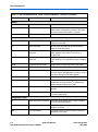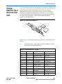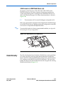
1
Nios Development Board Stratix II Edition
Reference Manual
101 Innovation Drive
San Jose, CA 95134
www.altera.com
Development Board Version
Document Version
Document Date
6XX-40019R
1.3
May 2007
Copyright © 2007 Altera Corporation. All rights reserved. Altera, The Programmable Solutions Company, the stylized Altera logo, specific device designations, and all other words and logos that are identified as trademarks and/or service marks are, unless noted otherwise, the trademarks and
service marks of Altera Corporation in the U.S. and other countries. All other product or service names are the property of their respective holders. Altera products are protected under numerous U.S. and foreign patents and pending applications, maskwork rights, and copyrights. Altera warrants
performance of its semiconductor products to current specifications in accordance with Altera's standard warranty, but reserves the right to make
changes to any products and services at any time without notice. Altera assumes no responsibility or liability arising out of the application or use of any information, product, or service described herein except as expressly agreed to in writing by Altera
Corporation. Altera customers are advised to obtain the latest version of device specifications before relying on any published information and before placing orders for products or services.
Part Number MNL-01001-1.3
ii
Altera Corporation
Contents
About this Manual................................................................................... v
How to Contact Altera .............................................................................................................................. v
Typographic Conventions ...................................................................................................................... vi
Chapter 1. Overview
Features Overview ................................................................................................................................. 1–1
General Description ............................................................................................................................... 1–1
Factory-Programmed Reference Design ............................................................................................ 1–2
Chapter 2. Board Components
Component List ...................................................................................................................................... 2–1
Stratix II EP2S60 Device (U60) ............................................................................................................. 2–3
Push-Button Switches (SW0 - SW3) .................................................................................................... 2–4
Individual LEDs (D0 - D7) .................................................................................................................... 2–5
Seven-Segment LEDs (U8 & U9) ........................................................................................................ 2–5
SSRAM Chip (U74) ................................................................................................................................ 2–6
DDR SDRAM Chip (U63) ..................................................................................................................... 2–9
Flash Memory (U5) .............................................................................................................................. 2–11
Ethernet MAC/PHY (U4) & RJ45 Connector (RJ1) ........................................................................ 2–13
Serial Connector (J19) ......................................................................................................................... 2–15
Expansion Prototype Connectors (PROTO1 & PROTO2) ............................................................. 2–16
CompactFlash Connector (CON3) .................................................................................................... 2–23
PMC Connector (JH1 & JH2) .............................................................................................................. 2–26
Mictor Connector (J25) ........................................................................................................................ 2–29
Test Points (TP1 – TP8) ....................................................................................................................... 2–31
EPCS64 Serial Configuration Device (U69) ..................................................................................... 2–32
Configuration Controller Device (U3) .............................................................................................. 2–33
Configuration-Status LEDs ........................................................................................................... 2–33
Configuration & Reset Buttons .................................................................................................... 2–34
SW8 – CPU Reset ...................................................................................................................... 2–34
SW9 – Factory Config ............................................................................................................... 2–35
SW10 – Reset, Config ................................................................................................................ 2–35
Reset Distribution ........................................................................................................................... 2–36
Starting Configuration ................................................................................................................... 2–36
Factory & User Configurations .................................................................................................... 2–36
Configuration Process ................................................................................................................... 2–37
Flash Memory Partitions ............................................................................................................... 2–38
User Application Space ............................................................................................................ 2–38
User Configuration ................................................................................................................... 2–39
Factory Configuration .............................................................................................................. 2–39
Persistent Data ........................................................................................................................... 2–39
Altera Corporation
iii
Contents
Nios Development Board Stratix II Edition
JTAG Connectors (J24 & J5) ...............................................................................................................
JTAG Connector to FPGA (J24) ....................................................................................................
JTAG Connector to EPM7256AE Device (J5) ..............................................................................
Clock Circuitry .....................................................................................................................................
Power-Supply Circuitry ......................................................................................................................
2–39
2–39
2–41
2–41
2–44
Appendix A. Restoring the Factory Configuration
Introduction ........................................................................................................................................... A–1
Reprogramming the Flash Memory ................................................................................................... A–1
Reprogramming the EPM7256AE Configuration Controller Device ............................................ A–1
Appendix B. Connecting to the Board via Ethernet
Introduction ...........................................................................................................................................
Connecting the Ethernet Cable ...........................................................................................................
Connecting the LCD Screen ...........................................................................................................
Obtaining an IP Address ................................................................................................................
LAN Connection .......................................................................................................................
DHCP ....................................................................................................................................
Static IP Address ..................................................................................................................
Point–to–Point Connections ....................................................................................................
Browsing to Your Board ......................................................................................................................
iv
B–1
B–1
B–2
B–2
B–3
B–3
B–3
B–4
B–5
Altera Corporation
About this Manual
This manual provides details about the Nios® development board,
Stratix™ II Edition.
The table shows this document’s revision history.
Date & Version
May 2007, 1.3
Description
●
●
●
October 2006, 1.2
●
●
How to Contact
Altera
Corrected Figure 2-21.
Revised “How to Contact Altera”.
Updated headers and footers.
Corrected pin assignments for proto2_io1, proto2_io29,
proto2_io30 in Table 2-12.
Changed Reference Designator for FPGA from U62 to
U60.
October 2006, 1.1
●
June 2006, 1.0
First publication.
Corrected statement: LEDs D0 - D7 turn on when driven
to 0 (not 1).
For the most up-to-date information about Altera products, refer to the
following table.
Contact (1)
Contact
Method
Address
Technical support
Website
www.altera.com/support
Technical training
Website
www.altera.com/training
Email
[email protected]
Product literature
Website
www.altera.com/literature
Altera literature services
Email
[email protected]
Non-technical support (General)
Email
[email protected]
(Software Licensing) Email
[email protected]
Note to table:
(1)
Altera Corporation
May 2007
You can also contact your local Altera sales office or sales representative.
v
Preliminary
About this Manual
Typographic
Conventions
This document uses the typographic conventions shown below.
Visual Cue
Meaning
Bold Type with Initial
Capital Letters
Command names, dialog box titles, checkbox options, and dialog box options are
shown in bold, initial capital letters. Example: Save As dialog box.
bold type
External timing parameters, directory names, project names, disk drive names,
filenames, filename extensions, and software utility names are shown in bold
type. Examples: fMAX, \qdesigns directory, d: drive, chiptrip.gdf file.
Italic Type with Initial Capital
Letters
Document titles are shown in italic type with initial capital letters. Example: AN 75:
High-Speed Board Design.
Italic type
Internal timing parameters and variables are shown in italic type.
Examples: tPIA, n + 1.
Variable names are enclosed in angle brackets (< >) and shown in italic type.
Example: <file name>, <project name>.pof file.
Initial Capital Letters
Keyboard keys and menu names are shown with initial capital letters. Examples:
Delete key, the Options menu.
“Subheading Title”
References to sections within a document and titles of on-line help topics are
shown in quotation marks. Example: “Typographic Conventions.”
Courier type
Signal and port names are shown in lowercase Courier type. Examples: data1,
tdi, input. Active-low signals are denoted by suffix n, e.g., resetn.
Anything that must be typed exactly as it appears is shown in Courier type. For
example: c:\qdesigns\tutorial\chiptrip.gdf. Also, sections of an
actual file, such as a Report File, references to parts of files (e.g., the AHDL
keyword SUBDESIGN), as well as logic function names (e.g., TRI) are shown in
Courier.
1., 2., 3., and
a., b., c., etc.
Numbered steps are used in a list of items when the sequence of the items is
important, such as the steps listed in a procedure.
■
Bullets are used in a list of items when the sequence of the items is not important.
●
v
•
The checkmark indicates a procedure that consists of one step only.
1
The hand points to information that requires special attention.
c
The caution indicates required information that needs special consideration and
understanding and should be read prior to starting or continuing with the
procedure or process.
w
The warning indicates information that should be read prior to starting or
continuing the procedure or processes
r
The angled arrow indicates you should press the Enter key.
f
The feet direct you to more information on a particular topic.
vi
Reference Manual
Nios Development Board Stratix II Edition
Altera Corporation
May 2007
1. Overview
Features
Overview
The Nios Development Board, Stratix II Edition, provides a hardware
platform for developing embedded systems based on Altera® Stratix II
devices. The Nios Development Board, Stratix II Edition provides the
following features:
■
■
■
■
■
■
■
■
■
■
■
■
■
■
■
■
■
General
Description
A Stratix II FPGA with more than 13,500 adaptive logic modules
(ALM) and 1.3 million bits of on-chip memory
16 MBytes of flash memory
2 MBytes of synchronous SRAM
32 MBytes of double data rate (DDR) SDRAM
On-board logic for configuring the FPGA from flash memory
On-board Ethernet MAC/PHY device and RJ45 connector
Two 5V-tolerant expansion/prototype headers each with access to 41
FPGA user I/O pins
CompactFlash connector for Type I CompactFlash cards
32-bit PMC Connector capable of 33 MHz and 66 MHz operation
Mictor connector for hardware and software debug
RS-232 DB9 serial port
Four push-button switches connected to FPGA user I/O pins
Eight LEDs connected to FPGA user I/O pins
Dual 7-segment LED display
JTAG connectors to Altera devices via Altera download cables
50 MHz oscillator and zero-skew clock distribution circuitry
Power-on reset circuitry
The Nios development board comes pre-programmed with a Nios II
processor reference design. Hardware designers can use the reference
design as an example of how to build systems using the Nios II processor
and to gain familiarity with the features included. Software designers can
use the pre-programmed Nios II processor design on the board to begin
prototyping software immediately.
This document describes the hardware features of the Nios development
board, including detailed pin-out information, to enable designers to
create custom FPGA designs that interface with all components on the
board. A complete set of schematics, a physical layout database, and
GERBER files for the development board are installed with the Nios II
development tools in the <Nios II EDS install path>/documents directory.
Altera Corporation
May 2007
1–1
Overview
f
See the Nios II Development Kit, Getting Started User Guide for instructions
on setting up the Nios development board and installing Nios II
development tools.
Figure 1–1shows a block diagram of the Nios development board.
Figure 1–1. Nios Development Board, Stratix II Edition Block Diagram
16 Mbyte DDR SDRAM
50MHz Oscillator
2 Mbyte SSRAM
Vccint 1.2-V
5.0 V Regulators
EPCS64 Configuration
Device
Vccio 3.3-V
JTAG Connector
Configuration
Controller
27
Mictor Connector
Stratix II
EP2S60
FPGA
Proto 1 Expansion
Prototype Connector
16 Mbyte Flash Memory
Ethernet
MAC/PHY
Compact Flash
Proto 2 Expansion
Prototype Connector
RJ45
Connector
41
PMC Connector
4
Push-button
Switches (4)
8
User LEDs (8)
16
Dual Seven-Segment Display
FactoryProgrammed
Reference
Design
RS-232
When power is applied to the board, on-board logic configures the FPGA
using hardware configuration data stored in flash memory. After
successful configuration, the Nios II processor design in the FPGA wakes
up and begins executing boot code from flash memory.
The board is factory-programmed with a default reference design. This
reference design is a web server that delivers web pages via the Ethernet
port. For further information on the default reference design, refer to
Appendix B: Connecting to the Board via Ethernet.
1–2
Reference Manual
Nios Development Board Stratix II Edition
Altera Corporation
May 2007
Overview
In the course of development, you might overwrite or erase the flash
memory space containing the default reference design. Altera provides
the flash image for the default reference design so you can return the
board to its default state. Refer to Appendix A: Restoring the Factory
Configuration for more information.
Altera Corporation
May 2007
Reference Manual
1–3
Nios Development Board Stratix II Edition
Overview
1–4
Reference Manual
Nios Development Board Stratix II Edition
Altera Corporation
May 2007
2. Board Components
Component List
This section introduces all the important components on the Nios
development board. See Figure 2–1 and Table 2–1 for component
locations and brief descriptions of all board features.
Figure 2–1. Nios Development Board
Reset, Config
(SW10)
J26
J19
J24
U4
LED7
LED6
JH2
TP1–
TP8
PROTO1
(J11, J12, J13)
D34
U5
JH1
Optional Power
Supply
RJ1
PROTO2
(J15, J16, J17)
J5
U3
J25
J27
U69
Y2
U74
U62
D0 – D7
J4
U63
U8
CPU Reset
(SW8)
U9
CON3
Factory Config
(SW9)
SW0 – SW3
Table 2–1. Nios Development Board, Stratix II Edition Components & Interfaces
Board Designation
U60
Name
Description
Stratix II FPGA
EP2S60F672C3N device.
SW0 – SW3
Push-button switches
Four momentary contact switches for user input to the
FPGA.
D0 – D7
Individual LEDs
Eight individual LEDs driven by the FPGA.
U8, U9
Seven-segment LEDs
Two seven-segment LEDs that display numeric
output from the FPGA.
User Interface
Altera Corporation
May 2007
2–1
Board Components
Table 2–1. Nios Development Board, Stratix II Edition Components & Interfaces (Continued)
Board Designation
Name
Description
Memory
U74
SSRAM memory
2 MBytes of synchronous SRAM.
U5, LED7
Flash memory
16 MBytes of nonvolatile memory for use by both the
FPGA and the configuration controller. LED7 lights
whenever the flash chip-enable is asserted.
U63
DDR SDRAM memory
32 MBytes of DDR SDRAM.
U4, RJ1
Ethernet MAC/PHY
10/100 Ethernet MAC/PHY chip connected to an RJ45 Ethernet connector.
J19
Serial connector
RS-232 serial connector with 5V-tolerant buffers.
Supports all RS-232 signals.
Connections & Interfaces
PROTO1 (J11, J12, J13) Expansion prototype
connector
Expansion headers connecting to 41 I/O pins on the
FPGA. Supplies 3.3 V and 5.0 V for use by a
daughter card.
PROTO2 (J15, J16, J17) Expansion prototype
connector
Expansion headers connecting to 41 I/O pins on the
FPGA. Supplies 3.3 V and 5.0 V for use by a daughter
card.
CON3
CompactFlash connector
CompactFlash connector for memory expansion.
JH1, JH2
PMC connector
Expansion connector for a PCI mezzanine card.
J25
Mictor connector
Mictor connector providing access to 27 I/O pins on
the FPGA. Allows debugging Nios II systems using a
First Silicon Solutions (FS2) debug probe.
TP1 – TP8
Test Points
Test points providing access to eight FPGA I/O pins.
J24
JTAG connector
JTAG connection to the FPGA allowing hardware
configuration using the Quartus® II software and
software debug using the Nios II IDE.
J5
JTAG connector
JTAG connection to the MAX® configuration
controller.
J27
EPCS configuration header
Connects to the EPCS serial configuration device for
in-system programming.
Configuration & Reset
U3
MAX Configuration controller Altera MAX EPM7256AE device used to configure
the FPGA from flash memory.
U69
Serial configuration device
Altera EPCS64 low-cost serial configuration device to
configure the FPGA.
SW8
CPU Reset button
Push-button switch to reboot the Nios II processor
configured in the FPGA.
2–2
Reference Manual
Nios Development Board Stratix II Edition
Altera Corporation
May 2007
Board Components
Table 2–1. Nios Development Board, Stratix II Edition Components & Interfaces (Continued)
Board Designation
Name
Description
SW9
Factory Config button
Push-button switch to reconfigure the FPGA with the
factory-programmed reference design.
SW10
Reset, Config
Push-button switch to reset the board.
LED0 – LED3, LED6
Configuration status LEDs
LEDs that display the current configuration status of
the FPGA.
Y2
Oscillator
50 MHz clock signal driven to FPGA.
J4
External clock input
Connector to FPGA clock pin.
J26
DC power jack
16 V DC unregulated power source.
D34
Bridge rectifier
Power rectifier allows for center-negative or centerpositive power supplies.
J28, J29, J30, J33 (and
more)
Optional Power Supply
External power supply can be connected for highcurrent applications.
Clock Circuitry
Power Supply
The sections that follow describe each component in detail.
Stratix II EP2S60
Device (U60)
U60 is a Stratix II FPGA in a 672-pin FineLine BGA® package. The part
number is EP2S60F672C3N. Table 2–2 lists the device features.
Table 2–2. Stratix II EP2S60 Device Features
Altera Corporation
May 2007
LEs
60,440
M4K Memory Blocks
255
Total RAM Bits
2,544,192
Embedded 18x18 Multiplier Blocks
144
Enhanced PLLs
4
Fast PLLs
8
User I/O Pins
718
Reference Manual
2–3
Nios Development Board Stratix II Edition
Board Components
The development board provides two separate methods for configuring
the FPGA:
f
Push-Button
Switches (SW0 SW3)
1.
Using the Quartus® II software running on a host computer, a
designer configures the device directly via an Altera download
cable connected to the FPGA JTAG header (J24).
2.
When power is applied to the board, a configuration controller
device (U3) attempts to configure the FPGA with hardware
configuration data stored in flash memory. For more information on
the configuration controller, refer to “Configuration Controller
Device (U3)” on page 2–33.
For Stratix II-related documentation including pin out data for the
EP2S60 device, see the Altera Stratix II literature page at
www.altera.com/literature/lit-stx2.jsp.
SW0 – SW3 are momentary-contact push-button switches to provide
stimulus to designs in the FPGA. Refer to Figure 2–2. Each switch is
connected to an FPGA general-purpose I/O pin with a pull-up resistor as
shown in Table 2–3. Each I/O pin perceives a logic 0 when its
corresponding switch is pressed.
Figure 2–2. Push-Button Switches (SW0 – SW3)
D1
D0
D3
D2
SW0
D5
D4
SW1
D7
D6
SW2
SW3
Table 2–3. Push Button Switches Pin Table
Button
FPGA Pin
Board Net Name
SW0
P4
user_pb0
SW1
P5
user_pb1
SW2
N6
user_pb2
SW3
N7
user_pb3
2–4
Reference Manual
Nios Development Board Stratix II Edition
Altera Corporation
May 2007
Board Components
Individual LEDs
(D0 - D7)
This Nios II development board provides eight individual LEDs
connected to the FPGA. Refer to “Push-Button Switches (SW0 - SW3)” on
page 2–4. D0 – D7 are connected to general purpose I/O pins on the
FPGA as shown in Table 2–4. When a pin drives logic 0, the
corresponding LED turns on.
Table 2–4. LED Pin Table
LED
Seven-Segment
LEDs (U8 & U9)
FPGA Pin
Board Net Name
D0
W15
pld_led0
D1
V14
pld_led1
D2
AD17
pld_led2
D3
AA17
pld_led3
D4
V16
pld_led4
D5
AB17
pld_led5
D6
AD18
pld_led6
D7
V17
pld_led7
U8 and U9 connect to the FPGA, and each segment is individually
controlled by a general-purpose I/O pin. Refer to Figure 2–3. When a pin
drives logic 0, the corresponding U8 and U9 LED turns on. See Table 2–5
for pin-out details.
Figure 2–3. Dual Seven-Segment Display
U8
U9
a
a
g
e
g
c
d
dp
Reference Manual
c
e
d
Altera Corporation
May 2007
b
f
b
f
dp
2–5
Nios Development Board Stratix II Edition
Board Components
Table 2–5. Dual Seven-Segment Display
FPGA Pin
U8 & U9 Pin
Pin Function
Board Net Name
U8
L8
10
a
hex_0A
L9
9
b
hex_0B
M7
8
c
hex_0C
M8
5
d
hex_0D
M5
4
e
hex_0E
M6
2
f
hex_0F
N4
3
g
hex_0G
N5
7
dp
hex_0DP
K8
10
a
hex_1A
K9
9
b
hex_1B
U9
SSRAM Chip
(U74)
L4
8
c
hex_1C
L5
5
d
hex_1D
M3
4
e
hex_1E
M4
2
f
hex_1F
L6
3
g
hex_1G
L7
7
dp
hex_1DP
U74 is a 32-bit, 2 MByte Cypress SSRAM chip. The part number is
CY7C1380C-167AC or CY7C1380D-167AXC. The chip is rated for
synchronous accesses up to 167 MHz. U74 connects to the FPGA so it can
be used by a Nios II embedded processor as general-purpose memory.
The factory-programmed Nios II reference design identifies the SSRAM
devices in its address space as a contiguous 2 MByte, 32-bit word,
zero-wait-state main memory.
2–6
Reference Manual
Nios Development Board Stratix II Edition
Altera Corporation
May 2007
Board Components
Table 2–6 shows all connections between the FPGA and the SSRAM chip.
Table 2–6. SSRAM Pin Table
FPGA Pin
Altera Corporation
May 2007
U74 Pin
Pin Function
Board Net Name
G16
37
A0
ssram_a0
G17
36
A1
ssram_a1
E26
35
A2
ssram_a2
E25
34
A3
ssram_a3
E24
33
A4
ssram_a4
E23
32
A5
ssram_a5
F26
38
NC/A19
ssram_a6
F25
39
NC/A20
ssram_a7
C17
42
A6
ssram_a8
C18
43
A7
ssram_a9
C19
44
A8
ssram_a10
C20
45
A9
ssram_a11
G26
46
A10
ssram_a12
G25
47
A11
ssram_a13
G24
48
A12
ssram_a14
G23
49
A13
ssram_a15
G21
50
A14
ssram_a16
G20
81
A15
ssram_a17
H26
82
A16
ssram_a18
H25
99
A17
ssram_a19
H24
100
A18
ssram_a20
B16
85
ADSC_N
ssram_adsc_n
H23
93
BE_n0
ssram_be_n0
J23
94
BE_n1
ssram_be_n1
K24
95
BE_n2
ssram_be_n2
F16
96
BE_n3
ssram_be_n3
C16
98
CE1_n
ssram_ce1_n
A17
52
D0
ssram_d0
A18
53
D1
ssram_d1
A19
56
D2
ssram_d2
A20
57
D3
ssram_d3
B17
58
D4
ssram_d4
Reference Manual
2–7
Nios Development Board Stratix II Edition
Board Components
Table 2–6. SSRAM Pin Table (Continued)
FPGA Pin
U74 Pin
Pin Function
Board Net Name
B18
59
D5
ssram_d5
B19
62
D6
ssram_d6
B20
63
D7
ssram_d7
B24
68
D8
ssram_d8
C22
69
D9
ssram_d9
B22
72
D10
ssram_d10
C21
73
D11
ssram_d11
E18
74
D12
ssram_d12
D18
75
D13
ssram_d13
E17
78
D14
ssram_d14
D17
79
D15
ssram_d15
F23
18
D24
ssram_d16
F22
19
D25
ssram_d17
F21
22
D26
ssram_d18
B23
23
D27
ssram_d19
D25
24
D28
ssram_d20
F24
25
D29
ssram_d21
H21
28
D30
ssram_d22
F19
29
D31
ssram_d23
B21
2
D16
ssram_d24
A21
3
D17
ssram_d25
A22
6
D18
ssram_d26
A24
7
D19
ssram_d27
C26
8
D20
ssram_d28
C25
9
D21
ssram_d29
J22
12
D22
ssram_d30
J21
13
D23
ssram_d31
J26
86
OE_n
ssram_oe_n
F17
87
WE_n
ssram_we_n
J25
84
ADSP_n
ssram_adsp_n
J24
83
ADV_n
ssram_adv_n
L25
97
CE2
ssram_ce2
L24
92
CE3_n
ssram_ce3_n
2–8
Reference Manual
Nios Development Board Stratix II Edition
Altera Corporation
May 2007
Board Components
Table 2–6. SSRAM Pin Table (Continued)
FPGA Pin
U74 Pin
Pin Function
Board Net Name
G18
88
GW_n
ssram_gw_n
A12
89
CLK
sram_clk
The following pins on U74 have fixed connections, which restricts the
usable modes of operation:
■
■
■
MODE is pulled low to enable Linear Burst
ZZ is pulled low to leave the chip enabled
GLOBALW_n is pulled high to disable the global write.This is the
default behavior for GLOBALW_n that can be changed.
CE2 and CE3_n are wired high and low respectively to be enabled
and to make CE1_n the master chip enable.This is the default
behavior for GLOBALW_n that can be changed.
■
f
DDR SDRAM
Chip (U63)
See www.cypress.com for detailed information about the SSRAM chip.
U63 is a Micron DDR SDRAM chip. The part number is MT46V16M16P6T. The DDR SDRAM pins are connected to the FPGA as shown in
Table 2–7. Altera provides a DDR SDRAM controller that allows a Nios II
processor to access the DDR SDRAM device as a large, linearlyaddressable memory.
Table 2–7. DDR SDRAM Pin Table
FPGA Pin
Altera Corporation
May 2007
U63 Pin
Board Net Name
DD9
2
sdram_dq0
D8
4
sdram_dq1
C8
5
sdram_dq2
A9
7
sdram_dq3
B11
8
sdram_dq4
C11
10
sdram_dq5
A10
11
sdram_dq6
D10
13
sdram_dq7
A5
54
sdram_dq8
B5
56
sdram_dq9
D6
57
sdram_dq10
A6
59
sdram_dq11
A8
60
sdram_dq12
Reference Manual
2–9
Nios Development Board Stratix II Edition
Board Components
Table 2–7. DDR SDRAM Pin Table (Continued)
FPGA Pin
f
U63 Pin
Board Net Name
A7
62
sdram_dq13
C7
63
sdram_dq14
D7
65
sdram_dq15
C9
16
sdram_dqs0
C6
51
sdram_dqs1
C10
20
sdram_dm0
B7
47
sdram_dm1
B10
29
sdram_a0
B9
30
sdram_a1
B8
31
sdram_a2
B6
32
sdram_a3
C5
35
sdram_a4
E11
36
sdram_a5
E10
37
sdram_a6
E9
38
sdram_a7
E8
39
sdram_a8
E7
40
sdram_a9
F11
28
sdram_a10
F10
41
sdram_a11
F8
42
sdram_a12
F10
26
sdram_ba0
G11
27
sdram_ba1
B3
22
sdram_cas_n
F13
44
sdram_cke
E12
24
sdram_cs_n
A3
23
sdram_ras_n
B4
21
sdram_we_n
C4
46
sdram_clk_n
C3
45
sdram_clk_p
See www.micron.com for detailed information.
2–10
Reference Manual
Nios Development Board Stratix II Edition
Altera Corporation
May 2007
Board Components
Flash Memory
(U5)
U5 is an 8-bit, 16 MByte AMD flash memory device connected to the
FPGA. The part number is S29GL128M10TFIR1. Refer to Table 2–8 for
connections between the FPGA and the flash memory chip. U5 can be
used for two purposes:
1.
A Nios II embedded processor implemented on the FPGA can use
the flash memory as general-purpose memory and non-volatile
storage.
2.
The flash memory can hold FPGA configuration data that is used by
the configuration controller to load the FPGA at power-up. Refer to
“Configuration Controller Device (U3)” on page 2–33 for related
information.
A Nios II processor design in the FPGA can identify the 16 MByte flash
memory in its address space, and can program new data (either new
FPGA configuration data, Nios II software, or both) into flash memory.
The Nios II development software includes subroutines for writing and
erasing flash memory.
1
The flash memory device shares address and data connections
with the Ethernet MAC/PHY device.
Table 2–8. Flash Memory Pin Table
FPGA Pin
Altera Corporation
May 2007
U5 Pin
Board Net Name
V25
51
fe_a0
U26
31
fe_a1
U25
26
fe_a2
T25
25
fe_a3
T24
24
fe_a4
V20
23
fe_a5
V19
22
fe_a6
U20
21
fe_a7
U19
20
fe_a8
T22
10
fe_a9
T21
9
fe_a10
T20
8
fe_a11
T19
7
fe_a12
U22
6
fe_a13
U21
5
fe_a14
V22
4
fe_a15
Reference Manual
2–11
Nios Development Board Stratix II Edition
Board Components
Table 2–8. Flash Memory Pin Table (Continued)
FPGA Pin
U5 Pin
Board Net Name
V21
3
fe_a16
W22
54
fe_a17
W21
19
fe_a18
V24
18
fe_a19
V23
11
fe_a20
U24
12
fe_a21
U23
15
fe_a22
R24
2
fe_a23
D15
35
fe_d0
G15
37
fe_d1
E19
39
fe_d2
D20
41
fe_d3
G19
44
fe_d4
D19
46
fe_d5
E20
48
fe_d6
F20
50
fe_d7
H19
32
flash_cs_n
H20
34
flash_oe_n
V26
13
flash_rw_n
H22
16
flash_wp_n
K18
53
flash_byte_n (1)
W25
17
flash_ry_by_n
Note to Table 2–8:
(1)
BYTE_n on U5 is pulled low to keep the flash memory in byte
mode which restricts the usable modes of operation.
The on-board configuration controller makes assumptions about what
resides where in flash memory. For details refer to “SW10 – Reset, Config”
on page 2–35.
f
See www.amd.com for detailed information about the flash memory
device.
2–12
Reference Manual
Nios Development Board Stratix II Edition
Altera Corporation
May 2007
Board Components
Ethernet
MAC/PHY (U4) &
RJ45 Connector
(RJ1)
The LAN91C111 chip (U4) is a 10/100 Ethernet media access control and
physical interface (MAC/PHY) chip. The control pins of U4 are
connected to the FPGA so that Nios II systems can access Ethernet
networks via the RJ-45 connector (RJ1) as shown in Figure 2–4. The
Nios II development tools include hardware and software components
that allow Nios II processor systems to communicate with the
LAN91C111 Ethernet device.
Figure 2–4. Ethernet RJ-45 Connector
U4
RJ1
Refer to Table 2–9 for connections between the FPGA and the MAC/PHY
device.
1
The Ethernet MAC/PHY device shares both address and data
connections with the flash memory.
Table 2–9. Ethernet MAC/PHY Pin Table
FPGA Pin
Altera Corporation
May 2007
U4 Pin
Pin Function
Board Net Name (1)
AB25
41
Address Enable
enet_aen
W20
43
Synchronous Ready
enet_srdy_n
W19
40
VL Bus Access
enet_vlbus_n
Y21
45
Local Device
enet_ldev_n
Y20
38
IO Char Ready
enet_iochrdy
AA22
37
Address Strobe
enet_ads_n
AA21
42
Local Bus Clock
enet_lclk
W26
46
Ready/Return
enet_rdyrtn_n
AA26
35
Bus Cycle
enet_cycle_n
AA25
36
Write/Read
enet_w_r_n
W24
34
Bus Chip Select
enet_datacs_n
W23
29
Interrupt
enet_intr0
Reference Manual
2–13
Nios Development Board Stratix II Edition
Board Components
Table 2–9. Ethernet MAC/PHY Pin Table (Continued)
FPGA Pin
Y24
U4 Pin
94
Pin Function
Byte Enable 0
Board Net Name (1)
enet_be_n0
Y23
95
Byte Enable 1
enet_be_n1
AA24
96
Byte Enable 2
enet_be_n2
AA23
97
Byte Enable 3
enet_be_n3
Y26
31
Read
enet_ior_n
Y25
32
Write
enet_iow_n
U26
78
Address Line
fe_a1
U25
79
Address Line
fe_a2
T25
80
Address Line
fe_a3
T24
81
Address Line
fe_a4
V20
82
Address Line
fe_a5
V19
83
Address Line
fe_a6
U20
84
Address Line
fe_a7
U19
85
Address Line
fe_a8
T22
86
Address Line
fe_a9
T21
87
Address Line
fe_a10
T20
88
Address Line
fe_a11
T19
89
Address Line
fe_a12
U22
90
Address Line
fe_a13
U21
91
Address Line
fe_a14
V22
92
Address Line
fe_a15
D15
107
Data Line
fe_d0
G15
106
Data Line
fe_d1
E19
105
Data Line
fe_d2
D20
104
Data Line
fe_d3
G19
102
Data Line
fe_d4
D19
101
Data Line
fe_d5
E20
100
Data Line
fe_d6
F20
99
Data Line
fe_d7
M20
76
Data Line
fe_d8
M19
75
Data Line
fe_d9
N20
74
Data Line
fe_d10
N19
73
Data Line
fe_d11
N22
71
Data Line
fe_d12
2–14
Reference Manual
Nios Development Board Stratix II Edition
Altera Corporation
May 2007
Board Components
Table 2–9. Ethernet MAC/PHY Pin Table (Continued)
FPGA Pin
U4 Pin
Pin Function
Board Net Name (1)
N21
70
Data Line
fe_d13
M22
69
Data Line
fe_d14
M21
68
Data Line
fe_d15
M24
66
Data Line
fe_d16
M23
65
Data Line
fe_d17
L19
64
Data Line
fe_d18
L18
63
Data Line
fe_d19
L21
61
Data Line
fe_d20
L20
60
Data Line
fe_d21
L23
59
Data Line
fe_d22
L22
58
Data Line
fe_d23
K20
56
Data Line
fe_d24
K19
55
Data Line
fe_d25
K22
54
Data Line
fe_d26
K21
53
Data Line
fe_d27
J20
51
Data Line
fe_d28
J19
50
Data Line
fe_d29
J22
49
Data Line
fe_d30
J21
48
Data Line
fe_d31
Note to Table 2–9:
(1)
f
Serial Connector
(J19)
Altera Corporation
May 2007
Nets fe_a0 and fe_a16 to fe_a23 do not connect to U4.
See www.smsc.com for detailed information about the LAN91C111
device.
J19 is a standard DB-9 serial connector. It is typically used for
communication between the FPGA and a host computer via an RS-232
serial cable. Level-shifting buffer (U52) is used between J19 and the FPGA
because the FPGA device cannot interface to RS-232 voltage levels
directly.
Reference Manual
2–15
Nios Development Board Stratix II Edition
Board Components
J19 is able to transmit all RS-232 signals. Alternately, the FPGA design can
use only the signals it needs, such as J19’s RXD and TXD pins. LEDs are
connected to the RXD and TXD signals and visually indicate when data
is being transmitted or received. Figure 6 and Table 2–10 show the pin
connections between the serial connectors and the FPGA.
Figure 2–5. Serial Connector J19
J19
Function
Direction
Connector Pin #
GND DTR RXD TXD DCD
IN OUT OUT
IN
3
2
1
5
4
Connector Pin #
8
7
6
9
OUT OUT IN OUT
RI CTS RTS DSR
Direction
Function
Table 2–10. Serial Connector Pin Table
FPGA Pin
Expansion
Prototype
Connectors
(PROTO1 &
PROTO2)
J19 Pin
Board Net Name
AD26
3
serial_rxd
AB23
2
serial_txd
AC25
4
serial_dtr
AC24
1
serial_dcd
AB24
6
serial_dsr
K23
9
serial_ri
AB26
8
serial_cts
AD25
7
serial_rts
PROTO1 and PROTO2 are standard-footprint, mechanically-stable
connectors that can be used (for example) as an interface to a specialfunction daughter card. Headers J11, J12, and J13 collectively form
PROTO1, and J15, J16 and J17 collectively form PROTO2.
The expansion prototype connector interface includes:
2–16
Reference Manual
Nios Development Board Stratix II Edition
Altera Corporation
May 2007
Board Components
■
41 I/O pins for prototyping. All 41 I/O pins connect to user I/O pins
on the FPGA. Each signal passes through analog switches to protect
the FPGA from 5.0 V logic levels. These analog switches are
permanently enabled. The output logic-level on the expansion
prototype connector pins is 3.3 V.
●
●
■
■
■
■
■
■
PROTO1 switches: U19, U20, U21, U22 and U25
PROTO2 switches: U27, U28, U29, U30 and U31
A buffered, zero-skew copy of the on-board oscillator output from
U2.
A buffered, zero-skew copy of the FPGA phase-locked loop (PLL)
output.
A power-on reset signal that is asserted low.
Five regulated 3.3 V power-supply pins (2 A total max load for both
PROTO1 & PROTO2).
One regulated 5.0 V power-supply pin (1 A total max load for both
PROTO1 & PROTO2).
Numerous ground connections.
The PROTO1 expansion prototype connector shares FPGA I/O pins with
the CompactFlash connector (CON3). Designs can use either the PROTO1
connector or the CompactFlash connector.
1
f
Do not connect cards to PROTO1 and CON3 at the same time.
Damage to one or both cards might result.
See the Altera web site for a list of available expansion daughter cards
that can be used with the Nios development board at
www.altera.com/devkits.
Table 2–11, Figure 2–6 and Figure 2–7 show connections from the
PROTO1 expansion headers to the FPGA.
Figure 2–6. PROTO1 Expansion Prototype Connector - J11, J12 & J13
J11
Pin 1
J13
J12
Pin 1
Altera Corporation
May 2007
Reference Manual
Pin 1
2–17
Nios Development Board Stratix II Edition
(1)
(2)
(3)
(4)
proto1_io35
proto1_io37
proto1_io39
10
12
14
9
11
13
1
3
5
7
9
11
13
15
17
19
proto1_io34
proto1_io36
proto1_io38
(1) Vunreg
NC
2–18
Reference Manual
Nios Development Board Stratix II Edition
VCC3_3
VCC3_3
(2) proto1_osc
(3) proto1_pllclk
(4) proto1_clkout
VCC3_3
VCC3_3
VCC3_3
20
18
16
14
12
10
8
6
4
GND
GND
GND
GND
GND
GND
GND
GND
GND
GND
proto1_io33
8
7
proto1_io32
J12
2
proto1_io31
6
5
proto1_io30
VCC5
proto1_io29
2
4
1
3
GND
proto1_io40
29
31
33
35
37
39
proto1_io22
proto1_io24
proto1_io25
proto1_io27
proto1_io28
GND
proto1_io21
19
proto1_io14
27
17
proto1_io12
proto1_io19
15
proto1_io10
25
13
proto1_io8
proto1_io18
11
proto1_io6
23
9
proto1_io4
proto1_io17
7
proto1_io2
21
5
proto1_io0
proto1_io16
1
3
proto1_RESET_n
GND
proto1_io23
NC
proto1_io26
proto1_cardsel_n
GND
32
34
36
38
40
NC
20
proto1_io20
proto1_io15
18
30
proto1_io13
16
GND
proto1_io11
14
28
proto1_io9
12
GND
proto1_io7
10
26
proto1_io5
8
GND
proto1_io3
6
24
proto1_io1
4
22
GND
2
Board Components
Figure 2–7. PROTO1 Pin Information – J11, J12, & J13
J11
J13
Notes to Figure 2–7:
Unregulated voltage from DC power supply.
Clk from board oscillator.
Clk from FPGA.
Clk output from PROTO1 card to FPGA.
Altera Corporation
May 2007
Board Components
.
Table 2–11. PROTO1 Pin Table
FPGA Pin
PROTO1 Pin
Connector
Board Net Name
J11
Altera Corporation
May 2007
U3 pin 56
1
J11
proto1_RESET_n
C1
3
J11
proto1_io0
C2
4
J11
proto1_io1
D2
5
J11
proto1_io2
D3
6
J11
proto1_io3
E1
7
J11
proto1_io4
E2
8
J11
proto1_io5
E3
9
J11
proto1_io6
E4
10
J11
proto1_io7
F1
11
J11
proto1_io8
F2
12
J11
proto1_io9
F3
13
J11
proto1_io10
F4
14
J11
proto1_io11
G3
15
J11
proto1_io12
G4
16
J11
proto1_io13
H3
17
J11
proto1_io14
H4
18
J11
proto1_io15
J3
21
J11
proto1_io16
J4
23
J11
proto1_io17
G1
25
J11
proto1_io18
G2
27
J11
proto1_io19
H1
28
J11
proto1_io20
H2
29
J11
proto1_io21
K3
31
J11
proto1_io22
K4
32
J11
proto1_io23
J1
33
J11
proto1_io24
J2
35
J11
proto1_io25
K1
36
J11
proto1_io26
KK2
37
J11
proto1_io27
J8
38
J11
proto1_cardsel_n
L2
39
J11
proto1_io28
Reference Manual
2–19
Nios Development Board Stratix II Edition
Board Components
Table 2–11. PROTO1 Pin Table (Continued)
FPGA Pin
PROTO1 Pin
Connector
Board Net Name
J12
J7
3
J12
proto1_io40
L3
4
J12
proto1_io29
M1
5
J12
proto1_io30
M2
6
J12
proto1_io31
G6
7
J12
proto1_io32
G7
8
J12
proto1_io33
H5
9
J12
proto1_io34
H6
10
J12
proto1_io35
J5
11
J12
proto1_io36
J6
12
J12
proto1_io37
H7
13
J12
proto1_io38
H8
14
J12
proto1_io39
U2 pin 19
9
J13
proto1_osc
K6
11
J13
proto1_pllclk
R26
13
J13
proto1_clkout
J13
Table 2–12, Figure 2–8 and Figure 2–9 show connections from the
PROTO2 expansion headers to the FPGA. Unless otherwise noted, the
labels indicate FPGA pin numbers
Figure 2–8. PROTO2 Expansion Prototype Connector - J15, J16 & J17
J16
Pin 1
J17
J15
Pin 1
Pin 1
2–20
Reference Manual
Nios Development Board Stratix II Edition
Altera Corporation
May 2007
(1)
(2)
(3)
(4)
Altera Corporation
May 2007
Reference Manual
3
5
7
9
11
13
15
17
19
NC
VCC3_3
VCC3_3
(2) proto2_osc
(3) proto2_pllclk
(4) proto2_clkout
VCC3_3
VCC3_3
VCC3_3
proto2_io39
14
13
proto2_io38
20
GND
GND
GND
GND
GND
GND
GND
GND
GND
29
31
33
35
37
39
proto2_io22
proto2_io24
proto2_io25
proto2_io27
proto2_io28
19
GND
proto2_io21
17
proto2_io14
27
15
proto2_io12
proto2_io19
13
proto2_io10
25
11
proto2_io8
proto2_io18
9
proto2_io6
23
7
proto2_io4
proto2_io17
5
proto2_io2
21
3
proto2_io0
proto2_io16
1
proto2_RESET_n
40
38
36
34
32
30
28
26
24
22
20
18
16
14
12
10
8
6
4
2
GND
proto2_cardsel_n
proto2_io26
NC
proto2_io23
GND
proto2_io20
GND
GND
GND
NC
proto_2io15
proto2_io13
proto2_io11
proto2_io9
proto2_io7
proto2_io5
proto2_io3
proto2_io1
GND
J16
18
16
14
12
10
8
6
4
GND
proto2_io37
12
11
proto2_io36
2
proto2_io35
10
9
proto2_io34
1
proto2_io33
8
7
proto2_io32
J15
(1) Vunreg
proto2_io31
6
5
proto2_io30
VCC5
proto2_io29
2
4
1
3
GND
proto2_io40
Board Components
Figure 2–9. PROTO2 Pin Information – J15, J16 & J17
J17
Notes to Figure 2–9:
Unregulated voltage from DC power supply.
Clk from board oscillator.
Clk from FPGA.
Clk output from PROTO2 card to FPGA.
2–21
Nios Development Board Stratix II Edition
Board Components
Table 2–12. PROTO2 Pin Table
FPGA Pin
PROTO2 Pin
Connector
Board Net Name
J16
U3 pin 57
1
J16
proto2_RESET_n
T2
3
J16
proto2_io0
T3
4
J16
proto2_io1
U1
5
J16
proto2_io2
U2
6
J16
proto2_io3
V1
7
J16
proto2_io4
V2
8
J16
proto2_io5
W1
9
J16
proto2_io6
W2
10
J16
proto2_io7
Y1
11
J16
proto2_io8
Y2
12
J16
proto2_io9
AA1
13
J16
proto2_io10
AA2
14
J16
proto2_io11
AB1
15
J16
proto2_io12
AB2
16
J16
proto2_io13
W3
17
J16
proto2_io14
W4
18
J16
proto2_io15
Y3
21
J16
proto2_io16
Y4
23
J16
proto2_io17
AA3
25
J16
proto2_io18
AA4
27
J16
proto2_io19
AB3
28
J16
proto2_io20
AB4
29
J16
proto2_io21
AC2
31
J16
proto2_io22
AC3
32
J16
proto2_io23
AD1
33
J16
proto2_io24
AD2
35
J16
proto2_io25
Y7
36
J16
proto2_io26
W9
37
J16
proto2_io27
Y10
38
J16
proto2_cardsel_n
W10
39
J16
proto2_io28
2–22
Reference Manual
Nios Development Board Stratix II Edition
Altera Corporation
May 2007
Board Components
Table 2–12. PROTO2 Pin Table (Continued)
FPGA Pin
PROTO2 Pin
Connector
Board Net Name
J15
AE3
3
J15
proto2_io40
Y9
4
J15
proto2_io29
AD7
5
J15
proto2_io30
W11
6
J15
proto2_io31
V12
7
J15
proto2_io32
AD8
8
J15
proto2_io33
Y11
9
J15
proto2_io34
W12
10
J15
proto2_io35
Y12
11
J15
proto2_io36
AD11
12
J15
proto2_io37
AE11
13
J15
proto2_io38
AB8
14
J15
proto2_io39
U2 pin 18
9
J17
proto2_osc
K7
11
J17
proto2_pllclk
P2
13
J17
proto2_clkout
J17
CompactFlash
Connector
(CON3)
Altera Corporation
May 2007
The CompactFlash connector header (CON3) enables hardware designs
to access a CompactFlash card. Refer to Figure 2–10. The following two
access modes are supported:
■
■
ATA (hot swappable mode)
IDE (IDE hard disk mode)
Reference Manual
2–23
Nios Development Board Stratix II Edition
Board Components
Figure 2–10. CompactFlash Connector
Most pins of CON3 connect to I/O pins on the FPGA. The following pins
have special connections:
■
Pin 13 and 38 of CON3 (VCC) are driven by a power MOSFET that is
controlled by an FPGA I/O pin. These connections allow the FPGA
to control power to the CompactFlash card for the IDE connection
mode.
Pin 26 of CON3 (-CD1) is pulled up to 5 V through a 10 kΩ resistor.
This signal is used to detect the presence of a CompactFlash card;
when the card is not present, the signal is pulled high through the
pull-up resistor.
Pin 41 of CON3 (RESET) is pulled up to 5.0 V through a 10 kΩ
resistor, and is controlled by the EPM7256AE configuration
controller. The FPGA can cause the configuration controller to assert
RESET, but the FPGA does not drive this signal directly.
■
■
The CompactFlash connector shares several FPGA I/O pins with
expansion prototype connector PROTO1. Refer to “Expansion Prototype
Connectors (PROTO1 & PROTO2)” on page 2–16 for details on PROTO1.
1
Do not connect cards to PROTO1 and CON3 at the same time.
Damage to one or both cards might result.
Table 2–13 lists connections between CON3 and the FPGA.
Table 2–13. CompactFlash Pin Table
FPGA Pin
CON3 Pin
Pin Function
Board Net Name (1)
C1
6
D7
proto1_io0
C2
47
D8
proto1_io1
2–24
Reference Manual
Nios Development Board Stratix II Edition
Altera Corporation
May 2007
Board Components
Table 2–13. CompactFlash Pin Table (Continued)
FPGA Pin
Altera Corporation
May 2007
CON3 Pin
Pin Function
Board Net Name (1)
D2
5
D6
proto1_io2
D3
48
D9
proto1_io3
E1
4
D5
proto1_io4
E2
49
D10
proto1_io5
E3
3
D4
proto1_io6
E4
27
D11
proto1_io7
F1
2
D3
proto1_io8
F2
28
D12
proto1_io9
F3
23
D2
proto1_io10
F4
29
D13
proto1_io11
G3
22
D1
proto1_io12
G4
30
D14
proto1_io13
H3
21
D0
proto1_io14
H4
31
D15
proto1_io15
J4
35
IOWR_n
proto1_io17
G1
34
IORD_n
proto1_io18
G2
42
IORDY_n
proto1_io19
K3
37
INTRQ
proto1_io22
K4
24
IOCS16_n
proto1_io23
J1
19
A1
proto1_io24
J2
20
A0
proto1_io25
K1
18
A2
proto1_io26
KK2
7
CS0_n
proto1_io27
L2
45
DASP
proto1_io28
L3
8
A10
proto1_io29
M1
46
PDIAG
proto1_io30
M2
10
A9
proto1_io31
G6
11
A8
proto1_io32
G7
12
A7
proto1_io33
H5
14
A6
proto1_io34
H6
15
A5
proto1_io35
J5
16
A4
proto1_io36
J6
17
A3
proto1_io37
H7
36
WE_n
proto1_io38
Reference Manual
2–25
Nios Development Board Stratix II Edition
Board Components
Table 2–13. CompactFlash Pin Table (Continued)
FPGA Pin
CON3 Pin
Pin Function
Board Net Name (1)
H8
43
INPACK_n
proto1_io39
J7
44
REG_n
proto1_io40
AE7
32
CS1_n
cf_cs_n
AE8
9
ATA_SEL_n
cf_atasel_n
AB12
5
Power supply
enable
cf_power (2)
AB11
26
CD1_n
cf_present_n
57 (U3)
41
RESET#
proto1_RESET_n (3)
Notes to Table 2–13:
(1)
(2)
(3)
f
PMC Connector
(JH1 & JH2)
Nets proto_io16, proto_io20, and proto_io21 do not connect to CON3.
The FPGA I/O pin controls a power MOSFET that supplies 5.0 V VCC to this net.
proto1_RESET_n is driven by the EPM7256AE configuration controller device
(U3).
For more information on the CompactFlash connector (CON3), see
www.compactflash.org and www.molex.com.
The PCI mezzanine card (PMC) connector, formed by JH1 and JH2,
allows Nios II systems in the FPGA to interface to daughter cards using
the standard 32-bit PMC form factor. Refer to Figure 2–11. The PMC
connector is capable of running at 33MHz or 66 MHz, and is configured
as the PMC host.
w
Before connecting a daughter card to the PMC connector, the
FPGA must first be configured with a design that includes a
PMC interface. Damage to either the FPGA or daughter card can
result if the FPGA is not configured correctly.
The factory-programmed Nios II reference design does not include a
PMC interface.
2–26
Reference Manual
Nios Development Board Stratix II Edition
Altera Corporation
May 2007
Board Components
Figure 2–11. PMC Connector
Pin 1
Pin 1
JH1
JH2
The PMC connector supplies +3.3 V, +5.0 V and ±12. V, as required by the
PCI specification. However, DC power regulators for these supplies
cannot provide enough power to fully satisfy the PCI power specification.
The current that the board can supply through JH1 and JH2 is dependent
on the design configured in the FPGA. As a general guideline, if the PMC
card power requirements exceed the specifications shown in Table 2–14,
you must connect an external power source.
Table 2–14. PMC Card Power Specifications
DC Supply
Apply External Power Source
9.5 Watts
J29
+5V
15 Watts
J28
+12V
45 Watts
J31
-12V
1.2 Watts
TP13
w
Altera Corporation
May 2007
Maximum Power
+3.3V
When connecting an external power supply, the fuse for the
corresponding voltage should be removed from the
development board to prevent the two power supplies from
interfering with each other. Refer to “Power-Supply Circuitry”
on page 2–44 for more information.
Reference Manual
2–27
Nios Development Board Stratix II Edition
Board Components
Table 2–15 lists the connections between the PMC connector and the
FPGA.
Table 2–15. PMC Connector Pin Table
FPGA Pin
JH1 & JH2 Pin
Connector
Board Net Name
AF22
61
JH1
pmc_ad0
AE22
60
JH1
pmc_ad1
AD22
59
JH1
pmc_ad2
AF21
58
JH1
pmc_ad3
AD21
55
JH1
pmc_ad4
AF20
54
JH1
pmc_ad5
AD20
53
JH1
pmc_ad6
AF19
51
JH2
pmc_ad7
AE19
49
JH2
pmc_ad8
AD19
49
JH1
pmc_ad9
AF18
48
JH2
pmc_ad10
AC18
48
JH1
pmc_ad11
Y18
47
JH1
pmc_ad12
AF17
46
JH2
pmc_ad13
AC17
45
JH2
pmc_ad14
Y17
46
JH1
pmc_ad15
AE16
31
JH2
pmc_ad16
AD16
32
JH1
pmc_ad17
AB16
29
JH2
pmc_ad18
AA16
29
JH1
pmc_ad19
Y16
28
JH2
pmc_ad20
AF10
28
JH1
pmc_ad21
AD10
27
JH1
pmc_ad22
AF9
26
JH2
pmc_ad23
AC9
23
JH2
pmc_ad24
AC8
23
JH1
pmc_ad25
AF7
22
JH2
pmc_ad26
AE6
22
JH1
pmc_ad27
AF5
21
JH1
pmc_ad28
AE5
20
JH2
pmc_ad29
AE4
19
JH2
pmc_ad30
AD4
20
JH1
pmc_ad31
2–28
Reference Manual
Nios Development Board Stratix II Edition
Altera Corporation
May 2007
Board Components
Table 2–15. PMC Connector Pin Table (Continued)
FPGA Pin
AC6
Mictor
Connector (J25)
JH1 & JH2 Pin
52
Connector
JH1
Board Net Name
pmc_be_n0
AF6
43
JH2
pmc_be_n1
AA10
32
JH2
pmc_be_n2
AC7
26
JH1
pmc_be_n3
AF8
43
JH1
pmc _par
AE14
13
JH1
pmc_clk
AA11
39
JH2
pmc_perr_n
AC10
42
JH2
pmc_serr_n
AA12
37
JH1
pmc_devsel_n
AD9
38
JH2
pmc_stop_n
AC14
36
JH1
pmc_irdy_n
AB9
4
JH1
pmc_inta_n
AB7
5
JH1
pmc_intb_n
V10
6
JH1
pmc_intc_n
AA8
9
JH1
pmc_intd_n
AD14
13
JH2
pmc_reset_n
AE9
33
JH1
pmc_frame_n
AF15
35
JH2
pmc_trdy_n
AB10
25
JH2
pmc_idsel
AD6
16
JH1
pmc_gnt_n
AD5
17
JH1
pmc_req_n
AD3
40
JH1
pmc_lock_n
AF3
47
JH2
pmc_m66en
AE23
64
JH1
pmc_req64_n
The Mictor connector (J25) can be used to transmit up to 27 high-speed
I/O signals with very low noise via a shielded Mictor cable. J25 can be
used as a debug port for the Nios II processor or as a general-purpose I/O
connector to the FPGA. Twenty-five of the Mictor connector signals are
used as data, and two signals are used as clock input and clock output.
Most pins on J25 connect to I/O pins on the FPGA (U60). For systems that
do not use the Mictor connector for debugging the Nios II processor, any
on-chip signals can be routed to I/O pins and probed at J25. External
scopes and logic analyzers can connect to J25 and analyze a large number
of signals simultaneously.
Altera Corporation
May 2007
Reference Manual
2–29
Nios Development Board Stratix II Edition
Board Components
f
For details on Nios II debugging products that use the Mictor connector,
see www.altera.com.
Figure 2–12 shows an example of an in-target system analyzer ISANios/T by First Silicon Solutions (FS2) Inc. connected to the Mictor
connector. For details, see www.fs2.com.
Figure 2–12. An ISA-Nios/T Connecting to the Mictor Connector (J25)
J25
Five of the signals connect to both the JTAG pins on the FPGA (U60), and
the FPGA’s JTAG connector (J24). The JTAG signals have special usage
requirements. J25 and J24 cannot be used at the same time.
Figure 2–13 below shows connections from the Mictor connector to the
FPGA.
Figure 2–13. Mictor Connector Signaling
JTAG Connector
Mictor Connector
(J24)
FPGA
(U62)
(J25)
5
40
2–30
Reference Manual
Nios Development Board Stratix II Edition
Altera Corporation
May 2007
Board Components
Table 2–16 shows the pin out information for J25.
Table 2–16. Mictor Connector Pin Table
FPGA Pin
Test Points
(TP1 – TP8)
Altera Corporation
May 2007
J25 Pin
Board Net Name
AD15
5
mictor_clk
T4
38
mictor0
T5
36
mictor1
U3
34
mictor2
U4
32
mictor3
T8
30
mictor4
T9
28
mictor5
V3
26
mictor6
V4
24
mictor7
U5
22
mictor8
U6
20
mictor9
T6
18
mictor10
T7
16
mictor11
U7
10
mictor12
U8
8
mictor13
V5
37
mictor14
V6
35
mictor15
V7
33
mictor16
V8
31
mictor17
WW5
29
mictor18
W6
27
mictor19
W
25
mictor20
W8
23
mictor21
AA5
13
mictor22
AA6
9
mictor23
Y6
7
mictor24
R1
6
mictor_trclk
TP1 – TP8 are test points connected to I/O pins on the FPGA. FPGA
designs can route signals to these I/O pins to be probed. TP1 –TP8 also
connect to the configuration controller (U3).
Reference Manual
2–31
Nios Development Board Stratix II Edition
Board Components
Table 2–17 lists the connections between the FPGA, U3, and the test
points.
Table 2–17. Test Point Pin Table
Test Point
EPCS64 Serial
Configuration
Device (U69)
FPGA Pin
CPLD Pin
75
Board Net Name
TP1
V18
pld_user0
TP2
AC19
76
pld_user1
TP3
W16
77
pld_user2
TP4
W17
78
pld_user3
TP5
AE17
79
pld_user4
TP6
AE18
80
pld_user5
TP7
AE20
81
pld_user6
TP8
AE21
83
pld_user7
U69 is a serial configuration device connected to the FPGA. Serial
configuration devices are flash memory devices with a serial interface
which can store configuration data, and load the data into the FPGA upon
power up or reconfiguration. U69 can store FPGA configuration data, or
Nios II program data, or both.
Table 2–18 lists the connections between U69 and the FPGA.
Table 2–18. EPCS64 Pin Table
FPGA Pin
U69 Pin
Board Net Name
C24
16
pld_dclk
E16
8
fe_d0
E14
7
pld_cs_n
G14
15
pld_asdo
The SOPC Builder EPCS Serial Flash Controller component enables
Nios II processor systems to access the EPCS device. Nios II processor
systems can read program code or data from the device, and can write
new data into the EPCS device.
U69 is blank by default. The Quartus II software can program FPGA
configuration data (a .pof file) into U69 through an Altera download
cable connected to J27. Alternately, software running on a Nios II
processor design can write configuration data to U69.
2–32
Reference Manual
Nios Development Board Stratix II Edition
Altera Corporation
May 2007
Board Components
1
f
Configuration
Controller
Device (U3)
The orientation of J27 is the reverse of J24.
See the Serial Configuration Devices chapter in Altera's Configuration
Device Handbook for more information about the EPCS64 device. See the
EPCS Device Controller Core with Avalon Interface chapter in the Quartus II
Handbook, Volume 5: Altera Embedded Peripherals for information about the
EPCS serial flash controller component in SOPC Builder.
The configuration controller (U3) is an Altera MAX 7000 EPM7256AE
device. It comes preprogrammed with logic for managing board reset
conditions and configuring the FPGA from data stored in flash memory
and the EPCS64 serial configuration device (U69).
FPGA configuration data files are generated by the Quartus II software.
The Nios II integrated development environment (IDE) can write new
configuration data to the board's flash memory.
f
For complete details on the configuration controller connections, see the
board schematic. For detailed information about the Altera EPM7256AE
device, see the MAX 7000 family literature at
www.altera.com/literature/lit-m7k.html. For details on programming
configuration data to flash memory, see the Nios II Flash Programmer User
Guide, or refer to the Nios II IDE help system.
Configuration-Status LEDs
The configuration controller is connected to four status LEDs that show
the configuration status of the board at a glance as shown in Figure 2–14.
The LEDs indicate which configuration, if any, was loaded into the FPGA
at power-on as shown in Table 2–19.
Figure 2–14. LED1 – LED 4
FPGA Config
LED 3
Loading
LED 4
Error
LED 1
User
LED 2
Factory
SW9
Factory
Config
Altera Corporation
May 2007
Reference Manual
2–33
Nios Development Board Stratix II Edition
Board Components
Table 2–19. Configuration Status LED Indicators
LED
Led Name
Color
Description
LED3
Loading
Green
This LED blinks while the configuration controller is actively
transferring data from flash memory into the FPGA.
LED4
Error
Red
If this LED is on, then configuration was not transferred from flash
memory into the FPGA. This can happen if, for example, the flash
memory does not contain either a valid user or factory
configuration.
LED1
User
Green
This LED turns on when the user configuration is being transferred
from flash memory and stays illuminated when the user
configuration data is successfully loaded into the FPGA. If the
FPGA was successfully configured by the EPCS64, LED1 will blink
slowly.
LED2
Factory
Amber
This LED turns on when the factory configuration is being
transferred from flash memory and stays illuminated if the factory
configuration was successfully loaded into the FPGA.
LED6
LED6
Red
This LED is an indicator of the CONFIG_DONE_signal from the
FPGA. This LED illuminates when FPGA configuration completes
successfully and CONFIG_DONE goes high.
LED7
LED7
Red
This LED is an indicator of the flash_CE_n line. It illuminates when
the flash is being accessed and the CE_n line is being asserted.
Configuration & Reset Buttons
The Nios development board uses dedicated switches SW8, SW9 and
SW10 for the following fixed functions:
SW8 – CPU Reset
When SW8 is pressed, a logic 0 is driven onto the FPGA I/O pin C5
(DEV_CLRn). The result of pressing SW8 depends on how the FPGA is
configured. Refer to Figure 2–15.
The factory-programmed Nios II reference design treats SW8 as a CPUreset button. The Nios II reference design resets and starts executing code
from its reset address when SW8 is pressed.
2–34
Reference Manual
Nios Development Board Stratix II Edition
Altera Corporation
May 2007
Board Components
Figure 2–15. CPU Reset Button
SW8
CPU
Reset
SW9 – Factory Config
Pressing Factory Config (SW9) commands the configuration controller to
reconfigure the FPGA with the factory configuration. Refer to
Figure 2–16.
Figure 2–16. Factory Config Button
SW9
Factory
Config
SW10 – Reset, Config
Reset, Config (SW10) is the power-on reset button. Refer to Figure 2–17.
When SW10 is pressed, a logic 0 is driven to the power on reset controller
(U18). Refer to “Power-Supply Circuitry” on page 2–44 for more details.
Whenever SW10 is pressed, the configuration controller attempts to
reconfigure the FPGA.
Altera Corporation
May 2007
Reference Manual
2–35
Nios Development Board Stratix II Edition
Board Components
Figure 2–17. Reset, Config Button
SW10
Reset,
Config
Reset Distribution
The EPM7256AE device takes a power-on reset pulse from the Linear
Technologies 1326 power-sense/reset-generator chip (U18) and
distributes it (through internal logic) to other reset pins on the board, that
include the following:
■
■
■
■
LAN91C111 (Ethernet MAC/PHY) reset
Flash memory reset
CompactFlash reset
Reset signals delivered to the expansion prototype connectors
(PROTO1 & PROTO2)
Starting Configuration
The following four methods start a configuration sequence:
1.
Board power-on
2.
Pressing the Reset, Config button (SW10).
3.
Asserting (driving 0 volts on) the pld_reconfigreq_n input pin
of the EPM7256AE device (U3 pin 94) from the FPGA (U60 pin H16).
4.
Pressing the Factory Config button (SW9).
Factory & User Configurations
The configuration controller can manage two separate FPGA
configurations stored in flash memory U5. These two configurations are
referred to as the factory configuration and the user configuration. A
2–36
Reference Manual
Nios Development Board Stratix II Edition
Altera Corporation
May 2007
Board Components
Nios II reference design is factory-programmed into the factory
configuration region of the flash memory. In addition, the FPGA can be
configured by the EPCS64 serial configuration device.
Configuration Process
At power-up or reset, the configuration controller attempts to configure
the FPGA with data from one of three sources, in the following order:
1.
The EPCS64 serial configuration device
2.
The user configuration from flash memory
3.
The factory configuration from flash memory
First, the configuration controller puts the FPGA in active serial (AS)
configuration mode. The FPGA then attempts to read configuration data
from the EPCS64. If the FPGA finishes configuration successfully, the
configuration controller stops. If there is a valid configuration image
stored in the EPCS64, then the FPGA will only boot from the EPCS64 or
from the factory image of flash memory when the SW9 switch is
depressed. The user segment of EPCS64 will be ignored.
If configuration from the EPCS64 does not succeed, the configuration
controller puts the FPGA into passive serial (PS) mode and attempts to
load the user configuration from CFI flash memory (U5). If this also fails
(because the user configuration is either invalid or not present), the
configuration controller attempts to load the factory configuration from
flash memory.
When SW9 (Factory Config) is pressed, the configuration controller
ignores the user configuration and EPCS64, and configures the FPGA
with the factory configuration. SW9 provides an escape from a situation
in which a valid-but-nonfunctional design is present in user flash
memory or the EPCS64.
1
Altera Corporation
May 2007
If the FPGA is configured in passive serial mode (such as when
it is configured from the CFI flash), the EPCS64 device is not
available to the FPGA after configuration.
Reference Manual
2–37
Nios Development Board Stratix II Edition
Board Components
Flash Memory Partitions
The configuration controller expects user and factory configuration data
to be stored at fixed locations (offsets) in flash memory. In addition, the
factory-programmed reference design expects Nios II software and data
to exist at certain locations in flash memory. Table 2–20 shows the
expected flash memory partitioning.
Table 2–20. Flash Memory Partitions
Offset
Usage
0x00000000 - 0x000FFFFF
0x00100000 - 0x001FFFFF
Factory-Programmed Content
Web Server Software
User Application Space (8 MB)
Web Pages
0x00200000 - 0x007FFFFF
0x00800000 - 0x00BFFFFF
User Configuration (4 MB)
0x00C00000 - 0x00FEFFFF
Factory Configuration (4032 KB)
Nios II Processor Reference
Design
0x00FF0000 - 0x00FFFFFF
Persistent Data (64 KB)
Network Settings for Web Server
1
This partitioning scheme is merely a convention used by the
configuration controller and the factory-programmed reference
design. Custom FPGA designs can use the flash memory space
in any way necessary.
c
Altera recommends that you not overwrite the factoryprogrammed flash memory contents. Without a valid factory
configuration, the configuration controller may not be able to
successfully configure the FPGA. If you alter the factory
configuration, you can restore the board to its factoryprogrammed state. Refer to Appendix B: Restoring the Factory
Configuration.
User Application Space
The lower 8 MB of flash memory is the user application space. This is free
space for user designs to store code and data for Nios II programs. The
Nios II IDE allows you to compile Nios II programs and program them
into the user application space.
2–38
Reference Manual
Nios Development Board Stratix II Edition
Altera Corporation
May 2007
Board Components
User Configuration
The user configuration partition is 4 MB, starting at offset 0x00800000.
This section contains the FPGA configuration data for the user
configuration. Nios II development tools include documentation on how
to create your own user configuration image and program it into flash
memory.
Factory Configuration
The factory configuration partition is 4032 KB, starting at offset
0x00C00000. This section contains the FPGA configuration data for the
factory configuration. The Nios II processor system in the factory
configuration is designed to start executing code from offset 0x00000000
in the flash memory. The Nios II development tools include the source
files for the factory programmed hardware and software reference
designs.
Persistent Data
The persistent data partition is 64 KB, starting at offset 0x00FF0000. This
partition is for maintaining nonvolatile settings and data, such as the
MAC address and IP address for the factory-programmed web server
reference design. Persistent data is technically no different than other
application data, but it is often convenient to think of certain data as
independent from the user hardware or software.
JTAG Connectors
(J24 & J5)
The Nios development board has two 10-pin JTAG headers (J24 and J5)
compatible with Altera download cables, such as the USB-Blaster™. On
the Nios development board, each JTAG header connects to one Altera
device and forms a single-device JTAG chain. J24 connects to the FPGA
(U60), and J5 connects to the EPM7256AE device (U3).
JTAG Connector to FPGA (J24)
J24 connects to the JTAG pins (TCK, TDI, TDO, TMS, TRST) of the FPGA
(U60) as shown in Figure 2–18. Altera Quartus II software can directly
configure the FPGA with a new hardware image via an Altera download
cable as shown in Figure 2–19. In addition, the Nios II IDE can access the
Nios II processor JTAG debug module via a download cable connected to
the J24 JTAG connector.
Altera Corporation
May 2007
Reference Manual
2–39
Nios Development Board Stratix II Edition
Board Components
Figure 2–18. JTAG Connector (J24) to Stratix II Device
To Mictor Connector (J25)
JTAG Signals
FPGA
(U62)
JTAG Connector
(J24)
TDI
TMS
TCK
TDO
TRST
Figure 2–19. USB Blaster Connected to J24 JTAG Connector
Pin 1
J24
The FPGA’s JTAG pins can also be accessed via the Mictor connector (J25).
The pins of J24 are connected directly to pins on J25, and care must be
taken so that signal contention does not occur between the two
connectors.
2–40
Reference Manual
Nios Development Board Stratix II Edition
Altera Corporation
May 2007
Board Components
JTAG Connector to EPM7256AE Device (J5)
J5 connects to the JTAG pins (TCK, TDI, TDO, TMS, TRST) of the
EPM7256AE device (U3). Altera Quartus II software can perform insystem programming (ISP) to reprogram the EPM7256AE device (U3)
with a new hardware image via an Altera download cable as shown in
Figure 2–20.
1
The orientation of J5 is rotated 180 degrees compared to J24.
Most users never need to reprogram the configuration controller design
in the EMP7256AE device. Reprogramming the configuration controller
can result in an inoperable development board.
f
To restore the board to its factory-programmed condition, see Appendix
B: Restoring the Factory Configuration.
Figure 2–20. JTAG Connector (J5) to MAX Device
J5
Pin 1
Clock Circuitry
Altera Corporation
May 2007
The Nios development board includes a 50 MHz free-running oscillator
(Y2) and a zero-skew, point-to-point clock distribution network that
drives the FPGA (U60), the EPM7256AE configuration controller device
(U3), and pins on the PROTO1 & PROTO2 connectors. The zero-skew
buffer (U2) drives the clock distribution network using the free-running
50 MHz clock. Refer to Figure 2–21.
Reference Manual
2–41
Nios Development Board Stratix II Edition
Board Components
Figure 2–21. Clock Circuitry
osc_CLK3
osc_CLK2 DDR SDRAM (U63)
osc_CLK0
osc_CLK1
sram_CLK
SSRAM (U74)
sram_CLKIN
sdram_CLKIN
Oscil ator (Y2)
SMA External
Input (J4)
Clock
Buffer
(U2)
mictor_CLK
FPGA
(U62)
PLLs
PMC_CLK
Mictor (J25)
PMC (JH1 & JH2)
proto1_PLLCLK
proto1_CLKOUT
PROTO1
proto1_OSCCLK
proto2_PLLCLK
proto2_CLKOUT
PROTO2
proto2_OSCCLK
cpld_CLKOSC
MAX (U3)
Note to Figure 2–21:
(1)
To use an external clock signal, remove the crystal oscillator from its socket. Make
sure to note the correct orientation of the oscillator before removing it.
2–42
Reference Manual
Nios Development Board Stratix II Edition
Altera Corporation
May 2007
Board Components
The FPGA receives clock input from buffer U2, and from the PROTO1 and
PROTO2 connectors, as shown in Table 2–21.
Table 2–21. FPGA Clock Input Pin Table
FPGA Pin
R1
FPGA Pin Name
PLL
CLK8p
PLL3, PLL4
Signal Source
J25 pin 6
Board Net Name
mictor_TRCLK
R26
CLK2p
PLL1, PLL2
J13 pin 13
proto1_CLKOUT
P2
CLK10p
PLL3, PLL4
J17 pin 13
proto2_CLKOUT
B13
CLK12p
PLL5
U2 pin 2
osc_CLK0
P25
CLK0p
PLL1, PLL2
U2 pin 3
osc_CLK1
AC13
CLK7p
PLL6
U2 pin 4
osc_CLK2
R3
CLK9p
PLL3, PLL4
U2 pin 6
osc_CLK3
The FPGA can synthesize new clock signals internally using on-chip
PLLs, and drive the clocks to various components on the board, as shown
in Table 2–22.
Table 2–22. FPGA Clock Output Pin Table
FPGA Pin
FPGA Pin Name
PLL
Signal
Destination
Board Net Name
C3
IO
N/A
U63 pin 45
sdram_CLK_p
C4
IO
N/A
U63 pin 46
sdram_CLK_n
A12
PLL5_OUT0p
PLL5 (1)
U74 pin 89
sram_CLK
AE14
IO
N/A
JH1 pin 13
pmc_CLK
K6
IO
N/A
J13 pin 11
proto1_PLLCLK
K7
IO
N/A
J17 pin 11
proto2_PLLCLK
AD15
PLL12_OUT0p
PLL12 (1)
J25 pin 5
mictor_CLK
Note to Table 2–22:
(1)
PLLS pins are only dedicated when using the Enhanced PLL. If you use the Fast
PLL, the PLL inputs and outputs can be routed to any user pin on the device. For
more information on using PLLs in the Stratix II refer to the data sheet.
The 50 MHz oscillator (Y2) is socketed and can be changed or removed by
the user. To drive the clock circuitry using the external clock connector
(J4), remove Y2.
1
Altera Corporation
May 2007
The factory-programmed configuration controller and Alteraprovided reference designs work only with the 50 MHz clock.
Reference Manual
2–43
Nios Development Board Stratix II Edition
Board Components
Power-Supply
Circuitry
The Nios development board runs on a 16.0 V, unregulated, input power
supply connected to J26. On-board circuitry generates ±12.0 V, +5.0 V,
+3.3 V, +2.5 V, and +1.2 V regulated power levels. For applications
requiring high current, separate voltage levels can be supplied from a
workbench power supply.
■
■
■
■
■
■
The input power-supply on J26 can be either center-negative or
center-positive. A bridge rectifier (D34) presents the appropriate
polarity to the voltage regulators.
The 5.0 V supply is presented on pin 2 of J12 and J15 for use by any
device plugged into the PROTO1 & PROTO2 expansion connectors.
The 3.3 V supply is used as the power source for all FPGA I/O pins.
The 3.3 V supply is also available for PROTO1 & PROTO2 daughter
cards.
The 2.5 V supply is used only as the power supply for the DDR
SDRAM chip and is not available on any connector or header.
The 1.2 V supply is used only as the power supply for the Stratix II
device core (VCCINT) and it is not available on any connector or
header.
The ±12.0 V supply is provided for the PMC connectors JH1 and JH2.
Refer to “PMC Connector (JH1 & JH2)” on page 2–26 for more
details. When workbench power supplies are connected to the board,
a corresponding fuse must be removed to decouple the on-board
voltage regulator. Each on-board regulator drives power through a
7 A fuse. Refer to Table 2–23.
Table 2–23 lists the details of what voltage levels can be supplied to what
points on the board.
Table 2–23. Power Supply and Fuse Details
Voltage
Pad
Fuse
Note
1.2V
J30
F3
Core power for FPGA.
1.2V
TP12
F7
FPGA PLL power supply.
1.25V
TP10
F5
DDR SDRAM I/O VTT.
1.25V
TP9
F4
DDR SDRAM I/O VREF.
2.5V
TP11
F6
DDR SDRAM VDD power supply. FPGA VCCIO for pins that
interface to DDR SDRAM.
3.3V
J29
F2
3.3 V power for multiple components on the board.
5V
J28
F1
5.0 V power for multiple components on the board.
+12V
J31
F8
Power for the PMC connectors.
-12V
TP13
F9
Power for the PMC connectors.
2–44
Reference Manual
Nios Development Board Stratix II Edition
Altera Corporation
May 2007
Appendix A. Restoring the
Factory Configuration
Introduction
To restore the factory configuration, you must reprogram the flash
memory on the board, and you must reprogram the EPM7256AE
configuration controller device.
Nios II Embedded Design Suite provides the files required for this
operation in the directory <Nios II EDS install path>/examples
/factory_recovery.
Reprogramming
the Flash
Memory
To reprogram the flash memory on the development board, perform the
following steps:
1.
Open a Nios II command shell.
On a Windows PC, click Windows Start, point to Programs, Altera,
Nios II EDS <installed version>, and then click Nios II Command
Shell.
2.
From the examples directory, change to the factory_recovery
directory for your development kit.
cd factory_recovery/niosII_stratixII_2s60_rohs
3.
Run the flash-restoration script:
./restore_my_flash
4.
Reprogramming
the EPM7256AE
Configuration
Controller
Device
Altera Corporation
May 2007
Follow the script's instructions.
If the configuration controller design was modified, you must also
reprogram the EMP7256AE device (U3). To reprogram the EMP7256AE
configuration controller, perform the following steps:
1.
Move the programming cable from J24 to J5, labeled “For U3.”
1
The orientation of J5 is opposite that of J24. When properly
connected to J5, the programming cable lies naturally over
the clock oscillator and the dual seven-segment display.
A–1
2.
Launch the Quartus II software, and click Programmer on the Tools
menu.
3.
Click Add File and select the following programming file:
<Nios II EDS install path>/examples/
factory_recovery/niosII_stratixII_2s60_rohs/config_controller.pof.
4.
In the Programmer, turn on the Program/Configure checkbox, and
click Start to reprogram the EPM7256AE device.
5.
Press the Factory Config button to perform a power on reset and
reconfigure the FPGA from flash memory. You should see the
Factory LED turned on and activity on LEDs D0 through D7.
Your board is now reconfigured to the default factory condition.
A–2
Reference Manual
Nios Development Board Stratix II Edition
Altera Corporation
May 2007
Appendix B. Connecting to
the Board via Ethernet
Introduction
The Nios development board is factory-programmed with a reference
design that implements a web server, among other functions as shown in
Figure B–1. This chapter describes how to connect a host computer to the
board's Ethernet port, assign an IP address to the board, and browse to the
web server from the host computer.
Figure B–1. Web Server Reference Design
Connecting the
Ethernet Cable
The Nios II development kit includes an Ethernet (RJ45) cable and a
male/female RJ45 crossover adapter. Before you connect these
components, you must decide how you want to use the network features
of your board. Select one of the two following connection methods:
1.
Altera Corporation
May 2007
LAN Connection — To use your Nios development board on a LAN (for
example, connecting to an Ethernet hub) do the following:
a.
Connect one end of the RJ45 cable to the Ethernet connector on
the development board (RJ1).
b.
Connect the other end to your LAN connection (hub, router,
wall plug, etc.).
B–1
2.
Point-to-Point Connection — To use your Nios development board
connected directly to a host computer point-to-point (not on a
LAN), do the following:
a.
Connect one end of your RJ45 cable to the female socket in the
crossover adapter and insert the male end of the crossover
adapter into RJ1 on the Nios development board as shown in
Figure B–2.
Figure B–2. Point-to-Point Connection
RJ1
b.
Connect the other end of the RJ45 connector directly to the
network (Ethernet) port on your host computer.
Connecting the LCD Screen
The Nios II development kit includes a two-line x 16-character LCD text
screen. The web-server software displays useful status and progress
messages on this display. If you wish to use the network features of the
board, connect the LCD screen to expansion prototype connector J12.
Refer to the Nios II Development Kit, Getting Started User Guide for details.
Obtaining an IP Address
In order to function on a network (either LAN or point-to-point), your
board must have an IP address. This section describes the methods to
assign an IP address to your board.
B–2
Reference Manual
Nios Development Board Stratix II Edition
Altera Corporation
May 2007
LAN Connection
If you have connected your board to a LAN, the board will either obtain
a dynamic IP address using DHCP, or a static IP address stored in flash
memory. If you do not know whether or not your LAN supports DHCP,
it is easiest to try DHCP first.
DHCP
Upon reset, the web server attempts to acquire an IP address via the
DHCP protocol. The board continues to attempt DHCP self-configuration
for two minutes. You can determine if DHCP has succeeded, or if it is still
in progress, by reading status messages on the LCD screen. If your LAN
does not support DHCP then DHCP configuration ultimately fails, and
the web server defaults to a static IP address.
If DHCP succeeds, the board displays a success message and the IP
address on the LCD screen. The web server is now ready to display web
pages. See “Browsing to Your Board” on page B–5 to continue.
Static IP Address
If the DHCP process fails, the board uses a static IP address stored in flash
memory. You need to obtain a safe IP address in your LAN's subnet from
your system administrator. Once you know a safe IP address, you can
assign it to your board using the steps below.
These steps send IP configuration data to the board via an Altera JTAG
download cable, such as the USB-Blaster cable.
1.
Install the Nios II development tools, connect the JTAG download
cable, and apply power to the board, as described in the Nios II
Development Kit, Getting Started User Guide.
2.
Open a Nios II command shell. On Windows PCs, On a Windows
PC, click Windows Start, point to Programs, Altera, Nios II EDS
<installed version>, and then click Nios II Command Shell. A shell
window appears with a command prompt.
3.
Press the SW9 button labeled Factory Config on the board.
4.
At the Nios II command shell command prompt, type:
nios2-terminal<Enter>
This command opens a terminal connection via the JTAG download
cable to a monitor program running on the board. The monitor
program displays status messages and text instructions that tell you
how to set the IP address for your board.
Altera Corporation
May 2007
Reference Manual
B–3
Nios Development Board Stratix II Edition
5.
Press the ! key to abort the DHCP process and display a prompt. If
you don't abort the DHCP process, it will fail after two minutes, and
eventually a prompt will appear.
1
6.
The monitor's prompt is the + character. You can enter
h<Enter> at the prompt for a complete list of supported
commands.
At the prompt, type xip:<safe IP address><Enter>
The xip command saves the IP address in flash memory. In general,
you only need to assign an IP address to your board once. However,
you can change it at any time by issuing another xip command. You
can also use the commands xsubnet and xgateway to assign
subnet and gateway addresses, but setting these addresses is not
usually necessary.
7.
Type xdhcp:off<Enter> to disable the board from attempting to
obtain the IP address using DHCP in the future. (You can re-enable
DHCP later, using the xdhcp:on command.)
8.
Type CTRL+C to terminate the JTAG terminal session and
disconnect from the monitor program, then close the Nios II
command shell.
9.
Press the SW8 button labeled CPU Reset to reboot the Nios II
processor and start the web server using the new IP address. The
LCD screen displays the static IP address assigned to the board,
along with other status messages.
The web server is now ready to display pages using the IP address you
assigned. See “Browsing to Your Board” on page B–5 to continue.
Point–to–Point Connections
All boards are factory programmed with a default IP address of 10.0.0.51
stored in flash memory. The 10.0.0.x subnet is conventionally reserved for
development, test, and prototyping. If DHCP fails or is aborted, the board
uses this static IP address. The LCD screen displays status messages to
indicate when the web server starts running using the default IP address.
Your host computer and the development board are the only two devices
connected to this simple point-to-point network. For most host operating
systems, it is necessary to assign your host computer an IP address on the
same subnet as the board. For example, the address 10.0.0.1 will work
fine. Any address in the 10.0.0.x subnet will work, and there is no
possibility of conflicting with another device on the network. After
B–4
Reference Manual
Nios Development Board Stratix II Edition
Altera Corporation
May 2007
modifying the host computer's IP address, your computer is ready to
connect to the web server. Refer to “Browsing to Your Board” on page B–5
to continue.
If you don't have the ability to change the IP address of your host
computer, you can change the IP address of the board to match the subnet
of the host computer. For example, if your computer's IP address is
1.2.3.4, then you can assign the address 1.2.3.5 to your board. To change
the board IP address, follow the steps in “Static IP Address ” on page B–3.
Every time you reset the board, the web server will attempt to obtain an
IP address via DHCP, which takes two minutes to time out. You can abort
the DHCP process, or disable DHCP entirely by using the steps in “Static
IP Address ” on page B–3.
Browsing to Your
Board
Altera Corporation
May 2007
Once your board has a valid IP address (obtained from either DHCP selfconfiguration or from flash memory), you can access the board via a web
browser (e.g., Microsoft Internet Explorer). To browse to this site, open a
web browser and type the IP address of the board (four numbers
separated by decimal-points) as a URL directly into the browser’s
Address input field. You can determine your board’s IP address by
reading the messages displayed on the LCD screen.
Reference Manual
B–5
Nios Development Board Stratix II Edition
B–6
Reference Manual
Nios Development Board Stratix II Edition
Altera Corporation
May 2007