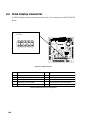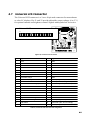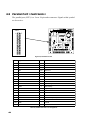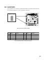
1
PCM-4330 PC/104 486 CPU Module with Flat Panel/CRT Interface Copyright Notice This document is copyrighted, 1997 by AAEON Technology Inc. All rights are reserved. AAEON Technology Inc. reserves the right to make improvements to the products described in this manual at any time without notice. No part of this manual may be reproduced, copied, rtanslated or transmitted in any form or by any means without the prior written permission of AAEON Technology Inc.Information provided in this manual is intended to be accurate and reliable. However, AAEON Technology Inc. assumes no responsibility for its use, nor for any infringements upon the rights of third parties which may result from its use. Acknowledgements ALI is a trademark of Acer Laboratories, Inc. AMD is a trademark of Advanced Micro Devices, Inc. AMI is a trademark of American Megatrends, Inc. A ward is a trademark of A ward Software Intermational, Inc. Cyrix is a trademark of Cyrix Corporation. IBM, PC/AT, PS/2, OS/2 and VGA are trademarks of International Business Machines Corporation. Intel and Pentium are trademarks of Intel Corporation. Microsoft Windows ® is a registered trademark of Microsoft Corp. SiS is a trademark of Silicon Integrated Systems Corporation. SMC is a trademark of Standard Microsystems Corporation. TGU1944GUI is a trademark of Trident Microsystems, Inc. WDC is a trademark of Western Digital Corporation. All other product names or trademarks are properties of their respective owners. Part No. 2007433000 PCM-4330 Rev.A1 1st Ed. Printed in Taiwan March 1997 Packing list Before you begin installing your card, please make sure that the following materials have been shipped: • 1 PCM-4330 CPU card • 1 SVGA adapter (10-pin to 15-pin) • 1 Power supply adapter (8-pin to 4-pin) • 2 Com port adapter (10-pin to 9-pin) • 1 Universal-LCD adapter (40-pin to 44-pin) • 1 System interface connector (10-pin) • 2 hard disk drive (IDE) interface cable (40-pin for 1.8"/2.5" or 3.5" HDD) • 1 floppy disk drive interface cable (34-pin) • 1 parallel port adapter (26-pin to 25-pin) • 1 utility disk )Flash BIOS program, Watchdog for Windows Librarym and Demo Program) • 2 utility disks with SVGA utility programs • PC/104 module mounting supports If any of these items are missing or damaged, contact your distributor or sales representative immediately. PCM-4330 Features PC/104-Board-Computer with 486SX, 486DX2, or 486DX4 n High MTBF n PC/104 standard size n High frequency mains shielded between GND and VCC layer n Flash-Memory for BIOS and customer specific extensions n SVGA, LC-display, keyboard, IDE-/AT-bus and floppy disk interface, one parn n n allel and two serial ports on-board Silicon disk for fast loading and booting of operating system optional Loudspeaker control Watchdog function SIS-85C471-AT-Controller n n n n n n n Includes components, which are compatible to: 82C37A-DMA, 82C54-Timer, 82C59-Interrupt-Controller, 82288-Bus-Controller, and 82284Clock-Generator Supports 70 ns DRAM modules providing a total of 1 MB, 4 MB and 16MB system memory on-board Memory controller with Page Mode Supports shadow RAM between 768 kB and 1 MB Memory remap of 256 kB to segments D000h and E000h with more than 1 MB memory installed and shadow disabled Supports synchronous and asynchronous bus timing SMC-FDC37C92x-Ultra-I/O-Controller n SuperCellTM technology n Licenced CMOS 765B-Floppy-Controller n IDE hard disk interface n Two NS16550-compatible serial ports with 230k baud and full modern support n ChiProtectTM protected parallel port can operate in standard mode, enhanced n mode, as an enhanced parallel port (EPP), or extended capabilities port (ECP) Award-Modular-BIOS n n n Modular BIOS Testing and initialization of all PCM-4330 hardware components Supports all IBM-AT03-compatible traps WD90C24-Controller n 32 bit memory interface n 1 MB display memory n Hardware drag of lines under MS-Windows (Strip Line) n Hardware pane of screen segments under MS-Windows (BitBLT) n Character set loading into display memory for screen segments outside visible area n CRT connector with integrated RAMDAC n Monochrome STN-LCD connector with 64 shades of gray n Color D STN or TFT-LCD connector n Plasma-display connector WD-VGA-BIOS n n n n n n Version 7.22A All IBM VGA standard modes and all VESA Super VGA modes Extended CRT mode with 132 columns 48 kB Video BIOS All VGA traps are supported Simultaneous display on CRT and LC-display possible Table of Contents 1 Introduction 11 1.1 Product Introduction 12 1.2 Compatibility 13 1.3 Reference Documents 14 2 PCM-4330-Installation 15 2.1 Hardware Installation 15 2.1.1 2.1.2 2.1.3 2.1.4 Jumper JP1: Panel Off Signal Jumper JP2: Contrast Voltage LC-Display Configuration Switches Installing the PC/104-Module 16 17 18 19 2.2 Setup 20 2.2.1 2.2.2 2.2.3 2.2.4 2.2.5 2.2.6 2.2.7 2.2.8 Time and Data AT Hard Disk Floppy Disk Boot Features Standard Chipset Timeout Peripherals Peripherals(Advance) 23 24 25 26 28 30 31 33 2.3 MS-DOS SVGA Software 35 2.3.1 Driver Installation 36 2.4 MS-Windows SVGA Software 41 2.4.1 Driver Installation 43 3 Layout and Functions 45 3.1 Block Circuit Diagram 45 3.2 General Layout 46 3.2.1 3.2.2 Processor (CPU) Memory 46 46 3.2.3 3.2.4 3.2.5 3.2.6 3.2.7 3.2.8 3.2.9 3.2.10 3.2.11 3.2.12 3.2.13 3.2.14 3.2.15 3.2.16 3.2.17 Cache DMA Controller Interrupt Controller Timer Real-time Clock (RTC) Keyboard Controller Loudspeaker Reset Logic A20 Logic Port B and NMI Logic Video Controller Floppy Disk Controlles IDE-/AT-Bus Parallel Port LPT1 Serial Ports COM1 and COM2 47 47 47 47 47 47 48 48 48 48 48 48 48 49 49 4 Hardware Interfaces 51 4.1 PC/104-Bus 52 4.1.1 4.1.2 PC/104-Bus Pin Assignment Signal Description 52 54 4.2 System Interface 58 4.3 Power Supply 59 4.4 Floppy Disk Interface 60 4.5 IDE-/AT-Bus Interface 61 4.6 SVGA Display Connector 62 4.7 Universal LCD Connector 63 4.8 Parallel Port (Centronics) 64 4.9 Serial Ports 65 5 Software interfaces 67 5.1 Address Summary of System Memory 67 5.2 Interrupt Channels 68 5.3 DMA Channels 69 5.3.1 5.3.2 DMA Channel Assignment DMA Address Generation 69 69 5.4 Port A 69 5.5 Port B 70 5.6 MicroDesign Feature Port 71 5.6.1 5.6.2 Setting the Base Address Feature Port Register Description 71 72 5.7 Real-Time Clock/CMOS-RAM 84 5.7.1 5.7.2 RTC/CMOS-RAM Address Assignment RTC/CMOS-RAM Operations 84 84 5.8 System Timer 85 5.8.1 Timer Programming 85 5.9 NMI Logic 86 5.10 Keyboard Interface 86 5.11 Floppy Disk Controller 86 5.12 Parallel Port 87 5.13 Serial Port 87 6 Firmware 6.1 POST (Power On Self Test) 89 6.1.1 6.1.2 6.1.3 Signal Tone Error Messages On-screen Error Messages POST Codes 89 90 93 89 6.2 SVGA-BIOS Calls (INT 1Oh) 6.2.1 6.2.2 6.2.3 Standard IBM VGA-compatible BIOS Calls (INT 1Oh) Extended BIOS Calls (INT 1Oh) VESA SuperVGA BIOS Calls (INT 1Oh) 7 Technical Specifications 7.1 Electrical Specifications 109 7.2 Environment Conditions 109 7.3 Dimension Sketch 110 Appendix A: Troubleshooting 111 Appendix B: LC-Displays 113 Appendix C: Silicon Disk 123 Appendix D: Installing PC/104 Modules 125 95 95 103 106 109 1 Introduction This manual describes the PCM-4330 PC/104 board computer with 486SX, 486DX2, or 486DX4 CPU as a PC/104 module. Figure 1, PCM-4330 with 486SX, 486DX2, or 486DX4-CPU (Top and Bottom View) Several notes in the text refer to product documentation not included in this manual. If you need more comprehensive and detailed information, please refer to data sheets and documents listed under chapter 1.3. 11 1.1 Product Introduction The PCM-4330 serves as a processor board in a PC/104 environment and provides for a fully ISA-compatible computer system. The system is built using the SIS-85C47i. This chip contains on a single VLSI component the main elements of an ISA system by implementing DMA, memory,bus, interrupt controller, memory mapper, and timer. For addressing peripheral devices, a chip from Standard Microsystem Corporation (SMC) is used on the board. The FDC37C92x-Ultra-I/O-Controller, built in SuperCel technology, includes IDE-/AT-bus, floppy disk, keyboard, serial, and parallel port controllers, as well as a real-time clock. The WD90C24 controller, addressing 1 MB of video memory via a 32 bit wide data bus, is used to control video output. The controller accelerates the screen display of window systems like MS-Windows by hardware support of CPU intensive screen operations. The graphics board supports all VGA, SVGA and Paradise enhanced video modes. TM Design The PCM-4330 board is AT-compatible including all interfaces. All software written for Intel 8086, 80286, 80386, 80486, and compatible processors runs on this board. It is built and fired in double-sided SMD technology requiring minimum space for a maximum of functions. Processor The 486SX, 486DX2, and 486DX4 CPUs offer virtual addressing capabilities, integrated MMU, 4-level memory protection in multi-user-mode (Protected Virtual Address Mode). 1 MB physical memory can be addressed in Real-Address-Mode and 4 GB in Protected Mode. Maximum virtual memory in Protected Mode is 64 TB. Co-processor All DX-CPUs used for the PowerDwarf feature on-chip math co-processors. Cache Presently available CPUs from the i486 family include 8 kB 4-way-on-chip-cache used for data and code caching by the CPU. Main Memory With respect to the 486SX, 486DX2, and 486DX4 CPU capabilities, main memory is addressed with an access width of 32 bit. RAM memory is parity checked. Two DRAM modules with access times of 70 ns are used in sockets providing 1 MB with/without parity (256K x 16 or 256K x 18), 4MB with/without parity (1M x16 or 1M x 18), or 16MB (4M x 16) on-board system memory. 12 Silicon Disk The PCM-4330 board can optionally be fitted with a 28F016SV (2MB) or 28F032SV (4 MB) flash module to provide a silicon disk, Data, programs, or operating software can be permanently stored on this disk. Data is accessed in16 kB banks that are paged into the address space of the processor.128 kB from the available memory space of the flash module is used for the System-BIOS. Video Controller The Western Digital WD90C24 video controller can address various monochrome or fiat panel displays directly, as well as all SVGA monitors. Depending on the LCD display connected, an additional CRT display may be used simultaneously. The WD90C24 offers accelerated display of windows via integrated hardware functions (such as Bit Block Transfer). Frame buffers and font-caching are also supported. Video Memory The 1 MB video memory on the VGA controller is addressed directly via a 32 bit wide interface from the video controller. The size of the video memory allows for a resolution of 1024 x 768 pixels (256 colors) on LED and CRT displays. ROM-BIOS A 64 kB segment at address F000h is reserved for the Award ROM-B IO S. All AT03-compatible traps are included in this address space. The Western Digital VGA-BIOS for the WD90C24 video controller uses 48 kB in the physical address space of the computer, starting at segment C000h. All VGA, SVGA- and VESA-compatible video traps are supported by the BIOS. The memory area is fitted with a 29F010 (128 kB), 29F020 (256 kB), or 29F040 (512 kB) Flash-Memory. Alternatively, the board can be equipped with a28F0xGSV (1 MB) or 28F032SV (4 MB) module to provide memory space for the BIOS and a silicon disk. Interfaces The PCM-4330 board includes the most important interfaces on-board. Two serial and one parallel port, keyboard, floppy disk and an IDE hard disk controller are included and can be configured by software. A SVGA connector is available, as well as a connector for monochrome or color LC-display. The PCM-4330 single board computer features an expansion slot according to the PC/104 norm. 1.2 Compatibility The board is fully XT/AT-compatible. All available expansion cards complying with the PC/104 norm can be used with the PCM-4330. 13 1.3 Reference Documents [1]ISA-Bus-Spezifikation S2636I-XXX-X-*-59 (allgemein) [2]Intel-Microprocessors: Volume II [3]Data-Manual SIS-85C471 Green PC ISA-VESA Single Chip [4]Data-Manual FDC37C92x-Ultra-I/O-Controller (SMC) [5]Data-Manual Intel Flash Memory: Volume I [6]Data-Sheet WD90C24 (Western Digital) [7]WD90C24 Windows Accelerated High Resolution VGA LCD Controller for Low Power Applications (Western Digital) [8]WD90C24 VGA Controller BIOS Specification (Western Digital) 14 2 PCM-4330-Installation Before installing the PCM-4330 PC/104 board computer please read the following notes very carefully. You must adhere to these rules to avoid damaging components: n Before touching the board or any other component, discharge your body by touching a grounded object such as the metal chassis of the computer. n Tools used to install the board must be free of static charges. n Always remove the power cord from the system before installing or removing components. n Handle the board carefully, holding it by its edges only. n Do not touch components on the board, connecting pins, or exposed circuits on the board. 2.1 Hardware Installation The PCM-4330 is installed in a PC/104 system taking over all functions of a modern ISA-compatible computer system. Please observe all notes listed above before installing the module. If the system does not operate as anticipated after installation, please refer to Appendix A: Troubleshooting. 15 2.1.1 Jumper JPI: Panel Off Signal Jumper JP1 sets the polarity for the LC-display panel off signal. Please refer to figure 9. for the exact location of jumper JP1 3 2 1 JP1 Figure 2, Jumper JP1 Jumper JP1: Panel Off Signal 1 - 2 closed: Panel off at high (1) 2 - 3 Closed: Panel off at low (0) 3 2 1 3 2 1 Table 1, Jumper JP1 16 2.1.2 Jumper JP2: Contrast Voltage Jumper JP2 on the PCM-4330 board selects the contrast voltage polarity (positive or negative) for LC-displays. Use the onboard contrast control to set the maximum contrast voltage. The corresponding value in the setup menu must be set to “o”. After adjustment, software can only select contrast voltage to less than the maximum set. Check with the display documentation prior to any adjustment to ensure that the connected LC-display is capable of supporting the selected voltage. Unsupported values might damage the display. See figure 3 for the exact location of jumper JP2: 3 2 1 JP2 Contrast Control Figure 3, Jumper JP2 Jumper JP2: Contrast Voltage 1 - 2 closed: Negative contrast voltage 2 - 3 Closed: Positive contrast voltage 3 2 1 3 2 1 Table 2, Jumper JP2 17 2.1.3 LC-Display Configuration Switches The PCM-4330 single board computer features a DIL-switch with 8 keys for easy configuration of a connected LC-display. See Appendix B: LC-Displays for a selection of displays and the corresponding settings of switches SW.1 to Sw.8. See figure 4 for the location of the configuration switches. Configuration Switches 8 7 6 5 4 3 2 1 Figure4 Configuration Switches Configuration Switches Key Setting SW.1 reserved SW.2 on: CRT, off: CRT and LCD simultaneous SW.3 Display type 0 SW.4 Display type 1 SW.5 Display configuration 0 SW.6 Display configuration 1 SW.7 Display configuration 2 SW.8 Display configuration 3 Table 3, Configuration Switches 18 2.1.4 Installing the PC/104-Module The PCM-4330 is installed in a PC/104 system and takes over the function of the CPU. Please observe the following guidelines for the installation of the module: Check that jumpers Jp1 and Jp2 and all configuration switches are set correctly before installation. 8 8 8 8 8 8 8 8 8 Switch off the computer system. Remove the power cord. Remove the cover or housing of the computer system If a PC/104-CPU-board, VGA graphics adapter, IDE-hard disk or floppy disk controller is installed in the system, remove it. The PCM-4330 comprises all functions of these boards. Carefully install the PCM-4330 in the PC/104 system. The board features four holes for safe fastening and a connector for the installation on a PC/ 104 bus. Connect all cables and connectors with the appropriate interfaces (system,LPT1, COM1, COM2, VGA/LCD, IDE hard disk, floppy disk, and power). See chapter 4. Replace the housing cover and plug in the power cord. Switch on the computer system. Call the Setup-Menu. 19 2.2 Setup The PCM-4330 board features an integrated setup program to easily select and adapt the system configuration, such as number and type of floppy disk or hard disk drives installed. Configuration details are stored in a battery-buffered RAM area retaining all information even when the system is switched off. Tne following messages are displayed during system boot: Figure 5, Setup Main Menu 20 After pressing the CTRL-ALT-ESC keys, the following menu is displayed: Figure 6, Setup Menu The following selections are available in the setup menu: User Help This selection displays a screen with help message and instructions on how to use list boxes and radio buttons. Load Defaults Use this option to reset current settings to factory default values. Time and Date Use this selection to set time and date. AT Hard Disk This selection offers automatic detection and manual drive parameter configuration of IDE-/AT-Bus hard disk drives connected to the primary (on-board) and secondary IDE-Controller. If using the BIOS automatic detection, several drive types may be available. Extended modes for IDE hard disk with a capacity of more than 528 MB are supported by the BIOS. Floppy Disk Select type of floppy disk drives installed. 21 Boot Features Additional configuration features for system boot. Standard Chipset Settings for Cache and Shadow. Timeout Select to switch off screen or spin down IDE hard disk drives after specified time of inactivity. Peripherals Setup settings for serial ports, parallel port, IDE-/AT-Bus-Controller, Floppy Disk Controller and PS/2-Mouse. Peripherals Adv. Sehup settings for feature controller, silicon disk and LC display. System Status Information on temperature and voltage (read only). Use the arrow keys to navigate between menu selections and press RETURN to enter the chosen dialog box. Use the TAB keys to jump between list boxes and buttons. To return to the setup menu or leave the setup program, hit ESC (or press the EXIT or CANCEL button). Before leaving the setup program, a confirmation box appears. Press SAVE to save all settings and leave the setup program, press EXIT the button or hit the ESC key to discard all changes and leave the setup program without saving, or press RETURN to return to the setup menu: 22 2.2.1 Time and Date After selecting Time and Date the following dialog box appears: Figure 7, Date and Time Setup The following parameters can be set (Use the TAB keys to jump between selections): Date Enter the current date in the form tt-MM-JJJJ Time Enter current system time in the format hh:mm:ss 23 2.2.2 AT Hard Disk After selecting AT Hard Disk the following dialog box is displayed: Figure 8, AT Herd Disk Setup Use the arrow keys to navigate to the appropriate hard disk drives settings or jump between buttons using the TAB keys. Press the AUTO All Drives button to configured drive parameters automatically or enter the applicable values. Use the AUTO checkmark to automatically detect the drive type during system boot and set the appropriate period of time the system is to wait for the drive to spin up (drive wait time). 24 2.2.3 Floppy Disk After selecting Floppy Disk the following dialog box appears: Figure 9, Floppy Disk Setup The following parameters can be set (Use the TAB keys to jump between items and select an highlighted option by pressing the space bar): Drive A:, Drive B: Select type of floppy disk drive installed n No floppy disk drive installed n 360 kB, 51/4 n 1.2 MB, 51/4 n 720 kB, 31/2 n I.44 MB, 31/2 n 2.88 MB, 31/2 None 360Kb 1.2Mb 720Kb 1.44MB 2.88MB Test Floppy Disks Activate/deactivate floppy disk drive testing at start-up 25 2.2.4 Boot Features After selecting Boot Features the following dialog box is displayed: Figure 10, Boot Features Setup The following parameters can be set (Use the TAB keys to jump between items and select/deselect an highlighted option by pressing the space bar): Boot Sequence Secluence for boot attempts n Drive A:, Drive C: (Default) n Drive C:, Drive A: A:, C: C:, A: Typematic Settings Enabled Enable this option if the typematic settings have to be programmed into the keyboard. Typematic Rate Select the keyboard repeat rate in characters per second (use cursor up/down keys) Typematic Delay Select the delay before first repeat (use cursor up/down keys) Num Lock On Activate/deactivate numeric key lock 26 Halt On Errors Halt boot on errors. Select which errors not to halt boot on: n Keyboard error n Disk errors Base Memory Base memory size Extended Memory Extended memory size Quick Memory Test Activate/deactivate quick memory testing Language Is Select language for POST and error messages (see also Figure 5 on page 16). Use the arrow up and down keys to navigate to select a desired language. n English boot messages (Default) English n German boot messages German n French boot messages French Display Graphic Logo Activate/deactivate graphic logo display during system boot 27 2.2.5 Standard Chipset After selecting Standard Chipset the following dialog box appears: Figure 11,Standard Chipset Setup The following parameters can be set (Use the TAB keys to jump between items and select/deselect an highlighted option by pressing the space bar): Cache Activate/Deactivate system cache. If an external cache is not available, this option can not be selected. n Cache off Disable n CPU cache only CPU only n Cache on CPU and External Cache Write Back Select writeback cache fiunction for CPU cache. This option can only be selected if supported by the CPU installed. External Cache Write Back Select writeback cache function for external (level z) cache. This option can only be selected if second level cache is installed on the board. 28 Boot Speed Define bootup system speed n Full operation speed n Reduced CPU speed for bootup High Low Onboard Parity Enable onboard parity checking if parity RAM is installed Enable Flash Update Enable System-ROM update (i.e. disable flash module write protection). After checking this option, the System-ROM Flash module will be unprotected at next power on and automatically be cleared again at the following power on. If option is not checked, the System-ROM is write protected. Shadow Activate/deactivate shadowing for memory area 29 2.2.6 Timeout After selecting Timeout the following dialog box is displayed: Figure 12, Timeout Setup Tne following parameters can be set (Use the TAB keys to jump between items and select an highlighted option by pressing the space bar): Video Timeout Select this option to switch off screen after specified time of keyboard inactivity. DPMS mode is used if supported by the video system. Select the time to wait before screen is switched off. AT Bus Hard Disk Timeout Select this option to spin down IDE drivel(s) after a specified time of drive inactivity. Select the time to wait before timeout. 30 2.2.7 Peripherals After selecting Peripherals the following dialog box appears: Figure 13, Peripherals Setup The following parameters can be set (Use the TAB keys to jump between items and select/deselect an highlighted option by pressing the space bar): Serial Port A Select base address for serial port I n Automatic assignment at start-up n Select address and interrupt n Not active Auto 3F8h, IRQ4. 2F8h, IRQ3 3E8h, IRQ4 2E8h, IRQ3 Disable Serial Port B Select base address for serial port 2 n Automatic assignment at start-up n Select address and interrupt n Not active Auto 3F8h, IRQ4 2F8h, IRQ3 3E8h, IRQ4 2E8h, IRQ3 Disable 31 Parallel Port Select base address for parallel port n Automatic assignment at start-up n Address and interrupt n Not active Auto 3BCh, IRQ7 378h, IRQ7 278h, IRQ5 Disable Select mode for active parallel port n Bidirectional n EPP n ECP n EPP+ECP Primary IDE Activate/deactivate primary (on-board) IDE-Controller and IDE-/AT-Bus interface n Automatic detection at start-up Auto n IDE-Controller off Disable n IDE-Controller on Enabled Floppy Disk Activate/deactivate on-board Floppy Disk Controller and floppy disk interface n Automatic detection at start-up Auto n FDC-Controller off Disable n FDC-Controller on Enabled Select mode for floppy disk drives n Standard assignment n Swap drive letter assignment Normal Swap A:/B: PS/2 Mouse Enable/disable onboard PS/2-mouse port. Please note: This function is not supported on the PCM-4330 platform. 32 2.2.8 Peripherals (Advanced) After selecting Peripherals (Advanced) the following dialog box appears: Figure 14, Peripherrls (Advanced) Setup The following parameters can be set (Use the TAB keys to jump between items and select values using the arrow up and down keys): Feature Controller I/O Base Select the I/O base for Feature Port access. The Feature Port interface uses two consecutive addresses, which should not conflict with any other system device. The new base address will be used after reboot. n Base address 100h - 7FFh Silicon Disk State Onboard silicon disk support. If this option is enabled the option ROM is mapped to the CPU address space, while no resources are needed if this function is disabled. n Onboard silicon disk on Enabled n Onboard silicon disk off Disabled 33 Silicon Disk Memory Base Define the 16 kB memory window within the CPU address space to be used for silicon disk access. n Memory Base D000h/D400h/D800h/ DC00h/CC00h LCD Display Contrast Select LC display bootup value for contrast. As visual feedback, the new value will be programmed immediately. n Contrast value 0 - 255 LCD Display Brightness Select LC display boohup value for brightness. As visual feedback, the new value will be programmed immediately. n Brightness value 0 - 255 34 2.3 MS-DOS SVGA Software Special SVGA software (drivers and programs) is included with the PCM-4330 single board computer to use the extended functions under MS-DOS. Operation of the SVGA adapter is also possible without this SVGA software. The SVGA software for use with MS-DOS is found on the disk labeled DOS Install Disk. The following files are included on this disk: Text n README.TXT n README.1ST Lists all drivers and programs on the disk (If included on the disk) Contains last-minute information and change remarks Drivers n n n n n n n n ACAD.LIF CADVANCE.LIF GENERIC.LIF LOTUS.LIF PCAD.LIF WORD.LIF WP.LIF UTILITY. LIF AutoCAD 386, AutoShade and 3D Studio display driver Cadvance display driver Generic CADD display driver Lotus 1-2-3 and Lotus Symphony display driver PCAD display driver Microsoft Word for MS-DOS display driver WordPerfect display driver ANSI.SYS driver for extended VGA mode (Paradise Mode) Programs n INSTALL. COM n CHIPTST. EXE n KDINSTAL. EXE n READID.EXE n VGAMODE.EXE Menu controlled installation program (used by INSTALL.COM) (used by INSTALL.COM) (used by INSTALL.COM) (used by INSTALL.COM) If the system does not operate as anticipated after the installation of a MS-DOS device driver, please refer to Appendix A:Troubleshooting. 35 2.3.1 Driver Installation To use the extended features of the WD90C24 controller under MS-DOS special SVGA software (programs and drivers) must be installed. The disk DOS-Install Disk contains the menu-controlled program INSTALL.COM. 8 Make a backup copy of the disk DOS-Install Disk and store the original at a secure place. 8 Check whether the PCM-4330 single board computer is correctly installed in the system and that all jumpers and switches are set properly. 8 Load the utility program INSTALL.COM from your backup copy of the installation disk from dis The following start-up page of the installation utility appears on the screen. It contains the version number and copyright information: Figure 15, (Install.com) Start-up Screen 36 8 Press the < E S C > key to quit the I N STALL.COM installation utility or press any other key to display the following menu: Rgure 16, (Install.com) Selection Screen for Program Groups 8 Use the cursor keys to select the program group for which you want to install a driver and press < ENTER > . Depending on your selection in the program selection screen (see figure 16), the following drivers and driver configurations may be selected:. Cadvance 1.2 to 3.0 Product Version Resolution Driver Name Cadvance 3 640x480x256 800x600x16 1024x768x16 gsvga.drv gs800.drv gs102416.drv Table 4, Cadvance Drivers Generic-CADD Level3 Product Version Resolution Driver Name Generic-CADD Level3 640x400x256 640x480x256 800x600x16 800x600x256 1024x768x16 1024x768x16 p640x400.vgd p640x480.vgd para800.vgd p800x600.vgd p1024x16.vgd p1024xff.vgd Table 5, Generic-CADD Drivers 37 Lotus 1-2-3 v.2/2.01/2.1/2.2 Product Version Resolution Driver Name Lotus 1-2-3 2,2.1,2.01,2.2 640x480x16 800x600x16 1024x768x16 123Columns sp1_480s.drv sp1_600s.drv sib2vga.drv(8x9font) sib3vga.drv(9x13font) s0_25s.drv(132x25) sp0_44s.drv(132x44) Table 6, Lotus 1-2-3 Drives Lotus Symphony Product Version Resolution Driver Name Lotus Symphony 1.1,1.2,2.0 640x480x16 800x600x16 1024x768x16 123Columns sp1_480s.drv sp1_600s.drv sib2vga.drv(8x9font) sib3vga.drv(9x13font) s0_25s.drv(132x25) sp0_44s.drv(132x44) Table 7, Lotus Symphony Drives Lotus 1-2-3 v.3.1 Product Version Resolution Driver Name Lotus 1-2-3 3.1 800x600x16 1024x768x16 l13v600.dld l13v768.dld Table 8, Lotus 1-2-3 v.3.1 Drivers PCad Level2 Product Version Resolution Driver Name PCAD Level2 800x600x16 1024x768x16 dwdpvga.drv dpvga1k.drv Table 9, PCad Drivers Microsoft Word 5.0/5.5 Product Version Resolution Driver Name WORD v5.5 800x600x16 vga.gsd Table 10, Microsoft Word 5.0/5.5 Drivers 38 WordPerfect 5.0/5.1 Product Version Resolution Driver Name WordPerfect v5.0 800x600x16 1024x768x16 wdpvga1.wpd wdpvga2.wpd WordPerfect v5.1 1024x768x16 wdpvga3.vrs Table 11, WordPerfect 5.0/5.1 Drivers AutoCAD/Autoshade Product Version Resolution Driver Name AutoCAD 386 Non D.L. Auto Shade 386 3D Studio Release 11 Version 2 640x480x256 640x480x256 / 32k 640x480x256 / 32k 11p6168.exp 11p6168.exp 11p6168.exp AutoCAD 386 Non D.L. Auto Shade 386 3D Studio Release 11 Version 2 800x600x256 / 32k 800x600x256 / 32k 800x600x256 / 32k 11p8188.exp 11p8188.exp 11p8188.exp AutoCAD 386 Non D.L. Auto Shade 386 Release 11 Version 2 640x480x256 640x480x256 11pshv68.exp 11pshv68.exp AutoCAD 386 Non D.L. Auto Shade 386 Release 11 Version 2 800x600x256 800x600x256 11pshv88.exp 11pshv88.exp AutoCAD 386 Non D.L. Auto Shade 386 Release 11 Version 2 1024x768x256 1024x768x256 11pshv18.exp 11pshv18.exp AutoCAD 386 Release 11 800x600x16 800x600x256 1024x768x16 1024x768x256 11pdlv84.exp 11pdlv88.exp 11pdlv14.exp 11pdlv18.exp Auto Shade Version 1 640x400x256 640x480x256 800x600x256 1024x768x256 rd400.exe rd480.exe rd800.exe rd1024.exe Table 12, AutoCAD Drivers Utilities Driver Description WDANSI.SYS ANSI.SYS driver for extended VGA mode Table 13, #Utilities 39 8 8 After selecting a driver and display resolution, the installation utility requests the target drive and the name of the destination directory to receive the driver software. The following example installs the driver into the directory that contains the Lotus1-2-3 software. Use the cursor keys to select a drive letter from the list of avafiable drives and press <ENTER>. Select the Drive on which to install Lotus Driver Drive Drive Drive Drive Drive A: B: C: D: E: Figure 17, (Install.com)Destination Drive 8 Enter the subdirectory and press <ENTER>. Which subdirectory is Lotus installed ? Figure 18,(Install.com)Destination Subdirectory 8 40 Please read all instructions carefully as the actual input parameters may vary according to the driver selected. 2.4 MS-Windows SVGA Software Special SVGA software (programs and drivers) is included with the PCM-4330 to use extended functions of the video controller under MS-Windows. Operation of the SVGA adapter is also possible without this special SVGA software. The SVGA software for use with MS-Windows is found on the disk labeled Windolvs-Install-Disk. The following files are found on this disk: Drivers n n n n n n n vga .dr_ wd24_8 .dr_ wd24ik_4.dr_ wd2464__4.dr_ wd2464_h.dr_ wd2480_4.dr_ wddci.dr_ Windows 3.1 driver(standard VGA) Windows 3.1 driver Windows 3.1 driver Windows 3.1 driver Windows 3.1 driver Windows 3.1 driver Windows 3.1 driver Character Sets n n n n n n n n n n n n n n n n n n 8514fix.fo_ 8514oem.fo_ 85x4sys.fo_ cga4owoa.fo_ cga8owoa.fo_ coure.fo_ courf. fo_ dosapp.fo_ ega4owoa.fo_ ega8owoa.fo_ serife.fo_ seriff. fo_ smalle.fo_ smallf. fo_ sserife.fo_ sseriff. fo_ symbole.fo_ symbolf. fo_ Windows 3.1 character set Windows 3.1 character set Windows 3.1 character set Windows 3.1 character set Windows 3.1 character set Windows 3.1 character set Windows 3.1 character set Windows 3.1 character set Windows 3.1 character set Windows 3.1 character set Windows 3.1 character set Windows 3.1 character set Windows 3.1 character set Windows 3.1 character set Windows 3.1 character set Windows 3.1 character set Windows 3.1 character set Windows 3.1 character set 41 vgaoem.fo_ vgasys .fo_ vgafix.fo_ Windows 3 .1 character set Windows 3 .1 character set Windows 3 .1 character set SetupPrograms setup.exe setup.inf setup.lst setup.rest setupapi.inc dciman.dl_ mscomstf. dll mscuisff. dll msdetsff. dll msinssff. dll msshlstf. dll msuilsff. dll oemsetup.inf pvga.gr_ v7vga.3g vddpvga.38ver.dll vgalogo.lg_ vgalogo .fi_ vidchg.ex_ vidchg.hl_ _mssetup.exe _mstest.exe Windows 3 .1 setup file Windows 3 .1 setup file Windows 3 .1 setup file Windows 3 .1 setup file Windows 3 .1 setup file Windows 3 .1 setup file Windows 3 .1 setup file Windows 3 .1 setup file Windows 3 .1 setup file Windows 3 .1 setup file Windows 3 .1 setup file Windows 3 .1 setup file Windows 3 .1 setup file Windows 3 .1 setup file Windows 3 .1 setup file Windows 3 .1 setup file Windows 3 .1 setup file Windows 3 .1 setup file Windows 3 .1 setup file Windows 3 .1 setup file Windows 3 .1 setup file Windows 3 .1 setup file Windows 3 .1 setup file If the system does not operate as anticipated after the installation of a MS-Windows device driver, please refer to Appendix A: Troubleshooting. 42 2.4.1 Driver Installation To use extended features of the SVGA controllers on the PCM-4330 single board computer under MS-Windows special SVGA drivers must be installed. The Windows-Install-Disk contains a special installation program to install SVGA video drivers and change video settings under MS-Windows. Use the MSWindows File Manager or Program Manager to start the installation. On-line-Help is available at every stage. Figure 19, Western Digital Video Changer Please check with your monitor specifications to ensure that the monitor is capable of supporting the particular option, to prevent damage to the display. Resolution Select a resolution for the video driver 640 x 480 This resolution supports the following color settings: 16,25,32k and 64k colors 800 x 600 This resolution supports 16 and 256 colors. The screen refresh rate may also be set: 56 Hz, 60 Hz and 72 Hz, non-interlaced, are sup ported. 1024 x 768 This resolution also supports 16 or 256 colors. Screen refresh rate can be set to 60 Hz interlaced or non-interlaced. 43 Refresh Rate Choose a screen refresh rate for the selected resolution 640 x 480 800 x 600 1024 x768 i No refresh rate can be set for this resolution. Select between non-interlaced 56 Hz, 60 Hz and 72 Hz. Choose between 60 Hz interlaced or non-interlaced. The higher the refresh rate, the better the display quality. Also, noninterlaced mode has a better display quality than interlaced mode. Color Choose a color option for the selected resolution 640 x 480 Color options are: 16,256, 32k or 64k colors 800 x 600 Color options are 16 and 256 colors 1024 x768 Color options are 16 and 256 colors When 256 color is selected for all resolutions, the following options are available: Font Size Select font size for the display n Large display font n Small display font Large Font Small Font Font Caching Enable font caching to increase performance Enable font cache Font cache off Disable font cache Font cache on Cursor Select cursor type n Normal cursor Normal n Inverted cursor Invert You do not have to restart Windows for this option to take effect. Virtual Screen Enable virtual screen n Enable virtual screen n Disable virtual screen 44 On Off 3 Layout and Functions This chapter describes the technical layout and functions of the PCM-4330 single board computer. 3.1 Block Circuit Diagram Figure 14 illustrates the schematic layout of the PCM-4330 in form of a circuit diagram: 16 Figure 20, PCM-4330 486SX-,486DX2-,and 486DS4-ISA-System 45 3.2 General Layout The following sections describe the individual components of the PCM-4330 single board computer. 3.2.1 Processor (CPU) A 32-bit CPU from the Intel i486 family is used. The PCM-4330 may be fitted with a 486SX, 486DX2, or 486DX4 processor. All these processors feature: Separate address and data bus Extensive instruction set, downward compatible to the 8086 set Integrated memory management (MM U) Memory protection on 4 levels Address space of 1 MB in Real Mode Physical addressable address space of up to 4 GB in Protected Mode The processor can be operated in Real Address Mode or Protected Virtual Mode. After a reset, the processor resumes operation in Real Mode. 3.2.2 Memory Memory on the PCM-4330 consists of ROM and RAM area depending on the board configuration, ROM memory size is 128 kB to 4 MB. 128 kB are located below the 1 MB and 4 GB address boundary. It is therefore available twice (mirrored). A socket is used for ROM memory modules with a 8-bit word width containing a 29F010 (128 kB), 29F020 (256 kB), or 29F040 (512 kB) Flash-Memory. Alternatively, a 28F016SV (I MB) or 28F032SV (4 MB) module can be used, which also offers silicon disk capabilities. The BIOS software can be reprogrammed by an auxiliary program during operation. RAM is build up by two dynamic memory modules in sockets to offer 1 MB, 4MB or 16 MB on-board. These RAM modules support an access width of 32 bit and may be parity checked bitwise (optional). 16MB Specific attributes can be assigned to certain regions of RAM memory: n Enable/Disable Shadow n RAM 1024kB BIOS 128kB enable/disable RAM 896kB CHANNEL-I/O 128kB enable/Disable RAM 768kB Video-Buff er 128kB enable/disable RAM 640kB DO S-area Table 14, RAM Area Attributes 46 Accessing the silicon disk is performed via 16 kB banks, that are paged into the address space of the processor. I/O port may be assigned for paging and individual banks may be designated for paging. Read operations can be performed on bytes, words or double-words. Special software must be used to write to the silicon disk, removing the write protection before write operations. 3.2.3 Cache The i486 family of processors all feature 8 kB on-chip cache and cache controller. 3.2.4 DMA Controller The DMA controller of the SIS-85C471-AT-Controller offers the ISA functionality of two 82C37-DMA controllers with seven independent channels. 3.2.5 Interrupt Controller Two 82C59-compatible interrupt controllers are implemented. They are cascaded and offer 2 external interrupt channels. 3.2.6 Timer A 82C54-compatible timer is also included. It comprises three independent channels which can be programmed in six different modes. 3.2.7 Real-time Clock (RTC) The RTC is included in the MC146818A-compatible cell of the FDC37C92x-UltraI/O-Controller. It is extended by 128 bytes via two 64 byte CMOS RAM pages in address space 40h - 7Fh of the RTC. The RTC manages system time, date, and offers alarm functions. 14 of 192 bytes of internal memory are used to control the clock functions, the remaining 178 bytes of CMOS RAM are used to store BIOS setup information. 3.2.8 Keyboard Controller The keyboard interface is implemented as a megacell in the SMC FDC37C92xUltra-I/O-Controller. In addition to the serial keyboard port, two ports for system status and control functions are available. The keyboard controller manages: n Keyboard lock n Color/monochrome toggling n Address line A20 (1 MB limit) n Keyboard reset n Keyboard interrupt request IRQ1 47 3.2.9 Loudspeaker The tone signal for the speaker is generated by Timer 2 (in the SIS-85C471-ATController). The timer is programmed as a square-wave generator. The generator is controlled by the System-Control-Registers in Port B. An additional bit of the System-Control-Registers is combined with output of Timer 2 by a logical and. Theresulting signal controls the internal or external speaker (using the system interface; c.f. Figure 23 on page 54). 3.2.10 Reset Logic A system reset may be initiated by the power supply, shutdown, keyboard reset or via I/O port 92h (Bit 0) and the SIS-85C471-AT-Controller. 3.2.11 A20 Logic The CPU line mask-A20 can be controlled as in AT-systems through the key-board controller. Additionally, the PS/2®-compatible port 92h (Bit 1) is available. 3.2.12 Port B and NMI Logic The status and control port B (061h) consists of the integrated System-ControlRegister and the System-Status-Buffer. Parity checking may be enabled/disabled via the System-Control-Register. The System-Status-Buffer informs on queued memory parity errors. 3.2.13 Video Controller The Western Digital WD90C24 video controller can address various monochrome or color flat panel displays directly, as well as regular SVGA monitors. A 2-row 10pin connector for SVGA displays and a 2-row 40-pin universal LCD-onnector arelocated on the board. 3.2.14 Floppy Disk Controller The FDC37C92x-Ultra-I/O-Controller from SMC with a licensed 765B-compatible SuperCellTM is used for floppy disk control. Data is exchanged over DMA channel2, interrupts are initiated via IRQ6. Up to two floppy disk drives (31/2 or 51/4) are supported. 3.2.15 IDE-/AT-Bus The FDC37C92x peripheral unit also includes an interface for IDE-/AT-bus hard disks. 48 3.2.16 Parallel Port LPT1 The parallel port LPT1 is also integrated into the FDC37C92x-Ultra-I/O-ontroller. In addition to the PC/AT standard it can be operated in bi- as wall as in uni-directional mode. This interface is equipped with a ChiProtectTM circuit protecting it from power surges at power-on of the printer device. I/O addresses are selectable in the setup menu. LPT1 is a 26-pin 2-row male connector on the board and can be extended to the exterior with an extension cable. 3.2.17 Serial Ports COM1 and COM2 Interfaces COM1 and COM2 are included in the FDC37C92x-Ultra-I/O-ontroller as a NS16550-compatible SuperCelLTM. I/O addresses are selectable in the set-up menu; interrupts (IRQn) are pre-assigned and can not be selected by the user. COM1 and COM2 are located as 2-row 10-pin connectors on the PCM-4330 single board computer. 49 50 4 Hardware Interfaces All interfaces required for an AT-compatible PC are included on-board. Figure 21 illustrates the location of interfaces and connectors on the PCM-4330 PC/104 single board computer. PC/104-Bus Power Supply PC/104-Bus COM1 System Interface LPT1 IDE-/AT-Bus COM2 Universal-LCD SVGA Figure 21, Location of on-board Interfaces The following sections describe individual interfaces of the PCM-4330 in detail. 51 PC/104-Bus The PC/104-Bus is a multimaster bus featuring: n 24-bit addressing for CPU, DMA and busmaster n 8-bit or 16-bit data n Multimaster capability n 11 interrupt channels, flank triggered n 7 DMA channels (four 8-bit, three 16-bit) n Waitstate control n Refresh control PC/104-Bus Pin Assignment The PCM-4330 features a PC/104-Bus. Please refer to table 16 for the pin assignment on the PC/104-Bus. PC/104-Bus D0 C0 A1 B1 SM C ® Figure 22, PC/104-Bus 52 Table 15 lists the PC/104-Bus pin assignments. Signals with# symbol are low active. Pin Signal Pin Signal Pin Signal Pin Signal B1 GND A1 IOCHK# C0 GND D0 GND B2 RSTDRV A2 D7 C1 SBHE# D1 MEMCS16# B3 VCC A3 D6 C2 LA23 D2 IOCS16# B4 IRQ9 A4 D5 C3 LA22 D3 IRQ10 B5 -5V A5 D4 C4 LA21 D4 IRQ11 B6 DRQ2 A6 D3 C5 LA20 D5 IRQ12 B7 -12V A7 D2 C6 LA19 D6 IRQ15 B8 WSO# A8 D1 C7 LA18 D7 IRQ14 B9 +12V A9 D0 C8 LA17 D8 DACK0# B10 GND A10 IOCHRDY C9 MEMR# D9 DRQ0 B11 SMEMW# A11 AEN C10 MEMW# D10 DACK5# B12 SMEMR# A12 SA19 C11 D8 D11 DRQ5 B13 IOW# A13 SA18 C12 D9 D12 DACK6# B14 IOR# A14 SA17 C13 D10 D13 DRQ6 B15 DACK3# A15 SA16 C14 D11 D14 DACK7# B16 DRQ3 A16 SA15 C15 D12 D15 DRQ7 B17 DACK1# A17 SA14 C16 D13 D16 VCC B18 DRQ1 A18 SA13 C17 D14 D17 MASTER# B19 REFRESH# A19 SA12 C18 D15 D18 GND B20 SYSCLK A20 SA11 C19 N. C. D19 GND B21 IRQ7 A21 SA10 B22 IRQ6 A22 SA9 B23 IRQ5 A23 SA8 B24 IRQ4 A24 SA7 B25 IRQ3 A25 SA6 B26 DACK2# A26 SA5 B27 TC A27 SA4 B28 BALE A28 SA3 B29 VCC A29 SA2 B30 OSC A30 SA1 B31 GND A31 SA0 B32 GND A32 GND Table 15, PC/104-Bus Pin Assignment 53 4.1.2 Signal Description The following section describes the meaning and specific attributes of individual signal. Signals with # symbol are low active. SD0 - SD15 Data is transferred on these lines between CPU / DMA, memory and I/O. 8-bit boards must use lines SD0 - SD7 while 16-bit boards use lines SD0 - SD15. A 16-bit processor access to an 8-bit board automatically results in the generation of two 8-bit accesses. More significant data is shifted by a swap buffer to D0 - D7 with High-Byte-Access. LA17 - LA23 LA17- LA23 represent the unlatched address bus. Together with lines SA0 - SA19 of the ISA Bus, they address a memory area of up to 16 MB. Lines must be latched by a BALE signal. Output signals are generated by the CPU or a busmaster, input signals must be generated by a busmaster. SA0 - SA19 These lines are used on the ISA-bus to address memory and I/O devices. They are stable during Command Phase and need not be latched. They are generated as output signals by the CPU or the DMA controller. Input signals must be generated by a busmaster. During a refresh cycle — indicated by a REFRESH# signal — lines SA0 - SA9 carry the dynamic memory’s refresh address. SBHE# This low active signal indicates data transfer on data lines SD8 - SD15. It may only be used for control of data bus drivers and write signals on the ISA-bus with 16-bit boards. AEN This low active signal specifies the I/O address space. AEN is the result of a logical and of signals HOLDA and MASTER# and indicates that a DMA controller or the refresh logic has taken control of the bus. It must always be used for I/O address coding for expansion cards. SYSCLK This signal is a synchronous signal to the system cycle on the AT-bus with a frequency of 8.25 MHz and a cycle proportion of 1:1(50%). 54 BALE This signal is the result of a logical or of signals ALE and HOLDA. Addresses LA17- LA23 must be latched with this signal. It is not generated for the second cycle of a 16-bit access to an 8-bit board and may thus not be evaluated as the beginning of a cycle. Due to the or operation, signal BALE is high during DMA or refresh cycles. SMEMR#,SMEMW# Signal SMEMR# indicates a read cycle, SMEMW# a write cycle within the first MB of the ISA memory area (000000H-0FFFFFH). These signals are generated by the CPU or DMA controllers, signal SMEM R# is also generated by the refresh logic during refresh cycles with lines SA0 - SA9 indicating the refresh address. SA10- SA16 are in state high-impedance! SA17 - SA19 and LA17 - LA23 are kept on low by the page register. Signal REFFRESH# indicates that this is a refresh cycle in contrast to a normal read. MEMR#,MEMW# Signal MEMR# indicates a read, signal MEMW# a write cycle within the 16 MB ISA address space. Output signals are generated by the CPU or by DMA controllers. For signal MEMW#, the refresh cycle operates analog to the SMEMR# signal. Input signals must be driven by a busmaster. IOR#, IOW# Signal IOR# indicates a read, signal IOW# a write cycle on an I/O device if signal AEN is active at the same time. Output signals are generated by the CPU or the DMA controllers. Input signals must be forced by a busmaster. Since the Slot-CPU does not support full address decoding of I/O addresses, only a limited address space of 000h - 3FFh is available for expansion cards. Therefore, lines SA10 - SA15 need not be coded for I/O devices. IOCHRDY This asynchronous signal is used to prolong the standard access times preset on the Slot-CPU for memory and port access. Slow boards generate this signal from the board address and the read/write signal. The CPU, DMA controller or refresh logic insert waitstates while this signal is set to low (NOT-READY). This signal should only be used if an access time of 500 ns for 8-bit or 220 ns for 16-bit ISA boards is insufficient. It must not be held by a ISA slave board for longer than 2.1 µs to avoid loss of data due to an overdue refresh cycle. WSO# The synchronous ready signal WS0# notifies the buslogic that the peripheral inserted into the expansion slot does not require wait states. In order to satisfy the setup and hold times of the peripheral, this signal must be logically combined with the processor synchronous signals: IOR#, IOW#, SMEMR#, SMEMW#, MEMR#, MEMW# and SYSCLK. To allow 16-bit memory access to a peripheral to proceed without waitstates (access time 100 ns), WS0# must be generated by combining the address and the read/write signal. If an 8-bit bus cycle with a minimum of 2 wait states is to occur, WS0# must be asserted (combined with the address coding) one clock cycle after the READ or WRITE signal is asserted. The signal must be asserted by an open collector or tri-state driver. 55 MEMCS16# The low active signal MEMCS16# indicates that the data transfer is a 16-bit access to memory. It must be generated by i6-bit memory units from addresses LAI7 LA23. These memory accesses require one wait state with an access time of 220 ns. If this is not sufficient, additional wait states must be inserted by asserting CHRDY. The signal must be asserted by an open collector or tri-state driver. IOCS16# This active low signal indicates that the current data transfer is a 16-bit I/O transfer. It must be generated by 16-bit I/O units from addresses SA1 - SA15. These transfers require one wait state with an access time of 220 ns. If this is not sufficient, additional wait states must be inserted by asserting CHRDY. The signal must be asserted by an open collector or tri-state driver. DRQO -DRQ3, DRQ5- DRQ7 An expansion component can request an I/O à memory or memory à I/O transfer or an ISA busmaster can request use of the bus by asserting the asynchronous DMA request lines. DRQ0 has the highest priority. The request is asserted by a high signal that must be maintained until the DMA controller responds with a DACK# signal. DRQ0 - DRQ3 can only be used to request byte (8-bit) transfers while DRQ5 - DRQ7 can only be used to request word (16-bit) transfers at even addresses (SBHE=0, A0=0). A DMA request can also be used to allow an expansion card to become a busmaster if the DMA channel is programmed in Cascade Mode and if the expansion card generates a MASTER# signal after receiving a DACK# signal. DACKO# - DACK3#, DACK5# - DACK7# The DACK# signals indicate that a DMA request is acknowledged by the DMA controller and that the DMA transfer can occur. These signals are used by the expansion cards as I/O select signals for the selected data register. An expansion card that wants to become bus master will generate a MASTER# signal in response to receiving a DACK# signal. TC This signal is bi-directional depending on the mode in which the DMA controller was programmed. In output mode, the TC signal indicates that a DMA transmission is finished. In input mode, a DMA slave may cancel a DMA transmission with this signal. MASTER# This signal, together with an DRQn / DACKn# pair, lets an expansion card become busmaster. The DMA channel must be programmed in Cascade Mode. After receiving the DACK# signal, the expansion card sets the MASTER# signal to low. One system cycle later (I25 ns) it may assume control of the address and data bus, another cycle later of the read and write lines. If a busmaster wants to retain control of the bus longer than 50 µs, it must refresh the memory every 15 µs to avoid loss of data. Signal MASTER# must be asserted by an open collector or tri-state driver. 56 REFRESH# Signal REFRESH# indicates a memory refresh cycle. It is generated as an output signal by the refresh control. As an input signal, it must be generated by a busmaster (open collector or tri-state driver) every 15 µs if the busmaster uses the bus for more than 10 µs. During a refresh, the refresh address is on lines SA0 - SA15. OSC This signal provides a frequency of 14.31818 MHz that can be used e.g. to generate the color signal of a CRT controller. It may also be used as a timer cycle. It is asynchronous to the system cycle and has a cycle ratio of 1:1. RSTDRV This signal is used to reset the control logic on ISA expansion boards. RETDRV is set by the Reset-Controller on power-up of the computer and after a bus time-out. IRQ3 - IRQ7, IRQ9 - IRQ12, IRQ14, IRQ15 The interrupt signals are used to interrupt program currently executed by the processor and indicates that an I/O device needs to be attended by the CPU. Their priority is 9, 10, 11, 12, 14, 15, 3, 4, 5, 6, 7 (in descending order). A CPU interrupt is initiated either by a flank or a level. The interrupt signal must be held until the processor has executed the appropriate INTA cycles. Since that can not be detected on the bus (no INTACK line), an Interrupt-Hold-Flip-Flop must be present for every interrupt signal. The flip-flop must be reset by an I/O command, which acknowledges the interrupt. IOCHK# An expansion board can indicate an error via this signal to the processor (e.g. a parity error), if IOCHK# was enabled prior by writing bit 3 to the port address 61h. In that case, a NMI can be created, if it is enabled via bit 7 (=0) on the I/O-address 70h. 57 4.2 System Interface The keyboard, a loudspeaker (to VCC), a hard-disk-LED (to VCC), a keylock (to GND)and a reset-button (to GND) are connected to the 10-pin system interface (see figure17). An external battery can also be connected. Please refer to table 16 for the coding of individual pins. System 10 8 6 4 2 Figure 23, System Interface Pin Signal Pin Signal 1 Speaker 2 GND 3 Reset 4 Keylock 5 Keyboard data 6 Keyboard clock 7 GND 8 VCC 9 VBAT 10 Hard-disk-buxy-LED Table 16, System Interface Pin Assignment 58 9 7 5 3 1 4.3 Power Supply Power is supplied to the PCM-4330 through a 8-pin male connector on the board. Power 1 2 Figure 24, Power Supply Pin Signal Pin Signal 1 GND 2 VCC 3 N.C. 4 +12 Volt 5 -5 Volt 6 -12 Volt 7 GND 8 VCC Table 17, Power Supply Pin Assignment 59 4.4 Floppy Disk Interface The floppy disk interface is a coded 34-pin, 2-row male connector. Two (31/2 or 51/4) floppy disk drives can be connected via a 34-wire flat cable. The odd pins connect the shielded wires to GND. Signals with # symbol are low active. Floppy 2 1 Figure 25,Floppy Disk Interface Pin Signal I/O Function 2 HDS# O High Density Select 4 N.C. - 6 N.C. - 8 INDEX# I Index Hole 10 MO1# O Motor 1 On 12 DS2# O Drive 2 Select 14 DS1# O Drive 1 Select 16 MO2# O Motor 2 On 18 DIRC# O Direction 20 STEP# O Step Impulse 22 WD# O Write Data 24 WE# O Write Enable 26 TRK0# I Track 0 28 WP# I Write Protection 30 RDD# I Read Data 32 HS# O Head Select 34 DISKCHG# I Disk Change Table 18, Floppy Disk Interface Pin Assignment 60 4.5 IDE-/AT-Bus Interface This is a coded 2-row 44-pin male connector on the board. Up to two IDE-/ATBus hard disk drives and/or IDE-/AT-bus CD-ROM drives can be connected via a flat ribbon cable. Signals with # symbol are low active. IDE-/AT-Bus 2 1 Figure 26 , IDE-/AT-Bus Pin Signal Pin Signal Pin Signal Pin Signal 1 RESET# 2 GND 23 IOW# 24 GND 3 D7 4 D8 25 IOR# 26 GND 5 D6 6 D9 27 N.C./IOCHRDY 28 BALE 7 D5 8 D10 29 N.C. 30 GND 9 D4 10 D11 31 IDINIT 32 IOCS16 11 D3 12 D12 33 SA1 34 N.C./MEMCS16# 13 D2 14 D13 35 SA0 36 SA2 15 D1 16 D14 37 CS# 38 HCS1# 17 D0 18 D15 39 HDLED 40 N.C. 19 GND 20 (coded) 41 VCC 42 VCC 21 N.C. 22 GND 43 GND 44 N.C. Table 19, IDE-/AT-Bus Pin Assignment 61 4.6 SVGA Display Connector A SVGA display can be connected to the 10-pin 2-row connector on the PCM-4330 board. SVGA 2 1 Figure 27 , SVGA Connector Pin Signal Pin Signal 1 Video signal red 2 Ground red 3 Video signal green 4 Ground green 5 Video signal blue 6 Ground blue 7 Horizontal synchronization 8 Ground horizontal synchronization 9 Vertical synchronization 10 Ground vertical synchronization Table 20, SVGA Connector Pin Assignment 62 4.7 Universal LCD Connector The Universal LCD connector is a 2-row 40-pin male connector for monochrome or color LC-displays. Pin 21 and 22 provide adjustable output voltages (0 to 5 V) for optional contrast and brightness control. Signals with#symbol are low active. Universal-LCD 2 1 Figure 28, Universal LCD Connector Pin Signal Pin Signal 1 Clock 2 GND 3 RGB-Data 12 4 RGB-Data 13 5 RGB-Data 14 6 GND 7 RGB-Data 6 8 RGB-Data 7 9 RGB-Data 8 10 GND 11 RGB-Data 0 12 RGB-Data 1 13 RGB-Data 2 14 GND 15 Line Pulse, HSync 16 GND 17 Frame Pulse, VSync 18 5 Volt (saveguarded) 19 GND 20 12 Volt (switched, safeguarded) 21 DA VCC / Contrast Voltage(0 to 5 volt) 22 DA out / Brighness(0 to 5 Volt) 23 RGB-Data 3 24 RGB-Data 4 25 RGB-Data 5 26 RGB-Data 9 27 RGB-Data 10 28 RGB-Data 11 29 RGB-Data 15 30 RGB-Data 16 31 RGB-Data 17 32 Pixel-Clock of RAMDAC 33 Negative contrast voltage 34 Frame Rate, Blank# 35 Positive contrast voltage 36 12 Volt (safeguarded) 37 LCD enable 38 Panel-OFF (see JP1 for Polarity) 39 GND 40 5 Volt (saveguarded) Table 21, Universal LCD Connector Pin Assignment 63 4.8 Parallel Port ( Centronics ) The parallel port (LPT1) is a 2-row 26-pin male connector. Signals with# symbol are low active. LPT1 2 1 Figure 29, Parallel Port LPT1 Pin Signal I/O Function 1 STB# O Strobe 2 PD0 I/O Data bit 0 3 PD1 I/O Data bit 1 4 PD2 I/O Data bit 2 5 PD3 I/O Data bit 3 6 PD4 I/O Data bit 4 7 PD5 I/O Data bit 5 8 PD6 I/O Data bit 6 9 PD7 I/O Data bit 7 10 ACK# I Acknowledge 11 BUSY I Device busy 12 PE I Paper empty 13 SLCT I Device selected 14 AFD# O Auto line feed 15 ERROR# I Error condition 16 INIT# O Initialization (Reset) 17 SLIN# O Select In 18-25 GND - Ground 26 VCC O +5 Volt Table 22, Parallet Port LPT1 Pin Assignment 64 4.9 Serial Ports Two serial RS-232-C interfaces (COM1 and COM2) are located on the PCM-4330 PC/104 board computer as 2-row 10-pin male connectors. COM1 & COM2 2 4 6 8 10 1 3 5 7 9 Figure 30, Serial Ports (COM1 and COM2) Pin Signal Function Pin Signal Function 1 DCD# Data Carrier Detect 2 DSR# Data Set Ready 3 RxD Receive Data 4 RTS# Request to Send 5 TxD Transmit Data 6 CTS# Clear to Send 7 DTR# Data Terminal Ready 8 RI# Ring Indicator 9 GND Ground 10 N.C. - Table 23, Serial Ports (COM1 and COM2) Pin Assignment 65 66 5 Software Interfaces This chapter describes the software interface of the PCM-4330 PC/104 board computer. 5.1 Address Summary of System Memory A 1 MB address space is available in Real Mode and up to 4 MB physical memory on-board in Protected Virtual Mode. After a system reset the CPU resumes operation in Real Address Mode. Code at address FFFFF0h is executed next. Therefore, the BIOS area must be paged into the upper 64 kB segment of the 4 MB address space. From there a far jump into segment F000h is performed. HEX Address Name Function 00000000h - 0009FFFFh 640 kB User RAM DOS application programs 000A0000h - 000BFFFFh 128 kB Video RAM Display refresh memory 000C0000h - 000CBFFFh 40 kB VGA BIOS 40 kB Flash-Filings 8kB 000CC000h - 000EFFFFh 144 kB Extemsion ROM Extended BIOS area 000F0000h - 000FFFFFh 64 kB BIOS on-board BIOS area 00100000h - 003FFFFFh On-board RAM 4 MB Extended Memory in Protected Mode only 00000000h - 00FFFFFFh Off-board RAM 16 MB On expansion boards (if enabled in setup menu) FFFF0000h - FFFFFFFFh 64 kB BIOS on-board BIOS area after reset Table 24, Address Summary of System Memory 67 5.2 Interrupt Channels 16 system interrupt channels are provided by the NMI of the CPU and two 8259 interrupt controllers in the SIS-85C471-AT-Controller. All interrupts may be masked. Interrupts are sorted by priority, starting with the highest priority. Table 16 lists all available interrupts: Interrupt Level Function NMi Master Parity or I/O error Slave IRQ 0 Timer Output 0 IRQ 1 Keyboard Cascading for slave controller IRQ 2 IRQ 8 Real-time clock (RTC) IRQ 9 Software redirect to INT 0Ah IRQ 10 available IRQ 11 available IRQ 12 available IRQ 13 Co-processor IRQ 14 Hard disk controller IRQ 15 available IRQ 3 COM2 IRQ 4 COM1 IRQ 5 available (LPT2) IRQ 6 Floppy disk controller IRQ 7 LPT1 Table 25, System Interrupt Levels 68 5.3 DMA Channels The PCM-4330 single board computer provides a total of seven DMA channels. Two 82c37-compatible DMA controllers in the SIS-85C471-AT-Controller are ATcompatibly cascaded as MASTER and SLAVE. 5.3.1 DMA Channel Assignment Channel 0 of the Master-Controller (= DMA channel 4) is used to cascade input for the Slave-Controller. Channels 0 to 3 (Slave) support 8-bit DMA data transfer between an 8-bit I/O unit and the 8/16-bit main memory. Channels 5 to 7 (Master 1 to 3) support 16-bit DMA data transfer between a 16-bit I/O component and the 16-bit main memory. Channels 5 to 7 can only address data on even byte boundaries. 5.3.2 DMA Address Generation The limited addressing capability (16 address lines = 64 kB memory) of the 8237DMA controller is extended to 16 MB by the Low-Page-Registers. The address is constituted by the contents of the Low-Page-Register and the DMA controller address in the current address register. 5.4 Port A The SIS-85C471-AT-Controller. supports port A (I/O address 92h) of the PS/2® system family. This offers a fast alternative to the PC/AT standard for controlling CPU resets and A20 control. Port 92h Data Port Description PS/2 Bit 7- 2 1 Name RES A20 0 RST RES RES RES RES RES RES A20 RST x x x x x x r/w r/w D7 D6 D5 D4 D3 D2 D1 D0 Function Reserved bits, always read “1” Fast A20 shift 0 = A20-line always low 1 = A20 under CPU control Fast CPU reset 0 = no reset initiated 1 = initiate reset 69 5.5 Port B Port B (I/O address 61h) supports the following settings. Bits 0 to 3 are read/write, bits 4 to 7 are read-only Port 61h Data Port Description KEYB 70 PRNMI INOMI SP SF IOCHK PR SPON SPCOU r r r r r/w r/w r/w r/w D7 D6 D5 D4 D3 D2 D1 D0 Bit 7 Name PRNMI 6 IONMI 5 4 3 SP RF IOCHK 2 PR 1 SPON 0 SPCOU Function parity error occurred 0 = no NMI from parity error 1 = parity active, NMI requested I/O error occurrend 0 = no NMI from IOCHK 1 = IOCHK active, NMI requested Loudspesker counter signal Refresh detection,changing with the refresh cycle (15 µs) I/O channel check 0 = enabled 1 = disabled and erased Parity checking on systom board 0 = enabled 1 = disabled and erased Direct speaker control 0 = speaker off 1 = speaker on Loudspeaker counter gate 0 = counter disabled 1 = counter disabled 5.6 AAEON Feature Port This port was introduced by AAEON to realize special functions of thePCM-4330 single board computer. Feature port functions are also available through BIOS calls. These calls provide a save and convenient method to use AAEON feature port features. You should use these BIOS calls whenever possible. Incorrect arguments for direct port calls might lead to unexpected behavior, system crashes or halts, render the system inoperative or even damage components. Please study this section closely and observe all notes as well as programming guidelines set fourth in the component data sheets and documentation. 5.6.1 Setting the Base Address To write to or read from the data on index port, the base address must be set first. Setting the base address is done by a Word-OUT to port address 90h. Programming can also be done with Byte-OUTs. Port 90h LOWARD PWR Bit 7-1 0 Port 91h HIGHADR PWR Bit 7-2 1-0 Data Port Description SA7 SA6 SA5 SA4 SA3 SA2 SA1 0 0 0 0 0 0 0 0 w w w w w w w w D7 D6 D5 D4 D3 D2 D1 D0 Name SA7 - SA1 REGEN REGEN Function Address bits SA7 - SA1 of base address Enable AAEON Feature Port 0 = AAEON Feature Port off 2 = AAEON Feature Port on Data Port Description RES RES RES RES RES RES SA9 x x x x x x x x x x x x x x w w D7 D6 D5 D4 D3 D2 D1 D0 Name RES SA9 - SA8 SA8 Font (reserved) Address bits SA9 - SA8 of base address 71 5.6.2 Feature Port Register Description Data Port xxxxxxxxx0b This port is used to write or read the data of the register set by the index port. The address of the register and description of bits are found in the following table. Index Port xxxxxxxxx1b The index port is used to address the corresponding data register through which the data port is to be accessed. MISCSET Register 0 Index: 0 Data Port Description MISCSET 0 PWR 72 Bit 7-4 3 Name ID3-ID0 VPPEN 2 1 RES WDEN 0 RES ID3 ID2 ID1 ID0 VPPEN RES WDEN RES 0 0 0 1 1 x 0 x r r r r r/w x r/w x D7 D6 D5 D4 D3 D2 D1 D0 Function Identification code 4h in High-Nibble for AIO486 Activate programming voltage (12 Volt) This bit also removes the write protection for all Flash and SRAM modules. 0 = Programming voltage on 1 = Programming voltage off (reserved) Enable watchdog timer 0 = Watchdog off 1 = Watchdog on (reserved) MISCSET Register 1 Index: 1 Data Port Description MISCSET 1 RES ROM CC V48K RES RES x 0 0 0 0 0 x x r r/w r/w r/w r/w r/w x x D7 D6 D5 D4 D3 D2 D1 D0 PWR Bit 7 6 Name RES ROM 5 CC 4 V48K 3 VGADIS 2 VGARIS 1-0 RES VGADIS VGARS Function (reserved) Disable VGA-ROM at address C0000h 0 = VGA-ROM on 1 = VGA-ROM off Disable VGA-ROM at address C0000h 0 = VGA-ROM on 1 = VGA-ROM off Select VGA-ROM size 0 = 48 kB 1 = 32 kB Disable on-board VGA controller 0 = WD90C24A on 1 = WD90C24A off Disable on-board VGA controller 0 = WD90C24A on 1 = WD90C24A off (reserved) Watchdog Retrigger Index: 2 Data Port Description WDTRIG x x x x x x x x PWR x x x x x x x x x x x x x x x x D7 D6 D5 D4 D3 D2 D1 D0 The watchdog timer is reset by a write operation to this register. 73 DA Converter for LCD Contrast Control Index: 5 Data Port Description DACTRL PWR Bit 1 0 RES RES RES RES RES RES LOAD x x x x x x x 0 x x x x x x w r/w D7 D6 D5 D4 D3 D2 D1 D0 Name LOAD DATA DATA Funtion Load impulse for DA converter Data for DA converter The DA converter used on-board is a 12-bit converter from Linear Technology (LTC1451). To avoid damaging the display, always check that the desired value is supported by the connected display. AD Converter and Temperature Sensor Index: 6 Data Port Description ADCTRL PWR Bit 1 0 Name CS DATA RES RES RES RES RES RES CS x x x x x x x DATA x x x x x x x w r/w D7 D6 D5 D4 D3 D2 D1 D0 Function Chip select for multiplexer and AD converter Data for multiplexer and from AD converter A 10-bit AD converter from Linear Technology (LTC1392) is used on-board. This component also contains a temperature sensor. The 5 V supply voltage is measured internally by a multiplexer of the LTC1392. Before the LTC1392. chip, an eight channel multiplexer is put in line. This multiplexer measures several voltages on the board. Please refer to the following table for the analog multiplexer input signals: Channel 1 Channel 2 Channel 3 Channel 4 Channel 5 Channel 6 Channel 7 Channel 8 Programming voltage (12 Volt) 12 Volt 5 Volt (switched) voltage for LC-display 12 Volt (switched) voltage for LC-display Keyboard voltage (5 Volt) Positive contrast voltage (max. 30 Volt) Negative contrast voltage (max. 30 Volt) Battery voltage (3 volt) Before programming the LTC1390 or LTC1392. converters, please refer to the component data sheets. 74 MISCSET Register 2 Index: D Data Port Description MISCSET 2 PWR Bit 7 6 5 4 3 2 1 0 US05 US15 US012 US112 1 0 1 0 S5VEN S12VEN COMM1 COMM0 0 0 0 0 r/w r/w r/w r/w r/w r/w r/w r/w D7 D6 D5 D4 D3 D2 D1 D0 Name US05 Function Enable 5 Volt supply voltage for display through LCDEN pin of the WD90C24 chip 0 = Enable through LCDEN off 1 = Enable through LCDEN on US15 Enable 5 Volt supply voltage for display through PNLOFF pin of WD90C24 chip 0 = Enable through PNLOFF off 1 = Enable through PNLOFF on US012 Enable 12 Volt supply voltage and contrast voltage for display through delayed LCDEN signal of the WD90C24 chip 0 = Enable through delayed LCDEN off 1 = Enable through delayed LCDEN on US112 Enable 12 Volt supply voltage and contrast voltage for display through PNLOFF signal of the WD90C24 chip 0 = Enable through PNLOFF off 1 = Enable through PNLOFF on S5VEN Enable 5 Volt supply voltage for display 0 = 5 Volt off 1 = 5 Volt on S12VEN Enable 12 Volt supply voltage and contrast voltage for display 0 = 12 Volt off 1 = 12 Volt on COMM1 Select mode for COMB 0 = RS232 mode 1 = RS485 / RS422 mode COMM0 Select mode for COMA 0 = RS232 mode 1 = RS485 / RS422 mode 75 MISCSET Register 3 Index: E Data Port Description MISCSET 3 PROG RES RES IRQ12 COM RES SOUND PWR PROG x x 0 0 x 0 1 r/w x x r/w r/w x r/w r/w D7 D6 D5 D4 D3 D2 D1 D0 BIT 7 Name PROG 6-5 4 RES IRQ12 3 COM 2 1 RES SOUND 0 NET NET Function Select on-board/external BIOS on ISA-bus 0 = External BIOS 1 = On-board BIOS (reserved) Enable PS/2 mouse interrupt on IRQ12 0 = IRQ12 disabled for PS/2 mouse 1 = IRQ12 enabled for PS/2 mouse Please note: This function is not supported on the PCM-4330 platform! Enable serial interface driver 0 = Interface driver off 1 = Interface driver on (reserved) Enable sound chip 0 = Sound chip off 1 = Sound chip on Please note: This function is not supported on the PCM-4330 platform! Enable ethernet chip 0 = Ethernet chip off 1 = Ethernet chip on Please note: This function is not supported on the PCM-4330 platform! Controller Revision Index: F Data Port Description REVISION PWR Bit 7-4 3-0 76 ID3 ID2 ID1 ID0 REV3 REV2 REV1 REV0 0 0 0 1 x x x x r r r r r r r r D7 D6 D5 D4 D3 D2 D1 D0 Name Function ID3 - ID0 Identification code 4h in High-Nibble for AIO486 REV3 - REV0 Revision number for controller, currently 2h Flash Page Index: 10 Data Port Description DEPAGE PWR EC E8 E4 E0 DC D8 D4 0 0 0 0 0 0 0 0 r/w r/w r/w r/w r/w r/w r/w r/w D7 D6 D5 D4 D3 D2 D1 D0 Bit Name Function 7 6 5 4 3 2 1 0 EC E8 E4 E0 DC D8 D4 D0 Enable 16 kB page m segment EC00h - EFFFh Enable 16 kB page m segment E800h - EBFFh Enable 16 kB page m segment E400h - E7FFh Enable 16 kB page in segment E000h - E3FFh Enable 16 kB page in segment DC00h - DFFFh Enable 16 kB page in segment D800h - DBFFh Enable 16 kB page in segment D400h - D7FFh Enable 16 kB page in segment D000h - D3FFh D0 77 Memory-Page 0 Index: 30 Data Port Description PAGE0LO PWR Bit 7-0 A21 A20 A19 A18 A17 A16 A15 0 0 0 0 0 0 0 0 r/w r/w r/w r/w r/w r/w r/w r/w D7 D6 D5 D4 D3 D2 D1 D0 Name A21 - A14 Function Address for active page of memory module (16 KB) Index: 31 Data Port Description PAGE0HI CARD0 A28 RES RES RES A24 A23 0 0 x x x 0 0 0 r/w r/w x x x r/w r/w r/w D7 D6 D5 D4 D3 D2 D1 D0 PWR 78 A14 Bit 7 Name CARD0 6 A28 5-3 2-0 RES A24 - A22 A22 Function Enable first 16 kB memory page 0 = Page disabled 1 = Page enabled Address for active page of memory module (16 kB). This address determines, whether the on-board flash disk This address determines, whether the on-board flash disk width) is used. 0 = SIMM64/Flash/SRAM module (16 bit) 1 = On-board flash disk (8 bit) Please note: Off-board modules are not supported on the PCM-4330 platform. (reserved) Address for active page of memory module (16 KB) Memory-Page 1 Index: 32 Data Port Description PAGE1LO A21 A20 A19 A18 A17 A16 A15 0 0 0 0 0 0 0 0 r/w r/w r/w r/w r/w r/w r/w r/w D7 D6 D5 D4 D3 D2 D1 D0 PWR Bit 7-0 Name A21 - A14 A14 Function Address for active page of memory module (16 KB) Index: 33 Data Port Description PAGE1HI CARD1 A28 RES RES RES A24 A23 0 0 x x x 0 0 0 r/w r/w x x x r/w r/w r/w D7 D6 D5 D4 D3 D2 D1 D0 PWR Bit 7 Name CARD1 6 A28 5-3 2-0 RES A24 - A22 A22 Function Enable second 16 kB memory page 0 = Page disabled 1 = Page enabled Address for active page of memory module (16 kB). This address determines, whether the on-board flash disk or an off-board SIMM64/Flash/SRAM module (8 or 16 bit width) is used. 0 = SIMM64/Flash/SRAM module (16 bit) 1 = On-board flash disk (8 bit) Please note: Off-board modules are not supported on the PCM-4330 platform. (reserved) Address for active page of memory module (16 KB) 79 Memory-Page 2 Index: 34 Data Port Description PAGE2LO PWR Bit 7-0 A20 A19 A18 A17 A16 A15 0 0 0 0 0 0 0 0 r/w r/w r/w r/w r/w r/w r/w r/w D7 D6 D5 D4 D3 D2 D1 D0 Name A21 - A14 A14 Function Address for active page of memory module (16 KB) Index: 35 Data Port Description PAGE1HI CARD2 A28 RES RES RES A24 A23 0 0 x x x 0 0 0 r/w r/w x x x r/w r/w r/w D7 D6 D5 D4 D3 D2 D1 D0 PWR 80 A21 Bit 7 Name CARD2 6 A28 5-3 2-0 RES A24 - A22 A22 Function Enable third 16 kB memory page 0 = Page disabled 1 = Page enabled Address for active page of memory module (16 kB). This address determines, whether the on-board flash disk or an off-board SIMM64/Flash/SRAM module (8 or 16 bit width) is used. 0 = SIMM64/FIash/SRAM module (16 bit) 1 = On-board flash disk (8 bit) Please note: Off-board modules are not supported on the PCM-4330 platform. (reserved) Address for active page of memory module(16 KB) Memory-page 3 Index: 36 Data Port Description PAGE3LO PWR Bit 7-0 A21 A20 A19 A18 A17 A16 A15 0 0 0 0 0 0 0 0 r/w r/w r/w r/w r/w r/w r/w r/w D7 D6 D5 D4 D3 D2 D1 D0 Name A21 - A14 A14 Function Address for active page of memory module(16kB) Index: 37 Data Port Description PAGE3HI CARD3 A28 RES RES RES A24 A23 0 0 x x x 0 0 0 r/w r/w x x x r/w r/w r/w D7 D6 D5 D4 D3 D2 D1 D0 PWR Bit 7 Name CARD3 6 A28 5-3 2-0 RES A24 - A22 A22 Function Enable fourth 16 kB memory page 0 = Page disabled 1 = Page enabled Address for active page of memory module (16 kB). This address determines. whether the on-board flash disk or an off-board SIMM64/Flash/SRAM module (8 or 16 bit width) is used. 0 = SIMM64/Flash/SRAM module (16 bit) 1 = On-board flash disk (8 bit) Please note: Off-board modules are not supported on the PCM-4330 platform. (reserved) Address for active page of memory module (16 KB) 81 Memory Address Space for Flash-/SRAM-Module Index: 38 Data Port Description PCPAGE0 PWR Bit 7-4 3-0 PWR SA17 SA16 SA15 x 0 0 0 SA14 0 x x x x r/w r/w r/w r/w D7 D6 D5 D4 D3 D2 D1 D0 RES RES RES RES SA17 SA16 SA15 x x x x 0 0 0 SA14 0 x x x x r/w r/w r/w r/w D7 D6 D5 D4 D3 D2 D1 D0 Data Port Description PCPAGE2 82 RES x Name Function RES (reserved) SA17 - SA14 AT address space of second 16 kB window. SA19 and SA18 are assigned as logically high. Address space may be set in 16 kB increments. Index: 3A Bit 7-4 3-0 RES x Data Port Description PCPAGE1 PWR RES x Name Function RES (reserved) SA17- SA14 AT address space of first 16 kB window SA19 and SA18 are assigned as logically high.Address space may be set in 16 kB increments. Index: 39 Bit 7-4 3-0 RES RES RES RES RES SA17 SA16 SA15 x x x x 0 0 0 0 x x x x r/w r/w r/w r/w D7 D6 D5 D4 D3 D2 D1 D0 Name Function RES (reserved) SA17 - SA14 AT address space of third 16 kB window. SA19 and SA18 are assigned as logically high. Address space may be set in 16 kB increments. SA14 Index: 3B Data Port Description PCPAGE3 PWR Bit 7-4 3-0 RES RES RES RES SA17 SA16 SA15 x x x x 0 0 0 SA14 0 x x x x r/w r/w r/w r/w D7 D6 D5 D4 D3 D2 D1 D0 Name Function RES (reserved) SA17 - SA14 AT address space of fourth 16 kB window. SA19 and SA18 are assigned as logically high. Address space may be set in 16 kB increments. PCM-4330 Register 0 Index: 40 Data Port Description PWRDWN0 PWR Bit 7-4 3 Name RES COM 2 ESS 1 SMC 0 VGA RES RES RES RES COM ESS SMC x x x x 0 x x VGA 0 x x x x r/w x x r/w D7 D6 D5 D4 D3 D2 D1 D0 Function (reserved) PCM-4330 for LTC1334 through SMOUT 3 of SIS85C471 0 = PCM-4330 off 1 = PCM-4330 on PCM-4330 for ESSI788 through SMOUT 3 of SIS85C471 0 = PCM-4330 off 1 = PCM-4330 on Please note: This function is not supported on the PCM-4330 platform! PCM-4330 for SMC9IC92 through SMOUT 3 of SIS85C471 0 = PCM-4330 off 1 = PCM-4330 on Please note: This function is not supported on the PCM-4330 platform! PCM-4330 for WD90C24 through SMOUT 0 of SIS85C471 0 = PCM-4330 off 1 = PCM-4330 on 83 5.7 Real-Time Clock/CMOS-RAM A MC146818A compatible, battery-buffered real-time clock (RTC) is included in the DC37C92x-Ultra-I/O-controller. It provides data for time, alarm, control and status information. The remaining RAM is used by the BIOS to store system configuration data. 5.7.1 RTC/CMOS-RAM Address Assignment Table26 illustrates the internal RTC port addresses To the programmer the RTC apears as a 128 byte RAM area that can be addressed via two I/O addresses. 192 bytes RAM are in this address-area. Two RAM pages are in area 40h to 3Fh which may be paged in/out alternatively. Address Description 00h Second 0-59 01h Seconds-Alarm 0-59 02h Minutes 0-59 03h Minutes-Alarm 0-59 04h Hours 1-12(24) 05h Hours-Alarm 0-23 06h Day of Week 1-7 07h Day of Month 1-31 08h Month 1-12 09h Year 0-99 0Ah Status Register A 0Bh Status Register B 0Ch Status Register C 0Dh Status Register D 0Eh-3Fh 50 bytes used by BIOS 40h-7Fh 2*64 bytes used by BIOS Table 26, RTC Address Assignment 5.7.2 RTC/CMOS-RAM Operations Writing into the RTC requires two steps: [1] Address output (OUT) at port70h [2] Data output (OUT) at port 71h i 84 Note to programmers: Accessing port 70h, databit 7 determines the status of the NMI controller: Bit 7 = 1, NMI disabled Bit 7 = 0, NMI enabled The desired control status for the NMI must be set for every application program accessing the RTC! 5.8 System Timer The system timer in the SIS-85C471-AT-Controller includes all 82C54 timer functions. It contains three AT-compatible, independently running and programmable counters for software controlled generation of precise time intervals (counter 0, 1 and 2) Counter 0 is connected to the interrupt request 0 of the Master-Interrupt-Controller. It has the highest priority of all maskable interrupts. Counter 0 has to interrupt the CPU every 50 ms to provide necessary time-updates. It is always active. Counter 1 works in mode 2, programmed to update the memory refresh logic every 15 µs. Counter 1 is always active. Counter 2 operates in mode 3, programmed as a square-wave generator to control the speaker. It is controlled by gate 2 via System-Control-Latch-Bit 0 (I/O port 61h). The output of counter 2 is combined by a logical and with bit 1 of the Port-BRegister to generate output signals for the speaker. 5.8.1 Timer Programming The timer is addressed as a 8-bit peripheral at I/O address 40h to 43h. Counters are programmed by writing the control word and then the initial counter state into the memory location of the counter. Please refer to the SIS-85C471 product documentation (Lit. [3]) for detailed information. IO-Port Register Description 040h Timer 1, System Timer (Counter 0) 041h Timer 1, Refresh Request (Counter 1) 042h Timer 1, Speaker Tone (counter 2) 043h Timer 1, Control Word Register Table 28, Timer Register 85 5.9 NMI Logic After a Power-On-Reset the AT-NMI is disabled. By writing to I/O address 70h the AT-NMI can be enabled or disabled. Bit 7 can not be read. n Bit 7 = 1: AT-NMI disabled n Bit 7 = 0: AT-NMI enabled The AT-NMI can be triggered by: n a parity error in the main memory n the ISA-bus signal IOCHCK of an expansion card Bits ENRAM and ENIOCK control the NMI sources via Port B. After a Power-On-Reset both NMI sources are enabled. Bits ENRAM and ENIOCK can be read via Port B even if the AT-NMI is disabled. If an enabled parity error or I/O channel error occurs, the corresponding ENRAM or ENIOCK bit must be disabled and then enabled again to reset the logic. 5.10 Keyboard Interface For the function of the keyboard interface, the controller is programmed to translate the codes received from the keyboard (Scan Codes) into system codes, which can be interpreted by the BIOS. The keyboard controller receives serial data from the keyboard, checks parity, translates key codes and sends the data to the system as data byte into its output buffer. As soon as data is present in the buffer, an interrupt request (IRQ1) is asserted. Commands can be sent to the keyboard by writing into the buffer. The data byte is sent to the keyboard as serial data with the uneven parity bit being inserted automatically. All data transmission to the keyboard must be acknowledged. No data may be sent to the keyboard until the previous byte is acknowledged. 5.11 Floppy Disk Controller A 765B-compatible SuperCellTM in the FDC37C92x-Ultra-I/O-controller from S MC (c.f. Lit. [4]) is used as floppy disk controller (FDC). Data is transferred over DMA channel 2. Interrupts are triggered by IRQ6. Two floppy disk drives (3½ or 5¼ ) are supported. Floppy disks must be formatted according to their capacity. Failure to do so may result in read/write errors. 86 5.12 Parallel Port The parallel centronics port is programmable (see Lit. [4]). It may operate in unidirectional mode (AT standard) or bi-directional mode. It contains the following registers: n Bi-directional parallel port for data transfer n Status register for requests of the printer status n Readback control register 5.13 Serial Port Both serial RS-232-C ports are programmable via the FDC37C92x chip. This highly integrated chip features two independent channels for the AT-compatible 16550 port. Each channel controls its own send/receive channel, has its own data register and interrupts. Modem control signals are provided for each channel. Programmable features are: n Serial data transmission with 5, 6, 7 or 8-bit characters n Generation/detection of even, odd or no parity n Generation of 1,1.5 or 2 Stop-Bits n Baud rate generator to divide the 1.8432 MHz clock frequency 87 88 6 Firmware This chapter describes the Award PowerBIOS functions of the PowerDwarf single board computer. 6.1 POST (Power On Self Test) After a (soft- or hardware) reset of the computer, a self-test and initializing of all hardware components is performed. This test is referred to as POST (Power On Self Test) . After a hardware reset, on-screen messages identiftr which component is currently being tested. If any errors occur during POST, a corresponding message is displayed on the screen. An error may occur due to hardware failure, i.e. an defective component, or if the setup configuration is incorrect (e.g. setup information contains entries for two floppy disk drives while only one drive is actually installed in the system). Errors, that occur before the primary display adapter has been initialized, are indicated by the BIOS through a series of signals tones (beeps). Please refer to chapter G.I.I for the description of possible signals tones and their meaning. After the display adapter initialization all errors are reported through on-screen error messages. A description of error messages is found in chapter 6.I.2 on page 86. During POST, diagnostic codes are also written to I/O Port 80h. Chapter 6·I*3 on page 89 lists possible diagnostic codes. 6.1.1 Signal Tone Error Messages n n n n n n n 1 Beep: Refresh error Check that the SIMM module is installed properly. If the error still occurs, replace the memory chip. 2 Beeps: Parity error Check that the SIMM module is installed properly. If the error still occurs, replace the memory chip. 3 Beeps: Error in the first 64 kB memory area Check that the SIMM module is installed properly. If the error still occurs, replace the memory chip. 4 Beeps: as above, or the timer does not work The board must be replaced. 5 Beeps: CPU error The board must be replaced. 6 Beeps: Gate Azo error Check the keyboard controller and supply. Ifnecessary, replace the keyboard controller. 7 Beeps: CPU asserted unnecessary interrupt The board must be replaced. 89 n 8 Beeps: Video adapter error Replace the video adapter or video adapter display memory RAM. n 9 Beeps: ROM-checksum error The BIOS will probably have to be replaced. n Io Beeps: CMOS-RAM register error The board must be replaced n 11 Beeps: Cache error Check the cache memory on the board. 6.1.2 On-screen Error Messages if an error occurs during POST one or more of the following messages may appear on the display: ERROR Message Line 1 ERROR Message Line 2 Press <F1> to continue The program stops, if the setup option Halt On Ewors is set to All ewors. Alternatively, the program might prompt you to run the setup utility program to correct settings. The following message would be displayed on-screen: RUN SETUP UTILITY The following section describes error messages, provides explanations and suggests work-arounds. Further POST messages and problem work-arounds can be found in the reference documents. 8042 Gate-A20 Error The keyboard controller gate Azo does not work properly. Replace the keyboard controller. Address Line Short! Address coding error. C: Drive Error Drive C: does not respond. Use the diagnostic utility program AM~Diag Hard Disk Utility to test the drive and check that all hard disk drive parameters and hard disk setup settings are correct. C: Drive Failure Drive C: does not respond. Replace the hard disk drive. Cache Memory bad. Do Not enable Cache! The cache memory is corrupt. Run the AMIDiag diagnostic utility program. CH-2 Timer Error Timer 2 error. 90 CMOS Battery State Low The CMOS-RAM is (almost) empty. CMOS Checksum Failure CMOS-RAM The checksum does not contain a valid value. Use the setup program to calculate a valid checksum. CMOS System Options Not Set CMOS-RAM values are false or non-existent. Use the setup program to identiftr and correct the problem. CMOS Display Type Mismatch The CMOS-RAM video adapter type setting does not correspond to the display adapter installed. Run the setup utility program to correct the problem. CMOS Memory Size Mismatch The size of memory installed does not correspond to the CMOS-RAM setting. Run the setup utility program to check settings. CMOS Time and Date Not Set Run the setup utility program to enter new time and date values. D: Drive Error Drive D: does not respond. Use the diagnostic utility program AM~Diag Hard Disk Utility to test the drive and check that all hard disk drive parameters and hard disk setup settings are correct. D: Drive Failure Drive D: does not respond. Replace the hard disk drive. Diskette Boot Failure The disk in drive A: is not a boot disk. Insert a boot disk and following directions on the screen. Display Switch Not Proper Some computer system use display type switches to set the display type to monochrome or color. Check the stting off this switch or jumper. DMA Error DMA controller error. DMA 1 Error or DMA 2 Error DMA channel error. 91 FDD Controller Failure BIOS could not address the floppy disk controller. Check that all cables are properly connected. HDD Controller Failure BIOS could not address the hard disk controller. Check that all cables are connected properly. INTR 1 Error orINTR 2 Error Interrupt channel error. Invalid Boot Diskette BIOS could read the disk but could not boot the system from the disk. Insert another boot disk and follow directions on the screen. Keyboard Is Locked...Unlock It The keyboard is locked (keyswitch). Keyboard Error The keyboard obviously has timing problems. KB/Interface Error The keyboard is not connected properly. No ROM BASIC BIOS could not find a free sector on drive A: or on the hard disk for the boot operation. Off Board Parity Error A memory parity error has occurred on an adapter board. On Board Parity Error A memory parity error has occurred on the board. Parity Error ???? A memory parity error has occurred at an unidentified location. 92 6.1.3 POST-Codes During the Power On SeEfTest, POST codes are sent to I/O port 80h. Each routine number (hexadecimal) is sent to the post Port before the routine is called. The following table lists all possible POST codes: Co de Fu nctio n Descr i ptio n 00h (N one) Hook for C pu t ype det ec tion (CPU ext ens ion) 01h Ti mer R eset I nit ializ es the tim er 02h D MA R eset Ini tial izes t he D MA c ontrol ler 03h IR Q POST I nit iali zes the int errupt c ontrol ler 04h RT C R eset Init ializ es R TC cont rol regis ters 05h KBD R eset I nit ializ es the k ey board Error codes : BAh... BFh 06h Video Blank Clears s creen (if 684~ pr esent ) 07h NVS Chec ks um Calc ulat es CMO S c hec ks um 08h N VS Def ault Ini ti alize s C MOS if c heck sum bad 09h RO M Chec ks um Cal culates ROM chec ks um, s ys tem halt ed if c heck sum bad 10h M emory Siz ing C heck s memor y pr esenc e, sav es s iz e in C MOS 11h PO ST Setup I nit ializ es memor y, s et s i nterr upt vec tors 12h Setup O pt ion R OM Init ial izes opt ion R OM t able 15h Tim er Test Enabl es tim er I RQ (I NT 8) 16h NC P POST D etec ts c o-proc ess or 17h KBD Setup Set up k eyboard varia bles (in dat a area), enabl es k ey board IRQ (INT 9) 18h Vide o POST I niti aliz es I SA v ideo if pres en 19h O ptio n POST Det ect s non-v ideo opt ion R OM s, s tores r in opt ion R O M t able 1Ah Dis play PO ST Set up PO ST wi ndow, di splay s early res ults 25h (N one) PS/ 2 m ouse i nit hooks here i f PS2M ex tens ion is present 26h F loppy POST Detec ti on and init ial izat ion of f loppy dis k drives 27h (N one) IDE hard disk ini t hook s here if F IXED ex tens ion is present 28h Serial POST Detec tion and init iali zat ion of s erial ports 29h Parallel POST D etec t ion and ini ti aliz ation of parallel ports Table 28, POST - Code 93 Co de Fu n c tio n D e s c r i ptio n 2Ah G a m e P o rt P O S T D e t e c tio n o f g a m e p o r t 2Bh R TC P O S T C o p ie s c u r r e n t R T C t im e in B I O S d a t a a r e a ( BD A ) 2Dh RA M P O S T M e m o r y t e st 40h C h e c ks u m R e ca lc u la t e s C M O S c h e c ks u m 41h O p t io n R O M I n it I n iti a liz e s a l l n o n - v id e o I S A o p t io n R O M s st o re d in o p t io n R O M t a b le 4 Fh Boot PO ST A tt e m p t t o b o o t 50h (N o n e ) R e st a r t DE h (N o n e ) P o w e r - o n o r h a rd w a r e r e se t 6xh P O S T S hutdown R e s ta r t c a u s e d b y so f t w a r e , x in d ic a te s sh u t d o w n ty p e 51h P O S T S hutdown I n va l id sh u td o w n t yp e d e t e c te d , s ys te m h a lt e d C Fh P O S T B e g in E a r l y in it, b e g i n e xe c u t io n o f P O S T r o u tin e s Table 28, POST - Codes 94 6.2 SVGA-BIOS Calls (INT l0h) The following sections describe the Standard-VGA-, Extended- and VESA-SuperVGA BIOS calls. 6.2.1 Standard IBM VGA-compatible BIOS Calls (INT 10h) These calls are IBM VGA-BIOS compatible functions. The following lists all functions supported by the WD-BIOS with call and return codes. AH = 00h set video mode AL= Type Colors Hex Text Resolution Font Clock HSync VSync Min. Brffer Pages MHz KHz Hz memo Start 0,1 A/N 16/256k 40x25 320x200 8x8 25.175 31.55 70.3 256K B8000 8 0,1* A/N 16/256k 40x25 320x350 8x14 25.175 31.55 70.3 256K B8000 8 0,1+ A/N 16/256k 40x25 360x400 9x16 28.322 31.34 69.8 256K B8000 8 2,3 A/N 16/256k 80x25 640x200 8x8 25.175 31.55 70.3 256K B8000 8 2,3* A/N 16/256k 80x25 640x350 8x14 25.175 31.55 70.3 256K B8000 8 2,3+ A/N 16/256k 80x25 720x400 9x16 28.322 31.34 69.8 256K B8000 8 4,5 A/N 4/256k 40x25 320x200 8x8 25.175 31.55 70.3 256K B8000 1 6 A/N 2/256k 80x25 640x200 8x8 25.175 31.55 70.3 256K B8000 1 7 A/N Mono 80x25 720x350 9x14 28.322 31.34 69.8 256K B8000 8 7+, A/N Mono 80x25 720x400 9x16 28.322 31.34 69.8 256K B8000 8 D APA 16/256k 40x25 320x200 8x8 25.175 31.55 70.3 256K A0000 8 E APA 16/256k 80x25 640x200 8x8 25.175 31.55 70.3 256K A0000 4 F APA Mono 80x25 640x350 8x14 25.175 31.55 70.3 256K A0000 2 10 APA 16/256k 80x25 640x350 8x14 25.175 31.55 70.3 256K A0000 2 11 APA 2/256k 80x30 640x480 8x16 25.175 31.55 60.1 256K A0000 1 12 APA 16/256k 80x30 640x480 8x16 25.175 31.55 60.1 256K A0000 1 13 APA 256/256k 40x25 320x200 8x8 25.175 31.55 70.3 256K A0000 1 Table 30, Supported VGA Video Modes AH = 01h set cursor type CH= CL= Bit 0..4 Bit 5..6 Bit 0..4 start line or cursor blinking attributes end line of cursors 95 96 AH = 02h set cursor position DH = line DL = rowscreen page number BH = 0 in graphics mode 0..3 in mode 2/3 0..7 in mode 0/1 AH = 03h read cursor position BH = screen page number 0 in graphics mode 0..3 in mode 2/3 0..7 in mode 0/1 DH: = line DL: = row CH: = start line of cursor CL: = end line of cursor AH = 05h select active screen page number AL = screen page number 0..3 in mode 2/3 0..7 in mode 0/1 AH = 06h scroll up sector of active screen AL = number of lines to scroll (0 for all lines of screen) BH = attribute for lines to delete CH = line of upper left corner of the sector CL = row of upper left comer of the sector DH = line of lower right comer of the sector DL = row of lower right comer of the sector AH = 07h scroll down sector of active screen AL = number of lines to scroll (0 for all lines of screen) BH = attribute for lines to delete CH = line of upper left corner of the sector CL = row of upper left comer of the sector DH = line of lower right comer of the sector DL = row of lower right comer of the sector AH = 08h read character and attribute at cursor position BH = screen page number AL: = character at cursor position AH: = attribute of character at cursor position AH = 09h write character and attribute at cursor position AL = character BL = attributes BH = screen page number CX = number of characters/attributes to write AH = 0Ah write character at cursor position BH = screen page number CX = number of characters to write AL = characters AH = 0Bh set color palette BH = color palette BL = color values used with color palette AH = 0Ch set single pixel AL = BH = DX = CX = color value for pixel screen page number (if more than one page) line of pixel row of pixel AH = 0Dh read single pixel BH = screen page number (if more than one page) DX = line of pixel CX = row of pixel AL = color value of pixel AH = 0Eh write character at cursor position (TTY Write) AL = character BL = foreground color in graphics mode BH = screen page number (if more than one page) read current screen status AL = character AH = current screen page number BH = current screen page number AH = 0Fh AX = 1000h set a palette register BL = number or palette register BH = color for palette register AX = 1001h set overscan register BH = color value for overscan register AX = 1002 h set all palette registers and overscan register ES:DX = address for 17 byte for the registers 97 98 AX= 1003h switch background intensity and blinking bit BL = 0: switches background intensity BL = 1: switches blinking bit AX = 1007h read palette register BL = number of palette register BH = color of register AX = 1008h read overscan register BH = color values of register AX = 1009h read all palette registers and overscan register ES:DX = address of the 17 byte for the registers AX = 1010h set one color register (DAC) BX = number of color register CH = new value for color green (0..63) CL = new value for color blue (0..63) DH = new value for color red (0..63) AX = 1012h set number of color registers (DAC) BX = number of first color register CX = number of color registers ES:DX = address for values of the registers AX = 1013h select video DAC color page BL = 0: select page mode: BH = 0: selects 4 blocks out of 64 BH = 1: selects 16 blocks out of 16 BL = 1: select color page BH = selected color page AX = 1015h read one color register (DAC) BX = number of color register CH = current value for color green CL = current value for color blue DH = current value for color red AX = 1017h read number ofcolor registers (DAC) BX = number of first color register CX = number of registers ES:DX = address of the values for the registers CX = number of color register triples read AX = 1018h set pixel mask BL = screen mask AX= 1019h read screen mask BL = screen mask AX= 101Ah read current video DAC color page BL = 0: read page mode: BH = 0: 4 blocks out of 64 BH = 1: 16 blocks out of 16 BL = 1: read color page BH = color page AX= 101Bh convert color values into shades of gray BX = number of first palette register CX = number of registers AX = 1100h load user defined character set for text mode ES:BP = address of character set CX = number of characters to load DX = character offset in second block BL = block to load into map 2 DH = number of bytes per character AX = 1101h load 8 x 14 monochrome ROM character set BL = block to load AX = 1102h load 8 x 8 (twin pixels) ROM character set BL = block to load AX = 1103h set parameters of block BL = parameters of the block AX = 1104h load 8 x 16 ROM character set AX = 1110h load user defined character set for text mode (see AX = 1100h) AX = 1111h load 8 x 14 monochrome ROM character set (see AX = 1101h) AX = 1112h load 8 x 8 (twin pixels) ROM character set (see AX = 1102h) AX = 1113h set parameters for block (see AX = 41103h) AX = 1114h load 8 x 16 ROM character set (see AX = 1104h) 99 AX = 1120h load user defined 8 x 8 graphic character set (INT 1Fh) ES:BP= address of character set load user definedcharacter set AX = 1121h ES:BP= address of character set CX= number of bytes per character BL= information about the number of lines on the screen page 0: DL defines number of lines 1:14 lines 2:25 lines 3:43 lines AX = 1122h load 8 x 14 ROM graphics character set BL= information about number of lines AX = 1123h load 8 x 8 (twin pixels) ROM graphics character set BL= information about number of lines AX = 1124h load 8 x 16 ROM graphics character set BL= information about number of lines AX = 1130h return information on current character set ES:BP= address of pointer to character set CX= number of bytes per character in character set DL= number of lines on the screen page AH = 12h BL=10h BH= BL= CL= return video information color or monochrome mode (0: color mode) size of screen memory in 64 byte steps switch setting AH = 12h AH = 12h BL=20h BL=30h AL= switch to alternative functions for screen print set vertical screen resolution number of vertical lines 0:200 lines 1:350 lines 2:400 lines 12h (since function is supported) load standard values for palette registers enable/disable loading of standard values for palette registers 12h (since function is supported) enable/disable video addressing enable/disable video addressing 12h (since function is supported) AH = 12h AH = 12h 100 AL= BL=31h AL= AL= BL=32h AL= AL= AH = 12h BL=33h AL= AL= conversion color to grayscale enable/disable conversion of color values to grayscale 12h (since function is supported) AH = 12h BL=34h AL= AL= cursor emulation enable/disable cursor emulation 12h (since function is supported) AH = 12hBL=35h AL= ES:DX= AL = monitor switching type of switching 128 byte array to store old video values 12h (since function is supported) AH = 12h BL=36h monitor on/off AH = 13h write text AL= BL= BH= DH= DL= CX= ES:BP= Mode (move cursor / additional attributes for text) attribute (if not included in the text) screen page number write text in line write text in column length of text address of text AX = 1A00h read video codes BL= current video code BH= alternate video code AL= 1Ah (since function is supported) AX = 1A01h write video code BL= current video code BH= alternate video code AL= 1Ah (since function is supported) AH = 1BhA read status information BX= type (0000h) ES:DI= 64 byte buffer for status information AL= 1Bh (since function is supported) X = 1C00h read size of buffer for video status CX= which video status BX= size of buffer in 64 byte blocks AL= 1Ch (since function is supported) 101 AX = 1C01h save video state CX= which video state ES:BX = buffer to save video state in AL = 1Ch (since function is supported) AX = 1C02 h restore video state CX= which video state ES:BX= buffer from which to restore video state AL= 1Ch (since function is supported) 102 6.2.2 Extended BIOS Calls (INT 10h) These calls are spedtic to the WD-BIOS. The following lists functions that are supported by the WD-BIOS with call and return codes. AX = 7F7Fh BH = 00h set non-VGA mode AX = 7F7Fh BH = 01h set VGA mode AX = 7F7Fh BH = 02h CH= CL= read spedtic status information number of available 64 KB blocks of screen memory number of used blocks AX = 7F7Fh BH = 03h BL= disable current VGA mode enable/disable current VGA mode AX = 7F7Fh BH = 04h set non-VGA MDA (monochrome) mode AX = 7F7Fh BH = 05h set non-VGA CGA (color) mode AX = 7F7Fh BH = 06h set VGA monochrome mode AX = 7F7Fh BH = 07h set VGA color mode AX = 7F7Fh BH = 08h BL= disable RAMDAC enable/disable RAMDAC AX = 7F7Fh BH = 22h BL= read BitBLT scroll status information hardware BitBLT or software scroll-function 0: hardware BitBLT scroll-function 1: software scroll-function AX = 7F7Fh BH = 23h BL= set BitBLT scroll-function 0: hardware BitBLT scroll-function 1: software scroll-function AX = 7F7Fh AX = 7F7Fh BX = 4100h BX = 4101h enable LCD- and CRT-monitor enable or disable auto-centering This function is not available if vertical expansion is actived. AX = 7F7Fh BX = 4102h toggle vertical expansion This function is available for video modes 3+ and 7+ only. 103 AX = 7F7Fh BX = 4104h AX = 7F7Fh BX = 4105h toggle display Toggle between LCD, CRT or simultaneous display on LC and CRT. For high resolution video modes which are not sup ported by the LC-display. simulaneous display cannot be selected. enable CRT-monitor AX = 7F7Fh BX = 4106h enable LCD-monitor AX = 7F7Fh BX = 4107h switch between LCD- and CRT-monitor AX = 7F7Fh BX = 4108h toggle simultaneous/non-simultaneous display AX = 7F7Fh BX = 410Ah switch between normal/inverted text display AX = 7F7Fh BX = 410Bh switch between normal/inverted graphics display AX = 7F7Fh BX = 410Dh switch to simultaneous display AX = 7F7Fh BX = 4200h BX= return extended status information status information Bit Description 0,1 (reserved) 2 0: 1: CRT display LCD display 3 0: 1: autocentering on artocentering off 5,4 00: 01: 10: 11: normal graphics and inverted text normal graphics and mormal text inverted graphics and text (reserved) 6 0: 1: vertical expansion on vertical expansion off 9,8 00: 01: 10: 11: 800x600 pixel at 56 Hz 800x600 Pixel at 60 Hz 800x600 pixel at 72 Hz 800x600 pixel (16 colors) at 72 Hz and 800x600 pixel (256 colors) at 60 Hz 11,10 00: 1024x768 pixel (16 colors) interlaced 01: 1024x768 pixel (16 colors) at 60 Hz 13,12 00: 1024x768 pixel (256 colors) interlaced 01: 1024x768 pixel (256 colors) at 60 Hz 14 0: 1: 15 (reserved) no simultaneous display on CRT / LCD simultaneous display on CRT and LCD Table 30, INT 10h AX= 7F7Fh / BX = 4200h, Return Extended Status Information 104 AX= 7F7Fh BX = 4201h set extended status information CX= status information Bit Description 0,1 (reserved) 2 0: 1: CRT display LCD display 3 0: 1: autocentering on artocentering off 5,4 00: 01: 10: 11: normal graphics and inverted text normal graphics and mormal text inverted graphics and text (reserved) 6 0: 1: vertical expansion on vertical expansion off 9,8 00: 01: 10: 11: 800x600 pixel at 56 Hz 800x600 Pixel at 60 Hz 800x600 pixel at 72 Hz 800x600 pixel (16 colors) at 72 Hz and 800x600 pixel (256 colors) at 60 Hz 11,10 00: 1024x768 pixel (16 colors) interlaced 01: 1024x768 pixel (16 colors) at 60 Hz 13,12 00: 1024x768 pixel (256 colors) interlaced 01: 1024x768 pixel (256 colors) at 60 Hz 14 0: 1: 15 (reserved) no simultaneous display on CRT / LCD simultaneous display on CRT and LCD Table 31, INT 10h AX= 7F7Fh / BX = 4201 h, Set Extended Status Information AX = 7F7Fh BX=4300h CX= set power-on condition value for INT 15h call (CMOS-value) AX = 7F7Fh BX=4400h BL= return power-on condition value of power-on condition AX = 7F7Fh BX=4500h BL= CH= CL= return version numbers of VGA BIOS 1. digit of version number 2. digit of version number 3. digit of version number AX = 7F7Fh BX=4700h BX= CX= return type of connected monitor (dynamic) status information status information 105 6.2.3 VESA SuperVGA 8105 Calls (INT 1Oh) These calls are VESA SuperVGA-BIOS specific. The following lists functions that are supported by the WD-BIOS with call return codes. AH = 00h and set video mode AL= HEX WD Type Colors Modus Text Resolution Font Min. Buffer Memory Start Pages 100 5E APA 256/256K 80x25 640x400 8x16 512K A0000 1 101 5F APA 256/256K 80x30 640x480 8x16 512K A0000 1 102 58/6A APA 16/256K 100x75 800x600 8x8 256K A0000 1 103 5C APA 256/256K 100x75 800x600 8x8 512K A0000 1 104 5D APA 16/256K 128x48 1024x768 8x16 512K A0000 1 105 60 APA 256/256K 128x48 1024x768 8x16 1M A0000 1 109 55 APA 16/256K 132x25 1056x400 8x16 256K B8000 4 10A 54 APA 16/256K 132x43 1056x344 9x9 256K B8000 2 10D 68 APA 32768 40x25 320x200 8x8 256K A0000 1 10E 78 APA 65536 40x25 320x200 8x8 256K A0000 1 110 62 APA 32768 80x30 640x480 8x16 1M A0000 1 111 72 APA 65536 80x30 640x480 8x16 1M A0000 1 Table 32, Supported VESA Super VGA Video Modes 106 AX = 4F00h return SuperVGA information ES:DI =256 Byte buffer for SuperVGA information AL= 00h: 4 Byte text string "VESA" AH= 004h: Word VESA version number 006h: DWord pointer to OEM-name 00Ah: 4 Byte properties 00Eh: DWord pointer to supported VESA and OEM 12h: display modes (reserved from here) 4Fh (since function is supported) 00h:OK (buffer filled with Super VGA information) 01h:error AX = 4F01h return SuperVGA mode information CX = SuperVGA screen mode ES:DI= 256 Byte buffer for SuperVGA mode information AL= 4Fh (since function is supported) AH= 00h: OK (buffer filled with SuperVGA mode information) 01h: error AX = 4F02h AX = 4F03h AX = 4F04h set SuperVGA screen mode BX = SuperVGA screen mode 100h: 640 x 400 x 256 101h: 640 x 480 x 256 102h: 800 x 600 x 16 103h: 800 x 600 x 256 104h: 1024 x 768 x 16 105h: 1024 x 768 x 256 106h: 1280 x 1024 x 16 107h: 1280 x 1024 x 256 AL = 4Fh (since function is supported) AH = 00h: OK (SuperVGA screen mode is set) return SuperVGA screen mode AL = 4Fh (since function is supported) AH = 00h: OK (SuperVGA screen mode is set) 01h: error BX = SuperVGA screen mode 100h: 640 x 400 x 256 101h: 640 x 480 x 256 102h: 800 x 600 x 16 103h: 800 x 600 x 256 104h: 1024 x 768 x 16 105h: 1024 x 768 x 256 106h: 1280 x 1024 x 16 107h: 1280 x 1024 x 256 DL= 00h CX= AL= AH= BX= AX = 4F04h DL=01h CX= ES:BX= AL= AH= read size of buffer for screen status Bit 0: Video-Hardware status Bit 1: Video-BIOS status Bit 2: Video-DAC status Bit 3: SuperVGA status 4Fh (since function is supported) 00h: OK 01h: error number of 64 Byte blocks (size of buffer) save status Bit 0: Video-Hardware status Bit 1: Video-BIOS status Bit 2: Video-DAC status Bit 3: SuperVGA status buffer for status 4Fh (since function is supported) 00h: OK 01h: error 107 AX = 4F04h DL = 02h CX= ES:BX= AL= AH= AX = 4F05h BH=00h BL= DX= AL= AH= AX = 4F05h BH=01h BL= DX= AL= AH= 108 load saved status Bit 0: Video-Hardware status Bit 1: Video-BIOS status Bit 2: Video-DAC status Bit 3: SuperVGA status buffer where status is saved 4Fh (as function is supported) 00h: OK 00h: OK 01h: error select memory screen window 00h: window A 01h: window B address of window in screen memory (units) 4Fh (since function is supported) 00h: OK 01h: error return memory screen window 00h: window A 01h: window B address of window in screen memory (units) 4Fh (since function is supported) 00h: OK 01h: error 7 Technical Specifications This chapter contains electrical and environmental specifications for the operation and storage of PCM-4330 boards and a dimension sketch. 7.1 Electrical Specifications The PCM-4330 PC/104 board computer is supplied with +5V (±5%) at typ. 1.0 A. Actual power consumption depends on the type of CPU installed, maximum consumption is 1.4 A. In power-off condition, power is supplied to the CMOS real-time clock by an onboard 3 V/280 mAh lithium battery. At a typical power consumption, this battery lasts for a minimum of 5 years. 7.2 Environment Conditions The PCM-4330 PC/104 board computer complies to conditions under climate class 2: Operating Conditions Storage Conditions Shipping Conditions for Packaged Boards Temperature +5 to +50 41 to 122 F 0 to +55 32 to 131F -40 to +70 -40 to +158 F Relative Humidity 5 to 85% 5 to 95% 5 to 100% (no condensation) Altitude -50 to +3,000 m -492 to 9,842 ft -50 to +3,000 m -492 to 6+9,842 ft -50 to +3,000 m -492 to +42,650 ft Max. Change in Temperature 0.5 per min. max. 7.5 in 30 min. 0.5 per min. 1 per min. Impact 150 m/s 6 ms 400 m/s 6 ms 400 m/s 6 ms Vibration 10 to 58 Hz 0.075 mm amplitude 58 to 500 Hz IO m/s velocity 5 to 9 Hz 2.5 mm amplitude 9 to 500 Hz 10 m/s velocity 5 to 9 Hz 3.5mm amplitude 9 to 500 Hz 10 m/s velocity 109 7.3 Dimension Sketch Controlling dimensions: millimeters. Dimensions in inches (in brackets) are for reference only and not necessarily accurate. Drawing not to scale. 110 Appendix A: Troubleshooting The following notes might help you when encountering problems after the installation of the PCM-4330 single board computer or software. If you can not solve the problem after referring to this section, please contact your dealer who will need the following information together with your problem report: n n n n n n n n Description of the problem. Have you tried workarounds? Which? Serial number of your PCM-4330. Type and model of your computer system. Type and model of expansion cards installed in the system. Name and version of installed software and drivers. Error messages by POST, operating software or application software (if any) Hardcopy of the files AUTOEXEC.BAT, CONFIG.SYS, SYSTEM.INI and WIN.INI (MS-DOS and MS-Windows only). Problem It seems as if the system is performing system checks and booting file operating system but there is no output on the screen. Answer Please check the following: 8 8 8 8 8 Is the PCM-4330PC/104 board computer installed properly? Check power supply of computer system and monitor. If the display has its own power switch, make sure it is set to the on position. If an additional graphics adapter is installed in the system, remove the secondary adapter and check whether the system operates properly with only one graphics adapter installed. Check settings of the switches and jumpers on the PCM-4330 board. Check settings of DIL-switches SW.3 to SW.8 of the LC display configuration switches. Check the LCD connector and cabling between the display and the PCM-4330 board (proper connectors, polarity). 111 Problem (Graphics) application software does not display correctly on the CRT or LCD display. Answer 8 8 8 Return to DOS and reboot the system and reload the operating software. Check the installation instructions of the application software; select a video mode and resolution that is supported the monitor or LCD display. Restart the (graphics) application software. Problem After installation of a new display driver under MS-Windows the monitor or LC-display does not operate properly. Answer 8 8 8 8 8 Return to DOS and reboot the system. Change into the MS-Windows directory. Start the MS-Windows Setup-Program and select the standard VGA display driver for your system. Quit the Setup-program. Install a display driver for the PCM-4330 board (see section 2.4.1 on page 35) that uses a video mode and resolution that is supported by your monitor or LC-Display (see Appendix B: LC-Displays). Problem You have selected a higher display resolution under MS-Windows using the Western Digital Display Changer. However, the display resolution is still unchanged. Answer 8 8 8 112 Please check the settings of the configuration switches. If you are using a CRT display only, make sure that switch SW.2 of the configuration switches is set to on. If you are using a simultaneous display on a CRT and LC display, the settings of switches SW.3 to SW.8 limit the maximum display resolution possible. You can not select a higher resolution than selected for the display. Appendix B: LC-Displays The following section contains an excerpt of supported LC-displays with reference tables assigning individual pins of the universal LCD connector on the PCM-4330 board to signal lines of several LC-displays and indicating proper configuration switch settings. Please contact your PCM-4330 dealer if you cannot find your LC-display in the following lists and ask for the LCD-Connector manual, which contains constantly updated lists of all supported displays and further configuration details and notes. Configuration Switches A row of configuration switches (DIL-switches) on the PCM-4330 board is used to select the connected LC-display. The individual keys of the configuration switches are assigned the following function: SW.1 SW.2 SW.3 SW.4 SW.5 SW.6 SW.7 SW.8 (reserved) Toggle between CRT and CRT/LCD simultaneous operation on: CRT only off: CRT and LCD simultaneously Panel Technology 0 Panel Technology 1 Display Configuration 0 Display Configuration 1 Display Configuration 2 Display Configuration 3 Please refer to figure 4 on page 14 for the location of these switches. Display BIOS-Code SW.3 SW.4 SW.5 SW.6 SW.7 SW.8 Mono Dual-Scan Display 8 Bit 00 on on reserved 01 on on Color Dual-Scan Display 16 Bit 02 on on Color Dual-Scan Display 16 Bit 03 on on reserved 04 on on reserved 05 on on reserved 06 on on reserved 07 on on reserved 08 on reserved 09 on on on on on on on on on on on on on on 113 Display 114 BIOS-Code SW.3 SW.4 SW.5 SW.6 SW.7 SW.8 reserved 0A on reserved 0B on reserved 0C on reserved 0D on reserved 0E on reserved 0F on EL Display (Sharp) Pixel 10 on EL Display 1 Pixel 11 on EL Display 2 Pixel 12 on Mono TFT Display 13 on EL Display (640x400) 1 Pixel (no grayscale) 14 on EL Display (640x400) 1 Pixel (no grayscale) 15 on reserved 16 on reserved 17 on 9 Bit Color TFT Display 18 9 Bit Color TFT Display 19 9 Bit Color TFT Display 1A 9 Bit Color TFT Display 1B Color Single-Scan Display 8 Bit 1C Color Single-Scan Display 8 Bit 1D Color Single-Scan Display 8 Bit 1E reserved 1F on on on on on on on on on on on on on on on on on on on on on on on on on on on on on on on on on on on on on EL Displays Configuration Switches Max. Contrast set to "on" Voltage Display Display Type Planar EL640.400-C2 1 Pixel no grayscale 4,7,8 (640x400) no contrast voltage required Planar EL640.400-CD3 1 Pixel no grayscale 4,7,8 (640x400) no contrast voltage required Planar EL640.400-CE1 1 Pixel no grayscale 4,5,7,8 (640x480) no contrast voltage required Planar EL640.480-A4 1 Pixel no grayscale 4,5 no contrast voltage required Planar EL640.480-AA1 1 Pixel no grayscale 4,5 no contrast voltage required Fujitsu FPF8050Hrud-001 1 Pixel no grayscale 4,6,7,8 (640x400) no contrast voltage required Sharp LJ64ZU49 2 Pixel 16 grayscale 4,8 (640x400) no contrast voltage required Monochrome Dual-Scan Displays Display Display Type Configuration Switches Max. Contrast set to "on" Voltage Hosiden HLM8619 Monochrome Dual-Scan 3,4 -24 Volt (to GND) Sanyo LCM-5494-24NTR Monochrome Dual-Scan 3,4 -26 Volt (to GND) Monochrome Sanyo LMC-5505-32NTK Dual-Scan 3,4 (no data available) Torisan LM-KE55-32NTK Monochrome Dual-Scan 3,4 -24 Volt (to GND) Sharp LM 64P10 Monochrome Dual-Scan 3,4 -24 Volt (to GND) Sharp LM 64P89 Monochrome Dual-Scan 3,4 -22 Volt (to GND) Sharp LM 64P831 Monochrome Dual-Scan 3,4 -22 Volt (to GND) 115 Monochrome Dual-Scan Displays Display Display Type Configuration Switches Max. Contrast set to "on" Voltage Sharp LM64P839 Monochrome Dual-Scan 3,4 -22 Volt (to GND) Hitachi LMG5160XUFC-3 Monochrome Dual-Scan 3,4 -22 Volt (to GND) Hitachi LMG5161XUFC-C Monochrome Dual-Scan 3,4 -21 Volt (to GND) Hitachi LMG5168XUFC-C Monochrome Dual-Scan 3,4 -21 Volt (to GND) Hitachi LMG6911RPBC Monochrome Dual-Scan 3,4 -22 Volt (to GND) Color Dual-Scan Displays Display 116 Display Type Configuration Switches Max. Contrast set to "on" Voltage Hosiden HLM6678-015211 Color Dual-Scan 1 3,4,6 35 Volt (to GND) Kyocera KCS6448CSTT Color Dual-Scan 1 3,4,6 36 Volt (to GND) Sanyo LCM-5331-22NTK Color Dual-Scan 1 3,4,6 30 Volt (to GND) Sanyo LCM-5334-22NTK Color Dual-Scan 1 3,4,6 28 Volt (to GND) Sanyo LCM-CC53-22NTK Color Dual-Scan 1 3,4,6 30 Volt (to GND) Torisan LM-CA53-22NTK Color Dual-Scan 1 3,4,6 30 Volt (to GND) Torisan LM-CD53-22NTK Color Dual-Scan 1 3,4,6 28 Volt (to GND) Torisan LM-CF53-22NTK Color Dual-Scan 1 3,4,6 30 Volt (to GND) Torisan LM-DC53-22NTK Color Dual-Scan 1 3,4,6 28 Volt (to GND) Torisan LM-HB53-22NTK Color Dual-Scan 1 3,4,6 -24 Volt (to GND) Sharp LM64C08P Color Dual-Scan 1 3,4,6 32.6 Volt (to GND) Sharp LM64C35P Color Dual-Scan 1 3,4,6 25.5 Volt (to GND) Sharp LM64C152 Color Dual-Scan 1 3,4,6 25.5 Volt (to GND) Hitachi LMG9460XUCC Color Dual-Scan 1 3,4,6 6 Volt (to GND) Hitachi LMG9520RPCC Color Dual-Scan 1 3,4,6 23 Volt (to GND) Hitachi LMG9822XUCC-A1 Color Dual-Scan 1 3,4,6 32 Volt (to GND) Orion OEM-6448C-2 35 Volt (to GND) Color Dual-Scan 1 3,4,6 TFT Color Displays Display Display Type Configuration Switches Max. Contrast set to "on" Voltage Seiko Epson EG9013F-NZ Monochrome Single-Scan 1 6,7 Display Type Configuration set to "on" 35 Volt (to GND) TFT Color Displays Display Switches Max. Contrast Voltage Toshiba LTM09C016K 9 Bit Color TFT (all switches set to "off") no contrast voltage required Toshiba LTM10C015K 9 Bit Color TFT (all switches set to "off") no contrast voltage required Toshiba LTM10C025K 18 Bit Color TFT 5,6 no contrast voltage required Toshiba LTM10C040K 18 Bit Color TFT 5,6 no contrast voltage required Toshiba LTM10C042 18 Bit Color TFT 5,6 no contrast voltage required Toshiba LTM10C209(A) 18 Bit Color TFT 5,6 no contrast voltage required Sharp LQ9D011 9 Bit Color TFT (all switches set to "off") no contrast voltage required Sharp LQ10D011 9 Bit Color TFT (all switches set to "off") no contrast voltage required Sharp LQ10D11 9 Bit Color TFT (all switches set to "off") no contrast voltage required Sharp LQ10D15 9 Bit Color TFT (all switches set to "off") no contrast voltage required Sharp LQ10D021 9 Bit Color TFT 5,6 no contrast voltage required Sharp LQ14D311 18 Bit Color TFT 5,6 no contrast voltage required Sharp LQ10D131 12 Bit Color TFT 6 no contrast voltage required Sharp LQ64D131 12 Bit Color TFT 6 no contrast voltage required Sharp LQ10D321 18 Bit Color TFT 5,6 no contrast voltage required NEC NL6448AC20-10 12 Bit Color TFT 6 no contrast voltage required NEC NL6448AC20-02 12 Bit Color TFT 6 no contrast voltage required 117 TFT Color Displays Display Display Type Configuration Switches Max. Contrast set to "on" Voltage NEC NL6448AC30-06 12 Bit Color TFT 6 no contrast voltage required NEC NL6448AC30-10 12 Bit Color TFT 6 no contrast voltage required NEC NL6448AC32-01 18 Bit Color TFT 5,6 no contrast voltage required NEC NL6448AC33-10 12 Bit Color TFT 6 no contrast voltage required NEC NL6448AC30-15 12 Bit Color TFT 6 no contrast voltage required NEC NL8060AC24-01 special setting: (800x600) 18 Bit-TFT 6,7 no contrast voltage required NEC NL8060AC26-02 special setting: (800x600) 18 Bit-TFT 6,7 no contrast voltage required Hitachi TX26D60VC1CAB 18 Bit Color TFT 5,6 no contrast voltage required Display Display Type Configuration Switches Max. Contrast set to "on" Voltage FPD LDH102T-10 18 Bit Color TFD 5 no contrast voltage required FPD LDH102T-20 18 Bit Color TFD 5 no contrast voltage required TFD Color Displays LCD-Enable-Signal The LCD-Enable-Signal (Panel Off Signal) is used to control the LC-displays and can be set to low or high. Use the appropriate jumper to select the polarity of this signal. Cabling The following tables contain pin assignments for a range of standard LCdisplays to the pins of the universal LCD connector on the PCM-4330 board. If you can not find a suitable display type in one of the tables and the examples are insufficient to produce a custom cable, please contact your PCM-4330 dealer. 118 Universal-LCD Color Monochrome Monochrome Single-Scan Display Single-Scan Display Single-Scan Display 8 Bit 640x480 8 Bit 640x480 8 Bit 640x480 Pin Function 1 XSCLK 2 GND 3 RGB12 Data4 UpperData3 Data4 4 RGB13 Data5 UpperData2 Data5 5 RGB14 Data6 UpperData1 Data6 6 GND 7 RGB6 Data0 LowerData3 Data0 8 RGB7 Data1 LowerData2 Data1 9 RGB8 Data2 LowerData1 Data2 10 GND 11 RGB0 12 RGB1 13 RGB2 14 GND 15 LP Line Pulse Line Pulse Line Pulse 16 GND 17 FP FramePulse FramePulse FramePulse 18 5V 19 GND 20 12V 21 CONTR 0-5V 22 BRGHT 05-V 23 RGB3 24 RGB4 25 RGB5 Clock Clock Clock 26 RGB9 Data3 LowerData0 Data3 27 RGB10 28 RGB11 29 RGB15 Data7 UpperData0 Data7 30 RGB16 31 RGB17 32 PCLK 33 LCD- 34 FR Frame Frame Frame 35 LCD+ 36 12V 37 LCDEN# 38 Panel On 39 GND 40 5V Clock 119 Universal-LCD 120 Color Single-Scan Display 16 Bit 640x480 Color Single-Scan Display 16 Bit 640x480 EL D isplay 1 6GS 1 Pixel 640x480 Pin F unction 1 X SCLK 2 GND 3 RGB12 Data4 UpperData4 Data0 4 RGB13 Data5 UpperData5 Data1 5 RGB14 Data6 UpperData6 Data2 6 GND 7 RGB6 Data0 LowerData0 8 RGB7 Data1 LowerData1 9 RGB8 Data2 LowerData2 10 GND 11 RGB0 Data12 UpperData4 12 RGB1 Data13 UpperData5 13 RGB2 Data14 UpperData6 14 GND Line Pulse Line Pulse HSync FramePulse FramePulse VSync Data15 UpperData7 15 LP 16 GND 17 FP 18 5V 19 GND 20 12V 21 CONTR 0-5V 22 BRGHT 05-V 23 RGB3 24 RGB4 Clock 25 RGB5 Clock Clock 26 RGB9 Data3 LowerData3 27 RGB10 Data10 UpperData2 28 RGB11 Data11 UpperData3 29 RGB15 Data7 UpperData7 30 RGB16 Data8 UpperData0 31 RGB17 Data9 UpperData1 32 PCLK 33 L CD- 34 FR Frame Frame 35 L CD+ 36 12V 37 LCDEN# 38 Panel On 39 GND 40 5V Data3 Blank Pin F unction EL D isplay 16GS 2 Pi xel 640x480 1 X SCLK Clock Clock Clock 2 GND 3 RGB12 Data0 Data0 Data0 4 RGB13 Data1 Data1 5 RGB14 Data2 Data2 6 GND 7 RGB6 Data0 8 RGB7 Data1 9 RGB8 Data2 10 GND 11 RGB0 12 RGB1 13 RGB2 14 GND Universal-LCD 15 LP 16 GND 17 FP 18 5V 19 GND 20 12V 21 CONTR 0-5V 22 BRGHT 05-V 23 RGB3 24 RGB4 25 RGB5 26 RGB9 27 RGB10 28 RGB11 29 RGB15 30 RGB16 31 RGB17 32 PCLK 33 L CD- 34 FR 35 L CD+ 36 12V 37 LCDEN# 38 Panel On 39 GND 40 5V EL D isplay 16GS 1 Pi xel 640x480 EL D isplay 16GS 1 Pi xel 640x480 HSync HSync HSync VSync VSync VSync Data13 Data03 Data3 Blank Blank Blank 121 Universal-LCD Pin 122 F unction TFT 9 Bit Color 640x480 TF T 1 2 Bit Color 640x480 TF T 1 8 Bit Color 640x480 TF D 18 Bit Color 640x480 Clock Clock Clock Clock 1 X SCLK 2 GND 3 RGB12 Red0 Red0 Red0 Red0 4 RGB13 Red1 Red1 Red1 Red1 5 RGB14 Red2 Red2 Red2 Red2 6 GND 7 RGB6 Green0 Green0 Green0 Green0 8 RGB7 Green1 Green1 Green1 Green1 9 RGB8 Green2 Green2 Green2 Green2 10 GND 11 RGB0 Blue0 Blue0 Blue0 Blue0 12 RGB1 Blue1 Blue1 Blue1 Blue1 13 RGB2 Blue2 Blue2 Blue2 Blue2 14 GND HSync HSync HSync HSync VSync VSync VSync VSync 15 LP 16 GND 17 FP 18 5V 19 GND 20 12V 21 CONTR 0-5V 22 BRGHT 05-V 23 RGB3 24 RGB4 25 RGB5 26 RGB9 27 Blue3 Blue3 Blue3 Blue4 Blue4 Blue5 Blue5 Green3 Green3 RGB10 Green4 Green4 28 RGB11 Green5 Green5 29 RGB15 Red3 Red3 30 RGB16 Red4 Red4 31 RGB17 Red5 Red5 32 PCLK DataEnable DataEnable 33 L CD- 34 FR 35 L CD+ 36 12V 37 LCDEN# 38 Panel On 39 GND 40 5V Green3 Red3 DataEnable DataEnable Appendix C: Silicon Disk To use the on-board flash module on the PCM-4330 board to emulate a hard disk drive (silicon disk) follow these steps: BlOS-Requirements and CMOS-Settings n The BIOS version on the PCM-4330 board must be 1.0c or higher to support the memory module. n To emulate a silicon disk, the 8105 extension requires that the memory area in which the extension is started is available as Shadow-RAM. n The ROM extension is started in area CC00 — CFFF. Therefore, this segment must be set to Shadow RAM in the setup menu (see page 23). n The emulation uses area D0000— D3FFF as a window to the memory module. Consequently, no other program or driver may use this area. Additionally, Shadow-RAM needs to be disabled for this segment. n To disable loading the 8105 extension, simply set the CMOS-RAM date to the year 2099. If the year is set to 2098, only a part of the extension is loaded. The modifications for INT 13 will not be loaded. BIOS Extension Setup To set up the 8105 extension, enter the following command at a DOS prompt: flashcl -v = FlashBIOS.<ver> <ver> indicates the current version of the 8105 extension. Do not cancel the program with a reset. This might otherwise render the computer inoperative since the 8105 may be deleted. Low Level Formatting Before using the silicon disk it must first be initialized with the memcform program. A signature and further parameters enable the 8105 extension to identify and access the disk. A drive number needs to be assigned to the disk before the formatting process: n Select values “0” to “9” for drive numbers 0x80 to 0x89 or values “A” to “F” for drive numbers 0xFA to 0xFF. n If a drive number is selected which is smaller or equal to a number of an existing hard disk drive, the number of the hard disk drive is raised for INT 53. n Choose any drive number if no hard disk drive is installed in the system. n If value “0” (corresponding to drive number 0x80) is selected for the silicon disk in a system with a hard disk drive, drive letter C: is assigned to the silicon disk and letter D: to the hard disk. Value “F” swaps drive letter assignments (letter C: for the hard disk drive and letter D: for the silicon disk). 123 Enter the following command at a DOS prompt to start low level formatting: memcform <paraml><param2> Enter “S” for param1 to format a SRAM-Module or “F” for a Flash-Memory. Entering “Z” for param2 will start the formatting without any further user input (if possible). After low level formatting the computer must be rebooted for the changes to take effect. GetMem Device Driver The BIOS extension requires the getmem driver which provides BIOS expansion memory (about 600 bytes). Add the following line to your config.sys file: device=getmem.exe DOS Formatting The silicon disk can now be prepared for use with the fdisk and format DOS programs. If a hard disk drive is installed in the system, make sure that fdisk is pointing to the appropriate disk (option “5”). The silicon disk is not entered into the CMOS-RAM. No additional controller(such as an IDE-Controller) is required to use the silicon disk. Reorganization If the silicon disk is predominately used for read operations, access times can possibly (depending on the disk size) be improved by reorganizing sector ordering. Use the memcform program to start the reorganization process: memcform rs Do not use any other method but the ESC key to stop a running reorganization process. CTRL- C or a system reset may result in data loss. After stopping the reorganization using the ESC key, the current segment and possibly one more segment are processed before the program stops. This might take up to 2 seconds. The program can then be restarted to resume the reorganization. Additional Considerations The segment D0000 — D3FFFF is used by the BIOS extension as a window to the memory module. Therefore this segment needs to be protected from accesses by any other program. This segment range should therefore be excluded when installing a memory manager such as emm386. 124 Installing PC/104 modules The CPU card's PC/104 connectors give you the flexibility to attach PC/104 expansion modules. These modules perform the functions of traditional plug-in expansion cards, but save space and valuable slots. Modules include: • PCM-4330 486 CPU Module with Flat Panel/CRT Interface • PCM-3335 386 CPU Module w/ Flat Panel/CRT Interface • PCM-3600 FAX/Modem Module • PCM-3420 Fast SCSI-2 Module • PCM-3200 Sound Module • PCM-3810 Solid State Disk Module • PCM-3820 High Density Flash Disk Module • PCM-3115 PCMCIA Module (two slots) • PCM-3610 Isolated RS-232 and RS-422/485 Module • PCM-3660 Ethernet Module • PCM-3718 30 KHz A/D Module • PCM-3724 48-Channel DIO Module • PCM-3910 Breadboard Module Installing these modules on the CPU card is quick and simple. The following steps show how to mount the PC/104 modules: 1. Remove the CPU card from your system paying particular attention to the safety instructions already mentioned. 2. Make any jumper or link changes required to the CPU card now. Once the PC/104 module is mounted you may have difficulty in accessing these. 3. Normal PC/104 modules have male connectors and mount directly onto the main card. However, to ensure better bus matching, the connectors on the CPU card and the PC/104 module are both female. For this reason, you may need to use the "male-male" adapter included with the CPU card in order to properly connect your PC/104 module. (Refer to the diagram on the following page.) 4. Mount the PC/104 module onto the CPU card by pressing the module firmly but carefully onto the mounting connectors. 5. Secure the PC/104 module onto the CPU card using the four mounting spacers and srews. 125 PC/104 Mounting Support Female Male PC/104 Module CPU Card PC/104 Module Mounting Diagram 126 127