1
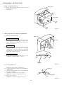
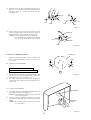
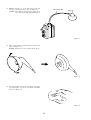
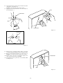
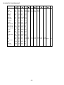
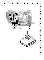
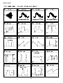
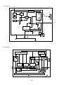
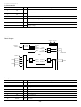
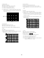
TV-SE2130
TV-SE1430
KY EZY
KY EZY
SERVICE MANUAL
S/M Code No. 09-009-350-0N1
DA
TA
COLOR TELEVISION
NOTICES BEFORE REPAIRING
To make the best use of this equipment, make sure to
obey the following items when repairing (or mending).
1. Do not damage or melt the tunicate of the leading
wire on the AC1 side, including the power supply
cord.
2. Do not soil or stain the letters on the spec.
inscription plates, notice labels, fuse labels, etc.
3. When repairing the part extracted from the
conducted side of the board pattern, fix it firmly
with applying bond to the pattern and the part.
4. Restore the following items after repairing.
1) Conditions of soldering of the wires (especially,
the distance on the AC1 side).
2) Conditions of wiring, bundling of wires, etc.
3) Types of the wries.
4) Attachment conditions of all types of the insulation.
5. After repairing, always measure the insulation
resistance and perform the voltage-withstand test
(See Fig-1).
1) The insulation resistance must be 7.3 MΩ to 10.1 MΩ
when applying 500V per second.
2) In the voltage withstand test, apply 3.0 kV for 1
minute and check that the GO lamp lights.
*
*
*
*
Insulation resistance: 7.3MΩ to 10.1 MΩ (500 V/s)
Voltage-withstand: 3.0 kV for 1 minute
Safety checker (Model 7110, etc.)
Earth cable
AC cable
Connect the earth cable
to the outside metal part
terminal.
Fig-1
Breaking current set to 10 mA.
Connect the safety checker as shown in Fig-1,
then measure the resistance and perform the test.
Do not touch the equipment during testing.
For details of the safety checker, refer to the supplied
Operation manual.
When servicing and checking on the TV, note the followings.
1. Keep the notices
As for the places which need special attentions, they
are indicated with the labels or seals on the cabinet,
chassis and parts. Make sure to keep the indications
and notices in the operation manual.
2. Avoid an electric shock.
There is a high voltage part inside. Avoid an electric
shock while the electric current is flowing.
3. Use the designated parts.
The parts in this equipment have the specific
characters of incombustibility and withstand voltage
for safety.
Therefore, the part which is replaced should be used
the part which has the same character. Especially as
to the important parts for safety which is indicated in
the circuit diagram or the table of parts as a ! mark,
the designated parts must be used.
4. Put parts and wires in the original position after
assembling or wiring.
There are parts which use the insulation material
such as a tube or tape for safety, or which are
assembled so that these parts do not contact with
the printed board. The inside wiring is designed not
to get closer to the pyrogenic parts and high voltage
parts. Therefore, put these parts in the original
positions.
5. Take care of the cathode-ray tube.
By setting an explosion-proof cathode-ray tube is set
in this equipment, safety is secured against
implosion.
However, when removing it or serving from
backward, it is dangerous to give a shock. Take
enough care to deal with it.
6. Avoid an X-ray.
Safety is secured against an X-ray by considering
about the cathode-ray tube and the high voltage
peripheral circuit, etc. Therefore, when repairing the
high voltage peripheral circuit, use the designated
parts and do not change the circuit. Repairing
except indicates causes rising of high voltage, and
the cathode-ray tube emits an X-ray.
7. Perform a safety check after servicing.
Confirm that the screws, parts and wiring which were
removed in order to service are put in the original
positions, or whether there are the portions which are
deteriorated around the places serviced.
! Safety Components Symbol
This symbol is given to important parts which serve to maintain the safety of the product, and which
are made to confirm to special Safety Specifications.
Therefore, when replacing a component with this symbol make absolutely sure that you use a
designated part.
-2-
SPECIFICATIONS
Tuner system
Picture tube
TV system
Channel coverage
Antenna input
Video input
Video output
Audio input
Audio output
Operating temperature
Power requirements
Power consumption
Standby
Dimensions
Weight
Frequency synthesized tuner
TV-SE2130: 21 in.(50.8 cm “V”), 90 degree deflection
TV-SE1430: 14 in.(34 cm “V”), 90 degree deflection
PAL (B/G, D/K, I), SECAM (D/K, L)
VHF: E2-E12
UHF: E21-E69
CABLE: S1-S41
75 ohms, unbalanced
1.0 Vp-p, 75 ohms, unbalanced
1.0 Vp-p, 75 ohms, unbalanced
-3.8 dBs, 50 kohms
-3.8 dBs less than 1 kohm
5°C to 40°C
220-240 V AC, 50 Hz
TV-SE2130: 74 watts
TV-SE1430: 60 watts
TV-SE2130: 3 watts
TV-SE1430: 3 watts
TV-SE2130: 610(W) x 448(H) x 485(D) mm
(241/8 x 173/4 x 191/8 in.)
TV-SE1430: 450(W) x 332(H) x 377(D) mm
(173/4 x 131/8 x 147/8 in.)
TV-SE2130: Approx. 22 kg (48.4 lbs.)
TV-SE1430: Approx. 11.5 kg (25.3 lbs.)
• Design and specifications are subject to change without notice.
ACCESSORIES LIST
REF. NO
1
1
2
2
PART NO.
KANRI
NO.
8A-JB4-901-010
8A-JB4-903-010
8A-JB4-610-010
8A-JB4-610-010
DESCRIPTION
IB,K (E) -SE2130/ 1430<14KY,21KY>
IB,EZ (EGDSI) -SE2130/ 1430<14EZY,21EZY>
RC UNIT,RC-AVT02<14KY,14EZY>
RC UNIT,RC-AVT02<21KY,21EZY>
-3-
DISASSEMBLY INSTRUCTIONS
1. REAR CABINET REMOVAL
(1)
Front cabinet
Remove eight screws 1, then remove the rear cabinet in
the direction of the arrow.
(See Figure1-1)
Rear cabinet
Figure 1-1
2. HIGH-VOLTAGE CAP (ANODE CAP) REMOVAL
2-1. Cautions before Removing
Anode cap
Discharge the anode voltage
(1)
The anode voltage is not discharged completely from the
CRT of this unit even after the power is turned off. Be
sure to discharge the residual anode voltage before
removing the anode cap.
CRT GND
Do not use pliers
(2)
Do not use pliers, etc. to remove the anode cap. If you
used pliers and bent the hook to remove the cap, the spring
characteristics of the hook could be lost, and when
reinstalled, the cap would come off from the CRT anode
button easily, causing an accident.
(3)
If the anode cap is turned in the direction of its
circumference, the hook is likely to come off.
Do not turn the anode cap
Grip
CRT
Hook
CRT GND
Figure 2-1
2-2. Anode Cap Removal
(1)
(2)
(3)
(4)
Discharge the anode voltage. (See Figure 2-1)
Connect a flat-bladed screwdriver to the CRT GND via
an alligator clip.
Use a tester to check the end of the screwdriver and ground
of the TV for continuity.
Touch the hook with the end of the screwdriver.
Caution : Be careful not to damage the anode cap.
Turn over the anode cap.
Caution : Be careful not to damage the anode cap.
Anode cap
CRT
Anode button
Hook
Figure 2-2
-4-
(5)
Push the anode cap with your thumb in the direction of
arrow 1 as shown in the figure, then lift the cap in the
direction of arrow 2 to release the hook on one side.
(See Figure 2-3)
Anode cap
CRT
CRT
Hook
Hook
Figure 2-3
(6)
Turn over the anode cap on the side where the hook was
released and pull out the cap in the direction opposite to
that on which the cap was pushed. (See Figure 2-4)
Caution : Do not pull out the anode cap straight up.
: Do not pull the cap forcibly. After removing
the cap, check that the hook is not deformed.
Anode cap
CRT
Anode button
Hook
Figure 2-4
3. ANODE CAP REINSTALLTION
Anode cap
Observe the cautions carefully so that no accident occurs
due to a defect in installing the anode cap and so it does
not come off.
Left
Right
3-1. Caution before Reinstalling
Never turn the anode cap after installing it
Never re-use the hook when it has been deformed
(1)
(2)
If the anode cap is turned after it is installed, it may come
off. Therefore, arrange the high-voltage cable before
attaching the anode cap. (See Figure 3-1)
If you have attached the anode cap before arranging the
high-voltage cable, arrange the cable carefully so the cap
does not turn.
Figure 3-1
3-2. Anode cap reinstallation
(1)
(2)
Anode button
Use a clean cloth moistened slightly with alcohol to clean
the installation section. (See Figure 3-2)
Caution : Check that the installation section is free from
dust, foreign matter, etc.
Coat the anode cap installation circumference with an
appropriate amount of the specified silicone grease (KS650N).
Caution : Be careful that silicone grease does not enter
the anode button.
Installation
section
-5-
Figure 3-2
(3)
Eliminate twisting, etc. of the high-voltage cable and
arrange it so that no twisting occurs. (See Figure 3-3)
Caution : If the cable is not arranged correctly, the anode
cap could turn and cause an installation defect.
High-voltage cable
Anode cap
Figure 3-3
(4)
Turn over the rubber cap symmetrically on the left and
right. (See Figure 3-4)
Caution : Take great care not to damage the anode cap.
Figure 3-4
(5)
Fit your forefinger over the projection at the center of the
cap and hold the cap between your thumb and middle
finger. (See Figure 3-5)
Figure 3-5
-6-
(6)
(7)
Apply the hook on one side to the anode button as shown
on the figure. (See Figure 3-6)
Caution : Check that the hook is held securely.
Apply the hook on the other side to the anode button as
shown in Figure 3-7.
Hook
Anode button
Hook
Anode button
30°
Figure 3-6
Anode button
Hook
Figure 3-7
(8)
Pull the anode cap slightly with the rubber cap turned
over and visually check that the hook is engaged securely.
(9) Release your hand from the rubber cap of the anode cap.
Caution : Cover the anode cap so that it does not lift.
(10) Hold the skirt of the andoe cap slightly to improve the
close contact between the cap and CRT.
(11) Check that the anode cap is in close contact with the CRT.
(See Figure 3-8)
Anode button
Skirt
Figure 3-8
-7-
4. NECK C.B. REMOVAL
Front Cabinet
(1) Disconnect P903 (CRT GND).
(2) Remove the NECK C.B. in the direction of arrow 1
(See Figure 4-1).
5. MAIN C.B REMOVAL
(1) Remove connector (P601).
(2) Remove connector (P801).
(3) Remove connector (P802).
(4) Remove connector (P402).
(5) Pull out the MAIN C.B. in the direction of the arrow 2
(See Figure 4-1).
NECK C.B
P903
P402
MAIN C.B
P601
(Speakers)
P801
(Power cord)
P802
(Degauss cord)
Figure 4-1
-8-
ELECTRICAL MAIN PARTS LIST
REF. NO
PART NO.
KANRI
NO.
DESCRIPTION
REF. NO
IC
!
S1-TDA-835-7J0
S1-TDA-936-7LW
S1-MSP-341-5D0
S1-TDA-894-4J0
SI-AL2-416-00B
IC,TDA8357J
IC,TDA9367LW
IC,MSP-3415D
IC,TDA8944J
IC,AT24C08-10PC
S1-TSO-P12-38W
87-A20-969-010
87-A91-033-010
SU-PC5-74J-000
S0-0SE-110-NS0
IC,TSOP1238WI1
IC,STR-F6653
IC,LTV-817C
IC,UPC574J
IC,SE110N
ST-X02-02D-A00
S1-KA7-805-000
S1-KA7-808-000
S1-LE3-3CZ-000
S1-TDA-610-7Q0
THYRISTOR X0202DA
IC,KA7805
IC,KA7808
IC,LE33CZ
IC,TDA6107Q
87-A30-492-080
ST-R32-020-9AA
87-A30-050-010
87-A30-114-080
ST-R33-300-9DB
TR,2SC5343Y
TR,KTC3202Y
TR,2SD2499
TR,2SD1207-T
TR,STA933-Y
TRANSISTOR
DIODE
SD-BAT-850-000
SD-1SS-85T-A00
SD-BYW-360-000
SD-TZX-12C-000
SD-TZX-22C-000
DIODE,BAT85
DIODE,1SS85TA
DIODE,BYW36
ZENER,TZX12C
ZENER,TZX22C
SD-UZ3-3B0-000
SD-BY2-280-000
87-A40-246-080
SD-TZX-2V4-A00
SD-TZX-5V1-B00
ZENER,UZ-33B
DIODE,BY228
DIODE,1N4148
ZENER,TZX2V4A
ZENER,TZX5V1B
SD-BYT-51J-000
SD-TZX-5V6-B00
SD-BYW-760-000
SD-TZX-9V1-B00
SD-BAV-210-000
DIODE,BYT51J
ZENER,TZX5V6B
DIODE,BYW76
ZENER,TZX9V1B
DIODE,BAV21
C101
C102
C106
C121
C305
87-010-405-040
87-010-408-040
87-010-409-090
87-010-405-040
87-016-584-080
CAP,E
CAP,E
CAP,E
CAP,E
CAP,E
10MF-50V
47MF-50V
220MF-50V
10MF-50V
220MF-25V
C315
C401
C404
C408
C408
87-016-647-010
87-010-408-040
SC-MYT-3C7-52J
SC-MYT-2D3-04J
SC-MYE-2D2-74J
CAP,E
CAP,E
CAP,M
CAP,M
CAP,M
47MF-160V
47MF-50V
7500PF-1.6KV
0.3MF-250V<14KY,14EZY>
0.27MF-200V<21KY,21EZY>
C412
C415
C417
C420
C500
S0-E7T-B3R-3M0
87-016-217-080
SC-MXL-2E1-04K
87-A10-469-080
87-015-694-080
CAP,E 3.3MF-160V
CAP,E 4.7MF-250V
CAP,M 0.1MF-250V
CAP,CER 2200PF-500V
CAP,E 0.47MF-50V
C501
C509
C514
C517
C519
87-010-405-040
87-A10-216-080
87-010-247-040
87-015-695-010
87-015-695-010
CAP,E
CAP,E
CAP,E
CAP,E
CAP,E
10MF-50V
47MF-25V
100MF-25V
1MF-50V
1MF-50V
C522
C528
C530
C532
C540
87-015-698-080
87-010-247-040
87-010-247-040
87-010-405-040
87-A12-092-080
CAP,E
CAP,E
CAP,E
CAP,E
CAP,E
4.7MF-50V
100MF-25V
100MF-25V
10MF-50V
22MF-50V
MAIN C.B
-9-
PART NO.
C541
C542
C543
C550
C555
KANRI
NO.
87-A12-092-080
CAP,E
87-010-405-040
CAP,E
87-010-405-040
CAP,E
87-010-615-080
CAP,E
87-010-553-080
CAP,E
DESCRIPTION
22MF-50V
10MF-50V
10MF-50V
2.2MF-50V
47MF-16V
C561
C564
C580
C593
C602
87-010-247-040
87-010-247-040
87-010-405-040
87-010-247-040
87-010-405-040
CAP,E
CAP,E
CAP,E
CAP,E
CAP,E
100MF-25V
100MF-25V
10MF-50V
100MF-25V
10MF-50V
C604
C605
C608
C610
C611
87-A10-493-080
87-A10-216-080
87-010-405-040
87-010-405-040
87-015-697-080
CAP,E
CAP,E
CAP,E
CAP,E
CAP,E
1000MF-25V
47MF-25V
10MF-50V
10MF-50V
3.3MF-50V
C612
C613
C614
C615
C616
87-015-695-010
87-015-695-010
87-015-695-010
87-015-695-010
87-010-405-040
CAP,E
CAP,E
CAP,E
CAP,E
CAP,E
1MF-50V
1MF-50V
1MF-50V
1MF-50V
10MF-50V
C625
C626
C630
C636
C660
87-015-698-080
87-015-698-080
87-A10-216-080
87-010-408-040
87-010-405-040
CAP,E
CAP,E
CAP,E
CAP,E
CAP,E
4.7MF-50V
4.7MF-50V
47MF-25V
47MF-50V
10MF-50V
C690
C691
C770
!C801
C803
87-015-698-080
87-015-698-080
87-010-247-040
SC-L1S-C34-74M
SC-CXF-3A4-72Z
CAP,E 4.7MF-50V
CAP,E 4.7MF-50V
CAP,E 100MF-25V
CAP,LINE ACROSS 0.47MF-275V
CAP,CER 4700PF-1KV
C804
C805
C806
C808
C810
SC-CXF-3A4-72Z
SC-EYN-2G1-21P
87-010-407-040
87-015-698-080
87-012-397-090
CAP,CER 4700PF-1KV
CAP,E 120MF-400V
CAP,E 33MF-50V
CAP,E 4.7MF-50V
CAP,CER 1000PF-2KV
!C812
C813
C814
C820
C823
87-A10-519-010
87-016-648-090
87-016-648-090
SC-CYR-3A4-71K
87-A10-493-080
CAP,CER 4700PF-4KV
CAP,E 100MF-160V
CAP,E 100MF-160V
CAP,CER 470PF-1KV
CAP,E 1000MF-25V
C824
C831
C832
C835
C840
SC-CYR-3A4-71K
SC-CYR-3A4-71K
87-A10-493-080
87-010-408-040
87-010-285-010
CAP,CER 470PF-1KV
CAP,CER 470PF-1KV
CAP,E 1000MF-25V
CAP,E 47MF-50V
CAP,E 2200MF-16V
C841
C844
C861
C863
C866
87-010-285-010
87-010-247-040
87-A10-493-080
87-010-247-040
SC-CYR-3A4-71K
CAP,E 2200MF-16V
CAP,E 100MF-25V
CAP,E 1000MF-25V
CAP,E 100MF-25V
CAP,CER 470PF-1KV
C888
D707
!F801
HP01
JPA01
87-010-553-080
SD-SML-121-6W0
S5-FSC-B40-22R
S4-859-102-130
S4-859-200-401
CAP,E 47MF-16V
LED,SML1216W
FUSE CERA 250V
JACK EARPHONE
SOCKET RGB
JPA02
JPA03
L101
L350
L380
S4-859-200-401
S4-859-108-450
S5-CPZ-100-K02
S5-CPZ-109-M04
S5-CPZ-109-M04
SOCKET RGB
JACK PIN BOARD
COIL PEAKING 10UH 3.5MM
COIL PEAKING 1UH 10.5MM
COIL PEAKING 1UH 10.5MM
L401
L401
L500
L501
L502
S5-8H0-000-016
S5-8H0-000-040
S5-CPZ-120-K02
S5-CPZ-100-K02
S5-CPZ-100-K02
COIL
COIL
COIL
COIL
COIL
H-LINEARITY L-102<14KY,14EZY>
H-LINEARITY TRL-341G<21KY,21EZY>
PEAKING 12UH 3.5MM
PEAKING 10UH 3.5MM
PEAKING 10UH 3.5MM
L510
L511
L512
L601
L602
S5-CPZ-100-K02
S5-CPZ-100-K02
S5-CPZ-100-K02
S5-CPZ-479-K02
S5-CPZ-479-K02
COIL
COIL
COIL
COIL
COIL
PEAKING
PEAKING
PEAKING
PEAKING
PEAKING
10UH 3.5MM
10UH 3.5MM
10UH 3.5MM
4.7UH 3.5MM
4.7UH 3.5MM
REF. NO
L603
L650
L801
L802
L803
PART NO.
KANRI
NO.
S5-CPZ-479-K02
COIL
S5-MC0-000-100
COIL
S5-MC0-000-100
COIL
S5-8C9-430-599
COIL
S5-MC0-000-100
COIL
DESCRIPTION
REF. NO
PEAKING 4.7UH 3.5MM
BEAD MD-5
BEAD MD-5
CHOKE(94MH)
BEAD MD-5
PART NO.
KANRI
NO.
DESCRIPTION
SW702
SW703
SW704
!SW801
T401
S5-S50-101-090
S5-S50-101-090
S5-S50-101-090
S5-S40-101-143
S5-0D1-0A2-000
SW TACT SKHV17910A
SW TACT SKHV17910A
SW TACT SKHV17910A
SW PUSH PS3-22SP
TRANS DRIVE TD-10A2
!T402
!T801
U100
X502
X601
S5-0H0-000-204
S5-0M3-934-A20
S4-859-719-930
S5-XE1-2R0-00E
S5-XE1-8R4-32E
FBT 1142.5106
TRANS SMPS 2084.0046
TUNER VARACTOR DT5-BF18D
X’TAL12.00000MHZ
X’TAL,18.43200MHZ
!LF801
P401
P402
P501
P501
S5-PLF-24A-100
S4-850-705-N18
S4-859-240-020
S4-850-705-N16
S4-850-705-N14
FILTER LINE LF-24A1
CONN AS BIC-05T-25T
CONN WAFER YFW500-05
CONNECTOR BIC-05T-25T<14KY,14EZY>
CONNECTOR BIC-05T-25T<21KY,21EZY>
P601
P801
P802
R305
R350
S4-859-231-720
S4-859-287-320
S4-859-242-220
SR-S02-Y33-1JS
87-025-601-080
CONN WAFER YW025-04
CONN WAFER MKS2822
CONN WAFER YFW800-02
RES,M-OXIDE 330-2W
RES,METAL 3.0K-1/4<14KY,14EZY>
Z501
Z601
Z602
Z603
Z604
S5-PXP-S5R-5MB
S5-PXF-1B4-71M
S5-PXF-1B4-71M
S5-PXF-1B4-71M
S5-PXF-1B4-71M
FILTER
FILTER
FILTER
FILTER
FILTER
CERA TPS5.5MB-TF21
EMI 470PF
EMI 470PF
EMI 470PF
EMI 470PF
R350
R351
R351
R415
R450
S4-25T-415-2F0
87-025-601-080
S4-25T-415-2F0
S3-U18-A10-2J0
S3-X18-A10-3J0
RES,R METAL 1.5K-1/4<21KY,21EZY>
RES,METAL 3.0K-1/4<14KY,14EZY>
RES,R METAL 1.5K-1/4<21KY,21EZY>
RES,M-OXIDE 1K-2W
RES,M-OXIDE 10K-2W
Z605
Z606
Z607
Z608
Z609
S5-PXF-1B4-71M
S5-PXF-1B4-71M
S5-PXF-1B4-71M
S5-PXF-1B4-71M
S5-PXF-1B4-71M
FILTER
FILTER
FILTER
FILTER
FILTER
EMI
EMI
EMI
EMI
EMI
R597
R598
R801
R802
R803
87-025-459-080
87-025-459-080
SD-T12-0B8-010
SR-S02-Y75-3JS
87-015-515-090
RES,METAL 15K-1/4
RES,METAL 15K-1/4
POSISTOR T120-B80-A110
RES,M-OXIDE 75K-2W
RES,M-OXIDE 47K-2W
Z610
ZZ100
S5-PXF-1B4-71M
S4-8B4-544-A01
FILTER EMI 470PF
TRANSMITTER REMOCON RC-AVT02
R804
R808
!R819
R920
R920
SR-F02-Y33-8K0
SR-S02-Y82-1JS
SR-X10-B33-9JN
87-A00-767-090
87-029-131-010
RES,FUSE 0.33-2W
RES,M-OXIDE 820-2W
RES,CEM 3.3-10W
RES,FUSE 1.2-1W<14KY,14EZY>
RES,FUSIBLE 1-1W<21KY,21EZY>
C905
C965
C968
P903
SCT1
87-016-217-080
87-012-397-090
SC-MXL-2E1-04K
S4-859-262-120
S4-859-303-430
CAP,E 4.7MF-250V
CAP,CER 1000PF-2KV
CAP,M 0.1MF-250V
CONN WAFER YFW 800-01
SOCKET CRT PCS633A<14KY,14EZY>
SF1
SF2
SP1A
SW700
SW701
S5-PK3-953-M00
S5-PK9-650-M00
S4-850-704-S31
S5-S50-101-090
S5-S50-101-090
FILTER SAW K3953M
FILTER SAW K9650M
CONN AS CP-385
SW TACT SKHV17910A
SW TACT SKHV17910A
SCT1
S4-859-303-530
SOCKET CRT PCS629-03C<21KY,21EZY>
470PF
470PF
470PF
470PF
470PF
NECK C.B
TRANSISTOR ILLUSTRATIONS
ECB
BEC
ECB
2SC5343
STA933
2SD1207
KTC3202
-10-
BCE
2SD2499
BLOCK DIAGRAM -1
U101
TUNER
RF INPUT
IF
JPA03
AVJACK
PIF
SF01
JPA02
SCARTJACK
JPA01
SCARTJACK
EXT R,G,B
S/SW
SIF
SF02
SDA
SCL
5V 33V
F/BLK
KEY-IN
SW700~704
LED
LED
D707.
S/B3.3V
SCART OUT
POWER
SECAM.L'/SW
TUNER AGC
FM-IN
SCL
SDA
RESET
A.MUTE
IF IN
SCL
SIF IN
SDA
SOUND
TRAP
VISION IF
ALIGNMENT-FREE
PLL DEMOD.
AGC/AFC
VIDEO AMP
CVBS
QSS SOUND IF
AGC
QSS MIXER
AM DEMODULATOR
I2C BUS
TRANSRECEIVER
VST PWM-DAC
I/O PORTS
ENHANCED
80C51 CPU
I702
EEPROM
10PAGE
MEMORY
5V
RC-IN
I703
PRE AMP
V
C.IN
VIDEO SWITCH
VIDEO IDENT.
VIDEO FILTERS
LUMA DELAY
PEAKING
BLACK STRETCH
REF
ROM/RAM
TELETEXT
ACQUISITION
CVBS
H
TELETEXT/OSD
DISPLAY
S/B 6V
CVBS/Y
HP01
JACK PHONE
SYNC
COR R
G
B
BL
REF
R
PAL/SECAM/NTSC
DECODER
SCART OUT
I601
SOUND
DECODER
B
RK
I901
VIDEO AMP
GK
BK
IBLK
FM-IN
SCL
SDA
5V
L R
R
I602
AUDIO
AMP
ABL
B
G
VERT.
H
L
12.5V
G
CONT./BRIGHT
OSD/TEXT INSERT
CCC
WHITE-P.ADJ.
BASE-BAND
DELAY LINE
H-DRIVE
2nd LOOP
H-SHIFT
H/V SYNC SEP.
H-OSC.+ PLL
R
V
V-DRIVE +
GEOMETRY
RGB/YUV INSERT
RGB/YUV MATRIX
SATURATION
YUV/RGB MATRIX
EW GEOMETRY
HOR.
A.MUTE
R
I501
MCU/VIDEO PROCESSOR
G
B
BL
H-DRIVE
SCP
SCREEN
5V
8V
S/B 3.3V
I806, I820, I822, I823
VOLTAGE
REGULATOR
T401
DRIVE TRANS
Q401
HORIZONTAL
OUTPUT
H.P.
D/G
F801
4A 250V
T402
FBT
LF801
V-DRIVE
12.5V
11V
I801
SWITCHING
REG.
8.5V
I301
VERTICAL
AMP
S/B 6V
H.V.
EWD
POWER
ABL
-11-
FOCUS
SCHEMATIC DIAGRAM MAP
LINE NAME
Connect MAP Connect MAP Connect MAP Connect MAP Connect MAP Connect MAP
SCL
I601
27-B I501
26-N U100
21-U I702
22-D
SDA
I601
27-C I501
25-N U100
21-T
22-D
S/B 3.3V
I823
27-N R720
19-B R888
20-Q R580
S/B 6V
I823
27-P R713
19-A
FM-IN
I601
31-F I501
15-J
RC-IN
I501
26-J
16-C
KEY-IN
I501
23-N SW700 16-C
SECAM L
I501
25-N Q103
14-N
POWER
I501
26-J
R817
20-Q
S/SW
I501
23-N DA01
17-G
EXT 1(A-L/R)
I601
27-F JPA01 15-F
I703
I702
14-L
EXT 2(A-L/R)
I601
26-E JPA02/03 12-L
EXT 1(V-IN)
R551
20-F JPA01 10-I
EXT 2(V-IN)
R554
15-F JPA02 11-L
C. IN
I501
18-J
JPA02 11-K
CVBS
I501
17-I
R524
ABL
R585
14-H T402
SCART OUT
I601
22-F JPA01 12-F
11V
C823
24-P R404
5V
I820
25-O R120
20-O L101
19-S L603
24-B 1702
22-E
8V
I822
22-P L501
22-N R117
17-O L502
12-I
26-F R543
110V-123V
T801
20-R T402
11-T
HV
T402
8-P
V901
8-D
FOCUS
T402
8-Q
V901
8-D
SCREEN
T402
8-R
V901
8-E
14-J
8-R
16-P
-12-
L602
16-D
SCHEMATIC DIAGRAM - 1 (MAIN C.B)
32
31
30
29
28
27
26
25
24
23
22
21
20
19
18
17
16
15
14
13
12
11
10
9
8
7
6
5
4
3
2
1
A
B
C
D
E
F
G
H
THE DIFFERENT PARTS FOR CRT
Ref. No.
V901
SCT1
C408
L401
R302
R350
R351
R556
R823
R920
LW
TV-SE2130
A51EBV13X081
PCS629-03C
0.27/200V
TRL-341G
1.5 1/2W
1.5k
1.5k
6.8k
5.1k
1 1W
TV-SE1430
A34JLL90X01
PCS633A
0.3/250V
L-102
3.9 1/2W
3k
3k
8.2k
3.9k
1.2 1W
I
J
K
L
M
N
O
P
Q
R
S
T
U
-13-
WIRING - 1 (MAIN C.B)
31
30
29
28
27
26
MAIN C. B
25
24
23
22
21
V
L
20
19
18
17
16
15
14
13
12
11
10
9
8
L
AV2
POWER
R
REMOCON
SENSOR
EAR.
TV/AV
MENU
7
6
5
4
3
2
1
R
A
P
SP01
(SPEAKER)
SP02
(SPEAKER)
B
220-240 V AC
50 Hz
BLN
RED
BLK
WHT
C
D
To
NECK C.B
P501A
To MAIN P601
E
BLK
BLK
BLK
BLK
BLU
BLU
BRN
P501
F
P801
G
DEGAUSSING
COIL
R548
R544
R546
P802
R540
R549
H
R522
C527
R521
I
J
R524
K
I823
L
R715
M
N
O
DY UNIT
P402
P
IF
R101
Q
R
S
T
U
To
NECK C.B
BLK
GRY
RED
To V901 (CTR)
ANODE
BLK
BLK
BLK
BLK
BLU
32
AV2
To
NECK C.B
P401A
AV1
ANT
-14-
WIRING - 2 (NECK C.B)
13
12
11
10
9
8
7
6
5
4
3
2
1
A
B
C
NECK C. B
GRY
To MAIN C.B
T402(FBT)
D
9
E
I901
14
F
G
BLU
BLK
BLK
BLK
H
BLK
BLK
To MAIN C.B
T402(FBT)
BLU
BLK
BLK
BLK
BLK
15
To MAIN C.B
P501
I
J
To MAIN C.B
P401
To
V901(CRT)
GND
K
L
M
V901(CRT)
N
O
P
Q
R
S
T
U
-15-
WAVEFORMS
-16-
IC BLOCK DIAGRAMS
IC, TDA8357J
IC, TDA8944J
-17-
IC, STR-F6653
Drain
3
V IN
4
DRV. RE=8.6V
Start
O.V.P.
Rg2
Rg1
DRV
Latch
Reg
2 Source
T.S.D.
Vth1=0.73 – 0.05v
1 OCP/FB
OCP/FB comp.
1.35mA
OSC
Vth2=1.3 ~ 1.6v
Tth(min)=1 S
4700pF
INH comp.
T OFF=50 S typ.
Iconst Irm.
5
GND
IC, TDA6107Q
Vdd
6
MIRROR 5
MIRROR 1
CASCODE 1
3
MIRROR 1
7 Voc(1)
1
CURRENT
SOURCE
8 Voc(2)
9 Voc(3)
1
THERMAL
PROTECTION
CIRCUIT
Rf
VIP
REFERENCE
DIFFERENTIAL
STAGE
Vi(1) 1
5 lo(m)
MIRROR 3
Vi(2) 2
Rj
Ra
Vi(3) 3
3
CASCODE 2
MIRROR 2
4
GND
-18-
IC DESCRIPTIONS
IC, AT24C08-10PC
Pin No.
Pin Name
I/O
1
E0
–
2
E1
–
3
E2
–
4
VSS
–
5
SDA
I/O
6
SCL
–
7
WC
8
VCC
Description
Device address
Ground
Serial data/address input/output
Serial clock
Write control
–
Supply voltage
IC, MSP3415D
• Block Diagram
XTAL IN XTAL OUT
62
63
Audio PLL
SOUND IF
ANA IN1+ ?
Demodulator
& NICAM
Decoder
FM1/AM
FM2
NICAM A
NICAM B
IDENT
LOUDSPEAKER L
D/A
29 DACM L
LOUDSPEAKER R
D/A
28 DACM R
LOUDSPEAKER
DSP
MONO IN 55
SC1 IN L 52
SCART1
A/D
SCART L
SCART1 L
D/A
37 SC1 OUT L
A/D
SCART R
SCART1 R
D/A
36 SC1 OUT R
SCART
SC1 IN R 53
SC2 IN L 49
SCART2
SC2 IN R 50
SCART Switching Facilitles
• Description
Pin No.
Pin Name
I/O
Description
1
TP
O
Test pin
2, 3
NC
–
Not connceted
4, 5
TP
O
Test pin
6
ADR SEL
I
I2C bus address select
7
STANDBYQ
I
Standby (low-active)
8
NC
–
Not connceted
9
I2C CL
I/O
I2C clock
10
I2C DA
I/O
I2C data
-19-
Pin No.
Pin Name
I/O
Description
11, 12
TP
I/O
Test pin
13
TP
O
Test pin
14
NC
–
Not connceted
15 ~ 17
TP
O
Test pin
18
DVSUP
–
Digital power supply +5V
19
DVSS
–
Digital ground
20 ~ 23
NC
–
Not connceted
24
RESETQ
–
Power-on-reset
25, 26
NC
–
Not connceted
27
VREF2
–
Referecne ground 2 high voltage part
28
DACM R
O
Loudspeaker out right
29
DACM L
O
Loudspeaker out left
30
NC
–
Not connceted
31
TP
–
Test pin
32 ~ 34
NC
–
Not connceted
35
VREF1
–
Reference gound 1 high voltage part
36
SC1 OUT R
O
Scart output 1 in, right
37
SC1 OUT L
O
Scart output 1 in,left
38
NC
–
Not connceted
39
AHVSUP
–
Analog power supply 8.0 V
40
CAPL M
–
Volune capacitor MAIN
41
AHVSS
–
Analog ground
42
AGNDC
–
Analog reference voltage high voltage part
43 ~ 47
NC
–
Not connceted
48
ASG2
–
Analog shield ground 2
49
SC2 IN L
I
Scart input 2 in, left
50
SC2 IN R
I
Scart input 2 in, right
51
ASG1
–
Analog shield ground 1
52
SC1 IN L
I
Scart input 1 in, left
53
SC1 IN R
I
Scart input 1 in, right
54
VREFTOP
–
Reference voltage IF A/D converter
55
MONO IN
I
Mono input
56
AVSS
–
Analog ground
57
AVSUP
–
Analog power supply
58
ANA IN1+
I
IF input 1
59
ANA IN1-
I
IF common
60
NC
–
Not connected
61
TESTEN
I
Test pin
62
XTAL IN
I
Crystal oscillator
63
XTAL OUT
O
Crystal oscillator
64
NC
–
Test pin
-20-
IC, TDA9367
• Block Diagram
-21-
• Description
Pin No.
Pin Name
I/O
Description
1
NC
–
Port 1.3 Not used.
2
SCL
I
I2C bus clock line
3
SDA
I
I2C data line
4
SECAM L OUT
O
Port 2.0: high when L' selected (PushPull)
5
OCP
O
Port 3.0: over current protection
6
RF AGC IN
I
ADC1: for factory use only (high impedance)
7
KEY-IN
I
ADC2: local key input (high impedance)
8
S/SW
I
ADC3: scart slow switching input
9
VSS C/P
–
Digital ground for µ-contoller core and peripheral
10
LED1
O
Port 0.5 (8 mA current sinking capability)
11
LED2
O
Port 0.6 (8 mA current sinking capability)
12
VSSA
–
Analog ground of teletext decoder and digital ground of TV processor
13
SEC PLL
–
SECAM PLL decoupling
14
VP2
–
2nd supply voltage TV-processor
15
DECDIG
–
Decoupling digital supply of TV-processor
16
PH2LF
–
Phase-2 filter
17
PH1LF
–
Phase-1 filter
18
GND3
–
Ground 3 for TV-processor
19
DECBG
–
Bandgap decoupling
20
AVL/EWD
O
East/West drive output
21
VDRB
O
Vertical drive B output
22
VDRA
O
Vertical drive A output
23
IFIN1
I
IF input 1
24
IFIN2
I
IF input 2
25
IREF
I
Reference current input
26
VSC
–
Vertical sawtooth capacitor
27
TUNERAGC
O
Tuner AGC output
28
SIFIN1
I
SIF input 1
29
SIFIN2
I
SIF input 2
30
GND2
–
Ground 2 for TV processor
31
SIF AGC
–
AGC sound IF
32
REF0
–
Not used.
33
HOUT
O
Horzontal output
34
FBISO
I/O
35
OSS OUT
O
QSS intercarrier output
36
EHT0
–
EHT/overvoltage protection
37
PLLIF
–
IF PLL loop filter
38
IFVO
O
IF video output
39
VP1
–
Main supply voltage TV-processor
40
CVBSINT
I
Internal CVBS input
41
GND1
–
Ground 1 for TV-processor
Flyback input/sandcastle output
-22-
Pin No.
Pin Name
I/O
Description
42
CVBS/Y
I
External CVBS/Y input
43
CHROMA
I
Chrominance input (SVHS)
44
AMOUT
–
Not used.
45
INSSW2
I
2nd RGB onsertion input
46
R2IN
I
2nd R input
47
G2IN
I
2nd G input
48
B2IN
I
2nd B input
49
BCLIN
I
Beam current limiter input
50
BLKIN
O
Black current output
51
R0
O
RED output
52
G0
O
GREEN output
53
B0
O
BLUE output
54
VDDA
–
Analog supply of teletext decoder and digital supply of TV-Processore (3.3 V)
55
VPE
–
OTP programming supply
56
VDDC
–
Digital supply to core (3.3 V)
57
OSCGND
–
Oscillator ground supply
58
XTALIN
I
Crystal oscillator input
59
XTALOUT
O
Crystal oscillator output
60
RESET
–
Reset
61
VDDP
–
Digital supply to periphery (3.3 V)
62
AUDIO MUTE
O
Port 1.0: audio mute output (PushPull)
63
POWER
O
Port 1.1: power output (PushPull)
64
IR IN
I
Interrupt input 0: R/C infrared input
-23-
ADJUSTMENT
SET-UP FOR ADJUSTMENT
1. CRT ADJUSTMENT
1-1. Precautions
Because the video signal output from a pattern generator is used as
the adjustment signal input during adjustment, the video signal
output from the pattern generator must conform with the
specifications. Measure the output waveform across 75 Ω load.
Confirm that the synchronizing signal has an amplitude of about
0.3 V, the video signal portion has an amplitude of about 0.7 V and
the burst signal has an amplitude of about 0.3 V with flat envelope.
Confirm that ratio of the burst signal amplitude and the red signal
amplitude is 0.30 : 0.66. If the output signal does not conform with
the specifications, calibrate the pattern generator. (Refer to pattern
generator operation manual.)
Use the LEADER: LCG 404 for the pattern generator.
(1) Receive the white raster signal, and then perform aging for at
least 20 minutes.
(2) Demagnetize the area surronding the CRT with a degausser
before making adjustments.
(3) Set the picture quality for each mode to the factory setting.
(4) Position the front screen facing the east as much as possible.
1-2. Purpose
(1) Beam landing adjustment (purity magnet)
Set the left/right balance of beam landing. If there is a
discrepancy in this adjustment, a color irregularity will occur.
After completion of the landing adjustment, it is necessary to
perform convergence adjustment.
Approx. 0.7V
1 Vp-p White (Approx.
75%)
Burst signal
Before adjustment
Approx.
0.3V
Color
irregularity
Black
Red
Blue
Magenta
Cyan
Fig. 1-1
Green
75% white
Yellow
Approx. 0.3V
After adjustment
TV display
Color bar signal of a pattern generator
PRECAUTIONS BEFORE STARTING ADJUSTMENT
Satisfy the following setting conditions before starting adjustment.
• Allow warm-up of 20 minutes or longer. (Do not turn off during
warm-up.)
• Set all picture quality controls of users' setting to initial set-up,
unless otherwise specified.
• Picture quality reset
1. Select "Picture" on the screen menu and press enter button.
2. Select "Normal" and press enter button.
3. Select "Reset" and press enter button.
• Set the pattern generator’s output level to 1.0Vp-p (across 75Ω
load).
-24-
(3) Beam convergence adjustment (6-pole magnet)
With a 4-pole magnet align the G beam with the already aligned
R/B beam.
(2) Beam convergence adjustment (4-pole magnet)
Align the R beam with the B beam. The G beam does not
move with this adjustment.
(magenta)
(magenta)
B
R/B
R
G
(white)
R/B
G
G
RGB
Align the G beam with the R/B beam
Fig. 1-3
Align the R beam with the B beam
Fig. 1-2
(4) The composition of each magnet is as shown in Fig. 1-4.
In making adjustments, rotate the lock ring clockwise (looking
from the CRT’s back screen) and disengage.
Be careful not to loose the lock ring too much. If the magnet
assembly has become shifted during adjustments, secure it to
the position in Fig. 1-4.
DY lock screw
Purity 4-pole 6-pole Lock ring
Magnet assembly
lock screw
CRT
DY
Magnet assembly
Fig 1-4
-25-
NK C.B
1-3. Beam Landing Adjustment
(1) Receive the green raster signal from the pattern generator.
(2) Loosen the magnet lock screw, and shift the magnet assembly
backward (toward the neck).
(3) Loosen the DY lock screw, and shift the DY deflecting yoke
backward (toward the neck).
(4) After opening the two purity magnets to the same angle, adjust
the color width of the bands on both sides of the screen so that
they are equal. (refer to Fig. 1-5 (a)).
As there is occurrence of convergence distortion after
completing the landing adjustments, be sure to carry out
convergence adjustments.
If the color irregularities in the screen’s corner section are
not improved, correct them with the landing magnet. After
using the landing magnet, be sure to demagnetize the CRT
with degausser and verify that there is no occurrence of color
irregularity. (refer to Fig. 1-6)
Landing magnet: 81-JTI-710-010
(two-sided adhesive tape) : 80-XVI-218-010 Cushion
R=B
R
G
B
Fig 1-5 (a)
As shown in Fig. 1-5 (b), the purity magnet functions in
relation to the electron beam.
(5) Gradually shift the deflecting yoke toward the front (toward
the CRT funnel). Stop movement at the point when the screen
has become completely green.
S
N
N
S
NS
Landing magnet
Cushion
SN
Since the landing magnet is polarized,
check the screen’s improvement through
rotation, not only by position.
S
S
N
N
SS
Fig 1-6
NN
Fig 1-5 (b)
(6) Also, verify the respective monochromatics of red and blue.
(7) While looking at the screen, adjust the tilt of the deflecting
yoke and tighten the DY lock screw.
(8) Shift the magnet assembly to the front (toward the CRT funnel),
stop movement before the adjustment position and then tighten
the magnet lock screw.
At this time, be careful not to shift the position of the purity
magnet.
-26-
1-4. Beam Center Convergence Adjustment
1-5. The Surrounding Convergence Adjustment
Perform this adjustment after completion of adjustment 1-4.
Make adjustments on the convergence with 4-pole and 6-pole
magnets. Operate each magnet in relation to the electron beam as
shown in Figs. 1-7 and 1-8. When performing this adjustment, verify
whether there is distortion in the focus adjustment. If necessary,
carry out adjustments again.
(1) Shake the deflecting yoke up, down to the right and left, and
adjust any discrepancies in the screen’s surroundings.
(2) Insert wedges in three locations in the gap between the
deflecting yoke and the surface of the CRT funnel in order
to secure the deflecting yoke. (Refer to Fig. 1-9)
S
S
B
N
G
B
N
R
G
R
N
Wedge
N
S
S
Fig 1-7
Wedge
Wedge
In Fig. 1-7, two 4-pole magnets are stacked together so as to be of
the same polarity. Move the B and R beams to their respective
direction, by rotating the two 4-pole magnets together. By adjusting
the opening of the two magnets, it is possible to adjust the amount
of the beam’s movement.
Position of wedge
N
S
S
N
Fig. 1-9
S
B
G
R
N
B
G
R
S
N
N
S
S
N
Fig 1-8
In Fig. 1-8, the two 6-pole magnets are stacked together so as to be
of the same polarity. Move the B and R beams to their respective
direction, by rotating the two 6-pole magnets together. By adjusting
the opening of the two magnets, it is possible to adjust the amount
of the beam’s movement.
(1) Receive the dot pattern signal from the pattern generator.
(2) Pay attention to the center of the screen, and perform
adjustments with two 4-pole magnets so that the R beam and
B beam are perfectly aligned and become a magenta color.
(Refer to Fig. 1-2)
(3) In the same way, pay attention to the screen, and perform
adjustments with a 6-pole magnet so that the magenta beam
and G beam are aligned and become a white dot.
(Refer to Fig. 1-3)
(4) After adjustments are completed, secure all magnets with the
lock link. (Refer to Fig. 1-4)
-27-
2. ELECTRICAL ADJUSTMENT
1. Use the numeric keys on the remote control to set the receiving channel to Pr91.
2. Set Sharpness on the Picture Menu screen to 0.
3. Press the buttons on remote control in the following order:
Skip (R) → Move (G) → Menu
The following menu will appear on the TV screen (the menu can be switched by the "P ^/v" button on the remote control):
1
SERVICE
**AGC
SERVICE
**WP Green
SERVICE
**H Shift
SERVICE
**V Shift
SERVICE
**Black R
SERVICE
**WP Blue
SERVICE
**V Slope
SERVICE
**H Width
SERVICE
**Black G
SERVICE
**H Parall
SERVICE
**V Amp
SERVICE
**EW Parabo
SERVICE
**WP Red
SERVICE
**H Bow
SERVICE
**V S Cor
SERVICE
**Up Corner
SERVICE
**Dw Corner
1
1
SERVICE
**EW Tapez
1
1
1
SERVICE
**Option
1
1
4. To terminate the menu screen, press the MENU button on the remote control, or the power button on the TV or remote control.
It is not necessary to adjust the above items marked
1.
-28-
5. G2 Alignment (SCREEN)
Input signal: Black signal
Adjustment point: SFR located at lower part of FBT (T402)
Measuring instrument: Pattern generator/PAL
Test point: R cathode (NECK C.B)
5-1. Set the TV to the "Normal I" mode.
5-2. Set the Black R and Black G data values on the menu screen
to 8.
5-3. Set the WP Red, WP Green and WP Blue data values on the
menu screen to 32.
5-4. Connect an oscilloscope to the test point.
5-5. Adjust the lower SFR of FBT (T402) so that the voltage at
the test point is 125 ± 5 V.
6-9. Lower the value until blue disappears.
6-10. Perform steps 2-1 _ 2-9 several times so that the picture is
seen more white.
7. Focus
Input signal: Dot pattern
Adjustment point: SFR located at upper part of FBT (T402)
Measuring instrument: Pattern generator/PAL
Adjust SFR which B located at upper part of FBT (T402) in
order to get the best focus for the dot.
8. Horizontal Center
Input signal: Crosshatch
Measuring instrument: Pattern generator/PAL
8-1. Set the TV to the "Normal I" mode.
8-2. Choose H. Shift from the menu screen.
8-3. Adjust the "Vol +/-" buttons on the remote control so that
the dot mark at the center of crosshatch is positioned at the
center of screen, and the number of squares on the left and
right is the equal.
6. White Balance
* Perform aging before adjustment for at least 20 minutes.
* Perform all adjustment steps several times.
Set the TV to the "Normal I" mode when performing adjustment
steps 6-1 _ 6-10.
Cutoff Adjustment:
Input signal: Stairstep (chroma OFF)
Measuring instrument: Pattern generator/PAL
6-1. Supply a stairstep signal from the pattern generator.
6-2. Use the "Vol +/-" buttons on the remote control to adjust the
Black R and Black G values on the menu screen so that the
color of scales A is gray.
A
Center
Fig.8-1
A
Fig. 6-1
Drive Adjustment:
Input signal: White raster
Measuring instrument: Pattern generator/PAL
6-3. Supply white raster from the pattern generator.
6-4. Use the Vol +/- buttons on the remote control to set the
WP Red value to 63 so that the picture is reddish.
6-5. Lower the value until red disappears.
6-6. Use the Vol +/- buttons on the remote control to set the
WP Green value to 63 so that the picture is greenish.
6-7. Lower the value until green disappears.
6-8. Use the Vol +/- buttons on the remote control to set the
WP Blue value to 63 so that the picture is bluish.
-29-
B
9. Vertical Center
Input signal: Crosshatch
Measuring instrument: Pattern generator/PAL
9-1. Set the TV to the "Normal I" mode.
9-2. Choose V. Shift from the menu screen.
9-3. Adjust the "Vol +/-" buttons on the remote control so that
the dot mark at the center of crosshatch is positioned at the
vertical center of screen.
10-2. S-Correction
1) Choose V. S Cor from the menu screen.
2) Perform adjustment in the same way as with 6-1 Slope.
* Repeat adjustments 10-1 and 10-2 so that A=B=C is available.
10-3. Amp
1) Choose V. Amp from the menu screen.
2) Adjust the "Vol +/-" buttons on the remote control so that the
dot mark at the center of crosshatch is positioned at the vertical center of screen, the circle is a perfect circle, and each
crosshatch is square.
* If vertical center is not correct, perform adjustment in 5. Vertical Center again.
CRT center
mark
Fig.9-1
A
10. Vertical Size
Input signal: Crosshatch (with circle)
Measuring instrument: Pattern generator/PAL
Set the TV to the "Normal I" mode for adjustment items 10-1
_ 10-3.
10-1. Slope
1) Choose V. Slope from the menu screen.
2) Adjust the "Vol +/-" buttons on the remote control so that the
vertical length of each square is equal (A=B=C).
Fig.10-2
11. AGC
Input signal: Color bar (ANT RF=Input)
Measuring instrument: Pattern generator/PAL
Test point: 1501 6 pin RF AGC
11-1. Receive the pattern generator frequency at Pr91.
11-2. Connect an oscilloscope to the test point.
11-3. Choose AGC from the menu screen.
11-4. Use the "P
" button on the remote control so that the
voltage at the test point is 2.5 VDC.
A
B
C
Fig.10-2
-30-
MECHANICAL EXPLODED VIEW 1/1
B
PWB
11
D
13
G
E
E
D
E
D
C
12
D
10
5
F
8
14
G
9
F
15
7
G
6
G
PWB
F
5
F
A
4
1
3
2
-31-
MECHANICAL MAIN PARTS LIST 1/1
REF. NO
!
!
!
!
PART NO.
1
1
2
2
3
KANRI
DESCRIPTION
NO.
87-054-087-010
BADGE,AIWA 40<1430KY,1430EZY>
87-054-086-010
BADGE,AIWA 52.5<2130KY,2130EZY>
8A-JB7-004-010
LENS,SENSOR<1430KY,1430EZY>
8A-JB4-004-010
LENS,LED<2130KY,2130EZY>
8A-JB7-002-010
PANEL,FRONT<1430KY,1430EZY>
3
4
4
5
5
8A-JB4-002-010
8A-JB7-003-010
8A-JB4-003-010
S4-858-314-610
S4-858-310-810
PANEL,FRONT<2130KY,2130EZY>
BTN,CHANNEL<1430KY,1430EZY>
BTN,CHANNEL<2130KY,2130EZY>
SPEAKER SP-50120F01 5W 8 OHM<1430KY,1430EZY>
SPEAKER F2250C-2141<2130KY,2130EZY>
6
6
7
8
8
8A-JB7-005-010
8A-JB4-005-010
S9-7P2-316-600
S4-859-906-310
S4-859-906-210
BTN,POWER<1430KY,1430EZY>
BTN,POWER<2130KY,2130EZY>
HOLDER AC CORD
CORD POWER 5A<1430KY,1430EZY>
CORD POWER<2130KY,2130EZY>
9
9
10
10
11
8A-JB7-001-010
8A-JB4-001-010
S4-859-607-140
S4-859-621-760
S5-8G0-000-084
CABI,FRONT<1430KY,1430EZY>
CABI,FRONT<2130KY,2130EZY>
CRT 14' OEC A34JLL90X01<1430KY,1430EZY>
CRT A51EBV13X081<2130KY,2130EZY>
COIL DEGAUSSING DC-1450<1430KY,1430EZY>
11
12
12
13
13
S5-8G0-000-123
S4-851-9A4-710
S4-851-9A5-210
8A-JB7-006-010
8A-JB4-006-010
COIL DEGAUSSING DC-2072F<2130KY,2130EZY>
CRT GROUND AS 14A3<1430KY,1430EZY>
CRT GROUND AS 21A5<2130KY,2130EZY>
CABI,BACK<1430KY,1430EZY>
CABI,BACK<2130KY,2130EZY>
14
15
A
B
C
S4-856-818-300
S4-853-533-600
S7-172-401-011
S4-856-013-300
S4-856-013-301
CLAMP WIRE PH-WL-5034
HOLDER LED P.P BK
SCREW TAPPING 4-10
SCREW CRT FIXING AS L-80
SCREW CRT FIXING AS L-140<1430KY,1430EZY>
C
D
E
E
F
S4-856-013-303
S4-856-215-402
S7-172-401-412
S7-172-401-612
87-741-096-410
SCREW CRT FIXING AS L-240<2130KY,2130EZY>
WASHER RUBBER
SCREW TAPPING 4-14<1430KY,1430EZY>
SCREW TAPPING 4-16<2130KY,2130EZY>
SCREW TAPPTITE 3-10
G 87-741-095-410
SCREW TAPPTITE 3-8
COLOR NAME TABLE
Basic color symbol
Color
Basic color symbol
Color
Basic color symbol
Color
B
Black
C
Cream
D
Orange
G
Green
H
Gray
L
Blue
LT
Transparent Blue
N
Gold
P
Pink
R
Red
S
Silver
ST
Titan Silver
T
Brown
V
Violet
W
White
WT
Transparent White
Y
Yellow
YT
Transparent Yellow
LM
Metallic Blue
LL
Light Blue
GT
Transparent Green
LD
Dark Blue
DT
Transparent Orange
GM
Metallic Green
YM
Metallic Yellow
DM
Metallic Orange
PT
Transparent Pink
LA
Aqua Blue
-32-
2–11, IKENOHATA 1–CHOME, TAITO-KU, TOKYO 110-8710, JAPAN TEL:03 (3827) 3111
737004
Printed in Singapore