1
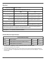
IS4920 / IS4921
Area Imaging Decode Engine
Integration Guide
Disclaimer
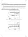
Honeywell International Inc. (“HII”) reserves the right to make changes in specifications and other information
contained in this document without prior notice, and the reader should in all cases consult HII to determine
whether any such changes have been made. The information in this publication does not represent a
commitment on the part of HII.
HII shall not be liable for technical or editorial errors or omissions contained herein: nor for incidental or
consequential damages resulting from the furnishing, performance, or use of this manual.
This document contains propriety information that is protected by copyright. All rights reserved. No part of this
document may be photocopied, reproduced, or translated into another language without the prior written
consent of HII.
© 2007 - 2010 Honeywell International Inc. All rights reserved.
Web Address: www.honeywellaidc.com
Trademarks
Metrologic, MetroSelect, MetroSet2, MetroVision, Omniplanar, and FirstFlash are trademarks or registered
trademarks of Metrologic Instruments, Inc. or Honeywell International Inc.
Microsoft, Windows, and Windows 95 are trademarks or registered trademarks of Microsoft Corporation.
Molex, FFC/FPC, and SlimStack are trademarks or registered trademarks of Molex, Inc.
Other product names mentioned in this manual may be trademarks or registered trademarks of their respective
companies and are the property of their respective owners.
Table of Contents
Introduction
Product Overview ..............................................................................................................................................1
Models and Accessories ...................................................................................................................................2
Components of the IS4920 / IS4921 Decode Engine
IS4920-0 / IS4921-0 (Bracket Not Included) .................................................................................................. 3
IS4920-1 / IS4921-1 (Bracket Included) ......................................................................................................... 3
Components of the IS4910 / IS4911 (Non-Decode Engine).............................................................................. 4
Components of the Decode Printed Circuit Board
TTL Level RS232 ...........................................................................................................................................5
USB ................................................................................................................................................................5
Labels ................................................................................................................................................................5
Mounting Specifications
IS4910-00 / IS4911-00 Non-Decode Engine Dimensions ................................................................................. 6
IS4910-01 / IS4911-01 Non-Decode Engine Dimensions ................................................................................. 7
IS4910-02 / IS4911-02 Non-Decode Engine Dimensions ................................................................................. 8
Decode Printed Circuit Board Dimensions
TTL Level RS232 .........................................................................................................................................10
USB ..............................................................................................................................................................10
IS4920-2 / IS4921-2 Bracketed Decode Engine Dimensions .......................................................................... 11
Enclosure Specifications
Electrostatic Discharge (ESD) Cautions ...................................................................................................... 12
Airborne Contaminants and Foreign Materials ............................................................................................. 12
Output Window Properties ...........................................................................................................................13
Output Window Coatings .............................................................................................................................13
Optical Clearance Specifications ................................................................................................................. 14
System Considerations
Power Supply ..................................................................................................................................................15
Host Flex Cable ...............................................................................................................................................15
Power Sequencing ..........................................................................................................................................15
Thermal Considerations ..................................................................................................................................15
iii
Theory of Operation
Overview .........................................................................................................................................................16
Host Interface Signals .....................................................................................................................................17
Usage of Host Interface Signals ......................................................................................................................18
Power Mode Descriptions ...............................................................................................................................20
Serial Configurations .......................................................................................................................................26
Abbreviated ASCII Table .................................................................................................................................27
Operational Timing
Power Up/Boot Up ...........................................................................................................................................28
Power Down/Suspend/Power Removed ......................................................................................................... 30
Decode Timing ................................................................................................................................................31
Summary of Operation Timings .......................................................................................................................32
Depth of Field vs Bar Code Element
IS4910 .............................................................................................................................................................33
IS4911 .............................................................................................................................................................34
Exposure Time for Image Acquisition ............................................................................................................ 35
Design Specifications
Operational ......................................................................................................................................................36
Mechanical ......................................................................................................................................................37
Environmental .................................................................................................................................................37
Electrical ..........................................................................................................................................................38
Detailed Electrical Specifications .................................................................................................................... 38
Current Waveforms .........................................................................................................................................40
Imaging Engine and Decode PCB Terminations
Imaging Engine Interface Connector ............................................................................................................... 42
Decode Board (USB & TTL) Interface Connector ........................................................................................... 43
Decode Board (USB) Output to Host Connector ............................................................................................. 44
Decode Board (TTL) Output to Host Connector .............................................................................................. 45
Flex Cable Specifications
Flex Cable Pinout – Imaging Engine Connection ............................................................................................ 46
Flex Cable Pinout – Decode Board Connection .............................................................................................. 47
Dimensions ......................................................................................................................................................48
Installation Notes .............................................................................................................................................49
iv
Regulatory Compliance
Safety ..............................................................................................................................................................50
Europe..........................................................................................................................................................50
United States................................................................................................................................................51
Canada.........................................................................................................................................................51
Limited Warranty ..............................................................................................................................................52
Patents ...............................................................................................................................................................53
Index ..................................................................................................................................................................54
Customer Support ............................................................................................................................................56
Technical Assistance .......................................................................................................................................56
Product Service and Repair ............................................................................................................................57
v
vi
Introduction
Product Overview
The IS4920 is a miniature area-imaging engine and decode board with image capturing and bar code decoding
capabilities. The engine module consists of a non-decode imaging engine (IS4910), a decode board and two
flex cables. The IS4920 features a mega-pixel CMOS sensor, integrated illumination, and patented FirstFlash®
technology; together they ensure capturing a high-resolution image with optimal brightness each time. IS4920
also has a wide-angle lens design, which covers a large scan area and delivers a true omni-directional
scanning performance. The high-quality images produced by the imaging engine can be used for decoding bar
codes, image upload, signature capture, document lifting and reading OCR fonts.
The decode board is powered by a fast processor and SwiftDecoder™ software to decode a wide array of 1D
and 2D bar codes plus OCR fonts. The decode board supports TTL level RS232 or USB 1.1 communication.
The decode board is compatible with MetroSet2, a PC-based software for easy configuration.
IS4920 is designed with the industrial standard size, mounting options and output to facilitate integration into
existing applications. The imaging engine’s miniature size makes IS4920 ideal for integration into data
terminals and other small devices. IS4920 is supplied as an assembled module with a mounting bracket or as
separate components for custom mounting. The imaging engine’s unique open system architecture allows
IS4920 to accept third party and custom plug-ins, giving the IS4920 virtually unlimited application flexibility.
The small yet powerful engine delivers a scanning performance that rivals a full-fledged handheld scanner.
A high-density version, IS4921, is also available.
1
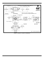
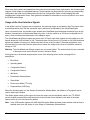
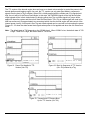
Models and Accessories
Figure 1. Part Number Designations
2
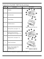
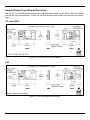
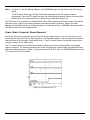
Components of the IS4920 / IS4921 Decode Engine
IS4920-0 / IS4921-0 (Bracket Not Included)
Item No.
Description
1
IS4920-0 / IS4921-0
Assembled Decode Engine
2
IS4910 / IS4911 Non-Decode Engine*
See pages 2, 4 and 6 for model
specifications.
3
Decode Board*
USB (See page 10)
TTL Level RS232 (See page 10)
4
Flex Cable
P/N 77-77101
Item Location
Figure 2. IS4920-0 / IS4921-0 *
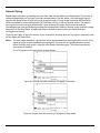
IS4920-1 / IS4921-1 (Bracket Included)
Item No.
Description
1
IS4920-1 / IS4921-1
Assembled Decode Engine
2
IS4910 / IS4911 Non-Decode Engine*
See pages 2, 4 and 6 for model
specifications.
3
Bracket
4
Decode Board*
USB (See page 10)
TTL Level RS232 (See page 10)
5
Flex Cable
P/N 77-77101
Item Location
Figure 3. IS4920-1 / IS4921-1 *
* Figures show the IS4910-01 Non-Decode Engine with a USB Decode PCB.
3
Components of the IS4910 / IS4911 Non-Decode Engine
Item No.
Description
1
Targeting
2
Area Illumination
3
Camera Imager
4
FirstFlash Aperture
Item Location
Figure 4. IS4910-00 / IS4911-00
5
Mounting Points (see pages 7 - 8)
6
Mounting Points Provided for
Self-Tapping Screw (see pages 6 - 8)
7
Keying Location (see pages 6 - 8)
8
Printed Circuit Boards
9
22-Pin, 0.50 mm (0.020") Pitch
SlimStack™ Plug, Molex
(P/N 55560-0227)
Figure 5. IS4910-01 / IS4910-02
IS4911-01 / IS4911-02
Molex and SlimStack are trademarks or registered trademarks of Molex, Inc.
4
Components of the Decode Printed Circuit Board
TTL Level RS232
See page 10 for printed circuit board dimensions and connector information.
See page 43 and page 45 for connector pinout information.
USB
See page 10 for printed circuit board dimensions and connector information.
See page 43 and page 44 for connector pinout information.
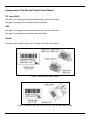
Labels
The serial number/model number label is located on the side of the engine.
Figure 6. Serial Number Label Sample
Figure 7. Decode Board (USB Version Shown) Serial Number Label Sample
5
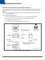
Mounting Specifications
IS4910-00 and IS4911-00 Non-Decode Engine Dimensions
The -00 models include two Ø .075" [1.9 mm] blind holes for mounting the engine with self-tapping screws.
The mounting holes are located on the bottom of the unit with an additional keying location point for engine
alignment.
Warning: The limited warranty (on page 52) is void if the following guidelines are not adhered to when
mounting the engine.
When securing the engine with screws:
•
Use M2.2 x 4.5 Philips pan head, type AB, steel, zinc clear, Trivalent self-tapping screws.
•
Do not exceed 1.75 +0.5 in-lb [2.02 +6 cm-kg] of torque during screw installation.
•
Use a minimum mount thickness of 0.3 mm.
•
Use safe ESD practices when handling and mounting the engine.
Figure 8. IS4910-00 / IS4911-00 Dimensions
6
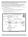
IS4910-01 / IS4911-01 Non-Decode Engine Dimensions
The -01 models include two Ø .075" [1.9 mm] blind holes for mounting the engine with self-tapping screws.
Two additional Ø .098" ± .002 [2.5 mm ±.05 mm] clearance holes are provided as a secondary mounting
option. The clearance holes are located on tabs that extend from the sides of the engine's chassis.
A keying location point is provided on the bottom of the engine to assist with alignment.
Warning: The limited warranty (on page 52) is void if the following recommendations are not adhered to when
mounting the engine.
When securing the engine with self-tapping screws:
•
Use M2.2 x 4.5 Philips Pan Head, Type AB, Steel, Zinc Clear, Trivalent self-tapping screws.
•
Do not exceed 1.75 +0.5 in-lb [2.02 +6 cm-kg] of torque during screw installation.
•
Use a minimum mount thickness of 0.3 mm.
•
Use safe ESD practices when handling and mounting the engine.
Figure 9. IS4910-01 / IS4911-01 Dimensions
7
IS4910-02 / IS4911-02 Non-Decode Engine Dimensions
The -02 models include two Ø .075" [1.9 mm] blind holes for mounting the engine with self-tapping screws.
Two additional M2 x .4 threaded inserts are provided as a secondary mounting option. The threaded inserts
are located on tabs that extend from the sides of the engine's chassis. A keying location point is provided on
the bottom of the engine to assist with alignment.
Warning: The limited warranty (on page 52) is void if the following recommendations are not adhered to when
mounting the engine.
When securing the engine with self-tapping screws:
•
Use M2.2 x 4.5 Philips pan head, type AB, steel, zinc clear, trivalent self-tapping screws.
•
Do not exceed 1.75 +0.5 in-lb [2.02 +6 cm-kg] of torque during screw installation.
•
Use a minimum mount thickness of 0.3 mm.
•
Use safe ESD practices when handling and mounting the engine.
When securing the engine by utilizing the M2 threaded inserts:
•
Use M2 x 0.4 Philips Pan Head, Type AB, Steel, Zinc Clear, or equivalent screws.
•
Do not exceed 2.5 in-lb [2.88 cm-kg] of torque during screw installation.
•
Use a minimum mount thickness of 0.3 mm.
•
Use safe ESD practices when handling and mounting the engine.
See Figure 10 on page 9 for detailed engine dimensions.
8
Figure 10. IS4910-02 / IS4911-02 Dimensions
9
Decode Printed Circuit Board Dimensions
Both the TTL Level RS232 decode board and the USB decode board have two Ø 0.098" [2.489 mm] clearance
holes for M2.2 mounting hardware. Always use safe ESD practices when handling and mounting the decode
board.
TTL Level RS232
Figure 11. TTL Level RS232 Decode Board
USB
Figure 12. USB Decode Board Dimensions
10
IS4920-2 / IS4921-2 Bracketed Decode Engine Dimensions
The bracketed decode engine includes two Ø 0.097" [2.464 mm] blind holes for mounting the engine
with self-tapping screws. Two additional M2 x .4 threaded inserts are provided as a secondary mounting
option. The threaded inserts are located on tabs that extend from the sides of the engine's chassis.
A keying location point is provided on the bottom of the engine to assist with alignment.
Warning: The limited warranty (on page 52) is void if the following recommendations are not adhered to when
mounting the engine.
When securing the engine by utilizing the M2 threaded inserts:
•
Use M2 x 0.4 Philips Pan Head, Type AB, Steel, Zinc Clear, or equivalent screws.
•
Do not exceed 2.5 in-lb [2.88 cm-kg] of torque when securing the engine module to the host.
•
Use a minimum mount thickness of 0.3 mm.
•
Use safe ESD practices when handling and mounting the engine.
Figure 13. IS4920 / IS4921 Bracketed Decode Engine Dimensions
11
Enclosure Specifications
The imaging engine was specifically designed for integration into custom housings for OEM applications. The
imaging engine’s performance will be adversely affected or permanently damaged when mounted in an
unsuitable enclosure.
Warning: The limited warranty (on page 52) is void if the following considerations are not adhered to when
integrating the area-imaging engine into a system.
Electrostatic Discharge (ESD) Cautions
All engines and decode boards are shipped in ESD protective packaging due to the sensitive nature
of the exposed electrical components.
•
ALWAYS use grounding wrist straps and a grounded work area when unpacking
and handling the engine.
•
Mount the engine in a housing that is designed for ESD protection and stray electric fields.
ESD has the ability to modify the electrical characteristics of a semiconductor device, possibly
degrading or even destroying the device. ESD also has the potential to upset the normal operation
of an electronic system, causing equipment malfunction or failure.
Airborne Contaminants and Foreign Materials
The imaging engine has very sensitive miniature electrical and optical components that must be protected from
airborne contaminants and foreign materials. In order to prevent permanently damaging the imaging engine
and voiding the limited warranty (on page 52), the imaging engine enclosure must be:
•
Sealed to prevent infiltration by airborne contaminants and foreign materials such as
dust, dirt, smoke, and smog.
•
Sealed to protect against water, humidity, and condensation.
Refer to page 15 for information on power and thermal considerations.
12
Output Window Properties
An improperly placed window has a serious potential to reduce the imaging engine’s performance.
Careful consideration must be made when designing the output window’s distance and angle relative
to the imaging engine’s camera aperture.
Follow these guidelines when designing the output window.
•
The output window material should have a spectral transmission of at least 85% from 580 nm to
680 nm and should block shorter wavelengths.
•
The output window should have a 60-40 surface quality, be optically flat, clear, and free of scratches,
pits, or seeds. If possible, recess the window into the housing for protection or apply a scratch
resistance coating (see Output Window Coatings below).
•
Apply an anti-reflective coating to the window surfaces to reduce the possibility of reflective light
interfering with the engine’s performance.
•
The clear aperture of the output window should extend beyond the Field of View. Refer to page 14
and pages 33 - 34 for Field of View specifications.
•
The window size must accommodate the illumination and targeting areas shown on page 14.
•
The window must be parallel to the engine face.
•
The distance from the engine face to the inside surface of the window of the enclosure should be
minimized and should not exceed 0.5 mm (0.02") due to possible specular reflections from internal
area illumination.
Output Window Coatings
•
Anti-Reflection
An anti-reflective coating can be applied to the inside and/or outside of the window to reduce the
possibility of internal beam reflections interfering with the performance of the engine. If an antireflective coating is applied, the coating is recommended to be on both sides of the window providing a
0.5% maximum reflectivity on each side from 600 - 700 nanometers at the nominal window tilt angle.
The coating must also meet the hardness adherence requirements of
MIL-M-13508.
•
Polysiloxane Coating
Applying a polysiloxane coating to the window surface can help protect the window from surface
scratches and abrasions that may interfere with the performance of the engine. Recessing the window
into the housing can also provide added protection against surface damage such as scratches and
chips. If an anti-reflective coating is used, there is no need to apply a polysiloxane coating.
13
Optical Clearance Specifications
The window size and enclosure design must provide unobstructed clearance for the illumination and targeting
areas shown below in figures 14 and 15 to avoid optical interference that decreases the engine's performance.
IS4910
Figure 14. IS4910 Optical Clearance Specifications
IS4911
Figure 15. IS4911 Optical Clearance Specifications
14
System Considerations
In order to ensure proper operation of the decode engine’s electrical system; care must be taken to ensure the
following requirements are met.
Power Supply*
The decode engine is powered from the host device via the VIN and GND pins of the ZIF connector on the
decode board. This voltage must be maintained within the specified voltage range at the decode board
(see electrical specifications on page 38). Voltage drops in the host flex cable must be taken into account.
The power must be clean and heavily decoupled in order to provide a stable power source.
Note: The power supply must be able to handle dynamic current loads because the input current will increase
considerably when the illumination LEDs are enabled.
Host Flex Cable
The host flex cable is used to carry power and data signals between the decode engine and the host system.
The flex cable should allow for minimal voltage drop and maintain a good ground connection between the host
and the decode engine. In terms of grounding and voltage drop, a shorter cable is better.
In addition to power, the flex cable will also carry the digital signals required for communication. The cable
design is especially important in the case of USB due to the relative high speed of the USB signals.
The impedance of the cable should match, or be as close as possible to, the impedance of the USB driver
(approximately 45 ohms per trace).
The routing of the host flex cable also plays a critical role in the system design. The cable should be routed
away from high frequency devices since these frequencies can couple onto the flex cable and cause potential
data corruption or unwanted electromagnetic inference, EMI.
Power Sequencing*
The decode engine is powered from the VIN power signal on the ZIF connector on the decode board. Most of
the host signals (signals present on the ZIF connector) are relative to this voltage. Not all of these signals are
overvoltage tolerant thus; care must be taken to ensure that the relationship between the VIN and the host
signals are always met (see electrical specifications on page 38).
Thermal Considerations
The decode engine is qualified over the specified operational temperatures (0°C to 40°C) for all operating
modes. Make sure ambient temperatures do not exceed this range in order to guarantee operation. Operating
the decode engine in continuous mode for an extended period may produce considerable heating. This mode
should be limited and sufficient airflow should be provided whenever possible to minimize internal heating.
Excessive heating may degrade images and potentially damage the engine.
* See page 42 for additional information on electrical specifications.
See pages 42 and 46 for additional information on the engine pinouts and flex cable pinouts.
15
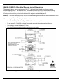
Theory of Operation
Overview
The IS4920 decode imaging engine series is ideal for integration into data terminals and other small devices.
The high-quality images produced by the imaging engine can be used for decoding bar codes, image upload,
signature capture, document lifting and reading OCR fonts.
The decode engine consists of two main system components: the a non-decode imaging engine, which utilizes
a high-resolution CMOS image sensor, and a small decode board that contains a powerful microprocessor and
the firmware to control all aspects of the engine’s operations and enabling communication with the host system
over the standard set of communication interfaces.
The model IS492x-xx103 provides communication with the host system over TTL-level RS232 communication
interface.
The model IS492x-xx38 provides communication with the host system over USB. It can be configured for the
following protocols of USB communication:
•
USB Keyboard Emulation Mode (default)
•
USB Serial Emulation Mode
The system hardware architecture of the decode engine is shown in the figure below.
Figure 16. IS4920 / IS4921 System Architecture
16
Host Interface Signals
The host interface signals are described in the table below.
Pin#
TTL RS232
USB
Description
1
232INV
NC
Input: TTL RS232 polarity control with 32k ohm pull-up. Connect to
ground for UART to UART signal polarity. Pull up to Vin for
standard TTL RS232 polarity.
2
Vin
Vin
Power: Supply voltage input (3V to 5.5V)
3
GND
GND
Ground: Power and signal ground.
D-
Input: TTL Level RS232 Receive data input, weak pull up to Vin.
Polarity determined by Pin1.
4
(n)RxD
Bidirectional: USB D- Signal
5
6
(n)TxD
(n)CTS
<reserved>
D+
Output: TTL Level RS232 transmits data. Polarity Determined by
Pin 1.
Input: TTL level Clear to Send, weak pull up to Vin. Polarity
configurable via software.
Bidirectional: USB D+ signal
7
(n)RTS
<reserved>
Output: TTL level RS232 Request to Send. Polarity configurable via
software.
8
PWRDWN
PWRDWN
Output: Open drain, 100K pull up to Vin; active high indicates that
the IS4920 is in Power Down Mode.
9
nBEEPER
nBEEPER
Output: Open drain, 100K pull up to Vin; active low signal capable of
sinking current. PWM controlled signal can be used to drive
an external beeper.
10
nGoodRead
nGoodRead
Output: Open drain, 100K pull up to Vin; active low signal for sinking
current of a Good Read LED circuit.
11
nWAKE
nWake
Input: Weak pull up to Vin; active low, the signal can be used to
bring the engine out of Power Down (TTL RS232 version
only) or Sleep Mode (TTL RS232 and USB versions).
12
nTrig
nTrig
Input: Weak pull up to Vin; active low, the signal can be used as a
trigger input to activate the IS4920.
17
Since many host systems and applications have unique formats and protocol requirements, the decode engine
supports a wide range of configurable features. These features may be selected by scanning a corresponding
configuration bar code from the MetroSelect Single-Line Configuration Guide or Area Imaging Bar code
Supplemental Configuration Guide. Both guides are available for download at www.honeywellaidc.com under
the IS4920 product page.
Usage of the Host Interface Signals
In the default “multi-try” trigger mode of operations, the scanning engine is activated by the nTrig signal, which
must be kept active (low) until the successful scan is achieved, as indicated by the nGoodRead signal.
Upon a successful scan, the decode engine asserts the nGoodRead signal and keeps it asserted (low) for the
duration of transmission of the decoded data to the host, or for the minimum of 100 msec (configurable to 50
msec), which coincides with the duration of the nBeeper signal.
The nGoodRead and nBeeper signals are driven with LVC family open drain outputs and are pulled up on the
decode board with 100K resistors to VIN. The default state of these pins is Hi-Z (pulled up via 100K) and these
signals are capable of sinking up to 24mA each when driven to the low state. For beeper applications, care
must be taken to ensure that inductive spikes do not cause the voltage on the lines to exceed the maximum
voltage of 5.5V.
Warning: The nGoodRead and nBeeper signals are not current limited. The external host circuitry connected
to these pins must ensure that the current is limited to 25mA.
At any given time, the decode engine can be in one of the following power modes, see page 20 for
descriptions:
•
Boot Mode
•
Operating Mode
•
Configuration Mode 1
•
Configuration Mode 2
•
Idle Mode
•
Presentation Wakeup Mode
•
Sleep Mode
•
Power-down Mode (TTL Only)
•
Suspend Mode (USB Only)
When the decode engine is in the Sleep or Presentation Wakeup Mode, the nWake or nTrig signals can be
used to wake up the engine.
The nWake signal wakes up the engine and turns the engine into the Idle Mode, which in the TTL RS232
version enables communication with the host for a short period of time defined by the value of the sleep
timeout, which is set to one second by default.
Note: In the USB decode engines with USB Serial Emulation Mode activated; communication with the host is
enabled even when the engine is in the Sleep or Presentation Wakeup Mode.
18
The nTrig signal not only wakes the engine up, but also immediately activates and turns the engine into the
Operating Mode.
Either nWake or nTrig signals can be used to restart the TTL RS232 scanning engine when the engine is in
Power-down Mode, which is indicated by the asserted (high) PWRDWN signal.
The PWDWN pin is used to indicate when the decode engine is in various operating modes such as Power
Down, Suspend, and Boot.
Note: The output signals from the decode engine can experience analog behavior when VIN is initially applied
or removed due to the supply voltage ramping up or down. Care must be taken to ensure that this
behavior does not adversely affect the host System. Special attention must be given to the PWRDWN
Pin. When power is initially applied, the output state of this line will be indeterminate for about 10mS
until the USB controller exits reset. The state of this pin should be disregarded during this time. The
following waveforms show several signals when VIN is first applied (Figure 17) and when VIN is
removed (Figure 18).
Figure 17. VIN First Applied (USB)
Figure 18. VIN Removed (USB)
19
Power Mode Descriptions
Boot Mode
The engine is booting up.
PWRDWN Pin State: Asserted (HIGH).
All bar code scanning by:
Trigger:
Not Working
Remote Activation USB: Not Working
Remote Activation TTL:
Not Working
Responsiveness:
Not Working
Serial Program Mode:
Not Working
Transition to Boot Mode:
•
The TTL RS232 engine is turned to Boot Mode from Power Down Mode when the power is applied
AND upon reception of the nTrig or nWake signals.
•
The USB engine enters Boot Mode upon completion of USB enumeration.
•
The engine can turn itself to Boot Mode from Operating Mode or Idle Mode upon some internal event,
such as at the end of the software upgrade procedure.
At the end of the boot-up cycle the engine turns to the Idle Mode and de-asserts the PWRDWN pin.
Operating Mode
The engine is acquiring and processing images or running other tasks.
PWRDWN Pin State: De-asserted (LOW).
All bar code scanning by:
Trigger:
Not Working
Remote Activation USB: Not Working
Remote Activation TTL:
Not Working
Responsiveness:
Not Working
Serial Program Mode:
Not Working
Transition to Operating Mode:
20
•
The engine is turned to Operating Mode from Idle, Sleep, or Presentation Wakeup Modes upon the
reception of the nTrig signal.
•
The engine can be turned to Operating Mode from Idle Mode (or Sleep Mode in USB version) upon the
reception of a special single-byte serial command from the host. The byte value is configurable.
•
The engine is turned to Operating Mode from the Presentation Wakeup Mode upon the object detection
event.
Configuration Mode 1
The engine is in configuration mode or updating firmware.
PWRDWN Pin State: De-asserted (LOW).
All bar code scanning by:
Trigger:
Not Working
Remote Activation USB: Not Working
Remote Activation TTL:
Not Working
Responsiveness:
Not Working
Serial Program Mode:
Not Working
Transition to Configuration Mode 1:
•
The engine is turned to Configuration Mode 1 using MetroSet2 AutoSet to upload/download
configuration.
•
The engine is turned to Configuration Mode 1 using MetroSet2 AutoSet to update main board or I/O
board firmware.
•
The engine is turned to Configuration Mode 1 using MetroVision to transfer an image from the engine to
the PC.
21
Configuration Mode 2
The engine is in serial programming mode.
PWRDWN Pin State: De-asserted (LOW).
Non-programming bar code scanning by:
Trigger:
Not Working
Remote Activation USB: Not Working
Remote Activation TTL:
Not Working
Responsiveness:
Not Working
Serial Program Mode:
Not Working
Programming bar code scanning by:
Trigger:
Working
Remote Activation USB: Working
Remote Activation TTL:
Working and will not go to Sleep
Responsiveness:
No delay, but can go into Idle or Presentation Wakeup Modes
Serial Program Mode:
Working
Transition to Configuration Mode 2:
22
•
The engine is turned to Configuration Mode 2 after scanning in the Enter / Exit Configuration Mode bar
code while in Operating Mode or Idle Mode.
•
The engine is turned to Configuration Mode 2 after entering Enter / Exit Configuration Mode serial
programming string while in Operating Mode or Idle Mode.
•
The engine is turned to Configuration Mode 2 after scanning a configuration bar code while in
Operating Mode or Idle Mode, but not while in Configuration Mode 2.
Idle Mode
The engine is not operating, but not sleeping and is fully powered. The CPU and image sensor are in the Idle
Mode, the wakeup from which does not require the image sensor reprogramming.
PWRDWN Pin State: De-asserted (LOW).
Non-programming bar code scanning by:
Trigger:
Working
Remote Activation USB: Working
Remote Activation TTL:
Working
Responsiveness:
No Delay
Serial Program Mode:
Working
Transition to Idle Mode:
•
The engine is turned to Idle Mode from Operating Mode immediately when no tasks are running in the
engine.
•
The engine is turned to Idle Mode from Sleep or Presentation Wakeup Modes upon the reception of the
nWake signal.
Presentation Wakeup Mode
The Presentation Wakeup Mode replaces the Idle Mode for an engine with Object Detection and Presentation
Mode turned on. The engine normally enters Idle Mode after exited Operating Mode, Configuration Mode or
Boot Mode with no pending operation.
PWRDWN Pin State: De-asserted (LOW).
Non-programming bar code scanning by:
Trigger:
Working
Remote Activation USB: Working
Remote Activation TTL:
Working
Responsiveness:
Costs a few milliseconds due to exiting of Object Detection.
Serial Program Mode:
Working
Transition to Presentation Wakeup Mode:
•
The engine is turned to Presentation Wakeup Mode any time the engine tries to enter Idle Mode, if the
engine is in Presentation Mode with the Presentation Wakeup feature enabled in NOVRAM. The
Presentation Mode and Presentation Wakeup feature together overrides the Idle Mode and will enter
Presentation Mode instead.
23
Sleep Mode
The engine is sleeping, but is fully powered. The CPU is in sleep mode. The image sensor is in standby
mode, the wakeup from the Sleep Mode requires the image sensor reprogramming (which is done
automatically in the engine software).
PWRDWN Pin State: De-asserted (LOW).
Non-programming bar code scanning by:
Trigger:
Working
Remote Activation USB: Working
Remote Activation TTL:
Not Working
Responsiveness:
Costs tens of microseconds; Remote activation does not work for TTL
Serial Program Mode USB:
Working
Serial Program Mode TTL:
Not Working
Transition to Sleep Mode:
•
The engine is turned to Sleep Mode from Idle Mode upon the expiration of the “sleep” timeout, which is
set to one second by default. The “sleep” timeout is restarted every time the engine enters the Idle
Mode.
•
The engine can be turned to Sleep Mode from Operating Mode or Idle Mode immediately upon the
reception of a special single-byte serial command from the host. The byte value is configurable.
Power Down Mode (TTL RS232 Only)
The power of the engine is turned off.
PWRDWN Pin State: Asserted (HIGH).
Non-programming bar code scanning by:
Trigger:
Not Working / But able to reboot engine
Remote Activation USB: N/A
Remote Activation TTL:
Not Working
Responsiveness:
Requires complete reboot (Require toggling of nTrig or nWake pin)
Serial Program Mode:
Not Working
Transition to Power Down Mode:
•
The engine is turned to Power Down Mode from Sleep Mode upon the expiration of the “power-down”
timeout, which is set to 10 minutes by default. The “power-down” timeout is restarted every time the
engine enters the Sleep Mode.
•
The engine can be turned to Power Down Mode immediately upon the reception of a special singlebyte serial command from the host. The byte value is configurable.
The engine can wake up from Power Down Mode and reboot:
•
24
Upon reception of the nTrig or nWake signals.
Suspend Mode (USB Only)
The engine is in its lowest power consumption state.
PWRDWN Pin State: Asserted (HIGH).
Non-programming bar code scanning by:
Trigger:
Not Working
Remote Activation USB: Not Working
Remote Activation TTL:
N/A
Responsiveness:
Requires complete reboot (Host controlled)
Serial Program Mode:
Not Working
Transition to Suspend Mode:
•
The engine is turned to Suspend Mode upon receiving the USB Suspend signal from the USB host.
•
The engine can be turned to Suspend Mode any time (by the USB host).
The engine can wake up from Suspend Mode and reboot:
•
Upon receiving the Resume signal from the USB host.
25
Serial Configuration
The IS4920 series can be configured by scanning configuration bar codes† or by serial commands sent from
the host device. With serial configuration, each command sent to the engine is the ASCII representation of
each numeral in the configuration bar code (see Figure 19). The entire numeric string is framed with an ASCII
[stx] and an ASCII [etx].
Do Not Include
in the Command
³ 1 0 0 1 0 4
Include in the
Command
Figure 19.
Example 1:
Feature
Host Command
String Sent to the Engine - ASCII Representation (Hexadecimal Values)
Disable Codabar
[stx]100104[etx]
02h 31h 30h 30h 31h 30h 34h 03h
If the command sent to the engine is valid, the engine will respond with an [ack]. If the command sent to the
engine is invalid, the engine will respond with a [nak] then automatically exit serial configuration mode. All the
settings chosen in the failed serial configuration session will be lost. There is a 20-second window between
commands. If a 60-second timeout occurs, the engine will send a [nak].
To enter serial configuration mode, send the following command, [stx]999999[etx]. The engine will not scan
bar codes while in serial configuration mode.
Note: Serial configuration mode uses the current Baud Rate, Parity, Stop Bits and Data Bits settings that
are configured in the engine. The default settings of the engine are 9600 bits-per-second, no parity,
1 stop bit, 8 data bits, and no flow control. If a command is sent to the engine to change any of these
settings, the change will not take effect until after serial configuration mode is exited.
To exit serial configuration mode, send the following command, [stx]999999[etx]. The engine will respond with
an [ack]. Refer to Example 2 on page 27.
†
26
Bar code configuration manuals are available for download from the IS4920 product page at
www.honeywellaidc.com.
Example 2:
The following sample illustrates the serial command sequence for configuring the engine for the
factory default settings, disabling Code 128 scanning, and adding a “G” as a configurable prefix.
Commands for features that require sequences of multiple bar codes for activation (i.e. prefixes,
suffixes, and timeout features) should be sent in the same order that they are normally scanned.
Feature
Host Command
ASCII Representation
Engine
Response
Enter Configuration Mode
[stx]999999[etx]
02h 39h 39h 39h 39h 39h 39h 03h
[ack] or 06h
Load Defaults
[stx]999998[etx]
02h 39h 39h 39h 39h 39h 38h 03h
[ack] or 06h
Disable Code 128
[stx]100113[etx]
02h 31h 30h 30h 31h 31h 33h 03h
[ack] or 06h
Configure Prefix #1
[stx]903500[etx]
02h 39h 30h 33h 35h 30h 30h 03h
[ack] or 06h
Code Byte 0
[stx]0[etx]
02h 30h 03h
[ack] or 06h
Code Byte 7
[stx]7[etx]
02h 37h 03h
[ack] or 06h
Code Byte 1
[stx]1[etx]
02h 31h 03h
[ack] or 06h
Exit Configuration Mode
[stx]999999[etx]
02h 39h 39h 39h 39h 39h 39h 03h
[ack] or 06h
Abbreviated ASCII Table
Character
Hex Value
Decimal Value
[STX]
02h
2
[ETX]
03h
3
[ACK]
06h
6
[NAK]
15h
21
0
30h
48
1
31h
49
2
32h
50
3
33h
51
4
34h
52
5
35h
53
6
36h
54
7
37h
55
8
38h
56
9
39h
57
27
Operational Timing
The following section describes the timing associated with the various operating modes of the decode engine
assembly including Power Up, Power Down, and Operating (from Idle or Sleep). The waveforms shown in this
section assume VIN = 3.3V, nGoodRead pulled up with 10K resistor to VIN, and nBeeper pulled up with 10K
resistor to VIN, unless otherwise noted.
Power Up / Boot Up
The power up sequence of the decode engine depends on the interface type. For the USB version, a USB
Microcontroller controls the power to the decoding platform and imaging engine via a power switch. When
power is initially applied, only the USB controller is active and begins the process of enumeration. Once
enumeration is complete, the USB controller turns power on to the imaging engine and decoding platform. As a
result, powering up the engine is completely controlled by the on board USB controller per the USB
specifications. In this version, only Idle and Sleep Modes are supported. For additional power savings, the unit
must be placed in Suspend Mode per the USB specification. Figure 20 shows the power up sequence of the
USB version of the decode engine.
Note: The PWNDWN signal remains high until the Decode platform transitions to Idle Mode and is ready to
accept commands. In the USB version, the PWNDWN Pin will only be high during this boot up condition
or when the Decode enters, Suspend Mode. From Figure 20, it can be seen that the entire boot up
sequence takes approximately nine seconds.
Figure 20. Power Up / Boot Up Sequence of USB Version
28
The TTL version of the decode engine does not have an on board microcontroller to control the power to the
decode platform and imaging engine. As such, the TTL version can only enter Boot Mode in response to
signals from the host (nTrig or nWake). When VIN is initially applied with the nWake and nTrig signals held
high, the unit will be in the Power Down Mode. In this state, the PWRDWN signal will be high and all other
output signals will be in their default state. By bringing either the nTrig or nWake signal low, power will be
applied to the entire system and the unit will enter the Boot Mode. The nTrig or nWake signal will need to be
held low continuously for approximately two seconds at which time the decode engine will take control of the
internal power circuitry. At this point, the nTrig and nWake signals can be used with out interrupting the power.
Figures 21 - 23 show the state several host signals when power is first applied and when the unit enters boot
mode.
Note: The default state of TxD depends on the 232INV signal. When 232INV is low, the default state of TxD
is high. When INV is high, the default state of TxD is low.
Figure 21. Power First Applied of TTL
Version (Vin= 5V)
Figure 22. Boot Up Sequence of TTL Version
(Vin= 5V) initiated by nTrig
Figure 23. Transmit and RTS during Boot
Up for TTL Version (Vin= 5V)
29
Notes: In Figure 21 , the nGoodRead, nBeeper, and PWRDWN signals are high while in the Power Down
Mode.
The RTS Signal will be high in Power Down Mode regardless of the RTS polarity software
configuration. Also, the RTS signal may have the incorrect polarity when the device first enters Boot
Mode (Figure 23) or right before the unit enters Power Down Mode (Figure 24).
The USB version can be placed into Suspend Mode via the USB suspend signal for low current consumption.
When this occurs, power to the decoding platform and imaging engine is removed. While in this state,
nBeeper and nGoodRead will be in their default state (Hi-z with weak pull up). PWRDWN will be high and the
USB data lines will be in the Suspend Mode.
Power Down / Suspend / Power Removed
At any time VIN can be completely removed from the decode engine however, care must be taken to avoid
removing power during the boot up, flash upgrades, or configuration updates. Removing power during these
times can result in the corruption of the flash memory. Figure 18 shows several host signals during a power
removed condition for the USB version.
The TTL version enters into the Power Down Mode in which power to the decoding platform and imaging
engine is removed. The decoding processor can initiate a Power Down sequence after a programmable time
period has elapsed without any activity. Figure 24 shows the TxD, RTS, VIN, and PWRDWN signals when the
TTL enters into Power Down Mode.
Figure 24. Power Down for TTL
30
Decode Timing
Engine image acquisition or decoding can occur from either the Idle Mode or the Sleep Mode. The process is
initiated by asserting the nTrig signal (or serial command when in the Idle Mode). Once the trigger signal is
received, the image sensor is reset and image acquisition begins. During image acquisition, the illumination
LEDs are enabled for a time determined by the FirstFlash circuitry on the non-decode engine. The image is
then transferred to the processor and decoded. Upon decoding the image, the processor asserts the
nGoodRead signal (low) and beings transmitting the decoded data. When the decode engine receives a trigger
signal while in the Sleep Mode, an additional delay is needed for the processor exit Sleep Mode and
reconfigures the sensor.
Figure 25 and Figure 26 show the amount of time required for decoding when a nTrig signal is asserted in both
the Idle Mode and Sleep Mode.
Notes: The total image acquisition / decode time can be approximated by measuring the time from the nTrig
signal going low to the nGoodRead signal going low. This time will vary slightly based on several
factors including code quality, code type, and distance from the engine. The following waveforms
show a typical condition.
The nTrig signal must be kept low for at least 20msec.
Figure 25. Decode time after receiving nTrig signal in Idle Mode.
Figure 26. Decode time after receiving nTrig signal in Sleep Mode.
31
Summary of Operation Timings
Operation Timing Specifications
Parameter
Description
Relevant
Note(s)
Typical
Tprw_up
Power Applied to Processor Ready Delay (USB)
6 seconds
Notes 4 and 5
Tprw_up_ttl
Trigger or Wake Low to Processor Ready Delay
(TTL)
5 seconds
Note 4
Tdec_idle
Trigger Low to Decode complete Delay
90 msec
Notes 1 and 2
Tdec_sleep
Trigger Low to Decode complete Delay
120 msec
Notes 1 and 3
Trig_min
Minimum Duration of Trigger Signal
20 msec
Trig_wake_min_pu
Minimum Activation Time for Trigger or
Wake Signal to Power Up TTL Unit
2 seconds
Notes:
1. Timing is the same for Both TTL or USB version
2. Processor is in Idle Mode when nTrig signal is received
3. Processor is in Sleep Mode when nTrig signal is received
4. Typical time specified may vary depending on the enumeration time of the USB host.
5. Typical times specified are valid for an IS4920 or an IS4921 with a firmware version of 15848 or
higher. Units with a firmware version lower than 15848 may require up to 3 seconds of an
additional time.
32
Depth of Field vs. Bar Code Element
IS4920
Bar Code
Element Width
1D
PDF
Data
Matrix
*
Depth of Field*
(In the Field of View)
Start
(From Engine Face)
Total
End
(From Engine Face)
0.127 mm
5 mil
55 mm (2.2")
130 mm (5.1")
75 mm (3.0")
0.254 mm
10 mil
30 mm (1.2")
220 mm (8.7")
190 mm (7.5")
0.330 mm
13 mil
25 mm (1.0")
310 mm (12.2")
285 mm (11.2")
0.170 mm
6.67 mil
45 mm (1.8")
155 mm (6.1")
110 mm (4.3")
0.254 mm
10 mil
25 mm (1.0")
300 mm (11.8")
275 mm (10.8")
0.254 mm
10 mil
40 mm (1.6")
85 mm (3.3")
45 mm (1.8")
0.381 mm
15 mil
40 mm (1.6")
155 mm (6.1")
115 mm (4.5")
0.508 mm
20 mil
45 mm (1.8")
330 mm (13.0")
285 mm (11.2")
Depth of field information is for reference only. Actual values may vary depending on testing conditions.
Figure 27. Field of View, Divergence Angle (model IS4910-01 shown)
33
IS4921
Depth of Field* in the Field of View
Bar Code Element Width
Start
(From Engine Face)
End
(From Engine Face)
Total
.076 mm
3 mil
68 mm (2.7")
105 mm (4.1")
37 mm (1.4")
.127 mm
5 mil
50 mm (2.0")
120 mm (4.7")
70 mm (2.75")
.330 mm
13 mil
50 mm (2.0")
170 mm (6.7")
120 mm (4.7")
PDF
.127 mm
5 mil
45 mm (1.8")
130 mm (5.0")
85 mm (3.2")
Data Matrix
and QR
.127 mm
5 mil
75 mm (3.0")
115 mm (4.5")
40 mm (1.5")
1D
* Depth of field information is for reference only. Actual values may vary depending testing conditions.
Figure 28. IS4911 Field of View, Divergence Angle (model IS4911-01 shown)
34
Exposure Time for Image Acquisition
By default, the maximum exposure time for image acquisition is 8 ms. Reducing the exposure time for image
acquisition may improve the reading performance of high-density bar codes for certain applications. Use the
following bar codes to set the desired maximum exposure time.
Set Exposure Time to 1 ms
³
3 2 7 6 1 0
Set Exposure Time to 2 ms
³
3 2 7 6 1 2
Set Exposure Time to 3 ms
³
3 2 7 6 3 0
Set Exposure Time to 4 ms
³
3 2 7 6 4 0
Set Exposure Time to 5 ms
³
3 2 7 6 5 0
Set Exposure Time to 6 ms
³
3 2 7 6 6 0
Set Exposure Time to 7 ms
³
3 2 7 6 7 0
Set Exposure Time to 8 ms
³
3 2 7 6 0 0
35
Design Specifications
Operational
Light Source: Four, 650 nm Red Light Emitting Diode LED
IS4920
25 mm – 310 mm (1.0" to 12.2") for 0.330 mm (13 mil) 1D Bar
Codes
See page 33 for additional information on engine depth of field.
IS4921
50 mm – 170 mm (2.0" to 6.7") for 0.330 mm (13 mil) 1D Bar
Codes
See page 34 for additional information on engine depth of field.
Depth of Field:
IS4920
Field of View:
IS4921
IS4920
Viewing Field Size:
IS4921
50° Horizontal
37.5° Vertical
38° Horizontal
28.5° Vertical
118.4 mm x 86.2 mm (4.7" x 3.4")
at 127 mm (5.0") from the Face of the Engine
236.8 mm x 172.4 mm (9.3" x 6.8")
at 254 mm (10.0") from Face of the Engine
37 mm x 28 mm (1.45" x 1.08")
at 80 mm (3.15") from the Face of the Engine
78 mm x 58 mm (3.09" x 2.3")
at 170 mm (6.69") from the Face of the Engine
Rotation Sensitivity: 360° Around the Optical Axis
IS4920
Minimum Element Width:
IS4921
.10 mm (4.0 mil) 1D, PDF
.191 mm (7.5 mil) 2D
.063 mm (2.5 mil) 1D, PDF
.10 mm (4.0 mil) 2D
Resolution: 1.2 mega pixels (1280 x 960)
Symbologies Supported: All standard 1D and 2D Bar Codes; Optional OCR fonts.
Print Contrast: 20% Minimum
36
Mechanical
Dimensions: See pages 6 - 8 for detailed specifications.
Weight: < 14 g (.494 oz.)
12-Pin, Molex FFC/FPC Connector (Molex P/N 52559-1252)
Termination:
See page 42 for engine pinouts.
See page 46 for flex cable specifications.
Mounting: See pages 6 - 11 for detailed specifications.
Keying Location: See pages 6 - 11 for detailed specifications.
FFC/FPC is a trademark of Molex, Inc., all rights reserved.
Environmental
Operating Temperature: 0°C to 40°C (32°F to 104°F)
Storage Temperature: -20°C to 70°C (-4°F to 158°F)
See page 15 for additional information on thermal considerations.
Humidity: 5% to 95% relative humidity, non-condensing
Light Levels: 0 - 110,000 Lux
Shock: 5 ft. (1.5 m)
Vibration Protection: 7G, 10 – 500 Hz
Contaminants: See page 12.
37
Electrical
Engine Input Voltage: 3.3VDC ~ 5.5VDC
Typical Operating Current: 235 mA (continuous scan mode, VIN=3.3V)
USB
TTL
Peak Operating Current: 400 mA (typical VIN=3.3V @ 25°C)
400 mA (typical VIN=3.3V @ 25°C)
Idle Current: 160 mA (typical VIN=3.3V @ 25°C)
125 mA (typical VIN=3.3V @ 25°C)
Sleep Current: 65 mA (typical VIN=3.3V @ 25°C)
Suspend Current (USB): 600 µA* (typical VIN=3.3V @ 25°C)
Power Down Current (TTL): N/A
25 mA (typical VIN=3.3V @ 25°C)
N/A
500 µA* (typical VIN=3.3V @ 25°C)
* Specifications are based on the assumption inputs are pulled high. If inputs are externally pulled low,
the current through the pull up registers must be added to these numbers.
See pages 50 - 51 for regulatory compliance information.
Detailed Electrical Specifications
Absolute Maximum Ratings
Signal
Signal Description
MIN
MAX
Vinput †
Voltage Applied to Any input pin (except D+ and D-) *
-0.3V
5.5V
Voutput
Voltage Applied to Any output pin **
-0.3V
VIN + .3V
*
For USB version, Voltages on D+ and D- signal must conform to USB Specification
** Voutput must be less than 5.5V for all pins
†
38
If the Vinput signal is greater than VIN, current will flow from the input to the VIN pin through the pull-up
resistors on the engine. In Suspend Mode, this may cause current to flow into the USB power. This is not
recommended.
DC Operating Voltages
Signal
Signal Description
MIN
MAX
VIN
Operating Voltage
3V
5.5V
VIH(1)
Input High (RX, CTS)
2.5V
VIL(1)
Input Low (RX, CTS)
VIH(2)
Input High (TTL_INV, nWake)
VIL(2)
Input Low (TTL_INV, nWake)
VIH(3)
Input High (Trigger)
VIL(3)
Input Low (Trigger)
VOH(1)
Output High Voltage (TX,RTS)
VOL(1)
Output Low Voltage (TX,RTS)
VOH(2)
Output High Voltage (nBeeper, nGoodRead)
VOL(2)
Output Low Voltage (nBeeper, nGoodRead)
VOH(3)
Output High Voltage (Power down)
VOL(3)
Output Low Voltage (Power down)
Condition
.8V
.8xVIN
.8V
.8xVIN
.25V
.8xVIN
Isource = 16 mA
.14xVIN
***
Isink = 16 mA
5.5V
.6V
***
Isink = 25 mA
5.5V
.2V
Isink = 8 mA
*** PWRDWN, nGoodRead, and nBeeper are open drain outputs w/ 100K pull-ups to VIN. Actual VOH will be
determined by the parallel resistance of the 100K pull up and any external impedance.
Current Draw @ 25°C
Signal
Signal Description
USB
TTL
VIN = 3.3V
VIN = 5V
VIN = 3.3V VIN = 5V
Continuous
Scan mode
Average current draw during continuous
scan mode*
235 mA
175 mA
200 mA
140 mA
Idle
Average current draw while in idle mode
160 mA
120 mA
125 mA
85 mA
65 mA
65 mA
25 mA
25 mA
600 µA
650 µA
N/A
N/A
N/A
N/A
500 µA
500 µA
Sleep
Suspend
Mode (USB)
Power Down
Mode (TTL)
Average current draw while in sleep
mode
Average current draw in USB suspend
(USB version only)
Average current draw in power down
mode (TTL Version Only)
* Note: Continuous Scan Mode current will vary based on object size, distance, and type. The numbers listed
above are typical.
39
Current Waveforms
Figure 29 - Figure 31 show typical current signature for the decode engine (USB version) in various operating
modes.
Note: The next three waveforms are shown with VIN = 3.3V and the output signals nBeeper and nGoodRead
are pulled high externally through 10K resistors. Thus, these waveforms only account for the current
drawn by the IS4920 circuitry and does not show additional current required for driving the LED or
Beeper.
The IS4920 series engines do not have current limiting fuses. Care must be taken on the host side to prevent
against over current conditions that could potential damage the host system.
Figure 29. Single Image Decode Current Waveform (from Idle Mode)
Figure 30. Continuous Image Decode Current Waveform (I_ave = 204mA)
40
Figure 31. Power Up / Boot Up Current Waveform
41
Imaging Engine and Decode PCB Terminations
Imaging Engine Interface Connector
Figure 32. Imaging Engine Interface Connector
Pin
Signal Name
Function
1
Aimer
High enables Targeting LED (Input)
2
Illum_On
High forces on Illumination LEDs (Input), Wake up Engine
3
Trigger
Controls Integration and Illumination in Snapshot mode (Input)
4
SDA
I2C data (Bi-Directional) – Devices Functions as Auxiliary Devices
5
SCL
I2C clock (Bi-Directional) – Devices Function as Auxiliary Devices
6
VLED
Voltage Supply for Targeting and Area LEDs (3V - 5.5V)
7
D0
Pixel Data0 (LSB) (Output)
8
Vimager
Camera Voltage (3.1V - 3.5V)
9
D1
Pixel Data1 (Output)
10
D2
Pixel Data2 (Output)
11
D3
Pixel Data3 (Output)
12
PCLK
Pixel Clock (Output)
13
D7
Pixel Data7 (Output)
14
D6
Pixel Data6 (Output)
15
D5
Pixel Data5 (Output)
16
D4
Pixel Data4 (Output)
17
VSYNC
Vertical Sync (Output)
18
HSYNC
Horizontal Sync (Output)
19
GND
Power and Signal ground
20
Reserved
Terminate with Resistor, Pulled Low, or Leave Unconnected
21
GND
Power and Signal Ground
22
NC
No Connection
* In the Phillips I2C specification auxiliary is defined as slave.
42
Decode Board (USB & TTL) Interface Connector
Figure 33. Decode Board Interface Connector
Pin
Signal Name
Function
1
GND
Power and Signal Ground
2
Reserved
Terminate with resistor, Pulled low, or Leave Unconnected
3
GND
Power and Signal Ground
4
HSYNC
Horizontal Sync (Output)
5
VSYNC
Vertical Sync (Output)
6
D4
Pixel Data4 (Output)
7
D5
Pixel Data5 (Output)
8
D6
Pixel Data6 (Output)
9
D7
Pixel Data7 (Output)
10
PCLK
Pixel Clock (Output)
11
NC
No Connection
12
D3
Pixel Data3 (Output)
13
D2
Pixel Data2 (Output)
14
D1
Pixel Data1 (Output)
15
Vimager
Camera Voltage (3.1V - 3.5V)
16
D0
Pixel Data0 (LSB) (Output)
17
VLED
Voltage supply for Targeting and Area LEDs (3V - 5.5V)
18
SCL
I2C clock (Bi-Directional) – Devices Function as Auxiliary Devices
19
SDA
I2C Data (Bi-Directional) – Devices Function as Auxiliary Devices
20
Trigger
Controls Integration and Illumination in Snapshot Mode (Input)
21
Illum_On
High Forces on Illumination LEDs (Input)
22
Aimer
High Enables Targeting LED (Input)
43
Decode Board (USB) Output to Host Connector
Figure 34. Decode Board (USB) Output Connector
Pin
Signal Name
Function
1
N/C
No Connection
2
Vin
Power: Supply voltage input (3V to 5.5V)
3
GND
Ground: Power and signal ground.
4
D-
Input: USB D- Signal
5
<reserved>
Pin Function Reserved.
6
D+
Input: USB D+ Signal
7
<reserved>
Pin Function Reserved.
8
PWRDWN
Output: active high = IS4920 is in power down mode.
9
nBEEPER
Output: active low signal capable of sinking current.
10
nGoodRead
Output: active low signal for sinking current (Good Read).
11
nWAKE
Input: Wakes engine from power-down or sleep mode.
12
nTrig
Input: Signal used as trigger input to activate the IS4920
44
Decode Board (TTL) Output to Host Connector
Figure 35. Decode Board (TTL) Output Connector
Pin
Signal Name
Function
1
232INV
Input: TTL RS232 polarity control with 32k ohm pull-up.
2
Vin
Power: Supply voltage input (3V to 5.5V)
3
GND
Ground: Power and signal ground.
4
(n)RxD
Input: TTL Level RS232 Receive data input.
5
(n)TxD
Output: TTL Level RS232 transmit data.
6
(n)CTS
Input: TTL level Clear to Send.
7
(n)RTS
Output: TTL level RS232 Request to Send.
8
PWRDWN
Output: active high = IS4920 is in power down mode.
9
nBEEPER
Output: active low signal capable of sinking current.
10
nGoodRead
Output: active low signal for sinking current (Good Read).
11
nWAKE
Input: Signal used to bring engine out of power-down.
12
nTrig
Input: Signal used as trigger input to activate the IS4920
45
Flex Cable Specifications
Flex Cable Pinout – Imaging Engine Connection
Figure 36. Flex Cable Pinout (Imaging Engine Connector End)
Pin
Signal Name
Function
1
Aimer
High enables Targeting LED (Input)
2
Illum_On
High forces on Illumination LEDs (Input), Wake up Engine
3
Trigger
Controls Integration and Illumination in Snapshot mode (Input)
4
SDA
I2C data (Bi-Directional) – Devices Functions as Auxiliary Devices
5
SCL
I2C clock (Bi-Directional) – Devices Function as Auxiliary Devices
6
VLED
Voltage Supply for Targeting and Area LEDs (3V - 5.5V)
7
D0
Pixel Data0 (LSB) (Output)
8
Vimager
Camera Voltage (3.1V - 3.5V)
9
D1
Pixel Data1 (Output)
10
D2
Pixel Data2 (Output)
11
D3
Pixel Data3 (Output)
12
PCLK
Pixel Clock (Output)
13
D7
Pixel Data7 (Output)
14
D6
Pixel Data6 (Output)
15
D5
Pixel Data5 (Output)
16
D4
Pixel Data4 (Output)
17
VSYNC
Vertical Sync (Output)
18
HSYNC
Horizontal Sync (Output)
19
GND
Power and Signal ground
20
Reserved
Terminate with Resistor, Pulled Low, or Leave Unconnected
21
GND
Power and Signal Ground
22
NC
No Connection
46
Flex Cable Pinout – Decode Board Connection
Figure 37. Flex Cable Pinout (Decode Connector End)
Pin
Signal Name
Function
1
GND
Power and Signal Ground
2
Reserved
Terminate with resistor, Pulled low, or Leave Unconnected
3
GND
Power and Signal Ground
4
HSYNC
Horizontal Sync (Output)
5
VSYNC
Vertical Sync (Output)
6
D4
Pixel Data4 (Output)
7
D5
Pixel Data5 (Output)
8
D6
Pixel Data6 (Output)
9
D7
Pixel Data7 (Output)
10
PCLK
Pixel Clock (Output)
11
NC
No Connection
12
D3
Pixel Data3 (Output)
13
D2
Pixel Data2 (Output)
14
D1
Pixel Data1 (Output)
15
Vimager
Camera Voltage (3.1V - 3.5V)
16
D0
Pixel Data0 (LSB) (Output)
17
VLED
Voltage supply for Targeting and Area LEDs (3V - 5.5V)
18
SCL
I2C clock (Bi-Directional) – Devices Function as Auxiliary Devices
19
SDA
I2C Data (Bi-Directional) – Devices Function as Auxiliary Devices
20
Trigger
Controls Integration and Illumination in Snapshot Mode (Input)
21
Illum_On
High Forces on Illumination LEDs (Input)
22
Aimer
High Enables Targeting LED (Input)
47
Dimensions
Figure 38. Flex Cable Dimensions, P/N 77-77101
See installation warning on page 49.
48
Installation Notes
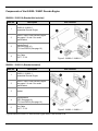
Note 1. Warning!
The flex cable must be installed in the orientation shown in Figure 39 and Figure 40. If the cable
is incorrectly installed, the engine can be damaged, and the warranty voided, see page 52.
Figure 39. Flex Cable Orientation – Imaging Engine
Figure 40. Flex Cable Orientation – Decode Board
Note 2. Proper installation of the flex cable is essential for engine performance. When installing the flex
cable, verify that the flex cable receptacle is fully seated in the engine plug. To achieve a full
connection, ensure that the alignment of the mating parts is not angled during installation. Flex cable
P/N 77-77101 is designed with universal ends.
Note 3. Once installed, it is recommended that the flex cable be connected and routed securely in the
enclosure to prevent loss of connection.
49
Regulatory Compliance
Safety
The IS4920 Series area imaging engines are designed to meet the
requirements of IEC Class 1 in accordance with
IEC 60825-1:1993+A1+A2. IEC Class 1 is defined as follows:
The specifications required for agency approval are not obtainable
until the IS4920 or IS4911 area imaging engine is used in its final
configuration. Honeywell International Inc. is unable to fulfill these
requirements because the imaging engine will operate differently
depending upon where the engine is used as a component.
If the product containing the engine is to be used other than the United States, the manufacturer who
incorporates the imaging engine into their product is responsible for fulfilling any regulatory compliance
requirements for that country. Refer to one of the following sections for further explanation.
Caution
Use of controls or adjustments or performance of procedures other than those specified herein may result in
hazardous radiation exposure. Under no circumstances should the customer attempt to service the LED
engine. Never attempt to look at the LED beam, even if the engine appears to be nonfunctional. Never open
the engine in an attempt to look into the device. Doing so could result in hazardous radiation exposure. The
use of optical instruments with the LED equipment will increase eye hazard.
Europe
The CE Mark is required on products that incorporate the IS4920 series engine if the products are to be
imported into European Economic Area (EEA) countries. Use of the CE Mark requires compliance with
directives and standards dependent upon the type of product. Information may be found at
http://europa.eu.int/comm/enterprise/newapproach/.
LED Safety
IEC 60825-1:1993+A1+A2,
EN 60825-1:1994+A1+A2
Compliance with either of the standards listed above is required for the product to bear the CE mark.
Note: Non-EEA countries may impose additional testing/certification requirements.
EMC
All combinations of IS4920 area imaging engines and associated electronics will require certification of
compliance with the European EMC Directive. EMC compliance of finished products in Europe can be
accomplished by the following method:
The manufacturer may certify to the EC’s Electromagnetic Compatibility Directive 2004/108/EC. Compliance is
required for the product to bear the CE Mark.
Note: Non-EEA countries may impose additional testing/certification requirements.
Electrical Safety
The IS4920 engines are built to conform to the European Low Voltage Directive 2006/95/EC.
50
United States
EMC
All combinations of imaging engines and associated electronics will require testing to insure compliance with
the following Federal Communications Commission regulation: 47 CFR Part 15
Note: When using the imaging engine with RF equipment, modems, etc. may require examination(s) to the
standard(s) for the specific equipment combination. It is the manufacturers’ responsibility to comply
with the applicable federal regulation(s).
Canada
EMC
Products meeting FCC 47 CFR Part 15 will meet Industry Canada interference-causing equipment standard for
digital apparatus, ICES-003. Additional testing is not required.
A written notice indicating compliance must accompany the apparatus to the end user. The notice shall be in
the form of a label that is affixed to the apparatus. The notice may be in the form of a statement included in the
user’s manual if, because of insufficient space or other restrictions, it is not feasible to affix a label to the
apparatus.
51
Limited Warranty
Honeywell International Inc. ("HII") warrants its products and optional accessories to be free from defects in
materials and workmanship and to conform to HII’s published specifications applicable to the products
purchased at the time of shipment. This warranty does not cover any HII product which is (i) improperly
installed or used; (ii) damaged by accident or negligence, including failure to follow the proper maintenance,
service, and cleaning schedule; or (iii) damaged as a result of (A) modification or alteration by the purchaser or
other party, (B) excessive voltage or current supplied to or drawn from the interface connections, (C) static
electricity or electro-static discharge, (D) operation under conditions beyond the specified operating
parameters, or (E) repair or service of the product by anyone other than HII or its authorized representatives.
This warranty shall extend from the time of shipment for the duration published by HII for the product at the
time of purchase ("Warranty Period"). Any defective product must be returned (at purchaser’s expense) during
the Warranty Period to HII factory or authorized service center for inspection. No product will be accepted by
HII without a Return Materials Authorization, which may be obtained by contacting HII. In the event that the
product is returned to HII or its authorized service center within the Warranty Period and HII determines to its
satisfaction that the product is defective due to defects in materials or workmanship, HII, at its sole option, will
either repair or replace the product without charge, except for return shipping to HII.
EXCEPT AS MAY BE OTHERWISE PROVIDED BY APPLICABLE LAW, THE FOREGOING WARRANTY IS
IN LIEU OF ALL OTHER COVENANTS OR WARRANTIES, EITHER EXPRESSED OR IMPLIED, ORAL OR
WRITTEN, INCLUDING, WITHOUT LIMITATION, ANY IMPLIED WARRANTIES OF MERCHANTABILITY OR
FITNESS FOR A PARTICULAR PURPOSE, OR NON-INFRINGEMENT.
HII’S RESPONSIBILITY AND PURCHASER’S EXCLUSIVE REMEDY UNDER THIS WARRANTY IS LIMITED
TO THE REPAIR OR REPLACEMENT OF THE DEFECTIVE PRODUCT WITH NEW OR REFURBISHED
PARTS. IN NO EVENT SHALL HII BE LIABLE FOR INDIRECT, INCIDENTAL, OR CONSEQUENTIAL
DAMAGES, AND, IN NO EVENT, SHALL ANY LIABILITY OF HII ARISING IN CONNECTION WITH ANY
PRODUCT SOLD HEREUNDER (WHETHER SUCH LIABILITY ARISES FROM A CLAIM BASED ON
CONTRACT, WARRANTY, TORT, OR OTHERWISE) EXCEED THE ACTUAL AMOUNT PAID TO HII FOR
THE PRODUCT. THESE LIMITATIONS ON LIABILITY SHALL REMAIN IN FULL FORCE AND EFFECT
EVEN WHEN HII MAY HAVE BEEN ADVISED OF THE POSSIBILITY OF SUCH INJURIES, LOSSES, OR
DAMAGES. SOME STATES, PROVINCES, OR COUNTRIES DO NOT ALLOW THE EXCLUSION OR
LIMITATIONS OF INCIDENTAL OR CONSEQUENTIAL DAMAGES, SO THE ABOVE LIMITATION OR
EXCLUSION MAY NOT APPLY TO YOU.
All provisions of this Limited Warranty are separate and severable, which means that if any provision is held
invalid and unenforceable, such determination shall not affect the validity of enforceability of the other
provisions hereof. Use of any peripherals not provided by the manufacturer may result in damage not covered
by this warranty. This includes but is not limited to: cables, power supplies, cradles, and docking stations. HII
extends these warranties only to the first end-users of the products. These warranties are non-transferable.
The duration of the limited warranty for the IS4920 and IS4921 is two year(s).
52
Patents
For patent information, please refer to www.honeywellaidc.com/patents.
53
Index
A
H
Aiming ............................................................ 16, 34
Ambient Light ....................................................... 16
Ambient Temperature .......................................... 15
Area Illumination .................................................... 4
ASCII ............................................................. 22, 23
Assembly ............................................................... 3
Humidity ....................................................12, 33, 49
B
Bar Code.................................................. 29, 30, 32
Bracket................................................................... 3
Bus....................................................................... 16
C
Cable ................................................................... 15
Camera Aperture ............................................. 4, 13
CMOS sensor .................................................. 1, 16
Connector .......................4, 5, 10, 33, 37–41, 44, 45
Contaminants........................................... 12, 33, 49
Contrast ............................................................... 32
Current ................................................................. 34
Customer Service .................................... 49, 53, 54
D
Depth of Field .......................................... 29, 30, 32
Divergence Angle .................................... 14, 29, 30
E
Electrical
Current Draw .................................................... 36
DC voltages ...................................................... 34
Max Ratings ...................................................... 34
Electrical Specification ................................... 34, 46
Electrostatic Discharge ............................ 12, 34, 49
EMC ............................................................... 46, 47
Enclosure ..................................... 12–14, 44, 45, 49
F
Field of View ...................................... 13, 29, 30, 32
FirstFlash® ............................................ 1, 4, 16, 27
Flex Cable................................................ See Cable
G
Ground ..................................................... 12, 37–41
54
I
Illumination ...............................4, 13, 14, 34, 37–41
Imager ....................................................................4
Imaging Engine ...................................................1, 4
Imaging Sensor ....................................................16
Input ..........................................................34, 37–41
K
Keying ...............................................................4, 33
Keying Location ................................................6–11
L
Label .......................................................................5
Light Levels ..........................................................34
Light Source .........................................................32
Limited Warranty ..................................................49
M
Mega-pixel ..............................................................1
Mode
serial ..................................................................22
Snapshot .....................................................16, 34
Video ...........................................................16, 34
Model ......................................................................1
Mounting ...........................................................6–11
O
Optical Clearance .................................................14
ORC
Fonts ....................................................................1
MICR....................................................................1
ORC-A .................................................................1
ORC-B .................................................................1
Output .............................................................37–41
P
Part Number ...........................................................1
PCLK ....................................................................16
Pin ..................................................................37–41
Pixel ..........................................................16, 37–41
Plug ..........................................................32, 37–41
Power ...................................................................15
Power Supply .......................................................15
R
Receptacle ............................................... 16, 44, 45
Regulatory Compliance ................................. 46, 47
Resolution ............................................................ 32
RMA ..................................................................... 49
Thermal Temperature ...........................................15
Threaded Inserts ....................................................8
Timing ...................................................................24
Torque ..............................................................6–11
Trigger ............................................................37–41
S
V
Self-Tapping Screw ................................. 1, 4, 6–11
Serial Configuration ............................................. 22
Serial Label ............................................................ 5
Service ..................................................... 49, 53, 54
Shock ....................................................... 33, 44, 45
Signals ......................................... 15–28, 34, 37–41
Snapshot Mode.............................................. 16, 34
SwiftDecoder™ ...................................................... 1
Video Mode ....................................................16, 34
Voltage .........................................34, 37–41, 46, 47
T
Targeting.................................................... 4, 37–41
Temperature ........................................................ 33
W
Warranty ...............................................................49
Watt(s) ..................................................................46
Weight ..................................................................33
Window
coatings .............................................................13
materials ............................................................13
specifications .....................................................13
transmission.......................................................13
55
Customer Support
Technical Assistance
If you need assistance installing or troubleshooting your device, please call your distributor or the nearest
technical support office:
North America/Canada
Telephone: (800) 782-4263
E-mail: [email protected]
Latin America
Telephone: (803) 835-8000
Telephone: (800) 782-4263
E-mail: [email protected]
Brazil
Telephone: +55 (11) 5185-8222
Fax: +55 (11) 5185-8225
E-mail: [email protected]
Mexico
Telephone: 01-800-HONEYWELL (01-800-466-3993)
E-mail: [email protected]
Europe, Middle East, and Africa
Telephone: +31 (0) 40 7999 393
Fax: +31 (0) 40 2425 672
E-mail: [email protected]
Hong Kong
Telephone: +852-29536436
Fax: +852-2511-3557
E-mail: [email protected]
Singapore
Telephone: +65-6842-7155
Fax: +65-6842-7166
E-mail: [email protected]
China
Telephone: +86 800 828 2803
Fax: +86-512-6762-2560
E-mail: [email protected]
Japan
Telephone: +81-3-3839-8511
Fax: +81-3-3839-8519
E-mail: [email protected]
Online Technical Assistance
You can also access technical assistance online at www.honeywellaidc.com.
56
Product Service and Repair
Honeywell International Inc. provides service for all its products through service centers throughout the world.
To obtain warranty or non-warranty service, contact the appropriate location below to obtain a Return Material
Authorization number (RMA #) before returning the product.
North America
Telephone: (800) 782-4263
E-mail: [email protected]
Latin America
Telephone: (803) 835-8000
Telephone: (800) 782-4263
Fax: (239) 263-9689
E-mail: [email protected]
Brazil
Telephone: +55 (11) 5185-8222
Fax: +55 (11) 5185-8225
E-mail: [email protected]
Mexico
Telephone: 01-800-HONEYWELL (01-800-466-3993)
Fax: +52 (55) 5531-3672
E-mail: [email protected]
Europe, Middle East, and Africa
Telephone: +31 (0) 40 2901 633
Fax: +31 (0) 40 2901 631
E-mail: [email protected]
Hong Kong
Telephone: +852-29536436
Fax: +852-2511-3557
E-mail: [email protected]
Singapore
Telephone: +65-6842-7155
Fax: +65-6842-7166
E-mail: [email protected]
China
Telephone: +86 800 828 2803
Fax: +86-512-6762-2560
E-mail: [email protected]
Japan
Telephone: +81-3-3839-8511
Fax: +81-3-3839-8519
E-mail: [email protected]
Online Product Service and Repair Assistance
You can also access product service and repair assistance online at www.honeywellaidc.com.
57
Honeywell Scanning & Mobility
9680 Old Bailes Road
Fort Mill, SC 29707
www.honeywellaidc.com
00-05325 Rev H
November 2010