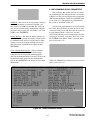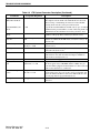
1
08/7,1(7 9,.,1*&0&. [[ 0+]+$1'+(/' 9'&:DWWV 0+]7[0+]5[ 3DUW1R[[[[ &RS\ULJKWE\WKH()-RKQVRQ&RPSDQ\ 7KH()-RKQVRQ&RPSDQ\GHVLJQVDQGPDQXIDFWXUHVWZRZD\UDGLRHTXLSPHQWWRVHUYHD ZLGH YDULHW\ RI FRPPXQLFDWLRQ QHHGV () -RKQVRQ SURGXFHV HTXLSPHQW IRU ODQG PRELOH UDGLRDQGPRELOHWHOHSKRQHVHUYLFHVZKLFKLQFOXGHEXVLQHVVLQGXVWULDOJRYHUQPHQWSXEOLF VDIHW\DQGSHUVRQDOXVHUV 9LNLQJ +HDG() -RKQVRQ ORJR 9LNLQJ 0XOWL1HW /75 $YHQJHU DQG &DOO *XDUG DUH UHJLVWHUHG WUDGHPDUNV RI WKH () -RKQVRQ &RPSDQ\ $OO RWKHU FRPSDQ\ DQGRU SURGXFW QDPHV XVHG LQ WKLV PDQXDO DUH WUDGHPDUNV DQGRU UHJLVWHUHG WUDGHPDUNV RI WKHLU UHVSHFWLYH PDQXIDFWXUHU ,QIRUPDWLRQLQWKLVPDQXDOLVVXEMHFWWRFKDQJHZLWKRXWQRWLFH GENERAL INFORMATION SECTION 1 GENERAL INFORMATION 1.1 SCOPE OF MANUAL 1.2.3 8585-8588 MODELS This service manual contains installation, operation, programming, alignment, and service information for the E.F. Johnson Multi-Net® 8560-8568 Viking CK and 8588-8588 Viking CM transceivers. For information on servicing the LTR® version of these transceivers (Viking CL), refer to Service Manual Part No. 001-8560-005. The 8585-8588 models are enhanced versions of the 8565-8568. These models have a 16-position quick select switch on the top panel which allows up to 16 preprogrammed system/groups to be quickly selected. In addition, they have enhanced software which allows the selected system or group to be decreased as well as increased. Also, a special menu can be selected for controlling high and low power, keypad disable, and clear-to-talk tone loudness. Other hardware differences between these and the 85608568 models are the top and front panels and logic board. Each of these models are also available with a DTMF keypad for making telephone calls. 1.2 EQUIPMENT DESCRIPTION 1.2.1 GENERAL The available Multi-Net transceivers and the main features of each are shown in Table 1-1. The 8560-8566 and 8585-8588 models covered by this manual operate on the 800 MHz frequencies from 806-825 MHz (mobile transmit). The receive channels are 45 MHz above these frequencies from 851-870 MHz. Channel spacing is 25 kHz and maximum deviation is 5 kHz. With NPSPAC models (see Section 1.2.6), channel spacing is 12.5 kHz and maximum deviation is 4 kHz. 1.2.4 VIKING CK AND CM MODELS In mid 1994, Viking CK and CM models were introduced. The CK designation applies to the 85608568, and the CM designation applies to the 85858588. The main change that occurred with these models is that the power output of the standard and NPSPAC models increased from 2.5 watts to 3.0 watts. The power output of the 1-watt models is unchanged as is the 2.5-watt power output of the high power intrinsically safe models. These transceivers can be programmed with up to 14 systems. Each Multi-Net system can be programmed with up to 11 groups, and each LTR and conventional system can be programmed with up to 10 groups. 1.2.5 INTRINSICALLY SAFE MODELS The intrinsically safe versions meet Factory Mutual standards for operation in certain flammable atmospheres. This manual covers servicing of both types of transceivers. Refer to Section 1.10 for important information on servicing intrinsically safe models. 1.2.2 8560-8568 MODELS The 8560 is the base 1-watt model, and the 8565 is the base high power model. Each is available with a DTMF keypad for making telephone calls (see photos on front cover). The 8560 power output is fixed, and the 8565 has a user selectable power output of 1.8 and 3.0 watts (see Section 1.2.4 for more information). 1.2.6 NPSPAC MODELS The NPSPAC transceivers meet the stricter specifications established by NPSPAC (National Public Safety Panel Advisory Committee) for operation on the public safety frequencies from 821-824 and 866869 MHz. The only differences between these and non-NPSPAC models are the TCXO (a 1.5 PPM version is used), receiver ceramic filter Z522, and the alignment procedure (deviation is less). The other 856x models are intrinsically safe and NPSPAC versions of these transceivers. All 85608568 models operate the same because they have the same software. These transceivers do not have a quick select switch or the other operation enhancements of the 8585-8588. 1-1 Revised February 1997 Part No. 001-8560-381 GENERAL INFORMATION Table 1-1 EFJOHNSON MULTI-NET TRANSCEIVERS Transceiver Freq (MHz) Type M-Net/LTR/Conv Power System/ Operation; Conv Output Groups [1] Talk-Around Special Features 8160 Avr SK 8161 Avr SK 8190 Vik CR 8560 Vik CK 8561 Vik CK 8562 Vik CK 8563 Vik CK 8565 Vik CK 8566 Vik CK 8567 Vik CK 8568 Vik CK 8570 Vik CK 8571 Vik CK 8585 Vik CM 8586 Vik CM 8587 Vik CM 8588 Vik CM 800 800 800 800 800 800 800 800 800 800 800 900 900 800 800 800 800 Handheld Handheld Handheld Handheld Handheld Handheld Handheld Handheld Handheld Handheld Handheld Handheld Handheld Handheld Handheld Handheld Handheld 1/3W 1/2W 0.6/1W 1W 1W 1W 1W 1.8/3.0W 1.5/2.5W 1.8/3.0W 1.5/2.5W 1W 1W 1.8/3.0W 1.5/2.5W 1.8/3.0W 1.5/2.5W 14/11 14/11 32/11 14/11 14/11 14/11 14/11 14/11 14/11 14/11 14/11 14/11 14/11 14/11 14/11 14/11 14/11 Yes Yes Talk-Around N/A Yes Yes Yes Yes Yes Yes Yes Yes Yes Yes Yes Yes Yes Yes 8590 Vik CM 8591 Vik CM 900 900 Handheld Handheld 1W 1W 14/11 14/11 Yes Yes Small size, Qk Sel Sw Small size, Qk Sel Sw, NPSPAC Full duplex cellular style Standard Model Intrinsically Safe NPSPAC Intrin Safe, NPSPAC High Power High Power, Intrin Safe High Power, NPSPAC Hi Pwr, Intrin Safe, NPSPAC Standard Model Intrinsically Safe Hi Pwr, Quick Select Switch Hi Pwr, Qk Sel Sw, Intrin Safe Hi Pwr, Qk Sel Sw, NPSPAC Hi Pwr, Qk Sel Sw, Intrin Safe, NPSPAC Quick Select Switch Qk Sel Sw, Intrin Safe 8605 8606 8615 8616 8620 8621 8622 8655 800 800 800 800 800 800 800 900 Frt Mount Frt Mount Frt Mount Frt Mount Rem Mount Rem Mount Rem Mount Frt Mount 15W 15W 35W 35W 35W 35W 12W 30W 16/11 16/11 16/11 16/11 16/11 16/11 16/11 16/11 Yes Yes Yes Yes Yes Yes Talk-Around N/A Yes Low Power Low Power, NPSPAC High Power High Power, NPSPAC High Power, Remote Mount High Pwr, Rem Mt, NPSPAC Full Duplex High Power 9753 Sum DM 800 Frt Mount 15W 32/11 Yes Hi Spec/Full Feature, Low Pwr 9754 Sum DM 800 Rem Mount 15W 32/11 Yes Hi Spec/Full Feature, Low Pwr 9755 Sum DM 800 Frt Mount 35W 32/11 Yes Hi Spec/Full Feature, Hi Pwr 9756 Sum DM 800 Rem Mount 35W 32/11 Yes Hi Spec/Full Feature, Hi Pwr 9773 Sum DM 900 Frt Mount 15W 32/11 Yes Hi Spec/Full Feature, Low Pwr 9774 Sum DM 900 Rem Mount 15W 32/11 Yes Hi Spec/Full Feature, Low Pwr 9775 Sum DM 900 Frt Mount 30W 32/11 Yes Hi Spec/Full Feature, Hi Pwr 9776 Sum DM 900 Rem Mount 30W 32/11 Yes Hi Spec/Full Feature, Hi Pwr [1] All models have up to 11 groups per Multi-Net system and up to 10 groups per LTR or conventional system. The 97xx transceivers can be programmed with more systems if less than the maximum number of groups are programmed (see Section 1.2.3). 1.2.7 VOICE ENCRYPTION This feature prevents conversations from being monitored by casual eavesdropping or analog scanners. Refer to Section 2.3.18 for more information on encryption. Voice encryption is available as a factory installed option on 8585-8588 transceivers (see Section 1.4). It is not available as a field-installed kit. Revised February 1997 Part No. 001-8560-381 1-2 GENERAL INFORMATION 1.2.8 MISCELLANEOUS INFORMATION 1.3 PART NUMBER BREAKDOWN The 856x and 857x transceivers shown in Table 1-1 are available in Multi-Net and LTR versions, and the 858x and 859x transceivers are available in only the Multi-Net version. The difference between the Multi-Net and LTR versions of the 856x/857x is the operating software in the microprocessor. The following is a breakdown of the part number used to identify this transceiver: NOTE: Encryption is available for 8585-8588 models only (see Section 1.2.7). 242 The Multi-Net models can be programmed for Multi-Net, LTR, and conventional operation, and the LTR models can be programmed for only LTR and conventional operation. Up to 14 systems can be programmed, and each Multi-Net system can have up to 11 groups, and each LTR and conventional system up to 10 groups. – 8 5x x – x 1 x See Table 1-1 0 = Std w/o accessories 1 = Std w/ant, bat, belt clip 2 = Std w/o access, w/encrypt 3 = Std w/ant, bat, clip, encryp 4 = 3W w/o accessories 5 = 3W w/ant, bat, belt clip 6 = 3W w/o access, w/encryp 7 = 3W w/ant, bat, clip, encryp Like other E.F. Johnson Multi-Net and LTR transceivers, these are digitally synthesized and logic controlled. In the Multi-Net and LTR modes, all the user has to do to make a call is select the desired system and group and press the push-to-talk switch. If a busy or out-of-range condition is not indicated by special tones, the path to the other party is complete and speaking can begin. Channel selection, monitoring before transmitting, and squelch control are all performed by the logic. 1 = LTR 2 = LTR w/DTMF 5 = Multi-Net 6 = Multi-Net w/DTMF 1.4 TRANSCEIVER IDENTIFICATION Programming is performed using a dealer supplied IBM® PC or compatible computer and EFJohnson programming software. No PROMs are ever needed because the personality information is stored by a reprogrammable memory device called an EEPROM. Refer to Section 4 for more programming information. The transceiver identification number is printed on a label that is affixed to the back cover. The identification number used with Viking CK and CM models is shown below and has an additional digit after the model number. This digit is used to identify the transceiver as a Multi-Net or LTR model and also if it has standard (1 or 2.5W) or 3W power output. For example, a Viking CK 8566 has a “5” because it is 2.5 watts, and a Viking CK 8565 has a “6” because it is 3 watts. An 85xx handheld transceiver can be converted to mobile operation using the optional Vehicular Adapter. Plugging the transceiver into this adapter connects it to the mobile antenna, microphone, and speaker. The Remote Control Unit can also be used in this application if desired. Model From P.N. The optional Vehicular Charger accessory is a low-cost alternative to the Vehicular Adapter. It provides only trickle charging and does not allow the use of the Remote Control Unit. Refer to Section 5 for more information on these accessories. 85xx x Revision Manufacture Warranty Plant Number Letter Date A 1 = LTR std 2 = LTR 3W 5 = M-Net std 6 = M-Net 3W 1-3 23 7 A 12345 A = Waseca Last Digit of Year Week No. of Year Revised February 1997 Part No. 001-8560-381 GENERAL INFORMATION • The following information is contained in numbers used with most earlier non-Viking CK/CM models. For the manufacture date, the 8560-8563 use month/year and the 8565-8568 use week/year. Model From P.N. 85xx Programming Accessories - Refer to Section 4 for information on transceiver programming. Revision Manufacture Warranty Plant Number Letter Date A Month or Week 23 7 A Extension Test Cable and Accessory Connector Kit- The extension test cable is used to operate the transceiver with the front cover removed. The accessory connector kit contains the parts required to make a test cable or some other type of cable that plugs into the accessory connector. This particular kit does not include the magnets that may be required for the LTR 5876 transceiver. Use Kit, Part No. 023-5810-110, if those magnets are required. 12345 A = Waseca Last Digit of Year 1.5 ACCESSORIES The accessories available for this transceiver are listed in Table 1-2. A brief description of several of these accessories follows. Table 1-2 856x/858x Accessories Accessory Battery Chargers - The -400/-476 chargers utilize ∆T/∆t charging technology. Refer to Sections 5.1 and 5.2 for information on battery packs and chargers. Vehicular Adapter and Remote Control UnitAllow transceiver to be converted to mobile use. Refer to Section 5 for more information. Microphones, Speaker, and Adapters - The speakermicrophones are equipped with a 360° swivel clip for attachment to the collar or lapel. They also have an earphone connector. The earphone and antenna adapters allow an earphone or external antenna to be connected to the accessory connector. The antenna adapter includes a 6-foot RG-58 cable with a female BNC connector. The transceiver automatically switches to the external device when these adapters are used. Carrying Accessories - The carrying accessories listed allow the transceiver to be carried in the following ways: • D-swivel attachment to the belt without a leather case. The –130 belt loop and –121 transceiver attachments are used. • D-swivel attachment to the belt or chest with the –125 leather case. The –130 belt loop is used to attach this case to the belt, or the –004 shoulder strap is used to attach it to the chest. Revised February 1997 Part No. 001-8560-381 Clip attachment to the belt without a D-swivel or leather case. This requires the –126 or –128 belt clip. A belt clip is included in the standard package. 1-4 Part No. Battery Packs 7.5V 1400 mAH (standard) 7.5V 1400 mAH (intrinsically safe) Antenna, Flexible 1/4-wave 1/2-wave 501-0105-012 501-0105-013 Battery Chargers Five-Unit Rapid Single-Unit Rapid (base only) 120 VAC power supply for -476 base 240 VAC power supply for -476 base Trickle (100 mA) transformer Base for trickle charger 239-5800-400 239-5800-476 585-4001-101 585-4001-102 563-0001-003 239-5800-371 Vehicular Adapter* Remote Control Unit, Multi-Net* Vehicular Charger* 239-5810-500 250-8610-506 239-5810-811 Speaker-Microphone, w/ant connector Speaker-Microphone, w/int amp Earphone for above speaker-mics Earphone (plugs into accessory conn.) External Antenna Adapter Cable Earphone Adapter, submin jack Earphone for above adapter, straight Earphone for above adapter, right angle 589-0015-015 589-0015-020 250-0881-003 250-5810-816 250-5810-813 250-5810-818 250-0881-001 250-0881-002 587-8565-171 587-8565-162 GENERAL INFORMATION Table 1-2 856x/858x Accessories (Continued) Accessory Dual earpiece headset w/mic (following cable also required) Belt mount PTT sw and interface cable Carrying Accessories Leather belt loop with D-swivel Leather case with D-swivel Shoulder strap Perimeter strap D-Swivel attachment for transceiver (if -125 case is not used) Belt clip for transceiver (if D-swivel and leather case are not used) Metal spring type Plastic press type contacted for Warranty Service Reports, claim forms, or any other questions concerning warranties or warranty service. Part No. 589-9006-021 1.7 FACTORY CUSTOMER SERVICE 589-9006-022 The Customer Service Department of the E.F. Johnson Company provides customer assistance on technical problems and the availability of local and factory repair facilities. Regular Customer Service hours are 7:30 AM. - 5:30 PM. Central Time, Monday - Friday. The Customer Service Department can be reached using one of the following telephone numbers: 023-8790-130 023-8560-125 508-4009-004 508-4011-410 250-5810-121 Toll-Free: (800) 328-3911 (From within continental United States only) 250-5810-126 250-5810-128 International: (507) 835-6911 Programming Accessories Remote Prog Interface (RPI) RPI Interface Cable (85xx) RPI Interface Cable (Control Unit) Replication Cable Cable, RPI to computer 6’ DB9M-DB9F Cable, RPI to computer 6’ DB25 M-F Cable, RPI to computer 6’ DB25M-DB9F Programming Software, Transceiver and Remote Control Unit IBM 5.25" Disk IBM 3.5" Disk 023-9800-000 023-5810-011 597-2002-200 023-5810-013 597-5900-002 023-5800-017 597-0005-057 FAX: (507) 835-6969 023-9998-191 023-9998-192 When your call is answered at the E.F. Johnson Company, you will hear a brief message informing you of numbers that can be entered to reach various departments. This number may be entered during or after the message using a tone-type telephone. If you have a pulse-type telephone, wait until the message is finished and an operator will come on the line to assist you. When you enter some numbers, another number is requested to further categorize the type of information you need. E-Mail: First Initial/Last [email protected] (You need to know the name of the person you want to reach. Example: [email protected]) NOTE: Emergency 24-hour technical support is also available at the 800 and preceding numbers during off hours, holidays, and weekends. Star washer, unprogrammed 015-0900-305 (see Section 1.12) Extension Test Cable 023-8560-910 Accessory Connector Kit 023-5810-109 SMA-BNC F-F adapter 515-3102-050 * Refer to Tables 5-1 and 5-2 for additional vehicle adapter accessories. You may also contact the Customer Service Department by mail. Please include all information that may be helpful in solving your problem. The mailing address is as follows: 1.6 PRODUCT WARRANTY The warranty statement for this transceiver is available from your product supplier or from the Warranty Department, E.F. Johnson Company, 299 Johnson Avenue, P.O. Box 1249, Waseca, MN 560930514. This information may also be requested from the Warranty Department by phone as described in Section 1.7. The Warranty Department may also be E.F. Johnson Company Customer Service Department 299 Johnson Avenue P.O. Box 1249 Waseca, MN 56093-0514 1-5 Revised February 1997 Part No. 001-8560-381 GENERAL INFORMATION 1.8 FACTORY RETURNS Johnson dealers also need to give their account number. If there is uncertainty about the part number, include the designator (C512, for example) and the model number of the equipment the part is from. Repair service is normally available through local authorized E.F. Johnson Land Mobile Radio Service Centers. If local service is not available, the equipment can be returned to the factory for repair. However, it is recommended that you contact the Customer Service Department before returning equipment because a service representative may be able to suggest a solution to the problem so that return of the equipment would not be necessary. You may also send your order by mail or FAX. The mailing address is as follows and the FAX number is shown in Section 1.7. E.F. Johnson Company Service Parts Department 299 Johnson Avenue P.O. Box 1249 Waseca, MN 56093-0514 Be sure to fill out a Factory Repair Request Form #271 for each unit to be repaired, whether it is in or out of warranty. These forms are available free of charge by calling Customer Service (see Section 1.7) or by requesting them when you send a unit in for repair. Clearly describe the difficulty experienced in the space provided and also note any prior physical damage to the equipment. Then include a form in the shipping container with each unit. Your telephone number and contact name are important because there are times when the technicians have specific questions that need to be answered in order to completely identify and repair a problem. 1.10 INTRINSICALLY SAFE INFORMATION 1.10.1 INTRODUCTION The 8561, 8563, 8566, 8568, 8586, and 8588 transceivers have been approved by the Factory Mutual Research Corporation for operation in certain flammable atmospheres. The specific atmospheres in which operation is approved are shown in Section 1.10.5 and also on the label on the back cover of the transceiver. When returning equipment for repair, it is also a good idea to use a PO number or some other reference number on your paperwork in case you need to call the repair lab about your unit. These numbers are referenced on the repair order and it makes it easier and faster to locate your unit in the lab. WARNING When servicing an intrinsically safe transceiver, the following rules must be followed to maintain intrinsic safety: • Return Authorization (RA) numbers are not necessary unless you have been given one by the Field Service Department. RA numbers are required for exchange units or if the Field Service Department wants to be aware of a specific problem. If you have been given an RA number, reference this number on the Factory Repair Request Form sent with the unit. The repair lab will then contact the Field Service Department when the unit arrives. Factory Mutual Research Corporation 1151 Boston-Providence Turnpike P.O. Box 9102 Norwood, Massachusetts 02062 Phone: (617) 762-4300 1.9 REPLACEMENT PARTS E.F. Johnson replacement parts can be ordered directly from the Service Parts Department. To order parts by phone, dial the toll-free number as described in Section 1.7. When ordering, please supply the part number and quantity of each part ordered. E.F. Revised February 1997 Part No. 001-8560-381 Service can be provided only by the factory or by service centers specifically authorized by the Factory Mutual Research Corporation to service E.F. Johnson intrinsically safe transceivers. Contact Factory Mutual at the following address for information concerning their auditing procedure. Contact the E.F. Johnson Customer Service Department as described in Section 1.7 if you have questions. • 1-6 Replace the battery pack only with Intrinsically Safe Battery Pack, Part No.587-8560-160 (1000 mAH) GENERAL INFORMATION or 587-8565-162 (1400 mAH). The 1000 mAH pack cannot be used with 8565-8588 transceivers. 1.10.4 INTRINSICALLY SAFE AND NONINCENDIVE RATINGS • Do not make any modifications to the circuitry. • When replacing a part, use only the exact replacement part listed in the service manual parts list. • Do not install any accessory that is not specifically approved for use in intrinsically safe 85xx models. This transceiver is rated intrinsically safe for some types of hazards and nonincendive for other types of hazards. An intrinsically safe rating applies to operation in Division 1 areas, and a nonincendive rating applies to operation in Division 2 areas (see next section). The difference between these ratings is as follows: 1.10.2 DEFINITIONS The intrinsically safe rating is a higher rating because more severe conditions must be met. To be approved for this rating, the transceiver must not cause ignition of a particular atmosphere if two of the faults specified in the testing procedure occur. In other words, it must be able to withstand two simultaneous unrelated breakdowns without causing ignition. To receive a nonincendive rating, the transceiver needs to withstand only a single fault without causing ignition of a particular atmosphere. Intrinsically Safe - This is a fire rating given to these transceivers by the Factory Mutual Research Corporation. When electrical equipment is given this rating, the equipment is considered incapable of releasing sufficient electrical and thermal energy under normal operation or specified fault conditions per the testing standard to cause ignition of a specific flammable or combustible atmosphere in its most easily ignited concentration. In other words, this transceiver should not cause a fire or explosion when used in certain flammable atmospheres. 1.10.5 CLASSIFICATION OF HAZARDOUS AREAS AND ATMOSPHERES Fault - A defect or electrical breakdown of any component, spacing, or insulation which alone or in combination with other faults may adversely affect the electrical or thermal characteristics of the intrinsically safe circuit (for example, a shorted transistor). Introduction The specific hazardous atmospheres and areas in which this transceiver is approved for operation are as follows. These descriptions are also indicated on the label on the back panel of the transceiver. The meanings of these Class, Division, and Group designations are as follows. 1.10.3 POSSIBLE IGNITION SOURCES When a transceiver is checked by Factory Mutual, possible sources of ignition are checked. These sources may be electrical (spark) or thermal (heat). The following could be sources of spark ignition: • • • • Intrinsically Safe - Class I and II, Division 1, Groups C, D, E, F, and G. Nonincendive - Class I, Division 2, Groups A, B, C, and D. Discharge of a capacitive circuit by a fault such as a short circuit. Interruption of an inductive circuit. Intermittent making or breaking of a resistive circuit. Hot-wire fusing. Temperature Code - T4A (1000 mAH pack, Part No. 587-8560-160) or T3C (1400 mAH pack, Part No. 587-8565-162). Atmosphere Classification (Class/Group) The following could be sources of thermal ignition: • • For the purposes of testing and approval, various atmospheric mixtures have been grouped on the basis of their hazardous characteristics. Equipment is approved for a class of material and also for the specific gas, vapor, or dust in that class. Class I mate- Heating of a small-gauge wire or PC board trace. High surface temperature of components. 1-7 Revised February 1997 Part No. 001-8560-381 GENERAL INFORMATION rials include gases and vapors, Class II materials include combustible dusts, and Class III materials include ignitable fibers. The various classes and some specific groups of gases in each are shown in Table 13. two remaining tabs on the star washer. To limit the rotation of this switch to certain positions, a new star washer (Part No. 015-0900-305) is required. One new star washer is included with the transceiver. To program this washer, proceed as follows: Table 1-3 Material Classification 1. Pull off the rubber knob cover and note the vertical position of the knob on the shaft. Loosen the set screw and remove the knob. Typical Hazard Group Class Acetylene Hydrogen Ethylene, ethyl ether, cyclopropane Gasoline, naphta, butane, propane, alcohol, acetone, benzol, natural gas Metal dust including aluminum, magnesium, and their alloys Carbon black, coal, or coke dust Flour, starch, or grain dusts Ignitable fibers/flyings such as rayon or cotton A B C D I I I I E II F G - II II III 2. Place the new star washer over the shaft as shown below (do not remove the spanner nut yet). Area Classification (Division) 3. The tabs removed are opposite the positions to be selected. Therefore, determine what numbers are opposite and then mark the tabs between those numbers. For example, to select positions 1-4, mark the three tabs between 9 and 12. Areas are either Division 1 or 2 as shown in Table 1-4. Since a Division 1 area is considered the most hazardous, a transceiver approved for a specific Division 1 area can also be used in the same Division 2 Class/Group. 4. Remove the marked tabs as shown below by bending them sharply or cutting them off. Table 1-4 Area Classification Division 1 2 Area An area where there is or could be an explosive atmosphere most of the time in normal operation. An area where an explosive atmosphere exists only as a result of a fault (something going wrong). 1.11 PROGRAMMING QUICK SELECT SWITCH STOPS (858x ONLY) 5. Remove the spanner nut and old star washer. Install the new star washer. Make sure that the removed tabs are opposite the numbers to be selected. There is a star washer under the quick select switch knob of 858x transceivers that limits the rotation of the switch (see Figure 1-1). As received from the factory, only the dot (● ) position of this switch is locked out. To also select that position, remove the Revised February 1997 Part No. 001-8560-381 6. Replace the spanner nut, knob, and rubber knob cover. 1-8 GENERAL INFORMATION Figure 1-1 Quick Select Switch Exploded View 1.12 INTERNET HOME PAGE The E.F. Johnson Company has a home page on the World Wide Web that can be accessed for information on such things as products, systems, and regulations. The address is http://www.efjohnson.com. 1-9 Revised February 1997 Part No. 001-8560-381 GENERAL INFORMATION MULTI-NET 8560-8566 AND 8585-8588 SPECIFICATIONS The following are general specifications intended for use in testing and servicing this transceiver. For current advertised specifications, refer to the specification sheet available from the Marketing Department. Specifications are subject to change without notice. GENERAL Operating Mode Frequency Range Systems Groups Channels Tx/Rx Separation Channel Spacing Channel Increment Dimensions Weight Power Source Compliance Circuit Protection Typical Battery Life, 5-5-90% duty cycle (Transmit/Receive/Standby) Multi-Net and LTR (trunked); Conventional (non-trunked) 806-825 MHz transmit, 851-870 MHz receive (standard) 851-870 MHz transmit (Conventional talk-around) Up to 14 Up to 11 per system (Multi-Net) Up to 10 per system (LTR and Conventional) Up to 10 per system, 140 total (Conventional) 45 MHz (no separation in talk-around) 25 kHz (12.5 kHz NPSPAC 12.5 kHz 5.90" (w/o bat), 8.31" (w/bat) H x 2.76" W x 1.70" D 15.0 cm (w/o bat), 21.1 cm (w/bat) H x 7.0 cm W x 4.3 cm D 15.0 oz (w/o bat), 24.7 oz. (w/ bat) 425 g (w/o bat), 700 g (w/bat) 7.5 VDC (nominal) rechargeable Nickel-Cadmium batt pack FCC Parts 15 and 90 4-ampere fuse on motherboard 8560-8563 - 11 hours (1000 mAH bat), 14 hours (1400 mAH bat) 8565-8588 (2.5W) - 10.5 hrs @ 1.5 W, 9.0 hrs @ 2.5W (1400 mAH battery pack) 8565-8588 (3.0W) - 10.3 hrs @ 1.8W, 8.5 hrs @ 3.0W (1400 mAH battery pack) RECEIVER Sensitivity Selectivity Standard 25 kHz NPSPAC 12.5 kHz Spurious and Harmonic Rejection Intermodulation Hum and Noise Audio Output Power Audio Distortion Audio Response Channel Spread 0.35 µV (12 dB SINAD) –70 dB –20 dB –70 dB (60 dB 1st/2nd image) –65 dB –40 dB (–30 NPSPAC) Internal Speaker - 0.5 watt (16-ohm load) External Speaker - 0.125 watt (16-ohm load) Less than 5% at rated output at speaker outputs (slightly higher at external speaker output of accessory connector) +2, –10 dB from 6 dB per octave pre-emphasis characteristic from 300-3000 Hz 19 MHz 1-10 Revised February 1997 Part No. 001-8560-381 GENERAL INFORMATION Frequency Stability Input Impedance Current Drain ± 2.5 PPM from –22 to +140 degrees F (–30 to +60 degrees C) ± 1.5 PPM (NPSPAC models) 50 ohms Standby (squelched) - 60 mA maximum, 55 mA typical Rated audio output - 250 mA maximum, 225 mA typical TRANSMITTER RF Power Output (see Section 1.2.4) 8560-8563 - 1 watt standard, 0.8 watt talk-around 8565-8588 (2.5W) high pwr - 2.5W standard, 2.0 W talk-around 8565-8588 (2.5W) low power - –2.25 ±.75 dB of high pwr setting (1.5 watt typical) 8565/67, 8585/87 (3.0W) high pwr - 3.0W std, 2.0 W talk-around 8565/67, 8585/87 (3.0W) low power - 1.8W typical Spurious and Harmonic Standard Models NPSPAC Models Audio Distortion Audio Frequency Response –55 dB (std), –47 dB (talk-around) FM Hum and Noise –40 dB (w/C-message weighting) –34 dB 5% maximum at 1 kHz +1, –3 dB from a 6 dB per octave de-emphasis characteristic from 300-3000 Hz 16KOF1D, 16KOF3E (standard) 14KOF1D, 14KOF3E (NPSPAC) 19 MHz (806-825 and 851-870 MHz) ±2.5 PPM from -22 to +140 degrees F (–30 to +60 degrees C) ±1.5 PPM NPSPAC 8560-8563 - 700 mA maximum, 600 mA typical 8565-8588 (2.5W) - 1350 mA maximum low power (1.5W) 1850 mA maximum high power (2.5W) 8565-8588 (3.0W) - 1400 mA maximum low power (1.5W) 2000 mA maximum high power (2.5W) 50 ohms 10% Audio Modulation Channel Spread Frequency Stability Current Drain Load Impedance Duty Cycle (6-6-48 seconds) (Transmit/Receive/Standby) Revised February 1997 Part No. 001-8560-381 1-11 GENERAL INFORMATION Revised February 1997 Part No. 001-8560-381 1-12 MULTI-NET SYSTEM OVERVIEW SECTION 2 MULTI-NET SYSTEM OVERVIEW REPEATERS (UP TO 30 PER RNT) OTHER RNT’S AND SYSTEMS AUDIO AND DATA LINK MULTI-NET 856x/7x/8x/9x, 8605/15/22/55, REMOTE NETWORK TERMINAL (RNT) SUMMIT DM 975x/977x MOBILE TRANSCEIVERS MULTI-NET PUBLIC SWITCHED TELEPHONE NETWORK (PSTN) AUDIO AND DATA LINK LTR 98xx, 8600/04, 856x/857x, 5876, 86xx, VIKING GT/HT 965x/967x MOBILE TRANSCEIVERS LTR DISPATCHER CONSOLE AUDIO AND DATA LINK CONVENTIONAL 98xx, 5876, 71x6/718x CONVENTIONAL SYSTEM MANAGEMENT MODULE USAGE ACCOUNTING SYSTEM Figure 2-1 Multi-Net System Components 2.1 MULTI-NET SYSTEM COMPONENTS levels of priority access are available if Multi-Net signaling is used. NOTE: For more information on Multi-Net systems, refer to the Multi-Net Application Note, Part No. 009-3039-003. 2. Users of different types of radio equipment can talk to each other. For example, a mobile operating on a Multi-Net 800 MHz channel could talk to a mobile operating on a conventional UHF channel. 2.1.1 INTRODUCTION The basic components of a Multi-Net system are shown in Figure 2-1. Because of the built-in adaptability of a Multi-Net system, one can be designed to meet the communication needs of almost any type of user. The following are some operating features that a Multi-Net system can provide: 3. Wide area radio coverage can be provided so that a mobile could talk to another mobile that is using a repeater that may be hundreds of miles away. That repeater may be part of the same Multi-Net system or another Multi-Net system. Phone lines or some other type of link can be used to provide a communication path. 1. Advanced features such as up to 8000 Unique ID code, automatic mobile identification, and five 2-1 Revised February 1997 Part No. 001-8560-381 MULTI-NET SYSTEM OVERVIEW Multi-Net systems are not restricted to a certain type of signaling. For example, an entire Multi-Net system could be designed using conventional channels which use tone or digitally controlled squelch. The various types of signaling can also be mixed in a system. For example, there could be ten channels using Multi-Net signaling, ten channels using LTR signaling, and ten channels using conventional signaling. Your EFJohnson representative can provide more information on the capabilities of Multi-Net systems. reprogramming of mobiles and disabling of lost or stolen mobiles are also performed by the SMM. The following information describes the MultiNet components shown in Figure 5-1. 2.1.5 DISPATCH CONSOLES A single RNT can control up to 30 repeaters which is the maximum allowed by the FCC at one site. The RNT is configured with one Channel Interface Module (CIM) for each repeater it controls and an Intelligent Dispatch Module (IDM) for each EFJohnson Dispatch Console. It also contains a Telephone Interface Module (TIM) for each telephone line used for interconnect calls and other modules. One or more EFJohnson Dispatch Consoles or other consoles can be connected to the RNT using direct connection, phone lines, or other types of links. Depending on the capabilities of the particular console, the dispatcher can perform such functions as placing calls to specific mobiles, placing calls to other dispatchers, patching mobiles together so they can talk to each other, and monitoring status messages from mobiles. 2.1.2 MOBILE TRANSCEIVERS The mobile and handheld transceivers used in a Multi-Net system must be compatible with the type of signaling being used (Multi-Net, LTR, or conventional) and also the frequency range of the system (UHF, 800 or 900 MHz). All Multi-Net transceivers are triple-mode which means that they can be programmed for Multi-Net, LTR, and conventional (non-trunked) operation. There are also many other EFJohnson transceivers available that can be programmed for LTR and/or conventional operation. 2.1.6 PUBLIC SWITCHED TELEPHONE NETWORK (PSTN) When telephone (interconnect) calls are placed by transceivers, the RNT routes the call to the PSTN. The specific transceivers which can place calls and other interconnect parameters are controlled by the system manager through the SMM and also by the programming of the transceivers. 2.1.3 REPEATERS The EFJohnson Summit® QX is used with UHF, 800, and 900 MHz systems. One repeater is required for each RF channel. The Summit QX contains a Multi-Net processor card which controls signaling on that channel and also allows the RNT to control the repeater. The specific card that is used is determined by the type of signaling used (Multi-Net, LTR, or conventional). The option to route telephone calls through a Private Automatic Branch Exchange (PABX) is available. The calling features of the PABX can then be utilized. 2.1.4 REMOTE NETWORK TERMINAL (RNT) 2.2 DEFINITIONS OF MULTI-NET TERMS The RNT along with the SMM (System Management Module) control the Multi-Net system. Conventional System - A type of radio system that is licensed to operate on only a single channel. There is no automatic access to several channels. The SMM is an IBM® PC or compatible computer that is running Multi-Net software. This computer connects to the RNT and is used by the system manager to control the system. The SMM also continuously monitors RNT operation and maintains usage information which can be monitored by the Usage Accounting System. Such activities as dynamic Revised February 1997 Part No. 001-8560-381 Home Repeater - All Multi-Net mobiles have one of the site repeaters assigned as their “home” repeater. When standard dispatch (group) calls are placed, the home repeater and group ID code identify the mobile or group of mobiles that receive the call. 2-2 MULTI-NET SYSTEM OVERVIEW Site - Repeaters that are physically located together and connected to the same high-speed data bus. Logic Trunked Radio (LTR) - This popular EFJohnson radio system provides the basis for the Multi-Net radio system. Both LTR and Multi-Net systems utilize a channel management concept called trunking (see “Trunked Radio System” which follows). Logic circuitry in the mobile transceivers and repeaters controls trunking. It continually monitors the system and generates data messages which update the mobiles and repeaters as to which repeaters are free. Specialized Mobile Radio System (SMRS) - A conventional or trunked radio system owned by an entrepreneur who makes a profit by selling service on the system. The entrepreneur is licensed for a base/mobile relay facility and all users of mobiles or control stations on his system are licensed as SMRS “users”. The entrepreneur can also be licensed as a user on his own system. An SMRS may provide service to any of the radio services in the Public Safety and Industrial/Land Transportation (PSIT) categories. In addition, the Federal Government and individuals may be licensed to use an SMRS. Mobile - This term refers to a transceiver mounted in a vehicle but it can also be applied to other types of transceivers because they all operate basically the same. The other types of transceivers are handhelds and control stations. A control station is essentially a mobile transceiver used at a stationary location such as at an office site. Status Repeater - One Multi-Net repeater at a site is designated to transmit update information for all calls occurring at that site. This repeater is also available for voice traffic, but is not assigned as a home repeater for any mobiles because none of its mobiles would have home channel backup (see Section 2.3 and Section 2.4). Monitor Repeater - This is the repeater that a mobile is currently monitoring for update messages. This repeater may be either the mobile's home repeater or the site status repeater. When a mobile is not receiving a call, it continually monitors the update messages for incoming call and free repeater information. When making a call, the mobile may be trunked to any of the site repeaters that are not busy. Trunked Radio System - A radio system which utilizes multiple radio channels and automatic channel switching to allow all system uses to access any channel that is not in use. This results in minimum waiting to make a call and maximum utilization of system channels. Multi-Net System - An advanced radio system which provides enhanced operating features such as auto-registration, busy queuing, emergency messages, and priority access. It utilizes trunking similar to an LTR system. 2.3 HOME AND STATUS REPEATERS When a mobile transceiver is programmed, it is assigned “home” and “status” repeaters. The home repeater is used by a mobile as its primary source of incoming call and free repeater information. When a mobile is not receiving a call, it is continually monitoring its home or status repeater for this information. In addition, the home repeater and group ID code are used to identify mobiles when standard group calls are placed. Public Safety - A radio service used by the Local Government, Police, Fire, Highway Maintenance, Forestry Conservation, and Special Emergency Radio services. Radio Network Terminal (RNT) - The RNT together with the System Management Module provide control of a Multi-Net system. The RNT can interconnect several different forms of communication to form a communication network. Refer to Section 2.1.4 for more information. One repeater at a site is designated as the status repeater. This repeater transmits update information for all calls occurring at that site. The status repeater is also available for voice traffic, but is usually not assigned as a home repeater for any mobiles. The reason for this is that mobiles assigned to the status repeater would not have home channel backup. However, no degradation in system calling efficiency Selectable System - This usually refers to one of the systems selectable by the transceiver System Select function. Each selectable system can be programmed with a unique set of operating parameters such as home repeater, group ID codes, and unique ID (see Section 3.14.2). 2-3 Revised February 1997 Part No. 001-8560-381 MULTI-NET SYSTEM OVERVIEW monitor. When valid data is detected, that repeater becomes the monitor repeater. The monitor repeater does not change unless valid data is no longer detected or a system programmed for a different site is selected. Transceiver performance is not affected by which repeater is being monitored. occurs if the status repeater is assigned as a home repeater. A home repeater transmits continuous update messages when it is in use or if any of its mobiles are trunked out to another repeater. The status repeater transmits continuous update messages at all times. During idle times, non-status repeaters transmit update messages every 10 seconds. Therefore, a mobile just coming into service will soon receive information as to which channel to use. 2.4.3 ASSIGNING THE STATUS CHANNEL Each selectable system of a mobile is programmed with a status channel and also the number of the site that is accessed by that system. For proper mobile operation, the same status channel must be programmed in all systems which access that site. For example, if systems 1, 3, and 4 access site 128, those systems must be programmed with the same status channel. If the home repeater is being monitored and it is not busy, it is used to make a call. Otherwise, the transceiver may be trunked to any repeater at the site to make a call. The repeater to which a mobile is trunked is selected randomly. 2.4.4 DETECTING DEFECTIVE REPEATERS Group ID codes 1-225 are assignable on each home repeater for standard dispatch calls. For example, if the system has ten channels, up to 2250 different group ID codes can be assigned. Group ID codes specify the specific mobile or group of mobiles being called and the mobile or group of mobiles from which calls are received. If a repeater is defective, it is important that it is taken off the air as quickly as possible to ensure that all transceivers are receiving quality service. To detect improper operation, calls can be periodically placed through an optional test mobile by the System Analyzer. A test mobile is simply a transceiver located off-site that has attenuated power output. These calls use the Interrogate special call described in Section 2.8.4, and they are placed through each repeater in the site. This call exercises the repeater RF receive, RF transmit, and logic circuitry. If the proper response is not received from the repeater by the RNT, the SMM alerts the system operator. The faulty repeater may then be automatically or manually shut down by the SMM. 2.4 HOME CHANNEL BACKUP (STATUS REPEATER) 2.4.1 INTRODUCTION If mobiles were limited to just their home repeater to receive update information and that repeater became inoperative, all the mobiles assigned to that home repeater would not be able to place or receive calls. To prevent this from happening, each site utilizing Multi-Net signaling has a repeater called a status repeater which transmits update messages for all calls occurring at the site. All mobiles assigned to the site can receive update messages from either the status or home repeater. Therefore, if a home repeater fails, the status repeater can still be monitored for the information needed to place and receive calls. 2.5 MOBILE-REPEATER DATA SIGNALING 2.4.2 SELECTING REPEATER TO MONITOR The setup and control of a call is accomplished by the exchange of data messages between the mobile and repeater. This data signaling occurs continuously with voice because it is at the subaudible frequency of 150 Hz. This allows operation without a dedicated control channel, and all channels can be used for voice communication. Each selectable Multi-Net system of a mobile is programmed with the channel numbers of the home and status repeaters. When transceiver power is turned on, it scans both repeaters to determine which one to When a mobile initiates a call, a data “handshake” occurs with the repeater. This handshake occurs in only half a second and it tells the mobile that the system has been successfully accessed and that the Revised February 1997 Part No. 001-8560-381 2-4 MULTI-NET SYSTEM OVERVIEW a receiver tuned to the channels being used, that may even be difficult because the message exchange may occur on several channels. signal is not occurring on the wrong channel because of intermodulation. The need to complete a handshake also prevents a mobile with a stronger signal from capturing a channel in use. Since Multi-Net and LTR signaling is different, the mobile must be programmed for the type of signaling being used. For example, if the selectable system of the mobile is programmed for Multi-Net operation, it cannot be selected to place calls on an LTR system and vice versa. However, since all current Multi-Net transceivers can be programmed for MultiNet, LTR, and conventional operation, all the user has to do to place a different type of call is select another system. Data messages are continuously transmitted to the repeater by the calling mobile while a conversation is in progress. A repeater is held for only the duration of the transmission with standard dispatch (mobile-tomobile) calls. Some special calls, such as telephone calls, hold the repeater for the duration of the call. When a mobile is trunked to another repeater to receive a call, additional data messages are transmitted continuously by that mobile’s home repeater, the status repeater (see Section 2.4), and the repeater to which the mobile was trunked. The messages on the home and status repeaters tell mobiles just coming into service which repeater to switch to in order to receive the call. Messages on the repeater being used by the transceiver keep it updated on what calls are being received by other mobiles assigned to its home repeater. Therefore, calls with a higher receive priority are not missed, even when trunked to another repeater. 2.6 REPEATER DATA BUS SIGNALING A single-line, high-speed serial data bus interconnects the control logic of the repeaters at a site. Control information is exchanged between repeaters via this bus. Repeaters in a Multi-Net system utilize a logic control technique called distributive processing in which the logic of each repeater performs all the control functions on that channel. This eliminates the need for a separate controller at each site. The sequence of data messages transmitted on a home or status repeater follows: Every third data message is the message to the mobile using that repeater. Then alternating between those messages are the messages to the other mobiles receiving calls. If it is a home repeater, these messages are for its assigned mobiles that are being trunked to other repeaters. When a repeater is in use, it places information on this data bus which includes the home repeater number and the group and unique ID code of the mobile using the channel. This information is monitored by the other repeaters at the site so that they can determine which repeaters are free and also if any of their assigned mobiles are trunked to other repeaters. In the case of the status repeater, messages to all mobiles currently using the site are transmitted. If it has assigned mobiles, this includes messages to those mobiles. For example, assume that five different transceivers are making calls. If all have Repeater 1 as their home repeater, the data message order on Repeater 1 is as follows: 1 2 3 1 4 5 1 2 3 and so on. Therefore, in this case, the maximum number of data messages that would occur before repeating is six. With Multi-Net signaling, repeater data bus synchronization is done distributively. Therefore, no single repeater is responsible for data bus synchronization. If any of the repeaters at the site become inoperative, the others continue to operate normally. 2.7 STANDARD AND SPECIAL CALLS 2.7.1 INTRODUCTION The calls that can be placed and received are determined by the ID codes programmed into the transceiver by the system operator. Therefore, other users in the system cannot eavesdrop on conversations of other groups. Although traffic can be monitored by The two types of calls that can be made with Multi-Net signaling are Standard (dispatch) and Special. Group ID codes 1-225 are used for Standard 2-5 Revised February 1997 Part No. 001-8560-381 MULTI-NET SYSTEM OVERVIEW addition to the selected group ID. Any control point equipped with a console that can receive the call then displays the ID of the calling unit. This provides automatic identification of transceivers making calls. calls, and group ID codes 226-255 are used for Special Calls. The following information describes these calls. 2.7.2 STANDARD CALLS Unique IDs also permit individual mobile units to be called. This is done using the special calls described in the preceding section. Calls can also be made to individual transceivers using standard call group IDs 1-225 if an ID code is assigned to only one transceiver. As stated earlier, up to 225 group ID codes are assignable on each Multi-Net home repeater. When a transceiver monitors its home or status repeater, it receives data messages containing a home repeater number, group ID, and unique ID code (see Section 2.8.1). When it detects its home repeater and a group ID from 1-225 that it is programmed to decode, it unsquelches and the call is received. The correct unique ID code does not need to be detected to receive a Standard Call. 2.8.2 ACCESS AND RECEIVE PRIORITY The priority access feature allows users that have a greater need to communicate, access to the system first. There are five levels of priority, with 1 the highest priority and 5 the lowest priority. Each repeater determines the current priority level using an algorithm that is selected by programming switches in the logic drawer. The access priority information is then transmitted in the data messages to the mobiles monitoring that repeater. Standard Calls can be placed only to mobiles assigned to the same home repeater. However, each selectable system of a transceiver can be programmed with a different home repeater which allows calls to mobiles assigned to other repeaters. Refer to Section 3.15.1 for more information on standard calls. 2.7.3 SPECIAL CALLS When a transceiver is programmed, a priority level between 1 and 5 is assigned to each group ID that is encoded (transmitted). If the priority level transmitted by the repeater is higher than that programmed for the selected group, a busy indication is produced when the PTT switch is pressed and the call cannot be placed at that time. If a group ID from 226-255 is received, a Special Call is indicated and the transceiver responds according to the type of call. Special calls are used to perform many of the special Multi-Net features described later in this section. The special calls usually originated by a mobile are Interconnect and Auxiliary. Most other special calls such as Interrogate, Mobile Disable, and Reassignment are originated by the system operator or a dispatcher. Generally, a transceiver must decode its unique ID code to respond to a Special Call. Refer to Section 3.15.2 for more information on special calls. There is also a priority order when receiving messages if the selected system of the transceiver is programmed with two or more receive group ID codes. This permits a call with a higher priority ID code to interrupt a call with a lower priority ID code. Receive priority occurs only with standard group calls. Telephone and other special calls cannot be interrupted by standard calls. Refer to Section 3.14.3 for more information. 2.8 OTHER MULTI-NET FEATURES 2.8.1 UNIQUE ID CODES 2.8.3 ALL CALL Each selectable system of a transceiver is programmed with a unique ID code in addition to the group ID codes. Unique ID codes are assigned on a site-wide basis, not on a repeater basis as with group IDs. Up to 8000 unique ID codes can be assigned per RNT. “All Call” is another of the special calls described earlier. This call goes out to all mobiles assigned to the site. It can be transmitted by the system operator or by a dispatcher that is authorized to do so. It is received by all mobiles assigned to the site because it goes out to all repeaters simultaneously and has the highest priority. Therefore, all calls in progress Whenever a transceiver makes a call, it always transmits the unique ID programmed in the system in Revised February 1997 Part No. 001-8560-381 2-6 MULTI-NET SYSTEM OVERVIEW 2.8.7 DYNAMIC MOVE TO NEW SYSTEM/ GROUP are dropped to receive it. If a mobile is turned on, the only time that this message can be missed is while it is in the transmit mode. The dynamic reprogramming feature just described does not change the currently selected group of the transceiver. This can be done using the dynamic move to system/group special call. The procedure is similar to that used for dynamic reprogramming. When this message is detected by the mobile, it automatically switches to the system and group number contained in the message. One use of this feature is to make sure that mobiles are set to the correct system/ group to receive an important “all call” message. It can also be used in conjunction with the dynamic reprogramming command to send a special message. 2.8.4 INTERROGATE A dispatcher with the proper authority can interrogate any mobile unit in the field. A special interrogate message is sent that contains the unique ID code of the affected mobile. If that mobile is turned on, it will automatically transmit a message back to the dispatcher that identifies it and sends one of eight status indications which are then displayed at the dispatch point (see Section 2.8.14). This feature can be used for such things as determining if a transceiver is in service or assisting in the recovery of lost or stolen units. It is also used to detect defective repeaters (see Section 2.4.4). 2.8.8 ID VALIDATION ID validation is the process of making sure that only the mobiles authorized service on the system can use it. This function is performed by the System Management Module. Both group and unique ID codes are checked. If an ID code is detected that is not authorized for service, a turn-off code is transmitted to the mobile or mobiles receiving the call. This effectively disables the unauthorized mobile because its calls are not received. 2.8.5 MOBILE DISABLE If a transceiver is lost or stolen or is being used to interfere with communications or monitor sensitive transmissions, it can be temporarily or permanently disabled by the system manager using the Mobile Disable special call. After this call is sent, verification is returned by the transceiver indicating that it has been successfully disabled. To make a permanently disabled transceiver operational again, it must be returned for reprogramming. 2.8.9 SYSTEM KEY The system repeaters and all mobiles are programmed with a unique System Key. The function of the System Key is to ensure that only authorized users can access a Multi-Net system. The repeater System Key is programmed at the factory, and the mobile system key is programmed into the transceiver by the system operator. The System Key is a number which is used by both the repeaters and the mobiles to encode the data stream. Unless both are programmed with the proper key, communication is not possible. The System Key used to program the mobiles is provided to the system operator by E.F. Johnson. 2.8.6 DYNAMIC REPROGRAMMING OF GROUP 11 Group 11 of each selectable system of a mobile can be dynamically reprogrammed over the air. That group is the only one that can be reprogrammed over the air and programmed normally. Making only one group reprogrammable in this manner prevents the transceiver from becoming inoperative because of a programming error caused by a poor RF signal. 2.8.10 DYNAMIC CHANNEL ASSIGNMENT Dynamic reprogramming is performed by the system manager. The data transmitted to the mobile includes the selectable system to be changed, the new encode and decode ID codes, and the access priority of the encode code. One use of this feature is to allow a transceiver to place or receive calls for which it was not originally programmed. When channels (repeaters) are added to a MultiNet system, mobiles do not have to be brought back in for reprogramming because they are informed over the air as to which channel number to use to place or receive a call. The only channel numbers programmed into the mobiles are the home and status channels. 2-7 Revised February 1997 Part No. 001-8560-381 MULTI-NET SYSTEM OVERVIEW 2.8.11 EMERGENCY CALLS 2.8.13 BUSY QUEUING An emergency switch is available with all MultiNet transceivers. This switch can be used in emergency situations to quickly place calls or transmit an emergency code. The transceiver can be programmed so that the emergency message is transmitted either automatically or manually. The busy queuing feature places the call in a queue if the system is busy when the PTT switch is pressed. Then when the system becomes available, the user is alerted by a tone and the call can be placed if desired. An available system is determined in the normal manner by the access priority of the selected group and the current access priority being transmitted by the repeater. Refer to Section 3.18 for more information on this feature. When automatic operation is programmed, the transceiver automatically transmits the emergency code on the designated system/group until an acknowledgment is received from the dispatcher. When manual operation is programmed, the transceiver goes to the designated system/group but no message is automatically transmitted. This ensures that when the user does transmit the message, it is transmitted at the highest priority. Refer to Section 3.16 for more information. 2.8.14 SENDING STATUS INFORMATION One of up to eight preprogrammed status conditions can be transmitted to the dispatcher. Conditions such as “AT SCENE” or “IN PURSUIT” can be selected by the user. Then when the transmitter keys, a number representing that status is transmitted and a message along with the mobile's unique ID are displayed on the dispatcher's console. Refer to Section 5.7.4 for more information. 2.8.12 AUTO-REGISTRATION Auto-registration can be used to automatically track the location of mobiles in multi-site systems. Calls can then be automatically routed to the correct site. This eliminates the need to enter the site of the mobile when placing a call. 2.8.15 TRANSMIT INHIBIT The Transmit Inhibit feature prevents the transmitter from keying if the mobile being called is busy with another call. The transceiver is programmed with a block of transmit inhibit ID codes that can include up to all 225. If a code within this block is detected up to 5 seconds before the push-to-talk switch is pressed, the transmitter does not key and the user is alerted by a tone and message in the display if applicable. Refer to Section 3.14.5 for more information. Auto-registration occurs only when the mobile is in the system scanning mode. If the mobile moves out of radio range of the site in which it is currently registered, it begins searching for another site. When one is found, it automatically registers on the new site. When the transceiver is searching for a new site, the user is alerted by a message in the display. Refer to Section 3.17 for more information. 2.8.16 VOICE ENCRYPTION Most Multi-Net transceivers also have a programmable parameter called Auto-Registration Dropout Criteria. This parameter determines the point at which the mobile attempts to register on another site. This is controlled by the percentage of good data messages that the mobile receives over a 10-second period. If it is programmable, it can be set for 50100%. If it is not, it is fixed at 50%. This percentage sets the number of good messages that must be received to stay on the current site. Therefore, the higher the percentage, the sooner auto-registration occurs. Revised February 1997 Part No. 001-8560-381 NOTE: Voice encryption is currently not available for 900 MHz transceivers such as the 857x/859x. Optional voice encryption provides security from unauthorized monitoring of conversations by casual eavesdropping and analog scanners. Multi-Net encryption employs Continuous Sync* technology to provide fast synchronization and decoding of messages. This means that calls can be received even if the transceiver is turned on in the middle of a message or if a call is entered from the scan mode. 2-8 MULTI-NET SYSTEM OVERVIEW encryption mode is indicated in the display or by a front-panel indicator. Encryption encodes the audio signal using a special code sequence. Over five-billion different codes are available, and only other mobiles with the same code sequence can receive a call. Encryption is available on both group and telephone calls (either mobile- and landside-originated). With telephone calls, dialing is normally completed before encryption is enabled. NOTE: Encryption is not compatible with companding; therefore, those features cannot be used together. An OTAR (Over-The-Air-Reprogramming) system is available which allows the system operator to periodically change part of the encryption code and certain other parameters. This system uses a speciallyequipped mobile transceiver, modem, IBM® PC or compatible computer, and special OTAR software. Encryption can be used with Multi-Net, LTR, and conventional operation. Each group can be * Continuous Sync is a trademark of Transcrypt International programmed for encryption and then when that group is selected, encryption is automatically enabled. The user can also manually turn encryption on and off. The 2-9 Revised February 1997 Part No. 001-8560-381 MULTI-NET SYSTEM OVERVIEW This page intentionally left blank. Revised February 1997 Part No. 001-8560-381 2-10 TRANSCEIVER OPERATION SECTION 3 TRANSCEIVER OPERATION LCK SYS LCK GRP MUTE SCAN PHONE MON CALL BUSY S S C N L C K R T N STO CLR RCL G ANTENNA ACCESSORY CONNECTOR BACKLIGHT SWITCH AUXILIARY SWITCH PUSH-TO-TALK SWITCH SYSTEM SELECT PHONE MODE SELECT SEND KEY BATTERY RELEASE BUTTON UNREVISED DISPLAY SYS MUTE GRP SCN PHON MON CALL BUSY S S C N L C K R T N STO CLR RCL G TRANSMIT INDICATOR EMERGENCY BUTTON ON-OFF VOLUME SPEAKER MICROPHONE SCAN KEY (STORE) LOCK KEY (CLEAR) RETURN KEY (RECALL) GROUP SELECT TELEPHONE KEYPAD REVISED DISPLAY Figure 3-1 8560-8565 Transceiver Controls And Display 3.1 OPERATING FEATURES • NOTE: “System” as used in the following information usually refers to the systems selected by the frontpanel System (S) key. Each system can be programmed with a unique set of operating parameters such as operating mode (Multi-Net, LTR, or conventional) and selectable groups or channels. • • • • • • 3.1.1 GENERAL TRANSCEIVER FEATURES • • The following features are available regardless of whether Multi-Net, LTR, or conventional operation is programmed. Dealer programming determines the specific operation of some of these features. • • • • Optional telephone keypad with 8-number (856x) or 7-number (858x), 14-digit memory System scan User programmable system scan list User selectable power output (except 8560-8563) Call indicator Time-out timer Cloning capability which allows one transceiver to program another Test mode Compatible with vehicular adapter and charger to allow mobile as well as handheld use. 3.1.2 MULTI-NET AND LTR FEATURES The following additional features are available when the selected system is programmed for MultiNet or LTR operation. 14 systems Each system programmable for Multi-Net, LTR (except early models), or conventional operation 16-position quick select switch (858x only) Backlighted LCD (Liquid Crystal Display) • 3-1 Up to 11 (Multi-Net) or 10 (LTR) groups per system programmable Revised February 1997 Part No. 001-8560-381 TRANSCEIVER OPERATION ANTENNA ACCESSORY CONNECTOR BACKLIGHT SWITCH AUXILIARY SWITCH MICROPHONE PUSH-TO-TALK SWITCH SYSTEM SELECT PHONE MODE SELECT SEND KEY BATTERY RELEASE BUTTON SYS MUTE QLK LO SCN U GRP PHON MON CALL BUSY S– S QSTO OPT 2ND S C N L C K R T N STO CLR RCL G– G QUICK SELECT SWITCH TRANSMIT INDICATOR EMERGENCY BUTTON ON-OFF VOLUME SPEAKER DISPLAY MICROPHONE SCAN KEY (STORE) LOCK KEY (CLEAR) RETURN KEY (RECALL) GROUP SELECT TELEPHONE KEYPAD BATTERY PACK Figure 3-2 8585-8588 Transceiver Controls And Display • • Up to all the following ID codes are programmable in each system: • – 11 (Multi-Net) or 10 (LTR) encode and decode ID codes selectable by Group switch – 2 fixed priority decode ID codes – Block of decode codes • • Talk-around to permit mobile-to-mobile communication A unique 7-character system identification can be displayed Receive-only channels Transmit disable on busy 3.2 TRANSCEIVER CONTROLS AND DISPLAY • • • • • Group scan User prog group scan list (Multi-Net only) A unique 5-character group (Multi-Net only) or 7-character system identification can be displayed Transmit inhibit Clear-to-talk (proceed) tone NOTE: The 8560-8568 controls and display are shown in Figure 3-1, and the 8585-8588 controls and display are shown in Figure 3-2. 3.2.1 CONTROLS 3.1.3 CONVENTIONAL FEATURES On-Off/Volume - Turning the knob clockwise turns power on and sets the volume level. Turning it counter-clockwise to the detent turns power off. Power is on when information appears in the display. If the key press tone is enabled, any function key except backlight can be pressed to provide a reference for setting the volume level. Otherwise, the volume level can be determined by noting the position of the index on the volume knob. The following additional features are standard when the selected system is programmed for conventional operation. • • Up to 10 channels (groups) per system selectable Tone or digital Call Guard squelch or standard carrier squelch programmable on each channel Revised February 1997 Part No. 001-8560-381 3-2 TRANSCEIVER OPERATION Quick Select Switch (858x Only) - Selects up to 16 preprogrammed system/groups. The system/ group for a position is programmed by pressing 2ND QSTO or by system operator programming. Refer to Section 3.11 for more information. With the 8585-8588, pressing 2ND (RTN) and then this switch decreases the system number. Emergency Switch - This switch is pressed to manually or automatically place a high-priority call. A beep sounds to indicate when this switch is pressed. Refer to Section 3.16 for more information. SCN (Scan) - Turns the system scan feature on and off. System scanning is enabled when “SCAN” is indicated in the lower part of the display and actually occurring when “IN SCAN” is displayed in the upper part of the display. Turning power on with this key pressed enables and disables the key press tone. G (Group) - This key functions like the System key to select the group. Accessory Connector - The connection point for the optional vehicular adapter and charger. It is also used for transceiver programming and connecting other optional accessories (see Table 1-2). With the 8585-8588, pressing 2ND (RTN) and then this key programs the current quick select switch position with the displayed system/group (see Section 3.11). Push-To-Talk Switch - Pressing the lower half of the rubber switch pad on the side of the transceiver keys the transmitter. The transmitter is keyed whenever the red indicator on the top panel is lighted and “TX” appears in the display. LCK (Lock) - Used to delete (lock out) systems and groups from the scan list so that they are not scanned. Pressing this key changes the status of whatever system or group was selected last. The lockout indicator is “▼” (revised display) or “LCK” (unrevised display) above “SYS” or “GRP”. Refer to Section 3.3.6 for more information. Auxiliary - Pressing the upper middle part of the rubber switch pad on the side of the transceiver temporarily suspends system and/or group scanning and causes the revert system/group to be displayed. When a conventional system is selected, this switch also selects the monitor mode (see Section 3.21.3). With the 8560-8568, turning power on with this key pressed disables all keys except push-to-talk and backlight. The keypad then remains locked even during power off and on cycles. To re-enable the keypad, turn power on again with this key pressed. Refer to Section 3.9.1 for more information. With the 8585-8588, turning power on with this switch pressed selects the menu mode that is used to select various functions (see Section 3.12). Backlight - With the 8560-8568, pressing the upper part of the upper rubber switch pad on the side of the transceiver lights the display so that it can be seen in low-light conditions. With the 8585-8588, the backlight stays on for 10 seconds after this switch is pressed or it can be turned off immediately by pressing the switch again. With the 8585-8588, the keypad disable function is selected using the menu. Pressing 2ND (RTN) and then this key toggles an auxiliary function such as encryption on and off (see Sections 3.12 and 3.13.8). RTN (Return) - With the 8560-8568, pressing this key displays either the home system/group or the currently selected system/group (see Section 3.8). Battery Release Button - Pushing this spring-loaded button upward releases the battery so that it can be turned and removed for recharging or replacement. With the 8585-8588, pressing this key once enables the second function of the S, G, SCN, and LCK keys. Pressing it twice selects the return function described in the preceding paragraph. S (System) - Pressing this key increases the selected system by one. Holding it down causes the function to repeat. Only programmed systems can be selected. After the highest programmed system is displayed, the display rolls over to the lowest programmed system. NOTE: The following keys are available only if the transceiver is equipped with the optional telephone keypad (see Section 3.19). 3-3 Revised February 1997 Part No. 001-8560-381 TRANSCEIVER OPERATION Telephone Keypad - 0-9, *, and # keys which are used for dialing a telephone number. turn this indicator off, press any key except backlight. Refer to Section 3.6 for more information. PHON (Phone) - Turns the phone mode on and off. ▼ (LCK) - This symbol appears above “SYS” or SND (Send) - This key can be pressed instead of the PHON key to select the phone mode. The system/ group preprogrammed for telephone calls is then automatically selected. Pressing this key after the phone mode is selected transmits the telephone number in the display. NOTE: The next three keys are dual-function keys which operate as described when the phone mode is selected and as described in the preceding information when the standard mode is selected. STO (SCN) - Pressing this key and then a number key from 1-8 (8560-8568) or 1-7 (8585-8588) stores the number in the display in that memory location. CLR (LCK) - Erases the last digit of the phone number in the display. Holding this key down causes the function to repeat. Pressing RCL and then CLR erases the entire phone number. RCL (RTN) - Pressing this key steps through the phone numbers stored in memory. Pressing this key and then the number of a memory location from 1-8 (8560-8568) or 1-7 (8585-8588) displays the telephone number stored in that location. “GRP” to indicate if the system or group is locked out (deleted from scan list). When scanning, the system or group lockout indicator appears if any scanned system or group is locked out. Refer to Section 3.3.6 for more information. MUTE - Indicates that the key press tone is muted. The status of this tone is changed by turning power on with the SCN key pressed (8560-8568) or by selecting the menu mode (8585-8588). - Indicates that the transmitter is on. The red indicator on the top panel also indicates that the transmitter is on. BUSY - When a conventional system is selected, indicates that the channel (group) is busy. Refer to Section 3.21.3 for more information. MON - When a conventional system is selected or scanned, indicates that the monitor mode has been enabled by the Auxiliary switch on the side of the transceiver. The monitor mode disables Call Guard squelch so that all messages occurring on a channel are heard. PHONE - Indicates that the phone mode has been selected by the PHON or SND key. 3.2.2 DISPLAY INFORMATION - Indicates that the displayed group is programmed for telephone calls (Multi-Net and LTR systems only). System Display - Indicates the selected system number. Group Display - Indicates the selected group number. SYS (System) - Always displayed above the system number when power is on. GRP (Group) - Always displayed above the group number when power is on. SCN (SCAN) - Indicates when the system scan mode has been selected by the SCN key. However, system scanning is not actually occurring until “IN SCAN” is indicated in the upper part of the display. CALL - Indicates that a call has been received. To Revised February 1997 Part No. 001-8560-381 3-4 - Indicates that the battery needs recharging. - Indicates that the displayed telephone number contains more than the 7 digits currently being shown. To momentarily display the overflow digits, press RCL 0. Alphanumeric Display - In the standard (non-phone) mode, this display indicates either the 5-character group identification or the 7-character system identification. (The 5-character group identification is programmable on Multi-Net systems only.) In the phone mode, this display indicates the telephone number being dialed. Operating modes and error TRANSCEIVER OPERATION 3.3.2 SINGLE-SITE AND MULTIPLE-SITE SCAN conditions may also be indicated by this display as described in Section 3.22. When the transceiver is programmed, either Single-Site or Multiple-Site system scanning is specified. These types of scanning operate as follows: NOTE: For information on telephone calling, refer to Section 3.19. 8585-8588 DISPLAY INFORMATION Single Site Scan - With this type of scan, calls are detected on one site only. A site is defined as a group of repeaters that are interconnected by the same highspeed data bus. - Indicates that optional voice encryption or some other accessory is enabled. The accessory is turned on and off by pressing 2ND OPT (RTN LCK). Therefore, if there is only one site that can be accessed, this is the type of scan that is always programmed. If several sites can be accessed, only the site of the revert system is scanned. For example, if System 2 was displayed when scanning was turned on, only the site programmed in that system is scanned. U - Indicates that the displayed group is programmed for a Multi-Net unique ID call. QLK - Indicates that the current quick select switch position is locked and cannot be user programmed. LO - Indicates that the low-power mode has been selected from the menu mode. Only Multi-Net systems are scanned by Single Site scan. Therefore, if LTR or conventional systems are also programmed, they are skipped in the scan sequence. If an attempt is made to turn on scanning with an LTR or conventional system displayed, scanning is not allowed. Refer to Sections 2.4 and 4.5.5 for more information on sites. 3.3 SYSTEM SCAN 3.3.1 GENERAL System scanning is turned on and off by the front panel SCN key. This feature is always available because the SCN key cannot be disabled by programming. The scan mode is indicated by “SCN” in the display. When scanning is actually occurring, “IN SCAN” appears in the display in place of the unique system or group identification, and the system and group numbers change to dashes. Scanning is sequential through all programmed systems unless they are deleted from the scan list as described in the Section 3.3.6. When scanning is occurring with this type of scanning programmed, the transceiver normally monitors only the status channel of the site. Therefore, this type of scanning is very efficient because no waiting is required for the transceiver to change channels. The data words decoded are checked against the home repeater/group ID codes of all selectable systems programmed with that site number to determine if there is a match. If no traffic is detected on the status channel for a period of time, the transceiver begins scanning the home repeaters of all systems programmed with the site number being scanned. This ensures that scanning occurs even if the status repeater is not on the air. The status channel also continues to be scanned, and normal scanning of the status channel resumes when messages are again detected. When home repeaters are scanned, data messages are decoded for only as long as necessary to detect all calls on that repeater. NOTE: 858x/859x transceivers display the system number while scanning is occurring. This allows the user to determine the current system when autoregistration is used (see Section 3.17). This has not been implemented in 856x/857x transceivers. When an incoming call is detected, scanning stops and the call is received. The display usually indicates the system and group on which the call is received so that a response can be made without changing the selected system and group. An exception may be calls on Multi-Net/LTR fixed priority or block ID codes (refer to Section 3.14.3). Multiple-Site Scan - This type of scan is programmed when more than one site is scanned or if LTR or conventional systems are to be scanned. Scanned are status 3-5 Revised February 1997 Part No. 001-8560-381 TRANSCEIVER OPERATION channels of Multi-Net systems, the home repeater of LTR systems, and the revert (last-selected) channels of conventional systems. As with Single-Site Scan, if the status channel of a particular Multi-Net site is not in service, the home channels are scanned until messages are again detected on that status channel. 3.3.3 RECEIVE AND TRANSMIT SCAN DELAYS After a message is received in the scan mode, there is a Receive Delay Timer that delays the resumption of scanning. If scanning resumes immediately, some other message may be received and the selected system/group would have to be changed to respond. The Receive Delay Timer can be programmed for 1, 2, 3, 4, 5, 6, or 7 seconds or “8”. With 8560-8568 transceivers, “8” programs an infinite time. This causes the scan mode to be exited and the system/group of the call becomes the revert system/group. With 8585-8588 transceivers with Version 206 software or later (units shipped starting November 1995), programming “8” selects an 8second delay and the “Last Received Revert” configuration described in Section 3.3.4. The “8” parameter is not available with earlier 858x transceivers. NOTE: The software version is displayed when the test mode is entered (it is the last three digits displayed). After transmitting a message in the scan mode, there is a Call Delay Timer that delays the resumption of scanning. This delay ensures that a response to a message is heard instead of some other message occurring on another system or group. This delay period can be programmed for the same times as the receive delay just discussed (except for “8” which is not available with any 858x transceiver). If the scan mode is selected after transmitting or receiving a message, actual scanning does not begin (“IN SCAN” displayed) until the applicable delay time expires. The receive and transmit scan delay times are transceiver parameters, so these times are the same for all programmed systems. 3.3.4 TRANSMITTING WHILE SCANNING NOTE: If Auto-Registration is used, revert system selection may be controlled by auto-registration. Refer to Section 3.17 for more information. Revised February 1997 Part No. 001-8560-381 3-6 When the transmitter is keyed when system or group scanning, the transmission occurs on the revert system/group. This is always the system/group that was displayed when the scan mode was entered except if it has been changed using the S and G keys. To display the revert system and group while scanning, temporarily halt scanning by pressing the Auxiliary or SCN switch. If a message is received while scanning, scanning stops and the system/group of the call is displayed. If the transmitter is keyed to respond to the call, Fixed Revert programming determines the system/group on which the response occurs. Operation with each configuration is as follows: Temporary (Fixed = No) - With this configuration, a response can always be made to the call without having to change the selected system/group as long as it occurs before the scan delay expires (see Section 3.3.3). If the transmitter is keyed after scanning resumes, transmissions occur on the revert system/group (which does not change when a call is received). For example, if System 1/Group 2 were displayed when scanning was turned on and a call is received on System 2/Group 4, System 2 and Group 4 are displayed and the call is received. If a response is then made, it occurs on System 2/Group 4. However, if it is not made before scanning resumes, it occurs on the revert system/group which is System 1/Group 2 in this example. This configuration may be programmed if responses must be made to messages occurring on different systems and groups while scanning. NOTE: With 858x transceivers, if the quick select switch is turned to a “locked” position (see Section 3.11), the following “Last Selected” configuration is always active. Last Selected (Fixed = Y) - With this configuration, the transceiver always transmits on the revert system/ group, even when responding to a call. If this was programmed in the preceding example, transmission would occur on System 1/Group 2 not System 2/Group 4. To respond to that call, the selected system and group would have to be changed manually using the S and G keys. The system and group of a call can also be made the revert system/group by turning off scanning before scanning resumes. This configuration may be programmed if other calls are normally only monitored while scanning and most transmissions occur on the revert system/group. TRANSCEIVER OPERATION programmed system is locked out; likewise, the group lockout indication appears if any group of a scanned system is locked out. If all locked-out groups are in locked-out systems, the group lockout indication does not appear. Last Received - With later model 858x transceivers, programming a “Receive Delay” time of 8 seconds (see Section 3.3.3) causes the revert system/group to change to the system/group of a call. Therefore, response can always be made to a call without changing the selected system/group. This scheme is also selected in early model 856x/857x transceivers by the “Fixed Revert = N” configuration. The Return key can also be programmed to select the last received system/group. To determine which systems or groups are locked out, step through the programmed systems and groups while watching the lockout indicator. The scan list status is stored in the EEPROM. Therefore, turning power off does not alter the status of any system or group. 3.3.5 SCANNING OF GROUPS IN SYSTEM SCAN If Group Scan is not programmed on a scanned Multi-Net or LTR system (refer to Section 3.4), calls are detected on only the revert (last selected) group of that system when system scanning. However, if Group Scan is programmed, calls are received on all selectable groups. Calls are detected on all fixed priority and block ID codes of a selected or scanned system regardless of Group Scan programming. The priority order of the various ID codes is the same as when not scanning (refer to Section 3.14.3). Since Group (channel) Scan is not available on conventional systems, calls on those systems are detected on only the last selected group. 3.3.7 SCANNING CONVENTIONAL SYSTEMS 3.3.6 SCAN LIST PROGRAMMING If Call Guard squelch is programmed on the group being scanned, it is detected (if it has not been disabled by the monitor mode). Conventional systems can be locked out of scanning the same as Multi-Net systems. Priority channel sampling is not available on conventional systems. If conventional systems are scanned, calls are received on only the last selected (revert) group because group scan is not available. For example, assume Groups 1-4 are programmed in a conventional system. If Group 2 was the last selected group of that system, it is the only group on which calls are received in that system while scanning. Only the last selected channel is scanned in conventional systems to prevent the scanning rate from being very slow, especially if a large number of channels were programmed with Call Guard squelch. Systems can be deleted from and also added to the scan list by the LCK (lock) key. On Multi-Net systems, the group scan list can also be programmed by the user if the Group Scan feature has been enabled by dealer programming (see Section 3.4). Group scan list programming is not available on LTR and conventional systems. 3.4 GROUP SCAN Pressing the LCK key changes the scan list status of the selected system or group, whichever was selected last. For example, if the system select switch was pressed last, pressing the LCK key once deletes (locks out) the displayed system (if it was unlocked), pressing it again adds it back, and so on. Group scan is available only with Multi-Net and LTR systems. When Group Scan is programmed on a selected or scanned system, all selectable groups are decoded regardless of which is selected. Group scanning is enabled whenever the system is selected or scanned (system scan does not need to be selected). When system scanning is turned off, group scanning is indicated by a dash in the group display (the system display continues to indicate the system number). However, when system scanning is occurring, both displays indicate a dash even if group scan is not programmed. When the indicated system is locked out, “▼” (revised display) or “LCK” (unrevised display) appears above “SYS” in the display. Likewise, when the indicated group is locked out, this indication appears above “GRP” in the display. When system scanning, the system lockout indication appears if any 3-7 Revised February 1997 Part No. 001-8560-381 TRANSCEIVER OPERATION As when system scanning, group scanning is inhibited for the programmed scan delay after a call is received or transmitted (see Section 3.3.3). When group scanning and a call is received on one of the selectable groups, the display automatically changes to the group of that call. The programming of “Fixed Revert = Yes/No” determines if the selected system/ group must be changed to respond to the call (see Section 3.3.4). Group scan is not available on conventional systems as described in the preceding section. 3.5 TIME-OUT TIMER The Time-Out Timer disables the transmitter if it is keyed continuously for longer than the programmed time. It is programmed in half-minute increments from 0.5-5 minutes. It cannot be disabled entirely. If the transmitter is keyed continuously for longer than the programmed time, the transmitter is disabled, the intercept tone begins sounding, and “TX TIME” appears in the display. The timer and tone are reset by releasing the push-to-talk switch. The Time-Out Timer can prevent a repeater from being kept busy for an extended period by an accidentally keyed transmitter. It can also prevent possible transmitter damage caused by overheating. 3.6 CALL INDICATOR The purpose of the call indicator is to show that a call was received while the user was away from the transceiver. This indicator is the word “CALL” in the lower part of the display, and it is turned off by pressing any key except backlight. The displayed system and group are usually those on which the call was received. An exception is if more than one call is received and the last one did not enable the call indicator. With Multi-Net and LTR systems, each of the two fixed priority ID codes and the selectable decode codes can be programmed to enable the Call indicator. However, it is not activated by block ID codes. With conventional systems, each channel (group) can be programmed for the call indicator. If Call Guard squelch is also programmed on a channel, it must also be detected for the call indication to appear (unless Call Guard squelch is disabled by the monitor mode). Revised February 1997 Part No. 001-8560-381 3-8 3.7 HORN ALERT When this transceiver is used with the optional vehicular adapter and remote control unit, the horn alert feature can be used to signal an incoming call while the user is away from the vehicle. The same types of ID codes or channels that can be programmed to enable the call indicator can also be programmed to enable the horn alert. When a call is received on the proper ID code or channel, the horn alert output turns on once per second for 3 seconds and then goes back to the off state. The horn alert output is on the system interface unit, and is active only when the ignition switch is off with transceiver power still on. Refer to Section 5.7.3 for more information. 3.8 RETURN (RTN) KEY OPERATION NOTE: With 8585-8588 transceivers, the following operation is selected by pressing the RTN key twice. Refer to Section 3.13 for more information. The Return (RTN) key is used to quickly return to either the home or the last active system/group. Dealer programming determines which is displayed and also the length of time that it is displayed. The system/group may be displayed briefly (1-7 seconds) or permanently (infinite) so that it becomes the selected system/group. (The infinite setting is not available with the 8585-8588.) If the Return key is programmed to display the home system/group, the system/group that has been programmed as the “home” is displayed. If it is programmed to display the last active system/group, pressing this key while scanning displays the system/ group that was displayed when scanning resumed. This may be the revert system/group or the system/ group of the last call. If it is pressed when not scanning, it has no affect because the last active system/ group is already being displayed. With the 8560-8568 only, the system/group that is displayed when the Return key is pressed can be made the revert system/group by pressing the key a second time. This can also be done by pressing other function keys such as PTT, S, SCN and G while the TRANSCEIVER OPERATION Later versions of the programming software have a question which allows the Auxiliary key tone to be enabled or disabled. This question does not apply to 856x/857x transceivers which always have this tone enabled (if the key press tone is enabled). The Auxiliary key tone is programmable with 858x/859x transceivers only. system/group is being displayed. This also turns scanning off if it was enabled. If “infinite” is programmed, this operation occurs when the Return key is pressed only once. Since Return key programming is a transceiver parameter, operation is the same on all programmed systems. 3.9 KEYPAD DISABLE, KEY PRESS TONE, AND LOW BATTERY INDICATOR 3.9.3 LOW-BATTERY INDICATOR 3.9.1 KEYPAD DISABLE When the battery voltage drops below approximately 6.2 VDC, the low-battery indication appears in the display. In addition, a beep sounds when this indication initially appears and when the push-to-talk switch is released (if the key press tone has not been disabled). The low battery indication is turned off by turning power off and then on again. The battery should be recharged as soon as possible after this indication appears. Refer to Section 5.1 for more information. NOTE: With 8585-8588 transceivers, this feature is controlled by the menu mode described in Section 3.12. Occasionally, the front-panel keys may be accidentally pressed. This could happen, for example, if the transceiver is carried in a holster and brushes against other objects. To prevent this from happening, all keys except push-to-talk and backlight can be disabled by turning power on with the LCK key pressed. If a key is then pressed, all that happens is that “KEYLOCK” is indicated in upper part of the display. To re-enable the keys again, simply turn power on again with the LCK key pressed. Turning power on without the LCK key pressed has no affect on the lock status of the keypad. 3.10 HIGH/LOW POWER SELECT NOTE: With 8585-8588 transceivers, this feature is controlled by the menu mode described in Section 3.12. The 8565-8568 and 8585-8588 transceivers have selectable high (3.0 or 2.5 watt) and low (1.8 or 1.5 watt) power output. (The Viking CK and CM have the higher output as described in Section 1.2.4) To toggle between these two levels, turn power on with the RTN key pressed. When high power is selected with the 8565-8568, “HI PWR” is flashed in the upper part of the display, and when low power is selected, “LOW PWR” is flashed. This is the only time this information is displayed. The high power may increase range, but decrease battery life. The opposite may occur with the low power setting. 3.9.2 KEY PRESS TONE NOTE: With 8585-8588 transceivers, this feature is controlled by the menu mode described in Section 3.12. A short tone normally sounds when all keys except push-to-talk and backlight are pressed. If this tone is annoying to the user, it can be disabled by turning power on with the SCN key pressed. “MUTE” then appears in the display to indicate that the key press tone has been disabled. To re-enable this tone, turn power on again with the SCN key pressed. NOTE: With later model 8560-8563 transceivers, the high and low power information is flashed in the display even though no change in power occurs (the 1-watt level is always selected). This happens because the same software is used in all 856x/857x transceivers The key press tone is not heard by the other party when transmitting because the microphone audio signal is muted while it sounds. Disabling the key press tone has no affect on the speaker audio which is still heard normally. It also has no affect on the tone that sounds when the emergency switch is pressed. This transceiver saves most operating parameters in the EEPROM. Therefore, when power is turned on, parameters such as selected system/group and scan 3-9 Revised February 1997 Part No. 001-8560-381 TRANSCEIVER OPERATION mode return to the state they were in when power was turned off. a. Set the quick select switch to the position to be programmed. 3.11 QUICK SELECT SWITCH (858X ONLY) b. Select the system/group for that position by pressing the front panel S (System) and G (Group) keys. If these keys are disabled, either the switch position is locked and cannot be reprogrammed or the keypad is locked. 3.11.1 GENERAL The rotary quick select switch on the top panel of 8585-8588 transceivers can be used to select up to sixteen preprogrammed system/group combinations. The positions can be programmed by the user as described in the next section or they can be programmed by the system operator. c. Press the 2ND (RTN) key and then the QSTO (SCN) key to program the position. If “LOCKED” is displayed and a beep sounds, the switch position is locked and cannot be reprogrammed. Positions programmed by the system operator can be locked so that they cannot be reprogrammed. When a locked position is selected, the front panel S (System) and G (Group) select keys are disabled. This ensures that the system/group programmed for that position is always selected. This is especially useful when the display cannot be viewed, such as when carrying the transceiver on the belt. Auto-registration and the return function of the RTN key are also disabled when a locked position is selected. With later transceivers which have the revised display, QLK indicates that a locked position is selected. When the remote control unit is used with the vehicular adapter, it is indicated by “OPT 3". With others, there is no indication. 3.12 MENU MODE (858X ONLY) If the quick select switch is turned while transmitting, the system/group does not change until the PTT switch is released. The system/group also does not change if a position has not been programmed or is programmed with an invalid system/group. The dot ( ● ) position is a selectable position the same as positions 1-15. Stops can be installed to limit the rotation of the switch to the positions that are programmed. For example, the switch may rotate only to positions 1-6. Installation of these stops is described in Section 1.11. The parameters and the available configurations for each are as follows: The 8585-8588 transceivers have a menu mode that is used to select keypad disable, key press tone, clear-to-talk tone level, and power output. To select this menu mode, proceed as follows: a. Turn transceiver power on with the Auxiliary switch on the side pressed. Then quickly press the Auxiliary switch to display the parameter to be changed. b. Press the PTT switch to select the desired configuration. Normal transceiver operation resumes 2 seconds after a parameter is changed. HI PWR - N/A (power output is always 1W) LO PWR - N/A (power output is always 1W) PTT 1TN - Single (soft) clear-to-talk tone. PTT 2TN - Dual (loud) clear-to-talk tone. PTT 0TN - Clear-to-talk tone disabled. KP_ENAB - Normal operation KP_MUTE - Key press tone disabled KP_LOCK - Keypad and Auxiliary key disabled 3.11.2 PROGRAMMING A POSITION FROM THE FRONT PANEL For example, to disable the keypad, turn power on with the Auxiliary switch pressed. Then quickly press the Auxiliary switch again until one of the “KP_xxxx” configurations are displayed. Then press the PTT switch to display “KP_LOCK”. When normal Any selectable switch position can be programmed from the front panel if it has not been locked by system operator programming as described in the preceding section. Proceed as follows to program a position: Revised February 1997 Part No. 001-8560-381 3-10 TRANSCEIVER OPERATION transceivers by pressing the RTN key once. All functions of this key except 2ND LCK are disabled if the quick select switch is turned to a locked position (see Section 3.11). In the phone mode, the RTN key continues to be the recall (RCL) key. operation resumes in 2 seconds, the keypad will be locked. 3.13 OTHER 858X FEATURES 3.13.1 SYSTEM AND GROUP SELECT Pressing the RTN key twice (or another key) does not make the displayed system/group the selected system/group as with the 8560-8568. However, if the push-to-talk switch is pressed while the return system/ group is displayed, the transmission occurs on that system/group. Then when the scan delay expires, the display returns to the selected system/group (this delay applies even if scanning is not enabled). An exception is if Fixed Revert is programmed. If the return system/group is then selected, transmission occurs on the selected system/group. Pressing the 2ND (RTN) key before pressing the System or Group key allows the selected system or group number to be decreased as well as increased. 3.13.2 DISPLAYING SYSTEM NUMBER DURING SCAN The system number is displayed while scanning. This is different than the 8560-8568 transceivers which display a dash in place of the system number while scanning. Displaying the system number during scan is especially useful with auto-registration because it automatically changes the selected system. 3.13.7 AUXILIARY SWITCH TONE ENABLE/DISABLE 3.13.3 LOUD/SOFT CLEAR-TO-TALK TONE The beep that sounds when the Auxiliary switch is pressed can now be enabled or disabled by programming. With the 8560-8568, it is enabled all the time. A single (soft) tone, double (loud), or no clear-totalk tone can now be selected by the menu mode described in Section 3.12. 3.13.8 OPTION ENABLE/DISABLE 3.13.4 EMERGENCY SWITCH TONE The backlight stays on for 10 seconds when the backlight switch is pressed. Pressing that switch a second time turns the backlight off. Pressing 2ND (RTN) and then the LCK key toggles the Q2 output of shift register U204 on the motherboard. This output controls an optional accessory. When accessory is enabled, this output goes low and is displayed. (With the remote control unit, SCRAMBLE is displayed.) Turning power off resets this output to the off mode which is a high state. Pressing only the LCK key programs the scan list as with the 8560-8568. 3.13.6 RETURN KEY 3.14 MULTI-NET AND LTR FEATURES Pressing the RTN key once selects the second (2ND) function of the S, G, SCN, and LCK keys. The display indicates “2ND” to show that the second function is enabled. The second function is active for 2 seconds and then the primary function is again active. 3.14.1 LTR FEATURES The tone that sounds when the emergency switch is pressed sounds longer to make it easier to hear. 3.13.5 BACKLIGHT There are both Multi-Net and LTR versions of the 8560-8568 transceiver (the 8585-8588 is available in the Multi-Net version only). The Multi-Net version can be programmed for all three modes (Multi-Net, LTR, conventional), and the LTR version can be programmed for only the LTR and conventional modes. Not all LTR features are available with the Multi-Net version. The features that are not available Pressing the RTN key twice displays the home or last displayed system/group for 1-7 seconds, whatever is programmed. (The infinite time is not available.) This operation is produced with the 8560-8568 3-11 Revised February 1997 Part No. 001-8560-381 TRANSCEIVER OPERATION 3.14.3 RECEIVE PRIORITY ID CODES are as follows. These features are available only with the LTR version. With standard (dispatch) calls, the fixed, selectable, and block ID codes have a priority order so that an incoming call with a higher priority ID code can interrupt a lower priority call in progress. (Conventional systems do not have priority with this transceiver.) Free System Ringback System Search Transpond The information which follows in this section (3.14) applies to both Multi-Net and LTR operation unless noted otherwise. Form more information on LTR operation, refer to Section 2 of the LTR 85608568 Service Manual, Part No. 001-8560-005. One use of receive priority is to allow someone such as a dispatcher to interrupt calls in progress with an important “all call” message. If the transceiver detects a call with a higher priority ID than the one it is receiving, it immediately drops the current call and switches to another repeater to receive the higher priority call. Telephone calls are not interrupted by priority calls. The priority order of the decode ID codes is as follows: 3.14.2 SELECTABLE SYSTEMS AND GROUPS Systems When a system is programmed for Multi-Net or LTR operation, information such as repeater channel numbers, home repeater, all encode and decode ID codes, and the emergency system/group is specified. The ID codes can be fixed, selectable, and block types. The types of ID codes and the number that can be programmed in each category are as follows. Any combination of codes can be programmed and all codes can be different. Decode (Receive) 1. 2. 3. 4. For example, if a call is being received on selectable group 4 and a call is detected on fixed priority ID 2, the call on group 4 is immediately dropped and the transceiver switches to the call on fixed priority ID 2. Encode (Transmit) Fixed 2 The fixed decode codes and the block codes are always decoded regardless of which group is selected or group scan programming (if the system is selected or scanned). With Multi-Net operation, when a fixed ID code is detected, the selectable ID codes are checked to see if any are the same. If a match is found, the display changes to that group. If no match is found, the display does not change. With LTR operation, the display changes to group 1 when fixed ID 1 is detected and to group 2 when fixed ID 2 is detected. With both types of operation, the display does not change when a block ID code is decoded. N/A Selectable 11 (Multi-Net) 10 (LTR) Block Up to all 225 (Multi-Net) Up to all 250 (LTR) 11 (Multi-Net) 10 (LTR) N/A N/A Groups The group select function chooses the selectable ID codes. Only the selected ID code is encoded when transmitting (it is not possible to encode more than one code). The group scan feature (see Section 3.3.5) determines if calls are received on all or only the selected ID code of a selected or scanned system. Without group scan, calls are detected on only the selected ID code; with group scan, they are detected on all selectable codes in that system. Revised February 1997 Part No. 001-8560-381 Fixed Priority ID Code 1 Fixed Priority ID Code 2 Selected ID Code Block ID codes If a change to a selectable group occurs, the scan revert mode programming described in Section 3.3.4 determines if the change to the new group is temporary or permanent and if a transmission occurs on the new group. In addition, if the change is not permanent, the programming of the scan delay described in Section 3.3.3 determines how long the transceiver stays on the priority group. 3-12 TRANSCEIVER OPERATION condition occurs when the push-to-talk switch is pressed, the intercept tone sounds instead (see Section 3.14.6). With Multi-Net operation, incoming call information is received on both the status repeater and the repeater to which the mobile is trunked (refer to Section 2.4). Therefore, a priority call is not missed even when some repeater other than the home repeater is being used. The clear-to-talk feature is not a programmable function, so it is always enabled whenever a Multi-Net or LTR system is selected. This tone is active with all types of Multi-Net and LTR calls described later. However, it does not sound when a conventional system is selected because no handshake with the repeater occurs. With LTR operation, incoming call information is received on only the home repeater. Therefore, priority calls are not detected while trunked to some other repeater. To reach most mobiles with a priority message in this case, the operator can key the transmitter and then not begin speaking for several seconds. This allows trunked-out mobiles time to finish the transmission and return to the home repeater. This still may not reach mobiles making telephone calls because they hold a repeater for the duration of a conversation (instead of the duration of the transmission as with dispatch calls). Either a single (standard), double (loud), or no clear-to-talk tone can be selected. To toggle between these states, turn power on with the “S” key pressed (8560-8568) or select the menu mode described in Section 3.12 (8585-8588). 3.14.5 TRANSMIT INHIBIT Other times when priority calls could be missed with both types of operation are when some other system not programmed with the priority ID is being monitored and while transmitting. This feature prevents the transmitter from keying if the mobile being called is busy with another call. To enable this feature, the Multi-Net or LTR system is programmed with a block of transmit inhibit ID codes that can include up to all 225 or 250. If a code within this block is detected up to 5 seconds before the PTT switch is pressed, the transmitter does not key, the intercept tone sounds, and “TX INHIB” is displayed. With Multi-Net operation, certain types of special calls may interrupt standard and other special calls. Table 3-1 shows which Multi-Net calls can interrupt another type. For more information on Multi-Net special calls, refer to Section 3.15.2. To make another call attempt, the PTT switch must be released and then pressed again. The 5-second timer does not count down while the PTT switch is pressed, so it is not possible to complete the call by holding the PTT switch down until the intercept tone stops sounding. 3.14.4 CLEAR-TO-TALK FEATURE The Clear-to-Talk (Proceed Tone) feature sounds a short tone to indicate when speaking can begin when transmitting a message. The clear-to-talk tone sounds after the push-to-talk switch is pressed when the system has been successfully accessed (handshake completed). If a busy condition is encountered when the push-to-talk switch is pressed, no busy or other tone sounds and “BUSY” appears in the display (refer to Section 3.22). If the push-to-talk switch is held down, the system will be accessed when a repeater becomes available. If an out-of-range or other error One use of this feature is to prevent the accidental interruption of a call in progress. This could happen when the other transmitting party unkeys or if an ID code with a higher priority is transmitted. Another use of this feature is to provide an indication that the mobile being called is busy. A similar Transmit Disable On Busy feature is available on conventional systems. 3-13 Revised February 1997 Part No. 001-8560-381 TRANSCEIVER OPERATION Table 3-1 Multi-Net Standard And Special Call Receive Priority Interrupting Call Call in Progress Standard InterconInterroAuxiliary Group nect gate Kill Reassign Emergency All Call Standard Group [1] [1] [1] Yes Yes Yes Yes Yes Interconnect No No No No Yes Yes Yes Yes Auxiliary No No No No No No Yes Yes Interrogate No No No No No No Yes Yes Kill No No No No No No Yes Yes Reassignment No No No No No No ----Emergency No No No No No No --Yes All Call No No No No No No [2] -[1] With these calls, the priority order is determined by the type of ID code as listed in Section 3.14.3. [2] Since the “All Call” call goes out on all system repeaters, the emergency call is not sent until that call is finished. 3.14.6 SUPERVISORY TONES programmed as receive-only. Refer to Section 3.21.2 for more information. There are several supervisory tones that are heard at various times when operating the transceiver. These tones are as follows: Clear-To-Talk Tone - This is a 50 millisecond burst of the 697 Hz tone which sounds after the push-to-talk switch is pressed to indicate when talking can begin. Refer to Section 3.14.4 for more information. Intercept Tone - This is a siren-like tone consisting of alternating 250 millisecond 1209 and 1864 Hz tones. This tone indicates the following out-of-range or other error conditions: • • • Key Press Tone - This is a 50 millisecond burst of the 697 Hz tone that sounds to indicate when a key is pressed. This tone can be enabled and disabled by turning on power with the SCN key pressed. When this tone sounds when attempting to access the system and “NO SITE” appears in the display, the data handshake with the repeater could not be completed. The usual cause of this is an out of radio range condition. Six access attempts are made before this tone sounds. Once it sounds, no more access attempts are made until the push-to-talk switch is released and then pressed again. Low-Battery Tone - This is a 50 millisecond burst of the 1336 Hz tone that sounds when the battery needs recharging. Refer to Section 3.9.3 for more information. Programming Tones - There are tones which sound when a transceiver is programmed to indicate whether or not proper programming occurred. Refer to Section 4.5 for more information. If this tone sounds after the transmitter has been on for an extended period and “TX TIME” appears in the display, the transmitter has been disabled by the Time-Out Timer feature. Refer to Section 3.5 for more information. MULTI-NET SPECIAL CALL TONES NOTE: The following tones are produced by the Multi-Net RNT and are heard only when placing special calls. If this tone sounds as soon as the push-to-talk switch is pressed and “TX DSBL” appears in the display, a channel is selected in the conventional mode that is Revised February 1997 Part No. 001-8560-381 3-14 TRANSCEIVER OPERATION Proceed Tone - This tone consists of two beeps and it tells the landside caller when to enter the five-digit number specifying the mobile being called. Dialing of this number must be started within 5 seconds of hearing this tone, and a tone-type telephone must be used. Confirmation Tone - A short tone which sounds when the number just dialed is accepted by the system. Call Proceed Tone - With Multi-Net Directed Group calls, ringing does not occur after the number is dialed. Instead, this short tone sounds after the confirmation tone to indicate that the audio path is complete and speaking can begin. 3.15 MULTI-NET STANDARD AND SPECIAL CALLS End Call Tone - Three beeps which sound when the end of the call has been detected by the system. NOTE: The Multi-Net standard calls described in the following information are also available with LTR operation. However, the special calls are not available except for a similar interconnect call. Proceed Dialing Tone - When placing a landsideoriginate call to a mobile, the caller may dial the number of the system and then when the system answers, a number specifying the mobile being called. This tone sounds to indicate when the number of the mobile should be entered. Refer to Section 3.15.2 for more information. 3.15.1 STANDARD CALLS Standard calls are between mobiles or groups of mobiles which use the standard group ID codes from 1-225 (Multi-Net) or 1-250 (LTR) that are assignable to each home repeater (see Section 2.3). Multi-Net and LTR standard calls are very similar and are placed and received using the same procedure. A standard call is placed by simply selecting a group programmed with the ID code of the mobile being called. No number is dialed with a DTMF keypad as with telephone or special calls. LTR TELEPHONE CALL TONES NOTE: The following tones are produced by the LTR RIC interconnect equipment and are heard only when placing LTR telephone calls. Reorder Tone - Three beeps which indicate that the call has been terminated by the system. To receive a standard call, the mobile must be programmed to decode the ID code being transmitted. With all Multi-Net calls, unique ID code information is also transmitted with each call. However, it is not decoded when receiving a standard call. Return Time Warning Tone - Two beeps which warn that you have not transmitted for an extended period. If you do not transmit within 5 seconds, the call is automatically terminated by the system. The time between transmissions is one of the parameters used by the system to detect the end of a call when the # character is not sent. 3.15.2 SPECIAL CALLS Introduction Conversation Time-Out Tone - Calls are limited to a certain length by the system. Thirty seconds before this time is reached, a “tick” begins sounding each second. When the 30-second time expires, the call is automatically terminated by the system. Standard and special calls can be placed and received with Multi-Net operation. Standard calls were described in Section 3.15.1. Special calls use the special call group ID codes from 226-254. The special calls typically originated by a mobile are Interconnect (telephone) and Auxiliary. Most other special calls such as Interrogate, Mobile Disable, and Reassignment are originated by the system operator or a dispatcher. A transceiver with the optional DTMF keypad and special programming are required to place Turn-Around Tone - This is a single beep which may be used to indicate to the landside party when to respond to your transmission. It sounds when you release the PTT switch, and you may partially hear this tone. 3-15 Revised February 1997 Part No. 001-8560-381 TRANSCEIVER OPERATION Note that with special Directed Group calls, the Auxiliary ID is encoded to place the call, and the specified group ID is decoded to receive the call. This is because the call is converted to a standard group call by the RNT. Also note that when a landside call is made to a specific mobile, it is always classified as an interconnect call even though the unique ID of the mobile may be specified (refer to “Landside-Originated Calls” which follows). special calls. The mobile-originated calls are described in the following information. Mobile-Originated Special Calls Interconnect - These are telephone calls to or from a mobile made through the Public Switched Telephone Network (PSTN). Auxiliary - These calls allow a mobile to communicate with any individual mobile or group at the same site or another Multi-Net site (when several Multi-Net systems form a network). Calls to specific mobiles are called Unique ID calls, and calls to specific groups are called Directed Group calls. Directed Group calls allow communication with groups that are otherwise not accessible because no selectable system has been programmed with the home repeater or group ID of those mobiles. Directed Group calls can be made to any home repeater on any group ID from 1-225. Special Call Authorization When a mobile is programmed to make Interconnect calls, system authorization is needed before service is available. This authorization is performed by the system operator through the System Management Module of the RNT, and it determines what type of service is available. For example, a mobile may be authorized to dial local numbers only. This authorization is keyed to the mobile’s unique ID which is transmitted when any call is made. Transceiver Programming For Special Calls With all Auxiliary calls, all that is required is proper programming of the mobiles originating and receiving the call. Therefore, a Unique ID call can be made to any mobile in the same site or some other site that is programmed for Auxiliary calls. The same applies to Directed Group calls except that the mobile receiving the call does not need to be programmed for Auxiliary calls, just the standard group ID being transmitted. To originate a special call, the transceiver must have one of its selectable group positions programmed for the special call being made (Interconnect or Auxiliary) as shown in the following chart. ID code 236 programs Auxiliary calls and ID code 237 programs Interconnect calls. This chart also shows which ID must be programmed to hear a response or receive a special call. These IDs may be fixed or selectable as described in Section 3.16.1. Placing a Special Call Type of Call Originating Mobile Receiving Mobile Encode ID The following is the procedure for placing a special call. As previously described, an optional DTMF microphone is required to place a special call. Decode ID Interconnect Interconnect Interconnect Auxiliary Unique ID Auxiliary Auxiliary Dir Group Auxiliary Group ID Auxiliary Calls = ID Code 236; Interconnect (Telephone) Calls = ID Code 237 a. Select the group programmed for Interconnect or Auxiliary calls, whichever is to be made. When an interconnect group is selected, is displayed; when a group programmed for unique ID calls is selected, “U” is displayed (858x only). NOTE: When receiving special calls, ID codes 236 and 237 are treated like fixed codes even when they are programmed as selectable codes. Therefore, calls on those ID codes are detected regardless of which group is selected or group scan programming (as long as the system is selected or scanned). Revised February 1997 Part No. 001-8560-381 b. Press the PTT switch and when the system is accessed, the clear-to-talk (proceed) tone sounds (if it is enabled). Release the PTT switch and a dial tone should be heard. Successful accesses and busy or out-of-range conditions are indicated as described in Section 3.14.6. 3-16 TRANSCEIVER OPERATION and release it to listen. c. If an interconnect call is being placed, dial the telephone number of the landside party you are calling. NOTE: Since this transceiver operates half-duplex, you cannot hear the other caller while transmitting or speak to the other caller while receiving. d. If a unique ID or directed group call is being made, a 4-8 digit number is dialed which specifies the destination of the call. This number is entered the same as with telephone calls. The digits dialed for the various types of calls are as follows: g. When the call is finished, terminate it by pressing the # key. This tells the system that the call is complete and prevents additional billing for the time required to automatically detect the end of the call. Unique ID Call (Current Site) 4-digit unique ID of mobile/dispatcher Receiving Special Calls Unique ID Call (Directed Site) 3-digit site ID + 4-digit unique ID of mobile/dispatcher To receive a special call, all that is required is that the system programmed for the special call be selected (see “NOTE” earlier in this section). When an Interconnect or Unique ID call is received, “ringing” is heard. If it is a Directed Group call, only the voice of the calling party is heard because no ringing occurs. Directed Group Call (Current Site) 2-digit home repeater number + 3-digit group ID Directed Group Call (Directed Site) 3-digit site number + 2-digit home repeater number + 3-digit group ID Landside-Originate Special Calls Calls can be also be made from any landside telephone to specific mobiles (Unique ID calls) or groups (Directed Group calls). Calls can also be placed to other sites similar to when they are mobile dialed. e. Release the PTT switch if it was pressed to dial the number. A beep should then sound which indicates that the number was accepted by the system. If this beep does not sound, an unauthorized number may have been dialed or a dialing mistake may have been made. If the system has DID lines, the landside caller can dial a mobile directly because each mobile that can receive these calls is given its own phone number. If the system has standard trunk lines, the telephone number of the system is dialed. Then when the system answers, a short tone sounds to indicate that the digits specifying the destination of the call should be dialed. The same digits are dialed as described in “Placing a Special Call”. The landside telephone must produce standard DTMF tones to dial these digits. f. The various types of calls proceed as follows: Interconnect Call - The normal landside ringing or busy tone is heard. When the party answers, press the PTT switch to talk and release it to listen as with standard calls. Unique ID Call - A “ringing” tone is heard which indicates that the mobile is being rung. If there is no answer, ringing stops after several rings or the call can be terminated by pressing the # key. When the party answers, press the PTT switch to talk and release it to listen as with a standard call. After these digits are dialed, a beep is heard which indicates that the number was accepted by the system. Ringing then indicates that the mobile is being rung unless it is a Directed Group call. With those calls, no ringing of the mobile occurs and another beep is heard which indicates the path is complete and speaking should begin. Directed Group Call - A second beep sounds which indicates that the path to the mobile is complete and speaking can begin (no ringing of the other mobile occurs). Press the PTT switch to talk After the mobile answers, the landside party should respond in the normal manner. Remember that the mobile is operating half duplex and cannot hear the landside party while transmitting. When the call is 3-17 Revised February 1997 Part No. 001-8560-381 TRANSCEIVER OPERATION 3.16.3 AUTOMATIC TRANSMIT finished, it should be terminated by the mobile party. Three beeps indicate that the call has terminated. When the Emergency switch is activated with Automatic Transmit programmed, system and group selection and scanning are disabled and the transceiver begins automatically transmitting the Emergency Alert call. This call is transmitted on the programmed emergency system/group every 10 seconds using access priority 1. 3.16 EMERGENCY CALL OPERATION 3.16.1 INTRODUCTION The general operation of Emergency Calls was described in Section 2.8.11. The two basic operating modes that can be programmed are Manual Transmit and Automatic Transmit. Any type of system can be programmed for Emergency Switch operation. However, with LTR and conventional systems, only the Manual Transmit mode is available. When the dispatcher receives the emergency call, the mobile's unique ID and other information is displayed on the console. The dispatcher then acknowledges the call by transmitting the Emergency Acknowledge call. When this call is detected by the mobile, it halts automatic transmissions. However, system and group selection and scanning remain disabled until the emergency call sequence ends. In addition, any further transmissions occur at the access priority programmed for the group selected by the emergency switch. When the Emergency switch is pressed, a beep sounds to indicate to the user that the switch has been pressed. The transceiver then looks at the emergency call information programmed in the currently selected system. If system scanning, it looks at the revert system. If an emergency system/group is programmed in that system, the transceiver changes to that system/ group. If none is programmed, the transceiver returns to normal operation. The emergency call sequence ends when the turnoff code is received or transceiver power is turned off and then on again. If the push-to-talk switch is pressed before the Emergency Acknowledge call is received, the Emergency Alert transmissions continue only until the push-to-talk switch is released. Operation from this point is controlled by Manual/Automatic Transmit programming. The following information describes operation in these modes. 3.17 AUTO-REGISTRATION 3.16.2 MANUAL TRANSMIT 3.17.1 INTRODUCTION In this mode, automatic transmissions do not occur. However, the transceiver locks on the emergency system/group (other system/groups cannot be selected), scanning is disabled, and all transmissions occur at access priority 1 (except on LTR and conventional systems which do not use access priority). The only calls received are those occurring on the emergency system/group or “all calls”. Calls on the selectable, fixed priority, and block ID codes of that system are not received. Auto-registration was described briefly in Section 2.8.12. This feature permits telephone and unique ID calls to be automatically routed to the site in which the mobile is operating. Standard calls can also be routed if the Site Tracking Module (STM) in the RNT is configured appropriately. To utilize auto-registration, “Auto Registration = Y” must be programmed and the system scan mode must be selected by the SCN key. Auto-registration does not occur when not scanning. Other mobiles may also join in the conversation, either by selecting the emergency mode or selecting that system/group. In this case, all rules of normal transmission and reception apply. To exit the emergency mode and resume normal transceiver operation after the emergency call is completed, turn transceiver power off and then on again. Revised February 1997 Part No. 001-8560-381 Auto-registration effectively controls the revert system when scanning (refer to Section 3.3.4). Therefore, it can be used with the “Last Selected” and “Temporary” configurations, but not “Last Received”. Upon entering the scan mode or if the signal from the currently registered site is weak, the transceiver begins checking all programmed status channels to 3-18 TRANSCEIVER OPERATION locate one with suitable signal strength. When a channel is located, a registration message is sent to the repeater. The repeater then forwards the information to the RNT. The location of the mobile is then known and when a call to that mobile is placed, it is automatically routed to the correct site. messages received over a 10-second period. With the 8560-8568 transceivers, this percentage is set at 50%. With 858x and later model mobile transceivers, it can be programmed for 50-100% on each Multi-Net site. The higher the percentage, the sooner auto-registration occurs. Refer to Section 2.8.12 for more information. When the mobile is searching for a site on which to register, “SCN” flashes in the lower part of the display (it is normally on constantly in the scan mode). To maintain communication on a site regardless of signal strength, simply turn scanning off by pressing the SCN key. This permits communication with a group in marginal signal conditions. 3.18 BUSY QUEUING (MULTI-NET) 3.18.1 INTRODUCTION Busy queuing places the call in a queue if the system is busy when the PTT switch is pressed. Then when the system becomes available, the user is alerted by a tone and the call can be placed if desired. An available system is determined in the normal manner by the access priority of the selected group and the current access priority being transmitted by the repeater. After registration, “SCN” is again displayed continuously and the revert system is the next higher system with a different site number that could be accessed (wrap-around occurs after the highest system is checked). For example, if System 3 was selected and System 5 is the first system with a different site number that could be accessed, that system becomes the revert system. The revert group is the group that was displayed before registration occurred. Since busy queuing is a transceiver parameter, it is either enabled or disabled on all Multi-Net systems. It is not available on LTR and conventional systems, and it functions with both standard and special calls. Busy queuing is referred to as “System Access Queuing” on the programming screen. 3.17.2 SCANNING WITH AUTOREGISTRATION When queuing has been programmed, the busy tone sounds when the system is busy. (When queuing is not programmed, no tone sounds because the clearto-talk feature sounds a tone only when a successful access is made.) System scanning is disabled while a call is in queue. However, group scanning continues if it has been programmed on the selected system. If single-site scan is programmed (refer to Section 3.3.2), only the site on which the transceiver is currently registered is scanned. If multiple-site scan is programmed, sites are scanned in the normal manner. However, if LTR or conventional systems are programmed in addition to Multi-Net systems, registration occurs on only Multi-Net systems. The queue mode is entered automatically when the PTT switch is released with the busy tone sounding. The busy tone then stops sounding and the word “QUEUED” is displayed in the unique identification area of the display. 3.17.3 AUTO-REGISTRATION WITH 858X QUICK SELECT SWITCH If the quick select switch position is locked by system operator programming, registration does not occur even if the selected system is programmed for auto-registration. If auto-registration was permitted, the selected system may automatically change which would defeat the purpose of having locked quick select switch positions (see Section 3.11). 3.17.4 DROPOUT CRITERIA When the system becomes available, the transceiver waits a random time and then accesses the repeater. This random delay minimizes the chance of collisions with other mobiles in queue. If an access attempt is unsuccessful, another access is attempted after a random time delay. This continues until a successful access is completed. The point at which registration on another site is triggered is controlled by the percentage of good data When the access is successful, the user is alerted by either a beeping tone or dial tone. The beeping tone 3-19 Revised February 1997 Part No. 001-8560-381 TRANSCEIVER OPERATION is heard if a standard call is being made, and the dial tone is heard if a special call such as interconnect or auxiliary is being made. The call can then be placed in the normal manner. SEND keys. The phone mode is indicated when “PHON” appears in the display. The phone mode provides the following features to make the placement of calls more convenient: When the access is successfully completed by the transceiver as described, the repeater hangtime indicator is set. This holds the repeater for the length of the hangtime programmed by the System Management Module. If no call is made by the user during this hangtime, the queue mode is exited and the transceiver returns to normal operation. • The 5-digit group or 7-digit system identification is cleared and the telephone number being dialed is displayed. • The SCN, LCK, and RTN keys become, respectively, STO, CLR, and RCL keys. • Numbers can be entered at any convenient rate and then transmitted automatically when desired by simply pressing the SEND key. • Up to 8 (857x) or 7 (858x) 14-digit numbers can be stored in memory and recalled as needed. • System and group scan are disabled, so calls are received on only the displayed system and group (and also any priority or block decode codes if programmed). 3.18.2 EXITING THE QUEUE MODE When the queue mode is exited, the queue indication turns off. The queue mode can be exited at any time by momentarily pressing the PTT switch (except when responding to a call on another group). It is also exited if any of the following occur. • A call is received on the selected group. • The selected system or group is changed manually. • The PTT or Emergency switch, or any key directly below the display is pressed. • A Reassign Select Command is received. Telephone calls can also be placed without selecting the phone mode by simply pressing the pushto-talk switch and dialing the number. However, since the dialed number does not appear in the display, it cannot be stored or recalled. When calls are received, selection of the phone mode is optional because operation is the same when is it not selected. 3.18.3 RECEIVING CALLS IN THE QUEUE MODE Although the phone mode is intended for use in making Multi-Net and LTR telephone calls, it can also be used in the conventional mode. The main difference in operation is when the telephone number can be sent using the SEND key. When a Multi-Net or LTR system is selected, the dial tone must first be obtained by briefly pressing the push-to-talk switch. The transceiver detects the probable presence of dial tone by detecting when receive audio is enabled. When a conventional system is selected, the telephone number can be sent at any time if a carrier is not present. If a carrier is present, the SEND key is active only if the receive audio is enabled. This ensures that any traffic on the channel is monitored. While in the queue mode, calls are received normally. In addition, if group scanning is programmed on the selected system, calls are received on the other selectable groups. However, since system scanning is temporarily disabled, calls are not received on other programmed systems. If a call is received while in queue, the user can respond to the call in the usual manner and then normal queuing of a call resumes shortly after the call is finished. The length of the delay before queuing resumes is set by the receive scan delay timer. 3.19 PHONE MODE 3.19.1 INTRODUCTION When equipped with the optional keypad, the phone mode can be selected by pressing the PHON or Revised February 1997 Part No. 001-8560-381 3-20 TRANSCEIVER OPERATION 3.19.2 ENTERING PHONE MODE This eliminates the need to re-enter frequently called numbers. To store and recall a number, proceed as follows: As stated earlier, the phone mode can be entered by pressing the PHON or SEND keys. The operation produced by these keys is slightly different as follows: 1. Select the phone mode and enter the number as described in the preceding information. When the PHON key is used, the displayed system and group do not change when the phone mode is entered and exited. For example, if System 2/Group 4 were displayed before the phone mode is selected, they would remain selected in the phone mode and also after the phone mode is exited by again pressing the PHON key (the PHON key is always used to exit the phone mode). 2. Press STO (SCN) and a number key from 1-8 or 1-7 to select the location where the phone number is stored. The * can also be stored, but is sent normally without a pause. The # should not be stored because the call will be terminated when it is sent. 3. To recall a number, select the phone mode and press RCL (RTN) and the location number from 1-8 or 1-7. The number then appears in the display and can be changed if desired and then transmitted by pressing SEND. When numbers longer than 7 digits are recalled, digits 8-14 are flashed in the display and then digits 1-7 are displayed continuously. When the SEND key is used to select the phone mode, the system/group that have been preprogrammed for telephone calls are automatically selected. Then when the phone mode is exited by pressing the PHON key, the system/group that were displayed before the phone mode was entered are again displayed. The system/group can be changed in either mode by pressing the system or group select keys. Any of the memory locations can also be dealer programmed. If the number has less than 14 digits, the unused digits can then be used to program a unique identification or other information. For example, if the telephone number has seven digits, the first seven positions can be programmed with a non-numeric identification such as “RICHARD”, and the last seven positions can be programmed with the telephone number. Then when this number is recalled, “RICHARD” is flashed in the display followed by the telephone number. 3.19.3 DIALING THE NUMBER In the phone mode, dialing errors can be corrected and then the number transmitted when desired by pressing the SEND key. To erase the last digit entered, press CLR (LCK). Holding the key down causes the function to repeat. To erase the entire number, press RCL CLR (RTN LCK). When a dealer-programmed number is transmitted, all characters except 0-9, “*”, and “#” are ignored. Therefore, various configurations of characters can be programmed as long as the phone number digits are in the correct order. Each dealer programmed number is also programmed so that it either may or may not be reprogrammed by the user. If a dealer-programmed number is changed by the user, any non-numeric identification is erased and can be reprogrammed only by the dealer. Refer to Section 4.3.2 for more information on telephone number programming. Numbers up to 14 digits in length can be entered in the phone mode. However, only the last 7 digits are displayed. To momentarily display the overflow digits, press RCL 0. When more than 7 digits have been entered, an overflow arrow appears on the left side of the telephone number. It is possible to dial a number without changing the number in the display. Simply press the push-to-talk switch and dial the number. This operation also allows special services to be accessed which require that DTMF digits be dialed after the connection is made. 3.19.4 STORING AND RECALLING TELEPHONE NUMBERS FROM MEMORY The RCL key can also be used to step through the programmed numbers. If RCL is pressed when the display is blank, the number in location 1 is displayed. Pressing it again displays the number in location 2 and Up to eight (857x) or seven (858x) 14-digit numbers can be stored in memory and later recalled. 3-21 Revised February 1997 Part No. 001-8560-381 TRANSCEIVER OPERATION encryption in the repeater must be disabled, it may still be necessary to disable encryption before dialing a number. so on. If a location contains more than seven characters, the upper seven characters are displayed momentarily and then the lower seven characters are displayed continuously. Therefore, to display only the unique identification in each location, press the RCL key rapidly (before lower characters are displayed). To display the upper characters, press RCL 0. 3.21 CONVENTIONAL SYSTEM OPERATION 3.21.1 CONVENTIONAL SYSTEMS AND GROUPS 3.19.5 TERMINATING A CALL Each group of a conventional system selects a channel. With up to ten groups per system, this permits up to 140 channels to be programmed with this transceiver. Each channel can be programmed with Call Guard squelch or standard carrier-controlled squelch. Refer to Section 3.21.5 for more information on Call Guard squelch. When a conversation is finished, one of the parties making the call should terminate it by transmitting the # character. When the phone mode is exited by pressing the PHON key, this character is sent automatically. This character can also be sent by pressing the # key. 3.21.2 TALK-AROUND AND RECEIVE-ONLY CHANNELS Transmitting the # character tells the RNT or LTR interconnect equipment that the call is finished. If the call is not terminated in this manner, the repeater or repeaters being used will be held until a system timer causes the call to be terminated automatically. Additional billing also occurs during this time. Each channel can be programmed as standard (both receive and transmit), receive-only, or talkaround. If the push-to-talk switch is pressed with a receive-only channel selected, the transmitter does not key, the intercept tone sounds, and “TX DSBL” is indicated in the display. If a channel is programmed as talk-around, transmission is on the mobile receive frequency. This permits mobile-to-mobile communication when out of range of the repeater system. Talkaround is not available with Multi-Net or LTR operation. 3.20 VOICE ENCRYPTION When the optional voice encryption feature is installed (see Section 1.2.7), it is controlled manually by pressing 2ND OPT (RTN LCK) as described in Section 3.13.8. Encryption is enabled when the f symbol is displayed (or SCRAMBLE with the remote control unit). When power is turned on, encryption always reverts to the off mode. 3.21.3 MONITORING BEFORE TRANSMITTING Encryption is not programmable on a per system or group basis with this transceiver. Therefore, it is not automatically enabled or disabled when specific systems or groups are selected and must be controlled manually. Encrypted calls are always received regardless of whether encryption is enabled or disabled. However, encryption must be enabled to transmit an encrypted call. When operating in the conventional mode, the channel must be monitored before transmitting unless it is done automatically as described in the next section. If Call Guard squelch is not programmed, the channel (group) can be monitored by simply listening for someone talking before pressing the push-to-talk switch. However, if Call Guard squelch is programmed, it must be disabled so that all messages on the channel can be heard. This is done by selecting the monitor mode using the Auxiliary switch on the side of the transceiver. The monitor mode is indicated by “MON” in the lower part of the display. When making a telephone call, the DTMF tones must always be transmitted non-encrypted. This is necessary because encryption causes some tonal distortion that may result in improper decoding. DTMF tones are always transmitted non-encrypted with this transceiver because the DTMF injection point is after the encryption module. How-ever, if Revised February 1997 Part No. 001-8560-381 A channel can also be monitored by noting if “BUSY” is indicated in the lower part of the display. This indication appears whenever there is a carrier 3-22 TRANSCEIVER OPERATION Tone Call Guard Squelch present on the channel (group) being displayed. The clear-to-talk and busy tones do not sound when a conventional system is selected (refer to Section 3.14.4). Tone-type Call Guard squelch utilizes subaudible tones from 67-250.3 Hz. Although there are 38 tones assigned, the top five are normally not used because of their close proximity to the voice band which starts at 300 Hz. A reverse burst can be transmitted when the push-to-talk switch is released to eliminate the squelch tail (noise burst) in the receiving transceiver. However, both the transmitting and receiving transceiver must be equipped with this feature for it to be utilized. The reverse burst is a 180-degree phase reversal for a period of time determined by the tone frequency. 3.21.4 TRANSMIT DISABLE ON BUSY The Transmit Disable On Busy feature prevents the transmitter from keying if there is a carrier present on the channel (“BUSY” indicated in the display). This is a dealer-programmed transceiver feature that is either enabled or disabled on all conventional systems. When the transmitter is disabled by this feature, the transceiver remains in the receive mode. As long as the push-to-talk switch remains pressed, Call Guard squelch is disabled so that any channel activity can be monitored. In some systems, “BUSY” may be indicated and the transmitter disabled even though no one is talking. If this is the case, the transmitter can be keyed by releasing and then pressing the push-to-talk switch again within 1 second. If the monitor mode is selected by the Auxiliary switch (“MON” indicated in display) or this feature has not been programmed, the transmitter keys even if the channel is busy. Digital Call Guard Squelch Digital Call Guard squelch uses digital data instead of subaudible tones to control the squelch. This data consists of continuous repetitions of 23-bit words. No bit or word synchronization information is used. When the push-to-talk switch is released, a turn-off code is transmitted which eliminates the squelch tail similar to the reverse burst. Although there are thousands of possible code combinations with 23 bits, only 83 are unique with the data scheme used. The number specified when the code is programmed is actually a seed for a special algorithm used to generate the 23-bit data word. The data is transmitted at a rate of 134.4 bits per second. Therefore, approximately six words are transmitted each second. When the data is decoded, 23-bit samples are taken and then the bits are rotated to determine if a valid code was received. 3.21.5 CALL GUARD SQUELCH Introduction Tone, digital, or inverted digital Call Guard squelch can be programmed on each transmit and receive channel in any order desired. There is also an option to transmit a reverse burst or turn-off code on transmit channels programmed with Call Guard squelch. The reverse burst and turn-off code are always detected by this transceiver on receive channels programmed with Call Guard squelch. External decoders are not supported by the Multi-Net version of this transceiver. Digital Call Guard squelch can be programmed as normal or inverted. The only difference is that the wave-form is inverted when “IDCG” is selected. The inverted type may need to be programmed if the signal is inverted by the repeater or another transceiver. If digital Call Guard squelch does not function, try changing to the other type. 3.22 DISPLAY MESSAGES The Call Guard squelch feature eliminates distracting messages intended for others using the channel. This is done by using a subaudible tone or digital code to control the squelch. This tone or code is unique to a user or a group on that channel. This tone or code is transmitted with the voice signal but is not heard because it is in the subaudible range and is attenuated by a filter. Call Guard squelch must be used in both the transmitting and receiving transceiver to be functional. Various messages appear in the seven-character system identification and telephone number area of the display to indicate operating modes and error conditions. The messages that may be displayed are as follows: NO SITE - Indicates an out-of-range condition when operating in the Multi-Net or LTR mode. Refer to 3-23 Revised February 1997 Part No. 001-8560-381 TRANSCEIVER OPERATION intercept tone description in Section 3.14.6 for more information. accessory connector shorted together. To reselect the normal mode again, turn power on without these pins shorted together. BUSY - Indicates that all repeaters are busy when a Multi-Net or LTR system is selected. The conventional mode BUSY indication is a separate indication which appears in the lower part of the display (see Section 3.21.3). The transceiver operates as follows when the test mode is selected: System Select Key - Selects the 10 programmed test channels. If no changes are made to the default test channels, the channels shown in Table 3-2 are programmed. TX TIME - Indicates the transmitter has been disabled by the Time-Out Timer (see Section 3.5). TX DSBL - Indicates that a receive-only channel is selected in the conventional mode, so transmitting is not allowed (see Section 3.21.2). Group Select Key - Selects the following transmit modulation types: Group 1: 134 Hz square wave; data filter bypassed. (Used to set modulation balance.) TX INHIB - Indicates that the selected group has been detected as busy by the Multi-Net or LTR transmit inhibit feature (see Section 3.14.5). Group 2: 134 Hz square wave; data filter utilized. (Used to set deviation.) SYN ERR - Indicates that the frequency synthesizer is out of lock (see Section 7.5). Group 3: No modulation other than from microphone. PRG ERR - Indicates that no transmit frequency has been programmed in the selected system (see Section 4.5). Groups 4-10: Not used in test mode. DTMF Keypad - Operative at all times in test mode. RX PRI1 - Indicates that a call has been received on the first priority ID code (see Section 3.14.3). SCN Key - Toggles talk-around mode (“SCAN” in display = talk-around mode). RX PRI2 - Indicates that a call has been received on the second priority ID code (see Section 3.14.3). Auxiliary Key - Pressing this key while transmitting mutes microphone audio. The audio unmutes again when the push-to-talk switch is released. IN SCAN - Indicates that system scanning is occurring (see Section 3.3). The following conditions are also present in the test mode: KEYLOCK - Indicates that the keypad has been disabled (see Section 3.9.1). LOCKED - With 858xx transceivers, indicates that the quick select switch position cannot be reprogrammed because it is locked by system operator programming (see Section 3.11). 3.23 TEST MODE The transceiver has a test mode that is selected by turning power on with the TxD and RxD pins of the Revised February 1997 Part No. 001-8560-381 3-24 • Receiver squelch is always controlled by the carrier. • Holding the LCK key down when power is turned on enables all segments of the LC display. • The software version is displayed in place of a unique system identification. TRANSCEIVER OPERATION Table 3-2 Default Test Channels System Channel System Channel 1 2 3 4 5 6 1 120 180 240 300 360 7 8 9 10 11-14 420 480 540 600 Not Selectable 3-25 Revised February 1997 Part No. 001-8560-381 TRANSCEIVER PROGRAMMING SECTION 4 TRANSCEIVER PROGRAMMING Figure 4-1 Programming Setup • • 4.1 GENERAL 4.1.1 PROGRAMMING SETUP The following items are required to program this transceiver. The part numbers of the RPI, cables, and software are shown in Table 1-2 in Section 1. The programming setup is shown above. • • • – One 3½” or 5¼” (standard density) disk drive and hard disk drive – One of the above floppy disk drives and another 720K or greater disk drive IBM® PC or compatible computer E.F. Johnson Remote Programming Interface (RPI) and interface cables E.F. Johnson transceiver programming software Although the program uses color to highlight various types of information on the screen, a monochrome monitor also provides satisfactory operation. Most IBM video formats are supported such as CGA, EGA, and VGA. A serial port is required to connect the RPI to the computer. One or two serial ports are usually standard with most computers. 4.1.2 COMPUTER DESCRIPTION The transceiver programming software is designed to run on an IBM PC or compatible computer that meets the following minimum requirements: • MS-DOS® Version 3.0 or higher The program extracts into several files that require a total of approximately 530K of disk space. Therefore, one of the following or better disk drive setups is required: The cables between the RPI and computer and transceiver are not included with the RPI. The latest 640K RAM 4-1 Revised February 1997 Part No. 001-8560-381 TRANSCEIVER PROGRAMMING system numbers above 14. Currently, the latest version is 4.11 dated March 12, 1996. The 4.xx version updates added Avenger SI/SK programming capability. The screens shown in this section are from Version 4.11. RPI, Part No. 023-9800-000, has a female DB9 connector and earlier models such as 023-9750-000 and 023-5810-000 have a female DB25 connector. Most computers have a male DB9 or DB25 serial connector. Therefore, a M-F cable with DB9 or DB25 connectors is required to connect the RPI to the computer. Suitable cables for this application and also for connecting to the transceiver are listed in Table 1-2. This is a DOS program and therefore is designed to run from the DOS operating system. If it is run from within the Windows® 3.x, 95, or NT operating system, it runs in the DOS mode. If the program does not run correctly in Windows, exit Windows (3.x), select the DOS mode (not DOS prompt) with Windows 95, or reboot in the DOS mode (NT). The program is then run from the DOS prompt (such as C:\>). 4.1.3 REMOTE PROGRAMMING INTERFACE (RPI) The RPI provides the required electrical interface between the computer and transceiver. It converts the RS-232 logic levels of the computer to the TTL levels of the transceiver and vice versa. The switch on the RPI is used to turn power of a remote-mount mobile transceiver on and off and also to select the flash programming mode with later models. This switch can be in either position for this application. The RPI has a green indicator that lights when power is applied to the transceiver and RPI. 4.1.6 SOFTWARE INSTALLATION When you receive the programming software, make a backup copy and store the master in a safe place. To make a copy of the distribution disk, use the DOS copy command. For example, to copy all the files on the disk in drive A: to the disk in drive B:, type COPY A:*.* B:. NOTE: Earlier RPIs, Part No. 023-9750-000 and 0235810-000 can also be used to program this transceiver. However, Part No. 023-5800-000 cannot be used. If you have a hard disk drive, you may want to create a separate directory for programming. For example, to create a directory called RADIOPRG on drive C:, type C: to make it the current drive and then MD \RADIOPRG (press ENTER after each command). Then to change to that directory so that it is the current directory, type CD \RADIOPRG. 4.1.4 EEPROM DATA STORAGE The data programmed into the transceiver is stored by an Electrically Erasable Programmable Memory (EEPROM) on the transceiver logic board (IC304). Since this type of memory is nonvolatile, data is stored indefinitely without the need for a constant power supply. Therefore, the battery can be removed from the transceiver and it can even be stored indefinitely on a shelf without affecting programming. Since an EEPROM is also reprogrammable, a new device is not needed if reprogramming is necessary. The programming software is shipped in a compressed format to allow it to fit on a 360K disk. The name of the compressed file is TRUNK2.EXE, and it unpacks into the following files: Filename TRUNKING.EXE CGINFO.WIN CRITERIA.WIN MHZ.WIN REVERT.WIN SYSINFO.WIN HELP.TXT 4.1.5 SOFTWARE DESCRIPTION Besides programming the Multi-Net and LTR 85xx transceivers, the programming software is also used to program the Avenger® SI/SK, 86xx mobile, and 86xx remote control unit. Since this is a Multi-Net transceiver, parameters referred to as “LTR Only” can be ignored. In addition, some of these transceivers can be programmed for more than 14 systems, so ignore Revised February 1997 Part No. 001-8560-381 Approx. Size 529K 3K 1K 1K 2K 3K 4K The TRUNK2.EXE file is self extracting which means that the files extract automatically when it is executed. To extract these files so that the program can 4-2 TRANSCEIVER PROGRAMMING first time the program is run (if the desired configuration has been selected using the SETUP screen). be used, first make the current directory the destination directory for these files. For example, to make it the \RADIOPRG directory on drive C: (if it is not the current directory), type C: (Return) and then CD \RADIOPRG as just described. To make it the disk in drive B:, simply type B:. Then insert the program disk in drive A: and type A:TRUNK2 (or B:TRUNK2 if drive B: is being used). The program files are automatically extracted into the current directory or disk. 4.2 REMOTE CONTROL UNIT PROGRAMMING When this transceiver is used with the optional Vehicular Adapter (see Section 5), the remote control unit may also be used. The remote control unit may then need to be programmed. A different interface cable is required between the RPI and control unit (Part No. 597-2002-200). In addition, the Vehicular Adapter system interface unit or junction box is required to provide power to the control unit and RPI. 4.1.7 CONNECTING PROGRAMMING SETUP Connect the programming setup as shown in Figure 4-1. The transceiver is shipped from the factory containing only test channels. After the RPI is connected, turn transceiver power on. The green indicator on the RPI should light to indicate that power is applied to the RPI. The transceiver programming software can also be used to program the control unit. Simply select “Multi-Net Control Unit” in the Select menu described in Section 4.3.2. The control unit programming screen is shown below. The only control unit parameters that may need to be programmed in this application are the turn-off delay and horn alert key enable/disable. The turn-off delay can be programmed for 0, 10, 20, 30 minutes, 1, 2, or 4 hours, or infinite. The factory-programmed time is 0 which causes the transceiver to turn off immediately. 4.1.8 STARTING PROGRAM If your computer is running one of the Windows operating systems, double click the icon for the program. If the program does not run properly, Windows must be exited and the program run from the DOS prompt (see Section 4.1.5). To run it from the DOS prompt, make sure the current directory is the directory containing the program (see preceding information) and then type TRUNKING (the current directory should be the directory containing the program and other files). Onscreen prompts then instruct you how to proceed. 4.1.9 OPERATION WITH LCD SCREENS With some computers (such as those with LCD screens), information on the screen may be difficult to see if the color mode is selected. Normally, the video mode and other configuration information is specified in the SETUP screen of the program (see Section 4.3.7). This information is then automatically saved to a file called TRUNKING.CFG which is used by the program to set the configuration the next time it is run. The control unit can also be programmed with a ten-character identification for each group. However, this identification is not used because the control unit always displays the seven-character identification indicated by the transceiver. The control unit identification is not used because different transceivers with different programming may be used with the same control unit. Refer to the Vehicular Adapter Service Manual, Part No. 001-5810-501, for more programming information. However, this file is not present the first time the program is run, so default conditions are used. If required, the monochrome mode can be selected from the command line by entering /L after TRUNKING (TRUNKING /L). This should only be necessary the 4-3 Revised February 1997 Part No. 001-8560-381 TRANSCEIVER PROGRAMMING Figure 4-2 Main Menu 4.3.2 SELECT MENU The Select menu shown Figure 4-3 is used to select the transceiver to be programmed. Move the highlight bar to “8560/65/70 Series” or “8585/8590 Series”, whichever is being programmed, and then press Enter. 4.3.3 EDIT MENU Figure 4-3 Select Menu 4.3 MAIN MENU PARAMETERS 4.3.1 INTRODUCTION The opening screen indicates the version number of the programming software. Press Enter from the opening screen to go to the Main Menu shown in Figure 4-2. Various screens can then be selected from the menu bar on the top. Use the arrow keys to select the desired menu (mouse operation is not supported) and then select it by pressing Enter. Help menus can be displayed by pressing F1. Error or warning messages are displayed if a parameter is entered that is not within the allowed limits. The EDIT menu shown above is used to enter the various types of programming data. The parameters in this menu are as follows: Edit/Clear Current Worksheet Normally, the parameters selected in the last programming session are displayed (see Section 4.3.1) when the program is started. “Edit Current Worksheet” selects the radio and system/group parameter programming screen without clearing the parameters. Selecting “Clear Worksheet” erases all information in the current worksheet and sets some parameters to default conditions. Information programmed in this screen is described in Section 4.5. When the program starts, the file TRUNKING.DAT is always loaded. This file contains the parameters that were selected the last time the program was run. Information is written to this file when the program is exited by selecting QUIT. NOTE: To save the current configuration to a disk file so that it can be recalled, use the FILES menu “Write Configuration To File” function (see Section 4.3.6). Edit Multi-Net UID To display a DOS shell, select “Temporary Exit To DOS” in the FILES menu. This allows DOS commands to be executed without exiting the program. The following information describes the screens that are selected from the main menu. Revised February 1997 Part No. 001-8560-381 This screen follows and it is used to edit the unique ID code and group alpha tags that are programmed for each system. This screen allows this information to be edited without having to individually display each system screen. 4-4 TRANSCEIVER PROGRAMMING Edit Test Channels When the data is programmed into the transceiver, ten test channels are also programmed. The default test channels are automatically programmed unless they are changed using the “Edit Test Channels” screen shown below. Refer to Section 3.23 for more information on test channels and the test mode. Edit Auto-Registration Criteria (858x Only) This screen is shown below and it is used to program the number of good data messages that must be detected to stay on the current site with auto-registration. The higher the percentage, the sooner autoregistration occurs. Refer to Section 3.17 for more information. Edit/Clear Phone Numbers This screen is shown below and it is used to program the seven (858x) or eight (856x) telephone numbers that can be recalled from memory in the Phone Mode. If “Write Protect = Y”, the number cannot be reprogrammed by the user. Refer to Section 3.19 for more information on programming these numbers. Edit/Clear Quick Select Assignments (858x Only) 4.3.4 RADIO INTERFACE MENU This screen follows and it is used to program the quick select switch positions. If the transceiver has a telephone keypad, these positions can be reprogrammed by the user if “Lock = N”. Refer to Section 3.11 for more information. The RADIO INTERFACE menu which follows is used to perform the actual programming of the transceiver and also read programming data from a transceiver. When Fast Write is selected, some prompts are not shown and writing begins immedi- 4-5 Revised February 1997 Part No. 001-8560-381 TRANSCEIVER PROGRAMMING ately. One time when this menu is selected is to program the transceiver after all required information has been entered in the Edit Worksheet screen. When the transceiver is in the programming mode, “PROGRAM” is displayed. Read Configuration - Copies all the configuration data from a disk file. This can be used to duplicate an existing file so that it can be edited. A directory listing can be displayed by pressing F2 after this function is selected. A different directory can be specified if desired. 4.3.5 SYSTEM MENU The SYSTEM menu shown below is used to copy, read, print, or delete a system configuration. Write Configuration - Saves the current configuration information to a disk file. The program prompts for a file name. Up to eight characters and a three-character extension can be entered (xxxxxxxx.xxx). A directory listing can be displayed by pressing F2. A different directory can be specified if desired. This operation must be performed if you want to recall the file for use at a later date. The current parameters are also saved to a file called TRUNKING.DAT (see Section 4.3.1). Copy a System - An existing system is copied to another system. For example, the data in System 2 can be copied to System 5. The information in that system can then be edited. This allows similar systems to be set up without having to re-enter all the data. NOTE: Total files in the default directory are limited to 100. Read a System From a Stored File - A system stored in a disk file is copied to a current system. A directory listing can be displayed if desired by pressing F2 after this function is selected. Print Current Configuration - Prints the current configuration information to a printer or disk file. Configuration information for a single system can be printed using the SYSTEM menu “Print a System” function described in the preceding section. Print a System - Prints the data programmed in the specified system. If you want to print the entire configuration including radio parameters and all system/ groups, use the FILES menu described in the next section. Temporary Entry to DOS - Displays the DOS command line without having to exit the program. This allows DOS commands to be executed such as file copies, directory listings, and disk formatting. To return to the program, type EXIT. Delete a System - Deletes data in the specified system and returns it to the “Not Used” status. 4.3.7 SETUP MENU 4.3.6 FILES MENU The SETUP menu which follows is used to select the serial port, display prompts, and video mode. Information selected in this menu is stored in a file called TRUNKING.CFG that is automatically loaded the next time the program is run. The FILES menu which follows is used to read, write, or print a configuration file. It is also used to temporarily shell to DOS. These functions operate as follows: Revised February 1997 Part No. 001-8560-381 4-6 TRANSCEIVER PROGRAMMING 4.4 PROGRAMMING RADIO PARAMETERS The parameters that are the same for all systems are programmed by the radio parameters screen shown in Figure 4-4. This screen is displayed by selecting the “Edit Current Worksheet” function of the EDIT menu (see Section 4.3.3). The parameters programmed in this screen are described in Table 4-1. COM Port - This selects the serial port that is used by the RPI. If the mouse is connected to COM1:, you may want to use COM2: for the RPI. The serial port may also be specified on the command line when the program is run by typing /C1 (for COM1:) or /C2 (for COM2:) after TRUNKING. Systems to be programmed are also selected from this screen. Press the F3 key to move the cursor to the system part of the screen and then select the system to be programmed. When a “Not Used” system is selected, the following screen is displayed to select the system type. To change a system to “Not Used”, select the SYSTEM menu and the “Delete a System” function (see Section 4.3.5). Display Prompts - This turns the display prompts on and off. These are prompts that request certain actions be confirmed before they are executed such as when exiting a level or the program. Prompts can also be turned off on the command line by typing /N after TRUNKING. Color or Monochrome Display - Selects either the color or monochrome video mode. Some laptop computers may not display information properly unless the monochrome mode is selected. To select the monochrome video mode from the command line, type /L after TRUNKING (see Section 4.1.9 for more information). NOTE: The LTR/Multi-Net Console parameters do not apply to this transceiver. Figure 4-4 Radio Parameters Screen 4-7 Revised February 1997 Part No. 001-8560-381 TRANSCEIVER PROGRAMMING Figure 4-5 Multi-Net System Programming Screen 4.5 PROGRAMMING SYSTEM AND GROUP PARAMETERS With LTR systems, they can also be assigned arbitrarily. However, for maximum system efficiency, a scheme should be used that equalizes, as much as possible, the gaps between numbers. For example, a five-repeater system should use numbers 1, 5, 9, 13, and 17. 4.5.1 INTRODUCTION When a Multi-Net, LTR, or conventional system is selected as described in the preceding section, the appropriate programming screen is displayed so that the system parameters can be edited. The figure and table which describes each of these screens is as follows: 4.5.3 CHANNEL NUMBER PROGRAMMING With LTR operation, the transceiver is programmed with the channel number of each repeater it can access. With Multi-Net operation, this is not necessary because the transceiver receives “goto” channel information over the air. The only channels that are programmed in Multi-Net systems are the home and status channels. This allows repeaters to be added to the system without reprogramming the mobiles. Multi-Net - Figure 4-5, Table 4-2 LTR - Figure 4-6, Table 4-3 Conventional - Figure 4-7, Table 4-4 4.5.2 REPEATER NUMBER PROGRAMMING Each Multi-Net repeater site can have up to 30 repeaters, and each LTR repeater site can have up to 20 repeaters. The repeaters at the same site are assigned a unique number from 1-30 or 1-20. With Multi-Net systems, they can be assigned arbitrarily as long as no two repeaters have the same number. Revised February 1997 Part No. 001-8560-381 Each system can be programmed with a different home repeater if desired. However, Multi-Net systems with the same site number must be programmed with the same status channel number. Refer to Section 2.3 for more information on site numbers. 4-8 TRANSCEIVER PROGRAMMING Figure 4-6 LTR System Programming Screen Figure 4-7 Conventional System Programming Screen 4-9 Revised February 1997 Part No. 001-8560-381 TRANSCEIVER PROGRAMMING with the number of the site that is accessed by that system. The channel numbers used to program this transceiver are listed at the end of this section. Be sure to use the programming channel number and not the FCC channel number. Programming channel numbers 1-600 are the same as the FCC channels, but some channels above 600 are not the same. A –12.5 kHz offset can be specified for channels 1-600 because they have a 25 kHz increment. However, channels above 600 have a 12.5 kHz increment, so the 12.5 kHz offset does not apply. 4.5.6 SPECIFYING RIC-EQUIPPED REPEATERS (LTR ONLY) When programming the channel numbers of LTR systems, you can specify if the repeater is equipped with E.F. Johnson RIC (repeater interconnect). If a system with a transmit ID code programmed for RIC telephone calls is then selected, the transceiver will attempt to access only repeaters specified as equipped with repeater interconnect. This allows both interconnect and non-interconnect equipped repeaters to be programmed in each system. 4.5.4 ACCESS PRIORITY PROGRAMMING (MULTI-NET ONLY) Each Multi-Net encode (transmit) ID code is programmed with an access priority number from 1-5. As stated in Section 2.8.2, this access priority and the current system priority being transmitted by the repeater determine if the system can be accessed. If the priority number being transmitted is greater than the priority number assigned to the ID code being transmitted, the system cannot be accessed at that time. There are various schemes that the repeater may use to determine the current system priority. Refer to the setup section of the repeater service manual for more information. Without this feature, the transceiver may trunk to a repeater not equipped with an interconnect controller when a telephone call is made. No dial tone or other supervision is then returned when the PTT switch is pressed which may be confusing to the user. 4.6 PROGRAMMING ERRORS When proper transceiver programming has occurred, a steady 697 Hz tone sounds. However, if an error occurs while programming is taking place, a busy tone sounds and MON or BUSY is displayed in the lower part of the display, and the system and group displays indicate the page and subpage on which the error occurred. The two types of errors that may be indicated are as follows: 4.5.5 SITE NUMBER PROGRAMMING (MULTI-NET ONLY) Each Multi-Net site must be assigned a number from 1-255. A repeater site is defined as a group of repeaters which share the same high-speed data bus (see Section 2.6). The site number programmed in the mobile is used for controlling scanning. A site number is also transmitted in the form of DTMF tones when a special call is made by a mobile to a different site. The System Management Module Uses the site information to route the call. Refer to Section 3.15.2 for more information on special calls. EEPROM Error - If an error is detected when the data written to the EEPROM is checked, MON is displayed. Try repeating the programming procedure. If an error occurs again, the EEPROM is probably defective. Communications Error - If the communications path is interrupted while programming is occurring, checksum information in the data indicates an error. This error is indicated by BUSY in the display. Check the programming setup cables and repeat the programming procedure. If there is only one site that can be accessed by the mobiles, the site number of the repeater system can be selected arbitrarily. Each selectable Multi-Net system of the mobile is then programmed with that site number. If there are several sites that can be accessed, each site must be assigned a unique number. Each selectable system of the mobile is then programmed Revised February 1997 Part No. 001-8560-381 NOTE: Error messages that are displayed by the program are also described in Appendix A. 4-10 TRANSCEIVER PROGRAMMING 4.7 PROGRAMMING ONE TRANSCEIVER WITH ANOTHER (CLONING) a. With both transceivers turned off, connect replication cable, Part No. 023-5810-013, between the accessory connectors of each transceiver. One transceiver can be used to program another of the same type with identical information. One use of this programming method is to program transceivers in the field when a computer is not available. This method of programming is slightly slower than using a computer. b. Turn the receiving (slave) transceiver on first. Then turn the transmitting (master) transceiver on with the AUX button on the side pressed. Both transceivers should then display “PROGRAM” as programming begins. c. The system and group display indicate the page and subpage as memory is programmed. When programming is complete, a beep sounds. Turn both transceivers off and remove the replication cable. Proceed as follows to program one transceiver with another: Table 4-1 Radio Parameter Description Parameter Acceptable Responses Description Frequency Band 800 or 900 MHz 856x/858x = 800 MHz Return Hang Time 1-7 seconds; 8 = infinite [1] Sets the length of time the home or last active system/group is displayed when the HOME key is pressed (see Section 3.8). Call Delay Timer 1-7 seconds; 8 = infinite [1] Sets the delay that occurs before scanning resumes after transmitting a message (see Section 3.3.3). Receive Delay Timer 1-8 seconds; 8 = infinite [1] Sets the delay that occurs before scanning resumes after receiving a message (see Section 3.3.3). In addition, with later model 858x transceivers, programming “8” selects an 8-second delay the Last Received revert (see Sections 3.3.3 and 3.3.4). Transmit Time-Out 0.5-5.0 minutes in 0.5 minute Programs the Time-Out Timer (see Section 3.5). increments Home System/Group Any programmed system/ group Programs the system/group that is selected by the RTN key if the RTN Option parameter which follows is programmed for Home function (see Section 3.8). RTN (Return) Option L = Last Selected H = Home Programs the system/group that is selected when the RTN key is pressed (see Section 3.8). Conv Tx Disable on Busy Yes, No “Yes” programs the Transmit Disable On Busy feature on all conventional systems (see Section 3.21.4). Auxiliary Tone Enable Enables or disables the tone that sounds when the Auxiliary switch on the side is pressed. This is programmable only with 858x models. It is always enabled with 856x models (see Section 3.2.1). Yes, No MULTI-NET OPTIONS [2] NOTE: The “LTR Options” do not apply to the Multi-Net version of this transceiver. Phone System/Group Any Multi-Net or LTR system/ Programs the telephone system/group that is automatically selected group that is programmed for when the Phone Mode is enabled by pressing SEND key (see telephone calls (conventional Section 3.19). NOTE: Version 4.00 programming software incorrectly allowed only Multi-Net groups to be entered. groups are not allowed) Group Alpha Tag Yes, No Programs if group alpha tags are to be displayed on Multi-Net systems instead of system alpha tags. System alpha tags are always displayed on LTR and conventional systems (Section 3.2.2). 4-11 Revised February 1997 Part No. 001-8560-381 TRANSCEIVER PROGRAMMING Table 4-1 Radio Parameter Description (Continued) Parameter Acceptable Responses Description Fixed Revert Yes, No Programs if the revert system/group is Temporary (No) or Last Selected (Yes) when scanning. With 858x models, to program “Last Received”, see “Receive Delay Timer” parameter above. The Fixed Revert programming is then ignored (Section 3.3.4). Scan Mode M = Multi-Site S = Single Site Programs the type of system scanning that is used (Section 3.3.2). Kill Setting Disallowed, w/interrogate, w/o Programs if the mobile can be disabled by the SMM. If it can, also interrogate programs if it can be interrogated after disabling (Section 2.8.5). Auto-Registration Yes, No Programs if auto-registration occurs while scanning (Section 3.17). System Access Queuing Yes, No Programs if busy queuing is enabled on Multi-Net systems (Section 3.18). System No./Type Multi-Net/LTR - standard or with group scan, Conventional, Unused Selects the system to be programmed. To change the system type, press F2 with the system selected. The alpha tag is programmed in the system screen (Section 4.4). [1] The “Infinite” setting is not available with 858x transceivers. Table 4-2 Multi-Net System Parameters Parameter Mode Alpha Tag (System) Home Repeater Key UID (Unique ID) Status Channel No. Site ID Home Channel No. Offset (-12.5 kHz) Emergency Switch Revised February 1997 Part No. 001-8560-381 Acceptable Responses Description M-Net or LTR (with or with- Identifies the type of system that is programmed. To change the out group scan), Conventional, system type, go to the Radio Parameters screen and press F2 with Unused the system selected. For information on group scan, see Section 3.4. Uppercase A-Z, 0-9, – + * ( ) / Programs the unique 7-character system identification. This is not displayed by the transceiver on Multi-Net systems if Group Alpha Tag were selected in Radio Parameters screen (Section 3.2.2). 1-30 Programs the number of the repeater to which the transceiver is assigned (Section 4.5.2). --This is a unique number supplied to the system operator by Transcrypt (Section 2.8.9). 1-8163 Programs the unique ID of the mobile (Section 2.8.1). This can also be programmed using the “Edit Multi-Net UID” screen (Section 4.3.3). 1-840 (800 MHz) Programs the channel number of the status repeater (Section 2.3). 1-479 (900 MHz) Channel numbers are shown in the table at the end of this section. 1-255 Programs the site number of the system (Section 4.5.5). 1-840 (800 MHz) Programs the channel number of the home repeater (Section 2.3). 1-479 (900 MHz) Channel numbers are shown in the table at the end of this section. Yes, No Programs if channels are offset 12.5 kHz on the low side. This can be programmed on 800 MHz channels 1-600 only (Section 4.5.3). System/Group, Automatic Programs the operation of the Emergency switch (Section 3.16). Y/N 4-12 TRANSCEIVER PROGRAMMING Table 4-2 Multi-Net System Parameters (Continued) Parameter Transmit Inhibit Block Acceptable Responses Description 1-225 Programs the transmit inhibit block of ID codes (up to all 225). If a code within this block is decoded up to 5 seconds before the PTT switch is pressed, the transmitter does not key (Section 3.14.5). Block Decode 1-225 Programs a block of ID codes (up to all 225) that are decoded regardless of the group selected (Section 3.14.2). Fixed Priority 1/2 1-225, 236, 237 [1] Programs the Fixed Priority 1 and 2 decode codes if they are used (Section 3.14.3). Call Light Yes, No Programs if Call indicator is enabled when the code is detected on the ID code (Section 3.6). Horn Yes, No Each of the fixed priority decode ID codes can be programmed to enable the horn alert when the Vehicular Adapter and Remote Control Unit are used (Section 3.7). Data Priority Group N/A This feature is not available with this transceiver. GROUP INFORMATION Alpha Tag (Group) Uppercase A-Z, 0-9, - + * ( ) / Programs the unique five-character group identification. This is displayed only if group alpha tags were enabled in the Radio Parameters screen (Section 3.2.2). This can also be programmed using the “Edit Multi-Net UID” screen (Section 4.3.3). Selectable 1-225, 236, 237 [1] Programs the selectable decode (receive) and encode (transmit) Groups (1-11) IDs (Section ). Both IDs in a group must be programmed. Priority (Tx) 1-5 Each of the selectable encode codes must be programmed with an access priority. “1” is the highest priority and “5” is the lowest priority (Section 2.8.2). Call Light Yes, No Each of the selectable decode ID codes can be programmed to enable the Call indicator (Section 3.6). Horn Yes, No Each of the selectable decode ID codes can be programmed to enable the horn alert when the Vehicular Adapter and Remote Control Unit are used (Section 3.7). [1] 236 = Auxiliary calls, 237 = Telephone (Interconnect) calls. Refer to Section 3.15.2 for more information. Table 4-3 LTR System Parameter Description Parameter Mode Alpha Tag Home Repeater Area Scan Weighting Acceptable Responses Description LTR standard, LTR with group Identifies the type of system that is being programmed. To change scan, Conventional, Unused the system type, go to the Radio Parameters screen and press F2 with the system selected. Uppercase A-Z, 0-9, – + * ( ) / Programs the 7-character system alpha tag that is displayed (Section 3.2.2). 1-20 Programs the number of the home repeater to which the transceiver is assigned (see Section 4.5.2). 0, 1 Selects the area of the LTR repeater system. This is usually 0 unless two systems are close enough to interfere with each other. One system then uses 0 and the other uses 1. Not applicable This LTR feature is not used or needed with the Multi-Net version of this transceiver. 4-13 Revised February 1997 Part No. 001-8560-381 TRANSCEIVER PROGRAMMING Table 4-3 LTR System Parameter Description (Continued) Parameter Acceptable Responses Repeater Interconnect (RIC) ID Code Block 1-250 Transmit Inhibit Code Block 1-250 Block Decode Code 1-250 Block Emergency System/Group System/Group ID, Auto Tx Auto-Tx Y/N Fixed Priority ID codes Call Light Priority 1 = 1-250 Priority 2 = 1-250 Yes, No Horn Yes, No Data Priority Repeater/Channel Numbers N/A Repeater No. = 1-20 Channel No. = 1-920 Selectable Group ID Codes Groups = 1-10 ID codes = 1-250 Transpond Not applicable Revised February 1997 Part No. 001-8560-381 Description Programs the block of ID codes (1 up to all 250) that are used for RIC telephone calls. If an ID code within this block is detected when receiving or transmitting, the transceiver enters the RIC operating mode and calls can be placed and received. Programs the transmit inhibit block of ID codes (1 up to all 250). If the PTT switch is pressed within 5 seconds of detecting an ID code within this block, the transmitter does not key (Section 3.14.5). Programs the block of ID codes (up to all 250) that are decoded regardless of the group that is selected (see Section 3.14.2). Programs the operation of the Emergency switch. Only manual operation is available in the LTR mode, so Auto Tx is always “N” (Section 3.16). Programs the Fixed Priority 1 and 2 ID codes if they are used (Section 3.14.3). Programs if the call indicator lights when a call is received on that priority ID code (Section 3.6). Each of the fixed priority decode ID codes can be programmed to enable the horn alert when the Vehicular Adapter and Remote Control Unit are used (Section 3.7). This feature does not apply to this transceiver. Programs the channel number of each repeater that can be accessed (the offset applies only to 800 MHz channels 1-600). Also programs if it is RIC-equipped. Channel numbers are shown at the end of this section (Sections 4.5.3 and 4.5.6). Programs the encode (transmit) and decode (receive) ID code for the selectable groups. Up to ten groups can be programmed, and the encode and decode IDs for each can be different. Both codes for each group must be programmed (Section ). This LTR feature is not available with the Multi-Net version of this transceiver. 4-14 TRANSCEIVER PROGRAMMING Table 4-3 LTR System Parameter Description (Continued) Parameter Acceptable Responses Call Light Yes, No Horn Yes, No Description Each of the selectable decode ID codes can be programmed to enable the call indicator (Section 3.6). Each of the selectable decode ID codes can be programmed to enable the horn alert when the Vehicular Adapter and Remote Control Unit are used (Section 3.7). Table 4-4 Conventional System Parameter Description Parameter Acceptable Responses Description System Type LTR standard, LTR with group Identifies the type of system that is being programmed. To change scan, Conventional, Unused the system type, go to the Radio Parameters screen and press F2 with the system selected. Alpha Tag Uppercase A-Z, 0-9, – + * ( ) / Programs the 7-character system alpha tag that is displayed when the system is selected (Section 3.2.2). Group No./ Channel No. Group = 1-10 Programs the channel number for the selectable groups being used. Channel = 1-479 The –12.5 kHz offset does not apply to 800 MHz channels above channel 600 (Section 4.5.3). Channel numbers are shown at the end of this section. Rx CG Type None, CG, DCG, IDCG Programs the type of receive (decode) Call Guard squelch for that group (Section 3.21.5). CG = Tone (CTCSS), DCG = Digital (CDCSS), IDCG - Inverted digital Rx CG Value Tone number or digital code If CG was selected, the tone number from 1-38 is entered. If digital was selected, the digital code is entered. These numbers are listed in Table 4-5 or they can be displayed by moving the cursor to “Value” and pressing F1. Tx CG Type None, CG, DCG, IDCG Programs the type of encode (receive) Call Guard squelch for that group (Section 3.21.5). Tx CG Value Tone number or digital code If CG was selected, the tone number from 1-38 is entered. If digital was selected, the digital code is entered. These numbers are listed in Table 4-5 or they can be displayed by moving the cursor to “Value” and pressing F1. Tx Disable Yes, No If “Yes” is programmed, the group is receive-only and transmitting is disabled (Section 3.21.2). Send Turnoff Yes, No If “Yes” is programmed, the Call Guard squelch turn-off code is transmitted when the PTT switch is released (Section 3.21.5). 4-15 Revised February 1997 Part No. 001-8560-381 TRANSCEIVER PROGRAMMING Table 4-4 Conventional System Parameter Description (Continued) Parameter Acceptable Responses Talk-Around Yes, No Call Light Yes, No Horn Yes, No Emergency System/Group System/Group ID, Auto Tx Auto-Tx Y/N Data Priority Grp Position N/A Description If “Yes” is programmed, transmitting occurs on the receive frequency (Section 3.21.2). Each of the selectable groups can be programmed to enable the call indicator (Section 3.6). Each of the selectable groups can be programmed to enable the horn alert when the Vehicular Adapter and Remote Control Unit are used (Section 3.7). Programs the operation of the Emergency switch. Only manual operation is available in the conventional mode, so Auto Tx is always “N” (Section 3.16). This feature does not apply to this transceiver. Table 4-5 Call Guard Codes and Tones Tone Call Guard Codes Code Freq Code Freq Code Freq Code Freq 00 00.0 08 88.5 16 114.8 24 151.4 01 67.0 09 91.5 17 118.8 25 156.7 02 71.9 10 94.8 18 123.0 26 162.2 03 74.4 11** 97.4 19 127.3 27 167.9 04 77.0 12 100.0 20 131.8 28 173.8 05 79.7 13 103.5 21 136.5 29 179.9 06 82.5 14 107.2 22 141.3 30 186.2 07 85.4 15 110.9 23 146.2 31 192.8 * These tones normally are not used because of their close proximity to the voice frequencies. ** This tone is normally is not used because it may cause interference with adjacent tones. Code Freq 32 33 34* 35* 36* 37* 38* 203.5 210.7 218.1 225.7 223.6 241.8 250.3 654 662 664 703 712 723 731 732 734 743 754 Recommended Digital Call Guard Codes 023 025 026 031 032 043 047 051 054 065 071 072 073 074 114 115 116 125 Revised February 1997 Part No. 001-8560-381 131 132 134 143 152 155 156 162 165 172 174 205 223 226 243 244 245 251 261 263 265 271 306 311 315 331 343 346 351 364 365 371 411 412 413 423 4-16 431 432 445 464 465 466 503 506 516 532 546 565 606 612 624 627 631 632 BATTERY & VEHICULAR ADAPTER/CHARGER INFORMATION SECTION 5 BATTERY & VEHICULAR ADAPTER/CHARGER INFORMATION 5.1 BATTERY PACK CAUTION Dispose of these nickel-cadmium batteries in accordance with local regulations. Do not dispose in a landfill. Do not incinerate because an explosion may result. 5.1.1 GENERAL Standard 1400 mAH Battery Pack, Part Number 587-8565-171, contains six size Af nickel-cadmium (Ni-Cd) batteries connected in series. Also inside the pack are a diode, thermistor, and resistor (refer to Figure 5-1). Diode CR1 protects against reverse polarity when charging and also prevents discharge of the battery through the charger. Thermistor RT1 is used by the rapid and vehicular chargers to sense battery temperature, and resistor R1 sets the charge rate. With the trickle charger, RT1 turns on the charge indicator, and R1 is not used. Intrinsically Safe 1400 mAH Battery Pack, Part Number 587-8565-162, is similar to the standard pack except that it has a series resistor connected to the negative terminal of the battery. This resistor limits current if a short circuit occurs. Figure 5-1 Battery Schematic The battery pack is a sealed unit that is not intended to be serviced. If the pack fails to hold a charge or is defective for some other reason, it must be replaced with a new unit. The batteries in this pack have a nominal capacity of 1400 mAH. Typical operating time before recharge is 13 hours. This time assumes that the transceiver is in the standby mode (receive, audio squelched) 90% of the time, the receive mode (receive, rated audio out) 5% of the time, and the transmit mode 5% of the time. approximately 1 volt per cell or 6 volts for these packs. Do not continue operating the transceiver until it is completely nonfunctional. Another cause of shortened battery life is frequent use at temperature extremes. Maximum battery life is achieved if the ambient temperature when using or recharging a battery is 68-86° F (20-30° C). The recommended temperature ranges for the various battery functions are as follows: 5.1.2 BATTERY CARE With proper care, a battery pack should provide many months of service. One major cause of shortened battery life is repeated deep discharge. Therefore, recharging should occur soon after the transceiver low battery indication appears. This indication appears when the battery pack voltage drops to 5-1 Function Fahrenheit Charging Actual Use Storage +50 to 104° –4 to +140° –22 to +122° Celsius +10 to 40 –20 to +60° –30 to +50° Revised February 1997 Part No. 001-8560-381 BATTERY & VEHICULAR ADAPTER/CHARGER INFORMATION Table 5-1 Battery Charge Times Charger Part No. Charge Time [1] 1400 mAH Pack Rapid Chargers (∆T/∆t) 239-5800-400/-476 2 Rapid Chargers (standard) 239-5800-300/-376 3 Vehicle Adapter 239-5810-500 2 In-Line (100 mA) 563-0001-003 16 [1] Charge times shown are in hours and are for a pack discharged to the point at which the transceiver low battery indication appears. With the -300/-376 chargers, charging a battery pack at the temperature extremes may cause overcharging if temperature is low or undercharging if temperature is high. The reason for this is that these chargers sense battery temperature to determine when the pack is fully charged, and at the temperature extremes, this temperature may not accurately indicate the battery charge. With the new technology -400/-476 chargers, this is not a problem because rapid charging does not occur if battery temperature is not in the normal range. packs in the rapid and trickle chargers. The pack can be installed in the charger backwards. When this happens, the charge indicator does not turn on and no charging occurs. The pack can be charged while attached to the transceiver. However, charge time may be slightly longer, especially with the trickle charger. Typical charge times are shown in Figure 5-1. NOTE: The E.F. Johnson Company recommends the use of the new technology battery chargers described in the next section. They result in more charge/ discharge cycles, longer operating time, faster charging, and reduced heat generation than the other chargers described in this section. Another cause of shortened battery life is regularly leaving fully charged battery packs in the charger for extended periods. In addition, short circuiting a battery pack may cause overheating which can also reduce life. 5.2.2 FIVE-UNIT AND SINGLE-UNIT RAPID CHARGERS (-400/476 MODELS) It is possible that a battery pack could develop a characteristic called “memory”, even though these battery packs are designed to minimize this effect. When a battery develops a memory, it reacts as though it is totally discharged even though it has greater capacity. The memory effect may be caused by consistently discharging a pack only slightly and then recharging it, charging at too high a temperature, or extended storage. If a pack develops this problem, it can usually be corrected by performing three complete discharge/charge cycles. The new technology -400/-476 rapid chargers use state-of-the-art ∆Τ/∆t (change in temperature/ change in time) and -∆V (negative change in voltage) sensing to determine when the battery is nearly fully charged. This type of sensing prolongs battery pack life because overcharging is minimized. The -400 five-unit and -476 single-unit chargers operate basically the same. Operation is in the fast charge mode until the battery pack is approximately 95% charged. Charging is then in slow mode until the pack is removed from the charger. The charge rate in the fast mode is determined by resistor R1 in the battery pack. With these battery packs, the fast rate is approximately 1000 mA (1400 mAH pack) and the slow rate is approximately 70 mA. 5.2 BATTERY CHARGERS 5.2.1 INTRODUCTION Chargers currently available to charge this battery pack are listed in Table 1-2. Charger Inserts, Part No. 032-0757-233, are required to charge the 857x/859x Revised February 1997 Part No. 001-8560-381 When the battery is inserted in the charger, the charge indicator usually turns on continuously to indi- 5-2 BATTERY & VEHICULAR ADAPTER/CHARGER INFORMATION be in the required range of +50 to +113° F (+10 to +45° C). When the temperature is not in this range, charging is at the slow rate. cate that charging in the fast mode is occurring. If this indicator flashes slowly when the pack is inserted, it indicates that charging is occurring at the slow rate. This occurs if the battery temperature is not in the required range of +50 to +104° F (+10 to +40° C) or if the battery voltage is below 6 volts. When these parameters return to the normal range, the charger automatically switches to the fast rate. When the battery temperature reaches approximately 113° F, the battery is almost fully charged and charging switches to the slow mode which is approximately 90 mA. This mode is indicated when the green SLOW indicator lights. The primary method used by these chargers to detect a fully charged battery is to sense the point at which the battery temperature begins increasing at a faster rate. This normally provides the first indication that the battery is fully charged. If this method does not indicate a charged battery, the charger also detects a negative change in battery voltage (minus ∆V). This also indicates a fully charged battery. 5.2.4 TRICKLE CHARGER The trickle charger is a single-unit charger designed to recharge the battery pack in about 16 hours as indicted in Figure 5-1. This charger consists of base, Part No. 239-5800-371, and in-line charger, Part No. 563-0001-003. The in-line charger plugs into 117 VAC power and provides 100 mA of charge current at 7.5 VDC. To provide fail-safe operation, the charger also switches to the slow rate if the battery temperature rises above approximately 113° F or total charge time in the fast mode exceeds approximately 3 hours. (Sensing 113° F results in operation similar to that of the -300/-376 chargers described in the next section.) When the battery is fully charged, the charge indicator begins flashing rapidly and the slow rate is selected. Flashing and the slow rate continue until the battery is removed from the charger. When the battery pack is inserted in the charger, the red charge indicator should light. If it does not, the battery pack may be in the charger backwards or it may be fully discharged. If the pack is fully discharged, it may need to charge for a short time for the indicator to light. If it still does not light, try partially charging it in a rapid charger. NOTE: It is recommended that one of the rapid chargers be used whenever possible. The battery packs are optimized for rapid charging and will usually provide more charge/discharge cycles when charged in a rapid charger. 5.2.3 SIX-UNIT AND SINGLE-UNIT RAPID CHARGERS (-300/376 MODELS) The -300 six-unit charger and -376 single-unit chargers have been replaced by the chargers discussed in the preceding section. The six-unit and single-unit models operate basically the same. Operation is in the rapid charge mode until the battery pack is approximately 80% charged. Charging is then in slow mode until the battery pack is removed from the charger. The charge rate in the rapid mode is determined by resistor R1 in the battery pack. With these battery packs, the rapid rate is approximately 850 mA (1400 mAH pack) or 750 mA (1000 mAH pack) and the slow rate is approximately 90 mA. 5.2.5 VEHICULAR ADAPTER When the transceiver is plugged into the optional vehicle adapter, the battery pack is charged by a charger circuit in the system interface unit that operates basically the same as the -300/-376 rapid chargers described in the preceding section. Differences are that the rapid charge rate is approximately 1.0 ampere, and a powered-up transceiver is sensed by monitoring the switched 7.5-volt supply. When a powered-up transceiver is detected, the charger current increases by approximately 65 mA. The FAST and SLOW indicators are located on the interface connector that is plugged into the transceiver accessory connector. If Vehicle Charger, Part No. 239- 5810-511, is used, a trickle charge of approximately 80 mA is provided. When the battery is inserted in the charger, the red FAST indicator normally lights to indicate that charging in the rapid mode is occurring. If this indicator does not light, the pack may be installed in the charger backwards or the battery temperature may not 5-3 Revised February 1997 Part No. 001-8560-381 BATTERY & VEHICULAR ADAPTER/CHARGER INFORMATION 5.3 VEHICULAR ADAPTER 5.4 VEHICULAR CHARGER The optional Vehicle Adapter, Part No. 239-5810500, is shown in Section 5-3. This accessory allows this transceiver to be used as a mobile transceiver (mounted in a vehicle). A handheld transceiver is converted to mobile use by simply sliding it into a special connector mounted in the vehicle. This connects it to vehicle antenna and also to the system interface unit. The system interface unit provides battery charging and interconnection with such things as a remote control unit and external speaker. Vehicular Charger, Part No. 239-5810-811, provides a low-cost means of converting to vehicle operation. This charger consists of a cable and small junction box as shown in Section 5-2. The junction box provides jacks for connecting vehicle power and the vehicle antenna. It does not have jacks for connecting a microphone, speaker-microphone, or speaker. However, locations for these jacks are provided on the junction box PC board and the end panels have the required knockouts. The part numbers of these jacks and a speaker-microphone for this application are as follows. When the remote control unit is not used with this adapter, the only transceiver function that can be controlled remotely is transmitter keying which can be performed by a handheld microphone. The microphone and push-to-talk switch of the transceiver can also be used if desired. However, the backlight and auxiliary switches on the side are not accessible. Description Modular microphone jack Speaker-mic jacks (both req’d) Miniature for speaker 3.6 mm for microphone Speaker-microphone Speaker jack, 3.6 mm An external speaker is always required because the audio to the internal speaker automatically mutes when the transceiver is plugged into the interface connector. This speaker is driven by an amplifier in the interface unit, and the volume level is controlled by the transceiver volume control. Transceiver power turns on and off with the vehicle ignition switch. Refer to the Vehicle Adapter and Charger Service Manual, Part No. 001-5810-501, for more information. Part No. 515-2006-040 515-2002-012 515-2001-011 589-0015-011 515-2001-011 The difference between the -811 charger and the 511 charger designed for the 5876 transceiver is that the -811 does not have the magnets required by the 5876. These magnets switch the antenna and speaker when the transceiver is plugged into the interface connector. They are not required with the 85xx transceivers because this switching is accomplished by sensing a load on those outputs. The vehicular charger provides an 80 mA trickle charge which is usually adequate to maintain the charge of the battery. To recharge a battery, one of the chargers described in Section 5.2 should be used. 5.5 ADAPTER INSTALLATION COMPONENTS The components required for installation are shown in Figure 5-3. The part numbers of the components identified by item number are shown in Table 5-5. Vehicular Adapter Assembly, Part No. 2395810-500, includes items 1-5 and also the required mounting hardware such as screws and a microphone hanger. The -545 hinge mount is used if the adapter must be tilted from the mounting surface. The -550 interface connector has a female BNC connector for interfacing with the vehicle antenna. Figure 5-2 Vehicular Charger Components Revised February 1997 Part No. 001-8560-381 5-4 BATTERY & VEHICULAR ADAPTER/CHARGER INFORMATION the Remote Control Unit Service Manual, Part No. 001-8610-502. The remote control unit cannot be used with the -811 charger because the data lines are not brought out to the box. NOTE: To connect an antenna with a Type N connector to the BNC connector on the cable, adapter, Part No. 515-3102-015, is required. When the remote control unit is used, the additional accessories which may be required are listed in Table 5-4. When the remote control unit is ordered using the 250 number listed in Table 5-4, the junction box and power cable which are not required are not included. If one of the optional mounting brackets are required, the standard mounting plate must still be used. 5.7.2 CONTROLS AND INDICATORS The equivalent transceiver and control unit switches are shown in Table 5-2. Likewise, the equivalent transceiver and control unit display characters are shown in Table 5-3. 5.7.3 MISCELLANEOUS CONTROL UNIT INFORMATION Installation instructions (Part No. 004-5810-500) are included with the Vehicular Adapter. These instructions describe installation of the interface connector, system interface unit, and control unit. They also describe control unit programming. Microphone Hanger - The microphone hanger controls the monitor mode similar to the Monitor key (off-hook = monitor). In addition, taking the microphone off-hook disables system and group scanning if it is enabled. 5.6 ADAPTER TELEPHONE CALLING Turning Power On and Off - Power to both the transceiver and control unit is controlled by the control unit PWR switch. However, the vehicle’s ignition switch also normally controls power. Therefore, it must be in the On or Accessory position for power to turn on. When the ignition switch is turned off and power has not been turned off by the PWR switch, power remains on for the programmed delay period (see next description). The control unit can also be installed so that the ignition switch does not control power. Power is then controlled only by the PWR switch and a turn-off delay is not available. The transceiver on-off/volume control is nonfunctional when the control unit is used with the vehicular adapter. If telephone calls are placed, a DTMF microphone can be used in place of, or in addition to, the keypad on the transceiver. However, a DTMF microphone cannot be used to program numbers into memory or enter numbers into the phone mode buffer. When the remote control unit is used and the phone mode has been selected by the P1 key, the P2 key can be used to step through the eight phone numbers stored in memory. This can be done even if the transceiver does not have the telephone keypad (as long as there are dealer-programmed telephone numbers). 5.7 REMOTE CONTROL UNIT 5.7.1 INTRODUCTION Turn-Off Delay - When the ignition switch controls power as described in the preceding paragraph, there is a turn-off delay that can be programmed (see Section 4.2). This delay can be 0, 10, 20, or 30 minutes, 1, 2, or 4 hours, or an infinite time (no turnoff occurs). The delay period begins when the ignition switch is turned off with the control unit power on. It can be canceled by turning power off using the PWR switch or turning the ignition switch back on. This delay can be used to keep functions such as the Call indicator, horn alert, and battery charger functional for a limited time after the vehicle is turned off. It can also be used to prevent accidental discharge of the vehicle battery. NOTE: Early remote control units cannot be used because several hardware and software changes are required for this application. These changes have been incorporated into control units with a revision letter of “C” or higher. These units were manufactured after approximately October 1989. The remote control unit shown in Figure 5-4 can be used with the vehicular adapter (see Section 5.3). The remote control unit enhances operation by making the transceiver controls more accessible. Service information for the remote control unit is located in 5-5 Revised February 1997 Part No. 001-8560-381 BATTERY & VEHICULAR ADAPTER/CHARGER INFORMATION Table 5-2 Equivalent Control Unit Switches Function Volume Control System Select Group Select Scan List Prog Phone Mode Select Return/RCL No. Monitor Horn Alert Send Phone No. Enable Volume Set Tone Push-To-Talk Transceiver Switch On-Off/Vol S G LCK PHON RTN Auxiliary Sw Table 5-3 Equivalent Control Unit Indicators Control Unit Switch Function Transceiver Indicator Control Unit Indicator Transmitter Keyed TX XMIT Monitor Mode MON MON None SEND None VOLUME SYSTEM GROUP LOCK P1 P2 MON/AUX Mic Hanger HORN CALL SET PTT Switch Mic PTT Sw Busy Conv Chan BUSY BUSY Key Press Tone Mute MUTE None None HORN Call Indicator CALL CALL High Power Sel None HI Low Power Sel None LO Scan List Delete ▼ (LCK) Scan Mode Sel SCN SCAN Phone Mode Sel PHONE P1 Telephone Group Horn Alert - When the remote control unit is used, a horn alert feature is available to signal an incoming call when the user is away from the vehicle. With LTR systems, each of the two fixed priority ID codes and the selectable ID codes can be programmed to enable the horn alert. With conventional systems, each channel can be programmed so that the horn alert is activated when a call is received. ←LOCKOUT→ None Overflow Digits None Low Battery None Table 5-4 Control Unit Accessories When a call is received that activates the horn alert, the horn alert turns on once per second for 3 seconds and then deactivates. The horn alert output is on the system interface unit, and is active only when the ignition switch is off with the control unit in its turn-off delay. The horn alert is turned on and off by the HORN button on the control unit. It is enabled when “HORN” is displayed. More information is located in the Vehicular Adapter and Charger Service Manual, Part No. 001-5810-501. Item No. 10 Accessory Std Ctrl Unit Mounting Plate Part No. - & hard (included w/item 9) Control Unit Mounting Brackets Control Unit Display - The control unit displays the same unique 7-character system or 5-character group identification as the transceiver display. Other information displayed in that area of the transceiver display is also indicated by the control unit display. Revised February 1997 Part No. 001-8560-381 Horn Alert Enable 11 Floor Mount 023-1154-221 12 Hinge 023-1154-226 13 Swivel 023-1154-530 Junction Box Assembly 5-6 023-8610-520 BATTERY & VEHICULAR ADAPTER/CHARGER INFORMATION Figure 5-3 Vehicular Adapter Components Table 5-5 Vehicle Adapter Accessories Item No. 1 2 3 4 5 Accessory Table 5-5 Vehicle Adapter Accessories Item No. Part No. Vehicle Adapter Accessory Includes: 239-5810-500 Interface Connector System Interface Unit Power Cable Horn/Ignition Cable Mounting Bracket 023-5810-550 023-5810-500 023-4144-410 023-5810-520 017-2222-128 6 7 8 9 14 5-7 Accessory Part No. Other Optional Accessories: Microphones: Amplified Dynamic DTMF Hinge Mount Speaker, 15W 3.2 ohm Remote Control Unit BNC-N adapter 250-0740-300 250-0751-021 023-5810-545 250-0151-005 250-8610-506 515-3102-015 Revised February 1997 Part No. 001-8560-381 BATTERY & VEHICULAR ADAPTER/CHARGER INFORMATION 5.7.4 SENDING STATUS INFORMATION selected status condition is transmitted whenever the transmitter is keyed. When the remote control unit is used, status information can be transmitted to a dispatcher when a Multi-Net system is selected. This feature is available if the STATUS key has been enabled by control unit programming and status messages have been programmed into the control unit. One of up to eight status conditions can then be selected using the STATUS key. The number representing the currently To momentarily display the currently selected status, press the STATUS key once. To change the status, press this key again while this information is displayed. This cycles through the available choices. For example, status conditions such as AT SITE, LVG SITE, or UNLOADING can be displayed. This information is not displayed by the transceiver display. POWER SWITCH SYSTEM/GROUP IDENTIFICATION SYSTEM NUMBER GROUP NUMBER VOLUME LEVEL VOLUME UP/DOWN SWITCHES SYSTEM UP/DOWN SWITCHES GROUP UP/DOWN SWITCHES Figure 5-4 Remote Control Unit Revised February 1997 Part No. 001-8560-381 5-8 CIRCUIT DESCRIPTION SECTION 6 CIRCUIT DESCRIPTION 6.1 6.1 GENERAL Transmitter 6.1.1 INTRODUCTION Audio/Logic This transceiver has ten separate modules and a logic board which connect to a mother board. All these assemblies can be plugged into the mother board except for the TCXO and power amplifier modules which must be unsoldered. Three flexible circuits provide interconnection between the mother board and the top-panel controls and connector, side-panel controls, and battery terminals. The information which follows provides a general description of each of these sections. Later sections then provide a detailed description. Transmitter Filter/Antenna Switch Transmit Audio/Power Ctrl [1] Logic Board Data Filter/Receive Audio Transmit Audio/Power Ctrl [1] [1] The power control section of this module is on the transmitter schematic and the transmit audio section is on the audio/logic schematic. 6.1.2 SYNTHESIZER The synthesizer output signal is produced by a VCO (Voltage-Controlled Oscillator) on the VCO module. This signal is then fed to doubler/filter module, doubled, and then fed to the receiver as the first injection signal and the transmitter as the transmit signal. The logic board is mounted on the inside of the front cover and unplugs from the mother board when the front cover is removed. Therefore, the extension test cable in Table 1-2 is required to operate the transceiver with the front cover removed. Removing the back cover exposes the bottom of the mother board. Most troubleshooting is done from the bottom of the mother board because module components are generally not accessible with the modules installed. Channels are selected by programming the counters in synthesizer chip U351 on the synthesizer module to divide by a different number for each channel. This programming data comes from the microcomputer on the logic board. The frequency stability of the synthesizer in both the receive and transmit modes is determined by the stability of TCXO Y610. The stability of Y610 is 2.5 PPM from – 22 to +140 degrees F (–30 to +60 degrees C). All circuitry of the transceiver is protected against short circuits by a 2-ampere fuse on the bottom of the mother board. This fuse is F201 and it is located near the battery end of the board. 6.1.3 RECEIVER In the circuit description which follows and also the schematic diagrams, the various modules have been grouped into synthesizer, receiver, transmitter, and audio/logic sections. The modules which make up each section are as follows: Section Synthesizer Receiver The receiver is a double-conversion type with intermediate frequencies of 44.9625 MHz and 450 kHz. Receiver selectivity is enhanced by a four-pole 44.9625 MHz crystal filter. Two three-pole bandpass filters in the front end attenuate the image, half IF, injection, and other frequencies which could degrade receiver performance. Modules VCO Synthesizer Doubler/Filter TCXO The first injection frequency of 44.9625 MHz is slightly offset from 45 MHz so that the injection frequency is not the same as the transmit frequency (the mobile transmit channels are 45 MHz below the receive channels). This minimizes desensitization of nearby repeaters caused by slight radiation of the injection signal. RF Amplifier/Mixer IF 6-1 Revised February 1997 Part No. 001-8560-381 CIRCUIT DESCRIPTION Figure 6-1 Transceiver Block Diagram Revised February 1997 Part No. 001-8560-381 6-2 CIRCUIT DESCRIPTION 6.1.4 TRANSMITTER The reference input to the phase detector (fR) is the 14.8375 MHz TCXO frequency divided by the reference counter in U351. The reference frequency is 6.25 kHz for all channels. Refer to Section 6.2.8 for more information. The transmitter module amplifies the synthesizer signal to produce a power output of 1 watt. All audio and data modulation occurs in the synthesizer. A power control circuit on the transmit audio/power control module maintains a constant power output by sensing current to the transmitter module. The input from the VCO (fV) is divided down by prescaler U352 and the N counter in U351. These counters are programmed for each channel to produce an input to the phase detector which is the same as the reference frequency (fR) when the VCO is oscillating at the correct frequency. The prescaler divide number is controlled by the A counter in synthesizer U351. The three counters in U351 are programmed by microcomputer U801 on the logic board. 6.1.5 AUDIO/LOGIC SECTION Microcomputer-based control logic on the logic board provides synthesizer programming, system scan, Multi-Net data encoding and decoding, and other functions. Channel information and other operating parameters are stored by EEPROM U804 (refer to Section 4.1.5 for more information). The audio amplifier is also located on the logic board. 6.2.2 VOLTAGE-CONTROLLED OSCILLATOR Oscillator (Q301! Data and receive audio filtering and transmit audio processing are also part of the audio/logic section. The data filtering circuitry located on the data filter/receive audio module provides filtering of the receive and transmit data and Call Guard signals. The receive audio circuitry on this module attenuates frequencies below 300 Hz and above 3 kHz. The transmit audio processing circuitry located on the transmit audio/power control module provides processing of the transmit audio/data signal that is fed to the synthesizer. The voltage-controlled oscillator (VCO) is formed by Q301, several capacitors and varactor diodes, and a section of microstrip*. It oscillates at half the transmit frequency in the transmit mode and half the first injection frequency in the receive mode (about 400 MHz). Biasing of Q301 is provided by R305, R306, and R309. RF choke L305 blocks the flow of RF through R309, and R308 provides isolation between the tank circuit and Q301. An AC voltage divider formed by C313, C314, C315, and C316 initiates and maintains oscillation and also matches Q301 to the tank circuit. 6.2 SYNTHESIZER CIRCUIT DESCRIPTION The microstrip is grounded at one end and provides distributed series inductance and shunt capacitance to the tank circuit. C310 and a tuning stub of the microstrip are used to tune the tank circuit to the desired frequency range. The tuning stub is laser trimmed at the factory. 6.2.1 INTRODUCTION A block diagram of the synthesizer is shown in Figure 6-1. The synthesizer output signal is produced by a voltage-controlled oscillator (VCO) on the VCO module. The VCO frequency is controlled by a DC voltage produced by the phase detector in synthesizer chip U351. This phase detector senses the phase and frequency of the two input signals. One signal is a reference frequency from the TCXO (fR) and the other signal is from the VCO (fV). If these signals are not the same frequency, the phase detector changes the VCO control voltage which changes the VCO frequency until both input signals are synchronized. The VCO is then said to be locked on frequency. * Microstrip is a form of transmission line with series inductance and shunt capacitance. The characteristic impedance is determined by the width of the line and the PC board material and thickness. Frequency Control and Modulation The VCO frequency is controlled by the DC voltage across varactor diode CR304. As the voltage across a reverse-biased varactor diode increases, its capacitance decreases. The result is that the VCO 6-3 Revised February 1997 Part No. 001-8560-381 CIRCUIT DESCRIPTION remain in the Q3 and Q4 stages. In the talk-around mode, the Q3 output is high and the Q4 output is low which forward biases PIN diode CR301. When a PIN diode is forward biased, it has a very low impedance. Therefore, C301, the two sections of microstrip, and C302 are effectively part of the tank circuit which increases the frequency by approximately 22.5 MHz. In the normal (not talk-around) mode, the Q3 and Q4 outputs of U353 are the opposite states, so CR301 is reverse biased. It then presents a high impedance and the two sections of microstrip are effectively switched out of the tank circuit. C301/C302 provide DC blocking, L301 is an RF choke, and R301 provides current limiting. frequency increases as the control voltage increases and vice versa. The VCO control line is isolated from tank circuit RF by choke L304 and bypass capacitor C312. The amount of frequency change produced by CR304 is controlled by C311 which is in series with CR304. The VCO frequency is modulated in a similar manner. The transmit audio/data signal is applied across varactor diode CR303. This varies the VCO frequency at an audio rate. C307 and C308 in series with CR303 set the amount of deviation produced by the modulation signal. L303 provides a DC ground on the anode of CR303. Resistors R303 and R304 provide summing of the 5-volt bias and the modulation signal. C225 on the mother board provides DC blocking so that changes in the transmit audio circuit bias supply do not affect the TCXO frequency. Potentiometer R201 on the mother board balances the VCO and TCXO modulation signals. Refer to Section 6.2.3 for more information. 6.2.3 VCO AND TCXO FREQUENCY MODULATION Both the VCO and TCXO are modulated in order to achieve the required frequency response. If only the VCO was modulated, the phase detector in U351 would sense the frequency change and increase or decrease the VCO control voltage to counteract the change (especially at the lower audio frequencies). If only the TCXO frequency was modulated, the VCO frequency would not change fast enough (especially at the higher audio frequencies). However, by modulating both the VCO and TCXO, the two phase detector inputs remain in phase and no frequency shift is sensed. This produces a flat audio response. Potentiometer R201 on the mother board balances the modulating signals. C309 provides compensation so that modulation remains flat over the entire bandwidth of the VCO. This compensation is required because modulation tends to increase as the capacitance of CR304 gets lower (VCO frequency gets higher). Talk-Around Mode Frequency Shift A circuit formed by PIN diode CR301 and several inductors and capacitors is used to increase the operating band of the VCO when transmitting in the talk-around mode. In this mode, transmission is on the receive frequency to permit mobile-to-mobile communication. The VCO frequency must therefore increase half the 45 MHz transmit/receive spacing or 22.5 MHz (the VCO frequency is later doubled). If this large of a shift was achieved by increasing the control voltage, the required VCO gain would be undesirably large. Therefore, the VCO frequency is increased by switching additional inductance into the tank circuit. This inductance is provided by a section of microstrip on each side of CR301. This microstrip switched into the circuit as follows: 6.2.4 ACTIVE FILTER (Q305) Q305 functions as a capacitance multiplier to provide filtering of the 5.7-volt supply to Q301. R318 provides transistor bias, and C328 provides the capacitance that is multiplied. If a noise pulse or other voltage change appears on the collector, the base voltage does not change significantly because of C328. Therefore, the base current does not change and transistor current remains constant. CR305 decreases the charge time of C328 to shorten the start-up time of the oscillator when power is turned on. R307 provides isolation, and C322 is an RF bypass capacitor. Programming data for synthesizer chip U351 is shifted through U353 which is an eight-stage shift register. The output of the last stage (QS) programs U351, and the Q3 and Q4 outputs control VCO frequency shifting. After U351 is programmed, bits Revised February 1997 Part No. 001-8560-381 6.2.5 BUFFER (Q303, Q304) A cascode amplifier formed by Q303 and Q304 provides amplification and also isolation between the 6-4 CIRCUIT DESCRIPTION and transmitter. C441, R440, and C437 provide impedance matching between the filter and Q432. Impedance matching on the output of Q432 is provided by a section of microstrip and C439. VCO and doubler/filter module. A cascode amplifier is used because it provides high gain and consumes only a small amount of power. The input signal to this amplifier is tapped from the collector of VCO Q301. Capacitor C320 provides DC blocking and L307 provides impedance matching. Bias for the amplifier is provided by R314-R317. RF bypass is provided by C329, C323, C324, and C326. The output of Q303/ Q304 is matched to the doubler/filter module by L308 and C327. Resistor R313 is used to lower the Q of L308 to broaden its response. The same bias current is shared by Q431 and 0432 in order to conserve power. This bias current is controlled by Q433 which functions as a constant current source. Q433 provides base bias current to Q432 which in turn provides collector-emitter current for Q431. Current flows through Q431 and Q432 so that the voltage across R433 is equal the voltage across R431 (minus the base-emitter drop of Q433). Several 0.01 µF and 100 pF capacitors in the circuit bypass RF frequencies. 6.2.6 PRESCALER BUFFER (Q302), PRESCALER (U352) Q302 provides amplification and isolation similar to Q303/Q304. The input signal is tapped from the emitter of VCO Q301 with C317 providing matching and DC blocking. R311 and R312 provide biasing, R310 provides supply voltage isolation, and C318 is an RF bypass capacitor. Impedance matching with prescaler U352 is provided by L306 and C319. 6.2.8 SYNTHESIZER INTEGRATED CIRCUIT (U351) Introduction A block diagram of synthesizer chip U351 is located in Figure 6-2. This device contains the following circuits: R (reference), N, and A counters; phase and lock detectors; and counter programming circuitry. The basic operation of U351 was described in Section 6.2.1. U352 is a dual-modulus prescaler. A prescaler is a digital counter capable of operating at high frequencies, and dual modulus refers to the two divide numbers, 128 and 129. This counter divides an input signal in the 400 MHz range down to the 3 MHz range so that it is within the operating range of the counters in synthesizer U351. Since the prescaler utilizes emitter-coupled logic (ECL), the logic swing is relatively small and the device may feel warm to the touch. The prescaler divides by 128 when the control signal from U351 on pin 6 is high, and by 129 when it is low. Channel Programming Channels are selected by programming the R, N, and A counters in U351 to divide by a certain number. These counters are programmed by microcomputer U801 on the logic board. The counter programming numbers are stored in EEPROM U804 when the transceiver is programmed. These counters are programmed as follows: 6.2.7 DOUBLER/FILTER (Q431, Q432, Q433) Data to be loaded into U351 is clocked through shift register U353. It is applied to the DATA input (pin 10) of U351 and clocked in a bit at a time by a low to high transition on the CLOCK input (pin 11). Data is first loaded into the 1-bit register (refer to Figure 6-2), and then into the 7-, 1O-J and 14-bit registers. The last bit loaded is present in the 1-bit register and it determines which counters will be programmed. If this bit is a 1, the data is latched into all three counters when the latch ENABLE input (pin 11) goes high. If this bit is a 0, data is latched into only the A and N counters. The VCO signal from buffer Q303/Q304 is applied to doubler Q431 on the doubler/filter module. Impedance matching between these stages is provided by R442, R435, C434, and L431. The output signal from Q431 is applied to a bandpass filter formed by microstrip. This filter attenuates the VCO frequency and other unwanted signals above and below approximately 800 MHz. Impedance matching with the filter is provided at twice the VCO frequency by a section of microstrip, C436, and R439. From the filter the signal is fed to buffer Q432 which provides isolation and also drive to the receiver 6-5 Revised February 1997 Part No. 001-8560-381 CIRCUIT DESCRIPTION 56,064 + 9417 or 65,481. The VCO frequency of 409.25625 MHz divided by 65,481 equals 6.25 kHz which is the fR input to the phase detector. The overall divide number K can also be determined by the following formula: K= 128N + A Where, N = N counter divide number and A = A counter divide number. U351 Operation As previously stated in Section 6.2.1, the counter divide numbers are chosen so that when the VCO is operating on the correct frequency, the VCO-derived input to the phase detector (fV) is the same frequency as the TCXO-derived input (fR). NOTE: Section 7.5.6 describes how the N and A counter numbers can be calculated for other channels. The fR input is produced by dividing the 14.8375 MHz TCXO frequency by 2374. This produces a reference frequency (fR) of 6.25 kHz. Since the VCO frequency is later doubled, this frequency allows channels to be changed in 12.5 kHz steps if required. The reference frequency is 6.25 kHz for all channels selected by this transceiver. 6.2.9 LOCK DETECT (Q357) When the synthesizer is locked on frequency, the LOCK DETECT output on pin 7 of U351 is basically a high voltage because only narrow negative-going pulses are present. Then when the synthesizer is unlocked, the negative-going pulses become much wider. The fV input is produced by dividing the VCO frequency using prescaler U352 and the N counter in U351. As stated in Section 6.2.6, the prescaler divides by 128 or 129. The divide number of the prescaler is controlled by the N and A counters in U351. The N and A counters function as follows: When the synthesizer is locked, the 5-volt level filtered by R361 and C363 turns Darlington amplifier Q357 on and a logic 0 is applied to the PA3 input of microcomputer U801 on the logic board. When the synthesizer is unlocked, the negative-going pulses widen and discharge C363 and C364 through CR354 and R362. The base voltage of Q357 drops below its turn-on point and a logic 1 (5 volts) is applied through R363 to the PA3 input of the microcomputer. When the microcomputer detects an out-of-lock synthesizer, “SYN ERR” is displayed and the audio is muted in the receive mode or the transmitter is disabled in the transmit mode. Both the N and A counters begin counting down from the number that they are programmed with. When the A counter reaches zero, it halts until the N counter reaches zero. Both counters then reset and the cycle repeats. The A counter is always programmed with a smaller number than the N counter. While the A counter is counting down, the modulus control output to the prescaler on pin 12 is low and the prescaler divides by 129. Then when the A counter is halted, the modulus control output is high and the prescaler divides by 128. 6.2.10 VOLTAGE MULTIPLIER (Q355, Q356) To illustrate the operation of these counters, an example will be used. Assume a transmit frequency of 818.5125 MHz (Channel 500). Since the VCO frequency is half this frequency, it must be 409.25625 for this channel. To produce this frequency, the N and A counters are programmed as follows: N = 511 The voltage multiplier circuit provides the 12volt DC supply to the charge pump circuit. The output signal on pin 14 of U351 is the buffered 14.8375 MHz TCXO signal. Q355 and Q356 are in a push-pull configuration, so one stage is turning off while the other is turning on. The output voltage on the emitter is approximately 4.7 volts P-P. A = 73 To determine the overall divide number of the prescaler and N counter, the number of VCO output pulses required to produce an N counter output pulse can be counted. In this example, the prescaler divides by 129 for 129 x 73 or 9417 input pulses. It then divides by 128 for 128 x (511-73) or 56,064 input pulses. The overall divide number K is therefore Revised February 1997 Part No. 001-8560-381 C356, C357, and C358 and several diodes form a three-stage voltage adder circuit. CR351A initially charges C358 to approximately 4.3 volts (assuming a drop of 0.7 volt across the diode). The voltage across C359 is then approximately 8.3 volts DC after the 4.7volt P-P signal is added and the CR351B drop 6-6 CIRCUIT DESCRIPTION Figure 6-2 Synthesizer U351 Block Diagram Q351 and Q352 are level translators which make the 5-volt levels of U351 compatible with the 12-volt supply to Q353 and Q354. Capacitors C351 and C352 momentarily bypass R351 and R355 when negativegoing pulses occur. This speeds up the turn-off time of Q351 and Q352 by minimizing the effect of the base charge. subtracted. This charges C357 to approximately 7.6 volts DC and process repeats across C360 and C361/ C362 to produce an output voltage of approximately 15 volts. That voltage is limited to approximately 12 volts by zener diodes CR355 and CR356. 6.2.11 CHARGE PUMP (Q351-Q354), LOOP FILTER (C353, C354) When a negative-going pulse occurs on pin 16, Q351 turns on which turns on Q353. The loop filter capacitors then charge through Q353 and R354 which increases the VCO control voltage. When a negativegoing pulse occurs on pin 15, Q352 turns on which turns on Q354 and the loop filter capacitors discharge through Q354 and R358. The charge pump circuit charges and discharges C353, C354, and C355 in the loop filter to produce the VCO control voltage. Pulses which control the charge pump are fed out of U351 on pins 15 and 16. When both phase detector inputs are in phase, these output signals are high except for a very short period when both pulse low in phase. If the frequency of the fR input to the phase detector is higher than that of the fV input (or if the phase of fR leads fV), the VCO frequency is too low. The negative-going pulses on the UP output (pin 16) then become much wider and the DOWN output (pin 15) stays essentially high. If the frequency of the fV input is greater than fR (VCO frequency too high), the opposite occurs. The loop filter formed by R359, R360, C353, C354, and C355 provides low-pass filtering of the signal from the charge pump. This filtering controls synthesizer stability and lock-up time and suppresses the 6.25 kHz reference frequency. 6-7 Revised February 1997 Part No. 001-8560-381 CIRCUIT DESCRIPTION 6.3 RECEIVER CIRCUIT DESCRIPTION 6.3.2 FIRST MIXER (Q502), CRYSTAL FILTER (Z521) 6.3.1 CERAMIC FILTER (Z200, RF AMPLIFIER (Q501) First mixer Q502 mixes the receive frequency with the first injection frequency to produce the 44.9625 MHz first IF. Since low-side injection is used, the injection frequency is 44.9625 MHz below the receive frequency. Q502 and Q504 are similar in design to Q501 and Q503 except that the collector current of Q502 is set for 2 mA. Buffering and attenuation of the injection signal are provided by C509, C511, R511, R513, and C512. The receive signal from the antenna is fed through the low-pass filter and antenna switch circuit in the transmitter to bandpass filter Z201 on the mother board. This is a three-pole dielectric filter with a center frequency of 860.5 MHz, a bandwidth of 19 MHz, and an insertion loss of approximately 1.5 dB. This filter attenuates the image and other unwanted frequencies and also prevents the injection signal from being fed back to the antenna. CR502, R510, and C508 are part of a network which controls the routing of the synthesizer signal. In the transmit mode, 7.5 volts is applied through R227 and CR207 on the mother board to pin 10. Current then flows through PIN diode CR502 and R510. When a PIN diode is forward biased, it presents a very low impedance. Therefore, C508 effectively grounds the quarter-wave line which exists between CR207 on the mother board and pin 10. When one end of a quarterwave line is grounded, the other end presents a high impedance to the quarter-wave (transmit) frequency. This effectively blocks the synthesizer signal from the receiver in the transmit mode. In the receive mode, the input to R227 is 0 volts, so both CR207 and CR502 are reverse biased. When a PIN diode is reverse biased, it presents a high impedance (low capacitance). Therefore, the synthesizer signal is blocked from the transmitter and applied to the first mixer because the quarter-wave line is no longer grounded by C508. The signal is then fed to RF amplifier Q501. Impedance matching between the filter and Q501 is provided by a section of microstrip* and C510. RF amplifier Q501 provides approximately 9 dB of gain to recover filter losses and increase the sensitivity of the receiver. CR501 limits the negative-going peaks of high-level input signals to prevent damage to Q501. Q503 is a switched constant current source which provides a base bias for Q501 that sets the collector current of Q501 to 3 mA. In the receive mode, pin 8 is 0 volts and CR503A is reverse biased. Q503 base bias is then provided by R501 and R504. Current flows through R508 so that the voltage across it equals the voltage across R504 (minus the base-emitter drop of Q503). In the transmit mode, pin 8 goes to 7.5 volts which forward biases CR503A and turns Q503 off. This removes the bias from Q501 which disables that stage in the transmit mode. This prevents noise and RF from being amplified by Q501 and fed back on the first injection line (particularly in the talk-around mode when the transmit and receive frequencies are the same). CR503A isolates the transmit 7.5-volt supply from the 5-volt supply applied through R504. Several components on the output of Q502 provide impedance matching with the crystal filter. They include L501, C507, C505, C525, L524, and C524. Resistor R503 lowers the Q of L501 to make it less frequency selective. C502, C503, and C504 are RF bypass capacitors. The output impedance of pin 14 of the RF amp/mixer module is 50 ohms as is the input impedance of pin 8 of the IF module. The output from the RF amplifier is fed to bandpass filter Z202. This filter is the same as Z201 and provides additional filtering. Impedance matching with Q501 is provided by a section of microstrip and C506. RF is bypassed by C511 and C501. Z521 is a four-pole crystal filter with a center frequency of 44.9625 MHz and a –3 dB passband of +7.5 kHz. This filter attenuates wideband noise, adjacent channels, frequencies resulting from intermodulation, and other frequencies close to the receive channel. The filter sections are a matched pair, and a dot on the case of each section indicates which leads connect together. Impedance matching on the output is * Microstrip is a form of transmission line with series inductance and shunt capacitance. The characteristic impedance is determined by the width of the line and the PC board material and thickness. Revised February 1997 Part No. 001-8560-381 6-8 CIRCUIT DESCRIPTION provided by C539, C523, L525, and C522. Variable inductors L524 and L525 allow the networks to be tuned for the best match. 6.3.3 SECOND MIXER/DETECTOR (U521) U521 contains second mixer and oscillator, limiter, detector, and squelch stages (refer to Figure 63). The 44.9625 MHz first IF signal is fed into U521 on pin 1 which is the input of the internal mixer stage. This signal is mixed with the 44.5125 MHz signal from an internal oscillator to produce a second IF of 450 kHz. The internal oscillator which produces the 44.5125 MHz injection signal uses LC network L523/ C534 to provide coarse frequency adjustment. An internal varicap diode is then used to provide fine frequency adjustment similar to the VCO described in Section 6.2.2. The DC voltage across this diode is adjusted by potentiometer R522. C541 provides RF decoupling. The third harmonic of the TCXO frequency is then used to lock the oscillator on 44.5125 MHz. Applying a signal near the operating frequency of the oscillator tends to pull it to that frequency. C535, C536, L522, and C540 form a bandpass filter tuned to the third harmonic, C537 is a coupling capacitor, and R529 and R535 provide buffering. Figure 6-3 Mixer/Detector U521 Block Diagram Pin 10 is an output from an internal RSSI (receive signal strength indicator) circuit which provides squelch control. Refer to the next section for more information. C529 and several 0.047 and 0.01 µF capacitors are used to decouple the 450 kHz and other RF signals. R533 drops the supply voltage to U521 to approximately 2.5 volts which also reduces current. 6.3.4 AUDIO/DATA AMPLIFIER (U522B), SQUELCH COMPARATOR (U522A) U522B amplifies the detected audio and data signal and also shifts the DC bias level to 2.25 volts. R531 and R537 set the gain at approximately three, and R536 and R530 provide a DC reference level. C538 bypasses the 450 kHz IF signal and C533 bypasses other frequencies. The output signal is then fed to the data filter module which is described in Section 6.6.2. The 450 kHz second IF is then fed out to ceramic filter Z522. This filter has a center frequency of 450 kHz and a bandwidth of 15 kHz, and it is used to attenuate wideband noise. The 450 kHz signal is then applied to limiter stage in U521. The limiter amplifies the 450 MHz signal and then limits it to a specific value. This clips off part of the noise present in the signal. The output signal on pin 10 of U521 is a current that is proportional to the strength of the 450 kHz IF signal. When this signal reaches a preset level, the output of comparator U522A goes high. The reference voltage on pin 3 of U522A is provided by R534, RT535, R526, R527, and R528. Thermistor RT535 provides temperature compensation of the reference level, and R528 provides hysteresis to prevent an intermittent squelch indication when receiving a weak or fading signal. A voltage divider formed by potentiometer R521 and R523 sets the input level. Adjusting R521 sets the squelch threshold, and C528 decouples RF. This circuit operates as follows: When the signal From the limiter the signal is fed to the quadrature detector. An external phase-shift network connected to pin 12 shifts the phase of one of the detector inputs 90 degrees at 450 kHz (the other inputs are unshifted in phase). When modulation occurs, the frequency of the IF signal changes at an audio rate as does the phase of the shifted signal. The detector, which has no output with a 90 degree phase shift, converts the phase shift into an audio signal. Z523 is adjusted to provide maximum undistorted output from the detector. The audio signal is then fed out of U521 on pin 13. 6-9 Revised February 1997 Part No. 001-8560-381 CIRCUIT DESCRIPTION the RF line (pin 9) and ground. This resistance causes Q451 to turn on because base current flows through L455 and R456. The line between L455 and the connector is a half-wave long. Therefore, when no external antenna is connected, the line appears as an open circuit where it connects to L455. strength increases, more current flows through R521 and R523, so the input voltage on pin 2 of U552A decreases. When it drops below the reference on pin 3, the output on pin 1 goes high and carrier detect is indicated to the logic. The reference voltage on pin 3 then increases, providing hysteresis, so the input voltage on pin 2 must increase by that amount for the output to go back low and indicate loss of carrier. When Q451 is turned on, PIN diode CR454 is forward biased by current flowing through R455 and L454. Since a forward biased PIN diode presents a low impedance, the discrete quarter-wave line formed by C463 and L455 is effectively AC grounded at one end. When one end of a quarter-wave line is grounded, the other end presents a high impedance to the quarterwave frequency. Therefore, the transceiver antenna is effectively disabled when the transceiver is plugged into the vehicle adapter. Capacitor C456 tunes out the series inductance of CR454 when the diode is forward biased, and C459 bypasses RF. 6.4 TRANSM1TTER CIRCUIT DESCRIPTION 6.4.1 TRANSMITTER MODULE (U400) The input to the transmitter module U400 is the modulated transmit frequency from the doubler/filter module shown on the synthesizer schematic. Transmitter module U400 amplifies the 1 milliwatt input signal to approximately 1 watt. The gain of the module is controlled by the DC voltage from the power control circuit applied to a PIN diode attenuator consisting of CR207 and CR502. When the transceiver is not plugged into the vehicle adapter, Q451 is turned off by R457. PIN diode CR454 is then reverse biased and presents a high impedance. Therefore, the quarter-wave line i no longer grounded, so it provides a low-impedance path to and from the transceiver antenna for the transmit and receive signals. C457 provides DC blocking and R454 dissipates static build-up on the antenna. Pins 2, 3, and 4 are the supply voltage inputs to the four amplifier stages in the module. The supply voltage on pin 2 is the transmit switched 7.5-volt supply, and the supply voltage to the last two stages (pins 3 and 4) is the unswitched 7.5-volt supply direct from the battery (through fuse F201). This supply flows through resistors R207 and R217 on the mother board. The voltage drop across these resistors is used for power control as described in Section 6.4.5. 6.4.4 TRANSMIT/RECEIVE ANTENNA SWITCH (CR452, CR453) 6.4.2 HARMONIC FILTER An antenna switch formed by PIN diodes CR451CR453 and several other components switches the antenna to the receiver in the receive mode and the transmitter in the transmit mode. In the transmit mode, 7.5 volts is applied to pin 2 of the module through L201 on the mother board. Current then flows through CR451, L452, CR452, R451, L453, CR453, and R452. Since a forward 1S biased PIN diode presents a low impedance to the RF signal, the transmit signal is fed through CR451 to the harmonic filter and antenna. The output from U400 is coupled by C452 and CR451 to a harmonic filter formed by microstrip printed on the ceramic substrate of the module. This is a low-pass filter which attenuates frequencies occurring above the transmit band. The output of this filter is fed to either the transceiver antenna or a mobile antenna connected to the accessory connector. 6.4.3 EXTERNAL/INTERNAL ANTENNA SWITCH (CR454, Q451) A discrete quarter-wave line formed by C461, L452, and C462 is AC grounded at one end by CR452 and CR453 similar to the way the line described in the preceding section was grounded by CR454. Therefore, the transmit signal is blocked from the receiver. Two PIN diodes are used to provide the required isolation. C453 and C454 tune out the series inductance of The antenna switch formed by CR454, Q451, and several other components controls which antenna is used. When the transceiver is plugged into the optional vehicle adapter interface connector, a resistance in the connector of approximately 1k ohms is applied across Revised February 1997 Part No. 001-8560-381 6-10 CIRCUIT DESCRIPTION CR452 and CR453, respectively, when the diode is forward biased. R451 and R452 provide current limiting. 6.5 LOGIC BOARD DESCRIPTION In the receive mode, the input to L201 is 0 volts, so none of the PIN diodes are forward biased. Since an “off” PIN diode presents a high impedance, the receive signal is not fed through CR451 to the transmitter. The quarter-wave line is also no longer grounded, so it provides a low impedance path into the receiver. L451 tunes out the capacitance of CR451 when it is “off” which increases transmitter isolation. C451 provides DC blocking. Introduction 6.5.1 MICROCOMPUTER (U801) The digital control logic is based on a 68HC05C9 eight-bit CMOS microcomputer. This particular device contains a 7744 byte ROM, 176 byte RAM, 24 input/output lines, and two serial ports. The operating speed of the microcomputer is set by crystal Y801. The 4 MHz frequency of the crystal is divided in half by an internal divider to produce an internal operating frequency of 2 MHz. 6.4.5 POWER CONTROL (U601A) Program Memory The power control circuit maintains constant power output by sensing the current to the last amplifier stages in transmitter module U400. This is done by sensing the voltage drop across R207 and R217 on the mother board. The voltage across those resistors is applied to pin 5 of amplifier U601A. That stage amplifies the difference between that voltage and the reference voltage on pin 6. The reference voltage is produced by zener diode CR601, potentiometer R601, and R602 and R603. The ROM (Read-Only Memory) in U801 is part of the microcomputer chip and is mask programmed when the device is manufactured. This memory contains the operating program of the transceiver. Other information which changes from transceiver to transceiver, such as channels and operating features, is stored in EEPROM U804. Reset The potentiometer effectively sets the power output level when it sets the reference voltage. R608 and R609 on the output of U601A set the input level to the transmitter module, and CR602 limits this input level to 3.9 volts. Gates U602B and U602C prevent current flow through U601 when power is off (U601 is powered by the unswitched 7.5-volt supply). The microcomputer is reset when transceiver power is turned on and when the 5-volt supply drops below a specific level. Reset clears several internal registers, disables the serial ports, and restarts the operating program. Reset prevents improper microcomputer operation resulting from low-voltage conditions. The power control circuit operates as follows: If the output power attempts to increase, current to the transmitter module increases. The voltage drop across R207 and R217 increases which causes the input voltage on pin 5 of U601A to decrease. The output voltage on pin 7 then decreases which causes the power output of the transmitter module to decrease and maintain a constant power output. If the power output attempts to decrease, the opposite occurs. Power-on reset occurs automatically for 4064 clock cycles whenever power is applied to the VDD input of the microcomputer. Low-voltage reset is initiated by 5-volt regulator U805. When the 5-volt supply drops below approximately 4.75 volts, the ERROR output of U805 goes low. This brings the RESET input (pin 1) of the microcomputer low which causes reset and also halts operation for as long as it is low. Data Input/Output Ports The internal eight-bit data bus of the microcomputer has three data input/output ports. These ports have eight lines each, giving a total of 24 input/output 6-11 Revised February 1997 Part No. 001-8560-381 CIRCUIT DESCRIPTION U802 on serial port SCK/MOSI. Refer to Section 6.5.4 for more information. lines. These ports are designated as PA, PB, and PC. Each line of these ports can be configured for input or output as required. There is also a fourth port consisting of PD0-PD5 and PD7. This port can be used for fixed inputs or if the serial ports are used, PD0PD5 provide the serial port signals. In this application, the serial ports are used, so PD0-PD5 provide the RDI, TDO, MISO (not used), MOSI, and SCK signals. The following is a brief description of the functions performed by each of these lines. PA7 - Busy input from U802. This input goes low when display controller U802 is busy. Refer to Section 6.5.4 for more information. PORT B PB0/PB1 - Generate the Multi-Net data or Conventional Call Guard waveforms. R826 and R827 form a voltage divider which provides up to four different voltage levels from the two bits of information produced by these outputs. When Multi-Net data is generated, a four-step waveform provides pulse shaping in order to obtain the desired response in the data filter (refer to Section 6.6.2). When digital Call Guard signaling is produced, a two-step signal is used; and when tone Call Guard signaling is produced, a four-step waveform is used. When no signal is being produced, both outputs are in a high-impedance state. Port A PA0 - Not used in Multi-Net versions of this transceiver because an external decoder is not supported. With the LTR version, this pin is used as the squelch control input from the decoder. This input can be either active high or low to indicate when the transceiver should unsquelch (enable the audio). PA1 - Squelch input. A high on this input indicates that a carrier is being detected. PB2 - Synthesizer enable. When a positive-going pulse appears on this output, data is latched in shift register U353 and synthesizer U351 on the synthesizer module. PA2 - Low-battery detect. A low on this input indicates that the battery needs recharging. PA3 - Synthesizer lock detect. A low on this input indicates that the VCO is locked on frequency. PB3 - Shift register U204 enable. When a positivegoing pulse appears on this output, data in shift register U204 on the mother board is latched. In addition, when this output remains high, the Q outputs of U204 are enabled. PA4 - Push-to-talk (PTT) detect. This input goes low when the transmitter is keyed by the PTT switch on the side of the transceiver or by an external PTT switch connected through the accessory connector. When this input goes low and transmission is allowed, the microcomputer keys the transmitter by programming the Q4 output of shift register U204 to go high (U2Q4 is located on the mother board). PB4/PB5 - Used to read columns 4 and 5 of the keypad. Refer to Section 6.5.5 for more information. PB6 - Serial clock output to tone generator U803 and EEPROM U804. This is a software-generated serial clock. Data is valid on the rising edge of this clock. Refer to Sections 6.5.2 and 6.5.3 for more information. PA5 - Power off detect. This input goes high when power is turned off by the power switch on top of the transceiver or by a power switch connected through the accessory connector. Although these switches are turned off, power does not actually turn off for approximately 200 milliseconds because C223 on the mother board must charge through R223. During this delay, the microcomputer stores the current operating parameters in the EEPROM. PB7 - Serial bidirectional data line to tone generator U803 and EEPROM U804. Refer to Sections 6.5.2 and 6.5.3 for more information. PORT C PC0SPC1/PC2/PC3 - Used to read the rows of the keypad. Refer to Section 6.5.5 for more information. PA6 - Chip select output to U802. This output goes high when data is to be written to display controller Revised February 1997 Part No. 001-8560-381 6-12 CIRCUIT DESCRIPTION 6.5.2 EEPROM (U804) PC4/PC5/PC6 - Used to read columns 1-3 of the keypad. Refer to Section 6.5.5 for more information. U804 is an Electrically Erasable Programmable Memory (EEPROM). This type of device can be reprogrammed over and over again by the microcomputer. Since it is also a nonvolatile memory, battery backup is not required to maintain the stored data when transceiver power is off or the battery is removed. This device can store 2048 eight-bit data words. The memory is arranged as eight 256 x 8 pages. PC7 - Control output to display controller U802. A high selects the command format and a low selects the data format. PORT D RDI/TDO (PD0/PD1) - Asynchronous serial data port. RDI is the receive data input and TDO is the transmit data output. These pins provide serial data communication with external equipment including the RPI when programming the transceiver and the remote control unit when the transceiver is used in mobile applications. Data is in an NRZ format at 9600 baud. The AFA2 pins are not used and are tied low. A software-generated synchronous serial port on the PB6 and PB7 outputs of the microcomputer is used to read and write to this device. The clock rate is approximately 100 kHz and data is valid on the positive-going edge of the clock signal. The SCL input of U804 is the serial clock and the SDA pin is the serial data input/ output. One control word is written to the device to specify the type of operation (read or write) and the page location, and another word specifies the location on that page. The actual data is then transferred. MOSI/SCK (PD2/PD4) - Synchronous serial data port. These outputs are used to program display controller U802, shift register U353 on the synthesizer module, and shift register U204 on the mother board. MOSI (master out, slave in) is the data output, and SCK (serial clock) is the clock signal. The clock rate is 1 MHz, and an eight-bit data format is used. The data transferred into the shift registers is latched by a positive-going pulse on the ENABLE output (PB3) and into the display controller by a low on the chip select output (PA6). 6.5.3 TONE GENERATOR (U803) U803 generates the DTMF tones that are transmitted when telephone calls are placed. In addition, it generates the supervisory tones heard in the Multi-Net mode such as the busy and intercept tone. The serial bus used to program EEPROM U804 also programs this device. When a tone is to be produced, the microcomputer writes the digital code for that tone to the tone generator. The tone is then generated and fed out of the logic board on pin 7 and applied to both the receive and transmit audio circuits. This allows the tone to be heard by the user and also transmitted if necessary. MISO/SS (PD3/PD5) - Synchronous serial data port pins that are not used. PD6 - Not assigned. PD7 - Input for receive Multi-Net data or Call Guard signaling. OTHER PINS 6.5.4 DISPLAY CONTROLLER (U802) TCMP - Audio amplifier control output. This is the timer compare output used to disable the audio amplifier stages. The audio is muted when this output is high. Receive audio is also muted by gate U203D as described in Section 6.6.1. U802 is an intelligent alphanumeric LCD (liquid crystal display) controller/driver. It communicates with the microcomputer through the same synchronous serial bus that is used to program the synthesizer and shift register U204. The functions of the various input and output pins are as follows: IRQ - Emergency switch input. The emergency switch is used in Multi-Net transceivers only. When this interrupt request input goes low, the microcomputer interrupts normal operation and vectors to the section of the program which services the emergency switch. SI (Serial Input) - Input for serial data from the MOSI output of the microcomputer. Data on this input 6-13 Revised February 1997 Part No. 001-8560-381 CIRCUIT DESCRIPTION is valid on the rising edge of the clock signal on the SCK input. key is released. They then return to the condition described in the preceding paragraph. SCK (Serial Clock) - Clock signal input which synchronizes the eight-bit data transfers. 6.5.6 FIVE-VOLT REGULATOR (U805), LOWBATTERY DETECT (U806) BUSY - Handshake output which indicates when the device is ready to receive data. This output goes low after a byte is received and then back high when another byte can be received. The output of regulator U805 is set for 5 volts by connecting the 5-volt tap (pin 6) to the feedback input (pin 7). The error output on pin 5 goes low when the 5volt supply drops below approximately 4.75 volts. This resets microcomputer (see Section 6.5.1) and display controller. C/D - Command/Data input. This input indicates whether the byte of data just received is a command or display data. A high indicates a command and a low indicates display data. The voltage output on pin 6 of U805 is a very stable 1.23 volts. Therefore, it is a good reference for low-battery detector U806. When the battery voltage drops below approximately 6.2 volts, the noninverting input of U806 drops below the 1.23-volt reference on the inverting input. The output then goes low and a low-battery condition is indicated to the microcomputer. CS (Chip Select) - A low on this input selects the device for data input. The display is updated when this input is high. RESET - A low on this input after power up resets the device much the same as microcomputer reset described in Section 6.5.1. 6.5.7 AUDIO AMPLIFIER (U808-U810) CL1/CL2 - Clock pins. CL1 is the input and CL2 is the output of the internal clock oscillator. CAUTION Do not connect a meter across the internal speaker that does not have floating inputs because grounding either speaker terminal will seriously damage U809 or U810. VLCD1-VLCD3 - LCD bias supply inputs to the internal LCD voltage controller. S0-S31 - LCD segment driver outputs. COM0-COM3 - LCD backplane driver outputs. The receive audio signal is applied to a threestage audio amplifier formed by U808-U810. The gain of U808 is set at about 26 by R852 and R854. R850 and R851 provide biasing, and C820 and C821 provide DC blocking, and C823 and R853 provide stabilization. C822 causes frequencies above the audio range to be attenuated. The output of U808 provides drive to U809/U810 and also to an external speaker if one is used. Power output from U808 is 125 milliwatts with a 16-ohm load. 6.5.5 KEYPAD DECODING The microcomputer detects which key is pressed by reading the columns and then the rows of the keypad. When no key is being pressed, the row pins (PC0-PC3) are outputs that are continuously low, and the column pins (PC4-PC6, PB4/PB5) are inputs in a high-impedance state (tri-state) except when they are periodically read. U809 and U810 form a push-pull audio amplifier. Therefore, the output voltage of one stage is increasing while the output voltage of the other stage is decreasing. This produces nearly twice the output voltage swing that is possible with a single stage. The gain is set by R857/R858, and C825/R859 and C826/ When a key is pressed, a low is detected on the column of that key. After a 30 millisecond debounce delay, the row and column states reverse so that the rows are inputs and the columns are low outputs. The active key is then determined by which row is low. The rows and columns remain in this state until the Revised February 1997 Part No. 001-8560-381 6-14 CIRCUIT DESCRIPTION R855 provide stabilization. Power output from U809/ U810 is 500 milliwatts with a 16-ohm load. 6.6.2 RECEIVE AUDIO PROCESSING (U553A/B) When a high voltage is applied to pin 8 of U808U810, the audio is muted. The voltage on these pins is controlled by the TCMP output of the microcomputer and also by Q801. The microcomputer mutes the audio when no tones are sounding and no message is being received which conserves power. The receive audio signal may also be muted by gate U203D as described in Section 6.6.1. The receive audio and data signal from detector U521 on the IF module is applied to the data filter module on pin 3. Gates U551C and U555A pass the signal in the receive mode and block it in the transmit mode. Therefore, in the transmit mode, U551C prevents the receive audio signal from interfering with the data signal, and U555A blocks the transmit data signal from the receive audio circuit. Gate U555B passes the DC bias signal from R579/R582 in the transmit mode. This maintains bias on the audio line to prevent an audible “click” when going from the transmit to the receive mode. Q801 shuts down U809 and U810 to mute the audio to the internal speaker whenever a load of 1k ohm or less is connected to pin 5 of the accessory connector. This load could be an external speaker or the system box. When Q801 turns on, 5 volts is applied to pin 8 of U809 and U810. However, pin 8 of U808 is still controlled by the microcomputer because of R860, so U808 operates normally. The receive audio signal is then fed to a bandpass filter formed by U553A, U553B, and several resistors and capacitors. This filter passes frequencies from 300-3000 Hz and provides de-emphasis of the audio signal. This attenuates LTR or Multi-Net data, Call Guard signaling, and high-frequency harmonics. Q801 is controlled by several resistors located on the mother board. The base current of Q801 flows through R830, R232, R234, and R233. When a load of 1k ohm or less is connected to the external speaker line, the voltage at the junction of R231 and R233 drops to a level which causes Q801 to turn on. R234, C245, and R232 provide isolation between the low and high level receive audio lines. The signal is then fed to audio gate Ur~03D located on the mother board. This gate is controlled by shift register U204 (refer to Section 6.7.3). The audio is blocked by this gate whenever no message intended for the user is being received. The receive audio signal is also muted at the audio amplifier as described in the preceding section. On the output of U203D, the signal is combined with the DTMF or supervisory tones if present. The signal is then fed to the volume control and to the audio amplifier located on the logic board (refer to preceding section). 6.6 RECEIVE AUDIO AND DATA PROCESSING 6.6.1 AUDIO AND DATA ROUTING (U551, U555) 6.6.3 RECEIVE AND TRANSM1T DATA PROCESSING (U553A/B, U552A-U552D) Several gates on the data filter module are used to control routing of the audio/data signal in the receive and transmit modes. These gates are controlled by the signal on pin 5 of the module. In the receive and test modes, this signal is low; in the transmit mode, it is high. When the control input of a gate is high, it passes the signal; and when it is low, it blocks the signal. Gate U551A functions as an inverter. The function of these gates in the receive, transmit, and test modes is described in the following information. Receive Mode Processing In the receive mode, gate U551B blocks any transmit data signal and gate U551C passes the receive data/audio signal. This routes the receive LTR or Multi-Net data and also Call Guard signal to the data filter circuit formed by U552A/B and several resistors 6-15 Revised February 1997 Part No. 001-8560-381 CIRCUIT DESCRIPTION Gate U555D blocks the signal in the transmit mode so that it is not fed to the DC restoration circuit. Gate U555C passes the DC bias signal from R579/ R582 in the transmit mode in order to maintain the DC level on pin 5 of U552. This ensures that the DC restoration circuit is ready to receive data when the receive mode is again enabled. and capacitors. This is a low-pass filter which attenuates voice and harmonic frequencies above the data band. The passband of the filter is controlled by Q551. When LTR or Multi-Net data, digital Call Guard data, or a low-frequency Call Guard tone is transmitted or received, Q551is turned on and the cutoff frequency is approximately 150 Hz. However, when a highfrequency Call Guard tone is transmitted or received, Q551is turned off and the cutoff frequency is approximately 190 Hz. Turning Q551 on switches additional capacitance into the filter which lowers the cutoff frequency. Test Mode Processing In the test mode, the group select switch selects different modulation schemes in the transmit mode as described in Section 2.15. Group 1 selects a 134 Hz square wave with the data filter bypassed, and Group 2 selects the same 134 Hz signal with the data filter utilized. When Group 1 is selected, the gates are configured as in the receive mode described in the preceding information. The transmit data signal is then fed through U551D and applied directly to the transmit audio circuit without going through the data filter. This passes harmonic frequencies so that a wide range of frequencies are available for setting modulation balance. When Group 2is selected, the gates are in the normal configuration for the transmit mode. From the filter the receive data signal is applied to a DC restoration circuit formed by U552C and U552D. Gate U555D passes the signal to the DC restoration circuit in the receive mode. The function of the DC restoration circuit is to convert the signal from AC floating at half the supply voltage to a digital signal at 0- and 5-volt levels that can be read by the microcomputer. U552C is a standard noninverting amplifier with a gain of approximately 2.7 set by R555 and R560 (R555is AC grounded by C565). Diodes CR551A and CR551B charge and discharge C565 to establish a DC reference on U552, pin 6 and U552D, pin 9. This reference is the average of the positive- and negative-going alternations of the data signal. 6.6.4 TRANSMIT AUDIO PROCESSING High-Pass Filter (U601B) The microphone audio signal is applied to a high-pass filter formed by U601B and several resistors and capacitors. This filter has a –3 dB cutoff frequency of approximately 300 Hz to attenuate frequencies which could cause interference with the Multi-Net data or Call Guard signals. The amplified data signal is applied to pin 10 of U552D. When this level rises above the reference level on pin 9, the output on pin 8 goes high (5 volts). Conversely, when the data signal falls below the reference level, the output goes low (0 volts). Transmit Mode Processing The signal is then fed through gate U602D which is controlled by the Q1 output of U204 on the mother board. A high on the control input of this gate passes the signal and a low blocks the signal. When microphone audio is being transmitted, the Q1 output is high. The 7.5-volt supply applied through R610 is used to increase the 5-volt high level from U204 that is applied to the gate. If DTMF tones are being transmitted, the microphone audio signal is blocked by this gate because the Q1 output of U204 is low. This prevents feedback of tones from the speaker to the microphone. The microphone audio signal is also blocked at other times such as in the receive mode to prevent modulation of the receive signal. In the transmit mode, gate U203B on the mother board and gate U551B on the module pass the signal, and gates U551C and U555A block the signal. Therefore, the transmit data or Call Guard signal on pin 6 of the module is applied to the filter. The operation of this filter was described in the preceding paragraphs. This filtering attenuates harmonics present in the synthesized waveform produced by the PB0 and PB1 outputs of the microcomputer. The output of the data filter is fed through gate U302B and applied to pin 4 of the transmit audio/power control module. Revised February 1997 Part No. 001-8560-381 6-16 CIRCUIT DESCRIPTION R212. This reverse biases CR204 and also applies a high voltage to the PA5 input of the microcomputer through pin 11 of the logic board. C223 then begins discharging through R223 which keeps Q201 turned on for a short time after the power switch is turned off. During this delay, the microcomputer stores the current transceiver operating parameters in the EEPROM. Limiter (U603A) C607 and R615 on the input of U603B provide pre-emphasis of the transmit audio signal. U603A functions as a limiter to prevent overmodulation caused by high input levels from the microphone. This stage is an amplifier which limits by saturating. A 2.6volt bias to this stage and also U601B is produced by voltage divider R613/R614. 6.7.2 TRANSMIT SWITCH (Q202, Q204) Combiner (U603B) Q202 functions as an inverter and driver. When the Q4 output of the shift register goes high, Q202 turns on. This turns on Q204 and 7.5 volts appear on the collector. R213 and R215 ensure that these stages turn off when the Q4 output of the shift register goes low. U603B combines the transmit audio and tone signal with the transmit data signal. The output of this stage is the difference between the input signals. The gain of the input signals is set by R621, R623, R622, R619, and R620. Capacitor C613 causes frequencies above approximately 3 kHz to be attenuated. The output signal is applied across potentiometer R624 which sets the deviation level. The data and microphone audio levels are preset by fixed resistors, so are not adjustable. 6.7.3 SHIFT REGISTER (U204) Shift register U204 is used as a port expander to provide additional microcomputer control outputs. Information is loaded into this device using the same serial bus used to program the synthesizer and display controller. Data on the DATA input is clocked into U204 by a positive transition of the CLOCK input. The data is latched into the register by a negative transition of the ENABLE input. This input functions as a chip select to select this device as the destination for information on the data bus. After data is loaded into this device, the ENABLE line is held high which causes gate U203A to conduct. This places a logic 0 on pin 15 which enables the Q outputs. Low-Pass Filter (U603C, U603D) U603C, U603D, and several resistors and capacitors form a low-pass splatter filter which attenuates frequencies above approximately 3 kHz. This prevents adjacent channel interference caused by harmonic frequencies resulting from amplitude limiting. The output from the filter is then fed to the synthesizer where it frequency modulates the transmit signal. 6.7 MOTHERBOARD POWER SWITCHING, REGULATORS, AND SHIFT REGISTER 6.7.4 REGULATORS (U201, U202) 6.7.1 POWER SWITCHING (Q201, Q203) Five-volt regulator U202 functions similar to U805 described in Section 6.5.6. Regulator U201 is similar except that resistor network R219 and R220 is used to provide the feedback voltage instead of the 5volt tap. The values of these resistors are chosen to provide an output voltage of 5.7 volts. The shutdown input (SD) is connected to the Q2 output of shift register U204. When this input is high, the regulator turns off and the output goes to zero volts. This input is currently not used, so it is always low. The switched 7.5-volt supply is controlled by Q201 which is a P-channel MOSFET. This transistor turns on when the gate is low and off when it is high. When the transceiver on-off switch or an external onoff switch is turned on, Q203 is turned on by 7.5 volts applied through R222 and R211. CR204 is then forward biased and Q201 turned on. When both the transceiver and external on-off switches are off (open), Q203 turns off. The collector then goes high because 7.5 volts is applied through 6-17 Revised February 1997 Part No. 001-8560-381 SERVICING SECTION 7 SERVICING 7.1 GENERAL described in Sections 3.15 and 8.1. The test mode is especially useful if the transceiver is programmed for Multi-Net operation because the logic normally inhibits operation unless a data handshake with a Multi-Net repeater is completed. 7.1.1 PERIODIC CHECKS This transceiver should be put on a regular maintenance schedule to ensure that it continues to operate properly. Important checks are receiver sensitivity and transmitter frequency, deviation, and power output. Performance tests for checking these and other parameters are located in Sections 8.5 and 8.6. It is recommended that the transceiver be checked at least annually. 7.2 MODULE TROUBLESUOOTING 7.2.1 TROUBLESHOOTING TO MODULE LEVEL 7.1.2 SCHEMATIC DIAGRAMS AND COMPONENT LAYOUTS This transceiver consists of ten separate modules, a logic board, and a mother board. The logic board and all ten modules connect to the mother board. All plug into the mother board except the power amplifier and TCXO modules which are soldered in place. Therefore, an inoperative transceiver can usually be returned quickly to service by simply replacing a module. (A ground strap must be unsoldered to replace some of the modules.) Schematic diagrams and component layouts for the various modules used in this transceiver are located in the back of this manual. There are schematics for the synthesizer, receiver, transmitter, audio/ logic, and mother board. Modules performing a similar function are shown on the same schematic. For example, the receiver schematic shows the RF amplifier/mixer and IF modules. The mother board schematic shows the interconnections between the various modules and also how the various modules are grouped together for schematic purposes. Component layouts are located with the schematic diagrams. These layouts permit easy location of components and measurement points. The easiest way to determine if a module is defective may be to replace it with a new one. The servicing information which follows can also be used to measure module input and output signals to determine if a module is operating properly. The first thing to check is the supply voltages that are indicated on the schematic diagram. Other voltages shown on the schematic diagram should then be checked. 7.1.3 REPLACEMENT PARTS Field repair of modules may be difficult because components and test points are generally not accessible while the module is installed. Therefore, a special extender card or test fixture may be required to perform troubleshooting with the module operating. Factory repair of some of the modules may be available. Contact Customer Service as described in Section 1.7 for more information. A replacement parts list containing the Johnson part numbers of aU parts used in this is transceiver is located in Section 9. The parts for all modules are combined together in one listing. Parts are listed alphanumerically according to designator. For information on ordering parts, refer to Section 1.9. Also included in Section 9 are exploded views which show the location of mechanical parts. NOTE: The VCO and a portion of the synthesizer module and mother board have been coated to protect against moisture. Therefore, a sharp probe may be required to pierce this coating when servicing these components. 7.1.4 TEST MODE This transceiver has a test mode that must usually be selected to perform testing. The test mode is 7-1 Revised February 1997 Part No. 001-8560-381 SERVICING 7.2.2 VCO AND TCXO MODULES NOT SERVICEABLE 7.4 CMOS HANDLING TECHNIQUES Several of the integrated circuits used in this transceiver, including microcomputer U801, are CMOS devices. The part number of CMOS integrated circuits usually has a ~3t as the fourth digit (544-3mm). CMOS devices have a very high open circuit impedance, so are particularly susceptible to damage from static charges. Damaging static charges may be present even if no static arcs are observed. In addition, damage may not be immediately apparent because the device may only be weakened. When handling CMOS devices, observe the following precautions: The VCO and TCXO modules cannot be repaired in the field. With the VCO module, a ceramic substrate is used and a tuning stub is laser trimmed at the factory to set the VCO for the correct frequency. It is also coated to protect against moisture. The TCXO is not field serviceable because if a part is changed, a factory recalibration must be performed to ensure that it stays within its 2.5 PPM tolerance. CAUTION The ceramic substrate of the VCO and antenna filter modules may break if the module is dropped on a hard surface or flexed excessively. • Before touching the transceiver or a CMOS device, discharge any built-up static charge on your body by touching a good earth ground. 7.2.3 ACCESSING MODULE PINS • Ground all test equipment and make sure that the soldering iron tip is grounded. • Connect ground leads before test probes. Leave the CMOS device in its conductive shipping container until it is inserted in the PC board. The signals on all input and output pins of the modules and logic board can be measured on the bottom of the mother board. The bottom of that board is accessed by removing the back cover of the transceiver. The front cover must be removed to access the modules and also components on the logic board. However, removing the front cover unplugs the logic board which is attached to the inside of that cover. Therefore, an extension test cable such as Part No. 023-8560-910 shown in Table 1-2 must be used to operate the transceiver with the front cover unplugged. Once the device is installed in the PC board, it is protected by internal diode protection circuits, so the chance of damage is reduced. A service bench protection kit, Part No. 299-0026-001, can be ordered from the Service Parts Department. This kit includes a conductive mat, wrist strap, and grounding strap with a 1 megohm resistor to eliminate static build-up on the body. 7.3 SURFACE-MOUNTED COMPONENTS 7.5 SYNTHESIZER TROUBLESHOOTING Surface-mounted components are used extensively in this transceiver. Because of the small size of these components and the PC board traces they are mounted on, special care must be used when replacing them. Multi-leaded components such as integrated circuits must usually be removed using a heat gun or some other type of heat source that heats the entire component. Care must then be used so that any nearby heat-sensitive components are not damaged. Surfacemounted components should not be reused since they may be damaged by the unsoldering process. For more information on replacing surface-mounted devices, refer to the Surface-Mounted Device Handbook, Part No. 001-0576-001. 7.5.1 INTRODUCTION Revised February 1997 Part No. 001-8560-381 When there is a synthesizer malfunction, the VCO is usually not locked on frequency. When an unlocked VCO is detected by the lock detector circuit, pin 15 of the synthesizer module goes high (5 volts). When this unlock indication is detected by the microcomputer, it will not allow the transmitter to be keyed or the receiver to unsquelch. In addition, “SYN ERR” is indicated in the upper part of the display. When the VCO is unlocked, the fR and fV inputs to the phase detector are usually not in phase (refer to Figures 6-1 and 6-2 in Section 6). The phase detector 7-2 SERVICING Output Frequency in U351 then causes the VCO control voltage to go to the high or low end of its operating range. This in turn causes the VCO to oscillate at the high or low end of its frequency range. Check the VCO frequency at pin 10 or 12. If the VCO is locked on frequency, it should be stable as follows for the receive and transmit modes: As shown in Figure 6-1 in Section 6, a loop is formed by VCO Q301, prescaler U352, and the N counter and phase detector in U351. Therefore, if any of these components begin to operate improperly, improper signals appear throughout the loop. However, correct operation of the counters can still be verified by measuring the input and output frequencies to check the divide number. Rx Mode VCO Freq = Tx Mode VCO Freq = Chan Freq – 44.9625 MHz 2 Channel Frequency 2 If the VCO is not locked on frequency, the VCO control voltage at pin 8 is probably near 1 or 12 volts. The VCO frequency should then be as follows: Proceed as follows to check the input and output signals of the synthesizer modules to determine if they are operating properly. Pin 8 near 1 volt - VCO frequency should be less than 403 MHz. 7.5.2 TCXO MODULE Pin 8 near 12 volts - VCO frequency should be greater than 413 MHz. Check the signal at pin 5 of the TCXO. It should be 14.8375 MHz at a level of approximately 1.5 V P-P. If the TCXO is defective, it is not serviceable and must be replaced with a new unit as described in Section 7.2.2. The VCO control voltage can also be controlled using a power supply if the synthesizer module is first removed. Connect the + lead of the power supply to pin 8 of the VCO module. At 3 volts the frequency should be about 403 MHz and then it should increase linearly up 10 volts when it should be approximately 413 MHz. 7.5.3 VCO MODULE NOTE: If the VCO module is defective, field repair should not be attempted for the reasons stated in Section 7.2.2. Talk-Around Switch Output Level The levels on pins 1 and 2 of the VCO module should be approximately as follows in the standard and talk-around modes: The output levels on pins 10 and 12 of the VCO module can be measured with an RF voltmeter or some other type of high-impedance meter. The minimum output levels should be as follows: Mode Pin 1 Pin 2 Standard Talk-around 4.5V 4.5 V 0.5V 0.5V Pin 10 = 5 dBm Pin 12 = 0 dBm 7.5.4 SYNTHESIZER MODULE Control Voltage Introduction Check the DC voltage at pin 8 of the VCO module with a channel near the center of the band selected. If the VCO is locked on frequency, it should be a steady DC voltage near 6.5 volts. If it is not locked on frequency, it should be near the lower or upper end of its range (1 or 12 volts). To check the talk-around, VCO control, and VCO RF input signals, refer to the preceding section. A locked or unlocked condition should be indicated by those checks. The lock detect output on pin 15 should then be as follows: 7-3 Revised February 1997 Part No. 001-8560-381 SERVICING VCO Pin 15 In lock Out of lock 0.5 volt 5 volts measured. If the VCO is not locked on frequency, the input and output frequencies may be different, but the divide number should be the same. 3.18125 MHz 6.25 kHz If further troubleshooting of the synthesizer module is desired in order to isolate a problem to a defective component, refer to the information which follows. However, to access components on this module, an extender card of some type is probably needed and a shield must be removed. NOTE: If a changing control voltage is causing the VCO frequency to be unstable, momentarily ground the control line at pin 2 of the module. The preceding frequencies may not be exactly as calculated due to counter accuracy and resolution limitations. If the divide number is not correct, U351 may be defective or the control logic may be programming the N counter with the wrong number. If the divide number is correct, continue the checks which follow. If a problem seems to be caused by the control logic, check transceiver programming to make sure that is it correct before performing other logic troubleshooting. The A and N counter divide numbers referred to in the following information can be calculated as described in Section 7.5.6. Phase Detector - When the VCO is not locked on frequency, the fR and fV inputs to the phase detector are probably not the same frequency. Measure the frequency at fR (pin 13) and fV (pin 3) and then check the phase detector outputs (DOWN and UP pins). If the phase detector is operating properly, these outputs should be as follows: Synthesizer U351 Troubleshooting Reference Counter - If the TCXO checked out okay as described in Section 7.5.2, the reference counter in U351 can be checked. The reference counter divides by 2374 for all channels. Dividing the TCXO frequency of 14.8375 MHz by 2374 produces an output from the reference counter of 6.25 kHz. This frequency can be measured at U351, pin 13, and it should be present even if the VCO is not locked on frequency. If the TCXO frequency is correct and the frequency on pin 13 is not correct, U351 may be defective or the control logic may be programming the reference counter with the wrong divide number. fV greater than fR - The negative-going pulses on the DOWN output (pin 15) should be much wider than the negative-going pulses on the UP output (pin 16). The DC voltage on pin 2 of the module should be near 1 volt. fV less than fR - The negative-going pulses on the UP output (pin 16) should be much wider than the negative-going pulses on the DOWN output (pin 15). The DC voltage on pin 2 of the module should be near 12 volts. N Counter - To check the operation of the N counter, the input and output frequencies can be measured to check the divide number. The divide number for the channel you have selected is calculated as described in Section 7.5.6. The input and output frequencies can be measured as follows: U351, pin 8 Frequency U351, pin 3 Frequency If the preceding phase detector output signals are not measured when the VCO is out of lock, U351 or the charge pump circuit may be defective. If the phase detector and charge pump are operating properly, check the lock detector and prescaler as described in the following information. = N Counter Div No. For example, the N counter divide number for channel 375 (receive) is 509. If the VCO is locked on frequency, the following frequencies should be Revised February 1997 Part No. 001-8560-381 = 509 6.25 kHz When the VCO is locked on frequency, the following waveforms should be observed at the points indicated (all pulses should occur simultaneously 7-4 SERVICING Prescaler U352 Troubleshooting The prescaler divide number can be checked by b measuring the input and output frequencies. The t prescaler divide number is calculated as follows. (Refer to Section 7.5.6 to calculate A and N counter divide numbers.) Prescaler divide number = 128 + Lock Detector - When the VCO is locked on frequency, the waveform at U351, pin 7 should be as follows. The lock detect output on pin 15 of the module should then be low. When the VCO is unlocked, the negative-going pulses should be much wider than those shown and the output on pin 15 should be high (5V). For example, for channel 375 (receive): Prescaler divide number = 128 + 80/509 or 128.1572 Measure the prescaler input frequency at pin 6 of the synthesizer module. Then measure the output frequency at pin 4 of U352 and calculate the divide number. If the VCO is not locked on frequency, the divide number should still be correct. The measured frequencies may not be exactly as calculated due to counter accuracy and resolution limitations. For example, for channel 375 (receive) with the VCO locked on frequency, the following frequencies should be measured: Modulus Control Signal - The frequency of the modulus control output on U351, pin 12 should be equal to the N counter output frequency on pin 3 (either in or out of lock). When the VCO is in lock, this frequency should be 6.25 kHz. 407.700 MHz (pin 6) = 128.1572 3.18125 MHz (pin 4) The duty cycle of the modulus control signal determines the divide number of the prescaler. The duty cycle should be as follows: T1 = T2 A Counter Divide Number N Counter Divide Number If the divide number is not correct, the modulus control signal from U351 may not be correct. To override this signal, tie pin 6 of U351 high and low and check the divide number. The divide number should be as follows: A Counter Divide Number N Counter Divide Number Pin 6 high (5V) = Divide by 128 Pin 6 low (0V) = Divide by 129 If the divide number is now correct, U352 is probably okay and the problem may be with U351. If the modulus control signal is not correct, U351 may be defective or the logic may not be programming the correct divide number. 7-5 Revised February 1997 Part No. 001-8560-381 SERVICING 7.5.5 DOUBLER/FILTER MODULE 7.6 RECEIVER SERVICING 7.6.1 RF AMPLIFIER/MIXER MODULE Check the input and output signals as follows: Input Signal - The signal on pin 7 can be checked as described in Section 7.5.3 under “Output Level” and “Output Frequency”. Check the DC voltages at pins 7 and 8. To determine if this module is defective, inject the signals at the output and input as shown on the schematic diagram. If this indicates that this module and the IF module are operating properly, the problem may be in the antenna switching circuitry in the transmitter. Output Signal -The output signal should be twice the VCO frequency at a level of approximately 0 dBm. 7.5.6 CALCULATING N AND A COUNTER DIVIDE NUMBERS 7.6.2 IF MODULE If the tests in the preceding section indicated a problem with the IF module, first check the 5-volt supply on pin 3. Then check the TCXO signal on pin 6 to make sure that it is 14.8375 MHz at a level of approximately 1.5 V P-P. To check the squelch and audio outputs, measure the audio and noise voltages shown on the schematic diagram. N COUNTER For example, for channel 375 (receive): 860.3625 – 44.9625 MHz VCO = 407.700 MHz Freq = 2 N Counter Divide No. = 407.700 MHz 0.8 = 509.625 7.7 TRANSMTTER SERVICING 7.7.1 GENERAL Integer (whole number) of 509.625 = 509 To isolate a transmitter problem to a defective module or stage, measure the DC and RF voltages shown on the schematic diagram. “A” COUNTER “A” Counter Divide Number = 7.7.2 REPLACING TRANSM1TTER MODULE VCO Freq (MHz) 0.00625 – (N Counter Div No. x 128) a. To replace the transmitter module, the rubber PTT/ auxiliary/light switch assembly on the side of the transceiver must first be removed. Proceed as follows: For example, for channel 375 (receive): b. Unsolder the ground strap from the transmitter module shield and bend it out of the way. “A” Counter Divide Number = 407.700 MHz – (509 x 128) 0.00625 c. Unplug the transmit audio/power control module adjacent to the transmitter module. Also unsolder the transmitter module pins and shield. A = 65,232 – 65,152 A = 80 d. Remove the two E clips (HW11) on the inside of the chassis that hold the switch assembly (MP4/S1) in place (refer to the exploded view in Section 9). NOTE: To determine the N and A counter divide numbers for 12.5 kHz offset channels from 1-600, calculate using a VCO frequency 6.25 kHz below that used for the standard channel frequency. Channels 601-910 are already numbered for a 12.5 kHz spacing. Revised February 1997 Part No. 001-8560-381 e. Carefully pull the switch assembly out enough to access the transmitter module screws (be careful not 7-6 SERVICING To check bandpass filter U553A/B, modulate a receive signal with 1 kHz at 3 kHz deviation and measure the voltages shown on the schematic diagram. to break the flex circuit traces near where they attach to the switch board). Remove the old module. f. Apply thermal grease to the new module and install it by reversing the above procedure. To check the data filter and DC restoration circuits, modulate the receive signal with a 100 Hz at 1 kHz deviation and measure the voltages shown on the schematic diagram. 7.8 AUDIO/LOGIC SERVICING 7.8.3 TRANSMIT AUDIO/POWER CONTROL MODULE 7.8.1 LOGIC BOARD SERVICING CAUTION NOTE: The power control part of this module is shown on the transmitter schematic. Do not connect test equipment to the speaker that does not have floating inputs. Grounding either speaker terminal will seriously damage the audio amplifier. Check the following DC supply voltages: Pin 2 - 5.5V Pin 10 - 7.5V unswitched Pin 11 - 7.25V in transmit To isolate a problem in the audio amplifier section, measure the AC voltages shown on the schematic diagram. If a problem is suspected with the digital circuits such as the microcomputer or display controller, several of the input and output signals can be checked. The signals on these pins are described in Section 6.5. To check the operation of the transmit audio stages, inject a 200 mV rms, 1 kHz signal at the microphone input (pin 5 of the accessory connector). Also select Group 2 of the test mode to generate a data signal. The voltages and waveforms measured should be similar to those shown on the schematic diagram. If the microcomputer or display controller must be replaced, it may be difficult to do so in the field because of the miniature size and the large number of leads of these surface-mounted components. Replacing the display may also be difficult because contact surface cleanliness and correct pressure on the Z-strip are very important for proper operation. Therefore, if there is a problem with these parts, the entire logic board should probably be replaced. If the EEPROM is defective, an error will usually occur during programming. Refer to Section 4.5 for more information. 7.9 SURFACE MOUNTED DEVICES (SMDs) 7.9.1 SERVICING TECHNIQUES Most of the components used in this transceiver are the surface mounted type. Since these components and the circuit traces on which they are mounted are very small in size, special care must be used when they are replaced. Multi-leaded components such as integrated circuits must usually be removed using a heat gun or some other type of heat source that heats the entire device. Take care so that nearby components are not damaged. Surface mounted components should not be reused since they may be damaged by the unsoldering process. 7.8.2 DATA FILTER/RECEIVE AUDIO MODULE First check the 5-volt supply at pin 4. Also verify that the voltage at pin 8 is high (5 volts) except when transmitting or receiving a Call Guard tone above approximately 130 Hz. The voltage at pin 5 should be high in the transmit mode and low in the receive mode and when Group 1 of the test mode is selected. 7.9.2 IDENTIFYING SMD RESISTORS 7-7 Revised February 1997 Part No. 001-8560-381 SERVICING The same value is identified with the Japanese standard by “E1”. The value of resistors is indicated by a number printed on the resistor. A three-digit number is used to identify ±5% and ±10% resistors, and a four-digit number is used to identify ±1% resistors. Refer to the following information. ± 5% And ± 10% Resistors (P.N. 569-0115XXX) The Japanese standard may also utilize a bar to indicate the temperature coefficient. The following coefficients are indicated by this bar. For example, “A2” indicates a 100 pF NPO capacitor. The three-digit number used to identify ±5% and ±10% resistors corresponds to the last three digits of the Transcrypt part number. This number is derived as follows. For example, “273” indicates a 27k ohm resistor and “339” indicates a 3.3 ohm resistor. XX = NPO XX = N150 XX = N220 XX = N330 XX = N470 XX = N750 |XX = X7R X X X Value in ohms Multiplier 0=0 1 = 10 2 = 100 3 = 1000 4 = 10,000 5 = 100,000 6 = 1,000,000 7 = 10,000,000 8 = .01 9 = .1 Table 7-1 Ceramic SMD Capacitor Identification American EIA Standard Japanese EIA Standard ± 1% Resistors (P.N. 569-0111-xxx) Some resistors with a ±1% tolerance are identified by a four-digit number and others may not have a marking. When identified with a four-digit number, the first three digits are the value and the fourth is the multiplier. For example, “5761” indicates a 5.76k ohm resistor. 7.9.3 SMD CAPACITOR IDENTIFICATION Ceramic SMD Capacitors (P.N. 510-36XXxxx) Ceramic SMD capacitors are identified using either an American or Japanese EIA standard. The American standard uses a single letter or number to indicate the value, and the color of this letter or number to indicate the multiplier. The Japanese standard uses a letter to indicate the value followed by a number to indicate the multiplier. The values for both standards are shown in the following table. For example, if there is a single black “E” on the capacitor, it uses the American standard and its value is 15 pF. Revised February 1997 Part No. 001-8560-381 7-8 First Letter/ Number Value (pF) First Letter/ Number Value (pF) A B C D E H I J K L N O R S T V W X Y Z 3 4 7 9 10 11 12 13 15 16 18 20 22 24 27 30 33 36 39 43 47 51 56 62 68 75 82 91 A B C D E F G H J K L M N P Q R S T U V W X Y Z 1.0 1.1 1.2 1.3 1.5 1.6 1.8 2.0 2.2 2.4 2.7 3.0 3.3 3.6 3.9 4.3 4.7 5.1 5.6 6.2 6.8 7.5 8.2 9.1 SERVICING Table 7-1 Ceramic SMD Capacitor Identification example, brown, black, and red dots indicate a value of 10 nH x 100 which is 1000 nH (1.0 µH). The last three digits of the part number are also the value and multiplier. American EIA Standard Japanese EIA Standard Color Orange Black Green Blue Violet Red Multiplier Second Number Multiplier 0.1 1 10 100 1000 10,000 0 1 2 3 4 5 1 10 100 1000 10,000 100,000 Table 7-2 SMD Inductor Identification Tantalum SMD Capacitors (P.N. 510-26xx-xxx) Tantalum SMD capacitor identification varies with vendor and physical size of the capacitor. The positive (+) end is usually indicated by a colored band or beveled edge. The value and voltage may be indicated by printing on the capacitor or by using a special code. Color 1st Digit 2nd Digit Black Brown Red Orange Yellow Green Blue Violet Gray White 0 1 2 3 4 5 6 7 8 9 0 1 2 3 4 5 6 7 8 9 Multiplier (Last PN Digit) 1 (7) 10 (8) 100 (9) 1000 (0) 10,000 (1) 100,000 (2) ------0.1 (6) 7.9.4 SMD INDUCTOR IDENTIFICATION 7.9.5 TRANSISTOR/DIODE IDENTIFICATION SMD inductors (P.N. 542-9000-xxx) use three colored dots to indicate the value. The two dots on the left side indicate the first and second digits of the value in nanohenries, and the single dot on the right side indicates the multiplier (see Table 7-2). For Surface mounted transistors and diodes are identified by a special number. Refer to page 10-1 for more information. 7-9 Revised February 1997 Part No. 001-8560-381 SERVICING Revised February 1997 Part No. 001-8560-381 7-10 ALIGNMENT PROCEDURE AND PERFORMANCE TESTS SECTION 8 ALIGNMENT PROCEDURE AND PERFORMANCE TESTS 8.1 GENERAL 8.1.1 INTRODUCTION The alignment described in this section may be required if repairs are made that could affect the factory alignment. To perform this alignment, the test mode described in the next section must be selected. In addition, the following cables and connectors are required: a. Extension Test Cable, Part No. 023-8560-910, or a similar cable is needed to operate the transceiver with the logic board unplugged from the mother board. This cable connects between the 24-pin connectors on these boards. The logic board is mounted to the inside of the front cover and must be unplugged to access the adjustment points. b. A test cable should be fabricated to allow signals to be injected and measured at the accessory connector. A diagram of this cable is shown in Figure 8-1. The connector is available in Connector Kit, Part No. 023-5810-109. Figure 8-1 Test Cable Fabrication c. A female SMA connector (with outside threads) is needed to connect equipment to the antenna jack. An SMA-BNC adapter is listed in Table 1-2. Test Channels Test channels are programmed into the transceiver when it is programmed as described in Section 4. The following test channels are programmed if the default channels are not changed. 8.1.2 TEST MODE Introduction Table 8-1 Default Test Channels This transceiver has a test mode that is selected to perform this alignment. The test mode is used because the transceiver cannot be keyed or unsquelched in the LTR mode unless a data handshake is completed. The test mode is entered by turning transceiver power on with the TxD and RxD pins (10 and 13) of the accessory connector shorted together. The normal operating mode is automatically selected again when power is turned on without those pins shorted. The following is a summary of test mode operation. Refer to Section 3.23 for more test mode information. 8-1 System Channel System Channel 1 2 3 4 5 6 1 120 180 240 300 360 7 8 9 10 11-14 420 480 540 600 Not Selectable Revised February 1997 Part No. 001-8560-381 ALIGNMENT PROCEDURE AND PERFORMANCE TESTS Test Mode Operation 8.2 PRELIMINARY SETUP When the test mode is selected as described above, the software version number is displayed. The transceiver controls operate as follows in the test mode: a. Remove the front cover by loosening the four captive screws in the back cover (a Torx #10 screwdriver is required). System Switch - Selects the ten test channels (Systems 11-14 are not selectable). b. Connect the extension test cable described in Section 8.1.1 between the logic and mother board connectors. Group Switch - Selects the following modulation types in the transmit mode: c. Connect a test cable similar to the one shown in Figure 8-1 to the accessory connector. Group 1 Group 2 Group 3 Groups 4-10 132 Hz square wave with data filter bypassed. 132 Hz square wave with data filter used. Modulation off except from microphone. Not selectable d. Connect a 7.5-volt power supply to the transceiver (the 7.5-volt input terminal is shown in Figure 8-4). 8.3 TRANSMITTER TUNEUP 8.3.1 PRELIMINARY Connect the test setup shown in Figure 8-2. Select a center channel (usually System 6). Refer to the alignment points diagram in Figure 8-4 and proceed as follows. DTMF Keypad - Active at all times in test mode. S (Scan) Key - Selects the talk-around mode. “SCAN” in the display indicates the talk-around mode. 8.3.2 FREQUENCY ADJUSTMENT Auxiliary Switch - Mutes microphone audio if pressed while transmitting. To re-enable audio, rekey the transmitter without this switch pressed. NOTE: Frequency adjustment should be performed when the ambient temperature is near the TCXO calibration reference of 77 degrees F (25 degrees C). This ensures that the frequency will be within tolerance at the temperature extremes. In addition, transceiver power should have been on for at least 1 minute prior to making this adjustment. Receiver Squelch - Controlled by carrier only. 5. Select Group 2. Key the transmitter and monitor the transmit signal with a communications monitor set to the transmit frequency (Channel 360 = 814.9875 MHz). 6. Adjust the trimmer capacitor in TCXO Y610 for the correct frequency (± 100 Hz standard, ± 50 Hz NPSPAC). 8.3.3 POWER OUTPUT ADJUSTMENT NOTE: For accurate power output measurement at 800 MHz, use a minimum number of connectors that have a Teflon or better dielectric. If coaxial cable is used, it should be a minimum length of a low-loss type. Figure 8-2 Transmitter Test Set-Up Revised February 1997 Part No. 001-8560-381 8-2 ALIGNMENT PROCEDURE AND PERFORMANCE TESTS c. Adjust balance control R201 on the mother board so that the signal is a square wave with no tilt or overshoot. Unkey the transmitter. 8560-8563 1W Models Adjust power control R601 for an output power of 1.0 watt. Select the talk-around mode by pressing the SCN key and power output should be 0.8 watt minimum. 8.3.5 DEVIATION LIMITING ADJUSTMENT 4. Select a center channel (usually System 6), Group 2, and the standard (not talk-around) mode. 8565/67 and 8585/87 3.0-Watt Models NOTE: These are always Viking CK/CM models and have “6” as the fifth digit of the identification number (see Sections 1.2.4 and 1.4). 5. Connect an audio generator to pin 11 of the accessory connector using a 10 µF or larger coupling capacitor. If the capacitor is polarized, connect the + side to the transceiver. Set the audio generator output for 1 kHz at a level of 250 mV rms. a. Connect a current meter between the power supply and transceiver. Select a channel near the middle of the band (not a talk-around channel) and select the high power mode as described in Section 8.1.2. 6. Key the transmitter and adjust deviation limiting control R624 for a deviation of ± 4.7 kHz (standard models) or ± 3.75 kHz (NPSPAC models). b. Adjust R601 for maximum power output and note the current drain at that level. NOTE: No data and microphone audio input level adjustment is required because those levels are fixed. c. Adjust R601 for 3.0 watts power output. The current drain must be at least 50 mA less than at the maximum power level and no higher than 2000 mA. Readjust R601 for lower power if required. 8.4 RECEIVER ALIGNMENT CAUTION d. Select the low power mode. Power output should be 1.5-2.0 watts (1.8W typical). Press the SCN key to select the talk-around mode. Power output in the high power mode should be 2.0 watts minimum. Make sure that any meter connected across the speaker has floating inputs because grounding either speaker terminal will destroy the audio amplifier. In addition, do not transmit with the signal generator connected to the antenna jack because the signal generator may be severely damaged. Intrin Safe and other 856x/858x 2.5-Watt Models a. Select the high power mode and the talk-around mode should not be selected. b. Adjust R601 for 2.6 watts. Power may vary ± .3 watt over the operating band. Power in the talkaround mode should be 2.0 watts minimum. c. Select the low power output level by turning power on with the RTN key pressed. Typical power output should be 1.25-1.75 watts. 8.3.4 MODULATION BALANCE Figure 8-3 Receiver Test Set-Up a. Select Group 1 with the test mode selected. b. Key the transmitter and view the demodulated signal on the CRT of a communications monitor. Connect the test setup shown in Figure 8-3. Select System 6 or some other test channel if desired. Refer 8-3 Revised February 1997 Part No. 001-8560-381 ALIGNMENT PROCEDURE AND PERFORMANCE TESTS to the alignment points diagram in Figure 8-4 and proceed as follows: addition, the internal speaker automatically mutes if a load of 1k ohms or less is connected to this pin. NOTE: Field adjustment of R533 and R536 should not be required unless parts are replaced on the IF module that could affect their adjustment. d. Adjust Z523 for maximum audio output. e. Adjust the signal generator output level for 16 dB SINAD. Adjust R522 for best sensitivity. Adjust L524 and L525 for minimum distortion. a. If equipped with R533 and adjustment is required, connect a DC voltmeter to U521, pin 6. Adjust R533 for 2.5 ± 0.2 volts (an extender card may be required to access R533). b. Adjust squelch control R521 fully counterclockwise so that the receiver unsquelches with no signal input. f. Connect a DC voltmeter to pin 4 of the IF module (not of U521). Set the signal generator for a modulated 10 µV output signal. If equipped with R536, adjust it for 2.3 ±.3 volts DC (an extender card may be required). If not equipped with R536, readjust Z523 instead. c. Set the signal generator output for the channel frequency (channel 360 = 859.9875 MHz) at an output level of 1000 microvolts. Adjust the modulation for 1 kHz at ± 3 kHz deviation (standard models) or ± 2.4 kHz deviation (NPSPAC models). g. Set the generator output level for 8 dB SINAD with the modulation described in step c. Adjust squelch control R521 fully clockwise and then counterclockwise until the receiver just unsquelches (audio is heard). NOTE: The external speaker output is at a lower level than the 0.5-watt signal to the internal speaker. In h. Remove the test cables and replace the transceiver covers. Figure 8-4 Alignment Points Diagram Revised February 1997 Part No. 001-8560-381 8-4 ALIGNMENT PROCEDURE AND PERFORMANCE TESTS PERFORMANCE TESTS 8.5 RECEIVER PERFORMANCE TESTS 8.5.4 AUDIO OUTPUT POWER CAUTION a. To measure audio power output, the front cover must be removed to access the speaker because full output power is not available at the accessory jack. Turn power off and after removing the cover, connect the extension cable described in Section 8.1.1. Then connect the AC voltmeter across the speaker (see CAUTION on left). If a load is connected to pin 5 of the accessory jack, unplug it to enable the internal speaker. Make sure that any meter connected across the speaker has floating inputs because grounding either speaker terminal will destroy the audio amplifier. In addition, do not transmit with the signal generator connected to the antenna jack because the signal generator may be severely damaged. 8.5.1 PRELIMINARY SETUP b. Set the signal generator output as described in Section 8.5.2, step a. Reselect the test mode. a. Connect the test cable described in Section 8.1.1 to the accessory jack. Connect a SINAD meter to the external speaker output (pin 5) of the accessory connector. c. Minimum output power should be 0.5 watt across the 16-ohm speaker (2.8 volts rms). Maximum distortion at 0.5 watt should be 5%. b. Select the test mode as described in Section 8.1.2. 8.6 TRANSMITTER PERFORMANCE TESTS NOTE: The external speaker output is at a lower level than the 0.5-watt signal to the internal speaker. In addition, the internal speaker automatically mutes if a load of less than 1k ohm is connected to this output. 8.6.1 POWER OUTPUT NOTE: For accurate power output measurement at 800 MHz, use a minimum number of connectors, and they should have a Teflon or better dielectric. If coaxial cable is used, it should be a minimum length of a low-loss type. 8.5.2 SINAD SENSITIVITY a. Connect a signal generator to the antenna jack. Set the output for the selected test channel frequency, modulated with 1 kHz at a deviation of 3 kHz (standard models) or ± 2.4 kHz (NPSPAC models). Adjust the volume control to midrange. a. Connect a wattmeter to the antenna jack. If necessary, select the test mode as described in Section 8.1.2. b. Decrease the generator output level to obtain a 12 dB SINAD reading on the SINAD meter. The generator output should be .35 µV maximum. Check channels on both ends of the operating band. b. 8560-8563 models - Power output with a fully charged battery should be 1.0 watt ± .1 watt. 8565/8567 and 8585/87 3.0W models (see Section 8.3.3) - Power output should be 3.0 watts (-.5/ +.1 watt) in the high power mode and 1.5-2.0 watts in the low power mode. 8.5.3 SQUELCH With the test setup and modulation used in the preceding test, slowly increase the output level. Just after the audio opens, SINAD sensitivity should be approximately 8 dB. If not, refer to Section 8.4, step g. 856x/858x 2.5W Models - Power output should be 2.5 watts ± 0.3 watt in the high power mode, and 1.25-1.75 watt in the low power mode. 8-5 Revised February 1997 Part No. 001-8560-381 ALIGNMENT PROCEDURE AND PERFORMANCE TESTS 8.6.3 TRANSMIT MODULATION c. Select the talk-around mode by pressing the SCN key. Power output should be 0.8 watt minimum for the 8560-8563, and 2.0 watts minimum for the 2.5and 3.0-watt models. a. Select Group 2 in the test mode and key the transmitter. Speak or whistle into the microphone. 8.6.2 TRANSMIT FREQUENCY b. Total deviation, including data deviation, should be ± 4.7 kHz maximum with standard models or 3.75 kHz maximum with NPSPAC models. Monitor the transmitter frequency with a communications monitor. It should be within ± 400 Hz of the channel frequency at room temperature. This also checks the receive injection frequency. c. With no voice present, data deviation should be 1 kHz ± 0.2 kHz. If data deviation is not correct, check the deviation limiting adjustment in Section 8.3.5. Data deviation is not adjustable. Revised February 1997 Part No. 001-8560-381 8-6 PARTS LIST SECTION 9 PARTS LIST SYMBOL NUMBER DESCRIPTION SYMBOL NUMBER PART NUMBER 8560-8568 AND 8585-8588 MULTI-NET TRANSCEIVERS A 500 A 520 NOTE: The following numbering scheme is used to identify components on the various subassemblies. For example, EP801 is a part on the logic board. A 550 A 600 Subassembly Chassis Parts Mother Board VCO Module Synthesizer Module Doubler/Filter Module Ant Sw/Filter Module RF amp/Mixer Module IF Module Data Filter/Rx Audio Module Transmit Audio Module Logic Board Number Series 000-199 200-299 300-349 350-399 430-449 450-499 500-519 520-549 550-599 600-699 800-899 A 800 A 180 A 200 A 300 A 350 A 430 A 450 Battery pack, 1400 maH Standard Intrinsically safe Antennas 3/8-wave 1/4-wave 1/2-wave Mother board assembly 8560-8563 8565-8568, 858x VCO module Synthesizer module, standard Synthesizer module, NPSPAC Doubler/filter module Antenna switch/filter module 8560-8563 8565-8568 858x RF amp/mixer module IF module, standard IF module, NPSPAC Data filter/rx audio module Transmit audio module 8560-8563 8565-8568, 858x Logic board assembly 856x 858x PART NUMBER 023-8560-500 023-8560-520 023-8567-520 023-8560-550 023-8560-600 023-8565-600 023-8560-810 023-8585-810 CAPACITORS C 200 C 201 C 202 ASSEMBLIES A 170 DESCRIPTION C 203 587-8565-171 587-8565-162 C 204 C 205 C 207 501-0105-010 501-0105-012 501-0105-013 023-8580-200 023-8585-200 023-8560-300 023-8560-350 023-8567-350 023-8560-430 C 208 023-8560-450 023-8565-450 023-8585-450 C 209 9-1 .001 µF ±5% NPO 50V cer smd (8560-8563 "A" models) .1 µF ±10% X7R 50V cer smd (8560-8563 "B" or later models) .1 µF ±10% X7R 50V smd (8565-8568, 858x) 2200 pF ±5% NPO 50V cer smd 100 pF ±5% X7R 50V cer smd (8560-8563 only) 1.0 µF 16V tantalum smd (All except "A" 8560-8563) 470 pF ±5% NPO 50V cer smd (8560-8563 only) .01 µF ±10% X7R 50V cer smd 6.8 pF ±5% NPO 50V cer smd (8560-8563 "A" models) 39 pF ±5% NPO 50V cer smd (8560-8563 "B" or later models) 680 pF ±5% NPO 50V cer smd (8565-8568, 858x) .001 µF ±5% NPO 50V cer smd (8560-8563 "A" models) 2200 pF ±5% NPO 50V cer smd (8560-8563 "B" or later models) 39 pF ±5% NPO 50V cer smd (8565-8568, 858x) .01 µF ±10% X7R 50V cer smd 510-3602-102 510-3606-104 510-3606-104 510-3602-222 510-3602-101 510-2625-109 510-3601-471 510-3606-103 510-3602-689 510-3601-390 510-3601-681 510-3602-102 510-3602-222 510-3601-390 510-3606-103 Revised February 1997 Part No. 001-8560-381 PARTS LIST SYMBOL NUMBER C 210 C 211 C 212 C 213 C 214 C 215 C 216 C 217 C 218 C 219 C 221 C 222 C 223 C 224 C 225 C 226 C 227 C 228 C 229 C 230 C 231 C 232 C 233 C 234 C 235 C 237 C 238 C 239 C 240 DESCRIPTION PART NUMBER .047 µF ±10% X7R 50V cer smd .047 µF ±10% X7R 50V cer smd 2200 pF ±5% NPO 50V cer smd 1.5 pF ±5% NPO 50V cer smd .0047 µF ±10% X7R 50V smd (8560-8563 "A" models) 2200 pF ±5% X7R 50V cer smd (8560-8563 "B" or later models) 100 pF ±5% NPO 50V cer smd (8565-8568, 858x) 2200 pF ±5% NPO 50V cer smd (8560-8563 "A" models only) 2200 pF ±5% NPO 50V cer smd (8560-8563 "A" models) 100 pF ±5% NPO 50V cer smd (8565-8568, 858x) .01 µF ±10% X7R 50V cer smd (8560-8563 "A" models only) 39 pF ±5% NPO 50V cer smd (8565-8568, 858x only) 39 pF ±5% NPO 50V cer smd 39 pF ±5% NPO 50V cer smd 1.0 µF 16V tantalum smd 1.0 µF 16V tantalum smd 2.2 µF 16V tantalum smd 4.7 µF 10V tantalum smd 4.7 µF 10V tantalum smd 4.7 µF 10V tantalum smd 10 µF 16V tantalum smd 39 pF ±5% NPO 50V cer smd 2200 pF ±5% NPO 50V cer smd 33 µF 10V tantalum smd 5.6 pF ±5% NPO 50V cer smd 39 pF ±5% NPO 50V cer smd 4.7 µF 10V tantalum smd 100 pF ±5% NPO 50V cer smd 39 pF ±5% NPO 50V cer smd .1 µF ±10% X7R 50V smd (All except "A" 8560-8563) 39 pF ±5% NPO 50V cer smd (All except "A" 8560-8563) 39 pF ±5% NPO 50V cer smd 510-3606-473 510-3606-473 510-3602-222 510-3602-159 510-3606-472 Revised February 1997 Part No. 001-8560-381 SYMBOL NUMBER C 241 C 243 C 244 C 245 C 246 C 247 C 248 C 249 C 250 510-3605-222 510-3601-101 510-3602-222 510-3602-222 510-3601-101 C 252 510-3606-103 510-3601-390 C 254 510-3602-390 510-3602-390 510-2625-109 510-2625-109 510-2625-229 510-2624-479 510-2624-479 510-2624-479 510-2625-100 510-3602-390 510-3602-222 510-2624-330 510-3602-569 510-3602-390 510-2624-479 510-3601-101 510-3602-390 510-3606-104 C 255 C 256 C 257 C 258 C 259 C 260 C 261 510-3601-390 C 263 510-3602-390 9-2 DESCRIPTION .1 µF ±10% X7R 50V cer smd (All except "A" 8560-8563) 39 pF ±5% NPO 50V cer smd (8565-8568, 858x only) 100 pF ±5% NPO 50V cer smd 1.0 µF 16V tantalum smd 100 pF ±5% NPO 50V cer smd 100 pF ±5% NPO 50V cer smd 100 pF ±5% NPO 50V cer smd 100 pF ±5% NPO 50V cer smd 100 pF ±5% NPO 50V cer smd (8560-8563 "A" models) 39 pF ±5% NPO 50V cer smd (All others) 100 pF ±5% NPO 50V cer smd (8560-8563 "A" models) 2200 pF ±5% NPO 50V cer smd (All others) 100 pF ±5% NPO 50V cer smd (8560-8563 "A" models only) 100 pF ±5% NPO 50V cer smd (8560-8563 "A" models) 27 pF ±5% NPO 50V cer smd (All others) 39 pF ±5% NPO 50V cer smd (All except "A" 8560-8563) 39 pF ±5% NPO 50V cer smd (All except "A" 8560-8563) 100 pF ±5% NPO 50V cer smd (8560-8563 "A" models) 39 pF ±5% NPO 50V cer smd (All others) 100 pF ±5% NPO 50V cer smd (8560-8563 "A" models) 39 pF ±5% NPO 50V cer smd (All others) .1 µF ±10% X7R 50V cer smd (All except "A" 8560-8563) 680 pF ±5% NPO 50V cer smd (8560-8563) 39 pF ±5% NPO 50V cer smd (All except "A" 8560-8563) PART NUMBER 510-3607-104 510-3602-390 510-3602-101 510-2625-109 510-3602-101 510-3602-101 510-3602-101 510-3601-101 510-3602-101 510-3602-390 510-3602-101 510-3602-222 510-3602-101 510-3602-101 510-3602-270 510-3602-390 510-3602-390 510-3601-101 510-3602-390 510-3602-101 510-3602-390 510-3606-104 510-3601-681 510-3601-390 PARTS LIST SYMBOL NUMBER C 264 DESCRIPTION C 299 680 pF ±5% NPO 50V cer smd (All except "A" 8560-8563) 39 pF ±5% NPO 50V cer smd (All except "A" 8560-8563) 39 pF ±5% NPO 50V cer smd (All except "A" 8560-8563) 100 pF ±5% NPO 50V cer smd (All except "A" 8560-8563) 100 pF ±5% NPO 50V cer smd (All except "A" 8560-8563) 39 pF ±5% NPO 50V cer smd (All except "A" 8560-8563) 100 pF ±5% NPO 50V cer smd (All except "A" 8560-8563) 680 pF ±5% NPO 50V cer smd (All except "A" 8560-8563) 100 pF ±5% NPO 50V cer smd (All except "A" 8560-8563) 100 pF ±5% NPO 50V cer smd (All except "A" 8560-8563) 39 pF ±5% NPO 50V cer smd (All except "A" 8560-8563) 39 pF ±5% NPO 50V cer smd (All except "A" 8560-8563) 39 pF ±5% NPO 50V cer smd (All except "A" 8560-8563) 27 pF ±5% NPO 50V cer smd (All except "A" 8560-8563) 100 pF ±5% NPO 50V cer smd (All except "A" 8560-8563) 27 pF ±5% NPO 50V cer smd (All except "A" 8560-8563) 100 pF ±5% NPO 50V cer smd (All except "A" 8560-8563) 39 pF ±5% NPO 50V cer smd (All except "A" 8560-8563) 27 pF ±5% NPO 50V cer smd (All except "A" 8560-8563) 27 pF ±5% NPO 50V cer smd C 301 C 302 C 303 100 pF ±5% NPO 50V cer smd 82 pF ±5% NPO 50V cer smd 39 pF ±5% NPO 50V cer smd C 268 C 269 C 271 C 272 C 276 C 277 C 278 C 279 C 280 C 285 C 287 C 290 C 291 C 292 C 293 C 294 C 295 C 298 SYMBOL NUMBER PART NUMBER 510-3601-681 C 304 C 305 C 307 C 308 C 309 C 310 510-3601-390 510-3601-390 510-3601-101 510-3601-101 C 311 C 312 C 313 C 314 C 315 C 316 C 317 C 318 C 319 C 320 C 322 C 323 C 324 C 326 C 327 C 328 C 329 C 351 C 352 C 353 C 354 C 355 C 356 C 357 C 358 C 359 C 360 C 361 C 362 C 363 C 364 C 365 C 366 C 367 C 368 510-3601-390 510-3601-101 510-3601-681 510-3601-101 510-3601-101 510-3601-390 510-3601-390 510-3601-390 510-3601-270 510-3601-101 510-3601-270 510-3601-101 510-3601-390 510-3601-270 510-3601-270 510-3602-101 510-3602-820 510-3602-390 9-3 DESCRIPTION 100 pF ±5% NPO 50V cer smd 100 pF ±5% NPO 50V cer smd 2.2 pF ±5% NPO 50V cer smd 12 pF ±5% NPO 50V cer smd 1.8 pF ±5% NPO 50V cer smd 3.3 pF ±5% NPO 50V cer smd 3.6 pF ±5% NPO 50V cer smd 4.3 pF ±5% NPO 50V cer smd 4.7 pF ±5% NPO 50V cer smd 10 pF ±5% NPO 50V cer smd 150 pF ±5% NPO 50V cer smd 18 pF ±5% NPO 50V cer smd 6.8 pF ±5% NPO 50V cer smd 12 pF ±5% NPO 50V cer smd 6.8 pF ±5% NPO 50V cer smd 2.2 pF ±5% NPO 50V cer smd .01 µF X7R ±10% 50V cer smd 2.2 pF ±5% NPO 50V cer smd 150 pF ±5% NPO 50V cer smd 150 pF ±5% NPO 50V cer smd 150 pF ±5% NPO 50V cer smd 150 pF ±5% NPO 50V cer smd 150 pF ±5% NPO 50V cer smd 3.3 pF ±5% NPO 50V cer smd 3.3 µF 16V tantalum smd .01 µF X7R ±10% 50V cer smd 5.6 pF ±5% NPO 50V cer smd 5.6 pF ±5% NPO 50V cer smd .01 µF ±10% X7R 50V cer smd .1 µF 35V tantalum smd .001 µF ±5% NPO 50V cer smd .01 µF ±10% X7R 50V cer smd .01 µF ±10% X7R 50V cer smd .01 µF ±10% X7R 50V cer smd .01 µF ±10% X7R 50V cer smd .01 µF ±10% X7R 50V cer smd .01 µF ±10% X7R 50V cer smd 1.5 µF 25V tantalum smd .01 µF ±10% X7R 50V cer smd .01 µF ±10% X7R 50V cer smd 100 pF ±5% NPO 50V cer smd 100 pF ±5% NPO 50V cer smd .01 µF ±10% X7R 50V cer smd .01 µF ±10% X7R 50V cer smd PART NUMBER 510-3601-101 510-3601-101 510-3601-229 510-3602-120 510-3602-189 510-3601-339 510-3601-369 510-3601-439 510-3601-479 510-3601-100 510-3601-151 510-3601-180 510-3601-689 510-3601-120 510-3601-689 510-3601-229 510-3605-103 510-3602-229 510-3601-151 510-3601-151 510-3601-151 510-3601-151 510-3601-151 510-3601-339 510-2625-339 510-3605-103 510-3602-569 510-3602-569 510-3606-103 510-2628-108 510-3602-102 510-3606-103 510-3606-103 510-3606-103 510-3606-103 510-3606-103 510-3606-103 510-2627-159 510-3606-103 510-3606-103 510-3602-101 510-3602-101 510-3606-103 510-3606-103 Revised February 1997 Part No. 001-8560-381 PARTS LIST SYMBOL NUMBER C 369 C 370 C 371 C 372 C 373 C 374 C 431 C 432 C 433 C 434 C 435 C 436 C 437 C 439 C 440 C 441 C 442 C 451 C 452 C 453 C 454 C 456 C 457 C 458 C 459 C 460 C 461 C 462 C 463 C 464 C 465 C 501 C 502 C 503 C 504 C 505 C 506 C 507 C 508 DESCRIPTION 100 pF ±5% NPO 50V cer smd 1.0 µF 16V tantalum smd 100 pF ±5% NPO 50V cer smd 100 pF ±5% NPO 50V cer smd (Standard Models) .001 µF ±5% NPO 50V cer smd (NPSPAC Models) 68 pF ±5% NPO 50V cer smd .001 µF ±5% NPO 50V cer smd .01 µF ±10% X7R 50V cer smd .01 µF ±10% X7R 50V cer smd 100 pF ±5% NPO 50V cer smd 100 pF ±5% NPO 50V cer smd 100 pF ±5% NPO 50V cer smd 1.8 pF ±5% NPO 50V cer smd 33 pF ±5% NPO 50V cer smd 1.5 pF ±5% NPO 50V cer smd 100 pF ±5% NPO 50V cer smd 3.9 pF ±5% NPO 50V cer smd .01 µF ±10% X7R 50V cer smd 100 pF ±5% NPO 50V cer smd 100 pF ±5% NPO 50V cer smd 8.2 pF ±5% NPO 50V cer smd 8.2 pF ±5% NPO 50V cer smd 5.6 pF ±5% NPO 50V cer smd 100 pF ±5% NPO 50V cer smd 470 pF ±5% NPO 50V cer smd 470 pF ±5% NPO 50V cer smd .01 µF ±10% X7R 50V cer smd 1.8 pF ±5% NPO 50V cer smd 2.2 pF ±5% NPO 50V cer smd 3.3 pF ±5% NPO 50V cer smd 1.8 pF ±5% NPO 50V cer smd .01 µF ±10% X7R 50V cer smd 39 pF ±5% NPO 50V cer smd .01 µF ±10% X7R 50V cer smd .01 µF ±10% X7R 50V cer smd 39 pF ±5% NPO 50V cer smd 82 pF ±5% NPO 50V cer smd 2.2 pF ±5% NPO 50V cer smd 39 pF ±5% NPO 50V cer smd 4.7 pF ±5% NPO 50V cer smd Revised February 1997 Part No. 001-8560-381 PART NUMBER SYMBOL NUMBER 510-3602-101 510-2625-109 510-3602-101 510-3602-101 C 509 C 510 C 511 C 512 C 513 C 514 C 521 C 522 C 523 510-3602-102 510-3602-680 510-3602-102 510-3606-103 510-3606-103 510-3602-101 510-3602-101 510-3602-101 510-3602-189 510-3602-330 510-3602-159 510-3602-101 510-3602-399 510-3606-103 510-3602-101 510-3602-101 510-3602-829 510-3602-829 510-3602-569 510-3602-101 510-3602-471 510-3602-471 510-3606-103 510-3602-189 510-3602-229 510-3602-339 510-3602-189 510-3606-103 510-3602-390 510-3606-103 510-3606-103 510-3602-390 510-3602-820 510-3602-229 510-3602-390 510-3602-479 C 524 C 525 C 526 C 527 C 528 C 529 C 530 C 531 C 532 C 533 C 534 C 535 C 536 C 537 C 538 C 539 C 540 C 541 C 543 C 544 C 551 C 552 C 553 C 554 C 555 C 556 C 557 C 558 9-4 DESCRIPTION PART NUMBER 2.2 pF ±5% NPO 50V cer smd 4.7 pF ±5% NPO 50V cer smd .01 µF ±10% X7R 50V cer smd 39 pF ±5% NPO 50V cer smd 39 pF ±5% NPO 50V cer smd 3.3 pF ±5% NPO 50V cer smd 1.0 µF 16V tantalum smd 8.2 pF ±5% NPO 50V cer smd 8.2 pF ±5% NPO 50V cer smd (Unrevised IF board) 4.7 pF ±5% NPO 50V cer smd (Revised IF board) 2.7 pF ±5% NPO 50V cer smd 10 pF ±5% NPO 50V cer smd .047 µF ±10% X7R 50V cer smd .047 µF ±10% X7R 50V cer smd .047 µF ±10% X7R 50V cer smd 2200 pF ±5% NPO 50V cer smd .01 µF ±10% X7R 50V cer smd .01 µF ±10% X7R 50V cer smd .01 µF ±10% X7R 50V cer smd .047 µF ±10% X7R 50V cer smd 15 pF ±5% NPO 50V cer smd 12 pF ±5% NPO 50V cer smd 12 pF ±5% NPO 50V cer smd .01 µF ±10% X7R 50V cer smd .001 µF ±5% NPO 50V cer smd 2200 pF ±5% NPO 50V cer smd 12 pF ±5% NPO 50V cer smd .01 µF ±10% X7R 50V cer smd .001 µF ±5% NPO 50V cer smd (Revised IF board only) .01 µF ±10% X7R 50V cer smd (Revised IF board only) 2700 pF ±10% X7R 50V smd 2200 pF ±5% NPO 50V cer smd 820 pF ±5% NPO 50V cer smd .0033 µF ±10% X7R 50V smd 1 µF 16V tantalum smd .01 µF ±10% X7R 50V cer smd .01 µF ±10% X7R 50V cer smd .01 µF ±10% X7R 50V cer smd 510-3602-229 510-3602-479 510-3606-103 510-3602-390 510-3602-390 510-3602-339 510-2625-109 510-3602-829 510-3602-829 510-3602-479 510-3602-279 510-3602-100 510-3606-473 510-3606-473 510-3606-473 510-3602-222 510-3606-103 510-3606-103 510-3606-103 510-3606-473 510-3602-150 510-3602-120 510-3602-120 510-3606-103 510-3602-102 510-3602-222 510-3602-120 510-3606-103 510-3602-102 510-3606-103 510-3606-272 510-3602-222 510-3602-821 510-3606-332 510-2625-109 510-3606-103 510-3606-103 510-3606-103 PARTS LIST SYMBOL NUMBER C 559 C 560 C 561 C 562 C 563 C 564 C 565 C 568 C 601 C 602 C 603 C 604 C 605 C 606 C 607 C 608 C 609 C 610 C 613 C 614 C 615 C 616 C 617 C 801 C 802 C 803 C 810 C 811 C 812 C 813 C 814 C 815 C 816 C 817 C 818 C 819 DESCRIPTION PART NUMBER SYMBOL NUMBER .01 µF ±10% X7R 50V cer smd .047 µF ±10% X7R 50V cer smd .01 µF ±10% X7R 50V cer smd 2700 pF ±10% X7R 50V smd .047 µF ±10% X7R 50V cer smd .047 µF ±10% X7R 50V cer smd 4.7 µF 10V tantalum smd .047 µF ±10% X7R 50V cer smd .01 µF ±10% X7R 50V cer smd .01 µF ±10% X7R 50V cer smd (8560-8563 only) .001 µF ±5% NPO 50V cer smd 510-3606-103 510-3606-473 510-3606-103 510-3606-272 510-3606-473 510-3606-473 510-2624-479 510-3606-473 510-3606-103 510-3606-103 C 820 C 821 C 822 C 823 C 824 C 825 C 826 C 827 510-3602-102 .0047 µF ±10% X7R 50V smd .0047 µF ±10% X7R 50V smd .0015 µF ±5% X7R 50V smd .0047 µF ±10% X7R 50V smd .047 µF ±10% X7R 50V cer smd .0047 µF ±10% X7R 50V smd .047 µF ±10% X7R 50V cer smd 2200 pF ±5% NPO 50V cer smd 750 pF ±5% NPO 50V cer smd 470 pF ±5% NPO 50V cer smd 2200 pF ±5% NPO 50V cer smd 220 pF ±5% NPO 50V cer smd .22 µF 35V tantalum smd 4.7 µF 10V tantalum smd .047 µF ±10% X7R 50V cer smd .1 µF ±10% X7R 50V cer smd .047 µF ±10% X7R 50V cer smd .047 µF ±10% X7R 50V cer smd (856x) 22 pF ±5% NPO 50V cer smd (858x) .047 µF ±10% X7R 50V cer smd 22 pF ±5% NPO 50V cer smd 22 pF ±5% NPO 50V cer smd .047 µF ±10% X7R 50V cer smd 4.7 µF 10V tantalum smd 22 pF ±5% NPO 50V cer smd 1 µF 16V smd tantalum (858x only) 510-3606-472 510-3606-472 510-3609-152 510-3606-472 510-3606-473 510-3606-472 510-3606-473 510-3602-222 510-3602-751 510-3602-471 510-3602-222 510-3602-221 510-2628-228 510-2624-479 510-3606-473 510-3606-104 510-3606-473 510-3606-473 CR001 CR201 CR202 CR203 CR204 CR206 CR207 CR301 CR303 CR304 CR305 CR351 CR352 CR353 CR354 CR355 CR356 CR451 CR452 CR453 CR454 CR501 CR502 CR503 CR551 CR601 CR602 CR801 CR802 CR804 CR808 DESCRIPTION .047 µF ±10% X7R 50V cer smd .047 µF ±10% X7R 50V cer smd 100 pF ±5% NPO 50V cer smd .1 µF ±10% X7R 50V cer smd .1 µF ±10% X7R 50V cer smd .1 µF ±10% X7R 50V cer smd .1 µF ±10% X7R 50V cer smd 22 µF 16V tantalum smd PART NUMBER 510-3606-473 510-3606-473 510-3602-101 510-3606-104 510-3606-104 510-3606-104 510-3606-104 510-2625-220 DIODES 510-3602-220 510-3606-473 510-3602-220 510-3602-220 510-3606-473 510-2624-479 510-3602-220 510-2625-109 9-5 LED, red (tx) Sw diode, com anode (dual) 549-4001-080 523-1504-024 Switching diode 1N4818 200V 1.5A rectifier PIN switching diode PIN switching diode Varicap Varicap Switching diode Switching diode (dual) Switching diode (dual) Switching diode (dual) Switching diode sot-23 Diode Diode PIN switching diode PIN switching diode PIN switching diode PIN diode Switching diode PIN switching diode Diode, com anode (dual) Switching diode (dual) 3.9V zener 4.3V zener Switching diode Switching diode Switching diode Switching diode 523-1504-002 523-0013-201 523-1504-001 523-1504-001 523-1504-014 523-1504-014 523-1504-002 523-1504-023 523-1504-023 523-1504-023 523-1504-002 523-2016-150 523-2016-150 523-1504-001 523-1504-001 523-1504-001 523-1504-027 523-1504-002 523-1504-001 523-1504-024 523-1504-023 523-2016-399 523-2016-439 523-1504-002 523-1504-002 523-1504-002 523-1504-002 Revised February 1997 Part No. 001-8560-381 PARTS LIST SYMBOL NUMBER DESCRIPTION SYMBOL NUMBER PART NUMBER HW012 HW013 HW014 HW015 HW016 HW017 HW018 HW019 HW020 HW021 HW022 LIGHTS AND DISPLAYS DS801 LCD backlight, green DS802 LCD backlight, green DS803 LCD display, custom (unrevised) LCD display, custom (revised) 549-4001-142 549-4001-142 549-4501-009 549-4501-019 ELECTRICAL PARTS EP001 EP002 EP003 EP020 EP202 EP451 EP452 EP522 EP801 EP802 RF ground plate (acc conn) Bushing, contact (battery) Grill cloth (under spkr) Edge clip (same clip is used on all modules) Pin, .025" sq (to flex circuits) Shield, ant sw/filter module (comp side) Pin (for filter module) Crystal pin insulator Foam tape, dbl side (under xtal) Foam tape, dbl side (under xtal) 017-2224-320 013-1723-120 018-1132-135 515-9034-004 HW023 HW035 515-7101-207 017-2224-415 HW201 HW221 HW301 HW521 HW601 515-9034-101 018-1080-006 574-3002-015 574-3002-015 Set screw, 2.5mm (vol knob) O-ring (ant conn) Screw, 2.5mm x 8mm Torx pan Screw, 2.5mm x 9mm Torx flthd Compression spring (batt rel) O-ring (tx LED) Washer (logic board) Gasket, .05" silicon (cover) Screw, 1.8mm x 5mm phil pan O-ring (captive screws) Nut, spanner em sw (856x) Nut, spanner em sw (858x) Screw, 2.5mm x 5mm Torx pan Nut, spanner qk sel S35 (858x only) Socket (for fuse F201) Socket, cl bottom (for modules) Ground clip Foam strip Black urethane foam PART NUMBER 575-9922-001 574-2002-007 575-7025-280 575-7125-290 580-1005-008 574-2002-008 014-0727-010 574-3002-039 575-7318-250 574-2002-008 013-1313-001 013-1313-017 575-7025-250 013-1313-002 515-5006-002 515-5006-055 537-5001-005 042-0361-342 042-0361-320 JACKS FUSES F 201 DESCRIPTION J 001 J 020 J 801 J 802 J 803 Fuse, 2A subminiature (8560-8563 534-0009-020 "A" models) Fuse, 4A subminiature 534-0009-040 (All others) Accessory connector SMA antenna connector Connector, 24-pin female Elastomeric connector Elastomeric connector 032-0757-330 142-0801-421 515-7111-174 515-9900-001 515-9900-001 HARDWARE INDUCTORS HW001 HW002 HW003 HW004 HW005 HW006 HW007 HW008 HW009 HW010 HW011 Screw, captive 3mm x 1.27" Screw, captive 3mm x 5mm Gasket, .05" silicon (cover) O-ring (batt contacts) Screw, 2mm x 4mm Torx pan Screw, 2.5mm x 5mm Torx pan Screw, 2.5mm x 5mm Torx pan Nut, spanner 6mm (vol pot) O-ring (acc conn) PA module ground strap E-ring .052 groove (PTT sw) Revised February 1997 Part No. 001-8560-381 575-9605-003 575-7703-050 574-3002-039 574-2002-006 575-7702-240 575-7025-250 575-7025-250 013-1313-005 574-2002-005 017-2224-325 537-1001-007 L 201 L 202 L 203 9-6 .039 µH smd inductor .15 µH ±10% RF choke (8560-8563) Ferrite bead smd (8565-8568) .15 µH ±10% RF choke (8560-8563) Ferrite bead smd (8565-8568) 542-9001-397 542-3508-158 517-2503-010 542-3508-158 517-2503-010 PARTS LIST SYMBOL NUMBER L 204 L 205 L 206 L 301 L 303 L 304 L 305 L 306 L 307 L 308 L 351 L 431 L 451 L 452 L 453 L 454 L 455 L 501 L 521 L 522 L 523 L 524 L 525 DESCRIPTION Ferrite bead smd (8565-8568 only) Ferrite bead smd (8565-8568 only) Ferrite bead smd (8565-8568 only) .039 µH smd inductor .220 µH smd inductor .220 µH smd inductor .220 µH smd inductor .022 µH smd inductor .022 µH smd inductor .022 µH smd inductor .039 µH smd inductor (Early models only) .030 µH ±5% smd inductor 7T 26 AWG .05" ID inductor 4T 22 AWG .05" ID inductor 4T 22 AWG .05 ID inductor 6T 22 AWG .05 ID inductor 3T 22 AWG .05 ID inductor 0.39 µH smd inductor 4.7 µH smd inductor 0.39 µH smd inductor 0.39 µH smd inductor 0.9 µH variable inductor 0.9 µH variable inductor SYMBOL NUMBER PART NUMBER 517-2503-002 MP001 Back cover MP002 PA module shield (under U400 for 8560-8563) PA module shield (under U400 for 8565-8568, 858x) MP004 PTT switch rubber cover MP005 PTT switch plate MP006 Snap ring stud (PTT sw) MP007 Battery contact MP008 Swivel collar (battery) MP010 Vent cloth (under MP21) MP011 Top plastic panel 856x w/emergency switch 858x w/emer/qk sel switch MP012 Seal, foam (under MP11) 856x w/emergency switch 858x w/emer/qk sel switch MP014 LED position plate (CR1) MP016 Volume knob MP017 Knob nut MP018 Rubber boot (acc conn) MP019 Main rail MP020 Retainer clip (acc conn J1) MP021 Carrier, battery contact MP022 Battery release button MP023 Water barrier, microphone MP024 Front cover assmbly, w/keypad, speaker, overlay Unrevised w/o DTMF keypad Unrevised w/DTMF keypad Viking CK w/o DTMF keypad Viking CK w/DTMF keypad Viking CM w/o DTMF keypad Viking CM w/DTMF keypad MP025 Rubber keypad Standard With DTMF keys MP026 Mic isolator cup (-002 mic) Mic isolator cup (-003 mic) MP027 Bottom ground strap MP028 Middle ground strap MP029 Emergency switch cap 517-2503-002 517-2503-002 542-9001-397 542-9001-228 542-9001-228 542-9001-228 542-9001-227 542-9001-227 542-9001-227 542-9001-397 542-9000-307 542-0017-007 542-0015-004 542-0015-004 542-0015-006 542-0015-003 542-9001-398 542-9001-479 542-9001-398 542-9001-398 542-1012-008 542-1012-008 SPEAKER LS001 Speaker, 2" 2W 16-ohm mylar 589-1012-006 MICROPHONE MK001 Microphone, electret omni-dir (early model 8560-8563, see also MP26) Microphone, electret directional (later 8560-8563, all 8565-8568, 858x, see also MP26) DESCRIPTION 589-0301-002 589-0301-003 MECHANICAL PARTS 9-7 PART NUMBER 032-0757-515 017-2224-465 017-2224-467 032-0757-590 017-2224-305 013-1723-165 016-2211-031 015-0900-280 574-3002-070 032-0757-916 032-0757-917 018-1132-050 018-1132-051 032-0757-825 032-0757-800 013-1723-115 032-0757-570 015-0900-274 016-2211-021 032-0757-540 032-0757-610 018-1132-130 032-0757-940 032-0757-935 032-0757-830 032-0757-832 017-2224-480 017-2224-475 Revised February 1997 Part No. 001-8560-381 PARTS LIST SYMBOL NUMBER MP030 MP035 MP036 MP037 MP200 MP201 MP301 MP302 MP351 MP352 MP452 MP453 MP501 MP520 MP521 MP801 MP802 MP803 DESCRIPTION 856x 858x PC board retainer (A520, A600) Knob nut, qk sel switch (858x) Star washer, quick sel sw Dot only locked out Unprogrammed Knob, quick sel sw (858x) Insulator (under Z201) Swage spacer (for mounting bd) Shield, VCO Shield insulator foam, VCO Shield, synthesizer Shield insulator, synth Shield, ant sw/filter module (filter side) Insulator, ant sw module Shield, RF amp module IF module shield IF module partition shield LCD holder LCD light pipe Shield (over U802) SYMBOL NUMBER PART NUMBER 032-0757-920 032-0757-921 017-2224-477 013-1723-150 PC450 PC500 PC520 PC550 PC600 PC801 015-0900-306 015-0900-305 032-0757-810 018-1132-095 013-1723-140 017-2224-400 018-1132-085 017-2224-410 018-1132-081 017-2224-490 Q 201 Q 202 Q 203 Q 204 018-1132-082 017-2224-430 017-2224-536 017-2224-185 017-2224-315 032-0757-603 017-2224-485 Q 205 Q 206 Q 301 Q 302 Q 303 Q 304 Q 305 Q 351 Q 352 Q 353 Q 354 Q 355 Q 356 Q 357 Q 431 Q 432 Q 433 Q 451 Q 501 Q 502 Q 503 NP003 Window, LC display (thin for ear- 559-8560-001 lier covers) Window, LC display .060" (for 559-8560-012 improved cover) PLUG Connector, 24-pin Connector, flex cable (858x) 515-7103-062 515-7111-248 PC BOARDS PC201 PC board, mother board 8560-8563 "A" models 8560-8563 "B" or later models 8565-8568 PC350 PC board, synthesizer PC430 PC board, doubler Revised February 1997 Part No. 001-8560-381 PC board, ant sw/filter module PC board, RF amp module PC board, IF module PC board, data fil/rx aud mod PC board, tx audio module PC board, logic 856x PC board, logic 858x PART NUMBER 035-8560-450 035-8560-500 035-8560-520 035-8585-550 035-8560-600 035-8560-800 035-8585-800 TRANSISTORS BEZEL P 201 P 802 DESCRIPTION 035-8560-200 035-8590-200 035-8585-200 035-8560-350 035-8560-430 9-8 MOSFET, P-channel 50V 1.1A (Early boards w/o Q201A) E-FET P-channel dual (Later boards w/Q201A, Q201B) NPN low-noise amp NPN low-noise amp PNP low-noise amp (8560-8563 "A" models) PNP switching (All others) NPN low-noise amp (All except "A" 8560/62) NPN low-noise amp (All except "A" 8560-8563) NPN low-noise amp NPN low-noise amp NPN low-noise amp NPN low-noise amp NPN low-noise amp NPN low-noise amp PNP low-noise amp PNP low-noise amp NPN low-noise amp NPN low-noise amp PNP low-noise amp NPN Darlington amp NPN low-noise amp NPN low-noise amp PNP low-noise amp PNP low-noise amp NPN low-noise amplifier NPN low-noise amplifier PNP low-noise amplifier 576-0006-111 576-0006-301 576-0001-300 576-0001-300 576-0003-657 576-0003-612 576-0001-300 576-0001-300 576-0003-610 576-0003-628 576-0003-628 576-0003-628 576-0001-300 576-0001-300 576-0003-650 576-0003-650 576-0001-300 576-0001-300 576-0003-650 576-0007-011 576-0003-659 576-0003-628 576-0003-650 576-0003-650 576-0003-620 576-0003-620 576-0003-650 PARTS LIST SYMBOL NUMBER Q 504 Q 530 Q 551 Q 801 Q 802 Q 803 DESCRIPTION PNP low-noise amplifier NPN VHF/UHF amplifier (Revised IF board only) NPN low-noise amplifier PNP low-noise amplifier NPN low-noise amp P-channel JFET PART NUMBER SYMBOL NUMBER 576-0003-650 576-0003-634 R 222 R 223 R 224 R 225 R 226 R 227 576-0001-300 576-0003-650 576-0001-300 576-0006-020 RESISTORS R 228 R 001 R 201 R 203 R 204 R 205 R 206 R 207 R 208 R 209 R 210 R 211 R 212 R 213 R 214 R 215 R 216 R 217 R 218 R 219 R 220 R 221 10k ohm vol pot SPST sw 200k ohm potentiometer 2.7k ohm ±5% 1/8W smd 1k ohm ±5% 1/8W smd 10k ohm ±5% 1/8W smd 10k ohm ±5% 1/8W smd 1 ohm ±10% 1/8W smd (8560-8563) .22 ohm ±5% met film (8565-8568, 858x) 100k ohm ±5% 1/8W smd 470k ohm ±5% 1/8W smd 1k ohm ±5% 1/8W smd 18k ohm ±5% 1/8W smd 10k ohm ±5% 1/8W smd 47k ohm ±5% 1/8W smd 100k ohm ±5% 1/8W smd 10k ohm ±5% 1/8W smd 1k ohm ±5% 1/8W smd (8560-8563 "A" models) 470 ohm ±5% 1/8W smd (All others) 1 ohm ±10% 1/8W smd (8560-8563) .22 ohm ±5% met film (8565-8568, 858x) 100k ohm ±5% 1/8W smd 51.1k ±1% 1/8W smd 187k ±1% 1/8W smd (8560-8563 "A" models) 178k ±1% 1/8W smd (All others) 10k ohm ±5% 1/8W smd 562-0018-061 562-0115-204 569-0115-272 569-0115-102 569-0115-103 569-0115-103 569-0115-109 R 229 R 230 R 231 R 232 R 233 R 234 R 236 569-0146-228 R 237 569-0115-104 569-0115-474 569-0115-102 569-0115-183 569-0115-103 569-0115-473 569-0115-104 569-0115-103 569-0115-102 R 238 R 239 R 240 569-0115-471 569-0115-109 569-0146-228 R 241 569-0115-104 569-0111-469 569-0111-527 R 242 569-0111-525 R 303 R 304 R 307 R 308 R 243 569-0115-103 9-9 DESCRIPTION PART NUMBER 2.2k ohm ±5% 1/8W smd 100k ohm ±5% 1/8W smd 1k ohm ±5% 1/8W smd 10k ohm ±5% 1/8W smd 22k ohm ±5% 1/8W smd 1k ohm ±5% 1/8W smd (8560-8563) 330 ohm ±5% 1/8W smd (8565-8568, 858x) 1k ohm ±5% 1/8W smd (8560-8563) 10 ohm ±5% 1/8W smd 100k ohm ±5% 1/8W smd 1k ohm ±5% 1/8W smd 100k ohm ±5% 1/8W smd 2.2k ohm ±5% 1/8W smd 100k ohm ±5% 1/8W smd 100 ohm ±5% 1/8W smd (All except "A" 8560-8563) 10k ohm ±5% 1/8W smd ("B" or later 8560-8563 models) 47k ohm ±5% 1/8W smd (All except "A" 8560-8563) 100k ohm ±5% 1/8W smd ("A" 8561/63 and "B" or later 8560-8563) 47k ohm ±5% 1/8W smd (8565-8568, 858x only) 569-0115-222 569-0115-104 569-0115-102 569-0115-103 569-0115-223 569-0105-102 4.7k ohm ±5% 1/8W smd ("A" 8561/63 and "B" or later 8560-8563) 10k ohm ±5% 1/8W smd (8565-8568 only) 0 ohm jumper (8565-8568, 858x only) 0 ohm jumper (All except "A" 8560-8563) 0 ohm jumper (All except "A" 8560-8563) 100k ohm ±5% 1/8W smd 15k ohm ±5% 1/8W smd 20 ohm ±5% 1/8W smd 10 ohm ±5% 1/8W smd 569-0115-472 569-0105-331 569-0115-102 569-0115-100 569-0115-104 569-0115-102 569-0115-104 569-0115-222 569-0115-104 569-0115-101 569-0105-103 569-0115-473 569-0115-104 569-0115-473 569-0115-103 569-0105-001 569-0105-001 569-0105-001 569-0115-474 569-0105-104 569-0105-153 569-0105-200 569-0105-100 Revised February 1997 Part No. 001-8560-381 PARTS LIST SYMBOL NUMBER R 309 R 313 R 317 R 351 R 352 R 353 R 354 R 355 R 356 R 357 R 358 R 359 R 360 R 361 R 362 R 363 R 364 R 365 R 366 R 367 R 431 R 432 R 433 R 435 R 436 R 437 R 438 R 439 R 440 R 441 R 442 R 451 R 452 R 454 R 455 R 456 R 457 R 501 R 502 R 503 R 504 R 505 R 506 DESCRIPTION 390 ohm ±5% 1/8W smd 680 ohm ±5% 1/8W smd 470 ohm ±5% 1/8W smd 100k ohm ±5% 1/8W smd 47k ohm ±5% 1/8W smd 3.9k ohm ±5% 1/8W smd 150 ohm ±5% 1/8W smd 100k ohm ±5% 1/8W smd 8.2k ohm ±5% 1/8W smd 3.3k ohm ±5% 1/8W smd 150 ohm ±5% 1/8W smd 15k ohm ±5% 1/8W smd 47k ohm ±5% 1/8W smd 1.0M ohm ±5% 1/8W smd 100 ohm ±5% 1/8W smd 27k ohm ±5% 1/8W smd 100k ohm ±5% 1/8W smd 2.2k ohm ±5% 1/8W smd 20 ohm ±5% 1/8W smd 47 ohm ±5% 1/8W smd 18k ohm ±5% 1/8W smd 47k ohm ±5% 1/8W smd 180 ohm ±5% 1/8W smd 15 ohm ±5% 1/8W smd 10k ohm ±5% 1/8W smd 4.7k ohm ±5% 1/8W smd 68 ohm ±5% 1/8W smd 100 ohm ±5% 1/8W smd 10 ohm ±5% 1/8W smd 18k ohm ±5% 1/8W smd 220 ohm ±5% 1/8W smd 680 ohm ±5% 1/8W smd 1.2k ohm ±5% 1/8W smd 18k ohm ±5% 1/8W smd 680 ohm ±5% 1/8W smd 560 ohm ±5% 1/8W smd 430 ohm ±5% 1/8W smd 330k ohm ±5% 1/8W smd 150 ohm ±5% 1/8W smd 1k ohm ±5% 1/8W smd 82k ohm ±5% 1/8W smd 100k ohm ±5% 1/8W smd 330k ohm ±5% 1/8W smd Revised February 1997 Part No. 001-8560-381 PART NUMBER SYMBOL NUMBER 569-0105-391 569-0105-681 569-0105-471 569-0115-104 569-0115-473 569-0115-392 569-0115-151 569-0115-104 569-0115-822 569-0115-332 569-0115-151 569-0115-153 569-0115-473 569-0115-105 569-0115-101 569-0115-273 569-0115-104 569-0115-222 569-0115-200 569-0115-470 569-0115-183 569-0115-473 569-0115-181 569-0115-150 569-0115-103 569-0115-472 569-0115-680 569-0115-101 569-0115-100 569-0115-183 569-0115-221 569-0115-681 569-0115-122 569-0115-183 569-0115-681 569-0115-561 569-0115-431 569-0115-334 569-0115-151 569-0115-102 569-0115-823 569-0115-104 569-0115-334 R 507 R 508 R 509 R 510 R 511 R 513 R 514 R 521 R 522 R 523 R 524 R 525 R 526 R 527 R 528 R 529 R 530 R 531 R 532 R 533 R 534 R 536 R 537 R 539 R 540 R 541 R 542 R 544 R 551 R 552 R 553 R 554 R 555 9-10 DESCRIPTION 100k ohm ±5% 1/8W smd 150 ohm ±5% 1/8W smd 68k ohm ±5% 1/8W smd 820 ohm ±5% 1/8W smd 18 ohm ±5% 1/8W smd 270 ohm ±5% 1/8W smd 2.2k ohm ±5% 1/8W smd 200k ohm potentiometer 100k ohm potentiometer 150k ohm ±5% 1/8W smd 47k ohm ±5% 1/8W smd 10k ohm ±5% 1/8W smd 4.7k ohm ±5% 1/8W smd 7.5k ohm ±5% 1/8W smd 180k ohm ±5% 1/8W smd 1k ohm ±5% 1/8W smd 100k ohm ±5% 1/8W smd 100k ohm ±5% 1/8W smd 10k ohm ±5% 1/8W smd 680 ohm ±5% 1/8W smd (Unrevised IF board) 1k ohm potentiometer (Revised IF board only) 3.9k ohm ±5% 1/8W smd 100k ohm ±5% 1/8W smd (Unrevised IF board) 220k ohm potentiometer (Revised IF board) 330k ohm ±5% 1/8W smd 470 ohm ±5% 1/8W smd (Revised IF board only) 51k ohm ±5% 1/8W smd (Revised IF board only) 12k ohm ±5% 1/8W smd (Revised IF board only) 1.5k ohm ±5% 1/8W smd (Revised IF board only) 0 ohm jumper 680k ohm ±5% 1/8W smd 47k ohm ±5% 1/8W smd 15k ohm ±5% 1/8W smd 47k ohm ±5% 1/8W smd 100k ohm ±5% 1/8W smd PART NUMBER 569-0115-104 569-0115-151 569-0115-683 569-0115-821 569-0115-180 569-0115-271 569-0115-222 562-0116-204 562-0116-104 569-0115-154 569-0115-473 569-0115-103 569-0115-472 569-0115-752 569-0115-184 569-0115-102 569-0115-104 569-0115-104 569-0115-103 569-0115-681 562-0130-102 569-0115-392 569-0115-104 562-0130-224 569-0115-334 569-0115-471 569-0115-513 569-0115-123 569-0115-152 569-0115-001 569-0115-684 569-0115-473 569-0115-153 569-0115-473 569-0115-104 PARTS LIST SYMBOL NUMBER R 556 R 557 R 558 R 559 R 560 R 561 R 562 R 563 R 564 R 565 R 566 R 567 R 568 R 569 R 570 R 571 R 572 R 573 R 579 R 583 R 601 R 602 R 603 R 604 R 605 R 606 R 608 R 609 R 610 R 611 R 612 R 613 R 614 R 615 R 616 R 617 R 618 R 619 R 620 R 621 R 622 R 623 DESCRIPTION 15k ohm ±5% 1/8W smd 68k ohm ±5% 1/8W smd 100k ohm ±5% 1/8W smd 47k ohm ±5% 1/8W smd 270k ohm ±5% 1/8W smd 27k ohm ±5% 1/8W smd 100k ohm ±5% 1/8W smd 100k ohm ±5% 1/8W smd 100k ohm ±5% 1/8W smd 100k ohm ±5% 1/8W smd 680k ohm ±5% 1/8W smd 220k ohm ±5% 1/8W smd 47k ohm ±5% 1/8W smd 18k ohm ±5% 1/8W smd 330k ohm ±5% 1/8W smd 100k ohm ±5% 1/8W smd 100k ohm ±5% 1/8W smd 68k ohm ±5% 1/8W smd 200k ohm ±5% 1/8W smd 0 ohm jumper 10k ohm potentiometer 100k ohm ±5% 1/8W smd 2.2k ohm ±5% 1/8W smd 4.7k ohm ±5% 1/8W smd 100k ohm ±5% 1/8W smd 270k ohm ±5% 1/8W smd (8565-8568 only) 470 ohm ±5% 1/8W smd 3k ohm ±5% 1/8W smd 47k ohm ±5% 1/8W smd 62k ohm ±5% 1/8W smd 680k ohm ±5% 1/8W smd 100k ohm ±5% 1/8W smd 120k ohm ±5% 1/8W smd 4.7k ohm ±5% 1/8W smd 270k ohm ±5% 1/8W smd 1.0M ohm ±5% 1/8W smd 18k ohm ±5% 1/8W smd 100k ohm ±5% 1/8W smd 82k ohm ±5% 1/8W smd 82k ohm ±5% 1/8W smd 2.7k ohm ±5% 1/8W smd 27k ohm ±5% 1/8W smd PART NUMBER SYMBOL NUMBER 569-0115-153 569-0115-683 569-0115-104 569-0115-473 569-0115-274 569-0115-273 569-0115-104 569-0115-104 569-0115-104 569-0115-104 569-0115-684 569-0115-224 569-0115-473 569-0115-183 569-0115-334 569-0115-104 569-0115-104 569-0115-683 569-0115-204 569-0115-001 562-0116-103 569-0115-104 569-0115-222 569-0115-472 569-0115-104 569-0115-274 569-0115-471 569-0115-302 569-0115-473 569-0115-623 569-0115-684 569-0115-104 569-0115-124 569-0115-472 569-0115-274 569-0115-105 569-0115-183 569-0115-104 569-0115-823 569-0115-823 569-0115-272 569-0115-273 PART NUMBER R 624 R 625 R 626 R 627 R 628 R 629 10k ohm potentiometer 91k ohm ±5% 1/8W smd 91k ohm ±5% 1/8W smd 82k ohm ±5% 1/8W smd 82k ohm ±5% 1/8W smd 1.0M ohm ±5% 1/8W smd 562-0116-103 569-0115-913 569-0115-913 569-0115-823 569-0115-823 569-0115-105 R 801 R 802 R 803 R 804 R 805 R 806 R 807 R 808 R 809 R 810 R 811 R 812 R 813 R 814 R 815 R 816 R 817 R 818 R 819 R 820 R 821 R 822 R 823 100k ohm ±5% 1/8W smd 100k ohm ±5% 1/8W smd 100k ohm ±5% 1/8W smd 100k ohm ±5% 1/8W smd 100k ohm ±5% 1/8W smd 4.7k ohm ±5% 1/8W smd 4.7k ohm ±5% 1/8W smd 4.7k ohm ±5% 1/8W smd 4.7k ohm ±5% 1/8W smd 4.7k ohm ±5% 1/8W smd 100k ohm ±5% 1/8W smd 100k ohm ±5% 1/8W smd 100k ohm ±5% 1/8W smd 100k ohm ±5% 1/8W smd 4.7k ohm ±5% 1/8W smd 4.7k ohm ±5% 1/8W smd 4.7k ohm ±5% 1/8W smd 4.7k ohm ±5% 1/8W smd 220k ohm ±5% 1/8W smd 10k ohm ±5% 1/8W smd 10k ohm ±5% 1/8W smd 10k ohm ±5% 1/8W smd 2.7k ohm ±5% 1/8W smd (856x) 4.7k ohm ±5% 1/8W smd (858x) 4.7M ohm ±5% 1/8W smd 10k ohm ±5% 1/8W smd 470k ohm ±5% 1/8W smd 100k ohm ±5% 1/8W smd 100k ohm ±5% 1/8W smd 100k ohm ±5% 1/8W smd 100k ohm ±5% 1/8W smd 187k ohm ±1% 1/8W smd 46.4k ohm 1% 1/8W smd 100k ohm ±5% 1/8W smd 569-0115-104 569-0115-104 569-0115-104 569-0115-104 569-0115-104 569-0115-472 569-0115-472 569-0115-472 569-0115-472 569-0115-472 569-0115-104 569-0115-104 569-0115-104 569-0115-104 569-0115-472 569-0115-472 569-0115-472 569-0115-472 569-0115-224 569-0115-103 569-0115-103 569-0115-103 569-0115-272 R 824 R 825 R 826 R 827 R 828 R 829 R 830 R 831 R 832 R 833 9-11 DESCRIPTION 569-0115-472 569-0115-475 569-0115-103 569-0115-474 569-0115-104 569-0115-104 569-0115-104 569-0115-104 569-0111-527 569-0111-465 569-0115-104 Revised February 1997 Part No. 001-8560-381 PARTS LIST SYMBOL NUMBER R 834 R 835 R 836 R 837 R 838 R 839 R 841 R 845 R 846 R 847 R 848 R 849 R 850 R 851 R 852 R 853 R 854 R 855 R 856 R 857 R 858 R 859 R 860 DESCRIPTION 100k ohm ±5% 1/8W smd 10k ohm ±5% 1/8W smd 1k ohm ±5% 1/8W smd 220k ohm ±5% 1/8W smd 330 ohm ±5% 1/8W smd 100k ohm ±5% 1/8W smd 10k ohm ±5% 1/8W smd 10k ohm ±5% 1/8W smd 100k ohm ±5% 1/8W smd 100k ohm ±5% 1/8W smd 100k ohm ±5% 1/8W smd 100k ohm ±5% 1/8W smd 100k ohm ±5% 1/8W smd 100k ohm ±5% 1/8W smd 18k ohm ±5% 1/8W smd 2.7 ohm ±5% 1/8W smd 470k ohm ±5% 1/8W smd 2.7 ohm ±5% 1/8W smd 10k ohm ±5% 1/8W smd 22k ohm ±5% 1/8W smd 22k ohm ±5% 1/8W smd 2.7 ohm ±5% 1/8W smd 10k ohm ±5% 1/8W smd SYMBOL NUMBER PART NUMBER 569-0115-104 569-0115-103 569-0115-102 569-0115-224 569-0115-331 569-0115-104 569-0115-103 569-0115-103 569-0115-104 569-0115-104 569-0115-104 569-0115-104 569-0115-104 569-0115-104 569-0115-183 569-0115-279 569-0115-474 569-0115-279 569-0115-103 569-0115-223 569-0115-223 569-0115-279 569-0115-103 U 351 U 352 U 353 U 400 U 521 U 522 U 551 U 552 U 553 U 555 U 601 U 602 U 603 U 801 U 802 U 803 U 804 U 805 U 806 U 807 U 808 U 809 U 810 THERMISTORS RT535 Thermistor, 10k ohm RT536 Thermistor 569-3004-013 569-3004-038 SWITCHES S 001 S 002 S 022 S 035 S 202 Switch bd (PTT, aux, bklt) See R1 Emerg switch 858x Quick select switch 858x Emerg switch 856x Regulator, 5V 100 mA LP2951 Regulator, 5V 100 mA LP2951 Analog switch (quad) 4066 Shift register, 8-stage 4094 Revised February 1997 Part No. 001-8560-381 PART NUMBER Synthesizer, ser in 145158 Prescaler, ÷128/129 12022SLAD Shift register, 8-stage 4094 PA module, 2W 806-870 MHz (8560-8563) PA module, 4W 806-870 MHz (8565-8568) FM receiver system 3362 Op amp, JFET (dual) 33172 Analog switch (quad) 4066 Op amp, low pwr (quad) 33174 Op amp, low pwr (dual) 33172 Analog switch (quad) 4066 Op amp (dual) 1558 Analog switch (quad) HC4016 Op amp, low pwr (quad) 33174 Microcomputer w/Multi-Net software 68HC05C9 856x 858x LCD disp controller 7225 (856x) LCD disp controller 8576 (858x) DTMF generator, ser in 3312 EEPROM, 2k x 8 24C16 Regulator, 5V 100mA LP2951 Op amp, low pwr (dual) 33172 Buffer, noninv (hex) 4050 Audio amp, 500 mW 6310 Audio amp, 500 mW 6310 Audio amp, 500 mW 6310 544-3016-058 544-3954-021 544-3016-094 544-4001-038 544-4001-043 544-2026-016 544-2019-017 544-3016-066 544-2020-017 544-2019-017 544-3016-066 544-2019-013 544-3767-016 544-2020-017 023-9998-185 023-9998-253 544-2027-012 544-2027-010 544-4005-008 544-5001-410 544-2003-067 544-2019-017 544-3016-050 544-2004-002 544-2004-002 544-2004-002 WIRES 583-9508-002 W 001 Top flexible circuit (acc jk) 856x 858x W 002 Side flexible circuit (PTT sw) W 003 Bot flexible circuit (batt) W 004 Coax RG-178BU .27 ft (to J20) W 005 Coax RG-178BU .27 ft (to J1) W 011 Flex circuit, 858x qk sel sw 583-4005-005 583-2009-042 583-4005-004 INTEGRATED CIRCUITS U 201 U 202 U 203 U 204 DESCRIPTION 544-2003-067 544-2003-067 544-3016-066 544-3016-094 CRYSTALS 9-12 035-8560-040 035-8560-140 035-8560-150 035-8560-080 023-8560-901 023-8560-901 035-8585-240 PARTS LIST SYMBOL NUMBER Y 610 Y 801 Y 802 DESCRIPTION TCXO 14.8375 MHz 2.5 PPM (for standard models) TCXO 14.8375 MHz 1.5 PPM (for NPSPAC models) Crystal, 4 MHz Crystal, 3.579 MHz PART NUMBER 518-7014-837 518-7014-836 521-1004-000 521-1003-579 FILTERS Z 201 Z 202 Z 521 Z 522 Z 523 Filter, 860 MHz 20 MHz bw 3P Filter, 860 MHz 20 MHz bw 3P 44.9625 MHz 4P crystal filter 450 kHz 15 kHz bw cer filter (for standard models) 450 kHz 12 kHz bw cer filter (for NPSPAC models) 455 kHz variable inductor 532-2007-011 532-2007-011 532-0009-005 532-2006-032 532-2006-033 542-1012-010 9-13 Revised February 1997 Part No. 001-8560-381 PARTS LIST Data Filter Board - In late 1992 a change was made to a new data filter board (035-8585-550). • 8565-8568, 858x Mother Board Revision - In late 1992, a change was made to a new mother board (Part No. 035-8585-200). This new board has Q201B, jumpers R242/R243, and several wire-outs added. When this change was made, the revision letter changed to “C” (8565) or “B” (8566-8568, 858x). Additional Changes Through March 1996 8560-8563 Mother Board Revision - In mid 1993, a new mother board was phased into 8560-8563 transceivers. The part number of this board assembly is 023-8580-200 and it uses PC board part number 0358590-200. As with the 8565 board, this board includes additional components and wire- outs. When this board change was made to the 8560-8563 transceivers, the transceiver revision letter changed from “A” to “B”. Both the unrevised and revised mother boards are covered in this manual. Table 1-2 - Corrected wrong part number for DB25DB9 cable. • Sections 3.3.3 and 3.3.4 - Updated for Last Received Revert in 858x transceivers. • Table 4-1 - Updated Receive Delay Timer and Multi-Net Phone System/Group descriptions. Also corrected section references on this and following tables. • Parts List - Changed C801 and HW20. C801 not changed on schematic. Added unique synthesizer and IF modules for NPSPAC transceivers: Synthesizer Module - The NPSPAC synthesizer module is Part No. 023-8567-350. The unique parts are C372, C373, and C374. Additional Changes Through September 1995 IF Module - The NPSPAC IF module is Part No. 023-8567-520. The unique part is Z522. Section 3.14.5 - Changed to state that counter does count down. Revised February 1997 Part No. 001-8560-381 • Additional Changes Through February 1997 856x/858x Series Display Change - In mid 1993, a new display was phased into 85xx series handheld transceivers. Both the unrevised and revised displays are shown in Section 2. • Section 4 - Updated to describe software installation and other software changes. 9-14 856x/858x (VIKING CM/CK) MULTI-NET® SERVICE MANUAL REVISION PART NO. 001-8560-382 INTRODUCTION This is a revision to the Multi-Net® II 856x/858x Service Manual, Part No. 001-8560-381, with a printing date of February 1997. It can also be used to update earlier versions of this manual such as the -377 to -380. Add the pages included in this revision to your copy of this manual. AUDIO/LOGIC BOARD CHANGE In 1997 a change was made to a new logic board. The reason for the change is that the 6310 audio amplifier is being phased out and a redesign of the circuit was required to use other devices. When the change to a new logic board was made, the transceiver revision letter changed as follows. Refer to Section 1.3 for more information on revision letters. 8560-8562 - To “D” 8563 - To “C” 8565-8568 - To “D” 8585-8587 - To “C” 8588 - To “D” The parts list for the revised board follows. No other changes have occurred to the -381 manual through September 1997. There are two errors in the manual that should be corrected. On page 9-5, change HW002 to 3mm x 1.37” and 575-9605-004. Then on page 10-17, change the title to “TRANSMITTER (8560-8563). Ref No. Description Part No. 856x REVISED LOGIC BOARD A 800* Logic board assembly 856x unrevised 856x revised 858x unrevised 858x revised C 801 023-8560-810 023-8570-821 023-8585-810 023-8585-821 .047 µF ±10% X7R 50V cer smd 510-3606-473 (856x) .22 µF 35V tantulum smd 510-2628-288 (858x) * - Component changed or added with revised logic board. Ref No. Description Part No. C 802 C 803 C 810* C 811 C 812 4.7 µF 10V tantalum smd .047 µF ±10% X7R 50V cer smd .1 µF ±10% X7R 50V cer smd .047 µF ±10% X7R 50V cer smd .047 µF ±10% X7R 50V cer smd (856x) 22 pF ±5% NPO 50V cer smd (858x) .047 µF ±10% X7R 50V cer smd 22 pF ±5% NPO 50V cer smd 22 pF ±5% NPO 50V cer smd .047 µF ±10% X7R 50V cer smd 4.7 µF 10V tantalum smd 22 pF ±5% NPO 50V cer smd 1 µF 16V smd tantalum (858x only) .047 µF ±10% X7R 50V cer smd .047 µF ±10% X7R 50V cer smd 100 pF ±5% NPO 50V cer smd .1 µF ±10% X7R 50V cer smd 1.0 µF16V tantalum smd .1 µF ±10% X7R 50V cer smd .1 µF ±10% X7R 50V cer smd 22 µF 16V tantalum smd 0.1 µF ±10% 50V X7R cer smd .047 µF ±10% X7R 50V cer smd 0.1 µF ±10% 50V X7R cer smd 56 pF ±5% 50V NPO cer smd .047 µF ±10% X7R 50V cer smd (856x) 510-2624-479 510-3606-473 510-3606-104 510-3606-473 510-3606-473 C 813 C 814 C 815 C 816 C 817 C 818 C 819 C 820 C 821 C 822 C 823 C 824* C 825 C 826 C 827 C 828* C 829* C 830* C 831* C 832* 510-3602-220 510-3606-473 510-3602-220 510-3602-220 510-3606-473 510-2624-479 510-3602-220 510-2625-109 510-3606-473 510-3606-473 510-3602-101 510-3606-104 510-2625-109 510-3606-104 510-3606-104 510-2625-220 510-3606-104 510-3606-473 510-3606-104 510-3601-560 510-3606-473 CR801 CR802 CR804 CR808 Switching diode Switching diode Switching diode Switching diode 523-1504-002 523-1504-002 523-1504-002 523-1504-002 DS801 DS802 DS803 EP801 EP802 LCD backlight, green LCD backlight, green LCD display, custom (revised) Foam tape, dbl side (under xtal) Foam tape, dbl side (under xtal) 549-4001-142 549-4001-142 549-4501-019 574-3002-015 574-3002-015 J 801 J 802 J 803 Connector, 24-pin female Elastomeric connector Elastomeric connector 515-7111-174 515-9900-001 515-9900-001 Ref No. Description Part No. Ref No. Description Part No. MP801 LCD holder MP802 LCD light pipe MP803 Shield (over U802) 017-2224-315 032-0757-603 017-2224-485 R 831 R 832 R 833 R 834* 569-0111-527 569-0111-465 569-0115-104 569-0115-473 P 802 515-7111-248 U 803 U 804 U 805 U 806 U 807 U 808* U 809* U 810* 187k ohm ±1% 1/8W smd 46.4k ohm ±1% 1/8W smd 100k ohm ±5% 1/8W smd 47k ohm ±5% 1/8W smd (856x) 100k ohm ±5% 1/8W smd (858x) 10k ohm ±5% 1/8W smd 1k ohm ±5% 1/8W smd 220k ohm ±5% 1/8W smd 330 ohm ±5% 1/8W smd 100k ohm ±5% 1/8W smd 10k ohm ±5% 1/8W smd 10k ohm ±5% 1/8W smd 100k ohm ±5% 1/8W smd 100k ohm ±5% 1/8W smd 100k ohm ±5% 1/8W smd 100k ohm ±5% 1/8W smd 22k ohm ±5% 1/8W smd 100 ohm ±5% 1/8W smd 10 ohm ±5% 1/8W smd 470k ohm ±5% 1/8W smd 2.7 ohm ±5% 1/8W smd 12k ohm ±5% 1/8W smd 22k ohm ±5% 1/8W smd 15k ohm ±5% 1/8W smd 2.7 ohm ±5% 1/8W smd 10k ohm ±5% 1/8W smd (856x) 12k ohm ±5% 1/8W smd (858x) Microprocessor, w/Multi-Net software 68HC05C9 856x 858x LCD disp controller 7225 (856x) LCD disp controller 8676 (858x) DTMF generator, ser in 3312 EEPROM, 2k x 8 24C16 Regulator, 5V 100mA LP2951 Op amp, low pwr (dual) 33172 Buffer, noninv (hex) 4050 Audio amp, 500 mW LM4861M Audio amp, 1 W LM4860M Regulator, 5V 100 mA LM2931-5 Y 801 Y 802 Crystal, 4 MHz Crystal, 3.579 MHz 521-1004-000 521-1003-579 Connector, flex cable (858x) PC801* PC board, logic 856x unrevised PC board, logic 856x revised PC board, logic 858x unrevised PC board, logic 858x revised 035-8560-800 035-8570-820 035-8585-800 035-8585-820 Q 801 Q 802 Q 803 PNP low-noise amplifier NPN low-noise amplifier P-channel JFET 576-0003-650 576-0001-300 576-0006-020 R 801 R 802 R 803 R 804 R 805 R 806 R 807 R 808 R 809 R 810 R 811 R 812 R 813 R 814 R 815 R 816 R 817 R 818 R 819 R 820 R 821 R 822 R 823 100k ohm ±5% 1/8W smd 100k ohm ±5% 1/8W smd 100k ohm ±5% 1/8W smd 100k ohm ±5% 1/8W smd 100k ohm ±5% 1/8W smd 4.7k ohm ±5% 1/8W smd 4.7k ohm ±5% 1/8W smd 4.7k ohm ±5% 1/8W smd 4.7k ohm ±5% 1/8W smd 4.7k ohm ±5% 1/8W smd 100k ohm ±5% 1/8W smd 100k ohm ±5% 1/8W smd 100k ohm ±5% 1/8W smd 100k ohm ±5% 1/8W smd 4.7k ohm ±5% 1/8W smd 4.7k ohm ±5% 1/8W smd 4.7k ohm ±5% 1/8W smd 4.7k ohm ±5% 1/8W smd 220k ohm ±5% 1/8W smd 10k ohm ±5% 1/8W smd 10k ohm ±5% 1/8W smd 10k ohm ±5% 1/8W smd 2.7k ohm ±5% 1/8W smd (856x) 4.7k ohm ±5% 1/8W smd (858x) 4.7M ohm ±5% 1/8W smd 10k ohm ±5% 1/8W smd 470k ohm ±5% 1/8W smd 100k ohm ±5% 1/8W smd 100k ohm ±5% 1/8W smd 100k ohm ±5% 1/8W smd 100k ohm ±5% 1/8W smd 569-0115-104 569-0115-104 569-0115-104 569-0115-104 569-0115-104 569-0115-472 569-0115-472 569-0115-472 569-0115-472 569-0115-472 569-0115-104 569-0115-104 569-0115-104 569-0115-104 569-0115-472 569-0115-472 569-0115-472 569-0115-472 569-0115-224 569-0115-103 569-0115-103 569-0115-103 569-0115-272 R 824 R 825 R 826 R 827 R 828 R 829 R 830 569-0115-472 569-0115-475 569-0115-103 569-0115-474 569-0115-104 569-0115-104 569-0115-104 569-0115-104 * - Component changed or added with revised logic board. R 835 R 836 R 837 R 838 R 839 R 841 R 845 R 846 R 847 R 848 R 849 R 851* R 852* R 853* R 854 R 855 R 856* R 857 R 858* R 859 R 860* U 801 U 802 569-0115-104 569-0115-103 569-0115-102 569-0115-224 569-0115-331 569-0115-104 569-0115-103 569-0115-103 569-0115-104 569-0115-104 569-0115-104 569-0115-104 569-0115-223 569-0105-101 569-0115-100 569-0115-474 569-0115-279 569-0105-123 569-0115-223 569-0105-153 569-0115-279 569-0105-103 569-0105-123 023-9998-185 023-9998-253 544-2027-012 544-2027-010 544-4005-008 544-5001-410 544-2003-067 544-2019-017 544-3016-050 544-2006-024 544-2006-023 544-2003-099