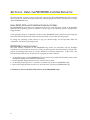
1
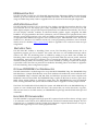
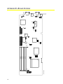
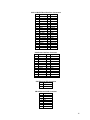
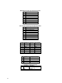
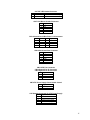
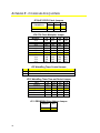
User's Manual for the IRV-3702 Single Board Computer with AGP/VGA & Ethernet MCSI PART NO. 89000 IRV-3702 All-In-One Single Board Computers For Industrial/Embedded Systems Applications MICRO COMPUTER SPECIALISTS, INC. "The Embedded PC Specialists" 1070 Joshua Way Vista, CA 92083 U.S.A. Voice (760) 598-2177 - Fax (760) 598-2450 email: [email protected] WebSite: http://www.mcsi1.com Revised January 14, 2000 Revision 1.1 Changes are made periodically to the information contained herein; these changes will be incorporated into new editions of this document. Requests for copies of this publication or the product(s) which it describes should be made to MCSI. While every effort has been made to insure that this document and its accompanying product(s) are free from defects, MCSI, its distributors, representatives, and employees shall not be responsible for any loss of profit or any other commercial damage including, but not limited to, special, incidental, consequential, or other damages occasioned by the use of this product(s). In the event of defect the buyer's sole recourse is to receive a refund or replacement unit at MCSI's discretion if notified within the time period covered by the product warranty. 1999 MCSI Micro Computer Specialists, Inc. All Rights Reserved. Celeron is a registered trademark of Intel Corporation IBM is a registered trademark of International Business Machines Corporation. PC/XT & PC/AT are registered trademarks of International Business Machines Corporation MS-DOS is a registered trademark of Microsoft Corporation. All other trademarks are the properties of their respective holders. PREFACE This manual provides information about the MCSI IRV-3702 All-In-One Single Board Computer. This information is intended for users who must implement IBM PC/AT compatible computer solutions to a wide variety of applications that cannot be satisfied using conventional desktop computers. This manual assumes that the reader has a good understanding of MS-DOS and the standard IBM PC/AT compatible architecture. For more information on the IBM PC compatible hardware and software architecture, refer to any of the many books available on the subject. A few suggestions are listed below: •Advanced MS-DOS Programming, Microsoft Press •Programmers Guide to the IBM PC, Microsoft Press •Programming the 80386, Sybex •Undocumented DOS, Addison Wesley INVENTORY CHECKLIST The complete IRV-3702 All-In-One Single Board Computer package consists of the following: IRV-3702 All-In-One Single Board Computer PROMDISK-Chip Software Utilities with ROM-DOS ver 6.22 (optional) VGA and E2Key Software Utilities This Manual If any of the above is missing or appears to be damaged, inform MCSI immediately. Table of Contents Section 1 - Introduction ___________________________________________________________________ 1 Features............................................................................................................................................................ 1 Section 2 - System Description _____________________________________________________________ 2 Processor.......................................................................................................................................................... 2 System Memory (SDRAM)............................................................................................................................ 2 DMA Controller.............................................................................................................................................. 2 Interrupt Controller........................................................................................................................................ 3 Timers .............................................................................................................................................................. 3 Clock/Calendar and CMOS RAM ............................................................................................................... 3 Keyboard Port................................................................................................................................................. 3 Mouse Port ...................................................................................................................................................... 4 Speaker Port .................................................................................................................................................... 4 Reset Switch .................................................................................................................................................... 4 Printer Port ...................................................................................................................................................... 4 Serial Ports....................................................................................................................................................... 4 Floppy Disk Port............................................................................................................................................. 4 EIDE Hard Disk Port...................................................................................................................................... 5 AGP/VGA Display Port................................................................................................................................ 5 WatchDog Timer ............................................................................................................................................ 5 Optional PROMDISK-Chip Disk Emulator ................................................................................................ 5 High Speed PCI Expansion Bus.................................................................................................................... 5 Ethernet Port ................................................................................................................................................... 6 Universal Serial Bus Port............................................................................................................................... 6 IrDA Infrared Interface Port ......................................................................................................................... 6 2 E Key 1K-bit User EEPROM ........................................................................................................................ 6 Section 3 - Setup _________________________________________________________________________ 7 Section 4 - Using the PROMDISK-Chip Disk Emulator ________________________________________ 8 Using ROM-DOS and Other Disk Operating Systems .............................................................................. 8 PROMDISK Low Level Format .................................................................................................................... 8 Section 5 - Installation ____________________________________________________________________ 9 Installing the DIMMs ..................................................................................................................................... 9 Installing the CPU .......................................................................................................................................... 9 Installing the PROMDISK-Chip ................................................................................................................... 9 Completing the Installation........................................................................................................................... 10 Appendix A - Specifications _______________________________________________________________ 11 Appendix B - Board Outline _______________________________________________________________ 12 Appendix C - Memory and I/O Maps ______________________________________________________ 13 Appendix D - Connectors _________________________________________________________________ 14 Appendix E - Configuration Jumpers _______________________________________________________ 18 Appendix F - BIOS Error Beep Codes _______________________________________________________ 20 SECTION 1 - INTRODUCTION The MCSI IRV-3702 Celeron All-In-One Single Board Computer (SBC) contains all the basic elements found in a high-performance IBM PC/AT compatible desktop computer system plus some unique features that make it ideally suited for industrial applications. The most outstanding features include: An optional 32MB PROMDISK-Chip Disk Emulator, dual PCI EIDE hard disk ports to support four EIDE drives, a high performance multi-I/O controller, a WatchDog timer, a 1K-bit E2Key memory for user data, and a 10/100Mbps Ethernet Port. The board uses the Intel 82443BX advanced chipset, and the S3 Trio 3D/2X Graphics controller. The multi-I/O controller includes: dual 16C550 UARTs, a floppy port, and a SPP/EPP/ECP multi-mode bi-directional parallel port. The optional PROMDISKChip Disk Emulator comes complete with ROM-DOS version 6.22, making it ideal for embedded diskless applications. The 1K-bit E2Key memory is a non-volatile memory useful for storing user data, such as: critical system parameters, terminal address, etc. The WatchDog timer is ideal for controlling critical processes where unattended operation is essential. The IRV-3702 SBC is fully compatible with the ISA Bus and the PCI Bus (version 2.1) which means virtually all the software written for the IBM PC/AT will run on the IRV-3702 SBC. FEATURES A complete list of features is listed below: • IBM PC/AT Compatible Plug-in Computer • Supports the Intel Celeron Processor up to 500MHz • Includes Zero Insertion CPU Socket 370 • Intel 82443BX ChipSet • Includes 32 bit PCI 2.1 Compatible Bus • AMI Plug-n-Play Flash BIOS • Passive Backplane Architecture • S3 Trio 3D AGP/VGA Controller and 4MB Video RAM • 10/100Mbps Auto-Sensing Ethernet Port Supports IEEE 802.3u 100BASE-TX Standard • 1G-Byte High Performance SDRAM System Memory (4-168 pin DIMMs) • Dual Floppy Disk Port Supports Two 3.5" or 5.25" Drives up to 2.88M-bytes • PCI Extended EIDE Hard Disk Port Supports up to Four Drives • PS2/AT Compatible Keyboard Port • PROMDISK-Chip Socket Supports up to 32MB PROMDISK-Chip Disk Emulator • PS2 Compatible Mouse Port • Two High Speed 16C550 Compatible RS-232 Serial Ports • Multimode Bi-directional Parallel Printer Port • Dual Universal Serial Bus Ports for future expansion • Infrared Data Access Port for future applications • Clock/Calendar with Battery Back-up • Low Power CMOS Design • Full Size AT Plug-in Multilayer Board for Low EMI and High Reliability • WatchDog Timer and Power Monitor • On-board Mini Speaker • Optional External Reset • Optional Datalight ROM-DOS 6.22 Operating System 1 SECTION 2 - SYSTEM DESCRIPTION The following sections describe the major system features of the IRV-3702 All-In-One Single Board Computer. PROCESSOR The IRV-3702 SBC supports the Intel Celeron processor up to 500MHz. The Celeron microprocessor includes MMX media enhancement technology, dynamic execution technology, a 32Kbyte (16Kbyte/16Kbyte) non-blocking, level-one cache that provides fast access to heavily used data, and 128Kbyte L2 cache. The on-board jumper selectable clock generator and ZIF CPU socket makes upgrading to a higher performance CPU easy. Some of the distinctive features of the Celeron processor include: • Enhanced 64-bit data bus • Integrated 128Kbyte L2 cache • 16Kbyte code and 16Kbyte data caches • 1G-byte Directly Addressable Memory Space • Dynamic execution technology • MMX multimedia technology • On-chip Pipelined Floating Point Processor • 66 MHz multi-transaction system bus • Integrated Memory Manager • Branch prediction feature SYSTEM MEMORY (SDRAM) The IRV-3702 SBC can support up to 1G-bytes of synchronous dynamic random access memory (SDRAM) organized as four banks of 32Mx72 including eight parity bits. The memory is configured using four dual in-line memory module sockets, which will accept 168-pin dual in-line memory modules (DIMMs) organized as 256MB (maximum) with a maximum access time of 10ns. DMA CONTROLLER The IRV-3702 SBC memory refresh and DMA functions are included in the System Controller chip that includes the equivalence of two 82C37 DMA controllers. The two DMA controllers are cascaded to provide four DMA channels for transfers to 8-bit peripherals (DMA1) and three channels for transfers to 16-bit peripherals (DMA2). DMA2 Channel 0 provides the cascade interconnection for the two DMA devices thereby maintaining IBM PC/AT compatibility. The DMA channel assignments are listed below: DMA Channel 0: DMA Channel 1: DMA Channel 2: DMA Channel 3: DMA Channel 5: DMA Channel 6: DMA Channel 7: Not Used (8-bit) Alternate for Multi-mode Parallel Port (8-bit) Floppy Disk (8-bit) Multi-mode Parallel Port (8-bit) Not Used (16-bit) Not Used (16-bit) Not Used (16-bit) The DMA request (DRQx) and acknowledge (DACKx/) lines are available on the P1 98-pin edge connector. 2 INTERRUPT CONTROLLER The IRV-3702 SBC has the equivalence of two 82C59A interrupt controllers included in the System Controller chip. The controllers accept requests from peripherals, resolve priorities on pending interrupts and interrupts in service, interrupt the CPU, and provide the vector address of the interrupt service routine. The two interrupt controllers are cascaded in a fashion compatible with the IBM PC/AT. The interrupt priority and assignments are shown below in descending order of priority: Highest IOCHCK/ IRQ0 IRQ1 IRQ8 IRQ9 IRQ10 IRQ11 IRQ12 IRQ13 IRQ14 IRQ15 IRQ3 IRQ4 IRQ5 IRQ6 Lowest IRQ7 Parity Check (Non-maskable) System Timer (Not Available) Keyboard (Not Available) Real Time Clock (Not Available) VGA Controller Not Used Not Used Not Used Co-processor (Not Available) EIDE Disk Controller Not Used Serial Port 2 Serial Port 1 Alternate for Parallel Port Floppy Disk Controller Parallel Port The interrupt request lines IRQx and IOCHCK/ are available on the 98-pin edge connector except as noted above. TIMERS The IRV-3702 SBC has the equivalence of an 82C54 Programmable Timer included in the System Controller chip. The 82C54 is a three channel Programmable Counter/Timer chip. The three timers are driven by a 1.19MHz clock source derived from the on-board 14.31818MHz crystal oscillator. The three timers are used as follows: TIMER Channel 0: System Timer TIMER Channel 1: Timer for DRAM refresh TIMER Channel 2: Tone Generation for Audio CLOCK/CALENDAR AND CMOS RAM The IRV-3702 SBC includes a DS12B887 real time clock/calendar with 128 bytes of CMOS RAM and integral Lithium battery which provides over 10 years of data retention when the system power is off. The 128 byte CMOS RAM consists of 14 bytes used by the clock/calendar, and 114 bytes used by the system BIOS. KEYBOARD PORT The IRV-3702 SBC contains an IBM PC/AT compatible keyboard controller for interfacing to a generic IBM PC/AT compatible keyboard. The keyboard controller assembles the serial data from the keyboard into bytes and interrupts the CPU via IRQ1 after each byte is ready to be read. The IRQ1 service routine reads port 60H to get the keyboard scan code and acknowledges by sending a positive 3 pulse to port 61H to clear the interrupt for the next byte. Refer to Appendix D for the keyboard connector location and pin assignments. MOUSE PORT The IRV-3702 SBC contains an IBM PS2 compatible mouse port for interfacing to a generic serial mouse. The mouse port controller assembles the serial data from the mouse into bytes and interrupts the CPU via IRQ1 after each byte is ready to be read. The IRQ1 service routine reads port 60H to get the scan code and acknowledges by sending a positive pulse to port 61H to clear the interrupt for the next byte. Refer to Appendix D for the mouse port connector location and pin assignments. SPEAKER PORT The IRV-3702 SBC contains an on-board sub-miniature audio speaker to provide audio interface to the user. Because of the small size of the speaker, the sound output is much reduced over that of the larger speaker found in most desktop computers. A connector is provided to connect an external speaker if the sound output is not sufficient. Refer to Appendix D for the speaker port connector location and pin assignments. RESET SWITCH The IRV-3702 SBC includes an on-board power detector and power on reset circuit to reset the computer after power is applied, and to hold the computer reset during low power, brown-out conditions. In addition, there are provisions for connecting an external, normally open, push button reset switch. Refer to Appendix D for the reset switch connector location and pin assignments. PRINTER PORT The IRV-3702 SBC contains a multimode parallel port that has the equivalence of an IBM PC/AT Parallel Printer Port. The multimode parallel printer port supports the PS/2 type bi-directional parallel port (SPP), the enhanced parallel port (EPP), and the extended capabilities port (ECP) parallel port modes. The port can be configured as a standard IBM PC/AT compatible LPT1, LPT2, or LPT3 printer port, or disabled completely using the CMOS Setup utility. Refer to Appendix D for the connector location and pin assignments. SERIAL PORTS The IRV-3702 SBC has the equivalence of two NC16C550 UARTs. The two UARTs can be configured as standard IBM PC/AT RS-232C compatible COM1, COM2, COM3, or COM4 serial ports or individually disabled using the CMOS Setup utility. The data rates are independently programmable up to 115.2K baud. Refer to Appendix D for the connector location and pin assignments. FLOPPY DISK PORT The IRV-3702 SBC contains an IBM PC/AT compatible dual floppy disk port with the equivalence of an NEC PD72056B Floppy Disk Controller, an on-chip digital data separator, and an IBM PC/AT compatible floppy disk adapter bus interface circuit. The floppy disk port can be disabled using the CMOS Setup utility. An on-chip digital data separator provides optimum performance with the following disk drive types: 5.25" 3.5" 5.25" 3.5" 3.5" 360K Double-Sided 720K High Capacity 1.2M High Capacity 1.44M High Density 2.88M High Density Refer to Appendix D for the connector location and pin assignments. 4 EIDE HARD DISK PORT The IRV-3702 SBC contains two PCI Extended Integrated Drive Electronics (EIDE) Ports that directly interface up to four hard disk drives with embedded controllers. The EIDE Disk Port can be disabled using the CMOS Setup utility. Refer to Appendix D for the connector location and pin assignments. AGP/VGA DISPLAY PORT The IRV-3702 SBC includes a S3 Trio 3D AGP/VGA display controller that interfaces directly to the local on-board PCI bus. The display port is fully compatible with IBM AGP, VGA, EGA, CGA, and MDA display adapters, and provides improved performance and additional functionality. The S3 Trio 3D AGP display controller combines an enhanced 128-bit graphics engine, integrated 230 MHz RAMDAC and programmable dual-clock synthesizer, and an enhanced local peripheral bus/video interface port for direct interface to live video and MPEG-2 peripherals. The board includes 4M-bytes of high-speed EDO DRAM and supports video resolutions up to 1600x1200x64K colors. Drivers for Windows 3.11, Windows NT, Windows 95/98, OS/2, and programming information can be obtained directly from S3’s Website http://www.s3.com. Refer to Appendix D for connector location and pin assignments. WATCHDOG TIMER The IRV-3702 SBC includes a WatchDog Timer circuit. The WatchDog Timer ensures that if an application program gets "lost or bombs", the system will reset or a non-maskable interrupt will be issued to the CPU. The WatchDog Timer is enabled by reading I/O port 443H. Once enabled, the WatchDog Timer must be triggered by reading I/O port 443H within the time out period, otherwise the WatchDog Timer will force a hardware reset or activate the IOCHCK/ line, generating a nonmaskable interrupt (NMI). The WatchDog Timer can be disabled by reading I/O port 43H. A jumper is provided to select the time out period and to enable the WatchDog Timer circuit. Refer to Appendix E for the WatchDog Timer configuration jumpers. OPTIONAL PROMDISK-CHIP DISK EMULATOR The IRV-3702 includes a socket designed to accept the MCSI PROMDISK-Chip. The PROMDISK-Chip Disk Emulator is a unique Flash Memory array which emulates a bootable read/write hard disk drive. The PROMDISK-Chip is offered in 4M, 8M, 16M, and 32M byte capacities and comes complete with ROM-DOS version 6.22 installed. The PROMDISK-Chip occupies an 8K block of memory space above 640K, whose starting address is selected by jumper JP11. The PROMDISK-Chip uses the Datalight Flash/FX integrated Flash File System and boot utilities. Refer to Appendix E for the jumper location. The Flash/FX Variable Block Flash (VBF) File System and ROM-DOS allow the PROMDISK-Chip to operate as a non-volatile Read/Write disk drive. This means that you can list directories, copy files, and read and write to the Flash memory on PROMDISK-Chip through standard DOS interrupts and commands. HIGH SPEED PCI EXPANSION BUS The IRV-3702 SBC is equipped with a high speed PCI expansion bus that allows the use of high- speed I/O controllers such as SVGA, SCSI, Ethernet Network, and Serial Communications adapters. The PCI expansion bus is compatible with the PICMG (PCI Industrial Computer Manufacturers Group) 2.1 standard and supports up to 4 PCI master peripheral boards. 5 ETHERNET PORT The IRV-3702 SBC contains a Realtek RTL8139 highly integrated single-chip Fast Ethernet controller. The RTL8139 provides 10Mbps and 100Mbps auto-sensing operation, PCI bus master capability, and full compliance with IEEE 802.3u 100Base-TX specifications. The RTL8139 keeps network maintenance cost low and eliminates usage barriers. It also supports full-duplex operation, making possible 200Mbps of bandwidth. Refer to Appendix D for connector location and pin assignments. For more information on the Realtek Ethernet controller contact their web site at http://www.realtek.com.tw. UNIVERSAL SERIAL BUS PORT The IRV-3702 SBC contains two Universal Serial Bus Ports for the future I/O expansion bus. Refer to Appendix D for connector location and pin assignments. IRDA INFRARED INTERFACE PORT The IRV-3702 SBC contains a built in IrDA infrared interface port which supports Serial Infrared (SIR) or Amplitude Shift Keyed IR (ASKIR) interfaces. The IrDA port is addressed as COM2 and must be setup in the BIOS’ Peripheral Setup. When the IrDA port is enabled, the standard COM2 serial port is disabled. Refer to Appendix D for connector location and pin assignments. E2 KEY 1K-BIT USER EEPROM 2 The IRV-3702 SBC includes the E Key 1K-bit electrically eraseable memory. This memory is useful for storing user data such as password, terminal address, configuration parameters, etc. The memory is configured as 64 words, which can be accessed a word at a time, and uses the parallel port for the hardware interface. Software utilities are provided on the distribution disk that includes a demo program, and two C library functions for integrating into your application program. 6 SECTION 3 - SETUP The IRV-3702 SBC uses the latest AMI Plug-n-Play BIOS that contains an internal Setup Utility for configuring the system. The BIOS includes a graphical user interface, and a new system configuration utility, as well as all the features of the standard BIOS. The system configuration settings are stored in the on-board CMOS memory which is backed up by a Lithium battery. The Setup Utility can be invoked by first causing a cold boot (reset) or a warm boot (Cntrl Alt Del) and pressing the Del key when instructed. This will cause the memory diagnostics to be aborted and the Setup Utility to display the MAIN SETUP MENU. Using the →↑↓← cursor keys, move the highlighted bar to the option you wish to modify and then press Enter to select it. When in the MAIN SETUP MENU, the F2 key is used to select the colors used in the setup screens, and the F10 key is used to save the changes before exiting the Setup Utility. The Esc key may be used to exit the Setup Utility without saving the changes. The PgUp and PgDn keys are used to scroll through the selections for a given setting. PgUp is also used to decrease the setting and PgDn to increase the setting. In addition, you may also enter the setup utility directly by pressing the Cntrl Alt Esc simultaneously. A jumper at JP4 is provided to force the BIOS to use its internal default SETUP values. This is accomplished by first removing power from the IRV-3702 and momentarily interrupting the battery power to the system controller chip. To interrupt the battery power, install a shunt on pins 3 & 4 momentarily (the "Clear CMOS" position). After waiting a few seconds, remove the shunt jumper. Note: This procedure must be performed with the power on. After making the desired selections from the various setup menus, you can save your selections by pressing the F10 key or by selecting the appropriate selection from the MAIN SETUP MENU. Notes: 1. The user should be aware that improper selection of certain values in the CHIPSET, POWER MANAGEMENT, and PNP/PCI selections may cause unpredictable results. If this occurs select the FAIL SAFE SETTINGS from the MAIN SETUP MENU and then press the F10 to save and exit. 7 SECTION 4 - USING THE PROMDISK-CHIP DISK EMULATOR The IRV-3702 SBC includes a 32-pin socket that supports the MCSI PROMDISK-Chip disk emulator which operates as a Read/Write fixed disk drive. The paragraphs that follow describe how to use the optional PROMDISK-Chip. USING ROM-DOS AND OTHER DISK OPERATING SYSTEMS The PROMDISK-Chip has been pre-configured at the factory with the latest version of the Datalight ROM-DOS disk operating system. In addition, a current copy of the operating system is supplied on a floppy diskette. If the operating system is accidentally erased from the PROMDISK-Chip it may be restored using the SYS command. The DOS format utility should not be used to restore the operating system. To change the operating system version or type you should simply use the equivalent DOS SYS command to transfer the operating system. PROMDISK LOW LEVEL FORMAT The Flash memory contained on the PROMDISK-Chip board was initialized with the Datalight CardTrick low level format at the factory. During normal operation the Flash memory should never require reformatting unless there is a serious hardware or software malfunction. In the event it has been determined that the low level format is corrupted, proceed as follows: 1. At the DOS prompt, run the PROMDISK-Chip low-level format utility PDCFMT.EXE located on the distribution diskette in the PDCHIP3 subdirectory. 2. Install a bootable floppy diskette in drive A and boot the system. 3. At the DOS prompt type SYS C: to transfer a bootable copy of DOS to PROMDISK-Chip. 4. Remove the floppy diskette from drive A: and reboot the system from PROMDISK-Chip. CAUTION: Do Not use the DOS Fdisk utilities on the PROMDISK-Chip. 8 SECTION 5 - INSTALLATION This section describes the procedures for installing the IRV-3702 All-In-One Single Board Computer into your system. The following is a list of typical peripherals required to build a minimum system: • • • • Passive Backplane and Power Supply IBM PC/AT Type Keyboard Monitor Floppy or Hard Disk with MS-DOS, ROM-DOS, or PROMDISK Disk Emulator INSTALLING THE DIMMS When installing or removing the SDRAM DIMMs, be sure to first touch a grounded surface to discharge any static electricity from your body. Use the following procedure to install the DIMMs: 1. Insert the first DIMM edge connector into the DIMM1 socket closest to the top of the board. Note that the DIMMs are keyed and will only go in one way. 2. Push the DIMM into the connector carefully until it snaps into place. 3. Check to make sure the DIMM is inserted securely. 4. Insert the remaining DIMMs (if required). To remove a DIMM, move the locking ejector tabs outward on each side of the DIMM and lift the DIMM from the connector. INSTALLING THE CPU When installing or removing the CPU, be sure to first touch a grounded surface to discharge any static electricity from your body. Use the following procedure to install the CPU: 1. Open the ZIF socket by lifting the release arm to its vertical position causing the sliding base plate to move to the open position. 2. Align pin one (white dot or beveled edge) on the CPU chip with pin one of the ZIF (zero insertion force) socket. Note pin 1 of the ZIF socket is located on the bottom right side of the socket. To complete the installation gently press the CPU chip into place and return the release arm to its locked position. 3. Double-check the insertion and orientation of the chip before applying power. Improper installation will result in permanent damage to the chip. Refer to Appendix E for CPU speed and configuration jumpers. To remove the CPU chip, open the ZIF socket by lifting the release arm to its vertical position and gently remove the chip. INSTALLING THE PROMDISK-CHIP When installing or removing the PROMDISK-Chip, be sure to first touch a grounded surface to discharge any static electricity from your body. Use the following procedure to install the PROMDISKChip: 1. Align pin one (square pad) on the PROMDISK-Chip with pin one of socket U31 on the CPU board. 9 2. Push the PROMDISK-Chip into the socket carefully until it is fully seated. 3. Check to make sure the PROMDISK-Chip is installed securely, and there are no bent pins. To remove the PROMDISK-Chip, insert a small screwdriver between the PROMDISK-Chip and the socket and gently pry around the edge until the PROMDISK-Chip is released from the socket. COMPLETING THE INSTALLATION To complete the installation, the following steps should be followed: 1. Set the configuration jumpers in accordance with Appendix E. 2. Install the IRV-3702 SBC into the CPU slot in a passive backplane. 3. Connect the applicable I/O cables and peripherals, i.e. floppy disk, IDE hard disk, monitor, keyboard, power supply, etc. 4. Connect an IBM PC compatible keyboard. 5. Turn power on to the display monitor. 6. Turn power on to the backplane power supply. 7. After the BIOS sign-on message is displayed, press the Del key to enter the Setup Utility. 8. Reconfigure the IRV-3702 CMOS using the internal SETUP. 9. Boot the system. 10 APPENDIX A - SPECIFICATIONS This appendix lists the specifications for the IRV-3702 All-In-One Single Board Computer. CPU: Co-processor: Memory: BIOS: Clock/Cal: I/O Bus: PCI Bus: DMA: Timers: Interrupts: Reset: I/O Ports: PCI Video Port: Speed: Battery: Benchmark: Size: Weight: Power: Supports: Intel Celeron processors up to 500MHz, 66MHz or 100MHz clock. Internal to the Celeron Chip System Memory Expandable to 1G-bytes. Supports: 8MB, 16MB, 32MB, 64MB, 128MB, or 256MB SDRAM DIMMs using four 168-pin DIMM sockets. 128K-bytes of L2 Cache Memory internal to CPU. AMI Plug-n-Play BIOS Flash EPROM. PC/AT Compatible with internal Lithium battery back-up IBM PC/AT Compatible 98-pin Edge Connector Industry Standard version 2.1 PICMG high performance I/O bus. 7 Channels (4 8-bit & 3 16-bit) PCI Ultra DMA/33 3 Programmable 16 Controlled by on-board power detector with provisions for external reset switch at header CN7 2 - RS-232 Serial Ports (CN12 at rear connector, and CN11 header) 1 - Parallel Printer Port (at connector CN4) 1 - PS2 Keyboard Port (at header CN8 and at rear PS2 type connector CN18) 1 - On-board Speaker with Speaker Port (CN7) 1 - Dual 3.5"/5.25" Floppy Disk Port (CN2) 2 - IDE Hard Disk Port (Primary at CN1 & Secondary at CN3) 1 - WatchDog Timer 1 - PS2 Mouse Port (CN18 and header CN17) 1 - IDE LED Port (CN7) 1 - Keylock & Power LED (CN7) 2 - Universal Serial Bus Ports (at header CN9) 1 - IrDA Infrared Port (CN6) 1 - Ethernet Port, RJ-45 connector (CN10), LAN LED (CN5) 3 – Cooling Fan Power/Status Ports (CN13-CN15) 1 - PCI VGA Video Port (at rear connector J1) Chipset: S3 Trio 3D Video Controller VRAM: 4MB SDRAM Resolution: 1600 x 1200 64K color 1280 x 1024, 64K color 1024 x 768 16M color 300-650MHz jumper selectable. Clock/Calendar with Internal Lithium battery (ten year life typical) LANDMARK v2.0 = 2337MHz for 400MHz CPU Full Size AT board 13.3"L X 4.8"H 12 Oz. +5VDC @ 5.5A, +12VDC @ 0.160A, -12VDC @ 0.060A 11 12 .Denotes pin 1 CN7 CN8 1 JP3 DIMM4 DIMM3 DIMM2 DIMM1 CN15 CN13 JP15 CN1 CN3 JP14 CN9 CN14 JP4 JP7 BIOS CN4 CN2 JP12 JP8 JP5 U31 PROMDISK-Chip JP11 CN6 CN5 CN17 CN12 CN18 CN11 CN10 J1 APPENDIX B - BOARD OUTLINE APPENDIX C - MEMORY AND I/O MAPS The following is the memory map for the IRV-3702 SBC. The addresses are fully PC/AT compatible, unless otherwise specified. IRV-3702 SBC Memory Map Address Used For 00000H - 003FFH Interrupt Vectors 00400H - 005FFH BIOS Values 00600H - 9FFFFH User RAM (DOS) A0000H - AFFFFH Reserved for VGA B0000H - B7FFFH Video RAM (MDA)* B8000H - BFFFFH Video RAM (CGA)* C0000H - C3FFFH Reserved C4000H - C7FFFH EMS Window C8000H - DFFFFH ROM Scan Devices* E0000H - FFFFFH System BIOS 100000H - 3FFFFFFFH User Memory *External to the IRV-3702 Size 1.0K 0.5K 638.5K 64.0K 32.0K 32.0K 16.0K 16.0K 96.0K 128.0K 1GB The following is the I/O map for the IRV-3702 SBC. I/O addresses are fully PC/AT compatible, unless otherwise specified. Address 000H - 01FH 020H - 021H 022H - 023H 040H - 05FH 060H - 063H 070H - 07FH 080H - 083H 0A0H - 0BFH 0C0H - 0DFH 0F0H 0F1H 1F0H - 1F8H 278H - 27FH 2E8H - 2EFH 2F8H - 2FFH 378H - 37FH 3BCH - 3BFH 3E8H - 3EFH 3F0H - 3F7H 3F8H - 3FFH 043H 443H IRV-3702 SBC I/O Map Function DMA Controller #1 Interrupt Controller #1 Configuration Address Register System Timers & WatchDog Timer Keyboard, Status, & System Control Clock/Calendar & CMOS Ram Access DMA Page Register Interrupt Controller #2 DMA Controller #2 Clear Math Co-processor Busy Reset Math Co-processor IDE Hard Disk Parallel Printer Port LPT2 Serial Port COM4 Serial Port COM2 Parallel Printer Port LPT1 Parallel Printer Port LPT3 Serial Port COM3 Floppy Disk Controller Serial Port COM1 Disable WatchDog Timer Enable WatchDog Timer 13 APPENDIX D - CONNECTORS CN8 Keyboard Header/Connector Pin 1 2 3 4 5 Signal KBCLK KBDATA N/C GND +5VDC CN18 Keyboard/Mouse Connector (PS2 type) Pin 1 2 3 4 5 6 Signal KBDATA MDATA GND +5VDC KBCLOCK MCLK CN7 Keylock Header/Connector Pin 2 4 6 8 10 Signal Name LED POWER (+) N/C (Key) GND KB LOCK/ GND Description Connect to anode of power LED N/C (Key) Connect to cathode of power LED Connect to ground to inhibit keyboard Ground CN2 Floppy Disk Port Connector Pin Signal Name 2 RPMLC 4 Not Used 6 Not Used 8 INDEX/ 10 MOTOR0/ 12 DRIVE SELECT1/ 14 DRIVE SELECT0/ 16 MOTOR1/ 18 DIRECTION 20 STEP/ 22 WRITE DATA/ 24 WRITE GATE/ 26 TRACK0/ 28 WRITE PROTECT/ 30 READ DATA/ 32 HEAD SELECT/ 34 DISK CHANGE/ All odd numbered pins are GND 14 CN1 & CN3 IDE Hard Disk Port Connectors Pin 1 3 5 7 9 11 13 15 17 19 21 23 25 27 29 31 33 35 37 39 Signal IDERST/ IDED7 IDED6 IDED5 IDED4 IDED3 IDED2 IDED1 IDED0 GND IDE DRQ IDEIOW/ IDEIOR/ IDE CHRDY IDEDACK IRQ14 IDESA1 IDESA0 HDCS0/ IDEACT/ Pin 2 4 6 8 10 12 14 16 18 20 22 24 26 28 30 32 34 36 38 40 Signal GND IDED8 IDED9 IDED10 IDED11 IDED12 IDED13 IDED14 IDED15 Not Used GND GND GND GND GND Not Used Not Used IDESA2 HDCS1/ GND CN4 Printer Interface Connector Pin 1 2 3 4 5 6 7 8 9 10 11 12 13 Signal STROBE/ PDAT0 PDAT1 PDAT2 PDAT3 PDAT4 PDAT5 PDAT6 PDAT7 ACK/ BUSY PE SLCT Pin 14 15 16 17 18 19 20 21 22 23 24 25 26 Signal AUTOFD/ ERROR/ INIT/ SLCTIN/ GND GND GND GND GND GND GND GND Not Used CN5 Ethernet LED Connector Pin 1 2 Signal +5VDC LAN ACTIVE CN10 Ethernet RJ45 Connector Pin 1 2 3 4 5 6 7 8 Signal TX+ TXRX+ N/C N/C RXN/C N/C 15 CN12 Serial Port #1 9-pin Sub D Connector Pin 1 2 3 4 5 6 7 8 9 Signal Name CARRIER DETECT #1 RECEIVE DATA #1 TRANSMIT DATA #1 DATA TERMINAL READY #1 GND DATA SET READY #1 REQUEST TO SEND #1 CLEAR TO SEND #1 RING INDICATOR #1 CN11 Serial Port #2 10-pin Header/Connector Pin 1 2 3 4 5 6 7 8 9 10 Signal Name CARRIER DETECT #2 DATA SET READY #2 RECEIVE DATA #2 REQUEST TO SEND #2 TRANSMIT DATA #2 CLEAR TO SEND #2 DATA TERMINAL READY #2 RING INDICATOR #2 GND N/C J1 VGA Display Connector (15-pin Sub-D) Pin 1 3 5 7 9 11 13 15 Signal RED BLUE GND GND VCC N/C HSYNC DDCCLK Pin 2 4 6 8 10 12 14 Signal GREEN N/C GND GND GND DDCDATA VSYNC CN7 Speaker Port Header/Connector Pin 1 3 5 7 Signal Name SPEAKER N/C N/C +5VDC Description Connect to Speaker (-) No Connection No Connection Connect to Speaker (+) CN7 Reset Header/Connector 16 Pin 9 Signal Name RESET/ 11 GND Description Connect to switch, ground this pin to reset Ground CN7 IDE LED Header/Connector Pin 13 15 Signal Name IDE LED +5VDC Description Connect to IDE LED anode (-) Connect to IDE LED cathode (+) CN17 PS2 Mouse Header/Connector Pin 1 2 3 4 5 Signal MSDATA N/C GND +5VDC MSCLK CN9 Universal Serial Bus Ports 1 & 2 Connector Pin 1 2 3 4 Signal +5VDC -DATA0 +DATA0 GND Pin 5 6 7 8 Signal GND +DATA1 -DATA1 +5VDC CN6 IrDA Infrared Port Connector Pin 1 2 3 4 5 6 Signal +5VDC FIR-RX IR-RX GND IR-TX CIR-RX CN13 CPU Fan Connector CN14 System Fan #1 Connector CN15 System Fan #2 Connector Pin 1 2 3 Signal FAN SENSOR +12VDC GND CN7 ATX Power Supply Power Switch Control Pin 17 19 Signal Switch (+) Switch (-) CN7 Standby Connector for ATX Power Supply Pin 12 14 16 18 20 Signal GND No Connection Suspend Control Signal +5VDC Standby Signal +5VDC Standby Signal 17 APPENDIX E - CONFIGURATION JUMPERS JP3 &JP15 CPU Clock Jumpers BUS FREQUENCY 66MHz 100MHz JP15 FS2 2-3 1-2 JP3 FS1 1-3 1-3 JP3 FS0 2-4 2-4 JP8 CPU Clock Multiplier Jumper Multiplier 3.0X 3.5X 4.0X 4.5X 5.0X 5.5X 6.0X 6.5X 7.0X 7.5X 8.0X 1-2 ON ON OFF OFF OFF OFF ON ON ON ON OFF 3-4 OFF OFF ON ON OFF OFF ON ON OFF OFF ON 5-6 ON OFF ON OFF ON OFF ON OFF ON OFF ON 7-8 ON ON ON ON ON ON OFF OFF OFF OFF OFF JP5 WatchDog Timer Control Jumper 2-3 1-2 OFF Generates hardware RESET when time out occurs. (Default) Generates NMI (IOCHRDY) when time out occurs. Disable JP12 WatchDog Timer Time-out Period Jumper Time 1second 2 seconds 10 (Default) 20 seconds 110 seconds 220 seconds 1-2 OFF OFF OFF OFF ON ON 3-4 OFF OFF ON ON OFF OFF 5-6 ON ON OFF OFF OFF OFF 7-8 OFF ON OFF ON OFF ON JP11 PROMDISK-Chip Address Jumper Address CE00H D600H DE00H 18 JP11 1-2 3-4 5-6 JP4 Clear CMOS Setup Jumper OFF 3-4 Normal Operation (Default) Clear CMOS Setup JP7 PS/2 Mouse Jumper ON OFF Enabled using IRQ12 Disabled JP14 Manufacturing Test Jumper 1-2 2-3 Do Not Use Do Not Use 19 APPENDIX F - BIOS ERROR BEEP CODES During the POST (Power On Self Test) routines, which are performed each time the system is powered on, errors may occur. Nonfatal errors are those which, in most cases, allow the system to continue the boot up process. The error messages normally appear on the screen. Fatal errors are those which will not allow the system to continue the boot-up procedure. If a fatal error occurs, you should consult with MCSI Customer Service for possible repairs. These fatal errors are communicated through a series of audible beeps. The numbers on the fatal error list below correspond to the number of beeps for the corresponding error. All errors listed, with the exception of number eight, are fatal errors. No. of Beeps 20 Error Message 1 Refresh Failure - The memory refresh circuitry is faulty. 2 Parity Error - A parity error was detected in the first 64K block of system memory. 3 Base 64KB Memory Failure - A memory failure occurred within the first 64KB of memory. 4 Timer Not Operational - Timer #1 has failed to function properly. 5 Processor Error - The CPU chip has generated an error. 6 8042-Gate A20 Failure - The keyboard controller (8042) contains the Gate A20 switch which allows the CPU to operate in virtual mode. This error message means that the BlOS is not able to switch the CPU into protected mode. 7 Processor Exception lnterrupt Error - The CPU chip has generated an exception interrupt. 8 Display Memory Read /Write Error - The video adapter is either missing or the video memory is faulty. PLEASE NOTE: This is not a fatal error. 9 ROM Checksum Error - The ROM checksum value does not match the value encoded in the BIOS. 10 CMOS Shutdown Register Read/Write Error - The shutdown register for the CMOS memory has failed. 11 Cache Memory Read/Write Error - A Cache Memory failure occurred, do not enable the Cache Memory to resume operation.