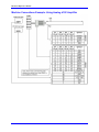
1
^1 HARDWARE REFERENCE MANUAL
PMAC2A-PC/104
Axis Expansion
Accessory-1P
^3 PMAC2A-PC/104 ACC-1P Hardware Reference
^4 4xx-603671-xHxx
^5 December 6, 2010
Single Source Machine Control
Power // Flexibility // Ease of Use
21314 Lassen Street Chatsworth, CA 91311 // Tel. (818) 998-2095 Fax. (818) 998-7807 // www.deltatau.com
Copyright Information
© 2009 Delta Tau Data Systems, Inc. All rights reserved.
This document is furnished for the customers of Delta Tau Data Systems, Inc. Other uses are
unauthorized without written permission of Delta Tau Data Systems, Inc. Information contained
in this manual may be updated from time-to-time due to product improvements, etc., and may not
conform in every respect to former issues.
To report errors or inconsistencies, call or email:
Delta Tau Data Systems, Inc. Technical Support
Phone: (818) 717-5656
Fax: (818) 998-7807
Email: [email protected]
Website: http://www.deltatau.com
Operating Conditions
All Delta Tau Data Systems, Inc. motion controller products, accessories, and amplifiers contain
static sensitive components that can be damaged by incorrect handling. When installing or
handling Delta Tau Data Systems, Inc. products, avoid contact with highly insulated materials.
Only qualified personnel should be allowed to handle this equipment.
In the case of industrial applications, we expect our products to be protected from hazardous or
conductive materials and/or environments that could cause harm to the controller by damaging
components or causing electrical shorts. When our products are used in an industrial
environment, install them into an industrial electrical cabinet or industrial PC to protect them
from excessive or corrosive moisture, abnormal ambient temperatures, and conductive materials.
If Delta Tau Data Systems, Inc. products are exposed to hazardous or conductive materials and/or
environments, we cannot guarantee their operation.
REVISION HISTORY
REV.
1
2
3
DESCRIPTION
ADDED ENCODER JUMPERS E20-E23
ADDED SOFTWARE SETUP INFO, P. 23
CORR. I-VARIABLES FOR USE WITH TURBO CPU
DATE
CHG
APPVD
04/10/07
CP
S. MILICI
10/15/09
10/01/10
CP
SS
S. MILICI
S. SATTARI
Hardware Reference Manual
Table of Contents
INTRODUCTION .......................................................................................................................................................4
Acc-1P: Axis Expansion Piggyback Board...........................................................................................................4
Acc-1P Option 1: I/O Ports .................................................................................................................................4
Acc-1P Option 2: Analog-to-Digital Converters .................................................................................................4
HARDWARE SETUP .................................................................................................................................................6
I/O Configuration Jumpers........................................................................................................................................6
Encoder Configuration Jumpers ................................................................................................................................6
Reserved Configuration Jumpers ..............................................................................................................................7
Resistor Packs Configuration (older rev boards without E20-23) .............................................................................7
Differential or Single-Ended Encoder Selection...................................................................................................7
Handwheel Encoder Termination Resistors .........................................................................................................8
MACHINE CONNECTIONS.....................................................................................................................................9
Mounting ...................................................................................................................................................................9
Power Supplies..........................................................................................................................................................9
Digital Power Supply............................................................................................................................................9
DAC Outputs Power Supply .................................................................................................................................9
Flags Power Supply............................................................................................................................................10
Overtravel Limits and Home Switches....................................................................................................................10
Types of Overtravel Limits..................................................................................................................................10
Home Switches....................................................................................................................................................10
Motor Signals Connections .....................................................................................................................................10
Incremental Encoder Connection .......................................................................................................................10
DAC Output Signals ...........................................................................................................................................11
Pulse and Direction (Stepper) Drivers ...............................................................................................................11
Amplifier Enable Signal (AENAx/DIRn).............................................................................................................11
Amplifier Fault Signal (FAULT-) .......................................................................................................................12
General-Purpose Digital Inputs and Outputs (J7 Port) ............................................................................................12
Thumbwheel Multiplexer Port (JTHW Port)...........................................................................................................13
Handwheel Port (JHW / PD Port) ...........................................................................................................................14
Optional Analog Inputs ...........................................................................................................................................14
Compare Equal Outputs ..........................................................................................................................................14
Machine Connections Example: Using Analog ±10V Amplifier ............................................................................15
Machine Connections Example: Using Pulse and Direction Drivers ......................................................................16
SOFTWARE SETUP (NON-TURBO PMAC2A-PC104) ......................................................................................18
Communications......................................................................................................................................................18
PMAC I-Variables...................................................................................................................................................18
Filtered DAC Outputs Configuration ......................................................................................................................18
Using Flag I/O as General-Purpose I/O...................................................................................................................18
General-Purpose Digital Inputs and Outputs...........................................................................................................19
Jumper E6 on Position 1-2 .................................................................................................................................19
Jumper E5 in Position 2-3 ..................................................................................................................................19
Thumbwheel Port Digital Inputs and Outputs .........................................................................................................21
Jumper E6 in Position 1-2 ..................................................................................................................................21
Jumper E6 in Position 2-3 ..................................................................................................................................21
Analog Inputs Setup ................................................................................................................................................22
Analog Inputs......................................................................................................................................................22
SOFTWARE SETUP (TURBO PMAC2A-PC104 AND CLIPPER) ....................................................................23
Filtered DAC Outputs Configuration ......................................................................................................................23
Motor Setup for channels 9-12 ...........................................................................................................................24
Using Flag I/O as General-Purpose I/O...................................................................................................................29
General-Purpose Digital Inputs and Outputs...........................................................................................................30
Table of Contents
i
Hardware Reference Manual
JOPTO port first ACC-1P, Jumper E6 on Position 1-2......................................................................................30
JTHW port first ACC-1P, Jumper E6 on Position 1-2........................................................................................31
JOPTO port second ACC-1P, Jumper E6 on Position 2-3 .................................................................................31
JTHW port second ACC-1P, Jumper E6 on Position 2-3 ...................................................................................32
Analog Inputs Setup ................................................................................................................................................33
Analog Inputs first ACC-1P................................................................................................................................33
Analog Inputs second ACC-1P ...........................................................................................................................33
HARDWARE REFERENCE SUMMARY .............................................................................................................35
Board Dimensions ...................................................................................................................................................35
Board Layout...........................................................................................................................................................36
Connectors and Indicators .......................................................................................................................................37
J2 - Thumbwheel Multiplexer Port (JTHW Port) ...............................................................................................37
J3 - Machine Connector (JMACH1 Port)...........................................................................................................37
J4 - Machine Connector (JMACH2 Port)...........................................................................................................37
J7 - General-Purpose Digital Inputs and Outputs (JOPT Port).........................................................................37
J8 – Handwheel / Pulse and Direction Port (JHW / PD Port) ...........................................................................37
TB1 – Power Supply Terminal Block (JPWR Connector) ..................................................................................37
E-POINT JUMPER DESCRIPTIONS ....................................................................................................................39
E0: Reserved for Future Use ..................................................................................................................................39
E1 - E2: Machine Output Supply Voltage Configure.............................................................................................39
E3 – E4: JHW, PD Function Select........................................................................................................................39
E5: Servo Gate Address Select...............................................................................................................................40
E6: I/O Gate Address Select....................................................................................................................................40
E7: Machine Input Source/Sink Control ................................................................................................................40
E16: ADC Inputs Enable........................................................................................................................................40
CONNECTOR PINOUTS.........................................................................................................................................41
TB1 (JPWR): Power Supply ..................................................................................................................................41
J2 (JTHW): Multiplexer Port Connector .................................................................................................................42
J3 (JMACH1): Machine Port Connector (50-Pin Header) .....................................................................................43
J4 (JMACH2): Machine Port Connector (34-Pin Header) ......................................................................................45
J7 (JOPTO): I/O Port Connector .............................................................................................................................46
J8 (JHW) Handwheel Encoder Connector...............................................................................................................47
SCHEMATICS ..........................................................................................................................................................49
ii
Table of Contents
Hardware Reference Manual
Table of Contents
iii
Hardware Reference Manual
INTRODUCTION
The PMAC2A PC/104 motion controller is a compact, cost-effective version of Delta Tau’s PMAC2
family of controllers. The PMAC2A PC/104 can be composed of three boards in a stack configuration.
The baseboard provides four channels of either DAC ±10V or pulse and direction command outputs. The
optional axis expansion board provides a set of four additional servo channels and I/O ports. The optional
communications board provides extra I/O ports and either the USB or Ethernet interface for faster
communications.
Acc-1P: Axis Expansion Piggyback Board
Acc-1P provides four additional channels axis interface
circuitry for a total of eight servo channels, each including:
• 12-bit ±10V filtered PWM analog output
• Pulse-and-direction digital outputs
• 3-channel differential/single-ended encoder input
• Four input flags, two output flags
• Three PWM top-and-bottom pairs (unbuffered)
Acc-1P Option 1: I/O Ports
PMAC2A PC/104 Base Board shown
Option 1 provides the following ports on the Acc-1P axes
stacked with the Acc-1P axes
expansion board for digital I/O connections.
• Multiplexer Port: This connector provides eight input lines and eight output lines at TTL levels.
When using the PMAC Acc-34x type boards these lines allow multiplexing large numbers of inputs
and outputs on the port. Up to 32 of the multiplexed I/O boards may be daisy-chained on the port, in
any combination.
• I/O Port: This port provides eight general-purpose digital inputs and eight general-purpose digital
outputs at 5 to 24Vdc levels. This 34-pin connector was designed for easy interface to OPTO-22 or
equivalent optically isolated I/O modules when different voltage levels or opto-isolation to the
PMAC2A PC/104 is necessary.
• Handwheel port: this port provides two extra channels, each jumper selectable between encoder input
or pulse output.
Acc-1P Option 2: Analog-to-Digital Converters
Option 2 permits the installation on the Acc-1P of two channels of analog-to-digital converters with ±10V
input range and 12-bits resolution. The key component installed with this option is U20.
4
Hardware Setup
Hardware Reference Manual
Introduction
5
Hardware Reference Manual
HARDWARE SETUP
On the Acc-1P, there are a number of jumpers called E-points or W-points that customize the hardware
features of the CPU for a given application and must be setup appropriately. The following is an
overview grouped in appropriate categories. For an itemized description of the jumper setup
configuration, refer to the E-Point Descriptions section.
I/O Configuration Jumpers
E1-E2: Machine Output Supply Configure – With the default sinking output driver IC (ULN2803A or
equivalent) in U7 for the J7 JOPT port outputs, these jumpers must connect pins 1 and 2 to supply the IC
correctly. If this IC is replaced with a sourcing output driver IC (UDN2981A or equivalent), these
jumpers must be changed to connect pins 2 and 3 to supply the new IC correctly. A wrong setting of
these jumpers will damage the associated output IC.
E3-E4: JHW, PD Function Select – When jumper E3 connects pins 2 and 3, a set of pulse and direction
signals can be output on channel 1 (pins 2 to 5) of the JHW, PD port. If E3 connects pins 1 and 2, then
channel 1 is configured as a handwheel encoder input. When jumper E4 connects pins 2 and 3, a set of
pulse and direction signals can be output on channel 2 (pins 6 to 9) of the JHW, PD port. If E4 connects
pins 1 and 2, then channel 2 is configured as a handwheel encoder input.
E5: Servo Gate address select – If jumper E5 connects pins 1 and 2 (default) the servo channels on the
Acc-1P will be accessed at the regular addresses for motors 5 to 8. When E5 connects pins 2 and 3 the
servo channels on the Acc-1P board will be accessed at the regular addresses for motors 5 to 8 plus $40,
and this is useful only when two Acc-1Ps are used with the same PMAC2A PC/104 baseboard.
E6: I/O Gate address select – If jumper E6 connects pins 1 and 2 (default) the I/O features on the Acc1P will be accessed at the regular addresses and the JTHW port can be used as a multiplexer port. When
E6 connects pins 2 and 3 the I/O features on the Acc-1P board will be accessed at the regular addresses
plus $40, and this is useful only when two I/O gate accessories are used with the same PMAC2A PC/104
baseboard.
E7: Machine Input Source/Sink Control – With this jumper connecting pins 1 and 2 (default) the
machine input lines on the J7 JOPT port are pulled up to +5V or the externally provided supply voltage
for the port. This configuration is suitable for sinking drivers. If the jumper is changes to connect pins 2
and 3, these lines are pulled down to GND – this configuration is suitable for sourcing drivers.
E16: ADC Enable Jumper – Install E16 to enable the analog-to-digital converter circuitry ordered
through Option-2. Remove this jumper to disable this option, which might be necessary to control motor
5 through a digital amplifier with current feedback.
Encoder Configuration Jumpers
E20-E23: Encoder Single Ended/Differential Select – The ACC-1P has differential line receivers for
each encoder channel, but can accept either single-ended (one signal line per channel) or differential (two
signal lines, main and complementary, per channel). A jumper for each encoder permits customized
configurations, as described below.
Single-Ended Encoders
With the jumper for an encoder set for single-ended (pin 1 to 2), the differential input lines for that
encoder are tied to 2.5V; the single signal line for each channel is then compared to this reference as it
changes between 0 and 5V. When using single-ended TTL-level digital encoders, the differential line
input should be left open, not grounded or tied high; this is required for The PMAC differential line
receivers to work properly.
6
Hardware Setup
Hardware Reference Manual
Differential Encoders
Differential encoder signals (pin 2 to 3) can enhance noise immunity by providing common-mode noise
rejection. Modern design standards virtually mandate their use for industrial systems, especially in the
presence of PWM power amplifiers, which generate a great deal of electromagnetic interference.
Connect pin 1 to 2 to tie differential line to +2.5V
• Tie to +2.5V when no connection
• Tie to +2.5V for single-ended encoders
Connect pin 2 to 3 to tie differential line to +5V
• Don’t care for differential line driver encoders
• Tie to +5V for complementary open-collector encoders (obsolete)
Reserved Configuration Jumpers
E0: Reserved for future use
Resistor Packs Configuration (older rev boards without E20-23)
Differential or Single-Ended Encoder Selection
The differential input signal pairs to the PMAC have user-configurable pull-up/pull-down resistor
networks to permit the acceptance of either single-ended or differential signals in one setting, or the
detecting loss of differential signals in another setting.
The ‘+’ inputs of each differential pair each have a hard-wired 1 kΩ pull-up resistor to +5V. This cannot
be changed.
The ‘-‘ inputs of each differential pair each have a hard-wired 2.2 kΩ resistor to +5V; each also has
another 2.2 kΩ resistor as part of a socketed resistor pack that can be configured as a pull-up resistor to
+5V, or a pull-down resistor to GND.
If this socketed resistor is configured as a pull-down resistor (the default configuration), the combination
of pull-up and pull-down resistors on this line acts as a voltage divider, holding the line at +2.5V in the
absence of an external signal. This configuration is required for single-ended inputs using the ‘+’ lines
alone; it is desirable for unconnected inputs to prevent the pick-up of spurious noise; it is permissible for
differential line-driver inputs.
If this socketed resistor is configured as a pull-up resistor (by reversing the SIP pack in the socket), the
two parallel 2.2 kΩ resistors act as a single 1.1 kΩ pull-up resistor, holding the line at +5V in the absence
of an external signal. This configuration is required if complementary open-collector drivers are used; it
is permissible for differential line-driver inputs.
If Pin 1 of the resistor pack, marked by a dot on the pack, matches Pin 1 of the socket, labeled by a white
square, then the pack is configured as a bank of pull-down resistors. If the pack is reversed in the socket,
it is configured as a bank of pull-up resistors. The following table lists the pull-up/pull-down resistor
pack for each input device:
Hardware Setup
Device
Resistor Pack
Pack Size
Encoder 1
Encoder 2
Encoder 3
RP30
RP31
RP36
6-pin
6-pin
6-pin
7
Hardware Reference Manual
Encoder 4
Handwheel Encoder
RP37
RP55
6-pin
6-pin
Handwheel Encoder Termination Resistors
The PMAC provides a socket for termination resistors on the handwheel encoder differential input pairs
coming into the board. As shipped, there is no resistor pack in the RP56 socket. If these signals are
brought long distances into the PMAC board and ringing at signal transitions is a problem, a SIP resistor
pack may be mounted on the RP56 socket to reduce or eliminate the ringing. The 6-pin termination
resistor pack is the type that has independent resistors (no common connection) with each resistor using 2
adjacent pins.
8
Hardware Setup
Hardware Reference Manual
MACHINE CONNECTIONS
Typically, the user connections are actually made to terminal blocks that are attached to the JMACH
connectors by a flat cable. The following are the terminal blocks recommended for connections:
• 34-Pin IDC header to terminal block breakouts (Phoenix part number 2281063) Delta Tau
part number 100-FLKM34-000
• 50-Pin IDC header to terminal block breakouts (Phoenix part number 2281089) Delta Tau
part number 100-FLKM50-000
Mounting
The PMAC2A PC/104 is always installed either using standoffs, when it is
stacked to a PC/104 computer or used as a stand-alone controller. At each of
the four corners of the PMAC2A PC/104 board, there are mounting holes that
can be used to mount the board on standoffs.
The PMAC2A PC/104 baseboard is placed always at the bottom of the stack.
The order of the Acc-1P or Acc-2P with respect to the baseboard does not
matter.
Power Supplies
Baseboard mounted at
the bottom of the stack
Digital Power Supply
3A @ +5V (±5%) (15 W)
(Eight-channel configuration, with a typical load of encoders)
The PMAC2A PC/104, the Acc-1P and the Acc-2P each require a 1A @ 5VDC power supply for
operation. Therefore, a 3A @ 5VDC power supply is recommended for a PMAC2A PC/104 board stack
with Acc-1P and Acc-2P boards.
• The host computer provides the 5 Volts power supply in the case PMAC is installed in the
PC/104 bus. With the board stack into the bus, it will automatically pull +5V power from the
bus and it cannot be disconnected. In this case, there must be no external +5V supply, or the
two supplies will "fight" each other, possibly causing damage. This voltage could be
measured on the TB1 terminal block or the JMACH1 connector.
• In a stand-alone configuration, when PMAC is not plugged in a computer bus, it will need an
external 5V supply to power its digital circuits. The 5V power supply can be brought in
either from the TB1 terminal block or from the JMACH1 connector.
DAC Outputs Power Supply
0.3A @ +12 to +15V (4.5W)
0.25A @ -12 to -15V (3.8W)
(Eight-channel configuration)
• The host computer provides the ±12 Volts power supply in the case PMAC is installed in the
PC/104 bus. With the board stack into the bus, it will pull ±12V power from the bus
automatically and it cannot be disconnected. In this case, there must be no external ±12V
supply, or the two supplies will fight each other, possibly causing damage. This voltage
could be measured on the TB1 terminal block.
• In a stand-alone configuration, when PMAC is not plugged in a computer bus, it will need an
external ±12V supply only when the digital-to-analog converter (DAC) outputs are used. The
±12V lines from the supply, including the ground reference, can be brought in either from the
TB1 terminal block or from the JMACH1 connector.
Machine Connections
9
Hardware Reference Manual
Flags Power Supply
Each channel of PMAC has five dedicated digital inputs on the machine connector: PLIMn, MLIMn
(overtravel limits), HOMEn (home flag), FAULTn (amplifier fault), and USERn. A power supply from 5
to 24V must be used to power the circuits related to these inputs. This power supply can be the same
used to power PMAC and can be connected from the TB1 terminal block or the JMACH1 connector.
Overtravel Limits and Home Switches
When assigned for the dedicated uses, these signals provide important safety and accuracy functions.
PLIMn and MLIMn are direction-sensitive over-travel limits that must conduct current to permit motion
in that direction. If no over-travel switches will be connected to a particular motor, this feature must be
disabled in the software setup through the PMAC Ix25 variable.
Types of Overtravel Limits
PMAC expects a closed-to-ground connection for the limits to not be considered on fault. This
arrangement provides a failsafe condition. Usually, a passive normally close switch is used. If a
proximity switch is needed instead, use a 5 to 24V normally closed to ground NPN sinking type sensor.
Home Switches
•
While normally closed-to-ground switches are required for the overtravel limits inputs, the
home switches could be either normally close or normally open types. The polarity is
determined by the home sequence setup, through the I-variables I9n2. .
Motor Signals Connections
Incremental Encoder Connection
Each JMACH1 connector provides two +5V outputs and two logic grounds for powering encoders and
other devices. The +5V outputs are on pins 1 and 2; the grounds are on pins 3 and 4. The encoder signal
pins are grouped by number: all those numbered 1 (CHA1+, CHA1-, CHB1+, CHC1+, etc.) belong to
encoder #1. The encoder number does not have to match the motor number, but usually does. Connect
the A and B (quadrature) encoder channels to the appropriate terminal block pins. For encoder 1, the
CHA1+ is pin 5 and CHB1+ is pin 9. If there is a single-ended signal, leave the complementary signal
pins floating – do not ground them. However, if single-ended encoders are used, check the settings of the
resistor packs (see the Hardware Setup section for details). For a differential encoder, connect the
complementary signal lines – CHA1- is pin 7, and CHB1- is pin 11. The third channel (index pulse) is
optional; for encoder 1, CHC1+ is pin 13, and CHC1- is pin 15.
Example: differential quadrature encoder connected to channel #1:
10
Machine Connections
Hardware Reference Manual
DAC Output Signals
If PMAC is not performing the commutation for the motor, only one analog output channel is required to
command the motor. This output channel can be either single-ended or differential, depending on what
the amplifier is expecting. For a single-ended command using PMAC channel 1, connect DAC1+ (pin
29) to the command input on the amplifier. Connect the amplifier’s command signal return line to
PMAC’s GND line (pin 48). In this setup, leave the DAC1- pin floating; do not ground it.
For a differential command using PMAC channel 1, connect DAC1 (pin 29) to the plus-command input
on the amplifier. Connect DAC1- (pin 31) to the minus-command input on the amplifier. PMAC’s GND
should still be connected to the amplifier common.
Any analog output not used for dedicated servo purposes may be utilized as a general-purpose analog
output by defining an M-variable to the command register, then writing values to the M-variable. The
analog outputs are intended to drive high-impedance inputs with no significant current draw. The 220Ω
output resistors will keep the current draw lower than 50 mA in all cases and prevent damage to the
output circuitry, but any current draw above 10 mA can result in noticeable signal distortion.
Example:
Pulse and Direction (Stepper) Drivers
The channels provided by the PMAC2A PC/104 board or the Acc-1P board can output pulse and
direction signals for controlling stepper drivers or hybrid amplifiers. These signals are at TTL levels.
Amplifier Enable Signal (AENAx/DIRn)
Most amplifiers have an enable/disable input that permits complete shutdown of the amplifier regardless
of the voltage of the command signal. PMAC’s AENA line is meant for this purpose. AENA1- is pin 33.
This signal is an open-collector output and an external 3.3 kΩ pull-up resistor can be used if necessary.
Machine Connections
11
Hardware Reference Manual
Amplifier Fault Signal (FAULT-)
This input can take a signal from the amplifier so PMAC knows when the amplifier is having problems,
and can shut down action. The polarity is programmable with I-variable Ix25 (I125 for motor 1) and the
return signal is ground (GND). FAULT1- is pin 35. With the default setup, this signal must actively be
pulled low for a fault condition. In this setup, if nothing is wired into this input, PMAC will consider the
motor not to be in a fault condition.
General-Purpose Digital Inputs and Outputs (J7 Port)
Acc-1P J7 connector provides eight general-purpose digital inputs and eight general-purpose digital
outputs. Each input and each output has its own corresponding ground pin in the opposite row. The 34pin connector was designed for easy interface to OPTO-22 or equivalent optically isolated I/O modules.
Delta Tau’s Acc-21F is a six-foot cable for this purpose. Characteristics of the JOPTO port on the
PMAC:
• 16 I/O points. 100 mA per channel, up to 24V
• Hardware selectable between sinking and sourcing in groups of 8; default is all sinking
(inputs can be changed simply by moving a jumper; sourcing outputs must be special-ordered
or field-configured)
• Eight inputs, and eight outputs only; no changes. Parallel (fast) communications to PMAC
CPU
• Not opto-isolated; easily connected to Opto-22 (PB16) or similar modules through Acc-21F
cable
Jumper E7 on the Acc-1P board controls the configuration of the eight inputs. If it connects pins 1 and 2
(the default setting), the inputs are biased to +5V for the OFF state, and they must be pulled low for the
ON state. If E7 connects pins 2 and 3, the inputs are biased to ground for the OFF state, and must be
pulled high for the ON state. In either case, a high voltage is interpreted as a 0 by the PMAC software,
and a low voltage is interpreted as a 1.
PMAC is shipped standard with a ULN2803A sinking (open-collector) output IC for the eight outputs.
These outputs can sink up to 100 mA and have an internal 3.3 kΩ pull-up resistor to go high (RP18). Do
not connect these outputs directly to the supply voltage, or damage to the PMAC will result from
excessive current draw. The user can provide a high-side voltage (+5 to +24V) into Pin 33 of the J7
connector, and allow this to pull up the outputs by connecting pins 1 and 2 of Jumper E1. Jumper E2
must also connect pins 1 and 2 for a ULN2803A sinking output.
It is possible for these outputs to be sourcing drivers by substituting a UDN2981A IC for the ULN2803A.
This U7 IC is socketed, and so may easily be replaced. Usually the U7 IC is offset by two pins on its
socket, and so pins 1 and 2 usually remain open.
WARNING
Having Jumpers E1 and E2 set wrong can damage the IC. The +V output on this
connector has a 2A fuse, F1, for excessive current protection.
For this driver, the internal resistor packs pull-down instead. With a UDN2981A driver IC, Jumper E1
must connect pins 2 and 3, and Jumper E2 must connect pins 2 and 3.
Example: Standard configuration using the ULN2803A sinking (open-collector) output IC.
12
Machine Connections
Hardware Reference Manual
Further software settings are required to configure this port. See the Software Setup section for details.
Thumbwheel Multiplexer Port (JTHW Port)
The Thumbwheel Multiplexer Port, or Multiplexer Port, on the JTHW connector has sixteen lines. These
lines can be used to multiplex large numbers of inputs and outputs on the port, and Delta Tau provides
accessory boards and software structures (special M-variable definitions) to capitalize on this feature. Up
to 32 of the multiplexed I/O boards may be daisy-chained on the port, in any combination. Either the
Acc-1P or the Acc-2P boards, but not both, can use this connector as a multiplexing port. This is selected
by jumper E6 on the Acc-1P board and jumper E5 on the Acc-2P board.
Alternatively, the inputs and outputs on this port may be used as discrete, non-multiplexed I/O. In this
case, these I/O lines can be accessed through M-variables. See the Software Setup section for details on
this.
Machine Connections
13
Hardware Reference Manual
When used as non-multiplexed I/O, jumpers E7 and E8 select the I/O lines direction of the JTHW
connector. This allows configuring this port as all inputs, all outputs or half inputs and half outputs. If
E7 is removed or E8 is installed then the multiplexing feature if the JTHW port cannot be used.
Handwheel Port (JHW / PD Port)
This port provides an extra encoder input or a set of pulse and direction outputs. Jumpers E3 and E4 select
the function of this connector between encoder input or pulse and direction outputs. The handwheel
encoder input can be linked to a servomotor for manual displacement or used by a motor as a secondary
encoder for dual-feedback applications. There is no C index channel input on the handwheel encoder
port.
Optional Analog Inputs
The optional analog-to-digital converter inputs are ordered either through Option-12 on the baseboard or
Option-2 on the axes expansion board. Each option provides two 12-bit analog inputs analog inputs with
a ±10Vdc range.
Compare Equal Outputs
The compare-equals (EQU) outputs have a dedicated use of providing a signal edge when an encoder
position reaches a pre-loaded value. This is very useful for scanning and measurement applications.
Instructions for use of these outputs are covered in detail in the PMAC2 User Manual.
14
Machine Connections
Hardware Reference Manual
Machine Connections Example: Using Analog ±10V Amplifier
Machine Connections
15
Hardware Reference Manual
Machine Connections Example: Using Pulse and Direction Drivers
16
Machine Connections
Hardware Reference Manual
Machine Connections
17
Hardware Reference Manual
SOFTWARE SETUP (non-Turbo PMAC2A-PC104)
Note:
The PMAC2A PC/104 requires the use of V1.17 or newer firmware. There are
few differences between the previous V1.16H firmware and the V1.17 firmware
other than the addition of internal support for the Flex CPU design.
Communications
Delta Tau provides software tools that allow communicating with of the PMAC2A PC/104 board by
either its standard RS-232 port or the optional USB or Ethernet ports. PEWIN is the most important in
the series of software accessories, and it allows configuring and programming the PMAC for any
particular application.
PMAC I-Variables
PMAC has a large set of Initialization parameters (I-variables) that determine the "personality" of the card
for a specific application. Many of these are used to configure a motor properly. Once set up, these
variables may be stored in non-volatile EAROM memory (using the SAVE command) so the card is
always configured properly (PMAC loads the EAROM I-variable values into RAM on power-up).
Filtered DAC Outputs Configuration
The following I-variables must be set properly to use the digital-to-analog (filtered DAC) outputs:
I900
I901
I902
I903
I906
I907
I9n6
Ix69
I10
=
=
=
=
=
=
=
=
=
1001
2
3
1746
1001
1746
0
1001
1710933
;
;
;
;
;
;
;
;
;
PWM frequency 29.4kHz, PWM 1-4
Phase Clock 19.6kHz
Servo frequency 4.9kHz
ADC frequency
PWM frequency 29.4kHz, PWM 5-8
ADC frequency
Output mode: PWM
DAC limit 10Vdc
Servo interrupt time
n = channel number from 1 to 8
x = motor number from 1 to 8
Using Flag I/O as General-Purpose I/O
Either the user flags or other not assigned axes flag on the base board can be used as general-purpose I/O
for up to 20 inputs and 4 outputs at 5-24Vdc levels. The indicated suggested M-variables definitions,
which are defined in the PMAC2 Software reference, allows accessing each particular line according to
the following table:
Flag
Type
HOME
PLIM
MLIM
USER
AENA
5-24 VDC Input
5-24 VDC Input
5-24 VDC Input
5-24 VDC Input
5-24 VDC Output
#5
M520
M521
M522
M515
M514
Channel Number
#6
#7
M620
M621
M622
M615
M614
M720
M721
M722
M715
M714
#8
M820
M821
M822
M815
M814
Note:
When using these lines as regular I/O points the appropriate setting of the Ix25
variable must be used to enable or disable the safety flags feature.
18
Software Setup
Hardware Reference Manual
General-Purpose Digital Inputs and Outputs
If one Acc-1P is present on the PMAC2A PC/104 stack configuration then its jumpers E5 and E6 should
be set at the default position 1-2. In this case, the lines on its J7 general-purpose I/O connector will be
mapped into PMAC’s address space in register Y:$C080. Jumpers E5 and E6 should be configured on
position 2-3 only when two Acc-1Ps are used. In this case, the I/O lines can be accessed at address
Y:$C0C0.
If no Acc-1P is present on the PMAC2A PC/104 stack configuration, and only Acc-2P is used, then
jumper E5 on the Acc-2P board should connect pins 1 and 2. In this case the lines on its JOPT generalpurpose I/O connector will be mapped into PMAC's address space in register Y:$C080.
If both Acc-1P and Acc-2P are used, then jumper E5 on the Acc-2P board should connect pins 2 and 3
and its I/O lines can be accessed at address Y:$C0C0.
Typically, these I/O lines are accessed individually with M-variables. Following is a suggested set of Mvariable definitions to use these data lines.
Jumper E6 on Position 1-2
M0->Y:$C080,0
M1->Y:$C080,1
M2->Y:$C080,2
M3->Y:$C080,3
M4->Y:$C080,4
M5->Y:$C080,5
M6->Y:$C080,6
M7->Y:$C080,7
M8->Y:$C080,8
M9->Y:$C080,9
M10->Y:$C080,10
M11->Y:$C080,11
M12->Y:$C080,12
M13->Y:$C080,13
M14->Y:$C080,14
M15->Y:$C080,15
M32->X:$C080,0,8
M34->X:$C080,8,8
M40->X:$C084,0,24
M42->Y:$C084,0,24
;
;
;
;
;
;
;
;
;
;
;
;
;
;
;
;
;
;
;
;
Digital Output M00
Digital Output M01
Digital Output M02
Digital Output M03
Digital Output M04
Digital Output M05
Digital Output M06
Digital Output M07
Digital Input MI0
Digital Input MI1
Digital Input MI2
Digital Input MI3
Digital Input MI4
Digital Input MI5
Digital Input MI6
Digital Input MI7
Direction Control bits 0-7 (1=output,
Direction Control bits 8-15 (1=output,
Inversion control (0 = 0V, 1 = 5V)
J7 port data type control (1 = I/O)
0 = input)
0 = input)
In order to properly setup the digital outputs an initialization PLC must be written scanning through once
on power-up/reset, then disabling itself:
OPEN PLC1 CLEAR
M32=$FF
M34=$0
M40=$FF00
M42=$FFFF
DIS PLC1
CLOSE
;BITS 0-8 are assigned as output
;BITS 9-16 are assigned as input
;Define as inputs and outputs
;All lines are I/O type
;Disable PLC1 (scanning through once on
;power-up/reset)
Note:
After loading this program, set I5=2 or 3 and ENABLE PLC 1.
Jumper E5 in Position 2-3
M0->Y:$C0C0,0
M1->Y:$C0C0,1
Software Setup
; Digital Output M00
; Digital Output M01
19
Hardware Reference Manual
M2->Y:$C0C0,2
M3->Y:$C0C0,3
M4->Y:$C0C0,4
M5->Y:$C0C0,5
M6->Y:$C0C0,6
M7->Y:$C0C0,7
M8->Y:$C0C0,8
M9->Y:$C0C0,9
M10->Y:$C0C0,10
M11->Y:$C0C0,11
M12->Y:$C0C0,12
M13->Y:$C0C0,13
M14->Y:$C0C0,14
M15->Y:$C0C0,15
M32->X:$C0C0,0,8
M34->X:$C0C0,8,8
M40->X:$C0C4,0,24
M42->Y:$C0C4,0,24
;
;
;
;
;
;
;
;
;
;
;
;
;
;
;
;
;
;
Digital Output M02
Digital Output M03
Digital Output M04
Digital Output M05
Digital Output M06
Digital Output M07
Digital Input MI0
Digital Input MI1
Digital Input MI2
Digital Input MI3
Digital Input MI4
Digital Input MI5
Digital Input MI6
Digital Input MI7
Direction Control (1=output, 0 = input)
Direction Control (1=output, 0 = input)
Inversion control (0 = 0V, 1 = 5V)
JI/O port data type control (1 = I/O)
In order to properly setup the digital outputs, an initialization PLC must be written scanning through once
on power-up/reset, and then disabling itself:
OPEN PLC1 CLEAR
M32=$FF
M34=$0
M40=$FF00
M42=$FFFF
DIS PLC1
CLOSE
;BITS 0-8 are assigned as output
;BITS 9-16 are assigned as input
;Define as inputs and outputs
;All lines are I/O type
;Disable PLC1 (scanning through once on
;power-up/reset)
Note:
After loading this program, set I5=2 or 3 and ENABLE PLC 1.
20
Software Setup
Hardware Reference Manual
Thumbwheel Port Digital Inputs and Outputs
The inputs and outputs on the thumbwheel multiplexer port of either the Acc-1P or the Acc-2P boards
may be used as discrete, non-multiplexed I/O. In this case, these I/O lines can be accessed through Mvariables that are defined according to the setup of the address selection jumpers. Jumper E6 on the Acc1P or E5 on the Acc-2P determine which set of the following M-variables are used:
Jumper E6 in Position 1-2
M40->Y:$C082,8,1
M41->Y:$C082,9,1
M42->Y:$C082,10,1
M43->Y:$C082,11,1
M44->Y:$C082,12,1
M45->Y:$C082,13,1
M46->Y:$C082,14,1
M47->Y:$C082,15,1
M48->Y:$C082,8,8,U
M50->Y:$C082,0,1
M51->Y:$C082,1,1
M52->Y:$C082,2,1
M53->Y:$C082,3,1
M54->Y:$C082,4,1
M55->Y:$C082,5,1
M56->Y:$C082,6,1
M57->Y:$C082,7,1
M58->Y:$C082,0,8,U
;
;
;
;
;
;
;
;
;
;
;
;
;
;
;
;
;
;
SEL0 Output
SEL1 Output
SEL2 Output
SEL3 Output
SEL4 Output
SEL5 Output
SEL6 Output
SEL7 Output
SEL0-7 Outputs treated as a byte
DAT0 Input
DAT1 Input
DAT2 Input
DAT3 Input
DAT4 Input
DAT5 Input
DAT6 Input
DAT7 Input
DAT0-7 Inputs treated as a byte
;
;
;
;
;
;
;
;
;
;
;
;
;
;
;
;
;
;
SEL0 I/O Line
SEL1 I/O Line
SEL2 I/O Line
SEL3 I/O Line
SEL4 I/O Line
SEL5 I/O Line
SEL6 I/O Line
SEL7 I/O Line
SEL0-7 I/O Lines treated as a byte
DAT0 I/O Line
DAT1 I/O Line
DAT2 I/O Line
DAT3 I/O Line
DAT4 I/O Line
DAT5 I/O Line
DAT6 I/O Line
DAT7 I/O Line
DAT0-7 I/O Lines treated as a byte
Jumper E6 in Position 2-3
M40->Y:$C0C2,8,1
M41->Y:$C0C2,9,1
M42->Y:$C0C2,10,1
M43->Y:$C0C2,11,1
M44->Y:$C0C2,12,1
M45->Y:$C0C2,13,1
M46->Y:$C0C2,14,1
M47->Y:$C0C2,15,1
M48->Y:$C0C2,8,8,U
M50->Y:$C0C2,0,1
M51->Y:$C0C2,1,1
M52->Y:$C0C2,2,1
M53->Y:$C0C2,3,1
M54->Y:$C0C2,4,1
M55->Y:$C0C2,5,1
M56->Y:$C0C2,6,1
M57->Y:$C0C2,7,1
M58->Y:$C0C2,0,8,U
Software Setup
21
Hardware Reference Manual
Analog Inputs Setup
The optional analog-to-digital converter inputs are ordered either through Option-12 on the baseboard or
Option-2 on the axes expansion board. Each option provides two 12-bit analog inputs with a ±10Vdc
range. The M-variables associated with these inputs provided a range of values between +2048 and –
2048 for the respective ±10Vdc input range. The following is the software procedure to setup and read
these ports.
Analog Inputs
I907 = 1746
WX:$C034, $1FFFFF
M305->X:$0714,12,12,S
M405->X:$0715,12,12,S
22
;Set ADC clock frequency at 4.9152 MHz
;Clock strobe set for bipolar inputs
;ADCIN_1 on JMACH1 connector (Acc-1P) pin 45
;ADCIN_2 on JMACH1 connector (Acc-1P) pin 46
Software Setup
Hardware Reference Manual
SOFTWARE SETUP (Turbo PMAC2A-PC104 and Clipper)
Filtered DAC Outputs Configuration
Although the Clipper Board uses standard Turbo PMAC2 firmware certain I-variables must be set
properly to use the digital-to-analog (filtered DAC) outputs. For the first ACC-1P board, the E5 jumper
should be set 1-2 to enable the four channels as motors 5-8 at base address $78100. The PMAC firmware
will automatically set up the encoder conversion table and basic motor I-variables for channels 5 through
8 after a “$$$***” command is issued. This will provide a total of 8 channels. The suggested M-variables
as specified in the Turbo PMAC/PMAC2 Software reference for motors 5 through 8 will apply. The Ivariables should be set as follows:
I7000
I7001
I7002
I7003
I7100
I7101
I7102
I7103
I7016
I7026
I7036
I7046
I7116
I7126
I7136
I7146
I169
I269
I369
I469
I569
I669
I769
I869
I10
= 1001
= 5
= 3
= 1746
= 1001
= 5
= 3
= 1746
= 0
= 0
= 0
= 0
= 0
= 0
= 0
= 0
= 1001
= 1001
= 1001
= 1001
= 1001
= 1001
= 1001
= 1001
= 3421867
;
;
;
;
;
;
;
;
;
;
;
;
;
;
;
;
;
;
;
;
;
;
;
;
;
PWM frequency 29.4kHz, PWM 1-4
Phase Clock 9.8kHz
Servo frequency 2.45kHz
ADC frequency
PWM frequency 29.4kHz, PWM 5-8
Phase Clock 9.8kHz
Servo frequency 2.45kHz
ADC frequency
Output mode ch#1: PWM
Output mode ch#2: PWM
Output mode ch#3: PWM
Output mode ch#4: PWM
Output mode ch#5: PWM
Output mode ch#6: PWM
Output mode ch#7: PWM
Output mode ch#8: PWM
DAC limit ch#1 10Vdc
DAC limit ch#2 10Vdc
DAC limit ch#3 10Vdc
DAC limit ch#4 10Vdc
DAC limit ch#5 10Vdc
DAC limit ch#6 10Vdc
DAC limit ch#7 10Vdc
DAC limit ch#8 10Vdc
Servo interrupt time
Once this has been downloaded to the Clipper board, save and reset the board (“SAVE” and “$$$”
commands). The executive’s tuning programs can now be used to set up the PID parameters.
For the second ACC-1P board, the E5 jumper should be set 2-3 to enable the four channels as motors 912 at base address $78140. This will require special set-up since there are no I-variables associated with
this servo gate address, nor will the PMAC firmware set up the encoder conversion table – this must be
done in a “run once startup PLC”. The following M-variables will be required to access the hardware setup registers of the 3rd servo gate:
M7200->X$7815C,8,16
M7201->X$78144,16,4
M7202->X$78144,20,4
M7203->X$78144,0,12
M7204->X$7815C,0,8
M7205->X$7814C,0,24
M7206->X$78154,0,24
;MaxPhase/PWM Frequency Control (I7m00 equivalent)
;Phase Clock Frequency Control (I7m01 equivalent)
;Servo Clock Frequency Control (I7m02 equivalent)
; Hardware Clock Control (I7m03 equivalent)
; PWM/PFM Deadtime/Width Control (I7m04 equivalent)
; DAC Strobe Word (I7m05 equivalent)
; ADC Strobe Word (I7m06 equivalent)
The following I-variables will add motors 9 through 12 to the encoder conversion table:
Software Setup
23
Hardware Reference Manual
I8008=$78140;ECT Entry
I8009=$78148;ECT Entry
I8010=$78150;ECT Entry
I8011=$78158;ECT Entry
I8012=$0;ECT Entry 12
motor
motor
motor
motor
#9
#10
#11
#12
The following run once startup PLC will assign the correct clock values and other hardware settings for
the third servo gate to properly set-up the filtered PWM DAC outputs:
OPEN PLC 25 CLEAR
M7200 = 1001
M7201 = 5
M7202 = 3
M7203 = 1746
M7204 = 15
M7205 = $7FFFC0
M7206 = $FFFFFE
DIS PLC 25
CLOSE
Motor Setup for channels 9-12
The following M-variables will be required to access the necessary registers for the set-up (with default
values) and status of each motor (listed separately for each motor):
// FIRST CHANNEL OF GATE #3 - MOTOR #9
M901->X:$078141,0,24,S
M902->Y:$078142,8,16,S
M903->X:$078143,0,24,S
M914->X:$078145,14
M915->X:$078140,19
M917->X:$078140,11
M918->X:$078140,8
M919->X:$078140,14
M920->X:$078140,16
M921->X:$078140,17
M922->X:$078140,18
M923->X:$078140,15
M7210->X:$78145,0,4
M7211->X:$78145,13,1
M7212->X:$78145,4,4
M7213->X:$78145,8,4
M7216->X:$78145,20,4
;
;
;
;
;
;
;
;
;
;
;
;
ENC9 24-bit counter position
OUT9A command value; DAC or PWM
ENC9 captured position
AENA9 output status
USER9 flag input status
ENC9 capture flag
ENC9 count error flag
CHC9 input status
HMFL9 flag input status
PLIM9 flag input status
MLIM9 flag input status
FAULT9 flag input status
;I7mn0 Servo IC m
;I7mn1 Servo IC m
;I7mn2 Servo IC
;I7mn3 Servo IC m
;I7mn6 Servo IC
Channel n Encoder/Timer Decode Control
Channel n Position Compare Channel Select
m Channel n Capture Control
Channel n Capture Flag Select Control
m Channel n Output Mode Select
// Default values (NOT retained on a "SAVE" command)
M7210 = 3
M7211 = 0
M7212 = 1
M7213 = 0
M7216 = 0
//Motor specific I-variables (retained on a "SAVE" command)
I924 = 1
I925 = $78140
I969 = 1001
I902 = $78142
24
Software Setup
Hardware Reference Manual
I903 = $3509
I904 = $3509
The default values not retained on a “SAVE” command must be added to the “run once startup PLC”
from the previous section that set up the main hardware clocks:
OPEN PLC 25 CLEAR
// Main HDW Clocks
M7200 = 1001
M7201 = 5
M7202 = 3
M7203 = 1746
M7204 = 15
M7205 = $7FFFC0
M7206 = $FFFFFE
// Motor #9 defaults
M7210 = 3
M7211 = 0
M7212 = 1
M7213 = 0
M7216 = 0
DIS PLC 25
CLOSE
Note:
After loading this program, set I5=2 or 3 and ENABLE PLC 1.
// SECOND CHANNEL OF GATE #3 - MOTOR #10
M1001->X:$078149,0,24,S ; ENC10 24-bit counter position
M1002->Y:$07814A,8,16,S ; OUT10A command value; DAC or PWM
M1003->X:$07814B,0,24,S ; ENC10 captured position
M1014->X:$07814D,14 ; AENA10 output status
M1015->X:$078148,19 ; USER10 flag input status
M1017->X:$078148,11 ; ENC10 capture flag
M1018->X:$078148,8 ; ENC10 count error flag
M1019->X:$078148,14 ; CHC10 input status
M1020->X:$078148,16 ; HMFL10 flag input status
M1021->X:$078148,17 ; PLIM10 flag input status
M1022->X:$078148,18 ; MLIM10 flag input status
M1023->X:$078148,15 ; FAULT10 flag input status
M7220->X:$7814D,0,4
M7221->X:$7814D,13,1
M7222->X:$7814D,4,4
M7223->X:$7814D,8,4
M7226->X:$7814D,20,4
;I7mn0
;I7mn1
;I7mn2
;I7mn3
;I7mn6
// Default values (NOT retained on a "SAVE" command)
M7220 = 3
M7221 = 0
M7222 = 1
M7223 = 0
Software Setup
25
Hardware Reference Manual
M7226 =
//Motor
I1024 =
I1025 =
I1069 =
I1002 =
I1003 =
I1004 =
0
specific I-variables (retained on a "SAVE" command)
1
$78148
1001
$7814A
$350A
$350A
The default values not retained on a “SAVE” command must again be added to the “run once startup
PLC” from the previous section:
OPEN PLC 25 CLEAR
// Main HDW Clocks
M7200 = 1001
M7201 = 5
M7202 = 3
M7203 = 1746
M7204 = 15
M7205 = $7FFFC0
M7206 = $FFFFFE
// Motor #9 defaults
M7210 = 3
M7211 = 0
M7212 = 1
M7213 = 0
M7216 = 0
// Motor #10 defaults
M7220 = 3
M7221 = 0
M7222 = 1
M7223 = 0
M7226 = 0
DIS PLC 25
CLOSE
Note:
After loading this program, set I5=2 or 3 and ENABLE PLC 1.
// THIRD CHANNEL OF GATE #3 - MOTOR #11
M1101->X:$078151,0,24,S ; ENC11 24-bit counter position
M1102->Y:$078152,8,16,S ; OUT11A command value; DAC or PWM
M1103->X:$078153,0,24,S ; ENC11 captured position
M1114->X:$078155,14 ; AENA11 output status
M1115->X:$078150,19 ; USER11 flag input status
M1117->X:$078150,11 ; ENC11 capture flag
M1118->X:$078150,8 ; ENC11 count error flag
M1119->X:$078150,14 ; CHC11 input status
M1120->X:$078150,16 ; HMFL11 flag input status
M1121->X:$078150,17 ; PLIM11 flag input status
M1122->X:$078150,18 ; MLIM11 flag input status
M1123->X:$078150,15 ; FAULT11 flag input status
26
Software Setup
Hardware Reference Manual
M7230->X:$78155,0,4
M7231->X:$78155,13,1
M7232->X:$78155,4,4
M7233->X:$78155,8,4
M7236->X:$78155,20,4
;I7mn0
;I7mn1
;I7mn2
;I7mn3
;I7mn6
// Default values (NOT retained on a "SAVE" command)
M7230 = 3
M7231 = 0
M7232 = 1
M7233 = 0
M7236 = 0
//Motor specific I-variables (retained on a "SAVE" command)
I1124 = 1
I1125 = $78150
I1169 = 1001
I1102 = $78152
I1103 = $350B
I1104 = $350B
The default values not retained on a “SAVE” command must again be added to the “run once startup
PLC” from the previous section:
OPEN PLC 25 CLEAR
M7200 = 1001
M7201 = 5
M7202 = 3
M7203 = 1746
M7204 = 15
M7205 = $7FFFC0
M7206 = $FFFFFE
// Motor #9 defaults
M7210 = 3
M7211 = 0
M7212 = 1
M7213 = 0
M7216 = 0
// Motor #10 defaults
M7220 = 3
M7221 = 0
M7222 = 1
M7223 = 0
M7226 = 0
// Motor #11 defaults
M7230 = 3
M7231 = 0
M7232 = 1
M7233 = 0
M7236 = 0
DIS PLC 25
CLOSE
Note:
After loading this program, set I5=2 or 3 and ENABLE PLC 1.
Software Setup
27
Hardware Reference Manual
// FOURTH CHANNEL OF GATE #3 - MOTOR #12
M1201->X:$078159,0,24,S ; ENC12 24-bit counter position
M1202->Y:$07815A,8,16,S ; OUT12A command value; DAC or PWM
M1203->X:$07815B,0,24,S ; ENC12 captured position
M1214->X:$07815D,14 ; AENA12 output status
M1215->X:$078158,19 ; USER12 flag input status
M1217->X:$078158,11 ; ENC12 capture flag
M1218->X:$078158,8 ; ENC12 count error flag
M1219->X:$078158,14 ; CHC12 input status
M1220->X:$078158,16 ; HMFL12 flag input status
M1221->X:$078158,17 ; PLIM12 flag input status
M1222->X:$078158,18 ; MLIM12 flag input status
M1223->X:$078158,15 ; FAULT12 flag input status
M7240->X:$7815D,0,4
M7241->X:$7815D,13,1
M7242->X:$7815D,4,4
M7243->X:$7815D,8,4
M7246->X:$7815D,20,4
;I7mn0
;I7mn1
;I7mn2
;I7mn3
;I7mn6
// Default values (NOT retained on a "SAVE" command)
M7240 = 3
M7241 = 0
M7242 = 1
M7243 = 0
M7246 = 0
//Motor specific I-variables (retained on a "SAVE" command)
I1224 = 1
I1225 = $78158
I1269 = 1001
I1202 = $7815A
I1203 = $350C
I1204 = $350C
The default values not retained on a “SAVE” command must again be added to the “run once startup
PLC” from the previous section:
OPEN PLC 25 CLEAR
M7200 = 1001
M7201 = 5
M7202 = 3
M7203 = 1746
M7204 = 15
M7205 = $7FFFC0
M7206 = $FFFFFE
// Motor #9 defaults
M7210 = 3
M7211 = 0
M7212 = 1
M7213 = 0
M7216 = 0
// Motor #10 defaults
M7220 = 3
M7221 = 0
M7222 = 1
28
Software Setup
Hardware Reference Manual
M7223 = 0
M7226 = 0
// Motor #11 defaults
M7230 = 3
M7231 = 0
M7232 = 1
M7233 = 0
M7236 = 0
// Motor #12 defaults
M7240 = 3
M7241 = 0
M7242 = 1
M7243 = 0
M7246 = 0
DIS PLC 25
CLOSE
Note:
After loading this program, set I5=2 or 3 and ENABLE PLC 1.
Using Flag I/O as General-Purpose I/O
Either the user flags or other unassigned axes flag on the ACC-1P board can be used as general-purpose
I/O for up to 20 inputs and 4 outputs at 5-24Vdc levels. The indicated M-variables definitions, which are
the suggested definitions for motors 5 through 8 in the Turbo PMAC/PMAC2 Software reference, allows
accessing each particular line according to the following table:
Flag
Type
HOME
PLIM
MLIM
USER
AENA
5-24 VDC Input
5-24 VDC Input
5-24 VDC Input
5-24 VDC Input
5-24 VDC Output
#5
M520
M521
M522
M515
M514
Channel Number
#6
#7
M620
M621
M622
M615
M614
M720
M721
M722
M715
M714
#8
M820
M821
M822
M815
M814
Motors 9 through 12 must use the following M-variables as defined from the previous section since the
servo gate used for these motors is at a non-standard address:
Flag
Type
HOME
PLIM
MLIM
USER
AENA
5-24 VDC Input
5-24 VDC Input
5-24 VDC Input
5-24 VDC Input
5-24 VDC Output
#9
M920
M921
M922
M915
M914
Channel Number
#10
#11
M1020
M1021
M1022
M1015
M1014
M1120
M1121
M1122
M1115
M1114
#12
M1220
M1221
M1222
M1215
M1214
Note:
When using these lines as regular I/O points the appropriate setting of the Ixx24
variable must be used to enable or disable the safety flags feature.
Software Setup
29
Hardware Reference Manual
General-Purpose Digital Inputs and Outputs
If one Acc-1P is present then its jumper E6 should be set at the default position 1-2. In this case, the lines
on its J7 general-purpose I/O connector will be mapped into PMAC’s address space at base address
Y:$78500. If a second Acc-1P is used then its E6 jumper should be configured 2-3 and its I/O lines can
be accessed at base address Y:$78540.
The inputs and outputs on the thumbwheel port of the Acc-1P boards may only be used as discrete, nonmultiplexed I/O. As in the case of the JOPTO port they are defined according to the setup of the address
selection jumper E6.
Typically, these I/O lines are accessed individually with M-variables. Following is a suggested set of Mvariable definitions to use these data lines.
JOPTO port first ACC-1P, Jumper E6 on Position 1-2
M4050->Y:$78500,0
M4051->Y:$78500,1
M4052->Y:$78500,2
M4053->Y:$78500,3
M4054->Y:$78500,4
M4055->Y:$78500,5
M4056->Y:$78500,6
M4057->Y:$78500,7
M4066->Y:$78500,0,8,u
; Digital Output M00
; Digital Output M01
; Digital Output M02
; Digital Output M03
; Digital Output M04
; Digital Output M05
; Digital Output M06
; Digital Output M07
;all outputs as an 8bit word
M4058->Y:$78500,8
M4059->Y:$78500,9
M4060->Y:$78500,10
M4061->Y:$78500,11
M4062->Y:$78500,12
M4063->Y:$78500,13
M4064->Y:$78500,14
M4065->Y:$78500,15
M4067->Y:$78500,8,8,u
;
;
;
;
;
;
;
;
;
Digital Input
Digital Input
Digital Input
Digital Input
Digital Input
Digital Input
Digital Input
Digital Input
all inputs as
M4068->X:$78500,0,8
M4069->X:$78500,8,8
M4070->X:$78504,0,24
M4071->Y:$78504,0,24
;
;
;
;
Direction
Direction
Inversion
port data
MI0
MI1
MI2
MI3
MI4
MI5
MI6
MI7
an 8bit word
Control bits
Control bits
control (0 =
type control
0-7 (1=output,
8-15 (1=output,
0V, 1 = 5V)
(1 = I/O)
0 = input)
0 = input)
In order to properly setup the JOPTO digital I/O an initialization PLC must be written scanning through
once on power-up/reset, and then disabling itself:
OPEN PLC12 CLEAR
M4068=$FF
M4069=$0
M4070=$FF00
M4071=$FFFF
DIS PLC1
up/reset)
CLOSE
;BITS 0-8 are assigned as output
;BITS 9-16 are assigned as input
;Define inputs and outputs
;All lines are I/O type
;Disable PLC1 (scanning through once on power-
Note:
After loading this program, set I5=2 or 3 and ENABLE PLC 1.
30
Software Setup
Hardware Reference Manual
JTHW port first ACC-1P, Jumper E6 on Position 1-2
M4080->Y:$78502,8,1 ; SEL0 Output
M4081->Y:$78502,9,1 ; SEL1 Output
M4082->Y:$78502,10,1 ; SEL2 Output
M4083->Y:$78502,11,1 ; SEL3 Output
M4084->Y:$78502,12,1 ; SEL4 Output
M4085->Y:$78502,13,1 ; SEL5 Output
M4086->Y:$78502,14,1 ; SEL6 Output
M4087->Y:$78502,15,1 ; SEL7 Output
M4088->Y:$78502,8,8,U ; SEL0-7 Outputs treated as a byte
M4090->Y:$78502,0,1 ;
M4091->Y:$78502,1,1 ;
M4092->Y:$78502,2,1 ;
M4093->Y:$78502,3,1 ;
M4094->Y:$78502,4,1 ;
M4095->Y:$78502,5,1 ;
M4096->Y:$78502,6,1 ;
M4097->Y:$78502,7,1 ;
M4098->Y:$78502,0,8,U
DAT0 Input
DAT1 Input
DAT2 Input
DAT3 Input
DAT4 Input
DAT5 Input
DAT6 Input
DAT7 Input
; DAT0-7 Inputs treated as a byte
M4099->X:$078502,0,8 ; Direction control for DAT0 to DAT7
M4099->X:$078502,8,8 ; Direction control for SEL0 to SEL7
In order to properly setup the JTHW digital I/O an initialization PLC must be written scanning through
once on power-up/reset, and then disabling itself:
OPEN PLC 13 CLEAR
M4089=0
M4099=$FF
DISPLC10
CLOSE
Note:
After loading this program, set I5=2 or 3 and ENABLE PLC 13.
JOPTO port second ACC-1P, Jumper E6 on Position 2-3
M4100->Y:$78540,0
M4101->Y:$78540,1
M4102->Y:$78540,2
M4103->Y:$78540,3
M4104->Y:$78540,4
M4105->Y:$78540,5
M4106->Y:$78540,6
M4107->Y:$78540,7
M4116->Y:$78540,0,8,u
; Digital Output M00
; Digital Output M01
; Digital Output M02
; Digital Output M03
; Digital Output M04
; Digital Output M05
; Digital Output M06
; Digital Output M07
;all outputs as an 8bit word
M4108->Y:$78540,8
M4109->Y:$78540,9
M4110->Y:$78540,10
M4111->Y:$78540,11
M4112->Y:$78540,12
M4113->Y:$78540,13
;
;
;
;
;
;
Software Setup
Digital
Digital
Digital
Digital
Digital
Digital
Input
Input
Input
Input
Input
Input
MI0
MI1
MI2
MI3
MI4
MI5
31
Hardware Reference Manual
M4114->Y:$78540,14
M4115->Y:$78540,15
M4117->Y:$78540,8,8,u
; Digital Input MI6
; Digital Input MI7
; all inputs as an 8bit word
M4118->X:$78540,0,8
M4119->X:$78540,8,8
M4120->X:$78544,0,24
M4121->Y:$78544,0,24
;
;
;
;
Direction Control
Direction Control
Inversion control
J9 port data type
bits 0-7 (1=output,
bits 8-15 (1=output,
(0 = 0V, 1 = 5V)
control (1 = I/O)
0 = input)
0 = input)
In order to properly setup the JOPTO digital I/O, an initialization PLC must be written scanning through
once on power-up/reset, and then disabling itself:
OPEN PLC14 CLEAR
M4118=$FF
M4119=$0
M4120=$FF00
M4121=$FFFF
DIS PLC3
up/reset)
CLOSE
;BITS 0-8 are assigned as output
;BITS 9-16 are assigned as input
;Define inputs and outputs
;All lines are I/O type
;Disable PLC1 (scanning through once on power-
Note:
After loading this program, set I5=2 or 3 and ENABLE PLC 1.
JTHW port second ACC-1P, Jumper E6 on Position 2-3
M4130->Y:$78542,8,1 ; SEL0 Output
M4131->Y:$78542,9,1 ; SEL1 Output
M4132->Y:$78542,10,1 ; SEL2 Output
M4133->Y:$78542,11,1 ; SEL3 Output
M4134->Y:$78542,12,1 ; SEL4 Output
M4135->Y:$78542,13,1 ; SEL5 Output
M4136->Y:$78542,14,1 ; SEL6 Output
M4137->Y:$78542,15,1 ; SEL7 Output
M4138->Y:$78542,8,8,U ; SEL0-7 Outputs treated as a byte
M4140->Y:$78542,0,1 ;
M4141->Y:$78542,1,1 ;
M4142->Y:$78542,2,1 ;
M4143->Y:$78542,3,1 ;
M4144->Y:$78542,4,1 ;
M4145->Y:$78542,5,1 ;
M4146->Y:$78542,6,1 ;
M4147->Y:$78542,7,1 ;
M4148->Y:$78542,0,8,U
DAT0 Input
DAT1 Input
DAT2 Input
DAT3 Input
DAT4 Input
DAT5 Input
DAT6 Input
DAT7 Input
; DAT0-7 Inputs treated as a byte
M4139->X:$078502,0,8 ; Direction control for DAT0 to DAT7
M4149->X:$078502,8,8 ; Direction control for SEL0 to SEL7
In order to properly setup the JTHW digital I/O an initialization PLC must be written scanning through
once on power-up/reset, and then disabling itself:
OPEN PLC 15 CLEAR
M4139=0
M4149=$FF
DISPLC10
32
Software Setup
Hardware Reference Manual
CLOSE
Note:
After loading this program, set I5=2 or 3 and ENABLE PLC 1.
Analog Inputs Setup
The optional analog-to-digital converter inputs are ordered either through Option-2 on the axes expansion
board. Each option provides two 12-bit analog inputs with a ±10Vdc range. The M-variables associated
with these inputs provided a range of values between +2048 and –2048 for the respective ±10Vdc input
range. The following is the software procedure to setup and read these ports on the first ACC-1P.
Analog Inputs first ACC-1P
I7103 = 1746
I7106 = $1FFFFF
M505->Y:$78105,12,12,S
M605->Y:$7810D,12,12,S
;Set ADC clock frequency at 4.9152 MHz
;Clock strobe set for bipolar inputs
;ADCIN_1 on JMACH1 connector (Acc-1P) pin 45
;ADCIN_2 on JMACH1 connector (Acc-1P) pin 46
Analog Inputs second ACC-1P
M7203 = 1746
M7206 = $1FFFFF
M905->Y:$78145,12,12,S
M1005->Y:$7814D,12,12,S
Software Setup
;Set ADC clock frequency at 4.9152 MHz
;Clock strobe set for bipolar inputs
;ADCIN_1 on JMACH1 connector (Acc-1P) pin 45
;ADCIN_2 on JMACH1 connector (Acc-1P) pin 46
33
Hardware Reference Manual
34
Software Setup
Hardware Reference Manual
HARDWARE REFERENCE SUMMARY
The following information is based on the Acc-1P board, part number 603671-100.
Board Dimensions
Hardware Reference Summary
35
Hardware Reference Manual
Board Layout
1
2
3
4
5
6
A
36
B
C
D
E
Feature
Location
Feature
Location
E0
E1
E2
E3
E4
E5
E6
E7
E16
D6
F1
C6
B2
B2
E4
E4
E5
E5
E5
D1
F6
A1
RP30
RP31
RP36
RP37
RP55
RP56
TB1
JMACH1
JMACH2
JHW / PD
J7
J2
E2
E2
E3
E3
E4
E5
B6
F4
A4
A2
A3
E4
F
Hardware Reference Summary
Hardware Reference Manual
Connectors and Indicators
J2 - Thumbwheel Multiplexer Port (JTHW Port)
The Thumbwheel Multiplexer Port, or Multiplexer Port, on the JTHW connector has eight input lines and
eight output lines. The output lines can be used to multiplex large numbers of inputs and outputs on the
port, and Delta Tau provides accessory boards and software structures (special M-variable definitions) to
capitalize on this feature. Up to 32 of the multiplexed I/O boards may be daisy-chained on the port, in
any combination.
1. 26-pin female flat cable connector T&B Ansley P/N 609-2641
2. Standard flat cable stranded 26-wire T&B Ansley P/N 171.26
3. Phoenix varioface module type FLKM 26 (male pins) P/N 22 81 05 0
J3 - Machine Connector (JMACH1 Port)
The primary machine interface connector is JMACH1, labeled J3 on the PMAC. It contains the pins for
four channels of machine I/O: analog outputs, incremental encoder inputs, amplifier fault and enable
signals and power-supply connections.
1. 50-pin female flat cable connector T&B Ansley P/N 609-5041
2. Standard flat cable stranded 50-wire T&B Ansley P/N 171-50
3. Phoenix varioface module type FLKM 50 (male pins) P/N 22 81 08 9
J4 - Machine Connector (JMACH2 Port)
This machine interface connector is labeled JMACH2 or J4 on the PMAC. It contains the pins for four
channels of machine I/O: end-of-travel input flags, home flag and pulse-and-direction output signals. In
addition, the B_WDO output allows monitoring the state of the Watchdog safety feature.
1. 34-pin female flat cable connector T&B Ansley P/N 609-3441
2. Standard flat cable stranded 34-wire T&B Ansley P/N 171-34
3. Phoenix varioface module type FLKM 34 (male pins) P/N 22 81 06 3
J7 - General-Purpose Digital Inputs and Outputs (JOPT Port)
Acc-1P’s JOPT connector provides eight general-purpose digital inputs and eight general-purpose digital
outputs. Each input and each output has its own corresponding ground pin in the opposite row. The 34pin connector was designed for easy interface to OPTO-22 or equivalent optically isolated I/O modules.
Delta Tau's Acc-21F is a six-foot cable for this purpose.
1. 34-pin female flat cable connector T&B Ansley P/N 609-3441
2. Standard flat cable stranded 34-wire T&B Ansley P/N 171-34
3. Phoenix varioface module type FLKM 34 (male pins) P/N 22 81 06 3
J8 – Handwheel / Pulse and Direction Port (JHW / PD Port)
This port provides an extra encoder input or a set of pulse and direction outputs, and its function is
selectable by jumpers.
1. 10-pin female flat cable connector T&B Ansley P/N 609-1041
2. Standard flat cable stranded 10-wire T&B Ansley P/N 171-10
3. Phoenix varioface module type FLKM 10 (male pins) P/N 22 81 01 8
TB1 – Power Supply Terminal Block (JPWR Connector)
In almost in all cases the PMAC2A PC/104 will be powered from the PC/104 bus when it is installed in a
host computer’s bus, or from the JMACH1 connector. This terminal block may be used as an alternative
power supply connector or to easily measure the voltages applied to the board.
1. 4-pin terminal block, 0.150 pitch
Hardware Reference Summary
37
Hardware Reference Manual
38
Hardware Reference Summary
Hardware Reference Manual
E-POINT JUMPER DESCRIPTIONS
E0: Reserved for Future Use
E Point and
Physical Layout
Location
Description
Default
E0
C6
For future use.
No jumper
E1 - E2: Machine Output Supply Voltage Configure
E Point and
Physical Layout
Location
Description
E1
B2
Jump pin 1 to 2 to apply +V (+5V to 24V) to
pin 10 of U7 (should be ULN2803A for sink
output configuration) JOPTO Machine
outputs M01-M08.
Jump pin 2 to 3 to apply GND to pin 10 of
U7 (should be UDN2981A for source output
configuration).
Default
1-2 Jumper installed
Warning:
The jumper setting must match the type of
driver IC, or damage to the IC will result.
B2
E2
Jump pin 1 to 2 to apply GND to pin 11 of
U7 (should be ULN2803A for sink output
configuration).
Jump pin 2 to 3 to apply +V (+5V to 24V) to
pin 10 of U7 (should be UDN2981A for
source output configuration).
1-2 Jumper installed
Warning:
The jumper setting must match the type of
driver IC, or damage to the IC will result.
E3 – E4: JHW, PD Function Select
E Point and
Physical Layout
Location
Description
E3
E4
E4
E4
Jump pin 1 to 2 to enable handwheel channel
1 inputs.
Jump pin 2 to 3 to enable pulse and direction
channel 1 outputs.
Jump pin 1 to 2 to enable handwheel channel
2 inputs.
Jump pin 2 to 3 to enable pulse and direction
channel 2 outputs.
E-Point Jumper Descriptions
Default
1-2 Jumper installed
1-2 Jumper installed
39
Hardware Reference Manual
E5: Servo Gate Address Select
E Point and
Physical Layout
Location
Description
E5
E5
Jump pin 1 to 2 to address Acc-1P channels at the
regular addresses for channels 5 to 8.
Jump pin 2 to 3 to address Acc-1P channels at the
regular addresses for channels 5 to 8 plus $40.
Default
1-2 Jumper installed
E6: I/O Gate Address Select
E Point and
Physical Layout
Location
E6
E5
Description
Default
Jump pin 1 to 2 to address Acc-1P I/O ports at
the regular addresses.
Jump pin 2 to 3 to address Acc-1P I/O ports at
the regular addresses plus $40.
1-2 Jumper installed
E7: Machine Input Source/Sink Control
E Point and
Physical Layout
E7
Location
Description
Default
E5
Jump pin 1 to 2 to apply +5V to input reference
resistor sip pack; this will bias MI1 to MI8 inputs
to +5V for OFF state; input must then be
grounded for ON state.
Jump pin 2 to 3 to apply GND to input reference
resistor sip pack; this will bias MI1 to MI8 inputs
to GND for OFF state; input must then be pulled
up for ON state (+5V to +24V).
1-2 Jumper installed
E16: ADC Inputs Enable
E Point and
Physical Layout
Location
D1
E16
40
Description
Jump pin 1 to 2 to enable the Option-12 ADC
inputs.
Remove jumper to disable the ADC inputs,
which might be necessary for reading current
feedback signals from digital amplifiers.
Default
No jumper
E-Point Jumper Descriptions
Hardware Reference Manual
CONNECTOR PINOUTS
TB1 (JPWR): Power Supply
(4-Pin Terminal Block)
Top View
Pin#
Symbol
Function
1
2
GND
+5V
Common
Input
Description
Notes
Reference Voltage
Positive Supply Voltage
Supplies all PMAC digital
circuits
3
+12V
Input
Positive Supply Voltage
REF to digital GND
4
-12V
Input
Negative Supply Voltage
REF to digital GND
This terminal block can be used to provide the input for the power supply for the circuits on the PMAC
board when it is not in a bus configuration. When the PMAC is in a bus configuration, these supplies
automatically come through the bus connector from the bus power supply; in this case, this terminal block
should not be used.
Connector Pinouts
41
Hardware Reference Manual
J2 (JTHW): Multiplexer Port Connector
(26-Pin Connector)
Pin#
Symbol
Front View
Function
Description
Notes
1
GND
Common
PMAC Common
2
GND
Common
PMAC Common
3
DAT0
Input
Data-0 Input
Data input from multiplexed accessory
4
SEL0
Output
Select-0 Output
Multiplexer select output
5
DAT1
Input
Data -1 Input
Data input from multiplexed accessory
6
SEL1
Output
Select -1 Output
Multiplexer select output
7
DAT2
Input
Data -2 Input
Data input from multiplexed accessory
8
SEL2
Output
Select -2 Output
Multiplexer select output
9
DAT3
Input
Data -3 Input
Data input from multiplexed accessory
10
SEL3
Output
Select -3 Output
Multiplexer select output
11
DAT4
Input
Data -4 Input
Data input from multiplexed accessory
12
SEL4
Output
Select -4 Output
Multiplexer select output
13
DAT5
Input
Data -5 Input
Data input from multiplexed accessory
14
SEL5
Output
Select -5 Output
Multiplexer select output
15
DAT6
Input
Data -6 Input
Data input from multiplexed accessory
16
SEL6
Output
Select -6 Output
Multiplexer select output
17
DAT7
Input
Data -7 Input
Data input from multiplexed accessory
18
SEL7
Output
Select -7 Output
Multiplexer select output
19
N.C.
N.C.
No Connection
20
GND
Common
PMAC Common
21
N.C.
Output
Buffer Request
Low is Buffer Request
22
GND
Common
PMAC Common
23
N.C.
Output
In Position
Low is In Position
24
GND
Common
PMAC Common
25
+5V
Output
+5VDC Supply
Power supply out
26
N.C.
Input
PMAC Reset
Low is Reset
The JTHW multiplexer port provides eight inputs and eight outputs at TTL levels. While these I/O can be used
in unmultiplexed form for 16 discrete I/O points, most users will utilize PMAC software and accessories to use
this port in multiplexed form to greatly multiply the number of I/O that can be accessed on this port. In
multiplexed form, some of the SELn outputs are used to select which of the multiplexed I/O are to be accessed.
42
Connector Pinouts
Hardware Reference Manual
J3 (JMACH1): Machine Port Connector
(50-Pin Header)
Top View
Pin#
Symbol
Function
1
2
3
4
5
6
7
8
9
10
11
12
13
14
15
16
17
18
19
20
21
22
23
24
25
26
27
28
29
30
31
32
33
34
35
36
37
38
39
+5V
+5V
GND
GND
CHA5
CHA6
CHA5/
CHA6/
CHB5
CHB6
CHB5/
CHB6/
CHC5
CHC6
CHC5/
CHC6/
CHA7
CHA8
CHA7/
CHA8/
CHB7
CHB8
CHB7/
CHB8/
CHC7
CHC8
CHC7/
CHC8/
DAC5
DAC6
DAC5/
DAC6/
AENA5/
AENA6/
FAULT5/
FAULT6/
DAC7
DAC8
DAC7/
Output
Output
Common
Common
Input
Input
Input
Input
Input
Input
Input
Input
Input
Input
Input
Input
Input
Input
Input
Input
Input
Input
Input
Input
Input
Input
Input
Input
Output
Output
Output
Output
Output
Output
Input
Input
Output
Output
Output
Connector Pinouts
Description
+5V Power
+5V Power
Digital Common
Digital Common
Encoder A Channel Positive
Encoder A Channel Positive
Encoder A Channel Negative
Encoder A Channel Negative
Encoder B Channel Positive
Encoder B Channel Positive
Encoder B Channel Negative
Encoder B Channel Negative
Encoder C Channel Positive
Encoder C Channel Positive
Encoder C Channel Negative
Encoder C Channel Negative
Encoder A Channel Positive
Encoder A Channel Positive
Encoder A Channel Negative
Encoder A Channel Negative
Encoder B Channel Positive
Encoder B Channel Positive
Encoder B Channel Negative
Encoder B Channel Negative
Encoder C Channel Positive
Encoder C Channel Positive
Encoder C Channel Negative
Encoder C Channel Negative
Analog Out Positive 5
Analog Out Positive 6
Analog Out Negative 5
Analog Out Negative 6
Amplifier-Enable 5
Amplifier -Enable 6
Amplifier -Fault 5
Amplifier -Fault 6
Analog Out Positive 7
Analog Out Positive 8
Analog Out Negative 7
Notes
For Encoders, 1
For Encoders, 1
2
2
2,3
2,3
2
2
2,3
2,3
2
2
2,3
2,3
2
2
2,3
2,3
2
2
2,3
2,3
2
2
2,3
2,3
4
4
4,5
4,5
6
6
4
4
4,5
43
Hardware Reference Manual
J3 JMACH1 (50-Pin-Header)
(Continued)
Top View
Pin#
Symbol
Function
Description
Notes
40
DAC8/
Output
Analog Out Negative 8
4,5
41
AENA7/
Output
Amplifier-Enable 7
42
AENA8/
Output
Amplifier -Enable 8
43
FAULT7/
Input
Amplifier -Fault 7
6
44
FAULT8/
Input
Amplifier -Fault 8
6
45
ADCIN_1
Input
Analog Input 1
Option-2 required
46
ADCIN_2
Input
Analog Input 2
Option-2 required
47
FLT_FLG_V
Input
Amplifier Fault pull-up V+
48
GND
Input
Analog Common
49
A+15V
Input
DACs +15V Supply
50
A-15V
Input
DACs -15V Supply
The J3 connector is used to connect PMAC to the second 4 channels (Channels 5, 6, 7, and 8) of servo amps and
encoders.
Note 1: In standalone applications, these lines can be used as +5V power supply inputs to power PMAC’s
digital circuitry.
Note 2: Referenced to digital common (GND). Maximum of ±12V permitted between this signal and its
complement.
Note 3: Leave this input floating if not used (i.e. digital single-ended encoders).
Note 4: ±10V, 10 mA max, referenced to common ground (GND).
Note 5: Leave floating if not used; do not tie to GND.
Note 6: Functional polarity controlled by variable Ix25. Must be conducting to 0V (usually GND) to produce a
0 in PMAC software. Automatic fault function can be disabled with Ix25.
44
Connector Pinouts
Hardware Reference Manual
J4 (JMACH2): Machine Port
Connector (34-Pin Header)
Pin#
Symbol
FLG_5_6_V
FLG_7_8_V
Function
Front View
Description
Notes
1
Input
Flags 5-6 Pull-Up
2
Input
Flags 7-8 Pull-Up
3
GND
Common
Digital Common
4
GND
Common
Digital Common
5
HOME5
Input
Home-Flag 5
10
6
HOME6
Input
Home-Flag 6
10
7
PLIM5
Input
Positive End Limit 5
8,9
8
PLIM6
Input
Positive End Limit 6
8,9
9
MLIM5
Input
Negative End Limit 5
8,9
10
MLIM6
Input
Negative End Limit 6
8,9
11
USER5
Input
User Flag 5
12
USER6
Input
User Flag 6
13
PUL_5
Output
Pulse Output 5
14
PUL_6
Output
Pulse Output 6
15
DIR_5
Output
Direction Output 5
16
DIR_6
Output
Direction Output 6
17
EQU5
Output
Encoder Comp-Equal 5
18
EQU6
Output
Encoder Comp-Equal 6
19
HOME7
Input
Home Flag 7
10
20
HOME8
Input
Home Flag 8
10
21
PLIM7
Input
Positive End Limit 7
8,9
22
PLIM8
Input
Positive End Limit 8
8,9
23
MLIM7
Input
Negative End Limit 7
8,9
24
MLIM8
Input
Negative End Limit 8
8,9
25
USER7
Input
User Flag 7
26
USER8
Input
User Flag 8
27
PUL_7
Output
Pulse Output 7
28
PUL_8
Output
Pulse Output 8
29
DIR_7
Output
Direction Output 7
30
DIR_8
Output
Direction Output 8
31
EQU7
Output
Encoder Comp-Equal 7
32
EQU8
Output
Encoder Comp-Equal 8
33
B_WDO
Output
Watchdog Out
Indicator/Driver
34
No Connect
Note 1: Pins marked PLIMn should be connected to switches at the positive end of travel. Pins marked MLIMn
should be connected to switches at the negative end of travel.
Note 2: Must be conducting to 0V (usually GND) for PMAC to consider itself not into this limit. Automatic limit
function can be disabled with Ix25.
Note 3: Functional polarity for homing or other trigger use of HOMEn controlled by Encoder/Flag Variable I9n2.
HMFLn selected for trigger by Encoder/Flag Variable I9n3. Must be conducting to 0V (usually GND) to
produce a 0 in PMAC software.
Connector Pinouts
45
Hardware Reference Manual
J7 (JOPTO): I/O Port Connector
(34-Pin Connector)
Front View
Pin#
Symbol
Function
Description
1
2
3
4
5
6
7
8
9
10
11
12
13
14
15
16
17
MI8
GND
MI7
GND
MI6
GND
MI5
GND
MI4
GND
MI3
GND
MI2
GND
MI1
GND
MO8
Input
Common
Input
Common
Input
Common
Input
Common
Input
Common
Input
Common
Input
Common
Input
Common
Output
Machine Input 8
PMAC Common
Machine Input 7
PMAC Common
Machine Input 6
PMAC Common
Machine Input 5
PMAC Common
Machine Input 4
PMAC Common
Machine Input 3
PMAC Common
Machine Input 2
PMAC Common
Machine Input 1
PMAC Common
Machine Output 8
18
19
20
21
22
23
24
25
26
27
28
29
30
31
32
33
GND
MO7
GND
MO6
GND
MO5
GND
MO4
GND
MO3
GND
MO2
GND
MO1
GND
+V
Common
Output
Common
Output
Common
Output
Common
Output
Common
Output
Common
Output
Common
Output
Common
Input/Output
PMAC Common
Machine Output 7
PMAC Common
Machine Output 6
PMAC Common
Machine Output 5
PMAC Common
Machine Output 4
PMAC Common
PMAC Common
PMAC COMMON
Machine Output 2
PMAC Common
Machine Output 1
PMAC Common
+V Power I/O
Notes
Low is TRUE
Low is TRUE
Low is TRUE
Low is TRUE
Low is TRUE
Low is TRUE
Low is TRUE
Low is TRUE
Low-TRUE (Sinking)
High-TRUE (Sourcing)
"
"
"
"
"
"
"
"
"
"
"
"
"
"
+V = +5V to +24V
+5V out from PMAC, +5 to +24V
in from external source, DIODE
isolation from PMAC
34
GND
Common
PMAC Common
This connector provides means for eight general-purpose inputs and eight general-purpose outputs. Inputs and
outputs may be configured to accept or provide either +5V or +24V signals. Outputs can be made sourcing with
an IC (U7 to UDN2981) and jumper (E1 and E2) change. E7 controls whether the inputs are pulled up or down
internally. Outputs are rated at 100mA per channel.
46
Connector Pinouts
Hardware Reference Manual
J8 (JHW) Handwheel Encoder Connector
Pin#
Symbol
Function
1
2
GND
HWA1+ /
PUL1+
HWA1- /
PUL1HWB1+ /
DIR1+
HWB1- /
DIR1HWA2+ /
PUL2+
HWA2- /
PUL2HWB2+ /
DIR2+
HWB2- /
DIR2+5V
Common
Input/Output
Reference voltage
HW1 Channel A or pulse output selected by jumpers E3 and E4
Input/Output
HW 1 Channel A or pulse output selected by jumpers E3 and E4
Input/Output
HW 1 Channel B or direction output selected by jumpers E3 and E4
Input/Output
HW 1 Channel B or direction output selected by jumpers E3 and E4
Input/Output
HW 2 Channel A or pulse output selected by jumpers E3 and E4
Input/Output
HW 2 Channel A or pulse output selected by jumpers E3 and E4
Input/Output
HW 2 Channel B or direction output selected by E3 and E4
Input/Output
HW 2 Channel B or direction output selected by E3 and E4
3
4
5
6
7
8
9
10
Connector Pinouts
Output
Description
Supply voltage
47
Hardware Reference Manual
48
Connector Pinouts
Hardware Reference Manual
SCHEMATICS
Connector Pinouts
49
Hardware Reference Manual
THIS DOCUMENT IS THE CONFIDENTIAL PROPERTY OF DELTA TAU
DATA SYSTEMS INC. AND IS LOANED SUBJECT TO RETURN UPON
DEMAND. TITLE TO THIS DOCUMENT IS NEVER SOLD OR
TRANSFERRED FOR ANY REASON. THIS DOCUMENT IS TO BE USED
ONLY PURSUANT TO WRITTEN LICENSE OR WRITTEN INSTRUCTIONS
OF DELTA TAU DATA SYSTEMS INC. ALL RIGHTS TO DESIGNS AND
INVENTIONS ARE RESERVED BY DELTA TAU DATA SYSTEMS INC.
POSSESSION OF THIS DOCUMENT INDICATES ACCEPTANCE OF THE
ABOVE AGREEMENT.
+5V
C26
DATA_6
DATA_7
SEL_0
SEL_1
SEL_2
SEL_3
SEL_4
SEL_5
SEL_6
SEL_7
RESET+
RP1
10KSIP10C
RP2
10KSIP10C
HEADER 26
GND
R4
74AC16245DL
(DL)
GND
3.3K
1
DATA_4
DATA_5
R3
1
2
3
4
5
6
7
8
9
10
11
12
13
14
15
16
17
18
19
20
21
22
23
24
9
8
7
6
5
4
3
2
DATA_2
DATA_3
10
GND
1
SA00
SA01
SA02
SA03
SA04
SA05
SA06
SA07
SA08
SA09
SA10
SA11
SA12
SA13
SA14
SA15
SA16
SA17
SA18
SA19
AEN
IOCHRDY
SD00
SD01
SD02
SD03
SD04
SD05
SD06
SD07
IOCHCHK-
T/R1
B0
B1
GND
B2
B3
VCC
B4
B5
GND
B6
B7
B8
B9
GND
B10
B11
VCC
B12
B13
GND
B14
B15
T/R2
OE1
A0
A1
GND
A2
A3
VCC
A4
A5
GND
A6
A7
A8
A9
GND
A10
A11
VCC
A12
A13
GND
A14
A15
OE2
9
8
7
6
5
4
3
2
32
31
30
29
28
27
26
25
24
23
22
21
20
19
18
17
16
15
14
13
12
11
10
9
8
7
6
5
4
3
2
1
.1UF
U5
48
47
46
45
44
43
42
41
40
39
38
37
36
35
34
33
32
31
30
29
28
27
26
25
J2 (JTHW)
GND
1
GND
2
DAT0
3
SEL0
4
DAT1
5
SEL1
6
DAT2
7
SEL2
8
DAT3
9
SEL3
10
DAT4
11
SEL4
12
DAT5
13
SEL5
14
DAT6
15
SEL6
16
DAT7
17
SEL7
18
N.C.
19
GND
20
BFLD21
GND
22
IPLD23
GND
24
+5V
25
INIT26
DAT0
SEL0
DAT1
SEL1
DAT2
SEL2
DAT3
SEL3
DAT4
SEL4
DAT5
SEL5
DAT6
SEL6
DAT7
SEL7
10
.1UF
DATA_0
DATA_1
J1A
GND
J2
+5V
C25
3.3K
GND
PC/104/HEADER_A32
J1B
-12V
+5V
-5V
+5V
E5
3
GND
-12V
4
E6
NC7SZ86M5
(SOT23-5)
SW4
GND
1
U37
GND
4
2
U36
NC7SZ32M5
(SOT23-5)
NC7SZ08M5
(SOT23-5)
IOEN-
DIN0
DIN1
DIN2
DIN3
DIN4
DIN5
DIN6
DIN7
GND
4
2
U34
BCS1-
C27
4
2
1
1
BCS1+5V
NC7SZ32M5
(SOT23-5)
+5V
+5V
2
4
2
U33
CS4-
E6
1
GND
1
2
BA06_A
BA06_A
BWDO_A-
SW1
3
3
1
+5V
2
GND
BCS4-
2
3
4
5
6
7
8
9
GND
GND
SSM-125-L-DV-LC
IO_16
IO_17
IO_18
IO_19
IO_20
IO_21
IO_22
IO_23
guard band
GND
GND
PC/104/HEADER/D20
2
3
4
5
6
7
8
9
1
E0
RP50
1
2
3
4
5
6
7
8
9
10
(jisp)
J9
10
E2
1
RESET+
D4
MBRS140T3
U7
1S
1A
2A
3A
4A
5A
6A
7A
8A
GND
VCC
1Y
2Y
3Y
4Y
5Y
6Y
7Y
8Y
2S
20
19
18
17
16
15
14
13
12
11
C31
.1UF
RP8
3.3KSIP10C
E1
E2
SHOULD BE
25mil
ETCH
E1
D5
F1
2AMP_FUSE
10
C20
.01UF
GND
1
RP53
RP54
10
TMS_U4
RP52
1
TCK_U4
2
3
4
5
6
7
8
9
2.2KSIP10C
10
10KSIP10C
1
10
10KSIP8I
RP6
1
19
SOCKET REQ'D
1
1KSIP10C
SOCKET REQ'D
RP55
GND
2
3
4
5
6
HW1_A1HW1_B1HW2_A2HW2_B2-
1
3
5
7
2
3
4
5
6
7
8
9
6
7
8
CMD_IN
DAT_STB
CMD_STB
VLTN
CTRL0
CTRL1
CTRL2
CTRL3
J7 (JOPT)
MI8
1
GND
2
MI7
3
GND
4
MI6
5
GND
6
MI5
7
GND
8
MI4
9
GND
10
MI3
11
GND
12
MI2
13
GND
14
MI1
15
GND
16
MO8
17
GND
18
MO7
19
GND
20
MO6
21
GND
22
MO5
23
GND
24
MO4
25
GND
26
MO3
27
GND
28
MO2
29
GND
30
MO1
31
GND
32
+V
33
GND
34
9
8
7
6
5
4
3
2
G1
G2
1SMC33AT3
10
TDO_U4
TDI_U4
BSCAN-
HSIP8NO5
RP56
HW1_A1+
HW1_B1+
HW2_A2+
HW2_B2+
2
4
6
8
220SIP8I
(IN-SOCKET)
2.2KSIP6C
(IN-SOCKET)
SW1
SW4
M1
CE1
+5V
.1UF
HOLE
CE2
M2
.1UF
D1
+ C1
1SMC5.0AT3
22UF
35V
U8
VCC
VCC
HW1_A1
CE3
M3
.1UF
HOLE
CE4
M4
.1UF
HOLE
+12V
D2
+ C2
1SMC18AT3
22UF
35V
C3
+
1SMC18AT3
HW1_B1
5
HW2_A2
13
12
HW2_B2
IN-A
OUT-C
IN-C
OUT-B
IN-B
11
EN-B,D
OUT-D
TP1
GND
IN-B
IN-D
GND
U9
16
VCC
2
HW1_A1+
1
HW1_A1-
22UF
35V
1
E3
2
4
6
HW1_B1+
PUL_1
7
14
HW2_A2+
DIR_2
15
15
HW2_A2-
1
9
HW2_B2-
3
10
HW2_B2+
8
IN-A
1
HW1_B1-
3
EN-A,C
OUT-A
OUT-A
OUT-C
E4
2
12
IN-C
OUT-C
IN-B
OUT-B
EN-B,D
OUT-B
OUT-D
PUL_2
9
IN-D
C32
.1UF
GND
TERMBLK 4
(.150 PITCH)
DIR_1
7
ST34C86CF16
(SO16)
GND
1
2
3
4
EN-A,C
IN-A
IN-D
D3
TB1
OUT-A
IN-C
-12V
(JPWR)
3
4
HOLE
GND
GND
+5V
+12V
-12V
J7
2
4
6
8
2
4
6
8
10KSIP10C
1
2
3
4
1
TMS
GND
TCK
VCC
GND
2
3
4
5
6
7
8
9
(DIP20)
XOR8-PLUS153
OR
ULN2803A
OR
UDN2981A
(IN-SOCKET)
RP7
2
3
4
5
6
7
8
9
+3.3V
TDO
TDI
BSCAN-
R40
3.3K
2
3
4
5
6
7
8
9
A1
A2
A3
A4
A5
A6
A7
A8
3.3K
1
10KSIP10C
RP51
Y1
Y2
Y3
Y4
Y5
Y6
Y7
Y8
R5
2
E0
10
1
IO_24
IO_25
IO_26
IO_27
IO_28
IO_29
IO_30
IO_31
+5V
RP4
74AC541
(SOL20)
10KSIP10C
J9
20
10
.1UF
1
IO_07
IO_06
IO_05
IO_04
IO_03
IO_02
IO_01
IO_00
.1UF
HEADER 25X2(FEM)
CLS125LDDV
+5V
RP9
10KSIP10C
+5V
C24
NC7SZ86M5
(SOT23-5)
U6
18
17
16
15
14
13
12
11
RP5
10KSIP8I
1
3
5
7
1
3
5
7
2
3
4
5
6
7
8
9
GND
+12V
CS1-
E5
1
U35
2
3.3KSIP10C
1
GND
BD01
BD03
BD05
BD07
BD09
BD11
BD13
BD15
BD17
BD19
BD21
BD23
BA01
BA03
BA05
VMECSCS4BWDO_ABRDPHASE
RESET-
+5V
GND
E7
10
9
8
7
6
5
4
3
2
PC/104/HEADER/D20
J2D
GND
0 1
MEMCS161 2
IOCS162 3
IRQ10
3 4
IRQ11
4 5
IRQ12
5 6
IRQ15
6 7
IRQ14
7 8
DACK08 9
DRQ0
9 10
DACK510 11
DRQ5
11 12
DACK612 13
DRQ6
13 14
DACK714 15
DRQ7
15 16
+5V
16 17
MASTER17 18
GND
18 19
GND
19 20
2
4
6
8
10
12
14
16
18
20
22
24
26
28
30
32
34
36
38
40
42
44
46
48
50
3
2
GND
1
3
5
7
9
11
13
15
17
19
21
23
25
27
29
31
33
35
37
39
41
43
45
47
49
E7
1
IO_15
IO_14
IO_13
IO_12
IO_11
IO_10
IO_09
IO_08
+5V
J5
BD00
BD02
BD04
BD06
BD08
BD10
BD12
BD14
BD16
BD18
BD20
BD22
BA00
BA02
BA04
BX/Y
CS1CS00BWRSERVO
19.6608Mhz
1
10KSIP10C
(JEXPA)
+5V
GND
RP3
5
GND
.1UF
3
KEY
C86
5
NC7SZ08M5
(SOT23-5)
GND
5
(KEY)
2
3
4
5
6
7
8
9
10
DISP0
DISP1
DISP2
DISP3
DISP4
DISP5
DISP6
DISP7
BX/Y_A
3
4
1
U38
2
PC/104/HEADER_B32
J2C
0 1
SBHE1 2
LA23
2 3
LA22
3 4
LA21
4 5
LA20
5 6
LA19
6 7
LA18
7 8
LA17
8 9
MEMR9 10
MEMW10 11
SD08
11 12
SD09
12 13
SD10
13 14
SD11
14 15
SD12
15 16
SD13
16 17
SD14
17 18
SD15
18 19
(KEY)
(KEY)
19 20
GND
1
BX/Y
2
GND
3
+5V
1
RESTDRV
10
IRQ9
3
GND
GND
+12V
5
+5V
DRQ2
3
-5V
ENDXFR-
+5V
5
-12V
BALE
TC
DACK2IRQ3
IRQ4
IRQ5
IRQ6
IRQ7
SYSCLK
REFRESHDRQ1
DACK1DRQ3
DACK3SIORSIOWSMEMRSMEMW(KEY)
3
(KEY)
+12V
GND
GND
OSC
5
32
31
30
29
28
27
26
25
24
23
22
21
20
19
18
17
16
15
14
13
12
11
10
9
8
7
6
5
4
3
2
1
+5V
3
GND
GND
SET "E3 1-TO-2 TO ENABLE HANDWHEEL FOR CHANNEL 1
SET "E3 2-TO-3 TO ENABLE PULSE/DIR FOR CHANNEL 1
SET "E4 1-TO-2 TO ENABLE HANDWHEEL FOR CHANNEL 2
SET "E4 2-TO-3 TO ENABLE PULSE/DIR FOR CHANNEL 2
OUT-D
GND
ST34C87CF16
(SO16)
16
3
DIR_1-
5
PUL_1-
6
PUL_1+
14
DIR_2+
13
DIR_2-
11
PUL_2-
+5V
PUL_1+
PUL_1DIR_1+
DIR_1PUL_2+
PUL_2DIR_2+
DIR_2-
GND
C33
Connector Pinouts
PUL_1+
PUL_1DIR_1+
DIR_1PUL_2+
PUL_2DIR_2+
DIR_2-
HEADER 10
.1UF
Delta Tau Data Systems, Inc.
SHEET2
Title
671-1SH2
|Link
Size
D
Document Number
Date:
Thursday, September 13, 2001
|671-1SH2.sch
50
J8 (JHW,PD)
GND
1
HW1_A1+
2
HW1_A13
HW1_B1+
4
HW1_B15
HW2_A2+
6
HW2_A27
HW2_B2+
8
HW2_B29
+5V
10
HW1_A1+
HW1_A1HW1_B1+
HW1_B1HW2_A2+
HW2_A2HW2_B2+
HW2_B2-
PUL_2+
10
8
J8
DIR_1+
2
PMAC2-PC/104, SECOND-FOUR-AXIS GENERAL I/O
Rev
--
603671-321
Sheet
1
of
2
1
3
5
7
9
11
13
15
17
19
21
23
25
27
29
31
33
35
37
39
BD01_A
BD03_A
BD05_A
BD07_A
BD09_A
BD11_A
BD13_A
BD15_A
BD17_A
BD19_A
BD21_A
BD23_A
BA01_A
BA03_A
BA05_A
BA07_A
BA09_A
BA11_A
BA13_A
2
4
6
8
10
12
14
16
18
20
22
24
26
28
30
32
34
36
38
40
BD01_A
BD03_A
BD05_A
BD07_A
BD09_A
BD11_A
BD13_A
BD15_A
BA01_A
BA03_A
BA05_A
BA07_A
BA09_A
BA11_A
BA13_A
HEADER 20X2(FEM)
CLS120LDDV
C100
1 RP13A
2
4
R10
47PF
5
U15B
47KSIP8I
(SO14)
4
47KSIP8I
200.0K
1%
LF347M
6
6
1 RP15A
3
47KSIP8I
C110
47PF
LF347M
6
5
U16B
6
47KSIP8I
4
2
1 RP19A
2
4
+
1
U17A
(SO14)
1 RP20A
2
3
47KSIP8I
C112
6
5
47PF
LF347M
5 RP20C
7
U17B
6
47KSIP8I
(SO14)
9
4
4
RP20D
47KSIP8I
C105
100KSIP8I
7 RP19D
47KSIP8I
DAC7-
3
ENC_C5
3 RP22B
2
3
47PF
-12V
5
U18B
5 RP21C
7
(SO14)
6
47KSIP8I
9
12
U17D
3 RP23B
14
4
DAC7+
ENC_C6
5
ENC_C7
13
220SIP8I
(SO14)
RP21D
47KSIP8I
IN-C
IN-B
OUT-B
IN-B
EN-B,D
11
OUT-D
IN-D
GND
5 RP23C
8
5 RP22C
7 RP22D
6
47KSIP8I
6
DAC8-
U10B
3
4
6
7
GND
(SO8)
3
DS75451M
(SOCKET)
BWDO_A+
(SO14)
74ACT14
.1UF
U14A
U14B
(SO8)
5
CHB5+
1
CHB5-
7
CHB6-
6
CHB6+
14
CHB7+
15
BWR_ASERVO
BD01_A
BD03_A
BD05_A
BD07_A
BD09_A
BD11_A
BD13_A
BD15_A
BD17_A
BD19_A
BD21_A
BD23_A
BA01_A
BA03_A
BWR_ASERVO
BRD_APHASE
12
U18D
CHB7-
9
CHB8-
10
CHB8+
8
+5V
C79
+5V
D6
LED
GRN
16
2
CHC5+
1
CHC5-
7
CHC6-
6
CHC6+
14
CHC7+
15
1
R32
1K
AENA_6
CHC8-
10
CHC8+
6
AENA_7
6
1
(SO14)
74ACT14
6
8
R20
+5V
+5V
RP45
6
1
3
5
7
9
11
13
15
17
19
21
23
25
27
29
31
33
HOME5+
PLIM5+
MLIM5+
USER5+
PUL_5+
DIR_5+
EQU_5+
HOME7+
PLIM7+
MLIM7+
USER7+
PUL_7+
DIR_7+
EQU_7+
B_WDO
GND
2
4
6
8
10
12
14
16
18
20
22
24
26
28
30
32
34
FLAG_C5
FLAG_D5
HOME6+
PLIM6+
MLIM6+
USER6+
PUL_6+
DIR_6+
EQU_6+
HOME8+
PLIM8+
MLIM8+
USER8+
PUL_8+
DIR_8+
EQU_8+
FLAG_A6
FLAG_B6
FLAG_C6
FLAG_D6
FLAG_A7
FLAG_B7
FLAG_C7
FLAG_D7
FLAG_A8
FLAG_B8
FLAG_C8
FLAG_D8
HEADER 17X2
DS75451M
(SOCKET)
OE1
A0
A1
GND
A2
A3
VCC
A4
A5
GND
A6
A7
A8
A9
GND
A10
A11
VCC
A12
A13
GND
A14
A15
OE2
74AC16245DL
(DL)
GND
10
1
10
2RP25
4
6
810KSIP8I
HOME5+
PLIM5+
MLIM5+
USER5+
1
3
5
7
2RP26
4
6
810KSIP8I
HOME6+
PLIM6+
MLIM6+
USER6+
1
3
5
7
2RP28
4
6
810KSIP8I
HOME7+
PLIM7+
MLIM7+
USER7+
1
3
5
7
2RP29
4
6
810KSIP8I
HOME8+
PLIM8+
MLIM8+
USER8+
1
4.99K/1%
+5V
.1UF
20.0K/1%
1
3
5
7
10
RP46
R23
C121
100PF
C122
100PF
3
LM6132AIM
R26
2
1
2
3
4
5
6
7
8
9
10
11
12
R25
4.99K/1%
8
48
47
46
45
44
43
42
41
40
39
38
37
36
35
34
33
32
31
30
29
28
27
26
25
2
3
4
5
6
7
8
9
T/R1
B0
B1
GND
B2
B3
VCC
B4
B5
GND
B6
B7
B8
B9
GND
B10
B11
VCC
B12
B13
GND
B14
B15
T/R2
R24
ADCIN_5
2
3
4
5
6
7
8
9
1
2
3
4
5
6
7
8
9
10
11
12
13
14
15
16
17
18
19
20
21
22
23
24
FLAG_A5
FLAG_B5
3
AENA7-
5
AENA8-
GND
+
1
U19A
(SO8)
R27
20.0K/1%
100PF
U20
DGND
CH_B1+
CH_B1CH_B0+
CH_B0CH_A1+
CH_A1CH_A0+
CH_A0REF_IN
REF_OUT
AGND
+VD
SDO_A
SDO_B
BUSY
CLOCK
CSRD
CONVST
A0
M0
M1
+VA
24
23
22
21
20
19
18
17
16
15
14
13
FLAG_T5
FLAG_U5
FLAG_V5
FLAG_W5
FLAG_T6
FLAG_U6
FLAG_V6
FLAG_W6
2
3
4
5
6
7
8
9
FLAG_T7
FLAG_U7
FLAG_V7
FLAG_W7
FLAG_T8
FLAG_U8
FLAG_V8
FLAG_W8
ADC_A5
ADC_A6
10
3.3KSIP10C
ADC_CLK
ADC_CSADC_STR
+5V
ADS7861E
(SSOP24)
C125
4.99K/1%
C123
2
3
4
5
6
7
8
9
3.3KSIP10C
+
7
U19B
(SO8)
4
(JMACH2)
J4
3.3KSIP10C
100PF
R21
4.99K/1%
C124
.1UF
U21
AENA6-
DS75452N
C80
1
C73
.1UF
Flag_3_4_V
5
DS75452N
U27B
(DIP8)
7 (SOCKET)
DAC8+
20.0K/1%
RP27
AENA5-
DS75452N
U27A
(DIP8)
2 (SOCKET)
AENA_8
8
3
DS75452N
U26B
(DIP8)
7 (SOCKET)
U10C
5
CHC7-
9
(DIP8)
2 (SOCKET)
AENA_5
BWDO_A+
GND
.1UF
U26A
220SIP8I
Flag_3_4_V
RP24
BRD_APHASE
+5V
7 RP23D
14
(SO14)
5
Flag_1_2_V
BD01_A
BD03_A
BD05_A
BD07_A
BD09_A
BD11_A
BD13_A
BD15_A
BD17_A
BD19_A
BD21_A
BD23_A
BA01_A
BA03_A
C126
.1UF
.1UF
+
C127
10UF/10V
GND
FLT_FLG_V
GND
+5V
RP43
RP44
10
2
2
1
1
16
1
.1UF
+5V
CHA8+
8
BD00_A
BD02_A
BD04_A
BD06_A
BD08_A
BD10_A
BD12_A
BD14_A
BD16_A
BD18_A
BD20_A
BD22_A
BA00_A
BA02_A
BA04_A
BX/Y_A
8
C120
1
GND
10
BD00_A
BD02_A
BD04_A
BD06_A
BD08_A
BD10_A
BD12_A
BD14_A
BD16_A
BD18_A
BD20_A
BD22_A
BA00_A
BA02_A
BA04_A
BX/Y_A
47KSIP8I
LF347M
13
20.0K/1%
Flag_1_2_V
C63
+5V
CHA8-
.1UF
ADCIN_6
GND
C64
CHA7-
9
.1UF
GND
12
RESET+
CHA7+
15
GND
3.3KSIP10C
RESET+
14
220SIP8I
(SO14)
24K
C72
2
CHA6+
C78
R22
GND
R31
3.3K
IN-C
OUT-C
ST34C86CF16
(SO16)
R17
+5V
1
BWDO_A-
EN-A,C
IN-D
(SO14)
74ACT14
(SO14)
74ACT14
4.7KSIP10C
3.3KSIP10C
FAULT_5
FAULT_6
FAULT_7
FAULT_8
EQU_5+
EQU_6+
EQU_7+
EQU_8+
+5V
+12V
HEADER 25X2
20
10
C85
PWM_C_T6
PWM_C_B6
PWM_C_T7
PWM_C_B7
PWM_C_T8
PWM_C_B8
BWDO_A+
GND
GND
74AC16245DL
(DL)
1 E16
2
3
4
5
6
7
8
9
ADC_CS-
2
JUMP E16 TO ENABLE ATD
1
2
3
4
5
6
7
8
9
10
11
12
13
14
15
16
17
18
19
20
21
22
23
24
PWM~A~T5
PWM~A~B5
GND
PWM~A~T6
PWM~A~B6
+5V
RP32
2.2KSIP10C
SIP SOCKET
DIR_6+
PUL_6+
RP30
DIR_7+
PUL_7+
1
DIR_8+
PUL_8+
6
5
4
3
2
RP33
1KSIP10C
CHA5CHB5CHC5-
CHA5+
CHB5+
CHC5+
1
2.2KSIP6C
RP31
GND
2.2KSIP6C
GND
51
RP38
2.2KSIP10C
SIP SOCKET
RP36
10
PWM~A~T8
PWM~A~B8
DIR_5+
PUL_5+
1
+5V
PWM~A~T7
PWM~A~B7
1
Connector Pinouts
1
19
6
5
4
3
2
RP39
1KSIP10C
2
3
4
5
6
7
8
9
PWM_A_T8
PWM_A_B8
PWM_C_T5
PWM_C_B5
T/R1
B0
B1
GND
B2
B3
VCC
B4
B5
GND
B6
B7
B8
B9
GND
B10
B11
VCC
B12
B13
GND
B14
B15
T/R2
G1
G2
74AC541
(SOL20)
.1UF
FALT5FALT6FALT7FALT8EQU_5
EQU_6
EQU_7
EQU_8
SERVO
PHASE
SCLK
2RP42
4
6
810KSIP8I
10
PWM_A_T6
PWM_A_B6
PWM_A_T7
PWM_A_B7
U22
OE1
A0
A1
GND
A2
A3
VCC
A4
A5
GND
A6
A7
A8
A9
GND
A10
A11
VCC
A12
A13
GND
A14
A15
OE2
VCC
GND
1
3
5
7
1
48
47
46
45
44
43
42
41
40
39
38
37
36
35
34
33
32
31
30
29
28
27
26
25
A1
A2
A3
A4
A5
A6
A7
A8
FAULT~5
FAULT~6
FAULT~7
FAULT~8
2
3
4
5
6
7
8
9
BWDO_A+
PWM_A_T5
PWM_A_B5
CHA6+
CHA6CHB6+
CHB6CHC6+
CHC6CHA8+
CHA8CHB8+
CHB8CHC8+
CHC8DAC6+
DAC6AENA6FALT6DAC8+
DAC8AENA8FALT8ADCIN_6
-12V
.1UF
Y1
Y2
Y3
Y4
Y5
Y6
Y7
Y8
2
3
4
5
6
7
8
9
10
2
4
6
8
10
12
14
16
18
20
22
24
26
28
30
32
34
36
38
40
42
44
46
48
50
C75
.1UF
GND
1
+5V
U32
2
3
4
5
6
7
8
9
1
3
5
7
9
11
13
15
17
19
21
23
25
27
29
31
33
35
37
39
41
43
45
47
49
CHA5+
CHA5CHB5+
CHB5CHC5+
CHC5CHA7+
CHA7CHB7+
CHB7CHC7+
CHC7DAC5+
DAC5AENA5FALT5DAC7+
DAC7AENA7FALT7ADCIN_5
FLT_FLG_V
(JMACH1)
J3
10
+5V
1
GND
C74
18
17
16
15
14
13
12
11
2
3
4
5
6
7
8
9
+5V
2
3
4
5
6
7
8
9
BWDO_A-
IN-A
IN-A
12
ENC_C8
U18C
10
C115
470PF
.1UF
U10A
RESET-
6
C77
OUT-A
200.0K
1%
LF347M
7
RP21B
47KSIP8I
C107
+5V
RESET-
IN-D
4
47KSIP8I
LF347M
13
LM6132AIM
R30
3.3K
CHA6-
10
13
3.3K
47KSIP8I
LF347M
6
8
10
2
4
8
100KSIP8I
8
2
4
7 RP18D
(SO14)
74ACT14
U10F
R38
+5V
1 RP21A
11
11
3.3K
+
1
U18A
(SO14)
+
(SO14)
74ACT14
U10E
R37
+5V
PWM~A~B8
OUT-D
R16
C114
-
3.3K
8
11
220SIP8I
C119
LF347M
2
9
IN-D
220PF
U10D
R36
+5V
1 RP23A
8
24K
3
GND
ENC_B8
220SIP8I
(SO14)
EN-B,D
DAC6+
VCC
R15
47KSIP8I
3.3K
U16D
(SO14)
1 RP22A
.1UF
SCLK_DIR
12
8
IN-B
IN-B
12
7 RP17D
OUT-B
U25
47KSIP8I
+
.1UF
R35
GND
CHA5-
7
.1UF
-
C54
13
IN-C
ST34C86CF16
(SO16)
8
C113
470PF
4
+5V
6
ENC_B7
OUT-C
GND
U17C
10
+12V
5 RP19C
5
8
14
IN-A
EN-A,C
IN-C
ENC_B6
200.0K
1%
LF347M
7
11
RP20B
47KSIP8I
+
LF347M
C106
6
13
IN-A
R14
.1UF
5 RP18C
4
DAC6-
220PF
-12V
PWM~A~T8
CHA5+
1
C76
OUT-A
C118
.1UF
-
3 RP19B
47KSIP8I
3
47KSIP8I
LF347M
R13
+
4
7 RP16D
6
-
3 RP18B
100KSIP8I
6
220SIP8I
47KSIP8I
47KSIP8I
2
PWM~A~B7
5 RP17C
8
24K
3
IN-D
GND
ST34C86CF16
(SO16)
ENC_B5
(SO14)
5 RP16C
+12V
1 RP18A
100KSIP8I
OUT-D
VCC
U16C
C104
PWM~A~T7
IN-D
DAC5+
220SIP8I
(SO14)
IN-B
U24
8
C111
470PF
.1UF
9
10
RP15D
47KSIP8I
C103
-12V
5 RP15C
7
(SO14)
8
47KSIP8I
4
IN-B
EN-B,D
11
ENC_A8
3 RP17B
14
200.0K
1%
LF347M
7
RP15B
47KSIP8I
11
100KSIP8I
2
+
8
U15D
OUT-B
R12
LF347M
+
1
U16A
(SO14)
-
PWM~A~B6
SSM-125-L-DV-LC
12
IN-C
2
.1UF
47KSIP8I
7 RP13D
4
47KSIP8I
LF347M
13
24K
2
7 RP12D
13
220PF
3
HEADER 25X2(FEM)
CLS125LDDV
ENC_A7
IN-C
OUT-C
THIS DOCUMENT IS THE CONFIDENTIAL PROPERTY OF DELTA TAU
DATA SYSTEMS INC. AND IS LOANED SUBJECT TO RETURN UPON
DEMAND. TITLE TO THIS DOCUMENT IS NEVER SOLD OR
TRANSFERRED FOR ANY REASON. THIS DOCUMENT IS TO BE USED
ONLY PURSUANT TO WRITTEN LICENSE OR WRITTEN INSTRUCTIONS
OF DELTA TAU DATA SYSTEMS INC. ALL RIGHTS TO DESIGNS AND
INVENTIONS ARE RESERVED BY DELTA TAU DATA SYSTEMS INC.
POSSESSION OF THIS DOCUMENT INDICATES ACCEPTANCE OF THE
ABOVE AGREEMENT.
16
C117
.1UF
BA07_A
BA09_A
BA11_A
3 RP16B
2
R11
4
100KSIP8I
5 RP13C
DAC5-
5
12
47KSIP8I
+12V
5 RP12C
2
ENC_A6
EN-A,C
220SIP8I
(SO14)
1 RP16A
C102
PWM~A~T6
1 RP17A
8
U15C
8
C109
470PF
.1UF
9
10
RP14D
47KSIP8I
C101
-12V
6
7
RP14B
47KSIP8I
5 RP14C
7
4
100KSIP8I
3 RP13B
3
47KSIP8I
11
4
LF347M
6
+
BA06_A
BA08_A
BA10_A
3 RP12B
C108
IN-A
IN-A
4
-
.1UF
PWM~A~B5
2
+
C56
GND
2
4
6
8
10
12
14
16
18
20
22
24
26
28
30
32
34
36
38
40
42
44
46
48
50
1 RP14A
-
+5V
1
3
5
7
9
11
13
15
17
19
21
23
25
27
29
31
33
35
37
39
41
43
45
47
49
2
PWM_B_T5
PWM_B_B5
PWM_B_T6
PWM_B_B6
PWM_B_T7
PWM_B_B7
PWM_B_T8
PWM_B_B8
ADC_A5
ADC_A6
ADC_A7
ADC_A8
ADC_B5
ADC_B6
ADC_B7
ADC_B8
ADC_STR
FAULT~5
FAULT~6
FAULT~7
FAULT~8
BA07_A
BA09_A
BA11_A
WAIT-
+
GND
LF347M
+
1
U15A
(SO14)
3
J6
PWM_A_T5
PWM_A_B5
PWM_A_T6
PWM_A_B6
PWM_A_T7
PWM_A_B7
PWM_A_T8
PWM_A_B8
PWM_C_T5
PWM_C_B5
PWM_C_T6
PWM_C_B6
PWM_C_T7
PWM_C_B7
PWM_C_T8
PWM_C_B8
ADC_CLK
AENA_5
AENA_6
AENA_7
AENA_8
BA06_A
BA08_A
BA10_A
DPRCS-
OUT-A
220PF
-
(JEXPB)
.1UF
3
ENC_A5
.1UF
47KSIP8I
+
2
-
1 RP12A
100KSIP8I
+
CUT PINS 1 THRU 42 OF P6 AFTER ASSEMBLY
C57
VCC
-
PWM~A~T5
+5V
U23
C116
+12V
+
SSM-120-L-DV-LC
-
BA00_A
BA02_A
BA04_A
BA06_A
BA08_A
BA10_A
BA12_A
BX/Y_A
(JEXP_A)
J11
BD00_A
BD02_A
BD04_A
BD06_A
BD08_A
BD10_A
BD12_A
BD14_A
BD16_A
BD18_A
BD20_A
BD22_A
BA00_A
BA02_A
BA04_A
BA06_A
BA08_A
BA10_A
BA12_A
BX/Y_A
+
BD00_A
BD02_A
BD04_A
BD06_A
BD08_A
BD10_A
BD12_A
BD14_A
-
Hardware Reference Manual
CHA7CHB7CHC7-
CHA7+
CHB7+
CHC7+
CHA8CHB8CHC8-
CHA8+
CHB8+
CHC8+
2.2KSIP6C
6
5
4
3
2
RP37
CHA6CHB6CHC6-
CHA6+
CHB6+
CHC6+
1
6
5
4
3
2
Title
GND
Delta Tau Data Systems, Inc.
PMAC2-PC/104, SECOND-FOUR-AXIS MACHINE I/O
2.2KSIP6C
671-1SH2.sch
Size
D
Document Number
Date:
Wednesday, October 10, 2001
Rev
--
603671-321
Sheet
2
of
2