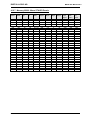
1
TECHNICAL USER'S MANUAL FOR: EBX-Standard Pentium Littleboard MSLB_P5 Low Power Product #190899-1 Nordstrasse 11/F, CH-4542 Luterbach Tel.: ++41 (0)32 681 53 33 - Fax: ++41 (0)32 681 53 31 COPYRIGHT 1999 BY DIGITAL-LOGIC AG DIGITAL-LOGIC AG MSLB_P5 Manual V0.3 No part of this document may be reproduced, transmitted, transcribed, stored in a retrieval system, in any form or by any means, electronic, mechanical, optical, manual, or otherwise, without the prior written permission of DIGITAL-LOGIC AG. The software described herein, together with this document, are furnished under a license agreement and may be used or copied only in accordance with the terms of that agreement. REVISION HISTORY: Prod.-Serialnumber: From: To: Product Version Document Version V0.1 V0.2 V0.3 Date/Vis: Modification: Remarks, News, Attention: 10.99 FK Initial version 11.99 FK RS422/485, EBX Standard 12.99 FK Current, VideoInput Registration Form: Please register your product under: http://www.digitallogic.ch -> SUPPORT -> Product Registration After registration, you will receive driver & software updates, errata information, customer information and news from DIGITAL-LOGIC AG products automatically. PRELIMINARY 2 DIGITAL-LOGIC AG MSLB_P5 Manual V0.3 Table of Contents 1 PREFACE ....................................................................................................................... 7 1.1 1.2 1.3 1.4 1.5 1.6 2 Trademarks..................................................................................................................7 Disclaimer ....................................................................................................................7 Who should use this Product....................................................................................7 Recycling Information ................................................................................................8 Technical Support ......................................................................................................8 Limited Warranty.........................................................................................................8 OVERVIEW..................................................................................................................... 9 2.1 Standard Features......................................................................................................9 2.2 Unique Features..........................................................................................................9 Block Diagram.....................................................................................................................10 2.4 MSLB-P5 Specifications...........................................................................................11 2.5 Thermoscan...............................................................................................................15 2.6 Ordering Codes.........................................................................................................16 2.7 BIOS History..............................................................................................................16 2.8 This product is “YEAR 2000 CAPABLE” ................................................17 2.9 High frequency Radiation (to meet EN55022) .......................................................18 2.10 Mechanical Dimensions ...........................................................................................19 2.10.1 Mechanical Dimensions Mounting Holes.............................................................. 19 2.10.2 Mechanical Dimensions Connectors.................................................................... 20 2.10.3 Mechanical Dimensions Frontside ....................................................................... 21 3 THE PCI, ISA , EPCI AND PC/104 BUS SIGNALS ..............................................22 3.1 3.2 3.3 ISA Signals on the PC/104 and ISA-Bus ................................................................22 Connect PCI peripheral cards to the PC/104plus BUS: ......................................26 EBX Specification — Ver 1.1 — July 9, 1997 ........................................................27 3.3.1 EBX DETAILED MECHANICAL DRAWINGS............................................................ 33 4 DETAILED SYSTEM DESCRIPTION ......................................................................35 4.1 4.2 Power Requirements................................................................................................35 CPUs, Boards and RAMs.........................................................................................35 4.2.1 CPUs of this MICROSPACE Product...................................................................... 35 4.3 Interface .....................................................................................................................36 4.3.1 4.3.2 4.3.3 4.3.4 4.3.5 4.3.6 4.3.7 4.3.8 4.3.9 4.4 PS/2-Keyboard ....................................................................................................... 36 PS/2-Mouse Interface ............................................................................................. 36 Line Printer Port LPT1............................................................................................ 36 Serial Ports COM1-COM4 RS232C........................................................................ 37 Serial Ports COM3-COM4 RS422 .......................................................................... 38 Serial Ports COM3-COM4 RS485 .......................................................................... 39 Driver for COM3-COM4 RS422/485 ....................................................................... 40 Floppy disk interface.............................................................................................. 41 Speaker interface ................................................................................................... 42 Controllers.................................................................................................................43 4.4.1 Interrupt Controllers............................................................................................... 43 4.5 Timers and Counters................................................................................................43 4.5.1 Programmable Timers............................................................................................ 43 4.5.2 Battery backed clock (RTC).................................................................................... 44 4.5.3 Watchdog............................................................................................................... 44 4.6 BIOS ...........................................................................................................................45 4.6.1 ROM-BIOS Sockets................................................................................................ 45 4.6.2 EEPROM Memory for Setup ................................................................................... 46 4.6.3 BIOS CMOS Setup.................................................................................................. 47 4.7 CMOS RAM Map........................................................................................................48 4.7.1 CMOS Setup Harddisk list...................................................................................... 54 4.7.2 Harddisk PIO Modes............................................................................................... 54 PRELIMINARY 3 DIGITAL-LOGIC AG MSLB_P5 Manual V0.3 4.7.3 EEPROM saved CMOS setup.................................................................................. 55 4.7.4 BIOS Download Function ....................................................................................... 55 4.7.5 VGA BIOS Download Function............................................................................... 56 4.8 Memory.......................................................................................................................57 4.8.1 Onboard DRAM Memory......................................................................................... 57 4.8.2 System Memory Map.............................................................................................. 57 4.8.3 System I/O map...................................................................................................... 58 4.9 BIOS Data Area Definitions .....................................................................................73 4.9.1 Compatibility Service Table ................................................................................... 79 4.10 VGA, LCD ...................................................................................................................80 4.10.1 4.10.2 4.10.3 4.10.4 4.10.5 4.10.6 4.10.7 VGA / LCD Controller C&T69000 (optional C&T69030) .......................................... 80 VGA / LCD BIOS for 69000.................................................................................... 80 Display Modes Supported...................................................................................... 81 VGA/LCD BIOS Support ......................................................................................... 82 Memory 69000 CRT/TFT Panels............................................................................. 83 Memory 69000 Color STN-DD Panels.................................................................... 84 Memory 69000 Mono STN-DD Panels.................................................................... 85 4.11 HiQ Video Multimedia Support.............................................................................86 4.11.1 HiQVideo Series Programming Examples............................................................ 87 4.11.2 Introduction............................................................................................................ 87 4.11.3 Video Playback through PCI/VL Bus...................................................................... 87 4.11.4 Video Capture and Playback Through Video Port.................................................. 87 4.11.5 ZoomUp.................................................................................................................. 87 4.11.6 Video Capture Using the Video Port....................................................................... 88 4.11.7 How to enable video capture and playback module (Init)....................................... 88 4.11.8 How to disable video playback and capture module (Exit)..................................... 89 4.11.9 How to start video capture ..................................................................................... 89 4.11.10 How to stop video capture .................................................................................. 90 4.11.11 How to set input video color format.................................................................... 91 4.11.12 How to set interlaced or non-interlaced video input ........................................... 91 4.11.13 How to enable/disable double buffer .................................................................. 92 4.11.14 How to scale input video (before acquiring into frame buffer)............................ 92 4.11.15 How to crop input video (programming of acquisition rectangle)....................... 93 4.11.16 Video Input with the SAA7111 VIP ................................................................... 98 5 DESCRIPTION OF THE CONNECTORS .............................................................100 5.1 5.2 Jumpers on this MICROSPACE product..............................................................112 Jumper and Connector Locations........................................................................113 5.2.1 Top-view .............................................................................................................. 113 5.2.2 Bottom-view......................................................................................................... 114 6 CABLE INTERFACE ................................................................................................115 6.1 6.2 6.3 6.4 7 SPECIAL PERIPHERALS, OPTIONAL FUNCTIONS........................................119 7.1 8 9 Special Peripherals.................................................................................................119 100/10 ETHERNET LAN.........................................................................................120 SCSI INTERFACE (OPTION)..................................................................................122 9.1 10 The Floppy Disk Cable ...........................................................................................115 The Harddisk Cable 40 pins...................................................................................116 The Harddisk Cable 44 pins...................................................................................117 The COM 1/2 Serial Interface Cable ......................................................................118 SCSI Drivers for operating system support.........................................................123 SOUNDPORT DRIVER INSTALLATION ..............................................................124 10.1 10.2 10.3 10.4 10.5 ESS1869 ...................................................................................................................124 Driver for WIN 3.11..................................................................................................124 Driver for WIN 95.....................................................................................................125 Driver for NT4.0.......................................................................................................125 Bundled Applications, MediaRack........................................................................125 PRELIMINARY 4 DIGITAL-LOGIC AG 11 MSLB_P5 Manual V0.3 INSTALLING THE FLASHDISK DOC2000 ..........................................................126 11.1 Enabling and Formatting of the DiskOnChip-Modules......................................126 12 BUILDING A SYSTEM..............................................................................................127 12.1 Starting up the System...........................................................................................127 12.2 Error on boot time ..................................................................................................127 13 DIAGNOSTICS...........................................................................................................128 14 BIOS.............................................................................................................................131 14.1.1 14.1.2 14.1.3 14.1.4 14.1.5 14.1.6 Main Menu Selections .......................................................................................... 131 Masters and Slaves.............................................................................................. 131 Memory Cache ..................................................................................................... 132 Memory Shadow .................................................................................................. 134 Boot Sequence..................................................................................................... 135 Keyboard Features............................................................................................... 136 14.2 Boot Menu ...............................................................................................................137 14.3 The Advanced Menu...............................................................................................138 14.3.1 Advanced Chipset Control Menu (PCI BIOS)....................................................... 139 14.3.2 PCI Devices Menu ................................................................................................ 140 14.3.3 I/O Device Configuration Menu ............................................................................ 141 The Security Menu ...........................................................................................................143 The Power Menu...............................................................................................................145 The Exit Menu ...................................................................................................................147 Saving Values................................................................................................................. 147 Exit Discarding Changes................................................................................................ 147 Load Setup Defaults ....................................................................................................... 148 Discard Changes............................................................................................................ 148 Save Changes................................................................................................................. 148 14.4 PhoenixBIOS Messages.........................................................................................149 14.5 Phoenix Phlash Tool ..............................................................................................150 14.6 Phoenix QuietBoot .................................................................................................150 14.6.1 14.6.2 14.6.3 14.6.4 Press <ESC> ........................................................................................................ 151 Press <F2> ........................................................................................................... 151 POST Error........................................................................................................... 151 Keyboard Input Request....................................................................................... 151 14.7 Phoenix MultiBoot ..................................................................................................151 14.7.1 14.7.2 14.7.3 14.7.4 15 PHOENIX PHLASH...................................................................................................154 15.1 15.2 15.3 15.4 15.5 16 The Setup Boot Menu........................................................................................... 151 Removable Format Menu ..................................................................................... 152 Fixed and Removable Media Menus..................................................................... 152 The Boot First Menu............................................................................................. 153 Installation ...............................................................................................................154 Create the Crisis Recovery Diskette ....................................................................154 Updating the Crisis Recovery Diskette ................................................................155 Executing Phoenix Phlash.....................................................................................155 Crisis Recovery Mode ............................................................................................156 PROGRAMMER'S GUIDE .......................................................................................157 What is a ROM BIOS?......................................................................................................157 Initialize and Configure the computer............................................................................. 158 16.1.1 BIOS Services...................................................................................................... 158 16.2 16.3 16.4 16.5 System Hardware Requirements ..........................................................................158 Fixed Disk Tables ...................................................................................................159 PhoenixBIOS Function Keys .................................................................................160 POST Errors and Beep Codes...............................................................................160 16.5.1 Recoverable POST Errors.................................................................................... 160 16.5.2 Terminal POST Errors.......................................................................................... 160 16.5.3 Test Points and Beep Codes................................................................................ 161 16.6 PhoenixBIOS 4.0 Services.....................................................................................164 PRELIMINARY 5 DIGITAL-LOGIC AG MSLB_P5 Manual V0.3 16.6.1 BIOS32 Service Directory..................................................................................... 164 16.6.2 Interrupt 10h–Video Services............................................................................... 166 16.6.3 Interrupt 11h–Return System Information............................................................ 168 16.6.4 Interrupt 12h–Return Memory Size ...................................................................... 168 16.6.5 Interrupt 13h–Diskette Services........................................................................... 168 16.6.6 Interrupt 13h–Fixed Disk Services........................................................................ 171 16.6.7 Interrupt 13h–Extended Fixed Disk Services........................................................ 174 16.6.8 Interrupt 13h–Bootable CD-ROM Services........................................................... 175 16.6.9 Interrupt 14h–Serial Services............................................................................... 177 16.6.10 Interrupt 15h–System Services......................................................................... 179 16.6.11 Interrupt 15h–APM Services.............................................................................. 181 16.6.12 Interrupt 15h–Big Memory Services.................................................................. 185 16.6.13 Interrupt 15h–PS/2 Mouse Services.................................................................. 186 16.6.14 Interrupt 15h–EISA Services............................................................................. 187 16.6.15 Interrupt 16h–Keyboard Services...................................................................... 189 16.6.16 Interrupt 17h–Parallel Printer Services............................................................. 190 16.6.17 Interrupt 17h–EPP Services.............................................................................. 191 16.6.18 Interrupt 1Ah–Time of Day Services.................................................................. 194 16.6.19 Interrupt 1Ah–General PCI Services................................................................. 195 16.6.20 PnP Run-Time Services.................................................................................... 197 16.6.21 SMBIOS Services.............................................................................................. 200 16.6.22 SMBIOS Services.............................................................................................. 201 16.6.23 MultiBoot II Run-Time Services......................................................................... 202 16.7 BIOS Data Area .......................................................................................................204 16.7.1 Extended BIOS Data Area .................................................................................... 207 16.8 Interrupt Vectors.....................................................................................................207 17 INDEX..........................................................................................................................208 PRELIMINARY 6 DIGITAL-LOGIC AG 1 MSLB_P5 Manual V0.3 PREFACE This manual is for integrators and programmers of systems based on the MICROSPACE card family. It contains information on hardware requirements, interconnections, and details of how to program the system. The specifications given in this manual were correct at the time of printing; advances mean that some may have changed in the meantime. If errors are found, please notify DIGITAL-LOGIC AG at the address shown on the title page of this document, and we will correct them as soon as possible. 1.1 Trademarks MICROSPACE, MicroModule DOS Vx.y, Windows PC-AT, PC-XT NetWare Ethernet DR-DOS, PALMDOS ROM-DOS DIGITAL-LOGIC AG Microsoft Inc. IBM Novell Corporation Xerox Corporation Digital Research Inc. / Novell Inc. Datalight Inc. 1.2 Disclaimer DIGITAL-LOGIC AG makes no representations or warranties with respect to the contents of this manual and specifically disclaims any implied warranty of merchantability or fitness for any particular purpose. DIGITALLOGIC AG shall under no circumstances be liable for incidental or consequential damages or related expenses resulting from the use of this product, even if it has been notified of the possibility of such damage. DIGITAL-LOGIC AG reserves the right to revise this publication from time to time without obligation to notify any person of such revisions. If errors are found, please contact DIGITAL-LOGIC AG at the address listed on the title page of this document. 1.3 Who should use this Product - Electronic engineers with know-how in PC-technology. Without electronic know-how we expect you to have questions. This manual assumes, that you have a general knowledge of PC-electronics. Because of the complexity and the variability of PC-technology, we can’t give any warranty that the product will work in any particular situation or combination. Our technical support will help you. Pay attention to the electrostatic discharges. Use a CMOS protected workplace. Power supply OFF when you are working on the board or connecting any cables or devices. This is a high-technology product. You need know-how in electronics and PC-technology to install the system ! PRELIMINARY 7 DIGITAL-LOGIC AG MSLB_P5 Manual V0.3 1.4 Recycling Information Hardware: - Print: Software: epoxy with glass fiber wires are of tin-plated copper - Components: ceramics and alloys of gold, silver check your local electronic recycling - no problems: re-use the diskette after formatting 1.5 Technical Support 1. Contact your local Digital-Logic Technical Support in your country. 2. Use Internet Support Request form on http://www.digitallogic.ch -> support 3. Send a FAX or an E-mail to DIGITAL-LOGIC AG with a description of your problem. DIGITAL-LOGIC AG Technical Support Dept. Nordstrasse 11/F CH-4542 Luterbach (SWITZERLAND) Fax: ++41-32 681 53 31 E-Mail: [email protected] 1.6 Limited Warranty DIGITAL-LOGIC AG warrants the hardware and software products it manufactures and produces to be free from defects in materials and workmanship for one year following the date of shipment from DIGITAL-LOGIC AG, Switzerland. This warranty is limited to the original purchaser of product and is not transferable. During the one year warranty period, DIGITAL-LOGIC AG will repair or replace, at its discretion, any defective product or part at no additional charge, provided that the product is returned, shipping prepaid, to DIGITAL-LOGIC AG. All replaced parts and products become property of DIGITAL-LOGIC AG. Before returning any product for repair, customers are required to contact the company. This limited warranty does not extend to any product which has been damaged as a result of accident, misuse, abuse (such as use of incorrect input voltages, wrong cabling, wrong polarity, improper or insufficient ventilation, failure to follow the operating instructions that are provided by DIGITAL-LOGIC AG or other contingencies beyond the control of DIGITAL-LOGIC AG), wrong connection, wrong information or as a result of service or modification by anyone other than DIGITAL-LOGIC AG. Neither if the user has not enough knowledge of these technologies or has not consulted the product manual or the technical support of DIGITALLOGIC AG and therefore the product has been damaged. Except, as expressly set forth above, no other warranties are expressed or implied, including, but not limited to, any implied warranty of merchantability and fitness for a particular purpose, and DIGITAL-LOGIC AG expressly disclaims all warranties not stated herein. Under no circumstances will DIGITAL-LOGIC AG be liable to the purchaser or any user for any damage, including any incidental or consequential damage, expenses, lost profits, lost savings, or other damages arising out of the use or inability to use the product. PRELIMINARY 8 DIGITAL-LOGIC AG 2 MSLB_P5 Manual V0.3 OVERVIEW 2.1 Standard Features The MICROSPACE PC is a miniaturized modular device incorporating the major elements of a PC/AT compatible computer. It includes standard PC/AT compatible elements, such as: - Powerfull LowVoltage PENTIUM P55 CPU at 166/266MHz FLASH BIOS , downloadable SDRAM up to 128 MBytes 256k burst piplined second level cache Timers DMA Real-time clock with CMOS-RAM and battery buffer LPT1 parallel port COM1, COM2, COM3, COM4 serial port PS/2 keyboard interface PS/2 mouse Int erface SVGA/LC Display interface Floppy disk Interface E-IDE harddisk interface PC/104plus Bus (ISA with PCI signals) Ethernet-LAN, 100/10 Base-T Video Input for 3 sources Soundport Optional SCSI-2 with 10MB/s 2.2 Unique Features The MICROSPACE MSLB_P5 includes all standard PC/AT functions plus unique DIGITAL-LOGIC AG enhancements, such as: - Low-power consumption, 10 watt Single 5 volt supply Watchdog Power-fail circuit EEPROM setup and configuration Video Input for 3 video sources PAL or NTSC ByteWide socket for DOC2000 (disk on chip) with up to 72MByte PC/104+ PCI extension UL approved parts PRELIMINARY 9 2.3 Block Diagram CPU 2.5V 1,8V switched P55-266MHz HOST BUS CACHE 256 kByte TXC 430TX DRAM 32/128 MByte PCI-BUS EIDE RTC Speaker LAN INTEL 82559 LCD/VGA Controller 69000 with 2Mb VRAM PIIX4 D LCD CRT LiBAT A SCSI Controller AIC-7860 Phillips SAA7111 100/10Base-T PC/104plus BUS SCSI Video-Input ISA-BUS ISA-BUS BIOS PC/104 128kByte SMSC - Super I/O 37C672 MAX2ll FD MAX2ll MAX2ll LPT1 COM1 COM2 SMSC 37C666 KB Mouse Soundport ESS1869 MAX2ll COM3 COM4 L R Speaker MIC EEPROM 2kByte Temp. Sensor DIGITAL-LOGIC AG MSLB-P5 Manual V0.3 2.4 MSLB-P5 Specifications CPU: CPU 64 Bit: CPU 16 Bit: Mode: Compatibility: Word Size: Physical Addressing: Virtual Addressing: Clock Rates: Socket Standard: Pentium 166MHz / 266MHz none Real / Protected 8086 – Pentium 32 Bits 32 lines 16 Gbytes 166 MHz BGA, 3.3V, 1.8V switched, 2.5V linear 3.3V linear) 2nd. Level Cache: available 256k onboard, burst pipelined SRAM for max. performance PC-Chipset: Intel TX430 8237A comp. 4 channels 8 Bits 3 channels 16 Bits DMA: Interrupts: 8259 comp. 8 + 7 levels, PC compatible Timers: 8254 comp. 3 programmable counter/timers Memory: DRAM 168pin SIMM Video Output: Controller: BUS: Enhanced BIOS: Video-Memory: CRT-Monitor: Flatpanel: Flatpanelinterface: 69000 from C&T 32 Bit highspeed 33 MHz PCI bus Multi VGA / LCD BIOS 2 MByte - 32 bit, expandable up to 4MByte up to 1600 x 1280 pixels TFT: 640 x 480, 800 x 600, 1024 x 768 STN: 640 x 480 color and monochrome Plasma: up to 1280 x 1024 EL: 640 x 350, 640 x 480 Standard: TTL 5V Controller Modes: Drivers: CRT only; Flatpanel only or simultaneous CRT and Flatpanel Windows 3.11, WIN95, NT3.5, NT4.0 and other applications PRELIMINARY 11 DIGITAL-LOGIC AG MSLB-P5 Manual V0.3 Video Input: (option) Controller: BUS: Videoinput Norm: Driversupport: Resolution: Capture speed: PAL/NTSC Decoder: Y-C resolution: RGB resolution: 69000 from C&T 32 Bit highspeed 33 MHz PCI bus 3 channels with PAL or NTSC (composite video sources = CVBS) 2 channels YC sources (=SVHS) 2 channels CVBS and 1 channel SVHS this configuration may be programmed into the SAA7111 WIN95, under development for NT4.0 720 x 512 up to 30 images/second Phillips SAA7111 4:4:4 or 4:2:2 or 4:1:1 4:4:4 (16 Bit), gamma corrected Mass Storage: FD: HD: SCSI Devices: Floppy disk interface, for max. 2 floppies, 34pin connector primary IDE 44pin interface for 2 drives (master & slave) secondary IDE 44pin interface for 2 drives (master & slave) PCI 10MB/s FAST SCSI-2 up to 7 devices, removable boot media AIC-7860 PCI SCSI controller Standard AT interfaces: Serial: Parallel: Keyboard: Mouse: Speaker: RTC: Backup current: Battery: Name FIFO IRQs Addr. COM1 COM2 COM3 COM4 yes yes yes yes IRQ4 IRQ3 IRQ4/11 IRQ3/10 3F8 2F8 3E8 2E8 StanOption dard RS232C RS232C RS232C RS485/RS422 RS232C RS485/RS422 (Baudrates: up to 115kBaud) LPT1 printer interface, in the EPP Mode bidirectional PS/2 PS/2 0.1W output drive 146818A compatible RTC with CMOS-RAM 128Byte 0.2µA Lithium 3V, Lifetime up to 10 years at 25°C LAN - Ethernet: (option) Type: Controller: Compatibility: Driver: Connector: Data Rate: Data-Bus: Cable Type: Remote Boot Socket: RAM Buffer: Configuration: PRELIMINARY IEEE 802.3 INTEL 82559 ODI-Novell ODI, packet-driver IEEE 802.3, NT3.5, OS/2, NDIS, NT4.0 RJ-45 for 100/10Base-T 100 or 10 MB/sec 32 Bit PCI none 4k with EEPROM 12 DIGITAL-LOGIC AG MSLB-P5 Manual V0.3 Sound I/O: (option) Controller: Driver Support: Output channels: Input: Features: ESS1869 8Bit Soundblaster compatible WIN 3.11, WIN95, NT4 Stereo Output Line Level Microphone, Line - Compatible with: SoundBlasterPro 8 Bit, AD-Lib, MicroSoft-Windows Sound System - OPL3 Synthesizer built in - 3D Stereo Enhancement - Digital mixer - Game Port, Midi Interface - Programmable IRQs, DRQs and I/O addresses - Supports 16 Bit type F DMA playback Supervisory: Watchdog: LTC1232 with power-fail detection Controller: Transferrate: Channels: PIIX4 12.5MBps / 1.5 MBps 2 USB: BUS internal: PCI Clock: IEEE-996 standard bus, by Intel 33MHz with 32bit data path and 100MB/s transferrate BUS external: ISA Clock: IEEE-996 standard bus 8 MHz or programmable Embedded BUS: PC/104 Clock: PC/104+ IEEE-996 standard bus 8 MHz or programmable PCI 32bit, 33Mhz bus , this is an assembly option Power Supply: Working: Current: Suspend: Rise Time: PRELIMINARY 5 Volts ± 5% 2.3A nominal, using P55-166 MHz 0.9A 100µs +/- 10% from 0V to 4.75V 13 DIGITAL-LOGIC AG MSLB-P5 Manual V0.3 Physical Characteristics: Dimensions: Weight: PCB Thickness: PCB Layer: Length: 204 mm Depth: 140 mm Height: 40 mm 300gr 1.6 mm / 0.0625 inches nominal 10 with separate ground and VCC plane for low noise Operating Environment: Relative humidity: Vibration: Shock: Temperature: 5 - 90% non condensing 5 to 2000 Hz 10 G Operating: Standard version: -25°C to +70°C Enhanced temp. range: -40°C to +85°C Storage: -55°C to +85°C -E48 Cooling: Standard: Temperaturesensor: Option: 5V Fan, with feedback (frequency sensor) onboard, located in the center below the CPU passive with air flow > 1000ft/Min. EMI / EMC (IEC1131-2 refer MIL 461/462): ESD Electro Static Discharge: REF Radiated Electromagnetic Field: EFT Electric Fast Transient (Burst): SIR Surge Immunity Requirements: High-Frequency Radiation: IEC 801-2, EN55101-2, VDE 0843/0847 Part 2 metallic protection needed, separate Ground Layer included,15kV single peak IEC 801-3, VDE 0843 Part 3, IEC770 6.2.9. not tested IEC 801-4, EN50082-1, VDE 0843 Part 4 250V - 4kV, 50 ohms, Ts=5ns Grade 2: 1KV Supply, 500 I/O, 5Khz IEC 801-5, IEEE587, VDE 0843 Part 5 Supply: 2 kV, 6 pulse/minute I/O: 500 V, 2 pulse/minute EN55022 Compatibility: MSLB: mechanically compatible to standard EBX single boards Any information is subject to change without notice. PRELIMINARY 14 DIGITAL-LOGIC AG 2.5 MSLB-P5 Manual V0.3 Thermoscan Product: PRELIMINARY MSLB-P5 Scan time: 15 60min. DIGITAL-LOGIC AG MSLB-P5 Manual V0.3 2.6 Ordering Codes MSLB-P5 MICROSPACE PCCard without CPU, with 256k Cache no Options Option - E Option - S Option - A LAN 100/10BASE-T Option SCSI-2 Audio Sound Interface 2.7 BIOS History Version: BETA Date: PRELIMINARY Status: Modifications: 16 DIGITAL-LOGIC AG 2.8 MSLB-P5 Manual V0.3 This product is “YEAR 2000 CAPABLE” This DIGITAL-LOGIC product is “YEAR 2000 CAPABLE”. This means, that upon installation, it accurately stores, displays, processes, provides and/or receives date data from, into, and between 1999 and 2000, and the 20. and 21. centuries, including leap year calculations, provided that all other technology used in combination with said product properly exchanges date data with it. DIGITAL-LOGIC makes no representation about individual components within the product should be used independently from the product as a whole. You should understand that DIGITAL-LOGIC’s statement that an DIGITAL-LOGIC product is “YEAR 2000 CAPABLE” means only that DIGITAL-LOGIC has verified that the product as a whole meet this definition when tested as a stand-alone product in a test lab, but dies not mean that DIGITAL-LOGIC has verified that the product is “YEAR 2000 CAPABLE” as used in your particular situation or configuration. DIGITAL-LOGIC makes no representation about individual components, including software, within the product should they be used independently from the product as a whole. DIGITAL-LOGIC customers use DIGITAL-LOGIC products in countless different configurations and in conjunction with many other components ans systems, and DIGITAL-LOGIC has no way to test wheter all those configurations and systems will properly handle the transition to the year 2000. DIGITAL-LOGIC encourages its customers and others to test whether their own computer systems and products will properly handle the transition to the year 2000. The only proper method of accessing the date in systems is indirectly from the Real-Time-Clock via the BIOS. The BIOS in DIGITAL-LOGIC computerboards contain a century checking and maintenance feature the checks the laest two significant digits of the year stored in the RTC during each BIOS request (INT 1A) to read the date and, if less than ‘80’ (i.e. 1980 is the first year supported by the PC), updates the century byte to ‘20’. This feature enables operating systems and applications using BIOS date/time services to reliably manipulate the year as a four-digit value. PRELIMINARY 17 DIGITAL-LOGIC AG MSLB-P5 Manual V0.3 2.9 High frequency Radiation (to meet EN55022) Since the boards are very high integrated embedded computers, no peripheral lines are protected against the radiation of high frequency spectrum. To meet a typical EN55022 requirement, all peripherals, they are going outside of the computer case, must be filtered externaly. Typical signals, they must be filtered: Interface: Keyboard: Mouse: COM1/2/3/4: LPT: CRT: Powerlines: Signals: onboard filter on the MSLB-P5: KBCLK, KBDATA, VCC onboard filter MSCLK, MSDATA, VCC onboard filter All serial signals must be filtered not filtered All parallel signals must be filtered not filtered red,blue,green, hsynch, vsynch must be filtered onboard filter +5V, +12V, Ground not filtered Typical signals, they must not be filtered, since they are internaly used: IDE: Floppy: LCD: 1. connected to the harddisk connected to the floppy connected to the internal LCD For peripheral cables: Use for all DSUB connector a filtered version. Select carefully the filter specifications. Place the filtered DSUB connector directly frontside and be shure that the shielding makes a good contact with the case. 9pin DSUB connector from AMPHENOL: FCC17E09P 25pin DSUB connector from AMPHENOL: FCC17B25P 2. Power supply: Use a currentcompensated dualinductor on the 5V supply SIEMENS PRELIMINARY B82721-K2362-N1 with 3.6A , 0.4mH 18 820pF 820pF DIGITAL-LOGIC AG MSLB-P5 Manual V0.3 2.10 Mechanical Dimensions 2.10.1 Mechanical Dimensions Mounting Holes PRELIMINARY 19 DIGITAL-LOGIC AG MSLB-P5 Manual V0.3 2.10.2 Mechanical Dimensions Connectors PRELIMINARY 20 DIGITAL-LOGIC AG MSLB-P5 Manual V0.3 2.10.3 Mechanical Dimensions Frontside PRELIMINARY 21 DIGITAL-LOGIC AG 3 MSLB-P5 Manual V0.3 T HE PCI, ISA , EPCI AND PC/104 B US SIGNALS 3.1 ISA Signals on the PC/104 and ISA-Bus AEN, output Address Enable is used to degate the microprocessor and other devices from the I/O channel to allow DMA transfers to take place. low = CPU Cycle , high = DMA Cycle BALE, output Address Latch Enable is provided by the bus controller and is used on the system board to latch valid addresses and memory decodes from the microprocessor. This signal is used so that devices on the bus can latch LA17..23. The SA0..19 address lines latched internally according to this signal. BALE is forced high during DMA cycles. /DACK[0..3, 5..7], output DMA Acknowledge 0 to 3 and 5 to 7 are used to acknowledge DMA requests (DRQO through DRQ7). They are active low. This signal indicates that DMA operation can begin. DRQ[0..3, 5..7], input DMA Requests 0 through 3 and 5 through 7 are asynchronous channel requests used by peripheral devices and the I/O channel microprocessors to gain DMA service (or control of the system). A request is generated by bringing a DRQ line to an active level. A DRQ line must be held high until the corresponding DMA Request Acknowledge (DACK/) line goes active. DRQO through DRQ3 will perform 8-bit DMA transfers; DRQ5-7 are used for 16 accesses. /IOCHCK, input IOCHCK/ provides the system board with parity (error) information about memory or devices on the I/O channel. low = parity error , high = normal operation IOCHRDY, input I/O Channel Ready is pulled low (not ready) by a memory or I/O device to lengthen I/O or memory cycles. Any slow device using this line should drive it low immediately upon detecting its valid address and a Read or Write command. Machine cycles are extended by an integral number of one clock cycle (67 nanoseconds). This signal should be held low for no more than 2.5 microseconds. low = wait, high = normal operation /IOCS16, input I/O 16 bit Chip Select signals the system board that the present data transfer is a 16-bit, 1 wait-state, I/0 cycle. It is derived from an address decode. /IOCS16 is active low and should be driven with an open collector (300 ohm pull-up) or tri-state driver capable of sinking 20mA. The signal is driven based only on SA15-SAO (not /IOR or /IOW) when AEN is not asserted. In the 8 bit I/O transfer, the default transfers a 4 wait-state cycle. /IOR, input/output I/O Read instructs an I/O device to drive its data onto the data bus. It may be driven by the system microprocessor or DMA controller, or by a microprocessor or DMA controller resident on the I/O channel. This signal is active low. /IOW, input/output PRELIMINARY 22 DIGITAL-LOGIC AG MSLB-P5 Manual V0.3 I/O Write instructs an I/O device to read the data on the data bus. It may be driven by any microprocessor or DMA controller in the system. This signal is active low . PRELIMINARY 23 DIGITAL-LOGIC AG MSLB-P5 Manual V0.3 IRQ[ 3 - 7, 9 - 12, 14, 15], input These signals are used to tell the microprocessor that an I/O device needs attention. An interrupt request is generated when an IRQ line is raised from low to high. The line must be held high until the microprocessor acknowledges the interrupt request . /Master, input This signal is used with a DRQ line to gain control of the system. A processor or DMA controller on the I/0 channel may issue a DRQ to a DMA channel in cascade mode and receive a /DACK. /MEMCS16, input MEMCS16 Chip Select signals the system board if the present data transfer is a 1 wait-state, 16-bit, memory cycle. It must be derived from the decode of LA17 through LA23. /MEMCS16 should be driven with an open collector (300 ohm pull-up) or tri-state driver capable of sinking 2OmA. /MEMR input/output These signals instruct the memory devices to drive data onto the data bus. /MEMR is active on all memory read cycles. /MEMR may be driven by any microprocessor or DMA controller in the system. When a microprocessor on the I/0 channel wishes to drive /MEMR, it must have the address lines valid on the bus for one system clock period before driving /MEMR active. These signals are active low. /MEMW, input/output These signals instruct the memory devices to store the data present on the data bus. /MEMW is active in all memory read cycles. /MEMW may be driven by any microprocessor or DMA controller in the system. When a microprocessor on the I/O channel wishes to drive /MEMW, it must have the address lines valid on the bus for one system clock period before driving /MEMW active. Both signals are active low. OSC, output Oscillator (OSC) is a high-speed clock with a 70 nanosecond period (14.31818 MHz). This signal is not synchronous with the system clock. It has a 50% duty cycle. OSC starts 100us after reset is inactive. RESETDRV, output Reset Drive is used to reset or initiate system logic at power-up time or during a low line-voltage outage. This signal is active high. When the signal is active all adapters should turn off or tri-state all drivers connected to the I/O channel. This signal is driven by the permanent Master. /REFRESH, input/output These signals are used to indicate a refresh cycle and can be driven by a microprocessor on the I/0 channel. These signals are active low. SAO-SA19, LA17 - LA23 input/output Address bits 0 through 19 are used to address memory and I/0 devices within the system. These 20 address lines, allow access of up to 1MBytes of memory. SAO through SA19 are gated on the system bus when BALE is high and are latched on the falling edge of BALE. LA17 to LA23 are not latched and addresses the full 16 MBytes range. These signals are generated by the microprocessors or DMA controllers. They may also be driven by other microprocessor or DMA controllers that reside on the I/0 channel. The SA17-SA23 are always LA17-LA23 address timings for use with the MSCS16 signal. This is advanced AT96 design. The timing is selectable with jumpers LAxx or SAxx. /SBHE, input/output Bus High Enable (system) indicates a transfer of data on the upper byte of the data bus, SD8 through SD15. Sixteen-bit devices use /SBHE to condition data-bus buffers tied to SD8 through SD15. PRELIMINARY 24 DIGITAL-LOGIC AG MSLB-P5 Manual V0.3 SD[O..15], input/output These signals provide bus bits 0 through 15 for the microprocessor, memory, and I/0 devices. DO is the least-significant bit and D15 is the most significant bit. All 8-bit devices on the I/O channel should use DO through D7 for communications to the microprocessor. The 16-bit devices will use DO through D15. To support 8-bit device, the data on D8 through D15 will be gated to DO through D7 during 8-bit transfers to these devices; 16-bit microprocessor transfers to 8-bit devices will be converted to two 8bit transfers. /SMEMR input/output These signals instruct the memory devices to drive data onto the data bus for the first MByte. /SMEMR is active on all memory read cycles. /SMEMR may be driven by any microprocessor or DMA controller in the system. When a microprocessor on the I/0 channel wishes to drive /SMEMR, it must have the address lines valid on the bus for one system clock period before driving /SMEMR active. The signal is active low. /SMEMW, input/output These signals instruct the memory devices to store the data present on the data bus for the first MByte. /SMEMW is active in all memory read cycles. /SMEMW may be driven by any microprocessor or DMA controller in the system. When a microprocessor on the I/O channel wishes to drive /SMEMW, it must have the address lines valid on the bus for one system clock period before driving /SMEMW active. Both signals are active low. SYSCLK, output This is a 8 MHz system clock. It is a synchronous microprocessor cycle clock with a cycle time of 167 nanoseconds. The clock has a 50% duty cycle. This signal should only be used for synchronization. It is not intended for uses requiring a fixed frequency. TC output Terminal Count provides a pulse when the terminal count for any DMA channel is reached. The TC completes a DMA-Transfer. This signal is expected by the onboard floppy disk controller. /OWS, input The Zero Wait State (/OWS) signal tells the microprocessor that it can complete the present bus cycle without inserting any additional wait cycles. In order to run a memory cycle to a 16-bit device without wait cycles, /OWS is derived from an address decode gated with a Read or Write command. In order to run a memory cycle to an 8-bit device with a minimum of one-wait states, /OWS should be driven active one system clock after the Read or Write command is active, gated with the address decode for the device. Memory Read and Write commands to an 8-bit device are active on the falling edge of the system clock. /OWS is active low and should be driven with an open collector or tri-state driver capable of sinking 2OmA. 12V +/- 5% used only for the flatpanel backligth supply only. GROUND = 0 Volt used for the entire system. VCC, +5V +/- 0.25 Volt 3-4 Amp. nominal, peak current of HD, SCSI-Devices and Cache could go up to 8 Amp.. PRELIMINARY 25 DIGITAL-LOGIC AG MSLB-P5 Manual V0.3 3.2 Connect PCI peripheral cards to the PC/104plus BUS: Internal used PCI-Signals: LAN: SCSI: A_D29, IRQA, REQ1, GNT1 A_D30, IRQB, REQ2, GNT2 Signals: PC/104plus: Master 1. PCI-Card Slave PCI_Clock: PCI_Clock_3 ----------------------> PCI_Clock 3 PCI_Clock_2 --------------------------------------------------------> PCI_Clock 2 GNT: GNT0 GNT1 GNT2 GNT3 -------------------------------> -------------------------------> -------------------------------> -------------------------------> GNT0 -----------------------> GNT1 -----------------------> GNT2 -----------------------> GNT3 -----------------------> GNT0 GNT1 GNT2 GNT3 REQ: REQ0 REQ1 REQ2 REQ3 -------------------------------> -------------------------------> -------------------------------> -------------------------------> REQ0 -----------------------> REQ1 -----------------------> REQ2 -----------------------> REQ3 -----------------------> REQ0 REQ1 REQ2 REQ3 PIRQ PIRQA ------------------------------> PIRQB ------------------------------> PIRQC ------------------------------> PIRQD ------------------------------> IDSEL: A_D22 ------------------------------> IDSEL A_D23 -------------------------------------------------------------------> IDSEL PIRQA PIRQB PIRQC PIRQD 2. PCI-Card Slave --------------------> --------------------> --------------------> --------------------> PIRQA PIRQB PIRQC PIRQD The number of the PCI cards is limited to totally 4 cards (inclusive PC/104plus). Following onboard SCSI yes yes yes combinations are possible: onboard PC/104plus Bus LAN yes 0 yes 1 yes 2 no * no * no * no * yes yes yes yes * * * * 0 1 2 3 no no 0 no no 1 no no 2 no no 3 no no 4 Attention: All signals must be routed by observing EPCI-Bus 2 1 0 Total PCI Loads 8 8 8 3 2 1 0 9 9 9 9 4 3 2 1 0 10 10 10 10 10 the definition in the PCI specification ! * The same limitation is valid for SCSI=yes and LAN = no PRELIMINARY Comments 26 DIGITAL-LOGIC AG MSLB-P5 Manual V0.3 3.3 EBX Specification — Ver 1.1 — July 9, 1997 1. INTRODUCTION Until now, embedded system designers had to choose among off-the-shelf backplane solutions, desktop motherboards, and proprietary designs. Size and power consumption constraints hampered finding the right solutions for embedded deployment. Consequently, OEMs wanting to purchase off-the-shelf equipment to shorten time-to-market were often forced to develop proprietary solutions. Standards are important to the embedded systems market. Popular backplane form-factors — including VME, CompactPCI?, Multibus?, STD32?, and passive backplane ISA — are well documented mechanical and electrical standards. Desktop motherboards, which fit certain high-end embedded applications, also follow standards such as Baby AT, LPX, ATX, and the new NLX standard. All these standards allow vendors and OEMs to create products that are easily packaged in enclosures and readily expanded via open interfaces. However, none of these backplane-based standards satisfy the unique space, power, and reliability constraints of small embedded systems. The availability of an embedded single-board computer (SBC) standard will ensure that embedded computing solutions can be designed into space constrained environments with off-theshelf components. The embedded market constantly demands improvements in functionality and performance, while at the same time seeking size and cost reduction. The “Embedded Board, eXpandable” (EBX) standard creates the opportunity for solutions which fit the requirements of embedded system OEMs; takes advantage of trends in the embedded computing market; and offers the convenience, flexibility, risk reduction, and scalability of multi-sourced off-the-shelf products. The “Embedded Board, eXpandable” (EBX) standard is the result of a collaboration between industry leaders, Motorola and Ampro, to unify the embedded computing industry on a small footprint embedded single-board computer standard. Derived from the Ampro Little Board??form-factor, EBX combines a standard footprint with open interfaces. The EBX form-factor is small enough for deeply embedded applications, yet large enough to contain the functions of a full embedded computer system: CPU, memory, mass storage interfaces, display controller, serial/parallel ports, and other system functions. PRELIMINARY 27 DIGITAL-LOGIC AG MSLB-P5 Manual V0.3 This EBX system expansion is based on popular existing industry standards — IEEE P996, PC/104?, PCI, PC/104-Plus?, and PCMCIA. IEEE P996 is the governing standard for the PC and PC/AT buses, informally known as the Industry Standard Architecture or “ISA.“ PC/104 places the P996 ISA bus on compact 3.6” x 3.8” modules with self-stacking capability. PC/104-Plus adds the power of a PCI bus to PC/104 while retaining the basic form-factor. For further expansion flexibility, PCMCIA offers access to PC Cards from the mobile and handheld computing markets. The EBX standard integrates all these off-the-shelf standards into a highly embeddable SBC form-factor. EBX supports the legacy of PC/104, hosting the wide variety of embedded system oriented expansion modules from hundreds of companies worldwide. PCMCIA brings the advantages of the latest portable and mobile system expansion technologies to embedded applications. Additionally, the EBX PCI infrastructure and PC/104-Plus expansion bus offer true processor independence and high performance standards-based system expansion. EBX compliant boards have a form-factor large enough to implement a powerful SBC capable of hosting today’s advanced operating systems, yet small enough to fit in the tight spaces of deeply embedded applications. This creates an exciting new opportunity for embedded system OEMs to standardize their designs and take advantage of off-the-shelf modules. The EBX standard is open to continuing technology advancements, since it is both processor and payload independent. It creates opportunity for economies of scale in chassis, power supply, and peripheral devices. It defines how products interoperate by providing mechanical rules for mandatory features and recommended zones for flexible I/O options. These attributes combine to make EBX the right choice for embedded computing. The aligning of DIGITAL-LOGIC, Ampro and Motorola, embedded computing industry leaders, brings stability to the embedded board market and offers OEMs assurance that a wide range of products will be available from multiple sources — now and in the future. The EBX specification is freely available to all interested companies, and may be used without licenses or royalties. For further technical information on the EBX standard, please contact: DIGITAL-LOGIC INC PRELIMINARY 28 DIGITAL-LOGIC AG MSLB-P5 Manual V0.3 2. REFERENCE DOCUMENTS This EBX specification makes reference to, and is based on, the current versions of the following specifications: IEEE P996 Draft Specification: IEEE Standards Office, Piscataway NJ; phone 908-562-3825, fax 908-562-1571. PC/104 and PC/104-Plus Specification: PC/104 Consortium, Mountain View CA; phone 415-903-8304, fax 415-967-0995. PCI Local Bus Specification: PCI Special Interest Group, Hillsboro OR; phone 800-443-5177 or 503-693-6232, fax 503-693-8344, email [email protected]. PC Card Standard: PCMCIA, San Jose CA; phone 408-433-2273, fax 408-4339558, email [email protected]. Technical references about the PCI and ISA buses themselves are available from numerous sources, including Annabooks (toll free 800-462-1042), the Computer Literacy Bookshops (408435-0744), and others. 3. HORIZONTAL DIMENSIONS AND MOUNTING HOLES Figure 1 in Appendix A provides the detailed horizontal dimensions and mounting hole locations of the EBX form-factor. With the exception of the four holes labeled “B”, all dimensions indicated in Figure 1 for board size and mounting holes are mandatory. 3.1 Horizontal Dimensions The horizontal dimensions of an EBX board are 5.75 x 8.00 inches (146 by 203 mm). 3.2 Mounting Holes Eight mounting holes are specified. These are marked “A” in Figure 1. Four of these are located in the corners of the EBX form-factor, and four others correspond to the PC/104-Plus module mounting locations defined by the PC/104-Plus specification. It is recommended that all eight defined mounting holes be used to provide rugged attachment of the EBX board to its enclosure or parent assembly. Note that the four holes marked “B” in Figure 1 are optional. These holes are for the screws used to mount a typical PC Card slot connector that meets the mechanical requirements of EBX. The connector that matches these mounting holes is indicated in Section 4.9 of this document. 3.2 PC/104- Plus Expansion Stack Location EBX provides a “PC/104-Plus Bus Compatible” module stack location as defined by the PC/104 and PC/104-Plus specifications. This location accepts either PC/104-Plus (PCI) or PC/104 (ISA) expansion modules, or a combination of both. Figure 1 defines the precise location of the PC/104-Plus expansion stack location, based on the location of the PC/104-Plus bus connectors and associated mounting holes. Refer to the PC/104 and PC/104-Plus specifications for information on the full electrical and mechanical specifications associated with this location. 3.2.1 PC/104- Plus Bus Connectors PC/104-Plus defines two buses. One is the 104-pin ISA connector pair (J1/J2) which consists of 64-pin and 40-pin pin-and-socket headers with 0.1 in. pin-to-pin spacing. The second bus is the 120-pin PCI connector (J3), a high density pin-and-socket connector with 2mm pin-to-pin spacing. These bus connectors and their typical vendor part numbers appear in Table 1. 3.2.2 Stackthrough Bus Option The PC/104-Plus specification defines ether stackthrough or non-stackthrough bus connectors. An EBX board may be populated with either of these bus options, as indicated in Table 1. When fitted with stackthrough bus connectors, the EBX board can be plugged onto another circuit board (often called a “baseboard”) and treated like a single-board computer “macrocomponent”. 3.2.3 PC/104- Plus Keep Out Area EBX preserves the mandatory “keep out” areas defined by the PC/104-Plus specification. PRELIMINARY 29 DIGITAL-LOGIC AG MSLB-P5 Manual V0.3 4. VERTICAL CLEARANCE ZONES The EBX form-factor is subdivided into zones which are intended for various interfaces and components. Each of these zones, and their associated functions, are defined in Figures 2 and 3 (Appendix A) and are described below. Each zone has a specified vertical dimension within which all components of that zone must fit. Table 2 specifies the maximum component height within each EBX zone. Figure 2 or 3 will apply, depending on whether the Tall CPU or PC Card option is desired. Many EBX compliant boards have single board computer functions. including memory expansion, PC Card slots, Ethernet ports, mass storage and auxiliary ports, and CRT and LCD interfaces. EBX does not require all these functions, nor does it specify that they must appear in a particular location. However, observing these guidelines facilitates interoperability among multiple EBX form-factor products, such as compatibility with multivendor packaging. Table 2. EBX Vertical Clearance Zones Zone A B C D E F G H I J ----- PRELIMINARY Description Max. Component Height (in.) Memory expansion 1.5 Power connector 0.5 Video I/O (option)(includes mating connectors) 0.75 Misc. primary side components 0.75 General purpose I/O, tall region (includes mating connectors) 0.75 PC/104- Plus stack location (Primary and secondary side) See PC/104- Plus spec PC/104- Plus module I/O areas 0.6 Tall CPU (option) (includes heat sink) 1.2 PC Card slot (option) 0.6 General purpose I/O, low profile region (includes mating connectors) 0.5 Secondary side components 0.19 Board thickness 0.062 30 DIGITAL-LOGIC AG MSLB-P5 Manual V0.3 4.1 Zone A: Memory Expansion Most EBX boards will require expansion memory, and this zone is recommended to allow the height profile necessary for industry standard SIMMs or DIMMs. 4.2 Zone B: Power Connector The 7-pin EBX power connector and external mating connector are located in this zone. Refer to Section 5 of this specification for further information. 4.3 Zone C: Video I/O (Option) Many EBX boards will provide onboard interface to CRT and/or flat panel displays. It is recommended that the I/O connectors for external display devices be located within this zone. Both the EBX board connectors and the typical mating cable connectors must fit within the defined height profile. 4.4 Zone D: Miscellaneous Primary Side Components Any primary side components within this zone must fit within the defined height profile. 4.5 Zone E: General Purpose I/O, Tall Region This zone is defined for I/O expansion interfaces for functions such as IDE, floppy, SCSI, keyboard, mouse, serial ports, parallel ports, etc. Both the EBX board connectors and the typical mating cable connectors must fit within the defined height profile. 4.6 Zone F: PC/104- Plus Expansion Stack Location This zone is for the onboard PC/104-Plus expansion stack. For the required height profile within this zone, refer to Figure 4 (Module Dimensions) of the PC/104-Plus specification. 4.7 Zone G: PC/104-Plus I/O Areas The two areas marked “G” correspond to the I/O connector areas of the PC/104 and PC/104-Plus module specifications. Components on the EBX board must not be too tall to fit beneath the I/O connectors of the PC/104 (Plus) module and must therefore conform to the height profile defined for this zone. Note that the PC/104 (Plus) module I/O connectors and mating cable connectors are expected to fit entirely within the two sets of horizontal boundaries indicated by “G” in Figures 2 and 3 of Appendix A. 4.8 Zone H: Tall CPU (Option) CPUs requiring a tall heatsink or fan attachment are recommended to be located in this zone, as defined in Figure 2. The defined height profile for this zone includes the CPU and its associated heatsink assembly. In this case, use of PC Cards will require a PC/104 or PC/104-Plus expansion module or other external adapter. 4.9 Zone I: PC Card Slot (Option) If an onboard PC Card expansion slot is used, its location should be as defined in Figure 3. When fully inserted, the external edge of the PC Card is flush with the outside edge of the EBX board as indicated in Figure 3; the location of the center of the card is also indicated in Figure 3. Figure 1 indicates four holes marked “B” that correspond to the location of the screws used to mount a specific PC Card connector, Berg part number 95547-XXX (or equivalent). 4.10 Zone J: General Purpose I/O, Low Profile Region This zone is defined for I/O expansion interfaces for functions such as IDE, floppy, SCSI, keyboard, mouse, serial ports, parallel ports, etc. Both the EBX board connectors and the typical mating cable connectors must fit within the defined height profile. 4.11 Secondary Side Components All components on the “secondary side” (bottom) of the EBX board, with the exception of the PC/104-Plus module area, must fit within this dimension. If the “stackthrough bus” option is employed, secondary side components in the PC/104-Plus module area must conform to the secondary side component height requirements specified in the PC/104-Plus specification. 4.12 Board Thickness This dimension specifies the thickness of the EBX PC board material. PRELIMINARY 31 DIGITAL-LOGIC AG MSLB-P5 Manual V0.3 5. POWER CONNECTOR AND POWER REQUIREMENTS The EBX power connector is a 7-pin locking connector. Two options are supported, right-angle and straight, as illustrated in the figure below. The power connector options are Molex part number 26-60-7070 for the right-angle, and 26-60-4070 for the straight (or equivalent). Figures 2 and 3 in Appendix A define the region where the power connector and its mating cable connector must be located. The figure below illustrates the orientation of the two power connector options on the EBX board. Power Connector Placement 5.1 Mating Connector The mating connector for either option of power connector consists of a shell and associated pins; these are Molex part numbers 09-50-8073 (shell) with appropriate pins, or equivalent. 5.2 Power Requirements The EBX specification only defines the available input voltages; it does not specify any electrical requirements for any of the referenced standards such as PC/104, PC/104-Plus, PCMCIA, or the various supported I/O interfaces. EBX boards are not obligated to use all these voltages. Specified input voltages on the pins of the 7-pin EBX power connector, and the associated maximum currents, are given in Table 3. Table 3. Power Connector Pinout and Voltage Requirements Supply Connector Pin(s) 4 +12V 1 +5V 2,3 Ground Maximum-Voltage +12.6V +5.25V Minimum-Voltage +11.4V +4.75V maximum current capacity is 7A per pin PRELIMINARY 32 DIGITAL-LOGIC AG MSLB-P5 Manual V0.3 3.3.1 EBX DETAILED MECHANICAL DRAWINGS PRELIMINARY 33 DIGITAL-LOGIC AG PRELIMINARY MSLB-P5 Manual V0.3 34 DIGITAL-LOGIC AG 4 MSLB-P5 Manual V0.3 DETAILED S YSTEM DESCRIPTION This system has a system configuration based on the ISA architecture. Check the I/O and the Memory map in this chapter. 4.1 Power Requirements The power is connected through the ISA Bus connector, or the PC/104 Power connector, or the separate power connector on the board. The supply uses only +5V and ground connection. For backplane supply and the Flash BIOS operation, the user has to connect the 12V (only for LCD port). Warning: Make sure that the power plug is wired correctly before supplying power to the board! A built-in diode protects the board against reverse polarity. Tolerance of 5 V supply: 5Volt ± 5%; Power-fail signal starts at ± 10% of 5 volt nominal and generates a reset status for the MICROSPACE PC. ATTENTION: With the harddisk connected to the IDE 44pin interface, the power re quirement is high. The peak current must be enough to spin up the HDmotor. The typical spin-up current of the harddisk is 0.8 - 1.5Amp at 5V. Too little current will drop the voltage under 5 volts for a short time. Due to this undervoltage, the system or the harddisk stops or falters. The VGA could also be "snowy". The precise power requirements of the MICROSPACE PCC-P5 depends on a number of factors, including what functions are present on the board and what peripherals are connected to the board's I/0 ports. For example, AT-keyboards draw their power from the keyboard connector on the MICROSPACE PCC-P5 board, and therefore add keyboard current to the total power drawn by the board from its power supply. CPU: Clock: P5-166 166MHz Suspended HD start current: AT-keyboard: Memory: no Harddisk HD-500MByte: 32 MByte 2.3 A 2.8 A 32 Mbyte 1.0 A ST-9096A Seagate 2,5" 80 MBytes HD-PowerUp: 3A ca. 0.8 Amp. ca. 10 mA 4.2 CPUs, Boards and RAMs 4.2.1 CPUs of this MICROSPACE Product Proposed: Standard: INTEL P55 166 or 266MHz (single 1.8V switched) The CPU Type must be defined by begin of the order. The CPU may not be changed after the assembly. PRELIMINARY 35 DIGITAL-LOGIC AG MSLB-P5 Manual V0.3 4.3 Interface 4.3.1 PS/2-Keyboard Standard PS2-Keyboard , also available on the utilityconnector 4.3.2 PS/2-Mouse Interface Standard PS/2 conector , also available on the utilityconnector 4.3.3 Line Printer Port LPT1 A standard bi-directional LPT port is integrated into the MICROSPACE PC, with DMA7 support. Further information about these signals is available in numerous publications, including the IBM technical reference manuals for the PC and AT computers and from some other reference doc uments. The current is: IOH = 12mA IOL = 24mA The SMC 37C672 may be programmed in the BIOS Setup. PRELIMINARY 36 DIGITAL-LOGIC AG MSLB-P5 Manual V0.3 4.3.4 Serial Ports COM1-COM4 RS232C Select the RS232C Interface with: J108: J109: 2-3 2-3 Select COM3 = RS232C Select COM4 = RS232C J115: J114: 2-3 2-3 Select COM3 = IRQ10 Select COM4 = IRQ11 (1-2 = IRQ4 *) (1-2 = IRQ3 *) *) if IRQ3/4 used, the driver must handle the shared IRQ3/4 with the COM1/2 ! The serial channels are fully compatible with 16C550 UARTS. COM1 is the primary serial port, and is supported by the board's ROM-BIOS as the PC-DOS 'COM1' device. The secondary serial port is COM2; it is supported as the 'COM2' device. Standard: COM 1/2: 16C550: 2 x 16C550 with 16 Byte FIFO Serial Port Connectors - COM1, 2 generally Pin Signal Name Function in/out DB25 Pin DB9 Pin 1 2 3 4 5 6 7 8 9 CD DSR RXD RTS TXD CTS DTR RI GND Data Carrier Detect Data Set Ready Receive Data Request To Send Transmit Data Clear to Send Data Terminal Ready Ring Indicator Signal Ground in in in out out in out in 8 6 3 4 2 5 20 22 7 1 6 2 7 3 8 4 9 5 The serial port signals are compatible with the RS232C specifications. PRELIMINARY 37 DIGITAL-LOGIC AG MSLB-P5 Manual V0.3 4.3.5 Serial Ports COM3-COM4 RS422 Select the RS422 Interface with: J108: J109: 1-2 1-2 Select COM3 = RS422 Select COM4 = RS422 J115: J114: 2-3 2-3 Select COM3 = IRQ10 Select COM4 = IRQ11 (1-2 = IRQ4 *) (1-2 = IRQ3 *) *) if IRQ3/4 used, the driver must handle the shared IRQ3/4 with the COM1/2 ! On the RS422/485-port the signals of UART have the following functions: Signal of UART Function of RS485 RxDx RO (Receive Line) RTSx RE/ (Receiver enable) 0 = Enable, 1 = Disable DTRx DE (Transceiver enable) 1=Enable, 0= Tristate TxDx DI (Transmission line) x stands for 3 or 4 depending of the COM3 or COM4 interface. Typical Application PRELIMINARY 38 DIGITAL-LOGIC AG MSLB-P5 Manual V0.3 Summary If the UART should transmit, then set the Bit RTS in the modem control register to ‘0’ and the DTR to ‘1’ befor the databyte is sent to the transmit register. If the UART should receive, wait on the receive buffer full flag as usual. Nothing special must be done, since the RS422/485 receiver is always enabled. FUNCTION TABLES ADM489 Transmitting INPUTS /RE = RTSx 0 0 0 0 Line Condition TE=DTRx 1 1 0 1 DI 1 0 X X INPUTS TE=DTRx 1 1 A-B ≥ + 0.2V ≤ - 0.2V no fault no fault X Fault OUTPUTS B 0 1 Z Z A 1 0 Z Z ADM489 Receiving /RE = RTSx 0 0 OUTPUTS R 1 0 4.3.6 Serial Ports COM3-COM4 RS485 Select the RS422 Interface with: J108: J109: 1-2 1-2 Select COM3 = RS485 Select COM4 = RS485 J115: J114: 2-3 2-3 Select COM3 = IRQ10 Select COM4 = IRQ11 (1-2 = IRQ4 *) (1-2 = IRQ3 *) *) if IRQ3/4 used, the driver must handle the shared IRQ3/4 with the COM1/2 ! On the RS422/485-port the signals of UART have the following functions: Signal of UART Function of RS485 RxDx RO (Receive Line) RTSx RE/ (Receiver enable) 0 = Enable, 1 = Disable DTRx DE (Transceiver enable) 1=Enable, 0= Tristate TxDx DI (Transmission line) x stands for 3 or 4 depending of the COM3 or COM4 interface. The RS485 is the same interface as the RS422 with the differenc, that several receiver/transmitter are in a bus line connected. In this case, the driver must have an access protocol, that make it shure, that only one transmitter at one time is enabled. PRELIMINARY 39 DIGITAL-LOGIC AG MSLB-P5 Manual V0.3 4.3.7 Driver for COM3-COM4 RS422/485 In the case of RS422 /485 a driver must handle the RTS and DTR control signall, to prevent of buscollisions and to become a proper bus access. This driver s must be programmed operating system dependent and/or application dependent. The modemcontrol register is defined as follow: Adress COM3: Adress COM4: Bit 7 reserved 3Ech 2ECh Bit 6 Reserved Bit 5 reserved Bit 4 reserved Bit 3 OUT2 Examples: To Enable Rx and Tx Mov Mov Out dx,3Ech al, 02 dx,al ; Select register 3Ech for COM3 ; Enable Receiver and Transmitter ; Set the value To Disable Rx and Tx Mov Mov Out dx,3Ech al, 01 dx,al ; Select register 3Ech for COM3 ; Enable Receiver and Transmitter ; Set the value To Enable Rx and Disable Tx (for RS485) Mov Mov Out dx,3Ech al, 00 dx,al ; Select register 3Ech for COM3 ; Enable Receiver and Disable Transmitter ; Set the value For COM use the adress 2Ech. PRELIMINARY 40 Bit 2 OUT1 Bit 1 RTS Bit 0 DTR DIGITAL-LOGIC AG MSLB-P5 Manual V0.3 4.3.8 Floppy disk interface The onboard floppy disk controller and ROM-BIOS support one or two floppy disk drives in any of the standard PC-DOS and MS-DOS formats shown in the table . 2.88mb floppy are not supported. 4.3.8.1 Supported floppy formats Capacity Drive size Tracks Data rate DOS version 1.2 MB 720 K 1.44 M 5-1/4" 3-1/2" 3-1/2" 80 80 80 500 KHz 250 KHz 500 KHz 3.0 - 6.22 3.2 - 6.22 3.3 - 6.22 4.3.8.2 Floppy interface connector We support only CMOS drives. That means that the termination resistors are 1 kOhm. 5 1/4“-drives are not recommended (TTL interface). The 34 pin Connector: The 26 pin Connector: PRELIMINARY Ribbon 1,27mm IDT dual row terminal with 2.54mm grid Optional: FFC/FPC 0.3mm thick 1.0mm (0.039") pitch (MOLEX 52030 Serie) on the rear side mounted 41 DIGITAL-LOGIC AG MSLB-P5 Manual V0.3 Floppy Disk Interface Connector FD34: Pin FD26: Pin Signal Name Function in/out 2 4 6 8 10 12 14 16 18 20 22 24 26 28 30 32 34 1-33 ------2 --4 --10 12 14 16 18 20 22 24 26 6 25,23,21,19,17 1,3,5 -RPM/-RWC (Not used) (Not used) -IDX -MO1 -DS2 -DS1 -M02 -DIRC -STEP -WD -WE -TRKO -WP -RDD -HS -DCHG GND VCC Speed/Precomp (option) out Index Pulse Motor On 1 Drive Select 2 Drive Select 1 Motor On 2 Direction Select Step Write Data Write Enable Track 0 Write Protect Read Data Head Select Disk Change Signal grounds +5 Volt in out out out out out out out out in in in out in 4.3.9 Speaker interface One of the board's CPU device provides the logic for a PC compatible speaker port. The speaker logic signal is buffered by a transistor amplifier, and provides approximately 0.1 watt of audio power to an external 8 ohm speaker. The speaker must be connected to VCC (and not to Ground). We propose to use a serial capacitor of 1uF with the speaker to eliminate any DC-current to protect the speaker himself from overheating. PRELIMINARY 42 DIGITAL-LOGIC AG MSLB-P5 Manual V0.3 4.4 Controllers 4.4.1 Interrupt Controllers An 8259A compatible interrupt controller, within the chipset device, provides seven prioritized interrupt levels. Of these, several are normally associated with the board's onboard device interfaces and controllers, and several are available on the AT expansion bus. Interrupt Sources onboard used IRQ0 IRQ1 IRQ2 IRQ3 IRQ4 IRQ5 IRQ6 IRQ7 IRQ8 IRQ9 IRQ10 IRQ11 IRQ12 IRQ13 IRQ14 IRQ15 ROM-BIOS clock tick function, from timer 0 Keyboard controller output buffer full Used for cascade 2. 8259 COM2 COM1 Free for user Floppy controller LPT1 parallel printer Battery backed clock, alarm function of the RTC Free for user Free for user, COM3/4 Free for user, COM3/4 PS/2 mouse Math coprocessor Harddisk IDE / SCSI Free for user (USB) yes yes yes yes yes no yes yes yes no yes no yes yes yes no 4.5 Timers and Counters 4.5.1 Programmable Timers An 8253 compatible timer/counter device is also included in the board's ASIC device. This device is utilized in precisely the same manner as in a standard AT implementation. Each channel of the 8253 is driven by a 1.190 MHz clock, derived from a 14.318 MHz oscillator, which can be internally divided down to provide a variety of frequencies. Timer 2 can also be used as a general purpose timer if the speaker function is not required. Timer Assignment Timer Function 0 1 2 ROM-BIOS clock tick (18.2 Hz) DRAM refresh request timing (15 µS) Speaker tone generation time base PRELIMINARY 43 DIGITAL-LOGIC AG MSLB-P5 Manual V0.3 4.5.2 Battery backed clock (RTC) An AT compatible date/time clock is located within the chipset. The device also contains a CMOS static RAM, compatible with that in standard ATs. System configuration data is normally stored in the clock chip's CMOS RAM in a manner consistent with the convention used in other AT compatible computers. One unique feature of the board's battery-backed clock device is that it contains the backup battery directly on the board. The battery is rated for a minimum of 6 years of clock and internal CMOS RAM backup under conditions of no power to the board. The battery is removable for easy exchange with a new type or replacement when the battery is exhausted. The battery is DIGITAL-LOGIC replacement part: PCC-P5L 3V-BAT. The battery-backed clock can be set by using the DIGITAL-LOGIC AG SETUP at boot-time. Addresses: 70h 71h = = RTC-Address MAP: 00 - 0F 10 - 3F 40 - 7F Index register Data transfer register RTC (Real time clock) BIOS setup (Standard) Extended BIOS or SuperState BIOS setup The chipset consumes the following currents: Typical battery current at 25°C : 0.2 µA Lifetime around 10 years at 25°C 4.5.3 Watchdog The watchdog timer detects a system crash and performs a hardware reset. After powering-up, the watchdog is always disabled as the BIOS does not send strobes to the watchdog. In case the user wants to take advantage of the watchdog, the application must produce a strobe at least every 800 ms. If no strobe occures within the 800 ms, the watchdog resets the system. To program the watchdog in user applications DIGITAL-LOGIC AG has implemented a special BIOS extension in Interrupt 60h (function: EBh). Calling this function by setting a 1 in the AL- Register, turns on the watchdog and performs a strobe. Calling the same function with a 0 in the AL-Register, turns off the watchdog. The following part has to be implemented in the users application: Watchdog on: The application has to call interrupt 15h function EBh and set a 1 into the AL-register at least every 800 ms. Watchdog off: The application has to call interrupt 15h function EBh and set a 0 into the AL-register within 800 ms after the last strobe has been sent while the watchdog was still in function (if the watchdog is not turned off in time, it will reset the system again!). PRELIMINARY 44 DIGITAL-LOGIC AG MSLB-P5 Manual V0.3 4.6 BIOS 4.6.1 ROM-BIOS Sockets An EPROM socket with 8 Bit wide data access normally contains the board's AT compatible ROMBIOS. The socket takes any of a 27C010 to 29F010 EPROM (or equivalent) device. The board's waitstate control logic automatically inserts four memory wait states in all CPU accesses to this socket. The ROM-BIOS sockets occupies the memory area from C0000H through FFFFFh; however, the board's ASIC logic reserves the entire area from C0000h through FFFFFh for onboard devices, so this area is already usable for ROM-DOS and BIOS expansion modules. Consult the appropriate address map for the MICROSPACE PCC-P5 ROM-BIOS sockets. 4.6.1.1 Standard BIOS FLASH 29F030 DEVICE: 29C020 PLCC32 with 90ns access time MAP: E0000 - FFFFFh Chipset BIOS from AMI including the SCSI BIOS 4.6.1.2 VGA BIOS FLASH 29F010 DEVICE: 29F010 PLCC32 with 90ns access time ( with 29F020 are 4 BIOS Segments with 64k jumper selectable) Segment-MAP: C0000 - CBFFF PRELIMINARY VGA BIOS 48k 45 DIGITAL-LOGIC AG MSLB-P5 Manual V0.3 4.6.2 EEPROM Memory for Setup The EEPROM is used for setup and configuration data, stored as an alternative to the CMOS-RTC. Optionally, the EEPROM setup driver may update the CMOS RTC, if the battery is running down, the checksum error would appear and stop the system. The capacity of the EEPROM is 2048 Bytes. Organisation of the 2048Byte EEPROMs: Address MAP: Function: 0000h 0001h 0003h 0010h-007Fh 0080h-00FFh 0100h-010Fh 0110h-0113h 0114h-0117h 0118h-011Bh 011Ch-011Fh 0120h-0122h 0123h-0125h 0126h-0128h CMOS-Setup valid (01=valid) Keymatrix-Setup valid (01=valid) Flag for DLAG-Message (FF=no message) Copy of CMOS-Setup data reserved for AUX-CMOS-Setup Serial-Number Production date (year/day/month) 1. Service date (year/day/month) 2. Service date (year/day/month) 3. Service date (year/day/month) Booterrors (Autoincremented if any booterror occurs) Setup Entries (Autoincremented on every Setup entry) Low Battery (Autoincremented everytime the battery is low, EEPROM -> CMOS) Startup (Autoincremented on every poweron start) Number of 512k SRAM Number of 512k Flash BIOS Version (V1.4 => [0132h]:= 4, [0133h]:=1) BOARD Version (V1.5 => [0124h]:=5, [0125h]:=1) BOARD TYPE (‘M’=PC/104, ‘E’=Euro, ‘W’=MSWS, ‘S’=Slot, ‘C’=Custom) CPU TYPE (01h=ELAN300/310, 02h=ELAN400, 03h=486SLC, 04h=486DX, 05h=P5). Keymatrix-Setup data Keymatrix Table Free for Customer’s use 0129h-012Bh 0130h 0131h 0132h/0133h 0134h/0135h 0136h 0137h 0200h-03FFh 0200h-027Fh 0400h-07FFh PRELIMINARY 46 DIGITAL-LOGIC AG MSLB-P5 Manual V0.3 4.6.3 BIOS CMOS Setup If wrong setups are memorized in the CMOS-RAM, the default values will be loaded after resetting the RTC/CMOS-RAM with the CMOS-RESET jumper. If the battery is down, it is always possible to start the system with the default values from the BIOS. The following entries may be made: Date: Time: Drive A or B: The current Real Date of the RTC The current Real Time of the RTC none = no drive present, FLASHDisk enabled (if device is loaded) 360k = 5,25" low density drive or FLASHDISK 1,2 MB = 5,25" high density drive or SRAMDISK 720 K = 3,5" low density drive 1,44 MB = 3,5" high density drive (Default for A:) The A: Drive is the bootable drive. Display type: CRT: 40 x 25: 80 x 25: VGA: Harddisk type: defines which drive is connected Type = 0 means no drive is present (Default)! Drive Type 48 and 49 let you define a custom harddisk parameter. for for for for Mono CRT's but no LCD operating possible. Color CGA or LCD Color CGA or LCD (Default) VGA PRESS the AUTODETECT FUNCTION to identify the HD! WARNING: On the next Setup pages (switched with PgDn and PgUp) the values for special parameters are modifiable. Normally the parameters are set correctly by DIGITAL-LOGIC AG. Be very careful in modifying any parameter since the system could crash. Some parameters are dependent on the CPU type. The cache parameter is always available, for example. So, if you select too few wait states, the system will not start until you reset the CMOS-RAM using the RTC-Reset jumper, but the default values are reloaded. If you are not familiar with these parameters, do not change anything. PRELIMINARY 47 DIGITAL-LOGIC AG MSLB-P5 Manual V0.3 4.7 CMOS RAM Map Systems based on the industry-standard specification include a battery backed Real Time Clock chip. This clock contains at least 64 bytes of non-volatile RAM. The system BIOS uses this area to store information including system configuration and initialization parameters, system diagnostics, and the time and date. This information remains intact even when the system is powered down. The BIOS supports 128 bytes of CMOS RAM. This information is accessible through I/O ports 70h and 71h. CMOS RAM can be divided into several segments: § Locations 00h - 0Fh contain real time clock (RTC) and status information § Locations 10h - 2Fh contain system configuration data § Locations 30h - 3Fh contain System BIOS-specific configuration data as well as chipsetspecific information § Locations 40h - 7Fh contain chipset-specific information as well as power management configuration parameters The following table provides a summary of how these areas may be further divided. Beginning 00h 10h 2Eh 30h 34h 40h 5Ch 5Eh 6Fh 7Eh PRELIMINARY Ending 0Fh 2Dh 2Fh 33h 3Fh 5Bh 5Dh 6Eh 7Dh 7Fh Checksum No Yes No No No Yes No No Yes No Description RTC and Checksum System Configuration Checksum Value of 10h - 2Dh Standard CMOS Standard CMOS - SystemSoft Reserved Extended CMOS - Chipset Specific Checksum Value of 40h - 5Bh Extended CMOS - Chipset Specific Extended CMOS - Power Management Checksum Value of 6Fh - 7Dh 48 DIGITAL-LOGIC AG MSLB-P5 Manual V0.3 Location 00h Description Time of day (seconds) specified in BCD 01h Alarm (seconds) specified in BCD 02h Time of Day (minutes) specified in BCD 03h Alarm (minutes) specified in BCD 04h 05h Time of Day (hours) specified in BCD Alarm (hours) specified in BCD 06h Day of week specified in BCD 07h Day of month specified in BCD 08h Month specified in BCD 09h 0Ah Year specified in BCD Status Register A Bit 7 = Update in progress Bits 6-4 = Time based frequency divider Bits 3-0 = Rate selection bits that define the periodic interrupt rate and output frequency. Status Register B Bit 7 = Run/Halt 0 Run 1 Halt Bit 6 = Periodic Timer 0 Disable 1 Enable Bit 5 = Alarm Interrupt 0 Disable 1 Enable Bit 4 = Update Ended Interrupt 0 Disable 1 Enable Bit 3 = Square Wave Interrupt 0 Disable 1 Enable Bit 2 = Calendar Format 0 BCD 1 Binary Bit 1 = Time Format 0 12-Hour 1 24-Hour Bit 0 = Daylight Savings Time 0 Disable 1 Enable Status Register C Bit 7 = Interrupt Flag Bit 6 = Periodic Interrupt Flag Bit 5 = Alarm Interrupt Flag Bit 4 = Update Interrupt Flag Bits 3-0 = Reserved 0Bh 0Ch 0Dh Status Register D Bit 7 = Real Time Clock 0 Lost Power 1 Power Continued... PRELIMINARY 49 DIGITAL-LOGIC AG CMOS Map MSLB-P5 Manual V0.3 Continued... Location Description 0Eh CMOS Location for Bad CMOS and Checksum Flags bit 7 = Flag for CMOS Lost Power 0 1 bit 6 = = Power OK Lost Power = Flag for CMOS checksum bad 0 1 = = 0Fh Shutdown Code 10h Diskette Drives bits 7-4 = Diskette Drive A 0000 0001 0010 0011 0100 0101 = = = = = = Checksum is valid Checksum is bad Not installed Drive A = 360 K Drive A = 1.2 MB Drive A = 720 K Drive A = 1.44 MB Drive A = 2.88 MB bits 3-0 = Diskette Drive B 0000 0001 0010 0011 0100 0101 = = = = = = Not installed Drive B = 360 K Drive B = 1.2 MB Drive B = 720 K Drive B = 1.44 MB Drive B = 2.88 MB 11h Reserved 12h Fixed (Hard) Drives bits 7-4 = Hard Drive 0, AT Type 0000 = 0001-1110 1111 = Not installed Types 1 - 14 Extended drive types 16-44. See location 19h. bits 3-0 = Hard Drive 1, AT Type 0000 = 0001-1110 1111 = Not installed Types 1 - 14 Extended drive types 16-44. See location 2Ah. See the Fixed Drive Type Parameters Table in Chapter 2 for information on drive types 16-44. 13h Reserved Continued... PRELIMINARY 50 DIGITAL-LOGIC AG CMOS Map MSLB-P5 Manual V0.3 Continued... Location Description 14h Equipment bits 7-6 = Number of Diskette Drives 00 = 01 = 10, 11 = One diskette drive Two diskette drives Reserved bits 5-4 = Primary Display Type 00 01 10 11 = = = = Adapter with option ROM CGA in 40 column mode CGA in 80 column mode Monochrome bits 3-2 = Reserved bit 1 = Math Coprocessor Presence 0 1 bit 0 = = Not installed Installed = Bootable Diskette Drive 0 1 = = Not installed Installed 15h Base Memory Size (in KB) - Low Byte 16h Base Memory Size (in KB) - High Byte 17h Extended Memory Size in (KB) - Low Byte 18h Extended Memory Size (in KB) - High Byte 19h Extended Drive Type - Hard Drive 0 See the Fixed Drive Type Parameters Table in Chapter 2 for information on drive types 16-44. 1Ah Extended Drive Type - Hard Drive 1 See the Fixed Drive Type Parameters Table in Chapter 2 for information on drive types 16-44. 1Bh Custom and Fixed (Hard) Drive Flags bits 7-6 = Reserved bit 5 = Internal Floppy Diskette Controller 0 1 bit 4 = = Disable Enabled = = Disable Enabled = Hard Drive 1 Cus tom Flag 0 1 bit 0 Disabled Enabled = Hard Drive 0 IDE Flag 0 1 bit 1 = = = Hard Drive 0 Custom Flag 0 1 bit 2 Disabled Enabled = Internal IDE Controller 0 1 bit 3 = = = = Disable Enabled = Hard Drive 1 IDE Flag 0 1 = = Disable Enabled Continued... PRELIMINARY 51 DIGITAL-LOGIC AG CMOS Map MSLB-P5 Manual V0.3 Continued... Location Description 1Ch Reserved 1Dh EMS Memory Size Low Byte 1Eh EMS Memory Size High Byte 1Fh - 24h Custom Drive Table 0 These 6 bytes (48 bits) contain the following data: Cylinders Landing Zone Write Precomp Heads Sectors/Track 10 bits 10 bits 08 bits 10 bits range 0-1023 range 0-1023 range 0-1023 08 bits range 0-15 range 0-254 1Fh Byte 0 bits 7-0 = Lower 8 Bits of Cylinders 20h Byte 1 bits 7-2 = Lower 6 Bits of Landing Zone bits 1-0 = Upper 2 Bits of Cylinders 21h Byte 2 bits 7-4 = Lower 4 Bits of Write Precompensation bits 3-0 = Upper 4 Bits of Landing Zone 22h Byte 3 bits 7-6 = Reserved bits 5-0 = Upper 6 Bits of Write Precompensation 23h Byte 4 bits 7-0 = Number of Heads 24h Byte 5 bits 7-0 = Sectors Per Track 25h - 2Ah Custom Drive Table 1 These 6 bytes (48 bits) contain the following data: Cylinders Landing Zone Write Precomp Heads Sectors/Track 10 bits 10 bits 08 bits 10 bits range 0-1023 range 0-1023 range 0-1023 08 bits range 0-15 range 0-254 25h Byte 0 bits 7-0 = Lower 8 Bits of Cylinders 26h Byte 1 bits 7-2 = Lower 6 Bits of Landing Zone bits 1-0 = Upper 2 Bits of Cylinders 27h Byte 2 bits 7-4 = Lower 4 Bits of Write Precompensation bits 3-0 = Upper 4 Bits of Landing Zone Continued... PRELIMINARY 52 DIGITAL-LOGIC AG CMOS Map MSLB-P5 Manual V0.3 Continued... Location Description 28h Byte 3 bits 7-6 = Reserved bits 5-0 = Upper 6 Bits of Write Precompensation 29h Byte 4 bits 7-0 = Number of Heads 2Ah Byte 5 bits 7-0 = Sectors Per Track 2Bh Boot Password bit 7 = Enable/Disable Password 0 1 = = Disable Password Enable Password bits 6-0 = Calculated Password 2Ch SCU Password bit 7 = Enable/Disable Password 0 1 = = Disable Password Enable Password bits 6-0 = Calculated Password 2Dh Reserved 2Eh High Byte of Checksum - Locations 10h to 2Dh 2Fh Low Byte of Checksum - Locations 10h to 2Dh 30h Extended RAM (KB) detected by POST - Low Byte 31h Extended RAM (KB) detected by POST - High Byte 32h BCD Value for Century 33h Base Memory Installed bit 7 = Flag for Memory Size 0 1 = = 640KB 512KB bits 6-0 = Reserved 34h Minor CPU Revision Differentiates CPUs within a CPU type (i.e., 486SX vs 486 DX, vs 486 DX/2). This is crucial for correctly determining CPU input clock frequency. During a power on reset, Reg DL holds minor CPU revision. 35h Major CPU Revision Differentiates between different CPUs (i.e., 386, 486, Pentium). This is crucial for correctly determining CPU input clock frequency. During a power on reset, Reg DH holds major CPU revision. 36h Hotkey Usage bits 7-6 = Reserved bit 5 = Semaphore for Completed POST bit 4 = Semaphore for 0 Volt POST (not currently used) bit 3 = Semaphore for already in SCU menu bit 2 = Semaphore for already in PM menu bit 1 = Semaphore for SCU menu call pending bit 0 = Semaphore for PM menu call pending 40h-7Fh Definitions for these locations vary depending on the chipset. PRELIMINARY 53 DIGITAL-LOGIC AG MSLB-P5 Manual V0.3 4.7.1 CMOS Setup Harddisk list Harddisk parameter selection Since the BIOS autodetects the harddisk type, no HD-drive parameter table is used. Go into the BIOS-HD-Setup and press autodetect. The parameters are read out of the IDE harddisk and stored in the CMOS memory. 4.7.2 Harddisk PIO Modes Block Mode (Multi-Sector) Transfer: Block mode boots IDE drive performance by increasing the amount of data transferred. No Block Mode: 512 Byte per interrupt Block Mode: up to 64 kByte per interrupt LBA Mode: LBA (logical block addressing) is a new method of addressing data on a disk drive. In the standard ST506 (MFM) ISA hard disk, data is accessed via a cylinder - head - sector format. LBA Mode disabled: LBA Mode enabled: max. 528 Mbyte per Disk max. 8 Gbyte per Disk Attention: The BIOS enables the LBA Mode only, if the harddisk was formatted on a system with enabled LBA. If the drive (capacity > 528MB) is formated on a system with disabled LBA, the AMI BIOS will never enable the LBA mode ! The maximum parameters are: 1024 Cyl. , 16 heads, 63 Sec/Track 32 Bit Transfer: Some operating system can handle two 16bit word as one 32bit access. This accelerates the IDE transfer. Advanced PIO Modes: PIO-Mode: Timing: Transferspeed: IDE 0 600ns IDE 1 383ns EIDE 2 240ns EIDE 3 180ns EIDE 4 120ns EIDE DMA 1 160ns Remarks: 2 Mbyte/sec 5.5Mbyte/sec 8.3Mbyte/sec 11,3Mbyte/sec 16,6Mbyte/sec 13,3Mbyte/sec Slowest I/O Standard I/O Fast I/O, Mem. IORDY Protocol IORDY Protocol DRQ, ATA-2 Begin always with the PIO-Mode 0 in the manual mode (not autodetect) to test a new drive or if you becomes trouble in the automatic mode. The autodetect mode selects with some drives wrong PIO modes. PRELIMINARY 54 DIGITAL-LOGIC AG MSLB-P5 Manual V0.3 4.7.3 EEPROM saved CMOS setup The EEPROM has different functions, as listed below: • • • Backup of the CMOS-Setup values. Storing system informations like: version, production date, customisation of the board, CPU type. Storing user/application values. The EEPROM will be updated automatically after exiting the BIOS setup menu. The system will operate also without any CMOS battery. While booting up, the CMOS is automatically updated with the EEPROM values. Press the Esc-key while powering on the system before the video shows the BIOS message and the CMOS will not be updated. This would be helpful, if wrong parameters are stored in the EEPROM and the setup of the BIOS does not start. If the system hangs or a problem appears, the following steps must be performed: 1. Reset the CMOS-Setup (use the jumper to reset or disconnect the battery for at least 10 minutes). 2. Press Esc until the system starts up. 3. Enter the BIOS Setup: a) load DEFAULT values b) enter the settings for the environment c) exit the setup 4. Restart the system. • • The user may access the EEPROM through the INT15 special functions. Refer to the chapter SFI functions. The system information are read onyl information. To read, use the SFI functions. 4.7.4 BIOS Download Function The BIOS is stored into a flash device and may be updated with a new version onbaord. To do this , you need an BIOS Updatedisk including the newest BIOS ve rsion. 1. Insert the BIOS Update disk into floppy A:, the BIOS-image is the AMIBOOT.ROM file. 2. Restart the system. 3. Press immediatly CONTROL + HOME before the BIOS message appears on the screen 4. The BIOS will be read from the disk and stored into the flashdevice. 5. Restart the system again and check the BIOS version. PRELIMINARY 55 DIGITAL-LOGIC AG MSLB-P5 Manual V0.3 4.7.5 VGA BIOS Download Function The BIOS for the VGA must be downloaded, before an LCD is connected. This could be also a new LCD-Display, which needs a corresponding VGA BIOS. The following points must be checked before downloading a BIOS: - Select the Shadow option in the BIOS for BIOS and VGA (if this option is available). - Disable the EMM386 or other memory managers in the CONFIG.SYS of your bootdisk. - Make sure, that the DOWN_000.EXE programm and the BIOS to download are on the same path and directory! How to download a VGABIOS: 1. 2. 3. 4. 5. 6. 7. 8. 9. Restart the system with SHADOW enabled and no EMM386 loaded. Check if you find the DOWN_000.EXE and also the *.000 files on your disk to download. Refer to the VGABIOS.DOC for more information about the VGABIOS files. Insert the floppydisk with the program DOWN.EXE and all VGA-Drivers. Start DOWN_000.EXE. Check if the DOWN_000 program has identified the product and the shadow correctly. Select the function PROGRAMM VGA-BIOS. Select the VGA BIOS out of the proposed file list (UP/DOWN arrows) and press ENTER. Check if the new VGA-Header is displayed on the VGA-INFO screen. If the download does not work: - Check if no EMM386 is loaded. - Check if no peripheral card is in the system, which occupies the same memory range. Disconnect this card. If the screen flickers or is misaligned after reboot: - The previously loaded VGA BIOS is not corresponding 100% or works only on the LCD properly. If the screen is dark after the reboot of the system: - A new system BIOS must be programmed. Ask DIGITAL-LOGIC AG for the binary file. PRELIMINARY 56 DIGITAL-LOGIC AG MSLB-P5 Manual V0.3 4.8 Memory 4.8.1 Onboard DRAM Memory Speed: Size: Bits: Capacity: Bank: 60ns soldered 64bit chips 64 Bit 32 MBytes, 64 MBytes allways two banks must be equipped 4.8.2 System Memory Map The CPU used as a central processing unit on the MICROSPACE PC has a memory address space which is defined by 32 address bits. Therefore, it can address 1GByte of memory. The memory address MAP is as follows: CPU P5 Address Size Function / Comments 000000 - 09FFFFh 0A0000 - 0BFFFFh 0C0000 - 0CFFFFh 640 KBytes 128 KBytes 64 KBytes 0D0000 - 0DFFFFh 0E0000 - 0EFFFFh 0F0000 - 0FFFFFh 100000 - 1FFFFFh 200000 - FFFFFFh 64 KBytes 64 KBytes 64 KBytes 1 MByte 14 MBytes Onboard DRAM for DOS applications CGA, EGA, LCD Video RAM 128kB Reserved for expansion bus ROMs: C000 - CC00 for VGA BIOS Free or DiskOnChip DOC2000 Module from MSystems PCI-System BIOS incl. SCSI-BIOS PCI-System BIOS incl. SCSI-BIOS DRAM for extended onboard memory DRAM for extended onboard memory Attention: Only the D-Segment is free for the user, to use EMM386 or HIMEM programs If the DOC2000 module is used, the D-Segment is also used, and no EMM386 may be used. For the HIMEM use the EMM386 with the option NOEMS ! Urgent: The AMI POWER BIOS for the P5 has a size of 128k and this value is definitiv, that means may be not decreased ! PRELIMINARY 57 DIGITAL-LOGIC AG MSLB-P5 Manual V0.3 4.8.3 System I/O map The following table shows the detailed listing of the I/O port assignments used in the MICROSPACE board: I/O Address Read/Write Status Description 0000h R/W DMA channel 0 address byte 0 (low), then byte 1 0001h R/W DMA channel 0 word count byte 0 (low), then byte 1 0002h R/W DMA channel 1 address byte 0 (low), then byte 1 0003h R/W DMA channel 1 word count byte 0 (low), then byte 1 0004h R/W DMA channel 2 address byte 0 (low), then byte 1 0005h R/W DMA channel 2 word count byte 0 (low), then byte 1 0006h R/W DMA channel 3 address byte 0 (low), then byte 1 0007h R/W DMA channel 3 word count byte 0 (low), then byte 1 0008h R DMA channel 0-3 status register bit 7 = 1 Channel 3 request bit 6 = 1 Channel 2 request bit 5 = 1 Channel 1 request bit 4 = 1 Channel 0 request bit 3 = 1 Terminal count on channel 3 bit 2 = 1 Terminal count on channel 2 bit 1 = 1 Terminal count on channel 1 bit 0 = 1 Terminal count on channel 0 Continued... PRELIMINARY 58 DIGITAL-LOGIC AG MSLB-P5 Manual V0.3 I/O Address Read/Write Status Description 0008h W DMA channel 0-3 command register bit 7 = DACK sense active high/low 0 low 1 high bit 6 = DREQ sense active high/low 0 low 1 high bit 5 = Write selection 0 Late write selection 1 Extended write selection bit 4 = Priority 0 Fixed 1 Rotating bit 3 = Timing 0 Normal 1 Rotating bit 2 = Controller enable/disable 0 Enable 1 Disable bit 1 = Memory-to-memory enable/disable 0 Disable 1 Enable bit 0 = Reserved 0009h W DMA write request register 000Ah R/W DMA channel 0-3 mask register bits 7-3 = Reserved bit 2 = 0 Clear bit 1 Set bit bits 1-0 = Channel Select 00 Channel 0 01 Channel 1 10 Channel 2 11 Channel 3 00Bh W DMA channel 0-3 mode register bits 7-6 = 00 Demand mode 01 Single mode 10 Block mode 11 Cascade mode bit 5 = 0 Address increment select 1 Address decrement select bit 4 = 0 Disable auto initialization 1 Enable auto initialization bits 3-2 = Operation type 00 Verify operation 01 Write to memory 10 Read from memory 11 Reserved bits 1-0 = Channel select 00 Channel 0 01 Channel 1 10 Channel 2 11 Channel 3 Continued... PRELIMINARY 59 DIGITAL-LOGIC AG MSLB-P5 Manual V0.3 I/O Address Read/Write Status Description 000Ch W DMA clear byte pointer flip/flop 000Dh R DMA read temporary register 000Dh W DMA master clear 000Eh W DMA clear mask register 000Fh W DMA write mask register 0020h W Programmable Interrupt Controller - Initialization Command Word 1 (ICW1) provided bit 4 = 1 bits 7-5 = 000 Used only in 8080 or 8085 mode bit 4 = 1 ICW1 is used bit 3 = 0 Edge triggered mode 1 Level triggered mode bit 2 = 0 Successive interrupt vectors separated by 8 bytes 1 Successive interrupt vectors separated by 4 bytes bit 1 = 0 Cascade mode 1 Single mode bit 0 = 0 ICW4 not needed 1 ICW4 needed 0021h W Used for ICW2, ICW3, or ICW4 in sequential order afterICW1 is written to port 0020h ICW2 bits 7-3 = Address A0-A3 of base vector address for interrupt controller bits 2-0 = Reserved (should be 000) ICW3 (for slave controller 00A1h) bits 7-3 = Reserved (should be 0000) bits 2-0 = 1 Slave ID ICW4 bits 7-5 = Reserved (should be 000) bit 4 = 0 No special fully nested mode 1 Special fully nested mode bits 3-2 = Mode 00 Non buffered mode 01 Non buffered mode 10 Buffered mode/slave 11 Buffered mode/master bit 1 = 0 Normal EOI 1 Auto EOI bit 0 = 0 8085 mode 1 8080 / 8088 mode Continued... PRELIMINARY 60 DIGITAL-LOGIC AG MSLB-P5 Manual V0.3 I/O Address Read/Write Status Description 0021h R/W PIC master interrupt mask register (OCW1) bit 7 = 0 Enable parallel printer interrupt bit 6 = 0 Enable diskette interrupt bit 5 = 0 Enable hard disk interrupt bit 4 = 0 Enable serial port 1 interrupt bit 3 = 0 Enable serial port 2 interrupt bit 2 = 0 Enable video interrupt bit 1 = 0 Enable kybd/pointing device/RTC interrupt bit 0 = 0 Enable interrupt timer 0021h W PIC OWC2 (if bits 4-3 = 0) bit 7 = Reserved bits 6-5 = 000 Rotate in automatic EOI mode (clear) 001 Nonspecific EOI 010 No operation 011 Specific EOI 100 Rotate in automatic EOI mode (set) 101 Rotate on nonspecific EOI command 110 Set priority command 111 Rotate on specific EOI command bits 4-3 = Reserved (should be 00) bits 2-0 = Interrupt request to which the command applies 0020h R PIC interrupt request and in-service registers programmed by OCW3 Interrupt request register bits 7-0 = 0 No active request for the corresponding interrupt line 1 Active request for the corresponding interrupt line Interrupt in-service register bits 7-0 = 0 Corresponding interrupt line not currently being serviced 1 Corresponding interrupt line is currently being serviced 0021h W PIC OCW3 (if bit 4 = 0, bit 3 = 1) bit 7 = Reserved (should 0) bits 6-5 = 00 No operation 01 No operation 10 Reset special mask 11 Set special mask bit 4 = Reserved (should be 0) bit = Reserved (should be 1) bit 2 = 0 No poll command 1 Poll command bits 1-0 = 00 No operation 01 Operation 10 Read interrupt request register on next read at port 0020 h 11 Read interrupt in-service register on next read at port 0020h Continued... PRELIMINARY 61 DIGITAL-LOGIC AG MSLB-P5 Manual V0.3 I/O Address Read/Write Status Description 0022h R/W Chipsset Register Adress 0023h R/W Chipsset Register Data 0040h R/W Programmable Interrupt Time read/write counter 0, keyboard controller channel 0 0041h R/W Programmer Interrupt Timer channel 1 0042h R/W Programmable Interrupt Timer miscellaneous register channel 2 0043h W Programmable Interrupt Timer mode port - control word register for counters 0 and 2 bits 7-0 = Counter select 00 Counter 0 select 01 Counter 1 select 10 Counter 2 select bits 5-4 = 00 Counter latch command 01 R / W counter, bits 0-7 only 10 R / W counter, bits 8-15 only 11 R / W counter, bits 0-7 first, then bits 8-15 bits 3-1 = Select mode 000 Mode 0 001 Mode 1 programmable one shot x10 Mode 2 rate generator x11 Mode 3 square wave generator 100 Mode 4 software-triggered strobe 101 Mode 5 hardware-triggered strobe bit 0 = 0 Binary counter is 16 bits 1 Binary counter decimal (BCD) counter 0048h R/W Programmable interrupt timer 0060h R Keyboard controller data port or keyboard input buffer 0060h W Keyboard or keyboard controller data output buffer Continued... PRELIMINARY 62 DIGITAL-LOGIC AG MSLB-P5 Manual V0.3 I/O Address Read/Write Status Description 0064h R Keyboard controller read status bit 7 = 0 No parity error 1 Parity error on keyboard transmission bit 6 = 0 No timeout 1 Received timeout bit 5 = 0 No timeout 1 Keyboard transmission timeout bit 4 = 0 Keyboard inhibited 1 Keyboard not inhibited bit 3 = 0 Data 1 Command bit 2 = System flag status bit 1 = 0 Input buffer empty 1 Input buffer full bit 0 = 0 Output buffer empty 1 Output buffer full 0064h W Keyboard controller input buffer 0070h R CMOS RAM index register port and NMI mask bit 7 = 1 NMI disabled bits 6-0 = 0 CMOS RAM index 0071h R/W CMOS RAM data register port 0080h R/W Temporary storage for additional page register 0080h R Manufacturing diagnostic port (this port can access POST checkpoints) 0081h R/W DMA channel 2 address byte 2 0082h R/W DMA channel 2 address byte 2 0083h R/W DMA channel 1 address byte 2 0084h R/W Extra DMA page register 0085h R/W Extra DMA page register 0086h R/W Extra DMA page register 0087h R/W DMA channel 0 address byte 2 0088h R/W Extra DMA page register 0089h R/W DMA channel 6 address byte 2 008Ah R/W DMA channel 7 address byte 2 008Bh R/W DMA channel 5 address byte 2 008Ch R/W Extra DMA page register 008Dh R/W Extra DMA page register 008Eh R/W Extra DMA page register 008Fh R/W DMA refresh page register Continued... PRELIMINARY 63 DIGITAL-LOGIC AG I/O Address Read/Write Status MSLB-P5 Manual V0.3 Description 00A0h - 00A1h are reserved for the slave programmable interrupt controller. The bit definitions are identical to those of addresses 0020h - 0021h except where indicated. 00A0h R/W Programmable interrupt controller 2 00A1h R/W Programmable interrupt controller 2 mask bit 7 = 0 Reserved bit 6 = 0 Enable hard disk interrupt bit 5 = 0 Enable coprocessor execution interrupt bit 4 = 0 Enable mouse interrupt bits 3-2 = 0 Reserved bit 1 = 0 Enable redirect cascade bit 0 = 0 Enable real time clock interrupt 00C0h R/W DMA channel 4 memory address bytes 1 and 0 (low) 00C2h R/W DMA channel 4 transfer count bytes 1 and 0 (low) 00C4h R/W DMA channel 5 memory address bytes 1 and 0 (low) 00C6h R/W DMA channel 5 transfer count bytes 1 and 0 (low) 00C8h R/W DMA channel 6 memory address bytes 1 and 0 (low) 00CAh R/W DMA channel 6 transfer count bytes 1 and 0 (low) 00CCh R/W DMA channel 7 memory address bytes 1 and 0 (low) 00CEh R/W DMA channel 7 transfer count bytes 1 and 0 (low) 00D0h R Status register for DMA channels 4-7 bit 7 = 1 Channel 7 request bit 6 = 1 Channel 6 request bit 5 = 1 Channel 5 request bit 4 = 1 Channel 4 request bit 3 = 1 Terminal count on channel 7 bit 2 = 1 Terminal count on channel 6 bit 1 = 1 Terminal count on channel 5 bit 0 = 1 Terminal count on channel 4 00D0h W Command register for DMA channels 4-7 bit 7 = 0 DACK sense active low 1 DACK sense active high bit 6 = 0 DREQ sense active low 1 DREQ sense active high bit 5 = 0 Late write selection 1 Extended write selection bit 4 = 0 Fixed Priority 1 Rotating Priority bit 3 = 0 Normal Timing 1 Rotating Timing bit 2 = 0 Enable controller 1 Disable controller bit 1 = 0 Disable memory-to-memory transfer 1 Enable memory-to-memory transfer bit 0 = Reserved Continued... PRELIMINARY 64 DIGITAL-LOGIC AG MSLB-P5 Manual V0.3 I/O Address Read/Write Status Description 00D2h W Write request register for DMA channels 4-7 00D4h W Write single mask register bit for DMA channels 4-7 bits 7-3 = 0 Reserved bit 2 = 0 Clear mask bit, bits 1-0 = Channel select 00 Channel 4 01 Channel 5 10 Channel 6 11 Channel 7 1 Set mask bit 00D6h W Mode register for DMA channels 4-7 bits 7-6 = 00 Demand mode 01 Single mode 10 Block mode 11 Cascade mode bit 5 = 0 Address increment select 1 Address decrement select bit 4 = 0 Disable auto initialization 1 Enable auto initialization bits 3-2 = Operation type 00 Verify operation 01 Write to memory 10 Read from memory 11 Reserved bits 1-0 = Channel select 00 Channel 4 01 Channel 5 10 Channel 6 11 Channel 7 00D8h W Clear byte pointer flip/flop for DMA channels 4-7 00DAh R Read Temporary Register for DMA channels 4-7 00DAh W Master Clear for DMA channels 4-7 00DCh W Clear mask register for DMA channels 4-7 00DEh W Write mask register for DMA channels 4-7 00F0h W Math coprocessor clear busy latch 00F1h W Math coprocessor reset 00F2h 00FFh R/W Math coprocessor 0140h – R/W SCSI Controller if installed 014Fh I/O addresses 0170h - 0177h are reserved for use with a secondary hard drive. See addresses 01F0h - 01F7h for bit definitions. 0170h R/W Data register for hard drive 1 0171h R Error register for hard drive 1 0171h W Precomposition register for hard drive 1 0172h R/W Sector count - hard drive 1 Continued... PRELIMINARY 65 DIGITAL-LOGIC AG MSLB-P5 Manual V0.3 I/O Address Read/Write Status Description 0173h R/W Sector number for hard disk 1 0174h R/W Number of cylinders (low byte) for hard drive 1 0175h R/W Number of cylinders (high byte) for hard drive 1 0716h R/W Drive/head register for hard drive 1 0177h R Status register for hard drive 1 0177h W Command register for hard drive 1 01F0h R/W Data register base port for hard drive 0 01F1h R Error register for hard drive 0 Diagnostic mode bits 7-3 = Reserved bits 2-0 = Errors 0001 No errors 0010 Controller error 0011 Sector buffer error 0100 ECC device error 0101 Control processor error Operation mode bit 7 = Block 0 Bad block 1 Block not bad bit 6 = Error 0 No error 1 Uncorrectable ECC error bit 5 = Reserved bit 4 = ID 0 ID located 1 ID not located bit 3 = Reserved bit 2 = Command 0 Completed 1 Not completed bit 1 = Track 000 0 Not found 1 Found bit 0 = DRAM 0 Not found 1 Found (CP-3022 always 0) 01F1h W Write precomposition register for hard drive 0 01F2h R/W Sector count for hard disk 0 01F3h R/W Sector number for hard drive 0 01F4h R/W Number of cylinders (low byte) for hard drive 0 01F5h R/W Number of cylinders (high byte) for hard drive 0 Continued... PRELIMINARY 66 DIGITAL-LOGIC AG MSLB-P5 Manual V0.3 I/O Address Read/Write Status Description 01F6h R/W Drive/Head register for hard drive 0 bit 7 = 1 bit 6 = 0 bit 5 = 1 bit 4 = Drive select 0 First hard drive 1 Second hard drive bits 3-0 = Head select bits 01F7h R Status register for hard drive 0 bit 7 = 1 Controller is executing a command bit 6 = 1 Drive is ready bit 5 = 1 Write fault bit 4 = 1 Seek operation complete bit 3 = 1 Sector buffer requires servicing bit 2 = 1 Disk data read completed successfully bit 1 = Index (is set to 1 at each disk revolution) bit 0 = 1 Previous command ended with error 01F7h W Command register for hard drive 0 0200h 020Fh R/W Game controller ports 0201h R/W I/O data - game port 0220h – R/W Soundport AD1816 reserved 022Fh I/O addresses 0278h - 027Ah are reserved for use with parallel port 2. See the bit definitions for addresses 0378h - 037Ah. 0278h R/W Data port for parallel port 2 0279h R Status port for parallel port 2 0279h W PnP Adress register (only for PnP devices) 027Ah R/W Control port for parallel port 2 02B0h – R/W Digital I/O for Latch, WDOG, Control 02BFh I/O addresses 02E8h - 02EFh are reserved for use with serial port 4. See the bit definitions for I/O addresses 03F8h - 03FFh. 02E8h W Transmitter holding register for serial port 4 02E8h R Receive buffer register for serial port 4 02E8h R/W Baud rate divisor (low byte) when DLAB = 1 02E9h R/W Baud rate divisor ( high byte) when DLAB = 1 02E9h R/W Interrupt enable register when DLAB = 0 02EAh R Interrupt identification register for serial port 4 02EBh R/W Line control register for serial port 4 02ECh R/W Modem control register for serial port 4 02EDh R Line status register for serial port 4 02EEh R Modem status register for serial port 4 02EFh R/W Scratch register for serial port 4 (used for diagnostics) Continued... PRELIMINARY 67 DIGITAL-LOGIC AG I/O Address Read/Write Status MSLB-P5 Manual V0.3 Description I/O addresses 02F8h - 02FFh are reserved for use with serial port 2. See the bit definitions for I/O addresses 03F8h - 03FFh. 02F8h W Transmitter holding register for serial port 2 02F8h R Receive buffer register for serial port 2 02F8h R/W Baud rate divisor (low byte) when DLAB = 1 02F9h R/W Baud rate divisor ( high byte) when DLAB = 1 02F9h R/W Interrupt enable register when DLAB = 0 02FAh R Interrupt identification register for serial port 2 02FBh R/W Line control register for serial port 2 02FCh R/W Modem control register for serial port 2 02FDh R Line status register for serial port 2 02FEh R Modem status register for serial port 2 02FFh R/W Scratch register for serial port 2 (used for diagnostics) 0300h – R/W LAN controller if installed 031Fh I/O addresses 0372h - 0377h are reserved for use with a secondary diskette controller. See the bit definitions for 03F2h - 03F7h. 0372h W Digital output register for secondary diskette drive controller 0374h R Status register for secondary diskette drive controller 0375h R/W Data register for secondary diskette drive controller 0376h R/W Control register for secondary diskette drive controller 0377h R Digital input register for secondary diskette drive controller 0377h W Select register for secondary diskette data transfer rate 0378h R/W Data port for parallel port 1 bit 7 = 0 Busy bit 6 = 0 Acknowledge bit 5 = 1 Out of paper bit 4 = 1 Printer is selected bit 3 = 0 Error bit 2 = 0 IRQ has occurred bit 1-0 = Reserved 0379h R/W Status port for parallel port 1 bit 7 bit 6 bit 5 bit 4 bit 3 bit 2 bit 1-0 = = = = = = = 0 Busy 0 Acknowledge 1 Out of paper 1 Printer is selected 0 Error 0 IRQ has occurred Reserved Continued... PRELIMINARY 68 DIGITAL-LOGIC AG MSLB-P5 Manual V0.3 I/O Address Read/Write Status Description 037Ah R/W Control port for parallel port 1 bits 7-5 = Reserved bit 4 = 1 Enable IRQ bit 3 = 1 Select printer bit 2 = 0 Initialize printer bit 1 = 1 Automatic line feed bit 0 = 1 Strobe 03B0h 03B8h R/W Various video registers I/O addresses 03BCh - 03BEh are reserved for use with parallel port 3. See the bit definitions for addresses 0378h - 037Ah. 03BCh R/W Data port - parallel port 3 03BDh R/W Status port - parallel port 3 03BEh R/W Control port - parallel port 3 03C0h 03CFh R/W Video subsystem (EGA/VGA) 03C2h 03D9h R/W Various CGA and CRTC registers 03E0h R/W PCCARD Adress select 03E1h R/W PCCARD Data transfer with 365SL controller I/O addresses 03E8h - 03EFh are reserved for use with serial port 3. See the bit definitions for I/O addresses 03F8h - 03FFh. 03E8h W Transmitter holding register for serial port 3 03E8h R Receive buffer register for serial port 3 03E8h R/W Baud rate divisor (low byte) when DLAB = 1 03E9h R/W Baud rate divisor ( high byte) when DLAB = 1 03E9h R/W Interrupt enable register when DLAB = 0 03EAh R Interrupt identification register for serial port 3 03EBh R/W Line control register for serial port 3 03ECh R/W Modem control register for serial port 3 03EDh R Line status register for serial port 3 03EEh R Modem status register for serial port 3 03EFh R/W Scratch register for serial port 3 (used for diagnostics) 03F2h W Digital output register for primary diskette drive controller bits 7-6 = 0 Reserved bit 5 = 1 Enable drive 1 motor bit 4 = 1 Enable drive 0 motor bit 3 = 1 Enable diskette DMA bit 2 = 0 Reset controller bit 1 = 0 Reserved bit 0 = 0 Select drive 0 1 Select drive 1 Continued... PRELIMINARY 69 DIGITAL-LOGIC AG MSLB-P5 Manual V0.3 I/O Address Read/Write Status Description 03F4h R Status register for primary diskette drive controller bit 7 = 1 Data register is ready bit 6 = 0 Transfer from system to controller 1 Transfer from controller to system bit 5 = 1 Non-DMA mode bit 4 = 1 Diskette drive controller is busy bits 3-2 = Reserved bit 1 = 1 Drive 1 is busy bit 0 = 1 Drive 0 is busy 03F5h R/W Data register for primary diskette drive controller 03F6h R Control port for primary diskette drive controller bits 7-4 = Reserved bit 3 = 0 Reduce write current 1 Head select enable bit 2 = 0 Disable diskette drive reset 1 Enable diskette drive reset bit 1 = 0 Disable diskette drive initialization 1 Enable diskette drive initialization bit 0 = Reserved 03F7h R Digital input register for primary diskette drive controller bit 7 = 1 Diskette drive line change bit 6 = 1 Write gate bit 5 = Head select 3 / reduced write current bit 4 = Head select 2 bit 3 = Head select 1 bit 2 = Head select 0 bit 1 = Drive 1 select bit 0 = Drive 0 select 03F7h W Select register for primary diskette data transfer rate bits 7-2 = Reserved bits 1-0 = 00 500 Kbs m ode 01 300 Kbs mode 10 250 Kbs mode 11 Reserved I/O addresses 03F8h - 03FFh are reserved for use with serial port 1. The bit definitions for these addresses also apply to serial ports 2, 3, and 4. 03F8h W Transmitter holding register for serial port 1 - Contains the character to be sent. Bit 0, the least significant bit, is the first bit sent. bits 7-0 = Data bits 0-7 when the Divisor Latch Access Bit (DLAB) is 0 03F8h R Receive buffer register for serial port 1 - Contains the character to be received. Bit 0, the least significant bit, is the first bit received. bits 7-0 = Data bits 0-7 when the Divisor Latch Access Bit (DLAB) is 0 Continued... PRELIMINARY 70 DIGITAL-LOGIC AG MSLB-P5 Manual V0.3 I/O Address Read/Write Status Description 03F8h R/W Baud rate divisor (low byte) - This byte along with the high byte (03F9h) store the data transmission rate divisor. bits 7-0 = Data bits 0-7 when the Divisor Latch Access Bit (DLAB) is 1 03F9h R/W Baud rate divisor (high byte) - This byte along with the low byte (03F8h) store the data transmission rate divisor. bits 7-0 = Bits 8-15 when DLAB = 1 03F9h R/W Interrupt enable register bits 7-4 = Reserved bit 3 = 1 Modem status interrupt enable bit 2 = 1 Receiver line status interrupt enable bit 1 = 1 Transmitter holding register empty interrupt enable bit 0 = 1 Received data available interrupt enable when DLAB = 0 03FAh R Interrupt identification register - serial port 1 bits 7-3 = Reserved bits 2-1 = Identify interrupt with highest priority 00 Modem status interrupt (4th priority) 01 Transmitter holding register empty (3rd priority) 10 Received data available (2nd priority) 11 Receiver line status interrupt (1st priority) bit 0 = 0 Interrupt pending (register contents can be used as a pointer to interrupt service routine) 1 No interrupt pending 03FBh R/W Line control register - serial port 1 bit 7 = Divisor Latch Access (DLAB) 0 Access receiver buffer, transmitter holding register, and interrupt enable register 1 Access divisor latch bit 6 = 1 Set break enable. Forces serial output to spacing state and remains there bit 5 = Stick parity bit 4 = Even parity select bit 3 = Parity enable bit 2 = Number of stop bits bit 1 = Word length 00 5-bit word length 01 6-bit word length 10 7-bit word length 11 8-bit word length 03FCh R/W Modem control register - serial port 1 bits 7-5 = Reserved bit 4 = 1 Loopback mode for diagnostic testing of serial port. bit 3 = 1 User-defined output 2 bit 2 = 1 User-defined output 1 bit 1 = Force Request To Send active bit 0 = Force Data Terminal Ready active Continued... PRELIMINARY 71 DIGITAL-LOGIC AG MSLB-P5 Manual V0.3 I/O Address Read/Write Status Description 03FDh R Line status register - serial port 1 bit 7 = Reserved bit 6 = 1 Transmitting shift and holding registers empty bit 5 = 1 Transmitter shift register empty bit 4 = 1 Break interrupt bit 3 = 1 Framing error bit 2 = 1 Overrun error bit 0 = 1 Data ready 03FEh R Modem status register - serial port 1 bit 7 = 1 Data Carrier Detect bit 6 = 1 Ring Indicator bit 5 = 1 Data Set Ready bit 4 = 1 Clear To Send bit 3 = 1 Delta Data Carrier bit 2 = 1 Trailing Edge Ring Indicator bit 1 = 1 Delta Data Set Ready bit 0 = 1 Delta Clear To Send 03FFh R/W Scratch register - serial port 1 (used for diagnostics) 0A79h W PnP Data write register (only for PnP devices) PRELIMINARY 72 DIGITAL-LOGIC AG MSLB-P5 Manual V0.3 4.9 BIOS Data Area Definitions The BIOS Data Area is an area within system RAM that contains information about the system environment. System environment information includes definitions associated with hard disks, diskette drives, keyboard, video, as well as other BIOS functions. This area is created when the system is first powered on. It occupies a 256-byte area from 0400h - 04FFh. The following table lists the contents of the BIOS data area locations in offset order starting from segment address 40:00h. Location Description 00h - 07h I/O addresses for up to 4 serial ports 08h - 0Dh I/O addresses for up to 3 parallel ports 0Eh - 0Fh Segment address of extended data address 10h - 11h Equipment list bits 15-14 = Number of parallel printer adapters 00 01 10 11 = = = = Not installed One Two Three bits 13-12 = Reserved bits 11-9= Number of serial adapters 00 001 010 011 100 = = = = = Not installed One Two Three Four bit 8 = Reserved bits 7-6 = Number of diskette drives 00 01 = = One drive Two drives bits 5-4 = Initial video mode 00 01 10 11 bit 3 bit 2 bit 1 bit 0 = = = = = = = = EGA or PGA 40 x 25 color 80 x 25 color 80 x 25 monochrome Reserved (1) Pointing device present (1) Math coprocessor present (1) Diskette drive present 12h Reserved for port testing by manufacturer bits 7-1 = Reserved bit 0 = (0) Non-test mode (1) Test mode 13h Memory size in kilobytes - low byte 14h Memory size in kilobytes - high byte Continued... PRELIMINARY 73 DIGITAL-LOGIC AG MSLB-P5 Manual V0.3 BIOS Data Area Definitions Continued... Location Description 15h - 16h Reserved 17h Keyboard Shift Qualifier States bit 7 = Insert mode bit 6 = CAPS lock bit 5 = Numlock bit 4 = Scroll Lock bit 3 = Either Alt key bit 2 = Either control key bit 1 = Left Shift key bit 0 = Right shift key 0 = not set / 1 = set 18h Keyboard Toggle Key States bit 7 = (1) Insert held down bit 6 = (1) CAPS lock held down bit 5 = (1) Num Lock held down bit 4 = (1) Scroll Lock held down bit 3 = (1) Control+Num Lock held down bit 2 = (1) Sys Re held down bit 1 = (1) Left Alt held down bit 0 = (1) Left Control held down 19h Scratch area for input from Alt key and numeric keypad 1Ah - 1Bh Pointer to next character in keyboard buffer 1Ch - 1Dh Pointer to last character in keyboard buffer 1Eh - 3Dh Keyboard Buffer. Consists of 16 word entries. 3Eh Diskette Drive Recalibration Flag bit 7 = (1) Diskette hardware interrupt occurred bits 6-4 = Not used bits 3-2 = Reserved bit 1 = (0) Recalibrate drive B bit 0 = (0) Recalibrate drive A Continued... PRELIMINARY 74 DIGITAL-LOGIC AG MSLB-P5 Manual V0.3 BIOS Data Area Definitions Continued... Location Description 3Fh Diskette Drive Motor Status bit 7 = Current operation 0 1 = = Write or Format Read or Verify bit 6 = Reserved bits 5-4 = Drive Select 00 01 = = Drive A Drive B bits 3-2 = Reserved 0 1 bit 1 = = Off On = Drive A Motor Status 0 1 40h Disable Enabled = Drive B Motor Status 0 1 bit 1 = = = = Off On Diskette Drive Motor Timeout Disk drive motor is powered off when the value via the INT 08h timer interrupt reaches 0. 41h Diskette Drive Status bit 7 = Drive Ready 0 1 bit 6 Ready Not ready = Seek Error 0 1= bit 5 = = = No error Error occurred = Controller operation 0 1 = = Working Failed bits 4-0 = Error Codes 00h = 01h = 02h = 03h = 04h = 06h = opened) 08h = 09h = 0Ch = 10h = 20h = 40h = 80h = No error Invalid function requested Address mark not located Write protect error Sector not found Diskette change line active (door DMA overrun error Data boundary error Unknown media type ECC or CRC error Controller failure Seek operation failure Timeout 42h - 48h Diskette Controller Status Bytes 49h Video Mode Setting 4Ah - 4Bh Number of Columns on screen 4Ch - 4Dh Size of Current Page, in bytes 4Eh - 4Fh Address of Current Page Continued... PRELIMINARY 75 DIGITAL-LOGIC AG BIOS Data Area Definitions MSLB-P5 Manual V0.3 Continued... Location Description 50h - 5Fh Position of cursor for each video page. Current cursor position is stored two bytes per page. First byte specifies the column, the second byte specifies the row. 60h - 61h Start and end lines for 6845-compatible cursor type. = starting scan line, 61h = ending scan line. 62h Current Video Display Page 63h - 64h 6845-compatible I/O port address for current mode 3B4h = Monochrome 3D4h = Color 65h Register for current mode select 66h Current palette setting 67 - 6Ah Address of adapter ROM 6Bh Last interrupt the occurred 6Ch - 6Dh Low word of timer count 6Eh - 6Fh High word of timer count 70h Timer count for 24-hour rollover flag 71h Break key flag 72h - 73h Reset flag 1243h = Soft reset. Memory test is bypassed. 74h Status of last hard disk operation 00h = No error 01h = Invalid function requested 02h = Address mark not located 03h = Write protect error 04h = Sector not found 05h = Reset failed 08h = DMA overrun error 09h = Data boundary error 0Ah = Bad sector flag selected 0Bh = Bad track detected 0Dh = Invalid number of sectors on format 0Eh = Control data address mark detected 0Fh = DMA arbitration level out of range 10h = ECC or CRC error 11h = Data error corrected by ECC 20h = Controller failure 40h = Seek operation failure 80h = Timeout AAh = Drive not ready BBh = Undefined error occurred CCh = Write fault on selected drive E0h = Status error or error register = 0 FFh = Sense operation failed 75h Number of hard drives 76h - 77h Work area for hard disk 60h Continued... PRELIMINARY 76 DIGITAL-LOGIC AG MSLB-P5 Manual V0.3 BIOS Data Area Definitions Continued... Location Description 78h - 7Bh Default parallel port timeout values 7Dh - 7Fh Default serial port timeout values 80h - 81h Pointer to start of keyboard buffer 82h - 83h Pointer to end of keyboard buffer 84h - 88h Reserved for EGA/VGA BIOS 8Ah Reserved 8Bh Diskette drive data transfer rate information bits 7-5 = Data rate on last operation 00 01 10 = = = 500 KBS 300 KBS 250 KBS bits 5-4 = Last drive step rate selected bits 3-2 = Data transfer rate at start of operation 00 01 10 = = = 500 KBS 300 KBS 250 KBS bits 1-0 = Reserved 8Ch Copy of hard status register 8Dh Copy of hard drive error register 8Eh Hard drive interrupt flag 8Fh Diskette controller information bit 7 = Reserved bit 6 = (1) Drive confirmed for drive B bit 5 = (1) Drive B is multi-rate bit 4 = (1) Drive B supports line change bit 3 = Reserved bit 2 = (1) Drive determined for drive A bit 1 = (1) Drive B is multi-rate bit 0 = (1) Drive B supports line change 90h - 91h Media type for drives bits 7-6 = Data transfer rate 00 01 10 = = = 500 KBS 300 KBS 250 KBS bit 5 = (1) Double stepping required when 360K diskette inserted into 1.2MB drive bit 4 = (1) Known media is in drive bit 3 = Reserved bits 2-0 = Definitions upon return to user applications 000 = 001 = 010 = 011 = 100 = 101 = 111 = 1.44 MB PRELIMINARY Testing 360K in 360K drive Testing 360K in 1.2 MB drive Testing 1.2 MB in 1.2 MB drive Confirmed 360K in 360K drive Confirmed 360K in 1.2 MB Confirmed 1.2 MB in 1.2 MB drive 720K in 720K drive or 1.44 MB in drive Continued... 77 DIGITAL-LOGIC AG BIOS Data Area Definitions MSLB-P5 Manual V0.3 Continued... Location Description 92h - 93h Scratch area for diskette media. Low byte for drive A, high byte for drive B. 94h - 95h Current track number for both drives. Low byte for drive A, high byte for drive B. 96h Keyboard Status bit 7 = (1) Read ID bit 6 = (1) Last code was first ID bit 5 = (1) Force to Num Lock after read ID bit 4 = (1) Enhanced keyboard installed bit 3 = (1) Right ALT key active bit 2 = (1) Right Control key active bit 1 = (1) Last code was E0h bit 0 = (1) Last code was E1h 97h Keyboard Status bit 7 = (1) Keyboard error bit 6 = (1) Updating LEDs bit 5 = (1) Resend code received bit 4 = (1) Acknowledge received bit 3 = Reserved bit 2 = (1) Caps lock LED state bit 1 = (1) Num lock LED state bit 0 = (1) Scroll lock LED state 98h - 99h Offset address of user wait flag 9Ah - 9Bh Segment address of user wait flag 9Ch - 9Dh Wait count, in microseconds (low word) 9Eh - 9Fh Wait count, in microseconds (high word) A0h Wait active flag bit 7 = (1) Time has elapsed bits 6-1 = Reserved bit 0 = (1) INT 15h, AH = 86h occurred A1h - A7h Reserved A8h - ABh Pointer to video parameters and overrides ACh - FFh Reserved 100h Print screen status byte PRELIMINARY 78 DIGITAL-LOGIC AG MSLB-P5 Manual V0.3 4.9.1 Compatibility Service Table In order to ensure compatibility with industry-standard memory locations for interrupt service routines and miscellaneous tabular data, the BIOS maintains tables and jump vectors. Location Description FE05Bh Entry Point for POST FE2C3h Entry point for INT 02h (NMI service routine) FE3FEh Entry point for INT 13h (Diskette Drive Services) FE401h Hard Drive Parameters Table FE6F1h Entry point for INT 19h (Bootstrap Loader routine) FE6F5h System Configuration Table FE739h Entry point for INT 14h (Serial Communications) FE82Eh Entry point for INT 16h (Keyboard Services) FE897h Entry point for INT 09h (Keyboard Services) FEC59h Entry point for INT 13h (Diskette Drive Services) FEF57h Entry point for INT OEh (Diskette Hardware Interrupt) FEFC7h Diskette Drive Parameters Table FEFD2h Entry point for INT 17h (Parallel Printer Services) FF065h Entry point for INT 10h (CGA Video Services) FF0A4h Video Parameter Table (6845 Data Table - CGA) FF841h Entry point for INT 12h (Memory Size Service) FF84Dh Entry point for INT 11h (Equipment List Service) FF859h Location Entry point for INT 15h (System Services) Description FFA6Eh Video graphics and text mode tables FFE6Eh Entry point for INT 1Ah (Time-of-Day Service) FFEA5h Entry Point for INT 08h (System Timer Service) FFEF3h Vector offset table loaded by POST FFF53h Dummy Interrupt routine IRET Instruction FFF54h Entry point for INT 05h (Print Screen Service) FFFF0h Entry point for Power-on FFFF5h BIOS Build Date (in ASCII) FFFFEh BIOS ID PRELIMINARY 79 DIGITAL-LOGIC AG MSLB-P5 Manual V0.3 4.10 VGA, LCD 4.10.1 VGA / LCD Controller C&T69000 (optional C&T69030) 69000 High Performance Flat Panel / CRT HiQVideo TM Accelerator with Integrated Memory • Highly integrated Flat Panel and CRT GUI Accelerator & Multimedia Engine, Palette/DAC, Clock Synthesizer, and integrated frame buffer • Integrated High performance SDRAM memory. 2MB integrated memory, 83 MHz SDRAM operation • HiQColor • Hardware Windows Acceleration • Integrated composite NTSC / PAL Support • Hardware Multimedia Support • High-Performance Flat Panel Display resolution and color depth at 3.3V • 36-bit direct interface to color and monochrom, single drive (SS), and dual drive (DD), STN & TFT panels • Advanced Power Management features minimize power usage in: - Normal operation - Standby (Sleep) modes - Panel-Off Power-Saving Mode • VESA Standards supported • Fully Compatible with IBM VGA • Driver Support for Windows 3.1, Windows 95/98, Windows NT3.1/NT4.0 TM Technology implemented with TMED (Temporal Modulated Energy Distribution) ® 4.10.2 VGA / LCD BIOS for 69000 VGA BIOS The 69000 VGA BIOS (hereafter referred to as 69000 BIOS) is an enhanced, high performance BIOS that is used with the 69000 VGA Flat Panel/CRT Controller to provide an integrated Flat panel VGA solution. The BIOS is optimized for 69000 VGA Flat Panel/CRT Controller and provides: Full compatibility with the IBM VGA BIOS Support for monochrome LCD, 640x480, 800x600, 1024x768 and 1280x1024 TFT or STN displays. Optional support for other displays. Supports VESA BIOS Extensions, including VBE 2.0, VBE/DDC 1.0, and VBE/PM 1.0. Supports either VESA local bus or PCI bus Extended BIOS functions which offer easy access to 69000 control ler features and capabilities Support for simultaneous display 44K BIOS supports 8 panels 48K BIOS supports 16 panels PRELIMINARY 80 DIGITAL-LOGIC AG MSLB-P5 Manual V0.3 High Performance Integrated Memory The integrated SDRAM memory can support up to 83MHz operation, thus increasing the available memory bandwidth for the graphics subsystem. The result is support for additional high color / high resolution graphics modes combined with real-time video acceleration. This additional bandwidth also allows more flexibility in the other graphics functions intensely used in Graphics User Interface (GUIs) TM TM such as Microsoft Windows . Versatile Panel Support The 69000 support a wide varety of monochrome and color Single-Panel, Single-Drive (SS) and DualPanel, Dual-Drive (DD), standard and high-resolution, passive STN and active matrix TFT/MIM LCD, TM and EL panels. With HiQColor technology, up to 256 gray scales are supported on passive STN LCDs. Up to 16.7M different colors can be displayed on passive STN LCDs and up to 16.7M colors on 24bit active matrix LCDs. The 69000 offers a varety of programmable features to optimize display quality. Vertical centering and streching are provided for handling modes with less than 480 lines on 480-line panels. Horizontal and vertical streching capabilities are also available for both text and graphics modes for optimal display of VGA text and graphics modes on 800x600, 1024x768 and 1280x1024 panels. Low Power Consumption The 69000 uses a variety of advanced power management features to reduce power consumption of the display sub-system and to extend battery life. optimized for 3.3V operation, the 69000 internal logic, bus and panel interfaces operate at 3.3V but can tolerate 5V operation. Software Compatibility / Flexibility The 69000 is fully compatible with the VGA standard at both the register and BIOS levels. DIGITALLOGIC supply a fully VGA compatible BIOS, end-user utilities and drivers for common application programs. Acceleration for All Panels and All Mode The 69000 graphics engine is designed to support high performance graphics and video acceleration for all supported display resolutions, display types, and color modes. There is no compromise in performance operating in 8, 16, or 24 bpp color modes allowing true acceleration while displaying up to 16.7M colors. 4.10.3 Display Modes Supported The 69000 supports the modes which appear in the table below. Resolution 640x480 640x480 640x480 800x600 800x600 800x600 1024x768 1024x768 1280x1024 PRELIMINARY Color (bpp) 8 16 24 8 16 24 8 16 8 Refresh Rates (Hz) 60, 75, 85 60, 75, 85 60, 75, 85 60, 75, 85 60, 75, 85 60, 75, 85 60, 75, 85 60, 75, 85 60 81 DIGITAL-LOGIC AG MSLB-P5 Manual V0.3 4.10.4 VGA/LCD BIOS Support Each LCD display needs a specific adapted VGA-BIOS. Standard this product is equiped with the CRT standard VGABIOS. To connect a LCD Display to this product, you need to perform the following: 1. Check the FP_LIST.PDF if the LCD BIOS is available. Ask DIGITAL-LOGIC to get the latest VGA-BIOS file ! IF THE LCD BIOS IS AVAILABLE: 2. In the FLATPANEL-SUPPORT documentation the connection between the LCD and this product will be described. 3. DOWNLOAD the corresponfing LCD-BIOS with the utility DOWN.EXE Go the the section 4.6.8 DOWNLOAD THE VGABIOS in this manual and follow those steps. 4. Restart the system and check the VGA-BIOS header message. The LCD name must be visible for only a short time. The VGABIOS message appears as first info page on the screen. 5. Stop the system, connect the LCD to the system and restart again 6. If on the LCD no image appears, as soon as the monitor begins to show the first text, stop the system immediately, otherways the LCD will become damaged. 7. Check the LCD connection again. FOR A NEW LCD TYPE, NOT AVAILABLE NOW: If the LCD BIOS for your LCD is not available, DIGITAL-LOGIC will adapt the LCD and provide you with one working cable. To initialise this, we need the following points from you: 1. 2. An order to adapt the LCD (for the costs ask your sales contact) Send the LCD panle, a datasheet, a connector to the LCD and the inverter for the backligth ATTENTION: DIGITAL-LOGIC AG is never responsible for a damaged LCD display. Even not if in the BIOS or in any documentation for the LCD is a mistake. PRELIMINARY 82 DIGITAL-LOGIC AG MSLB-P5 Manual V0.3 4.10.5 Memory 69000 CRT/TFT Panels Hor. Resol. Vert. Resol. 640 640 640 640 480 480 480 480 8 8 8 8 60 72 75 85 25.175 31.500 31.500 36.000 300 300 300 300 4.2 4.2 4.2 4.2 0 0 0 0 640 640 640 640 480 480 480 480 16 16 16 16 60 72 75 85 25.175 31.500 31.500 36.000 600 600 600 600 4.2 4.2 4.2 4.2 640 640 640 640 480 480 480 480 24 24 24 24 60 72 75 85 25.175 31.500 31.500 36.000 900 900 900 900 800 800 800 800 600 600 600 600 8 8 8 8 60 72 75 85 40.000 50.000 49.500 56.250 800 800 800 800 600 600 600 600 16 16 16 16 60 72 75 85 800 800 800 800 600 600 600 600 24 24 24 24 1024 1024 1024 1024 768 768 768 768 1024 1024 1024 1024 1280 1280 1280 1280 1280 1280 1280 1280 ! means 0 0 0 0 Video Input kByte 300 300 300 300 Total with Video 604 604 604 604 Total w/o Video 304 304 304 304 0 0 0 0 0 0 0 0 300 300 300 300 904 904 904 904 604 604 604 604 4.2 4.2 4.2 4.2 0 0 0 0 0 0 0 0 300 300 300 300 1204 1204 1204 1204 904 904 904 904 469 469 469 469 4.2 4.2 4.2 4.2 0 0 0 0 0 0 0 0 300 300 300 300 773 773 773 773 473 473 473 473 40.000 50.000 49.500 56.250 938 938 938 938 4.2 4.2 4.2 4.2 0 0 0 0 0 0 0 0 300 300 300 300 1242 1242 1242 1242 942 942 942 942 60 72 75 85 40.000 50.000 49.500 56.250 1406 1406 1406 1406 4.2 4.2 4.2 4.2 0 0 0 0 0 0 0 0 300 300 300 300 1710 1710 1710 1710 1410 1410 1410 1410 16 16 16 16 60 70 75 85 65.000 75.000 78.750 94.500 1536 1536 1536 1536 4.2 4.2 4.2 4.2 0 0 0 0 0 0 0 0 300 300 300 300 1840 1840 1840 1840 1540 1540 1540 1540 768 768 768 768 24 24 24 24 60 72 75 85 65.000 75.000 78.750 94.500 2304 2304 2304 2304 4.2 4.2 4.2 4.2 0 0 0 0 0 0 0 0 300 300 300 300 2608 2608 2608 2608 2308 2308 2308 2308 1024 1024 1024 1024 16 16 16 16 60 70 75 85 108.0 128.0 135.0 157.5 2560 2560 2560 2560 4.2 4.2 4.2 4.2 0 0 0 0 0 0 0 0 300 300 300 300 2864 2864 2864 2864 2564 2564 2564 2564 1024 24 60 108.0 3840 4.2 1024 24 72 128.0 3840 4.2 1024 24 75 135.0 3840 4.2 1024 24 85 157.5 3840 4.2 not possible resolution with the 4Mb Video RAM 0 0 0 0 0 0 0 0 300 300 300 300 4144! 4144! 4144! 4144! 3844 3844 3844 3844 PRELIMINARY Color bpp Refr. Hz DCLK Mhz MEM kByte Cursor FB/C kByte kByte 83 FB/M kByte DIGITAL-LOGIC AG MSLB-P5 Manual V0.3 4.10.6 Memory 69000 Color STN-DD Panels Hor. Resol. Vert. Resol. 640 640 640 640 480 480 480 480 8 8 8 8 60 72 75 85 25.175 31.500 31.500 36.000 300 300 300 300 4.2 4.2 4.2 4.2 120 120 120 120 640 640 640 640 480 480 480 480 16 16 16 16 60 72 75 85 25.175 31.500 31.500 36.000 600 600 600 600 4.2 4.2 4.2 4.2 640 640 640 640 480 480 480 480 24 24 24 24 60 72 75 85 25.175 31.500 31.500 36.000 900 900 900 900 800 800 800 800 600 600 600 600 8 8 8 8 60 72 75 85 40.000 50.000 49.500 56.250 800 800 800 800 600 600 600 600 16 16 16 16 60 72 75 85 800 800 800 800 600 600 600 600 24 24 24 24 1024 1024 1024 1024 768 768 768 768 1024 1024 1024 1024 1280 1280 1280 1280 1280 1280 1280 1280 ! means 0 0 0 0 Video Input kByte 300 300 300 300 Total with Video 724 724 724 724 Total w/o Video 424 424 424 424 120 120 120 120 0 0 0 0 300 300 300 300 1024 1024 1024 1024 724 724 724 724 4.2 4.2 4.2 4.2 120 120 120 120 0 0 0 0 300 300 300 300 1324 1324 1324 1324 1024 1024 1024 1024 469 469 469 469 4.2 4.2 4.2 4.2 188 188 188 188 0 0 0 0 300 300 300 300 960 960 960 960 660 660 660 660 40.000 50.000 49.500 56.250 938 938 938 938 4.2 4.2 4.2 4.2 188 188 188 188 0 0 0 0 300 300 300 300 1429 1429 1429 1429 1129 1129 1129 1129 60 72 75 85 40.000 50.000 49.500 56.250 1406 1406 1406 1406 4.2 4.2 4.2 4.2 188 188 188 188 0 0 0 0 300 300 300 300 1898 1898 1898 1898 1598 1598 1598 1598 16 16 16 16 60 70 75 85 65.000 75.000 78.750 94.500 1536 1536 1536 1536 4.2 4.2 4.2 4.2 307 307 307 307 0 0 0 0 300 300 300 300 2147 2147 2147 2147 1847 1847 1847 1847 768 768 768 768 24 24 24 24 60 72 75 85 65.000 75.000 78.750 94.500 2304 2304 2304 2304 4.2 4.2 4.2 4.2 307 307 307 307 0 0 0 0 300 300 300 300 2915 2915 2915 2915 2615 2615 2615 2615 1024 1024 1024 1024 16 16 16 16 60 70 75 85 108.0 128.0 135.0 157.5 2560 2560 2560 2560 4.2 4.2 4.2 4.2 512 512 512 512 0 0 0 0 300 300 300 300 3376 3376 3376 3376 3676 3676 3676 3676 1024 24 60 108.0 3840 4.2 1024 24 72 128.0 3840 4.2 1024 24 75 135.0 3840 4.2 1024 24 85 157.5 3840 4.2 not possible resolution with the 4Mb Video RAM 512 512 512 512 0 0 0 0 300 300 300 300 4656! 4656! 4656! 4656! 4356! 4356! 4356! 4356! PRELIMINARY Color bpp Refr. Hz DCLK Mhz MEM kByte Cursor FB/C kByte kByte 84 FB/M kByte DIGITAL-LOGIC AG MSLB-P5 Manual V0.3 4.10.7 Memory 69000 Mono STN-DD Panels Hor. Resol. Vert. Resol. Color bpp Refr. Hz DCLK Mhz MEM kByte Cursor FB/C kByte kByte 640 640 640 640 480 480 480 480 8 8 8 8 60 72 75 85 25.175 31.500 31.500 36.000 300 300 300 300 4.2 4.2 4.2 4.2 0 0 0 0 640 640 640 640 480 480 480 480 16 16 16 16 60 72 75 85 25.175 31.500 31.500 36.000 600 600 600 600 4.2 4.2 4.2 4.2 640 640 640 640 480 480 480 480 24 24 24 24 60 72 75 85 25.175 31.500 31.500 36.000 900 900 900 900 800 800 800 800 600 600 600 600 8 8 8 8 60 72 75 85 40.000 50.000 49.500 56.250 800 800 800 800 600 600 600 600 16 16 16 16 60 72 75 85 800 800 800 800 600 600 600 600 24 24 24 24 60 72 75 85 38 38 38 38 Video Input kByte 300 300 300 300 Total with Video 642 642 642 642 Total w/o Video 342 342 342 342 0 0 0 0 38 38 38 38 300 300 300 300 942 942 942 942 642 642 642 642 4.2 4.2 4.2 4.2 0 0 0 0 38 38 38 38 300 300 300 300 1242 1242 1242 1242 942 942 942 942 469 469 469 469 4.2 4.2 4.2 4.2 0 0 0 0 59 59 59 59 300 300 300 300 832 832 832 832 532 532 532 532 40.000 50.000 49.500 56.250 938 938 938 938 4.2 4.2 4.2 4.2 0 0 0 0 59 59 59 59 300 300 300 300 1300 1300 1300 1300 1000 1000 1000 1000 40.000 50.000 49.500 56.250 1406 1406 1406 1406 4.2 4.2 4.2 4.2 0 0 0 0 59 59 59 59 300 300 300 300 1769 1769 1769 1769 1469 1469 1469 1469 ! means not possible resolution with the 4Mb Video RAM PRELIMINARY 85 FB/M kByte DIGITAL-LOGIC AG 4.11 HiQ Video MSLB-P5 Manual V0.3 Multimedia Support The 69000 uses independent multimedia capture and display systems on chip. The capture system places data in display memory (usually off screen) and the display system places the data in a window on the screen. The capture system can receive data from the video portin the 422 YUV format. The YUV data are served from the VideoInputProcessor (VIP) type SAA7111A. The VIP converts the analog CVBS information, coming from a videocamera, into the YUV digital information. The YUV input data can also be scaled down in the 69000 bevor storage in the display memory. Capture of input data may also be double buffered for smoothing and to prevent image tearing. To better support MPEG2 (DVD) video decompression, the 69000 includes a line buffer to directly support the native format of MPEG2 data of 720 pixels wide. The capture engine also supports image mirroring and rotation for camera support. This feature is important for applications such as video teleconferencing because it allows the image movements to appear on the display as it actually occurs. The display system can independently place YUV data from anywhere in the display memory into an on-screen window which can be any size and located at any pixel boundary (YUV data is converted to RGB „on-the-fly“). This is important for the 69000 since the video must be stored in the integrated 2MB frame buffer and thus optimized to require very little space. Interlanced and non-interlanced data are both supported in the capture and display system. Display Modes Supported The 69000 supports the modes which appear in the table below. Resolution: 640 x 480 640 x 480 640 x 480 800 x 600 800 x 600 800 x 600 1024 x 768 1024 x 768 1280 x 1024 PRELIMINARY Color (bpp) 8 16 24 8 16 24 8 16 8 Refresh Rates (Hz) 60, 75, 85 60, 75, 85 60, 75, 85 60, 75, 85 60, 75, 85 60, 75, 85 60, 75, 85 60, 75, 85 60 86 DIGITAL-LOGIC AG MSLB-P5 Manual V0.3 4.11.1 HiQVideo Series Programming Examples 4.11.2 Introduction This application note shows how the CHIPS HiQVideo??Series controllers can be used for video capture and playback. This document includes a description of the hardware configuration, a discussion of the functions, and actual programming examples. 4.11.3 Video Playback through PCI/VL Bus The new generation of Chips and Technologies, Inc. Multimedia Accelerators (6555x) supports Color Space Conversion and Stretching (Zooming) in the back end with the chroma color key. The color space conversion functionality of the 6555x can be made available to video codecs by implementing the off-screen surface support in the DCI Provider (Windows 3.1 drivers). Only the playback feature of 6555x multimedia module is used to implement extended DCI functionality. This means the video input to the 6555x is kept in the frozen state (not grabbing) when DCI is running. For video playback, the CPU can write YUV, RGB15, and RGB16 data into the off-screen memory and fill the destination rectangle (where video need to be displayed on the visible screen) with the color key. Video can be zoomed up if the destination rectangle is bigger than the source rectangle in the off-screen buffer. 4.11.4 Video Capture and Playback Through Video Port The new generation of CHIPS Multimedia Accelerators (69000) can also capture live video from the video port into the off-screen memory and play it back with color space conversion onto a color keyed destination rectangle on the visible screen. Playback video can be zoomed up to fill the bigger destination rectangle while incoming video can be scaled down to fit into a smaller off-screen memory buffer or smaller destination rectangle. Zoomed video can be smoothed out with horizontal and vertical interpolation. Scaled down video can also be filtered out at input before capturing into the frame buffer. Input video can be cropped for the extra data which is usually associated with the NTSC or PAL video. The 69000 hardware can accommodate fast or slow capture applications through the CPU Bus by capturing the video frames in one of three methods: continuously, one frame at a time, or one every nth (n = 1-15) frame. Following diagram demonstrates the video capture. VideoRect comes from the input video stream fed through the Video Port (VAFC / ZV Port) and comprises of one of the following sizes based on the input source. NTSC: PAL: MPEG1: 640x480 60 fields / second (interlaced), Square Aspect Ratio (4:3). 720x486 60 fields / second (interlaced), Non-square Aspect Ratio. 768x576 50 fields / second (interlaced), Square Aspect Ratio (4:3). 720x576 50 fields / second (interlaced), Non-square Aspect Ratio. 320x240 30 frames / sec (non-interlaced), Square Aspect Ratio (4:3). 352x288 30 frames / sec (non-interlaced), Non-square Aspect Ratio. Top-left of VideoRect is always at (0,0). CropRect is defined relative to the VideoRect. CropRect is used to crop off some pixels from the top, left, right, or bottom to fit the image into a square pixel ratio or to drop some unwanted pixels. CropRect is programmed using the acquisition window registers After cropping, the video is scaled down to fit into a smaller memory buffer or in a smaller display window. The scaled video is captured into off-screen video memory buffer or buffers (as in double buffer mode). There is a horizontal filter to reduce the sampling artifacts caused by input video scaling. Video in the capture buffer is displayed on top of the pixels which matches the color key and/or with a specified rectangular window. 4.11.5 ZoomUp If client area of a window (DispRect) is larger than the capture buffer rectangle (CaptRect), the video can be zoomed up to fit into the DispRect. PRELIMINARY 87 DIGITAL-LOGIC AG MSLB-P5 Manual V0.3 4.11.6 Video Capture Using the Video Port We need some additional functions to manage video capture through video port. Some of the initialization and exit code can be merged together with the playback code. Capture code should also include the previously described playback code. 4.11.7 How to enable video capture and playback module (Init) This code should be executed before video starts flowing into the port. 1. Save and Set XRD0[4] = 1 2. Save and Set SAR04 = 0x2A; // To get wider (> 352) playback buffer width Static USHORT XR60,XRD0,SAR04; CaptureInit() { UCHAR XR_Index; bVideoFlowingIn = 0; // assume video is not flowing into the port XR_Index = ReadPortUshort(ulXrAddr); // Save XR Index WritePortUchar(ulXrAddr,0xd0); // Read XRD0 xrD0 = ReadPortUshort(ulXrAddr); // Save XRD0 WritePortUshort(ulXrAddr,xrD0 | 0x7000); // Enable video playback/Capture module // // Enable video port in 55x for ZV Port Style Video // WritePortUchar(ulXrAddr,0x60); // Read XR60 xr60 = ReadPortUshort(ulXrAddr); // Save XRD0 WritePortUshort(ulXrAddr,xr60 | 0x0300); // // Program 55x for playback of wider (> 352) video buffer. // WritePortUshort(ulXrAddr,0x044e); // Read SAR04 WritePortUchar(ulXrAddr,0x4f); SAR04 = ReadPortUshort(ulXrAddr); // Save SAR04 WritePortUshort(ulXrAddr,(SAR04 & 0x00ff) | 0x2a00); // SAR04=2a WritePortUchar(ulXrAddr,XR_Index); // Restore XR_Index // // Set video capture buffer address for both buffers. // u.d = osbMemAddress; // assign to a DWORD uinon to access bytes WritePortUshort(ulMrAddr,((UINT)u.b[0] << 8) | MR_VIN_ADDR_1_L); //mr06 WritePortUshort(ulMrAddr,((UINT)u.b[1] << 8) | MR_VIN_ADDR_1_M); //mr07 WritePortUshort(ulMrAddr,((UINT)u.b[2] << 8) | MR_VIN_ADDR_1_H); //mr08 WritePortUshort(ulMrAddr,((UINT)u.b[0] << 8) | MR_VIN_ADDR_2_L); //mr09 WritePortUshort(ulMrAddr,((UINT)u.b[1] << 8) | MR_VIN_ADDR_2_M); //mr0a WritePortUshort(ulMrAddr,((UINT)u.b[2] << 8) | MR_VIN_ADDR_2_H); //mr0b WritePortUshort(ulMrAddr,((UINT)u.b[0] << 8) | MR_VDP_ADDR_1_L); //mr22 WritePortUshort(ulMrAddr,((UINT)u.b[1] << 8) | MR_VDP_ADDR_1_M); //mr23 WritePortUshort(ulMrAddr,((UINT)u.b[2] << 8) | MR_VDP_ADDR_1_H); //mr24 WritePortUshort(ulMrAddr,((UINT)u.b[0] << 8) | MR_VDP_ADDR_2_L); //mr25 WritePortUshort(ulMrAddr,((UINT)u.b[1] << 8) | MR_VDP_ADDR_2_M); //mr26 WritePortUshort(ulMrAddr,((UINT)u.b[2] << 8) | MR_VDP_ADDR_2_H); //mr27 // // Set Aquisition rectangle to NULL (Left=-1, right=0) to avoid capturing of first // frame. This is needed to latch the capture counter with the new address. // WritePortUshort(ulMrAddr,0xff0e); // program Left=-1 WritePortUshort(ulMrAddr,0xff0f); WritePortUshort(ulMrAddr,0x0010); // program right=0 WritePortUshort(ulMrAddr,0x0011); WritePortUshort(ulMrAddr,0x0012); // program top=0 WritePortUshort(ulMrAddr,0x0013); WritePortUshort(ulMrAddr,0x0014); // program bottom=0 WritePortUshort(ulMrAddr,0x0015); PRELIMINARY 88 DIGITAL-LOGIC AG MSLB-P5 Manual V0.3 4.11.8 How to disable video playback and capture module (Exit) 1. Restore XRD0. 2. Restore SAR04. UCHAR XR_Index; XR_Index = ReadPortUshort(ulXrAddr); // Save XR Index WritePortUshort(ulXrAddr,XRD0); // Restore XRD0 WritePortUshort(ulXrAddr,0x044e); // Read SAR04 WritePortUshortAddr,SAR04); // Restore SAR04 WritePortUchar(ulXrAddr,XR_Index); // Restore XR_Index 4.11.9 How to start video capture // In 55x VGAs, capture counters are not updated with the new off-screen // address until the next Input Video VSync. So, the first frame of the input // video is captured at the old address left in the counters when we froze // the video. This may cause the memory corruption. To avoid this problem we // need to ignore the data of the first input video frame. We already set the // acquisition window to NULL during initialization. Now all we have to do is to // wait for the first couple of input Vsyncs then set the acquisition rectangle // to proper values. Acquisition rectangle must not be set till video started // flowing in (bVideoFlowingIn = 1). bVideoFlowingIn flag is set to 0 at // initialization time. // So let us perform the first frame ritual. // if(!bVideoFlowingIn) { // This is first time to start 550 video, see if video is flowing? start_time = timeGetTime(); // 1 millisec precision while(((timeGetTime() - start_time) < 200)) { // wait for 200 milisec (33.3 ms for 30Hz video) and VSyncActivity WritePortUchar(ulMrAddr, MR_VIN_CTRL_4); if(ReadPortUshort(ulMrAddr) & (VIC4_VSYNC << 8)) { bVideoFlowingIn = 1; // video start flowing // // Wait for Input VSync is over. // start_time = timeGetTime(); // 1 millisec precision WritePortUchar(ulMrAddr, MR_VIN_CTRL_4); while((ReadPortUshort(ulMrAddr) & (VIC4_VSYNC << 8)) && ((timeGetTime() - start_time) < 200)); // // Now wait for next VSync. // start_time = timeGetTime(); // 1 millisec precision WritePortUchar(ulMrAddr, MR_VIN_CTRL_4); while(!(ReadPortUshort(ulMrAddr) & (VIC4_VSYNC << 8)) && ((timeGetTime() - start_time) < 200)); // // Restore crop.right // SetCropRect((LPRECTL)&rCrop); break; } } } // FirstTime VideoFlowingIn mr03 |= (VIC2_START_GRAB << 8); // unfreeze the video (start capturing) WritePortUshort(ulMrAddr,mr03); // write new value PRELIMINARY 89 DIGITAL-LOGIC AG MSLB-P5 Manual V0.3 4.11.10 How to stop video capture //------------------------------------------------------------------------// FreezeVideo() : Stops capturing the incoming video; whatever is in the // frame buffer is being displayed. // // Enter: // none // Exit : // Nothing //------------------------------------------------------------------------void FreezeVideo() { int mr03; DWORD start_time; WritePortUchar(ulMrAddr, MR_VIN_CTRL_2); mr03 = ReadPortUshort(ulMrAddr); // Read current value if((mr03 & (VIC2_START_GRAB << 8))) { // video is running, h/w is grabbing video, wait for input VSync mr03 &= ~(VIC2_START_GRAB << 8); // turn off the bit to freeze the video // // Sometimes if Video Input is not comming thru video port (ZV Port // Disabled) then we will never get Video VSync (hanging problem). We must // time out our wait for VSync. If we do not see VSync within 2 frames // of input VSync (80 Miliseconds for 25Hz Video, worst case) we must get // out of the waiting loop. // start_time = timeGetTime(); // 1 millisec precision WritePortUchar(ulMrAddr, MR_VIN_CTRL_4); while( !(ReadPortUshort(ulMrAddr) & (VIC4_VSYNC << 8)) && ((timeGetTime() - start_time) < 200)); WritePortUshort(ulMrAddr, mr03); // freeze the video start_time = timeGetTime(); // 1 millisec precision WritePortUchar(ulMrAddr, MR_VIN_CTRL_4); while((ReadPortUshort(ulMrAddr) & (VIC4_FRM_READY << 8)) && ((timeGetTime() - start_time) < 200)); PRELIMINARY 90 DIGITAL-LOGIC AG MSLB-P5 Manual V0.3 4.11.11 How to set input video color format CHIPS 69000 supports three basic color formats which are YUV4:2:2, RG555 and RGB565. Each format is 16 bit per pixel. The 69000 also allows swapping of the UV positions within a 32 bit dword. The default sequence for YUV4:2:2 is Byte0=Y0, Byte1=U, Byte2=Y1, Byte3=V. The following code shows the input video format selection. //------------------------------------------------------------------------// SetVideoInputFormat() - sets Video Transfer Format bits //------------------------------------------------------------------------int ChipsVideoOverlay::SetVideoInputFormat(int iVideoFormat) { UINT i; WritePortUchar(ulMrAddr,MR_VIN_CTRL_1); // read video display control reg1 i = ReadPortUshort(ulMrAddr); i &= ~(VIC1_FORMAT << 8); // clear format bits (0 is YUV4:2:2) switch(iVideoFormat) { case CMM_FMT_YUV_422: // i |= (VIC1_YUV422 << 8); // 0 is YUV 4:2:2 break; case CMM_FMT_RGB_555: i |= (VIC1_RGB555 << 8); break; case CMM_FMT_RGB_565: i |= (VIC1_RGB565 << 8); break; default: return; } WritePortUshort(ulMrAddr,i); // write new format } 4.11.12 How to set interlaced or non-interlaced video input CHIPS 69000 supports interlaced or non-interlaced video sources. Usually, the NTSC/PAL video sources are interlaced and the hardware MPEG decoder generates non-interlaced video source. Following code selects video input type. void SetVideoInputBits(BOOL interlaced) { // interlaced = 1 for interlaced video source int mr02; WritePortUchar(ulMrAddr, MR_VIN_CTRL_1); mr02 = ReadPortUshort(ulMrAddr); // Read current value mr02 &= ~(VIC1_NONINTERLACE << 8); // assume interlaced video if(interlaced) mr02 |= (VIC1_NONINTERLACE << 8); WritePortUshort(ulMrAddr, mr02); // write new value PRELIMINARY 91 DIGITAL-LOGIC AG MSLB-P5 Manual V0.3 4.11.13 How to enable/disable double buffer CHIPS 69000 supports double buffering for the video capture and playback. Double buffering needs more memory but it minimizes the tearing effect generated by fast changing pictures. We assume that there is enough memory to accommodate both buffers and that the buffer address is programmed in (MR06, MR07, MR08, MR09, MR0A, MR0B). The following code sets/resets double buffering. void SetDoubleBuffer(BOOL double_buffer) { // double_buffer = 1 to enable double buffer int mr04,mr20; WritePortUchar(ulMrAddr, MR_VIN_CTRL_3); mr04 = ReadPortUshort(ulMrAddr); // Read current value mr04 &= ~((VIC3_DB_VLOCK+VIC3_ENABLE_DB) << 8); // assume no double buffer if(interlaced) mr04 |= ((VIC3_DB_VLOCK+VIC3_ENABLE_DB) << 8); WritePortUshort(ulMrAddr, mr04); // write new value // // Enable double buffer for video playback which locked with the input VSync. // WritePortUchar(ulMrAddr, MR_VDP_CTRL_3); mr20 = ReadPortUshort(ulMrAddr); // Read current value mr20 &= ~((VDC3_DB_VLOVK+VDC3_DB_TRIGGER) << 8); // assume no double buffer if(interlaced) mr20 |= ((VDC3_DB_VLOVK+VDC3_DB_TRIGGER) << 8); WritePortUshort(ulMrAddr, mr20); // write new value 4.11.14 How to scale input video (before acquiring into frame buffer) CHIPS 69000 can scale down the video before capturing into the off-screen buffer. //------------------------------------------------------------------------// SetVideoInputScale() : Sets video input scaling factors. Video input scaling // factor depends on aquisition rectangle and frame buffer rectangle (source // rectangle). // // Enter: // wCrop = crop rectangle width // hCrp = crop rectangle height // wCap = Capture buffer width // hCap = Capture buffer height // Exit : // Nothing //------------------------------------------------------------------------void SetVideoInputScale(int wCrop, int hCrop, int wCap, int hCap) { UINT mr03,scale_x,scale_y; WritePortUchar(ulMrAddr, MR_VIN_CTRL_2); mr03 = ReadPortUshort(ulMrAddr); mr03 &= ~((VIC2_SCALE_X | VIC2_SCALE_Y) << 8); // assume no scaling if(wCrop > wCap) { // horizontal input scaling needed scale_x = (int)(((DWORD)wCap*VIN_SCALE_X_MAX) / (DWORD)wCrop); WritePortUshort(ulMrAddr, (scale_x << 8) | MR_VIN_SCALE_X); mr03 |= (VIC2_SCALE_X << 8); // enable input scaling } if(hCrop > hCap) { // vertical input scaling needed scale_y = (int)(((DWORD)hCap*VIN_SCALE_Y_MAX) / (DWORD)hCrop); WritePortUshort(ulMrAddr, (scale_y << 8) | MR_VIN_SCALE_Y); mr03 |= (VIC2_SCALE_Y << 8); // enable input scaling } WritePortUshort(ulMrAddr, mr03); // set scale factors PRELIMINARY 92 DIGITAL-LOGIC AG MSLB-P5 Manual V0.3 4.11.15 How to crop input video (programming of acquisition rectangle) Video acquisition rectangle is used to crop the unwanted video input data before the 69000 hardware scales it and grabs it into off-screen buffer. This is also used to crop vertical blank interval data (Closed Caption or Tele Text) from the NTSC video. //------------------------------------------------------------------------// SetCropRect() : Sets cropping rectrangle on input video recctangle. // // +----------------+ // | +----------+ | // | | | | // | | CropRect | | // | | | | // | +----------+ | // | Input Video | // +----------------+ // // Enter: // lpRect Crop Rectangle withing Input Video rectangle (NTSC/PAL dependent) // rCrop - local copy of Cropping Rectangle // bVideoFlowingIn = 0 if video is not flowing into the port, 1 normally. // Exit : // Nothing //------------------------------------------------------------------------void SetCropRect(LPRECTL lpRect) { UINT mr0e,mr0f,mr10,mr11,mr12,mr13,mr14,mr15; union WORD16 u; if(&rCrop != lpRect) rCrop = *lpRect; // copy crop rectangle into our area if(!bVideoFlowingIn) return; // Use NULL Rectangle done by static initialization u.w = (USHORT)((int)rCrop.left); mr0e = ((UINT)u.b[0] << 8) + MR_VIN_AQW_XL_L; mr0f = ((UINT)u.b[1] << 8) + MR_VIN_AQW_XL_H; u.w = (USHORT)((int)rCrop.right -1); mr10 = ((UINT)u.b[0] << 8) + MR_VIN_AQW_XR_L; mr11 = ((UINT)u.b[1] << 8) + MR_VIN_AQW_XR_H; u.w = (USHORT)((int)rCrop.top); mr12 = ((UINT)u.b[0] << 8) + MR_VIN_AQW_YT_L; mr13 = ((UINT)u.b[1] << 8) + MR_VIN_AQW_YT_H; u.w = (USHORT)((int)rCrop.bottom -1); mr14 = ((UINT)u.b[0] << 8) + MR_VIN_AQW_YB_L; mr15 = ((UINT)u.b[1] << 8) + MR_VIN_AQW_YB_H; WritePortUshort(ulMrAddr,mr0e); // program Left WritePortUshort(ulMrAddr,mr0f); WritePortUshort(ulMrAddr,mr10); // program right WritePortUshort(ulMrAddr,mr11); WritePortUshort(ulMrAddr,mr12); // program top WritePortUshort(ulMrAddr,mr13); WritePortUshort(ulMrAddr,mr14); // program bottom WritePortUshort(ulMrAddr,mr15); PRELIMINARY 93 DIGITAL-LOGIC AG MSLB-P5 Manual V0.3 Definition of CHIPSMM.H /************************************************************************ * Description: Hardware register definitiona file for 6555x * * Copyright (C) Chips and Technologies, Inc. 1995 * ************************************************************************/ #define WritePortUchar(p,v) outp((USHORT)p,v) #define WritePortUshort(p,v) outpw((USHORT)p,v) #define WritePortUlong(p,v) outpd((USHORT)p,v) #define ReadPortUchar(p) inp((USHORT)p) #define ReadPortUshort(p) inpw((USHORT)p) #define ReadPortUlong(p) inpd((USHORT)p) //-----------------------------------------------------------------------// Chips multimedia register description for 6555x registers. // Any chages here must also be made in CHIPSMMH.INC //-----------------------------------------------------------------------#define ADDR_FR 0x03d0 // C&T Flat Panel Register address port #define DATA_FR 0x03d1 // C&T Flat Panel Register data port #define ADDR_MR 0x03d2 // C&T Multimedia Register address port #define DATA_MR 0x03d3 // C&T Multimedia Register data port #define ADDR_EXTR 0x03d6 // C&T XR Address #define DATA_EXTR 0x03d7 // C&T XR Data #define MR_CAPS_REG_1 0x00 // Multimedia capabilities reg 1 #define MR_CAPS_REG_2 0x01 // Multimedia capabilities reg 2 #define MR_VIN_CTRL_1 0x02 // Video Input Control Reg 1 #define MR_VIN_CTRL_2 0x03 // Video Input Control Reg 2 #define MR_VIN_CTRL_3 0x04 // Video Input Control Reg 3 #define MR_VIN_CTRL_4 0x05 // Video Input Control Reg 4(stat reg) #define MR_VIN_ADDR_1_L 0x06 // Video Input Address Pointer 1 (low) #define MR_VIN_ADDR_1_M 0x07 // Video Input Address Pointer 1 (mid) #define MR_VIN_ADDR_1_H 0x08 // Video Input Address Pointer 1 (high) #define MR_VIN_ADDR_2_L 0x09 // Video Input Address Pointer 2 (low) #define MR_VIN_ADDR_2_M 0x0A // Video Input Address Pointer 2 (mid) #define MR_VIN_ADDR_2_H 0x0B // Video Input Address Pointer 2 (high) #define MR_VIN_PITCH_QD 0x0C // Pitch of Video Input buff in quad // words (8 bytes = 1QD) #define MR_VIN_AQW_XL_L 0x0E // Aquisition Window X-Left low #define MR_VIN_AQW_XL_H 0x0F // Aquisition Window X-Left high #define MR_VIN_AQW_XR_L 0x10 // Aquisition Window X-Right low #define MR_VIN_AQW_XR_H 0x11 // Aquisition Window X-Right high #define MR_VIN_AQW_YT_L 0x12 // Aquisition Window Y-Top low #define MR_VIN_AQW_YT_H 0x13 // Aquisition Window Y-Top high #define MR_VIN_AQW_YB_L 0x14 // Aquisition Window Y-Bottom low #define MR_VIN_AQW_YB_H 0x15 // Aquisition Window Y-Bottom high #define MR_VIN_SCALE_X 0x16 // Video Input Horizontal scale factor #define MR_VIN_SCALE_Y 0x17 // Video Input Vertical scale factor #define MR_VIN_FRMCOUNT 0x18 // Frame Count for Nth Frame capturing //-----------------------------------------------------------------------// Video Display Registers: //-----------------------------------------------------------------------#define MR_VDP_CTRL_1 0x1E // Video Display Control Reg 1 #define MR_VDP_CTRL_2 0x1F // Video Display Control Reg 2 #define MR_VDP_CTRL_3 0x20 // Video Display Control Reg 3 #define MR_VDP_CTRL_4 0x21 // Video Display Control Reg 4 (status) #define MR_VDP_ADDR_1_L 0x22 // Video Display Addr Pointer 1 (low) #define MR_VDP_ADDR_1_M 0x23 // Video Display Addr Pointer 1 (mid) #define MR_VDP_ADDR_1_H 0x24 // Video Display Addr Pointer 1 (high) #define MR_VDP_ADDR_2_L 0x25 // Video Display Addr Pointer 2 (low) #define MR_VDP_ADDR_2_M 0x26 // Video Display Addr Pointer 2 (mid) #define MR_VDP_ADDR_2_H 0x27 // Video Display Addr Pointer 2 (high) PRELIMINARY 94 DIGITAL-LOGIC AG MSLB-P5 Manual V0.3 #define MR_VDP_PITCH_QD 0x28 // Pitch of Video Display Window in // quad words (8 bytes = 1QD) #define MR_VDP_WIN_XL_L 0x2A // Display Window X-Left low #define MR_VDP_WIN_XL_H 0x2B // Display Window X-Left high #define MR_VDP_WIN_XR_L 0x2C // Display Window X-Right low #define MR_VDP_WIN_XR_H 0x2D // Display Window X-Right high #define MR_VDP_WIN_YT_L 0x2E // Display Window Y-Top low #define MR_VDP_WIN_YT_H 0x2F // Display Window Y-Top high #define MR_VDP_WIN_YB_L 0x30 // Display Window Y-Bottom low #define MR_VDP_WIN_YB_H 0x31 // Display Window Y-Bottom high #define MR_VDP_ZOOM_X 0x32 // Video Display Horizontal Zoom factor #define MR_VDP_ZOOM_Y 0x33 // Video Display Vertical Zoom factor //-----------------------------------------------------------------------// Color key registers //-----------------------------------------------------------------------#define MR_VDP_CKEY_CTRL 0x3C // Video Color Key Control #define MR_VDP_CKEY_0 0x3F //sw Graphics Color Key Reg 0 (blue) #define MR_VDP_CKEY_1 0x3E // Graphics Color Key Reg 1 (green) #define MR_VDP_CKEY_2 0x3D //sw Graphics Color Key Reg 2 (red) #define MR_VDP_CKEY_M0 0x42 //sw Graphics Color Key Mask Reg0(blue) #define MR_VDP_CKEY_M1 0x41 // Graphics Color Key Mask Reg1 (green) #define MR_VDP_CKEY_M2 0x40 //sw Graphics Color Key Mask Reg2 (red) #define MR_CRT_SCAN_LO 0x43 // Current CRTC Refresh Scanline Line // Read Counter lo 8 bits #define MR_CRT_SCAN_HI 0x44 // Current CRTC Refresh Scanline Line // Read Counter hi 4 bits //------------------------------------------------------------------------// Multimedia capabilities register_1 definitions (MR00): //------------------------------------------------------------------------#define MCAPS_PLAYBACK 0x01 // Play back available #define MCAPS_CAPTURE 0x02 // Capture available //------------------------------------------------------------------------// Bit definition of Video Input Control Register1 (MR_VIN_CTRL_1) //------------------------------------------------------------------------#define VIC1_NONINTERLACE 0x01 // Interlaced video input #define VIC1_GAMEFORMAT 0x02 // Game format (duplicate field) video #define VIC1_YUV422 0x00 // Video Input is YUV #define VIC1_RGB565 0x04 // RGB16 video input (0 is YUV) #define VIC1_RGB555 0x0C // RGB15 video input #define VIC1_FORMAT 0x0E // all format bits #define VIC1_HSYNC_HI 0x10 // H-Sync Polarity : Hi asserted #define VIC1_VSYNC_HI 0x20 // V-Sync Polarity : Hi asserted #define VIC1_FLD_DT_INV 0x40 // Field detect polarity inverted #define VIC1_FLD_DT_LDE 0x80 // Field detect method leading edge //------------------------------------------------------------------------// Bit definition of Video Input Control Register2 (MR_VIN_CTRL_2) //------------------------------------------------------------------------#define VIC2_START_GRAB 0x01 // 1:start grab, 0:stop grab #define VIC2_SINGLE 0x02 // 1:single frame, 0:continuous #define VIC2_FIELD_GRAB 0x04 // 1:field grab, 0:frame grab #define VIC2_ODD_FIELD 0x08 // 1:odd field grab, 0:even filed grab #define VIC2_SCALE_X 0x10 // 1:enable x_scaling, 0:full screen #define VIC2_SCALE_Y 0x20 // 1:enable y_scaling, 0:full screen #define VIC2_YSCALE_ES 0x40 // 1:y-scale even spaced, 0:normal #define VIC2_YSCALE_OW 0x80 // y-scale overwrite, 0:as per prev bit //------------------------------------------------------------------------// Bit definition of Video Input Control Register3 (MR_VIN_CTRL_3) //------------------------------------------------------------------------#define VIC3_X_MIRRORED 0x01 // capture direction, 1:right to left, // 0: left to right PRELIMINARY 95 DIGITAL-LOGIC AG MSLB-P5 Manual V0.3 #define VIC3_Y_FLIPPED 0x02 // capture direction, 1:bottom to top, // 0: top to bottom #define VIC3_HFILTER 0x04 // 1:enable horizontal filter at input, // 0:no h filter #define VIC3_DB_VLOCK 0x08 // 1:DoubleBuffer Vsync locked, // 0:DoubleBuffer CPU forced #define VIC3_ENABLE_DB 0x10 // 1:Enable DoubleBuffer, // 0:No DoubleBuffer #define VIC3_PTR1_INUSE 0x20 // 1:PTR 1 in use for DoubleBuffer, // 0:PTR 0 in use for DoubleBuffer #define VIC3_CAPTURE_NF 0x80 // 1:Capture Nth Frame/Field, // 0:Capture single frame //------------------------------------------------------------------------// Bit definition of Video Input Status Register (MR_VIN_CTRL_4) //------------------------------------------------------------------------#define VIC4_FRM_READY 0x01 // 1:Frame is ready for grab by CPU // (synced with VSync) #define VIC4_VSYNC 0x08 // VSync after polarity correction // (read only) #define VIC4_PQE_PIXEL 0x10 // 1:Pixel Qualifier as valid pixel // 0:Pixel Qualifier as Blank signal #define VIC4_PQP_INV 0x20 // 1:Pixel Qualifier polarity inverted, // 0:Pixel Qualifier normal #define VIC4_SWAP_UV 0x40 // 1:Swap U & V, // 0:UV Normal sequence #define VIC4_HY_LUV 0x80 // 1:Y on high and UV on low pins(VESA) // 0:UV on high and Y on low pins //------------------------------------------------------------------------// Bit definition of Video Display Control Register1 (MR_VDP_CTRL_1) //------------------------------------------------------------------------#define VDC1_X_MIRRORED 0x01 // 1:mirrored (right to left), // 0:normal (left to right) #define VDC1_Y_FLIPPED 0x02 // 1:Flipped (bottom to top), // 0:normal (top to bottom) #define VDC1_ZOOM_X 0x04 // 1:enable x_zoom (zoom based on reg), // 0:normal #define VDC1_ZOOM_Y 0x08 // 1:enable y_zoom (zoom based on reg), // 0:normal #define VDC1_INTERLACE 0x10 // 1:VGA Mode is interlaced, // 0:non-interlaced mode //------------------------------------------------------------------------// Bit definition of Video Display Control Register2 (MR_VDP_CTRL_2) //------------------------------------------------------------------------#define VDC2_YUV422 0x00 // Video Buf is YUV4:2:2 #define VDC2_UV_SWAP 0x01 // Video Buf is YUV4:2:2 with UV Swap #define VDC2_SIGNED_UV 0x02 // Video Buf is YUV4:2:2 with Signed UV #define VDC2_YUV422_UVS 0x01 // Video Buf is YUV4:2:2 with UV Swap #define VDC2_YUV422_SUV 0x02 // Video Buf is YUV4:2:2 with Signed UV #define VDC2_YUV422_UV 0x03 // Video Buf is YUV4:2:2 Signed UV&Sawp #define VDC2_RGB555 0x09 // Video Buffer is RGB15 (5-5-5) #define VDC2_RGB565 0x08 // Video Buffer is RGB16 (5-6-5) #define VDC2_FORMAT 0x1F // All format bits #define VDC2_H_INTERPOL 0x20 // Enable Horizontal Interpolation #define VDC2_VI_RUNAVRG 0x40 // Vertical Interpolation is done as // running average method #define VDC2_V_INTERPOL 0x80 // Enable Vertical Interpolation //------------------------------------------------------------------------// Bit definition of Video Display Control Register3 (MR_VDP_CTRL_3) //------------------------------------------------------------------------#define VDC3_DB_TRIGGER 0x08 // Display new pointer on next VSync PRELIMINARY 96 DIGITAL-LOGIC AG MSLB-P5 Manual V0.3 #define VDC3_DB_CPU_PTR 0x04 // 1:Dbl buf src is buf ptr set by CPU // 0:Dbl buf src is Input Aqisition's // last frame #define VDC3_DB_PTR2 0x10 // 1:CPU buffer is pointer 2 // 0:CPU buffer is pointer 1 #define VDC3_DB_VLOVK 0x20 // 1:Double buffer is VSync locked // 0:Double buffer is unlocked //------------------------------------------------------------------------// Bit definition of Video Display Status Register4 (MR_VDP_CTRL_4) //------------------------------------------------------------------------#define VDC4_DB_PENDING 0x01 // 1:hasn't displayed CPU set buffer // 0:CPU Set buffer is displayed or in // process of being displayed #define VDC4_DB_USEPTR2 0x02 // 1:PTR2 is being displayed // 0:PTR1 is being displayed //------------------------------------------------------------------------// Bit definition of Video Color Key Control Register (MR_VDP_CKEY_CTRL) //------------------------------------------------------------------------#define VDC_EV_OVERLAY 0x01 // 1:Enable video overlay // 0:Display graphics only #define VDC_EV_COLOR_KEY 0x02 // 1:Enable video display using clr key // 0:Color Key Disabled #define VDC_EV_XY_RECT 0x04 // 1:Enable video display in Rect Rgn // 0:Video Display in Rect Rgn disabled #define VDC_ENABLE_VAFC 0x08 // 1:Enable external VAFC (like 545) // for color key only // 0:Our own video play back #define VDC_VAFC_18 0x10 // 1:18 bit external VAFC // 0:16 bit external VAFC #define VDC_BIT_15_KEY 0x40 // 1:in 16BPP modes MSB is routed thru // Blue0 for color key // 0:normal color key #define VDC_BIT_0_KEY 0x80 // 1:enable blue0 clr key for 16/24BP // 0:normal color key for 16/24BPP mode #define VIN_SCALE_X_MAX 0x100 // max value of x_scale reg (8 bit reg) #define VIN_SCALE_Y_MAX 0x100 // max value of y_scale reg (8 bit reg) //#define VDP_ZOOM_X_MAX 0x100 // max value of x_zoom reg (ES1 100h) //#define VDP_ZOOM_Y_MAX 0x100 // max value of y_zoom reg (ES1 100h) #define VDP_ZOOM_X_MAX 0x40 // max value of x_zoom reg (ES0 40h) #define VDP_ZOOM_Y_MAX 0x40 // max value of y_zoom reg (ES0 40h) /* PRELIMINARY 97 DIGITAL-LOGIC AG MSLB-P5 Manual V0.3 4.11.16 Video Input with the SAA7111 VIP The 69000 Series integrated configuration reguires only a NTSC/PAL decoder SAA7111 and standard DRAMs, without additional memory. The ITT decoder implements a 3 channel video multiplexer, which may be software controlled over the I2C bus. - Four analog inputs, internal analog source selectors, e.g. 4 CVBS or 2 Y/C or (1 Y/C and 2 CVBS) - Two analog preprocessing channels - Fully programmable static gain for the main channels or automatic gain control for the selected CVBS or Y/C channel - Switchable white peak control - Two built-in analog anti-aliasing filters - Two 8-bit video CMOS analog-to-digital converters - On-chip clock generator - Line-locked system clock frequencies - Digital PLL for horizontal-sync processing and clock generation - Requires only one crystal (24.576 MHz) for all standards - Horizontal and vertical sync detection - Automatic detection of 50 and 60 Hz field frequency, and automatic switching between PAL and NTSC standards - Luminance and chrominance signal processing for PAL BGHI, PAL N, PAL M, NTSC M, NTSC N, NTSC 4.43, SECAM - User programmable luminance peaking or aperture correction - Cross-colour reduction for NTSC by chrominance comb filtering - PAL delay line for correcting PAL phase errors - Real time status information output (RTCO) - Brightness Contrast Saturation (BCS) control on-chip - The YUV (CCIR-601) bus supports a data rate of: - 864 ??fH = 13.5 MHz for 625 line sources - 858 ??fH = 13.5 MHz for 525 line sources. - Data output streams for 16, 12 or 8-bit width with the following formats: – YUV 4 :1 :1 (12-bit) – YUV 4 :2 :2 (16-bit) = used on the product – YUV 4 :2 :2 (CCIR-656) (8-bit) – RGB (5, 6, and 5) (16-bit) with dither – RGB (8, 8, and 8) (24-bit) with special application. - Odd/even field identification by a non interlace CVBS input signal - Fix level for RGB output format during horizontal blanking - 720 active samples per line on the YUV bus - One user programmable general purpose switch on an output pin - Built-in line-21 text slicer - A 27 MHz Vertical Blanking Interval (VBI) data bypass programmable by I 2 C-bus for INTERCAST applications - Power-on control - Two via I 2 C-bus switchable outputs for the digitized CVBS or Y/C input signals AD1 (7 to 0) and AD2 (7 to 0) - Chip enable function (reset for the clock generator and power save mode up from chip version 3) - Compatible with memory-based features (line-locked clock) - Boundary scan test circuit complies with the ‘IEEE Std. 1149.1??1990’ (ID-Code = 0 F111 02 B) - I2C-bus controlled (full read-back ability by an external controller) - Low power (0.5 W), low voltage (3.3 V), small package (LQFP64) - 5 V tolerant digital I/O ports. The SECAM-processing contains the following blocks: Baseband ‘bell’ filters to reconstruct the amplitude and phase equalized 0 and 90??FM-signals Phase demodulator and differentiator (FM-demodulation) Pe-emphasis filter to compensate the pre-emphasised input signal, including frequency offset compensation (DB or DR white carrier values are subtracted from the signal, controlled by the SECAM-switch signal). The burst processing block provides the feedback loop of the chroma PLL and contains; PRELIMINARY 98 DIGITAL-LOGIC AG MSLB-P5 Manual V0.3 Burst gate accumulator Colour identification and killer Comparison nominal/actual burst amplitude (PAL/NTSC standards only) Loop filter chrominance gain control (PAL/NTSC standards only) Loop filter chrominance PLL (only active for PAL/NTSC standards) PAL/SECAM sequence detection, H/2-switch generation Increment generation for DTO1 with divider to generate stable subcarrier for non-standard signals. The chrominance comb filter block eliminates crosstalk between the chrominance channels in accordance with the PAL standard requirements. For NTSC colour standards the chrominance comb filter can be used to eliminate crosstalk from luminance to chrominance (cross-colour) for vertical structures. The comb filter can be switched off if desired. The embedded line delay is also used for SECAM recombination (cross-over switches). The resulting signals are fed to the variable Y-delay compensation, RGB matrix, dithering circuit and output interface, which contains the VPO output formatter and the output control logic. Luminance processing The 8-bit luminance signal, a digital CVBS format or a luminance format (S-VHS, HI8), is fed through a switchable prefilter. High frequency components are emphasized to compensate for loss. The following chrominance trap filter (f0 = 4.43 or 3.58 MHz centre frequency selectable) eliminates most of the colour carrier signal, therefore, it must be bypassed for S-video (S-VHS and HI8) signals. The high frequency components of the luminance signal can be peaked (control for sharpness improvement via I2C-bus) in two band-pass filters with selectable transfer characteristic. This signal is then added to the original (unpeaked) signal. A switchable amplifier achieves common DC amplification, because the DC gains are different in both chrominance trap modes. The improved luminance signal is fed to the BCS control located in the chrominance processing block. RGB matrix Y, Cr and Cb data are converted after interpolation into RGB data in accordance with CCIR-601 recommendations. The realized matrix equations consider the digital quantization: R = Y + 1.371 Cr G = Y 0.336 Cb 0.698 Cr B = Y + 1.732 Cb. After dithering (noise shaping) the RGB data is fed to the output interface within the VPO-bus output formatter. VBI-data bypass For a 27 MHz VBI-data bypass the offset binary CVBS signal is upsampled behind the ADCs. Upsampling of the CVBS signal from 13.5 to 27 MHz is possible, because the ADCs deliver high performance at 13.5 MHz sample clock. Suppressing of the back folded CVBS frequency components after upsampling is achieved by an interpolation filter. The TUF block on the digital top level performs the upsampling and interpolation for the bypassed CVBS signal. VPO-bus (digital outputs) The 16-bit VPO-bus transfers digital data from the output interfaces to a feature box or a field memory, a digital colour space converter (SAA7192 DCSC), a video enhancement and digital-to-analog processor (SAA7165 VEDA2) or a colour graphics board (Targa-format) as a graphical user interface. PRELIMINARY 99 DIGITAL-LOGIC AG 5 MSLB-P5 Manual V0.3 DESCRIPTION OF THE CONNECTORS Flat cable 44pin IDE is: All others are: X29 IDT Terminal for Dual Row (2.00mm grid) and 1.00mm flat cable IDT Terminal for Dual Row 0.1" (2.54mm grid) and 1.27mm flat cable Power Supply connector Pin Pin Pin Pin Pin Signal 1 2 3 4 VCC Logic, CPU Ground Ground +12V Input for LCD’s X14/X17 = COM1 serial port connector RS-232C X15 = COM2 serial port connector RS-232C Channel: Header onboard D-SUB connector Signal COM 1: X14/ X17 Pin 1 Pin 2 Pin 1 Pin 6 = DCD = DSR Pin 3 Pin 4 Pin 5 Pin 6 Pin 7 Pin 8 Pin 9 Pin 10 Pin 1 Pin 2 Pin 3 Pin 4 Pin 5 Pin 6 Pin 7 Pin 8 Pin 9 Pin 10 Pin Pin Pin Pin Pin Pin Pin Pin Pin Pin Pin Pin Pin Pin Pin Pin - = RxD = RTS = TxD = CTS = DTR = RI = GND = +5V = DCD = DSR = RxD = RTS = TxD = CTS = DTR = RI = GND = +5V COM 2: X15 PRELIMINARY 2 7 3 8 4 9 5 1 6 2 7 3 8 4 9 5 100 DIGITAL-LOGIC AG MSLB-P5 Manual V0.3 X16 = COM3/4 serial port connector RS-232C Channel: Header onboard 9pin D-SUB Signal COM 3: X16 Pin 1 Pin 2 Pin 3 Pin 4 Pin 5 Pin 6 Pin 7 Pin 8 Pin 9 Pin 10 Pin 11 Pin 12 Pin 13 Pin 14 Pin 15 Pin 16 Pin 17 Pin 18 Pin 19 Pin 20 Pin Pin Pin Pin Pin Pin Pin Pin Pin Pin Pin Pin Pin Pin Pin Pin Pin Pin - = DCD = DSR = RxD = RTS = TxD = CTS = DTR = RI = GND = +5V = DCD = DSR = RxD = RTS = TxD = CTS = DTR = RI = GND = +5V COM 4: X25 Pin Pin Pin Pin Signal 1 2 3 4 TxD + TxD RxD + RxD - COM4 serial port connector RS-422/485 Pin Pin Pin Pin Pin X12 1 6 2 7 3 8 4 9 5 COM3 serial port connector RS-422/485 Pin X24 1 6 2 7 3 8 4 9 5 Signal 1 2 3 4 TxD + TxD RxD + RxD - Ethernet Twisted Pair Interface 10/100Mhz (only if this Option is assembled) Pin Pin Pin Pin Pin Pin PRELIMINARY Signal 1 2 3 6 4,5,7,8 TxD + TxD RxD + RxD pull down with 75ohms 101 DIGITAL-LOGIC AG MSLB-P5 Manual V0.3 X7 (primary) / X8 (secondary) IDE interface connector 44 pins RM2.00mm on rear side Pin Signal Pin Signal Pin 1 Pin 3 Pin 5 Pin 7 Pin 9 Pin 11 Pin 13 Pin 15 Pin 17 Pin 19 Pin 21 Pin 23 Pin 25 Pin 27 Pin 29 Pin 31 Pin 33 Pin 35 Pin 37 Pin 39 Pin 41 Pin 43 = Reset (active low) = D7 = D6 = D5 = D4 = D3 = D2 = D1 = D0 = GND = DRQ0 = IOW (active low) = IOR (active low) = IORD4 = DACK0 = IRQ14 = ADR1 = ADR0 = CS0 (active low) = LED (active low) = VCC Logic = GND Pin 2 Pin 4 Pin 6 Pin 8 Pin 10 Pin 12 Pin 14 Pin 16 Pin 18 Pin 20 Pin 22 Pin 24 Pin 26 Pin 28 Pin 30 Pin 32 Pin 34 Pin 36 Pin 38 Pin 40 Pin 42 Pin 44 = GND = D8 = D9 = D10 = D11 = D12 = D13 = D14 = D15 = NC (keypin) = GND = GND = GND = VCC pullup = GND = IOCS16 (active low) = NC = ADR2 = CS1 (active low) = GND = VCC Motor = NC PRELIMINARY 102 DIGITAL-LOGIC AG X20 X13 MSLB-P5 Manual V0.3 Floppy disk interface connector for 5,25" and 3,5" FD (34 pins header) Pin Signal Pin Signal Pin 1, Pin 3 Pin 5 Pin 7 Pin 9 Pin 11 Pin 13 Pin 15 Pin 17 Pin 19 Pin 21 Pin 23 Pin 25 Pin 27 Pin 29 Pin 31 Pin 33 = GND = GND = GND = GND = GND = GND = GND = GND = GND = GND = GND = GND = GND = GND = GND = GND = GND Pin 2 Pin 4 Pin 6 Pin 8 Pin 10 Pin 12 Pin 14 Pin 16 Pin 18 Pin 20 Pin 22 Pin 24 Pin 26 Pin 28 Pin 30 Pin 32 Pin 34 = RPM = NC = NC = INDEX = Motor on device 0 = Drive select 1 = Drive select 0 = Motor on device 1 = Head direction = Step = Write data = Write gate = Track 00 = Write protection = Read data = Head selection 0/1 = Disk change signal Optionally assembled on the rear side for micro floppy 3,5" (26 pins FCC-header) Pin Signal Pin 1 Pin 2 Pin 3 Pin 4 Pin 5 Pin 6 Pin 7 Pin 8 Pin 9 Pin 10 Pin 11 Pin 12 Pin 13 Pin 14 Pin 15 Pin 16 Pin 17 Pin 18 Pin 19 Pin 20 Pin 21 Pin 22 Pin 23 Pin 24 Pin 25 Pin 26 = VCC = Index = VCC = Drive select = VCC = Disk change signal = nc = nc = nc = Motor on = nc = Dir = nc = Step = GND = Write data = GND = Write gate = GND = Track 00 = GND = Write protect = GND = Read data = GND = Head select PRELIMINARY 103 DIGITAL-LOGIC AG X19 MSLB-P5 Manual V0.3 Printerport connector (LPT1) The printer connector provides an interface for 8 bit centronics printers. Header onboard D-SUB connector on the cable Signal Pin 1 Pin 3 Pin 5 Pin 7 Pin 9 Pin 11 Pin 13 Pin 15 Pin 17 Pin 19 Pin 21 Pin 23 Pin 25 Pin 2 Pin 4 Pin 6 Pin 8 Pin 10,12,14,16,18 Pin 20,22,24 Pin 1 Pin 2 Pin 3 Pin 4 Pin 5 Pin 6 Pin 7 Pin 8 Pin 9 Pin 10 Pin 11 Pin 12 Pin 13 Pin 14 Pin 15 Pin 16 Pin 17 Pin 18 - 22 Pin 23 - 25 = = = = = = = = = = = = = = = = = = = Strobe Data 0 Data 1 Data 2 Data 3 Data 4 Data 5 Data 6 Data 7 Acknowledge Busy Paper end Select Autofeed Error Init printer Shift in (SI) Left open Ground X22 PS/2 - keyboard connector The keyboard connector, is a 6pin PS/2 connector that provides an interface for PS/2-keyboards. J32 Pin Pin Pin Pin Pin Pin Pin Keyboard Signal 1 2 3 4 5 6 = Keyboard Data = GND = GND = VCC , + 5 Volt = Keyboard Clock = GND X21 PS/2 - mouse connector The mouse connector, is a 6pin PS/2 connector that provides an interface for PS/2-mouse. J32 Pin Pin Pin Pin Pin Pin Pin PRELIMINARY Keyboard Signal 1 2 3 4 5 6 = Mouse Data = GND = GND = VCC , + 5 Volt = Mouse Clock = GND 104 DIGITAL-LOGIC AG X3 MSLB-P5 Manual V0.3 VGA-CRT connector (HiDens DSUB 15pin) * DDDA and DDCK are the DIGITAL-DISPLAY interface for power control functions of the monitor. Pin Signal Pin 1 Pin 2 Pin 3 Pin 5 Pin 6 Pin 7 Pin 8 Pin 10 Pin 12 Pin 13 Pin 14 Pin 15 Red Green Blue GND GND GND GND GND DDDA * H-Synch V-Synch DDCK * PRELIMINARY 105 DIGITAL-LOGIC AG X4 MSLB-P5 Manual V0.3 5V - VGA-LCD (buffered signals) 50pin RM2.00mm connector Pin Signal Function M-Clock Frame 12V/1A for Backlight Line pulse 5V 0V 5V / 1A for VEE Generator Shift clock 5V or +12V/1A for VDD-LCD (selected by J55) Data 0 Data 1 Data 2 Data 3 Data 4 Data 5 Data 6 Data 7 Data 8 Data 9 Data 10 Data 11 Data 12 Data 13 Data 14 Data 15 GND Data 16 Data 17 Data 18 Data 19 Data 20 Activity Data 21 Data 22 Data 23 Data 24 Data 25 Data 26 Data 27 Data 28 Data 29 Data 30 Data 31 GND Data 32 Data 33 Data 34 Data 35 +5V/1A +12V/1A Pin Pin Pin Pin Pin Pin Pin Pin Pin 1 2 3 4 5 6 7 8 9 M/FPM FLM VBACKLSAFE LP VCC for LCD GND VEESAFE SHFCLK VDDSAFE Pin Pin Pin Pin Pin Pin Pin Pin Pin Pin Pin Pin Pin Pin Pin Pin Pin Pin Pin Pin Pin Pin Pin Pin Pin Pin Pin Pin Pin Pin Pin Pin Pin Pin Pin Pin Pin Pin Pin Pin Pin 10 11 12 13 14 15 16 17 18 19 20 21 22 23 24 25 26 27 28 29 30 31 32 33 34 35 36 37 38 39 40 41 42 43 44 45 46 47 48 49 50 P0 P1 P2 P3 P4 P5 P6 P7 P8 P9 P10 P11 P12 P13 P14 P15 GND P16 P17 P18 P19 P20 ACT P21 P22 P23 P24 P25 P26 P27 P28 P29 P30 P31 GND P32 P33 P34 P35 VCC +12V PRELIMINARY 106 DIGITAL-LOGIC AG X5 MSLB-P5 Manual V0.3 3.3V - VGA-LCD (unbuffered signals) 50pin RM2.00mm connector Pin Signal Function M-Clock Frame 12V/1A for Backlight Line pulse 3.3V 0V 5V / 1A for VEE Generator Shift clock 5V or +12V/1A for VDD-LCD (selected by J55) Data 0 Data 1 Data 2 Data 3 Data 4 Data 5 Data 6 Data 7 Data 8 Data 9 Data 10 Data 11 Data 12 Data 13 Data 14 Data 15 GND Data 16 Data 17 Data 18 Data 19 Data 20 Activity Data 21 Data 22 Data 23 Data 24 Data 25 Data 26 Data 27 Data 28 Data 29 Data 30 Data 31 GND Data 32 Data 33 Data 34 Data 35 +5V/1A +12V/1A Pin Pin Pin Pin Pin Pin Pin Pin Pin 1 2 3 4 5 6 7 8 9 M/FPM FLM VBACKLSAFE LP VCC for LCD GND VEESAFE SHFCLK VDDSAFE Pin Pin Pin Pin Pin Pin Pin Pin Pin Pin Pin Pin Pin Pin Pin Pin Pin Pin Pin Pin Pin Pin Pin Pin Pin Pin Pin Pin Pin Pin Pin Pin Pin Pin Pin Pin Pin Pin Pin Pin Pin 10 11 12 13 14 15 16 17 18 19 20 21 22 23 24 25 26 27 28 29 30 31 32 33 34 35 36 37 38 39 40 41 42 43 44 45 46 47 48 49 50 P0 P1 P2 P3 P4 P5 P6 P7 P8 P9 P10 P11 P12 P13 P14 P15 GND P16 P17 P18 P19 P20 ACT P21 P22 P23 P24 P25 P26 P27 P28 P29 P30 P31 GND P32 P33 P34 P35 VCC +12V PRELIMINARY 107 DIGITAL-LOGIC AG X6 X23 MSLB-P5 Manual V0.3 ZV-Port connector (26pin RM2.54) (if this option is assembled) Pin Signal Pin Signal Pin 2 Pin 4 Pin 6 Pin 8 Pin 10 Pin 12 Pin 14 Pin 16 Pin 18 Pin 20 Pin 22 Pin 24 Pin 26 Data1 Data 3 Data 5 Data 7 Data 9 Data 11 Data 13 Data 15 Vert.Ref VRDY SCL 3.3V GND Pin 1 Pin 3 Pin 5 Pin 7 Pin 9 Pin 11 Pin 13 Pin 15 Pin 17 Pin 19 Pin 21 Pin 23 Pin 25 Data 0 Data2 Data 4 Data 6 Data 8 Data 10 Data 12 Data 14 Horiz.Ref P-Clock SDA 5.0V GND SCSI connector (50pin RM2.54) (if this option is assembled) Pin Signal Pin Signal Pin 2 Pin 4 Pin 6 Pin 8 Pin 10 Pin 12 Pin 14 Pin 16 Pin 18 Pin 20 Pin 22 Pin 24 Pin 26 Pin 28 Pin 30 Pin 32 Pin 34 Pin 36 Pin 38 Pin 40 Pin 42 Pin 44 Pin 46 Pin 48 Pin 50 SCSI data 0 SCSI data 1 SCSI data 2 SCSI data 3 SCSI data 4 SCSI data 5 SCSI data 6 SCSI data 7 SCSI parity GND Terminator GND Terminator power GND GND SCSI ATN GND SCSI BUSY SCSI ACK SCSI Reset SCSI MSG SCSI Select SCSI CD SCSI REQ SCSI IO Pin 1 Pin 3 Pin 5 Pin 7 Pin 9 Pin 11 Pin 13 Pin 15 Pin 17 Pin 19 Pin 21 Pin 23 Pin 25 Pin 27 Pin 29 Pin 31 Pin 33 Pin 35 Pin 37 Pin 39 Pin 41 Pin 43 Pin 45 Pin 47 Pin 49 GND GND GND GND GND GND GND GND GND GND GND GND GND GND GND GND GND GND GND GND GND GND GND GND GND PRELIMINARY 108 DIGITAL-LOGIC AG X2 X32 Utility connector Pin Function Pin 1 Pin 2 Pin 3 Pin 4 Pin 5 Pin 6 Pin 7 Pin 8 Pin 9 Pin 10 Pin 11 Pin 12 Pin 13 Pin 14 Pin 15 Pin 16 VCC PS/2 Mouse Data PS/2 Mouse Clock PS/2 Keyboard Data PS/2 Keyboard Clock Ground Resetinput Battery Input 3.0 to 3.6V (optional if no onboard battery assembled) RI Input (activ low) PowerOn Input (aktiv low) LID Input (aktiv low) LAN LED IrDA RX IrDA TX HD LED primary Speaker Output Audio Connector Pin Function Pin 1 Pin 2 Pin 3 Pin 4-8 Speaker Left GND Speaker Rigth NC X26, X27, X28 X1 MSLB-P5 Manual V0.3 Video Input connector Pin Function Pin 1 Pin 2 Video GND VGA / ZV-Port connector (14pin RM2.54) (if this option is assembled) Pin Signal Pin Signal Pin 2 Pin 4 Pin 6 Pin 8 Pin 10 Pin 12 Pin 14 VGA RED VGA GREEN VGA BLUE VGA HSYNCH VGA VSYNCH GND GND Pin 1 Pin 3 Pin 5 Pin 7 Pin 9 Pin 11 Pin 13 Video Video GND Video GND Video Nc PRELIMINARY 109 IN3 IN2 IN1 Composite In DIGITAL-LOGIC AG X31 X34 X33 MSLB-P5 Manual V0.3 Not used connector (6pin RM2.54) (if this option is assembled) Pin Signal Pin Signal Pin 2 Pin 4 Pin 6 SMB DATA GPI 14 GND Pin 1 Pin 3 Pin 5 SMB CLOCK GPI 13 +5V MIDI / GAME Port Pin Function Pin 1 Pin 2 Pin 3 Pin 4 Pin 5 Pin 6 Pin 7 Pin 8 Pin 9 Pin 10 Pin 11 Pin 12 Pin 13 Pin 14 Pin 15 Pin 16 VCC Game Port A1 Game Port AX GND GND Game Port AY Game Port A2 VCC VCC Game Port B1 Game Port BX MIDI OUTPUT Game Port BY Game Port B2 MIDI INPUT not connected Audio Interface Pin Pin Pin Pin Pin Pin Pin Pin Pin PRELIMINARY Function 1 2 3 4 5 6 7 8 Speaker Stereo Output 1W Left Speaker Stereo Output 1W Rigth AUX_Left Input AUX_Rigth Input Microphone Input Mono Line_Left Output Line_Rigth Output Analog Ground 110 DIGITAL-LOGIC AG X11 Dual USB Connector Pin Pin Pin Pin Pin Pin Pin Pin Pin X128 MSLB-P5 Manual V0.3 Function 1 2 3 4 5 6 7 8 VCC USB Port 0USB Port 0+ Ground VCC USB Port 1USB Port 1+ Ground CPU FAN Connector Pin Function Pin 1 Pin 2 Pin 3 +5V Speed sens TTL input GND PRELIMINARY 111 DIGITAL-LOGIC AG MSLB-P5 Manual V0.3 5.1 Jumpers on this MICROSPACE product Jumper Locations on the Board The figure shows the location of all the jumper blocks on the PCC-P5 board. The numbers shown in this figure are silk screened on the board so that the pins can easily be located. This chapter refers to the individual pin for these jumpers. The default jumper settings are written in bold. Be careful when you change some jumpers. Some jumpers are soldering jumpers, you need a miniature soldering station. The Jumpers of the MSLB-P5 V1.0 (RM2.54mm jumpers) CPU Speed select 166Mhz 266Mhz J7 J91 J102 J108 J109 J114 J115 J133 J55 J81 J86 factory settings factory settings Clock mode RTC reset SCSI-2 termination COM3 interface COM4 interface COM3 interface COM4 interface Comp.Flash Select VDD Save voltage VGA controller configuration 1-2 1-2 = close = run 1-2 = enable 1-2 = RS485 1-2 = RS485 1-2 = IRQ3 1-2 = IRQ4 Open = master 1-2 = 12V open J91 Source the RTC from 3.3V for batteryless systems only J113 J112 J103 Audio configuration EEPROM Audio configuration Mode Audio configuration GPO J124 J125 J126 J127 COM3 COM3 COM4 COM4 J118 J119 J120 J121 J122 COM2 Select GPS Battery Backup GPS Preamp GPS GPIO2 GPS GPIO3 1-2 = GPD Modul open=passiv open=passiv open=passiv Open = passiv J116 J117 J129 J130 J131 J132 Video SDA Video SCL Video BIOS Select 0 Video BIOS Select 1 Video BIOS Select 2 Flash select 1-2 = GP0 1-2 = GP1 1-2 = high 1-2 = high 1-2 = high Open = disable Receiver RS422 Transmitter RS422 Receiver RS422 Transmitter RS422 PRELIMINARY 112 J88 1-2 2-3 2-3 = open = reset 2-3 = auto 2-3 = RS232 2-3 = RS232 2-3 = IRQ10 2-3 = IRQ11 Close = Slave 2-3 = 5V close = GND close = low batteryless open = battery asse mbled 1-2 = ext.mode 2-3 = std.mode 1-2 = RTS3 control 1-2 = DTR3 control 1-2 = RTS3 control 1-2 = DTR3 control Settings written in bold are defaults! J87 2-3 2-3 2-3 2-3 = = = = hard hard hard hard enable enable enable enable 2-3=RS232 close=activ close=activ close=activ Close = activ 2-3 = GP2 2-3 = GP3 2-3 = low 2-3 = low 2-3 = low Close = Enable DIGITAL-LOGIC AG MSLB-P5 Manual V0.3 5.2 Jumper and Connector Locations 5.2.1 Top-view U75 EBX TOP SIDE 10/99 PRELIMINARY 113 DIGITAL-LOGIC AG MSLB-P5 Manual V0.3 5.2.2 Bottom-view EBX REAR SIDE 10/99 PRELIMINARY 114 DIGITAL-LOGIC AG 6 MSLB-P5 Manual V0.3 CABLE INTERFACE 6.1 The Floppy Disk Cable IDT Terminal for Dual Row 0.1" (2.54 mm grid) and 1.27 mm flat cable Floppydisk Cable 34pin MicroSpace 1 2 33 34 DRIVE B: 1 2 DRIVE A: 1 2 10 10 16 16 max. cable length = 400mm For drive A: the lines 10 to 16 are crossed (180 degrees). All floppy drives must be selected as drive number 2, because the cable assigns the drive letter A: or B: to the drives. The power must be connected separately. Refer to the technical manual of the floppy drives used. The last drive must be terminated with 1 Kohms. Do not use 150 ohms terminated floppy drives! PRELIMINARY 115 DIGITAL-LOGIC AG MSLB-P5 Manual V0.3 6.2 The Harddisk Cable 40 pins IDT terminal for dual row 0.1" (2.54 mm grid) and 1.27 mm flat cable. 40 pins signal, power is separately wired. Refer to the technical manual of the harddisk used. 1 2 1 2 39 40 39 40 Max. length for IDE cable is 30 cm. ATTENTION: A maximum of two IDE drives can be connected to the HD-Interfaces. The first drive must always be the MASTER drive (= C:) and the second is the SLAVE drive. Check the selection of the drive in the technical manual. An inverse connection could destroy the drive or the MICROSPACE PCC-P5. Be very careful. There is no warranty in this case. PRELIMINARY 116 DIGITAL-LOGIC AG MSLB-P5 Manual V0.3 6.3 The Harddisk Cable 44 pins IDT Terminal for Dual Row (2.00 mm grid) and 1.00 mm flat cable. 44 pins = 40 pins signal and 4 pins power. Pin spacing = 1mm 1 2 1 2 43 44 43 44 44 x 2mm pin spacing Max. length for the IDE cable is 30 cm. ATTENTION: Check the pin 1 marker of the cable and the connector before you power-on. See the technical manual of the drives used, because a wrong cable will immediately destroy the drive and/or the MICROSPACE PCC-P5L board. There is no warranty in this case. Without the technical manual you cannot connect this type of drive. The 44 pins IDE connector on the drives are normally composed of the 44 pins and 2 open pins and 4 test pins, total: 50 pins. Leave the 4 test pins unconnected . c d a b Testpin 1 3 43 44pin IDE Interface with integrated power lines open pin PRELIMINARY 117 DIGITAL-LOGIC AG MSLB-P5 Manual V0.3 6.4 The COM 1/2 Serial Interface Cable DT terminal for dual row 0.1" (2.54 mm grid) and 1.27 mm flat cable Line of pin 1 1 2 6 7 8 9 COM1/2 9 1 2 3 4 COM1 9pin D-Sub male 5 10 ATTENTION: - - Do not short-circuit these signal lines. Never connect any pins either to the same plug or to any other plug on the MICROSPACE PCC-P5L. The +/-10Volt will destroy the MICROSPACE core logic immediately. No warranty in this case! Do not overload the output: max. output current of Maxim converters: 10 mA The maximum supply current for the mouse is ~ 5mA! PRELIMINARY 118 DIGITAL-LOGIC AG 7 MSLB-P5 Manual V0.3 SPECIAL PERIPHERALS, OPTIONAL FUNCTIONS 7.1 Special Peripherals PRELIMINARY 119 DIGITAL-LOGIC AG 8 MSLB-P5 Manual V0.3 100/10 ETHERNET LAN Required programs and drivers are located in the directory \DRIVERS\NETWORK\82559\ Create a directory C:\LAN100 on your harddisk. Copy the programs and drivers of \DRIVERS\NETWORK\82559\ onto your HD. 1. 2. Load datas into EEPROM. Load with the command „EEUPDATE –ALL LAN100.EEP LAN100.DAT“ the datas of both files LAN100.EEP and LAN100.DAT into the EEPROM (in directory C:\LAN100\UTILITY\E2PROM) Run SETUP.EXE in C:\LAN100. Choose Install Network Drivers Novell DOS ODI Client Prefered Server (optional) Frame Type 802.2 Press F10 then select the Name of the Directory for example C:\NETWORK Choose Modify AUTOEXEC.BAT to run automatically. Exit Setup YES Change STARTPRO.BAT of C:\NETWORK\ in: C: CD \NETWORK LSL E100BODI IPXODI VLM CD \ Table LAN100.EEP: A000 01C9 2345 0000 0000 0301 0701 0000 6494 3903 40C0 0003 8086 0002 0000 0000 0000 0000 0000 0000 0000 0000 0000 0000 0000 0000 0000 0000 0000 0000 0000 0000 0000 0000 0000 0000 0000 0000 0000 0000 0000 0000 0000 0000 0000 0000 0000 0000 0000 0000 0000 0000 0000 0000 0000 0000 0000 0000 0000 0000 0000 0000 0000 CHKS Table LAN100.DAT: 00AA00000000 00AA00000001 00AA00000002 00AA00000003 00AA00000004 Test the transfer with HDTEST with a disk drive on your server! PRELIMINARY 120 DIGITAL-LOGIC AG MSLB-P5 Manual V0.3 Driver Installation Windows 95 Copy Intel Pro100+ driver on HD. De-install all networkdrivers under Windows95 in system and software folders and restart Windows. Networkcard Pro10 PCI will be auto-detected and all drivers can be installed (of the copied directory). Restart Windows and ... failure messages. Call up the networkcard-preferences in the ... Systemsteuerung and update the drivers. Choose the Intel 8255x-based PCI Ethernet Adapter (10/100) out of the list. Shut down Windows and switch of the power supply unit. Boot up again and the net is installed. PRELIMINARY 121 DIGITAL-LOGIC AG 9 MSLB-P5 Manual V0.3 SCSI I NTERFACE ( OPTION) The SCSI-2 interface is realized with the AIC-7880 controller. This chip is fully supported by Adaptec Device Management System (SDMS) software, that supports the Advanced SCSI Protocol Interface (ASPI) and the ANSI Common Access Method (CAM). The AIC-7880 operates the SCSI bus at 5 MB/s asynchronously or 10 MB/s synchronously, and bursts data to the host at full PCI speed up to 110 MB/s (at 33 MHz). The SCSI-2 controller has full PnP recognition, a 64-Byte DMA FIFO and all SCSI signals are ESD protected up to 2 kV. The user can connect up to 7 SCSI devices to the AIC-7880, all the SCSI devices are daisy chained trough one SCSI-Bus cable. This cable must have terminators at both ends; i.e. the beginning device and end device. Without proper installation of the terminators it will cause a SCSI devices malfunction. On the PCC-P5L board the terminator is active, when jumper J102 is set to 1-2. On position 2-3 the termination will be auto dedected. The following figures illustrate where the terminators can be placed: Example 1: PCC-P5 Example 2: PCC-P5 The boot devices on the SCSI-2 interface: - any SCSI-2 harddisk - CD drives PRELIMINARY - Syquest removable media - Tapes, MO- and ZIP-Drives 122 DIGITAL-LOGIC AG MSLB-P5 Manual V0.3 9.1 SCSI Drivers for operating system support PRELIMINARY 123 DIGITAL-LOGIC AG 10 MSLB-P5 Manual V0.3 SOUNDPORT DRIVER I NSTALLATION 10.1 ESS1869 To download the latest drivers at http://www.digitallogic.ch 10.2 Driver for WIN 3.11 Insert the DRIVER DISK FOR WIN3.1, after starting windows V3.1. Run „SETUP.EXE“ on the driver floppydisk A:. Choose „INSTALL“ for all the files to be loaded and system files to be modified. The setup utility allows a different directory to be choosen other than default „ C:\ADISOUND“ for copying. Select „CONTINUE“ to begin copying the files from the disk. After the setup has completed type „EXIT“, restart Windows. You may configure the device before restarting Windows by choosing „CONFIG“. This „ESS1869 I/O Configuration“ allows the user to configure the device to something other than default. After exiting setup, other configuration changes must be made using the program item drivers under ESS1869 Control Panel ! In the Control Panel for the ESS1869 the following setting may be made: Windows Sound System: Base Port: Address 800 - 807h IRQ IRQ5 DMA Play DMA 01 DMA Rec. DMA 00 MPU401: Base Port: IRQ: Address 330-331h IRQ5 Sound Blaster System: Base Port: 220-22fh Others: OPL3 Port: Game Port: 388h-38Bh 201h-201h (not free on MSM-P5!) After exiting setup and restarting Windows V3.1 the drivers will be loaded. If there is an I/O, DMA or IRQ conflict between the audio drivers and other devices in the system, use the Willow Pond Universal SoundComm Driver setup to change any setting, it is located in „drivers“ under Control Panel. The MPU-401 I/O address and IRQ settings are located in the Roland MPU-401 driver. PRELIMINARY 124 DIGITAL-LOGIC AG MSLB-P5 Manual V0.3 10.3 Driver for WIN 95 Win95 will recognize the new hardware by displaying a dialog box „New Hardware Found ESS1869“. Insert DRIVER DISK WIN95 into the floppydisk A:. Select the option „Driver from disk provided by hardware manufacturer“, and hit ENTER. In the next windows select the default driver and hit OK. Select the default driver also for the GAMEPORT. The DRIVER DISK WIN95 must be in the floppy drive and the correct drivers are loaded. Remove the disk and restart the system when prompted. Your soundcard is now active. 10.4 Driver for NT4.0 NT will recognize the new hardware by displaying a dialog box saying „New Hardware Found ESS1869“. Insert DRIVER DISK NT4.0 into the floppydisk A:. Select the option „Driver from disk provided by hardware manufacturer“, and hit ENTER. On the next windows select the default driver and hit OK. Select the default driver also for the GAMEPORT. The DRIVER DISK NT must be in the floppy drive and the correct drivers are loaded. Remove the disk and restart the system when prompted. Your soundcard is now active. 10.5 Bundled Applications, MediaRack Insert the Disk witch contains all the bundled and optional applications. Run a:\setup.exe (for Win 3.11, Win95, NT4.0). The installer will create a program group called „bundled applications“ and „optional applications“. Included applications: • MEDIA RACK • MEDIA LAUNCHER • WAVE SHAPER • DOC TALKER TTS and NOTE TALKER TTS • KARAOKE PRODUCER • PRESTO ARRANGER PRELIMINARY 125 DIGITAL-LOGIC AG 11 MSLB-P5 Manual V0.3 INSTALLING THE FLASHDISK DOC2000 On the SSD 36pin socket a DiskOnChip DOC2000 module from M-Systems may be installed with a capacity of 512k to 12MByte. This device is available from DIGITAL-LOGIC AG. Operating Systems: DOS, DL-DOS, RTX-DOS, WIN 3.11, ROM-WIN are working with these drives. All other non DOS compatible systems need a driver. Give attention to the pin 1 orientation in the 32pin SSD socket. 11.1 Enabling and Formatting of the DiskOnChip-Modules Enabling: No handlings need. Format: 1. Boot up from the standard floppydisk A: or from a harddisk. 2. Enter the tooldisk from M-Systems containing the formattool DFORMAT.EXE 3. Start format utility The screen should inform about the status of the flashdisk. 4. Enter the DOS-Bootdisk and transfer the bootfiles with SYS A: C: From this moment, the flashdisk is now the bootable drive C: and if any harddisk is conencted it changes to letter D: and E: PRELIMINARY 126 DIGITAL-LOGIC AG 12 MSLB-P5 Manual V0.3 BUILDING A S YSTEM To build a system based on the PCC-P5L board you must obtain the following equipment: - A chassis to hold all the system components. The board size is designed for EURO-RACKS 19" with 6HE. A power supply of 5V and 5- 10 Amps depending on the mass storage systems. 8 ohm speaker. A floppy disk drive (3,5" or 5,25") with a PC floppy cable (34 pin). You need at least one floppy to boot the first time. A harddisk IDE 3,5" or 2,5" or 1,8" with the appropriate cable (44 pin and 2mm grid or 40pin 2.54mm) Connect an LCD or a monitor to the VGA connector. An PS2-compatible keyboard. 12.1 Starting up the System Power-up the system and wait for the BIOS to show the BIOS activity on the screen. The BIOS diagnoses the system and displays the size of the memory being tested. CMOS-SETUP If the CMOS configuration is incorrect, the BIOS tells you to enter the setup screen with <DEL>. Select the correct options with the arrow keys and save. 12.2 Error on boot time A. If the display works: 1. 2. 3. 4. Check if you have a bootable floppy or harddisk. Check the CMOS parameter with the setup tools. Reset the CMOS RAM with the reset jumper J91 on the board. Close Jumper J91 for 5 seconds until the power-on procedure. Remove the jumper and the system will start with BIOS-defaults. Re-enter the correct values with Setup. B. If no display on the screen is available: 1. 2. 3. 4. 5. 6. 7. Check the power circuitry. Check the polarities of the cables. Measure the voltage of the power supply under load and offload. Measure the current between the supply and the MICROSPACE PC. Connect a floppy: does the bezel led light blink? Does the harddisk spindle motor start? Reset the CMOS-RAM: see A.3. C. If the error appears again 1. 2. Contact your nearest DIGITAL-LOGIC dealer for Technical Support. Or fill out the support request form (SRF) on the Internet: http://www.digitallogic.ch PRELIMINARY 127 DIGITAL-LOGIC AG 13 MSLB-P5 Manual V0.3 DIAGNOSTICS Check point Description Uncompressed INIT code check-points D0 D1 D3 D4 D5 D6 D7 NMI is Disabled. CPU ID saved. Init code Checksum verification starting. To do DMA init, Keyboard controller BAT test, start memory refresh and going to 4GB flat mode. To start Memory sizing. To come back to real mode. Execute OEM patch. Set stack. E000 ROM enabled. Init code is copied to segment 0 and control to be transfered to segment 0. Control is in segment 0. To check <CTRL><HOME> key and verify main BIOS checksum.. Main BIOS runtime code is to be decompressed and control to be passed to main BIOS in shadow RAM. Boot Block Recovery Code check-points E0 E1 E2 E6 ED EE EF F0 F1 F2 F3 F4 F5 FB FC FD FF Onboard Floppy Controller (if any) is initialized. To start base 512K memory test. To initialize interrupt vector table. To initialize DMA and interrupt controllers. To enable floppy and timer IRQ, enable internal cache. Initialize floppy drive. Start looking for a diskette in drive A: and read 1st sector of the dis kette. Floppy read error. Start searching ‘AMIBOOT.ROM’ file in root directory. ‘AMIBOOT.ROM’ file not present in root directory. Start reading FAT table and analyse FAT to find the clusters occupied by ‘AMIBOOT.ROM’ file. Start reading ‘AMIBOOT.ROM’ file cluster by cluster. ‘AMIBOOT.ROM’ file not of proper size. Disable internal cache. Detect Flash type present. Erase Flash. Program Flash. Flash program successful. BIOS is going to restart. Runtime code is uncompressed in F000 shadow ram 03 05 06 07 08 0B 0C 0E 0F 10 11 12 13 14 19 1A 23 24 25 27 28 2A 2B 2C 2D 2E 2F 30 31 32 34 37 38 39 3A 40 NMI is Disabled. To check soft reset/power-on. BIOS stack set. Going to disable Cache if any. POST code to be uncompressed. CPU init and CPU data area init to be done. CMOS checksum calculation to be done next. Any initialization before keyboard BAT to be done next. KB controller I/B free. To issue the BAT command to keyboard controller. Any initialization after KB controller BAT to be done next. Keyboard command byte to be written. Going to issue Pin-23,24 blocking/unblocking command. Going to check pressing of <INS> , <END> key during power-on. To init CMOS if “Init CMOS in every boot” is set or <END> key is pressed. Going to disable DMA and IRQC Video display is disabled and port-B is initialized. Chipset init about to begin. 8254 timer test about to start. About to start memory refresh test. Memory Refresh line is toggling. Going to check 15us ON/OFF time. To read 8042 input port and disable Megakey GreenPC feature. Make BIOS code segment writeable. To do any setup before Int vector init. Interrupt vector initialization about to begin. To clear password if necessary. Any initialization before setting video mode to be done. Going for monochrome mode and color mode setting. Different BUSes init (system, static, output devices) to start if present. To give control for any setup required before optional video ROM check. To look for optional video ROM and give control. To give control to do any processing after video ROM returns control. If EGA/VGA not found then do display memory R/W test. EGA/VGA not found. Display memory R/W test about to begin. Display memory R/W test passed. About to look for the retrace chec king. Display memory R/W test or retrace checking failed. To do alternate Display memory R/W test. Alternate Display memory R/W test passed. To look for the alternate Display retrace checking. Video display checking over. Display mode to be set next. Display mode set. Going to display the power on message. Different BUSes init (input, IPL, general devices) to start if present. Display different BUSes initialization error messages. (Please see Appendix for details of different BUSes.) New cursor position read and saved. To display the Hit <DEL> message. To prepare the descriptor tables. PRELIMINARY 128 DIGITAL-LOGIC AG 42 43 44 45 46 47 48 49 4B 4C 4D 4E 4F 50 51 52 53 54 57 58 59 60 62 65 66 7F 80 81 82 83 84 85 86 87 88 89 8B 8C 8D 8F 91 95 96 97 98 99 9A 9B 9C 9D 9E A2 A3 A4 A5 A7 A8 A9 AA AB B0 B1 00 MSLB-P5 Manual V0.3 To enter in virtual mode for memory test. To enable interrupts for diagnostics mode. To initialize data to check memory wrap around at 0:0. Data initialized. Going to check for memory wrap around at 0:0 and finding the total system memory size. Memory wrap around test done. Memory size calculation over. About to go for writing patterns to test memory. Pattern to be tested written in extended memory. Going to write patterns in base 640k memory. Patterns written in base memory. Going to find out amount of memory below 1M memory. Amount of memory below 1M found and verified. Going to find out amount of memory above 1M memory. Amount of memory above 1M found and verified. Check for soft reset and going to clear memory below 1M for soft reset. (If power on, go to check point No. 4Eh.) Memory below 1M cleared. (SOFT RESET) Going to clear memory above 1M. Memory above 1M cleared. (SOFT RESET) Going to save the memory size. (Goto check point No. 52h). Memory test started. (NOT SOFT RESET) About to display the first 64k memory size. Memory size display started. This will be updated during memory test. Going for seq. and random memory test. Memory testing/initialization below 1M complete. Going to adjust displayed memory size for relocation/shadow. Memory size display adjusted due to relocation/ shadow. Memory test above 1M to follow. Memory testing/initialization above 1M complete. Going to save memory size information. Memory size information is saved. CPU registers are saved. Going to enter in real mode. Shutdown successful, CPU in real mode. Going to disable gate A20 line and disable parity/NMI. A20 address line, parity/NMI disable successful. Going to adjust memory size depending on relocation/shadow. Memory size adjusted for relocation/shadow. Going to clear Hit <DEL> message. Hit <DEL> message cleared. <WAIT...> message displayed. About to start DMA and interrupt controller test. DMA page register test passed. To do DMA#1 base register test. DMA#1 base register test passed. To do DMA#2 base register test. DMA#2 base register test passed. To program DMA unit 1 and 2. DMA unit 1 and 2 programming over. To initialize 8259 interrupt controller. Extended NMI sources enabling is in progress. Keyboard test started. Clearing output buffer, checking for stuck key, to issue keyboard reset command. Keyboard reset error/stuck key found. To issue keyboard controller interface test command. Keyboard controller interface test over. To write command byte and init circular buffer. Command byte written. Global data init done. To check for lock-key. Lock-key checking over. To check for memory size mismatch with CMOS. Memory size check done. To display soft error and check for password or bypass setup. Password checked. About to do programming before setup. Programming before setup complete. To uncompress SETUP code and execute CMOS setup. Returned from CMOS setup program and screen is cleared. About to do programming after setup. Programming after setup complete. Going to display power on screen message. First screen message displayed. <WAIT...> message displayed. PS/2 Mouse check and extended BIOS data area allocation to be done Setup options programming after CMOS setup about to start. Going for hard disk controller reset. Hard disk controller reset done. Floppy setup to be done next. Floppy setup complete. Hard disk setup to be done next. Init of different BUSes optional ROMs from C800 to start. (Please see Appendix-I for details of different BUSes.) Going to do any init before C800 optional ROM control. Any init before C800 optional ROM control is over. Optional ROM check and control will be done next. Optional ROM control is done. About to give control to do any required processing after optional ROM returns control and enable external cache. Any initialization required after optional ROM test over. Going to setup timer data area and printer base address. Return after setting timer and printer base address. Going to set the RS-232 base address. Returned after RS-232 base address. Going to do any initialization before Coprocessor test. Required initialization before Coprocessor is over. Going to initialize the Coprocessor next. Coprocessor initialized. Going to do any initialization after Coprocessor test. Initialization after Coprocessor test is completed. Going to check extd keyboard, keyboard ID and num-lock. Going to display any soft errors. Soft error display complete. Going to set keyboard typematic rate. Keyboard typematic rate set. To program memory wait states. Going to enable parity/NMI. NMI and parity enabled. Going to do any initialization required before giving control to optional ROM at E000. Initialization before E000 ROM control over. E000 ROM to get control next. Returned from E000 ROM control. Going to do any initialization required after E000 optional ROM control. Initialization after E000 optional ROM control is over. Going to display the system configuration. To uncompress DMI data and execute DMI POST init. System configuration is displayed. Going to copy any code to specific area. Copying of code to specific area done. Going to give control to INT-19 boot loader. APPENDIX PRELIMINARY 129 DIGITAL-LOGIC AG MSLB-P5 Manual V0.3 The system BIOS gives control to the different BUSes at following check-points to performe various tasks on the different BUSes. CHECK-POINT DESCRIPTION OF CHECK-POINT 2A Different BUSes init (system, static, output devices) to start if present. 38 Different BUSes init (input, IPL, general devices) to start if present. 39 Display different BUSes initialization error messages. 95 Init of different BUSes optional ROMs from C800 to start. While control is inside the different BUS routines, additional check-points are output to port 80h as WORD to identify the routines under execution. These are WORD check-points, the LOW BYTE of check-point is the system BIOS check-point from where the control is passed to the different BUS routines and the HIGH BYTE of check-point is the indication of which routine is being executed in different BUSes. The details of HIGH BYTE of these checkpoints are as follows: HIGH BYTE XY the upper nibble 'X' indicates the function# is being executed. 'X' can be from 0 to 7. 0 = func#0, disable all devices on the BUS concerned. 1 = func#1, static devices init on the BUS concerned. 2 = func#2, output device init on the BUS concerned. 3 = func#3, input device init on the BUS concerned. 4 = func#4, IPL device init on the BUS concerned. 5 = func#5, general device init on the BUS concerned. 6 = func#6, error reporting for the BUS concerned. 7 = func#7, add-on ROM init for all BUSes. the lower nibble 'Y' indicates the BUS on which the different routines are being executed. 'Y' can be from 0 to 5. 0 = Generic DIM (Device Initialization Manager). 1 = Onboard System devices. 2 = ISA devices. 3 = EISA devices. 4 = ISA PnP devices. 5 = PCI devices. PRELIMINARY 130 DIGITAL-LOGIC AG MSLB-P5 Manual V0.3 14 BIOS 14.1.1 Main Menu Selections You can make the following selections on the Main Menu itself. Use the sub menus for other selections. Feature System Time System Date Diskette 1 Diskette 2 System Memory Options HH:MM:SS MM/DD/YYYY 360 kB, 5 ¼" 1.2 MB, 5 ¼" 720 kB, 3 ½" 1.44/1.25 MB, 3 ½" 2.88 MB, 3 ½" Not installed Disabled N/A Extended Memory N/A Description Set the system time. Set the system date. Select the type of floppy-disk drive installed in your system. 1.25 MB is a Japanese media format that requires a 3½" 3Mode Diskette drive. Displays amount of conventional memory detected during bootup. Displays the amount of extended memory detected during bootup. You can set the boot sequence of the bootable drives by selecting Boot Sequence on the Main Menu or opening the Boot Menu.. 14.1.2 Masters and Slaves The Master and Slave settings on the Main Menu control these types of devices: Hard-disk drives Removable-disk drives CD-ROM drives PhoenixBIOS 4.04 supports up to two IDE disk adapters, called primary and secondary adapters. Each adapter supports one master drive and one optional slave drive in these possible combinations: 1 Master 1 Master, 1 Slave 2 Masters 2 Masters, 1 Slave 2 Masters, 2 Slaves There is one IDE connector for each adapter on your machine, usually labelled "Primary IDE" and "Secondary IDE." There are usually two connectors on each ribbon cable attached to each IDE connector. When you have connected two drives to these connectors, the one on the end of the cable is the Master. When you enter Setup, the Main Menu displays the results of Autotyping– information each drive provides about its own size and other characteristics–and how they are arranged as Masters or Slaves on your machine. Note: Do not attempt to change these settings unless you have an installed drive that does not autotype properly (such as an older hard-disk drive that does not support autotyping). If you need to change your drive settings, use one of the Master or Slave sub-menu as explained in the following. PRELIMINARY 131 DIGITAL-LOGIC AG MSLB-P5 Manual V0.3 Use the legend keys listed on the bottom to make your selections and exit to the Main Menu. Use the following chart to configure the hard disk. Feature Type Options None 1 to 39 User Auto Cylinders Heads Sectors/Track Landing Zone* 1 to 2048 1 to 16 1 to 64 1 to 2048 Write Precomp* 1 to 2048 None Description 1 to 39 fills in all remaining fields with values for predefined disk type. See p. Fehler! Textmarke nicht definiert. "Fixed Disk Tables." User prompts user to fill in remaining fields. Auto attempts to fill in the fields automatically. Number of cylinders. Number of read/write heads. Number of sectors per track. Number of the cylinder specified as the landing zone for the read/write heads. Number of the cylinder at which to change the write timing. * IDE drives do not require setting Landing Zone and Write Precomp. WARNING: Incorrect settings can cause your system to malfunction. 14.1.3 Memory Cache Enabling cache saves time for the CPU by holding data most recently accessed in regular memory (dynamic RAM or DRAM) in a special storage area of static RAM (SRAM), which is faster. Before accessing regular memory, the CPU first accesses the cache. If it does not find the data it is looking for there, it accesses regular memory. Selecting "Memory Cache" from the Main menu displays a menu like the one shown here. The actual features displayed depend on your system's hardware. PhoenixBIOS Setup - Copyright 1992-1998 Phoenix Technologies Ltd. Main ÚÄÄÄÄÄÄÄÄÄÄÄÄÄÄÄÄÄÄÄÄÄÄÄÄÄÄÄÄÄÄÄÄÄÄÄÄÄÄÄÄÄÄÄÄÄÄÄÄÄÄÄÄÂÄÄÄÄÄÄÄÄÄÄÄÄÄÄÄÄÄÄÄÄÄÄÄÄÄ¿ ³ Memory Cache ³ Item Specific Help ³ ÃÄÄÄÄÄÄÄÄÄÄÄÄÄÄÄÄÄÄÄÄÄÄÄÄÄÄÄÄÄÄÄÄÄÄÄÄÄÄÄÄÄÄÄÄÄÄÄÄÄÄÄÄÃÄÄÄÄÄÄÄÄÄÄÄÄÄÄÄÄÄÄÄÄÄÄÄÄÄ´ ³ ^ ³ ³ ³ External cache: [Disabled] Û ³ Sets the state of the ³ ³ Û ³ external system memory ³ ³ Cache Interleave: [Disabled] Û ³ cache. ³ ³ Cache Write Back: [Disabled] Û ³ ³ ³ Cache Read Cycles: [2T] Û ³ ³ ³ Cache Write Cycles: [3T] Û ³ ³ ³ Û ³ ³ ³ Cache System BIOS: [Disabled] Û ³ ³ ³ Cache Video BIOS: [Disabled] Û ³ ³ ³ Cache E800 - EFFF: [Disabled] Û ³ ³ ³ Cache E000 - E7FF: [Disabled] Û ³ ³ ³ Cache D800 - DFFF: [Disabled] Û ³ ³ ³ Cache D000 - D7FF: [Disabled] ± ³ ³ ³ Cache C800 - CFFF: [Disabled] ± ³ ³ ³ ± ³ ³ ³ Û ³ ³ ³ Non-cacheable Regions Û ³ ³ ³ Region 0, start: [ 0 kB] Û ³ ³ ³ Region 0, size: [Disabled] Û ³ ³ ³ Region 1, start: [ 0 kB] Û ³ ³ ³ Region 1, size: [Disabled] _ ³ ³ ³ ³ ³ ÀÄÄÄÄÄÄÄÄÄÄÄÄÄÄÄÄÄÄÄÄÄÄÄÄÄÄÄÄÄÄÄÄÄÄÄÄÄÄÄÄÄÄÄÄÄÄÄÄÄÄÄÄÁÄÄÄÄÄÄÄÄÄÄÄÄÄÄÄÄÄÄÄÄÄÄÄÄÄÙ F1 Help XY Select Item -/+ Change Values F9 Setup Defaults ESC Exit [Z Select Menu Enter Select P Sub-Menu F10 Previous Values (The current BIOS doesn`t support this function.) Use the legend keys listed on the bottom to make your selections and exit to the Main Menu. Use the chart on the following page to configure the memory cache. PRELIMINARY 132 DIGITAL-LOGIC AG Feature External Cache Cache Interleave Cache Write Back Cache Read Cycles Options Enabled Disabled. Enabled Disabled Enabled Disabled Chipset Dependent Cache Write Cycles Chipset Dependent Cache System BIOS Enabled Disabled Enabled Disabled Enabled Disabled Cache Video BIOS Cache segments, e.g., E800-EFFF Non-cacheable regions: Region 0, start Region 0, size Region 1, start Region 1, size 0 Multiples of 64 Disabled Multiples of 64 0 Multiples of 64 Disabled Multiples of 64 MSLB-P5 Manual V0.3 Description Generally enables or disables all memory caching. Interleaving multiple banks of static RAM improves CPU access. Enabled caches both reads and writes to memory. Disabled caches reads only. Sets the number of clock pulses for reading from the cache. Shorter number of pulses improves performance. Sets the number of clock pulses for writing to the cache. Shorter number of pulses improves performance. Caches the system BIOS and improves performance. Caches the video BIOS and improves performance. Controls caching of individual segments of memory usually reserved for shadowing system or option ROMs Specifies areas of regular and extended memory as non-cacheable regions. Multiples of 64 define start of noncacheable region 0 in kilobytes. Disabling makes this region available for cache. Multiples of 64 define size of non-cacheable region 0 in kilobytes. Multiples of 64 define start of noncacheable region 1 in kilobytes. Disabling makes this region available for cache. Multiples of 64 define size of non-cacheable region 1 in kilobytes. WARNING: Incorrect settings can cause your system to malfunction. PRELIMINARY 133 DIGITAL-LOGIC AG MSLB-P5 Manual V0.3 14.1.4 Memory Shadow Selecting "System Shadow" or "Video Shadow" from the Main Menu displays a menu like the one shown here. The actual features displayed depend on the capabilities of your system's hardware. PhoenixBIOS Setup - Copyright 1992-1998 Phoenix Technologies Ltd. Main ÚÄÄÄÄÄÄÄÄÄÄÄÄÄÄÄÄÄÄÄÄÄÄÄÄÄÄÄÄÄÄÄÄÄÄÄÄÄÄÄÄÄÄÄÄÄÄÄÄÄÄÄÄÂÄÄÄÄÄÄÄÄÄÄÄÄÄÄÄÄÄÄÄÄÄÄÄÄÄ¿ ³ Memory Shadow ³ Item Specific Help ³ ÃÄÄÄÄÄÄÄÄÄÄÄÄÄÄÄÄÄÄÄÄÄÄÄÄÄÄÄÄÄÄÄÄÄÄÄÄÄÄÄÄÄÄÄÄÄÄÄÄÄÄÄÄÃÄÄÄÄÄÄÄÄÄÄÄÄÄÄÄÄÄÄÄÄÄÄÄÄÄ´ ³ ³ ³ ³ System shadow: Enabled ³ Enables option ROM ³ ³ Video shadow: [Enabled] ³ shadowing in this ³ ³ ³ region. ³ ³ Shadow Option ROM's ³ ³ ³ C800 - CFFF: [Disable] ³ ³ ³ D000 - D7FF: [Disable] ³ ³ ³ D800 - DFFF: [Disable] ³ ³ ³ E000 - E7FF: [Disable] ³ ³ ³ E800 - EFFF: [Disable] ³ ³ ³ ³ ³ ³ ³ ³ ³ ³ ³ ³ ³ ³ ³ ³ ³ ³ ³ ³ ³ ³ ³ ÀÄÄÄÄÄÄÄÄÄÄÄÄÄÄÄÄÄÄÄÄÄÄÄÄÄÄÄÄÄÄÄÄÄÄÄÄÄÄÄÄÄÄÄÄÄÄÄÄÄÄÄÄÁÄÄÄÄÄÄÄÄÄÄÄÄÄÄÄÄÄÄÄÄÄÄÄÄÄÙ F1 Help XY Select Item -/+ Change Values F9 Setup Defaults ESC Exit [Z Select Menu Enter Select P Sub-Menu F10 Previous Values (The current BIOS doesn`t support this function.) Use the legend keys to make your selections and exit to the Main Menu. Use the following chart to configure memory shadowing. WARNING: Incorrect settings can cause your system to malfunction. Feature System shadow Video shadow Shadow Option ROM PRELIMINARY Options N/A Enabled Disabled Enabled Disabled Description Usually permanently enabled. Shadows video BIOS and improves performance. Shadows option ROM located in the specified segments of memory and can improve performance. WARNING: Some option ROMs do not work properly when shadowed. 134 DIGITAL-LOGIC AG MSLB-P5 Manual V0.3 14.1.5 Boot Sequence Selecting "Boot Sequence" on the Main Menu displays the Boot Options menu. PhoenixBIOS Setup - Copyright 1992-1999 Phoenix Technologies Ltd. Main ÚÄÄÄÄÄÄÄÄÄÄÄÄÄÄÄÄÄÄÄÄÄÄÄÄÄÄÄÄÄÄÄÄÄÄÄÄÄÄÄÄÄÄÄÄÄÄÄÄÄÄÄÄÂÄÄÄÄÄÄÄÄÄÄÄÄÄÄÄÄÄÄÄÄÄÄÄÄÄ¿ ³ Boot Options ³ Item Specific Help ³ ÃÄÄÄÄÄÄÄÄÄÄÄÄÄÄÄÄÄÄÄÄÄÄÄÄÄÄÄÄÄÄÄÄÄÄÄÄÄÄÄÄÄÄÄÄÄÄÄÄÄÄÄÄÃÄÄÄÄÄÄÄÄÄÄÄÄÄÄÄÄÄÄÄÄÄÄÄÄÄ´ ³ ³ ³ ³ Boot sequence: [Disabled] ³ Order system searches ³ ³ SETUP prompt: [Enabled] ³ drives for a boot disk. ³ ³ POST Errors: [Enabled] ³ ³ ³ Floppy check: [Enabled] ³ ³ ³ Summary screen: [Enabled] ³ ³ ³ ³ ³ ³ ³ ³ ³ ³ ³ ³ ³ ³ ³ ³ ³ ³ ³ ³ ³ ³ ³ ³ ³ ³ ³ ³ ³ ³ ³ ³ ³ ³ ³ ÀÄÄÄÄÄÄÄÄÄÄÄÄÄÄÄÄÄÄÄÄÄÄÄÄÄÄÄÄÄÄÄÄÄÄÄÄÄÄÄÄÄÄÄÄÄÄÄÄÄÄÄÄÁÄÄÄÄÄÄÄÄÄÄÄÄÄÄÄÄÄÄÄÄÄÄÄÄÄÙ F1 Help XY Select Item -/+ Change Values F9 Setup Defaults ESC Exit [Z Select Menu Enter Select P Sub-Menu F10 Previous Values (The current BIOS doesn`t support this function.) Use the legend keys to make your selections and exit to the Main Menu. Use the following chart to select your boot options. Feature Boot sequence Options A: then C; C: then A: C: only Setup prompt Enabled Disabled Enabled Disabled POST errors Floppy seek Summary screen PRELIMINARY Enabled Disabled Enabled Disabled Description The BIOS attempts to load the operating system from the disk drives in the sequence selected here. Displays "Press <F2> for Setup" during bootup. At boot error, pauses and displays "Press <F1> to resume, <F2> to Setup". Seeks diskette drives during bootup. Disabling speeds boot time. Displays system summary screen during bootup. 135 DIGITAL-LOGIC AG MSLB-P5 Manual V0.3 14.1.6 Keyboard Features Selecting "Numlock" on the Main Menu displays the Keyboard Features menu: PhoenixBIOS Setup - Copyright 1992-1998 Phoenix Technologies Ltd. Main ÚÄÄÄÄÄÄÄÄÄÄÄÄÄÄÄÄÄÄÄÄÄÄÄÄÄÄÄÄÄÄÄÄÄÄÄÄÄÄÄÄÄÄÄÄÄÄÄÄÄÄÄÄÂÄÄÄÄÄÄÄÄÄÄÄÄÄÄÄÄÄÄÄÄÄÄÄÄÄ¿ ³ Keyboard Features ³ Item Specific Help ³ ÃÄÄÄÄÄÄÄÄÄÄÄÄÄÄÄÄÄÄÄÄÄÄÄÄÄÄÄÄÄÄÄÄÄÄÄÄÄÄÄÄÄÄÄÄÄÄÄÄÄÄÄÄÃÄÄÄÄÄÄÄÄÄÄÄÄÄÄÄÄÄÄÄÄÄÄÄÄÄ´ ³ ³ ³ ³ Numlock: [ Off ] ³ Selects Power-on state ³ ³ Key Click: [Disabled] ³ for Numlock ³ ³ Keyboard auto-repeat rate: [30/sec] ³ ³ ³ Keyboard auto-repeat delay: [1/2 sec] ³ ³ ³ ³ ³ ³ ³ ³ ³ ³ ³ ³ ³ ³ ³ ³ ³ ³ ³ ³ ³ ³ ³ ³ ³ ³ ³ ³ ³ ³ ³ ³ ³ ³ ³ ³ ³ ³ ÀÄÄÄÄÄÄÄÄÄÄÄÄÄÄÄÄÄÄÄÄÄÄÄÄÄÄÄÄÄÄÄÄÄÄÄÄÄÄÄÄÄÄÄÄÄÄÄÄÄÄÄÄÁÄÄÄÄÄÄÄÄÄÄÄÄÄÄÄÄÄÄÄÄÄÄÄÄÄÙ F1 Help XY Select Item -/+ Change Values F9 Setup Defaults ESC Exit [Z Select Menu Enter Select P Sub-Menu F10 Previous Values (The current BIOS doesn`t support this function.) Use the legend keys to make your selections and exit to the Main Menu. Use the following chart to configure the keyboard features: Feature Numlock Key Click Keyboard auto-repeat rate Keyboard auto-lag delay PRELIMINARY Options Auto On Off Enabled Disabled 2/sec 6/sec 10/sec 13.3/sec 21.8/sec 26.7/sec 30/sec ¼ sec ½ sec ¾ sec 1 sec Description On or Off turns NumLock on or off at bootup. Auto turns NumLock on if it finds a numeric key pad. Turns audible key click on. Sets the number of times a second to repeat a keystroke when you hold the key down. Sets the delay time after the key is held down before it begins to repeat the keystroke. 136 DIGITAL-LOGIC AG MSLB-P5 Manual V0.3 14.2 Boot Menu After you turn on your computer, it will attempt to load the operating system (such as Windows 98) from the device of your choice. If it cannot find the operating system on that device, it will attempt to load it from one or more other devices in the order specified in the Boot Menu. Boot devices (i.e., with access to an operating system) can include: hard drives, floppy drives, CD ROMs, removable devices (e.g., Iomega Zip drives), and network cards. Note: Specifying any device as a boot device on the Boot Menu requires the availability of an operating system on that device. Most PCs come with an operating system already installed on harddrive C:. Selecting "Boot" from the Menu Bar displays the Boot menu, which looks like this: PhoenixBIOS Setup - Copyright 1992-1998 Phoenix Technologies Ltd. Main Advanced Security Power Boot Exit ÚÄÄÄÄÄÄÄÄÄÄÄÄÄÄÄÄÄÄÄÄÄÄÄÄÄÄÄÄÄÄÄÄÄÄÄÄÄÄÄÄÄÄÄÄÄÄÄÄÄÄÄÄÂÄÄÄÄÄÄÄÄÄÄÄÄÄÄÄÄÄÄÄÄÄÄÄÄÄ¿ ³ ³ Item Specific Help ³ ³ -Removable Devices ÃÄÄÄÄÄÄÄÄÄÄÄÄÄÄÄÄÄÄÄÄÄÄÄÄÄ´ ³ Legacy Floppy Drives ³ Use these keys to set ³ ³ LS - 120 COSM ³ the boot order in ³ ³ -Hard Drive ³ which the BIOS attempts ³ ³ Bootable Add-in Cards ³ to boot the OS: ³ ³ WDC AC1100H - (PM) ³ <+> or <-> moves device ³ ³ ATAPI CD-ROM Drive ³ up or down ³ ³ Network Boot ³ <Enter> expands or ³ ³ ³ collapses devices marked³ ³ ³ with + or ³ ³ ³ <Ctrl+Enter> expands all³ ³ ³ <Shift+1> enables or ³ ³ ³ disables a device ³ ³ ³ <n> moves a removable ³ ³ ³ device between hard or ³ ³ ³ removable disk. ³ ³ ³ ³ ³ ³ ³ ³ ³ ³ ³ ³ ³ ÀÄÄÄÄÄÄÄÄÄÄÄÄÄÄÄÄÄÄÄÄÄÄÄÄÄÄÄÄÄÄÄÄÄÄÄÄÄÄÄÄÄÄÄÄÄÄÄÄÄÄÄÄÁÄÄÄÄÄÄÄÄÄÄÄÄÄÄÄÄÄÄÄÄÄÄÄÄÄÙ F1 Help XY Select Item -/+ Change Values F9 Setup Defaults ESC Exit [Z Select Menu Enter Select P Sub-Menu F10 Save and Exit Use this menu to arrange to specify the order of the devices from which the BIOS will attempt to boot the Operating System. Use the <Enter> key to expand or collapse the devices marked with <+> or <>. Press <Ctrl+Enter> to expand all such devices. To move a device, first select it with the up-or-down arrows, and move it up or down using the <+> and <-> keys. Pressing <n> moves a device between the Removable Devices and Hard Drive. Pressing <Shift+1> enables or disables a device. PRELIMINARY 137 DIGITAL-LOGIC AG 14.3 MSLB-P5 Manual V0.3 The Advanced Menu Selecting "Advanced" from menu bar on the Main Menu displays a menu like this: PhoenixBIOS Setup - Copyright 1992-98 Phoenix Technologies Ltd. Main Advanced Security Power Exit ÚÄÄÄÄÄÄÄÄÄÄÄÄÄÄÄÄÄÄÄÄÄÄÄÄÄÄÄÄÄÄÄÄÄÄÄÄÄÄÄÄÄÄÄÄÄÄÄÄÄÄÄÄÂÄÄÄÄÄÄÄÄÄÄÄÄÄÄÄÄÄÄÄÄÄÄÄÄÄ¿ ³ ³ Item Specific Help ³ ³ Setting items on this menu to incorrect values ÃÄÄÄÄÄÄÄÄÄÄÄÄÄÄÄÄÄÄÄÄÄÄÄÄÄ´ ³ may cause your system to malfunction. ³ ³ ³ ³ Select the operating ³ ³ Installed Operating System [Other] ³ system installed ³ ³ Reset Configuration Data: [No] ³ on your system which ³ ³ P PCI Configuration ³ you use most often. ³ ³ ³ ³ ³ PS/2 Mouse [Enabled] ³ Note: An incorrect ³ ³ Secured Setup Configurations [No] ³ setting can cause ³ ³ P Peripheral Configuration ³ unexpected behavior in ³ ³ ³ some operating systems. ³ ³ Large Disk Access Mode: [DOS] ³ ³ ³ Local Bus IDE adapter: [Both] ³ ³ ³ SMART Device Monitoring: [Enabled] ³ ³ ³ ³ ³ ³ P Advanced Chipset Control ³ ³ ³ P I/O Device Configuration ³ ³ ³ ³ ³ ÀÄÄÄÄÄÄÄÄÄÄÄÄÄÄÄÄÄÄÄÄÄÄÄÄÄÄÄÄÄÄÄÄÄÄÄÄÄÄÄÄÄÄÄÄÄÄÄÄÄÄÄÄÁÄÄÄÄÄÄÄÄÄÄÄÄÄÄÄÄÄÄÄÄÄÄÄÄÄÙ F1 Help XY Select Item -/+ Change Values F9 Setup Defaults ESC Exit [Z Select Menu Enter Select P Sub-Menu F10 Save and Exit Use the legend keys to make your selections and exit to the Main Menu. Feature Installed Operating System Reset Configuration Data Options Other Win95 Win98/NT Yes No PS/2 Mouse Enabled Disabled Auto OS Controlled Secured Setup Configurations Yes No Large Disk Access Mode DOS Other SMART Enabled Disabled Description Select the operating system you use most often. Yes erases all configuration data in ESCD, which stores the configuration settings for non-PnP plug-in devices. Select Yes when required to restore the manufacturer's defaults. Disabled disables any installed PS/2 mouse, but frees up IRQ 12. Auto lets the BIOS control the mouse. OS Controlled lets the operating system control the mouse. Yes prevents the Operating System from overriding selections you have made in Setup. Select DOS if you have DOS. Select Other if you have another operating system such as UNIX. A large disk is one that has more than 1024 cylinders, more than 16 heads, or more than 63 tracks per sector. Enabled installs SelfMonitoring AnalysisReporting Technology, which issues a warning if an IDE failure is imminent. Warning: Incorrect settings can cause your system to malfunction. PRELIMINARY 138 DIGITAL-LOGIC AG MSLB-P5 Manual V0.3 14.3.1 Advanced Chipset Control Menu (PCI BIOS) If the system has a PCI chipset, selecting "Advanced Chipset Control" from the Advanced menu displays a menu like this: PhoenixBIOS Setup - Copyright 1992-1998 Phoenix Technologies Ltd. Advanced ÚÄÄÄÄÄÄÄÄÄÄÄÄÄÄÄÄÄÄÄÄÄÄÄÄÄÄÄÄÄÄÄÄÄÄÄÄÄÄÄÄÄÄÄÄÄÄÄÄÄÄÄÄÂÄÄÄÄÄÄÄÄÄÄÄÄÄÄÄÄÄÄÄÄÄÄÄÄÄ¿ ³ Advanced Chipset Control ³ Item Specific Help ³ ÃÄÄÄÄÄÄÄÄÄÄÄÄÄÄÄÄÄÄÄÄÄÄÄÄÄÄÄÄÄÄÄÄÄÄÄÄÄÄÄÄÄÄÄÄÄÄÄÄÄÄÄÄÃÄÄÄÄÄÄÄÄÄÄÄÄÄÄÄÄÄÄÄÄÄÄÄÄÄ´ ³ ³ ³ ³ Hidden Refresh: [Disabled] ³ Enables CPU to PCI ³ ³ Code Read Page Mode: [Disabled] ³ write buffers, which ³ ³ Write Page Mode: [Disabled] ³ allow data to be ³ ³ CPU to PCI Write Buffers: [Disabled] ³ temporarily stored in ³ ³ PCI to DRAM Write Buffers: [Disabled] ³ buffers before writing ³ ³ CPU to DRAM Write Buffers: [Disabled] ³ the data. ³ ³ Snoop Ahead: [Disabled] ³ ³ ³ PCI Memory Burst Cycles: [Disabled] ³ ³ ³ ³ ³ ³ ³ ³ ³ ³ ³ ³ ³ ³ ³ ³ ³ ³ ³ ³ ³ ³ ³ ³ ³ ³ ÀÄÄÄÄÄÄÄÄÄÄÄÄÄÄÄÄÄÄÄÄÄÄÄÄÄÄÄÄÄÄÄÄÄÄÄÄÄÄÄÄÄÄÄÄÄÄÄÄÄÄÄÄÁÄÄÄÄÄÄÄÄÄÄÄÄÄÄÄÄÄÄÄÄÄÄÄÄÄÙ F1 Help XY Select Item -/+ Change Values F9 Setup Defaults ESC Exit [Z Select Menu Enter Select P Sub-Menu F10 Save and Exit (The current BIOS doesn`t support this function.) The chipset is a computer chip that acts as an interface between the CPU and the system's hardware. You can use this menu to optimize the performance of your computer. Use the legend keys to make your selections and exit to the Main Menu. Use the following chart in configuring the chipset: Feature Hidden Refresh Code Read Page Mode Write Page Mode CPU to PCI Write Buffers PCI to DRAM Write Buffers CPU to DRAM Write Buffers Snoop Ahead PCI Memory Burst Cycles Options Disabled Enabled Disabled Enabled Disabled Enabled Disabled Enabled Disabled Enabled Disabled Enabled Disabled Enabled Disabled Enabled Description Refreshes regular memory without holding up the CPU Improves performance when code contains mainly sequential instructions. Improves performance when data is written sequentially. Stores CPU data in buffers before writing to PCI. Stores PCI data in buffers before writing to DRAM. Stores CPU data in buffers before writing to DRAM. Improves PCI bus master access to DRAM. Enables PCI memory burst write cycles. NOTE: The contents of this menu depend on the chipset installed on your motherboard, and chipsets vary widely. Consult your dealer or the computer manual before changing the items on this menu. Incorrect settings can cause your system to malfunction. PRELIMINARY 139 DIGITAL-LOGIC AG MSLB-P5 Manual V0.3 14.3.2 PCI Devices Menu If the system has a PCI bus, selecting "PCI Devices" from menu bar on the Advanced menu displays a menu like this: PhoenixBIOS Setup - Copyright 1992-1998 Phoenix Technologies Ltd. Advanced ÚÄÄÄÄÄÄÄÄÄÄÄÄÄÄÄÄÄÄÄÄÄÄÄÄÄÄÄÄÄÄÄÄÄÄÄÄÄÄÄÄÄÄÄÄÄÄÄÄÄÄÄÄÂÄÄÄÄÄÄÄÄÄÄÄÄÄÄÄÄÄÄÄÄÄÄÄÄÄ¿ ³ PCI Devices ³ Item Specific Help ³ ÃÄÄÄÄÄÄÄÄÄÄÄÄÄÄÄÄÄÄÄÄÄÄÄÄÄÄÄÄÄÄÄÄÄÄÄÄÄÄÄÄÄÄÄÄÄÄÄÄÄÄÄÄÃÄÄÄÄÄÄÄÄÄÄÄÄÄÄÄÄÄÄÄÄÄÄÄÄÄ´ ³ ³ ³ ³ PCI Device Slot #1: ³ ³ ³ Option ROM Scan: [Enabled ] ³ Initialize device ³ ³ Enable Master: [Disabled] ³ expansion ROM ³ ³ Latency Timer: [0040h] ³ ³ ³ ³ ³ ³ PCI Device Slot #2: ³ ³ ³ Option ROM Scan: [Disabled] ³ ³ ³ Enable Master: [Disabled] ³ ³ ³ Latency Timer: [0000] ³ ³ ³ ³ ³ ³ PCI Device Slot #3: ³ ³ ³ Option ROM Scan: [Disabled] ³ ³ ³ Enable Master: [Disabled] ³ ³ ³ Latency Timer: [0000] ³ ³ ³ ³ ³ ³ Shared PCI IRQs: [Auto] ³ ³ ³ ³ ³ ³ ³ ³ ÀÄÄÄÄÄÄÄÄÄÄÄÄÄÄÄÄÄÄÄÄÄÄÄÄÄÄÄÄÄÄÄÄÄÄÄÄÄÄÄÄÄÄÄÄÄÄÄÄÄÄÄÄÁÄÄÄÄÄÄÄÄÄÄÄÄÄÄÄÄÄÄÄÄÄÄÄÄÄÙ F1 Help XY Select Item -/+ Change Values F9 Setup Defaults ESC Exit [Z Select Menu Enter Select P Sub-Menu F10 Save and Exit (The current BIOS doesn`t support this function.) PCI Devices are devices equipped for operation with a PCI (Peripheral Component Interconnect) bus, a standardized hardware system that connects the CPU with other devices. Use this menu to configure the PCI devices installed on your system. Use the legend keys to make your selections and exit to the Advanced menu. Use the following chart in configuring the PCI devices: Feature PCI Device Slots 1-n: Option ROM Scan Enable Master Options Disabled Enabled Disabled Enabled Latency Timer 0000h to 0280h Shared PCI IRQs Share One IRQ Share Two IRQs Share Three IRQs Auto Description Initialize device expansion ROM. Enables selected device as a PCI bus master. Not every device can function as a master. Check your device documentation. Bus master clock rate. A high-priority, highthroughput device may benefit from a greater value. Share n IRQs: Forces PCI devices to use at most n IRQs. Auto: Minimizes PCI IRQ Sharing. NOTE: The contents of this menu depend on the devices installed on your system. Incorrect settings can cause your system to malfunction. PRELIMINARY 140 DIGITAL-LOGIC AG MSLB-P5 Manual V0.3 14.3.3 I/O Device Configuration Menu Most devices on the computer require the exclusive use of system resources for operation. These system resources can include Input and Output (I/O) port addresses and Interrupt lines for getting the attention of the CPU. Allocating these resources to various devices is called device configuration. Some systems have devices called chipsets that manage a number of things, including the configuration of the serial and parallel ports and the diskette controller. Other systems have, instead, a special I/O chip on the motherboard for configuring these devices. If your system has a separate on-board I/O chip, select "I/O Device Configuration" on the Advanced Menu to display this menu and specify how you want to configure these I/O Devices: PhoenixBIOS Setup - Copyright 1992-1998 Phoenix Technologies Ltd. Advanced ÚÄÄÄÄÄÄÄÄÄÄÄÄÄÄÄÄÄÄÄÄÄÄÄÄÄÄÄÄÄÄÄÄÄÄÄÄÄÄÄÄÄÄÄÄÄÄÄÄÄÄÄÄÂÄÄÄÄÄÄÄÄÄÄÄÄÄÄÄÄÄÄÄÄÄÄÄÄÄ¿ ³ I/O Device Configuration ³ Item Specific Help ³ ÃÄÄÄÄÄÄÄÄÄÄÄÄÄÄÄÄÄÄÄÄÄÄÄÄÄÄÄÄÄÄÄÄÄÄÄÄÄÄÄÄÄÄÄÄÄÄÄÄÄÄÄÄÃÄÄÄÄÄÄÄÄÄÄÄÄÄÄÄÄÄÄÄÄÄÄÄÄÄ´ ³ ³ ³ ³ Serial Port A: [ User] ³ Set Serial Port A: ³ ³ Base I/O address/IRQ [3F8/IRQ4] ³ using options: ³ ³ Serial Port B: [OS Controlled] ³ ³ ³ Parallel Port: [User] ³ Disabled ³ ³ Mode: [Bi-directional] ³ [No configuration] ³ ³ Base I/O address [378] ³ ³ ³ Interrupt [IRQ5] ³ Enabled ³ ³ ³ [User configuration] ³ ³ Diskette Controller [Enabled] ³ ³ ³ Base I/O address: [Primary] ³ Auto ³ ³ ³ [BIOS configuration] ³ ³ ³ ³ ³ ³ OS Controlled ³ ³ ³ [OS configuration] ³ ³ ³ ³ ³ ³ ³ ³ ³ ³ ÀÄÄÄÄÄÄÄÄÄÄÄÄÄÄÄÄÄÄÄÄÄÄÄÄÄÄÄÄÄÄÄÄÄÄÄÄÄÄÄÄÄÄÄÄÄÄÄÄÄÄÄÄÁÄÄÄÄÄÄÄÄÄÄÄÄÄÄÄÄÄÄÄÄÄÄÄÄÄÙ F1 Help XY Select Item -/+ Change Values F9 Setup Defaults ESC Exit [Z Select Menu Enter Select P Sub-Menu F10 Save and Exit Use the legend keys to make your selections and exit to the Main Menu. PRELIMINARY 141 DIGITAL-LOGIC AG MSLB-P5 Manual V0.3 Use the following chart to configure the Input/Output settings: Options Description Serial port A: Serial port B: Feature Disabled Enabled Auto OS Controlled Base I/O Address/IRQ 3F8, IRQ 4 2F8, IRQ 3 Disabled Enabled Auto OS Controlled Disabled turns off the port. Enabled requires you to enter the base Input/Output address and the Interrupt number on the next line. Auto makes the BIOS configure the port automatically during POST. OS Controlled lets the PnP Operating Sy stem (such as Windows 95) configure the port after POST. If you select Enabled, choose one of these combinations. Disabled turns off the port. Enabled requires you to enter the base Input/Output address and the Interrupt number below. Auto makes the BIOS autoconfigure the port during POST. OS Controlled lets the PnP Operating Sy stem (such as Windows 95) configure the port after POST. Output only is standard one-way protocol for a parallel device. Bi-directional uses two-way protocol of an Extended Capabilities Port (ECP). If you select Enabled for the Parallel Port, choose one of these I/O addresses. Parallel Port: Mode Output only Bi-directional Base I/O Address 378 278 3BC IRQ5 IRQ7 Disabled Enabled Interrupts Diskette Controller Base I/O Address Primary Secondary If you select Enabled for the Parallel Port, choose one of these interrupt options. Enables the on-board legacy diskette co ntroller. Disabled turns off all legacy diskette drives. If you select Enabled for the Diskette Controller, choose Primary for one diskette drive installed or Secondary for two diskette drives installed. Use this menu to specify how the I/O (Input and Output) ports are configured: • • Manually by you. Automatically by the BIOS during POST (See "ROM BIOS Functions" on page Fehler! Textmarke nicht definiert.) • Automatically by a PnP Operating System such as Windows 95 after the Operating System boots. Warning: If you choose the same I/O address or Interrupt for more than one port, the menu displays an asterisk (*) at the conflicting settings. It also displays this message at the bottom of the menu: * Indicates a DMA, Interrupt, I/O, or memory resource conflict with another device. Resolve the conflict by selecting another settings for the devices. PRELIMINARY 142 DIGITAL-LOGIC AG MSLB-P5 Manual V0.3 The Security Menu Selecting "Security" from the Main Menu displays a menu like this: PhoenixBIOS Setup - Copyright 1992-1998 Phoenix Technologies Ltd. Main Advanced Security Power Exit ÚÄÄÄÄÄÄÄÄÄÄÄÄÄÄÄÄÄÄÄÄÄÄÄÄÄÄÄÄÄÄÄÄÄÄÄÄÄÄÄÄÄÄÄÄÄÄÄÄÄÄÄÄÂÄÄÄÄÄÄÄÄÄÄÄÄÄÄÄÄÄÄÄÄÄÄÄÄÄ¿ ³ ³ Item Specific Help ³ ³ Set User Password [Enter] ÃÄÄÄÄÄÄÄÄÄÄÄÄÄÄÄÄÄÄÄÄÄÄÄÄÄ´ ³ Set Supervisor Password [Enter] ³ ³ ³ ³ ³ ³ Virus Check Reminder: [Disabled] ³ ³ ³ System backup Reminder: [Disabled] ³ ³ ³ ³ ³ ³ ³ ³ ³ Password on boot: [Disabled] ³ ³ ³ Diskette access: [Disabled] ³ ³ ³ Fixed disk boot sector: [Normal] ³ ³ ³ ³ ³ ³ ³ ³ ³ ³ ³ ³ ³ ³ ³ ³ ³ ³ ³ ³ ³ ³ ³ ³ ³ ³ ÀÄÄÄÄÄÄÄÄÄÄÄÄÄÄÄÄÄÄÄÄÄÄÄÄÄÄÄÄÄÄÄÄÄÄÄÄÄÄÄÄÄÄÄÄÄÄÄÄÄÄÄÄÁÄÄÄÄÄÄÄÄÄÄÄÄÄÄÄÄÄÄÄÄÄÄÄÄÄÙ F1 Help XY Select Item -/+ Change Values F9 Setup Defaults ESC Exit [Z Select Menu Enter Select P Sub-Menu F10 Save and Exit (The current BIOS doesn`t support this function.) Use the legend keys to make your selections and exit to the Main Menu. Enabling "Supervisor Password" requires a password for entering Setup. The passwords are not case sensitive. Pressing <Enter> at either Set Supervisor Password or Set User Password displays a dialog box like this: ÚÄÄÄÄÄÄÄÄÄÄÄÄÄÄÄÄÄÄÄÄÄÄÄÄÄÄÄÄÄÄÄÄÄÄÄÄÄÄÄÄÄÄÄÄÄÄÄÄ¿ ³ Set Password ³ ÃÄÄÄÄÄÄÄÄÄÄÄÄÄÄÄÄÄÄÄÄÄÄÄÄÄÄÄÄÄÄÄÄÄÄÄÄÄÄÄÄÄÄÄÄÄÄÄÄ´ ³ Enter new password: [ ] ³ ³ Confirm new password: [ ] ³ ÀÄÄÄÄÄÄÄÄÄÄÄÄÄÄÄÄÄÄÄEnter:AcceptÄÄÄÄÄÄÄÄÄÄÄÄÄÄÄÄÄÙ Type the password and press <Enter>. Repeat. PRELIMINARY 143 DIGITAL-LOGIC AG MSLB-P5 Manual V0.3 Note: In some systems, the User and Supervisor passwords are related; you cannot have a User password without first creating a Supervisor password. In other systems, you can create and use them independently. Use the following chart to configure the system-security and anti-virus options. Feature Set User Password Options Up to seven alphanumeric characters Set Supervisor Password Up to seven alphanumeric characters Password on boot Enabled Disabled Diskette access Enabled Disabled Fixed disk boot sector Normal Write Protect System backup reminder Virus check reminder Disabled Daily Weekly Monthly PRELIMINARY Description Pressing <Enter> displays the dialog box for entering the user password. In related systems, this password gives restricted access to SETUP menus. Pressing <Enter> displays dialog box for entering the supervisor password. In related systems, this password gives full access to Setup menus. Enabled requires a password on boot. Requires prior setting of the Supervisor password. If supervisor password is set and this option disabled, BIOS assumes user is booting. Enabled requires a password to boot from or access the floppy disk. Write protects the boot sector on the hard disk for virus protection. Requires a password to format or Fdisk the hard disk. Displays a message during bootup asking (Y/N) if you have backed up the system or scanned it for viruses. Message returns on each boot until you respond with "Y". Daily displays the message on the first boot of the day, Weekly on the first boot after Sunday, and Monthly on the first boot of the month. 144 DIGITAL-LOGIC AG MSLB-P5 Manual V0.3 The Power Menu Selecting "Power" from the menu bar displays a menu like this: PhoenixBIOS Setup - Copyright 1992-1998 Phoenix Technologies Ltd. Main Advanced Security Power Exit ÚÄÄÄÄÄÄÄÄÄÄÄÄÄÄÄÄÄÄÄÄÄÄÄÄÄÄÄÄÄÄÄÄÄÄÄÄÄÄÄÄÄÄÄÄÄÄÄÄÄÄÄÄÂÄÄÄÄÄÄÄÄÄÄÄÄÄÄÄÄÄÄÄÄÄÄÄÄÄ¿ ³ ³ Item Specific Help ³ ³ ÃÄÄÄÄÄÄÄÄÄÄÄÄÄÄÄÄÄÄÄÄÄÄÄÄÄ´ ³ Power Savings [Customize] ³ Select Power Management ³ ³ ³ Mode. Choosing modes ³ ³ Standby Timeout: [15 sec] ³ changes system power ³ ³ Auto Suspend Timeout: [15 sec] ³ management settings. ³ ³ ³ Maximum Power Savings ³ ³ Hard Disk Timeout: [10 min] ³ conserves the greatest ³ ³ Video Timeout: [ 5 min] ³ amount of system power ³ ³ ³ while Maximum ³ ³ Resume On Modem Ring: [Off] ³ Performance conserves ³ ³ Resume On Time: [Off] ³ power but allows ³ ³ ³ greatest system ³ ³ ³ performance. To alter ³ ³ P Advanced Options ³ these settings, choose ³ ³ ³ Customize. To turn off ³ ³ ³ power management, ³ ³ ³ choose Disable. ³ ³ ³ ³ ³ ³ ³ ÀÄÄÄÄÄÄÄÄÄÄÄÄÄÄÄÄÄÄÄÄÄÄÄÄÄÄÄÄÄÄÄÄÄÄÄÄÄÄÄÄÄÄÄÄÄÄÄÄÄÄÄÄÁÄÄÄÄÄÄÄÄÄÄÄÄÄÄÄÄÄÄÄÄÄÄÄÄÄÙ F1 Help XY Select Item -/+ Change Values F9 Setup Defaults ESC Exit [Z Select Menu Enter Select P Sub-Menu F10 Save and Exit Use this menu to specify your settings for Power Management. Remember that the options available depend upon the hardware installed in your system. Those shown here are from a typical system. A power-management system reduces the amount of energy used after specified periods of inactivity. The Setup menu pictured here supports a Full On state, a Standby state with partial power reduction, and a Suspend state with full power reduction. Use the Advanced Options on this menu to specify whether or not the activity of interrupts can terminate a Standby or Suspend state and restore Full On. Do not change these settings without knowing which devices use the interrupts. Use the legend keys to make your selections and exit to the Main Menu. Use the following chart in making your selections: PRELIMINARY 145 DIGITAL-LOGIC AG MSLB-P5 Manual V0.3 Feature Power Management Mode Options Disabled Customize Maximum Power Savings Maximum Performance Standby Timeout Off 1 min 2 min 4 min 6 min 8 min 12 min 16 min Auto Suspend Timeout Disabled 5 min 10 min 15 min 20 min 30 min 40 min 60 min Disabled 1 min 2 min 4 min 8 min 12 min 16 min Disabled 10 sec 15 sec 20 sec 30 sec 45 sec 1 min to 15 min Off On Hard Disk Timeout Video Timeout Resume On Modem Ring Resume On Time IRQ0...IRQ15 SMI NMI PRELIMINARY Off On Disabled Enabled Description Maximum options: predefined values. Select Customize to make your own selections from the following fields. Disabled turns off all power management. Inactivity period required to put system in Standby (partial power shutdown). Inactivity period required after Standby to Suspend (maximum power shutdown). Inactivity period of hard disk required before standby (motor off). Set inactivity period required before independently turning off monitor. Disabled turns CRT off in Standby. Wakes up system when an incoming call is detected on the modem. Wakes up system at predetermined time. Enabling interrupt causes it to restore Full On during Standby or Suspend. SMI = System Management Interrupt. NMI = Non-Maskable Interrupt. 146 DIGITAL-LOGIC AG MSLB-P5 Manual V0.3 The Exit Menu Selecting "Exit" from the menu bar displays this menu: PhoenixBIOS Setup - Copyright 1992-1998 Phoenix Technologies Ltd. Main Advanced Security Power Exit ÚÄÄÄÄÄÄÄÄÄÄÄÄÄÄÄÄÄÄÄÄÄÄÄÄÄÄÄÄÄÄÄÄÄÄÄÄÄÄÄÄÄÄÄÄÄÄÄÄÄÄÄÄÂÄÄÄÄÄÄÄÄÄÄÄÄÄÄÄÄÄÄÄÄÄÄÄÄÄ¿ ³ ³ Item Specific Help ³ ³ Exit Saving Changes ÃÄÄÄÄÄÄÄÄÄÄÄÄÄÄÄÄÄÄÄÄÄÄÄÄÄ´ ³ Exit Discarding Changes ³ ³ ³ Load Setup Defaults ³ Exit System Setup and ³ ³ Discard Changes ³ save your changes to ³ ³ Save Changes ³ CMOS. ³ ³ ³ ³ ³ ³ ³ ³ ³ ³ ³ ³ ³ ³ ³ ³ ³ ³ ³ ³ ³ ³ ³ ³ ³ ³ ³ ³ ³ ³ ³ ³ ³ ³ ³ ³ ³ ³ ³ ³ ÀÄÄÄÄÄÄÄÄÄÄÄÄÄÄÄÄÄÄÄÄÄÄÄÄÄÄÄÄÄÄÄÄÄÄÄÄÄÄÄÄÄÄÄÄÄÄÄÄÄÄÄÄÁÄÄÄÄÄÄÄÄÄÄÄÄÄÄÄÄÄÄÄÄÄÄÄÄÄÙ F1 Help XY Select Item -/+ Change Values F9 Setup Defaults ESC Exit [Z Select Menu Enter Execute Command F10 Save and Exit The following sections describe each of the options on this menu. Note that <Esc> does not exit this menu. You must select one of the items from the menu or menu bar to exit. Saving Values After making your selections on the Setup menus, always select either "Saving Values" or "Save Changes." Both procedures store the selections displayed in the menus in CMOS (short for "battery-backed CMOS RAM") a special section of memory that stays on after you turn your system off. The next time you boot your computer, the BIOS configures your system according to the Setup selections stored in CMOS. After you save your selections, the program displays this message: Values have been saved to CMOS! Press <space> to continue If you attempt to exit without saving, the program asks if you want to save before exiting. During bootup, PhoenixBIOS attempts to load the values saved in CMOS. If those values cause the system boot to fail, reboot and press <F2> to enter Setup. In Setup, you can get the Default Values (as described below) or try to change the selections that caused the boot to fail. Exit Discarding Changes Use this option to exit Setup without storing in CMOS any new selections you may have made. The selections previously in effect remain in effect. PRELIMINARY 147 DIGITAL-LOGIC AG MSLB-P5 Manual V0.3 Load Setup Defaults To display the default values for all the Setup menus, select "Load Setup Defaults" from the Main Menu. The program displays this message: ROM Default values have been loaded! Press <space> to continue If, during bootup, the BIOS program detects a problem in the integrity of values stored in CMOS, it displays these messages: System CMOS checksum bad - run SETUP Press <F1> to resume, <F2> to Setup The CMOS values have been corrupted or modified incorrectly, perhaps by an application program that changes data stored in CMOS. Press <F1> to resume the boot or <F2> to run Setup with the ROM default values already loaded into the menus. You can make other changes before saving the values to CMOS. Discard Changes If, during a Setup Session, you change your mind about changes you have made and have not yet saved the values to CMOS, you can restore the values you previously saved to CMOS. Selecting “Discard Changes” on the Exit menu updates all the selections and displays this message: CMOS values have been loaded! Press <space> to continue Save Changes Selecting “Save Changes” saves all the selections without exiting Setup. You can return to the other menus if you want to review and change your selections. PRELIMINARY 148 DIGITAL-LOGIC AG MSLB-P5 Manual V0.3 14.4 PhoenixBIOS Messages The following is a list of the messages that the BIOS can display. Most of them occur during POST. Some of them display information about a hardware device, e.g., the amount of memory installed. Others may indicate a problem with a device, such as the way it has been configured. Following the list are explanations of the messages and remedies for reported problems. *If your system displays one of the messages marked below with an asterisk (*), write down the message and contact your dealer. If your system fails after you make changes in the Setup menus, reset the computer, enter Setup and install Setup defaults or correct the error. 0200 Failure Fixed Disk Fixed disk is not working or not configured properly. Check to see if fixed disk is attached properly. Run Setup. Find out if the fixed-disk type is correctly identified. 0210 Stuck key Stuck key on keyboard. 0211 Keyboard error Keyboard not working. *0212 Keyboard Controller Failed Keyboard controller failed test. May require replacing keyboard controller. 0213 Keyboard locked - Unlock key switch Unlock the system to proceed. 0220 Monitor type does not match CMOS - Run SETUP Monitor type not correctly identified in Setup *0230 Shadow Ram Failed at offset: nnnn Shadow RAM failed at offset nnnn of the 64k block at which the error was detected. *0231 System RAM Failed at offset: nnnn System RAM failed at offset nnnn of in the 64k block at which the error was detected. *0232 Extended RAM Failed at offset: nnnn Extended memory not working or not configured properly at offset nnnn. 0250 System battery is dead - Replace and run SETUP The CMOS clock battery indicator shows the battery is dead. Replace the battery and run Setup to reconfigure the system. 0251 System CMOS checksum bad - Default configuration used System CMOS has been corrupted or modified incorrectly, perhaps by an application program that changes data stored in CMOS. The BIOS installed Default Setup Values. If you do not want these values, enter Setup and enter your own values. If the error persists, check the system battery or contact your dealer. *0260 System timer error The timer test failed. Requires repair of system board. *0270 Real time clock error Real-Time Clock fails BIOS hardware test. May require board repair. 0271 Check date and time settings BIOS found date or time out of range and reset the Real-Time Clock. May require setting legal date (1991-2099). 0280 Previous boot incomplete - Default configuration used Previous POST did not complete successfully. POST loads default values and offers to run Setup. If the failure was caused by incorrect values and they are not corrected, the next boot will likely fail. On systems with control of wait states, improper Setup settings can also terminate POST and cause this error on the next boot. Run Setup and verify that the wait-state configuration is correct. This error is cleared the next time the system is booted. 0281 Memory Size found by POST differed from CMOS Memory size found by POST differed from CMOS. 02B0 Diskette drive A error 02B1 Diskette drive B error Drive A: or B: is present but fails the BIOS POST diskette tests. Check to see that the drive is defined with the proper diskette type in Setup and that the diskette drive is attached correctly. 02B2 Incorrect Drive A type - run SETUP Type of floppy drive A: not correctly identified in Setup. 02B3 Incorrect Drive B type - run SETUP Type of floppy drive B: not correctly identified in Setup. 02D0 System cache error - Cache disabled RAM cache failed and BIOS disabled the cache. On older boards, check the cache jumpers. You may have to replace the cache. See your dealer. A disabled cache slows system performance considerably. 02F0: CPU ID: CPU socket number for Multi-Processor error. *02F4: EISA CMOS not writeable ServerBIOS2 test error: Cannot write to EISA CMOS. *02F5: DMA Test Failed ServerBIOS2 test error: Cannot write to extended DMA (Direct Memory Access) registers. *02F6: Software NMI Failed ServerBIOS2 test error: Cannot generate software NMI (Non-Maskable Interrupt). *02F7: Fail-Safe Timer NMI Failed ServerBIOS2 test error: Fail-Safe Timer takes too long. device Address Conflict Address conflict for specified device. Allocation Error for: device Run ISA or EISA Configuration Utility to resolve resource conflict for the specified device. CD ROM Drive CD ROM Drive identified. Entering SETUP ... Starting Setup program PRELIMINARY 149 DIGITAL-LOGIC AG MSLB-P5 Manual V0.3 *Failing Bits: nnnn The hex number nnnn is a map of the bits at the RAM address which failed the memory test. Each 1 (one) in the map indicates a failed bit. See errors 230, 231, or 232 above for offset address of the failure in System, Extended, or Shadow memory. Fixed Disk n Fixed disk n (0-3) identified. Invalid System Configuration Data Problem with NVRAM (CMOS) data. I/O device IRQ conflict I/O device IRQ conflict error. PS/2 Mouse Boot Summary Screen: PS/2 Mouse installed. nnnn kB Extended RAM Passed Where nnnn is the amount of RAM in kilobytes successfully tested. nnnn Cache SRAM Passed Where nnnn is the amount of system cache in kilobytes successfully tested. nnnn kB Shadow RAM Passed Where nnnn is the amount of shadow RAM in kilobytes successfully tested. nnnn kB System RAM Passed Where nnnn is the amount of system RAM in kilobytes successfully tested. One or more I2O Block Storage Devices were excluded from the Setup Boot Menu There was not enough room in the IPL table to display all installed I2O block-storage devices. Operating system not found Operating system cannot be located on either drive A: or drive C:. Enter Setup and see if fixed disk and drive A: are properly identified. *Parity Check 1 nnnn Parity error found in the system bus. BIOS attempts to locate the address and display it on the screen. If it cannot locate the address, it displays ????. Parity is a method for checking errors in binary data. A parity error indicates that some data has been corrupted. *Parity Check 2 nnnn Parity error found in the I/O bus. BIOS attempts to locate the address and display it on the screen. If it cannot locate the address, it displays ????. Press <F1> to resume, <F2> to Setup, <F3> for previous Displayed after any recoverable error message. Press <F1> to start the boot process or <F2>Fehler! Verweisquelle konnte nicht gefunden werden. to enter Setup and 14.5 Phoenix Phlash Tool Phoenix Boot Utilities are: + Phoenix QuietBoot™ + Phoenix MultiBoot™ Phoenix QuietBoot displays a graphic illustration rather than the traditional POST messages while keeping you informed of diagnostic problems. Phoenix MultiBoot is a boot screen that displays a selection of boot devices from which you can boot your operating system. 14.6 Phoenix QuietBoot Right after you turn on or reset the computer, Phoenix QuietBoot displays the QuietBoot Screen, a graphic illustration created by the computer manufacturer instead of the text-based POST screen, which displays a number of PC diagnostic messages. To exit the QuietBoot screen and run Setup, display the MultiBoot menu, or simply display the PC diagnostic messages, you can simply press one of the hot keys described below. The QuietBoot Screen stays up until just before the operating system loads unless: You press <Esc> to display the POST screen. You press <F2> to enter Setup. POST issues an error message. The BIOS or an option ROM requests keyboard input. The following explains each of these situations. PRELIMINARY 150 DIGITAL-LOGIC AG MSLB-P5 Manual V0.3 14.6.1 Press <ESC> Pressing <Esc>Fehler! Verweisquelle konnte nicht gefunden werden. switches to the POST screen and takes one of two actions: 1. If MultiBoot is installed, the boot process continues with the text-based POST screen until the end of POST, and then displays the Boot First Menu, with these options: ? Load the operating system from a boot device of your choice. ? Enter Setup. ? Exit the Boot First Menu (with <Esc>) and load the operating system from the boot devices in the order specified in Setup. 2. If MultiBoot is not installed, the boot process continues as usual. 14.6.2 Press <F2> Pressing <F2> at any time during POST switches to the POST screen (if not already displayed) and enters Setup. 14.6.3 POST Error Whenever POST detects a non-fatal error, QuietBoot switches to the POST screen and displays the errors. It then displays this message: Press <F1> to resume, <F2> to Setup Press <F1> to continue with the boot. Press <F2> if you want to correct the error in Setup. 14.6.4 Keyboard Input Request If the BIOS or an Option ROM (add-on card) requests keyboard input, QuietBoot switches over to the POST screen and the Option ROM displays prompts for entering the information. POST continues from there with the regular POST screen. 14.7 Phoenix MultiBoot Phoenix MultiBoot expands your boot options by letting you choose your boot device, which could be a hard disk, floppy disk, or CD ROM. You can select your boot device in Setup, or you can choose a different device each time you boot by selecting your boot device in The Boot First Menu. MultiBoot consists of: The Setup Boot Menu The Removable Format Menu The Fixed Disk and Removable Disk Menus The Boot First Menu The following describes each one of these menus. 14.7.1 The Setup Boot Menu In the Setup Boot Menu, shown here, you can select the order of the devices from which the BIOS attempts to boot the operating system. During POST, if the BIOS is unsuccessful at booting from one device, it will try the next one on the list. The items on this menu each may represent the first of a class of items—if you have more than one device of this class installed on your system. For example, if you have more than one hard-disk drive, [Hard Drive] represents the first of such drives as specified in the Fixed Media menu described below. PRELIMINARY 151 DIGITAL-LOGIC AG MSLB-P5 Manual V0.3 PhoenixBIOS 4.0 Setup - Copyright 1992-1997 Phoenix Technologies Ltd. Main Advanced Boot Exit Item Specific Help 1. 2. 3. 4. 5. [Diskette Drive] [Hard Drive] [ATAPI CD-ROM Drive] [Removable Devices] [Network Boot] To select the boot device use the Up and Down arrows then press <+> to move the device up the list, or <-> to move it down the list. Press <Esc> to exit this menu P Removable Format P Fixed Media P Removable Media F1 Help ESC Exit Select Item Select Menu -/+ Change Values If you have more than one bootable hard drive, select Fixed Media and press <Enter> to display the Fixed Disk menu and choose which drive is represented in the boot-order list. If you have more than one Removable Media drive, select Removable Media and press <Enter> to display the Removable Media menu and choose which drive is represented in the boot-order list. Select Removable Format to display the Removable Format menu for determining whether the removable media is formatted as removable or fixed disk. 14.7.2 Removable Format Menu Selecting Removable Format brings up a menu like this: PhoenixBIOS 4.0 Setup - Copyright 1992-1997 Boot Removable Format LS-120 COSM [Removable] 01 IOMEGA ZIP 100 [Fixed] F1 Help ESC Exit Select Item Select Menu ATAPI Phoenix Technologies Ltd. Item Specific Help To select the device use the Up and Down arrows then press <Enter> to change the format to match the format you are using. Press <Esc> to exit this menu -/+ Change Values Use this menu to specify whether your removable media is formatted like a hard disk or floppy. 14.7.3 Fixed and Removable Media Menus Selecting Fixed Media or Removable Media brings up a menu like the one shown below for determining which item is represented on the order list specified in the Setup Menu described above and displayed in Boot First Menu shown below. “Bootable ISA Cards” refers to devices, such as Legacy (non-PnP) SCSI or network cards, from which you can boot the operating system. Use these menu to select the order in which POST installs the devices and the operating system assigns device letters: A:, B:, etc. to floppy drives C:, D: and E:, etc. to the hard-disk drives PRELIMINARY 152 DIGITAL-LOGIC AG MSLB-P5 Manual V0.3 NOTE: There is not always an exact correspondence between the order specified in these menus and the letters assigned by the operating system. Many devices such as Legacy Option ROMs support more than one device, which can be assigned more than one letter. PhoenixBIOS 4.0 supports up to six floppy devices, to which the operating system may assign, for example, drive letters A;, B:, E:, F:, G:, and H:. If you want the CD ROM Drive to have a letter coming before the Hard Drive, move it in front of the Hard Drive. MultiBoot attempts to boot only from the first item in this list and ignores the rest. PhoenixBIOS 4.0 Setup - Copyright 1992-1997 Boot Fixed Media Select Item Select Menu Item Specific Help To select the boot device use the Up and Down arrows then press <+> to move the device up the list, or <-> to move it down the list. Press <Esc> to exit this menu 1. [Primary Master] 2. [Legacy Option ROM] 3. [Network] F1 Help ESC Exit Phoenix Technologies Ltd. -/+ Change Values Selecting Removable Media brings up a similar menu for selecting the boot order of removable media devices if you have more than one. 14.7.4 The Boot First Menu Display the Boot First Menu by pressing <Esc> during POST. In response, the BIOS first displays the message, "Entering Boot Menu ..." and then displays the Boot Menu at the end of POST. Use the menu to select any of these options: 1. Override the existing boot sequence (for this boot only) by selecting another boot device. If the specified device does not load the operating system, the BIOS reverts to the previous boot sequence. 2. Enter Setup. 3. Press <Esc> to continue with the existing boot sequence. Boot Menu Select boot device or Setup. Use the Up and Down arrows, then <Enter> or press <Esc> to exit. 1. 2. 3. 4. 5. Hard Drive ATAPI CD-ROM Drive Diskette Drive Removable Devices Network Boot <Enter Setup> If there is more than one bootable hard drive, the first one in the Boot Connection Device Menu is the one represented here. PRELIMINARY 153 DIGITAL-LOGIC AG MSLB-P5 Manual V0.3 15 PHOENIX P HLASH (The current BIOS doesn`t support this function.) Phoenix Phlash gives you the ability to update your BIOS from a floppy disk without having to install a new ROM BIOS chip. Phoenix Phlash is a utility for "flashing" (copying) a BIOS to the Flash ROM installed on your computer from a floppy disk. A Flash ROM is a Read-Only Memory chip that you can write to using a special method called "flashing." Use Phoenix Phlash for the following tasks: Update the current BIOS with a new version. Restore a BIOS when it has become corrupted. 15.1 Installation Phoenix Phlash is shipped on a floppy disk with your computer as a compressed file called CRISDISK.ZIP that contains the following files: CRISDISK.BAT PHLASH.EXE PLATFORM.BIN BIOS.ROM MINIDOS.SYS MAKEBOOT.EXE Executable file for creating the Crisis Recovery Diskette. Programs the flash ROM. Performs platform-dependent functions. Actual BIOS image to be programmed into flash ROM. Allows the system to boot in Crisis Recovery Mode. Creates the custom boot sector on the Crisis Recovery Diskette. To install Phoenix Phlash on your hard disk, follow this simple procedure: 1. Insert the distribution diskette into drive A: 2. Unzip the contents of CRISDISK.ZIP into a local directory, presumably C:\PHLASH. 3. Store the distribution diskette in a safe place. 15.2 Create the Crisis Recovery Diskette If the OEM or dealer from whom you purchased your system has not provided you with one, then you should create a Crisis Recovery Diskette before you use the Phlash utility. If you are unable to boot your system and successfully load the Operating System, the BIOS may have been corrupted, in which case you will have to use the Crisis Recovery Diskette to reboot your system. There are several methods that you can use to create the Crisis Recovery Diskette. Below is one recommended procedure. 1. Be sure you have successfully installed the Phlash Utility onto your hard disk. 2. Insert a clean diskette into drive A: or B: 3. From the local directory, enter the following: CRISDISK [drive]: where [drive] is the letter of the drive into which you inserted the diskette. For help, type /? or /h. PRELIMINARY 154 DIGITAL-LOGIC AG 4. MSLB-P5 Manual V0.3 CRISDISK.BAT formats the diskette, then copies MINIDOS.SYS, VGABIOS.EXE (if available), PHLASH.EXE, PLATFORM.BIN and BIOS.ROM to the diskette, and creates the required custom boot sector. Write protect and label the Crisis Recovery Diskette. NOTE: You can only supply a volume label after the Crisis Recovery Diskette has been formatted and the necessary files copied because MINIDOS.SYS must occupy the first directory entry for the diskette to boot properly. 15.3 Updating the Crisis Recovery Diskette If the BIOS image (BIOS.ROM) changes due to an update or bug fix, you can easily update the Crisis Recovery Diskette. Simply copy the new BIOS.ROM image onto the Crisis Recovery Diskette. No further action is necessary. 15.4 Executing Phoenix Phlash You can run Phoenix Phlash in one of two modes: Command Line Mode Crisis Recovery Mode WARNING! For your own protection, be sure you have a Crisis Recovery Diskette ready to use before executing Phlash. 15.4.1.1 Command Line Mode Use this mode to update or replace your current BIOS. To execute Phlash in this mode, move to the directory into which you have installed Phoenix Phlash and type the following: phlash Phoenix Phlash will automatically update or replace the current BIOS with the one which your OEM or dealer supplies you. Phlash may fail if your system is using memory managers, in which case the utility will display the following message: Cannot flash when memory managers are present. If you see this message after you execute Phlash, you must disable the memory manager on your system. To do so, follow the instructions in the following sections. 15.4.1.2 Disabling Memory Managers To avoid failure when flashing, you must disable the memory managers that load from CONFIG.SYS and AUTOEXEC.BAT. There are two recommended procedures for disabling the memory managers. One consists of pressing the <F5> key (only if you are using DOS 5.0 or above), and the other requires the creation of a boot diskette. PRELIMINARY 155 DIGITAL-LOGIC AG MSLB-P5 Manual V0.3 15.4.1.3 DOS 5.0 (or later version) For DOS 5.0 and later, follow the two steps below to disable any memory managers on your system. If you are not using at least DOS 5.0, then you must create a boot diskette to bypass any memory managers (See Create a Boot Diskette, below). 1. 3. Boot DOS 5.0 or later version. (In Windows 95, at the boot option screen, choose Option 8, "Boot to a previous version of DOS.") When DOS displays the “Starting MS-DOS” message, press <F5>. After you press <F5>, DOS bypasses the CONFIG.SYS and AUTOEXEC.BAT files, and therefore does not load any memory managers. You can now execute Phlash. 15.4.1.4 Create a Boot Diskette To bypass memory managers in DOS versions previous to 5.0, follow this recommended procedure: 1. 2. Insert a diskette into your A: drive. Enter the following from the command line: Format A: /S 4. Reboot your system from the A: drive. Your system will now boot without loading the memory managers, and you can then execute Phlash. NOTE: The boot diskette you create here is distinct from a Crisis Recovery Diskette. See page 409 for details about creating the Crisis Recovery Diskette. 15.5 Crisis Recovery Mode You should only have to operate Phoenix Phlash in this mode only if your system does not boot the operating system when you turn on or reset your computer. In these cases, the BIOS on the Flash ROM has probably been corrupted. Boot your system with the Crisis Recovery Diskette taking these steps: 1. Insert the Crisis Recovery diskette (which your dealer supplied or one that you should have created from the instructions above) into drive A:. 2. Reset your computer, power on-off, or press <Ctrl> <Alt> <Del> to reboot the system. When your system reboots, Phoenix Phlash will restore the BIOS from the diskette and successfully boot the operating system. PRELIMINARY 156 DIGITAL-LOGIC AG MSLB-P5 Manual V0.3 16 PROGRAMMER 'S G UIDE This chapter of the User's Manual gives application developers, programmers, and expert computer users a detailed description of the BIOS. This chapter describes the following subjects: + + + + + + What is a ROM BIOS? System Hardware Requirements Fixed-Disk Tables PhoenixBIOS Function Keys POST Errors Run-Time Services What is a ROM BIOS? This section briefly explains the function of a BIOS in managing the special features of your system. A ROM BIOS (Basic Input/Output System) is a set of programs permanently stored in a ROM (Read-Only Memory) chip located on the computer motherboard. These programs micro-manage the hardware devices installed on your computer. When you turn on your computer, the ROM BIOS initializes and tests these devices. During runtime, the ROM BIOS provides the Operating System and application programs with access to these devices. You can also use the BIOS Setup program to change your computer's hardware or behavior. Software works best when it operates in layers, and the ROM BIOS is the bottommost software layer in the computer. It functions as the interface between the hardware and the other layers of software, isolating them from the details of how the hardware works. This arrangement enables you to change hardware devices without having to install a new operating system. The following diagram shows the function of the ROM BIOS as the interface between the hardware and other layers of software: Application Programs Operating System and Device Drivers ROM BIOS System Hardware PRELIMINARY 157 DIGITAL-LOGIC AG MSLB-P5 Manual V0.3 ROM BIOS Functions The PhoenixBIOS software performs these functions: The Setup Program Initialize Hardware at Boot Run-Time Routines Using the Setup program, you can install, configure, and optimize the hardware devices on your system (clock, memory, disk drives, etc.). At power-on or reset, perform Power-On Self Test (POST) routines to test system resources and run the operating system. Basic hardware routines that can be called from DOS and Windows applications. Initialize and Configure the computer The first job of a ROM BIOS is to initialize and configure the computer hardware when you turn on your computer (system boot). The BIOS runs a series of complex programs called the Power On Self Test (POST), which performs a number of tasks, including: + Test Random Access Memory (RAM) + Conduct an inventory of the hardware devices installed in the computer + Configure hard and floppy disks, keyboard, monitor, and serial and parallel ports + Configure other devices installed in the computer such as CD-ROM drives and sound cards + Initialize computer hardware required for computer features such as Plug and Play and Power Management + Run Setup if requested + Load and run the Operating System such as DOS, OS/2, UNIX, or Windows 95 or NT. 16.1.1 BIOS Services The second task of the ROM BIOS is to provide the Operating System, device drivers, and application programs with access to the system hardware. It performs this task with a set of program routines called BIOS Services, which are loaded into high memory at boot time. The number of BIOS Services is always changing. The BIOS Services of PhoenixBIOS 4.05 provide precise control of hardware devices such as disk drives, which require careful management and exhaustive checking for errors. They also help manage new computer features such as Power Management, Plug and Play, and MultiBoot. 16.2 System Hardware Requirements PhoenixBIOS 4.0 requires the following hardware components on the motherboard: 1. 2. 3. 4. System Board Requirements CPU (486 or later) AT-compatible and MC146818 RTC-compatible chipset. AT or PS/2-compatible Keyboard controller At least 1 MB of system RAM PRELIMINARY 158 DIGITAL-LOGIC AG MSLB-P5 Manual V0.3 The power on self test (POST) of the BIOS initializes additional ROM BIOS extensions (Option ROMs) if they are accessible in the proper format. The requirements are: Adapter ROM Requirements 1. 2. 3. 4. 5. 6. The code must reside in the address space between C0000H and F0000H. The code must reside on a 2K boundary. The first two bytes of the code must be 55H and AAH. The third byte must contain the number of 512-byte blocks. The fourth byte must contain a jump to the start of the initialization code. The code must checksum to zero (byte sum). NOTE: The address space from C0000H to C8000H is reserved for external video adapters (e.g. EGA, VGA). Part of the address space from D0000H to E0000H is typically used by expanded memory (EMS). 16.3 Fixed Disk Tables PhoenixBIOS 4.0 supports up to four fixed-disk drives. For each drive, it supports 39 pre-defined drive types and four user-defined types (40-43). Below is a table of the pre-defined drive types and their default values. End users can modify the user-defined drive type for each fixed disk listed in Setup by using the menus of the Setup program. This feature avoids the need for customized software for non-standard drives. Type 1 2 3 4 5 6 7 8 9 10 11 12 13 14 15 16 17 18 19 20 21 22 23 24 25 26 27 28 PRELIMINARY Cylinders 306 615 615 940 940 615 462 733 900 820 855 855 306 733 Reserved 612 977 977 1024 733 733 733 306 612 612 614 820 977 Fixed Disk Tables Heads Sectors 4 17 4 17 6 17 4 17 6 17 4 17 8 17 5 17 15 17 3 17 5 17 7 17 8 17 7 17 4 5 7 7 5 7 5 4 4 2 4 6 5 17 17 17 17 17 17 17 17 17 17 17 17 17 Wrt Pre 128 300 300 512 512 -1 256 -1 -1 -1 -1 -1 128 -1 Landing 305 615 615 940 940 615 511 733 901 820 855 855 319 733 0 300 -1 512 300 300 300 0 305 300 -1 -1 -1 633 977 977 1023 732 732 733 336 663 612 614 820 977 159 DIGITAL-LOGIC AG Type 29 30 31 32 33 34 35 36 37 38 39 40 41 42 43 Cylinders 1218 1224 823 809 830 830 1024 1024 615 1024 925 User def. User def. User def. User def. MSLB-P5 Manual V0.3 Heads 15 15 10 6 7 10 5 8 8 8 9 Sectors 36 17 17 17 17 17 17 17 17 26 17 Wrt Pre -1 -1 512 128 -1 -1 -1 -1 128 -1 -1 Landing 1218 1224 823 809 830 830 1024 1024 615 1024 925 16.4 PhoenixBIOS Function Keys The following are the special PhoenixBIOS function keys: <F2> Ctrl-Alt-<-> Ctrl-Alt-<+> Enter SETUP program during POST Switch to slow CPU speed Switch to fast CPU speed The speed switching keys are only operational when speed switching is available.Fehler! Verweisquelle konnte nicht gefunden werden. 16.5 POST Errors and Beep Codes 16.5.1 Recoverable POST Errors Whenever a recoverable error occurs during POST, PhoenixBIOS displays an error message describing the problem. PhoenixBIOS also issues a beep code (one long tone followed by two short tones) during POST if the video configuration fails (no card installed or faulty) or if an external ROM module does not properly checksum to zero. An external ROM module (e.g. VGA) can also issue audible errors, usually consisting of one long tone followed by a series of short tones. 16.5.2 Terminal POST Errors There are several POST routines that issue a POST Terminal Error and shut down the system if they fail. Before shutting down the system, the terminal-error handler issues a beep code signifying the test point error, writes the error to port 80h, attempts to initialize the video, and writes the error in the upper left corner of the screen (using both mono and color adapters). The routine derives the beep code from the test point error as follows: 1. The 8-bit error code is broken down to four 2-bit groups (Discard the most significant group if it is 00). 2. Each group is made one-based (1 through 4) by adding 1. 3. Short beeps are generated for the numb er in each group. Example: Testpoint 01Ah = 00 01 10 10 = 1-2-3-3 beeps PRELIMINARY 160 DIGITAL-LOGIC AG MSLB-P5 Manual V0.3 16.5.3 Test Points and Beep Codes At the beginning of each POST routine, the BIOS outputs the test point error code to I/O address 80h. Use this code during trouble shooting to establish at what point the system failed and what routine was being performed. Some motherboards are equipped with a seven-segment LED display that displays the current value of port 80h. For production boards which do not contain the LED display, you can purchase a card that performs the same function. If the BIOS detects a terminal error condition, it halts POST after issuing a terminal error beep code (See above) and attempting to display the error code on upper left corner of the screen and on the port 80h LED display. It attempts repeatedly to write the error to the screen. This may cause "hash" on some CGA displays. If the system hangs before the BIOS can process the error, the value displayed at the port 80h is the last test performed. In this case, the screen does not display the error code. The following is a list of the checkpoint codes written at the start of each test and the beep codes issued for terminal errors. Unless otherwise noted, these codes are valid for PhoenixBIOS 4.0 Release 6.x. Code 02h 03h 04h 06h 07h 08h 09h 0Ah 0Bh 0Ch 0Eh 0Fh 10h 11h 12h 13h 14h 16h 17h 18h 1Ah 1Ch 20h 22h 24h 28h 29h 2Ah 2Ch 2Eh 2Fh 32h 33h 36h 38h 3Ah PRELIMINARY Beeps 1-2-2-3 1-3-1-1 1-3-1-3 1-3-4-1 1-3-4-3 POST Routine Description Verify Real Mode Disable Non-Maskable Interrupt (NMI) Get CPU type Initialize system hardware Disable shadow and execute code from the ROM. Initialize chipset with initial POST values Set IN POST flag Initialize CPU registers Enable CPU cache Initialize caches to initial POST values Initialize I/O component Initialize the local bus IDE Initialize Power Management Load alternate registers with initial POST values Restore CPU control word during warm boot Initialize PCI Bus Mastering devices Initialize keyboard controller BIOS ROM checksum Initialize cache before memory Autosize 8254 timer initialization 8237 DMA controller initialization Reset Programmable Interrupt Controller Test DRAM refresh Test 8742 Keyboard Controller Set ES segment register to 4 GB Autosize DRAM Initialize POST Memory Manager Clear 512 kB base RAM RAM failure on address line xxxx* RAM failure on data bits xxxx* of low byte of memory bus Enable cache before system BIOS shadow Test CPU bus-clock frequency Initialize Phoenix Dispatch Manager Warm start shut down Shadow system BIOS ROM Autosize cache 161 DIGITAL-LOGIC AG Code 3Ch 3Dh 41h 42h 45h 46h 47h 48h 49h 4Ah 4Bh 4Ch 4Eh 4Fh 50h 51h 52h 54h 55h 58h 59h 5Ah 5Bh 5Ch 60h 62h 64h 66h 67h 68h 69h 6Ah 6Bh 6Ch 6Eh 70h 72h 76h 7Ch 7Dh 7Eh 80h 81h 82h 83h 84h 85h 86h 87h 88h 89h 8Ah 8Bh 8Ch 8Fh 90h 91h PRELIMINARY Beeps 2-1-2-3 2-2-3-1 MSLB-P5 Manual V0.3 POST Routine Description Advanced configuration of chipset registers Load alternate registers with CMOS values Initialize extended memory for RomPilot Initialize interrupt vectors POST device initialization Check ROM copyright notice Initialize I20 support Check video configuration against CMOS Initialize PCI bus and devices Initialize all video adapters in system QuietBoot start (optional) Shadow video BIOS ROM Display BIOS copyright notice Initialize MultiBoot Display CPU type and speed Initialize EISA board Test keyboard Set key click if enabled Enable USB devices Test for unexpected interrupts Initialize POST display service Display prompt "Press F2 to enter SETUP" Disable CPU cache Test RAM between 512 and 640 kB Test extended memory Test extended memory address lines Jump to UserPatch1 Configure advanced cache registers Initialize Multi Processor APIC Enable external and CPU caches Setup System Management Mode (SMM) area Display external L2 cache size Load custom defaults (optional) Display shadow-area message Display possible high address for UMB recovery Display error messages Check for configuration errors Check for keyboard errors Set up hardware interrupt vectors Initialilze Intelligent System Monitoring Initialize coprocessor if present Disable onboard Super I/O ports and IRQs Late POST device initialization Detect and install external RS232 ports Configure non-MCD IDE controllers Detect and install external parallel ports Initialize PC-compatible PnP ISA devices Re-initialize onboard I/O ports. Configure Motheboard Configurable Devices (optional) Initialize BIOS Data Area Enable Non-Maskable Interrupts (NMIs) Initialize Extended BIOS Data Area Test and initialize PS/2 mouse Initialize floppy controller Determine number of ATA drives (optional) Initialize hard-disk controllers Initialize local-bus hard-disk controllers 162 DIGITAL-LOGIC AG Code 92h 93h 95h 96h 97h 98h 99h 9Ah 9Ch 9Dh 9Eh 9Fh A0h A2h A4h A8h AAh ACh AEh B0h B1h B2h B4h B5h B6h B7h B9h BAh BBh BCh BDh BEh BFh C0h C1h C2h C3h C4h C5h C6h C7h C8h C9h CAh CBh CCh CDh CEh D2h E0h E1h E2h E3h E4h PRELIMINARY Beeps 1-2 1 MSLB-P5 Manual V0.3 POST Routine Description Jump to UserPatch2 Build MPTABLE for multi-processor boards Install CD ROM for boot Clear huge ES segment register Fixup Multi Processor table Search for option ROMs. One long, two short beeps on checksum failure Check for SMART Drive (optional) Shadow option ROMs Set up Power Management Initialize security engine (optional) Enable hardware interrupts Determine number of ATA and SCSI drives Set time of day Check key lock Initialize typematic rate Erase F2 prompt Scan for F2 key stroke Enter SETUP Clear Boot flag Check for errors Inform RomPilot about the end of POST. POST done - prepare to boot operating system One short beep before boot Terminate QuietBoot (optional) Check password (optional) Initialize ACPI BIOS Prepare Boot Initialize SMBIOS Initialize PnP Option ROMs Clear parity checkers Display MultiBoot menu Clear screen (optional) Check virus and backup reminders Try to boot with INT 19 Initialize POST Error Manager (PEM) Initialize error logging Initialize error display function Initialize system error handler PnPnd dual CMOS (optional) Initialize note dock (optional) Initialize note dock late Force check (optional) Extended checksum (optional) Redirect Int 15h to enable remote keyboard Redirect Int 13h to Memory Technologies Devices such as ROM, RAM, PCMCIA, and serial disk Redirect Int 10h to enable remote serial video Remap I/O and memory for PCMCIA Initialize digitizer and display message Unknown interrupt The following are for boot block in Flash ROM Initialize the chipset Initialize the bridge Initialize the CPU Initialize system timer Initialize system I/O 163 DIGITAL-LOGIC AG Code E5h E6h E7h E8h E9h EAh EBh ECh EDh EEh EFh F0h F1h F2h F3h F4h F5h F6h F7h Beeps MSLB-P5 Manual V0.3 POST Routine Description Check force recovery boot Checksum BIOS ROM Go to BIOS Set Huge Segment Initialize Multi Processor Initialilze OEM special code Initialize PIC and DMA Initialize Memory type Initialize Memory size Shadow Boot Block System memory test Initialize interrupt vectors Initialize Run Time Clock Initialize video Initialize System Management Manager Output one beep Boot to Mini DOS Clear Huge Segment Boot to Full DOS * If the BIOS detects error 2C, 2E, or 30 (base 512K RAM error), it displays an additional word-bitmap (xxxx) indicating the address line or bits that failed. For example, "2C 0002" means address line 1 (bit one set) has failed. "2E 1020" means data bits 12 and 5 (bits 12 and 5 set) have failed in the lower 16 bits. Note that error 30 cannot occur on 386SX systems because they have a 16 rather than 32-bit bus. The BIOS also sends the bitmap to the port-80 LED display. It first displays the check point code, followed by a delay, the high-order byte, another delay, and then the low-order byte of the error. It repeats this sequence continuously. 16.6 PhoenixBIOS 4.0 Services The ROM BIOS contains a number of useful run-time BIOS Services that are easily called by an outside program. As a programmer, you can execute these services, which are nothing more than subroutines, by invoking one of the BIOS interrupt routines (or, when specified, calling a protected-mode entry point and offset). Invoking a software interrupt causes the CPU to fetch an address from the interrupt table in low memory and execute the service routine. Some services return exit values in certain registers. All registers are preserved unless they return data or status. Generally, a Carry flag set on exit indicates a failed service. A zero on exit in the AH register usually indicates no error; any other value is the service's exit status code. 16.6.1 BIOS32 Service Directory While the standard BIOS services are accessed through the interrupt table, newer services are accessed by a FAR CALL to a service entry point. Programmers can determine the entry point by searching for a particular signature (such as "$PnP") in the BIOS range and finding the entry point in the header. The BIOS32 Service Directory (standard in PhoenixBIOS 4.0) provides a single entry point for all those services in the BIOS that are designed for BIOS clients running in a 32-bit code segment, such as 32-bit operating systems and 32-bit device drivers. The BIOS32 Service Directory itself is a 32-bit BIOS service that provides a single entry point for the other 32-bit services. For a full description of this service, see the Standard BIOS 32-Bit Service Directory Proposal, Rev 0.4 published by Phoenix and available on the Phoenix Web site at: http://www.phoenix.com/products/specs.html PRELIMINARY 164 DIGITAL-LOGIC AG MSLB-P5 Manual V0.3 Programs calling the 32-bit BIOS services should scan 0E0000h to 0FFFF0h on the 16-byte boundaries for the contiguous 16-byte data structure beginning with the ASCII signature "_32_". If they do not find this data structure, then the platform does not support the BIOS32 Service Directory. The following chart describes the data structure. Offset 0h Size 4 bytes 4h 4 bytes 8h 9h 1 byte 1 byte 0Ah 1 byte 0Bh 5 bytes Description ASCII signature "_32_" Offset 0 = underscore Offset 1 = "3" Offset 2 = "2" Offset 3 = underscore Entry point for the BIOS32 Service Directory, a 32-bit physical address Revision level. Currently 00h. Length of this structure in 16-byte units. This structure is 16 bytes long, so the field = 01h. Checksum of whole data structure. Result must be 0. Reserved. Must be zero. Once the data structure is found and verified, the program can do a FAR CALL to the entry point specified in the above structure. The calling environment requires: 1. 2. 3. The CS code segment selector and the DS data segment selector must encompass the physical page of the entry point as well as the following page. The SS stack segment selector must have available 1 kB of stack space. Access to I/O space. The BIOS32 Service Directory provides a single call that: 1. 2. Determines if the called 32-bit service is available, and, if it is available, Returns three values: a) Physical address of the base of the BIOS service. b) Length of the BIOS service. c) Entry point into the BIOS service (offset of the base). BIOS32 Service Directory Entry: EAX EBX Exit: AL EBX ECX EDX PRELIMINARY Service Identifier. Four-character string identifying the 32-bit service requested (e.g., "$PCI"). Low-order byte [BL] is the BIOS32 Service Directory Function Selector. Currently, zero supplies the values described below. Upper three bytes are reserved and must be zero on entry. Return code: 00h = Service corresponding to the Service Identifier is present. 80h = Service corresponding to the Service Identifier is not present. 81h = Function Selector specified not supported. Physical address of base of 32-bit service. Length of BIOS service. Entry point of BIOS service (offset to base in EBX). 165 DIGITAL-LOGIC AG MSLB-P5 Manual V0.3 16.6.2 Interrupt 10h–Video Services The INT 10h software interrupt handles all video services. The results of some of these functions may depend on the active video mode and the particular video controller installed. Interrupt 10 Video Services AH = 00h Entry: AL AH = 01h Entry: CH CL AH = 02h Entry: BH DL DH AH = 03h Entry: BH Exit: DL DH CL CH AH = 05h Entry: AL AH = 06h Entry: CL CH DL DH BH AL AH = 07h Entry: CL CH DL DH BH AL AH = 08h Entry: BH Exit: AL AH AH = 09h Entry: AL BL BH CX PRELIMINARY Set video mode Mode value (0-7): 0 = 40x25 Black & White 1 = 40x25 Color 2 = 80x25 Black & White 3 = 80x25 Color 4 = 320x200 Color 5 = 320x200 Black & White 6 = 640x200 Black & White 7 = Monochrome only Set cursor size Bits 4-0 = Cursor top scan line Bits 4-0 = Cursor bottom scan line Set cursor position Page to set cursor Character column position Character row position Get cursor position of page Page to return cursor Character column position Character row position Cursor top scan line Cursor bottom scan line Change displayed (active) page Page number to display Scroll active page up Upper left column to scroll up Upper left row to scroll up Lower right column to scroll up Lower right row to scroll up Attribute for blanked space Number of lines to scroll up 0 = Blank screen Scroll active page down Upper left column to scroll down Upper left row to scroll down Lower right column to scroll down Lower right row to scroll down Attribute for blanked space Number of lines to scroll down 0 = Blank screen Read character and attribute Video page to read character Character Character attribute Write character and attribute Character to write Character attribute (alpha) Character color (graphics) Page to write character Count of characters to write 166 DIGITAL-LOGIC AG continued AH = 0Ah Entry: BH AL CX AH = 0Bh Entry: BH = 00 MSLB-P5 Manual V0.3 Write character at cursor Page to write character Character to write Count of characters to write Set color palette Set colors: If mode = 4 or 5, BL = background color If mode = 0-3, BL = border color If mode = 6 or 11, BL = foreground color BL 0-31 = Intense versions of colors 0-15 BH = 01 Set palette for mode 4 or 5 BL 00 Palette = Green (1), Red (2), Yellow (3) 01 Palette = Cyan (1), Magenta (2), White (3) AH = 0Ch Write graphics pixel Entry: AL Color value for pixel (XORed if bit7=1) CX Column to write pixel DX Row to write pixel AH = 0D Read graphics pixel Entry: CX Column to read pixel DX Row to read pixel Exit: AL Value of pixel read AH = 0E Teletype write character Entry: AL Character to write BL Foreground color (graphics only) AH = 0F Return Current Video Parameters Exit: AL Current video mode AH Number of character columns BH Active page AH = 13h Write string Entry: ES:BP Pointer to string CX Length of string to display DH Character row for display DL Character column for display BL Display attribute AL Write string mode 0 = Chars only, no cursor update 1 = Chars only, update cursor 2 = Char, Attrib, no cursor update 3 = Char, Attrib, update cursor PRELIMINARY 167 DIGITAL-LOGIC AG MSLB-P5 Manual V0.3 16.6.3 Interrupt 11h–Return System Information This service returns the equipment installed as determined by the BIOS on power-up diagnostics and stored in the BIOS Data Area. Interrupt 11 Return System Information Exit: AX Equipment information: Bit Definition 0 Not used 1 Math coprocessor installed 2 PS/2 mouse installed 3 Not used 4,5 Initial video mode: 00 = EGA/VGA 01 = 40x25 CGA 10 = 80x25 CGA 11 = Monochrome 6,7 Diskette drives: 00 = 1 drive 01 = 2 drives 10 = 3 drives 11 = 4 drives 8 Not used 9-11 Number of serial adapters 12 Game Adapter installed 13 Not used 14,15 Number of parallel adapters 16.6.4 Interrupt 12h–Return Memory Size Returns the amount of system memory determined during the power on diagnostics. Interrupt 12 Return System Memory Size Exit: AX Number of 1-kilobyte memory blocks 16.6.5 Interrupt 13h–Diskette Services Interrupt 13 is the BIOS software interface for access to the 5-¼" and 3-½" inch diskette drives. When there is a fixed disk in the system, the BIOS assigns Interrupt 13h to the fixed disk and routes diskette calls to Interrupt 40h. The following table lists the AH error codes. AH AH PRELIMINARY Int 13 Diskette Exit Status Codes 00h = No error If Carry = 1: 01h = Illegal BIOS command 02h = Bad address mark 03h = Write-protect occurred 04h = Sector not found 06h = Media changed 09h = DMA crossed 64K boundary 08h = DMA failed 0Ch = Media not found 10h = CRC failed 20h = NEC failed 30h = Drive does not support media sense 31h = No media in drive 32h = Drive does not support media type 40h = Seek failed 80h = Time out occurred 168 DIGITAL-LOGIC AG MSLB-P5 Manual V0.3 The following table contains the combinations of drive types and media types supported by the INT 13 services 02h to 05h. Media 360 kB 360 kB 1.2 MB 720 kB 720 kB 1.44 MB 720 kB 1.44 MB 2.88 MB Drive Sec/Trk 360 kB 8-9 1.2 MB 8-9 1.2 MB 15 720 kB 9 1.44 MB 9 1.44 MB 18 2.88 MB 9 2.88 MB 18 2.88 MB 36 Diskette Types Tracks 40 40 80 80 80 80 80 90 80 The following describes the diskette services with their entry and exit values. AH = 00h AH = 01h Exit: AH AH = 02h Entry: ES:BX DL DH CH CL AL Exit: AL AH = 03h Entry: ES:BX DL DH CH CL AL Exit: AL AH = 04h Entry: DL DH CH CL AL Exit: AL Continued PRELIMINARY Interrupt 13h Diskette Services Reset diskette system Return diskette status 00h = No error 01h = Illegal BIOS command 02h = Address mark not found 03h = Write-protect error 04h = Sector not found 06h = Media has been changed 08h = DMA overrun 09h = DMA boundary error 0Ch = Media not found 10h = CRC error 20h = NEC error 40h = Seek error 80h = Time out occurred Read diskette sectors Buffer address Drive number (0-1) Head number (0-1) Track number (0-79) Sector number (8-36) Number of sectors (1-15) Number of sectors transferred Write diskette sectors Buffer address Drive number (0-1) Head number (0-1) Track number (0-79) Sector number (8-36) Number of sectors (1-15) Number of sectors transferred Verify diskette sectors Drive number (0-1) Head number (0-1) Track number (0-79) Sector number (8-36) Number of sectors (1-15) Number of sectors verified 169 DIGITAL-LOGIC AG Continued AH = 05h Entry: ES:BX DL DH CH CL AL Exit: AL AH = 08h Entry: DL Exit: ES:DI DH DL CH CL BL AH = 15h Entry: DL Exit: AH AH = 16h Entry: DL Exit: AH AH = 17h Entry: AL DL AH = 18h Entry: CH CL DL Exit: ES:DI AH = 20h Entry: DL Exit: PRELIMINARY MSLB-P5 Manual V0.3 Format diskette track Buffer address Drive number (0-1) Head number (0-1) Track number (0-79) Sector number (8-36) Number of sectors (1-15) Number of sectors formatted Read drive parameters Drive number Pointer to parameter table Maximum head number Number of diskette drives present Maximum track number Drive capacity: Bits 0-5 Maximum sector number Bits 6-7 Maximum track number Diskette drive type from CMOS: Bits 0-3: 00 = CMOS not present or invalid 01 = 360 kB 02 = 1.2 MB 03 = 720 kB 04 = 1.44 MB 06 = 2.88 MB Bits 4-7: 0 Read drive type Drive number 00 = Drive not present 01 = Drive cannot detect media change 02 = Drive can detect media change 03 = Fixed disk Detect media change Drive Number (0-1) If Carry = 0: 00 = Disk change not active 01 = Invalid drive number 06 = Either disk change line active or change line not supported 80h = Drive not ready or no drive present: (timeout) Set diskette type Format: 00 = Invalid Request 01 = 360kB floppy in 360kB drive 02 = 360kB floppy in 1.2MB drive 03 = 1.2MB floppy in 1.2MB drive 04 = 720kB floppy in 720kB (1.44MB not supported) Drive Number (0-1) Set media type for format Maximum track number Diskette parameters: Bits 0-5: Maximum sector number Bits 6-7: Maximum track number Drive Number (0-1) Pointer to parameter table Get media type Drive number (0-1) 170 DIGITAL-LOGIC AG MSLB-P5 Manual V0.3 Continued AL Type of media installed: 00h = 720 kB diskette 01h = 1.44 MB diskette 02h = 2.88 MB diskette 03h = 1 MB diskette 04h = 2 MB diskette 06h = 4 MB diskette 16.6.6 Interrupt 13h–Fixed Disk Services Interrupt 13h acceses these Services: • Standard Fixed-Disk Services, 00h-15h • Enhanced Disk Drive Services, 41h -48h • Bootable CD-ROM Services, 4Ah-4Dh The following box lists the error codes: AH AH Int 13h Fixed-Disk Exit Codes 00h = No error If Carry = 1: 01 = Bad command or parameter 02h = Address mark not found 04h = Sector not found 05h = Reset failed 07h = Drive parameter activity failed 0Ah = Bad sector flag detected 10h = ECC data error 11h = ECC data corrected 20h = Controller failure 40h = Seek failed 80h = Time out occurred AAh = Drive not ready BBh = Undocumented controller error CCh = Controller write fault E0h = Unrecognized controller error The following describes the Standard Fixed-Disk services of PhoenixBIOS 4.0: AH = 00 AH = 01h Entry: DL Exit: AH PRELIMINARY Interrupt 13 Standard Fixed Disk Services Reset diskette and fixed-disk systems Read disk status Drive number (80h-81h) 001h = Bad command 002h = Bad address mark 004h = Record not found 005h = Controller reset error 007h = Drive initialization error 00Ah = Bad sector 010h = ECC data error 020h = Controller failed 040h = Seek error 0AAh = Drive not ready 0BBh = Invalid controller error 0CCh = Controller write fault 0E0h = Unrecognized controller error 171 DIGITAL-LOGIC AG Continued AH = 02h Entry: ES:BX DL DH CH CL AL Exit: AL AH = 03h Entry: ES:BX DL DH CH CL AL Exit: AL AH = 04h Entry: ES:BX DL DH CH CL AL Exit: AL AH = 05h Entry: ES:BX DL DH CH CL AL Exit: AL AH = 08h Entry: DL Exit: CL CH DH DL AH AL CX DX PRELIMINARY MSLB-P5 Manual V0.3 Read disk sectors Buffer address Drive number (80h-81h) Head number (0-15) Track number (0-1023) Put the two high-order bits (8 and 9) in the high-order bits of CL Sector number (1-17) Number of sectors (1-80h for read) (1-79h for long read, includes ECC) Number of sectors transferred Write disk sectors Buffer address Drive number (80H-81H) Head number (0-15) Track number (0-1023) Put the two high-order bits (8 and 9) in the high-order bits of CL Sector number (1-17) Number of sectors (1-80h for write) (1-79h for long write, includes ECC) Number of sectors transferred Verify disk sectors Buffer address Drive number (80h-81h) Head number (0-15) Track number (0-1023) Put the two high-order bits (8 and 9) in the high-order bits of CL Sector number (1-17) Number of sectors (1-80h for write) (1-79h for long write, includes ECC) Number of sectors verified Format disk cylinder Pointer to table containing the following byte pair for each sector in the track: Byte 0: 00h if sector is good 80h if sector is bad Byte 1: Sector Number (0-255) Drive number (80H-81H) Head number (0-15) Track number (0-1023) Put the two high-order bits (8 and 9) in the high-order bits of CL Sector number (1-17) Number of sectors (1-80h for write) (1-79h for long write, includes ECC) Number of sectors formatted Read drive parameters Drive number (80H-81H) Maximum sector number Maximum cylinder number (High bits in CL) Maximum head number Number of responding drives (0-2) If Carry - 1: 07h = Invalid drive number 0 = Error 0 = Error 0 = Error 172 DIGITAL-LOGIC AG Continued AH = 09h Entry: DL AH = 0Ah Entry: ES:BX DL DH CH CL AL Exit: AL AH = 0Bh Entry: ES:BX DL DH CH CL AL Exit: AL AH = 0Ch Entry: ES:BX DL DH CH CL AH = 0Dh Entry: DL AH = 10h Entry: DL AH = 11h Entry: DL AH = 14h Entry: DL AH = 15h Entry: DL Exit: AH CX DX PRELIMINARY MSLB-P5 Manual V0.3 Initialize drive parameters Drive number (80H-81H) Read long sector Buffer address Drive number (80H-81H) Head number Cylinder number Sector number/Cyl high Number of sectors Number of sectors transferred Write long sector Buffer address Drive number (80H-81H) Head number Cylinder number Sector number/Cyl high Number of sectors Number of sectors transferred Seek drive Buffer address Drive number (80H-81H) Head number Cylinder number Cylinder high Alternate disk reset Drive number (80H-81H) Test drive ready Drive number (80H-81H) Recalibrate drive Drive number (80H-81H) Controller diagnostic Drive number (80H-81H) Read drive type Drive number (80H-81H) 00 = Drive not present 01 = Drive cannot detect media change 02 = Drive can detect media change 03 = Fixed disk High word of number of 512-byte blocks Low word of number of 512-byte blocks 173 DIGITAL-LOGIC AG MSLB-P5 Manual V0.3 16.6.7 Interrupt 13h–Extended Fixed Disk Services The following describes the Interrupt 13h Extended Fixed Disk Services, including the PhoenixBIOS Enhanced Disk Drive (EDD) services: AH = 41h Entry: BX DL Exit: AH AL BX CX AH = 42h Entry: DL DS:SI AH = 43h Entry: AL DL DS:SI AH = 44h Entry: DL DS:SI AH = 47h Entry: DL DS:SI AH = 48h Entry: DL DS:SI Exit: DS:SI PRELIMINARY Int 13h Extended Fixed Disk Services Check Extensions Present 55AAh Drive Number Major version number (20h) Internal use only 55AAh = Extensions present Feature support map: Bit 0: 1 = Extended disk access Bit 1: 1 = Removable drive control Bit 2: 1 = Enhanced Disk Drive Extensions Bits 3-7, Reserved, must be 0 Extended Read Drive Number Disk address packet Extended Write Verify Bits: Bit 0: 0 = Write with verify off 1 = Write with verify on Bits 1-7 Reserved, set to 0 Drive number Disk address packet Verify Sectors Drive number Disk address packet Extended Seek Drive number Disk address packet Get Drive Parameters Drive Number Address of Result Buffer Pointer to Result Buffer: info_size dw 30 ;size of this buffer flags dw ? ;info flags (See below) cylinders dd ? ;cylinders on disk heads dd ? ;heads on disk sec_per_track dd ? ;sectors per track sectors dq ? ;sectors on disk sector_size dw ? ;bytes per sector extended_table dd? ;extended table ptr ; (See below) info flags: Bit 00 = DMA boundary errors possible 1 = DMA errors handled Bit 10 = CHS info not supplied 1 = CHS info valid Bit 20 = Drive not removable 1 = Drive removable Bit 30 = No write with verify 1 = Write with verify Bit 40 = No change-line support 1 = Change-line support Bit 50 = Drive not lockable 1 = Drive lockable Bit 60 = CHS values for installed media 1 = Maximum CHS values for drive 174 DIGITAL-LOGIC AG MSLB-P5 Manual V0.3 Continued Byte 10-11 12-13 14 15 (media absent) Extended Fixed Disk Parameter Table Byte Type Description 0-1 Word I/O port address 2-3 Word Control port address 4 Bit 0-3 Reserved, must be 0 Bit 4 0 = Master, 1 = Slave Bit 5 Reserved, must be 0 Bit 6 1 = LBA enabled Bit 7 Reserved, must be 1 5 Bits0-3 Phoenix Proprietrary Bits 4-7 Reserved, must be 0 6 Bits 0-3 IRQ for this drive Bits 4-7 Reserved, must be 0 7 Byte Sector count for multisectored transfers 8 Bits 0-3 DMA channel Bits 4-7 DMA type 9 Bits 0-3 PIO type Bits 1-7 Reserved, must be 0 Type Description Bit 01 = Fast PIO access enabled Bit 11 = DMA access enabled Bit 21 = Block PIO access enabled Bit 31 = CHS translation enabled Bit 41 = LBA translation enabled Bit 51 = Removable media Bit 6 1 = CD ROM Bit 7 1 = 32-bit transfer mode Bit 81 = ATAPI Device uses Interrupt DRQ Bits 9-10 CHS Translation Type Bits 11-15 Reserved, must be 0 Byte Reserved, must be 0 Byte Extension Revision number Byte Checksum, 2s complement of the sum of bytes 0-14 16.6.8 Interrupt 13h–Bootable CD-ROM Services Bootable CD-ROM Services 4Ah-4Ch use a pointer to the Specification Packet, described here: Offset 0h Byte 1h Byte 2h Byte Bootable CD-ROM Specification Packet Type Description Packet size, currently 13h Boot media type: Bits 0-3: 00h = No emulation 01h = 1.2 MB diskette 02h = 1.44 MB diskette 03h = 2.88 MB diskette 04h = Hard disk (drive C:) Bits 05h-07h: Reserved Bit 6: 01h = Sysem has ATAPI driver with 8 & 9 below describing IDE interface. Bit 7: 01h = System has SCSI drivers with 8 & 9 below describing SCSI interface Drive number: 00h = Floppy image 80 = Bootable hard disk 81h -FFh = "Non-bootable" or "No emulation" Continued PRELIMINARY 175 DIGITAL-LOGIC AG Continued Offset 3h Byte 4h-7h 8h-9h Ah-Bh Ch-Dh Eh-Fh 10h Byte 11h Byte 12h Byte MSLB-P5 Manual V0.3 Type Description Controller index of CD drive Dword Logical Block Address Word Device specification: For SCSI: Byte 8: LUN and PUN of CD drive Byte 9: Bus number For IDE: Byte 8 LSB: 0 = Master, 1 = Slave Word User buffer segment Word Load segment (only for Int 13h 4Ch): 00h = 7C0h Word Virtual sector count (only for Int 13h 4Ch) Low-order bits (0-7) of the cylinder count (Matches returned CH of Int 13h 08h) Bits 0-5: Sector count Bits 6-7: High order 2 bits of cylinder count (Matches returned CL of Int 13h 08h) Head count (Matches returned DH of Int 13h 0h) Bootable CD-ROM Service 4Dh uses a pointer to the Command Packet, described here: Offset 0h Byte 1h Byte 2-h Dword 6-7h Word Bootable CD-ROM Command Packet Type Description Packet size in bytes, currently 08h Count of sectors in boot catalog to transfer Pointer to destination buffer for boot catalog Beginning sector to transfer, relative to start of the boot catalog. Int 14 4Dh should set this value to 00h. The following describes the Interrupt 13 Bootable CD-ROM Services of PhoenixBIOS 4.0: Int 13 Bootable CD-ROM Services AH = 4Ah Entry: AL DS:SI CF AH = 4Bh Entry: AL DL DS:SI Exit: DS:SI AX CF AH = 4Ch Entry: AL DS:SI AH = 4Dh Entry : AL DS:SI PRELIMINARY Initiate disk emulation 00 Pointer to Specification Packet (See above) 0 = Specified drive emulating 1 = System not in emulation mode Terminate disk emulation 00h = Return status and terminate emulation 01h = Return status only, do not terminate Drive number to terminate 7Fh = Terminate all Empty Specification Packet Completed Specification Packet (See above) Exit status codes 0 = System released 1 = System not in emulation mode Initiate disk emulation and boot 00h Specification Packet (See above) Return boot catalog 00h Point to Command Packet (See above) 176 DIGITAL-LOGIC AG MSLB-P5 Manual V0.3 16.6.9 Interrupt 14h–Serial Services The INT 14 software interrupt handles serial I/O service requests. Use the AH register to specify the service to invoke. This describes the UART Modem and Line Status returned by these services. It also includes two services, 04h and 05h, that support the extended communication capabilities of PS/2. The following describes the modem status returned by serial services. AL Bit 0 Bit 1 Bit 2 Bit 3 Bit 4 Bit 5 Bit 6 Bit 7 Modem Status Description 1 = Delta clear to send 1 = Delta data set ready 1 = Trailing edge ring indicator 1 = Delta data carrier detect 1 = Clear to send 1 = Data set ready 1 = Ring indicator 1 = Received line signal detect The following describes the line status returned by Int 14h Serial Services. AH Bit 0 Bit 1 Bit 2 Bit 3 Bit 4 Bit 5 Bit 6 Bit 7 Line Status Description 1 = Data ready 1 = Overrun error 1 = Parity error 1 = Framing error 1 = Break detect 1 = Trans holding register empty 1 = Trans shift register empty 1 = Time out error The following describes the serial communication services of PhoenixBIOS 4.0: AH = 00 Entry: AL DX Exit: AL AH PRELIMINARY Interrupt 14h Serial Services Initialize Serial Adapter Init parameters: Bit 1,0 10 = 7 data bits 11 = 8 data bits Bit 20 = 1 stop bit 1 = 2 stop bits Bit 4,3 00 = No parity 10 = No parity 01 = Odd parity 11 = Even parity Bit 7-5 000 = 110 Baud- 417 divisor 001 = 150 Baud-300 divisor 010 = 300 Baud-180 divisor 011 = 600 Baud-0C0 divisor 100 = 1200 Baud-060 divisor 101 = 2400 Baud-030 divisor 110 = 4800 Baud-018 divisor 111 = 9600 Baud-00C divisor Serial port (0-3) Modem status Line status 177 DIGITAL-LOGIC AG Continued AH = 01h Entry: AL DX Exit: AH AH = 02h Entry: DX Exit: AL AH AH = 03h Entry: DX Exit: AH AL AH = 04h Entry: DX AL BH BL CH CL MSLB-P5 Manual V0.3 Send character Character to transmit Serial port (0-3) Line status Receive character Serial port (0-3) Character received Line Status Return serial port status Serial port (0-3) Line status Modem status Extended Initialize (PS/2) 0-3 = Communications adapter 00 = Break 01 = No break Parity: 00 = None 01 = Odd 02 = Even 03 = Stick parity odd 04 = Stick parity even Stop bits: 00 = One 01 = Two if 6,7, or 8-bit word length One and one-half if 5-bit word length Word length: 00 = 5 bits 01 = 6 bits 02 = 7 bits 03 = 8 bits Baud rate: 00 = 110 baud 01 = 150 baud 02 = 300 baud 03 = 600 baud 04 = 1200 baud 05 = 2400 baud 06 = 6000 baud 07 = 9600 baud 08 = 19200 baud Exit: AL Modem status AH Line status AH = 05h Extended Communications Port Control (PS/2) AL = 00 Read modem control register Entry: DX Serial port (0-3) Exit: BL Modem control register AL = 01 Write modem control register Entry: DX Serial port (0-3) BL Modem control register Exit: AL Modem status AH Line status PRELIMINARY 178 DIGITAL-LOGIC AG MSLB-P5 Manual V0.3 16.6.10 Interrupt 15h–System Services The INT 15 software interrupt handles a variety of system services: • Multi-tasking–80h, 81h, 82h, 85h, 90h, and 91h • Joystick support–84h • Wait routines–83h and 86h • Protected-mode support–87h and 89h • Report extended memory to 64 kB–88h • System information–C0h • Advanced Power Management (optional)–53h • Report extended memory above 64 kB (optional)–8Ah and E8h • PS/2 Mouse support (optional)–C2h • EISA Support (optional)–D8h The first section describes the standard Interrupt 15 services, followed by separate sections describing each of the optional services. Interrupt 15h System Services AH = 00-03h Cassette services Entry: No longer supported Exit: Carry 1 = Not supported AH = 80h Device open Entry: BX Device identifier CX Process identifier AH = 81h Device close Entry: BX Device identifier CX Process identifier AH = 82h Program termination Entry: BX Device identifier AH = 83h Event wait AL 00 = Set interval Entry: ES:BX Pointer to byte in caller's memory that will have bit 7 set when interval expires. CX Microseconds before post (high byte) DX Microseconds before post (low byte) Exit: AH 83h AL A value written to CMOS register B 00h = Function busy AL 01 = Cancel set interval Exit: AH 83 AL 00 AH = 84h Joystick support Entry: DL 00 = Read switch settings Exit: AL Switch settings DL 01 Return resistive inputs Exit: AX Input bit 0 (Joystick A, x coordinate) BX Input bit 1 (Joystick A, y coordinate) CX Input bit 2 (Joystick B, x coordinate) DX Input bit 3 (Joystick B, y coordinate) PRELIMINARY 179 DIGITAL-LOGIC AG Continued AH = 85h Entry: AL AL AH = 86h Entry: CX DX AH = 87h Entry: CX ES:SI AH = 88h Exit: AX AX AH = 89h Entry: ES:SI BH BL AH = 90h Entry: AL ES:BX Exit: Carry AH = 91h Entry: AL Continued PRELIMINARY MSLB-P5 Manual V0.3 System request key pressed 00 System request key pressed 01 System request key released Wait Number of microseconds to wait (high byte) Number of microseconds to wait (low byte) Extended memory move block Number of words to move Pointer to Global Descriptor Byte 0-1 Bits 0-15 of Segment Limit Byte 2-3 Bits 0-15 of Base Address Byte 4 Bits 16-23 of Base Address Byte 5 Access Rights Byte 6 Bits 7-4 more Access Rights Bits 3-0 upper 4 bits of Segment Limit Byte 7 Bits 24-31 of Base Address (See Intel programmer's reference) Extended memory size For DOS and Windows 3.x (AT Compatible): Amount of extended memory to 64 MB, in 1 kB blocks For Windows NT 3.1 and OS/2 2.11 and 2.20: Amount of extended memory to 64 MB in 1 kB blocks 3C00 = 15 MB or > 64 MB (Test further with INT 15 E8) Enter protected mode Pointer to Global Descriptor (See service 87) Offset in IDT for IRQ 00-07 Offset in IDT for IRQ 08-0F Device busy Type code: 00h = Fixed disk (May time out) 01h = Diskette (May time out) 02h = Keyboard (No time out) 03h = Pointing device (May time out) 80h = Network (No time out) FCh = Fixed disk reset (May time out) FDh = Diskette drive motor start (May time out) FEh = Printer (May time out) Points to request block if AL = 80h-FFh 0 = No wait performed (Driver must perform own wait) 1 = Wait performed (I/O complete or time out) Interrupt complete Type code: See service 90h 180 DIGITAL-LOGIC AG Continued AH = C0h Exit: ES:BX in bytes (8) MSLB-P5 Manual V0.3 Return system parameters Pointer to System Configuration Byte 3 model (01h = AT) Byte 5 Byte 6 Bytes 1-2Length of table Model (FCh = AT Byte 4 Sub BIOS revision level (0) Feature information: Bit 0 0 = Reserved Bit 1 0 = ISA-type I/O channel Bit 2 0 = EDBA not allocated Bit 3 0 = Wait for external event supported Bit 4 1 = Keyboard intercept (INT 154F) called by INT 09h Bit 5 1 = Real time clock present Bit 6 1 = Second PIC present Bit 7 0 = Fixed disk BIOS does not use DMA channel 3 Byte 7 Reserved Byte 8 Reserved AH = C1h Return Extended BIOS Data Area Address Exit: ES Extended BIOS Data Area Segment Address If Carry = 1 AH 86 = Invalid BIOS routine call (No EBDA) 16.6.11 Interrupt 15h–APM Services The INT 15 software interrupt optionally handles the calls supporting APM (Advanced Power Management). The following are the APM exit status codes: APM Service Exit Status Codes AH AH PRELIMINARY 00h = No error If Carry = 1: 01h = Power Management disabled 02h = Real Mode interface already connected 03h = Interface not connected 05h = 16-bit protected mode interface already connected 06h = 16-bit protected mode interface not supported 07h = 32-bit protected mode interface already connected 08h = 32-bit protected mode interface not supported 09h = Unrecognized Device ID 0Ah = Parameter value out of range 0Bh = Interface not engaged 60h = Unable to enter requested state 80h = No PM events pending 86h = No APM present 181 DIGITAL-LOGIC AG MSLB-P5 Manual V0.3 following are the Interrupt 15 APM Services of PhoenixBIOS 4.0: Interrupt 15h APM Services AH = 53h APM 1.0 and APM 1.1 BIOS Services AL = 00h Installation Check Entry: BX 0000h = Power Device ID (APM BIOS) All other values reserved Exit: AH APM major revision in BCD AL APM minor revision in BCD BH ASCII "P" BL ASCII "M" CX APM information: Bit 01 = 16 bit Prot Mode supported Bit 11 = 32 Bit Prot Mode supported Bit 21 = CPU IDLE slows down CPU speed. Requires APM CPU Busy service Bit 31 = BIOS Power Management is disabled Bit 41 = APM disengaged AL = 01h Interface Connect Entry: BX 0000h = Power Device ID (APM BIOS) All other values reserved AL = 02h Protected-mode 16-bit interface connect Entry: BX 0000h = Power Device ID (APM BIOS) All other values reserved Exit: AX APM 16-bit code segment (real mode segment base address) BX Offset of entry point into the BIOS CX APM 16-bit data segment (real mode segment address) SI BIOS code segment length DI BIOS data segment length AL = 03h Protected-mode 32-bit interface connect Entry: BX Power Device ID, 0000h All other values reserved Exit: AX APM 32-bit code segment (real mode segment base address) EBX Offset of entry point into the BIOS CX APM 16-bit data segment (real mode segment address) DX APM data segment (real mode segment address) SI BIOS code segment length DI BIOS data segment length AL = 04h Protected-mode 32-bit interface connectFehler! Verweisquelle konnte nicht gefunden werden. Entry: BX 0000h = Power Device ID (APM BIOS) All other values reserved AL = 05h CPU Idle AL = 06h CPU busy PRELIMINARY 182 DIGITAL-LOGIC AG Continued AL = 07h Entry: BX MSLB-P5 Manual V0.3 Set Power State Power Device ID: 0001h = All PM devices managed by the BIOS 01XXh = Display 02XXh = Secondary Storage 03XXh = Parallel Ports 04XXh = Serial Ports 05XXh = Network Adapters 06XXh = PCMCIA Sockets E000h-EFFFh = OEM-defined power-device IDs where: XXh = Unit Number (0 based) Unit Number FFh = all units in this class CX Power State: *0000h = APM enabled 0001h = Standby 0002h = Suspend 0003h = Off **0004h = Last Request Processing Notification **0005h = Last Request Rejected 0006h-001Fh = Reserved system states 0020h-003Fh = OEM-defined system states 0040h-007Fh = OEM-defined device states 0080-FFFFh = Reserved device states * Not supported for Power Device ID 0001h **Only supported for Power Device ID 0001h AL = 08h Enable/disable power management Entry: BX Power Device ID: 0001h = All PM devices controlled by the BIOS FFFFh = All PM devices controlled by the BIOS (For compatibility with APM 1.0) All other values reserved CX Function code: 0000h = Disable power management 0001h = Enable power management AL = 09h Restore Power-On Defaults Entry: BX Power Device ID: 0001h = All PM devices managed by the BIOS FFFFh = All PM devices managed by the BIOS (For compatibility with APM 1.0) All other values reserved AL = 0Ah Get Power Status Entry: BX Power Device ID, 0000h = APM BIOS All other values reserved Exit: BH AC line status: 00h = Off line 01h = On line 02h = On backup power FFh = Unknown All other values reserved BL Battery status: 00h = High 01h = Low 02h = Critical 03h = Charging FFh = Unknown CL Percentage of charge remaining: 0-100 = Percentage of full charge FFh = Unknown All other values reserved PRELIMINARY 183 DIGITAL-LOGIC AG MSLB-P5 Manual V0.3 Continued AL = 0Bh Get PM Event Exit: BX PM event code AL = 0Ch Get Power State Entry: BX Power Device ID: 0001h = All PM devices managed by the BIOS 01XXh = Display 02XXh = Secondary Storage 03XXh = Parallel Ports 04XXh = Serial Ports 05XXh = Network Adapters 06XXh = PCMCIA Sockets E000h-EFFFh = OEM-defined power-device IDs All other values reserved where: XXh = Unit Number (0 based) AH = 53h APM 1.1 BIOS Services AL = 0Dh Enable/Disable power management Entry: BX Power Device ID: 0001h = All PM devices managed by the BIOS 01XXh = Display 02XXh = Secondary Storage 03XXh = Parallel Ports 04XXh = Serial Ports 05XXh = Network Adapters 06XXh = PCMCIA Sockets E000h-EFFFh = OEM-defined power-device IDs All other values reserved where: XXh = Unit Number (0 based) AL = 0Eh APM Driver Version (APM 1.1 only) Entry: BX 0000h = BIOS device CH APM Driver major version number (BCD) CL APM Driver minor version number (BCD) Exit: AH APM Connection major version number (BCD) AL APM Connection minor version number (BCD) AL = 0Fh Engage/disengage power management (APM 1.1 only) Entry: BX Power Device ID: 0001h = All PM devices managed by the BIOS 01XXh = Display 02XXh = Secondary Storage 03XXh = Parallel Ports 04XXh = Serial Ports 05XXh = Network Adapters 06XXh = PCMCIA Sockets E000h-EFFFh = OEM-defined power-device IDs All other values reserved where: XXh = Unit Number (0 based) Unit Number FFh = all devices in this class CX Function code: 0000h = Disengage power management 0100h = Engage power managment PRELIMINARY 184 (APM 1.1 only) DIGITAL-LOGIC AG MSLB-P5 Manual V0.3 16.6.12 Interrupt 15h–Big Memory Services The INT 15 software interrupt optionally handles the calls reporting extended memory over 64 MB. The first function, 8Ah, only supports certain versions of UNIX. The second function, E8h, incorporates these sub functions: • • Big memory for Windows NT 3.01 and OS/2 2.11 and 2.20–E801h (16 bit) and E881h (32 bit). System Memory Map–E820h Interrupt 15h Big Memory Services AH = 8Ah Big Memory size, Phoenix definition Entry: (For certain versions of UNIX) AX Low 16-bit value DX High 16-bit value = memory above 1024 kB in 1 kB blocks AH = E8h Big Memory size (over 64 kB) AL = 01h Big Memory Size, 16 Bit (Windows NT 3.1 and OS/2 2.11 and 2.20) Exit: Carry 0 = E801 Supported AX Memory 1 MB to 16 MB, in 1 kB blocks BX Memory above 16 MB, in 64 kB blocks CX Configured memory 1 MB to 16 MB, in 1 kB blocks DX Configured memory above 16 MB, in 64 kB blocks AL = 20h System Memory Map Entry: EBX Continuation value ES:DI Address of Address Range Descriptor ECX Length of Address Range Descriptor (=> 20 bytes) EDX "SMAP" signature Exit: Carry 0 = E820 Supported EAX "SMAP" signature ES:DI Same value as entry ECX Length of actual reported information in bytes EBX Continuation value Structure of Address Range Descriptor: Bytes 0-3 Low 32 bits of Base Address Bytes 4-7 High 32 bits of Base Address Bytes 8-11 Low 32 bits of Length in bytes Bytes 12-15 High 32 bits of Length in bytes Bytes 16-20 Type of Address Range: 1 = AddressRangeMemory, available to OS 2 = AddressRangeReserved, not available 3 = AddressRangeACPI, available to OS 4 = AddressRangeNVS, not available to OS Other = Not defined, not available NOTE: Each call of this service defines a descriptor buffer and requests the memory status of the address range specified by the continuation value, where zero = first address range. The function fills the buffer and returns the continuation value for the next address range range, where zero = last address range. AL = 81h Big Memory Size, 32-Bit Protected Mode (Windows NT 3.1 and OS/2 2.11 and 2.20) Exit: Carry 0 = E881 supported EAX Memory 1 MB to 16 MB, 1 kB blocks EBX Memory above 16 MB, 64 kB blocks ECX Configured memory 1 MB to 16 MB, 1 kB blocks EDX Configured memory above 16 MB, 64 kB blocks PRELIMINARY 185 DIGITAL-LOGIC AG MSLB-P5 Manual V0.3 16.6.13 Interrupt 15h–PS/2 Mouse Services The INT 15 software interrupt optionally supports systems with the PS/2 mouse or similar devices installed on the motherboard. The following table describes the exit status codes: AH PS/2 Mouse Exit Status Codes 00h = No error 01h = Invalid function call 02h = Invalid input value 03h = Interface error 04h = Request for resend received from 8042 05h = No driver installed (i.e., Function C207 has not been called) The following table describes the Interrupt 15h PS/2 mouse services of PhoenixBIOS 4.0: AH = C2h AL Entry: BH Interrupt 15h PS/2 Mouse Services PS/2 Mouse Support 00 = Enable/Disable PS/2 Mouse 00h = Disable 01h = Enable 01 = Reset PS/2 Mouse AL Exit: BH Device ID AL 02 = Set Sample Rate Entry: BH Sample rate: 00h = 10 reports per second 01h = 20 reports per second 02h = 30 reports per second 03h = 40 reports per second 04h = 60 reports per second 04h = 80 reports per second 05h = 100 reports per second 06h = 200 reports per second AL 03h = Set resolution Entry: BH Resolution value: 00h = 1 count per millimeter 01h = 2 counts per millimeter 02h = 4 counts per millimeter 03h = 8 counts per millimeter AL 04h = Read Device Type Exit: BH Device ID AL 05h = Initialize PS/2 mouse Entry: BH Data package size (01-08h, in bytes) Interrupt 15h-PS/2 Mouse Services, PRELIMINARY 186 DIGITAL-LOGIC AG MSLB-P5 Manual V0.3 continued AL 06h = Set Scaling or Get Status Entry: BH 00 = Return status (See Exit Status below) 01 = Set Scaling Factor to 1:1 02 = Set Scaling Factor to 2:1 Exit: If Entry BH = 00: BL Status byte 1: Bit 01 = Right button pressed Bit 10 = Reserved Bit 21 = Left button pressed Bit 30 = Reserved Bit 40 = 1:1 Scaling 1 = 2:1 Scaling Bit 50 = Disable 1 = Enable Bit 60 = Stream mode 1 = Remote mode Bit 70 = Reserved CL Status byte 2: 00h = 1 count per millimeter 01h = 2 counts per millimeter 02h = 4 counts per millimeter 03h = 8 counts per millimeter DL Status byte 3: 0Ah = 10 reports per second 14h = 20 reports per second 28h = 40 reports per second 3Ch = 60 reports per second 50h = 80 reports per second 64h = 100 reports per second C8h = 200 reports per second AL 07 = Set PS/2 mouse driver address Entry: ES:BX Pointer to mouse driver 16.6.14 Interrupt 15h–EISA Services The INT 15 software interrupt optionally supports systems with EISA (Extended Industry Standard Architecture) with these services: Read slot configuration information–D800h, D880h Read function configuration information–D801h, D881h Clear EISA CMOS–D802h , D882h Write slot configuration information to EISA CMOS–D803h, D883h Read physical slot information–D804, D884h The EISA BIOS services accommodate real and protected mode and 16 and 32-bit addressing. See the EISA specifications for descriptions of these services. The following are the exit status codes for the Int 15 EISA services: Int 15 EISA Exit Status Codes AH 00h = No error If Carry = 1 AH 80h = Invalid slot number 81h = Invalid function number 82h = Extended CMOS corrupted 83h = Empty slot specified 84h = Error writing to CMOS 85h = CMOS is full 86h = Invalid BIOS routine call 87h = Invalid system configuration 88h = Configuration utility not supported PRELIMINARY 187 DIGITAL-LOGIC AG MSLB-P5 Manual V0.3 The following are the Interrupt 15 EISA services of PhoenixBIOS 4.0: Interrupt 15h EISA Services AH = D8h AL Entry: CL Exit: AL BH BL CH DH DL DI SI AL Entry: CH CL DS:SI Exit: DS SI ESI AL Entry: BH BL AL Entry: CX DS SI ESI PRELIMINARY Access EISA System Information 00h = Read slot config information 80h = Read slot config information, 32 bit Slot number (0-63) Vendor information byte: Bits 3-0 Duplicate ID number: 0000 = No duplicate ID 0001 = First duplicate ID Bits 5-4 Slot type: 00 = Expansion slot 01 = Embedded device 10 = Virtual device 11 = Reserved Bit 6Product ID: 00 = Readable 01 = Not readable Bit 7Duplicate ID: 00 = No duplicate ID 01 = Duplicate IDs Major revision level of config utility Minor revision level of config utility MSbyte of checksum of config file LSbyte of checksum of config file Number of device functions Combined function information byte: Bit 7Reserved Bit 6Slot has free-form data entries Bit 5Slot has port initialization entries Bit 4 Slot has port range entries Bit 3Slot has DMA entries Bit 2Slot has IRQ entries Bit 1Slot has memory entries Bit 0Slot has function type entries First word of compressed device ID Second word of compressed device ID (See "Read physical slot information" below) 01h = Read function config information 81h = Read function config information, 32 bit Function number (0 to n-1) Slot number (0-63) Pointer to output data buffer Segment for return data buffer Offset to return data buffer (16 bit) Offset to return data buffer (32 bit) 02h = Clear EISA CMOS configuration 82h = Clear EISA CMOS configuration 32 bit Configuration utility major revision level Configuration utility minor revision level 03h = Write slot config information 83h = Write slot config information, 32 bit Length of data structure in bytes Segment of data table Offset of data table (16-bit call) Offset of data table (32-bit call) 188 DIGITAL-LOGIC AG Continued AL Entry: CL Exit: DI SI MSLB-P5 Manual V0.3 04h = Read board ID registers 84h = Read board ID registers, 32 bit Slot number (0-63) First word of compressed ID: Byte 0: Bits 1-0 2nd character of manufacturer code Bits 6-2 1st character of manufacturer code Bit 7 Reserved Byte 1: Bits 4-0 3rd character of manufacturer code Bits 5-7 2nd character of manufacture code, cont. Second word of compressed ID: Byte 0: Bits 3-0 2nd hex digit of product number Bits 7-4 1st hex digit of product number Byte 1: Bits 3-0 Hex digit of revision number Bits 7-4 3rd hex digit of product number If Carry = 1: 16.6.15 Interrupt 16h–Keyboard Services The INT 16 software interrupt handles keyboard I/O services. The following describes the keyboard services of PhoenixBIOS 4.0: AH = 00h Exit: AL AH AH = 01h Exit: AL AH ZF NZ AH = 02h Exit: AL AH = 03h Entry: AL BL BH AH = 05h Entry: CL CH Exit: AL AH = 10h Exit: AL AH PRELIMINARY Interrupt 16h Keyboard Services Read keyboard input ASCII keystroke pressed Scan code of key Return keyboard status ASCII keystroke pressed Scan code of key No keystroke available Keystroke in buffer Return shift-flag status Current shift status Set typematic rate and delay. 05 (subfunction number) 00H through 1FH, typematic rate (30 chars/sec to 2 char/sec) Delay rate: 00h = 250 ms 01h = 500 ms 02h = 750 ms 03h = 1000 ms 04h to 07h = Reserved Add key to Keyboard buffer. ASCII code Scan code If Carry = 1: Keyboard buffer full Read extended character from buffer. ASCII keystroke pressed Scan code of key 189 DIGITAL-LOGIC AG Continued AH = 11h Exit: AL AH ZF NZ AH = 12h Exit: AL AH MSLB-P5 Manual V0.3 Return extended buffer status. ASCII keystroke pressed Scan code of key No keystroke available Keystroke in buffer Return extended shift status. Shift status: Bit 71 = Sys Req pressed Bit 61 = Caps Lock active Bit 5 1 = Num Lock active Bit 4 1 = Scroll Lock active Bit 31 = Right Alt active Bit 21 = Right Ctrl active Bit 11 = Left Alt active Bit 01 = Left Ctrl active Extended shift status: Bit 71 = Insert active Bit 61 = Caps Lock active Bit 51 = Num Lock active Bit 41 = Scroll Lock active Bit 31 = Alt pressed Bit 21 = Ctrl pressed Bit 11 = Left Shift pressed Bit 01 = Right Shift pressed 16.6.16 Interrupt 17h–Parallel Printer Services The INT 17 software interrupt supports up to 4 parallel adapters. The BIOS stores the standard base addresses for three parallel adapters in the BIOS Data Area at 3FCh, 378h, and 278h. These services use the I/O ports 0278h-027Ah, 0378h-037Ah, and 03BCh-03BEh. Interrupt 17h Parallel Printer Services AH = 00h Entry: AL DX Exit: AH AH = 01h Entry: DX Exit: AH AH = 02h Entry: DX Exit: AH PRELIMINARY Print character Character to print Printer port (0-3) Printer Status (see below) Initialize printer port Printer port (0-3) Printer Status (see below) Return printer status Printer port (0-3) Printer Status: Bit 01 = Time-out error Bit 1Reserved Bit 2Reserved Bit 31 = I/O error Bit 41 = Printer selected Bit 51 = Out of paper Bit 61 = Acknowledgment from printer Bit 71 = Printer not busy 190 DIGITAL-LOGIC AG MSLB-P5 Manual V0.3 16.6.17 Interrupt 17h–EPP Services Use Interrupt 17h 02h to obtain the BIOS entry point (also called the EPP Vector) to Enhanced Parallel Printer (EPP) Services. To use the other EPP services, load AH with an appropriate function value and Far call the EPP Vector. The following are the EPP exit status codes: AH EPP Services Exit Status Codes 00h = No error 01h = Failed I/O function 02h = Invalid function 03h = EPP not supported 04h = Not an EPP port 20h = Multiplexor not present 40h = Multiplexor already locked The following are the Int 17 EPP services of PhoenixBIOS 4.0: Interrupt 17h EPP Service AH = 02h EPP Installation check Entry: DX EPP printer port (0-2) AL 0 CH 45h = "E" BL 50h = "P" BH 50h = "P" Exit: AL 45h CX 5050h DX:BX EPP BIOS entry point Vectored EPP Services (Call entry point) AH = 00h Query EPP port configuration Entry: DL EPP printer port (0-2) Exit: AL Interrupt level of EPP port (00-15h) FFh = Interrupts not supported BH EPP BIOS revision (MMMMnnnn or M.n) BL I/O capabilities: Bit 0Multiplexor present Bit 1PS/2 bi-directional capable Bit 2Daisy chain present Bit 3ECP capable CX SPP I/O base address ES:DI FAR pointer to EPP BIOS manufacturer's info/version text string, zero terminated AH = 01h Set mode Entry: DL EPP printer port (0-2) AL Modes: Bit 0Set compatibility mode Bit 1Set Bi-directional mode Bit 2Set EPP mode Bit 3Set ECP mode Bit 4Set EPP software emulation (via standard parallel port) AH = 02h Get mode Entry: DL EPP printer port (0-2) Exit: AL Modes: Bit 0In compatibility mode Bit 1In Bi-directional mode Bit 2In EPP mode Bit 3In ECP mode Bit 4In EPP software-emulation mode Bit 7EPP port interrupts enabled PRELIMINARY 191 DIGITAL-LOGIC AG MSLB-P5 Manual V0.3 Continued AH = 03h Interrupt control Entry: DL EPP printer port (0-2) AL 0 = Disable EPP port interrupts 1 = Enable EPP port interrupts AH = 04h Reset EPP port Entry: DL EPP printer port (0-2) AH = 05h Write address/select device Entry: DL EPP printer port (0-2) AL Device address to write AH = 06h Read address Entry: DL EPP printer port (0-2) AL Device address to write Exit: AL Address/device data returned AH = 07 Write byte Entry: DL EPP printer port (0-2) AL Data byte AH = 08 Write block Entry: DL EPP printer port (0-2) CX Number of bytes to write (0 = 64k) ES:SI Client buffer w/data Exit: CX Bytes not transferred (0 = no error) AH = 09h Read byte Entry: DL EPP printer port (0-2) Exit: AL Data byte returned AH = 0Ah Read block Entry: DL EPP printer port (0-2) CX Number of bytes to read (0 = 64k) ES:DI Client buffer for returned data Exit: CX Bytes not transferred (0 = no error) AH = 0Bh Write address, read byte Entry: DL EPP printer port (0-2) AL Device address Exit: AL Data byte returned AH = 0Ch Write address, write byte Entry: DL EPP printer port (0-2) AL Device address DH Data byte to write AH = 0Dh Write address, read block Entry: DL EPP printer port (0-2) AL Device address CX Number of bytes to read (0 = 64k) ES:DI Client buffer for data Exit: AL Returned byte data CX Bytes not transferred (0 = no error) AH = 0Eh Write address, write block Entry: DL EPP printer port (0-2) AL Device address CX Number of bytes to write ES:SI Client buffer w/data Exit: CX Bytes not transferred (0 = no error) PRELIMINARY 192 DIGITAL-LOGIC AG MSLB-P5 Manual V0.3 Continued AH = 0Fh Lock port Entry: DL EPP printer port (0-2) BL Port address: Bits 7-4 Daisy chain port number (1-8) Bits 3-0 Mux device port number (1-8) 0 = No multiplexor AH = 10h Unlock port Entry: DL EPP printer port (0-2) AH = 11h Device interrupt Entry: DL EPP printer port (0-2) BL The multiplexor device port (1-8) 0 = No multiplexor AL 0 = Disable device interrupts 1 = Enable device interrupts ES:DI Far pointer to interrupt-event handler AH = 12h Real time mode Entry: AL 0 = Query if any real-time device present 1 = Add (advertise) real-time device 2 = Remove real-time device Exit: AL 0 = No real-time devices present 1 = One or more real-time devices present AH = 40h Query multiplexor Entry: DL EPP printer port (0-2) Exit: AL Bit 01 = Channel locked Bit 11 = Interrupt pending BL Currently selected port AH = 41h Query multiplexor device port Entry: DL EPP printer port (0-2) BL The multiplexor device port (1-8) 0 = No multiplexor Exit: AL Status flags: Bit 01 = Port selected Bit 11 = Port locked Bit 21 = Interrupts enabled Bit 31 = Interrupt pending CX EPP product/Device ID 0 = Undefined AH = 42h Set product ID Entry: DL EPP printer port (0-2) AL Mapped EPP Mux device port (1-8) CX EPP Product ID AH = 50h Rescan daisy chain Entry: DL EPP printer port (0-2) BL The multiplexor device port (1-8) 0 = No multiplexor AH = 51h Query daisy chain Entry: DL EPP printer port (0-2) BL The multiplexor device port (1-8) 0 = No multiplexor Exit: AL Status flags: Bit 01 = Channel locked Bit 11 = Interrupt pending BL Currently selected device CL Depth of daisy chain on this port 0 = No daisy chain on this port ES:DI Pointer to ASCII string, driver vendor ID PRELIMINARY 193 DIGITAL-LOGIC AG MSLB-P5 Manual V0.3 16.6.18 Interrupt 1Ah–Time of Day Services The INT 1Ah software interrupt handles the time of day I/O services. A Carry flag set on exit may indicate the clock is not operating. AH = 00h Exit: CX DX AL AH = 01h Entry: CX DX AH = 02h Exit: CH CL DH DL AH = 03h Entry: CH CL DH DL AH = 04h Exit: CH CL DH DL AH = 05h Entry: CH CL DH DL AH = 06h Entry: CH CL DH Exit: C AH = 07h Exit: AL PRELIMINARY Interrupt 1Ah Time-of-Day Services Read current time High word of tick count Low word of tick count 00h = Day rollover has not occurred (Timer count is less than 24 hours since last power on or reset) Set current time (Clear rollover bit) High word of tick count Low word of tick count Read real time clock BCD hours BCD minutes BCD seconds 00 = Standard Time 01h = Daylight Savings Set the real time clock BCD hours BCD minutes BCD seconds 01h = Daylight saving 00h = Otherwise Read date from real time clock BCD century BCD year BCD month BCD date Set date in real time clock BCD century BCD year BCD month BCD date Set real-time alarm BCD hours to alarm BCD minutes to alarm BCD seconds to alarm 1 = Alarm already set Reset real-time alarm Value written to CMOS RAM register 0Bh 194 DIGITAL-LOGIC AG MSLB-P5 Manual V0.3 16.6.19 Interrupt 1Ah–General PCI Services PhoenixBIOS 4.0 optionally supports General PCI Interrupt 1Ah Services. The following are the exit status codes: PCI Services Exit Status Codes AH AH 00h = Successful If Carry = 1: 81h = Function not supported 83h = Bad vendor ID 86h = Device not found 87h = Bad register number 88h = Set failed 89h = Buffer too small The following are the PCI Services: AH = B1h AL Exit: EDX AL Interrupt 1Ah General PCI Services PCI Services 01h = PCI BIOS present "PCI", "P" in [DL], "C" in [DH], etc. Hardware mechanism: Bit Description 5 Spec. Cycle–Config Mechanism #2 support 4 Spec. Cycle–Config Mechanism #1 support 1 Config Mechanism #2 support 0 Config Mechanism #1 support BH Interface level major version BL Interface level minor version CL Number of last PCI bus AL 02h = Find PCI Device Entry: CX Device ID (0-65535) DX Vendor ID (0-65534) SI Index (0-n) Exit: BH Bus number (0-255) BL Bits 7-3 Device number Bits 2-0 Function number AL 03h = Find PCI class code Entry: ECX Class code in lower three bytes SI Index (0-n) Exit: BH Bus number (0-255) BL Bits 7-3 Device number Bits 2-0 Function number AL 06h = Generate special cycle Entry: BH Bus number (0-255) EDX Special cycle data AL 08h = Read configuration byte Entry: BH Bus number (0-255) BL Bits 7-3 Device number Bits 2-0 Function number DI Register number (0-255) Exit: CL Byte read PRELIMINARY 195 DIGITAL-LOGIC AG Continued AL Entry: BH BL DI Exit: CX AL Entry: BH BL DI Exit: ECX AL Entry: BH BL DI CL AL Entry: BH BL DI CX AL Entry: BH BL DI ECX AL Entry: DS ES DI EDI Exit: BX AL Entry: BH BL CL CH DS PRELIMINARY MSLB-P5 Manual V0.3 09h = Read configuration word Bus number (0-255) Bits 7-3 Device number Bits 2-0 Function number Register number (0, 2, 4,...254) Word read 0Ah = Read configuration dword Bus number (0-255) Bits 7-3 Device number Bits 2-0 Function number Register number (0, 4, 8,...252) Dword read 0Bh = Write configuration byte Bus number (0-255) Bits 7-3 Device number Bits 2-0 Function number Register number (0-255) Byte value to write 0Ch = Write configuration word Bus number (0-255) Bits 7-3 Device number Bits 2-0 Function number Register number (0, 2, 4,...254)) Word value to write 0Dh = Write configuration dword Bus number (0-255) Bits 7-3 Device number Bits 2-0 Function number Register number (0, 4, 8,...252) Dword value to write 0Eh = Get PCI IRQ routing options Segment or Selector for BIOS data Segment or Selector for Route Buffer parameter 16-bit offset for Route Buffer parameter 32-bit offset for Route Buffer parameter Exclusive-PCI IRQ data map: Bit 01 = IRQ0 PCI only Bit 11 = IRQ1 PCI only ... Bit 15 1 = IRQ15 PCI only 0Fh = Set PCI hardware interrupt Bus number (0-255) Bits 7-3 Device number Bits 2-0 Function number PCI interrupt pin (0Ah...0Dh) IRQ number (0-15) Segment or Selector for BIOS data 196 DIGITAL-LOGIC AG MSLB-P5 Manual V0.3 16.6.20 PnP Run-Time Services Plug and Play automatically configures PC hardware and attached devices without requiring you to manually configure the device with jumpers or in Setup. You can install a new device such as sound or fax card ("plug it in") and start working ("begin playing"). To work properly, however, Plug-and-Play must be supported in the hardware and software, including the BIOS, the operating system (such as Microsoft Windows 95), and the hardware drivers. Each Plug and Play device must have all of the following capabilities: 1. 2. 3. It must be uniquely identified It must state the services it provides and the resources it requires It must allow software to configure it. Note: To register a new unique vendor ID or manufacturer ID for Plug and Play hardware, please send e-mail to [email protected]. NOTE: There are a variety of Plug and Play technologies, including BIOS, ISA, SCSI, IDE, CD-ROM, LPT, COM, PCMCIA, and drivers. For complete instructions on using the PnP BIOS Services, consult the Plug and Play BIOS Specification V. 1.0a. You can download this specification and other PnP specifications from this Microsoft Web site: http://www.microsoft.com/hwdev/specs/pnpspecs.htm PhoenixBIOS 4.0 optionally supports PnP (Plug and Play) Runtime Services in Real and Protected Mode in with the following routines: 00h 01h 02h 03h 04h 05h 09h 0Ah 0Bh 40h 41h 42h 43h PnP Run-Time Services Get Number of Device Nodes Get Device Node Set Device Node Get Event Send Message Get Docking Station Information Set Statically Allocated Resources Get Statically Allocated Resources Get APM 1.1 ID Table Get ISA Configuration Structure Get ESCD Information Read ESCD Data Image Write ESCD Data Image The following are the exit status codes for the PnP Runtime Services PnP Runtime Service Exit Status Codes AH AH PRELIMINARY 00h = No error If Carry = 1: 7Fh = Device not set statically 81h = Unknown or invalid function 82h = Function not supported 83h = Handle for Device Node invalid or out of range 84h = Bad resource descriptors 85h = Set Device Node function failed 86h = No events pending 87h = System currently not docked 88h = No ISA PnP cards installed 89h = Cannot determine docking station capabilities 8Ah = Undocking failed: no battery 8Bh = Docking failed: conflict with primary boot device 8Ch = Caller's memory buffer too small 8Dh = Use ESCD support function instead 8Eh = Send Message 04h function not supported 8Fh = Hardware error 197 DIGITAL-LOGIC AG MSLB-P5 Manual V0.3 To find the PnP entry points, search for the PnP BIOS Support Installation Check structure by searching for the "$PnP" signature in system memory staring from F0000h to FFFFFh at every 16-byte boundary. Check the validity of the structure by adding the values of Length bytes, including the Checksum field, into a 8-bit value. Zero indicates a valid checksum. The following describes the support structure: PnP Support Installation Check Offset 00h 04h 05h 06h 08h 09h 0Dh 0Fh 11h 13h Size 4 1 1 2 1 4 2 2 2 4 17h 1Bh 1Dh 4 2 4 Description ASCII "$PnP" signature Version (10h) Length (21h) Control field Checksum Event-notification flag address Real Mode 16-bit offset to entry point Real Mode 16-bit code segment address 16-bit Protected Mode offset to entry point 16-bit Protected Mode code segment base address OEM Device Identifier Real Mode 16-bit data segment address 16-bit Protected Mode data segment base address Call each service by loading the function parameters on the stack and FAR calling the appropriate entry point. The following are the Runtime Services of PhoenixBIOS 4.0, in 'C' syntax. PnP Runtime-Service Function Parameters 00h Get Number of Device Nodes Entry: int FAR (*entryPoint)(Function, NumNodes, NodeSize, BiosSelector); int Function; unsigned char FAR *NumNodes; unsigned int FAR *NodeSize; unsigned int BiosSelector; 01h Get System Device Node Entry: int FAR (*entryPoint)(Function, Node, devNodeBuffer, Control, BiosSelector); int Function; unsigned char FAR *Node; struc DEV_NODE FAR *devNodeBuffer; unsigned int Control; unsigned int BiosSelector; 02h Set System Device Node Entry: int FAR (*entryPoint)(Function, Node, devNodeBuffer, Control, BiosSelector); int Function; unsigned char Node; struc DEV_NODE FAR *devNodeBuffer; unsigned int Control; unsigned int BiosSelector; 03h Get Event Entry: int FAR (*entryPoint)(Function, Message, BiosSelector); int Function; unsigned int FAR *Message; unsigned int BiosSelector; 04h Send Message Entry: int FAR (*entryPoint)(Function, Message, BiosSelector); int Function; unsigned int Message: unsigned int BiosSelector; Continued PRELIMINARY 198 DIGITAL-LOGIC AG MSLB-P5 Manual V0.3 Continued 05h Get Docking Station Information Entry: int FAR (*entryPoint)(Function, DockingStationInfo, BiosSelector); int Function; unsigned char FAR *DockingStationInfo; unsigned int BiosSelector; Exit: Docking station info buffer: Offset 00h Docking station location identifier Offset 04h Serial Number Offset 08h Docking Capabilities: Bits 2-1: 00 = Cold Docking 01 = Warm Docking 10 = Hot Docking Bit 0: 0 = Surprise-style docking 1 = VCR-style docking 09h Set Statically Allocated Resources Entry: int FAR (*entryPoint)(Function, Resource Block, BiosSelector); int Function; unsigned char FAR *ResourceBlock; unsigned int BiosSelector; 0Ah Get Statically Allocated Resources Entry: int FAR (*entryPoint)(Function, Resource Block, BiosSelector); int Function; unsigned char FAR *ResourceBlock; unsigned int BiosSelector; 0Bh Get APM ID Table (For APM 1.1 only) Entry: int FAR (*entryPoint)(Function, BufSize, APMIdTAble BiosSelector); int Function; unsigned int FAR *BufSize; unsigned char FAR *APMIdTable; unsigned int BiosSelector; Exit: APM ID table: Length Description Dword Device identifier Word APM 1.1 identifier 40h Get PnP ISA Configuration Structure Entry: int FAR (*entryPoint)(Function, Configuration, BiosSelector); int Function; unsigned char FAR *Configuration; unsigned int BIOS Selector; Exit: PnP ISA Configuration structure: Offset Description 00h Structure revision 01h Number of Card Select Numbers assigned 02h ISA Read Data port 04h Reserved 41h Get Extended System Configuration Data (ESCD) Entry: int FAR (*entryPoint)(Function, MinESCDWriteSize, ESCDSize, NVStorageBase, BiosSelector); int Function; unsigned int FAR *MinESCDWriteSize; unsigned int FAR *ESCDSize; unsigned long FAR *NVStorageBase; unsigned int BiosSelector; PRELIMINARY 199 DIGITAL-LOGIC AG MSLB-P5 Manual V0.3 Continued 42h Read Extended System Configuration Data Entry: int FAR (*entryPoint)(Function, ESCDBuffer, ESCDSelector, BiosSelector); int Function; char FAR *ESCDBuffer; unsigned int ESCDSelector; unsigned int BiosSelector; 43h Write Extended System Configuration Data (ESCD) Entry: int FAR (*entryPoint)(Function, ESCDBuffer, ESCDSelector, BiosSelector); int Function; char FAR *ESCDBuffer; unsigned int ESCDSelector; unsigned int BiosSelector; 16.6.21 SMBIOS Services The System Management BIOS (SMBIOS), one of the components of the Desktop Management Interface (DMI), is a method for managing PCs in an enterprise. Using SMBIOS, a Manager of Information Systems can access up-to-date information about the hardware and software installed on every computer on a network. NOTE: For complete instructions on using these services, see the System Management BIOS Reference Specification available at the Phoenix Web site: http://www.phoenix.com/products/specs-smbios.pdf For descriptions of the DMI architecture, see the Web site of the Desktop Management Task Force at: http://www.dmtf.org The SMBIOS Services are functions 50h through 5Fh of the PnP Run Time Services. See "PnP Run-Time Services" above for a description of how to find the PnP entry points to these SMBIOS Services. The following are the SMBIOS services supported in PhoenixBIOS 4.0: SMBIOS Services 50h 51h 52h 55h 56h 57h Get SMBIOS Information Get SMBIOS Structure Set SMBIOS Structure Get GPNV Information Read GPNV Information Write GPNV Data The following are the exit status codes for the SMBIOS Services: AX AX SMBIOS Services Exit Status Codes 00h = Function Completed Successfully 81h = Unknown, or invalid, function number passed 82h = The function is not supported on this system 83h = SMBIOS Structure number/handle passed is invalid or out of range. 84h = The function detected invalid parameter or, in he case of a “Set SMBIOS Structure” request, detected an invalid value for a to-be-changed structure field 85h = The SubFunction parameter supplied on a SMBIOS control function is not sup- ported by the system BIOS. 86h = There are no changed SMBIOS structures pending notification. Continued PRELIMINARY 200 DIGITAL-LOGIC AG MSLB-P5 Manual V0.3 Continued 40h Get PnP ISA Configuration Structure Entry: int FAR (*entryPoint)(Function, Configuration, BiosSelector); int Function; unsigned char FAR *Configuration; unsigned int BIOS Selector; Exit: PnP ISA Configuration structure: Offset Description 00h Structure revision 01h Number of Card Select Numbers assigned 02h ISA Read Data port 04h Reserved 41h Get Extended System Configuration Data (ESCD) Entry: int FAR (*entryPoint)(Function, MinESCDWriteSize, ESCDSize, NVStorageBase, BiosSelector); int Function; unsigned int FAR *MinESCDWriteSize; unsigned int FAR *ESCDSize; unsigned long FAR *NVStorageBase; unsigned int BiosSelector; 42h Read Extended System Configuration Data Entry: int FAR (*entryPoint)(Function, ESCDBuffer, ESCDSelector, BiosSelector); int Function; char FAR *ESCDBuffer; unsigned int ESCDSelector; unsigned int BiosSelector; 43h Write Extended System Configuration Data (ESCD) Entry: int FAR (*entryPoint)(Function, ESCDBuffer, ESCDSelector, BiosSelector); int Function; char FAR *ESCDBuffer; unsigned int ESCDSelector; unsigned int BiosSelector; 16.6.22 SMBIOS Services The System Management BIOS (SMBIOS), one of the components of the Desktop Management Interface (DMI), is a method for managing PCs in an enterprise. Using SMBIOS, a Manager of Information Systems can access up-to-date information about the hardware and software installed on every computer on a network. NOTE: For complete instructions on using these services, see the System Management BIOS Reference Specification available at the Phoenix Web site: http://www.phoenix.com/products/specs-smbios.pdf For descriptions of the DMI architecture, see the Web site of the Desktop Management Task Force at: http://www.dmtf.org The SMBIOS Services are functions 50h through 5Fh of the PnP Run Time Services. See "PnP Run-Time Services" above for a description of how to find the PnP entry points to these SMBIOS Services. The following are the SMBIOS services supported in PhoenixBIOS 4.0: SMBIOS Services 50h 51h 52h 55h 56h 57h PRELIMINARY Get SMBIOS Information Get SMBIOS Structure Set SMBIOS Structure Get GPNV Information Read GPNV Information Write GPNV Data 201 DIGITAL-LOGIC AG MSLB-P5 Manual V0.3 The following are the exit status codes for the SMBIOS Services: SMBIOS Services Exit Status Codes AX AX 00h = Function Completed Successfully 81h = Unknown, or invalid, function number passed 82h = The function is not supported on this system 83h = SMBIOS Structure number/handle passed is invalid or out of range. 84h = The function detected invalid parameter or, in the case of a “Set SMBIOS Struc- ture” request, detected an invalid value for a to-be-changed structure field 85h = The SubFunction parameter supplied on a SMBIOS control function is not supported by the system BIOS. 86h = There are no changed SMBIOS structures pending notification. 55h Get General-Purpose NonVolatile Information Entry: short FAR (*entryPoint) ( short Function; unsigned short FAR *Handle, unsigned short FAR *MinGPNVRWSize, unsigned short FAR *GPNVSize, unsigned long FAR *NVStorageBase, unsigned short BiosSelector); 56h Read General-Purpose NonVolatile Data Entry: short FAR (*entryPoint) ( short Function; unsigned short Handle, unsigned char FAR *GPNVBuffer, short FAR *GPNVLock, unsigned short GPNVSelector, unsigned short BiosSelector); 57h Write General-Purpose NonVolatile Data Entry: short FAR (*entryPoint)( short Function, unsigned short Handle, unsigned char FAR *GPNVBuffer, short GPNVLock, unsigned short GPNVSelector, unsigned short BiosSelector ); 16.6.23 MultiBoot II Run-Time Services An OS or application program can access the features of PhoenixBIOS MultiBoot II during run-time by using the following MultiBoot II Run-Time Services. You can use these services to query the number and type of Initial Program Load (IPL) devices in the system or display an IPL device menu for specifying the boot priority on the next system restart. MultiBoot II Run-Time Services are extensions to the Plug and Play run-time functions that implement the BIOS Boot Specification Ver. 1.01. You can access this specification in Acrobat format from the Phoenix Web site at: http://www.phoenix.com/desktop/bbs101.pdf PnP functions 60h through 6Fh are reserved for the BIOS Boot Specification. See Appendix C of the Plug and Play BIOS Specification mentioned above for the details of the calling conventions. These functions are available in Real Mode and 16-bit Protected Mode. PRELIMINARY 202 DIGITAL-LOGIC AG MSLB-P5 Manual V0.3 MultiBoot II Run-Time Services 60h Get Version and Installation Check Entry: short FAR (* entryPoint) (Function, Version, BiosSelector); short Function; unsigned short FAR *Version; unsigned short BiosSelector; PRELIMINARY 203 DIGITAL-LOGIC AG MSLB-P5 Manual V0.3 Continued 61h Get Device Count Entry: short FAR (* entryPoint) (Function, Switch, Count, MaxCount, StructSize, BiosSelector); short Function; short Switch; unsigned short FAR *Count; unsigned short FAR *MaxCount; unsigned short FAR *StructSize; unsigned short BiosSelector; 62h Get Priority and Table Entry: short FAR (* entryPoint) (Function, Switch, Priority, Table, BiosSelector); short Function; short Switch; unsigned char FAR *Priority; unsigned char FAR *Table; unsigned short BiosSelector; 63h Set Priority Entry: short FAR (* entryPoint) (Function, Switch, Priority, BiosSelector); short Function; short Switch; unsigned byte FAR *Priority; unsigned short BiosSelector; 64h Get IPL Device from Last Boot Entry: short FAR (* entryPoint) (Function, IPLEntry, BiosSelector); short Function; unsigned short FAR *IPLEntry; unsigned short BiosSelector; 16.7 BIOS Data Area The BIOS keeps information about the current operating environment of the AT system in the BIOS Data Area. The normal way to access this information is by means of the BIOS Services, described above. The BIOS Data Area is located from physical address 400h to 501h. BIOS Data Area Description Offset 00 02 04 06 08 0A 0C 0E 10 Size 2 2 2 2 2 2 2 2 2 Bit 0 1 2 3 4,5 6,7 PRELIMINARY Description Com1 address Com2 address Com3 address Com4 address Lpt1 address Lpt2 address Lpt3 address LPT4/EBDA address* Equipment installed: Definition Not used Math coprocessor installed PS/2 mouse installed Not used Initial video mode: 00 = EGA/VGA 01 = 40x25 CGA 10 = 80x25 CGA 11 = Monochrome Diskette drives: 00 = 1 drive 01 = 2 drives 10 = 3 drives 11 = 4 drives 204 DIGITAL-LOGIC AG MSLB-P5 Manual V0.3 Continued BIOS Data Area, Continued 8 Not used 9-11 Number of serial adapters 12 Game Adapter installed 13 Not used 14,15 Number of parallel adapters Offset Size Description 12 1 Interrupt flag (POST) 13 2 Memory size (K bytes) 15 1 Reserved 16 1 Control flag Keyboard Data Area Offset Size Description 17 1 Keyboard flag 0: Bit .... Definition 0....... Right shift key pressed 1....... Left shift key pressed 2....... Control key pressed 3....... Alt key pressed 4....... Scroll lock on 5....... Num lock on 6....... Caps lock on 7....... Insert mode on 18 1 Keyboard flag 1: Bit .... Definition 3....... Freeze state 4....... Scroll lock pressed 5....... Num lock pressed 6....... Caps lock pressed 7....... Insert mode pressed 19 1 Keypad input byte 1A 2 Key buffer head 1C 2 Key buffer tail 1E 20 Key buffer Diskette Data Area 3E 1 Seek/recalibrate status 3F 1 Drive motor status 40 1 Motor on time 41 1 Diskette status: Bit Definition 7....... 1 = Drive not ready 6....... 1 = Seek error occurred 5....... 1 = Diskette controller failed 4-0.... Error codes: ... 01h = Illegal function request ... 02h = Address mark not found ... 03h = Write protected error ... 04h = Sector not found ... 06h = Diskette change line active ... 08h = DMA overrun on operation ... 09h = Data-boundary error (64k) ... 0Ch = Media type not found ... 10h = Uncorrectable ECC or CRC error ... 20h = General controller failure ... 40h = Seek operation failed ... 80h = Device did not respond 42 7 Controller status Video Data Area Offset Size Description 49 1 Video mode 4A 2 Video columns 4C 2 Video length 4E 2 Video start 50 10 Cursor locations 60 2 Cursor size 62 1 Active page 63 2 6845 address 65 1 Mode register value 66 1 Video palette PRELIMINARY 205 DIGITAL-LOGIC AG MSLB-P5 Manual V0.3 Continued Extended Work Area 67 4 ROM check address 6B 1 CPU rate control Timer Data Area 6C 2 Timer count low word 6E 2 Timer count high word 70 1 Timer overflow byte System Data Area 71 1 Break pressed flag 72 2 Soft reset flag Fixed Disk Data Area 74 1 Fdisk status 75 1 Number of fixed disks 76 1 Fixed disk control 77 1 Reserved Serial and Parallel Timeout Counters 78 4 Lpt1-4 time-out values 7C 4 Com1-4 time-out values Extended Keyboard Data Area 80 2 Key buffer start 82 2 Key buffer end EGA/VGA Data Area 84 1 Number of video rows 85 2 Bytes per character 87 1 EGA Status A 88 1 EGA Status B 89 1 VGA Status A 8A 1 Display Combination Code index Extended Diskette Area 8B 1 Last diskette data rate Extended Fixed Disk Area 8C 1 FDisk status 8D 1 FDisk error value 8E 1 FDisk interrupt flag Additional Extended Diskette Area Offset Size Description 8F 1 Floppy info nibbles 90 4 Floppy state information 94 2 Floppy cylinder number Additional Extended Keyboard Data Area 96 1 Keyboard control 97 1 Keyboard flag 2: Bit .... Definition 0....... Scroll LED on 1....... Num lock LED on 2....... Caps lock LED on 4....... Ack code received 5....... Resend received 6....... LED being updated 7....... Keyboard error Real Time Clock Area Offset Size Description 98 4 RTC user flag 9C 2 RTC time low word 9E 2 RTC time high word A0 1 RTC wait flag Network Data Area A1 7 Network work area Extended EGA/VGA Data Area A8 4 EGA/VGA environment pointer Miscellaneous AC-FF Reserved 100 1 Print screen flag * If the BIOS supports the Extended BIOS Data Area, it uses the LPT4 address in the BIOS data area (Offset 0E) for the Extended BIOS Data Area segment. PRELIMINARY 206 DIGITAL-LOGIC AG MSLB-P5 Manual V0.3 16.7.1 Extended BIOS Data Area The Extended BIOS Data Area (EBDA), located in the top 1k of system RAM, contains information about the pointing device (PS/2 mouse). INT 15h AH = C1h returns the segment starting address of this table. Offset 00h 01h 21h 25h Size 1 33 4 1 26h 1 27h 2 Extended BIOS Data Area Description Size of EBDA in kbytes Reserved Pointer to device routine First byte of pointer information: Bit .... Definition 4....... Pointer error 5....... Pointer acknowledge 6....... Resend request 7....... Command in progress Second byte of pointer information Bit .... Definition 6....... Enable pointer device 7....... Pointer external device Pointer data package 16.8 Interrupt Vectors The following table describes the AT system interrupt vectors. Status indicates whether the BIOS supports the interrupt. INT 00 01 02 03 04 05 06 07 08 09 0A 0B 0C 0D 0E 0F 10 11 12 13 14 15 16 17 18 19 1A 1B 1C 1D 1E 1F 40 41 46 70 71 72 73 74 75 76 77 PRELIMINARY Description Divide by zero Single step Non-Maskable interrupt Breakpoint Overflow Print Screen Interrupt 286 LoadAll Handler Reserved IRQ0 - System Timer Interrupt IRQ1 - Keyboard Interrupt IRQ2 - Reserved IRQ3 - COM2: Interrupt IRQ4 - COM1: Interrupt IRQ5 - LPT2: Interrupt IRQ6 - Floppy Disk Interrupt IRQ7 - LPT1: Interrupt BIOS Video Interface BIOS Equipment Check BIOS Memory Request BIOS Fixed Disk/Diskette Interface BIOS Serial Interface BIOS System Functions Interface BIOS Keyboard Interface BIOS Parallel Printer Interface BIOS Secondary Boot Request BIOS Primary Boot Request BIOS System Timer Interface BIOS Control Break Interrupt BIOS User System Timer Interrupt BIOS Video Init Parameters BIOS Diskette Parameters BIOS Video Graphic Characters BIOS Diskette (when fixed disk present) BIOS Fixed disk 0 parameters BIOS Fixed disk 1 parameters IRQ8 - Real time clock interrupt IRQ9 - IRQ2 redirection IRQ10 - Reserved IRQ11 - Reserved IRQ12 - Available/PS/2 Mouse IRQ13 - Math coprocessor IRQ14 - Primary IDE HDD IRQ15 - Available/Secondary IDE HDD 207 Status Not Supported Not Supported Supported Not Supported Not Supported Supported Supported Not Supported Supported Supported Not Supported Supported Supported Supported Supported Supported Supported Supported Supported Supported Supported Supported Supported Supported Supported Supported Supported Supported Supported Supported Supported Supported Supported Supported Supported Supported Supported Not Supported Not Supported Supported Supported Supported Supported DIGITAL-LOGIC AG 17 MSLB-P5 Manual V0.3 INDEX 2 Block Diagram................................................................10 Boot First Menu....................................................151, 153 boot options..................................................................135 bootable CD ROM ........................................................175 build a system...............................................................127 Burst ...............................................................................14 BUS ................................................................................13 Bus currents....................................................................18 27C010 PLCC32 .........................................................45 27C040 PLCC32 .........................................................45 C 1 16C550 UARTS.............................................................37 cache.....................................................................132, 133 Cache ...........................................................................150 cassette..........................................................................179 CD ROM......................................................................175 Command Packet...................................................176 Specification Packet...............................................175 centronics ......................................................................104 check points, POST ......................................................161 chipset...........................................................................141 clock..............................................................................194 CMOS ..........................................................................147 error ..........................................................................150 save Setup values......................................................147 Code Read Page Mode..................................................139 color ..............................................................................167 palette.......................................................................167 COM 1/2 cable..............................................................118 COM port .....................................................................142 communications services ..............................................177 Compatibility ................................................................14 connectors.....................................................................100 CPU speed keys............................................................160 CRISDISK ....................................................................154 CRISDISK.BAT...................................................154, 155 CRISDISK.ZIP.............................................................154 Crisis disk .....................................................................154 Crisis Recovery Diskette..............................................154 CrisisRecovery disk......................................................156 CRT Displays................................................................81 current HD......................................................................35 cursor position.....................................................................166 cylinder, fixed disk........................................................159 8 8253................................................................................43 8259A.............................................................................43 A active page ...................................................................166 adapter disk...........................................................................131 adapter ROM ........................................................158, 159 Advanced Power Management........................... See APM alarm .............................................................................194 APM .............................................................................179 BIOS services ...........................................181, 182, 184 CPU busy .................................................................182 CPU Idle...................................................................182 driver version............................................................184 enable/disable power management ......................184 Enable/disable power management..........................183 engage/disengage power management .....................184 Get PM Event ..........................................................184 Get Power State.......................................................184 Get Power Status......................................................183 Installation Check ..................................................182 Interface Connect .....................................................182 Protected-mode 16-bit interface connect .................182 Protected-mode 32-bit interface connect ..............182 Restore Power_On Defaults ....................................183 Set Power State........................................................183 Autotype.......................................................................131 B D Basic Input and Output System....................................157 Battery backed clock (RTC)...........................................44 battery current ................................................................44 BDA .............................................................................204 beep code......................................................................160 Big Memory .........................................................179, 185 BIOS ............................................................................157 data area....................................................................204 service.......................................................................158 services .....................................................................164 test points.................................................................161 BIOS ROM ....................................................................45 BIOS.ROM ..................................................................154 BIOS32 Service Directory ...........................................164 PRELIMINARY date................................................................................131 Desktop Management Interface ............................200, 201 device busy ...................................................................180 device configuration......................................................141 Device Node..................................................................198 Direct Memory Access.................................................149 disk adapter......................................................................131 cylinder.....................................................................172 sector ........................................................................172 status.........................................................................171 diskette..........................................................................131 controller...................................................................142 208 DIGITAL-LOGIC AG MSLB-P5 Manual V0.3 sectors ......................................................................169 services .....................................................................168 status ........................................................................169 type...................................................................169, 170 diskette and fixed-disk systems....................................171 DMA ............................................................................149 DMI......................................................................200, 201 Docking Station ..........................................................199 DRAM Memory .............................................................57 drive parameter..........................................................170, 172 type...........................................................................170 Floppy disk interface connector for 5,25" and 3,5" FD (34 pins header) ......................................................103 Floppy disk interface connector for micro floppy 3,5" from TEAC (FD05) (26 pins FCC-header)..........103 floppy drive..................................................... See diskette floppy seek....................................................................135 format diskette track.....................................................170 Full On.........................................................................145 function keys................................................................160 G Get Drive Parameters....................................................174 graphics .........................................................................167 E EBDA...........................................................................207 EDD services ................................................................174 EEPROM Memory for Setup .........................................46 EEPROM saved CMOS setup ........................................55 EFT Electric Fast Transient ...........................................14 EISA services .....................................................................187 EMI................................................................................14 EN55022.........................................................................14 Enhanced Disk Drive services ......................................174 Enhanced Parallel Printer .............................................191 EPP...............................................................................191 equipment information .................................................168 error ..............................................................................160 address conflict.........................................................149 diskette.....................................................................168 fixed disk..................................................................171 keyboard...................................................................189 port 80h codes ..........................................................161 serial service.............................................................177 Error on boot time ........................................................127 ESCD....................................................................199, 201 ESD Electro Static Discharge .........................................14 exit menu ......................................................................147 exit status codes..........................................................164 Int 13 Diskette..........................................................168 Int 14h general PCI ..................................................195 Int 15 EISA ..............................................................187 Int17h EPP...............................................................191 PnP Runtime Services ..............................................197 SMBIOS 2.2 Services ......................................200, 202 Extended BIOS Data Area....................................181, 207 extended memory .................................................131, 185 move block ...............................................................180 size ...........................................................................180 Extended System Configuration Data..................199, 201 H hard disk....................................................... See fixed disk Harddisk cable 40 pins..................................................116 Harddisk cable 44 pins..................................................117 harddisk connected..........................................................35 Harddisk list....................................................................54 hardware requirements.............................................................158 head, fixed disk.............................................................159 High-frequency radiation................................................14 I I/O device error...............................................................150 I/O chip .........................................................................141 I/O map ...........................................................................58 IDE disk adapters .........................................................131 IDE interface connector - AT- IDE 2,5" 44 pins RM2.00mm..............................................................102 IEC..................................................................................14 IEEE587..........................................................................14 initialize PS/2 mouse...............................................................186 Initialize Serial Adapter................................................177 Int 10h video services ...................................................166 Int 11h return system info.............................................168 Int 12h return memory size...........................................168 Int 13h bootable CD ROM ...................................................175 diskette services........................................................168 Extended Fixed Disk Services ..................................174 fixed disk services ....................................................171 Int 14h serial services....................................................177 Int 14h services .............................................................177 Int 15h APM services ...........................................................181 Big Memory services................................................185 EISA services ...........................................................187 PS/2 mouse services .................................................186 system services .........................................................179 Int 15h services .............................................................207 Int 16h keyboard services .............................................189 Int 17h EPP services .............................................................191 Int 17h parallel printer services.....................................190 Int 1Ah PCI services ..............................................................195 time of day services ..................................................194 F fixed disk diagnostic .................................................................173 drive type.................................................................159 error codes ................................................................171 extended services......................................................174 recalibrate.................................................................173 services .............................................................171, 173 tables ........................................................................159 Flash ROM ...................................................................154 floppy disk cable...........................................................115 Floppy disk interface......................................................41 PRELIMINARY 209 DIGITAL-LOGIC AG MSLB-P5 Manual V0.3 interfaces.......................................................................12 interrupt non-maskable............................................................207 table.........................................................................164 vector........................................................................207 Interrupt Controllers.......................................................43 IRQ.................................................................................43 Operating System .........................................................158 option ROM.................................................................158 QuietBoot................................................................151 Ordering Codes ...............................................................16 OS/2 ..............................................................................180 J palette ...........................................................................167 parallel printer services .................................................190 Parity Check ...............................................................150 password.......................................................................143 PCI........................................................................139, 140 devices menu ............................................................140 PCI services ..................................................................195 Peripheral Component Interconnect .............................140 Phlash............................................................................154 PHLASH.EXE..............................................................155 PHLASH.EXE..............................................................154 PLATFORM.BIN.........................................................154 PnP BIOS support installation check ...........................198 Runtime Services ..............................197, 198, 200, 201 pointer device services ..................................................186 port 80h codes...............................................................161 POST ............................................................................158 <ESC> ......................................................................151 <F2>.........................................................................151 error ..........................................................................160 option ROM .............................................................151 terminal error ............................................................160 test points .................................................................160 Power Management ......................................................145 Power On Self Test.......................................................158 Power requirement ..........................................................35 Power Supply connector ....................................100, 101 Printer .....................................................................36, 190 Printerport connector (LPT1)....................................104 Program termination .....................................................179 protected mode......................................................180, 182 PS/2 - keyboard connector ........................................104 PS/2 Mouse...................................................................150 PS/2 mouse support ......................................................186 P joystick .........................................................................179 support .....................................................................179 Jumper Locations .........................................................112 K key click........................................................................136 key repeat .....................................................................136 keyboard error..........................................................................189 servicesInt16H .........................................................189 keyboard current.............................................................35 L landing zone..........................................................132, 159 Large Disk Mode..........................................................138 LCD Controller...............................................................80 LPT port .......................................................................142 M MAKEBOOT.EXE......................................................154 master drive ..................................................................131 math coprocessor..........................................................204 media change.......................................................................170 type for format .........................................................170 memory.........................................................................131 extended....................................................................179 refresh.......................................................................139 system ......................................................................168 memory address MAP....................................................57 MINIDOS.SYS.....................................................154, 155 MultiBoot .............................................................150, 151 MultiBoot II Run-Time Services ...................................................202 MultiBoot II Run-Time Services ..................................203 multi-tasking services ...................................................179 Q QuietBoot .....................................................................150 QuietBoot .....................................................................150 R RAM.............................................................................158 extended...................................................................150 read character....................................................................166 device type ...............................................................186 drive parameters .......................................................170 drive type..................................................................173 ESCD................................................................200, 201 graphics pixel............................................................167 modem control register.............................................178 real time clock...............................................................194 Receive character..........................................................178 REF Radiated Electromagnetic Field..............................14 requirements N NMI..............................................................................149 Non-Maskable Interrupt ...............................................149 numlock ........................................................................136 NVRAM error..........................................................................150 O OEM screen ......................................................................150 PRELIMINARY 210 DIGITAL-LOGIC AG MSLB-P5 Manual V0.3 option ROM .............................................................158 system board ............................................................158 Reset diskette system ...................................................169 ROM BIOS........................................................................157 default values............................................................147 ROM-BIOS....................................................................45 RTC..............................................................................206 RTC (Real time clock)....................................................44 RTC-Reset.....................................................................47 Runtime Services ..................................................197, 198 services .....................................................................179 System memory map ......................................................57 system resources ...........................................................141 T Teletype........................................................................167 terminal error.................................................................160 test points......................................................................161 time-of-day ...................................................................131 services .....................................................................194 Timer Assignment ........................................................43 troubleshooting.............................................................161 typematic rate................................................................189 S scroll page ...................................................................166 SCSI connector...........................................108, 109, 110 SCSI Interface (Option) ...............................................122 sector ............................................................................172 sectors, fixed disk .........................................................159 security.........................................................................143 Send character...............................................................178 serial interface cable .....................................................118 Serial Port connector .........................................100, 101 Serial Port Signal .........................................................37 serial port status ...........................................................178 Serial Ports ...................................................37, 38, 39, 40 serial services................................................................177 service entry point ........................................................164 set cursor........................................................................166 video mode ...............................................................166 Setup...............................................................................47 get CMOS values .....................................................148 get ROM defaults.....................................................148 MultiBoot.................................................................151 QuietBoot.................................................................151 save values to CMOS...............................................147 Setup Boot Menu .........................................................151 shadow..........................................................................134 Shadow.........................................................................150 signals .............................................................................22 SIR Surge Immunity Requirements ...............................14 slave drive.....................................................................131 Snoop Ahead ................................................................139 software interrupts........................................................164 Speaker interface............................................................42 Specifications .................................................................11 Standby ........................................................................145 Starting up the System..................................................127 summary screen............................................................135 Support .............................................................................8 Suspend .......................................................................145 system information...............................................................168 memory map ............................................................185 memory size.............................................................168 parameters................................................................181 PRELIMINARY U Utility connector .........................................109, 110, 111 V VDE................................................................................14 verify diskette sectors.........................................................169 VGA................................................................................80 VGA BIOS ROM ...........................................................45 VGA error.....................................................................160 VGABIOS.EXE............................................................155 VGA-CRT connector (HiDens DSUB 15pin)...........105 VGA-LCD connector..........................................106, 107 video parameter..................................................................167 services .....................................................................166 W wait ...............................................................................180 wait states .....................................................................149 warranty............................................................................8 Watchdog........................................................................44 Windows NT ................................................................180 write..............................................................................167 buffer ........................................................................139 character....................................................................166 cycle..........................................................................139 diskette sectors.........................................................169 ESCD................................................................200, 201 graphics pixel............................................................167 modem control register.............................................178 page mode.................................................................139 pixel ..........................................................................167 precomp............................................................132, 159 string.........................................................................167 teletype.....................................................................167 211