1
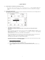
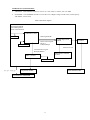
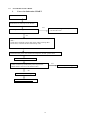
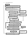
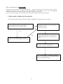
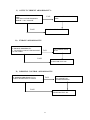
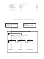
SERVICE MANUAL
17" LCD Monitor
LM730
P/N : 41A50-171
THESE DOCUMENTS ARE FOR REPAIR SERVICE INFORMATION ONLY. EVERY
REASONABLE EFFORT HAS BEEN MADE TO ENSURE THE ACCURACY OF THIS
MANUAL; WE CANNOT GUARANTEE THE ACCURACY OF THIS INFORMATION AFTER
THE DATE OF PUBLICATION AND DISCLAIMS RE LIABILITY FOR CHANGES, ERRORS
OR OMISSIONS,
MANUFACTURE DATA : Sep-29-2002
REVISE:
Sep-29-2002
1
TABLE OF CONTENTS
PAGE
1. SPECIFICATIONS ....................................................................................................
1-1
GENERAL SPECIFICATIONS ...................................................…..............
1-2 LCD MONITOR DESCRIPTION ..................................................................
1-3
INTERFACE CONNECTOR .................................................................…….
3
3
3
3
2.
PRECAUTION AND NOTICES ................................................................................
2-1
ASSEMBLY PRECAUTION .........................................................................
2-2 OPERATIONG PRECAUTION .....................................................................
2-3 STORAGE PRECAUTION …........................................................................
2-4 HIGH VOLTAGE WARNING .......................................................................
5
5
5
5
5
3.
OPERATING INSTRUCTIONS ................................................................................
6
4.
ADJUSTMENT ..........................................................................................................
4-1 ADJUSTMENT CONDITIONS AND PRECAUTIONS ...............................
4-2 ADJUSTMENTS METHOD .& DESCRIPTION.....................……………..
4-3 FRONT PANEL CONTROL KNOBS ............................................................
7
7
7-8
9
5.
CIRCUIT & SOFTWARE DESCRIPTION .............,……………………………....
5-1 SPECIAL FUNCTION WITH PRESS KEY ……………………………….
5-2
CIRCUIT FUNCTION DESCRIPTION………………………….………..
5-3
SOFTWARE FLOW CHART………………………………………………
10
10
10-11
12
6. A).
B).
INTERFACE-BOARD TROUBLE-SHOOTING CHART .......………….....
INVERTER –MODULE SPEC &TROUBLE SHOOTING CHART……….
14-21
22-26
7.
MECHANICAL OF CABINET FRONT DIS-ASSEMBLY......................................
27
8.
PARTS LISTING .........................................................................................………...
28-39
9.
POWER SYSTEM AND CONSUMPTION CURRENT............................................
40
10. PCB LAYOUT .....................................................................………………………...
41
11. MAINBOARD SCHEMATIC DIAGRAM ….............................….......….........
42-46
2
1. SPECIFICATIONS FOR LCD MONITOR
1-1
General specifications
1.
LCD-Panel :
Active display area
Pixel pitch
Pixel format
17 inches diagonal
0.264 mm x 0.264 mm
1280 x 1024 RGB vertical stripe arrangement
2.
Display Color :
6-bit, 16.2 million colors
3.
External Controls :
Power On/Off, Menu-key, Auto key, Left key, Right key
OSD menu Controls
Contras , Brightness, Auto Center, Focus, Clock , H/V-position , DOS mode select, R/G/B,
Color-(7200K,6500K), Languages, Reset
4.
Input Video Signal :
Analog-signal 0.7Vpp
Video signal termination impedance 75 OHM
5.
Scanning Frequencies :
Horizontal: 30 KHz - 83 KHz
Vertical:
55 Hz – 75 Hz
Pixel clock: 135 MHz
6.
Factory Preset Timing : 17
User Timings : 13
Input signal tolerance : H tolerance ± 1 K, V tolerance ± 0.5 Hz
7.
Input Power Source :
Switching Mode Power Supply
AC 100 – 240 V, 50/60 Hz Universal Type
8.
Operating Temperature : 5°C - 40°C Ambient
Non-operating Temperature : 5°C - 40°C
9.
Humidity :
Operating : 10% to 85% RH (non-condensing)
Non Operating : 5% to 85%RH (38.7℃ maximum wet bulb temperature)
10. Weight : 7.6 kg
11. External Connection : 15Pin D-type Connector, AC power-Cord
12. View Angle : x-axis right/left = 70, y-axis up/down = 45 ,65
13. Outside dimension : Width x Height x Thickness = 407x 434 x 173 mm
14. Plug and Play : VESA DDC1/DDC2B
15. Power saving : VESA DPMS
3
1-2
LCD MONITOR DESCRIPTION
The LCD MONITOR will contain an main board, an Inverter module, keyboard, External Adapter which house
the flat panel control logic, brightness control logic, DDC and DC-DC conversion
The Inverter module will drive the backlight of panel .
The Adapter will provides the 12V DC-power 4.16 Amp to Main-board,and Inverter module .
Monitor Block Diagram
Flat Panel and
CCFL backlight
CCFT Drive.
Inverter
RS232 Connector
For white balance
adjustment in
factory mode
Main Board or Interface Board
Keyboard
AC-IN
100v-240v
1-3
ADAPTER
HOST Computer
Interface Connectors
(A) AC-Power Cable
(B) Video Signal Connectors and Cable
(C) External Adapter
4
Video signal, DDC
2. PRECAUTIONS AND NOTICES
2-1
ASSEMBLY PRECAUTION
(1) Please do not press or scratch LCD panel surface with anything hard. And do not soil LCD panel surface by
touching with bare hands ( Polarizer film, surface of LCD panel is easy to be flawed)
In the LCD panel, the gap between two glass plates is kept perfectly even to maintain display characteristic
and reliability. If this panel is subject to hard pressing, the following occurs :
(a) Uniform color
(b) Orientation of liquid crystal becomes disorder
(2) Please wipe out LCD panel surface with absorbent cotton or soft cloth in case of it being soiled.
(3) Please wipe out drops of adhesive like saliva and water in LCD panel surface immediately.
They might damage to cause panel surface variation and color change.
(4) Do not apply any strong mechanical shock to the LCD panel.
2-2
OPERATING PRECAUTIONS
(1) Please be sure to unplug the power cord before remove the back-cover. (be sure the power is turn-off)
(2) Please do not change variable resistance settings in MAIN-BOARD, they are adjusted to the most suitable
value. If they are changed, it might happen LUMINANCE does not satisfy the white balance spec.
(3) Please consider that LCD backlight takes longer time to become stable of radiation characteristic in low
temperature than in room temperature.
(4) Please pay attention to displaying the same pattern for very long-time. Image might stick on LCD.
2-3
STORAGE PRECAUTIONS
(1) When you store LCD for a long time, it is recommended to keep the temperature between 5℃-40℃
without the exposure of sunlight and to keep the humidity less than 85% RH.
(2) Please do not leave the LCD in the environment of high humidity and high temperature such as 60℃
90%RH.
(3) Please do not leave the LCD in the environment of low temperature; below -15℃.
2-4
HIGH VOLTAGE WARNING
The high voltage was only generated by INVERTER module, if carelessly contacted the transformer on this
module, can cause a serious shock. (the lamp voltage after stable around 600V, with lamp current around 6.5mA,
and the lamp starting voltage was around 1650V, at Ta=25℃)
5
3. OPERATING INSTRUCTIONS
This procedure gives you instructions for installing and using the LCD monitor display.
1. Position the display on the desired operation and plug–in the power cord into External Adapter AC outlet.
Three-wire power cord must be shielded and is provided as a safety precaution as it connects the chassis
and cabinet to the electrical conduct ground. If the AC outlet in your location does not have provisions for
the grounded type plug, the installer should attach the proper adapter to ensure a safe ground potential.
2.
Connect the 15-pin color display shielded signal cable to your signal system device and lock both screws
on the connector to ensure firm grounding. The connector information is as follow:
1
5
6
10
11
15
15 - Pin Color Display Signal Cable
PIN NO.
1.
2.
3.
4.
5.
6.
7.
8.
3.
4.
5.
6.
DESCRIPTION
PIN NO.
RED
GREEN
BLUE
GND
GND
GND-R
GND-G
GND-B
9.
10.
11.
12.
13.
14.
15.
DESCRIPTION
5V power from VGA-card
GND
SYNC. GND
SDA
HORIZ. SYNC
VERT. SYNC
SCL
Apply power to the display by turning the power switch to the "ON" position and allow about thirty
seconds for Panel warm-up. The Power-On indicator lights when the display is on.
With proper signals feed to the display, a pattern or data should appear on the screen, adjust the brightness
and contrast to the most pleasing display, or press auto-key to get the best picture-quality.
This monitor has power saving function following the VESA DPMS. Be sure to connect the signal cable to
the PC.
If your LCD monitor requires service, it must be returned with the power cord & Adapter.
6
4. ADJUSTMENT
4-1
ADJUSTMENT CONDITIONS AND PRECAUTIONS
Adjustments should be undertaken only on following function : Contras , Brightness, Black level,
Phase, Clock , H/V-position , Languages, Color-(7200,6500,User), Auto level, OSD-position, Languages,
Reset
4-2
ADJUSTMENT METHOD
Press MENU button to activate OSD Menu or make a confirmation on desired function, Press Left/Right button to
select the function or done the adjustment.
1.
White-Balance, Luminance adjustment
Approximately 30 minutes should be allowed for warm up before proceeding white balance
adjustment.
Before started adjust white balance ,please setting the Chroma-7120 MEM. Channel 1 to 7200 color and
MEM. channel 2 to 6500 color, ( our 7200 parameter is x = 302 ±20, y = 319 ±20, Y = 200 ±20cd/m2
and 6500 parameter is x = 313 ±20, y = 329 ±20, Y = 200 ±20 cd/m2)
How to setting MEM.channel you can reference to chroma 7120 user guide or simple use “ SC” key and
“ NEXT” key to modify x,yY value and use “ID” key to modify the TEXT description
Following is the procedure to do white-balance adjust
Press MENU button during 1 seconds along with plug in the DC-power cord will activate the factory mode,
and the OSD screen will located at left top of panel.
I.
Bias (Low luminance) adjustment :
1.
2.
3.
Press “ AUTO” button , and wait for message “ Pass”
Set the contrast on OSD window to the value=45 , color (user )R,G,B set to “50”
adjust the brightness on OSD until chroma 7120 measurement reach the value Y=240 cd/m2 ±10
cd/m2
7
II.
Gain adjustment :
a.
adjust 7200 color-temperature
Set the Contrast of OSD function to 45 and Adjust Brightness to chroma 7120 Y=240 ±5 cd/m2
Switch the chroma-7120 to RGB-mode (with press “MODE” button )
Switch the MEM.channel to Channel 01 ( with up or down arrow on chroma 7120 )
The lcd-indicator on chroma 7120 will show x = 302 ±10, y = 319 ±10, Y = 200 ±5 cd/m2
Adjust the Color(user)Mode: RED on OSD window, until chroma 7120 indicator reached the value
R=100
6. Adjust the Color(user)Mode: GREEN on OSD window, until chroma 7120 indicator reached the value
G=100
7. Adjust the Color(user)Mode: BLUE on OSD window, until chroma 7120 indicator reached the value
B=100
8. repeat above procedure ( item 5,6,7) until chroma 7120 RGB value meet the torlence =100±2
9. switch the chroma-7120 to xyY mode With press “MODE” button
10. Press Color (7800) on OSD window to save the adjustment result
1.
2.
3.
4.
5.
b.
1
2
3
4
5
6
7
8
9
10
adjust 6500 color-temperature
Set the Contrast of OSD function to 45 and Adjust Brightness to chroma 7120 Y=240 ±5 cd/m2
Switch the chroma-7120 to RGB-mode (with press “MODE” button )
switch the MEM.channel to Channel 02 ( with up or down arrow on chroma 7120 )
The lcd-indicator on chroma 7120 will show x = 313 ±10, y = 329 ±10, Y = 200 ±5 cd/m2
Adjust the Color(user)Mode: RED on OSD window, until chroma 7120 indicator reached the value
R=100
Adjust the Color(user)Mode: GREEN on OSD window, until chroma 7120 indicator reached the
value G=100
Adjust the Color(user)Mode: BLUE on OSD window, until chroma 7120 indicator reached the value
B=100
repeat above procedure ( item 5,6,7) until chroma 7120 RGB value meet the tolence =100±2
switch the chroma-7120 to xyY mode With press “MODE” button
Press Color(6500) on OSD window to save the adjustment result
Turn the POWER-button off to on to quit from factory mode ( in USER-mode, the OSD window location
was placed at middle of screen)
8
2.
Clock adjustment
Set the Chroma at pattern 63 (cross-talk pattern) or WIN98/95 shut-down mode (dot-pattern).
Adjust until the vertical-Stripe-shadow as wide as possible or no visible.
This function is adjust the PLL divider of ADC to generate an accurate pixel clock
Example : Hsyn = 31.5KHz
Pixel freq. = 25.175MHz (from VESA spec)
The Divider number is (N) = (Pixel freq. x 1000)/Hsyn
From this formula, we get the Divider number, if we fill this number in ADC register (divider register), the
PLL of ADC will generate a clock which have same period with above Pixel freq.(25.175MHz) the
accuracy of this clock will effect the size of screen.(this clock was called PIXEL-CLOCK)
3.
Focus adjustment
Set the Chroma at pattern 63 (cross talk pattern) or WIN98/95 shut down mode (dot-pattern).
Adjust the horizontal interference as less as possible
This function is adjust the phase shift of PIXEL-CLOCK to acquire the right pixel data .
If the relationship of pixel data and pixel clock not so match, we will see the horizontal interference on
screen ,we only find this phenomena in crosstalk pattern or dot pattern , other pattern the affect is very light
4.
H/V-Position adjustment
Set the Chroma to pattern 1 (crosshatch pattern) or WIN98/95 full-white pattern confirm above item 2 & 3
functions (clock & focus) was done well, if that 2 functions failed, the H/V position will be failed too.
Adjust the four edge until all four-edges are visible at the edge of screen.
5.
LANGUAGE function
There have 5 language for selection, press “MENU” to selected and confirm , press “ LEFT” or “ RIGHT”
to change the kind of language ( English , Deutch , Francais, Espanol, Italian)
6.
Reset function
Clear each old status of auto-configuration and re-do auto-configuration ( for all mode)
This function also recall 7200 color-temperature , if the monitor status was in “ Factory-mode” this reset
function will clear Power-on counter ( backlight counter) too.
OSD-LOCK function
Press Left & Right key during switching on the monitor, the access to the OSD is locked, user only has
access to “ Contrast, Brightness, Auto-key “.
If the operator pressed the Left & Right during switching on the monitor again , the OSD is unlocked.
7.
4-3
FRONT PANEL CONTROL KNOBS
Power button : Press to switch on or switch off the monitor.
Auto button : to perform the automatic adjustment from CLOCK, FOCUS, H/V POSITION, but no affect the
color-temperature
Left/Right button : select function or do an adjustment.
MENU button : to activate the OSD window or to confirm the desired function
9
5.
5-1
CIRCUIT-DESCRIPTION
SPECIAL FUNCTION WITH PRESS-KEY
A). press Menu button during 2 seconds along with plug-in the DC Power cord:
That operation will set the monitor into “Factory- mode”, in Factory mode we can do the White balance
adjustment with RS232
In Factory mode, OSD-screen will locate in left top of screen.
Press POWER-button off to on once will quit from factory mode and back to user-mode.
B). Press both Left & Right button along with Power button off to on once will activate the OSD-LOCK
function, repeat this procedure will disable OSD-LOCK
In OSD-LOCK function, all OSD function will be lock , except Contrast and Brightness
OSD-INDEX EXPLANATION
1. CABLE NOT CONNECTED: Signal-cable not connected.
2. INPUT NOT SUPPORT:
a. INPUT frequency out of range: H > 83kHz, v > 75Hz or H < 28kHz, v < 55Hz
b. INPUT frequency out of VESA-spec. (out of tolerance too far)
5-2
CIRCUIT FUNCTION DESCRIPTION
1. U200,GMZAN2 ( all-in-one chip solution for ADC, OSD, scalar and interpolation) :
USE for computer graphics images to convert analog RGB data to digital data with interpolation process,
zooming, generated the OSD font , perform overlay function and generate drive-timing for LCD-PANEL.
2.
U302,89C51RD2 (PHILIPS- MCU, type 8052 series with 64k Rom-size and 512 byte ram) :
Use for calculate frequency, pixel-dot , detect change mode, rs232-communication, power-consumption
control, OSD-index warning , …etc.
3.
U203,24LC21 (MicroChip IC) :
EEPROM type, 1K ROM-SIZE, for saving DDC-CONTENT.
4.
U300,24C16 (ATMEL IC) :
EEPROM type, 16K ROM-SIZE, for saving AUTO-config data, White-balance data, and Power-key status
and Backlight-counter data.
5.
U304,LM2569S( NS brand switching regulator 12V to 5V with 3A load current) .
6.
U305,AIC 1084-33CM (AIC brand linear regulator 5V to 3.3V)
7. U905,RT9164(Linear regulator 5V to 2.5V)
8. U600,U601,LVDS ( use NOVATEK NT7181F)
Convert the TTL signal to LVDS signal , the advantage of LVDS signal is : the wire can be lengthen and
eliminate wire number , low EMI .LVDS signal is high frequency but low voltage, only 0.35 VPP ,the
frequency is seven times higher than TTL
9. U401, 74F14D(Schmitt triggger)
The 74F14 contains six logic inverters which accept standard TTL input signals and provide standard TTL
Output levels
10
MODULE-TPYE COMPONENT:
1.
ADAPTER : CONVERSION-module to convert AC 110V-240V to 12VDC, with 4.16 AMP
2.
INVERTER : CONVERSION-module to convert DC 12V to High-Voltage around 1650V, with frequency
30K-80Khz, 5.6mA-13mA
Main-board Block diagram
Input analog RGB &
H,V,& ddc signal &
Rs232 communication
GMZAN2 (U200)
DDC-chip
Data Digital RGB
Panel Control Signal:
Phs, Pvs,
PclkA/B,Pdispe
Oscillator 50 mhz
LVDS chip (U601,
U602)
PANEL
Panel Power 5V
Communication signal:
Hclk,Hfs,Hdata0
Panel-Power Control
(U202)
MCU ( U302 )
Crystal 20 MHz
DC 12V 4.16Amp
Keyboard module
INVERTER module
EXTERNAL-ADAPTER
11
5-3
SOFTWARE FLOW CHART
I.
Power-On Subroutine CHART
POWER-ON START
Initial MCU I/O, Interrupt vector & Ram
Yes
Initial 1.POC (backlight counter)
2. Clr all mode value
Check Eeprom is empty ?
No
Check White-balance data(6500
& 7200) same with the backup
OK
data ?
Check POC( backlight counter) data same with the backup data ?
IF not same, overwrite the data with backup value.
Check Previous power-switch status from Eeprom, & other system status
Initial GMZAN2
Yes
Check if in Factory mode?(when power-on,press the
MENU Button will be in FACTORY mode)
SET factory mode flag
No
Clear factory mode flag
MAIN-SUBROTINE LOOP
12
II.
MAIN SUBROTINE LOOP
Main loop start
Process Power-saving status ( according to below flow-chart result)
)
Check GMZAN2 IFM status .is change or not.
And check Signal cable status ( cable not connected or not )
** IFM is the register which measured the HSYN & Vsyn status
No
Yes, IFM have change
Yes
Is current system status in Power-saving ?
No
Wake-up GMZAN2
(because GMZAN2 was in
partial sleeping state)
Yes
Check the IFM result is in the standard
Mode table ?
No
Set mode index & parameter
Set change mode flag
Yes
Check the IFM result is in the user mode
table ?
No
Out of range ( input not support) be
confirm
No
confirm the frequency ( Hsyn or Vsyn) from IFM already
been changed ? ( check the change mode flag)
Yes , freq had been change
Process ( turn off OSD , setting GMZAN2according to
above parameter, set LED status, set backlight status)
No
Check Auto-config mode flag already been set?
Do Auto-config
automatically
Yes
Read Key status and Process on OSD-screen
Yes
Check Factory mode flag= 1
No
Monitoring the time-out of osd status ( if no key input persist for
10 sec , the osd time-out counter will trigger )
13
if the RS232 buffer is full,
process the command( while
adjust white-balance in factory
mode)
6 A). INTERFACE-BOARD TROUBLE-SHOOTING CHART
*Use the PC Win 98 white pattern, with some icon on it, and Change the Resolution to 640x480 60 Hz / 31 KHz
**NOTICE : The free-running freq. of our system is 48 KHz / 60 Hz, so we recommend to use another resolution
to do trouble shooting, this trouble shooting is proceed with 640x480 @60Hz 31Khz
I.
NO SCREEN APPEAR
DC-Power Part
Measured Input DC-voltage ( J1)= 12 V?
Measured U305 AIC 1084 pin 2 = 3.3V?
Measured U904 LT1117 pin 2= 3.3V?
Measured U905 RT9164 pin 2=2.5v
Check Correspondent component.
Is there any shortage or cold solder?
Yes, all DC level exist
Yes, there have OSD show
Disconnected the Signal cable( Loose the
Signal cable ),Is the screen show “Cable Not
Connected” ?
No, nothing is show
Led Green
Connected the Signal cable again,
Check LED status.
Led Orange
Check Power switch is in Power-on
status , and check if Power switch had
been stuck ?
Connected the Signal cable again,
Check LED status.
Replace MCU
Led orange
OK, Keyboard no stuck
Led Green
NG
Check the Wire-Harness from CN603
was tight enough?,
check the Wire connection to panel side too
Measured RGB (r200,r201,r202) H,V Input at U401
pin 9 ,4 ,was there have signal ?
Check Correspondent
component short/open
( Protection Diode )
and Signal cable
bad ?
OK,input Normal
OK,Wire tight enough
Check Panel-Power Circuit Block
Measured Oscillator Block
Oscillator U201 & Crystal X300
OK,clock normal
OK,Panel Power OK
Check U200 Data-output Block
OK, U200 data OK
Check communication pin between U200 &
MCU pin 2,6,7. , is it have transition?
OK, Mcu have transition
NG, no transition
Replace Inverter and Check
Inverter control relative circuit
Re-do White balance adjust
OK
Replace U200 (Gmzan2)
Replace U302 (MCU)
& check Reset pin 10
must be change from High to
low when first AC power plugin
OK
Note: 1. if Replace “MAIN-BOARD” , Please re-do “DDC-content” programmed & “WHITE-Balance”.
2. if Replace “ INVERTER” only, Please re-do “ WHITE-Balance”
14
PANEL-POWER CIRCUIT
Check the PPWR panel power relative circuit,
R223,R224, Q200,U202(pin 5,6,7,8)
In normal operation, when LED =green, R223
should =0 v,
If PPWR no-response when the power switch
Turn on and turn off, replace the U200-GMZAN2
NG
check R225 should have response from 0V to 5V
When we switch the power switch from on to off
OK,R225 have response
Yes
NG, no Voltage
Check U202 pin 1,3= 5V
Measured the U202 pin 5,6,7,8= 5 V?
Replace U202 ( Nmos, SI9953)
OK
NG
OK
Check U304 relative circuit.(D300,L906..)
Check JP202 shortage
INVERTER Control Relative Circuit
NG
Measured the inveter connector CN303
Pin 1,2=12V, pin 3 on/off control=5V (on)
YES, still no screen
Check the Bklt-On relative circuit, R315, Q304, R311,
In normal operation, when LED =green,
R315 Bklt-On should =0 v,
If Bklt-On no-response when the power switch turn on-off,
Replace the MCU
NG
Replace INVERTER to new-one, and
Check the screen is normal ??
OK,& Re-do white balance
OSCILLATOR
BLOCK
NG,no transition
Measured U201 Oscillator output R215= 50MhZ ?
Replace Oscillator U201
NG,no transition
OK, has transition
Replace Crystal X300
Measured X300 Crystal output R340= 20MhZ ?
OK
U200-DATA OUTPUT
NG , no transition
Measured PCLK(L207,R603)
PVS,PHS,PDISPE (pin 73,74,43 from U200 )
Is there have any transition?
Pclk around 47MHz to 57MHZ ,
PVS=60.09Hz , PHS around 67 KHz ??(refer to
input signal=640x480@60 Hz 31k, and LED is
green)
Replace GMZAN2 (U200) or replace
MAINBOARD.
If Main Board being replace , please
do the DDC – content reprogrammed
OK
15
II (a) THE SCREEN is Abnormal , stuck at white screen, OSD window can’t appear, but
keyboard & LED was normal operation.
At general, this symptom is cause by missing panel data or panel power, so we must check our
wire-harness which connected to panel or the panel power controller (U202)
NG
Check if the Wire harness from CN603 loose?
Check the wire on both Panel-side and Main board side.
Tighten it.
Yes, tight enough
Check the Panel-Power circuit as above (page 16)
U202 pin 5,6,7,8 ,must be 5V
Yes, Voltage normal
NG
Check U904,which convert the 5V to
3.3V
Check the LVDS-Power L601,L602,L603,L604,L900= 3.3V ?
Yes, Voltage normal
NG
Check the both U601 & U602 LVDS-Input pin 31= 45mhz –
65mhz, and pin 27 = Vsyn freq, pin 28 = 45khz- 65 khz
Check U200 DATA-OUPUT block as
above ( page 16)
NG, no data output
Yes, Frequency normal
Check OSCILLATOR Block as
above ( page 16)
Replace both LVDS chip ( U601 & U602)
OK, all clock is normal
Replace U302 MCU and check it RESET
pin 10 ,must be turn high to low when first
AC power-on
OK, reset is normal
Check U200 DATA-OUTPUT block again
NG, still no data out
Replace U200 GMZAN2
16
II. (b)The screen had the Vertical Straight Line, might be stuck in Red, Green, Blue
That symptom is cause by bad Panel issue ( might be the Source IC from Panel is cold solder or
open loop ) so REPLACE THE PANEL TO NEW ONE.
KEYBOARD BLOCK check
Check U302 MCU pin 43,42,41,40,39 at
High state(5V)? without press any key
NG
Mechanical was stuck, Check !
OK
NG
Press power key and check U302 pin 43
= low (0V) ?
Check main board R303 shortage?
Replace Tact-switch SW105 at keyboard if still
no work replace U302 MCU at main-board and
check MCU relative reset circuit, and crystal
OK
Check U302 pin 38 (LED green) will have
transition from hi to low or low to hi when we
press the power key??
OK
If still no Led green indicator, check Q102,
R106 & LED at keyboard !! cold solder or bad
NG, MCU no response
Check U302 pin 20= 20MHz ? and pin 44
(VDD)=5V ? and pin 10 (reset)=0V ? at normal
condition
OK
Without press key and change mode, Check U302
pin 16,17(sda,scl)= hi 5V ? or keep transition ?
NG
If one of this item was NG, check the relative
circuit
Keep transition, that means eeprom no response
NG
Check U300 eeprom 24LC16 relative circuit,
check U300 pin 7 = low?
NG
OK, no keep transition
Check JP302 is
connect ?
Replace U302 MCU
OK
Check U300 pin 8
(vdd)= 5V, and check
R300,R301 cold solder
Replace eeprom
17
POWER-BLOCK check
**Note : the Waveform of U304 pin 2 can determined the power situation
1.
2.
3.
stable rectangle waveform with equal duty, freq around 150K-158KHz
that means all power of this interface board is in normal operation
,and all status of 5V & 3.3V is working well
unstable or uneven rectangle waveform without same duty, that means ABNORMAL operation was
happened, check 3.3V or 5V ,if short-circuit or bad component
rectangle waveform with large spike & harmonic pulse on front side , means all 3.3v is no load, U200
Gmzan2 was shut-down, and only U302 MCU still working , that means the monitor is in power saving
status , all power system is working well .
NG
Measure input power at U304 LM2596 pin 1=
12V ?
OK
Check ADAPTER and connector if loose?
NG
Check U304 pin 2 is a stable rectangle wave?
Around 150k-158kHz stable rectangle wave
with equal duty without any spike or harmonic
pulse?
Check U304 pin 2 is a unstable rectangle wave ?
OK, unstable wave
Check all 3.3V & 5V power, there is
short circuit or bad component was
happened
OK
NG, with
harmonic
pulse
The interface board power is good
The interface board is in powersaving state, press power key to wake
up & check your signal input
18
III.ALL SCREEN HAS INTERFERENCES OR NOISE, CAN’T BE FIXED BY AUTO KEY
** NOTE: There is so many kind of interferences, 1). One is cause by some VGA-CARD that not meet VESA spec or
power grounding too bad that influence our circuit
2).other is cause by external interferences, move the monitor far from electronic equipment.( rarely
happened)
Use DOT-pattern, or win98/99 shut-down
mode pattern, press “AUTO” key, was the
interferences disappear ??
OK
END
NG, interferences still exist
Adjust “FOCUS” step by step, until the
horizontal interferences disappear
OK
END
NG
Does your signal-cable have an additional
cable for extension ??
Yes, has extension
Put away the additional cable
May be the additional cable grounding is
not quite well
NO additional extension cable
NO, all mode
Does your noise only exist in one mode only?
(ex: only at 1280x1024 @ 75 Hz, other is normal)
Yes, only happened on one mode
That was cause by you VGA-CARD setting, your VGA
card timing back porch / front porch exceed vesa timing
too far, for some new AGP-VGA-CARD such situation
always happened
So in your control-panel icon ,select monitor ,setting ,
advance ,screen-adjust ,at
Size icon, increase step by step slowly, press “”AUTO”
key every step you increase the SIZE . repeat the
procedure( increase/decrease SIZE one-step and press
AUTO) until the interferences disappear, press “APPLY”
to save in your VGA
19
Change the Signal-cable to new-one or
Try other brand VGA-CARD
(make sure just only that brand VGACARD has this problem ,contact RDTaipei)
There is interferences in DOS MODE
NOTE :the criteria of doing AUTO-CONFIGURATION : must be a full-size screen, if the screen not full , the autoconfiguration will fail. So in dos mode ,just set your “CLOCK” in OSD-MENU to zero or use some EDITOR
software which can full fill the whole screen (ex: PE2, HE) and then press “AUTO”
Or you can use “DOS1.EXE” which attached in your Driver disk to optimize DOS mode performance
V. THE PANEL LUMINANCE WAS DOWN
Use white pattern and resolution 1280x1024 @ 60Hz , CHROMA 7120 measured the center of panel
If Y can reach >240 cd/m2 that means
The lamp still working well, so we just re-do the
white-balance process
As following procedure
Set Contrast, brightness =maximal, RGB= 50
Quit from OSD-screen, measured Y(luminance)
With chroma 7120, check Y= 240±10 cd/m2 ?
OK
NG
OK
If the Y less than 200 cd/m2 (after the contrast,
brightness = max) then change the LAMP of panel
Use white-pattern, press MENU button along
with AC power-plug in ( you will in factory
mode) The OSD-menu will be at left-top of
screen,
press AUTO button to automatically adjust black
level value, you will see the sign PASS
Follow White-Balance, Luminance adjustment
as above ( page 8),method to more detail procedure
For do a white-balance adjust
20
6 B). INVERTER –MODULE SPEC &TROUBLE SHOOTING CHART
For LM720 model , use Hydis panel, and the INVERTER is made by SAMPO
SAMPO Parts No: DIVTL0085-D42 AOC Parts No.: 79LL17-3-S
I.
CONNECTOR PIN ASSIGMENT:
A) CON1: INPUT
MODEL NO.: S5B-PH-SM3-TB
PIN
SYMBOL
DESCRIPTION
1
Vin
Input voltage: 12V
2
Vin
Input voltage: 12V
3
ON/OFF
ON: 3V OFF:0V
4
Dimming
Dimming range (0V~+5.0V)
5
GND
GND
B) CON2,CON3,CON4,CON5: OUTPUT
MODEL NO.: SM02B-BHSS-1-TB
PIN
SYMBOL
DESCRIPTION
1
HV OUTPUT
2
RETURN
Input H.V to lamps
Return to control
C) FUNCTION SPECIFICATIONS:
The data test with the set of SAMPO
DC TO DC CONVERTER
(ROOM TEMPERATURE 25℃ ±4℃)
ITEM
SYMBOL
MIN.
TYP.
MAX.
UNIT
Input voltage
Vin
10.8
12
13.2
V
Input current
Iin
--
2100
2500
mA
output current
Iout
adj:0v( min.)
(min)
REMARK
FOR 1 CCFL
2.3
2.6
3.3
mA
LOAD:120KΩ
FOR 1 CCFL
Output current
Iout
adj.:5 v(max.)
(max)
5.5
6.0
6.5
mA
F
40
50
60
KHZ
H.V open
Vopen
1550
1700
1850
Vrms
NO LOAD
H.V Load
Vload
600
700
800
Vrms
RL=120KΩ
Frequency
21
LOAD:120KΩ
D) FUNCTION TEST CIRCUIT:
120KΩ
1
2
CON4
CON2
10Ω
1
VT-181
2
1
2
10Ω
CON5
CON3
CON1
1 2 3 4 5
120KΩ
1
2
VT
120KΩ
120KΩ
10Ω
10Ω
VT
VT-181
22
II. TROUBLE SHOOTING BLOCK DIAGRAM
A)
NO POWER:
CHECKED ON FUSE
F1 Vin=12
PASS
PASS
TO CHANGED
F1= 4.0A/63V
FAIL
TO CHECKED Q4 & Q6
VOUT = 9V
FAIL
TO CHANGED
CH1: Q4/Q3/Q11
CH2: Q5/Q6/Q12
TO CHECKED L1/L2
INPUT 9V TO L1 OR L2
TO CHANGED
CH1: Q7/Q8/D12/PT1
CH2: Q9/Q10/C13/PT2
FAIL
FUNCTION TEST OK !
PASS
B) HIGHT VOLTAGE PROTECTION:
1. SHORT R30 & OPEN LOAD
FAIL
2. TEST PT1 OR PT2 OUTPUT PIN 7 H.V
VOLTAGE Vh=1600 ±100V rms
PASS
TO CHANGE ON PT1
OR PT2
FUNCTION TEST OK!
23
C) OUTPUT CURRENT ABNORMALITY:
CHECK PWM FREQUNCY AT C6
CHIP
THE OSCILLATOR FREQUNCY
RANGE = 150 ~ 250 KHZ
FAIL
PASS
D)
TO CHANGE C6 CHIP OR IC
CHIP
FUNCTION TEST OK!
ENBALE ABNORMALITY:
IF ENABLE ABNORMALITY
1. TO CHECK IC PIN 9 TURN ON HAVE
12 VOLTAGES
TO CHANGE ON Q1
& Q2
FAIL
PASS
FUNCTION TEST OK!
E) DIMMING CONTROL ABNORMALITY:
IF DIMMING ABNORMALITY TO
CHECK R1/R2/R33/C6 IS FAILD?
FAIL
TO CHANGE ON
R1/R2/R33/C6R203
PASS
FUNCTION TEST OK!
24
F)
TRANSFORMER ABNORMALITY:
IF TRANSFORMER ABNORMELITY TO CHECK
C3 & C4 CHIP OUTLINE OR TRANSFORMER
FAIL
TO CHANGE C3 & C4 OR
TRANSFORMER
PASS
FUNCTION TEST OK!
G) INSTRUMENTS FOR TEST:
1.
DC POWER SUPPLY
GPS-3030D
2.
AC VTVM
VT:-181E
3.
DIGITAL MULTIMERTER
MODEL-34401
4.
HIGHTVOLT PROB
MODEL-1137A
5.
SCOPE
MODEL-V-6545
25
7.
MECHANICAL OF CABINET FRONT DIS-ASSEMBLY
26
BILL OF MATERIAL
========== ====================== ========================
1 ADPC12416AF
LCD ADAPTER ASS'Y
1 CBPC782KKZAE
CONVERSION BOARD FOR T7
1 DCPC780A7
DC POWER BOARD FOR T780K
1 KEPC782KA6
KEY BOARD FOR T78*
1 7L
1 7
WOODEN PALLET
1 7L
1 60
WOODEN PALLET
1 15L5689 2 A
GND CLAMP
1 15L5689 3 A
GROUND CLAMP
1 15L5695 1
REAR BRACKET
1 15L5709 3
MAIN FRAME
1 15L5791 1
VESA BRACKET
1 33L4344 CA 1L
HINGE COVER (L)
1 33L4344 CA 2L
HINGE COVER(R)
1 33L4345 CA L
CABLE COVER
1 33L4362 1
LENS
1 33L4447 CB L
POWER KEY PAD
1 34L 916 CA 3B
BACK COVER
1 34L 977ACA B
FRONT PANEL
1 40L 152509
RECYCLE LABEL
1 40L 152512
RECYCLE LABEL
1 40L 190786 1A
ID LABEL
1 40L 457716 1A
TCO99 LABEL
1 40L 459786 1A
CARTON LABEL
1 40L 581 26704
酠繷 FOR CARTON/PALLET
1 41L 68508 A
恨 1 41L1700786 1A
MANUAL
1 41L7800786 1A
WARRANTY BOOKLET
1 41L7800786 2A
TCO'99 CARD
1 44L3231 12 A
EVA WASHER
1 44L3231 13
EVA WASHER
1 44L3705 1
EPS
1 44L3705 2
EPS
1 44L6000 4 6B
SPACE PAPER
1 44L6002608 1A
PAPER PLATE
1 44L6002608 2A
PAPER PLATE
1 44L9003 9
CORNER PAPER
1 44LS705786 1A
CARTON
1 45L 76 28 RN
pe bag
1 45L 77 3
ゴ 饯
1 45L 77500
BARCODE RIBBON
1 45L 77501
BARCODE RIBBON
1 45L 88606
PE BAG FOR BASE
27
========= =====
1 PCS
1 PCS
1 PCS
1 PCS
0.0097 PCS
0.0097 PCS
1 PCS
2 PCS
1 PCS
1 PCS
1 PCS
1 PCS
1 PCS
1 PCS
1 PCS
1 PCS
1 PCS
1 PCS
0 PCS
0 PCS
1 PCS
1 PCS
1 PCS
0.1 PCS
0.2 PCS
1 PCS
1 PCS
1 PCS
2 PCS
1 PCS
1 PCS
1 PCS
0.01 PCS
0.01 PCS
0.01 PCS
0.0769 PCS
1 PCS
1 PCS
173 CM
19 CM
0.5 CM
1 PCS
1 45L 88607
PE BAG FOR MONITOR
1 50L 500 1
竕絬
1 50L 600 2
HANDLE1
1 50L 600 3
HANDLE2
1 52L
1186
SMALL TAPE
1 52L
1208 A
TAPE
1 52L6019 1
独︹荡絫溅盿
1 52L6020 1
PROTECT FILM
」 1
79L L17 3 S
INVERTER SAMPO
」 1
80L L17 2 CH
ADAPTER VER:(01A﹁盡 1 85L 594 1
SHIELD MAIN
1 89L 174L1710E
SIGNAL CABLE
」 1
89L402C18N GL
POWER CORD
」 1
89L402C18N YH
POWER CORD WALL OUT FOR
1 95L8014 5 14
HARNESS
1 95L8018 30 5
HARNESS
1 B1L1030 5128
SCREW
1 M1L 330 6128
SCREW
1 M1L1030 10128
SCREW
1 M1L1740 12128
SCREW
1 Q1L 340 12128
SCREW
1 Q1L 340 16120
SCREW 4X16
1 Q1L1030 10128
SCREW
」 1
750LLK70300
LCD PANEL HT17E11-300
1 705L782KB34016
LCD 催 ASS'Y
---------- ---------------------- -----------------------## PAREN
T NO :
ADPC12416AF LCD ADAPTER ASS'Y
---------- ---------------------- -----------------------2 ADPC12400AAI
LCD ADAPTER ASS'Y FOR AI
2 ADPC12400AD6
LCD ADAPTER A6 ASS'Y
2 ADPC12400ASMT
LCD ADAPTER ASS'Y FOR AI
2 GND1
9L6002 1
PIN
2 40L 45762412A
CBPC LABEL
2 52L
1213600
簧轰溅盿
」 2 IC903 56L 139 3
PC123FY2 BY SHARP
2 NR901
61L 58080 WT
8 OHM NCTR
2 R911
61L152M10457F
MOFR 100KOHM +-5% 2W
」 2 C901
63L 107334 5
0.33UF
2 C901
63L107K334 U
MPX 0.33UF,275VAC,+-10%
2 C902
65L305M1022E3
1000PF +-20% 400VAC BY
2 C903
65L305M1022E3
1000PF +-20% 400VAC BY
2 C902
65L305M1022EM
1000PF +-20% 250VAC/40
2 C903
65L305M1022EM
1000PF +-20% 250VAC/40
2 C916
65L305M3322F2
3300PF +-20% 250VAC/40
28
1 PCS
1 PCS
1 PCS
1 PCS
8 CM
2 PCS
15 CM
0.1 PCS
1 PCS
0 PCS
1 PCS
1 PCS
1 PCS
0 PCS
1 PCS
1 PCS
6 PCS
10 PCS
4 PCS
4 PCS
8 PCS
4 PCS
2 PCS
1 PCS
1 PCS
--------- ----M
舱
家舱
--------- ----1 PCS
1 PCS
1 PCS
1 PCS
2 PCS
1 PCS
1 PCS
1 PCS
1 PCS
0 PCS
1 PCS
1 PCS
1 PCS
0 PCS
0 PCS
0 PCS
2
2
2
2
2
2
2
2
2
2
2
C916
C900
C900
C921
C922
C921
C922
C921
C922
C906
C904
65L305M3322F3
3300PF400VAC/250VAC
65L305M4722B2
4700 +-20% 400VAC ACFY
65L305M4722B3
4700PF +-20% 400VAC/25
67L 215102 3H
綯筿秆筿甧 1000UF 16V
67L 215102 3H
綯筿秆筿甧 1000UF 16V
67L 215102 3J
綯筿秆筿甧 1000UF/16V
67L 215102 3J
綯筿秆筿甧 1000UF/16V
67L 215102 3K
綯筿秆筿甧 1000UF/16V
67L 215102 3K
綯筿秆筿甧 1000UF/16V
67L305L101 4
100UF +-20% 25V
67L305S10114H
HTR101M2GL33VR
2 71L 55 2
A
FERRITE BEAD 6.5*5*1.7
2 71L 55 30
FERRITE BEAD 4.0*2*3
2 L901
73L 174 26 T1
LINE LILTER 0.45mm
2 L902
73L 253 91 H
CHOKE COIL
2 L902
73L 253 91 L
CHOKE BY LI TA
2 L902
73L 253 91 S
CHOKE COIL
2 T901
80L 600 3 L
X'FMR BY LI TAI
2 T901
80L 600 3 T
SRW28EC-T40H017
2 LDE1
81L
2 3 2B
BL-B2441J-AA
」 2 F901
84L 53 1
FUSE 2A 250V LF-230002
2 CN901
87L 501 10
AC SOCKET
2 89L 171506
DC POWER CORD
」 2 BD901 93L 50460 8
BRIDGE 2KBP06M
2 D901
93L 6026T52T
RECTIFIER DIODE FR107
2 D901
93L 6026W52T
FR107
2 D902
93L 6038P52T
PS102R
2 D902
93L 6038T52T
FR103
2 715L 901 1 4
ADAPTOR
2 705L 560 57 03
Q901 ASS'Y
2 705L 560 61 03
R930 ASS'Y
2 705L 780 93 03
D911 ASS'Y
---------- ---------------------- -----------------------## PAREN
T NO :
ADPC12400AA I
LCD ADAPTER ASS'Y FO
---------- ---------------------- -----------------------3 715L 901 1A 3
42WBOARD
3 J901
95L 90 23
TIN COATED
3 J902
95L 90 23
TIN COATED
3 J903
95L 90 23
TIN COATED
3 J904
95L 90 23
TIN COATED
3 J905
95L 90 23
TIN COATED
3 R919
61L 21024352T
MFR 24K OHM +- 1% 1/6W
3 R925
61L 60220252T
CFR 2K OHM+-5% 1/6W
3 FB901
71L 55 19 T
FERRITE BEAD 9X3.5X0.8
29
1 PCS
0 PCS
1 PCS
1 PCS
1 PCS
0 PCS
0 PCS
0 PCS
0 PCS
1 PCS
1 PCS
1 PCS
1 PCS
1 PCS
0 PCS
0 PCS
1 PCS
0 PCS
1 PCS
1 PCS
1 PCS
1 PCS
1 PCS
1 PCS
1 PCS
0 PCS
1 PCS
0 PCS
1 PCS
1 PCS
1 PCS
1 PCS
--------- ----M
舱
家舱
--------- ----1 PCS
0 PCS
0 PCS
0 PCS
0 PCS
0 PCS
1 PCS
1 PCS
1 PCS
3 IC902
3 IC905
3 IC902
3 IC905
3 C905
3 C920
3 C923
---------## PAREN
----------
56L 158 2 T
3PIN IC TL431C/T.I.
56L 158 2 T
3PIN IC TL431C/T.I.
56L 158 4 T
A
HTL431
56L 158 4 T
A
HTL431
65L 1K152 1T
1.5NF/1KV Z5F+-10%
65L517K681 2T
680PF 500V +-10% 25P
67L 305471 3T
470UF 16V
---------------------- -----------------------T NO :
ADPC12400AD 6
LCD ADAPTER A6 ASS'Y
---------------------- -----------------------3 33L6007 1
LENS
3 40L 100 EW 1B
ADAPTER ID
3 40L 154501 1
HI-POT GND LABEL FOR M
3 45L 88525 E
PE BAG
3 W33L4477 D T
TOP COVER
3 W33L4478 D T
BOTTOM COVER
---------- ---------------------- -----------------------## PAREN
T NO :
ADPC12400AS MT LCD ADAPTER ASS'Y FO
---------- ---------------------- -----------------------3 IC901
56L 379 25
UC3842ADM
3 Q903
57L 417 4
PMBS3904/PHILIPS-SMT
3 Q902
57L 417 6
PMBS3906/PHILIPS-SMT
3 R928
61L0603102
CHIPR 1K OHM +-5% 1/16
3 R937
61L0603243 1F
CHIPR 2.43KOHM+-1% 1/1
3 R936
61L0603931 1F
CHIPR 9.31KOHM+-1% 1/1
3 R924
61L0805102
CHIPR 1K OHM +-5% 1/10
3 R929
61L0805102
CHIPR 1K OHM +-5% 1/10
3 R935
61L0805102
CHIPR 1K OHM +-5% 1/10
3 R927
61L0805103
CHIPR 10K OHM +-5% 1/1
3 R922
61L0805104
CHIPR 100K OHM+-5% 1/1
3 R915
61L0805471
CHIPR 470 OHM+-5% 1/10
3 R916
61L0805472
CHIRP 4.7K OHM +-5% 1/
3 R917
61L0805472
CHIRP 4.7K OHM +-5% 1/
3 R918
61L0805472
CHIRP 4.7K OHM +-5% 1/
3 R920
61L0805623
CHIPR 62K OHM +-5% 1/1
3 R921
61L0805683
CHIPR 68K OHM+-5% 1/10
3 R923
61L1206100
CHIPR 10 OHM+-5% 1/8W
3 R931
61L1206100
CHIPR 10 OHM+-5% 1/8W
3 R932
61L1206100
CHIPR 10 OHM+-5% 1/8W
3 R926
61L1206101
CHIP 100 OHM 5% 1/8W
3 R912
61L1206129
CHIP 1.2OHM +-5% 1/8W
3 R933
61L1206242
CHIPR 2.4K OHM+-5% 1/8
3 R938
61L1206242
CHIPR 2.4K OHM+-5% 1/8
3 R905
61L1206304
CHIP 300K OHM 1/8W
30
0 PCS
0 PCS
1 PCS
1 PCS
1 PCS
1 PCS
1 PCS
--------- ----X
舱
家舱
--------- ----1 PCS
1 PCS
1 PCS
1 PCS
1 PCS
1 PCS
--------- ----T M
舱 家舱
--------- ----1 PCS
1 PCS
1 PCS
1 PCS
1 PCS
1 PCS
1 PCS
1 PCS
1 PCS
1 PCS
1 PCS
1 PCS
1 PCS
1 PCS
1 PCS
1 PCS
1 PCS
1 PCS
1 PCS
1 PCS
1 PCS
1 PCS
1 PCS
1 PCS
1 PCS
3 R906
3 R907
3 R908
3 R909
3 R910
3 R934
」 3 R901
」 3 R902
」 3 R903
」 3 R904
3 C913
3 C910
3 C914
3 C927
3 C908
3 C909
3 C911
3 C928
3 C929
3 C924
3 C912
3 C915
3 C926
3 ZD901
3 D904
3 D905
3 D904
3 D905
3 ZD901
---------## PAREN
---------3 Q901
---------## PAREN
---------3 R930
---------## PAREN
----------
61L1206304
CHIP 300K OHM 1/8W
61L1206304
CHIP 300K OHM 1/8W
61L1206304
CHIP 300K OHM 1/8W
61L1206304
CHIP 300K OHM 1/8W
61L1206304
CHIP 300K OHM 1/8W
61L1206471
CHIPR 470 OHM+-5% 1/8W
61L1206684
CHIPR 680K OHM+-5% 1/8
61L1206684
CHIPR 680K OHM+-5% 1/8
61L1206684
CHIPR 680K OHM+-5% 1/8
61L1206684
CHIPR 680K OHM+-5% 1/8
65L0603101 31
CHIP 100PF 50V NPO
65L0603102 31
CHIP 1000PF 50V NPO
65L0603102 32
CHIP 1000PF 50V X7R
65L0603103 32
0.01UF+-10% 50V X7R
65L0603104 12
0.1UF +-10% 16V X7R
65L0603104 12
0.1UF +-10% 16V X7R
65L0603152 32
CHIP 1500PF 50V X7R
65L0805104 22
CHIP 0.1uF 25V X7R 080
65L0805104 22
CHIP 0.1uF 25V X7R 080
65L0805104 27
CHIP CAP 0.1uF 25V Y5V
65L0805105 17
chip ceramic cap 1UF 1
65L0805474 27
CHIP 0.47UF 25U Y5V
65L0805474 27
CHIP 0.47UF 25U Y5V
93L 39151
MMSZ5248B-SMT
93L 64 32
LL4148 SMD
93L 64 32
LL4148 SMD
93L 6432V
LL4148-GSO8
93L 6432V
LL4148-GSO8
93L 39S500 T
19VZENER PIODE
---------------------- -----------------------T NO : 705L 560 57 03 Q901 ASS'Y
---------------------- -----------------------57L 724 4
2SK2996
3 90L 396500 Q
HEAT SINK
3 M1L1730 7128
SCREW
---------------------- -----------------------T NO : 705L 560 61 03 R930 ASS'Y
---------------------- -----------------------61L 2J47859B
WIRE WOUND 0.47 OHM ZW
3 96L 29 6
SHRINK TUBE UL/CSA
---------------------- -----------------------T NO : 705L 780 93 03 D911 ASS'Y
---------------------- -----------------------3 90L 396500 D
HEAT SINK
31
1 PCS
1 PCS
1 PCS
1 PCS
1 PCS
1 PCS
1 PCS
1 PCS
1 PCS
1 PCS
1 PCS
1 PCS
1 PCS
1 PCS
1 PCS
1 PCS
1 PCS
1 PCS
1 PCS
1 PCS
1 PCS
1 PCS
1 PCS
1 PCS
0 PCS
0 PCS
1 PCS
1 PCS
0 PCS
--------- ----X
舱
家舱
--------- ----1 PCS
1 PCS
1 PCS
--------- ----X
舱
家舱
--------- ----1 PCS
1 PCS
--------- ----X
舱
家舱
--------- ----1 PCS
3
3
3
3
D911
D912
D911
D912
93L 60226
STPS 20H1.0 SGS-THOMSO
93L 60226
STPS 20H1.0 SGS-THOMSO
93L 60227
MBR20100CT
93L 60227
MBR20100CT
3 M1L1730 6128
SCREW M3x6
---------- ---------------------- -----------------------## PAREN
T NO :
CBPC782KKZA E
CONVERSION BOARD FO
2 AIC782KKZAE
LCD MAIN BOARD FOR T78
2 CN303
33L3802 5H
WAFER 5P RIGHT ANELE P
2 CN302
33L3802 9H
WAFER 9P RIGHT ANELE P
2 R319
33L8009 2
2 PIN MIN.JUMOER
2 33L8010 2 L
2PIN SHUNT MINI JUMPER
2 CN200
33L8013 14 H
PLUG 14P 90
2 CN603
33L801724A H
PIN HEADER 24P 2.0mm
2 40L 457624 1A
CPU LABEL
2 40L 45762412A
CBPC LABEL
2 44L3231 8 A
EVA WASHER
2 49L 51 1A
簕猳
2 51L 500 1
フ溅
2 51L6002 2
玃秈警
2 55L 100600 A
ň 聁瞜奎
2 55L 100603
к て瞜奎
2 U302
56L1125101 K3
WINBOND CPU
2 C307
67L305L331 6
330UF +-20% 35V
2 C309
67L305L331 6
330UF +-20% 35V
2 C310
67L305L331 6
330UF +-20% 35V
2 C312
67L305L331 6
330UF +-20% 35V
2 C945
67L309L471 3
470UF+-20% 16V
2 FB301
71L 55 28
FERRITE BEAD 7.62*5.08
2 L906
73L 253124 L
CHOCK
2 L905
73L 259 4
200UH +/-5%
2 VR501
75L 335103
CFVR 10K OHM +-20%
2 X300
93L 22 55
CRYSTAL 20MHz HC-49US
2 U201
93L 22 57
OSCILLATOR 50MHZ - 3.3
2 J1
95L 900 31
HARNESS
---------- ---------------------- -----------------------## PAREN
T NO :
AIC782KKZAE LCD MAIN BOARD FOR T
---------- ---------------------- -----------------------3 55L 23520
IPA
3 55L 100600 A
ň 聁瞜奎
3 55L 100602
奎籌
3 U601
56L 561 5
NT7181F
3 U602
56L 561 5
NT7181F
3 U200
56L 562 12
gmZAN2
32
0 PCS
0 PCS
1 PCS
1 PCS
2 PCS
--------- ----8 M
舱 家舱
1 PCS
1 PCS
1 PCS
1 PCS
1
1 PCS
1 PCS
1 PCS
1 PCS
1 PCS
0.05 ML
3G
0 ML
0.5 G
9.1 G
1 PCS
1 PCS
1 PCS
1 PCS
1 PCS
1 PCS
1 PCS
1 PCS
1 PCS
1 PCS
1 PCS
1 PCS
1 PCS
--------- ----* M
舱 家舱
--------- ----0.06 ML
0.5 G
0.85 G
1 PCS
1 PCS
1 PCS
3
3
3
3
3
3
3
3
3
3
3
3
3
3
3
3
3
3
3
3
3
3
3
3
3
3
3
3
3
3
3
3
3
3
3
3
3
3
3
3
3
3
3
3
U304
U305
U202
U904
U905
U401
U203
U300
Q200
Q304
RP300
RP301
JP301
L207
R203
R207
R208
R221
R229
R232
R233
R234
R310
R317
R340
R603
R200
R201
R202
R218
R219
R220
R227
R213
R214
R216
R217
R223
R224
R225
R300
R301
R311
R313
56L 563 1
56L 563 7
56L 566 6
56L 585 4
56L 585 5
56L 74F 14
56L1133 16
56L1133 33
57L 417 4
57L 417 4
61L 125103
61L 125472
61L0603000
61L0603000
61L0603000
61L0603000
61L0603000
61L0603000
61L0603000
61L0603000
61L0603000
61L0603000
61L0603000
61L0603000
61L0603000
61L0603000
61L0603101
61L0603101
61L0603101
61L0603101
61L0603101
61L0603101
61L0603101
61L0603102
61L0603102
61L0603103
61L0603103
61L0603103
61L0603103
61L0603103
61L0603103
61L0603103
61L0603103
61L0603103
P
8
8
LM2596S-5.0 SMT
AIC1084-33M
SI9953DY-T1
AIC1117-33CY
RT9164-25CG
N74F14D SMT
24LC21A/SN
M24C16-MN6T
PMBS3904/PHILIPS-SMT
PMBS3904/PHILIPS-SMT
CHIP AR 8P4R 10KOHM +CHIP AR 8P4R 4.7K OHM+
CHIPR 0OHM +-5% 1/16W
CHIPR 0OHM +-5% 1/16W
CHIPR 0OHM +-5% 1/16W
CHIPR 0OHM +-5% 1/16W
CHIPR 0OHM +-5% 1/16W
CHIPR 0OHM +-5% 1/16W
CHIPR 0OHM +-5% 1/16W
CHIPR 0OHM +-5% 1/16W
CHIPR 0OHM +-5% 1/16W
CHIPR 0OHM +-5% 1/16W
CHIPR 0OHM +-5% 1/16W
CHIPR 0OHM +-5% 1/16W
CHIPR 0OHM +-5% 1/16W
CHIPR 0OHM +-5% 1/16W
CHIPR 100 OHM +-5% 1/1
CHIPR 100 OHM +-5% 1/1
CHIPR 100 OHM +-5% 1/1
CHIPR 100 OHM +-5% 1/1
CHIPR 100 OHM +-5% 1/1
CHIPR 100 OHM +-5% 1/1
CHIPR 100 OHM +-5% 1/1
CHIPR 1K OHM +-5% 1/16
CHIPR 1K OHM +-5% 1/16
CHIPR 10K OHM +-5% 1/1
CHIPR 10K OHM +-5% 1/1
CHIPR 10K OHM +-5% 1/1
CHIPR 10K OHM +-5% 1/1
CHIPR 10K OHM +-5% 1/1
CHIPR 10K OHM +-5% 1/1
CHIPR 10K OHM +-5% 1/1
CHIPR 10K OHM +-5% 1/1
CHIPR 10K OHM +-5% 1/1
33
1 PCS
1 PCS
1 PCS
1 PCS
1 PCS
1 PCS
1 PCS
1 PCS
1 PCS
1 PCS
1 PCS
1 PCS
1 PCS
1 PCS
1 PCS
1 PCS
1 PCS
1 PCS
1 PCS
1 PCS
1 PCS
1 PCS
1 PCS
1 PCS
1 PCS
1 PCS
1 PCS
1 PCS
1 PCS
1 PCS
1 PCS
1 PCS
1 PCS
1 PCS
1 PCS
1 PCS
1 PCS
1 PCS
1 PCS
1 PCS
1 PCS
1 PCS
1 PCS
1 PCS
3
3
3
3
3
3
3
3
3
3
3
3
3
3
3
3
3
3
3
3
3
3
3
3
3
3
3
3
3
3
3
3
3
3
3
3
3
3
3
3
3
3
3
3
R315
R326
R327
R328
R329
R209
R210
R303
R204
R205
R206
JP202
JP302
L204
L205
C948
C949
C950
C951
C952
C953
C954
C955
C956
C957
C229
C230
C231
C232
C233
C234
C251
C606
C608
C614
C616
C201
C202
C204
C205
C207
C208
C209
C210
61L0603103
61L0603103
61L0603103
61L0603103
61L0603103
61L0603202
61L0603202
61L0603472
61L0603750
61L0603750
61L0603750
61L1206000
61L1206000
61L1206000
61L1206000
65L0603102
65L0603102
65L0603102
65L0603102
65L0603102
65L0603102
65L0603102
65L0603102
65L0603102
65L0603102
65L0603103
65L0603103
65L0603103
65L0603103
65L0603103
65L0603103
65L0603103
65L0603103
65L0603103
65L0603103
65L0603103
65L0603104
65L0603104
65L0603104
65L0603104
65L0603104
65L0603104
65L0603104
65L0603104
32
32
32
32
32
32
32
32
32
32
32
32
32
32
32
32
32
32
32
32
32
12
12
12
12
12
12
12
12
CHIPR 10K OHM +-5% 1/1
CHIPR 10K OHM +-5% 1/1
CHIPR 10K OHM +-5% 1/1
CHIPR 10K OHM +-5% 1/1
CHIPR 10K OHM +-5% 1/1
CHIPR 2K OHM+-5% 1/16W
CHIPR 2K OHM+-5% 1/16W
CHIPR 4.7K OHM +-5% 1/
CHIPR 75 OHM+-5% 1/16W
CHIPR 75 OHM+-5% 1/16W
CHIPR 75 OHM+-5% 1/16W
CHIPR 0 OHM +-5% 1/8W
CHIPR 0 OHM +-5% 1/8W
CHIPR 0 OHM +-5% 1/8W
CHIPR 0 OHM +-5% 1/8W
CHIP 1000PF 50V X7R
CHIP 1000PF 50V X7R
CHIP 1000PF 50V X7R
CHIP 1000PF 50V X7R
CHIP 1000PF 50V X7R
CHIP 1000PF 50V X7R
CHIP 1000PF 50V X7R
CHIP 1000PF 50V X7R
CHIP 1000PF 50V X7R
CHIP 1000PF 50V X7R
0.01UF+-10% 50V X7R
0.01UF+-10% 50V X7R
0.01UF+-10% 50V X7R
0.01UF+-10% 50V X7R
0.01UF+-10% 50V X7R
0.01UF+-10% 50V X7R
0.01UF+-10% 50V X7R
0.01UF+-10% 50V X7R
0.01UF+-10% 50V X7R
0.01UF+-10% 50V X7R
0.01UF+-10% 50V X7R
0.1UF +-10% 16V X7R
0.1UF +-10% 16V X7R
0.1UF +-10% 16V X7R
0.1UF +-10% 16V X7R
0.1UF +-10% 16V X7R
0.1UF +-10% 16V X7R
0.1UF +-10% 16V X7R
0.1UF +-10% 16V X7R
34
1 PCS
1 PCS
1 PCS
1 PCS
1 PCS
1 PCS
1 PCS
1 PCS
1 PCS
1 PCS
1 PCS
1 PCS
1 PCS
1 PCS
1 PCS
1 PCS
1 PCS
1 PCS
1 PCS
1 PCS
1 PCS
1 PCS
1 PCS
1 PCS
1 PCS
1 PCS
1 PCS
1 PCS
1 PCS
1 PCS
1 PCS
1 PCS
1 PCS
1 PCS
1 PCS
1 PCS
1 PCS
1 PCS
1 PCS
1 PCS
1 PCS
1 PCS
1 PCS
1 PCS
3
3
3
3
3
3
3
3
3
3
3
3
3
3
3
3
3
3
3
3
3
3
3
3
3
3
3
3
3
3
3
3
3
3
3
3
3
3
3
3
3
3
3
3
C211
C212
C213
C215
C217
C218
C219
C220
C221
C222
C223
C225
C226
C227
C228
C237
C244
C245
C246
C300
C304
C308
C311
C405
C601
C602
C604
C618
C619
C939
C940
C941
C942
C944
C946
C947
C250
C303
C306
CP301
CP302
C605
C607
C613
65L0603104
65L0603104
65L0603104
65L0603104
65L0603104
65L0603104
65L0603104
65L0603104
65L0603104
65L0603104
65L0603104
65L0603104
65L0603104
65L0603104
65L0603104
65L0603104
65L0603104
65L0603104
65L0603104
65L0603104
65L0603104
65L0603104
65L0603104
65L0603104
65L0603104
65L0603104
65L0603104
65L0603104
65L0603104
65L0603104
65L0603104
65L0603104
65L0603104
65L0603104
65L0603104
65L0603104
65L0603330
65L0603330
65L0603330
65L600M102
65L600M102
67L 312100
67L 312100
67L 312100
12
12
12
12
12
12
12
12
12
12
12
12
12
12
12
12
12
12
12
12
12
12
12
12
12
12
12
12
12
12
12
12
12
12
12
12
31
31
31
8T
8T
3
3
3
0.1UF +-10% 16V X7R
0.1UF +-10% 16V X7R
0.1UF +-10% 16V X7R
0.1UF +-10% 16V X7R
0.1UF +-10% 16V X7R
0.1UF +-10% 16V X7R
0.1UF +-10% 16V X7R
0.1UF +-10% 16V X7R
0.1UF +-10% 16V X7R
0.1UF +-10% 16V X7R
0.1UF +-10% 16V X7R
0.1UF +-10% 16V X7R
0.1UF +-10% 16V X7R
0.1UF +-10% 16V X7R
0.1UF +-10% 16V X7R
0.1UF +-10% 16V X7R
0.1UF +-10% 16V X7R
0.1UF +-10% 16V X7R
0.1UF +-10% 16V X7R
0.1UF +-10% 16V X7R
0.1UF +-10% 16V X7R
0.1UF +-10% 16V X7R
0.1UF +-10% 16V X7R
0.1UF +-10% 16V X7R
0.1UF +-10% 16V X7R
0.1UF +-10% 16V X7R
0.1UF +-10% 16V X7R
0.1UF +-10% 16V X7R
0.1UF +-10% 16V X7R
0.1UF +-10% 16V X7R
0.1UF +-10% 16V X7R
0.1UF +-10% 16V X7R
0.1UF +-10% 16V X7R
0.1UF +-10% 16V X7R
0.1UF +-10% 16V X7R
0.1UF +-10% 16V X7R
33PF+-5% 50V NPO
33PF+-5% 50V NPO
33PF+-5% 50V NPO
1000PF+-20% 50V 8P X7R
1000PF+-20% 50V 8P X7R
SMD 10uf +-20% 16V
SMD 10uf +-20% 16V
SMD 10uf +-20% 16V
35
1 PCS
1 PCS
1 PCS
1 PCS
1 PCS
1 PCS
1 PCS
1 PCS
1 PCS
1 PCS
1 PCS
1 PCS
1 PCS
1 PCS
1 PCS
1 PCS
1 PCS
1 PCS
1 PCS
1 PCS
1 PCS
1 PCS
1 PCS
1 PCS
1 PCS
1 PCS
1 PCS
1 PCS
1 PCS
1 PCS
1 PCS
1 PCS
1 PCS
1 PCS
1 PCS
1 PCS
1 PCS
1 PCS
1 PCS
1 PCS
1 PCS
1 PCS
1 PCS
1 PCS
3
3
3
3
3
3
3
3
3
3
3
3
3
3
3
3
3
3
3
3
3
3
3
3
3
3
3
3
3
3
3
3
3
3
3
3
3
3
3
3
3
3
3
3
C615
C620
C200
C203
C206
C214
C216
C224
C305
C403
C603
C927
C928
C929
C930
C943
C313
C314
L200
L201
L202
L203
L300
L900
L601
L602
L603
L604
R215
R237
R238
L601
L602
L603
L604
R215
R237
R238
MTG U
D200
D201
D208
D209
D210
67L
67L
67L
67L
67L
67L
67L
67L
67L
67L
67L
67L
67L
67L
67L
67L
67L
67L
71L
71L
71L
71L
71L
71L
71L
71L
71L
71L
71L
71L
71L
71L
71L
71L
71L
71L
71L
71L
30
93L
93L
93L
93L
93L
312100
312100
312101
312101
312101
312101
312101
312101
312101
312101
312101
312101
312101
312101
312101
312101
312220
312220
57G601
57G601
57G601
57G601
57G601
57G601
59B121
59B121
59B121
59B121
59B121
59B121
59B121
59C121
59C121
59C121
59C121
59C121
59C121
59C121
87L 202
39146
39146
39146
39146
39146
3
3
3
3
3
3
3
3
3
3
3
3
3
3
3
3
3
3
B
B
B
B
B
B
B
44
SMD 10uf +-20% 16V
SMD 10uf +-20% 16V
SMD 100UF +-20% 16V
SMD 100UF +-20% 16V
SMD 100UF +-20% 16V
SMD 100UF +-20% 16V
SMD 100UF +-20% 16V
SMD 100UF +-20% 16V
SMD 100UF +-20% 16V
SMD 100UF +-20% 16V
SMD 100UF +-20% 16V
SMD 100UF +-20% 16V
SMD 100UF +-20% 16V
SMD 100UF +-20% 16V
SMD 100UF +-20% 16V
SMD 100UF +-20% 16V
SMD 22UF +-20% 16V
SMD 22UF +-20% 16V
TI3216JIG601-T17A
TI3216JIG601-T17A
TI3216JIG601-T17A
TI3216JIG601-T17A
TI3216JIG601-T17A
TI3216JIG601-T17A
TB160808B12 SMD
TB160808B12 SMD
TB160808B12 SMD
TB160808B12 SMD
TB160808B12 SMD
TB160808B12 SMD
TB160808B12 SMD
FCM1608C-121T03 SMD
FCM1608C-121T03 SMD
FCM1608C-121T03 SMD
FCM1608C-121T03 SMD
FCM1608C-121T03 SMD
FCM1608C-121T03 SMD
FCM1608C-121T03 SMD
PLCC SMT CONN PD41C-44
LL5232B SMT
LL5232B SMT
LL5232B SMT
LL5232B SMT
LL5232B SMT
36
1 PCS
1 PCS
1 PCS
1 PCS
1 PCS
1 PCS
1 PCS
1 PCS
1 PCS
1 PCS
1 PCS
1 PCS
1 PCS
1 PCS
1 PCS
1 PCS
1 PCS
1 PCS
1 PCS
1 PCS
1 PCS
1 PCS
1 PCS
1 PCS
0 PCS
0 PCS
0 PCS
0 PCS
0 PCS
0 PCS
0 PCS
1 PCS
1 PCS
1 PCS
1 PCS
1 PCS
1 PCS
1 PCS
1 PCS
0 PCS
0 PCS
0 PCS
0 PCS
0 PCS
3
3
3
3
3
3
3
3
3
3
3
3
3
3
3
3
3
3
3
3
3
3
3
3
3
3
3
3
3
3
3
3
3
3
3
3
3
3
3
D200
D201
D208
D209
D210
D200
D201
D208
D209
D210
D300
D300
D303
D303
D303
D202
D203
D204
D205
D206
D207
D301
D302
D202
D203
D204
D205
D206
D207
D301
D302
D202
D203
D204
D205
D206
D207
D301
D302
93L 39147
TZMC5V6-GS08
93L 39147
TZMC5V6-GS08
93L 39147
TZMC5V6-GS08
93L 39147
TZMC5V6-GS08
93L 39147
TZMC5V6-GS08
93L 39149
MLL5232B BY FULL POWER
93L 39149
MLL5232B BY FULL POWER
93L 39149
MLL5232B BY FULL POWER
93L 39149
MLL5232B BY FULL POWER
93L 39149
MLL5232B BY FULL POWER
93L 60211
SMB340 BY FULL POWER
93L 60212
SMB340 SMT
93L 60219
BAT54C SMT
93L 60220
BAT54C-GS08
93L 60230
BAT54C
93L 64 32
LL4148 SMD
93L 64 32
LL4148 SMD
93L 64 32
LL4148 SMD
93L 64 32
LL4148 SMD
93L 64 32
LL4148 SMD
93L 64 32
LL4148 SMD
93L 64 32
LL4148 SMD
93L 64 32
LL4148 SMD
93L 6432U
MLL4148 SMD
93L 6432U
MLL4148 SMD
93L 6432U
MLL4148 SMD
93L 6432U
MLL4148 SMD
93L 6432U
MLL4148 SMD
93L 6432U
MLL4148 SMD
93L 6432U
MLL4148 SMD
93L 6432U
MLL4148 SMD
93L 6432V
LL4148-GSO8
93L 6432V
LL4148-GSO8
93L 6432V
LL4148-GSO8
93L 6432V
LL4148-GSO8
93L 6432V
LL4148-GSO8
93L 6432V
LL4148-GSO8
93L 6432V
LL4148-GSO8
93L 6432V
LL4148-GSO8
3 715L 820 2 2
TF-1780 LCD MAIN BOARD
---------- ---------------------- -----------------------## PAREN
T NO :
DCPC780A7 DC POWER BOARD FOR T
---------- ---------------------- -----------------------2 J7
33L3252 3 H
WAFER 3P 3.96MM 90
37
1 PCS
1 PCS
1 PCS
1 PCS
1 PCS
0 PCS
0 PCS
0 PCS
0 PCS
0 PCS
1 PCS
0 PCS
0 PCS
0 PCS
1 PCS
0 PCS
0 PCS
0 PCS
0 PCS
0 PCS
0 PCS
0 PCS
0 PCS
0 PCS
0 PCS
0 PCS
0 PCS
0 PCS
0 PCS
0 PCS
0 PCS
1 PCS
1 PCS
1 PCS
1 PCS
1 PCS
1 PCS
1 PCS
1 PCS
1 PCS
--------- ----* M
舱 家舱
--------- ----1 PCS
2
2
2
2
C71
JP2
JP2
F01
---------## PAREN
----------
2 SW101
2 SW102
2 SW103
2 SW104
2 SW105
2 LED1
2 JP801
---------## PAREN
---------3 J101
3 J102
3 R109
3 R101
3 R102
3 R103
3 R104
3 R105
3 R106
3 R107
3 R108
---------## PAREN
---------3 Q101
3 Q102
3 C101
---------## PAREN
----------
67L305L331 6
330UF +-20% 35V
88L 304 1S
DC POWER JACK
88L 3041CE
DC JACK
95L 90 23
TIN COATED
2 715L 919 2
15" 17" DC-IN BOARD
---------------------- -----------------------T NO :
KEPC782KA6 KEY BOARD FOR T78*
---------------------- -----------------------2 AIK782KA2
KEY BOARD FOR T78*
2 AIK782KA2SMT
KEY BOARD FOR T782K* S
77L 600 1GHJ
KEY SWITCH
77L 600 1GHJ
KEY SWITCH
77L 600 1GHJ
KEY SWITCH
77L 600 1GHJ
KEY SWITCH
77L 600 1GHJ
KEY SWITCH
81L 12 1 GP
LED
95L8014 9 24
HARNESS
---------------------- -----------------------T NO :
AIK782KA2 KEY BOARD FOR T78*
---------------------- -----------------------3 715L 707 1 2
KEPC
95L 90 23
TIN COATED
95L 90 23
TIN COATED
61L 60210252T
CFR 1K OHM+-5% 1/6W
61L 60210352T
CFR 10K OHM+-5% 1/6W
61L 60210352T
CFR 10K OHM+-5% 1/6W
61L 60210352T
CFR 10K OHM+-5% 1/6W
61L 60210352T
CFR 10K OHM+-5% 1/6W
61L 60210352T
CFR 10K OHM+-5% 1/6W
61L 60210352T
CFR 10K OHM+-5% 1/6W
61L 60210352T
CFR 10K OHM+-5% 1/6W
61L 60222152T
CFR 220 OHM +-5% 1/6W
---------------------- -----------------------T NO :
AIK782KA2SM T
KEY BOARD FOR T782K*
---------------------- -----------------------57L 417 4
PMBS3904/PHILIPS-SMT
57L 417 4
PMBS3904/PHILIPS-SMT
65L0805104 32
CHIP 0.1UF 50V X7R
---------------------- -----------------------T NO : 705L782KB34016 LCD 催 ASS'Y
---------------------- -----------------------2 12L 381 1
RUBBER FOOT
2 15L5711 1
BASE PLATE
2 34L 917 CA B
STAND FRONT COVER
38
1 PCS
0 PCS
1 PCS
1 PCS
1 PCS
--------- ----M
舱
家舱
--------- ----1 PCS
1 PCS
1 PCS
1 PCS
1 PCS
1 PCS
1 PCS
1 PCS
1 PCS
--------- ----M
舱
家舱
--------- ----1 PCS
0 PCS
0 PCS
1 PCS
1 PCS
1 PCS
1 PCS
1 PCS
1 PCS
1 PCS
1 PCS
1 PCS
--------- ----M
舱
家舱
--------- ----1 PCS
1 PCS
1 PCS
--------- ----X
舱
家舱
--------- ----0 PCS
1 PCS
1 PCS
2 34L 918 CA B
STAND BACK COVER
2 34L 919 CA B
BASE
2 37L 448 1
LCD HINGE
2 Q1L 140 10128
SCREW
2 Q1L1030 10128
SCREW
2 Q1L1030 12128
SCREW
========== ====================== ========================
9.
1 PCS
1 PCS
1 PCS
6 PCS
2 PCS
4 PCS
========= =====
POWER SYSTEM AND CONSUMPTION CURRENT
ADAPTER MODULE
Input AC 110V, 60Hz/240V, 50Hz
Output DC 12V 5A
INVERTER MODULE
Input DC 12V
Output AC 1500V/30K-80KHz
Current 14mA
Main board power system
LM2596S-5, 12V to 5V (5A SPEC)
5V
AIC1084
5V to 3.3V
(5A SPEC)
3.3V
for GMZAN2
consumption
To CPU, Eeprom, 24c21, control-inverter-on.off
860mA when Cable not Connected
841mA when Normal operation
To Hyundai-300 Panel around 1450mA
RT9164
5V to 2.5V
(800mA SPEC)
2.5V
LT1117
5V to 3.3V
( 800mAspec)
3.3V
for GMZAN2
consumption
39
for LVDS consumption
10.
PCB LAYOUT
MAIN PCB LAYOUT
DDC chip
RT9164
5V to 2.5v
LVDS power ( LT1117)
5V to 3.3v
Input
Connector
LVDS
Gmzan2
AIC1084
5V to 3.3v
PanelPower
Control
Inverter-connector
Keyboard-connector
LM2596 convert 12V to 5V
Audio-connector
MCU
40
11. SCHEMATIC DIAGRAM
TOP-LEVEL FLOW
Power block
POWER
+3.3V
+3.3V
+12V
12V
+2.5V
+2.5V
+5.0V
+3.3V +2.5V
+5V
AIC1084-3.3V
RT9164-2.5V
LM2596-5.0V
.Gmzan2 block
LVDS block
+3.3V
R
ERED
ERED[0-7]
EGRN
EGRN[0-7]
TX0-/+E
EBLU[0-7]
TX1-/+E
DENABLE
TX2-/+E
RED
EBLU
G
GREEN
B
BLUE
PDISPE
H-SYNC
HSYNC/CS
V-SYNC
VSYNC
+5V
LVDS1
PVS
PVS TX3-/+E
PHS
PHS
TX0-/+E
TX1-/+E
TX2-/+E
TX3-/+E
TXC-/+E
TXCLKIN
/PWRDWN
PCLK
LVDSEN
NT7181
PANEL(HYUNDAI-300)
VCC
VCC
+3.3V
INPUT
ZAN2
+2.5V
SCALER
TXC-/+E
+3.3V
LVDS2
HDATA0
/VGA_CON
ORED
ORED[0-7]
MFB2
OGRN
MFB7
OBLU
OGRN[0-7]
TX0-/+O
OBLU[0-7]
TX1-/+O
DENABLE
TX2-/+O
VGA_SCL
VGA_SDA
TXD
MFB8
RST1
RST
HCLK
TCLK1
IRQ
HFS
TCLK
MFB9
VCC
MFB1
RXD
TX0-/+O
TX1-/+O
TX2-/+O
PVS TX3-/+O
+5V
TX3-/+O
PHS
SCL
SDA
+5V
VCC
VCC
OUT
TXC-/+O
TXCLKIN
/PWRDWN
CRYSTAL2
TXC-/+O
NT7181
50MHZ
+5V
SDA
SDA
SCL
SCL
VCC
RST1
RST
HCLK
HFS
IRQ
TCLK1
MFB9
MFB8
MFB7
MFB2
MFB1
VCC
/VGA_CON
XTAL2
MICRO CONTROLLER
X2
TXD
XTAL1
RXD
X1
24LC21A
EEPROM
HDATA0
+5V
EEPROM1 24C16
Winbond
MCU
SIEMENS 43B1-M
Title
CRYSTAL1 20MHZ
41
BLOCK DIAGRAM
Size
B
Document Number
Date:
Monday, July 29, 2002
Rev
715L820-2-2
Sheet
A
1
of
1
+D5V
+3.3V
GMZAN2 Block
+3.3V
L200
C956
2
+B2.5V
RP300
103
101
98
HCLK
IRQ
HFS
C262
C(OP)
+5V
0(OP)
R317
0
R227
GND
/VGA_CON
MFB2
1N4148
C A
D203
VGA_5V
VDDA
C229
0
10 nF
C232
R203
75
C
1N4148
143
PLL_RVDDA
136
PLL_SVDDA
137
DAC_SVDDA
11
21
58
125
139
149
128
DAC_DVDDA
129
PLL_DVDDA
TCLK
PD47
PD46
PD45
PD44
PD43
PD42
PD41
PD40
PD39
PD38
PD37
PD36
PD35
PD34
PD33
PD32
PD31
PD30
PD29
PD28
PD27
PD26
PD25
PD24
PD23
PD22
PD21
PD20
PD19
PD18
PD17
PD16
PD15
PD14
PD13
PD12
PD11
PD10
PD9
PD8
PD7
PD6
PD5
PD4
PD3
PD2
PD1
PD0
PVS
PHS
PBIAS
PPWR
PDISPE
PCLKA
PCLKB
RED+
94
RED-
10 nF
A
ADC-AGND
100
D204
ADC-AGND
CN200
91
1N4148
CA
1
2
3
4
5
6
7
8
9
10
11
12
13
14
PGND
MFB10
MFB11
MFB4
MFB3
MFB2
MFB1
MFB0
95
R200
R206
D205
C230
75
R207
0
10 nF
C233
GREEN+
90
GREEN-
C
1N4148
10 nF
A
D206
100
R205
VDDA
BLUE
/VGA_CON1
VGA_HSYNC
VGA_VSYNC
VGA_SCL
VGA_SDA
R201
ADC-AGND
ADC-AGND
87
1N4148
C A
R202
ADC-AGND
HEADER 14
C948
1000PF
D207
C949
1000PF
1N4148
100
C231
0
10 nF
C234
R204
R208
75
BLUE+
86
BLUE-
A
10 nF
ADC-AGND
ADC-AGND
ADC-AGND
+5V
R220
RXD
R219
100
100
+5V
R216
10 K
10 K
R210
2K
148
11
C
0.1 uF
0.1 uF
U401D
10
9
A
74LVT14_ADC
74LVT14_ADC
150
PD47
PD46
PD45
PD44
PD43
PD42
PD41
PD40
PD39
PD38
PD37
PD36
PD35
PD34
PD33
PD32
PD31
PD30
PD29
PD28
PD27
PD26
PD25
PD24
PD23
PD22
PD21
PD20
PD19
PD18
PD17
PD16
PD15
PD14
PD13
PD12
PD11
PD10
PD9
PD8
PD7
PD6
PD5
PD4
PD3
PD2
PD1
PD0
PVS
PHS
LVDS EN
PPWR
PDISPE
CLK
100uF
L202
5.6V
ADC-AGND
OSD_DATA3
GND
2K
R218
1
7
2
3
4
100(op)
C237
0.1 uF
3
83
97
130
C235
135
142
100 pF(OP) 145
152
153
4
74LVT14_ADC
4
74LVT14_ADC
A
1K
GND
OUT
C214
C215
100uF
0.1 uF
4
3
50 MHz
R215
bead 120
PGND
TCLK
C250
33 pF
GND
PCLKA
PVS
PCLKA
PHS
PD[0..47]
PVS
PDISPE
PHS
PDISPE
PD[0..47]
LVDS EN
L207
1
2 PCLKB
0
0
117
116
115
PCLKA
120
119
118
R603
0(OP)
D200
5.6 V
Reserved
NC
Reserved
Reserved
XTAL(Reserved)
Reserved
Reserved
STI_TM1
121
R326
PCLKB
D302
R229
ADC-AGND
ZAN2
100
RST1
0
1
5
8
18
30
41
49
61
72
114
126
140
151
158
78
80
59
147
ADC-AGND
PCLKB
122
1N4148
RESETn
GND
+3.3V
2
VCC
PGND GND
10 K
Reserved
PSCAN
Reserved
U401B
2
R213
100
24LC21A
R211
U401A
STI_TM2
SCAN_IN1
Reserved
SCAN_IN2
SCAN_OUT1
SCAN_OUT2
PLL_DGNDA
SUB_DGNDA
SUB_SGNDA
PLL_SGNDA
DAC_DGNDA
DAC_SGNDA
PLL_RGNDA
SUB_RGNDA
100uF
R209
0.1UF
RVDDA
SB
154
155
156
157
159
160
C314
C957
22 uF
1000PF
GND
R229:
Let Zan1 been
reseted twice!
GND
+D5V
+12V
JP202
JP203
0
R (OP)
131
132
133
134
127
138
144
146
VCLK
C405
SUB_GNDA
ADC_GNDA
ADC_BGNDA
ADC_GGNDA
ADC_RGNDA
SDA
SCL
5
6
C
C943
NC
NC
NC
GNDVCC
8
U203
0.1 uF
U201
1
A
ADC-AGND
81
82
85
89
93
GND
1
2
3
0.1 uF
1
600(1206)
+D5V
OSD_FSW
CVSS1
CVSS1A
RVSS1
SRVSS1
RVSS2
CVSS2
RVSS3
RVSS4
CVSS3
CVSS4
DVSS
SVSS
SYN_VSS
SRVSS2
ADC_GND2
ADC_GND1
CVSS2A
CVSS5
C
+D5V
C205
PGND
2
HSYNC/CS
D201
5.6 V
+D5V
0.1 uF
6
7
9
10
13
14
15
16
17
19
20
22
23
24
25
26
27
28
29
31
32
34
35
36
37
38
39
42
46
47
48
50
51
52
53
54
55
56
57
62
63
64
66
67
68
69
70
71
73
74
75
76
43
44
45
+5V
GND
C619
OSD_DATA2
OSD_DATA1
OSD_DATA0
C236
100 pF(OP)
1K
C
SVDDA
C204
VSYNC
8
D208
A
5.6V
OSD_CLK
OSD_VREF
OSD_HREF
VSYNC
100 (op)
A
C244
BAT54
TCLK
C203
R602
U401E
R214
D209
D303
C618
R217
DDC_SCL
+5V
2
A
VGA_5V
DDC_SDA
TXD
TXD
141
R212
C
RXD
0.1 uF
1
600(1206)
D202
ADC-AGND
C202
0.1 uF
C
5.6 V
C
D210
10nF
A
C251
ADC-AGND
ADC GNDA
VDDA
C
100
C201
100uF
L201
2
MFB6
124
123
109
110
111
112
113
10 K
C200
RVDDA
MFB5
106
GND
R327
SVDDA
HCLK
IRQ
HFS
107
R316
SRVDD1
SRVDD2
CVDD2
DVDD
SVDD
SYN_VDD
HDATA
MFB7
MFB8
MFB9
77
ADC_VDD2
79
ADC_VDD1
99
105
104
102
HDATA0
MFB7
MFB8
MFB9
60
12
33
40
65
108
U200
RVDD2B
RVDD1
RVDD2
RVDD2A
RVDD3
RVDD3A
5
6
7
8
PCLKB
DVDDA
VDDA
0
GND
10 K
DVDDA
1
600(1206)
+A2.5V
R221
84
ADC_VDDA
88
ADC_BVDDA
92
ADC_GVDDA
96
ADC_RVDDA
4
3
2
1
1000pF
C208
C209
C210
C211
C212
100uF
0.1 uF
0.1 uF
0.1 uF
0.1 uF
0.1 uF
0.1 uF
R232
0
0
R233
0
R230
C942
R224
0.1 uF
10K
SI9933ADY
+A2.5V
ADC-AGND
2
R223
PPWR
+3.3V
0
C216
C213
C217
C218
C219
C220
0.1 uF
0.1 uF
0.1 uF
0.1 uF
0.1 uF
+2.5V
0.1 uF
U905
RT9164
R231
3
0(OP)
+3.3V
+2.5V
+B2.5V
GND
L203
2
L204
1
2
100uF
0
C224
100uF
ADC-AGND
C225
0.1 uF
C226
0.1 uF
C227
0.1 uF
IN
PANEL_P
OUT
C246
0.1 uF
2
GND
C930
C947
0.1uF
PANEL_P
0.1 uF
10uF
C929
VDDA
1
600(1206)
C620
C245
Q200
MMBT3904
10 K
+D5V
22uF
1
C221
R225
10K
3
1
ADJ
GND
GND
1
ADC-AGND
GND
GND
2
L205
PLL_GNDA
PGND
D2
D2
D1
D1
0(OP)
+2.5V
U202
G2
S2
G1
S1
C207
5
6
7
8
Connect two grounds at single point only.
C206
4
3
2
1
R234
+3.3V
100uF
GND
C946
0.1uF
C228
C222
C223
0.1 uF
0.1 uF
SIEMENS 43B1-M
0.1 uF
Title
ADC GNDA
GND
GND
Size
C
Document Number
Date:
Monday, July 29, 2002
ZAN2
Rev
715L820-2-2
Sheet
A
1
of
4
AVDD_3.3
LVDS Block
C601
EVEN
PD36
PD37
PD[0..5]
PD38
PD39
PD[6..11]
PD40
PD41
PD[12..17]
PD36
PD37
PD0
PD1
PD2
PD3
PD4
PD5
51
52
54
55
56
3
50
2
PD38
PD39
PD6
PD7
PD8
PD9
PD10
PD11
4
6
7
11
12
14
8
10
PD40
PD41
PD12
PD13
PD14
PD15
PD16
PD17
15
19
20
22
23
24
16
18
25
27
28
30
31
PCLKA
C602
C603
TXIN0
TXIN1
TXIN2
TXIN3
TXIN4
TXIN6
TXIN27
TXIN5
GND
EDGE
PWRDWN
TXOUT0TXOUT0+
TXOUT1TXOUT1+
TXOUT2TXOUT2+
TXOUT3TXOUT3+
TXIN7
TXIN8
TXIN9
TXIN12
TXIN13
TXIN14
TXIN10
TXIN11
+
0.1uF 100uF
26
V
1
9
0.1uF
V
V
U601
NT7181
TSSOP56
17
32
GND
48
47
46
45
42
41
38
37
TX0-E
TX0+E
TX1-E
TX1+E
TX2-E
TX2+E
TX3-E
TX3+E
TXE0
TXE1
TXE2
TXE3
TXE4
TXE5
TXE6
TXE7
40
39
TXCK-E
TXCK+E
TXE8
TXE9
AVDD_3.3
TXCLKOUTTXCLKOUT+
LVDSVCC
LVDSGND
LVDSGND
LVDSGND
TXIN15
TXIN18
TXIN19
TXIN20
TXIN21
TXIN22
TXIN16
TXIN17
PLLVCC
PLLGND
PLLGND
TXIN23
TXIN24
TXIN25
TXIN26
GND
GND
GND
GND
GND
TXCLKIN
44
CN603
49
43
36
C605
10uF
16V
+
C606
0.01UF
L601
BEAD (120)
C607
10uF
16V
+
C608
0.01UF
L602
BEAD (120)
TXE0
TXE2
TXE4
TXE8
TXE6
TXO0
TXO2
TXO4
TXO8
TXO6
34
35
33
53
29
21
13
5
2
4
6
8
10
12
14
16
18
20
22
24
PANEL_P
TXE1
TXE3
TXE5
TXE9
TXE7
TXO1
TXO3
TXO5
TXO10
TXO7
1
3
5
7
9
11
13
15
17
19
21
23
HEADER 12X2
GND
ADC GNDA
ADC GNDA
ADC-AGND
GND
AVDD_3.3
R605
GND
PD[24..29]
PD46
PD47
PD[30..35]
4
6
7
11
12
14
8
10
PD46
PD47
PD30
PD31
PD32
PD33
PD34
PD35
15
19
20
22
23
24
16
18
25
27
28
30
PHS
PVS
PDISPE
31
PCLKB
TXIN7
TXIN8
TXIN9
TXIN12
TXIN13
TXIN14
TXIN10
TXIN11
TXIN15
TXIN18
TXIN19
TXIN20
TXIN21
TXIN22
TXIN16
TXIN17
TXIN23
TXIN24
TXIN25
TXIN26
TXCLKIN
26
V
V
V
PD44
PD45
PD24
PD25
PD26
PD27
PD28
PD29
TXIN0
TXIN1
TXIN2
TXIN3
TXIN4
TXIN6
TXIN27
TXIN5
EDGE
PWRDWN
TXOUT0TXOUT0+
TXOUT1TXOUT1+
TXOUT2TXOUT2+
TXOUT3TXOUT3+
TXCLKOUTTXCLKOUT+
LVDSVCC
LVDSGND
LVDSGND
LVDSGND
PLLVCC
PLLGND
PLLGND
GND
GND
GND
GND
GND
17
32
GND
48
47
46
45
42
41
38
37
TX0+O
TX1-O
TX1+O
TX2-O
TX2+O
TX3-O
TX3+O
40
39
TXCK-O
TXO10
TXO0
TXO1
TXO2
TXO3
TXO4
TXO5
TXO6
TXO7
TX0-O
AVDD_3.3
TXO8
44
49
43
36
+D5V
C613
10uF
16V
+
C615
10uF
16V
+
C614
0.01UF
L603
BEAD (120)
C616
0.01UF
L604
BEAD (120)
AVDD_3.3
U904
LT1117
3
L900
IN
OUT
ADJ
PD44
PD45
51
52
54
55
56
3
50
2
GND
34
2
(600)
C927
35
33
C928
C939
0.1uF
330uF
C940
0.1uF
1
PD[18..23]
PD42
PD43
PD18
PD19
PD20
PD21
PD22
PD23
LVDS EN
0.1uF
1
9
U602
NT7181
TSSOP56
GND
PD42
PD43
C604
ODD
R
330uF
53
29
21
13
5
GND
GND
GND
SIEMENS 43B1-M
Title
Size
Document Number
Custom
Date:
Monday, July 29, 2002
LVDS
Rev
715A820-2-2
Sheet
B
6
of
6
+5V
MCU Block
+5V
+5V
R431
R239
10 K(OP)
R235
4.7K(OP)
4.7K(OP)
R238 0
MUTE
20MHz
22
33 pF
10 K
2
10 K
CN302
KEY1(ORANGE?)
KEY2(GREEN?) RP301
8
1
7
2
6
3
5
4
4.7K Ohm
C305
C304
100uF
0.1 uF
4
R303
4.7K
+5V
3
44
35
GND
1
2
3
4
5
6
7
8
9
2
VCC
EA/VP
XTAL1
R329
10 K
C951
1000PF
+5V
HEADER 9
CP301
CP302
1000 pF
1000 pF
MUTE
C306
C954 1000PF
5
TEST(OP)
C303
R313
36
37
38
39
40
41
42
43
6
A
21
R328
GND
+A5V
XTAL2
R341 0
RST
32
33
1
20
X300
MMBT3904(OP)
GND
7
1N4148
R236 10 K(OP)
+5V
8
22 uF
R340
KEY
GND
4
D301
GND
C313
P0.7/AD7
P0.6/AD6
P0.5/AD5
P0.4/AD4
P0.3/AD3
P0.2/AD2
P0.1/AD1
P0.0/AD0
0 (OP)
3
C
RST1
/VGA_CON
RXD/P3.0
TXD/P3.1
INT0/P3.2
INT1/P3.3
TO/P3.4
T1/P3.5
WR/P3.6
RD/P3.7
R325
0 (OP)
5
RXD
TXD
IRQ
MFB2
R323
0 (OP)
2
SDA
SCL
+5V
11
13
14
15
16
17
18
19
PSEN
ALE/PROG
R321
6
GND
RST
1
1
2
PW5V-ON
/BKLT-ON
1
10
1
2
7
RST
Q201
R237 0
NC
NC
NC
NC
R302
10 K
22 uF
P2.0/A8
P2.1/A9
P2.2/A10
P2.3/A11
P2.4/A12
P2.5/A13
P2.6/A14
P2.7/A15
STDBY
K/E SelectR319
PS3
1
12
23
34
C316
T2/P1.0
T2EX/P1.1
P1.2
P1.3
P1.4
P1.5
P1.6
P1.7
24
25
26
27
28
29
30
31
8
2
3
4
5
6
7
8
9
HDATA0
MFB7
MFB8
MFB9
HCLK
HFS
BKLT-PWM
VOL
(Panel-Select)* 3
8XC51/PLCC
U302
33 pF
GND
STDBY
C955 1000PF
GND
GND
GND
+A5V
+5V
R333
PS3
+12V
GND +12V
+12V
R301
10 K
10 K
2K
U300
VCC
+5V
8
C944
6
SI
SCK
VOL
10 K
1
2
3
4
5
GND
JP302
0
MUTE
STDBY
CN303
0.1 uF
WP
A0
A1
A2
VSS
0.1 uF
R311
R(OP)
7
1
2
3
4
R315
/BKLT-ON
MMBT3904
1
Q304
+5V
HEADER 5
+5V
1000PF
GND
R403
1K
GND
GND
R401
GND
GND
C953
HEADER 6
10 K
24LC04B
1
2
3
4
5
6
100uF
2
SCL
5
CN304
JP303
C300
SDA
C403
3
R300
R402
VR501
W BKLT ADJ
10 K(OP)
BKLT-PWM
0
C401 620
22uF
SIEMENS 43B1-M
GND
GND
2
Title
MICRO CONTROLLER
Size
B
Document Number
Date:
Monday, July 29, 2002
Rev
715L820-2-2
Sheet
B
3
of
6
+5V
+12V
U304
LM2596S-5.0 / Si8050
FB301
TO263
2
1
4
3
C307
C308
330 uF/35V
0.1 uF
VIN
FBK
Vout
4
2
T300
5
5
3
6
1
/ON
GND
J1
+12V POWER
C309
D300
33 uH(OP)
INDUCTOR-P
C941
0.1 uF
330 uF/35V
B320
L906
GND F
1
2
CHOKE
GND
POWER Block
GND
+5V
JP301(OP)
+A5V
3
2
1
L905
1
2
CHOKE
+A5V
+3.3V
C945
GND
470uF/16V
+12V
C952
GND
+5V
+5V
+D5V
PW5V-ON
Q202
MMBT3904
D1
D1
D2
D2
8
7
6
5
U305
0
AIC 1084
L300
3
4431
C310
330 uF/35V
C311
0.1 uF
Vin
Vout
2
1
2
(600)
C312
330 uF/35V
2
4.7K
R305
4.7K
S1
S2
S3
G
GND
+D5V
GND
3
1
1
2
3
4
GND
+3.3V
U306
10K
R307
R310
1000PF
1
R306
C950
1000PF
GND
GND
SIEMENS 43B1-M
Title
3
Size
A
Document Number
Date:
Monday, July 29, 2002
POWER
Rev
715L820-2-2
Sheet
A
5
of
6