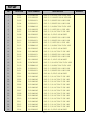
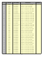
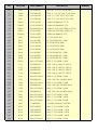
1
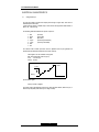
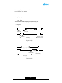
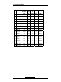
L17T TFT LCD COLOR MONITOR TECHNICAL SERVICE MANUAL L17T Technical Service Manual 1 FORWORD This document defines design and performance requirements for Hyundai 17.0" On Screen Display Color TFT LCD monitor L17T. It is capable of displaying maximum 1,280 horizontal dots and 1024 vertical lines resolution image. It also offers Power Management and DDC2B features according to VESA proposal. 2 GENERAL DESCRIPTION The monitor described in the followings is based on a multi- scanning, digital control display, 17.0 inches diagonal. The monitor is intended to be a finished product, basically a display device mounted inside a plastic enclosure which will provide the aesthetic, ergonomic and safety requirements. 2.1 LCD Descriptions ¬ Model Name : M170EN05 ¬ Display Area : 337.92(H) x 270.336(V) mm ¬ Drive system : A - Si TFT active matrix ¬ Display Colors : 262K Colors ¬ Number of pixels : 1280 x 1024 ¬ Module Size : 358.5 (H) x 296.5(V) x 19.0 typ. (D) mm ¬ Weight : 2,000g (TYP.) ¬ Contrast ratio : 450:1 (Typ.) ¬ Luminance : 260cd/m' (Typ) --1-- Control Description Front View LED Indicator Power Switch --2-- L17T Technical Service Manual ELECTRICAL CHARACTERISTICS 3.1 Analog R.G.B Input The input signal shall be applied to the display device through a signal cable, which must be intended as part of the monitor. A signal connector shall be a shielded 15pin D- Sub connector and signal cable shall be Black or White, 1.50¡ 0.05 meter long. The interfacing method described above requires 7 input lines : 1234567- Red Green Blue H Sync V Sync SDA SCL (red video) (green video) (blue video) (horizontal synchronization) (vertical synchronization) The reference video controller (the device used for adjustment and test) will guarantee the performances described below (measured on the output connector). Video signals on 75 ohm termination to the ground Red, Green & Blue Video (refer to Fig.3.01) Level : 0 to 0.700 Vpp Polarity : Positive 700mV 2.74mV Blanking Fig. 3.01 - Video Signal Synchronization signals Polarity : Positive or Negative This monitor shall not be demaged by improper sync timing and pulse duration, absence of sync, or abnormal input amplitude (video and/or sync too large too small). --3-- 3.1.1 Horizontal Scan Pixel Sampling Frequency : 25.056 ~ 135MHz H sync Frequency : 31.0 ~ 80 KHz 3.1.2 Vertical Scan Scanning Frequency : 56 ~ 75.0Hz 3.1.3 Timing This monitor shall be capable of displaying following video timing chart. * Timing Chart Display Time (T4) Front Porch (T5) Back Porch (T3) Sync Width (T2) High Level : 2.4V min Time Total (T1) Low Level : 0.4V max Fig. 3.02 - H-Sync Display Time (T4) Sync Width (T2) Front Porch (T5) Back Porch (T3) Time Total (T1) Fig. 3.03 - V-Sync --4-- L17T Technical Service Manual 3.1.4 No. Support Modes Resolution H Frequency Vfreq H V Dot Clock (kHz) (Hz) polarity polarity (MHz) 1 720 x 400 31.5 70.1 0 1 28.322 2 640 x 480 31.5 59.9 0 0 25.175 3 640 x 480 37.5 75 0 0 31.500 4 800 x 600 35.2 56.3 1 1 36.000 5 800 x 600 37.9 60.3 1 1 40.000 6 800 x 600 48.1 72.2 1 1 50.000 7 800 x 600 46.9 75.0 1 1 49.500 8 832 x 624 49.725 74.55 0 0 57.283 9 1024 x 768 48.4 60.0 0 0 65.000 10 1024 x 768 56.5 70.1 0 0 75.000 11 1024 x 768 60.0 75.0 1 1 78.750 12 1152 x 864 67.5 75 1 1 108.000 13 1280 x 1024 63.9 60.0 1 1 108.000 14 1280 x 1024 80.0 75 1 Table 3-01. Support Modes 1 135.000 --5-- 3.1.5 Preset Timing The timing shown in the following table will be factory preset for display. - Preset-mode table The timing shown in the following table will be factory preset for display. Horizontal Pixel Pixel Clock kHz Front Porch (T5) §` §` §` §` §` Vertical Lines Period (T1) Active (T4) Sync Width (T2) Back Porch (T3) Frequency Hz Period (T1) Active (T4) Sync Width (T2) Back Porch (T3) Front Porch (T5) Sync Polarity 640 640 800 800 800 800 832 1024 1024 1024 1152 1280 1280 MHz 28.322 25.175 31.500 36.000 40.000 49.500 50.000 57.283 65.000 75.000 78.750 108.00 108.00 135.00 Frequency Interlaced 720 Y 31.469 31.469 37.500 35.156 37.879 46.875 48.077 49.725 48.363 56.476 60.023 67.500 63.981 79.976 31.777 31.778 26.667 28.444 26.400 21.333 20.800 20.111 20.677 17.707 16.660 14.815 15.630 12.504 25.422 25.422 20.317 22.222 20.000 16.162 16.000 14.524 15.754 13.653 13.003 10.667 11.852 9.481 3.813 3.813 2.032 2.000 3.200 1.616 2.400 1.117 2.092 1.813 1.219 1.185 1.037 1.067 1.907 1.907 3.810 3.556 2.200 3.232 1.280 3.910 2.462 1.920 2.235 2.370 2.296 1.837 0.636 0.636 0.508 0.667 1.000 0.323 1.120 0.558 0.369 0.320 0.203 0.593 0.444 0.119 400 480 480 600 600 600 600 624 768 768 768 864 1024 1024 70.087 59.940 75.000 56.250 60.317 75.000 72.188 74.55 60.004 70.069 75.029 75.000 60.020 75.025 §´ §´ §´ §´ §´ /N 14.268 16.683 13.333 17.778 16.579 13.333 13.853 13.414 16.666 14.272 13.328 13.333 16.661 13.329 12.711 15.253 12.800 17.067 15.840 12.800 12.480 12.549 15.880 13.599 12.795 12.800 16.005 12.804 0.064 0.064 0.080 0.057 0.106 0.064 0.125 0.060 0.124 0.106 0.050 0.044 0.047 0.038 1.112 1.048 0.427 0.626 0.607 0.448 0.478 0.784 0.600 0.513 0.466 0.474 0.594 0.475 0.381 0.318 0.027 0.028 0.026 0.021 0.770 0.020 0.062 0.053 0.017 0.015 0.016 0.013 N N N N N N N N N N N N N N H - - - + + + + - - - + + + + V + - - + + + + - - - + + + + Table 3-02. Preset-Timings --6-- L17T Technical Service Manual 3.1.6 Brightness Definitions : Brightness This control is mainly intended as a raster luminance adjustment. Setting of User Controls Brightness Min Max Contrast Min Max Luminance Limits Data/Active area * ≤ 180 cd/m2 Table 3.03. Luminance Limits Legend : * Don’t care Full White screen @ 700mV video level, 1280x1024 resolution at H : 64kHz, V : 60Hz The measurement shall be executed after warming-up time during 30 minutes in a dark room ( Ambient luminance ≤ 10 lux, temperature 25 ¡C) O O --7-- 3.2 Composite Video Input The characteristics of video input composite are shown in Table 3.04 Signal Type Composite Video Signal Level 1.0 Vpp Connector Type RCA jack Termination 75 Table 3.04 Video Input Composite 3.3 Separate Video Input (SVHS) The characteristics of video input separate are shown in Table 3.05 Signal Type S-Video (Y/C) Luma Level 1.0 Vpp Chroma Level 0.286 Vpp(Reference Burst) Connector Type 4-pin mini-DIN Termination 75 Table 3.05 Video Input Separate 3.4 Input Formats The Composite, YC Video input formats are shown in Table 3.06 VIDEO MODES Mode Re solution Totoal Normal Normal H-Freq(Khz) V_Freq(Hz) Normal Pixel Clock(Mhz) NTSC Composite/YC 720x480@ 59.94Hz 858x525 15.734 59.940 13.500 PAL composite/YC 720x580@ 50Hz 864x625 15.625 50.000 13.500 Table 3.06 Composite, YC Input Formats --8-- L17T Technical Service Manual 3.5 TV Input 3.5.1 NTSC iAPPLICATION -Receiving System : ( NTSC STANDARD SYSTEM ) -Channel VHF Low BAND : 2(55.25MHz) ~ H(163.25MHz) High BAND : I(169.25MHz) ~ W+26(451.25MHz) UHF BAND : W+27(457.25MHz) ~ 78(855.25MHz) -Intermediate Frequeny PIF : (45.75)MHz CIF : (44.83)MHz SIF : (41.25)MHz -Input Impedance : UHF/VHF Terminal (75) Y , Unbalanced -Output Impedance : ViDEO : C.V.B.S AUDIO : IF : SECOND IF -Band Chang – Over System : (PLL Control System) -Tuning System : (Electronic Tuning System With PLL) --9-- 3.5.2 PAL - APPLICATIONS -Receiving System : ( PAL B/G+I+D/K + SECAM L/L’ STANDARD SYSTEM ) - Channel VHF Low BAND : E2(48.25MHz) ~ S10(168.25MHz) High BAND : E5(175.25MHz) ~ S41(463.25MHz) UHF BAND : E21(471.25MHz) ~ E69(855.25MHz) -Intermediate Frequency PIF : PAL B/G/I/D/K, SECAM L 38.90MHz SECAM L’ 33.90MHz CIF : PAL B/G/I/D/K, SECAM L 34.47MHz SECAM L’ 38.15 / 38.3MHz SIF : PAL B/G 33.4MHz, PAL I 32.9MHz PAL D/K, SECAM L 32.4MHz SECAM L’ 40.4MHz -Input Impedance : UHF/VHF Terminal (75)Y , Unbalanced -Band Change – Over System : PLL Control System -Tuning System : Electronic Tuning System With PLL -Applicable Standard Complies with European Regulations on Radiation, Signal handling and Immunity CENELEC EN55020, EN55013 --10-- L17T Technical Service Manual 3.6 Audio System This monitor has a audio system including two micro loudspeakers . Each of two micro loudspeakers has a 2W(Max.) output power . This system also supports a headphone (earphone) output. 3.6.1 Audio Amplifiers - 2W+2W Amplifier with DC Volume Control (for two micro loudspeakers) RL=8 3.6.2 @THD=10% Vcc=14V (min. 10V, max. 18V) Speaker - Micro Loudspeaker Spec. Normal impedance 8 ± 15% Resonance Freq. 550Hz ± 110Hz Freq. Range fo ~ 20KHz at 1.0V 1.5KHz at 1.0V Power Rating. Normal 1.0W /Peak 2.0W 3.6.3 Audio System Specification · Audio Amplifier Vcc=12V · Audio Signal Input : < -10.0dB (Vrms=300mV) Max · Audio Output : 1.0W Max (1ch) @THD=5% (Maximum Input) 3.7 Power Requirements This display device shall maintain the specified performances in the range described below : Frequency Voltage Power On/Off time 50 / 60Hz 90 ~ 264Vac RMS > 0.3 sec The following consumption requirements shall be met ; Power Consumption : 40W (max absolute value) Current consumption : < 1.0 Aac RMS --11-- 3.8 Power Management 3.8.1 Analog Signal The monitor requires a signal based on VESA DPMS (Display Power Management Signaling) proposal, and runs in three stages ; On Off : Normal Operation : Non Operation This monitor shall comply with the following specifications. Signals Power Recovery LED State H- Sync V- Sync Video Consumption time Description On Pulses Pulses Active 40W - Green On Less than Within Orange On 3.5W 3 sec Off no pulses no pulses Blanked Table 3.07 - Power Management 3.8.2 Video Signals ( S-Video,Composite Video) There is no definition of power management for Video signals. 3.8.3 TV Signal There is no definition of power management for TV signals. 3.8.4 Warm - Up Time The warm - up time shall be 30 minutes minimum. At the end of the warm- up period, no adjustment of service shall be necessary to cause the display to meet the requirements contained herein. After a warm- up time of 30 minutes, the display shall produce a usable image. Repetitive power ON/OFF cycles must be possible with a minimum switch- off time of about 3 sec. --12-- L17T Technical Service Manual 4 USER INTERFACE 4.1 User Controls This display device shall have following On- Screen Display controls. A) User Control Panel - Source - Volume - Menu - Power - Select - Down - Up B) Control Parameter (PC Mode) - Brightness - Contrast - Color Control - Miscellaneous - Audio - Auto Adjust - Language - H-V. Position - Clock Phase - Source C) Control Parameter (S-Video, Video, TV Mode) - Brightness - Contrast - Image Adjust - Miscellaneous - Audio - Language - ( TV ) - Source --13-- 4.2 On screen Display Controls By pressing Menu button, OSD menu is activated. The selected item is expressed by a highlight Icon and when ever button or button is pressed, a highlight icon is changed from side to side. And by pressing the select button, an item is selected and activated. If any button isn’t pressed during OSD setting time, the adjusted value is saved and OSD menu is disappeared. 4.2.1 Brightness and contrast Brightness or Contrast is showed by pressing the menu button and selected by pressing the select button. 4.2.2 Color Control The color control(color temperature) selecting by pressing menu button is following modes, mode1, mode2 and user modes. By selecting User mode, a user can control a R- G- B gain. 4.2.3 Miscellaneous - Recall Return to Factory adjustment condition. Change four parameters -> Brightness, Contrast, Color, Audio - OSD Timer and OSD Position By this menu, a user can control a location of OSD on screen and the display time of OSD menu. OSD Position is showed and selected by pressing the select button. 4.2.4 Audio - Volume : By this menu, a user can control the audio volume. - Sound off : By this menu, a user can control the audio on/off. 4.2.5 - Treble : By this menu, a user can control the treble gain(¡ 14dB,15step). - Base : By this menu, a user can control the base gain(¡ 14dB,15step). AUTO Adjust If you have done wrong selection at controlling this screen, you can use this menu. Automatically, if you select this key, this monitor will make a optimum screen. In order to get the optimized result of this function, display the white background or bright gray level image. --14-- L17T Technical Service Manual 4.2.6 Language By pressing LANGUAGE in main menu, a user can select one of 10 languages, English, Spanish, German, French, Italian, Swedish, Finnish, Danish, Portuguese, Dutch. To select a language must press Select button. 4.2.7 H-V. Position Horizontal (Vertical) Position is showed by pressing the menu button and selected by pressing the select button. To move the screen for the right side or the left side ( upward or downward) , and button is used. 4.2.8 4.2.9 Clock Phase 1) Phase : This menu adjusts the PLL parameter to synchronize the PLL clock 2) Clock : This menu adjusts the image clock. Source This menu used to choose the desired input signal source. There are four available signal source. - Analog RGB : 15 pin D-sub, analog signal 4.3 4.3.1 - S-Video : MINI DIN, Separate video signal - Composite : RCA Jack, Composite video signal - TV : NTSC, PAL Video ( T V ) User Control Brightness and contrast Brightness or Contrast is showed by pressing the menu button and selected by pressing the select button. 4.3.2 Image Adjust - Saturation : By this menu, a user can control the saturation of the video image. - Tint : By this menu, a user can control the tint of the video image - Sharpness : By this menu, a user can control the sharpness of the video image --15-- 4.3.3 Miscellangeous - Recall Return to Factory adjustment condition. Change four parameters -> Brightness, Contrast, Image, Audio - OSD Timer and OSD Position By this menu, a user can control a location of OSD on screen and the display time of OSD menu. OSD Position is showed and selected by pressing the select button. 4.3.4 Audio - Volume : By this menu, a user can control the audio volume. - Sound off : By this menu, a user can control the audio on/off. 4.3.5 - Treble : By this menu, a user can control the treble gain(¡ 14dB,15step). - Base : By this menu, a user can control the base gain(¡ 14dB,15step). Language By pressing LANGUAGE in main menu, a user can select one of 10 languages, English, Spanish, German, French, Italian, Swedish, Finnish, Danish, Portuguese, Dutch. To select a language must press Select button. 4.3.6 (TV) - CH Searching : By selecting country on the screen, this program enable to search for the channels automatically. If cable(Air/CATV) is disconnected or inappropriate country is selected, it may be operated improperly. - CH Edit : By this menu, a user can edit the TV channel (add channel / delete channel). - CH Fine Tune : By this menu, a user can tune the TV channel finely. - TV Input : By this menu, a user can select the TV channel (Air / Cable). 4.3.7 Source This menu used to choose the desired input signal source. There are four available signal source. - Analog RGB : 15 pin D-sub, analog signal - S-Video : MINI DIN, Separate video signal - Composite : RCA Jack, Composite video signal - TV : NTSC, PAL --16-- L17T Technical Service Manual 4.4 Direct Control ( Hot Key ) 4.4.1 4.4.2 - User Control Panel Source Volume - Power Select Down ( ) - Menu - Up ( ) Function of each key Source By this key, a user can change Input source sequentially. (PC->S-VIDEO->VIDEO->TV->PC) - Volume By this key, a user can activate Volume control menu. And press - button or button, a user can control the audio volume. Menu By this key, a user can activate OSD menu. - Power By this key, a user can turn on (off) the main Power. - Select If a user press this key, AUTO Adjust function(4.2.5) executing.(PC Mode only) - Down / Up By this key, a user can change TV Channel sequentially.(TV Mode only) 4.5 4.5.1 Remote Controller Figure of Remote Controller --17-- 4.5.2 - Function of each key POWER By this key, a user can turn on (off) the main Power. - INPUT SOURCE By this key, a user can change Input source sequentially. (PC->S-VIDEO->VIDEO->TV->PC) - Numeric By this key, a user can select Channel directly.(TV Mode only) - DISPLAY By this key, a user can know about current state.(PC, S-VIDEO, VIDEO, TV – CH) - PRE.CH By this key, a user can move previous Channel.(TV Mode only) - MUTE By this key, a user can control the audio on/off. (4.2.4 & 4.3.4) - EXIT By this key, a user can exit all kinds of OSD menu. - MENU By this key, a user can activate OSD menu. When OSD menu is activated, this key operate like select button. - CH ( + / - ) By this key, a user can change TV Channel sequentially.(TV Mode only) When OSD menu is activated, this key move selected item up or down. - VOL ( + / - ) By this key, a user can control the audio volume.(4.2.4 & 4.3.4) When OSD menu is activated, this key act like - button or button. AUTO If a user press this key, AUTO Adjust function(4.2.5) executing.(PC Mode only) - CH SEARCH If a user press this key, CH Searching function(4.3.6) executing.(TV Mode only) --18-- L17T Technical Service Manual Connecting with External Equipment Cautions Be sure to turn off the power of your computer before connecting the monitor. --19-- On Screen Controls & LED Indicator The menu for screen setting adjustment is located in the OSD and can be viewed in one of five languages OSD feature andmain funcrions are as follows: 1280X1024 V:60.0/H:63.9 --20-- L17T Technical Service Manual OSD Adjustments he OSD adjustments available to you are listed below. BrigHtness Adjust the brightness of the screen. Contrast Adjust the contrast of the screen. Color control Color temperature affects the tint of the image. With lower color temperatures the image turns reddish and with higher temperatures bluish. There are three color settings available: Mode 1(a cool white), Mode 2(a warm white) or USER. With the USER setting you can set individual values for red, green and blue. MISCELLANEOUS Recall Recall the saved color data. OSD TIMER You can set the displayed time of OSD Menu window on the screen by using this adjustment. OSD Position Adjust the OSD menu's horizontal or vertical position on the screen. AUDIO VOLUME Adjust the audio volume level. SOUND OFF This menu is used to choose audio on or off. TREBLE Emphasize high frequency audio. BASE Emphasize low frequency audio. AUTO ADJUST You can adjust the shape of screen automatically at the full screen pattern. Language You can select the language in which adjustment menus are displayed. The following languages are available : English, French, German, Italian, Spanish, Swedish, Finnish, Danish, Portuguese and Dutch. --21-- H/V. POSITION H POSITION Adjusts the horizontal position of the entire screen image. V POSITION Adjusts the vertical position of the entire screen image. CLOCK PHASE PHASE Adjust the noise of the screen image. CLOCK Adjust the horizontal size of the entire screen image. SOURCE No function. (Only supportable by the optional appliance.) --22-- L17T Technical Service Manual TV Direct access buttons(Option) Use this button to change a video source Video sources are changed in the following order : PC Æ S-Video Æ VIDEO Æ TV Use the button to select the volume adjustment. Adjust with Up or Down button. Opens the OSD and selects the highlighted function. Select function on the OSD. Moves the selector right or left on the OSD. Increases or decreases the values of the selected function. Increases or decreases the channel number. --23-- OSD Adjustments The OSD adjustments available to you are listed below. Brightness Adjust the brightness of the screen. Contrast Adjust the contrast of the screen. Image Adjust Saturation Adjust the saturation of the video image. Tint Adjust the Tint of the video image. Sharpness Adjust the sharpness and softness of the video image. Miscellaneous Recall Recall the saved color data. OSD Timer You can set the displayed time of OSD Menu window on the screen by using this adjustment. OSD Position Adjust the OSD menu's horizontal or vertical position on the screen. Audio Volume Adjust the audio volume level. Sound off This menu is used the choose audio on or off. Treble Emphasize high frequency audio. Base Emphasize low frequency audio. --24-- L17T Technical Service Manual Language You can select the language in which adjustment menus are displayed. The following languages are available : English, French, German, Italian, Spanish, Swedish, Finnish, Danish, Portuguese and Dutch. Source This menu is used to choose the desired input signal source. There are four signal sources available : - Analog RGB : 15 pin D-sub, Analog signal - S-video : MINI DIN, Separate video signal - Composite Video : RCA Jack, Composite video signal - TV : Antenna or CATV signal TV Ch Searching By selecting country on the screen, this program enabls to seach for the channels automatically. ! If cable(Air/CATV) is disconnected or inappropriate country is selected, It may be operated improperly. Ch Edit To add a newly found channel or remove an existing channel. Ch Fine Tune To make the video image as clear as posible. TV Input Select a channel system : Air or Cable. --25-- Getting Fine Picture Step 1. At first Display, a full screen, such as, Window's background or "H" character should be achieved by using Editor (ex: Notepad. exe) Step 2. Adjust the screen to the center of the Display(LCD), by using the top and bottom display controls. (i.e.Using V-Position Adjust menu) Step 3. Adjust the screen to the center of the Display(LCD), by using the right and left display controls. (i.e.Using Clock and H-Position adjust menu) Step 4. Adjust the Clock-phase until the "H" Character displays clear. Step 5. Using the Contrast. Brightness, and Color Control menu, set the color to your preference. Step 6. When you finish the adjustment, you can save your settings by pressing on the menu until the OSD screen has disappeared. Factory Setting & EEPROM Initialization Method Factory Setting Method - Connect the signal cable and power cable to the LCD monitor. - Press Power switch with pressed MENU key.(Menu key + Power key). - Then, a User can change the factory setting value in OSD menu. - Save changed value and Turn off the power s/w. - Turn on the power, adjust the screen. --26-- L17T Technical Service Manual Specification LCD Pixel pitch Brightness Response Time Display area Number of color Input signals Frequency rate Maximum bandwidth Maximum resolution Recommanded resolution Input voltage Power consumption Power management Plug & Play OSD menu Built in Speaker VESA FPMPMI Ergonomics, Safety and EMC Operating Temperature Weight Dimensions (W X H X D mm) 17"viewable, Diagonal, A-Si TFT 0.264 x 0.264mm 250cd/m2 16msec 337.920 x 270.336 mm 262 K R.G.B Analog, 15 pin D-sub Horizontal : 31.0 to 80.0KHz, Vertical : 56 to 75Hz 135 MHz 1280 x 1024@75Hz 1280 x 1024@60Hz 100-240 VAC, 1.0A 40W VESA DPMS VESA DDC 1/2B BRIGHTNESS, CONTRAST, COLOR CONTROL, MISCELLANEOUS, AUDIO, AUTO ADJUST, LANGUAGE, H/V. POSITION, CLOCK-PHASE, SOURCE 2ch x 2watts 75 x 75 mm screw mounting TCO, FCC Class B, CE, cULus, TÜV-GS, SEMKO 5 ~ 35O C 4.6Kg unpacked, 6.1Kg packed 372 X 395 X 185 mm • Specification is subject to change without notice for performance improvement. --27-- Critical Parts Specification AT24C164 MC68HC705BD7B Features - Low Voltage and Standard Voltage Operation - - - 5.0 (VCC = 4.5V to 5.5V) - 2.7 (VCC = 2.7V to 5.5V) - 2.5 (VCC = 2.5V to 5.5V) - 1.8 (VCC = 1.8V to 5.5V) Internally Organized 2048 x 8 (16K) 2-Wire Serial Interface Schmitt Trigger, Filtered Inputs for Noise Suppression Bidirectional Data Transfer Protocol 100 kHz (1.8V, 2.5V, 2.7V) and 400 kHz (5V) Compatibility Write Protect Pin for Hardware Data Protection Cascadable Feature Allows for Extended Densities 16-Byte Page Write Mode Partial Page Writes Are Allowed Self-Timed Write Cycle (10 ms max) High Reliability - Endurance: 1 Million Write Cycles - Data Retention: 100 Years - ESD Protection: >3,000V Automotive Grade and Extended Temperature Devices Available 8-Pin JEDEC SOIC and 8-Pin PDIP Packages Description The AT24C164 provides 16,384 bits of serial electrically erasable and programmable read only memory (EEPROM) organized as 2048 words of 8 bits each. The deviceís cascadable feature allows up to eight devices to share a common 2-wire bus. The device is optimized for use in many industrial and commercial applications where low power and low voltage operation are essential. The AT24C164 is available in space saving 8-pin PDIP and 8-pin SOIC packages and is accessed via a 2-wire serial interface. In addition, this device is available in 5.0V (4.5V to 5.5V), 2.7V (2.7V to 5.5V), 2.5V (2.5V to 5.5V) and 1.8V (1.8V to 5.5V) versions. Pin Configurations Pin Name Function A0 - A2 Address Inputs SDA Serial Data SCL Serial Clock Input WP Write Protect 8-Pin PDIP A0 A1 A2 GND 1 2 3 4 8 7 6 5 8-Pin SOIC VCC WP SCL SDA A0 A1 A2 GND --28-- 1 2 3 4 8 7 6 5 VCC WP SCL SDA L17T Technical Service Manual Absolute Maximum Ratings* *NOTICE: Operating Temperature .................................. -55°C to +125°C Storage Temperature ..................................... -65°C to +150°C Voltage on Any Pin with Respect to Ground .....................................-1.0V to +7.0V Maximum Operating Voltage........................................... 6.25V Stresses beyond those listed under ìAbsolute Maximum Ratingsî may cause permanent damage to the device. This is a stress rating only and functional operation of the device at these or any other conditions beyond those indicated in the operational sections of this specification is not implied. Exposure to absolute maximum rating conditions for extended periods may affect device reliability. DC Output Current........................................................ 5.0 mA Block Diagram WP Pin Description SERIAL CLOCK (SCL): The SCL input is used to positive edge clock data into each EEPROM device and negative edge clock data out of each device. SERIAL DATA (SDA): The SDA pin is bidirectional for serial data transfer. This pin is open-drain driven and may be wire-ORed with any number of other open-drain or open collector devices. DEVICE SELECT (A2, A1, A0): The A2, A1 and A0 pins are device address inputs that may be hardwired or actively driven to VDD or VSS. These inputs allow the selection for one of eight possible devices sharing a common bus. The AT24C164 can be made compatible with the AT24C16 by tying A2, A1 and A0 to VSS. Device addressing is discussed in detail in the device addressing section. WRITE PROTECT (WP): The write protect input, when tied low to GND, allows normal write operations. Memory Organization The AT24C164 is internally organized with 256 pages of 8 bytes each. Random word addressing requires an 11 bit data word address. --29-- RC1117 MC68HC705BD7B RC1117 1A Adjustable/Fixed Low Dropout Linear Regulator Features Description • • • • • • The RC1117 and RC1117-2.5, -2.85, -3.3 and -5 are low dropout three-terminal regulators with 1A output current capability. These devices have been optimized for low voltage where transient response and minimum input voltage are critical. The 2.85V version is designed specifically to be used in Active Terminators for SCSI bus. Low dropout voltage Load regulation: 0.05% typical Trimmed current limit On-chip thermal limiting Standard SOT-223 and TO-263 packages Three-terminal adjustable or fixed 2.5V, 2.85V, 3.3V, 5V Current limit is trimmed to ensure specified output current and controlled short-circuit current. On-chip thermal limiting provides protection against any combination of overload and ambient temperatures that would create excessive junction temperatures. Applications • • • • • • Active SCSI terminators High efficiency linear regulators Post regulators for switching supplies Battery chargers 5V to 3.3V linear regulators Motherboard clock supplies Unlike PNP type regulators where up to 10% of the output current is wasted as quiescent current, the quiescent current of the RC1117 flows into the load, increasing efficiency. The RC1117 series regulators are available in the industrystandard SOT-223 and TO-263 power packages. Typical Applications RC1117 VIN = 3.3V VIN + 10∝F VOUT 1.5V at 1A + 2 2∝F 124 ADJ 24.9 RC1117-2.85 VIN = 5V + VIN +VOUT 10∝F 2.85V at 1A 22∝F GND --30-- L17T Technical Service Manual Pin Assignments Tab is VOUT Front View Tab is VOUT 3 IN 2 OUT 1 ADJ/GND 4-Lead Plastic SOT-223 ΘJC = 15ϒC/W* 1 2 3 ADJ/ GND OUT IN 3-Lead Plastic TO-263 ΘJC = 10ϒC/W* *With package soldered to 0.5 square inch copper area over backside ground plane or internal power plane., ΘJA can vary from 30°C/W to more than 50°C/W. Other mounting techniques may provide better thermal resistance than 30°C/W. Absolute Maximum Ratings Parameter Min. Max. Unit 7.5 V 0 125 °C -65 150 °C 300 °C VIN Operating Junction Temperature Range Storage Temperature Range Lead Temperature (Soldering, 10 sec.) --31-- Electrical Characteristics Operating Conditions: VIN ≤ 7V, TJ = 25°C unless otherwise specified. The • denotes specifications which apply over the specified operating temperature range. Parameter Conditions 3 Min. Typ. Max. Units Reference Voltage 1.5V ≤ (VIN - VOUT) ≤ 5.75V, 10mA ≤ IOUT ≤ 1A • 1.225 (-2%) 1.250 1.275 (+2%) V Output Voltage 10mA ≤ IOUT ≤ 1A RC1117-2.5, 4V ≤ VIN ≤ 7V RC1117-2.85, 4.35V ≤ VIN ≤ 7V RC1117-3.3, 4.8V ≤ VIN ≤ 7V RC1117-5, 6.5V ≤ VIN ≤ 7V • • • • 2.450 2.793 3.234 4.900 2.5 2.85 3.3 5.0 2.550 2.907 3.366 5.100 V V V V Line Regulation1,2 (VOUT + 1.5V) ≤ VIN ≤ 7V, IOUT = 10mA • 0.005 0.2 % Load Regulation1,2 (VIN – VOUT) = 2V, 10mA ≤ IOUT ≤ 1A • 0.05 0.5 % Dropout Voltage ∆VREF = 1%, IOUT = 1A • 1.100 1.200 V Current Limit (VIN – VOUT) = 2V • Adjust Pin Current3 µA 0.2 5 µA • Minimum Load Current 1.5V ≤ (VIN – VOUT) ≤ 5.75 • • VIN = VOUT + 1.25V f = 120Hz, COUT = 22µF Tantalum, (VIN – VOUT) = 3V, IOUT = 1A Thermal Regulation TA = 25°C, 30ms pulse Temperature Stability 10 mA 4 60 0.004 • 13 72 TA = 125°C, 1000hrs. 0.03 RMS Output Noise (% of VOUT) TA = 25°C, 10Hz ≤ f ≤ 10kHz 0.003 mA dB 0.02 0.5 Long-Term Stability Thermal Resistance, Juncation to Case A 120 1.5V ≤ (VIN – VOUT) ≤ 5.75, 10mA ≤ IOUT ≤ 1A Quiescent Current 1.5 35 Adjust Pin Current Change3 Ripple Rejection 1.1 • %/W % 1.0 % % SOT-223 15 °C/W TO-263 10 °C/W 150 °C Thermal Shutdown Notes: 1. See thermal regulation specifications for changes in output voltage due to heating effects. Load and line regulation are measured at a constant junction temperature by low duty cycle pulse testing. 2. Line and load regulation are guaranteed up to the maximum power dissipation (18W). Power dissipation is determined by input/output differential and the output current. Guaranteed maximum output power will not be available over the full input/ output voltage range. 3. RC1117 only. --32-- L17T Technical Service Manual TDA7496L MC68HC705BD7B 2W+2W OUTPUT POWER RL = 8Ω @THD = 10% VCC = 14V ST-BY AND MUTE FUNCTIONS LOW TURN-ON TURN-OFF POP NOISE LINEAR VOLUME CONTROL DC COUPLED WITH POWER OP. AMP. NO BOUCHEROT CELL NO ST-BY RC INPUT NETWORK SINGLE SUPPLY RANGING UP TO 15V SHORT CIRCUIT PROTECTION THERMAL OVERLOAD PROTECTION INTERNALLY FIXED GAIN SOFT CLIPPING VARIABLE OUTPUT AFTER VOLUME CONTROL CIRCUIT POWERDIP (14+3+3) PACKAGE Powerdip (14+3+3) ORDERING NUMBER: TDA7496L 14+3+3 package, specially designed for high quality sound, TV and Monitor applications. Features of the TDA7496L include linear volume control, Stand-by and mute functions. DESCRIPTION The TDA7496L is a stereo 2W+2W class AB power amplifier assembled in the @ Powerdip BLOCK DIAGRAM VAROUT_R GND 1,2,3,13, 18,19,20 470nF 15,16 VOLUME 9 INR VS 7 30K 1000µF 14 + OUTR OP AMP S1 ST-BY 11 +5V STBY MUTE/STBY PROTECTIONS 60K VOLUME 470nF 12 MUTE 17 + 30K 1000µF 10 470µF 6 VOLUME 5 VAROUT_L +5V D97AU596A 100nF +5V 1µF OUTL OP AMP SVR S_GND S2 MUTE 4 INL 10K 300K --33-- ABSOLUTE MAXIMUM RATINGS Symbol Parameter Value DC Supply Voltage VS 26 V 8 6 0 to 70 Vpp W ∞C -40 to 150 ∞C 7 V Maximum Input Voltage Total Power Dissipation (Tcase = 60∞C) Ambient Operating Temperature VIN Ptot Tamb Tstg, Tj Storage and Junction Temperature Volume CTRL DC voltage V6 PIN CONNECTION Unit Rth with "on board" Square Heatsink vs. copper area. Rthj-a (∞C/W) GND 1 20 GND GND 2 19 GND GND 3 18 GND INL 4 17 OUTL VAROUT_L 5 16 VS VOLUME 6 15 VS VAROUT_R 7 14 OUTR N.C. 8 13 GND INR 9 12 MUTE SVR 10 11 STBY D97AU675 COPPER AREA 35µ THICKNESS 60 PC BOARD 50 40 D97AU597A 30 0 4 8 12 Area(cm2) THERMAL DATA Symbol Rth j-pins Rth j-amb (*) Value Unit Thermal Resistance Junction-pins Parameter max. 15 ∞C/W Thermal Resistance Junction-ambient max. 50 ∞C/W (*) Mounted on PCB with no heatsink ELECTRICAL CHARACTERISTICS (Refer to the test circuit VS = 14V; RL = 8Ω, Rg = 50Ω, Tamb = 25∞C). Symbol VS Iq DCVOS VO PO THD Ipeak Vin GV GvLine AMin VOL BW Parameter Supply Voltage Range Total Quiescent Current Output DC Offset Referred to SVR Potenial Quiescent Output Voltage Output Power Total Harmonic Distortion Output Peak Current Input Signal Closed Loop Gain Monitor Out Gain Attenuation at Minimum Volume Test Condition Min. 10 25 200 No Input Signal THD = 10%; RL = 8Ω; 1 THD = 1%; RL = 8Ω; 1 GV = 30dB; PO = 1W; f = 1KHz; (internally limited) Vol Ctrl > 4.5V Vol Ctrl > 4.5V; Zload > 30KΩ Vol Ctrl < 0.5V Typ. .6 7 2 .3 0.4 0.7 0.9 28.5 -1.5 80 30 0 0.6 --34-- Max. 18 50 2.8 31.5 1.5 Unit V mA mV V W W % A Vrms dB dB dB MHz L17T Technical Service Manual ELECTRICAL CHARACTERISTICS (continued) Symbol eN SR Ri RVar Out Rload Var Out SVR TM Ts Parameter Total Output Noise Test Condition f = 20Hz to 22KHz Play, max volume f = 20Hz to 22KHz Play, max attenuation f = 20Hz to 22KHz Mute Slew Rate Input Resistance Variable Output Resistance Variable Output Load Supply Voltage Rejection Min. 5 22.5 f = 1kHz; max volume CSVR = 470µF; VRIP = 1Vrms f = 1kHz; max attenuation CSVR = 470µF; VRIP =1Vrms Typ. 500 Max. 800 Unit µV 100 250 µV 60 150 µV 100 2 35 39 V/µs KΩ Ω KΩ dB 55 65 dB 150 160 ∞C ∞C Thermal Muting Thermal Shut-down 8 30 30 MUTE STAND-BY & INPUT SELECTION FUNCTIONS VST ON VST OFF VM ON VM OFF IqST-BY AMUTE IstbyBIAS ImuteBIAS Stand-by ON Threshold Stand-by OFF Threshold Mute ON Threshold Mute OFF Threshold Quiescent Current @ Stand-by Mute Attenuation Stand-by bias current Mute bias current 3.5 1.5 3.5 50 Stand by on VST-BY = 5V VMUTE = 5V Play or Mute Mute Play -20 0.6 65 80 -5 1 0.2 1.5 1 5 2 V V V V mA dB µA µA µA µA µA APPLICATION SUGGESTIONS The recommended values of the external components are those shown on the application circuit of figure 1A. Different values can be used, the following table can help the designer. R1 SUGGESTION VALUE 300K R2 P1 10K 50K C1 1000µF C2 C3 C4 C5 470nF 470nF 470µF 100nF C6 1000µF C7 C8 1µF 1000µF C9 100nF COMPONENT PURPOSE Volume control circuit Mute time constant Volume control circuit Supply voltage bypass Input DC decoupling Input DC decoupling Ripple rejection Volume control time costant Output DC decoupling Mute time costant Output DC decoupling Supply voltage bypass LARGER THAN SUGGESTION Larger volume regulation time Larger mute on/off time SMALLER THAN SUGGESTION Smaller volume regulation time Smaller mute on/off time Danger of oscillation Lower low frequency cutoff Lower low frequency cutoff Better SVR Larger volume regulation time Lower low frequency cutoff Higher low frequency cutoff Higher low frequency cutoff Worse SVR Smaller volume regulation time Higher low frequency cutoff Larger mute on/off time Lower low frequency cutoff Smaller mute on/off time Higher low frequency cutoff --35-- Danger of oscillation NT68F632V2 MC68HC705BD7B Section-1 General Description 1 Features • CMOS technology for low power consumption • Operating voltage Vcc ranges from 3.0V to 3.6V • 8031 8-bit CMOS Micro-Processor (uP) core • Interrupts - • • • • • • • • Intel compatible 8031 architecture 256-byte Internal DATA Memory Two 16-Bit Timer/Counter Fully duplex UART 5-vector interrupt structure with two programmable priority levels High level C-language for the F/W development On-Chip Oscillator 12MHz operating frequency 24MHz clock for CPU operating Reset External Reset Pin - Lo w-Voltage Reset Watch-Dog Timer Reset - IS P Reset Program memory 128K bytes of on-chip flash memory for program memory 2K bytes of Mask ROM for ISP control function 1,536 Bytes On-Chip RAM Extended 256 Bytes Internal DATA Memory of uP 8031 External Data Memory 768 Bytes General Purpose RAM Buffer! $F400 ~ $F6FF" 512 Bytes RAM Buffer for hardware DDC Port ! $F800 ~ $F9FF" A/D Converter - 7- Bit resolution 4 selectable Input channels Conversion Range Absolutely Monotonic linear from GND to VCC Conversion time 12us PWM D/A Converter - 8- Bit resolution 10 selectable output channels 6 channels with 3.3V Push-Pull Structure 4 channels with 5V Open-Drain Structure 35! 37 for PLCC Package" Selectable General Purpose I/O Pins • • • • --36-- 5-vector interrupt structure with two programmable priority levels for uP F8031 TF0: Timer/Counter 0 Overflow Interrupt TF1: Timer/Counter 1 Overflow Interrupt RI+TI: UART Interrupts - I NT0: Sync Processor Interrupts 2 I C Bus Port-0 (PB4, PB5) Interrupt NT1 - External Interrupts: INTE0 & INTE1 - I2C-Bus Port-1 (PB6, PB7) Interrupts Sync Processor Unit - S ignal Type Separate Sync, Composite Sync & Digital-Level Sync-On-Green! SOG" Powerful Polarity detection for HSYNCI and VSYNCI - H SYNCO/VSYNCO polarity-controlled outputs - F ast Auto-Mute function Half frequency I/O function Timer/Counters with 2-lay content latches for counting sync period/frequency stable results can be read Clamp pulse output Clamp pulse output at either the leading edge or trailing edge of HSYNC Selectable Clamp pulse width Selectable pulse output polarity Flexible free-run H/V sync output generator Flexible test pattern generator DDC Port Dual indepentent input DDC channels Pure hardware solution for VESA DDC1/2B Selectable 128/256 Bytes EDID-Buffer for hardware DDC port I2C-bus Two built-in master/slave I2C bus interfaces support VESA 2Bi/2B+ SCL clock speed supports up to 400Kbps Package - 42 -Pin S-DIP - 44 -Pin PLCC L17T Technical Service Manual 1-2 General Description This is an 8031 CPU core embedded micro-controller, which is designed for the high-performance low-cost LCD monitor control application. It contains an 8-bit 8031 micro-controller, on-chip 128K bytes flash-type program ROM, 1,536-bytes internal data memory, four 7-bit resolution A/D Converter, 10-channel 8-bit resolution PWM DAC, two16-bit timer/counters, and an UART. 2 Besides those, it has an internal SYNC processor, two-channel hardware DDC solution, and VESA 2Bi/2B+ master/slave I C bus interface. Those functions can help the user to develop a LCD monitor application as soon as possible. 1-3 Pin Configurations VSYNCI 41 HSYNCI PC0* 3 PC3/PWM0 RSTB 4 40 39 VCC 5 38 PC5/PATTO PD6 37 36 PC6 35 34 PD0 GND 6 7 OSCO 8 OSCI 9 P30/RXD 10 P31/TXD 11 P34/T0 12 PC4/PWM1 PC7 PD1/HSYNCO 33 PD2/VSYNCO 32 31 PD3/HALFO 30 PD5/CLMPO 29 PA0/PWM2 PD4/HALFI 14 PB2/ADC2/INTE0 15 28 PB4*/SCL0* PB1/ADC1 PB0/ADC0 16 17 27 26 PB5*/SDA0* PB6*/SCL1* PA7*/PWM9* 18 25 PB7*/SDA1* PA6*/PWM8* 19 24 PA1/PWM3 PA5*/PWM7* 20 23 PA2/PWM4 PA4*/PWM6* 21 22 PA3/PWM5 7 8 9 10 11 12 13 14 15 16 17 NT68F632L PB4*/SCL0* PB5*/SDA0* PB6*/SCL1* PB7*/SDA1* PA1/PWM3 PA2/PWM4 PA3/PWM5 PA4*/PWM6* PA5*/PWM7* PA6*/PWM8* PA7*/PWM9* 13 GND OSCO OSCI P30/RXD P31/TXD P34/T0 P35/T1 PB3/ADC3/INTE1 PB2/ADC2/INTE0 PB1/ADC1 PB0/ADC0 28 27 26 25 24 23 22 21 20 19 18 P35/T1 PB3/ADC3/INTE1 40 41 42 43 44 1 2 3 4 5 6 42 2 PC5/PATTO PC4/PWM1 PC3/PWM0 HSYNCI VSYNCI PC2/SOGI PC1* PC0* RSTB VCC PD6 1 PC1* NT68F632U PC2/SOGI 42-Pin S-DIP 44-Pin PLCC --37-- 39 38 37 36 35 34 33 32 31 30 29 PE1 PE0 PC6 PC7 PD0 PD1/HSYNCO PD2/VSYNCO PD3/HALFO PD4/HALFI PD5/CLMPO PA0/PWM2 1-4 Block Diagram Master/Slave I2C Bus *2 7-bit A/D Converter *4 JEDEC 32K-Byte *4Bank Flash Memory 2K-Byte Boot ROM Low Power detector 8-bit PWM DAC *10 768 Byte External Data SRAM 512 Byte DDC SRAM CPU F8031 Core 256-byte Internal SRAM Hardware DDC1/2B *2 I/O Ports Watch Dog Timer CPU Clock Interrupt Controller --38-- PLL H/V Sync Signal Processor L17T Technical Service Manual TDA7440D MC68HC705BD7B INPUT MULTIPLEXER - 4 STEREO INPUTS - SELECTABLE INPUT GAIN FOR OPTIMAL ADAPTATION TO DIFFERENT SOURCES ONE STEREO OUTPUT TREBLE AND BASS CONTROL IN 2.0dB STEPS VOLUME CONTROL IN 1.0dB STEPS TWO SPEAKER ATTENUATORS: - TWO INDEPENDENT SPEAKER CONTROL IN 1.0dB STEPS FOR BALANCE FACILITY - INDEPENDENT MUTE FUNCTION ALL FUNCTION ARE PROGRAMMABLE VIA SERIAL BUS SO28 ORDERING NUMBER: TDA7440D Selectable input gain is provided. Control of all the functions is accomplished by serial bus. The AC signal setting is obtained by resistor networks and switches combined with operational amplifiers. Thanks to the used BIPOLAR/CMOS Technology, Low Distortion, Low Noise and DC stepping are obtained DESCRIPTION The TDA7440D is a volume tone (bass and treble) balance (Left/Right) processor for quality audio applications in Hi-Fi systems. BLOCK DIAGRAM MUXOUTL L-IN1 INL 8 4 TREBLE(L) 9 18 BOUT(L) BIN(L) 14 100K 15 RB 5 L-IN2 100K L-IN3 G 6 VOLUME TREBLE 27 SPKR ATT LEFT BASS LOUT 100K L-IN4 7 100K R-IN1 21 0/30dB 2dB STEP 3 2 22 I CBUS DECODER + LATCHES 20 2 100K R-IN3 SDA DIG_GND 100K R-IN2 SCL G VOLUME TREBLE 26 SPKR ATT RIGHT BASS ROUT 1 VREF 100K 24 28 R-IN4 100K 25 SUPPLY INPUT MULTIPLEXER + GAIN RB 10 MUXOUTR 11 INR 19 TREBLE(R) --39-- 12 BIN(R) 13 BOUT(R) VS AGND 23 CREF D98AU883 PIN CONNECTION (Top view) R_IN3 1 28 R_IN4 R_IN2 2 27 LOUT R_IN1 3 26 ROUT L_IN1 4 25 AGND L_IN2 5 24 VS L_IN3 6 23 CREF L_IN4 7 22 SDA MUXOUTL 8 21 SCL 9 20 DIG-GND MUXOUT(R) IN(L) 10 19 TREBLE(R) IN(R) 11 18 TREBLE(L) BIN(R) 12 17 N.C. BOUT(R) 13 16 N.C. BIN(L) 14 15 BOUT(L) D98AU884 ABSOLUTE MAXIMUM RATINGS Symbol Parameter Value 10.5 V Tamb Operating Ambient Temperature -10 to 85 5C Tstg Storage Temperature Range -55 to 150 5C Value Unit 85 5C/W VS Operating Supply Voltage Unit THERMAL DATA Symbol R th j-pin Parameter Thermal Resistance Junction-pins QUICK REFERENCE DATA Symbol Min. Typ. Max. VS Supply Voltage Parameter 6 9 10.2 VCL Max. input signal handling 2 THD Total Harmonic Distortion V = 1Vrms f = 1KHz 0.01 S/N Signal to Noise Ratio V out = 1Vrms (mode = OFF) 106 dB SC Channel Separation f = 1KHz 90 dB Input Gain in (2dB step) Unit V Vrms % 30 dB -47 0 dB -14 +14 dB Bass Control (2dB step) -14 +14 dB Balance Control -79 0 dB Volume Control Treble Control 0 0.1 (1dB step) (2dB step) 1dB step Mute Attenuation 100 --40-- dB 5 4 3 2 1 L17T/L19T BLOCK DIAGRAM D D 12MHz LVDS Scaler 15PIN D-SUB NT7181-11 NT68520E-QFP160 LVDS C NT7181-11 COMPOSITE VIDEO S-VIDEO VIDEO DECORDER VPX3226E 17" LCD PANEL C EEPROM (24CXX) MCU NT68F632 TV TUNER INVERTER 12MHz B B POWER 12V/5V AUDIO PROCESSOR TDA7440D AUDIO AMP TDA7496L A A Title Size IMAGEQUEST L17T/L19T Document Number Rev VP2 Block Diagram Date: 5 4 3 2 Wednesday, April 23, 2003 Sheet 1 7 of 7 PART LIST NO LOCATION PART NUMBER DESCRIPTION 1 C101 2122240044 CAP-C-C,0.22UF 50V Z Y5V 1608 2 C102 2121020039 CAP-C-C,1000PF 50V K X7R 1608 3 C103 2123310021 CAP-C-C,330PF 50V J NP0 1608 4 C104 2123310021 CAP-C-C,330PF 50V J NP0 1608 5 C105 2126840013 CAP-C-C,0.68UF 50V Z Y5V 1608 6 C106 2121000029 CAP-C-C,10PF 50V J COG 1608 7 C107 2121040045 CAP-C-C,0.1UF 50V Z Y5V 1608 8 C108 2012200005 CAP-AL-C,22UF 16V M 5052 9 C109 2123310021 CAP-C-C,330PF 50V J NP0 1608 10 C110 2123310021 CAP-C-C,330PF 50V J NP0 1608 11 C111 2121000029 CAP-C-C,10PF 50V J COG 1608 12 C112 2126840013 CAP-C-C,0.68UF 50V Z Y5V 1608 13 C113 2012200005 CAP-AL-C,22UF 16V M 5052 14 C114 2121040045 CAP-C-C,0.1UF 50V Z Y5V 1608 15 C115 2123310021 CAP-C-C,330PF 50V J NP0 1608 16 C116 2123310021 CAP-C-C,330PF 50V J NP0 1608 17 C117 2011000006 CAP-AL-C,10UF 16V M 4052 18 C118 2124730035 CAP-C-C,0.047UF 50V Z Y5V 1608 19 C119 2126840013 CAP-C-C,0.68UF 50V Z Y5V 1608 20 C120 2123310021 CAP-C-C,330PF 50V J NP0 1608 21 C121 2123310021 CAP-C-C,330PF 50V J NP0 1608 22 C201 2012200005 CAP-AL-C,22UF 16V M 5052 23 C202 2121040045 CAP-C-C,0.1UF 50V Z Y5V 1608 24 C203 2121040045 CAP-C-C,0.1UF 50V Z Y5V 1608 25 C204 2121040045 CAP-C-C,0.1UF 50V Z Y5V 1608 26 C205 2121040045 CAP-C-C,0.1UF 50V Z Y5V 1608 27 C206 2121040045 CAP-C-C,0.1UF 50V Z Y5V 1608 28 C207 2121040045 CAP-C-C,0.1UF 50V Z Y5V 1608 29 C208 2121040045 CAP-C-C,0.1UF 50V Z Y5V 1608 30 C209 2121040045 CAP-C-C,0.1UF 50V Z Y5V 1608 31 C210 2121040045 CAP-C-C,0.1UF 50V Z Y5V 1608 32 C211 2121040045 CAP-C-C,0.1UF 50V Z Y5V 1608 33 C212 2121040045 CAP-C-C,0.1UF 50V Z Y5V 1608 34 C213 2121040045 CAP-C-C,0.1UF 50V Z Y5V 1608 35 C214 2012200005 CAP-AL-C,22UF 16V M 5052 9/ 1 REMARK NO LOCATION PART NUMBER DESCRIPTION 36 C215 2121050045 CAP-C-C,1UF 50V Z Y5V 1608 37 C216 2121050045 CAP-C-C,1UF 50V Z Y5V 1608 38 C217 2121050045 CAP-C-C,1UF 50V Z Y5V 1608 39 C218 2121040045 CAP-C-C,0.1UF 50V Z Y5V 1608 40 C219 2121040045 CAP-C-C,0.1UF 50V Z Y5V 1608 41 C220 2013300005 CAP-AL-C,33UF 10V M 5052 42 C221 2121040045 CAP-C-C,0.1UF 50V Z Y5V 1608 43 C222 2121040045 CAP-C-C,0.1UF 50V Z Y5V 1608 44 C223 2121040045 CAP-C-C,0.1UF 50V Z Y5V 1608 45 C224 CK7FXA1H103K CAP-CC,0.01UF 50V K X7R 1608 46 C225 CK7FXA1H103K CAP-CC,0.01UF 50V K X7R 1608 47 C226 2121000029 CAP-C-C,10PF 50V J COG 1608 48 C227 2121000029 CAP-C-C,10PF 50V J COG 1608 49 C228 CK7FXA1H103K CAP-CC,0.01UF 50V K X7R 1608 50 C232 2124730035 CAP-C-C,0.047UF 50V Z Y5V 1608 51 C233 CC7FCA1H330J CAP-CC,33PF 50V J 1608 52 C234 2121040045 CAP-C-C,0.1UF 50V Z Y5V 1608 53 C235 2011000006 CAP-AL-C,10UF 16V M 4052 54 C236 2011000006 CAP-AL-C,10UF 16V M 4052 55 C237 2121000029 CAP-C-C,10PF 50V J COG 1608 56 C238 2012200005 CAP-AL-C,22UF 16V M 5052 57 C239 2121040045 CAP-C-C,0.1UF 50V Z Y5V 1608 58 C240 2012200005 CAP-AL-C,22UF 16V M 5052 59 C241 2121040045 CAP-C-C,0.1UF 50V Z Y5V 1608 60 C242 2012200005 CAP-AL-C,22UF 16V M 5052 61 C243 2012200005 CAP-AL-C,22UF 16V M 5052 62 C244 2121040045 CAP-C-C,0.1UF 50V Z Y5V 1608 63 C245 2121040045 CAP-C-C,0.1UF 50V Z Y5V 1608 64 C246 2121040045 CAP-C-C,0.1UF 50V Z Y5V 1608 65 C247 2121040045 CAP-C-C,0.1UF 50V Z Y5V 1608 66 C248 2121040045 CAP-C-C,0.1UF 50V Z Y5V 1608 67 C249 2121040045 CAP-C-C,0.1UF 50V Z Y5V 1608 68 C250 2121040045 CAP-C-C,0.1UF 50V Z Y5V 1608 69 C251 2121040045 CAP-C-C,0.1UF 50V Z Y5V 1608 70 C252 2121040045 CAP-C-C,0.1UF 50V Z Y5V 1608 71 C253 2121040045 CAP-C-C,0.1UF 50V Z Y5V 1608 72 C254 2121000029 CAP-C-C,10PF 50V J COG 1608 9/ 2 REMARK NO LOCATION PART NUMBER DESCRIPTION 73 C255 2121050045 CAP-C-C,1UF 50V Z Y5V 1608 74 C302 2011000006 CAP-AL-C,10UF 16V M 4052 75 C303 2014700009 CAP-AL-C,47UF 16V M 6352 76 C304 2122700013 CAP-C-C,27PF 50V J COG 1608 77 C305 2122700013 CAP-C-C,27PF 50V J COG 1608 78 C306 2121040045 CAP-C-C,0.1UF 50V Z Y5V 1608 79 C307 2011000006 CAP-AL-C,10UF 16V M 4052 80 C309 CC7FCA1H101J CAP-C-C,100PF 50V J COG 1608 81 C310 CC7FCA1H101J CAP-C-C,100PF 50V J COG 1608 82 C311 CC7FCA1H101J CAP-C-C,100PF 50V J COG 1608 83 C312 CC7FCA1H101J CAP-C-C,100PF 50V J COG 1608 84 C313 CC7FCA1H101J CAP-C-C,100PF 50V J COG 1608 85 C314 CC7FCA1H101J CAP-C-C,100PF 50V J COG 1608 86 C315 2121040045 CAP-C-C,0.1UF 50V Z Y5V 1608 87 C316 2011000006 CAP-AL-C,10UF 16V M 4052 88 C317 CC7FCA1H101J CAP-C-C,100PF 50V J COG 1608 89 C401 2124710037 CAP-C-C,470PF 50V J COG 1608 90 C501 2011010014 CAP-AL-C,100UF 16V M 6357 91 C502 2121040045 CAP-C-C,0.1UF 50V Z Y5V 1608 92 C503 2121050045 CAP-C-C,1UF 50V Z Y5V 1608 93 C504 2012200005 CAP-AL-C,22UF 16V M 5052 94 C505 2012200005 CAP-AL-C,22UF 16V M 5052 95 C506 2121040045 CAP-C-C,0.1UF 50V Z Y5V 1608 96 C507 2121040045 CAP-C-C,0.1UF 50V Z Y5V 1608 97 C508 2011010014 CAP-AL-C,100UF 16V M 6357 98 C509 2121040045 CAP-C-C,0.1UF 50V Z Y5V 1608 99 C510 2012200005 CAP-AL-C,22UF 16V M 5052 100 C511 2121040045 CAP-C-C,0.1UF 50V Z Y5V 1608 101 C512 2012200005 CAP-AL-C,22UF 16V M 5052 102 C513 2121040045 CAP-C-C,0.1UF 50V Z Y5V 1608 103 C514 2011010014 CAP-AL-C,100UF 16V M 6357 104 C601 2121040045 CAP-C-C,0.1UF 50V Z Y5V 1608 105 C602 2121040045 CAP-C-C,0.1UF 50V Z Y5V 1608 106 C603 2121040045 CAP-C-C,0.1UF 50V Z Y5V 1608 107 C604 2121040045 CAP-C-C,0.1UF 50V Z Y5V 1608 108 C605 2121040045 CAP-C-C,0.1UF 50V Z Y5V 1608 109 C606 2121040045 CAP-C-C,0.1UF 50V Z Y5V 1608 9/ 3 REMARK NO LOCATION PART NUMBER DESCRIPTION 110 C607 2012200005 CAP-AL-C,22UF 16V M 5052 111 C608 2121040045 CAP-C-C,0.1UF 50V Z Y5V 1608 112 C609 2121050045 CAP-C-C,1UF 50V Z Y5V 1608 113 C610 2121050045 CAP-C-C,1UF 50V Z Y5V 1608 114 CN301 3720101978 CONN-M,SMW200-15 15 115 CN302 372010139501 CONN-M,SMAW200-12P 116 CN401 E4204307601A CONN,D-SUB 15P FEMALE STICK 117 CN601 3720101983 CONN-M,12507WR-30A00 30 118 CON503 3720101389 CONN-M,SMW200-07P 119 D201 3200001549 IC-LIN,KA431 SOT 120 D301 3101000382 DI-ZN,Z02W5.6V Y SMD 121 D401 3100100038 DI-AR,KDS226 SMD 122 D402 3100100038 DI-AR,KDS226 SMD 123 D403 3100100038 DI-AR,KDS226 SMD 124 D404 3101000382 DI-ZN,Z02W5.6V Y SMD 125 D405 3101000382 DI-ZN,Z02W5.6V Y SMD 126 D406 3101000382 DI-ZN,Z02W5.6V Y SMD 127 FB501 RK1JC0T0000J RES-C,0 0.063W J 1608 128 L101 3540800060 COR-CHP,FI-B2012-222KJT 129 L102 3540800060 COR-CHP,FI-B2012-222KJT 130 L103 3540800060 COR-CHP,FI-B2012-222KJT 131 L104 3540800060 COR-CHP,FI-B2012-222KJT 132 L201 RK1JC0T0000J RES-C,0 0.063W J 1608 133 L202 3540800054 COR-CHP,HB-1M1608-600JT 134 L203 RK1JC0T0000J RES-C,0 0.063W J 1608 135 L204 3540800054 COR-CHP,HB-1M1608-600JT 136 L205 RK1JC0T0000J RES-C,0 0.063W J 1608 137 L206 3540800054 COR-CHP,HB-1M1608-600JT 138 L401 RK1JC0T0000J RES-C,0 0.063W J 1608 139 L402 RK1JC0T0000J RES-C,0 0.063W J 1608 140 L403 RK1JC0T0000J RES-C,0 0.063W J 1608 141 Q501 TT2N3904D TR,SMD 2N3904D TAPPING 142 R101 2607509008 RES-C,75 0.063W J 1608 143 R102 2607509008 RES-C,75 0.063W J 1608 144 R103 2607509008 RES-C,75 0.063W J 1608 145 R104 2607509008 RES-C,75 0.063W J 1608 146 R105 RK1JC0T0000J RES-C,0 0.063W J 1608 9/ 4 REMARK NO LOCATION PART NUMBER DESCRIPTION 147 R106 RK1JC0T0000J RES-C,0 0.063W J 1608 148 R150 RK1JC0T0000J RES-C,0 0.063W J 1608 149 R151 RK1JC0T0000J RES-C,0 0.063W J 1608 150 R152 RK1JC0T0000J RES-C,0 0.063W J 1608 151 R203 RK1JC0T0101J RES-C,100 0.063W J 1608 152 R204 RK1JC0T0821J RES CHIP 820 5% 1/16W 153 R205 RK1JC0T0220J RES-C,22 0.063W J 1608 154 R206 2601509017 RES-C,15 0.1W J 1608 155 R207 2601509017 RES-C,15 0.1W J 1608 156 R208 2601509017 RES-C,15 0.1W J 1608 157 R210 RK1JC0T0000J RES-C,0 0.063W J 1608 158 R211 RK1JC0T0101J RES-C,100 0.063W J 1608 159 R213 RK1JC0T0000J RES-C,0 0.063W J 1608 160 R214 RK1JC0T0000J RES-C,0 0.063W J 1608 161 R302 RK1JC0T0152J RES-C,1.5K 0.063W J 1608 162 R303 RK1JC0T0101J RES-C,100 0.063W J 1608 163 R304 2603302014 RES-C,33K 0.1W J 1608 164 R305 RK1JC0T0105J RES-C,1M 0.063W J 1608 165 R306 RK1JC0T0472J RES-CHIP 4.7K J 1/16W 1608 166 R307 RK1JC0T0472J RES-CHIP 4.7K J 1/16W 1608 167 R308 RK1JC0T0472J RES-CHIP 4.7K J 1/16W 1608 168 R309 RK2AC0T0331J RES-CHIP 330J 1/10W 1608 169 R310 RK1JC0T0152J RES-C,1.5K 0.063W J 1608 170 R318 RK1JC0T0101J RES-C,100 0.063W J 1608 171 R319 RK1JC0T0101J RES-C,100 0.063W J 1608 172 R320 RK1JC0T0152J RES-C,1.5K 0.063W J 1608 173 R321 RK1JC0T0101J RES-C,100 0.063W J 1608 174 R323 RK1JC0T0101J RES-C,100 0.063W J 1608 175 R324 RK1JC0T0100J RES-C,10 0.063W J 1608 176 R325 RK1JC0T0100J RES-C,10 0.063W J 1608 177 R326 RK1JC0T0101J RES-C,100 0.063W J 1608 178 R327 RK1JC0T0101J RES-C,100 0.063W J 1608 179 R330 2605609008 RES-C,56 0.1W J 1608 180 R351 RK1JC0T0000J RES-C,0 0.063W J 1608 181 R352 RK1JC0T0000J RES-C,0 0.063W J 1608 182 R353 RK1JC0T0101J RES-C,100 0.063W J 1608 183 R354 RK1JC0T0101J RES-C,100 0.063W J 1608 9/ 5 REMARK NO LOCATION PART NUMBER DESCRIPTION 184 R355 RK1JC0T0471J RES-C,470 0.063W J 1608 185 R356 RK2AC0T0331J RES-CHIP 330J 1/10W 1608 186 R357 RK1JC0T0472J RES-CHIP 4.7K J 1/16W 1608 187 R358 RK1JC0T0221J RES-C,220 0.063W J 1608 188 R402 2607509008 RES-C,75 0.063W J 1608 189 R403 RK1JC0T0103J RES-C,10K 0.063W J 1608 190 R405 2607509008 RES-C,75 0.063W J 1608 191 R406 RK1JC0T0101J RES-C,100 0.063W J 1608 192 R407 RK1JC0T0101J RES-C,100 0.063W J 1608 193 R408 2607509008 RES-C,75 0.063W J 1608 194 R409 RK1JC0T0472J RES-CHIP 4.7K J 1/16W 1608 195 R410 RK1JC0T0472J RES-CHIP 4.7K J 1/16W 1608 196 R501 RK1JC0T0473J RES-C,47K 0.063W J 1608 197 R502 RK1JC0T0473J RES-C,47K 0.063W J 1608 198 R601 RK1JC0T0000J RES-C,0 0.063W J 1608 199 R602 RK1JC0T0000J RES-C,0 0.063W J 1608 200 R604 RK1JC0T0000J RES-C,0 0.063W J 1608 201 R605 RK1JC0T0000J RES-C,0 0.063W J 1608 202 R606 RK1JC0T0000J RES-C,0 0.063W J 1608 203 R607 RK1JC0T0000J RES-C,0 0.063W J 1608 204 R608 RK1JC0T0000J RES-C,0 0.063W J 1608 205 U101 3205001405 IC-U,VPX 3226E PMQFP VIDEO DEC 206 U201 3205001400 IC-U,NT68520-E QFP SCALER CHIP 207 U202 3202001505 IC-TTL,74LCX14M14A SOI 208 U301 3205001416 IC-U,NT68F632 44PIN PLCC 209 U301 3721100621 CONN-F,PLL-44-PPS-T-M 44 210 U302 3203000758 IC-MEMO,AT24C16AN-10SI-2.7 211 U501 3200001392 IC-LIN,RC1117-3.3 SOT 212 U502 3114000189 FET,GFC654 SMD 213 U503 3200001392 IC-LIN,RC1117-3.3 SOT 214 U601 3202001513 IC-TTL,NT7181CF TSOP02 LVDS CH 215 U602 3202001513 IC-TTL,NT7181CF TSOP02 LVDS CH 216 X101 3530200616 VIB-QUARTZ,SMD 20.25MHZ 20.25M 217 Y201 3530200537 VIB-QUARTZ,SX-1 12MHZ SMD 18PF 218 Y301 3530200537 VIB-QUARTZ,SX-1 12MHZ SMD 18PF 219 3200001310 IC-LIN,TDA7496L DIP 220 3200001584 IC-LIN,TDA7440D SO28 9/ 6 REMARK NO LOCATION PART NUMBER DESCRIPTION 221 3330500256 LCD,LTM190E1-L01 SS 222 3550100117 SPEAKER ASS'Y, L19T 223 3725005253 CONN-A,LVDS CABLE Q17 30 224 3725005300 POWER+INVERTER CABLE, L90D 225 3755000912 WIRE-ASS'Y,300MM RING TERMINAL 226 3758500474 CBL-SGN,1.5MT BLACK 5.5PAI DET 227 5001000579 SCR-MC,BIN + MC 3*8 228 5001000662 SCR-MC,BIN + MC 3X4 229 5004000187 SCR-TT2,BIN(+) MC 4*14 230 5004000197 SCR-TT,BIN + MC 3X10 231 6101221800 STAND HINGE "L",L17T/L19T 232 6101221900 STAND HINGE "R",L17T/L19T 233 6101222000 PLATE BOTTOM,L17T/L19T 234 6101222100 MAIN FRAME ASSY/E,L19T 235 6101222200 MAIN FRAME,L19T 236 6110282000 BRACKET WHASHER,L17T/L19T 237 6115025400 HINGE ASSY,L17T/L19T 238 6115025500 HINGE PANEL "L",L17T/L19T 239 6115025600 HINGE PANEL "R",L17T/L19T 240 6115025700 HINGE STOPPER,L17T/L19T 241 6115025800 TILT STOPPER,L17T/L19T 242 6128010173 GASKET EMI,8X3TX70 243 6128010174 GASKET EMI, 8X3TX110 244 6128010175 GASKET EMI, 8X3TX180 245 6128010176 GASKET EMI,12X10TX110 246 6128010177 GASKET EMI,10X15TX15 247 6201322501 STAND FRONT,L17T SILVER 248 6201322601 STAND REAR,L17T D.G 249 6201322701 STAND LEFT, L17T D.G 250 6201322801 STAND RIGHT, L17T D.G 251 6201323201 COVER FRONT,L19T SILVER 252 6201323301 COVER PANEL,L19T SILVER 253 6201323402 COVER REAR,L19T WITH LOGO D.G 254 6201323501 COVER F.ASSY,L19T SILVER 255 6201324001 TUNER COVER NO HOLE,L17T D.G 256 6210107111 AL TAPE,80X80 PE COATING 257 6210107117 AL TAPE(40*300) 9/ 7 REMARK NO LOCATION PART NUMBER DESCRIPTION 258 6215242001 KNOB OSD TV,L19T SILVER 259 6215242201 HINGE CAP " L", L19T D.G 260 6215242301 HINGE CAP " R", L19T D.G 261 6220086100 MULTI GUIDE,L17T/L19T 262 6220086200 AUDIO GUIDE,L17T/L19T 263 6220086300 LENS LED,L19T 264 6223066800 HOLDER,HANDLE TOP 265 6223066900 HOLDER,HANDLE BOTTOM 266 6243028300 BAG,PE(ST) CLEAR 14/15ALL 267 6243037901 MANUAL PE BAG 268 6253119400 PAD FOAM EVA 11X30X5 269 6253120900 CUSHION "L",L19T 270 6253121000 CUSHION "R",L19T 271 6261044701 RUBBER SCREW,L17T D.G 272 6301191400 PALLET PAD,ALL MODEL,SW-3 273 6301192100 BAND SQUARE,SW-3S527/S727 274 6301194600 BOX CARTON SW-3,L19T 275 6309030000 PAD,PALLET CTN PBE/U 1517 276 6309037300 PAD,PALLET ANGLE 277 6316332933 BACK LABEL,L90D/99 IQT(EXP)/SI 278 6316349271 BAR-CODE Q15 EXP/OTTO 279 6316349298 SMALL TCO'99 CABINET STICKER 280 6327037630 WARRANTY CARD HIA ALL 281 301070081901 OSD B/D ASS'Y, L17T/L19T 282 301070082201 AUDIO B/D ASSY,L17T/L19T 283 304100105301 PCB-DOUBLE,L17T/L19T MAIN F4 4 284 361020011601 POWER+INVERTER,L90D 285 372500527001 CONN-A, 15P MULTI CABLE L17T/L 286 375850041602 CBL-SGN,AUDIO INPUT CABLE 1 287 620132240002 STAND ASSY,L17T SILVER/D.G 288 631634925501 SILVER STICKER 289 632023022901 CD MANUAL IQT(EXP) ALL 290 632703520303 INSTALL GUIDE & SERVICE CENTER 291 B4204669501 KIT LAB & MAN,L19T HIA/SILVER 292 B4210334403 LCD MEC ASSY/S,L19T SILVER 293 B4210334502 KIT COVER ASSY,L19T SILVER 294 B4210334601 PACKING ASSY,L19T 9/ 8 REMARK ! NO LOCATION PART NUMBER DESCRIPTION 295 E4205020101 MAIN ASSY,L19T EXP 296 E42077006010 CORD AC,SVT 120V WALL N-SHIELD 297 E4208422211 PCBA MA(A1*),L17T 298 E4208522201 PCBA MA(I1*),L17T 299 E4208622301 PCBA MA(T1*),L19T 300 M17744006012 SCREW,BIN(+) M4*6 MSZPC 301 UKIA7808PI IC,VOLT REGU.KIA7808PI 9/ 9 REMARK 5 4 3 2 VD_VS 1 P3 VD[0..7] P2 VD0 VD1 VD2 VD3 VD4 VD5 D D VD6 VD7 C101 220nF 23 A0 24 A1 25 A3 A2 26 27 PVSS 29 28 PIXCLK R150 R151 R152 PVDD 30 A4 31 A5 32 A6 A7 U101 33 GND_VPX GND_VPX 34 FIELD /OE 22 35 VREF LLC 21 36 HREF VACT 20 37 TDO(DACT,LLC2) B7 19 38 TCK B6 18 39 TDI B5 17 40 TMS B4 16 41 ISGND B3 15 42 VIN3 B2 14 43 VRT B1 13 44 VIN2 B0 12 VD_OE P3 0 DGND GND_VPX C VPX3226E VCLK P2 C GND_VPX B P3 CVBS C119 9 8 7 6 5 4 3 2 1 GND_VPX L102 1 2 3 I2C TEST CONNECTOR DGND SDA 47nF CN101 11 GND_VPX C118 SCL GND_VPX C117 10uF/16V VIN1 75 /RES R101 10 330pF VSS 330pF VDD 680nF XTAL2 C116 XTAL1 C112 2012 2.2uH C115 AVDD L101 TV_VIDEO CIN P3 AVSS GND_VPX 680nF B 2012 2.2uH C120 C121 R102 330pF 330pF GND_VPX GND_VPX VD_SDA 75 P3 VD_SCL GND_VPX GND_VPX P3 RSTN GND_VPX P3, P2 3.3V2 P3 L103 S-VIDEO_Chroma C102 1nF 2012 2.2uH C103 C104 R103 330pF 330pF 75 R106 0 5V GND_VPX GND_VPX GND_VPX C106 L104 P3 S-VIDEO_Luma C105 C110 R104 330pF A C107 C108 0.1uF 22uF/16V 680nF R105 2012 2.2uH C109 10pF 0 X101 330pF A 75 20.25MHz C111 GND_VPX GND_VPX GND_VPX C113 C114 22uF/16V 0.1uF GND_VPX 10pF GND_VPX Title Size 4 3 L17T Document Number Rev VP2 VIDEO DECODER GND_VPX 5 IMAGEQUEST Date: 2 Wednesday, April 23, 2003 Sheet 1 1 of 6 5 4 3 3.3V1 2 1 DPP_VAA L202HB 600 1608 ADC_VAA PLL_VAA 3.3V1 DPP_VAA C203 C204 C205 C206 C207 C208 C209 C210 C211 C212 C213 0.1uF 0.1uF 0.1uF 0.1uF 0.1uF 0.1uF 0.1uF 0.1uF 0.1uF 0.1uF 0.1uF 0.1uF + C201 0 U201 DPP_GND D IRQN 156 IRQn 9 19 20 21 Vref Vtop Vmid Vbot Red 15 RIN Green 23 GIN Blue 28 BIN P3 R204 ADC_VAA 1 820 C220 33uF/10v C219 0.1uF C221 0.1uF C223 0.1uF 0.1uF 3 SOT23 C222 VD0 VD1 VD2 VD3 VD4 VD5 VD6 VD7 ADC_GND RIN R206 15 C224 0.01uF P5 GIN R207 15 C225 0.01uF P5 BIN R208 15 C228 0.01uF VD[0..7] P1 VCLK 39 Y201 12MHz 3.3V1 C226 10pF C227 10pF RSTN SC_SDA SC_SCL P3 P3 P3 R201 NC R202 NC 5 6 9 C254 10pF 8 R211 100 C255 1uF DGND 74HC14 74HC14 ADC_GND C232 47nF B U202E U202F C233 33pF DGND P4 VSI R213 0 11 10 38 40 HSYNCI VSYNCI 148 149 HSYNCO VSYNCO 13 74HC14 12 R214 10 11 TESTP TESTN 5 4 CZ VCON 41 43 159 PBUSSEL TCON_EN PLL_HS 0 PLL_GND 74HC14 R212 81 5V NC DGND DGND DGND DGND DGND DGND DGND NC NC I2C_ADDR0/R4 I2C_ADDR1/R5 R6 R7 DEI NC NC P4 RSTn SDA SCL C216 C217 1uF 1uF 1uF D BA0 BA1 BA2 BA3 BA4 BA5 BA6 BA7 117 116 115 114 113 112 111 110 BA0 BA1 BA2 BA3 BA4 BA5 BA6 BA7 GA0 GA1 GA2 GA3 GA4 GA5 GA6 GA7 108 107 106 105 104 103 102 101 GA0 GA1 GA2 GA3 GA4 GA5 GA6 GA7 RA0 RA1 RA2 RA3 RA4 RA5 RA6 RA7 99 98 97 96 95 94 93 92 RA0 RA1 RA2 RA3 RA4 RA5 RA6 RA7 DCLK NC NC NC 91 90 74 73 RB7 RB6 RB5 RB4 RB3 RB2 RB1 RB0 72 71 70 69 68 67 66 65 RB7 RB6 RB5 RB4 RB3 RB2 RB1 RBO GB7 GB6 GB5 GB4 GB3 GB2 GB1 GB0 63 62 61 60 59 58 57 56 GB7 GB6 GB5 GB4 GB3 GB2 GB1 GBO BB7 BB6 BB5 BB4 BB3 BB2 BB1 BB0 54 53 52 51 50 49 48 47 BB7 BB6 BB5 BB4 BB3 BB2 BB1 BBO DCLK_SRC DISP_DE DISP_HS DISP_VS 37 79 83 80 DISP_DE DISP_HS DISP_VS R205 DCLK 22 C B P6 55 75 86 89 109 135 160 76 88 150 151 152 153 157 84 85 U202D 0 OSCI OSCO 158 154 155 NC U202C R210 35 36 DGND R209 HSI SOGI NT68520E-QFP160 C229 22pF NC C230 22pF NC C231 22pF NC ADC_GND P1 Y0/G4 Y1/G5 Y2/G6 Y3/G7 Y4/R0 Y5/R1 Y6/R2 Y7/R3 YUV_CLK/DVI_CLK PLL_GND PLL_GNDA DPP_GNDA1 MIDBIAS_GNDA BIAS_GNDA RGNDA ADC_RGNDA GGNDA ADC_GGNDA BGNDA ADC_BGNDA CGND CGND CGND C P5 136 137 138 139 140 141 142 143 144 1 6 33 31 7 16 13 24 18 29 26 34 44 119 2 CVDD_CAP D201 TL431 147 CVDD_CAP C218 0.1uF C215 DGND G3 G2 G1 G0 B7 B6 B5 B4 B3 B2 B1 B0 DGND 133 132 131 130 129 128 127 126 125 124 123 122 DGND 30 32 8 12 17 25 14 22 27 2 3 45 46 64 78 100 118 121 145 82 146 42 120 134 77 87 L203 CVDD1 CVDD2 CVDD3 + C214 22uF/16V VCC DPP_VAA1 BIAS_VAA ADC_RVAA ADC_GVAA ADC_BVAA RVAA GVAA BVAA PLL_VDD PLL_VAA DVDD DVDD DVDD DVDD DVDD DVDD DVDD DVDD VDD VDD CVDD CVDD CVDD NC NC 22uF/16V C202 C234 P4 HSI R203 100 PLL_HS 1 U202A 14 14 0.1uF DGND 2 3 U202B 4 74HC14 SOP14 C236 + 10uF/16V + C235 10uF/16V 3.3V2 L204 HB 600 1608 PLL_VAA 74HC14 DGND 7 7 DPP_GND C237 10pF DGND C238 22uF/16V DGND PLL_GND + C239 0.1uF + C240 22uF/16V ADC_GND DGND L205 C241 0.1uF 0 ADC_VAA A L206HB 600 1608 3.3V1 + C242 C252 22uF/16V 0.1uF L201 AGND C244 C245 C246 C247 C248 C249 C250 C251 0.1uF 0.1uF 0.1uF 0.1uF 0.1uF 0.1uF 0.1uF 0.1uF A PLL_GND + C243 C253 22uF/16V 0 0.1uF Title IMAGEQUEST L17T DGND Size ADC_GND Document Number Rev NT68520 Date: 5 4 3 2 Wednesday, April 23, 2003 Sheet 1 VP1 2 of 6 5 4 3 2 5V 1 3.3V1 3.3V1 R309 R302 1.5K 330 C303 47uF/16V + D DGND R303 100 BL_BRT C306 0.1uF LCD_EN R304 33K BL_EN P5 BL_BRIGHT P5 D + C302 10uF/16V P5 DGND U301 R357 R305 1 2 3 4 5 6 7 8 9 10 11 12 13 14 15 16 17 18 19 20 21 22 4.7K 1M RXD TXD MSCL MSDA Y301 IR_INT IRQN MENU SELECT KEY_UP KEY_DOWN KEY_SOURCE C P2 12MHZ C304 C305 27pF 27pF PWR_SW PC2/SOGI PC1* PC0* RSTB VCC PD6 GND OSCO OSCI P30/RXD P31/TXD P34/T0 P35/T1 PB3/ADC3/INTE1 PB2/ADC2/INTE0 PB1/ADC1 PB0/ADC0 PA7*/PWM9* PA6*/PWM8* PA5*/PWM7* PA4*/PWM6* PA3/PWM5 VSYNCI HSYNCI PC3/PWM0 PC4/PWM1 PC5/PATTO PE1 PE0 PC6 PC7 PD0 PD1/HSYNCO PD2/VSYNCO PD3/HALFO PD4/HALFI PD5/CLMPO PA0/PWM2 PB4*/SCL0* PB5*/SDA0* PB6*/SCL1* PB7*/SDA1* PA1/PWM3 PA2/PWM4 44 43 42 41 40 39 38 37 36 35 34 33 32 31 30 29 28 27 26 25 24 23 R358 RSTN VD_OE 5V P1,P2 P1 VGA_DET EEP_WP P4 P4 VSI HSI 220 VD_VS 12V P4 P1 AUDIO_MUTE C LVDS_PWN P6 R330 56 AUDIO_VOLUME CN301 R351 R352 PWR_LEDA PWR_LEDG 0 0 DDC_SCL DDC_SDA P4 P4 Z02W5.6V D301 + C316 10uF/16V DGND NT68F632 PLCC44 SOCKET DGND DGND B DGND SCL_SUB 7 SDA_SUB 8 TV_VIDEO 9 GND 10 CVBS 11 GND 12 S-VIDEO Luma 13 GND 14 S-VIDEO Chroma 5V 15 GND TV_VIDEO P1 CVBS P1 S-VIDEO_Luma R318 100 24C16 SOP8 P1 5V GND 100 DGND R319 100 AUDIO_VOLUME 5 R354 P1 EEP_WP MSCL MSDA AUDIO_MUTE 4 6 U302 8 7 6 5 5V 3 100 C315 0.1uF A0 VCC A1 WP A2 SCLK GND SDA 12V 2 R353 5V 1 2 3 4 1 S-VIDEO_Chroma CN302 12PIN B DGND 3. 3V1 5V IR_INT KEY_VOLUME KEY_SOURCE PWR_SW PWR_LEDA PWR_LEDG GND KEY_UP KEY_DOWN SELECT MENU 12 11 10 9 8 7 6 5 4 3 2 1 HEADER 15 IR_INT KEY_VOLUME PWR_SW PWR_LEDA PWR_LEDG KEY_UP KEY_DOWN SELECT MENU R308 4.7K R310 R355 R356 470 330 1.5K R306 R307 4.7K 4.7K MSCL MSDA R320 1.5K R321 100 100 R323 SC_SCL SC_SDA P2 P2 100 VD_SDA P1 100 VD_SCL P1 DGND R326 C314 A C313 C310 C311 C312 C309 HEAD 4/SM C317 R327 HEAD 3/SM 100pF 1 2 3 100pF 100pF 100pF 100pF 100pF A 100pF 1 2 3 4 J3P1 RXD TXD J3P2 DGND R324 10 R325 10 MSDA MSCL IMAGEQUEST DGND Title DGND L17T FOR AUTO TUNE DEBUG Size Document Number Rev MCU Date: 5 4 3 2 Wednesday, April 23, 2003 VP2 Sheet 1 3 of 6 5 4 3 2 1 KDS226 KDS226 KDS226 ADC_VAA D403 D402 D D401 D ADC_GND 5V L401 BIN 0 P3 R402 75 R403 10K ADC_GND VGA_DET P3 C C Z02W5.6V CN401 D406 10 5 9 4 8 3 7 2 6 1 15 14 13 12 11 DGND L402 GIN P3 RIN P3 0 R405 75 D-SUB15 FEMAIL ADC_GND ADC_GND HSYNC R406 100 HSI P2,P3 VSYNC R407 100 VSI P2,P3 470pF C401 B B L403 D404 Z02W5.6V D405 Z02W5.6V DGND 0 R408 75 DGND ADC_GND 5V R409 4.7K R410 4.7K DDC_SDA P3 DDC_SCL P3 A A Title Size IMAGEQUEST L17T Document Number Rev VP2 VGA INPUT Date: 5 4 3 2 Wednesday, April 23, 2003 Sheet 1 4 of 6 5 4 3 2 1 D D 3.3V1 5V U501 RC1117_3.3 3 + C510 VIN SOT223 22uF/16V VOUT 5V 2 LCDVDD GND C511 0.1uF + C512 1 22uF/16V U502 GFC654 C513 0.1uF + DGND DGND R501 47K C514 100uF/16V 0 C501 + 3 C FB501 1 2 5 6 4 DGND C C502 0.1uF 100uF/16V DGND DGND 3 DGND 3.3V2 U503 RC1117_3.3 P3 LCD_EN R502 47K Q501 TT2N3904D 1 2 5V 3 VIN VOUT GND + C505 C507 22uF/16V SOT223 1 2 + C504 22uF/16V C503 1uF C506 0.1uF 0.1uF DGND DGND DGND AGND 5V DGND B B 12V CON503 1 2 3 4 5 6 7 + C508 C509 100uF/16V 0.1uF DGND P3 BL_EN P3 BL_BRIGHT DGND HEADER 7 DGND Back Light Connector A A IMAGEQUEST Title Size L17T Document Number Rev POWER Date: 5 4 3 2 Wednesday, April 23, 2003 VP2 Sheet 1 5 of 6 5 4 C601 C602 C603 C604 0.1uF 0.1uF 0.1uF 0.1uF 1 2 3 4 5 6 7 8 9 10 11 12 13 14 15 16 17 18 19 20 21 22 23 24 25 26 27 28 GA1 GA2 GA6 D P2 2 1 U601 RA7 RA5 GA0 LVDS_GND 3 3.3V2 GA7 GA3 GA4 GA5 BA0 BA6 BA7 BA1 BA2 BA3 BA4 BA5 DISP_HS DISP_VS VCC TD5 TD6 TD7 GND TD8 TD9 TD10 VCC TD11 TD12 TD13 GND TD14 TD15 TD16 RFB TD17 TD18 TD19 GND TD20 TD21 TD22 TD23 VCC TD24 TD25 TD4 TD3 TD2 GND TD1 TD0 TD27 LVDSGND T0M T0P T1M T1P LVDSVCC LVDSGND NT7181-11 T2M T2P TCLKM TCLKP T3M T3P LVDSGND PLLGND PLLVCC PLLGND PWDN# CLKIN TD26 GND 56 55 54 53 52 51 50 49 48 47 46 45 44 43 42 41 40 39 38 37 36 35 34 33 32 31 30 29 RA4 RA3 RA2 P2 RA1 RA0 RA6 D T0M_A T0P_A T1M_A T1P_A LVDSVCC T2M_A T2P_A TCLKM_A TCLKP_A T3M_A T3P_A CN601 T0M_A T0P_A T1M_A T1P_A T2M_A T2P_A PLLVCC LVDS_PWN DCLK R605 R606 P3 0 0 DISP_DE 30 29 28 27 26 25 24 23 22 21 20 19 18 17 16 15 14 13 12 11 10 9 8 7 6 5 4 3 2 1 TCLKM_A TCLKP_A T3M_A T3P_A T0M_B T0P_B NT7181-11 T1M_B T1P_B LVDS_GND LVDS_GND R607 R608 C 0 0 T2M_B T2P_B TCLKM_B TCLKP_B T3M_B T3P_B DCLK P2 DISP_DE DISP_HS DISP_VS R604 0 R602 0 R601 0 LCDVDD C613 C614 NC NC C615 C616 NC NC C HEADER30 LVDS_GND 3.3V2 U602 1 2 3 4 5 6 7 8 9 10 11 12 13 14 15 16 17 18 19 20 21 22 23 24 25 26 27 28 RB7 RB5 GB0 GB1 GB2 GB6 B GB7 GB3 GB4 P2 GB5 BB0 BB6 BB7 BB1 BB2 BB3 BB4 BB5 DISP_HS DISP_VS VCC TD5 TD6 TD7 GND TD8 TD9 TD10 VCC TD11 TD12 TD13 GND TD14 TD15 TD16 RFB TD17 TD18 TD19 GND TD20 TD21 TD22 TD23 VCC TD24 TD25 TD4 TD3 TD2 GND TD1 TD0 TD27 LVDSGND T0M T0P T1M T1P LVDSVCC LVDSGND NT7181-11 T2M T2P TCLKM TCLKP T3M T3P LVDSGND PLLGND PLLVCC PLLGND PWDN# CLKIN TD26 GND 56 55 54 53 52 51 50 49 48 47 46 45 44 43 42 41 40 39 38 37 36 35 34 33 32 31 30 29 RB4 RB3 RB2 P2 RB1 RB0 RB6 B T0M_B T0P_B T1M_B T1P_B LVDSVCC T2M_B T2P_B TCLKM_B TCLKP_B T3M_B T3P_B PLLVCC LVDS_PWN P3 NT7181-11 L603 NC DGND A LVDS_GND LVDS_GND LVDS_GND C605 C606 0.1uF 0.1uF + C607 22uF/16V C608 C609 C610 0.1uF 1uF 1uF 0603 A LVDS_GND IMAGEQUEST Title Size A3 Date: 5 4 3 2 L17T Document Number Rev LVDS OUTPUT Wednesday, April 23, 2003 Sheet 1 6 VP2 of 6 WAVE FORM D-sub Signal (red) H-sync V-sync X101 20.25Mhz XTAL1 X101 20.25Mhz XTAL2 Y201 X-tal 12Mhz Xin 4/ 1 Y201 X-tal 12Mhz Xout Y301 X-tal 12Mhz Xin Y301 X-tal 12Mhz Xout RSTN NT67F632 MCU VCC U101 VPX3226E VCLK 4/ 2 MSCL MSDA LCD_EN DCLK TCLKM_A TCLKM_B 4/ 3 TCLKP_A TCLKP_B 4/ 4