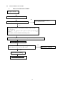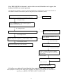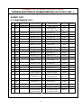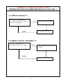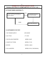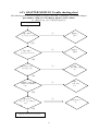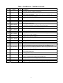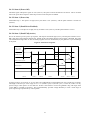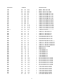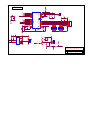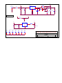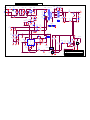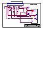
1
SERVICE MANUAL SPECTRUM Series LCD Monitor LM-700/LM-700A P/N : 41A50-144 THESE DOCUMENTS ARE FOR REPAIR SERVICE INFORMATION ONLY. EVERY REASONABLE EFFORT HAS BEEN MADE TO ENSURE THE ACCURACY OF THIS MANUAL; WE CANNOT GUARANTEE THE ACCURACY OF THIS INFORMATION AFTER THE DATE OF PUBLICATION AND DISCLAIMS RE LIABILITY FOR CHANGES, ERRORS OR OMISSIONS, MANUFACTURE DATA : JULY. 2001 REVISE 7 SEP 2001 1 TABLE OF CONTENTS PAGE 1. SPECIFICATIONS .................................................................................................... 1-1 GENERAL SPECIFICATIONS ...................................................….............. 1-2 LCD MONITOR DESCRIPTION .................................................................. 1-3 INTERFACE CONNECTOR .................................................................……. 3 3 4 4 2. PRECAUTION AND NOTICES ................................................................................ 2-1 ASSEMBLY PRECAUTION ......................................................................... 2-2 OPERATIONG PRECAUTION ..................................................................... 2-3 STORAGE PRECAUTION …........................................................................ 2-4 HIGH VOLTAGE WARNING ....................................................................... 5 5 5 5 5 3. OPERATING INSTRUCTIONS ................................................................................ 6 4. ADJUSTMENT .......................................................................................................... 4-1 ADJUSTMENT CONDITIONS AND PRECAUTIONS ............................... 4-2 ADJUSTMENTS METHOD .& DESCRIPTION......................... 4-3 FRONT PANEL CONTROL KNOBS ............................................................ 7 7 7-8 9 5. CIRCUIT & SOFTWARE DESCRIPTION ................ 5-1 THE DIFFERENT BETWEEN EACH PANEL ……………………………. 5-2 SPECIAL FUNCTION WITH PRESS KEY ……………………………….. 5-3 THE OPTIONAL ON MAINBOARD USING SHUTTLE & 4 KEY.. 5-4 THE OPTIONAL ON MAINBOARD OR OTHER ACCESSORY USING DIFFERENT PANEL 5-5 SIMPLE INTRODUCTION ABOUT LM500 CHIPSET …………………... 5-6 SOFTWARE FLOW-CHART 10 10 10 10 10 A). INTERFACE-BOARD TROUBLE SHOOTING CHART .................... B). INVERTER - MODULE TROUBLE SHOOTING CHART .................... I. CHI-MEI-inverter spec & trouble shooting chart C). ADAPTER TROUBLE SHOOTING CHART & BOM....... D). AUDIO TROUBLE SHOOTING CHART & BOM E). Main-chip GMZAN1 specifications 14 23 23 50 7. MECHANICAL OF CABINET FRONT DIS-ASSEMBLY...................................... 64 8. PARTS LISTING .........................................................................................………... 65 9. POWER SYSTEM AND CONSUMPTION CURRENT............................................ 73 10. PCB LAYOUT .....................................................................………………………... 74 11. MAINBOARD SCHEMATIC DIAGRAM …............................................... 12. ADAPTER SCHEMATIC DIAGRAM 13.AUDIO SCHEMATIC DIAGRAM 75 6. 2 11 12 54 1. SPECIFICATIONS FOR LCD MONITOR 1-1 1. General specifications LCD-PANEL : Active display area Pixel pitch Pixel format 17 inches diagonal 0.264 mm x 0.264 mm 1280 x 1024 RGB vertical stripe arrangement 2. Display Color : 8-bit, 16.7 million colors 3. ●External Controls : Power On/Off, Auto key, Left key, Right key ( for 4-key ) ●OSD menu Controls Contrast, Brightness, Focus, Clock,H-position, V-position, Language, Recall-7800, Recall-6500, Reset, Exit-osd, Red, Green, Blue, Selected Dos-resolution 4. Input Video Signal : Analog-signal 0.7Vpp Video signal termination impedance 75 OHM 5. Scanning Frequencies : Horizontal: 29 KHz - 80 KHz Vertical: 55 Hz – 75 Hz Pixel clock: 135 MHz 6. Factory Preset Timing : 18 User Timings : 19 Input signal tolerance : H tolerance ±1 K, V tolerance ±1 Hz 7. Power Source : Switching Mode Power Supply AC 100 – 240 V, 50/60 Hz Universal Type 8. Operating Temperature : 0℃ - 50℃ Ambient Non-operating Temperature : -20℃ - 60℃ 9. Humidity : Operating : 20% to 80% RH (non-condensing) Non Operating : 5% to 95%RH (38.7℃ maximum wet bulb temperature) 10. Weight : 5.5 kg 11. External Connection : 15Pin D-type Connector, AC power-Cord 12. View Angle : x-axis right/left = 60, y-axis up/down = 40 ,60 13. Outside dimension : Width x Height x Thickness = 422x 449 x 215 mm 14. Plug and Play : VESA DDC1/DDC2B 15. Power saving : VESA DPMS 3 1-2 LCD MONITOR DESCRIPTION The LCD MONITOR will contain an main board, an Inverter module, keyboard and External Adapter which house the flat panel control logic, brightness control logic, DDC and DC-DC conversion The Inverter module will drive the backlight of panel . The Adapter will provides the 12V DC-power 5 Amp to Main-board and Inverter module . Monitor Block Diagram Flat Panel and CCFL backlight CCFT Drive. Inverter RS232 Connector For white balance adjustment in factory mode Main Board or Interface Board Keyboard AC-IN 100v-240v 1-3 ADAPTER HOST Computer Interface Connectors (A) AC-Power Cable (B) Video Signal Connectors and Cable (C) External Adapter 4 Video signal, DDC 2. PRECAUTIONS AND NOTICES 2-1 ASSEMBLY PRECAUTION (1) Please do not press or scratch LCD panel surface with anything hard. And do not soil LCD panel surface by touching with bare hands (Polarizer film, surface of LCD panel is easy to be flawed) In the LCD panel, the gap between two glass plates is kept perfectly even to maintain display characteristic and reliability. If this panel is subject to hard pressing, the following occurs : (a) Uniform color (b) Orientation of liquid crystal becomes disorder (2) Please wipe out LCD panel surface with absorbent cotton or soft cloth in case of it being soiled. (3) Please wipe out drops of adhesive like saliva and water in LCD panel surface immediately. They might damage to cause panel surface variation and color change. (4) Do not apply any strong mechanical shock to the LCD panel. 2-2 OPERATING PRECAUTIONS (1) Please be sure to unplug the power cord before remove the back-cover. (be sure the power is turn-off) (2) Please do not change variable resistance settings in MAIN-BOARD, they are adjusted to the most suitable value. If they are changed, it might happen LUMINANCE does not satisfy the white balance spec. (3) Please consider that LCD backlight takes longer time to become stable of radiation characteristic in low temperature than in room temperature. (4) Please pay attention to displaying the same pattern for very long-time. Image might stick on LCD. 2-3 STORAGE PRECAUTIONS (1) When you store LCD for a long time, it is recommended to keep the temperature between 0℃-40℃ without the exposure of sunlight and to keep the humidity less than 90% RH. (2) Please do not leave the LCD in the environment of high humidity and high temperature such as 60℃ 90%RH. (3) Please do not leave the LCD in the environment of low temperature; below -15℃. 2-4 HIGH VOLTAGE WARNING The high voltage was only generated by INVERTER module, if carelessly contacted the transformer on this module, can cause a serious shock. (the lamp voltage after stable around 600V, with lamp current around 8mA, and the lamp starting voltage was around 1500V, at Ta=25℃) 5 3. OPERATING INSTRUCTIONS This procedure gives you instructions for installing and using the LM700 LCD monitor display. 1. Position the display on the desired operation and plug–in the power cord into External Adapter AC outlet. Three-wire power cord must be shielded and is provided as a safety precaution as it connects the chassis and cabinet to the electrical conduct ground. If the AC outlet in your location does not have provisions for the grounded type plug, the installer should attach the proper adapter to ensure a safe ground potential. 2. Connect the 15-pin color display shielded signal cable to your signal system device and lock both screws on the connector to ensure firm grounding. The connector information is as follow: 1 5 6 10 11 15 15 - Pin Color Display Signal Cable PIN NO. 1. 2. 3. 4. 5. 6. 7. 8. 3. 4. 5. 6. DESCRIPTION PIN NO. RED GREEN BLUE GND GND GND-R GND-G GND-B 9. 10. 11. 12. 13. 14. 15. DESCRIPTION 5V power from VGA-card GND SYNC. GND SDA HORIZ. SYNC VERT. SYNC SCL Apply power to the display by turning the power switch to the "ON" position and allow about thirty seconds for Panel warm-up. The Power-On indicator lights when the display is on. With proper signals feed to the display, a pattern or data should appear on the screen, adjust the brightness and contrast to the most pleasing display, or press auto-key to get the best picture-quality. This monitor has power saving function following the VESA DPMS. Be sure to connect the signal cable to the PC. If your LM700 LCD monitor requires service, it must be returned with the power cord & Adapter. 6 4. ADJUSTMENT 4-1 ADJUSTMENT CONDITIONS AND PRECAUTIONS Adjustments should be undertaken only on following function : contrast, brightness focus, clock, h-position, v-position, red, green, blue since 6500 color & 7800 color. 4-2 ADJUSTMENT METHOD Press MENU button to activate OSD Menu or make a confirmation on desired function, Press Left/Right button to select the function or done the adjustment. 1. White-Balance, Luminance adjustment Approximately 30 minutes should be allowed for warm up before proceeding white balance adjustment. Before started adjust white balance ,please setting the Chroma-7120 MEM. Channel 5 to 7800 color and MEM. channel 6 to 6500 color, ( our 7800 parameter is x = 296 ±10, y = 311 ±10, Y = 160 ±5cd/m2 and 6500 parameter is x = 313 ±10, y = 329 ±10, Y = 160 ±5 cd/m2) How to setting MEM.channel you can reference to chroma 7120 user guide or simple use “ SC” key and “ NEXT” key to modify xyY value and use “ID” key to modify the TEXT description Following is the procedure to do white-balance adjust Press MENU button during 2 seconds along with plug in the DC-power cord will activate the factory mode, and the OSD screen will located at left top of panel. I. Bias (Low luminance) adjustment : 1. 2. 3. Press “ AUTO” button , and wait for message “ Pass” ,check the Blacklevel value on OSD should be large than 30, if less than 30 that means the offset calculation FAIL, please manual adjust the blacklevel to value 43 set the contrast and brightness on OSD window to maximal value , RGB to “50” adjust the VR501 on INTERFACE board until chroma 7120 measurement reach the value Y=240 cd/m2 ±5 cd/m2 II. Gain adjustment : a. adjust 7800 color-temperature 4. 5. 6. 7. 8. Set the Contrast of OSD function to 40, Brightness to 48 Switch the chroma-7120 to RGB-mode (with press “MODE” button ) switch the MEM.channel to Channel 05 ( with up or down arrow on chroma 7120 ) The lcd-indicator on chroma 7120 will show x = 296 ±10, y = 311 ±10, Y = 160 ±5 cd/m2 Adjust the RED on OSD window until chroma 7120 indicator reached the value R=100 7 9. 10. 11. 12. 13. 14. adjust the GREEN on OSD, until chroma 7120 indicator reached G=100 adjust the BLUE on OSD, until chroma 7120 indicator reached B=100 repeat above procedure ( item 8,9,10) until chroma 7120 RGB value meet the tolence =100±2 switch the chroma-7120 to xyY mode With press “MODE” button Adjust the Contrast on OSD window until the Y measurement on chroma 7120 reached the value Y= 180 cd/m2 Press 78 on OSD window to save the adjustment result b. adjust 6500 color-temperature 1 Set the Contrast of OSD function to 40, Brightness to 48 2 Switch the chroma-7120 to RGB-mode (with press “MODE” button ) 3 switch the MEM.channel to Channel 06 ( with up or down arrow on chroma 7120 ) 4 The lcd-indicator on chroma 7120 will show x = 313 ±10, y = 329 ±10, Y = 160 ±5 cd/m2 5 Adjust the RED on OSD window until chroma 7120 indicator reached the value R=100 6 adjust the GREEN on OSD, until chroma 7120 indicator reached G=100 7 adjust the BLUE on OSD, until chroma 7120 indicator reached B=100 8 repeat above procedure ( item 5,6,7) until chroma 7120 RGB value meet the tolence =100 ±2 9 switch the chroma-7120 to xyY mode With press “MODE” button 10 Adjust the Contrast on OSD window until the Y measurement on chroma 7120 reached the value Y= 180 cd/m2 11 Press 65 on OSD window to save the adjustment result Turn the POWER-button off to on to quit from factory mode ( in USER-mode, the OSD window location was placed at middle of screen) 8 4-3 2. Clock adjustment Set the Chroma at pattern 63 (cross-talk pattern) or WIN98/95 shut-down mode (dot-pattern). Adjust until the vertical-Stripe-shadow as wide as possible or no visible. This function is adjust the PLL divider of ADC to generate an accurate pixel clock Example : Hsyn = 31.5KHz Pixel freq. = 25.175MHz (from VESA spec) The Divider number is (N) = (Pixel freq. x 1000)/Hsyn From this formula, we get the Divider number, if we fill this number in ADC register (divider register), the PLL of ADC will generate a clock which have same period with above Pixel freq.(25.175MHz) the accuracy of this clock will effect the size of screen.(this clock was called PIXEL-CLOCK) 3. Focus adjustment Set the Chroma at pattern 63 (cross talk pattern) or WIN98/95 shut down mode (dot-pattern). Adjust the horizontal interference as less as possible This function is adjust the phase shift of PIXEL-CLOCK to acquire the right pixel data . If the relationship of pixel data and pixel clock not so match, we will see the horizontal interference on screen ,we only find this phenomena in crosstalk pattern or dot pattern , other pattern the affect is very light 4. H/V-Position adjustment Set the Chroma to pattern 1 (crosshatch pattern) or WIN98/95 full-white pattern confirm above item 2 & 3 functions (clock & focus) was done well, if that 2 functions failed, the H/V position will be failed too. Adjust the four edge until all four-edges are visible at the edge of screen. 5. MULTI-LANGUAGE function There have 5 language for selection, press “MENU” to selected and confirm , press “ LEFT” or “ RIGHT” to change the kind of language ( English , Deutch , Francais, Espanol, Italian) 6. Reset function Clear each old status of auto-configuration and re-do auto-configuration ( for all mode) This function also recall 7800 color-temperature , if the monitor status was in “ Factory-mode” this reset function will clear Power-on counter ( backlight counter) too. 7. OSD-LOCK function Press Left & Right key during switching on the monitor, the access to the OSD is locked, user only has access to “ Contrast, Brightness, Auto-key “. If the operator pressed the Left & Right during switching on the monitor again , the OSD is unlocked. 8. View Power-on counter and reset the Power-on counter( if not necessary , no suggest to entry factory mode) The Power-on counter was used to record how long the backlight of panel already working, the backlight life time was guarantee minimal 25000 hours, the maintainer can check the record only in factory mode. Press MENU button for 2 seconds along with plug-in DC power cord will be in factory mode, and the OSD screen will located at left top of panel but take cautions don’t press icon “78” & “65”, if you press 78/65 , your white-balance data will overlap with the new-one, and you must perform the whitebalance process again. The result of counter was place at top of OSD, the maximal of record memory was 65000 hours, if exceed 65000 hours the counter will keep in 65000 hours until press “ RESET” at osd-menu in factory mode. The “ RESET” function in factory mode will execute following function: 1. clear the Power-on counter to zero hours 2. clear old auto-configuration status for all mode , so the monitor will automatically re-do auto-config when change to next mode or power on-off FRONT PANEL CONTROL KNOBS Power button : Press to switch on or switch off the monitor. Auto button : to perform the automatic adjustment from CLOCK, FOCUS, H/V POSITION, but no affect the color-temperature Left/Right button : select function or do an adjustment. MENU button : to activate the OSD window or to confirm the desired function 9 5. 5-1 CIRCUIT-DESCRIPTION SPECIAL FUNCTION with PRESS-KEY A). press Menu button during 2 seconds along with plug-in the DC Power cord: That operation will set the monitor into “Factory- mode”, in Factory mode we can do the White balance adjustment with RS232 , and view the Backlight counter (this counter is use to record the panel activate hours ,for convenient the maintainer to check the panel backlight life time) In Factory mode, OSD-screen will locate in left top of screen. Press POWER-button off to on once will quit from factory mode and back to user-mode. B). Press both Left & Right button along with Power button off to on once will activate the OSD-LOCK function, repeat this procedure will disable OSD-LOCK In OSD-LOCK function, all OSD function will be lock , except Contrast and Brighness OSD-INDEX EXPLANATION 1. CABLE NOT CONNECTED: Signal-cable not connected. 2. INPUT NOT SUPPORT: a. INPUT frequency out of range: H > 81kHz, v > 75Hz or H < 28kHz, v < 55Hz b. INPUT frequency out of VESA-spec. (out of tolerance too far) 3. UNSUPPORT mode, try different Video-card Setting: Input frequency out of tolerance, but still can catch-up by our system (if this message show, that means, this is new-user mode, AUTO-CONFIG will disable) 5-2 THE Different on MAINBOARD or other ACCESSORY when using different PANEL type 1). The MCU software should be change example : for CHI-MEI panel , the MCU part-number is 56A-1125-61-M for Hyundai panel , the MCU part-number is 56A-1125-61-Y and the other ACCESSORY when use different panel type should be change as following: 1). The INVERTER module for CHI-MEI panel part-number is 79AL17-1-S for Hyundai panel the INVERTER part number is 79A-L17-3-S 2). The cable to Panel side for CHI-MEI panel part number is 95A8018-30-1 for HYUNDAI panel is 95A8018-30-3 3). The Dsub cable for CHI-MEI is 89A-174D-5BF-GLF, for Hyundai is 89A-174-L17-3. 4). The Mechanical accessory is change or adding as follow; MAIN-FRAME Panel CHI-MEI PANEL M170E1 15A5684-1 750ALCD170-3 10 Hyundai PANELHT17E11-100 15A5705-1 750ALCD170-4 5-3 SIMPLE-INTRODUCTION about LM700 chipset 1. GMZAN1 ( all-in-one chip solution for ADC, OSD, scalar and interpolation) : USE for computer graphics images to convert analog RGB data to digital data with interpolation process, zooming, generated the OSD font , perform overlay function and generate drive-timing for LCD-PANEL. 2. M6759 (ALI- MCU, type 8052 series with 64k Rom-size and 512 byte ram) : Use for calculate frequency, pixel-dot , detect change mode, rs232-communication, power-consumption control, OSD-index warning , …etc. 3. 24LC21 (MicroChip IC) : EePROM type, 1K ROM-SIZE, for saving DDC-CONTENT. 4. 24C04 (ATMEL IC) : EePROM type, 4K ROM-SIZE, for saving AUTO-config data, White-balance data, and Power-key status and Backlight-counter data. 5. LM2569S( NS brand switching regulator 12V to 5V with 3A load current) . 6. AIC 1084-33CM (AIC brand linear regulator 5V to 3.3V) 7. LVDS ( use NOVATEK NT7181F) Convert the TTL signal to LVDS signal The advantage of LVDS signal is : the wire can be lengthen and eliminate wire number , low EMI . LVDS signal is high frequency but low voltage, only 0.35 VPP ,the frequency is seven times higher than TTL MODULE-TPYE COMPONENT : 1. ADAPTER : CONVERSION-module to convert AC 110V-240V to 12VDC, with 5.0 AMP 2. INVERTER : CONVERSION-module to convert DC 12V to High-Voltage around 1600V, with frequency 30K-80Khz, 7mA-9Ma 11 Main-board Block diagram Input analog RGB & H,V,& ddc signal & Rs232 communication GMZAN1 (U200) Data Digital RGB DDC-chip LVDS chip (U601, U602) PANEL Panel Control Signal: Dhs, Dvs, Dclk Oscillator 50 mhz Panel Power 5V Communication signal: Hclk,Hfs,Hdata0 Panel-Power Control (U202) MCU ( U302 ) Crystal 20 mhz DC 12V 5Amp Keyboard module INVERTER module EXTERNALADAPTER 12 5-4 SOFTWARE FLOW CHART I. Power-On Subrotine CHART POWER-ON START Initial MCU I/O, Interrupt vector & Ram Yes Initial 1.POC (backlight counter) 2. Clr all mode value Check Eeprom is empty ? No Check White-balance data(6500 & 7800) same with the OK backup data ? Check POC( backlight counter) data same with the backup data ? IF not same, overwrite the data with backup value. Check Previous power-switch status from Eeprom, & other system status Initial GMZAN1 Yes Check if in Factory mode?(when power-on,press the MENU Button will be in FACTORY mode) SET factory mode flag No Clear factory mode flag MAIN-SUBROTINE LOOP 13 II. MAIN SUBROTINE LOOP Main loop start Process Power-saving status ( according to below flow-chart result) ) Check GMZAN IFM status .is change or not. And check Signal cable status ( cable not connected or not ) ** IFM is the register which measured the HSYN & Vsyn status No Yes, IFM have change Yes Is current system status in Power-saving ? No Wake-up GMZAN1 (because GMZAN1 was in partial sleeping state) Yes Check the IFM result is in the standard Mode table ? No Set mode index & parameter Set change mode flag Yes Check the IFM result is in the user mode table ? No Out of range ( input not support) be confirm No confirm the frequency ( Hsyn or Vsyn) from IFM already been changed ? ( check the change mode flag) Yes , freq had been change Process ( turn off OSD , setting GMZAN1according to above parameter,set LED status, set backlight status) No Check Auto-config mode flag already been set? Do Auto-config automatically Yes Read Key status and Process on OSD-screen Yes Check Factory mode flag= 1 No Monitoring the time-out of osd status ( if no key input persist for 10 sec , the osd time-out counter will trigger ) 14 if the RS232 buffer is full, process the command( while adjust white-balance in factory mode) 6. A). Interface-Board Trouble-Shooting chart *Use the PC Win 98 white pattern, with some icon on it, and Change the Resolution to 640x480 60 Hz / 31 KHz **NOTICE : The free-running freq. of our system is 48 KHz / 60 Hz, so we recommend to use another resolution to do trouble shooting, this trouble shooting is proceed with 640x480 @60Hz 31Khz I. NO SCREEN APPEAR DC-Power Part Measured Input DC-voltage ( J1)= 12 V? Measured U305 AIC 1084 pin 2 = 3.3V? Measured U904 LT1117 pin 2= 3.3V? Check Correspondent component. Is there any shortage or cold solder? Yes, all DC level exist Yes, there have OSD show Disconnected the Signal cable( Loose the Signal cable ),Is the screen show “Cable Not Connected” ? No, nothing is show Led Green Connected the Signal cable again, Check LED status. Led Orange Check Power switch is in Power-on status , and check if Power switch had been stuck ? Connected the Signal cable again, Check LED status. Replace MCU Led orange OK, Keyboard no stuck Led Green NG Check the Wire-Harness from CN601,CN602 was tight enough?, check the Wire connection to panel side too Measured RGB (r200,r201,r202) H,V Input at U401 pin 9 ,4 ,was there have signal ? Check Correspondent component short/open ( Protection Diode ) and Signal cable bad ? OK,input Normal OK,Wire tight enough Check Panel-Power Circuit Block Measured Oscillator Block Oscillator U201 & Crystal X300 OK,clock normal OK,Panel Power OK Check U200 Data-output Block OK, U200 data OK Check communication pin between U200 & MCU pin 2,6,7. , is it have transition? OK, Mcu have transition NG, no transition Replace Inverter and Check Inverter control relative circuit Re-do White balance adjust OK Replace U200 (Gmzan1) Replace U302 (MCU) & check Reset pin 10 must be change from High to low when first AC power plugin OK Note: 1. if Replace “MAIN-BOARD” , Please re-do “DDC-content” programmed & “WHITE-Balance”. 2. if Replace “ INVERTER” only, Please re-do “ WHITE-Balance” 15 PANEL-POWER CIRCUIT Check the PPWR panel power relative circuit, R223, Q200,U202(pin 5,6,7,8) In normal operation, when LED =green, R223 should =0 v, If PPWR no-response when the power switch Turn on and turn off, replace the U200-GMZAN1 NG check R225 should have response from 12V to 0V When we switch the power switch from on to off OK,R225 have response Yes NG, no Voltage Check U202 pin 1,2,3,4= 5V Measured the U202 pin 5,6,7,8= 5 V? Replace U202 ( Nmos, SI9933) OK NG OK Check U304 relative circuit.(R905,T300..) INVERTER Control Relative Circuit Measured the inveter connector CN303 Pin 1=12V, pin 3 on/off control=5V (on) NG NG, still no screen Check the Bklt-On relative circuit, R315, Q304, R311, In normal operation, when LED =green, R315 Bklt-On should =0 v, If Bklt-On no-response when the power switch turn on-off, Replace the MCU NG Replace INVERTER to new-one, and Check the screen is normal ?? Replace INVERTER-module & Re-do white balance OK OSCILLATOR BLOCK NG,no transition Measured U201 Oscillator output R215= 50mhZ ? Replace Oscillator U201 NG,no transition OK, has transition Replace Crystal X300 Measured X300 Crystal output R340= 20mhZ ? OK U200-DATA OUTPUT NG , no transition Measured PCLK(L207) PVS,PHS (pin 73,74 from U200 ) Is there have any transition? Pclk around 47MHz to 57MHZ , PVS=60.09Hz , PHS around 67 KHz ??(refer to input signal=640x480@60 Hz 31k, and LED is green) Replace GMZAN1 (U200) or replace MAINBOARD. If MainBoard being replace , please do the DDC – content reprogrammed OK 16 II (a) THE SCREEN is Abnormal , stuck at white screen, OSD window can’t appear, but keyboard & LED was normal operation. At general, this symtom is cause by missing panel data or panel power, so we must check our wire-harness which connected to panel or the panel power controller (U202) NG Check if the Wire harness from CN601 & CN602 loose? Check the wire on both Panel-side and Mainboard side. Tighten it. Yes, tight enough Check the Panel-Power circuit as above (page 15) U202 pin 5,6,7,8 ,must be 5V Yes, Voltage normal NG Check the LVDS-Power L603,L604,L601,L602,L900= 3.3V ? Check U904,which convert the 5V to 3.3V Yes, Voltage normal Check the both U601 & U602 LVDS-Input pin 31= 45mhz – 65mhz, and pin 27 = Vsyn freq, pin 28 = 45khz- 65 khz Check U200 DATA-OUPUT block as above ( page 15) NG,no data output Yes, Frequency normal Check OSCILLATOR Block as above ( page 15) Replace both LVDS chip ( U601 & U602) OK,all clock is normal Replace U302 MCU and check it RESET pin 10 ,must be turn high to low when first AC power-on OK, reset is normal Check U200 DATA-OUTPUT block again NG,still no data out Replace U200 GMZAN1 II. (b)The screen had the Vertical Straight Line, might be stuck in Red, Green, Blue That symptom is cause by bad Panel issue ( might be the Source IC from Panel is cold solder or open loop ) so REPLACE THE PANEL TO NEW ONE. 17 KEYBOARD BLOCK check Check U302 MCU pin 43,42,41,40,39 at High state(5V)? without press any key NG Mechanical was stuck, Check ! OK NG Press power key and check U302 pin 43 = low (0V) ? Replace Tact-switch SW105 at keyboard if still no work replace U302 MCU at main-board and check MCU relative reset circuit, and crystal OK Check U302 pin 38 (LED green) will have transition from hi to low or low to hi when we press the power key?? OK If still no Led green indicator, check Q102, R106 & LED at keyboard !! cold solder or bad NG, MCU no response Check U302 pin 20= 20MHz ? and pin 44 (VDD)=5V ? and pin 10 (reset)=0V ? at normal condition OK Without press key and change mode, Check U302 pin 16,17(sda,scl)= hi 5V ? or keep transition ? NG If one of this item was NG, check the relative circuit Keep transition, that means eeprom no response NG Check U300 eeprom 24LC04 relative circuit, check U300 pin 7 = low? NG OK, no keep transition Check JP202 is connect ? Replace U302 MCU OK Check U300 pin 8 (vdd)= 5V, and check R300,R301 cold solder Replace eeprom 18 POWER-BLOCK check **Note : the Waveform of U304 pin 2 can determined the power situation 1. 2. 3. stable rectangle waveform with equal duty, freq around 150K-158KHz that means all power of this interface board is in normal operation ,and all status of 5V & 3.3V is working well unstable or uneven rectangle waveform without same duty, that means ABNORMAL operation was happened, check 3.3V or 5V ,if short-circuit or bad component rectangle waveform with large spike & harmonic pulse on front side , means all 3.3v is no load, U200 Gmzan1 was shut-down, and only U302 MCU still working , that means the monitor is in power saving status , all power system is working well . NG Measure input power at U304 LM2596 pin 1= 12V ? OK Check ADAPTER and connector if loose? NG Check U304 pin 2 is a stable rectangle wave? Around 150k-158kHz stable rectangle wave with equal duty without any spike or harmonic pulse? Check U304 pin 2 is a unstable rectangle wave ? OK, unstable wave Check all 3.3V & 5V power, there is short circuit or bad component was happened OK NG, with harmonic pulse The interface board power is good The interface board is in powersaving state, press power key to wake up & check your signal input 19 III.ALL SCREEN HAS INTERFERENCES OR NOISE, CAN’T BE FIXED BY AUTO KEY ** NOTE: There is so many kind of interferences, 1). One is cause by some VGA-CARD that not meet VESA spec or power grounding too bad that influence our circuit 2).other is cause by external interferences, move the monitor far from electronic equipment.( rarely happened) Use DOT-pattern, or win98/99 shut-down mode pattern, press “AUTO” key, was the interferences disappear ?? OK END NG, interferences still exist Adjust “FOCUS” step by step, until the horizontal interferences disappear OK END NG Does your signal-cable have an additional cable for extension ?? Yes, has extension Put away the additional cable May be the additional cable grounding is not quite well NO additional extension cable NO, all mode Does your noise only exist in one mode only? (ex: only at 1280x1024 @ 75 Hz, other is normal) Yes, only happened on one mode That was cause by you VGA-CARD setting, your VGA card timing backporch/frontporch exceed vesa timing too far, for some new AGP-VGA-CARD such situation always happened So in your control-panel icon ,select monitor ,setting , advance ,screen-adjust,at Size icon, increase step by step slowly, press “”AUTO” key every step you increase the SIZE . repeat the procedure( increase/decrease SIZE one-step and press AUTO) until the interferences disappear, press “APPLY” to save in your VGA 20 Change the Signal-cable to new-one or Try other brand VGA-CARD (make sure just only that brand VGACARD has this problem ,contact RDtaipei) There is an interferences in DOS MODE NOTE :the criteria of doing AUTO-CONFIGURATION : must be a full-size screen, if the screen not full , the autoconfiguration will fail. So in dos mode ,just set your “CLOCK” in OSD-MENU to zero or use some EDITOR software which can full fill the whole screen (ex: PE2, HE) and then press “AUTO” Or you can use “DOS1.EXE” which attached in your Driver disk to optimize DOS mode performance V. THE PANEL LUMINANCE WAS DOWN Use white pattern and resolution 1280x1024 @ 60Hz , CHROMA 7120 measured the center of panel If Y can reach >190 cd/m2 that means The lamp still working well, so we just re-do the white-balance process As following procedure Set Contrast, brightness =maximal, RGB= 50 Quit from OSD-screen, measured Y(luminance) With chroma 7120, check Y= 240±10 CD/M2 ? OK NG Adjust VR201 until maximal, measured Y = 240±10 cd/m2 ? OK NG If the Y less than 160 cd/m2 (after the VR201= MAX, contrast, brightness = max) then change the LAMP of panel Use white-pattern, press MENU button along with AC power-plug in ( you will in factory mode) The OSD-menu will be at left-top of screen, press AUTO button to automatically adjust blacklevel value, you will see the sign PASS ,if FAIL , manual adjust the blacklevel until value 43 ! Set contrast, brightness to max, and turn the VR201 to max , wait for 20 minutes until the luminance Y stable The Y should be larger than 200 cd/m2 (for panel which already use for a year, the Y luminance might be a little down, around 180 cd/m2, there is acceptable too) Follow this manual page 7 item 4-2 method to more detail procedure for do a white-balance adjust 21 6 B). Inverter –MODULE Spec &Trouble Shooting Chart In LM700 model , we use CHI-MEI panel, and the INVERTER PROVIDER is SAMPOCORPORATION I.) TROUBLE SHOOTING OF CHI-MEI INVERTER (part no : 79AL17-1-S) TYPE: L0037 FOR CHI-MEI 17”PANEL SAMPO CORPORATION TROUBLE SHOOTING OF CHI-MEI INVERTER ( DIVTL0037-D42- -) 1.SAMPO PART NO .: L0037 ,AOC PART NO.: 79AL17-1-S 2.SCOPE : this is to specify the requirements of the subject parts used in CHI-MEI (M170E1) 17 inch (4 C.C.F.L.) LCD monitor. 3.CONNECTOR PIN ASSIGMENT: 4-1. CON1: INPUT MODEL NO.: S5B-PH-SM3-TB PIN SYMBOL DESCRIPTION 1 Vin Input voltage: 12V 2 Vin Input voltage: 12V 3 ON/OFF ON: 3V OFF:0V 4 Dimming Dimming range (0V~+5.0V) 5 GND GND 4-2. CON2,CON3 : OUTPUT MODEL NO. PIN : SM04(4.0)B-BHS-1-TB SYMBOL DESCRIPTION 1 HV OUTPUT Input H.V to lamps 2 HV OUTPUT Input H.V to lamps 3 N.C. 4 RETURN N.C. Return to control 22 SAMPO CORPORATION TROUBLE SHOOTING OF CHI-MEI INVERTER ( DIVTL0037-D42- -) 5.FUNCTION SPECIFICATIONS: The data test with the set of SAMPO, and the test circuit is as below. SYMBOL MIN. TYP. MAX. UNIT Input voltage Vin 10.8 12 13.2 V Input current Iin -- 2200 2500 mA output current Iout ITEM adj:0v( min.) REMARK FOR 1 CCFL (min) 2.1 2.6 3.1 mA LOAD:120KΩ FOR 1 CCFL Output current Iout adj.:5 v(max.) (max) 5.5 6.0 6.5 mA Frequency F 40 50 60 KHZ H.V open Vopen 1400 1500 1600 Vrms NO LOAD H.V Load Vload 630 730 830 Vrms RL=120KΩ LOAD:120KΩ 6. FUNCTION LOAD CIRCUIT: 120KΩ 4 1 2 2 1 10Ω 4 CON1 1 2 3 4 5 TV 120KΩ 10Ω TV PIN SYMBOL 1 Vin 12V 2 Vin 12V 3 ON/OFF 4 Dimming 5 GND 23 120KΩ 10Ω TV 120KΩ 10Ω TV SAMPO CORPORATION TROUBLE SHOOTING OF CHI-MEI INVERTER ( DIVTL0037-D42- -) D D S S D D G D S S D G D D S S 7.CIRCUIT DIAGRAM: 24 SAMPO CORPORATION TROUBLE SHOOTING OF CHI-MEI INVERTER ( DIVTL0037-D42- -) 8.PART LIST 8-1 COMPONENTS LIST: NO. REF. PART NAME PART NUMBER QTY DESCRIPTION SUPPLIER REMARK 1. CON1 CONNECTOR VCNCP0015-EJSTA 1 S5B-PH-SM3-TB JST 2. CON2,3 〃 VCNCP0014-PJSTA 2 SM04(4.0)B.BHS-1-TB JST GL SM02(4.0)-WH2 GEAN-LEA VCNCP0014-ZGLEA 3. R1,2 RESISTOR VRMHNVA--103J-A 2 SMD 0603 10KΩ 5% YAGEO 4. R3,4 〃 VRMHNVA--683J-A 2 SMD 0603 68KΩ 5% YAGEO 5. R5,6 〃 VRMHNVA--912J-A 2 SMD 0603 9.1KΩ 5% YAGEO 6. R7,8 〃 VRMHNVA--274J-A 2 SMD 0603 270KΩ 5% YAGEO 7. R9,10 〃 VRMHNVA--R00J-A 2 SMD 0603 0Ω 5% YAGEO 8. R11,12, 31,32 〃 VRMCNV8--102F-A 4 SMD 0805 1KΩ 1% YAGEO 9. R13,14 〃 VRMHNVA--752J-A 2 SMD 0603 7.5KΩ 5% YAGEO 10. R15,16 〃 VRMHNVA--433J-A 2 SMD 0603 43KΩ 5% YAGEO 11. R17,18 〃 VRMHNVA--271J-A 2 SMD 0603 270Ω 5% YAGEO 12. R27 〃 VRMHNVA--472J-A 1 SMD 0603 4.7KΩ 5% YAGEO 13. R28,29, 〃 VRMHNVA--392J-A 2 SMD 0603 3.9KΩ 5% YAGEO 14. R23,24, 25,26 〃 VRMBNV4--102F-A 4 SMD 1206 1KΩ 1% YAGEO 15. R19,20 〃 VRMCNV8--183F-A 2 SMD 0805 18KΩ 1% YAGEO 16. R21,22 〃 VRMCNV8--133F-A 2 SMD 0805 13KΩ 1% YAGEO 17. R33 〃 VRMHNVA--363J-A 1 SMD 0603 36KΩ 5% YAGEO 18. Q1 TRANSIST0R VSTDTC144WKA--A 1 SMD DTC144WKA ROHM 19. Q2 〃 VSTDTA144WKA--A 1 SMD DTA144WKA ROHM 20. Q3,5 〃 VSTSST3904----A VSTMMBT3904-A 2 SMD SST3904-T116 ROHM 〃 VSTCEM9435A-----A 〃 21. Q4,6 22. Q7,8,9, 10 SMD MMBT3904 MOTOROLA 2 SMD CEM9435A CET VST2SD2150----A 4 SMD 2SD2150 ROHM 23. C1,2 CAPACITOR VCLFCN1EY224Z-A 2 SMD 0805 0.22 µF/25V TDK 24. C3,4,,9 〃 VCLRCN1EB104K-A 3 SMD 0805 0.1 µF/25V TDK 25. C5 VCEATU1EC336M-- 1 DIP UGX 33 µF/25V SANYO VCEATU1VC476M-- 25 DIP UGX 47 µF/35V SAMPO CORPORATION TROUBLE SHOOTING OF CHI-MEI INVERTER ( DIVTL0037-D42- -) 8-2 COMPONENTS LIST: NO. REF. PART NAME PART NUMBER QTY DESCRIPTION 26. C6 〃 VCLRCN1HB102K-A 1 SMD 0805 1000PF/50V TDK 27. C10,11 〃 VCLRCN1EB333K-A 2 SMD 0805 0.033 µF/25V TDK 28. C12,13 〃 VCMEBF2AB184J-P 2 DIP 0.18µF/100V ARCO DIP 0.18µF/100V THOMSON 4 DIP 22PF/3KV 10% TDK VCMECF2AC184J-P 29 C14,15,19, CAPACITOR VCDSEU3SL220K-20 SUPPLIER REMARK 30. C7,16,17 〃 VCLFCN1EY105Z-A 3 SMD 0805 1 µF/25V TDK 31. C18 〃 VCLFCN1CY225Z-A 1 SMD 0805 2.2 µF/16V TDK 32. C21 〃 VCLFBN1CY475Z-A 1 SMD 0805 4.7 µF/16V TDK 33. D1,2 DIODE VSDRLS4148----A 2 SMD RLS4148 ROHM 34. D3,4 〃 VSDRB160L40---A 2 SMD RB160L40 ROHM SMD SMA160 TPC VSDSMA160-----A 35. D5,6 〃 VSZRLZ8.2B-----A 2 SMD RLZ8.2B ROHM 36. D7,8 〃 VSDDA204K-----A 2 SMD DA204K ROHM 37. I.C I.C VSITL1451ACNS-A 1 SMD TL1451ACNS TEXAS 38. F1 FUSE QFS-N302FIDZD-A 1 SMD FUSE 3.0A/63 LITTLE QFS-Z302FIDZD-A 40. L1,2 COIL RCHOL0007ID151A SMD FUSE 3.0A/63 BUSSMANN (FEC1Q2) 2 RCHOL0007ID15141. PT1,2 TRANS RCVT-1207ID-Z-A 2 RCVT-1207ID-Z-C 42. PCB PCB QPWBGL983IDLF3- 1 DIP 150µH 10% YST DIP 150µH 10% 竑 赫 Attachment 1 SMD YST-1207 YST Attachment 2 SMD WT-1207 WT Attachment 2-1 QPWBGL983IDLF3- EISO LONGMAW 千友 26 Attachment SAMPO CORPORATION TROUBLE SHOOTING OF CHI-MEI INVERTER ( DIVTL0037-D42- -) 9. TROUBLE SHOOTING 9-1 NO POWER: . CHECK ON FUSE F1 Vin=12 PASS PASS TO CHANGE F1= 4.0A/63V FAIL TO CHECK ON Q4&Q6 Vout = 9V FAIL TO CHANGE CHANGE TO L: Q4&Q3& L: Q4&Q3&Q11 R: Q5&Q6& R: Q5&Q6&Q12 TO CHECK ON L1&L2 INPUT 9V TO L1 OR L2 TO CHANGE L: Q7&Q8&C12&PT1 R: Q9&Q10&C13&PT2 FAIL PASS FUNCTION TEST OK! 27 SAMPO CORPORATION TROUBLE SHOOTING OF CHI-MEI INVERTER ( DIVTL0037-D42- -) 9-2 HIGHT VOLTAGE PROTECTION: 1. SHORT R30 OPEN LOAD 2. TEST C14 INPUT POINT VOLTAGE Vh=1600 ±100V rms FAIL TO CHANGE ON PT1 OR PT2 FUNCTION TEST OK! PASS 9-3 OUTPUT CURRENT ABNORMALITY: 1 CHECK ON C6 FREQUNCY &CHIP&IC CPIP 2 OSCILLATOR FREQUNCY RANGE = 100 ~ 250 KHZ FAIL TO CHANGE ON C6 CHIP OR IC CHIP FUNCTION TEST OK! PASS 28 SAMPO CORPORATION TROUBLE SHOOTING OF CHI-MEI INVERTER ( DIVTL0037-D42- -) 9-4. ENBALE ABNORMALITY: IF ENBALE ABNORMALITY 1. TO CHECK IC PIN 9 TURN NO HAVE 12 VOLTAGES FAIL TO CHANGE ON Q1&Q2 FUNCTION TEST OK! PASS 9-5 DIMMING CONTROL ABNORMALITY: IF DIMMING ABNORMALITY TO CHECK R1&R2&C6&R33 HAVE BREAK IF DIMMING ABNORMALITY TO CHECK R1&R2&C6 HAVR BREAK FAIL TO CHANGE ON R1 OR R2 OR C6&R33 PASS FUNCTION TEST OK! 29 -9- SAMPO CORPORATION TROUBLE SHOOTING OF CHI-MEI INVERTER ( DIVTL0037-D42- -) 9-6 TRANSFORMER ABNORMALITY: IF TRANSFORMER ABNORMALITY TO CHECK C3&C4 CHIP OUTLINE OR TRANSFORMER PASS FAIL TO CHANGE ON C3&C4 OR TRANSFORMER FUNCTION TEST OK! 10. INSTRUMENTS FOR TEST: 1. DC POWER SUPPLY GPS-3030D 2. AC VTVM VT:-181E 3. DIGITAL MULTIMERTER MODEL-34401 4. HIGHTVOLT PROB MODEL-1137A 5.SCOPE MODEL-V-6545 6. AC mA METER MODEL-2016 (YOKOGAWA) 30 6 C). ADAPTER-MODULE Trouble shooting chart The following spec & block-diagram is offer by CHI-SAM –COMPANY, for External Adapter part number : 80AL17-1-CH ( Black), 80AL17-2-CH ( White) AC ADAPTER CH-1205 TROUBLE SHOOTING NO VOLTAGE O/P CHECK BD101 AC VOLT. I/P OK ? NO REPLACE F101 NO REPLACE BD101 YES CHECK BD101 DC VOLT. O/P OK ? YES CHECK U101 PIN7 12~15Vdc OK ? NO CHECK R115,D103,U101 NG ? NO CHECK C110,U101 NG ? NO CHECK Q101 NG YES CHECK U101 PIN4 FREQ. (50~70KHZ) OK ? YES CHECK Q101 PIN G & PIN D WAVE OK ? OK? YES CHECK D106, D107, U102, U103 31 I.) Adapter Schematic CH-1205 Please see the ADAPTER-SCHEMATIC in the end of this Document ( page 75) 32 IV. ADAPTER BOM LIST ( PART no. 80AL15-2-LI) Item Reference Part Quantity Cat.NO. 1 BD101 DIODE BRIDGE KBL405G 600V/4A 1 PCS 15D7L405G6 2 CN101 AC POWER SOCKET 1 PCS 64P21-0001 3 BEAD1,BEAD2,BEAD3,BEAD4 BEAD 3.5*3.2*1.6mm 4 PCS 62C-353216 4 C116 CAP CER 102P/500V +-10% Y5P 1 PCS 99426A1025 5 C105 CAP CER 103P/500V +80-20% Z5V 1 PCS 99459F1033 6 C107,C108,C109, C121,C122,C123 CAP CER 104P/50V +-10% X7R SMD(0805) 6 PCS 99B26D104D 7 C112 CAP CER 271P/50V +-5% NPO SMD(0805) 1 PCS 99B15E271D 8 C113 CAP CER 301P/50V +-5% NPO SMD(0805) 1 PCS 99B15E301D 9 C110,C111 CAP CER 332P/50V +-10% X7R SMD(1206) 2 PCS 99B26D332E CAP CER 102P/50V +-10% X7R SMD(0805) 1 PCS 99B26D102D 10 C114 11 C117,C118 CAP ELEC 1000U/16V +-20% 105℃(LOW ESR) 2 PCS 28D37-1021 12 C104 CAP ELEC 120U/400V +-20% 105℃ 650mA 18*36 1 PCS 281D701211 13 C106 CAP ELEC 150U/25V +-20% 105℃ 1 PCS 28147-1511 14 C119 CAP ELEC 470U/16V +-20% 105℃(LOW ESR) 1 PCS 28D37-4711 15 C103 CAP X1 0.47U/300Vac +-10% P=22.5 1 PCS 42A96-474G 16 C124 CAP Y2 102P/250Vac +-20% P=7.5,長腳 1 PCS 42D77-102F 17 C101,C102,C115 CAP Y2 222P/250Vac +-20% P=7.5 3 PCS 42D77-222F 18 L103 COIL CHOKE 5uH 5*20(RD005) 1 PCS 45M56-509C 19 D104,D105,D108,D109 DIODE 1N4148 75V/150mA(SMD) 4 PCS 15A2N41480 20 D102,D103 DIODE RLS245(SMD) 2 PCS 15AHLS2450 21 D106,D107 DIODE SCHOTTKY MBR20100CT 100V/20A 2 PCS 15B3100CT6 DIODE SCHOTTKY MBRF20100CT 100V/20A 15B3201006 DIODE SCHOTTKY FCH20A10 100V/20A 15B320A106 DIODE SCHOTTKY SS20FJK10L 100V/20A 15B3JK10L6 22 D101 DIODE UF4005G 600V/1A 1 PCS 15A74005G2 23 ZD102 DIODE ZENER RLZ18C(SMD) 1 PCS 15Z35Z18C0 24 ZD101 DIODE ZENER RLZ20B(SMD) 1 PCS 15Z35Z20B0 25 FOR COVER SCREW PHM3-20*10 2 pcs 6721A30101 26 F101 FUSE T2A/250Vac SLOW BLOW 1 PCS 49F54-202A 27 U105 IC AP431W*D 85℃ SMD(SOT-23) 1 PCS 171AP431WD 28 U104A IC BA10358F(SMD) 1 PCS 171A10358F 29 U101 IC CM3842 1 PCS 1700CM3842 30 U103 IC CM431 1 PCS 17000CM431 31 U102 IC H11A817C 32 J101 JUMPER 0.6ψ 8*12.5mm 1 PCS 54JB5-0005 34 J104 JUMPER 0.6ψ 8*22.5mm 1 PCS 54JB5-0009 35 J103,J105,J106 JUMPER 0.6ψ 8*5mm 3 PCS 54JB5-0002 36 J102 JUMPER 0.6ψ 8*7.5mm 1 PCS 54JB5-0003 37 LED101 LED L-34GD TYPE GREEN 1 PCS 1903112011 38 L102 LINE FILTER 18mH UU15.7(RD002) 1 PCS 47E10-0010 39 Q101 MOS FET 2SK2996 600V/10A 1 PCS 14K1SK2996 1 PCS 17011A817C MOS FET2SK2761-01MR 600V//10A 14K1SK2761 MOS FET 2SK2843 600V/10A 40 R101 NTCR 3 OHM/5A 10ψ +-15% 33 14K1SK2843 1 PCS 26B2L50011 41 PCB PCB FOR CH-1205 REV:D 1 PCS 11S43-0030 42 R117 RES 100 1/8W +-5% SMD(0805) 1 PCS 2242510000 43 J109,J110 RES 0 OHM 1/4W +-5% SMD(1206) 2 PCS 2243500000 44 R143 RES 1.8K 1/8W +-5% SMD(0805) 1 PCS 2242518010 45 R114 RES 100 1/4W +-5% SMD(1206) 1 PCS 2243510000 46 R124,R127 RES 10K 1/8W +-5% SMD(0805) 2 PCS 2242510020 47 R136 RES 113K 1/8W +-1% SMD(0805) 1 PCS 2242111330 48 R145 RES 12K 1/4W +-5% SMD(1206) 1 PCS 2243512020 49 R128 RES 13K 1/8W +-5% SMD(0805) 1 PCS 2242513020 50 R115 RES 15 1/4W +-5% SMD(1206) 1 PCS 2243515090 51 R123 RES 150 1/4W +-5% SMD(1206) 1 PCS 2243515000 52 R107,R108,R109,R110 RES 180K 1/4W +-5% SMD(1206) 4 PCS 2243518030 53 R142 RES 2.4K 1/8W +-1% SMD(0805) 1 PCS 2242124010 RES 24 1/4W +-5% SMD(1206) 4 PCS 2243524090 55 R141 RES 270 1/4W +-5% SMD(1206) 1 PCS 2243527000 56 R129 RES 3.6K 1/8W +-5% SMD(0805) 1 PCS 2242536010 57 R137 RES 3.74K 1/8W +-1% SMD(0805) 1 PCS 2242137410 58 R139 RES 330 1/4W +-5% SMD(1206) 1 PCS 2243533000 59 R105,R106 RES 3M 1/4W +-5% SMD(1206) 2 PCS 2243530040 60 R104,R116 RES 4.7K 1/4W +-5% SMD(1206) 2 PCS 2243547010 61 R118,R144,R120,R134 RES 4.7K 1/8W +-5% SMD(0805) 4 PCS 2242547010 62 R102,R103 RES 470K 1/4W +-5% SMD(1206) 2 PCS 2243547030 63 R122 RES 47K 1/8W +-5% SMD(0805) 1 PCS 2242547020 64 R126 RES 510 1/8W +-5% SMD(0805) 1 PCS 2242551000 65 R138 RES 680 1/8W +-1% SMD(0805) 1 PCS 2242168000 66 R121 RES 8.2K 1/8W +-1% SMD(0805) 1 PCS 2242182010 67 R140 RES 9.31K 1/8W +-1% SMD(0805) 1 PCS 2242193110 68 R119 RES CF 4.7 K 1/8W +-5% 1 PCS 2222547011 69 R135 RES CuNi 10mΩ +-1%(錳銅線) 1 PCS 24911-0189 70 R111 RES MOF 43K 3W +-5% 立式(小型化),不打KINK 1 PCS 2376543029 71 R125 RES W.W. 打KINK 1 PCS 24735-398B 72 FOR C124 SRK TUBE 1ψ*17mm 1 PCS 57701-0170 73 FOR CN101 RING TERMINAL *70mm 1 PCS 54B2310705 74 FOR PCB SCREW M3*6 ISO/SW ZNC 2 PCS 6720530051 75 FOR Q101,D107,D106 SPRING SK-7 3 PCS 76455-0010 76 FOR CN101 SRK TUBE 5ψ*0.9cm 1 PCS 57705-0090 77 FOR Q101,D107,D106 SRK TUBE 6ψ*16mm 3 PCS 57706-0160 78 FOR C105 SRK TUBE 8ψ*15mm 1 PCS 57708-0150 79 FOR R125 SRK TUBE 8ψ*22mm 1 PCS 57708-0220 80 L101 Toroidal choke coil 2mH TN12.7*7.9*3.5(RD009) 1 PCS 45M36-502L 81 Q102 TR NPN 2SC4505 400V/0.1A (SMD) 1 PCS 14D2SC4505 82 Q103,Q105 TR NPN C2412K 50V/0.15A(SMD) 2 PCS 14C2C2412K 83 Q104 TR PNP A1037AK -50V/-0.15A(SMD) 1 PCS 14A21037AK 84 VAR101 VARISTOR SAS-471KD07 1 PCS 27111-0001 85 T101 X'FORMER PWR PQ2620 FOR CH-1205(RD010) 1 PCS 47S10-0040 54 R130,R131,R132, R133 0.39 OHM 2W +-5% NKNP TYPE 立式 ,不 34 7ψ 86 FOR FRONT HEATSINK 導熱墊片 TCR- 05 15*25-ASAHI 1 PCS 85011-0001 87 FOR FRONT HEATSINK 導熱墊片 TCR- 10 1 PCS 85100-0001 88 3M擋牆膠帶#44 1L 35*40mm 1 PCS 80400-0001 89 FRONT COVER 129.3*63.8*19.34mm 1 PCS 0810400020 90 BASE COVER 129.3*63.8*18.7mm 1 PCS 0820400020 91 DC OUTPUT POWER CABLE UL1185#18AWG ψ5.5*ψ2.5 *20.5,(音叉&車溝,黑),L=80CM 1 PCS 56L1807811 92 FRONT HEATSINK FOR CH-1205 1 PCS 75170-0060 93 BOTTOM HEATSINK FOR CH-1205 REV:C 1 PCS 75170-005C 94 FRPP FOR CH-1205 BOTTOM HEATSINK 1 PCS 80300-0020 95 LED HOLDER 5*10 1 PCS 71720-0010 96 RATING FOR 1 PCS 0643C00026 97 15*4mm OK標籤 FOR 1 PCS 0643000031 98 FOR D106,D107 SILICON RUBBER COVER (TO-220ST-B) 2 PCS 80100-0001 10*20-ASAHI 捷聯 CH-1205 35 REV:C 捷聯 CH-1205 REV:A 6 D). AUDIO-MODULE Trouble shooting chart I.) NO VOICE OUTPUT Plug-out the DC power , make sure the monitor is in OFF status . NG Check J1,J2 is well connected? Measured J2 pin 4,5 & 2,3 is well connected ? Use OHM-METER measure U1 pin 2, 4 (channel-A ) is speaker well connected? Measure U1 pin 10,12 ( channel B) is speaker well connected ? YES YES ] Check is speaker open circuit ? Plug-in the DC power, set the monitor ON status . NG Check R10,R11 & J5, S1 is open circuit? Check U1 pin 1 = VCC 12V YES Check U1 is work properly? NG Check U1 pin 5 standby-bias voltage around 4 V ? Check R4 is open circuit? YES NG Check U1 pin 9 volume-bias around 1 V ? Check R7 , VR1 YES Check Audio cable and J4 is well connected 36 II.) SOUND DISTORTION NG Check U1 pin 2, 4 10, 12 is the voltage output = VCC / 2 . ? Check U1 YES CHECK SPEAKER AUDIO BOM Bill Of Materials September 7,2001 18:09:14 Page1 Item Quantity Reference Part ______________________________________________ 1 2 3 4 5 6 7 8 9 10 11 12 13 14 15 16 17 18 19 20 21 3 1 1 2 1 1 1 2 1 1 1 3 1 1 2 1 2 2 1 1 1 C1,C2,C4 C3 C5 C6,C7 C8 C9 D1 J1,J3 J2 J4 J5 VR1,R1,R2 R3 R4 R5,R6 R7 R9,R8 R11,R10 R12 S1 U1 1uF 2200uF/25V 10uF/50V 0.047uF 100uF/16V 100uF/25V LED CON2 EAR PHONE AUDIO IN DC IN 10K 33K 68K 15K 130K 3K 1(3W) 680 SW SPST AN7522 37 GMZAN1 The gmZAN1device utilizes Genesis’ patented third-generation Advanced Image Magnification technology as well as a proven integrated ADC/PLL to provide excellent image quality within a cost effective SVGA/XGA LCD monitor solution. As a pin-compatible replacement for the gmB120, the gmZAN1 incorporates all of the gmB120 features plus many enhanced features; including 10-bit gamma correction, Adaptive Contrast Enhancement (ACE) filtering, Sync On Green (SOG), and an enhanced OSD. 1.1 Features z z z z z z z Fully integrated 135MHz 8-bit triple-ADC, PLL, and pre-amplifier GmZ2 scaling algorithm featuring new Adaptive Contrast Enhancement (ACE) On-chip programmable OSD engine Integrated PLLs 10-bit programmable gamma correction Host interface with 1 or 4 data bits Pin-compatible with gmB120 Integrated Analog Front End z z z z Integrated 8-bit triple ADC Up to 135MHz sampling rates No additional components needed All color depths up to 24-bits/pixel are supported High-Quality Advanced Scaling z z z z Fully programmable zoom Independent horizontal / vertical zoom Enhanced and adaptive scaling algorithm for optimal image quality Recovery Mode / Native Mode Input Format z z z Analog RGB up to XGA 85Hz Support for Sync On Green (SOG) Support for composite sync modes Output Format z z Support for 8 or 6-bit panels (with high quality dithering) One or two pixel output format Built In High-Speed Clock Generator z z Fully programmable timing parameters On-chip PLLs generate clocks for the on-chip ADC and pixel clock from a single reference oscillator Auto-Configuration / Auto-Detection z z Phase and image positioning Input format detection Operation Modes z z Bypass mode with no filtering Multiple zoom modes: With filtering With adaptive (ACE) filtering Integrated On-Screen Display z z z z On-chip character RAM and ROM for better customization External OSD supported for greater flexibility Supports both landscape and portrait fonts Many other font capabilities including: blinking, overlay and transparency 38 1.3 Pin Description Unless otherwise stated, unused input pins must be tied to ground, and unused output pins left open. Table 1 : Analog-to-Digital Converter PIN # Name I/O Description 77 ADC_VDD2 78 ADC_GND2 79 ADC_VDD1 80 ADC_GND1 81 SUB_GNDA 82 ADC_GNDA 84 ADC_VDDA 83 Reserved 85 ADC_BGNDA 88 ADC_BVDDA 86 BLUE- I Analog ground for the blue channel. Must be directly connected to the analog system ground plane. Analog power for the blue channel. Must be bypassed with 0.1uF capacitor to pin 85(BGNDA). Negative analog input for the Blue channel. 87 BLUE+ I Positive analog input for the Blue channel. 89 ADC_GGNDA 92 ADC_GVDDA 90 GREEN- I Analog ground for the green channel. Must be directly connected to the analog system ground plane. Analog power for the green channel. Must be bypassed with 0.1uF capacitor to pin 89 (ADC_GGNDA). Negative analog input for the Green channel. 91 GREEN+ I Positive analog input for the Green channel. 93 ADC_RGNDA 96 ADC_RVDDA 94 RED- I Analog ground for the red channel. Must be directly connected to the analog system ground plane. Analog power for the red channel. Must be bypassed with 0.1uF capacitor to pin 93 (ADC_RGNDA). Negative analog input for the Red channel. 95 RED+ I Positive analog input for the Red channel. Digital power for ADC encoding logic. Must be bypassed with 0.1uF capacitor to pin 78 (ADC_GND2) Digital GND for ADC encoding logic. Must be directly connected to the digital system ground plane. Digital power for ADC clocking circuit. Must by passed with 0.1uF capacitor to pin 80 (ACD_GND1). Digital GND for ADC clocking circuit. Must be directly connected to the digital system ground plane. Dedicated pin for substrate guard ring that protects the ADC reference system. Must be directly connected to the analog system ground plane. Analog ground for ADC analog blocks that are shared by all three channels. Includes bandgap reference, master biasing and full scale adjust. Must be directly connected to analog system ground plane. Analog power for ADC analog blocks that are shared by all three channels. Includes bandgap reference, master biasing and full scale adjust. Must be bypassed with 0.1uF capacitor to pin 82 (ADC_GNDA). For internal testing purpose only. Do not connect. 39 Table 2 : Host Interface (HIF) / External On-Screen Display PIN # Name I/O Description 98 HFS I Host Frame Sync. Frames the packet on the serial channel. 103 HCLK I Clock signal input for the 3-wire serial communication. 99 HDATA I/O 100 RESETn I Resets the gmZAN1 chip to a known state when low. 101 IRQ O Interrupt request output. 115 OSD-HREF O HSYNC output for an external OSD controller chip. 116 OSD-VREF O VSYNC output for an external OSD controller chip. 117 OSD-Clk O Clock output for an external OSD controller chip. 118 OSD-Data0 I Data input 0 from an external OSD controller chip. 119 OSD-Data1 I Data input 1 from an external OSD controller chip. 120 OSD-Data2 I Data input 2 from an external OSD controller chip. 121 OSD-Data3 I 122 OSD-FSW I 123 MFB11 I/O Data input 3 from an external OSD controller chip. External OSD window display enable. Displays data from external OSD controller when high. Multi-Function Bus 11. One of twelve multi-function signals MFB[11:0]. 124 MFB10 I/O 102 MFB9 I/O 104 MFB8 I/O 105 MFB7 I/O 106 MFB6 I/O 107 MFB5 I/O 109 MFB4 I/O Multi-Function Bus 10. One of twelve multi-function signals MFB[11:0]. Multi-Function Bus 9. One of twelve multi-function signals MFB[11:0]. Also used as HDATA3 in a 4-bit host interface configuration. Multi-Function Bus 8. One of twelve multi-function signals MFB[11:0]. Also used as HDATA2 in a 4-bit host interface configuration. Multi-Function Bus 7. One of twelve multi-function signals MFB[11:0]. Also used as HDATA1 in a 4-bit host interface configuration. Multi-Function Bus 6. One of twelve multi-function signals MFB[11:0]. Internally pulled up. When externally pulled down (sampled at reset ) the host interface is configured for 4 bits wide. In this configuration, MFB9:7 are used as HDATA 3:1. Multi-Function Bus 5 One of twelve multi-function signals MFB[11:0]. Internally pulled up. When externally pulled down (sampled at reset ) the chip uses an external crystal resonator across pins 141 and 142, instead of an oscillator. Multi-Function Bus 4. One of twelve multi-function signals MFB[11:0]. 110 MFB3 I/O Multi-Function Bus 3. One of twelve multi-function signals MFB[11:0]. 111 FMB2 I/O Multi-Function Bus 2. One of twelve multi-function signals MFB[11:0]. 112 MFB1 I/O Multi-Function Bus 1. One of twelve multi-function signals MFB[11:0]. 113 MFB0 I/O Multi-Function Bus 0. One of twelve multi-function signals MFB[11:0]. Data signal for the 3-wire serial communication. 40 Table 3 : Clock Recovery / Time Base Conversion PIN # Name 125 DVDD 127 DAC_DGNDA 128 DAC_DVDDA 129 PLL_DVDDA 130 Reserved 131 PLL_DGNDA 132 SUB_DGNDA 133 SUB_SGNDA 134 PLL_SGNDA 135 Reserved 136 PLL_SVDDA 137 DAC_SVDDA 138 DAC_SGNDA 139 SVDD 141 142 TCLK XTAL 143 PLL_RVDDA I/O Description I O Digital power for Destination DDS (direct digital synthesizer). Must be bypassed with a 0.1uF capacitor to digital ground plane. Analog ground for Destination DDS DAC. Must be directly connected to the analog system ground plane. Analog power for Destination DDS DAC. Must be bypassed with a 0.1uF capacitor to pin 127 (DAC_DGNDA). Analog power for the Destination DDS PLL. Must be bypassed with a 0.1uF capacitor to pin 131 (PLL_DGNDA). For testing purposes only. Do not connect. Analog ground for the Destination DDS PLL. Must be directly connected to the analog system ground plane. Dedicated pin for the substrate guard ring that protects the Destination DDS. Must be directly connected to the analog system ground plane. Dedicated pin for the substrate guard ring that protects the Source DDS. Must be directly connected to the analog system ground plane. Analog ground for the Source DDS PLL. Must be directly connected to the analog system ground. For testing purposes only. Do not connect. Analog power for the Source DDS DAC. Must be bypassed with a 0.1uF capacitor to pin 134 (PLL_SGNDA) Analog power for the Source DDS DAC. Must be by passed with a 0.1uF capacitor to pin 138 (DAC_SGNDA) Analog power for the Source DDS DAC. Must be directly connected to the analog system ground. Digital power for the Source DDS. Must be bypassed with a 0.1uF capacitor to digital ground plane. Reference clock(TCLK) input from the 50 MHz crystal oscillator If using an external oscillator, leave this pin floating. If using an external crystal, connect crystal between TCLK(141) and XTAL(142). See MFB5(pin 107). Analog power for the Reference DDS PLL. Must be bypassed with a 0.1uF capacitor to pin 144(PLL_RGNDA) 144 PLL_RGNDA Analog ground for the Reference DDS PLL. Must be directly connected to the analog system ground plane. 145 Reserved 146 SUB_RGNDA For testing purposes only. Do not connect. Dedicated pin for the substrate guard ring that protects the Reference DDS. Must be directly connected to the analog system ground plane. 148 VSYNC 149 SYN_VDD 150 HSYNC/CSYNC I CRT Vsync input. TTL Schmitt trigger input. Digital power for CRT Sync input. I CRT Hsync or CRT composite sync input. TTL Schmitt trigger input. 41 Table 4. TFT Panel Interface PIN # Name I/O 6 PD47 7 Description 1pxl/clk 1pxl/clk 8-bit 6-bit 2pxl/clk 8bit 2pxl/clk 6-bit O OB1 - - - PD46 O OB0 - - - 9 PD45 O OG1 - - - 10 PD44 O OG0 - - - 13 PD43 O OR1 - - - 14 PD42 O OR0 - - - 15 PD41 O EB1 - B1 - 16 PD40 O EB0 - B0 - 17 PD39 O EG1 - G1 - 19 PD38 O EG0 - G0 - 20 PD37 O ER1 - R1 - 22 PD36 O ER0 - R0 - 23 PD35 O OB7 OB5 - - 24 PD34 O OB6 OB4 - - 25 PD33 O OB5 OB3 - - 26 PD32 O OB4 OB2 - - 27 PD31 O OB3 OB1 - - 28 PD30 O OB2 OB0 - - 29 PD29 O OG7 OG5 - - 31 PD28 O OG6 OG4 - - 32 PD27 O OG5 OG3 - - 34 PD26 O OG4 OG2 - - 35 PD25 O OG3 OG1 - - 36 PD24 O OG2 OG0 - - 37 PD23 O OR7 OR5 - - 38 PD22 O OR6 OR4 - - 39 PD21 O OR5 OR3 - - 42 PD20 O OR4 OR2 - - 46 PD19 O OR3 OR1 - - 47 PD18 O OR2 OR0 - - 48 PD17 O EB7 EB5 B7 B5 50 PD16 O EB6 EB4 B6 B4 51 PD15 O EB5 EB3 B5 B3 52 PD14 O EB4 EB2 B4 B2 53 PD13 O EB3 EB1 B3 B1 54 PD12 O EB2 EB0 B2 B0 55 PD11 O EG7 EG5 G7 G5 56 PD10 O EG6 EG4 G6 G4 57 PD9 O EG5 EG3 G5 G3 62 PD8 O EG4 EG2 G4 G2 42 TFT PIN # Name I/O 2pxl/clk 8bit 2pxl/clk 6-bit Description 1pxl/clk 1pxl/clk 8-bit 6-bit 63 PD7 O EG3 EG1 G3 G1 64 PD6 O EG2 EG0 G2 G0 66 PD5 O ER7 EG5 R7 R5 67 PD4 O ER6 ER4 R6 R4 68 PD3 O ER5 ER3 R5 R3 69 PD2 O ER4 ER2 R4 R2 70 PD1 O ER3 ER1 R3 R1 71 PD0 O EG2 ER0 R2 R0 43 PdispE O TFT This output provides a panel display enable signal that is active when flat panel data is valid. 74 PHS O This output provides the panel line clock signal. 73 PVS O This output provides the frame start signal. 44 PCLKA O This output is used to drive the flat panel shift clock. 45 PCLKB O Same as PCLKA above. The polarity and the phase of this signal are independently programmable. 75 Pbias O This output is used to turn on/off the panel bias power or controls backlight. 76 Ppwr O This output is used to control the power to a flat panel. Table 5. Test Pins PIN # Name I/O Description 3 PSCAN I 155 SCAN_IN1 I Enable automatic PCB assembly test. When this input is pulled high, the automatic PCB assembly test mode is entered. An internal pull-down resistor drives this input low for normal operation. Scan input 1 used for automatic PCB assembly tesing. 157 SCAN_IN2 I Scan input 2 used for automatic PCB assembly tesing. 159 SCAN_OUT1 O Scan output 1 used for automatic PCB assembly tesing. 160 SCAN_OUT2 O Scan output 2 used for automatic PCB assembly tesing. 153 Reserved 154 Reserved Table 6. VDD / VSS for Core Circuitry, Host Interface, and Panel/Memory Interface PIN # Description 65, 40, 33, 12 PVDD4~PVDD1 for panel / memory interface. Connect to +3.3V. Must be the same voltage as the CVDD’s SRVDD2-1, CVDD4, CVDD2-1 for core circuitry. Connect to +3.3V. Must be the same voltage as the PVDD’s. 149, 108, 58, 21, 11 158, 151, 140, 126, 114, 72, 61, Digital grounds for core circuiry and panel / memory interface. 49, 41, 30, 18, 8, 1 43 1.4 System-level Block Diagram CVDD ADC_VDD RVDDA gmZAN1 Core RGNDA Clock Generator ADC_GND Red ADC Video Connector Blue Green R1 R1 R1 R R R L1 TCLK OSC SVDDA RVDDA Hsync L2 To Clock Generator Vsync SGNDA C1 C2 C C DVDDA DGNDA Even Data R+,G+,B+ On-Screen Display Controller 4 24 OSD-FSW PCLKA OSD-CLK PHS HES MPU with EPROM HCLK HDATA MFBs 12 PVS TFT Panel IRQ Panel Interface OSD-VREF Host Interface OSD-HREF PDISPE Odd Data 24 +12V Pbias Power Switching Pbias Module RESETn +5/3.3V CVSS Figure 2. Typical Stand-alone Configuration 44 1.5 Operating Modes The Source Clock (also called SCLK in this document) and the Panel Clock are defined as follows: z The Source Clock is the sample clock regenerated from the input Hsync timing (called clock recovery) by SCLK DDS (direct digital synthesis) and the PLL. z The Panel Clock is the timing clock for panel data at the single pixel per clock rate. The actual PCLK to the panel may be one-half of this frequency for double-pixel panel data format. When its frequency is different from that of source clock, the panel clock is generated by Destination Clock (or DCLK) DDS/PLL. There are six display modes: Native, Slow DCLK, Zoom, Downscaling, Destination Stand Alone, and Source Stand Alone. Each mode is unique in terms of: z Input video resolution vs. panel resolution z Source Clock frequency / Panel Clock frequency ratio z Source Hsync frequency / Panel Hsync frequenc ratio z Data source (analog RGB, panel background color, on-chip pattern generator 1.5.1 Native Panel Clock frequency = Source Clock frequency Panel Hsync frequency = Input Hsync frequency Panel Vsync frequency = Input Vsync frequency This mode is used when the input resolution is the same as the panel resolution and the input data clock frequency is within the panel clock frequency specification of the panel being used. 1.5.2 Slow DCLK Panel Clock frequency < Source Clock frequency Panel Hsync frequency = Input Hsync frequency Panel Vsync frequency = Input Vsync frequency This mode is used when the input resolution is the same as the panel resolution, but the input data clock frequency is exceeds the panel clock frequency specification of the panel being used. The panel clock is scaled to the Source Clock, and the internal data buffers are used to spread out the timing of the input data by making use of the large CRT blanking time to extends the panel horizontal display time. 1.5.3 Zoom Panel Clock frequency > Source Clock frequency Panel Hsync frequency > Input Hsync frequency Panel Vsync frequency = Input Vsync frequency This mode is used when the input resolution is less than the panel resolution. The input data clock is then locked to the pnael clock, which is at a higher frequency. The input data is zoomed to the panel resolution. 45 1.5.4 Downscaling Panel Clock frequency < Source Clock frequency Panel Hsync frequency < Input Hsync frequency Panel Vsync frequency = Input Vsync frequency This mode is used when the input resolution is greater than the panel resolution, to provide enough of a display to enable the user to recover to a supported resolution. The input clock is operated at a frequency less than that of the input pixel rate(under-sampled horizontally) and the scaling filter is used to drop input lines. In this mode, zoom scaling must be disabled 1.5.5 Destination Stand Alone Panel Clock = DCLK in open loop (not locked) Panel Hsync frequency = DCLK frequency / (Destination Htotal register value) Panel Vsync frequency = DCLK frequency / (Dest. Htotal register value * Dest. Vtotal register value) This mode is used when the input is changing or not available. The OSD may still be used as in all other display modes and stable panel timing signals are produced. This mode may be automatically set when the gmZAN1 detects input timing changes that could cause out- of-spec operation of the panel. 1.5.6 Source Stand Alone Panel Clock = DCLK in open loop (not locked to input Hsync) Panel Hsync frequency = SCLK frequency / (Source Htotal register value) Panel Vsync frequency = SCLK frequency / (Source Htotal register value *Source Vtotal register value) This mode is used to display the pattern generator data. This mode may be useful for testing an LCD panel on the manufacturing line (color temperature calibration, etc.). 46 2. FUNCTIONAL DESCRIPTION Figure 3 below shows the main functional blocks inside the gmZAN1 2.1 Overall Architecture Figure 3. Block Diagram for gmZAN1 On-Screen Display Control Analog RGB MCU Triple ADC Source Timing Measurement / Generation Scaling Engine Host Interface Gamma Control (CLUT) + Dither Clock Recovery Panel Timing Control Panel Pixel Clock Generator Clock Reference 2.2 Clock Recovery Circuit The gmZAN1 has a built-in clock recovery circuit. This circuit consists of a digital clock synthesizer and an analog PLL. The clock recovery circuit generates the clock used to sample analog RGB data (SCLK or source clock). This circuit is locked to the HSUNC of the incoming video signal. The RCLK generated from the TCLK input is used as a reference clock. The clock recovery circuit adjusts the SCLK period so that the feedback pulse generated every SCLK period multiplied by the Source Horizontal Total value (as programmed into the registers) locks to the rising edge of the Hsync input. Even though the initial SCLK frequency and the final SCLK frequency are as far apart as 60MHz , locking can be achieved in less than 1ms across the operation voltage/temperature range. 47 The SCLK frequency (1/SCLK period) can be set to the range of 10-to-135 MHz. Using the DDS (direct digital synthesis) technology the clock recovery circuit can generate any SCLK clock frequency within this range. The pixel clock (DCLK or destination clock) is used to drive a panel when the panel clock is different from SCLK (or SCLK/2). It is generated by a circuit virtually identical to the clock recovery circuit. The difference is that DCLK is locked to SCLK while SCLK is locked to the Hsync input. DCLK frequency divided by N is locked to SCLK frequency divided by M. The value M and N are calculated and programmed in the register by firmware. The value M should be close to the Source Htotal value. Figure 4. Clock Recovery Circuit Hsync Sample Phase Delay DDS Digital Clock Synthesis VCO Output DDS Output Course Adjust Analog PLL & VCO Clock Divider ÷n SCLK Fine Adjust PLL Divider ÷m Prescaler ÷ 2 (or 1) Source Horizontal Total Divider TCLK Analog PLL & VCO PLL Divider ÷ n (2 to 8) Post Scale ÷ 2 (or 1) PLL Divider ÷ 2 (or 1) 48 RCLK The table below summarizes the characteristics of the clock recovery circuit. Table 7. Clock Recovery Characteristics Minimum 10MHz SCLK Frequency Sampling Phase Adjustment Typical Maximum 135 MHz 0.5 ns/step, 64 steps Patented digital clock synthesis technology makes the gmZAN1 clock circuits very immune to temperature/voltage drift. 2.2.1 Sampling Phase Adjustment The ADC sampling phase is adjusted by delaying the Hsync input at the programmable delay cell inside the gmZAN1. The delay value can be adjusted in 64 steps, 0.5 ns/step. The accuracy of the sampling phase is checked by the gmZAN1 and the “score” can be read in a register. This feature will enable accurate auto-adjustment of the ADC sampling phase. 2.2.2 Source Timing Generator The STG module defines a capture window and sends the input data to the data path block. The figure below shows how the window is defined. For the horizontal direction, it is defined in SCLKs (equivalent to a pixel count). For the vertical direction, it is defined in lines. All the parameters in the figure that begin with “Source” are programmed into the gmZAN1 registers. Note that the vertical total is solely determined by the input. The reference point is as follows: z z The first pixel of a line: the pixel whose SCLK rising edge sees the transition of the HSYNC polarity from low to high. The first line of a frame: the line whose HSYNC rising edge sees the transition of the VSYNC polarity from low to high. The gmZAN1 also supports the use of analog composite sync and digital sync signals as described in Section 2.3.2 Figure 5. Capture Window Reference Point Source Horizontal Total (pixels) Source Hstart Source Vstart Source Width Source Height Source Vertical Total (lines) Capture Window 49 2.3 Analog-to-Digital Converter 2.3.1 Pin Connection The RGB signals are to be connected to the gmZAN1 chip as described in Table 8 and Table 9. Table 8. Pin Connection for RGB Input with Hsync/Vsync GmZAN1 Pin Name (Pin Number) Red+(#95) Red- (#94) Green+(#91) Green- (#90) Blue+(#87) Blue- (#86) HSYNC/CS (#150) VSYNC (#148) CRT Signal Name Red N/A (Tie to Analog GND for Red on the board) Green N/A (Tie to Analog GND for Green on the board) Blue N/A (Tie to Analog GND for Blue on the board) Horizontal Sync Vertical Sync Table 9. Pin Connection for RGB Input with Composite Sync GmZAN1 Pin Name (Pin Number) Red+(#95) Red- (#94) Green+(#91) Green- (#90) Blue+(#87) Blue- (#86) HSYNC/CS (#150) CRT Signal Name Red N/A (Tie to Analog GND for Red on the board) Green When using Sync-On-Green this signal also carries the sync pulse. N/A (Tie to Analog GND for Green on the board) Blue N/A (Tie to Analog GND for Blue on the board) Digital composite sync. Not applicable for Sync-On-Green The gmZAN1 chip has three ADC’s (analog-to-digital converters), one for each color (red, green, and blue). Table 10 summarizes the characteristics of the ADC. Table 10. ADC Characteristics MIN RGB Track & Hold Amplifiers Band Width Settling Time to 1/2% Full Scale Adjust Range @ R,G,B Inputs Full Scale Adjust Sensitivity Zero Scale Adjust Range Zero Scale Adjust Sensitivity ADC+RGB Track & Hold Amplifiers Sampling Frequency (fs) DNL INL Channel to Channel Matching Effective Number of Bits (ENOB) Power Dissipation Shut Down Current (*) Guaranteed by design TYP MAX 160MHz 8.5ns 0.45V NOTE Full Scale Input = 0.75V, BW=160MHz(*) 0.95V +/-1 LSB +/-1 LSB Measured @ ADC Output (**) For a larger DC offset from an external video source, the AC coupling feature is used to remove the offset. Measured @ ADC Output 20MHz 110MHz +/- 0.9LSB fs = 80 MHz +/- 1.5LSB fs = 80 MHz +/- 0.5LSB 7 Bits fin = 1MHz, fs=80 MHz Vin= -1db below full scale=0.75V 400mW fs=110 MHz, Vdd=3.3V 100uA (**) Independent of full scale R,G,B input The gmZAN1 ADC has a built-in clamp circuit. By inserting series capacitors (about 10 nF) the DC offset of an external video source can be removed. The clamp pulse position and width are programmable. 50 2.3.2 Sync. Signal Support The gmZAN1 chip supports digital separate sync (Hsync/Vsync), digital composite sync, and analog composite sync (also known as sync-on-green). All sync types are supported without external sync separation / extraction circuits. Digital Composite Sync The types of digital composite sync inputs supported are: z OR/AND type: No Csync pulses toggling during the vertical sync period z XOR type: Csync polarity changes during the vertical sync period The gmZan1 provides enough sync status information for the firmware to detect the digital composite sync type. Sync-On-Green (Analog Composite Sync) The voltage level of the sync tip during the vertical sync period can be either –0.3V or 0V 2.3.3 Display Mode Support A mode calculation utility (MODECALC.EXE) provided by Genesis Microchip may be run before compilation of the firmware to determine which input modes can be supported. Refer to firmware documents for more details. 2.4 Input Timing Measurement As described in section 2.2.2 above, input data is sent from the analog-to-digital converter to the source timing generator (STG) block. The STG block defines a capture window (Figure5). The input timing measurement block consists of the source timing measurement (STM) block and interrupt request (IRQ) controller. Input timing parameters are measured by the STM block and stored in registers. Some input conditions will generate an IRQ to an external micro-controller. The IRQ generating conditions are programmable. 2.4.1 Source Timing Measurement When it receives the active CRT signal (R,G,B and Sync signals) the Source Timing Measurement unit begins measuring the horizontal and vertical timing of the incoming signal using the sync signals and TCLKi as a reference. Horizontal measurement occurs by measuring a minimum and a maximum value for each parameter to account for TCLKi sampling granularity. The measured value is updated every line. Vertical parameters are measured in terms of horizontal lines. The trailing edge of the Hsync input is used to check the polarity of the Vsync input. The table below lists all the parameters that may be read in the source timing measurement (STM) registers of the gmZAN1. Table 11. Input Timing Parameters Measured by the STM Block Parameter HSYNC Missing VSYNC Missing HSYNC/VSYNC Timing Change Unit N/A N/A N/A HSYNC Polarity VSYNC Polarity Horizontal Period Min/Max HSYNC High Period Min/Max Vertical Period VSYNC High Period Horizontal Display Start Horizontal Display End Vertical Display Start Vertical Display End Interlaced Input Detect CRC Data/Line Data CSYNC Detect Positive/Negative Positive/Negative TCLKs and SCLKs TCLKs Lines Lines SCLKs SCLKs Lines Lines N/A N/A N/A 51 Updated at: Every 4096 TCLKs and every 80ms (2-bits) Every 80ms When the horizontal period delta or the vertical period delta to the previous line / frame exceeds the threshold value (programmable). After register read Every frame After register read After register read Every frame Every frame Every frame Every frame Every frame Every frame Every frame Every frame Every 80ms The display start/end registers store the first and the last pixels/lines of the last frame that have RGB data above a programmed threshold. The reference point of the STM block is the same as that of the source timing generator (STG) block: z The first pixel: the pixel whose SCLK rising edge sees the transition of the HSYNC polarity from low to high. z The first line: the line whose HSYNC rising edge sees the transition of the VSYNC polarity from low to high. The CRC data and the line data are used to detect a test pattern image sent to the gmZAN1 input port. 2.4.2 IRQ Controller Some input timing conditions can cause the gmZAN1 chip to generate an IRQ. The IRQ-generating conditions are programmable, as given in the following table. Table 12. IRQ-Generation Conditions Remark One of the three events: z Leading edge of Vsync input, z Panel line count (the line count is programmable), z Every 10ms Only one event may be selected at a time. Any of the following timing changes: z Sync loss, z DDS tracking error beyond threshold, z Horizontal/vertical timing change beyond threshold Threshold values are programmable. IRQ Event Timing Event Timing Change Reading the IRQ status flags will not affect the STM registers. Note that if a new IRQ event occurs while the IRQ status register is being read, the IRQ signal will become inactive for minimum of one TCLK period and then get re-activated. The polarity of the IRQ signal is programmable. 2.5 Data Path The data path block of gmZAN1 is shown in Figure 6. Figure 6. gmZAN1 Data Path 8 or 6 Sampled Data 8 (or from pattern generator Scaling Filter 8 Gamma Table 10 Panel Data Dither RGB Offset Background Color 1 0 1 8 or 6 S Panel Data 0 Internal OSD External OSD 1 S 0 S 52 2.5.1 Scaling Filter The gmZAN1 scaling filter uses an advanced adaptive scaling technique proprietary to Genesis Microchip Inc. and provides high quality scaling of real time video and graphics images. This is Genesis’ third generation scaling technology that benefits from the expertise and feedback gained by supporting a wide range of solutions and applications. 2.5.2 Gamma Table The gamma table is used to adjust the RGB data for the individual display characteristics of the TFT panel. The overall gamma of the display may be set, as well as separate corrections for each of the three display channels. In addition, the gamma table may be used for contrast, brightness, and white balance (temperature) adjustments. The lookup table has an 8-bit input (256 different RGB entries) and produces a 10-bit output. 2.5.3 RGB Offset The RGB offsets provide a simple shift (positive or negative) for each of the three color channels. This may be used as a simple brightness adjustment within a limited range. The data is clamped to zero for negative offsets, and clamped to FFh for positive offsets. This adjustment is much faster than recalculating the gamma table, and could be used with the OSD user controller to provide a quick brightness adjust. An offset range of plus 127*4 to minus 127*4 is available. 2.5.4 Panel Data Dither For TFT panels that have fewer than eight bits for each R,G,B input, the gmZAN1 provides ordered and random dithering patterns to help smoothly shade colors on 6-bit panels. 2.5.5 Panel Background Color A solid background color may be selected for a border around the active display area. The background color is most often set to black. 2.6 Panel Interface The gmZAN1 chip interfaces directly with all of today’s commonly used active matrix flat panels with 640x480, 800x600 and 1024x768 resolutions. The resolution and the aspect ratio are NOT limited to specific values. 2.6.1 TFT Panel Interface Timing Specification The TFT panel interface timing parameters are listed in Table 13 below. Refer to three timing diagrams of Figure 7 and Figure 8 for the timing parameter definition. All aspects of the gmZAN1 interface are programmable. For horizontal parameters, Horizontal Display Enable Start, Horizontal Display Enable End, Horizontal Sync Start and Horizontal Sync End are programmable. Vertical Display Enable Start, Vertical Display Enable End, Vertical Sync Start and Vertical Sync End are also fully programmable. In order to maximize panel data setup and hold time, the panel clock (PCLKA, PCLKB) output skew is programmable. In addition, the current drive strength of the panel interface pins is programmable. 53 Table 13. gmZAN1 TFT Panel Interface Timing Signal Name PVS Period PHS PCLKA, PCLKB*4 Data Frequency Front porch Back porch Pulse width PdispE Disp. Start from VS PVS set up tp PHS PVS hold from PHS Period Front porch Back porch Pulse width PdispE Disp. Start fom HS Frequency Clock (H) *2 Clock (L) *2 Type Set up *3 Hold *3 width t1 Min 0 Typical 16.67 60 t2 t3 t4 t5 t6 t18 t19 t7 t8 t9 t10 t11 t12 t13 t14 t15 t16 t17 0 0 0 0 0 1 1 0 0 0 0 0 0 Panel height Panel width Max 2048 2048 2048 2048 2048 2048 2048 2048 2048 [1024 2048 2048 2048 2048 [1024] 2048 120 [60] DCLK/2-2 [DCLK-2] DCLK/2-2 [DCLK-2] - DCLK/2-3 [DCLK-3] DCLK/2-3 [DCLK-3] One pxl/clock [two pxl/clock] DCLK/2-5 [DCLK-5] DCLK/2-2 [DCLK-2] DCLK/2-5 [DCLK-5] DCLK/2-2 [DCLK-2] 3 bits 18 bits [36 bits] 24 bits [48 bits] Unit lines ms Hz lines lines lines lines lines PCLK *1 PCLK *1 PCLK *1 PCLK *1 PCLK *1 PCLK *1 PCLK *1 PCLK *1 MHz ns ns ns ns bits/pixel NOTE: Numbers in [ ] are for two pixels/clock mode. NOTE: The drive current of the panel interface signals is programmable as shown in Table 1. The drive current is to be programmed through the API upon chip initialization. Output current is programmable from 2 mA to 20mA in increments of 2 mA. Drive strength should be programmed to match the load presented by the cable and input of the panel. Values shown are based on a loading of 20pF and a drive strength of 8 mA. NOTE *1: The PCLK is the panel shift clock. NOTE *2: The DCLK stands for Destination Clock (DCLK) period. Is equal to: -PCLK period in one pixel/clock mode, -twice the PCLK period in two pixels/clock mode. NOTE *3: The setup/hold time spec. for PCLK also applies to PHS and PdispE. The setup time (t16) and the hold time (t17) listed in this table are for the case in which no clock-to-data skew is added. The PVS/PHS/PdispE/Pdata signals are asserted on the rising edge of the PCLK. The polarity of the PCLK and its skew are programmable. Clock to Data skew can be adjusted in sixteen 800-ps increments. In combination with the PCLK polarity inversion, the clock-to-data phase can be adjusted in total of 31 steps. NOTE *4: The polarity of the PCLKA and the PCLKB are independently programmable. The micro controller must have all the timing parameters of the panel used for the monitor. The parameters are to be stored in a non-volatile memory. As can be seen from this table, the wide range of timing programmability of the gmZAN1 panel interface makes it possible to support various kinds of panels known today: 54 Figure 7. timing Diagrams of the TFT Panel Interface (One pixel per clock) (a) Vertical size in TFT PVS t1 PHS t3 t5 t2 PDE (b) Vsync width and display position in TFT t4 PVS t18 t19 PHS t6 RGBs (c) Horizontal size in TFT t10 PHS t7 PCLK PDE t11 t8 t12 RGB data from data paths Panel Background Color Displayed (d) Hsync width in TFT t10 t13 t14 t16 t16 t15 55 t9 Figure 8. Data latch timing of the TFT Panel Interface (a) Two pixel per clock mode in TFT PDE t16 t13 t15 PCLK t14 t16 ER R0,(N:0) R2,(N:0) EG G0,(N:0) G2,(N:0) EB B0,(N:0) B2,(N:0) OR R1,(N:0) R3,(N:0) OG G1,(N:0) G3,(N:0) OB B1,(N:0) B3,(N:0) t17 R4,(N:0) (b) One pixel per clock mode in TFT PDE t16 t13 PCLK t15 t14 R(n:0) R0 G(n:0) G0 B(n:0) B0 t17 t16 R1 2.6.2 Power Manager LCD panels require logic power, panel bias power, and control signals to be sequenced in a specific order, otherwise severe damage may occur and disable the panel permanently. The gmZAN1 has a built in power sequencer (Power Manager) that prevents this kind of damage. The Power Manager controls the power up/down sequences for LCD panels within the four states described below. See the timing diagram Figure 9. 56 2.6.2.1 State 0 (Power Off) The Pbias signal and Ppower signal are low (inactive). The panel controls and data are forced low. This is the final state in the power down sequence. PM is kept in state 0 until the panel is enabled. 2.6.2.2 State 1 (Power On) Intermediate step 1. The Ppower is high (active), the Pbias is low (inactive), and the panel interface is forced low (inactive). 2.6.2.3 State 2 (Panel Drive Enabled) Intermediate step 2. The Ppower is high (active), the Pbias is low (inactive), and the panel interface is active. 2.6.2.4 State 3 (Panel Fully Active) This is the final step in the power up sequence, with Ppower and Pbias high (active), and the panel interface active. PM is kept in this state until the internal TFT_Enable signal controlled by Panel Control register is disabled. The panel can be disabled through either an API call under program control or automatically by the gmZAN1 to prevent damage to the panel. Figure 9. Panel Power Sequence TFT_EN Bit (register bit) t1 PPWR Output t4 t6 Data/Controls Signals t2 t5 PBias Output t3 <State0> <State1> <State3> <State2> <State2> <State1> <State0> In Figure 9 above, t2=t6 and t3=t5. t1,t2,t3 and t4 are independently programmable from one to eight steps in length. The length of each step is in the range of 511 * X* (TCLKi cycle) or (TCLKi cycle) * 32193 *X, where X is any positive integer value equal to or less than 256. TCLKi is the reference clock to the gmZAN1 chip, and ranges from 14.318 MHz to 50 MHz in frequency. This programmability provides enough flexibility to meet a wide range of power sequencing requirements by various panels. 57 2.6.3 Panel Interface Drive Strength As mentioned previously, the gmZAN1 has programmable output pads for the TFT panel interface. Three groups of panel interface pads (panel clock, data, and control) are independently controllable and are programmed using API calls. See the API reference manual for details. Table 14. Panel Interface Pad Drive Strength Value (4 bits) 0 1 2 3 4 5 6 7 8 9 10,11,12,13,14,15 Drive Strength in mA Outputs are in tri-state condition 2mA 4mA 6mA 8mA 10mA 12mA 14mA 16mA 18mA 20mA 2.7 Host Interface The host microcontroller interface of the gmZAN1 has two modes of operation: gmB120 compatible mode, and a 4bit serial interface mode. z GmB120 compatible mode-Four signals consisting of 1 data bit, a frame synchronization signal, a clock signal and an Interrupt Request signal (IRQ). This mode is entered when a pull-down resistor is not connected to MFB6(pin number 106). z 4-bit serial interface mode-Same as gmB120 compatible mode with the addition of three data bits so that four data bits are transferred on each clock edge. This mode is entered when a (10K ohm) pull-down resistor is connected to MFB6(pin number 106). When the chip is configured for 4-bit host interface, MFB9:7 are used as HDATA3:1 and HDATA is used as HDATA0. For instruction, Read Data, or Write Data, the data order is D3:0, D7:4, D11:8, The burst mode operation then uses three clocks (instead of twelve) for each 12-bit data (or address) transmission. In both modes, a reset pin sets the chip to a known state when the pin is pulled low. The RESETn pin must be low for at least 100ns after the CVDD has become stable (between +3.15V and +3.45V) in order to reset the chip to a known state. The gmZAN1 chip has an on-chip pull-down resistor in the HFS input pad. No external pull-up is required. The signal stays low until driven high by the microcontroller. 58 2.7.1 Serial Communication Protocol In the serial communication between the microcontroller and the gmZAN1, the microcontroller always acts as an initiator while the gmZAN1 is always the target. The following timing diagram describes the protocol of the serial channel of the gmZAN1 chip. Figure 10. Timing Diagram of the gmZAN1 Serial Communication 59 Table 15 summarizes the serial channel specification of the gmZAN1. Refer to Figure 10 for the timing parameter definition. Table 15. gmZAN1 Serial Channel Specification Parameter Word Size (Instruction and Data) HCLK low to HFS high (t1) HFS low to HCLK inactive (t2) HDATA Write to Read Turnaround Time (t3) HCLK cycle (t4) Data in setup time (t5) Data in hold time (t6) Data out valid (t7) Min. --100 ns 100 ns 1 HCLK cycle 100 ns 25 ns 25 ns 5 ns Typ. 12 bits Max. --- 1 HCLK cycle 10 In the read operation, the microcontroller (Initiator) issues an instruction lasting 12 HCLKs. After the last bit of the command is transferred to the gmZAN1 on the 12th clock, the microcontroller must stop driving data before the next rising edge of HCLK at which point the gmZAN1 will start driving data. At the 13th rising edge of HCLK, the gmZAN1 will begin driving data. Figure 11. Serial Host Interface Data Transfer Format 2 bits 10 bits 12 bits Command Address Data Command: 01 Write 00 = Read 1x = Reserved Note that when the chip is configured for a 4-bit host interface, MFB9:7 are used as HDATA 3:1 and HDATA is used as HDATA0. The command and address information are transferred as Address 1:0+Command1:0, Address5:2 and Address9:6. The data information is transferred as Data3:0,Data 7:4, Data 11:8. Thus, in this mode the HDATA pin carries Command0, Address2, Address6, Data0, Data4 and Data8. On the gmZAN1 reference design board, the microcontroller toggles the HCLK and HDATA lines under program control. Genesis Microchip provides API calls to facilitate communication between the microcontroller and the gmZAN1. Refer to the API reference manual for details. 2.7.2 Multi-Function Bus (MFB) The Multi-Function Bus provides additional 12 pins that are used as general purpose input and output (GPIO) pins. Each pin can be independently configured as input or output. MFB pins 9 through 5 have special functions: z When a 10K ohm pull-down resistor is connected to MFB6 (MFB6 has an internal pull-up resistor) MFB9:7 are used as host data bits HDATA3:1. z When a 10K ohm pull-down resistor is connected to MFB5 (MFB5 has an internal pull-up resistor) a crystal can be placed between XTAL and TCLK instead of using an external oscillator for the TCLK input. Note that all pins on the multi-function bus MFB11:0 are internally pulled-up. 2.8 On-Screen Display Control The gmZAN1 chip has a built-in OSD (On-Screen Display) controller with an integrated font ROM. The chip also supports an external OSD controller for monitor vendors to maintain a familiar user interface. The internal and external OSD windows may be displayed anywhere the panel Display Enable is active, regardless of whether the panel would otherwise display panel background color or active data. 60 2.8.1 OSD Color Map Both the internal and external OSD display use a 16 location SRAM block for the color programming. Each color location is a twelve-bit value that defines the upper four bits of each of the 8 bit Red, Blue and Green color components as follows: z D3:0 Blue; D7:4 of blue component of color z D7:4 Green; D7:4 of green component of color z D11:8 Red; D7:4 of red component of color To extend the 4-bit color value programmed to the full 8 bits the following rule is applied: if any of the upper four color bits are a “1”, then R (G, B) data 3:0=1111b, otherwise R (G, B) data 3:0=0000b 2.8.2 On-Chip OSD Controller The internal OSD uses a block of SRAM of 1536x12 bits and a ROM of 1024x12 bits. The SRAM is used for both the font data and the character-codes while the ROM is used to store the bit data for 56 commonly used characters. The font data is for 12 pixel x 18 line characters, one bit per pixel. The font data starts at address zero. The character-codes start at any offset (with an address resolution of 16) that is greater than the last location at which font data has been written . It is the programmer’s responsibility to ensure that there is no overlap between fonts and character-codes. This implementation results in a trade-off between the number of unique fonts on-screen at any one time and the total number of characters displayed. For example, one configuration would be 98 font maps (56 fonts in ROM and 42 fonts in SRAM) and 768 characters (e.g. in a 24x32 array). The on-chip OSD of the gmZAN1 can support a portrait mode (in which the LCD monitor screen is rotated 90 degrees). In this portrait mode, all the fonts must be loaded in the SRAM, because the ROM stores fonts for a landscape mode (typical orientation) only. The font size in the portrait mode is 12 pixels by 12 lines. As is the case in landscape mode, the SRAM is divided into a font storage area and a character code storage area. For example, 64 fonts can be stored in RAM and an OSD window of 768 characters (such as 24x32) can still be displayed. The first address of SRAM to be read for the first character displayed (upper left corner of window)is also programmable, with an address resolution of 16 (8-bits as the top bits of the 12-bit SRAM address). The charactercode is a 12-bit value used as follows: z D6:0 font-map select, this is the top seven bits of the address for the first line of font bits z D8:7 Background color, 00=bcolor0, 01=bcolor1, 10=bcolor2, 11=transparent background z D10:9 Foreground color (0, 1, 2 or 3) z D11 Blink enable if set to 1, otherwise no blink Although the OSD color map has room for sixteen colors, only seven are used by the internal OSD: three background colors and four foreground colors. The blink rate is based on either a 32 or 64 frame cycle and the duty cycle may be selected as 25/75/50/50% or 75/25%. The 2-bit foreground and background attributes directly select the color (there is no indirect “look-up”, i.e. there is no TMASK function). The 2560 addresses of the ROM/SRAM are mapped as 10 segments of 256 contiguous addresses each, to the OSD memory page of 100h-1FFh in the host interface. A 4-bit register value selects the segment to map to the host R/W page. The character cell height and width are programmable from 5-66 pixels or 2-65 lines. The X/Y offset of the font bitmap upper-left pixel relative to the upper-left pixel of the character cell is also programmable from 0-63 (pixels or lines). The OSD window height and width in characters/rows is programmable from 1-64. The Start X/Y position for the upper left corner of the OSD window is programmable (in panel pixels and lines) from 0-2047. There is an optional window border (equal width on all four sides of the window) or a window shadow (the window bottom and right side) the border is a solid color that is selected by an SRAM location as RGB444. The border width may be set as 1, 2, 4 or 8 pixels/lines. These parameters are summarized in Figure 12 and Table 16. The Font Data D11:0 for each line is displayed with bit D11 first (leftmost) and D0 last. The reference point for the OSD start is always the upper left corner of the Panel display, which is the start (leading edge) of Panel Display Enable for both Horizontal and Vertical timing. The OSD Window start position sets the location of the first pixel of the OSD to display, including any border. That is; if the border is enabled, the start of the character display of the OSD is offset from the OSD start position by the width/height of the border. 61 To improve the appearance and make it easy to find the OSD window on the screen, the user may select optional shadowing (3D effect). The “Shadow” feature operates in the same manner as in the B120; that is, it produces a region of half intensity (scaler data) pixels of the same width and height as the OSD window, but offset to the right and down by 8 pixels/lines (the border width setting has no effect). OSD foreground and background colors always cover the OSD window region of the “shadow”, but transparent background pixels in the OSD will show the half intensity panel data. Therefore, it is not recommended to use both the “shadow” feature and transparent background OSD pixels together. The ”shadow” does not change the intensity of any panel background color over which it may be located. The border and shadow are mutually exclusive, only one may be selected at a time. The OSD window is not affected by the scaling operation. The size will stay the same whether the source input data is scaled or not. 2.9 TCLK Input The source timing is measured by using the TCLK input as a reference. Also, the reference clock to the on-chip PLLs are derived from the TCLK. It is therefore crucial to have a jitter-free clock reference. Table 19 shows the requirements for the TCLK signal. Table 19. TCLK Specification Frequency Jitter Rise Time (10% to 90%) Duty Cycle 20 MHz to 50 MHz 250 ps maximum 5 ns 40-60 There is also an option to use a crystal (instead of an oscillator) for the TCLK input. This option is selected by pulling down MFB5 and connecting the crystal between XTAL and TCLK. 62 3. ELECTRICAL CHARACTERISTICS Table 20. Absolute Ratings Parameter PVDD CVDD Vin Operating temperature Storage temperature Maximum power consumption Min. Typ. Vss-0.5 volt 0 degree C -65 degree C Max. 5.6 volts 5.6 volts Vcc+0.5V 70 degree C 150 degree C ~2W Note Table 21. DC Electrical Characteristic Parameter Min. Typ. Max. Note PVDD 3.15 volts 3.3 volts 3.47 volts CVDD 3.15 volts 3.3 volts 3.47 volts Vil (COMS inputs) 0.3*CVDD Vil (TTL inputs) 0.8 volts Vih (COMS inputs) 0.7 * CVDD 1.1*CVDD (1) Vih (TTL inputs) 2.0 volts 5.0+0.5 volts Voh 2.4 volts CVDD Vol 0.2 volts 0.4 volts Input Current -10 uA 10 uA PVDD operating supply current 0 mA 20 mA/pad @ 10pF (2) CVDD operating supply current 0 mA 500 mA (3) NOTE 1:5V-Tolerent TTL Input pads are as follows: z CRT Interface: HSYNC (pin #150), VSYNC (#148) z Host Interface: HFS (#98), HCLK (#103), HDATA (#99), RESETN (#100), MFB[11:0]: MFB11 (#123), MFB10 (#124), MFB9 (#102), MFB8 (#104), MFB7 (#105), MFB6 (#106), MFB5 (#107), MFB4 (#109), MFB3 (#110), MFB2 (#111), MFB1 (#112), MFB0 (#113) z OSD Interface: OSD_DATA3 (#121), OSD_DATA2 (#120), OSD_DATA1 (#119), OSD_DATA0 (#118), OSD_FSW (#122) z Non-5V-Tolerant TTL Input Pad is: TCLK(#141) NOTE 2: When the panel interface is disabled, the supply current is 0 mA. The drive current of each pad can be programmed in the range of 2 mA to 20 mA (@capacitive loading = 10 pF) NOTE 3: When all circuits are powered down and TCLK is stopped, the CVDD supply current becomes 0 mA. 63 7. MECHANICAL OF CABINET FRONT DIS-ASSEMBLY For temporary, this page still not available. Wait for mechanical drawing ! 64 PARTS LIST OF CABINET LOCATION T780KMGHBAA0A AUPC780A1 CBPC780GM DCPC780A3 KEPC780EK SPECIFICATION 17” LCD AUDIO BOARD 17” CONVERSION BOARD 17” DC POWER BOARD KEYBOARD 12A 381 1 15A 5684 1 15A 5689 1 15A 5689 2 26A 800 13 33A 3647 1 33A 4058 YL 33A 4060 YL 33A 4061 YL 33A 4062 YL 33A 4063 YL 34A 756 1Y L 34A 757 Y 1L 34A 758 YL 34A 759 Y 3L 34A 760 YL 34A 761 YL 37A 443 1 40A 155 237 41A 401 948 1A 44A 3147 1 44A 3148 1 44A 3234 1 44A 3234 2 44A 3234 5 44A 3253 1 45A 113 1 45A 114 1 45A 116 1 52A 1208 A 52A 194 1 70A L17 3A0C 78A 309 1 79A L17 1S 80A L17 2C 85A 548 3 85A 574 1 85A 583 1 85A 583 6 85A 583 7 85A 583 8 89A 173 56 4 89A 174D 5BFG L 89A 404C 18N I 95A 8013 2 29 95A 8014 5 5A 95A 8018 30 1 B1A 1030 5128 B1A 1030 5128 B1A 1030 8128 B1A 1030 8128 M1A 330 6128 M1A 330 6128 M1A 330 6128 M1A 1030 10128 M1A 1740 12128 Q1A 330 8120 Q1A 340 12128 Q1A 340 16128 H F S 65 RUBBER FOOT MAIN FRAME GND.CABLE CLAMP GND. CLAMP LCD BAR-CODE POWER LED LENS POWER KEY PAD CABLE COVER AUDIO POWER BUTTON VOLUME KNOB SCREW COVER FRONT PANEL (AOC) BACK COVER SUPPORT FRONT (AUDIO) SUPPORT BACK BASE ARM COVER LCD HINGE ID LABEL ( LM-700A) OWNERS MANUAL WOODEN FLAT PALLES 1140X1 WOODEN FLAT PALLES 1140X1 EPS CUSHION (L) EPS CUSHION (R) CARTON (AOC) BASE SHEET PE BAG PE BAG CLIP BAG ALUMINIUM TAPE 35X25 50CM X 500MX X 0.017MMt DRIVER DISK SPEAKER 16 OHM 2W 30* 70 INVERTER BY SAMPO ADAPTOR WHITE SHIELD CBPC SHIELD INVERTER SOFT-SHIELD SOFT-SHIELD SOFT-SHIELD SOFT-SHIELD AUDIO CABLE SIGNAL CABLE POWER CORD HARNESS 2P 75mm HARNESS HARNESS SCREW 3X5mm SCREW 3X5 mm SCREW 3X8mm SCREW 3X8 mm SCREW M3X6mm SCREW M3X6mm SCREW M3X6mm SCREW M3X10mm SCREW M4X12mm SCREW 3X8mm SCREW 4X12mm SCREW 4X16mm PARTS LIST OF CABINET ( continue) LOCATION T780KMGHBAA0A Q1A Q1A Q1A 750A SPECIFICATION 1030 10128 1030 12128 1030 12128 LCD 170 3 SCREW SCREW 3X12mm SCREW 3X12mm LCD-PANEL M170E1-01 BY CHI-MEI 66 PARTS LIST OF CONVERSION BOARD LOCATION CN303 CN302 CN602 CN601 R319 JP201 JP303 CN200 U302 C307 C309 C310 C312 C927 C928 C945 FB301 T300 T300 L905 VR501 X300 U201 CN301 CBPC780GM 33A 38025H 33A 38029H 33A 3802- 10H 33A 3802- 14H 33A 8009233A 80093 33A 80093 33A 88102 33A 801314 40A 15243 44A 32318 56A 112561 67A 305331 67A 305331 67A 305331 67A 305331 67A 305331 67A 305331 67A 309471 71A 5528 73A 253108 73A 253108 73A 2594 75A 335103 90A 3722 93A 2255 93A 2257 95A 90016A L H M 6 6 6 6 6 6 3T Y LI 67 SPECIFICATION WAFER 5P RIGHT ANELE PITCH 2.0 WAFER 9P RIGHT ANELE PITCH 2.0 WAFER 10P RIGHT ANELE PITCH WAFER 14P RIGHT ANELE PITCH 2 PIN MIN. JUMPER 3 PIN PLUG 3 PIN PLUG 2P SHUNT MINI JUMPER PLUG 14P 90 LABEL (CBPC780GM) EVA M6759FG BY ALI 330uF +- 20% 35V 330uF +- 20% 35V 330uF +- 20% 35V 330uF +- 20% 35V 330uF +- 20% 35V 330uF +- 20% 35V 470uF +- 20% 16V BEAD P6H 7.62*5.08*6.4 BY TEC CHOKE COIL BY SHINING CHOKE COIL BY LINEARITY 200UH +/-5% 10K OHM +-30% RH0615C14J ALPS HEAT SINK CRYSTAL 20MHz HC-49US OSCILLATOR 50MHz –3.3V HARNESS LOCATION U601 U602 U200 U304 U305 U202 U904 U904 U401 U401 U203 U300 U300 Q200 Q304 D303 D303 RP300 L207 R200 R201 R202 R203 R207 R208 R229 R317 R340 R603 R905 R218 R219 R220 R227 R213 R214 R216 R217 R223 R224 R225 R300 R301 R311 R313 R315 R326 R327 R328 R329 R209 R210 R204 R205 R206 C229 C230 C231 C232 C233 C234 C251 C606 C608 C614 AI780GM 56A 56156A 56156A 56256A 56356A 56356A 56656A 58556A 58556A 74F56A 74F56A 113356A 113356A 113357A 41757A 41757A 75457A 75461A 12561A 060361A 060361A 060361A 060361A 060361A 060361A 060361A 060361A 060361A 060361A 060361A 060361A 060361A 060361A 060361A 060361A 060361A 060361A 060361A 060361A 060361A 060361A 060361A 060361A 060361A 060361A 060361A 060361A 060361A 060361A 060361A 060361A 060361A 060361A 060361A 060361A 060365A 060365A 060365A 060365A 060365A 060365A 060365A 060365A 060365A 060365A 0603- 5 5 8 1 7 6 2 4 14 14 16 17 29 4 4 1 2 103 000 000 000 000 000 000 000 000 000 000 000 000 101 101 101 101 102 102 103 103 103 103 103 103 103 103 103 103 103 103 103 103 202 202 750 750 750 103 103 103 103 103 103 103 103 103 103 - P 8 32 32 32 32 32 32 32 32 32 32 68 SPECIFICATION NT7181 56L TSSOP NT7181 56L TSSOP gmZAN1 PQFP-160 GENESIS CHIP LM2596S- 5.0 BY NS AIC1084-33M TO-263 ANALOG CHIP SI9953DY-T1 SILICON LT1117 SMD SOT223 BY LINEARITY AIC1117-33CY SOT-223 ANALOG CHIP MC74F14 BY MOTOROLA N74F14D BY PHILIPS CHIP 24LC21A/SN BY MICRO AT24C04N-10SC BY ATMEL 24LC04BT/SC SOI18 MICRO CHIP PMBS3904 BY PHILIPS CHIP PMBS3904 BY PHILIPS BAT54C-GS08 SOT-23 TELEFUKON BAT54C CHIP ARRAY 10K OHM 1/16W 8P4R CHIP 0 OHM 1/16W CHIP 0 OHM 1/16W CHIP 0 OHM 1/16W CHIP 0 OHM 1/16W CHIP 0 OHM 1/16W CHIP 0 OHM 1/16W CHIP 0 OHM 1/16W CHIP 0 OHM 1/16W CHIP 0 OHM 1/16W CHIP 0 OHM 1/16W CHIP 0 OHM 1/16W CHIP 0 OHM 1/16W CHIP 100 OHM 1/16W CHIP 100 OHM 1/16W CHIP 100 OHM 1/16W CHIP 100 OHM 1/16W CHIP 1KOHM 1/16W CHIP 1KOHM 1/16W CHIP 10K OHM 1/16W CHIP 10K OHM 1/16W CHIP 10K OHM 1/16W CHIP 10K OHM 1/16W CHIP 10K OHM 1/16W CHIP 10K OHM 1/16W CHIP 10K OHM 1/16W CHIP 10K OHM 1/16W CHIP 10K OHM 1/16W CHIP 10K OHM 1/16W CHIP 10K OHM 1/16W CHIP 10K OHM 1/16W CHIP 10K OHM 1/16W CHIP 10K OHM 1/16W CHIP 2K OHM 1/16W CHIP 2K OHM 1/16W CHIP 75 OHM 1/16W CHIP 75 OHM 1/16W CHIP 75 OHM 1/16W CHIP 0.01UF 50V X7R CHIP 0.01UF 50V X7R CHIP 0.01UF 50V X7R CHIP 0.01UF 50V X7R CHIP 0.01UF 50V X7R CHIP 0.01UF 50V X7R CHIP 0.01UF 50V X7R CHIP 0.01UF 50V X7R CHIP 0.01UF 50V X7R CHIP 0.01UF 50V X7R LOCATION C616 C201 C202 C204 C205 C207 C208 C209 C210 C211 C212 C213 C215 C217 C218 C219 C220 C221 C222 C223 C225 C226 C227 C228 C237 C244 C245 C246 C300 C304 C308 C311 C405 C601 C602 C604 C618 C619 C939 C940 C941 C942 C944 C250 C303 C306 CP301 CP302 C605 C607 C613 C615 C620 C200 C203 C206 C214 C216 C224 C305 C403 AI780GM 65A 65A 65A 65A 65A 65A 65A 65A 65A 65A 65A 65A 65A 65A 65A 65A 65A 65A 65A 65A 65A 65A 65A 65A 65A 65A 65A 65A 65A 65A 65A 65A 65A 65A 65A 65A 65A 65A 65A 65A 65A 65A 65A 65A 65A 65A 65A 65A 67A 67A 67A 67A 67A 67A 67A 67A 67A 67A 67A 67A 67A 0603060306030603060306030603060306030603060306030603060306030603060306030603060306030603060306030603060306030603060306030603060306030603060306030603060306030603060306030603060306030603600M600M312312312312 312 312 312 312 312 312 312 312 312 SPECIFICATION 103 104 104 104 104 104 104 104 104 104 104 104 104 104 104 104 104 104 104 104 104 104 104 104 104 104 104 104 104 104 104 104 104 104 104 104 104 104 104 104 104 104 104 330 330 330 102 102 100 100 100 100 100 101 101 101 101 101 101 101 101 3 3 3 3 3 3 3 3 3 3 32 12 12 12 12 12 12 12 12 12 12 12 12 12 12 12 12 12 12 12 12 12 12 12 12 12 12 12 12 12 12 12 12 12 12 12 12 12 12 12 12 12 12 31 31 31 8T 8T 3 3 3 1 1 1 1 1 1 1 1 1 1 69 CHIP 0.01UF 50V X7R CHIP 0.1UF 16V X7R CHIP 0.1UF 16V X7R CHIP 0.1UF 16V X7R CHIP 0.1UF 16V X7R CHIP 0.1UF 16V X7R CHIP 0.1UF 16V X7R CHIP 0.1UF 16V X7R CHIP 0.1UF 16V X7R CHIP 0.1UF 16V X7R CHIP 0.1UF 16V X7R CHIP 0.1UF 16V X7R CHIP 0.1UF 16V X7R CHIP 0.1UF 16V X7R CHIP 0.1UF 16V X7R CHIP 0.1UF 16V X7R CHIP 0.1UF 16V X7R CHIP 0.1UF 16V X7R CHIP 0.1UF 16V X7R CHIP 0.1UF 16V X7R CHIP 0.1UF 16V X7R CHIP 0.1UF 16V X7R CHIP 0.1UF 16V X7R CHIP 0.1UF 16V X7R CHIP 0.1UF 16V X7R CHIP 0.1UF 16V X7R CHIP 0.1UF 16V X7R CHIP 0.1UF 16V X7R CHIP 0.1UF 16V X7R CHIP 0.1UF 16V X7R CHIP 0.1UF 16V X7R CHIP 0.1UF 16V X7R CHIP 0.1UF 16V X7R CHIP 0.1UF 16V X7R CHIP 0.1UF 16V X7R CHIP 0.1UF 16V X7R CHIP 0.1UF 16V X7R CHIP 0.1UF 16V X7R CHIP 0.1UF 16V X7R CHIP 0.1UF 16V X7R CHIP 0.1UF 16V X7R CHIP 0.1UF 16V X7R CHIP 0.1UF 16V X7R CHIP33PF 50V NPO CHIP 33PF 50V NPO CHIP 33PF 50V NPO CHIP ARRAY 1000PF 8P CHIP ARRAY 1000PF 8P SMD EC 10UF 16V 85C B SMD EC 10UF 16V 85C B SMD EC 10UF 16V 85C B SMD EC 10UF 16V 85C B SMD EC 10UF 16V 85C B SMD EC 100UF 16V 85C D SMD EC 100UF 16V 85C D SMD EC 100UF 16V 85C D SMD EC 100UF 16V 85C D SMD EC 100UF 16V 85C D SMD EC 100UF 16V 85C D SMD EC 100UF 16V 85C D SMD EC 100UF 16V 85C D LOCATION C603 C943 C313 C314 L200 L201 L202 L203 L300 L900 L601 L602 L603 L604 R215 L601 L602 L603 L604 R215 MTG U3 D200 D201 D208 D209 D210 D200 D201 D208 D209 D210 D200 D201 D208 D209 D210 D300 D300 D300 D202 D203 D204 D205 D206 D207 D301 D302 D202 D203 D204 D205 D206 D207 D301 D302 D202 D203 D204 D205 D206 D207 D301 D302 AI780GM 67A 67A 67A 67A 71A 71A 71A 71A 71A 71A 71A 71A 71A 71A 71A 71A 71A 71A 71A 71A 87A 93A 93A 93A 93A 93A 93A 93A 93A 93A 93A 93A 93A 93A 93A 93A 93A 93A 93A 93A 93A 93A 93A 93A 93A 93A 93A 93A 93A 93A 93A 93A 93A 93A 93A 93A 93A 93A 93A 93A 93A 93A 93A 715A 312 312 312 312 57G 57G 57G 57G 57G 57G 59B 59B 59B 59B 59B 59C 59C 59C 59C 59C 202 391 391 391 391 391 391 391 391 391 391 391 391 391 391 391 602 602 602 64 64 64 64 64 64 64 64 64 64 64 64 64 64 64 64 64 64 64 64 64 64 64 64 820 SPECIFICATION 101 3 101 3 220 3 220 3 601 601 601 601 601 601 121 121 121 121 121 121 B 121 B 121 B 121 B 121 B 44 39 39 39 39 39 47 47 47 47 47 49 49 49 49 49 11 12 12 32 32 32 32 32 32 32 32 32 U 32 U 32 U 32 U 32 U 32 U 32 U 32 U 32 V 32 V 32 V 32 V 32 V 32 V 32 V 32 V 3 1 1 1 1 1 1 1 1 1 1 1 1 1 1 1 0 0 0 0 0 1 1 1 1 1 1 0 0 0 0 0 0 0 0 0 0 1 0 0 1 1 1 1 1 1 1 1 0 0 0 0 0 0 0 0 0 0 0 0 0 0 0 0 1 70 SMD EC 100UF 16V 85C D SMD EC 100UF 16V 85C D SMD EC 22UF 16V 85C CSIZE SMD EC 22UF 16V 85C CSIZE CHIP BEAD 600 OHM 1206 T13216 CHIP BEAD 600 OHM 1206 T13216 CHIP BEAD 600 OHM 1206 T13216 CHIP BEAD 600 OHM 1206 T13216 CHIP BEAD 600 OHM 1206 T13216 CHIP BEAD 600 OHM 1206 T13216 CHIP BEAD 120 OHM 0603 TB1608 CHIP BEAD 120 OHM 0603 TB1608 CHIP BEAD 120 OHM 0603 TB1608 CHIP BEAD 120 OHM 0603 TB1608 CHIP BEAD 120 OHM 0603 TB1608 CHIP BEAD 120 OHM 0603 FCM160 CHIP BEAD 120 OHM 0603 FCM160 CHIP BEAD 120 OHM 0603 FCM160 CHIP BEAD 120 OHM 0603 FCM160 CHIP BEAD 120 OHM 0603 FCM160 IC SOCKET 44P PLCC CHIP ZD 5.6V BY FCI MLL752 CHIP ZD 5.6V BY FCIMLL752 CHIP ZD 5.6V BY FCI MLL752 CHIP ZD 5.6V BY FCIMLL752 CHIP ZD 5.6V BY FCIMLL752 ZENER DIODES TZMC5V6-GS8 ZENER DIODES TZMC5V6-GS8 ZENER DIODES TZMC5V6-GS8 ZENER DIODES TZMC5V6-GS8 ZENER DIODES TZMC5V6-GS8 CHIP ZD 5.6V BY FULL POWMLL523 CHIP ZD 5.6V BY FULL POWMLL523 CHIP ZD 5.6V BY FULL POWMLL523 CHIP ZD 5.6V BY FULL POWMLL523 CHIP ZD 5.6V BY FULL POWMLL523 SMB340 BY FULL POWER SMB340 BY FCI SMB340 BY FCI LL4148 SMD BY FCI LL4148 SMD BY FCI LL4148 SMD BY FCI LL4148 SMD BY FCI LL4148 SMD BY FCI LL4148 SMD BY FCI LL4148 SMD BY FCI LL4148 SMD BY FCI MLL4148 SMD BY FULL POWER MLL4148 SMD BY FULL POWER MLL4148 SMD BY FULL POWER MLL4148 SMD BY FULL POWER MLL4148 SMD BY FULL POWER MLL4148 SMD BY FULL POWER MLL4148 SMD BY FULL POWER MLL4148 SMD BY FULL POWER LL4148 GS08 SMD BY VISHAY LL4148 GS08 SMD BY VISHAY LL4148 GS08 SMD BY VISHAY LL4148 GS08 SMD BY VISHAY LL4148 GS08 SMD BY VISHAY LL4148 GS08 SMD BY VISHAY LL4148 GS08 SMD BY VISHAY LL4148 GS08 SMD BY VISHAY TF1780 MAIN BOARD 125 X 13 PARTS LIST OF KEY PC BOARD LOCATION TP101 TP102 J7 Q101 Q102 R101 R102 R103 R104 R105 R106 R107 R108 C101 SW1 SW2 SW3 SW4 SW5 LED1 JP2 J101 Quantity KEPC780EK 9A 9A 33A 40A 57A 57A 61A 61A 61A 61A 61A 61A 61A 61A 65A 77A 77A 77A 77A 77A 81A 88A 95A 95A 715A 308 308 3252 152 419 419 6021 6021 6021 6021 6021 6021 6021 6022 450 600 600 600 600 600 13 304 90 8014 778 1 1 3 44 PP PP 0352 0352 0352 0352 0352 0352 0352 2152 104 1 1 1 1 1 1 1 23 9 1 H T T T T T T T T T T 7T G G G G G B S H 6 A 71 SPECIFICATION PIN PIN WAFER 3P 3.96mm 90 LABEL ( KEPC780EK) 10K OHM 5% 1/6W 10K OHM 5% 1/6W 10K OHM 5% 1/6W 10K OHM 5% 1/6W 10K OHM 5% 1/6W 10K OHM 5% 1/6W 10K OHM 5% 1/6W 220 OHM 5% 1/6W 0.1Uf+80-20% 56V Y5V TACT SWITCH TACT SWITCH TACT SWITCH TACT SWITCH TACT SWITCH LED 5*7 mmBL-RYG202N DC POWER JACK SCD-014A BY SC TIN COATED HARNESS KEPC-1780F LCD K/B PARTS LIST OF DC-POWER BOARD LOCATION P4 P3-1 C71 J2 J1 JP3 DCPC780A3 33A 33A 67A 88A 88A 89A 715A 3278 3278 305 302 304 171 851 Quantity 2 3 331 4 1 27 2 1 1 1 1 1 1 1 6 S S A SPECIFICATION 2P PLUG B2B-XHA/JST B2B-XHA/JS 3P PLUG B3B-XHA/JST B3B-XHA/JS 330uF+- 20% 35V 3.5mm P JACK SCJ-0356A-B-X SC DC POWER JACK SCD-014A BY SC DC POWER CORD LCD USB & AUDIO BRD PARTS LIST OF AUDIO BOARD LOCATION P1 P2 U1 R1 R2 R3 R12 R4 R10 R11 R7 R5 R6 C8 C1 C2 C4 C5 C3 VR1 S1 D1 J2 J003 J004 AUPC780A1 33A 33A 33A 56A 61A 61A 61A 61A 61A 61A 61A 61A 61A 61A 67A 67A 67A 67A 67A 67A 75A 77A 81A 88A 90A 95A 95A 95A 95A M1A 715A 3278 3278 8009 572 172 172 172 172 172 153M 153M 175L 175L 175L 309 309 309 309 309 309 347A 411A 2 302 400 90 90 8013 8013 330 799 Quantity 2 2 12E 3 103 103 333 681 683 109 109 134 153 153 101 109 109 109 109 222 103 2 3 4S 1 23 23 2 3 6128 1 H 5 5 5 5 5 5 5 5 5 5 4 7 7 7 7 3 5 S 2 2T 2T 2T 2T 2T 9 9 2T 2T 2T 5G 2 2 8 3 72 1 1 2 1 1 1 1 1 1 1 1 1 1 1 1 1 1 1 1 1 1 1 1 1 1 0 0 1 1 2 1 SPECIFICATION 2P PLUG B2B-XHA/JST B2B-XHA/JS 2P PLUG B2B-XHA/JST B2B-XHA/JS 2*6 PIN DUAL ROW RIGHT ANGLE AN7522 BY PANASONIC 10K OHM 5% 1/4W 10K OHM 5% 1/4W 33K OHM 5% 1/4W 680 OHM 5% 1/4W 68K OHM 5% 1/4W 1 OHM +- 5% 3W 1 OHM +- 5 % 3W 130K OHM 5% 1/2 W 15K OHM 5% 1/2W 15K OHM 5% 1/2 W 100uF+-20% 25V Matshushita 1uF +-20% 50V 1uF +-20% 50V 1uF +-20% 50V 1uF +-20% 50V 2200uF +-20% 16V VR 10K OHM 9mm 30/12 PUSH SW PS02-BAN LED LAMP-GREEN CSL-310G3GT 3.5mm P JACK SCJ-0356A-B-X SC HEAT SINK TIN COATED TIN COATED HARNESS 2P HARNESS 3P-2P SCREW M3X6mm 17”LCD AUDIO BOARD 76.0 X 1 9. POWER SYSTEM AND CONSUMPTION CURRENT ADAPTER MODULE Input AC 110V, 60Hz/240V, 50Hz Output DC 12V 5A INVERTER MODULE Input DC 12V Output AC 1500V/30K-80KHz Current 14mA Main board power system LM2596S-5, 12V to 5V (5A SPEC) 5V To CPU, Eeprom, 24c21, control-inverter-on.off 860mA when Cable not Connected 841mA when Normal operation To Chi-Mei Panel around 1250mA AIC1084, 5V to 3.3V (5A SPEC) LT1117 5V to 3.3V ( 800mAspec) 3.3V for LVDS consumption for GMZAN1 consumption 73 10. PCB LAYOUT LVDS power ( LT1117) DDC chip Input Connector LVDS Gmzan1 AIC1084 5V to 3.3v PanelPower Control MCU LM2596 convert 12V to 5V VR adjust for Lamp Luminance Keyboard-connector MCU 74 Inverter-connector 11. SCHEMATIC DIAGRAM I). TOP-LEVEL FLOW PAGE 4 +12V +3.3V +5V POWER MFB1 MFB2 +12V MFB1 MFB2 +3.3V Power block +5V PAGE 3 +5V PAGE 2 LVDS block PAGE 6 HDATA0 MFB2 MFB7 MFB8 MFB9 TCLK1 HDATA0 MFB2 MFB7 MFB8 MFB9 TCLK1 ERED ERED EGRN EGRN EBLU EBLU ORED ORED OGRN SCL SDA SCL SDA OGRN OBLU OBLU PCLK IRQ PCLK IRQ PHS HFS HCLK /VGA_CON RST RST1 MCU MICRO CONTROLLER RXD TXD HFS HCLK /VGA_CON PHS PVS PVS PDISPE PDISPE RST RST1 RXD TXD LVDS .Gmzan1 block AOC (Top Victory) Electronics Co., Ltd. ZAN1 Title 75 TOP LEVEL Size A Document Number Date: Monday, December 11, 2000 Rev 763-17.DSN Sheet A 2 of 6 +5V +3.3V II). GMZAN1 Block L200 DVDDA 8 7 6 5 +3.3V 3.3V 3.3V 600(1206) DVDDA VDDA SVDDA 103 101 98 HCLK IRQ HFS +5V 107 R327 R317 0 106 R316 NC 124 123 109 110 111 112 113 10 K R227 GND /VGA_CON VDDA 100 C251 D210 10nF 5.6 V MFB2 143 PLL_RVDDA 136 PLL_SVDDA 137 DAC_SVDDA 128 DAC_DVDDA 129 PLL_DVDDA 11 21 58 125 139 149 SRVDD1 SRVDD2 CVDD2 DVDD SVDD SYN_VDD HDATA MFB7 MFB8 MFB9 84 ADC_VDDA 88 ADC_BVDDA 92 ADC_GVDDA 96 ADC_RVDDA HDATA0 MFB7 MFB8 MFB9 RVDD1 RVDD2 CVDD1 RVDD3 CVDD4 99 105 104 102 77 ADC_VDD2 79 ADC_VDD1 1 2 3 4 U200 12 33 40 65 108 RP300 10 K MFB5 MFB6 MFB10 MFB11 MFB4 MFB3 MFB2 MFB1 MFB0 95 R200 0 C229 0 10 nF C232 RED+ ADC-AGND D203 VGA_5V R206 75 VDDA R203 94 RED- 1N4148 10 nF ADC-AGND D204 ADC-AGND CN200 91 1N4148 1 2 3 4 5 6 7 8 9 10 11 12 13 14 VDDA R205 75 D205 R201 0 C230 R207 0 10 nF C233 90 GREEN+ GREEN- BLUE 1N4148 /VGA_CON VGA_HSYNC VGA_VSYNC VGA_SCL VGA_SDA 10 nF D206 ADC-AGND ADC-AGND 1N4148 DDC_SCL DDC_SDA HEADER 14 87 R202 R204 75 D207 R208 0 C231 10 nF C234 0 86 BLUE+ BLUE- 1N4148 10 nF ADC-AGND ADC-AGND ADC-AGND +5V R220 R219 +5V 100 R R210 100 R 148 100 (op) 2K R217 R216 10 K 10 K U401D 9 VSYNC SVDDA TCLK OSD_CLK OSD_VREF OSD_HREF U401E 8 11 141 6 7 9 10 13 14 15 16 17 19 20 22 23 24 25 26 27 28 29 31 32 34 35 36 37 38 39 42 46 47 48 50 51 52 53 54 55 56 57 62 63 64 66 67 68 69 70 71 73 74 75 76 43 44 45 C618 R214 D209 D208 5.6V 5.6V 74LVT14_ADC 1K 100 pF 150 C244 0.1 uF OSD_DATA2 OSD_DATA1 OSD_DATA0 C236 74LVT14_ADC D303 BAT54 0.1 uF C203 C204 C205 100uF 0.1 uF 0.1 uF TCLK OBLU1 OBLU0 OGRN1 OGRN0 ORED1 ORED0 EBLU1 EBLU0 EGRN1 EGRN0 ERED1 ERED0 OBLU7 OBLU6 OBLU5 OBLU4 OBLU3 OBLU2 OGRN7 OGRN6 OGRN5 OGRN4 OGRN3 OGRN2 ORED7 ORED6 ORED5 ORED4 ORED3 ORED2 EBLU7 EBLU6 EBLU5 EBLU4 EBLU3 EBLU2 EGRN7 EGRN6 EGRN5 EGRN4 EGRN3 EGRN2 ERED7 ERED6 ERED5 ERED4 ERED3 ERED2 PVS PHS L202 PGND RVDDA 600(1206) U201 1 C237 0.1 uF 4 SB VCC GND OUT C214 C215 100uF 0.1 uF 8 5 50 MHz R215 PGND PGND bead 120 TCLK GND C250 33 pF GND PCLKA PPWR PDISPE PCLKA 117 116 115 120 119 118 HSYNC/CS PVS PCLKA PHS 10 +5V 1 2 VGA_5V 0.1 uF PVS PDISPE PHS ERED0 ERED1 ERED2 ERED3 ERED4 ERED5 ERED6 ERED7 ERED[0..3] EGRN0 EGRN1 EGRN2 EGRN3 EGRN4 EGRN5 EGRN6 EGRN7 EGRN[0..3] EBLU0 EBLU1 EBLU2 EBLU3 EBLU4 EBLU5 EBLU6 EBLU7 EBLU[0..3] ERED[4..7] EGRN[4..7] R212 TXD TXD C202 0.1 uF PGND 600(1206) RXD RXD C201 100uF L201 PD47 PD46 PD45 PD44 PD43 PD42 PD41 PD40 PD39 PD38 PD37 PD36 PD35 PD34 PD33 PD32 PD31 PD30 PD29 PD28 PD27 PD26 PD25 PD24 PD23 PD22 PD21 PD20 PD19 PD18 PD17 PD16 PD15 PD14 PD13 PD12 PD11 PD10 PD9 PD8 PD7 PD6 PD5 PD4 PD3 PD2 PD1 PD0 PVS PHS PBIAS PPWR PDISPE PCLKA PCLKB HCLK IRQ HFS D202 1N4148 C200 RVDDA EBLU[4..7] PDISPE ORED0 ORED1 ORED2 ORED3 ORED4 ORED5 ORED6 ORED7 ORED[0..3] OGRN0 OGRN1 OGRN2 OGRN3 OGRN4 OGRN5 OGRN6 OGRN7 OGRN[0..3] OBLU0 OBLU1 OBLU2 OBLU3 OBLU4 OBLU5 OBLU6 OBLU7 OBLU[0..3] ORED[4..7] OGRN[4..7] OBLU[4..7] +5V D201 5.6 V OSD_FSW 122 +5V 1 2 3 4 7 R213 C235 74LVT14_ADC 7 4 74LVT14_ADC 1K 100 pF D200 5.6 V GND +3.3V ADC-AGND ADC-AGND ZAN1 121 R326 D302 10 K R229: Let Zan1 been reseted twice! 1N4148 R229 RESETn 100 RST1 0 PLL_DGNDA SUB_DGNDA SUB_SGNDA PLL_SGNDA DAC_DGNDA DAC_SGNDA PLL_RGNDA SUB_RGNDA R218 100(op) U401B U401A Reserved PSCAN Reserved Reserved Reserved NC Reserved Reserved XTAL(Reserved) Reserved Reserved STI_TM1 STI_TM2 SCAN_IN1 Reserved SCAN_IN2 SCAN_OUT1 SCAN_OUT2 154 155 156 157 159 160 C314 22 uF GND JP201 +5V +12V 131 132 133 134 127 138 144 146 2K 2 3 4 60 83 97 130 135 142 145 152 153 SUB_GNDA ADC_GNDA ADC_BGNDA ADC_GGNDA ADC_RGNDA 0.1UF 100 R 24LC21A OSD_DATA3 R211 81 82 85 89 93 VCLK 5 6 R209 CVSS1 CVSS1A RVSS1 SRVSS1 RVSS2 CVSS2 RVSS3 RVSS4 CVSS3 CVSS4 DVSS SVSS SYN_VSS SRVSS2 ADC_GND2 ADC_GND1 CVSS2A CVSS5 100uF SDA SCL C405 1 5 8 18 30 41 49 61 72 114 126 140 151 158 78 80 59 147 8 C943 0.1 uF NC NC NC GNDVCC C619 1 2 3 ADC-AGND GND U203 14 GND 3 2 1 ADC-AGND 3 GND C208 C209 C210 C211 C212 0.1 uF 0.1 uF 0.1 uF 0.1 uF 0.1 uF 0.1 uF R232 0 0 R233 0 R230 C942 R224 0.1 uF 10K SI9933ADY GND GND PLL_GNDA R223 PPWR C216 C213 C217 C218 C219 C220 C221 22uF 0.1 uF 0.1 uF 0.1 uF 0.1 uF 0.1 uF 0.1 uF 1 C245 0.1 uF C246 10uF +3.3V +P5V PANEL_P Q200 MMBT3904 10 K C620 R225 10K 3 GND GND 2 ADC-AGND PGND D2 D2 D1 D1 0 ADC-AGND U202 G2 S2 G1 S1 C207 100uF 5 6 7 8 C206 4 3 2 1 R234 +3.3V Connect two grounds at single point only. 0.1 uF +3.3V GND GND L203 GND VDDA 600(1206) C224 100uF C225 0.1 uF C226 0.1 uF C227 0.1 uF C228 C222 C223 0.1 uF 0.1 uF AOC (Top Victory) Electronics Co., Ltd. 0.1 uF Title ADC-AGND GND ZAN1 Size C Document Number Date: Thursday, September 06, 2001 Rev 715AXXX-1 Sheet A 1 of 4 AVDD_3.3 C601 EVEN EGRN[0..7] EBLU[0..7] PD36 PD37 PD0 PD1 PD2 PD3 PD4 PD5 51 52 54 55 56 3 50 2 PD38 PD39 PD6 PD7 PD8 PD9 PD10 PD11 4 6 7 11 12 14 8 10 PD40 PD41 PD12 PD13 PD14 PD15 PD16 PD17 15 19 20 22 23 24 16 18 25 27 28 30 31 PCLKB 1 9 C602 + C603 0.1uF 100uF 26 V ERED[0..7] 0.1uF V V U601 NT7181 TSSOP56 EDGE PWRDWN TXIN0 TXIN1 TXIN2 TXIN3 TXIN4 TXIN6 TXIN27 TXIN5 TXOUT0TXOUT0+ TXOUT1TXOUT1+ TXOUT2TXOUT2+ TXOUT3TXOUT3+ TXIN7 TXIN8 TXIN9 TXIN12 TXIN13 TXIN14 TXIN10 TXIN11 TXCLKOUTTXCLKOUT+ LVDSVCC TXIN15 TXIN18 TXIN19 TXIN20 TXIN21 TXIN22 TXIN16 TXIN17 LVDSGND LVDSGND LVDSGND PLLVCC PLLGND PLLGND TXIN23 TXIN24 TXIN25 TXIN26 GND GND GND GND GND TXCLKIN 17 32 GND GND 48 47 46 45 42 41 38 37 TX0-E TX0+E TX1-E TX1+E TX2-E TX2+E TX3-E TX3+E TXE0 TXE1 TXE2 TXE3 TXE4 TXE5 TXE8 TXE9 40 39 TXCK-E TXCK+E TXE6 TXE7 TXE0 TXE1 TXE2 TXE3 TXE4 TXE5 TXE6 TXE7 TXE8 TXE9 AVDD_3.3 44 49 43 36 + C605 10uF 16V C606 0.01UF L601 BEAD120(0603) PANEL_P HEADER 14 35 33 + C607 10uF 16V C608 0.01UF GND BEAD120(0603) 53 29 21 13 5 TXO0 TXO1 TXO2 TXO3 TXO4 TXO5 TXO6 TXO7 TXO8 TXO9 C604 ODD OBLU[0..7] PD44 PD45 PD24 PD25 PD26 PD27 PD28 PD29 4 6 7 11 12 14 8 10 PD46 PD47 PD30 PD31 PD32 PD33 PD34 PD35 15 19 20 22 23 24 16 18 25 27 28 30 PHS PVS PDISPE 31 PCLKA TXIN0 TXIN1 TXIN2 TXIN3 TXIN4 TXIN6 TXIN27 TXIN5 TXIN7 TXIN8 TXIN9 TXIN12 TXIN13 TXIN14 TXIN10 TXIN11 TXIN15 TXIN18 TXIN19 TXIN20 TXIN21 TXIN22 TXIN16 TXIN17 TXIN23 TXIN24 TXIN25 TXIN26 TXCLKIN 1 9 26 V 51 52 54 55 56 3 50 2 TX0-O TX0+O TX1-O TX1+O TX2-O TX2+O TXCK-O TXCK+O TX3-O TX3+O GND EDGE PWRDWN TXOUT0TXOUT0+ TXOUT1TXOUT1+ TXOUT2TXOUT2+ TXOUT3TXOUT3+ TXCLKOUTTXCLKOUT+ LVDSVCC LVDSGND LVDSGND LVDSGND PLLVCC PLLGND PLLGND GND GND GND GND GND 17 32 TX0-O TX0+O TX1-O TX1+O TX2-O TX2+O TX3-O TX3+O TXO0 TXO1 TXO2 TXO3 TXO4 TXO5 TXO8 TXO9 40 39 TXCK-O TXCK+O TXO6 TXO7 CN602 ODD 1 2 3 4 5 6 7 8 9 10 CON10 GND 48 47 46 45 42 41 38 37 AVDD_3.3 44 +5V AVDD_3.3 L603 49 43 36 C613 10uF 16V + C614 0.01UF U904 LT1117 BEAD120(0603) 3 34 L604 35 33 C615 10uF 16V OUT IN ADJ OGRN[0..7] PD42 PD43 PD18 PD19 PD20 PD21 PD22 PD23 LVDS-EN 0.1uF V V ORED[0..7] EVEN 1 2 3 4 5 6 7 8 9 10 11 12 13 14 L602 AVDD_3.3 U602 NT7181 TSSOP56 CN601 34 GND GND TX0-E TX0+E TX1-E TX1+E TX2-E TX2+E TXCK-E TXCK+E TX3-E TX3+E + C616 0.01UF BEAD120(0603) 2 L900 BEAD (120) C927 C928 C939 0.1uF 330uF C940 0.1uF 1 LVDS Block 330uF 53 29 21 13 5 GND GND GND AOC (Top Victory) Electronics Co., Ltd. Title Size Document Number Custom Date: Tuesday, July 10, 2001 LVDS Rev 715A820-1 Sheet B 6 of 6 +5V MCU Block R431 10 K(OP) (Panel-Select)* K/E Select 8XC51/PLCC U302 PSEN ALE/PROG RST R340 1 2 3 4 5 6 7 8 9 C306 C305 C304 100uF 0.1 uF 4 3 2 44 35 HEADER 9 CP301 CP302 1000 pF 1000 pF 5 22 33 pF CN302 KEY1(ORANGE?) KEY2(GREEN?) KEY3(AUTO) KEY4(ENTER) KEY5(RIGHT) KEY6(LEFT) KEY7(POWER) 6 XTAL1 GND 21 R329 10 K WP 36 37 38 39 40 41 42 43 1 VCC EA/VP 20MHz R328 10 K GND +A5V XTAL2 R341 0 TEST(OP) C303 32 33 7 20 X300 KEY +5V 8 RST1 /VGA_CON GND P0.7/AD7 P0.6/AD6 P0.5/AD5 P0.4/AD4 P0.3/AD3 P0.2/AD2 P0.1/AD1 P0.0/AD0 1 2 GND 4 SDA SCL 10 K RXD/P3.0 TXD/P3.1 INT0/P3.2 INT1/P3.3 TO/P3.4 T1/P3.5 WR/P3.6 RD/P3.7 0 (OP) 3 R313 11 13 14 15 16 17 18 19 RXD TXD IRQ MFB2 R325 0 (OP) 5 10 R323 0 (OP) 2 RST RST R321 6 1N4148 /BKLT-ON 1 22 uF 1 2 7 D301 R319 24 25 26 27 28 29 30 31 NC NC NC NC C313 P2.0/A8 P2.1/A9 P2.2/A10 P2.3/A11 P2.4/A12 P2.5/A13 P2.6/A14 P2.7/A15 1 12 23 34 +5V T2/P1.0 T2EX/P1.1 P1.2 P1.3 P1.4 P1.5 P1.6 P1.7 8 2 3 4 5 6 7 8 9 HDATA0 MFB7 MFB8 MFB9 HCLK HFS BKLT-PWM 33 pF GND GND +A5V +12V R300 R301 10 K 10 K U300 R303 VCC +5V 10 K(OP) 8 wp C300 SDA SCL 5 6 C944 C403 0.1 uF 100uF CN303 SI SCK R311 0.1 uF WP A0 A1 A2 VSS 3 2 1 7 1 2 3 4 10 K 1 2 3 4 5 GND JP303 R315 MMBT3904 Q304 /BKLT-ON +5V R403 HEADER 5 +5V 4.7K(OP) 10 K 24LC04B GND GND GND GND VR501 R401 R402 BKLT-PWM 10 K 0(OP) C401 1K(OP) 100uF(OP) AOC (Top Victory) Electronics Co., Ltd. GND GND 2 Title MICRO CONTROLLER Size B Document Number Date: Tuesday, July 10, 2001 Rev 715A820-1 Sheet B 3 of 6 +5V +12V R905 0 U304 LM2596S-5.0 CN301 +12V POWER R904 TO263 FB301 VIN /ON GND 1 C307 C308 330 uF/35V 0.1 uF Vout 4 0(OP) 2 T300 5 3 INDUCTOR FBK R902 3K(OP) 33 uH C309 D300 C941 0.1 uF 330 uF/35V B320 R903 1K(OP) GND GND POWER Block GND +5V +A5V L905 C945 CHOKE 470uF/16V GND +3.3V +5V U305 AIC 1084 L300 Vout C311 0.1 uF 2 (600) C312 330 uF/35V 1 C310 330 uF/35V Vin GND 3 GND Distribute throughout digital 'Gnd' plane TP700 GND TP701 GND TP702 GND TP703 GND TP704 GND TP705 GND TP706 GND 1 1 1 1 1 1 1 AOC (Top Victory) Electronics Co., Ltd. Title GND 3 Size A Document Number Date: Tuesday, July 10, 2001 POWER Rev 715A820-1 Sheet B 5 of 6 12.) ADAPTER SCHEMATIC CH-1205 CN101 AC SOCKET C116 1000P/500V R101 NTCR 3/5A F101 2A/250V L101 2mH R102 470K 1/4W L102 18mH BD101 KBL405G C104 120U/400V C105 103P/500V C101 CY 2200P/250V + R132 24 1/4W R131 24 1/4W R133 24 1/4W 4 R111 43K/3W(MOF) - T101 PQ2620 for CH-1205 R130 24 1/4W D106 MBR20100CT A + 1 VAR101 471KD07 BEAD 1 BEAD C103 CX 0.47U/300V 12V 5A 5 3 R145 12K 1/4W D101 UF4005G C102 CY 2200P/250V L103 5UH 2 1 2 R134 4.7K 6 R103 470K 1/4W R106 3M 1/4W R107 180K 1/4W R109 180K 1/4W R108 180K 1/4W R110 180K 1/4W 3 BEAD2 C124 CY 1000P/250V Q103 R104 C2412K 4.7K 1/4W 1 + BEAD D107 MBR20100CT B + LED101 C117 1000U/16V C118 1000U/16V 3 R105 3M 1/4W C119 470U/16V R135 0.01 Q102 2SC4505 LED + HS101 HEATSINK ZD101 RLZ20B C123 0.1U C115 CY 2200P/250V D109 IN4148 R116 4.7K 1/4W D102 RLS245 C108 0.1U R114 100 1/4W D103 RLS245 BEAD 4 BEAD BEAD 3 BEAD R115 15 1/4W + C106 150U/25V C125 NC* D105 1N4148 ZD102 RLZ18C R119 4.7K R120 4.7K HS101 HEATSINK D104 1N4148 C107 0.1U R144 4.7K 2 C109 0.1U 6 OUT 7 R123 150 1/4W U101 CM3842 GND CS R124 10K R143 1.8K C114 1000P R138 680 1% D108 1N4148 3 R127 10K R126 510 R139 330 1/4W U104A BA10358F K 3 R 1 4 R125 0.39/2W (W.W.) R122 47K 2 4 1 C121 0.1U C111 3300P R136 113K 1% 8 R140 9.31K 1% C113 300P (NPO) U105 AP431W (SMD) R141 270 1/4W A 5 C110 3300P R118 4.7K RT/CT VREF 4 COMP R121 8.2K 1% 1 Q105 C2412K VCC 8 Q104 A1037AK VREF R117 100 Q101 2SK2996 R137 3.74K 1% U102 H11A817C300 R128 13K 3 2 APPROVAL : K R129 3.6K C122 0.1U CHECK BY : Title R C112 270P (NPO) U103 CM431 0.5% 4 A CH-1205 R142 2.4K 1% Size B Date: Document Number <Doc> Monday, July 23, 2001 Rev 02 Sheet 1 of 1 13.AUDIO SCHEMATIC DIAGRAM OUT2- C1,C2,C4 --- 1uF/50V 12 GND 11 10 OUT2+ Volume 9 Vin2 8 GND 7 Vin1 6 Stand-by 5 OUT14 3 2 1 GND OUT1+ AN7522 VCC U1 J1 GND C3 2200uF/25V + + GND C1 1uF GND + 1 2 C2 1uF CON2 R1 10K R2 10K + C4 1uF GND R3 + 33K R4 68K R5 GND GND 15K C5 10uF/50V GND R6 GND 15K 5 4 3 2 1 C6 0.047uF R8 3K C7 0.047uF R7 + C8 EAR PHONE 100uF/16V R9 3K VR1 10K 130K J3 GND GND J2 GND 2 1 GND J4 CON2 1 2 3 AUDIO IN GND R10 S1 R11 SW SPST J5 1 2 1(3W) 1(3W) + C9 100uF/25V DC IN R12 680 GND D1 LED GND GND Title Size A 5 Date: LM700A Audio 1.5W X2 Document Number <Doc> Friday, April 27, 2001 Rev <RevCode> Sheet 1 of 1