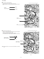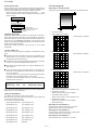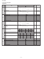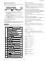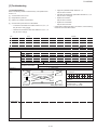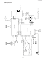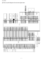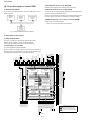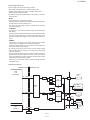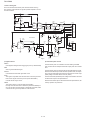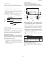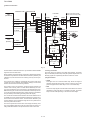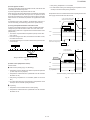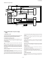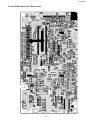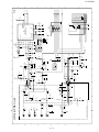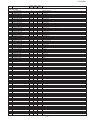
1
FO-2970MU
SERVICE MANUAL
No. 00ZFO2970USME
FACSIMILE
MODEL
FO-2970M
SELECTION CODE
U
DESTINATION
U.S.A.
Chapters 1, 3, 7 and 8 of this manual are omitted because they are partly common to the FO-2950MU. Please refer to
previous service manual UX-4000MU/FO-2950MU/C (00ZUX4000USME) for these chapters.
Difference between FO-2970MU and FO-2950MU
Control PWB
TEL/LIU PWB
Modem speed
FO-2970MU
DCEKC182PSCZZ
DCEKL259CSC01
33,600 bps
FO-2950MU
DCEKC388NSCZZ
DCEKL222CSC01
14,400 bps
CAUTION
This laser facsimile is a class 1 laser product that complies with 21CFR 1040.10 and 1040.11 of the CDRH or IEC60825-1 standard.
This means that this machine does not produce a hazardous laser radiation. The use of controls, adjustments or performance of
procedures other than those specified herein may result in hazardous radiation exposure.
This laser radiation is not a danger to the skin, but when an exact focusing of the laser beam is achieved on the eyes retina, there is
danger of spot damage to the retina.
The following cautions must be observed to avoid exposure of the laser beam to your eyes at the time of servicing.
1) When a problem in the laser optical unit has occurred, the whole optical unit must be exchanged as a unit, not an individual part.
2) Do not look into the machine with the main switch turned on after removing the toner/developer unit and drum cartridge.
3) Do not look into the laser beam exposure slit of the laser optical unit with the connector connected when removing and installing
the optical system.
4) The cover of Laser Printer Unit contains the safety interlock switch.
Do not defeat the safety interlock by inserting wedges or other items into the switch slot.
Laser Wave Length : 780 ±15 nm
Laser Pulse Times : (13.95 ± 3 µs)/7mm
Laser Output Power : 0.4 mW ± 0.05mW
Parts marked with " " is important for maintaining the safety of the set. Be sure to replace these parts with specified ones for maintaining the safety and performance of the set.
SHARP CORPORATION
This document has been published to be used
for after sales service only.
The contents are subject to change without notice.
FO-2970MU
CONTENTS
CHAPTER 1. GENERAL DESCRIPTION
[1] Specifications . . . . . . . . . . . . . . . . . . . . . . . . . . . . . . . . . . . . . . . . . . . . . . . . . . . . . . . . . . . . . . . . . . 1-1
[2] Operation panel . . . . . . . . . . . . . . . . . . . . . . . . . . . . . . . . . . . . . . . . . . . . . . . . . . . . . . . . . . . . . . . . 1-2
[3] Refer to the service manual of FO-2950MU
[4] Refer to the service manual of FO-2950MU
[5] Refer to the service manual of FO-2950MU
[6] Refer to the service manual of FO-2950MU
[7] Refer to the service manual of FO-2950MU
CHAPTER 2. ADJUSTMENTS
[1] Adjustments . . . . . . . . . . . . . . . . . . . . . . . . . . . . . . . . . . . . . . . . . . . . . . . . . . . . . . . . . . . . . . . . . . . 2-1
[2] Diagnostics and service soft switches . . . . . . . . . . . . . . . . . . . . . . . . . . . . . . . . . . . . . . . . . . . . . . . 2-4
[3] Troubleshooting . . . . . . . . . . . . . . . . . . . . . . . . . . . . . . . . . . . . . . . . . . . . . . . . . . . . . . . . . . . . . . . 2-27
[4] Error code table . . . . . . . . . . . . . . . . . . . . . . . . . . . . . . . . . . . . . . . . . . . . . . . . . . . . . . . . . . . . . . . 2-28
CHAPTER 3. MECHANICAL DESCRIPTION
[1] Refer to the service manual of FO-2950MU
[2] Refer to the service manual of FO-2950MU
CHAPTER 4. DIAGRAMS
[1] Block diagram . . . . . . . . . . . . . . . . . . . . . . . . . . . . . . . . . . . . . . . . . . . . . . . . . . . . . . . . . . . . . . . . . 4-1
[2] Wiring diagram . . . . . . . . . . . . . . . . . . . . . . . . . . . . . . . . . . . . . . . . . . . . . . . . . . . . . . . . . . . . . . . . . 4-2
[3] Point-to-point diagram and connector signal name . . . . . . . . . . . . . . . . . . . . . . . . . . . . . . . . . . . . . 4-3
CHAPTER 5. CIRCUIT DESCRIPTION
[1] Circuit description . . . . . . . . . . . . . . . . . . . . . . . . . . . . . . . . . . . . . . . . . . . . . . . . . . . . . . . . . . . . . . . 5-1
[2] Circuit description of control PWB . . . . . . . . . . . . . . . . . . . . . . . . . . . . . . . . . . . . . . . . . . . . . . . . . . 5-2
[3] Circuit description of TEL/LIU and Hook SW PWB . . . . . . . . . . . . . . . . . . . . . . . . . . . . . . . . . . . . 5-21
[4] Circuit description of power supply PWB . . . . . . . . . . . . . . . . . . . . . . . . . . . . . . . . . . . . . . . . . . . . 5-23
[5] Circuit description of CIS UNIT . . . . . . . . . . . . . . . . . . . . . . . . . . . . . . . . . . . . . . . . . . . . . . . . . . . 5-24
CHAPTER 6. CIRCUIT SCHEMATICS AND PARTS LAYOUT
[1] Control PWB circuit . . . . . . . . . . . . . . . . . . . . . . . . . . . . . . . . . . . . . . . . . . . . . . . . . . . . . . . . . . . . . 6-1
[2] TEL/LIU and Hook SW PWB circuit . . . . . . . . . . . . . . . . . . . . . . . . . . . . . . . . . . . . . . . . . . . . . . . . 6-12
[3] Printer PWB circuit . . . . . . . . . . . . . . . . . . . . . . . . . . . . . . . . . . . . . . . . . . . . . . . . . . . . . . . . . . . . . 6-15
[4] Power supply PWB circuit . . . . . . . . . . . . . . . . . . . . . . . . . . . . . . . . . . . . . . . . . . . . . . . . . . . . . . . 6-18
[5] Operation panel PWB circuit . . . . . . . . . . . . . . . . . . . . . . . . . . . . . . . . . . . . . . . . . . . . . . . . . . . . . 6-20
CHAPTER 7. OPERATION FLOWCHART
[1] Refer to the service manual of FO-2950MU
[2] Refer to the service manual of FO-2950MU
CHAPTER 8. OTHERS
[1] Refer to the service manual of FO-2950MU
[2] Refer to the service manual of FO-2950MU
PARTS GUIDE
FO-2970MU
CHAPTER 1. GENERAL DESCRIPTION
[1] Specifications
• GENERAL
Effective Scanning width
8.3" (210 mm) max.
Effective Printing width
8.0" (208 mm) max.
Reception modes
Fax/Tel/A.M.
Scanning speed
8 ppm (letter paper)
Automatic dialing
Rapid Key Dialing: 20 numbers
Speed Dialing: 100 numbers
Memory size*
4 MB (approx. 300 pages)
Modem speed
33,600 bps (max.)
Automatic fallback to lower speeds.
Full Dual Access
Yes
Transmission time*
Approx. 3 seconds
Copy function
Single/Multi/Sort (99 copies/page)
Toner cartridge yield
(4% page coverage, letter paper)
Initial starter cartridge (included with
fax machine): Approx. 1,875 pages
Replacement cartridge (FO-29ND):
Approx. 3,750 pages
Power requirements
120 V AC, 60 Hz
Operating temperature
50 - 86°F (10 - 30°C)
Humidity
20 to 85% RH
Power consumption
Standby: 8.1 W
Maximum: 650 W
Dimensions
Width: 15.2" (386 mm)
Depth: 15.7" (398 mm)
Height: 6.7" (169 mm)
Weight
Approx. 13.8 lbs. (6.3kg)
Drum cartridge yield
Scanning resolution
Initial starter cartridge (included with
fax machine): 20,000 pages (avg.)
Replacement cartridge (FO-29DR):
20,000 pages (avg.)
Fax/copy:
Horizontal: 203 pels/inch (8 pels/mm)
Vertical:
Standard: 98 lines/inch (3.85 lines/mm)
Fine /Halftone: 196 lines/inch
(7.7 lines/mm)
Super fine: 391 lines/inch
(15.4 lines/mm)
PC: Enhanced 600 dpi
Automatic document
feeder
20 pages max. (20-lb. letter paper)
Halftone (grayscale)
64 levels (PC scan: 256 levels)
Paper tray capacity
200 sheets (20-lb. letter paper)
Compression scheme
MMR, MR, MH, Sharp (H2)
Applicable telephone line
Public switched telephone network
Compatibility
ITU-T (CCITT) G3 mode
Printing resolution
Horizontal: 406 lines/inch (16 lines/mm)
Vertical: 391 lines/inch (15.4 lines/mm)
PC Printing: 600 dpi (enhanced 1,800 dpi)
Input document size
Automatic feeding:
Width: 5.8 to 8.5" (148 to 216mm)
Length: 5.5 to 11" (140 to 279mm)
Manual feeding:
Width: 5.8 to 8.5" (148 to 216mm)
Length:5.5 to 39.4" mm (140 to 1,000mm)
* Based on ITU-T Test Chart #1 at standard resolution in Sharp special
mode, excluding time for protocol signals (i.e., ITU-T phase C time
only).
Important:
•
This facsimile machine is not designed for use on a line which has call
waiting, call forwarding, or certain other special services offered by
your telephone company. If you attempt to use the fax machine in
conjunction with any of these services, you may experience errors
during transmission and reception of facsimile messages.
•
This facsimile machine is not compatible with digital telephone systems.
As a part of our policy of continuous improvement, SHARP reserves the right to make design and specification changes for product
improvement without prior notice. The performance specifications figures indicated are nominal values of production units. There may be some
deviations from these values in individual units.
1–1
FO-2970MU
[2] Operation panel
1
2
3
4
5
6
7
8
9
10 11
12
13
TEL FAX
A.M.
FUNCTION
VOLUME
DOWN
ABC
1
GHI
2
JKL
4
PQRS
5
PC
IN USE
RECEPTION
RESOLUTION BROADCAST
MODE
LINE
IN USE
6
HOLD/
SEARCH
9
SPEAKER
0
22
TONER
EMPTY
01
02
03
04
05
06
07
08
09
10
11
12
13
14
15
16/POLL
17/G1
18/G2
19/G3
20/G4
REDIAL
WXYZ
8
PAPER
CHECK
3
MNO
TUV
7
SPEED
DIAL
DEF
UP
21 20 19
COPY/HELP
REDUCTION/
ENLARGEMENT
START
STOP
18
17
16 15
14
1
SPEED DIAL key
Press this key to dial a fax or voice number using an
abbreviated 2 digit Speed Dial number.
13
BROADCAST key
Press this key to send a document to a group of receiving fax
machines.
2
REDIAL key
Press this key to automatically redial the last number dialed.
14
3
PAPER CHECK indicator
This lights when the paper tray is out of paper, the paper has
jammed, the printer compartment cover is open, or a paper
size error has occurred.
Rapid Dial Keys
Press one of these keys to dial a fax number automatically, or
send a document as an E-mail attachment to a preset E-mail
address.
15
E-MAIL key
Press this key to send a document as an E-mail attachment.
After you press the key, your specified E-mail program will
open to let you enter the E-mail address, a subject, and a
message if desired.
16
REDUCTION/ENLARGEMENT key
Press this key to select an enlargement or reduction setting
when making a copy of a document.
17
STOP key
Press this key to cancel an operation before it is completed.
18
START key
Press this key to begin transmission when using Speed Dialing,
Direct Keypad Dialing, or Normal Dialing.
19
COPY/HELP key
When a document is in the feeder, press this key to make a
copy of a document. At any other time, press this key to print
out the Help List, a quick reference guide to the operation of
your fax machine.
20
HOLD/SEARCH key
When dialing, press this key to search for an auto-dial fax
number. During a phone conversation, press this key to put the
other party on hold.
21
SPEAKER key
Press this key to listen to the line and fax tones through the
speaker when faxing a document.
Note: this is not a speakerphone. You must pick up the
handset to talk with the other party.
22
Number Keys
Use these keys to dial numbers, and enter numbers and letters
when storing auto-dial numbers.
4
TONER EMPTY indicator
This blinks when the toner cartridge nears empty and lights
steadily when the toner cartridge needs replacement.
5
Display
This displays messages and prompts during operation and
programming.
6
Panel release
Grasp this release and pull toward you to open the operation
panel.
7
PC IN USE light
This blinks when data is being sent to or from the computer
connected to the fax machine.
8
LINE IN USE light
This lights when the fax machine is using the telephone line.
9
RECEPTION MODE key
Press this key to select the reception mode. An arrow in the
display will point to the currently selected reception mode.
10
FUNCTION key
Press this key to select special functions and settings.
11
RESOLUTION Keys
Press this key to adjust the resolution for faxing or copying.
12
VOLUME (UP/DOWN) keys
Press these keys to adjust the volume of the speaker when the
SPEAKER key has been pressed, the volume of the handset
when the handset is lifted, or the volume of the ringer at all
other times. The keys can also be used to scroll through
FUNCTION key settings.
1–2
FO-2970MU
CHAPTER 2. ADJUSTMENTS
[1] Adjustments
General
Output
+5V
+24VH
+24V*
Since the following adjustments and settings are provided for this model,
make adjustments and/or setup as necessary.
1. Adjustments
Adjustments of output voltage (FACTORY ONLY)
PIN No.
1. Install the power supply unit in the machine.
3. When the document is loaded, power is supplied to the output lines.
Confirm that outputs are within the limits below.
Output voltage settings
Power
Supply
PWB 1
Printer PWB
1
CN101
12
Connector
No.
1
2
3
4
5
6
7
8
9
10
11
12
2. Set the recording paper and document.
CNPW
12
Voltage limits
4.75V~5.25V
23.04V~24.96V
23.04V~24.96V
CNPW
+5V
DG
DG
+24VH
MG
MG
+24VS
PWRLY–
HLON–
+24V
+24V
ZC
Fig. 1
2. High voltage power adjustments
VR1 (MC output voltage adjustment volume)
The high voltage power adjustments are composed of the MC output
voltage adjustment and the DC bias output voltage adjustment. Either
adjustment is performed with the diag function. (MAIN CHG ADJUST
MODE)
1 MC output voltage adjustment
In the measurement circuit shown below, adjust VR1 to be –1050V ~
–1200V (aim at –1100V)
Measure with the high
voltage tester
(effective value meter).
MC
DRUM
+
MC output
voltage check
–
• Capacitor: 1000pF/3KV (VCKYQY3FB102K)
• Diode:
SHV-03 (VHDSHV03///-1)
Fig. 3
Fig.2
2–1
FO-2970MU
2 DC bias output voltage adjustment
VR1 (MC output voltage adjustment volume)
Adjust VR2 so that the output voltage is –310V ±5V
For measurement, use the high voltage tester (effective value meter).
–
DC-Bias
Output voltage check
+
DRUM
DC-Bias
–
DC-Bias
Output voltage check
+
VR2
(DV bias output adjustment volume)
Fig.3
3 Transfer charger voltage check
VR1 (MC output voltage adjustment volume)
After MC output voltage adjustment and DC bias output voltage adjustment, check transfer charger voltage.
Check that the output voltage is +3200V ~ +3700V.
For measurement, use a high voltage tester (effective value meter).
+
Transfer charger
Output voltage check
D7
D8
–
DRUM
+
Transfer changer
Output voltage check
–
Note: For measurement, do not remove Printer PWB from the bottom
plate.
Fig.4
2–2
FO-2970MU
3. IC protectors replacement
ICPs (IC Protectors) are installed to protect the TX motor drive circuit
and verification stamp drive circuit. ICPs protect various ICs and electronic circuits from an overcurrent condition.
CNPRT
CNRTH
CNFUSE
The location of ICPs are shown below:
CNLIUA
CNPN
(1) F100 (ICPS10) is installed in order to protect IC’s from and
overcurrent generated in the verification stamp drive circuit. If F100
is open, replace it with a new one.
CNSP
F100
CNCIS
CNMT
CNLIUB
IC6
Control PWB (Bottom side)
Fig.5
4. Settings
(1) Dial mode selector
OPTION SETTING: DIAL MODE (Soft Switch No. SW2 DATA No. 1)
Use this to set the fax machine to the type of telephone line you are on.
• The factory setting is "TONE".
(step 1) Select "OPTION SETTING".
KEY:
FUNCTION
4
DISPLAY: OPTION SETTING
PRESS or #
(step 2) Select "DIAL MODE".
KEY:
Push # until " DIAL MODE " is
indicated because the number of
# s changes by the models.
DISPLAY: DIAL MODE
1= TONE, 2= PULSE
(step 3) Select, using "1" or "2".
KEY:
1
DISPLAY: TONE SELECTED
KEY:
2
DISPLAY: PULSE SELECTED
(step 4) End, using the "STOP" key.
KEY:
STOP
2–3
FO-2970MU
[2] Diagnostics and service soft switches
1. Operating procedure
1-2. Print diagnosis
Two kinds of diagnoses are supported.
This diagnosis is concerned with the print which is used for
production and service support.
1-1. Fax diagnosis
Entering the diagnostic mode
This diagnosis is concerned with the main body of fax which is used
for production and service support.
9
Press FUNC
display will appear.
Entering the diagnostic mode
9
Press FUNC
display will appear.
8
8
6 , and the following
PRINT DIAG MODE
7 , and the following
PRESS START KEY
Then press the START key. Select the desired item with
key and the
key or select with the rapid key.
DIAG MODE
ROM: FBF0
the
Enter the mode with the START key.
Then press the START key. Select the desired item with the
and the
key or select with the rapid key.
Enter the mode with the
key
(Diag • specifications)
START key.
(Diag • specifications)
9
FUNC
FUNC
8
7
9
8
PRINT DIAG MODE
6
ROM: FBF0
START
START
01
START
AREA PRINT MODE
02
START
CHECK PATTERN 1
03
START
CHECK PATTERN 2
04
START
CHECK PATTERN 3
05
START
PAPER FEED AGING
06
START
LIFE SET MODE
07
START
LIFE ALL CLEAR
08
START
LIFE ENTRY MODE
09
START
TOP ADJUST MODE
01
START
SOFT SWITCH MODE
02
START
ROM & RAM CHECK
03
START
AGING MODE
04
START
PANEL KEY TEST
05
START
OPTICAL ADJUST MODE
06
START
CHECK PATTERN MODE
07
START
SIGNAL SEND MODE
08
START
MEMORY CLEAR MODE
09
START
AUTO FEEDER MODE
10
START
LIFE CLEAR MODE
10
START
MOTOR AGING MODE
11
START
MAIN CHARGER ADJUST
11
START
TEL. NUMBER SET
12
START
SIGNAL SEND MODE 2
Memory clear when power is turned on
Pressing the START and STOP keys, turn on the main power, and the
following message will be displayed.
MEMORY CLEAR?
YES: START
Press START key, the memory will be cleared to be ready for operation.
Press COPY key, the memory will be cleared to be ready for process
check.
If press the other keys, it will continue ready for operation as it is.
2–4
FO-2970MU
4) Panel key test
2. Diagnostic items description
This is used to check whether each key is normally operated or not.
According to the key input, LCD is displayed.
1) When the START key is pressed while PANEL KEY TEST is being
displayed, a test will start. Since all of the LEDs will light up in sequence until the test is finished, the LED operation can be checked
as well.
2) Press all of the keys one at a time, but do not press the STOP key.
Every time a key is pressed, the name of that key will appear in the
display.
3) Finally, press the STOP key. If there was a key you pressed that was
not detected when the STOP key is pressed, PANEL TEST NG! will
be displayed. When all of the keys have been pressed and detected,
PANEL TEST OK! will be displayed.
Then the display will go blank, which is OK. If there was an NG, any
key which was not pressed or not detected will be printed in the result table. (For details about the printout format, see the list function
specifications.)
2-1. Fax diagnosis
1) Soft switch mode
The soft switches are provided so that each operation mode can be set
by using the operation panel.
In this mode, these switches can be checked and set.
The contents of these switches are backed up.
Soft switch mode screen
SOFT SWITCH MODE
SW01=00000000
Switch 1 2 3 4 5 6 7 8 :DATA No.
No.
Data
1 Switch number selection
•
•
Press START key for setting of the next soft switch. If the soft
switch number is the final, pressing START key will exit the soft
switch mode.
Enter two digits of a soft switch number to set the switch number.
SOFT SWITCH MODE
SW1
SOFT SWITCH MODE
SW01=00100000
1
5) Optical adjust mode
In this mode, the optical system is adjusted. Document feeding can be
started by pressing the START key two times. It can be stopped by pressing the STOP key.
SOFT SWITCH MODE
SW16=00010110
6
2 Data number selection
6) Check pattern mode
The effective printing area used will be according to the size specified.
A copy of a pattern will be printed, and the printing will be complete.
The cursor position shows the data to be set.
Pressing # key moves the cursor to the right. If, however, the cursor
is on data number 8, pressing # key shifts the cursor to data number
1 of the next switch number. If the switch number is the final, pressing # key will exit the soft switch mode.
Pressing key moves the cursor to the left. If, however, the cursor is
on data number 1, pressing key shifts the cursor to data number 1
of the former switch number. If the switch number is 1, pressing
key will not move the cursor and the error buzzer will sound.
7) Signal send mode
This mode is used to send various signals to the circuit during FAX communication. Every push of START key sends a signal in the following
sequence.
[ 1] No signals (CML-ON)
3 Data setting method
[ 2] 14400bps (V. 33)
[ 3] 12000bps (V. 33)
Press the FUNCTION key, and the data at the position of the cursor
will be reversed to 0 when it is 1, or to 1 when it is 0. (If the soft switch
can not be changed at the bit the error buzzer will sound with the
process not received.), When you press the START key or the # key
and the cursor moves to the next switch position, the changes in the
contents of the previous switch position will be saved. If you do not
want to save your changes, press the STOP key.
[ 4] 14400bps (V. 17)
[ 5] 12000bps (V. 17)
[ 6] 9600bps (V. 17)
[ 7] 7200bps (V. 17)
4 Outputting method of soft switch list
[ 8] 9600bps (V. 29)
In the soft switch mode, press the COPY/HELP key, and the soft
switch list will be output.
If the recording paper runs out or is clogged, condition is held until
recording paper is prepared, and an error buzzer doesn’t ring.
[ 9] 7200bps (V. 29)
[10] 4800bps (V27ter)
5 Prohibition against changing individual pieces of data and synchro-
[11] 2400bps (V27ter)
nized data changes
At present, there is no prohibition against changing data individually
and there is also no capability to make synchronized changes to data.
(The ECM may be turned on or off while using image memory.)
[12]
300bps (FLAG)
[13] 2100Hz (CED)
[14] 1100Hz (CNG)
[15] END
2) ROM & RAM check
ROM executes the sum check, and RAM executes the matching test.
If any error occurs, the buzzer will inform it. (Refer to the following table).
Finally, the result will be printed.
Number of buzzer sounds
8) Memory clear mode
This mode is used to clear the backup memory and to reset to the factory default setting.
The content of each setting will be cleared. Then, the initialized list be
output.
Device checked
1 time <Short sound>
MAIN ROM
2 times <Short sounds>
S-RAM
3 times <Short sounds>
D-RAM
4 times <Short sounds>
CPU integrated ROM/RAM
The buzzer beep pattern is: on for 0.25 seconds and then off for 0.25
seconds.
3) Aging mode
If any document is set up in the first state (when started), copying will be
executed. If it is not set up, "check pattern" of the print diagnosis is output at the intervals of 1 sheet/5 minutes. (A total of 10 sheets are output.)
2–5
FO-2970MU
9) Auto feeder mode
2-2. Print diagnosis
The auto feed function can be checked by inserting and discharging the
document. (After entering this mode, when a document is placed in the
machine and the START key is pressed, the operation will start.)
After this mode is activated, the document size A4(A4
) and
sensor information A4(A4 ORG) are displayed when the document
sensor is turned.
Rapid key 01: Area print mode
The effective printing area frame is printed in the specified sheet size.
4mm
1
2
3
AUTO FEEDER MODE
(
4
)
5
6
7
After setup of the document
8
AUTO FEEDER MODE
A4 (A4
9
4mm
ORG)
Only the sensor which is
activated (fallen down) is displayed.)
The paper sheet size (A4) is
displayed.
208mm
4mm
4mm
1. [Full black pattern]
2. [Intermediate tone 2 pattern]
10) Motor aging mode
Regardless of the presence or absence of a document, the transmission system motor will continue to run until the STOP key is pressed.
When the START key is pressed after this mode has been selected, the
motor will run at the STANDARD mode speed. Then, when the image
quality is changed using the RESOLUTION key, the motor will run at the
speed used for that image quality.
(When HALF-TONE is selected, the motor will run at the FINE
modespeed.)
The left pattern is repeated.
11) TEL. number set
The function is used to simplify the registration of FAX/TEL No. during
aging.
3. [Intermediate tone 1 pattern]
1 The diagnosis mode is activated. If anything is not registered in the
The left pattern is repeated.
Rapid number 01 or any program or group is registered, it will pass
the diagnosis without doing anything.
2 The FAX number (including the substitutive destination) of the Rapid
number 01 is copied to the Rapid numbers 02 thru 19.
3 FAX number of the Rapid number 01 is copied to SPEED key numbers 00 thru 99.
4 If any chain dial is not set in the Rapid number 01, the Rapid num-
4. [Mesh point pattern]
bers 01 thru 19 and SPEED key numbers 00 thru 10 are registered in
the group number 04.
If any chain dial is set, the group will be not produced but the chain
dial setting alone of the Rapid number 01 will be reset.
(In all others except the Rapid number 01, the chain dials will be
continuously set as they are.)
Rapid key
SPEED key
RXX
SXX
XX
XX
The left pattern is repeated.
: Rapid number
: Speed key number
5. [Longitudinal strip 2 pattern]
Black 2 dot and white 2 dot are repeated in line.
(12th and subsequential letters of the destination name registered in the
Rapid number 01 will be discarded.)
6. [Lateral strip 2 pattern]
Black 2 line and white 2 line are repeated.
12) Signal Send Mode 2
7. [Longitudinal strip 1 pattern]
Black 1 dot and white 1 dot are repeated in line.
The signals concerned with V.34 & V.8 are checked.
After this mode is activated, press the START key, and the signals will
be sent in the following sequence.
It can be used to check the modem.
8. [Lateral strip 1 pattern]
Black 1 line and white 1 line are repeated.
9. [Full White pattern]
[ 1] No signals (CML-ON)
[10] 14400bps (V.34)
[ 2] 33600bps (V.34)
[11] 12000bps (V.34)
Rapid key 02: Check pattern 1
[ 3] 31200bps (V.34)
[12] 9600bps (V.34)
The lateral stripe 2 pattern is printed on one sheet.
(Black 2 line and white 2 line are repeated.)
[ 4] 28800bps (V.34)
[13] 7200bps (V.34)
Rapid key 03: Check pattern 2
[ 5] 26400bps (V.34)
[14] 4800bps (V.34)
The lateral stripe 2 pattern is printed on multiple pages.
Press the STOP key to end the printing.
[ 6] 24000bps (V.34)
[15] 2400bps (V.34)
[ 7] 21600bps (V.34)
[16] 0-300bps (V.21)
[ 8] 19200bps (V.34)
[17] ANsam (V.8)
[ 9] 16800bps (V.34)
[18] END
Rapid key 04: Check pattern 3
The intermediate tone 1 is printed on one sheet.
2–6
FO-2970MU
Rapid key 05: Paper feed aging
Rapid key 07: Life all clear
The mode is used for aging related to the printing. In this mode, the
following modes are provided.
Blank paper aging mode (ALL WHITE AGING)
Whole black print aging mode (ALL BLACK AGING)
4% printing aging mode (4% AGING)
After selecting the paper-feed aging mode in the print diagnosis mode,
input the number of each mode above with the ten-key, and the mode
will be executed. The detailed specifications of each mode are described
as follows. Here, the operation in each mode is stopped only when the
STOP key is pressed by the operator or a printing-impossible error occurs.
The mode is used to clear the life counter of the printer of the counter
of the auto feeder.
1
2
3
•
•
Note:
The counter shows the operational state of the printer (e.g. how
many sheets have been printed since start of use?). The ordinary memory does not reset the counter. Accordingly, it is necessary to reset this counter in addition to the ordinary memory
clear if the content in the memory on the control PWB is broken
because of PWB repair, etc. (In the production stage, it is necessary to execute this in the last process.)
Rapid key 08: Life entry mode
(For Serviceman temporary counter)
Blank paper aging mode (ALL WHITE AGING)
In the mode, printing is continued in the whole white (white paper)
printing pattern until the STOP key is pressed by the operator. (In the
printing area)
The mode is used to set a desired value for the judgment value (alarm
judgment counter value) of the general purpose life counters 1 thru 3 of
the printer. If the life of a consumable part (developer, imprinter, etc) is
set, the model which has the error display and RMS function will inform
RMS when the counter reaches the set value. For setting, proceed with
the following procedure.
Whole black printing aging mode (ALL BLACK AGING)
In the mode, printing is continued in the whole black (whole black)
printing pattern until the STOP key is pressed by the operator. (In the
printing area)
1 When the life counter entry mode is selected, the following will be
displayed.
Rapid key 06: Life set mode
The mode is used to set the life counter of the printer and the counter of
the auto feeder at desired values. For setting, proceed with the following procedure.
1 When the life counter setting mode is selected, the following will be
L I F E 1 = 0 0 0 1 2 3
is displayed.
# key
L I F E 2 = 0 0 0 1 2 3
key
M A C H I N E = 0 0 0 1 2 3
L I F E 3 = 0 0 0 1 2 3
D R U M
L I F E = 0 0 0 1 2 3
The cursor blinks at the top data.
Three counters can be selected with the "#" and " " keys.
2 In the state 1 , input a desired setting number of 6 digits with the tenkey.
3 After input of 6 digits, shift to another counter with the "#" and " "
L I F E 1 = 0 0 0 1 2 3
# key
key
L I F E 2 = 0 0 0 1 2 3
keys as necessary. When all necessary counters are completely input, press the START key.
4 "STORED" will be displayed with the set values stored into the
L I F E 3 = 0 0 0 1 2 3
memory. For checking, retry this mode.
F E E D E R
L F = 0 0 0 1 2 3
T O N E R
L F = 0 0 0 1 2 3
Note:
The cursor blinks at the top data.
Seven counters can be selected with the "#" and " " keys.
2 In the state 1, input a desired setting number of 6 digits with the tenkey.
3 After input of 6 digits, shift to another counter with the "#" and " "
The counter shows the operational state of the printer (how many
sheets have been printed since start of use? and others). The
ordinary memory does not reset the counter. Accordingly, it is
necessary to reset the counter or do the clear process in addition to the ordinary memory clear if the content in the memory
on the control PWB is broken because of PWB repair, etc. (In
the production stage, it is necessary to execute this in the last
process.)
Rapid key 9: Top adjust mode
Adjust the top margin for printing on a page. You can enter any value
from 0 to 99 using the ten-key keypad.
The standard (initial) value is 50.
When the setting is increased, the print start position will be moved closer
to the beginning of page.
When the setting is decreased, the print start position will be moved
further away from the beginning of page.
keys as necessary. When all necessary counters are completely input, press the START key.
4 "STORED" will be displayed with the set values stored into the
memory. For checking, retry this mode.
Note:
This counter indicates the printer use conditions such as numbers of
printed pages from the beginning of use. In the normal memory clear
condition, the counter will not be reset.
In conditions including damaged memory contents caused by repairing
the panel, this counter should be reset or cleared in addition to the ordinary memory clear.
2–7
FO-2970MU
Rapid key 10: Life clear mode
The mode is used to respectively clear the life counter of the printer and
the counter of the auto feeder. For setting, proceed with the following
procedure.
1 When the life counter clearing mode is selected, the following will be
is displayed.
Seven counters can be selected with the "#" and " " keys.
L F
C L E A R
L I F E
C L E A R
L I F E 1
C L E A R
L I F E 2
C L E A R
L I F E 3
C L E A R
M A C H I N E
D R U M
# key
key
L F
C L E A R
L I F E
C L E A R
F E E D E R
T O N E R
2 In the state of 1, select the counter value you want to clear using the
"#" key or the " " key, and then press the START key.
3 "CLEARED " will be displayed, and the counter value will be cleared.
After clearing the counter value, another counter value can be cleared
using the # or key, if desired. Press the STOP key to exit from the
mode.
Note:
The counter shows the operational state of the printer (how many
sheets have been printed since start of use? and others). The
ordinary memory does not reset the counter. Accordingly, it is
necessary to reset the counter or do the clear process in addition to the ordinary memory clear if the content in the memory
on the control PWB is broken because of PWB repair, etc. (In
the production stage, it is necessary to execute this in the last
process.)
Rapid key 11: Main charger adjust
This mode is used to control voltage of main charger.
2–8
FO-2970MU
3. How to make soft switch setting
To enter the soft switch mode, make the following key entries in sequence.
Press FUNCTION
9
8
7
START
01
START
SFT S W 1 = 0 0 0 0 0 0 0 0
Press FUNCTION key.
SFT S W 1 = 1 0 0 0 0 0 0 0
Press
key.
Press
key.
SFT S W 1 = 1 0 0 0 0 0 0 0
SFT S W 1 = 1 0 0 0 0 0 0 0
Bit1 - 8 are set.
SFT S W 1 = 1 0 0 0 0 0 0 0
Press START key during setting.
SFT S W 2 = 0 0 0 0 0 0 0 0
Soft SW2 - 65 are set.
S F T S W 65 = 0 0 0 0 0 0 0 0
To finish the settings halfway between
SW 1 and SW65, press the STOP key.
In this case, the setting being done to
the SW No. on display will be nullified
while settings done to the preceding
SW Nos. remain in effect.
The soft switch mode is terminated.
2–9
FO-2970MU
4. Soft switch description
• Soft switch
SW DATA
NO. NO.
SW1
SW2
SW3
1
2
3
4
5
6
7
8
1
2
3
4
5
6
7
8
1
2
3
4
5
6
7
8
1
2
3
4
SW4
1
0
Recall interval
Binary input
No. =
8
1
0
4
2
1
2
3
0
1
4
1 (5 x 60 sec = 5 min)
Recall times
Binary input
No. =
8
5
0
4
6
0
2
7
1
1
8
0 (Twice)
Dial mode
Reception mode
ECM mode
CNG detection in stand-by mode
Polling security
Automatic cover sheet
Junk fax function in manual reception
Anti junk fax function
Number of rings for auto receive
Pulse
Auto
No
No
On
No
Yes
Yes
Binary input
No. =
Automatic switching manual to auto receive
mode
(0: OFF)
Binary input
No. =
Communication results printout
(transaction report)
Err/Tmr/Mem Send only No print
Always
0
0
1
1
0
1
0
1
0
0
0
0
0 sec
3.6 sec
3.0 sec
1.7 sec
3.0 sec
No. 5
1
1
0
0
No. 6
1
0
1
0
1 pulse
2 pulses
3 pulses
4 pulses
No. 7
0
0
1
0
No. 8
0
1
0
0
24-hours
12-hours
Month-Day-Year
Day-Month-Year
Delay timer before line connect in auto dial
Delay timer of after line connect in auto dial
5
6
Number of CNG detect (STAND-BY mode)
SW5
Switch setting and function
ITEM
7
8
1
2
Time format
Date format
3
4
5
6
7
8
Sender’s information transmit
Footer print
Reserved
Substitute reception
Substitute reception conditions
CSI transmission
No. 1
No. 2
No. 3
3 sec
8
1
0
4
2
1
2
3
0
Tone
Manual
Yes
Yes
Off
Yes
No
No
1
4
0 (4 times)
8
5
0
4
6
0
2
7
0
1
8
0 (off)
Error
0
0
1
Off
On
On
Off
Off
On
Reception disable without TSI Reception enable without TSI
Off
On
2 – 10
Initial
setting
0
1
0
1
0
0
1
0
0
1
0
0
0
1
0
0
0
1
0
0
0
0
0
0
Remarks
OPTION
Set to 01~15
OPTION
Set to 0~10
OPTION
Recep key
OPTION
OPTION
FUNC +3
OPTION
OPTION
OPTION
OPTION
0
0
1
0
0
1
0
1
0
1
0
0
0
0
0
0
FO-2970MU
SW DATA
NO. NO.
1
2
3
4
SW6
H2 mode
MH fixed
Reserved
Reserved
Modem speed
(DCS data reception speed)
5
6
7
8
Reception speed fixed
1
2
3
Switch setting and function
ITEM
DIS receive acknowledgement during
G3 transmission
1
Initial
setting
0
No
Yes
Yes
No (depends on remote machine)
Remarks
0
0
0
0
V.17
V. 29
V. 27ter
14400 12000 9600 7200 9600 7200 4800 2400
No. 5
1
1
1
1
0
0
0
0
No. 6
0
0
0
0
0
0
0
0
No. 7
0
1
0
1
0
1
1
0
No. 8
0
0
1
1
1
1
0
0
NO
V. 17V. 29- V. 27 ter14400 bps 9600 bps 4800 bps
No. 1
0
1
0
1
No. 2
0
1
1
0
Twice
0
0
0
0
On
Off
0
25 sec
On
On
No limit
13 sec
Off
Off
Copy/Send:1m Receive:1.5 m
1.8 Km 3.6 Km
7.2 Km
0
1
1
1
0
1
4sec
2 1
7 8
0 1 (–9 dBm)
0
0
0
0
1
0
0
0
When 14400 bps
modem used,
setting to
14400 bps is
ignored.
SW7
4
5
6
7
8
SW8
1
2
3
4
5
6
7
8
Non modulated carrier for V.29
transmission mode
EOL detect timer
Protocol monitor
Line monitor
Length limitation of copy/send/receive
Digital line equalization setting
(Reception)
Dial pausing (sec/pause)
Signal transmission level
No. 1
No. 2
2sec
Binary input
No. =
CED tone signal interval
SW9
SW10
1
2
3
4
5
6
7
8
1
2
3
4
5
6
7
8
Distinctive ringing setting
Factory setting : OFF
16 8
4 5
0 1
4
6
0
On
All
500 ms
500 ms 750 ms
0
1
1
0
Off
7200 bps
1000 ms
Yes
No
No. 1
No. 2
Equalizer freeze control (MODEM)
Equalizer freeze conditions
CED detection time
Reserved
Reserved
Busy tone detection (after auto dial)
Reserved
Reserved
CI off detection timer
(Distinctive ring setting off only)
0 Km
0
0
No. 5
No. 6
No. 7
No. 8
No. 3
No. 4
OFF
0
0
0
0
2 – 11
75 ms
0
0
1000 ms
1
1
1200 ms 1000 ms 700 ms
350 ms
0
1
0
1
0
0
1
1
STD RING1 RING2 RING3 RING4 RING5
0
1
0
1
0
1
0
0
1
1
0
0
0
0
0
0
1
1
1
0
0
0
0
0
0
0
1
0
1
0
0
1
0
0
0
0
0
0
0
1
0
0
0
1
0
0
0
0
OPTION
RING4/RING5
Canada
Only
FO-2970MU
SW DATA
NO. NO.
End buzzer
1
2
3
SW11
SW12
SW13
SW14
SW15
4
5
6
7
8
1
2
3
4
5
6
7
8
1
2
3
4
5
6
7
8
1
2
3
4
5
6
7
8
1
2
3
4
5
6
7
8
Switch setting and function
ITEM
Communication error treatment
in RTN sending mode (reception)
CNG transmission after auto dialing
Error criterion
Pulse to tone change by key
CNG transmission in manual transmission
Reserved
DTMF signal transmission level (Low)
Reserved
Reserved
Reserved
DTMF signal transmission level (High)
1
3 sec
No. 1
0
No. 2
0
No communication error
0
1 sec No Beep No Beep
0
1
1
1
0
1
Communication error
No
10 ~ 20 %
On
No
Yes
5 ~ 10 %
Off
Yes
Binary input
No. =
16 8
1 2
0 1
4
3
1
2 1
4 5
0 0 (–6 dBm)
Binary input
No. =
16 8
1 2
0 1
4
3
0
2 1
4 5
0 0 (–4 dBm)
Reserved
Reserved
Reserved
Reserved
Reserved
Reserved
Reserved
Reserved
Reserved
Reserved
Reserved
Reserved
Reserved
Reserved
Reserved
Reserved
Reserved
Reserved
Reserved
2 – 12
Initial
setting
Remarks
OPTION
0
0
0
0
0
0
0
0
0
1
1
0
0
0
0
0
0
1
0
0
0
0
0
0
0
0
0
1
1
0
0
0
0
0
0
0
0
0
0
0
FO-2970MU
SW DATA
NO. NO.
SW16
1
2
3
4
5
6
7
8
Switch setting and function
ITEM
1
Reserved
Reserved
Reserved
Reserved
Reserved
Reserved
Reserved
Reserved
Speaker volume (3 stages)
No. 1
No. 2
Hand-set receiver volume (3 stages)
3
4
No. 3
No. 4
Ringer volume (4 stages)
5
6
No. 5
No. 6
Key volume
SW18
7
8
1
2
3
4
5
6
7
8
No. 7
No. 8
Reserved
Auto reception in PC I/F mode
Summer time setting
Sender’s phone number setting
Polling key
Activity report print
Total communication hours and pages print
Line density selection
Density adjustment (when Fine/STD mode)
High
0
0
High
0
0
Off
0
0
Off
0
0
FAX
No
Cannot change
Yes
Automatic printout
Off
Fine
Normal
1
2
No. 1
No. 2
0
0
Normal
No. 3
No. 4
0
0
Density adjustment (when Half-tone mode)
SW19
SW20
3
4
5
6
7
8
1
2
3
4
5
6
7
8
Reserved
Reserved
Reserved
Reserved
Reserved
Reserved
Reserved
Reserved
Reserved
Reserved
F.A.S.T (RMS) mode
Quick on-line
Remarks
1
0
0
0
1
0
0
0
1
2
SW17
Initial
setting
0
On
Yes
High
0
1
High
0
1
High
0
1
High
0
1
Low
1
1
Low
1
1
Low
1
1
Low
1
1
PC
Yes
Change allowed
No
No printout when memory full
On
Standard
Faint
Deep
Deep
(when Dark
mode)
0
1
1
1
0
1
Faint
Deep
Deep
(when Dark
mode)
0
1
1
1
0
1
Off
No
2 – 13
Middle
1
0
Middle
1
0
Middle
1
0
Low
1
0
1
0
1
0
1
0
1
0
1
1
1
0
0
0
0
0
Using
Volume
key
Using
Volume
key
Using
Volume
key
FUNC + #
FUNC + 3
OPTION
OPTION
OPTION
0
0
0
0
0
0
1
0
0
0
0
0
0
0
1
1
OPTION
FO-2970MU
SW DATA
NO. NO.
SW21
SW22
SW23
SW24
SW25
1
2
3
4
5
6
7
8
1
2
3
4
5
6
7
8
1
2
3
4
5
6
7
8
1
2
3
4
5
6
7
8
1
2
3
4
5
6
7
8
1
2
SW26
3
4
5
6
7
8
Switch setting and function
ITEM
Reserved
Reserved
Reserved
Reserved
Reserved
Reserved
Reserved
Reserved
Reserved
Reserved
Reserved
Reserved
Reserved
Reserved
Reserved
Reserved
Automatic reduce of receive
Cut off mode (COPY mode)
Paper set size
1
Auto
Continue
No. 3
No. 4
Letter
0
0
No. 1
No. 2
50 ms
0
0
Reserved
Reserved
Reserved
Reserved
DTMF detection time
Protection remote reception (5
) detect
Reserved
Remote operation code figures by external
tel (0 ~ 9)
Yes
Binary input
No. =
EX
eg.
Busy tone detection ON/OFF time (Shorter duration) 350ms
Busy tone detection ON/OFF time
(Longer duration)
No. 2
No. 3
Busy tone continuous sound detect time
10 sec
Busy tone detect continuation sound detect
No
Busy tone detect intermittent sound detect
No
Busy tone detection pulse number
No. 7
No. 8
TAD connect
Yes
Fax switching when A.M. full
Yes
Selection time of quiet detection
No. 3
No. 4
Number of CNG detect (AM mode)
No. 5
No. 6
Reserved
Reserved
2 – 14
Initial
setting
0
8
5
0
5
4
6
1
2
7
0
0
0
1
0
0
0
0
0
0
0
0
0
0
0
0
0
1
0
100%
Cut-off
Legal
0
1
80 ms
0
1
No
A4
1
0
Letter
1
1
100 ms
1
0
120 ms
1
1
1
8 (Data No.)
1
150 ms
900 ms 2700 ms 900 ms
0
1
1
1
0
1
5 sec
Yes
Yes
2 pulses 4 pulses 6 pulses 10 pulses
0
0
1
1
0
1
0
1
No
No
30 sec
40 sec
50 sec
60 sec
0
0
1
1
0
1
0
1
1 pulse 2 pulses 3 pulses 4 pulses
0
0
1
1
0
1
0
1
650 ms
0
0
Remarks
OPTION
OPTION
OPTION
0
0
0
0
0
0
0
0
0
0
0
1
0
1
0
OPTION
OPTION
0
1
1
0
0
0
1
0
0
0
1
0
1
0
1
Recep key
OPTION
FO-2970MU
SW DATA
NO. NO.
SW27
SW28
SW29
SW30
SW31
1
2
3
4
5
6
7
8
1
2
3
4
5
6
7
8
1
2
3
4
5
6
7
8
1
2
3
4
5
6
7
8
1
2
3
4
5
6
7
8
ITEM
Switch setting and function
1
0
Quiet detect time
Binary input
No. =
8
1
0
4
2
1
2
3
0
1
4
0 (4 sec)
Quiet detect start timing
Binary input
No. =
8
5
0
4
6
1
2
7
0
1
8
1 (5 sec)
Reserved
Reserved
Reserved
Reserved
Reserved
Reserved
Reserved
Reserved
Reserved
Reserved
Reserved
Reserved
Reserved
Reserved
Reserved
Reserved
Reserved
Reserved
Reserved
Reserved
Reserved
Reserved
Reserved
Reserved
Reserved
Reserved
Reserved
Reserved
Reserved
Reserved
Reserved
Reserved
2 – 15
Initial
setting
0
1
0
0
0
1
0
1
0
0
0
0
0
0
0
0
0
0
0
0
0
0
0
0
0
0
0
0
0
0
0
0
0
0
0
0
0
0
0
0
Remarks
OPTION
FO-2970MU
SW DATA
NO. NO.
SW32
SW33
SW34
SW35
SW36
SW37
SW38
ITEM
Switch setting and function
1
0
Initial
setting
1
2
3
4
5
6
7
8
1
2
3
4
5
6
7
8
1
2
3
4
5
6
7
8
1
2
3
4
5
6
7
8
1
2
3
4
5
6
7
8
1
2
3
4
5
6
7
8
1
2
Reserved
Reserved
Reserved
Reserved
Reserved
Reserved
Reserved
Reserved
Reserved
Reserved
Reserved
Reserved
Reserved
Reserved
Reserved
Reserved
Reserved
Reserved
Reserved
Reserved
Reserved
Reserved
Reserved
Reserved
Reserved
Reserved
Reserved
Reserved
Reserved
Reserved
Reserved
Reserved
Reserved
Reserved
Reserved
Reserved
Reserved
Reserved
Reserved
Reserved
Reserved
Reserved
Reserved
Reserved
Reserved
Reserved
Reserved
Reserved
Reserved
Reserved
0
0
0
0
0
0
0
0
0
1
0
0
0
0
0
0
0
0
0
0
1
1
0
1
1
1
0
1
1
1
0
1
1
1
1
1
1
1
0
0
0
0
0
0
0
0
0
0
0
0
3
4
5
6
7
8
Reserved
Reserved
Reserved
Reserved
Reserved
Reserved
0
0
0
0
0
0
2 – 16
Remarks
FO-2970MU
SW DATA
NO. NO.
SW39
SW40
SW41
SW42
SW43
SW44
SW45
ITEM
Switch setting and function
1
0
Initial
setting
1
2
3
4
5
6
7
8
1
2
3
4
5
6
7
8
1
2
3
4
5
6
7
8
1
2
3
4
5
6
7
8
1
2
3
4
5
6
7
8
1
2
3
4
5
6
7
8
1
2
Reserved
Reserved
Reserved
Reserved
Reserved
Reserved
Reserved
Reserved
Reserved
Reserved
Reserved
Reserved
Reserved
Reserved
Reserved
Reserved
Reserved
Reserved
Reserved
Reserved
Reserved
Reserved
Reserved
Reserved
Reserved
Reserved
Reserved
Reserved
Reserved
Reserved
Reserved
Reserved
Reserved
Reserved
Reserved
Reserved
Reserved
Reserved
Reserved
Reserved
Reserved
Reserved
Reserved
Reserved
Reserved
Reserved
Reserved
Reserved
Reserved
Reserved
0
0
0
0
0
0
0
0
0
0
0
0
0
0
0
0
0
0
0
0
0
0
0
0
0
0
0
0
0
0
0
0
0
0
0
0
0
0
0
0
0
0
0
0
0
0
0
0
0
0
3
4
5
6
7
8
Reserved
Reserved
Reserved
Reserved
Reserved
Reserved
0
0
0
0
0
0
2 – 17
Remarks
FO-2970MU
SW DATA
NO. NO.
SW46
SW47
SW48
SW49
SW50
SW51
SW52
ITEM
Switch setting and function
1
0
Initial
setting
1
2
3
4
5
6
7
8
1
2
3
4
5
6
7
8
1
2
3
4
5
6
7
8
1
2
3
4
5
6
7
8
1
2
3
4
5
6
7
8
1
2
3
4
5
6
7
8
1
2
Reserved
Reserved
Reserved
Reserved
Reserved
Reserved
Reserved
Reserved
Reserved
Reserved
Reserved
Reserved
Reserved
Reserved
Reserved
Reserved
Reserved
Reserved
Reserved
Reserved
Reserved
Reserved
Reserved
Reserved
Reserved
Reserved
Reserved
Reserved
Reserved
Reserved
Reserved
Reserved
Reserved
Reserved
Reserved
Reserved
Reserved
Reserved
Reserved
Reserved
Reserved
Reserved
Reserved
Reserved
Reserved
Reserved
Reserved
Reserved
Reserved
Reserved
0
0
0
0
0
0
0
0
0
0
0
0
0
0
0
0
0
0
0
0
0
0
0
0
1
0
0
0
0
0
0
0
0
0
0
0
0
0
0
0
0
0
0
0
0
0
0
0
0
0
3
4
5
6
7
8
Reserved
Reserved
Reserved
Reserved
Reserved
Reserved
0
1
1
0
1
0
2 – 18
Remarks
FO-2970MU
SW DATA
NO. NO.
SW53
SW54
SW55
SW56
SW57
SW58
SW59
1
2
3
4
5
6
7
8
1
2
3
4
ITEM
Switch setting and function
1
Reserved
Reserved
Reserved
Reserved
Reserved
Reserved
Reserved
Reserved
V.34 mode sending speed
1
2
3
4
5
6
7
8
1
2
3
4
5
6
7
8
1
2
3
4
5
6
7
8
1
2
3
4
5
6
7
8
Sending speed = 2400 (bps) x N
Example:
2400 (bps) x 12 = 28800 (bps)
2400 (bps) is set for N = 0.
33600 (bps) is set for N = 15.
V.34 mode receiving speed
Receiving speed = 2400 (bps) x N
Example:
2400 (bps) x 12 = 28800 (bps)
2400 (bps) is set for N = 0.
33600 (bps) is set for N = 15.
V.34 mode function in case of manual communication On
Off
V.34 mode function
On
Off
V.34 control channel communication speed
2400 bps
1200 bps
Reserved
Reserved
Reserved
Reserved
Reserved
Reserved
Reserved
Reserved
Reserved
Reserved
Reserved
Reserved
Reserved
Reserved
Reserved
Reserved
Reserved
Reserved
Reserved
Reserved
Reserved
Reserved
Reserved
Reserved
Reserved
Reserved
Reserved
Reserved
Reserved
1
2
3
4
5
6
7
8
Reserved
Reserved
Reserved
Reserved
Reserved
Reserved
Reserved
Reserved
5
6
7
8
0
Initial
setting
0
0
1
0
0
0
1
1
1
1
1
0
1
1
1
0
1
1
0
0
0
0
0
0
0
1
1
0
0
0
0
0
1
1
1
1
1
1
0
0
0
0
0
0
0
0
0
0
1
1
1
1
0
0
0
0
2 – 19
Remarks
FO-2970MU
SW DATA
NO. NO.
SW60
SW61
SW62
SW63
SW64
SW65
1
2
3
4
5
6
7
8
1
2
3
4
5
6
7
8
1
2
3
4
5
6
7
8
1
2
3
4
5
6
7
8
1
2
3
4
5
6
7
8
1
2
3
4
5
6
7
8
ITEM
Switch setting and function
1
Reserved
Reserved
Reserved
Reserved
Reserved
Reserved
Reserved
Reserved
Reserved
Reserved
Reserved
Reserved
Reserved
Reserved
Reserved
Reserved
Reserved
Reserved
Reserved
Reserved
Reserved
Reserved
Reserved
Reserved
Reserved
Reserved
Reserved
Reserved
Reserved
Reserved
Reserved
Reserved
Reserved
Reserved
Reserved
Reserved
Reserved
Reserved
Reserved
Reserved
Reserved
Reserved
Reserved
Reserved
Reserved
Reserved
Reserved
Reserved
0
Initial
setting
0
0
1
0
1
1
1
1
0
0
0
0
1
0
0
0
1
0
0
1
0
0
1
1
0
1
0
0
0
1
1
0
0
0
1
0
0
0
0
1
0
0
1
0
0
0
0
1
2 – 20
Remarks
FO-2970MU
• Soft switch function description
SW1 No. 1 ~ No. 4 Recall interval
Choice is made for a recall interval for speed, rapid dial numbers, ten
key +START and search + START. Use a binary number to program
this. If set to 0 accidentally, 1 will be assumed.
SW1 No. 5 ~ No. 8 Recall times
Choice is made as to how many recall times should be made. Use a
binary number to program this.
SW2 No. 1 Dial mode
Switch the type according to the telephone circuit connected to the facsimile.
0: TONE DIAL
1: PULSE DIAL
SW2 No. 2 Reception mode
Auto/manual receiving mode is set.
SW2 No. 3 ECM mode
Used to determine ECM mode function. Refer to the following table.
SW2- No. 3 ECM mode
0
0
0
0
0
0
0
0
1
1
1
1
1
1
1
1
SW6- No. 2 MH fixed
0
1
0
1
0
1
0
1
0
1
0
1
0
1
0
1
Compression method ECM MMR mode
ECM MR mode
Yes
No
Yes
No
No
No
No
No
No
No
No
No
No
No
No
No
Yes
No
Yes
No
Yes
No
Yes
No
No
No
No
No
No
No
No
No
Yes Yes
No
ECM MMH mode
Yes Yes
No
No
No
No
No
No
No
No
No
No
No
ECM MH mode
Yes Yes
Yes
Yes Yes Yes Yes Yes
No
No
No
No
No
No
No
No
Yes
No
Yes
No
Yes
No
Yes
No
MR mode
Yes
No
Yes
No
MH mode
Yes Yes
Yes
Yes Yes Yes Yes Yes Yes Yes Yes Yes Yes Yes Yes Yes
Yes
No
Yes
No
(Depending on remote machine)
SW2 No. 4 CNG detection in stand-by mode
SW3 No. 5 ~ No. 8 Automatic switching manual to auto receive mode
(0: OFF)
The CNG signal detection function during stand-by stops.
This setting allows machine to switch from manual to Auto Receive mode.
Setting this number to 0 forces machine to stay in Manual receive mode.
Entering the binary number 0 forces the machine to remain in the manual
answer mode. If a number between 1 and 9 is entered, the machine will
go into the answer mode after the given number of rings. However, it
can be used as an ordinary telephone if the handset is taken off the
hook before this programmed number is finished. If entry of a number
above 9 by accident, it will be set to 9. In this case, it must be corrected
to the proper number.
0: Yes
1: No
SW2 No. 5 Polling security
This switch is employed to enable or disable the polling operation using
the ID code verification function, in order to prevent unauthorized polling operation.
SW2 No. 6 Automatic cover sheet
SW4 No. 1 ~ No. 3 Communication results printout
(transaction report)
When "0" (=YES) is selected, the cover sheet is automatically sent after
transmission of the original to notify the receiver of the number of original sheets transmitted.
Every communication, the result can be output. As usual, it is set to print
the timer sending communication error alone. If No.1 : 1 No.2 : 1 No.3 :
0 are set, printing is always on (printed ever if it is normally ended).
000 : Error, timer and memory sending/receiving
010 : Sending
110 : Continuous printing
100 : Not printed
001 : Communication error
SW2 No. 7 Junk fax function in manual reception
It is set whether JUNK-FAX is functioned in the manual receiving mode
or not.
SW2 No. 8 Anti junk fax function
This function is used to receive data from a specific remote machine
(station registered in entry mode). It is the function that refused a reception in the case that TSI of remote machine matched with fax number of
the station registered.
SW4 No. 4 Delay timer before line connect in auto dial
0: No
Delay time between the dial key input and line connection under the
auto dial mode.
1: Yes
SW4 No. 5, No. 6 Delay timer of after line connect in auto dial
Delay time between the line connection and dial data output under the
auto-dial mode.
SW3 No. 1 ~ No. 4 Number of rings for auto receive
When the machine is set in the auto receive mode, the number of rings
before answering can be selected. It may be set from one to nine rings
using a binary number. If the soft switch was set to 1, a direct connection is made to the facsimile. If it was set to 0 accidentally, receive ring is
set to 1. If it was above 9, receive rings are set to 9.
SW4 No. 7, No. 8 Number of CNG detect (STAND-BY mode)
Used for detection of CNG in 1 to 4 pulses.
SW5 No. 1 Time format
When this switch is set to "0", time is displayed in 12-hour system.
When set to "1", 24-hour system.
2 – 21
FO-2970MU
SW5 No. 2 Date format
SW7 No. 5 EOL detect timer
Used to select date display/print formats.
25 seconds or 13 seconds are selected for the detection timer of EOL
(end of line). This is effective against communication trouble on a specific type of long EOL.
0: DAY-Month-Year
1: Month-DAY-Year
0: 13 seconds
SW5 No. 3 Sender’s information transmit
1: 25 seconds
When it is set at 0, sender’s name, sending page number and so on
are automatically printed in the recording paper on the receiving side
during transmission. Thus, the sender can be known on the receiving
side.
SW7 No. 6 Protocol monitor
Normally set to "0". If set to "1", communication can be checked, in case
of troubles, without using a G3 tester or other tools.
0: Applied
When communication FSK data transmission or reception is made, the
data is taken into buffer. When communication is finished, the data
analyzed and printed out. When data is received with the line monitor
(SW7-No.7) set to "1" the reception level is also printed out.
1: Not applied
SW5 No. 4 Footer print
When set to "1", the date of reception, the sender machine No., and the
page No. are automatically recorded at the end of reception.
SW7 No. 7 Line monitor
SW5 No. 5 Reserved
Normally set to "0". If set to "1", the transmission speed and the reception level are displayed on the LCD. Used for line tests.
Set to "0".
SW7 No. 8 Length limitation of copy/send/receive
SW5 No. 6 Substitute reception
Used to set the maximum page length.
Selection of substitute reception in the case of recording paper exhausted or paper jam. If set to "NO", auto receive is disabled even when
the receive memory is ready to receive.
To avoid possible paper jam, the page length is normally limited to 1m
for copy or transmit, and 1.5 meters for receive.
It is possible to set it to "No limit" to transmit/receive a long document,
such as a computer print form, etc. (In this case, the receiver/transmitter must also be set to no limit.)
Substitute reception is not performed even during receive operation.
SW5 No. 7 Substitute reception conditions
SW8 No. 1, No. 2 Digital line equalization setting (Reception)
Selection of substitute reception according to existence of TEL number
from transmitting side. Initial setting allows substitute reception without
CSI. If set to "no", the receiver cannot receive any documents
The specific line equalizer is inserted.
No. 1 No. 2
SW5 No. 8 CSI transmission
0
0
The line equalizer built in the modem is turned off.
CSI signal contains the sender’s phone number registered in the machine. If this switch is set to "1", no sender’s name will be printed at the
receiving side.
0
1
Line equalizer corresponding to 1.8 km
1
0
Line equalizer corresponding to 3.6 km
0
1
Line equalizer corresponding to 7.2 km
SW6 No. 1 H2 mode
SW8 No. 3 Dial pausing (sec/pause)
Used to determine reception of H2 mode (15 sec transmission mode).
When set to OFF, H2 mode reception is inhibited even though the transmitting machine has H2 mode function.
Pauses can be inserted between telephone numbers of direct dial connection. Selection of 4 sec or 2 sec pause is available.
SW8 No. 4 ~ No. 8 Signal transmission level
SW6 No. 2 MH fixed
Used to control the signal transmission level in the range of –0dB to
–31dB.
Normally set to allow automatic selection of MH and MR mode according to the remote side.
If set to 1, the mode is fixed to MH and is useful if the remote side is a
MH only unit ; or a lot of image distortion is met due to a bad line.
SW9 No. 1, No. 2 CED tone signal interval
For international communication, the 2100Hz CED tone may act as an
echo suppresser switch, causing a communication problem. Though this
soft switch is normally set to "00", it should be change the time between
CED tone and DIS signal from 75ms to 1000ms to eliminate the communication problem caused by echo.
SW6 No. 3, No. 4 Reserved
Set to "0".
SW6 No. 5 ~ No. 8 Modem speed (DCS data reception speed)
Used to determine the initial modem speed. The default is
14400BPS(V.17). It may be necessary to program it to a slower speed
when frequent line fallback is encountered, in order to save the time
required for the fallback procedure.
SW9 No. 3 Equalizer freeze control (MODEM)
The transferable speed of modem in the receiving mode is set.
This switch is used to perform reception operation by fixing the equalizer control of modem for the line which is always in an unfavorable
state and picture cannot be received. Usually, the control is executed
according to the state of line where the equalizer setting is changed
always.
SW7 No. 3 DIS receive acknowledgement during G3 transmission
SW9 No. 4 Equalizer freeze conditions
Used to make a choice of whether reception of NSF (DIS) is acknowledged after receiving two NSFs (DISs) or receiving one NSF (two DISs).
Setting which specifies SW9 No.3 control only in condition of 7200bps
modem speed.
It may be useful for overseas communication to avoid an echo suppression problem, if set to 1.
SW9 No. 5 CED detection time
SW7 No. 1, No. 2 Reception speed fixed
The detection time of the CED signal from the called side in the auto
calling mode is set.
SW7 No. 4 Non modulated carrier for V.29 transmission mode
Though transmission of a non-modulated carrier is not required for transmission by the V29 modem according to the CCITT Recommendation,
it may be permitted to send a non-modulated carrier before the image
signal to avoid an echo suppression problem.
SW9 No. 6, No. 7 Reserved
It may be useful for overseas communication to avoid an echo suppression problem, if set to 1.
this is used to set busy tone detection in auto dialing.
Set to "0".
SW9 No. 8 Busy tone detection (after auto dial)
SW10 No.1, No. 2 Reserved
Set to "0".
2 – 22
FO-2970MU
SW11 No. 1, No. 2 End buzzer
SW10 No. 3, No. 4 CI off detection timer
(Distinctive ring setting off only)
The sounding length of the buzzer for normal end of operation set.
Set the minimum time period of CI signal interruption which affords to be
judged as a CI OFF section with 50ms steps.
SW11 No. 3 Communication error treatment in RTN setting mode
(reception)
(Example)
A
Used to determine communication error treatment when RTN is sent by
occurrence of a received image error in G3 reception. When it is set to
“1”, communication error is judged as no error.
B
SW11 No. 4 CNG transmission after auto dialing
400msec
2000msec
1
2
When set to “0”, this model allows CNG transmission by pressing the
Start key in the key pad dialing mode. When set to “1”, CNG transmission in the key pad dialing mode cannot be performed. In either case.
CNG transmission can be performed in the auto dial mode.
1
2
01 : 700ms (CI interruption>700ms:Judged as a CI OFF section)
The section is not judged as a CI OFF section, the CI signal A is
counted as one signal.
The section
is judged as a CI OFF section, the CI signal B is
considered as the second signal.
11: 350ms (CI interruption>350ms: Judged as a CI OFF section)
The section
is judged as a CI OFF section, and the CI signal A
is counted as two signals.
The section
is judged as a CI OFF section, and the CI signal B
is considered as the third signal.
SW11 No. 5 Error criterion
Used to select error criterion for sending back RTN when receiving image data.
1
2
SW11 No. 6 Pulse to tone change by
When setting to 1, the mode is changed by pressing the
pulse dial mode to the tone dial mode.
key from the
SW10 No. 5 ~ No. 8 Distinctive ringing
Factory setting : OFF
SW11 No. 7 CNG transmission in manual transmission
When the ringing setting is turned off, all of the CI signal are received.
When any of the standard, and ring patterns 1 through 4 or 5 is selected
for the ringing setting, only the selected CI signal is received.
SW11 No. 8 Reserved
CI signal patterns
SW12 No. 1 ~ No. 5 DTMF signal transmission level (Low)
The CI signal patterns consists of the standard pattern, and ring patterns 1 through 9. The standard pattern is the conventional one.
The transmission level of DTMF signal is adjusted. (lower frequency)
CNG signal sending ON/OFF in case of manual transmission is set.
Set to "0".
00000 : 0 dBm
↓
2S
11111 : -15.5 dBm
4S
SW12 No. 6 ~ No. 8 Reserved
2S
Set to "0".
2S
SW13 No. 1 ~ No. 5 DTMF signal transmission level (High)
1.5S
The transmission level of DTMF signal is adjusted. (higher frequency)
STANDARD
3S
00000 : 0 dBm
1S
↓
4S
11111 : -15.5 dBm
0.5S
1.5S
0.5S
RING
PATTERN 1
for USA
Set to "0".
0.8S
0.8S
0.4S
RING
PATTERN 2
for USA
Set to "0".
0.2S
RING
PATTERN 5
for CANADA
Set to "0".
SW16 No. 1 Reserved
3.5S
Set to "1".
0.5S
0.5S
0.5S
0.5S
RING
PATTERN 4
for CANADA
SW15 No.1 ~ No. 8 Reserved
3S
1S
0.5S
0.5S
Set to "0".
1S
1S
0.5S
RING
PATTERN 3
for CANADA
SW14 No. 6 ~ No. 8 Reserved
1S
1S
0.5S
RING
PATTERN 2
for CANADA
Set to “1”.
4S
1S
RING
PATTERN 1
for CANADA
SW14 No. 4 , No. 5 Reserved
4S
0.4S 0.4S 0.8S
0.2S 0.2S
RING
PATTERN 4
for USA
SW14 No. 1 ~ No. 3 Reserved
4S
0.3S
0.3S 1S
0.2S
RING
PATTERN 3
for USA
SW13 No. 6 ~ No. 8 Reserved
4S
SW16 No. 2 ~ No. 4 Reserved
3S
Set to "0".
1S
0.5S
SW16 No. 5 Reserved
3S
Set to "1".
0.25S 0.25S 0.25S
SW16 No. 6 ~ No. 8 Reserved
0.2S 0.2S
4.8S
Set to "0".
0.25S 0.25S
0.2S
5.3S
2 – 23
FO-2970MU
SW17 No. 1, No. 2 Speaker volume (3 stages)
SW19 No. 5, No. 6 Reserved
Used to adjust sound volume from a speaker.
Set to "0".
SW17 No. 3, No. 4 Hand-set receiver volume (3 stages)
SW19 No. 7 Reserved
Used to adjust sound volume from a handset receiver volume.
Set to "1".
SW17 No. 5, No. 6 Ringer volume (4 stages)
SW19 No. 8 Reserved
Used to adjust ringing volume.
Set to "0".
SW17 No. 7, No. 8 Key volume
SW20 No. 1 ~ No. 6 Reserved
Key buzzer volume:
The sound volume of key inputting buzzer and other buzzers is set.
Set to "0".
SW18 No. 1 Reserved
Used to determine a function of remote maintenance system (F.A.S.T).
SW20 No. 7 F.A.S.T (RMS) mode
Set to "1".
SW20 No. 8 Quick on-line
SW18 No. 2 Auto reception in PC I/F mode
Automatic receiving of I/F mode:
Which receives the call is determined.
It is selected whether auto dial call is activated in the memory input
mode when one document is completely read or when all pages are
completely read.
SW18 No. 3 Summer time setting
SW21 No. 1, No. 2 Reserved
The day light saving function ON/OFF is set.
Set to "0".
SW18 No. 4 Sender’s phone number setting
SW21 No. 3 Reserved
Whether the registered sender’s phone number can be changed or not
is selected. If it is set at 1, the phone number of the sender can not be
registered or changed. Set 1 in order to prevent careless change of the
sender’s phone number.
Set to "1".
SW21 No. 4 ~ No. 8 Reserved
Set to "0".
0: Change allowed
SW22 No.1 ~ No. 8 Reserved
1: Cannot change
Set to "0".
SW18 No. 5 Polling key
SW23 No. 1 Automatic reduce of receive
If this switch is set to 1, the last of Rapid key works as polling key.
If set to 1, it is reduced automatically.
SW18 No. 6 Activity report print
SW23 No. 2 Cut off mode (COPY mode)
Whether the communication record table is automatically printed or not,
it is selected if the number of communication data is excessive. Regardless of the setting of this selection, communication record table can be
printed at all times by operating the keys.
When in copy, if the scanned data is out of the range of recording, the
operator has one of the choices below using the switch
1: Continue: Data is printed onto the next page with the last 20mm
also printed at the beginning of the next page
0: Cut off.
Data scanned out of the limit is cut off (a page is printed.)
FUNCTION + “2” + “#” + “START”
SW23 No. 3, No. 4 Paper set size
When the communication record table is printed, the memorized content of the data sent and received up to now will be all cleared (erased).
If No (non-printing) is set, the oldest data will be erased when the number
of memorized items is excessive.
At present a size of the record paper.
00: LETTER
0: No (first data lost when memory is full)
01: LEGAL
1: YES (when memory is full)
10: A4
SW18 No. 7 Total communication hours and pages print
SW23 No. 5 ~ No. 8 Reserved
Whether the total time of communication and total number of sheets are
recorded in the communication record table or not is selected.
Set to "0".
SW24 No. 1, No. 2 DTMF detection time
0: Recorded.
Used to set detect time of DTMF (Dual Tone Multi Frequency) used in
). The longer the detection time is, the error
remote reception (5
detection is caused by noises.
1: Not recorded.
SW18 No. 8 Line density selection
SW24 No. 3 Protection remote reception (5
Used to set the transmission mode which is automatically selected when
the Resolution Key is not pressed. In the copy mode, however, the fine
mode is automatically selected unless the Resolution key is manually
set to another mode.
Used to set the function of remote reception (5
the remote reception function is disabled.
) detect
). When set to “1”,
SW24 No. 4 Reserved
SW19 No. 1 , No. 2 Density adjustment (when Fine/STD mode)
Set to "0".
This is used for density adjustment in fine/standard mode. Adjust the
density according to that of frequently used original.
Set to “Dark” for darker reading (either in the auto or the dark mode) of
light original. Set to “Light” for lighter reading (either in the auto or the
dark mode) of dark original.
Set to “Dark only in dark mode” for darker reading only in the dark mode.
SW24 No. 5 ~ No. 8 Remote operation code figures by external tel
(0 ~ 9)
Remote operation codes can be changed from 0 through 9. if set to
greater than 9, it defaults to 9. The “5
” is not changed.
SW19 No. 3 , No. 4 Density adjustment (when Half-tone mode)
This is used for density adjustment in the half tone. Setting procedures
are the same as SW19 No. 1, No. 2.
2 – 24
FO-2970MU
SW25 No. 1 Busy tone detection ON/OFF time (Shorter duration)
SW33 No. 2 Reserved
The initial value of detection is set according to electric condition.
The set value is changed according to the local switch board. (Erroneous detection of sound is reduced.)
Normally the upper limit is set to 900msec. and the lower limit to 150msec.
If erroneous detection is caused by sound, etc., adjust the detection
range.
The lower limit can be set in the range of 350msec to 150msec.
Set to "1".
SW25 No. 2, No. 3 Busy tone detection ON/OFF time (Longer
duration)
SW34 No. 5, No. 6 Reserved
Similarly to SW-25 No.1, the set value can be varied.
The upper limit can be set in the range of 650msec to 2700msec.
SW34 No. 7 Reserved
SW33 No. 3 ~ No. 8 Reserved
Set to "0".
SW34 No. 1 ~ No. 4 Reserved
Set to "0".
Set to "1".
Set to "0".
SW25 No. 4 Busy tone continuous sound detect time
SW34 No. 8 Reserved
Set detecting time busy tone for 5 seconds or as is PTT.
Set to "1".
SW25 No. 5 Busy tone detect continuation sound detect
SW35 No. 1, No. 2 Reserved
Used to select detection of the continuous sound of certain frequency.
Set to "1".
SW25 No. 6 Busy tone detect intermittent sound detect
SW35 No. 3 Reserved
Used to select detection of the intermittent sound of certain frequency.
Set to "0".
SW25 No. 7, No. 8 Busy tone detection pulse number
SW35 No. 4 ~ No. 6 Reserved
Used to set detection of Busy tone intermittent sounds.
Set to "1".
SW26 No. 1 TAD connect
SW35 No. 7 Reserved
When connecting the answering machine to the extension telephone
jack.
Set to "0".
SW26 No. 2 Fax switching when A.M. full
SW35 No. 8 Reserved
If the answering machine’s memory (tape) is full and there is no response, the machine automatically switches to Fax reception.
Set to "1".
SW26 No. 3, No. 4 Selection time of quiet detection
Set to "1".
The switch which sets the time from the start of detection function to the
end of the function.
SW36 No. 7, No. 8 Reserved
SW36 No. 1 ~ No. 6 Reserved
Set to "0".
SW26 No. 5, No. 6 Number of CNG detect (AM mode)
SW37 No. 1 ~ No. 8 Reserved
Used for detection of CNG in 1 to 4 pulses.
Set to "0".
SW26 No. 7, Reserved
SW38 No. 1 ~ No.8 Reserved
Set to "0".
Set to "0".
SW26 No. 8, Reserved
SW39 No. 1 ~ No.8 Reserved
Set to "1".
Set to "0".
SW27 No. 1 ~ No. 4 Quiet detect time
SW40 No. 1 ~ No.8 Reserved
When an answering machine is connected, if a no sound status is detected for a certain period of time, the machine judges it as a transmission from a facsimile machine and automatically switches to the FAX
mode.
Set to "0".
SW41 No. 1 ~ No.8 Reserved
Set to "0".
SW27 No. 5 ~ No. 8 Quiet detect start timing
SW42 No. 1 ~ No.8 Reserved
Inserts a pause before commencing quit detection.
Set to "0".
0000: 0 seconds
SW43 No. 1 ~ No.8 Reserved
1111 : 15 seconds
Set to "0".
SW28 No. 1 ~ No. 8 Reserved
SW44 No. 1 ~ No.8 Reserved
Set to "0".
Set to "0".
SW29 No. 1 ~ No. 8 Reserved
SW45 No. 1 ~ No.8 Reserved
Set to "0".
Set to "0".
SW30 No. 1 ~ No. 8 Reserved
SW46 No. 1 ~ No.8 Reserved
Set to "0".
Set to "0".
SW31 No. 1 ~ No. 8 Reserved
SW47 No. 1 ~ No.8 Reserved
Set to "0".
Set to "0".
SW32 No. 1 ~ No. 8 Reserved
SW48 No. 1 ~ No.8 Reserved
Set to "0".
Set to "0".
SW33 No. 1 Reserved
SW49 No. 1 Reserved
Set to "0".
Set to "1".
2 – 25
FO-2970MU
SW49 No. 2 ~ No.8 Reserved
SW59 No. 5 ~ No. 8 Reserved
Set to "0".
Set to "0".
SW50 No. 1 ~ No.8 Reserved
SW60 No. 1, No. 2 Reserved
Set to "0".
Set to "0".
SW51 No. 1 ~ No.8 Reserved
SW60 No. 3 Reserved
Set to "0".
Set to "1".
SW52 No. 1 ~ No.3 Reserved
SW60 No. 4 Reserved
Set to "0".
Set to "0".
SW52 No. 4, No. 5 Reserved
SW60 No. 5 ~ No. 8 Reserved
Set to "1".
Set to "1".
SW52 No. 6 Reserved
SW61 No. 1 ~ No. 4 Reserved
Set to "0".
Set to "0".
SW52 No. 7 Reserved
SW61 No. 5 Reserved
Set to "1".
Set to "1".
SW52 No. 8 Reserved
SW61 No. 6 ~ No. 8 Reserved
Set to "0".
Set to "0".
SW53 No. 1, No. 2 Reserved
SW62 No. 1 Reserved
Set to "0".
Set to "1".
SW53 No. 3 Reserved
SW62 No. 2, No. 3 Reserved
Set to "1".
Set to "0".
SW53 No. 4 ~ No. 6 Reserved
SW62 No. 4 Reserved
Set to "0".
Set to "1".
SW53 No. 7, No. 8 Reserved
SW62 No. 5, No. 6 Reserved
Set to "1".
Set to "0".
SW54 No. 1 ~ No. 4 V.34 mode sending speed
SW62 No. 7, No. 8 Reserved
Used to determine the initial modem speed when communication method
is V.34 sending mode.
Set to "1".
SW54 No. 5 ~ No. 8 V.34 mode receiving speed
Set to "0".
Used to determine the initial modem speed when communication method
is V.34 reception mode.
SW63 No. 2 Reserved
SW63 No. 1 Reserved
Set to "1".
SW55 No. 1 V.34 mode function in case of manual communication
Used to select whether the V.34 mode is made valid when automatically
transmitting/receiving.
SW63 No. 3 ~ No. 5 Reserved
SW55 No. 2 V.34 mode function
SW63 No. 6, No. 7 Reserved
Used to select the V.34 mode for communication when set to "1", communication method is V.34 mode.
Set to "1".
SW55 No. 3 V.34 control channel communication speed
Set to "0".
Set to "0".
SW63 No. 8 Reserved
Used to select the control channel communication speed for V.34 mode.
SW64 No. 1, No. 2 Reserved
SW55 No. 4 ~ No. 8 Reserved
Set to "0".
Set to "0".
SW64 No. 3 Reserved
SW56 No. 1 Reserved
Set to "1".
Set to "0".
SW64 No. 4 ~ No. 7 Reserved
SW56 No. 2, No. 3 Reserved
Set to "0".
Set to "1".
SW64 No. 8 Reserved
SW56 No. 4 ~ No. 8 Reserved
Set to "1".
Set to "0".
SW65 No. 1, No. 2 Reserved
SW57 No. 1 ~ No. 6 Reserved
Set to "0".
Set to "1".
SW65 No. 3 Reserved
SW57 No. 7, No. 8 Reserved
Set to "1".
Set to "0".
SW65 No. 4 ~ No. 7 Reserved
SW58 No. 1 ~ No. 8 Reserved
Set to "0".
Set to "0".
SW65 No. 8 Reserved
SW59 No. 1 ~ No. 4 Reserved
Set to "1".
Set to "1".
2 – 26
FO-2970MU
[3] Troubleshooting
1. Fax troubleshooting
Refer to the following actions to troubleshoot any of the problems mentioned in 1-4.
[1]
A communication error occurs.
[2]
Image distortion produced.
[3]
Unable to do overseas communication.
[4]
Communication speed slow due to FALLBACK.
•
Increase the transmission level SOFT SWITCH 8-4, 5, 6, 7, 8
May be used in case [1] [2] [3].
•
Decrease the transmission level SOFT SWITCH 8-4, 5, 6, 7, 8
May be used in case [3].
*
•
Apply line equalization SOFT SWITCH 8-1, 2
May be used in all cases.
•
Slow down the transmission speed SOFT SWITCH 6-5, 6, 7, 8
May be used in case [2] [3].
•
Replace the LIU PWB.
May be used in all cases.
•
Replace the control PWB.
May be used in all cases.
If transmission problems still exist on the machine, use the following
format and check the related matters.
TO:
ATT:
Ref.No. :
CC:
ATT:
Date
:
Dept
:
Sign
:
FM:
From: Mr.
Our customer
Other party
Problem mode
Name
Address
Contact person
Name
Address
Contact person
Line: Domestic / international
Reception / Transmission
Frequency:
Confirmation
item
Ref.No.:
***** Facsimile communication problem *****
Fax Tel No.:
Our customer
Date:
Mode:
G3
Automatic reception / Manual reception
Automatic dialing / Manual dialing / Others
% ROM version:
Other party
B1
B2
Tel No.
Fax No.
Model name
Tel No.
Fax No.
Model name
Phase: A. B. C. D.
Please mark problem with an X
No problem is: 0
A1 A2 B1 B2 C1 C2
A1
A2
C1
D2
C2
E1
E2
Our service
D1
Other party's service
Comment
Countermeasure
**** Please attach the G3 data and activity report on problem. ****
2 – 27
D1 D2 E1 E2
Transmission level setting is (
customer
Transmission level (
) dBm
Reception level (
) dBm
By level meter at B1 and B2
) dB at our
FO-2970MU
[4] Error code table
1. Communication error code table
G3 Transmission
Code
Final received signal
Error Condition (Receiver side)
0
Incomplete signal frame
Cannot recognize bit stream after flag
1
NSF, DIS
Cannot recognize DCS signal by echo etc.
2
CFR
Cannot recognize NSS signal (FIF code etc)
Disconnects line during reception (carrier missing etc)
3
4
FTT
MCF
Disconnects line by fallback
Disconnects line during reception of multi page
5
PIP or PIN
Cannot recognize NSS, DCS signal in the case of mode change
The line is hung up without replying to telephone request from the receiving party.
6
RTN or RTP
Cannot recognize NSS, DCS signal after transmit RTN or RTP signal.
7
8
No signal or DCN
−
No response on receiver side or DCN signal received* (transmitter side)
Owing to error in some page the error could not be corrected although the specified number of
error retransmission was attempted.
11
−
Error occurred after or while reception by the remote (receiving) machine was revealed to be
impossible.
12
−
Error occurred just after fallback.
13
−
Error occurred after a response to retransmission end command was received.
G3 Reception
Code
0
Final received signal
Incomplete signal frame
Error Condition (Receiver side)
Cannot recognize bit stream after flag
1
NSS, DCS
2
NSC, DTC
Cannot recognize CFR or FTT signal
Disconnects line during transmission (line error)
Cannot recognize NSS signal (FIF code etc)
3
EOP
Cannot recognize MCF, PIP, PIN, RTN, RTP signal
4
5
EOM
MPS
Cannot recognize MCF, PIP, PIN, RTN, RTP signal in the case of mode change
The line is hung up without replying to communication request.
6
7
PR1-Q
No signal or DCN
Cannot recognize PIP, PIN signal in the case of TALK request
No response in transmitter (cannot recognize DIS signal) or DCN signal received* (receiver side)
8
9
−
−
Error occurred upon completion of reception of all pages.
Error occurred when mode was changed or Transmission/Reception switching was performed.
10
11
−
−
Error occurred during partial page or physical page reception.
Error occurred after or during inquiry from the remote (transmitting) machine as to whether
reception is possible or not.
12
−
Error occurred during or just after fallback.
13
14
−
−
Error occurred after the retransmission end command was received.
Error occurred after the voice communication command was received.
2 – 28
FO-2970MU
Super G3 mode
Error Code
Transmission Errors
Reception Errors
E-16
E-17
Same as E-0
Same as E-1
Same as E-0
Same as E-1
E-18
E-19
Same as E-2
−
Same as E-2
Same as E-8
E-20
E-21
Same as E-4
−
Same as E-9
Same as E-10
E-22
E-23
E-24
−
Same as E-7
Same as E-8
−
Same as E-7
−
E-25
E-26
Same as E-11
Same as E-12
Same as E-11
Same as E-12
E-27
Same as E-13
Same as E-13
E-28
−
Same as E-14
E-29
E-30
Error occured during handshaking for super G3 mode
E-31
<Reference> Details of E-29 ~ 31
E-29
E-30
Handshaking error in V.8 negotiation procedure
Handshaking error in V.34 line probing procedure
E-31
Handshaking error in V.34 HDX training procedure
2. Service call error massage
The following service call errors may occur in FO-2970MU.
Message
Description
1
POLYGON ERROR
Cause: When the recognition of the laser beam detection signal (HSYNC) is impossible after the printing is
started.
[HSYNC interruption is usually done once every 846.7µS for PC printing and once every 1298.7524µS for
other printing (copying, reception and list).]
2
HEATER ERROR
Cause: When the disconnection of the thermistor is counted 8 times (80ms).
3
HEATER HIGH ERROR
Cause: When the temperature of the heater lamp exceeds 188°C during 200 ms.
4
HEATER LOW ERROR
Cause: When the temperature does not exceed 97°C within 15 seconds after the heater lump is ON, or it is
less than 97°C even while printing.
Only the power on and off can be restored when the service error occurs.
2 – 29
SCAN LSI
LC82103
CNCIS
4–1
SPEAKER
OPERATION PANEL
PWB
LCD
CNSP
CNPN
CNMT
MODEM
33.6k bps
ROM
8M bit
CNLIU
CNRTH
SCANNER MOTOR
CIS
TEL/LIU
PWB
THERMISTER
RTC
CONTROL PWB
ASIC
LR38784
CPU
SH7041
BAT
CNPRT
4M bit DRAM
ONLY PC-PRINT
DRAM
1M x 16bit x 3
SRAM
1M bit
PICK UP
SOLENOID
CNPL
TONER
SENSOR
CNTNR
PRINTER
PWB
CNFM
FAN
MOTOR
SENTRONICS CABLE
CNLSU
CNMMT
CNPW
LASER UNIT
PAPER FEED MOTOR
POWER
PWB
CNHT
HEATER
LAMP
PERSONAL
COMPUTER
FO-2970MU
CHAPTER 4. DIAGRAMS
[1] Block diagram
4–2
PC
36
2
PICKUP
SOLENOID
CNTNR
5
CNPC
HIGH VOLTAGE
CIRCUIT
12
CN1
2
POWER SUPPLY
UNIT
INTERLOCK
SWITCH
CN2
2
HOOK
SWITCH
PWB
CNHS2
2
CNHS1
TEL/LIU PWB
AC 120V/60HZ
LINE
FAN
MOTOR
3
CNFM
PRINTER PWB
HEATER
LAMP
THERMAL
FUSE UNIT
3
CNFUSE
12
FJ
CNLIUA
TONER
SENSOR
LSU UNIT
CNLSU
3
9
CNMMT
BEAM DETECTOR
PWB
5
CNMT
2
CNRTH
CNLIUA
AUTO POWER
CONTROL
PWB
4
PRINTER
MOTOR
50
CNSP
2
SPEAKER
EXT.TEL
CNPRT
CNPRT
CONTROL PWB
CNCIS
7
CIS
HANDSET
LASER
SCANING
MOTOR
6
22
CNPN
TX
MOTOR
OPERATION
PANEL
PWB
CNLCD
14
LCD
TEL LINE
FO-2970MU
[2] Wiring diagram
CN101
THERMISTOR
CNPW
CNPL
4–3
FAN MOTOR
PC
TONER
SENSOR
LSU
UNIT
PRINTER
MOTOR
PICK UP
SOLENOID
PRINTER
PWB
HEATER
LAMP
CNPC
1
NSTOROBE
2
DATA1
3
DATA2
4
DATA3
5
DATA4
6
DATA5
7
DATA6
8
DATA7
9
DATA8
10 NACK
11 BUSY
12 PERROR
13 SELECT
14 NAUTOFD
15 N.C.
16 DG
17 DG
18 PLH
19 DG
20 DG
21 DG
22 DG
23 DG
24 DG
25 DG
26 DG
27 DG
28 DG
29 DG
30 DG
31 NINIT
32 NFAULT
33 N.C.
34 N.C.
35 N.C.
36 NSELECTON
CNFM
1
VFMOUT
2
N.C.
3
MG
CNTNR
1 +5V
2 TSEN
3 DG
4 N.C.
5 FG
CNLSU
1
+24V
2
DG
3
VIDEO
4
SAMP
5
SYNC6
APCSTT
7
PMCLK
8
PMD9
PE
CNMMT
1
MA
2
MA3
MB
4
MB-
CNPL
+24V
1
PUS
2
CN2
CN1
HLL
N.C.
HLN
L
N.C.
N
1
2
3
CNPW
1
2
3
4
5
6
7
8
9
10
11
12
+5V
DG
DG
+24VH
MG
MG
+24VS
PWRLYHLON+24V
+24V
ZC
1
2
3
CNPRT
1a
1b
2a
2b
3a
3b
4a
4b
5a
5b
6a
6b
7a
7b
8a
8b
9a
9b
10a
10b
11a
11b
12a
12b
13a
13b
14a
14b
15a
15b
16a
16b
17a
17b
18a
18b
19a
19b
20a
20b
21a
21b
22a
22b
23a
23b
24a
24b
25a
25b
POUTPWMSIN
PINDOPTSEN
24VS
MENMA
MB
VIDEO
SAMP
SYNCAPCSTT
PMCLK
PMDPE
MCOM
PUS
TC/BIASON
HLON
PWRLY
NSTOROBE
DATA1
DATA2
DATA3
DATA4
DATA5
DATA6
DATA7
DATA8
DG
ZC
NACK
BUSY
PERROR
SELECT
NFAULT
NAUTOFD
NINIT
NSELECTIN
+5V
+5V
DG
DG
+24VH
+24V
VFM+24V
MG
MG
POWER SUPPLY
CN101
+5V
1
DG
2
DG
3
+24VH
4
MG
5
MG
6
+24VS
7
PWRLY8
HLON9
10 +24V
11 +24V
12 ZC
CNPRT
1a
POUT1b
PWMSIN
2a
PIN2b
DOP3a
TSEN
3b
24VS
4a
MEN4b
MA
5a
MB
5b
VIDEO
6a
SAMP
6b
SYNC7a
APCSTT
7b
PMCLK
8a
PMD8b
PE
9a
MCOM
9b
PUS
10a
TC/BIASON
10b
HLON
11a
PWRLY
11b
NSTOROBE
12a
DATA1
12b
DATA2
13a
DATA3
13b
DATA4
14a
DATA5
14b
DATA6
15a
DATA7
15b
DATA8
16a
DG
16b
ZC
17a
NACK
17b
BUSY
18a
PERROR
18b
SELECT
19a
NFAULT
19b
NAUTOFD
20a
NINIT
20b
NSELECTIN
21a
+5V
21b
+5V
22a
DG
22b
DG
23a
+24VH
23b
+24V
24a
VFM24b
+24V
25a
MG
25b
MG
CONTROL PWB
DG
+5V
DG
+5V
RS
E
LD0
LD1
LD2
LD3
P-CHK
TONER
PC IN USE
TEL LINE
FRTSNS
ORGSNS
SEN0
SEN1
SEN2
SEN3
SEN4
B4SNS
CNPN
1
2
3
4
5
6
7
8
9
10
11
12
13
14
15
16
17
18
19
20
21
22
SPEAKER
CNPN
1
DG
2
+5V
3
DG
4
+5V
5
RS
6
E
7
LD0
8
LD1
9
LD2
10
LD3
11
P-CHK
12
TONER
PC IN USE 13
14
TEL LINE
15
FRTSNS
16
ORGSNS
17
SEN0
18
SEN1
19
SEN2
20
SEN3
21
SEN4
22
B4SNS
CNSP
1
2
SP+
SP–
THERMISTOR
CNLIUA
+24V
1
DG
2
+5VA
3
CML
4
CI5
HS6
RHS7
TXOUT
8
RXIN
9
10 TELMUTE
11 TELOUT
12 TELIN
CNRTH
1
2
+5V
RTH
THERMAL
FUSE UNIT
TX
MOTOR
CIS
CNLIUA
+24VA
1
DG
2
+5VA
3
CML
4
CI5
HS6
RHS7
TXOUT
8
RXIN
9
TELMUTE
10
TELOUT
11
TELIN
12
CNFUSE
1
2
3
CNMT
1
2
3
4
5
6
CNCIS
1
2
3
4
5
6
7
+24V
MG
+24VS
TPA
TPB
TPATPB+24V
+24V
AO
DG
5V
SH
CISCLK
GLED
VLED
CNLCD
1
2
3
4
5
6
7
8
9
10
11
12
13
14
CNHS1
1
2
OPERATION
PANEL
PWB
DG
+5V
VO
RS
R/W
E
N.C.
N.C.
N.C.
N.C.
LD0
LD1
LD2
LD3
RHSDG
TEL/LIU PWB
LCD
CNHS2
1
RHS2
DG
HOOK
SW PWB
FO-2970MU
[3] Point- to-point diagram and connector signal name
FO-2970MU
3. Operational description
CHAPTER 5. CIRCUIT DESCRIPTION
Operational descriptions are given below:
•
[1] Circuit description
When a document is loaded in stand-by mode, the state of the document sensor is sensed via the ASIC (IC15).
If the sensor signal was on, the motor is started to bring the document into the standby position. With depression of the START key in
the off-hook state, transmission takes place.
1. General description
The compact design of the control PWB is obtained by using Risc Processor (CPU) in the main control section and high density printing of
surface mounting parts. Each PWB is independent according to its function as shown in Fig. 1.
Then, the procedure is sent out from the modem and the motor is
rotated to move the document down to the scan line. In the scan
processor, the signal scanned by the CIS is sent to the internal image processor and the AD converter to convert the analog signal into
binary data. This binary data is transferred from the scan processor
to the image buffer within the RAM and encoded and stored in the
transmit buffer of the RAM. The data is then converted from parallel
to serial form by the modem where the serial data is modulated and
sent onto the line.
2. PWB configuration
FAN
MOTOR
AC CORD
PC
LSU UNIT
HEATER
LAMP
POWER
SUPPLY
PWB
PICK UP SOLENOID
PRINTER
PWB
•
PRINTER MOTOR
THERMAL FUSE UNIT
SPEAKER
LINE CABLE
HOOK
SW
PWB
First, the CPU(SH2) controls the procedure signals from the modem
to be ready to receive data. When the program goes into phase C,
the serial data from the modem is converted to parallel form in the
modem interface of the 1 fax CPU(SH2) which is stored in the receive buffer of the RAM. The data in the receive buffer is decoded
software-wise to reproduce it as binary image data in the image buffer.
The data is DMA transferred to the recording processor within the
ASIC (IC15) and sent to the LSU on printer PWB.
CPU (SH2) and ASIC (IC15) control printing data, LSU, main motor,
high-voltage circuit, heater control and fan motor.
THERMISTOR
CONTROL
PWB
TX
MOTOR
CIS
OPERATION
PANEL PWB
Receive operation
There are two ways of starting reception, manual and automatic.
Depression of the START key in the off-hook mode in the case of
manual receive mode, or CI signal detection by the LIU in the automatic receive mode.
TONER SENSOR
TEL/LIU
PWB
Transmission operation
LCD
•
Fig. 1
(1) Control PWB
Copy operation
To make a copy on this facsimile, the COPY key is pressed when the
machine is in stand-by with a document on the document table and
the telephone set is in the on-hook state.
The control PWB controls peripheral PWBs, mechanical parts, transmission, and performs overall control of the unit.
This machine employs a 1-chip modem (FM336) which is installed on
the control PWB.
First, depression of the COPY key advances the document to the
scan line. Similar to the transmitting operation, the image signal from
the CIS is converted to a binary signal in the DMA mode via the
reading processor which is then sent to the image buffer of the RAM.
Next, the data is transferred to the ASIC in the DMA mode to send
the image data to the printer PWB in order to print. The copying takes
place as the operation is repeated.
(2) TEL/LIU and Hook SW PWB
This PWB controls connection of the telephone line to the unit.
(3) Power supply PWB
This PWB provides voltages of +5V, VREG and +24V to the another
PWB.
(4) Panel PWB
The panel PWB allows input of the operation keys.
(5) Printer PWB
This PWB controls the printer mechanical parts.
This PWB employs 8 bit CPU that is installed on printer PWB.
This CPU control a printer mechanical parts.
(6) LCD PWB
This PWB controls the LCD display.
5–1
FO-2970MU
[2] Circuit description of control PWB
2) M27C800-90F1 (IC14): pin-42 DIP (ROM)
EPROM of 8M bit equipped with software for the main CPU.
1. General description
3) W24010S-70LET (IC1): pin-32 SOP (RAM)
Fig. 2 shows the functional blocks of the control PWB, which is composed of 5 blocks.
Line memory for the main CPU system RAM area and coding/decoding
process. Used as the transmission buffer.
MAIN
CONTROL
BLOCK
Memory of recorded data such as daily report and auto dials. When the
power is turned off, this memory is backed up by the lithium battery.
ASIC/PRINTING
CONTROL
BLOCK
MODEM/
CONTROL
BLOCK
4) MSM5118165D (IC11, IC13, IC22): pin-42 SOJ (DRAM)
Image memory for recording process.
•
Memory for recording pixel data at without paper.
IMAGE
SIGNAL
PROCESS
BLOCK
Fig. 2 Control PWB functional block diagram
2. Description of each block
(1) Main control block
The main control block is composed of HITACHI CPU (SH2),
ROMX1 (8M bit), SRAMX1 (1M bit), DRAMX3 (16M bit).
Devices are connected to the bus to control the whole unit.
1) SH7041 (IC5) : pin-144 QFP
The CPU Integrated Facsimile Controllers.
PB0/A16
PB1/A17
PB2/IRQ0/POE0/RAS
PB3/IRQ1/POE1/CASL
PB4/IRQ2/POE2/CASH
PB5/IRQ3/POE3/RDWR
PB6/IRQ4/A18/BACK
PB7/IRQ5/A19/BREQ
PB8/IRQ6/A20/WAIT
PB9/IRQ7/A21/ADTRG
PA2/SCK0/DREQ0/IRQ0
PA7/TCLKB/CS3
PA6/TCLKA/CS2
PA9/TCLKD/IRQ3
PA8/TCLKC/IRQ2
,,,,,,,,,,,,,,,
,,,,,,,,,,
,,,,,
,,,,,
INTERRUPT
CONTROLLER
PA1/TXD0
,,
,,
,,
,,
,,
,,
,,
,,
,,
CPU
PA0/RXD0
PA3/RXD1
PA4/TXD1
PA11/CS1
PA10/CS0
PA12/WRL
PA13/WRH
PA15/CK
RAM/CACHE
4KB/1KB
PROM/MASKROM
128KB/64KB
P
L
L
PC15/A15
PC14/A14
PC13/A13
PC12/A12
PC11/A11
PC10/A10
PC9/A9
PC8/A8
PC7/A7
PC6/A6
PC5/A5
PC4/A4
PC3/A3
PC2/A2
PC1/A1
PC0/A0
,
,
,,,,,,,
,
,
,,
,
,,,,,,,
,
,
,,,,,,,,
,
,,,,,,,,
,,,,,,,
,,,,,,,,
,,,,,,,,
,,,
,
,,,,,,,,
,,,
,
,,,,,,,
,,,,,,,,
,
,,,,,,,,
,,,,,,,,
,,
,,,,,,,
,,,,,,,
,
,,,,,,,
,
,
,,
PA14/RD
PA16/AH
VSS
VSS
VSS
VSS
VSS
VSS
VSS
VSS
VSS
VSS
VSS
VSS
VSS
VSS
AVCC
AVSS
AVREF
PA17/WAIT
PA18/BREQ/DRAK0
PA20/CASHL
PA19/BACK/DRAK1
PA22/WRHL
PA21/CASHH
PA23/WRHH
RES/VPP
MDTOVF
MD3
MD2
MD1
MD0
NMI
EXTAL
XTAL
PLLVCC
PLLCAP
PLLVSS
VCC
VCC
VCC
VCC
VCC
VCC
VCC
VCC
VCC
PA5/SCK1/DREQ1/IRQ1
SH7041, contains an internal 32 bit microprocessor with an external 16
bit address space and dedicated circuitry optimized for facsimile image
processing and facsimile machine control and monitoring.
USER
BREAK
DATA TRANSFER
CONTROLLER
DIRECT MEMORY
ACCESS CONTROLLER
BUS STATE
CONTROLLER
SERIAL COMMUNICATION
INTERFACE
(X2CHANNELS)
COMPARE MATCH TIMER
(X2CHANNELS)
MULTI FUNCTION
TIMER PULSE UNIT
CONVERTER
WATCHDOG
TIMER
PE0/TIOC0A/DREQ0
PE1/TIOC0B/DRAK0
PE2/TIOC0C/DREQ1
PE3/TIOC0D/DRAK1
PE4/TIOC1A
PE5/TIOC1B
PE6/TIOC2A
PE7/TIOC2B
PE8/TIOC3A
PE9/TIOC3B
PE10/TIOC3C
PE11/TIOC3D
PE12/TIOC4A
PE13/TIOC4B/MRES
PE14/TIOC4C/DACK0/AH
PE15/TIOC4D/DACK1/IRQOUT
PF0/AN0
PF1/AN1
PF2/AN2
PF3/AN3
PF4/AN4
PF5/AN5
PF6/AN6
PF/AN7
Fig. 3
5–2
PD31/D31/ADTRG
PD30/D30/IRQOUT
PD29/D29/CS3
PD28/D28/CS2
PD27/D27/DAK1
PD26/D26/DACK0
PD25/D25/DREQ1
PD24/D24/DREQ0
PD23/D23/IRQ7
PD22/D22/IRQ6
PD21/D21/IRQ5
PD20/D20/IRQ4
PD19/D19/IRQ3
PD18/D18/IRQ2
PD17/D17/IRQ1
PD16/D16/IRQ0
PD15/D15
PD14/D14
PD13/D13
PD12/D12
PD11/D11
PD10/D10
PD9/D9
PD8/D8
PD7/D7
PD6/D6
PD5/D5
PD4/D4
PD3/D3
PD2/D2
PD1/D1
PD0/D0
: PERIPHERAL ADDRESS BUS(32BIT)
: PERIPHERAL DATA BUS(16BIT)
: INTERNAL ADDRESS BUS(32BIT)
: INTERNAL HIGH-ORDER DATA(16BIT)
: INTERNAL LOW-ORDER DATA(16BIT)
FO-2970MU
SH7041 (IC5) Terminal descriptions
Classification
Power
Code
Vcc
Vss
Terminal No.
12,26,40,
63,77,85,
99,112,135
I/O
I
Power
6,14,28,
35,42,55,
61,71,79,
87,93,117,
129,141
I
Ground
Connect to the ground.
Connect Vss terminals with the ground for all systems.
If any open terminal remained, operation is impossible.
I
Program power source
Connected with the power source (Vcc) for normal operation.
In case of PROM mode, apply 12.5 V.
Vpp
Clock
Name
Function
Connect Vcc terminals with the power source for all systems.
If any open terminal remained, operation is impossible.
PLL Vcc
104
I
PLL power
Power source for the built-in PLL oscillator.
PLL Vss
106
I
PLL ground
Ground for the built-in PLL oscillator.
PLLCAP
105
I
PLL capacity
External capacity terminal for the built-in PLL oscillator.
EXTAL
96
I
External clock
Connected with the crystal oscillator. By EXTAL terminal the external
clock can be input.
XTAL
94
I
Crystal
Connected with the crystal oscillator.
CK
107
O
System clock
Supplied to peripheral devices.
RES
108
I
Power-on-reset
When impressing low level onto this terminal, power-on-reset
condition is attained.
MRES
144
I
Manual reset
When applying low level to this terminal, manual reset condition
is obtained.
WDTOVF
44
O
Watch dog timer
overflow
Overflow output signal from WDT.
BREQ
33,38
I
Bus right demand
Low level obtained when external device demands to release
the bus right.
BACK
30,37
O
Bus right demand
acknowledge
Shows that the bus right has been released to the external device.
The device outputting signal BREQ can acknowledge the pass
right gained by receiving signal BACK.
Operation
mode control
MD0~
MD3
95,97
102,103
I
Mode setting
The terminal to determine operation modes.
Do not change the input value during operation.
Interrupt
NMI
98
I
Non-maskable
interrupt
Non-maskable interruption demand terminal. Receiving on either
leading edge or trailing edge can be selected.
31,32,34
37~39
41,51,52
64~69
70,72
132,136
I
Interruption demand
0 to 7
Maskable interruption demand terminal. Level input and edge
input can be selected.
IRQOUT
5,46
O
Interruption demand
output
Shows that the interrupt factor has occurred.
During bus release, interrupt occurred can be known.
A0~A21
7~11,13,
O
Address bus
Outputs address.
System control
IRQ0 ~
IRQ7
Address bus
15~24,25,
27,29,30,
37~39,41
(Continuing)
5–3
FO-2970MU
SH7041 (IC5) Terminal descriptions
Classification
Code
Terminal No.
I/O
Data bus
D0 ~ D15
(QFP-112)
D0 ~ D31
(QFP-144)
45,46
56~60,
62,64~70
72~76,78
80~84
86,88~92
O
Data bus
Bilateral data bus for 16 bit (Pin plate QFP-112 ) or 32 bit (Pin plate
QFP-144).
Bus control
CS0~CS3
49,50,53
54,56,57
O
Chip select 0 to 3
Chip select signals for external memory or device.
RD
43
O
Read-out
Shows reading-out from the external device.
WRH
47
O
Higher side writing
Shows writing in higher 8 bits (bits 15 to 8).
WRL
48
O
Lower side writing
Shows writing in lower 8 bits (bits 7 to 0).
WAIT
39,101
I
Wait
To insert wait cycle into the bus cycle when accessing external space.
RAS
31
O
Low address strobe
Timing signal for low address strobe of DRAM.
CASH
34
O
Higher column address Timing signal for column address strobe of DRAM.
strobe
It is output when accessing higher eight bits of data.
CASL
32
O
Lower column address Timing signal for column address strobe of DRAM.
strobe
RDWR
Name
Function
36
O
DRAM read/write
Strobe signal for DRAM writing.
2,100
O
Address hold
Address hold timing signal for the device using multiplex bus of
address/data.
WRHH
(QFP-144)
1
O
HH writing
Shows writing of bits 31 to 24 of external data.
WRHL
(QFP-144)
3
O
HL writing
Shows writing of bits 23 to 16 of external data.
CASHH
(QFP-144)
4
O
HH column address
strobe
Timing signal for column address strobe of DRAM.
It is output when accessing bits 31 to 24 of data.
CASHL
(QFP-144)
29
O
HL column address
strobe
Timing signal for column address strobe of DRAM.
It is output when accessing bits 23 to 16 of data.
TCLKA
TCLKB
TCLKC
TCLKD
51~54
I
MTU timer clock input External clock input terminal for MTU counter.
TIOC0A
TIOC0B
TIOC0C
TIOC0D
109~111,
113
I/O
MTU input capture/
output conveyer
(Channel 0)
Channel 0 terminal for inputting Input Capture/outputting Output
Conveyer/outputting PWM.
TIOC1A
TIOC1B
114,115
I/O
MTU input capture/
output conveyer
(Channel 1)
Channel 1 terminal for inputting Input Capture/outputting Output
Conveyer/outputting PWM.
TIOC2A
TIOC1B
116,117
I/O
MTU input capture/
output conveyer
(Channel 2)
Channel 2 terminal for inputting Input Capture/outputting Output
Conveyer/outputting PWM.
TIOC3A
TIOC3B
TIOC3C
TIOC3D
138~140,
I/O
MTU input capture/
output conveyer
(Channel 3)
Channel 3 terminal for inputting Input Capture/outputting Output
Conveyer/outputting PWM.
TIOC4A
TIOC4B
TIOC4C
TIOC4D
2,5,143,144
I/O
MTU input capture/
output conveyer
(Channel 4)
Channel 4 terminal for inputting Input Capture/outputting Output
Conveyer/outputting PWM.
Direct memory
access control
DREQ0,
DREQ1
60,62,109,
111,132,136
I
DMA transfer demand Input terminal for external DMA transfer demand.
(Channels 0 and 1)
(DMAC)
DRAK0,
DRAK1
2,30,33,110,
113
O
DREQ demand
Outputs sampling acceptance of external DMA transfer demand
acceptance (Channels input.
0 and 1)
DACK0,
DACK1
5,58,59
O
DMA transfer strobe
(Channels 0 and 1)
AH
Multi function
timer pulse unit
Outputs strobe to external I/O of external DMA transfer demand.
(Continuing)
5–4
FO-2970MU
SH7041 (IC5) Terminal descriptions
Classification
Serial
communication
interface (SCI)
A/D converter
I/O port
Code
Terminal No.
I/O
Name
Function
TxD0,
TxD1
131,
134
O
Transmitting data
(Channels 0 and 1)
Output terminal for transmitting data of SC10 to 1.
RxD0,
RxD1
130,
133
I
Receiving data
(Channels 0 and 1)
Input terminal for receiving data of SC10 to 1.
SCK0,
SCK1
132,
136
I/O
Serial clock
(Channels 0 and 1)
Input/output terminal for clock of SC10 to 1.
AVcc
128
I
Analog power source
Vcc potential is connected by analog power source.
AVss
124
I
Analog ground
Vss potential is connected by analog power source.
AVref
(QFP-144)
127
I
Analog reference
power source
Input terminal for analog reference power source.
AN0~AN7
118~123,
125,126
I
Analog input
Analog signal input terminal.
ADTRG
41,45
I
A/D conversion
trigger input
External trigger input to start A/D conversion.
POE0~
POE3
31,32,34,36
I
Port output enable
Input terminal to enable general port to control driving of port
terminal in case of setting output.
PA0~PA15 1,3,4,33,43,
(QFP-112) 47~54,100,
PA0~PA23 101,107,
(QFP-144) 130~134,136
I/O
General port
General input/output port terminal to specify input/output by every bit.
PB0~PB9
25,27,31,32,
34,36~39,41
I/O
General port
General input/output port terminal to specify input/output by every bit.
PC0~PC15 45,46,57~60,
I/O
General port
General input/output port terminal to specify input/output by every bit.
PD0~PD15 62,64~70,72,
(QFP-112) 73~76,78,
PD0~PD31 80~84,86,
(QFP-144)
88~92
I/O
General port
General input/output port terminal to specify input/output by every bit.
PE0~PE15 2,5,109~111,
113~116
137~140
142~144
I/O
General port
General input port terminal to specify input/output by every bit.
I
General port
General input port terminal.
PF0~PF7
118~123,
125,126
5–5
FO-2970MU
LR38784A (IC15) Terminal description
(2) Panel control block
Pin No.
I/O
Signal name
Operation panel key scanning
1
–
GND
Operation panel LCD display
2
–
GND
The following controls are performed by the Gate array (LR38784).
•
•
3
I
LCPD3
(3) ASIC/Printing control block
4
I
LCPD4
1) ASIC [LR38784A 208pin (embedded gate array)
functions(IC15)
5
I
LCDREQ
1 Mapper
6
TO
LEDDV4
Mapping can connect the modem and image handing LSI to a domain of CS2 (Chip Select 2).
7
TO
LEDDV3
2 Real-time-clock interface
8
TO
LEDDV2
This interface has the clock-synchronous type serial transfer mode
and can write and read to the CLOCK IC (SM8578BV or NJU6355).
9
TO
LEDDV1
3 Image handing LSI interface
10
TO
RS
11
O
LCDACKZ
4 GDI ASIC
This function GDI i/f for PC printing only.
5 IEEE1284
This function IEEE 1284 i/f for PC scanning and PC fax.
6 Sending motor control
12
TO
E
13
IOR
LD3
14
–
GND
15
IOR
LD2
This function outputs the sending motor control signals of 2 or 1-2
phase excitation to the motor driver.
16
IOR
LD1
7 Buzzer and Ringer control
17
IOR
LD0
This function outputs a buzzer (1042Hz) or a ringer (controlled signal) signal.
18
IU
SEN4Z
8 Laser signal control
This function controls to output laser beam.
9 Protection circuits
19
IU
SEN3Z
20
IU
SEN2Z
21
IU
SEN1Z
22
IU
SEN0Z
23
I
FRSNS
24
I
ORGSNS
25
I
B4SNS
26
I
MDMINTZ
27
O
MDMRDZ
28
O
MDMWRZ
29
O
MDMCSZ
30
O
MDMRSTZ
31
–
GND
32
IS
CK16M
33
O
OE3Z
34
O
WE3Z
35
O
BZOUT
36
I
LCINT
37
O
LCRDZ
38
O
LCWRZ
39
I
SD
40
I
SDE
41
I
SDCK
42
ID
MTST
43
I
DACK0Z
44
I
DACK1Z
45
I
DRAK0
This interface has parallel or serial transfer mode with the image
handing LSI.
LR38784A has protection circuits for a pick-up-solenoid and a heater.
5–6
FO-2970MU
LR38784A (IC15) Terminal description
Pin No.
I/O
Signal name
Pin No.
I/O
Signal name
46
I
DRAK1
92
OR
PA3
47
O
DREQ0Z
93
OR
PA4
48
O
DREQ1Z
94
OR
PA5
49
–
GND
95
–
GND
50
IS
SHCK
96
OR
PA6
51
–
GND
97
OR
PA7
52
–
GND
98
OR
PA8
53
–
VDD
99
IOR
PD4
54
–
VDD
100
IOR
PD5
55
O
RESET2Z
101
IOR
PD6
56
O
USOUT
102
IOR
PD7
57
O2M
INT1Z
103
–
VDD
58
O
INT2Z
104
–
VDD
59
O2M
INT3Z
105
–
GND
60
O2M
INT4Z
106
–
GND
61
O
INT5Z
107
OSC3M
PEPCKO
62
I
RDZ
108
OSCI
PEPCKI
63
I
WRHZ
109
IU
EXINT1Z
64
I
WRLZ
110
IS
RESETZ
65
I
CS2Z
111
O
PCASZ
66
I
CSIZ
112
O
PWRZ
67
IS
WDTOVFZ
113
O
PRASZ
68
O
RTCIO
114
O
TPA
69
O
RTCCE
115
O
TPB
70
–
GND
116
O
TPAZ
71
O
RTCCK
117
O
TPBZ
72
IOR
RTCDT
118
–
GND
73
ID
TEST1
119
O
OE1Z
74
IU
CASHZ
120
O
WE1Z
75
IU
CASLZ
121
O
OE2Z
76
IU
RASZ
122
O
WE2Z
77
IU
RDWRZ
123
O
CASLOZ
78
O
BREQZ
124
O
RASOZ
79
I
BACKZ
125
O
CASHOZ
80
IOR
PD0
126
–
GND
81
IOR
PD1
127
O
PWRLY
82
IOR
PD2
128
O
HLON
83
IOR
PD3
129
O
TC_BIASON
84
–
GND
130
O
PUS
85
OR
PA9
131
O
MCON
86
OR
PA0
132
I
PE
87
I
LCPD0
133
O
PMDZ
88
I
LCPD1
134
O
APCSTT
89
I
LCPD2
135
ICS
SYNCZ
90
OR
PA1
136
O
SMAP
91
OR
PA2
137
–
GND
5–7
FO-2970MU
LR38784A (IC15) Terminal description
Pin No.
I/O
Signal name
Pin No.
I/O
Signal name
138
–
VDD
184
IOR
D11
139
IOR
MA
185
IOR
D12
140
IOR
MB
186
IOR
D13
141
I
DOPZ
187
IOR
D14
142
I
PINZ
188
IOR
D15
143
I
POUTZ
189
–
GND
144
I
XBPSTB
190
I
A21
145
IO12MR
BPBD7
191
I
A20
146
O
VIDEO
192
I
A13
147
–
GND
193
I
A12
148
IO12MR
BPBD6
194
I
A11
149
IO12MR
BPBD5
195
IOR
A10
150
IO12MR
BPBD4
196
IOR
A9
151
–
GND
197
IOR
A8
152
IO12MR
BPBD3
198
IOR
A7
153
IO12MR
BPBD2
199
IOR
A6
154
IO12MR
BPBD1
200
–
GND
155
–
GND
201
IOR
A5
156
–
GND
202
IOR
A4
157
–
VDD
203
IOR
A3
158
–
VDD
204
IOR
A2
159
IO12MR
BPBD0
205
IOR
A1
160
I
XBPAF
206
I
A0
161
O12M
XBPOACK
207
–
VDD
162
O12M
BPOBY
208
–
VDD
163
I
XBPINI
164
–
GND
165
O12M
BPOPE
166
O12M
BPOSE
167
O12M
XBPOFT
168
I
XBPSEI
169
–
GND
170
–
VDD
171
IS
PRTCLK
172
IOR
D0
173
IOR
D1
174
IOR
D2
175
IOR
D3
176
IOR
D4
177
IOR
D5
178
IOR
D6
179
IOR
D7
180
–
GND
181
IOR
D8
182
IOR
D9
183
IOR
D10
5–8
FO-2970MU
2) Printing control (PCU)
The CPU and ASIC control printing.
1. Blockdiagram
Laser scanning unit
Laser start
position
sensor
Main motor
Motor
driver
Laser diode
Scanning motor
CPU
(SH7041)
and
ASIC
IEEE1284
I/F Connector
(LR38784A)
Heater lamp
control circuit
Driver
Reset circuit
Thermistor
PIN sensor
Driver
POUT sensor
High
voltage
generating
circuit
PE sensor
Driver
Solenoid
Door switch
Driver
PUS
Fig. 4
The PCU controls the following functions and items:
1 Rotation of the main motor (pulse motor)
2 High voltage output
3 Fusing temperature
4 Optical system (polygon motor/ laser APC circuit start)
5 400/600DPI resolution automatic selection
6 Temperature correction of fusing temperature and high voltage
output
5–9
Host
computer
FO-2970MU
3) Unit control
c. Electrical connection
a. Main motor drive circuit
In the paper feed and transportation system, drive parts and sensors
are connected as shown in the figure below.
This machine uses the 4-phase pulse motor, and is driven by the following pulses and the circuit
24VP
5V
CONTROL PWB
14
VBB ENABLE1
7
ENABLE2
OUT1
13
IN1
OUT2
OUT3
8
IN2
OUT4
CNMMT
MA
MAMB
MB-
MM
1
2
3
4
PRINTER PWB
CPU
(SH7041)
IC2
116 MA
60
MEN137 MB
IC5
MA 116
MEN- 60
MB 137
13
7,14
8
CNMMT
1
17
IC2
Motor 4
driver 2
1
2
3
4
MA
MAMB
MB-
MAIN MOTOR
+24V
Stop
CNPL
1 +24V
2 PUS-
( Control PWB)
( Printer PWB)
ASIC
130
(LR38784A)
(Drive waveform)
PUS
4
Rotation
13
IC1
+5V
1
142 PIN-
MCA
3
4
PAPER
PICK-UP SOLENOID
PAPER IN
SENSOR
PI2
2
MCB
143 POUT-
MEN-
3
4
1
+5V
PAPER OUT
SENSOR
PI1
LSU PWB
2
+24V
Fig. 5
b. Paper feed controller
CNLSU
9 PE
132 PE
Basically, the feed roller is rotated 1.5 times.
If interval between PUS and PIN is within 0.5 sec., it is rotated 1 time.
1
2
3
4
5
6
7
8
1
1
1
1
• The main motor, which is the drive source for the paper feed and transportation system, is a 4-phase stepping motor in 2-phase excitement
bipolar system, The step angle is 7.5°.
• The pick-up solenoid operates on 24V to turn on/off paper feed.
1
• There are following kinds of sensors.
Paper empty sensor (Transmission photo transistor) :
The paper empty sensor is positioned on the LSU PWB, and is used to
detect presence of paper on the multi-purpose paper tray.
Paper in sensor: (Transmission photo transistor):
This sensor is used to detect the paper feed timing of the next paper
(in prefeed) and to make synchronization between paper transport and
image forming on the drum. This sensor is also used to detect paper
jams.
The paper in detector signal (PIN_) is used for the top margin control
signal in addition to jam detection.
The diagram below shows timings of clutch operation.
Paper out sensor: (Transmission photo transistor):
This sensor senses paper exit, and paper jam.
0.8
0.1
PIN
0.45
0.8
1.534
0.5
0.5
0.991 1.25 1.534 2.334
PD601
Fig. 7
If the paper is not fed normally and the paper in detector signal (PIN_) is
not outputted even with the above operation, the PCU judges it as a
paper jam display is made.
PUS
PE
PAPER
EMPTY
SENSOR
CNPRT
The procedure of clutch control
Timer is cleared by PUS ON according to clutch control demand.
PUS OFF 100 ms after PUS ON
PUS ON again 450 ms after the procedure
above.
If paper is remained in PIN 500 ms after the procedure , the third
PUS ON is stopped.
PUS OFF 1.25s after the procedure . Clutch control demand OFF
if additional control is cancelled.
PUS ON again 1.534s after the procedure .
PUS OFF 2.334s after the procedure .
Clutch control demand OFF 3.366s after the procedure .
1
CN601
9
3.366
Fig. 6
5 – 10
FO-2970MU
d. High voltage unit control
The high voltage unit outputs the following voltages:
• Main charger voltage (DC-950V + AC600V peak to peak)
• Transfer charger voltage (DC+2100V + AC600V peak to peak)
• Developing bias voltage (DC-390V)
The following signals are outputted from the CPU (ASIC) to control the
above voltages.
• MCON
This signal is to turn on/off the main charger.
When this signal is outputted, Q7 is driven to the high impedance state.
Then Q9 conducts to drive transformer T2.
As a result, the main charger voltage is outputted to the secondary
side of the transformer.
• TC/BIASON
This signal is to turn on/off the transfer charger and the developing
bias voltage.
When this signal is outputted, Q3 is driven to the high impedance state.
Then Q5 is conducted to drive T1 to output the transfer charger voltage and developing bias voltage to the secondary side of the transformer.
• PWMSIN
This signal is to control the main charger voltage and the transfer
charger voltage. The PWM pulse of 295.28Hz is outputted.
This pulse waveform adds the AC component to the main charger voltage and the transfer charger voltage.
By changing the pulse duty of this signal, the main charger voltage
and the transfer charger voltage are controlled (during temperature
correction operation).
When the pulse duty of this signal is changed, the collector currents of
Q4 and Q8 are changed. Therefore, the base current of Q9 and the
drive current of transformer T2 are changed to change the main charger
voltage and the transfer charger voltage.
R29, R31, C19, and C20 from a filter circuit which dulls the waveform
of PWMSIN signal.
e. Electrical connection
CONTROL PWB
PRINTER PWB
ASIC
IC15
(LR38784A)
Charger
roller
131
MC ON
5
12
Q7
Q9
Q8
MC
T2
Transformer
+24VP
OPC
DRUM
Driver
IC1
+24VP
Separation electrode
129 TC/Bias ON 3
14
Q3
Q5
TC
T1
Transformer
Q6
CPU
(SH7041)
115
PW MSIN
DC
Bias
100V
Transfer roller
Doctor
Developing
roller
Q4
Supply rollier
CNPRT
Fig. 8
5 – 11
FO-2970MU
f. Laser scanning unit
This unit controls the laser beam power and laser beam scanning.
The control is performed with the signals inputted outputted to or from
the CPU and ASIC.
+5VL
BD CIRCUIT
Q601
A1015
R603
30K
R604
820
D601
PD481PI
CN604
Q602
C1815
1
2
2
SYNC-
SYNCGND
+
3
GND
BD
3
C602
0.1uF
C601
47uF/10V
OUT
IN
1
R601 +24V
130ohm/2W
CN601
1
2
C603
0.1uF
2
3
+5VL
+5VL
IC602
7805
+5VL
1
GND
R605
240
CN603
3
4
BD
5
6
7
+5VL
C608
4700p
3
4
+24V
2
3
2
CONT
IC603
Vdd
4
C606
220uF/10V
4
4
5
GND
+
O/I
I/O
R610
9.1
Q603
A1206
1
GND
C605
0.1uF
3
PD
BU4S66
LD D602
LNC702
R611
750
VIDEO
SAMP
SYNCAPCSTT
PMCLK
PMDPE
CN602
1
+5VL
OUT
2
Cp
3
IM
GND
LSU
PD601
GP1S53
2
Vps
Vcc
INH
R607
1K
R608
30
C607
2200p
1
9
VR601
15K
IC601
IR3C07
8
So
R609
10K
5
7
6
R606
10K
8
R613
180
1
APC CIRCUIT
+5VL
+5VL
+24V
5
GND
PMD+24V
PMCLK
GND
PM
R612
510
Fig. 9
1) Signal functions
2) Laser beam power control
PMCLK
The laser beam power is controlled in the laser emitting unit PWB.
Clock signal for driving the scanning (polygon) motor. (1.18KHz/770Hz)
This circuit functions to keep the laser beam output power at a constant
level.
PMD
Scanning motor ON/OFF signal.
The laser beam output is monitored with photo diode D602 for monitor.
When the laser beam output rises above the specified value, the impedance of photo diode D602 is decreased to decrease the monitor input
(3PIN) voltage of the laser diode control IC (IC601).
APCSTT
Used to start the laser beam generation circuit.
SYNC
This signal is outputted when the laser beam scanned by the laser
beam sensor signal is sensed by sensor (Photo diode D601).
Then the laser diode (LTO28GS) drive voltage is decreased to decrease
the laser beam output to the specified level.
Used for the left margin control.
When the laser beam output is decreased below the specified level, the
contrary operation are performed.
VIDEO
This signal is used to control the laser diode emitting.
Not only when the laser beam is emitted to perform the LEND process, but also when the laser beam is emitted as image data, ASIC
controls and the signal is outputted from video terminal.
5 – 12
FO-2970MU
• Laser control signal
3) Starting operation
LEND signal is controlled based on HSYNC signal.
Warm-up operation of laser scanning is described below.
For simultaneous APC control, SAMP signal is also controlled.
The operation is made when the cover is closed from the open state,
and is made before starting printing.
These timings are made by ASIC. The line-end-off section is set by the
register.
The PMCLK signal is the clock signal for scanner motor speed control.
It is rectangular waveform of 1.18kHz.
A
1 The PMD_signal is to turn on/off the scanner motor. When this signal
B
is outputted, the scanner motor is operated.
SYNC
signal APCSTT and the laser diode ON signal VIDEO (LEND) are
outputted to output laser beams.
VIDEO
2 After 2 sec of starting the scanner motor, the laser power control
1st dot
3 After 0.5sec from outputting the VIDEO (LEND) signal and turning
C
2nd dot
last dot
D
Next line
1 line data
on the laser diode, the LEND process operation is started.
Keep low level.
SAMP
Stop
Clock of 1,18KHz is always outputted.
Start
2 µs
2 µs
LEND_
PMCLK
Line end off
PMD_
(Scanning motor)
Fig. 11
APCSTT
(Laser power control)
1 When the LEND_ signal is on, the dummy laser beam is outputted,
LEND_
2.0sec
0.5sec
After about 0.5sec of turning on the LEND_ signal,
the LEND process is started.
and the scanned laser beam is detected by the laser beam sensor to
output the SYNC signal. When the SYNC signal is outputted, the
CPU detects the scanning position.
2 At the rising of the SYNC signal, the CPU turns off the LEND_signal.
Fig. 10
By this, the dummy laser beam is turned off. When the CPU detects
the scanning position with the SYNC signal, the dummy laser beam
becomes unnecessary.
4) LEND process operation
The LEND process operation means outputting the HSYNC (HSYNC_)
signal for left margin control.
3 The draw signal Video_ is made from the DDATA_ signal of one line
To control the left margin, the scanning position of the scanning mirror
on the virtual area of the left side out of the margin must be precisely
detected when the scanning motor reaches the stable rpm. Therefore,
the dummy laser beam must be outputted to detect the position.
4 When making of latent electrostatic images for one line is completed,
outputted from the ASIC. When it is outputted, the laser beam is turned
on off accordingly. This corresponds to the making of latent electrostatic images on the photoconductor drum.
the CPU turns on the LEND_ signal before the output timing of the
SYNC.
The laser beam scanning position is detected by the laser beam sensor,
and the SYNC signal is outputted.
Procedures
The dummy laser beam is outputted for every scanning of one line only
when the scanning position of the scanning mirror is outside the left
area of virtual paper. (The laser is forcibly turned on by the PCU when
the laser beam scanned by the scanning mirror come in front of the
laser beam sensor (left margin reference).)
1~4 are repeated.
Time
Resolution
600dpi
Note: The laser beam is not outputted continuously during printing operation of one paper. It repeated ON and OFF for every scanning
of one line.
The laser beam is outputted only when the LEND process for controlling the print left margin is made and when the print image is
drawn on the photoconductor.
A
846.7µs
B
C
D
Line end off
3 ~ 10µSec (29.97µSec) (84.3nSec)
510µs
406.4x 1298.7524µs 4.6 ~15.3µSec (45.971µSec) (190.907nSec)
391.16dpi
720µs
5) Automatic acknowledgment of resolution
The CPU control 600dpi/400dpi when starting the LEND process.
When the scanner motor rotation is stabilized, the SYNC interval is
judged.
5 – 13
FO-2970MU
g. Electrical connection
PRINTER PWB
CNLSU
1 +24V
2 DG
3 VIDEO
4 SAMP
5 SYNC6 APCSTT
7 PMCLK
8 PMD-
136 SAMP
146 VIDEO
135 SYNC134 APCSTT
133 PMD-
CPU
(SH7041)
LSU PWB
+24V
ASIC
(LR38784A)
IC603
3 3-terminal 1
CN601
1 +24V
2 DG
3 VIDEO
4 SAMP
5 SYNC6 APCSTT
7 PMCLK
8 PMD-
65 SYNC-
CN603
1 +5VL
2 SYNC_
3 GND
regulator
2
CN604
1 +5VL
2 SYNC_
3 GND
+24V
CN602
1 GND
2 PMD3 +24V
4 PMCLK
5 GND
5
1
INH
114 PMCLK
LD
/PD
VCC
VPS
GND IC601
CNPRT
Scanning motor
Q603
(APC circuit)
4
Laser beam detecting PWB
(Start position detecting PWB)
OUT
CONTROL PWB
IM
3
VR601
7 8
+5VL
GND
VDD
3
5
CONT
4
IC603 O/I
2
I/O
1
Fig. 12
h. Fusing unit control
The laser diode control board is driven in synchronization with the VIDEO
signal sent from the CPU board.
The fusing section is heated by the heater lamp (400W). The heater
lamp is controlled (turned on/off) to keep the optimum temperature. The
following signals are outputted by the ASIC and CPU for control.
By the operation of the laser diode control board, infrared laser beams
of 780nm are outputted from the laser diode and made in parallel by the
collimator lens, and focused onto the scanning motor by the first cylinder lens.
1) Signal functions
•
The scanning mirror rotation is controlled by the scanning motor to be
constant at 11811rpm (600dpi) and 8000rpm (400dpi), and the laser
beam is directed to the main scanning direction.
HLON
This signal is to turn on/off the heater lamp. When this signal is
outputted, photo triac PD101 turns on to turn on triac T2. Then an AC
power is supplied to the heater lamp to turn on the heater lamp.
The scanning motor is of six-surface, and six-line print is made for one
rotation of the scanning motor. The laser beam reflected by the scanning mirror is directed to the curved mirror by the first reflection mirror.
Before reaching the curved mirror, the laser beam enters the photo sensor on the start position detector board, making vertical synchronization
and print data synchronization (generating the SYNC signal).
•
RTH
This is the output signal of the thermistor which detects the surface
temperature of the heat roller. It is inputted to the CPU. The heater
lamp is turned on/off depending on the value of RTH voltage.
The curved mirror directs the laser beam to the second reflection mirror
in parallel and in even interval regardless of difference in angles of incidence from the first reflection mirror. The laser beam reflected by the
second reflection mirror ia passed through the second cylinder lens to
reach the photoconductor drum.
The second cylinder lens corrects blur of the images caused by variations in the installing angle due to the two-surface scanning mirror, providing stable laser beams to the photoconductor drum for each line.
5 – 14
FO-2970MU
2) Protect against overheat
Though the heater lamp ON signal (HLON) is normal, if triac PD101 and
T2 are kept ON, overheat may result.
•
After printing, temperature is not controlled.
•
Fan motor starts revolving from the beginning of temperature control
and stops 120 seconds after printing is finished.
To prevent against this, temperature fuses are used.
When the fusing roller surface temperature exceeds about 187 degrees
C, the temperature fuse blows off to open the 12V power line which
drives the power relay RY101, opening the power line for the photo triac
PD101 and triac T2. Therefore, the power is not supplied to the heater
lamp.
Temperature control is not started from the start of printing because the
first copying time should be within 28 seconds.
In case of the base machine printing
(Single sheet continuous printing)
A temperature fuse is also provided in the heater lamp power line. In
case of overheating, the heater lamp power line is opened directly.
155°C
3) Timing of temperature detection and heater control
The value is compared with the temperature (155°C) control value
every 100 ms.
•
If the value is higher than 155°C, the heater becomes OFF. If lower,
the heater becomes ON.
•
The heater ON timing is in accordance with the timing of Power Zero
Cross interrupt.
Printing finished
Preparation of printing
data started
As shown by the following timings, four values of software thermistor
voltage are input as A/D conversion values. The mean value of two
medians among these four is regarded as the newest thermistor value
(temperature).
•
120s
Temperature control started
HLON
OFF
FAN
CDPAGE
(Base machine Printing started)
Printing started
Heater ON/OFF Control
Heater ON/OFF Control
Fig. 14
In case of PC printing
(Single sheet/continuous)
T (x 10ms)
155°C
Inputting thermistor values
Timings of thermistor value input and heater control
120s
Printing finished
Printing started
Fig. 13
Temperature control started
HLON
4) Heater control (Temperature control)
OFF
Control method
1 Base machine printing (Copy, List, Receiving)
•
Temperature control is started when data to be printed are produced
(or when slips are to be prepared).
•
Temperature is controlled at 155 °C. (Heater OFF over 155 °C. Heater
ON below 155 °C.)
•
After printing, temperature is not controlled. (Heater is not turned
ON.)
•
Fan motor starts revolving from the beginning of temperature control
and stops 120 seconds after printing is finished.
FAN
CDPAGE
(PC printing started)
The Heater ON timing is set during Zero Cross interrupt.
Fig. 15
2 PC printing
•
Temperature control is started when PC starts printing.
•
Temperature is controlled at 155 °C. (Heater OFF over 155 °C. Heater
ON below 155 °C.
5 – 15
FO-2970MU
i. Electrical connection
Heater lamp:
The 400W halogen lamp is used.
This spring presses the pressure roller with a 690g
pressure on one side.
Thermistor:
Thermistor of chip type with good response is
used to respond to rapid heating (rapid warm-up
of about 8 sec) of the heat roller.
Temperature fuse 1
(132°C):
Temperature fuse 1 is installed to the fusing cover.
It blows off when the ambient temperature of the
fusing cover rises abnormally (132°C).
Temperature fuse 2
(187°C):
Temperature fuse 2 is in close contact with the
heat roller. It blows off when the heat roller temperature rises abnormally high (187°C).
CNPW
CNPRT
CONTROL PWB
PRINTER PWB
POWER PWB
ASIC
(LR38784A)
131 HLON
2
127 PWRLY 1
IC1
Driver
CNHT
1 HLL
15 HLON-
Temperature
fuse (132 °C)
16 PWRLY-
Heater
lamp
CPU
(SH7041)
Temperature
fuse (187 °C)
118 RTH
CNLN
1 ACL
2 ACN
+5V
Thermistor
CNRTH
1 +5V
2 RTH
+24VS
CNHT
3 HLN
+24V
CNFUSE
1 +24V
3 +24VS
Fig. 16
• The heat roller surface temperature is maintained to the optimum level
by controlling ON/OFF of the heater lamp according to the temperature data (voltage) from the thermistor. The heat roller surface temperature is controlled to 155°C. Two temperature fuses are provided
to protect the heat machine from an abnormally high temperature in
the fusing section. The heater lamp is lighted by the AC power.
5 – 16
FO-2970MU
j. Timing chart
Continuous printing processing
• Printing process
*1 Waiting according to fixing temperature (Environmental temperature)
Pre-revolution processing
*2 Top margin
Timing from DPAGE (internal signal of ASIC) to BIAS ON (pre-revolution processing) is specified.
READY
DPAGE
Before rotation of printing (unit:sec)
MM
VSYNC
PMD
PRSTT
APCSTT
MM
LEND_
3.5
PMD
3.0
APCSTT
HSYNC_
LEND
LDATAEN
HSYNC
LD_
LDATAEN
MC
1.03
3.5
ACSIN
0.7
44%DC ON
LD_
AC SIN
68%DC ON
4.0mm(*2)
MCON
0.98
TC/Bias
ACSIN
PU
0.28
Min1.0(*1)
Tc/BiasON
(0.5)
0.68
HLON
0.54
PUS
DREADY_
1.25Typ.
PIN
DPAGE_
POUT
Before rotation
of printing
After rotation
of printing
(Letter Size)
AC 68%
Fig. 19
143.9
AC 44%
93.1
unit(µs)
211.7
Revolution before cleaning when power is on and cover is closed
Fig. 17
Unit: second
Laser control becomes hard control from the movement when HSYNC
interruption was permitted.
ON
MM
3.0
5.6
PMD
ON
Post-revolution processing
APCSTT
Timings from POUT to motor stop (post-revolution processing for printing) are specified.
LEND_ Hard control start
HSYNC_
MM
LD_
OFF
3.0
APCST
Generation
LDATAEN
OFF
PMD
OFF
Harf line discharge(20Line)
MC
OFF
ON
1.0
LEND
68%DC ON
(5.0)
ACSIN
HSYNC_
OFF
0.47
TC/Bias
output voltage
LDATAEN
OFF
Cleaning
Harf line discharge(20Line)
LD_
TC/Bias
MC
OFF
Sine wave form output
50% DC ON
HLON
68% DC ON
ACSCN
DREADY_
4.8
TC output
0.5
OFF
TC/Bias output
0.54
LEND_ Hard control end
LEND_
After rotation of printing (unit:sec)
POUT
3.5
DPAGE_
Cleaning
Fig. 20
OFF
After rotation of printing
STOP
DREADY
DPAGE
Fig. 18
5 – 17
FO-2970MU
k. Top margin control
Top margin is set according to the number of lines (the number of HSYNC
interrupt) from detail paper Pin On to LASER input.
(4) MODEM control block
1) INTRODUCTION
Conexant's FM336 modem is a V.34 half-duplex modem. It supports
Group 3 facsimile transmission/reception at speeds up to 33,600bps in
the V.34 half-duplex mode. In order to optimize the modem configuration for the line conditions, this modem uses V.34 technology. It connects at an optimally selected data rate so that speeds from 2,400bps to
33,600bps can be supported.
The interval between Pin On and point D is 52.6747 mm.
The interval between Point D and point B is: 27.33 (C-D) + 8.3769 (B-C)
= 35.7069 mm
If top margin is 4 mm,
52.6747 - 35.7069 + 4 = 20.9678 m
This modem can be used on the general public telephone network using
a network control unit (NCU) line termination device. This modem conforms to ITU-T V.17, V.21, V.23, V.27ter, V.29, and V.34 specifications. It
also complies with V.8 and T.30 binary signaling conditions. This modem supports HDLC internally. Therefore, products using built-in error
correction and the T.30 protocol do not need an external serial input/
output (SIO) line on DTE. This modem can execute HDLC framing, as
specified in T.30, at all data rates. Since it can perform zero insertion/
deletion and CRC tasks, this allows enhanced SDLC/HDLC frame operation. The FSK flag pattern detector facilitates FSK detection during
high-speed reception.
In case of the actual software processing, chattering of the sensor is
considered to be observed for 9 msec.
The processing speed is 50 mm/sec; while chattering is being observed,
paper is fed by 0.45 mm (9 x 50/1000 = 0.45 mm).
In order to gain top margin of 4 mm, printing data should be processed
after paper is fed by 20.5178 mm (20.9678 – 0.45 = 20.5178 mm) following PIN On detection.
The base machine resolution in the sub-scanning direction is 391.16
dpi; If the value 20.5178 mm is converted into the number of lines, 315.9
lines are obtained from 391.16 x 20.5178/25.4. Accordingly the software set value is considered to be based on 316 lines.
This modem features a programmable DTMF transmitter/receiver that
operates in tone mode, and three programmable tone detectors. This
modem is primarily suited to use in small system designs in such environments as work plants, offices, and homes because of its low power
consumption and small size. This modem is packaged in a 100-pin PQFP.
Similarly, considering from the fact that resolution of PC printing is 600
dpi, the number of lines is 484.6 lines (600 x 20.5178/25.4=484.6).
The software set value is based on 485 lines.
2) FEATURES
Process speed 50mm/sec
LASER
OPC drum speed 49mm/sec=(50x0.98)
Pout sensor
Discharge
brush
9.3389mm(A-B)
8.3769mm(B-C)
nip 5.7523mm
Pin sensor
B
C
A
Paper exit roller
Developing
roller
OPC drum
Fusing
Diameter ø24mm
D
nip 2.7693mm
Paper feed
roller
27.33mm(C-D)
30.3522mm(D-A)
Transfer
roller
52.6747mm(from Pin On)
37.2mm
(until Pin On)
40.0697mm(from Pin Off)
ø13.4(13.7)
100.4mm(from Pin On)
123.8410mm(from Pin On until Pout On)
207.875mm(from Pin Off)
Fig. 21
5 – 18
• Two-wire, half-duplex fax modem that supports transmission/recep
tion speeds up to 33,600bps
- V.17, V.27ter, V.29, V.34, and V.21 2 channel
- Short train option in V.17 and V.27ter
• Two-wire, full-duplex data modem mode
V.21 and V.23 (75bps TX/1,200bps RX or 1,200bps TX/75bps RX)
• PSTN session start
- V.8 signaling
• HDLC supported at all the speeds
- Flag sending, 0 bit insertion, ITU CRC-16 or CRC-32 calculation
and sending
- Flag detection, 0 bit deletion, ITU CRC-16 or CRC-32 checksum
error detection
- FSK flag pattern detection (during high-speed reception)
• Tone mode and function
- Programmable single or dual tone transmission
- DTMF reception
- Tone detection using three programmable tone detectors
• Serial synchronous data
• Parallel synchronous data
• V.34 half-duplex and Automatic Rate Adaptation (ARA)
• TTL- and CMOS-compatible DTE interface
- ITU-T V.24 (EIA/TIA-232-E) (data/control)
- Microprocessor bus (data/configuration/control)
• Reception dynamic range: 0dBm ~ –43dBm (V.17, V.33, V.29, V.27ter,
and V.21)
–9dBm ~ –43dBm (V.34 half-duplex)
• Programmable RLSD turn-on and turn-off thresholds
• Programmable transmission level: 0 ~ –15dBm
• Adjustable speaker output for monitoring communication signals
• DMA support interrupt line
• 16 byte FIFO data buffer (2) for transferring burst data, can be ex
panded up to 255 bytes
• NRZ1 encoding/decoding
• Diagnostic function
• +3.3V operation (+5V input possible)
• +5V analog signal interface
• Standard power consumption:
- Sleep mode: 20mW
- Normal mode: 250mW
• 100-pin PQFP package
FO-2970MU
FM336 (IC8) Terminal description
PIN
Signal Name
Interface 3
I/O Type
1
RESERVED
–
2
RS2
3
RS3
4
5
6
/WR
7
/RD
8
/RDCLK
9
/RLSD
10
TDCLK
11
TXD
12
PIN
Signal Name
RESERVED
Interface 3
I/O Type
–
51
–
IA
Host interface
52
VSUB
GND
–
IA
Host interface
53
VSS
GND
–
RS4
IA
Host interface
54
NC
–
NC
/CS
IA
Host interface
55
NC
–
NC
IA
Host interface
56
SLEEP
MI
IA
Host interface
57
VDD1
PWR
–
OA
DTE Serial interface
58
RESERVED
–
–
OA
DTE Serial interface
59
RESERVED
–
–
OA
DTE Serial interface
60
NC
–
NC
IA
DTE Serial interface
61
SR1IO
MI
Modem interconnect
/CTS
OA
DTE Serial interface
62
VCORE
PWR
–
13
VDD1
PWR
–
63
VDD1
PWR
–
14
RESERVED
–
–
64
XTCLK
15
RESERVED
–
–
65
VSS
–
66
RESERVED
NC
67
RXD
IA
GND
–
–
Modem interconnect
DTE Serial interface
–
16
VSS
GND
17
NC
–
18
/RESET
OA
Modem interconnect
68
/DTR
IA
19
SR4OUT
OA
Modem interconnect
69
VDD1
PWR
20
NC
–
NC
70
IA_SLEEP
21
SR4IN
IA
Modem interconnect
71
VGG
PWR
22
CLK_OUT
OA
Modem interconnect
72
YCLK
OA
23
EYESYNC
OA
Diagnosis signal
73
XCLK
OA
Overhead signal
24
EYECLK
OA
Diagnosis signal
74
EYEXY
OA
Diagnosis signal
25
MAVSS
GND
–
75
/DSR
OA
DTE Serial interface
26
MAVDD
PWR
–
76
/RI
OA
Telephone lines interface
27
SPKR
O(DF)
Telephone lines interface
77
RINGD
IA
Telephone lines interface
28
TXA2
O(DD)
Telephone lines interface
78
/RTS
IA
DTE Serial interface
29
TXA1
O(DD)
Telephone lines interface
79
IRQ
OA
Host interface
30
VREF
MI
Modem interconnect
80
VSS
GND
31
VC
MI
Modem interconnect
81
GPO0
MI
Modem interconnect
OA
MI
–
DTE Serial interface
DTE Serial interface
–
Modem interconnect
–
Overhead signal
–
32
RIN
I(DA)
Telepone lines interface
82
RESERVED
–
–
33
MAVSS
AGND
–
83
RESERVED
–
–
34
/POR
Modem interconnect
84
VDD1
PWR
–
35
RESERVED
–
–
85
XTALI/CLKIN
I
Overhead signal
36
RESERVED
–
–
86
XTALO
O
Overhead signal
37
/TALK
O(DD)
Telephone lines interface
87
D0
IA/OB
Host interface
38
VDD
PWR
–
88
D1
IA/OB
Host interface
39
RESERVED
–
–
89
D2
IA/OB
Host interface
40
RESERVED
–
–
90
D3
IA/OB
Host interface
41
NC
–
NC
91
D4
IA/OB
Host interface
42
M_CNTRL_SIN
IA
Modem interconnect
92
VDD1
PWR
–
43
M_CLKIN
IA
Modem interconnect
93
D5
IA/OB
Host interface
44
M_TXSIN
IA
Modem interconnect
94
D6
IA/OB
Host interface
45
M_SCK
IA
Modem interconnect
95
D7
IA/OB
Host interface
46
M_RXOUT
IA
Modem interconnect
96
RS0
IA/OB
Host interface
47
M_STROBE
IA
Modem interconnect
97
RS1
IA/OB
Host interface
48
RESERVED
–
–
98
PLL VDD
PWR
–
49
OH
O(DD)
Telephone lines interface
99
VSS
GND
–
50
VDD
PWR
–
100
PLL GND
GND
–
LA
Notes:
I/O types: MI = Modem interconnect
IA, IB = Digital input
OA, OB = Digital output
I(DA) = Analog input
O(DD), O(DF) = Analog output
NC = Not connect
RESERVED = No external connection allowed
Interface description: HOST = Modem control unit (Host)
DTE = Data terminal equipment
5 – 19
FO-2970MU
(5) Image signal process block
LOCAL
BUS
CIS
ASIC
VIDEO
SIGNAL
LC82103
CLOCK
(IC4)
VREF+
VREF–
Fig. 22
The CIS is driven by the LSI (LC82103), and the output video signal
from the CIS in input into the LC82103.
The ADC and buffer are provided in the LC82103, and the digital image
processing is performed.
n. Speaker amplifier
The speaker amplifier monitors the line under the on-hook mode, outputs the buzzer sound generated from the SH7041, ringer sound, DTMF
generated from the modem, and line sound.
o. Adjustment of voice/ringer volume
The voice/ringer volume can be adjusted by using the panel buttons
“UP” and “DOWN”.
• The ringer volume can be adjusted in the Stand-by mode by pressing
the UP/DOWN button.
• The reception level can be adjusted by pressing the UP/DOWN button
when the handset is located in the off-hook state.
• The speaker volume can be adjusted by using the speaker key.
5 – 20
FO-2970MU
[3] Circuit description of TEL/LIU and Hook
SW PWB
1. TEL/LIU block operation description
(1) Block diagram
LIU PWB
CONTROL PWB
HS
CML
GAIN -C
CML
TXOUT
H
SIGTX
HS DETECTOR
LINE
L
CI DETECTOR
EXT.
0:CID
1:RX
RXIN
SIXGRX
IC8
MODEM(FM336)
TEL MUTE
(H:MUTE)
RX
TEL IN
TX
TELOUT
SPKR
0:MID
1:HIGH
SP MUTE
(H:MUTE)
BZCONT
0:LINE
1:BZ
BZCONT
IC15 G.A
LR38784A
BZOUT
SPEAKER
MIC MUTE
RCVOL
VOL C
VOL B
VOL A
SP MUTE
TEL MUTE
CI
GAIN-C
CML
IC5 SH2
(7041)
HS
CI
RHS
+5VA
+24VA
DG
HOOK-SW PWB
Fig. 23
2) On-hook status detection circuit
(2) Circuit description
The TEL/LIU PWB is composed of the following 9 blocks.
1. Surge protection circuit
2. On-hook status detection circuit
3. Dial pulse generation circuit
4. CML relay
5. Matching transformer
6. Hybrid circuit
7. Signal selection
8. CI detection circuit
9. Power supply and bias circuit
The on-hook status detection circuit detects the status of the hook
switch (RHS) of built-in telephone, and the status of the hook of a
telephone externally connected.
(3) Block description
This circuit comprises the photo-coupler PC1, resistors R1 and R2,
Zener diodes ZD1 and ZD2.
• The status of on-hook switch (RHS) is determined from the logical
level of RHS signal. (RHS is in the hook SW PWB)
RHS LOW: ON-HOOK
RHS HIGH: OFF-HOOK
• External telephone hook status detection circuit (HS)
1) Surge Protection circuit
When an external telephone is connected and enters the on-hook
mode, the LED of photo-coupler PC1 emits light and the light receiving element turns on. The status signal HS is input to the pin119 of
(SH7041) (IC5: control PWB).
This circuit protects the circuit from the surge voltage occurring on
the telephone line.
• The AR1 protects the circuit from the 390V or higher line surge
voltages.
HS LOW: EXT. TEL OFF-HOOK
• The VA1 and VA2 protect the circuit from the 470V or higher vertical
surge voltage.
HS HIGH:EXT. TEL ON-HOOK
3) Dial pulse generation circuit
The pulse dial generation circuit comprises the CML relay.
4) CML relay
The CML relay switches over connection to the matching transformer
T1 while the FAX or built-in telephone is being used.
5 – 21
FO-2970MU
[Signals for status recognition according to input signals]
5) Matching transformer
Signal Name
The matching transformer performs electrical insulation from the telephone line and impedance matching for transmitting the TEL/FAX
signal.
RHS
Function
H: The handset is in the on-hook state.
(On the HOOK-SW PWB) L: The handset is in the off-hook state.
6) Hybrid circuit
CI
The hybrid circuit performs 2-wire-to-4-wire conversion using the IC1
of operational amplifier, transmits the voice transmission signal to
the line, and feeds back the voice signal to the voice reception circuit
as the side tone.
HS
Incoming call (CI) detection signal.
H: The handset or external telephone is in the
on-hook state.
L: The handset or external telephone is in the
off-hook state.
7) Signal selection
The following signals are used to control the transmission line of TEL/
FAX signal. For details, refer to the signal selector matrix table.
[Other signals]
Signal Name
[Control signals from output port]
Description
TEL IN
Line connecting relay and DP generating relay
H: Line make
L: Line break
TEL OUT
Signal Name
CML
SP MUTE
Speaker tone mute control signal
H: Muting (Power down mode)
L: Muting cancel (Normal operation)
TEL MUTE
Handset reception mute control signal
H: Muting
L: Muting cancel
TXOUT
RXIN
Handset receiver volume control signal
RCVOL
(The circuit is located
in the control PWB.)
Volume
High
Middle
Low
RCVOL
H
L
L
Set the line driver of MODEM (FM336)
to – 6 dBm
VOL A
VOL B
VOL C
(The circuit is located
in the control PWB.)
GAIN-C
(The circuit is located
in the control PWB.)
BZCONT
(The circuit is located
in the control PWB.)
MIC MUTE
Speaker volume control signal
VRSEL1 VRSEL2 matrix
VOL A
VOL B
VOL C
H
L
L
L
L
H
L
L
L
L
H
L
RING./
Buzzer
Receiving
Function
Receiving signal from line or modem
Transfer signal to line
Transmission (DTMF) analog signal output
from modem
Reception (DTMF, others) analog signal input
into modem
No.
Signal Name (CNLIU)
No.
Signal Name (CNLIU)
1
+24V
7
2
3
DG
+5VA
8
9
RHS
TXOUT
RXIN
4
5
CML
10
TELMUTE
CI
11
TELOUT
6
HS
12
TELIN
No.
Signal Name (CNHS 1 and 2)
No.
Signal Name (CNHS 1 and 2)
1
RHS
2
DG
DTMF
High
—
High
Middle — Middle
Low
—
Low
— Fixed —
8) CI detection circuit
Reception gain switching signal
L: When connected to line, 1: 1 gain
H: When not connected to line, HIGH gain
The CI detection circuit detects the CI signals of 15.3 Hz to 68 Hz.
A CI signal, which is provided to the photo-coupler PC2 through the
C3 (0.82 uF), R3 (22 K), and ZD3 when the ring signal is inputted
from the telephone line.
Speaker output signal switching
H: Buzzer signal output
L: When monitoring line signal
9) Power supply and bias circuits
Handset mic mute control signal
H: Muting
L: Muting cancel
The voltages of +5VA and +24V are supplied from the control PWB
unit.
5 – 22
FO-2970MU
(Example: Fax signal send)
LIU PWB
CONTROL PWB
HS
CML
GAIN -C
CML
TXOUT
H
SIGTX
HS DETECTOR
LINE
L
CI DETECTOR
EXT.
0:CID
1:RX
RXIN
SIXGRX
IC8
MODEM(FM336)
TEL MUTE
(H:MUTE)
RX
TEL IN
TX
TELOUT
SPKR
0:MID
1:HIGH
SP MUTE
(H:MUTE)
BZCONT
0:LINE
1:BZ
BZCONT
IC15 G.A
LR38784A
BZOUT
SPEAKER
MIC MUTE
RCVOL
VOL C
VOL B
VOL A
SP MUTE
TEL MUTE
CI
GAIN-C
CML
IC5 SH2
(7041)
HS
CI
RHS
+5VA
+24VA
DG
HOOK-SW PWB
Fig. 24
[4] Circuit description of power supply
PWB
1. Noise filter circuit
Increase of the secondary output voltage 24 V is led to the overcurrent
condition by turning on power zener diode D202 between 24 V output
and GND.
The filter part removes noises generated from the power unit to avoid
noise release outside and prevent external noises from entering.
Excessive surge such as thunder is prevented by varistor Z1.
Thus overvoltage is protected by operating the overcurrent protective
circuit of the control circuit.
2. Rectified smoothing circuit
4. 24 V circuit
The rectified smoothing circuit rectifies AC input at diodes D10, 11, 12,
and 13, and then smoothens it at capacitor C5 to supply DC voltage to
the switching part.
To supply output, transformer T1 output is rectified and smoothened
with the use of diode D101 and capacitor C101. Voltage is controlled by
Volume VR101.
3. Switching part
5. +5 V circuit
This circuit adopts the ringing choke converter system of self-excited
type.
Transformer T1 output is rectified and smoothened with the use of diode
D301 and capacitor C301 to stabilize +5 V output by using 3-terminal
regulator IC301.
By repeating ON/OFF of MOS FETQ1, this system converts DC voltage
supplied from the rectified smoothing part into high-frequency pulse,
stores energy in the primary winding of transformer T1 during ON period, releases energy to the secondary winding during OFF period, and
supplies power.
6. Heater circuit
To maintain the optimal temperature, the heater lamp is controlled by
HLON signal from the control panel.
Frequency changes according to output load; As load increases, ON
period becomes longer.
This HLON signal is to switch ON/OFF the heater lamp. If this signal is
input LOW, PC2 is switched ON, resulting TRIACK TRA1 ON.
Constant voltage is controlled by applying feedback to the control circuit
via photo coupler from 24 V output.
Accordingly, AC power is supplied to the heater lamp to switch the heater
lamp ON.
The overcurrent protective circuit detects prolonged ON period caused
by excessive output load, lengthens Q1 OFF period by using the control
circuit, and restricts energy stored in the primary winding of transformer
T1.
7. Zero cross circuit
When AC input reaches the zero cross point (0 V), PC3 is switched ON.
When Q501 is switched ON, the zero cross signal is output to the control panel.
5 – 23
FO-2970MU
T1
TRANSFORMER
F1
NOISE
FILTER
CIRCUIT
CN1
AC IN
RECTIFIED
SMOOTHING
CIRCUIT
SWITCHING
CIRCUIT
+5V
CIRCUIT
+5V
+24V
CIRCUIT
+24VH
+24V
SW101
PC1
ZC
ZERO CROSS CIRCUIT
+24VS
HEATER CIRCUIT
HLON
PC2
CN2
Fig. 25
[5] Circuit description of CIS UNIT
This CIS unit picks up optical information from the document, converts it
into an electrical (analog) signal and it to the control PWB.
2. Description of blocks
1. Block diagram
The DL100-05AUJC is highly sensitive charged coupled image sensor
that consists of 1728 picture elements.
(1) CIS
Receiving two drive signal (SI,CLK) from the control PWB, the transferred photoelectric analog signal SIG is impedance converted, and the
signal AIN, is supplied to the control PWB.
SH
CISCLK
(2) Waveforms
VLED
1. CLK, SI, SIG signals within the control PWB.
GLED
CIS
CLK
+5V
GND
SI
AiN
OUTPUT CIRCUIT
(emitter follower)
SIG
SIG
1
2
3
1720
Fig. 26
5 msec/line
Fig. 27
5 – 24
1721
1722
8
7
6
5
BR2
10K x 4
1
2
3
4
8
7
6
5
1
2
3
4
BR3
10K x 4
8
7
6
5
6–1
CS0
CS1
CS2
CS3
RD
WRL
WRH
RAS
CASL
CASH
RDWR
DREQ0
DREQ1
DRAK0
DRAK1
DACK0
DACK1
WDTOVF
RES
CK
EXTAL
XTAL
PLLCAP
PLLVCC
PLLVSS
AVREF
AVCC
AVSS
PF7/AN7
PF6/AN6
PF5/AN5
AN4/PF4
PF3/AN3
PF2/AN2
PF1/AN1
AN0/PF0
N.M.
3
4
BR11(B)
10K x 4
6
5
IC5
SH7041
32bit RISC MICROPROCESSOR
NMI
A21
A20
A19
A18
A17
A16
A15
A14
A13
A12
A11
A10
A9
A8
A7
A6
A5
A4
A3
A2
A1
A0
MD3
MD2
MD1
MD0
VCC
VCC
VCC
VCC
VCC
VCC
VCC
VCC
VCC
+5V
E
ZC
C324 N.M.
DG
(9-4I)
F
14
28
42
61
79
87
93
117
141
129
71
55
35
6
57
58
59
/MEN
60
(9-5E)
MPXC
144 R196
(9-3A)
N.M.
64
56
R173
1K
TSEN
72
(9-5E)
BZCONT
1 TP107
(6-3F)
R334 270
3
TP106
VFM
4 R341 100
(9-4E)
29 R342 68 PNLON
(7-3E)
101
R371MIC MUTE
(6-5A)
270 LAMPON
100
(7-2A)
1
8
51 R370
270
52
BR11(A)
136
R232 2 CML 7 10K x 4
(9-5A)
RCVOL
134 R198 470
(6-2A)
133 270 R233
(9-3A)
132 R231 470
131 1K R199
100
130
D
R339
0
DG
98
41
39
38
37
27
25
24
23
22
21
20
19
18
17
16
15
13
11
10
9
8
7
95
97
102
103
135
112
99
85
77
63
40
26
12
8
7
6
5
8
7
6
5
1
2
3
4
0.1 x 9
C37
C221 C180
C181 C160
C24 C25
C157 C179
C
TELMUTE2
GAINC
SPMUTE
TELMUTE
R197
B
C161
A
R161 270
R162 270
R193 270
(9-4A)
(6-4A)
(6-3H)
(9-5A)
R195
R228 N.M.
+5V
5
6
7
8
DG
5
6
7
8
VSS
VSS
VSS
VSS
VSS
VSS
VSS
VSS
VSS
VSS
VSS
VSS
VSS
VSS
PD28
PD27
PD26
PD25
PE13
IRQ7
PD29
PD16
PA23
PA22
PA21
PA20
PA17
PA16
PA9
PA8
PA5
PA4
PA3
PA2
PA1
PA0
1
BR22
33 x 4
D0
D1
D2
D3
D4
D5
D6
D7
D8
D9
D10
D11
D12
D13
D14
D15
PE12
PE11
PE10
PE9
PE8
TIOC2B/PE7
TIOC2A/PE6
TIOC1B/PE5
TIOC1A/PE4
PD31
PD30
IRQ6
IRQ1
IRQ2
IRQ3
IRQ4
IRQ5
BACK
BREQ
PD24
+5V
4
3
2
1
92
91
90
89
88
86
84
83
82
81
80
78
76
75
74
73
143
142
140
139
138
137
116
115
114
45
46
65
70
69
68
67
66
30
33
62
8
7
6
5
G
DG
1
2 BR9
3 100 x 4
4
1
2 BR6
3 33 x 4
4
+5VSH
+5V
1
2 BR25
3 100 x 4
4
4
8
7 BR7
6 33 x 4
5
8
7
6
5
1
2 BR24
3 33 x 4
USOUT
R125 33
R126 33
DG
(2-3B)
H
D15
D14
D13
D12
D11
D10
D9
D8
D7
D6
D5
D4
D3
D2
D1
D0
A[21:0]
D[15:0]
18P x 22
DG
C120
A21
A20
A19
A18
A17
A16
A15
A14
A13
A12
A11
A10
A9
A8
A7
A6
A5
A4
A3
A2
A1
A0
CA4
100P x 4
C121
C118
C117
C112
C113
C114
C116
C115
C110
C111
C147
C148
C149
C150
C155
C156
C152
C153
C144
C145
C146
D107
DA204K
+5V
BR5
33 x 4
5
6
7
8
R131 100
R129 100
R130 100
BR23
33 x 4
/CS0
/CS1
/CS2
/CS3
/RD
4
3
2
1
CA1
CA3
100P x 4
100P x 4
R206
R208
10K
100
DG
5
6
7
8
C183
2200P
4
3
2
1
DG
5
6
7
8
N.N.
CA2
100P x 4
H
1/9
4
3
2
1
DG
R172
4.7K
C123
2200P
DG
5
6
7
8
+5V
MRES
C125
2200P
C126 C124
2200P 2200P
G
5
6
7
8
2
(7-5A)
C127
2200P
F
4
3
2
1
3
+5V
R164
33
BR4
10K x 4
E
4
3
2
1
5
6
7
8
4
R194
10K
(2-5C)
(2-3G)
(2-3G)
(2-3G)
(2-3G)
(2-3G)
/HSYNC
/INT1
/INT2
/INT3
/INT4
/INT5
1
2
3
4
C154
N.M.
DG
R163
10K
+5V
N.M.
C6
+5VSH
D
MPXB
MPXA
VOLC
VOLB
VOLA
MB
MA
PWMSIN
PMCLK
R160
100
DG
C128
R132
0
CPU block
4
3
2
1
4
3
2
1
50
(3-4D)
49
(2-4G)
54
(2-4G)(4-3E)
53
(3-4F)
43
R127 68
(2-4G)(3-4D)(3-4F)(8-4G)
/WRL
48
R128 68
(2-4G)(3-4F)(8-4G)
/WRH
47
R166 68
+5V
(2-4G)(8-4G)
/RAS
31
R169 100
(2-1E)
/CASL
32
R170 100
(2-1E)
34
/CASH
R171 100
(2-1E)
/RDWR
R234
36
R165 100
(2-1E)
/DREQ0 33
109
(2-4G)
/DREQ1
111
(2-4G)
110
DRAK0 R230
R203 68
(2-4H)
33
113
DRAK1
R202 68
(2-4H)
2
/DACK0
R205 68
(2-4H)
5
/DACK1
R204 68
(2-3H)
R235
R236
44
/WDTOVF
C220
C219 (2-3G)
10K
10K
108
/RESET
N.M. DG
DG
DG
DG (7-5D)
107
SHCK
C222
(2-3G)
1000P
96
R3
R2
33
33
DG
94
R174 3.3K
X1
C226
R240 105
6.912MHz
3K 104
C63
PLLVCC 470P R238
(9-3I)
200
C62
106
C224 0.1
C162
27P
N.M.
+5V
127
PLLVSS
(9-3I)
C163 DG
128
C217
22P
0.1
C27 124
DG
1000P 126
DG
CHK24V
(2-6B)
DG
125
C182
1000P
123
PIN
C26
(9-5E)
1000P
122
R201
470
121
CI
(9-5A)
120
RHS
R168
(9-5A)
270
119
HS
(9-5A)
118
RTH R200
R333
N.M. (9-1G)
DG
2K
470
/BACK
/BREQ
R134
0
C
BR8
33 x 4
5
+5V
+5V
8
7
6
5
(2-3H)
(2-3H)
B
(9-3A)
(9-3A)
(6-3F)
(6-2F)
(6-2F)
(9-5E)
(9-5I)
(9-5I)
(9-5I)
6
A
[1] Control PWB circuit
I
I
(2-5H)
(2-5H)
(3-3A)
(3-3G)
(3-4D)
(3-5F)
(3-6A)
(3-6D)
(4-5E)
(5-4D)
(8-5A)
(2-6G)
(3-3D)
(3-3I)
(3-6C)
(3-6F)
(3-6I)
(4-5E)
(5-5D)
(8-3A)
1
2
3
4
5
6
FO-2970MU
CHAPTER 6. CIRCUIT SCHEMATICS AND PARTS LAYOUT
BR19
10K x 4
1
2
3
4
6–2
BR18
10K x 4
4
3
2
1
/TPB
/TPA
TPB
TPA
USOUT
LEDDV4
LEDDV3
LEDDV2
LEDDV1
1
2
3
4
8
7
6
5
B
DG
R251
10K
+5V
5
6
7
8
PD7
PD6
PD5
PD4
PD3
PD2
PD1
PD0
/PRAS
/PCAS
/PWR
PA9
PA8
PA7
PA6
PA5
PA4
PA3
PA2
PA1
PA0
BR26
470 x 4
5
4
6
3
7
2
8
1
IC15
LR38784A
GATE ARRAY
95 : GND
1 : GND
C
DG
C247
1000P
R229
10K
/MDMINT
D
C244
1000P
DG
C277
18P
C276
18P
E
C249
47P
DG
DG
C275
18P
F
(2-6E)
(2-6E)
(2-6E)
(2-6E)
DG
2
14
31
49
51
52
70
84
105
106
118
126
137
147
151
155
156
164
169
180
189
200
76
/RAS
74
/CASH
75
/CASL
77
/RDWR
124
R286 33 /RASO
125
R285 33/CASHO
123
R287 33 /CASLO
119
/OE1 (3-4A)
121
/OE2 (3-2A)
/OE3 (3-2G)
33
120
/WE1 (3-5A)
/WE2 (3-2A)
122
34
/WE3 (3-2G)
89
LCPD2 (4-5I)
LCPD3 (4-5I)
3
29 /MDMCS (5-3C)
30 /MDMRST (5-2C)
27 /MDMRD (5-4C)
28 /MDMWR (5-4C)
26
4
LCPD4
35
BZOUT
36
LCINT
37
/LCRD (4-3E)
38
/LCWR (4-3E)
LCPD7
39
(4-5I)
40
LCPD5
(4-5I)
41
LCPD6
(4-5I)
32
CK16M
(4-2E)
E
12
DG
R263
3K
R262
270
N.M.
C248
C246
C218
11 : LCDACKZ
135 : SYNCZ
5 : LCDREQ
GND
GND
GND
GND
GND
GND
GND
GND
GND
GND
GND
GND
GND
GND
GND
GND
GND
GND
GND
GND
GND
GND
RASZ
CASHZ
CASLZ
RDWRZ
RASOZ
CASHOZ
CASLOZ
OE1Z
OE2Z
OE3Z
WE1Z
WE2Z
WE3Z
LCPD2
LCPD3
MDMCSZ
MDMRSTZ
MDMRDZ
MDMWRZ
MDMINTZ
LCPD4
BZOUT
LCINT
LCRDZ
LCWRZ
SD
SDE
SDCK
CK16M
E
A
5
6
7
8
BR16
270 x 4
(7-2A)
(7-2A)
(7-2A)
(7-2A)
(1-5H)
(9-2E)
(9-2E)
(9-2E)
(9-1A)
R290
0
(3-3G)
(3-3G)
(3-3G)
(3-3G)
(3-3G)
(3-3G)
(3-3G)
(3-3G)
(3-2D)
(3-2D)
(3-2D)
(3-3D)
(3-3D)
(3-3D)
(3-3D)
(3-3D)
(3-3D)
(3-3D)
(3-3D)
(3-3D)
(3-3D)
12
A21
A20
A13
A12
A11
A0
A10
A9
A8
A7
A6
A5
A4
A3
A2
A1
RDZ
WRHZ
WRLZ
CS2Z
CS1Z
DREQ0Z
DREQ1Z
DRAK0
DRAK1
DACK0Z
DACK1Z
SHCK
INT1Z
INT2Z
INT3Z
INT4Z
INT5Z
BREQ
BACKZ
RESETZ
WDTOVFZ
RESET2Z
MTST
LCPD1
VCC
VCC
VCC
VCC
VCC
VCC
VCC
VCC
VCC
VCC
/WDTOVF
/RESET2
MTP
LCPD1
SHCK
/INT1
/INT2
/INT3
/INT4
/INT5
A21
A20
A13
A12
A11
A0
A10
A9
A8
A7
A6
A5
A4
A3
A2
A1
/RD
/WRH
/WRL
/CS2
/CS1
/DREQ0
/DREQ1
RTCDT
RTCCK
RTCCE
RTCIO
N.M.
R292
+5V
G
6
5
1
(1-6I)
DATA
CLK
CE
INTN
3
2
8
4
C274
100P
XT
XTN
VCC
VSS
H
/BREQ
/BACK
/RESET
C291
0.1
H
DG
X6
32.768KHz
DG
C287
47P
DG
(1-5I)
(1-5I)
DRAK0
DRAK1
/DACK0
/DACK1
C285
100P
A[21:0]
A[10:1]
C278
1000P
C263
100P
IC16
SM8578BV
(1-3C)
(4-3E)
(4-5I)
(4-5I)
(1-3A)
(1-6B)
(1-6B)
(1-6B)
(1-6B)
(1-6B)
(1-4B)
(1-4B)
(1-4B)
(1-4B)
(1-4B)
(1-4A)
(1-4A)
+5V
R294
10K 7
R293
4.7K
DG
R295
10K
C361 1000P
C261 0.1
C39 0.1
C38 0.1
C40 0.1
C41 0.1
C34 0.1
1
2
X5
35.5721237MHz
L100
0.47
C279
C290
47P
0.01
BR17
470 x 4
DG
5
4
/SEN4
(9-1E)
6
3
/SEN3
(9-1E)
2
/SEN2 R252 7
(9-1E)
1
/SEN1 470 8
(9-1E)
/SEN0
(9-2E)
LD3
(9-1A)
LD2
(9-1A)
R261
LD1
(9-1A)
270
LD0
(9-1A)
RS
(9-2A)
/LCDACK0
(4-5I)
R260
100
R268
200
1
2
R291
1M
DG
1
DG
R258
470
X4
20.95261MHz
C260
10P
7
14
R257
0
13
MA
MB
PMDZ
APCSTT
SAMP
VIDEO
PRTCLK
PD7
PD6
PD5
PD4
PD3
PD2
PD1
PD0
PRASZ
PCASZ
PWRZ
PA9
PA8
PA7
PA6
PA5
PA4
PA3
PA2
PA1
PA0
PEPCKO
PEPCKI
TPBZ
TPAZ
TPB
TPA
USOUT
LEDDV4
LEDDV3
LEDDV2
LEDDV1
SEN4Z
SEN3Z
SEN2Z
SEN1Z
SEN0Z
LD3
LD2
LD1
LD0
RS
190
191
192
193
194
206
195
196
197
198
199
201
202
203
204
205
62
63
64
65
66
47
48
45
46
43
44
50
57
58
59
60
61
78
79
110
67
55
42
88
208
207
170
158
157
138
104
103
54
53
95
1
D[15:0]
G
C264
100P
2
3
4
C262
15P
DG
7
10
DG
F
D0
D1
D2
D3
D4
D5
D6
D7
D8
D9
D10
D11
D12
D13
D14
D15
LCPD0
EXINT1Z
TEST1
RTCIO
RTCCE
RTCDT
RTCCK
B4SNS
ORGSNS
FRTSNS
XBPSEI
XBPINI
XBPAF
XBPOFT
BPOSE
BPOPE
BPOBY
XBPOACK
BPBD0
BPBD1
BPBD2
BPBD3
BPBD4
BPBD5
BPBD6
BPBD7
XBPSTB
POUTZ
PINZ
DOPZ
PWRLY
PUS
TC_BIASON
HLON
MCON
PE
R259
1M
11
IC18E
74HCU04 14
IC18F +5V
74HCU04
LCDREQ
MA
MB
PMD
APCSTT
SAMP
VIDEO
135
5
139
140
133
134
136
146
R256 171
68 102
101
100
99
83
82
81
80
113
111
112
85
98
97
96
94
93
92
91
90
86
107
108
117
116
115
114
56
6
4
3 BR15 7
2 10 x 4 8
9
1
18
19
20
21
22
13
15
16
17
10
11
(1-6B)
470
470
470
47
47
47
47
47
47
47
47
47
47
47
47
47
47
47
47
47
/HSYNC
R282
20K
+5V
C286
470P
DG
(4-5I)
(9-5I)
(9-5E)
(9-5E)
(9-5E)
(9-5E)
(9-5I)
+5V
LCPD0
172
173
174
175
176
177
178
179
181
182
183
184
185
186
187
188
87
109
73
68
69
72
71
25
24
23
168
163
160
167
166
165
162
161
159
154
153
152
150
149
148
145
144
143
142
141
127
130
129
128
131
132
+5V
SYNC
DG
C304
680P
R283
33K
R284
33K
E
D0
D1
D2
D3
D4
D5
D6
D7
D8
D9
D10
D11
D12
D13
D14
D15
5
(9-5I)
R280
1K
+5V
R281
680
(1-2B)
+5V
R250
R253
R254
R271
R275
R278
R272
R273
R274
R276
R277
R279
R315
R301
R316
R302
R317
R304
R318
R305
DG
C289
0.1
CHK24V
D
RTCIO
RTCCE
RTCDT
RTCCK
/B4SNS
/ORGSNS
/FRTSNS
NSELECTIN
NINIT
NAUTOFD
NFAULT
SELECT
PERROR
BUSY
NACK
DATA1
DATA2
DATA3
DATA4
DATA5
DATA6
DATA7
DATA8
NSTROBE
POUT
PIN
DOP
PWRLY
PUS
TC/BIASON
HLON
MCON
PE
R288
3.9K
R289
20K
C
(2-1F)
(2-1F)
(2-1F)
(2-1F)
(9-1E)
(9-2E)
(9-2E)
(9-4I)
(9-4E)
(9-4I)
(9-4E)
(9-4I)
(9-4E)
(9-4I)
(9-4E)
(9-5E)
(9-5I)
(9-4E)
(9-4I)
(9-4E)
(9-4I)
(9-4E)
(9-4I)
(9-5I)
(9-5E)
(9-5E)
(9-5I)
(9-5E)
(9-5I)
(9-5E)
(9-5I)
(9-5E)
(9-5I)
+24VS
B
(4-5I)
6
Gate Array block
A
C305
10P
C306
10P
(1-5A)
(1-5A)
(7-5D)
(1-3A)
(1-3A)
(1-3A)
(1-3A)
I
VBAT
2/9
I
1
2
3
4
5
6
FO-2970MU
(1-4B)
(1-4B)
(1-4B)
(1-4B)
(3-4A)
(3-4A)
(3-4A)
(5-3C)
(4-5I)
(6-1H)
(4-2E)
(9-2A)
6–3
1
2
3
4
5
6
(2-1D)
(2-1D)
(1-5I)
(2-1D)
(2-1D)
(2-1D)
(2-1D)
(2-1D)
A
DG
C269
/WE2
/OE2
A[10:1]
/CASLO
/CASHO
/RASO
DG
C272
/WE1
/OE1
(1-5I)
C270
N.M.
R265
100
A10
A9
A8
A7
A6
A5
A4
A3
A2
A1
C271
N.M.
R266
100
A[10:1]
A10
A9
A8
A7
A6
A5
A4
A3
A2
A1
R264
100
R267
100
11
12
15
16
32
28
27
26
25
24
23
20
19
18
17
31
30
14
13
29
11
12
15
16
32
28
27
26
25
24
23
20
19
18
17
31
30
14
13
29
Memory block
A
VSS
VSS
VSS
VCC
VCC
VCC
I/O15
I/O14
I/O13
I/O12
I/O11
I/O10
I/O9
I/O8
I/O7
I/O6
I/O5
I/O4
I/O3
I/O2
I/O1
I/O0
VSS
VSS
VSS
VCC
VCC
VCC
I/O15
I/O14
I/O13
I/O12
I/O11
I/O10
I/O9
I/O8
I/O7
I/O6
I/O5
I/O4
I/O3
I/O2
I/O1
I/O0
B
1M x 16bit DRAM
N.C.
N.C.
N.C.
N.C.
N.C.
A9
A8
A7
A6
A5
A4
A3
A2
A1
A0
LCAS
UCAS
RAS
WE
OE
IC11
HY5118164CJC-6
1M x 16bit DRAM
N.C.
N.C.
N.C.
N.C.
N.C.
A9
A8
A7
A6
A5
A4
A3
A2
A1
A0
LCAS
UCAS
RAS
WE
OE
IC13
HY5118164CJC-6
B
42
37
22
1
6
21
41
40
39
38
36
35
34
33
10
9
8
7
5
4
3
2
42
37
22
21
6
1
41
40
39
38
36
35
34
33
10
9
8
7
5
4
3
2
C
D15
D14
D13
D12
D11
D10
D9
D8
D7
D6
D5
D4
D3
D2
D1
D0
C273
0.1
D15
D14
D13
D12
D11
D10
D9
D8
D7
D6
D5
D4
D3
D2
D1
D0
C
DG
(1-5I)
(1-5B)
(1-4B)
DG
C253
0.1
D
(2-4B)
DG
R320 33
7
22
9
20
19
18
17
16
13
12
11
10
/PWR
PA9
PA8
PA7
PA6
PA5
PA4
PA3
PA2
PA1
PA0
E
12
31
22
30
28
26
24
21
19
17
15
29
27
25
23
20
18
16
14
DG
VSS
VSS
N.C.
N.C.
VCC
VCC
I/O7
I/O6
I/O5
I/O4
I/O3
I/O2
I/O1
I/O0
E
512K x 8bit DRAM
WE
OE
RAS
CAS
A9
A8
A7
A6
A5
A4
A3
A2
A1
A0
15
28
6
21
1
14
27
26
25
24
5
4
3
2
D15
D14
D13
D12
D11
D10
D9
D8
D7
D6
D5
D4
D3
D2
D1
D0
C43
0.1
IC17
HM514800-70J
VSS
VSS
VCC
Q15A-1
Q14
Q13
Q12
Q11
Q10
Q9
Q8
Q7
Q6
Q5
Q4
Q3
Q2
Q1
Q0
EPROM
A18
A17
A16
A15
A14
A13
A12
A11
A10
A9
A8
A7
A6
A5
A4
A3
A2
A1
A0
E
G
BYTEVPP
N.C.
R321 33 8
R319 33 23
1
2
33
34
35
36
37
38
39
40
41
3
4
5
6
7
8
9
10
11
13
32
42
IC14
M27C800
/PRAS
/PCAS
(2-4B)
PA[9:0]
A19
A18
A17
A16
A15
A14
A13
A12
A11
A10
A9
A8
A7
A6
A5
A4
A3
A2
A1
R269
N.M.
(2-4B)
(2-4B)
C250
0.1
+5V
(1-6I)
A20
/CS0
/RD
A[19:1]
(1-5I)
D[15:0]
C254
0.1
C268 C267
0.1
0.1
+5V
D[15:0] (1-6I)
D
C320
0.1
+5V
DG
F
(2-1D)
(2-1D)
DG
C362
/WE3
/OE3
A[10:1]
(2-4B)
24
29
22
30
2
31
3
28
4
25
23
26
27
5
6
7
8
9
10
11
12
R372
100
G
GND
VCC
11
12
15
16
32
28
27
26
25
24
23
20
19
18
17
31
30
14
13
29
16
32
1
21
20
19
18
17
15
14
13
DG
C266
0.1
VSS
VSS
VSS
VCC
VCC
VCC
I/O15
I/O14
I/O13
I/O12
I/O11
I/O10
I/O9
I/O8
I/O7
I/O6
I/O5
I/O4
I/O3
I/O2
I/O1
I/O0
H
1M x 16bit DRAM
N.C.
N.C.
N.C.
N.C.
N.C.
A9
A8
A7
A6
A5
A4
A3
A2
A1
A0
LCAS
UCAS
RAS
WE
OE
42
37
22
1
6
21
41
40
39
38
36
35
34
33
10
9
8
7
5
4
3
2
D7
D6
D5
D4
D3
D2
D1
D0
H
IC22
HY5118164CJC-6
1Mbit SRAM
A10
A9
A8
A7
A6
A5
A4
A3
A2
A1
OE
W
S1
S2
N.C.
DQ8
DQ7
DQ6
DQ5
DQ4
DQ3
DQ2
DQ1
IC21
BS62LV1024
A16
A15
A14
A13
A12
A11
A10
A9
A8
A7
A6
A5
A4
A3
A2
A1
A0
G
R373
C363 100
N.M.
N.M.
R338
R225
100
R337 VBAT
N.M.
R336
0
A16
A15
A14
A13
A12
A11
A10
A9
A8
A7
A6
A5
A4
A3
A2
A1
A0
R335
33
(1-5I)
PD[7:0]
C319
0.1
+5V
PD7
PD6
PD5
PD4
PD3
PD2
PD1
PD0
(1-4B)
(1-4B)
(1-4B)
(7-4D)
/RD
/WRL
/CS3
TCS1
A[16:1]
(1-5I)
D[15:0] (1-6I)
F
DG
I
C366
0.1
D[15:0]
D15
(1-6I)
D14
D13
D12
D11
D10
D9
D8
D7
D6
D5
D4
D3
D2
D1
D0
+5V
(1-6I)
C44 C365
0.1
0.1
VBAT
D[7:0]
3/9
I
1
2
3
4
5
6
FO-2970MU
6–4
1
2
3
4
5
6
(9-5C)
A
AO
+5VR
D105
DA204K
DG
Reading block
A
B
B
R186
N.M.
DG
C
E
R340
2.2K
+5VR
B
Q101
2SA1037K
Q100
2SA1037K
B
DG
C
E
R116
N.M.
2.2K
R331
+5VR
C
C
C214
30P
DG
4
2
C215
30P
D
R224
0
R226
0
DG
R225
1M
X3
16MHz
1
DG
7
3
14
+5V
IC18B
74HCU04
R332
0
D
DG
7
1
14
+5V
2
IC18A
74HCU04
R223
68
AIN
E
CK16M
(2-1C)
(4-5E)
C259
0.1
+5V
(2-1C)
LCINT
AIN
/CS2
/LCRD
/LCWR
/RESET2
DG
DG
14
9
7
F
8
F
25
33
39
40
35
29
22
21
32
23
26
27
28
11
12
13
14
15
16
18
19
20
1
2
3
4
5
6
7
8
AGND
AGND
AVDD
DGND
DGND
DGND
DGND
DVDD
DVDD
DVDD
DALRL
DAHRL
DAHRH
DALRH
TEST
SH
CLK1
CLK2
RS
ATAPH
ATAPL
TRIG
ICLK
MTP/PP7
DACK/PP5
DREQ/PP6
PD7/SD
PD6/SDCK
PD5/SDE
PD4/PP4
PD3/PP3
PD2/PP2
PD1/PP1
PD0/PP0
CLKIN
SAMP/LININT
AIN
TEMP
REF
CS
RD
WR
RESET
A12
A11
A10
A9
A8
A7
A6
A5
A4
A3
A2
A1
A0
D7
D6
D5
D4
D3
D2
D1
D0
IC4
LC82103
36
46
43
9
17
49
64
10
24
56
37
38
42
44
34
63
61
60
62
41
45
31
30
59
57
58
47
48
50
51
52
53
54
55
G
G
IMAGE SIGNAL PROCESSOR
C178 N.M.
R191 100
R190 100
D7
D6
D5
D4
D3
D2
D1
D0
A12
A11
A10
A9
A8
A7
A6
A5
A4
A3
A2
A1
A0
IC18D
74HCU04
+5V
A[12:0]
(4-2E)
D[7:0]
(1-5I)
(1-4B)
(2-1C)
(2-1C)
(2-3G)
(1-6I)
E
C142
0.1
+5VR
DG
C10
47/16
+5V
H
DG
CISSI
CISCLK
I
I
(9-5D)(9-5C)
(9-5D)(9-5C)
(2-3G)
(2-2A)
(2-5B)
(2-1C)
(2-1C)
(2-1C)
(2-1C)
(2-1D)
(2-1D)
(2-3G)
(2-6E)
4/9
MTP
/LCDACK0
LCDREQ
LCPD7
LCPD6
LCPD5
LCPD4
LCPD3
LCPD2
LCPD1
LCPD0
DG
+5V
R124
10K
+5V
C177
N.M.
C9
47/16
R119
10K
DG
C108 0.01
C107 0.01
C64 C143 C22
0.1 0.1 0.1
DG
+5VR
TP411
TP412
100
68
68
68
68
68
68
68
68
R123 33
R120 0
R345
R121
R117
R227
R346
R347
R348
R349
R350
R122 100
H
1
2
3
4
5
6
FO-2970MU
6–5
1
2
3
4
5
6
A
C104
1
+5V
2
A
DG
1
3
DG
REG1
XC62FP3302P
K
D100
1SS355
C376
0.1
Modem block
A
B
MAG
+5VA
+3.3V
C58
22/50
C57
22/50
+3.3V
C322
1
B
C
/MDMINT
C379
0.1
2
MAG
L101
10
(2-1D)
1
C
DG
DG
C382
18P
(2-1D)
6
R390
18P
D[7:0]
1
2
+3.3V
D
R380
100
X2
28.224MHz
D0
D1
D2
D3
D4
D5
D6
D7
DG
MAG
R379
47K
R398
N.M
R378 TP204
10
A0
A1
A2
A3
A4
100
100
68
C381
2200P
DG
C380
2200P
DG
R377
4.7K
/MDMRST
5
D
0.1
0.1
0.1
0.1
0.1
0.1
R374
R375
R376
A[4:0]
/MDMRD
/MDMWR
/MDMCS
IC18C
74HCU04
(2-1D)
(2-1D)
(2-1D)
(1-6I)
0.1
0.1
0.1
(1-5I)
C50
C51
C52
DG
+5V
C45
C46
C47
C48
C371
C49
85
86
52
16
53
65
80
99
43
22
19
44
17
20
39
41
48
34
18
54
55
60
79
21
46
87
88
89
90
91
93
94
95
96
97
2
3
4
7
6
5
62
38
50
71
69
63
13
57
84
92
26
E
XTALI/CLKIN
XTALO
VSUB
VSS
VSS
VSS
VSS
VSS
M_CLKIN
CLK_OUT
SR4OUT
M_TXSIN
N.C
N.C
N.C
N.C
N.C
POR
RESET
N.C
N.C
N.C
IRQ
SR4IN
M_RXOUT
D0
D1
D2
D3
D4
D5
D6
D7
RS0
RS1
RS2
RS3
RS4
RD
WR
CS
VCORE
VDD
VDD
VGG
VDD1
VDD1
VDD1
VDD1
VDD1
VDD1
MAVDD
PLL_GND
PLL_VDD
MAVSS
MAVSS
RESERVED
RESERVED
RESERVED
RESERVED
RESERVED
RESERVED
RESERVED
RESERVED
RESERVED
TXA2
TXA1
RIN
VREF
VC
M_STROBE
EYESYNC
EYECLK
M_SCK
EYEXY
GRO0
RDCLK
YCLK
XCLK
SLEEP
IA_SLEEP
RESERVED
RESERVED
RESERVED
M_CNTRL_SIN
SR1IO
DTR
DSR
XTCLK
TDCLK
RTS
CTS
RLSD
TXD
RXD
RINGD
SPKR
RI
OH
TALK
IC8
FM336
33600 bps FAX MODEM
E
100
98
33
25
51
1
14
15
58
59
66
82
83
28
29
32
30
31
47
23
24
45
74
81
8
72
73
56
70
35
36
40
42
61
68
75
64
10
78
12
9
11
67
77
27
76
49
37
F
F
MAG
TP212
TP211
TP210
TP208
TP209
R383
10K
TP206
TP207
R382
10K
TP205
C53
0.1
C60
10/50
C61
10/50
DG
C388
0.1
C389
0.1
C59
10/50
C386
0.1
+5V
G
1
G
R381
0
L102
0 2
DG
+3.3V
(6-3D)
H
R384
0
(6-5B)
(6-5B)
(6-3A)
MAG
TXA2
TXA1
SIGRX
SPKRP
H
DG
I
5/9
I
1
2
3
4
5
6
FO-2970MU
6–6
1
A
(9-5A)
(1-1D)
DG
C54
N.M
DG
E
C
TELIN
DG
RCVOL
N.M
C55
VREF (2.5V)
R395
4.7K
R178
10K
+5V
+5VA
R100
1.5K
B
DG
R327
3.3K
7
14
DG
R330
3.3K
C133
0.1
5
IC1D
NJM2902M
– 13
+ 12
C35
0.1
C131 R138
1
1.5K
R101
47K
+24VA
DG
11
4
TXA2
TXA1
DG
VREF R386
(2.5V) 0
7
R137
62K
– 6
+ 5
C100
1000P
DG
11
4
C130
470P
(5-3H)
(5-2H)
4
3
IC2B
BU4066
14
+24VA
+5V
C411
1
Q105
2SC2412
+5VA2
DG
E
C
IC1B
NJM2902M
B
K
D101
1SS355
A
SIGRX
GAINC
DG
(5-2H)
(1-1C)
Q104
DTC114
MIC MUTE B
C392
N.M
(1-1D)
(9-5A)
R394
TEL OUT 1K
B
C56
N.M.
2
3
4
5
6
Analog block
A
4
–
5
3
C
DG
8
15
DG
R182
62K
DG
2
1
R329
10K
R328
10K
R218
11K
R183
27K
(5-5H)
R215
0
D
C197
0.1(K)
R180
44.2K
C166
330P
0
1
11
14
E
DG
+5V
C165
0.1(K)
R175
3.3K
16
+5V
(9-5A)
N.M
E
7
C400
0.1 7
8
14
11
14
7
1
14
DG
R179
10K
6
12
13
F
F
C196
0.1(K)
(1-1D)
R217
20K
IC2C
BU4066
R149
9 33K
IC2D
BU4066
R148
10 120K
IC2A
BU4066
R212
390K
N.M.
R150
2 1M
BZCONT
(9-5A)
C401
+5V
TXOUT
IC1C
NJM2902M
DG
(9-4A)
8
IC7C 8
HCF4053 DG
12
13
RXIN
EXTSIG
+5VA2
DG
11
4
+24VA
9 –
10 +
R214 TP600
N.M.
R391
44.2K
SPKRP
C129
1
R177
0
R176
3K
+5VA
DG
C7
10/50
C390
N.M.
C397
N.M.
R388
6.2K
R389
22K
C395
0.1(K)
C396
0.1(K)
IC7B
HCF4053
1
0
16 10
+5V
DG
C1
4.7/50
D
IC1A
NJM2902M
DG
R393
3.3K
1
R387
10K
DG
11
+
R392
1K
3
2
4
+24VA
C391
1000P
IC7A
DG HCF4053
1
0
16 9
+5V
8
DG
+5VA
C394
1
R385
10K
C
VOLC
C199
0.01(K)
VOLA
VOLB
R245
100K
C409
0.1
DG
G
C231
4700P
C405
1000P
DG
R246
20K
R397
BLM11A102
N.M.
R352
N.M.
R367
IC9
NJM2113
VEE
VSS
VDD
IC7D
HCF4053
6 INH
5
R244
150K
C230
330P
7 8
6
DG
1
4
2 –
3 +
C12
1/50
DG
R247
2K
(1-6E)
(1-6E)
(1-6E)
DG DG
C13
4.7/50
DG
R213
3K
C15
47/16
+5V
DG
G
DG
C36
0.1
H
BZOUT
SPMUTE
SP–
R396
BLM11A102
SP+
7
8
16
+5V
H
(2-1C)
(1-1C)
(9-1E)
(9-2E)
I
6/9
I
1
2
3
4
5
6
FO-2970MU
6–7
A
TPA
TPB
/TPA
/TPB
LAMPON
MRES
R133
10K
DG
C351
15P
DG
N.M.
DG
MG
MG
C228
1
B
8
G
7
6
5
4
1
2
3
C407
1000P
VOUT
VCC
COM
IC6
ULN2003A
C189
1000P
9
10
11
12
13
16
15
14
IC20
PST596
1
M/R
2
SUB
3
GND
4
5
C
2
1
Q1
2SC4081
SW1
C323
DG
R242
4.7K
E
C
+5V
TXPA
TXPB
/TXPA
/TXPB
GLED
TX24V
F100
KAB2404 801
+24V
B
ZD2
RD22FB3
R239
10K
R241
1K
+5V
C
(9-3C)
(9-3C)
(9-4C)
(9-4C)
(5-5B)(9-5D)
(9-3C)
DG
N.M.
D
TSC1
RESET
D
(3-4F)
(1-3C)(2-3H)
E
E
(1-1D)
PNLON
+5V
DG
2
1
B
R353
10K
E
F
E
R296
0
0
0
R369
R351
R368
0
Q103
DTC114
R354
4.7K
C
DG
B
C
Q102
2SA1036
D103
HRW0502A
R322
5.6K
FG4 FG3 FG2 FG1
BAT
CR2032
D102
1SS355
F
3
DG
2
1
D1
DAP202U
1
(2-3B)
(2-3B)
(2-3B)
(2-3B)
(1-1D)
(1-5B)
C350
2
3
4
5
6
B
Reset/Driver block
A
DG
R325
10K
R324
10K
R323
10K
G
N.M.
R209
R210
R211
C408
0.1
N.M.
R355
+5V
G
MG
+5VPN
DG
C21
33/16
+5V
+24VA
VBAT
H
H
7/9
I
I
1
2
3
4
5
6
FO-2970MU
6–8
1
2
3
4
5
6
(1-6I)
(1-5I)
A
D[15:0]
A[21:0]
Other block
A
D15
D14
D13
D12
D11
D10
D9
D8
D7
D6
D5
D4
D3
D2
D1
D0
A21
A20
A19
A18
A17
A16
A15
A14
A13
A12
A11
A10
A9
A8
A7
A6
A5
A4
A3
A2
A1
A0
B
B
4 3 2 1
5 6 7 8
+5V
4 3 2 1
5 6 7 8
+5V
BR12
10K x 4
BR1
10K x 4
C
4 3 2 1
5 6 7 8
4 3 2 1
5 6 7 8
C
BR29
10K x 4
BR27
10K x 4
4 3 2 1
5 6 7 8
4 3 2 1
5 6 7 8
D
BR13
10K x 4
BR21
10K x 4
D
4 3 2 1
5 6 7 8
R270
10K
BR30
10K x 4
E
4 3 2 1
5 6 7 8
E
BR14
10K x 4
4 3 2 1
5 6 7 8
F
BR28
10K x 4
F
R343
10K
(1-4B)
(1-4B)
(1-4B)
G
/WRH
/WRL
/RD
G
H
DG
H
N.M.
I
8/9
I
1
2
3
4
5
6
FO-2970MU
C252
C251
C119
6–9
C193
56P
C190
56P
C191
56P
C192
56P
RS
E
LD0
LD1
LD2
LD3
LEDDV1
C
R364
10K
R365
10K
R366
10K
C208
C237
C209
C238
C210
C241
C211
C242
C212
C243
C236 1
C207
C235
C206
C234
C205
C233
D
1
1
1
2200P
2200P
1000P
1000P
1000P
1000P
1000P
B
DG
12
13
14
15
16
17
18
19
20
21
22
B22B-PHDSS-B
CNPN
LEDDV2
LEDDV3
LEDDV4
/FRTSNS
/ORGSNS
/SEN0
/SEN1
/SEN2
/SEN3
/SEN4
/B4SNS
(2-3B)
(2-3B)
(2-3B)
(2-6E)
(2-6E)
(2-2A)
(2-2A)
(2-2A)
(2-2A)
(2-3A)
(2-6E)
E
(6-4H)
(6-3H)
SP+
SP–
MG
+24V
DG
C257
C325
1000P
C346
A
56P
N.M.
C194
C347
1000P
+24VS
DG
MG
F
C258
N.M.
DG
N.M.
DG
B2B-PH-K-R
1
2
CNSP
B3B-PH-K-S
1
2
3
CNFUSE
MG
N.M. C308
0.1
C348
1
(2-2A)
(2-1C)
(2-2A)
(2-2A)
(2-2A)
(2-2A)
(2-3B)
C229
1000P
1
2
3
4
5
6
7
8
9
10
11
C187
56P
C204
0.1
C186
56P
+5V
C185
56P
MG
N.M.
+5V
+24VH
C17
2
DG
(1-1D)
VFM
NACK
PERROR
NFAULT
NINIT
DATA1
DATA3
DATA5
DATA7
100
100
0
200
0
0
0
0
1b
2b
3b
4b
5b
6b
7b
8b
9b
10b
11b
12b
13b
14b
15b
16b
17b
18b
19b
20b
21b
22b
23b
24b
25b
(1-2B)
50pin
1a
2a
3a
4a
5a
6a
7a
8a
9a
10a
11a
12a
13a
14a
15a
16a
17a
18a
19a
20a
21a
22a
23a
24a
25a
MG
G
R306
20K
RTH
+24VH
MG
C42
0.1
R1
10
+5V
+5V
C281
0.1
C18
47/16
100
33
0
0
R300
R299
R298
R297
H
B2B-PH-K-S
1
2
CNRTH
DG
C16
100/50
PWMSIN
DOP
DG
(1-6D)
(2-6C)
N.M.
C360
+24VS
9/9
I
PLLVCC
PLLVSS
N.M.
I
(1-3B)
(1-2B)
MA
(1-6D)(2-5B)
VIDEO
(2-5B)
SYNC
(2-5A)
PMCLK
(1-6D)
PE
(2-6C)
PUS
(2-6C)
HLON
(2-6C)
NSTROBE
(2-6D)
DATA2
(2-6D)
DATA4
(2-6D)
DATA6
(2-6D)
DATA8
(2-6D)
ZC
(1-1F)
BUSY
(2-6D)
SELECT
(2-6D)
NAUTOFD
(2-6D)
NSELECTIN
(2-6E)
100
H
R303
+24VA
DG
C20
47/16
C307 C326
0.1 56P DG
DG
DG
+24V
C357
1000P
B6B-PH-K-S
1
2
3
4
5
6
CNMT
(2-6D)
(2-6D)
(2-6D)
(2-6D)
(2-6D)
(2-6D)
(2-6D)
(2-6D)
R314
R313
R312
R311
R310
R309
R308
R307
C309
C310
C312
C313
C315
C410
1000P
TP13
TP12
TP11
TP10
TP14
CISCLK
GLED
CISSI
DG
POUT
PIN
TSEN
/MEN
MB
SAMP
APCSTT
PMD
MCON
TC/BIASON
PWRLY
N.M.
C188
56P
/TXPB
/TXPA
TXPB
TXPA
TX24V
R360
R361
R362
R363
(2-6C)
(2-6C)(1-2B)
(1-1D)
(1-1E)
(2-5B)(1-6D)
(2-5B)
(4-4I)
(2-5B)
(2-5B)
(4-4I)
(7-2D) (2-6C)
+24VH (2-6C)
(2-6C)
C19 N.M.
+5VPN
(7-2D)
(7-2D)
(7-2D)
(7-2D)
(7-3D)
C8
47/16
B7B-PH-K-S
8
9
10
N.M.
DG
CNPRT
G
C293
0.1
6R-FJ
1
2
3
4
5
6
CNLIUB
DG
C352
MG 2200P DG
C173
0.1
C175
1000P
1
2
3
4
5
6
7
F
C301 47P
C300 1000P
C299 4700P
C298 4700P
C342
C343
C344
C330
C345
C321
C297
C314
C311
C296
C295
C294
DG
C174
N.M.
C172
330P
R359
0
R357 0
R358 0
DG
R356
0
TP7
CNCIS
E
N.M.
EXTSIG
TELMUTE2
MPXA
MPXB
MPXC
RCVOL
12R-FJ
C195
1000P
+24VH
TP8
CISSI
CISCLK
GLED
TP9
TELMUTE
(4-4I)
(4-4I)
(7-2D)
AO
+5V
D
C303
3
(6-4E)
(1-1C)
(1-6E)
(1-6E)
(1-1E)
(1-1D)
C255
N.M.
+24VA
+5VA
DG
C256
1000P
CML
CI
HS
RHS
TXOUT
RXIN
TELMUTE
TELOUT
TELIN
(4-4A)
C329
56P
C
C341
C340
C339
C338
C337
C336
C335
C334
C333
C332 56P
C331
N.M. C316
C317 4700P
C318 4700P
4
(1-1D)
(1-2B)
(1-2B)
(1-2B)
(6-5E)
(6-3E)
(1-1C)
(6-6A)
(6-2A)
DG
TP1
TP2
TP3
TP4
TP5
TP6
1
2
3
4
5
6
7
8
9
10
11
12
CNLIUA
B
N.M.
5
6
Connector block
A
1
2
3
4
5
6
FO-2970MU
C213 2200P
FO-2970MU
Control PWB parts layout (Top side)
6 – 10
FO-2970MU
Control PWB parts layout (Bottom side)
6 – 11
6 – 12
B
C
AR1
RA-391P-V6-2
C
SW1
HOOK SW
3
EX RING
EX TIP
B 2
M 1
VA1
ERZVA5D471
RING
TIP
A
+24VA
CNHS1-2
N.M.
A
D2
1SS133
K
CML
JP5
L7
HOOK SW PWB(F3134)
CNHS1-1
MJ2-4
MJ2-3
MJ1-4
MJ1-3
DG
E
B
N.M.
Q102
DTC114EK
C
DG
L8
JP6
B
CML
RHS
DG
CNLIUA-4
CNLIUA-7
(1-3G)
CNHS2-2
CNHS2-1
N.M.
N.M.
RHS
L5
R-5C
JP3
L4
R-5C
JP2
VA2
ERZVA5D471
C100
0.1
2
2
ARG
1
1
L3
R-5C
L2
R-5C
ZD1
RD2.2FB2
R1
91
VREF
R2
30
+24VA
C
DG
R105
1K
R106
1K
+5VA
N.M.
JP1
M
B
DG
3
4
DG
3
4
C4
47/50
PC1
PC814X
PC2
TLP521-BL
DG
D
C101
1000P
1
C6
22/50
DG
+5VA
+24VA
HS
CI
PC2
TLP521-BL
2
D1
1SS133
A
K
R7
22K
R6
4.7(1/2W)
C102
1000P
DG
ZD3
HZ27-A
R3
22K
(1/2W)
C3
0.82/250
L1
EL0909RR-102K-2
CML
OUAZ-SH-124DZ
C
PC1
PC814X
ZD2
RD2.2FB2
D
2
1
–
+
DB1
0R5G4B42
~
~
CNLIUA-2
CNLIUA-3
CNLIUA-1
DG
R114
3.3K
CNLIUA-6
3
4
5
–6
+
E
N.M.
R101
13K
R102
10K
DG
DG
C108
1000P
R111
51K
C109
1000P
R117
1K
C1
10/50
G
C10
10/50
R4
15(1/2W)
Q1
BS108
R5
15(1/2W)
R8
150
DG
+5VA
R116
1.5K
R115
1.5K
1
C9
4.7/50
E
L6
JP4
N.M.
B
+5VA
RX+
C112
2200P
RX–
G
TEL MUTE
TELIN
N.M.
TX–
TX+
RHS
C103
2200P
TELOUT
+5VA
C8
4.7/50
C111
1
G
R113
3.3K
DG
Q101
DTC114EK C
4
8
560P
36K
VREF
C11 DG
2.2/50
S
D
Q103
2SC2412KR
F
3 +
2 –
C106
R112
IC1
NJM2904D
C105
3300P
R110
0
F
ZD4
MTZJ6.8B
DG
R109
16K
R108
47K
R107
620
C107
Q104
DTC114EK
IC1
NJM2904D
7
R118
11K
C110
2200P
ZD5
1ZC27
VREF
ZD6
HZ2C1
ZD7
HZ2C1
C7
4.7/50
DG
VA3
TNR07G101K
2
1
C104
0.033
T1
TRTEP17-0411F
CNLIUA-5
C5
0.01
C2
2.2
E
D3
1
2
3
4
5
6
A
[2] TEL/LIU and Hook SW PWB circuit
CNLIUA-10
CNLIUA-12
MJTEL-2
MJTEL-3
(1-2B)
MJTEL-4
MJTEL-1
CNLIUA-11
CNLIUA-9
H
CNHS1/2
1
RHS
2
DG
I
1/1
CNLIUA-8
CNLUA
1
+24V
2
DG
3
+5VA
4
CML
5
CI
6
HS
7
RHS
8
TXOUT
9
RXIN
10
TELMUTE
11
TELOUT
12
TELIN
RXIN
TXOUT
H
I
1
2
3
4
5
6
FO-2970MU
D4
FO-2970MU
TEL/LIU and Hook SW PWB parts layout (Top side)
6 – 13
FO-2970MU
TEL/LIU and Hook SW PWB parts layout (Bottom side)
6 – 14
6 – 15
C35
1000P/6KV
A
B
DG
3
2
K
C
DG
A
6
T1
0022GC
7
10
12
ZD3
RD30JS
DG
5 R40
1 560
6
2
D
DG
C22
1000P
R38
1M
2
Q3
C1815
DG
1
DG
3
1
Q6
A933S
3
R39
5.1K
CNPL
1
+24V
2
PUS
S2B-PH-K-E
DG
2
A
K
E
R15
4.7K
2
DG
DG
C14
4700P
R33
62
DG
+24V
C45
1000P
1
2
DG
DG
D1
DSM1D
R41
330K
R57
100M RK(1/2W)
1
FG
K
D9
SHV-02
A
A
C20
0.015(F)
VR2
RH0165(200K)
R53
3.9M(1/2W)
RCR50
C36
1000P/6KV
C37
1000P/1KV
A K
C33
1000P/3KV
Q5
2SD1264
R17
10K
R16
15K
R32
3.0(1/2W)
DG
3
1
+24VP
DG
C44
1000P
C5
1000P
ZD1
RD2.4ES
HIGH VOLTAGE AREA
FG
K
C19
4700P(F)
D8
SHV-06
K
D7
D2
D3
SHV-06 SHV-06 SHV-06
C34
1000P/6KV
D5
SHV-03
DG
F
+24VP
(2-2C)
(2-4C)
DG
C7
1000P
MG
ZC
R45
1K
MG
9
COM
10
11
12
13
14
15
16
G
IC1
ULN2003
MG
R44
1K
MG
8
7
6
5
4
3
2
1
MA
MB
G
+24V
+24VH
DG
R1
C2
47/35
MG
N.M.
+5V
PWMSIN
H
CNPW
1
+5V
2
DG
3
DG
4
+24VH
5
MG
6
MG
7
+24VS
8
PWRLY
9
HLON
10
+24V
11
+24V
12
ZC
9176B-12L-TL
MG
MCON
PUS
TC/BIASON
HLON
PWRLY
MEN
13
8
R12
10K
+5V
H
14
7
TRANSISTOR ARRAY
MG
+24VH
C6
1000P
24VS
C12 1000P
C8 1000P
1
C41
1000P/1KV
A
R56
250M RM18
R59
8.2M RK(1/2)
TC
TC
FG
C39
1000P/1KV
DG
C31
1000P
R18
20K
2
3
FG
ZD6
RD100E
ZD7
RD100E
A
R48
4.7K
2
R36
10K
1
2
3
4
DG
R46
0.56(1W)
C23
0.1
DC-BIAS
K
3
R47
15K
DG
CNMMT
1
MA
2
MA
3
MB
4
MB
S4B-PH-KS
18
DC-BIAS
2
Q7
C1815
DG
GND
RC1
C24
0.1
Q4
A933S
1
1
DG
10
IN2
RC2
ENABLE1
IC2
ENABLE2
A2918SWH
MOTOR DRIVER
IN1
VREF
R43
0.56(1W)
4
ZD8
RD100E
R31
20K
R54
3.0(1/2W)
+24VP
3
12
9
15
11 LOGIC SPLY
5 VBB
16
2
4
17
1
ZD9
RD100E
C21
1000P
R29
100K
DG
ZD4
RD2.4ES
C9
330P
R28
10K
DG
A
K
R19
20K
+5V
DG
Q8
A933S
C11
330P
R30
11K(F)
DG
1
3
Q9
2SD1264
1
2
C10
0.1
R20
10K
+5V
2
R49
5.1K
MG
1
G
SENSE1
OUT4
OUT3
OUT2
OUT1
CB
3
R50
560
ZD2
RD30JS
DG
5
1
6
R51
1M
C32
2200P(F)
R55
62
2
+5V
6
DG
DG
8
2
MG
C25
47/35
F2
ICP-N25
F
E1
R37
470K
VR1
RH0165(1M)
2
FG
C40
150P/2KV
1
+24VP
+24V
3
CB
3
1
R52
3.9M(1W)
T2
0021GC
11
F1
ICP-N10
C1
47/35
E
SENSE2
FG
R58
200M RK(1/2)
FG
ZD5
1ZB200Y
D6
SHV-03
A
K
2
+24V
D
E2
FU EARTH
FU-G
DRUM EARTH
DRUM
MC
MC
C
R34
680
5
6
[3] Printer PWB circuit
B
D4
DSM1D
A
(2-5C)
(2-4C)
(2-3C)
(2-3C)
(2-3C)
(2-3C)
(2-4C)
(2-4C)
(2-4C)
1/2
I
I
1
2
3
4
5
6
FO-2970MU
6 – 16
MG
25a
24a
23a
22a
21a
20a
19a
18a
17a
16a
15a
14a
13a
12a
11a
10a
9a
8a
7a
6a
5a
4a
3a
2a
POUT
MG
VFM
+24VH
DG
+5V
NINIT
NFAULT
PERROR
NACK
DG
DATA7
DATA5
DATA3
DATA1
PWRLY
TC/BIASON
MCON
PMD
APCSTT
SAMP
MB
MEN
TSEN
PIN
B
DG
MG
DG
ZC
MCON
PUS
TC/BIASON
HLON
PWRLY
+24VS
MEN
MA
MB
PWMSIN
+24V
+24VH
+5V
(1-1F)
(1-3I)
(1-3I)
(1-3I)
(1-3I)
(1-3I)
(1-1F)
(1-6I)
(1-5I)
(1-5I)
(1-3I)
C
DG
C46
47/35
B
DG
E
C
D
Q1
DTC114
R2
4.7K
DG
R3
47K
C43
100P
B
C
E
1
2
3
Q2
2SA854S
MG
+24V
FG
CNTNR
DG
DG
F
C28 C17 C16 C15 C13
100P 100P 100P 100P 100P
B3B-PH-K-R
E
C4
0.1
F
DG
R13
3.9K
R14
20K
+24VP
4
PIN
3
4
3
POUT
2
1
2
+5V
DG
DG
1
R4
R6
R8 N.M.
1.2K 1.2K 1.2K
DG
R27
220
G
N.M. C30
0.1
G
1
2
3
4
5
6
7
8
9
18
35
14
31
36
CNPC
SG
FG
GND
GND
GND
GND
GND
GND
GND
GND
GND
GND
GND
GND
N.C.
N.C.
N.C.
57RE-40360-830B(D29B)
PLH
VCC
NAUTOFD
NINIT
NSELECTON
NACK
BUSY
PERROR
SELECT
NFAULT
NSTOROBE
DATA1
DATA2
DATA3
DATA4
DATA5
DATA6
DATA7
DATA8
+5V
10
11
12
13
32
+5V
DG
R7
1.2K
PI2
PIN
R42
220
PI1
POUT
R26 R25 R24 R23 R22 R21 R11 R10 R9
C3
1.2K 1.2K 1.2K 1.2K 1.2K 1.2K 1.2K 1.2K 1.2K 390P
S5B-PH-KS
+5V
TSEN
DG
N.C.
FG
CNFM
1
2
3
4
5
VFMOUT
N.C.
MG
C42
0.1
+5V
R60
0
D10
1SS133
A
K
E
C26
390P
A
25b
+24V
+24V
DG
+5V
NSELECTON
NAUTOFD
SELECT
BUSY
ZC
DATA8
DATA6
DATA4
DATA2
NSTOROBE
HLON
PUS
PE
PMCLK
SYNC
VIDEO
MA
+24VS
DOP
PWMSIN
1a
CNPRT
128A-050S2B-L14N(50PIN)
C38
390P
C47
0.1
+24V
D
C27
24b
23b
22b
21b
20b
19b
18b
17b
16b
15b
14b
13b
12b
11b
10b
9b
8b
7b
6b
5b
4b
3b
2b
1b
1
2
3
4
5
6
7
8
9
00 6216 009 100 808(9PIN)
+24V
DG
VIDEO
SAMP
SYNC
APCSTT
PMCLK
PMD
PE
CNLSU
C
R5
1
2
3
4
5
6
B
Printer PWB circuit
A
H
16
17
19
20
21
22
23
24
25
26
27
28
29
30
15
33
34
H
DG
N.M.
R35
DG
I
2/2
I
1
2
3
4
5
6
FO-2970MU
C18
390P
C29
390P
FO-2970MU
Printer PWB parts layout
6 – 17
6 – 18
A
1
PC3
(OPTION)
R54
(OPTION)
B
C5
C1
L1
F2
BEA1
C8
Q1
C15
C3
Z1
R5
R19
R3
R2
C
Q2
C9
R6
R8
R13
R11
D7
ZC
R23
C7
D5
R7
C5
C10
R12
D4
R21
R20
TRA1
D
C11
D6
R17
1
3
CN2
R16 R10
PC1
R9
D
T1
C301
D301
C101
D101
RL1
D501
E
C103
E
R120
IC301
D202
PC2
R501
R102
D110
F
F
R106
C105
R103
PC1
R504
R503
R502
Q101
R101
R53
(OPTION)
R52
(OPTION)
R51
(OPTION)
D52
(OPTION)
D10
NTC1
D11
F1
R1
C2
(OPTION)
PC2
C22
C
VR101
R105
C302
R507
(OPTION)
1
D12
D13
LIVE
3
NEUTRAL
CN1
[4] Power supply PWB circuit
B
R505
(OPTION)
2
3
4
5
6
A
G
Q501
(OPTION)
R508
(OPTION)
R509
(OPTION)
R130
(OPTION)
G
F101
(OPTION)
R131
(OPTION)
SW101
R132
(OPTION)
+24VH
4
5
6
2
3
12
MG
MG
DG
DG
ZC
+5V
+24V
1
+24V
PWRLY–
8
10
HLON–
9
11
+24VS
1/1
7
CN101
H
H
I
I
1
2
3
4
5
6
FO-2970MU
PC3
(OPTION)
D51
(OPTION)
FO-2970MU
Power supply PWB parts layout
CN1
C15
C7
C10
Q2
D6
D7
PC3
D5 R13 PC1
R12 R11
R9
R3 C9
T1 R17 R7 R6 D4
BEA1
R19
Q1
2 C 8 1
R20
PC2
R21
1
R101
R131
R102 J103
R130
F101
C302
C301
C101
D202
IC301
D101
J105
Q501
CN101
J101
D110
VR101
R504
R503 R103
R502
R501
Q101
R120
R105
R509
R507
C103
R132
J104
R505
SW101
6 – 19
C105
R106
R10
D51
TRA1
J1
R508
R8
C8
C6
RL1
J102
C5
C3
NTC1
D13
Z1 L1
F2
C2
D12
R1
R51
R52
R53
R54
CN2 1
D501
R2
R16
D52
C22
R23
D301
R5 C11
D10
D11
1
C1
6 – 20
1
2
3
4
5
6
B
C
Q2
DTC114ES
DG
(TONER)
(P-CHK)
(TEL/FAX)
(PC IN USE)
2
2
2
2
1
1
1
1
LED2 RED
LED1 RED
LED4 GREEN
LED3 GREEN
R2
R1
R6
R5
220
220
220
220
E-MAIL
SPEAKER
HOLD/
SEARCH
REDIAL
SPEED DIAL
A
+5V
E
STOP
START
COPY
RECEPTION
FUNCTION
DOWN
16
11
06
01
F
CNPN
1
2
3
4
5
6
7
8
9
10
11
UP
17
12
07
02
DG
+5V
DG
+5V
RS
E
LD0
LD1
LD2
LD3
P-CHK
DG
18
13
08
03
R4
6.2K
R3
360
DG
19
14
09
04
C3
LD0
LD1
LD2
LD3
RS
R/W
E
VO
20
15
10
BROADCAST
H
PC IN USE
TEL LINE
P-CHK
TONER
B4SNS
ORGSNS
FRSNS
DG
DG
DG
DG
DG
Q4
DTC114ES
Q3
DTC114ES
Q1
DTC114ES
N.M.
ORG SNS
B
C
D
12
13
14
15
16
17
18
19
20
21
22
G
TONER
PC IN USE
TEL LINE
FRTSNS
ORGSNS
SEN0
SEN1
SEN2
SEN3
SEN4
B4SNS
DG
N.M.
CNLCD-1
CNLCD-2
CNLCD-11
CNLCD-12
CNLCD-13
CNLCD-14
CNLCD-4
CNLCD-5
CNLCD-6
CNLCD-3
H
CNLCD
1
DG
+5V
2
VO
3
RS
4
R/W
5
E
6
N.C.
7
N.C.
8
N.C.
9
N.C.
10
LD0
11
LD1
12
LD2
13
LD3
14
DG
FR SNS
1
2
3
4
5
6
7
9
10
11
05
#
9
6
3
G
+5V
C1
33/16
Y0
Y1
Y2
Y3
Y4
Y5
Y6
Y7
Y8
Y9
RESOLUTION
0
8
5
2
F
DG
DG
A
B
C
D
IC1
LS145
16
VCC
C2
22000P
8 GND
+5V
15
14
13
12
REDUCTION
7
4
1
E
+5V
E
RS
LD0
LD1
LD2
LD3
SEN4
SEN3
SEN2
SEN1
SEN0
D
Note: Since the parts of this PWB cannot be supplied, change it as a unit.
CNPN-13
CNPN-14
CNPN-11
CNPN-12
CNPN-22
CNPN-16
CNPN-15
CNPN-3
CNPN-1
CNPN-2,4
CNPN-6
CNPN-5
CNPN-7
CNPN-8
CNPN-9
CNPN-10
CNPN-21
CNPN-20
CNPN-19
CNPN-18
CNPN-17
[5] Operation panel PWB circuit
A
1/1
I
I
1
2
3
4
5
6
FO-2970MU
FO-2970MU
PARTS GUIDE
MODEL
FO-2970M
SELECTION CODE
U
DESTINATION
U.S.A.
CONTENTS
1
Cabinet, etc.
9
Fusing unit
2
Operation panel unit
10
Packing material & Accessories
3
Document guide upper unit
11
Control PWB unit
4
Drive unit
12
TEL/LIU and Hook SW PWB unit
5
Scanner frame unit
13
Printer PWB unit
6
Printer frame
14
Power supply PWB unit
7
Upper frame
15
Operation panel PWB unit
8
Lower frame
Index
Because parts marked with " " is indispensable for the machine safety maintenance and operation, it must be
replaced with the parts specifi to the product specification.
FO-2970MU
[1] Cabinet, etc.
34
35
B1
B1
B1
B1
36
B4
B4
8
14
31
28
B6
B4
15
27
30
23
B2
32
33
47 45
B1
46
B7 26
10
47
B1
7
46
22
B1
B1
13
B1
45
19
Scanner frame unit
44
B1
40
Operation
panel unit
42
43
16
21
Printer unit
20
18
B3
B3
B3
B3
B5
48
41
29
24
B1
B5
B8
B1
25 B7
B1
B1
38
12
5
B1
B1
Document guide
upper unit
4
1
2
B4
39
11
6
5
37
B1
17
3
B1
9
–1–
FO-2970MU
NO.
PARTS CODE
PRICE
RANK
NEW
MARK
PART
RANK
DESCRIPTION
[1] Cabinet,etc.
!
1
2
3
4
5
6
7
8
9
10
11
12
13
14
15
16
17
18
19
20
21
22
23
24
25
26
27
28
29
30
31
32
33
34
35
36
37
38
39
40
41
42
43
44
45
46
47
48
B1
B2
B3
B4
B5
B6
B7
B8
CCNW-270ASC01
GDAI-2074XHZZ
GDAI-2075XHZZ
DCEKC182PSCZZ
DCEKL259CSC01
MLEVP2332SCZZ
GCABA2350SCZA
GCABB2351SCZA
GCABC2352SCZA
GCABD2353SCYA
GCOVA2418SCZA
LBSHZ2007HCZZ
HPNLH2398SCZZ
LANGA2828SCZZ
LANGA2830SCZZ
QCNW-285ASCZZ
LBNDJ2006SCZZ
TCAUS2034SCZZ
PGUMS2169SCZZ
LSTPP0022GCZZ
LANGH2829SCZZ
PGIDM2584SCYA
LPLTP3089SCZA
PSHEZ3534SCZZ
LANGR2833SCZZ
MSPRC3161SCZZ
MSPRC3165SCZZ
MSPRC3166SCZZ
QCNW-342ASCZZ
NGERH2363AXZZ
NGERP2318XHZZ
NROLR2333XHZZ
NSFTZ2321SCZZ
PCOVP2127SCZA
PGIDM2585SCZA
PGIDM2586SCZA
PSHEZ3508SCZZ
PSHEZ3522SCZZ
PSLDM2063SCZZ
PSHEZ3531SCZZ
QCNW-343ASCZZ
MSPRC3177SCZZ
PSHEZ3529SCZZ
PSHEZ3530SCZZ
MSPRP3054XHFJ
NROLP2332XHZZ
MSPRC3154SCZZ
RCORF2125XHZZ
XEBSD30P10000
XEBSD30P30000
XEBSE30P08000
XEBSF30P12000
XHBSE30P06000
LX-BZ2138XHZZ
LX-BZ2205SCZZ
LX-BZ1006LC03
AN
AK
AE
CF
BG
AD
AU
AN
AW
AM
AL
AB
AK
AD
AD
AH
AA
AD
AE
AD
AG
AD
AD
AC
AC
AC
AC
AB
AC
AC
AD
AP
AE
AK
AF
AF
AE
AD
AF
AD
AC
AA
AE
AD
AD
AD
AB
AE
AA
AA
AA
AA
AA
AB
AB
AA
N
N
C
C
C
E
E
C
D
C
D
D
D
C
C
C
C
C
C
D
C
C
C
C
C
C
C
C
C
C
C
C
C
C
C
D
C
C
C
C
C
C
C
C
C
C
C
C
C
B
C
C
C
C
C
C
C
C
Speaker ass’y
Handset holder upper
Handset holder lower
Control PWB unit
TEL/LIU and Hook SW PWB unit
Hook switch lever
Upper cabinet
Document guide lower
Bottom cabinet
Inner cabinet
Back cover
SW spacer
Decoration panel
Stopper bracket,left
Stopper bracket,right
Ground cable B
Band(100mm)
Laser caution label
FD guide sheet
DV protector
Scanner strengthen plate
Feed guide
Shading plate
SF insulation sheet M
Earth bracket
Stopper spring
Clutch spring
Hopper spring
Ground cable C
Paper feed gear
Pinion gear
Paper feed roller
Paper feed roller shaft
ROM cover
Hopper guide,left
Hopper guide,right
Jack sheet
Reset sheet
Shield plate
Shading sheet
Ground cable D
CIS earth spring
SF insulation sheet L
SF insulation sheet R
Panel lock spring
Paper out pinch roller
Paper out pinch spring
Core
Screw(3x10)
Screw(3x30)
Screw(3x8)
Screw(3x12)
Screw(3x6)
Screw(2x6)
Screw(3x8)
Screw
–2–
FO-2970MU
[2] Operation panel unit
3
901
6
8
9
2
5
7
4
10
1
B1
12
B1
B1
11
[3] Document guide upper unit
14
10
10
13
15
4
6
14
7
12
B2
B1
6
16
2
B2
B2
9
B1
5
17
3
19
11
8
21
11
8
21
18
1
1
20
–3–
FO-2970MU
NO.
PARTS CODE
PRICE
RANK
NEW
MARK
PART
RANK
DESCRIPTION
[2] Operation panel unit
1
2
3
4
5
6
7
8
9
10
11
12
B1
901
DCEKP223CSC01
GCASP2121SCZG
JBTN-2282SCZA
JBTN-2283SCZA
JBTN-2284SCZZ
JBTN-2285SCZA
JBTN-2286SCZA
JBTN-2287SCZZ
JBTN-2288SCZA
QCNW-268ASCZZ
QSW-Z2262AXZZ
QSW-M2294XHZZ
XUBSD20P06000
(Unit)
CCASP2121SC08
BF
AQ
AE
AE
AC
AC
AC
AC
AK
AN
AE
AE
AA
BH
N
N
E
D
C
C
C
C
C
C
C
C
C
C
C
Operation panel PWB unit(without sensor)
Panel case
10 key
Direct key
Start key
Copy,reduction key
Stop key
E-mail key
Function key
Panel cable
FR sensor switch
ORG sensor switch
Screw(2x6)
E
Operation panel unit
C
C
C
C
C
C
C
C
C
C
C
C
C
C
C
C
C
C
C
C
C
C
C
Back bracket
Separation rubber plate
Document paper guide plate
Separate plate
Ground cable B
FD arm
Release lever
Back spring 2
LC-RT spring
Pinch roller spring
Back spring 1
Separate spring
Feed spring
Pinch roller
Pinch roller shaft 1
Pinch roller shaft 2
Paper brush
Back guide
Document guide upper
Back sheet
Rear plate earth sheet
Screw(3x6)
Screw(3x8)
[3] Document guide upper unit
1
2
3
4
5
6
7
8
9
10
11
12
13
14
15
16
17
18
19
20
21
B1
B2
LANGF2827SCZZ
LPLTG2707XHZZ
LPLTM3090SCZZ
LPLTP2790XHZZ
QCNW-285ASCZZ
MARMP2025SCZZ
MLEVP2331SCZA
MSPRC3153SCZZ
MSPRC3163SCZZ
MSPRC3164SCZZ
MSPRP3152SCZZ
MSPRT3162SCZZ
MSPRT3168SCZZ
NROLP2334XHZA
NSFTZ2322SCZZ
NSFTZ2323SCZZ
PBRS-2050SCZZ
PGIDM2583SCZZ
PGIDP2582SCZZ
PSHEZ3497SCZZ
PSHEZ3591SCZZ
XHBSD30P06000
LX-BZ2205SCZZ
AD
AE
AG
AD
AH
AC
AC
AA
AB
AB
AE
AB
AC
AC
AC
AC
AH
AK
AP
AE
AG
AA
AB
N
–4–
FO-2970MU
[4] Drive unit
B1
9
8
B1
7
2
5
1
6
4
3
[5] Scanner frame unit
10
7
8
10
11
B1
14
2
13
4
1
12
B1
11
Drive unit
3
6
9
5
–5–
FO-2970MU
PARTS CODE
NO.
PRICE
RANK
NEW
MARK
PART
RANK
DESCRIPTION
[4] Drive unit
1
2
3
4
5
6
7
8
9
B1
LPLTM3091SCZZ
LPLTP3094SCZZ
NGERH2277XHZZ
NGERH2279XHZZ
NGERH2380XHZZ
NGERH2395AXZZ
PSHEZ3528SCZZ
RMOTZ2150SCZZ
QCNW-342ASCZZ
XEBSE30P08000
AD
AG
AC
AC
AC
AD
AC
AU
AC
AA
C
C
C
C
C
C
C
B
C
C
Radiator plate
Drive frame
Reduction gear B
Idler gear
Reduction gear(17/36Z)
Gear,White(15/23Z)
Motor sheet
Transfer motor
Ground cable C
Screw(3x8)
AG
AB
AQ
AC
AC
BE
AL
AK
AC
AH
AC
AE
AD
AC
AA
C
C
C
C
C
E
C
C
C
C
C
B
C
C
C
CIS cable
Transfer roller bearing
Scanner frame
CIS holder,left
CIS holder,right
CIS(Contact image sensor)unit
Transfer roller 1
Transfer roller 2
CIS earth sheet
Transfer bearing
Transfer gear
Core
CIS sheet
Roller earth spring
Screw(3x10)
[5] Scanner frame unit
!
1
2
3
4
5
6
7
8
9
10
11
12
13
14
B1
QCNW-269ASCZZ
LBSHP2121SCZZ
LFRM-2213SCZC
LHLDZ2180XHZZ
LHLDZ2181XHZZ
RUNTZ2057SCZZ
NROLR2435SCZZ
NROLR2436SCZZ
PSHEZ3540SCZZ
NBRGP2141XHZZ
NGERH2275XHZZ
RCORF2124XHZZ
PSHEZ3498SCZZ
MSPRC3234SCZZ
XEBSD30P10000
N
–6–
FO-2970MU
[6] Printer frame
24
10
B2
3
23
Upper frame
37
A
9
10
15
33
21
B2
12
28
11
B4
8
36
5
B2
18
7
26
34
19 22
B4
B2
B2
13
B1
B3
14
1
25
B4
B3
4
17
1
Lower frame
Fusing unit
20
6
16
2
B2
31
B6
B1
B6
B6
B6
B6
29
B6
30
B2
A
B5
B6
37
35
32
27
–7–
27
B3
FO-2970MU
NO.
PARTS CODE
PRICE
RANK
NEW
MARK
PART
RANK
DESCRIPTION
[6] Printer frame
!
!
1
2
3
4
5
6
7
8
9
10
11
12
13
14
15
16
17
18
19
20
21
22
23
24
25
26
27
28
29
30
31
32
33
34
35
36
37
B1
B2
B3
B4
B5
B6
JKNBZ0004GCZZ
LPLTM0159GCZ1
LPLTM0282GCZ2
MLEVP0037GCZZ
MLEVP0093GCZZ
MSPRC0135GCAZ
MSPRC3151SCZZ
MSPRT0307GCZZ
NBLTH0008GCA1
NBRGP0106GCZZ
NBRGP0108GCZZ
NFANP0005GCZZ
NGERH0071GCZZ
NGERH0072GCZ1
NGERH0076GCZZ
NGERH0077GCZZ
NGERH0078GCZZ
NGERH0094GCZZ
NGERH0096GCZZ
NGERH0171GCZ1
NGERH0172GCZZ
NGERH0173GCZZ
PCUSG2136SCZZ
NROLP0109GCZZ
NROLP2442SCZZ
PCOVP0086GCZZ
GLEGG2075SCZZ
PRNGP0088FCZZ
DCEK-224CSC01
RDENT2148SCZZ
QACCD2027XHZZ
LPLTM3083SCZZ
MSPRP3150SCZZ
NROLP2443SCZZ
RMOTZ2153SCZZ
MLEVP2330SCZZ
QCNW-387ASCZZ
XBPSN40P06K00
XEBSD30P10000
XEPSD30P08X00
XHBSE30P08000
LX-BZ2252SCZZ
XHBSE30P06000
AC
AD
AD
AB
AD
AB
AA
AA
AC
AF
AD
AE
AC
AD
AC
AC
AC
AC
AC
AE
AH
AD
AD
AY
AF
AD
AK
AB
BG
BH
AR
AP
AD
AF
AU
AE
AD
AA
AA
AA
AA
AB
AA
C
C
C
C
C
C
C
C
C
C
C
C
C
C
C
C
C
C
C
C
C
C
C
C
C
C
C
C
E
E
C
C
C
C
B
C
C
C
C
C
C
C
C
Fusing knob
Gear plate
Heat sink plate
Fusing clutch lever
Tray lock lever
Fusing clutch spring
SW lever spring
Lock lever spring
Fan belt
Fusing bearing
Fan bearing
Cooling fan
Motor idle gear
Drum idle gear
Developer drive gear B
Fusing clutch gear A
Fusing clutch gear B
PU idle gear A
PU idle gear C
Fusing idle gear
Developer drive gear A
PU idle gear B2
Speaker cushion
Fusing roller
Paper exit roller upper A
Fusing gear cover
Gum leg
G ring
Printer PWB unit
Power supply PWB unit
AC cord
Bottom plate
Speaker spring
Paper exit roller upper B
Fan motor
Interlock sw lever
Ground cable D2
Screw(4x6)
Screw(3x10)
Screw(3x8)
Screw(3x8)
Screw
Screw(3x6)
–8–
FO-2970MU
[7] Upper frame
B1
12
8
6
23
10
21
20
23
9
7
1
4
11
B2
3
5
B2
19
13
3
15
16
W1
W2
B3
2
W3
22
18
14
17
–9–
FO-2970MU
NO.
PARTS CODE
PRICE
RANK
NEW
MARK
PART
RANK
DESCRIPTION
[7] Upper frame
!
1
2
3
4
5
6
7
8
9
10
11
12
13
14
15
16
17
18
19
20
21
22
23
B1
B2
B3
W1
W2
W3
DHAI-0139GCZZ
LBOSZ0058GCZ1
LFIX-0003GCZZ
LPLTM0273GCZZ
PMLT-0124GCZZ
RCORF7013XCZZ
RMOTN0039GCZZ
RPLU-0004GCZZ
MLEVP0046GCZZ
MLEVP0088GCZZ
MSPRC0149GCAZ
MSPRC0159GCAZ
MSPRC0319GCZZ
MSPRT0137GCAZ
NGERH0080GCZ1
NROLP0112GCZZ
PPIPP0003GCZ1
PPIPP0006GCZ2
PSHEP0166GCZZ
PSHEP0320GCZ1
PSHEZ0335GCZZ
PSPAZ0049GCZZ
CFRM-2214SC51
XEBSD30P08000
XHBSD30P06000
LX-BZ0187FCZ1
LX-WZ0017GCZZ
LX-WZ0018GCZZ
LX-WZ0019GCZZ
AF
AE
AC
AF
AB
AH
AZ
AN
AE
AC
AA
AB
AB
AC
AE
AR
AC
AC
AC
AF
AD
AC
BZ
AA
AA
AA
AC
AC
AC
C
C
C
C
C
B
B
C
C
C
C
C
C
C
C
C
C
C
C
C
C
C
E
C
C
C
C
C
C
MM harness
Paper feed roller boss
DV fixer
MM heat sink
FFC protect molt
Core
Main motor
Paper feed solenoid
Sleeve release lever
PE lever
DV press spring
Lever release spring
DV spring
Clutch spring
Paper feed clutch gear
Paper feed roller
Clutch sleeve
Clutch R sleeve
Shading sheet C
Shading sheet 1
Shading sheet 2
Spacer
Optical unit
Screw(3x8)
Screw(3x6)
Screw(3x8)(Red,Left type)
Washer
Washer
Washer
– 10 –
FO-2970MU
[8] Lower frame
25
27
14
24
26
5
14
18
16
21
22
30
1
B2
32
17
W3
1
8
3
29
30
7
17
22
W3
11
W1
B3
31
15
B1
W2
4
B1
20
2
6
23
9
10
13
19
– 11 –
28
12
W2
B1
FO-2970MU
NO.
PARTS CODE
PRICE
RANK
NEW
MARK
PART
RANK
DESCRIPTION
[8] Lower frame
1
2
3
4
5
6
7
8
9
10
11
12
13
14
15
16
17
18
19
20
21
22
23
24
25
26
27
28
29
30
31
32
B1
B2
B3
W1
W2
W3
CPLTP0274PS51
DUNTK0152PSZZ
LFRM-0045GCZ1
LPLTM0163GCZZ
LPLTM0275GCZ1
QSLP-0028GCZZ
MLEVP0038GCZZ
MLEVP0039GCZZ
MLEVP0040GCZZ
MLEVP0089GCZZ
MLEVP0090GCBZ
MLEVP0091GCZZ
MSPRC0133GCA1
MSPRC0155GCA2
QSLP-0032GCZZ
MSPRC0305GCZ2
MSPRC0306GCZZ
MSPRC0309GCZZ
MSPRC0312GCZZ
MSPRC0313GCZZ
MSPRC0314GCZZ
MSPRP0158GCAZ
MSPRP0304GCZZ
NBRGP0104GCZZ
NBRGP0105GCZZ
NGERH0169GCZZ
NROLP7046XCZZ
PCOVP0038GCAZ
PGIDM0078GCZZ
PMLT-0120GCZZ
XPLUW20-14000
PSHEZ0190GCZZ
XEBSD30P08000
XEBSD30P18000
XEBSD30P30000
XWHSD30-05080
XWSSD30-07000
LX-WZ0044FCZZ
AL
AE
AY
AE
AK
AE
AC
AC
AC
AC
AE
AC
AB
AB
AD
AD
AA
AB
AB
AB
AB
AB
AC
AC
AC
AC
AX
AA
AM
AC
AC
AC
AA
AA
AA
AA
AA
AA
C
C
C
C
C
C
C
C
C
C
C
C
C
C
C
C
C
C
C
C
C
C
C
C
C
C
C
C
C
C
C
C
C
C
C
C
C
C
Separate plate ass’y
DV bias
Lower frame
Separation electrode
Lift plate
Earth terminal
DR lock lever R
DR lock lever L
PIN actuator
POUT actuator
Tray release lever
SB release lever
High voltage terminal DR-MC spring
Pressure spring
DV bias electrode
Tray spring
Separate spring
Fusing spring L
Fusing guide spring
DV bias spring
Fusing spring R
DR lock spring
High voltage terminal TC
Transfer bearing R
Transfer bearing L
Transfer gear
Transfer roller
Cover
Fusing guide
Dumper 1
Pin
TR sheet
Screw(3x8)
Screw(3x18)
Screw(3x30)
Washer
Washer
Washer(CS-3)
– 12 –
FO-2970MU
[9] Fusing unit
18
11
B2
17
18
4
2
901
13
15
9
4
B5
15
7
18
12
B7
6
10
14
16
W1
B6
3
1
B1
B4
B3
5
8
B1
NO.
PARTS CODE
PRICE
RANK
NEW
MARK
PART
RANK
DESCRIPTION
[9] Fusing unit
!
1
2
3
4
5
6
7
8
9
10
11
12
13
14
15
16
17
18
B1
B2
B3
B4
B5
B6
B7
W1
901
CHLDZ0040PS73
QSLP-0030GCZZ
RDTCT0014GCZZ
MSPRT0308GCZZ
RLMPU0021GCZZ
NBRGC0035GCZ1
NBRGP0082GCZZ
NGERH0083GCZZ
NGERH0174GCZZ
NROLM0108GCZ1
TCAUH0992FCZZ
PBARM0001GCA1
PCOVP0091GCZZ
PSHEP0161GCZ2
PTME-0022GCZZ
QFS-T0005GCZZ
QSLP-0029GCZZ
XNGSN30-18000
XBPSN30P05K00
XBPSN30P06KS0
XEBSD30P08000
XEBSD30P10000
XEPSD30P06X00
LX-BZ0030GCZZ
LX-BZ3004SC0B
XWVUW30-04000
(Unit)
DUNTW221CSC01
AR
AD
AP
AA
AX
AE
AB
AC
AD
AV
AE
AD
AW
AC
AF
AQ
AD
AC
AA
AA
AA
AA
AA
AB
AA
AA
E
C
B
C
B
C
C
C
C
C
D
C
C
C
C
A
C
C
C
C
C
C
C
C
C
C
Temperature fuse holder
Fusing AC terminal C
Thermistor
Fusing separate spring
Heater lamp
Fusing bearing R
Fusing bearing L
Fusing gear(27T)
Paper out idler gear
Heat roller
Caution label
Fusing bar
Fusing cover
Fuse sheet
Separate nail
Temperature fuse
Fusing terminal
Nut(M3)
Screw(3x5)
Screw(3x6)
Screw(3x8)
Screw(3x10)
Screw(3x6)
Screw
Screw
Washer
BL
E
Fusing unit
– 13 –
FO-2970MU
[10] Packing material & Accessories
6
7
1
18
2
15
16
14
4
8
9
AC Cord
17
5
10
19
3
11
12
13
Fro
nt
NO.
PARTS CODE
PRICE
RANK
NEW
MARK
PART
RANK
N
C
C
E
C
S
D
E
C
C
D
D
D
D
D
D
D
D
D
D
DESCRIPTION
[10] Packing material & Accessories
!
!
1
2
3
4
5
6
7
8
9
10
11
12
13
14
15
16
17
18
19
CPLTP3084SC02
CPLTP3088SC02
DUNTK369BSCOG
CPLTP3085SC02
DUNT-205CSCZA
TLABM311BSCZA
UDSKA2024SCZA
QCNW-289ASCOG
QCNW-290ASCZZ
SPAKA315BSCZZ
SPAKA316BSCZZ
SPAKA317BSCZZ
SPAKC229CSCCZ
SPAKP355BSCZZ
SSAKA2340QCZZ
SSAKA3001CCZZ
TCAUZ2035SCZZ
TINSE4147SCCZ
SPAKA266CSCZZ
AF
AH
AR
AT
BL
AE
AK
AG
AE
AK
AK
AE
AS
AE
AA
AA
AC
AZ
AC
N
N
Original document support ass’y
Received document tray ass’y
Handset unit
Paper tray ass’y
Toner cartridge(Initial starter cartridge)
Rapid key labels
Sharp laser multifunction CD-ROM
Handset cord
Telephone line cord
Add.,left
Add.,right
Add.
Packing case
Body cover
Bag,operation manual
Bag(140x360mm)
Caution sheet
Operation manual
DV-pad
– 14 –
FO-2970MU
NO.
PARTS CODE
PRICE
RANK
NEW
MARK
PART
RANK
DESCRIPTION
[11] Control PWB unit
1
2
3
4
5
6
7
8
9
10
11
12
13
14
15
16
17
18
19
20
21
22
23
24
25
26
27
28
29
30
31
32
33
34
35
36
37
38
39
40
41
42
43
44
45
46
47
48
49
50
51
52
53
54
55
56
57
58
59
60
61
62
63
64
65
66
67
68
69
70
71
72
73
74
75
76
77
78
79
80
UBATL2049SCZZ
RR-DZ1115AFZZ
RR-DZ1115AFZZ
RR-DZ1115AFZZ
RR-DZ1115AFZZ
RR-TZ3016SCZZ
RR-TZ3016SCZZ
RR-TZ3016SCZZ
RR-TZ3016SCZZ
RR-TZ3012SCJ0
RR-DZ1115AFZZ
RR-DZ1115AFZZ
RR-DZ1115AFZZ
RR-DZ1115AFZZ
RR-TZ3012SC10
RR-TZ3017SCZZ
RR-TZ3018SCZZ
RR-DZ1115AFZZ
RR-DZ1115AFZZ
RR-DZ1115AFZZ
RR-TZ3016SCZZ
RR-TZ3016SCZZ
RR-TZ3016SCZZ
RR-TZ3012SCJ0
RR-TZ3018SCZZ
RR-DZ1115AFZZ
RR-DZ1115AFZZ
RR-DZ1115AFZZ
RR-DZ1115AFZZ
VCEAJA1HW475M
VCEAJA1HW106M
VCEAGA1CW476M
VCEAGA1CW476M
VCEAGA1CW476M
VCEAGA1HW105M
VCEAGA1HW475M
VCEAGA1CW476M
VCEAGA1HW107M
VCEAEA1CW476M
VCEAEA1CW476M
VCEAEA1CW336M
VCKYCY1EF104Z
VCKYCY1EF104Z
VCKYCY1EF104Z
VCKYCY1HB102K
VCKYCY1HB102K
VCKYCY1EF104Z
VCKYCY1HF104Z
VCKYCY1EF104Z
VCKYCY1EF104Z
VCKYCY1EF104Z
VCKYCY1EF104Z
VCKYCY1EF104Z
VCKYCY1EF104Z
VCKYCY1HF104Z
VCKYCY1EF104Z
VCKYCY1EF104Z
VCKYCY1EF104Z
VCKYCY1EF104Z
VCKYCY1EF104Z
VCKYCY1EF104Z
VCKYCY1EF104Z
VCKYCY1EF104Z
VCKYCY1EF104Z
VCKYCY1EF104Z
VCKYCY1EF104Z
VCEAJA1HW226M
VCEAGA1HW226M
VCEAGA1HW106M
VCEAGA1HW106M
VCEAGA1HW106M
VCKYCY1EF104Z
VCKYCY1HB102K
VCKYCY1AF105Z
VCKYCY1HB103K
VCKYCY1HB103K
VCCCCY1HH180J
VCCCCY1HH180J
VCCCCY1HH180J
VCCCCY1HH180J
AF
AC
AC
AC
AC
AA
AA
AA
AA
AB
AC
AC
AC
AC
AB
AC
AC
AC
AC
AC
AA
AA
AA
AB
AC
AC
AC
AC
AC
AB
AB
AB
AB
AB
AB
AA
AB
AA
AA
AA
AB
AA
AA
AA
AA
AA
AA
AA
AA
AA
AA
AA
AA
AA
AA
AA
AA
AA
AA
AA
AA
AA
AA
AA
AA
AA
AC
AB
AA
AA
AA
AA
AA
AC
AA
AA
AA
AA
AA
AA
N
B
C
C
C
C
C
C
C
C
C
C
C
C
C
C
C
C
C
C
C
C
C
C
C
C
C
C
C
C
C
C
C
C
C
C
C
C
C
C
C
C
C
C
C
C
C
C
C
C
C
C
C
C
C
C
C
C
C
C
C
C
C
C
C
C
C
C
C
C
C
C
C
C
C
C
C
C
C
C
C
Battery(CR2032T23)
Resistor array(10KΩx4)
Resistor array(10KΩx4)
Resistor array(10KΩx4)
Resistor array(10KΩx4)
Resistor array(33Ωx4)
Resistor array(33Ωx4)
Resistor array(33Ωx4)
Resistor array(33Ωx4)
Resistor array(100Ωx4)
Resistor array(10KΩx4)
Resistor array(10KΩx4)
Resistor array(10KΩx4)
Resistor array(10KΩx4)
Resistor array(10Ωx4)
Resistor array(270Ωx4)
Resistor array(470Ωx4)
Resistor array(10KΩx4)
Resistor array(10KΩx4)
Resistor array(10KΩx4)
Resistor array(33Ωx4)
Resistor array(33Ωx4)
Resistor array(33Ωx4)
Resistor array(100Ωx4)
Resistor array(470Ωx4)
Resistor array(10KΩx4)
Resistor array(10KΩx4)
Resistor array(10KΩx4)
Resistor array(10KΩx4)
Capacitor(50WV 4.7µF)
Capacitor(50WV 10µF)
Capacitor(16WV 47µF)
Capacitor(16WV 47µF)
Capacitor(16WV 47µF)
Capacitor(50WV 1µF)
Capacitor(50WV 4.7µF)
Capacitor(16WV 47µF)
Capacitor(50WV 100µF)
Capacitor(16WV 47µF)
Capacitor(16WV 47µF)
Capacitor(16WV 33µF)
Capacitor(25WV 0.1µF)
Capacitor(25WV 0.1µF)
Capacitor(25WV 0.1µF)
Capacitor(50WV 1000PF)
Capacitor(50WV 1000PF)
Capacitor(25WV 0.1µF)
Capacitor(50WV 0.1µF)
Capacitor(25WV 0.1µF)
Capacitor(25WV 0.1µF)
Capacitor(25WV 0.1µF)
Capacitor(25WV 0.1µF)
Capacitor(25WV 0.1µF)
Capacitor(25WV 0.1µF)
Capacitor(50WV 0.1µF)
Capacitor(25WV 0.1µF)
Capacitor(25WV 0.1µF)
Capacitor(25WV 0.1µF)
Capacitor(25WV 0.1µF)
Capacitor(25WV 0.1µF)
Capacitor(25WV 0.1µF)
Capacitor(25WV 0.1µF)
Capacitor(25WV 0.1µF)
Capacitor(25WV 0.1µF)
Capacitor(25WV 0.1µF)
Capacitor(25WV 0.1µF)
Capacitor(50WV 22µF)
Capacitor(50WV 22µF)
Capacitor(50WV 10µF)
Capacitor(50WV 10µF)
Capacitor(50WV 10µF)
Capacitor(25WV 0.1µF)
Capacitor(50WV 1000PF)
Capacitor(10WV 1µF)
Capacitor(50WV 0.01µF)
Capacitor(50WV 0.01µF)
Capacitor(50WV 18PF)
Capacitor(50WV 18PF)
Capacitor(50WV 18PF)
Capacitor(50WV 18PF)
– 15 –
[BAT]
[BR1]
[BR2]
[BR3]
[BR4]
[BR5]
[BR6]
[BR7]
[BR8]
[BR9]
[BR11]
[BR12]
[BR13]
[BR14]
[BR15]
[BR16]
[BR17]
[BR18]
[BR19]
[BR21]
[BR22]
[BR23]
[BR24]
[BR25]
[BR26]
[BR27]
[BR28]
[BR29]
[BR30]
[C1]
[C7]
[C8]
[C9]
[C10]
[C12]
[C13]
[C15]
[C16]
[C18]
[C20]
[C21]
[C22]
[C24]
[C25]
[C26]
[C27]
[C34]
[C35]
[C36]
[C37]
[C38]
[C39]
[C40]
[C41]
[C42]
[C43]
[C44]
[C45]
[C46]
[C47]
[C48]
[C49]
[C50]
[C51]
[C52]
[C53]
[C57]
[C58]
[C59]
[C60]
[C61]
[C64]
[C100]
[C104]
[C107]
[C108]
[C110]
[C111]
[C112]
[C113]
FO-2970MU
NO.
PARTS CODE
PRICE
RANK
NEW
MARK
PART
RANK
DESCRIPTION
[11] Control PWB unit
81
82
83
84
85
86
87
88
89
90
91
92
93
94
95
96
97
98
99
100
101
102
103
104
105
106
107
108
109
110
111
112
113
114
115
116
117
118
119
120
121
122
123
124
125
126
127
128
129
130
131
132
133
134
135
136
137
138
139
140
141
142
143
144
145
146
147
148
149
150
151
152
153
154
155
156
157
158
159
160
VCCCCY1HH180J
VCCCCY1HH180J
VCCCCY1HH180J
VCCCCY1HH180J
VCCCCY1HH180J
VCCCCY1HH180J
VCCCCY1HH180J
VCKYCY1HB222K
VCKYCY1HB222K
VCKYCY1HB222K
VCKYCY1HB222K
VCKYCY1HB222K
VCKYCY1AF105Z
VCCCCY1HH471J
VCKYCY1AF105Z
VCKYCY1CB104K
VCKYCY1EF104Z
VCKYCY1EF104Z
VCCCCY1HH180J
VCCCCY1HH180J
VCCCCY1HH180J
VCCCCY1HH180J
VCCCCY1HH180J
VCCCCY1HH180J
VCCCCY1HH180J
VCCCCY1HH180J
VCCCCY1HH180J
VCCCCY1HH180J
VCCCCY1HH180J
VCKYCY1EF104Z
VCKYCY1EF104Z
VCCCCY1HH270J
VCCCCY1HH220J
VCKYCY1CB104K
VCCCCY1HH331J
VCCCCY1HH331J
VCKYCY1EF104Z
VCKYCY1HB102K
VCKYCY1EF104Z
VCKYCY1EF104Z
VCKYCY1EF104Z
VCKYCY1HB102K
VCKYCY1HB222K
VCCCCY1HH560J
VCCCCY1HH560J
VCCCCY1HH560J
VCCCCY1HH560J
VCKYCY1HB102K
VCCCCY1HH560J
VCCCCY1HH560J
VCCCCY1HH560J
VCCCCY1HH560J
VCCCCY1HH560J
VCKYCY1HB102K
VCKYCY1CB104K
VCKYCY1CB104K
VCKYCY1HB103K
VCKYCY1EF104Z
VCKYCY1AF105Z
VCKYCY1AF105Z
VCKYCY1HB222K
VCKYCY1HB102K
VCKYCY1HB102K
VCKYCY1HB222K
VCCCCY1HH300J
VCCCCY1HH300J
VCKYCY1EF104Z
VCKYCY1EF104Z
VCKYCY1HB102K
VCKYCY1EF104Z
VCCCCY1HH471J
VCKYCY1AF105Z
VCKYCY1HB102K
VCCCCY1HH331J
VCKYCY1HB472K
VCKYCY1AF105Z
VCKYCY1AF105Z
VCKYCY1HB222K
VCKYCY1HB102K
VCKYCY1HB102K
AA
AA
AA
AA
AA
AA
AA
AA
AA
AA
AA
AA
AC
AA
AC
AB
AA
AA
AA
AA
AA
AA
AA
AA
AA
AA
AA
AA
AA
AA
AA
AA
AA
AB
AB
AB
AA
AA
AA
AA
AA
AA
AA
AA
AA
AA
AA
AA
AA
AA
AA
AA
AA
AA
AB
AB
AA
AA
AC
AC
AA
AA
AA
AA
AB
AB
AA
AA
AA
AA
AA
AC
AA
AB
AA
AC
AC
AA
AA
AA
C
C
C
C
C
C
C
C
C
C
C
C
C
C
C
C
C
C
C
C
C
C
C
C
C
C
C
C
C
C
C
C
C
C
C
C
C
C
C
C
C
C
C
C
C
C
C
C
C
C
C
C
C
C
C
C
C
C
C
C
C
C
C
C
C
C
C
C
C
C
C
C
C
C
C
C
C
C
C
C
Capacitor(50WV 18PF)
Capacitor(50WV 18PF)
Capacitor(50WV 18PF)
Capacitor(50WV 18PF)
Capacitor(50WV 18PF)
Capacitor(50WV 18PF)
Capacitor(50WV 18PF)
Capacitor(50WV 2200PF)
Capacitor(50WV 2200PF)
Capacitor(50WV 2200PF)
Capacitor(50WV 2200PF)
Capacitor(50WV 2200PF)
Capacitor(10WV 1µF)
Capacitor(50WV 470PF)
Capacitor(10WV 1µF)
Capacitor(16WV 0.1µF)
Capacitor(25WV 0.1µF)
Capacitor(25WV 0.1µF)
Capacitor(50WV 18PF)
Capacitor(50WV 18PF)
Capacitor(50WV 18PF)
Capacitor(50WV 18PF)
Capacitor(50WV 18PF)
Capacitor(50WV 18PF)
Capacitor(50WV 18PF)
Capacitor(50WV 18PF)
Capacitor(50WV 18PF)
Capacitor(50WV 18PF)
Capacitor(50WV 18PF)
Capacitor(25WV 0.1µF)
Capacitor(25WV 0.1µF)
Capacitor(50WV 27PF)
Capacitor(50WV 22PF)
Capacitor(16WV 0.1µF)
Capacitor(50WV 330PF)
Capacitor(50WV 330PF)
Capacitor(25WV 0.1µF)
Capacitor(50WV 1000PF)
Capacitor(25WV 0.1µF)
Capacitor(25WV 0.1µF)
Capacitor(25WV 0.1µF)
Capacitor(50WV 1000PF)
Capacitor(50WV 2200PF)
Capacitor(50WV 56PF)
Capacitor(50WV 56PF)
Capacitor(50WV 56PF)
Capacitor(50WV 56PF)
Capacitor(50WV 1000PF)
Capacitor(50WV 56PF)
Capacitor(50WV 56PF)
Capacitor(50WV 56PF)
Capacitor(50WV 56PF)
Capacitor(50WV 56PF)
Capacitor(50WV 1000PF)
Capacitor(16WV 0.1µF)
Capacitor(16WV 0.1µF)
Capacitor(50WV 0.01µF)
Capacitor(25WV 0.1µF)
Capacitor(10WV 1µF)
Capacitor(10WV 1µF)
Capacitor(50WV 2200PF)
Capacitor(50WV 1000PF)
Capacitor(50WV 1000PF)
Capacitor(50WV 2200PF)
Capacitor(50WV 30PF)
Capacitor(50WV 30PF)
Capacitor(25WV 0.1µF)
Capacitor(25WV 0.1µF)
Capacitor(50WV 1000PF)
Capacitor(25WV 0.1µF)
Capacitor(50WV 470PF)
Capacitor(10WV 1µF)
Capacitor(50WV 1000PF)
Capacitor(50WV 330PF)
Capacitor(50WV 4700PF)
Capacitor(10WV 1µF)
Capacitor(10WV 1µF)
Capacitor(50WV 2200PF)
Capacitor(50WV 1000PF)
Capacitor(50WV 1000PF)
– 16 –
[C114]
[C115]
[C116]
[C117]
[C118]
[C120]
[C121]
[C123]
[C124]
[C125]
[C126]
[C127]
[C129]
[C130]
[C131]
[C133]
[C142]
[C143]
[C144]
[C145]
[C146]
[C147]
[C148]
[C149]
[C150]
[C152]
[C153]
[C155]
[C156]
[C157]
[C160]
[C162]
[C163]
[C165]
[C166]
[C172]
[C173]
[C175]
[C179]
[C180]
[C181]
[C182]
[C183]
[C185]
[C186]
[C187]
[C188]
[C189]
[C190]
[C191]
[C192]
[C193]
[C194]
[C195]
[C196]
[C197]
[C199]
[C204]
[C208]
[C209]
[C210]
[C211]
[C212]
[C213]
[C214]
[C215]
[C217]
[C221]
[C222]
[C224]
[C226]
[C228]
[C229]
[C230]
[C231]
[C236]
[C237]
[C238]
[C241]
[C242]
FO-2970MU
NO.
PARTS CODE
PRICE
RANK
NEW
MARK
PART
RANK
DESCRIPTION
[11] Control PWB unit
161
162
163
164
165
166
167
168
169
170
171
172
173
174
175
176
177
178
179
180
181
182
183
184
185
186
187
188
189
190
191
192
193
194
195
196
197
198
199
200
201
202
203
204
205
206
207
208
209
210
211
212
213
214
215
216
217
218
219
220
221
222
223
224
225
226
227
228
229
230
231
232
233
234
235
236
237
238
239
240
VCKYCY1HB102K
VCKYCY1HB102K
VCKYCY1HB102K
VCCCCY1HH470J
VCKYCY1EF104Z
VCKYCY1EF104Z
VCKYCY1EF104Z
VCKYCY1HB102K
VCKYCY1EF104Z
VCCCCY1HH100J
VCKYCY1EF104Z
VCCCCY1HH150J
VCCCCY1HH101J
VCCCCY1HH101J
VCKYCY1EF104Z
VCKYCY1EF104Z
VCKYCY1EF104Z
VCKYCY1EF104Z
VCCCCY1HH101J
VCCCCY1HH180J
VCCCCY1HH180J
VCCCCY1HH180J
VCKYCY1HB102K
VCCCCY1HH470J
VCKYCY1HF104Z
VCCCCY1HH101J
VCCCCY1HH471J
VCCCCY1HH470J
VCKYCY1EF104Z
VCKYCY1HB103K
VCKYCY1EF104Z
VCKYCY1EF104Z
VCKYCY1HB472K
VCKYCY1HB472K
VCKYCY1HB102K
VCCCCY1HH470J
VCCCCY1HH681J
VCCCCY1HH100J
VCCCCY1HH100J
VCKYCY1EF104Z
VCKYCY1HF104Z
VCKYCY1HB472K
VCKYCY1HB472K
VCKYCY1EF104Z
VCKYCY1EF104Z
VCKYCY1AF105Z
VCKYCY1HB102K
VCCCCY1HH560J
VCCCCY1HH560J
VCCCCY1HH560J
VCKYCY1HB102K
VCKYCY1HB222K
VCCCCY1HH150J
VCKYCY1HB222K
VCKYCY1HB102K
VCKYCY1HB102K
VCKYCY1HB102K
VCKYCY1HB102K
VCKYCY1EF104Z
VCKYCY1EF104Z
VCKYCY1EF104Z
VCKYCY1EF104Z
VCKYCY1EF104Z
VCKYCY1HB222K
VCKYCY1HB222K
VCCCCY1HH180J
VCKYCY1EF104Z
VCKYCY1EF104Z
VCKYCY1EF104Z
VCCCCY1HH180J
VCKYCY1HB102K
VCKYCY1AF105Z
VCKYCY1CB104K
VCKYCY1CB104K
VCKYCY1EF104Z
VCKYCY1HB102K
VCKYCY1HB102K
VCKYCY1EF104Z
VCKYCY1EF104Z
VCKYCY1HB102K
AA
AA
AA
AA
AA
AA
AA
AA
AA
AA
AA
AB
AA
AA
AA
AA
AA
AA
AA
AA
AA
AA
AA
AA
AA
AA
AA
AA
AA
AA
AA
AA
AA
AA
AA
AA
AA
AA
AA
AA
AA
AA
AA
AA
AA
AC
AA
AA
AA
AA
AA
AA
AB
AA
AA
AA
AA
AA
AA
AA
AA
AA
AA
AA
AA
AA
AA
AA
AA
AA
AA
AC
AB
AB
AA
AA
AA
AA
AA
AA
C
C
C
C
C
C
C
C
C
C
C
C
C
C
C
C
C
C
C
C
C
C
C
C
C
C
C
C
C
C
C
C
C
C
C
C
C
C
C
C
C
C
C
C
C
C
C
C
C
C
C
C
C
C
C
C
C
C
C
C
C
C
C
C
C
C
C
C
C
C
C
C
C
C
C
C
C
C
C
C
Capacitor(50WV 1000PF)
Capacitor(50WV 1000PF)
Capacitor(50WV 1000PF)
Capacitor(50WV 47PF)
Capacitor(25WV 0.1µF)
Capacitor(25WV 0.1µF)
Capacitor(25WV 0.1µF)
Capacitor(50WV 1000PF)
Capacitor(25WV 0.1µF)
Capacitor(50WV 10PF)
Capacitor(25WV 0.1µF)
Capacitor(50WV 15PF)
Capacitor(50WV 100PF)
Capacitor(50WV 100PF)
Capacitor(25WV 0.1µF)
Capacitor(25WV 0.1µF)
Capacitor(25WV 0.1µF)
Capacitor(25WV 0.1µF)
Capacitor(50WV 100PF)
Capacitor(50WV 18PF)
Capacitor(50WV 18PF)
Capacitor(50WV 18PF)
Capacitor(50WV 1000PF)
Capacitor(50WV 47PF)
Capacitor(50WV 0.1µF)
Capacitor(50WV 100PF)
Capacitor(50WV 470PF)
Capacitor(50WV 47PF)
Capacitor(25WV 0.1µF)
Capacitor(50WV 0.01µF)
Capacitor(25WV 0.1µF)
Capacitor(25WV 0.1µF)
Capacitor(50WV 4700PF)
Capacitor(50WV 4700PF)
Capacitor(50WV 1000PF)
Capacitor(50WV 47PF)
Capacitor(50WV 680PF)
Capacitor(50WV 10PF)
Capacitor(50WV 10PF)
Capacitor(25WV 0.1µF)
Capacitor(50WV 0.1µF)
Capacitor(50WV 4700PF)
Capacitor(50WV 4700PF)
Capacitor(25WV 0.1µF)
Capacitor(25WV 0.1µF)
Capacitor(10WV 1µF)
Capacitor(50WV 1000PF)
Capacitor(50WV 56PF)
Capacitor(50WV 56PF)
Capacitor(50WV 56PF)
Capacitor(50WV 1000PF)
Capacitor(50WV 2200PF)
Capacitor(50WV 15PF)
Capacitor(50WV 2200PF)
Capacitor(50WV 1000PF)
Capacitor(50WV 1000PF)
Capacitor(50WV 1000PF)
Capacitor(50WV 1000PF)
Capacitor(25WV 0.1µF)
Capacitor(25WV 0.1µF)
Capacitor(25WV 0.1µF)
Capacitor(25WV 0.1µF)
Capacitor(25WV 0.1µF)
Capacitor(50WV 2200PF)
Capacitor(50WV 2200PF)
Capacitor(50WV 18PF)
Capacitor(25WV 0.1µF)
Capacitor(25WV 0.1µF)
Capacitor(25WV 0.1µF)
Capacitor(50WV 18PF)
Capacitor(50WV 1000PF)
Capacitor(10WV 1µF)
Capacitor(16WV 0.1µF)
Capacitor(16WV 0.1µF)
Capacitor(25WV 0.1µF)
Capacitor(50WV 1000PF)
Capacitor(50WV 1000PF)
Capacitor(25WV 0.1µF)
Capacitor(25WV 0.1µF)
Capacitor(50WV 1000PF)
– 17 –
[C243]
[C244]
[C247]
[C249]
[C250]
[C253]
[C254]
[C256]
[C259]
[C260]
[C261]
[C262]
[C263]
[C264]
[C266]
[C267]
[C268]
[C273]
[C274]
[C275]
[C276]
[C277]
[C278]
[C279]
[C281]
[C285]
[C286]
[C287]
[C289]
[C290]
[C291]
[C293]
[C298]
[C299]
[C300]
[C301]
[C304]
[C305]
[C306]
[C307]
[C308]
[C317]
[C318]
[C319]
[C320]
[C322]
[C325]
[C326]
[C329]
[C332]
[C347]
[C349]
[C351]
[C352]
[C357]
[C358]
[C359]
[C361]
[C365]
[C366]
[C371]
[C376]
[C379]
[C380]
[C381]
[C382]
[C386]
[C388]
[C389]
[C390]
[C391]
[C394]
[C395]
[C396]
[C400]
[C405]
[C407]
[C408]
[C409]
[C410]
FO-2970MU
NO.
PARTS CODE
PRICE
RANK
NEW
MARK
PART
RANK
DESCRIPTION
[11] Control PWB unit
241
242
243
244
245
246
247
248
249
250
251
252
253
254
255
256
257
258
259
260
261
262
263
264
265
266
267
268
269
270
271
272
273
274
275
276
277
278
279
280
281
282
283
284
285
286
287
288
289
290
291
292
293
294
295
296
297
298
299
300
301
302
303
304
305
306
307
308
309
310
311
312
313
314
315
316
317
318
319
320
VCKYCY1AF105Z
RC-KZ0001RCZZ
RC-KZ0001RCZZ
RC-KZ0001RCZZ
RC-KZ0001RCZZ
QCNCM7014SC0G
QCNCM7014SC0C
QCNCW2500SC1B
QCNCM7014SC0F
QCNCM2482SC2B
QCNCM2436SC5J
QCNCM7014SC0B
QCNCM2401SC0B
VHDDAP202U/-1
VHD1SS355//-1
VHD1SS355//-1
VHD1SS355//-1
VHDHRW0502A-1
VHDDA204K//-1
VHDDA204K//-1
QFS-P2010SCZZ
VHINJM2902M-1
VHIBU4066BCF1
VHILC82103/-1
VHISH7041/28A
VHIULN2003AN/
VHIHCF4053M1T
VHIFM336///-1
VHINJM2113M-1
VHI1M16E//J-6
VHI1M16E//J-6
QSOCZ2067SC42
VHI27080FBF0A
VHILR38784/-1
VHISM8578BV-1
RH-IX2129SCZZ
VHI74HCU04S-1
VHIPST596CMT1
RH-IX2164XHZZ
VHI1M16E//J-6
RCILZ0006GCZZ
VRS-CY1JB100J
VRS-CY1JB000J
VS2SC4081R/-1
VS2SA1037KS-1
VS2SA1037KS-1
VS2SA1036KR-1
VSDTC114EK/-1
VSDTC114EK/-1
VS2SC2412KR-1
VRD-HT2EY100J
VRS-CY1JB330J
VRS-CY1JB330J
VRS-CY1JB152J
VRS-CY1JB473J
VRS-CY1JB222J
VRS-CY1JB680J
VRS-CY1JB103J
VRS-CY1JB000J
VRS-CY1JB680J
VRS-CY1JB101J
VRS-CY1JB330J
VRS-CY1JB103J
VRS-CY1JB330J
VRS-CY1JB330J
VRS-CY1JB680J
VRS-CY1JB680J
VRS-CY1JB101J
VRS-CY1JB101J
VRS-CY1JB101J
VRS-CY1JB000J
VRS-CY1JB103J
VRS-CY1JB000J
VRS-CY1JB623J
VRS-CY1JB152J
VRS-CY1JB124J
VRS-CY1JB333J
VRS-CY1JB105J
VRS-CY1JB101J
VRS-CY1JB271J
AC
AD
AD
AD
AD
AB
AA
AF
AB
AE
AB
AD
AA
AB
AB
AB
AB
AD
AC
AC
AD
AF
AD
BA
BE
AE
AG
BN
AG
AZ
AZ
AE
BQ
BD
AK
AY
AF
AF
AY
AZ
AC
AA
AA
AB
AB
AB
AC
AB
AB
AD
AA
AA
AA
AA
AA
AA
AA
AA
AA
AA
AA
AA
AA
AA
AA
AA
AA
AA
AA
AA
AA
AA
AA
AA
AA
AA
AA
AA
AA
AA
N
N
N
C
C
C
C
C
C
C
C
C
C
C
C
C
B
B
B
B
B
B
B
B
B
B
B
B
B
B
B
B
B
B
C
B
B
B
B
B
B
B
B
C
C
C
B
B
B
B
B
B
B
C
C
C
C
C
C
C
C
C
C
C
C
C
C
C
C
C
C
C
C
C
C
C
C
C
C
C
C
C
C
Capacitor(10WV 1µF)
Ceramic capacitor array(100PFx4)
Ceramic capacitor array(100PFx4)
Ceramic capacitor array(100PFx4)
Ceramic capacitor array(100PFx4)
Connector(7pin)
Connector(3pin)
Connector(12pin)
Connector(6pin)
Connector(22pin)
Connector(50pin)
Connector(2pin)
Connector(2pin)
Diode(DAP202U)
Diode(1SS355)
Diode(1SS355)
Diode(1SS355)
Diode(HRW0502ATR)
Diode(DA204K)
Diode(DA204K)
IC protector(KAB2402)
IC,OPERATIONAL AMP.(NJM2902M)
IC,ANALOG SW(BU4066)
IC,IMAGE SIGNAL PROCESSOR(LC82103)
IC,32bit RISC MICROPROCESSOR(SH7041)
IC,DRIVER(ULN2003A)
IC,ANALOG SW(HCF4053)
IC,33600bps FAX MODEM(FM336)
IC,SPEAKER AMP(NJM2113)
IC,1Mx16bit DRAM(HY5118164CJC-6)
IC,1Mx16bit DRAM(HY5118164CJC-6)
IC socket(42pin)
IC,EPROM(8Mbit)
IC,GATE ARRAY(LR38784A)
IC,REAL TIME CLOCK(SM8578BV)
IC,512Kx8bit DRAM(HM514800-70J)
IC,INVERTER(74HCU04)
IC,SYSTEM RESET(PST596)
IC,1Mbit SRAM(BS62LV1024)
IC,1Mx16bit DRAM(HY5118164CJC-6)
Coil
Resistor(1/10W 10Ω ±5%)
Resistor(1/10W 0Ω ±5%)
Transistor(2SC4081R)
Transistor(2SA1037)
Transistor(2SA1037)
Transistor(2SA1036)
Transistor(DTC114EK)
Transistor(DTC114EK)
Transistor(2SC2412KR)
Resistor(1/4W 10Ω ±5%)
Resistor(1/10W 33Ω ±5%)
Resistor(1/10W 33Ω ±5%)
Resistor(1/10W 1.5KΩ ±5%)
Resistor(1/10W 47KΩ ±5%)
Resistor(1/10W 2.2KΩ ±5%)
Resistor(1/10W 68Ω ±5%)
Resistor(1/10W 10KΩ ±5%)
Resistor(1/10W 0Ω ±5%)
Resistor(1/10W 68Ω ±5%)
Resistor(1/10W 100Ω ±5%)
Resistor(1/10W 33Ω ±5%)
Resistor(1/10W 10KΩ ±5%)
Resistor(1/10W 33Ω ±5%)
Resistor(1/10W 33Ω ±5%)
Resistor(1/10W 68Ω ±5%)
Resistor(1/10W 68Ω ±5%)
Resistor(1/10W 100Ω ±5%)
Resistor(1/10W 100Ω ±5%)
Resistor(1/10W 100Ω ±5%)
Resistor(1/10W 0Ω ±5%)
Resistor(1/10W 10KΩ ±5%)
Resistor(1/10W 0Ω ±5%)
Resistor(1/10W 62KΩ ±5%)
Resistor(1/10W 1.5KΩ ±5%)
Resistor(1/10W 120KΩ ±5%)
Resistor(1/10W 33KΩ ±5%)
Resistor(1/10W 1MΩ ±5%)
Resistor(1/10W 100Ω ±5%)
Resistor(1/10W 270Ω ±5%)
– 18 –
[C411]
[CA1]
[CA2]
[CA3]
[CA4]
[CNCIS]
[CNFUSE]
[CNLIUA]
[CNMT]
[CNPN]
[CNPRT]
[CNRTH]
[CNSP]
[D1]
[D100]
[D101]
[D102]
[D103]
[D105]
[D107]
[F100]
[IC1]
[IC2]
[IC4]
[IC5]
[IC6]
[IC7]
[IC8]
[IC9]
[IC11]
[IC13]
[IC14]
[IC14]
[IC15]
[IC16]
[IC17]
[IC18]
[IC20]
[IC21]
[IC22]
[L100]
[L101]
[L102]
[Q1]
[Q100]
[Q101]
[Q102]
[Q103]
[Q104]
[Q105]
[R1]
[R2]
[R3]
[R100]
[R101]
[R116]
[R117]
[R119]
[R120]
[R121]
[R122]
[R123]
[R124]
[R125]
[R126]
[R127]
[R128]
[R129]
[R130]
[R131]
[R132]
[R133]
[R134]
[R137]
[R138]
[R148]
[R149]
[R150]
[R160]
[R161]
FO-2970MU
NO.
PARTS CODE
PRICE
RANK
NEW
MARK
PART
RANK
DESCRIPTION
[11] Control PWB unit
321
322
323
324
325
326
327
328
329
330
331
332
333
334
335
336
337
338
339
340
341
342
343
344
345
346
347
348
349
350
351
352
353
354
355
356
357
358
359
360
361
362
363
364
365
366
367
368
369
370
371
372
373
374
375
376
377
378
379
380
381
382
383
384
385
386
387
388
389
390
391
392
393
394
395
396
397
398
399
400
VRS-CY1JB271J
VRS-CY1JB103J
VRS-CY1JB330J
VRS-CY1JB101J
VRS-CY1JB680J
VRS-CY1JB271J
VRS-CY1JB101J
VRS-CY1JB101J
VRS-CY1JB101J
VRS-CY1JB472J
VRS-CY1JB102J
VRS-CY1JB332J
VRS-CY1JB332J
VRS-CY1JB302J
VRS-CY1JB000J
VRS-CY1JB103J
VRS-CY1JB103J
VRSCY1JD4422F
VRS-CY1JB623J
VRS-CY1JB273J
VRS-CY1JB101J
VRS-CY1JB101J
VRS-CY1JB271J
VRS-CY1JB103J
VRS-CY1JB271J
VRS-CY1JB101J
VRS-CY1JB471J
VRS-CY1JB471J
VRS-CY1JB680J
VRS-CY1JB680J
VRS-CY1JB680J
VRS-CY1JB680J
VRS-CY1JB103J
VRS-CY1JB101J
VRS-CY1JB394J
VRS-CY1JB302J
VRS-CY1JB000J
VRS-CY1JB203J
VRS-CY1JB113J
VRS-CY1JB680J
VRS-CY1JB000J
VRS-CY1JB105J
VRS-CY1JB000J
VRS-CY1JB680J
VRS-CY1JB103J
VRS-CY1JB330J
VRS-CY1JB102J
VRS-CY1JB471J
VRS-CY1JB471J
VRS-CY1JB330J
VRS-CY1JB103J
VRS-CY1JB103J
VRS-CY1JB201J
VRS-CY1JB103J
VRS-CY1JB302J
VRS-CY1JB102J
VRS-CY1JB472J
VRS-CY1JB154J
VRS-CY1JB104J
VRS-CY1JB203J
VRS-CY1JB202J
VRS-CY1JB471J
VRS-CY1JB103J
VRS-CY1JB471J
VRS-CY1JB471J
VRS-CY1JB471J
VRS-CY1JB101J
VRS-CY1JB680J
VRS-CY1JB000J
VRS-CY1JB471J
VRS-CY1JB105J
VRS-CY1JB101J
VRS-CY1JB271J
VRS-CY1JB271J
VRS-CY1JB302J
VRS-CY1JB101J
VRS-CY1JB101J
VRS-CY1JB101J
VRS-CY1JB101J
VRS-CY1JB201J
AA
AA
AA
AA
AA
AA
AA
AA
AA
AA
AA
AA
AA
AA
AA
AA
AA
AA
AA
AA
AA
AA
AA
AA
AA
AA
AA
AA
AA
AA
AA
AA
AA
AA
AA
AA
AA
AA
AA
AA
AA
AA
AA
AA
AA
AA
AA
AA
AA
AA
AA
AA
AA
AA
AA
AA
AA
AA
AA
AA
AA
AA
AA
AA
AA
AA
AA
AA
AA
AA
AA
AA
AA
AA
AA
AA
AA
AA
AA
AA
N
C
C
C
C
C
C
C
C
C
C
C
C
C
C
C
C
C
C
C
C
C
C
C
C
C
C
C
C
C
C
C
C
C
C
C
C
C
C
C
C
C
C
C
C
C
C
C
C
C
C
C
C
C
C
C
C
C
C
C
C
C
C
C
C
C
C
C
C
C
C
C
C
C
C
C
C
C
C
C
C
Resistor(1/10W 270Ω ±5%)
Resistor(1/10W 10KΩ ±5%)
Resistor(1/10W 33Ω ±5%)
Resistor(1/10W 100Ω ±5%)
Resistor(1/10W 68Ω ±5%)
Resistor(1/10W 270Ω ±5%)
Resistor(1/10W 100Ω ±5%)
Resistor(1/10W 100Ω ±5%)
Resistor(1/10W 100Ω ±5%)
Resistor(1/10W 4.7KΩ ±5%)
Resistor(1/10W 1KΩ ±5%)
Resistor(1/10W 3.3KΩ ±5%)
Resistor(1/10W 3.3KΩ ±5%)
Resistor(1/10W 3KΩ ±5%)
Resistor(1/10W 0Ω ±5%)
Resistor(1/10W 10KΩ ±5%)
Resistor(1/10W 10KΩ ±5%)
Resistor(1/10W 44.2KΩ ±1%)
Resistor(1/10W 62KΩ ±5%)
Resistor(1/10W 27KΩ ±5%)
Resistor(1/10W 100Ω ±5%)
Resistor(1/10W 100Ω ±5%)
Resistor(1/10W 270Ω ±5%)
Resistor(1/10W 10KΩ ±5%)
Resistor(1/10W 270Ω ±5%)
Resistor(1/10W 100Ω ±5%)
Resistor(1/10W 470Ω ±5%)
Resistor(1/10W 470Ω ±5%)
Resistor(1/10W 68Ω ±5%)
Resistor(1/10W 68Ω ±5%)
Resistor(1/10W 68Ω ±5%)
Resistor(1/10W 68Ω ±5%)
Resistor(1/10W 10KΩ ±5%)
Resistor(1/10W 100Ω ±5%)
Resistor(1/10W 390KΩ ±5%)
Resistor(1/10W 3KΩ ±5%)
Resistor(1/10W 0Ω ±5%)
Resistor(1/10W 20KΩ ±5%)
Resistor(1/10W 11KΩ ±5%)
Resistor(1/10W 68Ω ±5%)
Resistor(1/10W 0Ω ±5%)
Resistor(1/10W 1MΩ ±5%)
Resistor(1/10W 0Ω ±5%)
Resistor(1/10W 68Ω ±5%)
Resistor(1/10W 10KΩ ±5%)
Resistor(1/10W 33Ω ±5%)
Resistor(1/10W 1KΩ ±5%)
Resistor(1/10W 470Ω ±5%)
Resistor(1/10W 470Ω ±5%)
Resistor(1/10W 33Ω ±5%)
Resistor(1/10W 10KΩ ±5%)
Resistor(1/10W 10KΩ ±5%)
Resistor(1/10W 200Ω ±5%)
Resistor(1/10W 10KΩ ±5%)
Resistor(1/10W 3KΩ ±5%)
Resistor(1/10W 1KΩ ±5%)
Resistor(1/10W 4.7KΩ ±5%)
Resistor(1/10W 150KΩ ±5%)
Resistor(1/10W 100KΩ ±5%)
Resistor(1/10W 20KΩ ±5%)
Resistor(1/10W 2KΩ ±5%)
Resistor(1/10W 470Ω ±5%)
Resistor(1/10W 10KΩ ±5%)
Resistor(1/10W 470Ω ±5%)
Resistor(1/10W 470Ω ±5%)
Resistor(1/10W 470Ω ±5%)
Resistor(1/10W 100Ω ±5%)
Resistor(1/10W 68Ω ±5%)
Resistor(1/10W 0Ω ±5%)
Resistor(1/10W 470Ω ±5%)
Resistor(1/10W 1MΩ ±5%)
Resistor(1/10W 100Ω ±5%)
Resistor(1/10W 270Ω ±5%)
Resistor(1/10W 270Ω ±5%)
Resistor(1/10W 3KΩ ±5%)
Resistor(1/10W 100Ω ±5%)
Resistor(1/10W 100Ω ±5%)
Resistor(1/10W 100Ω ±5%)
Resistor(1/10W 100Ω ±5%)
Resistor(1/10W 200Ω ±5%)
– 19 –
[R162]
[R163]
[R164]
[R165]
[R166]
[R168]
[R169]
[R170]
[R171]
[R172]
[R173]
[R174]
[R175]
[R176]
[R177]
[R178]
[R179]
[R180]
[R182]
[R183]
[R190]
[R191]
[R193]
[R194]
[R198]
[R199]
[R200]
[R201]
[R202]
[R203]
[R204]
[R205]
[R206]
[R208]
[R212]
[R213]
[R215]
[R217]
[R218]
[R223]
[R224]
[R225]
[R226]
[R227]
[R229]
[R230]
[R231]
[R232]
[R233]
[R234]
[R235]
[R236]
[R238]
[R239]
[R240]
[R241]
[R242]
[R244]
[R245]
[R246]
[R247]
[R250]
[R251]
[R252]
[R253]
[R254]
[R255]
[R256]
[R257]
[R258]
[R259]
[R260]
[R261]
[R262]
[R263]
[R264]
[R265]
[R266]
[R267]
[R268]
FO-2970MU
NO.
PARTS CODE
PRICE
RANK
NEW
MARK
PART
RANK
DESCRIPTION
[11] Control PWB unit
401
402
403
404
405
406
407
408
409
410
411
412
413
414
415
416
417
418
419
420
421
422
423
424
425
426
427
428
429
430
431
432
433
434
435
436
437
438
439
440
441
442
443
444
445
446
447
448
449
450
451
452
453
454
455
456
457
458
459
460
461
462
463
464
465
466
467
468
469
470
471
472
473
474
475
476
477
478
479
480
VRS-CY1JB103J
VRS-CY1JB470J
VRS-CY1JB470J
VRS-CY1JB470J
VRS-CY1JB470J
VRS-CY1JB470J
VRS-CY1JB470J
VRS-CY1JB470J
VRS-CY1JB470J
VRS-CY1JB470J
VRS-CY1JB102J
VRS-CY1JB681J
VRS-CY1JB203J
VRS-CY1JB333J
VRS-CY1JB333J
VRS-CY1JB330J
VRS-CY1JB330J
VRS-CY1JB330J
VRS-CY1JB392J
VRS-CY1JB203J
VRS-CY1JB000J
VRS-CY1JB105J
VRS-CY1JB472J
VRS-CY1JB103J
VRS-CY1JB103J
VRS-CY1JB000J
VRS-CY1JB000J
VRS-CY1JB000J
VRS-CY1JB330J
VRS-CY1JB101J
VRS-CY1JB470J
VRS-CY1JB470J
VRS-CY1JB101J
VRS-CY1JB470J
VRS-CY1JB470J
VRS-CY1JB203F
VRS-CY1JB000J
VRS-CY1JB000J
VRS-CY1JB000J
VRS-CY1JB000J
VRS-CY1JB201J
VRS-CY1JB000J
VRS-CY1JB101J
VRS-CY1JB101J
VRS-CY1JB470J
VRS-CY1JB470J
VRS-CY1JB470J
VRS-CY1JB470J
VRS-CY1JB330J
VRS-CY1JB330J
VRS-CY1JB330J
VRS-CY1JB562J
VRS-CY1JB103J
VRS-CY1JB103J
VRS-CY1JB103J
VRS-CY1JB332J
VRS-CY1JB103J
VRS-CY1JB103J
VRS-CY1JB332J
VRS-CY1JB000J
VRS-CY1JB202J
VRS-CY1JB271J
VRS-CY1JB000J
VRS-CY1JB000J
VRS-CY1JB000J
VRS-CY1JB222J
VRS-CY1JB101J
VRS-CY1JB680J
VRS-CY1JB103J
VRS-CY1JB101J
VRS-CY1JB680J
VRS-CY1JB680J
VRS-CY1JB680J
VRS-CY1JB680J
VRS-CY1JB680J
VRS-CY1JB000J
VRS-CY1JB103J
VRS-CY1JB472J
VRS-CY1JB000J
VRS-CY1JB000J
AA
AA
AA
AA
AA
AA
AA
AA
AA
AA
AA
AA
AA
AA
AA
AA
AA
AA
AA
AA
AA
AA
AA
AA
AA
AA
AA
AA
AA
AA
AA
AA
AA
AA
AA
AA
AA
AA
AA
AA
AA
AA
AA
AA
AA
AA
AA
AA
AA
AA
AA
AA
AA
AA
AA
AA
AA
AA
AA
AA
AA
AA
AA
AA
AA
AA
AA
AA
AA
AA
AA
AA
AA
AA
AA
AA
AA
AA
AA
AA
C
C
C
C
C
C
C
C
C
C
C
C
C
C
C
C
C
C
C
C
C
C
C
C
C
C
C
C
C
C
C
C
C
C
C
C
C
C
C
C
C
C
C
C
C
C
C
C
C
C
C
C
C
C
C
C
C
C
C
C
C
C
C
C
C
C
C
C
C
C
C
C
C
C
C
C
C
C
C
C
Resistor(1/10W 10KΩ ±5%)
Resistor(1/10W 47Ω ±5%)
Resistor(1/10W 47Ω ±5%)
Resistor(1/10W 47Ω ±5%)
Resistor(1/10W 47Ω ±5%)
Resistor(1/10W 47Ω ±5%)
Resistor(1/10W 47Ω ±5%)
Resistor(1/10W 47Ω ±5%)
Resistor(1/10W 47Ω ±5%)
Resistor(1/10W 47Ω ±5%)
Resistor(1/10W 1KΩ ±5%)
Resistor(1/10W 680Ω ±5%)
Resistor(1/10W 20KΩ ±5%)
Resistor(1/10W 33KΩ ±5%)
Resistor(1/10W 33KΩ ±5%)
Resistor(1/10W 33Ω ±5%)
Resistor(1/10W 33Ω ±5%)
Resistor(1/10W 33Ω ±5%)
Resistor(1/10W 3.9KΩ ±5%)
Resistor(1/10W 20KΩ ±5%)
Resistor(1/10W 0Ω ±5%)
Resistor(1/10W 1MΩ ±5%)
Resistor(1/10W 4.7KΩ ±5%)
Resistor(1/10W 10KΩ ±5%)
Resistor(1/10W 10KΩ ±5%)
Resistor(1/10W 0Ω ±5%)
Resistor(1/10W 0Ω ±5%)
Resistor(1/10W 0Ω ±5%)
Resistor(1/10W 33Ω ±5%)
Resistor(1/10W 100Ω ±5%)
Resistor(1/10W 47Ω ±5%)
Resistor(1/10W 47Ω ±5%)
Resistor(1/10W 100Ω ±5%)
Resistor(1/10W 47Ω ±5%)
Resistor(1/10W 47Ω ±5%)
Resistor(1/10W 20KΩ ±1%)
Resistor(1/10W 0Ω ±5%)
Resistor(1/10W 0Ω ±5%)
Resistor(1/10W 0Ω ±5%)
Resistor(1/10W 0Ω ±5%)
Resistor(1/10W 200Ω ±5%)
Resistor(1/10W 0Ω ±5%)
Resistor(1/10W 100Ω ±5%)
Resistor(1/10W 100Ω ±5%)
Resistor(1/10W 47Ω ±5%)
Resistor(1/10W 47Ω ±5%)
Resistor(1/10W 47Ω ±5%)
Resistor(1/10W 47Ω ±5%)
Resistor(1/10W 33Ω ±5%)
Resistor(1/10W 33Ω ±5%)
Resistor(1/10W 33Ω ±5%)
Resistor(1/10W 5.6KΩ ±5%)
Resistor(1/10W 10KΩ ±5%)
Resistor(1/10W 10KΩ ±5%)
Resistor(1/10W 10KΩ ±5%)
Resistor(1/10W 3.3KΩ ±5%)
Resistor(1/10W 10KΩ ±5%)
Resistor(1/10W 10KΩ ±5%)
Resistor(1/10W 3.3KΩ ±5%)
Resistor(1/10W 0Ω ±5%)
Resistor(1/10W 2KΩ ±5%)
Resistor(1/10W 270Ω ±5%)
Resistor(1/10W 0Ω ±5%)
Resistor(1/10W 0Ω ±5%)
Resistor(1/10W 0Ω ±5%)
Resistor(1/10W 2.2KΩ ±5%)
Resistor(1/10W 100Ω ±5%)
Resistor(1/10W 68Ω ±5%)
Resistor(1/10W 10KΩ ±5%)
Resistor(1/10W 100Ω ±5%)
Resistor(1/10W 68Ω ±5%)
Resistor(1/10W 68Ω ±5%)
Resistor(1/10W 68Ω ±5%)
Resistor(1/10W 68Ω ±5%)
Resistor(1/10W 68Ω ±5%)
Resistor(1/10W 0Ω ±5%)
Resistor(1/10W 10KΩ ±5%)
Resistor(1/10W 4.7KΩ ±5%)
Resistor(1/10W 0Ω ±5%)
Resistor(1/10W 0Ω ±5%)
– 20 –
[R270]
[R271]
[R272]
[R273]
[R274]
[R275]
[R276]
[R277]
[R278]
[R279]
[R280]
[R281]
[R282]
[R283]
[R284]
[R285]
[R286]
[R287]
[R288]
[R289]
[R290]
[R291]
[R293]
[R294]
[R295]
[R296]
[R297]
[R298]
[R299]
[R300]
[R301]
[R302]
[R303]
[R304]
[R305]
[R306]
[R307]
[R308]
[R309]
[R310]
[R311]
[R312]
[R313]
[R314]
[R315]
[R316]
[R317]
[R318]
[R319]
[R320]
[R321]
[R322]
[R323]
[R324]
[R325]
[R327]
[R328]
[R329]
[R330]
[R332]
[R333]
[R334]
[R335]
[R336]
[R339]
[R340]
[R341]
[R342]
[R343]
[R345]
[R346]
[R347]
[R348]
[R349]
[R350]
[R351]
[R353]
[R354]
[R356]
[R357]
FO-2970MU
NO.
PARTS CODE
PRICE
RANK
NEW
MARK
PART
RANK
DESCRIPTION
[11] Control PWB unit
481
482
483
484
485
486
487
488
489
490
491
492
493
494
495
496
497
498
499
500
501
502
503
504
505
506
507
508
509
510
511
512
513
514
515
516
517
518
519
520
521
522
523
524
901
VRS-CY1JB000J
VRS-CY1JB000J
VRS-CY1JB103J
VRS-CY1JB103J
VRS-CY1JB103J
VRS-CY1JB000J
VRS-CY1JB000J
VRS-CY1JB271J
VRS-CY1JB271J
VRS-CY1JB101J
VRS-CY1JB101J
VRS-CY1JB101J
VRS-CY1JB101J
VRS-CY1JB680J
VRS-CY1JB472J
VRS-CY1JB100J
VRS-CY1JB473J
VRS-CY1JB101J
VRS-CY1JB000J
VRS-CY1JB103J
VRS-CY1JB103J
VRS-CY1JB000J
VRS-CY1JB103J
VRS-CY1JB000J
VRS-CY1JB103J
VRS-CY1JB622J
VRS-CY1JB223J
VRSCY1JD4422F
VRS-CY1JB102J
VRS-CY1JB332J
VRS-CY1JB102J
VRS-CY1JB472J
RCILZ2165SCZZ
RCILZ2165SCZZ
VHI62FP332P-1
QSW-K0005AWZZ
RCRSQ2161SCZZ
RCRSB2167SCZZ
RCRSZ7008SCZZ
RCRSQ2159SCZZ
RCRSZ0028GCZZ
RCRSB0297AFZZ
VHERD22FB3/-1
TLABZ3405FCZZ
(Unit)
DCEKC182PSCZZ
AA
AA
AA
AA
AA
AA
AA
AA
AA
AA
AA
AA
AA
AA
AA
AA
AA
AA
AA
AA
AA
AA
AA
AA
AA
AA
AA
AA
AA
AA
AA
AA
AB
AB
AF
AC
AF
AK
AD
AF
AH
AD
AC
AB
CF
N
N
N
N
C
C
C
C
C
C
C
C
C
C
C
C
C
C
C
C
C
C
C
C
C
C
C
C
C
C
C
C
C
C
C
C
C
C
B
C
B
B
B
B
B
B
B
D
Resistor(1/10W 0Ω ±5%)
Resistor(1/10W 0Ω ±5%)
Resistor(1/10W 10KΩ ±5%)
Resistor(1/10W 10KΩ ±5%)
Resistor(1/10W 10KΩ ±5%)
Resistor(1/10W 0Ω ±5%)
Resistor(1/10W 0Ω ±5%)
Resistor(1/10W 270Ω ±5%)
Resistor(1/10W 270Ω ±5%)
Resistor(1/10W 100Ω ±5%)
Resistor(1/10W 100Ω ±5%)
Resistor(1/10W 100Ω ±5%)
Resistor(1/10W 100Ω ±5%)
Resistor(1/10W 68Ω ±5%)
Resistor(1/10W 4.7KΩ ±5%)
Resistor(1/10W 10Ω ±5%)
Resistor(1/10W 47KΩ ±5%)
Resistor(1/10W 100Ω ±5%)
Resistor(1/10W 0Ω ±5%)
Resistor(1/10W 10KΩ ±5%)
Resistor(1/10W 10KΩ ±5%)
Resistor(1/10W 0Ω ±5%)
Resistor(1/10W 10KΩ ±5%)
Resistor(1/10W 0Ω ±5%)
Resistor(1/10W 10KΩ ±5%)
Resistor(1/10W 6.2KΩ ±5%)
Resistor(1/10W 22KΩ ±5%)
Resistor(1/10W 44.2KΩ ±1%)
Resistor(1/10W 1KΩ ±5%)
Resistor(1/10W 3.3KΩ ±5%)
Resistor(1/10W 1KΩ ±5%)
Resistor(1/10W 4.7KΩ ±5%)
Coil
Coil
REG(XC62FP3302P)
Tact switch
Crystal(6.912MHz)
Crystal(28.224MHz)
Crystal(16MHz)
Crystal(20.95261MHz)
Crystal(35.57212371MHz)
Crystal(32.768KHz)
Zener diode(RD22FB3)
Label
E
Control PWB unit
B
C
C
C
C
C
C
C
C
C
C
C
C
C
C
C
C
C
C
C
C
C
C
C
B
C
C
C
Varistor(RA391PV6)
Capacitor(50WV 10µF)
Capacitor(250WV 2.2µF)
Capacitor(250WV 0.82µF)
Capacitor(50WV 47µF)
Capacitor(50WV 0.01µF)
Capacitor(50WV 22µF)
Capacitor(50WV 4.7µF)
Capacitor(50WV 4.7µF)
Capacitor(50WV 4.7µF)
Capacitor(50WV 10µF)
Capacitor(50WV 2.2µF)
Capacitor(50WV 0.1µF)
Capacitor(50WV 1000PF)
Capacitor(50WV 1000PF)
Capacitor(50WV 2200PF)
Capacitor(25WV 0.033µF)
Capacitor(50WV 3300PF)
Capacitor(25WV 560PF)
Capacitor(50WV 1000PF)
Capacitor(50WV 1000PF)
Capacitor(50WV 2200PF)
Capacitor(10WV 1µF)
Capacitor(50WV 2200PF)
Relay
Conector(2pin)
HS cable
Connector(12pin)
[R358]
[R359]
[R364]
[R365]
[R366]
[R368]
[R369]
[R370]
[R371]
[R372]
[R373]
[R374]
[R375]
[R376]
[R377]
[R378]
[R379]
[R380]
[R381]
[R382]
[R383]
[R384]
[R385]
[R386]
[R387]
[R388]
[R389]
[R391]
[R392]
[R393]
[R394]
[R395]
[R396]
[R397]
[REG1]
[SW1]
[X1]
[X2]
[X3]
[X4]
[X5]
[X6]
[ZD2]
[12] TEL/LIU and Hook SW PWB unit
1
2
3
4
5
6
7
8
9
10
11
12
13
14
15
16
17
18
19
20
21
22
23
24
25
26
27
28
VHVRA391PV6-1
VCEAJA1HW106M
RC-FZ3061SCZZ
RC-FZ3024SCZZ
VCEAGA1HW476M
VCKYPA1HB103K
VCEAGA1HW226M
VCEAGA1HW475M
VCEAGA1HW475M
VCEAGA1HW475M
VCEAJA1HW106M
VCEAEA1HW225M
VCKYCY1HF104Z
VCKYCY1HB102K
VCKYCY1HB102K
VCKYCY1HB222K
VCKYCY1EB333K
VCKYCY1HB332K
VCCCCY1EH561J
VCKYCY1HB102K
VCKYCY1HB102K
VCKYCY1HB222K
VCKYCY1AF105Z
VCKYCY1HB222K
RRLYD3433XHZZ
QCNCM2442SC0B
QCNW-271ASCZZ
QCNCM2548SC1B
AE
AB
AG
AG
AB
AA
AB
AA
AA
AA
AB
AA
AA
AA
AA
AA
AB
AA
AB
AA
AA
AA
AC
AA
AH
AB
AC
AH
N
– 21 –
[AR1]
[C1]
[C2]
[C3]
[C4]
[C5]
[C6]
[C7]
[C8]
[C9]
[C10]
[C11]
[C100]
[C101]
[C102]
[C103]
[C104]
[C105]
[C106]
[C108]
[C109]
[C110]
[C111]
[C112]
[CML]
[CNHS1]
[CNHS2]
[CNLIU]
FO-2970MU
NO.
PARTS CODE
PRICE
RANK
NEW
MARK
PART
RANK
DESCRIPTION
[12] TEL/LIU and Hook SW PWB unit
!
!
!
!
29
30
31
32
33
34
35
36
37
38
39
40
41
42
43
44
45
46
47
48
49
50
51
52
53
54
55
56
57
58
59
60
61
62
63
64
65
66
67
68
69
70
71
72
73
74
75
76
77
78
79
80
81
82
83
901
VHDDSS133//-1
VHDDSS133//-1
VHD0R5G4B42-1
VHINJM2904D-1
RCILZ2118SCZZ
RFILN2027XHZZ
RFILN2027XHZZ
RFILN2027XHZZ
RFILN2027XHZZ
QJAKZ2060SC0B
QJAKZ2060SC0B
QJAKZ2079XH0D
VHPPC814X//-1
VHPTLP521-1BL
VSBS108////-1
VSDTC114EK/-1
VSDTC114EK/-1
VS2SC2412KR-1
VSDTC114EK/-1
VRD-HT2EY910J
VRD-HT2EY300J
VRD-HT2HY223J
VRD-HT2HY150J
VRD-HT2HY150J
RR-HZ3011SCZZ
VRD-HT2EY223J
VRD-HT2EY151J
VRS-CY1JB133J
VRS-CY1JB103J
VRS-CY1JB102J
VRS-CY1JB102J
VRS-CY1JB621J
VRS-CY1JB473J
VRS-CY1JB163J
VRS-CY1JB000J
VRS-CY1JB513J
VRS-CY1JB363J
VRS-CY1JB332J
VRS-CY1JB332J
VRS-CY1JB152J
VRS-CY1JB152J
VRS-CY1JB102J
VRS-CY1JB113J
QSW-Z2263XHZZ
RTRNZ2163SCZZ
VHVERZV5D471/
VHVERZV5D471/
VHVTN07G101-1
VHERD2R2FB2-1
VHERD2R2FB2-1
VHEHZ27-1//-1
VHEMTZJ6R8B-1
VHE1ZC27+++-1
VHEHZ2C1///-1
VHEHZ2C1///-1
(Unit)
DCEKL259CSC01
AA
AA
AF
AG
AD
AC
AC
AC
AC
AD
AD
AD
AE
AE
AE
AB
AB
AD
AB
AA
AA
AA
AA
AA
AC
AA
AA
AA
AA
AA
AA
AA
AA
AA
AA
AA
AA
AA
AA
AA
AA
AA
AA
AG
AH
AC
AC
AB
AD
AD
AB
AC
AC
AA
AA
BG
N
N
N
N
N
B
B
B
B
C
C
C
C
C
C
C
C
B
B
B
B
B
B
B
C
C
C
C
C
C
C
C
C
C
C
C
C
C
C
C
C
C
C
C
C
C
C
C
B
B
B
B
B
B
B
B
B
B
B
B
Diode(1SS270)
Diode(1SS270)
Diode bridge(0R5G4B42)
IC,OPE AMP.(NJM2904D)
Coil
Coil(R-5C)
Coil(R-5C)
Coil(R-5C)
Coil(R-5C)
Line jack
Line jack
Handset jack
Photo transistor(PC814X)
Photo coupler(TLP521)
Transistor(BS108)
Transistor(DTC114EK)
Transistor(DTC114EK)
Transistor(2SC2412KR)
Transistor(DTC114EK)
Resistor(1/4W 91Ω ±5%)
Resistor(1/4W 30Ω ±5%)
Resistor(1/2W 22KΩ ±5%)
Resistor(1/2W 15Ω ±5%)
Resistor(1/2W 15Ω ±5%)
Resistor(1/2W 4.7Ω)
Resistor(1/4W 22KΩ ±5%)
Resistor(1/4W 150Ω ±5%)
Resistor(1/16W 13KΩ ±5%)
Resistor(1/16W 10KΩ ±5%)
Resistor(1/16W 1KΩ ±5%)
Resistor(1/16W 1KΩ ±5%)
Resistor(1/16W 620Ω ±5%)
Resistor(1/16W 47KΩ ±5%)
Resistor(1/16W 16KΩ ±5%)
Resistor(1/16W 0Ω ±5%)
Resistor(1/16W 51KΩ ±5%)
Resistor(1/16W 36KΩ ±5%)
Resistor(1/16W 3.3KΩ ±5%)
Resistor(1/16W 3.3KΩ ±5%)
Resistor(1/16W 1.5KΩ ±5%)
Resistor(1/16W 1.5KΩ ±5%)
Resistor(1/16W 1KΩ ±5%)
Resistor(1/16W 11KΩ ±5%)
Hook switch
Transformer(TRTEP17-0411F)
Varistor(ERZV5D471)
Varistor(ERZV5D471)
Varistor(TNR07G101K)
Zener diode(RD2.2FB2)
Zener diode(RD2.2FB2)
Zener diode(HZ27)
Zener diode(MTZJ6.8B)
Zener diode(1ZC27)
Zener diode(HZ2C1)
Zener diode(HZ2C1)
E
TEL/LIU and Hook SW PWB unit
C
C
C
C
C
C
C
C
C
C
C
C
C
C
C
C
C
Capacitor(35WV 47µF)
Capacitor(35WV 47µF)
Capacitor(50WV 390PF)
Capacitor(50WV 0.1µF)
Capacitor(50WV 1000PF)
Capacitor(50WV 1000PF)
Capacitor(50WV 1000PF)
Capacitor(50WV 1000PF)
Capacitor(50WV 330PF)
Capacitor(50WV 0.1µF)
Capacitor(50WV 330PF)
Capacitor(50WV 1000PF)
Capacitor(50WV 100PF)
Capacitor(50WV 4700PF)
Capacitor(50WV 100PF)
Capacitor(50WV 100PF)
Capacitor(50WV 100PF)
[D1]
[D2]
[DB1]
[IC1]
[L1]
[L2]
[L3]
[L4]
[L5]
[MJ1]
[MJ2]
[MJTEL]
[PC1]
[PC2]
[Q1]
[Q101]
[Q102]
[Q103]
[Q104]
[R1]
[R2]
[R3]
[R4]
[R5]
[R6]
[R7]
[R8]
[R101]
[R102]
[R105]
[R106]
[R107]
[R108]
[R109]
[R110]
[R111]
[R112]
[R113]
[R114]
[R115]
[R116]
[R117]
[R118]
[SW1]
[T1]
[VA1]
[VA2]
[VA3]
[ZD1]
[ZD2]
[ZD3]
[ZD4]
[ZD5]
[ZD6]
[ZD7]
[13] Printer PWB unit
1
2
3
4
5
6
7
8
9
10
11
12
13
14
15
16
17
VCEAGA1VW476M
VCEAGA1VW476M
VCKYPA1HB391K
VCTYPA1HF104Z
VCKYPA1HB102K
VCKYPA1HB102K
VCKYPA1HB102K
VCKYPA1HB102K
VCKYPA1HB331K
VCTYPA1HF104Z
VCKYPA1HB331K
VCKYPA1HB102K
VCKYPA1HB101K
VCQYNA1HM472K
VCKYPA1HB101K
VCKYPA1HB101K
VCKYPA1HB101K
AB
AB
AA
AC
AA
AA
AA
AA
AA
AC
AA
AA
AA
AA
AA
AA
AA
– 22 –
[C1]
[C2]
[C3]
[C4]
[C5]
[C6]
[C7]
[C8]
[C9]
[C10]
[C11]
[C12]
[C13]
[C14]
[C15]
[C16]
[C17]
FO-2970MU
NO.
PARTS CODE
PRICE
RANK
NEW
MARK
PART
RANK
DESCRIPTION
[13] Printer PWB unit
18
19
20
21
22
23
24
25
26
27
28
29
30
31
32
33
34
35
36
37
38
39
40
41
42
43
44
45
46
47
48
49
50
51
52
53
54
55
56
57
58
59
60
61
62
63
64
65
66
67
68
69
70
71
72
73
74
75
76
77
78
79
80
81
82
83
84
85
86
87
88
89
90
91
92
93
94
95
96
97
VCKYPA1HB391K
VCQYNA1HM472K
VCQYNA1HM153K
VCKYPA1HB102K
VCKYPA1HB102K
VCTYPA1HF104Z
VCTYPA1HF104Z
VCEAGA1VW476M
VCKYPA1HB391K
VCKYPA1HB101K
VCKYPA1HB391K
VCTYPA1HF104Z
VCKYPA1HB102K
VCQYNA1HM222K
VCKYQY3FB102K
VCKYQY3JB102K
VCKYQY3JB102K
VCKYQY3JB102K
VCKYQY3AB102K
VCKYPA1HB391K
VCKYQY3AB102K
VCKYQY3DB151K
VCKYQY3AB102K
VCTYPA1HF104Z
VCKYPA1HB101K
VCKYPA1HB102K
VCKYPA1HB102K
VCEAGA1VW476M
VCTYPA1HF104Z
QCNCM2401SC0C
QCNCW0053GCZZ
QCNCM7022SC0D
QCNCW0946FCZZ
QCNCM704BAF06
QCNCW2436SC5J
QCNCM2575SC1B
QCNCM7022SC0E
VHDDSM1D1//-1
VHDSHV06NK/-1
VHDSHV06NK/-1
VHDDSM1D1//-1
VHDSHV03///-1
VHDSHV03///-1
VHDSHV06NK/-1
VHDSHV06NK/-1
VHDSHV02///-1
VHDDSS133//-1
QTANN2046SCZZ
QTANN2046SCZZ
VHVICPN10//-1
VHVICPN25//-1
QTANN2046SCZZ
VHIULN2003AN/
VHIA2918SWH//
QTANN2046SCZZ
VHPSG206S//-1
VHPSG206S//-1
VSDTC114ES/-1
VS2SA854SR/-1
VS2SC1815GR-1
VS2SA933SS/-1
VS2SD1264-/-1
VS2SA933SS/-1
VS2SC1815GR-1
VS2SA933SS/-1
VS2SD1264-/-1
VRD-HT2EY472J
VRD-HT2EY473J
VRD-HT2EY122J
VRD-HT2EY122J
VRD-HT2EY122J
VRD-HT2EY122J
VRD-HT2EY122J
VRD-HT2EY122J
VRD-HT2EY122J
VRD-HT2EY103J
VRD-HT2EY392J
VRD-HT2EY203J
VRD-HT2EY472J
VRD-HT2EY153J
AA
AA
AB
AA
AA
AC
AC
AB
AA
AA
AA
AC
AA
AA
AD
AD
AD
AD
AC
AA
AC
AC
AC
AC
AA
AA
AA
AB
AC
AB
AD
AC
AH
AC
AB
AF
AB
AB
AE
AE
AB
AE
AE
AE
AE
AD
AA
AC
AC
AD
AD
AC
AE
AR
AC
AG
AG
AB
AC
AB
AB
AF
AB
AB
AB
AF
AA
AA
AA
AA
AA
AA
AA
AA
AA
AA
AA
AA
AA
AA
C
C
C
C
C
C
C
C
C
C
C
C
C
C
C
C
C
C
C
C
C
C
C
C
C
C
C
C
C
C
C
C
C
C
C
C
C
B
B
B
B
B
B
B
B
B
B
C
C
C
C
C
B
B
C
B
B
B
B
B
B
B
B
B
B
B
C
C
C
C
C
C
C
C
C
C
C
C
C
C
Capacitor(50WV 390PF)
Capacitor(50WV 4700PF)
Capacitor(50WV 0.015µF)
Capacitor(50WV 1000PF)
Capacitor(50WV 1000PF)
Capacitor(50WV 0.1µF)
Capacitor(50WV 0.1µF)
Capacitor(35WV 47µF)
Capacitor(50WV 390PF)
Capacitor(50WV 100PF)
Capacitor(50WV 390PF)
Capacitor(50WV 0.1µF)
Capacitor(50WV 1000PF)
Capacitor(50WV 2200PF)
Capacitor(3KWV 1000PF)
Capacitor(6KWV 1000PF)
Capacitor(6KWV 1000PF)
Capacitor(6KWV 1000PF)
Capacitor(1KWV 1000PF)
Capacitor(50WV 390PF)
Capacitor(1KWV 1000PF)
Capacitor(2KWV 150PF)
Capacitor(1KWV 1000PF)
Capacitor(50WV 0.1µF)
Capacitor(50WV 100PF)
Capacitor(50WV 1000PF)
Capacitor(50WV 1000PF)
Capacitor(35WV 47µF)
Capacitor(50WV 0.1µF)
Connector(3pin)
Connector(9pin)
Connector(4pin)
Connector(36pin)
Connector(2pin)
Connector(50pin)
Connector(12pin)
Connector(5pin)
Diode(DSM1D)
Diode(SHV-06)
Diode(SHV-06)
Diode(DSM1D)
Diode(SHV-03)
Diode(SHV-03)
Diode(SHV-06)
Diode(SHV-06)
Diode(SHV-02)
Diode(1SS270)
Terminal(N2046)
Terminal(N2046)
IC protector(ICP-N10)
IC protector(ICP-N25)
Terminal(N2046)
IC,TRANSISTOR ARRAY(ULN2003)
IC,MOTOR DRIVER(A2918SWH)
Terminal(N2046)
Photo transistor(SG206S)
Photo transistor(SG206S)
Transistor(DTC114)
Transistor(2SA854SR)
Transistor(2SC1815GR)
Transistor(2SA933S)
Transistor(2SD1264)
Transistor(2SA933S)
Transistor(2SC1815GR)
Transistor(2SA933S)
Transistor(2SD1264)
Resistor(1/4W 4.7KΩ ±5%)
Resistor(1/4W 47KΩ ±5%)
Resistor(1/4W 1.2KΩ ±5%)
Resistor(1/4W 1.2KΩ ±5%)
Resistor(1/4W 1.2KΩ ±5%)
Resistor(1/4W 1.2KΩ ±5%)
Resistor(1/4W 1.2KΩ ±5%)
Resistor(1/4W 1.2KΩ ±5%)
Resistor(1/4W 1.2KΩ ±5%)
Resistor(1/4W 10KΩ ±5%)
Resistor(1/4W 3.9KΩ ±5%)
Resistor(1/4W 20KΩ ±5%)
Resistor(1/4W 4.7KΩ ±5%)
Resistor(1/4W 15KΩ ±5%)
– 23 –
[C18]
[C19]
[C20]
[C21]
[C22]
[C23]
[C24]
[C25]
[C26]
[C28]
[C29]
[C30]
[C31]
[C32]
[C33]
[C34]
[C35]
[C36]
[C37]
[C38]
[C39]
[C40]
[C41]
[C42]
[C43]
[C44]
[C45]
[C46]
[C47]
[CNFM]
[CNLSU]
[CNMMT]
[CNPC]
[CNPL]
[CNPRT]
[CNPW]
[CNTNR]
[D1]
[D2]
[D3]
[D4]
[D5]
[D6]
[D7]
[D8]
[D9]
[D10]
[DC-BIA]
[DRUM]
[F1]
[F2]
[FU-G]
[IC1]
[IC2]
[MC]
[PI1]
[PI2]
[Q1]
[Q2]
[Q3]
[Q4]
[Q5]
[Q6]
[Q7]
[Q8]
[Q9]
[R2]
[R3]
[R4]
[R6]
[R7]
[R8]
[R9]
[R10]
[R11]
[R12]
[R13]
[R14]
[R15]
[R16]
FO-2970MU
NO.
PARTS CODE
PRICE
RANK
NEW
MARK
PART
RANK
DESCRIPTION
[13] Printer PWB unit
98
99
100
101
102
103
104
105
106
107
108
109
110
111
112
113
114
115
116
117
118
119
120
121
122
123
124
125
126
127
128
129
130
131
132
133
134
135
136
137
138
139
140
141
142
143
144
145
146
147
148
149
150
151
152
901
VRD-HT2EY103J
VRD-HT2EY203J
VRD-HT2EY203J
VRD-HT2EY103J
VRD-HT2EY122J
VRD-HT2EY122J
VRD-HT2EY122J
VRD-HT2EY122J
VRD-HT2EY122J
VRD-HT2EY122J
VRD-HT2EY221J
VRD-HT2EY103J
VRD-HT2EY104J
VRNHT2EK1102F
VRD-HT2EY203J
VRD-HT2HY3R0J
VRD-HT2EY620J
VRD-HT2EY681J
VRD-HT2EY103J
VRD-HT2EY474J
VRD-HT2EY105J
VRD-HT2EY512J
VRD-HT2EY561J
VRD-HT2EY334J
VRD-HT2EY221J
VRS-HT3AAR56J
VRD-HT2EY102J
VRD-HT2EY102J
VRS-HT3AAR56J
VRD-HT2EY153J
VRD-HT2EY472J
VRD-HT2EY512J
VRD-HT2EY561J
VRD-HT2EY105J
VRHDPT3AF395J
VRH-PT2HF395J
VRD-HT2HY3R0J
VRD-HT2EY620J
VRHYKU3AD257K
VRHAKU2HD107J
VRHAKU2HD207J
VRHAKU2HD825J
VRD-HT2EY000J
RTRNZ0022GCZ1
RTRNZ0021GCZZ
QTANN2046SCZZ
RVR-M1615QCZZ
RVR-M251AQCZZ
VHED2.4ESAB11
VHERD30JSAB21
VHERD30JSAB21
VHED2.4ESAB11
VHE1ZB200Y/-1
VHERD100E//-1
VHERD100E//-1
(Unit)
DCEK-224CSC01
AA
AA
AA
AA
AA
AA
AA
AA
AA
AA
AA
AA
AA
AA
AA
AB
AA
AA
AA
AA
AA
AA
AA
AA
AA
AB
AA
AA
AB
AA
AA
AA
AA
AA
AD
AC
AB
AA
AH
AF
AF
AF
AA
AL
AL
AC
AC
AC
AC
AC
AC
AC
AF
AC
AC
C
C
C
C
C
C
C
C
C
C
C
C
C
C
C
C
C
C
C
C
C
C
C
C
C
C
C
C
C
C
C
C
C
C
C
C
C
C
C
C
C
C
C
B
B
C
C
C
B
B
B
B
B
B
B
Resistor(1/4W 10KΩ ±5%)
Resistor(1/4W 20KΩ ±5%)
Resistor(1/4W 20KΩ ±5%)
Resistor(1/4W 10KΩ ±5%)
Resistor(1/4W 1.2KΩ ±5%)
Resistor(1/4W 1.2KΩ ±5%)
Resistor(1/4W 1.2KΩ ±5%)
Resistor(1/4W 1.2KΩ ±5%)
Resistor(1/4W 1.2KΩ ±5%)
Resistor(1/4W 1.2KΩ ±5%)
Resistor(1/4W 220Ω ±5%)
Resistor(1/4W 10KΩ ±5%)
Resistor(1/4W 100KΩ ±5%)
Resistor(1/4W 11.0KΩ ±1%)
Resistor(1/4W 20KΩ ±5%)
Resistor(1/2W 3.0Ω ±5%)
Resistor(1/4W 62Ω ±5%)
Resistor(1/4W 680Ω ±5%)
Resistor(1/4W 10KΩ ±5%)
Resistor(1/4W 470KΩ ±5%)
Resistor(1/4W 1.0MΩ ±5%)
Resistor(1/4W 5.1KΩ ±5%)
Resistor(1/4W 560Ω ±5%)
Resistor(1/4W 330KΩ ±5%)
Resistor(1/4W 220Ω ±5%)
Resistor(1W 0.56Ω ±5%)
Resistor(1/4W 1.0KΩ ±5%)
Resistor(1/4W 1.0KΩ ±5%)
Resistor(1W 0.56Ω ±5%)
Resistor(1/4W 15KΩ ±5%)
Resistor(1/4W 4.7KΩ ±5%)
Resistor(1/4W 5.1KΩ ±5%)
Resistor(1/4W 560Ω ±5%)
Resistor(1/4W 1.0MΩ ±5%)
Resistor(1W 3.9MΩ ±5%)
Resistor(1/2W 3.9MΩ ±5%)
Resistor(1/2W 3.0Ω ±5%)
Resistor(1/4W 62Ω ±5%)
Resistor(1W 250MΩ ±10%)
Resistor(1/2W 100MΩ ±5%)
Resistor(1/2W 200MΩ ±5%)
Resistor(1/2W 8.2MΩ ±5%)
Resistor(1/4W 0Ω ±5%)
H/V transformer(Z0022)
H/V transformer(Z0021)
Terminal(N2046)
Variable resistor
Variable resistor
Zener diode(RD2.4ES)
Zener diode(RD30JS)
Zener diode(RD30JS)
Zener diode(RD2.4ES)
Zener diode(1ZB200Y)
Zener diode(RD100E)
Zener diode(RD100E)
BG
E
Printer PWB unit
AE
AM
AM
AV
AF
AN
AG
AE
AE
AE
AF
AF
AM
AM
AF
AL
AG
C
C
C
C
C
C
C
C
C
C
C
C
C
C
C
C
C
Ferrite beads(BL02RN1)
Film capacitor(250WV 0.1µF)
Film capacitor(250WV 0.1µF)
Electrolytic capacitor(220PF)
Ceramic capacitor(1000PF)
Ceramic capacitor(0.01µF)
Ceramic capacitor(1KWV 220PF)
Film capacitor(50WV 0.01µF)
Film capacitor(50WV 4700PF)
Ceramic capacitor(50WV 100PF)
Ceramic capacitor(1000PF)
Ceramic capacitor(50WV 0.1µF)
Electrolytic capacitor(330PF)
Electrolytic capacitor(330PF)
Ceramic capacitor(50WV 0.1µF)
Electrolytic capacitor(330PF)
Electrolytic capacitor(33PF)
[R17]
[R18]
[R19]
[R20]
[R21]
[R22]
[R23]
[R24]
[R25]
[R26]
[R27]
[R28]
[R29]
[R30]
[R31]
[R32]
[R33]
[R34]
[R36]
[R37]
[R38]
[R39]
[R40]
[R41]
[R42]
[R43]
[R44]
[R45]
[R46]
[R47]
[R48]
[R49]
[R50]
[R51]
[R52]
[R53]
[R54]
[R55]
[R56]
[R57]
[R58]
[R59]
[R60]
[T1]
[T2]
[TC]
[VR1]
[VR2]
[ZD1]
[ZD2]
[ZD3]
[ZD4]
[ZD5]
[ZD6]
[ZD7]
[14] Power supply PWB unit
1
2
3
4
5
6
7
8
9
10
11
12
13
14
15
16
17
0KY0L551A0010
0KY0C245Q1040
0KY0C245Q1040
0KY0C344K2210
0KY0C176Q1020
0KY0C176Q1030
0KY0C1A9R2210
0KY0C251E1030
0KY0C251E4720
0KY0C151E1010
0KY0C176Q1020
0KY0C162E1040
0KY0C3A0D3310
0KY0C3A0D3310
0KY0C162E1040
0KY0C3A0B3310
0KY0C3A0D3300
– 24 –
[BEA1]
[C1]
[C3]
[C5]
[C6]
[C7]
[C8]
[C9]
[C10]
[C11]
[C15]
[C22]
[C101]
[C103]
[C105]
[C301]
[C302]
FO-2970MU
NO.
PARTS CODE
PRICE
RANK
NEW
MARK
PART
RANK
DESCRIPTION
[14] Power supply PWB unit
18
19
20
21
22
23
24
25
26
27
28
29
30
31
32
33
34
35
36
37
38
39
40
41
42
43
44
45
46
47
48
49
50
51
52
53
54
55
56
57
58
59
60
61
62
63
64
65
66
67
68
69
70
71
72
73
74
75
76
77
78
79
80
81
82
83
84
85
86
87
88
89
90
91
92
93
94
95
96
97
0KY0K207B0020
0KY0K251A0020
0KY0K214L0120
0KY0D251A0020
0KY0D466A0600
0KY0D251A0020
0KY0D251A0020
0KY0D157A0060
0KY0D157A0060
0KY0D157A0060
0KY0D157A0060
0KY0D157A0060
0KY0D157A0060
0KY0D221B0020
0KY0D466A0480
0KY0D461A2700
0KY0D277A0030
0KY0D251A0020
0KY0K716A8R00
0KY0K761A4R00
0KY0W000A0050
0KY0M851A0010
0KY0M851A0010
0KY0MPS901200
0KY0MPS901200
0KY0H135A5R00
0KY0L114K1230
0KY0D763A4R00
0KY0H719A0010
0KY0H725A0010
0KY0H719A0010
0KY0T641A0010
0KY0T358A0040
0KY0T351A0050
0KY0T351A0050
0KY0R153U1050
0KY0R353U1840
0KY0R353U1840
0KY0R353U2430
0KY0R153U4710
0KY0R153U1810
0KY0R153U3330
0KY0R153U1010
0KY0R153U3320
0KY0R153U5620
0KY0R153U1530
0KY0R153U1820
0KY0R153U3320
0KY0R153U6810
0KY0R153U1000
0KY0R362U1000
0KY0R153U2200
0KY0R362U1510
0KY0R153U2230
0KY0R153U2230
0KY0R153U2730
0KY0R153U2730
0KY0R153U1020
0KY0R153U3310
0KY0R153U3340
0KY0R153U1530
0KY0R353U7520
0KY0R153U4720
0KY0R153U3920
0KY0R153U3920
0KY0R153U3920
0KY0R153U4720
0KY0R153U4720
0KY0R153U4720
0KY0R153U4720
0KY0R153U1030
0KY0R153U1030
0KY0R153U4730
0KY0R153U4730
0KY0K309A0240
0KY0K140A0010
0KY0L200C0810
0KY0D513A6120
0KY0R854E5020
0KY0D762A2410
AK
AK
AQ
AD
AE
AD
AD
AG
AG
AG
AG
AG
AG
AT
AE
AK
AP
AD
AK
AQ
AC
AF
AF
AE
AE
AV
AR
AN
AP
AT
AP
AY
AG
AF
AF
AC
AD
AD
AD
AC
AC
AB
AC
AC
AC
AC
AD
AC
AC
AC
AG
AC
AG
AB
AB
AB
AB
AB
AC
AC
AC
AD
AB
AC
AC
AC
AB
AB
AB
AB
AC
AC
AC
AC
AY
AU
BA
AV
AK
AH
C
C
C
B
B
B
B
B
B
B
B
B
B
B
B
B
B
B
C
C
C
C
C
C
C
B
C
B
B
B
B
C
B
B
B
C
C
C
C
C
C
C
C
C
C
C
C
C
C
C
C
C
C
C
C
C
C
C
C
C
C
C
C
C
C
C
C
C
C
C
C
C
C
C
B
C
B
C
B
C
Connector
Connector(B2P3-VH)
Connector
Diode(1SS133)
Zener diode(HZS9B)
Diode(1SS133)
Diode(1SS133)
Diode(ERA15-06)
Diode(ERA15-06)
Diode(ERA15-06)
Diode(ERA15-06)
Diode(ERA15-06)
Diode(ERA15-06)
Diode(YG911S2R)
Zener diode(HZS7A2)
Zener diode
Diode
Diode(1SS133)
Fuse
Fuse
Fuse
Fuse holder
Fuse holder
Heatsink
Heatsink
IC(PQ05RD11)
Inductor
NTC thermistor(4Ω)
Optical isolater(PC817B)
Optical isolater
Optical isolater(PC817B)
FET(2SK2638)
Transistor(2SC1741AS)
Transistor(2SC1740S)
Transistor(2SC1740S)
Resistor(1/4W 1MΩ)
Resistor(1/4W 180KΩ)
Resistor(1/4W 180KΩ)
Resistor(1/4W 24KΩ)
Resistor(1/4W 470Ω ±5%)
Resistor(1/4W 180Ω)
Resistor(1/4W 33KΩ)
Resistor(1/4W 100Ω ±5%)
Resistor(1/4W 3.3KΩ ±5%)
Resistor(1/4W 5.6KΩ ±5%)
Resistor(1/4W 15KΩ)
Resistor(1/4W 1.8KΩ ±5%)
Resistor(1/4W 3.3KΩ ±5%)
Resistor(1/4W 680Ω)
Resistor(1/4W 10Ω)
Resistor(1/4W 10Ω)
Resistor(1/4W 22Ω ±5%)
Resistor(1/4W 22Ω ±5%)
Resistor(1/4W 22KΩ ±5%)
Resistor(1/4W 22KΩ ±5%)
Resistor(1/4W 27KΩ ±5%)
Resistor(1/4W 27KΩ ±5%)
Resistor(1/4W 1KΩ)
Resistor(1/4W 330Ω ±5%)
Resistor(1/4W 330KΩ ±5%)
Resistor(1/4W 15KΩ)
Resistor(1/4W 7.5KΩ)
Resistor(1/4W 4.7KΩ)
Resistor(1/4W 3.9KΩ ±5%)
Resistor(1/4W 3.9KΩ ±5%)
Resistor(1/4W 3.9KΩ ±5%)
Resistor(1/4W 4.7KΩ)
Resistor(1/4W 4.7KΩ)
Resistor(1/4W 4.7KΩ)
Resistor(1/4W 4.7KΩ)
Resistor(1/4W 10KΩ)
Resistor(1/4W 10KΩ)
Resistor(1/4W 47KΩ)
Resistor(1/4W 47KΩ)
Relay
Switch
Transformer
Transient voltage surge suppressor
Variable resistor(1/10W 5KΩ)
Transient voltage surge suppressor
– 25 –
[CN1]
[CN2]
[CN101]
[D4]
[D5]
[D6]
[D7]
[D10]
[D11]
[D12]
[D13]
[D51]
[D52]
[D101]
[D110]
[D202]
[D301]
[D501]
[F1]
[F2]
[F101]
[FL1]
[FL2]
[HS1]
[HS2]
[IC301]
[L1]
[NTC1]
[PC1]
[PC2]
[PC3]
[Q1]
[Q2]
[Q101]
[Q501]
[R1]
[R2]
[R3]
[R5]
[R6]
[R7]
[R8]
[R9]
[R10]
[R11]
[R12]
[R13]
[R16]
[R17]
[R19]
[R20]
[R21]
[R23]
[R51]
[R52]
[R53]
[R54]
[R101]
[R102]
[R103]
[R105]
[R106]
[R120]
[R130]
[R131]
[R132]
[R501]
[R502]
[R503]
[R504]
[R505]
[R507]
[R508]
[R509]
[RL1]
[SW101]
[T1]
[TRA1]
[VR101]
[Z1]
FO-2970MU
PARTS CODE
NO.
PRICE
RANK
NEW
MARK
PART
RANK
DESCRIPTION
[14] Power supply PWB unit
!
901
(Unit)
RDENT2148SCZZ
BH
E
Power supply PWB unit
AC
AE
AE
C
C
C
Tact switch
FR sensor switch
ORG sensor switch
BF
E
Operation panel PWB unit(without sensor)
[15] Operation panel PWB unit
1
2
3
901
QSW-K0005AWZZ
QSW-Z2262AXZZ
QSW-M2294XHZZ
(Unit)
DCEKP223CSC01
– 26 –
[SW]
[FR SNS]
[ORG SNS]
FO-2970MU
Index
PARTS CODE
[C]
CCASP2121SC08
CCNW-270ASC01
CFRM-2214SC51
CHLDZ0040PS73
CPLTP0274PS51
CPLTP3084SC02
CPLTP3085SC02
CPLTP3088SC02
[D]
DCEK-224CSC01
″
DCEKC182PSCZZ
″
DCEKL259CSC01
″
DCEKP223CSC01
″
DHAI-0139GCZZ
DUNT-205CSCZA
DUNTK0152PSZZ
DUNTK369BSCOG
DUNTW221CSC01
[G]
GCABA2350SCZA
GCABB2351SCZA
GCABC2352SCZA
GCABD2353SCYA
GCASP2121SCZG
GCOVA2418SCZA
GDAI-2074XHZZ
GDAI-2075XHZZ
GLEGG2075SCZZ
[H]
HPNLH2398SCZZ
[J]
JBTN-2282SCZA
JBTN-2283SCZA
JBTN-2284SCZZ
JBTN-2285SCZA
JBTN-2286SCZA
JBTN-2287SCZZ
JBTN-2288SCZA
JKNBZ0004GCZZ
[L]
LANGA2828SCZZ
LANGA2830SCZZ
LANGF2827SCZZ
LANGH2829SCZZ
LANGR2833SCZZ
LBNDJ2006SCZZ
LBOSZ0058GCZ1
LBSHP2121SCZZ
LBSHZ2007HCZZ
LFIX-0003GCZZ
LFRM-0045GCZ1
LFRM-2213SCZC
LHLDZ2180XHZZ
LHLDZ2181XHZZ
LPLTG2707XHZZ
LPLTM0159GCZ1
LPLTM0163GCZZ
LPLTM0273GCZZ
LPLTM0275GCZ1
LPLTM0282GCZ2
LPLTM3083SCZZ
LPLTM3090SCZZ
LPLTM3091SCZZ
LPLTP2790XHZZ
LPLTP3089SCZA
LPLTP3094SCZZ
LSTPP0022GCZZ
LX-BZ0030GCZZ
LX-BZ0187FCZ1
LX-BZ1006LC03
LX-BZ2138XHZZ
LX-BZ2205SCZZ
″
LX-BZ2252SCZZ
LX-BZ3004SC0B
No.
PRICE NEW PART
RANK MARK RANK
2-901
1-1
7-23
9-1
8-1
10-1
10-4
10-2
BH
AN
BZ
AR
AL
AF
AT
AH
N
6-29
13-901
1-4
11-901
1-5
12-901
2-1
15-901
7-1
10-5
8-2
10-3
9-901
BG
BG
CF
CF
BG
BG
BF
BF
AF
BL
AE
AR
BL
1-7
1-8
1-9
1-10
2-2
1-11
1-2
1-3
6-27
AU
AN
AW
AM
AQ
AL
AK
AE
AK
1-13
AK
C
2-3
2-4
2-5
2-6
2-7
2-8
2-9
6-1
AE
AE
AC
AC
AC
AC
AK
AC
C
C
C
C
C
C
C
C
1-14
1-15
3-1
1-21
1-25
1-17
7-2
5-2
1-12
7-3
8-3
5-3
5-4
5-5
3-2
6-2
8-4
7-4
8-5
6-3
6-32
3-3
4-1
3-4
1-23
4-2
1-20
9-B6
7-B3
1-B8
1-B6
1-B7
3-B2
6-B5
9-B7
AD
AD
AD
AG
AC
AA
AE
AB
AB
AC
AY
AQ
AC
AC
AE
AD
AE
AF
AK
AD
AP
AG
AD
AD
AD
AG
AD
AB
AA
AA
AB
AB
AB
AB
AA
C
C
C
C
C
C
C
C
C
C
C
C
C
C
C
C
C
C
C
C
C
C
C
C
C
C
C
C
C
C
C
C
C
C
C
N
N
N
N
N
N
E
C
E
E
C
C
C
C
E
E
E
E
E
E
E
E
C
S
C
E
E
D
C
D
D
D
D
C
C
C
PRICE NEW PART
RANK MARK RANK
PARTS CODE
No.
LX-WZ0017GCZZ
LX-WZ0018GCZZ
LX-WZ0019GCZZ
LX-WZ0044FCZZ
[M]
MARMP2025SCZZ
MLEVP0037GCZZ
MLEVP0038GCZZ
MLEVP0039GCZZ
MLEVP0040GCZZ
MLEVP0046GCZZ
MLEVP0088GCZZ
MLEVP0089GCZZ
MLEVP0090GCBZ
MLEVP0091GCZZ
MLEVP0093GCZZ
MLEVP2330SCZZ
MLEVP2331SCZA
MLEVP2332SCZZ
MSPRC0133GCA1
MSPRC0135GCAZ
MSPRC0149GCAZ
MSPRC0155GCA2
MSPRC0159GCAZ
MSPRC0305GCZ2
MSPRC0306GCZZ
MSPRC0309GCZZ
MSPRC0312GCZZ
MSPRC0313GCZZ
MSPRC0314GCZZ
MSPRC0319GCZZ
MSPRC3151SCZZ
MSPRC3153SCZZ
MSPRC3154SCZZ
MSPRC3161SCZZ
MSPRC3163SCZZ
MSPRC3164SCZZ
MSPRC3165SCZZ
MSPRC3166SCZZ
MSPRC3177SCZZ
MSPRC3234SCZZ
MSPRP0158GCAZ
MSPRP0304GCZZ
MSPRP3054XHFJ
MSPRP3150SCZZ
MSPRP3152SCZZ
MSPRT0137GCAZ
MSPRT0307GCZZ
MSPRT0308GCZZ
MSPRT3162SCZZ
MSPRT3168SCZZ
[N]
NBLTH0008GCA1
NBRGC0035GCZ1
NBRGP0082GCZZ
NBRGP0104GCZZ
NBRGP0105GCZZ
NBRGP0106GCZZ
NBRGP0108GCZZ
NBRGP2141XHZZ
NFANP0005GCZZ
NGERH0071GCZZ
NGERH0072GCZ1
NGERH0076GCZZ
NGERH0077GCZZ
NGERH0078GCZZ
NGERH0080GCZ1
NGERH0083GCZZ
NGERH0094GCZZ
NGERH0096GCZZ
NGERH0169GCZZ
NGERH0171GCZ1
NGERH0172GCZZ
NGERH0173GCZZ
NGERH0174GCZZ
NGERH2275XHZZ
NGERH2277XHZZ
NGERH2279XHZZ
NGERH2363AXZZ
NGERH2380XHZZ
7-W1
7-W2
7-W3
8-W3
AC
AC
AC
AA
C
C
C
C
3-6
6-4
8-7
8-8
8-9
7-9
7-10
8-10
8-11
8-12
6-5
6-36
3-7
1-6
8-13
6-6
7-11
8-14
7-12
8-16
8-17
8-18
8-19
8-20
8-21
7-13
6-7
3-8
1-47
1-26
3-9
3-10
1-27
1-28
1-42
5-14
8-22
8-23
1-45
6-33
3-11
7-14
6-8
9-4
3-12
3-13
AC
AB
AC
AC
AC
AE
AC
AC
AE
AC
AD
AE
AC
AD
AB
AB
AA
AB
AB
AD
AA
AB
AB
AB
AB
AB
AA
AA
AB
AC
AB
AB
AC
AB
AA
AC
AB
AC
AD
AD
AE
AC
AA
AA
AB
AC
C
C
C
C
C
C
C
C
C
C
C
C
C
C
C
C
C
C
C
C
C
C
C
C
C
C
C
C
C
C
C
C
C
C
C
C
C
C
C
C
C
C
C
C
C
C
6-9
9-6
9-7
8-24
8-25
6-10
6-11
5-10
6-12
6-13
6-14
6-15
6-16
6-17
7-15
9-8
6-18
6-19
8-26
6-20
6-21
6-22
9-9
5-11
4-3
4-4
1-30
4-5
AC
AE
AB
AC
AC
AF
AD
AH
AE
AC
AD
AC
AC
AC
AE
AC
AC
AC
AC
AE
AH
AD
AD
AC
AC
AC
AC
AC
– 27 –
N
C
C
C
C
C
C
C
C
C
C
C
C
C
C
C
C
C
C
C
C
C
C
C
C
C
C
C
C
PARTS CODE
NGERH2395AXZZ
NGERP2318XHZZ
NROLM0108GCZ1
NROLP0109GCZZ
NROLP0112GCZZ
NROLP2332XHZZ
NROLP2334XHZA
NROLP2442SCZZ
NROLP2443SCZZ
NROLP7046XCZZ
NROLR2333XHZZ
NROLR2435SCZZ
NROLR2436SCZZ
NSFTZ2321SCZZ
NSFTZ2322SCZZ
NSFTZ2323SCZZ
[P]
PBARM0001GCA1
PBRS-2050SCZZ
PCOVP0038GCAZ
PCOVP0086GCZZ
PCOVP0091GCZZ
PCOVP2127SCZA
PCUSG2136SCZZ
PGIDM0078GCZZ
PGIDM2583SCZZ
PGIDM2584SCYA
PGIDM2585SCZA
PGIDM2586SCZA
PGIDP2582SCZZ
PGUMS2169SCZZ
PMLT-0120GCZZ
PMLT-0124GCZZ
PPIPP0003GCZ1
PPIPP0006GCZ2
PRNGP0088FCZZ
PSHEP0161GCZ2
PSHEP0166GCZZ
PSHEP0320GCZ1
PSHEZ0190GCZZ
PSHEZ0335GCZZ
PSHEZ3497SCZZ
PSHEZ3498SCZZ
PSHEZ3508SCZZ
PSHEZ3522SCZZ
PSHEZ3528SCZZ
PSHEZ3529SCZZ
PSHEZ3530SCZZ
PSHEZ3531SCZZ
PSHEZ3534SCZZ
PSHEZ3540SCZZ
PSHEZ3591SCZZ
PSLDM2063SCZZ
PSPAZ0049GCZZ
PTME-0022GCZZ
[Q]
QACCD2027XHZZ
QCNCM2401SC0B
QCNCM2401SC0C
QCNCM2436SC5J
QCNCM2442SC0B
QCNCM2482SC2B
QCNCM2548SC1B
QCNCM2575SC1B
QCNCM7014SC0B
QCNCM7014SC0C
QCNCM7014SC0F
QCNCM7014SC0G
QCNCM7022SC0D
QCNCM7022SC0E
QCNCM704BAF06
QCNCW0053GCZZ
QCNCW0946FCZZ
QCNCW2436SC5J
QCNCW2500SC1B
QCNW-268ASCZZ
QCNW-269ASCZZ
QCNW-271ASCZZ
QCNW-285ASCZZ
″
No.
PRICE NEW PART
RANK MARK RANK
4-6
1-31
9-10
6-24
7-16
1-46
3-14
6-25
6-34
8-27
1-32
5-7
5-8
1-33
3-15
3-16
AD
AD
AV
AY
AR
AD
AC
AF
AF
AX
AP
AL
AK
AE
AC
AC
C
C
C
C
C
C
C
C
C
C
C
C
C
C
C
C
9-12
3-17
8-28
6-26
9-13
1-34
6-23
8-29
3-18
1-22
1-35
1-36
3-19
1-19
8-30
7-5
7-17
7-18
6-28
9-14
7-19
7-20
8-32
7-21
3-20
5-13
1-37
1-38
4-7
1-43
1-44
1-40
1-24
5-9
3-21
1-39
7-22
9-15
AD
AH
AA
AD
AW
AK
AD
AM
AK
AD
AF
AF
AP
AE
AC
AB
AC
AC
AB
AC
AC
AF
AC
AD
AE
AD
AE
AD
AC
AE
AD
AD
AC
AC
AG
AF
AC
AF
C
C
C
C
C
D
C
C
C
C
C
C
C
C
C
C
C
C
C
C
C
C
C
C
C
C
C
C
C
C
C
C
C
C
C
C
C
C
6-31
11-253
13-47
11-251
12-26
11-250
12-28
13-53
11-252
11-247
11-249
11-246
13-49
13-54
13-51
13-48
13-50
13-52
11-248
2-10
5-1
12-27
1-16
3-5
AR
AA
AB
AB
AB
AE
AH
AF
AD
AA
AB
AB
AC
AB
AC
AD
AH
AB
AF
AN
AG
AC
AH
AH
N
C
C
C
C
C
C
C
C
C
C
C
C
C
C
C
C
C
C
C
C
C
C
C
C
FO-2970MU
PRICE NEW PART
RANK MARK RANK
PARTS CODE
No.
QCNW-289ASCOG
QCNW-290ASCZZ
QCNW-342ASCZZ
″
QCNW-343ASCZZ
QCNW-387ASCZZ
QFS-P2010SCZZ
QFS-T0005GCZZ
QJAKZ2060SC0B
″
QJAKZ2079XH0D
QSLP-0028GCZZ
QSLP-0029GCZZ
QSLP-0030GCZZ
QSLP-0032GCZZ
QSOCZ2067SC42
QSW-K0005AWZZ
″
QSW-M2294XHZZ
″
QSW-Z2262AXZZ
″
QSW-Z2263XHZZ
QTANN2046SCZZ
″
″
″
″
[R]
RC-FZ3024SCZZ
RC-FZ3061SCZZ
RC-KZ0001RCZZ
″
″
″
RCILZ0006GCZZ
RCILZ2118SCZZ
RCILZ2165SCZZ
″
RCORF2124XHZZ
RCORF2125XHZZ
RCORF7013XCZZ
RCRSB0297AFZZ
RCRSB2167SCZZ
RCRSQ2159SCZZ
RCRSQ2161SCZZ
RCRSZ0028GCZZ
RCRSZ7008SCZZ
RDENT2148SCZZ
″
RDTCT0014GCZZ
RFILN2027XHZZ
″
″
″
RH-IX2129SCZZ
RH-IX2164XHZZ
RLMPU0021GCZZ
RMOTN0039GCZZ
RMOTZ2150SCZZ
RMOTZ2153SCZZ
RPLU-0004GCZZ
RR-DZ1115AFZZ
″
″
″
″
″
″
″
″
″
″
″
″
″
″
RR-HZ3011SCZZ
RR-TZ3012SCJ0
″
10-8
10-9
1-29
4-9
1-41
6-37
11-261
9-16
12-38
12-39
12-40
8-6
9-17
9-2
8-15
11-272
11-516
15-1
2-12
15-3
2-11
15-2
12-72
13-65
13-66
13-69
13-72
13-143
AG
AE
AC
AC
AC
AD
AD
AQ
AD
AD
AD
AE
AD
AD
AD
AE
AC
AC
AE
AE
AE
AE
AG
AC
AC
AC
AC
AC
C
C
C
C
C
C
B
A
C
C
C
C
C
C
C
C
C
C
C
C
C
C
B
C
C
C
C
C
12-4
12-3
11-242
11-243
11-244
11-245
11-281
12-33
11-513
11-514
5-12
1-48
7-6
11-522
11-518
11-520
11-517
11-521
11-519
6-30
14-901
9-3
12-34
12-35
12-36
12-37
11-276
11-279
9-5
7-7
4-8
6-35
7-8
11-2
11-3
11-4
11-5
11-11
11-12
11-13
11-14
11-18
11-19
11-20
11-26
11-27
11-28
11-29
12-53
11-10
11-24
AG
AG
AD
AD
AD
AD
AC
AD
AB
AB
AE
AE
AH
AD
AK
AF
AF
AH
AD
BH
BH
AP
AC
AC
AC
AC
AY
AY
AX
AZ
AU
AU
AN
AC
AC
AC
AC
AC
AC
AC
AC
AC
AC
AC
AC
AC
AC
AC
AC
AB
AB
C
C
C
C
C
C
C
C
C
C
B
B
B
B
B
B
B
B
B
E
E
B
C
C
C
C
B
B
B
B
B
B
C
C
C
C
C
C
C
C
C
C
C
C
C
C
C
C
C
C
C
N
N
N
N
N
PRICE NEW PART
RANK MARK RANK
PARTS CODE
No.
RR-TZ3012SC10
RR-TZ3016SCZZ
″
″
″
″
″
″
RR-TZ3017SCZZ
RR-TZ3018SCZZ
″
RRLYD3433XHZZ
RTRNZ0021GCZZ
RTRNZ0022GCZ1
RTRNZ2163SCZZ
RUNTZ2057SCZZ
RVR-M1615QCZZ
RVR-M251AQCZZ
[S]
SPAKA266CSCZZ
SPAKA315BSCZZ
SPAKA316BSCZZ
SPAKA317BSCZZ
SPAKC229CSCCZ
SPAKP355BSCZZ
SSAKA2340QCZZ
SSAKA3001CCZZ
[T]
TCAUH0992FCZZ
TCAUS2034SCZZ
TCAUZ2035SCZZ
TINSE4147SCCZ
TLABM311BSCZA
TLABZ3405FCZZ
[U]
UBATL2049SCZZ
UDSKA2024SCZA
[V]
VCCCCY1EH561J
VCCCCY1HH100J
″
″
VCCCCY1HH101J
″
″
″
VCCCCY1HH150J
″
VCCCCY1HH180J
″
″
″
″
″
″
″
″
″
″
″
″
″
″
″
″
″
″
″
″
″
″
″
″
″
″
VCCCCY1HH220J
VCCCCY1HH270J
VCCCCY1HH300J
″
VCCCCY1HH331J
11-15
11-6
11-7
11-8
11-9
11-21
11-22
11-23
11-16
11-17
11-25
12-25
13-142
13-141
12-73
5-6
13-144
13-145
AB
AA
AA
AA
AA
AA
AA
AA
AC
AC
AC
AH
AL
AL
AH
BE
AC
AC
C
C
C
C
C
C
C
C
C
C
C
B
B
B
B
E
C
C
10-19
10-10
10-11
10-12
10-13
10-14
10-15
10-16
AC
AK
AK
AE
AS
AE
AA
AA
D
D
D
D
D
D
D
D
9-11
1-18
10-17
10-18
10-6
11-524
AE
AD
AC
AZ
AE
AB
11-1
10-7
AF
AK
B
E
12-19
11-170
11-198
11-199
11-173
11-174
11-179
11-186
11-172
11-213
11-77
11-78
11-79
11-80
11-81
11-82
11-83
11-84
11-85
11-86
11-87
11-99
11-100
11-101
11-102
11-103
11-104
11-105
11-106
11-107
11-108
11-109
11-180
11-181
11-182
11-226
11-230
11-113
11-112
11-145
11-146
11-115
AB
AA
AA
AA
AA
AA
AA
AA
AB
AB
AA
AA
AA
AA
AA
AA
AA
AA
AA
AA
AA
AA
AA
AA
AA
AA
AA
AA
AA
AA
AA
AA
AA
AA
AA
AA
AA
AA
AA
AB
AB
AB
C
C
C
C
C
C
C
C
C
C
C
C
C
C
C
C
C
C
C
C
C
C
C
C
C
C
C
C
C
C
C
C
C
C
C
C
C
C
C
C
C
C
– 28 –
N
N
D
D
D
D
D
D
PARTS CODE
No.
VCCCCY1HH331J
″
VCCCCY1HH470J
″
″
″
VCCCCY1HH471J
″
″
VCCCCY1HH560J
″
″
″
″
″
″
″
″
″
″
″
VCCCCY1HH681J
VCEAEA1CW336M
VCEAEA1CW476M
″
VCEAEA1HW225M
VCEAGA1CW476M
″
″
″
VCEAGA1HW105M
VCEAGA1HW106M
″
″
VCEAGA1HW107M
VCEAGA1HW226M
″
VCEAGA1HW475M
″
″
″
VCEAGA1HW476M
VCEAGA1VW476M
″
″
″
VCEAJA1HW106M
″
″
VCEAJA1HW226M
VCEAJA1HW475M
VCKYCY1AF105Z
″
″
″
″
″
″
″
″
″
″
″
VCKYCY1CB104K
″
″
″
″
″
VCKYCY1EB333K
VCKYCY1EF104Z
″
″
″
″
″
″
″
″
″
11-116
11-154
11-164
11-184
11-188
11-196
11-94
11-151
11-187
11-124
11-125
11-126
11-127
11-129
11-130
11-131
11-132
11-133
11-208
11-209
11-210
11-197
11-41
11-39
11-40
12-12
11-32
11-33
11-34
11-37
11-35
11-69
11-70
11-71
11-38
11-68
12-7
11-36
12-8
12-9
12-10
12-5
13-1
13-2
13-25
13-45
11-31
12-2
12-11
11-67
11-30
11-74
11-93
11-95
11-139
11-140
11-152
11-156
11-157
11-206
11-232
11-241
12-23
11-96
11-114
11-135
11-136
11-233
11-234
12-17
11-42
11-43
11-44
11-47
11-49
11-50
11-51
11-52
11-53
11-54
PRICE NEW PART
RANK MARK RANK
AB
AB
AA
AA
AA
AA
AA
AA
AA
AA
AA
AA
AA
AA
AA
AA
AA
AA
AA
AA
AA
AA
AB
AA
AA
AA
AB
AB
AB
AB
AB
AA
AA
AA
AA
AB
AB
AA
AA
AA
AA
AB
AB
AB
AB
AB
AB
AB
AB
AC
AB
AC
AC
AC
AC
AC
AC
AC
AC
AC
AC
AC
AC
AB
AB
AB
AB
AB
AB
AB
AA
AA
AA
AA
AA
AA
AA
AA
AA
AA
N
C
C
C
C
C
C
C
C
C
C
C
C
C
C
C
C
C
C
C
C
C
C
C
C
C
C
C
C
C
C
C
C
C
C
C
C
C
C
C
C
C
C
C
C
C
C
C
C
C
C
C
C
C
C
C
C
C
C
C
C
C
C
C
C
C
C
C
C
C
C
C
C
C
C
C
C
C
C
C
C
FO-2970MU
PARTS CODE
No.
VCKYCY1EF104Z
″
″
″
″
″
″
″
″
″
″
″
″
″
″
″
″
″
″
″
″
″
″
″
″
″
″
″
″
″
″
″
″
″
″
″
″
″
″
″
″
″
″
″
″
″
″
″
″
″
VCKYCY1HB102K
″
″
″
″
″
″
″
″
″
″
″
″
″
″
″
″
″
″
″
″
″
″
″
″
″
″
″
″
″
11-56
11-57
11-58
11-59
11-60
11-61
11-62
11-63
11-64
11-65
11-66
11-72
11-97
11-98
11-110
11-111
11-117
11-119
11-120
11-121
11-138
11-147
11-148
11-150
11-165
11-166
11-167
11-169
11-171
11-175
11-176
11-177
11-178
11-189
11-191
11-192
11-200
11-204
11-205
11-219
11-220
11-221
11-222
11-223
11-227
11-228
11-229
11-235
11-238
11-239
11-45
11-46
11-73
11-118
11-122
11-128
11-134
11-142
11-143
11-149
11-153
11-159
11-160
11-161
11-162
11-163
11-168
11-183
11-195
11-207
11-211
11-215
11-216
11-217
11-218
11-231
11-236
11-237
11-240
12-14
PRICE NEW PART
RANK MARK RANK
AA
AA
AA
AA
AA
AA
AA
AA
AA
AA
AA
AA
AA
AA
AA
AA
AA
AA
AA
AA
AA
AA
AA
AA
AA
AA
AA
AA
AA
AA
AA
AA
AA
AA
AA
AA
AA
AA
AA
AA
AA
AA
AA
AA
AA
AA
AA
AA
AA
AA
AA
AA
AA
AA
AA
AA
AA
AA
AA
AA
AA
AA
AA
AA
AA
AA
AA
AA
AA
AA
AA
AA
AA
AA
AA
AA
AA
AA
AA
AA
C
C
C
C
C
C
C
C
C
C
C
C
C
C
C
C
C
C
C
C
C
C
C
C
C
C
C
C
C
C
C
C
C
C
C
C
C
C
C
C
C
C
C
C
C
C
C
C
C
C
C
C
C
C
C
C
C
C
C
C
C
C
C
C
C
C
C
C
C
C
C
C
C
C
C
C
C
C
C
C
PARTS CODE
No.
VCKYCY1HB102K
″
″
VCKYCY1HB103K
″
″
″
VCKYCY1HB222K
″
″
″
″
″
″
″
″
″
″
″
″
″
″
″
VCKYCY1HB332K
VCKYCY1HB472K
″
″
″
″
VCKYCY1HF104Z
″
″
″
″
VCKYPA1HB101K
″
″
″
″
″
VCKYPA1HB102K
″
″
″
″
″
″
″
″
″
VCKYPA1HB103K
VCKYPA1HB331K
″
VCKYPA1HB391K
″
″
″
″
VCKYQY3AB102K
″
″
VCKYQY3DB151K
VCKYQY3FB102K
VCKYQY3JB102K
″
″
VCQYNA1HM153K
VCQYNA1HM222K
VCQYNA1HM472K
″
VCTYPA1HF104Z
″
″
″
″
″
″
VHDDAP202U/-1
VHDDA204K//-1
″
12-15
12-20
12-21
11-75
11-76
11-137
11-190
11-88
11-89
11-90
11-91
11-92
11-123
11-141
11-144
11-158
11-212
11-214
11-224
11-225
12-16
12-22
12-24
12-18
11-155
11-193
11-194
11-202
11-203
11-48
11-55
11-185
11-201
12-13
13-13
13-15
13-16
13-17
13-27
13-42
13-5
13-6
13-7
13-8
13-12
13-21
13-22
13-30
13-43
13-44
12-6
13-9
13-11
13-3
13-18
13-26
13-28
13-37
13-36
13-38
13-40
13-39
13-32
13-33
13-34
13-35
13-20
13-31
13-14
13-19
13-4
13-10
13-23
13-24
13-29
13-41
13-46
11-254
11-259
11-260
– 29 –
PRICE NEW PART
RANK MARK RANK
AA
AA
AA
AA
AA
AA
AA
AA
AA
AA
AA
AA
AA
AA
AA
AA
AA
AA
AA
AA
AA
AA
AA
AA
AA
AA
AA
AA
AA
AA
AA
AA
AA
AA
AA
AA
AA
AA
AA
AA
AA
AA
AA
AA
AA
AA
AA
AA
AA
AA
AA
AA
AA
AA
AA
AA
AA
AA
AC
AC
AC
AC
AD
AD
AD
AD
AB
AA
AA
AA
AC
AC
AC
AC
AC
AC
AC
AB
AC
AC
C
C
C
C
C
C
C
C
C
C
C
C
C
C
C
C
C
C
C
C
C
C
C
C
C
C
C
C
C
C
C
C
C
C
C
C
C
C
C
C
C
C
C
C
C
C
C
C
C
C
C
C
C
C
C
C
C
C
C
C
C
C
C
C
C
C
C
C
C
C
C
C
C
C
C
C
C
B
B
B
PARTS CODE
No.
VHDDSM1D1//-1
″
VHDDSS133//-1
″
″
VHDHRW0502A-1
VHDSHV02///-1
VHDSHV03///-1
″
VHDSHV06NK/-1
″
″
″
VHD0R5G4B42-1
VHD1SS355//-1
″
″
VHED2.4ESAB11
″
VHEHZ2C1///-1
″
VHEHZ27-1//-1
VHEMTZJ6R8B-1
VHERD100E//-1
″
VHERD2R2FB2-1
″
VHERD22FB3/-1
VHERD30JSAB21
″
VHE1ZB200Y/-1
VHE1ZC27+++-1
VHIA2918SWH//
VHIBU4066BCF1
VHIFM336///-1
VHIHCF4053M1T
VHILC82103/-1
VHILR38784/-1
VHINJM2113M-1
VHINJM2902M-1
VHINJM2904D-1
VHIPST596CMT1
VHISH7041/28A
VHISM8578BV-1
VHIULN2003AN/
″
VHI1M16E//J-6
″
″
VHI27080FBF0A
VHI62FP332P-1
VHI74HCU04S-1
VHPPC814X//-1
VHPSG206S//-1
″
VHPTLP521-1BL
VHVERZV5D471/
″
VHVICPN10//-1
VHVICPN25//-1
VHVRA391PV6-1
VHVTN07G101-1
VRD-HT2EY000J
VRD-HT2EY100J
VRD-HT2EY102J
″
VRD-HT2EY103J
″
″
″
″
VRD-HT2EY104J
VRD-HT2EY105J
″
VRD-HT2EY122J
″
″
″
″
″
13-55
13-58
12-29
12-30
13-64
11-258
13-63
13-59
13-60
13-56
13-57
13-61
13-62
12-31
11-255
11-256
11-257
13-146
13-149
12-82
12-83
12-79
12-80
13-151
13-152
12-77
12-78
11-523
13-147
13-148
13-150
12-81
13-71
11-263
11-268
11-267
11-264
11-274
11-269
11-262
12-32
11-278
11-265
11-275
11-266
13-70
11-270
11-271
11-280
11-273
11-515
11-277
12-41
13-73
13-74
12-42
12-74
12-75
13-67
13-68
12-1
12-76
13-140
11-291
13-124
13-125
13-93
13-98
13-101
13-109
13-116
13-110
13-118
13-131
13-86
13-87
13-88
13-89
13-90
13-91
PRICE NEW PART
RANK MARK RANK
AB
AB
AA
AA
AA
AD
AD
AE
AE
AE
AE
AE
AE
AF
AB
AB
AB
AC
AC
AA
AA
AB
AC
AC
AC
AD
AD
AC
AC
AC
AF
AC
AR
AD
BN
AG
BA
BD
AG
AF
AG
AF
BE
AK
AE
AE
AZ
AZ
AZ
BQ
AF
AF
AE
AG
AG
AE
AC
AC
AD
AD
AE
AB
AA
AA
AA
AA
AA
AA
AA
AA
AA
AA
AA
AA
AA
AA
AA
AA
AA
AA
N
N
N
N
N
B
B
B
B
B
B
B
B
B
B
B
B
B
B
B
B
B
B
B
B
B
B
B
B
B
B
B
B
B
B
B
B
B
B
B
B
B
B
B
B
B
B
B
B
B
B
B
B
B
B
B
B
B
B
B
B
B
B
C
C
B
B
C
C
C
C
C
C
C
C
C
C
C
C
C
C
C
C
C
C
FO-2970MU
PARTS CODE
No.
VRD-HT2EY122J
″
″
″
″
″
″
VRD-HT2EY151J
VRD-HT2EY153J
″
VRD-HT2EY203J
″
″
″
VRD-HT2EY221J
″
VRD-HT2EY223J
VRD-HT2EY300J
VRD-HT2EY334J
VRD-HT2EY392J
VRD-HT2EY472J
″
″
VRD-HT2EY473J
VRD-HT2EY474J
VRD-HT2EY512J
″
VRD-HT2EY561J
″
VRD-HT2EY620J
″
VRD-HT2EY681J
VRD-HT2EY910J
VRD-HT2HY150J
″
VRD-HT2HY223J
VRD-HT2HY3R0J
″
VRH-PT2HF395J
VRHAKU2HD107J
VRHAKU2HD207J
VRHAKU2HD825J
VRHDPT3AF395J
VRHYKU3AD257K
VRNHT2EK1102F
VRS-CY1JB000J
″
″
″
″
″
″
″
″
″
″
″
″
″
″
″
″
″
″
″
″
″
″
″
″
″
″
″
″
″
″
″
″
VRS-CY1JB100J
″
13-92
13-102
13-103
13-104
13-105
13-106
13-107
12-55
13-97
13-127
13-95
13-99
13-100
13-112
13-108
13-122
12-54
12-49
13-121
13-94
13-84
13-96
13-128
13-85
13-117
13-119
13-129
13-120
13-130
13-114
13-135
13-115
12-48
12-51
12-52
12-50
13-113
13-134
13-133
13-137
13-138
13-139
13-132
13-136
13-111
11-283
11-299
11-311
11-313
11-335
11-357
11-361
11-363
11-389
11-421
11-426
11-427
11-428
11-437
11-438
11-439
11-440
11-442
11-460
11-463
11-464
11-465
11-476
11-479
11-480
11-481
11-482
11-486
11-487
11-499
11-502
11-504
12-63
11-282
11-496
PRICE NEW PART
RANK MARK RANK
AA
AA
AA
AA
AA
AA
AA
AA
AA
AA
AA
AA
AA
AA
AA
AA
AA
AA
AA
AA
AA
AA
AA
AA
AA
AA
AA
AA
AA
AA
AA
AA
AA
AA
AA
AA
AB
AB
AC
AF
AF
AF
AD
AH
AA
AA
AA
AA
AA
AA
AA
AA
AA
AA
AA
AA
AA
AA
AA
AA
AA
AA
AA
AA
AA
AA
AA
AA
AA
AA
AA
AA
AA
AA
AA
AA
AA
AA
AA
AA
C
C
C
C
C
C
C
C
C
C
C
C
C
C
C
C
C
C
C
C
C
C
C
C
C
C
C
C
C
C
C
C
C
C
C
C
C
C
C
C
C
C
C
C
C
C
C
C
C
C
C
C
C
C
C
C
C
C
C
C
C
C
C
C
C
C
C
C
C
C
C
C
C
C
C
C
C
C
C
C
PARTS CODE
VRS-CY1JB101J
″
″
″
″
″
″
″
″
″
″
″
″
″
″
″
″
″
″
″
″
″
″
″
″
″
″
″
″
″
VRS-CY1JB102J
″
″
″
″
″
″
″
″
VRS-CY1JB103J
″
″
″
″
″
″
″
″
″
″
″
″
″
″
″
″
″
″
″
″
″
″
″
″
″
″
″
″
″
″
VRS-CY1JB104J
VRS-CY1JB105J
″
″
″
VRS-CY1JB113J
″
VRS-CY1JB124J
VRS-CY1JB133J
VRS-CY1JB152J
No.
11-301
11-308
11-309
11-310
11-319
11-324
11-327
11-328
11-329
11-341
11-342
11-346
11-354
11-387
11-392
11-396
11-397
11-398
11-399
11-430
11-433
11-443
11-444
11-467
11-470
11-490
11-491
11-492
11-493
11-498
11-331
11-367
11-376
11-411
11-509
11-511
12-58
12-59
12-70
11-298
11-303
11-312
11-322
11-336
11-337
11-344
11-353
11-365
11-371
11-372
11-374
11-383
11-401
11-424
11-425
11-453
11-454
11-455
11-457
11-458
11-469
11-477
11-483
11-484
11-485
11-500
11-501
11-503
11-505
12-57
11-379
11-318
11-362
11-391
11-422
11-359
12-71
11-316
12-56
11-294
– 30 –
PRICE NEW PART
RANK MARK RANK
AA
AA
AA
AA
AA
AA
AA
AA
AA
AA
AA
AA
AA
AA
AA
AA
AA
AA
AA
AA
AA
AA
AA
AA
AA
AA
AA
AA
AA
AA
AA
AA
AA
AA
AA
AA
AA
AA
AA
AA
AA
AA
AA
AA
AA
AA
AA
AA
AA
AA
AA
AA
AA
AA
AA
AA
AA
AA
AA
AA
AA
AA
AA
AA
AA
AA
AA
AA
AA
AA
AA
AA
AA
AA
AA
AA
AA
AA
AA
AA
C
C
C
C
C
C
C
C
C
C
C
C
C
C
C
C
C
C
C
C
C
C
C
C
C
C
C
C
C
C
C
C
C
C
C
C
C
C
C
C
C
C
C
C
C
C
C
C
C
C
C
C
C
C
C
C
C
C
C
C
C
C
C
C
C
C
C
C
C
C
C
C
C
C
C
C
C
C
C
C
PARTS CODE
VRS-CY1JB152J
″
″
VRS-CY1JB154J
VRS-CY1JB163J
VRS-CY1JB201J
″
″
VRS-CY1JB202J
″
VRS-CY1JB203F
VRS-CY1JB203J
″
″
″
VRS-CY1JB222J
″
VRS-CY1JB223J
VRS-CY1JB271J
″
″
″
″
″
″
″
″
″
VRS-CY1JB273J
VRS-CY1JB302J
″
″
″
VRS-CY1JB330J
″
″
″
″
″
″
″
″
″
″
″
″
″
″
VRS-CY1JB332J
″
″
″
″
″
″
VRS-CY1JB333J
″
″
VRS-CY1JB363J
VRS-CY1JB392J
VRS-CY1JB394J
VRS-CY1JB470J
″
″
″
″
″
″
″
″
″
″
″
″
″
″
″
″
VRS-CY1JB471J
″
No.
11-315
12-68
12-69
11-378
12-62
11-373
11-400
11-441
11-381
11-461
11-436
11-358
11-380
11-413
11-420
11-296
11-466
11-507
11-320
11-321
11-326
11-343
11-345
11-393
11-394
11-462
11-488
11-489
11-340
11-334
11-356
11-375
11-395
11-292
11-293
11-302
11-304
11-305
11-323
11-366
11-370
11-416
11-417
11-418
11-429
11-449
11-450
11-451
11-332
11-333
11-456
11-459
11-510
12-66
12-67
11-317
11-414
11-415
12-65
11-419
11-355
11-402
11-403
11-404
11-405
11-406
11-407
11-408
11-409
11-410
11-431
11-432
11-434
11-435
11-445
11-446
11-447
11-448
11-347
11-348
PRICE NEW PART
RANK MARK RANK
AA
AA
AA
AA
AA
AA
AA
AA
AA
AA
AA
AA
AA
AA
AA
AA
AA
AA
AA
AA
AA
AA
AA
AA
AA
AA
AA
AA
AA
AA
AA
AA
AA
AA
AA
AA
AA
AA
AA
AA
AA
AA
AA
AA
AA
AA
AA
AA
AA
AA
AA
AA
AA
AA
AA
AA
AA
AA
AA
AA
AA
AA
AA
AA
AA
AA
AA
AA
AA
AA
AA
AA
AA
AA
AA
AA
AA
AA
AA
AA
C
C
C
C
C
C
C
C
C
C
C
C
C
C
C
C
C
C
C
C
C
C
C
C
C
C
C
C
C
C
C
C
C
C
C
C
C
C
C
C
C
C
C
C
C
C
C
C
C
C
C
C
C
C
C
C
C
C
C
C
C
C
C
C
C
C
C
C
C
C
C
C
C
C
C
C
C
C
C
C
FO-2970MU
PRICE NEW PART
RANK MARK RANK
PARTS CODE
No.
VRS-CY1JB471J
″
″
″
″
″
″
VRS-CY1JB472J
″
″
″
″
″
VRS-CY1JB473J
″
″
VRS-CY1JB513J
VRS-CY1JB562J
VRS-CY1JB621J
VRS-CY1JB622J
VRS-CY1JB623J
″
VRS-CY1JB680J
″
″
″
″
″
″
″
″
″
″
″
″
″
″
″
″
″
″
VRS-CY1JB681J
VRS-HT3AAR56J
″
VRSCY1JD4422F
″
VSBS108////-1
VSDTC114EK/-1
″
″
″
″
VSDTC114ES/-1
VS2SA1036KR-1
VS2SA1037KS-1
″
VS2SA854SR/-1
VS2SA933SS/-1
″
″
VS2SC1815GR-1
″
VS2SC2412KR-1
″
VS2SC4081R/-1
VS2SD1264-/-1
″
[X]
XBPSN30P05K00
XBPSN30P06KS0
XBPSN40P06K00
XEBSD30P08000
″
″
XEBSD30P10000
″
″
″
XEBSD30P18000
XEBSD30P30000
11-368
11-369
11-382
11-384
11-385
11-386
11-390
11-330
11-377
11-423
11-478
11-495
11-512
11-295
11-497
12-61
12-64
11-452
12-60
11-506
11-314
11-339
11-297
11-300
11-306
11-307
11-325
11-349
11-350
11-351
11-352
11-360
11-364
11-388
11-468
11-471
11-472
11-473
11-474
11-475
11-494
11-412
13-123
13-126
11-338
11-508
12-43
11-288
11-289
12-44
12-45
12-47
13-75
11-287
11-285
11-286
13-76
13-78
13-80
13-82
13-77
13-81
11-290
12-46
11-284
13-79
13-83
AA
AA
AA
AA
AA
AA
AA
AA
AA
AA
AA
AA
AA
AA
AA
AA
AA
AA
AA
AA
AA
AA
AA
AA
AA
AA
AA
AA
AA
AA
AA
AA
AA
AA
AA
AA
AA
AA
AA
AA
AA
AA
AB
AB
AA
AA
AE
AB
AB
AB
AB
AB
AB
AC
AB
AB
AC
AB
AB
AB
AB
AB
AD
AD
AB
AF
AF
9-B1
9-B2
6-B1
7-B1
8-B1
9-B3
1-B1
5-B1
6-B2
9-B4
8-B2
1-B2
AA
AA
AA
AA
AA
AA
AA
AA
AA
AA
AA
AA
N
N
C
C
C
C
C
C
C
C
C
C
C
C
C
C
C
C
C
C
C
C
C
C
C
C
C
C
C
C
C
C
C
C
C
C
C
C
C
C
C
C
C
C
C
C
C
C
B
B
B
B
B
B
B
B
B
B
B
B
B
B
B
B
B
B
B
B
B
C
C
C
C
C
C
C
C
C
C
C
C
PRICE NEW PART
RANK MARK RANK
PARTS CODE
No.
XEBSD30P30000
XEBSE30P08000
″
XEBSF30P12000
XEPSD30P06X00
XEPSD30P08X00
XHBSD30P06000
″
XHBSE30P06000
″
XHBSE30P08000
XNGSN30-18000
XPLUW20-14000
XUBSD20P06000
XWHSD30-05080
XWSSD30-07000
XWVUW30-04000
[0]
0KY0C1A9R2210
0KY0C151E1010
0KY0C162E1040
″
0KY0C176Q1020
″
0KY0C176Q1030
0KY0C245Q1040
″
0KY0C251E1030
0KY0C251E4720
0KY0C3A0B3310
0KY0C3A0D3300
0KY0C3A0D3310
″
0KY0C344K2210
0KY0D157A0060
″
″
″
″
″
0KY0D221B0020
0KY0D251A0020
″
″
″
0KY0D277A0030
0KY0D461A2700
0KY0D466A0480
0KY0D466A0600
0KY0D513A6120
0KY0D762A2410
0KY0D763A4R00
0KY0H135A5R00
0KY0H719A0010
″
0KY0H725A0010
0KY0K140A0010
0KY0K207B0020
0KY0K214L0120
0KY0K251A0020
0KY0K309A0240
0KY0K716A8R00
0KY0K761A4R00
0KY0L114K1230
0KY0L200C0810
0KY0L551A0010
0KY0MPS901200
″
0KY0M851A0010
″
0KY0R153U1000
0KY0R153U1010
0KY0R153U1020
0KY0R153U1030
″
0KY0R153U1050
0KY0R153U1530
″
0KY0R153U1810
0KY0R153U1820
8-B3
1-B3
4-B1
1-B4
9-B5
6-B3
3-B1
7-B2
1-B5
6-B6
6-B4
9-18
8-31
2-B1
8-W1
8-W2
9-W1
AA
AA
AA
AA
AA
AA
AA
AA
AA
AA
AA
AC
AC
AA
AA
AA
AA
C
C
C
C
C
C
C
C
C
C
C
C
C
C
C
C
C
14-7
14-10
14-12
14-15
14-5
14-11
14-6
14-2
14-3
14-8
14-9
14-16
14-17
14-13
14-14
14-4
14-25
14-26
14-27
14-28
14-29
14-30
14-31
14-21
14-23
14-24
14-35
14-34
14-33
14-32
14-22
14-95
14-97
14-45
14-43
14-46
14-48
14-47
14-93
14-18
14-20
14-19
14-92
14-36
14-37
14-44
14-94
14-1
14-41
14-42
14-39
14-40
14-67
14-60
14-75
14-88
14-89
14-53
14-63
14-78
14-58
14-64
AG
AE
AF
AF
AF
AF
AN
AM
AM
AE
AE
AL
AG
AM
AM
AV
AG
AG
AG
AG
AG
AG
AT
AD
AD
AD
AD
AP
AK
AE
AE
AV
AH
AN
AV
AP
AP
AT
AU
AK
AQ
AK
AY
AK
AQ
AR
BA
AE
AE
AE
AF
AF
AC
AC
AB
AC
AC
AC
AC
AC
AC
AD
C
C
C
C
C
C
C
C
C
C
C
C
C
C
C
C
B
B
B
B
B
B
B
B
B
B
B
B
B
B
B
C
C
B
B
B
B
B
C
C
C
C
B
C
C
C
B
C
C
C
C
C
C
C
C
C
C
C
C
C
C
C
– 31 –
PARTS CODE
No.
0KY0R153U2200
0KY0R153U2230
″
0KY0R153U2730
″
0KY0R153U3310
0KY0R153U3320
″
0KY0R153U3330
0KY0R153U3340
0KY0R153U3920
″
″
0KY0R153U4710
0KY0R153U4720
″
″
″
″
0KY0R153U4730
″
0KY0R153U5620
0KY0R153U6810
0KY0R353U1840
″
0KY0R353U2430
0KY0R353U7520
0KY0R362U1000
0KY0R362U1510
0KY0R854E5020
0KY0T351A0050
″
0KY0T358A0040
0KY0T641A0010
0KY0W000A0050
14-69
14-71
14-72
14-73
14-74
14-76
14-61
14-65
14-59
14-77
14-81
14-82
14-83
14-57
14-80
14-84
14-85
14-86
14-87
14-90
14-91
14-62
14-66
14-54
14-55
14-56
14-79
14-68
14-70
14-96
14-51
14-52
14-50
14-49
14-38
PRICE NEW PART
RANK MARK RANK
AC
AB
AB
AB
AB
AC
AC
AC
AB
AC
AC
AC
AC
AC
AB
AB
AB
AB
AB
AC
AC
AC
AC
AD
AD
AD
AD
AG
AG
AK
AF
AF
AG
AY
AC
C
C
C
C
C
C
C
C
C
C
C
C
C
C
C
C
C
C
C
C
C
C
C
C
C
C
C
C
C
B
B
B
B
C
C
FO-2970MU
CAUTION FOR BATTERY REPLACEMENT
(Danish)
ADVARSEL !
Lithiumbatteri-Eksplosionsfare ved fejlagtig håndtering.
Udskiftning må kun ske med batteri
af samme fabrikat og type.
Levér det brugte batteri tilbage til leverandoren.
(English)
Caution !
Danger of explosion if battery is incorrectly replaced.
Replace only with the same or equivalent type
recommended by the equipment manufacturer.
Discard used batteries according to manufacturer’s instructions.
(Finnish)
VAROITUS
Paristo voi räjähtää, jos se on virheellisesti asennettu.
Vaihda paristo ainoastaan laitevalmistajan suosittelemaan
tyyppiin. Hävitä käytetty paristo valmistajan ohjeiden
mukaisesti.
(French)
ATTENTION
Il y a danger d’explosion s’ il y a remplacement incorrect
de la batterie. Remplacer uniquement avec une batterie du
même type ou d’un type recommandé par le constructeur.
Mettre au rébut les batteries usagées conformément aux
instructions du fabricant.
(Swedish)
VARNING
Explosionsfare vid felaktigt batteribyte.
Använd samma batterityp eller en ekvivalent
typ som rekommenderas av apparattillverkaren.
Kassera använt batteri enligt fabrikantens
instruktion.
(German)
Achtung
Explosionsgefahr bei Verwendung inkorrekter Batterien.
Als Ersatzbatterien dürfen nur Batterien vom gleichen Typ oder
vom Hersteller empfohlene Batterien verwendet werden.
Entsorgung der gebrauchten Batterien nur nach den vom
Hersteller angegebenen Anweisungen.
FO-2970MU
COPYRIGHT © 2000 BY SHARP CORPORATION
ALL RIGHTS RESERVED.
No part of this publication may be reproduced,
stored in a retrieval system, or transmitted in
any form or by any means, electronic, mechanical,
photocopying, recording, or otherwise, without
prior written permission of the publisher.
SHARP CORPORATION
Communication Systems Group
Quality & Reliability Control Center
Higashihiroshima, Hiroshima 739-0192, Japan
Printed in U.S.A.
A0009-1820SS•IS•C