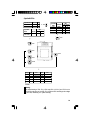
1
G586IPVF
Rev. A+
System Board
User’s Manual
- 31760710 -
FCC Statement on Class B
This equipment has been tested and found to comply with the limits for
a Class B digital device, pursuant to Part 15 of the FCC rules. These
limits are designed to provide reasonable protection against harmful interference when the equipment is operated in a residential installation.
This equipment generates, uses and can radiate radio frequency energy
and, if not installed and used in accordance with the instruction manual,
may cause harmful interference to radio communications. However,
there is no guarantee that interference will not occur in a particular installation. If this equipment does cause harmful interference to radio or
television reception, which can be determined by turning the equipment
off and on, the user is encouraged to try to correct the interference by
one or more of the following measures:
• Reorient or relocate the receiving antenna.
• Increase the separation between the equipment and the receiver.
• Connect the equipment into an outlet on a circuit different from that
to which the receiver is connected.
• Consult the dealer or an experienced radio TV technician for help.
Notice:
1. The changes or modifications not expressly approved by the party
responsible for compliance could void the user's authority to operate the equipment.
2. Shielded interface cables must be used in order to comply with the
emission limits.
The manufacturer makes no warranties with respect to this documentation and disclaims any implied warranties of merchantability, quality, or
fitness for any particular purpose. The information in this document is
subject to change without notice. The manufacturer reserves the right to
make revisions to this publication and to make changes to any and/or
all parts of its content, at any time, without obligation to notify any person or entity of such changes. Further, the manufacturer assumes no
responsibility for any errors that may appear in this document.
Table of Contents
Chapter 1: Introduction ............................................................ 5
Features and Specifications .................................................. 6
Package Checklist .............................................................. 8
Chapter 2: Hardware Installation ............................................... 9
Preparing the Area.............................................................. 9
Handling the System Board .................................................. 9
Installing the System Board .................................................10
Board Layout ....................................................................12
System Memory ................................................................13
DIMM ........................................................................13
SIMM ........................................................................14
Jumper settings for DIMM and SIMM ................................15
Cache Memory .................................................................16
Installing the Cache Module ...........................................16
CPU Installation ................................................................17
Jumper Settings for CPUs ..............................................18
Installing Upgrade CPUs ................................................21
Installing A Fan/Heatsink for Cyrix CPUs ...........................23
Jumper Settings for Password Clear and Display Type Select ......25
Built-in Ports .....................................................................26
Serial Ports .................................................................26
PS/2 Mouse Port ..........................................................27
Parallel Port ................................................................27
Floppy Disk Drive Controller ...........................................28
IDE Hard Disk Interface .................................................28
Installing Expansion Cards...................................................30
Chapter 3: Software Installation ............................................... 31
Award BIOS CMOS Setup Utility ...........................................31
Standard CMOS Setup ..................................................31
BIOS Features Setup ....................................................34
Chipset Features Setup .................................................41
Power Management Setup .............................................42
PNP/PCI Configuration Setup..........................................46
Load BIOS Defaults ......................................................48
Load Setup Defaults .....................................................48
Integrated Peripherials ...................................................48
Supervisor Password ....................................................52
User Password ............................................................52
IDE HDD Auto Detection ................................................53
HDD Low Level Format .................................................55
Save & Exit Setup ........................................................56
Exit Without Saving.......................................................57
System Error Report ..........................................................57
IDE Device Drivers .............................................................59
Chapter 4: Troubleshooting Checklist ............................................. 60
Appendix A: Types of Modules ...................................................... 61
Appendix B: Memory and I/O Maps ................................................ 62
Appendix C: PCI I/O Pin Assignments ............................................ 64
Appendix D: ISA I/O Pin Assignments ............................................ 65
Appendix E: Connector Pin Assignments ....................................... 66
Appendix F: Row Address of the DRAM and SDRAM ........................ 73
Appendix G: Using G586IPVF with CD-ROM Drives .......................... 74
4
Chapter 1
Introduction
The G586IPVF, equipped with a 321-pin Zero Insertion Force (ZIF)
CPU socket, is a fast Pentium processor-class system board supporting
Intel Pentium CPUs running at 75MHz, 90MHz, 100MHz, 120MHz,
133MHz, 150MHz, 166MHz and 200MHz frequencies. The G586IPVF
also supports Cyrix 6x86 P120+/P133+/P150+/P166+ and AMD-K5
PR75 75MHz/PR90 90MHz CPUs.
The G586IPVF can support 8MB to 128MB of system memory. It is
equipped with a DIMM socket using x64 EDO, fast page mode or
SDRAM, and 4 SIMM sockets using EDO or fast page mode x32
DRAM. This system board also supports pipeline burst SRAM, and provides easy cache upgrades using 256KB cache module.
The G586IPVF design is based on the Peripheral Component Interconnect (PCI) local bus and Industry Standard Architecture (ISA) standards. It is equipped with 3 dedicated PCI slots, 3 dedicated 16-bit ISA
slots and 1 shared PCI/ISA slot.
The G586IPVF board has two bus master PCI IDE connectors. Bus
mastering reduces CPU use during disk transfer. This system board is
also equipped with two NS16C550A-compatible serial ports, an SPP/
ECP/EPP parallel port, a floppy disk drive controller, one PS/2 mouse
port and one PS/2 or AT keyboard connector.
5
Features and Specifications
Processor
• Intel Pentium™ 75/90/100/120/133/150/166/200MHz
• Future Pentium™ OverDrive processor
• Cyrix 6x86 P120+/P133+/P150+/P166+
• AMD-K5 PR75 75MHz/PR90 90MHz
Chipset
• Intel 82430VX PCIset
Cache Memory
• Supports 256KB or 512KB pipeline burst, direct map write-back
cache
• One 160-pin cache module slot
• Onboard 256KB: upgradeable with a 256KB cache module for a
maximum of 512KB cache
System Memory
• 8MB to 128MB onboard memory
• One 168-pin DIMM socket using x64 EDO, fast page mode, or
SDRAM, 60ns or 70ns, 3.3V
• Four 72-pin SIMM sockets using EDO or fast page mode x32
DRAM, 60ns or 70ns, 5V
BIOS
• Award BIOS, Windows 95 Plug and Play compatible
• Flash EPROM for easy BIOS upgrades
Energy Efficient Design
• System power management supported
• CPU stopped clock control
• Hardware supports SMI green mode
• Microsoft/Intel APM 1.1 compliant
• External power management switch supported
6
PCI IDE Interface
• PIO Mode 3 and Mode 4 Enhanced IDE (data transfer rate up to
16.6MB/sec.)
• DMA Mode 2 Bus Master IDE (data transfer rate up to 22.2MB/
sec.)
• Bus mastering reduces CPU utilization during disk transfer
• ATAPI IDE CD-ROM supported
Integrated I/O
• Super I/O controller
• Two NS16C550A-compatible high speed UARTs
• One SPP/ECP/EPP parallel port
• Supports 360KB, 720KB, 1.2MB, 1.44MB, and 2.88MB floppy drives
• One IrDA TX/RX header
• Two universal serial bus connectors supported in future revision
CPU Socket
• 321-pin ZIF socket (Intel Socket 7)
• Supports future low-voltage CPUs
Connectors
• 2 serial ports
• 1 parallel port
• 2 IDE connectors
• 1 floppy connector
• 1 PS/2 mouse port
• 1 PS/2 or AT keyboard connector
Expansion Slots
• 3 dedicated PCI slots
• 3 dedicated 16-bit ISA slots
• 1 shared PCI/ISA slot
PCB
• 4 layers, Baby AT form factor
• 26cm (10.14") x 22cm (8.66")
7
Package Checklist
The G586IPVF package contains the following items:
•
•
•
•
•
•
•
•
•
The G586IPVF system board
The G586IPVF user’s manual
One 40-pin IDE hard disk cable
One 34-pin floppy disk drive cable
One 25-pin printer port cable for chassis mounting
One card-edge bracket for mounting the printer port cable
One card-edge bracket with serial and mouse port cables
One IDE driver diskette
Cache module (optional)
If any of these items are missing or damaged, please contact your
dealer or sales representative for assistance.
8
Chapter 2
Hardware Installation
This chapter summarizes the steps to install the G586IPVF system
board into your system unit. It also includes a description of the area in
which you must work and directions for memory installation. Before installing the system board, obtain the memory you plan to install. Please
refer to the information on pages 13 and 14 for the number and type of
memory modules needed for the amount of memory you require.
Preparing the Area
Before unpacking the system board, make sure the location you have
selected is relatively free of dust and static electricity. Excessive exposure to dust, static electricity, direct sunlight, excessive humidity, extreme cold, and water can damage the operational capabilities of your
system board. Avoid placing the unit on surfaces such as carpeted
floors. These areas also attract static electricity which can damage
some circuits on your system board.
Make sure the power source has a properly grounded, three-pronged
socket. It is essential that the power connection be properly grounded
for correct functioning of your system board. For further protection, we
recommend that you use a surge suppressor. This will protect the system board from damage that may result from a power surge on the
electrical line.
Move items that generate magnetic fields away from your system board
since magnetic fields can also damage your system board. Once you
have selected the ideal location, unpack the G586IPVF system board
carefully.
Handling the System Board
It is quite easy to inadvertently damage your system board even before
installing it in your system unit. Static electrical discharge can damage
computer components without causing any signs of physical damage.
You must take extra care in handling the system board to ensure
against electrostatic build-up.
9
Static Electricity Precautions
1. To prevent electrostatic build-up, leave the board in its anti-static
bag until you are ready to install it.
2. Wear an antistatic wrist strap.
3. Do all preparation work on a static-free surface with the system
board components facing up.
4. Hold the system board only by its edges. Be careful not to touch
any of the components, contacts or connections, especially gold
contacts, on the board.
5. Avoid touching the pins or contacts on all modules and connectors.
Hold modules and connectors by their ends.
Warning:
Electrostatic discharge (ESD) can damage your processor, disk drives,
add-in boards, and other components. Perform the upgrade instruction
procedures described at an ESD workstation only. If such a station is
not available, you can provide some ESD protection by wearing an antistatic wrist strap and attaching it to a metal part of the system chassis.
If a wrist strap is unavailable, establish and maintain contact with the
system chassis throughout any procedures requiring ESD protection.
Installing the System Board
If you are installing the G586IPVF system board, the following outlines
the basic installation steps. Before installing the system board into your
system unit, you should prepare the tools you will need.
You will need:
• One medium size, flat-bladed screwdriver
• One medium Phillips screwdriver
• One needle-nosed pliers
• One small nutdriver
1. Unlock your system unit. Turn off the power and disconnect all
power cords and cables.
10
2. Remove the system unit cover. Refer to the manufacturer’s instructions if necessary.
3. Detach all connectors from the old system board and remove expansion cards seated in any expansion slots.
4. Loosen the screws holding the original system board and remove
the board from the system. Save the screws.
5. Remove the G586IPVF from its original packing box. Be careful to
avoid touching all connectors and pins on the board. Please refer to
the handling instructions on pages 9-10 for proper handling techniques.
6. Insert the memory modules into the memory banks on the
G586IPVF. The quantity and location of the memory modules depends on the memory configuration and type of modules you intend
to use.
7. Insert the cache module, if any, into the cache module slot on the
G586IPVF. Refer to the Cache Memory section on page 16 for upgrading your cache memory.
8. Install the CPU. Be sure pin 1 of the CPU is aligned with pin 1 of
the socket.
9. Set the corresponding jumpers.
10. Install the prepared G586IPVF system board into the case and replace the screws.
11. Reinstall all cards and connectors and replace the system unit
cover. Reconnect all power cords and cables.
11
Board Layout
1. " " square denotes pin 1
2. PBSRAM = Pipeline Burst SRAM
12
System Memory
The G586IPVF system board supports two kinds of memory modules:
DIMM and SIMM. DIMM, which uses SDRAM, performs better than
SIMM, which uses DRAM.
DIMM
The DIMM (Dual In-line Memory Module) socket uses x64 EDO, FPM
and SDRAM. The G586IPVF system board can support 8MB to 16MB
memory using 1MBx64 or 2MBx64 168-pin DIMM. Refer to page 12 for
the location of the DIMM socket.
Installing the DIM Module
A DIM module simply snaps into a socket on the system board. Pin 1 of
the DIM module must correspond with Pin 1 of the socket.
Notch
Tab
Pin 1
Tab
Key
1. Pull the "tabs" which are at the ends of the socket to the side.
2. Position the DIMM above the socket with the "notches" in the module aligned with the "keys" on the socket.
3. Seat the module vertically into the socket. Make sure it is completely
seated. The tabs will hold the DIMM in place.
13
SIMM
The SIMM (Single In-line Memory Module) sockets are divided into two
banks on the system board, Bank 0 and Bank 1. Each bank consists of
2 SIMM sockets.
You will need either 2 or 4 pieces of SIM modules, depending on the
amount of memory you intend to install. The system board will not work
if you install 1 or 3 pieces. Make sure you insert the same type of
SIMMs in one bank. You can install SIMMs in either of the banks, Bank
0 or Bank 1, but you must populate a bank first before going to the next
bank.
The G586IPVF system board can support 8MB to 128MB of memory
using 1MBx32, 2MBx32, 4MBx32, or 8MBx32 72-pin SIMMs. The table
below shows the supported SIM modules and their corresponding
memory sizes.
SIMMs
Memory Size
1MBx32
2MBx32
4MBx32
8MBx32
4MB
8MB
16MB
32MB
Examples:
If you are installing 8MB of memory, you must insert two 1MBx32
SIMMs in Bank 0 or Bank 1. Inserting one 2MBx32 module will not
work.
If you are installing 24MB of memory, you must insert two 1MBx32
SIMMs in Bank 0 and two 2MBx32 SIMMs in Bank 1. You may also
install it vice versa by inserting two 1MBx32 SIMMs in Bank 1 and two
2MBx32 SIMMs in Bank 0.
Installing a SIM Module
A SIM module simply snaps into a socket on the system board. Pin 1 of
the SIM module must correspond with Pin 1 of the socket .
14
notch
key
1. Position the SIMM above the socket with the “notch”in the module
aligned with the “key”on the socket.
2. Seat the module at a 45° angle into the bank. Make sure it is completely seated. Tilt the module upright until it locks in place in the
socket.
Warning:
The DIMM and SIMM can not exist on the G586IPVF system board at
the same time. You must only use either a DIMM or SIMMs on your
system board.
Jumper Settings for DIMM and SIMM
Jumper JP10
DIMM and SIMM Select
Jumper JP10 must match the type of module installed on the G586IPVF
system board. If you change your memory module, make sure this
jumper is changed accordingly.
1
2
1
2
3
4
3
4
5
6
5
6
3-5, 4-6 On: DIMM
1-3, 2-4 On: SIMM
(Default)
15
Cache Memory
The G586IPVF system board can support 256KB or 512KB pipeline
burst, direct map write-back cache SRAM. Your system board may
come with 256KB or 512KB cache mounted onboard. The 160-pin
cache module slot lets you upgrade your cache memory by installing a
256KB cache module.
Note:
You do not need to set any jumpers or modify the Award BIOS Setup
utility when you install the cache module.
If your system board comes with 256KB cache at locations U22 and
U23, you can upgrade your cache memory to 512KB by installing a
256KB cache module in the cache module slot. Please refer to page 12
for the locations of the cache module slot (SSM1), U22 and U23.
Warning:
We highly recommend that you use the T2BSM32-256 cache module. If
you are using the cache module other than the one recommended
above, make sure your cache module meets the Intel COAST 2.x specification. Severe damage might occur on the cache module or system
board if you insert modules other than those specified above.
Installing the Cache Module
Locate the 160-pin cache module slot on the system board (SSM1).
Refer to page 12 for the location of SSM1. Position the cache module
above the slot. Make sure pin 1 of the cache module is aligned with pin
1 of the slot. Carefully slide the module into the slot. Press firmly on the
top of it to seat it properly.
16
Note:
With the cache module installed in the cache module slot, the components on the solder side of the add-in card in PCI Slot 2 must not protrude more than 5mm. The components on the component side of the
add-in card in PCI Slot 1 must not protrude more than 5mm too.
CPU Installation
The G586IPVF allows for easy installation of CPUs. Make sure all jumpers
are set correctly before applying power or you may damage the CPU or
system board. Please see the jumper settings on the following pages. Use
the needle-nosed pliers to move the jumpers if necessary.
17
Jumper Settings for CPUs
Intel CPUs
JP6
JP8
Intel CPUs
CPU CLK Pin 1-2 Pin 3-4
Off
Off
75/90/100MHz
1.5x
On
Off
120/133MHz
2x
On
On
150/166MHz
2.5x
Off
On
200MHz
3x
1
2
Intel CPUs
CPU CLK Pin 1-2 Pin 3-4
75MHz
50MHz
On
On
90/120/150MHz
60MHz
On
Off
100/133/166/
66MHz
Off
On
200MHz
↓
JP4
↓
Intel CPUs
CPU CLK JP4
75MHz
50MHz Off
90/100/120/133/ 60/66MHz On
150/166/200MHz
1
3
2
4
JP6
1
2
3
4
JP31
↓
3
4
1
2
JP8
3
4
1
2
JP9
1
3
5
2
4
6
JP11
1
3
5
2
4
6
JP30
↓
Voltage
2.5V
2.8V
2.9V
3.3V*
3.52V
JP9
1-2 On
1-2 On
1-2 On
1-2 On
3-4 On
JP11
1-3 On, 2-4 On
1-3 On, 2-4 On
1-3 On, 2-4 On
3-5 On, 4-6 On
3-5 On, 4-6 On
JP30
1-2 On
3-4 On
5-6 On
3-4 On
3-4 On
JP31
1-2 Off, 3-4 Off
1-2 Off, 3-4 Off
1-2 Off, 3-4 Off
1-2 On, 3-4 On
1-2 On, 3-4 On
*Default
Warning:
The default setting of JP9, JP11, JP30 and JP31 is 3.3V. If your CPU is not a
3.3V CPU, make sure you set JP9, JP11, JP30 and JP31 according to the voltage
of your CPU, otherwise, your system will hang.
18
Cyrix 6x86 CPUs
↓
Cyrix 6x86 CPUs CPU CLK JP4
P120+/P133+
50/55MHz Off
P150+/P166+
60/66MHz On
JP4
1
2
Cyrix 6x86
JP8
CPUs
PCI CLK Pin 1-2 Pin 3-4
P120+/P133+/
On
Off
2x
P150+/P166+
JP6
Cyrix 6x86
CPU
CLK
Pin
1-2
Pin 3-4
CPUs
50MHz
O
n
On
P120+
55MHz
Off
Off
P133+
60MHz
O
n
Off
P150+
66MHz
Off
O
n
P166+
↓
1
3
↓
3
4
1
2
JP8
3
4
1
2
JP9
1
2
1
3
5
2
4
6
JP11
1
3
5
2
4
6
JP30
2
4
3
4
JP6
JP31
↓
Voltage
2.5V
2.8V
2.9V
3.3V*
3.52V
JP9
1-2 On
1-2 On
1-2 On
1-2 On
3-4 On
JP11
1-3 On, 2-4 On
1-3 On, 2-4 On
1-3 On, 2-4 On
3-5 On, 4-6 On
3-5 On, 4-6 On
JP30
1-2 On
3-4 On
5-6 On
3-4 On
3-4 On
JP31
1-2 Off, 3-4 Off
1-2 Off, 3-4 Off
1-2 Off, 3-4 Off
1-2 On, 3-4 On
1-2 On, 3-4 On
*Default
Warning:
The default setting of JP9, JP11, JP30 and JP31 is 3.3V. If your CPU is not a
3.3V CPU, make sure you set JP9, JP11, JP30 and JP31 according to the voltage
of your CPU, otherwise, your system will hang.
19
AMD-K5 CPUs
JP6
JP4
1
2
AMD-K5 CPUs CPU CLK Pin 1-2 Pin 3-4
On
On
PR75 75MHz
50MHz
On
Off
PR90 90MHz
60MHz
↓
CPU CLK JP4
50MHz Off
60MHz On
↓
AMD-K5 CPUs
PR75 75MHz
PR90 90MHz
JP8
PCI CLK Pin 1-2 Pin 3-4
1.5x
Off
Off
AMD-K5 CPUs
PR75 75MHz/
PR90 90MHz
1
3
2
4
JP6
↓
3
4
1
2
JP8
3
4
1
2
JP9
1
3
5
2
4
6
JP11
1
3
5
2
4
6
JP30
1
2
3
4
JP31
↓
Voltage
2.5V
2.8V
2.9V
3.3V*
3.52V
JP9
1-2 On
1-2 On
1-2 On
1-2 On
3-4 On
JP11
1-3 On, 2-4 On
1-3 On, 2-4 On
1-3 On, 2-4 On
3-5 On, 4-6 On
3-5 On, 4-6 On
JP30
1-2 On
3-4 On
5-6 On
3-4 On
3-4 On
JP31
1-2 Off, 3-4 Off
1-2 Off, 3-4 Off
1-2 Off, 3-4 Off
1-2 On, 3-4 On
1-2 On, 3-4 On
*Default
Warning:
The default setting of JP9, JP11, JP30 and JP31 is 3.3V. If your CPU is not a
3.3V CPU, make sure you set JP9, JP11, JP30 and JP31 according to the voltage
of your CPU, otherwise, your system will hang.
20
Installing Upgrade CPUs
The G586IPVF is equipped with a 321-pin Zero Insertion Force (ZIF)
socket at location U25 of the system board. Refer to page 12 for the
location of the ZIF socket. This socket is designed for easy removal of
an old CPU and easy insertion of an upgrade CPU. The socket allows
you to carefully place the new CPU into its position. If you need to
apply excessive force to insert the CPU, you are not installing the CPU
correctly.
Warning:
Open the socket only if you are actually installing a CPU. The warranty
on the original CPU will be voided if the S/N seal is broken. Before
proceeding with the upgrade, take note of the following. The microprocessor and heatsink may be hot if the system has been running. To
avoid the possibility of a burn, power the system off and let the processor and heatsink cool for 10 minutes.
The 321-pin ZIF socket consists of five rows of pin holes on each side.
To prevent improper CPU installation, the ZIF socket has a Plug/Keying
mechanism. Several holes in the socket are plugged so that the CPU
will go in only one way. If you cannot easily insert the CPU, verify that
pin 1 of the CPU is aligned with pin 1 of the socket.
Zero Insetion Force (ZIF) Socket
21
To install an upgrade CPU, do the following.
1. Make sure the handle on the side of the ZIF socket is up. To raise
the handle, push it down, slightly pull it out to the side, then raise it
as far as it will go. It may be necessary to initially apply a small
amount of sideways force to free the handle from its retaining “tab”.
Once clear of the “tab”, the handle will open relatively easily. The
top plate will slide back. Do not use screwdrivers or other tools to
open the socket, or you may damage the system or socket.
Lifting the Handle
2. Once the lever is completely up, remove the old CPU carefully by
lifting it straight out of the socket. You are now ready to insert the
new CPU.
22
3. Position the CPU above the ZIF socket. Make sure pin 1 of the
CPU is aligned with pin 1 of the socket. Lower the chip until the
pins are inserted properly in their corresponding holes. Remember
that very little force is needed to install the CPU. If the CPU is not
easily inserted, verify whether or not pin 1 of the CPU is aligned
with pin 1 of the socket. Applying too much pressure can damage
the CPU or the socket.
Positioning the CPU Above the ZIF Socket
4. Push the handle down until the handle locks into place. The top
plate will slide forward. You will feel some resistance as the pressure starts to secure the CPU in the socket. This is normal and will
not damage the CPU. However, if the handle is not completely
closed, damage to the CPU and/or system board may result.
Installing A Fan/Heatsink for Cyrix CPUs
If you are using a Cyrix CPU, you must choose a fan/heatsink which is
made for Cyrix processors. Position the fan/heatsink on the CPU such
that the air from the side of the fan/heatsink will flow across the heat
regulators on the system board. See the figure on the next page.
23
Clearance Requirements
Your CPU comes with a heatsink mounted on top. To maintain proper
airflow once the upgrade is installed on the system board, the CPU and
heatsink require certain space clearances.
The clearance above the CPU’s fan/heatsink must be at least 0.4
inches. The clearance on at least 3 of 4 sides of the processor and
heatsink must be at least 0.2 inches. All cables (for floppy drive, hard
drive, CD-ROM, etc.) must be routed clear of the CPU and its airspace.
Fan Exhaust
The CPU must be kept cool by using a fan with heatsink. The temperature of the air entering the fan/heatsink cannot exceed 45oC (113oF).
The ambient or room temperature must be below 37oC (99oF).
24
Jumper Settings for Password Clear and Display
Type Select
Jumper JP2
Password Clear
If you set a password in the "Password Setting" option and forget your
password, power off your system and set jumper JP2 to On to clear the
password stored in your CMOS. Now power on your system. After your
system has detected the floppy or hard drive, turn it off again and set
JP2 to off.
Off: Normal
(Default)
On: Password Clear
Jumper JP3
Display Type Select
Jumper JP3 sets the display adapter to color or mono. This jumper
must match the type of display adapter installed. If you change your
video adapter, make sure this jumper is changed accordingly.
1
1
2
2
3
3
1-2 On: Color
(Default)
2-3 On: Mono
25
Built-in Ports
The G586IPVF system board is equipped with two serial ports, one parallel printer port, one FDD connector, two IDE hard disk shrouded headers and one PS/2 mouse connector. Refer to page 12 for the locations
of the built-in connectors and pin 1 of those connectors.
Serial Ports
The built-in serial ports are RS-232C asynchronous communication
ports with 16C550A-compatible UARTs that can be used with modems,
serial printers, remote display terminals, and other serial devices. They
use the following system I/O addresses:
Port Configuration
COM1
COM2
COM3
COM4
Serial Port 1
Serial Port 2
3F8h*
3F8h
2F8h
2F8h*
3E8h
3E8h
2E8h
2E8h
* Default
26
Connecting the Serial Ports
Two DB-9P serial port cables are provided with the system board. They
are mounted on a card-edge bracket along with the PS/2 mouse cable.
The upper serial port cable should be used for the COM 1 primary serial port; connect it to connector J4 on the system board. The lower
serial port cable should be used for the COM 2 secondary serial port;
connect it to connector J5 on the system board. Make sure the colored
stripes on the ribbon cables are aligned with pin 1 of connectors J4 and
J5. Mount the card-edge bracket to the system chassis.
PS/2 Mouse Port
The PS/2 mouse port is a 6-pin connector on the system board. Attach
the 6-pin mouse port cable, which is mounted on the card-edge bracket,
to connector J3. Make sure the brown wire on the PS/2 mouse connector is aligned with pin 1 of connector J3.
Parallel Port
The G586IPVF system board has a standard connector for interfacing
your PC to a parallel printer. The parallel port on your system board can
be set to any of the following system I/O addresses:
I/O Address: 3BC-3BE Hex
378-37A Hex (default)
278-27A Hex
Connecting the Parallel Printer Port
Attach the DB-25S printer cable, which came with the system board, to
connector J7 on the G586IPVF system board. Make sure the colored
stripe on the ribbon aligns with pin 1 of connector J7. Use a small
nutdriver to mount the cable into a DB-25 cutout in the system chassis.
You may also attach the cable to the card-edge bracket which came
with the system board. After attaching the cable to the card-edge
bracket, mount the bracket to the system chasis.
27
Floppy Disk Drive Controller
The G586IPVF system board has a built-in floppy disk controller that
supports two standard floppy disk drives. You can install any 360KB,
720KB, 1.2MB, 1.44MB, or 2.88MB floppy disk drives.
Connecting the Floppy Disk Cable
1. Install the 34-pin header connector into the floppy disk connector
(J6) on the system board. The colored edge of the ribbon should be
aligned with pin 1 of connector J6.
2. Install the other 34-pin header connector(s) into the disk drive(s).
Align the colored edge of the daisy chained ribbon cable with pin 1
of the drive edge connector(s). The end-most connector should be
attached to the drive you want to designate as Drive A.
IDE Hard Disk Interface
The G586IPVF system board is equipped with two PCI IDE shrouded
headers that will interface four Enhanced IDE (Integrated Drive Electronics) hard disk drives.
Note:
Only Enhanced IDE hard drives or ATAPI CD-ROMs can be connected
to the IDE interface.
Connecting the IDE Hard Disk Interface
To prevent improper IDE cable installation, each PCI IDE shrouded
header has a keying mechanism. The 40-pin connector on the IDE
cable can be placed into the header only if pin 1 of the connector is
aligned with pin 1 of the header.
28
Header
Note:
An IDE cable with a standard 40-pin connector (without the keying
mechanism) can be installed in the PCI IDE shrouded header. Be extremely careful to match the colored edge of the ribbon with pin 1 of the
header.
Connecting the Hard Disk Cable
1. If you are connecting two hard drives, install the 40-pin connector
of the IDE cable into the primary IDE shrouded header (connector
J8). If you are adding a third or fourth IDE device, install the 40-pin
connector of the other IDE cable into the secondary IDE shrouded
header (connector J9).
2. Install the other 40-pin header connector(s) into the device with the
colored edge of the ribbon cable aligned with pin 1 of the drive
edge connector(s).
Note:
Refer to your disk drive user’s manual for information about selecting
proper drive switch settings.
Adding a Second IDE Hard Drive
When using two IDE drives, one must be set as the master and the
other as the slave. Follow the instructions provided by the drive manufacturer for setting the jumpers and/or switches on the drives.
29
We recommend that the Enhanced IDE hard drives be from the same
manufacturer. In a few cases, drives from two different manufacturers
will not function properly when used together. The problem lies in the
hard drives, not the G586IPVF system board.
Preparing an IDE Drive for Use
IDE disk drives are already low-level formatted, with any bad-track errors entered, when shipped by the drive manufacturer. Do not attempt
to do a low-level format or you may cause serious damage to the drive.
To use an IDE drive, you need to enter the drive type (this information
is provided by the drive manufacturer) into the system’s CMOS setup
table. Then run FDISK and FORMAT provided with DOS. You also can
use the “IDE Auto Detection”to set your IDE Drive mode, please refer
to the relevant information on the section “IDE Auto Detection”.
Warning:
Do not run FDISK and FORMAT programs on a drive that has already
been formatted or you will lose all programs and data stored on the
drive.
Installing Expansion Cards
The G586IPVF system board is equipped with 3 dedicated PCI slots
and 3 dedicated 16-bit ISA slots and 1 shared PCI/ISA slot. All PCI
slots are bus masters. Refer to page 12 for the locations of the expansion slots.
Due to the size of the CPU with its accompanying fan/heatsink component, the length of the add-in cards in ISA slot 1, ISA slot 2 and PCI
slot 4 are limited to 18cm (7.07", measured from the bracket of the
card). With the cache module installed in the cache module slot, the
components on the solder side of the add-in card in PCI Slot 2 must not
protrude more than 5mm. The components of the component side of
the add-in card in PCI Slot 1 also must not protrude more than 5mm.
Note:
The BIOS needs to be configured for the PCI add-in cards installed in
the PCI slots. Refer to the “PCI Configuration Setup”presented in the
“Software Installation”section of the manual.
30
Chapter 3
Software Installation
After you power up your system, the BIOS message appears on your
screen and the memory count begins.
After the memory test, the following message will appear on the screen:
Press DEL to enter setup
If the message disappears before you respond, restart your system or
press the “Reset”button on the front of your computer. You may also
restart the system by pressing the <Ctrl> <Alt> and <Del> keys simultaneously.
If you have set a password and selected “System”in the Security Option of the BIOS Features Setup menu, you will be prompted for the
password every time the system is rebooted or any time you try to enter
Setup. Type in the correct password and press <Enter>.
If you selected “Setup”in the Security Option, you will be prompted for
the password only when you try to enter Setup. Refer to the “BIOS
Features Setup”section for more information.
Award CMOS Setup Utility
Press <Ctrl> <Alt> <Esc> simultaneously or <Del> to enter the Setup
utility. A screen similar to the one below will appear.
ROM PCI/ISA BIOS
CMOS SETUP UTILITY
AWARD SOFTWARE, INC.
STANDARD CMOS SETUP
BIOS FEATURES SETUP
CHIPSET FEATURES SETUP
POWER MANAGEMENT SETUP
PNP/PCI CONFIGURATION
LOAD BIOS DEFAULTS
LOAD SETUP DEFAULTS
ESC
F10
:Quit
:Sve & Exit Setup
INTEGRATED PERIPHERALS
SUPERVISOR PASSWORD
USER PASSWORD
IDE HDD AUTO DETECTION
HDD LOW LEVEL FORMAT
SAVE & EXIT SETUP
EXIT WITHOUT SAVING
↑↓→ ←
(Shift) F2
:Select Item
:Change Color
Time, Date, Hard Disk Type...
31
Use the arrow keys to highlight the option you want and press <Enter>.
The following describes each of these options.
Standard CMOS Setup
Use the arrow keys to highlight “Standard CMOS Setup”and press
<Enter>. A screen similar to the one below will appear.
ROM PCI/ISA BIOS
STANDARD CMOS SETUP
AWARD SOFTWARE, INC.
Date (mm:dd:yy) : Mon, Apr 15 1996
Time (hh:mm:ss) : 9 : 5 : 55
HARD DISKS
Primary Master
Primary Slave
Secondary Master
Secondary Slave
DriveA
DriveB
Video
Halt on
TYPE SIZE CYLS
0
:Auto
0
0
:Auto
0
0
:Auto
0
0
:Auto
0
HEAD PRECOMP LANDZ SECTOR
0
0
0
0
0
0
0
0
0
0
0
0
0
0
0
0
:1.44M,3.5in.
:None
:EGA/VGA
:All Errors
ESC :Quit
F1
:Help
MODE
AUTO
AUTO
AUTO
AUTO
Base Memory : 640K
Extended Memory : 31744K
Other Memory : 384K
Total Memory : 32768K
↑↓→ ←
(Shift)F2
:Select Item
:Change
PU/PD/+/-
: Modify
Date
Enter the current date in the following format: <Day>, <Date>, <Month>,
<Year>. These items can be altered; they are detected and displayed
automatically.
Day
Displays a day from Sunday to Saturday
Month
Displays the month, January through December
Date
Displays the date from 1 to 31
Year
Displays the last two digits of the year
Time
Enter the current time in the following format: <Hour>, <Minute>, <Second>. The time is based on the 24-hour military-time clock. For example, 1 p.m. is 13:00:00.
32
Hour
Displays hours from 00 to 23.
Minute
Displays minutes from 00 to 59.
Second
Displays seconds from 00 to 59.
Primary Master, Primary Slave, Secondary Master and Secondary
Slave
These categories allow you to enter the appropriate specifications for
the type of hard disk drive(s) installed in your system. There are 45
predefined types and 4 user definable types for Enhanced IDE BIOS.
Type 1 to Type 45 are predefined. Type user is user-definable.
Press <PgUp> or <PgDn> to select a numbered hard disk type or type
the number and press <Enter>. The hard disk will not work properly if
you enter improper information for this category. You can use Type
“User”to define your own drive type manually.
If you select Type “User”, you will need to know the information listed
below. Enter the information directly from the keyboard and press <Enter>. This information should be included in the documentation from
your hard disk vendor or the system manufacturer.
If the controller of the HDD interface is ESDI, you must select “Type 1”.
If the controller of the HDD interface is SCSI, you must select “None”.
If you select Type ”Auto”, the BIOS will auto-detect the HDD & CD-ROM
drive at the POST stage and show the IDE for the HDD & CD-ROM
drive.
Type
Drive type
Cyls
Number of cylinders
Heads
Number of heads
Precomp
Write precomp
Landzone
Landing zone
Sectors
Number of sectors
Mode
Mode type
If a hard disk has not been installed, select None and press <Enter>.
33
Drive A and Drive B
This category identifies the types of floppy disk drive installed. The following are the options for drives A and B.
None
No floppy drive is installed.
360K, 5.25" 5-1/4 inch PC-type standard drive; 360 kilobyte capacity.
1.2M, 5.25" 5-1/4 inch AT-type standard drive; 1.2 megabyte capacity.
720K, 3.5"
3-1/2 inch double-sided drive; 720 kilobyte capacity.
1.44M, 3.5" 3-1/2 inch double-sided drive; 1.44 megabyte capacity.
2.88M, 3.5" 3-1/2 inch double-sided drive; 2.88 megabyte capacity.
Note:
Choosing an incorrect type number might cause your system to format
the floppy disk improperly.
Item
Drive A
Drive B
Factory Default
1.44M, 3.5"
None
Video
This refers to the type of adapter used for the primary system monitor.
You should choose the setting that matches your video display card and
monitor. The four options are as follows:
EGA/VGA
Select this setting for EGA, VGA, SVGA and PGA monitor
adapters (Enhanced Graphics Adapter/ Video Graphics
Array).
CGA40
Power up in 40-column mode (Color Graphics Adapter).
CGA80
Power up in 80-column mode (Color Graphics Adapter).
Mono
Includes high resolution monochrome adapters (Monochrome adapter).
34
Halt on
This category controls whether the system will halt in case an error is
detected during power up.
No Errors
The system boot will not stop for any errors detected.
All Errors
The system boot will stop whenever the BIOS detects a
non-fatal error.
All, But
The system boot will not stop for a keyboard error; it will
Keyboard
stop for all other errors.
All, But
The system boot will not stop for a disk error; it will stop
Diskette
for all other errors.
All, But
The system boot will not stop for a disk or keyboard error;
Disk/Key
it will stop for all other errors.
Memory
The lower right corner of the Standard CMOS Setup Screen shows the
base memory size, extended memory size and the memory size of your
system.
Base
This refers to the amount of base or conventional memory
Memory
installed on the system board.
Extended
This is the amount of memory located above 1MB in the
Memory
memory address map of the CPU.
Other
This memory size refers to the memory located in the ad-
Memory
dress space between 640K and 1024K. DOS uses this
area to load device drivers to keep base memory free for
application programs. The most appropriate uses of this
area is for Shadow RAM.
BIOS Features Setup
The BIOS Features Setup allows you to configure your system for basic
operation. Some entries are defaults required by the system board,
while others, if enabled, will improve the performance of your system or
let you set some features according to your preference.
35
ROM PCI/ISA BIOS
BIOS FEATURES SETUP
AWARD SOFTWARE, INC.
Virus Warning
CPU Internal Cache
External Cache
Quick Power On Self Test
Boot Sequence
Swap Floppy Drive
Boot Up Floppy Seek
Boot Up NumLock Status
Gate A20 Option
Typematic Rate Setting
Typematic Rate (Char/Sec)
Typematic Delay (Msec)
Security Option
PCI/VGA Palette Snoop
OS Select For DRAM>64MB
: Disabled
: Enabled
: Enabled
: Enabled
: A, C
: Disabled
: Enabled
: On
: Fast
: Disabled
:6
: 250
: Setup
: Disabled
: Non-OS2
Video BIOS Shadow
C8000-CBFFF Shadow
CC000-CFFFF Shadow
D0000-D3FFF Shadow
D4000-D7FFF Shadow
D8000-DBFFF Shadow
DC000-DFFFF Shadow
ESC
F1
F5
F6
F7
: Enabled
: Disabled
: Disabled
: Disabled
: Disabled
: Disabled
: Disabled
:Quit
:Select Item
↑↓→ ←
PU/PD/+/- :Modify
:Help
:Old Values (Shift) F2 :Color
:Load BIOS Defaults
:Load Setup Defaults
Virus Warning
This category protects the boot sector and partition table of your hard
disk drive. When this item is enabled, the Award BIOS will monitor the
boot sector and partition table of the hard disk drive for any attempt at
modification. If an attempt is made, the BIOS will halt the system and
the following error message will appear.
! WARNING !
Disk boot sector is to be modified
Type “Y”to accept write or “N”to abort write
Award Software, Inc.
Afterwards, if necessary, you will be able to run an anti-virus program to
locate and remove the problem before any damage is done.
Many disk diagnostic programs which attempt to access the boot sector
table will cause the warning message to appear. If you are running such a
program, we recommend that you first disable this category. Also, disable
this category if you are installing or running certain operating systems like
Windows 95 or the operating system may not install nor work.
Enabled
BIOS issues a warning when any program or virus sends a
Disk Format command or attempts to write to the boot sector of the hard disk drive.
Disabled
No warning message will appear when the hard disk drive
is accessed.
36
CPU Internal Cache and External Cache
These categories speed up the memory access. However, it depends
on the CPU/chipset design. The default value is enabled. Enable the
External Cache for better performance.
Enabled
Enables the internal/external cache.
Disabled
Disables the internal/external cache.
Quick Power On Self Test
This category speeds up Power On Self Test (POST) after you power up
the computer. If it is set to Enable, BIOS will shorten or skip some check
items during POST.
Enabled Enabled quick POST.
Disabled Normal POST.
Boot Sequence
This category determines which drive to search first for the disk
operating system (i.e., DOS). Default value is A, C.
A, C
System will first search for a floppy drive and then a hard
disk drive.
C, A
System will first search for a hard disk drive and then a
floppy disk drive.
CDROM,
System will first search for CDROM drive, then hard disk
C, A
drive and then floppy disk drive.
C,
System will first search for hard disk drive, then CDROM
CDROM, A drive, and then floppy disk drive.
37
Swap Floppy Drive
Enabled
When this option is enabled and the system is booting
from the floppy drive, this option causes the system to
boot from drive B instead of drive A.
Disabled
When this option is disabled and the system is booting
from the floppy drive, the system will boot from drive A.
Boot Up Floppy Seek
During POST, BIOS will determine if the floppy disk drive is 40 or 80
tracks. 360KB type is 40 tracks while 720KB, 1.2M, 1.44M and 2.88MB
are all 80 tracks. The default value is Enabled.
Enabled
BIOS will check whether the floppy disk drive installed is 40
or 80 tracks. 360KB floppy disk drives have 40 tracks while
720KB, 1.2MB 1.44MB and 2.88MB floppy drives all have 80
tracks.
Disabled BIOS will not search for the type of floppy disk drive by track
number. There will not be any warning message if the drive
installed is 360KB.
Boot up NumLock Status
This allows you to determine the default state of the numeric keypad.
The default value is On.
On
The function of the numeric keypad is the number keys.
Off
The function of the numeric keypad is the arrow keys.
Gate A20 Option
This entry allows you to select how the gate A20 is handled. The gate
A20 is a device used to address memory above 1 Mbytes. Initially, the
gate A20 was handled via a pin on the keyboard. Today, while keyboards still provide this support, it is more common, and much faster, for
the system chipset to provide support for gate A20. The default value is
Fast.
38
Normal
Keyboard
Fast
Chipset
Typematic Rate Setting
When disabled, continually holding down a key on your keyboard will
cause the BIOS to report that the key is down. When the typematic rate
is enabled, the BIOS will not only report that the key is down, but will
first wait for a moment, and, if the key is still down, it will begin to report
that the key has been depressed repeatedly. For example, you would
use such a feature to accelerate cursor movements with the arrow keys.
Enabled
Enable the typematic rate.
Disabled
Disable the typematic rate.
Typematic Rate (Chars/Sec)
When the typematic rate is enabled, this selection allows you to select
the rate at which the keys are accelerated.
6
6 characters per second
8
8 characters per second
10
10 characters per second
12
12 characters per second
15
15 characters per second
20
20 characters per second
24
24 characters per second
30
30 characters per second
Typematic Delay (Msec)
When the typematic rate is enabled, this selection allows you to select
the delay between when the key was first depressed and when the acceleration begins.
39
250
250 msec
500
500 msec
750
750 msec
1000
1000 msec
Security Option
This category allows you to limit access to the system and setup, or just
to setup. The default value is Setup.
System
The system will not boot and access to setup will be denied
if the correct password is not enter at the prompt.
Setup
The system will boot, but access to setup will be denied if
the correct password is not entered at the prompt.
PCI/VGA Palette Snoop
It determines whether the MPEG ISA/VESA VGA Cards can work with
PCI/VGA or not. The default value is Disabled.
Enabled
PCI/VGA working with MPEG ISA/VESA VGA Card.
Disabled
PCI/VGA not working with MPEG ISA/VESA VGA Card.
OS Select for DRAM > 64MB
This item allows you to access the memory that is over 64MB in OS/2.
The options are: Non-OS2 and OS2.
Video BIOS Shadow
Determines whether video BIOS will be copied to RAM. Video Shadow
will increase the video speed. The default value is Enabled.
Enabled
Video shadow is enabled.
Disabled Video shadow is disabled.
40
C8000-CBFFF Shadow to DC000-DFFFF Shadow
These categories determine whether option ROMs will be copied to
RAM.
Enabled
Optional shadow is enabled.
Disabled
Optional shadow is disabled.
Chipset Features Setup
The G586IPVF system board uses the Intel 82430VX chipset. This section allows you to configure the system based on the specific features
of the chipset. This chipset manages bus speeds and access to system
memory resources, such as DRAM and the external cache. It also coordinates communications between the conventional ISA bus and the PCI
bus. These items should not be altered unless necessary. The default
settings have been chosen because they provide the best operating
conditions for your system. The only time you might consider making
any changes would be if you discovered that data was being lost while
using your system.
ROM PCI/ISA BIOS
CHIPSET FEATURES SETUP
AWARD SOFTWARE, INC.
Auto Configuration
DRAM Timing
: Enabled
: 60 ns
DRAM RAS# Precharge Time
DRAM R/W Leadoff Timing
Fast RAS To CAS Delay
DRAM Read Burst (EDO/FP)
DRAM Write Burst Timing
Fast MA to RAS# Delay CLK
Fast EDO Path Select
Refresh RAS# Assertion
ISA Bus Clock
:3
:6
:3
: x222/x333
: x222
:1
: Disabled
: 4 Clks
: PCICLK/4
System BIOS Cacheable
Video BIOS Cacheable
8 Bit I/O Recovery Time
16 Bit I/O Recovery Time
Memory Hole At 15M-16M
Peer Concurrency
: Enabled
: Enabled
:1
:1
: Disabled
: Enabled
ESC
F1
F5
F6
F7
↑↓→ ←
:Select Item
:Quit
PU/PD/+/- :Modify
:Help
:Old Values (Shift) F2 :Color
:Load BIOS Defaults
:Load Setup Defaults
Auto Configuration
Enabled The system will set the DRAM Timing automatically. The
predefined items will become show-only.
Disabled The system will set the DRAM Timing to manual.
41
Power Management Setup
The Power Management Setup allows you to configure your system to
most effectively save energy.
ROM PCI/ISA BIOS
POWER MANAGEMENT SETUP
AWARD SOFTWARE, INC.
Power Management : Disabled
PM Control by APM : Yes
Video Off Method
: V/H SYNC+Blank
Doze Mode
Standby Mode
Suspend Mode
HDD Power Down
: Disabled
: Disabled
: Disabled
: Disabled
** Wake Up Events In Doze & Standby **
IRQ3 (Wake-Up Event) : On
IRQ4 (Wake-Up Event) : On
IRQ8 (Wake-Up Event) : On
IRQ12 (Wake-up Event) : On
** Power Down & Resume Events **
: On
IRQ3 (COM 2)
: On
IRQ4 (COM 1)
: On
IRQ5 (LPT 2)
: On
IRQ6 (Floppy Disk)
: On
IRQ7 (LPT 1)
: On
IRQ8 (RTC Alarm)
: Off
IRQ9 (IRQ2 Redir)
: On
IRQ10(Reserved)
: On
IRQ11(Reserved)
: On
IRQ12 (PS2 Mouse)
: On
: On
IRQ13 (Corpocessor)
: On
IRQ14 (Hard Disk)
: Off
IRQ15 (Reserved)
ESC
F1
F5
F6
F7
:Select Item
:Quit
↑↓→ ←
:Help
PU/PD/+/- :Modify
:Old Values (Shift) F2 :Color
:Load BIOS Defaults
:Load Setup Defaults
Power Management
This category allows you to select the type (or degree) of power saving
and is directly related to the following modes: Doze Mode, Standby
Mode, and Suspend Mode. The default value is Disabled.
Disabled
No power management. Disables all three modes.
Min Power The predefined timer settings that have the max values.
Saving
Doze Mode = 1hr. Standby Mode = 1hr., Suspend Mode =
1hr., and HDD Power Down = 15min.
Max Power The predefined timer settings that have the min values. Doze
Saving
Mode = 1min., Standby Mode = 1min., Suspend Mode =
1min., and HDD Power Down=1min.
User
Allows you to set each mode individually. When not disabled,
Defined
each ranges from 1min. to 1hr. except for HDD Power Down
which ranges from 1min. to 15 min. and disable.
PM Control by APM
If the Max Power Saving is not enabled, this will be preset to No. The
default value is Yes.
42
Yes
System Power Management will wait for the APM calls before it enters a software power management mode.
Note: If the APM is installed and there is a task running, the
APM will not prompt the BIOS to put the system into
any of the power management modes even if the APM
timer is out.
Normally, the APM is installed in the DOS and Windows
systems by loading the device C:\DOS\POWER.EXE file
in CONFIG.SYS. In Windows 95, enable Power Management before installing the operating system or the Windows 95 APM may not work.
No
The System BIOS will ignore Advanced Power Management
(APM) when initiating the power management mode.
Note: If the APM is not installed, this option has no effect.
Video Off Method
This determines the manner in which the monitor is blanked. The default
value is V/H SYNC + Blank.
V/H
This selection will cause the system to turn off the vertical
SYNC+
and horizontal synchronization ports and write blanks to the
Blank
video buffer.
Note: After detecting the V/H SYNC signals, an energy saving monitor will turn off its table.
Blank
This option only writes blanks to the video buffer.
Screen
DPMS
This option should be enabled only for VGA cards supporting
DPMS. Initial Display Power Management Sigaling.
Doze Mode
When enabled and after the set time of the system inactivity, the CPU
clock will run at slower speed while all other devices still operate at full
speed. The default value is Disabled.
43
Disabled This function cannot be executed.
1Min-1Hr This option defines the idle time that elapses before the system enters the Doze mode.
Standby Mode
When enabled and after the set time of the system inactivity, the fixed
disk drive and the video would be shut off while all other devices still
operate at full speed. The default value is Disabled.
Disabled This function cannot be executed.
1Min-1Hr The Standby mode will be set to one minute.
This option defines the idle time that elapses before the system enters Standby mode.
Suspend Mode
When enabled and after the set time of system inactivity, all devices
except the CPU will be shut off. The default value is Disabled.
Disabled This function cannot be executed.
1Min-1Hr The Suspend mode will be set to one minute.
This option defines the idle time that elapses before the system enters the Suspend mode.
HDD Power Mode
When enabled and after the set time of system inactivity, the hard drive
will be powered down while all other devices remain active. The default
value is Disabled.
Disabled This function cannot be executed.
1Min-
The HDD Power Down mode will be set to one minute.
15Min
The option defines the continuous HDD idle that elapses before the HDD enters the power saving mode (motor off).
Note: When a HDD is in power saving mode, any access to
the HDD will wake up the HDD.
44
Wake Up Event In Doze & Standby (IRQ3, 4, 8 and 12)
The default value is On.
On
The activity of this wake-up event causes the timers to be
reset, i.e., the Power Management Unit (PMU) monitors the
specified activities as power management events.
Off
The activity of this event will not affect the power management timers.
Power Down & Resume Events (IRQ 3 - 15)
Power Down and Resume events are I/O events whose occurrence can
prevent the system from entering a power saving mode or can awaken
the system from such a mode. In effect, the system remains alert for
anything which occurs to a device which is configured as On, even
when the system is in a power down mode.
The following is a list of IRQ's, Interrupt ReQuests, which can be exempted much as the COM ports and LPT ports above can. When an I/O
device wants to gain the attention of the operating system, it signals
this by causing an IRQ to occur. When the operating system is ready to
respond to the request, it interrupts itself and performs the service.
When set on, activity will neither prevent the system from going into a
power management mode nor awaken it.
The default value is On.
On
The activity of this event causes the power management timers to be reset, i.e., the Power Management Unit (PMU)
monitors the specified activities as power management
events.
Off
The activity of this event will not affect the power management timers.
45
PNP/PCI Configuration Setup
This section describes configuring the PCI bus system. PCI, or
Peropheral Computer Interconnect, is a system which allows I/O devices to operate at speeds nearing the speed the CPU itself uses when
communicating with its own special components. This section covers
some very technical items and it is strongly recommended that only experienced users should make any changes to the default settings.
ROM PCI/ISA BIOS
PNP/PCI CONFIGURATION SETUP
AWARD SOFTWARE, INC.
Resources Control By
Reset Configuration Data
:Auto
:Disabled
PCI IRQ Active By
PCI IDE IRQ Map To
Primary
IDE INT#
Secondary IDE INT#
ESC
F1
F5
F6
F7
:
:
:
:
Level
PCI-AUTO
A
B
↑↓→ ←
:Select Item
:Quit
PU/PD/+/- :Modify
:Help
:Old Values (Shift) F2 :Color
:Load BIOS Defaults
:Load Setup Defaults
Resources Controlled By
The BIOS has the capacity to automatically configure all of the boot
and compatible devices. However, this capability means absolutely
nothing unless you are using an operating system such as Windows 95.
The default value is Auto.
Auto
The BIOS will control the locations of the resources.
Manual
You can set the locations of the resources. The screen will
show the information of the IRQ and DMA.
Reset Configuration Data
This item allows you to determine whether to reset the configuration
data or not.
Enabled The BIOS will reset the configuration data automatically.
Disabled The BIOS will not reset the configuration data.
46
PCI IRQ Activated By
This sets the method by which the PCI bus recognizes that an IRQ
service is being requested by a device. Under all circumstances, you
should retain the default configuration unless advised otherwise by your
system's manufacturer. The default value is Level.
Level
The interrupt will be controlled by the level.
Edge
The interrupt will be controlled by the edge.
PCI IDE IRQ Map To
This allows you to configure your system to the type of IDE disk controller in use. By default, setup assumes that your controller is an ISA device rather than a PCI controller. The more apparent difference is the
type of the slot being used.
If you have equipped your system with a PCI controller, changing this
allows you to specify which slot has the controller and which PCI interrupt (A, B, C or D) is assumed with the connected hard devices.
This setting refers to the hard disk drive itself, rather than individual
partitions. Since each IDE controller supports two separate hard drives,
you can select the INT# for each. You will note that the primary has a
lower interrupt than the secondary.
Selecting "PCI Auto" allows the system to automatically determine how
your IDE disk system is configuration. The default value is PCI-Auto.
PCI-Auto The BIOS will scan for PCI IDE devices and determine the
location of the PCI IDE device.
ISA/PCI- You can determine the location of the PCI IDE device in ISA,
Slot 1-4
PCI-SLOT 1, 2 ,3 or 4.
Primary/Secondary IDE INT #
A/B/C/D You can choose INT A, B, C or your D PCI IDE card is using
for its interrupt.
47
Load BIOS Defaults
The “Load BIOS Defaults”option loads the troubleshooting default values permanently stored in the ROM chips. These settings are not optimal and turn off all high performance features. You should use these
values only if you have hardware problems. Highlight this option on the
main menu and press <Enter>. The message below will appear.
Load BIOS Defaults (Y/N)? N
If you want to proceed, press <Y> and the default settings will be
loaded.
Load Setup Defaults
The “Load Setup Defaults”option loads optimized settings from the
BIOS ROM. Use the Setup default values as standard values for your
system
Highlight this option on the main menu and press <Enter>. The message below will appear.
Load Setup Defaults (Y/N)? N
Type <Y> and press <Enter> to load the Setup default values.
Integrated Peripherals
Use the arrow keys to highlight “Integrated Peripherals”and press
<Enter>. A screen similar to the one on the next page will appear.
48
ROM PCI/ISA BIOS
INTEGRATED PERIPHERALS
AWARD SOFTWARE, INC.
IDE HDD Block Mode
IDE Primary Master PIO
IDE Primary Slave PIO
IDE Secondary Master PIO
IDE Secondary Slave PIO
On-Chip Primary PCI IDE
On-Chip Secondary PCI IDE
PCI Slot IDE 2nd Channel
: Enabled
: AUTO
: AUTO
: AUTO
: AUTO
: Enabled
: Enabled
: Disabled
Onboard FDD Controller
Onboard Serial Port 1
Onboard Serial Port 2
UART 2 Mode
Onboard Parallel Port
Onboard Parallel Mode
: Enabled
: 3F8/IRQ4
: 2F8/IRQ3
: Standard
: 378H/IRQ7
: SPP
ESC
F1
F5
F6
F7
↑↓→ ←
:Quit
:Select Item
PU/PD/+/- :Modify
:Help
:Old Values (Shift) F2 :Color
:Load BIOS Defaults
:Load Setup Defaults
IDE HDD Block Mode
If this option is enabled, the system BIOS will check the hard disk drive
for the maximum block size the system can transfer. The block size
depends on the type of your hard disk. If the option is disabled, the
system BIOS will check the hard disk drive for standard mode. The
default value is Enabled.
Enabled IDE controller uses block mode.
Disabled IDE controller uses standard Mode.
IDE Primary or Secondary Master/Slave PIO
IDE hard drive controllers can support up to two separate hard drives.
These drives have a master/slave relationship which are determined by
the cabling configuration used to attach them to the controller. Your
system supports two IDE controllers - a primary and a secondary - so
you have to ability to install up to four separate hard disks.
PIO means Programmed Input/Output. Rather than have the BIOS issue a
series of commands to effect a transfer to or from the disk drive, PIO allows
the BIOS to tell the controller what it wants and then let the controller and
the CPU perform the complete task by themselves. The simpler and more
efficient (and faster).
Your system supports five modes, numered from 0 (default) to 4, which
primarily differ in timing. When Auto is selected, the BIOS will select the
best available mode.
49
Auto
The BIOS will set the system board to fit the hard disk drive
timing automatically.
Mode 0-4 You can select the setting to fit your hard disk timing.
On-Chip Primary/Secondary PCI IDE
This setup item allows you to either enable or disable the primary/
secondary controller. You might choose to disable the controller if you
were to add a higher performance or specialized controller. The default
value is Enabled.
Enabled
Primary/Secondary HDD controller used.
Disabled Primary/Secondary HDD controller not used.
PCI Slot IDE 2nd Channel
This item allows you to designate an IDE controller board inserted into
one of the physical PCI slots as your secondary IDE controller. The
default value is Disabled.
Enabled External IDE Controller designated as the secondary controller.
Disabled No IDE controller occupying a PCI slot.
Onboard FDD Controller
This item allows you to designate a floppy controller board inserted into
one of the slots as your floppy controller. The default value is Enabled.
Enabled
FDD Controller used.
Disabled FDD Controller not used.
Onboard Serial Port 1 or 2
This option allows you to control the assignment of the serial port 1 or 2
connector on the system board. The default value of port 1 is 3F8/IRQ4,
and that of port 2 is 2F8/IRQ3.
50
Disabled When disabled, you cannot set the assignment of the serial
port.
3F8/IRQ4 This option allows you to control the assignment of the serial
2F8/IRQ3 port 1 or 2 connector on the system board.
3E8/IRQ4
2E8/IRQ3
UART 2 Mode
This item allows you to use IrDA function. The default value is Standard.
Standard If you are using the COM 2 serial port.
HPSIR
If your IrDA is an HP standard.
ASKIR
If your IrDA is a SHARP standard.
Onboard Parallel Port
The default value is 378H/IRQ7.
Disabled
When disabled, you cannot select the address and IRQs of
the onboard parallel port.
278H/IRQ5 This option allows you to select different addresses and
378H/IRQ7 IRQs the onboard parallel port.
3BC/IRQ7
Parallel Port Mode
The default value is SPP.
SPP
This function is the mode of the device. Set this according to
EPP/SPP your parallel devices.
ECP
ECP/EPP
51
Supervisor Password
If you want to protect your system and setup from unauthorized entry,
set a supervisor’s password with the “System”option selected in the
BIOS Features Setup.
If you want to protect access to setup only, but not your system, set a
supervisor’s password with the “Setup”option selected in the BIOS Features Setup. You will not be prompted for a password when you cold
boot the system.
Use the arrow keys to highlight the “Supervisor Password”option and
press <Enter>. The message below will appear.
Enter Password:
Type in the password. You are limited to eight characters. When done,
the message below will appear:
Confirm Password:
You are asked to verify the password. Type in exactly the same password. If you type in a wrong password, you will be prompted to enter
the correct password again.
To delete or disable the password function, highlight “Supervisor Password”and press <Enter>, instead of typing in a new password. Press
the <Esc> key to return to the main menu.
User Password
If you want another user to have access only to your system but not to
setup, set a user’s password with the “System”option selected in the
BIOS Features Setup.
If you want a user to enter a password when trying to access setup, set
a user’s password with the “Setup”option selected in the BIOS Features Setup. Using user’s password to enter Setup allows a user to
access only the “User Password”option that appears on the main
screen. Access to all other options is denied.
52
To set, confirm, verify, disable or delete a user’s password, follow the
procedures described in the section “Supervisor Password”. If you forget your password, refer to the procedure described in the same section.
IDE HDD Auto Detection
This option detects the hard disk parameters for the hard disk drives
installed in your system. Highlight this option and press <Enter>. A
screen similar to the one below will appear.
ROM PCI/ISA BIOS
CMOS SETUP UTILITY
AWARD SOFTWARE, INC.
HARD DISKS
TYPE SIZE CYLS HEAD RECOMP LANDZ SECTOR MODE
Primary Master:
Select Primary Master Option (N=Skip): N
OPTIONS
SIZE
CYLS
HEAD
2 (Y)
1
3
853
853
853
827
1654
827
32
16
32
RECOMP
0
65535
65536
LANDZ
SECTOR
MODE
1653
1653
1653
63
63
63
LBA
Normal
Large
Note: Some OS (like SCO-UNIX) must be “NORMAL” for installation
ESC: Skip
Enter your choice, and press <Enter> to accept the parameters or press
<Esc> to abort. The parameters of the hard disk will be displayed in the
Standard CMOS Setup.
Hard Drive Mode
The G586IPVF supports three HDD modes: Normal, LBA and Large. If
your hard disk drive does not support LBA mode, the “LBA”option will
not be displayed. If your HDD has 1024 or fewer cylinders, the “Large”
option will not be displayed.
Normal Mode
The Normal mode is the generic access mode in which neither the
BIOS nor the IDE controller will make any transformations during harddrive access.
53
The maximum number of cylinders, heads and sectors for Normal mode
are 1024, 16 and 63, respectively.
no. Cylinders
x no. Heads
x no. Sectors
x bytes per sector
(1024)
( 16)
( 63)
( 512)
528 megabytes
If you set your HDD to Normal mode, the maximum accessible HDD will
be 528 megabytes even though the physical size of the HDD may be
greater than that.
LBA (Logical Block Addressing) Mode
The LBA mode is a HDD accessing method to overcome the 528 megabyte limitation. The number of cylinders, heads and sectors shown on
the screen may not be the actual number for the HDD.
During the HDD accessing, the IDE controller will transform the logical
address described by the sector, head and cylinder number into its own
physical address inside the HDD.
The maximum HDD size supported by the LBA mode is 8.4 gigabytes. It
is obtained by the following formula.
no. Cylinders
x no. Heads
x no. Sectors
x bytes per sector
(1024)
( 255)
( 63)
( 512)
8.4 gigabytes
54
Large Mode
Large mode is the extended HDD access mode supported by the
G586IPVF system boards. Some IDE HDDs have more than 1024 cylinders without LBA support (in some cases, you may not want the LBA
mode). These system boards provide another alternative to support
these kinds of HDDs.
The BIOS tells the operating system that the number of cylinders is half
of the actual number and that the number of heads is double the actual
number. During disk access, the reverse conversion is done by the
INT13h routine.
Example of Large mode:
CYLS. HEADS SECTORS MODE
1120
560
16
32
59
59
NORMAL
LARGE
Maximum HDD size:
no. Cylinders
x no. Heads
x no. Sectors
x bytes per sector
(1024)
( 32)
( 63)
( 512)
1 gigabyte
Note:
To support LBA or Large mode, address translation software is included
in the Award BIOS HDD Service Routine (INT13h). If you are running
an operating system that bypasses the BIOS Int13 Service Routine,
LBA and Large Mode may fail.
HDD Low Level Format
This option will format, set the interleave mode and do a media analysis
of your hard drives. Highlight this option and press <Enter>. A screen
similar to the one on the next page will appear.
55
ROM PCI/ISA BIOS
CMOS SETUP UTILITY
AWARD SOFTWARE, INC.
Hard Disk Low Level Format Utility
No. CYLS HEAD
SELECT DRIVE
BAD TRACK LIST
PREFORMED
Current select drive is : C
DRIVE: C CYLINDER: 0
SIZE
Primary Master:
853
Primary Slave:
0
Secondary Master:
0
Secondary Slave:
0
CYLS
1654
0
0
0
HEAD: 0
HEAD RECOMP
16
65536
0
0
0
0
0
0
LANDZ
1653
0
0
0
SECTOR
63
0
0
0
MODE
AUTO
AUTO
AUTO
AUTO
Up/Down-Select item
ENTER-Accept
ESC-Exit/Abort
Copyright (C) Award Software, Inc. 1992-94 All Rights Reserved
Warning:
Do not attempt to do a low-level format on an IDE drive, or you may
cause serious damage to the drive. IDE disk drives are already lowlevel formatted, with any bad-track errors entered, when shipped by the
drive manufacturer.
Save & Exit Setup
When all the changes have been made, highlight “Save & Exit Setup”
and press <Enter>. The message below will appear:
Save to CMOS and Exit (Y/N)? N
Type “Y”and press <Enter>. The following message will appear:
Reboot System (Y/N)? N
Type “Y”and press <Enter>. The modifications you have made will be
written into the CMOS memory, and the system will reboot. You will
once again see the initial diagnostics on the screen. If you wish to
make additional changes to the setup, press <Ctrl> <Alt> <Esc> simultaneously or <Del> after memory testing is done.
56
Exit Without Saving
When you do not want to save the changes you have made, highlight “Exit
Without Saving”and press <Enter>. The message below will appear:
Quit Without Saving (Y/N)? N
Type “Y”and press <Enter>. The system will reboot and you will once
again see the initial diagnostics on the screen. If you wish to make any
changes to the setup, press <Ctrl> <Alt> <Esc> simultaneously or
<Del> after memory testing is done.
System Error Report
When the BIOS encounters an error that requires the user to correct
something, either a beep code will sound or a message will be displayed in a box in the middle of the screen and the message PRESS
F1 TO CONTINUE, CTRL-ALT-ESC or DEL TO ENTER SETUP, will be
shown in the information box at the bottom. Enter Setup to correct the
error.
POST Beep
Currently there are two kind of beep codes in BIOS. The one code
indicates that a video error has occured and the BIOS cannot initialize
the video screen to display any additional information. This beep code
consists of a signle long beep followed by three short beeps. The other
one code indicates that your DRAM error has occured. This beep code
consists of a signle long beep repeatedly.
Error Messages
One or more of the following messages may be displayed if the BIOS
detects an error during the POST. This list indicates the error messages
for all Awards BIOSes:
CMOS BATTERY HAS FILED
CMOS battery is no longer functional. It should be replaced.
57
CMOS CHECKSUM ERROR
Checksum of CMOS is incorrect. This can indicate that CMOS has become corrupt. This error may have been caused by a weak battery.
Check the battery and replace if necessary.
DISPLAY SWITCH IS SET INCORRECTLY
Display switch on the motherboard can be set to either monochrome or
color. This indicates the switch is set to a different setting than indicated in Setup. Determine which setting is correct, and then either turn
off the system and change the jumper, or enter Setup and change the
VIDEO selection.
FLOPPY DISK(S) fail (80) → Unable to reset floppy subsystem.
FLOPPY DISK(S) fail (40) → Floppy Type dismatch.
Hard Disk(s) fail (80) →
HDD reset failed.
Hard Disk(s) fail (40) →
HDD controller diagnostics failed.
Hard Disk(s) fail (20) →
HDD initialization error.
Hard Disk(s) fail (10) →
Unable to recalibrate fixed disk.
Hard Disk(s) fail (08) →
Sector Verify failed.
Keyboard is locked out - Unlock the key
BIOS detect the keyboard is locked. Keyboard controller is pulled low.
Keyboard error or no kayboard present
Cannot initialize the keyboard. Make sure the keyboard is attached correctly and no keys are being pressed during the boot.
Manufacturing POST loop
System will repeat POST procedure infinitely while the keyboard controller is pull low. This is also used for M/B burn in test.
BIOS ROM checksum error - System halted
The checksum of ROM address F0000H-FFFFFH is bad.
58
Memory test fail
BIOS reports the memory test fail if the onboard is tested error.
IDE Device Drivers
To install the IDE device drivers supported by the G586IPVF system
boards, please refer to the “Readme”file contained in the provided diskette.
59
Chapter 4
Troubleshooting Checklist
If you experience difficulty with the G586IPVF system board, please refer to the checklist below. If you still cannot identify the problem, please
contact your dealer.
1. Check the jumper settings to ensure that the jumpers are properly
set. If in doubt, refer to the “Hardware Installation”section.
2. Verify that all SIMMs or DIMM are seated securely into the bank
sockets.
3. Make sure the SIMMs or DIMM are in the correct locations.
4. Check that all populated memory banks are filled with correctly
sized SIMMs.
5. If your board fails to function, place the board on a flat surface and
seat all socketed components (gently press each component into
the socket).
6. If you made changes to the BIOS settings, re-enter setup and
load the BIOS defaults.
60
Appendix A
Types of Modules
The G586IPVF system board allows you to populate memory with
1MBx64 or 2MBx64 DIMM, and 1MBx32, 2MBx32, 4MBx32 and
8MBx32 SIMMs. The following modules have been tested with this
board. Most untested brands will work but a few may fail to do so.
DIMM
DIMM
Brand
Chip Number
1MBx64
NEC
D4516161G5-7JF
(SDRAM)
SIMM
Brand
Chip Number
1MBx32
Fujitsu
OKI
81C1000A-70
M51440A-70
2MBx32
OKI
NEC
Micron
TI
Micron
Micron
NEC
M511000B-70
424400-60
40447-60
TMS4400DJ-70
MT4C4007-70 (EDO)
MT4C4007-60 (EDO)
4218165-60 (EDO)
4MBx32
Hitachi
Fujitsu
Mitsubishi
Hitachi
NEC
NEC
7400AS-70
8117400-70
422A06-70
5117400AS-70
4217400-60
4217405-70 (EDO)
8MBx32
NEC
4217405-60 (EDO)
SIMM
61
Appendix B
Memory and I/O Maps
Memory Address Map
62
Address
Name
Function
00000000 to
0009FFFF
640KB System
Board RAM
System Board Memory
000A0000 to
000BFFFF
128KB Video
Display Memory
Reserved for Graphics
Display Memory
000C0000 to
000E7FFF
160KB I/O
Expansion ROM
Reserved for ROM on
I/O Adapter Card
000E8000 to
000FFFFF
96KB ROM on
the System Board
System Board BIOS
00100000 to
07FFFFFF
Maximum
Memory 128MB
System Board Memory
I/O Address Map
I/O Address
0000-001F
0020-003F
0040-005F
0060-006F
0070-007F
0080-009F
00A0-00BF
00C0-00DF
00E8
00F0
00F1
00F8-00FF
01F0-01F8
0200-0207
0278-027F
02F8-02FF
0300-031F
0360-036F
0378-037F
0380-038F
03A0-03AF
03B0-03BF
03C0-03CF
03D0-03DF
03F0-03F7
03F8-03FF
Function
DMA Controller 1, 8237A-5
Interrupt Controller 1, 8259A, Master
Timer, 8254-2
8742 (Keyboard Controller)
Real-time Clock, NMI
(Non-maskable Interrupt) Mask
DMA Page Memory, 74LS612
Interrupt Controller 2, 8259A
DMA Controller 2, 8237A-5
Shadow RAM and Cache Control Bit
Clear Numeric Processor
Extension Busy
Reset Numeric Processor Extension
Numeric Processor Extension
Fixed Disk
Game I/O
Parallel Printer Port 2
Serial Port 2
Prototype Card
Reserved
Parallel Printer Port 1
SDLC, Bisynchronous 2
Bisynchronous 1
Monochrome Display and Printer Adapter
Reserved
Color/Graphics Monitor Adapter
Diskette Controller
Serial Port 1
Note:
The I/O address hex 0000 to 00FF are reserved for the system board I/
O. Hex 0100 to 03FF are available on the I/O channels.
63
Appendix C
PCI I/O Pin Assignments
B
-12V
TCK
Ground
TDO
+5V
+5V
INTB#
INTD#
PRSNT1#
Reserved
PRSNT2#
Ground
Ground
Reserved
Ground
CLK
Ground
REQ#
+5V (I/O)
AD[31]
AD[29]
Ground
AD[27]
AD[25]
N. C.
C/BE[3]#
AD[23]
Ground
AD[21]
AD[19]
N. C.
AD[17]
C/BE[2]#
Ground
IRDY#
N. C.
DEVSEL#
Ground
LOCK#
PERR#
N. C.
SERR#
N. C.
C/BE[1]#
AD[14]
Ground
AD[12]
AD[10]
Ground
- 01 - 02 - 03 - 04 - 05 - 06 - 07 - 08 - 09 - 10 - 11 - 12 - 13 - 14 - 15 - 16 - 17 - 18 - 19 - 20 - 21 - 22 - 23 - 24 - 25 - 26 - 27 - 28 - 29 - 30 - 31 - 32 - 33 - 34 - 35 - 36 - 37 - 38 - 39 - 40 - 41 - 42 - 43 - 44 - 45 - 46 - 47 - 48 - 49 -
A
Solder Side
TRST#
+12V
TMS
TDI
+5V
INTA#
INTC#
+5V
Reserved
+5V (I/O)
Reserved
Ground
Ground
Reserved
RST#
+5V (I/O)
GNT#
Ground
Reserved
AD[30]
N. C.
AD[28]
AD[26]
Ground
AD[24]
IDSEL
N. C.
AD[22]
AD[20]
Ground
AD[18]
AD[16]
N. C.
FRAME#
Ground
TRDY#
Ground
STOP#
N. C.
SDONE
SBO#
Ground
PAR
AD[15]
N. C.
AD[13]
AD[11]
Ground
AD[09]
AD[08]
AD[07]
N. C.
AD[05]
AD[03]
Ground
AD[01]
+5V (I/O)
ACK64#
+5V
+5V
- 52 - 53 - 54 - 55 - 56 - 57 - 58 - 59 - 60 - 61 - 62 -
C/BE[0]#
N. C.
AD[06]
AD[04]
Ground
AD[02]
AD[00]
+5V (I/O)
REQ64#
+5V
+5V
Component Side
64
Appendix D
ISA I/O Pin Assignments
B
Ground
ResetDrv
+5V
IRQ9
-5V
DRQ2
-12V
OWS
+12V
Ground
-SEMEMW
-SEMEMR
-IOW
-IOR
-Dack3
-DRQ3
-Dack1
DRQ1
-Refresh
CLK
IRQ7
IRQ6
IRQ5
IRQ4
IRQ3
-Dack2
T/C
Bale
+5V
OSC
Ground
A
- 01 - 02 - 03 - 04 - 05 - 06 - 07 - 08 - 09 - 10 - 11 - 12 - 13 - 14 - 15 - 16 - 17 - 18 - 19 - 20 - 21 - 22 - 23 - 24 - 25 - 26 - 27 - 28 - 29 - 30 - 31 -
C
D
-MemCS16
-I/OCS16
IRQ10
IRQ11
IRQ12
IRQ13
IRQ14
-Dack0
DRQ0
-Dack5
DRQ5
-Dack6
DRQ6
-Dack7
DRQ7
+5V
-Master
Ground
-I/OChck
SD7
SD6
SD5
SD4
SD3
SD2
SD1
SD0
-I/OChrdy
AEN
SA19
SA18
SA17
SA16
SA15
SA14
SA13
SA12
SA11
SA10
SA9
SA8
SA7
SA6
SA5
SA4
SA3
SA2
SA1
SA0
- 01 - 02 - 03 - 04 - 05 - 06 - 07 - 08 - 09 - 10 - 11 - 12 - 13 - 14 - 15 - 16 - 17 - 18 -
SBHE
LA23
LA22
LA21
LA20
LA19
LA18
LA17
-Memr
-Memw
SD08
SD09
SD10
SD11
SD12
SD13
SD14
SD15
65
Appendix E
Connector Pin Assignments
Connector J3
PS/2 Mouse Connector
Pin
Function
1
2
3
4
5
6
Mouse Data
N.C.
Ground
+5V
Mouse Clock
N.C.
J4 (COM1) and J5 (COM2)
COM 1 and COM 2 Serial Ports
Pin
Function
1
2
3
4
5
6
7
8
9
DCD (Data Carrier Detect)
RX (Receive Data)
TX (Transmit Data)
DTR (Data Terminal Ready)
Ground (Signal Ground)
DSR (Data Set Ready)
RTS (Request to Send)
CTS (Clear to Send)
RI (Ring Indicator)
Connector J6
Floppy Disk Drive Connector
66
Pin
Function
Pin
Function
1
2
3
4
5
6
7
8
9
10
11
Ground
DENSEL
Ground
N.C.
Ground
Drate0
Ground
Index
Ground
MTR0
Ground
12
13
14
15
16
17
18
19
20
21
22
DR1
Ground
DR0
Ground
MTR1
Drate1
Dir
Ground
Step
Ground
Write Data
Pin
Functon
Pin
Function
23
24
25
26
27
28
Ground
Write Gate
Ground
Track 0
MSEN
Wr Protect
29
30
31
32
33
34
Ground
Read Data
Ground
Head Select
Ground
Disk Change
Connector J7
Parallel Printer Port
Pin
Function
1
2
3
4
5
6
7
8
9
10
11
12
13
-Strobe
Data 0
Data 1
Data 2
Data 3
Data 4
Data 5
Data 6
Data 7
-Ack
Busy
Paper Empty
Select
Pin
14
15
16
17
18
19
20
21
22
23
24
25
Function
-Autofd
-Error
-Init
-Slctin
Ground
Ground
Ground
Ground
Ground
Ground
Ground
Ground
Connectors J8 and J9
Primary and Secondary IDE Hard Disk Drive Connectors
Pin
Function
Pin
Function
1
2
3
4
5
6
7
8
9
10
11
12
13
14
15
-Reset
Ground
D7
D8
D6
D9
D5
D10
D4
D11
D3
D12
D2
D13
D1
16
17
18
19
20
21
22
23
24
25
26
27
28
29
30
D14
D0
D15
Ground
N.C.
N.C.
Ground
-IOW
Ground
-IOR
Ground
N.C.
BALE
N.C.
Ground
67
Pin
Function
Pin
Function
31
32
33
34
35
IRQ
IOCS16
SA1
N.C.
SA0
36
37
38
39
40
SA2
HCS0
HCS1
LED
Ground
Connector J10
Fan Connector
Pin
Function
1
2
3
Ground
+12V
Ground
Connector J11
Infrared Connector
Pin
Function
1
2
3
4
5
IRTX
Ground
IRRX
N.C.
+5V
Connector J13
HD LED Connector
Pin
Function
1
2
+5V
Signal
Connector J14
Green LED Connector
68
Pin
Function
1
2
+5V
Signal
Connector J15
Green Button Connector
Pin
Function
1
2
Ground
Signal
Connector J16
Reset Switch Connector
Pin
Function
1
2
Ground
Reset
Connector J17
Speaker Connector
Pin
Function
1
2
3
4
Signal
N.C.
Ground
+5V
Connector J18
Power LED/Keylock Connector
Pin
Function
1
2
3
4
5
LED Signal
N.C.
Ground
Keylock Signal
Ground
69
Connector CN1
PS/2 Keyboard Connector
Pin
Function
1
2
3
4
5
6
Keyboard Data
N.C.
Ground
+5V
Keyboard Clock
N.C.
Connector CN2
AT Keyboard Connector
Pin
Function
1
2
3
4
5
Keyboard Clock
Keyboard Data
N.C.
Ground
+5V
Connector PL1
Power Connector
70
Pin
Function
1
2
3
4
5
6
7
8
9
10
11
12
Power Good
+5V
+12V
-12V
Ground
Ground
Ground
Ground
-5V
+5V
+5V
+5V
Connector SSM1
Cache Module Slot
Pin
Function
Pin
Function
1
2
3
4
5
6
7
8
9
10
11
12
13
14
15
16
17
18
19
20
21
22
23
24
25
26
27
28
29
30
31
32
33
34
35
36
37
38
39
40
41
42
43
44
45
46
Ground
TIO0
TIO2
TIO6
TIO4
RSVD
+3.3V
TWE#
CADS#/CAA3
Ground
HBE4#
HBE6#
HBE0#
HBE2#
+3.3V
CCS#/CAB4
GWE#
BWE#
Ground
A3
A7
A5
A11
A16
+3.3V
A18
Ground
A12
A13
ADSP#
ECS1#/(CS#)
ECS2#
PD1
PD3
Ground
CLK1
Ground
D62
+3.3V
D60
D58
D56
Ground
D54
D52
D50
47
48
49
50
51
52
53
54
55
56
57
58
59
60
61
62
63
64
65
66
67
68
69
70
71
72
73
74
75
76
77
78
79
80
81
82
83
84
85
86
87
88
89
90
91
92
D48
Ground
D46
D44
D42
+3.3V
D40
D38
D36
Ground
D34
D32
D30
+3.3V
D28
D26
D24
Ground
D22
D20
D18
+3.3V
D16
D14
D12
Ground
D10
D8
D6
+3.3V
D4
D2
D0
Ground
Ground
TIO1
TIO7
TIO5
TIO3
RSVD
+5V
RSVD
CADV#/CAA4
Ground
COE#
HBE5#
71
72
Pin
Function
Pin
Function
93
94
95
96
97
98
99
100
101
102
103
104
105
106
107
108
109
110
111
112
113
114
115
116
117
118
119
120
121
122
123
124
125
126
HBE7#
HBE1#
+5V
HBE3#
CAB3
CALE
Ground
RSVD
A4
A6
A8
A10
+5V
A17
Ground
A9
A14
A15
RSVD
PD0
PD2
PD4
Ground
CLK0
Ground
F63
+5V
D61
D59
D57
Ground
D55
D53
D51
127
128
129
130
131
132
133
134
135
136
137
138
139
140
141
142
143
144
145
146
147
148
149
150
151
152
153
154
155
156
157
158
159
160
D49
Ground
D47
D45
D43
+5V
D41
D39
D37
Ground
D35
D33
D31
+5V
D29
D27
D25
Ground
D23
D21
D19
+5V
D17
D15
D13
Ground
D11
D9
D7
+5V
D5
D3
D1
Ground
Appendix F
Row Address Strobe of the DRAM and SDRAM
After you power up your system, the BIOS message appears on your
screen and the memory count begins.
After the memory test, the screen will appear as below:
Award Software, Inc.
System Configurations
CPU Type
Co-Processor
CPU Clock
:6x86-P166+
:Installed
:133MHz
Base Memory
Extended Memory
Cache Memory
:640K
:15360K
:256K
Diskette Drive A
Diskette Drive B
Pri. Master Disk
Pri. Slave Disk
Sec. Master Disk
Sec. Slave Disk
:1.44M, 3.5in.
:None
:None
:None
:None
:None
Display Type
Serial Port (s)
Parallel Port (s)
EDO DRAM at Row (s)
SDRAM at Row (s)
PB SRAM Presence
:EGA/VGA
:3F8 2F8
:378
: 0, 1
:None
:Yes
EDO DRAM at Row (s)
"Row (s)" refers to the Row Address Strobe of the DRAM or SDRAM.
The Row Address Strobe differs according to the location and type of
DRAM or SDRAM installed on the system board. The table below shows
the Row Address Strobe values with their corresponding type of SIM/
DIM modules and Bank locations.
"Rows"
Number/Location of
SIM or DIM modules
Types of SIM/DIM module
( Single/Double Density)
0
2 SIMM / Bank 0
Single density EDO DRAM
0, 1
2 SIMM / Bank 0
Double density EDO DRAM
0, 2
4 SIMM / Bank 0, 1
Single density EDO DRAM
0, 1, 2, 3
4 SIMM / Bank 0, 1
Double density EDO DRAM
2
1 DIMM / DM1
Single density SDRAM
2, 3
1 DIMM / DM1
Double density SDRAM
73
Appendix G
Using G586IPVF with CD-ROM Drives
Important:
If you encountered problems while using an ATAPI CD-ROM drive
that is set in Master mode, please set the CD-ROM drive to Slave
mode. Some ATAPI CD-ROMs may not be recognized and cannot
be used if incorrectly set in Master mode.
74