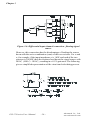
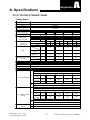
1
Copyright This documentation and the software included with this product are copyrighted 2001 by Advantech Co., Ltd. All rights are reserved. Advantech Co., Ltd. reserves the right to make improvements in the products described in this manual at any time without notice. No part of this manual may be reproduced, copied, translated or transmitted in any form or by any means without the prior written permission of Advantech Co., Ltd. Information provided in this manual is intended to be accurate and reliable. However, Advantech Co., Ltd. assumes no responsibility for its use, nor for any infringements of the rights of third parties which may result from its use. Acknowledgments PC-LabCard is a trademark of Advantech Co., Ltd. IBM and PC are trademarks of International Business Machines Corporation. MS-DOS, Windows, Microsoft Visual C++ and Visual BASIC are trade-marks of Microsoft Corporation. Intel and Pentium are trademarks of Intel Corporation. Delphi and C++ Builder are trademarks of Inprise Corporation. CE notification The PCI-1710/1710L/1710HG/1710HGL/1711/1711L/1716/1716L, developed by ADVANTECH CO., LTD., has passed the CE test for environmental specifications when shielded cables are used for external wiring. We recommend the use of shielded cables. This kind of cable is available from Advantech. Please contact your local supplier for ordering information. On-line Technical Support For technical support and service, please visit our support website at: http:\\www.advantech.com/support Part No. 2003171600 1st Edition Printed in Taiwan June 2001 Contents 1. Introduction....................................................... 1 1.1 1.2 1.3 1.4 Features ............................................................................ 2 Installation Guide ............................................................. 4 Software ............................................................................ 6 Accessories ....................................................................... 6 2. Installation ........................................................ 9 2.1 2.2 2.3 2.4 2.5 Unpacking ......................................................................... 9 Driver Installation .......................................................... 11 Hardware Installation .................................................... 13 Device Setup & Configuration ...................................... 15 Device Testing ................................................................ 19 3. Signal Connections ......................................... 23 3.1 3.2 3.3 3.4 3.5 3.6 Overview ......................................................................... 23 I/O Connector ................................................................. 23 Analog Input Connections .............................................. 26 Analog Output Connections ........................................... 29 Trigger Source Connections .......................................... 30 Field Wiring Considerations .......................................... 31 4. Software Overview ........................................ 33 4.1 4.2 Programming Choices .................................................... 33 DLL Driver Programming Roadmap ............................ 34 5. Calibration ...................................................... 37 5.1 5.2 5.3 PCI-1710/1710L/1710HG/1710HGL Calibration ......... 38 PCI-1711/1711L Calibration .......................................... 41 PCI-1716/1716L Calibration .......................................... 43 Appendix A. Specifications ................................ 55 Appendix B. Block Diagram ............................... 65 C. Register Structure and Format ..................... 69 C.1 Overview ......................................................................... 69 C.2 I/O Port Address Map ................................................... 70 C.3 Channel Number and A/D Data - BASE+0 and BASE+1 ......................................................................................... 76 C.4 Software A/D Trigger - BASE+0 ................................... 77 C.5 A/D Channel Range Setting - BASE+2 ........................... 78 C.6 MUX Control - BASE+4 and BASE+5 ......................... 81 C.7 Control Register - BASE+6 ........................................... 83 C.8 Status Register - BASE+6 and BASE+7 ...................... 85 C.9 Clear Interrupt and FIFO - BASE+8 and BASE+9 ...... 86 C.10 D/A Output Channel 0 - BASE+10 and BASE+11 ........ 86 C.11 D/A Output Channel 0 - BASE+10 and BASE+11 ........ 87 C.12 D/A Output Channel 1 - BASE+12 and BASE+13 ....... 87 C.13 D/A Output Channel 1 - BASE+12 and BASE+13 ....... 88 C.14 D/A Reference Control -BASE+14 ............................... 89 C.15 Digital I/O Registers - BASE+16 and BASE+17 ......... 90 C.16 Calibration Registers - BASE+18 and BASE+19 ......... 91 C.17 Board ID Registers - BASE+20 .................................... 92 C.18 Programmable Timer/Counter Registers BASE+24, BASE+26, BASE+28 and BASE+30 ............................. 92 Appendix D. 82C54 Counter Function ............... 93 D.1 D.2 D.3 D.4 The Intel 82C54 .............................................................. 93 Counter Read/Write and Control Registers ................. 94 Counter Operating Modes ............................................. 96 Counter Operations ........................................................ 98 Appendix E. PCI-1716/1716L Calibration (Manually) ......................................................... 101 E.1 A/D Calibration ............................................................ 101 E.2 D/A Calibration (for PCI-1716 only) ........................... 103 Appendix F. Screw-terminal Bord.................... 107 F.1 F.2 F.3 F.4 F.5 F.6 Introduction .................................................................. 107 Features ........................................................................ 107 Applications .................................................................. 108 Board Layout ................................................................ 108 Pin Assignment ............................................................. 109 Technical Diagram ....................................................... 110 Figures Figure 1-1: Figure 2-1: Figure 2-2: Figure 2-3: Figure 2-4: Figure 2-5: Figure 2-6: Figure 2-7: Figure 2-8: Figure 2-9: Figure 2-10: Figure 2-11: Figure 2-13: Figure 2-12: Figure 2-14: Figure 3-1: Figure 3-2: Figure 3-3: Figure 3-4: Figure 3-5: Figure 5-1: Figure 5-2: Figure 5-3: Figure 5-4: Figure 5-5: Figure 5-6: Figure 5-7: Figure 5-8: Installation Flow Chart ............................................................ 5 The Setup Screen of Advantech Automation Software .......... 11 Different options for Driver Setup ......................................... 12 The device name listed on the Device Manager ...................... 14 The Advantech Device Installation utility program ............... 15 The I/O Device Installation dialog box.................................... 16 The “Device(s) Found” dialog box .......................................... 17 The Device Setting dialog box ................................................ 17 The Device Name appearing on the list of devices box ........... 18 Analog Input tab on the Device Test dialog box ...................... 19 Analog Input tab on the Device Test dialog box ...................... 20 Analog Output tab on the Device Test dialog box ................... 20 Digital Output tab on the Device Test dialog box .................... 21 Digital Input tab on the Device Test dialog box ....................... 21 Counter tab on the Device Test dialog box .............................. 22 I/O connector pin assignments for the PCI-1710/1710L/ 1710HG/1710HGL/1711/1711L/1716/1716L ....................... 24 Single-ended input channel connection ................................. 26 Differential input channel connection - ground reference signal source .......................................................................... 27 Differential input channel connection - floating signal source ................................................................................................ 28 Analog output connections ..................................................... 29 PCI-1710/1710L/1710HG/1710HGL VR assignment .......... 38 PCI-1711/1711L VR assignment ........................................... 41 PCI-1716/1716L VR assignment .......................................... 44 Selecting the device you want to calibrate .............................. 45 Warning message before start calibration ............................ 45 Auto A/D Calibration Dialog Box ........................................... 46 A/D Calibration Procedure 1 ................................................. 46 A/D Calibration Procedure 2 ................................................. 47 Figure 5-9: A/D Calibration Procedure 3 ................................................. 47 Figure 5-11: Range Selection in D/A Calibration ....................................... 48 Figure 5-10: A/D Calibration is finished .................................................... 48 Figure 5-12: Calibrating D/A Channel 0 .................................................... 49 Figure 5-13: Calibrating D/A Channel 1 .................................................... 49 Figure 5-14: D/A Calibration is finished .................................................... 50 Figure 5-15: Selecting Input Rage in Manual A/D Calibration panel ........ 51 Figure 5-16: Adjusting registers ................................................................ 51 Figure 5-17 & Figure 5-18: Selecting D/A Range and Choosing Output Voltage .................................................................................... 52 Figure 5-19: Adjusting registers ................................................................ 53 Tables Table 3-1: I/O Connector Signal Description ......................................... 25 Table C-1: PCI-1710/1710L/1710HG/1710HGL/1711/1711L/1716/ 1716L register format (Part 3) .............................................. 72 PCI-1710/1710L/1710HG/1710HGL/1711/1711L register format (Part 4) ........................................................................ 73 PCI-1716/1716L register format (Part 5) ............................. 74 PCI-1710/1710L/1710HG/1710HGL/1711/1711L/1716/ 1716L register format (Part 6) .............................................. 75 PCI-1716/1716L Register for A/D data ................................. 76 PCI-1710/1710L/1710HG/1710HGL/1711/1711L Register for channel number and A/D data ........................................... 76 Register for A/D channel range setting ............................... 78 Gain codes for PCI-1710/1710L ............................................ 79 Gain codes for PCI-1710HG/1710HGL ................................. 80 Gain codes for PCI-1711/1711L ............................................. 80 Register for multiplexer control ............................................ 81 Control Register ..................................................................... 83 Status Register ....................................................................... 85 Register to clear interrupt and FIFO .................................... 86 Register for load D/A channel 0 data ..................................... 86 Register for D/A channel 0 data ............................................. 87 Register for load D/A channel 1 data .................................... 87 Register for D/A channel 1 data ............................................. 88 PCI-1710/1710HG/1711 Register for D/A reference control .. ................................................................................................ 89 PCI-1716 Register for D/A reference control ....................... 89 Register for digital input ....................................................... 90 Register for digital output ..................................................... 90 Calibration Command and Data Register .............................. 91 Table C-1: Table C-1: Table C-1: Table C-3: Table C-2: Table C-4: Table C-5: Table C-6: Table C-7: Table C-8: Table C-9: Table C-10: Table C-11: Table C-12: Table C-13: Table C-14: Table C-15: Table C-16: Table C-17: Table C-18: Table C-19: Table C-20: Table C-21: Calibration Command and Data Register .............................. 91 Table C-22: Register for Board ID ............................................................ 92 Table E-1: Table E-2: A/D binary code table ............................................................ 102 D/A binary code table ............................................................ 105 1 Chapter 1 Chapter 1. Introduction Thank you for buying the Advantech PCI-1710/1710L/1710HG/ 1710HGL/1711/1711L/1716/1716L PCI card. The Advantech PCI-1710/ 1710L/1710HG/1710HGL/1711/1711L/1716/1716L is a powerful data acquisition (DAS) card for the PCI bus. It features a unique circuit design and complete functions for data acquisition and control, including A/D conversion, D/A conversion, digital input, digital output, and counter/timer. PCI-1710/1710L/1710HG/1710HGL/1711/ 1711L/1716/1716L provides specific functions for different user requirements: PCI-1710 12-bit, 100kS/s Multifunction card PCI-1710L 12-bit, 100kS/s Multifunction card w/o analog output PCI-1710HG 12-bit, 100kS/s High-Gain Multifunction card PCI-1710HGL 12-bit, 100kS/s High-Gain Multifunction card w/o analog output PCI-1711 12-bit, 100kS/s 16-ch S.E. Inputs Low-cost Multifunction card PCI-1711L 12-bit, 100kS/s 16-ch S.E. Inputs Low-cost Multifunction card w/o analog output PCI-1716 16-bit, 250kS/s High-Resolution Multifunction card PCI-1716L 16-bit, 250kS/s High-Resolution Multifunction card w/o analog output The following sections of this chapter will provide further information about features of the multifunction cards, a Quick Start for installation, together with some brief information on software and accessories for the PCI-1710/1710L/1710HG/1710HGL/1711/1711L/1716/1716L card. Advantech Co., Ltd. www.advantech.com –1– PCI-1710 series User’s Manual Chapter 1 1.1 Features The Advantech PCI-1710/1710L/1710HG/1710HGL/1711/1711L/1716/ 1716L provides users with the most requested measurement and control functions as seen below: ❏ PCI-bus mastering for data transfer ❏ 16-channel Single-Ended or 8-channel Differential A/D Input ❏ 12-bit A/D conversion with up to 100 kHz sampling rate (PCI-1710/ 1710L/1710HG/1710HGL/1711/1711L) 16-bit A/D conversion with up to 250 kHz sampling rate (PCI-1716/ 1716L) ❏ Programmable gain for each input channel (only for PCI-1710/ 1710L/1710HG/1710HGL/1716/1716L) ❏ On board samples FIFO buffer: 4K for PCI-1710/1710L/1710HG/1710HGL, 1K for PCI-1711/ 1711L1716/1716L ❏ 2-channel D/A Output (PCI-1710/1710HG/1711/1716) ❏ 16-channel Digital Input ❏ 16-channel Digital Output ❏ Programmable Counter/Timer ❏ Automatic Channel/Gain Scanning The Advantech PCI-1710/1710L/1710HG/1710HGL/1711/1711L/1716/ 1716L offers the following main features: Plug-and-Play Function The Advantech PCI-1710/1710L/1710HG/1710HGL/1711/1711L/1716/ 1716L is a Plug-and-Play device, which fully complies with the PCI Specification. Rev 2.1 for PCI-1710/1710L/1710HG/1710HGL/1711/ 1711L, and Rev 2.2 for PCI-1716/1716L. During card installation, all busrelated configurations such as base I/O address and interrupts are conveniently taken care of by the Plug-and-Play function. You have PCI-1710 series User’s Manual –2– Advantech Co., Ltd. www.advantech.com Chapter 1 virtually no need to set any jumpers or DIP switches. Flexible Input Types and Range Settings The PCI-1710/1710L/1710HG/1710HGL/1711/1711L/1716/1716L features an automatic channel/gain scanning circuit. This circuit design controls multiplexer switching during sampling. Users can set different gain values for each channel according to their needs for the corresponding range of input voltage. The gain value settings thus selected is stored in the SRAM. This flexible design enables multi-channel and high-speed sampling for high-performance data acquisition. On-board FIFO (First-In-First-Out) Memory The PCI-1710/1710L/1710HG/1710HGL/1711/1711L/1716/1716L provides an on-board FIFO memory buffer, storing up 1 to 1K/4K A/D samples. Users can either enable or disable the interrupt request feature of the FIFO buffer. While the interrupt request for FIFO is enabled, users are allowed to specify whether an interrupt request will be sent with each sampling action or only when the FIFO buffer is half saturated. This useful feature enables a continuous high-speed data transfer with a more predictable performance on operating systems. Optional D/A Output for Cost Savings The PCI-1710/1710HG/1711/1716 goes further with 2 analog output channels, while the PCI-1710L/1710HGL/1711L/1716L doesn’t. It is for users to differentiate between the PCI-1710/1710HG/1711/1716 and the PCI-1710L/1710HGL/1711L/1716L according to what they really need as the best solution with no extra cost. 16 Digital Inputs and 16 Digital Outputs The PCI-1710/1710L/1710HG/1710HGL/1711/1711L/1716/1716L provides 16 digital input channels and 16 digital output channels. Users are left with great flexibility to design and customize their applications according to their specific needs. On-board Programmable Counter The PCI-1710/1710L/1710HG/1710HGL/1711/1711L/1716/1716L is equipped with a programmable counter, which can serve as a pacer trigger for A/D conversions. The counter chip is an 82C54 or its equivalent, which incorporates three 16-bit counters on a 10 MHz clock. One of the three counters is used as an event counter for input Advantech Co., Ltd. www.advantech.com –3– PCI-1710 series User’s Manual Chapter 1 channels or pulse generation. The other two are cascaded into a 32-bit timer for pacer triggering. Note: ✎ Pace trigger determines how fast A/D conversion will be done in pacer trigger mode. ✎ For detailed specifications of the PCI-1710/1710L/1710HG/1710HGL/ 1711/1711L/1716/1716L, please refer to Appendix A, Specifications. 1.2 Installation Guide Before you install your PCI-1710/1710L/1710HG/1710HGL/1711/1711L/ 1716/1716L card, please make sure you have the following necessary components: ❏ PCI-1710/1710L/1710HG/1710HGL/1711/1711L/1716/1716L Multifunction card ❏ PCI-1710/1710L/1710HG/1710HGL/1711/1711L/1716/1716L User’s Manual ❏ Driver software Advantech DLL drivers (included in the companion CD-ROM) ❏ Wiring cable PCL-10168 ❏ Wiring board PCLD-8710, ADAM-3968 ❏ Computer Personal computer or workstation with a PCI-bus slot (running Windows 95/98/NT/ 2000) Some other optional components are also available for enhanced operation: ❏ Application software ActiveDAQ, GeniDAQ or other third-party software packages After you get the necessary components and maybe some of the accessories for enhanced operation of your Multifunction card, you can then begin the Installation procedures. Figure 1-1 on the next page provides a concise flow chart to give users a broad picture of the software and hardware installation procedures: PCI-1710 series User’s Manual –4– Advantech Co., Ltd. www.advantech.com Chapter 1 Figure 1-1: Installation Flow Chart Advantech Co., Ltd. www.advantech.com –5– PCI-1710 series User’s Manual Chapter 1 1.3 Software Advantech offers a rich set of DLL drivers, third-party driver support and application software to help fully exploit the functions of your PCI1710/1710L/1710HG/1710HGL/1711/1711L/1716/1716L card: • DLL driver (on the companion CD-ROM) • LabVIEW driver • Advantech ActiveDAQ • Advantech GeniDAQ For more information on software, please refer to Chapter 4, Software Overview. Users who intend to program directly at the registers of the Multifunction card can have register-level programming as an option. Since register-level programming is often difficult and laborious, it is usually recommended only for experienced programmers. For more information, please refer to Appendix C, Register Structure and Format. 1.4 Accessories Advantech offers a complete set of accessory products to support the PCI-1710/1710L/1710HG/1710HGL/1711/1711L/1716/1716L cards. These accessories include: Wiring Cable ❏ PCL-10168 The PCL-10168 shielded cable is specially designed for PCI-1710/1710L/1710HG/1710HGL/1711/1711L/ 1716/1716L cards to provide high resistance to noise. To achieve a better signal quality, the signal wires are twisted in such a way as to form a “twisted-pair cable”, reducing cross-talk and noise from other signal sources. Furthermore, its analog and digital lines are separately sheathed and shielded to neutralize EMI/EMC problems. Wiring Boards ❏ ADAM-3968 The ADAM-3968 is a 68-pin SCSI wiring terminal module for DIN-rail mounting. This terminal module PCI-1710 series User’s Manual –6– Advantech Co., Ltd. www.advantech.com Chapter 1 can be readily connected to the Advantech PC-Lab cards and allow easy yet reliable access to individual pin connections for the PCI-1710/1710L/1710HG/ 1710HGL/1711/1711L/1716/1716L card. ❏ PCLD-8710 The PCLD-8710 is a DIN-rail mounting screw-terminal board to be used with any of the PC-LabCards which have 68-pin SCSI connectors. The PCLD-8710 features the following functions: • 2 additional 20-pin flat-cable connectors for digital input and output • Reserved space on the board to meet future needs for signalconditioning circuits (low-pass filter, voltage attenuator and current shunt) • Industrial-grade screw-clamp terminal blocks for heavy-duty and reliable connections. Advantech Co., Ltd. www.advantech.com –7– PCI-1710 series User’s Manual Chapter 1 This page is left blank on purpose. PCI-1710 series User’s Manual –8– Advantech Co., Ltd. www.advantech.com 2 Chapter 2 Chapter 2. Installation This chapter gives users a package item checklist, proper instructions about unpacking and step-by-step procedures for both driver and card installation. Be noted that using PCI-1716/1716L for example. 2.1 Unpacking After receiving your PCI-1710/1710L/1710HG/1710HGL/1711/1711L/ 1716/1716L package, please inspect its contents first. The package should contain the following items: þ PCI-1710/1710L/1710HG/1710HGL/1711/1711L/1716/1716L card þ Companion CD-ROM (DLL driver included) þ User’s Manual þ Quick Start The PCI-1710/1710L/1710HG/1710HGL/1711/1711L/1716/1716L card harbors certain electronic components vulnerable to electrostatic discharge (ESD). ESD could easily damage the integrated circuits and certain components if preventive measures are not carefully paid attention to. Before removing the card from the antistatic plastic bag, you should take following precautions to ward off possible ESD damage: • Touch the metal part of your computer chassis with your hand to discharge static electricity accumulated on your body. Or one can also use a grounding strap. • Touch the antistatic bag to a metal part of your computer chassis before opening the bag. • Take hold of the card only by the metal bracket when removing it out of the bag. After taking out the card, first you should: • Inspect the card for any possible signs of external damage (loose or damaged components, etc.). If the card is visibly damaged, please notify our service department or our local sales representative immediately. Avoid installing a damaged card into your system. Advantech Co., Ltd. www.advantech.com –9– PCI-1710 series User’s Manual Chapter 2 Also pay extra caution to the following aspects to ensure proper installation: Avoid physical contact with materials that could hold static electricity such as plastic, vinyl and Styrofoam. Whenever you handle the card, grasp it only by its edges. DO NOT TOUCH the exposed metal pins of the connector or the electronic components. Note: ✎ Keep the antistatic bag for future use. You might need the original bag to store the card if you have to remove the card from PC or transport it elsewhere. PCI-1710 series User’s Manual – 10 – Advantech Co., Ltd. www.advantech.com Chapter 2 2.2 Driver Installation We recommend you to install the driver before you install the PCI1710/1710L/1710HG/1710HGL/1711/1711L/1716/1716L card into your system, since this will guarantee a smooth installation process. The 32-bit DLL driver Setup program for the PCI-1710/1710L/1710HG/ 1710HGL/1711/1711L/1716/1716L card is included on the companion CD-ROM that is shipped with your DAS card package. Please follow the steps below to install the driver software: Step 1: Insert the companion CD-ROM into your CD-ROM drive. Step 2: The Setup program will be launched automatically if you have the autoplay function enabled on your system. When the Setup Program is launched, you’ll see the following Setup Screen. Note: ✎ If the autoplay function is not enabled on your computer, use Windows Explorer or Windows Run command to execute SETUP.EXE on the companion CD-ROM. Figure 2-1: The Setup Screen of Advantech Automation Software Step 3: Select the DLL Drivers option. Step 4: Select the Windows 95/98 or Windows NT or Windows 2000 option according to your operating system. Just follow the installation instructions step by step to complete your DLL driver setup. Advantech Co., Ltd. www.advantech.com – 11 – PCI-1710 series User’s Manual Chapter 2 Figure 2-2: Different options for Driver Setup For further information on driver-related issues, an online version of DLL Drivers Manual is available by accessing the following path: Start/Programs/Advantech Driver for 95 and 98 (or for NT/2000)/ Driver Manual PCI-1710 series User’s Manual – 12 – Advantech Co., Ltd. www.advantech.com Chapter 2 2.3 Hardware Installation Note: ✎ Make sure you have installed the driver first before you install the card (please refer to 2.2 Driver Installation) After the DLL driver installation is completed, you can now go on to install the PCI-1710/1710L/1710HG/1710HGL/1711/1711L/1716/1716L card in any PCI slot on your computer. But it is suggested that you should refer to the computer user manual or related documentations if you have any doubt. Please follow the steps below to install the card on your system. Step 1: Turn off your computer and unplug the power cord and cables. TURN OFF your computer before installing or removing any components on the computer. Step 2: Remove the cover of your computer. Step 3: Remove the slot cover on the back panel of your computer. Step 4: Touch the metal part on the surface of your computer to neutralize the static electricity that might be on your body. Step 5: Insert the 1710/1710L/1710HG/1710HGL/1711/1711L/1716/ 1716L card into a PCI slot. Hold the card only by its edges and carefully align it with the slot. Insert the card firmly into place. Use of excessive force must be avoided, otherwise the card might be damaged. Step 6: Fasten the bracket of the PCI card on the back panel rail of the computer with screws. Step 7: Connect appropriate accessories (68-pin cable, wiring terminals, etc. if necessary) to the PCI card. Step 8: Replace the cover of your computer chassis. Re-connect the cables you removed in step 2. Step 9: Plug in the power cord and turn on the computer . Note: ✎ In case you installed the card without installing the DLL driver first, Windows 95/98 will recognize your card as an “unknown device” after rebooting, and will prompt you to provide the necessary driver. You should ignore the prompting messages (just click the Cancel button) and set up the driver according to the steps described in 2.2 Driver Installation. Advantech Co., Ltd. www.advantech.com – 13 – PCI-1710 series User’s Manual Chapter 2 After the PCI-1710/1710L/1710HG/1710HGL/1711/1711L/1716/1716L card is installed, you can verify whether it is properly installed on your system in the Device Manager: 1. Access the Device Manager through Control Panel/System/Device Manager. 2. The device name of the PCI-1710/1710L/1710HG/1710HGL/1711/ 1711L/1716/1716L should be listed on the Device Manager tab on the System Property Page. Figure 2-3: The device name listed on the Device Manager Note: ✎ If your card is properly installed, you should see the device name of your card listed on the Device Manager tab. If you do see your device name listed on it but marked with an exclamation sign “!”, it means your card has not been correctly installed. In this case, remove the card device from the Device Manager by selecting its device name and press the Remove button. Then go through the driver installation process again. After your card is properly installed on your system, you can now configure your device using the Device Installation Program that has itself already been installed on your system during driver setup. A complete device installation procedure should include device setup, configuration and testing. The following sections will guide you through the Setup, Configuration and Testing of your device. PCI-1710 series User’s Manual – 14 – Advantech Co., Ltd. www.advantech.com Chapter 2 2.4 Device Setup & Configuration The Device Installation program is a utility that allows you to set up, configure and test your device, and later stores your settings on the system registry. These settings will be used when you call the APIs of Advantech 32-bit DLL drivers. Setting Up the Device Step 1: To install the I/O device for your card, you must first run the Device Installation program (by accessing Start/Programs/ Advantech Driver for 95 and 98 (or for NT/2000)/Device Installation). Figure 2-4: The Advantech Device Installation utility program Step 2: On the Device Installation program window, select the Setup menu item on the menu bar, and click the Device command (Figure 2-4) to bring up the I/O Device Installation dialog box (Figure 2-5). You can then view the device(s) already installed on your system (if any) on the Installed Devices list box. Since you haven’t installed any device yet, you might see a blank list such as the one on the next page (Figure 2-5). Advantech Co., Ltd. www.advantech.com – 15 – PCI-1710 series User’s Manual Chapter 2 Figure 2-5: The I/O Device Installation dialog box Step 3: Scroll down the List of Devices box to find the device that you wish to install, then click the Add... button to evoke the Device(s) found dialog box such as one shown in Figure 2-6. The Device(s) found dialog box lists all the installed devices of selected option on your system. Select the device you want to configure from the list box and press the OK button. After you have clicked OK, you will see a Device Setting dialog box such as the one in Figure 2-8. PCI-1710 series User’s Manual – 16 – Advantech Co., Ltd. www.advantech.com Chapter 2 Figure 2-6: The “Device(s) Found” dialog box Configuring the Device Step 4: On the Device Setting dialog box (Figure 2-7), you can configure the voltage source either as External or Internal, and specify the voltage output range for the 2 D/A channels. Figure 2-7: The Device Setting dialog box Note: ✎ Users can configure the source of D/A reference voltage either as Internal or External, and select the output voltage range. When selecting voltage source as Internal, users have two options for the output voltage range : 0 ~ 5 V and 0 ~ 10 V. When selected as External, the output voltage range is determined by the external reference voltage in the following way : By inputting an external reference voltage: -xV , where |x| <= 10, you will get a output voltage range: 0 to xV. Advantech Co., Ltd. www.advantech.com – 17 – PCI-1710 series User’s Manual Chapter 2 Step 5: After you have finished configuring the device, click OK and the device name will appear in the Installed Devices box as seen below: Figure 2-8: The Device Name appearing on the list of devices box Note: ✎ As we have noted, the device name “000:PCI-1716 I/O=E000H” begins with a device number “000”, which is specifically assigned to each card. The device number is passed to the driver to specify which device you wish to control. If you want to test the card device further, go right to the next section on the Device Testing. PCI-1710 series User’s Manual – 18 – Advantech Co., Ltd. www.advantech.com Chapter 2 2.5 Device Testing Following through the Setup and Configuration procedures to the last step described in the previous section, you can now proceed to test the device by clicking the Test Button on the I/O Device Installation dialog box (Figure 2-8). A Device Test dialog box will appear accordingly: Figure 2-9: Analog Input tab on the Device Test dialog box On the Device Test dialog box, users are free to test various functions of PCI-1710/1710L/1710HG/1710HGL/1711/1711L/1716/1716L on the Analog output, Digital input, Digital output or Counter tabs. And the Analog output function only available for 1710/1710HG/1711/1716. Note: ✎ You can access the Device Test dialog box either by the previous procedure for the Device Installation Program or simply by accessing Start/Programs/Advantech Driver for 95 and 98 (or for NT/2000) / Test Utility. ✎ All the functions are performed by software polling method. For highspeed data acquirement or output, they have to use corresponding VC example like ADINT or ADDMA or ADBMDMA. Advantech Co., Ltd. www.advantech.com – 19 – PCI-1710 series User’s Manual Chapter 2 Testing Analog Input Function Click the Analog Input tab to bring it up to the front of the screen. Select the input range for each channel in the Input range drop-down boxes. Configure the sampling rate on the scroll bar. Switch the channels by using the up/down arrow. Figure 2-10: Analog Input tab on the Device Test dialog box Testing Analog Output Function (only for PCI-1710/1710HG/ 1711/1716) Click the Analog Output tab to bring it up to the foreground. The Analog Output tab allows you to output quasi-sine, triangle, or square waveforms generated by the software automatically, or output single values manually. You can also configure the waveform frequency and output voltage range. Figure 2-11: Analog Output tab on the Device Test dialog box PCI-1710 series User’s Manual – 20 – Advantech Co., Ltd. www.advantech.com Chapter 2 Testing Digital Input Function Click the Digital Input tab to show forth the Digital Input test panel as seen below. Through the color of the lamps, users can easily discern whether the status of each digital input channel is either high or low. Figure 2-12: Digital Input tab on the Device Test dialog box Testing Digital Output Function Click the Digital Output tab to bring up the Digital Output test panel such as the one seen on the next page. By pressing the buttons on each tab, users can easily set each digital output channel as high or low for the corresponding port. Figure 2-13: Digital Output tab on the Device Test dialog box Advantech Co., Ltd. www.advantech.com – 21 – PCI-1710 series User’s Manual Chapter 2 Testing Counter Function Click the Counter Tab to bring its test panel forth. The counter channel (Channel 0) offers the users two options: Event counting and Pulse out. If you select Event counting, you need first to connect your clock source to pin CNT0_CLK, and the counter will start counting after the pin CNT0_GATE is triggered. If you select Pulse Out, the clock source will be output to pin CNT0_OUT. You can configure the Pulse Frequency by the scroll bar right below it. Figure 2-14: Counter tab on the Device Test dialog box Only after your card device is properly set up, configured and tested, can the device installation procedure be counted as complete. After the device installation procedure is completed, you can safely proceed to the next chapter, Signal Connections. PCI-1710 series User’s Manual – 22 – Advantech Co., Ltd. www.advantech.com 3 Chapter 3 3. Signal Connections Chapter 3.1 Overview Maintaining signal connections is one of the most important factors in ensuring that your application system is sending and receiving data correctly. A good signal connection can avoid unnecessary and costly damage to your PC and other hardware devices. This chapter provides useful information about how to connect input and output signals to the PCI-1710/1710L/1710HG/1710HGL/1711/1711L/1716/1716L via the I/ O connector. 3.2 I/O Connector The I/O connector on the PCI-1710/1710L/1710HG/1710HGL/1711/ 1711L/1716/1716L is a 68-pin connector that enable you to connect to accessories with the PCL-10168 shielded cable. Note: ✎ The PCL-10168 shielded cable is especially designed for the PCI-1710/ 1710L/1710HG/1710HGL/1711/1711L/1716/1716L to reduce noise in the analog signal lines. Please refer to Section 1.4 Accessories. Pin Assignment Figure 3-1 shows the pin assignments for the 68-pin I/O connector on the PCI-1710/1710L/1710HG/1710HGL/1711/1711L/1716/1716L. Note: ✎ The three ground references AIGND, AOGND, and DGND should be used discreetly each according to its designated purpose. Actually, we offer the individual GND pin for AI, AO and DIO to provide best signal quality. However, all the signals on the DA&C card need to refer to the same GND finally. So we test and choice a best point to connect AIGND, AOGND and DGND together. In short, this is base on the "single-point" ground principle. Advantech Co., Ltd. www.advantech.com – 23 – PCI-1710 series User’s Manual Chapter 3 AI0 68 34 AI1 AI2 67 33 AI3 AI4 66 32 AI5 AI6 65 31 AI7 AI8 64 30 AI9 AI10 63 29 AI11 AI12 62 28 AI13 AI14 61 27 AI15 AIGND 60 26 AIGND AO0_REF* 59 25 AO1_REF* AO0_OUT* 58 24 AO1_OUT* AOGND* 57 23 AOGND* DI0 56 22 DI1 DI2 55 21 DI3 DI4 54 20 DI5 DI6 53 19 DI7 DI8 52 18 DI9 DI10 51 17 DI11 DI12 50 16 DI13 DI14 49 15 DI15 DGND 48 14 DGND DO0 47 13 DO1 DO2 46 12 DO3 DO4 45 11 DO5 DO6 44 10 DO7 DO8 43 9 DO9 DO10 42 8 DO11 DO12 41 7 DO13 DO14 40 6 DO15 DGND 39 5 DGND CNT0_CLK 38 4 PACER_OUT CNT0_OUT 37 3 TRG_GATE CNT0_GATE 36 2 EXT_TRG +12V 35 1 +5V Figure 3-1: I/O connector pin assignments for the PCI-1710/1710L/ 1710HG/1710HGL/1711/1711L/1716/1716L *: Pins 23~25 and pins 57~59 are not defined for PCI-1710L/1710HGL/ 1711L/1716L PCI-1710 series User’s Manual – 24 – Advantech Co., Ltd. www.advantech.com Chapter 3 I/O Connector Signal Description Table 3-1: I/O Connector Signal Description Signal Name Reference Direction Description AI<0...15> AIGND Input Analog Input Channels 0 through 15. Each channel pair, AI<i, i+1> (i = 0, 2, 4...14), can be configured as either two single-ended inputs or one differential input of PCI-1710/1710L/ 1710HG/1710HGL/1716/1716L. AIGND - - Analog Input Ground. The three ground references (AIGND, AOGND, and DGND) are connected together on the PCI-1710/1710L/ 1710HG/1710HGL/1711/1711L/1716/1716L card. AO0_REF AO1_REF AOGND Input Analog Output Channel 0/1 External Reference. AO0_OUT AO1_OUT AOGND Output Analog Output Channels 0/1. Analog Output Ground. The analog output voltages are referenced to these nodes. The three ground references (AIGND, AOGND, and DGND) are connected together on the PCI-1710/1710L/ 1710HG/1710HGL/1711/1711L/1716/1716L card. AOGND - - DI<0..15> DGND Input DO<0..15> DGND Output Digital Input channels. Digital Output channels. DGND - - Digital Ground. This pin supplies the reference for the digital channels at the I/O connector as well as the +5VDC supply. The three ground references (AIGND, AOGND, and DGND) are connected together on the PCI-1710/1710L/ 1710HG/1710HGL/1711/1711L/1716/1716L card. CNT0_CLK DGND Input Counter 0 Clock Input. The clock input of counter 0 can be either external or internal , as set by software. CNT0_OUT DGND Output CNT0_GATE DGND Input PACER_OUT DGND Counter 0 Output. Counter 0 Gate Control. Output Pacer Clock Output. This pin pulses once for each pacer clock when turned on. If A/D conversion is in the pacer trigger mode, users can use this signal as a synchronous signal for other applications. A low- to- high edge triggers A/D conversion to start. TRG_GATE DGND Input A/D External Trigger Gate. When TRG _GATE is connected to +5 V, it will enable the external trigger signal to input. When TRG _GATE is connected to DGND, it will disable the external trigger signal to input. EXT_TRG DGND Input A/D External Trigger. This pin is external trigger signal input for the A/D conversion. A low-to-high edge triggers A/D conversion to start. +12V DGND Output +12 VDC Source. +5V DGND Output +5 VDC Source. Advantech Co., Ltd. www.advantech.com – 25 – PCI-1710 series User’s Manual Chapter 3 3.3 Analog Input Connections The PCI-1710/1710L/1710HG/1710HGL/1716/1716L supports both 16channel Single-Ended or 8 differential A/D Input, however the PCI1711/1711L only supports 16 single-ended analog inputs. Each individual input channel is software-selected. Single-ended Channel Connections The single-ended input configuration has only one signal wire for each channel, and the measured voltage (Vm) is the voltage of the wire as referenced against the common ground. A signal source without a local ground is also called a “floating source”. It is fairly simple to connect a single-ended channel to a floating signal source. In this mode, the PCI-1710/1710L/1710HG/ 1710HGL/1711/1711L/1716/1716L provides a reference ground for external floating signal sources. Figure 3-2 shows a single-ended channel connection between a floating signal source and an input channel on the PCI-1710/1710L/1710HG/1710HGL/1711/1711L/1716/ 1716L. Figure 3-2: Single-ended input channel connection Differential Channel Connections The differential input channels operate with two signal wires for each channel, and the voltage difference between both signal wires is measured. On the PCI-1710/1710L/1710HG/1710HGL/1716/1716L, when all channels are configured to differential input, up to 8 analog channels are available. PCI-1710 series User’s Manual – 26 – Advantech Co., Ltd. www.advantech.com Chapter 3 If one side of the signal source is connected to a local ground, the signal source is ground-referenced. Therefore, the ground of the signal source and the ground of the card will not be exactly of the same voltage. The difference between the ground voltages forms a commonmode voltage (Vcm ). To avoid the ground loop noise effect caused by common-mode voltages, you can connect the signal ground to the Low input. Figure 3-3 shows a differential channel connection between a groundreference signal source and an input channel on the PCI-1710/1710L/ 1710HG/1710HGL/1716/1716L. With this connection, the PGIA rejects a common-mode voltage Vcm between the signal source and the PCI1710/1710L/1710HG/1710HGL/1716/1716L ground, shown as Vcm in Figure 3-3. Figure 3-3: Differential input channel connection - ground reference signal source If a floating signal source is connected to the differential input channel, the signal source might exceed the common-mode signal range of the PGIA, and the PGIA will be saturated with erroneous voltage-readings. You must therefore reference the signal source against the AIGND. Figure 3-4 shows a differential channel connection between a floating signal source and an input channel on the PCI-1710/1710L/1710HG/ 1710HGL/1716/1716L. In this figure, each side of the floating signal source is connected through a resistor to the AIGND. This connection can reject the common-mode voltage between the signal source and the PCI-1710/1710L/1710HG/1710HGL/1716/1716L ground. Advantech Co., Ltd. www.advantech.com – 27 – PCI-1710 series User’s Manual Chapter 3 Figure 3-4: Differential input channel connection - floating signal source However, this connection has the disadvantage of loading the source down with the series combination (sum) of the two resistors. For ra and rb, for example, if the input impedance rs is 1 kW, and each of the two resistors is 100 kW, then the resistors load down the signal source with 200 kΩ (100 kΩ+ 100 kΩ), resulting in a -0.5% gain error. The following gives a simplified representation of the circuit and calculating process. PCI-1710 series User’s Manual – 28 – Advantech Co., Ltd. www.advantech.com Chapter 3 3.4 Analog Output Connections The PCI-1710/1710HG/1711/1716 provides two D/A output channels (PCI-1710L/1710HGL/1711L/1716L are not designed to have this function), AO0_OUT and AO1_OUT. Users may use the PCI-1710/ 1710HG/1711/1716 internally-provided precision -5V (-10V) reference to generate 0 to +5 V (+10 V) D/A output range. Users also may create D/ A output range through external references, AO0_REF and AO1_REF. The external reference input range is +/-10 V. For example, connecting with an external reference of -7 V will generate 0 ~ +7 V D/A output. Figure 3-5 shows how to make analog output and external reference input connections on the PCI-1710/1710HG/1711/1716. Internal +5V +10V External AO0_REF INT_REF AO0 + AO0_OUT Load _ Load _ External Reference For DA Signal 0 AOGND DATA BUS AO1 External Reference For DA Signal 1 AO1_OUT + AO1_REF INT_REF I/O Connector Figure 3-5: Analog output connections Advantech Co., Ltd. www.advantech.com – 29 – PCI-1710 series User’s Manual Chapter 3 3.5 Trigger Source Connections Internal Pacer Trigger Connection The PCI-1710/1710L/1710HG/1710HGL/1711/1711L/1716/1716L includes one 82C54 compatible programmable Timer/Counter chip which provides three 16-bit counters connected to a Oscillator, each designated specifically as Counter 0, Counter 1 and Counter 2. Counter 0 is a counter which counts events from an input channel or outputing pulse. Counter 1 and Counter 2 are cascaded to create a 32-bit timer for pacer triggering. A low-to-high edge from the Counter 2 output (PACER_OUT) will trigger an A/D conversion on the PCI-1710/1710L/ 1710HG/1710HGL/1711/1711L/1716/1716L. At the same time, you can also use this signal as a synchronous signal for other applications. External Trigger Source Connection In addition to pacer triggering, the PCI-1710/1710L/1710HG/1710HGL/ 1711/1711L/1716/1716L also allows external triggering for A/D conversions. When a +5 V source is connected to TRG_GATE, the external trigger function is enabled. A low-to-high edge coming from EXT_TRG will trigger an A/D conversion on the PCI-1710/1710L/1710HG/ 1710HGL/1711/1711L/1716/1716L. When DGND is connected to TRG_GATE, the external trigger function is thereby disabled. PCI-1710 series User’s Manual – 30 – Advantech Co., Ltd. www.advantech.com Chapter 3 3.6 Field Wiring Considerations When you use the PCI-1710/1710L/1710HG/1710HGL/1711/1711L/1716/ 1716L to acquire data from outside, noises in the environment might significantly affect the accuracy of your measurements if due cautions are not taken. The following measures will be helpful to reduce possible interference running signal wires between signal sources and the PCI-1710/1710L/1710HG/1710HGL/1711/1711L/1716/1716L. • The signal cables must be kept away from strong electromag-netic sources such as power lines, large electric motors, circuit breakers or welding machines, since they may cause strong electromagnetic interference. Keep the analog signal cables away from any video monitor, since it can significantly affect a data acquisition system. • If the cable travels through an area with significant electromagnetic interference, you should adopt individually shielded, twisted-pair wires as the analog input cable. This type of cable has its signal wires twisted together and shielded with a metal mesh. The metal mesh should only be connected to one point at the signal source ground. • Avoid running the signal cables through any conduit that might have power lines in it. • If you have to place your signal cable parallel to a power line that has a high voltage or high current running through it, try to keep a safe distance between them. Or, you should place the signal cable at a right angle to the power line to minimize the undesirable effect. • The signals transmitted on the cable will be directly affected by the quality of the cable. In order to ensure better signal quality, we recommend that you use the PCL-10168 shielded cable. Advantech Co., Ltd. www.advantech.com – 31 – PCI-1710 series User’s Manual Chapter 3 This page is left blank on purpose. PCI-1710 series User’s Manual – 32 – Advantech Co., Ltd. www.advantech.com 4 Chapter 4 4. Software Overview Chapter This chapter gives you an overview of the software programming choices available and a quick reference to source codes examples that can help you be better oriented to programming. After following the instructions given in Chapter 2, it is hoped that you feel comfortable enough to proceed further. Programming choices for DAS cards: You may use Advantech application software such as Advantech DLL driver. On the other hand, advanced users are allowed another option for register-level programming, although not recommended due to its laborious and time-consuming nature. 4.1 Programming Choices DLL Driver The Advantech DLL Drivers software is included on the companion CD-ROM at no extra charge. It also comes with all the Advantech DAS cards. Advantech’s DLL driver features a complete I/O function library to help boost your application performance. The Advantech DLL driver for Windows 95/98/NT/2000 works seamlessly with development tools such as Visual C++, Visual Basic, Inprise C++ Builder and Inprise Delphi. Register-level Programming Register-level programming is reserved for experienced programmers who find it necessary to write codes directly at the level of device registers. Since register-level programming requires much effort and time, we recommend that you use the Advantech DLL drivers instead. However, if register-level programming is indispensible, you should refer to the relevant information in Appendix C, Register Structure and Format, or to the example codes included on the companion CD-ROM. Advantech Co., Ltd. www.advantech.com – 33 – PCI-1710 series User’s Manual Chapter 4 4.2 DLL Driver Programming Roadmap This section will provide you a roadmap to demonstrate how to build an application from scratch using Advantech DLL driver with your favorite development tools such as Visual C++, Visual Basic, Delphi and C++ Builder. The step-by-step instructions on how to build your own applications using each development tool will be given in the DLL Drivers Manual. Moreover, a rich set of example source codes are also given for your reference. Programming Tools Programmers can develop application programs with their favorite development tools: ❏ Visual C++ ❏ Visual Basic ❏ Delphi ❏ C++ Builder For instructions on how to begin programming works in each development tool, Advantech offers a Tutorial Chapter in the DLL Drivers Manual for your reference. Please refer to the corresponding sections in this chapter on the DLL Drivers Manual to begin your programming efforts. You can also take a look at the example source codes provided for each programming tool, since they can get you very well-oriented. The DLL Drivers Manual can be found on the companion CD-ROM. Or if you have already installed the DLL Drivers on your system, The DLL Drivers Manual can be readily accessed through the Start button: Start/Programs/Advantech Driver for 95 and 98 (or for NT/2000)/Driver Manual The example source codes could be found under the corresponding installation folder such as the default installation path: \Program Files\Advantech\ADSAPI\Examples For information about using other function groups or other development tools, please refer to the Creating Windows 95/NT/2000 Application with DLL Driver chapter and the Function Overview chapter on the DLL Drivers Manual. PCI-1710 series User’s Manual – 34 – Advantech Co., Ltd. www.advantech.com Chapter 4 Programming with DLL Driver Function Library Advanech DLL driver offers a rich function library to be utilized in various application programs. This function library consists of numerous APIs that support many development tools, such as Visual C++, Visual Basic, Delphi and C++ Builder. According to their specific functions or sevices, those APIs can be categorized into several function groups: ❏ Analog Iutput Function Group ❏ Analog Output Function Group ❏ Digital Input/Output Function Group ❏ Counter Function Group ❏ Temperature Measurement Function Group ❏ Alarm Function Group ❏ Port Function Group ❏ Communication Function Group ❏ Event Function Group For the usage and parameters of each function, please refer to the Function Overview chapter in the DLL Drivers Manaul. Troubleshooting DLL Driver Error Driver functions will return a status code when they are called to perform a certain task for the application. When a function returns a code that is not zero, it means the function has failed to perform its designated function. To troubleshoot the DLL driver error, you can pass the error code to DRV_GetErrorMessage function to return the error message. Or you can refer to the DLL Driver Error Codes Appendix in the DLL Drivers Manaul for a detailed listing of the Error Code, Error ID and the Error Message. Advantech Co., Ltd. www.advantech.com – 35 – PCI-1710 series User’s Manual Chapter 4 This page is left blank on purpose. PCI-1710 series User’s Manual – 36 – Advantech Co., Ltd. www.advantech.com 5 Chapter 5 Chapter 5. Calibration This chapter provides brief information on PCI-1710/1710L/1710HG/ 1710HGL/1711/1711L/1716/1716L calibration. Regular calibration checks are important to maintain accuracy in data acquisition and control applications. We provide the calibration programs or utility on the companion CD-ROM to assist you in A/D and D/A calibration. Note: ✎ If you installed the program to another directory, you can find these programs in the corresponding subfolders in your destination directory. The PCI-1710/1710L/1710HG/1710HGL/1711/1711L/1716/1716L has been calibrated at the factory for initial use. However, a calibration of the analog input and the analog output function every six months is recommended. These calibration programs make calibration an easy job. With a variety of prompts and graphic displays, these programs will lead you through the calibration and setup procedures, showing you all the correct settings and adjustments. To perform a satisfactory calibration, you will need a 4½-digit digital multi-meter and a voltage calibrator or a stable, noise-free D. C. voltage source. Note: ✎ Before you calibrate the A/D or D/A function, you must turn on the power at least 15 minutes to make sure the DAS card getting stable. Advantech Co., Ltd. www.advantech.com – 37 – PCI-1710 series User’s Manual Chapter 5 5.1 PCI-1710/1710L/1710HG/1710HGL Calibration Two calibration programs are included on the companion CD-ROM : ADCAL.EXE A/D calibration program DACAL.EXE D/A calibration program (only for PCI-1710/1710HG) These calibration programs are designed only for the DOS environment. Access these programs from the default location: C:\Program Files\Advantech\ADSAPI\Utility\PCI1710 VR Assignment There are five variable resistors (VRs) on the PCI-1710/1710HG card and three variable resistors (VRs) on the PCI-1710L/1710HGL card. These variable resistors are to facilitate accurate adjustments for all A/ D and D/A channels. Please refer to the following two figures for the VR positions. Figure 5-1: PCI-1710/1710L/1710HG/1710HGL VR assignment The following list shows the function of each VR : VR VR1 VR2 VR3 VR4 VR5 Function A/D unipolar offset adjustment A/D bipolar offset adjustment A/D full scale (gain) adjustment D/A channel 0 full scale adjustment (for PCI-1710/1710HG only) D/A channel 1 full scale adjustment (for PCI-1710/1710HG only) PCI-1710 series User’s Manual – 38 – Advantech Co., Ltd. www.advantech.com Chapter 5 A/D Calibration Regular and accurate calibration procedures ensure the maximum possible accuracy. The ADCAL.EXE calibration program leads you through the whole A/D offset and gain adjustment procedure. The basic steps are outlined below: 1. Set analog input channel AI0 as single-ended, bipolar, range ±5 V, and set AI1 as single-ended, unipolar, range 0 to 10 V. 2. Connect a DC voltage source with value equal to 0.5 LSB (-4.9959 V) to AI0. 3. Adjust VR2 until the output codes from the card’s AI0 flickers between 0 and 1. 4. Connect a DC voltage source with a value of 4094.5 LSB (4.9953 V) to AI0. 5. Adjust VR3 until the output codes from the card’s AI0 flickers between 4094 and 4095. 6. Repeat step 2 to step 5, adjusting VR2 and VR3. 7. Connect a DC voltage source with value equal to 0.5 LSB (1.22 mV) to AI1. 8. Adjust VR1 until the output codes from the card’s AI1 flickers between 0 and 1. A/D code Mapping Voltage Hex. Dec. Bipolar ±5V 000h 0 -4.9971 V Unipolar 0 to 10V 0V 7FFh 2047 -0.0024 V 4.9947 V 800h 2048 0V 4.9971 V FFFh 4095 4.9947 V 9.9918 V D/A Calibration (for PCI-1710/1710HG only) In a way similar to the ADCAL.EXE program, the DACAL.EXE program leads you through the whole D/A calibration procedure. You can either use the on-board -5 V (-10 V) internal reference voltage or use an external reference. If you use an external reference, connect a reference voltage within the range ±10 V to the reference input of the D/A output channel you want to calibrate. Adjust the full scale (gain) of D/A channel 0 and 1, with VR4 and VR5 respectively. Advantech Co., Ltd. www.advantech.com – 39 – PCI-1710 series User’s Manual Chapter 5 Note: ✎ Using a precision voltmeter to calibrate the D/A outputs is recommended. Set the D/A data register to 4095 and adjust VR3 until the D/A output voltage equals the reference voltage minus 1 LSB, but with the opposite sign. For example, if V ref is -5 V, then V out should be +4.9959 V. If V ref is -10 V, V out should be +9.9918 V. Self A/D Calibration Under many conditions, it is difficult to find a good enough DC voltage source for A/D calibration. There is a simple method to solve this problem. First, you should calibrate D/A channel 0, DA0_OUT, with internal reference -5 V, and D/A channel 1, DA1_OUT, with reference -10 V. Then, run the ADCAL.EXE program to finish the self-A/D calibration procedure. 1. Set AI0 as differential, bipolar, range ±5 V and AI2 as differential, unipolar, range 0 to 10 V. 2. Connect DA0_OUT with codes equal to 4095 LSB (4.9959 V) to AI 0. Notice that the polarity of AI0 should be connected with reverse polarity (i.e. D/A + to A/D -, D/A - to A/D +). 3. Adjust VR2 until the output codes from the card’s AI0 flicker between 0 and 1. 4. Connect DA0_OUT with codes equal to 4095 LSB (4.9959 V) to AI0. 5. Adjust VR3 until the output codes from the card’s AI0 flickers between 4094 and 4095. 6. Repeat steps 2 through 5, adjusting VR2 and VR3. 7. Connect DA1_OUT with codes equal to 1 LSB (2.44 mV) to AI2. 8. Adjust VR1 until the output codes from the card’s AI1 flicker between 0 and 1. 9. Finish ADCAL.EXE. PCI-1710 series User’s Manual – 40 – Advantech Co., Ltd. www.advantech.com Chapter 5 5.2 PCI-1711/1711L Calibration Three calibration programs are included on the companion CD-ROM : ADCAL.EXE A/D calibration program DACAL.EXE D/A calibration program (only for PCI-1711) SELFCAL.EXE D/A self-calibration program (only for PCI-1711) These calibration programs are designed only for the DOS environment. Access these programs from the default location: C:\Program Files\Advantech\ADSAPI\Utility\PCI1711 VR Assignment There are four variable resistors (VRs) on the PCI-1711 card and two variable resistors (VRs) on the PCI-1711L card. These variable resistors are to facilitate accurate adjustments for all A/D and D/A channels. Please refer to the following figure for the VR positions. PCI-1711 Series VR2 VR1 VR4 VR3 CN1 Figure 5-2: PCI-1711/1711L VR assignment The following list shows the function of each VR : VR VR1 VR2 VR3 VR4 Advantech Co., Ltd. www.advantech.com Function A/D bipolar offset adjustment A/D full scale (gain) adjustment D/A channel 0 full scale adjustment (for PCI-1711 only) D/A channel 1 full scale adjustment (for PCI-1711 only) – 41 – PCI-1710 series User’s Manual Chapter 5 A/D Calibration Regular and accurate calibration procedures ensure the maximum possible accuracy. The A/D calibration program ADCAL.EXE leads you through the whole A/D offset and gain adjustment procedure. The basic steps are outlined below: 1. Connect a DC voltage source of +9.995 V to AI0. 2. Connect AGND to AI1, AI2, AI3, AI4 and AI5. 3. Run the ADCAL.EXE program. 4. Adjust VR2 until the output codes from the card’s AI0 are focused on FFE (at least 70%), and adjust VR1 until the output codes from the card’s AI1, AI2, AI3, AI4 and AI5 are focused on 7FF (at least 70%). 5. Press the SPACE key to finish A/D calibration. D/A Calibration (for PCI-1711 only) The D/A calibration program DACAL.EXE leads you through the whole D/A calibration procedure. You can select the on-board -5V or -10V internal reference voltage or an external voltage as your analog output reference voltage. If you use an external reference, connect a reference voltage within the range of ±10V to the reference input of the D/A output channel you want to calibrate. Adjust the full scale of D/A channel 0 and 1, with VR3 and VR4 respectively. Note: ✎ Using a precision voltmeter to calibrate the D/A outputs is recommended. You can adjust VR3 and VR4 until the D/A channel 0 and 1 output voltages approach the reference voltage (at least 1LSB), but with the reverse sign. For example, if Vref is -5V, then Vout should be +5V. If Vref is -10V, Vout should be +10V. PCI-1710 series User’s Manual – 42 – Advantech Co., Ltd. www.advantech.com Chapter 5 Self A/D Calibration We know, in most cases, it is difficult to find a good enough DC voltage source for A/D calibration. We provide a self-adjusted A/D calibration program “SELFCAL.EXE” to help solve this problem. The steps of self-calibration are outlined as below: 1. Connect DA0_OUT to AI0. 2. Connect AGND to AI1, AI2, AI3, AI4 and AI5. 3. Run the SELFCAL.EXE program. 4. First calibrate the D/A channel. Adjust VR3 until the DA0_OUT output voltage approaches +10V. Then press the SPACE key. 5. Next we will do the A/D calibration. Now the DA0_OUT output voltage will be +9.995V, then adjust VR2 until the output codes from the card’s AI0 focused on FFE (at least 70%) and adjust VR1 until the output codes from the card’s AI1, AI2, AI3, AI4 and AI5 focused on 7FF (at least 70%). 6. Press the SPACE key to finish calibration procedures. 5.3 PCI-1716/1716L Calibration A calibration utility, AutoCali, is included on the companion CD-ROM : AutoCali.EXE PCI-1716/1716L calibration utility This calibration utility is designed for the Microsoft©Windows™ environment. Access this program from the default location: C:\Program Files\Advantech\ADSAPI\Utility\Auto Calibration VR Assignment There is one variable resistor (VR1) on the PCI-1716/1716L to adjust the accurate reference voltage on the PCI-1716/1716L. We have provided a test point (See TP4 in Figure 5-3) for you to check the reference voltage on board. Before you start to calibrate A/D and D/A channels, please adjust VR1 until the reference voltage on TP4 has reached +5.0000 V. Figure 5-3 shows the locations of VR1 and TP4. Advantech Co., Ltd. www.advantech.com – 43 – PCI-1710 series User’s Manual Chapter 5 PCI-1716 Series P1 VR1 TP4 SW1 Figure 5-3: PCI-1716/1716L VR assignment Calibration Utility The calibration utility, AutoCali, provides four functions - auto A/D calibration, auto D/A calibration, manual A/D calibration and manual D/A calibration. The program helps the user to easily finish the calibration procedures automatically; however, the user can calibrate the PCI1716/1716L manually. Appendix E illustrated the standard calibration procedures for your reference. If you want to calibrate the hardware in your own way, these two sections will guide you. The following steps will guide you through the PCI-1716/1716L software calibration. Step 1: Access the calibration utility program AutoCali.exe from the default location: C:\Program Files\Advantech\ADSAPI\Utility\Auto Calibration Note: ✎ If you installed the program to another directory, you can find this program in the corresponding subfolders in your destination directory. Step 2: Select PCI-1716/1716L in the ADSDAQ dialog box. PCI-1710 series User’s Manual – 44 – Advantech Co., Ltd. www.advantech.com Chapter 5 Figure 5-4: Selecting the device you want to calibrate Step 3: After you start to calibrate the PCI-1716/1716L, please don’t forget to adjust VR1. Figure 5-5: Warning message before start calibration Advantech Co., Ltd. www.advantech.com – 45 – PCI-1710 series User’s Manual Chapter 5 A/D channel Auto-Calibration Step 4: Click the Auto A/D Calibration tab to show the A/D channel auto-calibration panel (Fig. 5-6). Press the start button to calibrate A/D channels automatically. Figure 5-6: Auto A/D Calibration Dialog Box Step 5: The first A/D calibration procedure is enabled (Fig. 5-7). Figure 5-7: A/D Calibration Procedure 1 PCI-1710 series User’s Manual – 46 – Advantech Co., Ltd. www.advantech.com Chapter 5 Step 6: The second A/D calibration procedure is enabled (Fig. 5-8) Figure 5-8: A/D Calibration Procedure 2 Step 7: The third A/D calibration procedure is enabled (Fig. 5-9) Figure 5-9: A/D Calibration Procedure 3 Advantech Co., Ltd. www.advantech.com – 47 – PCI-1710 series User’s Manual Chapter 5 Step 8: Auto-calibration is finished. (See fig. 5-10) Figure 5-10: A/D Calibration is finished D/A channel Auto-Calibration Step 9: Click the Auto D/A Calibration tab to show the D/A channel auto calibration panel. Please finish the A/D calibration procedure first before you start the D/A calibration procedure. There are two D/A channels in PCI-1716; select the output range for each channel and then press the start button to calibrate D/A channels (Fig. 5-11). Figure 5-11: Range Selection in D/A Calibration PCI-1710 series User’s Manual – 48 – Advantech Co., Ltd. www.advantech.com Chapter 5 Step 10: D/A channel 0 calibration is enabled (Fig. 5-12) Figure 5-12: Calibrating D/A Channel 0 Step 11: D/A channel 1 calibration is enabled (Fig. 5-13) Figure 5-13: Calibrating D/A Channel 1 Advantech Co., Ltd. www.advantech.com – 49 – PCI-1710 series User’s Manual Chapter 5 Step 12: Auto-calibration is finished (Fig. 5-14) Figure 5-14: D/A Calibration is finished A/D channel Manual-Calibration Step 1: Click the Manual A/D Calibration tab to show the A/D channel manual calibration panel. Before calibrating, acquire the reference voltage from a precision standard voltage reference. Go to the Range form, select a channel and the target voltage range according to the input voltage value from a precision standard voltage reference(Fig. 5-15). Note: ✎ The input voltage value you selected from a precision standard voltage reference needs to correspond with the one that the PCI-1716/ 1716L can read. ✎ The input voltage will be analog code so the computer will convert the voltage data into digitial code; therefore, the input voltage value you selected from a precision standard voltage reference needs to correspond with the one that the PCI-1716/1716L can read. For example, if the input range is 0 ~ 5V, then input voltage should be 2.9992V not 3V. PCI-1710 series User’s Manual – 50 – Advantech Co., Ltd. www.advantech.com Chapter 5 Figure 5-15: Selecting Input Rage in Manual A/D Calibration panel Step 2: According to the difference between reference voltage and receiving data in PCI-1716/1716L, adjust the gain, bipolar offset and unipolar offset registers (Figure 5-16) Figure 5-16: Adjusting registers Advantech Co., Ltd. www.advantech.com – 51 – PCI-1710 series User’s Manual Chapter 5 Step 3: Adjust the registers until they fall between the input voltage from the standard voltage reference and the receiving voltage reflectected in the Manual A/D Calibration tab. D/A channel Manual-Calibration Step 1: Click the Manual D/A Calibration tab to show the D/A channel manual calibration panel. Two D/A channels are individually calibrated . Before calibrating, output desired voltage from the D/A channels and measure it through an external precision multimeter. Step 2: For example, choose channel 0; select the Range and select the wished output voltage code or value from the radio buttons (Fig. 5-17 and Fig. 5-18). Figure 5-17 & Figure 5-18: Selecting D/A Range and Choosing Output Voltage PCI-1710 series User’s Manual – 52 – Advantech Co., Ltd. www.advantech.com Chapter 5 Step 3: According to the difference between the output voltage from D/A channel and the value in the multimeter, adjust the gain, bipolar offset and unipolar offset registers (Fig. 5-19) Figure 5-19: Adjusting registers Step 4: Adjust registers until they fall between the output voltage from the D/A channel and the value in the multimeter. Advantech Co., Ltd. www.advantech.com – 53 – PCI-1710 series User’s Manual Chapter 5 This page is left blank on purpose. PCI-1710 series User’s Manual – 54 – Advantech Co., Ltd. www.advantech.com A Appendix A Appendix A. Specifications PCI-1710/1710L/1710HG/1710HGL Analog Input: Channels Resolution FIFO Size PCI-1710/1710L Max. Sampling Rate1 16 single-ended or 8 differential or combination 12-bit 4K samples 100 KS/s Gain Speed PCI-1710HG/1710HGL Max. Sampling Rate 0.5, 1 100 KS/s 5, 10 35 KS/s Conversion Time Input range and Gain List for PCI1710HG/1710HGL Gain Small Signal Bandwidth for PGA Zero (µV/º C) Gain (ppm//º C) Gain Bandwidth Common mode voltage Max. Input voltage Input Protect Input Impedance Trigger Mode DC PCI-1710/1710LAccuracy Gain Gain error (% FSR) Ch Type 0.5 N/A ±10 1 0~10 ±5 0.5 N/A ±10 DC Gain Gain error (% FSR) Ch Type 1 0~10 ±5 Advantech Co., Ltd. www.advantech.com 5 N/A ±1 10 0~1 ±0.5 4 8 0~2.5 0~1.25 ±1.25 ±0.625 50 100 500 1000 N/A 0~0.1 N/A 0~0.01 ±0.1 ±0.05 ±0.01 ±0.005 2 4 8 16 15 15 15 15 15 25 25 25 30 40 1 2 4 8 4.0 MHz 2.0 MHz 1.5 MHz 0.65 MHz ±11 V max. (operational) ±15 V 30 Vp-p 1 GΩ/5 pF Software, on-board Programmable Pacer or External INLE: ±1 LSB Monotonicity: 12 bits Offset error: Adjustable to zero 0.5 16 0.35 MHz 1 2 4 8 0.02 0.02 0.04 D D 0.01 0.01 S.E./D S.E./D 0.5,1 5,10 50,100 500 1000 0.01 0.02 0.04 0.08 0.08 S.E./D S.E./D D D S.E./D SNR: 68 dB ENOB: 11 bits INLE: ±1LSB Monotonicity: 12 its Offset error: Adjustable to zero AC External TTL Trigger Input 2 0~5 ±2.5 1 AC PCI-1710HG/1710HGL Accuracy 500, 1000 770 S/s 8 µs Gain Unipolar Bipolar Gain Unipolar Bipolar Input range and Gain List for PCI-1710/1710L Drift 50, 100 7 KS/s D SNR: 68 dB ENOB: 11 bits Low High 0.4 V max. 2.4 V min. – 55 – PCI-1710 series User’s Manual Appendix A Analog Output: Channels 2 Resolution 12-bit Output Range (Internal & External Reference) Accuracy Using Internal Reference 0~+5V,0~+10 V Using External Reference 0 ~ +x V @ +x V (-10≤ x ≤ 10) Relative ±0.5 LSB Differential Non-linearity Gain Error ±0.5 LSB (monotonic) Adjustable to zero Slew Rate 10V/µs Drift 40 ppm/° C Driving Capability 3 mA Max. Update Rate 100 K samples/s Output Impedance 0.81 Ω (min.) Digital Rate 5 MHz Settling Time 26µs (to ±1/2 LSB of FSR) Reference Voltage Internal -5 V ~ + 5 V External -10 V ~ + 10 V Digital Input/Output: Input Channels 16 Input Voltage Input Load Low 0.4V max. High 2.4 V min. Low 0.4 V max. @ -0.2mA High Output Channels Output Voltage PCI-1710 series User’s Manual 2.7 V min. @ 20µA 16 – 56 – Low 0.4 V max.@ +8.0mA (sink) High 2.4 V [email protected] (source) Advantech Co., Ltd. www.advantech.com Appendix A Counter/Timer: Channels 3 channels, 2 channels are permanently configured as programmable pacers; 1 channel is free for user application Resolution 16-bit Compatibility TTL level Base Clock Channel 2: Takes input from output of channel 1 Channel 1: 1MHz Channel 0: Internal 100kHz or external clock (1 MHz) max Selected by software Max. Input Frequency Clock Input Gate Input Counter Output 1 MHz Low 0.8 V max. High 2.0 V min. Low 0.8 V max. High 2.0 V min. Low 0.5 V max.@+24 mA High 2.4 V min.@-15 mA General: I/O Connector Type 68-pin SCSI-II female Dimensions Power Consumption Temperature 175 mm x 100 mm (6.9" x 3.9") Typical +5 V @ 850 mA Max. +5 V @ 1 A Operation 0~+60° C (32~158° F) (refer to IEC 68-2-1,2) Storage -20~+70° C (-4~158° F) Operation 5~85%RH non-condensing (refer to IEC 68-1,-2,-3) Storage 5~95%RH non-condensing (refer to IEC 68-1,-2,-3) Relative Humidity Certification Advantech Co., Ltd. www.advantech.com CE certified – 57 – PCI-1710 series User’s Manual Appendix A PCI-1711/1711L Analog Input: Channels 16 Single-Ended Resolution 12-bit FIFO Size 1K samples Max. Sampling Rate 100 KS/s max. Conversion Time 10 µs Input range and Gain List Gain 1 2 4 Input ± 10 V ±5V ± 2.5 V Drift (ppm/°C) 1 2 4 8 Zero 15 15 15 15 15 Gain 25 25 25 30 40 4 8 16 Small Signal Bandwidth for PGA 1 Bandwidth 4.0 MHz 2 2.0 MHz Max. Input Overvoltage 8 16 ± 1.25 V ± 0.625 V 16 1.5 MHz 0.65 MHz 0.35 MHz ±15 V Input Protect 70 Vp-p Input Impedance 2 MΩ/5 pF Trigger Mode Software, On-board Programmable Pacer or externa INLE: ±0.5 LSB DC Accuracy Monotonicity: 12 bits Offset error: Adjustable to zero Gain error: 0.005% FSR (Gain=1) AC PCI-1710 series User’s Manual SNR: 68 dB ENOB: 11 bits – 58 – Advantech Co., Ltd. www.advantech.com Appendix A Analog Output: (Only for PCI-1711) Channels Resolution Output Range (Internal & External Reference) Accuracy 2 12-bit Internal Reference 0 ~ +5 V, 0 ~ +10 V External Reference 0 ~ +x V@ -x V (-10≤ x ≤10) Relative ±1/2 LSB Differential Non-linearity ±1/2 LSB Gain Error Slew Rate Drift Driving Capability Throughput Output Impedance Settling Time Reference Voltage Internal External Adjustable to zero 11V/µs 40 ppm/° C 3 mA 38 kHz (min.) 0.81 Ω 26 µs (to ±1/2 LSB of FSR) -5 V or -10 V -10 V ~ +10 V Digital Input/Output: Input Channels Input Voltage Input Load 16 Low 0.4V max. High 2.4 V min. Low 0.4 V max. @ -0.2mA High Output Channels Output Voltage Advantech Co., Ltd. www.advantech.com 2.7 V min. @ 20µA 16 Low 0.4 V max.@ +8.0mA (sink) High 2.4 V [email protected] (source) – 59 – PCI-1710 series User’s Manual Appendix A Progrmmable Counter/Timer: Channels 3 channels, 2 channels are permanently configured as programmable pacers; 1 channel is free for user application Resolution 16-bit Compatibility TTL level Base Clock Channel 2: Takes input from output of channel 1 Channel 1: 10 MHz Channel 0: Internal 1MHz or external clock (10 MHz) max Selected by software Max. Input Frequency 1 MHz Clock Input Gate Input Counter Output Low 0.8 V max. High 2.0 V min. Low 0.8 V max. High 2.0 V min. Low 0.5 V max.@+24 mA High 2.4 V min.@-15 mA General: I/O C o n n e c to r Ty p e 6 8 - p in S C S I- II fe m a le D im e n s io n s 1 7 5 m m x 1 0 0 m m ( 6 .9 " x 3 .9 ") Pow er C o n s u m p tio n Te m p e r a tu re Ty p ic a l +5 V @ 1 A O p e ra tio n 0 ~ + 6 0 ° C (3 2 ~ 1 5 8 ° F ) ( re fe r to IE C 6 8 - 2 - 1 ,2 ) S to r a g e - 2 0 ~ + 7 0 ° C (- 4 ~ 1 5 8 ° F ) O p e ra tio n 5 ~ 8 5 % R H n o n - c o n d e n s in g ( re fe r to IE C 6 8 - 1 ,-2 ,- 3 ) S to r a g e 5 ~ 9 5 % R H n o n - c o n d e n s in g ( re fe r to IE C 6 8 - 1 ,-2 ,- 3 ) R e la tiv e H u m id ity C e rtific a tio n PCI-1710 series User’s Manual +5 V @ 850 m A M ax. C E c e r tifie d – 60 – Advantech Co., Ltd. www.advantech.com Appendix A PCI-1716/1716L Analog Input: Channels Resolution 16 single-ended or 8ndifferential or combinatio 16-bit 1K samples 250 kS/s max. FIFO Size Sampling Rate* Conversion Time 2.5 µs Gain Unipolar Bipolar Input rang and Gain List Small Signal Gain Bandwidth for Bandwidth PGA Gain Common mode voltage Max. Input voltage Input Protect Input Impedance Trgger Mode 1 0~10 ±5 2 0~5 ±2.5 4 0~2.5 ±1.25 8 0~1.2 ±0.625 0.5 1 2 4 8 4.0 MHz 4.0 MHz 2.0 MHz 1.5 MHz 0.65 MHz ±11 V max. (operational) ±20 V 30 Vp-p 100 MΩ/10pF(Off); 100 MΩ/100pF(On) DC Accuracy AC Trigger Mode Clocking and A/D pacer clock Trigger Inputs External A/D trigger clock Advantech Co., Ltd. www.advantech.com 0.5 N/A ±10 Software, on-board programmable pacer or external DNLE: ±1LSB INLE: ±1LSB Zero (Offset) error: Adjustable to ±1 LSB 1 Ga in 0.5 . 2 4 Gain error 0.15 0.03 0.03 0.05 (% FSR) 8 0.1 SNR: 82 dB ENOB: 13.5 bits THD: -84 dB typical Software, on-board programmable pacer or external 250 kHz (max.); 58µHz (min.) Min. pulse width: 2µs (high); 2µs (low) Max. frequency: 250 kHz – 61 – PCI-1710 series User’s Manual Appendix A Analog Output: (Only for PCI-1716) Channels Resolution Operation mode Throughput* 2 16-bit Single output 200 kS/s max. per channel (FSR) Output Range Using Internal Reference 0~+5V,0~+10 V, -5~+5V,-10~+10 (Internal & 0 ~ +x V @ +x V (-10 ≤ x ≤ 10) External Using External Reference -x ~ +x V @ +x V (-10 ≤ x ≤ 10) Reference) DNLE: ±1LSB (monotonic) INLE: ±1LSB Accuracy DC Zero (Offset) error: Adjustable to ±1 LSB Gain (Full-scale) error: Adjustable to ±1 LSB Settling Time 5µs (to 4 LSB of FSR) Dynamic Performance Slew Rate 20 V/µs Drift 10 ppm/˚ Driving ±20mA Capability Output 0.1 Ω max. Impedance Digital Input/Output: Input Channels 16 Input Voltage Input Load Low 0.4V max. High 2.4 V min. Low 0.4 V max. @ -0.2mA High Output Channels Output Voltage PCI-1710 series User’s Manual 2.7 V min. @ 20µA 16 – 62 – Low 0.4 V max.@ +8.0mA (sink) High 2.4 V [email protected] (source) Advantech Co., Ltd. www.advantech.com Appendix A Counter/Timer: Channels 3 channels, 2 channels are permanently configured as programmable pacers; 1 channel is free for user application Resolution 16-bit Compatibility TTL level Base Clock Channel 2: Takes input from output of channel 1 Channel 1: 10 MHz Channel 0: Internal 1MHz or external clock (10 MHz) max Selected by software Max. Input Frequency 1 MHz Clock Input Gate Input Counter Output Low 0.8 V max. High 2.0 V min. Low 0.8 V max. High 2.0 V min. Low 0.5 V max.@+24 mA High 2.4 V min.@-15 mA General: I/O Connector Type 68-pin SCSI-II female Dimensions 175 mm x 100 mm (6.9" x 3.9") Power Consumption Temperature Typical +5 V @ 850 mA +12 V @ 600 mA Max. +5 V @ 1 A +12 V @ 700 mA Operation 0~+60° C (32~158° F) (refer to IEC 68-2-1,2) Storage -20~+85° C (-4~158° F) Operation 5~85%RH non-condensing (refer to IEC 68-1,-2,-3) Storage 5~95%RH non-condensing (refer to IEC 68-1,-2,-3) Relative Humidity Certification Advantech Co., Ltd. www.advantech.com CE certified – 63 – PCI-1710 series User’s Manual Appendix A This page is left blank on purpose. PCI-1710 series User’s Manual – 64 – Advantech Co., Ltd. www.advantech.com B Appendix B Appendix B. Block Diagram PCI-1710/1710L/1710HG/1710HGL Address Bus Address Decoder PCI Controller P C I B us Data Bus INT 16-bit Digital Output 16-bit Digital Input A/D & D/A Status Control Logic 12-bit D/A Output 0 12-bit D/A Output 1 CNT0_CLK 4K Samples FIFO IRQ Control Logic 1 MHz/10= 100 KH Z COUNTER 0 CNT0_OUT CNT0_GATE COUNTER 1 1 MHz OSC 12-bit A/D Convertor COUNTER 2 A/D Trigger Logic PACER_OUT EXT_TRG S/W_TRG AI0 + PGIA - AI1 Multiplexer 16 S/E or 8 DIFF Channel Scan Logic Gain Control RAM AI15 Advantech Co., Ltd. www.advantech.com – 65 – PCI-1710 series User’s Manual Appendix B PCI-1711/1711L Address Bus Address Decoder PCI Controller P C I B us Data Bus INT 16-bit Digital Output 16-bit Digital Input A/D & D/A Status Control Logic 12-bit D/A Output 0 12-bit D/A Output 1 CNT0_CLK 1K Samples FIFO 10 MHz/10= 1 MHZ IRQ Control Logic COUNTER 0 CNT0_OUT CNT0_GATE COUNTER 1 10 MHz OSC 12-bit A/D Convertor COUNTER 2 A/D Trigger Logic PACER_OUT EXT_TRG S/W_TRG AI0 + PGIA - AI1 Multiplexer 16 S/E Channel Scan Logic Gain Control RAM AI15 PCI-1710 series User’s Manual – 66 – Advantech Co., Ltd. www.advantech.com Appendix B PCI-1716/1716L Address Bus Address Decoder PCI Controller P C I B us Data Bus INT 16-bit Digital Output 16-bit Digital Input A/D & D/A Status Control Logic 16-bit D/A Output 0 16-bit D/A Output 1 CNT0_CLK 1K Samples FIFO IRQ Control Logic 10 MHz/10= 1 MHz COUNTER 0 CNT0_OUT CNT0_GATE COUNTER 1 10 MHz OSC 12-bit A/D Convertor COUNTER 2 A/D Trigger Logic PACER_OUT EXT_TRG S/W_TRG AI0 + PGIA - AI1 Multiplexer 16 S/E or 8 DIFF Channel Scan Logic Gain Control RAM AI15 Advantech Co., Ltd. www.advantech.com – 67 – PCI-1710 series User’s Manual Appendix B This page is left blank on purpose. PCI-1710 series User’s Manual – 68 – Advantech Co., Ltd. www.advantech.com C Appendix C Appendix C. Register Structure and Format C.1 Overview The PCI-1710/1710L/1710HG/1710HGL/1711/1711L/1716/1716L is delivered with an easy-to-use 32-bit DLL driver for user programming under the Windows 95/98/NT/2000 operating system. We advise users to program the PCI-1710/1710L/1710HG/1710HGL/1711/1711L/1716/ 1716L using the 32-bit DLL driver provided by Advantech to avoid the complexity of low-level programming by register. The most important consideration in programming the PCI-1710/1710L/ 1710HG/1710HGL/1711/1711L/1716/1716L at the register level is to understand the function of the card’s registers. The information in the following sections is provided only for users who would like to do their own low-level programming. Advantech Co., Ltd. www.advantech.com – 69 – PCI-1710 series User’s Manual Appendix C C.2 I/O Port Address Map The PCI-1710/1710L/1710HG/1710HGL/1711/1711L/1716/1716L requires 32 consecutive addresses in the PC’s I/O space. The address of each register is specified as an offset from the card’s base address. For example, BASE+0 is the card’s base address and BASE+7 is the base address plus seven bytes. The table C-1 shows the function of each register of the PCI-1710/ 1710L/1710HG/1710HGL/1711/1711L/1716/1716L or driver and its address relative to the card’s base address. Table C-1: PCI-1710/1710L/1710HG/1710HGL/1711/1711L register format (Part 1) Base Address +decimal 7 6 5 4 1 CH3 CH2 CH1 CH0 0 AD7 AD6 AD5 AD4 Read 3 2 1 0 AD11 AD10 AD9 AD8 AD3 AD2 AD1 AD0 A/D Data N/A 3 2 N/A 5 4 A/D Status Register 7 6 CNT0 ONE/FH IRQEN IRQ F/F F/H F/E GATE EXT PACER SW N/A 9 8 N/A 11 10 N/A 13 12 N/A 15 14 PCI-1710 series User’s Manual – 70 – Advantech Co., Ltd. www.advantech.com Appendix C Table C-1: PCI-1716/1716L register format (Part 2) Base Address +decimal Read 7 6 5 4 3 2 1 0 A/D Data 1 AD15 AD14 AD13 AD12 AD11 AD10 AD9 AD8 0 AD7 AD6 AD5 AD4 AD3 AD2 AD1 AD0 IRQ F/F F/H F/E GATE EXT PACER SW N/A 3 2 N/A 5 4 A/D Status Register 7 CAL 6 AD16/12 CNT0 ONE/FH IRQEN N/A 9 8 D/A channel 0 data 11 10 D/A channel 1 data 13 12 N/A 15 14 Advantech Co., Ltd. www.advantech.com – 71 – PCI-1710 series User’s Manual Appendix C Table C-1: PCI-1710/1710L/1710HG/1710HGL/1711/1711L/1716/ 1716L register format (Part 3) -Base Address +decimal 7 6 5 4 17 DI15 DI14 DI13 DI12 16 DI7 DI6 DI5 DI4 Read 3 2 1 0 DI11 DI10 DI9 DI8 DI3 DI2 DI1 DI0 BD2 BD1 BD0 D2 D1 D0 D2 D1 D0 D2 D1 D0 Digital Input N/A 19 18 Board ID (only for PCI-1716/1716L) 21 20 BD3 N/A 23 22 Counter 0 25 24 D7 D6 D5 D4 D3 Counter 1 27 26 D7 D6 D5 D4 D3 Counter 2 29 28 D7 D6 D5 D4 D3 N/A 31 30 PCI-1710 series User’s Manual – 72 – Advantech Co., Ltd. www.advantech.com Appendix C Table C-1: PCI-1710/1710L/1710HG/1710HGL/1711/1711L register format (Part 4) Base Address +decimal Write 7 6 5 4 3 2 1 0 G1 G0 Software A/D Trigger 1 0 A/D Channel Range Setting 3 2 *S/D *B/U G2 Multiplexer Control 5 Stop channel 4 Start channel A/D Control Register 7 6 CNT0 ONE/FH IRQEN GATE EXT0 PACER SW Clear Interrupt and FIFO 9 Clear FIFO 8 Clear interrupt D/A Output Channel 0 11 10 DA7 DA6 DA5 DA4 DA11 DA10 DA9 DA8 DA3 DA2 DA1 DA0 D/A Output Channel 1 13 12 DA7 DA6 DA5 DA4 DA11 DA10 DA9 DA8 DA3 DA2 DA1 DA0 D/A Control Register 15 14 DA1_I/E DA1_5/10 DA0/I/E DA0_5/10 *: S/D, B/U are not supported for PCI-1711/1711L Advantech Co., Ltd. www.advantech.com – 73 – PCI-1710 series User’s Manual Appendix C Table C-1: PCI-1716/1716L register format (Part 5) Base Address +decimal Write 7 6 5 4 3 2 1 0 G1 G0 Software A/D Trigger 1 0 A/D Channel Range Setting 3 2 S/D B/U G2 Multiplexer Control 5 Stop channel 4 Start channel A/D Control Register 7 6 CAL AD16/12 CNT0 ONE /FH IRQEN GATE EXT0 PACER SW Clear Interrupt and FIFO 9 Clear FIFO 8 Clear interrupt D/A Output Channel 0 11 DA15 DA14 DA13 DA12 DA11 DA10 DA9 DA8 10 DA7 DA6 DA5 DA4 DA3 DA2 DA1 DA0 13 DA15 DA14 DA13 DA12 DA11 DA10 DA9 DA8 12 DA7 DA6 DA5 DA4 DA3 DA2 DA1 DA0 D/A Output Channel 1 D/A Control Register 15 DA1_LDEN DA1_I/E DA0_B/U DA1_5/10 14 DA0_LDEN PCI-1710 series User’s Manual – 74 – DA0/I/E DA0_B/U DA0_5/10 Advantech Co., Ltd. www.advantech.com Appendix C Table C-1: PCI-1710/1710L/1710HG/1710HGL/1711/1711L/1716/ 1716L register format (Part 6) Base Address +decimal 7 6 5 17 DO15 DO14 DO13 DO12 16 DO7 DO6 DO5 DO4 Read 4 3 2 1 0 DO11 DO10 DOI9 DO8 DO3 DO2 DO1 DO0 Digital Output Calibration Command and Data (only for PCI-1716/1716L) 19 18 D7 D6 D5 D4 CM3 CM2 CM1 CM0 D3 D2 D1 D0 D2 D1 D0 D2 D1 D0 D2 D1 D0 D2 D1 D0 N/A 21 20 N/A 23 22 Counter 0 25 24 D7 D6 D5 D4 D3 Counter 1 27 26 D7 D6 D5 D4 D3 Counter 2 29 28 D7 D6 D5 D4 D3 Counter Control 31 30 Advantech Co., Ltd. www.advantech.com D7 D6 D5 – 75 – D4 D3 PCI-1710 series User’s Manual Appendix C C.3 Channel Number and A/D Data - BASE+0 and BASE+1 BASE+0 and BASE+1 hold the result of A/D conversion data. For PCI-1710/1710L/1710HG/1710HGL/1711/1711L, the 12 bits of data from the A/D conversion are stored in BASE+1 bit 3 to bit 0 and BASE+0 bit 7 to bit 0.BASE+1 bit 7 to bit 4 hold the source A/D channel number. Table C-2: PCI-1710/1710L/1710HG/1710HGL/1711/1711L Register for channel number and A/D data Read Bit # BASE + 1 BASE + 0 7 CH3 AD7 6 CH2 AD6 Channel Number and A/D Data 5 4 3 2 CH1 CH0 AD11 AD10 AD5 AD4 AD3 AD2 1 AD9 AD1 0 AD8 AD0 AD11 ~ AD0 Result of A/D Conversion AD0 the least significant bit (LSB) of A/D data AD11 the most significant bit (MSB) CH3 ~ CH0 A/D Channel Number CH3 ~ CH0 hold the number of the A/D channel from which the data is received CH3 MSB CH0 LSB For PCI-1716/1716L, the 16 bits of data from the A/D conversion are stored in BASE+1 bit 7 to bit 0 and BASE+0 bit 7 to bit 0. Table C-3: PCI-1716/1716L Register for A/D data Read Bit # BASE + 1 BASE + 0 7 AD15 AD7 AD15 ~ AD0 6 AD14 AD6 5 AD13 AD5 A/D Data 4 3 AD12 AD11 AD4 AD3 2 AD10 AD2 1 AD9 AD1 0 AD8 AD0 Result of A/D Conversion AD0 the least significant bit (LSB) of A/D data AD15 the most significant bit (MSB) PCI-1710 series User’s Manual – 76 – Advantech Co., Ltd. www.advantech.com Appendix C C.4 Software A/D Trigger - BASE+0 You can trigger an A/D conversion by software, the card’s on-board pacer or an external pulse. BASE+6, Bit 2 to bit 0, select the trigger source. (see Section C.7, Control Register — BASE+6 ) If you select software triggering, a write to the register BASE+0 with any value will trigger an A/D conversion. Advantech Co., Ltd. www.advantech.com – 77 – PCI-1710 series User’s Manual Appendix C C.5 A/D Channel Range Setting - BASE+2 Each A/D channel has its own input range, controlled by a gain code stored in the on-board RAM. To change the range code for a channel: • Write the same channel in BASE+4 (the start channel) and BASE+5 (the stop channel) (refer to Section C.6). • Write the gain code to BASE+2 bit 0 to bit 2. Table C-4: Register for A/D channel range setting Write Bit # BASE + 2 7 6 A/D Channel Range Setting 5 4 3 2 *S/D *B/U G2 1 G1 0 G0 *: S/D, B/U are not supported for PCI-1711/1711L S/D Single-ended or Differential 0 single-ended 1 differential. B/U Bipolar or Unipolar 0 bipolar 1 unipolar. G2 to G0 Gain Code table C-5 lists the gain codes for the PCI-1710/1710L. table C-6 lists the gain codes for the PCI-1710HG/ 1710HGL. table C-7 lists the gain codes for the PCI-1711/1711L. PCI-1710 series User’s Manual – 78 – Advantech Co., Ltd. www.advantech.com Appendix C Table C-5: Gain codes for PCI-1710/1710L PCI-1710/1710L Gain Input Range(V) B/U 1 -5 to +5 2 Gain Code G2 G1 G0 0 0 0 0 -2.5 to +2.5 0 0 0 1 4 -1.25 to +1.25 0 0 1 0 8 -0.625 to +0.625 0 0 1 1 0.5 -10 to +10 0 1 0 0 N/A 0 1 0 1 N/A 0 1 1 0 1 N/A 0 1 1 1 0 to 10 1 0 0 0 2 0 to 5 1 0 0 1 4 0 to 2.5 1 0 1 0 8 0 to 1.25 1 0 1 1 0 Advantech Co., Ltd. www.advantech.com N/A 1 1 0 N/A 1 1 0 1 N/A 1 1 1 0 N/A 1 1 1 1 – 79 – PCI-1710 series User’s Manual Appendix C Table C-6: Gain codes for PCI-1710HG/1710HGL PCI-1710HG/1710HGL Gain Code Gain Input Range(V) B/U G2 G1 G0 1 -5 to +5 0 0 0 0 10 -0.5 to +0.5 0 0 0 1 100 -0.05 to +0.05 0 0 1 0 1000 -0.005 to +0.005 0 0 1 1 0.5 -10 to +10 0 1 0 0 5 -1 to +1 0 1 0 1 50 -0.1 to +0.1 0 1 1 0 500 -0.01 to +0.01 0 1 1 1 1 0 to 10 1 0 0 0 10 0 to 1 1 0 0 1 100 0 to 0.1 1 0 1 0 1000 0 to 0.01 1 0 1 1 N/A 1 1 0 0 N/A 1 1 0 1 N/A 1 1 1 0 N/A 1 1 1 1 Table C-7: Gain codes for PCI-1711/1711L PCI-1710HG/1710HGL Gain Code Gain Input Range(V) G2 G1 G0 1 -10 to +10 0 0 0 2 -5 to +5 0 0 1 4 -2.5 to +2.5 0 1 0 8 -1.25 to +1.25 0 1 1 16 -0.625 to +0.625 1 0 0 Example: To set channel 3 as gain=1 1. Write channel 3 to BASE+4 as 00000011. 2. Write channel 3 to BASE+5 as 00000011. 3. Refer to the gain code list, write gain=1 to BASE+2 as 00000000. PCI-1710 series User’s Manual – 80 – Advantech Co., Ltd. www.advantech.com Appendix C C.6 MUX Control - BASE+4 and BASE+5 Table C-8: Register for multiplexer control Write Bit # BASE + 5 BASE + 4 7 6 5 Multiplexer Control 4 3 STO3 STA3 STA3 ~ STA0 Start Scan Channel Number STO3 ~ STO0 Stop Scan Channel Number • 2 STO2 STA2 1 STO1 STA1 0 STO0 STA0 When you set the gain code of analog input channel n, you should set the Multiplexer start & stop channel number to channel n to prevent any unexpected errors. In fact BASE+4 bit 3 to bit 0, STA3 ~ STA0, act as a pointer to channel n’s address in the SRAM when you program the A/D channel setting (refer to Section C.5). Caution! ✎ We recommend you to set the same start and stop channel when writing to the register BASE+2. Otherwise, if the A/D trigger source is on, the multiplexer will continuously scan between channels and the range setting may be set to an unexpected channel. Make sure the A/D trigger source is turned off to avoid this kind of error. The write-only registers of BASE +4 and BASE+5 control how the multiplexers (Multiplexer) scan. • BASE+4 bit 3 to bit 0, STA3 ~ STA0, hold the start scan channel number. • BASE+5 bit 3 to bit 0, STO3 ~ STO0, hold the stop scan channel number. Writing to these two registers automatically initializes the scan range of the Multiplexer. Each A/D conversion trigger also sets the Multiplexer to the next channel. With continuous triggering, the Multiplexer will scan from the start channel to the stop channel and then repeat. The following examples show the scan sequences of the Multiplexer. Example 1 If the start scan input channel is AI3 and the stop scan input channel is AI7, then the scan sequence is AI3, AI4, AI5, AI6, AI7, AI3, AI4, AI5, AI6, AI7, AI3, AI4... Advantech Co., Ltd. www.advantech.com – 81 – PCI-1710 series User’s Manual Appendix C Example 2 If the start scan channel is AI13 and the stop scan channel is AI2, then the scan sequence is AI13, AI14, AI15, AI0, AI1, AI2, AI13, AI14, AI15, AI0, AI1, AI2, AI13, AI14... The scan logic of the PCI-1710/1710L/1710HG/1710HGL/1716/1716L card is powerful and easily understood. You can set the gain code, B/U and S/D, for each channel. For the Analog Input function, we set two AI channel AI<i, i+1> ( i= 0, 2, 4, ...,14) work as a pair. For example, the AI0 and AI1 is a pair. When in single-ended mode, we can get data from AI0 and AI1 separately. But if we set them as differential mode, the results polling AI0 and AI1 will be the same. That is if we set the AI0 and AI1 as a differential input channel, we can get the correct result no matter we polling channel 0 or channel 1. But if we want to use the multiple channels input function, the things will be a little bit different. If we set two AI channel as a differential channel, it will be take as one channel in the data array. Since the resulted data array of the multi-channel scan function is ranked with the order of channel, let us give a example to make it more clear. Now we set channel 0, 1 as differential and 2, 3 as single ended and then 4,5 as differential mode. And we set the start channel as channel 0 and number of channel as 4, the result will be ##.#### ##.#### ##.#### ##.#### ##.#### ##.#### ##.#### ##.#### ##.#### ... -> channel 0,1 -> channel 2 -> channel 3 -> channel 4,5 -> channel 0,1 -> channel 2 -> channel 3 -> channel 4,5 -> channel 0,1 Warning! ✎ Only even channels can be set as differential. An odd channel will become unavailable if its preceding channel is set as differential. Only for PCL-1710/1710L/1710H/1710HG/1710HGL/1716/1716L PCI-1710 series User’s Manual – 82 – Advantech Co., Ltd. www.advantech.com Appendix C C.7 Control Register - BASE+6 The write-only register BASE+6 and BASE+7 allows users to set an A/D trigger source and an interrupt source. Table C-9: Control Register Write Bit # 7 BASE + 7 * CAL BASE + 6 *AD16/12 A/D Status Register 4 3 6 5 CNT0 ONE/FH IRQEN GATE 2 1 0 EXT PACER SW *: AD16/12 and CAL are only supported for PCI-1716/1716L SW Software trigger enable bit 1 enable; 0 disable. PACER Pacer trigger enable bit 1 enable; 0 disable. EXT External trigger enable bit 1 enable; 0 disable. Note! ✎ Users cannot enable SW, PACER and EXT concurrently. GATE External trigger gate function enable bit. 0 Disable 1 Enable IRQEN Interrupt enable bit. 0 Disable 1 Enable ONE/FH Interrupt source bit 0 Interrupt when an A/D conversion occurs 1 Interrupt when the FIFO is half full. CNT0 Counter 0 clock source select bit 0 The clock source of Counter 0 comes from the internal clock 1 MHz for PCI-1711/1711L/17161716L 100 KHz for PCI-1710/1710L/1710HG/1710HGL 1 The clock source of Counter 0 comes from the external clocock maximum up to 10 MHz for PCI-1711/1711L/ 17161716L Advantech Co., Ltd. www.advantech.com – 83 – PCI-1710 series User’s Manual Appendix C maximum up to 1 MHz for PCI-1710/1710L/ 1710HG/1710HGL AD16/12 Analog Input resolution. 0 16 bit 1 12 bit. And those two registers BASE+0 & BASE+1 will the same as PCI-1710/1710L/ 1710HG/1710HGL/1711/1711L (Table C-2) CAL Analog I/O calibration bit 0 Normal mode All analog input and outputs channels are connected to 68 pin SCSI-II connector respectively. 1 A/D and D/A calibration mode The wiring becomes that AI0 is connected to 0 V (AGND), AI2 is connected to +5 V, AI4 is connected to AO0, and AI6 is connected to AO1 automatically. PCI-1710 series User’s Manual – 84 – Advantech Co., Ltd. www.advantech.com Appendix C C.8 Status Register - BASE+6 and BASE+7 The registers of BASE+6 and BASE+7 provide information for A/D configuration and operation. Table C-10: Status Register Write Bit # 7 BASE + 7 * CAL BASE + 6 *AD16/12 6 CNT0 A/D Control Register 4 3 IRQ ONE/FH IRQEN GATE 5 2 F/F EXT 1 F/H PACER 0 F/E SW *: CAL is only supported for PCI-1716/1716L The content of the status register of BASE+6 is the same as that of the control register. F/E FIFO Empty flag This bit indicates whether the FIFO is empty. 1 means that the FIFO is empty. F/H FIFO Half-full flag This bit indicates whether the FIFO is half-full. 1 means that the FIFO is half-full. F/F FIFO Full flag This bit indicates whether the FIFO is full. 1 means that the FIFO is full. IRQ Interrupt flag This bit indicates the interrupt status. 1 means that an interrupt has occurred. Advantech Co., Ltd. www.advantech.com – 85 – PCI-1710 series User’s Manual Appendix C C.9 Clear Interrupt and FIFO - BASE+8 and BASE+9 Writing data to either of these two bytes clears the interrupt or the FIFO. Table C-11: Register to clear interrupt and FIFO Write Bit # BASE + 9 BASE + 8 7 6 5 Clear Interrupt and FIFO 4 3 Clear FIFO Clear Interrupt 2 1 0 C.10 D/A Output Channel 0 - BASE+10 and BASE+11 The PCI-1716 provides the innovative design as gate control for Analog Output function. It works as general Analog Output function when you disable the flag (bit 3 (DA0_LDEN) of BASE+14). That means the data will be output immediately. However, when you enable the flag, you need to read these two registers BASE+10 and BASE+11 to output the data to the Analog Output channel. Table C-12: Register for load D/A channel 0 data Read Bit # BASE + 11 BASE + 10 7 6 PCI-1710 series User’s Manual 5 Load D/A Channel 0 data 4 3 – 86 – 2 1 0 Advantech Co., Ltd. www.advantech.com Appendix C C.11 D/A Output Channel 0 - BASE+10 and BASE+11 The write-only registers of BASE+10 and BASE+11 accept data for D/ A Channel 0 output. PCI-1710L/1710HGL/1711L/1716L The PCI-1710L/1710HGL/1711L/1716L is not equipped with the D/A functions. PCI-1711/1710HG/1711/1716 Table C-13: Register for D/A channel 0 data Write Bit # 7 BASE + 11 *DA15 BASE + 10 DA7 6 *DA14 DA6 5 *DA13 DA5 D/A Output Channel 0 4 3 *DA12 DA11 DA4 DA3 2 DA10 DA2 1 DA9 DA1 0 DA8 DA0 *: DA15, DA14, DA13, DA12 are only supported for PCI-1716/1716L DA11 ~ DA0 Digital to analog data DA0 LSB of the D/A data DA11 MSB of the D/A data (for PCI-1710/1710L/1710HG/ 1710HGL/1711/1711L) DA15 MSB of the D/A data (for PCI-1716/1716L) C.12 D/A Output Channel 1 - BASE+12 and BASE+13 The PCI-1716 provides the innovative design as gate control for Analog Output function. It works as general Analog Output function when you disable the flag (bit 11 (DA1_LDEN) of BASE+14). That means the data will be output immediately. However, when you enable the flag, you need to read these two registers BASE+12 and BASE+13 to output the data to the Analog Output channel. Table C-14: Register for load D/A channel 1 data Read Bit # BASE + 13 BASE + 12 Advantech Co., Ltd. www.advantech.com 7 6 5 Load D/A Channel 1 data 4 3 – 87 – 2 1 0 PCI-1710 series User’s Manual Appendix C C.13 D/A Output Channel 1 - BASE+12 and BASE+13 The write-only registers of BASE+12 and BASE+13 accept data for D/ A channel 1 output. PCI-1710L/1710HGL/1711L/1716L The PCI-1710L/1710HGL/1711L/1716L is not equipped with the D/A functions. PCI-1711/1710HG/1711/1716 Table C-15: Register for D/A channel 1 data Write Bit # BASE + 13 BASE + 12 7 *DA15 DA7 6 *DA14 DA6 5 *DA13 DA5 D/A Output Channel 1 4 3 *DA12 DA11 DA4 DA3 2 DA10 DA2 1 DA9 DA1 0 DA8 DA0 *: DA15, DA14, DA13, DA12 are only supported for PCI-1716/1716L DA11 ~ DA0 Digital to analog data DA0 LSB of the D/A data DA11 MSB of the D/A data (for PCI-1710/1710L/1710HG/ 1710HGL/1711/1711L) DA15 MSB of the D/A data (for PCI-1716/1716L) PCI-1710 series User’s Manual – 88 – Advantech Co., Ltd. www.advantech.com Appendix C C.14 D/A Reference Control -BASE+14 The write-only register of BASE+14 allows users to set the D/A reference source. PCI-1710L/1710HGL/1711L/1716L The PCI-1710L/1710HGL/1711L/1716L is not equipped with the D/A functions. PCI-1710/1710HG/1711/1716 Table C-16: PCI-1710/1710HG/1711 Register for D/A reference control Write Bit # BASE + 14 7 6 5 D/A Output Channel 1 4 3 2 1 DA1_I/E DA1_5/10 DA0/I/E 0 DA0_5/10 Table C-17: PCI-1716 Register for D/A reference control Write Bit # BASE + 15 BASE + 14 7 6 5 D/A Output Channel 1 4 3 2 1 0 DA1_LDEN DA1_I/E DA0_B/U DA1_5/10 DA0_LDEN DA0/I/E DA0_B/U DA0_5/10 DAn_5/10 The internal reference voltage for the D/A output channel n 0 -5V 1 - 10 V DAn_B/U for D/A output channel n 0 Bipolar 1 Unipolar DAn_I/E Internal or external reference voltage for D/A output channel n 0 Internal source 1 External source DAn_LDEN for Gate Control of D/A output channel n (Please refer to C.10 and C.12) 0 Disable 1 Enable Advantech Co., Ltd. www.advantech.com – 89 – PCI-1710 series User’s Manual Appendix C C.15 Digital I/O Registers - BASE+16 and BASE+17 The PCI-1710/1710L/1710HG/1710HG/1711/1711L/1716/1716L offers 16 digital input channels and 16 digital output channels. These I/O channels use the input and output ports at addresses BASE+16 and BASE+17. Table C-18: Register for digital input Read Bit # BASE + 17 BASE + 16 7 DI15 DI7 6 DI14 DI6 5 DI13 DI5 Digital Input 4 3 DI12 DI11 DI4 DI3 2 DI10 DI2 1 DI9 DI1 0 DI8 DI0 1 DO9 DO1 0 DO8 DO0 Table C-19: Register for digital output Write Bit # BASE + 17 BASE + 16 7 DO15 DO7 6 DO14 DO6 5 DO13 DO5 Digital Output 4 3 DO12 DO11 DO4 DO3 2 DO10 DO2 Note! ✎ The default configuration of the digital output channels is a logic 0. This avoids damaging external devices during system start-up or reset since the power on status is set to the default value. PCI-1710 series User’s Manual – 90 – Advantech Co., Ltd. www.advantech.com Appendix C C.16 Calibration Registers - BASE+18 and BASE+19 The PCI-1716/1716L offers Calibration registers BASE+16 and BASE+17 for user to calibrate the A/D and D/A. Table C-20: Calibration Command and Data Register Write Bit # BASE + 19 BASE + 18 7 6 D7 D6 Calibration Command and Data 4 3 2 CM3 CM2 D5 D4 D3 D2 5 1 CM1 D1 D7 to D0 Calibration data D0 LSB of the calibration data D7 MSB of the calibration data CM3 to CM0 Calibration Command and table C-18 lists the command code for PCI-1716/1716L. 0 CM0 D0 Table C-21: Calibration Command and Data Register PCI-1716/1716L Meaning Command Code CM3 CM2 CM1 CM0 A/D bipolar offset adjust 0 0 0 0 A/D unipolar offset adjust 0 0 0 1 PGA offset adjust 0 0 1 0 A/D gain adjust 0 0 1 1 D/A 0 gain 1 adjust (10 V) 0 1 0 0 D/A 0 gain 2 adjust (5 V) 0 1 0 1 0 D/A 0 bipolar offset adjust 0 1 1 D/A 0 unipolar offset adjust 0 1 1 1 D/A 1 gain 1 adjust (10 V) 1 0 0 0 D/A 1 gain 2 adjust (5 V) 1 0 0 1 D/A 1 bipolar offset adjust 1 0 1 0 D/A 1 unipolar offset adjust 1 0 1 1 Advantech Co., Ltd. www.advantech.com – 91 – PCI-1710 series User’s Manual Appendix C C.17 Board ID Registers - BASE+20 The PCI-1716/1716L offers Board ID register BASE+20. With correct Board ID settings, user can easily identify and access each card during hardware configuration and software programming. Table C-22: Register for Board ID Read Bit # BASE + 20 7 6 5 Board ID 4 3 BD3 2 BD2 1 BD1 0 BD0 C.18 Programmable Timer/Counter Registers BASE+24, BASE+26, BASE+28 and BASE+30 The four registers of BASE+24, BASE+26, BASE+28 and BASE+30 are used for the 82C54 programmable timer/counter. Please refer to Appendix D 82C54 Counter Chip Functions for detailed application information. Note! ✎ Users have to use a 16-bit (word) command to read/write each register. PCI-1710 series User’s Manual – 92 – Advantech Co., Ltd. www.advantech.com D Appendix D D. 82C54 Counter Function Appendix D.1 The Intel 82C54 The PCI-1710/1710L/1710HG/1710HGL/1711/1711L/1716/1716L uses one Intel 82C54 compatible programmable interval timer/counter chip. The popular 82C54 offers three independent 16-bit counters, counter 0, counter 1 and counter 2. Each counter has a clock input, control gate and an output. You can program each counter for maximum count values from 2 to 65535. The 82C54 has a maximum input clock frequency of 10 MHz. The PCI1710/1710L/1710HG/1710HGL/1711/1711L/1716/1716L provides 10 MHz input frequencies to the counter chip from an on-board crystal oscillator. Counter 0 On the PCI-1710/1710L/1710HG/1710HGL/1711/1711L/1716/1716L , counter 0 can be a 16-bit timer or an event counter, selectable by users. When the clock source is set as an internal source, counter 0 is a 16-bit timer; when set as an external source, then counter 0 is an event counter and the clock source comes from CNT0_CLK. The counter is controlled by CNT0_GATE. When CNT0_GATE input is high, counter 0 will begin to count. Counter 1 & 2 Counter 1 and counter 2 of the counter chip are cascaded to create a 32-bit timer for the pacer trigger. A low-to-high edge of counter 2 output (PACER_OUT) will trigger an A/D conversion. At the same time, you can use this signal as a synchronous signal for other applications. Advantech Co., Ltd. www.advantech.com – 93 – PCI-1710 series User’s Manual Appendix D D.2 Counter Read/Write and Control Registers The 82C54 programmable interval timer uses four registers at addresses BASE + 24(Dec), BASE + 26(Dec), BASE + 28(Dec) and BASE + 30(Dec) for read, write and control of counter functions. Register functions appear below: Register BASE + 24 (Dec) BASE + 26 (Dec) BASE + 28 (Dec) BASE + 30 (Dec) Function Counter 0 read/write Counter 1 read/write Counter 2 read/write Counter control word Since the 82C54 counter uses a 16-bit structure, each section of read/ write data is split into a least significant byte (LSB) and most significant byte (MSB). To avoid errors it is important that you make read/ write operations in pairs and keep track of the byte order. The data format for the control register is as below: BASE+30(Dec) 82C54 control, standard mode Bit D7 D6 D5 D4 D3 D2 Value SC1 SC0 RW1 RW0 M2 M1 D1 M0 D0 BCD Description: SC1 & SC0 Select counter Counter 0 1 2 Read-back command SC1 0 0 1 1 SC0 0 1 0 1 RW1 & RW0 Select read/write operation Operation Counter latch Read/write LSB Read/write MSB Read/write LSB first, then MSB PCI-1710 series User’s Manual RW1 0 0 1 1 – 94 – RW0 0 1 0 1 Advantech Co., Ltd. www.advantech.com Appendix D M2, M1 & M0 Select operating mode M2 0 0 X X 1 1 M1 0 0 1 1 0 0 M0 0 1 0 1 0 1 Mode 0 1 2 3 4 5 Description Stop on terminal count Programmable one shot Rate generator Square wave rate generator Software triggered strobe Hardware triggered strobe BCD Select binary or BCD counting BCD 0 1 Type Binary counting 16-bits Binary coded decimal (BCD) counting If you set the module for binary counting, the count can be any number from 0 up to 65535. If you set it for BCD (Binary Coded Decimal) counting, the count can be any number from 0 to 9999. If you set both SC1 and SC0 bits to 1, the counter control register is in read-back command mode. The control register data format then becomes: BASE + 30(Dec) 82C54 control, read-back mode Bit D7 D6 D5 D4 D3 D2 Value 1 1 CNT STA C2 C1 D1 C0 CNT = 0 Latch count of selected counter(s) STA = 0 Latch status of selected counter(s) C2, C1 & C0 Select counter for a read-back operation C2 = 1 select Counter 2 C1 = 1 select Counter 1 C0 = 1 select Counter 0 D0 X If you set both SC1 and SC0 to 1 and STA to 0, the register selected by C2 to C0 contains a byte which shows the status of the counter. The data format of the counter read/write register then becomes: Advantech Co., Ltd. www.advantech.com – 95 – PCI-1710 series User’s Manual Appendix D BASE+24/26/28 (Dec) Status read-back mode Bit D7 D6 D5 D4 D3 D2 Value OUT NC RW1 RW0 M2 M1 D1 M0 D0 BCD OUT Current state of counter output NC Null count is 1 when the last count written to the counter register has been loaded into the counting element D.3 Counter Operating Modes MODE 0 Stop on Terminal Count The output will initially be low after you set this mode of operation. After you load the count into the selected count register, the output will remain low and the counter will count. When the counter reaches the terminal count, its output will go high and remain high until you reload it with the mode or a new count value. The counter continues to decrement after it reaches the terminal count. Rewriting a counter register during counting has the following results: 1. Writing to the first byte stops the current counting. 2. Writing to the second byte starts the new count. MODE 1 Programmable One-shot Pulse The output is initially high. The output will go low on the count following the rising edge of the gate input. It will then go high on the terminal count. If you load a new count value while the output is low, the new value will not affect the duration of the one-shot pulse until the succeeding trigger. You can read the current count at any time without affecting the one-shot pulse. The one-shot is retriggerable, thus the output will remain low for the full count after any rising edge at the gate input. MODE 2 Rate Generator The output will be low for one period of the input clock. The period from one output pulse to the next equals the number of input counts in the counter register. If you reload the counter register between output pulses, the present period will not be affected, but the subsequent period will reflect the value. PCI-1710 series User’s Manual – 96 – Advantech Co., Ltd. www.advantech.com Appendix D The gate input, when low, will force the output high. When the gate input goes high, the counter will start from the initial count. You can thus use the gate input to synchronize the counter. With this mode the output will remain high until you load the count register. You can also synchronize the output by software. MODE 3 Square Wave Generator This mode is similar to Mode 2, except that the output will remain high until one half of the count has been completed (for even numbers), and will go low for the other half of the count. This is accomplished by decreasing the counter by two on the falling edge of each clock pulse. When the counter reaches the terminal count, the state of the output is changed, the counter is reloaded with the full count and the whole process is repeated. If the count is odd and the output is high, the first clock pulse (after the count is loaded ) decrements the count by 1. Subsequent clock pulses decrement the count by 2. After time-out, the output goes low and the full count is reloaded. The first clock pulse (following the reload) decrements the counter by 3. Subsequent clock pulses decrement the count by two until time-out, then the whole process is repeated. In this way, if the count is odd, the output will be high for (N+1)/2 counts and low for (N-1)/2 counts. MODE 4 Software-Triggered Strobe After the mode is set, the output will be high. When the count is loaded, the counter will begin counting. On terminal count, the output will go low for one input clock period then go high again. If you reload the count register during counting, the new count will be loaded on the next CLK pulse. The count will be inhibited while the GATE input is low. MODE 5 Hardware-Triggered Strobe The counter will start counting after the rising edge of the trigger input and will go low for one clock period when the terminal count is reached. The counter is retriggerable. Advantech Co., Ltd. www.advantech.com – 97 – PCI-1710 series User’s Manual Appendix D D.4 Counter Operations Read/Write Operation Before you write the initial count to each counter, you must first specify the read/write operation type, operating mode and counter type in the control byte and write the control byte to the control register [BASE + 30(Dec)]. Since the control byte register and all three counter read/write registers have separate addresses and each control byte specifies the counter it applies to (by SC1 and SC0), no instructions on the operating sequence are required. Any programming sequence following the 82C54 convention is acceptable. There are three types of counter operation: Read/load LSB, read /load MSB and read /load LSB followed by MSB. It is important that you make your read/write operations in pairs and keep track of the byte order. Counter Read-back Command The 82C54 counter read-back command lets you check the count value, programmed mode and current states of the OUT pin and Null Count flag of the selected counter(s). You write this command to the control word register. Format is as shown at the beginning of this section. The read-back command can latch multiple counter output latches. Simply set the CNT bit to 0 and select the desired counter(s). This single command is functionally equivalent to multiple counter latch commands, one for each counter latched. The read-back command can also latch status information for selected counter(s) by setting STA bit = 0. The status must be latched to be read; the status of a counter is accessed by a read from that counter. The counter status format appears at the beginning of the chapter. Counter Latch Operation Users often want to read the value of a counter without disturbing the count in progress. You do this by latching the count value for the specific counter then reading the value. PCI-1710 series User’s Manual – 98 – Advantech Co., Ltd. www.advantech.com Appendix D The 82C54 supports the counter latch operation in two ways. The first way is to set bits RW1 and RW0 to 0. This latches the count of the selected counter in a 16-bit hold register. The second way is to perform a latch operation under the read-back command. Set bits SC1 and SC0 to 1 and CNT = 0. The second method has the advantage of operating several counters at the same time. A subsequent read operation on the selected counter will retrieve the latched value. Advantech Co., Ltd. www.advantech.com – 99 – PCI-1710 series User’s Manual Appendix D This page is left blank on purpose. PCI-1710 series User’s Manual – 100 – Advantech Co., Ltd. www.advantech.com E Appendix E E. PCI-1716/1716L Calibration (Manually) Appendix E.1 A/D Calibration Regular and proper calibration procedures ensure the maximum possible accuracy. It is easy to complete the A/D calibration procedure automatically (i.e. through software calibration) by executing the A/D calibration program AutoCali. Therefore, it is not necessary to adjust the hardware settings of the PCI-1716/1716L. However, the following calibration steps are also provided for your reference in case manual calibration is needed: 1. Adjust the on board reference voltage. First, adjust VR1 until the reference voltage on TP4 has reached +5.0000 V. Next, to write 0x0080, 0x0180, 0x0280 and 0x0380 sequentially to Calibration Command and Data register (BASE+18). After that, to set PCI1716/1716L to AI software trigger and calibration mode. 2. Adjust the PGA offset voltage. First, writing any value to BASE+9 to clear FIFO. Then to set A/D channel to channel 0. 3. Writing the value from 0x0200 to 0x02FF sequentially to Calibration Command and Data register (BASE+18), and get each bipolar range’s data by software trigger A/D method. Be noted that to repeat this procedure 1000 times then to average those data for each value. After that, to compare the average data of the range between ±5 V and ±0.625 V and to see whether the discrepancy is less then 2 LSB. If so, to go to next step. Otherwise, you must change the value and repeat all the procedure in this step again until the discrepancy is less then 2 LSB. 4. Adjust the BIPOLAR offset voltage. First, writing any value to BASE+9 to clear FIFO. Then to set A/D channel to channel 0, and to set the range as -5 V to +5 V. 5. Writing the value from 0x0000 to 0x00FF sequentially to Calibration Command and Data register (BASE+18), and get each bipolar range’s data by software trigger A/D method. Be noted that to repeat this procedure 1000 times then to average those data for each value. After that, to see whether the average data is close to 32767.5. If so, to go to next step. Otherwise, you must change the value and repeat all the procedure in this step again until the average data close to 32767.5. Advantech Co., Ltd. www.advantech.com – 101 – PCI-1710 series User’s Manual Appendix E 6. Adjust UNIPOLAR offset voltage. First, writing any value to BASE+9 to clear FIFO. Then to set A/D channel to channel 0, and to set the range as 0 V to 10 V. 7. Writing the value from 0x0100 to 0x01FF sequentially to Calibration Command and Data register (BASE+18), and get each bipolar range’s data by software trigger A/D method. Be noted that to repeat this procedure 1000 times then to average those data for each value. After that, to see whether the average data is close to 32767.5. If so, to go to next step. Otherwise, you must change the value and repeat all the procedure in this step again until the average data close to 32767.5. 8. Adjust GAIN offset voltage. First, writing any value to BASE+9 to clear FIFO. Then to set A/D channel to channel 2, and to set the range as -5 V to +5 V. 9. Writing the value from 0x0300 to 0x03FF sequentially to Calibration Command and Data register (BASE+18), and get each bipolar range’s data by software trigger A/D method. Be noted that to repeat this procedure 1000 times then to average those data for each value. After that, to see whether the average data is close to 65534.6. If so, to go to next step. Otherwise, you must change the value and repeat all the procedure in this step again until the average data close to 65534.6. 10. Repeat steps 2 to 9 several times. Table E-1: A/D binary code table A/D code Mapping Voltage Hex. Dec. Bipolar Unipolar 0000h 0 -FS 0 7FFFh 32767 -1 LSB 0.5 FS - 1 LSB 8000h 32768 0 0.5 FS FFFFh 65535 +FS - 1 LSB FS - 1 LSB Note: ✎ 1 LSB = FS / 65535 for Unipolar (For example: 1LSB = 10 / 65535, while the range is 0 V to10 V) ✎ 1 LSB = +FS / 32768 for Bipolar (For example: 1LSB = 5 / 32768, while the range is -5 V to +5 V) PCI-1710 series User’s Manual – 102 – Advantech Co., Ltd. www.advantech.com Appendix E E.2 D/A Calibration (for PCI-1716 only) You can select an on-board +5V or +10V internal reference voltage or an external voltage as your analog output reference voltage. If you use an external reference, connect the reference voltage within the ±10V range to the reference input of the D/A output channel you want to calibrate. Then adjust the gain value, unipolar offset voltage, bipolar offset voltage, respectively, of D/A channels 0 and 1 with the Calibration Command and Data register (BASE+18). Note: ✎ Using a precision voltmeter to calibrate the D/A outputs is recommended. The auto-calibration program AutoCali.EXE helps you finish the D/A calibration procedure automatically. In order to get the maximum possible accuracy of the D/A channels, you need to calibrate the A/D channels first. Although the procedure is not necessary, the following calibration steps are provided below for your reference in case you want to implement the calibration yourself: 1. Writing 0x0400, 0x0500, 0x0600, 0x0700, 0x0800, 0x0900, 0x0A00 and 0x0B00 sequentially to Calibration Command and Data register (BASE+18). Next, to set PCI-1716/1716L to AI software trigger and calibration mode. After that, to set the A/D channel to corresponding D/A channel. That means connected A/D channel 4 to D/A channel 0, connected A/D channel 6 to D/A channel 1. 2. Adjust GAIN 10V calibration. First, writing any value to BASE+9 to clear FIFO. Then to set the A/D range as 0 V to 10 V, and to set the D/A range as 0 V to 10 V. Next, writing 0xFFFF to corresponding D/ A registers (BASE+10 and BASE+12). 3. Writing the value from 0x0400 to 0x04FF sequentially to Calibration Command and Data register (BASE+18), and get each bipolar range’s data by software trigger A/D method. Be noted that to repeat this procedure 1000 times then to average those data for each value. After that, to see whether the average data is close to 65534.6. If so, to go to next step. Otherwise, you must change the value and repeat all the procedure in this step again until the average data close to 65534.6. Advantech Co., Ltd. www.advantech.com – 103 – PCI-1710 series User’s Manual Appendix E 4. Adjust GAIN 5V calibration. First, writing any value to BASE+9 to clear FIFO. Then to set the A/D range as -5 V to +5 V, and to set the D/A range as 0 V to 5 V. Next, writing 0xFFFF to corresponding D/A registers (BASE+10 and BASE+12). 5. Writing the value from 0x0500 to 0x05FF sequentially to Calibration Command and Data register (BASE+18), and get each bipolar range’s data by software trigger A/D method. Be noted that to repeat this procedure 1000 times then to average those data for each value. After that, to see whether the average data is close to 65534.6. If so, to go to next step. Otherwise, you must change the value and repeat all the procedure in this step again until the average data close to 65534.6. 6. Adjust BIPOLAR offset calibration. First, writing any value to BASE+9 to clear FIFO. Then to set the A/D range as -5 V to +5 V, and to set the D/A range as -5 V to +5 V. Next, writing 0x0000 to corresponding D/A registers (BASE+10 and BASE+12). 7. Writing the value from 0x0600 to 0x06FF sequentially to Calibration Command and Data register (BASE+18), and get each bipolar range’s data by software trigger A/D method. Be noted that to repeat this procedure 1000 times then to average those data for each value. After that, to see whether the discrepancy is less then 0.4 LSB. If so, to go to next step. Otherwise, you must change the value and repeat all the procedure in this step again until the discrepancy is less then 0.4 LSB. 8. Adjust UNIPOLAR offset calibration. First, writing any value to BASE+9 to clear FIFO. Then to set the A/D range as -5 V to +5 V, and to set the D/A range as 0 V to 5 V. Next, writing 0x8000 to corresponding D/A register (BASE+10 and BASE+12). 9. Writing the value from 0x0600 to 0x06FF sequentially to Calibration Command and Data register (BASE+18), and get each bipolar range’s data by software trigger A/D method. Be noted that to repeat this procedure 1000 times then to average those data for each value. After that, to see whether the average data is close to 32767.5. If so, to go to next step. Otherwise, you must change the value and repeat all the procedure in this step again until the average data close to 32767.5. 10. Repeat steps 2 to 9 several times. PCI-1710 series User’s Manual – 104 – Advantech Co., Ltd. www.advantech.com Appendix E Table E-2: D/A binary code table A/D code Hex. Mapping Voltage Dec. Bipolar Unipolar 0000h 0 -FS 0 7FFFh 32767 -1 LSB 0.5 FS - 1 LSB 8000h 32768 0 0.5 FS FFFFh 65535 +FS - 1 LSB FS - 1 LSB Note: ✎ 1 LSB = FS / 65535 for Unipolar (For example: 1LSB = 10 / 65535, while the range is 0 V to10 V) ✎ 1 LSB = +FS / 32768 for Bipolar (For example: 1LSB = 5 / 32768, while the range is -5 V to +5 V) Advantech Co., Ltd. www.advantech.com – 105 – PCI-1710 series User’s Manual Appendix E This page is left blank on purpose. PCI-1710 series User’s Manual – 106 – Advantech Co., Ltd. www.advantech.com F Appendix F Appendix F. Screw-terminal Bord F.1 Introduction The PCLD-8710 Screw-terminal Board provides convenient and reliable signal wiring for the PCI-1710 series card, both of which have a 68-pin SCSI-II connector. This screw terminal board also includes cold junction sensing circuitry that allows direct measurement of thermocouples trans-ducers. Together with software compensation and linearization,every thermocouple type can be accommodated. Due to its special PCB layout you can install passive components to construct your own signal-conditioning circuits. The user can easily construct a low-pass filter, attenuator or current shunt converter by adding resistors and capacitors on to the board circuit pads. F.2 Features • Low-cost screw-terminal board for the PCI-1710 series card with 68pin SCSI-II connector. • On-board CJC (Cold Junction Compensation) circuits for direct thermocouple measurement. • Reserved space for signal-conditioning circuits such as low-pass filter, voltage attenuator and current shunt. • Industrial-grade screw-clamp terminal blocks for heavy-duty and reliable connections. • DIN-rail mounting case for easy mounting. • Dimensions:169 mm (W) x 112mm (L) x 51mm (H) (6.7" x 4.4" x 2.0") Advantech Co., Ltd. www.advantech.com – 107 – PCI-1710 series User’s Manual Appendix F F.3 Applications • F.4 Field wiring for the PCI-1710 series card equipped with 68-pinSCSIII connector. Board Layout PCLD-8710 WIRING TERMINAL BOARD REV.A1 01-1 DIG IN CN1 DIG OUT CN3 CN2 CJC ADJUST VR1 JP0 JP1 CN1: 68-pin SCSI-II connector for connection with the PCI-1710 series card CN2: 20-pin connector for digital output CN3: 20-pin connector for digital input VR1: Variable resistor for CJC sensing transducer adjustment JP0, 1: Jumpers for CJC setting PCI-1710 series User’s Manual – 108 – Advantech Co., Ltd. www.advantech.com Appendix F F.5 Pin Assignment CN2 DO 0 1 2 DO 1 DO 2 3 4 DO 3 DO 4 5 6 DO 5 DO 6 7 8 DO 7 DO 8 9 10 DO 9 DO 10 11 12 DO 11 DO 12 13 14 DO 13 DO 14 15 16 DO 15 DGND 17 19 +5 V 18 DGND 20 +12 V CN3 Advantech Co., Ltd. www.advantech.com DI 0 1 2 DI 1 DI 2 3 4 DI 3 DI 4 5 6 DI 5 DI 6 7 8 DI 7 DI 8 9 10 DI 9 DI 10 11 12 DI 11 DI 12 13 14 DI 13 DI 14 15 16 DI 15 DGND 17 19 +5 V 18 DGND 20 +12 V – 109 – PCI-1710 series User’s Manual Appendix F F.6 Technical Diagram Q2 V+ 1 R 2 V- +12V 3 RJ 68 LM334Z 2 JP0 3 1 J1 3 Q1 LM335 C0 VR1 10K DGND 2 AI0 RA0 1 RB0 1 CD0 JP1 RB1 3 C1 RD0 RA1 2 1 AIGND 3 AIGND 4 2 AI1 C2 AI2 RA2 5 RB2 CD2 RD2 RA3 6 RB3 70 C3 AI3 C4 AI4 AIGND 7 AIGND 8 RA4 9 RB4 CD4 AI0 68 34 AI1 AI2 AI4 67 66 33 32 AI3 AI5 AI6 65 31 AI7 AI8 AI10 64 63 30 29 AI9 AI11 C5 AI5 C6 AI6 62 61 28 27 60 26 DA0_REF 59 58 25 24 DA1_REF 23 22 AOGND DI0 57 56 DI2 55 21 DI3 DI4 54 20 DI5 DI6 53 19 DI7 DI8 DI10 52 51 18 17 DI9 DI11 DI12 50 16 DI13 DI14 DGND DO0 49 48 15 14 DI15 DGND DO2 47 46 13 12 DO1 DO3 DO4 45 11 DO5 DO6 44 43 10 9 DO7 DO9 42 41 8 7 DO11 DO13 C11 AI11 DO12 DO14 40 6 C12 AI12 DGND 39 5 DO15 DGND CNT0_CLK CNT0_OUT 38 4 37 3 AOGND DO8 DO10 CNT0_GATE +12V 36 2 35 1 RA5 10 AIGND 11 AIGND 12 RA6 13 RB6 AI12 AI14 AIGND DA0_OUT RD4 RB5 AI13 AI15 AIGND CD6 RD6 RA7 14 RB7 DA1_OUT C7 DI1 C8 AIGND 15 AIGND 16 AI7 AI8 RA8 17 RB8 CD8 RB9 C9 C10 RD8 RA9 18 AIGND 19 AIGND 20 AI9 AI10 RA10 21 RB10 CD10 RD10 RA11 22 RB11 AIGND 23 AIGND 24 RA12 25 RB12 PACER_OUT TRG_GATE CD12 RD12 RA13 26 RB13 EXT_TRG +5V C13 AI13 C14 AI14 69 AIGND 27 AIGND 28 RA14 29 RB14 CD14 CONNECTOR SCSI 68P_4 RD14 RA15 RB15 C15 30 AIGND 31 AIGND 32 AI15 DA0_REF 33 DA1_REF 34 AOGND 35 AOGND 36 DA0_OUT 37 DA1_OUT 38 AOGND 39 AOGND 40 TB40 PCI-1710 series User’s Manual – 110 – Advantech Co., Ltd. www.advantech.com