1
APDCAM User’s Guide
APDCAM
Digital Avalanche Photodiode camera
User’s Guide
Version 1.01
Copyright © Adimtech Kft. 2010
Page 1/32
APDCAM User’s Guide
CONTENTS
1. Introduction ................................................................................................................. 3 1.1. Using this document ............................................................................................. 3 2. Using APDCAM ......................................................................................................... 7 2.1. Power connection ................................................................................................. 7 2.2. Operating environment ......................................................................................... 7 2.3. Camera cooling .................................................................................................... 7 2.4. Configuration ....................................................................................................... 7 2.5. PC communication ............................................................................................... 7 2.6. Software interface ................................................................................................ 8 2.7. Optical input interface .......................................................................................... 8 2.8. The detector and its operation .............................................................................. 9 2.9. Data acquisition .................................................................................................... 9 2.10. Controls and indicators ................................................................................... 10 3. APDCAM Reference Manual .................................................................................. 12 3.1. System Overview ............................................................................................... 12 3.2. Detector and analog electronics ......................................................................... 13 3.3. Data Acquisition Unit......................................................................................... 15 3.3.1. ADC Timing ............................................................................................... 18 3.3.2. Filtering, resampling and channel selection................................................ 18 3.3.3. Triggering, overload protection .................................................................. 21 3.3.4. Data output format ...................................................................................... 22 3.3.5. Offset control .............................................................................................. 22 3.4. Control unit ........................................................................................................ 23 3.4.1. Detector bias voltage setting ....................................................................... 23 3.4.2. Temperature control .................................................................................... 23 3.4.3. Shutter and calibration light ........................................................................ 24 3.5. Ethernet Communication.................................................................................... 26 3.6. Software interface .............................................................................................. 27 3.6.1. Received data memory map ........................................................................ 31
Page 2/32
APDCAM User’s Guide
1. Introduction
APDCAM is a 4x8 pixel Avalanche Photodiode Detector camera containing all detector infrastructure and data acquisition in one compact package. This type of detector is
designed for special applications where low light level has to be measured with extreme
high speed (up to several MHz). The detector pixels have large area (1.6x1.6 mm) compared to CCD sensors therefore they are easier to match to low f-number optics used in
low light applications. All pixels of the detector are read out simultaneously; therefore the
throughput is not limited by readout time. The intrinsic gain of the detector allows measurement under conditions where photodiodes would not be applicable. Stable gain is provided by the temperature stabilised detector and the calibration process is made easy by
the built-in shutter and calibration light source.
The digital part of the camera contains individual Analog to Digital Converters for all
32 channels. These ADCs continuously digitize data with 14 bit resolution and 10-50
MHz frequency. The resulting data stream can be digitally filtered and downsampled in
the camera to provide an output data stream with a frequency band matching the final
sampling rate. Various triggering and sampling schemes are available for the data acquisition, including external, internal, post-trigger, external sample control. The resampled
data stream is transferred to a Personal Computer via standard 1 Gbit Ethernet communication, either over UTP or fibre cable. The same connection is used for camera control.
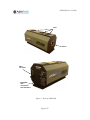
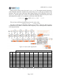
Technical specifications of the system are shown in Table 1 and Table 2. Figure 1.
shows photos of APDCAM where the location of its elements are indicated.
1.1.
Using this document
Section 2 briefly describes the information needed for setting up and operating the
camera. Section 3. contains a detailed reference documentation intended for software
developers and for advanced users.
Page 3/32
APDCAM User’s Guide
Detector
Avalanche Photodiode array
Hamamatsu S8550
Array size
4x8
Pixel size
1.6 x 1.6mm
Pixel pitch
2.3 mm
Spectral response range
300 to 1000 nm
Peak quantum efficiency
85% typical at 650 nm
Detector Gain
Typical 50, max 100
Temperature control range1
Typical 10...30 ºC
Temperature control type
Peltier, cooling/heating
Optical interface
Lens mount
Nikon F mount
Window material
BK7 with antireflection coating
Shutter
Type
Electromagnetically operated mechanical
Control
Software or external input
Calibration light
Type
Red LED with fibre coupling
Control
DC set from software
Sensitivity and noise
Sensitivity @ Gain=100, 14 bit mode2
2.4 106 photon/s/digit
Noise equivalent photon flux @ no light2
Typical 5 107 photon/s
2
Analog bandwidth
1 MHz
Digitizer
Internal sampling rate / bits
10-50 MHz / 14 bits
Digital filter
5-point FIR + 1point recursive
Output bits
14/12/8 (MSB from internal 14 bits)
Ring buffer
0...1024 samples/channel
Trigger
Internal level/External TTL/software
Trigger delay
1µs....1000s
Resampling control
Internal fixed divider or external TTL
input
Clock base
Internal 20 MHz or external
Detector type
Table 1. Technical specifications of APDCAM, part 1.
1
2
Temperature range depends on ambient temperature.
Standard setting. Sensitivity and bandwidth can be specified at order time. Selection affects noise level.
Page 4/32
APDCAM User’s Guide
Data transmission
Gigabit Ethernet over UTP and Fibre
UDP, both directions
Multimode, Duplex SC
2 MHz/12bit
Power input
Power input
12 V DC, max. 6A
Power connector on power supply
Lemo FFA.0S.302.CLAK68
Mechanical
Size (L,W,H)
36*16*19 cm
Weight without power supply
6.7 kg
Data and control interface
Communication format
Fibre interface
Max. data rate @ 32 channels3
Table 2. Technical specifications of APDCAM, part 2.
3
For typical PCIe computer card. For certain interface cards and computer configurations data rate might
be significantly lower.
Page 5/32
APDCAM User’s Guide
Fans
F-mount
Fibre
converter
Backplate
with
connectors
and indicators
Figure 1. View of APDCAM.
Page 6/32
APDCAM User’s Guide
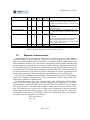
2. Using APDCAM
2.1.
Power connection
APDCAM is delivered with an external 12 V DC power adaptor. This unit has a replaceable power cord, please use one which matches your local mains outlet. The camera
needs a single 12 V DC input, maximum current is 6A. The power adaptor is usable from
100 to 230 V mains voltage.
2.2.
Operating environment
Some effort might be needed in the setup to minimise noise pick up by the camera. Although APDCAM is housed in a grounded Aluminium enclosure and the detector and
analog amplifiers are housed in an additional Faraday shield strong environmental electrical noise sources might cause disturbances in the signals. To avoid such conditions
separate the camera ground from noise electronic equipment. The camera housing is connected to electrical ground on the power supply mains connector.
2.3.
Camera cooling
APDCAM has three independent fans on the top of the device which circulate air from
the openings on the lower part of the camera out through the fans. The openings should
be free to provide the necessary air flow. In the default setup the speed of the three fans is
controlled automatically, their speed will depend on the temperature of the internal components. If this is not desirable the fans can also be set to fixed speed.
2.4.
Configuration
The operating parameters of APDCAM are set up in two internal register tables, one for
the data acquisition and one for the camera control. Status of the camera can also be read
from these registers. Settings are stored in non-volatile memory, therefore after switching
off and on the camera the setup will remain the same. There are a few exceptions from
this rule:
Detector bias voltage is always off and disabled after switching on the camera.
The desired number of samples in the measurement are set to 0 on power-on.
The camera also contains configuration information which can only be read by the user.
An example is the maximum allowed detector bias voltage. These register values can be
changed by the manufacturer only.
2.5.
PC communication
APDCAM can be connected to a PC either via UTP cable or fibre optics communications. In both cases Gigabit Ethernet is used with 100/10 Mbit as fallback. For using the
maximum data acquisition bandwidth it is essential to use a Gigabit interface card on the
PC side which connects to the internal bus via a PCI Express interface. A card connected
to the PCI bus will not deliver the maximum performance although camera operation at
lower acquisition speeds will not be affected.
If UTP (electrical) connection is intended simply connect a Gbit compatible UTP cable between the APDCAM UTP port and the PC interface card. In case of optical com-
Page 7/32
APDCAM User’s Guide
munication a media converter is needed on the PC side. Adimtech recommends D-Link
DMC-700SC media converters, which were extensively tested with APDCAM.
On the camera side the media converter is included in the camera. Connect a short
UTP cable between the camera UTP port and the camera Fibre module’s UTP port. Connect the optical cable to the camera fibre converter optical connector. On the PC side
similarly connect the media converter between the PC Gigabit interface and the optical
cable.
To communicate with APDCAM the PC Ethernet interface IP address should be set up
to the same subnet as the camera. The default IP address of the camera is 10.123.13.101,
therefore the PC can be set up e.g. to 10.123.13.202. The netmask should be 255.0.0.0.
The camera Gigabit interface can be set up for a different IP address using a software
command over the internet connection; therefore it can also be connected to a local network shared by other devices. However, in applications needing high data acquisition
performance this is not recommended as high network traffic can result in loss of data.
If the camera network address was set up in a wrong way or the address is not noted it
can happen that the PC cannot find the camera on the network. In such cases consult the
manufacturer for a solution.
2.6.
Software interface
A user program can control APDCAM by sending UDP datagrams to the Gbit communications module (Gigabit Ethernet Controller, ByteStudio, www.bytestudio.hu). The
control datagrams fall into two basic categories: control for the Gbit interface and register
read/write in one of the two internal modules of APDCAM: the data acquisition module
and the control module. The camera may answer to these UDP datagrams by sending one
ore more responding UDP datagrams.
For a standard setup the Gigabit interface parameters need not be modified. For special settings please consult the separate Gigabit interface documentation.
Additionally to register read/write operations data form the camera are also sent to the
PC in UDP datagrams. This form of communication is optimal for sending large amounts
of data but it has no feedback to the sending device. This means that if a data packet is
lost the camera will not resend it. UDP packets are counted sequentially, therefore the
receiving program can detect when data loss occurred.
To ease usage a Windows library (CamControl.dll) is provided which can perform all
necessary register read/write and data stream control operations. The functions can be
called from C++ or IDL. Detailed description of the DLL functions and their use is presented in Section 3.6.
During data collection the PC might need a large amount of memory. These DLL
functions attempt to allocate this in a way which prevents it from being paged to virtual
memory. This possibility is by default not enabled for all users of a PC, and should be
enabled in the Windows Control Panel. For details see Section 3.6.
2.7.
Optical input interface
APDCAM has a standard Nikon F-mount as optical input interface. A BK7 glass window is located in the F-mount therefore dust will not enter the detector housing. A shutter
is mounted between the window and the detector. The shutter can be opened either with a
software command or via an external TTL signal. A calibration light source is coupled to
Page 8/32
APDCAM User’s Guide
the detector surface which can be set up via software to emit various levels of constant
light on the detector, thus allowing calibration. The light level is not strictly proportional
to the setting and the illumination of the detector is not uniform, therefore the calibration
light cannot be used for calibrating the relative sensitivity of the pixels.
The calibration light is also useful for setting up the optical system. As APDCAM has
low spatial resolution viewing its image does not help in adjusting the lens focus. Instead
it can be done by illuminating the detector with the calibration light and observing its
image on a screen at the object.
2.8.
The detector and its operation
The detector has 32 identical Avalanche Photodiode elements (pixels) biased from a
single voltage. The bias voltage determines the internal gain of the detector. The detector
bias voltage should be set between 200-400V using the appropriate control register. Although the detector and electronics are protected from overload, damage cannot be excluded if e.g. only a single pixel is illuminated over an extensive period of time. To protect accidental switch-on of the bias voltage a voltage enable register is provided where
an appropriate code should be entered. Voltage can be switched on only after this.
An additional protection against overload is provided by the digital electronics. If enabled it can switch off the detector bias voltage when the signal level is above a certain
limit over a predefined time.
In order to stabilise the gain the detector temperature should be kept constant. This is
accomplished by a temperature control circuit. The standard detector temperature is 18 C
which under normal room temperature does not require too much cooling and prevents
condensation of humidity. If the environmental temperature is much lower or higher 2025 Celsius the detector reference temperature can be set to a different value.
2.9.
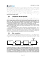
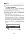
Data acquisition
The logical scheme of the data acquisition is shown in Figure 2. This scheme is operating for all 32 channels independently; all channels can be enabled/disabled. The Analog
to Digital Converter (ADC) continuously samples the amplified detector signal to 14 bits
Trigger
ADC
Digital filter
Resampling
Output control
Figure 2. Logical scheme of the basic data acquistion sytem.
at a frequency between 10-50 MHz. A configurable digital filter provides high frequency
cutoff. The filtered signal is resampled at a lower frequency or using an external clock to
reduce data load to the computer. The data output can be controlled from external or internal trigger or software command. A ring buffer is also available which can store the
last maximum 1023 resampled data. When the trigger arrives data output starts with the
contents of the buffer, this post-trigger operation is possible. This is very useful in comPage 9/32
APDCAM User’s Guide
bination with the internal trigger mode, as APDCAM can trigger itself on the incoming
light signal. The camera can also produce an output trigger when the output is started.
In the standard setup the data acquisition system timing is based on in internal quartz
oscillator. However, if needed this can be replaced by an external clock signal to provide
strictly synchronous operation between several cameras or other devices.
2.10.
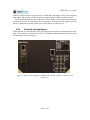
Controls and indicators
APDCAM has several indicator LEDs and input-output connectors mounted on its backplate. Their function is described in Table 3. The photo of the backplate where these units
are mounted is shown in Figure 3.
Figure 3. Photo of the backplate of APDCAM with the controls, connectors and
indicators.
Page 10/32
APDCAM User’s Guide
Power switch
Reset button
Power connector
Clock in
Clock out
Trigger in
Trigger out
Sample in
Opt
Ethernet
Optical Ethernet
UTP
Optical Ethernet
fibre
Temp.
Overload
Comm.
ADC
Control
Calib.
Shutter
HV
Ext. Clock
Data out
Gbit
Controls
Switches the input power.
This depressed button can be operated with a pen or other pointed
device. Pressing it causes both the control unit and the data acquisition unit to return to factory default settings.
Connectors
Receives input 12 V DC power.
Reference TTL clock input. Synchronises clock base of APDCAM
to external source. (Signal standard 3.3 V CMOS)
Reference clock output. Can be used to synchronize clock base of
external device. (Signal standard 3.3 V CMOS)
Data acquisition start trigger signal input.
(Signal standard 3.3 V CMOS)
Outputs High level while data transmission is active.
(Signal standard 3.3 V CMOS)
Input resample clock. (Signal standard 3.3 V CMOS)
Optional input-output. Can be selected among various internal signals in the factory.
UTP connection to PC.
UTP cable connection from Ethernet connector of APDCAM if
fibre communication is desired.
Fibre data connection to PC
LEDs
Red light means temperature alarm. Some element of the camera is
overheated.
Red light means overload condition occurred, detector bias voltage
is switched off.
Green light flashes when control communication occurs between
PC and camera
Data acquisition module state: Green indicates normal state, red
means error condition.
Control module state: Green indicates normal state, red means error
condition.
Yellow light means calibration light is on.
Yellow light means shutter is open
Blue light means detector bias voltage is on.
Green light means external reference clock signal is accepted.
Green light indicates data output to PC.
Ethernet interface is operating at Gigabit speed.
Table 3. List of controls, connectors and LED indicators of APDCAM.
Page 11/32
APDCAM User’s Guide
3. APDCAM Reference Manual
In this section a detailed description is given of the APDCAM system.
3.1.
System Overview
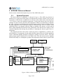
The block scheme of APDCAM is shown in Figure 4. The APD array detector is
mounted on a copper tab which can be cooled/heated by a Peltier element. This way the
temperature of the detector is stabilised at a reference value which can be somewhat (max
~15 C) below or above the ambient temperature. Cooling the detector does not offer advantages in terms of noise, therefore the temperature control is provided only to stabilise
the gain. A shutter is mounted in front of the detector so that it can be coupled off from
the input light and can be calibrated using the calibration light. The DC current of the
calibration LED is set digitally while the light is coupled to the detector via four optical
fibres which illuminate the detector from 4 directions. The detector bias voltage is also
controlled digitally thus having the possibility of adjusting the detector gain to the requirements.
The photocurrent from each of the 32 detector pixels is amplified by a sensitive low
noise amplifier. To compensate for the offset drift the output offset level of the amplifiers
can be controlled digitally through 32 Digital to Analog Converters (DAC). The final
analog output signal is digitized at 10-50 MHz/14 bit. The data stream can be digitally
filtered and finally it is resampled to produce the output data stream which is packed into
Temp.
sensors
Fans
Shuter control
Power input
(12 V DC)
Calibration light
Control and
Power Unit
Detector bias voltage (HV)
Detector temperature control
Overload
Gigabit
Ethernet Controller
Gbit
Ethernet
(RJ-45)
To PC
Detector
Analog
Amplifiers
Data Acquisition
Data
Unit (DAQ)
Control
Shutter
Peltier
UTP-Fibre media converter
Figure 4. Block scheme of APDCAM.
Page 12/32
APDCAM User’s Guide
UDP packets and transmitted through the Ethernet connection to the PC. Communication
with the PC can be done via the UTP connection. If needed fibre optics communication is
also possible through the built-in media converter.
The ADC works all the time, therefore it is possible to perform some triggering operations inside the camera. One possibility is internal triggering, where the data acquisition
starts when the signal reaches a certain level. The trigger level can be set individually for
all 32 channels. Another possibility is detector protection from extended periods of overload. If the signals are above a certain level over a specified time the bias voltage of the
detector is switched off. Details of the data acquisition operation are given in Section 3.2.
The Control and Power Unit provides power for all the other units and controls the detector infrastructure: detector bias voltage, temperature, calibration light, shutter, fans.
The detector bias voltage can be set by the user up to a factory set limit in the range of
400-500 V. The exact limit is dependent on the individual detector. There is also a minimum recommended detector bias voltage of 200 V, below that the crosstalk through the
pixels causes excessive noise. The control card also controls the detector temperature by
cooling or heating it via a Peltier element. No computer intervention is needed for the
control, only parameters can be set from the PC.
Operation parameters of the camera are set by setting registers in the ADC or the control unit. For a description of the register tables see Sections 3.2 and 3.4.
The communication between APDCAM and the host PC is performed by a general
purpose Gigabit communication card. It communicates with the two internal units via an
internal bus. The register tables of the camera can be written or read by sending UDP
datagrams to the Gigabit card. Acquired data is also sent via this card.
3.2.
Detector and analog electronics
The detector has 32 identical Avalanche Photodiode elements (pixels) connected to a
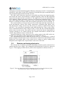
common positive bias voltage. The arrangement and dimensions of pixels is shown in
Figure 5. The mapping to/from detector pixels to data acquisition is shown in Table 4.
Figure 5. Detector dimensions and arrangement of pixels viewing the detector from
the front of the camera. All dimensions are in mm.
Page 13/32
APDCAM User’s Guide
APD#
A1
B1
C1
D1
E1
F1
G1
H1
Channel
1
2
3
4
5
6
7
8
Channel
18
20
21
23
25
27
28
30
APD#
APD#
A2
B2
C2
D2
E2
F2
G2
H2
Channel
Channel
19
17
22
24
26
32
29
31
APD#
APD#
A3
B3
C3
D3
E3
F3
G3
H3
Channel
Channel
15
13
16
10
8
6
1
3
APD#
APD#
A4
B4
C4
D4
E4
F4
G4
H4
Channel
Channel
14
12
11
9
7
5
4
2
APD#
G3
9
D4
17
B2
25
E1
H4
10
D3
18
A1
26
E2
H3
11
C4
19
A2
27
F1
G4
12
B4
20
B1
28
G1
F4
13
B3
21
C1
29
G2
F3
14
A4
22
C2
30
H1
E4
15
A3
23
D1
31
H2
E3
16
C3
24
D2
32
F2
Table 4. Allocation of data acquisition channels for the detector pixels.
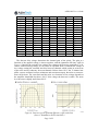
The detector bias voltage determines the internal gain of the pixels. The gain as a
function of the applied voltage is shown together with the Quantum efficiency (QE) in
Figure 6. Besides the gain the bias voltage also changes the detector capacitance, it decreases with increasing voltage. As all pixels are operated from a common bias voltage at
low voltage setting the crosstalk increases between channels which results in an increase
of the noise and its coherency between channels. Below about 150 V the 32 channel amplifier system oscillates between minimum and maximum output, therefore no measurement can be done. The exact limit and the noise as a function of bias voltage depends on
the amplifier bandwidth but above 200 V bias voltage the detector is stable. The noise
level decreases slightly until about 300 V.
Figure 6. Detector typical Quantum Efficiency (QE) and Gain.
(Source: Hamamatsu S8550 datasheet.)
Page 14/32
APDCAM User’s Guide
The detector can be overloaded if high input light level is applied while the bias voltage is on. Although the detector and electronics is protected against overload under the
most unfavourable conditions about 0.4W heat can be generated in the detector which
might result in damage if present for an extensive time. To prevent damage the camera
electronics contains an overload protection function which switches off the detector bias
voltage if the output signal is above a limit for an adjustable time.
An additional measure to prevent overload is the two-step bias voltage switch-on procedure. When APDCAM is switched on the bias voltage is off. First a bias voltage enable
code should be written into the bias enable register and the voltage can be switched on
only after that. This procedure prevents accidental biasing die to any accidental software
error.
The detector is mounted on a temperature controlled tab. The reference temperature is
set in a register of the control module. This temperature can be either below or above the
environmental temperature. (The environmental temperature is measured on the base of
the camera and can be read from the register table.) Cooling the camera does not provide
specific advantage, but temperature changes affect the detector, therefore the aim of temperature control is to provide a stable gain. 18 C is recommended for detector temperature as it is slightly below usual room temperature but it does not cause condensation of
air humidity on the detector. Please note that the temperature of the detector has an effect
on the gain as well. Applying the same bias voltage at lower temperature causes higher
gain. Please consult the Hamamatsu S8550 datasheet for details.
The analog electronics utilize two amplifier stages for each channel, their bandwidth is
from DC to a maximum frequency. Parameters of the first stage (feedback resistor and
capacitance) determine the bandwidth and also the noise level. For setting an optimal
Signal to Noise ratio some information on the expected light level is required. As default
the amplifier is set up for about 1010 photons/s light level and 1 MHz bandwidth. For
considerable different conditions the amplifier should be mounted with different components, therefore a rough estimation of the light level and required bandwidth is necessary
at manufacturing time.
The high sensitivity amplifiers and the detector bias current can cause some drift in the
signal DC level. In order to compensate for this the analog electronics is equipped with a
DC offset input which can be set for each channel individually in the data acquisition
unit. The analog signals are negative in response to the input light, therefore the DC offset should be set to a high positive value to fit the signal into the 0-2V range of the digitizer.
The detector is mounted directly on to the analog amplifier circuit board and cooled by
a cooling tab. The whole unit is mounted inside an Aluminium housing. The temperature
of the detector, the analog electronics and the housing are measured.
3.3.
Data Acquisition Unit
The block scheme of the data acquisition unit (DAQ) is shown in Figure 7, while the
register map is in Table 5. and Table 6. After power-on different registers are set from
various sources as indicated in the table. Most of the registers recover their last data from
an on-board EEPROM memory, therefore they preserve their settings. Several of the registers will show the factory default value. This factory default can be regenerated for all
Page 15/32
APDCAM User’s Guide
registers by writing a code into the FACTORY_RESET register. This is identical to
pressing the reset button at the camera back.
R/W
Offset
(byte)
Size
(byte)
BOARD_VERSION
MC_VERSION
SERIAL
FPGA_VERSION
STATUS1
R
R
R
R
R
0
1
3
5
8
1
2
2
2
1
Value
after start
factory
factory
factory
factory
N/A
STATUS2
R
9
1
N/A
CONTROL
R/W
11
1
EEPROM
ADC_PLL_MULT
R/W
12
1
EEPROM
ADC_PLL_DIV
R/W
13
1
EEPROM
STREAM_PLL_MULT
R/W
14
1
EEPROM
STREAM_PLL_DIV
R/W
15
1
EEPROM
STREAM_CTRL
R/W
16
1
0
SAMPLE_NUMBER
CH_ENABLE
RINGBUFSIZE
R/W
R/W
R/W
17
21
25
4
4
2
0
EEPROM
EEPROM
RESOLUTION
R/W
27
1
EEPROM
SAMPLEDIV_X_7
R/W
28
2
EEPROM
TRIGGER
R/W
30
1
EEPROM
Parameter
Description
Board version code.
Microcontroller program version code.
Board unique serial No.
FPGA program version code.
Status flags, group 1
Bit 0: ADC PLL locked
Bit 1: Stream PLL locked
Bit 2-7: Reserved
Bit 0: Reserved
Bit 1: Overload
Bit 2: External clock PLL locked
Bit 3: Reserved
Bit 4-7: ADC 1-4 sample enable
Various control bits:
Bit 0: External clock select
Bit 1: Clock out enable
Bit 2: External sample select
Bit 3: Sample out enable
Bit 4: Digital filter enable
Bit 5: Reserved
Bit 6: Reverse bit order in stream (1: LSB first)
Bit 7: Preamble enable
PLL multiplier for ADC clock generation.
Valid: 20...50
PLL divider for ADC clock generation.
Valid: 8...100
PLL multiplier for ADC clock generation.
Valid: 20...50
PLL divider for ADC clock generation.
Valid: 8...100
The four lower bits enable the data output to the
four streams.
Requested number of samples. 0 for infinite.
Enable bits for the 32 channels.
Size of the ring buffer in samples per channel.
(Valid: 0...1023)
Output resolution.
0: 14 bit, 1: 12 bit, 2: 8 bit.
Divider for generation of the sample clock from
7xADC_CLOCK. E.g. to take every second
sample write 14.
Trigger enable bits.
Bit 0: Enable external trigger rising edge.
Bit 1: Enable external trigger falling edge.
Bit 2: Enable internal trigger. (For polarity see
INT_TRIG_LEVEL
Table 5. Register table of the DAQ unit, part one.
Page 16/32
APDCAM User’s Guide
Parameter
R/W
Offset
(byte)
Size
(byte)
ADC_TEST_MODE
R/W
32
4
Value
after start
EEPROM
FACTORY_RESET
W
37
1
N/A
BYTE_PER_SAMPLE
R
40
4
N/A
CLOCK_PLL_MULT
CLOCK_PLL_DIV
OFFSET
R/W
R/W
R/W
46
47
48
1
1
64
EEPROM
EEPROM
EEPROM
INT_TRIG_LEVEL
R/W
112
64
EEPROM
ACT_SAMPLE
R
176
16
0
OVERLOAD_LEVEL
R/W
192
2
EEPROM
OVERLD_STATUS
R/W
194
1
0
OVERLD_TIME
TRIGGER_DELAY
R/W
R/W
195
197
2
4
EEPROM
EEPROM
FILTER_COEFF
R/W
208
16
EEPROM
Parameter
Description
Each byte controls the mode of one ADC, first
is ADC 1. The codes in the lower 3 bits are:
0: Normal measurement
1: 10 0000 0000 0000
2: 11 1111 1111 1111
3: 00 0000 0000 0000
4: 10 1010 1010 1010, 01 0101 0101 0101
5: Long pseudorandom
(See Sect. 5.6 of ITU-T 0.150 (05/96) standard )
6: Short pseudorandom
(See Sect. 5.1 of ITU-T 0.150 (05/96) standard )
7: 11 1111 1111 1111, 00 0000 0000 0000
Writing hex CD into this register causes all
settings to return to factory reset.
The ADC indicates here the number of bytes
per sample sent in one stream. The four bytes
correspond to the four streams, (See section
2.6)
External clock PLL multiplier. Valid: 2..33
External clock PLL divider. Valid: 1..32
These are the 32x2byte offset settings for the 32
analog channels. Standard values are 500..1000.
32x2 bytes internal trigger setting for each
channel:
Bits 0...13: trigger level
Bit 14: 0: positive trigger (level)
1: negative trigger (level)
Bit 15: Enable trigger from this channel
4x4 byte indicating the number of acquired
samples per stream. As the sample timing is
identical for all channels these values are normally identical.
Overload condition setting for all channels:
Bits 0...13: level
Bit 14: 0: overload above level
1: overload below level
Bit 15: Overload enable.
Bit 0: overload status
Writing this register clears overload.
Overload time in 10 µs units.
Delay of data transmission start after any trigger
condition in units of the base clock period time.
Signed 16 bit integer coefficients for digital
filter. These should be written sequentially, they
are loaded into the FPGA when the last byte is
written.
Order of 2-byte coefficients:
COEFF_01...COEFF_05: FIR coefficients
COEFF_06: Recursive filter coefficient.
COEFF_07: Reserved
Coeff_08: Filter divide factor: 0...11.
Table 6. Register table of theDAQ unit, part two.
Page 17/32
APDCAM User’s Guide
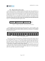
At the beginning of the register map some registers describe the program and hardware versions and the unique serial number of the ADC board.
After power-up the red-green bicolor ADC LED is lit green on the camera backplate.
If the ADC unit encounters a fatal problem this LED is red.
The DAQ unit is attached to the analog output signals at the backside of the detector
housing. The 32 input channels have an analog bandwidth of about 3 MHz, the input
voltage range is 0-2V. The input channels are grouped into 8-channel blocks, each block
is served by an 8-channel pipeline ADC chip. Data from one block is sent to one data
stream on the Gigabit communication card. The four streams are sent in separate UDP
datagrams on a single Gigabit connection to separate software ports in the PC.
3.3.1. ADC Timing
The timing is identical for all 32 channels and it is based on a single clock. This can be
either an internal 20 MHz oscillator or an external clock (clock in). Selection is done with
bit 0 in the CONTROL register. The external clock frequency is multiplied/divided by a
PLL (see CLOCK_PLL_MULT, CLOCK_PLL_DIV), therefore different input clock
frequencies can be accommodated in the 1...40 MHz range. The base clock generated
from the external clock should be between 19 and 40 MHz.
The ADC clock is generated from the selected base clock with a PLL (see
ADC_PLL_MULT, ADC_PLL_DIV), the resulting ADC clock must be between 10 and
50 MHz. An additional limitation is that the base clock multiplied by ADC_PLL_MULT
should be between 400 and 1000 MHz.
The status of the PLL units can be read from the STATUS1 and STATUS2 registers.
This is important especially if external clock is used. The external clock PLL status is
also shown on the camera backplate by the green Ext. Clock LED.
The 8-channel ADC blocks have a built-in test pattern generator which can be activated individually for all 4 blocks using the ADC_TEST_MODE register. This forces all
8 channels in one block to send the same test pattern.
3.3.2. Filtering, resampling and channel selection
The ADCs generate a data stream with 32x14 bits. A digital filter can be enabled in
the CONTROL register which filters all 32 channel data with identical settings. The layout of one filter is shown in Figure 8. The 14 bit data is fed in from the left side. A 5stage FIR filter allows steep cut of the frequency band somewhat below the sampling
frequency of the ADC. An additional recursive filter is implemented after the FIR filter to
allow for lower frequency cut-off, albeit with less steep characteristic. The recursive filter
implementation with integer arithmetic deserves some attention as long integration times
can cause overflow in the data. To handle this situation some flexibility is provided at
the end of the filter where the output 8, 12 or 14 bit data is cut out: the location of the
output bits can be selected.
The following procedure is proposed for calculation of the filter coefficients. The desired cutoff frequency of the recursive filter (frec) should be selected. From this the COEFF_06 is
COEFF_06= 4096 e
Page 18/32
2 f rec f ADC
.
APDCAM User’s Guide
If the recursive filter is not to be used, COEFF_06=0. The impulse transfer function hi
of the FIR filter should be calculated at 5 points using 1/fADC as the time resolution of the
function. This can be done with some filter design toolbox. If the FIR filter is not to be
used h1 is 1, all the others are 0. These hi coefficients should be normalised by their sums
and multiplied by (4096-c)/8 to yield the coefficients of the FIR filter:
h
COEFF_0i = 5 i (4096-COEFF_06)/8,
i=1...5.
hi
i 1
The two last coefficients should always have the same value:
COEFF_07 = 0,
COEFF_08=9.
The filter coefficients are listed for selected cases in Table 7. Here the ADC frequency
is assumed to be 10 MHz. If a different ADC frequency is used all frequencies should be
scaled proportionally.
Figure 8. Layout of the digital filter.
Filter Coefficients
fREC
fFIR
[MHz]
[MHz]
50.0
COEFF_01...COEFF_08
01
02
03
04
05
06
07
08
00512
00000
00000
00000
00000
00000
00000
00009
00290
00202
00048
00000
00000
00000
00000
00009
00190
00164
00102
00042
00008
00000
00000
00009
00138
00000
00000
00000
00000
02991
00000
00009
00078
00054
00012
00000
00000
02991
00000
00009
00050
00044
00026
00010
00002
02991
00000
00009
00030
00000
00000
00000
00000
03846
00000
00009
00016
00012
00002
00000
00000
03846
00000
00009
00010
00010
00006
00002
00000
03846
00000
00009
5 0
50.0
2 0
50.0
1 0
0.5
5 0
0.5
2 0
0.5
1 0
0.1
5 0
0.1
2 0
0.1
1 0
Table 7. Filter coefficients for some selected cases.
Page 19/32
APDCAM User’s Guide
Figure 9. shows the simulated frequency transfer functions of the same cases. From
these it is clear that the FIR filter is effective down to about 1/10-th of the ADC frequency. For lower frequency cutoffs it can be used in combination with the recursive
filter. The recursive filter works at least down to 100 kHz, but at these low frequency cuts
the FIR filter has no effect.
After the filter the desired number of output bit resolution (8,12 or 14 bits, see RESOLUTION register) is selected by keeping the most significant bits.
The resulting amount of data could not be transferred through the Ethernet connection
when all the channels are operating, therefore some data reduction is needed. This can be
done either by reducing the number of active channels or by resampling the data (decimation) to lower frequency.
Channels can be enabled individually, see CH_ENABLE register.
Resampling can be done for all active channels in the same way. The resampling clock
can be either a divided version of the ADC clock (see register SAMPLEDIV_X_7) or it can
be an external input clock. In this latter case it has to be noted, that the data acquisition
unit will not sample exactly at the time of the input clock pulse, but will take the latest
sample when the sample clock arrives. Depending on ADC clock This can result in
20...100 ns jitter.
Figure 9. Simulated frequency transfer functions of the filter cases listed inTable 7. Filter
coefficients for some selected cases.Table 7 .
Page 20/32
APDCAM User’s Guide
By balancing the bit resolution, the channel number and the resampling rate the bandwidth of the data transmission can be used optimally. E.g. 10 MHz/12bit measurement is
possible if one channel is selected in each block or 2 MHz/12bit if all 32 channels are
working.
3.3.3. Triggering, overload protection
The ADC measurement, digital filtering and resampling works continuously in
APDCAM. but data output to the host is enabled only when data is needed. The first requirement for data transmission is that the STREAM_CTRL bits should be set to enable
data output from the four 8-channel blocks of the DAQ unit to the Gigabit card. If no
triggering scheme is enabled data transmission starts immediately.
When the data transfer is started a certain number of samples per channel (SAMPLE_NUMBER register) are transmitted to the host and after that the data transmission is
stopped. The exception is when SAMPLE_NUMBER=0 for which the transmission runs
for an unlimited time. The actual number of transmitted samples are shown in 4 32 bit
long ACT_SAMPLE registers.
Triggering of data transmission can be achieved using several schemes:
External trigger. Bit 0 or 1 of the TRIGGER register should be set and the
TTL trigger signal connected to the Trigger In connector. Depending on the bit set
the trigger event happens on rising or falling edge.
Internal trigger. This enables starting the data acquisition when the signal
level in the detector channels is above or below some level. This is not an edge trigger mode, which means that if the stream inputs are enabled when the level fulfils
the condition the measurement starts immediately. Internal trigger is globally enabled by bit 2 of the TRIGGER register while the 32 INT_TRIG_LEVEL registers
set the internal trigger parameters for all channels independently. Bit 15 enables,
while bit 14 sets the polarity for the corresponding channel. the trigger level is set
by the 14 least significant bits. The trigger event happens when any of the 32 channels fulfils the trigger condition. It has to be emphasized that light input to the detector causes negative signal, therefore for triggering on rising light negative trigger
should be set.
SAMPLENUM samples
RINGBUFSIZE
samples
Time
Measured data
TRIGGER_DELAY
TRIGGER OUT signal
Trigger event
Figure 10. Triggered start of measurement.
Page 21/32
APDCAM User’s Guide
After the trigger event the data transmission can be delayed by setting the TRIGGER_
DELAY register which allows several ten second delay. After the TRIGGER_DELAY
time data transmission starts and the Trigger Out signal goes to H on the backplate. At
the same time the Data LED shows the active data transmission.
Data from the measurement are continuously filling a ring buffer which size can be set
in register RINGBUFSIZE. This enables a post-trigger capability that is, samples acquired before the trigger event can be transmitted. This is extremely useful when
APDCAM is measuring a fast transient event as the staring phase can be measured without any external trigger.
The timing scheme of a triggered measurement is shown in Figure 10.
A separate scheme, similar to the internal trigger, is used for overload protection of the
detector. Although it is protected from excess light imput under very unfavourable conditions a long-term overload might cause considerable power dissipation in the detector
which might in turn result in damage. To avoid this an overload protection scheme can
be switched on in the OVERLOAD register. Bits 14 and 15 should be set to 1 to enable
the overload feature and the desired overload level should be entered in bits 0...13. A
typical level would be close to 0 as the detector delivers negative signal. An overload
event is generated when any of the signals fulfills the overload condition for more than
OVERLD_TIME. The overload event switches off the detector bias voltage and lits the
red Overload LED on the backplate. The status of the overload can be read from
OVERLD_STATUS and writing any value into this register clears the overload. The bias
voltage should be switched back in the Control unit. This overload protection works
without the measurement enabled.
3.3.4. Data output format
After a trigger event or stream enable first a preamble block is sent to the output data
stream. This identities the start of the data and contains the stream ID. After that data is
sent in identical sample blocks each containing data from the same sampletime of all the
enabled channels of the given 8-channel ADC block. The data bits are packed bitcontinuously into the sample block and padded to the next full byte. Details are described
in section 3.6.1.
3.3.5. Offset control
The sensitive analog amplifiers or the detector leakage current can cause a drift in the
detector offset voltage. To compensate for this the DAQ unit contains 32 12bit Digital to
Analog Converters (DACs) which can be used to shift the analog input signal to the
ADC. The corresponding values can be entered in the OFFSET register. These values
are 12bit unsigned numbers, increasing values shift the in put signal to higher values. As
the analog amplifiers deliver negative signal the offset should be set close to the upper
limit of the ADCs. Typical needed values are in the 700-900 range.
Page 22/32
APDCAM User’s Guide
3.4.
Control unit
The Control unit fulfils the following tasks:
Detector bias voltage setting
Detector temperature control,
Shutter open/close,
Calibration light setting,
Temperature measurements,
Fan control for regulating the camera internal temperature.
The operating parameters of the Control unit can be found in its register table listed in
Table 8 and Table 9. The unit stores its actual settings in an EEPROM non volatile memory. After power on the registers marked with EEPROM reload their data from this storage. These way settings need not be always re-entered from scratch. There is one important exception from this rule, the BIAS_ON and BIAS_ENABLE registers are set to 0 on
power on. This causes the detector voltage to be switched off but the set value preserved
in BIAS_SET.
The factory default values can be recovered by writing a code into the FACTORY_RESET register.
The electronics version code and the microcontroller program version code can be
read from the BOARD_VERSION and MC_VERSION registers, respectively. The
unique serial number of the board is stored in BOARD_SERIAL.
After power-up the red-green bicolor Control LED is lit green on the camera backplate. If the Control unit encounters a fatal problem this LED is red.
3.4.1. Detector bias voltage setting
In order to prevent accidental setting by e.g. software error the detector bias voltage is
set in several steps. First the required value is entered in the BIAS_SET register. Please
note the conversion factor. The Control unit limits bias voltage to a maximum value
(BIAS_MAX) set during factory calibration. This aims at setting a detector-specific
maximum. If the user tries to set a bias voltage higher than this maximum only the
maximum will be set and an error code is written into ERROR_CODE.
After setting the voltage the output should be enabled by writing code hex $AB to
BIAS_ENABLE. As a final step the voltage can be switched on by setting bit 0 in
BIAS_ON. The actual bias voltage can be read in BIAS_MONITOR. After the switch-on
procedure the set value can be changed if a different voltage is intended to be set.
When the bias voltage is enabled and switched on the blue HV LED is lit on the camera backplate.
3.4.2. Temperature control
The detector can be cooled/heated by a Peltier element. Depending on its current direction this pumps heat in either directions between the detector and a heatsink. The detector temperature is measured and available in TEMP_DETECTOR. This value is compared by the control unit against a set value (DET_TEMP_SET) and the Peltier current is
Page 23/32
APDCAM User’s Guide
driven through a PID controlled. The weight factors of this can be set in the PID_P,
PID_I, PID_D registers. For strongly different temperature settings these might need to
be modified from the factory default. The actual Peltier current can be read in
PELTIER_OUT. The operation of the temperature control can be suspended if all three
PID_x registers are filled with 0. This means no current will be driven through the Peltier
element.
The camera internal temperature is controlled by three variable-speed fans located on
the top of the housing. They are controlled by the Control unit using measured temperatures in the camera (TEMP_xxx registers). From the detector side the first fan cools the
detector housing and the DAQ card. The second moves air through the heatsink of the
Peltier element. It will switch on gradually when the heatsink is either cooler or warmer
than 25 degrees. The third fan cools the Control unit, power supplies and communication
cards. The actual fan speeds can be read from registers FAN_xxx.
The temperature control scheme of APDCAM is highly reconfigurable by special configuration programs from the PC. If the camera is intended to be operated in an environment where the temperature is significantly different from room temperature or when the
fans need to be controlled manually please consult the manufacturer.
3.4.3. Shutter and calibration light
The shutter is mounted in front of the detector but behind the camera window. It
is operated with and electromagnet controlled from the Control unit. In its basic setup
(SHUTTER_MODE=0) the SHUTTER_STATE register opens and closes the shutter.
The drive electronics is not designed to open/close the shutter at high frequency, but it is
intended for single open/close cycles every few seconds as the shortest period time. The
shutter can be kept open or closed for any time. When the shutter is open the yellow
Shutter LED is lit on the camera backplate.
In SHUTTER_MODE=1 the shutter can be controlled externally by an electrical
signal. For this the shutter signal should be routed to the Optional signal connector in the
backplate using an internal jumper. The shutter state signal can also be output on the
same connector. Please consult the manufacturer if such operation is needed.
The aim of the calibration light is to enable verification of the detector operation,
measurement of SNR levels and noise spectra with variable light input. It is intended neither for absolute calibration of the sensitivity nor for relative calibration of the pixels.
The light source is an ultra bright red LED. To avoid any electrical interference
the LED is mounted in the Control unit and the light is coupled into the detector housing
using four 1 mm diameter optical fibres. These illuminate the detector from four directions providing more-or less uniform illumination. The current of the LED is provided by
a current generator which can be controlled digitally through the CALIB_LIGHT register. At 0 settings there is no light emission. At about 100-200 the light saturates the detector amplifier with ~350 V detector voltage. As the detector gain is typically around 30-50
at this bias voltage the maximum light emission at 4095 approximately saturates the detector with low gain around 200 V. (Below 150 V bias voltage the amplifiers show excessive noise.)
When the calibration light is on at any level the yellow Calibration LED is lit on
the camera backplate.
Page 24/32
APDCAM User’s Guide
R/W
Offset
(byte)
Size
(byte)
BOARD_VERSION
MC_VERSION
BIAS_MONITOR
R
R
R
0
2
4
1
2
2
Value
after start
factory
factory
actual
TEMP_ADC
R
12
8
actual
TEMP_DETECTOR
TEMP_ANALOG
R
R
20
22
2
2
actual
actual
TEMP_DETHOUSE
R
24
2
actual
TEMP_PELTIER
R
26
2
actual
TEMP_CONTROL
R
28
2
actual
TEMP_BASE
R
30
2
actual
TEMP_DAQ
R
40
2
actual
PELTIER_OUT
R
44
2
actual
PID_P
PID_I
PID_D
BIAS_SET
R/W
R/W
R/W
R/W
80
82
82
86
2
2
2
2
EEPROM
EEPROM
EEPROM
EEPROM
BIAS_ON
R/W
94
1
0
BIAS_ENABLE
W
96
1
0
DET_TEMP_SET
R/W
106
2
EEPROM
FAN_PELTIER
R
108
1
actual
FAN_ELECTRONICS
R
110
1
actual
FAN_DAQ_DET
R
112
1
actual
CALIB_LIGHT
R/W
122
2
EEPROM
Parameter
Description
Board version code.
Microcontroller program version code.
The measured detector bias voltage.
The conversion factor is 0.12V/digit.
The temperature of the 4 ADC blocks.
(2 bytes each in 0.1 ºC units.)
The temperature of the detector in 0.1 ºC units.
The temperature of the analog amplifier in 0.1
ºC units.
The temperature of the detector housing in 0.1
ºC units.
The temperature of the Peltier cooler/heater
heatsink in 0.1 ºC units.
The temperature of the Control unit heatsink in
0.1 ºC units.
The temperature of APDCAM baseplate in 0.1
ºC units.
The temperature of the DAQ unit FPGA in 0.1
ºC units.
Signed 2-s complement 16 bit value representing the status of the Peltier cooler/heater. Negative values mean cooling, positive heating. The
maximum is about 4000.
Weights of the P, I and D components of the
detector temperature controller.
The set value of the detector bias voltage. The
conversion factor is 0.12V/digit.
Bit 0 switches on the detector bias voltage. The
bias voltage should be enabled first in
BIAS_ENABLE.
A hex $AB (decimal 171) should be written
into this register to enable detector bias voltage.
The detector temperature set value. This is the
reference for the Peltier PID controller. (0.1 ºC
units.)
The actual speed of the fan cooling the Peltier
heatsink (range 0...255).
The speed of the fan cooling the electronics
(except DAQ) (range 0...255).
The speed of the fan cooling the DAQ and the
detector shielding (range 0...255).
The current of the calibration LED. (valid:
0...4095). 0 means no light.
Table 8. Register map of the Control unit, part one.
Page 25/32
APDCAM User’s Guide
R/W
Offset
(byte)
Size
(byte)
SHUTTER_MODE
R/W
128
1
Value
after start
EEPROM
SHUTTER_STATE
R/W
130
1
EEPROM
FACTORY_RESET
W
132
1
0
ERROR_CODE
R
134
1
0
BOARD_SERIAL
BIAS_MAX
R
R
256
258
2
2
factory
factory
Parameter
Description
Bit 0 controls shutter mode.
0: Shutter controlled by SHUTTER_STATE
1: Shutter controlled from Opt. connector if set
up in factory.
Bit 0 controls shutter state in manual mode.
0: closed, 1: open.
Writing hex $CD (decimal 205) into this register causes all settings to return to factory default.
Error code. (Write 0 to erase.)
0: No error
0x41: BIAS_SET set higher than BIAS_MAX.
0x50: Write attempt to read only register.
0x7C: Peltier controller has no valid weight
values or temp sensor error.
Board unique serial No.
Maximum allowed value for detector bias.
Table 9. Register map of the Control unit, part two.
3.5.
Ethernet Communication
Communication over the Ethernet connection is performed using a Gigabit Ethernet
Controller (GEC) by ByteStudio Ltd. This device receives data in four 8-bit streams,
packs it into UDP datagrams and sends them to a destination address. Additionally to the
data transmission to the PC the card can also communicate with the APDCAM DAQ and
Control units on an internal bus and arrange register read-write operations between the
PC and APDCAM. Communication on this internal bus is shown by blinking of the green
Communication LED on the camera backplate. Details of the GEC card are described in
its own documentation. The software interface description in Section 3.6 introduces the
functions for setting the GEC for data transfer and communication with APDCAM.
The GEC has a standard electrical Gigabit connector. Below it the green Gbit LED indicates when Gigabit communication is set up with the host. If this is not possible GEC
falls back to 100 Mbit or 10 Mbit speed.
To allow long-range fibre optic communication with APDCAM a D-Link DMC700SC UTP-fibre media converter has been integrated into APDCAM. To use fibre
communication a short UTP cable can be connected between the GEC UTP port and the
fibre media converter. The fibre cable should be connected to the media convert’s fibre
port. The connector type is duplex SC, the fibre cable is multimode. The fibre communication signal should be converted back to UTP on the camera side. For the camera side
conversion the same unit ( D-Link DMC-700SC) is recommended. There are two jumpers on this card, they should be set as follows:
SW1: on (forced)
Sw2: off
Page 26/32
APDCAM User’s Guide
3.6.
Software interface
Control of APDCAM is performed using the CamControl.dll Dynamic Link Library
for C++. To use the functions the CamControl.lib static library should be linked to the
program. The DLL was compiled with Microsoft Visual Studio 2005 Professional Edition
ENU Service Pack 1 (KB926601). Version 8.0.50727.762 (SP.050727-7600), Microsoft
.NET Framework Version 2.0.50727. To use the binaries MS XP Service pack 1 should
be installed. The software has been tested on MS XP, Vista and Windows 7.
From the software point of view APDCAM can be considered as two register tables
corresponding to the DAQ and the Control unit and additionally the Gbit communication
unit. The Gbit unit translates register read/write requests to/from UDP datagrams and
communicates with the two internal units. Additionally it receives 4 data streams from
the 4 8-channels ADCs in the DAQ card and packs them into UDP datagrams sent to 4
different sockets in the PC network interface. Sending of data can be enabled/disabled in
the Gbit interface. However, data transfer will actually happen when the DAQ unit starts
sending data that is, it encounters a trigger condition.
The table below lists the available functions in the DLL:
Function name
open
close
writePDI
readPDI
GetPdiIrqCount
SendTS
DontSendTS
Description
Opens communication with the camera.
Closes communication with the camera.
Write one or more registers in one of the camera modules.
Read the contents of one or more registers in one of the camera modules.
Return the number of interrupt UDP datagrams received.
Start data sending from the camera to the PC.
Stop sending data from the camera to the PC.
Table 10. Functions of the camera control DLL.
To perform a measurement the user program should do the following. First the camera
should be opened, which opens sockets in the network interface. The identification codes
should be read from the ID registers of both the DAQ and the Control units and compared
to the values listed in the register tables. This step ensures that the communication is set
up with all elements of the camera. As the next step the desired operation mode of the
camera should be set by setting registers. PC memory should be allocated and locked in
memory to ensure that data can be received at maximum speed. Stream data transfer
should be enabled (SendTS) and data transfer should be enabled in the DAQ stream enable registers. The number of acquired data samples can be read from the sample count
registers of the DAQ module. Once the desired amount of data has been received it can
be read from the PC memory. The number of interrupts can be checked using the
GetPdiIrqCount call. If an interrupt happened conditions should be checked in the registers.
Page 27/32
APDCAM User’s Guide
Declaration of DLL functions can be found in CamControl.h. Detailed use of the DLL
calls is the following.
open
Declaration:
CAMCONTROL_API int open(unsigned int ipAddress);
Description:
This call opens the sockets for communication. The ipAddress argument is the IP addres
of the camera, each 8 bits correspond to one subnet address, eg. the default camera address is translated to:
10.123.13.101 -> 10<<24 + 123<<16 + 13<<8 + 10 = 175836517
close
Declaration:
CAMCONTROL_API int close();
Description:
This call closes the communication to the camera and closes the sockets.
writePDI
Declaration:
CAMCONTROL_API int writePDI(unsigned char address,
unsigned int subaddress, unsigned int noofbytes, unsigned char *pData);
Description:
This call performs a register write operation. Parameter address is the module address;
1 is for the DAQ module, 2 is for the Control module. subaddrss is the start address of
the register which should be written, while noofbytes is the number of bytes to be written
and *PData is the pointer to the data to be written. If the return value is less than 0 then
an error occurred.
readPDI
Declaration:
CAMCONTROL_API int readPDI(unsigned char address,
unsigned int subaddress, unsigned int noofbytes, unsigned char *pData);
Description:
The parameters have identical meaning than for writePDI, but the registers are not written
but their contents are read from APDCAM. If the return value is less than 0 then an error
occurred.
GetPdiIrqCount
Declaration:
CAMCONTROL_API int GetPdiIrqCount();
Description:
This call reads the interrupt counter register in the DLL. Interrupts happen in the DAQ
and ADC modules on certain conditions, but the interrupt does not contain any information on what happened. As the camera operates autonomously interrupts are of limited
use, they make detection of unexpected conditions easier.
Page 28/32
APDCAM User’s Guide
SendTS
Declaration:
CAMCONTROL_API int SendTS(int *pStreams);
Description:
This call enables stream data input from APDCAM to the PC but does not provide the
data storage. It should be noted that APDCAM sends data in four separate streams each
transmitting data from 8 channels. (Provided they are enabled for transfer.) The input
parameter to this function is a 4-element int array specifying the length of the UDP datagram measurement data field in the 4 streams:
int streams[4];
streams[0] = 1440
streams[1] = 1440
streams[2] = 1440
streams[3] = 1440
The datagram measurement data length is not an important parameter. Smaller packets
use higher overhead and need more frequent handling in the network software. 1440 is
the maximum size, in most cases it will be used.
To set up data transfer the following procedure should be followed for all 4 streams
separately. First the necessary memory should be allocated. For this purpose a special
memory allocation is desirable which prevents the allocated memory from paged to virtual memory. If virtual memory is used the data transfer might be blocked when memory
is paged and this might result in data loss. A code example for memory allocation is:
// request a 64 MByte
#define MEMORY_REQUESTED 0x04000000
try
{
CNonPagedMem memoryManager(MEMORY_REQUESTED);
PVOID lpMemReserved0 = memoryManager.GetMem();
}
catch (CNPMemoryException *pEx)
{
delete pEx;
}
The address of the allocated memory is returned in the lpMemReserved0 variable. It is
important, that this type of memory allocation should be enabled for the user which will
run the data acquisition program. This can be done by opening “Local Security Policy” in
the XP Control Panel (in Administrative Tools under Windows 7). In the “Local Policies
-> User Rights Assignments” panel click “Lock pages in memory” with the right mouse
button and select “Properties” from the menu. Add the user to the list who is going to run
the data acquisition program and reboot the computer.
As described above data is transferred from APDCAM in UDP datagrams. Besides the
measurement data their data fields also contain a header for each datagram and a header
for the whole data transmission. Memory should be allocated for all of these elements,
see Section 3.6.1 for a detailed description of the memory map.
For receiving data in to the allocated buffers the CCamServer class should be used. An
example code is the following:
CCamServer TS0_Server;
Page 29/32
APDCAM User’s Guide
TS0_Server.SetListeningPort(57000);
TS0_Server.SetBuffer(lpMemReserved0, MEMORY_REQUESTED);
HANDLE hEvent0 = CreateEvent(NULL, TRUE, FALSE, NULL);
if (hEvent0 == NULL) throw new CExcp(0);
TS0_Server.SetPacketSize(stream_1_packetsize + sizeof(CW_FRAME));
TS0_Server.SetNotification(requestedData0, hEvent0);
TS0_Server.Reset();
if (requestedData0 != 0)
{
if (TS0_Server.Start(true))
{
_tprintf(_T("TS0 started\n"));
}
else
{
_tprintf(_T("Could not start TS0\n"));
}
}
Here 57000 is the port number, separate numbers should be used for the four streams.
In the lpMemReserved0 the address of the reviously allocated memory is given, the
memory size is in MEMORY_REQUESTED in bytes. The stream_1_packetsize parameter is the data size for measurement data in the UDP packets also used as input parameter
of sendTS(). As it can be seen from the code the full UDP packet data size is the measurement data size plus a header which contains a packet counter and other infromation.
This header is also stored with the measurement data in memory, for details see Section
3.6.1.
In the example above the SetNotification() call specifies a data amount and an event.
This event will be called when the given amount of data has been received. The wait for
the event use e.g:
DWORD res = WaitForSingleObject(hEvent0, INFINITE);
After receiving the desired amount of data the server has to be stopped:
TS0_Server.Stop();
DontSendTS
Declaration:
CAMCONTROL_API int DontSendTS();
Description:
This function should be called to stop data transfer through the 4 streams of the DAQ
module.
Page 30/32
APDCAM User’s Guide
3.6.1. Received data memory map
This section defines the memory map after data transfer has been completed to a
buffer. Each stream has its own buffer, therefore normally 4 buffers should be processed
after the measurement. Data from the DAQ Unit is packed into data packets which are
extended with a header by the Gbit Ethernet Controller. The length of the data packet is
specified in the call to SendTS(), most often it is set to 1440 bytes, what is the maximum
size. The header is a 32-byte long block, its 8-th byte (first byte is 1) it contains a 1-byte
continuity counter. This can be used to check for any packet loss. Removing these headers one gets a continuos byte stream of data sent by the DAQ Unit in the format shown in
Figure 11. The following description applies to this.
Preamble
Sample block 1
Sample block 1
Figure 11. Memory map after removal of the packet headers.
At the beginning of the data transfer the DAQ Unit sends a 14 byte preamble, if this
feature is enabled in the register table. Sending a preamble is useful as 1-2 bytes might be
left in the Ethernet Controller internal buffers from the last measurement. The preamble
has the following format:
Preamble format
Byte
Data
0
12
1
11
2
10
3
9
4
8
5
7
6
6
7
5
8
4
9
3
10
2
11
1
12
TM
13
AD
Table 11. The preamble format
The values are shown in decimal format. TM indicates the test mode register value of
the corresponding string, e.g 0 means measured data. AD indicates the stream source,
0x11 is stream 1, 0x22 stream 2, etc. After the preamble identical sample data blocks are
sent which contain one sample from each enabled ADC channels of the stream. The sample bits are packed in a continuous bit stream which is padded with zeros at the beginning
to fill a full byte. The length of a sample block is shown in
Table 12. These values can also be read from the BYE_PER_SAMPLE register for all
4 ADC blocks after setting the resolution and channel masks. The bit order of the individual ADC samples can be adjusted in the CONTOL register bit 6 of the DAQ register
table. For 0, the LSB is sent first, for 1 the MSB.
Page 31/32
APDCAM User’s Guide
Number of
enabled
channels
1
2
3
4
5
6
7
8
Resolution (bits)
8
12
14
1
2
3
4
5
6
7
8
2
3
5
6
8
9
11
12
2
4
6
7
9
11
13
14
Table 12. Number of bytes in a sample block for different numbers of enabled channels
and resolution.
Page 32/32