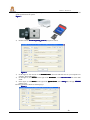
1
SBC-S2416
User Manual
Introduction
© 201112 IndusTech Ltd.
All Rights Reserved. No part of this document may be photocopied, reproduced, stored in a retrieval system, or
transmitted, in any form or by any means whether, electronic, mechanical, or otherwise without the prior written
permission of IndusTech Ltd..
No warranty of accuracy is given concerning the contents of the information contained in this publication. To the extent
permitted by law no liability (including liability to any person by reason of negligence) will be accepted by IndusTech
Ltd., its subsidiaries or employees for any direct or indirect loss or damage caused by omissions from or inaccuracies in
this document.
IndusTech Ltd. reserves the right to change details in this publication without notice. Product and
company names herein may be the trademarks of their respective owners.
IndusTech Ltd.
P.O. Box 923
310018 Hangzhou, China
Tel: +86-571- 28110896
http://www.industech.com.cn
Fax: +86-571-28110896
November 2011
SBC-S2416 User Manual
2
Table of Contents
te
nts
Tab
Tablle of Con
Conte
ten
1
2
3
4
5
6
7
INTRODUCTION...................................................................................................................................................9
1.1 About This Document..................................................................................................................................... 9
1.2 Related Documents......................................................................................................................................... 9
OVERVIEW.......................................................................................................................................................... 10
2.1 Highlights......................................................................................................................................................10
2.2 Block Diagram.............................................................................................................................................. 11
2.3 Features......................................................................................................................................................... 12
SYSTEM COMPONENTS................................................................................................................................. 14
3.1 DC Power Supply......................................................................................................................................... 14
3.2 Ethernet Connector....................................................................................................................................... 14
3.3 LVDS Transmitter......................................................................................................................................... 14
3.4 USB HOST Subsystem................................................................................................................................. 15
3.5 WLAN Module............................................................................................................................................. 16
3.6 Audio Amplifier............................................................................................................................................ 17
3.7 Back-Up Battery........................................................................................................................................... 17
INTERFACES AND CONNECTORS................................................................................................................18
4.1 CoM-S2416 Interface Connectors (U1)........................................................................................................ 18
4.2 DC Power Jack (P1)......................................................................................................................................18
4.3 RS232 connector (J6/J9)............................................................................................................................... 18
4.4 UART connector (J5/J10).............................................................................................................................. 19
4.5 USB Slave Connector (J12).......................................................................................................................... 19
4.6 USB Host Connector (J1)............................................................................................................................. 19
4.7 USB Connectors (J2,J3).............................................................................................................................20
4.8 Ethernet Connector (J7)................................................................................................................................ 20
4.9 MMC/SD/SDIO Socket (J4)........................................................................................................................... 21
4.10 LCD FPC (J13)............................................................................................................................................. 21
4.11 Touch-screen Headers (J14).......................................................................................................................... 22
4.12
LVDS Header (J16)................................................................................................................................22
4.13 Audio Jacks (J19, J20).................................................................................................................................. 23
4.14 Miscellaneous Signals Headers (J11, J15).................................................................................................... 23
4.15 GPIO Header (J8)......................................................................................................................................... 24
4.16 RTC Backup Battery Socket (BAT1)............................................................................................................ 25
4.17 Boot Source Jumper (S1,S2).........................................................................................................................25
4.18 LED’s (D6,D7,D8)........................................................................................................................................25
MECHANICAL DRAWINGS...............................................................................................................................26
OPERATIONAL CHARACTERISTICS.............................................................................................................27
6.1 Absolute Maximum Ratings..........................................................................................................................27
6.2 Recommended Operating Conditions........................................................................................................... 27
6.3 DC Electrical Characteristics........................................................................................................................ 27
6.4 Power Consumption......................................................................................................................................28
6.5 Operating Temperature Ranges.....................................................................................................................28
Software –Linux................................................................................................................................................... 29
7.1 Warning!....................................................................................................................................................... 29
7.2 Establish Linux Development Environment................................................................................................. 29
7.3 Load the Linux Images on the Board by the SD-card...................................................................................29
7.3.1 Step1 – Burn the Linux Images into the SD-card.............................................................................. 29
7.3.2 Step 2 –Load the Linux Images into the NAND Flash...................................................................... 31
7.4 Load the Linux Images on the board by the Ethernet................................................................................... 34
7.5 Make the Linux Images................................................................................................................................ 39
7.5.1
Step1 – Establish the Cross Compilation Environment................................................................. 39
7.5.2
Step2 – Make the U-boot Image.................................................................................................... 40
7.5.3
Step3 – Make the Linux Kernel Image.......................................................................................... 41
November 2011
SBC-S2416 User Manual
3
Table of Contents
7.5.4
Step4 – Make the ROOT file system............................................................................................. 43
7.6 How to..............................................................................................................................................................44
7.6.1 After recompiling the system how to update it into the board.............................................................. 44
7.6.2 How to calibrate the touch screen in Linux.......................................................................................... 44
8 Software - Windows CE........................................................................................................................................45
8.1 Warning........................................................................................................................................................... 45
8.2
Load the WINCE Images into the NAND Flash....................................................................................45
8.2.1 Step1 – Create a SD-card...................................................................................................................... 45
8.2.2 Step2 – Load the Images into the NAND flash.....................................................................................47
8.3 Make the WINCE Images................................................................................................................................ 52
8.3.1 Step1 – Establish the WINCE Development Environment...................................................................52
8.3.2 Get the BSP...........................................................................................................................................53
8.3.3 Create a New Platform..........................................................................................................................53
8.3.4 System Customization...........................................................................................................................55
8.4 HOW TO.........................................................................................................................................................57
8.4.1 How to change the LCD parameters............................................................................................................. 57
November 2011
SBC-S2416 User Manual
4
Table of Contents
Tables
Table 1
Table 2
Table 3
Table 4
Table 5
Table 6
Table 7
Table 8
Table 9
Table 10
Table 11
Table 12
Table 13
Table 14
Table 15
Table 16
Table 17
Table 18
Table 19
Table 20
Table 21
Table 22
Table 23
Table 24
Table 25
Table 26
Table 27
Table 28
Table 29
Table 30
Table 31
Table 32
Table 33
Table 34
Table 35
Table 36
Table 37
Table 38
Table 39
Table 40
Table 41
Table 42
Table 43
Table 44
Table 45
Document Revision Notes...................................................................................................................7
Board Revision Notes......................................................................................................................... 8
Related Documents............................................................................................................................. 9
SBC-S2416 Features......................................................................................................................... 12
Electrical, Mechanical and Environmental Specifications................................................................ 13
RF1 connector data............................................................................................................................16
802.11b/g (WLAN) RF system specifications.................................................................................. 16
802.11g EVM Requirement.............................................................................................................. 17
802.11b EVM.................................................................................................................................... 17
Receiver............................................................................................................................................ 17
5V DC input jack pinout................................................................................................................... 18
P1 connector data.............................................................................................................................. 18
J6/J9 connector pinout.......................................................................................................................18
J6/J9 connector data.......................................................................................................................... 18
J5 connector pinout........................................................................................................................... 19
J10 connector pinout......................................................................................................................... 19
J5/J10 connector data........................................................................................................................ 19
J12 connector pinout......................................................................................................................... 19
J12 connector data.............................................................................................................................19
J1 connector pinout........................................................................................................................... 20
J1 connector data...............................................................................................................................20
J2 connector pinout........................................................................................................................... 20
J3 connector pinout........................................................................................................................... 20
J2/J3 connector data.......................................................................................................................... 20
J7 connector pinout........................................................................................................................... 21
J7 connector pinout........................................................................................................................... 21
J4 connector pinout........................................................................................................................... 21
J13 connector pinout......................................................................................................................... 22
J13 connector data.............................................................................................................................22
J14 connectors pinout........................................................................................................................22
J16 connector pinout......................................................................................................................... 23
J16 connector data.............................................................................................................................23
J20 connector pinout......................................................................................................................... 23
J19 connector pinout......................................................................................................................... 23
J19 and J20 connectors data.............................................................................................................. 23
J15 connector pinout......................................................................................................................... 24
J11 connector pinout......................................................................................................................... 24
J11/J15 connector data...................................................................................................................... 24
J8 connector pinout........................................................................................................................... 24
J8 connector data...............................................................................................................................24
Boot Source Jumper Modes.............................................................................................................. 25
LED Description............................................................................................................................... 25
Operating Temperature Ranges......................................................................................................... 28
WINCE 6.0 development environment software............................................................................... 52
WINCE 6.0 Components Customization........................................................................................... 56
November 2011
SBC-S2416 User Manual
5
Table of Contents
Figures
Figure 1
SBC-S2416 Block Diagram................................................................................................................11
Figure 2
Power Scheme.................................................................................................................................... 14
Figure 3
Ethernet Scheme................................................................................................................................. 14
Figure 4
USB Subsystem.................................................................................................................................. 15
Figure 5
SBC-S2416 top................................................................................................................................... 26
Figure 6
SBC-S2416 bottom (X-Ray view - as seen from top side).................................................................26
Figure 7.................................................................................................................................................................. 30
Figure 8.................................................................................................................................................................. 30
Figure 9.................................................................................................................................................................. 31
Figure 10................................................................................................................................................................ 31
Figure 11................................................................................................................................................................ 32
Figure 12................................................................................................................................................................ 32
Figure 13................................................................................................................................................................ 32
Figure 14................................................................................................................................................................ 33
Figure 15................................................................................................................................................................ 33
Figure 16................................................................................................................................................................ 34
Figure 17................................................................................................................................................................ 34
Figure 18................................................................................................................................................................ 35
Figure 19................................................................................................................................................................ 35
Figure 20................................................................................................................................................................ 36
Figure 21................................................................................................................................................................ 36
Figure 22................................................................................................................................................................ 37
Figure 23................................................................................................................................................................ 38
Figure 24................................................................................................................................................................ 39
Figure 25................................................................................................................................................................ 41
Figure 26................................................................................................................................................................ 42
Figure 27................................................................................................................................................................ 42
Figure 28................................................................................................................................................................ 43
Figure 29................................................................................................................................................................ 46
Figure 30................................................................................................................................................................ 46
Figure 31................................................................................................................................................................ 46
Figure 32................................................................................................................................................................ 47
Figure 33................................................................................................................................................................ 47
Figure 34................................................................................................................................................................ 47
Figure 35................................................................................................................................................................ 48
Figure 36................................................................................................................................................................ 48
Figure 37................................................................................................................................................................ 49
Figure 38................................................................................................................................................................ 49
Figure 39................................................................................................................................................................ 50
Figure 40................................................................................................................................................................ 50
Figure 41................................................................................................................................................................ 50
Figure 42................................................................................................................................................................ 51
Figure 43................................................................................................................................................................ 51
Figure 44................................................................................................................................................................ 53
Figure 45................................................................................................................................................................ 53
Figure 46................................................................................................................................................................ 54
Figure 47................................................................................................................................................................ 55
November 2011
SBC-S2416 User Manual
6
Revision Information
Table 1
Date
November 2009
November 2011
Document Revision Notes
Description
First release
Updated for SBC-S2416 1v1. For details, please refer to the “Board
Revision
Notes” table.
Please check for a newer revision of this manual at IndusTech's web site – http://www.industech.com.cn. Compare the
revision notes of the updated manual from the web site with those of the printed or electronic version you have.
November 2011
SBC-S2416 User Manual
7
Revision Information
Table 2
Board Revision Notes
Date
November 2009
November 2011
Description
Board revision 1v0.
First release
Board revision 1v1.
Change the Mechanics of the board.
Remove CAN transceiver and isolator.
Added WLAN Module and RF connector.
Added support for four additional USB2.0 ports. Added the USB hub
Changed the supply power connector and DC value.
Added 7 inch LCD support and LVDS connector.
Added 7 inch LCD backlight power drive and four-channel power
TCON support
Fixed LVDS synchronization signal connection.
November 2011
SBC-S2416 User Manual
8
Introduction
1
INTRODUCTION
1.1
cume
nt
Abou
outt Th
Thiis Do
Doc
men
This document is part of a set of reference documents providing information necessary to operate and program
IndusTech’s SBC-S2416 baseboard.
1.2
Related Documents
For additional information not covered in this manual, refer to the documents listed in Table 3.
Table 3
Related Documents
Document
CoM-S2416 Developer Resources
November 2011
Location
http://www.industech.com.cn
SBC-S2416 User Manual
9
Overview
2
OVERVIEW
2.1
High
li
ght
s
ghli
light
ghts
�
�
�
�
�
�
�
�
�
�
�
�
�
Carrier base-board designed to support the
CoM-S2416 product line
Implements a Single Board Computer when
combined with a CoM-S2416 module.
Extends the CoM-S2416 graphics controller
with interfaces for LVDS, RGB and LCD
WLAN support
Up to 4 serial ports:two RS232 and two
UART TTL
Up to 4 USB 2.0 Host and one slave USB
ports
Touchscreen interface
GPIO connectors
Audio support with stereo amplifier output
and mic input
One 100 Mbps Ethernet ports
MMC / SD / SDIO socket
Back-up battery for RTC
+5V Power DC input
November 2011
The SBC-S2416 is a carrier baseboard designed for
the IndusTech CoM-S2416 product line.
The SBC-S2416 routes the CoM-S2416 interfaces to
standard connectors and also enriches the CoMS2416 feature set with additional peripheral devices.
A combination of the SBC-S2416 with one of the
CoM-S2416 modules implements a fully functional
SBC (single board computer).
The rich feature set of the SBC is customizable
according to the price / performance targets of the
user's application.
The power supply options of the SBC-S2416 enable
its integration in mobile applications powered by a
rechargeable battery.
SBC-S2416 User Manual
10
Overview
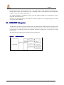
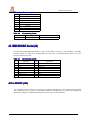
2.2
Block Diagram
Figure 1
November 2011
ock Dia
gram
SBC-S2416 Bl
Blo
Diag
SBC-S2416 User Manual
11
Overview
2.3
Features
The SBC-S2416 is a carrier baseboard designed for the IndusTech CoM-S2416 product line. This product line is
based on the SAMSUNG ARM926EJ CPU.
A combination of the SBC-S2416 with a CoM-S2416 module is referred to as “SBC-S2416”.
Table 4 summarizes the features available with the SBC-S2416.
The "SBC Option" column specifies the SBC-S2416 P/N code that is required, in order to have the particular
feature. The "CoM-S2416 Option" column specifies the CoM-S2416 P/N code that is required to have
the particular feature. SBC-S2416 features are the combination of features provided by the attached CoM-S2416
module and the features implemented on the SBC-S2416. To have the particular feature, both the CoM and SBC
options of that feature must be implemented.
"+" means that the feature is always available, regardless of P/N code.
"-" means that the feature is never available with the specific CoM-S2416 CoM, regardless of P/N
code.
Table 4
Feature
CPU
SDRAM
Flash Disk
SBC-S2416 Features
Specifications
See Feature List of the relevant CoM-S2416
SBC Option
CoM-S2416
Option
+
COM-1
COM-2
COM-3
Rx/Tx only, RS-232, DB9
Rx/Tx only, RS-232, DB9 (for DEBUG)
Rx/Tx only, TTL, 2-mm pitch header
+
+
+
+
+
+
COM-4
Rx/Tx only, TTL, 2-mm pitch header
+
+
Ethernet
CoM-S2416 100 Mbps Ethernet port, RJ-45 connector
and activity LED's
+
E
LCD Panel
AT070TN92 (7”, 800x480, TFT) panel support. 50-pos FPC
connector for direct interface to AT070TN92
+
+
LL
+
+
+
+
+
+
+
LVDS
USB
Slave
4 pair LVDS panel interface, 2-mm pitch header
2.0
USB 2.0 slave port, USB mini-B connector
Two USB 1.1 host ports, 12Mbps. Dual type- A connector
USB 2.0 host
Two USB 1.1 host ports, 12Mbps. 2-mm pitch header
WLAN
WiFi IEEE802.11b/g module, USI WM-G-MR-09 module
integrated on the SBC
W
+
GPIO
8 lines on 2-mm pitch header
+
+
+
+
Touch Panel
November 2011
4-wire resistive panels connector. Interface to LCD panel
SBC-S2416 User Manual
12
Overview
Sound I/O
RTC Battery
SDIO /
MMC
Table 5
I2S compliant audio codec, Line input and
Speakers (stereo) jacks with amplifier
supplied by lithium battery on SBC-S2416
MMC / SD / SDIO support including SDHC up to 32GB.
Standard full-size SD socket
Power consumption
Dimensions
Weight
Operation temperature
(case)
Storage temperature
Relative humidity
November 2011
A
+
+
+
+
Electrical, Mechanical and Environmental Specifications
Supply Voltage
Shock
Vibration
MTBF
+
High efficiency switched power supply. regulated 5V from wall adapter
1W to 3W in full activity, depending on CPU speed and selected features
Below 50mW in sleep mode
180 mm (L) x 80 mm (W) x 23 mm (H)
105 grams
Commercial: 0o to 70o C
Extended:
-20o to 70o C
Industrial:
-40o to 85o C
-40o to 85o C
10% to 90% (operation)
05% to 95% (storage)
50G / 20 ms
20G / 0 - 600 Hz
> 100,000 hours
SBC-S2416 User Manual
13
Overview
3
SYSTEM COMPONENTS
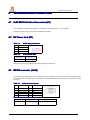
3.1
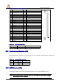
DC Power Supply
The SBC-S2416 DC power sub-system uses an external 5V DC power supply through connector P1. The SBCS2416 generates a 5V power rail internally, using the TD1583 DC-DC step-down converter.
The various voltages required for powering SBC-S2416 peripherals are generated by on-board circuitry
according to the block diagram below.
Figure 2
3.
2
3.2
Power Scheme
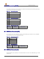
Ethernet Connector
The SBC-S2416 Ethernet connector J7 is interface from CoM-S2416 Ethernet signal pins. Ethernet signals are
routed to the RJ-45 connector (J7).
Figure 3
ernet Scheme
Eth
the
3
3.
3.3
LVDS Transmitter
The SBC-S2416 is equipped with an LVDS Transmitter that is based on the DS90C363A IC. LVDS output
signals are routed from the LVDS Transmitter IC to an onboard 2mm header (J16). The LVDS Transmitter is
November 2011
SBC-S2416 User Manual
14
Overview
connected to the display interface of the CoM-S2416.
The DS90C363A is a National Semiconductor +3.3V Programmable LVDS Transmitter 18-bit Flat Panel
Display link-87.5MHz. The transmitter is fully compatible with the TIA/EIA-644 LVDS standard and
supports VGA, SVGA and XGA display modes.
The LVDS Transmitter is configured for rising edge data sampling. GPH8 can be configured to put the
transmitter into shutdown mode.
In order to use the LVDS interface, the CoM-S2416 display system has to be configured properly for 18bit
active matrix data transmission.
4
3.
3.4
USB HOST Subsystem
The SBC-S2416 provides four full-speed USB2.0 host ports implemented by USB hub GL850A chip which fully
compliant with the USB 2.0 specification. The USB hub up-link is directly interfaced with the USB host port of
the CoM-S2416. The USB hub provides four downlink connections routed directly to the dual type-A USB
connector (J1).
The following block-diagram describes the SBC-S2416 USB subsystem.
Figure 4
November 2011
USB Subsystem
SBC-S2416 User Manual
15
Overview
3.
5
3.5
WLAN Module
The SBC-S2416 incorporates full-featured 802.11b/g capabilities, implemented with the USI WM-BG-MR09 WLAN controller module. The WM-BG-MR-09 is based on the Marvell 88W8688 chipset.
WLAN Standards supported:
�
802.11 data rates of 1 and 2 Mbps
�
802.11b data rates of 5.5 and 11 Mbps
�
802.11a/g data rates of 6, 9, 12, 18, 24, 36, 48, and 54Mbps for multimedia content transmission
�
802.11e Quality of Service (QoS)
�
802.11h DFS statistics processing
�
802.11h transmit power control
�
802.11j channels (Japan)
�
802.11s mesh networking
WLAN Security features:
�
AES-CCMP hardware implementation as part of 802.11i security standard
�
WPA (Wi-Fi Protected Access) encryption
�
WEP 64- and 128-bit encryption with hardware TKIP processing
�
IPSEC security acceleration in hardware
The WM-BG-MR-09 is connected to the CoM-S2416 via the MMC-2 port.
An
Anttenna Connec
nnecttion
The WM-BG-MR-09 requires a single 2.45GHz antenna. The antenna is connected via the onboard
UFL high frequency connector RF1. Any type of 2.45GHz antenna can be used.
Table 6
ec
to
RF1 conn
onnec
ecto
torr data
Manufacturer
Hirose
Mfg. P/N
U.FL-R-MT(10)
Table 7
Mating Connector
Hirose U.FL-LP-040
2.11
b/g (WLAN) RF system speci
s
80
802
.11b
ciffication
ons
Feature
Frequency Band
Description
Supported rates
2.4000 – 2.4835 GHz (2.4 GHz ISM Band)
14 channels
(f=2412+n*5 MHz, n=0,…,12; channel 14=2484MHz)
OFDM, DSSS (Direct Sequence Spread Spectrum), DBPSK,
DQPSK, CCK, 16QAM, 64QAM
1, 2, 5.5, 11, 6, 9, 12, 18, 24, 36, 48, 54 Mbps
Maximum receive level
- 10dBm (with PER < 8%)
Number of selectable Sub-channels
Modulation
Output Power
Carrier Frequency Accuracy
November 2011
15 dBm +2.0 /-1.5 dBm for 1, 2, 5.5, 11Mbps
13 dBm +2.0 /-1.5 dBm for 6 , 9 and > 12Mbps
+/- 25ppm in 25ºC
SBC-S2416 User Manual
16
Interfaces and Connectors
Table 8
M Re
qu
802
802..11g EV
EVM
Requ
quiirement
Item
Data rate (Mbps)
1
2
3
4
5
6
7
8
Relative constellation error
(dB)
EVM
(%RMS)
-5
-8
-10
-13
-16
-19
-22
-25
56.2
39.8
31.6
22.4
15.8
11.2
7.9
5.6
6 (BPSK)
9 (BPSK)
12 (QPSK)
18 (QPSK)
24 (16-QAM)
36 (16-QAM)
48 (64-QAM)
56 (64-QAM)
Table 9
M
802
802..11b EV
EVM
Item
1
2
3
4
Table 10
Data rate (Mbps)
EVM (%RMS)
1(BPSK)
2 (QPSK)
5.5 (QPSK)
11 (QPSK)
35
35
35
35
eiver
Rec
Rece
Receiver Characteristics
Typical (25ºC)
Maximum
Unit
PER <8%, Rx Sensitivity @ 1 Mbps
PER <8%, Rx Sensitivity @ 11 Mbps
PER <10%, Rx Sensitivity @ 6 Mbps
PER <10%, Rx Sensitivity @ 54 Mbps
-97
-89
-91
-74
-93
-85
-87
-68
dBm
dBm
dBm
dBm
For additional details, please refer to the USI WM-BG-MR-09 datasheet.
il
able only with the ‘W’ configur
at
NOTE
TE:: The WLAN module is ava
avail
ila
urat
atiion option.
6
3.
3.6
Audio Amplifier
The SBC-S2416 is equipped with a stereo audio out signal amplifier that is based on the CP2210 class-D
audio power amplifier IC. Amplifier inputs are driven by the AUDIO_OUT_R/L signals of the CoM-S2416.
Amplifier output is routed directly to the onboard headphone jack (J20).
The CP2210 is a 3W Stereo Power Amplifier from Chip Homer. The audio amplifier is capable of delivering
1.5W of continuous RMS power per channel into 8Ω loads and 3W power into 4 Ω loads.
The Audio amplifier is configured for a gain of 1V/V.
7
3.
3.7
Back-Up Battery
An on-board 18mAh rechargeable coin cell lithium battery is the back-up power supply for RTC timekeeping.
This battery is in charge of powering the CoM-S2416 RTC whenever the main power supply is not present.
November 2011
SBC-S2416 User Manual
17
Interfaces and Connectors
4
INTERFACES AND CONNECTORS
4.1
CoM-S2416 Interface Connectors (U1)
The CoM-S2416 is interfaced through one 1.27mm pitch, 120pin connectors – U1. For signal
descriptions, please refer to the relevant CoM Reference Guide.
4.2
DC Power Jack (P1)
Table 11
Pin
ut
5V DC inpu
nputt jack pino
nou
Signal Name
1
2
3
VCC_5V
GND
GND
Table 12
P1 connector data
Manufacturer
Astron
Mfg. P/N
15-02037-R
Mating with power supply adapter 209C10020 supplied by IndusTech.
3
4.
4.3
RS232 connector (J6/J9
J6/J9))
The UART0 and UART1 ports of the CoM-S2416 are power shift level from TTL to RS-232 by MAX3232CSE
IC and connected to the SBC-S2416 on-board RS-232 standard DB9 male connector(J6/J9). All signals are at RS232 levels.
Table 13
Pin
1
2
3
4
5
Table
J6/J9 connector pinout
Signal Name
Pin
Signal Name
NC.
6
NC
7
RS232_RXD
NC
RS232_TXD
8
NC
NC
9
NC
GND
14
J6/J9 connector data
Manufacturer
Pinrex
November 2011
Mfg. P/N
982-11-P00012
Mating connector
Standard DB-9 Male connector
SBC-S2416 User Manual
18
Interfaces and Connectors
4.
4 UART connector (J5/J10
4.4
J5/J10))
The UART2 and UART3 ports of the CoM-S2416 are connected to the SBC-S2416 on-board 2mm pitch header
connector (J5/J10). All signals are at TTL levels.
Table 15
J5 connector pinout
Pin
Signal Name
1
VCC_5V
2
UART2_TX
3
UART2_RX
4
GND
Table 16
J10 connector pinout
Pin
Signal Name
1
VCC_5V
2
UART3_TX
3
UART3_RX
4
GND
Table 17
J5/J10 connector data
Manufacturer
Mfg. P/N
Pinrex
5
4.
4.5
Mating connector
721-93-00-TW01
2mm pitch SMT wire to board header
USB Slave Connector (J12
J12))
The USB Slave port of the CoM-S2416 is routed to the mini-USB type B connector (J12). For additional
details, please refer to the relevant CoM Reference Guide.
Table 18
J12 connector pinout
Pin
Signal Name
1
2
USBD_ID
USBD_DM
3
USBD_DP
4
NC.
5
GND
Table 19
J12 connector data
Manufacturer
Astron
4.6
Mfg. P/N
Mating connector
22-2601-5G-1T-R
Standard USB mini-B plug
USB Host Connector (J1
J1))
The two USB host ports provided by the on-board USB hub are routed to the standard dual type-A USB
connector (J1).
November 2011
SBC-S2416 User Manual
19
Interfaces and Connectors
Table 20
J1 connector pinout
USB HUB port 1
Pin
Signal Name
Pin
Signal Name
1
VCC_5V
5
VCC_5V
2
HUB_DM1
6
HUB_DM2
3
HUB_DP1
7
HUB_DP2
4
GND
8
GND
Table 21
J1 connector data
Manufacturer
Astron
4.7
USB HUB port 2
Mfg. P/N
Mating connector
22-2104-8(W)-1T-R
Standard USB type A plug
USB Connectors (J2
,J3
J2,
J3))
The 2mm headers J2 and J3 are routed to USB ports 3 and 4 of the USB hub GL850A.
Table 22
J2 connector pinout
Pin
Signal Name
1
VCC_5V
2
HUB_DM3
3
HUB_DP3
4
GND
Table 23
J3 connector pinout
Pin
Signal Name
1
VCC_5V
2
HUB_DM4
3
HUB_DP4
4
GND
Table 24
J2/J3 connector data
Manufacturer
Pinrex
8
4.
4.8
Mfg. P/N
Mating connector
721-93-00-TW01
2mm pitch SMT wire to board header
Ethernet Connector (J7
J7))
The SBC-S2416 is equipped with a standard Ethernet RJ45 connector (J7) interfaced with the CoM-S2416
integrated Ethernet controller.
November 2011
SBC-S2416 User Manual
20
Interfaces and Connectors
Table 25
J7 connector pinout
Pin
Signal Name
1
2
ETH_TXP
ETH_TXN
3
ETH_RXP
4
-
5
-
6
ETH_RXN
7
-
8
-
Table 26
J7 connector pinout
Manufacturer
UDE
Mfg. P/N
Mating connector
RTA-1D4B8V1A
Standard Ethernet RJ45 plug
9 MMC/SD/SDIO Socket (J4
4.
4.9
J4))
The SBC-S2416 MMC/SD/SDIO interface is based on the MMC-1 interface of the CoM-S2416. The MMC
controller signals are routed to the standard MMC/SD socket (J4). For additional details, please refer to the
relevant CoM reference guide.
Table 27
Pin
1
2
3
4
5
6
7
8
J4 connector pinout
Signal Name
MMC1_DAT3
MMC1_CMD
GND
VCC_3P3
MMC1_CLK
GND
MMC1_DAT0
MMC1_DAT1
Pin
9
10
11
12
13
14
15
Signal Name
MMC1_DAT2
NC.
MMC1_CD
GND
GND
GND
GND
0 LCD FPC (J13
4.1
4.10
J13))
The on-board LCD FPC connector (J13) allows easy integration with Annolux 7 inch AT070TN92 LCD panels.
The CABFPC50 provides a generic 0.5mm header connection including the power for the LCD backlight and
module logic voltages. For additional details, please refer to section 7 of this document.
November 2011
SBC-S2416 User Manual
21
Interfaces and Connectors
Table 28
Pin
J13 connector pinout
Signal Name
Pin
Signal Name
1
2
3
4
5
6
7
8
9
10
11
12
13
14
15
16
17
18
19
20
VLED+
VLED+
VLEDVLEDGND
VCOM
VCC_3P3
LCD_MODE
LCD_DE
LCD_VSYNC
LCD_HSYNC
VCC3_3
LCD_D6
LCD_D5
LCD_D4
LCD_D3
LCD_D2
GND
GND
LCD_D15
26
27
28
29
30
31
32
33
34
35
36
37
38
39
40
41
42
43
44
45
GND
GND
LCD_D23
LCD_D22
LCD_D21
LCD_D20
LCD_D19
LCD_D18
GND
GND
GND
LCD_PCLK
GND
L/R
U/D
VGH
VGL
AVDD
SYS_nRST
NC.
21
22
23
24
25
LCD_D14
LCD_D13
LCD_D12
LCD_D11
LCD_D10
46
47
48
49
50
VCOM
DITHER
GND
NC
NC
Table 29
50
J13 connector data
Manufacturer
Pinrex
Mfg. P/N
Mating connector
979-41-750200
FFC, 50 cont, 0.5mm
1 Touch-screen Headers (J14
4.1
4.11
J14))
The on-board FPC4, 1mm pitch (J14) provides an easy way to interface with CoM-S2416 touch-screen
interface.
Table 30
Pin
1
2
J14 connectors pinout
Signal Name
TS_X+
TS_Y+
Pin
3
4
Signal Name
TS_XTS_Y-
4.12 LVDS Header (J16
J16))
LVDS output signals are routed from the LVDS transmitter IC to the onboard 2mm header (J16).
to
ov
ide power for the LVDS LCD panel and its backli
g h t.
NOTE
TE:: The J16 connec
nnecto
torr does not pr
prov
ovide
cklig
quired.
Ex
Exttern
ernaal power source is re
req
November 2011
SBC-S2416 User Manual
22
Interfaces and Connectors
Table 31
Pin
J16 connector pinout
Signal Name
Pin
Signal Name
1
2
3
4
5
VCC_3P3
VCC_3P3
LVDS_P0
LVDS_N0
GND
11
12
13
14
15
LVDS_P2
LVDS_N2
GND
GND
LVDS_PCLK
6
7
8
9
GND
LVDS_P1
LVDS_N1
GND
16
17
18
19
LVDS_NCLK
GND
GND
LCD_BKL
10
GND
20
LCD_PWRDN
NOTE
TE:: J16 provides the backlight logic control signal and power down control signal by GPIO
GPIO..
Table 32
J16 connector data
Manufacturer
Mfg. P/N
Pinrex
Mating connector
522-90-20-GB00
2.0mm Box header SMT-type
3 Audio Jacks (J
19
4.1
4.13
(J19
19,, J20
20))
The SBC-S2416 features two 3.5mm jacks, one for stereo headphone output (J20) and the other (J19) for
mono audio input.
Table 33
J20 connector pinout
Pin
1
2
3
Signal Name
Mating plug pin
GND
AMP_VOP
AMP_VON
Table 34
Jack pin-out
Mating plug
Outer ring
Middle ring
Tip
Signal Name
Mating plug pin
1
GND
Outer ring
2
NC
Middle ring
3
MIC_IN
Tip
J19 and J20 connectors data
Manufacturer
Kycon
Mating plug
J19 connector pinout
Pin
Table 35
Jack pin-out
Mfg. P/N
ST-3500-3N
Mating connector
Standard 3.5mm stereo plug
14 Miscellaneous Signals Headers (J11
4.
4.14
J11,, J15)
The 2mm header (J15) provides access to some of the CoM-S2416 serial interfaces. These signals are routed
through SBC-S2416 level shifters and operate at 3.3V voltage levels.
November 2011
SBC-S2416 User Manual
23
Interfaces and Connectors
Table 36
1
2
3
4
5
J15 connector pinout
VCC_3P3
VCC_3P3
I2C_SCL
I2C_SDA
SPI0_CLK
6
7
8
9
10
SPI0_SIMO
SPI0_CS1
SPI0_SOMI
GND
GND
The 2mm header (J11) provides access to some of the CoM-S2416 static memory control bus signals. These
signals are routed directly from the CoM to J11 and operate at VCC_3P3 voltage levels.
Table 37
J11 connector pinout
Pin
Signal Name
Pin
Signal Name
1
2
3
4
5
6
7
8
9
VCC_3P3
GND
SMC_D7
SMC_D6
SMC_D5
SMC_D4
SMC_D3
SMC_D2
SMC_D1
13
14
15
16
17
18
19
20
21
SMC_A4
SMC_A5
SMC_A2
SMC_A3
GND
SMC_A1
SMC_nCS3
SMC_nWE
SMC_nOE
10
11
12
SMC_D0
GND
SMC_A6
22
23
24
SMC_nWAIT
SMC_CLK
SYS_nRST
Table 38
J11/J15 connector data
Manufacturer
Mfg. P/N
Pinrex
Mating connector
522-90-24-GB00
2.0mm Box header SMT-type
15 GPIO Header (J8
4.
4.15
J8))
The 2mm header (J8) outputs eight GPIO signals of CoM-S2416.
Table 39
J8 connector pinout
Pin
1
2
3
4
5
Signal Name
VCC_3P3
GPF5:GPIO0
GPF6:GPIO1
GPF7:GPIO2
GPG0:GPIO3
Table 40
November 2011
Signal Name
GPG1:GPIO4
GPG2:GPIO5
GPG3:GPIO6
GPG4:GPIO7
GND
J8 connector data
Manufacturer
Pinrex
Pin
6
7
8
9
10
Mfg. P/N
522-90-10-GB00
Mating connector
2.0mm Box header SMT-type
SBC-S2416 User Manual
24
Interfaces and Connectors
16 RTC Backup Battery Socket (BAT1
4.
4.16
BAT1))
The RTC backup battery socket should be assembled a CR1220 backup battery for normal operation. In the
external DC Power on mode, the VCC_3P3 will supply for the RTC of CoM-S2416, but in the power off mode,
RTC should be supplied by the backup power from on the baseboard. For additional details, please refer to the
relevant CoM Reference Guide.
17 Boot Source Jumper (S1,S2
4.
4.17
S1,S2))
The boot source jumpers control the boot sequence of the CoM-S2416. These jumpers are alternative to the
“Boot Source” jumpers.
For additional details, please refer to the relevant CoM Reference Guide.
Table 41
Boot Source Jumper Modes
Jumper Position (Shorted pins)
S1
1 ---- 2
S2
2 ---- 3
S1
2- --- 3
S2
1 ---- 2
Operating mode
System software will be boot from NAND for
CoM-S2416 v1.0 module
System will be boot from MMC-1 for CoMS2416 v2.0 module
System software will be boot from MMC-1 for
CoM-S2416 v1.0 module
System will be boot from NAND for CoMS2416 v2.0 module
18 LED
6,D7,D8
4.
4.18
LED’’s (D
(D6,D7,D8
6,D7,D8))
The table below describes SBC-S2416 LEDS.
Table 42
LED
D6
D7
D8
LED Description
Color
Red
Green
Green
System
Power
System status
WLAN status
LED
activity
Indicates that the 3.3V rail is active
Indicates that the system is normal operation
Indicates that the WLAN module is link mode
4.
18 BUZZER (LS3)
4.18
The SBC-S2416 features a buzzer routed GPF0 with CoM-S2416.
November 2011
SBC-S2416 User Manual
25
Mechanical Drawings
5
MECHANICAL DRAWINGS
Figure 5
Figure 6
SBC-S2416 top
SBC-S2416 bottom (X-Ray view - as seen from top side)
Mechanical drawings are available in DXF format from CompuLab's website, following [Developer]
>> [SBC-S2416] >> [SBC-S2416 - Dimensions and Connectors Location] links.
November 2011
SBC-S2416 User Manual
26
Operational Characteristics
6
OPERATIONAL CHARACTERISTICS
6.1
Absolute Maximum Ratings
Parameter
Main power supply voltage
6.2
Typ
Max
Unit
4.8
5
5.2
V
Min
Typ
Max
Unit
4.8
5
5.2
V
Min
Typ
Max
Unit
Recommended Operating Conditions
Parameter
Main power supply voltage
6.3
Min
DC Electrical Characteristics
Parameter
Operating Conditions
SD / MMC / SDIO
VIH
VIL
VOH
VOL
VCC_MMC = 1.8V
VCC_MMC = 3.0V
VCC_MMC = 1.8V
VCC_MMC = 3.0V
VCC_MMC = 1.8V
VCC_MMC = 3.0V
VCC_MMC = 1.8V
VCC_MMC = 3.0V
1.17
1.875
-0.3
-0.3
1.6
2.25
2.1
3.3
0.63
0.75
V
V
V
0.2
0.375
V
1.8V Digital I/O
VIH
VIL
VOH
VOL
1.17
-0.3
1.4
2.1
0.63
0.4
V
V
V
V
3.3V Digital I/O
VIH
VIL
VOH
VOL
2.145
0
2.9
3.3
1.155
0.4
V
V
V
V
Display Interface
VOH
LCD_VIO = 3.3V
VOL
LCD_VIO = 3.3V
2.3
0.7
V
V
V
V
I2C (open drain with internal pull up to 1.8V)
VIH
VIL
VOH (open drain with
3mA sink current)
November 2011
1.26
-0.5
2.3
0.54
V
V
0
0.36
V
SBC-S2416 User Manual
27
Accessories
RS232
TX Voltage Swing
RX Voltage Swing
6.4
±5
±5.4
±25
V
V
Power Consumption
To be added in a future revision of this document.
6.5
Operating Temperature Ranges
The information in this section refers to the SBC-S2416 board only. For temperature ranges of off-board
components such as the LCD panel or battery pack, please refer to the component’s datasheet.
The SBC-S2416 is available with three options of operating temperature range:
Table 43
Range
Commercial
Operating Temperature Ranges
Temp.
0o to 70o C
Extended
-20o to 70o C
Industrial
-40o to 85o C
November 2011
Description
Sample boards from each batch are tested for the lower and upper
temperature limits. Individual cards are not tested.
Every board undergoes a short test for the lower limit
(-20o C) qualification.
Every board is extensively tested for both lower and upper limits and
at several midpoints.
SBC-S2416 User Manual
28
Software – Windows CE
7
Software –Linux
7.1
Warning!
Warning! Installing software is not easy. Finish the procedure completely and be patient to let
the compilation and installation finish.
7.2
Establish Linux Development Environment
Before the development, you need to establish Linux development environment. If you are not familiar with
this procedure, please refer to the corresponding documentations.
7.3
Load the Linux Images on the Board by the SD-card
There are two methods to load the Linux images into the NAND flash on the baseboard. One is used with SDcard, the other is used with Ethernet. This section will provide the operation steps to guide how to load the
Linux images into the NAND flash by the SD-card. The Linux images and tools include following files:
� moviNand_Fusing_Tool.exe : The program on the PC is used to fuse the Linux images into the SDcard
�
DNW.exe: The serial debug program the PC is used to communicate the baseboard by the serial cable.
�
tftpd.exe: The FTP server on the PC is used to download the Linux images on the board by the TFTP
�
u-boot-movi.bin
u-boot-movi.bin:: The SD-card Bootloader to boot the Linux kernel or write it into the NAND flash.
�
u-boot.bin: The NAND flash Bootloader to boot the Linux kernel or write it into the NAND flash.
�
zImage: The Linux Kernel of the baseboard includes drivers and components
�
uramdisk: The Linux RAM file system
�
rootfs.tar.bz2
rootfs.tar.bz2: The Linux ROOT file-system includes QT and other application program.
All above files can be downloaded from following location:
http://www.industech.com.cn/s2416/sbc-2416-linux.html
If you buy the EVM of the CoM-S2416, these bin files are located in the /Linux/IMG/ file folder on the CD-ROM
and these tools are located in the /TOOLS/ folder.
3.1
7.
7.3.1
Step1 – Burn the Linux Images into the SD-card
board.
Note
Note!! The different symbols are used to express different environment between the PC and the base
baseboard.
#: indicates the command line on the baseboard
$: indicates the command line on the PC
1)
November 2011
Preparing a 2GB SD-card and plug it with an adapter into your computer. Make sure your SD-card
29
SBC-S2416 User Manual
Software – Windows CE
adapter can be normally used in your computer and select the Removable Disk as your device; you could
format it with FAT32 file-system.
Figure 7
2)
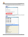
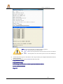
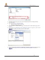
Double-click the moviNand_Fusing_Tool.exe program as follows.
Figure 8
In the Figure 8, click the left of the SD/MMC Drive
Drive; Select the SD-card letter on your computer. For
example, “Removable Disk J”
4) In the Figure 8, click Browse on the right of the Bootloader
Bootloader, select u-boot-movi.bin file in the IMG
folder.
5) In the Figure 8, click Browse on the right of the Specific Sector
Sector, select zImage file, and type 3200000
into the sector.
All above operation is shown as following Fig.9
Figure 9
3)
30
November 2011
SBC-S2416 User Manual
Software – Windows CE
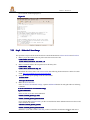
6)
START
In the Fig.10, click ‘START
START’’ button, fuse above files into the SD-card until the message box pops
up as following Fig. 10
Figure 10
7)
Reopen the moviNand_Fusing_Tool.exe software, and click the Browse button on the right of the
Specific Sector
Sector, select uramdisk file, and type 3500000 into the Sector editor. Click the START button
and burn the uramdisk into the SD-card successfully until the message box pops up
Figure 11
8)
Click the Browse button on the right of the Specific Sector
Sector, select u-boot.bin file, and type 3800000
into the Sector editor. Click the START button and burn the u-boot.bin into the SD-card successfully
until the message box pops up
Figure 12
31
November 2011
SBC-S2416 User Manual
Software – Windows CE
9)
Copy ‘rootfs.tar.bz2’ and ‘setup’ file into the SD card
10) Now, the Linux images have been burn into the SD-card successfully.
Note
Note!! The moviNAND_Fusing_Tool program allows the size of zImage is less than 2M bytes;
otherwise, loading the kernel into the NAND flash must use the Ethernet mode
7.3.2
Step 2 –Load the Linux Images into the NAND Flash
Warning! This procedure will erase all the data in the NAND Flash.
Before this procedure, some preparing steps have to be done as follows:
1) Make sure the present baseboard system is boot from MMC-1 instead of the NAND Flash before the
system is power ON. So you have to set the S1/S2 jumpers to the right location. More details about the
S1/S2 jumpers, please view 4.17 section in this document.
2) Connect the DB9 connector (J16 on the SBC-S2416 ) with your computer DB9 serial port by the serial
cable.
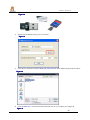
3) Open the DNW.exe software as Figure 13.
Figure 13
4)
Configure the DNW software and make sure the PC’s serial can be open normally:
[DNW->Configuration->Options]
Baud Rate: 115200 bps
COM port: COM1
Figure 14
Click ‘OK’ to save the configuration and exit. In the menu, click [Serial Port -> Connect] to connect the
32
November 2011
SBC-S2416 User Manual
Software – Windows CE
serial port.
When above preparing steps have been completed, the load procedure is beginning.
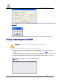
1) Insert the SD-card into the SD/MMC connector (J4) on the baseboard, then plug the power cable into the
board, the Bootloader will boot from the SD-card and the information will be shown on the DNW
program as follows.
Figure 15
2)
When the ‘Really scrub this NAND flash?’ characters appear, please push ‘Y’ key on the keyboard to
erase all the NAND flash block on the board, the Linux Images on the SD-card will be automatically
loaded into the NAND flash as following Figure 16.
Figure 16
33
November 2011
SBC-S2416 User Manual
Software – Windows CE
3)
7.4
Unplug the power cable; Change the S1/S2 jumpers’ location to make sure the system is boot from
NAND flash instead of MMC-1. Then plug the power cable into the board, the Bootloader will boot
from NAND flash as following Figure 17.
Figure 17
Load the Linux Images on the board by the Ethernet
The Linux system can also be loaded directly from your computer with the Ethernet and burn it into the NAND
flash. This section will provide the steps to guide how to operate it.
Before the procedure, make sure Bootloader on the NAND flash is not erased by all. If it has been erased, you
have to insert the SD-card and then boot from it. Please see the 7.3.1. Here assuming the system is boot from
the NAND flash.
1) Plug the network cable into the J7 connector on the board and connect it with the router or your
computer directly.
2)
Double-click the tftpd32.exe on your computer and set the [Current Directory] is the directory where all
the Linux images stored.
Figure 18
34
November 2011
SBC-S2416 User Manual
Software – Windows CE
3)
Plug into the power cable, reboot the board and quickly push the space key and let u-boot program into
the u-boot command mode. set the board IP address and server address, ensure the IP address is the same
network segment with your computer. For example:
# setenv ipaddr 192.168.1.5 ( the board IP address)
# setenv serverip 192.168.1.8 ( your computer IP address)
# saveenv
Figure 19
4)
Download the u-boot.bin file and load it into the NAND flash
# tftp 30000000 u-boot.bin
# nand scrub
# nand write 30000000 0 40000
Figure 20
5)
Download the zImage file and load it into the NAND flash
# tftp 32000000 zImage
# nand erase 40000 300000
# nand write 32000000 40000 300000
Figure 21
35
November 2011
SBC-S2416 User Manual
Software – Windows CE
!: Current NAND flash MTD is divided three different partitions:
Note
Note!:
� 0~40000: the first partition stores the Bootloader
� 40000 ~ 300000: the second partition stores the Linux kernel, the size is less than 4M
Bytes.
� 300000 ~: the third partition stores the root file-system. the size is about 1000M bytes.
6)
Use the SD card to copy the ‘rootfs.tar.bz2’ and ‘setup’ file from your computer and insert the SD card
into the baseboard
7) Download the RAM file system: uramdisk and start it by kernel
# tftp 30800000 uramdisk
# tftp 32000000 zimage
# set bootargs root=/dev/ram rw console=ttySAC0,115200 init=/linuxrc
# bootm 32000000 30800000
Figure 22
36
November 2011
SBC-S2416 User Manual
Software – Windows CE
From Fig.22, the rootfs file system will be load into the NAND flash.
8)
7.5
Unplug the power cable, then plug it into the board again to restart the system, the Linux system will be
boot from the NAND flash.
Make the Linux Images
This section will provide the details about how to make the Linux images. This procedure includes following
steps:
� How to establish the Linux cross compilation environment.
� How to make the SD-card Bootloader image: u-boot-movi.bin
� How to make the NAND flash ootloader image: u-boot.bin
� How to make the Linux kernel image: zImage
7.5.1 Step1 – Establish the Cross Compilation Environment
The first step to make above Linux images is to establish your Linux cross compilation environment.
The cross compilation tool can be download from following location:
http://www.industech.com.cn/s2416/linux_tools.html
The current cross compilation version is cross-4.2.2-eabi, you can download the update version from
Linux Open-source Forum: http://www.linuxforums.org/.
1) Make a file folder to store the cross compile tools
$ sudo mkdir /usr/local/arm
$ cp cross-4.2.2-eabi.tar.bz2 /usr/local/arm
$ cd /usr/local/arm
$ sudo tar xjvf cross-4.2.2-eabi.tar.bz2
2)
Edit the bashrc file to notice Linux the compile location
$ sudo gedit ~/.bashrc
Finding the end of all the lines, and add following codes:
export PATH=$PATH:/usr/local/arm/4.2.2-eabi/usr/bin
37
November 2011
SBC-S2416 User Manual
Software – Windows CE
save it and exit as following Figure 23.
Figure 23
7.5.2 Step2 – Make the U-boot Image
This procedure will provide the details about how to make the Bootloader: u-boot-movi.bin and u-boot.bin
1) Make a project file folder in the root path to store the Linux source files
$ sudo mkdir /sbc-s2416
$ sudo chmod book:book /sbc-s2416 –R
2)
Make a TFTP file folder in the root path to store the binary files
$ sudo mkdir /tftp
$ sudo chown book:book /tftp -R
3)
Download the U-boot source code: u-boot.tar.bz2 from following location and store it in the sbc-s2416
folder: http://www.industech.com.cn/s2416/linux.html
Unzip the U-boot zip file package in the sbc-s2416 folder
4)
$ cd /sbc-s2416
$ tar xjvf uboot.tar.bz2
5)
Make the u-boot-movi.bin
Enter sbc-s2416/u-boot/include/configs/, open the smdk2416.h header file with gedit editor as following
command:
$ cd /sbc-s2416/u-boot-1.3.4 /include/configs
$ gedit smdk2416.h
In the 363 line, revise two macro definitions:
#define CONFIG_BOOT_NAND
#define CONFIG_BOOT_MOVINAND
If you want to make u-boot-movi.bin, you have to mask the first macro definition and reserve the second
macro definition as follows
//#define CONFIG_BOOT_NAND
#define CONFIG_BOOT_MOVINAND
Otherwise, if you want to make u-boot.bin, you have to mask the second macro definition
and reserve
38
November 2011
SBC-S2416 User Manual
Software – Windows CE
the first definition as follows
#define CONFIG_BOOT_NAND
//#define CONFIG_BOOT_MOVINAND
Save the smdk2416.h header file and exit. Return to the u-boot root file path, enter following commands
to set the u-boot compile configuration and make it:
$ cd /sbc-s2416/u-boot-1.3.4
$ sudo make distclean
$ sudo make smdk2416_config
$ sudo make all
If the make procedure is successful, the u-boot.bin file will be generated in the TFTP folder
Delete this u-boot.bin file and run the mkmovi command to generate u-boot-movi.bin binary file:
$ rm /tftp/u-boot.bin
$ ./mkmovi
$ cp u-boot-movi.bin /tftp/
6)
Revise the boot command to load the Linux images into the NAND flash automatically.
In the 378 line of smdk2416.h header file, you will find a macro definition:
CONFIG_BOOTCOMMAND which can load the Linux images into the NAND flash automatically. The
load procedure can be changed by revising this command:
#define CONFIG_BOOTCOMMAND
"sleep 1;nand scrub ;sleep 1;nand erase;sleep 1;movi
read 3800000# 40000 30000000 ;sleep 1;nand write 30000000 0 40000;sleep 1;movi read 3200000#
300000 32000000;sleep 1;nand write 32000000 40000 300000;sleep 1;movi read 3500000# 300000
30800000;sleep 1;bootm 32000000 30800000"
7)
Make the u-boot.bin.
The procedure to make the u-boot.bin binary file is the same with u-boot-movi.bin. the steps are listed as
follows
#define CONFIG_BOOT_NAND
//#define CONFIG_BOOT_MOVINAND
$ cd /sbc-s2416/u-boot-1.3.4
$ sudo make distclean
$ sudo make smdk2416_config
$ sudo make all
7.5.3 Step3 – Make the Linux Kernel Image
1)
Download the SBC-S2416 Linux kernel package from following location and store it in the sbc-s2416
folder: http://www.industech.com.cn/s2416/linux.html. Unzip this file package in the sbc-s2416 folder
$ cd /sbc-s2416
$ tar xjvf kernel.tar.bz2
2)
Set the kernel configuration parameters
$ cd /sbc-s2416/kernel
$ make menuconfig
39
November 2011
SBC-S2416 User Manual
Software – Windows CE
Figure 24
3)
Down it by using the arrow key and select the ‘Load an Alternate Configuration File’, push the enter key
on the keyboard as follows
Figure 25
4)
Type ‘sbc-s2416’, click ‘OK’ and exit from it until configuration graphic as follows
Figure 26
40
November 2011
SBC-S2416 User Manual
Software – Windows CE
5)
Make the kernel image
$ cd /sbc-s2416/kernel
$ make clean
$ make zImage
6)
If the making procedure is successful, the zImage file will be generated in the TFTP file folder as
follows:
Figure 27
Note
ote!! The Linux kernel includes only some necessary components in this procedure. If you want
to include other components, please make menuconfig to select.
7.6 How to
7.6.1 After recompiling the system how to update it into the board?
In the previous section 7.5, the Linux images including u-boot.bin, zImage and rootfs.yaffs can be loaded by the
41
November 2011
SBC-S2416 User Manual
Software – Windows CE
Ethernet. Therefore, once the system has been generated, you can use the Ethernet mode to download it and
update the board. Certainly, you have to install the TFTP server on your Ubuntu computer as follows:
1) Download the tfpt server package, tftp client package and xinetd package and install it
$ sudo apt-get install tftpd tftp xinetd
2)
Create /etc/xinetd.d/tftp file and add following codes into it:
3)
service tftp
{
protocol = udp
port = 69
socket_type = dgram
wait = yes
user = nobody
server = /usr/sbin/in.tftpd
server_args = /tftp
disable = no
}
Set the tftp directory as the tftp server root directory
$ sudo chmod –R 777 /tftp
$ sudo chown –R nobody /tftp
4)
Start the tftpd server by the xinetd super-server
$ sudo /etc/init.d/xinetd start
OK, the tftp server has been install on your computer, you can download all Linux images into the board and
update it. More details, please refer to the section 7.4
.2 How to calibrate the touch screen in Linux
7.6
7.6.2
Plug the power cable into the board and boot the system into the Linux console. Open the DNW software on your
computer (or other terminal software), type following commands:
# tsbra
s-ccali
lib
ratte (Touch the crosses that appear on the screen)
all
# kill
illa
# Xo
Xorrg
weroff (to save settings)
# po
pow
42
November 2011
SBC-S2416 User Manual
Software – Windows CE
8 Software - Windows CE
8.1 Warning
Warning! Installing software is not easy. Finish the procedure completely and be patient to
let the compilation and installation finish.
8.2 Load the WINCE Images into the NAND Flash
Generally, the default factory system is the Linux in the NAND flash of the baseboard. Therefore, you have
to load the WINCE images into the NAND flash if you want to use WINCE as the development
environment. The WINCE images and fusing tool include following files:
� IROM_Fusing_Tool.exe
IROM_Fusing_Tool.exe: the program is used to fuse the Bootloader into the SD-card (only for XP)
�
DNW.exe
DNW.exe: the serial debug program is used to show the board details on the computer
�
DNW USB Download Firmware: the USB drivers of the PC is used to download the files on the
baseboard from computer (only for XP).
�
IROM_SD_EBOOT.nb0
IROM_SD_EBOOT.nb0: the SD-card Bootloader is used to boot the WINCE kernel or load it into
NAND flash
�
STEPLDR.bin
STEPLDR.bin: the first NAND flash Bootloader is used to boot the EBOOT.bin
�
EBOOT.bin
EBOOT.bin: the second NAND flash Bootloader is used to boot the WINCE kernel
�
XIP.bin
XIP.bin: the WINCE kernel image
�
SMDK2416: the SBC-S2416 CE 6.0 BSP software package.
All above files can be download from IndusTech’s website:
http://www.industech.com.cn/s2416/
The SMDK2416/TOOLS file folder includes DNW.exe, DNW USB Download
IROM_Fusing_Tool.exe.
This section will guide how to fuse the WINCE images into the NAND flash on the board
Firmware,
8.2.1 Step1 – Create a SD-card
1)
Preparing a 2GB SD-card and plug it with an adapter into your computer. Make sure your SD-card
adapter can be normally used in your computer and select the Removable Disk as your device; you could
format it with FAT32 file-system.
43
November 2011
SBC-S2416 User Manual
Software – Windows CE
Figure 28
2)
Double-click the IROM_Fusing_Tool.exe as follows.
Figure 29
3)
Click ‘Browse’ button and select the IROM_SD_EBOOT.nb0 file in the WINCE images folder as follows:
Figure 30
4)
Click ‘SD/MMC Drive’ and select the Removable Disk letter on your computer, for example: H
Figure 31
44
November 2011
SBC-S2416 User Manual
Software – Windows CE
5)
6)
Click ‘START’ button to fuse the IROM_SD_EBOOT.nb0 into the SD-card until the windows message
box pops-up.
Figure 32
Unplug the SD-card from the SD-card adapter and insert it into the connector J4 on the baseboard.
8.2.
8.2.22 Step
Step22 – Load the Images into the NAND flash
Warning! This procedure will erase all the data that is present in the NAND Flash.
Before this procedure, some preparing steps have to be done as following:
1) Make sure the system is boot from MMC-1 instead of NAND Flash. So you have to set the S1/S2
jumpers to the right location. More details about the S1/S2 jumpers, please view 4.17 section in this
document.
2) Connect the baseboard’s serial connector (J6 on the SBC-S2416) with PC’s serial port by the serial cable
(If your computer has no any serial port, you have to buy the UART->USB translator).
3) Connect the board’s USB slave connector (J12 on the SBC-S2416) with PC’s USB port by the USB
cable.
4) Open the DNW.exe program and set it’s configuration as follows.
Figure 33
45
November 2011
SBC-S2416 User Manual
Software – Windows CE
5)
Configure the DNW software as follows:
[DNW->Configuration->Options]
Baud Rate: 115200
COM port: COM1 ( your computer serial number)
Figure 34
Click ‘OK’ to save the configuration and exit. In the menu, click [Serial Port -> Connect] to open the
serial port.
When above preparing steps have been over, the installing procedure begin.
1) Plug the power cable into the baseboard, the Bootloader will boot from the SD-card and the information
will be shown on the DNW as following Fig.35
Figure 35
2)
When ‘Initiating image download in 5 seconds’ characters appear, quickly push the space key on the
keyboard, and enter the EBOOT program as follows
Figure 36
46
November 2011
SBC-S2416 User Manual
Software – Windows CE
3)
In ‘Enter your selection:’ command line, push ‘5’ and ‘6’ digital key on the keyboard respectively, make
sure the No.5 and No.6 of the EBOOT program is the same with above Fig. Then push ‘9’ to format the
NAND flash on the baseboard
Figure 37
4)
In ‘Enter your selection:’ command line, push ‘U’ on the keyboard and start to load the images from PC
by the USB cable as follows:
Figure 38
47
November 2011
SBC-S2416 User Manual
Software – Windows CE
5)
Plug the USB cable into the J12 connector on the board and connect it with your computer. The PC
system will quickly indicate you have to install the USB driver. Select the DNW USB Download
Firmware folder and install the USB driver on your computer rightly.
(Note! This USB Download Firmware only support Windows XP system)
6) Once the USB driver is install rightly, the DNW menu will indicate USB connection status is ‘OK
as follows:
Figure 39
7)
In the menu click [USB Port->UBOOT], select the STEPLDR.bin in the WINCE images folder and load
it on the baseboard:
Figure 40
48
November 2011
SBC-S2416 User Manual
Software – Windows CE
8)
9)
The SD-card Bootloader IROM_SD_EBOOT.nb0 will load it into the first block of the NAND flash.
Restart the board by the power cable and enter the EBOOT menu again, Push ‘U’ to download the
EBOOT.bin file into the NAND flash as follows
Figure 41
10) Reboot the board again and enter the EBOOT menu, push ‘U’ to download the XIP.bin and load it into
the NAND flash. Once the load procedure is end, the system will be boot automatically as follows
Figure 42
49
November 2011
SBC-S2416 User Manual
Software – Windows CE
11) There are two methods to boot the WINCE kernel from the NAND flash: one is from the SD-card, the
other is from the NAND flash. The method can be selected by setting the S1/S2 jumpers.
8.3 Make the WINCE Images
8.3.1 Step1 – Establish the WINCE Development Environment
Before this section start, Make sure you have installed the VS2005 and Windows Embedded CE 6.0 development
environment on your computer. The whole WINCE 6.0 development environment includes following tools
Table 44 WINCE 6.0 development environment software
Name
VS2005 demo version
Website
http://download.microsoft.com/download/e/1/4/e1405d9e-47e3-404c-8b09-489437b27
fb0/En_vs_2005_Pro_90_Trial.img
VS2005 Service Pack1
http://www.microsoft.com/downloads/details.aspx?familyid=bb4a75ab-e2d4-4c96-b39
(VS80sp1-KB926601-X86-ENU.exe)
37baf6b5b1dc&displaylang=en
d-
Visual Studio 2005 Service Pack 1 Update http://www.microsoft.com/downloads/details.aspx?FamilyID=90E2942D-3AD1-4873- A2EE4ACC0AACE5B6&displaylang=en
for Windows Vista/WIN7
(VS80sp1-KB932232-X86-ENU.exe)
Visual Studio 2005 Service Pack 1 ATL
Security Update
http://www.microsoft.com/downloads/details.aspx?familyid=7C8729DC-06A2-4538A90D-FF9464DC0197&displaylang=en
(VS80sp1-KB971090-X86-INTL.exe)
Windows Embedded CE 6.0 demo version
http://www.microsoft.com/downloads/details.aspx?displaylang=en&FamilyID=7e286847-6e064a0c-8cac-ca7d4c09cb56
Windows Embedded CE 6.0 Platform
http://www.microsoft.com/downloads/details.aspx?FamilyId=BF0DC0E3-8575-4860-
Builder Service Pack 1
290ADF242678&displaylang=en
A8E3-
Windows Embedded CE 6.0 R2
http://www.microsoft.com/downloads/details.aspx?FamilyId=F41FC7C1-F0F4-4FD6-9366B61E0AB59565&displaylang=en
Windows Embedded CE 6.0 R3
http://www.microsoft.com/downloads/details.aspx?FamilyID=BC247D88-DDB6-4D4A-A5958EEE3556FE46&displaylang=ja&displaylang=en
Windows Embedded CE 6.0 for ARM
pack
http://www.microsoft.com/download/en/details.aspx?displaylang=en&id=1127
(WinCEPB60-101231-Product-UpdateRollup-Armv4I.msi)
More details about installing procedure, please refer to some documentations from Microsoft website or MSDN
help document.
8.3
8.3..2 Get the BSP
The WINCE 6.0 BSP package can be download from IndusTech website:
http://www.industech.com.cn/s2416/wince.html
50
November 2011
SBC-S2416 User Manual
Software – Windows CE
8.3.
8.3.33 Create a New Platform
Platform..
1)
Copy the BSP: SMDK2416.rar file to D:/WINCE600/PLATFORM/ path and unzip it
Figure 43
2)
Open the ‘Microsoft Visual Studio 2005’ program and create a new platform builder project as follows:
Microsoft Visual Studio 2005->File->New->Project->Other Project Type->Platform Builder for CE 6.0
Project Name: SBC-S2416
Path: D:/WINCE600/OSDesigns/
Figure 44
51
November 2011
SBC-S2416 User Manual
Software – Windows CE
3)
4)
5)
6)
7)
Click ‘OK’ to save this project, then start to set the configuration parameters according with design
wizard until finish it.
Select submenu [Build-> Global Build Settings]
� Copy Files to Release Directory After Build
� Make Run-Time Image After build
If KITL is needed, set Enable Kernel Debugger and Enable KITL into Build Options page [Project->
Properties].
In the menu click [build/advanced build command/Clean Sysgen] (See figure 45), this will take
approximately 20 minutes, after which you will see “build complete”
Figure 45
Images including XIP.bin, EBOOT.bin, STEPLDR.bin and IROM_SD_EBOOT.nb0 and so on will be
generated; You can copy these files in the WINCE image file folder and update it (see figure 46).
Figure 46
52
November 2011
SBC-S2416 User Manual
Software – Windows CE
8.3.
8.3.44 System Customization
Customization..
Windows Embedded CE 6.0 consists of a number of independent modules. Each module provides specific
functions, of which some modules can be divided into several components. Each component has specific
feature, making OEM/ODM customize a stable and efficient version according to specific application. Taking
Mobile Handheld as a template, sample SBC-S2416 OS image adds features of components including:
Table 45 WINCE 6.0 Components Customization
Components Name
Location
ActiveSync
CAB File installer/uninstaller
OS Dependencies for .NET Compact
Framework 3.5
Core OS->CEBASE->Application – End User
Core OS->CEBASE->Applications-End User
Core OS->CEBASE->Applications and Services Development->.NET Compact
Framework 3.5
Point-to-Point Protocol over Ethernet (PPPoE)
Core OS->CEBASE->Communication Services and Networking->Networking – Wide
Area Network (WAN)
USB Function Driver
Core OS->CEBASE->Core OS Services->USB Host Support
USB Host Support
Core OS->CEBASE->Core OS Services->USB Host Support
USB Human Input Device (HID) Class Driver
Core OS->CEBASE->Core OS Services->USB Host Support
USB HID Keyboard and Mouse
Core OS->CEBASE->Core OS Services->USB Host Support-> USB Human Input
Device (HID) Class Driver
USB Storage Class Driver
Core OS->CEBASE->Core OS Services->USB Host Support
RAM and ROM File System
Core OS->CEBASE->File Systems and Data Store->File System – Internal (Choose 1)
Hive-based Registry
Core OS->CEBASE->File Systems and Data Store->Registry Storage – Internal (Choose
1)
exFAT File System
Core OS->CEBASE->File Systems and Data Store->Storage Manager
53
November 2011
SBC-S2416 User Manual
FAT File System
Software
– Windows
CE
Core OS->CEBASE->File Systems and Data
Store->Storage
Manager
Storage Manager Control Panel Applet
Core OS->CEBASE->File Systems and Data Store->Storage Manager
Transaction-Safe FAT File System (TFAT)
Core OS->CEBASE->File Systems and Data Store->Storage Manager
Video/Image Compression Manager
Core OS->CEBASE->Graphics and Multimedia Technologies->Media->Video Codecs
and Renderers
Console Window
Core OS->CEBASE->Shell and User Interface->Shell->Command Shell
SD Memory
Device Drivers->SDIO->SDIO Memory
serial
Device Drivers->USB Function->USB Function Clients
Windows Embedded CE Test Kit
Device Drivers
Components can be added or deleted in window Catalog Items View of Visual Studio 2005(VS2005) integrated
development environment
8.4 HOW TO
8.4.1 How to Change The LCD Parameters
In the factory, the LCD parameters are pre-set as the 7 inch LCD. You have to change the macro definition in
the bsp_cfg.h header file. The path is:
SMDK2416/SRC/ INC/
In the final line of this header file, the LCD_MODULE_TYPE macro is pre-defined as follows:
#define LCD_MODULE_TYPE
LCD_MODULE_LW500AC9601
You can change this macro and define other parameters such as:
#define LCD_MODULE_AT043TN13 //4.3 inch LCD, 480x272
#define LCD_MODULE_N101L6 //10.1 inch LCD, 1024x600
#define LCD_MODULE_VGA800600 //VGA out, 800x600
#define LCD_MODULE_121
//12.1 inch LCD, 1024x768
After changing this macro, re-compile the WINCE BSP and update following the WINCE images into the
NAND flash: ‘IROM_SD_EBOOT.nb0’, ‘EBOOT.bin’ and ‘XIP.bin’
8.4.2 How to Install the SDK
The SBC-S2416 baseboard SDK of WINCE 6.0 is placed in the SMDK2416/SDK/ file folder, you have to
install it firstly before you want to develop application based on the VS2005/2008 or eVC. Double-click the
‘SBC_S2416_SDK.msi’ program and install it with the wizard. Certainly, you can export the new SDK in the
platform builder when your new component drivers have been developed. More details, please refer to the
MSDN documents about your development environment.
54
November 2011
SBC-S2416 User Manual
8.4.3 How to Test Ports On The WINCE
Software – Windows CE
1)
Serial Test
SBC-S2416 baseboard includes four COM ports. Once the WINCE OS is on, you have to use the serials
by the serial demo application if your application has no any serial test function. The serial demo
application is located in the SMDK2416/SRC/APPS/SerialPort/ file folder. You can compile it by the
VS2008 compiling tools based on the SBC-S2416 CE 6.0 SDK, the SerialPort.exe program will be
generated. You can copy it into the baseboard by the SD-card or ActiveSync on-line debug function and
test serial ports.
2)
GPIO Test
SBC-S2416 baseboard includes eight GPIOs. Once the WINCE6.0 OS is on, you can’t directly access
the GPIO physical address except for GPIO driver. The BSP provides GPIO driver and demo application.
The demo application is located in the SMDK2416/SRC/APPS/GPIODemo/ file folder. You can refer and
compile it by the VS2008 platform builder. When the GPIODemo.exe program is generated, you can copy
it by the SD-card or ActiveSync on-line debug function into the SBC-S2416 and test eight GPIOs.
Anyway, the GPIO demo application only provide GPIO output function (high-level or low-level), the
input capture is not included here.
3)
LED Test
SBC-S2416 baseboard includes two LEDs, one is on the CoM-S2416, the other is on the baseboard. Once
the WINCE6.0 OS is on, you can’t directly access the LED physical address except for LED driver.
The BSP provides LED driver and demo application. The demo application is located in the
SMDK2416/SRC/APPS/LEDDemo/ file folder. You can refer and compile it by the VS2008 platform
builder. When the LEDDemo.exe program is generated, you can copy it by the SD-card or ActiveSync
on-line debug function into the SBC-S2416 and test LED status: ON or OFF.
4)
PWM Test
SBC-S2416 baseboard includes PWM test function. The BSP provides PWM driver and demo application.
The demo application is located in the SMDK2416/SRC/APPS/PWMDemo/ file folder. You can refer and
compile it by the VS2008 platform builder. When the PWM.exe program is generated, you can copy it by
the SD-card or ActiveSync on-line debug function into the SBC-S2416 and test PWM output. Anyway,
the SBC-S2416 baseboard only provides one PWM tune that drives the backlight of the LCD. Please refer
to baseboard schematic about more details.
5)
Recorder Test
SBC-S2416 baseboard includes MIC input port. The BSP provides audio codec driver and recorder demo
application. The demo application is located in the SMDK2416/SRC/APPS/Recorder/ file folder. You can
refer and compile it by the VS2008 platform builder. When the recorder.exe program is generated, you
can copy it by the SD-card or ActiveSync on-line debug function into the SBC-S2416 and test MIC input.
6)
Watchdog Test
SBC-S2416 baseboard includes watchdog function. Once the WINCE6.0 OS is on, you can’t directly
access the watchdog physical address except for watchdog driver. BSP provides watchdog driver and
demo application. The demo application is located in the SMDK2416/SRC/APPS/WatchdogDemo/ file
folder. You can refer and compile it by the VS2008 platform builder. When the watchdogdemo.exe
program is generated, you can copy it by the SD-card or ActiveSync on-line debug function into the SBCS2416 and test watchdog function. Anyway, the watchdog function is only included in the CoM-S2416
V1.0 board.
55
November 2011
SBC-S2416 User Manual