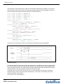
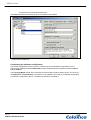
1
Platform Developer’s Kit
PDK Tutorial Manual
PDK Tutorial Manual
Celoxica, the Celoxica logo and Handel-C are trademarks of Celoxica Limited.
All other products or services mentioned herein may be trademarks of their respective owners.
Neither the whole nor any part of the information contained in, or the product described in, this document
may be adapted or reproduced in any material form except with the prior written permission of the
copyright holder.
The product described in this document is subject to continuous development and improvement. All
particulars of the product and its use contained in this document are given by Celoxica Limited in good
faith. However, all warranties implied or express, including but not limited to implied warranties of
merchantability, or fitness for purpose, are excluded.
This document is intended only to assist the reader in the use of the product. Celoxica Limited shall not
be liable for any loss or damage arising from the use of any information in this document, or any
incorrect use of the product.
The information contained herein is subject to change without notice and is for general guidance only.
Copyright © 2005 Celoxica Limited. All rights reserved.
Authors: RG
Document number: 1
Customer Support at http://www.celoxica.com/support/
Celoxica in Europe
Celoxica in Japan
Celoxica in the Americas
T: +44 (0) 1235 863 656
T: +81 (0) 45 331 0218
T: +1 800 570 7004
E: [email protected]
E: [email protected]
E: [email protected]
Page 2
www.celoxica.com
PDK Tutorial Manual
Contents
1 PAL TUTORIAL ........................................................................................................... 7
1.1 RUNNING THE PAL TUTORIAL IN SIMULATION .......................................................... 7
1.2 RUNNING THE PAL TUTORIAL IN HARDWARE ........................................................... 7
1.3 PAL TUTORIAL PART 1 ......................................................................................... 8
1.3.1 Compile-time configuration...................................................................................................... 8
1.3.2 Run-time operations ................................................................................................................ 9
1.4 PAL TUTORIAL PART 2 ....................................................................................... 10
1.4.1 Compile-time configuration.................................................................................................... 10
1.4.2 Run-time operations .............................................................................................................. 11
1.5 PAL TUTORIAL PART 3 ....................................................................................... 12
1.5.1 Compile-time configuration.................................................................................................... 12
1.5.2 Run-time operations .............................................................................................................. 12
2 DSM TUTORIALS ....................................................................................................... 14
2.1 DSM PATTERN MATCHING TUTORIAL .................................................................... 14
2.1.1 Running the DSM tutorial in simulation ................................................................................. 14
2.1.2 Part 1 of the tutorial ............................................................................................................... 15
2.1.3 Part 2 of the tutorial ............................................................................................................... 16
2.1.4 Part 3 of the tutorial ............................................................................................................... 17
2.2 DSM FIR FILTER TUTORIAL ................................................................................. 18
2.2.1 Introduction............................................................................................................................ 18
2.2.2 Tutorial requirements ............................................................................................................ 18
2.2.3 System design ....................................................................................................................... 19
2.2.4 Simulating the tutorial............................................................................................................ 22
2.2.5 Running the tutorial in hardware ........................................................................................... 24
3 PLATFORM SUPPORT LIBRARY TUTORIAL.................................................................... 28
3.1 INTRODUCTION.................................................................................................... 28
3.2 USING PAL ........................................................................................................ 28
3.3 CREATING A PSL................................................................................................ 29
3.4 DESIGNING A DEVICE DRIVER ............................................................................... 29
3.4.1 Device driver design flow ...................................................................................................... 30
3.4.2 Example device drivers ......................................................................................................... 31
3.4.3 Encapsulating drivers in a PSL ............................................................................................. 43
4 TUTORIAL: HANDEL-C AND PSL BASICS ..................................................................... 44
4.1 HANDEL-C LANGUAGE BASICS ............................................................................. 45
4.1.1 Use of parallel code............................................................................................................... 45
4.1.2 Channel communications ...................................................................................................... 47
4.1.3 Bit manipulation examples .................................................................................................... 49
4.1.4 Using signals ......................................................................................................................... 52
4.2 CREATING A DEVICE DRIVER................................................................................. 53
4.2.1 Example device driver: seven-segment display .................................................................... 53
4.2.2 Seven-segment display hardware interface .......................................................................... 54
4.3 USING PAL TO CREATE A GENERIC DEVICE DRIVER ................................................ 55
4.3.1 Setting up a PAL workspace ................................................................................................. 55
4.3.2 Seven-segment project in PAL.............................................................................................. 61
5 TUTORIAL: HANDEL-C AND VGA GRAPHICS OUTPUT ................................................... 63
5.1 GENERATING VGA GRAPHICS .............................................................................. 63
5.2 RESPONDING TO USER INPUT ............................................................................... 65
Page 3
www.celoxica.com
PDK Tutorial Manual
5.3 ADDING MOUSE INPUT ......................................................................................... 68
6 TUTORIAL: HANDEL-C CODE OPTIMIZATION ................................................................. 71
6.1 TIMING AND AREA EFFICIENT CODE ....................................................................... 71
6.1.1 Complex statements.............................................................................................................. 71
6.1.2 Arrays and memories ............................................................................................................ 72
6.1.3 Macro procedures vs. functions ............................................................................................ 74
6.1.4 Static initialization.................................................................................................................. 74
6.2 LOOPS AND CONTROL CODE ................................................................................ 74
6.2.1 Clock-cycle efficiency of loops .............................................................................................. 74
6.2.2 Timing efficiency of loops ...................................................................................................... 75
6.2.3 Avoiding combinatorial loops................................................................................................. 76
6.2.4 Nested control ....................................................................................................................... 77
7 TUTORIAL: HANDEL-C ADVANCED OPTIMIZATION ......................................................... 78
7.1 PIPELINING ......................................................................................................... 78
7.2 PIPELINES AND REPLICATORS .............................................................................. 79
7.3 CLIENT-SERVER ARCHITECTURE ........................................................................... 80
7.3.1 Client-server divide example ................................................................................................. 80
7.3.2 Flash memory client-server example .................................................................................... 82
8 TUTORIAL: USING THE LOGIC ESTIMATOR .................................................................... 87
8.1 ENABLING THE LOGIC ESTIMATOR......................................................................... 87
8.2 USING THE LOGIC ESTIMATOR RESULTS ................................................................ 88
8.3 REDUCING THE LOGIC DELAY ............................................................................... 90
8.4 REDUCING THE LOGIC AREA ................................................................................. 93
9 FIR TUTORIAL ........................................................................................................ 100
9.1 INTRODUCTION.................................................................................................. 100
9.2 INITIAL VERSION ................................................................................................ 101
9.3 USING PARALLEL MULTIPLIERS .......................................................................... 107
9.4 SINGLE CYCLE FIR............................................................................................ 112
9.5 REDUCING LOGIC AREA ..................................................................................... 114
9.6 USING ALU MAPPING ....................................................................................... 117
9.7 USING A PIPELINED ADDER TREE ........................................................................ 119
9.8 USING RETIMING ............................................................................................... 123
9.9 IMPROVING PERFORMANCE WITH RETIMING.......................................................... 126
10 INDEX ................................................................................................................... 129
Page 4
www.celoxica.com
PDK Tutorial Manual
Conventions
The following conventions are used in this document.
2
Warning Message. These messages warn you that actions may damage your hardware.
Ï
Handy Note. These messages draw your attention to crucial pieces of information.
Hexadecimal numbers will appear throughout this document. The convention used is that of prefixing
the number with '0x' in common with standard C syntax.
Sections of code or commands that you must type are given in typewriter font like this:
void main();
Information about a type of object you must specify is given in italics like this:
copy SourceFileName DestinationFileName
Optional elements are enclosed in square brackets like this:
struct [type_Name]
Curly brackets around an element show that it is optional but it may be repeated any number of times.
string ::= "{character}"
Page 5
www.celoxica.com
PDK Tutorial Manual
Assumptions & Omissions
This manual assumes that you:
•
have used Handel-C or have the Handel-C Language Reference Manual
•
are familiar with common programming terms (e.g. functions)
•
are familiar with your operating system (Linux or MS Windows)
This manual does not include:
•
instruction in VHDL or Verilog
•
instruction in the use of place and route tools
•
tutorial example programs. These are provided in the Handel-C User Manual
Page 6
www.celoxica.com
PAL tutorial
1 PAL tutorial
The PAL tutorial shows an experienced Handel-C programmer how to implement platform-independent
hardware using the Handel-C language, DK and the PAL API.
The application implemented in the tutorial is a simple program that displays a square bouncing around
the screen.
The tutorial workspace can be accessed from the Start menu, by default it is under Celoxica>Platform
Developer’s Kit>PAL>PAL Tutorial Workspace.
The PAL tutorial is in three stages, with each contained in a separate project:
•
Part1: Displays a simple white square.
•
Part2: Introduces some user input control of the colour and square movement
•
Part3: Adds a simple frame buffer.
All the interfacing to external logic is done using PAL. The source code contains comments describing
the program.
To compile the tutorial for yourself, you need DK.
If you want to run the tutorial designs in hardware you will need a Celoxica RC100, with Xilinx place and
route tools, or an Altera Nios development board (NDB) with Altera Quartus-II place and route tools.
1.1 Running the PAL tutorial in simulation
The 3 stages of the PAL tutorial can be run in simulation using the PALSim Virtual Platform.
1. Choose Part1, Part2 or Part3 of the tutorial projects by selecting Project>Set Active Project.
2. Choose to target the "Sim" platform (Build>Set Active Configuration).
3. Build the project by pressing F7.
4. Execute the simulation by pressing F5.
If you run Part1, you will see a white square that moves slightly every time the screen refreshes. (If you
run the same program in hardware, the square will seem to bounce around the screen, because of the
faster refresh rate.)
If you run Part2 or Part3, you will see a coloured square. If you press Button 0 on the PALSim application
with your mouse, the colour of the square changes when the screen refreshes. In Part3, a trace is left as
the ball moves across the screen. If you press Button 1 with your mouse, the ball stops moving. You can
restart it by pressing Button 1 again.
1.2 Running the PAL tutorial in hardware
If you have an RC100 you can run the 3 stages of the PAL tutorial in hardware.
1. Open the tutorial workspace.
2. Choose Part1, Part2 or Part3 of the tutorial by selecting Project>Set Active Project.
3. Choose the RC100 target (Build>Set Active Configuration).
4. Build the project by pressing F7.
The build files will appear in the RC100 directory for the relevant project (e.g.
InstallDir\Tutorials\PAL\Part3\RC100).
An EDIF file and a constraints file will be produced.
Page 7
www.celoxica.com
PAL tutorial
5. Place and route the files (using Xilinx or Altera tools as appropriate).
6. Download the resulting .bit file onto the Spartan II FPGA on the RC100.
1.3 PAL Tutorial Part 1
The Part1 project in the PAL tutorial describes how to use PAL resources. The application created
bounces a square around a VGA screen.
1.3.1 Compile-time configuration
Checking the resource is available
When building generic code, you need to have a mechanism for checking that you have the required
resources available on the platform to be targeted, and that the API you’re compiling against is
compatible with the API you’ve written your code to. PAL provides a set of utility macros for this purpose.
For example:
PalVersionRequire (1, 0);
PalVideoOutRequire (1);
This pair of statements asserts at compile time that the API being linked against is v1.0 (or is compatible
with v1.0) and that at least 1 VideoOut resource is available. These statements build no hardware and
consume no clock cycles of execution time.
Selecting the resource to use
Once you have ensured that a particular type of resource is available, you can get a handle to the
specific resource that you want to use. A handle to a PAL resource is used to identify to the PAL
methods the specific resource that you want to use. A resource handle can be returned at compile-time
by the macro expression PalXCT(), where X is the resource type.
PAL typically provides many different video output resolution resources for each physical video
resource. A resource handle to the first video resource can be defined as a macro expression to be used
throughout the code as follows:
macro expr VideoOut = PalVideoOutCT (0);
PAL also supplies a macro PalVideoOutOptimalCT (ClockRate), which selects the optimal video
output resolution and refresh rate for the specified target clock rate. The tutorial source code uses this
macro as follows:
macro expr VideoOut = PalVideoOutOptimalCT (ClockRate);
Checking the data width of the resource
PAL resources have interfaces with specific widths. The width of an interface should be tested at
compile time to ensure that it matches the required width for the application.
This can be done using PalXGetYWidthCT (PalHandle), where X is the type of resource, Y is the
attribute to query and PalHandle is the handle to the PAL resource to be queried.
The tutorial application is written to output 24-bit video data. Different platforms may have different data
widths on their video interfaces, so the application needs to check that the target platform uses 24-bit
video data, which can be done using a compile-time assert:
assert (PalVideoOutGetColorWidthCT (VideoOut) == 24, 0,
"Video output does not support 24-bit data");
Page 8
www.celoxica.com
PAL tutorial
Getting compile-time information from the resource
There are a number of API calls that allow you to get information from PAL resources at compile time.
They can be recognized by the abbreviation CT appended to the name of the macro.
For this application, the number of visible lines and columns in the video scan is used in order to be able
to test where the current scan position is in a frame.
In the tutorial code, the macro procedure GenerateData() uses
•
PalVideoOutGetVisibleYCT (VideoOut): this returns the number of visible lines.
•
PalVideoOutGetVisibleXCT (VideoOut, ClockRate): this returns the number of
visible columns.
1.3.2 Run-time operations
Running the resource
Resources must run in parallel with your main program. If you use more than one resource, they should
all be run in parallel with each other.
In the tutorial source code, the video output resource is run in parallel with the procedure generating the
video data:
par
{
PalVideoOutRun (VideoOut);
// main program here
}
Enabling the resource
Once a PAL resource is running, it needs to be enabled before you can use it. This enabling method can
take zero or more clock cycles, depending on the target platform.
In this application, the video output resource needs to be permanently enabled, so the enable procedure
is only called once, before starting to output video data.
par
{
PalVideoOutRun (VideoOut);
seq
{
PalVideoOutEnable (VideoOut);
// do the video output
}
}
Writing data to the resource
Once a PAL resource has been enabled, you can read data from and write data to it. Writing to the
resource takes the form PalXWrite (PalHandle), where X is the type of video resource and
PalHandle is the handle to the specific resource to use.
In the tutorial application, once the video output has been enabled, the program starts sending the video
output process some data to display, as follows:
Page 9
www.celoxica.com
PAL tutorial
PalVideoOutWrite (VideoOut, {24-bit expression});
Getting run-time information from the resource
Some PAL resources return run-time information to the user about their current state. The PAL methods
for accessing this information are of the form PalXGetY (PalHandle), where X is the type of
resource, Y is the attribute to query and PalHandle is the handle to the PAL resource to be queried.
In the tutorial source code, the macro GenerateData(), for generating the display pattern, uses some
information retrieved from the video output resource. Every clock cycle, it tests the x and y coordinates
of the current scan position, to see if they are at the bottom right of the visible area of the screen. The
macros for getting the x and y coordinates are PalVideoOutGetY() and PalVideoOutGetX(). They
are used in conjunction with the compile-time macros that find the dimensions of the visible area of the
screen:
macro expr VisibleX = PalVideoOutGetVisibleXCT (VideoOut, ClockRate);
macro expr VisibleY = PalVideoOutGetVisibleYCT (VideoOut);
EndOfFrame = (PalVideoOutGetY(VideoOut) == VisibleY) &&
(PalVideoOutGetX(VideoOut) == VisibleX);
This sets the variable EndOfFrame to 1 when the current scan position is one pixel to the bottom and
right of the visible area of the screen and 0 otherwise. The position of the square is recalculated once
each frame using this variable.
1.4 PAL Tutorial Part 2
The Part2 project in the PAL tutorial describes how to add resource selection to your program.
You may need to write an application that will run on boards with very different devices available and so
write code that will use different resources for different platforms. This can be written in a portable
fashion, without testing explicitly for a particular platform.
In this part of the tutorial, user control is added for:
•
Stopping and starting the movement of the square
•
Changing the colour of the square
Depending on the resources available on the target device, buttons on either the target platform circuit
board or a mouse attached to a PS/2 port are used.
The significant change from the first part of the tutorial is the addition of the macro
HumanInterface(): this macro is called by the GenerateData() macro in order to read the input
from the user. This code also makes use of the PS/2 mouse driver in the pal_mouse.hcl library.
1.4.1 Compile-time configuration
Determining which resources will be used
Some applications may need to perform the same functions on boards with different resources. PAL
allows you to write one piece of code that will automatically select the resources to use for the target
platform. This can be done by querying the resources available on the target platform, rather than
explicitly testing for a particular target platform. This makes your code much more portable because it
will support any board with those resources available.
In the tutorial source code, two key expressions are used to determine which resources will be used.
These are:
Page 10
www.celoxica.com
PAL tutorial
macro expr UsingButtons = PalSwitchCount () > 1;
macro expr UsingMouse
= !UsingButtons && (PalPS2PortCount () > 0);
The first expression, UsingButtons, is set to one if there are two or more buttons available on the
target board. If there are no buttons available, the code needs to check if there is a mouse available
instead: if the expression UsingButtons evaluates to false and there is at least one PS2 port available,
then the macro expression UsingMouse will evaluate to true.
Ensuring that at least one of the required devices is available
A compile-time assertion can be used to ensure that at least one of the supported devices is available on
the target platform.
For this application, either the buttons or a mouse needs to be available (one of UsingButtons and
UsingMouse needs to be true). If they are not, then the compilation needs to fail gracefully with a clear
error message. This is done using an assert, as used for checking the availability of the video resource:
assert (UsingMouse || UsingButtons, 0, "Not enough buttons and no mouse");
Selecting the correct resource for the target platform
Handel-C offers compile-time selection of sections of code to compile, depending on evaluation of
constant expressions. This is done using the ifselect keyword, which looks the same as the standard
if statement. The difference is that the condition in the brackets must be a compile-time constant and
the result is a choice of compilation rather than run-time execution.
ifselect (UsingButtons)
{
// run the button code
}
else
{
// run the mouse code
}
Note that the expression UsingMouse() does not need to be tested here because the compilation will
have already failed due to the assert statement in Step 2 if there were neither buttons nor a mouse
available.
1.4.2 Run-time operations
Running PAL Cores
Part 2 of the tutorial uses a PAL Core resource. PAL Cores are utility cores that only use PAL resources,
and are therefore portable across PAL platforms.
PalMouse *MousePtr;
The core is connected to a PS/2 resource:
macro expr PS2Port = PalPS2PortCT (0);
PalMouseRun (&MousePtr, PS2Port, ClockRate);
The core now behaves in a similar way to a normal PAL resource, so it needs to be enabled to run in
parallel with the rest of the program before it can be used. For each PAL Core routine, a pointer to the
core needs to be passed in as the first argument.
Page 11
www.celoxica.com
PAL tutorial
1.5 PAL Tutorial Part 3
The Part3 project in the PAL tutorial describes how to use an external RAM.
The RAM is initialized and run from the main() function. The GenerateData() macro no longer
displays the square directly to the screen but draws the square into RAM. Every clock cycle during the
visible period of the scan, the display process reads pixels out of the RAM and displays them on the
screen.
1.5.1 Compile-time configuration
Choosing the type of RAM to use
There are three different types of RAM access available in the PAL API: multi-cycle, single-cycle and
pipelined. For this application, single-cycle access is sufficient. This is perhaps the simplest way to use
the RAM on a platform as it means that all reads and writes take a single clock cycle. The name for
single-cycle access in PAL is PalFastRAM.
Checking the required RAM resource is available
A compile-time assertion is needed to check that the platform for which the code is being compiled has
the required RAM resource. This is done in the same way as for the video output resource:
PalFastRAMRequire (1);
Selecting the RAM resource to use
Some boards have many banks of RAM, so one of the available FastRAM resources needs to be
chosen. This application only needs the one RAM bank for the frame buffer, so the first bank is used:
macro expr FastRAM = PalFastRAMCT (0);
Checking that the RAM is the correct size
For this application, the frame-buffer will store 640*480 pixels with eight pixels packed into one 32-bit
word, which means that the RAM needs to have 640*480/8 32-bit entries. In order that compilation fails
gracefully on inappropriate platforms, the application needs to assert that the number of entries in the
RAM (which can be inferred from the width of the address bus) is equal to or greater than the number
required (which means a minimum of a 16-bit address bus):
assert (PalFastRAMGetAddressWidthCT (FastRAM) > 15, 0,
"Not enough entries in FastRAM resource");
The RAM resource also needs to have a data width of at least 32 bits. This is checked as follows:
assert (PalFastRAMGetDataWidthCT (FastRAM) > 31, 0,
"Data width less than 32-bit in FastRAM resource");
Extending this method further, it is possible to write an application that will build different frame-buffers
that will be automatically selected depending on the attributes of the RAM resources available on the
target platform.
1.5.2 Run-time operations
Running the RAM resource
The RAM resource needs to be run in the standard way for PAL resources: in parallel with the main body
of the code and the running of any other PAL resources.
Page 12
www.celoxica.com
PAL tutorial
par
{
PalVideoOutRun (VideoOut);
PalFastRAMRun (FastRAM);
// main program here
}
Enabling the RAM resource
Once the RAM resource is being run, it needs to be enabled before it can be accessed. This is done
using the PalFastRAMEnable() macro. In this application, it is done at the same time as the enabling
of the video resource:
par
{
PalFastRAMEnable (FastRAM);
PalVideoOutEnable (VideoOut);
}
Writing data to the RAM
This application uses a single-bank of RAM as a frame-buffer. While the video scan position is visible,
the RAM is being read and the contents interpreted and displayed on the screen. While the scan position
is in the blanking period at the end of a frame, the image of the square in its new position is written to the
RAM.
As the application packs the colour information for eight pixels into a single 32-bit word, the write
procedure uses a register as temporary storage before writing out to the RAM. If the location to be
written to in the frame-buffer is stored in the same physical RAM location as the last pixel location written
to, then the temporary register store is used. If not, then the temporary register is written out to RAM and
a new value read into it from the RAM. The 4-bit pixel information for the square is then written into this
register. This is implemented in the macro WriteValue(), where the PAL API macro
PalFastRAMWrite() is called:
PalFastRAMWrite (FastRAM, LastAddress, RAMRegister);
There is also a simple command to flush the contents of the temporary register store to RAM. This is
used to update the RAM after the whole of the square has been drawn.
Reading data from the RAM
The read process reads a 32-bit value from the RAM every eight clock cycles and interprets this word as
colour information for eight 4-bit pixels. This colour information is used as an index to a colour palette
and the result is displayed on the screen.
The read itself is wrapped up in a macro procedure called ReadValue(). The value read from the RAM
is assigned into a signal in parallel with an assignment of the value of that signal into the Data argument
of the procedure. This means that the data from the RAM is directly assigned into the register supplied in
the call to the procedure. This is implemented in the ReadValue() macro, which calls the PAL API
macro PalFastRAMRead().
PalFastRAMRead (FastRAM, 0 @ Address, &DataSignal);
Page 13
www.celoxica.com
PAL tutorial
2 DSM tutorials
There are two Data Stream Manager tutorials:
•
Pattern matching tutorial: a simple example, targeting the DSM Simulation Virtual platform
•
FIR filter tutorial: a more complex example, running on the DSM Sim platform, the RC200
and the Memec Virtex-II Pro development board.
The tutorials show you how to implement platform-independent hardware-software co-designs between
a processor and an FPGA using DK, and the DSM API.
There are also a number of DSM example programs. These include explanation of how to target
different platforms, but not how to program using DSM.
2.1 DSM pattern matching tutorial
The DSM pattern matching tutorial has 3 stages:
•
Part 1: matches a single word of fixed-pattern data against a stream of information.
•
Part 2: adds the ability to match against multiple words, and the words are sent using a
separate DSM port before the data is sent.
•
Part 3: implements a fuzzy matching algorithm that will find the best match in any given
stream for any given pattern.
The PAL API is used to provide platform abstraction for peripheral access.
All interfacing between the software side and the hardware side is done using the DSM API.
Running the tutorial
You can run the tutorial using the DSM Virtual simulation platform. To compile the tutorial for simulation,
you will need DK for the hardware side and Microsoft Visual C++ v6 or v7 for the software side (other
compilers may work but have not been tested).
The tutorial workspace
The DK tutorial workspace can be accessed from the Start menu under Programs>Celoxica>Platform
Developer's Kit>DSM>DSM Tutorial Workspace [DK].
The tutorial workspace is already set up for use with DSM and contains three projects: "Part1", "Part2"
and "Part3", which refer to the three stages of the tutorial.
2.1.1 Running the DSM tutorial in simulation
The 3 stages of the DSM pattern matching tutorial can be run in simulation using the DSM Sim Virtual
Platform.
1. Open the DSM tutorial DK workspace from the start menu: Start>Programs>Celoxica>Platform
Developer's Kit>DSM>DSM Tutorial Workspace [DK].
2. Choose Part1, Part2 or Part3 of the tutorial projects by selecting Project>Set Active Project.
3. Choose to target the "Sim" platform (Build>Set Active Configuration).
4. Build the project by pressing F7.
5. Begin the simulation by pressing F5. A console window will open but will not generate any
output.
Page 14
www.celoxica.com
PAL tutorial
6. Open the tutorial MSVC workspace: Start>Programs> Celoxica>Platform Developer's
Kit>DSM>DSM Tutorial Workspace [VC++].
7. Choose Part1, Part2 or Part3 of the tutorial by selecting Project>Set Active Project.
8. Compile the project by pressing F7.
9. Execute the simulation by pressing F5. The output will depend on which part of the tutorial
you have downloaded, but will describe any patterns matched and the time taken to do so.
2.1.2 Part 1 of the tutorial
Part 1 of the DSM pattern matching tutorial matches a single word of fixed pattern data against a stream
of information.
Hardware side
The data value is the only thing sent from software to hardware hence only one S2H port is required. The
count is sent back from hardware to software, so also one H2S port is required. This makes the
initialization on the hardware side as follows:
DsmVersionRequire (2, 0);
DsmInit (Interface);
par
{
DsmRun (Interface, InterfaceData, H2S_COUNT, S2H_COUNT);
DsmPortS2HRun (DataInPort);
DsmPortH2SRun (MatchOutPort);
/* … */
}
The ports are read and written with the DsmRead() and DsmWrite() macros, e.g.:
DsmWord DataLength, Data, NewData;
int DataCount = 0, MatchCount = 0;
DsmRead (DataInPort, &DataLength);
DsmRead (DataInPort, &Data);
while (/* still data */)
{
DsmRead (DataInPort, &NewData);
while (/* bits left in NewData */)
{
if (Pattern == Data)
{
MatchCount++;
}
/* shift next bit from NewData into Data */
}
}
DsmPortWrite(MatchOutPort, MatchCount);
Software side
The requirement for S2H and H2S ports is the same as in the hardware side, making the initialization of
DSM in software as follows:
Page 15
www.celoxica.com
PAL tutorial
DsmInstance *Instance;
DsmPortS2H *DataOutPort;
DsmPortH2S *MatchInPort;
int DsmTutorial (DsmInterface Interface, void *InterfaceData)
{
DsmWord Data[MAX_DATA_LENGTH_WORDS];
DsmWord Pattern;
int i, DataLengthWords;
DsmSetDefaultErrorHandler ();
DsmInit (Interface, InterfaceData, H2S_COUNT, S2H_COUNT,
&Instance);
DsmPortS2HOpen (Instance, DATA_S2H_PORT, &DataOutPort);
DsmPortH2SOpen (Instance, MATCH_H2S_PORT, &MatchInPort);
// Do tutorial algorithm here
DsmPortS2HClose (DataOutPort);
DsmPortH2SClose (MatchInPort);
DsmExit (Instance);
}
The writing and reading from ports is done using the DsmRead() and DsmWrite() functions.
2.1.3 Part 2 of the tutorial
Part 2 of the DSM pattern matching tutorial adds the ability to match against multiple words, and the
words are sent using a separate DSM port before the data is sent.
The method for using multiple ports in DSM is very simple. The only requirement is that you keep track of
how many ports are required on each side of the hardware/software divide and send the correct data to
the correct port.
Hardware side
There are two S2H ports and one H2S port, and these can be represented in the enumeration format, as
shown in the DSM User Guide.
Software side
The setup and algorithm now look as follows:
Page 16
www.celoxica.com
PAL tutorial
DsmInstance
DsmPortS2H
DsmPortS2H
DsmPortH2S
*Instance;
*DataOutPort;
*PatternOutPort;
*MatchInPort;
int DsmTutorial (DsmInterface Interface, void *InterfaceData)
{
DsmWord Data[MAX_DATA_LENGTH_WORDS];
DsmWord Pattern;
int i, DataLengthWords;
DsmSetDefaultErrorHandler ();
DsmInit (Interface, InterfaceData, H2S_COUNT, S2H_COUNT,
&Instance);
DsmPortS2HOpen (Instance, DATA_S2H_PORT,
&DataOutPort);
DsmPortS2HOpen (Instance, PATTERN_S2H_PORT, &PatternOutPort);
DsmPortH2SOpen (Instance, MATCH_H2S_PORT,
&MatchInPort);
// Send pattern.
// Send data stream.
DsmPortS2HClose (DataOutPort);
DsmPortS2HClose (PatternOutPort);
DsmPortH2SClose (MatchInPort);
DsmExit (Instance);
}
Again, reading and writing is done using DsmRead() and DsmWrite().
2.1.4 Part 3 of the tutorial
Part 3 of the DSM pattern matching tutorial implements a best-case matching algorithm, which finds the
closest match in a stream of data to a pattern (fuzzy matching). This is then performed in software and
the speed of the software implementation and the hardware implementation is compared.
The algorithm used in Part3 of the tutorial example is a simple XNOR of the pattern as it is shifted
through a series of shift registers. The resulting pattern is fed into a population count algorithm, which
results in a count of the number of matching bits.
When the population count is deduced, the best case population count is compared with the current
population count, and if the new count is better, then the offset of the count is stored in the best case
count register.
When the stream is complete, the best-case count is returned to the host, along with the offset where it
occurred.
The DSM framework is the same as in Part 2 of this tutorial.
Depending on the platform, the speed-up of using a hardware/software co-design for this algorithm is
upwards of two orders of magnitude compared to a purely software implementation. In addition, the
co-design implementation runs in the same number of clock cycles as the pattern length increases,
giving an asymptotic improvement in complexity, O(1) instead of O(n).
Page 17
www.celoxica.com
PAL tutorial
2.2 DSM FIR filter tutorial
2.2.1 Introduction
The DSM FIR filter tutorial connects a FIR filter to a processor using DSM. The application sends a set of
input samples stored in RAM to the FIR filter and reads the filtered data back. The input and output
waveform is then displayed on the screen for DSM Virtual Simulation, MicroBlaze and Virtex-II Pro
PowerPC platforms. The connection to the video display is also based on a DSM layer.
The tutorial runs on:
•
the DSM Virtual Simulation Platform.
•
the MicroBlaze platform on the Celoxica RC200/E and RC300/E.
•
the Virtex-II Pro/PowerPC405 platform on the Memec Design DS-BD-2VP7-FG456 REV2
board.
If you target the Virtex-II Pro/PowerPC platform, the FIR filter output is sent through the serial port to a
console running on a PC. Optionally, if you have MATLAB 6.5 (Release 13) you can plot the output data
on a PC screen.
The MicroBlaze PSL, Virtex-II Pro PSL and PAL API are used to provide platform abstraction for
peripheral access and implementation of a simple FIR filter.
All interfacing between the software side and the hardware side is done using the DSM API.
The DK workspace for this tutorial can be accessed from the Start menu under
Programs>Celoxica>Platform Developer's Kit>DSM>DSM Examples Workspace [DK].
2.2.2 Tutorial requirements
To compile DSM FIR filter tutorial, you need :
From Celoxica:
•
DK Design Suite version 4.0 Service Pack 1 or greater
•
Platform Developer’s Kit (PDK) version 4.1 or greater
•
RC200/RC200E or RC300/RC300E Development Board or the Memec Design
DS-BD-2VP7-FG456 REV2 Virtex-II Pro board (MV2P)
From Xilinx:
•
Xilinx EDK 7.1i
•
Xilinx ISE 7.1i
•
Xilinx parallel or serial JTAG cable (for the Memec platform)
From Microsoft:
•
Microsoft Visual C++ 6.0 or 7.0 to compile this tutorial for DSM Virtual Simulation Platform.
(Other compilers may work but have not been tested.)
•
MS HyperTerminal (to display results from the Memec platform). MS HyperTerminal is
provided with all MS Windows operating systems. Alternatively, you can use any other
terminal program that supports the serial ports of your PC.
Other:
Page 18
www.celoxica.com
PAL tutorial
•
RS-232 Serial cable
Optionally from MathWorks for MV2P Target:
•
MATLAB 7.0.1 (Release 14). Other versions might work, but have not been tested.
2.2.3 System design
The DSM FIR filter tutorial demonstrates a method for hardware/software co-design using DK and DSM.
1. Create a system-level design.
2. Translate the hardware side of the design into Handel-C.
3. Translate the software side of the design into ANSI-C.
Block diagram
A block diagram of the system used for the DSM FIR filter tutorial is shown below.
DSM FIR FILTER BLOCK DIAGRAM
The system consists of a FIR filter that is connected to the processor platform through DSM ports. One
software-to hardware port (S2H) is used to transfer data from software to FIR filter while the
hardware-to-software (H2S) port is used to transfer data from the FIR filter back to the software side. To
visualize the data processing a framebuffer is connected to the application. The framebuffer is
connected to the software side through a DSM S2H port.
A Handel-C coded representation of the system in the block diagram for MicroBlaze running on RC200,
RC200E, RC300 or RC300E is as follows:
DsmVersionRequire (2, 0);
PalVersionRequire (1, 0);
PalVideoOutRequire (1);
PalPL1RAMRequire
(1);
par
{
DsmRun (DSM, DsmInterfaceDefault,
DSM_INTERFACE_DATA,
PORT_H2S_COUNT,
PORT_S2H_COUNT);
Page 19
www.celoxica.com
PAL tutorial
FIRFilter (FIRPortH2S, FIRPortS2H);
DsmVideo (VideoPortS2H, VideoPortH2S, VideoPL1RAM,
PAL_ACTUAL_CLOCK_RATE);
}
DSM FIR filter tutorial: hardware side
The Handel-C code for the DSM FIR filter tutorial can be opened from Start>Programs>Celoxica>Platform
Developer's Kit>DSM>DSM Examples Workspace [DK].
FIR Filter implementation
The main task of the filter is to take input data and operate on it, and to provide results from operations
on earlier input data.
The data value is the only thing sent from the software side to the FIR filter. The software side and the
hardware side are connected together through a DSM S2H port.
The FIR filter is implemented in the filterlib.hcl library. It is a symmetrical type filter; the
coefficients are symmetrical, so only half of them need be specified, rounded up if there are an odd
number. e.g. {1,1,0,0,1,1} would be {1,1,0}, and {1,1,0,0,0,1,1} would be {1,1,0,0}.
To use the filter, you need to include filterlib.hch. This is done at the beginning of the source file
dsm_fir.hcc. Then the dsm_fir.h header file is included. This is shared between hardware and
software sides, and defines coefficients for the FIR filter and type of the filter. If you want to build a
highpass filter you need to define the HIGHPASS preprocessor macro (#define HIGHPASS) in this
header file. If the macro is not defined the default is a lowpass filter.
The FIRFilter() macro reads data from the DSM S2H port and stores it in the variable input. The
value of Input is then written to the FIR filter and processed. The new result available from the filter is
then sent to the DSM H2S port.
The ports are read and written with the DsmRead() and DsmWrite() macros, e.g.:
macro proc FIRFilter (PortH2S, PortS2H)
{
unsigned Input;
signed (PFirSIResultWidth (DATAWIDTH, TAPS)) Output;
par
{
/* Run the input and output FIR ports */
DsmPortS2HRun (PortS2H);
DsmPortH2SRun (PortH2S);
PFirSIRun (&myFIR, DATAWIDTH, TAPS, Coeffs, EXTRA_REGS);
while (1)
{
seq
{
/* Read sample from DSM */
DsmRead (PortS2H, &Input);
/* Enable FIR Filter */
PFirSIEnable (&myFIR);
par
{
/* Write new sample to the filter */
PFirSIWrite (&myFIR, (signed)Input<-DATAWIDTH);
PFirSIRead (&myFIR, &Output);
PFirSIDisable (&myFIR);
}
DsmWrite (PortH2S,
Page 20
www.celoxica.com
PAL tutorial
(unsigned) adjs (Output, width(DsmWord)));
DsmFlush (PortH2S);
}
}
}
}
Video output implementation
The DSM video driver is used to display processed data in visual form on a monitor screen.
To use the video driver on hardware side, you need to include dsm_video.hch and link your
application with dsm_vide.hcl library. This is done at the beginning of the source file dsm_fir.hcc.
The dsm_fir.h which is shared between hardware and software sides defines the DSM H2S and S2H
ports for video. The index number of the video S2H port is VIDEO_PORT_S2H and H2S port is
VIDEO_PORT_H2S.
To use the video driver on software side, you need to link your ANSI-C application code with graphic
library. Only MicroBlaze platform is supported. The graphic library for MicroBlaze platform is
libmbdsmgraphics.a. This library provides communication with the video driver and allows you to
draw simple graphical objects like lines, circles, rectangles, ellipses, etc.
DSM FIR filter tutorial: software side
The software side is of the DSM FIR filter tutorial implemented in dsm_fir.c.
The requirement for S2H and H2S ports is the same as in the hardware side, making the initialization
and use of DSM in software as follows:
int FirFilter (DsmInterface Interface, void *InterfaceData)
{
DsmInstance *Instance;
DsmPortS2H *FirPortS2H;
DsmPortH2S *FirPortH2S;
DsmPortS2H *VideoPortS2H;
DsmPortH2S *VideoPortH2S;
DsmWord Input[] =
{
#include "samples.h"
}
};
...
DsmSetDefaultErrorHandler ();
DsmInit (Interface, InterfaceData,
PORT_H2S_COUNT , PORT_S2H_COUNT , &Instance);
DsmPortS2HOpen (Instance, FIR_S2H, &FirPortS2H);
DsmPortH2SOpen (Instance, FIR_S2H, &FirPortH2S);
DsmPortS2HOpen (Instance, VIDEO_PORT_S2H, &VideoPortS2H);
DsmPortH2SOpen (Instance, VIDEO_PORT_H2S, &VideoPortH2S);
#if defined WIN32 || defined __MICROBLAZE__
DsmGraphicsInit (Instance, VideoPortS2H, VideoPortH2S);
...
#endif
for (i = 0; i < NSamples; i++)
{
printf
("Input = %d
", Input[i]);
DsmWrite (FirPortS2H, &Input[i], 1, NULL);
DsmFlush (FirPortS2H);
DsmRead (FirPortH2S, &OutSample, 1, &Count);
Output = (int)OutSample / ScaleFactor;
Page 21
www.celoxica.com
PAL tutorial
printf
("Output = %d\n", Output);
#if defined WIN32 || defined __MICROBLAZE__
if (i != 0)
{
SetColor (LIGHTGREEN); /* draw input by green */
Line (i - 1, Input[i-1] + HEIGHT/2, i,Input[i] + HEIGHT/2);
SetColor (LIGHTRED); /* draw output by red */
Line (i - 1, OldOutput + HEIGHT/2, i, Output + HEIGHT/2);
}
OldOutput = Output;
#endif
/* Flush remaining writes */
DsmFlush (PlotPortS2H);
/* Shutdown */
DsmPortS2HClose (FirPortS2H);
DsmPortH2SClose (FirPortH2S);
DsmPortS2HClose (VideoPortS2H);
DsmPortH2SClose (VideoPortH2S);
DsmExit
(Instance);
/* Exit cleanly */
return 0;
}
The samples of input waveform are defined in the samples.h header file. The reading from and writing
to ports is done using the DsmRead() and DsmWrite() functions. The application must be linked with
the libraries listed below:
Library name
Description
Platform
libdsmmicroblaze_dma_rc100.a
DSM library for MicroBlaze running on
RC200 and using DMA engine.
MB_RC200
libmbdsmgraphics.a
Simple graphic library for MicroBlaze
using DSM interface.
MB_RC200
librcx00microblaze.a
Library for send protocol and standard
input from keyboard connected to RC100
or RC200 board.
MB_RC200,
libdsmv2pro.a
DSM library for PPC running in Virtex-II
Pro devices.
MV2P
libmv2p.a
Library for standard input using serial
port (UART).
MB_RC100
2.2.4 Simulating the tutorial
The DSM FIR filter tutorial can be run in simulation using the DSM Sim Virtual Platform.
1. Open the tutorial DK workspace as described above.
2. Right-click the DsmFIR project in the left pane and select Set Active Project.
3. Choose to target the Sim platform (Build>Set Active Configuration).
4. Build the project by pressing F7.
5. Begin the simulation by pressing F5. A console window will open but will not generate any
output.
Page 22
www.celoxica.com
PAL tutorial
6. Open the MSVC Examples workspace from the start menu: Start>Programs>
Celoxica>Platform Developer's Kit>DSM>DSM Examples Workspace [VC++].
7. Right click the DsmFIR project in the left pane and select Set Active Project.
8. Compile the project by pressing F7.
9. Execute the simulation by pressing F5.
When you run the simulation, the PALSim application and the DSM Sim Monitor will appear.
The PALSim application allows you to simulate your PAL based designs providing a visual
representation of the behaviour of devices such as a VGA screen, RAM and LEDs on a board.
When the simulation is finished the PALSim application appears as shown below. The input data is
represented by the green square wave signal. The samples of the input signal are stored in an array in
the software source code. The output from the FIR filter is displayed in red.
PALSIM APPLICATION IN THE FIR FILTER TUTORIAL EXAMPLE
The DSM Sim Monitor allows you to track transactions between the software and hardware sides. The
number of DSM ports displayed depends on the number of hardware-to-software (H2S) and
software-to-hardware (S2H) ports created in the Handel-C design.
The content of the DSM Sim Monitor for the example is show below. There are two
software-to-hardware (S2H) ports, one to the FIR filter and another one to the framebuffer that serves as
a display device. The hardware-to-software (H2S) port is from the FIR filter, and sends filtered data back
to the software application.
Page 23
www.celoxica.com
PAL tutorial
DSM SIM MONITOR CONTENTS
2.2.5 Running the tutorial in hardware
The DSM FIR filter tutorial workspace is configured to automatically run Xilinx EDK and Place and Route
tools in a custom build step when you target the MicroBlaze processor on the RC200, RC200E or
Memec Design platform. You must have the Xilinx software installed for this to work.
You can run the application using a lowpass filter or a highpass filter (either low frequency or high
frequency waves are let through). To build a highpass filter, uncomment the line
//#define HIGHPASS
at the beginning the dsm_fir.h header file. This file is shared between hardware and software side.
Targeting the RC200
To target the RC200/RC200E or RC300/RC300E you need a parallel cable (usb cable for RC300/E) to
download BIT files onto the board and a serial cable to download the software. The BIT file is
downloaded using Celoxica's FTU2 utility.
The description below assumes that you are targeting a standard or professional RC200/E board. If you
are targeting the expert version of the RC200, substitute references to RC200 for RC200E.
Page 24
www.celoxica.com
PAL tutorial
Building the hardware side
1. Make sure that the board is connected to your PC with a parallel cable before you build the
hardware.
2. Open the DSM Examples Workspace in DK by clicking on Start>Programs>Celoxica>Platform
Developer's Kit>DSM>DSM Examples Workspace [DK].
3. Choose the DsmFIR project and set it as the active project.
4. Choose the MB_RC200 platform in Active Build Configuration.
5. Click on the build icon, or press F7 to start the compilation.
Building the software side
After the building of the hardware the software side might be already built for you. If not, you can build it
as follows:
1. Open the DSM command prompt by clicking on Start>Programs>Celoxica>Platform Developer's
Kit>DSM>DSM Command Prompt.
2. Change directory to the project, for example: cd DsmFIR.
3. Compile and link the source code by running a batch file in the command prompt; type:
BuildSw MB_RC200
This command will call the compiler that creates executable.elf in the DsmFIR\MB_RC200\code
folder.
Running the application
1. Make sure that the board is connected to your PC with a serial cable and has a video
monitor connected to it.
2. To download the executable onto the board, type: mbconnect MB_RC200.
This command downloads executable.elf onto the board and runs it.
After running the application you should see the same waveforms on the PAL sim monitor screen as
shown for the running the tutorial in simulation (see page 22). The values of output samples are sent
to XMD console through serial port.
Targeting the Memec Virtex-II Pro
To target the Memec Virtex-II Pro you need a Xilinx JTAG cable to download BIT files and a terminal
program such as HyperTerminal for the standard I/O (see the requirements for the FIR filter tutorial).
Ï
If you are using MATLAB, please make sure that you have downloaded the latest patch (for
serial communication problems) from
http://www.mathworks.co.uk/support/solutions/data/34431.shtml.
Building the hardware side
1. Make sure that the board is connected to your PC with a parallel JTAG cable before you
build the hardware.
2. Open the DSM Examples Workspace in DK by clicking on Start>Programs>Celoxica>Platform
Developer's Kit>DSM>DSM Examples Workspace [DK].
3. Choose DsmFIR project and set it as the active project.
4. Choose the MV2P platform in Active Build Configuration.
5. Click on the build icon, or press F7 to start the compilation.
Page 25
www.celoxica.com
PAL tutorial
Building the software side
The software is built before generation of the BIT file. You must run the terminal program before the BIT
file is downloaded onto the board.
1. Select Start>Programs>Celoxica>Platform Developer's Kit> PowerPC Hyperterminal.
2. If you changed the program code and need to recompile it again, you can just hit the build
button in DK. Program will be recompiled and downloaded with the bit file onto the board.
Running the application
1. Make sure that the board is connected to your PC with a serial cable.
2. To download the executable onto the board hit the build button or press F7 in DK. This
command downloads the BIT file with the new executable.elf onto the board and runs
it.
After running the application you should see the output values from the FIR filter on the HyperTerminal
console.
Running the application using MATLAB for video output
Due to the lack of video output on MV2P target you can use MATLAB to display input and output
waveforms. The M-script to run this application is provided in dsm_fir.m M-file. This file is in
PDKInstall/Examples/DSM/DsmFIR folder.
To display the waveforms in MATLAB:
1. Make sure that the board is connected to your PC with a serial cable.
2. Run MATLAB.
3. Change the directory in the MATLAB shell to DsmFIR.
Type: cd PDKInstall/Examples/DSM/DsmFIR
4. Type: dsm_fir and hit enter.
5. Hit the build button or press F7 in DK to download the bit file onto the MV2P board. After
downloading the BIT file you should see the waveforms as shown below.
Page 26
www.celoxica.com
PAL tutorial
6. You can compare the results gnerated from the board with the results generated in matlab
by running the dsm_fir_ref.m script.
MATLAB OUTPUT FOR THE VIRTEX-II PRO
Page 27
www.celoxica.com
DSM tutorials
3 Platform Support Library tutorial
3.1 Introduction
A Platform Support Library (PSL) is a Handel-C library containing functions for communicating with
peripheral devices on an FPGA/PLD platform. A collection of functions for a particular device is referred
to as a device driver. The PSL tutorial guide describes techniques and considerations for implementing
device drivers in Handel-C, and thereby creating a PSL.
A device driver has two interfaces, one for the device and one for the application programmer. The
device interface is defined by the device manufacturer, whereas the Application Programmers Interface
(API) is defined by the author of the device driver. Where possible, a device driver presents an API
which is less complex than the device interface by encapsulating device command timing and command
sequences.
DEVICE DRIVER INTERFACES
3.2 Using PAL
The functions presented in a device driver API reflect the characteristics of the device. For example, an
API function which reads data from a device will return data of a specific bit-width that corresponds to
that device. Different devices that achieve the same purpose but have different characteristics (such as
data width) will have APIs that reflect these differences.
Celoxica’s Platform Abstraction Layer (PAL) offers a way to abstract over the differences in device driver
APIs. PAL sits between the application and the device driver layer and translates calls to functions in the
PAL API into the calls in the device drivers API.
USING PAL TO CREATE PORTABLE DEVICE DRIVERS
PAL performs generalization of device driver APIs with auxiliary functions that can report the device
characteristics from within an application. For example, there are PAL functions for determining the data
width of a resource.
When you write a device driver you should make the API specific to the device and then use PAL to
make the device driver compatible with existing portable applications.
Page 28
www.celoxica.com
DSM tutorials
3.3 Creating a PSL
To create a PSL you compile the device drivers that match the peripherals on your target platform into a
Handel-C library and header file. Each of the drivers should be configured with interfaces that match the
pin allocations on your platform.
The organization of a PSL with respect to device drivers and application code is illustrated here:
ORGANIZATION OF PLATFORM SUPPORT LIBRARIES
3.4 Designing a device driver
A device driver can be divided into three parts:
•
Device interface
•
Application Programming Interface
•
Interface translation code
The device interface is defined by the manufacturer and is specified in the device documentation. Your
device driver must conform to this interface. Device documentation can usually be obtained from a
manufacturers website.
Keep the API simple. Where the device has a great deal of functionality it is sometimes appropriate to
constrain the functionality presented by the API to just the functions required by common applications.
How you implement your interface translation code will affect the efficiency and the flexibility of your
device driver. Some issues to consider when designing this part are:
•
How much hardware should your device driver consume
Page 29
www.celoxica.com
DSM tutorials
•
How fast does it need to run
•
Can it function independently of the system clock frequency
•
Can you perform multiple instantiations of the device driver
The size and speed of your device driver will be related to its complexity. If you require a device driver
that does a lot of work translating API functions to device commands you will have to trade this off
against hardware size or speed. This trade off can affect how you design your API, the more different
your API is to the device interface, the more complex (and therefore larger or slower) your device driver
is likely to become.
For your device driver to function independently of the system clock frequency you should use macros to
calculate the number of clock cycles for a required time delay from the system clock frequency. This is
demonstrated by the RAM device driver example (see page 32).
The ability to create multiple instantiations of the device driver is useful for systems where several
copies of the same peripheral device are present. To achieve this you must limit the use of global
variables and Handel-C constructs which share hardware such as Handel-C functions. You can find a
description of Handel-C functions in the Functions book in the DK online help. This is located under the
contents at: DK Help>Handel-C Language Reference Manual>Functions and macros>Functions. The Flash
memory device driver example (see page 38) uses Handel-C macro procedures to implement a
device driver that can be instantiated multiple times.
3.4.1 Device driver design flow
The steps in this design flow are intended to give you a starting point for your own driver development;
they are not mandatory or comprehensive for all situations.
Step 1: Capture information about the target device
Use the manufacturers documentation to gather information about the target device. Essential
information includes:
•
External connections to the device. Connection type (Input/Output/Tri-state) and technology
standard (LVTTL, CMOS, LVDS etc.)
•
Device commands or operations, initialization routines
•
Command timing, range of clocking frequencies if the device is synchronous
Read the schematics and any design notes available for your development system. You may find it
useful to create your own high-level block diagram which illustrates data and control flow between the
FPGA/PLD and your target device. List typical operations the programmer will want to perform with the
device.
Step 2: Prototype the API
Create a prototype API from your list of typical program operations. Include data type information,
decide if the API functions should be blocking or non-blocking.
Step 3: Implement Handel-C interface connections
Define Handel-C macro expressions for the pin names on your target FPGA which connect to the pins
on your peripheral device. Then define Handel-C interfaces to connect to your pins or busses. You can
find information about Handel-C interfaces in the DK online help: You can find a description of Handel-C
interfaces in the Interfacing to logic or devices book in the DK online help. This is located under the
contents at: DK Help>Handel-C Language Reference Manual>Interfacing to other logic or devices.
Page 30
www.celoxica.com
DSM tutorials
Step 4: Implement procedures for the device interface
Wrap communication with the Handel-C interfaces inside macro procedures. You should implement
macros that do simple device operations such as writing a value to an input to the device. If the device
uses some handshaking mechanism to input or output data you should also capture this inside the
macros.
Step 5: Implement the API to device interface translation
In cases where the API and the device interface are very similar this step may only require calling the
device interface macros directly from API. If the API functions require a complicated set of device
interface operations then your device driver may benefit from a client-server type design. In this you
capture all of your translation code in a server, and then implement your API as small clients to the
server. The benefit of this is that the amount of hardware you use for an instance of your device driver
does not increase each time you use API functions in an application.
To implement a device driver server use a non-terminating loop inside a macro procedure and then run
it in parallel with the application. The server can accept commands from its client API macros through a
shared variable or a Handel-C channel and then perform the corresponding device interface operations.
As well as reducing the hardware resources used by a device driver, this technique can be used to
provide arbitration between API functions, allowing only a single API function to run at one time. The
Flash memory device driver (see page 38) is an example of the client-server type device driver.
3.4.2 Example device drivers
The PSL Tutorial contains three example device drivers which can be used as a starting point for writing
your own drivers:
•
LED driver
•
Asynchronous RAM driver
•
Flash memory driver
The LED example gives an introduction to device Input/Output (I/O) from Handel-C. The Asynchronous
RAM example deals with timing issues and Handel-C. The Flash memory example shows how a device
driver can be implemented for use with more than one device.
Handel-C source code for the LED and RAM drivers is shown in the documentation. Source code for the
Flash memory driver is in the PSL Tutorial workspace. To open the workspace in DK select:
Start>Programs>Celoxica>Platform Developer's Kit>PSL>PSL Tutorial Workspace.
LED device driver
A device driver for an LED provides control of the LED state.
LED DEVICE DRIVER
First define a macro expression for the input to the LED.
static macro expr LedPin = {"P1"};
Page 31
www.celoxica.com
DSM tutorials
Now define a Handel-C interface to attach this pin to a Handel-C variable. Use the Handel-C bus_out
interface as the pin is an output from the device driver. Define a variable to serve as the expression
output on the interface:
static unsigned 1 LedValue = 0;
interface bus_out () Led0 (unsigned 1 data = LedValue) with {data = LedPin};
Note that making the LedValue variable static prevents it from being visible outside the file it is
defined in.
Implement a macro procedure to set a value on the LED:
macro proc SetLED (Value)
{
LedValue = Value;
}
The device interface in this case is sufficient to use as the API since there are no command sequences
or timing constraints required by the device.
RAM device driver
This PSL tutorial example demonstrates how to implement a device driver for asynchronous static RAM.
The timing information for this example is taken from the data sheet for Cypress Static RAM part number
CY7C1049B-25. You can obtain the data sheet from http://www.cypress.com. A similar RAM
device is used on some versions of the Celoxica RC1000 board.
Handel-C offers special support for RAM devices that allows an external RAM to be accessed in a
Handel-C program using C array syntax. The Handel-C language semantics state that assignments
take one clock cycle. Reads and writes using the built in array syntax must therefore complete within a
single Handel-C clock cycle. This is fine when the speed of the RAM is comparable with or faster than
the clock speed of your design. However, if the RAM is slower than your design you may prefer to use
multi-cycle procedures instead. This allows you to control how many clock cycles a read or write takes
and therefore your device driver can be more flexible with regard to the system clock frequency. This
example shows two RAM driver implementations. The first uses the Handel-C built in RAM support, and
the second uses macro procedures.
The RAM device driver API requires two functions, read and write. Here are the prototypes:
/* Read a datum from RAM at specified Address into (*DataPtr)
* Parameters: Address : input of type (unsigned 16)
*
DataPtr : input of type (unsigned 8)*
*/
macro proc RAMRead (Address, DataPtr);
/* Write a datum from Data into RAM at specified Address
* Parameters: Address : input of type (unsigned 16)
*
Data
: input of type (unsigned 8)
*/
macro proc RAMWrite (Address, Data);
This device has the following connections:
•
8 bit bi-directional data bus
•
16 bit input address bus
•
active low chip select pin
•
active low write enable pin
•
active low output enable pin
Page 32
www.celoxica.com
DSM tutorials
Here are macro expressions for the RAM pins:
static macro expr RAMAddrBus =
{"A1", "A2","A3", "A4", "A5", "A6", "A7", "A8",
"A9","A10","A11","A12","A13","A14","A15","A16"};
static macro expr RAMDataBus =
{"D1","D2","D3", "D4","D5","D6","D7","D8"};
static macro expr RAMCSPin
= {"CS"};
static macro expr RAMWEPin
= {"WE"};
static macro expr RAMOEPin
= {"OE"};
The Cypress CY7C1049B-25 has an access time of 25ns, which corresponds to a maximum clock
frequency of 40MHz. When you include routing delays to the access time the maximum clock frequency
may be reduced further.
If your target clock frequency is less than or comparable with the speed of the RAM, you should use the
built-in Handel-C RAM support to define a RAM like this:
ram unsigned 8 Ram0[65536] with {
offchip
addr
data
cs
we
oe
westart
welength
};
=
=
=
=
=
=
=
=
1,
RAMAddrBus,
RAMDataBus,
RAMCSPin,
RAMWEPin,
RAMOEPin,
2,
1
This RAM definition requires a divided Handel-C clock. You can find a more information about the built in
RAM support in the DK online help. This is located under the contents at: DK Help>Handel-C Language
Reference Manual>Interfacing to other logic or devices>Use of RAMs and ROMs with Handel-C.
Now you can implement the RAM driver using Handel-C array syntax as shown in the following code:
macro proc RAMRead (Address, DataPtr)
{
(*DataPtr) = Ram0[Address];
}
macro proc RAMWrite (Address, Data)
{
Ram0[Address] = Data;
}
If you require the system to clock faster than the RAM, use interfaces instead of the RAM definition to
connect to your external RAM device and implement macro procedures to control the expressions on
the interfaces.
First define the interfaces and interface output expressions to connect to the RAM device pins. Most
often a variable is used as the expression on an output interface however constants (macro expressions
and expressions formed from infix operators such as a+b, or !a) are also syntactically correct. This
example uses a constant to set the RAM chip select always on. The interfaces require timing constraints
which inform the FPGA/PLD place and route or fitter tools how much routing delay can be tolerated
between the expression on the interface and the pin on the FPGA/PLD package. You must select
appropriate values for your design. Very small constraints can prevent the place and route or fitter
software from successfully processing your design. Input and output timing constraints of 5ns are used
Page 33
www.celoxica.com
DSM tutorials
in this example. The DK online help contains more information about timing constraints. To locate this
information select the Index tab from the online help navigation window and enter timing as a keyword.
Here are interface and output expression definitions for the RAM device:
static
static
static
static
static
signal
signal
signal
signal
signal
unsigned 16 RAMAddress;
unsigned 8 RAMDataOut;
unsigned 1 RAMDataOE = 0;
unsigned 1 nRAMOE = 1;
unsigned 1 nRAMWE = 1;
interface bus_out ( )
RAMAddr (unsigned 16 RAMAddress = RAMAddress)
with {data = RAMAddrBus, outtime=5};
interface bus_ts (unsigned 8 In)
RAMData (unsigned 8 RAMData = RAMDataOut,
unsigned 1 oe = RAMDataOE)
with {data= RAMDataBus, outtime=5, intime=5};
interface bus_out ( )
RAMOE (unsigned 1 nRAMEnable = nRAMOE)
with {data = RAMOEPin, outtime=5};
interface bus_out( )
RAMCS(unsigned 1 nRAMChipSelect = 0)
with {RAMCSPin};
interface bus_out( )
RAMWE(unsigned 1 nRAMWriteEnable = nRAMWE)
with {data = RAMWEPin, outtime=5};
The timing for a read operation given in the data sheet corresponds to this timing diagram:
RAM READ OPERATION
The data becomes valid 25ns after the address is presented on the address pins and the output enable
pin is set low. Maximum input and output routing delays of 5ns specified by the timing constraints add
10ns to the total access time. You need a macro procedure that sets the value of the address and output
enable expressions and then samples the data input at least 35ns later.
In Handel-C the only unit of time is the clock cycle, you must calculate how many clock cycles are
needed to delay for 35ns using the system clock frequency. Time delay, clock frequency and clock
cycles are related by this equation:
clock cycles = time * clock frequency
Page 34
www.celoxica.com
DSM tutorials
You can capture this equation in a Handel-C macro expression and use it to evaluate the required
number of clock cycles at compile time.
/* Return the number of clock cycles needed for a time delay.
* Parameter: Time : compile time constant in units of nanoseconds
* Requires an externally defined variable ClockFrequency which
* holds the system clock frequency in units of megahertz
*/
macro expr Time2Cycles (Time) = ((Time*ClockFrequency)+500)/1000;
The device operation for a read is shown in the following macro procedure:
macro proc RAMRead (Address, DataPtr)
{
seq (i = 0; i != Time2Cycles (35); i++)
{
par
{
RAMAddress = Address;
(*DataPtr) = RAMData.In;
nRAMOE
= 0;
}
}
}
The variable RAMAddress is a signal and so the value of Address appears on the FPGA/PLD pins no
longer than 5ns after the start of the clock cycle in which the macro is executed. The register pointed to
by DataPtr latches the value of RAMData. In at the rising edge of the clock after the macro completes.
The macro takes a number clock cycles whose time duration is greater than or equal to 35ns. Here is a
timing diagram for the macro execution:
Page 35
www.celoxica.com
DSM tutorials
HANDEL-C RAM READ
The timing for a write operation given in the data sheet corresponds to this diagram:
RAM WRITE OPERATION
The address and data must be stable when the write enable is active. Handel-C has a synchronous
timing model and there is no facility for designing asynchronous systems. You can only guarantee that
the value of a changing expression is stable at the end of a clock cycle (at the rising edge of the clock).
Page 36
www.celoxica.com
DSM tutorials
In order to guarantee the write enable is active only when the data and address are valid, the operation
must be performed over three clock cycles. As illustrated in the following timing diagram:
HANDEL-C RAM WRITE
This example implements the write operation over three clock cycles to achieve complete flexibility over
the system clock frequency.
Page 37
www.celoxica.com
DSM tutorials
macro proc RAMWrite (Address, Data)
{
par
{
seq
{
par
{
RAMAddress = Address;
RAMDataOut = Data;
}
seq(i = 0; i++; i != Time2Cycles (15))
{
par
{
RAMAddress = Address;
RAMDataOut = Data;
NRAMWE
= 0;
}
}
par
{
RAMAddress = Address;
RAMDataOut = Data;
}
}
seq(i = 0; i++; i != Time2Cycles (25))
{
delay;
}
}
}
Flash memory device driver
The operation of flash memory is more complicated than asynchronous RAM. It is organized into blocks
of data. An entire block must be erased before any locations within it can be programmed.
This PSL tutorial example is based on the Intel flash memory part 28F640J3A, which is used on the
Celoxica RC100 board. This part has a capacity of 64 Mbits, organized as 64 blocks. You can obtain the
data sheet for this part from http://developer.intel.com.
The source code for the example is provided in the PSL tutorial workspace. To open the workspace in
DK select Start>Programs>Celoxica>Platform Developer's Kit>PSL>PSL Tutorial Workspace.
The 28F640J3A has an internal state machine that you must program to perform device operations. The
device has the following connections:
•
23 bit address bus (input)
•
16 bit data bus (bi-directional)
•
chip enable pins (input)
•
reset pin (input)
•
output enable pin (input)
Page 38
www.celoxica.com
DSM tutorials
•
write enable pin (input)
•
status pin (output)
•
byte enable pin (input)
The device can operate in 16 bit data or 8 bit data mode. You select the mode using the byte enable
input. In 16 bit mode the Least Significant Bit (LSB) of the address bus is discarded. This example uses
the device in 16 bit mode so the byte enable is deactivated by wiring high (it is active low) and only the
most 22 most significant bits of the address bus are used. Each block inside the flash device contains
128 Kb. In 16 bit mode the blocks are 64 Kwords long. Of the total 23 address bits, the block address is
given by the most significant 6 bits and the address within a block is given by the least significant 17 bits.
The API requires functions for reading, writing and erasing data from the Flash device. Although the
device also features operations for querying device identity and locking blocks of data (to prevent them
from being erased) these are not essential for the operation of the device.
This example implements the interface translation code that converts API functions into device
operations using a server process that runs in parallel with an application. The API functions act as
clients to the server. The server is implemented using a non-terminating loop inside a macro procedure.
The API functions and the server use shared variables and a channel to communicate. These are
collected together inside a structure and passed as a parameter to the API functions and the server.
Here are the prototypes for the read, write and erase API functions:
/*
* Read datum from specified Address in flash into (*DataPtr)
* Parameters: FlashPtr : input of type (Flash)*
*
Address : input of type (unsigned 22)
*
DataPtr : input of type (unsigned 16)*
*/
extern macro proc FlashReadWord (FlashPtr, Address, DataPtr);
/*
* Write a datum from Data into Flash at specified Address
* Parameters: FlashPtr : input of type (Flash)*
*
Address : input of type (unsigned 22)
*
Data
: input of type (unsigned 16)
*/
extern macro proc FlashWriteWord (FlashPtr, Address, Data);
/*
* Erase data from the block in the Flash referenced by BlockNumber
* Parameters: FlashPtr
: input of type (Flash)*
*
BlockNumber : input of type (unsigned 6)
*/
extern macro proc FlashEraseBlock (FlashPtr, BlockNumber);
The macro procedure containing the server has the following prototype:
/*
* Run the Flash device driver server
* Parameters: FlashPtr : input of type (Flash)*
*
ClockRate : clock rate in Hz
*/
extern macro proc FlashRun (FlashPtr, ClockRate);
Page 39
www.celoxica.com
DSM tutorials
The structure that contains variables shared between the server and API functions also contains
expressions for the interfaces to the device. The advantage of this is that the same API functions and
server code can be used to control multiple 28F640J3A flash memory devices at the same time. A
different copy of the structure is created for each device and then the server is run multiple times in
parallel with the application, once for each device. The structure has the following definition:
struct _Flash
{
interface bus_ts (unsigned DataIn) *DataBus
(unsigned DataOut, unsigned OE);
interface bus_clock_in (unsigned Input) *StatusBus ();
unsigned 1 CEn;
unsigned 1 WEn;
unsigned 1 OEn;
unsigned 1 DataOE;
unsigned 22 Addr;
unsigned 16 Data;
unsigned 1 ByteEnable;
unsigned 22 APIAddress;
unsigned 16 APIData;
unsigned 6 APIBlockNumber;
chan unsigned 3 APICommand;
};
typedef struct _Flash Flash;
The declaration and the definition of the structure type are placed in separate files to indicate that the
structure should be treated as opaque. Putting expressions for the interfaces inside the Flash structure
separates the interface definitions that connect to the flash device from the implementation of the device
driver. The interfaces will now be defined in the context of an application or PSL that uses the device
driver to control a specific 28F640J3A flash memory device.
The members of the Flash structure are:
Page 40
www.celoxica.com
DSM tutorials
DataBus
Connects the server to the input expression of the flash data bus interface.
StatusBus
Connects the server to the input expression of the flash status bus interface.
CEn
Connects the server to the output expression on the flash chip enable pin.
WEn
Connects the server to the output expression on the flash write enable pin.
OEn
Connects the server to the output expression on the flash output enable pin.
DataOE
Connects the server to the output enable expression on the flash data bus
(enables output from the FPGA/PLD to the device).
Addr
Connects the server to the output expression on the flash address bus.
Data
Connects the server to the output expression on the flash data bus.
ByteEnable
Connects the server to the output expression on the flash byte enable pin.
APIAddress
Shared between the API clients and server, used to communicate the address
for a read or write operation.
APIData
Shared between the API clients and server, used to communicate the Data for
a read or write operation.
APIBlockNumber
Shared between the API clients and server, used to communicate the block
number for a block erase operation.
APICommand
Used by the API clients to send commands to the server.
A single instance of the Flash structure can be declared, initialized and connected to pins by a call to
the FlashInit() macro, which is declared as follows:
extern macro proc FlashInit (FlashPtrPtr,
FlashAddrPins,
FlashDataPins,
FlashChipEnablePins,
FlashOutputEnablePin,
FlashWriteEnablePin,
FlashStatusPin,
FlashByteEnablePin,
FlashEraseEnablePin);
The APICommand channel can take any of three values equivalent to the different operations, these
values are defined using the following macro expressions.
static macro expr FlashAPICommandReadWord
= 1<<0;
static macro expr FlashAPICommandWriteWord = 1<<1;
static macro expr FlashAPICommandEraseBlock = 1<<2;
The commands are decoded inside the server with a switch-case construct. Using the series x=2n to
generate values for each branch assists the DK compiler in optimizing away branches that are never
used. This is desirable since a programmer may not use all of the available operations in an application.
The server process has the following skeleton structure:
Page 41
www.celoxica.com
DSM tutorials
macro proc FlashRun (FlashPtr, ClockRate)
{
// Initialization sequence
unsigned 3 Command;
do
{
FlashPtr->APICommand ? Command;
switch (Command)
{
case FlashAPICmdRead:
// Read sequence goes here
FlashPtr->APICommand ! 0;
break;
case FlashAPICmdWrite:
// Write sequence goes here
break;
case FlashAPICmdErase:
// Erase sequence goes here
break;
default:
delay;
break;
}
}
while (1);
}
The full implementation of the server can be found in the accompanying source code.
The API functions have the following implementation:
macro proc FlashReadWord (FlashPtr, Address, DataPtr)
{
static unsigned 3 Dummy;
par
{
FlashPtr->APICommand ! FlashAPICommandReadWord;
FlashPtr->APIAddress = Address;
}
FlashPtr->APICommand ? Dummy;
*DataPtr = FlashPtr->APIData;
}
Page 42
www.celoxica.com
DSM tutorials
macro proc FlashWriteWord (FlashPtr, Address, Data)
{
par
{
FlashPtr->APICommand ! FlashAPICommandWriteWord;
FlashPtr->APIAddress = Address;
FlashPtr->APIData = Data;
}
}
macro proc FlashEraseBlock (FlashPtr, BlockNumber)
{
par
{
FlashPtr->APICommand ! FlashAPICommandEraseBlock;
FlashPtr->APIBlockNumber = BlockNumber;
}
}
When the flash device driver is used, the application programmer must:
•
Declare a variable of type (Flash *)
•
Call FlashInit() with appropriate parameters to build interfaces to the correct pins and
to create and initialize a Flash structure.
•
Run the FlashRun() server process in parallel with the application
Alternatively, you can encapsulate drivers inside a PSL that is configured for a specific platform.
3.4.3 Encapsulating drivers in a PSL
A PSL is a collection of device drivers compiled into a Handel-C library. If you have written generic
device drivers, a PSL should encapsulate these and present an API for exactly the devices present on
the board.
In the following example PSL, a macro PSLFlashRun()is defined which calls the FlashInit()
macro to construct interfaces for a particular platform, and then calls the FlashRun() macro to run a
driver for that particular interface. This has the added benefit of creating the interfaces for the flash
device only when the device driver is actually used in an application. Putting the interfaces in the global
scope as shown in the earlier examples instructs the DK compiler to build those interfaces even if they
are not used in the application.
The macro PSLFlashRun() exports an initialized interface to the driver via a global FlashPtr
variable. This is declared as static so that it cannot be seen by the application programmer. The same
is done for platform specific pin definitions:
Page 43
www.celoxica.com
DSM tutorials
static macro expr
{
"A17", "D15",
"B15", "E13",
"C13", "B13",
};
FlashAddrPins =
"C16", "D14", "E14", "A16", "C15",
"A15", "F12", "C14", "B14", "A14", "D13",
"E12", "A13", "B12", "D12", "C12", "D11"
/* … */
static Flash *FlashPtr;
The API implementation for the PSL is given in the following code:
macro proc PSLFlashRun (ClockRate)
{
FlashInit (&FlashPtr, FlashAddrPins, FlashDataPins,
FlashChipEnablePins, FlashOutputEnablePin,
FlashWriteEnablePin, FlashStatusPin,
FlashByteEnablePin, FlashEraseEnablePin);
FlashRun (FlashPtr, ClockRate);
}
macro proc PSLFlashReadWord (Address, DataPtr)
{
FlashReadWord (FlashPtr, Address, DataPtr);
}
macro proc PSLFlashWriteWord (Address, Data)
{
FlashWriteWord (FlashPtr, Address, Data);
}
macro proc PSLFlashEraseBlock (BlockNumber)
{
FlashEraseBlock (FlashPtr, BlockNumber);
}
4 Tutorial: Handel-C and PSL basics
The Handel-C and PSL basics tutorial demonstrates:
•
Basic use of the common Handel-C operators which are not present in C or C++.
•
How to create a device driver for a Platform Support Library.
•
How to make the driver portable by using the Platform Abstraction Layer.
The examples can be used with any FPGA-based board, but are shown configured for the Celoxica
RC200.
New users are recommended to work through the following topics in order:
•
Handel-C language basics (see page 45)
•
Creating a device driver (see page 53)
Page 44
www.celoxica.com
DSM tutorials
•
Making a driver portable (see page 55)
4.1 Handel-C language basics
The TutorialHCBasics workspace illustrates the use of some of the Handel-C operators and constructs
which are not present in C or C++. To open the workspace, select Start>Programs>Celoxica>Platform
Developer's Kit>Tutorials>TutorialHCBasics.
•
Use of parallel code: parexample and swapexample projects
•
Channel communication: channelexample project
•
Bit manipulation: dropexample, takeexample, selectexample and catexample projects
•
Use of signals: signalexample project
4.1.1 Use of parallel code
par{} is one of the key Handel-C constructs used to improve the performance of a program. It executes
multiple code blocks in parallel. The seq{} construct is used to explicitly execute code sequentially,
instead of in parallel. Sequential execution is the default if neither par{} or seq{} is specified.
The parexample project in the TutorialHCBasics workspace runs two counters (Count and Circle) in
parallel. They cycle from 0 to 15 and 0 to 5 respectively. Count is displayed on one of the
seven-segment displays, while Circle is used to index the ROM CircleDisplayEncode, which
contains the appropriate values to display a lit segment moving around a display. The declaration of the
variables is shown below:
static rom unsigned 8 CircleDisplayEncode[6] = {0x1,0x2,0x4,0x8,0x10};
unsigned 4 Count;
unsigned 3 Circle;
After calling the required PAL functions to request and initialize the seven-segment displays, the Count
and Circle variables are initialized to zero, and the following loop is executed forever:
Page 45
www.celoxica.com
DSM tutorials
while (1)
{
/*
* Run the two displays in parallel
*/
par
{
seq
{
/*
* Increment up to 15, then wrap round to 0
*/
Count++;
/*
* Write Count to display
*/
PalSevenSegWriteDigit (PalSevenSegCT (0), Count, 0);
}
seq
{
/*
* Increment up to 5, then reset to 0
*/
Circle = (Circle == 5) ? 0 : (Circle + 1);
/*
* Look up value in ROM, and set display
*/
PalSevenSegWriteShape (PalSevenSegCT (1),
CircleDisplayEncode[Circle]);
}
}
}
Each iteration of the while(1) loop takes two clock cycles to complete, as the par{} statement
causes the two sequential code blocks within it to be executed in parallel. Without the use of par{}, the
loop would take four clock cycles to execute.
The execution time can in fact be reduced to a single clock cycle by removing the seq{} from around
the two code blocks, causing all four lines of code to be executed in parallel. This creates a simple
two-stage pipeline, as in Handel-C values are only assigned to variables at the end of a clock cycle.
Therefore the value displayed would be that held by the counter during the previous clock cycle.
Try executing the parexample project in the TutorialHCBasics workspace in simulation, and changing the
code to make each loop iteration take 1 or 4 clock cycles. Use the F11 key to step through the code one
cycle at a time, and observe its behaviour. If the Variables Debug Window is open, and the Locals tab
selected, the value of the variables in the project will be visible.
If an RC200 board is available, try compiling the project for it, and using the Xilinx Place & Route tools to
create a bitfile to download to the board. Note that the call to Sleep() will now be active, slowing the
program down in the hardware so it can be observed. The behaviour should be the same as that seen in
simulation.
Page 46
www.celoxica.com
DSM tutorials
Swapping variable values
The swapexample project in the TutorialHCBasics workspace shows how the values of two variables can be
exchanged in a single clock cycle without using an intermediate location to store the contents of one of
them. This is possible because a variable in Handel-C does not take on the value assigned to it until the
end of a clock cycle. By assigning the value of each variable to the other in parallel, the contents are
swapped in a single cycle, without any intermediate storage. The source code shown below assigns
values to the variables and swaps them back and forth, displaying their values on the two 7-segment
displays.
The main point of this demonstration is that it is impossible to achieve this behaviour using C with a
conventional compiler.
/*
* Initialise x and y
*/
par
{
x = 3;
y = 7;
}
while (1)
{
/*
* Swap x and y in a single cycle
*/
par
{
x = y;
y = x;
}
/*
* Write x and y to displays
*/
par
{
PalSevenSegWriteDigit (PalSevenSegCT (0), x, 0);
PalSevenSegWriteDigit (PalSevenSegCT (1), y, 0);
}
}
4.1.2 Channel communications
Channels are used for communication between separate processes. They can be used for
synchronization and/or to pass data. Synchronization is enforced because the write to and read from the
channel must take place in the same clock cycle. This means that a process writing to a channel must
wait until data has been read from the channel before proceeding, and a process reading from a channel
must wait for the data to be written.
The channelexample project in the TutorialHCBasics workspace uses two processes, one counting a
seven-segment display in hexadecimal, and the other circling a lit segment, as shown below.
Page 47
www.celoxica.com
DSM tutorials
par
{
while (1)
{
unsigned 1 Temp;
do
{
par
{
Count++;
PalSevenSegWriteDigit (PalSevenSegCT (0), Count, 0);
}
} while(Count != 0);
CountChan ! 0;
CircleChan ? Temp;
/* Write to one channel
*/
/* Read from other channel */
}
while (1)
{
unsigned 1 Temp;
CountChan ? Temp;
/* Read from one channel
*/
do
{
par
{
Circle++;
PalSevenSegWriteShape
CircleDisplayEncode[Circle]);
}
} while(Circle != 6);
Circle = 0;
CircleChan ! 0;
(PalSevenSegCT (1),
/* Reset Circle for next loop */
/* Write to other channel
*/
}
}
The first process counts from 0x0 to 0xF on its display, writes to the CountChan channel, and then
reads from the CircleChan channel, before counting again. The second process reads from the
CountChan channel, circles a lit segment around the display, writes to the CircleChan channel, and
then waits to read from the CountChan channel again.
The channels are only a single bit wide, and are used for synchronization rather than communication of
data. The result is that the two 7-segment displays operate alternately, as the channel synchronization
ensures that only one process can be executing its display loop at any time.
When a channel is read, it must be read into a variable, so the example uses Temp to receive the value
coming from each of the channels. Because this variable is never read from, the optimizer in DK will be
able to remove the hardware used by the variable during compilation.
Page 48
www.celoxica.com
DSM tutorials
The channelexample project is straightforward to run in hardware, but in simulation breakpoints must be
set in each of the two parallel loops. This is necessary because otherwise the Debugger will continue to
follow the thread it is currently in, and it will not be possible to step through the code in the other thread.
By setting breakpoints on the Circle++ and Count++ lines, it will be possible to step through the code
continuously, and see both displays operating cycle-by-cycle.
4.1.3 Bit manipulation examples
The following examples illustrate how to use the four Handel-C bit manipulation operators which are not
used in C/C++.
•
Drop operator (see page 49)
•
Take operator (see page 50)
•
Select operator (see page 50)
•
Concatenate operator (see page 51)
Drop operator
The dropexample project in the TutorialHCBasics workspace shows how to use the drop bits \\ operator.
The source code is shown below:
while (1)
{
par
{
/*
* Increment up to 15, then wrap round to 0
*/
Count++;
/*
* Write Count and Count \\ 1 to display
*/
PalSevenSegWriteDigit (PalSevenSegCT (0), Count, 0);
PalSevenSegWriteDigit (PalSevenSegCT (1), adju( (Count \\ 1), 4), 0);
}
}
The \\ operator returns a value with the least n significant bits dropped.
The value of Count is shown on the first 7-segment display; the second display shows Count with the
lowest bit dropped. The adju() macro from the Standard Macro Library is used to adjust the width of
the modified value of Count to four bits, as this is the width required to be passed to
PalSevenSegWriteDigit(). The example uses Count \\ 1 to drop a single bit, so while the first
display counts from 0 to 0xF, the second counts from 0 to 7, but at half the rate, as shown below.
Count
0000
0001
0010
0011
0100
0101
0110
0111
1000
1001
1010
1011
1100
1101
1110
1111
Display 1
0
1
2
3
4
5
6
7
8
9
A
B
C
D
E
F
Count \\ 1
000
000
001
001
010
010
011
011
100
100
101
101
110
110
111
111
Display 2
0
0
1
1
2
2
3
3
4
4
5
5
6
6
7
7
DROP EXAMPLE DISPLAYS
Page 49
www.celoxica.com
DSM tutorials
Take operator
The takeexample project in the TutorialHCBasics workspace shows how to use the take bits <- operator.
The source code is shown below:
while (1)
{
par
{
/*
* Increment up to 15, then wrap round to 0
*/
Count++;
/*
* Write Count and Count <- 3 to display
*/
PalSevenSegWriteDigit (PalSevenSegCT (0), Count, 0);
PalSevenSegWriteDigit (PalSevenSegCT (1), adju( (Count <- 3), 4), 0);
}
}
The <- operator returns the n least significant bits from its operand.
The value of Count is shown on the first 7-segment display, while the second display shows the value of
the lowest three bits of Count. The adju() macro from the Standard Macro Library is used to adjust the
width of the modified value of count to four bits, as this is the width required to be passed to
PalSevenSegWriteDigit(). The example uses Count <- 3 to take the lowest 3 bits, so while the
first display counts once from 0 to 0xF, the second counts twice from 0 to 7, as shown in the table below.
Count
Display 1
Count<-3
Display 2
0000
0001
0010
0011
0100
0101
0110
0111
1000
1001
1010
1011
1100
1101
1110
1111
0
1
2
3
4
5
6
7
8
9
A
B
C
D
E
F
000
001
010
011
100
101
110
111
000
001
010
011
100
101
110
111
0
1
2
3
4
5
6
7
0
1
2
3
4
5
6
7
TAKE EXAMPLE DISPLAYS
Select operator
The selectexample project in the TutorialHCBasics workspace shows how to use the select bits [m:n]
operator. The source code is shown below:
Page 50
www.celoxica.com
DSM tutorials
while (1)
{
par
{
/*
* Increment up to 15, then wrap round to 0
*/
Count++;
/*
* Write Count and Count[2:1] to display
*/
PalSevenSegWriteDigit (PalSevenSegCT (0), Count, 0);
PalSevenSegWriteDigit (PalSevenSegCT (1), adju( (Count[2:1]), 4), 0);
}
}
The [m:n] operator returns bits m to n from its operand.
The value of Count is shown on the first 7-segment display, while the second display shows the value
of the middle two bits of Count. The adju() macro is used to adjust the width of the modified value of
count to four bits, as this is the width required to be passed to PalSevenSegWriteDigit(). The
example uses Count[2:1] to select the middle two of four bits, so while the first display counts once
from 0 to 0xF, the second counts twice from 0 to 3 at half the rate, as shown in the table below.
Count
Display 1
Count[2:1]
Display 2
0000
0001
0010
0011
0100
0101
0110
0111
1000
1001
1010
1011
1100
1101
1110
1111
0
1
2
3
4
5
6
7
8
9
A
B
C
D
E
F
00
00
01
01
10
10
11
11
00
00
01
01
10
10
11
11
0
0
1
1
2
2
3
3
0
0
1
1
2
2
3
3
SELECT EXAMPLE DISPLAY VALUES
Concatenatation operator
The catexample project in the TutorialHCBasics workspace shows how to use the concatenate bits @
operator. The source code is shown below:
Page 51
www.celoxica.com
DSM tutorials
while (1)
{
par
{
/*
* Increment up to 15, then wrap round to 0
*/
Count++;
/*
* Write Count and (Count[2:0] @ 0) to display
*/
PalSevenSegWriteDigit (PalSevenSegCT (0), Count, 0);
PalSevenSegWriteDigit (PalSevenSegCT (1), Count[2:0] @ 0, 0);
}
}
The @ operator joins together two operands to form a result whose width is equal to the sum of the
operand widths. In this case that means the adju() macro does not need to be called, as three bits are
selected from Count, and DK will infer that the concatenated zero should be one bit wide, giving the
required total of four bits.
The value of Count is shown on the first 7-segment display, while the second display shows the value of
the low three bits of Count with zero concatenated at the right. The result is that while the first display
counts once from 0 to 0xF, the second counts 0, 2, 4, 6, 8, A, C, E twice, as shown in the table below.
Count
0000
0001
0010
0011
0100
0101
0110
0111
1000
1001
1010
1011
1100
1101
1110
1111
Display 1
0
1
2
3
4
5
6
7
8
9
A
B
C
D
E
F
Count[2:0]@0
0000
0010
0100
0110
1000
1010
1100
1110
0000
0010
0100
0110
1000
1010
1100
1110
Display 2
0
2
4
6
8
A
C
E
0
2
4
6
8
A
C
E
CONCATENATE EXAMPLE DISPLAY VALUES
4.1.4 Using signals
Signal variables can be assigned to and read from in the same clock cycle. They hold their value ONLY
for that clock cycle.
The signalexample project in the TutorialHCBasics workspace contains the source code shown below. This
sets a signal equal to the value of Count1 + 1, then uses this signal in two separate places, to set
counters used to drive the two 7-segment displays. Although this example is very simple, it illustrates
how signals can be used to eliminate common sub-expressions, and make code more readable.
Page 52
www.celoxica.com
DSM tutorials
unsigned 4 Count1;
unsigned 4 Count2;
unsigned 4 Count3;
signal <unsigned 4> CountSig;
while (1)
{
/*
* Increment up to 15, then wrap round to 0
*/
Count1++;
par
{
CountSig = Count1 * 2;
Count2 = CountSig;
Count3 = CountSig + 1;
/* Assign value to the signal,
*/
/* use the value from the signal */
/* and use it again here
*/
}
/*
* Write Count2 and Count3 to display
*/
PalSevenSegWriteDigit (PalSevenSegCT (0), Count2, 0);
PalSevenSegWriteDigit (PalSevenSegCT (1), Count3, 0);
}
4.2 Creating a device driver
The handel-C source code for the driver should be in a separate .hcc file, with a .hch header file
containing prototypes for the API. These files can then be used directly in a project, or compiled into a
library. By doing this the header and source file can be included directly in projects during their
development, and later the Handel-C file can be linked into a PSL library, and the prototypes for the
macros pasted into the PSL library header.
4.2.1 Example device driver: seven-segment display
The TutorialSevenSeg1 workspace contains a library project with the code for a seven-segment driver, with
the interface pins set up for the Celoxica RC200 board. There is also an example project using the
library, again set up for the RC200. The workspace can be opened by selecting
Start>Programs>Celoxica>Platform Developer's Kit>Tutorials>TutorialSevenSeg1.
The driver provides control of the display state. It is possible to write a raw shape to the display, or a digit
which will be interpreted by the driver to display the correct shape.
Page 53
www.celoxica.com
DSM tutorials
BLOCK DIAGRAM
4.2.2 Seven-segment display hardware interface
First define macro expressions for the pins which the seven-segment displays are connected to. The
example shown is for the RC200:
static macro expr SevenSeg0Pins = {"L5", "G4", "F3", "K3", "L4", "L3", "H4",
"G3"};
static macro expr SevenSeg1Pins = {"K4", "G5", "H3", "L6", "F5", "H5", "J3",
"J4"};
Now define registers to hold the values to be displayed, initialising them to zero. The example shown is
for the RC200, which has two seven-segment displays, hence the array of two 8-bit unsigned integers.
static unsigned 8 SevenSeg[2] = {0, 0};
Now define a Handel-C interface to attach the pins to the variables. Use the Handel-C bus_out
interface as the pins are outputs from the device driver.
static interface bus_out () SevenSeg0Out (SevenSeg[0]) with {data =
SevenSeg0Pins};
static interface bus_out () SevenSeg1Out (SevenSeg[1]) with {data =
SevenSeg1Pins};
Note that making the SevenSeg variable and the various macros static prevents them from being
visible outside the file they are defined in.
Now implement a macro procedure to display a ‘shape’ on the seven-segment display. The figure below
shows how the segments of the display are numbered, so that when an 8-bit data value is written to the
display, bit 0 is the top segment, and bit 7 is the decimal point.
macro proc SevenSeg0WriteShape (Shape)
{
SevenSeg[0] = Shape;
}
NUMBERING OF DISPLAY SEGMENTS
Now implement a macro procedure which accepts a 4-bit unsigned integer and displays the
corresponding hexadecimal digit on the seven-segment display. The decimal point is set according to a
further 1-bit unsigned integer parameter. The required shapes to display hexadecimal digits have been
provided in the ROM TranslationROM0 in the example project (TutorialSevenSeg1).
Page 54
www.celoxica.com
DSM tutorials
macro proc SevenSeg0WriteDigit (Value, DecimalPoint)
{
SevenSeg[0] = DecimalPoint @ TranslationROM0[Value];
}
The two macros shown for displaying a shape and a digit are for a single seven-segment display, and a
further copy of each will be required for each additional display.
4.3 Using PAL to create a generic device driver
Rather than using the seven-segment PSL driver (see page 53), the tutorial will continue using the
standard PAL seven-segment displays instead. This will allow a range of boards to be used with the
tutorial, and also simulation using the PAL Virtual Platform. Each platform which is going to be supported
can have its own configuration created in DK, to allow easy customization.
Setting up and configuring a PAL workspace
The seven-segment project using PAL
4.3.1 Setting up a PAL workspace
Creating a new workspace
First, select the File>New menu and create a new workspace, as shown below.
Page 55
www.celoxica.com
DSM tutorials
CREATING A NEW WORKSPACE
Creating a new project
Then, select the File>New menu again and create a new project in the workspace, as shown below. If you
are targeting a board, the chip type must be set correctly – the figure below shows the setting for the
Celoxica RC200. For simulation, the chip type is irrelevant.
CREATING A NEW PROJECT
Page 56
www.celoxica.com
DSM tutorials
Creating simulation and hardware configurations
Now, select the Build>Configurations menu, select the Debug configuration, and click the Add button. A
dialog box will appear, where a new configuration name can be entered, and settings copied from an
existing configuration. Create a new configuration called Sim, based on the existing Debug configuration,
as shown below. Also create a configuration called RC200, based on the existing EDIF configuration.
CREATING A NEW CONFIGURATION
Page 57
www.celoxica.com
DSM tutorials
Customizing the simulation configuration
The two new configurations can now be customized for their particular targets. Select the
Project>Settings menu, and from the Settings for drop-down, select the newly created Sim configuration.
On the General tab, change the output directories to match the configuration name – Sim in this case, as
shown below.
SETTING OUTPUT DIRECTORIES
Page 58
www.celoxica.com
DSM tutorials
On the Preprocessor tab, add USE_SIM to the Preprocessor definitions box, as shown below. This definition
is used to specify which PAL target is to be used for this configuration.
SETTING PREPROCESSOR DEFINITIONS
The final step in setting up the new configuration is to go to the Linker tab in the Project Settings, and add
libraries which are required for PAL. For simulation the target is the PalSim Virtual Platform, which
requires the Handel-C libraries sim.hcl and pal_sim.hcl to be added. The C++ library palSim.lib is also
required, and must be included explicitly in the Additional C/C++ Modules box. It is possible to browse to
locate the C++ module, the default path would be:
Page 59
www.celoxica.com
DSM tutorials
C:\program files\celoxica\pdk\software\lib\palsim.lib
The Linker tab with all the libraries set up for simulation is show below.
LINKER SETTINGS FOR SIMULATION
Customizing the hardware configuration
The RC200 configuration must be set up in a similar way to the simulation configuration, but the
preprocessor definition should be USE_RC200, and the included Handel-C libraries should be rc200.hcl
and pal_rc200.hcl.
The Technology Mapper should also be enabled, as it allows DK to produce faster circuits. This is set on
the Synthesis tab in Project Settings. (The option is only available if you base your hardware configuration
on the EDIF configuration.) No C++ modules are required to be linked in.
Page 60
www.celoxica.com
DSM tutorials
As the RC200 is a hardware target, a device type must also be specified. Go to the Chip tab in Project
Settings, make sure that Family is set to Xilinx Virtex-II, Device is set to XC2V1000, Package is set to fg456 and
Speed Grade is set to 4, as shown below.
CHIP TYPE SETTINGS FOR RC200
4.3.2 Seven-segment project in PAL
To use PAL in a project, a target clock rate must be set and the pal_master.hch header file must be
included, as shown below. For the seven-segment examples, the clock rate is not very important – a
value of 20MHz has been set here.
#define PAL_TARGET_CLOCK_RATE 20000000
#include "pal_master.hch"
At the start of the project’s main function, calls should be made to specify what version of PAL is
required, and what resources we need to be available. For the seven-segment tutorials we want to use
two seven-segment displays, so the required code is as shown below:
PalVersionRequire (1, 2);
// require PAL v1.2 or later
PalSevenSegRequire (2);
// require two seven-segment displays
Before writing data to the seven-segment displays, they must be enabled using the
PalSevenSegEnable macro. The parameter to this macro should be a call to the PalSevenSegCT
macro, which itself should be passed a number to index into the requested number of displays, as
shown below:
PalSevenSegEnable (PalSevenSegCT (0));
PalSevenSegEnable (PalSevenSegCT (1));
After enabling the displays, data can be written to them, again using calls to PalSevenSegCT with an
index to identify which display to send the data to, as shown below:
Page 61
www.celoxica.com
DSM tutorials
PalSevenSegWriteDigit (PalSevenSegCT (0), (unsigned 4) 0xE, 0);
PalSevenSegWriteShape (PalSevenSegCT (1), (unsigned 8) 0b11110110);
The TutorialSevenSeg2 workspace has this code in it, set up for Sim and RC200. To open the tutorial, select
Start>Programs>Celoxica>Platform Developer's Kit>Tutorials>TutorialSevenSeg2.
Page 62
www.celoxica.com
Tutorial: Handel-C and PSL basics
5 Tutorial: Handel-C and VGA graphics output
The Handel-C and VGA graphics tutorial illustrates how to use Handel-C to generate simple VGA
graphics and respond to user input. Three examples are used, each building on the previous one to add
new features.
The TutorialVGA workspace contains the code for each of the examples. To open the workspace, select
Start>Programs>Celoxica>Platform Developer's Kit>Tutorials>TutorialVGA.
A basic knowledge of Handel-C is assumed, and some knowledge of digital electronics and design
techniques will also be helpful. New users are recommended to work through the examples in order:
•
GraphicsDemo1 project: Generating VGA graphics (see page 63)
•
GraphicsDemo2 project: Responding to user input (see page 65)
•
GraphicsDemo3 project: Adding mouse input (see page 68)
5.1 Generating VGA graphics
The GraphicsDemo1 project in the TutorialVGA workspace (Start>Programs>Celoxica>Platform Developer's
Kit>Tutorials>TutorialVGA on the Start Menu) contains the code for this example. The first step in
generating VGA graphics using DK and Handel-C is to set up a PAL workspace for one or more targets.
This has already been done in the GraphicsDemo1 project for Simulation and RC200, but the procedure is
explained fully in Setting up a PAL workspace (see page 55).
In the main function, a macro is defined which returns the PalHandle representing the optimal video
mode for the chosen clock rate, and the version of PAL and the resources required are specified:
macro expr VideoOut = PalVideoOutOptimalCT (ClockRate);
PalVersionRequire (1, 0);
PalVideoOutRequire (1);
The next step is to run the video driver in parallel with the code which will generate the graphics to be
displayed, in this case a macro called RunOutput. Note that the video output must also be enabled. The
ClockRate macro should be defined to return the actual clock rate of the system. In GraphicsDemo1 the
clock rate is PAL_ACTUAL_CLOCK_RATE.
par
{
PalVideoOutRun (VideoOut, ClockRate);
seq
{
PalVideoOutEnable (VideoOut);
RunOutput (VideoOut);
}
}
In order to display graphics, the RunOutput macro will need to know what the current VGA scan
position is and have some predefined colours to write to the screen. PAL uses 24-bit RGB colour format,
which is then reduced to the colour depth supported by the target device. To determine the current VGA
scan position, a pointer to the video PalHandle is passed into RunOutput, and the standard PAL video
macros are used. The code sample below shows the definitions of the colours and two macro
expressions to give quick access to the current VGA scan position.
Page 63
www.celoxica.com
Tutorial: Handel-C and PSL basics
macro
macro
macro
macro
macro
expr
expr
expr
expr
expr
White
Black
Red
Green
Blue
=
=
=
=
=
0xFFFFFF;
0x000000;
0xFF0000;
0x00FF00;
0x0000FF;
macro expr ScanX = PalVideoOutGetX (VideoOut);
macro expr ScanY = PalVideoOutGetY (VideoOut);
Having defined these simple macro expressions, it is now possible to make the RunOutput macro
display graphics on a VGA output. The example in GraphicsDemo1 draws a white grid on a black
background. This is achieved by taking the lowest five bits of ScanX and ScanY, and drawing a white
pixel whenever these bits are equal to zero. All other pixels are drawn as black, resulting in a grid of
white lines one pixel wide, and spaced by 32 pixels vertically and horizontally. The code to generate this
grid is shown below, and a screenshot of the output in simulation is shown in the figure below. Note that
the code to generate the grid graphics is inside a while(1) loop, so it will run forever, and it also
executes in a single cycle, as this is the rate at which pixels must be sent out to the VGA display.
while (1)
{
if ((ScanY <- 5 == 0) || (ScanX <- 5 == 0))
PalVideoOutWrite (VideoOut, White);
else
PalVideoOutWrite (VideoOut, Black);
}
PALSIM RUNNING GRAPHICSDEMO1
Page 64
www.celoxica.com
Tutorial: Handel-C and PSL basics
To run the example yourself, open the TutorialVGA workspace (Start>Programs>Celoxica>Platform
Developer's Kit>Tutorials>TutorialVGA on the Start Menu), set GraphicsDemo1 as the active project, set the
Active Configuration to Sim, then build and run the project. For a Celoxica RC200 board with a VGA
monitor connected, set the Active Configuration to RC200, rebuild, then use the Place and Route tools
to generate a bitfile to download to the board.
5.2 Responding to user input
The GraphicsDemo2 project in the TutorialVGA workspace (Start>Programs>Celoxica>Platform Developer's
Kit>Tutorials>TutorialVGA on the Start Menu) contains the code for this example. This example takes the
GraphicsDemo1, which drew a white grid on the screen, and adds a red box, drawn underneath the white
grid. The size of the box can be varied using the switches in the PalSim Virtual Platform and on the
Celoxica RC200 board.
To enable the use of switches for user input, they should be required at the start of the program, at the
same time as requesting video output and PAL version. In this case a minimum of two switches are
requested, as shown below. Switches do not require a Run macro (like the video output does), as they
are simple devices and can be accessed directly.
PalVersionRequire (1, 0);
PalVideoOutRequire (1);
PalSwitchRequire
(2);
The RunOutput macro must first be modified to draw a box as well as the white grid, so some additional
macros are defined to help in this task, as shown below. MaxX and MaxY return the maximum number of
pixels visible, XWidth and YWidth return the bit width required to hold the X and Y VGA scan variables,
and XPos and YPos are used to mark the center of the box which will be displayed.
macro
macro
macro
macro
macro
macro
expr
expr
expr
expr
expr
expr
MaxX
MaxY
XWidth
YWidth
XPos
YPos
=
=
=
=
=
=
PalVideoOutGetVisibleXCT (VideoOut, ClockRate);
PalVideoOutGetVisibleYCT (VideoOut);
PalVideoOutGetXWidthCT (VideoOut);
PalVideoOutGetYWidthCT (VideoOut);
MaxX/2;
MaxY/2;
As the size of the box to be drawn will be changed according to user input, it needs to be a variable with
an initial value assigned:
static unsigned YWidth BoxSize = 20;
To actually draw the box, the display output code must be changed to detect when the VGA scan
position is within the box region:
while (1)
{
if ((ScanY <- 5 == 0) || (ScanX <- 5 == 0))
PalVideoOutWrite (VideoOut, White);
else if((ScanX > (Xpos - BoxSize)) && (ScanX < (Xpos + BoxSize)) &&
(ScanY > (YPos - BoxSize)) && (ScanY < (YPos + BoxSize)))
PalVideoOutWrite (VideoOut, Red);
else
PalVideoOutWrite (VideoOut, Black);
}
In parallel with the while(1) loop running the display output, there must be another while(1) loop
which reads the switches and modifies the box size to account for any user input detected. The size of
the box should be limited so that it does not go below zero, and does not go above the maximum visible
Page 65
www.celoxica.com
Tutorial: Handel-C and PSL basics
number of pixels in the Y direction. This is necessary for the display output code shown to work correctly,
as attempting to store a negative result in an unsigned number results in a large (incorrect) positive
number. The code below shows how the user interaction is performed. Two calls are made in parallel to
PalSwitchRead() to get data from the two switches, and at the same time the data from the switches
is checked and the box size updated. As Handel-C only updates variables at the end of a clock cycle,
data read from the switches will not be checked until the following cycle, but this will not have any impact
on the operation of this example.
while (1)
{
par
{
PalSwitchRead (PalSwitchCT (0), &SwitchData[0]);
PalSwitchRead (PalSwitchCT (1), &SwitchData[1]);
if (SwitchData[0] == 1)
{
if (BoxSize != (MaxY / 2))
{
BoxSize++;
Sleep (20);
}
else
delay;
}
else if (SwitchData[1] == 1)
{
if (BoxSize != 0)
{
BoxSize--;
Sleep (20);
}
else
delay;
}
else
delay;
}
}
The calls to the Sleep() macro are required to avoid the box size changing too quickly, so that you can
observe it happening. In this case a sleep period of 20ms is used, limiting the rate of change to 50 pixels
per second. The code for the Sleep() macro is shown below, including a notional clock rate of
10000Hz for simulation.
Page 66
www.celoxica.com
Tutorial: Handel-C and PSL basics
static macro proc Sleep (Milliseconds)
{
#ifdef USE_SIM
macro expr Cycles = (10000 * Milliseconds) / 1000;
#else
macro expr Cycles = (ClockRate * Milliseconds) / 1000;
#endif
unsigned (log2ceil (Cycles)) Count;
Count = 0;
do
{
Count++;
}
while (Count != Cycles - 1);
}
The figure below shows the GraphicsDemo2 project running in simulation on the PalSim Virtual Platform.
To run the example yourself, open the TutorialVGA workspace (Start>Programs>Celoxica>Platform
Developer's Kit>Tutorials>TutorialVGA on the Start Menu), set GraphicsDemo2 as the active project, set the
Active Configuration to Sim, then build and run the project. For a Celoxica RC200 board with a VGA
monitor connected, set the Active Configuration to RC200, rebuild, then use the Place and Route tools
to generate a bitfile to download to the board.
PALSIM RUNNING GRAPHICSDEMO2
Page 67
www.celoxica.com
Tutorial: Handel-C and PSL basics
5.3 Adding mouse input
The GraphicsDemo3 project in the TutorialVGA workspace (Start>Programs>Celoxica>Platform Developer's
Kit>Tutorials>TutorialVGA on the Start Menu) contains the code for this example. This example extends
the GraphicsDemo2, by allowing the red box drawn on the screen to be moved around using a mouse and
changing the colour of the box when the mouse buttons are pressed.
To use the mouse under PAL, the pal_mouse.hch header must be included and the pal_mouse.hcl
library added to the linker settings for both Sim and RC200 targets. A pointer of type PalMouse must be
created, and a PS2 port will be required to connect the mouse to. It is also useful to create a macro
expression to provide quick access to the PS2 port, as shown in the code below:
macro expr PS2 = PalPS2PortCT (0);
PalMouse *MousePtr;
PalPS2PortRequire (1);
The mouse driver must be run and enabled in parallel with the video driver and the RunOutput macro,
the limits on the cursor position should be set and wrapping (what happens to the cursor at the edge of
the screen) turned off, as show below. MaxX and MaxY are macro expressions returning the number of
visible pixels.
par
{
PalVideoOutRun (VideoOut, ClockRate);
PalMouseRun (&MousePtr, PS2, ClockRate);
seq
{
par
{
PalVideoOutEnable (VideoOut);
PalMouseEnable (MousePtr);
}
par
{
PalMouseSetMaxX (MousePtr, MaxX);
PalMouseSetMaxY (MousePtr, MaxY);
PalMouseSetWrap (MousePtr, 0);
}
RunOutput (VideoOut, MousePtr, ClockRate);
}
}
The final code to add for this example takes the mouse input and uses it to control the position and
colour of the box displayed on the VGA output. This code is in the RunOutput macro, running in parallel
with the code reading the switches and updating the box size. The mouse coordinates are copied into
the box position every cycle, if the left mouse button is pressed the 24 bit box colour is incremented, and
if the right mouse button is pressed, the colour is reset to red. Two new macro expressions, MouseX and
MouseY are created to provide easy access to the current mouse coordinates, and their use can be
seen in the code below:
Page 68
www.celoxica.com
Tutorial: Handel-C and PSL basics
while (1)
{
par
{
XPos = MouseX;
YPos = MouseY;
if (MouseL == 1)
BoxColour++;
else
delay;
if (MouseR == 1)
BoxColour = Red;
else
delay;
}
}
The code for updating the box position and colour can not go in the same while(1) loop as the code
which reads the switches, as it needs to execute every cycle, and the switch code includes calls to
Sleep(). Instead, separate while(1) loops are run in parallel within the RunOutput macro, allowing
each to take different numbers of cycles simultaneously.
Page 69
www.celoxica.com
Tutorial: Handel-C and PSL basics
The figure below shows the GraphicsDemo3 project running in simulation on the PalSim Virtual Platform.
To run the example yourself, open the TutorialVGA workspace (Start>Programs>Celoxica>Platform
Developer's Kit>Tutorials>TutorialVGA on the Start Menu), set GraphicsDemo3 as the active project, set the
Active Configuration to Sim, then build and run the project. For a Celoxica RC200 board with a VGA
monitor connected, set the Active Configuration to RC200, rebuild, then use the Place and Route tools
to generate a bitfile to download to the board.
PALSIM RUNNING GRAPHICSDEMO3
Page 70
www.celoxica.com
Tutorial: Handel-C and VGA graphics output
6 Tutorial: Handel-C code optimization
The following examples illustrate different methods of optimizing Handel-C code to produce smaller and
faster designs. A basic knowledge of Handel-C is assumed, and some knowledge of digital electronics
and design techniques will also be helpful.
Timing and area efficient code (see page 71)
Loops and control code (see page 74)
6.1 Timing and area efficient code
A common goal in digital hardware design is to produce circuits which are small and run at a high clock
rate. As Handel-C is a higher level language than HDLs, a new user may sometimes be unclear as to
how to produce optimal designs. The following sections illustrate a Handel-C coding style which will
usually result in area efficient and fast designs.
•
Complex statements (see page 71)
•
Arrays and memories (see page 72)
•
Macro procedures versus functions (see page 74)
•
Static initialization (see page 74)
6.1.1 Complex statements
When DK compiles Handel-C code for hardware implementation, it generates all the logic required to
execute each line of code in a single clock cycle. Therefore, the more complex a line of code is, the
longer it will take to execute, and the lower the design clock rate will be. Some of the operators which
produce complex hardware are division, multiplication, addition/subtraction and shifting by a variable.
The complexity also depends on width of the operands – larger variables need more hardware. The
example code below shows a mixture of simple and complex statements:
unsigned 16 a, b, c, d;
a = b + c;
a = d + c;
a = d >> 2;
a = ((b << c) + (b * d);
The first three lines of code are quite simple, but the fourth is very complex. The clock rate of the whole
design will be limited by the fourth line, so it would be better to break it up into several simpler
statements:
unsigned 16
par
{
temp1 =
temp2 =
}
a = temp1 +
temp1, temp2;
b << c;
b * d;
temp2;
Although the modified code will take two cycles to execute it will be better overall as the whole design will
now be able to run at a higher clock rate. In many designs it is possible to use pipelining to hide this extra
cycle. The use of pipelining is explained in the Advanced Optimization tutorial.
A further issue with complex statements is the use of signals. The code below shows the complex
statement from the previous example implemented using signals:
Page 71
www.celoxica.com
Tutorial: Handel-C and VGA graphics output
signal unsigned 16 temp1, temp2;
par
{
temp1 = b << c;
temp2 = b * d;
a = temp1 + temp2;
}
This code still has the complex statement broken into three parts however as temp1 and temp2 are
signals all the operations must still be performed in one clock cycle. This is because signals do not store
the values assigned to them, so the results from the first two lines of code are fed straight into the third
line in the same cycle.
In summary:
•
Avoid division wherever possible, and use shifts or subtracts instead.
•
Break complex statements up into several simpler statements
•
Remember that signals "stack up" the complexity of the lines of code which write and read
them in parallel.
6.1.2 Arrays and memories
Handel-C supports arrays in the same way as in C. However, there are differences resulting from the
way arrays are implemented in hardware. An array can be seen as a collection of variables which can all
be accessed in parallel, with elements either specified explicitly or indexed by a variable. Explicit access
to individual array elements is efficient but indexing through an array can generate significant amounts
of hardware, particularly if it is done from more than one point in the code. Arrays are good for
implementing shift registers and allowing initialization of the contents of every element in a single cycle,
as shown below. This use of arrays is efficient, as every element is specified explicitly.
unsigned 8 Array[4];
par /* Initialise array in single cycle */
{
Array[0] = 23;
Array[1] = 25;
Array[2] = 26;
Array[3] = 29;
}
while (1)
{
par /* Move data through shift register */
{
Array[0] = Input;
Array[1] = Array[0];
Array[2] = Array[1];
Array[3] = Array[2];
}
}
RAM and ROM
If random access into an array can not be avoided it is better to use a RAM, simply by adding the ram
keyword at the start of the array declaration:
Page 72
www.celoxica.com
Tutorial: Handel-C and VGA graphics output
ram unsigned 8 Memory[4];
This will create a more efficient structure in hardware, but will now be limited to a single access per clock
cycle. The rom keyword can be used if a read-only memory is required and can be declared as static to
allow initialization:
static rom unsigned 8 Memory[4] = {23, 25, 26, 29};
Block Memory
Many FPGAs have more than one method of implementing memories, optimized for different sizes. You
should investigate the memory types available on their target FPGA when choosing how they should
implement them. Typically memories larger than a few kbits should use the {block = 1} setting to
make use of an FPGA’s support for larger memory structures as shown below. The number of block
memories available on an FGPA is limited, you should plan which parts of their design need to make use
of them.
ram unsigned 32 BigMemory[1024] with {block = 1};
Multi-port memory
If memory needs to be accessed more than once per clock cycle, it is possible to use multi-ported
memories. The number and type of ports depends on the type of FPGA being targeted, most support
two ports (see DK online help for detail). When a dual-port RAM is built in distributed memory (without
{block = 1}), it will take up twice the amount of hardware as a single-ported memory. The block
memories in many FPGAs are already dual-ported so if {block = 1} is used, the dual port memory
may take up no further hardware.
Dual port memories are useful for the design of FIFO buffers, increasing the read/write bandwidth and
interfacing between clock domains (as the two ports can run at different clock rates).
Timing efficient use of memories
As a memory of any sort includes addressing logic, there is always an inherent delay in accessing it for
a read or write operation. Because of this, a memory access should be regarded as a complex operation
to include in a statement so the points explained in the section on Complex statements (see page 71)
should be taken into account. In general it is best to use three single registers for the address, input and
output of a memory and to re-use these registers whenever the memory is accessed at different points in
the code as shown below:
ram unsigned 16 Memory[64];
unsigned 16 MemoryDataIn, MemoryDataOut, a, b, c;
unsigned 6 MemoryAddress;
par
{
/* set up data and address first */
MemoryDataIn = a * b;
MemoryAddress = c * 3;
}
par
{
/* access memory, and set up next address */
Memory[MemoryAddress] = MemoryDataIn;
MemoryAddress = c * 5;
}
a = Memory[MemoryAddress];
Page 73
www.celoxica.com
/* access memory again */
Tutorial: Handel-C and VGA graphics output
6.1.3 Macro procedures vs. functions
The main difference between a macro proc and a function in Handel-C is the number of hardware
copies that result. Placing a block of frequently used code in a function means that one copy of the code
will exist in the hardware and every time the function is called this single copy of the code will be used. A
macro procedure builds a fresh copy of the code every time it is called. This means that if the code block
needs to be called several times in parallel, a single function can not be used as multiple copies of the
code are required. To cater for this situation, arrays of functions can be declared to build a specified
number of copies which can then be called in parallel. However, a further consideration is that multiple
sequential calls to a single function will result in complex circuitry at the entry and exit points of the
function, leading to the following trade-offs:
•
a function may take up less space than a macro proc.
•
using a macro proc will generally result in a higher clock rate
Overall, the best practice is to use macro procedures by default, as they are easier to design with and
result in higher performance. If there is a particularly large (in hardware terms) block of code that is used
infrequently but in several places, it may be a candidate for implementation in function. Another
alternative is to implement a client-server architecture, as described in the Advanced Optimization
tutorial.
6.1.4 Static initialization
For a variable to be initialized in Handel-C it must either be declared as global or static. As assigning a
value directly to a variable takes a clock cycle, static initialization can be used to save cycles and
increase the performance in a design.
Ï
Variables should always be initialized before use, as their values can not be assumed to be
zero at startup.
6.2 Loops and control code
The following sections illustrate how to code efficient loops and other control structures in Handel-C,
optimizing for both area and timing efficiency.
•
Clock-cycle efficiency of loops (see page 74)
•
Timing efficiency of loops and control code (see page 75)
•
Avoiding combinatorial loops (see page 76)
•
Nested control (see page 77)
6.2.1 Clock-cycle efficiency of loops
As Handel-C is very close to C, it is common to port code directly from C to Handel-C, modifying it to add
parallelism. There are several areas where common coding styles in C will not produce the most efficient
hardware design in Handel-C. In the area of control statements it is the for() loop which is not ideal.
for() loops are supported by Handel-C. Because the control portion of the loop typically contains an
assignment, it must use a clock cycle. This is because the Handel-C timing model requires every
Page 74
www.celoxica.com
Tutorial: Handel-C and VGA graphics output
assignment to take a single clock cycle. The result is that for() loops have a single clock cycle
overhead so the example below takes 20 cycles to execute, rather than 10:
for (i = 0; i < 10; i++)
{
a[i] = 0;
}
To improve the performance, a while() loop should be used instead as shown below. In this example
the loop will now take 11 clock cycles instead of 20. In practice it may be possible to initialize i to zero in
parallel with an earlier operation, effectively reducing the number of cycles taken from 11 to 10.
i = 0;
while (i < 10)
{
par
{
a[i] = 0;
i++;
}
}
6.2.2 Timing efficiency of loops
The section on Complex statements explained that they can result in a design having a low clock rate.
When control code such as a while() loop or an if()...else statement is used, the logic
implementing the control must be execute in the same clock cycle as the first line of code which actually
operates on data. For example, the code shown below would have a low clock rate, even though the
operation a++ is simple because the condition for the while loop is so complicated.
unsigned 8 a;
unsigned 32 b, c, d;
while (((b * c) + d) > (d - b))
{
a++;
}
The same principle applies to for() loops, if()…else statements, conditional assignments, and any
other control code which might be used. To increase the performance in loops there are a couple of
simple techniques to use:
•
Test for equality (==, !=) where possible rather than using comparisons (<, <=), as this
produces smaller and faster hardware.
•
Set a single bit variable within the loop and test it in the loop control.
The code below illustrates the use of the second of these two techniques, using the complex example
above:
Page 75
www.celoxica.com
Tutorial: Handel-C and VGA graphics output
static unsigned 1 Test = 1;
unsigned 8 a;
unsigned 32 b, c, d;
while (Test == 1)
{
par
{
a++;
Test = ((b * c) + d) > (d - b);
}
}
6.2.3 Avoiding combinatorial loops
A combinatorial loop is a series of logic components connected in a loop with no latches or delay
elements inserted. Combinatorial loops are typically generated from if() statements and while()
loops in Handel-C, as shown in the example code below:
while (Wait == 1)
{
a = 0;
}
if (Wait == 1)
{
a = 0;
}
The while() loop shown can generate a combinatorial loop as it may take zero cycles to execute.
Similarly, the if() statement could take zero or one cycle to execute, depending on the value of Wait.
Code which causes combinatorial loops is bad for two reasons:
•
The number of cycles to execute the code at runtime is unclear, making the design difficult.
•
As the code could take zero cycles to execute, the Place and Route tools will assume the
worst case when calculating the maximum clock rate, which will be the time taken to
execute the if() or while() condition added to the time taken to execute the following
line of code.
To avoid these problems for while() loops, ensure that they always take at least 1 cycle to execute, by
carefully selecting the condition or by using do...while() instead. For if() statements, always
include an else block which takes at least 1 cycle to execute, as shown below:
if (Wait == 1)
{
a = 0;
}
else
{
delay;
}
Note that this also applies to switch() statements where a default case should always be included,
even if it only contains a single delay statement.
Page 76
www.celoxica.com
Tutorial: Handel-C and VGA graphics output
6.2.4 Nested control
Using nested if() statements, or long chains of if()...else() blocks can result in a design having
a low clock rate. This is because the worst case is that all the nested conditions must be executed in a
single cycle, so the delay can become significant. If possible, Handel-C code should be written to avoid
nesting control statements more than a few layers deep. If this is not avoidable, there are two options for
reducing the impact:
•
Ensure that the first line of code to be execute after nested control statements is relatively
simple, so as not to adversely affect the clock rate.
•
Break up the nesting of control statements by executing a line of code in the middle:
if (a == 1)
if (b == 1)
{
x = 0; // execute code here to break up nested control
if (c == 1)
if (d == 1)
e = 0;
else
delay;
else
delay;
}
else
delay;
else
delay;
Page 77
www.celoxica.com
Tutorial: Handel-C code optimization
7 Tutorial: Handel-C advanced optimization
The following examples illustrate advanced methods of optimizing Handel-C code to produce smaller
and faster designs. This builds on the content of the Code Optimization Tutorial, which should be studied
first. Two main techniques are covered; pipelining and client-server architectures. A thorough
knowledge of Handel-C is assumed, and some knowledge of digital electronics and design techniques
will also be helpful.
•
Pipelining (see page 78)
•
Pipelines and replicators (see page 79)
•
Client-Server architecture (see page 80)
7.1 Pipelining
A simple technique for increasing the clock rate of a Handel-C design is to split complex operations over
several cycles. However, this results in more cycles being required to perform the operation. Pipelining
splits operations up in the same way, but achieves the same data throughput as the original circuit.
The following code illustrates a complex expression that is might result in a low clock rate for the design
it is included in:
while (1)
{
a = (b + c) * (d + e);
}
This can be split into two operations to calculate the sums, which can be executed in parallel, and then
the following cycle the multiplication can be performed. This will result in each line having a shallower
logic depth, allowing a higher clock rate.
while (1)
{
par
{
sum1 = (b + c);
sum2 = (d + e);
}
a = sum1 + sum2;
}
However, the original operation took only one cycle, and the modified version takes 2 cycles. If all three
lines of code are executed in parallel, a two stage pipeline will be formed, as shown below:
while (1)
{
par
{
/* pipeline stage 1 */
sum1 = (b + c);
sum2 = (d + e);
/* pipeline stage 2 */
a = sum1 + sum2;
}
}
Page 78
www.celoxica.com
Tutorial: Handel-C code optimization
The behaviour and timing of the code is as follows:
•
After the first clock cycle:
•
•
•
new values for the additions are calculated and stored in sum1 and sum2.
the value in a will be undefined, as it depends on sum1 and sum2 for its inputs, and they
were undefined at the start of the cycle.
After the second clock cycle:
•
another set of new values for the additions are calculated and stored in sum1 and sum2.
•
The multiplication has been performed, using the values of sum1 and sum2 generated
in the previous clock cycle, and the result is stored in a.
The behaviour in the second cycle is then repeated in all following cycles, providing that the data in b, c,
d and e is valid on every cycle.
The result is that the block of code will be capable of running at a higher clock rate when implemented in
hardware, at the expense of results being delayed by one cycle. As long as new inputs are presented
every cycle, there will be a new result every cycle, after the initial one cycle delay. Hence the pipeline
has a latency of one cycle and a throughput of one result per cycle.
7.2 Pipelines and replicators
Parallel and sequential replicators can be used in Handel-C to build complex program structures quickly
and allow them to be parameterized. Replicators are used in the same way as for() loops, except that
during compilation they are expanded so that all iterations are implemented individually. They can be
executed sequentially or in parallel. So, the following code:
par (i=0; i<3; i++)
{
a[i] = b[i];
}
expands to:
par
{
a[0] = b[0];
a[1] = b[1];
a[2] = b[2];
}
If a seq had been used instead of the par, the expanded code would have been executed sequentially
instead of in parallel.
Replicators are useful for implementing algorithms which access iterate over an array or bitwise across
several variables. A good example is a pipelined multiplier where the number of pipeline stages is equal
to the width. The input data and a sum are passed through each stage, the inputs being shifted and
added to the sum as required. The code below implements a pipelined multiplier with a user-defined
data width.
Page 79
www.celoxica.com
Tutorial: Handel-C code optimization
#define WIDTH 8
unsigned WIDTH sum[WIDTH];
unsigned WIDTH a[WIDTH];
unsigned WIDTH b[WIDTH];
while(1)
{
par
{
sum[0] = ((a[0][0] == 0) ? 0 : b[0]);
par (i=1; i<=(WIDTH-1); i++)
{
sum[i] = sum[i - 1] + ((a[i][0] == 0) ? 0 : b[i]);
a[i] = a[i - 1] >> 1;
b[i] = b[i - 1] << 1;
}
}
}
The first line of code inside the while(1) loop sets the value of sum[0], then the replicated par
moves the shifted inputs through the a[] and b[] arrays, and the results through the sum[] array. The
final result is available in the last element of the sum[] array, after a latency equal to the width of the
input data. The TutorialMult workspace contains a copy of this code set up for simulation, using chanin
to get input data from two files, and chanout to write data to another file. You can open the workspace
by selecting Start>Programs>Celoxica>Platform Developer's Kit>Tutorials>TutorialMult.
7.3 Client-server architecture
When an operation or device driver is particularly complex or requires significant resources when
implemented in hardware, it may not be efficient to use it repeatedly in different locations in a Handel-C
program. A client-server architecture puts all the complexity into a "server" process which runs
indefinitely, and provides a "client" API through which you can gain access to the resources of the
server. The end result is similar to using a function in Handel-C, but allows more control, as you can
specify an API and devise methods of handling multiple simultaneous requests for access to the
resource.
The following examples illustrate how to implement client-server architectures, first using a simple divide
operation, then a more complex Flash Memory driver:
•
Client-Server divide example (see page 80)
•
Flash Memory client-server example (see page 82)
7.3.1 Client-server divide example
A simple example of a client-server architecture can be based on a divider, which inherently requires a
large amount of hardware. If the divider is used several times throughout a program, but never more
than once simultaneously, then it can be implemented in a server process as follows.
Create a data structure which will be used to access the server:
Page 80
www.celoxica.com
Tutorial: Handel-C code optimization
struct _DivideStruct
{
unsigned 16 InputA;
unsigned 16 InputB;
unsigned 16 Result;
};
typedef struct _DivideStruct DivideStruct;
Now create a server process:
macro proc DivideServer(DividePtr)
{
/* perform divide operations forever */
while(1)
{
DividePtr->Result = DividePtr->InputA / DividePtr->InputB;
}
}
and a client API macro:
macro proc Divide(DividePtr, a, b, ResultPtr)
{
/* send data to the divide server */
par
{
DividePtr->InputA = a;
DividePtr->InputB = b;
}
/* wait one cycle for divide to be performed */
delay;
/* send back the result of the divide */
*ResultPtr = DividePtr->Result;
}
Note that because the server will take a cycle to calculate the result and store it in the data structure, a
delay is inserted in the client macro to allow for this. Other methods include using channels in the data
structure to transfer data in and out of the server, or using a shift register filled with "valid" bits in the
server, so the client macro can tell when the result is valid.
The server does not exit, so should be run in parallel with the main program, and the client macro can be
called as many times as required (sequentially) without imposing large hardware overheads. If more
than one divide needed to be carried out in parallel it is possible to run two servers, and explicitly call
them using the client macro in parallel. For this to operate correctly, two differently named data
structures must be used and passed to the respective server and client macros.
The TutorialClientServer workspace contains two projects, the first using normal divide operators, and the
second using the client-server architecture described above. Compile them both for EDIF output, with the
Technology Mapper and Logic Estimator enabled, and compare the output. The client-server version
takes significantly less hardware.
Page 81
www.celoxica.com
Tutorial: Handel-C code optimization
7.3.2 Flash memory client-server example
The operation of flash memory is more complicated than asynchronous RAM. It is organized into blocks
of data. An entire block must be erased before any locations within it can be programmed.
This example is based on the Intel flash memory part 28F640J3A, which has a capacity of 64 Mbits,
organized as 64 blocks. You can obtain the data sheet for this part from http://developer.intel.com.
The 28F640J3A has an internal state machine that you must program to perform device operations. The
device has the following connections:
•
23 bit address bus (input)
•
16 bit data bus (bi-directional)
•
chip enable pins (input)
•
reset pin (input)
•
output enable pin (input)
•
write enable pin (input)
•
status pin (output)
•
byte enable pin (input)
The device can operate in 16 bit data or 8 bit data mode. You select the mode using the byte enable
input. In 16 bit mode the Least Significant Bit (LSB) of the address bus is discarded. This example uses
the device in 16 bit mode so the byte enable is deactivated by wiring high (it is active low) and only the 22
most significant bits of the address bus are used. Each block inside the flash device contains 128 Kb. In
16 bit mode the blocks are 64 Kwords long. Of the total 23 address bits, the block address is given by the
most significant 6 bits and the address within a block is given by the least significant 17 bits.
The API requires functions for reading, writing and erasing data from the Flash device. Although the
device also features operations for querying device identity and locking blocks of data (to prevent them
from being erased) these are not essential for the operation of the device.
This example implements the interface translation code that converts API functions into device
operations using a server process that runs in parallel with an application. The API functions act as
clients to the server. The server is implemented using a non-terminating loop inside a macro procedure.
The API functions and the server use shared variables and a channel to communicate. These are
collected together inside a structure and passed as a parameter to the API functions and the server.
Here are the prototypes for the read, write and erase API functions:
/*
* Read datum from specified Address in flash into (*DataPtr)
* Parameters: FlashPtr : input of type (Flash)*
*
Address : input of type (unsigned 22)
*
DataPtr : input of type (unsigned 16)*
*/
extern macro proc FlashReadWord (FlashPtr, Address, DataPtr);
/*
* Write a datum from Data into Flash at specified Address
* Parameters: FlashPtr : input of type (Flash)*
*
Address : input of type (unsigned 22)
*
Data
: input of type (unsigned 16)
*/
extern macro proc FlashWriteWord (FlashPtr, Address, Data);
Page 82
www.celoxica.com
Tutorial: Handel-C code optimization
/*
* Erase data from the block in the Flash referenced by BlockNumber
* Parameters: FlashPtr
: input of type (Flash)*
*
BlockNumber : input of type (unsigned 6)
*/
extern macro proc FlashEraseBlock (FlashPtr, BlockNumber);
The macro procedure containing the server has the following prototype:
/*
* Run the Flash device driver server
* Parameters: FlashPtr : input of type (Flash)*
*
ClockRate : clock rate in Hz
*/
extern macro proc FlashRun (FlashPtr, ClockRate);
The structure that contains variables shared between the server and API functions also contains
expressions for the interfaces to the device. The advantage of this is that the same API functions and
server code can be used to control multiple 28F640J3A flash memory devices at the same time. A
different copy of the structure is created for each device and then the server is run multiple times in
parallel with the application, once for each device. The structure has the following definition:
struct _Flash
{
interface bus_ts (unsigned DataIn) *DataBus
(unsigned DataOut, unsigned OE);
interface bus_clock_in (unsigned Input) *StatusBus ();
unsigned 1 CEn;
unsigned 1 WEn;
unsigned 1 OEn;
unsigned 1 DataOE;
unsigned 22 Addr;
unsigned 16 Data;
unsigned 1 ByteEnable;
unsigned 22 APIAddress;
unsigned 16 APIData;
unsigned 6 APIBlockNumber;
chan unsigned 3 APICommand;
};
typedef struct _Flash Flash;
The declaration and the definition of the structure type are placed in separate files to indicate that the
structure should be treated as opaque. Putting expressions for the interfaces inside the Flash structure
separates the interface definitions that connect to the flash device from the implementation of the device
driver. The interfaces will now be defined in the context of an application or PSL that uses the device
driver to control a specific 28F640J3A flash memory device.
The members of the Flash structure each have the following purpose:
Page 83
www.celoxica.com
Tutorial: Handel-C code optimization
DataBus
Connects the server to the input expression of the flash data bus interface
StatusBus
Connects the server to the input expression of the flash status bus interface
CEn
Connects the server to the output expression on the flash chip enable pin
WEn
Connects the server to the output expression on the flash write enable pin
OEn
Connects the server to the output expression on the flash output enable pin
DataOE
Connects the server to the output enable expression on the flash data bus
(enables output from the FPGA/PLD to the device)
Addr
Connects the server to the output expression on the flash address bus
Data
Connects the server to the output expression on the flash data bus
ByteEnable
Connects the server to the output expression on the flash byte enable pin
APIAddress
Shared between the API clients and server, used to communicate the address
for a read or write operation
APIData
Shared between the API clients and server, used to communicate the Data for
a read or write operation
APIBlockNumber
Shared between the API clients and server, used to communicate the block
number for a block erase operation
APICommand
Used by the API clients to send commands to the server
A single instance of the Flash structure can be declared, initialized and connected to pins by a call to
the FlashInit() macro, which is declared as follows:
extern macro proc FlashInit (FlashPtrPtr,
FlashAddrPins,
FlashDataPins,
FlashChipEnablePins,
FlashOutputEnablePin,
FlashWriteEnablePin,
FlashStatusPin,
FlashByteEnablePin,
FlashEraseEnablePin);
The APICommand channel can take any of three values equivalent to the different operations, these
values are defined using the following macro expressions.
static macro expr FlashAPICommandReadWord
= 1<<0;
static macro expr FlashAPICommandWriteWord = 1<<1;
static macro expr FlashAPICommandEraseBlock = 1<<2;
The commands are decoded inside the server with a switch-case construct. Using the series x=2n to
generate values for each branch assists the DK compiler in optimizing away branches that are never
used. This is desirable since a programmer may not use all of the available operations in an application.
The server process has the following skeleton structure:
Page 84
www.celoxica.com
Tutorial: Handel-C code optimization
macro proc FlashRun (FlashPtr, ClockRate)
{
// Initialization sequence
unsigned 3 Command;
do
{
FlashPtr->APICommand ? Command;
switch (Command)
{
case FlashAPICmdRead:
// Read sequence goes here
FlashPtr->APICommand ! 0;
break;
case FlashAPICmdWrite:
// Write sequence goes here
break;
case FlashAPICmdErase:
// Erase sequence goes here
break;
default:
delay;
break;
}
}
while (1);
}
The full implementation of the server can be found in the TutorialFlashRAM workspace.
The API functions have the following implementation:
macro proc FlashReadWord (FlashPtr, Address, DataPtr)
{
static unsigned 3 Dummy;
par
{
FlashPtr->APICommand ! FlashAPICommandReadWord;
FlashPtr->APIAddress = Address;
}
FlashPtr->APICommand ? Dummy;
*DataPtr = FlashPtr->APIData;
}
Page 85
www.celoxica.com
Tutorial: Handel-C code optimization
macro proc FlashWriteWord (FlashPtr, Address, Data)
{
par
{
FlashPtr->APICommand ! FlashAPICommandWriteWord;
FlashPtr->APIAddress = Address;
FlashPtr->APIData = Data;
}
}
macro proc FlashEraseBlock (FlashPtr, BlockNumber)
{
par
{
FlashPtr->APICommand ! FlashAPICommandEraseBlock;
FlashPtr->APIBlockNumber = BlockNumber;
}
}
When the flash device driver is used, the application programmer must:
•
Declare a variable of type (Flash *)
•
Call FlashInit() with appropriate parameters to build interfaces to the correct pins and
to create and initialize a Flash structure.
•
Run the FlashRun() server process in parallel with the application
Alternatively, the calls can be put inside a PSL that is configured for a specific platform.
Page 86
www.celoxica.com
Tutorial: Handel-C advanced optimization
8 Tutorial: Using the logic estimator
The following examples illustrate the use of the DK Logic Estimator to produce smaller and faster
designs. A basic knowledge of Handel-C is assumed and some knowledge of digital electronics and
design techniques will also be helpful.
The tutorial workspace can be opened by selecting Start>Programs>Celoxica>Platform Developer's
Kit>Tutorials>TutorialEstimator.
New users are recommended to work through the following topics in order:
•
Enabling the logic estimator (see page 87)
•
Using the logic estimator results (see page 88)
•
Reducing the logic delay (see page 90)
•
Reducing the logic area (see page 93)
8.1 Enabling the logic estimator
The logic estimator is a tool included in DK which generates a HTML-based report on the expected logic
area and delay of the Handel-C code in the current project. This information can be very useful to
increase the speed and reduce the size of a Handel-C design. Further information on the detailed
operation of the logic estimator can be found in the DK online help.
To enable the logic estimator for a given project, select the Project>Settings menu, and select the Linker
tab. Make sure that the Settings for drop-down list is set to EDIF. Check the box for Generate estimation info.
Also make sure that the box for Enable technology mapper on the Synthesis tab is checked.
ENABLING THE LOGIC ESTIMATOR
Enabling the technology mapper allows the logic estimator to produce more accurate results. If the
mapper is not enabled, logic estimation can still be used but the timing and resource usage information
will be expressed in general terms, rather than specific components and delays.
Page 87
www.celoxica.com
Tutorial: Handel-C advanced optimization
8.2 Using the logic estimator results
The results from the logic estimator can help you to improve the speed and reduce the size of a
Handel-C design.
The version1 project in the TutorialEstimator workspace (accessible from Start>Programs>Celoxica>Platform
Developer's Kit>Tutorials>TutorialEstimator) contains the following simple piece of code:
set clock = external;
void main(void)
{
interface bus_in(unsigned 16) InBusA();
interface bus_in(unsigned 16) InBusB();
unsigned 16 A, B, C, D, Output;
unsigned 32 Index;
interface bus_out() OutBus(Output);
while(1)
{
par
{
A = InBusA.in;
B = InBusB.in;
Index = 0;
}
do
{
par
{
C = A * B;
D = A + B;
}
par
{
Output = C + D;
Index++;
}
} while (Index < 10000);
}
}
Build the above code in the version1 project in the TutorialEstimator workspace. The logic estimator will
save its results in the TutorialEstimator\version1\EDIF directory. Open the file named Summary.html by
double-clicking on it (this should load your computers default web browser).
Page 88
www.celoxica.com
Tutorial: Handel-C advanced optimization
It should appear as below:
ESTIMATION SUMMARY FROM VERSION1 PROJECT
The first section of the summary provides an estimation of the logic area, described in terms of LUTs,
FFs, memory bits and miscellaneous other components. The numbers of these components are listed
per source file in the project, with a total at the end. Clicking on the link to the source file will take you to
a page providing more detail on how the logic area is distributed within the source file.
The second section of the summary provides an estimate of the logic and routing delay for the project,
giving times for the specified target device and speed grade. Note that the estimate given here is
different from that in DK2, which did not include routing delay, so the delays will appear to be longer,
though they are in fact more accurate. The exact delay can only be found by implementing the design
using the FPGA vendors Place and Route tools. Clicking on the link to Detailed path information takes you
to a page showing which lines of Handel-C source code contributed to the longest path in the design.
Note that if the Technology Mapper is not turned on, the information provided will not be as detailed or
accurate as that shown here.
The following sections include instructions for reducing the logic delay and area of the design in the
version1 project in the TutorialEstimator workspace.
Page 89
www.celoxica.com
Tutorial: Handel-C advanced optimization
8.3 Reducing the logic delay
If you build the code for the TutorialEstimator version1 project, open the summary.html page, and then
click on the Detailed information path, you should see information on the longest paths in the project.
DETAILED PATH INFORMATION FROM VERSION1 PROJECT
This information shows that most of the logic in the longest path is on line number 49 in the Handel-C
source, and also that this line is associated with a large number of LUTs and other logic elements. The
high logic delay is due to line 49 including a multiply and two adds in a single cycle, and it can be
reduced by creating two extra variables C and D, and performing the calculation over two cycles, as
shown below:
Page 90
www.celoxica.com
Tutorial: Handel-C advanced optimization
do
{
par
{
C = A * B;
D = A + B;
}
par
{
Output = C + D;
Index++;
}
} while (Index < 10000);
The while() loop now takes two cycles to execute, but the longest path has been reduced from 31.13ns to
21.81ns (for a grade 4 part), as shown in the new estimation summary below, from the version2 project in
the TutorialEstimator workspace (accessible from Start>Programs>Celoxica>Platform Developer's
Kit>Tutorials>TutorialEstimator). This summary should be compared to that for the the version1 project.
ESTIMATION SUMMARY FROM VERSION2 PROJECT
You can generate this summary yourself by building the version2 project in the TutorialEstimator
workspace. The logic estimator will save its results in the TutorialEstimator\version2\EDIF
Page 91
www.celoxica.com
Tutorial: Handel-C advanced optimization
directory. Open the file named Summary.html by double-clicking on it (this should load your computers
default web browser).
The code can be altered to allow the loop to execute in one cycle again by implementing a two-stage
pipeline, where the first stage calculates the values of C and D, and the second stage adds them
together. The pipeline must be primed before the while() loop begins executing, as shown below:
/* prime pipeline */
par
{
C = A * B;
D = A + B;
}
do
{
par
{
/* pipeline stage 1 */
C = A * B;
D = A + B;
/* pipeline stage 2 */
Output = C + D;
Index++;
}
} while (Index < 10000);
Page 92
www.celoxica.com
Tutorial: Handel-C advanced optimization
Try modifying the code in the version2 project in the TutorialEstimator workspace to use this pipeline,
rebuild it, and open the estimation summary again. You will see that the longest path is unchanged, and
there has been no significant change in the number of LUTs or other logic elements used, despite
calculating the values for C and D in two separate places. This is because the optimizations in DK include
identifying common expressions which do not execute at the same time, and sharing hardware between
them. The details on the new longest paths when using the pipeline are shown below:
LONGEST PATHS AFTER MODIFYING THE VERSION2 PROJECT
8.4 Reducing the logic area
The section on Reducing the logic delay (see page 90) looked at using the Logic Estimator to help
increase the maximum clock rate at which a design could run. This section looks at how you can use the
Estimator to reduce the logic area of a design.
Page 93
www.celoxica.com
Tutorial: Handel-C advanced optimization
If you open the summary.html page for the version2 project in the TutorialEstimator workspace
(accessible from Start>Programs>Celoxica>Platform Developer's Kit>Tutorials>TutorialEstimator), and click on
the link to version2.hcc, you will see a page showing the logic used to implement each line of Handel-C
source code:
LOGIC AREA INFORMATION FROM VERSION2 PROJECT
Some of the logic is associated with the calculation of the values of C, D and Output, and there is no
opportunity to eliminate this, unless the widths of the variables were reduced. However, the loop control
code is not as efficient as it could be, so we will now look at how to improve it.
Page 94
www.celoxica.com
Tutorial: Handel-C advanced optimization
First, the while condition on line number 57 uses a "less than" < comparison, when in fact a "not equal"
!= will perform the same function, as Index is only incremented by 1 each time through the loop. Try
changing this line of code from < to != in the in the version2 project in the TutorialEstimator workspace,
rebuild it, and look at the Estimator output again. You will notice that the logic associated with line
number has now reduced, as shown below:
A further reduction in logic area is possible because the Index variable is 32 bits wide, but is never
incremented above 10,000, which only requires a width of 14 bits. Try changing the width of Index in
the version2 project in the TutorialEstimator workspace, rebuild it, and look at the Estimator output again.
You will notice that the logic associated with line numbers 30, 55 and 57 has now reduced, as shown
below:
Page 95
www.celoxica.com
Tutorial: Handel-C advanced optimization
The version3 project in the TutorialEstimator workspace (accessible from Start>Programs>Celoxica>Platform
Developer's Kit>Tutorials>TutorialEstimator) contains these changes and the estimation summary from
building it is show below. Comparing this with the summary from the version2 project, it can be seen that
a logic area reduction of over 15% has been achieved by changing only two lines of code.
ESTIMATION SUMMARY FROM VERSION3 PROJECT
Page 96
www.celoxica.com
Tutorial: Handel-C advanced optimization
One final change can be made to reduce the logic area further still, and it will have the side-effect of
reducing the delay at the same time. In the version3 project of TutorialEstimator workspace, Open the
Project Settings dialog, go to the Synthesis tab, and enable ALU mapping, as shown below:
ENABLING ALU MAPPING FOR VERSION3 PROJECT
Page 97
www.celoxica.com
Tutorial: Handel-C advanced optimization
As we are targetting a Xilinx Virtex-II device in this case, and the design contains a multiplier, the ALU
Mapper will use a single embedded multiplier on the device to perform this operation. The logic
estimator summary after this change is shown below:
LOGIC ESTIMATOR SUMMARY FOR VERSION3 PROJECT WITH ALU MAPPING ENABLED
Page 98
www.celoxica.com
Tutorial: Handel-C advanced optimization
You can see that with ALU mapping enabled there is another column in the area estimation, showing
how many embedded ALUs were used. You can also see the dramatic reduction in logic area and delay
compared to the original estimator output for the version3 project, shown earlier. Below is the detailed
area estimation with ALU mapping enabled, where you can see that an ALUs column is now present, and
one is used on the line of code with the multiplier.
LOGIC AREA FOR VERSION3 PROJECT WITH ALU MAPPING ENABLED.
Page 99
www.celoxica.com
Tutorial: Using the logic estimator
9 FIR Tutorial
The FIR tutorial illustrates how to implement a FIR (Finite Impulse Response) filter using Handel-C,
starting with a software-style implementation and finishing with an efficient hardware implementation.
This tutorial will not cover the theory of FIR filters.
The TutorialFIR workspace contains the code for each of the examples. To open the workspace, select
Start>Programs>Celoxica>Platform Developer's Kit>Tutorials>TutorialFIR.
A basic knowledge of Handel-C is assumed, and some knowledge of digital electronics and design
techniques will also be helpful. New users are recommended to work through the examples in order.
9.1 Introduction
A FIR (Finite Impulse Response) filter takes some number of historical input samples, multiplies each by
a coefficient, and sums the results. The figure below shows an example which takes the last 7 samples
of x(n), multiplies them by the coefficients h(0) to h(6), and sums them, generating the result y(n).
For every new sample x(n), a new result at y(n) will be generated. In a software implementation the
maximum sample rate of x(n) will be dependant on the filter complexity and the performance of the
processor on which it is executed. When implemented in hardware the maximum performance is defined
by the clock rate at which the filter is run and the design of the filter.
x(n)
z-1
z-1
z-1
z-1
z-1
z-1
h(0)
h(1)
h(2)
h(3)
h(4)
h(5)
h(6)
Σ
y(n)
FIR BLOCK DIAGRAM
The coefficients of the FIR filter can be any value, but if they are symmetrical the implementation of the
filter can be made more efficient. An example of symmetric coefficients is shown below:
h(0) = 0.1, h(1) = 0.3, h(2) = 0.2, h(3) = 0.5, h(4) = 0.2, h(5) = 0.3, h(6) = 0.1
Page 100
www.celoxica.com
Tutorial: Using the logic estimator
When the coefficients are symmetrical, pairs of samples taken from the start and end of the series can
be added together, as shown in the figure below. The advantage of this is that the number of
multiplications required can be reduced by up to 50% (in this case it is now four, instead of the seven
required in the diagram above). This is important for a hardware implementation of an FIR filter as
multipliers require a significant amount of logic.
x(n)
z-1
z-1
z-1
z-1
z-1
z-1
+
+
h(0)
+
h(1)
Σ
h(2)
h(3)
y(n)
SYMMETRIC FIR BLOCK DIAGRAM
This tutorial will start with a software-like implementation of a FIR filter, and will proceed in three stages
to an efficient hardware implementation which can accept and generate a new data item every clock
cycle.
9.2 Initial version
The Initial version of the FIR can be found in the TutorialFIR workspace, in the project called Version1. To
open the workspace, select Start>Programs>Celoxica>Platform Developer's Kit>Tutorials>TutorialFIR.
Open the TutorialFIR workspace, and set Version1 as the active project. Within this project, open the
fir1.hcc file.
In fir1.hcc, after setting up a clock and including the standard library header stdlib.hch, a structure
representing an interface to the FIR is defined. This structure contains variables which are used to pass
data in and out of the FIR, as shown below. The input and output registers also have a single bit
associated with each of them to signify if there is valid data present in the register. The Coeffs[] array
holds the values of the FIR coefficients when the FIR filter is operating.
Page 101
www.celoxica.com
Tutorial: Using the logic estimator
/*
* Structure of variables to interface to FIR filter
*/
struct _FirStruct
{
unsigned 1 InputValid;
unsigned 1 OutputValid;
signed Input;
signed Output;
signed Coeffs[];
};
typedef struct _FirStruct FirStruct;
There are then prototypes for the FIR macro procedures:
macro proc FirFilter (FirPtr, DataWidth, Taps, CoeffList);
macro proc FirWrite (FirPtr, Data);
macro proc FirRead (FirPtr, DataPtr);
The FirWrite and FirRead macros are shown below. The FirWrite macro passes data into the
FIR interface structure and sets the valid bit to notify the FIR that new data is available. The FirRead
macro waits until the FIR interface indicates that valid output data is present, then it reads this data from
the interface and passes it back in DataPtr.
macro proc FirWrite (FirPtr, Data)
{
/*
* Write data to FIR interface
*/
par
{
FirPtr->Input = Data;
FirPtr->InputValid = 1;
}
}
macro proc FirRead (FirPtr, DataPtr)
{
/*
* Read from FIR interface until we get a valid output
*/
do
{
*DataPtr = FirPtr->Output;
}while(FirPtr->OutputValid == 0);
/*
* Reset Output Valid
*/
FirPtr->OutputValid = 0;
}
Page 102
www.celoxica.com
Tutorial: Using the logic estimator
The FirFilter macro contains the code to perform the actual FIR filtering. Before the filter starts
operation, the coefficients which were passed into the FirFilter macro are stored in the Coeffs[]
array in the FIR interface structure:
par (i = 0; i < Taps; i++)
{
FirPtr->Coeffs[i] = CoeffList[i];
}
After storing the coefficients, the FirFilter macro enters a while(1) loop which contains several
sequential stages within it. The first stage is to wait for new data to be written to the FIR:
do
{
TempData = FirPtr->Input;
}while (FirPtr->InputValid == 0);
Once new data has been read, the it can be stored in the array holding past data samples – the contents
of the array are shifted in parallel with the new data being stored. In parallel with this, the InputValid
bit in the FIR interface structure is reset, and the Index and Accumulator variables are initialized.
par
{
DataArray[Taps - 1] = TempData;
par (i = Taps - 1; i != 0; i--)
{
DataArray[i-1] = DataArray[i];
}
FirPtr->InputValid = 0;
Index = 0;
Accumulator = 0;
}
After the array of sample data has been shifted, the next step is to multiply each sample by its
corresponding coefficient, and sum the results. This is done using a loop which indexes through the
array of data, performing a multiply and Accumulate (MAC) on each element. The number of cycles
taken by this loop will be equal to the number of taps in the FIR filter. The code for the MAC loop is show
below.
while (Index != (Taps - 1))
{
par
{
Accumulator += adjs(DataArray[Index],ResultWidth) *
FirPtr->Coeffs[Index];
Index++;
}
}
Having completed the MAC loop, the filtered output is now in the Accumulator variable, and the only
remaining task is to send it out to the FIR interface structure:
Page 103
www.celoxica.com
Tutorial: Using the logic estimator
par
{
FirPtr->Output = Accumulator;
FirPtr->OutputValid = 1;
}
The main function in fir1.hcc is set up to read input data from a file using chanin during simulation,
and to read from an interface when built for EDIF. Build the project for Debug, and start the simulation.
The input data will be read from the file input.txt, and the filtered output will be written to the file output.txt.
You will need to stop the simulation manually, as the filter is designed to run continuously.
Change the Active Configuration to EDIF as shown below:
SELECTING EDIF FROM CONFIGURATION DROP-DOWN LIST.
Open the Project Settings dialog from the Project->Settings menu. Select the Chip tab and ensure that a
specific Family and Device have been selected, as shown below:
Page 104
www.celoxica.com
Tutorial: Using the logic estimator
SETTING THE CHIP TYPE
Now select the Synthesis tab and ensure that the settings are exactly as shown below, with the
Technology Mapper enabled, and Retiming disabled.
SYNTHESIS SETTINGS
Page 105
www.celoxica.com
Tutorial: Using the logic estimator
Finally, select the Linker tab, and check that Generate estimation info is enabled.
LINKER SETTINGS
Page 106
www.celoxica.com
Tutorial: Using the logic estimator
Now rebuild the project for EDIF, and open Summary.html in the folder
PDK/Tutorials/General/TutorialFIR/Version1/EDIF. The summary file shows logic area and delay estimation for
the project, as shown below. As we improve the FIR in the next stages of the tutorial, you can refer back
to the summary on this page to compare the area and delay of new versions.
LOGIC ESTIMATION SUMMARY FOR VERSION1 PROJECT
The next stage in the tutorial is to improve the performance of the FIR by reducing the number of cycles
it takes to produce each output.
9.3 Using parallel multipliers
The previous version of the FIR (Initial version (see page 101)) took a large number of clock cycles to
generate each output, as it had to loop through all the filter taps performing MAC operations. In this
version we will use a bank of parallel multipliers so that the products of the data samples and coefficients
can all be calculated in a single cycle, and we will also add all these products in a single cycle. The
changes are in the Version2 project in the TutorialFIR workspace, accessible from
Start>Programs>Celoxica>Platform Developer's Kit>Tutorials>TutorialFIR on the Start Menu.
To perform all the multiplications in one cycles we use the following code:
signed ResultWidth MultResults[Taps];
par (i = 0; i < Taps; i++)
{
MultResults[i] = FirPtr->Coeffs[i] * adjs(DataArray[i], ResultWidth);
}
Page 107
www.celoxica.com
Tutorial: Using the logic estimator
The replicated par{} builds a copy of the line of code it contains for every tap in the FIR, and all the
lines are executed in parallel. The results from the parallel multiplications are stored in the
MultResults array, and are added together by a call to the RecurseAdd macro as shown below:
Accumulator = RecurseAdd(MultResults, Taps-1);
RecurseAdd is a recursive macro expression which is passed an array and the index of the top element
of that array. It will add all the elements of the array together in a single cycle and return the result. The
definition is shown below. This macro takes the top element off the array (specified by Index) and adds
to to the result of another call to RecurseAdd, which is passed Index-1, until the final call, when the
last element of the array is returned instead of any further calls to the macro being made.
macro expr RecurseAdd(Array, Index) =
Array[Index] + select(Index == 1, Array[0] , RecurseAdd(Array,
Index-1));
This version of RecurseAdd is not optimal, as the adder tree which it will build is as shown below:
7
6
result
ADDER TREE BUILT BY RECURSEADD
Page 108
www.celoxica.com
5
4
3
2
1
0
Tutorial: Using the logic estimator
A more efficient adder tree in terms of logic delay is shown below:
7
6
5
4
3
2
1
0
result
IMPROVED ADDER TREE
Shown below is the logic estimator summary and longest path for the first version of RecurseAdd, used
in the Version2 project in the TutorialFIR workspace. This summary can be viewed by building the project
for EDIF, and opening Summary.html in the folder PDK/Tutorials/General/TutorialFIR/Version2/EDIF.
Page 109
www.celoxica.com
Tutorial: Using the logic estimator
LOGIC ESTIMATION SUMMARY FOR VERSION2 PROJECT
LONGEST PATH SUMMARY FOR VERSION2 PROJECT
The RecurseAdd macro expression can be re-written to build such an adder tree. This is achieved by
writing a recursive macro expression which locates the middle element of the array it has been asked to
add, then makes two calls to itself; one from Bottom to Middle, and the other from Middle+1 to Top,
as shown below.
macro expr RecurseAdd(Array, Index) =
let macro expr RecurseAddAux(Array, Top, Bottom) =
let macro expr Middle = Bottom + (Top-Bottom)/2; in
select (Top == Bottom,
Array[Top],
RecurseAddAux(Array, Top, Middle + 1) +
RecurseAddAux(Array, Middle, Bottom));
in
RecurseAddAux(Array, Index, 0);
The let...in syntax allows further macro expressions to be defined for use within the RecurseAdd
macro. RecurseAdd is now only called once, and it calls RecurseAddAux, which is recursive. The
macro expression Middle is also defined to locate the middle element of the array. When
RecurseAddAux is called, it checks to see if the Top and Bottom indices are equal, and if so it returns
the value from the specified array element. If Top and Bottom are not equal, RecurseAddAux makes
two calls to itself with the top and bottom halves of the array, and adds the results together.
As well as producing a more efficient adder tree, this new version of RecurseAdd will also result in
faster compile times. This style of writing recursive macros can be applied in a variety of situations, and
should be used whenever possible.
The improved version of RecurseAdd is used in the Version3 project in the TutorialFIR workspace,
accessible from Start>Programs>Celoxica>Platform Developer's Kit>Tutorials>TutorialFIR on the Start Menu.
Page 110
www.celoxica.com
Tutorial: Using the logic estimator
The logic estimator summary and longest path is shown below. This summary can be viewed by building
the project for EDIF, and opening Summary.html in the folder PDK/Tutorials/General/TutorialFIR/Version3/EDIF.
LOGIC ESTIMATION SUMMARY FOR VERSION3 PROJECT
LONGEST PATH SUMMARY FOR VERSION3 PROJECT
It can be seen that the logic delay is approximately one third of what it was the the first version of
RecurseAdd, which is what would be expected. The longest path is no longer in the RecurseAdd
macro, but is instead in the multipliers, indicating that we were successful in reducing the logic delay in
Page 111
www.celoxica.com
Tutorial: Using the logic estimator
the adder tree. Note that the logic area in the Estimator Summary is larger for the Version2 and Version3
projects than for Version1 (Initial version), which is to be expected as we now have a larger number of
multipliers and adders. The tradeoff is that the number of clock cycles taken to process each data
sample is significantly reduced.
9.4 Single cycle FIR
The previous version of the FIR (Using parallel multipliers) modified the code to allow the multiplication
by coefficients and the summing of these results each to be performed in a single clock cycle. It is now
therefore possible to make the whole FIR take a single cycle by executing all the parts of it in parallel
rather than in sequence.
Several changes are required to make the FIR single cycle. The first is to put a par{} block inside the
while(1) loop in the FirFilter macro proc. The next change is needed to handle the incoming data,
as the filter must now be able to accept a new item every cycle. The code was originally as shown below:
do
{
TempData = FirPtr->Input;
}while (FirPtr->InputValid == 0);
par
{
DataArray[Taps - 1] = TempData;
par (i = Taps - 1; i != 0; i--)
{
DataArray[i-1] = DataArray[i];
}
FirPtr->InputValid = 0;
}
This must be changed to:
DataArray[Taps - 1] = FirPtr->Input;
par (i = Taps - 1; i != 0; i--)
{
DataArray[i-1] = DataArray[i];
}
This imposes the requirement that the caller of the FIR filter must supply data on every clock cycle, as
we are no longer checking the FirPtr->InputValid bit.
The final change to produce the single cycle FIR filter is to remove the accumulator and send instead
write the result of the call to the RecurseAdd macro expression directly to the output register of the
filter, as shown below:
FirPtr->Output = RecurseAdd(MultResults, Taps-1);
As for the input, this imposes the requirement that the caller of the FIR filter must read data from the
output on every clock cycle.
The FirWrite and FirRead macros and the interface structure must be updated accordingly, as there
is no longer any need for registers to check the validity of the input and output data. The modified
versions are shown below:
Page 112
www.celoxica.com
Tutorial: Using the logic estimator
struct _FirStruct
{
signed Input;
signed Output;
signed Coeffs[];
};
macro proc FirWrite (FirPtr, Data)
{
FirPtr->Input = Data;
}
macro proc FirRead (FirPtr, DataPtr)
{
*DataPtr = FirPtr->Output;
}
If an application for the FIR filter was unable to provide new input data or accept output data every cycle,
the interface structure could be modified to include an Enable register. All the code withing the body of
the FIR filter would then be put inside an if...else block which checks the condition of the Enable
register on every cycle.
Shown below is the logic estimator summary for the Version3 project from the TutorialFIR workspace,
which can be accessed from Start>Programs>Celoxica>Platform Developer's Kit>Tutorials>TutorialFIR on the
Start Menu. This project contains the code for the Single Cycle FIR. The summary can be viewed by
building the project for EDIF, and opening Summary.html in the folder
PDK/Tutorials/General/TutorialFIR/Version3/EDIF.
Page 113
www.celoxica.com
Tutorial: Using the logic estimator
LOGIC ESTIMATION SUMMARY FOR VERSION3 PROJECT
9.5 Reducing logic area
There is one final optimization which we will make to the FIR filter to reduce the area it takes up on a
device.
It is possible to reduce the number of multipliers in the FIR filter by up to 50%, by taking advantage of the
fact the FIR filters can have symmetrical coefficients. For example, a FIR filter with 7 taps may have
coefficients: {1, 2, 3, 4, 3, 2, 1}
The design of FIR filter used in the previous version (Using parallel multipliers (see page 107)) would
have the structure shown below:
x(n)
z-1
z-1
z-1
z-1
z-1
z-1
h(0)
h(1)
h(2)
h(3)
h(4)
h(5)
h(6)
Σ
y(n)
STANDARD FIR
An FIR filter which takes advantage of the symmetrical coefficients will add the input data in pairs before
doing the multiplications, as shown below:
x(n)
z-1
z-1
z-1
z-1
z-1
z-1
+
+
h(0)
+
h(1)
Σ
Page 114
www.celoxica.com
h(2)
h(3)
y(n)
Tutorial: Using the logic estimator
FIR TAKING ADVANTAGE OF SYMMETRICAL COEFFICIENTS
The FIR filter can easily be modified to take advantage of symmetrical coefficients. First, we add code to
add pairs of inputs, as per the diagram shown above:
par (i = Taps - 1, j = 0; i > j; i--, j++)
{
AddLayer[j] = adjs((DataArray[i]),(DataWidth + 1)) +
adjs((DataArray[0@j]),(DataWidth + 1));
}
Then, we handle a possible middle input, if there are an odd number of coefficients:
ifselect((Taps % 2) == 1)
AddLayer[((Taps + 1) / 2) - 1] = adjs(DataArray[Taps / 2],(DataWidth + 1));
The block of multipliers is then used as before, but this time the number of multipliers is smaller:
macro expr NumberMults = (Taps + 1) / 2;
par(i = 0; i < NumberMults; i++)
{
MultResults[i] = FirPtr->Coeffs[i] * adjs(AddLayer[i],ResultWidth);
}
The call to RecurseAdd is also modified to take account of the reduced number of multipliers:
FirPtr->Output = RecurseAdd(MultResults, NumberMults-1);
The modified code is included in the Version4 project in the TutorialFIR workspace, accessible from
Start>Programs>Celoxica>Platform Developer's Kit>Tutorials>TutorialFIR on the Start Menu.
Page 115
www.celoxica.com
Tutorial: Using the logic estimator
In the summary from the Logic Estimator below, the hardware usage can be seen to be significantly
reduced from the previous version (Single cycle FIR), with the number of FFs down by 6%, LUTs down
by 34% and other components down by 38%. This summary can be viewed by building the project for
EDIF, and opening Summary.html in the folder PDK/Tutorials/General/TutorialFIR/Version4/EDIF.
LOGIC ESTIMATION SUMMARY FOR VERSION4 PROJECT
Page 116
www.celoxica.com
Tutorial: Using the logic estimator
9.6 Using ALU Mapping
One of the new features introduced in DK 3.0 was ALU Mapping. This is only supported on FPGA
devices which contain embedded ALU primitives, such as multipliers or MAC units. When this feature is
enabled, DK will automatically target embedded ALUs, making use of them where they will result in the
biggest increase in performance or reduction in logic area. It is possible to limit the number of ALUs
which will be used, if some of them are being specifically used for other purposes. The settings for ALU
Mapping are accessed through the Project->Settings menu, from which you must select the Synthesis tab,
as shown below:
ALU MAPPING SETTINGS
Page 117
www.celoxica.com
Tutorial: Using the logic estimator
Open the alumapping1 project in the TutorialFIR workspace, accessible from
Start>Programs>Celoxica>Platform Developer's Kit>Tutorials>TutorialFIR on the Start Menu. This project
contains the same source code as the Version4 project in the same workspace, but has ALU Mapping
enabled. Build the project for EDIF, and open Summary.html in the folder
PDK/Tutorials/General/TutorialFIR/alumapping1/EDIF. The summary from the logic estimator is shown below:
LOGIC ESTIMATION SUMMARY FOR ALUMAPPING1 PROJECT
Page 118
www.celoxica.com
Tutorial: Using the logic estimator
Compared to the summary for the previous project (Reducing logic area), it can be seen that the number
of LUTs and "other" (e.g. fast carry chains) components has dropped significantly, while 11 ALUs are
now used, and there has been an increase in the number of FFs. It can also be seen that with the use of
the embedded ALUs, the estimated longest path has been reduced by almost 30%. If you click on
detailed path information, you can see where the critical path is now, as shown below:
LONGEST PATH SUMMARY FOR ALUMAPPING1 PROJECT
With the use of ALU mapping, the longest path is now through the RecurseAdd macro, which adds the
results of the multiplications. The next version of the FIR tutorial (Using a pipelined adder tree) will
address this, decreasing the longest path further still.
9.7 Using a pipelined adder tree
In the previous version of the FIR tutorial (Using ALU Mapping), the use of ALU mapping reduced the
logic delay of the multipliers in the FIR to the point where the longest path was no longer there, but was
in the RecurseAdd macro instead. The longest paths from the previous version are shown again below:
Page 119
www.celoxica.com
Tutorial: Using the logic estimator
LONGEST PATH SUMMARY FOR ALUMAPPING1 PROJECT
Our goal is now to reduce the delay on this path further. We will do this by pipelining the adder tree which
is currently built by the RecurseAdd macro. This macro is explained in detail in the Using parallel
multipliers (see page 107) section of this tutorial, but an example of the adder tree it is building is shown
below (only for 8 inputs):
7
6
5
4
3
2
1
0
result
ADDER TREE BUILT BY RECURSEADD MACRO
The long logic path is because several layers of additions must be completed within a single clock cycle.
We will re-write the adder tree to be pipelined, using a layer of registers after each layer of additions.
This will increase the latency, but the throughput will remain the same, at one new result per clock cycle.
The adder tree will then appear as below:
7
6
5
reg
4
3
reg
www.celoxica.com
0
reg
reg
result
Page 120
1
reg
reg
PIPELINED ADDER TREE
2
Tutorial: Using the logic estimator
To simplify the Handel-C code required to implement this adder tree, we will declare a 2-dimensional
array, as wide and deep as the adder tree required for the specified number of taps in the FIR filter. This
can be pictured as below:
reg
reg
reg
reg
reg
reg
reg
reg
reg
reg
reg
reg
reg
reg
reg
reg
reg
reg
reg
reg
reg
reg
reg
reg
reg
reg
reg
reg
reg
reg
reg
reg
REPRESENTATION OF ADDER TREE IN HANDEL-C HARDWARE
The adder tree above has redundant logic, as only some of the adders and registers have valid data
entering them - these are shaded. The logic which is not shaded is redundant, and when DK is compiling
this code for EDIF, the optimization stages will remove the redundant logic. Relying on the optimizer to
do this allows you to write simpler Handel-C code; the code for the adder tree is shown below:
macro expr TreeElements = ((Taps + 1) / 2) + (((Taps + 1) / 2) % 2);
macro expr TreeDepth = log2ceil(Taps);
// load the first layer of adder tree with multiplier results
par(i = 0; i < NumberMults; i++)
{
AddTreeRegs[0][i] = FirPtr->Coeffs[i] * adjs(AddLayer[i],ResultWidth);
}
// perform all additions in adder tree
par(i = 1; i < (TreeDepth); i++)
{
par(j = 0; j < TreeElements; j += 2)
{
AddTreeRegs[i][j / 2] = AddTreeRegs[i-1][j] + AddTreeRegs[i-1][j + 1];
}
}
// Send output of adder tree out of the FIR filter
FirPtr->Output = AddTreeRegs[TreeDepth-1][0];
In the code above, the macro expressions are used to determine the depth and width of the adder tree
"rectangle", allowing for odd and even numbers of inputs. The first layer of the adder tree is loaded with
the results of the multipliers. There are then two nested replicated par{} blocks, which index through
the depth and with of the rectangle of adder tree registers, producing the hardware shown in the diagram
above. The final result comes from the last layer in the rectangle, from the right-most element, as shown
in the diagram above.
Page 121
www.celoxica.com
Tutorial: Using the logic estimator
Open the alumapping2 project in the TutorialFIR workspace, accessible from
Start>Programs>Celoxica>Platform Developer's Kit>Tutorials>TutorialFIR on the Start Menu. This contains the
code shown above for the pipelined adder tree. Build the project for EDIF, and open Summary.html in the
folder PDK/Tutorials/General/TutorialFIR/alumapping2/EDIF. The summary from the logic estimator is shown
below:
LOGIC ESTIMATION SUMMARY FOR ALUMAPPING1 PROJECT
Comparing this estimation summary for that from the previous version of the FIR filter (Using ALU
Mapping), it can be seen that the hardware usage has increased somewhat, but also that the longest
path has now been reduced by 40%. The critical path is now back in the multipliers once again, as
shown below:
LONGEST PATH SUMMARY FOR ALUMAPPING2 PROJECT
Page 122
www.celoxica.com
Tutorial: Using the logic estimator
The longest path is now through the multiplier again, but as this is now an embedded ALU, it is not
possible to break it down and gain any further increase in speed.
The next step in the tutorial will look at an alternative approach: using retiming to increase the speed of
the FIR filter.
9.8 Using Retiming
For this stage in the tutorial, we will return to the source code as used in "Reducing logic area". This
version uses the RecurseAdd macro, rather than the pipelined adder tree. You can see the source
code in the Retiming1 project in the TutorialFIR workspace, accessible from
Start>Programs>Celoxica>Platform Developer's Kit>Tutorials>TutorialFIR on the Start Menu.
Note that ALU mapping has been turned off, as it could limit the ability of the retimer to improve the
performance of the design.
With retiming off, as in "Reducing logic area", the logic estimator gave the following results:
LOGIC ESTIMATION SUMMARY FOR VERSION4 PROJECT
In this case, the DK logic estimator turned out to be too pessimistic, and the Xilinx Place And Route
(PAR) tools actually achieved a delay of 15.128ns. This happens because the logic estimator is using an
approximation to the routing delay, while the PAR tools have a fully placed and routed design to use in
determining the timing. In any case, the actual performance is always above the estimation from DK.
Page 123
www.celoxica.com
Tutorial: Using the logic estimator
The next step is to switch on the retimer. The settings for retiming are accessed through the
Project->Settings menu, from which you must select the Synthesis tab, as shown below:
RETIMING SETTINGS
To enable retiming, simply check the box next to Enable Retiming. You must also have Enable Technology
Mapper checked to use retiming. The other requirement for retiming is that you must have a rate
specification on your clock, as shown below:
set clock = external with {warn = 0, rate = 120};
Open the Retiming1 project in the TutorialFIR workspace, accessible from Start>Programs>Celoxica>Platform
Developer's Kit>Tutorials>TutorialFIR on the Start Menu. Build the project for EDIF - you will see the retimer
giving you information about what it is doing, in the DK Output window:
Page 124
www.celoxica.com
Tutorial: Using the logic estimator
RETIMER OUTPUT DURING BUILD
In this you can see that the retimer has found a path with a delay of 27.31ns - which is equivalent to the
final delay in the estimation summary above for the Version4 project. The retimer has discovered a
requirement for a delay of 8.333ns, and has tried to meet this, achieving 8.878ns. Although this is longer
than the required delay, it is likely to be close enough for the PAR tools to achieve the requested clock
rate.
After the build is complete, open the logic estimator summary - Summary.html in the folder
PDK/Tutorials/General/TutorialFIR/retiming1/EDIF. The summary from the logic estimator is shown below:
LOGIC ESTIMATION SUMMARY FOR RETIMING1 PROJECT
You can see that the the estimated delay is much lower than that of the Version4 project, and is also lower
than that of the version using ALU mapping and a pipelined adder tree (Using a pipelined adder tree).
The retiming has achieved higher performance than the embedded multipliers used in ALU mapping
because it has been able to move registers inside the FIR to balance the logic in each pipeline stage. In
this case, this has resulted in distributed multipliers which are faster then the embedded multipliers.
The PAR is run as a post-build step in DK for all the FIR projects, so you can compare the clock rate
actually achieved. For the Version4 project the FIR ran at 65MHz, when using ALU mapping with a
pipelined adder tree (alumapping2 project), it ran at 90MHz, and with this retiming project, it can run at
120MHz.
The next version of the FIR example will increase performance further still by better use of the retiming.
Page 125
www.celoxica.com
Tutorial: Using the logic estimator
9.9 Improving performance with retiming
The previous version of the FIR (Using Retiming) used retiming but did not change the design at all.
Build the Retiming1 project in the TutorialFIR workspace, accessible from Start>Programs>Celoxica>Platform
Developer's Kit>Tutorials>TutorialFIR on the Start Menu. Open the logic estimator summary - Summary.html
in the folder PDK/Tutorials/General/TutorialFIR/retiming1/EDIF, and click on the Detailed path information link.
This will take you to the page show below, where clicking on the links in the left pane will jump the right
pane to the location of code with the highest logic delay, as shown below.
LONGEST PATH SUMMARY FOR RETIMING1 PROJECT
From this estimation, you can see that the longest path is still in the multiplier. The retimer will be able to
reduce the longest path further still if it has more registers to spread through components such as the
multiplier. You can modify the design to give the retimer more registers to work with by adding a shift
register immediately before the output of the FIR filter. This will increase the latency, but will allow a
significantly higher clock rate. The modified code is shown below:
#define RETIME_REGS 3
...
RetimeRegs[0] = RecurseAdd(MultResults, NumberMults-1);
par(i=1; i<RETIME_REGS; i++)
{
RetimeRegs[i] = RetimeRegs[i-1];
}
FirPtr->Output = RetimeRegs[RETIME_REGS-1];
By using a #define for the number of extra registers to add at the FIR output, you can easily adjust it to
achieve different clock rates. With no extra registers, the Retiming1 project achieved 120MHz. (Retiming1
project is in the TutorialFIR workspace, accessible from Start>Programs>Celoxica>Platform Developer's
Kit>Tutorials>TutorialFIR on the Start Menu). The Retiming2 in the TutorialFIR workspace, accessible from
Start>Programs>Celoxica>Platform Developer's Kit>Tutorials>TutorialFIR on the Start Menu, contains the
modified code for retiming with extra registers.
Try building the project with different clock rates and number of extra registers. You will find that the FIR
code in the Retiming2 project can achieve 130MHz with 1 extra register, 139MHz with 2, 150Mhz with 3,
152MHz with 4 and 153MHz with 6. These clock rates should be compared to a rate of 120MHz with no
extra registers. Note that registers can not be added indefinitely to achieve higher clock rates, as there
will be a certain minimum amount of logic in any design which can not be broken down any further.
Page 126
www.celoxica.com
Tutorial: Using the logic estimator
Page 127
www.celoxica.com
FIR Tutorial
10 Index
Using ALU Mapping
117
Using an adder tree
119
A
Using Parallel multipliers
107
add tree............................................... 107, 114
ALU Mapping................................ 93, 117, 119
arrays and memories.................................... 72
Using retiming
123, 126
flash memory ................................................82
G
graphics ........................................................63
C
client-server .................................................. 80
combinatorial loops....................................... 76
concatenation ............................................... 51
I
introduction to ...............................................47
L
D
logic area ......................................................93
device drivers ............................................... 29
logic delay .....................................................90
abstraction
28
logic depth.....................................................90
design flow
29, 30
logic estimator...............................................87
Logic Est dummy
87
Reducing logic area
93
drop operator ................................................ 49
Reducing logic delay
93
DSM
Using Logic Estimator results
88
examples
including in PSL
examples
tutorial
31, 32, 38
43
14
14, 18
loops .................................................74, 75, 76
M
DSM FIR filter tutorial ................................... 18
mouse input ..................................................68
DSM pattern matching tutorial...................... 14
O
compiling
14
optimization.............................................71, 78
Part1
15
P
Part2
16
Part3
17
running
14
simulating
14
E
examples .................................................. 7, 28
PAL ...............................................................55
examples
7
tutorial
7
PAL tutorial .....................................................7
compiling
7
Part1
8
14, 18
Part2
10
Flash memory device driver
38
Part3
12
LED device driver
31
running
7
simulating
7
DSM
PAL
7
PSL
28
PALMouse ....................................................68
RAM device driver
32
PALSim .........................................................63
F
par.................................................................45
FIR Tutorial ................................................. 100
parallelism.....................................................45
FIR T Introduction
100
pipeline....................................................78, 79
Initial version
101
pipelining.................................................78, 79
Reducing Logic area
114
PSL ...............................................................28
Single cycle FIR
112
Page 129
www.celoxica.com
creating
28, 29
FIR Tutorial
device drivers
examples
tutorials
29, 30
28, 31, 32, 38
28
R
RAM use ....................................................... 72
recursive macro .......................................... 107
retiming ............................................... 123, 126
S
select operator.............................................. 50
seven segment display ........................... 54, 61
signals........................................................... 52
static initialization.......................................... 74
T
take ............................................................... 50
tree, add.............................................. 107, 114
tutorials ............................................... 7, 18, 28
creating device drivers
creating graphics
DSM
53, 55
63
14, 18
Handel-C
44
Logic Estimator
87
optimization
71, 78
PSL
28, 44
V
VGA graphics ............................................... 63
Virtual Platform ............................................. 63
Page 130
www.celoxica.com