1
Preface
LCD Computer
L390T
Service Manual
Preface
I
Preface
Notice
The company reserves the right to revise this publication or to change its contents without notice. Information contained herein
is for reference only and does not constitute a commitment on the part of the manufacturer or any subsequent vendor. They
assume no responsibility or liability for any errors or inaccuracies that may appear in this publication nor are they in anyway
responsible for any loss or damage resulting from the use (or misuse) of this publication.
This publication and any accompanying software may not, in whole or in part, be reproduced, translated, transmitted or reduced to any machine readable form without prior consent from the vendor, manufacturer or creators of this publication, except for copies kept by the user for backup purposes.
Brand and product names mentioned in this publication may or may not be copyrights and/or registered trademarks of their
respective companies. They are mentioned for identification purposes only and are not intended as an endorsement of that
product or its manufacturer.
Preface
©August 2008
Version 2.0
Trademarks
This product incorporates copyright protection technology that is protected by method claims of certain U.S. patents and other
intellectual property rights owned by Macrovision Corporation and other rights owners. Use of this copyright protection technology must be authorized by Macrovision Corporation, and is intended for home or other limited viewing uses only unless
otherwise authorized by Macrovision Corporation. Reverse engineering or disassembly is prohibited.
Intel and Intel Core are trademarks/registered trademarks of Intel Corporation.
II
Preface
About this Manual
This manual is intended for service personnel who have completed sufficient training to undertake the maintenance and
inspection of personal computers.
It is organized to allow you to look up basic information for servicing and/or upgrading components of the L390T series
LCD PC.
The following information is included:
Chapter 1, Introduction, provides general information about the location of system elements and their specifications.
Chapter 2, Disassembly, provides step-by-step instructions for disassembling parts and subsystems and how to upgrade
elements of the system.
Preface
Appendix A, Part Lists
Appendix B, Schematic Diagrams
Appendix C, Wall Moutning Information
Appendix D, CPU Dip Switch Settings
III
Preface
FCC Statement
(Federal Communications Commission)
You are cautioned that changes or modifications not expressly approved by the party responsible for compliance could void
the user's authority to operate the equipment.
This equipment has been tested and found to comply with the limits for a Class B digital device, pursuant to Part 15 of the
FCC Rules. These limits are designed to provide reasonable protection against harmful interference in a residential installation. This equipment generates, uses and can radiate radio frequency energy and, if not installed and used in accordance with
the instructions, may cause harmful interference to radio communications. However, there is no guarantee that interference
will not occur in a particular installation. If this equipment does cause harmful interference to radio or television reception,
which can be determined by turning the equipment off and on, the user is encouraged to try to correct the interference by one
or more of the following measures:
Preface
•
•
•
•
Re orient or relocate the receiving antenna.
Increase the separation between the equipment and receiver.
Connect the equipment into an outlet on a circuit different from that to which the receiver is connected.
Consult the service representative or an experienced radio/TV technician for help.
Operation is subject to the following two conditions:
1.
This device may not cause interference.
And
2.
IV
This device must accept any interference, including interference that may cause undesired operation of the device.
Preface
FCC RF Radiation Exposure Statement:
1.
This Transmitter must not be co-located or operating in conjunction with any other antenna or transmitter.
2.
This equipment complies with FCC RF radiation exposure limits set forth for an uncontrolled environment. This equipment
should be installed and operated with a minimum distance of 20 centimeters between the radiator and your body.
Warning
Use only shielded cables to connect I/O devices to this equipment. You are cautioned that changes or modifications not expressly approved by the manufacturer for compliance with the above standards could void your authority to operate the
equipment.
Preface
V
Preface
IMPORTANT SAFETY INSTRUCTIONS
Follow basic safety precautions, including those listed below, to reduce the risk of fire, electric shock, and injury to persons
when using any electrical equipment:
1.
2.
3.
4.
5.
Do not use this product near water, for example near a bath tub, wash bowl, kitchen sink or laundry tub, in a wet basement or
near a swimming pool.
Avoid using this equipment with a telephone line (other than a cordless type) during an electrical storm. There may be a
remote risk of electrical shock from lightning.
Do not use the telephone to report a gas leak in the vicinity of the leak.
Use only the power cord and batteries indicated in this manual. Do not dispose of batteries in a fire. They may explode. Check
with local codes for possible special disposal instructions.
This product is intended to be supplied by a Listed Power Unit (Full Range AC/DC Adapter – AC Input 100 - 240V, 50 - 60Hz,
DC Output 19V, 4.74A).
Preface
CAUTION
Always disconnect all telephone lines from the wall outlet before servicing or disassembling this equipment.
TO REDUCE THE RISK OF FIRE, USE ONLY NO. 26 AWG OR LARGER,
TELECOMMUNICATION LINE CORD
This Computer’s Optical Device is a Laser Class 1 Product
VI
Preface
Instructions for Care and Operation
The computer is quite rugged, but it can be damaged. To prevent this, follow these suggestions:
1.
Don’t drop it, or expose it to shock. If the computer falls, the case and the components could be damaged.
2.
Keep it dry, and don’t overheat it. Keep the computer and power supply away from any kind of heating element. This is an
electrical appliance. If water or any other liquid gets into it, the computer could be badly damaged.
3.
Avoid interference. Keep the computer away from high capacity transformers, electric motors, and other strong magnetic
fields. These can hinder proper performance and damage your data.
4.
Follow the proper working procedures for the computer. Shut the computer down properly and don’t forget to save your
work. Remember to periodically save your data as data may be lost.
5.
Take care when using peripheral devices.
Preface
VII
Preface
Power Safety
Power Safety
Warning
Preface
Before you undertake
any upgrade procedures, make sure that
you have turned off the
power, and disconnected all peripherals
and cables (including
telephone lines).
VIII
The computer has specific power requirements:
• When you want to unplug the power cord, be sure to disconnect it by the plug head, not by its wire.
• Make sure the socket and any extension cord(s) you use can support the total current load of all the connected devices.
• Before cleaning the computer, make sure it is disconnected from any external power supplies.
Do not plug in the power
cord if you are wet.
Do not use the power cord if
it is broken.
Do not place heavy objects
on the power cord.
Preface
Cleaning
Do not apply cleaner directly to the computer, use a soft clean cloth.
Do not use volatile (petroleum distillates) or abrasive cleaners on any part of the computer.
Servicing
Do not attempt to service the computer yourself. Doing so may violate your warranty and expose you and the computer to
electric shock. Refer all servicing to authorized service personnel. Unplug the computer from the power supply. Then refer
servicing to qualified service personnel under any of the following conditions:
•
•
•
•
•
When the power cord is damaged or frayed.
If the computer has been exposed to any liquids.
If the computer does not work normally when you follow the operating instructions.
If the computer has been dropped or damaged (do not touch the poisonous liquid if the LCD panel breaks).
If there is an unusual odor, heat or smoke coming from your computer.
Preface
Removal Warning
When removing any cover(s) and screw(s) for the purposes of device upgrade, remember to replace the cover(s) and
screw(s) before turning the computer on.
IX
Preface
Related Documents
You may also need to consult the following manual for additional information:
Preface
User’s Manual on CD
This describes the notebook PC’s features and the procedures for operating the computer and its ROM-based setup program. It also describes the installation and operation of the utility programs provided with the notebook PC.
X
Preface
Contents
Removing the Fan Module ........................................................... 2-12
Removing the Ion Thermal Module ............................................. 2-13
Removing the Optical (CD/DVD) Device .................................... 2-15
Removing the Wireless LAN Module .......................................... 2-16
Removing the Bluetooth Module .................................................. 2-17
Removing the Modem Module ..................................................... 2-18
Removing the CPU ....................................................................... 2-19
Removing the Inverter .................................................................. 2-22
Introduction ..............................................1-1
Part Lists ..................................................A-1
Overview .........................................................................................1-1
System Specifications .....................................................................1-2
Tilting the LCD Screen ...................................................................1-5
External Locator - Front View ........................................................1-6
External Locator - Left & Right Side Views ...................................1-7
External Locator - Rear View .........................................................1-8
Mainboard Overview - Top (Key Parts) .........................................1-9
Mainboard Overview - Bottom (Key Parts) ..................................1-10
Mainboard Overview - Top (Connectors & Switches) .................1-11
Part List Illustration Location ........................................................ A-2
LCD (L390T) ................................................................................. A-3
Stand (L390T) ................................................................................ A-4
Back Fan-1 (L390T) ...................................................................... A-5
Back Fan-2 (L390T) ...................................................................... A-6
DVD (L390T) ................................................................................ A-7
Combo (L390T) ............................................................................. A-8
Disassembly ...............................................2-1
Overview .........................................................................................2-1
Maintenance Tools ..........................................................................2-2
Connections .....................................................................................2-2
Maintenance Precautions .................................................................2-3
Disassembly Steps ...........................................................................2-4
Removing the Rear Top Cover ........................................................2-6
Removing the Hard Disk Drive .......................................................2-7
Upgrading the System Memory (RAM) ..........................................2-8
Removing the Stand ......................................................................2-10
Removing the Rear Bottom Cover ................................................2-11
Schematic Diagrams................................. B-1
System Block Diagram ...................................................................B-2
Clock Generator ..............................................................................B-3
Penryn (Socket-P) CPU 1/2 ............................................................B-4
Penryn (Socket-P) CPU 2/2 ............................................................B-5
Cantiga 1/7 Host .............................................................................B-6
Cantiga 2/7 Graphics ......................................................................B-7
Cantiga 3/7 ......................................................................................B-8
Cantiga 4/7 ......................................................................................B-9
Cantiga 5/7 ....................................................................................B-10
Cantiga 6/7 ....................................................................................B-11
Cantiga 7/7 ....................................................................................B-12
DDRII SO-DIMM_0 ....................................................................B-13
XI
Preface
Notice ............................................................................................. 1-II
About this Manual .........................................................................1-III
FCC Statement ..............................................................................1-IV
FCC RF Radiation Exposure Statement: ........................................ 1-V
Instructions for Care and Operation ............................................ 1-VII
Power Safety .............................................................................. 1-VIII
Cleaning ........................................................................................1-IX
Servicing ........................................................................................1-IX
Preface
Preface
DDRII SO-DIMM_1 .................................................................... B-14
Panel, Inverter, CRT ..................................................................... B-15
ICH9M 1/4 ................................................................................... B-16
ICH9M 2/4, PCI, USB, SPI .......................................................... B-17
ICH9M 3/4 ................................................................................... B-18
ICH9M 4/4 ................................................................................... B-19
New Card, Mini PCIE .................................................................. B-20
Mini, PW Conn, Fan .................................................................... B-21
USB Port Con ............................................................................... B-22
CardReader, IEEE 1394 ............................................................... B-23
SATA ODD, Audio ...................................................................... B-24
PCI-E LAN RTL8111C ............................................................... B-25
Audio Codec ALC888 .................................................................. B-26
Audio AMP2056 .......................................................................... B-27
KBC-ITE IT8513E ....................................................................... B-28
5VS, 3, 3VS, VIN ......................................................................... B-29
Power VDD3/VDD5 .................................................................... B-30
Power 1.5V/1.05V ........................................................................ B-31
POWER 1.8V/0.9V ...................................................................... B-32
GFX_VCORE .............................................................................. B-33
VCORE ........................................................................................ B-34
BT, CCD, MDC, AC-IN CONN .................................................. B-35
TOUCH PANEL CONN .............................................................. B-36
HDMI CONN ............................................................................... B-37
COM PORT .................................................................................. B-38
USB, AUDIO, BOARD ............................................................... B-39
POWER, SW, BOARD ................................................................ B-40
LED BOARD ............................................................................... B-41
XII
Wall Mounting Guide ............................. C-1
Removing the Stand ........................................................................C-2
Mounting Systems ..........................................................................C-3
General Guidelines for Wall Mounting ..........................................C-4
Mounted System Example ..............................................................C-5
CPU Type DIP Switch Settings ..............D-1
Introduction
Chapter 1: Introduction
Overview
This manual covers the information you need to service or upgrade the L390T series LCD computer. Information about
operating the computer (e.g. getting started, and the Setup utility) is in the User’s Manual. Information about drivers (e.g.
VGA & audio) is also found in User’s Manual. That manual is shipped with the computer.
Operating systems (e.g. Windows XP, Windows Vista, etc.) have their own manuals as do application software (e.g. word
processing and database programs). If you have questions about those programs, you should consult those manuals.
1.Introduction
The L390T series notebook is designed to be upgradeable. See “Disassembly” on page 2 - 1 for a detailed description
of the upgrade procedures for each specific component. Please note the warning and safety information indicated by the
“” symbol.
The balance of this chapter reviews the computer’s technical specifications and features.
Overview 1 - 1
Introduction
System Specifications
Feature
1.Introduction
Processor
Specification
Intel® Core™2 Duo Processor
(478-pin) Micro-FC-PGA Package, Socket P
TDP: 35W
T9400/ T9600
45nm (45 Nanometer) Process Technology
6MB On-die L2 Cache & 1066MHz FSB
2.53/ 2.8 GHz
Intel® Core™2 Duo Processor
(478-pin) Micro-FC-PGA Package, Socket P
TDP: 25W
P9500
45nm (45 Nanometer) Process Technology
6MB On-die L2 Cache & 1066MHz FSB
2.53 GHz
Intel® Core™2 Duo Processor
(478-pin) Micro-FC-PGA Package, Socket P
TDP: 25W
P8400/ P8600
45nm (45 Nanometer) Process Technology
3MB On-die L2 Cache & 1066MHz FSB
2.26/ 2.40 GHz
Core Logic
Intel GM45 + ICH9M Chipset
LCD
19" WXGA+ (1440*900) Flat Panel TFT
Hard Glass (Factory Option)
Touch Panel (Factory Option)
Memory
Two 200 Pin SO-DIMM Sockets Supporting DDRII (DDR2) 667 MHz/ 800 MHz
64-bit Wide DDRII (DDR2) Data Channel
Memory Expandable up to 4GB (1024/ 2048 MB DDRII Modules)
Video Adapter
Intel GM45 Integrated Video
High Preference 2D/3D Graphic Accelerator
Shared Memory Architecture (up to 256MB dynamically allocated from system memory where needed)
MS DirectX® 10.0 Compatible
BIOS
One 32Mb Flash ROM
Storage
One Changeable 12.7mm(h) Optical Device (CD/DVD) Type Drive (see page 1 - 4 for drive options) with SATA (Serial)
Interface
Changeable 2.5" 9.5 mm (h) HDD with SATA (Serial) Interface
1 - 2 System Specifications
Phoenix™ BIOS
Introduction
Feature
Specification
Audio
Intel High Definition Audio Interface (HDA)
3D Stereo Enhanced Sound System
Sound-Blaster PRO™ Compatible
S/PDIF Digital Output
2 * Built-In Speakers
Security
Security (Kensington® Type) Lock Slot
BIOS Password
Keyboard
Standard USB Keyboard (Option) or RF Keyboard with Receiver (Option)
Interface
Five USB 2.0 Ports (Three for VESA Support)
One HDMI-Out Port
Two Headphone-Out Jacks
Two Microphone-In Jacks
One S/PDIF Output Jack
One eSATA Port (IDE mode only and does not support
Card Reader
Embedded 7-in-1 Card Reader (MS/ MS Pro/ SD/ Mini SD/ MMC/ RS MMC/ MS Duo)
Note: MS Duo/ Mini SD/ RS MMC Cards Require a PC Adapter
ExpressCard Slot
ExpressCard/34/54 Slot
Mini-Card Slots
One Mini-Card Slot for Wireless LAN Module
Communication
Built-In 56K Fax/Modem
Built-In Gigabit Ethernet LAN
Bluetooth 2.0 + EDR (Enhanced Data Rate) Module (Factory Option)
1.3M or 2.0M Pixel USB PC Camera Module (Factory Option)
1.Introduction
One RJ-11 Jack for Plug & Play Fax/Modem
One RJ-45 Jack for 10Mb/ 100Mb Fast Ethernet
One DC-in Jack
One External Monitor Port
One Mini-IEEE 1394a Port
One Line-In Jack
Two (Serial) COM Ports
Wireless LAN Module Options:
Intel® WiFi Link 5300 Series (3*3 - 802.11a/g/n) Wireless LAN Mini-Card Module (Option)
Intel® WiFi Link 5100 Series (1*2 - 802.11a/g/n) Wireless LAN Mini-Card Module (Option)
3rd Party 802.11b/g Wireless LAN MiniCard Module with USB Interface (Option)
Power
Management
Supports ACPI 3.0
Supports Wake on LAN
Supports Resume from Modem Ring
Power
Full Range AC/DC Adapter – AC in 100 - 240V, 50 - 60Hz DC Output 19V, 4.74A (90 Watts)
System Specifications 1 - 3
Introduction
Feature
Specification
Environmental
Spec
Temperature
Operating:
Non-Operating:
Dimensions &
Weight
450mm (w) * 312mm (d) * 66.5mm (h)
11kg with ODD
Optional
SATA Optical Drive Module Options:
Combo Drive Module
DVD Dual (Super Multi) Drive Module
1.3M or 2.0M Pixel USB PC Camera Module (Factory
Option)
5°C ~ 35°C
-20°C ~ 60°C
1.Introduction
Wireless LAN Module:
Intel® WiFi Link 5300 Series (3*3 - 802.11a/g/n) Wireless
LAN Mini-Card Module (Option)
Intel® WiFi Link 5100 Series (1*2 - 802.11a/g/n) Wireless
LAN Mini-Card Module (Option)
3rd Party 802.11b/g Wireless LAN MiniCard Module with
USB Interface (Option)
1 - 4 System Specifications
Relative Humidity
Operating:
Non-Operating:
20% ~ 80%
10% ~ 90%
Bluetooth 2.0 + EDR (Enhanced Data Rate) Module
(Factory Option)
Ion Thermal Module (Factory Option) - Note that the Ion
Thermal Module is compatible only with the Intel®
Core™2 Duo Processor P8400/ P8600 (2.26/ 2.40 GHz)
Introduction
Tilting the LCD Screen
It is possible to tilt the LCD screen in order to get the best possible viewing angle of the screen without glare etc. Apply
pressure with one hand at the base of the computer, while carefully pushing the LCD screen to tilt it to the appropriate
viewing angle.
45°
Moving the Computer
1.Introduction
We strongly recommend using both hands to
move the computer. You can use one hand to
grip the computer by the stand, and the other to
hold the top of the LCD screen.
Figure 1
Tilting the LCD
Screen
It is recommended that you carry the computer
with the LCD facing your body to avoid scratching
the surface against other objects. However take
care not to scratch the LCD with any personal
items, belt fittings or jewelry etc.(one hand gripping the stand and the other gripping the top of
the computer to avoid accidentally dropping it).
-5°
Tilting the LCD Screen 1 - 5
Introduction
Figure 2
External Locator - Front View
1.Introduction
Front View
1. Optional Built-In PC
Camera
2. LCD (With Optional
Touch Panel)
3. Power & System
Activity LED
Indicators
4. Volume Buttons
(under the LCD)
5. Brightness Buttons
(under the LCD)
6. Power Button
(under the LCD)
7. USB Ports
8. Microphone-In Jack
9. Headphone/
Speaker-Out Jack
10. DC-In Jack (under
the LCD)
11. 2 * COM Ports
(under the LCD)
12. External Monitor
Port (under the
LCD)
13. eSATA Port (under
the LCD)
14. 2 * USB Ports
(under the LCD)
15. RJ-11 Phone Jack
(under the LCD)
16. RJ-45 LAN Jack
(under the LCD)
1
2
5
4
3
3
7
4
5
7
6
8 9
6
7
7
1 - 6 External Locator - Front View
8
9
10
11
11
12
13
14
15 16
Introduction
External Locator - Left & Right Side Views
Figure 3
Left & Right Side
Views
10
9
The ExpressCard Slot accepts
either ExpressCard/34 or ExpressCard/54 formats.
7-in-1 Card Reader
8
7
6
5
4
1
The card reader allows you to
use the most popular digital
storage card formats:
MMC (MultiMedia Card) / SD (Secure Digital) / MS (Memory Stick) /
MS Pro (Memory Stick Pro) / MS
Duo (requires PC adapter) /
Mini SD (requires PC adapter) / RS
MMC (requires PC adapter)
3
Mini-IEEE 1394 Port
2
The Mini-IEEE 1394 port only
supports SELF POWERED
IEEE 1394 devices.
11
1
External Locator - Left & Right Side Views 1 - 7
1.Introduction
1. Stand
2. S/PDIF-Out Jack
3. Headphone-Out
Jack
4. Microphone-In
Jack
5. Line-In Jack
6. Mini-IEEE 1394
Port
7. HDMI-Out Port
8. 1 * USB 2.0 Port
9. 7-in-1 Card
Reader
10. ExpressCard Slot
11. Optical Device
Drive Bay
ExpressCard Slot
Introduction
Figure 4
External Locator - Rear View
Rear View
3
1. Stand
2. Rear Component
Cover
3. Vent/Fan Intake
4. Security Lock Slot
5. Carrying Handle
Area
1.Introduction
2
1
3
3
4
5
Overheating
To prevent your computer from overheating
make sure nothing
blocks the vent/fan intakes while the computer is in use.
Carrying the Computer
We strongly recommend using both hands to move the computer (one hand gripping the handle area and the other gripping the
computer) to avoid accidentally dropping it. Be careful that objects such as belt buckles etc. do not scratch the screen while it
is being carried.
1 - 8 External Locator - Rear View
Introduction
Mainboard Overview - Top (Key Parts)
Figure 5
Mainboard Top
Key Parts
VCORE
3
1
1.
2.
3.
4.
5.
4
Touch Panel
2
6
5
8
7
North Bridge
9
Card Reader/IEEE 1394/
10
11
South Bridge
17
HDMI ConT
13
12
14
KBC-ITE IT8513E
18
Audio Codec ALC888
15
16 PCI-E LAN/RTL8111C
19
19
Serial Port
Mainboard Overview - Top (Key Parts) 1 - 9
1.Introduction
Clock Gen
VCORE
CPU Socket
Touch Panel
WLAN Socket
Turbo Memory
Socket
6. USB Port
(Internal for USB
Wireless &
Keyboard)
7. 7-in-1 Card
Reader
8. Clock Generator
9. North Bridge
10. Card Reader/
IEEE 1394
11. USB Ports
12. HDMI-Out Port
13. HDMI Cont
14. RAM Sockets
15. Audio Codec
ALC888
16. PCI-E LAN/
RTL8111C
17. South Bridge
18. KBC-ITE IT8513E
19. Serial Port
Introduction
Figure 6
Mainboard Overview - Bottom (Key Parts)
Mainboard Bottom
Key Parts
1.Introduction
1. Express Card Slot
1
1 - 10 Mainboard Overview - Bottom (Key Parts)
Introduction
Mainboard Overview - Top (Connectors & Switches)
2
Figure 7
Mainboard Top
Connectors
3
5
4
1
1.
2.
3.
4.
7
13
8
14
18
17
15
16
12
10
11
9
Mainboard Overview - Top (Connectors & Switches) 1 - 11
1.Introduction
HDD (J_HDD1/2)
LCD (LCD1)
Camera (J_CCD1)
Bluetooth Cable
(J_BT1)
5. Touch Panel
(J_TP1)
6. WLAN Socket
(J_Mini1)
7. Turbo Memory
Socket
(J_Robson1)
8. CPU DIP Switch
(CPU_SW1)
9. Speaker (JSPK_1)
10. LED (J_LED)
11. Power Switch
(J_PW1)
12. Modem Cable
(J_MODEM1)
13. Ionizer
(J_OZONE)
14. Fan (J_FAN1)
15. Modem (J_MDC1)
16. Optical Device
(J_ODD1)
17. Inverter (J_INV1)
18. Base (B-CN1)
6
1.Introduction
Introduction
1 - 12
Disassembly
Chapter 2: Disassembly
Overview
This chapter provides step-by-step instructions for disassembling the L390T series LCD computer’s parts and subsystems. When it comes to reassembly, reverse the procedures (unless otherwise indicated).
We suggest you completely review any procedure before you take the computer apart.
Warning
Information
2.Disassembly
Procedures such as upgrading/replacing the RAM, optical device and hard disk are included in the User’s Manual but are
repeated here for your convenience.
To make the disassembly process easier each section may have a box in the page margin. Information contained under
the figure # will give a synopsis of the sequence of procedures involved in the disassembly procedure. A box with a lists the relevant parts you will have after the disassembly process is complete. Note: The parts listed will be for the disassembly procedure listed ONLY, and not any previous disassembly step(s) required. Refer to the part list for the previous disassembly procedure. The amount of screws you should be left with will be listed here also.
A box with a will also provide any possible helpful information. A box with a contains warnings.
An example of these types of boxes are shown in the sidebar.
Overview 2 - 1
Disassembly
NOTE: All disassembly procedures assume that the system is turned OFF, and disconnected from any power supply (the
battery is removed too).
Maintenance Tools
The following tools are recommended when working on the notebook PC:
2.Disassembly
•
•
•
•
•
•
M3 Philips-head screwdriver
M2.5 Philips-head screwdriver (magnetized)
M2 Philips-head screwdriver
Small flat-head screwdriver
Pair of needle-nose pliers
Anti-static wrist-strap
Connections
Connections within the computer are one of four types:
2 - 2 Overview
Locking collar sockets for ribbon connectors
To release these connectors, use a small flat-head screwdriver to gently pry
the locking collar away from its base. When replacing the connection, make
sure the connector is oriented in the same way. The pin1 side is usually not
indicated.
Pressure sockets for multi-wire connectors
To release this connector type, grasp it at its head and gently rock it from side
to side as you pull it out. Do not pull on the wires themselves. When replacing
the connection, do not try to force it. The socket only fits one way.
Pressure sockets for ribbon connectors
To release these connectors, use a small pair of needle-nose pliers to gently
lift the connector away from its socket. When replacing the connection, make
sure the connector is oriented in the same way. The pin1 side is usually not
indicated.
Board-to-board or multi-pin sockets
To separate the boards, gently rock them from side to side as you pull them
apart. If the connection is very tight, use a small flat-head screwdriver - use
just enough force to start.
Disassembly
Maintenance Precautions
The following precautions are a reminder. To avoid personal injury or damage to the computer while performing a removal and/or replacement job, take the following precautions:
Power Safety
Warning
Before you undertake
any upgrade procedures, make sure that
you have turned off the
power, and disconnected all peripherals and
cables (including telephone lines).
Removal Warning
When removing any
cover(s) and screw(s)
for the purposes of device upgrade, remember
to replace the cover(s)
and screw(s) before
turning the computer on.
Cleaning
Do not apply cleaner directly to the computer, use a soft clean cloth.
Do not use volatile (petroleum distillates) or abrasive cleaners on any part of the computer.
Overview 2 - 3
2.Disassembly
1. Don't drop it. Perform your repairs and/or upgrades on a stable surface. If the computer falls, the case and other
components could be damaged.
2. Don't overheat it. Note the proximity of any heating elements. Keep the computer out of direct sunlight.
3. Avoid interference. Note the proximity of any high capacity transformers, electric motors, and other strong magnetic fields. These can hinder proper performance and damage components and/or data. You should also monitor
the position of magnetized tools (i.e. screwdrivers).
4. Keep it dry. This is an electrical appliance. If water or any other liquid gets into it, the computer could be badly
damaged.
5. Be careful with power. Avoid accidental shocks, discharges or explosions.
•Before removing or servicing any part from the computer, turn the computer off and detach any power supplies.
•When you want to unplug the power cord or any cable/wire, be sure to disconnect it by the plug head. Do not pull on the wire.
6. Peripherals – Turn off and detach any peripherals.
7. Beware of static discharge. ICs, such as the CPU and main support chips, are vulnerable to static electricity.
Before handling any part in the computer, discharge any static electricity inside the computer. When handling a
printed circuit board, do not use gloves or other materials which allow static electricity buildup. We suggest that
you use an anti-static wrist strap instead.
8. Beware of corrosion. As you perform your job, avoid touching any connector leads. Even the cleanest hands produce oils which can attract corrosive elements.
9. Keep your work environment clean. Tobacco smoke, dust or other air-born particulate matter is often attracted
to charged surfaces, reducing performance.
10. Keep track of the components. When removing or replacing any part, be careful not to leave small parts, such as
screws, loose inside the computer.
Disassembly
Disassembly Steps
The following table lists the disassembly steps, and on which page to find the related information. PLEASE PERFORM
THE DISASSEMBLY STEPS IN THE ORDER INDICATED.
To remove the Rear Top Cover:
1. Remove the rear top cover
To remove the Ion Thermal Module:
page 2 - 6
To remove the Hard Disk Drive:
2.Disassembly
1. Remove the rear top cover
2. Remove the HDD
page 2 - 6
page 2 - 7
To remove the System Memory:
1. Remove the rear top cover
2. Remove the system memory
page 2 - 6
page 2 - 8
To remove the Stand:
1. Remove the rear top cover
2. Remove the stand
page 2 - 6
page 2 - 10
To remove the Rear Bottom Cover:
1. Remove the rear top cover
2. Remove the stand
3. Remove the rear bottom cover
page 2 - 6
page 2 - 10
page 2 - 11
Remove the rear top cover
Remove the stand
Remove the rear bottom cover
Remove the fan module
2 - 4 Disassembly Steps
Remove the rear top cover
Remove the stand
Remove the rear bottom cover
Remove the ion thermal module
page 2 - 6
page 2 - 10
page 2 - 11
page 2 - 13
To remove the Optical Device:
1.
2.
3.
4.
Remove the rear top cover
Remove the stand
Remove the rear bottom cover
Remove the optical device
page 2 - 6
page 2 - 10
page 2 - 11
page 2 - 15
To remove the WLAN Module:
1. Remove the rear top cover
2. Remove the WLAN module
page 2 - 6
page 2 - 16
To remove the Bluetooth Module:
1. Remove the rear top cover
2. Remove the Bluetooth module
page 2 - 6
page 2 - 17
To remove the Modem Module:
To remove the Fan Module:
1.
2.
3.
4.
1.
2.
3.
4.
page 2 - 6
page 2 - 10
page 2 - 11
page 2 - 12
1.
2.
3.
4.
Remove the rear top cover
Remove the stand
Remove the rear bottom cover
Remove the modem module
page 2 - 6
page 2 - 10
page 2 - 11
page 2 - 18
Disassembly
To remove the CPU:
1. Remove the rear top cover
2. Remove the CPU
page 2 - 6
page 2 - 19
To remove the Inverter:
1. Remove the rear top cover
2. Remove the inverter
page 2 - 6
page 2 - 22
2.Disassembly
Disassembly Steps 2 - 5
Disassembly
Figure 1
Rear Top Cover
Removal
a. Remove the screws.
b. Slide the top cover to
unlock.
c. Remove the rear top
cover.
Removing the Rear Top Cover
Before undertaking any upgrade procedure it is necessary to remove the rear top cover to access the components.
1. Turn off the computer and disconnect all cables and peripherals.
2. Carefully place the computer flat with the LCD facing down (make sure you cover the LCD to avoid scratches) so
that you may access the rear cover.
3. Remove screws A - D .
4. Slide the rear top cover until the arrow is aligned with the unlock icon E .
5. When the arrow is aligned with the unlock icon you can remove the rear top cover F6 .
a.
c.
2.Disassembly
A
B
C
b.
F. Rear Top Cover
E
• 4 Screws
2 - 6 Removing the Rear Top Cover
D
F
Disassembly
Removing the Hard Disk Drive
The hard disk drive can be taken out to accommodate other 2.5" serial (SATA) hard disk drives with a height of 9.5mm
(h). Follow your operating system’s installation instructions, and install all necessary drivers and utilities (as outlined in
Chapter 4 of the User’s Manual) when setting up a new hard disk.
Hard Disk Upgrade Process
1.
2.
3.
4.
5.
Remove the rear top cover (page 2 - 6).
Remove screws A - C .
Firstly slide the hard disk in the direction of arrow D , and then slide it in the direction of arrow E to remove it.
Remove the adhesive hard disk cover F6 .
Reverse the process to install a new hard disk.
c.
a. Remove the screws.
b. Slide the hard disk in
the direction of the arrows.
c. Remove the adhesive
hard disk cover top
cover.
2.Disassembly
a.
Figure 2
Hard Disk Drive
Removal
HDD System Warning
A
F
B
New HDD’s are blank. Before you begin
make sure:
You have backed up any data you want
to keep from your old HDD.
C
You have all the CD-ROMs and FDDs
required to install your operating system and programs.
b.
E
Hard Disk Slot
D
Make sure you install the
hard disk into the lower slot
on the mainboard.
If you have access to the internet,
download the latest application and
hardware driver updates for the operating system you plan to install. Copy
these to a removable medium.
F. Adhesive Hard Disk
Cover
• 3 Screws
Removing the Hard Disk Drive 2 - 7
Disassembly
Figure 3
RAM Module
Removal
a. Locate the RAM.
b. Pull the latches to release the RAM module(s).
c. Remove the RAM
module(s).
Upgrading the System Memory (RAM)
The computer has two memory sockets for 200 pin Small Outline Dual In-line (SO-DIMM) DDRII (DDR2) type memory modules (see “Memory” on page 1 - 2 for details of supported module types).
The total memory size is automatically detected by the POST routine once you turn on your computer.
1. Remove the rear top cover (page 2 - 6).
2. The RAM is located at point A .
3. Gently pull the two release latches on the sides of the memory socket in the direction indicated by the arrows ( B
& C ) in Figure 3b.
6 will pop-up, and you can remove it (see over).
4. The RAM module D
2.Disassembly
a.
b.
B
C
A
c.
Contact Warning
D
D. RAM Module
2 - 8 Upgrading the System Memory (RAM)
Be careful not to touch the metal pins on the module’s connecting edge. Even
the cleanest hands have oils which can attract particles, and degrade the module’s performance.
Disassembly
5. Pull the latches to release the second module if necessary.
6. Insert a new module holding it at about a 30° angle and fit the connectors firmly into the memory slot.
7. The module’s pin alignment will allow it to only fit one way. Make sure the module is seated as far into the slot as it
will go. DO NOT FORCE the module; it should fit without much pressure.
8. Press the module in and down towards the mainboard until the slot levers click into place to secure the module.
9. Replace the module bay cover and screws.
10. Restart the computer to allow the BIOS to register the new memory configuration as it starts up.
2.Disassembly
Upgrading the System Memory (RAM) 2 - 9
Disassembly
Figure 4
Stand Removal
a. Remove the screws
and stand cover.
b. Disconnect the cable
and
remove
the
screws.
c. Remove the stand.
Removing the Stand
1. Turn off the computer and disconnect all cables and peripherals.
2. Carefully place the computer flat with the LCD facing down (make sure you cover the LCD to avoid scratches) so
that you may access the rear cover.
6 .
3. Remove screws A & B from the stand cover, and then remove the stand cover C
4. Carefully release cable D , and remove screws E - H .
5. Remove the stand 6I
a.
b.
A
D
2.Disassembly
C
B
c.
C. Stand Cover
I. Stand
• 6 Screws
2 - 10 Removing the Stand
I
E
G
F
H
Disassembly
Removing the Rear Bottom Cover
1. Remove the rear top cover (page 2 - 6) and stand (page 2 - 10).
2. Remove screws A .- C .
6 (a fan cable is attached at point E and this will need to be discon3. Carefully remove the rear bottom cover D
nected) .
a.
Figure 5
Rear Bottom
Cover Removal
a. Remove the screws.
b. Carefully remove the
rear bottom cover and
disconnect the fan cable as you lift up the
cover.
2.Disassembly
C
A
B
b.
E
E
D
D. Rear Bottom Cover
• 3 Screws
Removing the Rear Bottom Cover 2 - 11
Disassembly
Figure 6
Fan Module
Removal
a. Remove the screws.
b. Remove the Fan unit.
c. Remove the bracket if
required,
Removing the Fan Module
1.
2.
3.
4.
Remove the rear top cover (page 2 - 6), stand (page 2 - 10) and rear bottom cover (page 2 - 11).
Turn over the rear bottom cover and remove screws A .& B .
6 .
Carefully remove the fan module C
6 (if required).
Remove the fan bracket D
a.
b.
c.
2.Disassembly
D
B
A
C. Fan Module
D. Fan Bracket
• 2 Screws
2 - 12 Removing the Fan Module
C
Disassembly
Removing the Ion Thermal Module
Figure 7
Ion Thermal
Module Removal
1. Remove the rear top cover (page 2 - 6).
2. Remove screws A .& B from the ion thermal module.
6 .
3. Carefully (cables are attached to the module) remove the ion thermal module C
a.
a. Remove the screws.
b. Carefully remove the
ion thermal module.
b.
Ion Thermal Module
Service Personnel
Note
C
A
Processors Supported
Note that the Ion Thermal Module is compatible only
with the Intel® Core™2 Duo Processor P8400/
P8600 (2.26/ 2.40 GHz).
Note that user’s will
send the computer for
service if they hear a
buzzing sound emanating from the area of the
ion thermal module (after they have tried to restart the computer to
resolve the problem).
If the sound persists,
then the module has
reached the end of it’s
life cycle and will require
replacing.
Ion Thermal Module Rear Cover
Note that the ion thermal module rear cover must be re-inserted with the warning sign on the rear of the cover facing upwards
(the point of the lightning arrow must point upwards) as illustrated above.
C. Ion Thermal Module
• 2 Screws
Removing the Ion Thermal Module 2 - 13
2.Disassembly
B
Disassembly
Figure 8
2.Disassembly
Ion Thermal
Module Cables
c. Remove the screws
and connect the new
module to the appropriate cables.
d. DO NOT touch the
mesh.
e. Reconnect the module in the correct orientation.
4.
5.
6.
7.
8.
Turn the module over to access the bottom as illustrated (in Figure 8c).
DO NOT touch the mesh at the top of the module as this will affect the module’s performance.
Remove screws D .& E in order to disconnect the cables
Remove the module and connect the cables to the new module.
Make sure that the white (positive) cable is connected to the PCB to point D , and the black (negative) cable is
connected to point E on the right as illustrated (in Figure 8c).
9. Carefully replace screws F .& G to reconnect the module and make sure the warning sign is orientated correctly
(in Figure 8e).
c.
d.
D
E
e.
Ion Thermal Module Rear Cover
Note that the ion thermal module rear cover must be re-inserted with the warning sign on the rear of the cover facing
upwards (the point of the lightning arrow must point upwards) as illustrated right (in Figure 8e).
• 2 Screws
2 - 14 Removing the Ion Thermal Module
F
G
Disassembly
Removing the Optical (CD/DVD) Device
1. Remove the rear top cover (page 2 - 6), stand (page 2 - 10) and rear bottom cover (page 2 - 11).
2. Remove screws A from the optical device.
6 out in the direction of arrow C .
3. Push the optical device B
a.
Figure 9
Optical Device
Module Removal
a. Remove the screw.
b. Push out the optical
device module.
b.
B
2.Disassembly
A
C
B. Optical Device Module
• 1 Screw
Removing the Optical (CD/DVD) Device 2 - 15
Disassembly
Figure 10
2.Disassembly
WLAN Module
Module Removal
a. Locate the WLAN
module.
b. Remove the screw
and disconnect the
antenna cables.
c. The module will pop
up.
d. You can then remove
the module.
Removing the Wireless LAN Module
1.
2.
3.
4.
Remove the rear top cover (page 2 - 6).
The WLAN module is located at point A .
Remove screw B , and disconnect antenna cables C & D .
When the screw and cables have been removed/disconnected the WLAN module E6 will pop up and can be
removed.
a.
b.
A
B
C
D
c.
d.
E
E. WLAN Module
• 1 Screw
2 - 16 Removing the Wireless LAN Module
Disassembly
Removing the Bluetooth Module
1.
2.
3.
4.
Remove the rear top cover (page 2 - 6) and Wireless LAN module (page 2 - 16).
The Bluetooth module is located under the WLAN module (if the WLAN option is installed) at point A .
Remove screw B , disconnect antenna cable C .
Disconnect the connector cable D and remove the Bluetooth module E6 .
c.
a.
A
Figure 11
Bluetooth Module
Module Removal
a. Locate the Bluetooth
module.
b. Remove the screw
and disconnect the
cables.
c. You can then remove
the module.
E
2.Disassembly
b.
D
C
E. Bluetooth Module
B
• 1 Screw
Removing the Bluetooth Module 2 - 17
Disassembly
Figure 12
2.Disassembly
Modem Module
Removal
a. Locate the bracket
which covers the modem module.
b. Remove the screws.
c. Remove the bracket.
d. Remove the screws
and disconnect the
cable.
e. You can then remove
the module.
Removing the Modem Module
1.
2.
3.
4.
5.
Remove the rear top cover (page 2 - 6), stand (page 2 - 10) and rear bottom cover (page 2 - 11).
The modem module is located at point A (under the bracket).
Remove screws B - E and remove the bracket F6 .
Remove screws G & H and disconnect antenna cable I .
You can then remove the modem module J6 .
a.
b.
c.
D
A
E
B
A
d.
C
F
e.
H
I
G
F. Bracket
J. Modem Module
• 6 Screws
2 - 18 Removing the Modem Module
J
Disassembly
Removing the CPU
1.
2.
3.
4.
Figure 13
Remove the rear top cover (page 2 - 6).
The CPU heat sink unit is located at point A .
Loosen the heat sink unit screws in the order 3 , 2 , 1 .
6 .
You can then remove the heat sink unit B
a.
CPU Removal
a. Locate the heat sink.
b. Loosen the screws in
the order indicated.
c. Remove the heat sink
unit
b.
A
2.Disassembly
1
3
2
To remove the heat sink unit loosen the screws in
the order 3 , 2 , 1 (there are numbers on the
heat sink unit itself).
c.
B
Caution
The heat sink, and CPU area in general, contains parts which are subject to
high temperatures. Allow the area time to cool before removing these parts.
B. Heat Sink Unit
Removing the CPU 2 - 19
Disassembly
Figure 14
CPU Removal
(cont’d)
5.
6.
7.
8.
Turn the release latch towards the unlock symbol C , to release the CPU.
6 up out of the socket.
Carefully (it may be hot) lift the CPU D
See overleaf for information on inserting a new CPU.
When inserting a CPU, pay careful attention to the pin alignment, it will fit only one way (DO NOT FORCE IT!).
d.
e.
d. Unlock the cpu.
e. Remove the cpu.
2.Disassembly
C
D
D. CPU
2 - 20 Removing the CPU
Disassembly
Processor Installation Procedure
1.
2.
3.
4.
5.
6.
Insert the CPU paying careful attention to the pin alignment, it will fit only one way (DO NOT FORCE IT!).
Turn the release latch towards the lock symbol A .
Remove the sticker B from the heat sink.
6 as indicated.
Insert the heat sink C
Tighten screws in the order 1 , 2 , 3 .
Replace the rear top cover and tighten all the screws.
a.
b.
B
A
Figure 15
Processor
Installation
a. Lock the cpu.
b. Insert the heat sink
(remember to remove
any sticker on a new
heat sink unit).
c. Tighten the screws in
the order indicated.
2.Disassembly
C
To remove the heat sink unit
loosen the screws in the order
1 , 2 , 3 (there are numbers
on the heat sink unit itself).
c.
1
3
C. Heat Sink Unit
2
Removing the CPU 2 - 21
Disassembly
Figure 16
inverter Removal
1.
2.
3.
4.
Remove the rear top cover (page 2 - 6), stand (page 2 - 10) and rear bottom cover (page 2 - 11).
The inverter is located at point A .
Remove screws B & C and disconnect cables D - G .
6 .
You can then remove the inverter H
a.
b.
D E
B
2.Disassembly
a. Locate the inverter.
b. Remove the screws
and disconnect the
cables.
c. You can then remove
the inverter.
Removing the Inverter
A
c.
C
F G
H
H. Inverter
• 2 Screws
2 - 22 Removing the Inverter
Inverter Removal Warning
Note that if you have the rear cover removed and are testing the inverter, wait until at least
5 seconds after the system has been POWERED OFF before removing the inverter.
Failure to do so may result in damage to the inverter.
Part Lists
Appendix A: Part Lists
This appendix breaks down the L390T series LCD computer’s construction into a series of illustrations. The component
part numbers are indicated in the tables opposite the drawings.
Note: This section indicates the manufacturer’s part numbers. Your organization may use a different system, so be sure
to cross-check any relevant documentation.
Note: Some assemblies may have parts in common (especially screws). However, the part lists DO NOT indicate the
total number of duplicated parts used.
A.Part Lists
Note: Be sure to check any update notices. The parts shown in these illustrations are appropriate for the system at the
time of publication. Over the product life, some parts may be improved or re-configured, resulting in new part numbers.
A - 1
Part Lists
Part List Illustration Location
The following table indicates where to find the appropriate part list illustration.
Table A- 1
A.Part Lists
Part List Illustration
Location
A - 2 Part List Illustration Location
Parts
L390T
LCD
page A - 3
Stand
page A - 4
Back Fan-1
page A - 5
Back Fan-2
page A - 6
DVD
page A - 7
COMBO
page A - 8
Part Lists
LCD (L390T)
無鉛
無鉛
無鉛
無鉛
無鉛
無鉛
無鉛
無鉛
無鉛
高能離子風靜電集塵器
無鉛
無鉛
海華
無鉛
無鉛
無鉛
(非耐落)
無鉛
無鉛
無鉛
無鉛
藍天3 互億
凱碩
無鉛
無鉛
無鉛
無鉛
無鉛
無鉛
無鉛
無鉛
Figure A - 1
LCD (L390T)
無鉛
無鉛
無鉛
無鉛
無鉛
無鉛
無鉛
無鉛
無鉛
無鉛
無鉛
黑色
黑色
精乘
無鉛
精乘
無鉛
無鉛
無鉛
黑色
精乘
精乘
無鉛
無鉛
無鉛
無鉛
無鉛
無鉛
無鉛
無鉛
無鉛
無鉛
無鉛
無鉛
無鉛
無鉛
無鉛
無鉛
無鉛
無鉛
無鉛
無鉛
無鉛
無鉛
無鉛
無鉛
無鉛
無鉛
無鉛
銘板
無鉛
無鉛
導電布
無鉛
無鉛
LCD (L390T) A - 3
A.Part Lists
無鉛
Part Lists
Stand (L390T)
A.Part Lists
Figure A - 2
Stand (L390T)
無鉛
無鉛
無鉛
無鉛
無鉛
無鉛
無鉛
無鉛
無鉛
無鉛
無鉛
無鉛
無鉛
無鉛
無鉛
無鉛
無鉛
無鉛
A - 4 Stand (L390T)
Part Lists
Back Fan-1 (L390T)
Figure A - 3
無鉛
無鉛
無鉛
無鉛
無鉛
無鉛
無鉛
無鉛
無鉛
Back Fan-1 (L390T) A - 5
A.Part Lists
Back Fan-1
(L390T)
Part Lists
Back Fan-2 (L390T)
A.Part Lists
Figure A - 4
Back Fan-2
(L390T)
無鉛
無鉛
高能離子風靜電集塵器
無鉛
無鉛
無鉛
無鉛
無鉛
A - 6 Back Fan-2 (L390T)
Part Lists
DVD (L390T)
Figure A - 5
無鉛
無鉛
無鉛
寬降低
無鉛
無鉛
DVD (L390T) A - 7
A.Part Lists
DVD
(L390T)
Part Lists
Combo (L390T)
A.Part Lists
Figure A - 6
Combo
(L390T)
無鉛
無鉛
寬降低
無鉛
無鉛
A - 8 Combo (L390T)
Schematic Diagrams
Appendix B: Schematic Diagrams
This appendix has circuit diagrams of the L390T series LCD computer’s PCBs. The following table indicates where to
find the appropriate schematic diagram.
Diagram - Page
Diagram - Page
Diagram - Page
ICH9M 3/4 - Page B - 18
VCORE - Page B - 34
Clock Generator - Page B - 3
ICH9M 4/4 - Page B - 19
BT, CCD, MDC, AC-IN CONN - Page B - 35
Penryn (Socket-P) CPU 1/2 - Page B - 4
New Card, Mini PCIE - Page B - 20
TOUCH PANEL CONN - Page B - 36
Penryn (Socket-P) CPU 2/2 - Page B - 5
Mini, PW Conn, Fan - Page B - 21
HDMI CONN - Page B - 37
Cantiga 1/7 Host - Page B - 6
USB Port Con - Page B - 22
COM PORT - Page B - 38
Cantiga 2/7 Graphics - Page B - 7
CardReader, IEEE 1394 - Page B - 23
USB, AUDIO, BOARD - Page B - 39
Cantiga 3/7 - Page B - 8
SATA ODD, Audio - Page B - 24
POWER, SW, BOARD - Page B - 40
Cantiga 4/7 - Page B - 9
PCI-E LAN RTL8111C - Page B - 25
LED BOARD - Page B - 41
Cantiga 5/7 - Page B - 10
Audio Codec ALC888 - Page B - 26
Cantiga 6/7 - Page B - 11
Audio AMP2056 - Page B - 27
Cantiga 7/7 - Page B - 12
KBC-ITE IT8513E - Page B - 28
DDRII SO-DIMM_0 - Page B - 13
5VS, 3, 3VS, VIN - Page B - 29
DDRII SO-DIMM_1 - Page B - 14
Power VDD3/VDD5 - Page B - 30
Panel, Inverter, CRT - Page B - 15
Power 1.5V/1.05V - Page B - 31
ICH9M 1/4 - Page B - 16
POWER 1.8V/0.9V - Page B - 32
ICH9M 2/4, PCI, USB, SPI - Page B - 17
GFX_VCORE - Page B - 33
Schematic
Diagrams
B.Schematic Diagrams
System Block Diagram - Page B - 2
Table B - 1
Version Note
The schematic diagrams in this chapter
are based upon version 6-71-L39T0-D03.
If your mainboard (or
other boards) are a later version, please
check with the Service
Center for updated diagrams (if required).
B - 1
Schematic Diagrams
System Block Diagram
AC-IN,
3VS, 5VS,,3.3V,5V,1.5VS
CLEVO L390T System Block Diagram
SHEET 34
SHEET 28
POWER,LED BOARD
POWER KEY,VOLUME,BL
14.318
SHEET 39
POWER GPU, GFX_VCORE
MHz
SHEET 32
Colck Generator
ICS9LPR363
LED BOARD
Intel Penryn
PROCESSOR
PW-ON ,HDD, LED
SHEET 40
VDD3,VDD5
SHEET 12,13
SHEET 29
4 78p ins uFCB GA
SHEET 2
USB, AUDIO,BOARD
Me mory Ter minatio n
DDRII
SO-DIMM0
PHONE JACK, USB
SHEET 38
1.05VS,1.5V
SHEET 30
SHEET 12
SHEET 3,4
CRT CONNECTOR
DDRII
SO-DIMM1
<15"
SH EET 14
LCD CONNECTOR,
IVERTER
0.5"~5.5"
<8"
1.8V,0.9VS(VTT_MEM)
SHEET 31
SHEET 13
FSB
667/800 /1066 MH z
VTT=1.0 5T
VCORE
SHEET 33
B.Schematic Diagrams
SH EET 14
NOR TH BRIDGE
Graphics
HDMI Port
Int el Cantiga
SHEET 36
AUDIO BOARD
667/8 00 MHz
DDR2
RJ-11
SHEET 6
Sheet 1 of 48
System Block
Diagram
SPDIF
OUT
MIC
IN
HP
OUT
LI NE
IN
1 329 Bal l FC BGA
SHEET 23
Serical Port
SHEET 37
SHEET 5,6,7,8,9,10,11
AZALIA
MDC
MODULE
32.768 KHz
EC
ITE 8513E
128pins LQFP
SPI
INT. K/B
<=8"
SHEET 27
14 * 14 * 1. 6 mm
SHEET 27
LPC
SYSTEM SMBUS
SOUTH BRIDGE
ICH9M
EC SMBUS
6 76 m BGA
SHEET 27
THERMAL
SENSOR
DMI
33 MH z
0.5"~11"
SMART
FAN
0.1"~13
MDC CON
SHEET 34
INT SPK R
SHEET 26
Azalia Codec
Realtek
ALC 662
AUDIO
AMP.
APA2056
48pins LQFP
9* 9 * 1. 6 mm
SHEET 25
SH EET 26
INT SPK L
SHEET 26
EXT MIC
SHEET 37
AZALIA LINK 24 MH z
SPI
SHEET 1 6
100 M Hz
PCIE
<12"
SHEET 15,16,17,18
32.768KHz
ADT7421
SHEET 3
SHEET 20
USB2.0
<12"
SATA I/II 3.0Gb/s
480 Mbp s
New Card
SOCKET
(USB3)
ROBSON
MINI CARD
(USB4)
SHEET 23
SHEET 20
(Optional)
Mini PCIE
SOCKET
(USB6)
SHEET 19
1"~16"
SHEET 24
MINI PCIE
SATA ODD
SHEET 23
SATA HDD
X 2
eSATA
SHEET 23
SHEET 23
USB0
USB2
SHEET37
SHEET21
SHEET 34
CCD
(USB7)
(USB10)
TOUCH PANEL
GOLAN
SHEET34
SHEET 35
12 MHz
USB1
SHEET37
AUDIO
BOARD
B - 2 System Block Diagram
Bluetooth
(USB5)
CARD READER
IEEE 1394
LAN
REALTEK
RTL8111C
RJ-45
25
MHz
SHEET22
7IN1
SOCKET
SHEET 22
2 4.576
M Hz
JMB380
Schematic Diagrams
Clock Generator
Layout note:
CLOCK GENERATOR
3.3VS
0324 D03
Insatlled: Differential clock
level is higher
3.3VM_CLK
C63
1102
.
L5
HCB1608KF-121T25_06
1U_6.3V_04
3.3VM_CLK
3.3VM_CLK
R59
40mils
3.3VM_CLK
C73
Layout note:
C67
C69
C68
ICSVREF
PLACE CRYSTAL WITHIN 500
MILS OF ICS9LPR363
.1U_10V_X7R_04
10U_10V_08
.1U_10V_X7R_04
R60
.1U_10V_X7R_04
30mils
C61
.1U_10V_X7R_04
11
45
VDD48
VDDA
14.318MHz
22P_50V_04
0102
17
CLK_ICH14
58
XTAL_OUT
57
R53
CLK_ICH48
R52
R46
2.2K_04
33_04 REF_14.318M
60
CPU_BSEL2
R47
10K_04
61
FSLC
62
63
R40
*10K_04
PCLKTPM 5
R36
33_04
PCLKKBC 4
ICSPCICLK1
R43
10K_04
ICSREQ_SEL
R45
PCLK_ICH
PCLK_ICH
R42
33_04
10K_04
3
0321 D03
R44
PCLKICH
9
*10mil_short
FSLA/USB_48MHz
PCIeT_L6
PCIeC_L6
REF0_14.318M
REF1/FSLC/TEST_SEL
PCIeT_L5
PCIeC_L5
CPU_STOP#
PCI/PCIEX_STOP#
PCIeT_L4
PCIeC_L4
PCICLK3/*SELPCIEX0_LCD#
SATACLKT_L
SATACLKC_L
PCICLK2
PCIeT_L3
PCIeC_L3
*PEREQ4#
PCICLK1
54
55
CLK_PWRGD_T
10
PCIeT_L2
PCIeC_L2
*PEREQ3#
**PCICLK0/REQ_SEL
PCIeT_L1
PCIeC_L1
*PWRSAVE#
*SELLCD_27#/PCICLK_F5
PCICLK_F4/ITP_EN
27FIX/LCD_SSCGT/PCIeT_L0
27SS/LCD_SSCGC/PCIeC_L0
FSLB/TEST_MODE
SCLK
SDATA
C56
*.1U_10V_X7R_04
0324 D3
Z0201
Z0202
1
2
C57
C51
*10P_50V_04
PCLK_ICH
C55
*10P_50V_04
C50
.1U_10V_X7R_04
10U_10V_08
4 RN3
CLK_MCH_BCLK
3 4P2RX33_04 CLK_MCH_BCLK#
Sheet 3 of 48
Clock Generator
Z0203
Z0204
1
2
4 RN2
CLK_CPU_BCLK
3 4P2RX33_04 CLK_CPU_BCLK#
44
43
Z0205
Z0206
3
4
CLK_PCIE_ICH
2 RN6
1 4P2RX33_04 CLK_PCIE_ICH#
41
40
Z0207
Z0208
39
38
Z0209
Z0210
1
2
4 RN10
CLK_PCIE_CARDREADER
3 4P2RX33_04 CLK_PCIE_CARDREADER#
36
35
Z0211
Z0212
1
2
4 RN12
CLK_PCIE_MINI
3 4P2RX33_04 CLK_PCIE_MINI#
30
31
Z0213
Z0214
2
1
CLK_PCIE_3GPLL
3 RN11
4 4P2RX33_04 CLK_PCIE_3GPLL#
26
27
Z0215
Z0216
4
3
1 RN9
CLK_SATA
2 4P2RX33_04 CLK_SATA#
24
25
33
Z0217
Z0218
4
3
1 RN8
CLK_PCIE_MINI_3G
2 4P2RX33_04 CLK_PCIE_MINI_3G#
22
23
32
Z0219
Z0220
4
3
1 RN7
CLK_PCIE_NEW_CARD
2 4P2RX33_04 CLK_PCIE_NEW_CARD#
19
20
34
Z0222
Z0223
4
3
1 RN5
CLK_PCIE_GLAN
2 4P2RX33_04 CLK_PCIE_GLAN#
17
18
16
Z0225
Z0226
Z0227
4
3
CLK_DREFSS
1 RN4
2 4P2RX33_04 CLK_DREFSS#
14
15
Z0228
Z0229
R61
R63
PCIeT_L9/DOTT_96MHzL
PCIeC_L9/DOTC_96MHzL
4
3
Place terminationclose to
ICS9LPR363
CLK_CPU_BCLK 3
CLK_CPU_BCLK# 3
CLK_PCIE_ICH 16
CLK_PCIE_ICH# 16
475_1%_04
475_1%_04
0_04
Layout note:
CLK_MCH_BCLK 5
CLK_MCH_BCLK# 5
52
51
R57
VTT_PWR_GD/PD#
2
6
13
29
37
.1U_16V_04
8
ICH_SMBCLK0
ICH_SMBDAT0
100K_04
R50
17 CLK_PWRGD
64
ICSPCICLK_F4
12,13,17 ICH_SMBCLK0
12,13,17 ICH_SMBDAT0
3.3VS
C53
PCIeT_L8/CPUITPT_L2
PCIeC_L8/CPUITPC_L2
GND
GND
GND
GND
GND
3.3VS
0324 D03
X2
0314 D03
0324 D03
16
12
CPU_BSEL0
CLK_ICH14
PCLK_KBC
CPUT_L0
CPUC_L0
X1
33_04
FSLA
PCLK_KBC
49
48
CPUT_L1F
CPUC_L1F
PCIeT_L7/PEREQ1#
PCIeC_L7/PEREQ2#
17 PM_STPCPU#
17 PM_STPPCI#
27
*10P_50V_04
PCLK_KBC
U2
GNDA
GND
GND
CLK_ICH48
*10P_50V_04
C62
0102
3.3VS
B.Schematic Diagrams
17
XTAL_IN
LAN_CLKREQ# 24
MCH_CLKREQ# 7
LAN_CLKREQ#
R62
MCH_CLKREQ# R64
WLAN_CLKREQ# R27
CLK_PCIE_CARDREADER 22
CLK_PCIE_CARDREADER# 22
CLK_PCIE_MINI 19
CLK_PCIE_MINI# 19
10K_04
10K_04
10K_04
1220
CLK_PCIE_3GPLL 7
CLK_PCIE_3GPLL# 7
CLK_SATA 15
CLK_SATA# 15
CLK_PCIE_MINI_3G 20
CLK_PCIE_MINI_3G# 20
WLAN_CLKREQ# 19,20
CLK_PCIE_NEW_CARD 19
CLK_PCIE_NEW_CARD# 19
NEWCARD_CLKREQ# 19
CLK_PCIE_GLAN 24
CLK_PCIE_GLAN# 24
PWRSAVE# 17
CLK_DREFSS 7
CLK_DREFSS# 7
PEREQ1#: PCIECLK
PEREQ2#: PCIECLK
PEREQ3#: PCIECLK
PEREQ4#: PCIECLK
PEREQ[1..4]# have
internal pull up
CPU_BSEL1
1 RN1
CLK_DREF
2 4P2RX33_04 CLK_DREF#
CLK_DREF 7
CLK_DREF# 7
ICS9LPR363DGLF
46
53
59
22P_50V_04
1
7
56
1U_6.3V_04
VDDPCI
VDDPCI
VDDREF
10U_10V_08
C59
47
C60
C52
.1U_10V_X7R_04 1U_6.3V_04
21
28
42
50
C66
VREF
2
ICSVDDA
C74
VDDPCIEX
VDDPCIEX
VDDPCIEX
VDDCPU
1
C58
C54
300_1%_04
ICSVDDPCI
20mils
X1
CLK_ICH14
CLK_ICH48
1K_1%_04
EMI
0,
1,
2,
3,
6
8
4
5, 7
1.05VS
1.05VS
D03B
For Celero CPU 0506
3
1.05VS
CPU_BSEL1
CPU_BSEL1
*56_04
R56
CPU_BSEL0
CPU_BSEL0
R51
R41
3
1K_04
0
1
1
1
166 MHz
667 MHz
1K_04
0
1
0
200 MHz
800 MHz
1
1
1
Reserved
533 MHz
*0_04
R38
1K_04
MCH_BSEL2 7
2
MCH_BSEL0 7
1-4 2-3
ON OFF
OFF ON
CK505
0
CPU_SW1
FHDS-02F-T-T/R
CPU TYPE
Penryn CPU
Celeron CPU
BSEL0
0
CPU_BSEL2
CPU_BSEL2
1K_04
4
1K_04
3
R590
1K_04
R49
FSA
BSEL1
R55
1
3
*0_04
FSB
BSEL2
R37
1K_04
R54
FSC
Host Clock
Frequency
133 MHz
1.05VS
R58
MCH_BSEL1 7
3.3VS
3,6,7,10,12,13,14,15,16,17,18,19,20,22,23,24,25,26,27,28,32,33,36,37
1.05VS
3,4,5,7,10,15,18,28,29
Clock Generator B - 3
Schematic Diagrams
Penryn (Socket-P) CPU 1/2
15
H _A2 0M#
15
H _IGN N E#
A6
A5
C4
15
15
15
15
H _STPC LK #
H _IN TR
H _NMI
H _SMI#
D5
C6
B4
A3
A 20 M#
F ER R#
I GN NE #
PR O C HO T#
TH ER MDA
TH ER MD C
TH ER MTR I P#
H4
H _ D#[ 63 : 0]
H _ D# 0
H _ D# 1
H _ D# 2
H _ D# 3
H _ D# 4
H _ D# 5
H _ D# 6
H _ D# 7
H _ D# 8
H _ D# 9
H _ D# 1 0
H _ D# 1 1
H _ D# 1 2
H _ D# 1 3
H _ D# 1 4
H _ D# 1 5
H _BR 0 #
5
H_ I ER R#
H _I NI T#
15
Zo=
55£[¡Ó15%
H _L OC K# 5
C1
F3
F4
G3
G2
H _C PU RS T# 5
H _R S# 0 5
H _R S# 1 5
H _R S# 2 5
H _TRD Y # 5
G6
E4
H _H IT#
5
H _H ITM# 5
AD 4
AD 3
AD 1
AC 4
AC 2
AC 1
AC 5
AA6
AB3
AB5
AB6
C 20
H_ BP M0 #
H_ BP M1 #
H_ BP M2 #
H_ BP M3 #
H_ PR D Y #
H_ PR EQ #
H_ TC K
H_ TD I
H_ TD O
H_ TMS
H_ TR ST#
ITP_ D BR ST#
D 21
A2 4
B2 5
H_ PR OC HOT#
H_ TH ER MD A
H_ TH ER MD C
H_CPURST#
1"<L<5"
Zo=
55£[¡Ó15%
5
5
5
H_ D STBN # 0
H_ D STBP#0
H_ D I NV #0
5
H_ D # [6 3 :0 ]
C7
5
5
5
BC LK [0 ]
BC LK [1 ]
A2 2
A2 1
E 22
F 24
E 26
G22
F 23
G25
E 25
E 23
K 24
G24
J 24
J 23
H 22
F 26
K 22
H 23
J 26
H 26
H 25
H _ D# 1 6
H _ D# 1 7
H _ D# 1 8
H _ D# 1 9
H _ D# 2 0
H _ D# 2 1
H _ D# 2 2
H _ D# 2 3
H _ D# 2 4
H _ D# 2 5
H _ D# 2 6
H _ D# 2 7
H _ D# 2 8
H _ D# 2 9
H _ D# 3 0
H _ D# 3 1
P M_ TH RMTR IP# 7 , 15 , 29
R 2 88
R 3 01
*1 K_04
C PU _ TE ST1
*1 K_04
C PU _ TE ST2
C PU _ TE ST3
*. 1 U_1 0V _X7 R _0 4 C PU _ TE ST4
C PU _ TE ST5
C PU _ TE ST6
C PU _ TE ST7
C LK_ C PU _B CL K 2
C LK_ C PU _B CL K# 2
2
2
2
CP U_ BS EL 0
CP U_ BS EL 1
CP U_ BS EL 2
10mils
C PU _ GTL R EF
no decoupling should be
placed on the
GTLREF pin
DESIGN GUIDE P.65
R 34
1 K_1%_ 0 4
R3 3
C 43
2K_ 1%_0 4
. 01 U _1 6 V_ X7 R _ 04
D [ 16] #
D [ 17] #
D [ 18] #
D [ 19] #
D [ 20] #
D [ 21] #
D [ 22] #
D [ 23] #
D [ 24] #
D [ 25] #
D [ 26] #
D [ 27] #
D [ 28] #
D [ 29] #
D [ 30] #
D [ 31] #
D STBN [ 1] #
D STBP [1 ] #
D I N V[1 ] #
AD 26
C 23
D 25
C 24
AF 26
AF1
A 26
C3
B 22
B 23
C 21
La you t no te:
Zo =55 ohm , 0 .5" max fo r GT LRE F
Pe nry n
D [ 0]#
D [ 1]#
D [ 2]#
D [ 3]#
D [ 4]#
D [ 5]#
D [ 6]#
D [ 7]#
D [ 8]#
D [ 9]#
D [ 10] #
D [ 11] #
D [ 12] #
D [ 13] #
D [ 14] #
D [ 15] #
D STBN [ 0] #
D STBP [0 ] #
D I N V[0 ] #
N 22
K 25
P 26
R 23
L 23
M24
L 22
M23
P 25
P 23
P 22
T24
R 24
L 25
T25
N 25
L 26
M26
N 24
H_ D STBN # 1
H_ D STBP#1
H_ D I NV #1
C 42
H CLK
R SV D[ 0 1]
R SV D[ 0 2]
R SV D[ 0 3]
R SV D[ 0 4]
R SV D[ 0 5]
R SV D[ 0 6]
R SV D[ 0 7]
R SV D[ 0 8]
R SV D[ 0 9]
0324 D3
D 20
B3
U 13 B
5
H _D EFER # 5
H _D RD Y # 5
H _D BSY # 5
THERM AL
S TP CLK#
LI N T0
LI N T1
S MI #
CP UR SV D0 1 M4
CP UR SV D0 2 N5
CP UR SV D0 3 T2
CP UR SV D0 4 V3
CP UR SV D0 5 B2
CP UR SV D0 6 D2
CP UR SV D0 7 D 22
CP UR SV D0 8 D3
CP UR SV D0 9 F6
BPM[ 0] #
BPM[ 1] #
BPM[ 2] #
BPM[ 3] #
P RD Y #
PR EQ#
TCK
TD I
TD O
TMS
TR ST#
D BR #
F1
H _AD S# 5
H _BN R # 5
H _BPR I # 5
G TL RE F
TES T1
TES T2
TES T3
TES T4
TES T5
TES T6
TES T7
B SEL [0 ]
B SEL [1 ]
B SEL [2 ]
MISC
D [ 3 2] #
D [ 3 3] #
D [ 3 4] #
D [ 3 5] #
D [ 3 6] #
D [ 3 7] #
D [ 3 8] #
D [ 3 9] #
D [ 4 0] #
D [ 4 1] #
D [ 4 2] #
D [ 4 3] #
D [ 4 4] #
D [ 4 5] #
D [ 4 6] #
D [ 4 7] #
D STBN [ 2] #
D STB P[ 2] #
DI N V[ 2] #
DATA GRP 2
CONTROL
H IT#
H ITM#
A [1 7 ]#
A [1 8 ]#
A [1 9 ]#
A [2 0 ]#
A [2 1 ]#
A [2 2 ]#
A [2 3 ]#
A [2 4 ]#
A [2 5 ]#
A [2 6 ]#
A [2 7 ]#
A [2 8 ]#
A [2 9 ]#
A [3 0 ]#
A [3 1 ]#
A [3 2 ]#
A [3 3 ]#
A [3 4 ]#
A [3 5 ]#
A DS TB [1] #
H5
F2 1
E1
DATA GRP 1
H _AD STB# 1
H _F ER R#
R EQ [ 0]#
R EQ [ 1]#
R EQ [ 2]#
R EQ [ 3]#
R EQ [ 4]#
Y2
U5
R3
W6
U4
Y5
U1
R4
T5
T3
W2
W5
Y4
U2
V4
W3
AA4
AB2
AA3
V1
5
LOC K#
H1
E2
G5
D [ 4 8] #
D [ 4 9] #
D [ 5 0] #
D [ 5 1] #
D [ 5 2] #
D [ 5 3] #
D [ 5 4] #
D [ 5 5] #
D [ 5 6] #
D [ 5 7] #
D [ 5 8] #
D [ 5 9] #
D [ 6 0] #
D [ 6 1] #
D [ 6 2] #
D [ 6 3] #
D STBN [ 3] #
D STB P[ 3] #
DI N V[ 3] #
DATA GRP 3
K3
H2
K2
J3
L1
BR 0#
I ER R #
I N IT#
RE SET#
R S[ 0] #
R S[ 1] #
R S[ 2] #
TRD Y #
ICH
<12inches
H _A #1 7
H _A #1 8
H _A #1 9
H _A #2 0
H _A #2 1
H _A #2 2
H _A #2 3
H _A #2 4
H _A #2 5
H _A #2 6
H _A #2 7
H _A #2 8
H _A #2 9
H _A #3 0
H _A #3 1
H _A #3 2
H _A #3 3
H _A #3 4
H _A #3 5
DE FER #
D RD Y #
D BSY #
XDP/ITP SIGNALS
H_A# [ 35: 3]
H_NMI
H_INTR
H_A20M#
H_DPSLP#
H_IGNNE#
H_INIT#
H_SMI#
H_STPCLK#
0.5" < L< 12"
CPU TO ICH with same
ground plane
15
H _R EQ# 0
H _R EQ# 1
H _R EQ# 2
H _R EQ# 3
H _R EQ# 4
AD S#
BN R #
BPR I #
A [3 ] #
A [4 ] #
A [5 ] #
A [6 ] #
A [7 ] #
A [8 ] #
A [9 ] #
A [1 0 ]#
A [1 1 ]#
A [1 2 ]#
A [1 3 ]#
A [1 4 ]#
A [1 5 ]#
A [1 6 ]#
A DS TB [0] #
ADDR
GROUP_1
C OMP [0 ]
C OMP [1 ]
C OMP [2 ]
C OMP [3 ]
D PR STP#
DP SLP#
D PW R #
PW RGOOD
SLP#
PSI #
Y 22
AB2 4
V24
V26
V23
T22
U 25
U 23
Y 25
W 22
Y 23
W 24
W 25
AA2 3
AA2 4
AB2 5
Y 26
AA2 6
U 22
H_D #32
H_D #33
H_D #34
H_D #35
H_D #36
H_D #37
H_D #38
H_D #39
H_D #40
H_D #41
H_D #42
H_D #43
H_D #44
H_D #45
H_D #46
H_D #47
AE2 4
AD 2 4
AA2 1
AB2 2
AB2 1
AC 2 6
AD 2 0
AE2 2
AF2 3
AC 2 5
AE2 1
AD 2 1
AC 2 2
AD 2 3
AF2 2
AC 2 3
AE2 5
AF2 4
AC 2 0
H_D #48
H_D #49
H_D #50
H_D #51
H_D #52
H_D #53
H_D #54
H_D #55
H_D #56
H_D #57
H_D #58
H_D #59
H_D #60
H_D #61
H_D #62
H_D #63
R 26
U 26
AA1
Y1
COMP0
COMP1
COMP2
COMP3
1. 0 5V S
Zo=
55£[¡Ó15%
H_ D # [6 3 :0 ] 5
H_ D STBN #3 5
H_ D STBP# 3 5
H_ D IN V#3 5
COMP[3:0]
traces should be at least 25 mils (> 50 mils
preferred) away from any other toggling
signal.
H_ D PR STP# 7 ,15 ,33
H_ D PSLP# 1 5
H_ D PW R # 5
H_ PW R GD 15 H_PWRGD
H_ C PU SLP# 5
PSI #
33
<12" (CPU TO ICH9M)
TO POW ER PAG E
L ayo ut n ote :
C OMP 0, C OMP 2:
C OMP 1, C OMP 3:
B est est ima te
l aye rs a nd 14
l aye rs.
1105
H_ D # [6 3 :0 ] 5
H_ D STBN #2 5
H_ D STBP# 2 5
H_ D IN V#2 5
E5
B5
D 24
D6
D7
AE6
Penry n
If PROCHOT# is routed between CPU, IMVP and MCH,
pull-up resistor has to be 68 ohm ¡Ó 5%. If not
use, pull-up resistor has to be 56 ohm ¡Ó 5%
0.5 " M ax, Zo= 27. 4 O hms
0.5 " M ax, Zo= 55
O hms
is 18 mils wi de tra ce for out er
mil s w ide tra ce if on int erna l
C OMP0
C OMP1
C OMP2
C OMP3
1.0 5VS
R 29 1
R 21
R 28 9
56_ 04
54. 9_1 %_ 04
54. 9_1 %_ 04
0314 D03
R 294
*2 0m il_ sh ort
H _I ER R #
H _P RE Q#
H _P ROC H O T#
3. 3 V
VD D 3
R17
R 20
R 25
Z03 0 2
5 4 .9 _ 1%_04
0314 D03
54. 9_1 %_ 04
649 _0 6
H _TMS
H _TD I
H _TC K
H _TR ST#
1 0K_ 04
Lay out No te:
Wit hin 2. 0"
of the CP U
C4 3 1
R 293
Z0 306
R 30 3
10 0 K_ 04
*. 01U _16 V_0 4
*1 0m il_s h ort 1 K_ 04
* 100 K_04
R 29 0
G
TH ER M
AL ER T
R 30 6
1 K_ 04
*1 0K_ 04
DGN D
SD ATA
SC L K
TH ER M_ AL ER T# 27
4
6 Z 03 0 3
R 30 4
3
5
Q 21 H _TH ER MDC
*2 N 70 0 2W
7
8
D 20
C
SC S75 1V -40
A
*0_0 4
SMD _C PU _ THE RM 27
SMC _C PU _ THE RM 27
A SC 75 25
H_TDI
Circult: 54.9 ohm check 150 ohm
B - 4 Penryn (Socket-P) CPU 1/2
VD D
D+
C 4 27
1 000 P_5 0V _04
I TP _D BR ST#
2 7 TH ER M_ RS T#
1
2
H _TH ER MDA
D
*1K _0 4
R 3 07
U 15
Z0 307
*1 0 0K _0 4
R 3 05
1U _6 .3V_ 04
R 29 9
R 292
3 .3VS
. 1 U_ 1 6V_0 4
C4 25
G
54. 9_1 %_ 04
54. 9_1 %_ 04
R28 5
R 2 87
R 2 96
C 4 33
R 19
R 26
R 18
V_TH R M
Q2 2
*A O3 40 9
S
D
S
B.Schematic Diagrams
H_AD STB# 0
H_R EQ# [4: 0]
J4
L5
L4
K5
M3
N2
J1
N3
P5
P2
L2
P4
P1
R1
M1
DATA GRP 0
5
H _A #3
H _A #4
H _A #5
H _A #6
H _A #7
H _A #8
H _A #9
H _A #1 0
H _A #1 1
H _A #1 2
H _A #1 3
H _A #1 4
H _A #1 5
H _A #1 6
ADDR
GROUP_0
5
5
Sheet 4 of 48
Penryn (Socket-P)
CPU 1/2
U 13A
H _A# [3 5:3 ]
RESERVED
5
La you t N ote :
Lay out No te:
Ro ute H_ THE RMD A a nd
H_ THE RMD C o n s ame lay er.
10 mi l t rac e o n 1 0 mi l
sp aci ng.
Nea r t o T her mal
IC
14 , 15 , 16 , 17 , 18, 19, 24, 28 , 30 , 3 1, 3 4, 3 5, 37 3 . 3V
15, 27, 28 , 29 , 34 VD D 3
2 ,4, 5, 7,1 0,15 ,18 ,28 ,2 9 1 .05 VS
2, 6, 7,10 ,12 ,13 ,1 4 ,1 5 ,1 6 ,1 7,1 8,1 9,20 , 22 , 23 , 24 , 25 , 26 , 27, 28, 32, 33 , 36 , 37 3. 3VS
PM_ THR M# 1 7
2 7. 4 _1% _0 4
54 . 9_ 1%_ 04
2 7 . 4_ 1%_ 04
Schematic Diagrams
Penryn (Socket-P) CPU 2/2
P LA CE N EA R CP U
V CO R E
U 13D
VC O R E
VC O R E
U 13C
A B20
A B7
A C7
A C9
A C12
A C13
A C15
A C17
A C18
A D7
A D9
A D10
A D12
A D14
A D15
A D17
A D18
A E9
A E10
A E12
A E13
A E15
A E17
A E18
A E20
A F9
A F10
A F12
A F14
A F15
A F17
A F18
A F20
VC C [ 001]
V CC [ 0 68]
VC C [ 002]
V CC [ 0 69]
VC C [ 003]
V CC [ 0 70]
VC C [ 004]
V CC [ 0 71]
VC C [ 005]
V CC [ 0 72]
VC C [ 006]
V CC [ 0 73]
VC C [ 007]
V CC [ 0 74]
VC C [ 008]
V CC [ 0 75]
VC C [ 009]
V CC [ 0 76]
VC C [ 010]
V CC [ 0 77]
VC C [ 011]
V CC [ 0 78]
VC C [ 012]
V CC [ 0 79]
VC C [ 013]
V CC [ 0 80]
VC C [ 014]
V CC [ 0 81]
VC C [ 015]
V CC [ 0 82]
VC C [ 016]
V CC [ 0 83]
VC C [ 017]
V CC [ 0 84]
VC C [ 018]
V CC [ 0 85]
VC C [ 019]
V CC [ 0 86]
VC C [ 020]
V CC [ 0 87]
VC C [ 021]
V CC [ 0 88]
VC C [ 022]
V CC [ 0 89]
VC C [ 023]
V CC [ 0 90]
VC C [ 024]
V CC [ 0 91]
VC C [ 025]
V CC [ 0 92]
VC C [ 026]
V CC [ 0 93]
VC C [ 027]
V CC [ 0 94]
VC C [ 028]
V CC [ 0 95]
VC C [ 029]
V CC [ 0 96]
VC C [ 030]
V CC [ 0 97]
VC C [ 031]
V CC [ 0 98]
VC C [ 032]
V CC [ 0 99]
VC C [ 033]
V CC [ 1 00]
VC C [ 034]
VC C [ 035]
VC C P[ 01]
VC C [ 036]
VC C P[ 02]
VC C [ 037]
VC C P[ 03]
VC C [ 038]
VC C P[ 04]
VC C [ 039]
VC C P[ 05]
VC C [ 040]
VC C P[ 06]
VC C [ 041]
VC C P[ 07]
VC C [ 042]
VC C P[ 08]
VC C [ 043]
VC C P[ 09]
VC C [ 044]
VC C P[ 10]
VC C [ 045]
VC C P[ 11]
VC C [ 046]
VC C P[ 12]
VC C [ 047]
VC C P[ 13]
VC C [ 048]
VC C P[ 14]
VC C [ 049]
VC C P[ 15]
VC C [ 050]
VC C P[ 16]
VC C [ 051]
VC C [ 052]
VC C A[ 01]
VC C [ 053]
VC C A[ 02]
VC C [ 054]
VC C [ 055]
VI D [0]
VC C [ 056]
VI D [1]
VC C [ 057]
VI D [2]
VC C [ 058]
VI D [3]
VC C [ 059]
VI D [4]
VC C [ 060]
VI D [5]
VC C [ 061]
VI D [6]
VC C [ 062]
VC C [ 063]
VC C [ 064] VC C SEN SE
VC C [ 065]
VC C [ 066]
VC C [ 067] VSS SEN SE
80mils
G 21
V6
J6
K6
M6
J 21
K 21
M21
N 21
N6
R 21
R6
T21
T6
V 21
W 21
1.05 VS
1. 5VS
La you t not e:
20mils
C 428
C 430
10U _10V_08
B 26
C 26
A D6
A F5
A E5
A F4
A E3
A F3
A E2
H _VI D 0
H _VI D 1
H _VI D 2
H _VI D 3
H _VI D 4
H _VI D 5
H _VI D 6
A F7
V CC S EN SE
A E7
VS SSE NS E
33
33
33
33
33
33
33
PLACE AS CLOSE
AS POSSIBLE TO
THE CPU VCCA PIN
. 01U _16V_X7R_0 4
T O POW ER PA GE
VC C SE NS E 33
VS SSE NS E 3 3
Penry n
.
R 261
R 259
L ay out n ote :
100_1% _06
VC OR E
100_1% _06 Route VCCSENSE and
VSSSENSE traces at 27.4Ohm
with 50 mil spacing.
Place PU and PD within 1
inch of CPU.
V SS[ 001 ]
V SS[ 002 ]
V SS[ 003 ]
V SS[ 004 ]
V SS[ 005 ]
V SS[ 006 ]
V SS[ 007 ]
V SS[ 008 ]
V SS[ 009 ]
V SS[ 010 ]
V SS[ 011 ]
V SS[ 012 ]
V SS[ 013 ]
V SS[ 014 ]
V SS[ 015 ]
V SS[ 016 ]
V SS[ 017 ]
V SS[ 018 ]
V SS[ 019 ]
V SS[ 020 ]
V SS[ 021 ]
V SS[ 022 ]
V SS[ 023 ]
V SS[ 024 ]
V SS[ 025 ]
V SS[ 026 ]
V SS[ 027 ]
V SS[ 028 ]
V SS[ 029 ]
V SS[ 030 ]
V SS[ 031 ]
V SS[ 032 ]
V SS[ 033 ]
V SS[ 034 ]
V SS[ 035 ]
V SS[ 036 ]
V SS[ 037 ]
V SS[ 038 ]
V SS[ 039 ]
V SS[ 040 ]
V SS[ 041 ]
V SS[ 042 ]
V SS[ 043 ]
V SS[ 044 ]
V SS[ 045 ]
V SS[ 046 ]
V SS[ 047 ]
V SS[ 048 ]
V SS[ 049 ]
V SS[ 050 ]
V SS[ 051 ]
V SS[ 052 ]
V SS[ 053 ]
V SS[ 054 ]
V SS[ 055 ]
V SS[ 056 ]
V SS[ 057 ]
V SS[ 058 ]
V SS[ 059 ]
V SS[ 060 ]
V SS[ 061 ]
V SS[ 062 ]
V SS[ 063 ]
V SS[ 064 ]
V SS[ 065 ]
V SS[ 066 ]
V SS[ 067 ]
V SS[ 068 ]
V SS[ 069 ]
V SS[ 070 ]
V SS[ 071 ]
V SS[ 072 ]
V SS[ 073 ]
V SS[ 074 ]
V SS[ 075 ]
V SS[ 076 ]
V SS[ 077 ]
V SS[ 078 ]
V SS[ 079 ]
V SS[ 080 ]
V SS[ 081 ]
C36
P6
P 21
P 24
R2
R5
R 22
R 25
T1
T4
T23
T26
U3
U6
U 21
U 24
V2
V5
V 22
V 25
W1
W4
W 23
W 26
Y3
Y6
Y 21
Y 24
A A2
A A5
A A8
A A11
A A14
A A16
A A19
A A22
A A25
A B1
A B4
A B8
A B11
A B13
A B16
A B19
A B23
A B26
A C3
A C6
A C8
A C11
A C14
A C16
A C19
A C21
A C24
A D2
A D5
A D8
A D11
A D13
A D16
A D19
A D22
A D25
A E1
A E4
A E8
A E11
A E14
A E16
A E19
A E23
A E26
A2
A F6
A F8
A F11
A F13
A F16
A F19
A F21
A 25
A F25
V SS[ 082]
V SS[ 083]
V SS[ 084]
V SS[ 085]
V SS[ 086]
V SS[ 087]
V SS[ 088]
V SS[ 089]
V SS[ 090]
V SS[ 091]
V SS[ 092]
V SS[ 093]
V SS[ 094]
V SS[ 095]
V SS[ 096]
V SS[ 097]
V SS[ 098]
V SS[ 099]
V SS[ 100]
V SS[ 101]
V SS[ 102]
V SS[ 103]
V SS[ 104]
V SS[ 105]
V SS[ 106]
V SS[ 107]
V SS[ 108]
V SS[ 109]
V SS[ 110]
V SS[ 111]
V SS[ 112]
V SS[ 113]
V SS[ 114]
V SS[ 115]
V SS[ 116]
V SS[ 117]
V SS[ 118]
V SS[ 119]
V SS[ 120]
V SS[ 121]
V SS[ 122]
V SS[ 123]
V SS[ 124]
V SS[ 125]
V SS[ 126]
V SS[ 127]
V SS[ 128]
V SS[ 129]
V SS[ 130]
V SS[ 131]
V SS[ 132]
V SS[ 133]
V SS[ 134]
V SS[ 135]
V SS[ 136]
V SS[ 137]
V SS[ 138]
V SS[ 139]
V SS[ 140]
V SS[ 141]
V SS[ 142]
V SS[ 143]
V SS[ 144]
V SS[ 145]
V SS[ 146]
V SS[ 147]
V SS[ 148]
V SS[ 149]
V SS[ 150]
V SS[ 151]
V SS[ 152]
V SS[ 153]
V SS[ 154]
V SS[ 155]
V SS[ 156]
V SS[ 157]
V SS[ 158]
V SS[ 159]
V SS[ 160]
V SS[ 161]
V SS[ 162]
V SS[ 163]
C 27
C 40 4
C 370
C372
C 373
C 3 76
C 47
C 418
C 40
10 U _ 10V_08 10U _1 0V_08 10U _1 0V_08 10U _10V_0 8 10U _10V _08 10U _10V_08 10U _10V _0 8
1 0U _10V _08 10U _10V_08 10U_ 10V_08
V CO R E
C 401
C 414
22U _6.3V_ 08
C 44
22U _6. 3V_08
C 377
C 424
22U _6.3V_08
C 388
2 2U _6. 3 V_08
C 42 2
22U _6.3V_08
C 33
22U _ 6.3 V_08
22U _6. 3V_08
C 378
22U _6. 3V_08
C 417
22U_ 6. 3V _08
22U _6. 3V_08
VC O R E
C407
C 391
1U _6. 3V_04 1U _6. 3V_04
C 416
C 41
1U _6. 3V_ 04
C 48
1U _6. 3V _04
C38
1U _6. 3V_04 1U _ 6.3V_04
Sheet 5 of 48
Penryn (Socket-P)
CPU 2/2
VC O R E
C49
C 23
1 U _6. 3V _04 1U _6. 3V_04
C 29
C 24
C 25
C31
1U _6.3V_ 04
1U _6.3 V_04 1U _6. 3V_04 1U _ 6.3V_04
V CO R E
C 399
+
*470U _2.5V_D
C 26
.0 1U _16V_X7R _04
C 32
C 34
C 4 00
C395
C 389
.01U _16V_X7R _ 04
. 01U _16 V_X7R _04
. 01U _ 16V _X7 R _04
.01U _16V_X7R _04
. 01U _16V_X7
N EAR C PU PIN
1 . 05V S
EMI
C4 06
+
470U _2 . 5V _D
C 28
C 37
C35
C 46
C 45
C 30
. 1U _ 10V _X7 R _ 04
. 1U _10V_X7R _04
.1 U _ 10V_X7 R_04
. 1U _10V _X7R _04
. 1U_10V_X7R _04
. 1U _10 V_X7R _04
6-11-4771P-DB6
H=1.9 (ESR9)
1 . 05V S
C39
C 3 98
C 396
C393
C 39 2
.1U _10V_ X7R_04
. 1U _1 0V _X7R _04
. 1U_10V_X7R _04
.1U _10V_X7R _ 04
.1U _10V _X7R _04
Penry n
.
+VCCP = 1.05V (0.997V~1.102V)
10, 15, 16, 18, 19,20,25,28 1. 5V S
2 , 3,5, 7, 10, 15,18,28,29 1. 05VS
29,33 VC O R E
Penryn (Socket-P) CPU 2/2 B - 5
B.Schematic Diagrams
A7
A9
A10
A12
A13
A15
A17
A18
A20
B7
B9
B10
B12
B14
B15
B17
B18
B20
C9
C 10
C 12
C 13
C 15
C 17
C 18
D9
D 10
D 12
D 14
D 15
D 17
D 18
E7
E9
E10
E12
E13
E15
E17
E18
E20
F7
F9
F10
F12
F14
F15
F17
F18
F20
AA 7
AA 9
A A10
A A12
A A13
A A15
A A17
A A18
A A20
AB 9
AC 10
A B10
A B12
A B14
A B15
A B17
A B18
A4
A8
A11
A14
A16
A19
A23
AF2
B6
B8
B11
B13
B16
B19
B21
B24
C5
C8
C11
C14
C16
C19
C2
C22
C25
D1
D4
D8
D11
D13
D16
D19
D23
D26
E3
E6
E8
E11
E14
E16
E19
E21
E24
F5
F8
F11
F13
F16
F19
F2
F22
F25
G4
G1
G23
G26
H3
H6
H21
H24
J2
J5
J22
J25
K1
K4
K23
K26
L3
L6
L21
L24
M2
M5
M22
M25
N1
N4
N23
N26
P3
Schematic Diagrams
Cantiga 1/7 Host
U 1 6A
H _ D # [63 : 0]
Layout Notice:
Sheet 6 of 48
Cantiga 1/7 Host
0.1uF should be placed
100mils or less from GMCH
pin.
Layout Notice:
MCH_HSWING a 10 mils traces
and 20 mils spacing
1. 05 VS
R 32 8
2 2 1_ 1% _0 4
10mils
1.0 5VS
1K _1% _0 4
C 440
1 0 0_ 1% _0 4
. 1U _ 10 V_ X7R _04
MC H _H SW I N G
MC H _H R C OMP
R 319
C 43 8
2K _1% _0 4
. 1 U _ 10V _X7 R _ 04
H _D #_ 0
H _D #_ 1
H _D #_ 2
H _D #_ 3
H _D #_ 4
H _D #_ 5
H _D #_ 6
H _D #_ 7
H _D #_ 8
H _D #_ 9
H _D #_ 10
H _D #_ 11
H _D #_ 12
H _D #_ 13
H _D #_ 14
H _D #_ 15
H _D #_ 16
H _D #_ 17
H _D #_ 18
H _D #_ 19
H _D #_ 20
H _D #_ 21
H _D #_ 22
H _D #_ 23
H _D #_ 24
H _D #_ 25
H _D #_ 26
H _D #_ 27
H _D #_ 28
H _D #_ 29
H _D #_ 30
H _D #_ 31
H _D #_ 32
H _D #_ 33
H _D #_ 34
H _D #_ 35
H _D #_ 36
H _D #_ 37
H _D #_ 38
H _D #_ 39
H _D #_ 40
H _D #_ 41
H _D #_ 42
H _D #_ 43
H _D #_ 44
H _D #_ 45
H _D #_ 46
H _D #_ 47
H _D #_ 48
H _D #_ 49
H _D #_ 50
H _D #_ 51
H _D #_ 52
H _D #_ 53
H _D #_ 54
H _D #_ 55
H _D #_ 56
H _D #_ 57
H _D #_ 58
H _D #_ 59
H _D #_ 60
H _D #_ 61
H _D #_ 62
H _D #_ 63
C5
E3
H _SW I N G
H _R C O MP
R 76
2 4.9 _1 %_0 4
3
3
10mils
F2
G8
F8
E6
G2
H6
H2
F6
D4
H3
M9
M11
J1
J2
N 12
J6
P2
L2
R2
N9
L6
M5
J3
N2
R1
N5
N6
P 13
N8
L7
N 10
M3
Y3
A D 14
Y6
Y 10
Y 12
Y 14
Y7
W2
AA8
Y9
AA 13
AA9
AA 11
A D 11
A D 10
A D 13
AE 12
AE9
AA2
AD 8
AA3
AD 3
AD 7
AE 14
AF3
AC 1
AE3
AC 3
AE 11
AE8
AG 2
AD 6
0903
R 32 9
R 320
H _D # 0
H _D # 1
H _D # 2
H _D # 3
H _D # 4
H _D # 5
H _D # 6
H _D # 7
H _D # 8
H _D # 9
H _D # 10
H _D # 11
H _D # 12
H _D # 13
H _D # 14
H _D # 15
H _D # 16
H _D # 17
H _D # 18
H _D # 19
H _D # 20
H _D # 21
H _D # 22
H _D # 23
H _D # 24
H _D # 25
H _D # 26
H _D # 27
H _D # 28
H _D # 29
H _D # 30
H _D # 31
H _D # 32
H _D # 33
H _D # 34
H _D # 35
H _D # 36
H _D # 37
H _D # 38
H _D # 39
H _D # 40
H _D # 41
H _D # 42
H _D # 43
H _D # 44
H _D # 45
H _D # 46
H _D # 47
H _D # 48
H _D # 49
H _D # 50
H _D # 51
H _D # 52
H _D # 53
H _D # 54
H _D # 55
H _D # 56
H _D # 57
H _D # 58
H _D # 59
H _D # 60
H _D # 61
H _D # 62
H _D # 63
H _C P U R ST#
H _ C PU S L P#
Z05 55
C 12
E 11
A 11
B 11
SHORT BOTH PIN
BELOW GMCH
PACKAGE
H _C PU R S T#
H _C PU S LP #
H _A# _3
H _A# _4
H _A# _5
H _A# _6
H _A# _7
H _A# _8
H _A# _9
H _ A# _ 10
H _ A# _ 11
H _ A# _ 12
H _ A# _ 13
H _ A# _ 14
H _ A# _ 15
H _ A# _ 16
H _ A# _ 17
H _ A# _ 18
H _ A# _ 19
H _ A# _ 20
H _ A# _ 21
H _ A# _ 22
H _ A# _ 23
H _ A# _ 24
H _ A# _ 25
H _ A# _ 26
H _ A# _ 27
H _ A# _ 28
H _ A# _ 29
H _ A# _ 30
H _ A# _ 31
H _ A# _ 32
H _ A# _ 33
H _ A# _ 34
H _ A# _ 35
HOST
B.Schematic Diagrams
3
H _ A D S#
H _A D STB# _0
H _A D STB# _1
H _ BN R #
H _B PR I #
H _B R EQ#
H _ D EF ER #
H _D B SY #
H PL L _C LK
H PLL _ C L K#
H _DP W R #
H _D R D Y #
H _H I T#
H _H I TM#
H _ L OC K#
H _TR D Y #
H _ D I N V# _0
H _ D I N V# _1
H _ D I N V# _2
H _ D I N V# _3
H _D STBN # _0
H _D STBN # _1
H _D STBN # _2
H _D STBN # _3
H _D S TB P# _0
H _D S TB P# _1
H _D S TB P# _2
H _D S TB P# _3
H _R EQ# _0
H _R EQ# _1
H _R EQ# _2
H _R EQ# _3
H _R EQ# _4
H _ R S# _0
H _ R S# _1
H _ R S# _2
A14
C 15
F16
H 13
C 18
M16
J13
P16
R 16
N 17
M13
E17
P17
F17
G20
B19
J16
E20
H 16
J20
L17
A17
B17
L16
C 21
J17
H 20
B18
K17
B20
F21
K21
L20
H 12
B16
G17
A9
F11
G12
E9
B10
AH 7
AH 6
J11
F9
H9
E12
H 11
C9
J8
L3
Y 13
Y1
L10
M7
AA5
AE6
L9
M8
AA6
AE5
B15
K13
F13
B13
B14
B6
F12
C8
H _AV R EF
H _D VR E F
C A N TI GA
0903
2, 3 ,4, 7 ,1 0 , 1 5, 1 8 ,2 8 , 2 9 1 .05 VS
B - 6 Cantiga 1/7 Host
H _ A# [ 3 5: 3] 3
H _ A# 3
H _ A# 4
H _ A# 5
H _ A# 6
H _ A# 7
H _ A# 8
H _ A# 9
H _ A# 1 0
H _ A# 1 1
H _ A# 1 2
H _ A# 1 3
H _ A# 1 4
H _ A# 1 5
H _ A# 1 6
H _ A# 1 7
H _ A# 1 8
H _ A# 1 9
H _ A# 2 0
H _ A# 2 1
H _ A# 2 2
H _ A# 2 3
H _ A# 2 4
H _ A# 2 5
H _ A# 2 6
H _ A# 2 7
H _ A# 2 8
H _ A# 2 9
H _ A# 3 0
H _ A# 3 1
H _ A# 3 2
H _ A# 3 3
H _ A# 3 4
H _ A# 3 5
H _AD S # 3
H _AD S TB # 0 3
H _AD S TB # 1 3
H _BN R # 3
H _BP R I# 3
H _BR 0 #
3
H _D EF ER # 3
H _D BS Y # 3
C LK _MC H _B C L K 2
C LK_ MC H _ BC LK# 2
H _D PW R # 3
H _D R D Y # 3
H _H I T#
3
H _H I TM# 3
H _L OC K# 3
H _TR D Y # 3
H _D I N V#0
H _D I N V#1
H _D I N V#2
H _D I N V#3
3
3
3
3
H _D STBN # 0 3
H _D STBN # 1 3
H _D STBN # 2 3
H _D STBN # 3 3
H _D STBP # 0
H _D STBP # 1
H _D STBP # 2
H _D STBP # 3
H _ R EQ# [ 4 :0] 3
H _ R EQ# 0
H _ R EQ# 1
H _ R EQ# 2
H _ R EQ# 3
H _ R EQ# 4
H _R S# 0
H _R S# 1
H _R S# 2
3
3
3
3
3
3
3
Schematic Diagrams
Cantiga 2/7 Graphics
1 . 05VM_ P EG
3 . 3 VS
U 16C
2 . 2K _04
2. 2K _ 04
R 31 5
R 31 4
10 K_ 04
10 K_0 4
L _ BK_ C TR L
14
NB _ BL ON
Z0 6 01
Z0 6 02
P _D D C _C L K
P _D D C _D ATA
R 67
2 .3 7 K_ 1 %_0 4
R 75
R 74
0 _0 4
0 _0 4
R 73
R 82
R 87
M29
C 44
B 43
E 37
E 38
C 41
C 40
B 37
A 37
14
14
14
14
L VD S -L C L KN
LVD S -L C L KP
L VD S -U C L KN
LVD S -U C L KP
14
14
14
14
L VD S-L 0 N
L VD S-L 1 N
L VD S-L 2 N
L VD S-L 3 N
H 47
E 46
G40
A 40
14
14
14
14
L VD S-L 0 P
L VD S-L 1 P
L VD S-L 2 P
L VD S-L 3 P
H 48
D 45
F 40
B 40
14
14
14
14
L VD S-U 0 N
L VD S-U 1 N
L VD S-U 2 N
L VD S-U 3 N
A 41
H 38
G37
J 37
14
14
14
14
L VD S-U 0 P
L VD S-U 1 P
L VD S-U 2 P
L VD S-U 3 P
B 42
G38
F 37
K 37
75_ 1 %_ 04
75_ 1 %_ 04
75_ 1 %_ 04
TVA _D A C
TVB _D A C
TVC _ D AC
F 25
H 25
K 25
C 31
E 32
14
D A C_ B LU E
14
D AC _ GR EEN
14
D AC _ R ED
D AC _ BLU E
E 28
D AC _ GR EE N
G28
D AC _ R ED
J 28
R 86
R 80
R 72
15 0 _1 % _04
1 5 0_ 1% _ 04
15 0 _ 1%_ 0 4
G29
L _C TR L _D ATA
L _D D C _ C L K
L _D D C _ D ATA
L _V D D _E N
L VD S_ I BG
L VD S_ VB G
L VD S_ VR E FH
L VD S_ VR E FL
L VD SA _C LK #
L VD SA _C LK
L VD SB _C LK #
L VD SB _C LK
L VD SA _D A TA# _0
L VD SA _D A TA# _1
L VD SA _D A TA# _2
L VD SA _D A TA# _3
L VD SA _D A TA_ 0
L VD SA _D A TA_ 1
L VD SA _D A TA_ 2
L VD SA _D A TA_ 3
L VD SB _D A TA# _0
L VD SB _D A TA# _1
L VD SB _D A TA# _2
L VD SB _D A TA# _3
L VD SB _D A TA_ 0
L VD SB _D A TA_ 1
L VD SB _D A TA_ 2
L VD SB _D A TA_ 3
TVA_ D AC
TVB_ D AC
TVC _ D AC
TV_ R TN
TV_ D C ONS EL_ 0
TV_ D C ONS EL_ 1
C R T_ B LU E
C R T_ GR EE N
C R T_ R E D
VGA
Zo=
50£[¡Ó15 %
PEG_ C OMPI
P EG_ C OMPO
TV
H 24
4 9 .9 _ 1%_ 0 4
L _B KL T_ CTR L
L _B KL T_ EN
L _C TR L _C LK
P EG_ R X# _ 0
P EG_ R X# _ 1
P EG_ R X# _ 2
P EG_ R X# _ 3
P EG_ R X# _ 4
P EG_ R X# _ 5
P EG_ R X# _ 6
P EG_ R X# _ 7
P EG_ R X# _ 8
P EG_ R X# _ 9
P EG_ R X#_ 1 0
P EG_ R X#_ 1 1
P EG_ R X#_ 1 2
P EG_ R X#_ 1 3
P EG_ R X#_ 1 4
P EG_ R X#_ 1 5
PE G_RX_ 0
PE G_RX_ 1
PE G_RX_ 2
PE G_RX_ 3
PE G_RX_ 4
PE G_RX_ 5
PE G_RX_ 6
PE G_RX_ 7
PE G_RX_ 8
PE G_RX_ 9
P EG_ R X_ 1 0
P EG_ R X_ 1 1
P EG_ R X_ 1 2
P EG_ R X_ 1 3
P EG_ R X_ 1 4
P EG_ R X_ 1 5
P EG_ TX# _ 0
P EG_ TX# _ 1
P EG_ TX# _ 2
P EG_ TX# _ 3
P EG_ TX# _ 4
P EG_ TX# _ 5
P EG_ TX# _ 6
P EG_ TX# _ 7
P EG_ TX# _ 8
P EG_ TX# _ 9
PEG_ TX#_ 1 0
PEG_ TX#_ 1 1
PEG_ TX#_ 1 2
PEG_ TX#_ 1 3
PEG_ TX#_ 1 4
PEG_ TX#_ 1 5
P EG_ TX_ 0
P EG_ TX_ 1
P EG_ TX_ 2
P EG_ TX_ 3
P EG_ TX_ 4
P EG_ TX_ 5
P EG_ TX_ 6
P EG_ TX_ 7
P EG_ TX_ 8
P EG_ TX_ 9
P EG_ TX_ 1 0
P EG_ TX_ 1 1
P EG_ TX_ 1 2
P EG_ TX_ 1 3
P EG_ TX_ 1 4
P EG_ TX_ 1 5
T37
T36
Z0 6 03
H4 4
J46
L44
L40
N4 1
P4 8
N4 4
T43
U4 3
Y4 3
Y4 8
Y3 6
AA43
AD 37
AC 47
AD 39
FOR
H4 3
J44
L43
L41
N4 0
P4 7
N4 3
T42
U4 2
Y4 2
W 47
Y3 7
AA42
AD 36
AC 48
AD 40
HDMI CONN
POR TB_ H PD # 3 6
Sheet 7 of 48
Cantiga 2/7
Graphics
J41
M4 6
M4 7
M4 0
M4 2
R4 8
N3 8
T40
U3 7
U4 0
Y4 0
AA46
AA37
AA40
AD 43
AC 46
PEG_ TX#0
PEG_ TX#1
PEG_ TX#2
PEG_ TX#3
.1 U _1 0V _X7R _ 0 4
.1 U _1 0V _X7R _ 0 4
.1 U _1 0V _X7R _ 0 4
.1 U _1 0V _X7R _ 0 4
C 674
C 675
C 676
C 677
J42
L46
M4 8
M3 9
M4 3
R4 7
N3 7
T39
U3 6
U3 9
Y3 9
Y4 6
AA36
AA39
AD 42
AD 46
PEG_ TX0
PEG_ TX1
PEG_ TX2
PEG_ TX3
.1 U _1 0V _X7R _ 0 4
.1 U _1 0V _X7R _ 0 4
.1 U _1 0V _X7R _ 0 4
.1 U _1 0V _X7R _ 0 4
C 680
C 678
C 679
C 681
H D MIB _D 2B N 3 6
H D MIB _D 1B N 3 6
H D MIB _D 0B N 3 6
H D MIB _C LK BN 3 6
H D MIB _D 2B P 3 6
H D MIB _D 1B P 3 6
H D MIB _D 0B P 3 6
H D MIB _C LK BP 3 6
C R T_ I R TN
1 4 D A C_ D D C AC LK
14 D AC _ D D C AD ATA
Zo=
55£[¡Ó15%
R 85
R 71
R 93
1 4 D A C_ H S YN C
14
D A C _V SY N C
C 91
* 30P _5 0V_ 0 4
C 80
30 . 1_ 1% _ 04 C R T_ H S
1. 0 2K_ 1 %_0 4 C R T_ TV O
30 . 1_ 1% _ 04 C R T_ VS
H 32
J 32
J 29
E 29
L 29
C R T_ D D C _ C L K
C R T_ D D C _ D ATA
C R T_ H S YN C
C R T_ TVO_I R EF
C R T_ V SY N C
MAX=0.5"
*3 0P _ 50 V _0 4
Minimize REFSET
routing length and
shield with VSS
C AN TI GA
2 ,3 , 7 ,1 0, 12 , 13, 1 4 ,1 5 , 1 6, 1 7,18 , 19 , 2 0, 2 2,23 , 24 , 2 5 ,2 6 , 27, 2 8, 3 2 ,3 3 , 36, 3 7 3 .3 V S
1 0 1. 0 5V M_P EG
Cantiga 2/7 Graphics B - 7
B.Schematic Diagrams
Zdiff=
100£[¡Ó20%
L VD S_I BG
L VD S_V BG
Z06 06
Z06 07
M33
K 33
J 33
LVDS
¤º«ØDISABLE:
LVDS_VREFH/LVDS_VREFL/
LVDS_IBG/LVDS_VBGªÅ±µ
14 N B_ E NA VD D
L 32
G32
M32
R 102
GRAPHICS
R 311
PCI-EXPRESS
R 3 10
Schematic Diagrams
Cantiga 3/7
U 16 B
MC H_ C FG_5
R 65
*2 .21 K_ 1% _0 4
ME TLS
Confidentiality
MC H_ C FG_7
R 88
*2 .21 K_ 1% _0 4
B 31
B2
M1
PCI express graphics lane
reverse option for layout
convenience
MC H_ C FG_9
R 77
*2 .21 K_ 1% _0 4
AY 21
MCH_CFG_10
PCIE Loopback enable
MCH_CFG_12
MCH_CFG_13
clock un-gating
Sheet 8 of 48
Cantiga 3/7
MC H_ C FG_12
MC H_ C FG_13
R 70
R 96
R 107
*2 .21 K_ 1% _0 4
MC H _ CF G_6
R 89
*2 .21 K_ 1% _0 4
R 113
2. 2K_1% _04
2
2
2
MC H _ BSEL 0
MC H _ BSEL 1
MC H _ BSEL 2
12 10
3. 3V S
DMI lane reversal
R10 1
* 4. 02K_ 1%_0 6
SA _C K# _0
SA _C K# _1
SB _C K# _0
SB _C K# _1
R SV D20
R SV D22
R SV D23
R SV D24
R SV D25
*2 .21 K_ 1% _0 4
*2 .21 K_ 1% _0 4
FSB Dynamic ODT
MC H_ C FG_16
R SV D15
R SV D16
R SV D17
SA_C K_0
SA_C K_1
SB_C K_0
SB_C K_1
MC H _C FG_ 19
MCH _ C FG_3
MCH _ C FG_4
MCH _ C FG_5
MCH _ C FG_6
MCH _ C FG_7
MCH _ C FG_8
MCH _ C FG_9
MCH _ C FG_10
MCH _ C FG_11
MCH _ C FG_12
MCH _ C FG_13
MCH _ C FG_14
MCH _ C FG_15
MCH _ C FG_16
MCH _ C FG_17
MCH _ C FG_18
MCH _ C FG_19
MCH _ C FG_20
T25
R 25
P 25
P 20
P 24
C 25
N 24
M24
E 21
C 23
C 24
N 21
P 21
T21
R 20
M20
L 21
H 21
P 29
R 28
T28
SA_ C KE_0
SA_ C KE_1
SB_ C KE_0
SB_ C KE_1
SA _C S# _0
SA _C S# _1
SB _C S# _0
SB _C S# _1
SDVO/DP/iHDMI
Concurrent with PCIe
R10 8
* 4. 02K_ 1%_0 6
SA_ ODT_0
SA_ ODT_1
SB_ ODT_0
SB_ ODT_1
S M_R C OMP
SM_R C O MP #
SM_RC O MP_ VO H
SM_RC OMP_ VOL
SM_VR EF
SM_PW RO K
S M_R EXT
SM_D R AMR ST#
PEG_ CL K
PE G_C LK #
D MI _ R XN _0
D MI _ R XN _1
D MI _ R XN _2
D MI _ R XN _3
D MI _R XP_0
D MI _R XP_1
D MI _R XP_2
D MI _R XP_3
D MI_ TXN _ 0
D MI_ TXN _ 1
D MI_ TXN _ 2
D MI_ TXN _ 3
DMI _TXP_ 0
DMI _TXP_ 1
DMI _TXP_ 2
DMI _TXP_ 3
MC H _C FG_ 20
1031
AP2 4
AT21
AV2 4
AU 20
AR 24
AR 21
AU 24
AV2 0
BC 28
AY 28
AY 36
BB3 6
BA1 7
AY 16
AV1 6
AR 13
BD 17
AY 17
BF1 5
AY 13
M_CLK_D D R0
M_CLK_D D R1
M_CLK_D D R2
M_CLK_D D R3
12
12
13
13
1 . 8V
Zdiff=
70£[¡Ó20%
SM_R C O MP _V OH
M_CLK_D D R0 # 12
M_CLK_D D R1 # 12
M_CLK_D D R2 # 13
M_CLK_D D R3 # 13
M_CK E0
M_CK E1
M_CK E2
M_CK E3
12
12
13
13
M_CS 0#
M_CS 1#
M_CS 2#
M_CS 3#
12
12
13
13
M_OD T0
M_OD T1
M_OD T2
M_OD T3
12
12
13
13
BG22
BH 21
SM_RC O MP
SM_RC O MP#
BF2 8
BH 28
SM_RC O MP_ VO H
SM_RC O MP_ VO L
AV4 2
AR 36
BF1 7
BC 36
M_V RE F_MC H
SM_PW R OK
SM_RE XT
D D R3 _DR AMR ST#
B38
A38
E41
F41
C LK _D R EF
C LK _D R EF#
C LK _D R EFS S
C LK _D R EFS S#
R3 59
C 47 9
C48 6
1K_1% _04
R3 50
. 0 1U _1 6V _X7R_0 4 2. 2 U_ 6.3 V_ 06
3. 0 1K _1 %_ 04
SM_R C O MP _V OL
Zo=
55£[¡Ó15%
C 47 8
. 01U _ 16V_X7R _04
C48 5
R3 58
2. 2 U_ 6.3 V_ 06
1K _1%_ 04
1 . 8V
R35 4
R35 3
R35 2
R35 1
* 20 _1% _06
8 0.6_ 1% _0 6
* 20 _1% _06
8 0.6_ 1% _0 6
1. 8V
R 117
1K_1% _04
R 118
C 72 3
R 3 49
DP LL_ R EF_ CL K
D PLL_R EF_C LK #
D PL L_R EF _SS CL K
D P LL _RE F_SSC LK #
C FG_ 0
C FG_ 1
C FG_ 2
C FG_ 3
C FG_ 4
C FG_ 5
C FG_ 6
C FG_ 7
C FG_ 8
C FG_ 9
C FG_ 10
C FG_ 11
C FG_ 12
C FG_ 13
C FG_ 14
C FG_ 15
C FG_ 16
C FG_ 17
C FG_ 18
C FG_ 19
C FG_ 20
F43
E43
C LK _D R EF 2
C LK _D R EF# 2
C LK _D R EFS S 2
C LK _D R EFS S# 2
1K_1% _04
4 99_ 1% _0 4
.1 U _ 16 V_ X7R _ 04
C LK_P CI E_ 3GP LL 2
C LK_P CI E_ 3GP LL# 2
AE4 1
AE3 7
AE4 7
AH 39
D MI_TXN0
D MI_TXN1
D MI_TXN2
D MI_TXN3
AE4 0
AE3 8
AE4 8
AH 40
D MI_TXP0 16
D MI_TXP1 16
D MI_TXP2 16
D MI_TXP3 16
AE3 5
AE4 3
AE4 6
AH 42
AD 35
AE4 4
AF4 6
AH 43
16
16
16
16
S M_ PW R OK
Zo=
55£[¡Ó15%
R 1 15
*1 0mil_ s hor t
0324 D3
D MI_R XN0
D MI_R XN1
D MI_R XN2
D MI_R XN3
16
16
16
16
D MI_R XP0
D MI_R XP1
D MI_R XP2
D MI_R XP3
16
16
16
16
1. 05V S
R 32 1
PM_E XTTS1#
DE LA Y_PW R G D
PL T_ R ST#
PM_TH R MTR I P#
PM_D PR SLP VR
R 11 4
R 99
R 92
0314 D03
R91
R98
10 K_ 04
10 K_ 04
PM_E XTTS0 #
PM_E XTTS1 #
N C _1
N C _2
N C _3
N C _4
N C _5
N C _6
N C _7
N C _8
N C _9
N C _10
N C _11
N C _12
N C _13
N C _14
N C _15
N C _16
N C _17
N C _18
N C _19
N C _20
N C _21
N C _22
N C _23
N C _24
N C _25
N C _26
C AN TI GA
B - 8 Cantiga 3/7
MC H_TSATN #
GFX_V ID _ 0
GFX_V ID _ 1
GFX_V ID _ 2
GFX_V ID _ 3
GFX_V ID _ 4
GFX_ VR _E N
B33
B32
G33
F33
E33
D FG T_V ID _ 0
D FG T_V ID _ 1
D FG T_V ID _ 2
D FG T_V ID _ 3
D FG T_V ID _ 4
C 34
0314 D03
32
32
32
32
32
1.05 VM
D FG T_V R_EN 3 2
R 1 11
1K_1% _04
MC H _C L_ VR EF
CL_ CL K
C L _D ATA
C L _PW RO K
C L_R ST#
C L_VR EF
AH 37
AH 36
AN 36
AJ 35
AH 34
C L_C LK0 17
C L_D ATA0 1 7
MPW R OK 1 4, 1 7, 27
C L_R ST# 0 17
C 1 20
R 1 12
Add 0.1uF capacitor on this
rail close to (G)MCH.
. 1U_1 0V_X7R _0 4
51 1_ 1%_04
0314 D03
3. 3 VS
NC
BG 48
BF 48
BD 48
BC 48
BH 47
BG 47
BE 47
BH 46
BF 46
BG 45
BH 44
BH 43
B H6
B H5
B G4
B H3
BF3
B H2
B G2
BE2
B G1
BF1
B D1
B C1
F1
A 47
MISC
3.3 VS
1 2, 1 3
1 7, 3 3
16
3 ,1 5,2 9
1 7,3 3
DD PC _ C TR L CL K
D D PC _CTR LD ATA
SD VO_ C TR L CL K
SD VO_CTR LD ATA
C L KR EQ #
I C H_SY N C #
TSATN #
HDA
The Daisy chain topology should be
routed from ICH9M to Intel MVP , then
to (G)MCH and CPU, in that order.
P M_SY N C #
P M_D PR STP#
P M_EXT_TS# _0
P M_EXT_TS# _1
P W ROK
R STI N #
TH ER MTR I P#
D PR SLPV R
ME GRAPHICS VID
54 .9 _1% _04
1 7 PM_BMBU SY #
3 , 15, 33 H _ DP RS TP #
R 29
B7
PM_ EXTTS0 # N 33
PM_ EXTTS1 # P 32
AT40
1 00 _0 4 Z070 1
AT11
*10 mil_s ho rtZ07 02
T20
*10 mil_s ho rtZ07 04
R 32
PM
B.Schematic Diagrams
MC H_ C FG_10
BG 23
BF 23
BH 18
BF 18
R SV D1
R SV D2
R SV D3
R SV D4
R SV D5
R SV D6
R SV D7
R SV D8
R SV D9
R SV D10
R SV D11
R SV D12
R SV D13
R SV D14
CFG
DDR CLK/ CONTROL/COMPENSATION
CLK
DMI
DMI X2 select Low= DMI x 2
High=DMI x 4 (default)
RSVD
M36
N 36
R 33
T33
A H9
AH 10
AH 12
AH 13
K 12
AL 34
AK 34
AN 35
AM35
T24
H D A_B CL K
HD A_R ST#
H D A_ SD I
H D A_ SD O
H D A_ SY N C
N 28
M28
G36
E36
K36
H 36
D D PC _C TR LC L K
D D PC _C TR LD ATA
B12
MC H _ TS ATN #
B28
B30
B29
C 29
A28
1105
H DMI C _S CL 3 6
H DMI C _S DA 3 6
MC H _C LKR EQ#
MC H _I C H_ SY N C #
MC H _H D A_BC LK
MC H _H D A_RS T#
MC H _H D A_SD I
MC H _H D A_SD O
MC H _H D A_SY NC
MC H _C L KR EQ# 2
MC H _I C H _SY N C # 17
MC H _H D A_BC L K 15
MC H _H D A_R ST# 15
R 322
3 3_0 4
MC H _HD A_SD O 15
MC H _HD A_SY N C 1 5
D DP C_C TRL C LK
D DP C_C TRL D ATA
H DMI C_ SC L
H DMI C_ SD A
R 3 12
R 3 09
R 69
R 68
*2 .2K_0 4
2.2K_0 4
2.2K_0 4
2.2K_0 4
ON BOARD VGA HDMI
9, 10, 28 , 30 , 32
2, 3 ,4,5, 10, 15, 18 , 28 , 29
2, 3 ,6, 10 , 12 , 13 , 14, 15, 16, 17 , 18 , 19 , 20, 22, 23, 24 , 25 , 26 , 27, 28, 32, 33 , 36 , 37
9, 10, 12 , 13 , 31
H DA _S DI N 2 15
1 . 05VM
1 . 05VS
3 . 3V S
1 . 8V
Schematic Diagrams
Cantiga 4/7
S A_ D Q S_0
S A_ D Q S_1
S A_ D Q S_2
S A_ D Q S_3
S A_ D Q S_4
S A_ D Q S_5
S A_ D Q S_6
S A_ D Q S_7
S A_ D Q S# _0
S A_ D Q S# _1
S A_ D Q S# _2
S A_ D Q S# _3
S A_ D Q S# _4
S A_ D Q S# _5
S A_ D Q S# _6
S A_ D Q S# _7
S A_ MA_0
S A_ MA_1
S A_ MA_2
S A_ MA_3
S A_ MA_4
S A_ MA_5
S A_ MA_6
S A_ MA_7
S A_ MA_8
S A_ MA_9
S A_ M A_ 10
S A_ M A_ 11
S A_ M A_ 12
S A_ M A_ 13
S A_ M A_ 14
BB 2 0
BD 2 0
AY 2 0
M_ A _ R A S# 1 2
M_ A _ C A S# 1 2
M_ A _ W E # 12
AM3 7
AT4 1
AY 4 1
AU 3 9
BB 1 2
AY 6
AT7
AJ 5
M_ A _ D M0
M_ A _ D M1
M_ A _ D M2
M_ A _ D M3
M_ A _ D M4
M_ A _ D M5
M_ A _ D M6
M_ A _ D M7
AJ 4 4
AT4 4
BA 4 3
BC 3 7
AW 12
BC 8
AU 8
AM7
AJ 4 3
AT4 3
BA 4 4
BD 3 7
AY 1 2
BD 8
AU 9
AM8
BA 2 1
BC 2 4
BG2 4
BH 2 4
BG2 5
BA 2 4
BD 2 4
BG2 7
BF 2 5
AW 24
BC 2 1
BG2 6
BH 2 6
BH 1 7
AY 2 5
Z o=
5 5£[ ¡Ó 15 %
M _ A_ A 0
M _ A_ A 1
M _ A_ A 2
M _ A_ A 3
M _ A_ A 4
M _ A_ A 5
M _ A_ A 6
M _ A_ A 7
M _ A_ A 8
M _ A_ A 9
M _ A_ A 1 0
M _ A_ A 1 1
M _ A_ A 1 2
M _ A_ A 1 3
M _ A_ A 1 4
12
12
12
12
12
12
12
12
M_ A _ D Q S 0
M_ A _ D Q S 1
M_ A _ D Q S 2
M_ A _ D Q S 3
M_ A _ D Q S 4
M_ A _ D Q S 5
M_ A _ D Q S 6
M_ A _ D Q S 7
M_ A _ D Q S 0 #
M_ A _ D Q S 1 #
M_ A _ D Q S 2 #
M_ A _ D Q S 3 #
M_ A _ D Q S 4 #
M_ A _ D Q S 5 #
M_ A _ D Q S 6 #
M_ A _ D Q S 7 #
M_ A _ A[ 1 4 : 0 ]
12
12
12
12
12
12
12
12
12
12
12
12
12
12
12
12
12
Z o=
5 5£[ ¡Ó 15%
U 1 6E
M_ B_D
M_ B_D
M_ B_D
M_ B_D
M_ B_D
M_ B_D
M_ B_D
M_ B_D
M_ B_D
M_ B_D
M_ B_D
M_ B_D
M_ B_D
M_ B_D
M_ B_D
M_ B_D
M_ B_D
M_ B_D
M_ B_D
M_ B_D
M_ B_D
M_ B_D
M_ B_D
M_ B_D
M_ B_D
M_ B_D
M_ B_D
M_ B_D
M_ B_D
M_ B_D
M_ B_D
M_ B_D
M_ B_D
M_ B_D
M_ B_D
M_ B_D
M_ B_D
M_ B_D
M_ B_D
M_ B_D
M_ B_D
M_ B_D
M_ B_D
M_ B_D
M_ B_D
M_ B_D
M_ B_D
M_ B_D
M_ B_D
M_ B_D
M_ B_D
M_ B_D
M_ B_D
M_ B_D
M_ B_D
M_ B_D
M_ B_D
M_ B_D
M_ B_D
M_ B_D
M_ B_D
M_ B_D
M_ B_D
M_ B_D
Q0
Q1
Q2
Q3
Q4
Q5
Q6
Q7
Q8
Q9
Q10
Q11
Q12
Q13
Q14
Q15
Q16
Q17
Q18
Q19
Q20
Q21
Q22
Q23
Q24
Q25
Q26
Q27
Q28
Q29
Q30
Q31
Q32
Q33
Q34
Q35
Q36
Q37
Q38
Q39
Q40
Q41
Q42
Q43
Q44
Q45
Q46
Q47
Q48
Q49
Q50
Q51
Q52
Q53
Q54
Q55
Q56
Q57
Q58
Q59
Q60
Q61
Q62
Q63
A K 47
AH 4 6
A P 47
A P 46
A J 46
A J 48
AM 4 8
A P 48
AU 4 7
AU 4 6
B A 48
AY 4 8
A T4 7
AR 4 7
B A 47
BC 4 7
BC 4 6
BC 4 4
BG 4 3
B F 43
B E 45
BC 4 1
B F 40
B F 41
BG 3 8
B F 38
BH 3 5
BG 3 5
BH 4 0
BG 3 9
BG 3 4
BH 3 4
BH 1 4
BG 1 2
BH 1 1
BG 8
BH 1 2
B F 11
BF8
BG 7
BC 5
BC 6
AY 3
AY 1
BF6
BF5
BA1
BD 3
AV2
AU 3
AR 3
AN 2
AY 2
AV1
AP3
AR 1
A L1
A L2
AJ1
AH 1
AM 2
AM 3
AH 3
AJ3
S B_ D Q
S B_ D Q
S B_ D Q
S B_ D Q
S B_ D Q
S B_ D Q
S B_ D Q
S B_ D Q
S B_ D Q
S B_ D Q
S B_ D Q
S B_ D Q
S B_ D Q
S B_ D Q
S B_ D Q
S B_ D Q
S B_ D Q
S B_ D Q
S B_ D Q
S B_ D Q
S B_ D Q
S B_ D Q
S B_ D Q
S B_ D Q
S B_ D Q
S B_ D Q
S B_ D Q
S B_ D Q
S B_ D Q
S B_ D Q
S B_ D Q
S B_ D Q
S B_ D Q
S B_ D Q
S B_ D Q
S B_ D Q
S B_ D Q
S B_ D Q
S B_ D Q
S B_ D Q
S B_ D Q
S B_ D Q
S B_ D Q
S B_ D Q
S B_ D Q
S B_ D Q
S B_ D Q
S B_ D Q
S B_ D Q
S B_ D Q
S B_ D Q
S B_ D Q
S B_ D Q
S B_ D Q
S B_ D Q
S B_ D Q
S B_ D Q
S B_ D Q
S B_ D Q
S B_ D Q
S B_ D Q
S B_ D Q
S B_ D Q
S B_ D Q
_0
_1
_2
_3
_4
_5
_6
_7
_8
_9
_ 10
_ 11
_ 12
_ 13
_ 14
_ 15
_ 16
_ 17
_ 18
_ 19
_ 20
_ 21
_ 22
_ 23
_ 24
_ 25
_ 26
_ 27
_ 28
_ 29
_ 30
_ 31
_ 32
_ 33
_ 34
_ 35
_ 36
_ 37
_ 38
_ 39
_ 40
_ 41
_ 42
_ 43
_ 44
_ 45
_ 46
_ 47
_ 48
_ 49
_ 50
_ 51
_ 52
_ 53
_ 54
_ 55
_ 56
_ 57
_ 58
_ 59
_ 60
_ 61
_ 62
_ 63
S B_B S_ 0
S B_B S_ 1
S B_B S_ 2
SB _ R A S#
SB _ C A S#
S B_ W E#
SB _ D M_ 0
SB _ D M_ 1
SB _ D M_ 2
SB _ D M_ 3
SB _ D M_ 4
SB _ D M_ 5
SB _ D M_ 6
SB _ D M_ 7
B
SA _ D M_0
SA _ D M_1
SA _ D M_2
SA _ D M_3
SA _ D M_4
SA _ D M_5
SA _ D M_6
SA _ D M_7
A
0
1
2
3
4
5
6
7
8
9
0
1
2
3
4
5
6
7
8
9
0
1
2
3
4
5
6
7
8
9
0
1
2
3
4
5
6
7
8
9
0
1
2
3
4
5
6
7
8
9
0
1
2
3
M_ A _ BS 0 # 1 2
M_ A _ BS 1 # 1 2
M_ A _ BS 2 # 1 2
MEMORY
SA _ R A S#
SA _ C A S#
S A_ W E#
BD 2 1
BG1 8
AT2 5
SYSTEM
SA _B S_0
SA _B S_1
SA _B S_2
MEMORY
SA _ D Q_ 0
SA _ D Q_ 1
SA _ D Q_ 2
SA _ D Q_ 3
SA _ D Q_ 4
SA _ D Q_ 5
SA _ D Q_ 6
SA _ D Q_ 7
SA _ D Q_ 8
SA _ D Q_ 9
SA _ D Q_ 1
SA _ D Q_ 1
SA _ D Q_ 1
SA _ D Q_ 1
SA _ D Q_ 1
SA _ D Q_ 1
SA _ D Q_ 1
SA _ D Q_ 1
SA _ D Q_ 1
SA _ D Q_ 1
SA _ D Q_ 2
SA _ D Q_ 2
SA _ D Q_ 2
SA _ D Q_ 2
SA _ D Q_ 2
SA _ D Q_ 2
SA _ D Q_ 2
SA _ D Q_ 2
SA _ D Q_ 2
SA _ D Q_ 2
SA _ D Q_ 3
SA _ D Q_ 3
SA _ D Q_ 3
SA _ D Q_ 3
SA _ D Q_ 3
SA _ D Q_ 3
SA _ D Q_ 3
SA _ D Q_ 3
SA _ D Q_ 3
SA _ D Q_ 3
SA _ D Q_ 4
SA _ D Q_ 4
SA _ D Q_ 4
SA _ D Q_ 4
SA _ D Q_ 4
SA _ D Q_ 4
SA _ D Q_ 4
SA _ D Q_ 4
SA _ D Q_ 4
SA _ D Q_ 4
SA _ D Q_ 5
SA _ D Q_ 5
SA _ D Q_ 5
SA _ D Q_ 5
SA _ D Q_ 5
SA _ D Q_ 5
SA _ D Q_ 5
SA _ D Q_ 5
SA _ D Q_ 5
SA _ D Q_ 5
SA _ D Q_ 6
SA _ D Q_ 6
SA _ D Q_ 6
SA _ D Q_ 6
SYSTEM
A J 38
A J 41
AN 3 8
AM 3 8
A J 36
A J 40
AM 4 4
AM 4 2
AN 4 3
AN 4 4
AU 4 0
A T3 8
AN 4 1
AN 3 9
AU 4 4
AU 4 2
A V 39
AY 4 4
B A 40
BD 4 3
A V 41
AY 4 3
B B 41
BC 4 0
AY 3 7
BD 3 8
A V 37
A T3 6
AY 3 8
B B 38
A V 36
A W 36
BD 1 3
AU 1 1
BC 1 1
B A 12
AU 1 3
A V 13
BD 1 2
BC 1 2
BB9
BA9
AU 1 0
AV9
B A 11
BD 9
AY 8
BA6
AV5
AV7
A T9
AN 8
AU 5
AU 6
A T5
AN 1 0
AM 1 1
AM 5
AJ9
AJ8
AN 1 2
AM 1 3
A J 11
A J 12
S B_D Q S_ 0
S B_D Q S_ 1
S B_D Q S_ 2
S B_D Q S_ 3
S B_D Q S_ 4
S B_D Q S_ 5
S B_D Q S_ 6
S B_D Q S_ 7
S B_ D QS# _ 0
S B_ D QS# _ 1
S B_ D QS# _ 2
S B_ D QS# _ 3
S B_ D QS# _ 4
S B_ D QS# _ 5
S B_ D QS# _ 6
S B_ D QS# _ 7
S B _MA_ 0
S B _MA_ 1
S B _MA_ 2
S B _MA_ 3
S B _MA_ 4
S B _MA_ 5
S B _MA_ 6
S B _MA_ 7
S B _MA_ 8
S B _MA_ 9
S B _ MA_ 1 0
S B _ MA_ 1 1
S B _ MA_ 1 2
S B _ MA_ 1 3
S B _ MA_ 1 4
BC 1 6
BB 1 7
BB 3 3
M_ B _ B S0 # 1
M_ B _ B S1 # 1
M_ B _ B S2 # 1
AU 1 7
BG 1 6
BF 1 4
M_ B _ R A S# 1
M_ B _ C A S# 1
M_ B _ W E # 13
AM 4 7
AY 4 7
BD 4 0
BF 3 5
BG 1 1
BA 3
AP 1
AK 2
M_ B _ D M0
M_ B _ D M1
M_ B _ D M2
M_ B _ D M3
M_ B _ D M4
M_ B _ D M5
M_ B _ D M6
M_ B _ D M7
AL 4 7
AV 4 8
BG 4 1
BG 3 7
BH 9
BB 2
AU 1
AN 6
AL 4 6
AV 4 7
BH 4 1
BH 3 7
BG 9
BC 2
AT2
AN 5
AV 1 7
BA 2 5
BC 2 5
AU 2 5
AW 2 5
BB 2 8
AU 2 8
AW 2 8
AT3 3
BD 3 3
BB 1 6
AW 3 3
AY 3 3
BH 1 5
AU 3 3
M_ B_A 0
M_ B_A 1
M_ B_A 2
M_ B_A 3
M_ B_A 4
M_ B_A 5
M_ B_A 6
M_ B_A 7
M_ B_A 8
M_ B_A 9
M_ B_A 1 0
M_ B_A 1 1
M_ B_A 1 2
M_ B_A 1 3
M_ B_A 1 4
13
13
13
13
13
13
13
13
M_ B _ D Q S 0
M_ B _ D Q S 1
M_ B _ D Q S 2
M_ B _ D Q S 3
M_ B _ D Q S 4
M_ B _ D Q S 5
M_ B _ D Q S 6
M_ B _ D Q S 7
M_ B _ D Q S 0 #
M_ B _ D Q S 1 #
M_ B _ D Q S 2 #
M_ B _ D Q S 3 #
M_ B _ D Q S 4 #
M_ B _ D Q S 5 #
M_ B _ D Q S 6 #
M_ B _ D Q S 7 #
M_ B _ A [1 4 : 0 ]
1
1
1
1
1
1
1
1
Sheet 9 of 48
Cantiga 4/7
C A N TI GA
C A N TI GA
Cantiga 4/7 B - 9
B.Schematic Diagrams
Q0
Q1
Q2
Q3
Q4
Q5
Q6
Q7
Q8
Q9
Q1 0
Q1 1
Q1 2
Q1 3
Q1 4
Q1 5
Q1 6
Q1 7
Q1 8
Q1 9
Q2 0
Q2 1
Q2 2
Q2 3
Q2 4
Q2 5
Q2 6
Q2 7
Q2 8
Q2 9
Q3 0
Q3 1
Q3 2
Q3 3
Q3 4
Q3 5
Q3 6
Q3 7
Q3 8
Q3 9
Q4 0
Q4 1
Q4 2
Q4 3
Q4 4
Q4 5
Q4 6
Q4 7
Q4 8
Q4 9
Q5 0
Q5 1
Q5 2
Q5 3
Q5 4
Q5 5
Q5 6
Q5 7
Q5 8
Q5 9
Q6 0
Q6 1
Q6 2
Q6 3
DDR
1 3 M_ B _ D Q [ 6 3 : 0 ]
U 1 6D
M _ A_ D
M _ A_ D
M _ A_ D
M _ A_ D
M _ A_ D
M _ A_ D
M _ A_ D
M _ A_ D
M _ A_ D
M _ A_ D
M _ A_ D
M _ A_ D
M _ A_ D
M _ A_ D
M _ A_ D
M _ A_ D
M _ A_ D
M _ A_ D
M _ A_ D
M _ A_ D
M _ A_ D
M _ A_ D
M _ A_ D
M _ A_ D
M _ A_ D
M _ A_ D
M _ A_ D
M _ A_ D
M _ A_ D
M _ A_ D
M _ A_ D
M _ A_ D
M _ A_ D
M _ A_ D
M _ A_ D
M _ A_ D
M _ A_ D
M _ A_ D
M _ A_ D
M _ A_ D
M _ A_ D
M _ A_ D
M _ A_ D
M _ A_ D
M _ A_ D
M _ A_ D
M _ A_ D
M _ A_ D
M _ A_ D
M _ A_ D
M _ A_ D
M _ A_ D
M _ A_ D
M _ A_ D
M _ A_ D
M _ A_ D
M _ A_ D
M _ A_ D
M _ A_ D
M _ A_ D
M _ A_ D
M _ A_ D
M _ A_ D
M _ A_ D
DDR
12 M_ A _ D Q[ 6 3 : 0 ]
Zo =
55 £[ ¡Ó 15%
Schematic Diagrams
Cantiga 5/7
U 1 6G
1. 8 V
VGFX_C OR E
U 16 F
B - 10 Cantiga 5/7
1 . 0 5V M
POWER
C99 .2 2U _16 V_ X7 R_0 6
C 112 . 1U _ 10V _X 7R _0 4
22U _ 6.3V_0 8
C 12 3. 22U _ 16V _X 7R _0 6
C 11 7
*2 20 U _ 4V _D
*2 20 U_ 4 V_ D
C 125
C 10 6
. 1U_1 0V_X 7R _ 04
VC C _35
C 1 05
.1 U _10V_X7R _ 04
. 2 2U_1 6V_ X7 R_ 06
C 10 9
C 1 21
VC C _13
VC C _14
VC C _15
VC C _16
VC C _17
VC C _18
VC C _19
VC C _20
VC C _21
VC C _22
VC C _23
VC C _24
VC C _25
VC C _26
VC C _27
VC C _28
VC C _29
VC C _30
VC C _31
VC C _32
VC C _33
VC C _34
22U _ 6.3V_0 8
1 U _6. 3V_0 4
C 118
V CC NC TF
22 U _6. 3V_ 08
C 96
V CC _ N C TF _1
V CC _ N C TF _2
V CC _ N C TF _3
V CC _ N C TF _4
V CC _ N C TF _5
V CC _ N C TF _6
V CC _ N C TF _7
V CC _ N C TF _8
V CC _ N C TF _9
VC C_ N C TF_10
VC C_ N C TF_11
VC C_ N C TF_12
VC C_ N C TF_13
VC C_ N C TF_14
VC C_ N C TF_15
VC C_ N C TF_16
VC C_ N C TF_17
VC C_ N C TF_18
VC C_ N C TF_19
VC C_ N C TF_20
VC C_ N C TF_21
VC C_ N C TF_22
VC C_ N C TF_23
VC C_ N C TF_24
VC C_ N C TF_25
VC C_ N C TF_26
VC C_ N C TF_27
VC C_ N C TF_28
VC C_ N C TF_29
VC C_ N C TF_30
VC C_ N C TF_31
VC C_ N C TF_32
VC C_ N C TF_33
VC C_ N C TF_34
VC C_ N C TF_35
VC C_ N C TF_36
VC C_ N C TF_37
VC C_ N C TF_38
VC C_ N C TF_39
VC C_ N C TF_40
VC C_ N C TF_41
VC C_ N C TF_42
VC C_ N C TF_43
VC C_ N C TF_44
AM32
AL 32
AK3 2
AJ 32
AH 32
AG32
AE3 2
AC 32
AA3 2
Y3 2
W32
U3 2
AM30
AL 30
AK3 0
AH 30
AG30
AF3 0
AE3 0
AC 30
AB3 0
AA3 0
Y3 0
W30
V3 0
U3 0
AL 29
AK2 9
AJ 29
AH 29
AG29
AE2 9
AC 29
AA2 9
Y2 9
W29
V2 9
AL 28
AK2 8
AL 26
AK2 6
AK2 5
AK2 4
AK2 3
. 22 U _16V_X7R _ 06
. 4 7U _ 10V _04
1U _ 6 .3V_0 4
1 U _6 . 3V _0 4
C 14 5
C 1 37
C A NTI GA
C 1 27
. 1U _ 10V _X 7R _0 4
C 110
C A NTI GA
V CC SM_ L F1
V CC SM_ L F2
V CC SM_ L F3
V CC SM_ L F4
V CC SM_ L F5
V CC SM_ L F6
V CC SM_ L F7
C 1 38
VC C _ AXG_S EN SE
VS S_ AXG_S EN SE
A V4 4
B A3 7
A M40
A V2 1
AY5
A M10
B B1 3
AE3 3
AC 3 3
AA3 3
Y 33
W 33
V3 3
U33
AH 2 8
AF2 8
AC 2 8
AA2 8
AJ 2 6
AG2 6
AE2 6
AC 2 6
AH 2 5
AG2 5
AF2 5
AG2 4
AJ 2 3
AH 2 3
AF2 3
VC C _1
VC C _2
VC C _3
VC C _4
VC C _5
VC C _6
VC C _7
VC C _8
VC C _9
VC C _10
VC C _11
VC C _12
VGFX_C ORE
. 1U _1 6 V_ 04
A J14
AH 14
VC C _S M_ L F1
VC C _S M_ L F2
VC C _S M_ L F3
VC C _S M_ L F4
VC C _S M_ L F5
VC C _S M_ L F6
VC C _S M_ L F7
AG3 4
AC 3 4
AB3 4
AA3 4
Y 34
V3 4
U34
AM3 3
AK3 3
AJ 3 3
AG3 3
AF3 3
T3 2
.22 U _1 6V_X7R _0 6
. 1 U _10 V_ X7R _0 4
.1U _ 10 V_ X7 R _04
C 103
. 1U _ 10V _X 7R _0 4
C 11 6
3 2 GP UV C CS EN SE
3 2 GP UV SSS EN SE
VC C _ AXG_1
VC C _ AXG_2
VC C _ AXG_3
VC C _ AXG_4
VC C _ AXG_5
VC C _ AXG_6
VC C _ AXG_7
VC C _ AXG_8
VC C _ AXG_9
VC C _ AXG_1 0
VC C _ AXG_1 1
VC C _ AXG_1 2
VC C _ AXG_1 3
VC C _ AXG_1 4
VC C _ AXG_1 5
VC C _ AXG_1 6
VC C _ AXG_1 7
VC C _ AXG_1 8
VC C _ AXG_1 9
VC C _ AXG_2 0
VC C _ AXG_2 1
VC C _ AXG_2 2
VC C _ AXG_2 3
VC C _ AXG_2 4
VC C _ AXG_2 5
VC C _ AXG_2 6
VC C _ AXG_2 7
VC C _ AXG_2 8
VC C _ AXG_2 9
VC C _ AXG_3 0
VC C _ AXG_3 1
VC C _ AXG_3 2
VC C _ AXG_3 3
VC C _ AXG_3 4
VC C _ AXG_3 5
VC C _ AXG_3 6
VC C _ AXG_3 7
VC C _ AXG_3 8
VC C _ AXG_3 9
VC C _ AXG_4 0
VC C _ AXG_4 1
VC C _ AXG_4 2
V CC G FX
C 111
VGFX_ C OR E
Y 26
AE25
AB25
AA25
AE24
AC 24
AA24
Y 24
AE23
AC 23
AB23
AA23
A J21
AG21
AE21
AC 21
AA21
Y 21
AH 20
AF20
AE20
AC 20
AB20
AA20
T17
T16
AM15
A L15
AE15
A J15
AH 15
AG15
AF15
AB15
AA15
Y 15
V15
U 15
AN 14
AM14
U 14
T14
C 11 9
*.1 U _16V_ 04
VGFX_C ORE
C 14 1
* .1U _ 16 V_ 0 4
+
PLACE CLOSE
TO THE GMCH
. 1U _1 6V _04
C 14 2
* .1 U _1 6V_ 04
+
C 1 29
C153
*. 1U _16 V_ 04
V CC G FX NC TF
C 143
*. 1 U_1 6V_ 04
W 28
V 28
W 26
V 26
W 25
V 25
W 24
V 24
W 23
V 23
A M21
A L2 1
A K2 1
W 21
V 21
U 21
A M20
A K2 0
W 20
U 20
A M19
A L1 9
A K1 9
A J1 9
A H 19
A G19
A F1 9
A E1 9
A B1 9
A A1 9
Y 19
W 19
V 19
U 19
A M17
A K1 7
A H 17
A G17
A F1 7
A E1 7
A C 17
A B1 7
Y 17
W 17
V 17
A M16
A L1 6
A K1 6
A J1 6
A H 16
A G16
A F1 6
A E1 6
A C 16
A B1 6
A A1 6
Y 16
W 16
V 16
U 16
C 1 47
VC C SM_ 42
C1 3 6
C 1 39
VC C _ SM_ 36 / N C
VC C _ SM_ 37 / N C
VC C _ SM_ 38 / N C
VC C _ SM_ 39 / N C
VC C _ SM_ 40 / N C
VC C _ SM_ 41 / N C
VC C _ SM_ 42 / N C
VC C S M LF
VC C SM_ 40
BA36
BB24
BD 16
BB21
AW 16
AW 13
A T13
POWER
22 U_ 6. 3V _0 8
.2 2U_ 16 V_ X7 R_0 6
VC C SM_ 36
VC C SM_ 37
VC C SM_ 38
VC C _A XG_N CTF_1
VC C _A XG_N CTF_2
VC C _A XG_N CTF_3
VC C _A XG_N CTF_4
VC C _A XG_N CTF_5
VC C _A XG_N CTF_6
VC C _A XG_N CTF_7
VC C _A XG_N CTF_8
VC C _A XG_N CTF_9
VC C _AXG_ N C TF _10
VC C _AXG_ N C TF _11
VC C _AXG_ N C TF _12
VC C _AXG_ N C TF _13
VC C _AXG_ N C TF _14
VC C _AXG_ N C TF _15
VC C _AXG_ N C TF _16
VC C _AXG_ N C TF _17
VC C _AXG_ N C TF _18
VC C _AXG_ N C TF _19
VC C _AXG_ N C TF _20
VC C _AXG_ N C TF _21
VC C _AXG_ N C TF _22
VC C _AXG_ N C TF _23
VC C _AXG_ N C TF _24
VC C _AXG_ N C TF _25
VC C _AXG_ N C TF _26
VC C _AXG_ N C TF _27
VC C _AXG_ N C TF _28
VC C _AXG_ N C TF _29
VC C _AXG_ N C TF _30
VC C _AXG_ N C TF _31
VC C _AXG_ N C TF _32
VC C _AXG_ N C TF _33
VC C _AXG_ N C TF _34
VC C _AXG_ N C TF _35
VC C _AXG_ N C TF _36
VC C _AXG_ N C TF _37
VC C _AXG_ N C TF _38
VC C _AXG_ N C TF _39
VC C _AXG_ N C TF _40
VC C _AXG_ N C TF _41
VC C _AXG_ N C TF _42
VC C _AXG_ N C TF _43
VC C _AXG_ N C TF _44
VC C _AXG_ N C TF _45
VC C _AXG_ N C TF _46
VC C _AXG_ N C TF _47
VC C _AXG_ N C TF _48
VC C _AXG_ N C TF _49
VC C _AXG_ N C TF _50
VC C _AXG_ N C TF _51
VC C _AXG_ N C TF _52
VC C _AXG_ N C TF _53
VC C _AXG_ N C TF _54
VC C _AXG_ N C TF _55
VC C _AXG_ N C TF _56
VC C _AXG_ N C TF _57
VC C _AXG_ N C TF _58
VC C _AXG_ N C TF _59
VC C _AXG_ N C TF _60
V CC C ORE
Sheet 10 of 48
Cantiga 5/7
C48 0
C 160
C 16 7 * 22 0U _4 V_ D 2
+
VC C _ SM_ 1
VC C _ SM_ 2
VC C _ SM_ 3
VC C _ SM_ 4
VC C _ SM_ 5
VC C _ SM_ 6
VC C _ SM_ 7
VC C _ SM_ 8
VC C _ SM_ 9
VC C _ SM_ 10
VC C _ SM_ 11
VC C _ SM_ 12
VC C _ SM_ 13
VC C _ SM_ 14
VC C _ SM_ 15
VC C _ SM_ 16
VC C _ SM_ 17
VC C _ SM_ 18
VC C _ SM_ 19
VC C _ SM_ 20
VC C _ SM_ 21
VC C _ SM_ 22
VC C _ SM_ 23
VC C _ SM_ 24
VC C _ SM_ 25
VC C _ SM_ 26
VC C _ SM_ 27
VC C _ SM_ 28
VC C _ SM_ 29
VC C _ SM_ 30
VC C _ SM_ 31
VC C _ SM_ 32
VC C _ SM_ 33
VC C _ SM_ 34
VC C _ SM_ 35
V CC S M
B.Schematic Diagrams
C 47 6 . 1 U _10 V_X7R _0 4
1. 05 VM
AP33
AN 33
BH 32
BG32
BF32
BD 32
BC 32
BB32
BA32
AY 32
AW 32
AV32
AU 32
A T32
AR 32
AP32
AN 32
BH 31
BG31
BF31
BG30
BH 29
BG29
BF29
BD 29
BC 29
BB29
BA29
AY 29
AW 29
AV29
AU 29
A T29
AR 29
AP29
7, 10 ,2 8,30 ,3 2 1.05 VM
32 VGF X_ C ORE
2, 3,6 , 7 ,1 0,12 ,13 ,1 4, 15 , 16, 17 , 18 , 1 9, 20, 2 2, 23 ,24 ,2 5,26 ,2 7,2 8 , 32 , 33, 36 , 3 7 3. 3VS
7 , 10 , 12, 13 , 3 1 1. 8V
Schematic Diagrams
Cantiga 6/7
MCH _VC C A_C RTD AC
C 673
C 447
C 437
4. 7U_25V _X5R _08
. 01U _16V _04
.1U _10V_X7R _04
1. 05VS
U16H
3.3VS_TV_C RT_BG
L61
B27
A26
C 76
A25
B25
.
1. 05VM
L62
H C B1005KF-121T20_04
.
*220U _4V _D
1. 05V M
L63
.
10mils
L48
VC C A_MPLL
AE1
V CC A_D PLLB
V CC A_H PLL
V CC A_MPLL
+ C70
*220U _4V_D
C725
C 451
4. 7U_25V_X5R _08
1.8V_TXLV DS
. 1U _10V_X7R _04
V CC A_H PLL
C 458
C 86
. 1U _10V_X7R_04
1000P_50V_04
J48
J47
V CC A_LVD S
V SSA_LVD S
C 113
. 1U_10V_X7R _04
. 1U_10V_X7R _04
V CC A_PE G_PLL
1018
C 133
C 124
C128
1U_6.3V_04
4. 7U _6.3V_06
*22U _6.3V_08
22U _6. 3V_08
30mil s
R 316
* 32mil_s hort
4.7U _6. 3V_06
C 434
C 443
. 01U _16V _04
.1U _10V_X7R _04
R 324
0_04
MC H _VC C _H D A
C 445
VC C _A XF _1
VC C _A XF _2
VC C _A XF _3
VC C _SM_CK _1
VC C _SM_CK _2
VC C _SM_CK _3
VC C _SM_CK _4
V CC _TX_LVD S
V CC A_SM_C K_1
V CC A_SM_C K_2
V CC A_SM_C K_3
V CC A_SM_C K_4
V CC A_SM_C K_5
V CC A_SM_C K_N CTF_1
V CC A_SM_C K_N CTF_2
V CC A_SM_C K_N CTF_3
V CC A_SM_C K_N CTF_4
V CC A_SM_C K_N CTF_5
V CC A_SM_C K_N CTF_6
V CC A_SM_C K_N CTF_7
V CC A_SM_C K_N CTF_8
B24
A24
VC C _P EG_1
VC C _P EG_2
VC C _P EG_3
VC C _P EG_4
VC C _P EG_5
R66
0_04
C 89
. 1U_10V _X7R _04
M25
MC H _VC C D_QD AC
1. 05V M
L28
1. 05VM
1.05VM_P EG_P LL
L7
C 114
C 104
. 01U _16V _04
22U _6. 3V _08
AA47
V CC D _TV D AC
V CC D _QDA C
V CC D _H PLL
V CC D _PEG_PLL
1. 8V
R 94
0_04
M38
L37
MC H _VC CD _LVD S
C 115
.1U _10V_X7R _04
Z1001
C
D 21
SC S355V
A
1.05VS
Sheet 11 of 48
Cantiga 6/7
B22
B21
A21
20mils
MC H _V CC _AXF
C 442
C436
1U _6. 3V_04
*10U _10V_08
BF21
BH 20
BG20
BF20
25mils
C 481
V CC D _LV D S_1
V CC D _LV D S_2
C 122
C90
.1U _10V_X7R _04
CA N TI GA
1U _6. 3V_04
R 326
0_06
R 356
0_06
VTTLF1
VTTLF2
VTTLF3
1.05VM
1.8V
C163
L6
H C B1005KF-121T20_04
. 1U_10V_X7R _04 10U _6. 3V_X5R _08
.
C 85
C87
1000P_50V _04
22U _6. 3V_08
K47
1. 05VM
L108
H C B1608KF-121T25_06
.
30mils
V48
U48
V47
U47
U46
C452
C 101
+C 92
4. 7U_6.3V_06
22U _6.3V_08
0324 D3
* 100U_6. 3V_B2
1. 05VM
L65
H C B1608KF-121T25_06
.
20mil s
AH 48
AF48
AH 47
AG47
+ C126
C 461
. 1U_10V_X7R _04
A8
L1
AB2
*100U _6. 3V_B2
C 759
22U _6. 3V _08
0324 D3
V TTLF_C AP1
V TTLF_C AP2
V TTLF_C AP3
C 455
C81
C441
. 47U _10V _04
.47U _10V_04
.47U_10V_04
LV DS
H CB 1608KF-121T25_06
AF1
10mils
.
V CC _H D A
D TV /C RT
C 78
. 01U _16V _X7R _04
R 318
10_06
0_06
1.05VM_DMI
VC C _D MI _1
VC C _D MI _2
VC C _D MI _3
VC C _D MI _4
HD A
A32
1. 5V S
V CC A_TV_D AC _1
V CC A_TV_D AC _2
D MI
. 1U _10V_X7R _04
3. 3V S
R 325
1.05VM_PEG
TV
C 444
. 01U _16V_04
*100U _6. 3V_B2
C446
. 1U _10V _X7R_04
C 435
+ C 454
12 10
MC H _V CC _SMC K
A CK
AP28
A N28
AP25
A N25
A N24
A M28
A M26
A M25
A L25
A M24
A L24
A M23
A L23
1.5VS
20mils
C 459
4. 7U_6.3V_06
1. 8V _TXLVD S
0324 D3
*0_04
C456
2. 2U_6.3V_06
22U _6. 3V_08
MCH _VC C A_TV DA C
R 323
C35
B35
A35
C132
. 1U_10V_X7R _04 *2.2U _6. 3V_06
3.3VS_TV_C RT_BG
103 0
1.05VSM_C LK
C 134
V CC A_SM_1
V CC A_SM_2
V CC A_SM_3
V CC A_SM_4
V CC A_SM_5
V CC A_SM_6
V CC A_SM_7
V CC A_SM_8
V CC A_SM_9
PE G
C 135
A R20
AP20
A N20
A R17
AP17
A N17
A T16
A R16
AP16
A SM
100U _6. 3V_B 2
C 130
S M CK
50mil s
+ C 107
C453
.47U_10V_04
POWER
A XF
AA48
V CC A_PE G_BG
A P EG
C 460
1. 05VM
C450
.1U _16V_04
A D48
3.3VS
VC C _HV _1
VC C _HV _2
VC C _HV _3
1. 05V M_PE G_PLL
.1U _10V_X7R _04
MC H _V TT
V CC _H V
1.5VS
C462
22U _6. 3V_08
V CC A_D PLLA
H C B1005KF-121T20_04
V CC A_MPLL
C 463
AD 1
VT TLF
.
.
10mi ls
VC C A_D PLLB
A L VDS
C457
L64
H CB 1005K F-121T20_04 10U_6.3V_X5R_08
.1U _10V_X7R _04 VC C A_H PLL
U13
T13
U12
T12
U11
T11
U10
T10
U9
T9
U8
T8
U7
T7
U6
T6
U5
T5
V3
U3
V2
U2
T2
V1
U1
6 1. 05VM_PEG
7,9,28, 30, 32 1. 05VM
7, 9, 12, 13, 31 1. 8V
4, 15, 16, 18, 19, 20, 25, 28 1. 5VS
2, 3,6, 7, 12, 13, 14, 15,16,17,18,19,20,22,23, 24, 25, 26, 27, 28, 32, 33, 36, 37 3. 3VS
2,3, 4, 5,7, 15, 18, 28, 29 1. 05V S
Cantiga 6/7 B - 11
B.Schematic Diagrams
H C B1005KF-121T20_04
F47
C 439
4. 7U_25V _X5R _08
10mi ls
0324 D3
L66
VC C A_D PLLA
C 724
V CC A_D AC _BG
V SSA_D AC _BG
PL L
+ C 155
10mil s
V CC A_C R T_D AC _1
V CC A_C R T_D AC _2
C RT
C 72
.01U_16V_X7R _04 . 1U_10V _X7R _04
V TT
MCH _VC C A_D AC BG
HC B1005K F-121T20_04
HV
3. 3VS
VTT_1
VTT_2
VTT_3
VTT_4
VTT_5
VTT_6
VTT_7
VTT_8
VTT_9
VTT_10
VTT_11
VTT_12
VTT_13
VTT_14
VTT_15
VTT_16
VTT_17
VTT_18
VTT_19
VTT_20
VTT_21
VTT_22
VTT_23
VTT_24
VTT_25
Schematic Diagrams
Cantiga 7/7
U 16 I
AM3 6
AE3 6
P3 6
L36
J36
F3 6
B3 6
AH 3 5
AA3 5
Y 35
U 35
T35
BF3 4
AM3 4
AJ 3 4
AF3 4
AE3 4
W 34
B3 4
A3 4
BG3 3
BC 3 3
BA3 3
AV3 3
AR 3 3
AL 3 3
AH 3 3
AB3 3
P3 3
L33
H 33
N 32
K3 2
F3 2
C 32
A3 1
AN 2 9
T29
N 29
K2 9
H 29
F2 9
A2 9
BG2 8
BD 2 8
BA2 8
AV2 8
AT2 8
AR 2 8
AJ 2 8
AG2 8
AE2 8
AB2 8
Y 28
P2 8
K2 8
H 28
F2 8
C 28
BF2 6
AH 2 6
AF2 6
AB2 6
AA2 6
C 26
B2 6
BH 2 5
BD 2 5
BB2 5
AV2 5
AR 2 5
AJ 2 5
AC 2 5
Y 25
N 25
L25
J25
G 25
E2 5
BF2 4
AD 1 2
AY 2 4
AT2 4
AJ 2 4
AH 2 4
AF2 4
AB2 4
R 24
L24
K2 4
J24
G 24
F2 4
E2 4
BH 2 3
AG2 3
Y 23
B2 3
A2 3
AJ 6
BG 21
L 12
AW 21
AU 21
A P21
AN 21
AH 21
A F21
A B21
R 21
M21
J 21
G 21
BC 20
B A20
AW 20
AT20
AJ 20
AG 20
Y 20
N 20
K20
F20
C 20
A20
BG 19
A18
BG 17
BC 17
AW 17
AT17
R 17
M17
H 17
C 17
B A16
AU 16
AN 16
N 16
K16
G 16
E16
BG 15
AC 15
W15
A15
BG 14
A A14
C 14
BG 13
BC 13
B A13
AN 13
AJ 13
A E13
N 13
L 13
G 13
E13
B F12
A V12
AT12
AM12
A A12
J 12
A12
BD 11
B B11
AY 11
AN 11
AH 11
Y 11
N 11
G 11
C 11
BG 10
A V10
AT10
AJ 10
A E10
A A10
M10
BF 9
B C9
A N9
A M9
A D9
G9
B9
B H8
BB 8
AV 8
AT8
V SS _1 99
V SS _2 00
V SS _2 01
V SS _2 02
V SS _2 03
V SS _2 04
V SS _2 05
V SS _2 06
V SS _2 07
V SS _2 08
V SS _2 09
V SS _2 10
V SS _2 11
V SS _2 12
V SS _2 13
V SS _2 14
V SS _2 15
V SS _2 16
V SS _2 17
V SS _2 18
V SS _2 19
V SS _2 20
V SS _2 21
V SS _2 22
V SS _2 23
V SS _2 24
V SS _2 25
V SS _2 26
V SS _2 27
V SS _2 28
V SS _2 29
V SS _2 30
V SS _2 31
V SS _2 32
V SS _2 33
VSS
V SS _2 35
V SS _2 37
V SS _2 38
V SS _2 39
V SS _2 40
V SS _2 41
V SS _2 42
V SS _2 43
V SS _2 44
V SS _2 45
V SS _2 46
V SS _2 47
V SS _2 48
V SS _2 49
V SS _2 50
V SS _2 51
V SS _2 52
V SS _2 55
V SS _2 56
V SS _2 57
V SS _2 58
V SS _2 59
V SS _2 60
V SS _2 61
V SS _2 62
V SS _2 63
V SS _2 64
V SS _2 65
V SS _2 66
V SS _2 67
V SS _2 68
V SS _2 69
V SS _2 70
V SS _2 71
V SS _2 72
V SS _2 73
V SS _2 75
V SS _2 76
V SS _2 77
V SS _2 78
V SS _2 79
V SS _2 80
V SS _2 81
V SS _2 82
V SS _2 83
V SS _2 84
V SS _2 85
V SS _2 86
V SS _2 87
V SS _2 88
V SS _2 89
V SS _2 90
V SS _2 91
V SS _2 92
V SS _2 93
V SS _2 94
V SS _2 95
V SS _2 96
C AN TI GA
C AN TIGA
B - 12 Cantiga 7/7
VSS _ 29 7
VSS _ 29 8
VSS _ 29 9
VSS _ 30 0
VSS _ 30 1
VSS _ 30 2
VSS _ 30 3
VSS _ 30 4
VSS _ 30 5
VSS _ 30 6
VSS _ 30 7
VSS _ 30 8
VSS _ 30 9
VSS _ 31 0
VSS _ 31 1
VSS _ 31 2
VSS _ 31 3
VSS _ 31 4
VSS _ 31 5
VSS _ 31 6
VSS _ 31 7
VSS _ 31 8
VSS _ 31 9
VSS _ 32 0
VSS _ 32 1
VSS _ 32 2
VSS _ 32 3
VSS _ 32 4
VSS _ 32 5
VSS _ 32 7
VSS _ 32 8
VSS _ 32 9
VSS _ 33 0
VSS _ 33 1
VSS _ 33 2
VSS _ 33 3
VSS _ 33 4
VSS _ 33 5
VSS _ 33 6
VSS _ 33 7
VSS _ 33 8
VSS _ 33 9
VSS _ 34 0
VSS _ 34 1
VSS _ 34 2
VSS _ 34 3
VSS _ 34 4
VSS _ 34 5
VSS _ 34 6
VSS _ 34 7
VSS _ 34 8
VSS _ 34 9
VSS _ 35 0
VSS _ 35 1
VSS _ 35 2
VSS _ 35 3
VSS _ 35 4
VSS NCTF
VSS
V SS _1 0 0
V SS _1 0 1
V SS _1 0 2
V SS _1 0 3
V SS _1 0 4
V SS _1 0 5
V SS _1 0 6
V SS _1 0 7
V SS _1 0 8
V SS _1 0 9
V SS _1 1 0
V SS _1 1 1
V SS _1 1 2
V SS _1 1 3
V SS _1 1 4
V SS _1 1 5
V SS _1 1 6
V SS _1 1 7
V SS _1 1 8
V SS _1 1 9
V SS _1 2 0
V SS _1 2 1
V SS _1 2 2
V SS _1 2 3
V SS _1 2 4
V SS _1 2 5
V SS _1 2 6
V SS _1 2 7
V SS _1 2 8
V SS _1 2 9
V SS _1 3 0
V SS _1 3 1
V SS _1 3 2
V SS _1 3 3
V SS _1 3 4
V SS _1 3 5
V SS _1 3 6
V SS _1 3 7
V SS _1 3 8
V SS _1 3 9
V SS _1 4 0
V SS _1 4 1
V SS _1 4 2
V SS _1 4 3
V SS _1 4 4
V SS _1 4 5
V SS _1 4 6
V SS _1 4 7
V SS _1 4 8
V SS _1 4 9
V SS _1 5 0
V SS _1 5 1
V SS _1 5 2
V SS _1 5 3
V SS _1 5 4
V SS _1 5 5
V SS _1 5 6
V SS _1 5 7
V SS _1 5 8
V SS _1 5 9
V SS _1 6 0
V SS _1 6 1
V SS _1 6 2
V SS _1 6 3
V SS _1 6 4
V SS _1 6 5
V SS _1 6 6
V SS _1 6 7
V SS _1 6 8
V SS _1 6 9
V SS _1 7 0
V SS _1 7 1
V SS _1 7 2
V SS _1 7 3
V SS _1 7 4
V SS _1 7 5
V SS _1 7 6
V SS _1 7 7
V SS _1 7 8
V SS _1 7 9
V SS _1 8 0
V SS _1 8 1
V SS _1 8 2
V SS _1 8 3
V SS _1 8 4
V SS _1 8 5
V SS _1 8 6
V SS _1 8 7
V SS _1 8 8
V SS _1 8 9
V SS _1 9 0
V SS _1 9 1
V SS _1 9 2
V SS _1 9 3
V SS _1 9 4
V SS _1 9 5
V SS _1 9 6
V SS _1 9 7
V SS _1 9 8
V SS _1 9 9
VSS SCB
Sheet 12 of 48
Cantiga 7/7
VSS _ 1
VSS _ 2
VSS _ 3
VSS _ 4
VSS _ 5
VSS _ 6
VSS _ 7
VSS _ 8
VSS _ 9
VSS _ 10
VSS _ 11
VSS _ 12
VSS _ 13
VSS _ 14
VSS _ 15
VSS _ 16
VSS _ 17
VSS _ 18
VSS _ 19
VSS _ 20
VSS _ 21
VSS _ 22
VSS _ 23
VSS _ 24
VSS _ 25
VSS _ 26
VSS _ 27
VSS _ 28
VSS _ 29
VSS _ 30
VSS _ 31
VSS _ 32
VSS _ 33
VSS _ 34
VSS _ 35
VSS _ 36
VSS _ 37
VSS _ 38
VSS _ 39
VSS _ 40
VSS _ 41
VSS _ 42
VSS _ 43
VSS _ 44
VSS _ 45
VSS _ 46
VSS _ 47
VSS _ 48
VSS _ 49
VSS _ 50
VSS _ 51
VSS _ 52
VSS _ 53
VSS _ 54
VSS _ 55
VSS _ 56
VSS _ 57
VSS _ 58
VSS _ 59
VSS _ 60
VSS _ 61
VSS _ 62
VSS _ 63
VSS _ 64
VSS _ 65
VSS _ 66
VSS _ 67
VSS _ 68
VSS _ 69
VSS _ 70
VSS _ 71
VSS _ 72
VSS _ 73
VSS _ 74
VSS _ 75
VSS _ 76
VSS _ 77
VSS _ 78
VSS _ 79
VSS _ 80
VSS _ 81
VSS _ 82
VSS _ 83
VSS _ 84
VSS _ 85
VSS _ 86
VSS _ 87
VSS _ 88
VSS _ 89
VSS _ 90
VSS _ 91
VSS _ 92
VSS _ 93
VSS _ 94
VSS _ 95
VSS _ 96
VSS _ 97
VSS _ 98
VSS _ 99
NC
B.Schematic Diagrams
U 16 J
AU 48
AR 48
AL 48
B B47
AW 47
AN 47
AJ 47
A F47
AD 47
A B47
Y 47
T47
N 47
L 47
G 47
BD 46
B A46
AY 46
A V46
AR 46
AM46
V46
R 46
P46
H 46
F46
B F44
AH 44
AD 44
A A44
Y 44
U 44
T44
M44
F44
BC 43
A V43
AU 43
AM43
J 43
C 43
BG 42
AY 42
AT42
AN 42
AJ 42
A E42
N 42
L 42
BD 41
AU 41
AM41
AH 41
AD 41
A A41
Y 41
U 41
T41
M41
G 41
B41
BG 40
B B40
A V40
AN 40
H 40
E40
AT39
AM39
AJ 39
A E39
N 39
L 39
B39
BH 38
BC 38
B A38
AU 38
AH 38
AD 38
A A38
Y 38
U 38
T38
J 38
F38
C 38
B F37
B B37
AW 37
AT37
AN 37
AJ 37
H 37
C 37
BG 36
BD 36
A K15
AU 36
V SS_ N C TF_ 1
V SS_ N C TF_ 2
V SS_ N C TF_ 3
V SS_ N C TF_ 4
V SS_ N C TF_ 5
V SS_ N C TF_ 6
V SS_ N C TF_ 7
V SS_ N C TF_ 8
V SS_ N C TF_ 9
V SS _N C TF _1 0
V SS _N C TF _1 1
V SS _N C TF _1 2
V SS _N C TF _1 3
V SS _N C TF _1 4
V SS _N C TF _1 5
V SS _N C TF _1 6
VSS _SC B_ 1
VSS _SC B_ 2
VSS _SC B_ 3
VSS _SC B_ 4
VSS _SC B_ 5
N C _2 6
N C _2 7
N C _2 8
N C _2 9
N C _3 0
N C _3 1
N C _3 2
N C _3 3
N C _3 4
N C _3 5
N C _3 6
N C _3 7
N C _3 8
N C _3 9
N C _4 0
N C _4 1
N C _4 2
AH 8
Y8
L8
E8
B8
AY 7
AU 7
AN 7
AJ 7
AE 7
AA 7
N7
J7
BG 6
BD 6
AV 6
AT6
AM6
M6
C6
BA 5
AH 5
AD 5
Y5
L5
J5
H5
F5
BE 4
BC 3
AV 3
AL 3
R3
P3
F3
BA 2
AW 2
AU 2
AR 2
AP 2
AJ 2
AH 2
AF 2
AE 2
AD 2
AC 2
Y2
M2
K2
AM1
AA 1
P1
H1
U 24
U 28
U 25
U 29
AF 32
AB 32
V3 2
AJ 3 0
AM29
AF 29
AB 29
U 26
U 23
AL 2 0
V2 0
AC 19
AL 1 7
AJ 1 7
AA 17
U 17
BH 48
BH 1
A4 8
C1
A3
E1
D2
C3
B4
A5
A6
A4 3
A4 4
B4 5
C 46
D 47
B4 7
A4 6
F4 8
E4 8
C 48
B4 8
Z 1 10 1
Z 1 10 2
Z 1 10 3
Z 1 10 4
R 1 05
R 1 03
R 1 04
R 1 06
*1 0mil_ s h o rt
*1 0mil_ s h o rt
*1 0mil_ s h o rt
*1 0mil_ s h o rt
0324 D3
Schematic Diagrams
DDRII SO-DIMM_0
SO-DIMM 0
8
J D IMM_ 1A
M_A_ A[ 1 4: 0]
M_A_ A0
M_A_ A1
M_A_ A2
M_A_ A3
M_A_ A4
M_A_ A5
M_A_ A6
M_A_ A7
M_A_ A8
M_A_ A9
M_A_ A10
M_A_ A11
M_A_ A12
M_A_ A13
M_A_ A14
L ayo ut No te :
s ign al /sp ac e/s ig nal :
9 / 5 / 9
8
M_A _B S2#
R 431
R 432
1 0K_04
10K _04
M_A_BS2#
M_A_BS0#
M_A_BS1#
M_C S0#
M_C S1#
M_C KE0
M_C KE1
M_A_C AS#
M_A_R AS#
M_A_W E#
SA 0_D I M0_1
SA 1_D I M0_1
2, 13 , 17 IC H _ SMBC L K0
2, 13 , 17 IC H _ SMBD AT0
M_ODT0
M_ODT1
1 02
1 01
1 00
99
98
97
94
92
93
91
1 05
90
89
1 16
86
84
85
1 07
1 06
1 10
1 15
30
32
1 64
1 66
79
80
1 13
1 08
1 09
1 98
2 00
1 97
1 95
1 14
1 19
7
7
M_ OD T0
M_ OD T1
8
8
8
8
8
8
8
8
M_A_DM0
M_A_DM1
M_A_DM2
M_A_DM3
M_A_DM4
M_A_DM5
M_A_DM6
M_A_DM7
8
8
8
8
8
8
8
8
M_A _D QS0
M_A _D QS1
M_A _D QS2
M_A _D QS3
M_A _D QS4
M_A _D QS5
M_A _D QS6
M_A _D QS7
13
31
51
70
1 31
1 48
1 69
1 88
8
8
8
8
8
8
8
8
M_A_ D QS0 #
M_A_ D QS1 #
M_A_ D QS2 #
M_A_ D QS3 #
M_A_ D QS4 #
M_A_ D QS5 #
M_A_ D QS6 #
M_A_ D QS7 #
11
29
49
68
1 29
1 46
1 67
1 86
10
26
52
67
1 30
1 47
1 70
1 85
A0
A1
A2
A3
A4
A5
A6
A7
A8
A9
A1 0/A P
A1 1
A1 2
A1 3
A1 4
A1 5
A1 6_B A2
D Q0
D Q1
D Q2
D Q3
D Q4
D Q5
D Q6
D Q7
D Q8
D Q9
DQ1 0
DQ1 1
DQ1 2
DQ1 3
DQ1 4
DQ1 5
DQ1 6
DQ1 7
DQ1 8
DQ1 9
DQ2 0
DQ2 1
DQ2 2
DQ2 3
DQ2 4
DQ2 5
DQ2 6
DQ2 7
DQ2 8
DQ2 9
DQ3 0
DQ3 1
DQ3 2
DQ3 3
DQ3 4
DQ3 5
DQ3 6
DQ3 7
DQ3 8
DQ3 9
DQ4 0
DQ4 1
DQ4 2
DQ4 3
DQ4 4
DQ4 5
DQ4 6
DQ4 7
DQ4 8
DQ4 9
DQ5 0
DQ5 1
DQ5 2
DQ5 3
DQ5 4
DQ5 5
DQ5 6
DQ5 7
DQ5 8
DQ5 9
DQ6 0
DQ6 1
DQ6 2
DQ6 3
BA0
BA1
S0 #
S1 #
C K0
C K0#
C K1
C K1#
C KE0
C KE1
C AS#
R AS#
W E#
SA0
SA1
SC L
SD A
OD T0
OD T1
D M0
D M1
D M2
D M3
D M4
D M5
D M6
D M7
D QS0
D QS1
D QS2
D QS3
D QS4
D QS5
D QS6
D QS7
D QS0#
D QS1#
D QS2#
D QS3#
D QS4#
D QS5#
D QS6#
D QS7#
5
7
17
19
4
6
14
16
23
25
35
37
20
22
36
38
43
45
55
57
44
46
56
58
61
63
73
75
62
64
74
76
123
125
135
137
124
126
134
136
141
143
151
153
140
142
152
154
157
159
173
175
158
160
174
176
179
181
189
191
180
182
192
194
M_A _R A S#
M_C S 0#
M_OD T0
M_A _A 1 3
VTT_MEM
M_ A_D Q [ 63: 0] 8
M_A_D Q0
M_A_D Q1
M_A_D Q2
M_A_D Q3
M_A_D Q4
M_A_D Q5
M_A_D Q6
M_A_D Q7
M_A_D Q8
M_A_D Q9
M_A_D Q1 0
M_A_D Q1 1
M_A_D Q1 2
M_A_D Q1 3
M_A_D Q1 4
M_A_D Q1 5
M_A_D Q1 6
M_A_D Q1 7
M_A_D Q1 8
M_A_D Q1 9
M_A_D Q2 0
M_A_D Q2 1
M_A_D Q2 2
M_A_D Q2 3
M_A_D Q2 4
M_A_D Q2 5
M_A_D Q2 6
M_A_D Q2 7
M_A_D Q2 8
M_A_D Q2 9
M_A_D Q3 0
M_A_D Q3 1
M_A_D Q3 2
M_A_D Q3 3
M_A_D Q3 4
M_A_D Q3 5
M_A_D Q3 6
M_A_D Q3 7
M_A_D Q3 8
M_A_D Q3 9
M_A_D Q4 0
M_A_D Q4 1
M_A_D Q4 2
M_A_D Q4 3
M_A_D Q4 4
M_A_D Q4 5
M_A_D Q4 6
M_A_D Q4 7
M_A_D Q4 8
M_A_D Q4 9
M_A_D Q5 0
M_A_D Q5 1
M_A_D Q5 2
M_A_D Q5 3
M_A_D Q5 4
M_A_D Q5 5
M_A_D Q5 6
M_A_D Q5 7
M_A_D Q5 8
M_A_D Q5 9
M_A_D Q6 0
M_A_D Q6 1
M_A_D Q6 2
M_A_D Q6 3
1. 8V
112
111
117
96
95
118
81
82
87
103
88
104
0324 D03
3 .3 VS
20mil s
C 271
C 2 72
2.2U _6. 3V_06
. 1U _16 V_0 4
199
83
120
50
69
163
7, 13 PM_E XTTS1 #
20mil s
C 265
2.2U _ 6. 3V_ 06
MV RE F_ D IM0_1
C 2 64
Z 120 1
Z 120 2
1
201
202
. 1U _ 16V _0 4
47
133
183
77
12
48
184
78
71
72
121
122
196
193
8
VSS 16
VSS 17
VSS 18
VSS 19
VSS 20
VSS 21
VSS 22
VSS 23
VSS 24
VSS 25
VSS 26
VSS 27
VSS 28
VSS 29
VD D SP D
VSS 30
VSS 31
NC1
VSS 32
NC2
VSS 33
NC3
VSS 34
NC4
VSS 35
N C TEST
VSS 36
VSS 37
VR E F
VSS 38
VSS 39
GND0
VSS 40
GND1
VSS 41
VSS 42
VSS 43
VS S1
VSS 44
VS S2
VSS 45
VS S3
VSS 46
VS S4
VSS 47
VS S5
VSS 48
VS S6
VSS 49
VS S7
VSS 50
VS S8
VSS 51
VS S9
VSS 52
VS S1 0
VSS 53
VS S1 1
VSS 54
VS S1 2
VSS 55
VS S1 3
VSS 56
VS S1 4
VSS 57
VS S1 5
A S0A4 21-N 2 RN - 4F
VD D 1
VD D 2
VD D 3
VD D 4
VD D 5
VD D 6
VD D 7
VD D 8
VD D 9
VD D 10
VD D 11
VD D 12
18
24
41
53
42
54
59
65
60
66
12 7
13 9
12 8
14 5
16 5
17 1
17 2
17 7
18 7
17 8
19 0
9
21
33
15 5
34
13 2
14 4
15 6
16 8
2
3
15
27
39
14 9
16 1
28
40
13 8
15 0
16 2
8
7 R N47
6 8 P4 RX5 6_0 4
5
1
2
3
4
M_C S 1#
M_OD T1
J D I MM_1B
1
2
3
4
8
7 R N53
6 8 P4 RX5 6_0 4
5
M_A _A 3
M_A _A 1
M_A _A 5
M_A _A 8
1
2
3
4
8
7 R N52
6 8 P4 RX5 6_0 4
5
M_A _A 9
M_A _A 1 2
M_A _B S2#
M_C K E0
1
2
3
4
8
7 R N51
6 8 P4 RX5 6_0 4
5
M_A _W E #
M_A _C A S#
M_A _B S0#
M_A _A 1 0
8
7 R N50
6 8 P4 RX5 6_0 4
5
4
3
2
1
M_A _A 6
M_A _A 7
M_A _A 1 1
M_C K E1
M_A _A 4
M_A _A 2
M_A _A 0
M_A _B S1#
M_A_ A14
1
2
3
4
5
6
7 R N49
8 8 P4 RX5 6_0 4
1
2
3
4
8
7 R N48
6 8 P4 RX5 6_0 4
5
R 436
56_ 04
C 276
. 1U_ 10V_X7R _0 4
C 277
. 01U _16V _X7R _ 04
C 278
. 1U_ 10V_X7R _0 4
C 279
. 1U_ 10V_X7R _0 4
C 280
. 1U_ 10V_X7R _0 4
C 281
. 1U_ 10V_X7R _0 4
C 282
. 1U_ 10V_X7R _0 4
C 273
. 1U_ 10V_X7R _0 4
C 559
. 1U_ 10V_X7R _0 4
C 555
. 1U_ 10V_X7R _0 4
C 560
. 1U_ 10V_X7R _0 4
C 561
. 1U_ 10V_X7R _0 4
C 562
. 1U_ 10V_X7R _0 4
C 563
. 1U_ 10V_X7R _0 4
C 564
. 1U_ 10V_X7R _0 4
C 565
. 01U _16V _X7R _ 04
C 554
. 1U_ 10V_X7R _0 4
Sheet 13 of 48
DDRII SO-DIMM_0
La yo ut not e:
P lace on e cap close t o e ve ry 2 pul l-up resi sto rs
term ina ted to +V TT _M EM
CL OSE T O S O- DIM M_ 0
1.8V
R 20 3
1 K_1 %_04
MVR EF_D I M0_1
R 20 2
C 26 2
C 263
1K_1%_ 04
1U _ 6. 3V_ 04
.1U _ 10 V _X7R _04
VTT_MEM
AS 0A 421- N2R N -4F
C 5 56
C 27 4
1 0U _ 10V_08
10U _1 0V _ 08
1. 8V
12 10
C 20 3
C 266
C28 6
C 287
C28 8
C 2 89
C 2 90
C 269
C 27 0
*1 50U_4V_B2
. 1U_10 V_X7R _ 04
.1 U _10V_ X7R_04
. 1U _1 0V_ X7 R _04
.1U _10V_X7 R_0 4
. 1U _ 10V _X7R _04
. 1U _10 V_X7R _ 04
. 1U _10V _X7R _ 04
. 1 U _1 0V_ X7R _04
1. 8 V
1 21 0
7 , 9,1 0,13, 31 1 . 8V
13 , 3 1 V TT_ MEM
2, 3, 6,7, 10, 13, 14,15 ,16, 17 , 18, 19, 2 0, 22,23 ,24, 25 , 26, 27, 2 8, 32,3 3,36, 37 3 . 3V S
1. 8V
+ C 55 3
*1 50U_4V_B2
C 2 85
C26 1
C 258
C2 84
C 291
C216
C 267
C 268
1 0U _10V_08
10 U _10V _08
1 0U_ 10V_0 8
4. 7U _6. 3V _06
4.7U _6 .3V_ 06
1U _6 .3 V_0 4
1U _6. 3V _04
1U _6 .3V_ 04
C 2 60
.22U _16 V_X7R _ 06
C 2 59
. 22 U_1 6V_ X7 R _06
+ C 292
* 22 0U _4V _D
DDRII SO-DIMM_0 B - 13
B.Schematic Diagrams
8
M_A _B S0#
8
M_A _B S1#
7
M_ C S0 #
7
M_ C S1 #
7 M_ CLK_D D R 0
7 M_C LK_ D D R 0#
7 M_ CLK_D D R 1
7 M_C LK_ D D R 1#
7
M_ C KE0
7
M_ C KE1
8
M_A _C AS #
8
M_A _R AS #
8
M_A _WE #
+ VTT _MEM RE SISTOR S
0317 D03
Schematic Diagrams
DDRII SO-DIMM_1
SO-DIMM 1
+VTT_MEM RESIST ORS
0317 D03
VTT_ MEM
8
JD I MM_ 2A
M_B_A[ 14: 0]
M_ B_A0
M_ B_A1
M_ B_A2
M_ B_A3
M_ B_A4
M_ B_A5
M_ B_A6
M_ B_A7
M_ B_A8
M_ B_A9
M_ B_A10
M_ B_A11
M_ B_A12
M_ B_A13
M_ B_A14
La you t N ote :
si gna l/s pac e/s ign al:
9 / 5 / 9
B.Schematic Diagrams
8
R 20 0
10 K_04
Sheet 14 of 48
DDRII SO-DIMM_1
R 20 1
10 K_04
3. 3VS
M_B_B S2#
8
M_B_B S0#
8
M_B_B S1#
7
M_C S2#
7
M_C S3#
7 M_C LK _D D R 2
7 M_ CLK_D D R2#
7 M_C LK _D D R 3
7 M_ CLK_D D R3#
7
M_C KE2
7
M_C KE3
8
M_B _C AS #
8
M_B _R AS #
8
M_B_ WE #
M_B_ BS2 #
M_B_ BS0 #
M_B_ BS1 #
M_C S2 #
M_C S3 #
M_C KE2
M_C KE3
M_B_ C AS#
M_B_ R AS#
M_B_ W E#
SA0_D I M1_ 1
SA1_D I M1_ 1
2,1 2,17 I CH _SMBC LK0
2,1 2,17 I CH _SMBD AT0
7
7
M_ODT2
M_ODT3
8
8
8
8
8
8
8
8
M_B_ DM0
M_B_ DM1
M_B_ DM2
M_B_ DM3
M_B_ DM4
M_B_ DM5
M_B_ DM6
M_B_ DM7
8
8
8
8
8
8
8
8
M_B _D QS0
M_B _D QS1
M_B _D QS2
M_B _D QS3
M_B _D QS4
M_B _D QS5
M_B _D QS6
M_B _D QS7
8
8
8
8
8
8
8
8
M_B_D QS0#
M_B_D QS1#
M_B_D QS2#
M_B_D QS3#
M_B_D QS4#
M_B_D QS5#
M_B_D QS6#
M_B_D QS7#
M_OD T2
M_OD T3
102
101
100
99
98
97
94
92
93
91
105
90
89
116
86
84
85
107
106
110
115
30
32
164
166
79
80
113
108
109
198
200
197
195
114
119
10
26
52
67
130
147
170
185
13
31
51
70
131
148
169
188
11
29
49
68
129
146
167
186
A0
A1
A2
A3
A4
A5
A6
A7
A8
A9
A 10/ AP
A 11
A 12
A 13
A 14
A 15
A 16_BA2
B A0
B A1
S 0#
S 1#
C K0
C K0 #
C K1
C K1 #
C KE 0
C KE 1
C AS #
R AS #
W E#
S A0
S A1
S CL
S DA
OD T0
OD T1
D M0
D M1
D M2
D M3
D M4
D M5
D M6
D M7
D QS0
D QS1
D QS2
D QS3
D QS4
D QS5
D QS6
D QS7
D QS0#
D QS1#
D QS2#
D QS3#
D QS4#
D QS5#
D QS6#
D QS7#
AS0A421- N 2R N -4 F
DQ0
DQ1
DQ2
DQ3
DQ4
DQ5
DQ6
DQ7
DQ8
DQ9
D Q1 0
D Q1 1
D Q1 2
D Q1 3
D Q1 4
D Q1 5
D Q1 6
D Q1 7
D Q1 8
D Q1 9
D Q2 0
D Q2 1
D Q2 2
D Q2 3
D Q2 4
D Q2 5
D Q2 6
D Q2 7
D Q2 8
D Q2 9
D Q3 0
D Q3 1
D Q3 2
D Q3 3
D Q3 4
D Q3 5
D Q3 6
D Q3 7
D Q3 8
D Q3 9
D Q4 0
D Q4 1
D Q4 2
D Q4 3
D Q4 4
D Q4 5
D Q4 6
D Q4 7
D Q4 8
D Q4 9
D Q5 0
D Q5 1
D Q5 2
D Q5 3
D Q5 4
D Q5 5
D Q5 6
D Q5 7
D Q5 8
D Q5 9
D Q6 0
D Q6 1
D Q6 2
D Q6 3
5
7
17
19
4
6
14
16
23
25
35
37
20
22
36
38
43
45
55
57
44
46
56
58
61
63
73
75
62
64
74
76
123
125
135
137
124
126
134
136
141
143
151
153
140
142
152
154
157
159
173
175
158
160
174
176
179
181
189
191
180
182
192
194
M_ B_ D Q[63:0] 8
M_B _D Q0
M_B _D Q1
M_B _D Q2
M_B _D Q3
M_B _D Q4
M_B _D Q5
M_B _D Q6
M_B _D Q7
M_B _D Q8
M_B _D Q9
M_B _D Q10
M_B _D Q11
M_B _D Q12
M_B _D Q13
M_B _D Q14
M_B _D Q15
M_B _D Q16
M_B _D Q17
M_B _D Q18
M_B _D Q19
M_B _D Q20
M_B _D Q21
M_B _D Q22
M_B _D Q23
M_B _D Q24
M_B _D Q25
M_B _D Q26
M_B _D Q27
M_B _D Q28
M_B _D Q29
M_B _D Q30
M_B _D Q31
M_B _D Q32
M_B _D Q33
M_B _D Q34
M_B _D Q35
M_B _D Q36
M_B _D Q37
M_B _D Q38
M_B _D Q39
M_B _D Q40
M_B _D Q41
M_B _D Q42
M_B _D Q43
M_B _D Q44
M_B _D Q45
M_B _D Q46
M_B _D Q47
M_B _D Q48
M_B _D Q49
M_B _D Q50
M_B _D Q51
M_B _D Q52
M_B _D Q53
M_B _D Q54
M_B _D Q55
M_B _D Q56
M_B _D Q57
M_B _D Q58
M_B _D Q59
M_B _D Q60
M_B _D Q61
M_B _D Q62
M_B _D Q63
Layout note :
SO-DIMM_1 is pla ce d farthe r fro m
the GMCH than SO-DIM M_0
M_ B_R AS#
M_C S2#
M_B _A 13
M_OD T2
1. 8V
1
2
3
4
8
7 R N 56
6 8P4R X56_ 04
5
M_ B_A4
M_ B_A0
M_ B_A2
M_ B_BS1#
1
2
3
4
M_ B_BS2#
M_ C KE2
C504
.1U _10 V_ X7R _04
C505
.1U _10 V_ X7R _04
8
7 R N 55
6 8P4R X56_ 04
5
C506
.1U _10 V_ X7R _04
C507
.1U _10 V_ X7R _04
1
2
3
4
8
7 R N 60
6 8P4R X56_ 04
5
C508
.01 U_1 6V_X7 R _0 4
C514
.1U _10 V_ X7R _04
C509
.1U _10 V_ X7R _04
1
2
3
4
8
7 R N 58
6 8P4R X56_ 04
5
C510
.01 U_1 6V_X7 R _0 4
C242
.1U _10 V_ X7R _04
C233
.1U _10 V_ X7R _04
J D IMM_2B
C 208
C2 10
112
111
117
96
95
118
81
82
87
103
88
104
2. 2U _ 6.3V_ 06
.1U _16V_04
199
0324 D03
3. 3VS
20mils
83
120
50
69
163
7, 1 2 PM_E XTTS1#
20mils
MVR EF_ D IM1_1
C 215
C2 13
2. 2U _ 6.3V_ 06
.1U _16V_04
Z1 30 1
Z1 30 2
1
201
202
47
133
183
77
12
48
184
78
71
72
121
122
196
193
8
VD D 1
VD D 2
VD D 3
VD D 4
VD D 5
VD D 6
VD D 7
VD D 8
VD D 9
VD D 10
VD D 11
VD D 12
VD D SPD
N C1
N C2
N C3
N C4
N CTES T
VR EF
G ND 0
G ND 1
VSS 1
VSS 2
VSS 3
VSS 4
VSS 5
VSS 6
VSS 7
VSS 8
VSS 9
VSS 10
VSS 11
VSS 12
VSS 13
VSS 14
VSS 15
VSS16
VSS17
VSS18
VSS19
VSS20
VSS21
VSS22
VSS23
VSS24
VSS25
VSS26
VSS27
VSS28
VSS29
VSS30
VSS31
VSS32
VSS33
VSS34
VSS35
VSS36
VSS37
VSS38
VSS39
VSS40
VSS41
VSS42
VSS43
VSS44
VSS45
VSS46
VSS47
VSS48
VSS49
VSS50
VSS51
VSS52
VSS53
VSS54
VSS55
VSS56
VSS57
18
24
41
53
42
54
59
65
60
66
12 7
13 9
12 8
14 5
16 5
17 1
17 2
17 7
18 7
17 8
19 0
9
21
33
15 5
34
13 2
14 4
15 6
16 8
2
3
15
27
39
14 9
16 1
28
40
13 8
15 0
16 2
M_ B_BS0#
M_ B_A10
M_ B_A1
M_ B_A3
M_ B_A5
M_ B_A8
M_ B_A9
M_ B_A12
1
2
3
4
8
7 R N 59
6 8P4R X56_ 04
5
M_ B_W E#
M_ B_C AS#
M_ C S3 #
M_ OD T3
4
3
2
1
5
6
7 R N 57
8 8P4R X56_ 04
C234
.1U _10 V_ X7R _04
C235
.1U _10 V_ X7R _04
M_ B_A11
M_ C KE3
M_ B_A7
M_ B_A6
1
2
3
4
8
7 R N 54
6 8P4R X56_ 04
5
C236
.1U _10 V_ X7R _04
C237
.1U _10 V_ X7R _04
M_B_ A14
R1 94
C238
.1U _10 V_ X7R _04
C239
.1U _10 V_ X7R _04
C240
.1U _10 V_ X7R _04
56 _0 4
L ayout not e:
P la ce on e cap cl ose to e ve ry 2 p ull-u p resistors
t ermina ted to + V TT_M EM
CLO SE TO SO- DIM M_1
AS 0A 421-N 2 R N- 4F
R 18 2
1. 8 V
1 .8 V
MV RE F_DI M1_ 1
1 K_1 %_04
R181
C 212
C 214
1K _1 %_0 4
1U_6 .3 V_0 4
.1U _10V_X7R _0 4
VTT_MEM
C 202
+ C 275
150 U _4V _B2
C 2 26
C2 27
1U _6 . 3V _0 4
1U _6.3V_04 1U _6. 3V _04
C 228
C 217
C 218
+
.2 2U _16V_X7R _06 . 22U _16V_ X7R _06
*220U _ 4V _D
C 2 00
C 243
1 0U_ 10V _0 8
10U _1 0V_08
2, 3 ,6 , 7, 1 0, 12, 1 4, 15, 1 6, 17, 18, 19,20 ,22,23 ,2 4,25 ,2 6,27,2 8,32,3 3,36,37 3.3 VS
7, 9,10 ,12,31 1.8 V
12, 31
VTT_MEM
1 . 8V
+C 20 1
15 0U _ 4V_ B2
B - 14 DDRII SO-DIMM_1
C 229
C 25 5
10 U _10V_ 08 10 U _1 0V_ 08
C 23 0
1 0U _ 10V _0 8
C 256
4. 7U_6.3 V_0 6
C 257
4. 7U _ 6.3V_06
C 250
C 25 1
C 2 52
C 253
C2 54
C 223
C 224
C 225
.1U _ 10V_X7R _0 4 . 1U _10V_ X7R_04 . 1U_ 10V _X7R _04 . 1 U _1 0V_ X7R _0 4 .1U _10V_X7R _04 .1 U _10V_ X7R _04 . 1U _ 10V _X7R_ 04 . 1U_1 0V_X7R _04
Schematic Diagrams
Panel, Inverter, CRT
PANEL ID SELECTOR
3.3VS
SY S15V
5VS
1
2
3
4
SY S15V
Z1418
NB_ENAVDD
NB_ENAVDD
B
D
C
Z1419
Q4
Q6
D
D
D
6
PLVDD
R6
SI3456BDV-T1-E3
G
SW_LCDID1
5
4
6
3 LCDID_2
7
2 LCDID_1
8
1 LCDID_0
4
S
G
.1U_16V_04
*100U_6.3V_B2
5
R13
DTC114EUA
R16
3
C11
+
D
R7
C5
C4
C14
200_1%_04
1K_04
1K_04
1K_04
LCDID2
LCDID1
LCDID0
17
17
17
*200_1%_04
.1U_16V_04 10U_10V_08
.1U_16V_04
S
E
2N7002W
100K_04
Z1401
0324 D3
R510
R511
R512
NHDS-04-T
1210
D
*100K_04
0324 D03
0324 D03
Q3
G
S
2N7002W
INVERTER CONNECTOR
14
U18A
74LVC08PW
1
BKL_EN
VIN
U18B
74LVC08PW
NB_BLON
NB_BLON
2
PANEL
VIN_INV
C512
C495
C498
.1U_16V_04
.1U_50V_06
.1U_50V_06
40 mil
6
100K_04
U18C
74LVC08PW
14
100K_04
R370
7
R521
J_INV1
INV_BLON
8
U18D
74LVC08PW
7
14
SB_BLON
1
2
3
4
5
6
9
Z1404 10
3.3V
R386
C511
1M_04
100P_50V_04
PLVDD
JLCD1
5
Z1403
17
L70
HCB1608KF-121T25_06
1
2
3 Z1402 4
7
6
100K_04
14
R371
27
3.3V
12
6
6
6
6
6
6
LVDS-L0N
LVDS-L0P
LVDS-L1N
LVDS-L1P
LVDS-L2N
LVDS-L2P
6
6
LVDS-LCLKN
LVDS-LCLKP
6
6
6
6
LVDS-L3N
LVDS-L3P
LVDS-U0N
LVDS-U0P
LVDS-L0N
LVDS-L0P
LVDS-L1N
LVDS-L1P
LVDS-L2N
LVDS-L2P
1
3
5
7
9
11
13
15
17
19
21
23
25
27
Z1405 29
LVDS-LCLKN
LVDS-LCLKP
LVDS-L3N
LVDS-L3P
LVDS-U0N
LVDS-U0P
LVDS-U3N
LVDS-U3P
2
4
6
8
10
12
14
16
18
20
22
24
26
28
30
LVDS-U1N
LVDS-U1P
LVDS-U2N
LVDS-U2P
LVDS-U1N 6
LVDS-U1P 6
LVDS-U2N 6
LVDS-U2P 6
LVDS-UCLKN
LVDS-UCLKP
Z1406
Z1407
R1
R4
LVDS-UCLKN 6
LVDS-UCLKP 6
LVDS-U3N
LVDS-U3P
LCDID1
LCDID0
*0_06
*0_06
LVDS-U3N 6
LVDS-U3P 6
LCDID1
17
LCDID0
17
Sheet 15 of 48
Panel, Inverter,
CRT
88107-30001
C6
C1
0_06
13
7,17,27 MPWROK
RXE1RXE1+
RXE2RXE2+
GND
RXECRXEC+
GND
RXE3RXE3+
NC/DE OUT
NC/SELLVDS
VCC
VCC
VCC
R14
88290-060G
11
RXO0RXO0+
RXO1RXO1+
RXO2RXO2+
GND
RXOCRXOC+
GND
RXO3RXO3+
RXE0RXE0+
NC/TEST
.1U_16V_04
*10U_10V_08
C695 *10P_50V_04
C697 *10P_50V_04
C694 *10P_50V_04
C696 *10P_50V_04
7
J_INV1
D18
BAV99
L36
Z1423
L37
R245
0_04
Z1424
L38
J_CRT1
DZ11A91-ND208-AF
AC
Z1422
0_04
AC
D19
BAV99
A
C
A
C
A
C
0_04
R243
AC
R242
FCM1005KF-121T03_04
Z1408
1
FCM1005KF-121T03_04
FGRN
2
FCM1005KF-121T03_04
Z1409
3
9
10
11
C347
R241
R244
R246
C344
C345
24 mil
4
C348
C349
C346
150_1%_04
150_1%_04
12
DDCDATA
13
HSYNC
5
22P_50V_04 22P_50V_04 22P_50V_04
6
150_1%_04 22P_50V_04 22P_50V_04 22P_50V_04
14
VSY NC
7
15
PLEASE CLOSE TO CONNECTOR
DDCLK
8
C671
GND1
GND2
5VS
C670
C669
C668
1000P_50V_X7R_04
1000P_50V_X7R_04
1000P_50V_X7R_04
1000P_50V_X7R_04
0324 D3
L103
FCM1005KF-121T03_04
DDCLK
FCM1005KF-121T03_04
HSYNC
FCM1005KF-121T03_04
1023
D28
BAV99
5VS
VSYNC
D29
BAV99
5VS
D27
*BAV99
5VS
D30
*BAV99
3.3V
3.3VS
5V
5VS
SYS15V
VIN
C
L104
AC
L102
Z1415
Z1416
AC
Z1414
DDCDATA
FCM1005KF-121T03_04
A
D
Q36
2N7002W
L105
C
5VS
D
Q35
2N7002W
Z1413
AC
S
S
3.3VS
1K_04
0324 D3
Q37
D 2N7002W
S
Q34
D 2N7002W
A
Z1412
1K_04
R506
C
Z1411
22_04
R507
AC
22_04
R482
G
R483
4.7K_04
A
S
6 DAC_DDCACLK
6 DAC_VSYNC
4.7K_04
R485
C
6 DAC_DDCADATA
6 DAC_HSY NC
R475
A
2.2K_04
G
2.2K_04
R484
G
R481
G
3.3VS
.
.
.
.
6 DAC_BLUE
0328 D03
GND(6)/SPAC(6)/SIGNAL(8)/SPAC(10)/SGINAL(8)/SPAC(6)/GND(6)
D17
BAV99
6 DAC_GREEN
0328 D03
3.3VS
CRT
6 DAC_RED
C692 *10P_50V_04
C693 *10P_50V_04
C690 *10P_50V_04
C691 *10P_50V_04
C682
C683
C684
C685
6
C688 *10P_50V_04
C689 *10P_50V_04
C686 *10P_50V_04
C687 *10P_50V_04
*10P_50V_04
*10P_50V_04
*10P_50V_04
*10P_50V_04
1
27 BRIGHTNESS
5VS
3,15,16,17,18,19,24,28,30,31,34,35,37
2,3,6,7,10,12,13,15,16,17,18,19,20,22,23,24,25,26,27,28,32,33,36,37
18,20,21,25,28,29,30,31,32,33,34,35,37
18,20,23,25,26,28,36
28,29
28,29,30,31,32,33,34
ÂÅ ¤Ñ ¹q ¸£
Title
Size
C
Date:
CLEVO CO.
[14]PANEL,INVERTER,CRT
Document Number
L390T
Rev
3.0
6-71-L39T0-D03
Tuesday , May 06, 2008
Sheet
14
of
40
Panel, Inverter, CRT B - 15
B.Schematic Diagrams
3.3V
.
.
.
6
C13
U1
2
8
7
6
5
1M_04
ON
R15
1M_04
1
A
*SCS751V-40
1 2 3 4
R22
0324 D3
C
D32
7,17,27 MPWROK
RN46
8P4RX10K_04
Schematic Diagrams
ICH9M 1/4
RTCVCC
C466
3,27,28,29,34 VDD3
2,3,6,7,10,12,13,14,16,17,18,19,20,22,23,24,25,26,27,28,32,33,36,37 3.3VS
14,18,20,23,25,26,28,36 5VS
4,10,16,18,19,20,25,28 1.5VS
18
RTCVCC
2,3,4,5,7,10,18,28,29 1.05VS
15P_50V_04
2
1
20mils
C465
1U_6.3V_04
10M_04
C
D23
C467
Zo=
50£[¡Ó15%
15P_50V_04
SCS751V-40
R131
20K_1%_04
U19A
C162
R332
1U_6.3V_04
10mils
2
1K_04
JCBAT1
1
RTC CLEAR
JOPEN2
*OPEN_10mil-1MM
R135
20K_1%_04
Z1504
C23
C24
RTCRST#
SRTCRST#
INTRUDER#
A25
F20
C22
R345
1
2
R128
C166
332K_1%_06
TPM CLEAR
GLAN_CLK
JOPEN1
*OPEN_10mil-1MM
1U_6.3V_04
F14
G13
D14
Sheet 16 of 48
ICH9M 1/4
D13
D12
E13
3.3V
1.5VS
1030
R339
7 MCH_HDA_BCLK
7 MCH_HDA_SY NC
7 MCH_HDA_RST#
R360
24.9_1%_04
R204
33_04
R206
33_04
R205
33_04
3.3VS
Z1502
25,34
25
34
7
R207
R191
R190
ICH_GPIO56
B10
B28
B27
AF6
AH4
25,34 AZ_BITCLK
25,34 AZ_SY NC
3.3VS
7 MCH_HDA_SDO
10K_04
AE7
AZ_RST#
AZ_SDIN0
AZ_SDIN1
HDA_SDIN2
AF4
AG4
AH3
AE5
HDA_SDIN2
HDA_SDIN3
33_04
AG5
25,34 AZ_SDOUT
*1K_04
*10K_04
HDA_DOCK_EN#_R AG7
AE8
HDA_DOCK_RST#
C232
Zdiff=
100£[¡Ó20%
HD_LED#
HDD0
*.1U_16V_04
23
23
23
23
SATARXN0
SATARXP0
SATATXN0
SATATXP0
23
23
23
23
SATARXN1
SATARXP1
SATATXN1
SATATXP1
AG8
C537
C536
C538
C539
.01U_16V_X7R_04
.01U_16V_X7R_04
.01U_16V_X7R_04
.01U_16V_X7R_04
SATA_RXN0_C
SATA_RXP0_C
SATA_TXN0_C
SATA_TXP0_C
AJ16
AH16
AF17
AG17
C533
C532
C534
C535
.01U_16V_X7R_04
.01U_16V_X7R_04
.01U_16V_X7R_04
.01U_16V_X7R_04
SATA_RXN1_C
SATA_RXP1_C
SATA_TXN1_C
SATA_TXP1_C
AH13
AJ13
AG14
AF14
RTCX1
RTCX2
RTCRST#
SRTCRST#
INTRUDER#
INTVRMEN
LAN100_SLP
K5
K4
L6
K2
FWH0/LAD0
FWH1/LAD1
FWH2/LAD2
FWH3/LAD3
K3
FWH4/LFRAME#
J3
J1
LDRQ0#
LDRQ1#/GPIO23
GLAN_CLK
GPIO56
DPRSTP#
DPSLP#
FERR#
SATA1RXN
SATA1RXP
SATA1TXN
SATA1TXP
H_NMI
Z1507
SATA4RXN
SATA4RXP
SATA4TXN
SATA4TXP
R399
Z1501
10K_04
C529
C528
C246
C249
AH9 SATA_RXN5_C
AJ9 SATA_RXP5_C
AE10 SATA_TXN5_C
AF10 SATA_TXP5_C
.01U_16V_X7R_04
.01U_16V_X7R_04
.01U_16V_X7R_04
.01U_16V_X7R_04
C531
C530
C244
C248
1.05VS
3.3VS
*10mil_short
H_SMI#
3
0324 D03
PM_THRMTRIP# 3,7,29
R400
.01U_16V_X7R_04
.01U_16V_X7R_04
.01U_16V_X7R_04
.01U_16V_X7R_04
AJ7
AH7
SATARBIAS#
SATARBIAS
R369
R198
56_04
*56_04
*56_04
54.9_1%_04
AH11SATA_RXN4_C
AJ11 SATA_RXP4_C
AG12SATA_TXN4_C
AF12 SATA_TXP4_C
AH18
AJ18
SATA_CLKN
SATA_CLKP
3
H_STPCLK# 3
AG27
TP12
H_FERR# 3
R405
R403
R407
H_IGNNE# 3
AG26SB_THRMTRIP#
SATA5RXN
SATA5RXP
SATA5TXN
SATA5TXP
SATA0RXN
SATA0RXP
SATA0TXN
SATA0TXP
56_04
<0.2inches
H_INIT# 3
H_INTR
3
KBC_RST# 27
3.3VS
H_DPRSTP# 3,7,33
H_DPSLP# 3
H_PWRGD 3
AH27
THRMTRIP#
SATALED#
R404
AF23
AF24
HDA_RST#
HDA_DOCK_EN#/GPIO33
HDA_DOCK_RST#/GPIO34
AJ26 ICH_FERR#
10K_04
0324 D03
*10mil_short
*10mil_short
AE22
AG25
L3
INIT#
INTR
RCIN#
STPCLK#
HDA_SDOUT
R406
R402
<2inches
NMI
SMI#
HDA_SDIN0
HDA_SDIN1
HDA_SDIN2
HDA_SDIN3
AJ25 ICH_DPRSTP#
AE23 ICH_DPSLP#
AF25
IGNNE#
GLAN_COMPI
GLAN_COMPO
GA20
27
H_A20M# 3
AD22
CPUPWRGD
HDA_BIT_CLK
HDA_SY NC
LPC_FRAME# 27
R177
LAN_RSTSY NC
LAN_TXD0
LAN_TXD1
LAN_TXD2
27
27
27
27
LPC_DRQ0#
LDRQ1#
N7
AJ27
A20GATE
A20M#
LAN_RXD0
LAN_RXD1
LAN_RXD2
LPC_AD0
LPC_AD1
LPC_AD2
LPC_AD3
56_04
1.05VS
ODD
SATARXN4 23
SATARXP4 23
SATATXN4 23
SATATXP4 23
SATA
Zdiff=
100£[¡Ó20%
SATARXN5 23
SATARXP5 23
SATATXN5 23
SATATXP5 23
e-SATA
CLK_SATA# 2
CLK_SATA 2
Layout note:
Z1506
Within 500mil
R412
54.9_1% needs to placed
within 2" of ICH8, 56 Ohm
must be placed within 2" of
24.9_1% w/o stub.
ICH9M
HDD1
27.4_1%_04
0328 D03
0324 D03
H14
H17
H16
H19
H15
H20
H23
H22
H7_0D2_9 H7_0D2_9 H9_0B5_0D4_0 H9_0B5_0D4_0 H9_0B5_0D4_0 H7_0B6_0D3_7 H7_0B6_0D3_7 HU20x22B8_0D8_0N
H27
HU22X20D3_3D5_5X8N-L390T
H1
2
3
4
5
3.3VS
H2
1
9
8
7
6
2
3
4
5
H3
1
9
8
7
6
2
3
4
5
R413
9
8
7
6
2
3
4
5
H6
9
8
7
6
1
H7
1
9
8
7
6
2
3
4
5
1
9
8
7
6
H4
C126D126N
MTHU8_0X9_0B8_0D2_8N
H12
9
2
9
8
3
8
1
7
4
7
6
5
6
MTH8_0D2_8
MTHU8_0X9_0B8_0D2_8N
MTHU8X9B13X10RD2_8N
MTH8_0D2_8
MTHU8_0X9_0B8_0D2_8N
H10
C126D126N
0317 D03
S1
SMD80X80
1
HD_LED# 20
MTHU8_0X9_0B8_0D2_3NMTHU8_0X9_0B8_0D2_8NMTHU8_0X9_0B8_0D2_8N
H8
H13
H11
H9
2
9
2
9
2
9
2
3
8
3
8
3
8
3
1
1
1
1
4
7
4
7
4
7
4
5
6
5
6
5
6
5
MTHU8_0X9_0B8_0D2_8N
B - 16 ICH9M 1/4
2
3
4
5
MH2
C158D158N
MH5
C158D158N
MH6
C158D158N
MH3
M_MARK
MH4
M_MARK
MH7
M_MARK
MH8
M_MARK
MH11
M_MARK
MH12
M_MARK
MH9
M_MARK
MH10
M_MARK
H21
U6_0X8_0B6_0D2_8
MTH8_0D2_8
*10K_04
HD_LED#
H5
1
MH1
C158D158N
H26
H18
HU20X22B8X9D3_3 H3_0B6_0D2_7
SATA HDD & ODD LED
1
B.Schematic Diagrams
E25
LAN_RSTSY NCC13
2
1M_04
B22
A22
ICH_INTVRMEN
RTCVCC
BH8009
RTC_X1
RTC_X2
RTC
LPC
SCS751V-40
LAN / GLAN
CPU
D22
IHDA
C
1
Z1503 A
SATA
20milsA
R348
3
4
VDD3
X5
32.768KHz
3.3V
3,14,16,17,18,19,24,28,30,31,34,35,37
Schematic Diagrams
ICH9M 2/4, PCI, USB, SPI
. 1U_10V_X7R _04 PC IE _TXN 1_C
. 1U_10V_X7R _04 PC IE _TXP1_C
N 29
N 28
P27
P26
19
19
19
19
C 501
C 500
. 1U_10V_X7R _04 PC IE _TXN 2_C
. 1U_10V_X7R _04 PC IE _TXP2_C
L 29
L 28
M27
M26
20 P C IE_R XN3_3G
20 P C IE_R XP3_3 G
20 PC IE_ TXN3_3G
20 PC IE_ TXP3_3 G
C 499
C 497
. 1U_10V_X7R _04 PC IE _TXN 3_C
. 1U_10V_X7R _04 PC IE _TXP3_C
J 29
J 28
K27
K26
2 4 PC I E_RXN 4_GLAN
2 4 PC I E_RXP4_GLA N
24 PC I E_TXN 4 _GLAN
24 PC I E_TXP4_GLA N
C 493
C 491
. 1U_10V_X7R _04 PC IE _TXN 4_C
. 1U_10V_X7R _04 PC IE _TXP4_C
G29
G28
H 27
H 26
C 488
C 487
. 1U_10V_X7R _04 PC IE _TXN 5_C
. 1U_10V_X7R _04 PC IE _TXP5_C
E29
E28
F27
F26
PC IE _R XN 2_N EW _C AR D
PC IE _R XP2 _NE W _C AR D
PC I E_TXN 2_ N EW _C AR D
PC I E_TXP2_ NE W _C AR D
0314 D03
3. 3V
22
22
22
22
. 1U _16V _04
5
C 17 9
P LT_R ST#
U7
74AH C 1G08GW
1
4
PC I E_RXN 5_C AR D
PC I E_RXP5_C AR D
PC I E_TXN 5 _C AR D
PC I E_TXP5_C AR D
C 29
C 28
D 27
D 26
B U F_P LT_R ST# 19, 20, 22, 24, 27
2
0324 D03
R 172
3
100K_0 4
R 144
R 165
SP I_C S0#
SP I_C S1#
*3. 3K _04
*3. 3K _04
R 163
R 155
*10K_04
*10K_04
21
21
19
SP I_SI
SP I_SO
U SB_OC#1
U SB_OC#2
U SB_OC#3
3. 3V
21
U SB_OC#8
20
U SB_OC#11
R 398
Zo=
60£[¡Ó15%
R1 40
R1 52
15_1%_04 Z1 605
15_1%_04 Z1 606
R1 66
R1 64
*1K_04
15_1%_04 Z1 607
R3 73
R3 84
R1 76
R3 83
10K_04
10K_04
10K_04
10K_04
Z1 610
Z1 611
Z1 612
Z1 613
R1 78
10K_04
Z1 614
19. 1_1%_06
Z 16 08
P lac e w ith in 500
m ils of IC H
0324 D03
D 23
D 24
F23
D 25
E23
N4
N5
N6
P6
M1
N2
M4
M3
N3
N1
P5
P3
AG2
AG1
PE RN 2
PE RP 2
PE TN 2
PE TP2
PE RN 3
PE RP 3
PE TN 3
PE TP3
PE RN 4
PE RP 4
PE TN 4
PE TP4
PE RN 5
PE RP 5
PE TN 5
PE TP5
DMI 0R XN
D MI0R XP
DMI 0TXN
D MI0TXP
DMI 1R XN
D MI1R XP
DMI 1TXN
D MI1TXP
DMI 2R XN
D MI2R XP
DMI 2TXN
D MI2TXP
DMI 3R XN
D MI3R XP
DMI 3TXN
D MI3TXP
D MI _C LKN
D MI _C LK P
D MI_ZC OMP
D MI _IR C OMP
PE RN 6/GLAN _R XN
PE RP 6/ GLA N_R XP
PE TN 6/GLAN _TXN
PE TP6 / GLA N_TXP
U SBP0 N
U SB P0P
U SBP1 N
U SB P1P
U SBP2 N
SP I_C LK
U SB P2P
SP I_C S0#
SP I_C S1#/ GPI O58/C LGPI O6 U SBP3 N
U SB P3P
U SBP4 N
SP I_MOS I
U SB P4P
SP I_MIS O
U SBP5 N
OC 0#/ GP IO59
U SB P5P
OC 1#/ GP IO40
U SBP6 N
OC 2#/ GP IO41
U SB P6P
OC 3#/ GP IO42
U SBP7 N
OC 4#/ GP IO43
U SB P7P
OC 5#/ GP IO29
U SBP8 N
OC 6#/ GP IO30
U SB P8P
OC 7#/ GP IO31
U SBP9 N
OC 8#/ GP IO44
U SB P9P
OC 9#/ GP IO45
U SBP 10 N
OC 10#/GPI O46
US BP10P
OC 11#/GPI O47
U SBP 11 N
US BP11P
U SBR BI AS
U SBR BI AS #
I C H 9M
SP I
US B
V 27
V 26
U29
U28
D MI _R XN 0 7
D MI _R XP0 7
D MI _TXN 0 7
D MI _TXP0 7
Y 27
Y 26
W 29
W 28
D MI _R XN 1
D MI _R XP1
D MI _TXN 1
D MI _TXP1
7
7
7
7
A B27
A B26
A A29
A A28
D MI _R XN 2
D MI _R XP2
D MI _TXN 2
D MI _TXP2
7
7
7
7
A D27
A D26
A C29
A C28
D MI _R XN 3 7
D MI _R XP3 7
D MI _TXN 3 7
D MI _TXP3 7
T26
T25
A F29
A F28
Zo=
55£[¡Ó15%
C LK_PC I E_I C H # 2
C LK_PC I E_I C H 2
Z1609 R 193
A C5
A C4
A D3
A D2
A C1
A C2
A A5
A A4
A B2
A B3
A A1
A A2
W5
W4
Y3
Y2
W1
W2
V2
V3
U5
U4
U1
U2
24. 9_1%_04
1.5VS
P lac e w ith in 500
m ils of IC H
U SB _P N0 21
U SB _P P0 21
U SB _P N1 21
U SB _P P1 21
U SB _P N2 21
U SB _P P2 21
U SB _P N3 19
U SB _P P3 19
U SB _P N4 20
U SB _P P4 20
U SB _P N5 34
U SB _P P5 34
U SB _P N6 19
U SB _P P6 19
U SB _P N7 34
U SB _P P7 34
U SB _P N8 21
U SB _P P8 21
U SB _P N9 20
U SB _P P9 20
U SB _P N10 3 5
U SB _P P10 35
U SB _P N11 2 0
U SB _P P11 20
Zdiff=
90£[¡Ó15%
USB 0: Por t 1
USB 1: Por t 2
USB 2: Por t 3
USB 3: New ca rd
USB 4: 3G
USB 5: Blu eto ot h
USB 6: Min i C ar d
USB 7: CCD
USB 8: Por t 4
USB 9: Por t 5
USB 10: To uch P ane l
USB 11: X
AD2 0:C ard Rea de r
AD2 5:1 394
Sheet 17 of 48
ICH9M 2/4
PCI, USB, SPI
3. 3V S
NC2
N C _04
REQ #0: Ca rdR ead er
REQ #2: 13 94
SPI _*_ R = 0. 1"~ 0.5 "
1 6M bit
C159
.1 U _16V_04
U6
8
SP IV DD
U 19 B
VD D
SI
SO
R 139
3. 3K _0 4 SPI _ W P#
3
R 133
3. 3K _0 4 SPI _ H OL D # 7
WP #
C E#
SC K
17
FW H _W P#
HOLD # V SS
AT26D F3 21-SU - SL383
R508
5
SPI _SI
2 SPI _S O_R
SPI _SO
R132
D 11
C8
D9
E 12
E9
C9
E 10
B7
C7
C5
G11
F8
F 11
E7
A3
D2
F 10
D5
D 10
B3
F7
C3
F3
F4
C1
G7
H7
D1
G5
H6
G1
H3
15_ 1%_ 04
1
SPI _CS 0#
6
SPI _SC LK
4
*0_0 4
0504 D03A
J_SP I1
S PIV DD
S PI _C S0#
S PI _S O_R
1
3
5
7
2
4
6
8
SP I_ SC LK
SP I_ SI
*SPU FZ -10S3-V B-0- B
IN TA# :
IN TB# : Ca rdR ead er
Boot BIOS select
IN TC# :
Strap
PCI_GNT#0
11
Stuff
Stuff
PCI
10
Stuff
Unst aff
SPI
01
Unst aff
Stuff
F WH(default)
SPI_CS#1
IN TD# : 13 94
PC IRS T#: LAN ,C ard bus ,KB C
PC I _I N T#A
PC I _I N T#B
PC I _I N T#C
PC I _I N T#D
J5
E1
J6
C4
A D0
A D1
A D2
A D3
A D4
A D5
A D6
A D7
A D8
A D9
A D1 0
A D1 1
A D1 2
A D1 3
A D1 4
A D1 5
A D1 6
A D1 7
A D1 8
A D1 9
A D2 0
A D2 1
A D2 2
A D2 3
A D2 4
A D2 5
A D2 6
A D2 7
A D2 8
A D2 9
A D3 0
A D3 1
R EQ0#
GN T0#
RE Q1#/GP IO50
GN T1#/GP IO51
RE Q2#/GP IO52
GN T2#/GP IO53
RE Q3#/GP IO54
GN T3#/GP IO55
PC I
C /B E0#
C /B E1#
C /B E2#
C /B E3#
IR D Y #
PA R
PC I R ST#
D EVS EL#
PER R #
PLOCK #
SER R #
STOP #
TR D Y #
F RA ME #
PL TR ST#
PC I CLK
P ME #
I nte rr up t I /F
P IR QA#
P IR QB#
P IR QC #
P IR QD #
IC H 9M
PI R QE#/GPI O2
PI R QF#/GPI O3
PIR QG#/GPI O4
PIR QH #/GPI O5
F1
G4
B6
A7
F13
F12
E6
F6
PC I_ R EQ#0
P CI _GN T#0
PC I_ R EQ#1
PC I_ GN T#1
PC I_ R EQ#2
PC I_ GN T#2
PC I_R EQ#3
PC I_ GN T#3
D8
B4
D6
A5
PC I_ C / BE#0
PC I_ C / BE#1
PC I_ C / BE#2
PC I_ C / BE#3
D3
E3
R1
C6
E4
C2
J4
A4
F5
D7
PC I_ I R DY #
PC I_ PA R
PC I_ R ST#
PC I_ D EVS EL#
PC I_ PE RR #
PC I_ LOCK #
PC I_ SE RR #
PC I_ STOP#
PC I_ TR DY #
PC I_ FR AME#
C 14
D4
R2
PLT_ R ST#
PC LK_I C H
H4
K6
F2
G2
PC I_ I N T#E
PC I_ I N T#F
PC I_ I N T#G
PC I_ I N T#H
3. 3V S
R1 67
R1 61
1 K_04
* 1K _04
P CI _D EVSE L# 4
P CI _R EQ#1
3
P CI _FR AME# 2
P CI _R EQ#2
1
8
P CI _IN T#D
7
P CI _STOP#
6
P CI _R EQ#3
5
8
P CI _IN T#E
P CI _R EQ#0
7
P CI _IN T#G
6
P CI _IN T#B
5
P CI _IN T#F
8
7
P CI _SER R #
P CI _IN T#A
6
5
P CI _IN T#C
P CI _TRD Y #
8
P CI _PER R #
7
P CI _IR D Y #
6
P CI _L OC K#
5
5
6
7
8
1
2
3
4
1
2
3
4
1
2
3
4
1
2
3
4
P CI _IN T#H R366
8. 2K_04
R N15
8P4RX8.2 K_04
R N16
8P4RX8.2 K_04
R N18
8P4RX8.2 K_04
R N19
8P4RX8.2 K_04
R N17
8P4RX8.2 K_04
PLT_R ST# 7
PC L K_IC H 2
PME#
27
PL T_R ST# : N /B, IDE ,FW H
BU F_P LT_ RST #: NEW CA RD, MIN I C ARD
2, 3,6, 7, 10, 1 2, 1 3, 14 ,15,17,18,19,20,22,23,24, 25, 26, 27, 28, 32, 33, 36, 37
3,14,15,17,18, 19, 24, 28, 30, 31, 34, 35, 37
4, 10, 15, 18, 19, 20, 25, 28
14, 18, 20, 23, 25, 26 , 28, 36
3. 3VS
3. 3V
1. 5VS
5V S
ICH9M 2/4, PCI, USB, SPI B - 17
B.Schematic Diagrams
Zo=
55£[¡Ó15%
SP I_SC LK
3. 3VS
PE RN 1
PE RP 1
PE TN 1
PE TP1
P CI -Ex pr ess
D ire ct Me di a Int er fa ce
U 19D
C 503
C 502
19 PC I E_RXN 1_W LAN
19 PC I E_RXP1_W LA N
19 PC I E_ TXN 1_W LAN
19 PC I E_ TXP1_W LA N
Schematic Diagrams
ICH9M 3/4
3 .3V
RN 13
8P4 R X10 K_ 04
R 136
R 142
R 171
R 340
10K_ 0 4
10K_ 0 4
2. 2K_ 04
2. 2K_ 04
SU SPW R _A CK
AC PR ESEN T
IC H _ SMB CL K0
IC H _ SMB DA T0
R 522
R 523
*10K_ 0 4
*10K_ 0 4
IC H _ SUS B#
SB_ MUTE#
37
P M_ R I#
S B_S US STA T#
P M_ SY SR ST#
PM_R I #
7
M6
PM_B MB USY #
27
3.3 VS
R4
G19
S WI #
SW I#
A17
A14
E19
PM_ STP PC I#
PM_S TP CPU #
P M_ STPPC I #
P M_ STPC PU #
1 9 ,2 0 ,2 4 PC IE _W AKE #
27
SER IR Q
3
PM_TH R M#
P CI E_ W AKE#
S ER IR Q
P M_ THR M#
E20
M5
AJ 23
V RM_ PW RG D
D 21
2
2
P M_ C LK RU N #
L4
R1 49
D
C1 70
G
C LK EN #
Sheet 18 of 48
ICH9M 3/4
R1 5 0
14
3 .3VS
1 M_ 04
Z1721
S B_B LON
0324 D03
R 169
R 335
26
PM_S TPC PU #
PM_S TPP CI #
*10K_ 0 4
*10K_ 0 4
SB_ MU TE#
3 .3 VS
16
2
R 4 18
FW H _W P#
R 3 68
PW R SAVE #
22 I CH _ GPIO3 8
R 4 17
3 .3VS
R 372
R 175
R 420
R 195
R 416
R 415
R 367
R 186
R 524
8. 2K_ 04
8. 2K_ 04
8. 2K_ 04
100 K_ 04
100 K_ 04
10K_ 0 4
10K_ 0 4
10K_ 0 4
10K_ 0 4
PM_C LKR UN #
SER I RQ
PM_TH R M#
SC I#
O DD _ D ETE CT#
SMI#
PW R SAVE# _R
IC H _ GPI O17
IC H _ GPI O38
R 1 45
0919
8.2-k Pull-up
to Vcc3_3 if
TEMP SENSOR
not used
A20
S MI #
OD D _D ETEC T#
S CI #
I C H_ GPI O8
S B_B LON
I C H_ GPI O1 3
I C H_ GPI O1 7
F WH _ TB L#
*.1 U _1 0 V_ X7 R _04
27
S MI #
2 3 OD D_ D ETECT#
27
S CI #
S
33
10 K_0 4
AG19
AH 21
AG21
A21
C 12
C 21
A E18
K1
AF8
*1 0K _0 4
AJ 22
FW H _W P #
A9
Z1701
Z1702 D 19
*0 _0 4
P WR SA VE# _R
L1
A E19
I C H_ GPI O3 8
*1 0K _0 4
Z1704 AG22
Z1705 A F21
Z1706 AH 24
*1 00 K_ 0 4
I CH _G PIO5 7 A8
M7
AJ 24
Z1707 B21
Z1708 AH 20
Z1709 AJ 20
Z1710 AJ 21
25
I CH _ SPKR
7 MCH _ IC H _ SY NC #
S ATA 0GP/ G PIO2 1
S ATA 1GP/ G PIO1 9
S ATA 4GP/ G PIO3 6
S ATA 5GP/ G PIO3 7
CL K1 4
CL K4 8
SU SC LK
SL P_ S3 #
SL P_ S4 #
SL P_ S5 #
PMS YN C # /GPI O0
SMB ALER T#/GPI O 11
S4 _STATE #/ G PIO2 6
STP _P CI #
STP _C PU #
CL KR U N#
WA KE#
SER IR Q
TH R M#
VRMPW R GD
TP1 1
GPI O1
GPI O6
GPI O7
GPI O8
GPI O1 2
GPI O1 3
GPI O1 7
GPI O1 8
GPI O2 0
SCLO C K/G PI O22
GPI O2 7
GPI O2 8
SATAC LKR EQ # /GPI O 35
SLOAD / GP IO 38
SDA TA OU T0/ GPI O39
SDA TA OU T1/ GPI O48
GPI O4 9
GPI O5 7/ C LGPI O5
SPKR
MC H _S YN C #
TP3
TP8
TP9
TP1 0
PW R OK
DP RSLPV R/ G PIO1 6
BATLOW #
PW RBTN #
L AN _R ST#
RS MR ST#
CK _P WR GD
C L PW R OK
S LP_ M#
C L _C LK0
C L _C LK1
C L_ D ATA0
C L_ D ATA1
C L _ VRE F0
C L _ VRE F1
CL_ RS T0 #
CL_ RS T1 #
MEM_ LE D/ G PIO2 4
GPIO 10 /SU S_PW R _A CK
GP IO 14/ AC _PR ESEN T
W OL_ EN / GP IO9
AH 2 3
AF1 9
AE2 1
AD 2 0
SB_ GP IO2 1
LC D ID 2
LC D ID 0
LC D ID 1
H1
AF3
CL K_ I CH 1 4
CL K_ I CH 4 8
P1
SU SC LK
L C DI D 2
L C DI D 0
L C DI D 1
14
14
14
IC H _S US B#
SL P_S 4#
SL P_S 5#
C 10
S4 _STATE#
G 20
SB_ PW R OK
M2
Z1 71 8
R 375
*1 0mil_ sho rt
B1 3
SB_ BATL OW #
R 146
8 .2 K_ 04
R3
PW R_ BTN #
R 385
*10K_ 04
D 20
Z1 71 7
R 156
10 K_ 04
D 22
Z1 71 6
R 157
10 0 _0 4
R 381
*100 K_ 04
PM_D PR SL PVR 7 , 33
3. 3 V
3 .3 V
PW R_BTN # 27
RS MR ST# 27
0324 D03
MP WR O K
MP WR O K
R 153
B1 6 S LP_ M#
SL P_ M#
CL_ D ATA 0 7
C L_ D ATA1 19
CL _ VR EF0
CL _ VR EF1
F2 1
D 18
CL _ RS T# 1
A1 6
C 18
C 11
C 20
Z1 71 1
R 341
SU SPW R _AC K R 138
AC PR ESEN T R 141
Z1 71 4
R3 4 3
10 K_0 4
C 174
100P_ 50 V_ 0 4
R 14 3
27 , 28
3 . 24 K_ 1%_06
CL_ C LK0 7
C L_C L K1 19
C 25
A1 9
3 .3 VS
M 540R
7 , 14 ,27¦ ³±µ¨ ìKB C
Zo=
55£[¡Ó15%
3 .3 V
C 16 5
R 15 1
12mils
4 5 3_ 1 %_ 06
.1 U _ 10 V_ X7 R _ 04
R 3 33
Zo=
55£[¡Ó15%
3 . 24 K_1 %_06
C L _RS T#0 7
C L _RS T#1 19
10 K_0 4
*1 0m il_s h ort
*1 0m il_s h ort
1 00 K_ 04
CL_VRET0/1=0.405V 12mils
3 . 3V
C 472
SU S_ PW R _ ACK 2 7
AC _P RES EN T 27
R 3 34
. 1U _ 10V_ X7R _ 0 4
4 5 3_ 1%_06
0324 D03
IC H 9M
3. 3 V
14
3. 3V
SY S_ PW ROK
U2 1 A
74L VC 08 PW
1
3
0314 D03
10 K_ 0 4
for internal testing
purposes only
0324 D03
3 . 3VS
C 52 2
R 41 9
3
1
It"s
CLK_ PW R GD 2
F2 2
C 19
*10 K_ 0 4
La you t no te:
SLP _S 4#
R5
F2 4
B1 9
R 42 6
C LK_ IC H 14 2
C LK_ IC H 48 2
C 16
E1 6
G 17
R6
SB_G PIO2 1
0 108
SB_PW ROK
2
31 1. 8 V_P WR GD
3. 3 V
R 52 5
C 54 5
R 42 9
R SMR ST#
4
I CH _SU SB#
5
*. 1U _ 16 V_ 0 4
7
*100 K_ 04
14
14
.1 U _1 6 V_ 04
U 21B
7 4 LV C0 8PW
U2 1 C
74 LVC 08PW
10 K_ 0 4
01 08
9
8
6
SU SB#
19 ,27 ,29
7, 3 3 DE LAY _ PW R GD
R 52 6
C 71 9
*1 M_ 0 4
*. 1U _ 16 V_0 4
SY S_ PW RO K
10
7
R 424
R 428
3 .3 V
* 10 0K_ 04
7
14
1 0 0K_ 04
0324 D03
30 1 .0 5 VM_P WR GD
0321 D03
SL P_S4 #
S4 _S TA TE#
R 4 08
R 411
*1 0mi l_s hort
3 1 1 . 8V _PW R GD
S US C#
S USC #
27
11
MPW ROK
13
R 4 10
010 8
* 0_ 0 4
1 0 K_ 04
POWER OK
3 .3 VS
U5
3
C 1 50
2
R ST#
VC C
1
GN D
*G6 90L 2 93 T73
(IMP809)
P M_ PW R OK
R 12 2
*1 00 K_ 0 4
*. 1 U_ 16V _0 4
14 , 18 , 20 , 23 , 25 ,26 ,28 ,3 6 5 VS
3, 14, 1 5, 16 , 18 , 19 , 24 , 28 , 30 , 31 ,34 ,35 ,3 7 3 .3 V
2 ,3 ,6 , 7, 1 0, 1 2, 1 3, 14, 15, 16 , 18 , 19 , 20 , 22 ,2 3 ,2 4 ,2 5 ,26 ,27 ,28 ,32 ,33, 3 6, 3 7 3. 3 VS
B - 18 ICH9M 3/4
U 21 D
74LVC 0 8PW
12
7
B.Schematic Diagrams
Q1 7
2 N 70 0 2W
SUS _S TAT# /L PC PD #
SYS _R ES ET#
3 .3VS
SATA
GPIO
SM B
I C H_ SMBC L K1
I C H_ SMBD AT1
1 9,2 0 IC H _SMB CL K1
1 9,2 0 IC H _SMB DA T1
N EW C ARD, MI NI C ARD
SB_ SU SSTAT#
C L_ R ST# 1
PM_R I #
PM_S YS RST#
IC H _ GPI O13
IC H _ GPI O8
SW I#
IC H _ GPI O60
1
2
3
4
1
2
3
4
U1 9 C
G16
SMB CLK
A13
SMB DA TA
E17
LI N KAL ER T# / GP IO6 0/ C LGPI O4
C 17
SMLI N K0
B18
SMLI N K1
F19
RI #
I C H_ SMBC L K0
I C H_ SMBD AT0
I C H_ GPI O6 0
Clocks
8
7
6
5
8
7
6
5
2,1 2,1 3 IC H _SMB CL K0
2,1 2,1 3 IC H _SMB DA T0
D DR2, CLK GE N
SYS GP IO
Pow er MGT
RN 14
8P4 R X10 K_ 04
PC IE _W AKE #
SB_ BL ON
IC H _ SMB CL K1
IC H _ SMB DA T1
IC H _ GPI O57
10K_ 0 4
10K_ 0 4
10K_ 0 4
10K_ 0 4
*10K_ 0 4
MI SC
GPIO
Con tro ller Link
R 170
R 147
R 148
R 342
R 137
Schematic Diagrams
ICH9M 4/4
RTCVC C
U 19F
CLO SE TO pi n A23
5 VS
3. 3VS
1 .5 VS
A
20mils
D2 4
R3 37
R13 4
SCS7 51V- 40
1. 5VS_PC IE_I CH
C
10 _1 %_ 04
0_0 6
VCC5 REF
C46 9
C 76 0
. 1U _10 V_X7R_ 04
+ C15 8
*1 U_ 10V_ 06
0 32 6 D 03
*220 U_ 4V_D
C 20 9
C 20 4
C1 88
2 2U _6. 3V_ 08
2 2U _6. 3V_ 08
22 U_ 6. 3V_0 8
Layout note:
5V
L1 5
HC B10 05KF- 12 1T2 0_ 04
10mils
.
1 .5VS
VCC SATAPLL
Layout note:
C 24 5
C 24 7
Pl ac e w it hin 1 00m il s
of I CH on th e bot to m
si de or 1 40 mi ls on
th e top
1 0U _10 V_0 8
1 U_ 6.3 V_0 4
3 .3V
A
10mils
D1 1
10 _0 4
SCS7 51V- 40
032 4 D0 3
C
R1 89
AJ19
1. 5VS
V5REF_ SUS
C 219
C 75 5
.1 U_ 10V_ X7 R_0 4
1 U_ 10V_ 06
1 U_6 .3 V_0 4
Layout note:
03 18 D0 3
C2 41
1U _6 .3 V_ 04
R3 47
0_0 4
10mils
VCCG LANPL L
10mils
03 24 D0 3
AC11
AD11
AE11
AF11
AG10
AG11
AH10
AJ10
AC9
1. 5VS
C2 20
C 21 1
AC18
AC19
.1 U_1 0V_ X7R _0 4
. 1U _16 V_0 4
AC21
C47 4
.1 U_1 6V_ 04
G10
G9
1. 5VS
3.3 VS
03 24 D0 3
C20 7
AC12
AC13
AC14
.1U _1 0V_X7R _04
R3 36
0_0 4
AJ5
C47 1
.1 U_1 6V_ 04
Layout note:
C 221
Pl ac e w it hin 1 00m il s o f ICH
on t he bo tto m sid e or 14 0 m ils
on t he to p n ea r p in F 1
. 1U_ 10 V_X7 R_ 04
C 470
AA7
AB6
AB7
AC6
AC7
A10
A11
VC CLAN 3_3
A12
B12
VC CGL ANPLL
A27
1 .5 VS_ PCI E_ IC H
D28
D29
E26
E27
. 1U_ 16 V_04
3.3 VS
1 .5VS_ PCIE_ IC H
R3 46
0_0 4
10mils
VCCG LAN3 _3
C47 3
.1 U_1 6V_ 04
C1 69
C17 3
.1 U_1 6V_ 04
.1U _1 6V_0 4
VC CGL AN3_ 3
A26
V_ CPU_ IO [1]
V_ CPU_ IO [2]
VCC3 _3 [1]
VCC3 _3 [2]
VCC3 _3 [7]
VCC1 _5 _A[9 ]
VCC1 _5 _A[1 0]
VCC1 _5 _A[1 1]
VCC1 _5 _A[1 2]
VCC1 _5 _A[1 3]
VCC1 _5 _A[1 4]
VCC1 _5 _A[1 5]
VCC1 _5 _A[1 6]
VC CSUSH DA
VCC SUS1_ 05 [1]
VCC SUS1_ 05 [2]
VC CSUS1 _5 [1]
VC CSUS1 _5 [2]
VC CSUS3 _3 [1]
VC CSUS3 _3 [2]
VC CSUS3 _3 [3]
VC CSUS3 _3 [4]
VCC1 _5 _A[1 8]
VCC1 _5 _A[1 9]
VCC1 _5 _A[2 0]
VCC1 _5 _A[2 1]
VCC1 _5 _A[2 2]
VCC1 _5 _A[2 3]
VCC1 _5 _A[2 4]
VCC1 _5 _A[2 5]
VCCU SBPL L
.1 U_ 10V_ X7 R_0 4
VC CSUS3 _3 [6]
VC CSUS3 _3 [7]
VC CSUS3 _3 [8]
VC CSUS3 _3 [9]
VCC SUS3_ 3[ 10]
VCC SUS3_ 3[ 11]
VCC SUS3_ 3[ 12]
VCC SUS3_ 3[ 13]
VCC SUS3_ 3[ 14]
VCC SUS3_ 3[ 15]
VCC SUS3_ 3[ 16]
VCC SUS3_ 3[ 17]
VCC SUS3_ 3[ 18]
VCC SUS3_ 3[ 19]
VCC SUS3_ 3[ 20]
VCCC L1 _0 5
C 19 2
2 20 U_4 V_D
. 1U _1 6V_0 4
Layout note:
Pl ac e a t MCH e dge
Layout note:
P lac e wit hin 1 00m il s o f ICH o n t he
b ott om si de or 14 0 mil s on th e t op
R2 9
L1 4
1. 5VS
HC B10 05KF- 12 1T2 0_ 04
10mils
Z180 2
C1 86
C19 1
10 U_1 0V_ 08
.0 1U_ 16 V_X7 R_ 04
20mils
W2 3
Y2 3
.
L 12
HC B16 08KF- 12 1T2 5_ 06
1 .05 VS
.
Z1 80 3
C2 05
1. 05VS
4 .7 U_ 6.3 V_0 6
20mils
AB23
AC23
C1 95
C2 31
C1 93
.1 U_ 16 V_ 04
.1 U_ 16V_ 04
4. 7U _6. 3V_ 06
C 52 0 .1 U_ 16V_ 04
AG29
AJ6
C 52 7 .1 U_ 16V_ 04
032 5 D0 3
AC10
AD19
AF20
AG24
AC20
C2 22
.1 U_ 16 V_ 04
B9
F9
G3
G6
J2
J7
K7
3.3 VS
C1 75
C1 84
C1 83
.1 U_ 16 V_ 04
.1 U_ 16V_ 04
.1 U_ 16 V_ 04
L 79
1 .5 VS
AJ4 Z18 08
.
.
L 80
C 52 6 .1 U_ 16V_ 04
AJ3 Z18 09
C 52 5 .1 U_ 16V_ 04
AC8
F17
AD8
. HC B1 00 5KF-1 21 T2 0_0 4
3.3 VS
*HC B10 05KF- 12 1T2 0_ 04
.
TP_ VC CSU S1 5_ IC H2
3 .3V
C 17 6 .1 U_ 16V_ 04
A18
D1 6
D1 7
E22
10mils
0 325 D 03
VCC CL 1_ 5
VCC CL3 _3 [1]
VCC CL3 _3 [2]
AF1
T1
T2
T3
T4
T5
T6
U6
U7
V6
V7
W6
W7
Y6
Y7
T7
C 197
C1 94
C2 06
2 2n_ 16 V_04
2 2n_ 16 V_04
.1 U_ 10 V_ X7 R_ 04
G2 2 TP_ VCCC L_ 105
C1 82 . 1U _16 V_0 4
G2 3 TP_ VCCC L_ 15
A24
B24
3 .3 VS
C1 81
C18 0
*.1 U_ 10 V_ X7 R_ 04
*1U_ 6. 3V_0 4
C7 20
.1 U_ 10V_ X7 R_0 4
0 32 4 D 03
VCCG LANPL L
VCCG LAN1 _5 [1 ]
VCCG LAN1 _5 [2 ]
VCCG LAN1 _5 [3 ]
VCCG LAN1 _5 [4 ]
1 .5V
L 78
*HC B10 05KF- 12 1T2 0_ 043.3 V
L 77
HC B1 00 5KF-1 21 T2 0_0 4
TP_ VC CSU S1 05 _I CH1
TP_ VC CSU S1 05 _I CH2
TP_ VC CSU S1 5_ IC H1
F18
20mils
VCCL AN1 _05 [1 ]
VCCL AN1 _05 [2 ]
VCCL AN3 _3[ 1]
VCCL AN3 _3[ 2]
1 .05 VS
+
C 19 6
3 .3V
VC CSUS3 _3 [5]
VCC1 _5 _A[1 7]
VCC1 _5 _A[2 6]
VCC1 _5 _A[2 7]
VCC1 _5 _A[2 8]
VCC1 _5 _A[2 9]
VCC1 _5 _A[3 0]
VCC3 _3 [8]
VCC3 _3 [9]
VC C3_ 3[ 10]
VC C3_ 3[ 11]
VC C3_ 3[ 12]
VC C3_ 3[ 13]
VC C3_ 3[ 14]
VC CH DA
VCCSATAPL L
VCC1 _5 _A[1 ]
VCC1 _5 _A[2 ]
VCC1 _5 _A[3 ]
VCC1 _5 _A[4 ]
VCC1 _5 _A[5 ]
VCC1 _5 _A[6 ]
VCC1 _5 _A[7 ]
VCC1 _5 _A[8 ]
VCC3 _3 [3]
VCC3 _3 [4]
VCC3 _3 [5]
VCC3 _3 [6]
0 32 5 D03
1.0 5VS
C1 85
G LA N P OW ER
TP_VCC LAN1 05 _I CH1
TP_VCC LAN1 05 _I CH2
VC C_D MI [1]
VC C_D MI [2]
U SB CO RE
10mils
VC CL AN3_ 3
VC CDMIPL L
A TX
1.5 VS
Pl ace w ith in 10 0mi ls of
IC H o n the b ott om si de or
14 0 m il s o n the to p nea r
pi n A E7
VCC1 _5 _B[1 ]
VCC1 _5 _B[2 ]
VCC1 _5 _B[3 ]
VCC1 _5 _B[4 ]
VCC1 _5 _B[5 ]
VCC1 _5 _B[6 ]
VCC1 _5 _B[7 ]
VCC1 _5 _B[8 ]
VCC1 _5 _B[9 ]
VCC1 _5 _B[1 0]
VCC1 _5 _B[1 1]
VCC1 _5 _B[1 2]
VCC1 _5 _B[1 3]
VCC1 _5 _B[1 4]
VCC1 _5 _B[1 5]
VCC1 _5 _B[1 6]
VCC1 _5 _B[1 7]
VCC1 _5 _B[1 8]
VCC1 _5 _B[1 9]
VCC1 _5 _B[2 0]
VCC1 _5 _B[2 1]
VCC1 _5 _B[2 2]
VCC1 _5 _B[2 3]
VCC1 _5 _B[2 4]
VCC1 _5 _B[2 5]
VCC1 _5 _B[2 6]
VCC1 _5 _B[2 7]
VCC1 _5 _B[2 8]
VCC1 _5 _B[2 9]
VCC1 _5 _B[3 0]
VCC1 _5 _B[3 1]
VCC1 _5 _B[3 2]
VCC1 _5 _B[3 3]
VCC1 _5 _B[3 4]
VCC1 _5 _B[3 5]
VCC1 _5 _B[3 6]
VCC1 _5 _B[3 7]
VCC1 _5 _B[3 8]
VCC1 _5 _B[3 9]
VCC1 _5 _B[4 0]
VCC1 _5 _B[4 1]
VCC1 _5 _B[4 2]
VCC1 _5 _B[4 3]
VCC1 _5 _B[4 4]
VCC1 _5 _B[4 5]
VCC1 _5 _B[4 6]
VCC1 _5 _B[4 7]
VCC1 _5 _B[4 8]
VCC1 _5 _B[4 9]
A RX
C5 19
AC16
AD15
AD16
AE15
AF15
AG15
AH15
AJ15
V5REF_ SUS
V CC A3G P
P lac e wit hi n 1 00 mi ls
o f p in G4 o f I CH 8M on
t he bo tto m sid e of
1 40m il s o n the t op
AA24
AA25
AB24
AB25
AC24
AC25
AD24
AD25
AE25
AE26
AE27
AE28
AE29
F25
G25
H24
H25
J24
J25
K24
K25
L23
L24
L25
M24
M25
N23
N24
N25
P24
P25
R24
R25
R26
R27
T24
T27
T28
T29
U24
U25
V24
V25
U23
W24
W25
K23
Y24
Y25
A15
B15
C1 5
D1 5
E15
F15
L1 1
L1 2
L1 4
L1 6
L1 7
L1 8
M1 1
M1 8
P11
P18
T1 1
T1 8
U1 1
U1 8
V11
V12
V14
V16
V17
V18
AA26
AA27
AA3
AA6
AB1
AA23
AB28
AB29
AB4
AB5
AC 17
AC 26
AC 27
AC3
AD1
AD 10
AD 12
AD 13
AD 14
AD 17
AD 18
AD 21
AD 28
AD 29
AD4
AD5
AD6
AD7
AD9
AE12
AE13
AE14
AE16
AE17
AE2
AE20
AE24
AE3
AE4
AE6
AE9
AF13
AF16
AF18
AF22
AH 26
AF26
AF27
AF5
AF7
AF9
AG 13
AG 16
AG 18
AG 20
AG 23
AG3
AG6
AG9
AH 12
AH 14
AH 17
AH 19
AH2
AH 22
AH 25
AH 28
AH5
AH8
AJ 12
AJ 14
AJ 17
AJ8
B11
B14
B17
B2
B20
B23
B5
B8
C 26
C 27
E11
E14
E18
E2
E21
E24
E5
E8
F16
F28
F29
G 12
G 14
G 18
G 21
G 24
G 26
G 27
G8
H2
H 23
H 28
H 29
VSS[ 1]
VSS[ 2]
VSS[ 3]
VSS[ 4]
VSS[ 5]
VSS[ 6]
VSS[ 7]
VSS[ 8]
VSS[ 9]
VSS[ 10 ]
VSS[ 11 ]
VSS[ 12 ]
VSS[ 13 ]
VSS[ 14 ]
VSS[ 15 ]
VSS[ 16 ]
VSS[ 17 ]
VSS[ 18 ]
VSS[ 19 ]
VSS[ 20 ]
VSS[ 21 ]
VSS[ 22 ]
VSS[ 23 ]
VSS[ 24 ]
VSS[ 25 ]
VSS[ 26 ]
VSS[ 27 ]
VSS[ 28 ]
VSS[ 29 ]
VSS[ 30 ]
VSS[ 31 ]
VSS[ 32 ]
VSS[ 33 ]
VSS[ 34 ]
VSS[ 35 ]
VSS[ 36 ]
VSS[ 37 ]
VSS[ 38 ]
VSS[ 39 ]
VSS[ 40 ]
VSS[ 41 ]
VSS[ 42 ]
VSS[ 43 ]
VSS[ 44 ]
VSS[ 45 ]
VSS[ 46 ]
VSS[ 47 ]
VSS[ 48 ]
VSS[ 49 ]
VSS[ 50 ]
VSS[ 51 ]
VSS[ 52 ]
VSS[ 53 ]
VSS[ 54 ]
VSS[ 55 ]
VSS[ 56 ]
VSS[ 57 ]
VSS[ 58 ]
VSS[ 59 ]
VSS[ 60 ]
VSS[ 61 ]
VSS[ 62 ]
VSS[ 63 ]
VSS[ 64 ]
VSS[ 65 ]
VSS[ 66 ]
VSS[ 67 ]
VSS[ 68 ]
VSS[ 69 ]
VSS[ 70 ]
VSS[ 71 ]
VSS[ 72 ]
VSS[ 73 ]
VSS[ 74 ]
VSS[ 75 ]
VSS[ 76 ]
VSS[ 77 ]
VSS[ 78 ]
VSS[ 79 ]
VSS[ 80 ]
VSS[ 81 ]
VSS[ 82 ]
VSS[ 83 ]
VSS[ 84 ]
VSS[ 85 ]
VSS[ 86 ]
VSS[ 87 ]
VSS[ 88 ]
VSS[ 89 ]
VSS[ 90 ]
VSS[ 91 ]
VSS[ 92 ]
VSS[ 93 ]
VSS[ 94 ]
VSS[ 95 ]
VSS[ 96 ]
VSS[ 97 ]
VSS[ 98 ]
VSS[ 99 ]
VSS[ 10 0]
VSS[ 10 1]
VSS[ 10 2]
VSS[ 10 3]
VSS[ 10 4]
VSS[ 10 5]
VSS[ 10 6]
VSS[ 10 7]
VSS[ 10 8]
VSS[ 10 9]
VSS[ 11 0]
VSS[ 11 1]
VSS[ 11 2]
VSS[ 11 3]
VSS[ 11 4]
VSS[ 11 5]
VSS[ 11 6]
VSS[ 11 7]
VSS[ 11 8]
VSS[ 11 9]
VSS[ 12 0]
VSS[ 12 1]
VSS[ 12 2]
VSS[ 12 3]
VSS[ 12 4]
VSS[ 12 5]
VSS[ 12 6]
VSS[ 12 7]
VSS[ 12 8]
VSS[ 12 9]
VSS[ 13 0]
VSS[ 13 1]
VSS[ 13 2]
VSS[ 13 3]
VSS[ 13 4]
VSS[ 13 5]
VSS[ 13 6]
VSS[ 13 7]
VSS[ 13 8]
VSS[ 13 9]
VSS[ 14 0]
VSS[ 14 1]
VSS[ 14 2]
VSS[ 14 3]
VSS[ 14 4]
VSS[ 14 5]
VSS[ 14 6]
VSS[ 14 7]
VSS[ 14 8]
VSS[ 14 9]
VSS[ 15 0]
VSS[ 15 1]
VSS[ 15 2]
VSS[ 15 3]
VSS[ 15 4]
VSS[ 15 5]
VSS[ 15 6]
VSS[ 15 7]
VSS[ 15 8]
VSS[ 15 9]
VSS[ 16 0]
VSS[ 16 1]
VSS[ 16 2]
VSS[ 16 3]
VSS[ 16 4]
VSS[ 16 5]
VSS[ 16 6]
VSS[ 16 7]
VSS[ 16 8]
VSS[ 16 9]
VSS[ 17 0]
VSS[ 17 1]
VSS[ 17 2]
VSS[ 17 3]
VSS[ 17 4]
VSS[ 17 5]
VSS[ 17 6]
VSS[ 17 7]
VSS[ 17 8]
VSS[ 17 9]
VSS[ 18 0]
VSS[ 18 1]
VSS[ 18 2]
VSS[ 18 3]
VSS[ 18 4]
VSS[ 18 5]
VSS[ 18 6]
VSS[ 18 7]
VSS[ 18 8]
VSS[ 18 9]
VSS[ 19 0]
VSS[ 19 1]
VSS[ 19 2]
VSS[ 19 3]
VSS[ 19 4]
VSS[ 19 5]
VSS[ 19 6]
VSS[ 19 7]
VSS[ 19 8]
VSS_NC TF[ 1]
VSS_NC TF[ 2]
VSS_NC TF[ 3]
VSS_NC TF[ 4]
VSS_NC TF[ 5]
VSS_NC TF[ 6]
VSS_NC TF[ 7]
VSS_NC TF[ 8]
VSS_NC TF[ 9]
VSS_ NCTF[1 0]
VSS_ NCTF[1 1]
VSS_ NCTF[1 2]
H5
J 23
J 26
J 27
AC 22
K2 8
K2 9
L 13
L 15
L2
L 26
L 27
L5
L7
M12
M13
M14
M15
M16
M17
M23
M28
M29
N 11
N 12
N 13
N 14
N 15
N 16
N 17
N 18
N 26
N 27
P1 2
P1 3
P1 4
P1 5
P1 6
P1 7
P2
P2 3
P2 8
P2 9
P4
P7
R 11
R 12
R 13
R 14
R 15
R 16
R 17
R 18
R 28
T12
T13
T14
T15
T16
T17
T23
B2 6
U 12
U 13
U 14
U 15
U 16
U 17
AD 23
U 26
U 27
U3
V1
V1 3
V1 5
V2 3
V2 8
V2 9
V4
V5
W 26
W 27
W3
Y1
Y 28
Y 29
Y4
Y5
AG 28
AH 6
AF2
B2 5
Sheet 19 of 48
ICH9M 4/4
A1
A2
A2 8
A2 9
AH 1
AH 29
AJ 1
AJ 2
AJ 28
AJ 29
B1
B2 9
I CH9 M
VCCG LAN3 _3
I CH9 M
2 8, 30, 34
1 .5 V
2 0, 21 ,25 ,2 8, 29, 30 ,3 1,3 2, 33 ,3 4,3 5, 37 5 V
3 ,1 4, 15 ,16 ,1 7, 19, 24 ,2 8,3 0, 31 ,3 4,3 5, 37 3 .3 V
4, 10 ,1 5,1 6, 19 ,2 0,2 5, 28 1 .5 VS
15
RTCVCC
2 ,3 ,6 ,7, 10 ,1 2, 13, 14 ,1 5,1 6, 17 ,19 ,2 0, 22 ,23 ,2 4, 25, 26 ,2 7,2 8, 32 ,3 3,3 6, 37 3 .3 VS
14 ,2 0,2 3, 25 ,2 6,2 8, 36 5 VS
2, 3,4 ,5 ,7 ,1 0,1 5, 28 ,29 1. 05VS
ICH9M 4/4 B - 19
B.Schematic Diagrams
P la ce ab ove C aps wi th in 10 0 m il s o f ICH o n t he bo tto m
s id e o r 140 m ils on t he to p n ea r D 28 , T 28 , A D28
Layout note:
AE1
V5REF
CO RE
V5R EF_ SUS
. 1U_ 16 V_04
U1 9E
VC C1_ 05 [1]
VC C1_ 05 [2]
VC C1_ 05 [3]
VC C1_ 05 [4]
VC C1_ 05 [5]
VC C1_ 05 [6]
VC C1_ 05 [7]
VC C1_ 05 [8]
VC C1_ 05 [9]
VCC1 _0 5[ 10]
VCC1 _0 5[ 11]
VCC1 _0 5[ 12]
VCC1 _0 5[ 13]
VCC1 _0 5[ 14]
VCC1 _0 5[ 15]
VCC1 _0 5[ 16]
VCC1 _0 5[ 17]
VCC1 _0 5[ 18]
VCC1 _0 5[ 19]
VCC1 _0 5[ 20]
VCC1 _0 5[ 21]
VCC1 _0 5[ 22]
VCC1 _0 5[ 23]
VCC1 _0 5[ 24]
VCC1 _0 5[ 25]
VCC1 _0 5[ 26]
VCCR TC
VCC P_ CO RE
.1U _1 0V_X7R _0 4
A6
PCI
VCC 5REF
C 164
VC CPS US
C16 1
P lac e wit hi n 1 00 mi ls
o f p in A1 6 and T 7 o f
I CH8 M on th e b ot tom
s ide o r 1 40 mi ls on
t he to p s id e
VC CPU SB
A23
Layout note:
Schematic Diagrams
New Card, Mini PCIE
NEW CARD
3. 3VS
*.1 U _16V_ 0 4
5
C 95
BU F_ PL T_ R ST#
0324 D03
1
4
2
3.3 V
U4
. 1U _ 16 V_ 04
21
AU XIN
3 . 3VS
C 102
C 83
. 1U _ 16 V_ 04
. 1U _ 16 V_ 04
6
5
3.3 VI N
3.3 VI N
1 . 5VS
C 97
C 98
16 , 20, 22 , 24 , 27 BU F_ PL T_R ST#
16
U SB_ OC# 3
3 .3 V
Sheet 20 of 48
New Card, Mini
PCIE
. 1U _ 16 V_ 04
. 1U _ 16 V_ 04
BU F_ PLT_R ST#
2
23
4
SU SB#
R 90
18
19
1 0 K_ 04
1
10
12
13
24
1.5 VI N
1.5 VI N
SY SR ST#
OC #
3 .3 VO U T
3 .3 VO U T
1 .5 VO U T
1 .5 VO U T
C PPE #
C PU SB #
N C_ R ST#
9
J_ N EW 1
NC _ PER ST#
.1 U _1 6 V_04
N C _ 3. 3 V
20 mi l
C 93
N C _ 3. 3 VS
40 mi l
C 88
.1 U _1 6 V_04
C 84
.1 U _1 6 V_04
C 100
.1 U _1 6 V_04
13
PE RS T#
12
+3.3 VAU X
6-01-74108-Q61
8
7
40 mi l
N C _ 1. 5 VS
16
17
C 108
R 11 0
R 10 9
22
3
Z1 903 R 9 5
Z1 904 R 9 7
17, 20 ,2 4 PC I E_ WA KE#
2 NE WC AR D _ CL KR EQ#
*1 0 0K _0 4
*1 0 0K _0 4
3 .3 V
11
25
Add GND pin
ENE P2231 pin3,4,14,15,22
has internally pulled high
( 170K ohmS )
R 83
3. 3 VS
*10 K_ 0 4
*10 K_ 0 4
14
15
.1 U _1 6 V_04
1 0 K_ 04
2 C LK_ PC IE _N EW _C ARD
2 C L K_ PC IE_ N EW _ CA RD #
19
18
22
21
25
24
16
US B_PP3
US B_PN 3
16
+1.5 V
+1.5 V
17
4
11
16
16 P CI E_ R XP2 _ N EW _C AR D
16 P CI E_ R XN 2 _N EW _ C AR D
16 PC I E_TXP2 _ NE W_ C AR D
16 PC I E_TXN 2 _N EW _ CA RD
Port 3
+3.3 V
+3.3 V
9
10
NC _ CP PE#
NC _ CP US B#
PCI E_ W AKE#
15
14
STBY #
NC
R CLKE N
NC
SH D N #
NC
NC
GN D
NC
GN D
P 22 3 1TH LF C1
U3
7 4 LV C1 G 08 GW
20
C PPE #
C PU SB#
W AKE #
C L KR EQ#
R EFC L K+
R EFC L KR ESE RVE D
PE Rp 0 R ESE RVE D
PE Rn 0
PE Tp 0
GND
PE Tn 0
GND
GND
GND
U SB_ D +
GND
U SB_ D GND
GND
SMB_ D ATA
GND
SMB_ C L K
3
2
8
7
5
6
Z19 05
Z19 06
1
20
23
26
GND 1
GND 2
GND 3
GND 4
13 0801 -1
GN D1 ~4 =G N D
17 ,2 0 I CH _ SMBD AT1
17 ,2 0 I CH _ SMBC LK 1
MINI CARD
20 mil
J_ MIN I 1
PC IE_W AKE#
1
3
5
7
11
13
9
15
2 , 20 W L AN _C L KR EQ #
2 C L K_ PC IE_ MIN I #
2 C L K_PC IE _MI NI
W AK E#
C OEX1
C OEX2
3. 3 VAU X_0
1 . 5V _0
U I M_ PW R
U I M_ D ATA
U I M_C L K
U IM_ R ESET
U I M_V PP
C L KR EQ#
R EFC L KR EFC L K+
GND 0
GND 1
GN D5
2
6
8
10
12
14
16
20 mil
3. 3 V
W LA N1 . 5V S
UI M_P W R_ 1
UI M_D ATA_ 1
UI M_C L K_1
UI M_R ST_1
UI M_V PP_1
W LA N1. 5V S
35
23
25
31
33
2 7 W LA N_ D ET#
1 6 PC I E_R XN 1_ W LA N
16 PC I E_R XP1 _W L AN
16 PC I E_TXN 1_W LA N
1 6 PC I E_ TXP1 _W LAN
L3
3 .3 V
17
17
17
R 24 8
R 24 9
R 25 0
C L_C L K1
C L_D ATA1
C L_R ST#1
3G-PO WE R
H C B1 60 8KF-1 21 T25 _ 06
0 _0 4
0 _0 4
0 _0 4
Z1 90 9
Z1 91 0
Z1 91 1
17
19
37
39
41
43
45
47
49
51
R 2 72
G N D 11
PE Tn 0
PE Tp 0
PE Rn 0
PE Rp 0
R e se rv ed0
R e se rv ed1
G N D 12
3 . 3VA UX_ 3
3 . 3VA UX_ 4
G N D 13
R e se rv ed2
R e se rv ed3
R e se rv ed4
R e se rv ed5
W _D I SABL E#
PER SE T#
S MB _C L K
SMB_ D ATA
US B_DUS B_ D+
3. 3 VAU X_1
1 . 5V _1
1 . 5V _2
3. 3 VAU X_2
L ED _ WW A N#
L ED _ W LA N#
L ED _W PA N#
20
22
30
32
36
38
24
28
48
52
42
44
46
Z 190 7
Z 190 8
C 39 0
C 3 55
. 1U_ 1 6V _04
10 U _10V_ 0 8
. 1 U_ 1 6V _0 4 1 0U _1 0 V_ 08
1 . 5V S
C 358
BU F_ PL T_ R ST#
R 257
R 255
2 0 m il
3 . 3V AU X
R29 5
40 mil
W L AN _E N 27
*0 _0 4
*0 _0 4
0 _0 4
I C H_ SMBC LK1 1 7, 20
I C H_ SMBD AT1 1 7, 20
U SB_ PN 6
U SB_ PP 6
3 . 3V
0 108
W L AN 1. 5 VS
3. 3 V
20 mil
1.5 VS
3.3 V
3.3 VS
5V
3 .3 V
B - 20 New Card, Mini PCIE
18
26
34
40
50
1 025
Port 6
1016
C 3 87
0 _ 06
0324 D03
GN D6
GN D7
GN D8
GN D9
G N D 10
88 9 08 -52 0 4
For WLAN Device
W LAN_ PWR Sig nal def aul t H I fo r W LAN
1 .BIO S S etup HI for In tel PCI E W LAN
2 .USB WL AN B IOS Set up LOW for
F n+F1 0
GND 2
GND 3
GND 4
1 .5 VS
4
KEY
21
27
29
.
B.Schematic Diagrams
1 7, 27 , 29
PER ST#
A UXO U T
3
C 94
3. 3V
C 38 0
C 38 4
C 368
. 1 U_ 1 6 V_04
1 0U _10V_ 0 8
.1U _ 16 V_ 04
4 ,10 ,1 5, 1 6, 1 8, 2 0, 25, 2 8
3 ,14 ,1 5, 1 6, 1 7, 1 8, 24, 2 8, 3 0, 3 1, 3 4, 35, 37
2 ,3,6 , 7, 1 0, 12, 1 3, 1 4, 1 5, 1 6, 17 , 18 , 20 , 22, 23 , 24 , 25 , 26 , 27, 28 ,3 2 ,3 3 ,36
1 8, 2 0, 21 , 25 , 28 , 29 , 30, 31 , 32 , 33 , 34 , 35 ,3 7
Schematic Diagrams
Mini, PW Conn, Fan
20 m il
C 40 5
*22 0U_4 V_D 2
+
ROBSON
C 41 2
AUDIO & USB CONN
GN D
.1U _1 6V _0 4
J _ ROBSON 1
1
3
5
17 , 19,24 PC IE _W AKE #
R 35
2, 19 W LAN _C L KRE Q#
*0 _0 4
7
11
13
9
15
Z 20 03
2 C LK_ PCI E_ MIN I_ 3G#
2 CL K_PC IE_MIN I _3 G
W AKE#
C OEX1
C OEX2
C LKR EQ#
R EFC LKR EFC LK+
GND 0
GND 1
GN D
35
23
25
31
33
3G_D ET#
1 6 P CI E_RXN 3_3 G
16 PCI E_ R XP3_ 3G
16 PCI E_ TXN 3_3 G
1 6 PCI E_TXP3_ 3G
GND
C42 3
.1 U _1 6V_0 4
10 U _1 0V_08
GND
GND 2
GND 3
GND 4
GND 11
PETn0
PETp0
PER n 0
PER p 0
R es erv ed 0
R es erv ed 1
GND 12
3 .3 VAU X_ 3
3 .3 VAU X_ 4
GND 13
R es erv ed 2
R es erv ed 3
R es erv ed 4
R es erv ed 5
88 908-5 20 4
3.3 VS
1.5 VS
UI M_PW R
UI M_D ATA
UI M_C LK
UI M_R ST
UI M_VP P
J_PW1
C 4 26
W _D I SABLE#
PER SET#
S MB _C L K
SMB_D ATA
US B_D US B_D +
3. 3 VAU X_ 1
1. 5V_ 1
1. 5V_ 2
3. 3 VAU X_ 2
LED _WW AN #
LED _W LAN #
LED _W PAN #
1
16
2
. 1 U_ 16V _0 4
4
GN D
5V
GND
GND 6
GND 7
GND 8
GND 9
GN D1 0
15
18
26
34
40
50
20
22
30
32
36
38
B_C N 1
Z2 001 R 28 6
Z2 002 R 28 4
*0 _ 04
*0 _ 04
3G_EN
27
BU F_PL T_R ST# 1 6, 19, 2 2, 24 , 27
I C H_SMBC LK 1 17 ,1 9
I C H_SMBD AT1 17 ,1 9
16
US B_O C #11
16
16
16
16
USB _PN 9
U SB_PP9
U SB_ PP1 1
US B_P N1 1
1
2
3
4
5
6
7
8
9
10
11 12
13 14
15 16
87 216-16 06
U SB_PN 4 16
U SB_PP4 16
24
28
48
52
42
44
46
MI C_ SEN SE _B 25
MI C 2-R 25
MI C 2-L 25
H EA DPH ON E-L _B 2 6
H EAD PH ONE -R _B 2 6
H P_ SEN SE_ B 2 5
AD G
3. 3VS
R 58 5
0 _04
1. 5VS
3. 3VS
Sheet 21 of 48
Mini, PW Conn, Fan
R 586
*0_ 04
+ C4 21
*220 U_4 V_ D2
1.5 VS
GND
0314 D03
change to D01 Connector
3. 3VS
C4 19
C 429
.1 U _1 6V_04
.1 U _16 V_ 04
A UD G
GN D
GND
GN D
FAN CONTROL
5VS
POWER SWITCH CONN
FAN _ V
L4
H C B160 8 KF-1 21T2 5_0 6
FAN _ VS
FAN _V
.
C 64
C 65
. 1U _ 16V_04
8
1 0 U_ 10V _0 8
40 MIL
3
+
2
-
0318 D03
4
LED CONN
R 29 8
4. 99K _1 %_ 06
G
R 29 7
10K_1 %_04
J_PW 1
27 VOL UME_U P#
27 VOL UME_ D OW N #
27 BR IGH T_ U P#
2 7 BR IGH T_ D OW N #
28
M_ BTN#
1
2
3
4
5
6
7
852 05 -0 700 1
J_LE D
27
27
15
1
2
3
4
5
6
85 204-0 60 01
LED _AC IN #
L ED _P WR #
H D _L ED #
GN D
27
R5 4 1
C PU _F AN
Q14
+
-
D6
SCS 551 V-3 0
N DS 35 2AP_NL
7 Z2 004
U 14B
G M3 58
J_FAN 1
FAN _D C _VOL
0_ 04
1
2
3
C 432
+
100 U _6.3 V_ B2
8 5 205 -0 300 1
J_FAN1
3
27 C PU _F AN SEN
GN D
3. 3 VS
R48
C
D7
J_PW1
1
6
A
FAN _ DC _ VOL_R5
FAN _DC _VOL
D
VD D5
D C _FA N
3.3 VS
S
C
POWE R SW CONN
1
U14 A
GM3 58
4. 7K_04
A
S CS55 1V -3 0
C 4 48
1
*. 1 U_ 16V _04
7
VIN
VDD 5
5V
1. 5V S
3. 3V
3. 3V S
5VS
1 4, 2 8, 29, 30 , 31 ,3 2,33 ,34
2 8, 2 9
1 8, 2 1, 25, 28 , 29 ,3 0,31 ,32 ,3 3, 34, 35, 37
4 ,10 ,1 5, 16, 18, 19 , 25, 28
3 ,14 ,1 5, 16, 17, 18 , 19, 24,28 ,3 0,3 1,34, 3 5, 3 7
2 ,3,6, 7, 1 0, 12 , 13, 14 , 15 ,1 6,17 ,1 8, 1 9, 22, 23 , 24 , 25,26 ,27 ,2 8,32, 3 3, 3 6, 37
1 4, 1 8, 23, 25 , 26 ,2 8,36
Mini, PW Conn, Fan B - 21
B.Schematic Diagrams
17
19
37
39
41
43
45
47
49
51
3. 3VS
C42 0
GND 5
2
6
8
10
12
14
16
KEY
21
27
29
27
3. 3 VAU X_ 0
1. 5V_ 0
U I M_ PW R
U I M_D ATA
UI M_C L K
U IM_ R ESET
UI M_VP P
Schematic Diagrams
USB Port Con
USB PORT6
USB PORT 3
US BVC C 03
5V
50 mil
C 177
U8
4
3
VI N
VO U T
VI N
VO U T
10U _10V_08
5 0 m il
1
GN D
5
C 172
C 171
C 178
2
. 1U _16V _04
. 1U _16V _04
10U _10V _08
R T9701-C PL
GN D
GN D
US BVC C 03
1102
+
100U _6.3V_B2
R566
16
US B_PN 1
16
U SB_PP 1
16
C 489
R 158
560K_04
.1U _16V_04
0_04
US B_PP1
4
3
2
A US B_PP1_R
3
L67
R567
0410 D03
L58
H C B1608KF -121T25_06
U SB VC C_2
60 mil
C 413
C 415
*100U _6.3 V_B2
. 1U _16V_04
+
J _U SB 1
1
*W C M2012 F2S-161T03
1
2
A US B_PN 1_R
US B_PN 1
U S B_OC #2
4
0_04
V+
D ATA _L
R555
0_04
J_U SB2
1
D ATA _H
G ND
SK 10713
0321 D03
16
US B_PN 2
16
U SB _PP 2
U SB _P N2
4
U SB _P P2
1
L59
3
A US B_PN 2_R
2
2
A US B_PP2_R
3
*W C M2012 F 2S-161T03
GN D
R556
4
V+
D ATA_L
D ATA_H
GN D
0_04
0317 D03
GN D1
GN D 2s hield
shield
Sheet 22 of 48
USB Port Con
C 494
R 159
470K_04
GN D2
GN D 2
R1 74
560K_04
U SBV CC _1
mi l
GN D 1
GN D 1
U SB _OC #1
.
16
L10
HC B1608K F-121T25_06 60
.
C 10786
G ND
GN D
GN D
US BVC C 02
16
L91
R 478
R 486
U SB_O C #8
.
B.Schematic Diagrams
U SBVC C 03
R1 73
470K_04
Z2101
H C B1608KF- 121T25_06
+C 61 4
470K _04
560K _04
USB PORT 4,5
C 642
100U _6.3V_B2 . 1U_16V_04
J _U SB3
1
R 569
0_04
5
VC C
5V
VC C
US BVC C 02
U 29
4
16
U SB_PN 8
16
U SB_PP8
4
3
Z2102
2
1
2
Z2103
3
1D ATA-
C 626
1D ATA+
10U_10V _08
* W CM2012 F2S-161T03
L94
R 56 8
0_04
6
R 570
0_04
7
16
U SB_PN 0
4
3
16
U SB_PP0
1
2
4
Z2105
8
* W CM2012 F2S-161T03
L93
0_04
2D ATA+
GN D 1
GN D 2
GN D
GN D
GN D 3
GN D 4
0314
G N D3
G N D4
D03 Change Foot Print "c10783-108A3-R"
3.3V
3.3VS
5V
5VS
B - 22 USB Port Con
G N D1
G N D2
C 10783-108A3-L
R 57 1
0321 D03
2D ATA-
Z 2104
3,14 ,15, 16, 17, 18, 19, 24, 28, 30, 31, 34, 35, 37
2,3, 6, 7,10,12, 13, 14, 15, 16, 17, 18, 19, 20, 22, 23, 2 4, 25,26,27,28,32,33,3 6,37
18, 2 0,25,28,29,30,31,32,33, 34, 35, 37
14, 1 8,20,23,25,26,28,36
3
10 0 M IL
VI N
VO U T
VI N
VO U T
GN D
R T9701-C PL
1
5
C 604
C 616
C 607
2
. 1U _16V _04
. 1U _16V _04
10U _10V _08
Schematic Diagrams
CardReader, IEEE 1394
Card Reader Power
IEEE1394 (JMB380 ONLY)
3. 3VS
3. 3V S
R362
1219
C 154
13 94 _TPB IAS0
J 1_1394A1
GN D 1
GN D 2
GN D 3
GN D 4
GN D
GN D
GN D
GN D
4
3
2
1
TP A+
TP ATP B+
TP B-
Z2 202
Z2 203
Z2 204
Z2 205
16 0 OHM #94 4C M-0051
5
4
6
3
7
2
8
1
R 409
R 414
R 423
R 425
C 13117
R124
56_ 1% _04
R126
56_ 1% _04
R361
*0_04
*0_04
*0_04
*0_04
Z2206 R 130
56_ 1% _04
R127
56_ 1% _04
R129
4. 99K_1%_ 06
V CC _CA RD
R1 19
10K_ 04
10 K_04
MD IO1 2 R3 55
MD IO1 4 R3 64
MD IO7
CAR D _ PWR EN #
MS _I N S#
30 mil s
200K_0 4
200K_0 4
Us e 08 05 typ e an d o ver 20 mil s tr ace wid th on
bo th s ide
SD W P R 120
MD IO13 R 365
1 0K _04
1 0K _04
¹w¯d ½u¸ ô, JMB¤ U¤@ ª©±N §ï¥ Ñ
CR1_ PCT LNª ½±µ´ £¨Ñ VCC_ CAR D¹q ·½
Card Reader Pull
High/Low
Resistors
2 20P_50V_0 6
Q19
*AO34 09
S
D
3. 3VS
VC C _C AR D
R3 63
R 160
C 168
R 1 54
*4 70 _04
*. 1U _16 V_0 4
100K_04
G
C156
SD _C D #
VC C _C AR D
1394_TPA0+
1394_TPA01394_TPB0+
1394_TPB0-
LP1
4. 7K_04
. 33U _ 10V_X7R _0 6
*100 K_0 4
1102
1
1394_XI
1394_XO
MDI O7
SD W P
MDI O5
MDI O4
X2
24.57 6MH z
1M_ 04
2
3. 3VS
22P _5 0V_04
13 94_ XO
MDI O3
MDI O2
MDI O1
MDI O0
C 14 6
0314 D03
. 1U _16V_ 04
Card Reader
Connector
37
38
39
40
41
42
43
44
45
46
47
48
49
BU F_PLT_RS T#
16,19 ,2 0, 24, 27 B UF _PLT_R ST#
2 C LK_ PC I E_C AR D RE ADE R#
2 C LK_ PC I E_C AR D RE ADE R
1.8VS
J _C AR D -R EV1
VC C_C AR D
SD C LK1
MDI O0
MDI O1
SD W P
VC C_C AR D
MCL K1
MDI O3
MS_ IN S#
MDI O2
MDI O0
MDI O1
MBS1
P1
P2
P3
P4
P5
P6
P7
P8
P9
P1 0
P1 1
P1 2
P1 3
P1 4
P1 5
P1 6
P1 7
P1 8
P1 9
P2 0
P2 1
CD _SD
DAT2 _S D
CD / DAT3_S D
CMD _S D
VSS_ SD
VDD _SD
CLK_ SD
VSS_ SD
DAT0 _S D
DAT1 _S D
WP _SD
VSS_ MS
VCC _MS
SCLK_MS
DAT3 _MS
IN S_MS
DAT2 _MS
SDI O/D AT0_MS
DAT1 _MS
P22
BS_MS
GN D P23
GN D
VSS_ MS
MDR 019 -C0 -0010(Rev ers e)
APVD D
L8
*3 2mi l_s h or t
0324 D03
C 67 2
C 157
C 144
1000P_50V_04
. 1U_16V_0 4 1n_50V _0 4
C 490
+
*100U _6. 3V_B 2
G
S
*2 N 70 02W
12 10
Sheet 23 of 48
CardReader,
IEEE 1394
TC PS
MDI O13
MDI O14
CR _ LE DN
D V33
R EG_C TRL
D V18
C R 1_PC TLN
CR 1_C D 0N
CR 1_C D 1N
SEEC LK
SEED AT
JMB380
24
23
22
21
20
19
18
17
16
15
14
13
TC PS R 357
MD I O13
MD I O14
CR 1 _LED N
10K_0 4
3 . 3VS
CAR D _P WR EN #
SD_C D#
A
MS_I NS #
*SC S751V- 40
SEEC LK
SEED AT
C 484
C 152
.1 U _1 6V_04
. 1U _ 16 V_04
IC H _GPI O38 17
J MB 380-QGAZ0B
QFN-48
C 482
C 477
.1U_ 10V _X7 R_04
.1U_ 10V _X7 R_04
PC IE _R XP5_C AR D 16
PC IE _R XN5_CAR D 16
C 140
1 0U _10V_ 08
1. 8VS
C
D33
AP VD D
Note:
C 468
C 151
. 1U _16V_04
1 0U _10V_08
P CI E_TXN 5_C AR D 16
P CI E_TXP5_CAR D 16
AGN D
close pin 5
1210
C ARD _ PW RE N#
. 1U _16V_04
MD I O8
M DI O9
MD IO10
MD IO11
MD I O12
TR EXT
1394_T PBI AS0
1394 _TPA0+
1394_TPA 01394_T PB0+
13 94_ TPB0-
DV 18
TXI N
TXOUT
MD I O7
MD I O6
MD I O5
MD I O4
DV 33
MD I O3
MD I O2
MD I O1
MD I O0
GN D
C 496
U 17
TR EXT
T PBI AS_1
TPA1P
TPA 1N
TP B1P
TPB1 N
TAV33
MD I O8
M DI O9
MD IO10
MD I O11
M DI O12
. 1U _16V_ 04
R12 1
1
GN D 2
3
4
5
A PGN D6
PR EXT 7
PC IE _TX P5_C AR D
8
9
PC I E_TXN 5_C AR D
10
APTX N 1 1
AP TXP 1 2
13 94_ XI
22P _5 0V_04
SD _ CD #
MDI O2
MDI O3
SD C MD 1
10 U _10 V_08
XR STN
X TEST
APC LK N
APC LKP
AP VD D
APGND
APR EXT
AP RXP
A PR XN
APV18
APT XN
A PTXP
C 48 3
C1 49
C 49 2
.1 U _1 6V_04
36
35
34
33
32
31
30
29
28
27
26
25
1. 8VS
Q18
.
12K _04
C47 5
JMB 380 Pin
24, 38,3 9
tra ce
wid th o ver
10m ils
AGN D
R 3 38
8. 2K_04
AGN D
L9
*20mil _s hor t
3.3VS
VC C_C ARD
2, 3, 6, 7,10,12, 13, 14, 15 , 16, 17,18 ,1 9,20, 23, 2 4, 25, 26 , 27,28,32 ,3 3,36, 37
AGN D
SD CLK1
MCL K1
C8 2
C 75
C 79
C71
C7 7
10P_ 50V_04
10P _5 0V _04
. 1U_ 16V_04
.1U _1 6V_04
*1 0U _ 10V_08
M DIO5
SD CLK1
M CLK1
M DIO4
SD CMD1
M BS1
MD IO5
R 125
2 2_0 4
MD IO4
SD C LK 1
SD C MD 1
0324 D03
MC L K1
MBS 1
Near Car drea der CONN
CardReader, IEEE 1394 B - 23
B.Schematic Diagrams
R 123
Crystal Placement
C1 48
D
L69 HC B1608KF-121T25_06
Not e:
Clo se t o JMB 380
Crystal must be place as close as
possible to the Chip. Keep traces
all on one PCB layer.
Z2 20 1
3.3VS
VD DA3 3
Note :
Clos e to 1394
CONN .
Schematic Diagrams
SATA ODD, Audio
SATA HDD 0
SATA HDD 1
J _HD D 1
S1
S2
S3
S4
S5
S6
S7
J_H D D2
12 10
SATATXP0
SATATXN 0
SA TA TXP0 15
SA TA TXN 0 15
SATAR XN 0
SATAR XP0
SA TA RXN 0 15
SA TA RXP0 15
M54J
3. 3VS
S1
S2
S3
S4
S5
S6
S7
121 0
SATATXP 1
SATATXN 1
SATATXP1 15
SATATXN 1 15
SATAR XN1
SATAR XP1
SATAR XN 1 15
SATAR XP 1 15
3.3VS
P1
P2
P3
P4
P5
P6
P7
P8
P9
P10
P11
P12
P13
P14
P15
C 22
P1
P2
P3
P4
P5
P6
P7
P8
P9
P 10
P 11
P 12
P 13
P 14
P 15
C 374
*. 01U _16V_04
0317 D03
*10U _10V_08
5VS
12 10
Z2301
Z2302
Z2303
Z2304
C 364
C 15
C 20
C 17
C 357
+ C366
. 1U _16V_04
. 1U_16V _04
.1U _16V_04
1U _10V_06
10U_10V _08
*100U _6. 3V_B2
C 21
C371
*. 01U _16V_04
*10U _10V_08
0317 D03
5VS
Z2305
Z2306
Z2307
Z2308
+ C 365
C 360
C367
C 359
C16
C356
. 1U_16V_04
.1U _16V_04
. 1U _16V_04
1U _10V_06
10U _10V_08
100U _6. 3V _B2
C 166J5- 12204
P IN GN D1 ~2=G ND
Sheet 24 of 48
SATA ODD, Audio
SATA ODD
J SPD IF 1
AUDIO JACK
Z2310
Z2311
25
C 351
. 01U _16V_X7R _04
S PD IFO
Z2322 L35
SPD IF O
.
Z2312
Z2313
FC M1005K F-102T02_04
5
4
3
6
2
1
25
C 342
SPDIF OUT
220_04
680P_50V _X7R_04
BLACK
MI C 1- R
MI C1- R
L22
25
MI C 1- L
MI C1- L
L19
F CM1005KF-121T03_04
Z2314
Z2315
Z2316
F CM1005KF-121T03_04
S1
S2
S3
S4
S5
S6
S7
5
4
3
6
2
1
P1
P2
P3
P4
P5
P6
2SJ-S351-S30
C295
C 308
MIC IN
680P_50V_X7R _04
680P_50V _X7R_04
H P_SEN SE
26
S PK_H P#
H P_SEN SE
SA TAR XN 4 15
SA TAR XP4 15
5VS
ODD _DE TE CT# 17
Z2309
91922-0137P
BLACK
C580
C 575
C 557
. 1U _16V_04
.1U _16V_04
1U _10V_06
10U_10V_08
R 230
100_06 Z2323 L29
26 HE ADP HON E-L
R 229
100_06 Z2324 L24
FC M1005KF-121T03_04
Z2317
FC M1005KF-121T03_04
Z2318
5
4
3
6
2
1
e SATA
2SJ-S351-S30
R 517
R 518
C319
1K_04
1K_04
680P_50V_X7R _04
680P_50V _X7R_04
C 340
0321 D03
R572
HEADPHO NE
BLACK
15
15
SA TATXP5
SATATXN 5
SATATXP 5
SATATXN 5
0_04
J- E_1
L99
*LEC
1 M2012H -900Q2T
4
3
R573
0_04
R574
0_04
1
2
1
2
3
4
5
6
7
GN D
SOLD ER S IDE VIE W
J LIN EI N 1
LI N E_SEN SE
LI N E-R
25
LI N E-L
L18
L17
.
.
25 LI NE _S ENS E
25
LI NE- R
F CM1005KF-121T03_04
Z2319
Z2320
Z2321
F CM1005KF-121T03_04
5
4
3
6
2
1
15
SATAR XN5
15
S ATA RXP5
SATAR XN 5
SATAR XP 5
1
2GN D 1
3GN D 2
4GN D 3
5GN D 4
6
7
P SABT6-07MLBS1N N4N 0
4
3
*LEC M2012H -900QT
L98
R575
0_04
1102
¦P M7 40T
011 4
2SJ -S 351-S30
C283
C293
P IN G N D1 ~2 =G N D
680P _50V_X7R _04
680P_50V_X7R _04
LINE IN
BLACK
B - 24 SATA ODD, Audio
100U _6. 3V_B2
J HP 1
26 HE ADP HON E-R
LI NE- L
+ C 568
C 587
» PD01 ¤@¼ Ë
GN D
S PK_HP #
.
.
25
SA TATXP4 15
SA TATXN 4 15
J MI C 1
MIC _SEN SE
MIC _SEN SE
25
J _OD D 1
2SJ-S351-S30
R240
GN D
.
.
B.Schematic Diagrams
C 16687- 12204
P IN G N D1 ~2=G ND
3. 3V
3. 3VS
5V
5VS
3,14,15,16, 17, 18, 19, 24, 28, 30, 31, 34, 35, 37
2,3, 6, 7, 10, 12, 13, 14, 15, 16, 17, 18, 19, 20, 22, 24,25,26,27,28,32
18, 20, 21, 25, 28, 29, 30, 31, 32,33,34,35,37
14, 18, 20, 25, 26, 28, 36
Schematic Diagrams
PCI-E LAN RTL8111C
FOR RTL8101E
must be within
0.5cm (to pin 1)
R531
0402 D03
*0_06
LANVDD18
0108
40 mil
LANVDD15
FB12
L95
SWF2520CF-4R7M-M
1102
C660
+ C661
R491
CTRL18
C652
0_06
*100U_6.3V_B2*10U_10V_08
3.3V
LAN_VDD3
L87
HCB1608KF-121T25_06
C586
C306
.1U_16V_04
40 mil
.1U_16V_04
»Ý¨Ï¥ÎINDUCTOR
(600mA)
.1U_16V_04
.
C591
C582
*22U_6.3V_08
C602
.1U_16V_04
C601
.1U_16V_04
C639
.1U_16V_04
.1U_16V_04
22U_6.3V_08
.1U_16V_04
C584
C583
C300
C333
C334
.1U_16V_04 .1U_16V_04
LAN_AVDD3
.
.1U_16V_04
.1U_16V_04
FOR RTL8101E
R492¤£¤W¥ó 0108
RTL8111B
.1U_16V_04 .1U_16V_04 .1U_16V_04 .1U_16V_04 .1U_16V_04
RTL8111C
1.8V
1.5V
LANVDD18
LANVDD15
60 mil
+ C650
1.2V
1.2V
C651
*100U_6.3V_B2
*0_04
R528
0_04
0108
LAN_AVDD18
Z2413
40 mil
C636
C640
C637
*10U_10V_08
.1U_16V_04 .1U_16V_04
LAN_EVDD18
.
HCB1608KF-121T25_06
C641
SH5
1
SHORT
2
FB12
40 mil
C606
C612
*10U_10V_08
22
28
25
31
.1U_16V_04
.1U_16V_04
5
8
11
14
Z2401
0402 D03
23
24
16 PCIE_TXP4_GLAN
16 PCIE_TXN4_GLAN
C603
C599
16 PCIE_RXP4_GLAN
16 PCIE_RXN4_GLAN
.1U_10V_X7R_04 PCIE_RXP2_GLAN_C
.1U_10V_X7R_04 PCIE_RXN2_GLAN_C
29
30
26
27
2 CLK_PCIE_GLAN
2 CLK_PCIE_GLAN#
19
17,19,20 PCIE_WAKE#
20
16,19,20,22,27 BUF_PLT_RST#
2.49K_1%_04
Z2403
64
R441
1K_04
Z2404
36
R442
15K_04
R469
LAN_VDD3
1210
0_04
62
Z2402
Enable Switching
regulator
Hi: Enable
Low: Disable
EVDD18
EVDD18
EGND
EGND
HSIP
HSIN
58
52
49
43
41
38
33
32
21
15
VDD15
VDD15
VDD15
VDD15
VDD1
VDD15
VDD15
VDD15
VDD15
VDD15
R444
44
48
47
45
EECS
MA2/EESK
MA1/EEDI
MA0/EEDO
*0_04
1
2
3
4
10K_04
PCI-E LAN
MDIP1
MDIN1
RTL8111C-VB
MDIP2
MDIN2
MDIP3
MDIN3
REFCLK_P
REFCLK_N
LED0
LED1
LED2
LED3
LANWAKEB
PERSTB
VCTRL18
VCTRL15
RSET
ISOLATEB
CKTAL2
CKTAL1
3
4
MDIO0+
MDIO0-
6
7
MDIO1+
MDIO1-
9
10
MDIO2+
MDIO2-
12
13
MDIO3+
MDIO3-
57
56
55
54
CTRL18
CTRL15/VDD33
61
60
Z2406
*.1U_16V_04
C581
J_MODEM1
Z3406
1
Z3407
2
.1U_16V_04
L100
L101
BK1608HS121_06 TIP
BK1608HS121_06 RING
L92
>40MILS
FOR RTL8101E
§ï¤WR530
*0_06
LAN_VDD15
R529
0_06
LAN_VDD3
0108
C303
C615
.1U_16V_04
MCT1
MX1+
MX1MCT2
MX2+
MX2MCT3
MX3+
MX3MCT4
MX4+
MX4-
24
23
22
21
20
19
18
17
16
15
14
13
RTL8111C-VB-GR
LMX3+
LMX3LMX4+
LMX4-
Z2407
Z2408
Z2409
Z2410
>40MILS
*0_04
2
V_DAC
C314
25MHz
C605
C611
R236
R237
R238
R239
LANVDD18
R222
X7
1
LMX1+
LMX1LMX2+
LMX2-
LMX1+
LMX1LMX2+
LMX3+
LMX3LMX2LMX4+
LMX4-
1
2
3
4
5
6
7
8
TIP
RING
TX+
TX- GND
RX+ GND
N/C
N/C
RXN/C
N/C
GND1
GND2
1009
C1000D-110A4-L
6-21-B4900-010
GS5019PLF
R530
22U_6.3V_08
TCT1
TD1+
TD1TCT2
TD2+
TD2TCT3
TD3+
TD3TCT4
TD4+
TD4-
9
10
P/N: 6-19-31001-093
85205-02001
PCB Footprint = 85205-0200
0102
0108
*.1U_16V_04
8
7
6
5
VCC
NC
ORG
GND
POWER PLAN FOR PIN1
1
63
40 mil
MDIO0+
MDIO0-
R533
R532
*49.9_1%_04
*49.9_1%_04
C721
*.01U_16V_04
MDIO1+
MDIO1-
R534
R535
*49.9_1%_04
*49.9_1%_04
C722
*.01U_16V_04
75_1%_04 Z2411
75_1%_04
75_1%_04
75_1%_04
0108
FOR RTL8101E
R222 ¤W¥ó
C317
C315
.01U_16V_X7R_04
.01U_16V_X7R_04
.01U_16V_X7R_04
.01U_16V_X7R_04
22P_50V_04
FOR RTL8101E
C592
CS
SK
DI
DO
1
2
3
4
5
6
7
8
9
10
11
12
FOR RTL8101E
R469¤£¤W¥ó
C596
RJ_11+RJ45
AT93C46DN-SH-T
22P_50V_04
3.3V
MODEM
0317 D03
MDIP0
MDIN0
Z2405
R468
RJ-11
3.6K_06
U24
R447
HSOP
HSON
GVDD
J_MODEM1
2 1
LAN_VDD3
U28
17
18
34
35
39
40
42
50
51
3.3VS
R472
EECS
EESK
EEDI
EEDO
AVDD18
AVDD18
AVDD18
AVDD18
NC
NC
NC
NC
NC
NC
NC
NC
NC
FOR RTL8101E
L97§ï¤W0_06
LANVDD18
53
46
37
16
2
59
.1U_16V_04
VDD33
VDD33
VDD33
VDD33
C634
L97
Sheet 25 of 48
PCI-E LAN
RTL8111C
²bªÅ 2.5mm ¥H¤W
LAN_CLKREQ# 2
C635
.1U_16V_04
AVDD33
AVDD33
0_08
.
.
R493
RJ-11
RJ-11
LANVDD18
0402 D03
.1U_16V_04
0402 D03
LAN_VDD15
R527
C653
*10U_10V_08
FOR RTL8101E
§ï¤WR527
C659
1000p_2KV_12
C316
2,3,6,7,10,12,13,14,15,16,17,18,19,20,22,23,25,26,27,28,32,33,36,37 3.3VS
3,14,15,16,17,18,19,28,30,31,34,35,37 3.3V
PCI-E LAN RTL8111C B - 25
B.Schematic Diagrams
C633
0_06
LANVDD15
C613
40 mil
C309
R492
must be within
0.5cm
C638
HCB1608KF-121T25_06
C631
60 mil
0402 D03
L88
C643
C585
.1U_16V_04
.1U_16V_04
C305
Schematic Diagrams
Audio Codec ALC888
1031
1.5VS
D14
C
PIN25,PIN38 ¦U1Áû10uF/.1uF
*SCS551V-30
A
5V
3.3VS_AUD
L85
C610
.1U_16V_04
10U_10V_08
L23
5VS_AUD
HCB1005KF-121T20_04
.
3.3VS
C307
4
R218
.
C576
C301
C299
.1U_16V_04
10U_10V_08
.1U_16V_04
.1U_16V_04
R220
*0_04
0_04
5VS
U10
HCB1005KF-121T20_04
C569
C296
C574
.1U_16V_04
10U_10V_08
OUT
VIN
SHDN#
AUDG
Z2509 3
BY P
GND
5
1
2
C335
1U_10V_06
*G924
Z2505
15,34 AZ_SDOUT
15,34 AZ_BITCLK
15
AZ_SDIN0
15,34 AZ_SY NC
15,34
AZ_RST#
BEEP
AUDG
26
26
20
20
R228
R223
C318
33_04
33_04
22_04
33_04
33_04
AZ_SDOUT_R
AZ_BITCLK_R
AZ_SDIN0_R
AZ_SY NC_R
AZ_RST#_R
0_04
23
GPIO0
GPIO1
SDATA-OUT
BIT-CLK
SDATA-IN
SYNC
RESET#
1U_10V_06 Z2507
12
JD_SENSE_A
JD_SENSE_B
13
34
23
23
MIC1-L
MIC1-R
1
9
25
38
NC1
NC3
MIC2-VREFO
LINE2-VREFO
FRONT-OUT-L
FRONT-OUT-R
PCBEEP
SURR-OUT-L
SURR-OUT-R
100P_50V_04
Sense A(JD1)
Sense B(JD2)
1K_04 Z2501
1K_04 Z2502
C646
C647
4.7U_6.3V_X5R_06
MIC2_L
4.7U_6.3V_X5R_06
MIC2_R
LINE2-L
LINE2-R
16
17
1K_04 Z2503
1K_04 Z2504
C648
C649
MIC1_L
4.7U_6.3V_X5R_06
4.7U_6.3V_X5R_06
MIC1_R
CEN-OUT
LFE-OUT
ANALOG
NC2
CD-L
CD-GND
CD-R
21
22
JDREF
MIC1-L
MIC1-R
ALC888
MIC2_L
MIC2_R
MIC1_L
MIC1_R
C627
C628
C629
C630
NC4
NC5
MIC2-L
MIC2-R
18
19
20
MIC1-L R233
MIC1-R R232
MIC1-VREFO-L
MIC1-VREFO-R
DIGITAL
SPDIFO
14
15
MIC2-L R235
MIC2-R R234
.
VREF
EAPD
48
SPDIFO
10K_04 Z2508 C310
1K_04
5
6
8
10
11
Z2506 47
MSPKL
MSPKR
MIC2-L
MIC2-R
2
3
22P_50V_04
LINE1-L
LINE1-R
27
28
32
Z2510 C597
10U_10V_08
MIC1-VREFO-L
MIC1-VREFO-R
L96
HCB1608KF-121T25_06
AUDG
AUDG
29
37
30
31
Layout Note:
Very close to Audio Codec
MIC2-VREFO
Z2511
35
36
Z2525
Z2526
C573
C572
1U_6.3V_X5R_06
1U_6.3V_X5R_06
39
41
Z2527
Z2528
C571
C570
4.7U_6.3V_X5R_06
4.7U_6.3V_X5R_06
43
44
FRONT-L 26
FRONT-R 26
L_HP_OUT_A 26
R_HP_OUT_A 26
Z2512
Z2513
45
46
33
40
23
24
Z2514 R439
20K_1%_04
Z2515 C620
Z2516 C621
AUDG
4.7U_6.3V_X5R_06
Z2521 R479
4.7U_6.3V_X5R_06
Z2522 R480
1K_04
1K_04
LINE-L
LINE-R
R490
26
42
LINE-L
LINE-R
23
23
R489
22K_04
22K_04
*.1U_16V_04
*.1U_16V_04
0102
*.1U_16V_04
*.1U_16V_04
AUDG
AUDG
AUDG
Layout Note:
AUDG
Codec pin 1 ~ pin 11 and pin 47 and pin 48
are Digital signals.
The others are Analog signals.
Layout Note:
Very close to Audio Codec
PIN 13 JD_SENSE
»Ý-n¹j¶}¨¾¤î¤zÂZ
JD_SENSE_B
D16
BAT54H
BEEP
BEEP
C322
1U_10V_06
17
ICH_SPKR
MIC1-VREFO-R
R225
R224
4.7K_04
4.7K_04
MIC1-L
D15
BAT54H
C326
680P_50V_04
680P_50V_04
AUDG
MIC_SENSE_B 20
39.2K_1%_04
HP_SENSE_B 20
R211
10K_1%_04
LINE_SENSE 23
R213
20K_1%_04
MIC_SENSE 23
R214
39.2K_1%_04
HP_SENSE 23
C
R227
4.7K_04
close ALC888 Codec
1.5VS
3.3VS
5V
5VS
R226
4.7K_04
MIC2-R
C329
C328
680P_50V_04
680P_50V_04
AUDG
1219
1018
MIC2-L
MIC1-R
C327
AUDG
B - 26 Audio Codec ALC888
Z2519
MIC1-VREFO-L
27
20K_1%_04
R516
Z2518
PC BEEP
R515
A
JD_SENSE_A
A
MIC2-VREFO
C
B.Schematic Diagrams
R216
Sheet 26 of 48
Audio Codec
ALC888
Z2529
*0_04
C598
R449
R457
R460
R461
R467
*.1U_16V_04
AVDD1
AVDD2
R448
EAPD_MODE
AUDG
AVSS1
AVSS2
26
DVDD1
DVDD2
U27
DVSS1
DVSS2
4
7
C336
AUDG
4,10,15,16,18,19,20,28
2,3,6,7,10,12,13,14,15,16,17,18,19,20,22,23,24,26,27,28,32,33,36,37
18,20,21,28,29,30,31,32,33,34,35,37
14,18,20,23,26,28,36
Schematic Diagrams
Audio AMP2056
0 102
3. 3VS
C 294
C 297
C
D 12
A
SC S355V
C
D 13
A
*SC S355V
.1U _10V_X7R _04
OP MU TEAPM#
1
FOR EMI
C 352
C350
180P_50V _04
180P_50V_04
C 625 . 1U_16V _04Z2608
5
Z2605
4
Z2604
6
R 503
12K_04
Z2615
C 658
1U_10V _06
R 501
0_04
Z2616
C 663
1U_10V _06
Z2618
R 497
39K_04
R 504
0_04
Z2617
C 662
1U_10V _06
Z2619
R 496
39K_04
AMP_EN # 27
R _I N _H P
L_OUT+
L_I N_H P
24
10K _04
L_H P_OU T
12
C PVD D
G
5V S
0318 D03
. 1U _10V_X7R _04
5
C716
1
010 2
MU TE APM#
R519 10K_04
4Z2634
AMP_EN #
PG ND
C 311
29
*510K_04
S
D TC114E UA
C PVSS
H PVSS
CPG N D
PG N D
Q 39
AU DG
L26
R_OUT- _C
L25
8
L_O UT+_C
L31
9
L_O UT-_C
L32
17
R_H P_OU T_C
L28
18
L_H P_OU T_C
L27
11
Z2613
19
H PVD D
C P-
23
R 565
D
10K_04
15
16
13
7
2.2U _6. 3V _X5R_06
GN D
Q32
2N 7002W
S
R 509
SPK_H P#
C P+
G
Z 2610 14
R_OUT+_C
21
BY PASS
D
Z2633
R_H P_OU T
H P_E N
C near CP+ and CPZ2602
22
SP KOU TR -
L33
0_04
SPKO U TL+
L55
0_04
SPKO U TL-
L56
APA2056A
FC M1005KF -121T03_04
F CM1005KF- 121T03_04
FC M1005KF -121T03_04
C 339
1U _10V_06
. 1U_16V _04
A PU DG
R 466
Z2601
85204-04001
M54JE
JSPK_1
C 354
C353
180P_50V _04
180P_50V_04
4
H EAD PH ONE-L 23
1
Sheet 27 of 48
Audio AMP2056
FOR EMI
0_06
C 338
4
3
2
1
FC M1005KF -121T03_04
H EAD PH ONE-R 23
FC M1005KF -121T03_04
R 231
5VS _AMP
0_04
3. 3VS
C 609
2.2U _6. 3V _X5R_06
C 323
C 321
1U _10V_06
. 1U_16V _04
.1U _16V_04
0318 D03
C 717
3
S PKO U TR +
0_04
J SPK _1
S PKOUTR +_R
S PKOUTR -_R
S PKOUTL-_R
S PKOUTL+_R
Z2612
2
U 33
74AH C1G 08G W
0_04
F CM1005KF- 121T03_04
APA2056
AMP_EN #
GN D
R498
R 499
R_OUT+
25
100K_04
122 0
L34
R_O U T-
R 465
Z2609
C 656
R 502
L_I N_AMP
2
*10K_04
*10K _04
R 464
5V S
100K_04
R 505
R _I N _AMP
L_O U T-
R 463
23
U 30
APU D G
APU D G
1U _10V_06
+
C 589
*100U _10V_D
Z2620
R 217
*64. 9_1%_06
+
0318 D03
*100U _10V_D
Z2621
R 219
*64. 9_1%_06
C 324
*68p_04
C 320
*68p_04
APU D G
5VS_AMP
5VS
1031
C 590
L30
.
H C B1608KF- 121T25_06
C 343
C 298
. 1U_16V_04
C 588
10U _10V_08
C341
C 330
C337
C 332
C 312
10U _10V_08
10U _10V_08
.1U _16V_04
. 1U _16V_04
. 1U _16V_04
. 1U _10V_X7R _04
3. 3VS
L86
H C B1608KF- 121T25_06
L90
.
H C B1608KF- 121T25_06
4.7K_04 Z 2625 15
4.7K_04 Z 2626 13
10
C 1N
O UTR
IN R
SH D NR #
IN L
SH D NL#
PLACE CLOSE CODEC
TPA 4411
C 304
1U _10V_06
AU DG
9
S UR R -L/ HP -O U T-L
L21
11
S UR R -R / H P-O U T-R
L20
14
18
F CM1005KF-121T03_04
F CM1005KF-121T03_04
H EAD PH O N E-L_B 20
H EAD PH O N E-R _B 20
MU TEAPM#
SG N D
Z 2631 R446
4.7U _6. 3V _X5R_06
. 1U_16V _04
17
C579
PGN D
C 578 4.7U _6. 3V _X5R_06
Z 2630 R445
MSP KL
PV SS
MSP KR
2
MSPKL
5
MSPKR
25
OUTL
Z2627 7
25
C 632
APU D G
C 1P
SVSS
Z 2623 1
2.2U _6. 3V_06
Z 2624 3
SVD D
PVD D
U 25
C 302
AU D G
.
.
19
Z2622
2,3, 6, 7,10,12, 13, 14, 15, 16, 17, 18, 19, 20, 22, 23, 24, 25, 27, 28, 32,33,36,37 3.3VS
18, 20, 21, 25, 28, 29, 30, 31, 32, 33,34,35,37 5V
14, 18, 20, 23,25,28,36 5VS
AU D G
Audio AMP2056 B - 27
B.Schematic Diagrams
*10K_04
1U_10V _06
* 10K_04
C 657
1
20
10
Z2606
Z2614
01 24
VDD
PVD D
PV DD
3
12K_04
BE EP
S D#
AP UD G
Z2607
R 500
28
26
APU D G
.
.
3
U9
74A HC 1G 08GW
.
.
.
.
25 L_H P_OUT_A
. 1U_16V _04
.
.
25 R _H P_OUT_A
C 331
. 1U _16V_04
.
.
F RO N T-L
C 325
1U _10V_06
2
1 210
25
C 313
100K_04
MU TE APM#
4
27 KBC _MU TE#
F RO N T-R
.1U _16V_04
5
SB_MU TE#
R 221
10K_04
25
C715
R 215
25 EAPD _MO D E
40mils
AP UD G
Lo w m ute!
17
5VS_AMP
5VS
. 1U _10V_X7R _04
Schematic Diagrams
KBC-ITE IT8513E
KBC_AVDD
L89
HCB1005KF-121T20_04
VDD3
C552
C543
C546
C594
10U_10V_08
.1U_16V_04
.1U_16V_04
VDD3
.
C550
C593
R455
VDD3
WDT_EN
10K_04
C595
R454
.1U_16V_04
.1U_16V_04
.1U_16V_04
VDD3
R456
PJ22
.1U_16V_04
10K_04
WD_DISABLE
100K_04
1
2
C541
R450
U26
VOLUME_UP#
VOLUME_DOWN#
20 VOLUME_UP#
20 VOLUME_DOWN#
CPU_FAN
34
19
OZONE_FAN
WLAN_EN
34
CCD_DET#
20 BRIGHT_DOWN#
34 OZONE_DET#
23
15
SY S_FAN
OZONE_FAN
76
77
78
79
BAT_DET
CCD_DET#
MODEL_ID
BRIGHT_DOWN#
OZONE_DET#
66
67
68
69
70
0324 D3
80DET#
PME#
SMC_CPU_THERM
SMD_CPU_THERM
SMC_VGA_THERM
SMD_VGA_THERM
16
PME#
3 SMC_CPU_THERM
3 SMD_CPU_THERM
25
17
110
111
115
116
117
118
LCD_BRIGHTNESS 24
25
KBC_BEEP
28
OZONE_PWR 29
BT_EN
30
BT_EN
BKL_EN
31
BKL_EN
LED_PWR# 32
LED_PWR#
C540
1U_10V_06
RSMRST#
BEEP
RSMRST#
0314 D03
34
14
20
17 SUS_PWR_ACK
26
KBC_MUTE#
3
80CLK
3IN1
SUS_PWR_ACK
KBC_MUTE#
125
THERM_RST#
28
PWR_SW#
17 AC_PRESENT
20 CPU_FANSEN
17,28 SLP_M#
AC_PRESENT
18
21
CPU_FANSEN
SLP_M#
47
48
120
124
33
VCORE_ON
7,14,17 MPWROK
BRIGHT_UP#
3G_DET#
20 BRIGHT_UP#
20 3G_DET#
17
85
86
89
90
SWI#
CHG_EN
119
123
19
112
74
3
VBAT
AVCC
VSTBY
VSTBY
VSTBY
VSTBY
VSTBY
VSTBY
11
GA20/GPB5
KBRST#/GPB6(UP)
PWUREQ#/GPC7(PU)
L80LLAT/WUI7/GPE7(PU)
ECSCI#/GPD3(PU)
ECSMI#/GPD4(PU)
DAC
DAC0/GPJ0
DAC1/GPJ1
DAC2/GPJ2
DAC3/GPJ3
IT8513E
ADC
ADC0/GPI0
ADC1/GPI1
ADC2/GPI2
ADC3/GPI3
ADC4/GPI4
KSO0/PD0
KSO1/PD1
KSO2/PD2
KSO3/PD3
KSO4/PD4
KSO5/PD5
KSO6/PD6
KSO7/PD7
KSO8/ACK#
KSO9/BUSY
KSO10/PE
KSO11/ERR#
KSO12/SLCT
KSO13
KSO14
KSO15
FLASH
SSCE0#/GPG2
FSCE#
FMOSI
FMISO
FSCK
(PD)SSCE1#/GPG0/TM
SM BUS
SMCLK0/GPB3
SMDAT0/GPB4
SMCLK1/GPC1
SMDAT1/GPC2
SMCLK2/GPF6(PU)
SMDAT2/GPF7(PU)
GPIO
(PD)KSO16/SSO/GPC3
(PD)KSO17/SSI/GPC5
PWM
(PD)CLKRUN#/GPH0/ID0
(PD)GPH3/ID3
(PD)GPH4/ID4
(PD)GPH5/ID5
(PD)GPH6/ID6
PWM0/GPA0(PU)
PWM1/GPA1(PU)
PWM2/GPA2(PU)
PWM3/GPA3(PU)
PWM4/GPA4(PU)
PWM5/GPA5(PU)
PWM6/SSCK/GPA6(PU)
EXT GPIO
(PD)EGAD/GPE1
(PD)EGCS#/GPE2
(PD)EGCLK/GPE3
PS/2
PS2CLK0/GPF0(PU)
PS2DAT0/GPF1(PU)
PS2CLK2/GPF4(PU)
PS2DAT2/GPF5(PU)
WAKE UP
(PD)LPCPD#/WUI6/GPE6
UART port
WAKE UP
DAC4/DCD0#/GPJ4
DSR0#/GPG6
GINT/CTS0#/GPD5
PS2DAT1/RTS0#/GPF3
DAC5/RIG0#/GPJ5
PS2CLK1/DTR0#/GPF2
TXD/SOUT0/GPB1
RXD/SIN0/GPB0
PWRSW/GPE4(PU)
RI1#/WUI0/GPD0(PU)
RI2#/WUI1/GPD1(PU)
PWM/COUNTER
TACH0/GPD6(PD)
TACH1/GPD7(PD)
ADC5/DCD1#/GPI5
ADC6/DSR1#/GPI6
ADC7/CTS1#/GPI7
WUI5/RTS1#/GPE5
PWM7/RIG1#/GPA7
GPG1/DTR1#/ID7
CTX1/SOUT1/GPH2/ID2
CRX1/SIN1/GPH1/ID1
TMR0/WUI2/GPC4(PD)
TMR1/WUI3/GPC6(PD)
CIR
CRX0/GPC0(PD)
CTX0/GPB2(PD)
L80HLAT/GPE0(PD)
RING#/PWRFAIL#/LPCRST#/GPB7(PD)
LPC/WAKE UP
IT8513
NC4
CLOCK
CK32KE
CK32K
AVSS
AC_IN#
K/B
3
58
59
60
61
62
63
64
65
KB-SI0
KB-SI1
KB-SI2
KB-SI3
KB-SI4
KB-SI5
KB-SI6
KB-SI7
4
5
6
8
11
12
14
15
36
37
38
39
40
41
42
43
44
45
46
51
52
53
54
55
KB-SO0
KB-SO1
KB-SO2
KB-SO3
KB-SO4
KB-SO5
KB-SO6
KB-SO7
KB-SO8
KB-SO9
KB-SO10
KB-SO11
KB-SO12
KB-SO13
KB-SO14
KB-SO15
1
2
3
7
9
10
13
16
17
18
19
20
21
22
23
24
100
101
102
103
105
106
GPG2
KBC_SPI_CE#
KBC_SPI_SI
KBC_SPI_SO
KBC_SPI_SCLK
MR#
RESET#
5
C600
KSI0/STB#
KSI1/AFD#
KSI2/INIT#
KSI3/SLIN#
KSI4
KSI5
KSI6
MATRIX KSI7
WRST#
Z2703
24
J_KB1
J_KB1
85202-24051
VCC
WDI
2
.1U_16V_04
Z2704 S
1
4
C608
AT3510IGV-2.93-C-C-T1
3IN1
VER.
MODEL_ID
V1.0
HIGH
MODEL_ID
VOLTAGE
M720R
3.3V
R458
10K_04
VDD3
R453
RX
C524
PCLK_KBC
R422
*10_04
Z2707
*10P_50V_04
CCD_EN
34
SUSB#
SUSC#
17,19,29
17
VDD3
56
57
93
96
97
98
99
3G_EN
WDT_EN
3G_EN
BAT_DET
CCD_DET#
BRIGHT_DOWN#
20
OZONE_DET#
WLAN_DET# 19
BT_DET# 34
DD_ON
29
82
83
84
R451
R452
R459
10K_04
10K_04
10K_04
R543
10K_04
0314 D03
SMI#
17
SCI#
17
PWR_BTN# 17
17
1015
KBC_RST# 15
80
104
33
88
81
87
109
108
DCD0#
DSR0#
CTS0#
RTS0#
RI0#
DTR0#
TXD0
RXD0
71
72
73
35
34
107
95
94
DCD1#
DSR1#
CTS1#
RTS1#
RI1#
DTR1#
TXD1
RXD1
DCD0#
DSR0#
CTS0#
RTS0#
RI0#
DTR0#
TXD0
RXD0
37
37
37
37
37
37
37
37
DCD1#
DSR1#
CTS1#
RTS1#
RI1#
DTR1#
TXD1
RXD1
37
37
37
37
37
37
37
37
VDD3
NC3
16 Mbit
NC_04
C548
KBC_SPI_*_R = 0.1"~0.5"
.1U_16V_04
U23
8
SPI_VDD
µL«OÅ@
VDD
SI
SO
R443
1K_04
KBC_FLASH 3
WP#
CE#
SCK
R434
4.7K_04
HOLD#
7
HOLD#
VSS
5 KBC_SPI_SI_R
R435
2 KBC_SPI_SO_R
R438
1 KBC_SPI_CE#_R
R440
6 KBC_SPI_SCLK_R
R437
4
KBC_SPI_SI
C549
KBC_SPI_SO
15_1%_04
C566
KBC_SPI_CE#
15_1%_04
C577
KBC_SPI_SCLK
47_04
C558
47_04
*33P_50V_04
*33P_50V_04
*33P_50V_04
*33P_50V_04
SST25VF512A
0421
D03A
change frootprint M-SO8
1015
2
Z2705
128 Z2706
R427
X6
4
3
C544
*10M_04
J_SPI2
SPI_VDD
KBC_SPI_CE#_R
KBC_SPI_SO_R
32.768KHz
1
2
15P_50V_04
C542
1
3
5
7
2
4
6
8
KBC_SPI_SCLK_R
KBC_SPI_SI_R
*SPNZ-08S3-B-C-0-P
J_H8DBG1
1
2
KBC_AGND
R421
30K_04
C523
*.1U_16V_04
LCD_BRIGHTNESS
10
9
WDT_EN
3IN1
2
4
6
8
10
1
3
5
7
9
SPUFZ-10S3-VB-0-B
J_SPI1 PIN °Ñ¦Ò M670SU
VDD3
3.3V
3.3VS
15P_50V_04
J_H8DBG1
B - 28 KBC-ITE IT8513E
KBC_WRESET#
D
1U_10V_06
NC_04
14 BRIGHTNESS
20mil
100K_04
Q31
2N7002W
GND
R462
0324 D03
75
15
GA20
34
AC_IN#
20
LED_ACIN#
3 THERM_ALERT#
14
126
4
16
20
1
12
27
49
91
113
122
B.Schematic Diagrams
KBC_WRESET#
LAD0
LAD1
LAD2
LAD3
LPC
LPCCLK
LFRAME#
SERIRQ
LPCRST#/WUI4/GPD2(UP)
VSS
VSS
VSS
VSS
VSS
VSS
VSS
PCLK_KBC
10
9
8
7
13
6
5
22
VCC
15
LPC_AD0
15
LPC_AD1
15
LPC_AD2
15
LPC_AD3
2
PCLK_KBC
15 LPC_FRAME#
17
SERIRQ
16,19,20,22,24 BUF_PLT_RST#
26
50
92
114
121
127
1
U22
20
G
KBC_AGND
.1U_16V_04
3.3VS
Sheet 28 of 48
KBC-ITE IT8513E
WD_DISABLE
10K_04
VDD3
80CLK
80DET#
3,15,28,29,34
3,14,15,16,17,18,19,24,28,30,31,34,35,37
2,3,6,7,10,12,13,14,15,16,17,18,19,20,22,23,24,25,26,28,32,33,36,37
Schematic Diagrams
5VS, 3, 3VS, VIN
5VS
NM OS
5VS
Q27
AO4468
8
7
3
6
2
5
1
1.5VS
D
C521
1000P_50V_X7R_04
PR79
1M_04
G
SUSB
PR141
1.5VS
PQ40
AO4468
8
7
3
6
2
5
1
4
1.5V
.1U_16V_04
*10K_04
0108
SLP_M
C131
29,30,31
PC59
2200P_50V_04
D
S
Z2816
.1U_16V_04
R116
*100_1%_04
10U_10V_08
Q16
2N7002W
G
17,27 SLP_M#
Z2817
Q15
G
SUSB
G
S
ON
SLP_M
30
C464
D
SY S15V
C513
Q29
2N7002W
PQ42
PC171
*2N7002W
*.1U_16V_04
S
1M_04
Z2814
SY S5V
NM OS
D
R397
PR140
*2N7002W
*100K_04
S
VDD5
4
SY S15V
Sheet 29 of 48
5VS, 3, 3VS, VIN
ON
1.05VM TO 1.05VS
C
VDD3
D25
0122
R401
PWR_SW#
10K_04
D
27
A
*SCS551V-30
Q30
S
G
PWR-SWA
2N7002W
C547
R430
1.05VM
PJ16
5V
VDD5
3A
PR144
PQ46
AO4468
8
7
3
6
2
5
1
1M_04
.1U_16V_04
100K_04
2
PR146
C Z2812
E
VIN
100K_04
8mm
5V
3A
SYS15V
VDD3
5V
3A
Power Plane
PQ47
AO4468
8
7
3
6
2
5
1
PR143
3.3V
PC180
.1U_50V_06
Z2811
0317 D03
3A
PR145
Power Plane
20
PQ50
DTA114EUA
10K_04
M_BTN#
4
Z2802
1
1.05VS
B
SYS15V
3.3V
SHORT
D
Z2801
2N7002W
G
PQ45
DD_ON#
PC175
1
S
D
PC178
2200P_50V_04
4
1M_04
PQ48
PJ20
2N7002W
G
2200P_50V_04
DD_ON# 29,31
2
S
40mil
NM OS
SYS15V
VDD3
PR142
1M_04
3.3VS
PQ43
AO4468
8
7
3
6
2
5
1
C517
4
C518
R394
*100_1%_04
10U_10V_08
Q25
2N7002W
Z2807
D
D
Q26
G
SUSB
G
1.5V
1.5VS
18,30,34
4,10,15,16,18,19,20,25
1.8V
1.05VS
1.05VM
5V
3.3V
VIN
VDD5
VDD3
5VS
3.3VS
SY S15V
7,9,10,12,13,31
2,3,4,5,7,10,15,18,29
7,9,10,30,32
18,20,21,25,29,30,31,32,33,34,35,37
3,14,15,16,17,18,19,24,30,31,34,35,37
14,29,30,31,32,33,34
20,29
3,15,27,29,34
14,18,20,23,25,26,36
2,3,6,7,10,12,13,14,15,16,17,18,19,20,22,23,24,25,26,27,32,33,36,37
14,29
*2N7002W
S
PC173
2200P_50V_04
.1U_16V_04
S
Z2806
3.3VS
ON
5VS, 3, 3VS, VIN B - 29
B.Schematic Diagrams
ON
Schematic Diagrams
Power VDD3/VDD5
VIN
SY S5V
C
PC164
Z2928
LGATE1
A
SY S5V
PD18 SCS355V
VIN
PR148
PR107
2.2_04
A
.1U_16V_04
1015
10K_04
C
SY S10V
PD16 SCS355V
PC163
2200P_50V_04
PC79
DD_ON#
DD_ON#
28,31
D
PQ53
A
PD5
C
FM0540-N
A
Z2907
23
17
LGATE2
8
Z2923
Z2909 27
10_04
SENSE2+
2
Z2912
3
SENSE1-
SENSE2EXTVCC
ITH1
.01U_50V_X7R_04
PC137
.1U_50V_06
C
0325 D03
PR106
Z2925
*32mil_short 5V
5
PC68
Z2922 220P_50V_04
MODE/PLLIN
+
VFB2
47K_04
63.4K_1%_06
1011
*100P_50V_04
PR92
SGND4
Z2921
20K_1%_04
SGND4
ILIM
TK/SS1
TK/SS2
16
LDO5V
VCORE
PU5
LTC3850
PIN 29 = SGND4
10
9
3V EN
PGND
Z2916
Z2917
Z2918
Z2919
Z2920
SGND4
SGND4
PR89 1009
PC64
PR90
*100P_50V_04
4
5A
FREQ/PLLFLTR
1
25
PR101
3.32K_1%_06
PR104
*0_04
1000P_50V_X7R_04
2
OPEN-5mm
Change pull up 5V
2007/2/27
Z2926
PC67
6
PR102
10K_04
ITH2
RUN1
Z2915
LDO5V
SGND4
PC187
1000P_50V_04
PR97
10_04
Z2924
11
PGOOD
RUN2
24
20K_1%_04
VFB1
26
12
Z2914
0122
10_04
7
*100P_50V_04
*10mil_short
PR99
PC72
Z2911
PR93
14,28,30,31,32,33,34
18,20,21,25,28,30,31,32,33,34,35,37
3,15,27,28,34
14,28
20,28
4,33
2,3,4,5,7,10,15,18,28
SENSE1+
PC73
Z2910 28
PC69
220P_50V_04
Z2913
PC70
0325 D03
10_04
PJ19
2
10_04
SGND4
LDO5VPR105
4.7U_25V_X5R_08
4.7U_25V_X5R_08
5
6
7
8
FM5822
1219
1.05VS
5V
6-02-03850-CQ0
PR109
R514
R513
*10K_04
*1K_04
*1K_04
PR111
5V EN
105K_1%_06
PR153
4
VDD3
5A 1
.1U_10V_X7R_04
BG2
SYS3V
PC170
BG1
PR139
8m_12
1 25mohm_NEC
220U_6.3V_6.3*5
20
PL7
4.7uH_6.8*7.3*3.5
1
2Z2927
PD15
PC168
PR98
1000P_50V_04
PR91
47K_04
PC49
15
19
VIN
INTVCC
1
2
3
6-06-05822-061
PR96
VIN
5V
VDD3
SY S15V
VDD5
VCORE
1.05VS
PQ39
AO4468
1000P_50V_X7R_04
PR88
*22P_50V_04
Z2901
3
2
1
A
2
LGATE1
0122
PC65
13
4
PQ38
AO4468
4
220U_6.3V_6.3*5
25mohm_NEC
PC188
SW2
Z2902
PQ37
AO4468
PD14
FM5822
10_04
SW1
14
A
8
7
6
5
PR152
+ PC167
PC169
.1U_10V_X7R_04
TG2
PC76
.1U_10V_X7R_04
5
6
7
8
4.7uH_6.8*7.3*3.5
2
1
PC172
.1U_10V_X7R_04
TG1
1017
1
2
3
PL6
Z2908 1
BOOST2
22
18
21
Z2906
BOOST1
8
7
6
5
.1U_10V_X7R_04
4
PC139
Z2903
3
2
1
6-19-41001-242
C
8m_12
*1M_04
PC43
.01U_50V_X7R_04
PC48
PC47
PC134
.1U_50V_06
4.7U_25V_X5R_08
S
PR138
5A
OPEN-5mm
PR108
.1U_10V_X7R_04
Z2905
SY S5V
6-13-R0080-13B
PC78
4.7U_6.3V_06
6-15-04800-7B1
VDD5
2
SY S15V
PC165
2200P_50V_04
6-06-00355-061
PC80
PQ36
AO4468
PJ18
LDO5V
Z2904
PC77
Z2930
Z2934
*10K_04
SY S5V
Z2933
PJ10
1
2 SHORT
SUSB#
PQ52
2N7002W
G
PC182
1
D
17,19,27 SUSB#
28,30,31
PJ21
OPEN-3mm
100K_04
SGND4
B - 30 Power VDD3/VDD5
C
PQ18
PQ55
*2N3904
B
C
D
D
D
G
SGND4
PR110
*100K_04
PJ11
40mil
PQ54
*2N3904
B
E
SGND4
2
2
PR95
*0_04
*.1U_16V_04
S
*10K_04
SGND4 SGND4
SGND4
PC81
PR103
0.1u_16V_04
PR150
PQ17
*2N7002W
G
*2N7002W
E
SUSB
PQ16
*2N7002W
G
1
SUSB
LDO5V
*10mil_short
S
*0_04
0325 D03
PR100
S
0504 D01A
PR94
PC71
2200P_50V_04
.01U_16V_X7R_04
1000P_50V_04
10K_04
PC66
PC75
.01U_16V_X7R_04
SY S5V
PC74
PR147
S
B.Schematic Diagrams
C
.1U_10V_X7R_04
100K_04
1
C
PD17 SCS355V
2N7002W
5A
A
PD19 SCS355V
A
.1U_16V_04
PC183
PR151
Sheet 30 of 48
Power VDD3/VDD5
LDO5V
6-06-00540-021
G
PC136
DD_ON
DD_ON
4.7U_25V_X5R_08
27
C
PC166
Z2929
0.1U_25V_06
PD4
FM0540-N
1009 EMI
PM_THRMTRIP# 3,7,15
Schematic Diagrams
Power 1.5V/1.05V
2
3
1
Z370511
N.C
DL
PAD
V1.05
8A
Z370711
3
4
Z3708
PR154
PD11
10_04
4
17
PQ31
AO4456
+ PC130
FM5822
+ PC131
1.05VM
PJ13
1
2
8mm
820U_2.5V_8*8
820U_2.5V_8*8
PC189
1000P_50V_X7R_04
1U_10V_06
.22U_16V_X7R_06
PC42
PC40
5
6
7
8
A
PC38
.1U_16V_04
FB
2
C
VCC
VOUT
Z370611
1
5
6
7
8
16
15
N.C
BST
PGD
PL4
BCIHP1040-2R5M-NL
1
2
PR67
PR65
*10mil_short
0317 D03
11K_1%_04
SGND1
Sheet 31 of 48
Power 1.5V/1.05V
0325 D03
PC39
PC41
PR68
.01U_16V_04
20P_50V_04
24.9K_1%_06
0325 D03
PR66
*32mil_short
SGND1
SGND1
VDDQ
PQ33
AO4468
8
7
3
6
2
5
1
2A
0324 D03
PC141
PC140
*4.7U_10V_X5R_08
4.7U_10V_X5R_08
1.5V
V1.5
PJ9
2.5A
1
2
1.5V
OPEN_3A
PC149
+
PC152
4
Z3712
4.7U_10V_X5R_08
PU7
SC339
-n²¾¾aªñPIN1,2¸}
1
5V
IN
PR131
100_04
DRV
6
1A
820U_2.5V_8*8
PC144
.47U_10V_04
Z3713
PC142
PR136
PC158
20K_1%_04
*.1U_16V_04
PR129
1U_10V_06
100K_1%_04
2
Z3709
GND
EN
ADJ
PGOOD
4
Z3714
PR137
D
10K_1%_04
PC146
PQ34
*2N7002W
G
.1U_10V_X7R_04
D
S
28,29,31 SUSB
3
5
PJ17
PR132
*10K_04 Z3710
2
1
*OPEN_20mil
Z3711
PQ35
*2N7002W
G
PC162
S
5V
*1U_10V_06
31
7,9,10,12,13,31
7,9,10,28,32
14,28,29,31,32,33,34
20,28,29
18,20,21,25,28,29,31,32,33,34,35,37
3,14,15,16,17,18,19,24,28,31,34,35,37
18,28,34
VDDQ
1.8V
1.05VM
VIN
VDD5
5V
3.3V
1.5V
Power 1.5V/1.05V B - 31
B.Schematic Diagrams
17 1.05VM_PWRGD
9
LX
1.05VM
1031
2
3
1
11
Z370211 10
Z37031
PQ30
AO4474
.1U_50V_06
PU3
SC412A
GND
PR64
100K_1%_04
EN
RTN
12
4
PC37
DH
Z37041
3.3V
14
13
SGND1
4.7U_25V_X5R_08
5
6
7
8
C
.1U_10V_X7R_04
4.7U_25V_X5R_08
10K_1%_04
PC135
D
FM0540-N
PR60
N.C
PR62
PD3
PC36
ILIM
SLP_M
*10mil_short
G
Z370111
*0_04
N.C
28
PR63
S
SUSB
EN_1.05VM
PQ9
2N7002W
4.7U_25V_X5R_08
PR61
100K_1%_04
0325 D03
A
5V
PC133
VIN
PC132
5V
Schematic Diagrams
POWER 1.8V/0.9V
5V
PR74
PR81
1.5M_04
10_06
3.3V
A
VIN
VDDQ
PD13
PC54
PJ15
2
Z3110 14
15
1.5A
1
OPEN_2A
PC156
*4.7U_10V_X5R_08
PC157
PC154
PR133
12
13
VDDQ
PC155
PC57
PC62
*4.7U_10V_X5R_08
*4.7U_10V_X5R_08
4.7U_10V_X5R_08
*20K_1%_06
PC63
1
1U_25V_08
*4.7U_10V_X5R_08
4.7U_10V_5XR_08
11
VIN
PR130
*32mil_short
PC184
PR71
.1U_10V_X7R_04
Z3118
*32mil_short
4
VTTEN
PC50
0122
22
4.02K_1%_06
Z3113
19
Z3112
VDDQ
PL5
6A
.
PD12
DD_ON#
G
20
5V
PC51
PC150
AO4456
FM5822
820U_2.5V_8*8 .1U_16V_04
1U_10V_06
PGND2
PGND1
PGND1
PGND2
25
18
16
17
PR134
PC53
2N7002W
.1U_16V_04
PR75
*0_04
PR73
VTTEN
5V
1
D
PQ11
SLP_S4#
28,29,30
SUSB
2N7002W
.1U_16V_04
PJ8
2N7002W
OPEN-3mm
2
S
17
G
PC148
PQ12
G
S
PR69
*0_04
D
100K_04
PR77
*100K_04
PR70
*10mil_short Z3122
0325 D03
30
14,28,29,30,32,33,34
18,20,21,25,28,29,30,32,33,34,35,37
3,14,15,16,17,18,19,24,28,30,34,35,37
7,9,10,12,13
12,13
B - 32 POWER 1.8V/0.9V
2
PC151
4
VDDP1
S
DD_ON#
1
OPEN_6A
+ PC143
PQ13
28,29
PJ14
2.5uH_7*7*3.5
1.8VEN
D
5V
.1U_50V_06
Z3117
*32mil_short VSSA
SC486
47K_04
PC185
22U_25V_8*11
4.7U_25V_X5R_08
0325 D03
PR76
+ PC91
4.7U_25V_X5R_08
PQ10
PQ32
VDDP2
VDDP2
EN/PSV
PC52
.1U_50V_06
AO4474
21 Z3114
VSSA
VTT
VTT
PC44
.1U_50V_06
0122
PR72
ILIM
DL
1U_10V_06
4
VTT_MEM
VCCA
PC56
1000P_50V_04
23 Z3115
VTTS
LX
*.068U_16V_06
VSSA
Sheet 32 of 48
POWER 1.8V/0.9V
5
Z3108
0325 D03
PR78
*32mil_short
PC159
24 Z3116
COMP
DH
Z3107 10
1U_10V_06
0325 D03
BST
PC145
*.1U_16V_04
PC160
C
9
FB
REF
PC61
Z3121
B.Schematic Diagrams
Z3106
1.8V_PWRGD 17
Z3119
TON
C
10_06
PR82
10K_1%_06
6
8
1U_10V_06
10_04
Rb
Z3104
Z3105
1.8V_PWRGD
A
1U_10V_06
PR87
PR135
2
PGD
PC55
5
6
7
8
100P_50V_04
Z3103
VDDQS
7
1
2
3
PR85
2.2K_1%_04
3
5
6
7
8
PC161
Z3102
1
2
3
Ra
PC60
10_06
PR86
100K_04
FM0540-N
PU4
PR80
VDDQ
VIN
5V
3.3V
1.8V
VTT_MEM
.01U_16V_04
1.8V
PC45
.1U_50V_06
Schematic Diagrams
GFX_VCORE
*.01U_50V_X7R_04
*.01U_50V_X7R_04
0328 D03 BOM DEL
0317 D03
1.05VM
PJ23
PC117
PC118
*4.7U_25V_X5R_08
*.1U_50V_06
PC46
C
4
PC122
*FM0540-N
*1U_25V_08 *1U_25V_08
PC99
5
6
7
8
PD2
PC116
PC19
*AO4474
A
1
GPU
GFX_VCORE
*22K_04
2
BST
TG
DRN
BG
V5
PMON
PGD
EN
RAMP
CS+
CSFB+
.01U_16V_04
.01U_16V_04
.01U_16V_04
.01U_16V_04
.01U_16V_04
PC127
PC128
PC123
PC35
A
PC125
*22n__50V_X7R_06
PC124
C
*.1U_16V_04
+
VGFX_CORE
OPEN_6A
PC34
+
2
0114
*10K_04
Sheet 33 of 48
GFX-VCORE
PR36
PC21
PR46
*100_1%_04
*100P_50V_04
*5.1K_1%_06
PR41
*100_1%_04
PC22
*100P_50V_04
GSS
GPU
PR48
*10K_04
5V
PQ8
D
PR43
*0_04
*2N7002W
PC24
G
Z3214
PR50
*47K_04
PR53
S
GPUVCCSENSE 9
PQ7
PJ7
D
1
*.1U_16V_04
*2N7002W
PR55
S
Note: All Grounds Tied together at output Caps.
*47K_04
G
40mil
0124
DFGT_VR_EN 7
2
PC30 *100P_50V_04
GPUVSSSENSE 9
PC26 *100P_50V_04
GVREF
PC28 *.01U_16V_X7R_04
PC29 *100P_50V_04
PR59
*8.2K_1%_04
PC32 *560P_50V_X7R_04
PR52
*1000P_50V_04
PC33
PC31 *100P_50V_04
PR54
*130K_1%_04
*120K_1%_04
Z3213
PR51
VGAPWR_EN
1220
GHY S
PC27 *100P_50V_04
2
CLSET
VREF
AGND
ERROUT
FBSS
PR47
20mil
25
PJ6
PR39
GCLSET 7
GVREF 8
9
E_OUT 10
11
12
*22K_04
*130K_1%_04
PR42
20mil
PC25
Z3211
*16.2K_1%_06
*1000P_50V_04
*SC472B
PR58
PJ5
PR49
*10K_04
18 Z3209
17 VGAPWR_EN
16 RAMP
15 Z3208
14 Z3207
13
PR44
Z3212
*18.2K_1%_06 *33K_1%_06
1
2
3
PR37
PU2
*100K_04
*22K_04
1
PR40
20mil
1
1
PJ4
VID4
VID3
VID2
VID1
VID0
HY S
GND
1
2
3
4
5
6
PQ28
*1000P_50V_04
*22K_04
DFGT_VID_4
DFGT_VID_3
DFGT_VID_2
DFGT_VID_1
DFGT_VID_0
2
7
7
7
7
7
20mil
PC23
2
*22K_04
2
20mil
PR34
*10K_1%_04
PR45
PD10
*FM5822
1
PR57
*0_04
PR56
*0_06
100K_04
DEL 2.5VS
Vout = 1.24V ( 1 + Ra / Rb )
1.05VM 7,9,10,28,30
3.3VS
2,3,6,7,10,12,13,14,15,16,17,18,19,20,22,23,24,25,26,27,28,33,36,37
VIN
14,28,29,30,31,33,34
5V
18,20,21,25,28,29,30,31,33,34,35,37
VDD5
20,28,29
VDD3
3,15,27,28,29,34
3.3V
3,14,15,16,17,18,19,24,28,30,31,34,35,37
VGFX_CORE 9
GFX_VCORE B - 33
B.Schematic Diagrams
PC20
4
3.3VS
24
23
22
21
20
19
1
1
PR35
Z3202
Z3204
Z3205
Z3206
Z3203
PJ2
DRN
5
6
7
8
*AO4456
*1uH _7*7*3.5
DRN
PJ12
8A
1
*820U_2.5V_8*8
2
*820U_2.5V_8*8
*1U_25V_08
PC129
PC17
*0_04
PC126
PL3
PR33
*.01U_16V_X7R_04
1
2
3
*0_04
PR38
OPEN_8A
Z3201
PR32
PJ3
2
PQ29
PC18
*4.7U_25V_X5R_08
*4.7U_25V_X5R_08
VIN
5V
Schematic Diagrams
VCORE
VCORE FOR MEROM CPU
5V
A
V-RC1
PC4
PC6
PD1
1000P_50V_04
FM0540-N
1U_25V_08
PR118
VIN
10_06
C
100_1%_04
VIN
0326 D03
PR116
PC2
1U_25V_08
DPRSL_STP
EN_VCORE
DPRSL
7.5K_1%_04
1
2
3
DRN1
A
1009
CS1N
1015
1000P_50V_06
*32mil_short
PR31
*32mil_short
PC111
+
100P_50V_04
PC113
.1U_50V_06
V-RC2
PQ27
IRF7413ZPBF
22A
DRN2
PQ25
AO4456
*32mil_short
PQ26
AO4456
PL2
5
6
7
8
BCIHP1338-0R6M
PD9
4
PR127
10_06
4
FM5822
PC115
Z3316
*32mil_short
A
FM0540-N
22U_25V_8*11
4
5V
PD7
PC119
+
PC138
+
PC114
.1U_50V_06 .1U_50V_06
1
2
3
PR128
0326 D03
PC112
5
6
7
8
PC93
.015U_50V_06
DEL PC144
0325 D03
PR21
CS2N
PR117
1K_1%_04
1U_25V_08
1500p_50V_04
1000P_50V_04
PC12
CS2P
PC120
+
820U_2.5V_8*8 820U_2.5V_8*8
VIN
1
2
3
SGND3SGND3SGND3SGND3
7.5K_1%_04
TG2
BG2
DRN2
1U_25V_08
PR124
100_1%_04
PR121
PC121
+
PR119
10_06
820U_2.5V_8*8 820U_2.5V_8*8
VCORE_VREF
SGND3
PC98 *100P_50V_04
3.3VS
PC97 *100P_50V_04
*680_04
PC102 *100P_50V_04
PR125
1018
E-RC
PC92
FB+
FB-
PC94
Z3310
PC96
DAC
VC_SS
DRPDRP+
PC100 *100P_50V_04
7,17 DELAY_PWRGD
4
VCCSENSE
4
VSSSENSE
3
PSI#
*10mil_short
10_04
10_04
PC101
Z3312
VCCA
PC95 .022U_16V_X7R_04
45
PR123
1K_04
0325 D03
DELAY_PWRGD PR120
VCCSENSE
PR126
VSSSENSE
PR122
PSI#
5
6
7
8
44
43
42
41
40
39
38
37
36
35
34
GND
3.3VS
SGND3
SC452
CS1N
CS2N
PC105
PR19
130K_1%_06
PU6
33
32
31
30
29
28
27
26
25
24
23
A
1000P_50V_04
H_VID6
H_VID5
H_VID4
H_VID3
H_VID2
H_VID1
H_VID0
.1U_50V_06
CS1+
CS1CS2CS2+
ERROUT
VCCA
AGND
DAC
SS
DRP+
DRP-
1U_25V_08
100P_50V_04
PC10
4
4
4
4
4
4
4
CLKEN#
VREF
HYS
CLSET
VID6
VID5
VID4
VID3
VID2
VID1
VID0
PC107
PC13
CLKEN# 1
VCORE_VREF 2
VCORE_HYS 3
VCORE_CLSET 4
H_VID6
5
H_VID5
6
7
H_VID4
8
H_VID3
H_VID2
9
H_VID1 10
H_VID0 11
CLKEN#
C
357K_1%_06
17
PC103 1000P_50V_04
PR20
130K_1%_06
PWRGD
VPN2
VIN2
BST2
TG2
DRN2
BG2
V5_2
PSI#
FB+
FB-
47K_1%_06
44A
BCIHP1338-0R6M
4
Z3315
Sheet 34 of 48
VCORE
100P_50V_04
4
FM5822
12
VPN2 13
14
15
16
17
18
19
20
21
22
PC11
PR18
22A
PD8
PC9
DPRSL
VPN1
VIN1
BST1
TG1
DRN1
BG1
V5_1
EN
PRSTP#
ISH
PR17
PQ24
AO4456
PL1
Z3314
PR11
1000P_50V_06
0325 D03
BST2
VIN
DCR_DR2
PC3
DRN2
.1U_16V_04
SGND3
PR30
PC16
5
47K_04
PR28
PR25
13K_1%_06
680P_50V_X7R_04
DRPPC15
DPRSL
RT2
DRP_L2 2
28K_1%_04
CS2N
0521
PR2
Z3301G
*0_04
PQ5
*2N7002W
PQ4
SGND3
*2N7002W
NTC_100K_06
SGND3
B - 34 VCORE
PQ3
*2N7002W
G
SGND3
SGND3
PR1
4,29
2,3,6,7,10,12,13,14,15,16,17,18,19,20,22,23,24,25,26,27,28,32,36,37
18,20,21,25,28,29,30,31,32,34,35,37
14,28,29,30,31,32,34
Z3308
Z3309 2
G
*0_04
DPRSL_STP
1
SGND3
1
DRP+
PC7
*0.022U_16V_X7R_04
*0.022U_16V_X7R_04
S
PR26
PC5
*.1U_16V_04
PU1
*74AHCT1G02
4
47K_04
47K_04
PR29
SGND3
CLKEN#
PR27
33n__50V_X7R_06
17.4K_1%_04
*10K_04
PR24
47K_04
DCR_DR1
PR15
*10K_04
D
33n__50V_X7R_06
17.4K_1%_04
PC1
PR14
S
PC14
*10K_04
40mil
CS1N
D
DRN1
PR23
1
VCORE_ON
PR5
PJ1
PQ2
2N7002W
G
2N7002W
1
NTC_100K_06
Z3304
27
KBCVRON
*10mil_short
G
S
D
2
Z3305
DRP_L1 2
S
D
PR22
28K_1%_04
PQ6
Z3313
100K_04
0325 D03
5V
RT1
PR13
PR7
VC_SS
3.3VS
EN_VCORE
D
10K_04
3
PR8
5V
SGND3
S
B.Schematic Diagrams
PR16
680_04
.1U_50V_06
VCORE
PQ23
AO4456
ISH
3.3VS
PC110
.01U_50V_06
.015U_50V_06
TG1
DRN1
BG1
C
499_1%_06
close to IMVP6
22U_25V_8*11
PC108
Z3311
5
6
7
8
C
0_04
PR6
+ PC90
*4.7U_25V_X5R_08 .1U_50V_06
1
2
3
PR3
PM_DPRSLPVR
PC109
PQ22
IRF7413ZPBF
5
6
7
8
H_DPRSTP#
VPN1
3,7,15 H_DPRSTP#
7,17 PM_DPRSLPVR
PC8
PR9
.1U_50V_06
*32mil_short
4
Z3302
1
2
3
SGND3
0430 D03A
PC104
1
2
3
*0_04
PC106
5
6
7
8
PR10
PR4
BST1
VCORE
3.3VS
5V
VIN
Schematic Diagrams
BT, CCD, MDC, AC-IN CONN
AC-IN
CCD
VIN
PL8
HCB4532KF-800T60
.
5V
L1
PC88
PC89
PC86
PR115
PC85
PC82
PC84
PC83
C8
.1U_50V_06
.1U_50V_06
.1U_50V_06
10K_08
.1U_50V_06
.1U_50V_06
.1U_50V_06
.1U_50V_06
10U_10V_08
C2
Z3403
5V_CCD
Q2
AO3409
S
D
HCB1608KF-121T25_06
.1U_16V_04
Z3404
48 mil
J_CCD1
R8
C7
C3
100K_04
.1U_16V_04
10U_10V_08
5
G
Z3401
1
2
GND1
GND2
GND3
GND4
.
JAC1
2DC-G213-B200
1
R2
1031
100K_04
GND
330K_04
Z3405
GND
D
R3
VDD3
27
CCD_EN
CCD_EN
Q1
2N7002W
G
16
16
27
1
2
3
4
5
USB_PN7
USB_PP7
CCD_DET#
USB_PN7
USB_PP7
CCD_DET#
85204-05R
S
PR114
J_CCD1
10K_04
C
GND
C
27
A
Z3402
B
PQ21
UDZ16B
DTD114EK
OZONE FAN CONTROL
E
PC87
Sheet 35 of 48
BT, CCD, MDC, ACIN CONN
*0.1U_16V_04
VIN
OZONE_VS
L106
HCB1608KF-121T25_06
.
VIN
C756
G
6
R559 68K_1%_04
7OZONE
OZONE_G
+
-
1
U35A
GM358
MDC MODULE
Q44
AO3409
-
U35B
GM358
D
OZO_DC_VOL_R 5
R558
1.5K_1%_04
+
2
S
R557
7.15K_1%_04
OZONE_DC_VOL
3
4
R560
10K_1%_04
8
40MIL
.1U_50V_06
J_OZONE
OZONE_DC_VOL
C757
R588
10K_04
J_MDC1
1
2
3
4
27 OZONE_FAN
10U_25V_12
12
11
2
1
1105
85204-04001
0421 D03A
3.3V
L83
.
*HCB1005KF-121T20_04
L84
.
HCB1005KF-121T20_04
10mil L82
.
HCB1005KF-121T20_04
27 OZONE_DET#
1.5V
Bluetooth
3.3V
J_MDC1
3.3V
L2
HCB1608KF-121T25_06
3V_BT
50mil
J_BT1
15,25 AZ_SDOUT
AZ_SDOUT
15,25 AZ_SY NC
15
AZ_SDIN1
15,25 AZ_RST#
AZ_SY NC
AZ_SDIN1
AZ_RST#
R212
R210
R209
R208
33_04 MAZ_SDOUT_R
33_04 MAZ_SY NC_R
22_04 MAZ_SDIN1_R
33_04 MAZ_RST#_R
1
3
5
7
9
11
GND
RESERVED
Azalia_SDO
RESERVED
GND
3.3V Main/aux
Azalia_SY NC
GND
Azalia_SDI
GND
Azalia_RST#
Azalia_BCLK
2
4
6
8
10
12
Z3410
Z3411
Z3412
MAZ_BITCLK_R
.
88018-120G
C10
6
C12
.1U_16V_04
10U_10V_08
R251
R252
0_04
0_04
USB_PN6_R
USB_PP6_R
R247
10K_04
BT_EN#
R433
C567
C551
.1U_16V_04
*22P_50V_04
0_04
AZ_BITCLK
AZ_BITCLK 15,25
1
J_BT1
USB_PN5
USB_PP5
BT_DET#
3.3V
BT_EN#
0314 D03
BT_EN
From EC default HI
GND
87212-06G0
D
27
GND
1
2
3
4
5
6
Q20
2N7002W
6-20-41A10-106
H24
H25
H6_0D2_7 H6_0D2_7
G
S
Port 5
16
16
27
GND
GND
SY S15V
1.5V
VIN
VDD3
3.3V
3.3VS
5V
14,28,29
18,28,30
14,28,29,30,31,32,33
3,15,27,28,29
3,14,15,16,17,18,19,24,28,30,31,35,37
2,3,6,7,10,12,13,14,15,16,17,18,19,20,22,23,24,25,26,27,28,32,33,36,37
18,20,21,25,28,29,30,31,32,33,35,37
BT, CCD, MDC, AC-IN CONN B - 35
B.Schematic Diagrams
PD6
VIN
GND
From H8 default HI
AC_IN#
Schematic Diagrams
TOUCH PANEL CONN
3.3V
R267
E
TOUCH PANEL
10K_04
B
C C
Q12
2N3906
Q13
2N3904
Z3531
R264
2K_04
Z3532
R263
2K_04
3.3V
B
0215
C19
U11
.1u_16V_04
E
Z3515
TP_AGND2
Z3516
Z3517
Z3518
Z3519
Z3520
3.3V
10K_04
B
Z3533
E
R268
Q11
2N3906
R265
Z3521
Z3522
Z3539
2K_04
Q9
2N3904
LL
UL
WIPER
LR
UR
B
Z3534
R262
2K_04
C363
E
1u_10V_06
TP_AGND2
3.3V
R253
C9
R269
Q10
2N3906
Sheet 36 of 48
TOUCH PANEL
CONN
3.3V
10K_04
10K_04
Z3535
B
R266
42
41
40
39
38
37
36
35
34
33
32
31
30
29
28
27
26
25
24
23
22
21
20
19
SW9
NC
NC
NC
NC
NC
NC
NC
CH1
CH2
V33
DP/D+
DM/DNC
NC
NC
NC
NC
NC
AD2
AD1
VSS
XTAL1
XTAL2
Z3528
C369
4.7u_25V_08
USBPP R28
USBPN R30
24_1%_06
24_1%_06
1031
R24
XTAL1
XTAL2
2
TP_AGND2
C C
4
Z3536
R260
C18
R23
.01u_16V_04
100K_04
TP_AGND2
TP_AGND2
GND
C362
B
WIPER
GND
HSX531S_12MHz
GND
GND
1
3
GND
Q8
2N3904
1K_04
X3
GND
.1u_16V_04
2K_04
GND
USB_PP10
USB_PN10
Z3525
ET1405-5
C375
E
.01u_16V_04
SW8
LED
VDD
SW0
SW1
SW2
SW3
SW4
SW5
SW6
SW7
RESET
NC
NC
NC
NC
NC
NC
NC
NC
VSS
NC
NC
VDD
C361
2K_04
15P_50V_04
E
15P_50V_04
0328 D03
TP_AGND2
3.3V
GND
10K_04
B
Z3537
R256
2K_04
B
Z3538
R258
2K_04
E
R254
Q7
2N3906
NC_04
1210
CC
NC1
TP_AGND2
Q5
2N3904
BOM DEL
E
TP_AGND2
5V
C411 *15P_50V_04
R282
GND
Z3510 R279
*10K_04
C409
GND
*1.5K_04
16
USB_PP10
*33_04
R274
*33_04
GND
3
2
18
*.1U_16V_04
OSC0
#RES
BAV99
C381
C382
*.1U_16V_04
*1U_10V_06
AC
GPIOA
GPIOB
GPIOC
GPIOD
GPIOE
SCL/GPIOF
#TOUCH_HOLD/GPIOH
#MEMCS/SDA/GPIOG
27
26
2
5
6
15
28
16
R273
*3.3K_04
#TOUCH_HOLD
R276
GND
*3.3K_04
9
C397
C385
*47P_50V_04
*47P_50V_04
C394
C386
*22P_50V_04
*22P_50V_04
GND
Z3511
11
Z3512
10
1
31
32
29
30
V33O
X+
Y+
XY-
UL
USBD+/CLK/TXD
DCLK
DIN
N.C
DOUT
RTS/LED/GPIOJ
4
8
12
13
UL+
UR+
LL+
LR+
R271
R270
R29
R32
*0_04
*0_04
*0_04
*0_04
UR
AC
#PENIRQ
VREF
IN4
IN3
25
23
22
21
Z3513
WIPER+
R277
R31
AC
LL
C
AC
BAV99
LR
UL(LT)
J_TP1
RT
UR
LR
RL
WIPER SG
UL
LT
LL
LL
UL
UR
LL
LR
R12
R11
R5
R10
R9
0_04
0_04
0_04
0_04
0_04
UR_R
LR_R
WIPER_R
UL_R
LL_R
1
2
3
4
5
AC
UR(RT)
TOP VIEW
SG
5 Wire -PANEL
1015
SNBHY-05R
*100K_04
LL(LL)
LR(RL)
1015
*0_04 WIPER
C403
14
17
GND
GND
5V
3.3V
BAV99
1015
*.1U_16V_04
GND
GND
D3
C
BAV99
5V
USBD-/DATA/RXD
*IDC6681
B - 36 TOUCH PANEL CONN
C
BAV99
GND
V33O
GND
C
3
24
OSC1
R280
*1M_04
19
Z3508
*HSX531S_12MHz
Z3509
VCC1
VCC1
GND
C383
*1U_10V_06
R275
20
C402
*1U_10V_06
USB_PN10
1
*15P_50V_04
GND
16
Z3507
4
C410
*100K_04
GND
R278
VCC2
X4
5V
D4
A
*1U_10V_06
5V
D1
A
*10U_10V_08 1102
7
*1M_04
5V
D5
A
C379
D2
A
Z3540
R281
C408
5V
5V
U12
L57
*HCB1608KF-121T25_06
2
1
C
5V
A
B.Schematic Diagrams
CC
3.3V
43
44
45
46
47
48
1
2
3
4
5
6
7
8
9
10
11
12
13
14
15
16
17
18
18,20,21,25,28,29,30,31,32,33,34,37
3,14,15,16,17,18,19,24,28,30,31,34,37
WIPER
Schematic Diagrams
HDMI CONN
HDMI CONNECTOR
U20
20K_1%_04
48
47
D
PORTB_HPD#
Q28
2N7002W
7
7
HDMIC_SCL
HDMIC_SDA
R396
7.5K_04
Z3504
G
S
R393
3.3VS
R389
R382
9
8
HDMIB_SCL
HDMIB_SDA
0_04
*4.7K_04
Z3503
Z3502
*0_04
DCC_EN#
*20K_1%_04
7
25
32
10
R374
PC0
PC1
R388
R377
R376
*4.7K_04
*4.7K_04
34
35
IN_D4+
IN_D4-
OUT_D4+
OUT_D4-
SCL
SDA
SCL_SINK
SDA_SINK
HPD
HPD_SINK
OE#
VCC[1]
VCC[2]
VCC[3]
VCC[4]
VCC[5]
VCC[6]
VCC[7]
VCC[8]
DCC_EN#
RT_EN#
PC0
PC1
REXT
GND[1]
GND[2]
GND[3]
GND[4]
GND[5]
GND[6]
GND[7]
GND[8]
GND[9]
GND[10]
OE_1
QE_2
3.3VS
R391
R390
R387
R392
R378
*1.5K_04
*1.5K_04
4.7K_04
*4.7K_04
4.7K_04
HDMIB_SCL
HDMIB_SDA
PC0
PC1
DCC_EN#
49
GND
HDMIB_DATA1N
HDMIB_DATA1P
5VS
5VS
16
17
HDMIB_DATA0N
HDMIB_DATA0P
13
14
HDMIB_CLOCKN
HDMIB_CLOCKP
28
29
HDMIB_EXT1_SCL
HDMIB_EXT1_SDA
30
HDMIB_EXT1_HPD
R380
R379
1.5K_04
1.5K_04
D10
BAV99
D9
BAV99
D8
BAV99
For ESD
2
11
15
21
26
33
40
46
3.3VS
C190
C198
C187
.1U_16V_04
.1U_16V_04
.1U_16V_04
1
5
12
18
24
27
31
36
37
43
Sheet 37 of 48
HDMI CONN
PS8101
1019
3.3VS
C199
C189
.1U_10V_X7R_04.1U_16V_04
5VS
J2
C516
C515
22U_10V_12 22U_10V_12
18
HDMIB_EXT1_SDA
R581
HDMIB_CLOCKN
2
HDMIB_CLOCKP
3
HDMIB_DATA1P
1HDMIB_CLOCKN_R
12
4HDMIB_CLOCKP_R
L75
*LECM2012H-900QT
R580
0_04
10
8
6
R583
0_04
4
2
1HDMIB_DATA1N_R
2
3
4HDMIB_DATA1P_R
L72
*LECM2012H-900QT
R582
0_04
DDC/CEC GND
SDA
SCL
RESERVED
CEC
TMDS CLOCKCLK SHIELD
TMDS CLOCK+
TMDS DATA0SHIELD0
TMDS DATA0+
TMDS DATA1SHIELD1
TMDS DATA1+
TMDS DATA2SHIELD2
TMDS DATA2+
0321 D03
C12807-119A5-L
19
HDMIB_EXT1_HPD
17
R179
15
HDMIB_EXT1_SCL
13
HDMI_CEC
11
20K_1%_04
R576
0_04
9
HDMIB_DATA0N_R
1
2
7
HDMIB_DATA0P_R
4
3
L74
*LECM2012H-900QT
R577
0_04
5
3
HDMIB_DATA0N
HDMIB_DATA0P
VR6
HDMIB_DATA2N_R
R579
0_04
1
2
1
HDMIB_DATA2P_R
4
3
L71
*LECM2012H-900QT
R578
0_04
HDMIB_DATA2N
HDMIB_DATA2P
0321 D03
VR3
FOR EMI
5VS
3.3VS
VR2
VR1
*LVAR0402-240E0R05P-LF
FOR EMI
*LVAR0402-240E0R05P-LF
*LVAR0402-240E0R05P-LF
*LVAR0402-240E0R05P-LF
VR4
VR5
*LVAR0402-240E0R05P-LF
HDMIB_DATA1N
14
HOT PLUG DETECT
+5V
*LVAR0402-240E0R05P-LF
VR7
*LVAR0402-240E0R05P-LF
*LVAR0402-240E0R05P-LF
VR8
0_04
16
14,18,20,23,25,26,28
2,3,6,7,10,12,13,14,15,16,17,18,19,20,22,23,24,25,26,27,28,32,33,37
HDMI CONN B - 37
B.Schematic Diagrams
3.3VS
Z3501
499_1%_04
3
4
6
OUT_D3+
OUT_D3-
GND1
GND2GND1
GND3GND2
GND4GND3
GND4
6
IN_D3+
IN_D3-
HDMIB_DATA2N
HDMIB_DATA2P
19
20
A
45
44
HDMIB_CLKBN
HDMIB_CLKBP
22
23
C
HDMIB_D0BN
HDMIB_D0BP
6
6
OUT_D2+
OUT_D2-
AC
6
6
R395
OUT_D1+
OUT_D1-
IN_D2+
IN_D2-
A
42
41
C
HDMIB_D1BN
HDMIB_D1BP
AC
6
6
3.3VS
IN_D1+
IN_D1-
A
39
38
C
HDMIB_D2BN
HDMIB_D2BP
AC
6
6
Schematic Diagrams
COM PORT
Serial Port 1
5V
26
C619
Z3605 28
C1+
.1U_16V_04
V+
27
Z3609
3
Z3610
To Chipset
NRI0#
R476
*0_04
PM_RI#
C
C617
VCC
U31
Z3606 24
0.1U_ K_ 50V_ X7R_04
V-
C1-
MCOM1RI C644
.1U_16V_04Z3602 R487
B
Q38
C665
6-07-10424-3A0
Z3607
1
Z3608
2
C2+
2N3904
R494
C654
10K_04
1U_6.3V_04
E
C664
C618
0.1U_ K_ 50V_ X7R_04
0.1U_ K_ 50V_ X7R_04
10K_04 Z3601
3.3VS
3.3V
DSR0#
RI0#
CTS0#
RXD0
DCD0#
R470
100K_04
R471
*100K_04
20
19
18
17
16
15
23
Z3611
22
Z3612
21
Sheet 38 of 48
COM PORT
T1IN
T2IN
T3IN
T1OUT
T2OUT
T3OUT
R2OUTB
R1OUT
R2OUT
R3OUT
R4OUT
R5OUT
R1IN
R2IN
R3IN
R4IN
R5IN
9
10
11
NTXD0
NRTS0#
NDTR0#
4
5
6
7
8
NDSR0#
NRI0#
NCTS0#
NRXD0
NDCD0#
21
NDCD0# L54
NDSR0# L53
NRXD0 L52
NRTS0# L51
NTXD0 L50
NCTS0# L49
NDTR0# L48
NRI0# L47
FCM1005KF-121T03_04
NDCD0#_R
FCM1005KF-121T03_04
NDSR0#_R
NRXD0_R
FCM1005KF-121T03_04
FCM1005KF-121T03_04
NRTS0#_R
FCM1005KF-121T03_04 NTXD0_R
FCM1005KF-121T03_04 NCTS0#_R
FCM1005KF-121T03_04
NDTR0#_R
NRI0#_R
FCM1005KF-121T03_04
1
6
2
7
3
8
4
9
5
NRI1#
R477
*0_04
C
14
13
12
MCOM1RI
DSR0#
RI0#
CTS0#
RXD0
DCD0#
MCOM2RI C645
.1U_16V_04Z3604 R488
FORCEON
DZ10191-NT208-AF
25
GND
/INVALID
1220 change
MAX3243
C703 180P_50V_04
C704 180P_50V_04
C705 180P_50V_04
C706 180P_50V_04
C699 180P_50V_04
C700 180P_50V_04
C701 180P_50V_04
C702 180P_50V_04
0102
Serial Port 2
6-07-18134-1A0
5V
C622
Z3614 24
0.1U_ K_ 50V_ X7R_04
C1+
VCC
Z3613 28
26
C624
U32
C1-
.1U_16V_04
V+
V-
27
Z3617
3
Z3618
C667
Z3615
1
Z3616
2
C666
0.1U_ K_ 50V_ X7R_04
27
27
27
27
27
27
27
27
3.3VS
3.3V
TXD1
RTS1#
DTR1#
DSR1#
RI1#
CTS1#
RXD1
DCD1#
TXD1
RTS1#
DTR1#
MCOM2RI
DSR1#
RI1#
CTS1#
RXD1
DCD1#
14
13
12
20
19
18
17
16
15
R473
100K_04
FORCEON 23
R474
*100K_04
FORCEOFF 22
INVALID
21
C2+
C623
0.1U_ K_ 50V_ X7R_04
0.1U_ K_ 50V_ X7R_04
C2T1IN
T2IN
T3IN
R2OUTB
R1OUT
R2OUT
R3OUT
R4OUT
R5OUT
COM2
T1OUT
T2OUT
T3OUT
R1IN
R2IN
R3IN
R4IN
R5IN
9
10
11
NTXD1
NRTS1#
NDTR1#
4
5
6
7
8
NDSR1#
NRI1#
NCTS1#
NRXD1
NDCD1#
21
NDCD1# L46
NDSR1# L45
NRXD1 L44
NRTS1# L43
NTXD1 L42
NCTS1# L41
NDTR1# L40
NRI1# L39
FCM1005KF-121T03_04
FCM1005KF-121T03_04
FCM1005KF-121T03_04
FCM1005KF-121T03_04
FCM1005KF-121T03_04
FCM1005KF-121T03_04
FCM1005KF-121T03_04
FCM1005KF-121T03_04
NDCD1#_R
NDSR1#_R
NRXD1_R
NRTS1#_R
NTXD1_R
NCTS1#_R
NDTR1#_R
NRI1#_R
1
6
2
7
3
8
4
9
5
11
FORCEON
DZ10191-NT208-AF
/FORCEOFF
GND
25
1220 change
/INVALID
MAX3243
0102
C711 180P_50V_04
C712 180P_50V_04
C713 180P_50V_04
C714 180P_50V_04
C707 180P_50V_04
C708 180P_50V_04
C709 180P_50V_04
C710 180P_50V_04
6-07-18134-1A0
3.3V
3.3VS
5V
B - 38 COM PORT
Z3603 B
Q33
2N3904
11
/FORCEOFF
10K_04
R495
C655
10K_04
1U_6.3V_04
E
27
27
27
27
27
TXD0
RTS0#
DTR0#
TXD0
RTS0#
DTR0#
COM1
.
.
.
.
.
.
.
.
B.Schematic Diagrams
27
27
27
C2-
.
.
.
.
.
.
.
.
0.1U_ K_ 50V_ X7R_04
3,14,15,16,17,18,19,24,28,30,31,34,35
2,3,6,7,10,12,13,14,15,16,17,18,19,20,22,23,24,25,26,27,28,32,33,36
18,20,21,25,28,29,30,31,32,33,34,35
17
Schematic Diagrams
USB, AUDIO, BOARD
USB PORT 1,2
AUDIO JACK
5V_B
5V_B
USBVCC01_B
BC11
3
VIN
VOUT
VIN
VOUT
10U_10V_08
GND
JB_MIC1
100 MIL
1
5
2
BC3
BC4
BC12
.1U_16V_04
.1U_16V_04
10U_10V_08
BC2
BC1
*.1U_16V_04
*.1U_16V_04
1219
B_MIC_SENSE
B_MIC2-R
BL1
B_MIC2-L
BL2
.
.
BU1
4
For ESD
06/15
RT9701-CPL
GND_B
GND_B
USBVCC01_BBL5
BR2
470K_04
HCB1608KF-121T25_06
Z3701
Z3702
Z3703
FCM1005KF-121T03_04
5
4
3
6
2
1
2SJ-S351-018
BC8
BC7
MIC IN 2
680P_50V_04
680P_50V_04
PINK
GND_B
0410
B_USB_OC#11
FCM1005KF-121T03_04
USBVCC_2B
PJAUDG
60 mil
.
BC5
100U_6.3V_B2
.1U_16V_04
+
1219
JB_USB1
BR3
GND_B
B_USB_PN9
B_USB_PP9
4
0_04
BL6
3
1
2
1
AUSB_PN9_R
AUSB_PP9_R
*LECM2012H-900QT
BR4
2
3
4
JB_HP1
Z3706 BL3
B_HEADPHONE-R
V+
BR5
100_06
BR6
100_06
B_HEADPHONE-L
DATA_L
Z3707 BL4
GND
0_04
0314 D03
Z3704
FCM1005KF-121T03_04
Z3705
FCM1005KF-121T03_04
5
4
3
6
2
1
2SJ-S351-017
0118
DATA_H
GND1
GND2shield
shield
GND_B
B_HP_SENSE
B_SPK_HP#
.
.
BC13
6-21-B4910-104
BC10
BC9
680P_50V_04
680P_50V_04
HEADPHONE
GREEN
USB-04RMX
PJAUDG
GND_B
Sheet 39 of 48
USB, AUDIO,
BOARD
0327 D03
GND_B
BC15 .1U_16V_04
USBVCC_2B
60 mil
+
BC14
BC6
*100U_6.3V_B2
.1U_16V_04
BC16 .1U_16V_04
JB_USB2
4
B_USB_PP11
1
0_04
BL7
1
3
AUSB_PN11_R
2
2
AUSB_PP11_R
3
*LECM2012H-900QT
BR8
0_04
4
0314 D03
BC17 *MLVS0402K 1420A 6-24-30003-05
V+
DATA_L
DATA_H
GND
GND1
GND2shield
shield
BR7
GND_B
B_USB_PN11
0118
6-21-B4910-104
BC18 *MLVS0402K 1420A 6-24-30003-05
0314 D03
change to 740T MJ_FB1 Connector
5V_B
USB-04RMX
BC19 .1U_16V_04
B_CN2
1
3
5
7
9
11
13
15
B_USB_OC#11
GND_B
GND_B
GND_B
B_USB_PN9
B_USB_PP9
B_USB_PP11
B_USB_PN11
PJAUDG
2
4
6
8
10
12
14
16
B_MIC_SENSE
B_MIC2-R
B_MIC2-L
B_HEADPHONE-L
B_HEADPHONE-R
B_HP_SENSE
88107-16001
1012
GND_B
BH2
BH3
H6_0D2_8 H6_0D2_8
GND_B
PJAUDG
BH1
C67D67N
GND_B
0321 D03
USB, AUDIO, BOARD B - 39
B.Schematic Diagrams
BR1
560K_04
Schematic Diagrams
POWER, SW, BOARD
POWER BOARD
POWER SW
SSW5
TA-32W-T/R
SM_BTN#
2
GND1
GND2
3
4
1
SC1
SGND
Sheet 40 of 48
POWER, SW,
BOARD
SGND
SJ_PW1
BRIGHT_UP
SVOLUME_UP
SVOLUME_DOWN
SBRIGHT_UP
SBRIGHT_DOWN
SM_BTN#
BRIGHT_DOWN
SSW4
TA-32W-T/R
SSW3
TA-32W-T/R
SBRIGHT_UP
1
2
GND1
GND2
3
4
2
GND1
GND2
3
4
1
SGND
SGND
SBRIGHT_DOWN
1
2
3
4
5
6
VOLUME_UP
B - 40 POWER, SW, BOARD
SGND
SSW1
TA-32W-T/R
2
SVOLUME_UP
1
2
GND1
GND2
3
4
1
SGND
SGND
6
87212-06G0
VOLUME_DOWN
SSW2
TA-32W-T/R
SJ_PW1
1
SGND
SH1
SH4
SH3
H6_0D2_3 H6_0D2_3 C67D67N
GND1
GND2
3
4
B.Schematic Diagrams
0.1U_25V_06
SVOLUME_DOWN
SGND
SH6
C67D67N
SH2
H6_0D3_2
SGND
Schematic Diagrams
LED BOARD
LED
L3VS
LVDD5
LVDD5
E
ACIN/PW-ON
LED
SR3
SR2
B L_HD_LED#
330_06
Z3804
3
2
4
3
LD2
KPB-3025Y SGC
4
2
150_1%_04
L3VS
LVDD5
A
Z3805
LD1
HDD/CD-ROM
LED
JL_LED
KP-2012SGC
C
L_LED_ACIN#
L_LED_ACIN#
L_LED_PWR#
L_HD_LED#
L_LED_PWR#
Sheet 41 of 48
LED BOARD
1
2
3
4
5
6
85204-06001
GND_L
GND_L
LH2
LH1
H6_0D2_3 C67D67N
LED BOARD B - 41
B.Schematic Diagrams
1
Z3803
SG
SR1
Y
1
C
DTA114EUA
PQ1
0124
330_06
B.Schematic Diagrams
Schematic Diagrams
B - 42
Wall Mounting Info
Appendix C: Wall Mounting Guide
The computer may be mounted on a wall for display, however in order to avoid personal injury or damage to the computer
make note of the standards, warnings and precautions listed in this chapter:
The system meets VESA (FDMI) Standard (100mm * 100mm), however before attaching any display bracket it is necessary to remove the stand.
C. Wall Mounting Info
C - 1
Wall Mounting Info
Figure 1
Stand Removal
C. Wall Mounting Info
a. Remove the screws
and stand cover.
b. Disconnect the cable
and
remove
the
screws.
c. Remove the stand.
d. Remove the rubber
covers.
Removing the Stand
1. Turn off the computer and disconnect all cables and peripherals.
2. Carefully place the computer flat with the LCD facing down (make sure you cover the LCD to avoid scratches) so
that you may access the rear cover.
6 .
3. Remove screws A & B from the stand cover, and then remove the stand cover C
4. Carefully release cable D , and remove screws E - H .
5. Remove the stand 6I .
6. Remove the rubber covers J - M .
a.
b.
A
D
C
B
E
G
F
H
d.
c.
J
Stand & Screws
C. Stand Cover
I. Stand
• 6 Screws & 4
Rubber Covers
C - 2 Removing the Stand
K
L
I
M
Make sure you keep the stand
and removed screws in a safe
place in case you need to re-attach the stand at a later date.
Wall Mounting Info
Mounting Systems
This computer complies to the VESA FDMI (Flat Display Mounting Interface) 100mm * 100mm standard. Make sure
that any mounting system you want to use meets the same standard.
It is imperative that you consult appropriate professional installers (i.e. qualified engineering, construction or architectural personnel) to install, move or service any mounting system. This is especially so as vertical surfaces vary widely
and thus the actual mounting of any screen is beyond the scope of what can be outlined in written manual form. Some
surfaces require significant reinforcement before any mount and display can function safely. Professional installers can
determine if any vertical surface can bear the weight of the whole system.
C. Wall Mounting Info
Warning
If non-qualified installers are used to install any mounting system the system may fall and cause a serious injury if:
The wall bracket does not support the weight of the system.
The wall bracket is not securely (or is unevenly) fastened to the wall.
The wall itself is not sturdy enough to support the system.
An earthquake occurs.
Mounting Systems C - 3
Wall Mounting Info
General Guidelines for Wall Mounting
• Only use professional installers to install, move or service any mounting system.
• The system must only be mounted on a wall which can support the whole system’s weight (including the weight of any
arm or bracket).
• Make sure any wall is perpendicular and flat.
• Any mounting system used must support a minimum of 30kg weight and be VESA compliant.
C. Wall Mounting Info
• Only use the screws and fittings supplied with the mounting system.
• Only use M4 screws of a length of 12mm to attach any bracket to the computer.
• Drill any holes to a depth of 30mm (minimum), and only use the screws supplied with any bracket to attach it to the wall.
• Bear in mind that sufficient space must be left between the rear of the computer and the wall in order to allow:
access to the ports & jacks
the screen to be tilted (if the mounting system supports this)
ventilation space
• It usually requires two people to mount the display on the wall (i.e. when joining the display bracket to the wall bracket).
• Make sure that any cables are firmly secured and do not cause an obstruction.
• Do not make any alterations or adjustments to any wall bracket yourself.
• Do not hang anything from (or add any other items to) the system.
• Do not expose the system to moisture or liquid.
• Do not mount the system in a location where it may excessively protrude or cause an obstruction.
• Do not mount the system too close to an air conditioning unit.
• Take care, and do not lean your weight on the system when cleaning it.
• Keep flammable objects and/or open flames away from the mounted system.
• Do not spill or spray liquid on the system.
C - 4 Mounting Systems
Wall Mounting Info
Mounted System Example
The following pictures show some examples of how a system can be mounted on to a wall. These pictures are intended
for guideline purposes only, and are not specific instructions. Professional installers will determine the exact installation
procedure for your specific bracket and mounting conditions.
Installation Example
1.
After removing the stand, the display bracket (which must to be VESA 100mm * 100mm compliant - weight rating
of 30kg minimum) is attached firmly to the rear of the computer using M4 screws (of a length of 12mm) provided
with the bracket.
2. The (VESA compliant) wall bracket can then be attached to the wall using the screws provided with the system
(holes in the flat, perpendicular wall should be drilled to a minimum depth of 30mm).
Figure 3
Wall Bracket
Mounting Systems C - 5
C. Wall Mounting Info
Figure 2
Display Bracket
Attached
Wall Mounting Info
3. The display can now be mounted by lowering the display bracket (in this example) over the wall bracket and
attaching the screws. Note that this procedure usually requires two people, as one person will need to hold the
computer while the other inserts and tightens the screws.
C. Wall Mounting Info
Figure 4
Mounting the
Display
4. The cables may now be attached, and firmly secured, to the system’s ports and jacks.
Rotation
Figure 5
Wall Bracket
C - 6 Mounting Systems
Once mounted the screen may
be rotated through 180 degrees
up/down and left/right, and
through 270 degrees clockwise/
counterclockwise.
Dip Switch
Appendix D: CPU Type DIP Switch Settings
Figure 1
CPU Type Switch
This appendix is about the system’s CPU type (Penryn or Celeron CPU) switch settings.
The following figure shows the location of the CPU Type DIP Switch. You can access the DIP Switch after you remove
the Rear Top Cover. Be sure to turn OFF the system before you perform any part removal procedure.
a. Locate the Dip Switch
CPU_SW1.
b. Adjust the settings for
the CPU as per the instructions.
1. Remove the rear top cover (see “Removing the Rear Top Cover” on page 2 - 6).
2. Locate the Dip Switch at point A .
3. Set the switch as per the setting in Table D - 1 on page 2
b.
D. Dip Switch
a.
A
3
4
2
1
B
B. CPU Type Switch
(CPU_SW1)
CPU Type DIP Switch Settings D - 1
Dip Switch
CPU Type Switch Settings (CPU_SW1)
CPU Type
1-4
2-3
Penryn CPU
ON
OFF
Celeron CPU
OFF
ON
D. Dip Switch
Table D - 1 - CPU Type Switch
D - 2 CPU Type DIP Switch Settings


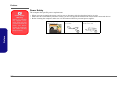


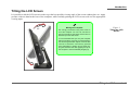
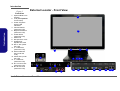

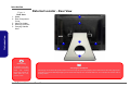
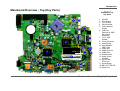


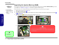


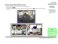
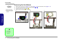
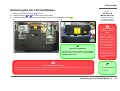
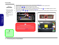

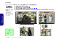
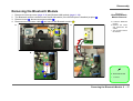

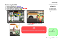
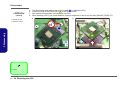


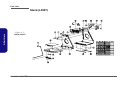
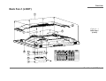
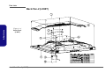


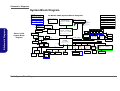
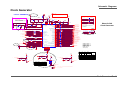

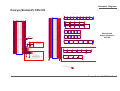
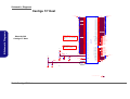

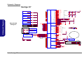

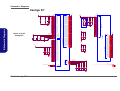

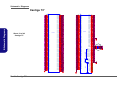

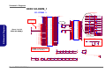

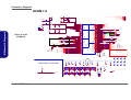
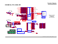
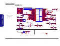

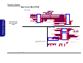
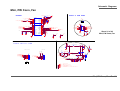
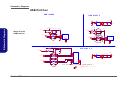
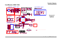

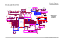

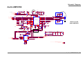
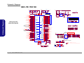
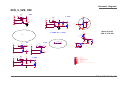
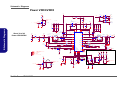
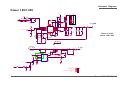


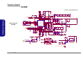

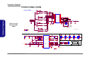
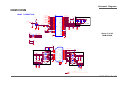
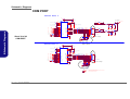
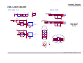
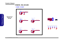

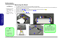

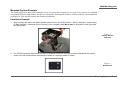

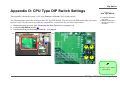


![取扱説明書[EH-SW53/CSW53] (3.75 MB/PDF)](http://vs1.manualzilla.com/store/data/006687909_2-690cfa537022a21bc081bff8fc6b6bb5-150x150.png)