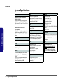
1
Preface Notebook Computer R130T Service Manual Preface I Preface Notice The company reserves the right to revise this publication or to change its contents without notice. Information contained herein is for reference only and does not constitute a commitment on the part of the manufacturer or any subsequent vendor. They assume no responsibility or liability for any errors or inaccuracies that may appear in this publication nor are they in anyway responsible for any loss or damage resulting from the use (or misuse) of this publication. This publication and any accompanying software may not, in whole or in part, be reproduced, translated, transmitted or reduced to any machine readable form without prior consent from the vendor, manufacturer or creators of this publication, except for copies kept by the user for backup purposes. Preface Brand and product names mentioned in this publication may or may not be copyrights and/or registered trademarks of their respective companies. They are mentioned for identification purposes only and are not intended as an endorsement of that product or its manufacturer. Version 1.0 November 2009 Trademarks Intel and Intel Core are trademarks of Intel Corporation. Windows® is a registered trademark of Microsoft Corporation. Other brand and product names are trademarks and/or registered trademarks of their respective companies. II Preface About this Manual This manual is intended for service personnel who have completed sufficient training to undertake the maintenance and inspection of personal computers. It is organized to allow you to look up basic information for servicing and/or upgrading components of the R130T series notebook PC. The following information is included: Chapter 1, Introduction, provides general information about the location of system elements and their specifications. Chapter 2, Disassembly, provides step-by-step instructions for disassembling parts and subsystems and how to upgrade elements of the system. Preface Appendix A, Part Lists Appendix B, Schematic Diagrams III Preface IMPORTANT SAFETY INSTRUCTIONS Follow basic safety precautions, including those listed below, to reduce the risk of fire, electric shock and injury to persons when using any electrical equipment: Preface 1. Do not use this product near water, for example near a bath tub, wash bowl, kitchen sink or laundry tub, in a wet basement or near a swimming pool. 2. Avoid using a telephone (other than a cordless type) during an electrical storm. There may be a remote risk of electrical shock from lightning. 3. Do not use the telephone to report a gas leak in the vicinity of the leak. 4. Use only the power cord and batteries indicated in this manual. Do not dispose of batteries in a fire. They may explode. Check with local codes for possible special disposal instructions. 5. This product is intended to be supplied by a Listed Power Unit (Full Range AC/DC Adapter – AC Input 100 - 240V, 50 - 60Hz, DC Output 19V, 3.42A or 18.5V, 3.5A). This Computer’s Optical Device is a Laser Class 1 Product IV Preface Instructions for Care and Operation The notebook computer is quite rugged, but it can be damaged. To prevent this, follow these suggestions: 1. Don’t drop it, or expose it to shock. If the computer falls, the case and the components could be damaged. Do not expose the computer to any shock or vibration. 2. Do not place anything heavy on the computer. Keep it dry, and don’t overheat it. Keep the computer and power supply away from any kind of heating element. This is an electrical appliance. If water or any other liquid gets into it, the computer could be badly damaged. Do not leave it in a place where foreign matter or moisture may affect the system. Don’t use or store the computer in a humid environment. Do not place the computer on any surface which will block the vents. Preface Do not expose it to excessive heat or direct sunlight. 3. Do not place it on an unstable surface. Follow the proper working procedures for the computer. Shut the computer down properly and don’t forget to save your work. Remember to periodically save your data as data may be lost if the battery is depleted. Do not turn off the power until you properly shut down all programs. Do not turn off any peripheral devices when the computer is on. Do not disassemble the computer by yourself. Perform routine maintenance on your computer. V Preface 4. 5. Avoid interference. Keep the computer away from high capacity transformers, electric motors, and other strong magnetic fields. These can hinder proper performance and damage your data. Take care when using peripheral devices. Use only approved brands of peripherals. Unplug the power cord before attaching peripheral devices. Preface Power Safety The computer has specific power requirements: VI • • Power Safety Warning • Before you undertake any upgrade procedures, make sure that you have turned off the power, and disconnected all peripherals and cables (including telephone lines). It is advisable to also remove your battery in order to prevent accidentally turning the machine on. • • • Only use a power adapter approved for use with this computer. Your AC adapter may be designed for international travel but it still requires a steady, uninterrupted power supply. If you are unsure of your local power specifications, consult your service representative or local power company. The power adapter may have either a 2-prong or a 3-prong grounded plug. The third prong is an important safety feature; do not defeat its purpose. If you do not have access to a compatible outlet, have a qualified electrician install one. When you want to unplug the power cord, be sure to disconnect it by the plug head, not by its wire. Make sure the socket and any extension cord(s) you use can support the total current load of all the connected devices. Before cleaning the computer, make sure it is disconnected from any external power supplies. Do not plug in the power cord if you are wet. Do not use the power cord if it is broken. Do not place heavy objects on the power cord. Preface Battery Precautions • Only use batteries designed for this computer. The wrong battery type may explode, leak or damage the computer. • Do not continue to use a battery that has been dropped, or that appears damaged (e.g. bent or twisted) in any way. Even if the computer continues to work with a damaged battery in place, it may cause circuit damage, which may possibly result in fire. • Recharge the batteries using the notebook’s system. Incorrect recharging may make the battery explode. • Do not try to repair a battery pack. Refer any battery pack repair or replacement to your service representative or qualified service personnel. • Keep children away from, and promptly dispose of a damaged battery. Always dispose of batteries carefully. Batteries may explode or leak if exposed to fire, or improperly handled or discarded. • Keep the battery away from metal appliances. • Affix tape to the battery contacts before disposing of the battery. • Do not touch the battery contacts with your hands or metal objects. Battery Guidelines Preface The following can also apply to any backup batteries you may have. • If you do not use the battery for an extended period, then remove the battery from the computer for storage. • Before removing the battery for storage charge it to 60% - 70%. • Check stored batteries at least every 3 months and charge them to 60% - 70%. Battery Disposal The product that you have purchased contains a rechargeable battery. The battery is recyclable. At the end of its useful life, under various state and local laws, it may be illegal to dispose of this battery into the municipal waste stream. Check with your local solid waste officials for details in your area for recycling options or proper disposal. Caution Danger of explosion if battery is incorrectly replaced. Replace only with the same or equivalent type recommended by the manufacturer. Discard used battery according to the manufacturer’s instructions. Battery Level Click the battery icon in the taskbar to see the current battery level and charge status. A battery that drops below a level of 10% will not allow the computer to boot up. Make sure that any battery that drops below 10% is recharged within one week. VII Preface Related Documents You may also need to consult the following manual for additional information: Preface User’s Manual on CD This describes the notebook PC’s features and the procedures for operating the computer and its ROM-based setup program. It also describes the installation and operation of the utility programs provided with the notebook PC. VIII Preface Contents Introduction ..............................................1-1 Overview .........................................................................................1-1 System Specifications .....................................................................1-2 External Locator - Top View with LCD Panel Open ......................1-4 External Locator - Front & Right side Views .................................1-5 External Locator - Left Side & Rear View .....................................1-6 External Locator - Bottom View .....................................................1-7 Mainboard Overview - Top (Key Parts) .........................................1-8 Mainboard Overview - Bottom (Key Parts) ....................................1-9 Mainboard Overview - Top (Connectors) .....................................1-10 Mainboard Overview - Bottom (Connectors) ...............................1-11 Overview .........................................................................................2-1 Maintenance Tools ..........................................................................2-2 Connections .....................................................................................2-2 Maintenance Precautions .................................................................2-3 Disassembly Steps ...........................................................................2-4 Removing the Battery ......................................................................2-5 Removing the Hard Disk Drive .......................................................2-6 Removing the Optical (CD/DVD) Device ......................................2-7 Removing the System Memory (RAM) ..........................................2-8 Removing the Processor ................................................................2-10 Removing the Wireless LAN Module ...........................................2-12 Removing the Bluetooth Module ..................................................2-13 Removing the Keyboard ................................................................2-14 Schematic Diagrams................................. B-1 System Block Diagram ...................................................................B-2 HDI Con ..........................................................................................B-3 KBC-ITE IT8513E .........................................................................B-4 CRT Port, LEDI ..............................................................................B-5 LVDS & LED Panel Driver ............................................................B-6 Azalia Codec AMP ALC269QFN ..................................................B-7 JMB385 Card Reader .....................................................................B-8 New Card, CCD, Fan ......................................................................B-9 PCIE LAN RTL8111DL, RJ45 ....................................................B-10 Click, BT Con., TPM ....................................................................B-11 WLAN, 3G, GPS ..........................................................................B-12 HDD, ODD, USB, G-Sensor ........................................................B-13 COM Port, Ext USB Con. .............................................................B-14 5VS, 3VS, 3.3VM, 1.5VS, VIN1 .................................................B-15 Power VDD3/VDD5 .....................................................................B-16 AC_In, Charge ..............................................................................B-17 USB+COM Board ........................................................................B-18 Power Button Board .....................................................................B-19 Click Board ...................................................................................B-20 FingerPrint Board .........................................................................B-21 GPS Antenna Board ......................................................................B-22 Part Lists ..................................................A-1 Part List Illustration Location ........................................................ A-2 Top ................................................................................................. A-3 Bottom ............................................................................................ A-4 IX Preface Disassembly ...............................................2-1 LCD ............................................................................................... A-5 DVD Super Multi .......................................................................... A-6 Preface Preface X Introduction Chapter 1: Introduction Overview This manual covers the information you need to service or upgrade the R130T series notebook computer. Information about operating the computer (e.g. getting started, and the Setup utility) is in the User’s Manual. Information about drivers (e.g. VGA & audio) is also found in User’s Manual. That manual is shipped with the computer. Operating systems (e.g. Windows Vista, Windows 7, etc.) have their own manuals as do application software (e.g. word processing and database programs). If you have questions about those programs, you should consult those manuals. 1.Introduction The R130T series notebook is designed to be upgradeable. See Disassembly on page 2 - 1 for a detailed description of the upgrade procedures for each specific component. Please note the warning and safety information indicated by the “” symbol. The balance of this chapter reviews the computer’s technical specifications and features. Overview 1 - 1 Introduction System Specifications Processor 1.Introduction Intel® Core™2 Duo Processor ULV: SU9300 (1.20GHz) 45nm (45 Nanometer) Process Technology, 3MB L2 Cache & 800MHz FSB - TDP 10W, BGA Socket P Pin-Out, 22 * 22mm CPU On Board Intel® Celeron® Processor ULV: 723 (1.20GHz) 45nm (45 Nanometer) Process Technology, 1MB L2 Cache & 800MHz FSB - TDP 10W, BGA Socket P Pin-Out, 22 * 22mm CPU On Board Core Logic Intel® GS45 + ICH9M-SFF Chipset Display 13.3” WXGA (1280 * 800) LED Backlight Panel Memory 64-bit Wide DDRII (DDR2) Data Channel Supporting Dual Channel DDRII (DDR2) SDRAM One 200 Pin SO-DIMM Socket Supporting DDRII (DDR2) 800MHz Memory Expandable up to 2GB 1 - 2 System Specifications Video Interface Intel® GS45 Integrated Video High Preference 3D/2D Graphic Accelerator Shared Memory Architecture of up to 256M Supports Microsoft DirectX 10 Three USB 2.0 Ports One Serial (COM1) Port One External Monitor Port One Headphone-Out Jack One Microphone-In Jack One S/PDIF-Out Jack One RJ-45 LAN Jack for 10/100/1000Mb Fast Ethernet One DC-In Jack BIOS One 16Mb SPI Flash ROM Phoenix™ BIOS Storage One Changeable 12.7mm(h) Super Multi Optical Device Drive - SATA interface Card Reader One Changeable 2.5" 9.5 mm (h) HDD OR 2.5" SSD with SATA (Serial) Interface Embedded 7-in-1 Card Reader (MS/ MS Pro/ SD/ Mini SD/ MMC/ RS MMC/ MS Duo) Note: MS Duo/ Mini SD/ RS MMC Cards require a PC adapter Audio Slots High Definition Audio Compliant with Microsoft UAA (Universal Audio Architecture) Direct Sound 3D™ Compatible Built-In Microphone 2 * Built-In Speakers One ExpressCard/34/54 Slot Two Mini-Card Slots with USB & PCIe interface: Slot 1 for Half Mini-Card WLAN Module Slot 2 for 3.75G Module (Factory Option) Keyboard & Pointing Device Full Size WinKey Keyboard Built-in TouchPad (integrated scrolling key functionality) Introduction Communication Security Optional Built-In 10M/100M/100M Base-TX Ethernet LAN Bluetooth 2.1 + EDR (Enhanced Data Rate) Module (Factory Option) Intel® WiFi Link 5300 Series (3*3 - 802.11a/g/ n) Wireless LAN PCIe interface Half Mini-Card Module (Option) 802.11a/g/n Wireless LAN PCIe interface Half Mini-Card Module 2.0M Pixel PC Camera Module with USB interface (Factory Option) Security (Kensington® Type) Lock Slot Fingerprint ID Reader Module BIOS Password Trusted Platform Module V1.2 Super Multi Optical Device Drive Operating System 802.11a/g/n Wireless LAN PCIe interface Half Mini-Card Module 8 Cell Smart Lithium-Ion Battery Pack, 5200mAH GPS Module without Internal Antenna (Factory Option) Power Management Environmental Spec Temperature Operating: Non-Operating: Relative Humidity Operating: Non-Operating: 5°C - 35°C -20°C - 60°C 20% - 80% 10% - 90% Bluetooth 2.1 + EDR (Enhanced Data Rate) Module (Factory Option) 2.0M Pixel PC Camera Module with USB interface (Factory Option) UMTS/HSPDA-based 3.75G Module with Mini-Card Interface (Factory Option) GPS Module without Internal Antenna (Factory Option) Dimensions & Weight 317mm (w) * 229mm (d) * 35mm (h) 2.0 kg (full system with 1G RAM, 2.5” HDD, ODD and 4 Cell Battery) Supports Wake on LAN Supports Wake on Modem Ring Power Full Range AC/DC Adapter AC input 100 - 240V, 50 - 60Hz, DC Output 19V, 3.42A or 18.5V, 3.5A (65 Watts) 4 Cell Smart Lithium-Ion Battery Pack, 2600mAH 8 Cell Smart Lithium-Ion Battery Pack, 5200mAH (Option) System Specifications 1 - 3 1.Introduction 3.75G Module: UMTS/HSPDA-based 3.75G Module with Mini-Card Interface (Factory Option) Quad-band GSM/GPRS (850 MHz, 900 MHz, 1800 MHz, 1900 MHz) UMTS WCDMA FDD (2100 MHz) Note that UMTS modes CAN NOT be used in North America Windows® Vista (with Service Pack 2) Windows® XP (with Service Pack 3) Intel® WiFi Link 5300 Series (3*3 - 802.11a/g/ n) Wireless LAN PCIe interface Half Mini-Card Module Introduction Figure 1 External Locator - Top View with LCD Panel Open Top View 1.Introduction 1 2 1. LCD Latch 2. Built-In PC Camera (Optional) 3. LCD 4. Power Button 5. Keyboard 6. Fingerprint Reader Module 7. Touchpad & Buttons 8. Built-In Microphone 9. LED Indicators 10. Carrying Handle 3 4 5 8 6 7 9 10 1 - 4 External Locator - Top View with LCD Panel Open Introduction External Locator - Front & Right side Views Figure 2 Front Views 1. LCD Latch 2. Carrying Handle 3. Speakers 1 3 2 3 4 5 6 7 8 9 4. Optical Device Drive Bay (for CD/DVD Device) 5. ODD Lock 6. 1 * USB 2.0 Port 7. GPS Antenna Socket (for optional GPS Module) 8. Serial (COM1) Port 9. Security Lock Slot External Locator - Front & Right side Views 1 - 5 1.Introduction Figure 3 Right Side Views Introduction External Locator - Left Side & Rear View Figure 4 Left Side View 1.Introduction 1. 2. DC-In Jack External Monitor Port 3. S/PDIF-Out Jack 4. Microphone-In Jack 5. Headphone-Out Jack 6. Vent/Fan Intake/ Outlet 7. RJ-45 LAN Jack 8. 2 * USB 2.0 Port 9. ExpressCard Slot 10. 7-in-1 Card Reader 3 1 2 4 6 5 9 7 8 Figure 5 Rear View 11. Battery 11 1 - 6 External Locator - Left Side & Rear View 8 10 Introduction External Locator - Bottom View Figure 6 Bottom View 1 4 2 3 5 4 Overheating To prevent your computer from overheating make sure nothing blocks the vent/fan intakes while the computer is in use. External Locator - Bottom View 1 - 7 1.Introduction 1. Battery 2. Hard Disk Bay Cover 3. RAM & CPU Bay Cover 4. Vent/Fan Intake/ Outlet 5. Drainage Outlet Introduction Figure 7 Mainboard Overview - Top (Key Parts) Mainboard Top Key Parts 1.Introduction 1. ExpressCard Connector 2. KBC ITE IT8513E 2 1 1 - 8 Mainboard Overview - Top (Key Parts) Introduction Mainboard Overview - Bottom (Key Parts) Figure 8 Mainboard Bottom Key Parts 2 1 3 4 5 Mainboard Overview - Bottom (Key Parts) 1 - 9 1.Introduction 1. Mini-Card Connector (3G Module) 2. SIM Card Socket 3. Mini-Card Connector (WLAN Module) 4. CPU and Memory Card Slot 5. Card Reader Socket Introduction Figure 9 Mainboard Overview - Top (Connectors) Mainboard Top Connectors 1.Introduction 1. 2. 3. 4. LED Connector CCD Connector Comport Connector Power Button Connector 5. SATA HDD Connector 6. Keyboard Cable Connector 7. ODD Connector 1 2 3 4 5 6 7 1 - 10 Mainboard Overview - Top (Connectors) Introduction Mainboard Overview - Bottom (Connectors) Figure 10 Mainboard Bottom Connectors 1 1. CPU Fan Cable Connector 2. Bluetooth Module Connector 3. GPS Module Connector 4. Touchpad Connector 1.Introduction 2 3 4 Mainboard Overview - Bottom (Connectors) 1 - 11 1.Introduction Introduction 1 - 12 Disassembly Chapter 2: Disassembly Overview This chapter provides step-by-step instructions for disassembling the R130T series notebook’s parts and subsystems. When it comes to reassembly, reverse the procedures (unless otherwise indicated). We suggest you completely review any procedure before you take the computer apart. To make the disassembly process easier each section may have a box in the page margin. Information contained under the figure # will give a synopsis of the sequence of procedures involved in the disassembly procedure. A box with a lists the relevant parts you will have after the disassembly process is complete. Note: The parts listed will be for the disassembly procedure listed ONLY, and not any previous disassembly step(s) required. Refer to the part list for the previous disassembly procedure. The amount of screws you should be left with will be listed here also. Information A box with a will also provide any possible helpful information. A box with a contains warnings. An example of these types of boxes are shown in the sidebar. Warning Overview 2 - 1 2.Disassembly Procedures such as upgrading/replacing the RAM, optical device and hard disk are included in the User’s Manual but are repeated here for your convenience. Disassembly NOTE: All disassembly procedures assume that the system is turned OFF, and disconnected from any power supply (the battery is removed too). Maintenance Tools The following tools are recommended when working on the notebook PC: 2.Disassembly • • • • • • M3 Philips-head screwdriver M2.5 Philips-head screwdriver (magnetized) M2 Philips-head screwdriver Small flat-head screwdriver Pair of needle-nose pliers Anti-static wrist-strap Connections Connections within the computer are one of four types: 2 - 2 Overview Locking collar sockets for ribbon connectors To release these connectors, use a small flat-head screwdriver to gently pry the locking collar away from its base. When replacing the connection, make sure the connector is oriented in the same way. The pin1 side is usually not indicated. Pressure sockets for multi-wire connectors To release this connector type, grasp it at its head and gently rock it from side to side as you pull it out. Do not pull on the wires themselves. When replacing the connection, do not try to force it. The socket only fits one way. Pressure sockets for ribbon connectors To release these connectors, use a small pair of needle-nose pliers to gently lift the connector away from its socket. When replacing the connection, make sure the connector is oriented in the same way. The pin1 side is usually not indicated. Board-to-board or multi-pin sockets To separate the boards, gently rock them from side to side as you pull them apart. If the connection is very tight, use a small flat-head screwdriver - use just enough force to start. Disassembly Maintenance Precautions The following precautions are a reminder. To avoid personal injury or damage to the computer while performing a removal and/or replacement job, take the following precautions: Power Safety Warning Before you undertake any upgrade procedures, make sure that you have turned off the power, and disconnected all peripherals and cables (including telephone lines). It is advisable to also remove your battery in order to prevent accidentally turning the machine on. Cleaning Do not apply cleaner directly to the computer, use a soft clean cloth. Do not use volatile (petroleum distillates) or abrasive cleaners on any part of the computer. Overview 2 - 3 2.Disassembly 1. Don't drop it. Perform your repairs and/or upgrades on a stable surface. If the computer falls, the case and other components could be damaged. 2. Don't overheat it. Note the proximity of any heating elements. Keep the computer out of direct sunlight. 3. Avoid interference. Note the proximity of any high capacity transformers, electric motors, and other strong magnetic fields. These can hinder proper performance and damage components and/or data. You should also monitor the position of magnetized tools (i.e. screwdrivers). 4. Keep it dry. This is an electrical appliance. If water or any other liquid gets into it, the computer could be badly damaged. 5. Be careful with power. Avoid accidental shocks, discharges or explosions. •Before removing or servicing any part from the computer, turn the computer off and detach any power supplies. •When you want to unplug the power cord or any cable/wire, be sure to disconnect it by the plug head. Do not pull on the wire. 6. Peripherals – Turn off and detach any peripherals. 7. Beware of static discharge. ICs, such as the CPU and main support chips, are vulnerable to static electricity. Before handling any part in the computer, discharge any static electricity inside the computer. When handling a printed circuit board, do not use gloves or other materials which allow static electricity buildup. We suggest that you use an anti-static wrist strap instead. 8. Beware of corrosion. As you perform your job, avoid touching any connector leads. Even the cleanest hands produce oils which can attract corrosive elements. 9. Keep your work environment clean. Tobacco smoke, dust or other air-born particulate matter is often attracted to charged surfaces, reducing performance. 10. Keep track of the components. When removing or replacing any part, be careful not to leave small parts, such as screws, loose inside the computer. Disassembly Disassembly Steps The following table lists the disassembly steps, and on which page to find the related information. PLEASE PERFORM THE DISASSEMBLY STEPS IN THE ORDER INDICATED. To remove the Battery: 1. Remove the battery To remove the Wireless LAN Module: page 2 - 5 To remove the HDD: 2.Disassembly 1. Remove the battery 2. Remove the HDD page 2 - 5 page 2 - 6 To remove the Optical Device: 1. Remove the battery 2. Remove the Optical device page 2 - 5 page 2 - 7 To remove the System Memory: 1. Remove the battery 2. Remove the System Memory page 2 - 5 page 2 - 8 To remove the Processor: 1. Remove the battery 2. Remove the System Memory 3. Remove the Processor 2 - 4 Disassembly Steps page 2 - 5 page 2 - 8 page 2 - 10 1. Remove the battery 2. Remove the System Memory 3. Remove the Wireless LAN page 2 - 5 page 2 - 8 page 2 - 12 To remove the Bluetooth Module: 1. Remove the battery 2. Remove the HDD 3. Remove the Bluetooth page 2 - 5 page 2 - 6 page 2 - 13 To remove the Keyboard: 1. Remove the battery 2. Remove the Keyboard page 2 - 5 page 2 - 14 Disassembly Removing the Battery Figure 1 If you are confident in undertaking upgrade procedures yourself, for safety reasons it is best to remove the battery. 1. 2. 3. 4. 5. Battery Removal a. Slide the latch in the direction of the arrow. b. Slide the battery out in the direction of the arrow. c. Lift the battery out of the bay as indicated. Turn the computer off, and turn it over. Slide the latch 1 in the direction of the arrow. Slide the latch 2 in the direction of the arrow, and hold it in place. Slide the battery out in the direction of the arrow 3 . Lift the battery 4 (Figure c) out of the bay as indicated. b. a. 2.Disassembly 1 2 3 c. 4 4. Battery Removing the Battery 2 - 5 Disassembly Figure 2 2.Disassembly HDD Assembly Removal a. Remove the screws. b. Remove the cover c. Carefully lift the hard disk up. d. Remove the HDD from the connector. e. Remove the HDD. f. Insert a new HDD and replaced all the cover and screws Removing the Hard Disk Drive The hard disk drive is mounted in a removable case and can be taken out to accommodate other 2.5" SATA hard disk drives with a height of 9.5mm (h). Follow your operating system’s installation instructions, and install all necessary drivers and utilities (as outlined in Chapter 4 of the User’s Manual) when setting up a new hard disk. Hard Disk Upgrade Process 1. 2. 3. 4. 5. 6. 7. Turn off the computer, and turn it over and remove the battery (page 2 - 5). Locate the hard disk bay cover and remove screws 1 & 2 . Remove the hard disk bay cover 3 . Carefully lift the hard disk up at point 4 . Grip the tab 5 and slide the hard disk in the direction of arrow 6 . Remove the hard disk 7 . Carefully insert the new hard disk and replace all the cover and screws. a. c. e. 7 4 2 1 3. Hard Disk Bay Cover 7. HDD d. b. f. 3 • 2 Screws 6 2 - 6 Removing the Hard Disk Drive 5 8 Disassembly Removing the Optical (CD/DVD) Device 1. 2. 3. 4. 5. 6. Figure 3 Turn off the computer, and turn it over and remove the battery (page 2 - 5). Locate the RAM & CPU bay cover and remove screws 1 - 4 . Carefully (a fan and cable are attached to the under side of the cover) lift up the bay cover 5 . Carefully disconnect the fan cable 6 , and remove the cover 5 . Remove screws 7 - 9 and use a screwdriver to push the optical device 11 out of the computer at point 10 . Reverse the process to install the new device. a. b. 2 1 a. Remove the screws. b. Lift off the bay cover and disconnect the fan cable. c. Remove the screw and push the optical device out of the computer at point 10. 6 2.Disassembly 5 4 Optical Device Removal 5 3 c. 11 7 8 9 10 5. RAM & CPU Bay Cover 11. Optical Device • 7 Screws Removing the Optical (CD/DVD) Device 2 - 7 Disassembly Figure 4 RAM Module Removal a. Remove the screws. b. Lift off the bay cover and disconnect the fan cable. 2.Disassembly Caution The heat sink, and CPU area in general, contains parts which are subject to high temperatures. Allow the area time to cool before removing these parts. Removing the System Memory (RAM) The computer has two memory sockets for 200 pin Small Outline Dual In-line Memory Modules (SO-DIMM) DDR II (DDR2) supporting 800 MHz. The main memory can be expanded up to 2GB. The SO-DIMM modules supported are 1024MB and 2048MB DDR Modules. The total memory size is automatically detected by the POST routine once you turn on your computer. Memory Upgrade Process 1. 2. 3. 4. Turn off the computer, and turn it over and remove the battery (page 2 - 5). Locate the RAM & CPU bay cover and remove screws 1 - 4 . Carefully (a fan and cable are attached to the under side of the cover) lift up the bay cover 5 . Carefully disconnect the fan cable 6 , and remove the cover 5 . a. b. 2 1 6 5 4 5 3 RAM Module Speeds 5. RAM & CPU Bay Cover • 4 Screws 2 - 8 Removing the System Memory (RAM) Use either 800MHz DDRII (DDR2) modules of the same brand. Do not mix DRAM speeds/brands in order to prevent unexpected system behavior. Disassembly 5. Gently pull the two release latches 7 & 8 on the sides of the memory socket in the direction indicated by the arrows (Figure c). 6. The RAM module 9 will pop-up (Figure d), and you can then remove it. c. Figure 5 RAM Module Removal (cont’d.) d. RAM Module Speeds 9 7 8 c. Pull the release latch(es). d. Remove the module(s). Use either 800MHz DDRII (DDR2) modules of the same brand. Do not mix DRAM speeds/brands in order to prevent unexpected system behavior. Contact Warning Be careful not to touch the metal pins on the module’s connecting edge. Even the cleanest hands have oils which can attract particles, and degrade the module’s performance. 9. RAM Module Removing the System Memory (RAM) 2 - 9 2.Disassembly 7. Insert a new module holding it at about a 30° angle and fit the connectors firmly into the memory slot. 8. The module’s pin alignment will allow it to only fit one way. Make sure the module is seated as far into the socket as it will go. DO NOT FORCE the module; it should fit without much pressure. 9. Press the module in and down towards the mainboard until the slot levers click into place to secure the module. 10. Replace the heat sink unit, RAM fan, cover and screws. 11. Restart the computer to allow the BIOS to register the new memory configuration as it starts up. Disassembly Figure 6 Processor Removal 2.Disassembly a. Remove the cover and Iocate the heat sink. b. Remove the screws in the order indicated. c. Remove the heat sink. Removing the Processor 1. 2. 3. 4. Turn off the computer, and turn it over, remove the battery (page 2 - 5) and RAM (page 2 - 8). The CPU heat sink will be visible at point A on the mainboard. Remove the CPU heat sink screws 1 - 4 in the order indicated on the label. Carefully lift up the heat sink B (Figure 6c) off the computer. c. a. A B Caution The heat sink, and CPU area in general, contains parts which are subject to high temperatures. Allow the area time to cool before removing these parts. b. 3 2 1 4 B. CPU Heat Sink • 4 Screws 2 - 10 Removing the Processor Disassembly 5. 6. 7. 8. 9. Remove screws 5 - 8 from the CPU board. The CPU board C will pop-up. Carefully (it may be hot) lift the CPU board C up and off the computer (Figure e). Reverse the process to install a new CPU board. When re-inserting the CPU, pay careful attention to the pin alignment, it will fit only one way (DO NOT FORCE IT!). d. d. Remove the screws on the CPU board. e. Lift the CPU board out. Caution 8 5 Figure 7 Processor Removal (cont’d) 6 2.Disassembly The heat sink, and CPU area in general, contains parts which are subject to high temperatures. Allow the area time to cool before removing these parts. 7 e. C C C. CPU Board • 4 Screws Removing the Processor 2 - 11 Disassembly Figure 8 Wireless LAN Module Removal a. Disconnect the cables and remove the screws. b. Remove the WLAN module. Removing the Wireless LAN Module 1. Turn off the computer, and turn it over, remove the battery (page 2 - 5) and RAM (page 2 - 8). 2. Carefully disconnect the cables 1 - 2 accordingly and remove screws 3 - 4 . 3. The Wireless LAN Module 5 (Figure c) will pop-up, and you can remove it. b. a. 5 3 2.Disassembly 1 5 2 4 5. Wireless LAN Module • 2 Screws 2 - 12 Removing the Wireless LAN Module Disassembly Removing the Bluetooth Module 1. 2. 3. 4. Figure 9 Turn off the computer, and turn it over, remove the battery (page 2 - 5), and hard disk (page 2 - 6). Remove the screw 1 . Carefully disconnect cables 2 & 3 . Lift the Bluetooth module 4 off the computer. a. c. Bluetooth Module Removal a. Remove the screw. b. Disconnect the cables. c. Remove the Bluetooth module. 1 b. 4 3 2 4. Bluetooth Module • 1 Screw Removing the Bluetooth Module 2 - 13 2.Disassembly Note: Make sure you reconnect the antenna cables to the socket (Figure a). Disassembly Removing the Keyboard Figure 10 Keyboard Removal 2.Disassembly a. Use a screwdriver to lift the hinge cover. b. Push the hinge cover up. c. Remove screws from the keyboard. d. Remove screws from the keyboard plate. 1. Turn off the computer, and turn it over and remove the battery (page 2 - 5). 2. Turn to the rear of the computer and lift the hinge cover 1 & 2 to release it (you may need to use a small screwdriver to do this). 3. Turn the computer back around and push at point 3 to release the whole hinge cover. 4. Carefully lift the hinge cover 4 up (Figure b). 5. Remove screws 6 - 11 from the keyboard 5 . 6. Carefully lift up the keyboard 5 (Figure d) and remove screws 12 - 15 from the keyboard plate 16 . a. c. 2 1 6 7 8 9 10 11 5 3 Re-Inserting the Keyboard When re-inserting the keyboard firstly align the four keyboard tabs at the bottom at the bottom of the keyboard with the slots in the case. b. 4 d. 12 5. Keyboard 16. Keyboard plate • 10 Screws 2 - 14 Removing the Keyboard 14 16 13 15 Disassembly 7. Remove the keyboard plate 16 (Figure e). 8. Disconnect the keyboard ribbon cable 17 from the locking collar socket 18 . 9. Carefully lift up the keyboard 5 (Figure f) off the computer. e. Figure 11 Keyboard Removal (cont’d) f. e. Remove the keyboard plate and disconnect the cable from the locking collar. f. Remove the keyboard. 17 18 2.Disassembly 5 16 5. Keyboard 16. Keyboard plate Removing the Keyboard 2 - 15 2.Disassembly Disassembly 2 - 16 Part Lists Appendix A: Part Lists This appendix breaks down the R130T series notebook’s construction into a series of illustrations. The component part numbers are indicated in the tables opposite the drawings. Note: This section indicates the manufacturer’s part numbers. Your organization may use a different system, so be sure to cross-check any relevant documentation. Note: Some assemblies may have parts in common (especially screws). However, the part lists DO NOT indicate the total number of duplicated parts used. A.Part Lists Note: Be sure to check any update notices. The parts shown in these illustrations are appropriate for the system at the time of publication. Over the product life, some parts may be improved or re-configured, resulting in new part numbers. A - 1 Part Lists Part List Illustration Location The following table indicates where to find the appropriate part list illustration. Table A- 1 Part List Illustration Location A.Part Lists Parts A - 2 Part List Illustration Location Top page A - 3 Bottom page A - 4 LCD page A - 5 DVD Super Multi page A - 6 Part Lists Top Figure A - 1 無鉛 黑色(無鉛) 無鉛 無鉛 無鉛 無鉛 無鉛 (灰色) 無鉛 無鉛 無鉛 無鉛 無鉛 無鉛 無鉛 無鉛 無鉛 無鉛 無鉛 Top A - 3 A.Part Lists Top Part Lists Bottom 無鉛 無鉛 無鉛 無鉛 海華 無鉛 展達 無鉛 無鉛 海華 無鉛 展達 無鉛 (半卡) 無鉛 無鉛 無鉛 A.Part Lists Figure A - 2 無鉛 無鉛 Bottom 無鉛 黑色 無鉛 無鉛 無鉛 無鉛 無鉛 無鉛 無鉛 無鉛 無鉛 無鉛 北橋 無鉛 無鉛 無鉛 無鉛 無鉛 無鉛 無鉛 無鉛 度 黑色 無鉛 無鉛 (無鉛) 無鉛 無鉛 無鉛 無鉛 咬花 無鉛 無鉛 無鉛 無鉛 無鉛 無鉛 無鉛 度,黑色 無鉛 無鉛 無鉛 無鉛 藍天7 互億 無鉛 無鉛 無鉛 無鉛 無鉛 非耐落 A - 4 Bottom 無鉛 Part Lists LCD Figure A - 3 無鉛 無鉛 無鉛 無鉛 無鉛 無鉛 無鉛 精乘 無鉛 無鉛 無鉛 無鉛 無鉛 無鉛 無鉛 (壓克力) 無鉛 精乘 無鉛 透明 設變虛線 無鉛 LCD A - 5 A.Part Lists LCD Part Lists DVD Super Multi A.Part Lists Figure A - 4 DVD Super Multi 無鉛 無鉛 內縮 無鉛 無鉛 (非耐落) A - 6 DVD Super Multi 無鉛 Schematic Diagrams Appendix B: Schematic Diagrams This appendix has circuit diagrams of the R130T notebook’s PCB’s. The following table indicates where to find the appropriate schematic diagram. Diagram - Page Diagram - Page Diagram - Page Table B - 1 Schematic Diagrams New Card, CCD, Fan - Page B - 9 Power VDD3/VDD5 - Page B - 16 HDI Con - Page B - 3 PCIE LAN RTL8111DL, RJ45 - Page B - 10 AC_In, Charge - Page B - 17 KBC-ITE IT8513E - Page B - 4 Click, BT Con., TPM - Page B - 11 USB+COM Board - Page B - 18 CRT Port, LEDI - Page B - 5 WLAN, 3G, GPS - Page B - 12 Power Button Board - Page B - 19 LVDS & LED Panel Driver - Page B - 6 HDD, ODD, USB, G-Sensor - Page B - 13 Click Board - Page B - 20 Azalia Codec AMP ALC269QFN - Page B - 7 COM Port, Ext USB Con. - Page B - 14 FingerPrint Board - Page B - 21 JMB385 Card Reader - Page B - 8 5VS, 3VS, 3.3VM, 1.5VS, VIN1 - Page B - 15 GPS Antenna Board - Page B - 22 B.Schematic Diagrams System Block Diagram - Page B - 2 Version Note The schematic diagrams in this chapter are based upon version 6-7P-R1306-002. If your mainboard (or other boards) are a later version, please check with the Service Center for updated diagrams (if required). B - 1 Schematic Diagrams System Block Diagram CLEVO R130T System Block Diagram USB BOARD COM Port. USB Port. 6-71-R1303-D03 CLOCK GEN. 14.318 MHz 6-71-R1302-D03 POWER BOARD Power Button LED Sheet 1 of 21 System Block Diagram FINGER PRINT BOARD Finger Print 5VS,3VS,3.3VM,1.5VS,VIN1 VDD3/VDD5 FSB SO-DIMM1 AC_IN,CHARGE NORTH BRIDGE 667/800 MHz 1.8V DDRII Cantiga-SFF GS45 6-71-R130F-D03 GPS ANT. BOARD Ext. ANT. 1363 ball FCBGA 6-71-R130G-D03 6 -7 1- R1 30 5- D0 3 CRT/RGB MAIN BO ARD 6- 71 -R 13 00 -D 03 DMI X4 SYSTEM SMBUS ICH9M-SFF 569 BGA 32.768 KHz LVDS HP OUT SOUTH BRIDGE MIC IN CPU CARD SATA HDD VCORE DDR2 SDRAM SOCKET Socket P 667/800/1067 MHz Vtt=1.05V 6-71-R130C-D02 1.8V/0.9V MEMORY TERMINATIONS PROCESSOR Penryn-SFF 956 mFCPGA SL G8 SP 51 3V SPDIF OUT B.Schematic Diagrams CLICK BOARD Int Mic Con. Finger Print Con. T/P Con. 1.5VS/1.05VS AZALIA AZALIA LINK 24 MHz CODEC A LC 26 9 LVDS INT. SPK SATAII 300Mhz SATA ODD PCIE 100 MHz SO-DIMM TOUCH PAD Mini CARD Mini CARD EC IT8513 LPC 33 MHz SO CK ET S OC KE T USB2 USB10 W LA N 8 0P or t SIM Ca rd NEW CARD USB5 10/100/1000M 3G INT. K/B 25 MHz EC SMBUS GPS THERMAL SENSOR ASC7525 B - 2 System Block Diagram JMB385 LAN RTL8111DL SMART FAN 32.768 KHz SMART BATTERY USB 1.1/2.0 RJ- 45 ITE8305 G SENSOR COM PORT USB3 CARD READER 7 IN 1 M MC /S D/ MS /M S Pr o USB0 USB1 CCD USB6 BT USB4 Finger Printer USB8 12 MHz Schematic Diagrams HDI Con 3. 3V S VIN ED GE _C ON N EC TO R 1 1 3 5 7 9 11 13 15 17 19 21 23 25 27 29 31 33 35 37 39 VD D 3 T25 3 .3VM T28 3. 3V T27 R TC VC C T20 13 13 8 8 10 10 4 U SB_ PP3 U SB_P N3 U SB_ PP6 U SB_P N6 U SB_ PP8 U SB_P N8 SATA_ LE D# T22 3, 12 GSEN _IN T T21 T23 6 SB _MU TE# 8, 9, 1 1 PC I E_WAK E# 12 O DD _DETEC T# 5 SB_B LO N 14 DD _ON # 8, 1 1 I C H_SMBDA T1 8, 1 1 I C H_SMBCLK1 980506 Del 6 I C H_ SPKR 7 7 7 7 PC IE_ R XN 5_C R PC IE_ R XP5_CR PC IE_ TXN 5_C R PC IE_ TXP5_CR 9 9 9 9 PC IE_ R XN 6_G LA N PC IE_ R XP6_GL AN PC IE_ TXP6_GL AN PC IE_ TXN 6_GLA N 11 PC IE_ R XN 3_W LAN 11 PC IE_ R XP3_WLAN 1 1 PC IE_ TXP3_WLAN 11 PC IE_ TXN 3_W LA N 8 8 8 8 PC IE _R XN2_N EW _CAR D PC IE _R XP2_ N EW _C AR D PC IE _TXP2_N EW_C AR D PC IE _TXN2_N EW _CAR D 12 12 12 12 S ATA _TXN 1 S ATA _TXP 1 S ATA _R XN 1 S ATA _R XP 1 5 5 5 5 5 5 GM_ LVDS _L 2P GM_ LVDS _L 2N GM_ LVDS _L 0N GM_ LVDS _L 0P GM_ LVDS _L 1P GM_ LVDS _L 1N 5 G M_LV DS_LCLKN 5 G M_LV DS_LCLKP 4 GM_DAC _VSY NC 4 GM_DAC _HS YN C 5 GM_ ED ID _DA TA 5 GM_ ED ID _CLK 4 GM_ D DC _CLK 4 GM_ D DC _DA TA 5 G M_E NAVD D 5 GM_BLON T24 T65 IC H _G PI O4 9 41 43 45 47 49 51 53 55 57 59 61 63 65 67 69 71 73 75 77 79 81 83 85 87 89 91 93 95 97 99 101 103 105 107 109 111 113 115 117 119 121 123 125 127 129 131 133 135 137 139 141 143 145 147 149 151 153 155 157 159 161 163 165 167 169 171 173 175 177 179 181 183 185 187 189 191 193 195 197 199 41 43 45 47 49 51 53 55 57 59 61 63 65 67 69 71 73 75 77 79 81 83 85 87 89 91 93 95 97 99 10 1 10 3 10 5 10 7 10 9 11 1 11 3 11 5 11 7 11 9 12 1 12 3 12 5 12 7 12 9 13 1 13 3 13 5 13 7 13 9 14 1 14 3 14 5 14 7 14 9 15 1 15 3 15 5 15 7 15 9 16 1 16 3 16 5 16 7 16 9 17 1 17 3 17 5 17 7 17 9 18 1 18 3 18 5 18 7 18 9 19 1 19 3 19 5 19 7 19 9 2 4 6 8 10 12 14 16 18 20 22 24 26 28 30 32 34 36 38 40 42 44 46 48 50 52 54 56 58 60 62 64 66 68 70 72 74 76 78 80 82 84 86 88 90 92 94 96 98 100 102 104 106 108 110 112 114 116 118 120 122 124 126 128 130 132 134 136 138 140 142 144 146 148 150 152 154 156 158 160 162 164 166 168 170 172 174 176 178 180 182 184 186 188 190 192 194 196 198 200 2 4 6 8 10 12 14 16 18 20 22 24 26 28 30 32 34 36 38 40 To CPU Board 5V S T9 SYS 5V 5V Sheet 2 of 21 HDI Con T7 T10 1.0 5VS 1 .5VS LAN _ DS M# 9 980506 Add 42 44 46 48 50 52 54 56 58 60 62 64 66 68 70 72 74 76 78 80 82 84 86 88 90 92 94 96 98 1 00 1 02 1 04 1 06 1 08 1 10 1 12 1 14 1 16 1 18 1 20 1 22 1 24 1 26 1 28 1 30 1 32 1 34 1 36 1 38 1 40 1 42 1 44 1 46 1 48 1 50 1 52 1 54 1 56 1 58 1 60 1 62 1 64 1 66 1 68 1 70 1 72 1 74 1 76 1 78 1 80 1 82 1 84 1 86 1 88 1 90 1 92 1 94 1 96 1 98 2 00 B.Schematic Diagrams 3 V CO R E_ON 1 2 U SB_ OC0 1# 12 U SB_ PP1 12 U SB_P N1 11 U SB_ PP2 11 U SB_P N2 12 USB _O C 3# 8 USB _O C 5# 1 3 5 7 9 11 13 15 17 19 21 23 25 27 29 31 33 35 37 39 SMC _ TH ER M 3 SMD _ TH ER M 3 PM_THR M# 3 SYS _PW R GD 14 USB _PN 0 USB _PP0 USB _PN 5 USB _PP 5 12 12 8 8 USB _PN 4 10 USB _PP 4 10 USB _PN 1 0 11 USB _PP 10 11 LPC _ FR AME# 3,1 0,13 LPC _ AD 3 3, 10,1 3 L PC _AD 1 3, 1 0, 1 3 L PC _AD 2 3, 1 0, 1 3 LPC _ AD 0 3, 10,1 3 AZ_SDI N 0 6 AZ_SDOU T 6 AZ_SYN C 6 AZ_RST# 6 AZ_BITC LK 6 D2 2 C H7 51H -40 PT A C PWR _BTN# 3 RSMR ST# 3 SLP _M# 3, 1 4 SD_C D# 7 PCI _RST# 8, 1 3 PME # 3 KBC _LPC PD# 10 SWI # 3 PM_C LK RU N # 1 0 IN T_SE RI RQ 3,1 0,13 PM_PW R OK 3, 5 SUS B# 3, 8 SUS B 14 KBC _R ST# 3 SUS _PW R _A CK 3 AC_PR ESEN T 16 GA20 3 PLT_RST# 10 SUS C# 3 SCI # 3 SMI # 3 CLK_SI O48 13 BUF _PLT_R ST# 3 , 7, 8, 9,11 LA N_C LKR EQ# 9 NE W_C ARD _RE Q# 8 PC LK_KBC 3,13 PC LK_TPM 10 SATA _TXN0 1 2 SATA _TXP0 12 SATA _R XN0 1 2 SATA _R XP0 1 2 CLK_ PC IE_N EW_ C AR D 8 CLK_ PC IE_N EW_ C AR D# 8 CLK_ PC IE_GLAN 9 CLK_ PC IE_GLAN # 9 GM_DAC _ B 4 GM_DAC _ G 4 GM_DAC _ R 4 WLAN _C L KR EQ# 11 CLK_ PC IE_W LAN # 11 CLK_ PC IE_W LAN 11 CLK_ PC IE_C R# 7 CLK_ PC IE_C R 7 6-86-24200-062 8 002 1-202 1 (H=5.2) HDI Con B - 3 Schematic Diagrams KBC-ITE IT8513E K B C _A V D D L10 H C B 1 00 5 K F -1 21 T 2 0 . V DD 3 C9 1 C9 6 C 10 7 C1 0 0 C 74 1 0 u _1 0 V _Y 5 V _0 8 0 . 1u _ 1 6V _ Y 5 V _ 0 4 0 . 1 u _1 6 V _ Y 5 V _0 4 0 . 1 u _1 6 V _ Y 5 V _0 4 V D D3 C 71 C6 5 V DD3 0 . 1u _ 1 6V _ Y 5V _ 0 4 0. 1 u _1 6 V _ Y 5 V _ 04 0 . 1 u_ 1 6V _ Y 5V _ 0 4 C1 0 5 R 1 01 K B C _A G N D 0 . 1u _ 16 V _ Y 5 V _ 0 4 10 0 K _0 4 3 . 3V S K B C _W R E S E T # Sheet 3 of 21 KBC-ITE IT8513E P C LK _ K B C K B C _W R E S E T # 2 16 4 2 980506 Add 9 L AN_ IN R2 4 5 14 126 4 16 20 G A2 0 AC_ IN# L E D_ A C IN# P M _T H R M# *1 0 mi l _s h o r t LA N _I N _ A 2 3 W E B _ E M A I L# 15 74 3 KSI0 /ST B# K S I 1/ A F D # KSI2 /INIT # K S I 3 / S LI N # K SI4 K SI5 MATRIX KK SS II 76 K/B W RS T # GA 2 0 / GP B 5 K B R S T # / GP B 6 (U P ) P W U R E Q# / GP C 7(P U ) L8 0 L LA T / W U I 7/ G P E 7 (P U ) E C S C I #/ G P D 3 (P U ) E C S M I #/ G P D 4 (P U ) DAC B A T 1 _ DE T 66 67 B A T 1 _ V OL T_ R C H G_ C U R S E N _ R 6 8 69 T OT A L _ C U R _ R 70 D A C 0/ G P J0 D A C 1/ G P J1 D A C 2/ G P J2 D A C 3/ G P J3 IT8513E ADC A D C 0/ G P I 0 A D C 1/ G P I 1 A D C 2/ G P I 2 A D C 3/ G P I 3 A D C 4/ G P I 4 S S C E 0# / GP G 2 FSC E# F MOS I F MI S O FSC K (P D )S S C E 1 # / GP G 0/ T M SM BUS 16 S MC _ B A T 1 16 S MD _ B A T 1 2 S MC _ T H E R M 2 S MD _ T H E R M 12 S MC _G S E N 12 S MD _G S E N 110 111 115 116 117 118 S M C _ GS E N S M D _ GS E N B R I GH TN E S S 6 K B C _B E E P L E D _ S C R OL L # 4 L E D _ N U M# 4 L E D_ CA P # 4 L E D _ B A T _C H G # 4 L E D _ B A T _F U L L# 11 11 10 10 2 ,1 2 85 86 89 90 80 C LK 3I N 1 80 C LK 3 IN1 T P _C L K T P _D A T A R9 3 GS E N _I N T 24 25 28 29 30 31 32 *0 _ 04 1 2 5 18 21 1 4 P W R _S W # 5, 1 2 L I D _ S W # S MC S MD S MC S MD S MC S MD LK 0 / GP A T0 / GP LK 1 / GP A T1 / GP LK 2 / GP A T2 / GP B3 B4 C1 C2 F 6(P U ) F 7(P U ) GPIO (P D )K S O1 6/ S S O/ GP C 3 (P D ) K S O1 7 / S S I / GP C 5 PWM (P D ) C L K R U N # / GP H ( P D )GP H ( P D )GP H ( P D )GP H ( P D )GP H P W M0 / GP A 0 ( P U ) P W M1 / GP A 1 ( P U ) P W M2 / GP A 2 ( P U ) P W M3 / GP A 3 ( P U ) P W M4 / GP A 4 ( P U ) P W M5 / GP A 5 ( P U ) P W M6 / S S C K / GP A 6 ( P U ) L AN_ IN 2 V C OR E _ O N 2 , 5 P M _P W R OK R2 4 6 *0 _ 04 120 124 WAKE UP (P D ) LP C P D # / W U I 6/ G P E 6 B T_ E N B K L_ E N 2 16 SW I# C H G _E N 19 112 D A C 4 / D C D 0 # / GP J 4 D S R 0# / GP G 6 GI N T/ C TS 0# / GP D 5 P S 2 D A T 1 / R T S 0 #/ G P F 3 D A C 5/ R I G0 # / GP J 5 P S 2C L K 1/ D TR 0 #/ G P F 2 T X D / S OU T 0/ G P B 1 R X D / S I N 0/ G P B 0 R I 1 # / W U I 0 / GP D 0(P U ) R I 2 # / W U I 1 / GP D 1(P U ) TA C H 0 / GP D 6 (P D ) TA C H 1 / GP D 7 (P D ) A D C 5 / D C D 1 #/ G P I 5 A D C 6 / D S R 1 #/ G P I 6 A D C 7 / C T S 1 #/ G P I 7 W U I 5 / R T S 1 #/ G P E 5 P W M7 / R I G 1 #/ G P A 7 GP G 1/ D T R 1 #/ I D 7 C T X 1/ S OU T 1 / GP H 2/ I D 2 C R X 1 / S I N 1 / GP H 1/ I D 1 TM R 0 / W U I 2 / G P C 4 (P D ) TM R 1 / W U I 3 / G P C 6 (P D ) C R X 0 / GP C 0 ( P D ) C T X0 / G P B 2( P D ) L8 0 H L A T / GP E 0 (P D ) R I N G # / P W R F A I L # / L P C R S T # / GP B 7 (P D ) LPC/WAKE UP I T 8 5 13 E R 1 05 36 37 38 39 40 41 42 43 44 45 46 51 52 53 54 55 K B - S O0 K B - S O1 K B - S O2 K B - S O3 K B - S O4 K B - S O5 K B - S O6 K B - S O7 K B - S O8 K B - S O9 K B - S O1 0 K B - S O1 1 K B - S O1 2 K B - S O1 3 K B - S O1 4 K B - S O1 5 10 0 10 1 10 2 10 3 10 5 10 6 24 23 22 21 20 19 18 17 16 15 14 13 12 11 10 9 25 26 L A N _ P C I E _W A K E # K B C_ S P I_ CE # KBC_ S PI_ SI KBC_ S PI_ SO K B C_ S P I_ S CL K R6 3 CLOCK C K 3 2K E CK 3 2 K 5 L C D _ B R I GH T N E S S B R I GH T N E S S R 10 3 *1 0 mi l _s h o r t C 11 0 *0 . 1 u_ 1 6V _Y 5V _ 0 4 C AC D8 B A V 99 R E C T I F I E R 16 B A T 1_ D E T B A T1 _ V OL T C CD_ E N 8 10 K _ 0 4 R 59 *1 0 K _0 4 1 2 3 4 CCD _ E N B T_ E N LI D _S W # K B C _ MU TE # B A T 1_ D E T AC D7 B A V 99 R E C T I F I E R A SU SB# S U S C# 2, 8 2 82 83 84 B A T 1_ V O LT AC D6 B A V 99 R E C T I F I E R C V D D3 8 7 6 5 R8 3 R9 0 R 1 02 R5 6 R N1 1 0 K _ 8P 4 R _0 4 * 10 K _ 0 4 * 10 K _ 0 4 * 10 K _ 0 4 * 10 K _ 0 4 S MC _ G S E N S MD _ G S E N S MC _ B A T 1 S MD _ B A T 1 1 2 3 4 8 7 6 5 R N2 4 . 7 K _ 8P 4 R _0 4 B A T1 _ D E T 80 D E T # 80 C L K 1 2 3 4 8 7 6 5 R N3 1 0 K _ 8P 4 R _0 4 A VDD 3 J _ 80 D E B U G1 GL A N _ ON 1 2 3 4 5 S MI # 2 SCI# 2 P W R_ B T N# 2 17 A C H G_ C U R S E N A C D5 B A V 99 R E C T I F I E R 16 C H G_ C U R S E N 3 IN1 8 0C L K 8 0D E T # R6 2 R1 0 6 * 10 0 K _ 04 C 11 2 *1 0 p_ 5 0 V _N P O_ 0 4 *1 0 _0 4 P C LK _ K B C 8 5 20 5 -0 50 0 1 K B C_ RS T # 2 6-20-51150-105 80 10 4 33 88 81 87 10 9 10 8 71 72 73 35 34 10 7 95 94 S LP _ M # B A T 1 _ V OL T 2 ,1 4 E C _ U S B 3 _ C T R L # 13 P ME # 2 K B C _ MU TE # 6 80 D E T # 11 GP S _ T XD 0 1 1 GP S _ R X D 0 1 1 8 0 DE T # 3G _D E T # 1 1 C C D _D E T # 8 MOD E L _I D R S MR S T # 2 LE D _P W R # 4 3G _E N 11 GP S _ E N 1 1 US B 3 _ P W R_ E N# 1 2 US B 3 _ P W R_ E N# V DD 3 NC2 C8 5 B A T 1_ V O LT _ R C7 3 1 u _6 . 3 V _ Y 5 V _ 04 1 0 0_ 0 4 C H G_ C U R S E N _ R C 7 2 1 u _6 . 3 V _ Y 5 V _ 04 KBC_SPI_*_R = 0.1"~0.5" U 6 8 S P I _V D D V DD SI SO ? ? ? R 80 1 K_ 0 4 K BC_ F L AS H 3 W P# C E# SCK *1 0 M_ 0 4 R 68 X1 1 0 0_ 0 4 0 . 1 u _1 6 V _ Y 5 V _0 4 2 12 8 R 95 R5 1 C H G _C U R S E N R 5 0 1 6 M bi t N C _0 4 4 . 7 K _ 04 H OL D # 7 5 K B C_ S P I _ S I _ R 2 K B C _ S P I _ S O_ R R 73 1 6 R 79 K B C_ S P I _ CE # _ R R 67 K B C_ S P I _ S CL K _ R R 82 4 H O LD # V S S 2 5 V F 01 6 B -7 5 C M 20 0 S 32 7 6 81 2 2 0_ 3 2. 7 6 8 K H z 1 2 C 10 3 C 10 4 1 5 p _5 0 V _N P O_ 0 4 1 5 p_ 5 0V _N P O_ 0 4 S P I _V D D N C_ 0 4 S P I _V D D K B C_ S P I_ CE # _ R K B C _ S P I _ S O_ R K B C_ A G ND J_SPI? 1 2 7 B - 4 KBC-ITE IT8513E R130T 3. 3V R 64 A J _ SP I1 for "J"? ? del R, add C VOL TA GE V DD3 C 16 HIG H 3G _D E T # B T_ D E T# CCD _ DE T # GP S _ D E T E C T # C S MD _B A T1 check M860TU? ? ? ? EC MOD EL _ID V 1. 0 MOD E L _I D A AC D9 B A V 99 R E C T I F I E R V ER . VDD 3 S MC _B A T1 S U S _P W R _ A C K 2 W D T_ E N 11 W L A N _ D E T# 1 1 B T _ D E T # 10 D D _ ON 14 4 3 NC 1 C P U _ F A N _R 0. 1u _ 16 V _ Y 5 V _ 0 4 C W DT _ E N 0 _0 4 C 1 06 *0 . 1u _ 1 0V _ X 7 R _ 04 12 0 K _ 1% _ 0 4 C6 8 LA N _P C I E _ W A K E # 9 56 57 93 96 97 98 99 1u _ 10 V _ 0 6 UART port WAKE UP P W R S W / G P E 4 (P U ) VSS VSS VSS VSS VSS VSS VSS 4 , 10 5 0 3 4 5 6 EXT GPIO CIR 119 123 0/ I D 3/ I D 4/ I D 5/ I D 6/ I D (P D )E G A D / G P E 1 ( P D )E GC S #/ G P E 2 ( P D )E GC LK / G P E 3 PS/2 P S 2C L K 0/ G P F 0 ( P U ) P S 2D A T 0/ G P F 1 ( P U ) P S 2C L K 2/ G P F 4 ( P U ) P S 2D A T 2/ G P F 5 ( P U ) PWM/COUNTER 47 48 8 C P U _F A N S E N K B -S I0 K B -S I1 K B -S I2 K B -S I3 K B -S I4 K B -S I5 K B -S I6 K B -S I7 FLASH AV SS 1 1 G P S _ DE T E CT # 76 77 78 79 K S O 0/ P D 0 K S O 1/ P D 1 K S O 2/ P D 2 K S O 3/ P D 3 K S O 4/ P D 4 K S O 5/ P D 5 K S O 6/ P D 6 K S O 7/ P D 7 K S O 8/ A C K # KS O 9 /BUSY K S O1 0/ P E K S O 11 / E R R # K S O1 2 / S LC T K S O1 3 K S O1 4 K S O1 5 58 59 60 61 62 63 64 65 J _ KB1 8 52 0 2- 2 6 0 51 change K/B matrix 1 ? ? 26 pin 2 3 4 5 6 7 8 8 C PU_ F AN 75 C P U_ F A N_ R 9 GL A N _ ON 11 3G _P W R 4 , 1 1 W LA N _ E N 1 J_KB1 C 1 08 AVC C 26 50 92 11 4 121 12 7 11 LA D 0 LA D 1 LA D 2 LA D 3 LPC LP C C L K LF R A ME # S E RIR Q LP C R S T # / W U I 4 / GP D 2 ( U P ) VB AT 10 9 8 7 13 6 5 22 VCC 2 , 10 , 1 3 LP C _ A D 0 2 , 10 , 1 3 LP C _ A D 1 2 , 10 , 1 3 LP C _ A D 2 2 , 10 , 1 3 LP C _ A D 3 2, 1 3 P C L K _ K B C 2, 1 0 , 1 3 L P C _F R A ME # 2 , 1 0, 1 3 I N T _ S E R I R Q 2 , 7 , 8 , 9, 1 1 B U F _P L T _R S T # V ST BY VST BY VST BY VST BY VST BY VST BY U8 1 12 27 49 91 1 13 122 B.Schematic Diagrams 26 8 1 3 5 7 2 4 6 8 *S P N Z -0 8 S 3-B - C -0 -P K B C_ S P I_ S CL K _ R K BC_ SP I_ S I_ R K B C _ S P I _S I C8 2 K B C _ S P I _S O 1 5 _1 % _ 04 C8 4 K B C _ S P I _C E # 1 5 _1 % _ 04 C8 0 K B C _ S P I _S C L K 4 7 _0 4 C8 7 4 7 _0 4 *3 3 p _5 0 V _N P O_ 0 4 *3 3 p _5 0 V _N P O_ 0 4 *3 3 p _5 0 V _N P O_ 0 4 *3 3 p _5 0 V _N P O_ 0 4 Schematic Diagrams CRT Port, LEDI CRT PORT 3. 3V S 980506 Add"*" A C A C A C *B A V 9 9 R E C TI F I E R * B A V 9 9 R E CT IF IE R * B A V 9 9 R E CT I F IE R J _ C R T1 D1 G M_ D A C _ R G M_ D A C _ G R 23 3 G M_ D A C _ B R 23 5 R 23 7 GM _ D A C _R GM _ D A C _G GM _ D A C _B GM_ D A C _ R L GM_ D A C _ GL GM_ D A C _ B L *0 _0 4 *0 _0 4 *0 _0 4 D S 0 1A 9 1 - MD 22 1 -7 F 6-21-64140-115 ML P 1 *F C A 32 1 6K F 4-1 2 1 T0 3 1 8 2 7 3 6 4 5 AC D 3 AC D 2 AC 2 2 2 F R E D _L F GR N _ L R 2 3 4 F B L U_ L R2 3 6 R2 3 8 *0 _ 04 *0 _ 04 *0 _ 04 F RE D F GR N 980304 Value change R8 C6 C1 5 8 C 1 60 24 mil 10 3 C 1 61 *1 0 p_ 5 0 V _N P O_ 0 4* 10 p _ 50 V _ N P O _ 04 *1 0p _ 5 0V _ N P O_ 04 11 *2 2 p_ 5 0 V _N P O_ 0 4 *2 2 p _5 0 V _ N P O_ 0 4 *2 2 p_ 5 0V _N P O_ 0 4 12 D DC DA T A 13 H SYN C 5 6 PLEA SE CLOS E TO CO NNECTOR Add cost down new part 14 V S Y NC GM _ D A C _ R GM _ D A C _ G GM _ D A C _ B 3. 3 V S D D C LK 8 C 8 980225 change G ND 1 GN D 2 5 6 7 8 15 980 30 4 DVT ? ? ? , ? ES D? ? LC3 ok ? ,? ? ? ? 5 VS C1 0 C1 1 C 12 Sheet 4 of 21 CRT Port, LED 2 20 p _5 0 V _ N P O _0 4 1 0 0 0p _ 50 V _ X 7R _ 04 1 0 0 0p _ 5 0V _ X 7 R _ 04 2 20 p _ 50 V _ N P O _0 4 E F 0 8 05 V 0 5 40 0 3. 3 V S 4 . 7 K _0 4 R1 5 7 4 . 7 K _0 4 G PL EASE CL OSE TO CONNECT OR R1 5 9 2 GM _D D C _D A T A 2 GM _D D C _C L K G L C3 1 2 3 4 10 7 9 F RE D F GR N FBL U C 9 4 1 50 _ 1 %_ 0 4 1 5 0_ 1 % _0 4 1 5 0 _1 % _ 04 980304 C 7 G M_ D D C _ D A T A G M_ D D C _ C L K R1 5 8 4 . 7 K _ 04 Q 24 M T N 7 00 2 Z H S 3 S S R9 * 1K _ 0 4 R1 1 * 1K _ 0 4 R 10 4 . 7 K _ 04 ML P 2 F C A 32 1 6K F 4-1 2 1 T0 3 1 8 2 7 3 6 4 5 D D Q2 5 MT N 70 0 2Z H S 3 DD CDA T A DD CL K HS Y NC VSYN C 5 VS AC AC A D 17 E MI ? ? ( D17 ~2 0) 9 80 30 3 E DS ? ? ? C AC D2 0 C A A A 2 G M_ D A C _V S Y N C D1 8 D G S D 19 C Q4 MT N 7 0 02 Z H S 3 G 5 VS AC 2 G M_ D A C _H S Y N C D C S B A V 99 R E C T I F I E R BAV 9 9 REC T IF IER B A V 9 9 R E C TI F I E R B A V 9 9 R E C TI F I E R Q 5 M TN 70 0 2 Z H S 3 5 VS 1, R1 19 ,R2 07 ne ar t o N .B .(D es ig n b y Chi ps et ) R1 .4 N oti ce : 2, Q1 1+ Q12 +R 349 +R 35 0 f or 91 5/ 94 5GM & th ir d par ty Ch ip se t 3, by pa ss Q1 1,Q 12 ,R 349 ,R 350 f or G9 65 /GM 96 5 POWER ON LED 3 . 3V S 3. 3 V S 3. 3 V S NUM LOCK LED C B S A TA _ L E D # S A T A _ LE D # 2 Q1 9 D T A 1 14 E U A BAT CHARGER LED 3. 3 V S CAPS LOCK LED E HDD/ODD LED R 15 0 R 14 9 2 2 0 _0 4 2 2 0_ 0 4 V DD 3 WLAN LED BT LED R 2 25 R 1 43 R 1 46 R 14 7 R 14 4 2 2 0 _0 4 22 0 _0 4 2 2 0_ 0 4 2 2 0_ 0 4 R1 4 5 2 20 _ 0 4 2 20 _ 0 4 B W L A N _E N Q2 0 P D T C 1 1 4E U L E D_ CA P # 3 3 L E D_ A C IN# 3 L E D_ P W R # 3 , 11 L E D_ P W R # 3 L E D _ B A T _C H G # 3 L E D _ B A T _F U L L# 3 1 D1 6 Y 4 SG 2 2 3 R Y - S P 15 5 H Y Y G 4 4 3 R Y -S P 1 55 H Y Y G 4 1 L E D_ B A T _ CHG # L E D_ B A T _ F UL L # E L E D_ CA P # 4 L E D_ A C IN# D1 5 C L E D _ N U M# 3 B E L E D _ N U M# G ND 2 Y SG 1 C C C R Y -S P 15 5 H Y Y G4 3 2 Y R Y -S P 17 2 Y G 34 C R Y -S P 1 7 2Y G3 4 2 D1 2 1 4 R Y - S P 1 72 Y G 3 4 A D1 3 SG D 11 D1 4 4 A A 22 0 _ 04 3 1 R 1 48 BT _ EN 3 , 10 Q 33 P D T C 1 1 4E U CRT Port, LEDI B - 5 B.Schematic Diagrams R7 9 2 F BL U R 5 1 Schematic Diagrams LVDS & LED Panel Driver 3 .3 V 3 .3 V 3 . 3V 3. 3 V SYS1 5 V 1 1 M _0 4 2 GM_ E N A V D D D C G S 6 0 . 1u _ 1 0V _ X 7 R _ 04 H8 5 2A 4 C1 R 1 51 0. 0 1 u _1 6 V _ X7 R _ 0 4 *1 00 K _ 0 4 3 B K L _E N 12 11 C9 9 1 *0 . 1 u _1 6 V _ Y 5 V _ 04 13 3 2 P LV D D 2 R1 5 2 R1 5 3 20 0 _ 1% _ 0 6 2 00 _ 1 %_ 0 6 GM _B LO N R 10 9 1 K_ 0 4 C 11 1 R 10 7 1 0 0 p_ 5 0V _N P O_ 0 4 1 0 0 K _0 4 U 10 C 7 4 LV C 0 8P W 9 8 I N V _ B LO N 10 3 .3 V *1 0 K _ 04 14 D R1 0 8 Q 21 M TN 70 0 2 Z H S 3 3 , 12 R 24 4 L I D_ S W # * 1 5m i _l s h ort 2 ,3 R 92 U 10 B 7 4 LV C 0 8P W 1 M_ 0 4 4 6 S G 5 P M _P W R OK 980506 7 Sheet 5 of 21 LVDS & LED Panel Driver U1 0 A 74 L V C 0 8 P W 7 Q 2 MT N 7 0 02 Z H S 3 E D S I 34 5 6 B D V -T 1 -E 3 G S 2 D D change LED PANEL BACKLIGHT DRIVER 3 .3 VS PD 5 F M 2 60 VIN PL 2 4 . 7u H _6 . 7 *6 . 3 *3 . 5 A 3 LC D _ B R I G H T N E S S P C 59 P C5 7 1 0 u_ 2 5 V _1 2 1 0u _ 2 5V _ 1 2 GM _E D I D _ C LK R1 2 . 2 K _1 % _ 04 GM _E D I D _ D A TA R2 2 . 2 K _1 % _ 04 SEL1 SEL2 SEL3 0 0 0 Only LED1 on 1 0 0 LED1 throgh LED2 on 0 1 0 LED1 throgh LED3 on 1 1 0 LED1 throgh LED4 on 0 0 0 LED1 throgh LED5 on LEDx Output LE D _ P W R + C V DD5 OVP =3 5V P C5 5 P C5 4 1 0 1 LED1 throgh LED6 on 1 u _ 50 V _ 1 2 1u _ 5 0V _ 1 2 0 1 1 LED1 throgh LED7 on 1 1 1 LED1 throgh LED8 on P R3 9 PC 1 90 . 9 K _ 1% _ 0 4 1 u _ 10 V _ 0 6 D P Q1 3 MT N 7 0 0 2Z H S 3 2 0K -2M H z PR7:power ? 13K?10K_1% G 20 6 2 22 23 SW A G ND PW M EP APW M P G ND SK IP P G ND 4 F sw =2 M H z G P R4 4 S I N V _ B LO N PQ 1 4 M TN 7 00 2 Z H S 3 PC5 6 SEL 3 FSET SEL 2 1 . 0 5 K _1 % _ 04 L E D = 20 m A 5 26 ISE T SEL 1 L E D1 LE D 2 P L V DD 21 S G ND V D D5 18 S E L 3 = H P R4 0 1 0K _0 4 17 S E L 2 = L P R4 1 *1 0 m li _ s ho rt _ 0 4 16 S E L 1 = H P R4 2 1 0K _0 4 PR 4 7 *1 5 mi l _s h o rt _0 6 Fsw = 26.03/R.FSET 1.23/I.SET * 210 (mA/LED) ID = 15 L E D2 - A8 5 0 0 L E D4 L E D6 L E D5 L E D3 - S GN D L E D1 - B - 6 LVDS & LED Panel Driver 980302 short 2 GM_ L V D S _ L 0 N 2 GM_ L V D S _ L 0 P 2 GM_ L V D S _ L 2 N 2 GM_ L V D S _ L 2 P 2 G M_ LV D S _ LC L K N 2 G M_ LV D S _ LC L K P L E D_ P W R+ GM _ LV D S _ L0 N GM _ LV D S _ L0 P GM _ LV D S _ L2 N GM _ LV D S _ L2 P GM _ LV D S _ LC LK N GM _ LV D S _ LC LK P 30mil 1 3 5 7 9 11 13 15 17 19 21 23 25 27 29 1 3 5 7 9 11 13 15 17 19 21 23 25 27 29 87 2 1 6-3 0 06 L ED 4 14 L ED8 L G ND L ED7 LE D 5 L ED6 13 S GN D 12 S GN D 11 S GN D 9 12 K _ 1 %_ 0 4 8 PR4 6 10 K _ 1% _ 0 4 10 7 PR4 5 0 . 1 u _1 6 V _ Y 5 V _ 04 L ED 3 0 . 1u _ 1 6V _ Y 5 V _ 0 4 P C5 8 J_ L E D P A N E L 1 2A 27 1 C OMP D S 3 EN S GN D 1 00 - 4 0 0H z 1 0 0K _0 4 O VP 19 PR 4 3 VIN PU 3 SW 25 V D D5 24 R.OVP = (V.OVP-30)/54.9uA S GN D B.Schematic Diagrams 3 Q2 2 P D T C 1 14 E U B D S B _ B L ON 7 R 1 55 1 M_ 04 2 7 R1 5 4 C2 14 Q1 14 U1 0 D 74 L V C 0 8 P W 14 S Y S 1 5V 2 4 6 8 10 12 14 16 18 20 22 24 26 28 30 2 4 6 8 10 12 14 16 18 20 22 24 26 28 30 3 .3 VS GM _E D I D _ C L K GM _E D I D _ D A T A GM _L V D S _L 1 N GM _L V D S _L 1 P LE LE LE LE LE LE D1 D2 D3 D4 D5 D6 - G M_ E D I D _C L K 2 G M_ E D I D _D A T A 2 G M_ L V D S _ L 1N 2 G M_ L V D S _ L 1P 2 Schematic Diagrams Azalia Codec AMP ALC269QFN ALC269 (QFN) 3 .3 V S 3 . 3V S _ A U D L1 2 F C M1 6 08 K -1 2 1T 0 6 R6 6 * 0_ 0 4 R7 0 C 95 C 94 0 . 1 u_ 1 6 V _Y 5 V _0 4 C 86 1 0u _ 10 V _ Y 5 V _ 0 8 0 . 1u _ 1 6V _ Y 5V _ 0 4 1 .5 VS * 10 m i _l s ho r t INT SPK-L 3. 3 V S _ A U D C7 6 0 . 1u _ 16 V _ Y 5 V _ 0 4 C7 7 1 0u _ 10 V _ Y 5 V _ 0 8 C1 5 6 10 0 0 p_ 5 0 V _X 7 R _ 0 6 J _ SPKL 1 S P K O U T L +_ R 1 S P K O U T L -_R 1 1 2 8 82 6 6 - 02 0 01 P C B F oo t p ri nt = 8 8 26 6 -2 R 5V S EAPD NEED SETTING (DATASHEET) 3. 3 V S 3 .3 V S C9 0 0 . 1 u _1 6 V _ Y 5 V _ 04 C9 3 1 0 u _1 0 V _ Y 5 V _0 8 L1 8 F C M1 0 05 K F -1 2 1T 0 3 L11 F C M 1 60 8 K -1 21 T 0 6 3 .3 V S _ A UD 5 V S _ A UD C 15 2 C1 5 3 1 80 p _ 50 V _ N P O _0 4 5 VS 18 0 p_ 5 0 V _N P O_ 0 4 U 7 C5 6 R4 5 *1 0 0 K _0 4 4 C8 8 5 R2 2 6 *1 5m i l _s h o rt 10 0 K _ 04 4 C 70 O UT C6 6 VIN S H DN # 3 MU T E A P M # BY P G ND 5 1 C9 2 2 INT SPK-R 1 u_ 6 . 3 V _Y 5 V _0 4 L1 7 F C M1 0 05 K F -1 2 1T 0 3 S P K OU TR + S P K OU TR - *G 9 24 S P D I F -OU T 47 48 2 3 22 _ 0 4 A Z _B I TC LK _R _2 6 9 6 R 65 22 _ 0 4 A Z _S D I N 0 _ R _ 2 6 9 8 22 _ 0 4 A Z _S Y N C _ R _ 26 9 10 22 _ 0 4 A Z _R S T #_ R _2 6 9 11 R 58 R 57 BEEP R 49 R 54 C6 4 1 0 K _0 4 C 69 1 K _ 04 12 1 9 25 38 A V DD1 AVDD 2 ANALOG VR EF S D A TA - I N M I C 1 -V R E F O -L M I C 1 -V R E F O- R MI C 2 -V R E F O S Y NC R ESET# H P -O U T -L H P -OU T - R PC BEEP CB N 1 u _ 6. 3 V _ Y 5 V _ 0 4 10 0 p _5 0 V _ N P O _0 4 C 25 4 1 u _6 . 3 V _ Y 5 V _ 04 L I N E 1 -L L IN E 1 -R B I T -C L K AVSS1 AV SS2 A Z _R S T # R 69 M I C 1 -L MI C 1 - R S D A TA - OU T GN D A Z _ S Y NC 2 5 26 37 2 DIGITAL 49 A Z _S D I N 0 J DR E F M ON O-O U T G P I O0 G P I O1 DV S S 2 A Z _ B IT CL K S en s e -B S PD IF C2 /E APD S PD IF O PVSS1 PVS S2 2 2 S P K -R S P K -R + A Z _S D OU T _R _2 6 9 22 p _ 50 V _ N P O _ 04 M I C 2 -L MI C 2 - R 7 C7 9 22 _ 0 4 S en s e A L I N E 2 -L L IN E 2 -R S P K -L + S P K -L - 42 43 R 78 A Z _ S D OU T PD # C 97 * 0. 1u _ 16 V _ Y 5 V _ 0 4 CR V RE F 44 45 A UDG C BP OP V E E 13 J D_ S E NS E R 47 14 15 16 17 20 K _ 1 % _0 4 MI C _S E N S E R 48 39 . 2 K _ 1 %_ 0 4 HP _ S E NS E C 63 C 62 4 . 7 u _6 . 3 V _ X5 R _ 0 6 4 . 7 u _6 . 3 V _ X5 R _ 0 6 C1 5 7 10 0 0 p_ 5 0 V _X 7 R _ 0 6 J _ SP KR1 SPK O UT R+ _ R1 S P K O U T R -_ R 1 L1 6 F C M1 0 05 K F -1 2 1T 0 3 C 15 4 1 2 8 82 6 6 - 02 0 01 P C B F oo t p ri nt = 8 8 26 6 -2 R C1 5 5 1 80 p _ 50 V _ N P O _0 4 18 0 p_ 5 0 V _N P O_ 0 4 MI C 2 _L _ 26 9 MI C 2 _R _2 6 9 I N T_ MI C 18 R 46 19 20 2 0 K _1 % _ 04 A UDG 21 22 C6 1 C6 0 23 24 C7 5 4. 7u _ 6. 3 V _ X 5R _ 06 4. 7u _ 6. 3 V _ X 5R _ 06 MI C 1 -L MI C 1 -R J_ S P D I F 1 5 4 3 S P D I F -OU T C7 8 27 MI C 1 -V R E F O -L MI C 1 -V R E F O -R MI C 2 -V R E F O 32 33 H E A D P H O N E -L H E A D P H O N E -R 35 C 83 C 21 R2 2 L2 2 6 1 1 u _1 0 V _ 06 A UDG 28 30 29 0 . 01 u _ 50 V _ X 7R _0 4 10 0 _1 % _ 04 F C M 10 0 5 K F -1 21 T 03 R 18 2 2 0 _0 4 K B C_ B EEP 6 8 0p _ 50 V _ X 7R _ 04 SPDIF OUT BLACK 980506 Edit 2 . 2 u_ 6 . 3V _Y 5V _ 0 6 36 34 A LC 2 69 Q 2 . 2 u_ 6 . 3 V _Y 5V _0 6 2 IC H_ SP KR Note: Pin13~38 is Analog Pin1~12,Pin39~48 is Digital C5 0 1 u _ 6. 3 V _ Y 5 V _ 0 4 C4 8 1 u _ 6. 3 V _ Y 5 V _ 0 4 L 2S J -T 3 51 -S 2 3 C 17 MI C 1-V R E F O-R R2 7 4 . 7 K _ 04 M I C 1 -V R E F O-L R3 4 4 . 7 K _ 04 M I C 1 -R R2 9 1 K _ 04 E XT _ MI C 1-R L4 F C M 1 00 5 K F -1 21 T 0 3 M I C 1 -L R3 0 1 K _ 04 E XT _ MI C 1-L L7 F C M 1 00 5 K F -1 21 T 0 3 MI C _ S E N S E J _ MI C 1 5 4 3 A UD G 3 R 0 . 1 u _1 6 V _ Y 5 V _0 4 A UDG PC BEEP Sheet 6 of 21 Azalia Codec AMP ALC269QFN C 81 31 40 41 S P K OU TR S P K OU TR + PVDD 1 P V D D2 4 S P K OU TL + S P K OU TL - DV D D1 U 5 D V D D -I O U4 74 A H C 1 G0 8 GW 39 46 2 K B C _M U T E # 2 C8 9 0 . 1 u_ 1 6 V _Y 5 V _0 4 0. 1 u _ 16 V _ Y 5 V _ 0 4 1 0 u _1 0 V _ Y 5 V _ 08 1 0 u _1 0 V _ Y 5 V _ 08 1 3 3 S B _M U T E # R7 7 *0 . 1u _ 1 0V _ X 7 R _ 04 Low mute! 2 BEEP C3 7 C2 5 1 0 0 p_ 5 0 V _N P O_ 0 4 R 2 L 6 1 2S J -T 3 51 -S 2 3 10 0 p_ 5 0 V _N P O_ 0 4 MI C 2-V R E F O MIC IN BLACK R 25 A UDG 4 . 7 K _0 4 I N T _ MI C I N T _ MI C _C L R2 2 7 7 5 _ 1% _ 04 C 13 0 6 8 0p _ 50 V _ X 7R _ 04 J P1 *1 0 m li _ sh o rt I N T _ MI C _C L 10 H P _S E N S E J _ HP 1 MIC CON.? Click Board? H E A D P H O N E -R R4 1 2 0 0_ 1 % _0 4 L8 F C M 10 0 5 K F -1 21 T 03 H E A D P H O N E -L R4 2 2 0 0_ 1 % _0 4 L9 F C M 10 0 5 K F -1 21 T 03 5 4 3 J P2 *1 0 m li _ sh o rt J P3 *1 0 m li _ sh o rt J P4 *1 0 m li _ sh o rt C 59 R 2 L 6 1 2S J -T 3 51 -S 2 3 A UD G C 42 1 00 p _ 50 V _ N P O _ 04 10 0 p _5 0 V _ N P O_ 0 4 HEADPHONE BLACK AUD G A U DG Azalia Codec AMP ALC269QFN B - 7 B.Schematic Diagrams L1 9 F C M1 0 05 K F -1 2 1T 0 3 S P K OU TL + S P K OU TL - Schematic Diagrams JMB385 Card Reader JMB385 CARD READER 02/12 3. 3 V S 3 .3 V S _ CA R D 3 . 3V S _ C A R D R 21 4 R2 2 1 S D _C D # 4 .7 K_ 0 4 40mil S D _ CD # 2 *1 5 m i _l s h or t 40mil DV1 .8 V SD W P# MD I O 13 MD I O 7 M S _ INS # U 20 Sheet 7 of 21 JMB385 Card Reader 2 0 0 K _ 04 2 0 0 K _ 04 HIGH M DIO1 2 M DIO1 4 LOW On Borad M DIO7 37 38 3 .3 V S_ CA RD 39 40 MD I O7 SDW P # 41 S D / MS C L K R 2 1 5 22_04 S D/M S CL K _ R 4 2 S D C MD / MS B S4 3 44 3 .3 V S _ C A RD 45 SD/M S_ D3 SD/M S_ D2 46 47 C2 3 1 SD/M S_ D1 SD/M S_ D0 48 0 . 1u _ 1 6 V _Y 5 V _ 0 4 MD I O 12 MD I O 14 Add-in Card CR1_PCTLN High Active CR1_LEDN High Active CR1_PCTLN Low Active CR1_LEDN Low Active D V1 8 PC IES _ EN PC IES M DIO 7 M DIO 6 M DIO 5 M DIO 4 D V3 3 M DIO 3 M DIO 2 M DIO 1 M DIO 0 G ND MD I O1 3 MD I O1 4 C R_ L E DN DV 3 3 R E G_ C T R L DV 1 8 C R 1 _ P C T LN C R 1 _C D 0N C R 1 _C D 1N SEEC L K SEED AT JMB385 24 23 22 21 20 19 18 17 16 15 14 13 M D I O 13 M D I O 14 3 .3 V S_ C ARD DV 1 .8 V V C C_ C A RD S D _ CD # M S _ INS# 0. 1u _ 1 6V _Y 5 V _ 04 0 . 1 u _1 6 V _ Y 5 V _ 0 4 2 C L K _ P C I E _C R # 2 CL K _ P C IE _ CR Layout Note: Must > 30mil J MB 3 8 5 -L GE Z 0 B C2 4 1 C2 4 0 2 ,3 ,8 ,9 ,1 1 B UF _ PL T _ RST # C2 4 4 C 2 43 X RS T N XTES T A P CL K N APC L KP APVD D A P GN D APR EXT A P RX P APR XN APV1 8 AP TXN APTXP R2 1 9 R2 2 2 N C NC NC G ND GN D G ND T AV3 3 M D I O8 M D I O9 M D I O 10 M D I O1 1 M DIO 1 2 0 . 1 u _1 6 V _ Y 5 V _ 0 4 36 35 34 33 32 31 30 29 28 27 26 25 C 23 2 1 2 3 4 5 6 7 8 9 10 11 12 B.Schematic Diagrams 3 .3 V S _ C A RD R N4 10 K _ 8 P 4 R _ 0 4 1 8 2 7 3 6 4 5 M D I O1 2 3 .3 V S_ CAR D VC C_ CA RD 0 . 1u _ 1 0 V _ X7 R _0 4 0 . 1u _ 1 0 V _ X7 R _0 4 P C IE_ RXP 5 _ CR 2 P C IE_ RXN5 _ C R 2 D V 1 . 8V P C IE_ T XN5 _ CR 2 P C I E _ T X P 5 _C R 2 DV 1 .8 V R2 1 8 8. 2 K _ 1 % _ 04 Layout note: Very closed between pin 19 and pin 20 3 .3 V S _ CA RD V C C _C A R D 3 .3 V S_ C ARD S D / M S C LK C 2 30 C2 3 8 C 2 33 10 u _ 1 0V _Y 5 V _ 08 0 . 1 u _ 16 V _ Y 5V _0 4 C2 3 6 1 0p _ 5 0V _N P O _0 4 C 24 2 C 2 45 0 . 1 u_ 1 6 V _ Y 5 V _ 0 4 0. 1 u _ 1 6V _Y 5 V _ 04 C2 4 6 0. 1u _ 1 6V _Y 5 V _ 04 0 . 1 u _ 16 V _ Y 5V _0 4 Near Cardreader CONN Card Reader Connector Layout note: Layout note: Very closed to pin 5(Trace width/length: 20mil/ <120mil) Very closed between pin 10 D V 1 .8 V J _ C A R D -R _ 1 S D _ CD # SD /M S _ D2 SD /M S _ D3 S D C MD / MS B S V C C_ C ARD S D /M S CL K SD /M S _ D0 SD /M S _ D1 SD W P# V C C_ C ARD S D /M S CL K SD /M S _ D3 M S _ INS # SD /M S _ D2 SD /M S _ D0 SD /M S _ D1 S D C MD / MS B S P1 P2 P3 P4 P5 P6 P7 P8 P9 P1 0 P1 1 P1 2 P1 3 P1 4 P1 5 P1 6 P1 7 P1 8 P1 9 P2 0 P2 1 CD _ S D D A T2 _ S D C D / D A T3 _ S D CM D_ S D VSS_ SD V D D_ S D CL K _ S D VSS_ SD D A T0 _ S D D A T1 _ S D W P_ SD VSS_ M S V C C _ MS S C LK _ M S D A T3 _ MS I N S _M S D A T2 _ MS S D I O/ D A T 0_ M S D A T1 _ MS B S _ MS VSS_ M S C2 3 7 footprint change G ND G ND M D R 01 9 -C 0-1 0 4 2 ? ? ? ? B - 8 JMB385 Card Reader C 2 35 0 . 1 u_ 1 6 V _ Y 5 V _ 0 4 1 00 0 p _5 0 V _ X 7 R _ 0 4 P2 2 P2 3 C 23 4 10 u _ 1 0V _ Y 5 V _ 08 C 23 9 0 . 1 u_ 1 6 V _ Y 5 V _ 0 4 Schematic Diagrams New Card, CCD, Fan NEW CARD 3 .3 V B U F _P LT _R S T# 3. 3V 10m il C 140 0 . 1u _16 V _Y 5 V_ 04 5 U1 4 7 4A H C 1G 08G W 2 , 3, 7, 9 , 11 B U F _P LT _R S T # 1 4 2 U 13 0. 1 u_ 16 V_ Y 5V _0 4 17 J _N E W 1 A UX N I P E R S T# 3. 3V S C 1 41 A U XOU T 0. 1 u_ 16 V_ Y 5V _0 4 2 3 . 3V I N 3. 3V OU T 8 N C _ R S T# 15 S U SB # 3. 3 V 6 19 SUSB# R 1 40 1 4 5 13 14 16 10 K_ 04 1 . 5V I N 1. 5V OU T C P PE # C P U SB # S Y S R S T# OC # 0 . 1u_ 16 V _Y 5 V_ 04 C 139 0 . 1u_ 16 V _Y 5 V_ 04 N C _ P ER S T # 12 48 mil 14 15 48 mil 9 10 N C _1 .5 V N C _ C PP E # N C _ C PU SB # P C I E _W AK E # R 14 2 1 0K _0 4 R 13 9 18 20 R 13 8 R 14 1 7 21 2 , 9, 1 1 P C I E_ WA K E # 3 .3 V S 2 N E W_ C A R D _R E Q# *10 0K _0 4 C L K_ P C I E_ N E W_ C AR D 2 C LK _ PC I E _ N EW _C AR D C L K_ P C I E_ N E W_ C AR D # 2 C L K_ P C I E_ N E W_ C A R D # *10 K_ 04 2 P C I E _R X P2 _N E W _C A R D 10K _ 04 P C I E _R X P2 _N E W _C A R D 2 P C I E _R X N 2_ N EW _C AR D P C I E _R X N 2_N EW _C A R D P C I E_ TX P 2_N E W _C A R D C 1 48 0 . 1u_ 10 V _X 7R _ 04 2 P C I E _T XP 2_ N E W_ C A R D P C I E_ TX N 2_ N E W_ C AR D C 1 46 0 . 1u_ 10 V _X 7R _ 04 2 P C I E _T XN 2 _N E W _C A R D L1 5 U S B _P P 5 1 2 2 U SB _ PP 5 U S B _P N 5 4 3 2 U S B _P N 5 *W C M20 12 F 2S -16 1T 03- s ho rt mon Choke? sho rt, ? EMI *10 0K _0 4 3. 3V Co-lay Com DVT? ? ? ? . 2, 11 IC H _S MB D AT 1 2 , 11 I C H _ S MBC L K 1 13 36 mil 10 9 S T BY # E NE P2231 pin3,4,15,22 h as internally p ulled high (170Kohm) C 143 N C _3 V 11 R 13 7 NC R C LK E N NC S HDN# NC NC GN D NC GN D P 22 31N F E 2 0 . 1u_ 16 V _Y 5 V_ 04 17 4 11 16 19 18 22 21 25 24 3 2 8 7 I C H _S MB D A T1 I C H _S MB C LK 1 P ER S T # +3 . 3V A U X +3 . 3V +3 . 3V +1 . 5V +1 . 5V C P PE # C P U SB # WA K E # C LK R E Q# R E FC L K + R E FC L K P ET p0 P ET n0 P ER p 0 P ER n 0 R E S E R VE D R E S E R VE D U S B_ D + U S B_ D - GN D GN D GN D GN D S MB_ D A TA S MB_ C LK 1 30 80 1-1 6 -2 1- G3 A1 0-1 26 ,- S2 Sheet 8 of 21 New Card, CCD, Fan 5 6 1 20 23 26 ? ? ? , ? ? pa d? ? sh or t FAN CONTROL CCD 5 V S_ F AN 5V S U2 FON # 3 R 15 6 P owe r O n S oft S tar t b y ? ? ? ? ? S *15 mi _l sh?ort C o-lay Common Choke? short, ? EMI D VT? ? ? ? . Q2 3 A O3 40 9 D C3 U S B _P N 6 U S B _P P 6 U S B _P N 6 U S B _P P 6 5V S 1 2 4 3 C5 33 0K _ 04 *WC M2 01 2F 2S -1 61 T03 - sh or t Q3 G 1 2 3 4 5 5V S _F A N C 19 C 14 0. 1u _1 6V _Y 5V _0 4 10 u_ 10 V_ Y 5V _ 08 1 2 3 85 20 5-0 37 01 6-20-5113 0-103 1 0u _6 .3 V _X 5R _ 06 0. 1 u_1 6V _ Y 5V _0 4 D R3 CCD_ E N * 0_ 04 J_ F AN 1 R6 Fro m H 8 d efa ult H I 8 7 6 5 R2 0 L1 2 2 R4 10 0K _0 4 4. 7 u_ 6. 3 V_ X5 R _0 6 3 GN D GN D GN D GN D FON # ? ? ? ,? ? p ad ? ? s ho rt G C4 0 . 1u _10 V _X 7R _ 04 C 15 9 F ON V IN V OU T V SE T AP E 88 72 5 V_ C C D 48 mi l J _C C D 1 8 52 05 -050 01 J _C CD 1 10 0K _ 04 MT N 70 02 Z H S3 S 5V 1 2 3 4 C P U _F A N 3 C C D _ D E T# 3 C PU _ F AN S E N 3. 3 VS 6 -2 0- 511 50 -1 05 f oo tp rin t sa me J _8 0D EBU G1 R 21 C D4 4 . 7K _0 4 A C H 3 55 P T CLEVO CO. 藍天電腦 New Card, CCD, Fan B - 9 B.Schematic Diagrams P C I _ R ST # U S B _O C 5# 2, 13 PC I _ R S T# 2 U S B_ OC 5# 2, 3 12 0. 1 u_ 16 V_ Y 5V _0 4 C 142 3 1 . 5V S C 1 37 N C _ 3V A U X 3 C 1 38 Schematic Diagrams PCIE LAN RTL8111DL, RJ45 RTL8111DL LA N _ V D D 3 FOR RTL8102EL/8103EL R 1 91 mus t be w ith in 0.5 cm ( to pi n 48) L2 6 H C B 16 0 8 K F -1 21 T 2 5 4 0 mil C 2 20 C 2 19 C 2 07 . PV T: Fo r Cl evo N or ma l D es ig n 1A PV T: Fo r EP SON S 5 LA N W ea ku p E V D D1 2 mu st b e w it hi n 0. 5c m L 24 R 19 4 D FOR RTL PIN1,29,37,40 40 mi l S VDD 3 C2 2 9 S W F 2 5 2 0C F -4 R 7 M-M * 50 m i l_ s h ort _ 0 8 C 2 08 ? ? ? I ND UC TOR ( 60 0m A) C 20 9 C 21 4 C2 1 3 Q 32 *N D S 3 5 2A P _N L G CT RL 1 2 A C2 2 8 * 0. 1 u _ 16 V _ Y 5 V _ 0 4 0. 1u _ 1 6V _ Y 5V _ 0 4 0 . 1 u_ 1 6 V _ Y 5 V _ 04 2 2u _ 6 . 3V _X 5 R _ 0 8 *0 . 0 1u _ 5 0V _X 7 R _ 0 4 0 . 1u _ 1 6V _ Y 5V _0 4 FO R RT L PI N1 9 R2 1 2 DV D D1 2 R 19 2 C 21 1 C 20 5 C 20 6 C2 2 5 * 33 0 K _ 04 D C 22 4 *5 0 mi l _ sh o r t _ 08 R 2 13 *1 0 0K _ 0 4 60 mi l Q 31 *M TN 7 00 2 Z H S 3 0 . 1u _ 1 6V _ Y 5V _ 0 4 0. 1 u _ 16 V _ Y 5 V _ 0 4 0. 1 u _ 16 V _ Y 5 V _ 0 4 0. 1u _ 16 V _ Y 5V _ 0 4 0. 1 u _ 16 V _ Y 5 V _ 0 4 G GL A N _O N 3 S Sheet 9 of 21 PCIE LAN RTL8111DL, RJ45 3. 3 V 1 00 MHz /1 00 C 2 23 0 . 1 u_ 1 6 V _Y 5 V _0 4 0 . 1u _ 1 6V _Y 5V _0 4 0 . 1u _ 1 6V _Y 5V _0 4 0 . 1u _ 1 6V _ Y 5V _ 0 4 . R2 1 1 F OR R TL P IN 10 ,1 3, 30 ,3 6, 39 * 10 0 K _ 04 980506 Add EEPROM ? ? ? L A N_ DS M # 2 LA N _ V D D 3 3 .3 VS EEC S M A2/ EESK M A1/ EEDI M A0/ EEDO 1 2 3 4 R 2 06 R 2 07 1 0K _ 0 4 3 . 6K _0 6 L A N_ V DD 3 *A T 9 3 C 4 6 D N - S H - T * 0. 1 u _ 16 V _ Y 5 V _ 0 4 L A N _D S M# R2 0 4 R2 0 5 *1 K _ 0 4 *1 5 K _ 0 4 RST B R2 0 3 *1 0m i l _s h o rt D VDD 1 2 L A N _V D D 3 CS SK DI D O DV DD 1 2 C 22 7 VC C N C O RG G ND M A2 /EESK M A1 /EED I M A0 /EEDO EE CS U 18 8 7 6 5 980508 ? ? pull ? "*" FOR RTL8102EL/8103EL B U F _ P LT _ R S T # 2 , 3 , 7, 8 , 1 1 P CIE _ W A K E # 2 ,8 ,1 1 M DIO 0 + M DIO 0 - R 18 1 R 18 2 * 49 . 9 _ 1% _ 0 4 * 49 . 9 _ 1% _ 0 4 M D I O 0_ R C 19 9 *0 . 0 1 u_ 1 6 V _ X7 R _ 0 4 M DIO 1 + M DIO 1 - R 18 3 R 18 4 * 49 . 9 _ 1% _ 0 4 * 49 . 9 _ 1% _ 0 4 M D I O 1_ R C 20 2 *0 . 0 1 u_ 1 6 V _ X7 R _ 0 4 L A N _C L K R E Q # 2 36 35 34 33 32 31 30 29 28 27 26 25 L A N_ V D D3 R 1 97 >40 MI LSR 1 9 5 *0 _0 6 *1 5 m il _ s ho rt _ 0 6 D V D D 12 L AN_ V D D3 L A N_ V D D3 >40 MI LSR 1 9 6 *5 0 m il _ s ho rt _ 0 8 R 1 93 C 21 5 2 . 49 K _ 1 % _0 4 37 38 39 40 41 X T A L1 X T A L2 42 E N S W RE G 43 C T R L1 2 / V D D 4 4 45 RS E T 46 47 C T R L1 2 A 48 C 2 12 2 2u _ 6 . 3 V _X 5 R _ 0 8 V D D 3 3 _2 L ED0 A V D D 1 2 _2 A V D D 3 3 _2 C K TA L 1 C K TA L 2 E N S W RE G V D D S R _1 V D D S R _2 RS E T GN D _ 4 S R OU T 1 2 PCI-E LAN RT L8 11 1D L N C / S MD A T A N C/S M CL K E GN D H S ON HS O P EV D D1 2 R E F C L K _N R E F CL K _ P HS IN H S IP GN D _ 2 D V D D 1 2_ 1 A V D D 3 3_ 1 M D IP 0 M DIN 0 F B 12 M DIP1 M D IN1 GN D _ 1 M D IP 2 M DIN 2 AV D D1 2 _ 1 M DIP3 M DI N3 D V D D 12 0 . 1 u _1 6 V _ Y 5 V _ 0 4 3 . 3V S U 17 R TL 8 1 11 D L -G R R 2 02 DV D D1 2 _ 3 L E D 1/ E E S K L E D2 /E E D I L E D 3/ E E D O EECS G N D _3 D V D D 1 2 _2 V D D3 3 _ 1 I S OL A T E B PER STB L A NW A K E B C LK R E Q B FOR RTL8102EL/ 8103EL? ? ? FOR RTL8102EL/8103EL 1 K _ 04 980506 Add L A N _I N 24 23 22 21 20 19 18 17 16 15 14 13 PCIE_ R XN 2 _G L AN_ C C 2 1 8 PCIE_ R XP2 _ GL AN _C C 2 1 6 980303 Add LP2,LP3 for EMI MP? ? ? 3 0 . 1 u_ 1 0 V _X 7 R _ 0 4 0 . 1 u_ 1 0 V _X 7 R _ 0 4 P C I E _ R X N 6_ GL A N 2 P C I E _ R X P 6 _G LA N 2 L 22 MD I O0 + MD I O0 DV DD1 2 MD I O1 + MD I O1 - M D I O3 + M D I O 3- M D I O 2+ M D I O2 - M D I O1 + M D I O 1- M D I O 0+ M D I O0 - 1 2 3 4 5 6 7 8 9 10 11 12 MD I O2 + MD I O2 MD I O3 + MD I O3 - R1 8 9 C 22 1 2 2 p _5 0 V _ N P O _0 4 1 2 3 4 5 6 7 8 9 10 11 12 D V D D 12 D V D D 12 C2 0 3 C 2 01 C1 9 8 0. 0 1 u _1 6 V _ X7 R _0 4 0 . 0 1 u_ 1 6 V _ X7 R _ 0 4 0 . 01 u _ 16 V _ X 7 R _ 04 C2 2 2 T1 1+ 1T2 2+ 2T3 3+ 3T4 4+ 4- M CT 1 MX 1 + MX 1M CT 2 MX 2 + MX 2M CT 3 MX 3 + MX 3M CT 4 MX 4 + MX 4- 24 23 22 21 20 19 18 17 16 15 14 13 2 2p _ 5 0V _N P O_ 0 4 LP 1 0_ 8 P 4 R _ 0 6 4 5 3 6 2 7 1 8 L P2 * #9 4 4 C M-0 0 5 1= P 3 L MX 1+ 1 8 D L MX 1 + L MX 1- 2 7 D L MX 1 L MX 2+ 3 6 D L MX 2 + L MX 2- 4 5 D L MX 2 L P3 * #9 4 4 C M-0 0 5 1= P 3 L M X3 + 1 8 D L MX 3 + L M X3 - 2 7 D L MX 3 L M X4 + 3 6 D L MX 4 + L M X4 - 4 5 D L MX 4 - J_ R J 4 5 _1 1 2 3 6 4 5 7 8 LP 4 0_ 8 P 4 R _ 0 6 4 5 3 6 2 7 1 8 GS T 5 0 09 L F 4 0 mil XT A L 2 TC TD TD TC TD TD TC TD TD TC TD TD *0 _ 0 4 XT A L 1 X3 X8 A 0 2 50 0 0 F G1 H _ 2 5 MH z 2 1 980508 change E V D D1 2 C L K _ P C I E _ G LA N # 2 C LK _ P C I E _ GL A N 2 P C I E _ TX N 6 _ GL A N 2 P C I E _ T X P 6_ G LA N 2 D V D D 12 L A N_ V DD 3 B.Schematic Diagrams FOR RTL8102EL/8103EL ? ? ? *0 _ 0 6 D A+ D AD B+ D B- s hi e ld s hi e ld G ND 1 G ND 2 D C+ D CD D+ D DC 1 00 9 9 -10 8 A 4 C 2 04 0 . 01 u _ 16 V _ X 7R _ 04 NM CT _ 1 NM CT _ 2 NM CT _ 3 NM CT _ 4 R1 1 2 R1 1 5 R1 1 6 R1 1 8 75 _ 1 %_ 0 4 75 _ 1 %_ 0 4 75 _ 1 %_ 0 4 75 _ 1 %_ 0 4 NM CT _ R C 1 17 1 0 00 p _ 2K V _ X 7 R _ 1 2_ H 12 5 L A N _V D D 3 R2 0 0 * 0_ 0 4 R 20 1 *1 0 K _0 4 980506 2 , 8 , 11 P C I E _ W A K E # PCIE_ W A KE # A D2 1 B - 10 PCIE LAN RTL8111DL, RJ45 C C H 75 1 H -4 0 P T L A N _ P C I E _W A K E # del L A N _ P C I E _W A K E # 3 Schematic Diagrams Click, BT Con., TPM CLICK CONN (T/P,F/P,MIC) Bluetooth *2 0 mi l _ sh o rt R 1 35 5V * 0_ 0 6 R 1 32 R 1 31 10 K _ 0 4 1 0 K _ 04 C 1 32 C 1 31 Sheet 10 of 21 Click, BT Con., TPM 3 VS_ BT J _T P 1 T P _D A T A T P _C L K C1 3 5 T P _ DA T A T P _ CL K I N T _ MI C _ C L A U DG 3 3 C175 50V?10V R1 7 7 R1 7 6 *1 0m i l _s h o rt *1 0m i l _s h o rt 48 mil L 20 C 19 3 1 u _1 0 V _ 06 I N T_ M I C _ C L 6 L21 4 7 p_ 5 0V _N P O_ 0 4 4 7p _ 5 0V _ N P O_ 0 4 AU DG U S B _P N 8 U S B _P P 8 U S B _ P N8 2 U SB_ PP8 2 2 U S B _P N 4 2 3 U S B _P P 4 B T _D E T # US B _ P N4 US B _ P P 4 BT _ DET # 4 3 3 .3 V 0. 1 u _ 10 V _ X 7R _0 4 1 0 u _6 . 3 V _ X5 R _0 6 1 2 3 4 5 6 R1 7 8 10 K _ 0 4 8 5 20 5 -0 60 0 1 6-20-41A10-106 3 . 3V S B T_ E N # D 3 .3 VS_ F P change footprint same L295N(CCN1) 50mil J_ B T 1 * W C M 20 1 2F 2S -1 6 1 T0 3 1 2 85 2 05 - 1 0 00 1 L1 4 H C B 1 0 05 K F -1 2 1T 2 0 *1 0 mi l _s h o r t C1 9 4 C 12 0 C 1 28 1 u _1 0 V _ 06 0 . 1 u _1 0 V _ X7 R _0 4 Q 30 M T N 7 00 2 Z H S 3 1 TPM 1.2 J_BT1 6 G B T_ E N 3 ,4 S 1 2 3 4 5 6 7 8 9 10 CHECK U1 1 L C LK 22 16 27 15 2 , 3 , 1 3 LP C _F R A M E # 2 P LT _ R S T # 2 , 3 , 13 I N T_ S E R I R Q 2 P M _C L K R U N # 2 28 K B C_ L P CP D # TP M _ B A D D 9 TP M _ P P 7 1 3 12 R1 2 3 L AD 0 L AD 1 L AD 2 L AD 3 21 PCL K_ T PM 1 00 _ 0 4 T P M_ T E S T 8 VDD 1 VDD 2 VDD 3 10 19 24 3. 3 V S C 12 7 C1 1 6 0. 1u _ 16 V _ Y 5 V _ 0 4 L F R A ME # L R ESET# S E RIRQ C L K RU N# L PC PD# VS B 5 R1 1 0 3 3 _0 4 R1 2 2 1 0 K _ 04 T P M_ B A D D R1 2 4 1 0 K _ 04 R1 2 6 * 10 K _ 0 4 1 u _1 0 V _ 06 C1 1 4 1 0p _ 5 0V _ N P O_ 0 4 3 . 3V S 3. 3V S 3. 3V S 0 . 1 u _1 6 V _ Y 5 V _ 04 XT AL I 6 2 13 T P M_ X I PP X TA L O TESTI P C L K _ TP M T P M_ P P C1 1 3 C 12 6 GP I O GP I O 2 T E ST B I/BA D D N C_ 1 N C_ 2 N C_ 3 C1 1 5 0 . 1 u _1 6 V _ Y 5 V _ 04 0. 1 u _ 16 V _ Y 5 V _ 0 4 TPM C 1 21 1 5 p _5 0 V _ N P O_ 0 4 4 3 2 26 23 20 17 LP C _ A D 0 LP C _ A D 1 LP C _ A D 2 LP C _ A D 3 GN D _ 1 GN D _ 2 GN D _ 3 GN D _ 4 14 T P M_ X O 4 11 18 25 X2 C M 2 00 S 3 2 76 8 1 22 0 _3 2 . 7 68 K H z 1 2 2 ,3 ,1 3 2 ,3 ,1 3 2 ,3 ,1 3 2 ,3 ,1 3 C 1 22 1 5 p _5 0 V _ N P O_ 0 4 asserted before entering S3 LPC reset timing: LPCPD# inactive to LRST# inactive 32~96us T PM _PP HI : ACCESS LOW: NORMAL ( In ter n al PD ) HI : 4E/4F h T PM _BADD LOW: 2E / 2F h S LB 96 3 5 TT 6- 03- 09 63 5-0 H1 Click, BT Con., TPM B - 11 B.Schematic Diagrams 5 VS_ TP R 1 33 5V S Schematic Diagrams WLAN, 3G, GPS GPS POWER MINI-PCIE CARD (WLAN) R 10 4 GP S _ 3 . 3 V S 10 K _ 0 4 7 11 13 9 15 3 . 3 V _0 1 . 5 V _0 U I M _P W R U I M_ D A T A U I M_ C L K UIM _ RE S E T U I M_ V P P C L K R E Q# REF C L K REF C L K + GN D 0 GN D 1 R 17 4 20 mil * 1 5m i l _s h o rt C1 0 9 1 .5 V S C 1 81 *0 . 1 u _ 16 V _ Y 5 V _ 0 4 C 1 82 * 0 . 1u _ 1 6V _ Y 5V _ 0 4 * 10 U _6 . 3 V _ X5 R _0 6 GP S _ 3 . 3V S D 3 W L A N _D E T # 2 P C I E _ R X N 3_ W L A N 2 P C I E _ R X P 3 _W L A N 2 P C I E _ TX N 3_ W L A N 2 P C I E _T X P 3 _W L A N 3 3 R1 6 5 R1 6 4 35 23 25 31 33 * 10 m i _l s h ort * 10 m i _l s h ort 17 19 37 39 41 43 45 47 49 51 8 0D E T # 3 IN 1 3. 3 V CL _ CL K 1 CL _ DAT A1 CL _ RST # 1 VDD 3 R2 2 8 * 15 m i _l s h ort GN D 1 1 PETn 0 PETp 0 P E Rn 0 P E Rp 0 NC NC NC NC NC NC NC NC NC NC 3 4 6 7 8 9 10 11 12 13 3 18 26 34 40 50 G ND6 G ND7 G ND8 G ND9 G N D 10 R 19 W L A N_ E N B UF _ P L T _ RS T # R1 6 3 R1 6 2 R 17 24 28 48 52 42 44 46 3 .3 V AUX 1 . 5 V _1 1 . 5 V _2 3 . 3 V _1 N C ( LE D _ W W A N # ) L E D_ W L A N# N C (LE D _ W P A N # ) *1 0 mi l _s h o r t *1 0 mi l _s h o r t 3. 3 V S 0_ 0 4 20 mil 20 mil 20 mil 3 .3 V W L A N 1. 5 V S 3 .3 V 8 0 CL K 3 88908-5204 GP S _ 3 . 3 V S RT C V CC R 72 * 0_ 0 4 R1 .6 ? ? ( del et e) Co -l ay Co mm on Ch ok e? s ho rt , ? EM I DV T? ? ? ? . * 1 5m i _l s h ort _0 6 R7 4 *0 _ 04 R7 1 R7 5 3 3 GP S _ R X D 0 GP S _ T X D 0 3 GP S _D E T E C T # MINI-PCIE CARD 3G J _G P S 1 8 72 1 2 -06 G 0 1 2 3 4 5 6 *1 0m i l _s h o rt _0 4 *1 0m i l _s h o rt _0 4 3G POWER R 16 0 98 03 0 2 3G _3 . 3V S * 0_ 0 8 C189 16V?6.3V 3 . 3V S R1 5 3 . 3V R1 6 3 G_ 3 . 3 V 3 3 G_ D E T# C1 7 8 0 . 1 u_ 1 0 V _X 7 R _ 0 4 C 1 68 1 0u _ 1 0V _Y 5V _0 8 NC 3 NC 4 GN D 2 PETn 0 PETp 0 GN D 3 GN D 4 P E R n0 P E R p0 GN D 1 1 NC 6 3 . 3 V _3 3 . 3 V _4 NC 9 NC 1 0 NC 1 1 NC 1 2 NC 1 3 *5 0m i l _s h o rt _0 8 C1 6 2 1 u_ 6 . 3 V _Y 5 V _0 4 C1 3 A O3 4 15 D 3 G_ 3 . 3 V M M M M M UIM UIM UIM UIM UIM _P W R _D A T A _C LK _R S T _V P P G ND 6 W _ D I S A B LE # PER SET # 3 .3 V_ 2 G ND 7 1 .5 V_ 1 N C (S MB _ C L K ) N C ( S MB _ D A T A ) G ND 8 N C (U S B _ D - ) N C (U S B _ D +) G ND 9 N C (LE D _ W W A N #) L E D_ W L A N # N C (L E D _ W P A N #) 1 .5 V_ 2 GN D 1 0 3 .3 V_ 1 R1 6 1 C1 6 5 10 0 K _ 04 0 . 1u _ 1 6V _Y 5V _0 4 R1 3 10 K _ 1 % _0 4 R1 4 1 00 K _ 0 4 C1 6 4 0 . 1u _ 1 0V _ X 7 R _ 0 4 3 Q6 M TN 7 00 2 Z H S 3 G 3 G_ P W R S 18 20 22 24 26 28 30 32 34 36 38 40 42 44 46 48 50 52 8 8 9 08 -5 2 04 M- 0 1 88908-5204 120mil D 3 .3 V_ 0 G ND 5 1 .5 V_ 0 UI M _ P W R U I M_ D A T A U I M_ C L K U I M_ R E S E T U I M_ V P P ? ? /9.9mm /RVS : 6-21-84D10-226 B - 12 WLAN, 3G, GPS 3 G_ 3 . 3V Q 26 S 120mil 10 u _1 0 V _ Y 5 V _ 0 8 W AKE# B T _ DAT A B T _ CHC L K C L K R E Q# GN D 0 RE F CL K RE F CL K + GN D 1 2 4 6 8 10 12 14 16 KEY 17 19 21 23 25 27 29 31 33 35 37 39 41 43 45 47 49 51 *0 _ 0 8 G C1 6 3 2 20 U _4 V _ D 2 _ D 20 mil 980508 RF? ? 150u?220u size change M-B3528?M-D7343 J _ 3 G1 1 3 5 7 9 11 13 15 C 1 96 R 1 80 W DT _ E N 3 USB_ PN 2 2 USB_ PP 2 2 WLAN_PWR Signal default HI for WLAN 1.BIOS Setup HI for Intel PCIE WLAN 2.USB WLAN BIOS Setup LOW for Fn+F10 ? ? / 9.9 mm / RVS : 6 -2 1-8 4D 10 -2 26 C1 9 7 + *2 2 0 u_ 6 . 3 V _6 . 3 *6 _ B 0 . 1 u _1 6 V _ Y 5 V _ 04 For GPS W L A N_ E N 3 ,4 B U F _ P L T _R S T # 2 , 3 , 7 , 8 , 9 U S B _ P N2 U SB_ PP2 Q7 G GP S _E N M TN 7 00 2 Z H S 3 >> >WL AN _E N: Co nn ec t t o H8 >> >Hi gh l ev el ( ON ); L ow l eve l ( OFF ) 20 22 30 32 36 38 W _ D I S A B LE # P E R S E T# N C (S MB _ C L K ) N C (S M B _ D A T A ) N C (U S B _ D -) NC( US B _ D+ ) 10 K _ 0 4 8 8 90 8 -5 20 4 M-0 1 MINI-PCIE CARD Debug Port ? ? WLAN? ? ? . 0 . 1 u _1 6 V _ Y 5 V _ 04 20 K _ 1 %_ 0 4 R 88 1 0 0K _ 0 4 S Sheet 11 of 21 WLAN, 3G, GPS C 1 95 1 0 0 K _ 04 R8 6 4 G ND5 GN D 2 GN D 3 GN D 4 R 1 79 1 0 u _1 0 V _ Y 5 V _ 08 C1 8 0 KEY 21 27 29 20mil G W AKE# B T _D A T A B T _C H C LK A O3 4 09 D 1 R1 7 3 * 0_ 0 8 2 3 .3 V S 2 W L A N _C L K R E Q # 2 CL K_ PCIE_ W L AN # 2 C L K _ P C I E _W L A N Q 8 S 20mil C9 8 1u _ 6 . 3V _Y 5V _0 4 + B.Schematic Diagrams 2 , 8 , 9 P C I E _W A K E # 2 6 8 10 12 14 16 *0 _ 0 8 *5 0 m li _ sh o rt _ 08 R9 4 3 . 3V 0. 1 u _ 16 V _ Y 5 V _ 0 4 W L A N 1. 5 V S J _ MI N I 1 1 3 5 R9 9 3. 3V S C1 8 3 PCIE_ W AK E# C189 16V?6.3V 3 .3 V 20 mil 3 G _E N 3 3 G_ 3 . 3 V R 16 8 R1 6 6 R1 6 7 * 0_ 0 4 * 0_ 0 4 IC H_ S M B CL K 1 2 ,8 IC H_ S M B DA T 1 2 ,8 *4 . 7 K _0 4 J _S I M1 check L OC K U SB_ PN1 0 U S B _ P P 10 U SB_ PN1 0 2 U SB_ PP1 0 2 MU I M_ C LK MU I M_ R S T MU I M_ P W R R 16 9 * 10 m li _ s ho rt C 3 C 2 C 1 U I M _C L K U I M _R S T U I M _P W R UIM _ DA T A U I M_ V P P U I M_ GN D C 17 3 OP EN *2 2 p_ 5 0 V _N P O_ 0 4 3 G_ 3 . 3 V 9 17 1 8 -00 6 0 A + C 16 6 2 20 U _4 V _ D 2 _ D 980508 RF? ? 150u?220u size change M-B3528?M-D7343 R 17 0 *1 0 mi l _s h o r t (TO P VI EW) La y out ? 1. SIM ? ? ? ? ? ? ? ? ( 10 mil ) 2. ? ? ? ? ? ? ? ? G ND 3. SIM hol d ? ? ? ? ? G ND? ? 4.S IM CO NN ? ? M INI CAR D CO NN C 7 C 6 C 5 MU I M_ D A T A MU I M_ V P P C1 7 0 C1 7 5 C 1 72 * 22 p _ 50 V _ N P O _ 04 *2 2 p _5 0 V _ N P O _0 4 *2 2p _ 5 0V _N P O_ 0 4 Schematic Diagrams HDD, ODD, USB, G-Sensor SATA ODD G Sensor J _O D D 2 S1 S2 S3 S4 S5 S6 S7 S A T A _ T XP 1 S A T A _ T XN 1 V D D3 S A T A _ T XP 1 2 S A T A _ T XN 1 2 S A T A _ RX N 1 S A T A _ RX P 1 V DD 3 R 1 20 SB O D D _ D E TE C T # 2 2, 3 R 1 14 R 1 11 GS E N _ I N T 1 7 1 0K _0 4 *1 0 m il _ s ho rt 8 9 5V S 12 13 14 1.6A C 2 47 C1 5 1 C 1 50 C 14 4 C1 4 7 +C 25 6 C 14 5 EC 3 3 S MD _G S E N S MC _G S E N V D D_ I O C S IN T 1 IN T 2 VDD R es e rv e d R es e rv e d SD O S D A /S DI/S DO S C L/ S P C 6 3 11 R 2 39 * 10 m i _l s h ort 2 4 5 10 R 1 19 * 10 m i _l s h ort C 25 5 4 . 7 u _2 5 V _ X5 R _0 8 G ND G ND G ND G ND V D D3 L IS3 0 2 DL 0 . 1u _ 1 6V _Y 5V _0 4 C 1 8 5 35 -1 1 30 5 -L 0 . 1 u _1 6 V _ Y 5 V _ 0 4 1 0u _ 1 0V _ Y 5V _ 0 8 22 u _ 6. 3 V _ X 5 R _ 0 8 1 u_ 6 . 3 V _Y 5 V _0 4 2 2 u_ 6 . 3 V _ X5 R _0 8 * 10 0 u _6 . 3 V _ B _ B C 12 3 C1 2 4 C 12 5 0. 1u _ 1 6V _ Y 5V _ 0 4 10 u _ 6. 3 V _ X 5 R _ 06 0 . 1 u_ 1 6 V _ Y 5 V _ 04 ? PCB? ? (? ? ) USB PORT SATA HDD ? ? ? USB PORT? ? PORT 1,PORT2 POWER 3. 3V 2 98 05 06 fo ot pr in t PORT3 POWER U S B _ OC 3# L ?R Sheet 12 of 21 HDD, ODD, USB, G-Sensor J _S A TA 2 U SBVCC 0 100 MIL U 19 USB_ O C0 1 # 5 F L G # V OU T1 2 3 4 VIN 1 V OU T2 VIN 2 V OU T3 EN # GN D 6 7 R 2 40 0 _0 8 5V R 2 41 *0 _ 08 5 V I N1 3 R 12 3 U S B 3 _ P W R_ E N # * 10 m i l_ s h ort 980304 UP7534DSA8 =>RT9715BGS V I N2 4 1 2 3 4 5 6 7 8 9 10 11 12 13 6 F LG # V OU T 1 2 to FPC Cable 100 MIL U1 5 U S B _ OC 3# 100mil 8 1 R T 97 1 5 B GS U S B V C C1 10 K _ 0 4 V D D5 7 V OU T 2 8 V OU T 3 E N# 1 G ND R T 9 71 5 B GS S A T A _T X P 0 S A T A _T X N 0 S A T A _ TX P 0 2 S A T A _ TX N 0 2 S A T A _R X N 0 S A T A _R X P 0 S A TA _R XN 0 2 S A TA _R XP 0 2 3 .3 VS 980306 "*" C1 7 7 C1 9 2 * 0 . 1u _ 1 6V _ Y 5V _ 0 4 * 10 u _ 10 V _ Y 5V _ 0 8 5 VS 8 8 28 7 -1 30 0 1 -01 3 .3 V R 2 09 * 1 0K _ 0 4 US B V C C0 R2 1 0 1 0K _0 4 L 27 * H C B 1 60 8 K F -1 21 T 2 5_ 1 5 m li _ sh o r t R2 0 8 1 5K _0 4 + (? ? ) U S B _ V C C 0 1 _0 C1 6 9 C1 9 0 C1 9 1 0 . 1 u _1 6 V _ Y 5 V _ 0 4 0 . 1 u _1 6 V _ Y 5 V _ 0 4 C 18 4 C1 6 7 1 0 u _1 0 V _ Y 5 V _ 08 1 0 u _1 0 V _ Y 5 V _ 08 1 0u _ 1 0V _ Y 5V _ 0 8 60 mil U S B _ OC 01 # 980506 ?? ?? C2 0 0 C2 1 0 *1 0 0u _ 1 0V _D 2_ A 0 . 1 u _1 6 V _ Y 5 V _ 04 Port 0 TO POWER SWITCH BOARD J _ US B 1 2 U SB_ PP0 2 4 3 * W C M 2 01 2 F 2 S -16 1 T 03 U S B _ P N0 _ R 2 U SB_ PP0 _ R 3 4 980508 R 1 90 *1 0 mi l _ sh o rt change V+ DA T A _ L DA T A _ H GN D GN D 2 U SB_ PN0 1 *1 0 mi l _ sh o rt L 23 GN D 1 60 mil C2 1 7 + C2 2 6 Port 1 0 . 1 u _1 6 V _ Y 5 V _ 04 2 20 u _ 6. 3 V _ 6 . 3* 6 _B 3 .3 V 3 .3 V S J _P W R S W 1 S K 1 0 7 13 U S B _ V C C 0 1 _0 GN D 2 2 1 GN D 1 R 1 88 1 2 3 4 5 L ID_ S W # M_ B T N # 3 ,5 14 8 82 6 6 -05 0 0 1 G ND J _ US B 2 U SB_ PP1 1 *1 0 mi l _ sh o rt L 25 2 4 3 * W C M 2 01 2 F 2 S -16 1 T 03 U S B _ P N1 _ R 2 U SB_ PP1 _ R 3 4 R 1 99 980508 change *1 0 mi l _ sh o rt V+ DA T A _ L DA T A _ H GN D GN D 2 2 1 U SB_ PN1 GN D 1 R 1 98 2 S K 1 0 7 13 GN D 2 2 ? ? ? GN D 1 5V R2 2 9 HDD, ODD, USB, G-Sensor B - 13 B.Schematic Diagrams O D D _D E T E C T # P1 P2 P3 P4 P5 P6 *0 _ 04 U 12 S A T A _ RX N1 2 SAT A_ RXP1 2 Schematic Diagrams COM Port, Ext USB Con. CO M POR T R9 8 *1 0 mi l _s h ort _0 4 C L K _S I O4 8 2 3 .3 V AVC C L 13 3 .3 V 3 4 U 9 OU T G ND V CC OE 5V 2 C 10 1 1 U1 6 D CD# D S R# R XD R TS # TXD C TS # R I# D TR # Sheet 13 of 21 COM Port, Ext USB Con. VSS AVC C VSTBY C L KIN D C D # / G P I O2 1 / C I R 1 T X AVSS D S R # / GP I O 22 / C I R 1 R X C L K R U N # / GP I O 20 S I N / C I R 0T X / GP I O 23 L P C P D # / GP I O 17 R TS # / C I R 0 R X / GP I O 24 SERIR Q S O U T / W U I N TR # / GP I O2 5 L P C R S T# C TS # / G P I O2 6 / E D 1 L AD3 R I # / G P I O2 7 / E D 0 L AD2 D TR # / G P I O3 0 / B A D D R L AD1 F I R R X / GP I O 31 L AD0 F I R TX / G P I O3 2 LF R A ME # VSS VC C F I R R X 2( B W )/ GP I O 33 LP C C L K VC C VSS E R R # / GP I O 34 L D R Q# S L C T / G P I O3 5 P E / GP I O 16 S T B # / GP I O 00 B U S Y / GP I O 15 P D 0 / G P I O0 1 A C K # / GP I O 14 P D 1 / G P I O0 2 S L I N # / GP I O 13 P D 2 / G P I O0 3 A F D # / GP I O 12 P D 3 / G P I O0 4 I N I T # / GP I O 11 P D 4 / G P I O0 5 P D 7 / GP I O 10 P D 5 / G P I O0 6 P D 6 / GP I O 07 48 47 46 45 44 43 42 41 40 39 38 37 36 35 34 33 32 31 30 29 28 27 26 25 28 AVSS CL K RU N# LP C P D # C 18 8 AVSS R 96 C 1+ R 1 00 5 6 0_ 0 4 27 V + C 18 7 AVSS R 97 10 0 _1 % _ 04 4. 7 K _ 04 3 .3 V I N T _S E R I R Q 2, 3 , 1 0 P C I _ R S T# 2 , 8 L P C _A D 3 2 , 3 , 1 0 L P C _A D 2 2 , 3 , 1 0 L P C _A D 1 2 , 3 , 1 0 L P C _A D 0 2 , 3 , 1 0 L P C _F R A ME # 2 , 3, 1 0 3 .3 V 0 . 1 u_ 1 0V _ X 7 R _ 04 CL K _ RUN # 4. 7 K _ 04 24 C 1- 0 . 1 u_ 1 0 V _X 7 R _ 0 4 3 V- C 1 74 1 C 17 1 0 . 1 u_ 1 0V _ X 7 R _ 04 P CL K _ K B C 2 ,3 L D R Q# R 9 1 C1 0 2 1 00 0 p_ 5 0 V _X 7 R _ 0 4 0. 1 u _ 10 V _ X7 R _0 4 0 . 1 u _1 6 V _ Y 5 V _0 4 VCC B.Schematic Diagrams * D S O7 5 1S V _4 8 MH z 1 2 3 4 5 6 7 8 9 10 11 12 13 14 15 16 17 18 19 20 21 22 23 24 H C B 1 00 5 K F -1 21 T 2 0 C 1 86 26 A V CC . OS C 1 3 .3 V 14 13 12 D R C R D S R# I# T S# XD CD # 20 19 18 17 16 15 1 0 0K _ 0 4 23 3 .3 V 3 .3 V S R1 7 5 2 TXD R T S# D T R# 22 I T 8 7 09 E 21 C 2+ J _ C O MP OR T1 0. 1 u _1 0 V _ X7 R _ 0 4 T XD0 R T S 0# D T R0 # D SR0 # R I0 # C T S 0# R XD0 D C D 0# C 2T 1 IN T 2 IN T 3 IN T 1 OU T T 2 OU T T 3 OU T 9 10 11 T X D0 R TS 0 # D TR 0 # 4 5 6 7 8 D R C R D 1 2 3 4 5 6 7 8 9 10 11 12 13 14 15 16 U S B V CC 1 R R R R R R 2O 1O 2O 3O 4O 5O UT B UT UT UT UT UT R1 IN R2 IN R3 IN R4 IN R5 IN S R0 # I 0# TS 0 # XD 0 CD0 # 2 2 R2 4 2 R2 4 3 USB _ PN3 USB _ PP 3 U SB VCC 1 U S B _ P N 3 _R U S B _ P P 3_ R *0 _ 0 4 *0 _ 0 4 980506 Add"*" F O R C E ON C1 5 0 . 0 1u _ 5 0V _ X 7R _ 04 / F O R C E OF F 8 8 26 6 - 1 60 0 1 25 GN D / I N V A LI D USB3 ? ? ? ,? ? ? ? ? ? ? R242,R243 ? U21 ? ? ? ? ? co-layout TI / M A X3 2 4 3C D B R 980508 change VDD3 V DD3 U2 1 1 3 E C _U S B 3 _C TR L# 2 2 US B _ P N 3 US B _ P N3 _ R 3 4 1 O E# VC C 1A 2 OE # 1B 2B G ND 2A 8 7 US B _ P P 3 _ R 6 5 U S B _P P 3 2 S N 74 C B 3Q 33 0 6 A P W R SN74CB3Q300APWR?SN74CB3Q3306APWR H2 8 C 2 37 B 3 1 5D 14 6 H 23 C 23 7 B 3 15 D 1 4 6 H3 7 C 2 37 B 3 1 5D 14 6 H3 2 C 2 3 7 B 31 5 D 1 4 6 H3 1 C 2 3 7B 3 1 5 D 1 46 H2 7 C 2 37 B 3 1 5D 14 6 H 36 C 23 7 B 3 15 D 1 4 6 H 26 C 23 7 B 31 5 D 1 4 6 H5 2 3 4 5 H4 9 8 7 6 1 2 3 4 5 M TH 3 15 D 1 1 1 H 10 C 91 D 91 H9 C 9 1D 9 1 H6 C6 7 D6 7 N H1 1 C 6 7 D 6 7N H2 9 C 7 9D 79 H 41 C 79 D 79 2 3 4 5 H 39 C 79 D 7 9 H2 1 H 7 _5 B 5 _ 0D 3_ 7 H 2 C 15 8 D 1 5 8 H3 C 1 58 D 15 8 H7 C 1 5 8 D 1 58 H4 5 C 1 5 8D 15 8 H1 6 C 2 3 6D 1 10 H4 4 C 1 58 D 1 5 8 2 3 4 5 M2 M-M A R K 1 M3 M -MA R K 1 M4 M-M A R K 1 M5 M -MA R K 1 M6 M-M A R K 1 M7 M-MA R K 1 2 3 4 5 M TH 31 5 D 1 1 1 H 20 C 23 6 D 1 1 0 2 3 4 5 M8 M-M A R K 1 980509 Add 2 3 4 5 MT H 3 1 5D 11 1 MT H 3 1 5 D 1 11 2 3 4 5 9 8 7 6 2 3 4 5 2 3 4 5 MT H 3 1 5D 11 1 H 19 C 23 6 D 1 1 0 H1 4 1 9 8 7 6 2 3 4 5 M TH 31 5 D 1 1 1 H 38 9 8 7 6 1 H1 8 C 2 3 6 D 1 10 H1 2 1 M T H 3 15 D 1 1 1 H 43 9 8 7 6 1 H1 7 C 2 36 D 11 0 H 15 9 8 7 6 1 H3 0 9 8 7 6 1 HDD cable ? ? ? ? B - 14 COM Port, Ext USB Con. H 33 9 8 7 6 1 MT H 3 1 5 D 1 11 H2 2 H 7 _ 5B 5 _ 0 D 3 _7 M1 M - MA R K 1 2 3 4 5 H2 5 9 8 7 6 1 M TH 3 15 D 1 1 1 H1 C 1 58 D 1 5 8 H1 3 9 8 7 6 1 M TH 31 5 D 1 1 1 H2 4 H8 C 9 1D 91 980506 Change footprint to M-TSSOP8 H4 0 1 M T H 3 15 D 1 1 1 9 8 7 6 2 3 4 5 1 9 8 7 6 MT H 3 1 5 D 1 11 H4 2 1 M TH 31 5 D 1 1 1 9 8 7 6 2 3 4 5 1 MT H 3 1 5 D 1 11 9 8 7 6 Schematic Diagrams 5VS, 3VS, 3.3VM, 1.5VS, VIN1 PD 9 C H3 5 5 PT A C VA V D D3 VIN 1 SY S5 V VIN PM OS S Q 10 D A O3 4 0 9 PD 1 0 C H3 5 5 PT A C 150mA P C 83 PR 3 0 0 . 1 u_ 5 0 V _ Y 5 V _0 6 R1 2 9 R 1 21 3 3 K _ 1 % _0 4 D D _ ON # P W R -S W A G D D_ O N 3 3 G P R3 8 1 0 0 K_ 0 4 E V IN C C1 2 9 1 0 0 K_ 0 4 0 . 1 u_ 1 6 V _ Y 5 V _ 0 4 D D_ O N *0 . 1 u _1 6 V _ Y 5 V _ 04 PR 3 1 1 0 0 K _ 04 ON PQ 1 2 D TA 1 14 E U A Sheet 14 of 21 5VS, 3VS, 3.3VM, 1.5VS, VIN1 DDON L TO H FROM EC B PC 8 5 0. 1 u _ 5 0 V _ Y 5 V _ 0 6 R 1 25 2 P C3 2 S S S G S G 5 VS PR 8 0 1 0 K_ 0 4 1 3 M_ B T N # 2 4 C2 4 8 C2 4 9 C 2 50 V DD 3 3 .3 V S 0 . 0 1 u _ 16 V _ X 7 R _ 0 4 0 . 0 1 u _1 6 V _ X 7 R _ 0 4 0. 01 u _ 1 6 V _ X7 R _ 04 5 6 12 S W1 T J G -5 33 -S - T/ R DEBUG USE PVT? BOM Del R1 2 8 R 1 27 1 0 K _ 04 1 0 K_ 0 4 S Y S _P W R G D # 5V R 1 13 Power Plane C 25 1 C2 5 2 R1 3 6 *0 . 0 1 u _ 16 V _ X 7 R _0 4 * 0 . 0 1u _ 1 6 V _ X 7R _ 0 4 C 1 18 1 . 0 5V S Q 11 M T N7 0 0 2 Z HS 3 G D D _ ON # 1 0 0 0p _ 5 0 V _ X 7R _ 0 4 S US B R1 3 4 2 1 K_ 0 4 B Q1 7 2 N3 9 0 4 EMI Add 1 S 1 PJ 2 PJ 4 C1 3 4 0 . 1u _ 1 6 V _ Y 5 V _ 0 4 4 0 m il 4 0 m il 3 . 3V 2 2 Q1 8 2 N3 9 0 4 C P C4 7 D D B 0 . 1 u _1 6 V _ Y 5V _0 4 10 0 0 p _ 50 V _ X 7 R _ 0 4 S 1 K_ 0 4 C1 3 6 0 . 1u _ 1 6 V _ Y 5 V _ 0 4 4 C 11 9 G D 1 .5 VS 1 M _0 4 4 C1 3 3 0 . 1u _ 1 6 V _ Y 5 V _ 0 4 3 . 3V S 5 VS Q 9 S I4 8 0 0 B DY 8 7 3 6 2 5 1 PQ 1 1 M T N 7 0 0 2Z H S 3 2 Q 15 M TN 7 0 02 Z H S 3 S S 5V 3A G Q1 6 MT N 7 00 2 Z H S 3 C 3A 1M _ 0 4 N MO S S Y S 1 5 V V DD 5 DY 3 2 1 G E PR3 7 P Q 10 S I 4 8 0 0B 8 7 6 5 1 K_ 0 4 E V D D5 5 VS R1 3 0 5VS S YS1 5 V S Y S _P W R G D D EMI Add 5V C2 5 3 ON *0 . 0 1 u _ 16 V _ X 7 R _0 4 3.3VS S YS1 5 V NM O S 3A Power Plane P R6 5 V DD 3 R1 7 2 D D _O N # C1 7 9 3 .3 VM 4A P C7 8 Q 29 M T N7 0 0 2 Z HS 3 5. 1 _ 0 6 10 0 0 p _ 50 V _ X 7 R _ 0 4 3 . 3V S 2 PR 7 0 * 1 00 K _ 0 4 Q2 7 A O3 4 0 2 L 2 S US B 2 , 3 S L P _ M# P R6 8 * 0_ 0 4 P Q1 9 * MT N 7 00 2 Z H S 3 G P R6 9 *1 0 m i l_ s h o rt PC 7 7 0 . 0 1 u _ 5 0V _X 7 R _0 4 G S S SU SB 4m m EN_ 3 .3 VM 0 . 1 u _ 1 6V _Y 5 V _ 0 4 1 0 u_ 1 0 V _ Y 5V _0 8 G J1 1 0 . 1 u _ 16 V _ Y 5 V _ 04 1 0u _ 1 0 V _ Y 5 V _ 0 8 C 18 9 R1 7 1 4 P Q 18 MT N 7 00 2 Z H S 3 G 2 2 0 0 p_ 5 0 V _ X 7 R _ 0 4 P Q2 0 *A O 4 46 8 8 7 3 6 2 5 1 PC 7 9 1 M _ 04 C 185 D D P C7 4 4A P R6 7 4 1M _ 0 4 1 M _ 04 V DD 3 EMI Add 3. 3 V S Q 28 S I4 8 0 0 B D Y 8 7 3 6 2 5 1 D S YS1 5 V 3. 3 V S 3A P Q1 7 S I 4 80 0 B D Y 8 7 3 6 2 5 1 D VDD 3 S SY S1 5 V 4 3.3V 980506 Change 1000pF to 1500pF ON 5VS, 3VS, 3.3VM, 1.5VS, VIN1 B - 15 B.Schematic Diagrams M T N 7 0 0 2Z H S 3 Q 14 MT N 7 00 2 Z H S 3 D D _ ON # PQ 9 D Q 13 M TN 7 0 02 Z H S 3 D Q 12 MT N 7 0 0 2 Z H S 3 D PW R _ SW # D 3 G 1 0 K_ 0 4 R 117 3 3 0 K_ 0 4 1 0K _0 4 Schematic Diagrams Power VDD3/VDD5 VIN 1 P R3 3 980506 Power change 12K?24K 1 0 _0 6 P C3 9 0 . 0 1 u _ 50 V _ X 7 R _0 4 C LG A T E 1 P C3 6 2. 2 u _ 6 . 3 V _ Y 5 V _ 0 6 P C4 2 A PD 4 A C 1 0 0 0 p_ 5 0 V _ X 7 R _ 0 4 4 22 K _ 1 % _ 0 6 PD 3 F M 05 4 0 -N S Y S 10 V PC 3 5 S G ND 4 2 2 0 0 p_ 5 0 V _ X 7 R _ 0 4 P C3 7 0 . 0 1 u _ 50 V _ X 7 R _0 4 P R3 5 VIN 2 4 K_ 1 % _ 0 4 4 3 5 VIN S GN D 4 S G ND 4 P Q2 1 A S P 8 K 1 0 S F D 5T B 1 u_ 2 5 V _ 0 8 P G ND SYS 5 V 8 1 LX L G AT E1 11 12 D L V D DP RP S V 14 13 P R3 6 P C8 1 8 9 4 . 7u _ 2 5 V _ X 5 R _ 0 8 *1 5 U _ 25 V _ 6 . 3 *4 . 5 _ E L N A PL 5 4 . 7 U H _ 6 . 8* 7 . 3 *3 . 5 2 V D D5 PJ 3 4A 1 2 P Q 21 B SP8 K1 0 SFD 5 TB 3 5m m P R7 9 9 1K _1 % _ 0 6 P C4 6 10 0 0 p _ 50 V _X 7 R _0 4 4 1 2K _1 % _ 0 4 0. 1 u _ 5 0 V _ Y 5 V _ 0 6 10 15 P C 50 1 3 7 K _ 1 % _ 04 P R7 3 *0 . 1 u _ 2 5V _0 4 PC3 8 1 0 K_ 0 4 0 . 02 2 u _ 2 5V _ X 7 R _ 0 6 IL IM D H P GO OD 16 PR 7 6 BS T EN/ P SV PR3 2 1 0 K_ 1 % _ 0 4 PR7 1 * 1 0 0K _0 4 + P C 84 P R7 8 PR 7 4 11 3 K _ 1 % _ 0 4 P C4 9 2 2 0 u_ 6 . 3 V _ 6 . 3 *6 _ B P C4 4 0 . 1 u _ 16 V _Y 5 V _ 0 4 1 0K _1 % _ 0 6 P C4 8 1 u_ 1 0 V _ 0 6 S G ND 4 S G ND 4 *3 0 p _5 0 V _ N P O _0 4 P C4 5 1 u _ 1 0 V_ 0 6 S GN D 4 PN C 2 N C _ 06 S G N D4 S GN D 4 S YS5 V I NT V C C2 P R2 8 0_ 0 6 P R2 9 *0 _ 0 6 A V IN P D2 F M0 5 4 0 -N PC 2 1 P R2 7 2 0 K _ 1 % _ 06 PR 1 6 4 . 7u _ 2 5 V _ X 5 R _ 0 8 8 1 0 K _ 1 % _0 4 PR1 9 SP8 K1 0 SFD 5 TB 1 0 0 p_ 5 0 V _ N P O_ 0 4 P C 27 GN D 5 N. C D L P AD 7 0 . 1 u _2 5 V _ X 7 R _ 0 6 1 1 S GN D 6 B - 16 Power VDD3/VDD5 S GN D 6 1 2 3 PQ 1 6 B 4 PC 7 2 + 3 P C 68 S P 8K 1 0S F D 5 T B 17 PC 2 6 0 . 1 u _ 16 V _Y 5 V _ 0 4 2 2 0 u _ 6. 3V _6 . 3 * 6 _B PNC 1 1 u _ 1 0V _0 6 S G ND 6 S G N D6 V D D3 PJ 5 5A 5m m 2 . 9 4 K _ 1 % _0 4 0 . 0 1 u _5 0 V _ X 7 R _ 0 4 S G ND 6 SY S3 V PL 4 4. 7U H _6 . 8 * 7 . 3* 3 . 5 2 5 6 2 4 16 DH 15 N .C N .C IL IM 13 PR 1 7 VC C FB 8 980508 "*" V O UT Rb R TN 9 *1 0 K _ 0 4 LX BS T N .C 10 P R2 5 PC 3 0 PU 1 S C 4 12 A PG D 6 11 EN 7 12 14 P C2 8 * 1 0 m li _ s h ort 0 . 0 1 u _5 0 V _ X 7 R _ 0 4 P C1 9 4 . 7 u _2 5 V _ X 5 R _ 0 8 P Q 16 A 0_ 0 4 27K_1%_04 ?0 PC 6 7 1 2 P R 23 1 5m i l _ s ho rt C Ra P R2 6 980508 F M 05 4 0 -N C F M 05 4 0 -N S Y S 15 V PC 8 2 P C3 4 2 2 0 0 p_ 5 0 V _ X 7 R _ 0 4 I NT V C C2 VL D O SC418 A GN D + PC 8 0 6 7 RT O N 17 PC 4 3 A P C3 3 19 18 A PD 7 P C5 1 1 u _ 2 5 V _ 08 NC 2 ENL PU2 C PD 8 V OU T V D DA Sheet 15 of 21 Power VDD3/VDD5 F B S G ND 4 20 FBL PAD S G ND 4 1 21 7 5 K_ 1 % _ 0 6 1 2 P R7 2 5 .1 K _ 0 4 5 7 6 PR 7 5 1 0 00 p _ 5 0 V _ X 7 R _ 0 4 B.Schematic Diagrams 10_06 P R3 4 S Y S 5V F M 05 4 0 -N P R7 7 I N TV C C 2 N C_ 0 6 Schematic Diagrams AC_In, Charge VA P R1 0 * 15 m i _l s ho rt 1 2 3 3.6A VA + 10 K _ 0 6 0 . 1 u _5 0 V _ Y 5 V _ 06 PC6 1 PR 4 chang FP 1 0 K _1 % _ 04 BAT PR 4 9 2 0 m_ 3 2 3.6A 5 6 2.0A P C 13 +P C 6 5 *1 5 U _ 2 5V _ 6 . 3 *4 . 5 _E L N A 0. 1 u _ 50 V _ Y 5 V _ 0 6 PR 2 2 0 0 K _1 % _ 04 P R1 2 PR 1 1 * 10 m i _l s h or t 3 P C 62 * 10 m li _ s ho r t 4 P R1 PL 3 1 0 U H _6 . 8 *7 . 3 *3 . 5 1 2 P C 66 P C6 3 4. 7u _ 25 V _ X 5 R _ 08 P Q2 B S P 8 K 1 0S F D 5 TB 0. 1 u _ 50 V _ Y 5 V _ 0 6 4 . 7 u _2 5 V _ X5 R _0 8 4. 7 u _ 25 V _ X 5R _ 08 12/23 change PD 1 F M0 5 4 0-N P C2 0 PC 8 A P R5 2 1 0 0 K _0 4 1u _ 2 5V _ 0 8 C PQ 3 A O 3 40 9 D PR1 3 30 0 K _ 1% _ 0 4 VA 6 0 . 4 K _ 1% _ 0 4 0 . 1u _ 1 6V _ Y 5V _ 0 4 P R 56 1 2 3 4 5 6 7 8 2 0K _ 1 % _0 4 D 10 0 K _ 0 4 S 32 31 30 29 28 27 26 25 MB 3 9 A 1 32 PC 2 3 C TL PR5 8 S GN D 5 * 1 0m i _l s h ort PR 2 2 1 K _ 1 %_ 0 4 P C7 0 P R6 3 PC 2 9 22 0 0p _ 5 0V _X 7 R _ 0 4 10 K _ 1 %_ 0 4 1 0 0 K _0 4 S GN D 5 1 00 p _ 50 V _ N P O _ 04 S GN D 5 S G ND 5 P C7 3 D C TL P R1 5 1 0 0K _ 0 4 G S SYS5 V D 2 1 0 00 p _ 50 V _ X 7R _ 04 1 3 . 7K _1 % _ 06 S G ND 5 S G ND 5 0 .5 V/ 1A 1 M TN 70 0 2 Z H S 3 S 3 C H G _C U R S E N P R6 1 P R 66 *1 0 m li _ sh o rt * 1 5m i _l s h or t 3. 3 V J _ B A T TA 1 S GN D 5 PR2 4 3 3 3 10 K _ 0 4 V IN P R 20 1 0K _0 4 +P C 6 9 D D 1 M_ 0 4 G 10 _ 0 4 10 _ 0 4 10 0 _ 04 Bttery Voltage: 3 P C3 1 PQ 8 A C_ IN# PR 9 PR 8 PR 7 S M C_ B A T 1 S M D_ B A T 1 B A T 1_ D E T A C _P R E S E N T 2 AC_ IN # P Q7 12V~16.8V *C A R 4 0 0 L1 6 M 1 2 3 4 5 6 7 8 9 PC 3 PC4 PC 5 A LL T OP -C 1 44 P 8 -1 09 A 8 -L PR 5 PR 6 *1 5m i l _s h o r t * 1 5m i l _s h or t 1 0 0p _ 5 0V _N P O_ 0 4 1 00 p _ 50 V _ N P O _ 04 10 0 p _5 0 V _ N P O _0 4 0 . 1 u _1 0 V _ X 7R _0 4 G PR2 1 S MT N 70 0 2 Z H S 3 S PR1 8 FO R EM I P C 76 *1 0 m li _ sh o rt V D D3 VA 0. 1 u _ 50 V _ Y 5 V _ 0 6 P R6 4 P R6 0 2 0 m il G C H G_ E N P C 60 CHARGE CURRENT ADJ 2 2 K _ 1% _ 0 4 M T N 7 00 2 Z H S 3 PJ 1 P Q5 3 S GN D 5 *2 2 p _5 0 V _ N P O _0 4 P R5 9 PC7 5 10 0 0 p_ 5 0 V _X 7 R _ 0 4 PQ 6 0. 1 u _ 50 V _ Y 5 V _ 0 6 0 . 1 u _5 0 V _ Y 5 V _ 06 10 K _ 1 %_ 0 4 PR 5 3 S G ND 5 C H_ VREF PR5 4 1 0K _ 1 % _0 4 SYS5 V PC6 0 . 1 u _5 0 V _ Y 5 V _ 06 3 9. 2 K _ 1 %_ 0 4 P R5 7 0 . 1 u _5 0 V _ Y 5 V _ 06 PC 7 24 23 22 21 20 19 18 17 33 0 . 1u _ 1 6V _ Y 5 V _ 0 4 TOTAL POWER ADJ TRERMAL PAD VIN CT L 1 GN D V RE F R T CS AD J 3 BAT T S GN D P R5 5 980506 power BCN 6.04K?60.4K PQ 4 MT N 7 0 0 2Z H S 3 VCC -I N C 1 +I N C 1 ACIN ACO K -I N E 3 ADJ 1 C OM P 1 P C7 1 G *2 0 K _0 4 VA P R 62 49 . 9 K _ 1% _ 0 4 PC2 2 C TL2 CB O U T -1 LX VB OU T -2 P G ND CE L L S P R1 4 PR8 2 SYS5 V P R5 0 Sheet 16 of 21 AC_In, Charge P C2 4 PU4 G 3 00 K _ 1 % _0 4 0 _0 4 B A T1 _ V OL T 3 P R8 1 -I N E 1 OU T C 1 O UT C 2 + INC2 -I N C 2 A DJ 2 C OM P 2 C O MP 3 S P R5 1 9 10 11 12 13 14 15 16 BA T P C6 4 4. 7 u _ 25 V _ X 5R _ 08 4 . 7u _ 2 5V _X 5 R _ 0 8 P C2 5 0 . 1 u _2 5 V _ X7 R _0 6 MT N 7 0 02 Z H S 3 20 0 K _ 04 BAT VIN P C1 5 PC 9 P C1 4 0 . 1 u _5 0 V _ Y 5 V _ 06 0 . 1 u_ 5 0V _Y 5V _0 6 0. 1 u _ 50 V _ Y 5 V _ 0 6 P C1 0 P C 17 P C1 6 PC 1 8 0 . 1 u _5 0 V _ Y 5 V _ 06 0. 1 u _ 50 V _ Y 5 V _ 0 6 0. 1 u _ 50 V _ Y 5 V _ 0 6 0 . 1u _ 5 0V _ Y 5V _ 0 6 AC_In, Charge B - 17 B.Schematic Diagrams 0 . 1 u _5 0 V _ Y 5 V _ 06 PC 2 PQ 2 A S P 8 K 1 0S F D 5 TB 2 1 7 3.6A RL-2550 to ESR3216 3.6A 8 P C 52 20 m _ 32 P C1 2 1 3 0K _ 1 % _0 4 P C5 3 PR4 8 4 PR 3 4 . 7u _ 2 5V _ X 5 R _ 0 8 8 S I 4 8 35 B D Y 7 3 6 2 5 1 P Q1 5 3.6A P C1 1 1 2 G ND1 G ND2 G ND3 G ND4 4. 7 u _ 25 V _ X 5 R _ 0 8 PL 1 H C B 4 5 32 K -8 0 0_ 1 8 *1 5U _ 25 V _ 6 . 3* 4 . 5_ E L N A J_ D C -J A C K 1 2D C - G 21 3 -B 4 9 P Q1 A M4 8 35 P 5 6 7 8 4 VIN Schematic Diagrams USB+COM Port Board UV C C US B 1 U L1 H C B 1 0 0 5 K F -1 2 1 T2 0 + Part No: 6-19-31001-247 U V C C U S B 1 _1 60 mil U C2 U C3 1 0 0 u _6 . 3 V _ B _ B 0 . 1 u _ 1 0V _X 7 R _0 4 UJ _ U SB 1 1 U G ND V+ 2 DA T A _ L UV CC US B 1 UU S B_ P N 3 2 4 6 8 10 12 14 16 3 * 1 0m i l _ sh o rt U L2 UU S B _ P N 3 UU S B _ P P 3 U VCC US B 1 U US B _ P P 3 4 1 2 4 3 * W C M 2 0 12 F 2 S - 16 1 T 0 3 U R1 DA T A _ H GN D S K 1 07 1 3 * 1 0m i l _ sh o rt G N D2 1 3 5 7 9 11 13 15 U RT S # U DS R # U CT S # U DC D# G ND 1 U R2 UT XD UD T R# U R I N G# UR X D USB PORT3 G ND 2 U J _ C OM P OR T 1 G ND 1 Sheet 17 of 21 USB+COM Board U C1 8 8 10 7 -1 6 0 1 U GN D UG ND 0 . 0 1 u _5 0 V _ X 7 R _ 0 4 980508 change U GN D TO M/B U J _ C OM 1 10 F C M1 0 0 5 K F -1 2 1T 0 3 F C M1 0 0 5 K F -1 2 1T 0 3 F C M1 0 0 5 K F -1 2 1T 0 3 F C M1 0 0 5 K F -1 2 1T 0 3 COM PORT 1 8 0 p _ 50 V _ N P O_ 0 4 1 8 0 p_ 5 0 V _ N P O_ 0 4 18 0 p _ 5 0V _N P O _0 4 1 80 p _ 5 0 V _ N P O _ 0 4 11 18 0 p _ 50 V _ N P O _0 4 UL 8 UL 7 UL 6 UL 5 1 8 0 p_ 5 0 V _ N P O_ 0 4 U R TS # U R XD UD S R# UD CD # 5 9 4 8 3 7 2 6 1 F C M1 0 0 5 K F -1 2 1T 0 3 F C M1 0 0 5 K F -1 2 1T 0 3 F C M1 0 0 5 K F -1 2 1T 0 3 F C M1 0 0 5 K F -1 2 1T 0 3 1 8 0 p _5 0 V _ N P O_ 0 4 UL 4 UL 3 UL 1 0 UL 9 1 80 p _ 5 0 V _ N P O _ 04 UR ING # U D TR # U C TS # UT X D . . . . . . . . D Z 11 A 9 1 -N T 20 8 -4 F UG ND UH 3 O6 7 X 1 18 D 6 7X 1 1 8 U H1 2 3 4 5 1 UH 2 9 8 7 6 2 3 4 5 MT H 27 6 D 11 1 U GN D B - 18 USB+COM Board 1 UG N D U C 11 U C1 0 UC 9 UC 8 UC 7 U C6 UG N D 9 8 7 6 M TH 2 7 6D 1 1 1 UG ND U C5 ? L390T UC 4 B.Schematic Diagrams USB+COM Board Schematic Diagrams Power Button Board L_3.3V L_3.3V LR1 C LD3 LID SWITCH 100K_04 *BAV99 RECTIFIER 3 2 AC LC2 ME268-002H 0.1u_16V_Y5V_04 100p_50V_NPO_04 LGND LGND PSU 1, PSU 2 3 LGND LGND Sheet 18 of 21 Power Button Board LLID_SW# 2 1 L_3.3V LJ_CON1 1 2 3 4 5 88266-05001 LLED_PWR# LLID_SW# LM_BTN# LSW1 TJG-533-S-T/R 1 3 2 4 LM_BTN# POWER SWITCH 5 6 LGND LGND LH1 H6_0D2_3 LH2 H6_0D2_3 LLED_PWR# LGND 220_04 220_04 LD2 HT-150NB-DT HT-150NB-DT C LD1 C LGND POW ER ON LE D A LR3 A LR2 LGND Power Button Board B - 19 B.Schematic Diagrams LC1 OUT A VCC GND LU1 1 Schematic Diagrams Click Board D R A O B K C I L C CC 1 0. 1u _10 V_X7 R_0 4 C 5V CG ND C TPBUTTON _L C TP_SCR OL L_D OWN C TP_SCR OL L_U P C TPBUTTON _R RIGHT KEY LIFT KEY C SW1 ~4 2 1 4 3 C SW 2 TJG- 53 3-S- T/ R CGN D 1 3 C TP_C LK C TP_D ATA CSW1 TJG -5 33- S-T/ R 2 4 C5V 1 3 CTPBU TTON_ R 2 4 CTPBU TTON_ L 5 6 1 2 3 4 5 6 7 8 9 10 11 12 5 6 B.Schematic Diagrams C J_ TP2 CC2 87 151 -1 207 G 0.1 u_ 10V_ X7R _0 4 Sheet 19 of 21 Click Board CJ _TP1 1 2 3 4 5 6 7 8 9 10 C GND to T/P CGN D C GND CTP_ DATA CTP_ CL K CI NT_ MIC _C L CAUD G CG ND CU SB_ PN 8 CU SB_ PP8 C3 .3VS_FP 8 82 66- 10 001 to M/B C3. 3VS_FP CAUD G CGN D CJ_ INTMI C1 1 C INT_MIC_ CL C AUDG 2 1 to 2 882 66- 02 001 MIC ? s pea ke r c on. CAU DG C 3. 3VS_FP C J_ FP1 1 2 3 4 C USB_PP8 C USB_PN8 85 201 -0 405 1 C GND J _FP 1 4 1 C H1 2 3 4 5 1 CH3 9 8 7 6 2 3 4 5 MTH17 7D 91 CGN D B - 20 Click Board 1 C H2 9 8 7 6 2 3 4 5 MTH17 7D 91 CGN D CGN D 1 CH 4 9 8 7 6 2 3 4 5 MTH17 7D 91 CGN D CG ND 1 9 8 7 6 MTH1 77D 91 CGN D CG ND CGN D Schematic Diagrams FingerPrint Board Tot al:4 6 Pcs F 3 .3 V F 3 .3 V F C 11 F L1 H C B 1 00 5 K F -1 2 1 T 20 1 1 2 3 4 4 FJ_FP1 FJ _ FP1 FU SB_ PP1 F U S B _P N 1 F GP I O 0 / I N T F R6 1 . 5 K _0 4 F U S B _P P 1_ R F R1 2 7. 4_ 1 % _ 04 FU SB_ PP1 F C1 0 1 u _ 6 . 3V _Y 5 V _ 04 F E S D _G N D 0 . 1 u_ 1 6 V _ Y 5 V _ 0 4 F G ND 8 5 2 01 -0 4 0 51 F G ND FC 9 F T C _V D D F G ND F DAT A2 F DAT A1 F R8 F R7 4 7 K _ 04 4 7 K _ 04 F MI S O / M OD E 3 F R3 4 7 K _ 04 F GP I O 1 F R1 2 3 3 0K _0 4 F U1 E X T _R I N G2 CR IDO R ING M UX O UT A V DD MC S P A D _ V DD 1 B MI S O D V DD A1 F E S D _R I N G B1 F GR I D 0 / S E N S E F U S B _P N 1 _ R C 1 D 1 F C1 4 2 2 p _5 0 V _ N P O_ 0 4 F C4 1 u _ 6. 3V _ Y 5 V _0 4 F G ND E1 F1 FC 7 1 0 0K _0 4 4 7p _ 5 0 V _ N P O _0 4 F G ND F GN D 0 . 1 u _ 16 V _ Y 5V _ 0 4 A2 F GP I O1 B2 F GN D F D A TA 0 F T C_ VDD F U2 5 2 1 6 F MI S O / M OD E 3 F MO S I F MC S F MC L K F G ND J1 C 2 F G ND F G ND F T C _V D D F MI S O/ M OD E 3 F C3 F D VDD 1 S Q C S# S CK VD D V SS H OL D # 0 . 1 u _1 6 V _ Y 5 V _ 0 4 M9 5 12 8 W M N 6 T P F G ND E2 F GP I O0 / I N T F2 F MC L K G 2 F U S B _P N 1 _ R H 2 F U S B _P P 1 _R J2 F MO S I A3 F P D _R E G U S B _ DN MO S I PD _ REG NR E SET DG ND D ATA2 X TA L I N P G ND XT A L O U T FC 17 0. 1 u _ 1 0V _X 7 R _ 0 4 FR 16 1 0 0 _0 4 F GR I D 0 / S E N S E B3 C 3 F NR E S E T F GN D D 3 F D A TA 2 E3 F E S D _R I N G F R9 4 7K _0 4 F C1 2 0 . 1 u_ 1 6 V _ Y 5 V _ 0 4 J3 F GN D FG _ F ET 1 u_ 6 . 3 V _ Y 5 V _ 0 4 F XIN *4 7 p _5 0 V _ N P O _ 0 4 1 F GN D 2 F X OU T *0 _ 0 4 3 FR 2 F G ND TCS4B Unstuff FAVD D FR 14 F C 15 4 TCS4C 47P_50V_06 15 _ 0 6 1 F GN D F C 16 1 u _ 6. 3V _ Y 5 V _0 4 0 . 1 u _ 16 V _ Y 5V _ 0 4 33 _ 0 4 B F DV D D1 *4 7 K _ 04 FC 2 FC 6 F Q2 2 S B 1 19 8 K R / T 14 6 L / P N P F C1 F G ND F GN D 2 2 p _5 0 V _ N P O _ 0 4 1 u _6 . 3 V _ Y 5 V _ 0 4 A# FR 20 F C2 1 1 0 0 K _0 4 1u _ 6 . 3 V _ Y 5 V _ 0 4 980226 18P to 22P F 3. 3 V TCS4B Unstuff TCS4C 330K_04 TCS4B Unstuff TCS4C 1U_10V_06 FR 21 VC C B 3 8 3 3 0 K _ 04 7 F R 11 FC 13 *3 3 0 K _ 04 * 1 u_ 6 . 3 V _ Y 5 V _ 0 4 6 C LR # 4 F 3 . 3V F G ND R x /Cx F GN D F G ND F C2 2 0 . 1 u _ 16 V _ Y 5V _0 4 FU 4 1 2 2 2 p_ 5 0 V _ N P O _ 04 R1.7 F 3 .3 V F R1 5 F X1 H S X 5 31 S _ 1 2 MH z TC S 4 B 02/14 F R 18 0 . 0 2 2 u_ 1 6 V _ X7 R _0 4 F G ND F T C _ V DD Sensor IC? TCS4B and TCS4C? ? 3 30 K _ 0 4 F C1 9 F T C _V D D F GN D F C1 8 3 FQ 1 M TP 2 3 0 3 N 3 G 2 008. 03.26 ? ? F C8 H 3 10mil F R1 7 R C L A MP 0 5 0 2 B F T C _ VDD F3 G 3 FU 3 F E S D_ R ING 2 F 3 .3 V E X T _R I N G1 P V DD FC13? ? ? ? ? ? ? , ? ? ? ? 0.1U~1U F GN D R1.7 E USB_ D P 7 G ND Cx Q F C2 0 5 F R1 9 2. 2 u _ 6 . 3V _X 5 R _ 0 4 1 0K _ 0 4 F P D_ R E G F G_ F E T C MC L K F D A TA 1 4 F G ND S GP I O0 D 2 4 7 K _ 04 D D ATA1 FC 5 WP # F R1 3 C A G ND 8 3 GP I O1 D ATA0 Sheet 20 of 21 FingerPrint Board FU SB_ PN 1 2 7. 4_ 1 % _ 04 FR 5 F A V DD F MC S G 1 H 1 F R4 F E S D _ GN D F R 10 FD 1 S N 7 4 LV C 1 G1 2 3 D C T 0 _0 4 * S C S 55 1 V -3 0 F G ND A F GN D F H2 C9 5 D9 5 FH 1 C 95 D 9 5 TCS4B 0_04 TCS4C Unstuff F E S D _ GN D F GN D from R2.3 FingerPrint Board B - 21 B.Schematic Diagrams 4 7p _ 5 0 V _ N P O _0 4 Schematic Diagrams B.Schematic Diagrams GPS Antenna Board Sheet 21 of 21 GPS Antenna Board GJ_ ANT1 GN D1 GH1 C197 D91 GN D2 GN D3 GN D4 GN D1 GN D2 GN D3 GN D4 * TN70G-0 10 ? ? ? ? GPS Antenna Con. ? ? ? layout ? ? ? ? ? ? ? ? ? ? B - 22 GPS Antenna Board