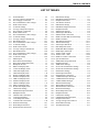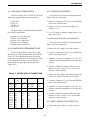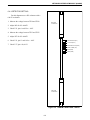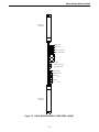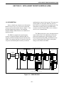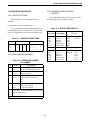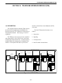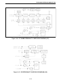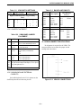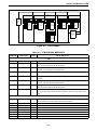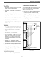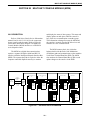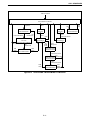
1
SET-UP AND
ALIGNMENT
MULTI-NET ® II SWITCH
MULTI-NET II
3000 SERIES
SWITCH
®
SET-UP AND
ALIGNMENT
October 2003
Supersedes: Part No. 001-3139-003/004; 5/99
MULTI-NET® II
3000 SERIES SWITCH
SETUP AND ALIGNMENT MANUAL
Copyright© 2003 by the EFJohnson Company
The EFJohnson Company, which was founded in 1923, provides wireless communication systems solutions for
public safety, government, and commercial customers. The company designs, manufactures, and markets conventional and trunked radio systems, mobile and portable subscriber radios, repeaters, and Project 25 digital radio
products. EFJohnson is a wholly owned subsidiary of EFJ, Inc.
Viking Head/EFJohnson logo, Multi-Net®, and LTR®are registered trademarks of the EFJohnson Company. All
other company and/or product names used in this manual are trademarks and/or registered trademarks of their
respective manufacturer.
Information in this manual is subject to change without notice. The EFJohnson Company will not be liable for any
misunderstanding due to misinformation or errors found in this document.
SAFETY INFORMATION
The FCC has adopted a safety standard for human exposure to RF energy. Proper operation of this radio under
normal conditions results in user exposure to RF energy below the Occupational Safety and Health Act and Federal
Communication Commission limits.
WARNING
DO NOT allow the antenna to touch or come in very close proximity with the eyes, face, or any exposed body
parts while the radio is transmitting.
DO NOT allow the antenna to come close to or touch, the eyes, face, or any exposed body parts while the radio is
transmitting.
DO NOT operate the radio in explosive or flammable atmospheres. The transmitted radio energy could trigger
blasting caps or cause an explosion.
DO NOT operate the radio without the proper antenna installed.
DO NOT operate the radio unless all radio frequency connectors are secure and any open connectors are properly
terminated.
DO NOT allow children to operate or play with this equipment.
NOTE: The above warning list is not intended to include all hazards that may be encountered when using this
radio.
This device complies with Part 15 of the FCC rules. Operation is subject to the condition that this device does not
cause harmful interference. In addition, changes or modifications to this equipment not expressly approved by
EFJohnson could void the user’s authority to operate this equipment (FCC rules, 47CFR Part 15.19).
LAND MOBILE PRODUCT WARRANTY
The manufacturer’s warranty statement for this product is available from your product supplier or from EFJohnson
Company, 299 Johnson Avenue, Box 1249, Waseca, MN 56093-0514. Phone (507) 835-6222.
TABLE OF CONTENTS
TABLE OF CONTENTS
1
INTRODUCTION
1.1
1.2
SCOPE OF MANUAL . . . . . . . . . . . . . . . . . . . 1-1
DEFINITIONS . . . . . . . . . . . . . . . . . . . . . . . . . . 1-1
Trunked System . . . . . . . . . . . . . . . . . . . . . . . . . . 1-1
LTR Trunked System . . . . . . . . . . . . . . . . . . . . . 1-1
Multi-Net Trunked System . . . . . . . . . . . . . . . . . 1-1
Conventional System . . . . . . . . . . . . . . . . . . . . . . 1-1
3000 Series Switch . . . . . . . . . . . . . . . . . . . . . . . 1-1
Call Processor . . . . . . . . . . . . . . . . . . . . . . . . . . . 1-1
System and Subscriber Manager . . . . . . . . . . . . . 1-1
Repeater Site . . . . . . . . . . . . . . . . . . . . . . . . . . . . 1-1
Home Repeater Channel . . . . . . . . . . . . . . . . . . . 1-1
Status Repeater Channel . . . . . . . . . . . . . . . . . . . 1-2
Monitor Repeater Channel. . . . . . . . . . . . . . . . . . 1-2
Telephone Interconnect and Data Transmission . 1-2
Public Switched Telephone Network (PSTN) . . . 1-2
Private Automatic Branch Exchange (PABX) . . 1-2
2
3000 SERIES SWITCH
2.1
2.2
2.3
INTRODUCTION. . . . . . . . . . . . . . . . . . . . . . . . 2-1
ELEMENTS OF THE SWITCH . . . . . . . . . . . . 2-2
SWITCH MODULES (ELEMENTS) . . . . . . . . 2-2
3
ARCHITECTURE
3.1
3.2
3.3
INTRODUCTION. . . . . . . . . . . . . . . . . . . . . . . .
SWITCH INTERFACES . . . . . . . . . . . . . . . . . .
BUS STRUCTURE . . . . . . . . . . . . . . . . . . . . . .
Data Bus. . . . . . . . . . . . . . . . . . . . . . . . . . . . . . . .
Control Bus . . . . . . . . . . . . . . . . . . . . . . . . . . . . .
Voice Bus. . . . . . . . . . . . . . . . . . . . . . . . . . . . . . .
4
SYSTEM RACK
4.1
TWO SHELF 3000 SERIES SWITCH . . . . . . 4-1
Power Consumption. . . . . . . . . . . . . . . . . . . . . . . 4-1
Equipment Required . . . . . . . . . . . . . . . . . . . . . . 4-1
Two Shelf Power Supply . . . . . . . . . . . . . . . . . . . 4-2
Power Supply Redundant Plate . . . . . . . . . . . . . . 4-2
Voltage Adjustments . . . . . . . . . . . . . . . . . . . . . . 4-2
Redundant Supply Adjustments . . . . . . . . . . . . . 4-2
Verify Fan Air Flow Direction . . . . . . . . . . . . . . 4-2
Verify Voltages on Power Distribution Cable. . . 4-3
System Test Procedure . . . . . . . . . . . . . . . . . . . . 4-3
Final Configuration Verification . . . . . . . . . . . . . 4-5
FOUR SHELF 3000 SERIES SWITCH . . . . . 4-7
Power Consumption. . . . . . . . . . . . . . . . . . . . . . . 4-7
Equipment Required . . . . . . . . . . . . . . . . . . . . . . 4-7
4-Shelf Power Supply . . . . . . . . . . . . . . . . . . . . . 4-7
Power Supply Redundant Plate . . . . . . . . . . . . . . 4-7
4.2
4.3
4.4
3-1
3-1
3-2
3-2
3-3
3-4
5
CALL PROCESSOR
5.1
5.2
5.3
INTRODUCTION . . . . . . . . . . . . . . . . . . . . . . . . 5-1
DATA BUSES . . . . . . . . . . . . . . . . . . . . . . . . . . 5-1
CALL PROCESSOR CONTROL . . . . . . . . . . 5-2
System Configuration . . . . . . . . . . . . . . . . . . . . 5-2
Manual Device Control . . . . . . . . . . . . . . . . . . . 5-2
Subscriber Management. . . . . . . . . . . . . . . . . . . 5-2
Activity Log Utilities . . . . . . . . . . . . . . . . . . . . . 5-2
Call Completion . . . . . . . . . . . . . . . . . . . . . . . . . 5-2
Keyboard Lock. . . . . . . . . . . . . . . . . . . . . . . . . . 5-3
Log Out/Log In . . . . . . . . . . . . . . . . . . . . . . . . . 5-3
ALARM CONTROL . . . . . . . . . . . . . . . . . . . . . 5-3
SYSTEM ANALYZER . . . . . . . . . . . . . . . . . . . 5-3
CALL PROCESSING . . . . . . . . . . . . . . . . . . . . 5-3
5.4
5.5
5.6
6
NETWORK INTERFACE MODULE
(NetNIM)
6.1
6.2
DESCRIPTION . . . . . . . . . . . . . . . . . . . . . . . . . 6-1
OPERATION . . . . . . . . . . . . . . . . . . . . . . . . . . . 6-1
LEDs . . . . . . . . . . . . . . . . . . . . . . . . . . . . . . . . . 6-2
SETUP PROCEDURE . . . . . . . . . . . . . . . . . . . 6-2
Jumpers . . . . . . . . . . . . . . . . . . . . . . . . . . . . . . . 6-2
Switches . . . . . . . . . . . . . . . . . . . . . . . . . . . . . . . 6-2
ALIGNMENT SPECIFICATIONS . . . . . . . . . . 6-2
Detector Setting . . . . . . . . . . . . . . . . . . . . . . . . . 6-3
6.3
6.4
i
Voltage Adjustments . . . . . . . . . . . . . . . . . . . . . 4-8
Redundant Supply Adjustments. . . . . . . . . . . . . 4-8
Verify Fan Air Flow Direction. . . . . . . . . . . . . . 4-8
Verify Voltages On Power Distribution Cable . 4-8
System Test Procedure. . . . . . . . . . . . . . . . . . . . 4-9
Final Configuration Verification . . . . . . . . . . . 4-11
SIX SHELF 3000 SERIES SWITCH . . . . . . 4-13
Power Consumption . . . . . . . . . . . . . . . . . . . . . 4-13
Equipment Required . . . . . . . . . . . . . . . . . . . . 4-13
Verify Resistance of Bus Bar and Power Supply
Lines . . . . . . . . . . . . . . . . . . . . . . . . . . . . . . 4-14
Verify Cooling Fan Air Flow Direction. . . . . . 4-14
Verify Voltages On Power Distribution Cable 4-14
System Test Procedure. . . . . . . . . . . . . . . . . . . 4-14
Final Configuration Verification . . . . . . . . . . . 4-17
EIGHT SHELF 3000 SERIES SWITCH. . . . 4-20
Power Consumption . . . . . . . . . . . . . . . . . . . . . 4-20
Equipment Required . . . . . . . . . . . . . . . . . . . . 4-20
Verify Resistance of Bus Bar and Power
Supply Lines . . . . . . . . . . . . . . . . . . . . . . . . 4-20
Verify Cooling Fan Air Flow Direction. . . . . . 4-21
Verify Voltages On Power Distribution Cable 4-21
System Test Procedure. . . . . . . . . . . . . . . . . . . 4-21
Final Configuration Verification . . . . . . . . . . . 4-23
TABLE OF CONTENTS
TABLE OF CONTENTS (CONT’D)
7
BASIC BOARD MODULE (BBM)
7.1
DESCRIPTION . . . . . . . . . . . . . . . . . . . . . . . . . 7-1
Main Audio . . . . . . . . . . . . . . . . . . . . . . . . . . . . . 7-1
Secondary Communication . . . . . . . . . . . . . . . . . 7-1
Internal Communication . . . . . . . . . . . . . . . . . . . 7-1
BBM SETUP PROCEDURE . . . . . . . . . . . . . . 7-3
Switch Settings . . . . . . . . . . . . . . . . . . . . . . . . . . 7-3
Jumper Placement . . . . . . . . . . . . . . . . . . . . . . . . 7-3
BBM Backplane External Connections . . . . . . . . 7-3
BBM ALIGNMENT PROCEDURES . . . . . . . 7-4
Introduction . . . . . . . . . . . . . . . . . . . . . . . . . . . . . 7-4
Alignment . . . . . . . . . . . . . . . . . . . . . . . . . . . . . . 7-4
TEST TASKS . . . . . . . . . . . . . . . . . . . . . . . . . . 7-5
System Switch Equals “1” . . . . . . . . . . . . . . . . . . 7-5
System Switch Equals “2” . . . . . . . . . . . . . . . . . . 7-5
System Switch Equals “3” . . . . . . . . . . . . . . . . . . 7-5
System Switch Equals “4” . . . . . . . . . . . . . . . . . . 7-5
System Switch Equals “5” . . . . . . . . . . . . . . . . . . 7-5
System Switch Equals “6” . . . . . . . . . . . . . . . . . . 7-5
System Switch Equals “7” . . . . . . . . . . . . . . . . . . 7-6
System Switch Equals “8” . . . . . . . . . . . . . . . . . . 7-6
System Switch Equals “9” . . . . . . . . . . . . . . . . . . 7-6
TROUBLESHOOTING. . . . . . . . . . . . . . . . . . . 7-6
Test “1” . . . . . . . . . . . . . . . . . . . . . . . . . . . . . . . . 7-6
Test “2” . . . . . . . . . . . . . . . . . . . . . . . . . . . . . . . . 7-7
Test “3” . . . . . . . . . . . . . . . . . . . . . . . . . . . . . . . . 7-7
Test “4” . . . . . . . . . . . . . . . . . . . . . . . . . . . . . . . . 7-7
Test “5” . . . . . . . . . . . . . . . . . . . . . . . . . . . . . . . . 7-8
Test “6” . . . . . . . . . . . . . . . . . . . . . . . . . . . . . . . . 7-9
Test “7” . . . . . . . . . . . . . . . . . . . . . . . . . . . . . . . . 7-9
Test “8” . . . . . . . . . . . . . . . . . . . . . . . . . . . . . . . . 7-9
Test “9” . . . . . . . . . . . . . . . . . . . . . . . . . . . . . . . . 7-9
DS1 DISPLAY DEFINITIONS. . . . . . . . . . . . . 7-9
7.2
7.3
7.4
7.5
7.6
8
CHANNEL INTERFACE MODULE
(CIM)
8.1
DESCRIPTION . . . . . . . . . . . . . . . . . . . . . . . . . 8-1
Repeater Signaling. . . . . . . . . . . . . . . . . . . . . . . . 8-1
Repeater Control . . . . . . . . . . . . . . . . . . . . . . . . . 8-1
Voice Connection . . . . . . . . . . . . . . . . . . . . . . . . 8-1
Internal Communication . . . . . . . . . . . . . . . . . . . 8-1
CIM SETUP PROCEDURE . . . . . . . . . . . . . . . 8-1
Switch Settings . . . . . . . . . . . . . . . . . . . . . . . . . . 8-1
Jumper Placement . . . . . . . . . . . . . . . . . . . . . . . . 8-2
CIM Backplane External Contacts . . . . . . . . . . . 8-2
External Connections. . . . . . . . . . . . . . . . . . . . . . 8-4
CIM ALIGNMENT SPECIFICATIONS . . . . . 8-4
Pre-Alignment . . . . . . . . . . . . . . . . . . . . . . . . . . . 8-4
CIM Alignment Procedure . . . . . . . . . . . . . . . . . 8-4
CIM AUDIO SUMMATION PERSONALITY
CARD . . . . . . . . . . . . . . . . . . . . . . . . . . . . . . . . 8-6
Internal Connections . . . . . . . . . . . . . . . . . . . . . . 8-6
8.2
8.3
8.4
External Connections . . . . . . . . . . . . . . . . . . . . . 8-6
Alignment Procedure . . . . . . . . . . . . . . . . . . . . . 8-6
9
CONVENTIONAL CHANNEL MODULE
(CCM)
9.1
DESCRIPTION. . . . . . . . . . . . . . . . . . . . . . . . . . 9-9
Repeater Signaling . . . . . . . . . . . . . . . . . . . . . . . 9-9
Repeater Control. . . . . . . . . . . . . . . . . . . . . . . . . 9-9
Voice Connection . . . . . . . . . . . . . . . . . . . . . . . . 9-9
Internal Communication . . . . . . . . . . . . . . . . . . . 9-9
CCM SETUP PROCEDURE . . . . . . . . . . . . . . 9-9
CCM Switch Settings . . . . . . . . . . . . . . . . . . . . . 9-9
AFSK Communication on the Main Lines . . . . . 9-9
CCM Jumper Placement. . . . . . . . . . . . . . . . . . . 9-9
CCM Backplane External Contacts . . . . . . . . . 9-10
CCM ALIGNMENT SPECIFICATIONS . . . . 9-10
Pre-Alignment . . . . . . . . . . . . . . . . . . . . . . . . . 9-10
CCM Alignment Procedure . . . . . . . . . . . . . . . 9-10
9.2
9.3
10
DISPATCH CHANNEL MODULE
(DCM)
10.1 DESCRIPTION. . . . . . . . . . . . . . . . . . . . . . . . . 10-1
Repeater Signaling . . . . . . . . . . . . . . . . . . . . . . 10-1
Repeater Control. . . . . . . . . . . . . . . . . . . . . . . . 10-1
Voice Connection . . . . . . . . . . . . . . . . . . . . . . . 10-1
Internal Communication . . . . . . . . . . . . . . . . . . 10-1
10.2 DCM SETUP PROCEDURE . . . . . . . . . . . . . 10-1
DCM Switch Settings . . . . . . . . . . . . . . . . . . . . 10-1
AFSK Communication on the Main Lines . . . . 10-1
DCM Jumper Placement. . . . . . . . . . . . . . . . . . 10-1
DCM Backplane External Contacts . . . . . . . . . 10-2
10.3 DCM ALIGNMENT SPECIFICATIONS . . . . 10-2
Pre-Alignment . . . . . . . . . . . . . . . . . . . . . . . . . 10-2
DCM Alignment Procedure . . . . . . . . . . . . . . . 10-2
11
DISPATCH INTERFACE MODULE
(DIM)
11.1 DESCRIPTION. . . . . . . . . . . . . . . . . . . . . . . . . 11-1
11.2 DIM SETUP PROCEDURE . . . . . . . . . . . . . . 11-1
Switch Settings . . . . . . . . . . . . . . . . . . . . . . . . . 11-1
DIM Jumper Placement . . . . . . . . . . . . . . . . . . 11-1
E-Lead Selection. . . . . . . . . . . . . . . . . . . . . . . . 11-2
DIM Backplane External Contacts . . . . . . . . . . 11-2
11.3 DIM ALIGNMENT SPECIFICATION . . . . . . 11-2
Pre-Alignment . . . . . . . . . . . . . . . . . . . . . . . . . 11-2
Pre-Alignment With Tone Remote Personality
Card . . . . . . . . . . . . . . . . . . . . . . . . . . . . . . . 11-2
11.4 ALIGNMENT . . . . . . . . . . . . . . . . . . . . . . . . . . 11-3
11.5 TONE REMOTE DTMF OPERATION . . . . . 11-4
ii
TABLE OF CONTENTS
TABLE OF CONTENTS (CONT’D)
12
INTELLIGENT DISPATCH MODULE
(IDM)
14.3 LED STATUS FOR E&M LEADS. . . . . . . . . 14-7
TELCO Side Status . . . . . . . . . . . . . . . . . . . . . 14-7
E&M Logic Status . . . . . . . . . . . . . . . . . . . . . . 14-7
14.4 E&M LEAD CIRCUIT THEORY OF
OPERATION . . . . . . . . . . . . . . . . . . . . . . . . . 14-8
E&M Interface . . . . . . . . . . . . . . . . . . . . . . . . . 14-8
Signal Conditioning . . . . . . . . . . . . . . . . . . . . . 14-8
14.5 TIM SETUP PROCEDURE . . . . . . . . . . . . . 14-11
TIM Jumper Placement . . . . . . . . . . . . . . . . . 14-11
Main Board Switch Settings . . . . . . . . . . . . . . 14-11
14.6 2WY SETUP AND ALIGNMENT
PROCEDURES (-670) . . . . . . . . . . . . . . . . 14-11
2WY Jumper Setup. . . . . . . . . . . . . . . . . . . . . 14-11
2WY Pre-Alignment Procedures . . . . . . . . . . 14-11
14.7 2-WAY TIM ALIGNMENT
PROCEDURES (-670) . . . . . . . . . . . . . . . . 14-13
Main Receive . . . . . . . . . . . . . . . . . . . . . . . . . 14-13
Dial Tone Detector . . . . . . . . . . . . . . . . . . . . . 14-13
Output Hybrid Adjust . . . . . . . . . . . . . . . . . . . 14-14
14.8 DID SETUP AND ALIGNMENT (-660) . . . 14-15
DID Personality Card Jumper Settings. . . . . . 14-15
Pre-Alignment . . . . . . . . . . . . . . . . . . . . . . . . 14-15
14.9 DID OPERATIONAL ALIGNMENT
PROCEDURES (-660) . . . . . . . . . . . . . . . . 14-16
14.10 E&M SETUP AND ALIGNMENT (-680) . . 14-17
Equipment Required . . . . . . . . . . . . . . . . . . . . 14-17
Transmit Alignment . . . . . . . . . . . . . . . . . . . . 14-17
Receiver Alignment . . . . . . . . . . . . . . . . . . . . 14-18
4-Wire E&M Dial Tone Detector Receive
Alignment. . . . . . . . . . . . . . . . . . . . . . . . . . 14-18
14.11 TERMSET MODULES . . . . . . . . . . . . . . . . . 14-23
Equipment Setup. . . . . . . . . . . . . . . . . . . . . . . 14-23
Initializing the Tellabs Cards . . . . . . . . . . . . . 14-23
Switch Settings On 6132A (DID
Applications) . . . . . . . . . . . . . . . . . . . . . . . 14-24
XEL Termset Rack . . . . . . . . . . . . . . . . . . . . . 14-25
Connection To the Phone Lines . . . . . . . . . . . 14-26
Final Path Inspection . . . . . . . . . . . . . . . . . . . 14-27
14.12 BACKGROUND INFORMATION . . . . . . . . 14-27
Standard Signal. . . . . . . . . . . . . . . . . . . . . . . . 14-27
Outlined Objective . . . . . . . . . . . . . . . . . . . . . 14-27
The Order of Things . . . . . . . . . . . . . . . . . . . . 14-27
14.13 TUNING A DOD OR DID 2-WIRE INTERFACE
TO THE 4-WIRE E&M BOARD.. . . . . . . . 14-28
14.14 BALANCING TO THE CENTRAL
OFFICE. . . . . . . . . . . . . . . . . . . . . . . . . . . . . 14-30
Introduction . . . . . . . . . . . . . . . . . . . . . . . . . . 14-30
Statistics . . . . . . . . . . . . . . . . . . . . . . . . . . . . . 14-30
Adding Capacitance to the Termset . . . . . . . . 14-30
Rural Areas . . . . . . . . . . . . . . . . . . . . . . . . . . . 14-30
Urban Areas . . . . . . . . . . . . . . . . . . . . . . . . . . 14-30
14.15 FCC USER INSTRUCTIONS AND
CUSTOMER INFORMATION . . . . . . . . . . 14-31
12.1 DESCRIPTION . . . . . . . . . . . . . . . . . . . . . . . . 12-1
12.2 IDM SETUP PROCEDURE . . . . . . . . . . . . . . 12-2
Switch Settings . . . . . . . . . . . . . . . . . . . . . . . . . 12-2
IDM Jumper Placement . . . . . . . . . . . . . . . . . . . 12-2
IDM Backplane External Contacts . . . . . . . . . . 12-2
12.3 IDM ALIGNMENT SPECIFICATION . . . . . . 12-4
Pre-Alignment . . . . . . . . . . . . . . . . . . . . . . . . . . 12-4
12.4 ALIGNMENT . . . . . . . . . . . . . . . . . . . . . . . . . . 12-4
12.5 PCM SUMMATION PERSONALITY CARD12-5
Internal Connections . . . . . . . . . . . . . . . . . . . . . 12-5
External Connections. . . . . . . . . . . . . . . . . . . . . 12-5
Alignment Procedure . . . . . . . . . . . . . . . . . . . . . 12-5
13
SYSTEM NETWORK MODULE (SNM)
13.1 DESCRIPTION . . . . . . . . . . . . . . . . . . . . . . . .
13.2 SNM SETUP PROCEDURE . . . . . . . . . . . . .
SNM Switch Settings. . . . . . . . . . . . . . . . . . . . .
AFSK Communication on the Main Lines . . . .
SNM Jumper Placement . . . . . . . . . . . . . . . . . .
SNM Backplane External Contacts . . . . . . . . . .
13.3 SNM ALIGNMENT SPECIFICATIONS . . . .
Pre-Alignment . . . . . . . . . . . . . . . . . . . . . . . . . .
SNM Alignment Procedure . . . . . . . . . . . . . . . .
14
13-1
13-2
13-2
13-2
13-2
13-2
13-2
13-2
13-2
TELEPHONE INTERFACE MODULE
(TIM)
14.1 DESCRIPTION . . . . . . . . . . . . . . . . . . . . . . . . 14-1
Supervision . . . . . . . . . . . . . . . . . . . . . . . . . . . . 14-2
Signaling . . . . . . . . . . . . . . . . . . . . . . . . . . . . . . 14-2
Call Supervision. . . . . . . . . . . . . . . . . . . . . . . . . 14-2
Intra-terminal Communication . . . . . . . . . . . . . 14-2
Telephone Line Styles . . . . . . . . . . . . . . . . . . . . 14-3
Audio Processing . . . . . . . . . . . . . . . . . . . . . . . . 14-3
Receive Audio . . . . . . . . . . . . . . . . . . . . . . . . . . 14-3
Transmit Audio . . . . . . . . . . . . . . . . . . . . . . . . . 14-4
14.2 4-WIRE E&M INTERFACE DESCRIPTION 14-4
Audio . . . . . . . . . . . . . . . . . . . . . . . . . . . . . . . . . 14-4
E&M Leads . . . . . . . . . . . . . . . . . . . . . . . . . . . . 14-4
8-position Dip Switch S201. . . . . . . . . . . . . . . . 14-5
Type I and V . . . . . . . . . . . . . . . . . . . . . . . . . . . 14-6
Type II and III . . . . . . . . . . . . . . . . . . . . . . . . . . 14-6
Type IV . . . . . . . . . . . . . . . . . . . . . . . . . . . . . . . 14-6
Type II Trunk-To-Trunk . . . . . . . . . . . . . . . . . . 14-6
Type V Trunk-to-Trunk . . . . . . . . . . . . . . . . . . . 14-7
iii
TABLE OF CONTENTS
TABLE OF CONTENTS (CONT’D)
15
VOTER DIAGNOSTICS MODULE
(VDM)
15.1 DESCRIPTION . . . . . . . . . . . . . . . . . . . . . . . .
15.2 VDM SETUP PROCEDURE . . . . . . . . . . . . .
Switch Settings . . . . . . . . . . . . . . . . . . . . . . . . .
Jumper Placement . . . . . . . . . . . . . . . . . . . . . . .
VDM Backplane External Contacts. . . . . . . . . .
15.3 VDM ALIGNMENT SPECIFICATIONS . . . .
16
20
20.1 DESCRIPTION. . . . . . . . . . . . . . . . . . . . . . . . . 20-1
20.2 MCM SETUP PROCEDURE . . . . . . . . . . . . . 20-2
Switch Settings . . . . . . . . . . . . . . . . . . . . . . . . . 20-2
MCM Jumper Placement . . . . . . . . . . . . . . . . . 20-2
MCM Backplane External Contacts . . . . . . . . . 20-2
20.3 MCM ALIGNMENT SPECIFICATION . . . . . 20-2
Pre-Alignment . . . . . . . . . . . . . . . . . . . . . . . . . 20-2
20.4 ALIGNMENT . . . . . . . . . . . . . . . . . . . . . . . . . . 20-3
20.5 PCM SUMMATION PERSONALITY CARD20-4
Internal Connections. . . . . . . . . . . . . . . . . . . . . 20-4
External Connections . . . . . . . . . . . . . . . . . . . . 20-4
Alignment Procedure . . . . . . . . . . . . . . . . . . . . 20-4
15-1
15-1
15-1
15-2
15-2
15-2
POWER TERMINATION MODULE
(PTM)
16.1 DESCRIPTION . . . . . . . . . . . . . . . . . . . . . . . . 16-1
16.2 SETUP PROCEDURE . . . . . . . . . . . . . . . . . . 16-1
17
LOGGING ENCODER MODULE (LEM)
21
17.1 DESCRIPTION . . . . . . . . . . . . . . . . . . . . . . . .
17.2 LEM SETUP PROCEDURE . . . . . . . . . . . . .
LEM Switch Settings . . . . . . . . . . . . . . . . . . . . .
LEM Jumper Placement . . . . . . . . . . . . . . . . . .
LEM Backplane External Contacts . . . . . . . . . .
17.3 LEM ALIGNMENT SPECIFICATIONS . . . .
Pre-Alignment . . . . . . . . . . . . . . . . . . . . . . . . . .
LEM Alignment Procedure . . . . . . . . . . . . . . . .
18
17-1
17-2
17-2
17-2
17-2
17-2
17-2
17-2
CONVENTIONAL PATCH MODULE
(CPM)
21.1 DESCRIPTION. . . . . . . . . . . . . . . . . . . . . . . . . 21-1
21.2 PCM SETUP PROCEDURE . . . . . . . . . . . . . 21-1
Switch Settings . . . . . . . . . . . . . . . . . . . . . . . . . 21-1
CPM Jumper Placement . . . . . . . . . . . . . . . . . . 21-1
E-Lead Selection. . . . . . . . . . . . . . . . . . . . . . . . 21-2
CPM Backplane External Contacts . . . . . . . . . 21-2
21.3 CPM ALIGNMENT SPECIFICATION . . . . . 21-2
Pre-Alignment . . . . . . . . . . . . . . . . . . . . . . . . . 21-2
Alignment . . . . . . . . . . . . . . . . . . . . . . . . . . . . . 21-2
VOICE TONE MODULE (VTM)
18.1 DESCRIPTION . . . . . . . . . . . . . . . . . . . . . . . .
18.2 SETUP PROCEDURE . . . . . . . . . . . . . . . . . .
VTM Jumper Placement . . . . . . . . . . . . . . . . . .
VTM Switch Settings . . . . . . . . . . . . . . . . . . . .
18.3 ALIGNMENT SPECIFICATIONS . . . . . . . . .
19
MULTI-NET CONSOLE MODULE
(MCM)
18-1
18-1
18-1
18-1
18-1
22
POWER SUPPLY
22.1 INTRODUCTION . . . . . . . . . . . . . . . . . . . . . . . 22-1
22.2 POWER CONSUMPTION . . . . . . . . . . . . . . . 22-1
WIDE AREA MODULE (WAM)
19.1 DESCRIPTION . . . . . . . . . . . . . . . . . . . . . . . . 19-1
19.2 WAM SETUP PROCEDURE . . . . . . . . . . . . 19-2
WAM Switch Settings . . . . . . . . . . . . . . . . . . . . 19-2
WAM Jumper Placement. . . . . . . . . . . . . . . . . . 19-2
WAM Backplane External Contacts . . . . . . . . . 19-2
19.3 WAM ALIGNMENT SPECIFICATIONS . . . 19-2
Pre-Alignment . . . . . . . . . . . . . . . . . . . . . . . . . . 19-2
WAM Alignment Procedure . . . . . . . . . . . . . . . 19-2
19.4 WAM E&M-LEAD CONNECTIONS . . . . . . 19-4
One Location . . . . . . . . . . . . . . . . . . . . . . . . . . . 19-5
Two Locations . . . . . . . . . . . . . . . . . . . . . . . . . . 19-5
Three Locations . . . . . . . . . . . . . . . . . . . . . . . . . 19-5
19.5 M-LEAD SPLITTER BOX . . . . . . . . . . . . . . . 19-5
General. . . . . . . . . . . . . . . . . . . . . . . . . . . . . . . . 19-5
Installation . . . . . . . . . . . . . . . . . . . . . . . . . . . . . 19-5
19.6 WAM AUDIO CONNECTIONS. . . . . . . . . . . 19-6
23
BACKPLANE
23.1 DESCRIPTION. . . . . . . . . . . . . . . . . . . . . . . . . 23-1
23.2 BACKPLANE SETUP PROCEDURE . . . . . 23-1
Shelf Address Settings . . . . . . . . . . . . . . . . . . . 23-1
Termination Settings. . . . . . . . . . . . . . . . . . . . . 23-1
Jumper Definitions and Settings. . . . . . . . . . . . 23-1
23.3 STANDARD SHELF I/O CONNECTIONS . 23-2
23.4 CIM SHELF I/O CONNECTIONS . . . . . . . . . 23-3
Primary PCM . . . . . . . . . . . . . . . . . . . . . . . . . . 23-3
Secondary PCM . . . . . . . . . . . . . . . . . . . . . . . . 23-3
23.5 NetNIM SHELF WITH CIM/CCMs . . . . . . . . 23-4
23.6 NetNIM SHELF WITHOUT CIM/CCMs . . . . 23-5
iv
TABLE OF CONTENTS
TABLE OF CONTENTS (CONT’D)
24
INTERCOM
B.2
24.1 DESCRIPTION . . . . . . . . . . . . . . . . . . . . . . . .
24.2 INSTALLATION . . . . . . . . . . . . . . . . . . . . . . .
Equipment Required . . . . . . . . . . . . . . . . . . . . .
Installation Procedure . . . . . . . . . . . . . . . . . . . .
APPENDIX A
A.1
A.2
24-1
24-1
24-1
24-1
ERROR MESSAGES
IDB Error Messages To Message
Accounting Bus From Modules . . . . . . . .A-1
MAB Error Messages From System
Management Module . . . . . . . . . . . . . . . . . .A-2
APPENDIX B
B.1
Dispatch Console (DC) To Mobile Group
Call . . . . . . . . . . . . . . . . . . . . . . . . . . . . . . . . . B-1
B.3 Mobile Group Call To Dispatch Console . B-1
B.4 Mobile To Unique ID . . . . . . . . . . . . . . . . . . . B-2
B.5 Mobile To Unique ID For a Mobile Outside
Switch . . . . . . . . . . . . . . . . . . . . . . . . . . . . . . B-3
B.6 Mobile To Directed Group Call (DTMF
Entry Within Switch) . . . . . . . . . . . . . . . . . B-3
B.7 Mobile To Directed Group Call (DTMF
Entry Outside the Switch)B-4
B.8 Mobile Originated Telephone Call. . . . . . . B-5
B.9 Landside (TIM) Originate To Mobile
Within Switch Using a DID Line . . . . . . . B-6
B.10 Landside (TIM) Originate To Mobile
Within Switch Using a 2WY Line . . . . . . B-6
B.11 TIM Originate To Mobile Outside Switch
Using a DID Line . . . . . . . . . . . . . . . . . . . . . B-7
B.12 Landside Originate To Mobile Outside
Switch Using a 2WY Line . . . . . . . . . . . . . B-7
CALL SEQUENCES
GROUP CALL . . . . . . . . . . . . . . . . . . . . . . . . . . B-1
Mobile To Mobile On Same Site. . . . . . . . . . . . B-1
Mobile To Mobile With DIM Monitoring. . . . . B-1
LIST OF FIGURES
2-1
2-2
2-3
2-4
3-1
3-2
3-3
3-4
4-1
4-2
4-3
4-4
4-5
4-6
4-7
4-8
4-9
4-10
5-1
6-1
6-2
6-3
7-1
7-2
7-3
8-1
8-2
8-3
9-1
10-1
11-1
11-2
11-3
12-1
12-2
12-3
13-1
13-2
13-3
14-1
14-2
14-3
14-4
14-5
2-Shelf 3000 Series Switch . . . . . . . . . . . . . . . . 2-3
4-Shelf 3000 Series Switch . . . . . . . . . . . . . . . . 2-3
6-Shelf Switch Rack Layout . . . . . . . . . . . . . . . 2-4
8-Shelf Switch Rack Setup . . . . . . . . . . . . . . . . 2-5
Multi-Net System Switch . . . . . . . . . . . . . . . . . 3-1
Data Buses . . . . . . . . . . . . . . . . . . . . . . . . . . . . . 3-2
Control Buses. . . . . . . . . . . . . . . . . . . . . . . . . . . 3-3
Voice Buses . . . . . . . . . . . . . . . . . . . . . . . . . . . . 3-4
2-shelf 3000 Series Switch Backplane Cables. . 4-6
2-shelf 3000 Series Switch Setup . . . . . . . . . . . 4-6
4-shelf 3000 Series Switch Backplane Cables. 4-12
4-shelf 3000 Series Switch Setup . . . . . . . . . . 4-12
Six Shelf 3000 Series Switch Backplane Cables 4-18
Six Shelf 3000 Series Switch Setup. . . . . . . . . 4-19
Eight Shelf 3000 Series Sw Backplane Cables 4-25
8-Shelf 3000 Series Switch Rack Setup . . . . . 4-26
2-4 Shelf Power Supply Interconnect . . . . . . . 4-27
6-8 Shelf Power Supply Interconnect Diagram 4-28
Data Buses . . . . . . . . . . . . . . . . . . . . . . . . . . . . . 5-1
Data Bus Block Diagram . . . . . . . . . . . . . . . . . . 6-1
NetNIM Card Edge Layout . . . . . . . . . . . . . . . . 6-3
NetNIM Alignment Points Diagram . . . . . . . . . 6-4
v
Basic Board Module Block Diagram . . . . . . . . . 7-2
Basic Board Module Align Points Diagram . . . 7-12
Basic Board Module Card Edge Layout. . . . . . 7-13
Alignment Points Diagram . . . . . . . . . . . . . . . . . 8-3
CIM Input and Output Levels. . . . . . . . . . . . . . . 8-5
Summation Board Alignment Points Diagram. . 8-7
Alignment Points Diagram . . . . . . . . . . . . . . . . 9-11
Alignment Points Diagram . . . . . . . . . . . . . . . . 10-3
Alignment Points Diagram . . . . . . . . . . . . . . . . 11-5
PTT Tone Remote Card Block Diagram . . . . . 11-6
PTT Tone Remote Card Alignment Points Diag 11-7
IDM Data Bus. . . . . . . . . . . . . . . . . . . . . . . . . . 12-1
Alignment Points Diagram . . . . . . . . . . . . . . . . 12-3
Summation Board Alignment Points Diagram. 12-6
Data Bus Block Diagram . . . . . . . . . . . . . . . . . 13-1
Alignment Points Diagram . . . . . . . . . . . . . . . . 13-3
SNM Cable Layout. . . . . . . . . . . . . . . . . . . . . . 13-4
Data Buses . . . . . . . . . . . . . . . . . . . . . . . . . . . . 14-1
E&M Interface Connections. . . . . . . . . . . . . . . 14-5
S201 . . . . . . . . . . . . . . . . . . . . . . . . . . . . . . . . . 14-5
TYPE I and V . . . . . . . . . . . . . . . . . . . . . . . . . . 14-6
TYPE II and III. . . . . . . . . . . . . . . . . . . . . . . . . 14-6
TABLE OF CONTENTS
LIST OF FIGURES (CONT’D)
14-6
14-7
14-8
14-9
14-10
14-11
14-12
14-13
14-14
14-15
14-16
14-17
14-18
14-19
14-20
14-21
14-22
14-23
14-24
14-25
14-26
14-27
14-28
14-29
15-1
15-2
15-3
16-1
17-1
17-2
18-1
18-2
19-1
19-2
19-3
19-4
19-5
19-6
19-7
19-8
19-9
19-10
20-1
20-2
20-3
21-1
22-1
22-2
22-3
22-4
22-5
22-6
22-7
22-8
22-9
23-1
23-2
23-3
23-4
23-5
23-6
23-7
23-8
23-9
23-10
23-11
23-12
23-13
23-14
23-15
23-16
23-17
B-1
B-2
B-3
B-4
B-5
B-6
B-7
B-8
TYPE IV . . . . . . . . . . . . . . . . . . . . . . . . . . . . . 14-6
TYPE II Trunk-Trunk . . . . . . . . . . . . . . . . . . . 14-7
TYPE IV Trunk-Trunk . . . . . . . . . . . . . . . . . . 14-7
E&M Personality Board . . . . . . . . . . . . . . . . . 14-7
Main Board . . . . . . . . . . . . . . . . . . . . . . . . . . . 14-7
Type III Interface . . . . . . . . . . . . . . . . . . . . . . . 14-8
Charging Characteristic of C227 . . . . . . . . . . . 14-8
4-Wire E&M Block Diagram (-680) . . . . . . . . 14-9
DT & MBS Personality Card Blk Diag (-670) 14-10
DID Personality Card Block Diagram (-660) 14-10
Transmit Diagram . . . . . . . . . . . . . . . . . . . . . 14-18
Receive Diagram . . . . . . . . . . . . . . . . . . . . . . 14-18
Alignment Points Diagram . . . . . . . . . . . . . . 14-19
DT & MBS Alignment Points Diagram (-670) 14-20
DID Alignment Points Diagram (-660) . . . . . 14-21
4-Wire E&M Alignment Points Diag (-680) . 14-22
TELLABS 6132B - POTS . . . . . . . . . . . . . . . 14-23
TELLABS 6132A - DID . . . . . . . . . . . . . . . . 14-24
XEL Termset Rack (Rear Close-up) . . . . . . . 14-25
Termset Rack (Front View) . . . . . . . . . . . . . . 14-26
Network Link (Switch Rack Back View) . . . 14-26
E&M Interface . . . . . . . . . . . . . . . . . . . . . . . . 14-28
Tellabs 6132A/B Termset . . . . . . . . . . . . . . . 14-29
6132 Tellabs Card . . . . . . . . . . . . . . . . . . . . . 14-31
Data Buses . . . . . . . . . . . . . . . . . . . . . . . . . . . . 15-1
VDM Connections . . . . . . . . . . . . . . . . . . . . . . 15-2
Alignment Points Diagram . . . . . . . . . . . . . . . 15-3
Power Termination Mod Align Points Diag . . 16-2
Data Bus Block Diagram . . . . . . . . . . . . . . . . . 17-1
Alignment Points Diagram . . . . . . . . . . . . . . . 17-4
Voice Buses . . . . . . . . . . . . . . . . . . . . . . . . . . . 18-2
VTM Card Edge Layout . . . . . . . . . . . . . . . . . 18-3
Data Bus Block Diagram . . . . . . . . . . . . . . . . . 19-1
Alignment Points Diagram . . . . . . . . . . . . . . . 19-3
WAM E&M Lead Cable Layout 1 Location . . 19-4
WAM E&M Lead Cable Layout 2 Locations . 19-5
M-Lead Splitter Box I/Os . . . . . . . . . . . . . . . . 19-5
WAM E&M Lead Cable Layout 3 Locations . 19-6
WAM Audio Cable Layout One Location. . . . 19-6
WAM Audio Cable Layout Two Locations . . 19-6
vi
Audio Cable Lay. Two Loc. w/Ext Audio Dev 19-7
Audio Cable Lay. Host Loc. 3 Location Config 19-7
Data Bus Block Diagram . . . . . . . . . . . . . . . . . 20-1
Alignment Points Diagram . . . . . . . . . . . . . . . . 20-5
Summation Board (-760) Align Points Diagram 20-6
CPM Alignment Points Diagram . . . . . . . . . . . 21-3
Power Supply . . . . . . . . . . . . . . . . . . . . . . . . . . 22-1
6-8 Shelf Power Supply Interconnect Diagram 22-2
A3-A4 Connector . . . . . . . . . . . . . . . . . . . . . . . 22-3
A5-A6 Connector . . . . . . . . . . . . . . . . . . . . . . . 22-3
Power Supply Terminal Blocks . . . . . . . . . . . . 22-3
Power Supply Drawer. . . . . . . . . . . . . . . . . . . . 22-4
2-4 Shelf Power Supply Interconnect. . . . . . . . 22-5
2-4 Shelf Power Supply (Front View) . . . . . . . 22-6
2-4 Shelf Power Supply (Rear View) . . . . . . . . 22-6
Std Shelf Backplane Sw and Jumper Settings . 23-2
S2 - S8 Switch Settings . . . . . . . . . . . . . . . . . . 23-3
CIM/CCM Shelf Backplane Sw & Jmpr Set. . . 23-3
NetNIM Shelf w/CIM/CCMs Sw & Jmpr Set.. 23-4
NetNIM Shelf w/o CIM/CCMs Sw & Jmpr Set. 23-5
2-Shelf 3000 Series Switch. . . . . . . . . . . . . . . . 23-6
4-Shelf 3000 Series Switch. . . . . . . . . . . . . . . . 23-6
6-Shelf Switch Rack Layout. . . . . . . . . . . . . . . 23-7
8-Shelf Switch Rack Setup . . . . . . . . . . . . . . . . 23-8
2-Shelf Switch Backplane Cables. . . . . . . . . . . 23-9
4-Shelf Switch Backplane Cables. . . . . . . . . . . 23-9
6-Shelf Switch Backplane Cables. . . . . . . . . . 23-10
8-Shelf Switch Backplane Cables. . . . . . . . . . 23-11
Basic Board Backplane Wiring Layout . . . . . 23-12
NetNIM Shelf Backplane Wiring Layout. . . . 23-12
Telephone Terminal Block Layout. . . . . . . . . 23-13
Backplane I/O Jacks . . . . . . . . . . . . . . . . . . . . 23-14
SNM Unique ID Request Flowchart . . . . . . . . B-8
DIM Unique ID Request Flowchart . . . . . . . . . B-9
CIM DTMF Auxiliary Call Flowchart . . . . . . . B-9
Dialed Digits and Number of Digits Flowchart B-10
Telephone TIM Incoming Flowchart . . . . . . . B-11
Telephone Calling CIM Call Req Flowchart . B-12
Dynamic Reass User Interface Req Flowchart B-13
Selective Unit Dis User Interface Req Flow . B-13
TABLE OF CONTENTS
LIST OF TABLES
2-1
4-1
4-2
4-3
4-4
4-5
4-6
4-7
4-9
4-8
4-10
4-11
4-12
4-13
4-15
4-14
4-16
4-17
4-18
4-19
4-20
6-1
7-1
7-2
7-3
7-4
7-5
7-6
7-7
7-9
7-8
7-11
7-12
7-13
7-10
7-14
8-1
8-2
8-3
8-4
9-1
9-2
9-3
10-1
10-2
10-3
11-1
11-2
11-3
11-4
12-1
12-2
12-3
13-1
13-2
13-3
14-1
14-2
14-3
14-4
14-5
14-6
14-7
14-8
14-9
14-10
14-11
14-12
15-2
15-3
15-1
16-1
16-2
17-1
17-2
17-3
18-1
18-2
18-3
19-1
19-2
19-3
20-1
20-2
20-3
21-1
21-2
21-3
22-1
23-1
23-2
Switch Modules . . . . . . . . . . . . . . . . . . . . . . . . . 2-2
Average Voltage/Current/Power . . . . . . . . . . . . 4-1
Power Supply Connections . . . . . . . . . . . . . . . . . 4-2
Power Distribution Cable Voltages . . . . . . . . . . 4-3
PCM Cable Location . . . . . . . . . . . . . . . . . . . . . 4-3
S1 Switch Settings . . . . . . . . . . . . . . . . . . . . . . . 4-4
Average Voltage/current/power . . . . . . . . . . . . . 4-7
Power Supply Connections . . . . . . . . . . . . . . . . . 4-8
PCM Cable Location . . . . . . . . . . . . . . . . . . . . . 4-9
Power Distribution Cable Voltages . . . . . . . . . . 4-9
S1 Switch Settings . . . . . . . . . . . . . . . . . . . . . . . 4-9
Average Voltage/Current/Power . . . . . . . . . . . 4-13
Bus Bar Resistance . . . . . . . . . . . . . . . . . . . . . . 4-13
Power Distribution Cable Voltages . . . . . . . . . 4-14
S1 Switch Settings . . . . . . . . . . . . . . . . . . . . . . 4-15
PCM Cable Location . . . . . . . . . . . . . . . . . . . . 4-15
Average Voltage/Current/Power . . . . . . . . . . . 4-20
Bus Bar Resistance . . . . . . . . . . . . . . . . . . . . . . 4-20
Power Distribution Cable Voltages . . . . . . . . . 4-21
PCM Cable Location . . . . . . . . . . . . . . . . . . . . 4-21
S1 Switch Settings . . . . . . . . . . . . . . . . . . . . . . 4-22
NIM Jumpers . . . . . . . . . . . . . . . . . . . . . . . . . . . 6-2
Basic Board Switch Settings . . . . . . . . . . . . . . . . 7-3
Basic Board Jumper Placement . . . . . . . . . . . . . 7-3
Backplane Pin-outs . . . . . . . . . . . . . . . . . . . . . . . 7-3
DIM Card Display/tasks . . . . . . . . . . . . . . . . . . . 7-9
CCM Card Display Tasks . . . . . . . . . . . . . . . . . . 7-9
CIM Card Display/tasks . . . . . . . . . . . . . . . . . . 7-10
TIM Card Display/tasks . . . . . . . . . . . . . . . . . . 7-10
DCM Card Display/tasks . . . . . . . . . . . . . . . . . 7-10
SNM Card Display/tasks . . . . . . . . . . . . . . . . . 7-10
LEM Card Display/tasks . . . . . . . . . . . . . . . . . . 7-11
GPM Card Display/tasks . . . . . . . . . . . . . . . . . 7-11
VDM Card Display/tasks . . . . . . . . . . . . . . . . . 7-11
IDM Card Display/tasks . . . . . . . . . . . . . . . . . . 7-11
WAM Card Display/tasks . . . . . . . . . . . . . . . . . 7-11
CIM Switch Settings . . . . . . . . . . . . . . . . . . . . . . 8-2
CIM Board Jumper Placement . . . . . . . . . . . . . . 8-2
Backplane Pinouts . . . . . . . . . . . . . . . . . . . . . . . 8-2
CIM External Connections . . . . . . . . . . . . . . . . . 8-4
CCM Switch Settings . . . . . . . . . . . . . . . . . . . . . 9-9
CCM Jumper Placement . . . . . . . . . . . . . . . . . . . 9-9
CCM External Connections . . . . . . . . . . . . . . . 9-10
DCM Switch Settings . . . . . . . . . . . . . . . . . . . . 10-1
DCM Jumper Placement . . . . . . . . . . . . . . . . . . 10-1
DCM External Connections . . . . . . . . . . . . . . . 10-2
vii
DIM Switch Settings . . . . . . . . . . . . . . . . . . . . . 11-1
DIM Board Jumper Placement . . . . . . . . . . . . . 11-1
Backplane Placement . . . . . . . . . . . . . . . . . . . . . 11-2
Tone Remote Formats . . . . . . . . . . . . . . . . . . . . 11-4
IDM Switch Settings . . . . . . . . . . . . . . . . . . . . . 12-2
IDM Board Jumper Placement . . . . . . . . . . . . . 12-2
Backplane Pinouts . . . . . . . . . . . . . . . . . . . . . . .12-2
SNM Switch Settings . . . . . . . . . . . . . . . . . . . . . 13-2
SNM Jumper Placement . . . . . . . . . . . . . . . . . . 13-2
SNM External Connections . . . . . . . . . . . . . . . . 13-2
E&M Card S201 DIP Switch Settings . . . . . . . . 14-5
E&M Lead States . . . . . . . . . . . . . . . . . . . . . . . . 14-6
TIM Jumper Placement . . . . . . . . . . . . . . . . . . 14-11
TIM Switch Settings . . . . . . . . . . . . . . . . . . . . 14-11
2WY Jumper Placement . . . . . . . . . . . . . . . . . 14-11
DID Jumper Placement . . . . . . . . . . . . . . . . . . 14-15
E&M Main Board Jumpers . . . . . . . . . . . . . . . 14-17
E&M Jumper Placement . . . . . . . . . . . . . . . . . 14-17
Tellabs 6132B - POTS . . . . . . . . . . . . . . . . . . . 14-23
Tellabs 6132A - DID . . . . . . . . . . . . . . . . . . . . 14-24
E&M To Termset Connections . . . . . . . . . . . . 14-27
System Information . . . . . . . . . . . . . . . . . . . . . 14-31
VDM Board Jumper Placement . . . . . . . . . . . . . 15-2
Backplane Pinouts . . . . . . . . . . . . . . . . . . . . . . .15-2
VDM Switch Settings . . . . . . . . . . . . . . . . . . . . 15-2
S5/S7 Switch Termination Settings . . . . . . . . . . 16-1
S6/S8 Switch Termination Settings . . . . . . . . . . 16-1
LEM Switch Settings . . . . . . . . . . . . . . . . . . . . . 17-2
LEM Jumper Placement . . . . . . . . . . . . . . . . . . 17-2
LEM External Connections . . . . . . . . . . . . . . . . 17-2
VTM Board Jumper Placement . . . . . . . . . . . . . 18-1
VTM Board Switch Settings . . . . . . . . . . . . . . . 18-1
VTM PCM Bus Messages . . . . . . . . . . . . . . . . . 18-2
WAM Switch Settings . . . . . . . . . . . . . . . . . . . . 19-2
WAM Jumper Placement . . . . . . . . . . . . . . . . . . 19-2
WAM External Connections . . . . . . . . . . . . . . . 19-2
MCM Switch Settings . . . . . . . . . . . . . . . . . . . . 20-2
MCM Jumper Placement . . . . . . . . . . . . . . . . . . 20-2
Backplane Pinouts . . . . . . . . . . . . . . . . . . . . . . .20-2
CPM Switch Settings . . . . . . . . . . . . . . . . . . . . . 21-1
CPM Board Jumper Placement . . . . . . . . . . . . . 21-1
Backplane Placement . . . . . . . . . . . . . . . . . . . . . 21-2
Average Voltage/Current/Power . . . . . . . . . . . . 22-1
Shelf Address Settings . . . . . . . . . . . . . . . . . . . . 23-1
Termination Settings . . . . . . . . . . . . . . . . . . . . . 23-1
TABLE OF CONTENTS
TABLE OF CONTENTS (CONT’D)
This page intentionally left blank.
viii
INTRODUCTION
SECTION 1 INTRODUCTION
1.1 SCOPE OF MANUAL
1.2.4 CONVENTIONAL SYSTEM
This manual describes the 3000 Series Switch
modules and the alignment instructions for these
modules. This manual is not intended to explain the
entire Multi-Net® system, just the 3000-Series Switch
segment. For parts list, schematic diagrams, and
circuit board component layout information, refer to
the 3000 Series Switch Service Manual, Part No. 0013139-102. For more detailed information on the operation of the entire system, refer to Multi-Net Application Note, Part No. 009-3039-004CD.
Refers to systems which are licensed on a single
repeater channel. Operation is similar to that of a
community repeater because there is no automatic
access to several repeater channels.
1.2 DEFINITIONS
1.2.6 CALL PROCESSOR
The following are brief definitions of terms and
their usage as they are applied to the Switch.
The Call Processor controls the databases for the
Switch and provides processing for certain types of
calls within the system.
1.2.1 TRUNKED SYSTEM
1.2.7 SYSTEM AND SUBSCRIBER MANAGER
Refers to systems which pool multiple channels
and use automatic switching so that all system users
can access any repeater channel that is not in use. This
results in minimum waiting to make a call.
The Switch along with the System and Subscriber
Manager control the Multi-Net System. The System
and Subscriber Manager is an IBM® PC or compatible
computer that is running the Johnson management
program. The System and Subscriber Manager is used
by the System Manager to program, control and
continuously monitor Switch operation. Refer to
System and Subscriber Manager Operating Manual,
Part No. 002-3139-078CD for more information.
1.2.5 3000 SERIES SWITCH
The Switch connects several forms of communication together in a “Network” that allows communication between users in the system.
1.2.2 LTR TRUNKED SYSTEM
The LTR® (Logic Trunked Radio) systems utilize
a concept called trunking. Trunking makes all repeater
channels on a system automatically available to the
users. This is done by logic control system that continually monitors the system and updates the mobiles and
repeaters using data messages. These data messages
tell the mobiles which repeater channels are free and
can be accessed if a call is to be made.
1.2.8 REPEATER SITE
A location where one or more repeaters are
housed. Trunked system repeaters are connected to the
same high-speed data bus and are required to be
located close together.
1.2.9 HOME REPEATER CHANNEL
1.2.3 MULTI-NET TRUNKED SYSTEM
All mobiles have one site repeater channel
assigned as their “Home” repeater. The Home
repeater and Group ID information identifies mobiles
for standard dispatch calls.
A trunking system similar to the LTR Trunked
System, but which offers a number of additional and
enhanced features.
1-1
INTRODUCTION
1.2.10 STATUS REPEATER CHANNEL
The actual connection to the public telephone
system may take place at any location such as the
repeater or a control station. The interconnect device
can be separate or shared. Timers which limit the
maximum length of transmissions are not required.
However, the equipment must automatically turn off
the transmitter within 3 minutes of the last transmission (except if another dispatch or interconnect call is
initiated within this interval).
The Status Repeater Channel is one repeater in a
site that is designated to transmit update messages
occurring on all other repeaters at the site. This
repeater is available for voice traffic, but is not
normally assigned as the Home repeater for any
mobiles.
1.2.11 MONITOR REPEATER CHANNEL
Data transmission and paging are also allowed on
these frequencies. It also must be secondary to voice
communication. Refer to applicable FCC rules and
regulations for more information.
This is the repeater channel that a mobile is
currently monitoring for update messages. This
repeater may be either the mobile's Home repeater or
the site Status repeater. A special algorithm is used by
the mobile to determine which is to be monitored.
Generally, it is the last repeater that a valid data
message was detected on.
1.2.13 PUBLIC SWITCHED TELEPHONE
NETWORK (PSTN)
If interconnect calls are to be placed by mobiles
or landside users to mobiles, the Switch is connected
to the Public Switched Telephone Network. The
specific mobiles which can place calls and other interconnect parameters are determined by how the system
manager programs the Call Processor and by the
programming of each mobile transceiver.
1.2.12 TELEPHONE INTERCONNECT AND
DATA TRANSMISSION
Mobile transceivers can be used to access the
Public Switched Telephone Network (PSTN) on the
800 and 900 MHz bands. However, this interconnect
operation must be on a secondary basis to dispatch
operation. An exception is when the trunked system or
channel is assigned exclusively to one user. In addition, interconnect calls in a private radio service must
be related to the business activities of the particular
user.
1.2.14 PRIVATE AUTOMATIC BRANCH
EXCHANGE (PABX)
The system has the ability to connect to a PABX
or PBX. This allows mobile originated calls to use the
dial access codes and the least cost routing facility of
the PABX/PBX.
1-2
3000 SERIES SWITCH
SECTION 2 3000 SERIES SWITCH
2.1 INTRODUCTION
A Switch contains a Channel Interface Module
(CIM) for each repeater it controls, a Telephone Interconnect Module (TIM) for each telephone line used
for interconnect calls, an Intelligent Dispatch Module
(IDM) or Multi-Net Console Module (MCM) for each
dispatch console and others described in this section.
A single Switch can control up to 30 repeater channels
all at one site or divided among a combination of sites
(e.g. 3-10 channel Localities on one Switch). Each
repeater has an identical Switch interface/logic panel
that performs the call processing for the channel. The
Switch provides interface between the Locality equipment and the control consoles and directs all activity
in Multi-Net site applications.
A Multi-Net radio system is a combination of
several key elements that together make up a communication system. By using the basic elements of a
Multi-Net system as building blocks, a Multi-Net
system can be designed to meet the communication
needs of almost any type of user. Elements of a MultiNet system are:
•
Backbone
This consists of repeater site equipment including
the links to the Switch.
•
Control Consoles
RF units in the coverage area of one repeater site
can communicate with RF units in the coverage area
of other repeater sites through the Switch. Where more
than 30 channels are required, multiple Switches can
be used with communication between them to direct
calls. Wide area radio coverage is provided to allow a
mobile to talk to another mobile using a repeater
hundreds of miles away. That repeater may be part of
the same Multi-Net system or another Multi-Net
system with phone lines or some other type of link that
provides the communication path.
Used for dispatch operators.
•
Switch
Provides the interface between the Backbone and
Control Consoles.
•
RF Equipment
Consists of mobiles, control stations, and handheld
portables.
One or more dispatch consoles can be connected
to the Switch using; direct connection, phone lines, or
some other type of link. Depending on the capabilities
of the particular console, the dispatcher can perform
such functions as; place calls to specific mobiles, place
calls to other dispatchers, and make a patch between
two mobiles.
Each Multi-Net site is an independent trunking
system that processes calls between RF units, maintains fleet partitioning, and provides priority access
control. The backbone elements are interconnected by
either microwave, fiber optics, RF links or private telephone lines equivalent to a 4-Wire voice grade phone
circuit.
2-1
3000 SERIES SWITCH
2.2 ELEMENTS OF THE SWITCH
•
Telephone Interface Module (TIM), to the PSTN or
a PABX.
The Switch is a rack of modules. The rack may
contain the following modules: (Table 2-1).
•
System Network Module (SNM), to other SNM,
Switches.
•
Network Interface Module (NetNIM), to the Call
Processor.
•
Dispatch Channel Module (DCM), to the Conventional Channel, network side.
•
Voter Diagnostics Module (VDM), to the Voter
system.
•
Power Termination Module (PTM), provides fusing
of power and termination for a shelf.
•
Intelligent Dispatch Module (IDM), to the Tracer
Series Dispatch Consoles.
•
Logging Encoder Module (LEM), interface to a
logging recorder.
2.3 SWITCH MODULES (ELEMENTS)
•
The Switch is constructed of different modules
that interface from the Switch to external devices. The
modules are:
Multi-Net Acquisition Module (MAM), interface
from the Switch to the VR-CM50 CRT Consoles for
Tone Paging.
•
Multi-Net Console Module (MCM), to VRCM-50
CRT Consoles.
•
Conventional Patch Module (CPM), to dynamically
patch a single conventional channel to a single
trunked group.
•
Wide Area Module (WAM), to other WAMs,
Switches.
Table 2-1 SWITCH MODULES
NetNIM
CIM
CCM
DCM
DIM
IDM
SNM
TIM
VDM
PTM
VTM
LEM
MAM
MCM
CPM
WAM
Network Interface Module
Channel Interface Module
Conventional Channel Module
Dispatch Channel Module
Dispatch Interface Module
Intelligent Dispatch Module
System Network Module
Telephone Interface Module
Voter Diagnostics Module
Power Termination Module
Voice Tone Module
Logging Encoder Module
Multi-Net Acquisition Module
Multi-Net Console Module
Conventional Patch Module
Wide Area Module
•
Channel Interface Module (CIM), to the Multi-Net
or LTR System.
•
Conventional Channel Module (CCM), to a
Conventional Channel, channel side.
•
Dispatch Interface Module (DIM), to the Dispatch
Consoles.
2-2
3000 SERIES SWITCH
P C C C C C C D D L L W W
T I I I I C C C C E E A A
M M M M M M M M M M M M M
16
17 18
P N N V
T e e T
M t t M
N N 1
I I
M M
0
1
2
SHELF 2
19 20 21 22 23 24 25 26
27
V S S T T T T D D
T N N I I I I I I
M M M M M M M M M
2
SHELF 1
3
4
5
6
7
8
9
10 11
POWER SUPPLY
Figure 2-1 2-SHELF 3000 SERIES SWITCH
P W W W W W W
T A A A A A A
M M M M M M M
48 49 50
SHELF 4
51 52 53 54 55 56 57
58 59
P D D L L
T C C E E
M M M M M
32
33 34
SHELF 3
35 36 37 38 39 40 41 42
43
P C C C C C C C C C C C C
T I I I I I I I I I I C C
M M M M M M M M M M M M M
16
17 18
P N N V
T e e T
M t t M
N N 1
I I
M M
0
1
“A”
2
SHELF 2
19 20 21 22 23 24 25 26
27
V S S T T T T D D
T N N I I I I I I
M M M M M M M M M
2
SHELF 1
3
4
5
6
7
POWER SUPPLY
8
9
10 11
“B”
Figure 2-2 4-SHELF 3000 SERIES SWITCH
2-3
3000 SERIES SWITCH
P
T
M
80
81
82
83
SHELF 6
84 85 86
87
88
89
90
91
64
65
66
67
SHELF 5
68 69 70
71 72
73
74
75
SHELF 4
52 53 54
55
56
57
58
59
SHELF 3
35 36 37 38
39
40
41
42
43
P
T
M
P W W W W W W
T A A A A A A
M M M M M M M
48
49
50
51
P D D L L
T C C E E
M M M M M
32
33
34
P C C C C C C C C C C C C
T I I I I I I I I I I C C
M M M M M M M M M M M M M
16
SHELF 2
20 21 22
23
24
25
26
27
17
18
19
P N N
T e e
M t t
N N
I I
M M
V
T
M
1
V S S T T T T D D
T N N I I I I I I
M M M M M M M M M
2
0
1
“A”
SHELF 1
2
3
4
5
6
7
POWER SUPPLY
8
9
10
11
“B”
Figure 2-3 6-SHELF SWITCH RACK LAYOUT
2-4
3000 SERIES SWITCH
P
T
M
SHELF 8
112 113 114 115 116 117 118 119 120 121 122 123
P
T
M
96
97
98
SHELF 7
99 100 101 102 103 104 105 106 107
80
81
82
83
SHELF 6
84 85 86
87
88
89
90
91
64
65
66
67
SHELF 5
68 69 70
71
72
73
74
75
55
56
57
58
59
P
T
M
P
T
M
P W W W W W W
T A A A A A A
M M M M M M M
48
49
50
SHELF 4
51 52 53 54
P D D L L
T C C E E
M M M M M
32
33
34
35
M C C
C P P
M M M
1 2
SHELF 3
36 37 38
39
40
41
42
43
P C C C C C C C C C C C C
T I I I I I I I I I I C C
M M M M M M M M M M M M M
16
17
18
P N N V
T e e T
M t t M
N N 1
I I
M M
1
2
0
“A”
19
SHELF 2
20 21 22
23
24
25
26
27
V S S T T T T D D
T N N I I I I I I
M M M M M M M M M
2
3
4
SHELF 1
5
6
7
POWER SUPPLY
8
9
10
11
“B”
Figure 2-4 8-SHELF SWITCH RACK SETUP
2-5
3000 SERIES SWITCH
This page intentionally left blank.
2-6
ARCHITECTURE
SECTION 3 ARCHITECTURE
3.1 INTRODUCTION
The architecture of the Switch includes the
modules or elements that make up the physical
portions of the switch and the busses that carry data,
control and voice information.
MULTI-NET
3.2 SWITCH INTERFACES
LTR
a
b
The main interfaces to the switch are as follows
(see Figure 3-1):
CONVENTIONAL
CHANNEL
a. Channel Interface to Multi-Net RF
c
CIM
DCM
S
W
CIM I
T
C
H
CCM
TIM
WAM
SNM
d
e
f
DISPATCH
PSTN
OTHER
SWITCHES
NetNIM
b. Channel Interface to LTR Systems
g
CALL
PROCESSOR
c. Channel Interface to Conventional Channels
d. Interface with Dispatch Consoles
Figure 3-1 MULTI-NET SYSTEM SWITCH
e. Interface with the Public Switched Telephone
Network
f. Interface to other Switches
g. Interface to the Call Processor
3-1
ARCHITECTURE
INTRA-TERMINAL DATA BUS (IDB)
CHANNEL INTERFACE BUS
CHANNEL INTERFACE BUS
(CIB)
(CIB)
DISPATCH INTERFACE BUS
LOGGING RECORDER
PSTN OR PABX
(DIB)
NETWORK
INTRA-TERMINAL
DATA BUS
(NetIDB)
NetNIM
CALL
PROCESSOR
NETWORK
CHANNEL
STATUS BUS
(NetCSB)
NETWORK
INTERFACE
MODULE
CHANNEL
INTERFACE
MODULE
CONVENTIONAL
CHANNEL
MODULE
CIMs
CCMs
DISPATCH
INTERFACE
MODULE
DIMs
DISPATCH
CHANNEL
MODULE
LOGGING
ENCODER
MODULE
LEMs
TELEPHONE
INTERFACE
MODULE
TIMs
DCMs
SYSTEM
AND
SUBSCRIBER
MANAGER
SYSTEM
NETWORK
MODULE
WIDE
AREA
MODULE
SNMs
WAMs
ETHERNET
BUS
CHANNEL STATUS BUS (CSB)
SYSTEM NETWORK BUS (SNB)
Figure 3-2 DATA BUSES
3.3 BUS STRUCTURE
•
The modules in the system are connected by
various busses as described in the following sections.
A 19200 baud sync-escape protocol bus that
modules communicate on to pass control information
to each other using high speed CSMA.
Intra-Terminal Data Bus (IDB)
3.3.1 DATA BUS
•
•
Ethernet Bus
A 19200 baud sync-escape protocol bus that
passes channel status from channel modules to other
system modules using high speed Carrier Sense
Multiple Access (CSMA).
The Ethernet Bus is a broadcast networking technology that can use several different physical media,
including twisted-pair cable and coaxial cable. The
Ethernet bus connects multiple Call Processors and
the System and Subscriber Manager together using
TCP/IP for communication. This allows the Call
Processors and the System and Subscriber Manager to
pass information to keep each other up to date. The
bus passes data for Subscriber Management,
Subscriber Registration, and Switch Configuration
Management.
•
Channel Status Bus (CSB)
•
Channel Interface Bus (CIB)
A 1200 baud sync-escape protocol bus that
passes system channel control and status to and from
the CIM.
•
Network Intra-Terminal Data Bus (NetIDB)
System Network Bus (SNB)
A 19200 baud sync-escape protocol bus that
passed information from the Call Processor to and
from other modules via the NetNIM.
A 1200 baud sync-escape protocol bus that
passes control and status between SNMs.
•
•
Network Channel Status Bus (NetCSB)
A 19200 baud Sync-escape protocol bus that
passes the CSB data to the Call Processor or external
peripheral equipment via the NetNIM.
PSTN or PABX
Connects to a PSTN (Public Switch Telephone
Network) or a PABX (Private Automatic Branch
Exchange) for outgoing and incoming telephone calls.
3-2
ARCHITECTURE
3.3.2 CONTROL BUS
2. The CSB Idle/Collision line is a three level line that
indicates if the line is idle, busy or collision
occurred for the CSB communication process. This
provides high speed CSMA of the CSB.
The following are descriptions of control buses.
Refer to Figure 3-3.
1. The IDB Idle/Collision line is a three level line that
indicates if the line is idle, busy or collision
occurred for the IDB communication process. This
provides for high speed CSMA of the IDB.
INTRA-TERMINAL DATA BUS (IDB) IDLE / COLLISION
NetNIM
NETWORK
INTERFACE
MODULE
CHANNEL
INTERFACE
MODULE
CONVENTIONAL
CHANNEL
MODULE
WIDE
AREA
MODULE
CIMs
CCMs
WAMs
DISPATCH
INTERFACE
MODULE
DISPATCH
CHANNEL
MODULE
DIMs
DCMs
CHANNEL STATUS BUS (CSB) IDLE / COLLISION
Figure 3-3 CONTROL BUSES
3-3
LOGGING
ENCODER
MODULE
TELEPHONE
INTERFACE
MODULE
LEMs
TIMs
SYSTEM
NETWORK
MODULE
SNMs
ARCHITECTURE
VOICE TONE MODULE BUS
TX/RX PCM
VTM
VOICE
TONE
MODULE
CHANNEL
INTERFACE
MODULE
CONVENTIONAL
CHANNEL
MODULE
WIDE
AREA
MODULE
CIMs
CCMs
WAMs
LOGGING
ENCODER
MODULE
TELEPHONE
INTERFACE
MODULE
LEMs
TIMs
SYSTEM
NETWORK
MODULE
SNMs
DISPATCH
CHANNEL
MODULE
DCMs
MASTER SYNC / MASTER CLOCK
Figure 3-4 VOICE BUSES
3.3.3 VOICE BUS
3. Rx PCM Bus
The following are descriptions of voice buses.
Refer to Figure 3-4.
A 2.048 MHz Pulse Code Modulated (PCM) bus
contains 32 slots. Audio is transmitted from the other
system modules to these slots and received by the
channel modules to be transmitted on the RF channel.
1. VTM Bus
4. Master Sync
A 2.048 MHz Pulse Code Modulated (PCM) bus
containing 32 slots of tones or voice the modules use
to indicate call progress to an end user by means of
audio information.
Provides the synchronization signal for the PCM
bus communication to begin the frame of 32 PCM
slots.
2. Tx PCM BUS
5. Master Clock
A 2.048 MHz Pulse Code Modulated (PCM) bus
containing 32 slots. Audio received from the RF
channel is transmitted on these slots by the channel
modules and received by the other system modules.
Provides the 2.048 MHz clocking signal for the
PCM buses.
3-4
ARCHITECTURE
SPECIFICATIONS
SYSTEM RACK
Dimensions
19" W x 31" D x 83.5" H
Environment
0° C to 50° C (32° F to 122° F) at 20% to 80% humidity (noncondensing)
Average Power
72 Modules x 5.1W ÷ 0.7 (efficiency) = 525W
Average Heat
525W x 3.6 = 1890 Btu/Hr
Weight
MODULES
Dimensions
11.5" W x 8" H (8.6" including extractors)
Weight
0.95 lbs. (module only)
1.47 lbs. (module with Personality Card)
Environment
0° C to 50° C (32° F to 122° F) at 20% to 80% humidity (noncondensing)
Maximum Power and Current
+5V DC at 0.65A = 3.25W
+12V DC at 0.1A = 1.2W
-12V DC at 0.05A = 0.6W
-48V DC at 0.03A = 1.44W (TIM-DID only)
Total Power (less TIM-DID) = 5.05W
Total Power (with TIM-DID) = 6.49W
Maximum Power (with TIM-DID) = 8.0W
SYSTEM and SUBSCRIBER MANAGER
Computer
Dimensions
Weight
Power and Current
21.3" W x 18.7" D x 6.4" H
45 pounds
115V AC at 8A or 230V AC at 5A
CRT
Dimensions
Weight
Power and Current
14.1" W x 15.3" D x 14.7" H
35 pounds
120V AC at 2A or 240V AC at 1.5A
Environment
10° C to 40° C (50° F to 104° F) at 20% to 80% humidity (noncondensing)
3-5
ARCHITECTURE
This page intentionally left blank.
3-6
SYSTEM RACK
SECTION 4 SYSTEM RACK
4.1 TWO SHELF 3000 SERIES SWITCH
normal modules. The total wattage of the terminal is
found by multiplying the wattage of a module by the
number of modules.
The system rack is a framework for modules that
consists of up to two shelves with thirteen slots per
shelf. In each shelf, twelve slots are for function
modules and one slot is reserved for the power
module. The power supplies for the shelves are
located in the lower portion of the rack framework.
The framework also provides support for interconnection wiring, routed between shelves, and external
devices.
Total Watts x No. of Modules = Terminal Power
The wattage required by the power supply is
found by dividing the total wattage of the terminal by
the efficiency of the power supply (0.7).
Terminal Power ÷ 0.7 = Wattage of Power Supply
4.1.1 POWER CONSUMPTION
The BTUs per hour are found by multiplying a known
value (3.6) by the wattage required by the power
supply.
The following tables shows the average voltage,
current and power for each supply voltage per card
(based on loading of 24 cards).
3.6 x Wattage of Power Supply = Btu/Hr.
EXAMPLE:
Table 4-1 AVERAGE VOLTAGE/CURRENT/
POWER
4.3W x 12 = 51.6W
Voltage
Current
Power
+5V DC
0.50A
2.50W
+12V DC
0.10A
1.20W
-12V DC
0.05A
0.60W
4.1.2 EQUIPMENT REQUIRED
-48V DC
0.03A*
1.44W
1. Digital Multimeter, voltmeter resolution to 0.001V.
Total
5.74W
2. Transmission test set, HP 3551A.
51.6W ÷ 0.7 = 73.7W
3.6 x 73.7W = 265 Btu/Hr
* DIDs only.
3. IBM NT compatible computer, with Call Processor
Software.
Total watts including TIM-DID is 5.74W.
Excluding the TIM-DID provides a total of 4.3W for
4. Two CIMs (023-3039-035)
4-1
SYSTEM RACK
4.1.3 TWO SHELF POWER SUPPLY
4.1.5 VOLTAGE ADJUSTMENTS
The Power Supply has a 115/230V AC 50/60 Hz
input and 4 continuous duty outputs as follows:
See Figure 4-10 for location of components and
Table 4-2 for wire connections.
1. Connect a voltmeter to U1, pin 76 on an RVM (DO
NOT use an extender card).
+5V DC 24A.
-5V DC 6A.
+12V DC 3A.
-12V DC 5A.
2. Adjust the +5V pot on the power supply for a
reading of 5.1V.
The power supply can handle 2-shelves and has
the following connections:
3. If +5.1V cannot be obtained, change R84 to a 5.6k
ohm 1/4W resistor.
4 separate +5V 2A connections.
2 separate -5V connections.
2 separate +12V connections.
2 separate -12V connections.
6 separate ground connections.
4.1.6 REDUNDANT SUPPLY ADJUSTMENTS
See Figure 4-10 for location of components and
Table 4-2 for wire connections.
4.1.4 POWER SUPPLY REDUNDANT PLATE
1. Remove the AC voltage to one of the supplies.
The power supply drawer can be made redundant by the use of the redundant diode plate (PN 0233039-553). The redundant plate allows two power
supply drawers to share the load via diodes. One of the
power supply drawers may be removed and the
remaining drawer will supply the full load. (See
Figure 4-10.)
2. Connect a voltmeter to U1, pin 76 on an RVM (DO
NOT use an extender card).
3. Adjust the +5V pot for a reading of 5.1V. (If +5.1V
cannot be obtained, change R84 to a 5.1k ohm 1/4W
resistor.)
4. Connect a voltmeter to output of CR3 and verify
that the -5V line is -4.8V to -5.2V. (If not, make
R68 lower to raise voltage.)
Table 4-2 POWER SUPPLY CONNECTIONS
TB1
Term 1
Term 2
Term 3
Wire
No.
Color
5. Remove the AC voltage to the adjusted supply and
connect AC voltage to the other power supply.
From
W1
W1
W1
Blk
Wht
Grn
AC (Hot)
AC (Ntrl)
AC (Gnd)
Line
Line
Line
W1
W2
W6
NC
W7
W4
W5
W3
W8
Red
Red
Blu
+5V
+5V
Gnd
F1
F1
Gnd
Blu
Blu
Wht
Grn
Blu
Gnd
+12V
-12V
-5V
Gnd
Gnd
F3
F4
F2
Gnd
6. Connect a voltmeter to U1, pin 76 on an RVM (DO
NOT use an extender card).
7. Adjust the +5V pot for a reading of 5.1V. (If +5.1V
cannot be obtained, change R84 to a 5.1k ohm 1/4W
resistor.)
TB2
Term 1
Term 2
Term 3
Term 4
Term 5
Term 6
Term 7
Term 8
Term 9
8. Connect a voltmeter to output of CR3 and verify
that the -5V line is -4.8V to -5.2V. (If not, make
R68 lower to raise voltage.)
4.1.7 VERIFY FAN AIR FLOW DIRECTION
1. Connect the power cables to a 110V AC source.
4-2
SYSTEM RACK
4.1.9 SYSTEM TEST PROCEDURE
2. Connect the Plus lead of the Fan Cable to Bus Bar
D1-16.
The following test procedure is for the Switch
with six Power Termination Modules (PTMs), one
Network Interface Module (NetNIM) and one Voice
Termination Module (VTM).
3. Verify both power supplies are turned OFF.
(Power Supply "A", is located on the left side at the
bottom of the rack. Power Supply "B" is located on
the right side at the bottom of the rack.)
1. Install all Power Termination Cables onto the backplane at mating connector P33.
4. Install both power supplies.
2. Unplug all modules from the backplane card slots
(leave unplugged modules in the card guides).
5. Turn Power Supply "A" on.
6. Verify that the Power On indicator is "ON" for
Power Supply "A".
3. Verify the installation of the PCM W1 and W3
cables as shown in Table 4-14 (see Figure 4-5).
7. Verify that the air flow from the fan is to the outside.
Table 4-4 PCM CABLE LOCATION
4.1.8 VERIFY VOLTAGES ON POWER DISTRIBUTION CABLE
From
1. Verify voltages in Table 4-13 for the Power
Termination Cables for Shelves 1-6.
2. Turn Power Supply "A" OFF.
Table 4-3 POWER DISTRIBUTION CABLE
VOLTAGES
Pin
1
2
3
4
5
6
7
8
9
10
11
12
13
14
15
Color
Green
Not Used
Black
White
Not Used
Black
Red
Not Used
Black
Red
Blue
Black
Red
Blue
Black
-48V ±2V
None
Common
-12V ±1V
None
Common
+5V +0.5/-0.1V
+12V ±1V
Common
+5V +0.5/-0.1V
+12V ±1V
Common
+5V +0.5/-0.1V
+12V ±1V
Common
4-3
To
Shelf 1 - J25
Shelf 1 - J5
Shelf 1 - J6
Shelf 1 - J23
Shelf 1 - J24
Shelf 1 - J26
Shelf 2 - J3
Shelf 2 - J4
Shelf 2 - J25
Shelf 2 - J26
Shelf 2 - J5
Shelf 2 - J6
Shelf 2 - J23
Shelf 2 - J24
Shelf 3 - J3
Shelf 3 - J4
Shelf 3 - J25
Shelf 3 - J26
SYSTEM RACK
Table 4-5 S1 SWITCH SETTINGS
Shelf Number
1
2
3
4
5
6
7
8
9
10
11
12
13
14
15
16
17
18
2. NetCSB Connection: Use the 20’ RS-232 cable to
connect Shelf 1-J101 to Port 2 of the Call Processor
computer.
Switch 1, Open Sections
ALL Closed
1
2
1,2
3
1,3
2,3
1,2,3
4
1,4
2,4
1,2,4
3,4
1,3,4
2,3,4
1,2,3,4
5
1,5
3. Install a Power Termination Module in the first slot
on the left side of each shelf.
4. Install the NetNIM in Shelf 1, Slot 0.
5. Turn "On" both Power Supplies, turn "On" the Call
Processor and note that the four LEDs on each PTM
card are "On".
a. Verify that the Call Processor comes up in the
Switch mode.
b. Verify that the Call Processor displays the NetNIM’s clock status, "A Pass B Pass" in the Call
Processor’s Device Activity window. If necessary, press the reset button S1on the NetNim to
activate the clock status.)
Shelf S1 Switch Settings
PCM Bank Verification
Verify switch settings of S1 in Table 4-15 for
each shelf address (see Figure 4-5).
PCM Bank Verification requires two Channel
Interface Modules (CIMs).
Backplane Switch Settings
1. On both CIMs place a patch cord from the top jack
of J1 to the top jack of J2 (see Figure 10-1).
Verify the backplane switch settings for S2 - S8
on each shelf are set with all sections closed.
2. Close S1, sections 3-4; open sections 1-2 on each
module.
PTM Switch Settings
3. On both CIMs set switch sections as follows:
Switch Section
S3
1-2 open; 3-4 closed
S4
1-2 closed; 3-4 open
S5
1-2-3-4 closed.
Verify the switch settings of the Power Termination Module (PTM) are as follows:
S5, S7 all sections closed;
S6, S8 section 8 closed;
sections 1, 2, 3, 4, 5, 6, 7 open
4. Set one module for System Test "5"
(S5-sections 1 and 3 open; sections 2 and 4 closed).
Place this module in any slot on Shelf 1.
Call Processor Connection To Switch
Verify the Call Processor connection to the
System rack as follows:
5. Set the second module for System Test "6".
(S5-sections 2-3 open; 1-4 closed). Place this
module in any slot on Shelf 2.
1. NetIDB Connection: Use the 20’ RS-232 cable to
connect Shelf 1-J100 to Port 1 of the Call Processor
computer.
6. Loop Primary Tx PCM to the Primary Rx PCM by
connecting a cable (023-3039-842) from Shelf 1-J3
to Shelf 1-J4 (see Figure 4-5).
4-4
SYSTEM RACK
•
7. The modules display an "A" if the PCM bank is
good. Press S2 to reset the module if "A" is not
displayed.
•
•
•
A failure on the primary displays a "1" on one or
both modules.
A failure on the secondary displays a "2" on one
or both modules.
Verify -3 dBm ±0.5 dB at TP3
(adjust R83 if necessary).
Verify -12 dBm ±0.5 dB at J12
(adjust R44 if necessary).
7. Move the module to a slot on Shelf 2.
•
•
8. After the PCM bank has proven good, force failures
on both the primary and secondary as follows:
Verify -3 dBm ±0.5 dB at TP3.
Verify -12 dBm ±0.5 dB at J12
8. Set the CIM to System Test "0".
(S5 all sections closed.)
Primary
9. Remove the CIM from the rack.
•
•
•
Remove cables on Shelf 1, J5 and J6.
A "1" on both modules indicates a Primary
failure.
Reconnect the cables.
4.1.10 FINAL CONFIGURATION VERIFICATION
NOTE: Make sure both power supplies are turned
OFF.
Secondary
•
•
•
•
1. Disconnect AC Power Cables from AC power
source.
Remove cables on Shelf 1, J23 and J24.
A "2" on both modules indicates a Secondary
failure.
Reconnect the cables.
Remove the cable from Shelf 1, J3 to J4.
2. All PTMs should be installed and configured as
follows:
Switch
Sections Closed
Sections Open
S5, S7
1-8
S6, S8
8
1,2,3,4,5,6,7
9. Remove CIMs from rack and patch cords from
J1-J2.
3. Select one of the Backplane boards for measuring.
Measurements can be made on any of the
64-pin connectors on the Backplane selected.
VTM PCM Bank Verification
4. All measurements should be referenced to ground
(pins 9, 10, 41 or 42) unless otherwise noted.
This requires the use of one CIM and one VTM1.
1. Verify the VTM1 card is in Shelf 1-slot 2.
5. All test readings should be within 5% of the
following specifications:
2. On the VTM1 connect a Transmission Test Set to
TP1 and TP2 (common).
Pins
16/48
17/49
18/50
19/51
20/52
21/53
22/54
23/55
24/56
3. On the VTM1 set S2 to select the 1020 Hz alignment tone. The tone should be heard in the Test Set
speaker. Adjust the monitor volume as necessary.
4. Set the CIM for System Test "1".
(S5, section 1 open; sections 2,3,4 closed.)
5.
Place the module in any slot on Shelf 1.
6. Connect a Transmission Test Set with the common
lead in CIM connector J13.
Ohms
37.5
37.5
37.5
75.0
37.5
37.5
100 (measured to +5V DC*)
37.5
100 (measured to +5V DC*)
* Pins 11, 12, 43 or 44.
4-5
SYSTEM RACK
6. On the top Backplane board, the following measurements should be referenced to ground (pins 9, 10, 41
or 42).
NOTE: The four readings should be ±1 ohm from
the test specifications.
7. Test is completed.
Ohms
37.5
37.5
19.2
19.2
SHELF 2
J5
J6
J23
J24
J3
J4
J25
J26
J22
J2
J1
P33
J21
J5
J6
J23
J24
J3
J4
J25
J26
J20
J2 J1
J103
J102
J101
J100
Center Pin of
J5
J6
J23
J24
SHELF 1
P33
NIM SHELF
J22
J21
J20
POWER SUPPLY
Figure 4-1 2-SHELF 3000 SERIES SWITCH BACKPLANE CABLES
P C C C C C C D D L L W W
T I I I I C C C C E E A A
M M M M M M M M M M M M M
16
17 18
P N N V
T e e T
M t t M
N N 1
I I
M M
0
1
2
SHELF 2
19 20 21 22 23 24 25 26
27
V S S T T T T D D
T N N I I I I I I
M M M M M M M M M
2
SHELF 1
3
4
5
6
7
8
9
10 11
POWER SUPPLY
Figure 4-2 2-SHELF 3000 SERIES SWITCH SETUP
4-6
SYSTEM RACK
4.2 FOUR SHELF 3000 SERIES SWITCH
3.6 x Wattage of Power Supply = Btu/Hr.
The system rack is a framework for modules that
consists of up to 4-shelves with 13-slots per shelf. In
each shelf, 12-slots are for function modules and
1-slot is reserved for the power module. The power
supplies for the shelves are located in the lower
portion of the rack framework. The framework also
provides support for interconnection wiring, routed
between shelves, and external devices.
EXAMPLE:
4.3W x 48 = 206W
206W ÷ 0.7 = 295W
3.6 x 295W = 1,061 Btu/Hr
4.2.1 POWER CONSUMPTION
4.2.2 EQUIPMENT REQUIRED
The following tables shows the average voltage,
current and power for each supply voltage per card
(based on loading of 48 cards).
•
•
•
Table 4-6 AVERAGE VOLTAGE/CURRENT/
POWER
•
Voltage
Current
Power
+5V DC
0.50A
2.50W
+12V DC
0.10A
1.20W
-12V DC
0.05A
0.60W
-48V DC
0.03A*
1.44W
Total
5.74W
Digital Multimeter, voltmeter resolution to 0.001V.
Transmission test set, HP 3551A.
IBM NT compatible computer, with Call Processor
Software.
Two CIMs (023-3039-035).
4.2.3 4-SHELF POWER SUPPLY
The Power Supply has a 115/230V AC 50/60 Hz
input and 4 continuous duty outputs as follows:
+5V DC 24A.
-5V DC 6A.
+12V DC 3A.
-12V DC 5A.
* DIDs only.
Total watts including TIM-DID is 5.74W.
Excluding the TIM-DID provides a total of 4.3W for
normal modules. The total wattage of the terminal is
found by multiplying the wattage of a module by the
number of modules.
The power supply can handle 2-shelves and has
the following connections:
4 separate +5V 2A connections.
2 separate -5V connections.
2 separate +12V connections.
2 separate -12V connections.
6 separate ground connections.
Total Watts x No. of Modules = Terminal Power
The wattage required by the power supply is
found by dividing the total wattage of the terminal by
the efficiency of the power supply (0.7).
4.2.4 POWER SUPPLY REDUNDANT PLATE
The power supply drawer can be made redundant
by the use of the redundant diode plate (PN 023-3039553). The redundant plate allows two power supply
drawers to share the load via diodes. One of the power
supply drawers may be removed and the remaining
drawer will supply the full load (see Figure 4-10).
Terminal Power ÷ 0.7 = Wattage of Power Supply
The BTUs per hour are found by multiplying a known
value (3.6) by the wattage required by the power
supply.
4-7
SYSTEM RACK
Table 4-7 POWER SUPPLY CONNECTIONS
TB1
Term 1
Term 2
Term 3
Wire
No.
Color
5. Remove the AC voltage to the adjusted supply and
connect AC voltage to the other power supply.
From
W1
W1
W1
Blk
Wht
Grn
AC (Hot)
AC (Ntrl)
AC (Gnd)
Line
Line
Line
W1
W2
W6
NC
W7
W4
W5
W3
W8
Red
Red
Blu
+5V
+5V
Gnd
F1
F1
Gnd
Blu
Blu
Wht
Grn
Blu
Gnd
+12V
-12V
-5V
Gnd
Gnd
F3
F4
F2
Gnd
6. Connect a voltmeter to U1, pin 76 on an RVM (DO
NOT use an extender card).
7. Adjust the +5V pot for a reading of 5.1V. (If +5.1V
cannot be obtained, change R84 to a 5.1k ohm 1/4W
resistor.)
TB2
Term 1
Term 2
Term 3
Term 4
Term 5
Term 6
Term 7
Term 8
Term 9
8. Connect a voltmeter to output of CR3 and verify that
the -5V line is -4.8V to -5.2V. (If not, make R68
lower to raise voltage.)
4.2.7 VERIFY FAN AIR FLOW DIRECTION
4.2.5 VOLTAGE ADJUSTMENTS
1. Connect the power cables to a 110V AC source.
See Figure 4-10 for location of components and
Table 4-2 for wire connections.
2. Connect the Plus lead of the Fan Cable to Bus Bar
D1-16.
1. Connect a voltmeter to U1, pin 76 on an RVM (DO
NOT use an extender card).
3. Verify both power supplies are turned OFF.
(Power Supply "A", is located on the left side at the
bottom of the rack. Power Supply "B" is located on
the right side at the bottom of the rack.)
2. Adjust the +5V pot on the power supply for a
reading of 5.1V.
4. Install both power supplies.
3. If +5.1V cannot be obtained, change R84 to a 5.6k
ohm 1/4W resistor.
5. Turn Power Supply "A" on.
4.2.6 REDUNDANT SUPPLY ADJUSTMENTS
6. Verify that the Power On indicator is "ON" for
Power Supply "A".
See Figure 4-10 for location of components and
Table 4-2 for wire connections.
7. Verify that the air flow from the fan is to the outside.
1. Remove the AC voltage to one of the supplies.
2. Connect a voltmeter to U1, pin 76 on an RVM (DO
NOT use an extender card).
4.2.8 VERIFY VOLTAGES ON POWER DISTRIBUTION CABLE
3. Adjust the +5V pot for a reading of 5.1V. (If +5.1V
cannot be obtained, change R84 to a 5.1k ohm 1/4W
resistor.)
1. Verify voltages in Table 4-13 for the Power Termination Cables for Shelves 1-6.
4. Connect a voltmeter to output of CR3 and verify that
the -5V line is -4.8V to -5.2V. (If not, make R68
lower to raise voltage.)
2. Turn Power Supply “A” OFF.
4-8
SYSTEM RACK
Table 4-8 POWER DISTRIBUTION CABLE
VOLTAGES
Pin
1
2
3
4
5
6
7
8
9
10
11
12
13
14
15
4.2.9 SYSTEM TEST PROCEDURE
The following test procedure is for the Switch
with six Power Termination Modules (PTMs), one
Network Interface Module (NetNIM) and one Voice
Termination Module (VTM).
Color
Green
Not Used
Black
White
Not Used
Black
Red
Not Used
Black
Red
Blue
Black
Red
Blue
Black
-48V ±2V
None
Common
-12V ±1V
None
Common
+5V +0.5/-0.1V
+12V ±1V
Common
+5V +0.5/-0.1V
+12V ±1V
Common
+5V +0.5/-0.1V
+12V ±1V
Common
1. Install all Power Termination Cables onto the backplane at mating connector P33.
2. Unplug all modules from the backplane card slots
(leave unplugged modules in the card guides).
3. Verify the installation of the PCM W1 and W3
cables as shown in Table 4-14 (see Figure 4-5).
Table 4-10 S1 SWITCH SETTINGS
Shelf Number
1
2
3
4
5
6
7
8
9
10
11
12
13
14
15
16
17
18
Table 4-9 PCM CABLE LOCATION
From
To
Shelf 1 - J25
Shelf 1 - J5
Shelf 1 - J6
Shelf 1 - J23
Shelf 1 - J24
Shelf 1 - J26
Shelf 2 - J3
Shelf 2 - J4
Shelf 2 - J25
Shelf 2 - J26
Shelf 2 - J5
Shelf 2 - J6
Shelf 2 - J23
Shelf 2 - J24
Shelf 3 - J3
Shelf 3 - J4
Shelf 3 - J25
Shelf 3 - J26
Shelf 3 - J5
Shelf 3 - J6
Shelf 3 - J23
Shelf 3 - J24
Shelf 4 - J3
Shelf 4 - J4
Shelf 4 - J25
Shelf 4 - J26
Shelf 4 - J5
Shelf 4 - J6
Shelf 4 - J23
Shelf 4 - J24
Shelf 5 - J3
Shelf 5 - J4
Shelf 5 - J25
Shelf 5 - J26
Switch 1, Open Sections
ALL Closed
1
2
1,2
3
1,3
2,3
1,2,3
4
1,4
2,4
1,2,4
3,4
1,3,4
2,3,4
1,2,3,4
5
1,5
Shelf S1 Switch Settings
Verify switch settings of S1 in Table 4-15 for
each shelf address (see Figure 4-5).
Backplane Switch Settings
Verify the backplane switch settings for S2 - S8
on each shelf are set as follows:
Shelf 1-4 section 1 closed
sections 2,3,45,6,7,8 open
4-9
SYSTEM RACK
PTM Switch Settings
3. On both CIMs set switch sections as follows:
Switch Section
S3
1-2 open; 3-4 closed
S4
1-2 closed; 3-4 open
S5
1-2-3-4 closed.
Verify the switch settings of the Power Termination Module (PTM) are as follows:
S5, S7 section 1 closed;
sections 2,3,4,5,6,7,8 open
S6, S8 sections 1,2,6 closed;
sections 3,4,5,7,8 open
4. Set one module for System Test "5"
(S5-sections 1 and 3 open; sections 2 and 4 closed).
Place this module in any slot on Shelf 1.
Call Processor Connection To Switch
5. Set the second module for System Test "6".
(S5-sections 2-3 open; 1-4 closed). Place this
module in any slot on Shelf 4.
Verify the Call Processor connection to the
System rack as follows:
6. Loop Primary Tx PCM to the Primary Rx PCM by
connecting a cable (023-3039-842) from Shelf 1-J3
to Shelf 1-J4 (see Figure 4-5).
1. NetIDB Connection: Use the 20’ RS-232 cable to
connect Shelf 1-J100 to Port 1 of the Call Processor
computer.
7. The modules display an "A" if the PCM bank is
good. Press S2 to reset the module if "A" is not
displayed.
2. NetCSB Connection: Use the 20’ RS-232 cable to
connect Shelf 1-J101 to Port 2 of the Call Processor
computer.
•
3. Install a Power Termination Module in the first slot
on the left side of each shelf.
•
A failure on the primary displays a "1" on one or
both modules.
A failure on the secondary displays a "2" on one
or both modules.
4. Install the NetNIM in Shelf 1, Slot 0.
8. Repeat this procedure by moving the module on
Shelf 4 to Shelf 3. Reset both modules if “A” is not
displayed.
5. Turn "On" both Power Supplies, turn "On" the Call
Processor and note that the four LEDs on each PTM
card are "On".
a. Verify that the Call Processor comes up in the
Switch mode.
9. Repeat this procedure by moving the module on
Shelf 3 to Shelf 2. Reset both modules if "A" is not
displayed.
b. Verify that the Call Processor displays the NetNIM’s clock status, "A Pass B Pass" in the Call
Processor’s Device Activity window. If necessary, press the reset button S1on the NetNim to
activate the clock status.)
10.After the PCM bank has proven good, force failures
on both the primary and secondary as follows:
Primary
• Remove cables on Shelf 1, J5 and J6.
• A "1" on both modules indicates a Primary
failure.
• Reconnect the cables.
PCM Bank Verification
PCM Bank Verification requires two Channel
Interface Modules (CIMs).
Secondary
• Remove cables on Shelf 1, J23 and J24.
• A "2" on both modules indicates a Secondary
failure.
• Reconnect the cables.
• Remove the cable from Shelf 1, J3 to J4.
1. On both CIMs place a patch cord from the top jack
of J1 to the top jack of J2 (see Figure 10-1).
2. Close S1, sections 3-4; open sections 1-2 on each
module.
4-10
SYSTEM RACK
4.2.10 FINAL CONFIGURATION VERIFICATION
11.Remove CIMs from rack and patch cords from
J1-J2.
NOTE: Make sure both power supplies are turned
OFF.
VTM PCM Bank Verification
1. Disconnect AC Power Cables from AC power
source.
This requires the use of one CIM and one VTM1.
2. On the VTM1 connect a Transmission Test Set to
TP1 and TP2 (common).
2. All PTMs should be installed and configured as
follows:
Switch
Sections Closed
Sections Open
S5, S7
2,5,6,7
1,3,4
S6, S8
2,5,6
1,3,4,7,8
3. On the VTM1 set S2 to select the 1020 Hz alignment
tone. The tone should be heard in the Test Set
speaker. Adjust the monitor volume as necessary.
3. Select one of the six Backplane boards for
measuring. Measurements can be made on any of
the 64-pin connectors on the Backplane selected.
4. Set the CIM for System Test "1".
(S5, section 1 open; sections 2,3,4 closed.)
4. All measurements should be referenced to ground
(pins 9, 10, 41 or 42) unless otherwise noted.
5.
5. All test readings should be within 5% of the
following specifications:
1. Verify the VTM1 card is in Shelf 1-slot 2.
Place the module in any slot on Shelf 1.
6. Connect a Transmission Test Set with the common
lead in CIM connector J13.
•
•
Pins
16/48
17/49
18/50
19/51
20/52
21/53
22/54
23/55
24/56
Verify -3 dBm ±0.5 dB at TP3
(adjust R83 if necessary).
Verify -12 dBm ±0.5 dB at J12
(adjust R44 if necessary).
7. Move the module to a slot on Shelf 2.
•
•
Verify -3 dBm ±0.5 dB at TP3.
Verify -12 dBm ±0.5 dB at J12
* Pins 11, 12, 43 or 44.
6. On the top Backplane board, the following
measurements should be referenced to ground (pins
9, 10, 41 or 42).
8. Move the module to a slot on Shelf 3.
•
•
Verify -3 dBm ±0.5 dB at TP3.
Verify -12 dBm ±0.5 dB at J12
Center Pin of
J5
J6
J23
J24
9. Move the module to a slot on Shelf 4.
•
•
Ohms
37.5
37.5
37.5
75.0
37.5
37.5
100 (measured to +5V DC*)
37.5
100 (measured to +5V DC*)
Verify -3 dBm ±0.5 dB at TP3.
Verify -12 dBm ±0.5 dB at J12
Ohms
37.5
37.5
19.2
19.2
NOTE: The four readings should be ±1 ohm from
the test specifications.
10.Set the CIM to System Test “0”.
(S5 all sections closed.)
7. Test is complete.
11.Remove the CIM from the rack.
4-11
SYSTEM RACK
J5
J6
J23
J24
J3
J4
J25
J26
J22
J2
J1
P33
J21
SHELF 3
J20
J5
J6
J23
J24
J3
J4
J25
J26
J5
J6
J23
J24
J3
J4
J25
J26
J5
J6
J23
J24
J3
J4
J25
J26
J22
J2
J1
P33
J21
SHELF 2
J22
J20
J2 J1
P33
J21
J20
J2 J1
SHELF 1
J103
J102
J101
J100
SHELF 4
P33
NIM SHELF
J22
J21
J20
POWER SUPPLY
Figure 4-3 4-SHELF 3000 SERIES SWITCH BACKPLANE CABLES
P W W W W W W
T A A A A A A
M M M M M M M
SHELF 4
48 49 50 51 52 53 54 55 56 57 58 59
P D D L L
T C C E E
M M M M M
SHELF 3
32 33 34 35 36 37 38 39 40 41 42 43
P C C C C C C C C C C C C
T I I I I I I I I I I C C
M M M M M M M M M M M M M
SHELF 2
16 17 18 19 20 21 22 23 24 25 26 27
P N N V
T e e T
M t t M
N N 1
I I
M M
0
1
2
V S S T T T T D D
T N N I I I I I I
M M M M M M M M M
2
SHELF 1
3
4
5
6
7
8
9
10 11
POWER SUPPLY
Figure 4-4 4-SHELF 3000 SERIES SWITCH SETUP
4-12
SYSTEM RACK
4.3 SIX SHELF 3000 SERIES SWITCH
The wattage required by the power supply is
found by dividing the total wattage of the terminal by
the efficiency of the power supply (0.7).
The system rack is a framework for modules that
consists of up to 6-shelves with 13-slots per shelf. In
each shelf, 12-slots are for function modules and
1-slot is reserved for the power module. The power
supplies for the shelves are located in the lower
portion of the rack framework. The framework also
provides support for interconnection wiring, routed
between shelves, and external devices.
Terminal Power ÷ 0.7 = Wattage of Power Supply
The BTUs per hour are found by multiplying a known
value (3.6) by the wattage required by the power
supply.
3.6 x Wattage of Power Supply = Btu/Hr.
EXAMPLE:
4.3.1 POWER CONSUMPTION
4.3W x 72 = 310W
The following tables shows the average voltage,
current and power for each supply voltage per card
(based on loading of 72 cards).
310W ÷ 0.7 = 443W
3.6 x 443W = 1,595 Btu/Hr
4.3.2 EQUIPMENT REQUIRED
Table 4-11 AVERAGE VOLTAGE/CURRENT/
POWER
1. Digital Multimeter, voltmeter resolution to 0.001V.
Voltage
Current
Power
2. Transmission test set, HP 3551A.
+5V DC
0.50A
2.50W
+12V DC
0.10A
1.20W
3. IBM NT compatible computer, with Call Processor
Software.
-12V DC
0.05A
0.60W
-48V DC
0.03A*
1.44W
Total
5.74W
4. Two CIMs (023-3039-035)
Table 4-12 BUS BAR RESISTANCE
Ohm Meter Lead Positions
* DIDs only.
Total watts including TIM-DID is 5.74W.
Excluding the TIM-DID provides a total of 4.3W for
normal modules. The total wattage of the terminal is
found by multiplying the wattage of a module by the
number of modules.
Total Watts x No. of Modules = Terminal Power
4-13
From
To
Resistance in
Ohms
Bus Bar A1-A2
Bus Bar A1-A2
Bus Bar A1-A2
Bus Bar A1-A2
Bus Bar A1-A2
Bus Bar A1-A2
C1-C2 Red
D1-Blue
E1-White
Chassis/Frame
B1-B2 Black
C1-C2 Red
D1
Blue
E1
White
F1
Green
D1
Blue
E1
White
F1
Green
Infinite
0
Infinite
Infinite
Infinite
Infinite
Infinite
Infinite
Infinite
SYSTEM RACK
Table 4-13 POWER DISTRIBUTION CABLE
VOLTAGES
4.3.3 VERIFY RESISTANCE OF BUS BAR AND
POWER SUPPLY LINES
Pin
1. Verify the Power Cables are not connected to a
power source.
1
2
3
4
5
6
7
8
9
10
11
12
13
14
15
2. Verify the Power Supplies are not installed in the
Power Supply shelf.
3. Measure the resistance from point-to-point and
verify the resistance as shown in Table 4-12.
4.3.4 VERIFY COOLING FAN AIR FLOW DIRECTION
1. Connect the power cables to a 110V AC source.
Color
Green
Not Used
Black
White
Not Used
Black
Red
Not Used
Black
Red
Blue
Black
Red
Blue
Black
-48V ±2V
None
Common
-12V ±1V
None
Common
+5V +0.5/-0.1V
+12V ±1V
Common
+5V +0.5/-0.1V
+12V ±1V
Common
+5V +0.5/-0.1V
+12V ±1V
Common
2. Connect the Plus lead of the Fan Cable to Bus Bar
D1-16.
3. Verify both power supplies are turned OFF.
(Power Supply "A", is located on the left side at the
bottom of the rack. Power Supply "B" is located on
the right side at the bottom of the rack.)
4. Install both power supplies.
5. Turn Power Supply "A" on.
6. Verify that the Power On indicator is "ON" for
Power Supply "A".
4.3.6 SYSTEM TEST PROCEDURE
7. Verify that the air flow from the fan is to the outside.
The following test procedure is for the Switch
with six Power Termination Modules (PTMs), one
Network Interface Module (NetNIM) and one Voice
Termination Module (VTM).
1. Install all Power Termination Cables onto the backplane at mating connector P33.
4.3.5 VERIFY VOLTAGES ON POWER DISTRIBUTION CABLE
2. Unplug all modules from the backplane card slots
(leave unplugged modules in the card guides).
1. Verify voltages in Table 4-13 for the Power Termination Cables for Shelves 1-6.
3. Verify the installation of the PCM W1 and W3
cables as shown in Table 4-14 (see Figure 4-5).
2. Turn Power Supply "A" OFF.
4-14
SYSTEM RACK
Table 4-14 PCM CABLE LOCATION
From
Shelf S1 Switch Settings
Verify switch settings of S1 in Table 4-15 for
each shelf address (see Figure 4-5).
To
Shelf 1 - J25
Shelf 1 - J5
Shelf 1 - J6
Shelf 1 - J23
Shelf 1 - J24
Shelf 1 - J26
Shelf 2 - J3
Shelf 2 - J4
Shelf 2 - J25
Shelf 2 - J26
Shelf 2 - J5
Shelf 2 - J6
Shelf 2 - J23
Shelf 2 - J24
Shelf 3 - J3
Shelf 3 - J4
Shelf 3 - J25
Shelf 3 - J26
Shelf 3 - J5
Shelf 3 - J6
Shelf 3 - J23
Shelf 3 - J24
Shelf 4 - J3
Shelf 4 - J4
Shelf 4 - J25
Shelf 4 - J26
Shelf 4 - J5
Shelf 4 - J6
Shelf 4 - J23
Shelf 4 - J24
Shelf 5 - J3
Shelf 5 - J4
Shelf 5 - J25
Shelf 5 - J26
Shelf 5 - J5
Shelf 5 - J6
Shelf 5 - J23
Shelf 5 - J24
Shelf 6 - J3
Shelf 6 - J4
Shelf 6 - J25
Shelf 6 - J26
Backplane Switch Settings
Verify the backplane switch settings for S2 - S8
on each shelf are set as follows:
Shelf 1-6 sections 2,5,6,7,8 closed
sections 1,3,4 open
PTM Switch Settings
Verify the switch settings of the Power Termination Module (PTM) are as follows:
S5, S7 sections 2,5,6,7 closed;
sections 1,3,4 open
S6, S8 sections 2,5,6 closed;
sections 1,3,4,7,8 open
Call Processor Connection To Switch
Verify the Call Processor connection to the
System rack as follows:
1. NetIDB Connection: Use the 20’ RS-232 cable to
connect Shelf 1-J100 to Port 1 of the Call Processor
computer.
Table 4-15 S1 SWITCH SETTINGS
Shelf Number
1
2
3
4
5
6
7
8
9
10
11
12
13
14
15
16
17
18
Switch 1, Open Sections
ALL Closed
1
2
1,2
3
1,3
2,3
1,2,3
4
1,4
2,4
1,2,4
3,4
1,3,4
2,3,4
1,2,3,4
5
1,5
2. NetCSB Connection: Use the 20’ RS-232 cable to
connect Shelf 1-J101 to Port 2 of the Call Processor
computer.
3. Install a Power Termination Module in the first slot
on the left side of each shelf.
4. Install the NetNIM in Shelf 1, Slot 0.
5. Turn "On" both Power Supplies, turn "On" the Call
Processor and note that the four LEDs on each PTM
card are "On".
a. Verify that the Call Processor comes up in the
Switch mode.
b. Verify that the Call Processor displays the NetNIM’s clock status, “A Pass B Pass” in the Call
4-15
SYSTEM RACK
10.Repeat this procedure by moving the module on
Shelf 4 to Shelf 3. Reset both modules if "A" is not
displayed.
Processor’s Device Activity window. If necessary, press the reset button S1on the NetNim to
activate the clock status.)
PCM Bank Verification
11.Repeat this procedure by moving the module on
Shelf 3 to Shelf 2. Reset both modules if "A" is not
displayed.
PCM Bank Verification requires two Channel
Interface Modules (CIMs).
12.After the PCM bank has proven good, force failures
on both the primary and secondary as follows:
1. On both CIMs place a patch cord from the top jack
of J1 to the top jack of J2 (see Figure 10-1).
Primary
• Remove cables on Shelf 1, J5 and J6.
• A "1" on both modules indicates a Primary
failure.
• Reconnect the cables.
2. Close S1, sections 3-4; open sections 1-2 on each
module.
3. On both CIMs set switch sections as follows:
Switch Section
S3
1-2 open; 3-4 closed
S4
1-2 closed; 3-4 open
S5
1-2-3-4 closed.
Secondary
• Remove cables on Shelf 1, J23 and J24.
• A "2" on both modules indicates a Secondary
failure.
• Reconnect the cables.
• Remove the cable from Shelf 1, J3 to J4.
4. Set one module for System Test "5"
(S5-sections 1 and 3 open; sections 2 and 4 closed).
Place this module in any slot on Shelf 1.
13.Remove CIMs from rack and patch cords from
J1-J2.
5. Set the second module for System Test "6".
(S5-sections 2-3 open; 1-4 closed). Place this
module in any slot on Shelf 6.
6. Loop Primary Tx PCM to the Primary Rx PCM by
connecting a cable (023-3039-842) from Shelf 1-J3
to Shelf 1-J4 (see Figure 4-5).
VTM PCM Bank Verification
7. The modules display an "A" if the PCM bank is
good. Press S2 to reset the module if "A" is not
displayed.
This requires the use of one CIM and one VTM1.
1. Verify the VTM1 card is in Shelf 1-slot 2.
•
•
A failure on the primary displays a "1" on one or
both modules.
A failure on the secondary displays a "2" on one
or both modules.
2. On the VTM1 connect a Transmission Test Set to
TP1 and TP2 (common).
3. On the VTM1 set S2 to select the 1020 Hz alignment tone. The tone should be heard in the Test Set
speaker. Adjust the monitor volume as necessary.
8. Repeat this procedure by moving the module on
Shelf 6 to Shelf 5. Reset both modules if "A" is not
displayed.
4. Set the CIM for System Test "1".
(S5, section 1 open; sections 2,3,4 closed.)
9. Repeat this procedure by moving the module on
Shelf 5 to Shelf 4. Reset both modules if "A" is not
displayed.
5.
4-16
Place the module in any slot on Shelf 1.
SYSTEM RACK
6. Connect a Transmission Test Set with the common
lead in CIM connector J13.
•
•
2. All PTMs should be installed and configured as
follows:
Switch
Sections Closed
Sections Open
S5, S7
2,5,6,7
1,3,4
S6, S8
2,5,6
1,3,4,7,8
Verify -3 dBm ±0.5 dB at TP3
(adjust R83 if necessary).
Verify -12 dBm ±0.5 dB at J12
(adjust R44 if necessary).
3. Select one of the six Backplane boards for
measuring. Measurements can be made on any of
the
64-pin connectors on the Backplane selected.
7. Move the module to a slot on Shelf 2.
•
•
Verify -3 dBm ±0.5 dB at TP3.
Verify -12 dBm ±0.5 dB at J12
4. All measurements should be referenced to ground
(pins 9, 10, 41 or 42) unless otherwise noted.
8. Move the module to a slot on Shelf 3.
•
•
5. All test readings should be within 5% of the
following specifications:
Verify -3 dBm ±0.5 dB at TP3.
Verify -12 dBm ±0.5 dB at J12
Pins
16/48
17/49
18/50
19/51
20/52
21/53
22/54
23/55
24/56
9. Move the module to a slot on Shelf 4.
•
•
Verify -3 dBm ±0.5 dB at TP3.
Verify -12 dBm ±0.5 dB at J12
10.Move the module to a slot on Shelf 5.
•
•
Verify -3 dBm ±0.5 dB at TP3.
Verify -12 dBm ±0.5 dB at J12
* Pins 11, 12, 43 or 44.
11.Move the module to a slot on Shelf 6.
•
•
Ohms
37.5
37.5
37.5
75.0
37.5
37.5
100 (measured to +5V DC*)
37.5
100 (measured to +5V DC*)
Verify -3 dBm ±0.5 dB at TP3.
Verify -12 dBm ±0.5 dB at J12
6. On the top Backplane board, the following measurements should be referenced to ground (pins 9, 10, 41
or 42).
12.Set the CIM to System Test "0".
(S5 all sections closed.)
Center Pin of
J5
J6
J23
J24
13.Remove the CIM from the rack.
4.3.7 FINAL CONFIGURATION VERIFICATION
Ohms
37.5
37.5
19.2
19.2
NOTE: The four readings should be ±1 ohm from
the test specifications.
NOTE: Make sure both power supplies are turned
OFF.
7. Test is complete.
1. Disconnect AC Power Cables from AC power
source.
4-17
SYSTEM RACK
SHELF 6
A7
023-3039-842
J5
J6
J23
J24
J3
J4
J25
J26
J22
J6
J23
J24
J3
A4
STANDARD SHELF
J4
J25
J26
J22
J1
P33
A6
023-3039-841
J20
J21
J5
SHELF 5
J2
J2
J1
P33
J21
J20
023-3039-870
597-3003-295
SHELF 4
J5
J6
J23
J24
J3
J4
J25
J26
J22
SHELF 3
J2
J1
P33
J21
J20
J5
J6
J23
J24
J3
J4
J25
J26
J22
J2
J1
P33
J21
J20
597-3003-295
023-3039-870
J5
J6
J23
J24
J3
J4
J25
J26
J22
J2
J1
P33
J21
J5
J6
J23
J24
J3
J4
J25
J26
J20
J2 J1
SHELF 1
J103
J102
J101
J100
SHELF 2
P33
NIM SHELF
J22
J21
“A”
POWER SUPPLY
J20
“B”
Figure 4-5 SIX SHELF 3000 SERIES SWITCH BACKPLANE CABLES
4-18
SYSTEM RACK
P
T
M
SHELF 6
83 84 85 86 87 88 89 90 91
80
81 82
64
65 66 67
P
T
M
SHELF 5
68 69 70 71 72
73 74 75
P W W W W W W
T A A A A A A
M M M M M M M
48 49 50
SHELF 4
51 52 53 54 55
56
57 58
59
P D D L L
T C C E E
M M M M M
32 33 34
SHELF 3
35 36 37 38 39 40 41
42 43
P C C C C C C C C C C C C
T I I I I I I I I I I C C
M M M M M M M M M M M M M
16
17 18
P N N V
T e e T
M t t M
N N 1
I I
M M
0
1
“A”
2
SHELF 2
19 20 21 22 23 24 25 26
27
V S S T T T T D D
T N N I I I I I I
M M M M M M M M M
2
SHELF 1
3
4
5
6
7
POWER SUPPLY
8
9
10 11
“B”
Figure 4-6 SIX SHELF 3000 SERIES SWITCH SETUP
4-19
SYSTEM RACK
4.4 EIGHT SHELF 3000 SERIES SWITCH
The BTUs per hour are found by multiplying a known
value (3.6) by the wattage required by the power
supply.
The system rack is a framework for modules that
consists of up to 8-shelves with 13-slots per shelf. In
each shelf, 12-slots are for function modules and
1-slot is reserved for the power module. The power
supplies for the shelves are located in the lower
portion of the rack framework. The framework also
provides support for interconnection wiring, routed
between shelves, and external devices.
3.6 x Wattage of Power Supply = Btu/Hr.
EXAMPLE:
4.3W x 96 = 413W
413W ÷ 0.7 = 590W
3.6 x 590W = 2,123 Btu/Hr
4.4.1 POWER CONSUMPTION
4.4.2 EQUIPMENT REQUIRED
The following tables shows the average voltage,
current and power for each supply voltage per card
(based on loading of 96 cards).
•
•
•
Table 4-16 AVERAGE VOLTAGE/CURRENT/
POWER
Voltage
Current
Power
+5V DC
0.50A
2.50W
+12V DC
0.10A
1.20W
-12V DC
0.05A
0.60W
-48V DC
0.03A*
1.44W
Total
5.74W
•
Digital Multimeter, voltmeter resolution to
0.001V.
Transmission test set, HP 3551A.
IBM NT compatible computer, with NetSMM
Call Processing Software.
Two CIMs (023-3039-035)
4.4.3 VERIFY RESISTANCE OF BUS BAR AND
POWER SUPPLY LINES
1. Verify the Power Cables are not connected to a
power source.
2. Verify the Power Supplies are not installed in the
Power Supply shelf.
3. Measure the resistance from point-to-point and
verify the resistance as shown in Table 4-17.
* DIDs only.
Table 4-17 BUS BAR RESISTANCE
Ohm Meter Lead Positions
Total watts including TIM-DID is 5.74W.
Excluding the TIM-DID provides a total of 4.3W for
normal modules. The total wattage of the terminal is
found by multiplying the wattage of a module by the
number of modules.
Total Watts x No. of Modules = Terminal Power
The wattage required by the power supply is
found by dividing the total wattage of the terminal by
the efficiency of the power supply (0.7).
Terminal Power ÷ 0.7 = Wattage of Power Supply
4-20
From
To
Resistance in
Ohms
Bus Bar A1-A2
Bus Bar A1-A2
Bus Bar A1-A2
Bus Bar A1-A2
Bus Bar A1-A2
Bus Bar A1-A2
C1-C2 Red
D1-Blue
E1-White
Chassis/Frame
B1-B2 Black
C1-C2 Red
D1
Blue
E1
White
F1
Green
D1
Blue
E1
White
F1
Green
Infinite
0
Infinite
Infinite
Infinite
Infinite
Infinite
Infinite
Infinite
SYSTEM RACK
4.4.6 SYSTEM TEST PROCEDURE
4.4.4 VERIFY COOLING FAN AIR FLOW
DIRECTION
The following test procedure is for the 3000
Series Switch with:
8 - Power Termination Modules (PTMs)
1 - Network Interface Module (NetNIM)
1 - Voice Termination Module (VTM).
1. Connect the power cables to a 110V AC source.
2. Connect the Plus lead of the Fan Cable to Bus Bar
D1-16.
1. Install all Power Termination Cables onto the backplane at mating connector P33.
3. Verify both power supplies are turned OFF.
(Power Supply "A", is located on the left side at the
bottom of the rack. Power Supply "B" is located on
the right side at the bottom of the rack.)
2. Unplug all modules from the backplane card slots
(leave unplugged modules in the card guides).
4. Install both power supplies.
3. Verify the installation of the PCM W1 and W3
cables as shown in Table 4-19 (see Figure 4-7).
5. Turn Power Supply "A" on.
6. Verify that the Power On indicator is "ON" for
Power Supply "A".
Table 4-19 PCM CABLE LOCATION
From
7. Verify that the air flow from the fan is to the outside.
Table 4-18 POWER DISTRIBUTION CABLE
VOLTAGES
Pin
1
2
3
4
5
6
7
8
9
10
11
12
13
14
15
Color
Green
Not Used
Black
White
Not Used
Black
Red
Not Used
Black
Red
Blue
Black
Red
Blue
Black
-48V ±2V
None
Common
-12V ±1V
None
Common
+5V +0.5/-0.1V
+12V ±1V
Common
+5V +0.5/-0.1V
+12V ±1V
Common
+5V +0.5/-0.1V
+12V ±1V
Common
4.4.5 VERIFY VOLTAGES ON POWER DISTRIBUTION CABLE
1. Verify voltages in Table 4-18 for the Power Termination Cables for Shelves 1-6.
2. Turn Power Supply "A" OFF.
4-21
To
Shelf 1 - J25
Shelf 1 - J5
Shelf 1 - J6
Shelf 1 - J23
Shelf 1 - J24
Shelf 1 - J26
Shelf 2 - J3
Shelf 2 - J4
Shelf 2 - J25
Shelf 2 - J26
Shelf 2 - J5
Shelf 2 - J6
Shelf 2 - J23
Shelf 2 - J24
Shelf 3 - J3
Shelf 3 - J4
Shelf 3 - J25
Shelf 3 - J26
Shelf 3 - J5
Shelf 3 - J6
Shelf 3 - J23
Shelf 3 - J24
Shelf 4 - J3
Shelf 4 - J4
Shelf 4 - J25
Shelf 4 - J26
Shelf 4 - J5
Shelf 4 - J6
Shelf 4 - J23
Shelf 4 - J24
Shelf 5 - J3
Shelf 5 - J4
Shelf 5 - J25
Shelf 5 - J26
Shelf 5 - J5
Shelf 5 - J6
Shelf 5 - J23
Shelf 5 - J24
Shelf 6 - J3
Shelf 6 - J4
Shelf 6 - J25
Shelf 6 - J26
Shelf 6 - J5
Shelf 6 - J6
Shelf 6 - J23
Shelf 6 - J24
Shelf 7 - J3
Shelf 7 - J4
Shelf 7 - J25
Shelf 7 - J26
Shelf 7 - J5
Shelf 7 - J6
Shelf 7 - J23
Shelf 7 - J24
Shelf 8 - J3
Shelf 8 - J4
Shelf 8 - J25
Shelf 8 - J26
SYSTEM RACK
Shelf S1 Switch Settings
Call Processor Connection To Switch
Verify switch settings of S1 in Table 4-20 for
each shelf address (see Figure 4-8).
Verify the Call Processor connection to the
System rack as follows:
Table 4-20 S1 SWITCH SETTINGS
Shelf Number
Switch 1, Open Sections
1
2
3
4
5
6
7
8
9
10
11
12
13
14
15
16
17
18
19
20
21
22
23
24
ALL Closed
1
2
1,2
3
1,3
2,3
1,2,3
4
1,4
2,4
1,2,4
3,4
1,3,4
2,3,4
1,2,3,4
5
1,5
2,5
1,2,5
3,5
1,3,5
2,3,5
1,2,3,5
1. NetIDB Connection: Use the 20’ RS-232 cable to
connect Shelf 1-J100 to Port-1 of the Call Processor
computer.
2. NetCSB Connection: Use the 20’ RS-232 cable to
connect Shelf 1-J101 to Port-2 of the Call Processor
computer.
3. Install a Power Termination Module in the first slot
on the left side of each shelf.
4. Install the NetNIM in Shelf-1, Slot-0.
5. Turn "On" both Power Supplies, turn "On" the Call
Processor and note that the four LEDs on each PTM
card are "On".
a. Verify that the Call Processor comes up in the
Switch mode.
b. Verify that the Call Processor displays the NetNIM’s clock status, “A Pass B Pass” in the Call
Processor’s Device Activity window. (If necessary, press the reset button S1on the NetNIM to
activate the clock status.)
Backplane Switch Settings
PCM Bank Verification
Verify the backplane switch settings for S2 - S8
on each shelf are set as follows:
PCM Bank Verification requires 2-Channel Interface Modules (CIMs).
1. On both CIMs place a patch cord from the top jack
of J1 to the top jack of J2 (see Figure 10-1).
Shelf 1-8 Sections 3,4,5,6,8 closed
Sections 1,2,7 open
PTM Switch Settings
2. On both CIMs
Close S1, Sections 3-4
Open S1, Sections 1-2
Verify the switch settings of the Power Termination Module (PTM) are as follows:
3. On both CIMs set switch sections as follows:
Switch Section
S3
1-2 open; 3-4 closed
S4
1-2 closed; 3-4 open
S5
1-2-3-4 closed.
S5, S7 Sections 3,4,5,6,7 closed;
Sections 1,2 open
S6, S8 Sections 2,3,6 closed;
Sections 1,4,5,7,8 open
4-22
SYSTEM RACK
4. Set one CIM for System Test "5"
(S5-Sections 1-3 open; Sections 2-4 closed). Place
this module in any slot on Shelf 1.
VTM PCM Bank Verification
5. Set the second CIM for System Test "6".
(S5-Sections 2-3 open; 1-4 closed). Place this
module in any slot on Shelf 8.
1. Verify the VTM1 card is in Shelf 1-slot 2.
This requires the use of 1-CIM and 1-VTM1.
2. On the VTM1 connect a Transmission Test Set to
TP1 and TP2 (common).
6. Loop Primary Tx PCM to the Primary Rx PCM by
connecting a cable (023-3039-842) from Shelf 1-J3
to Shelf 1-J4 (see Figure 4-5).
3. On the VTM1 set S2 to select the 1020 Hz alignment
tone. The tone should be heard in the Test Set
speaker. Adjust the monitor volume as necessary.
7. The CIMs display an "A" if the PCM bank is good.
Press S2 to reset the CIM if "A" is not displayed.
4. On the CIM, set all Sections for System Test "1".
(S5, Section 1 open; Sections 2,3,4 closed.)
a. A failure on the primary displays a "1" on one or
both CIMs.
5. Place the CIM in any open slot on Shelf 1.
6. On the CIM, connect a Transmission Test Set with
the common lead in connector J13.
b. A failure on the secondary displays a "2" on one or
both CIMs.
• Move the CIM on Shelf 8 to Shelf 7.
Reset both CIMs if "A" is not displayed.
• Move the CIM on Shelf 7 to Shelf 6.
Reset both CIMs if "A" is not displayed.
• Move the CIM on Shelf 6 to Shelf 5.
Reset both CIMs if "A" is not displayed.
• Move the CIM on Shelf 5 to Shelf 4.
Reset both CIMs if "A" is not displayed.
• Move the CIM on Shelf 4 to Shelf 3.
Reset both CIMs if "A" is not displayed.
• Move the CIM on Shelf 3 to Shelf 2.
Reset both CIMs if "A" is not displayed.
a. Verify -3 dBm ±0.5 dB at TP3
(adjust R83 if necessary).
b. Verify -12 dBm ±0.5 dB at J12
(adjust R44 if necessary).
3. Move the CIM to an open slot on Shelf 2.
• Verify -3 dBm ±0.5 dB at TP3.
• Verify -12 dBm ±0.5 dB at J12
4. Move the module to a open slot on Shelves 3-8 and
verify the levels in Step 7.
3. After the PCM bank has proven good, force failures
on both the primary and secondary as follows:
5. Set the CIM to System Test "0".
(S5 all sections closed.)
Primary
• Remove cables on Shelf 1, J5 and J6.
• A "1" on both CIMs indicates a Primary failure.
• Reconnect the cables.
6. Remove the CIM form the rack.
Secondary
• Remove cables on Shelf 1, J23 and J24.
• A "2" on both CIMs indicates a Secondary
failure.
• Reconnect the cables.
• Remove the cable from Shelf 1, J3 to J4.
4.4.7 FINAL CONFIGURATION VERIFICATION
NOTE: Make sure both power supplies are turned
OFF.
4. Remove both CIMs from rack and patch cords from
J1-J2.
1. Disconnect AC Power Cables from AC power
source.
4-23
SYSTEM RACK
6. On the top Backplane board, the following measurements should be referenced to ground (pins 9, 10, 41
or 42).
2. All PTMs should be installed and configured as
follows:
Switch
Sections Closed
Sections Open
S5, S7
3,4,5,6,7
1,2
S6, S8
2,3,6
1,4,5,7,8
Center Pin of
J5
J6
J23
J24
3. Select one of the 8 Backplane boards for measuring.
Measurements can be made on any of the
64-pin connectors on the Backplane selected.
NOTE: The four readings should be ±1 ohm from
the test specifications.
4. All measurements should be referenced to ground
(pins 9, 10, 41 or 42) unless otherwise noted.
7. Test is completed.
Disconnect the cables from the Call Processor.
5. All test readings should be within 5% of the
following specifications:
Pins
16/48
17/49
18/50
19/51
20/52
21/53
22/54
23/55
24/56
Ohms
37.5
37.5
19.2
19.2
Ohms
37.5
37.5
37.5
75.0
37.5
37.5
100 (measured to +5V DC*)
37.5
100 (measured to +5V DC*)
* Pins 11, 12, 43 or 44.
4-24
SYSTEM RACK
A7
023-3039-842
J5
J6
J23
J24
J3
J4
J25
J26
J22
J6
J23
J24
J3
A4
STANDARD SHELF
J4
J25
J26
J22
SHELF 6
J5
J6
J23
J24
J3
J4
J25
J26
J1
P33
J20
J2
J1
P33
J20
J5
J6
J23
J24
J3
J4
J25
J26
J2
J1
P33
J21
J20
J5
J6
J23
J24
J3
J4
J25
J26
J22
SHELF 3
J2
J21
J22
SHELF 4
A6
023-3039-841
J20
J21
J22
SHELF 5
J1
P33
J21
J5
SHELF 7
J2
J2
J1
P33
J21
J20
J5
J6
J23
J24
J3
J4
J25
J26
J2
J1
P33
023-3039-841
023-3039-842
J22
SHELF 2
J21
J20
J5
J6
J23
J24
J3
J4
J25
J26
J22
J2
J1
P33
J21
J5
J6
J23
J24
J3
J4
J25
J26
J20
J2 J1
SHELF 1
J103
J102
J101
J100
SHELF 8
P33
NIM SHELF
J22
J21
“A”
POWER SUPPLY
J20
“B”
Figure 4-7 EIGHT SHELF 3000 SERIES SWITCH BACKPLANE CABLES
4-25
SYSTEM RACK
P
T
M
SHELF 8
112 113 114 115 116 117 118 119 120 121 122 123
P
T
M
96
97 98
SHELF 7
99 100 101 102 103 104 105 106 107
80
81 82
SHELF 6
83 84 85 86 87 88 89 90 91
P
T
M
P
T
M
64 65 66
SHELF 5
67 68 69 70 71
72
73 74
75
P W W W W W W
T A A A A A A
M M M M M M M
48 49 50
SHELF 4
51 52 53 54 55 56 57
58 59
P D D L L
T C C E E
M M M M M
32
33 34
SHELF 3
35 36 37 38 39 40 41 42
43
P C C C C C C C C C C C C
T I I I I I I I I I I C C
M M M M M M M M M M M M M
16
17 18
P N N V
T e e T
M t t M
N N 1
I I
M M
0
1
“A”
2
SHELF 2
19 20 21 22 23 24 25 26
27
V S S T T T T D D
T N N I I I I I I
M M M M M M M M M
2
SHELF 1
3
4
5
6
7
POWER SUPPLY
8
9
10 11
“B”
Figure 4-8 8-SHELF 3000 SERIES SWITCH RACK SETUP
4-26
SYSTEM RACK
POWER SUPPLY POSITION “B”
OUTPUT 1
BACKPLANE P33
SHELF 2
(POWER SUPPLY HARNESS PN 023-3139-105)
P1
-48V
1
-12V
4
7
+5V
7
11
+5V
10
8
+5V
13
5
+12V
11
4
+12V
14
1
GND
3
12
GND
6
9
GND
9
6
GND
12
3
GND
15
2
10
AC IN (LOAD)
AC IN (GND)
AC (NEUTRAL)
POWER SUPPLY POSITION “A”
OUTPUT 2
BACKPLANE P33
SHELF 1
P1
(POWER SUPPLY HARNESS PN 023-3139-105)
-48V
1
-12V
4
7
+5V
7
11
+5V
10
8
+5V
13
5
+12V
11
4
+12V
14
1
GND
3
12
GND
6
9
GND
9
6
GND
12
3
GND
15
2
10
AC IN (LOAD)
AC IN (GND)
AC (NEUTRAL)
Figure 4-9 2-4 SHELF POWER SUPPLY INTERCONNECT
4-27
SYSTEM RACK
DELTRON POWER SUPPLY
POSITION “B”
BUS BAR
ASSEMBLY
J2
+5V SENSE (RED)
1
+5V SENSE RETURN (WHITE/VIOLET)
2
+12V SENSE (BLUE)
3
+12V SENSE RETURN (WHITE/VIOLET)
4
+12V (BLUE)
5
+12V RETURN (BLACK)
6
POWER FAIL (ORANGE)
8
-48V RETURN (BLACK)
10
-48V (GREEN)
11
TB2
POWER FAIL/
OUTPUT GOOD RETURN
A1
B1
A2
B2
A3
B3
A4
B4
A5
B5
A6
B6
OUTPUT GOOD (YELLOW)
23
24
25
P2
+5V/+12V RETURN
A
A
+5V/+12V RETURN
B
B
+5V/+12V RETURN
C
C
+5V
D
D
+5V
E
E
+5V
F
F
+12V
G
G
+12V
H
13
H
REDUNDANT POWER SUPPLY
AC IN (GND)
TB2
AC IN (LOAD)
A1
B1
AC (NEUTRAL)
A2
B2
A3
B3
A4
B4
AC IN (LOAD)
A5
B5
AC (NEUTRAL)
A6
B6
DELTRON POWER SUPPLY
POSITION “A”
J1
23
24
AC IN (GND)
25
BUS BAR
ASSEMBLY
+5V SENSE (RED)
1
+5V SENSE RETURN (WHITE/VIOLET)
2
+12V SENSE (BLUE)
3
+12V SENSE RETURN (WHITE/VIOLET)
4
+12V (BLUE)
5
+12V RETURN (BLACK)
6
POWER FAIL (ORANGE)
8
-48V RETURN (BLACK)
10
-48V (GREEN)
11
TB2
POWER FAIL/
OUTPUT GOOD RETURN
A
B
C
D
E
F
G
H
A1
B1
A2
B2
A3
B3
A4
B4
A5
B5
A6
B6
OUTPUT GOOD (YELLOW)
13
P1
+5V/+12V RETURN
A
+5V/+12V RETURN
B
+5V/+12V RETURN
C
+5V
D
+5V
E
+5V
F
+12V
G
+12V
H
Figure 4-10 6-8 SHELF POWER SUPPLY INTERCONNECT DIAGRAM
4-28
CALL PROCESSOR
SECTION 5 CALL PROCESSOR
5.1 INTRODUCTION
1. Net Intra-Terminal Data Bus (NetIDB)
The NetIDB is a 9600 baud full duplex port
connected to the Network Interface Module
(NetNIM). The NetNIM buffers the Call Processor
data to the Intra-Terminal Data Bus (IDB). The Call
Processor communicates with the rest of the Switch
modules on the IDB via the NetNIM.
The Call Processor controls the databases for the
Switch and provides processing for certain types of
calls within the system. The Call Processor consists of
the following:
•
•
•
Large Multi-Net Controller (PN 558-3000-126)
10 MHz 4-port RS-232 Assembly
(PN 558-3000-122)
Call Processor Software (PN 023-9998-180).
2. Net Channel Status Bus (NetCSB)
The NetCSB is a 9600 baud single data path that
receives data from the NetNIM to the Call
Processor. This data is a “snap shot” of the channel
activity from the Channel Status Bus (CSB) within
the Switch, collected and buffered by the NETNIM
and sent once every two seconds. This information
may be used by an external device to determine
subscriber air time usage. The NetCSB data
protocol and format are available upon request.
5.2 DATA BUSES
The Call Processor connects to the system via
five different RS-232 ports. The SMB and SSB
connect the Call Processor to the Switch via the
Network Interface Module (NetNIM). The MAB,
RGB and RMB connect the Call Processor to ancillary
equipment of the overall system. Refer to Figure 5-1.
INTRA-TERMINAL DATA BUS (IDB)
CHANNEL INTERFACE BUS
(CIB)
LOGGING RECORDER
CHANNEL INTERFACE BUS
(CIB)
PSTN OR PABX
NETWORK
INTRA-TERMINAL
DATA BUS
(NetIDB)
NetNIM
CALL
PROCESSOR
NETWORK
CHANNEL
STATUS BUS
(NetCSB)
NETWORK
INTERFACE
MODULE
CHANNEL
INTERFACE
MODULE
CONVENTIONAL
CHANNEL
MODULE
WIDE
AREA
MODULE
CIMs
CCMs
WAMs
LOGGING
ENCODER
MODULE
TELEPHONE
INTERFACE
MODULE
LEMs
TIMs
ETHERNET
BUS
DISPATCH
CHANNEL
MODULE
DCMs
SYSTEM
NETWORK
MODULE
SNMs
CHANNEL STATUS BUS (CSB)
SYSTEM NETWORK BUS (SNB)
Figure 5-1 DATA BUSES
5-1
CALL PROCESSOR
5.3 CALL PROCESSOR CONTROL
5.3.3 SUBSCRIBER MANAGEMENT
The Call Processor controls several different
databases and secondary functions of the Switch. The
following are some of the major functions of the Call
Processor.
The Subscriber Management allows an operator
to view, set or modify the Home/Group IDs and the
Unique IDs permissions. Unique IDs may be
controlled for suspend audio, and selective unit disable
(kill).
5.3.1 SYSTEM CONFIGURATION
The Dynamic Reassignment of Unique IDs can
be controlled from the Call Processor. A Unique ID
may be moved to a new System and Group or it may
have the programmable group of a system set to a new
group.
The system configuration provides for initialization of modules and database management. When a
module sends an initialization request to the Call
Processor, the Call Processor searches the configuration database and sends initialization information to
the module. If the module number is not found, the
Call Processor creates an alarm and places the module
in standby mode.
This function allows the following:
1. A Unique ID to be interrogated.
The specific parameters for each module are
contained in the database. Both configuration's database and Switch-to-site setup is viewed or modified
and the channel configuration's loading time is set.
The system analyzer parameters may be viewed and
modified. The system loading may be viewed. The
total configuration database is stored and retrieved
from hard disk or floppy disk.
2. The current ID being used on each channel to be
displayed by the operator.
5.3.2 MANUAL DEVICE CONTROL
The file management for the above databases is
done by storing and retrieving the files from the hard
disk or floppy disk.
3. Access for each user for Group and Unique IDs can
be set or viewed for RMF control.
4. Passwords for each user may be assigned for RMF
control.
The manual device control allows the operator to
do the following:
5.3.4 ACTIVITY LOG UTILITIES
1. Restart single or multiple modules
The system operator can use the Call Processor
keyboard to enter information messages. The Call
Processor monitor activity window displays alarms
and information for the current day's log and history
files. The activity log contains a time stamp of when
the activity occurred.
2. Enable/disable a module from operation
3. Read/write to memory of modules or devices
4. Set date/time.
5.3.5 CALL COMPLETION
5. Turn on/off the alarm records storage, activity log,
and screen saver functions
The call completion function handles database
management of trunk assignments and telephone
number assignments. The trunk assignments may be
viewed, set, stored or retrieved on both hard disk and
floppy disk. The telephone numbers are viewed and
assigned Unique IDs and the telephone assignment
database is stored and retrieved on the hard disk and
floppy disk.
6. Change password.
7. Change the system title of the SMM.
8. Control the receiver voter functions.
9. Control the system analyzer operator by site.
5-2
CALL PROCESSOR
5.3.6 KEYBOARD LOCK
5.6 CALL PROCESSING
The system operator has the ability to lock the
keyboard by password control to prevent the unauthorized use of the Call Processor. The password is a
single level of control.
The Call Processor processes Unique ID calls,
telephone calls and group site calls (see Call Sequence
Appendix B). Normal dispatch call processing is
handled independently in the associated modules.
5.3.7 LOG OUT/LOG IN
The Call Processor determines if an originated
Unique ID call is to be automatically routed or not and
routes the call to the appropriate facility, i.e. DIM or
SNM. The destination Unique ID call is processed by
the Call Processor to determine routing to a DIM or
CIM. Both origination and destination calls are
accounted for and a message accounting record is
generated.
This function allows the operator to log out of
Call Processor thereby locking the keyboard from
unauthorized usage. Once the Call Processor has been
logged out, the function becomes Log In. The log in
function will ask for a password. If the password is
not correct, access is denied.
5.4 ALARM CONTROL
The dialed digits of an incoming telephone call
determine the Unique ID requested and the Call
Processor routes the call to where the Unique ID is
registered. The Call Processor determines if the
Unique ID on an outgoing call has the proper permission for the digits dialed, selects the proper trunk, and
creates a message accounting message.
The alarm control is where errors are time
stamped and passed to the activity log function and the
message accounting output function.
5.5 SYSTEM ANALYZER
The group site call is routed to the site selected on
origination and creates a message accounting record.
The Call Processor has the ability to perform an
analysis on the system. This is a complete handshake
(interrogation) of a test mobile in the RF coverage of
sites. This verifies the correct operation of the system
to and from the mobile. The analysis includes all links
including the antenna systems and RF coverage. The
system analyzer has the ability to automatically
disable channels from the system that do not pass the
analysis.
The Call Processor uses the information from the
SSB to validate the use of the system for audio on
Home repeater channel, Group ID sets and Unique
IDs. If an unauthorized user is detected, the Call
Processor intervenes and disconnects the audio being
transmitted from the modules or mobiles.
5-3
CALL PROCESSOR
This page intentionally left blank.
5-4
NETWORK INTERFACE MODULE (NetNIM)
SECTION 6 NETWORK INTERFACE MODULE (NetNIM)
6.1 DESCRIPTION
The Switch is allowed a Master and Slave
NetNIM, enabled or disabled from operation on the
data communication path. The master tells the slave
when both of its clocks are off frequency and the
slave clock is distributed, if the slave clocks are on
frequency.
The NetNIM interfaces the Call Processor to the
internal communication of the Switch. The NetNIM
passes data communication via a 19200 baud full
duplex channel on the Intra-Terminal Data Bus (IDB)
to the Network Intra-terminal Data Bus (NetIDB) at
19200 baud. The NetNIM also passes data between
the Channel Status Bus (CSB) to the Network
Channel Status Bus (NetCSB).
6.2 OPERATION
The NetNIM may be redundant using a master
and slave module. The master is placed in a card slot
with the least significant bit equal to zero. The slave
is placed in a card slot with the least significant bit
equal to one. The NetNIM Master/Slave LED is ON
for master and OFF for slave.
The Master Clock and Master Sync for the PCM
busses are redundant in the NetNIM. A detection
circuit monitors the two different sets and if Master
Clock-A is off frequency, Master Clock-B is activated. If both -A and -B are off frequency, an alarm is
sent to the Call Processor and the NetNIM removes
both sets from distribution in the Switch.
The card slot(s) used for the NetNIM has the
backplane wired for this operation. Refer to Section
23 for further details.
INTRA-TERMINAL DATA BUS (IDB)
CHANNEL INTERFACE BUS
(CIB)
LOGGING RECORDER
CHANNEL INTERFACE BUS
(CIB)
PSTN OR PABX
NETWORK
INTRA-TERMINAL
DATA BUS
(NetIDB)
NetNIM
CALL
PROCESSOR
NETWORK
CHANNEL
STATUS BUS
(NetCSB)
NETWORK
INTERFACE
MODULE
CHANNEL
INTERFACE
MODULE
CONVENTIONAL
CHANNEL
MODULE
WIDE
AREA
MODULE
CIMs
CCMs
WAMs
LOGGING
ENCODER
MODULE
TELEPHONE
INTERFACE
MODULE
LEMs
TIMs
ETHERNET
BUS
DISPATCH
CHANNEL
MODULE
DCMs
SYSTEM
NETWORK
MODULE
SNMs
CHANNEL STATUS BUS (CSB)
SYSTEM NETWORK BUS (SNB)
Figure 6-1 DATA BUS BLOCK DIAGRAM
6-1
NETWORK INTERFACE MODULE (NetNIM)
6.2.1 LEDS
2. Adjust C62 for 4.096 MHz ±200 Hz at TP31.
1. Clock A and B LED
3. Measure the frequency of U30, pin 1 for 4 kHz ±0.25
Hz.
Clock A/B LED is on for clock A and off for
clock B.
4. Measure the frequency of clock "B" at J32 with a 10
MHz counter.
2. Companion Clock LED
5. Adjust C65 for 4.096 MHz ±200 Hz at TP32.
The companion clock LED is on if the companion
card indicates a malfunction or if the companion card
is not installed. Otherwise, the clock(s) are functioning and the LED is off.
6. Measure the frequency of U29, pin 1 for 4 kHz ±0.25
Hz.
3. Comm to SMM LED
Table 6-1 NIM JUMPERS
The Comm to SMM LED is on if the NIM is the
selected unit to communicate to the SMM. Otherwise,
the LED is off.
Jumpers
J11
J12
J13
J14
NetCSB
J15
4. Alarm LED
The Alarm LED is on if there is a NIM failure.
This is presently done on power-up if there is a RAM
or ROM malfunction.
6.3 SETUP PROCEDURE
NetIDB
J16
6.3.1 JUMPERS
J11 and J12 select the Tx/Rx direction of the SSB
lines. J13 and J14 select the Tx/Rx direction of the
SMB lines. (See Figure 6-3.)
Pins
1 to 2
1 to 2
1 to 2
1 to 2
Pins
1 to 2
3 to 4
5 to 6
7 to 8
9 to 10
Pins
1 to 2
3 to 4
5 to 6
7 to 8
9 to 10
Bus
NetCSB Rx
NetCSB Tx
NetIDB Rx
NetIDB Tx
Baud Rate
19200
9600 (normal)
4800
2400
1200
Baud Rate
19200
9600 (normal)
4800
2400
1200
Addressing
27256
(normal)
27128
PROM Addressing
J24-pin 1 to J25-pin 1
J24-pin 2 to J25-pin 2
J24-pin 1 to J25-pin 1
J24-pin 3 to J25-pin 3
J24-pin 1 only
2764
J24-pin 3 to J25-pin 3
Watch-Dog Timer Operation
J26 - Not used, jumper is placed on J26-pin 1
only for normal operation.
DCB/CSB Data Bus Select
Data Bus
J33
pin 1 to pin 2
Switch CSB (normal)
pin 2 to pin 3
ACS
6.3.2 SWITCHES
S1 - Reset
Normally open, press to reset. Momentary switch
used to reset the module.
6.4 ALIGNMENT SPECIFICATIONS
The NetNIM alignment ensures the correct PCM
Clock and Sync frequencies and sets the frequency
detectors.
1. Measure the frequency of clock "A" at TP31 with a
10 MHz counter.
6-2
NETWORK INTERFACE MODULE (NetNIM)
6.4.1 DETECTOR SETTING
For this alignment use a DC voltmeter with a
0.001V resolution.
1. Measure the voltage between TP34 and TP36.
INJECTOR/
EXTRACTOR
2. Adjust R93 for 0V ±0.005V.
3. Check U31, pins 1 and 2 for < 0.8V.
4. Measure the voltage between TP33 and TP35.
5. Adjust R75 for 0V ±0.005V.
6. Check U31, pin 13 and 14 for < 0.8V.
MASTER/SLAVE (YEL)
CLOCK A/B (YEL)
7. Check U37, pin 6 for, 0.8V.
COMPANION CLOCK (GRN)
COMM TO SMM (YEL)
ALARM (RED)
POWER (GRN)
INJECTOR/
EXTRACTOR
Figure 6-2 NetNIM CARD EDGE LAYOUT
6-3
6-4
CR8
CR10
CR9
(RED)
(GRN)
CR7
(YEL)
CR6
(YEL)
(GRN)
2 1
CR5 J26
R75
J30
Figure 6-3 NetNIM ALIGNMENT POINTS DIAGRAM
7
1
U29
TP35
8
14
TP33
256
64/128
U49
8
7
1
14
J25
J24
TP36
7
1
2 3
1 2 3
128/256
1
U30
8
14
TP34
J13
J14
1 2 3
1
+ C65
2 3
2 3
J11
J12
1
6 4
J15
1
2
1
2
J32
7 5 3
1 2 3
9
6 4
7 5 3
10 8
9
10 8
J16
TP37
+ C62
TP31
F2
F1
F3
8
7
6
5
4
3
2
1
3 2 1
J33
(YEL)
S1
64 32
33 1
P1
NETWORK INTERFACE MODULE (NetNIM)
R93
BASIC BOARD MODULE (BBM)
SECTION 7 BASIC BOARD MODULE (BBM)
7.1 DESCRIPTION
7.1.1 MAIN AUDIO
The Basic Board Module (BBM) is the mother
board of the following modules:
The main external audio connection is via RXA±,
P1, pins 31 and 32, and TXA±, P1, pins 63 and 64.
These connections go to P33. This allows the personality cards to intercept the lines. When a 2-Wire
connection is required on a module, it enters the card
via the RXA± connection. The personality card then
intercepts the signal on P33, pins 2 and 4. The receive
and transmit buffers are connected to the personality
card via P33 also. Refer to the Basic Board Module
block diagram, Figure 7-1.
•
Dispatch Interface Module (DIM)
•
Intelligent Dispatch Module (IDM)
•
Dispatch Channel Module (DCM)
•
Channel Interface Module (CIM)
•
Telephone Interface Module (TIM)
•
System Network Module (SNM)
7.1.2 SECONDARY COMMUNICATION
•
Conventional Channel Module (CCM)
•
Logging Encoder Module (LEM)
•
Voter Diagnostic Module (VDM)
•
Multi-Net Console Module (MCM)
•
Conventional Patch Module (CPM)
•
Wide Area Module (WAM)
There is a secondary communication connection
to the BBM. This is used to pass data information to
and from an external device, i.e. the Multi-Net Logic
Module (MLM), another SNM, etc. These connections are the RXS±, P1, pins 27 and 28, and TXS±, P1,
pins 59 and 60. There are two forms of communication on these lines, digital and audio frequency shift
keyed data. The form of communication is determined
by the switch setting of S3 and S4.
7.1.3 INTERNAL COMMUNICATION
These modules are made up of the BBM plus the
appropriate software and personality cards as
required.
There are several switch selections for the proper
internal routing and use of the audio. This occurs via
switch S1 and J27. There are several internal communication buses that are selected for operation of the
microprocessor. These include both data and audio
buses.
The BBM uses four wire audio to connect to the
external equipment. There is an additional connection
for secondary data transmission.
7-1
7-2
Figure 7-1 BASIC BOARD MODULE BLOCK DIAGRAM
TXA-
TXA+
RXA-
RXA+
RXS-
RXS+
TXS-
TXS+
P33
6
5
4
3
2
1
R41
U51
J11
R90
J12
R44
DTMF DECODER
4
3
2
1
4
3
2
1
TO PERSONALITY CARD
S4
S3
TP9
3
4
7
8
1
2
S1
5
6
FROM
PERSONALITY
CARD
R102
TD
RD
RC
U16
TC FSK
R86
TP8
FSR
1
2
3
SEL
TxDTMF
TxPCM
J27
TP4
PERSONALITY CARD TX
PCM FSK
AUDIO
RCM
TD
U6
RD UART
PCM LOOP
TP3
J36
R83
TP5
MB
MA
EB
EA
3
2
1
PO
CODEC
VX
M-LEAD OUTPUT
E-LEAD
DETECTOR
-15V
-48V
BASIC BOARD MODULE (BBM)
BASIC BOARD MODULE (BBM)
Table 7-2 BASIC BOARD JUMPER
PLACEMENT
7.2 BBM SETUP PROCEDURE
Refer to the Tables in this section for switch
settings, jumper placements and the backplane wire
harness description. Also refer to Section 23 for more
information on the backplane.
JU
Pin
J24
1 to 2
Not Used
2 to 3*
Normal operation
1 to 2
Not Used
2 to 3*
No ALC
No personality card attached
1 to 2*
No personality card attached
3 to 4*
open
5
open
6
1 only*
Not used
1 to 2
-48V E-lead operation
2 to 3
-15V E-lead operation
Jumper pin 1 to 2 for high impedance ground path
for split 600 ohm inputs and outputs. Leave open
if no ground path desired.
J27
7.2.1 SWITCH SETTINGS
P33
Refer to the Basic Board Module alignment
points diagram Figure 7-2 for the location of these
switches.
J36
7.2.2 JUMPER PLACEMENT
J14
J15
J21
J22
* Normal setting.
Refer to the Basic Board Module alignment
points diagram Figure 7-2 for the location of these
jumpers.
7.2.3 BBM BACKPLANE EXTERNAL
CONNECTIONS
Table 7-3 BACKPLANE PIN-OUTS
See the Backplane Section 23 for pin-outs on the
shelf backplane and wire harness pin-outs.
Backplane
P34 to P45
Table 7-1 BASIC BOARD SWITCH SETTINGS
Sw
S1
S2
S3
S4
S5
Sec
1
2
3
4
1
2
3
4
1
2
3
4
1
2
3
4
Description
pin 25
pin 26
pin 27
pin 28
pin 29
pin 30
pin 31
Description
AFSK Data Receive Secondary Line
AFSK Data Receive Main Audio Input
Voice from main board
AFSK Data Receive from PCM
Resets the microprocessor
AFSK Secondary Transmit Data +
AFSK Secondary Transmit Data Digital Secondary Transmit Data ground
Digital Secondary Transmit Data signal
Digital Secondary Receive Data signal
Digital Secondary Receive Data ground
AFSK Secondary Receive Data +
AFSK Secondary Receive Data Bit 0 - Alignment Test Switch
Bit 1
Bit 2
Bit 3
pin 32
Description
Test Tx Data
Test Rx Data
Sec Rx +
Sec Rx EA lead
EB lead
main Rx
Audio, Tip +
Main Rx
Audio, Ring _
Wire Harness
P-Odd
J1,3,5,7
pin 1
pin 2
pin 3
pin 4
pin 5
pin 6
pin 7
RxS+
RxSEA
EB
RxA+
pin 1
pin 2
pin 3
pin 4
pin 5
pin 8
RxA-
pin 6
P-Even
pin 57
pin 58
pin 59
pin 60
pin 61
pin 62
pin 63
pin 64
7-3
Alarm
Alarm
Sec Tx +
Sec Tx MA lead
MB lead
Main Tx
Audio +
Main Tx
Audio -
J2,4,6,8
pin 1
pin 2
pin 3
pin 4
pin 5
pin 6
pin 7
TxS+
TxSMA
MB
TxA+
pin 1
pin 2
pin 3
pin 4
pin 5
pin 8
TxA-
pin 6
BASIC BOARD MODULE (BBM)
7.3 BBM ALIGNMENT PROCEDURES
b. Jumper J27, pin 2 to pin 3.
7.3.1 INTRODUCTION
c. No personality card attached with P33, pin 1
jumpered to pin 2 and pin 3 jumpered to pin 4.
The module is designed to operate at a maximum
input level and maintain that level without added
distortion or noise levels significantly different from
the maximum input level. The overall distortion
should be less than 5% with noise less than -45 dB, Cmessage weighted. Adjustments at the maximum
level are difficult due to possible higher distortion and
clipping of the signal, therefore, an average level is
used for alignment. A voice application typically uses
an average level that is -12 dB from the maximum
level. When the module(s) are pre-aligned with the 12 dB average level, the only adjustment necessary is
to set the input and output levels to the -12 dB level.
d. Close S1, section 3.
e. Open S1, sections 1, 2 and 4.
f. Set S5 for test 1, open section 1; close sections
2, 3, and 4.
g. Reset the module, press S2 and release.
2. Main Rx Audio input level from J1.
a. Setup for alignment as in Step 1.
b. Adjust R41 to -6 dBm ±0.5 dB at J11.
The module contains operational amplifier stages
with gain that require the absolute alignment level to
be lowered by the gain of the op amp stage. The
module op amp stages have a +9 dBm output swing.
Since the alignment level is -12 dB from maximum,
the absolute average alignment level would be -3 dBm
for a unity gain op amp stage.
c. Verify the level at TP5 of the CODEC to be
-6 dBm ±1 dB.
3. Main Rx to FSK input from J1.
a. Setup for alignment as in Step 1.
The module contains a PCM CODEC chip that
converts the analog audio to digital and back to
analog. The maximum input of the codec is +6 dBm
absolute level since there is a gain of 3 dB in the
circuitry and the output stage can handle +9 dBm
absolute level. The +6 dBm input level requires the
average alignment level to be lower than a -6 dBm
absolute level.
b. Close S1, section 2.
c. Adjust R102 for -12 dBm ±1 dB at TP8.
d. Open S1, section 2.
4. Main Tx Audio output level from J1.
7.3.2 ALIGNMENT
a. Setup for alignment as in Step 1.
The basic module is pre-aligned with a tone of
1004 Hz at -12 dBm with a 600 ohm driving impedance. The -12 dBm level is verified by measuring the
level across the interface with a high impedance
balanced AC voltmeter. The main audio levels of the
module relative to the input are adjusted to provide
pre-alignment.
b. Adjust R83 for a -6 dBm ±0.5 dB at TP3.
c. Adjust R44 for a -12 dBm ±0.5 dB at J12.
5. FSK Output
1. Set the module for pre-alignment. Refer to the
Alignment Points Diagram Figure 7-2.
a. Set S5 for test 8. Close sections 1, 2 and 3, Open
section 4.
a. Inject 1004 Hz at -12 dBm at EQU of Rx input J1.
b. Reset the module, Press S2 and release.
7-4
BASIC BOARD MODULE (BBM)
c. Adjust R90 for -12 dBm ±0.5 dB at TP9.
7.4.4 SYSTEM SWITCH EQUALS "4"
d. Adjust R86 for -12 dBm ±0.5 dB at TP4.
1. Sends an FSK message out the main transmit.
e. Verify the level at J12 to be -21 dBm ±1 dB.
2. Receives the message on the main receive.
3. Sends a digital message out the secondary transmit.
6. Normal Operation
4. Receives the message on the secondary receive.
a. Set S5 to 0 (normal operation). Close section 1, 2,
3 and 4.
5. Closes the M-lead and receives the E-lead input.
b. Reset the module, Press S2 and release.
6. If display shows:
c. Remove the input alignment tone from J1.
a. "A" - all three tests passed.
b. "1" - main test failed.
7.4 TEST TASKS
c. "2" - secondary test failed.
The following are the eight available tests with
the Test Switch S5 and the functions the module
performs. These tests can be used for additional verification of a module and the system.
d. "3" - M-lead/E-lead test failed.
7.4.1 SYSTEM SWITCH EQUALS "1"
7.4.5 SYSTEM SWITCH EQUALS "5"
1. Connects the System Alignment Tone on the VTM
Bus to the Transmit Audio.
1. Sends an FSK message on both the main and
secondary transmit PCMs in Slot 31.
2. Close the telephone line relays to connect to the telephone line.
2. Receives a message on both the main and secondary
receive PCMs in Slot 0.
7.4.2 SYSTEM SWITCH EQUALS "2"
3. If display shows:
1. Turns on the TXDTMF gate.
a. "A" - both receive messages passed.
2. Programs the tone remote personality card for 2175
Hz at maximum level.
b. "1" - main receive message failed.
c. "2" - secondary receive message failed.
3. Turns on the tone to the main transmit line.
7.4.3 SYSTEM SWITCH EQUALS "3"
7.4.6 SYSTEM SWITCH EQUALS "6"
1. Turns on the TXDTMF gate.
1. Sends an FSK message on both the main and
secondary transmit PCMs in Slot 0.
2. Programs the tone remote personality card for
DTMF.
2. Receives a message on both the main and secondary
receive PCMs in Slot 31.
3. Sends the tone out the main transmit.
7-5
BASIC BOARD MODULE (BBM)
The transmission gates U30A, U30B, U31D,
U31C, U57C and U31A should be off ( < 1V on the
control pins). U46, pins 5, 3, 9, 11 and 13 should be
low ( < 1V). U6, pin 15 should be high, > 4.5V.
3. If display shows:
a. "A" - both receive messages passed.
b. "1" - main receive message failed.
4. The tone should pass through the op amp 600 ohm
line drivers, U28A and U28B. Adjust R44 for a
level of -12 dBm ±1 dB at J12. The level should be
-12 dBm ±1 dB across the Tx line.
c. "2" - secondary receive message failed.
7.4.7 SYSTEM SWITCH EQUALS "7"
TIM With DID Personality Card (-660)
1. Closes the relays on the telephone line personality
card to connect the telephone line and the Silent Slot
of the VTM Bus to the main transmit audio.
1. The Test Tone of 1004 Hz should be -3 dBm ±1 dB
at U19, pin 2 (CODEC IC).
7.4.8 SYSTEM SWITCH EQUALS "8"
2. The tone should pass through op amp U32A. Adjust
R83 for a level of -6 dBm ±0.5 dB at TP3.
1. Turns on the FSK transmit for the 1200 Hz tone.
3. The tone should pass through transmission gate
U31B with less than 0.25 dB of loss. This gate
should have a high on U31B, pin 5 (control pin),
from U46A, pin 1.
2. Turns on the FSR gate to the main transmit audio.
7.4.9 SYSTEM SWITCH EQUALS "9"
1. This allows the TIM-DID to answer an incoming
call and to provide a System Alignment Tone to the
telephone line. This allows the DID to have the
hybrid adjust circuit tuned.
4. The tone should pass through the op amp 600 ohm
line drivers, U28A and U28B. Adjust R44 for a
level of -8 dBm ±1 dB at J12.
5. The tone should pass through P33, pins 5 and 6 to
the personality card to R263 and transformer T201,
pins 10 and 9, via the jumper. Relay K204 should
be active
( < 1V on pin 8), U208, pin 16 should be high ( >
4.5V).
7.5 TROUBLESHOOTING
This section provides some basic hardware troubleshooting procedures. These procedures follow the
Test Tasks (See Section 7.4).
7.5.1 TEST "1"
6. The audio should pass through to the line with a
level of -12 dBm ±2 dB across a series 600 ohm and
2.2 microfarad capacitor.
System Alignment Tone Test.
TIM With 2WY Personality Card (-670)
1. The Test Tone of 1004 Hz should be -3 dBm ±1 dB
at U19, pin 2 (CODEC IC).
1. The Test Tone of 1004 Hz should be -3 dBm ±1 dB
at U19, pin 2 (CODEC IC).
2. The tone should pass through op amp U32A. Adjust
R83 for a level of -6 dBm ±0.5 dB at TP3.
2. The tone should pass through op amp U32A. Adjust
R83 for a level of -6 dBm ±0.5 dB at TP3.
3. The tone should pass through transmission gate
U31B with less than 0.25 dB of loss. This gate
should have a high on U31B, pin 5 (control pin),
from U46A, pin 1.
3. The tone should pass through transmission gate
U31B with less than 0.25 dB of loss. This gate
should have a high on U31B, pin 5 (control pin),
from U46A, pin 1.
7-6
BASIC BOARD MODULE (BBM)
4. The tone should pass through the op amp 600 ohm
line drivers, U28A and U28B.
• Adjust R44 for a level of -1 dBm ±1 dB at J12.
• The level should be -1 dBm ±1 dB across the Tx
line.
4. The tone should pass through the op amp 600 ohm
line drivers, U28A and U28B. Adjust R44 for a
level of -8 dBm ±1 dB at J12.
5. The tone should pass P33, pins 5 and 6 to the
personality card to transformer T201, pins 9 and 10
via the jumper.
•
•
•
•
•
•
•
•
7.5.3 TEST "3"
Relay K204 should be active ( < 1V on pin 8)
Latch U208, pin 16 should be high ( > 4.5V)
Relay K203 should be active ( < 1V on pin 2)
Latch U208, pin 17 should be high ( > 4.5V)
Relay K202 should be active ( < 1V on pin 2)
Latch U208, pin 18 should be high ( > 4.5V)
Relay K201, K205 and K206 should be inactive
( > 11V on pin 2 and 8 of each)
Latch U208, pins 14/15/19 should be low (< 1V).
This sends a DTMF digit "5" tone from the Tone
Remote Personality Card (-420) to the line.
1. The DTMF digit is generated on the -420 board by
U218.
• The digit passes through adjustment op amp
U201A.
• Adjust R216 for a level of -3 dBm ±0.5 dB at EP223.
• This passes through summing op amp U201C and to
the main board via STXA P202,
pin 2.
6. The audio should pass through to the line with a
level of -12 dBm ±2 dB across a series 600 ohm and
2.2 microfarad capacitor.
2. The digit passes through transmission gate U31A.
• This gate control pin (U31A, pin 13) should be high,
from U46, pin 13.
• The tone should pass through the op amp 600 ohm
lines drivers, U28A and U28B.
• Adjust R44 for a level of -12 dBm ±1 dB at J12.
• The level should be -12 dBm, ±1 dB across the Tx
line.
7.5.2 TEST "2"
This sends 2175 Hz tone from the Tone Remote
Personality Card (-420) to the line.
1. The 2175 Hz tone is generated on the -420 board by
U209, U212 and U213. The tone is passed through
buffer op amp U204B and the major level control
U214A and U214B.
7.5.4 TEST "4"
2. The 2175 Hz tone passes through adjustment op
amp U204A.
• Adjust R267 for a level of +8 dBm ±0.5 dB at
EP226.
• This passes through summing op amp U201C and to
the main board via STXA P202, pin 2.
This tests the card for sending and receiving data
messages via FSK on the Main Audio and via digital
on the Secondary Data lines. The M-lead and E-lead
circuitry is tested.
3. The 2175 Hz tone pass through transmission gate
U31A.
• This gate should have a high on the control pin
(U31A, pin 13), from U46, pin 13.
• The transmission gates U30A, U30B, U31D, U31C,
U57A and U31B should be off (< 1V on the control
lines).
• U46, pins 1, 3, 5, 9, 11 and 13 should be low ( < 1V).
U6, pin 15 should be high ( > 4.5V).
•
1. Sends an FSK message out the main transmit.
•
•
•
•
7-7
The FSK is generated by U16, then passes through
level op amp U32B.
Adjust R86 for a level of -12 dBm ±0.5 dB at TP4.
The FSK then passes through transmission gate
U31C and balanced line driver op amps U28A and
U28B.
Adjust R44 for a level of -21 dBm ±1 dB at J12.
The level should be -21 dBm ±1 dB across the Tx
line.
BASIC BOARD MODULE (BBM)
2. Receives the message on the main receive.
•
•
•
•
•
•
•
•
•
The main transmit is looped back to the main
receive.
The FSK enters the balanced to unbalanced receiver
U28C and U28D.
Adjust R41 for a level of -21 dBm ±1 dB at J11. The
FSK goes to switch S1, close section 3.
The FSK goes through J27 with pins 2/3 jumpered
together.
The FSK goes to switch S1, close section 2, open
sections 1 and 4.
The FSK passes through level op amp U34B.
Adjust R102 for a level of -12 dBm ±1 dB at TP8.
The FSK is then passed to U16 to be decoded.
The serial data is then passed through transmission
gate U33C to the DUART U6 to be sent to the
microprocessor.
3. Sends a digital message out the secondary transmit.
•
•
The digital data is sent by the DUART U6 and sent
out of the RS-232 driver U35E.
Close sections 3 and 4 on S3.
4. Receives the message on the secondary receive.
• The secondary transmit is connected to the
secondary receive.
• Close sections 1 and 2 of S4.
• The data is received by the RS-232 receiver U35D
and is passed to the DUART U6 through the transmission gate U33D.
1. Sends an FSK message on both the Main and
Secondary Transmit PCMs in Slot 31.
•
•
•
•
•
•
•
•
•
•
•
2. Receives a message on both the main and secondary
receive PCMs in Slot 0.
•
•
5. Closes the M-lead and receives the E-lead.
•
•
•
•
•
•
The relay K1 is activated to close the M-lead.
The M-lead is connected to the E-lead.
J36 is jumper to pin 1 and 2 or pin 2 and 3.
The E-lead is detected by opto isolator U29.
This indication is passed to the microprocessor.
An FSK message is generated and is sent through
the leveling op amp U32B.
The FSK message is passed through transmission
gate U31C.
This is then sent out the balanced op amp drivers
U28A and U28B.
The transmit is looped to the receive of the same
card.
The FSK message is received by the balanced line
receiver op amp U28C and U28D.
The message is routed to J27, pin 2 and pin 3
connected together.
The message then passes through transmission gate
U30B to the summing op amp U32C.
The message is then sent to the CODEC ID U19.
The transmit time slot is determined by U26, U22,
U23, U36A, U36B, U20 and U21.
The PCM is then routed to the main PCM via U25
through the selection by microprocessor U7, pin 5
and Pin 48.
Once the message is sent via the main PCM it is
then routed to the secondary PCM.
•
•
7.5.5 TEST "5"
•
This test is used with Test "6" to verify the
correct operation of the main and secondary PCMs.
Use Test "1" and Test "8" to setup the cards.
•
7-8
The PCM is received by U59 and U26.
The appropriate PCM is selected by selecting transmission gate U27A for the Main PCM and U27D
for the Secondary PCM.
The PCM is then passed to the CODEC IC U19.
The receive time slot is determined by U26, U55,
U56, U3A, U3B, and U52.
The output of the CODEC IC passes through
leveling op amp U32A.
The message then passes through transmission gate
U57C to switch S1, section 4.
The message then passes through leveling op amp
U34B to the FSK IC U16.
The message is converted to digital and is passed
through transmission gate U33C to the DUART U6
to be decoded by the microprocessor.
BASIC BOARD MODULE (BBM)
7.5.6 TEST "6"
and then sends the System Alignment Tone to the telephone line.
This test is used in conjunction with Test "5" to
verify the correct operation of the main and secondary
PCMs. Use Test "1" and Test "8" to setup the cards.
7.6 DS1 DISPLAY DEFINITIONS
The following tables define the tasks performed
when displayed on DS1.
This test is the same as Test "5" but transmits in
Slot 0 and receives in Slot 31.
Table 7-4 DIM CARD DISPLAY/TASKS
7.5.7 TEST "7"
DS1
0
1
2
3
4
5
6
7
8
9
A
A
B
C
D
E
F
Closes the relays on the telephone line personality card. This connects the telephone line and the
Silent Slot of the VTM Bus to the main transmit audio.
This test is conducted the same as Test "1" except
the System Alignment Tone is replaced with the Silent
Slot of the VTM PCM.
7.5.8 TEST "8"
Turns on the FSK and transmits the 1200 Hz tone.
1. The FSK is generated by U16, passes through level
op amp U32B.
• Adjust R86 for a level of -12 dBm ±0.5 dB at TP4.
TASK
Initialization
Await Enable
Idle
Transmit
Receive
All Call
Connect PTT
Trunk Verification
Interrogate
Trunk Conversation
Facility Acquisition
Await Trunk
Trunk Destination Conversation
Ring Channel
Channel Conversation
Console Initialization
Standby
2. The FSK then passes through transmission gate
U31C with less than 0.25 dB of loss. The control
line (U31C, pin 6) should be high ( > 8V).
Table 7-5 CCM CARD DISPLAY TASKS
3. The signal then passes to the balanced line driver op
amps U28A and U28B.
• Adjust R44 for a level of -21 dBm ±1 dB at J12.
• The level should be -21 dBm ±1 dB across the Tx
line.
DS1
TASK
Initialization
0
Await Enable
1
Idle
2
IDB Bus Access Error
2*
Transmit
3
CSB Bus Access Error
3*
Receive
4
Duplex
5
Suspend Audio
8
Standby
F
* With Red Alarm LED CR402 on
7.5.9 TEST "9"
This allows the TIM-DID to answer an incoming
call and provide System Alignment Tone to the telephone line. This allows the DID to have the hybrid
adjust circuit tuned.
This test is the same as Test "1". The exception
here is that the DID waits to answer the incoming call
7-9
BASIC BOARD MODULE (BBM)
Table 7-6 CIM CARD DISPLAY/TASKS
DS1
Table 7-8 SNM CARD DISPLAY/TASKS
TASK
DS1
Initialization
0
Await Enable
1
Idle
2
IDB Bus Access Error
2*
Incoming Seize
3
SNM Incoming
4
Incoming Channel
5
Acquire DIM Incoming
6
DIM Incoming Conversation
7
SNM Outgoing
8
8** Queue Call
Outgoing Channel
9
9** Queue Seize
Queue Wait
A
Link Test
B
End Call
C
Link Wait
D
TIM Outgoing Conversation
E
Standby
F
* With Green LED CR401 on.
** With Red Alarm LED CR402 on.
Initialization
0
Await Enable
1
Idle
2
Registration
21
IDB Bus Access Error
22
Transmit
3
Hold
31
CSB Bus Access Error
32
Receive
4
Duplex Task3
5
6
Duplex Task4
7
Hang
71
Busy Hang
Suspend Audio
8
Selective Disable
9
Dynamic Reassignment
A
Channel Verification
B
Interrogate
B
Dial Tone
C
DTMF Confirmation
C
Ring
D
All Call
E
End Call
E
Standby
F
1 With Green LED CR401 on.
2 With Red Alarm LED CR402 on.
3 Rx/Tx with different Home, Group and Site.
4 Rx/Tx with same Home, Group and Site.
Table 7-9 DCM CARD DISPLAY/TASKS
DS1
0
1
2
3
4
5
8
F
Table 7-7 TIM CARD DISPLAY/TASKS
DS1
TASK
TASK
Initialization
0
Await Enable
1
Idle
2
Incoming Seize
3
TIM Incoming
4
Incoming Channel Unique ID
5
DIM Incoming Conversation
7
TIM Outgoing
8
Channel Conversation
9
End Call
C
SNM Incoming Conversation
D
Incoming Channel Group ID
E
Standby
F
F* No Trunk
* With Green LED CR401 on.
7-10
TASK
Initialization
Await Enable
Idle
Transmit
Receive
Duplex
Suspend Audio
Standby
BASIC BOARD MODULE (BBM)
Table 7-10 IDM CARD DISPLAY/TASKS
DS1
Table 7-13 VDM CARD DISPLAY/TASKS
TASK
DS1
Initialization
0
Await Enable
1
Idle
2
Transmit
3
Receive
4
Connect PTT
6
Trunk Verification
7
Interrogate
8
Trunk Conversation
9
Facility Acquisition
A
Telephone Acquisition
B
Await Trunk
B
DIM Outgoing Conversation
B
Ring Channel
C
Channel Verification
C
Channel Conversation
D
All Call
E
Standby
F
F* No Trunk
* With Green LED CR401 on.
Initialization
0
Await Enable
1
Idle
2
IDB Bus Access Error
2*
Transmit
3
Standby
F
* With Red Alarm LED CR402 on.
Table 7-14 WAM CARD DISPLAY/TASKS
DS1
TASK
Initialization
0
Await Enable
1
Idle
2
IDB Bus Access Error
2*
* With Red Alarm LED CR4021 on.
Table 7-12 GPM CARD DISPLAY/TASKS
DS1
TASK
0 Not Initialized
1 Initialized but Waiting for WAC Configuration
2 WAC Configured but Idle
3 Receive Only
4 Receive of Other Transmit1
5 Transmit Only2
6 Not Used
7 Acquiring a Channel3
8 Full Duplex Mode4
1
Console Originated Calls.
2
E-Lead Activated Call; an Outbound WAM.
3
Happens very fast, should rarely see a 7.
4
Tx and Rx; the Originating WAM.
Table 7-11 LEM CARD DISPLAY/TASKS
DS1
TASK
TASK
Initialization
0
Await Enable
1
Idle
2
IDB Bus Access Error
2*
Transmit
3
Standby
F
* With Red Alarm LED CR402 on.
7-11
CR404
(GRN)
7-12
EQU
MON/
LINE
EQU
TP9
CR402
(RED)
MON/
LINE
CR403
(YEL)
J24
3
2
1
(LINE)
J15
J14
TP8
21
21
R102
J2
R90
MAIN OUTPUT (Tx)
J1
MAIN INPUT (Rx)
R44
R41
J11
J12
J13
DS1
CR401
(GRN)
S2
J22 J21
2 2
1 1
6
5
4
3
2
1
P33
4
3
2
1
S1
TP6
Figure 7-2 BASIC BOARD MODULE ALIGNMENT POINTS DIAGRAM
R77
4
3
2
1
ON
J27
3
R80
2
1
11
10
9
8
7
6
5
4
3
2
1
J32
R83 R86
TP4
1
2 3
J36
4
3
2
1
ON
S4
ON
4
3
2
1
ON
S3
TP3
S5
J31
11 10 9 8 7 6 5 4 3 2 1
TP5
P2
1
2
3
4
5
6
7
8
64 32
33 1
P1
BASIC BOARD MODULE (BBM)
BASIC BOARD MODULE (BBM)
INJECTOR/
EXTRACTOR
(GRN) CR401
(YEL) CR403
(RED) ALARM CR402
(GRN) POWER CR404
DS1
J13 GROUND
J12
OUTPUT TEST POINT
J11
INPUT TEST POINT
R41 MAIN INPUT
R42 MAIN OUTPUT
MON/LINE
EQU
J1 RX
MON/LINE
EQU
J2 TX
INJECTOR/
EXTRACTOR
Figure 7-3 BASIC BOARD MODULE CARD EDGE LAYOUT
7-13
BASIC BOARD MODULE (BBM)
This page intentionally left blank.
7-14
CHANNEL INTERFACE MODULE (CIM)
SECTION 8 CHANNEL INTERFACE MODULE (CIM)
8.1 DESCRIPTION
The status of the CIM/Repeater combination is
determined by the other modules by what the CIM
transmits on the Channel Status Bus (CSB). The other
modules monitor the CSB and determine if a CIM has
the appropriate group and status for the type of
communication the module requires.
Refer to 3000 Series Switch Service Information
manual, Part No. 001-3139-102, for the component
layout, parts list and schematic. Refer to Figure 7-1
for the Basic Board block diagram. The Channel Interface Module (CIM) connects the Switch to the MultiNet and LTR Repeaters. Each repeater has a CIM that
monitors and controls the repeater through logic
signaling.
8.2 CIM SETUP PROCEDURE
8.2.1 SWITCH SETTINGS
8.1.1 REPEATER SIGNALING
Refer to Figure 8-1 for Alignment Points
Diagram.
The CIM uses one of three methods to exchange
control information with its repeater: RS-232 lines,
Audio Frequency Shift Keying (AFSK) data on a
separate audio path, or by AFSK data in a blank and
burst mode on the voice audio path.
Command and Control Communication
The command and control communication to the
Multi-Net Logic Module or the Repeater Interface
Module may take place by several different forms.
8.1.2 REPEATER CONTROL
The CIM controls the repeater with restart,
enable and disable, executes requests to read and write
to the repeater's memory, and tells the repeater
transmit code, hang or send turnoff. The CIM
receives confirmation of all requests made to the
repeater and sends information the repeater receives.
The form chosen is typically dependent upon the
location of the repeaters to the CIM equipment.
8.1.3 VOICE CONNECTION
2. If the location is greater than 200 feet, the communication taking place uses the Audio Frequency
Shift Keyed (AFSK) modems. This may take place
on the Secondary lines if the appropriate facilities
are available; i.e. 4-Wire leased line or microwave
link.
1. If the location is within 200 feet, it is suggested that
the communication take place digitally on the
secondary line.
The CIM provides a 4-Wire 600 ohm balanced
voice connection to the repeater, converts audio to and
from Pulse Code Modulation (PCM), transmits and
receives on the PCM buses, and controls voice audio
gating to and from the repeater.
3. The AFSK may be done using the blank and burst
mode on the Main audio lines. This is typically
used when the link is by leased lines or microwave,
but the number of lines available does not allow for
the use of the secondary line connections. (This has
a low level burst of data (100 ms) at the end of transmissions.)
8.1.4 INTERNAL COMMUNICATION
The CIM uses the Intra-Terminal Data Bus (IDB)
to communicate to other modules and send messages
to and receive messages from the Call Processor that
controls its actions.
8-1
CHANNEL INTERFACE MODULE (CIM)
8.2.3 CIM BACKPLANE EXTERNAL CONTACTS
Table 8-1 CIM SWITCH SETTINGS
Switch
Open Sections
See the Backplane Section 23 for pin-outs on the
shelf backplane and wire harness pinouts.
Close Sections
Digital Communication Using Secondary Lines
Table 8-3 BACKPLANE PINOUTS
S1
S3
S4
S5
1
1
-
2
2
-
3
-
4
4
-
1
1
2
2
3
3
3
4
4
Backplane
P34 to P45
pin 27
pin 28
pin 29
pin 30
pin 31
pin 32
AFSK Communication Using Secondary Lines
S1
S3
S4
S5
1
-
2
2
-
3
-
4
4
-
1
1
1
2
2
3
3
3
4
4
1
1
1
-
2
2
-
3
3
-
4
4
4
-
1
2
2
3
3
pin 59
pin 60
pin 61
pin 62
pin 63
pin 64
4
8.2.2 JUMPER PLACEMENT
Table 8-2 CIM BOARD JUMPER
PLACEMENT
JU
J24
J27
P33
J36
Pin
Sec Rx +
Sec Rx EA lead
EB lead
Pri Rx Audio+
Pri Rx Audio-
Wire Harness
J1,3,5,7
pin 1
pin 2
pin 3
pin 4
pin 5
pin 6
RxS+
RxSEA
EB
RxA+
RxA-
J2,4,6,8
AFSK Communication On The Main Line
S1
S3
S4
S5
Description
Description
1 to 2*
Selects 27512 EPROM operation
2 to 3
Selects 27256 EPROM operation
1 to 2
Not Used
2 to 3*
Normal Operation
No personality card attached
1 to 2*
No personality card attached
3 to 4*
open
5
open
6
1 only*
Not used
1 to 2
-48V E-lead operation
2 to 3
-15V E-lead operation
Jumper pin 1 to 2 for high impedance ground path
for split 600 ohm inputs and outputs. Leave open
if no ground path desired.
J14
J15
J21
J22
*Setting for Normal operation.
8-2
Sec Tx +
Sec Tx MA lead
MB lead
Pri Tx Audio+
Pri Tx Audio-
TxS+
TxSMA
MB
TxA+
TxA-
pin 1
pin 2
pin 3
pin 4
pin 5
pin 6
CR404
(GRN)
8-3
Figure 8-1 ALIGNMENT POINTS DIAGRAM
EQU
MON/
LINE
EQU
TP9
CR402
(RED)
MON/
LINE
CR403
(YEL)
J24
3
2
1
(LINE)
J15
J14
TP8
21
21
R102
J2
R90
MAIN OUTPUT (Tx)
J1
MAIN INPUT (Rx)
R44
R41
J11
J12
J13
DS1
CR401
(GRN)
S2
J22 J21
2 2
1 1
6
5
4
3
2
1
P33
4
3
2
1
S1
TP6
R77
4
3
2
1
ON
J27
3
R80
2
1
11
10
9
8
7
6
5
4
3
2
1
J32
R83 R86
TP4
1
2 3
J36
4
3
2
1
ON
S4
ON
4
3
2
1
ON
S3
TP3
S5
11 10 9 8 7 6 5 4 3 2 1
J31
TP5
P2
1
2
3
4
5
6
7
8
64 32
33 1
P1
CHANNEL INTERFACE MODULE (CIM)
CHANNEL INTERFACE MODULE (CIM)
8.2.4 EXTERNAL CONNECTIONS
1. Direct Connection
When connecting the CIM to a RIM or Multi-Net
Logic Drawer, cross connect the Tx lines with the Rx
lines. Connect the Secondary Tx and Rx lines with the
Drawers Tx and Rx Data lines.
2. Leased Lines
3. Microwave Link
4. T1 Channel Bank Interfaces
This ancillary equipment requires certain input and
output levels for proper operation. The module
should be adjusted accordingly.
Table 8-4 CIM EXTERNAL CONNECTIONS
RIM to CIM CONNECTIONS
Label
TB701
RxDA+
RxDATxDA+
TxDARxA+
RxATxA+
TxA-
pin 1
TB702
pin 1
pin 2
pin 2
pin 3
pin 3
pin 4
pin 4
CIM/
P1
Label
-pin 59
-pin 60
-pin 27
-pin 28
-pin 63
-pin 64
-pin 31
-pin 32
TxS+
TxSRxS+
RxSRxA+
TxARxA+
RxA-
Main Transmit
1. Determine the maximum level to be received by the
ancillary equipment to be transmitted.
2. Select Test 1 (S5, open section 1, close sections 2, 3
and 4).
3. Reset the module, Press S2 and release.
MLM to CIM CONNECTIONS
Label
TB 1
CIM/
P1
1
2
3
4
5
6
7
8
9
NC
-pin 31
-pin 32
-pin 63
-pin 64
-pin 59
-pin 60
-pin 27
-pin 28
4. Adjust R44 for -12 dB from the maximum level in
Step 1 at J12.
Label
5. Select for normal operation (S5 all sections closed).
GND
STA1
STA2
SRA1
SRA2
SRD1
SRD2
STD1
STD2
RxA+
RxATxA+
TxATxS+
TxSRxS+
RxS-
6. Reset the module, Press S2 and release.
Example: Microwave has -16 dBm max input, Set
J12 for -28 dBm.
Main Receive
1. Determine the maximum transmit level that is sent
by the ancillary equipment to the interface module.
8.3 CIM ALIGNMENT SPECIFICATIONS
2. Select Test 1 (S5, open section 1, close sections 2, 3
and 4).
8.3.1 PRE-ALIGNMENT
The CIM is pre-aligned with the Basic Board
Module alignment procedures, Refer to Section 7.3.
3. Reset the module, Press S2 and release.
4. Insert an alignment tone -12 dB from the level determined in Step 1 using a 600-ohm audio oscillator
into EQU port of J1. Otherwise, set the ancillary
equipment to send the alignment tone to the interface module.
8.3.2 CIM ALIGNMENT PROCEDURE
Connections to the CIM may take several forms
as follows:
8-4
CHANNEL INTERFACE MODULE (CIM)
Figure 8-2 CIM INPUT AND OUTPUT LEVELS
Secondary Receive
5. Adjust R41 to be -6 dBm at J11, +6 dBm if
maximum level is sent by the ancillary equipment.
1. Determine the maximum transmit level that is sent
by the ancillary equipment to the interface module.
6. Select for normal operation (S5 all sections closed).
7. Reset the module, Press S2 and release.
2. Select Test 8 (S5, open section 4, close sections 1, 2
and 3).
Example: Microwave has +7 dBm max output.
Apply -5 dBm and set J11 for -6 dBm or apply +7
dBm, then set for +6 dBm.
3. Reset the module, Press S2 and release.
4. Insert an alignment tone -12 dB from the level
determined in Step 1 using a 600 ohm audio oscillator into RXS±, breaking the connection to the
ancillary equipment. Otherwise, set the ancillary
equipment to send the alignment tone to the interface module.
Secondary Transmit
1. Determine the maximum level to be received by the
ancillary equipment to be transmitted.
2. Select Test 8 (S5, open section 4, close 1, 2 and 3).
3. Reset the module, Press S2 and release.
5. Adjust R102 to be -12 dBm at TP8, 0 dBm if
maximum level is sent by the ancillary equipment.
4. Adjust R90 for -12 dB from maximum level in Step
1 at TP9.
6. Select for normal operation (S5 all sections closed).
5. Select for normal operation (S5 all sections closed).
7. Reset the module, Press S2 and release.
6. Reset the module, Press S2 and release.
Example: Microwave has +7 dBm max output.
Apply -5 dBm and set TP8 for -12 dBm or if
+7 dBm then set TP8 for 0 dBm.
Example: Microwave has -16 dBm maximum input,
set TP9 for -28 dBm.
8-5
CHANNEL INTERFACE MODULE (CIM)
8.4 CIM AUDIO SUMMATION PERSONALITY
CARD
4. Adjust R44 for -12 dB from the maximum level in
Step 1 at J12. Adjust R1 for -12 dBm at EP2.
The CIM Audio Summation Personality Card
sums the CIM card transmit and receive audio output
from the external connections. This summation
provides voice recording of a channel's audio. The
audio is summed to require only one voice track of a
logging recorder (see Figure 8-3).
5. Select for normal operation (S5 all sections closed).
6. Reset the module, Press S2 and release.
Example: Microwave has -16 dBm max input, Set
J12 for -28 dBm.
8.4.1 INTERNAL CONNECTIONS
1. Remove the jumpers on P33.
2. Plug the personality card into P33.
Main Receive
3. Connect the wire harness to the M-lead relay, K1,
pins 1 and 4.
1. Determine the maximum transmit level that is sent
by the ancillary equipment to the interface module.
4. Remove Q12 to ensure the M-lead is inactive.
2. Select Test 1 (S5, open section 1, close sections 2, 3
and 4).
5. Plug the wire harness into the audio summation
board.
3. Reset the module, Press S2 and release.
8.4.2 EXTERNAL CONNECTIONS
4. Insert an alignment tone -12 dB from the level
determined in Step 1 using a 600 ohm audio oscillator into EQU port of J1. Otherwise, set the ancillary equipment to send the alignment tone to the
interface module.
The summed audio is outputted on the MA and
MB external connections. The appropriate track of
the logging recorder is then connected to the MA and
MB lines.
5. Adjust R41 to be -6 dBm at J11, +6 dBm if
maximum level is sent by the ancillary equipment.
Adjust R2 for -12 dBm at EP1 if average level, or
0 dBm if maximum level.
8.4.3 ALIGNMENT PROCEDURE
Main Transmit
6. Select for normal operation (S5 all sections closed).
1. Determine the maximum level to be received by the
ancillary equipment to be transmitted.
7. Reset the module, Press S2 and release.
2. Select Test 1 (S5, open section 1, close sections 2, 3
and 4).
Example: Microwave has +7 dBm max output.
Apply -5 dBm and set J11 for -6 dBm or apply
+7 dBm, then set for +6 dBm.
3. Reset the module, Press S2 and release.
8-6
CHANNEL INTERFACE MODULE (CIM)
Figure 8-3 SUMMATION BOARD ALIGNMENT POINTS DIAGRAM
8-7
CHANNEL INTERFACE MODULE (CIM)
This page intentionally left blank.
8-8
CONVENTIONAL CHANNEL MODULE (CCM)
SECTION 9 CONVENTIONAL CHANNEL MODULE (CCM)
9.1 DESCRIPTION
9.2 CCM SETUP PROCEDURE
Refer to 3000 Series Switch Service Information
manual, Part No. 001-3139-102, for the component
layout, parts list and schematic. Refer to Figure 7-1
for the Basic Board block diagram. The Conventional
Channel Module (CCM) connects the Switch to a
Conventional Repeater. Each repeater has a CCM that
controls the repeater through logic signaling.
9.2.1 CCM SWITCH SETTINGS
Refer to Figure 9-1 for Alignment Points
Diagram.
Command and Control Communication
The command and control communication to the
Conventional Repeater Module (CRM) is by blank
and burst mode of Audio Frequency Shift Keyed data
on the Main audio lines.
9.1.1 REPEATER SIGNALING
The CCM exchanges control information with
the CRM via Audio Frequency Shift Keying (AFSK)
data in a blank and burst mode on the voice audio
path.
9.2.2 AFSK COMMUNICATION ON THE MAIN
LINES
9.1.2 REPEATER CONTROL
Refer to Table 9-1 for switch settings.
Table 9-1 CCM SWITCH SETTINGS
The CCM monitors and controls the repeater
transmit, receives confirmation of all requests made to
the repeater and sends information the repeater
received.
Switch
S1
S3
S4
S5
9.1.3 VOICE CONNECTION
Open Sections
1
1
1
-
2
2
-
3
3
-
Close Sections
4
4
4
-
1
2
2
3
3
4
9.2.3 CCM JUMPER PLACEMENT
The CCM provides a 4-Wire 600 ohm balanced
voice connection to the repeater, converts audio to and
from Pulse Code Modulation (PCM), transmits and
receives on the PCM buses, and controls voice audio
gating to and from the repeater.
Table 9-2 CCM JUMPER PLACEMENT
JU
J24
9.1.4 INTERNAL COMMUNICATION
J27
The CCM uses the Intra-Terminal Data Bus
(IDB) to communicate to other modules and send
messages to and receive messages from the Call
Processor that controls its actions.
P33
J36
The status of the CCM/CRM/Repeater combination is determined by the other modules by what the
CCM transmits on the Channel Status Bus (CSB).
The other modules monitor the CSB and determine if
a CCM has the appropriate group and status for the
type of communication the module requires.
Pin
1 to 2*
Selects 27512 EPROM operation
2 to 3
Selects 27256 EPROM operation
1 to 2
Not used
2 to 3*
Normal operation
1 to 2
open
3 to 4
open
5 and 6
open
1 only
Not used
1 to 2
-48V E-lead operation
2 to 3
-15V E-lead operation
Jumper pin 1 to 2 for high impedance ground path
for split 600 ohm inputs and outputs. Leave open if
no ground path desired.
J14
J15
J21
J22
* Indicates normal operation.
9-9
Description
CONVENTIONAL CHANNEL MODULE (CCM)
9.2.4 CCM BACKPLANE EXTERNAL
CONTACTS
Main Transmit
1. Determine the maximum level to be received by the
ancillary equipment to be transmitted.
See Backplane Section 23 for pinouts on the shelf
backplane and wire harness pinouts.
Table 9-3 CCM EXTERNAL CONNECTIONS
2. Select Test 1 (S5, open section 1, close sections 2, 3
and 4).
Backplane
P34 to P45
Description
3. Reset the module, Press S2 and release.
pin 27
pin 28
pin 29
pin 30
pin 31
pin 32
Sec Rx +
Sec Rx EA lead
EB lead
Pri Rx Audio+
Pri Rx Audio-
Wire Harness
J1,3,5,7
RxS+
RxSEA
EB
RxA+
RxA-
pin 1
pin 2
pin 3
pin 4
pin 5
pin 6
4. Adjust R44 for -12 dB from the maximum level in
Step 1 at J12.
5. Select for normal operation (S5 all sections closed).
6. Reset the module, Press S2 and release.
J2,4,6,8
pin 59
pin 60
pin 61
pin 62
pin 63
pin 64
Sec Tx +
Sec Tx MA lead
MB lead
Pri Tx Audio+
Pri Tx Audio-
TxS+
TxSMA
MB
TxA+
TxA-
Example: Microwave has -16 dBm max input, Set
J12 for -28 dBm.
pin 1
pin 2
pin 3
pin 4
pin 5
pin 6
Main Receive
1. Determine the maximum transmit level that is sent
by the ancillary equipment to the interface module.
9.3 CCM ALIGNMENT SPECIFICATIONS
2. Select Test 1 (S5, open section 1, close sections 2, 3
and 4).
9.3.1 PRE-ALIGNMENT
3. Reset the module, Press S2 and release.
The CCM is pre-aligned with the Basic Board
Module alignment procedures, Refer to Section 7.3.
4. Insert the maximum level determined in Step 1
using a 600 ohm audio oscillator into EQU port of
J1. Otherwise, set the ancillary equipment to send
the maximum level alignment tone to the interface
module.
9.3.2 CCM ALIGNMENT PROCEDURE
Connections to the CCM may take several forms:
1. Direct Connection
5. Adjust R41 to be -6 dBm at J11.
2. Leased Lines
6. Adjust R102 to be 0 dBm at TP8.
3. Microwave Link
7. Select for normal operation (S5 all sections closed).
4. T1 Channel Bank Interfaces
8. Reset the module, Press S2 and release.
This ancillary equipment requires certain input
and output levels for proper operation. The module
should be adjusted accordingly.
Example: Microwave has +7 dBm maximum
output, set J11 for -5 dBm.
9-10
CR402
(RED)
9-11
Figure 9-1 ALIGNMENT POINTS DIAGRAM
EQU
MON/
LINE
EQU
MON/
LINE
TP9
J24
3
2
1
(LINE)
J15
J14
TP8
21
21
R102
J2
R90
MAIN OUTPUT (Tx)
J1
MAIN INPUT (Rx)
R44
R41
J11
J12
J13
DS1
CR404
CR403
(YEL)
(GRN)
CR401
(GRN)
S2
J22 J21
2 2
1 1
6
5
4
3
2
1
P33
4
3
2
1
S1
TP6
R77
4
3
2
1
ON
J27
3
R80
2
1
11
10
9
8
7
6
5
4
3
2
1
J32
R83 R86
TP4
1
2 3
J36
4
3
2
1
ON
S4
ON
4
3
2
1
ON
S3
TP3
S5
11 10 9 8 7 6 5 4 3 2 1
J31
TP5
P2
1
2
3
4
5
6
7
8
64 32
33 1
P1
CONVENTIONAL CHANNEL MODULE (CCM)
CONVENTIONAL CHANNEL MODULE (CCM)
This page intentionally left blank.
9-12
DISPATCH CHANNEL MODULE (DCM)
SECTION 10 DISPATCH CHANNEL MODULE (DCM)
10.1 DESCRIPTION
10.2 DCM SETUP PROCEDURE
Refer to 3000 Series Switch Service Information
manual, Part No. 001-3139-102, for the component
layout, parts list and schematic. Refer to Figure 7-1 for
the Basic Board block diagram. The Dispatch Channel
Module (DCM) connects the Switch to a Conventional
Repeater. Each repeater has a DCM that controls the
repeater through logic signaling.
10.2.1 DCM SWITCH SETTINGS
Refer to Figure 10-1 for the Alignment Points
Diagram.
Command and Control Communication
The command and control communication to the
Conventional Repeater Module (CRM) is by blank and
burst mode of Audio Frequency Shift Keyed data on
the Main audio lines.
10.1.1 REPEATER SIGNALING
The DCM exchanges control information with the
CRM via Audio Frequency Shift Keying (AFSK) data
in a blank and burst mode on the voice audio path.
10.2.2 AFSK COMMUNICATION ON THE MAIN
LINES
Refer to Table 10-1 for switch settings.
10.1.2 REPEATER CONTROL
Table 10-1 DCM SWITCH SETTINGS
The DCM monitors and controls the repeater
transmit, receives confirmation of all requests made to
the repeater and sends information the repeater
received.
Switch
S1
S3
S4
S5
10.1.3 VOICE CONNECTION
Open Sections
1
1
1
-
2
2
-
3
3
-
Close Sections
4
4
4
-
1
2
2
3
3
4
10.2.3 DCM JUMPER PLACEMENT
Table 10-2 DCM JUMPER PLACEMENT
The DCM provides a 4-Wire 600 ohm balanced
voice connection to the repeater, converts audio to and
from Pulse Code Modulation (PCM), transmits and
receives on the PCM buses, and controls voice audio
gating to and from the repeater.
JU
J24
J27
P33
10.1.4 INTERNAL COMMUNICATION
The DCM uses the Intra-Terminal Data Bus
(IDB) to communicate to other modules and send
messages to and receive messages from the Call
Processor that controls its actions.
J36
Pin
1 to 2*
Selects 27512 EPROM operation
2 to 3
Selects 27256 EPROM operation
1 to 2
Not used
2 to 3*
Normal operation
1 to 2
open
3 to 4
open
5 and 6
open
1 only
Not used
1 to 2
-48V E-lead operation
2 to 3
-15V E-lead operation
Jumper pin 1 to 2 for high impedance ground path
for split 600 ohm inputs and outputs. Leave open if
no ground path desired.
J14
J15
J21
J22
* Indicates normal operation.
The DCM monitors the CSB to determine if a
CIM is active with the appropriate group.
10-1
Description
DISPATCH CHANNEL MODULE (DCM)
10.2.4 DCM BACKPLANE EXTERNAL
CONTACTS
Main Transmit
1. Determine the maximum level to be received by the
ancillary equipment to be transmitted.
See the Backplane Section 23 for pinouts on the
shelf backplane and wire harness pinouts.
2. Select Test 1 (S5, open section 1, close sections 2, 3
and 4)
Table 10-3 DCM EXTERNAL CONNECTIONS
Backplane
P34 to P45
Description
Wire Harness
J1,3,5,7
pin 27
pin 28
pin 29
pin 30
pin 31
pin 32
Sec Rx +
Sec Rx EA lead
EB lead
Pri Rx Audio+
Pri Rx Audio-
pin 1
pin 2
pin 3
pin 4
pin 5
pin 6
3. Reset the module, Press S2 and release.
RxS+
RxSEA
EB
RxA+
RxA-
4. Adjust R44 for -12 dB from the maximum level in
Step 1 at J12.
5. Select for normal operation (S5 all sections closed).
6. Reset the module, Press S2 and release.
J2,4,6,8
pin 59
pin 60
pin 61
pin 62
pin 63
pin 64
Sec Tx +
Sec Tx MA lead
MB lead
Pri Tx Audio+
Pri Tx Audio-
TxS+
TxSMA
MB
TxA+
TxA-
Example: Microwave has -16 dBm max input, set
J12 for -28 dBm.
pin 1
pin 2
pin 3
pin 4
pin 5
pin 6
Main Receive
10.3 DCM ALIGNMENT SPECIFICATIONS
Determine the maximum transmit level that is sent by
the ancillary equipment to the interface module.
10.3.1 PRE-ALIGNMENT
1. Select Test 1 (S5, open section 1, close sections 2, 3
and 4).
The DCM is pre-aligned with the Basic Board
Module alignment procedures (refer to Section 7.3).
2. Reset the module, Press S2 and release.
3. Insert the maximum level determined in Step 1
using a 600 ohm audio oscillator into EQU port of
J1. Otherwise, set the ancillary equipment to send
the maximum level alignment tone to the interface
module.
10.3.2 DCM ALIGNMENT PROCEDURE
Connections to the DCM may take several forms:
1. Direct Connection
4. Adjust R41 to be -6 dBm at J11.
2. Leased Lines
5. Adjust R102 to be 0 dBm at TP8.
3. Microwave Link
6. Select for normal operation (S5 all sections closed).
4. T1 Channel Bank Interfaces
7. Reset the module, Press S2 and release.
This ancillary equipment requires certain input
and output levels for proper operation. The module
should be adjusted accordingly.
Example: Microwave has +7 dBm maximum
output, set J11 for -5 dBm.
10-2
CR404
(GRN)
10-3
Figure 10-1 ALIGNMENT POINTS DIAGRAM
EQU
MON/
LINE
EQU
TP9
CR402
(RED)
MON/
LINE
CR403
(YEL)
J24
3
2
1
(LINE)
J15
J14
TP8
21
21
R102
J2
R90
MAIN OUTPUT (Tx)
J1
MAIN INPUT (Rx)
R44
R41
J11
J12
J13
DS1
CR401
(GRN)
S2
J22 J21
2 2
1 1
6
5
4
3
2
1
P33
4
3
2
1
S1
TP6
R77
4
3
2
1
ON
J27
3
R80
2
1
11
10
9
8
7
6
5
4
3
2
1
J32
R83 R86
TP4
1
2 3
J36
4
3
2
1
ON
S4
ON
4
3
2
1
ON
S3
TP3
S5
11 10 9 8 7 6 5 4 3 2 1
J31
TP5
P2
1
2
3
4
5
6
7
8
64 32
33 1
P1
DISPATCH CHANNEL MODULE (DCM)
DISPATCH CHANNEL MODULE (DCM)
This page intentionally left blank.
10-4
DISPATCH INTERFACE MODULE (DIM)
SECTION 11 DISPATCH INTERFACE MODULE (DIM)
11.1 DESCRIPTION
1. If the Console is a normal contact closure PTT, the
connection is by direct connect. This uses the E&M
lead input and output.
Refer to 3000 Series Switch Service Information
manual, Part No. 001-3139-102, for the component
layout, parts list and schematic. Refer to Figure 7-1 for
the Basic Board block diagram. The Dispatch Interface Module (DIM) uses one of two methods of interface to the dispatch equipment:
2. A Tone Remote Console uses 4-Wire audio for the
connection. The DIM requires the use of a tone
remote personality card.
Table 11-1 DIM SWITCH SETTINGS
1. Direct Connection
Switch
Open Sections
Close Sections
Direct Connection
2. Tone Remote
S1
S3
S4
S5
A DIM with direct connection is associated with
only one group code and uses a form of Type II E&M
lead input similar to the mobile PTT.
1
1
1
-
2
2
2
-
3
3
-
4
4
4
-
1
2
3
3
4
1
2
3
4
Tone Remote
A DIM with tone remote connection decodes
guard tone for the PTT indication and decodes DTMF
to select from one of ten group codes. A control
sequence uses the DTMF to place the DIM in scan
mode or to stop and use a specific group code. The
tone remote feature requires the use of a plug-in
personality card.
S1
S3
S4
S5
1
1
1
-
2
2
2
-
3
3
3
-
4
4
4
-
11.2.2 DIM JUMPER PLACEMENT
The DIM connects the 4-Wire 600 ohm balanced
audio with the Pulse Code Modulation (PCM) data
paths and communicates to other modules via the
Intra-Terminal Data Bus (IDB). The DIM also monitors the Channel Interface Module (CIM) Channel
Status Bus (CSB) to determine if a CIM is active with
a DIM group.
Table 11-2 DIM BOARD JUMPER
PLACEMENT
JU
J24
J27
11.2 DIM SETUP PROCEDURE
P33
11.2.1 SWITCH SETTINGS
Refer to Figure 11-1 for Alignment Points
Diagram.
J36
Command and Control Communication
Pin
1 to 2*
Selects 27512 EPROM operation
2 to 3
Selects 27256 EPROM operation
1 to 2
Not Used
2 to 3*
Normal Operation
No personality card attached
1 to 2*
No personality card attached
3 to 4*
open
5
open
6
1 only*
Not used
1 to 2
-48V E-lead operation
2 to 3
-15V E-lead operation
Jumper pin 1 to 2 for high impedance ground path
for split 600 ohm inputs and outputs. Leave open if
no ground path desired.
J14
J15
J21
J22
*Setting for Normal operation.
The command and control communication to the
Consoles may take the place by two different forms.
The form chosen is typically dependent upon the type
of console connected to the DIM.
11-1
Description
DISPATCH INTERFACE MODULE (DIM)
Table 11-3 BACKPLANE PLACEMENT
Backplane
P34 to P45
Description
Wire Harness
J1,3,5,7
pin 27
pin 28
pin 29
pin 30
pin 31
pin 32
Sec Rx +
Sec Rx EA lead
EB lead
Pri Rx Audio+
Pri Rx Audio-
pin 1
pin 2
pin 3
pin 4
pin 5
pin 6
1. Set the card Tone Remote PTT level alignment:
a. Inject 2175 Hz ±1 Hz at 0 dBm into EQU of Rx
input J1.
RxS+
RxSEA
EB
RxA+
RxA-
b. Open S1 (Sections 1, 2, 3 and 4).
c. Set S5 for Test 1 (Open section 1, close section 2,
3 and 4).
J2,4,6,8
pin 59
pin 60
pin 61
pin 62
pin 63
pin 64
Sec Tx +
Sec Tx MA lead
MB lead
Pri Tx Audio+
Pri Tx Audio-
TxS+
TxSMA
MB
TxA+
TxA-
d. Reset the module, press S2 and release.
pin 1
pin 2
pin 3
pin 4
pin 5
pin 6
5. Main Rx audio level from J1:
a. Setup for alignment as in Step 1.
b. Adjust R41 to -6 dBm ±0.5 dB at J11.
11.2.3 E-LEAD SELECTION
3. Tone Remote Personality Card:
If the PTT from the console is an open contact
relay, either of the above options for J36 may be used.
a. Adjust R207 for a minimum at EP221. (Should
be < -15 dBm.)
If the PTT is a closure to ground with a pull-up
resistor to a positive voltage, J36, pin 2 should be
connected to ground without connection to pin 1 or
pin 3.
b. Adjust R228 for 0 dBm ±0.5 dB at EP224.
c. Adjust R236 for a peak level at EP225.
d. Adjust R272 for a peak level at EP227.
11.2.4 DIM BACKPLANE EXTERNAL
CONTACTS
e. Verify EP228/EP229 are high (> 4.5V).
See Backplane Section 23 for pinouts on the shelf
backplane and wire harness pinouts.
f. Reduce the level of the 2175 Hz tone until EP228
goes low (< 0.8V). Verify the level of the 2175 Hz
tone is -10 dBm ±2 dB.
11.3 DIM ALIGNMENT SPECIFICATION
g. Verify that EP229 is still high ( > 4.5V).
11.3.1 PRE-ALIGNMENT
h. Reduce the level of the 2175 Hz tone until EP229
goes low (< 0.8V). Verify the level of the 2175 Hz
tone is -40 dBm ±2 dB.
The DIM is pre-aligned with the Basic Board
Module alignment procedures (Refer to Section 7.3).
The tone remote personality card should be removed
and P33 jumpered accordingly for the proper prealignment of the module (Refer to Table 11-2).
i. Change the frequency and level of the input tone
to 1004 Hz at -12 dBm.
j. Verify that the level at J11 is -6 dBm ±1 dB.
11.3.2 PRE-ALIGNMENT WITH TONE REMOTE
PERSONALITY CARD
k. Verify that the level at EP221 is -6 dBm ±1 dB.
l. Verify that the level at TP5 is -6 dBm ±1 dB.
Set the module for pre-alignment by referring to
Table 11-1, Alignment Points Diagram Figure 7-2, and
Figure 11-1.
m.Adjust R211 for -12 dBm ±1 dB at EP222.
11-2
DISPATCH INTERFACE MODULE (DIM)
3. Microwave Link.
14.Main Tx Audio Output Level From J1.
a. Setup for alignment as in Step 1.
4. T1 Channel Bank Interfaces.
b. Adjust R83 for a -3 dBm ±0.5 dB level at TP3.
This ancillary equipment requires certain input
and output levels for proper operation. The module
should be adjusted accordingly.
c. Adjust R44 for a -12 dBm ±0.5 dB level at J12.
Main Transmit
4. Tone Remote PTT Tone Output Level.
a. Set S5 for Test 2 (open section 2, close 1, 3 and
4).
1. Determine the maximum level to be received by the
ancillary equipment to be transmitted.
b. Reset the module, Press S2 and release.
2. Set S5 to Test 1 (open section 1, close sections 2, 3
and 4)
c. Adjust R267 for +8 dBm ±0.5 dB at EP226.
3. Reset the module, Press S2 and release.
d. Verify the level at J12 to be -1 dBm ±1 dB.
4. Adjust R44 for -12 dB from the maximum level in
Step 1 at J12.
5. DTMF Encoder Level of the Tone Remote Card.
5. Set S5 for normal operation (all sections closed).
a. Set S5 for Test 3 (open sections 1 and 2, close 3
and 4).
6. Reset the module, Press S2 and release.
b. Reset the module, Press S2 and release.
Example: Microwave has -16 dBm max input, set
J12 for -28 dBm.
c. Adjust R216 for -3 dBm ±0.5 dB at EP223.
d. Verify the level at J12 to be -12 dBm ±1 dB.
Main Receive
5. Normal Operation
1. Determine the maximum transmit level that is sent
by the ancillary equipment to the interface module.
a. Set S5 to 0, normal operation (sections 1, 2, 3 and
4 closed).
2. Set S5 to Test 1 (open section 1, close sections 2, 3
and 4).
b. Reset the module, Press S2 and release.
3. Reset the module, Press S2 and release.
c. Remove the input alignment tone from J1.
4. Insert the maximum level determined in Step 1
using a 600 ohm audio oscillator into EQU port of
J1. Otherwise, set the ancillary equipment to send
the alignment tone to the interface module.
NOTE: FSK is not aligned since it is not used on the
DIM.
5. Adjust R41 to be -6 dBm at J11.
11.4 ALIGNMENT
6. Set S5 for normal operation (all sections closed).
Connections to the DIM may take several forms:
7. Reset the module, press S2 and release.
1. Direct Connection.
Example: Microwave has +7 dBm maximum
output, set J11 for -5 dBm.
2. Leased Lines.
11-3
DISPATCH INTERFACE MODULE (DIM)
Press the additional digits.
Secondary Transmit and Receive
Not aligned since the DIM does not use FSK
signaling.
A confirmation tone is heard if the digit sequence was
accepted.
11.5 TONE REMOTE DTMF OPERATION
Table 11-4 TONE REMOTE FORMATS
The following formats are the valid sequences of
DTMF control. "N" is the digits 0 through 9.
Function
Press the starting digit.
Start Scan
Stop Scan (Group Select)
Enable List N
Disable List N
Enable All
The tone remote console automatically keys, hold
this first digit for 1 second to ensure the tone remote
keys and passes the digit.
11-4
Digits
**
#N
*N*
*N#
*#
11-5
Figure 11-1 ALIGNMENT POINTS DIAGRAM
EQU
MON/
LINE
TP9
J15
J14
TP8
21
21
R102
J2
R90
MAIN OUTPUT (Tx)
J1
(LINE)
MAIN INPUT (Rx)
R44
R41
J11
J12
J13
J24
3
2
1
J22 J21
2 2
1 1
6
5
4
3
2
1
P33
S4
ON
ON
4
3
2
1
4
3
2
1
S3
S1
TP6
4
3
2
1
R77
ON
J27
3
R80
2
1
TP3
11
10
9
8
7
6
5
4
3
2
1
J32
R83 R86
TP4
S5
1
2
J36
4
3
2
1
EQU
MON/
LINE
CR404
(GRN)
DS1
CR402
CR403
(YEL)
(RED)
CR401
(GRN)
S2
3
11 10 9 8 7 6 5 4 3 2 1
J31
TP5
P2
1
2
3
4
5
6
7
8
64 32
33 1
P1
DISPATCH INTERFACE MODULE (DIM)
ON
DISPATCH INTERFACE MODULE (DIM)
HIGH LEVEL DETECTOR
2175 Hz
BANDPASS FILTER
U216
U203
U217C
U210A/B
U211A
U206
LOW LEVEL DETECTOR
U210C/D
U211B
FROM MAIN
BOARD
2175 Hz
NOTCH FILTER
U201B/D
U202
U218
U201A/C
TO MAIN BOARD
U205
DTMF ENCODER
TO MAIN BOARD
TRANSMIT DTMF
U201A/C
TONE GENERATOR
U209
U204A/B
U214A/B
Q204/Q205
U212
U208
TONE LEVEL CONTROL
Figure 11-2 PTT TONE REMOTE CARD BLOCK DIAGRAM
11-6
DATA
BUS
11-7
CR8
CR10
CR9
(RED)
(GRN)
CR7
(YEL)
CR6
(YEL)
(GRN)
2 1
CR5 J26
R75
J30
7
1
U29
TP35
8
14
TP33
256
64/128
U49
8
7
1
14
J25
J24
TP36
7
1
2 3
1 2 3
128/256
1
U30
8
14
TP34
J13
J14
1 2 3
1
+ C65
2 3
2 3
J11
J12
1
6 4
J15
1
2
1
2
J32
7 5 3
1 2 3
9
6 4
7 5 3
10 8
9
10 8
J16
TP37
+ C62
TP31
F2
F1
F3
8
7
6
5
4
3
2
1
3 2 1
J33
(YEL)
S1
64 32
33 1
P1
DISPATCH INTERFACE MODULE (DIM)
Figure 11-3 PTT TONE REMOTE CARD ALIGNMENT POINTS DIAGRAM
R93
DISPATCH INTERFACE MODULE (DIM)
This page intentionally left blank.
11-8
INTELLIGENT DISPATCH MODULE (IDM)
SECTION 12 INTELLIGENT DISPATCH MODULE (IDM)
12.1 DESCRIPTION
and display the status of other groups. This status and
display update can take place while the console is
busy with voice communication on another group. The
information exchanged between the IDM and the
console(s) controls what the IDM receives and transmits for voice communication.
Refer to 3000 Series Switch Service Information
Manual, Part No. 001-3139-102, for the component
layout, parts list and schematic. Refer to Figure 7-1 for
the Basic Board block diagram. The Intelligent
Dispatch Module (IDM) interfaces to a Multi-Net II
dispatch console.
The IDM connects the 4-wire, 600-ohm balanced
audio with the Pulse Code Modulation (PCM) data
paths and communicates to other modules via the
Intra-Terminal Data Bus (IDB). The IDM also monitors the Channel Status Bus (CSB) to send update
changes to the IDM via the IDIB.
The IDM has a digital data connection that
requires a separate full duplex 9600 baud RS-232
interface called the Intelligent Dispatch Interface Bus
(IDIB). The separate data path is required to allow the
computer controlled dispatch console(s) to monitor
INTRA-TERMINAL DATA BUS (IDB)
CHANNEL INTERFACE BUS
(CIB)
LOGGING RECORDER
CHANNEL INTERFACE BUS
(CIB)
PSTN OR PABX
NETWORK
INTRA-TERMINAL
DATA BUS
(NetIDB)
NetNIM
CALL
PROCESSOR
NETWORK
CHANNEL
STATUS BUS
(NetCSB)
NETWORK
INTERFACE
MODULE
CHANNEL
INTERFACE
MODULE
CONVENTIONAL
CHANNEL
MODULE
WIDE
AREA
MODULE
CIMs
CCMs
WAMs
LOGGING
ENCODER
MODULE
TELEPHONE
INTERFACE
MODULE
LEMs
TIMs
ETHERNET
BUS
DISPATCH
CHANNEL
MODULE
DCMs
IDMs
SYSTEM
NETWORK
MODULE
SNMs
CHANNEL STATUS BUS (CSB)
SYSTEM NETWORK BUS (SNB)
INTELLIGENT DISPATCH INTERFACE BUS (IDIB)
Figure 12-1 IDM DATA BUS
12-1
INTELLIGENT DISPATCH MODULE (IDM)
12.2 IDM SETUP PROCEDURE
12.2.3 IDM BACKPLANE EXTERNAL
CONTACTS
12.2.1 SWITCH SETTINGS
See the Backplane Section 23 for pinouts on the
shelf backplane and wire harness pinouts.
Refer to Figure 12-2 for Alignment Points
Diagram.
Command and Control Communication
Table 12-3 BACKPLANE PINOUTS
The command and control communication to the
Consoles takes place on a digital RS-232 link at 9600
baud. The digital link occurs on the Secondary lines.
Backplane
P34 to P45
pin 27
pin 28
pin 29
pin 30
pin 31
pin 32
Table 12-1 IDM SWITCH SETTINGS
Switch
S1
S3
S4
S5
Open Sections
1
1
-
2
2
-
3
-
4
4
-
Close Sections
1
1
2
2
3
3
3
4
4
pin 59
pin 60
pin 61
pin 62
pin 63
pin 64
Table 12-2 IDM BOARD JUMPER
PLACEMENT
J24
J27
P33
J36
Pin
Sec Rx +
Sec Rx EA lead
EB lead
Pri Rx Audio+
Pri Rx Audio-
Wire Harness
J1,3,5,7
pin 1
pin 2
pin 3
pin 4
pin 5
pin 6
Signal
Ground
J2,4,6,8
12.2.2 IDM JUMPER PLACEMENT
JU
Description
Description
1 to 2*
Selects 27512 EPROM operation
2 to 3
Selects 27256 EPROM operation
1 to 2
Not Used
2 to 3*
Normal Operation
No personality card attached
1 to 2*
No personality card attached
3 to 4*
open
5
open
6
1 only*
Not used
1 to 2
-48V E-lead operation
2 to 3
-15V E-lead operation
Jumper pin 1 to 2 for high impedance ground path
for split 600 ohm inputs and outputs. Leave open if
no ground path desired.
J14
J15
J21
J22
*Setting for Normal operation.
12-2
Sec Tx +
Sec Tx MA lead
MB lead
Pri Tx Audio+
Pri Tx Audio-
Signal
Ground
pin 1
pin 2
pin 3
pin 4
pin 5
pin 6
CR402
(RED)
12-3
Figure 12-2 ALIGNMENT POINTS DIAGRAM
EQU
MON/
LINE
EQU
MON/
LINE
TP9
J24
3
2
1
(LINE)
J15
J14
TP8
21
21
R102
J2
R90
MAIN OUTPUT (Tx)
J1
MAIN INPUT (Rx)
R44
R41
J11
J12
J13
DS1
CR404
CR403
(YEL)
(GRN)
CR401
(GRN)
S2
J22 J21
2 2
1 1
6
5
4
3
2
1
P33
4
3
2
1
S1
TP6
R77
4
3
2
1
ON
J27
3
R80
2
1
11
10
9
8
7
6
5
4
3
2
1
J32
R83 R86
TP4
1
2 3
J36
4
3
2
1
ON
S4
ON
4
3
2
1
ON
S3
TP3
S5
11 10 9 8 7 6 5 4 3 2 1
J31
TP5
P2
1
2
3
4
5
6
7
8
64 32
33 1
P1
INTELLIGENT DISPATCH MODULE (IDM)
INTELLIGENT DISPATCH MODULE (IDM)
12.3 IDM ALIGNMENT SPECIFICATION
12.3.1 PRE-ALIGNMENT
This ancillary equipment requires certain input
and output levels for proper operation. The module
should be adjusted accordingly.
The IDM is pre-aligned with the Basic Board
Module alignment procedures, refer to Section 7.3.
Main Transmit
1. Main Rx Audio Level From J1:
1. Determine the maximum level to be received by the
ancillary equipment to be transmitted.
a. Setup for alignment, input 1004 Hz tone at
-12 dBm into J1 EQU.
2. Set S5 to Test 1 (open section 1, close sections 2, 3
and 4).
b. Set S5 for Test 1 (open section 1; close 2, 3 and 4).
3. Reset the module, press S2 and release.
c. Reset the module, press S2 and release.
d. Adjust R41 to -6 dBm ±0.5 dB at J11.
4. Adjust R44 for -12 dB from the maximum level in
step 1 at J12.
e. Verify that the level at TP5 is -6 dBm ±1 dB.
5. Set S5 for normal operation (all sections closed).
6. Main Tx Audio Output Level From J1:
6. Reset the module, Press S2 and release.
a. Setup for alignment as in Step 1.
Example: Microwave has -16 dBm maximum input,
set J12 for -28 dBm.
b. Adjust R83 for a -3 dBm ±0.5 dB level at TP3.
c. Adjust R44 for a -12 dBm ±0.5 dB level at J12.
Main Receive
4. Normal Operation:
1. Determine the maximum transmit level that is sent
by the ancillary equipment to the interface module.
a. Set S5 to 0, normal operation (Close sections 1, 2,
3 and 4).
b. Reset the module, Press S2 and release.
2. Set S5 to Test 1 (open section 1, close sections 2, 3
and 4)
c. Remove the input alignment tone from J1.
3. Reset the module, press S2 and release.
NOTE: FSK is not aligned since it is not used on
the IDM.
4. Insert the maximum level determined in Step 1
using a 600 ohm audio oscillator into EQU port of
J1. Otherwise, set the ancillary equipment to send
the alignment tone to the interface module.
12.4 ALIGNMENT
5. Adjust R41 to be -6 dBm at J11.
Connections to the IDM may take several forms:
•
•
•
•
6. Set S5 for normal operation (all sections closed).
7. Reset the module, Press S2 and release.
Direct Connection
Leased Lines
Microwave Link
T1 Channel Bank Interfaces
Example: Microwave has +7 dBm maximum
output, set J11 for -5 dBm.
12-4
INTELLIGENT DISPATCH MODULE (IDM)
Secondary Transmit and Receive
5. Remove Q12 to ensure the M-lead is inactive.
Not aligned since the IDM does not use FSK
signaling.
6. Plug the wire harness into the audio summation
board.
12.5 PCM SUMMATION PERSONALITY CARD
12.5.2 EXTERNAL CONNECTIONS
The PCM Summation Personality Card sums
multiple time slots on the PCM audio bus for the unselect audio for the Multi-Net Tracer Series of consoles
(see Figure 12-3).
The summed audio output is on the MA and MB
external connections. The unselect audio is then
connected to the MA and MB leads.
12.5.3 ALIGNMENT PROCEDURE
12.5.1 INTERNAL CONNECTIONS
1. Set CIM S5 to Test 9 (open section 1-4, close 2-3).
1. Plug the personality card into J32.
2. Set IDM S5 to Test 9 (open section 1-4, close 2-3).
2. Plug the personality card into the piggyback bus via
J31.
3. Adjust R1 for +2.5 dBm at TP1 on the PCM
Summation card.
3. Connect a wire harness to:
Rx PCM Primary U26, pin 13 (Blk)
Master Clock U26, pin 9 (Wht)
Master Sync U26, pin 7 (Red)
4. Adjust R25 for -3 dBm at TP2 on the PCM Summation card.
5. Set S5 on CIM and IDM (all closed).
4. Connect the summed audio using a wire harness to
M-lead relay K1, pin 1 (Wht) and pin 4 (Red).
6. Reset each module, Press S2 and release.
12-5
WHT
RED
P3
1
RED
J3
WHT
2
R25
R1
5
6
7
8
9
10
11
TP1
1
2
3
P1
TP2
TP3
J1
11 10 9 8 7 6 5 4 3 2 1
BLUE LINE
TP4
1
2
3
J4
P4
BLK
INTELLIGENT DISPATCH MODULE (IDM)
Figure 12-3 SUMMATION BOARD ALIGNMENT POINTS DIAGRAM
12-6
SYSTEM NETWORK MODULE (SNM)
SECTION 13 SYSTEM NETWORK MODULE (SNM)
13.1 DESCRIPTION
The SNM communicates with other modules via
the Intra-Terminal Data Bus (IDB) and monitors the
Channel Status Bus (CSB) for the group set up to use
the SNM.
Refer to 3000 Series Switch Service Information
manual, Part No. 001-3139-102, for the component
layout, parts list and schematic. Refer to Figure 7-1
for the Basic Board block diagram. The System
Network Module (SNM) is the interface that allows
Unique ID calling from RF units and multiple
Switches to be connected in a total system network.
SNMs pass information on the interface relative
to the type of call desired and connection status of the
end device, using Audio Frequency Shift Keying
(AFSK) data in a blank and burst mode. This form of
data passing allows a standard 4-Wire interface
connection and does not require a specialized system
switching node.
The SNM uses a 4-wire 600 ohm balanced audio
on the interface and connects audio to the PCM data
paths. The SNM also uses a Type II E&M lead
connection set for connection initiation and supervision.
INTRA-TERMINAL DATA BUS (IDB)
CHANNEL INTERFACE BUS
(CIB)
LOGGING RECORDER
CHANNEL INTERFACE BUS
(CIB)
PSTN OR PABX
NETWORK
INTRA-TERMINAL
DATA BUS
(NetIDB)
NetNIM
CALL
PROCESSOR
NETWORK
CHANNEL
STATUS BUS
(NetCSB)
NETWORK
INTERFACE
MODULE
CHANNEL
INTERFACE
MODULE
CONVENTIONAL
CHANNEL
MODULE
WIDE
AREA
MODULE
CIMs
CCMs
WAMs
LOGGING
ENCODER
MODULE
TELEPHONE
INTERFACE
MODULE
LEMs
TIMs
ETHERNET
BUS
DISPATCH
CHANNEL
MODULE
DCMs
SYSTEM
NETWORK
MODULE
SNMs
CHANNEL STATUS BUS (CSB)
SYSTEM NETWORK BUS (SNB)
Figure 13-1 DATA BUS BLOCK DIAGRAM
13-1
SYSTEM NETWORK MODULE (SNM)
13.2 SNM SETUP PROCEDURE
13.2.4 SNM BACKPLANE EXTERNAL CONTACTS
13.2.1 SNM SWITCH SETTINGS
See the Backplane Section 23 for pinouts on the
shelf backplane and wire harness pinouts.
See Figure 13-2 for Alignment Points Diagram.
Command and Control Communication
Table 13-3 SNM EXTERNAL CONNECTIONS
The command and control communication is by
blank and burst signaling using Audio Frequency Shift
Keyed data on the Main audio lines.
Backplane
P34 to P45
13.2.2 AFSK COMMUNICATION ON THE MAIN
LINES
pin 27
pin 28
pin 29
pin 30
pin 31
pin 32
Table 13-1 SNM SWITCH SETTINGS
Wire Harness
J1,3,5,7
Description
Sec Rx +
Sec Rx EA lead
EB lead
Pri Rx Audio+
Pri Rx Audio-
pin 1
pin 2
pin 3
pin 4
pin 5
pin 6
RxS+
RxSEA
EB
RxA+
RxA-
J2,4,6,8
Switch
Open Sections
pin 59
pin 60
pin 61
pin 62
pin 63
pin 64
Close Sections
AFSK Communication On The Main Line.
S1
S3
S4
S5
1
1
1
-
2
2
-
3
3
-
4
4
4
-
1
2
2
3
3
4
Sec Tx +
Sec Tx MA lead
MB lead
Pri Tx Audio+
Pri Tx Audio-
TxS+
TxSMA
MB
TxA+
TxA-
pin 1
pin 2
pin 3
pin 4
pin 5
pin 6
13.3 SNM ALIGNMENT SPECIFICATIONS
13.3.1 PRE-ALIGNMENT
13.2.3 SNM JUMPER PLACEMENT
The SNM is pre-aligned with the Basic Board
Module alignment procedures; refer to Section 7.3.
Table 13-2 SNM JUMPER PLACEMENT
JU
J24
J27
P33
J36
Pin
Description
13.3.2 SNM ALIGNMENT PROCEDURE
1 to 2*
Selects 27512 EPROM operation
2 to 3
Selects 27256 EPROM operation
1 to 2
Not used
2 to 3*
Normal operation
1 to 2
Jumpered
3 to 4
Jumpered
5 and 6
open
1 only
Not used
1 to 2
-48V E-lead operation
2 to 3
-15V E-lead operation
Jumper pin 1 to 2 for high impedance ground path
for split 600 ohm inputs and outputs. Leave open if
no ground path desired.
Connections to the SNM may take several forms:
1. Direct Connection
2. Leased Lines
3. Microwave Link
4. T1 Channel Bank Interfaces
J14
J15
J21
J22
* Indicates normal operation.
This ancillary equipment requires certain input
and output levels for proper operation. The module
should be adjusted accordingly.
13-2
13-3
Figure 13-2 ALIGNMENT POINTS DIAGRAM
EQU
MON/
LINE
EQU
MON/
LINE
TP9
CR404
(GRN)
J24
3
2
1
(LINE)
J15
J14
TP8
21
21
R102
J2
R90
MAIN OUTPUT (Tx)
J1
MAIN INPUT (Rx)
R44
R41
J11
J12
J13
DS1
CR402
CR403
(YEL)
(RED)
CR401
(GRN)
S2
J22 J21
2 2
1 1
6
5
4
3
2
1
P33
S1
TP6
R77
4
3
2
1
ON
J27
3
R80
2
1
11
10
9
8
7
6
5
4
3
2
1
J32
R83 R86
TP4
1
2 3
J36
4
3
2
1
ON
S4
ON
ON
4
3
2
1
4
3
2
1
S3
TP3
S5
11 10 9 8 7 6 5 4 3 2 1
J31
TP5
P2
1
2
3
4
5
6
7
8
64 32
33 1
P1
SYSTEM NETWORK MODULE (SNM)
SYSTEM NETWORK MODULE (SNM)
Main Transmit
2. Set S5 for Test 1 (open section 1, close sections 2, 3
and 4).
1. Determine the maximum level to be received by the
ancillary equipment to be transmitted.
3. Reset the module, Press S2 and release.
2. Set S5 for Test 1 (open section 1, close sections 2, 3
and 4).
4. Insert the maximum level determined in Step 1
using a 600 ohm audio oscillator into EQU port of
J1. Otherwise, set the ancillary equipment to send
the alignment tone to the interface module.
3. Reset the module, Press S2 and release.
4. Adjust R44 for -12 dB from the maximum level in
Step 1 at J12.
5. Adjust R41 to be -6 dBm at J11.
6. Close section 2 of S1.
5. Set S5 for Test 8 (open section 4, close 1, 2 and 3).
7. Adjust R102 to be 0 dBm at TP8.
6. Reset the module, Press S2 and release.
8. Set S5 for normal operation (all sections closed).
7. Adjust R86 to be -12 dBm ±0.5 dB at TP4.
9. Reset the module, Press S2 and release.
8. Verify the level at J12 to be -21 dB ±1 dB from the
maximum level from Step 1.
Example: Microwave has +7 dBm maximum
output, set J11 for -5 dBm.
9. Select for normal operation (S5 all sections closed).
10.Reset the module, Press S2 and release.
Secondary Transmit and Receive
Example: Microwave has -16 dBm max input, set
J12 for -28 dBm.
Not used since the secondary line is not used.
Main Receive
1. Determine the maximum transmit level that is sent
by the ancillary equipment to the interface module.
SNM
SNM
EA
EB
MA
MB
RXA+
RXATXA+
TXA-
EA
EB
MA
MB
RXA+
RXATXA+
TXA-
Figure 13-3 SNM CABLE LAYOUT
NOTE: This cabling is used within a single Switch or between Switches to allow Unique ID calls to occur.
13-4
TELEPHONE INTERFACE MODULE (TIM)
SECTION 14 TELEPHONE INTERFACE MODULE (TIM)
14.1 DESCRIPTION
interface with the Pulse Code Modulation (PCM)
voice path.
The Telephone Interface Module (TIM) connects
the Switch to the telephone lines and handles telephone line protocols. The TIM may be referred to as a
Trunk Interface Module. Refer to page 31 for FCC
regulations.
The basic TIM operation functions are as
follows:
1. Supervision
2. Signaling
The TIM logic unit is microprocessor controlled
and communicates to the Call Processor via the intraterminal data communication bus. A Switch may have
multiple TIMs with varying styles of telephone lines
attached. The telephone line audio is processed to
3. Call Supervision
4. Intra-Terminal Communication
INTRA-TERMINAL DATA BUS (IDB)
CHANNEL INTERFACE BUS
(CIB)
LOGGING RECORDER
CHANNEL INTERFACE BUS
(CIB)
PSTN OR PABX
NETWORK
INTRA-TERMINAL
DATA BUS
(NetIDB)
NetNIM
CALL
PROCESSOR
NETWORK
CHANNEL
STATUS BUS
(NetCSB)
NETWORK
INTERFACE
MODULE
CHANNEL
INTERFACE
MODULE
CONVENTIONAL
CHANNEL
MODULE
WIDE
AREA
MODULE
CIMs
CCMs
WAMs
LOGGING
ENCODER
MODULE
TELEPHONE
INTERFACE
MODULE
LEMs
TIMs
ETHERNET
BUS
DISPATCH
CHANNEL
MODULE
DCMs
SYSTEM
NETWORK
MODULE
SNMs
CHANNEL STATUS BUS (CSB)
SYSTEM NETWORK BUS (SNB)
Figure 14-1 DATA BUSES
14-1
TELEPHONE INTERFACE MODULE (TIM)
14.1.1 SUPERVISION
The TIM sends or receives the appropriate
signaling depending on the direction of the call. The
TIM is capable of sending and receiving "end-to- end"
signaling where the call is completed and normal voice
communication takes place, or numeric information
can be sent or received via DTMF. Dial pulse information cannot pass through the telephone company's
Central Office (CO) to make it back and forth to the
units.
The TIM can be seized from either landside or
internal. Landside seizure occurs by Direct Inward
Dial (DID) or Two-Way Start (2WY). Internal seizure
comes from the Intra-Terminal Data Bus (IDB) as a
request for outgoing service on the telephone line (see
Figure 14-15).
Once seizure has occurred, connection supervision takes place. Incoming calls are connected by
Immediate Start or Wink Start. Immediate Start
requires the ability to accept digits in less than 70
milliseconds before digits are sent. Wink Start sends
digits after a short battery reversal and back to normal
Battery before digits are received. Two-Way
Incoming indicates readiness to accept "end-to-end"
DTMF digits by outputting a "proceed" tone.
14.1.3 CALL SUPERVISION
Once the signaling of the digits has occurred, call
status is determined for answer and disconnect.
Answer supervision is an indication of when the
called party answers the telephone. The preferred
method is by reverse battery answer, where the CO
reverses the battery connection, therefore, current flow
reverses when the called party answers. The other
method is mobile speech activity that detects the presence of mobile speech for a certain length of time. If
the telephone line cannot recognize reverse battery
answer, none is sent toward the CO, and no real
answer supervision exits. However, the mobile speech
activity can be used for answer detection.
Outgoing calls have three ways to determine
when to send digits:
1. Immediate Start
Waits 70 milliseconds before digits are sent.
2. Dial Tone Delay
Disconnect supervision detects when the called
party hangs-up (disconnects) and a message is sent to
the TIM to disconnect from the telephone line. The
preferred method is from reverse battery answer,
where the battery returns to normal when the called
party disconnects. The next method is to wait for the
mobile disconnect message. If the mobile does not
hang up properly, the message is not sent and the call
continues. Fail-safe alternatives watch for loss of
mobile speech or detect the return of dial tone. This
ensures call disconnect allowing another call to be
placed. The TIM then informs the Call Processor that
it has disconnected from the telephone line.
Waits until 100 milliseconds of dial tone is received
before digits are sent
3. Wink Delay
Waits for battery reversal and back to normal battery
before digits are sent.
14.1.2 SIGNALING
Once connection supervision has occurred, the
digit signaling is done. There are two ways to send
and receive digits:
14.1.4 INTRA-TERMINAL COMMUNICATION
1. Dial Pulse
The TIM communicates to the Call Processor
through the Intra-Terminal Data Bus (IDB) and sends
activity information to the Call Processor. The Call
Processor sends messages to the TIM to request
service, informs the TIM to disconnect, and any other
necessary control information.
Counts the "breaks and makes" of loop current.
2. DTMF
Determines the tone pair of a set of frequencies.
14-2
TELEPHONE INTERFACE MODULE (TIM)
14.1.5 TELEPHONE LINE STYLES
audio to eliminate sidetone and echoing. The hybrid
also converts the balanced telephone line to unbalanced connections.
There are several different styles of telephone
lines the TIM controls. The following styles of lines
and their basic connection are supported.
14.1.7 RECEIVE AUDIO
The receive audio is from the telephone line and
processed for the intra-terminal Pulse Code Modulation (PCM) channel stream (see Figure 14-14). The
received audio has three paths:
1. Direct Inward Dialing (DID)
The DID offers direct inward dialing of the telephone number and supplies the -48V DC battery
voltage to the incoming lines. The Central Office
(CO) contacts the DID by closing the loop and sends
the number to the DID by dial pulse or DTMF. The
DID can handle 2, 3 or 4 digits being spilled forward
by the CO.
1. Voice Audio
The receive audio from the telephone line comes
from the unbalanced receive side of the hybrid. The
audio is level adjusted through an amplifier to give
a correct line level adjustment and passes through
minimal filtering to eliminate the possibility of
unwanted frequencies. A transmission gate turns
the audio on and off toward the terminal. The gate
is followed by a level adjustment amplifier/buffer
before the audio enters the intra-terminal voice
processing. The intra-terminal voice processing is a
PCM CODEC with a time slot determination circuit.
The CODEC digitizes the analog voice and outputs
it onto the PCM transmit channel stream in the
appropriate time slot. The master clock and master
frame sync are inputs to the TIM. These inputs
provide timing for the CODEC and timing determination circuit.
2. 4-Wire E&M
4-Wire E&M is primarily used with electronic
switches, public leased lines or microwave equipment to provide complete separation of transmit and
receive audio lines. The signaling unit provides the
-48V DC battery to the M-Lead, while the trunk unit
provides ground to the M-Lead. The signaling is
reversed for the E-Lead (see Section 14.2).
3. Dial Pulse
Dial pulsing is the "break and make" of the loop path
current to cause no flow and flow. The number of
breaks, when no current flows, is the number of the
desired digit, with 10 pulses equaling 0.
2. Dial Tone Detection
The receive audio from the telephone line is taken
from the line level adjust amplifier buffer and passes
into a bandpass filter centered on the frequencies
used for dial tone. The bandpass filter is adjusted
for detection of the dial tone sent by the CO. The
output of the bandpass filter passes to a rectification
and detection circuit. The output of the detection
circuit indicates the presence of dial tone to the logic
unit.
4. Dual Tone Multi-Frequency (DTMF)
DTMF tone signaling is used on almost all push
button telephones. DTMF is where the desired digit
is composed of a combination of two tones. A tone
pair consists of one tone from the low band group
(697, 770, 852 or 941 Hz), and the high band group
(1209, 1336, 1447 or 1633 Hz).
14.1.6 AUDIO PROCESSING
3. DTMF Detection
The receive audio from the telephone line is taken
from the line level adjust amplifier buffer. The
audio passes into the DTMF detection circuitry and
outputs the tone pair received and the valid tone pair
signal to the logic unit.
The audio processing converts intra-terminal
voice path audio to be placed on the telephone lines.
The telephone line interface contains a hybrid that
transmits and receives audio from the telephone line
and keeps the transmitted audio out of the received
14-3
TELEPHONE INTERFACE MODULE (TIM)
14.1.8 TRANSMIT AUDIO
14.2.1 AUDIO
The transmit audio from the PCM channel stream
is processed to analog and sent to the telephone line
(see Figure 14-14). The functional paths of the
transmit audio are:
The audio circuit consists of a transmit (Tx) pair
and a receive (Rx) pair. The Tx pair transmits audio
and DTMF digits. The Rx pair receives audio and
DTMF digits. Dial Tone detection is also supported
by the Rx pair.
1. Voice Path
The transmit voice is processed from the PCM
channel stream by the same CODEC and time slot
determination circuitry as in the receive audio voice
path section above. The digitized voice is converted
to analog and filtered by the CODEC to a high pass
filter to eliminate low frequency audio. The audio
is level adjusted by an amplifier buffer and gated
into a summing amplifier buffer. The audio gating
provides on/off control of the voice audio to the
telephone line. The summing buffer has a level
adjustment to set the outgoing line level and drives
the unbalanced side of the telephone line hybrid.
14.2.2 E&M LEADS
The E&M leads can be configured for Type I, II,
III, IV and V signaling by changing S201 on the
personality card (see Figure 14-21).
The E-Lead is a single input that monitors for 48V, or ground. This lead is used to detect inbound
ringing (detected as battery reversals), receive pulse
dialed digits (detected as battery reversals), wink start
pulse (detected as a single battery reversal), and an
answer or hang-up by the connected circuit (detected
as a lead reversal). This lead can be set up for -48V or
ground idle states by changing S201, section 7 and 8.
2. Mobile Speech Detection
The audio for mobile speech detection comes from
the CODEC amplifier buffer. The bandpass filter is
centered at the audio frequency recognized for
voice peaks. The filtered audio is rectified and
detected for the presence of voice. The output of the
detector is an input to the logic unit.
The M-Lead is a single output that signals to the
connected circuit with -48V, or ground. This lead is
used to request service (battery reversal), send a wink
start pulse (battery reversal), signal a hang-up or
answer to the circuit (battery reversal), transmit pulse
dial digits (sent as battery reversals). The state of this
lead is configured by S201, section 1 through 6.
3. DTMF Generation
The DTMF signaling is generated on the TIM and
transmitted toward the telephone line. The logic
unit provides the inputs to the DTMF generation
circuit. The generator outputs the desired tones and
is adjusted to the proper level with respect to the
voice path by an amplifier. The tones pass through
a logic unit controlled audio transmission gate,
summing amplifier buffer, to the telephone line.
NOTE: If this card is connected to a 2-Wire circuit, a
Termset is required. This card supports pulse dialing
for both inbound and outbound. Pulse dialing is
described as full battery reversal, not click detection
from the Central Office (CO). If click detection is
required, an external device is needed to support this
feature.
14.2 4-WIRE E&M INTERFACE DESCRIPTION
The E&M Interface Card installation instructions
are not for a specific installation because of the many
unique configurations. The field engineer customizes
or alters the installation for the appropriate interface
requirements.
The 4-Wire E&M Interface Card connects the
Switch with a 4-Wire audio circuit that supports Ear
and Mouth (E&M) signaling.
14-4
TELEPHONE INTERFACE MODULE (TIM)
S1, P4
S1, P3
S1, P2
S1, P1
+5V
+12V
-12V
-48V
MAS SYNC
MAS CLK
TX PCM
RX PCM
CSB DATA
IDB DATA
IDB IDLE
VTM PCM
CSB IDLE
1
2
SB
3
SG
4
M-LEAD
5
E-LEAD
6
TX+
7
TX-
8
ALM +
ALM -
TXS+
TXS-
MA
MB
TXA+
TXA-
33
1
34
2
35
3
36
4
37
5
38
6
39
7
40
8
41
9
42
10
43
11
44
12
45
13
46
14
47
15
48
16
49
17
50
18
51
19
52
20
53
21
54
22
55
23
56
24
57
25
58
26
59
27
60
28
61
29
62
30
63
31
64
32
14.2.3 8-POSITION DIP SWITCH S201
S1, P8
S1, P7
The 8-position DIP switch S201 determines the
interface type. There are five types of E&M interface
signaling, Type I through Type V.
S1, P6
S1, P5
CAUTION
SEC TX PCM
SEC RX PCM
Do not adjust S201 with the E&M card connected in
any way to the Switch. Damage to the E&M card
could result.
Refer to Table 14-1 for S201 configurations for
each type of signaling.
+5V
NOTE: S201 positions 7 and 8 are for E-Lead detection type.
+12V
-12V
Table 14-1 E&M CARD S201 DIP SWITCH
SETTINGS
-48V
MAS SYNC
Type
MAS CLK
Position
1
2
3
4
5
6
7
8
I
On
Off
On
On
On
Off
Off
On
CSB DATA
II
Off
On
Off
On
Off
Off
Off
On
IDB DATA
III
Off
On
On
On
On
Off
Off
On
IDB IDLE
IV
Off
On
Off
On
Off
Off
Off
On
VTM PCM
V
Off
Off
On
Off
Off
On
Off
On
TX PCM
RX PCM
CSB IDLE
8
7
RXS+
RXS-
EA
EB
RXA+
RXA-
6
5
4
Figure 14-3 S201
3
NOTE: Black is switch position
2
RX+
1
RX-
Figure 14-2 E&M INTERFACE CONNECTIONS
.
14-5
TELEPHONE INTERFACE MODULE (TIM)
Table 14-2 E&M LEAD STATES
TRUNK
CIRCUIT
M-Lead States for Type I through V
Type
Idle
Active
Ground
I
-48V
II
Open
-48V
III
Ground
-48V
IV
Open
-48V
V
Open
Ground
RNT
SIGNALING
CIRCUIT
E-LEAD
E-LEAD
M-LEAD
M-LEAD
SB
SB
SG
SG
TR1
TX AUDIO
RR1
T1
RX AUDIO
R1
E-Lead State for all Types
7 (Off), 8 (On)
7 (On), 8 (Off)
Open
Ground
Figure 14-5 TYPE II AND III
Ground
Open
14.2.6 TYPE IV
This interface is a cross-connect between the
trunk circuit and signaling circuit. Two conductors are
signaling, four are balanced audio and two are System
Battery and System Ground. This type of interface has
the M-Lead and System Battery cross-connected (see
Figure 14-6).
14.2.4 TYPE I AND V
A straight interconnect between the trunk circuit
and signaling circuit. Two conductors are signaling
and four are balanced audio (see Figure 14-4).
TRUNK
CIRCUIT
RNT
TRUNK
CIRCUIT
SIGNALING
CIRCUIT
E-LEAD
E-LEAD
M-LEAD
M-LEAD
RNT
SIGNALING
CIRCUIT
E-LEAD
E-LEAD
M-LEAD
M-LEAD
SB
SB
SG
SG
TR1
TX AUDIO
TR1
RR1
TX AUDIO
RR1
T1
RX AUDIO
T1
R1
RX AUDIO
R1
Figure 14-6 TYPE IV
Figure 14-4 TYPE I AND V
14.2.7 TYPE II TRUNK-TO-TRUNK
Some applications may require an interface to
another trunk circuit (e.g. PBX). This interface is a
cross-connect between trunk circuits. Two conductors
are signaling, four are balanced audio and two are
System Battery (SB) and System Ground (SG). The
System Battery and System Ground are crossconnected with the E-Lead and M-Lead (see 147Figure 14-6).
14.2.5 TYPE II AND III
A straight interconnect between the trunk circuit
and signaling circuit. Two conductors are signaling,
four are balanced audio and two are System Battery
and System Ground (see Figure 14-5).
14-6
TELEPHONE INTERFACE MODULE (TIM)
TRUNK
CIRCUIT
RNT
SIGNALING
CIRCUIT
M-LEAD
M-LEAD
SB
SB
SG
SG
E-LEAD
E-LEAD
TR1
TX AUDIO
RR1
T1
RX AUDIO
R1
Figure 14-7 TYPE II TRUNK-TRUNK
Figure 14-9 E&M PERSONALITY BOARD
14.2.8 TYPE V TRUNK-TO-TRUNK
This interface is a cross-connect between the
trunk circuits. Four conductors are balanced audio and
the M-Lead and E-Lead conductors are crossconnected (see Figure 14-8).
TRUNK
CIRCUIT
RNT
14.3.2 E&M LOGIC STATUS
The status of E&M Logic can be monitored on
CR401 (E-Lead) and CR403 (M-Lead) of the main
board (see Figure 14-10). These are logic levels that
display the true status of the E&M leads. If either LED
is illuminated, that lead is active. Both LEDs should
not illuminate in the idle state.
SIGNALING
CIRCUIT
E-LEAD
E-LEAD
M-LEAD
M-LEAD
TR1
TX AUDIO
RR1
T1
RX AUDIO
R1
Figure 14-8 TYPE IV TRUNK-TRUNK
14.3 LED STATUS FOR E&M LEADS
14.3.1 TELCO SIDE STATUS
The Telco Side Status can be monitored on
CR206 (M-Lead) and CR204 (E-Lead) see Figures
14-9 and 14-21. These LEDs are used to show a status
change on the Telco side of the E&M Personality
Board. In some instances either or both could be illuminated in the idle state.
Figure 14-10 MAIN BOARD
14-7
TELEPHONE INTERFACE MODULE (TIM)
14.4.2 SIGNAL CONDITIONING
14.4 E&M LEAD CIRCUIT THEORY OF
OPERATION
Q201 inverts the logic to the Schmitt buffer
U211. The buffer output is used to charge and
discharge C227 through R230 and the series output
resistance of CMOS gate U211. When the buffer is on,
C227 is charged through R230 which sets up an exponential ramp voltage on C227. R231/R232 set a reference of 2.17V and R233/R234 set a reference at 2.86V.
As C227 is charging from 0 to +5V the comparator
sequentially trips causing U213 to trip first and U214
to trip ~ 0.3 ms later (see Figure 14-12).
14.4.1 E&M INTERFACE
This card was designed to mate with any of the
five available E&M signaling formats. E&M
signaling usually requires a -48V supply with positive
ground and must have some type of current limiting
available. Q205 and Q204 are a bipolar constant
current source used for current limiting.
CR201, CR202 and CR203 are 68V, 0.5W zener
diodes that act with RV202-RV208 to provide electrostatic discharge protection. These devices ground any
voltage spikes caused from back-EMF associated with
driving relay type E&M systems.
The basic switching for this card comes from
Q202/Q203 (a complementary Darlington pair). With
S201 (8-position DIP switch) the relative configuration of Q202/Q203 can be manipulated. Figure 14-11
is an “equivalent switching” diagram for a TYPE III
configuration.
Figure 14-12 CHARGING CHARACTERISTIC
OF C227
The drive for Q202 and Q203 is from optoisolators U213/U214. Q206 is used only in Type V interface where an inversion is required to drive Q202.
When a "0" is written to Q201 the reverse action
occurs with the discharge of C227 through R230. The
reason for this sequencing is to emulate a "breakbefore-make" switch. By sequencing the drive to the
optoisolators U204 becomes an equivalent SPDT
switch. When the output of the comparators goes low,
they activate U213/U214.
The E-Lead current sensor consists of current
limit resistor R219 and an optoisolator U212. CR205
is for reverse voltage protection for the optoisolator
and LED CR204.
The E-Lead output from U212 is debounced by
dual retriggerable monostable multivibrator U210. It
is configured as two one-shot multivibrators with RC
time constants of 5 ms and 10 ms respectively. This
circuit debounces transients in both E-Lead signal
states (low or high).
The first one-shot multi vibrator is used to
debounce a transient “1” during a logic “0”. The Q
output of the first one-shot is NANDed with its input
(R221/C226 are used to eliminate a possible race
condition that may occur through the one-shot) in
which the output of U211, pin 3 goes low only when
the input pulse width exceeds 5 ms. This output is fed
into U210, pin 12 which is being retriggered by the
Figure 14-11 TYPE III INTERFACE
14-8
TELEPHONE INTERFACE MODULE (TIM)
oscillator of U211 running at ≈ 3.7 kHz. With U244,
pin 12 low the output of U210, pin 9 is a “1” (U210,
pin 12 is constantly being retriggered). If a transient
“0” during a logic “1” is encountered at the E-Lead,
U210, pin 7 is retriggered causing U211, pin 3 to go
high for 5 ms. This will not change the output of
U211, pin 9 because it is being retriggered. If U211,
pin 3 stays high longer than 10 ms, U211, pin 9 goes
low. For this to occur, the transient would need to
exceed 10 ms.
Figure 14-13 4-WIRE E&M BLOCK DIAGRAM (-680)
14-9
TELEPHONE INTERFACE MODULE (TIM)
Figure 14-14 DT & MBS PERSONALITY CARD BLOCK DIAGRAM (-670)
Figure 14-15 DID PERSONALITY CARD BLOCK DIAGRAM (-660)
14-10
TELEPHONE INTERFACE MODULE (TIM)
14.5 TIM SETUP PROCEDURE
14.6 2WY SETUP AND ALIGNMENT
PROCEDURES (-670)
There are two personality cards that may be setup
and aligned: (See Figures 14-19, 14-20 and 14-21.)
1. 2WY (new style) Section 14.6.
Part No. 023-3039-670
Reg. # ATHUSA-61094-MF-E
2WY card (023-3039-670) is to be setup and
aligned according to the following procedures. The
023-3039-670 has been approved with the following
FCC number ATHUSA-61094-MF-E.
14.6.1 2WY JUMPER SETUP
2. DID Section 14.8.
Part No. 023-3039-660
Reg. # ATHUSA-61904-MF-E
Table 14-5 2WY JUMPER PLACEMENT
JU
Pin
J204
3. 4-Wire E&M Section 14.10
Part No. 023-3039-680
1 to 2
2 to 3
2 only*
14.5.1 TIM JUMPER PLACEMENT
J205
1 only*
1 to 2
Table 14-3 TIM JUMPER PLACEMENT
JU
J24
J27
P33
J36
Pin
Description
J206
1 only*
1 to 2
1 to 2* Selects 27512 EPROM operation
2 to 3
Selects 27256 EPROM operation
1 to 2
Not used
2 to 3* Normal operation
1 to 2
open
3 to 4
open
5and 6 open
1 only Not used
1 to 2
-48V E-lead operation
2 to 3
-15V E-lead operation
Jumper pin 1 to 2 for high impedance ground path
for split 600 ohm inputs and outputs. Leave open if
no ground path desired.
J207
J208
Description
Loop Impedance
High impedance < 19k ohms
Low impedance < 150 ohms
Infinite impedance
Line default disable mode - RING
Open line
Default to ground
Line default disable mode - TIP
Open line
Default to ground
Battery or Ground Detect - TIP
J208
No detect
1 to 2
-12V or less
1 to 2*
-7V or less
1 to 2
Not Used
2 to 3
-5V or more
2 to 3
J209
Transmit Gain
No gain
1 to 2
1 only*
+6 dB gain
2WY Ground Start - Tip P1, pin 32,
Ring P1, pin 31
* Indicates normal operation.
J207
1 only
1 to 2*
2 to 3
1 to 2
2 to 3
J14
J15
J21
J22
* Indicates normal operation.
14.5.2 MAIN BOARD SWITCH SETTINGS
14.6.2 2WY PRE-ALIGNMENT PROCEDURES
The TIM does not use secondary signaling for
Command and Control Communication (see Figure
14-18).
Table 14-4 TIM SWITCH SETTINGS
Switch
S1
S3
S4
S5
Open Sections
1
1
1
-
2
2
2
-
3
3
-
Close Sections
4
4
4
-
1
2
3
3
4
The Central Office (CO) typically provides a dial
up Test Tone (TT) and a Silent Line (SL). A DDO or
2WY TIM can dial these numbers for alignment
purposes when the modules are installed in a working
system.
The TT from the CO is typically the maximum
level the line will output or accept. The typical level
is 0 dBm at the CO interface. The average level of
speech on the line will typically be -13 to -16 dBm.
14-11
TELEPHONE INTERFACE MODULE (TIM)
9. Set Detector
The TIM should be pre-aligned using the Basic
Board Module alignment procedures, Section 14-18.
a. Measure EP225 with an oscilloscope.
Input With Personality Card Installed
b. Adjust R274 until EP225 is high ( >4V).
1. Jumper T201, pin 8 to T202, pin 12.
c. Adjust R274 until EP225 just goes low (< 0.8V).
2. Insert 1004 Hz at -12 dBm with a 600 ohm driving
impedance into the EQU of J1.
d. Verify that EP226 is a square wave of the input
waveform.
3. Set S5 for Test 7 ( sections 1, 2 and 3 open, close 4).
5. Set S5 for normal operation (all sections closed).
4. Reset the module, Press S2 and release.
6. Reset the module, Press S2 and release.
5. Adjust R41 for -6 dBm ±0.5 dB at J11.
Output
6. Verify -6 dBm ±1 dB at TP5.
1. Jumper T201, pin 8 to T202, pin 12.
7. Adjust R214 on the personality card for -12 dBm
±1 dB at EP223 (DTMF input level).
2. Place a 600 ohm resistor in series with a non-polarized 2.2 µF capacitor in EQU J1.
8. Adjust R210 on the personality card for -12 dBm
±1 dB at EP222.
3. Set S5 for Test 1 (1 open, close 2, 3 and 4).
9. Set S5 for normal operation (all sections closed).
4. Reset the module, Press S2 and release.
10.Reset the module, Press S2 and release.
5. Adjust R83 for -3 dBm ±0.5 dB at TP3.
Bandpass Filter and Pulse Detector
6. Adjust R44 to be -9 dBm ±1 dB at J12.
(This provides a maximum level of -13 dBm ±2 dB
across the line. The loss is due to the hybrid transformer. Verify the level across the 600 ohm resistor
and 2.2 µF cap is -13 dBm ±2 dB, measure with a
balanced non-grounded AC voltmeter.)
1. Jumper T201, pin 8 to T202, pin 12.
2. Insert 395 Hz at -12 dBm with a 600 ohm driving
impedance into the EQU of J1. (The typical Dial
Tone is 380 + 440 Hz, the 395 Hz simulates this Dial
Tone.)
7. Mobile Speech Detection
3. Set S5 for Test 7 (sections 1, 2 and 3 open, close 4).
a. Set S5 for Test 7 (section 1, 2, 3; open, close 4).
4. Reset the module, Press S2 and release.
b. Reset the module, Press S2 and release.
5. Verify -6 dBm ±0.5 dB at J11.
c. Insert 700 Hz into J2 EQU with a 600 ohm
balanced ungrounded oscillator.
6. Verify -6 dBm ±1 dB at TP5.
d. Set oscillator for -15 dBm at J201, pin 5.
7. Adjust R210 on the personality card for 0 dBm
±1 dB at EP222.
e. Adjust R282 for -18 dBm ±1 dB at EP227.
8. Adjust R257 for a peak level at U203, pin 7
(typically -1 dBm ±1 dB).
f. Adjust R286 (counterclockwise) for a peak at
U220, pin 7, -19 dBm ±1 dB.
14-12
TELEPHONE INTERFACE MODULE (TIM)
g. Adjust R293 until U204, pin 14 is high (> 4V).
14.7.1 MAIN RECEIVE
h. Adjust R293 until U204, pin 14 just goes low
(< 0.8V).
1. Put the card under test into the extension card.
i. Remove 700 Hz.
2. Insert the lineman's set into the MON (top) jack of
J1 and dial the Test Tone. Verify that Test Tone is
heard.
10.DTMF Output Level
3. Set S5 for Test 7 (sections 1, 2, 3 open, close 4).
a. Jumper T201, pin 8 to T202, pin 12.
4. Reset the module, Press S2 and release.
b. Set S5 for Test 3 (sections 1-2 open; close 3-4).
5. Remove the lineman's set.
c. Reset the module, Press S2 and release.
d. Adjust R206 on the personality card for -12 dBm
±0.5 dB at EP221. Verify the level across the 600
ohm resistor and 2.2 µF cap is -16 dBm ±2 dB,
measure with a balanced non-grounded AC
voltmeter.
6. Insert a Transmission Test Set in the MON jack of
J1 and record the level. The level is ___ dBm. This
is the line loss from the CO (assuming 0 dBm is
being sent by the CO).
7. Record the level at J201, pins 1 and 3 (see Figure 1419). The level is _____ dBm.
5. Set S5 for normal operation (all closed).
6. Reset the module, Press S2 and release.
14.7 2-WAY TIM ALIGNMENT PROCEDURES
(-670)
Contact the Telephone Company and obtain the
Test Tone and Silent telephone numbers. The levels
provided by the telephone company may be at
different levels than stated in this procedure. Typically,
the Central Office (CO) provides a Test tone at 0 dBm
which represents a Maximum Level. There is a possibility that the level provided is an Average Level
(-12 dBm), the Voice Level can be above and below
the Average Level. Some COs or PBXs use different
Maximum Levels.
The alignment tone in the Switch is -12 dB relative to maximum audio level within the Switch. This
procedure is used to set the transmit level at a level
that is -12 dB relative to the maximum audio level of
the telephone line. Dial Tone is typically provided at
about 1 dB above Average Voice. Some adjustments
may be necessary to or from the phone line to allow
for acceptable audio levels.
NOTE: Determine the Maximum Level being used by
the CO or the equipment being connected to for proper
alignment.
8. Connect the Transmission Test Set or AC voltmeter
to J11, adjust R41 for 0 dBm.
9. Verify 0 dBm, ±1 dBm at TP5.
10.Adjust R214 on the personality card for
0 dBm, ±1 dB at EP223 (assuming the DTMF level
was -10 to -13 dB).
11.Adjust R210 on the personality card for
0 dBm, ±1 dB at EP222.
14.7.2 DIAL TONE DETECTOR
1. Connect the meter to J11, momentarily remove the
card from the slot and reinstall. This resets the card
so the level and frequency of the dial tone can be
measured.
2. Measure and record level and frequency at J11. The
level is _____ dBm and frequency is _________Hz.
The frequency should be recorded only if it is
different than the standard 350-440 Hz dial tone.
3. Continue to measure at J11. Insert the generate
portion of the Transmission Test Set into the EQU
jack (bottom) of J1.
14-13
TELEPHONE INTERFACE MODULE (TIM)
4. Set the Transmission Test Set to generate 395 Hz. If
non-standard dial tone frequencies are used, use the
frequency measured in Step 14.
to maximum level plus 8 dB for hybrid loss plus 7 dB
for line loss for an Absolute Level of +3 dBm.
J12 = 0 dBm-12 dB+8 dB+7 dB = +3 dBm
5. Adjust the generator until J11 is the same level as
measured in Step 14.
Example 2:
6. Monitor J11, decrease the output of the Transmission Test Set until the level at J11 is 10 dB below the
level in Step 17.
7. Adjust R210 on the personality card for
-6 dBm, ±1 dB at EP222.
8. Adjust R257 for a peak reading at U203, pin 7.
Assume a PBX maximum level is sent at a
-10 dB relative level or an absolute level of -12 dB.
Assume the level measured in Section 14.7.1, Step 6 is
-15 dBm. This means there is 3 dB of line loss. The
level at J12 should be set to -2 dBm as maximum level
minus 12 dB for the Switch Alignment Tone relative
to maximum level plus 8 dB for hybrid loss plus 3 dB
for line loss for an Absolute Level of +3 dBm.
J12 = -2 dBm-12 dB+8 dB+3 dB = -3 dBm
9. Connect an oscilloscope or DC voltmeter to EP225.
Adjust R274 until EP225 is high, slowly adjust
R274 until EP225 just goes low.
5. Adjust Hybrid Balance by monitoring J11 with the
Transmission Test Set.
10.Remove the Test Set from EQU jack.
11.Set S5 for 0 and reset the card by pressing S2. A 2
should be displayed on the front 7-segment display.
a. Switch in/out S201-S202 and adjust R261-R262
for a minimum level.
14.7.3 OUTPUT HYBRID ADJUST
b. Switch S201-S202 in or out until little change or
degradation is noted.
1. Insert the lineman's set into the MON jack of J1 and
dial the Silent telephone number. If a silent number
is unavailable, call a nearby phone where the
mouthpiece can be removed or covered to obtain a
quiet termination.
c. Tune R261-R262 for minimum, then switch
S201-S202 for minimum and again tune R261R262 for minimum.
2. Set S5 for Test 1 (section 1 open, 2, 3, 4 closed).
d. This process should be repeated several times.
The level should be -20 dB minimum (typically
≈ 30 dB) from the level recorded in Step 7.
3. Reset the module and remove the lineman's set.
5. Set S5 for Test 3, (sections 1, 2 open, 3, 4 closed).
4. Connect the Transmission Test Set to J12 and adjust
R44 for a level -4 dB plus the level recorded in
Section 14.7.1, Step 6. There is 8 dB loss through
the hybrid.
6. Connect the Transmission Test Set to EP221 and
adjust R206 for -12 dBm.
7. Set S5 for normal operation (all sections closed).
Example 1:
Assume the CO maximum level is 0 dBm and
that the Test Tone is sent at this level (0 dBm).
Assume the level measured in Section 14.7.1, Step 6 is
-7 dBm. This means there is 7 dB of line loss. The
level at J12 should be set to 0 dBm as maximum level
minus 12 dB for the Switch Alignment Tone relative
8. Remove the card from the extender card and insert
the card back into the appropriate slot. The card
displays a "2" in the 7-segment display.
9. To display digits dialed on the system, to or from the
TIM and SNM on the Alarm Display, select the
following:
14-14
TELEPHONE INTERFACE MODULE (TIM)
The TIM should be pre-aligned using the Basic
Board Module alignment procedures, Section 7.3.
F2 Manual Device Control/Setup
F4 User Setup
F6 Diagnostic Control
Y Displays digits in alarm display
Enter, Enter
Select F10 until the main menu is displayed
All digits, both in-bound and out-bound are
displayed on the Alarm Display.
Input With Personality Card Installed
1. Insert 1004 Hz at -12 dBm with a 600 ohm driving
impedance into the EQU of J1.
NOTE: Be sure to block the DC voltage provided by the
DID by using a non-polarized 2.2 µF capacitor with a
working voltage greater than 63V.
14.8 DID SETUP AND ALIGNMENT (-660)
14.8.1 DID PERSONALITY CARD JUMPER SETTINGS
Table 14-6 DID JUMPER PLACEMENT
JU
Pin
3. Reset the module, Press S2 and release.
4. Adjust R41 for -6 dBm ±0.5 dB at J11.
Line default disable mode - RING
J205
1 only*
1 to 2
Open line
Default to ground
Line default disable mode - TIP
1 only*
1 to 2
Open line
Default to ground
Dial Tone or Mobile Speech Det.
J206
J207
1 to 2
2 to 3
1 only*
J208
J209
Description
2. Set S5 for Test 7 ( sections 1, 2 and 3 open, close 4).
Dial Tone Detect
Mobile Speech Detect
Not Used
Fuse Holder
Transmit Gain
No Gain
1 to 2
+6 dB Gain
1 only*
DID line connections - Tip, P1, pin 31
Ring, P1, pin 32
* Indicates normal operation.
14.8.2 PRE-ALIGNMENT
The Central Office (CO) typically provides a dial
up Test Tone (TT) and a Silent Line (SL). The DID
alignment is more difficult since the line does not
allow outward dialing, but the DID can still be
aligned.
5. Verify -6 dBm ±1 dB at TP5.
6. Adjust R214 on the personality card for -12 dBm ±1
dB at TP203 (DTMF input level).
7. Set S5 for normal operation (all sections closed).
8. Reset the module, Press S2 and release.
Output
1. Place a 600 ohm resistor in series with a non-polarized 2.2 µF capacitor, 63V breakdown or greater in
EQU of J1.
2. Set S5 for Test 1 (section 1 open, close 2, 3 and 4).
3. Reset the module, Press S2 and release.
4. Adjust R83 for -3 dBm ±0.5 dB at TP3.
5. Adjust R44 to be -9 dBm ±1 dB at J12.
(This provides a maximum level of -13 dBm ±2 dB
across the line. The loss is due to the hybrid transformer. Verify the level across the 600 ohm resistor
and 2.2 µF cap is -13 dBm ±2 dB, measure with a
balanced non-grounded AC voltmeter.)
a. DTMF Output Level:
The TT from the CO is typically the maximum
level the line will output or accept. The typical level
is 0 dBm at the CO interface. The average level of
speech on the line will typically be -13 to -16 dBm.
b. Set S5 for Test 3 (sections 1-2 open; 3-4 closed).
c. Reset the module, Press S2 and release.
14-15
TELEPHONE INTERFACE MODULE (TIM)
d. Adjust R206 on the personality card for -12 dBm
±0.5 dB at EP221. Verify the level across the 600
ohm resistor and 2.2 µF cap is -16 dBm ±2 dB,
measure with a balanced non-grounded AC voltmeter.
7. Set S5 for normal operation (all closed).
8. Reset the module, Press S2 and release.
14.9 DID OPERATIONAL ALIGNMENT
PROCEDURES (-660)
The DID line cannot dial numbers towards the
CO. This requires the card be pre-aligned and the
levels from the CO are known. A known good
working mobile or portable is required for the alignment of the DID line. Align the 2WY or DDO lines
first to obtain the line loss from the CO.
6. Adjust R44 to add 8 dB, ±1 dB to the CO Test Tone
level at J12. Verify that the level across the line is
-12 dB, ±2 dB from the Test Tone level of the CO,
use a balanced non-grounded AC voltmeter.
7. Verify the level at the telephone is clean and clear.
Remove or cover the mouthpiece.
8. Adjust the Hybrid balance by switching capacitor
using S201 and S202 and adjusting R261 and R262
for a minimum level at J11, the Rx test point. (This
is an iterative process. The level should be -20 dB
from the CO Test Tone at this level.)
9. Remove the tone and speak over the telephone and
RF unit to ensure a clean and clear voice path.
NOTE: The mobile or portable must be keyed to transmit every 1 or 2 minutes for a brief period (1 or 2 seconds) to hold the connection.
Call a mobile or portable that is active in the
system. Use a phone that can generate continuous
DTMF. Answer with the mobile or portable.
Receive
Transmit (Revision 203 or Later)
1. Press the "5" key on the DTMF phone.
1. Set S5 for Test 9 (1-4 open, 2-3 closed).
This level should be about -6 dB from the Test
Tone on the transmitting phone. Verified by measuring
the transmitting telephone using a high impedance
ungrounded AC voltmeter across the line. Take note
of this level relative to the CO Test Tone level. The
level across the interface at the DID should be this
level plus twice the line loss as measured when setting
up a 2WY line.
2. Reset the module. Press and release S2.
3. Call a number to the DID. The DID answers and
places alignment tone on the line.
4. Adjust R83 for -3 dBm ±0.5 dB at TP3.
2. Adjust R41 for the same relative level from +6 dBm
at J11 as measured in Step 1.
5. Adjust R44 to add 8 dB, ±1 dB to the CO Test Tone
level at J12. Verify that the level across the line is 12 dB ±2 dB from the Test Tone level of the CO, use
a balanced non-grounded AC voltmeter.
3. Adjust R214 for the same relative level from +6
dBm at EP203 as measured in Step 1.
6. Verify that the level at the telephone is clean and
clear. Remove or cover the mouthpiece.
4. Release the "5" key.
7. Adjust the Hybrid balance by switching capacitor
using S201 and S202 and adjusting R261 and R262
for a minimum level at J11, the Rx test point. (This
is an iterative process. The level should be -20 dB
from the CO Test Tone at this level.)
Transmit (Revision 202 or Earlier.)
5. Inject 1004 Hz tone at the junction of C61 and R69
using a 0.1 µF cap in series with a 600 ohm oscillator. Adjust the oscillator level for a -3 dBm ±0.5
dB level at TP3.
8. Set S5 to 0 (close all sections) and reset the card for
normal operation.
14-16
TELEPHONE INTERFACE MODULE (TIM)
14.10 E&M SETUP AND ALIGNMENT (-680)
14.10.2 TRANSMIT ALIGNMENT
The standard audio signal is defined as a 1 kHz
audio tone modulated at 2 kHz deviation, with data
modulated at 1 kHz deviation (total deviation is
3 kHz).
DTMF Transmit Level Adjust
Table 14-7 E&M MAIN BOARD JUMPERS
JU
Pin
Description
J24 1 to 2*
Selects 27512 EPROM operation
2 to 3
Selects 27256 EPROM operation
J27 1 to 2
Not used
2 to 3*
Normal operation
P33 1 to 2
open
3 to 4
open
5 and 6
open
J36 2 to 3
For E&M operation
J14 Jumper pin 1 to 2 for high impedance ground path
J15 for split 600 ohm inputs and outputs. Leave open if
J21 no ground path desired.
J22
* Indicates normal operation.
Table 14-8 E&M JUMPER PLACEMENT
JU
Pin
J207 1 to 2
2 to 3
J209 1 to 2
Description
Connects Dial Tone circuit
Removes Dial Tone circuit
Connects SG to Switch 0V (gnd)
14.10.1 EQUIPMENT REQUIRED
1. Digital storage scope (Tektronix 2430 or equivalent
with roll mode trigger capability from 100 ms to 1
second).
2. Printer or plotter for scope (recommended for
sending data back to E.F. Johnson for analysis).
3. Telephone test set (Ameritec V.F. test set model
AM-44 or equivalent).
4. RF communications monitor.
5. Multi-Net Encoder/Decoder Box.
1. Set S5 on the main board for Test 3
(sections 1 and 2 open, 3 and 4 closed).
2. Adjust R214 for -7 dB at TP201 (EP201). This sets
the correct level of TX DTMF with respect to TX
Audio.
NOTE: After adjusting this level, DTMF and audio
are adjusted together by R44 (TX+/TX-). TX+ DTMF
and audio are monitored at J12.
Transmit Audio Level Adjust
This procedure requires a fully tuned repeater for
testing. Test this repeater by keying up in dispatch
mode with a radio. Monitor the receive frequency and
record the receive data level. Generate a DTMF 5
from the radio and record the total deviation of data +
audio. Subtract the previous data level and record the
audio level received.
Monitor the transmit frequency of the repeater.
Key up the radio and record the transmit data level.
Generate a DTMF 5 from the radio and record the
total deviation of data + audio. Subtract the data level
previously recorded and record the audio level
received. This level of audio should be the same as
the receive level. If not, retune the repeater before
proceeding with this procedure.
Disable dial-tone detection in the Call Processor.
With a known good repeater, attempt to make a call to
a test phone over the 4-Wire circuit. If the call did not
go through, check digit timing parameters (pulse and
DTMF) or the level of DTMF transmitted at TX+/TX. Normally this level is -7 dBm (346 mV RMS or
978 mV P-P). If the 4-Wire requires a different level
adjust R44 while monitoring the transmit level for the
appropriate level.
Once the call is connected to a test phone (a
phone located at the site provided the call went
through the CO or PBX), collect the repeater using the
Multi-Net Encoder/Decoder box and communications
monitor with a data level of 1 kHz. With the call still
going, turn off the radio (do not pound '#' down the
14-17
TELEPHONE INTERFACE MODULE (TIM)
call) and add in a 1 kHz tone at 2 kHz deviation
(3 kHz deviation total). Adjust the E&M transmit
level at TX+/TX- using R44 to the appropriate level
(normally -7 dB).
NOTE: If the 4-Wire circuit requires a different level,
adjust R44 to this level. If the circuit is a microwave
link and is terminated into the CO or PBX with a 2Wire to 4-Wire termset module, the output level of this
device should be -7 dBm at TIP and RING (a 1 kHz
tone modulated at 2 kHz should = -7 dB at Tip and
Ring).
14.10.4 4-WIRE E&M DIAL TONE DETECTOR
RECEIVE ALIGNMENT
1. Disable Dial Tone Detection at the Call Processor.
Set the CO settle time to 750.
NOTE: This lengthens the time between going off-hook
and dialing the first digit. Allow enough time to measure the level and frequency at J11 in Step 2.
2. With the telephone test set connected to J11 place a
call. When dial tone is present measure and record
the level and frequency at J11. The level is ____
dBm and the frequency is _____ Hz.
3. Continue to measure at J11. Insert the generate
portion of the transmission test set into the EQU
jack (bottom) of J1.
4. Set the transmission test set to generate
the same frequency measured in Step 2.
Figure 14-16 TRANSMIT DIAGRAM
14.10.3 RECEIVER ALIGNMENT
Receiver Audio Level Adjust
Tuning the receive path requires a 1 kHz tone at 7 dB be injected across Tip and Ring of the test phone
(remote phone used in the transmit procedure). If the
CO requires a level higher or lower for receive
average audio, adjust to this level (-7 dB is accepted
by 90% of COs).
Monitor the transmit frequency of the test
repeater and adjust R41 until 3 kHz of audio deviation
is transmitted (2 kHz audio + 1 kHz data =
3 kHz total deviation).
With the tone still injected at the remote phone
monitor RX+/RX- at J11 and record the level of audio
received. This value is used in the Receive DTMF
procedure that follows.
5. Adjust the generator until J11 is the same level as
measured in Step 2.
6. Monitor J11, decrease the output of the transmission
test set until the level at J11 is 2 dB below the level
in Step 2.
7. Adjust R207 on the personality card for -6 dBm, ±1
dB at TP202.
8. Adjust R247 for a peak AC voltage or dB level
reading at TP204.
9. Connect an oscilloscope or DC voltmeter to TP206.
Adjust R255 until TP206 is high, slowly adjust
R255 until TP206 just goes low.
10.Remove the test set from EQU jack.
11.Re-enable dial tone detection in the Call Processor.
Place a call to verify dial tone detection.
Receive DTMF Level Adjust
Inject DTMF across RX+/RX- (J11) at the level
recorded in the Receive Audio Level Adjust above.
On the E&M personality board monitor TP203 and
adjust R210 for -7 dB.
Figure 14-17 RECEIVE DIAGRAM
14-18
14-19
EQU
MON/
LINE
EQU
MON/
LINE
TP9
CR404
(GRN)
J24
3
2
1
Figure 14-18 ALIGNMENT POINTS DIAGRAM
J15
J14
TP8
21
21
R102
J2
R90
MAIN OUTPUT (Tx)
J1
(LINE)
MAIN INPUT (Rx)
R44
R41
J11
J12
J13
DS1
CR402
CR403
(YEL)
(RED)
CR401
(GRN)
S2
J22 J21
2 2
1 1
6
5
4
3
2
1
P33
4
3
2
1
S1
TP6
R77
4
3
2
1
ON
J27
3
R80
2
1
11
10
9
8
7
6
5
4
3
2
1
J32
R83 R86
TP4
1
2 3
J36
4
3
2
1
ON
S4
ON
4
3
2
1
ON
S3
TP3
S5
11 10 9 8 7 6 5 4 3 2 1
J31
TP5
P2
1
2
3
4
5
6
7
8
64 32
33 1
P1
TELEPHONE INTERFACE MODULE (TIM)
J201
5
4
3
2
1
J204
123
J206
1
2
J208
1
2
J207
1
2
3
1
2
J205
11
10
9
8
7
6
5
4
3
2
1
P202
J209
21
EP232
EP233
EP221
EP231
EP222
R206
EP230
R210
R257
R214
R286
14-20
5
4
S201
6
1 2 3 4 5 6 7
R261
7
S202
R262
8
P203
10 9
1 2 3 4 5 6 7
EP223
R282
11
3
2
EP226
EP225
1
EP227
EP224
EP229
R274
EP228
R293
TELEPHONE INTERFACE MODULE (TIM)
Figure 14-19 DT & MBS ALIGNMENT POINTS DIAGRAM (-670)
1
2
3
4
5
J201
123
J204
J206
1
2
J208
1
2
11
10
9
8
7
1
6
2
5
J205
4
3
2
1
P202
21
J209
TP201
R206
TP202
R210
J207
1
2
3
R214
TP203
14-21
9
8
7
6
5
1 2 3 4 5 6 7
P203
1 2 3 4 5 6 7
10
S201
R261
11
S202
R262
12
4
3
2
1
TELEPHONE INTERFACE MODULE (TIM)
Figure 14-20 DID ALIGNMENT POINTS DIAGRAM (-660)
P205
1
2
1
2
3
4
1
1
3
2
4
5
6
2
1
2
8
7
9
1
10
3
4
2
11
5
6
M-LEAD
E-LEAD
1 2 3 4
11 10 9
8
7
6
5
4
3
2 1
1
2
3
4
5
OPEN
6
7
8
P204
TELEPHONE INTERFACE MODULE (TIM)
Figure 14-21 4-WIRE E&M ALIGNMENT POINTS DIAGRAM (-680)
14-22
TELEPHONE INTERFACE MODULE (TIM)
14.11 TERMSET MODULES
The Termset modules are used for converting a 2Wire, Loop Start (LS), Ground Start (GS) or Reverse
Burst (RB) circuit to a 4-Wire E&M for use with the
Switch 4-Wire E&M board.
S14
NORM
S12
LS (LOOP START)
GS (GROUND START)
S5
2W
14.11.1 EQUIPMENT SETUP
S4
900
ALL CAPS ON
NOTE: Use Type V signaling on E&M for Tellabs
cards.
14.11.2 INITIALIZING THE TELLABS CARDS
R38
Switch Settings on 6132B (POTS Applications),
see Table 14-9. POTS lines use the Tellabs 6132B
Termset. Initialize the Termset switch settings, see
Figure 14-22.
Table 14-9 TELLABS 6132B - POTS
Sw
TOP DOWN
Purpose
S14 Initially set to NORM. If the E-Lead (Green LED)
stays on constantly, or the termset does not answer
in-dial, place S14 in REV position. This switch
reverses the battery polarity presented to the E&M
card from the CO in POTS applications. BYPASS
(and removal of B subassembly) will allow 6132 to
be used without signaling.
S5 Place in 2W. This switch determines the interface.
S4 To get started, set to 900, with all capacitors in. Set
to variable and adjust R38 when performing the
actual balance. This balance network allows 600,
900 or variable resistor (2k) resistive balance. Also,
5 capacitors ranging from .002 µF to .032 µF in
octaves (i.e. .064 µF total capacitance) provide for a
capacitive balance.
R38 This potentiometer controls the resistive balance in
the variable mode of S4.
S12 Supervisory Mode. Set to GS (Ground Start), LS
(Loop Start), RB (Reverse Battery) allows the termset to detect battery reversal from the CO (if it is provided) which indicates hang-up).
S19 Set to sig for Loop Start, inv for Ground Start applications. This switch provides for normal (sig) or
inverted (inv) E&M outputs.
S18 Set to sig. This switch provides for normal (sig) or
inverted (inv) E&M inputs.
S11 Set to B. This switch swaps roles of E-Lead and MLead.
S3
Set to 600. This switch provides 2W port terminating impedance.
14-23
S19
SIG (LOOP START)
INV (GROUND START)
S18
SIG
S11
B
S3
600
BOTTOM UP
Figure 14-22 TELLABS 6132B - POTS
TELEPHONE INTERFACE MODULE (TIM)
14.11.3 SWITCH SETTINGS ON 6132A (DID APPLICATIONS)
S14
NORM
Table 14-10 TELLABS 6132A - DID
Sw
Purpose
S14 Initially set to NORM. If the E-Lead (Green LED)
stays on constantly, or the termset does not answer
in-dial, place S14 in REV position. This switch
reverses the battery polarity presented to the CO
from the Termset in DID applications.
S5 Place in 2W. This switch determines the interface.
S4 To get started, set to 900, with all capacitors in. Set
to variable and adjust R38 when performing the
actual balance. This balance network allows 600,
900 or variable resistor (2k) resistive balance. Also,
5 capacitors ranging from .002 µF to .032 µF in
octaves (i.e. .064 µF total capacitance) provide for a
capacitive balance.
R38 This potentiometer controls the resistive balance in
the variable mode of S4.
S11 Set to B. This switch swaps roles of E-Lead and MLead.
S12 Supervisory Mode. Set to RB (Reverse Battery) for
DID applications.
S15 Set to a = inv, b = inv, c = d = e = off.
'a' sets up inverted E&M inputs.
'b' sets up inverted E&M outputs.
'c' sets up continuous (vs. interrupted ringing.
'd' sets up no ring-back tone.
'e' sets up no pulse correction.
S3 Set to 600. This switch provides 2W port terminating impedance.
S11B
S5
2W
S4
900
ALL CAPS ON
S12
RB (REVERSE BURST)
R38
TOP DOWN
S15
a = inv
b = inv
c = d = e = off
S3
600
BOTTOM UP
Figure 14-23 TELLABS 6132A - DID
14-24
TELEPHONE INTERFACE MODULE (TIM)
14.11.4 XEL TERMSET RACK
Set up the equipment shown in Figures 14-24,
14-25 and 14-26.
2. Ensure that there is a connection from Slot-12, pin
27 to the power connector ground pin (see Figure
14-24).
3. Attach the grounding strap to earth ground.
1. Ensure that the jumpers have been installed on the
backside of the XEL rack, where the power plug
attaches (see Figure 14-24).
4. The XEL Rack requires -48V DC from the Switch.
See Figure 14-24 for wiring.
TO SLOT-12, PIN 27
CHASSIS GROUND
XEL RACK
SWITCH-GND
-48V
FROM SWITCH
POWER FOR
SLOTS 1-6
6
5
POWER FOR
SLOTS 7-12
4
3
2
1
SLOTS 1-6
J1 CONNECTION TO CO
12
11
10
9
8
7
SLOTS 7-12
J2 CONNECTION TO CO
6
5
4
3
2
1
SLOTS 1-6
J3 CONNECTION TO E&M
12
11
10
9
8
7
SLOTS 7-12
J4 CONNECTION TO E&M
Figure 14-24 XEL TERMSET RACK (REAR CLOSE-UP)
14-25
TELEPHONE INTERFACE MODULE (TIM)
14.11.5 CONNECTION TO THE PHONE LINES
1. Method 1: An RJ-11 harmonica to 50-pin
connector J1 or J2. On the RJ-11 harmonica the
slots 1-6 correspond to the RJ-11 jacks going from
right to left as viewed from the back of the Termset
rack (see Figure 14-26).
2. Method 2: A punch down block and a 50-pin to 50pin cable that also attaches to J1 or J2. The phone
lines then connect to the punch down block in positions corresponding to their location on the 50-pin
connector.
Figure 14-25 TERMSET RACK (FRONT VIEW)
Figure 14-26 NETWORK LINK (SWITCH RACK BACK VIEW)
14-26
TELEPHONE INTERFACE MODULE (TIM)
14.11.6 FINAL PATH INSPECTION
3. In dispatch mode, Audio In = Audio out of the
repeater.
If all of the mechanical assembly has been made
properly, the connections in Table 14-11 should exist.
Table 14-11 E&M TO TERMSET
CONNECTIONS
5. The hybrids interfacing system equipment to the CO
are properly balanced.
SLOT 1
6132/Backplane [1]
J3 [2]
Pin #
Signal
Pin #
Signal
Pin #
41
47
7
13
21
23
Tx Tip
Tx Ring
Rx Tip
Rx Ring
M-Lead
E-Lead
26
1
27
2
29
28
Rx +
Rx Gnd
Tx +
Tx Gnd
E-Lead
M-Lead
1
6
8
10
13
14
E&M DB-15 [3]
SLOT 2
6132/Backplane [1]
J3[2]
Pin #
Pin #
Signal
E&M DB-15 [3]
Signal
4. Levels transmitted to and received from the CO are
given adequate gain.
Pin #
6. The links all have unit gain across them.
7. Interconnect and Dispatch audio are at the same
level (in terms of Exciter deviation).
The purpose of tuning the Switch is to ensure all
audio coming into the Switch, either from an RF
channel, a Telco resource, or a Network Link, bus at
the same level. In other words, regardless of where
audio originates, the amplitude is the same level in the
Switch. Once achieved, the Switch directs the audio
in from any resource out to any other resource with all
the proper levels.
1
Rx +
30
Tx Tip
41
6
Rx Gnd
5
Tx Ring
47
8
Tx +
31
Rx Tip
7
10
Tx Gnd
6
Rx Ring
13
13
E-Lead
33
M-Lead
21
14
M-Lead
32
E-Lead
23
[1] Information from Page 10 of 6132 handout,
corresponds to page 5 of rack handout.
[2] Information from Page 4 (Table 3) of rack handout.
[3] Information from E&M card schematics.
Standard audio received from a mobile is defined
in terms of ±2 kHz of audio deviation (±3 kHz total).
Defining standard audio from the Central Office (CO)
is not as simple. It ranges from -10 to -30 dBm,
depending on distance from the CO and line quality.
One objective of the tuning procedure is to determine
the level of average audio from the CO, and to
normalize that level.
14.12 BACKGROUND INFORMATION
Tuning the system ensures that ±2 kHz of audio
received from a mobile results in the same level on the
backplane as does the CO standard level.
14.12.1 STANDARD SIGNAL
The standard signal is defined as a 1 kHz audio
tone modulated to ±2 kHz deviation, with data modulated to ±1 kHz (total deviation is ±3 kHz).
14.12.2 OUTLINED OBJECTIVE
The specific technical purposes of tuning the
repeater and 4-Wire E&M are to ensure:
Once the levels are properly set, ±2 kHz of audio
deviation is injected into the receiver and
±2 kHz of audio deviation is transmitted from the
Exciter (dispatch). Also, standard audio coming in
from the CO results in ±2 kHz of audio deviation transmitted from the Exciter (interconnect). Finally, ±2
kHz of audio deviation injected into the Receiver
results in a standard audio level transmitted to the CO.
14.12.3 THE ORDER OF THINGS
1. The RF hardware is properly tuned.
2. Data levels (LTR and high speed) are properly set,
both in/out of the Radio Concentrator.
First, properly tune the RF equipment. Next, the
repeater (dispatch) channels. ±2 kHz of audio in, gives
±2 kHz of audio out.
14-27
TELEPHONE INTERFACE MODULE (TIM)
Once the repeater channel is tuned, it is used as a
tool in tuning the interconnect channel. Average
audio transmitted to the CO is defined as -7 dBm.
±2 kHz of audio deviation in from a repeater is transmitted to the CO at a level of -7 dBm. Similarly, -7
dBm going to the CO from a remote location results in
±2 kHz of audio transmitted from the Exciter. The
level at tip and ring locally, with -7 dBm injected
remotely, is the average audio level from the CO (-10
to -30 dBm, typically -20 dBm).
14.13 TUNING A DOD OR DID 2-WIRE INTERFACE TO THE 4-WIRE E&M BOARD.
Refer to Figure 14-27 for this Section.
1. Establish an interconnect to a remote location, using
the DOD or DID line to be tuned.
2. Collect the call with a service monitor and encoder
box. Data level is 1 kHz.
3. Turn the radio off (do not end call). Monitor and
encoder are now collecting the call.
4. Inject a standard tone (±2 kHz audio) into the
receiver.
5. Use a bantam jack to monitor Tip and Ring (2-Wire
transmit in/monitor) at the Termset (see Figure 1428).
6. Adjust R44 (Tx Gain) on the E&M Main Board for
a level of -7 dBm (346 mV RMS, 978 mV P-P) at
Tip and Ring of the Termset. If R44 does not have
enough range, use dip switches on Tellabs cards for
more adjustment.
7. Adjust the balance circuit of the Termset (see
Figures 14-22 or 14-23) for minimum Exciter deviation or RMS voltage at J11 on the E&M Main
Board. See Section 14.14 for additional information
on reflected energy levels from the CO.
Figure 14-27 E&M INTERFACE
14-28
TELEPHONE INTERFACE MODULE (TIM)
ever, will sound good with no
further adjustments.
Figure 14-28 TELLABS 6132A/B TERMSET
8. A good way to measure the effectiveness of the
balance across the Tellabs hybrid is to send a tone
towards the CO and measure the energy reflected. A
clear way of accomplishing this is to establish an
interconnect, then inject a 1 kHz tone at ±2 kHz
modulation into the Receiver. With ±2 kHz of audio
going in towards the CO, measure the amount
reflected out of the Exciter with a communication
monitor or measure pin 1 with respect to pin 7 on the
E&M card. A good balance, usually with the addition of a 0.033 µF capacitor across the Tellabs
balance network, will result in virtually nothing but
data coming out of the Exciter. A very poor balance
can send the Exciter to the limiter. A breakdown
follows:
Reflected Energy
Above Data
500-1500 Hz
(37-86 mV RMS)
Poor. Definitely try to lower
this reflected energy by adding
capacitance to the balance
circuit.
1.5-4 kHz
(86 mV-1V RMS)
Unusable. More energy is
reflected than is sent into the
CO. May be acceptable if all
users are half-duplex. A full
duplex radio will not work on
this system.
Reflected Energy
Above Data
Balance Quality
>4 kHz
(>1V RMS)
Reset the limiter on the
Exciter. The balance is poor
and a maladjusted audio
limiter.
9. After the reflected is minimized, check the Tx level
to the CO for -7 dBm.
10.Turn off the tone, but keep the call going.
11.Inject a 1 kHz tone onto Tip and Ring at the remote
location. A good remote location would be the SMR
operator's shop (vs the operator's site), or any CO
exchange other than the one at the site. Inject the
tone into Tip and Ring using a Telephone Test Set.
Setup the remote location for a 1 kHz tone at -7 dBm
(346 mV RMS, 978 mV P-P) on Tip and Ring at the
remote location.
Balance Quality
0-200 Hz
(Out of Exciter
Receive on E&M
0-16 mV RMS)
Great. No further
adjustments are necessary.
200-500 Hz
(16-37 mV RMS)
Good. Try to lower this by
placing additional capacitance
(0.033 µF, non-polarized caps)
in parallel with the Termset
LSB cap. This system, how-
NOTE: If a remote location is not used for injecting
onto Tip and Ring, interconnect and dispatch levels
will likely be different. Typically, if audio is injected
from a telephone line of the same CO exchange and
the Exciter deviation set for ±2 kHz of audio, the same
level injected into a line from a different exchange will
result in less than ±2 kHz of audio from the Exciter.
Injection can be done locally as long as the difference
is made up by placing dispatch and interconnect calls
and comparing the levels. Make up for differences
using the Tellabs Termset dip switches.
14-29
TELEPHONE INTERFACE MODULE (TIM)
These figures show that it may be necessary to
add additional capacitance to the 6132 balance circuit
to improve the balance.
12.Monitor the Exciter deviation.
13.Adjust R41 (Rx Audio) on the E&M Main Board
such that ±3 kHz is transmitted from the Exciter (±1
kHz data + ±2 kHz audio).
14.14.3 ADDING CAPACITANCE TO THE
TERMSET
14.Make several calls, interconnect and dispatch
comparing the levels. Make minor adjustments as
needed to ensure interconnect and dispatch are the
same level. While the E&M Main Board potentiometers can be used for this fine tuning, it will be
more convenient to use the Termset dip switches.
15.Remove the tone from Tip and Ring, and tear down
the call. This telephone line is now tuned such that:
a. ±2 kHz into the Receiver results in -7 dBm at
Tip and Ring.
b. Standard audio from the CO results in ±2 kHz
Exciter audio transmitted.
c. Network equipment is balanced to the telephone
lines.
d. Interconnect/Dispatch levels are equal.
14.14 BALANCING TO THE CENTRAL OFFICE
14.14.1 INTRODUCTION
Tellabs places a circuit on their Termsets that
balances to 4k/ft of standard 2-Wire line. This is 24
gauge cable with specification of 0.016 µF/1000 ft.
That's why Tellabs provides a total of 0.064 µF of
capacitance in their balance circuit.
14.14.2 STATISTICS
The Tellabs 6132 has a maximum line drive
capability of 7.2 miles. The capacitance specification
for 24 gauge (commonly used) station cable is
0.044 µF/mile. The maximum capacitance of a line
will therefore be 7.2 x 0.084 mF = 0.605 mF. But, the
maximum capacitance of a 6132 balance circuit is
0.064 µF.
Capacitance may be added to the Termset (see
Figure 14-29) by soldering non-polarized, 0.033 µF
capacitors in paralleled with the capacitors in the
balance circuit of the Tellabs Termsets. Start with the
least significant capacitor (0.002 µF) and work
towards the most significant if necessary. See the
handout for the 6132 for the locations of these capacitors.
14.14.4 RURAL AREAS
It will be typical of rural sites to find that the 2Wire line leading to the CO (and, eventually, another
hybrid to convert to 4-Wire for the telephone
company) is longer than 4000 feet. When this is the
case, the capacitance in the Tellabs balance circuit is
inadequate for the task. If all of the Termset capacitors have been placed in line to minimize the balance,
then try placing (soldering) additional capacitors
across the LSBs of the Tellabs cards as described
above.
14.14.5 URBAN AREAS
In other cases, there may not be enough cable
between the Termset hybrid and the CO hybrid. Near
large building (e.g. hotels, office buildings, etc.) the
CO will place a SLIC pedestal, or digital switcher. In
these cases, there may only be a few hundred feet
between the Tellabs hybrid and the CO hybrid. This is
likely the case if, when balancing, the addition of any
capacitance at all degrades the balance. All that can be
done to minimize reflected energy is using the variable resistor of the 6132 balance circuit.
14-30
TELEPHONE INTERFACE MODULE (TIM)
TOP
S4
S4
S5
R34
FRONT
ADDED CAPS
Figure 14-29 6132 TELLABS CARD
14.15 FCC USER INSTRUCTIONS AND
CUSTOMER INFORMATION
NOTE: This information does not apply to the 4-Wire
E&M. The 4-Wire E&M does not direct connect to the
telephone company equipment.
In order to connect a DID or 2WY system to the
network, provide the telephone company with:
1. The quantities and USOC numbers of the required
jacks (Table 14-12).
have assurance that all devices ring properly when
called. In most, but not all areas, the sum of the RENs
of all devices should not exceed 5.0. To be certain of
the number of devices you may connect to each line,
call the local Telco and request the maximum allowable REN for the calling area.
If any of your telephone equipment causes harm
to the network, the Telco may discontinue your
service. If possible, you will be notified in advance,
otherwise you will be notified as soon as possible.
You will also be advised of your rights to file a
complaint with the FCC.
2. The sequence for trunk connections.
3. The facility interface codes by position.
4. The ringer equivalence number or service order
code, as applicable, by the position.
This equipment complies with Part 68 of the FCC
rules. A label with the FCC registration number and
Ringer Equivalence number (as applicable) for this
equipment is on the rear access door.
The REN (as applicable to the service provided
by the Telco) is used to determine the number of
devices you may connect to the telephone line and still
The Telco may make changes in its facilities,
equipment operations, or procedures, that could affect
the proper operation of your equipment. Advance
notice will be given to provide an opportunity to maintain uninterrupted service.
In the event repairs are needed on this equipment,
please contact: E.F. Johnson Co., Customer Service
Department, Waseca, MN 56093-0514.
FCC rules prohibit the connection of customer
provided equipment to central office implemented
coin telephone service. Connection to party lines is
subject to state tariffs. (Contact your state public
service commission for information.)
Table 14-12 SYSTEM INFORMATION
TYPE OF INTERFACE
DID (-660 Card Interface)
Loop/Ground Start (PSTN) (-670) Card Interface
Reg # ATHUSA-61094-MF-E
USOC
RJ-21X
RJ-21X
14-31
REN
-----2.3B(AC)
SOC
9.0F
9.0F
FIC
02V2-T
02LS2/02GS2
TELEPHONE INTERFACE MODULE (TIM)
This page intentionally left blank.
14-32
VOTER DIAGNOSTICS MODULE (VDM)
SECTION 15 VOTER DIAGNOSTICS MODULE (VDM)
15.1 DESCRIPTION
The VDM has the ability to enable and disable
channels and sites, to inquire on the received signal
strengths, and receive alarms from the RVMs.
Refer to 3000 Series Switch Service Information
manual, Part No. 001-3139-102, for the component
layout, parts list and schematic. Refer to Figure 15-1
for the Basic Board block diagram. The Voter Diagnostics Module (VDM) controls the receiver voter
system. This module communicates to the Call
Processor via the Intra-Terminal Data Bus (IDB) and
to the Receiver Voter Module(s) (RVM) via the Voter
Control Bus (VCB). Voice communication does not
take place on this module.
15.2 VDM SETUP PROCEDURE
15.2.1 SWITCH SETTINGS
Refer to Figure 15-3 for Alignment Points
Diagram.
Command and Control Communication
The command and control communication to the
RVMs is by 1200 baud RS-232 data communication to
the VCB via the secondary lines.
Refer to Voter Manual 001-3139-500 for more
information on the VDM and the Voter system.
INTRA-TERMINAL DATA BUS (IDB)
CHANNEL INTERFACE BUS
(CIB)
LOGGING RECORDER
CHANNEL INTERFACE BUS
(CIB)
PSTN OR PABX
NETWORK
INTRA-TERMINAL
DATA BUS
(NetIDB)
NetNIM
CALL
PROCESSOR
NETWORK
CHANNEL
STATUS BUS
(NetCSB)
NETWORK
INTERFACE
MODULE
CHANNEL
INTERFACE
MODULE
CONVENTIONAL
CHANNEL
MODULE
WIDE
AREA
MODULE
CIMs
CCMs
WAMs
LOGGING
ENCODER
MODULE
TELEPHONE
INTERFACE
MODULE
LEMs
TIMs
ETHERNET
BUS
DISPATCH
CHANNEL
MODULE
DCMs
SYSTEM
NETWORK
MODULE
SNMs
CHANNEL STATUS BUS (CSB)
SYSTEM NETWORK BUS (SNB)
Figure 15-1 DATA BUSES
15-1
VOTER DIAGNOSTICS MODULE (VDM)
Table 15-1 VDM SWITCH SETTINGS
Switch
Open Sections
Table 15-3 BACKPLANE PINOUTS
Close Sections
Backplane
P34 to P45
Digital Communication Using Secondary
Lines.
S1
S3
S4
S5
1
1
-
2
2
-
3
-
4
4
-
1
1
2
2
3
3
3
pin 27
pin 28
pin 29
pin 30
pin 31
pin 32
4
4
Description
Sec Rx +
Sec Rx EA lead
EB lead
Pri Rx Audio+
Pri Rx Audio-
Wire Harness
J1,3,5,7
pin 1
pin 2
pin 3
pin 4
pin 5
pin 6
Signal
Ground
J2,4,6,8
15.2.2 JUMPER PLACEMENT
pin 59
pin 60
pin 61
pin 62
pin 63
pin 64
Table 15-2 VDM BOARD JUMPER
PLACEMENT
JU
J24
J27
P33
J36
Pin
Sec Tx +
Sec Tx MA lead
MB lead
Pri Tx Audio+
Pri Tx Audio-
Signal
Ground
pin 1
pin 2
pin 3
pin 4
pin 5
pin 6
Description
1 to 2
Selects 27512 EPROM operation
2 to 3*
Selects 27256 EPROM operation
1 to 2
Not Used
2 to 3*
Normal Operation
No personality card attached
1 to 2*
No personality card attached
3 to 4*
open
5
open
6
1 only*
Not used
1 to 2
-48V E-lead operation
2 to 3
-15V E-lead operation
Jumper pin 1 to 2 for high impedance ground path
for split 600 ohm inputs and outputs. Leave open if
no ground path desired.
15.3 VDM ALIGNMENT SPECIFICATIONS
No alignment is required for the VDM. The
setup procedures are to make the proper switch
settings and connections.
J14
J15
J21
J22
*Setting for Normal operation.
15.2.3 VDM BACKPLANE EXTERNAL
CONTACTS
See the Backplane Section 23 for pinouts on the
shelf backplane and wire harness pinouts.
Figure 15-2 VDM I/O CONNECTIONS
15-2
15-3
Figure 15-3 ALIGNMENT POINTS DIAGRAM
EQU
MON/
LINE
EQU
MON/
LINE
TP9
CR404
(GRN)
J24
3
2
1
(LINE)
J15
J14
TP8
21
21
R102
J2
R90
MAIN OUTPUT (Tx)
J1
MAIN INPUT (Rx)
R44
R41
J11
J12
J13
DS1
CR402
CR403
(YEL)
(RED)
CR401
(GRN)
S2
J22 J21
2 2
1 1
6
5
4
3
2
1
P33
4
3
2
1
S1
TP6
R77
4
3
2
1
ON
J27
3
R80
2
1
11
10
9
8
7
6
5
4
3
2
1
J32
R83 R86
TP4
1
2 3
J36
4
3
2
1
ON
S4
ON
4
3
2
1
ON
S3
TP3
S5
11 10 9 8 7 6 5 4 3 2 1
J31
TP5
P2
1
2
3
4
5
6
7
8
64 32
33 1
P1
VOTER DIAGNOSTICS MODULE (VDM)
VOTER DIAGNOSTICS MODULE (VDM)
This page intentionally left blank.
15-4
POWER TERMINATION MODULE (PTM)
SECTION 16 POWER TERMINATION MODULE (PTM)
Table 16-2 S6/S8 SWITCH TERMINATION
SETTINGS
16.1 DESCRIPTION
The Power Termination Module (PTM) provides
loading of the Data Communication Busses (DCB)
and PCM busses for each shelf. The PTM also
provides each shelf with fuse protection for supply
voltages.
S6 - IDB Idle (100 ohms)
S8 - CSB Idle (100 ohms)
16.2 SETUP PROCEDURE
Table 16-1 S5/S7 SWITCH TERMINATION
SETTINGS
S5 - IDB Data (37.5 ohms)
S7 - CSB Data (37.5 ohms)
Number of Shelves
Switch Sections Closed
2
3
4
5
6
7
8
9
10
11
12
13
14
15
16
17
18
19
20
21
22
23
24
ALL
1,3,6,7
1
2,4,5,6,7
2,5,6,7
2,7
3,4,5,6,7
3,4,6,7
3,4
3,5,6
3,5
3,6
3,7
3
4,5,6,7
4,5,6,7
4,5,6
4,5,7
4,5
4,5
4,6,7
4,6,7
4,6
16-1
Number of Shelves
Switch Sections Closed
2
3
4
5
6
7
8
9
10
11
12
13
14
15
16
17
18
19
20
21
22
23
8
4,5,7
1,2,6
5,6
2,5,6
1,3,6
6
2,3,4,5
1,2,4,5
4,5
1,2,4,5
1,4,5
1,2,5
1,2,5
2,5
5
5
1,2,3,4
1,2,3,4
1,2,3,4
3,4
3,4
POWER TERMINATION MODULE (PTM)
Figure 16-1 POWER TERMINATION MODULE ALIGNMENT POINTS DIAGRAM
16-2
LOGGING ENCODER MODULE (LEM)
SECTION 17 LOGGING ENCODER MODULE (LEM)
17.1 DESCRIPTION
The LEM communicates with the other modules
via the Intra-Terminal Data Bus (IDB) and monitors
the Channel Status Bus (CSB) for the groups set up to
use the LEM. The LEM is configured to monitor up to
five channels for information. The LEM converts the
CSB information for the five channels and outputs
1200 baud AFSK to a logging recorder. There may be
up to six LEMs in a Switch to cover up to thirty
channels.
Refer to 3000 Series Switch Service Information
manual, Part No. 001-3139-102, for the component
layout, parts list and schematic. Refer to Figure 7-1 for
the Basic Board block diagram. The Logging Encoder
Module (LEM) is the interface that performs the data
collection and outputs of information for recording
voice traffic.
INTRA-TERMINAL DATA BUS (IDB)
CHANNEL INTERFACE BUS
(CIB)
LOGGING RECORDER
CHANNEL INTERFACE BUS
(CIB)
PSTN OR PABX
NETWORK
INTRA-TERMINAL
DATA BUS
(NetIDB)
NetNIM
CALL
PROCESSOR
NETWORK
CHANNEL
STATUS BUS
(NetCSB)
NETWORK
INTERFACE
MODULE
CHANNEL
INTERFACE
MODULE
CONVENTIONAL
CHANNEL
MODULE
WIDE
AREA
MODULE
CIMs
CCMs
WAMs
LOGGING
ENCODER
MODULE
TELEPHONE
INTERFACE
MODULE
LEMs
TIMs
ETHERNET
BUS
DISPATCH
CHANNEL
MODULE
DCMs
SYSTEM
NETWORK
MODULE
SNMs
CHANNEL STATUS BUS (CSB)
SYSTEM NETWORK BUS (SNB)
Figure 17-1 DATA BUS BLOCK DIAGRAM
17-1
LOGGING ENCODER MODULE (LEM)
17.2 LEM SETUP PROCEDURE
Table 17-3 LEM EXTERNAL CONNECTIONS
17.2.1 LEM SWITCH SETTINGS
Backplane
P34 to P45
pin 27
pin 28
pin 29
pin 30
pin 31
pin 32
See Figure 17-2 for Alignment Points Diagram.
Table 17-1 LEM SWITCH SETTINGS
Switch
S1
S3
S4
S5
Open Sections
1
1
1
-
2
2
2
-
3
3
-
Close Sections
4
4
4
-
1
2
3
3
Wire Harness
J1,3,5,7
Description
Sec Rx +
Sec Rx EA lead
EB lead
Pri Rx Audio+
Pri Rx Audio-
pin 1
pin 2
pin 3
pin 4
pin 5
pin 6
RxS+
RxSEA
EB
RxA+
RxA-
J2,4,6,8
4
pin 59
pin 60
pin 61
pin 62
pin 63
pin 64
17.2.2 LEM JUMPER PLACEMENT
Sec Tx +
Sec Tx MA lead
MB lead
Pri Tx Audio+
Pri Tx Audio-
TxS+
TxSMA
MB
TxA+
TxA-
pin 1
pin 2
pin 3
pin 4
pin 5
pin 6
Table 17-2 LEM JUMPER PLACEMENT
JU
J24
J27
P33
J36
Pin
17.3 LEM ALIGNMENT SPECIFICATIONS
Description
1 to 2*
Selects 27512 EPROM operation
2 to 3
Selects 27256 EPROM operation
1 to 2
Not used
2 to 3*
Normal operation
1 to 2
open
3 to 4
open
5 and 6
open
1 only
Not used
1 to 2
-48V E-lead operation
2 to 3
-15V E-lead operation
Jumper pin 1 to 2 for high impedance ground path
for split 600 ohm inputs and outputs. Leave open
if no ground path desired.
17.3.1 PRE-ALIGNMENT
The LEM is pre-aligned with the Basic Board
Module alignment procedures. Refer to Section 7.3.
17.3.2 LEM ALIGNMENT PROCEDURE
The main transmit audio of the LEM is the only
connection to the logging recorder. Good alignment
practice should be followed and the module should be
adjusted accordingly.
J14
J15
J21
J22
* Indicates normal operation.
Connections to the LEM are:
1. Direct Connection
17.2.3 LEM BACKPLANE EXTERNAL
CONTACTS
2. Leased Lines
3. Microwave Link
See the Backplane Section 23 for pinouts on the
shelf backplane and wire harness pinouts.
4. T1 Channel Bank Interfaces
The main transmit audio of the LEM is the only
external connection that is required. This connects to
the logging recorder.
This ancillary equipment requires certain input
and output levels for proper operation. The module
should be adjusted accordingly.
17-2
LOGGING ENCODER MODULE (LEM)
Main Transmit
1. Determine the maximum level to be received by the
ancillary equipment to be transmitted.
2. Set S5 for Test 1 (open section 1, close sections 2, 3
and 4).
3. Reset the module, Press S2 and release.
4. Adjust R44 for -12 dB from the maximum level in
Step 1 at J12.
5. Set S5 for Test 8 (open section 4, close 1, 2 and 3).
6. Reset the module, Press S2 and release.
7. Adjust R86 to be -3 dBm ±0.5 dB at TP4.
8. Verify the level at J12 to be -12 dB ±1 dB from the
maximum level from Step 1.
9. Select for normal operation (S5 all sections closed).
10.Reset the module, Press S2 and release.
Example: Microwave has -16 dBm max input, set
J12 for -28 dBm.
17-3
17-4
EQU
MON/
LINE
TP9
(LINE)
Figure 17-2 ALIGNMENT POINTS DIAGRAM
J15
J14
TP8
21
21
R102
J2
R90
MAIN OUTPUT (Tx)
J1
MAIN INPUT (Rx)
R44
R41
J11
J12
J13
J24
3
2
1
J22 J21
2 2
1 1
6
5
4
3
2
1
P33
S4
ON
ON
4
3
2
1
4
3
2
1
S3
S1
TP6
4
3
2
1
R77
ON
J27
3
R80
2
1
TP3
11
10
9
8
7
6
5
4
3
2
1
J32
R83 R86
TP4
S5
11
10
1
2
J36
4
3
2
1
EQU
MON/
LINE
CR404
(GRN)
DS1
CR402
CR403
(YEL)
(RED)
CR401
(GRN)
S2
3
9
8
7
6
J31
5
4
3
2
TP5
1
P2
1
2
3
4
5
6
7
8
64 32
33 1
P1
LOGGING ENCODER MODULE (LEM)
ON
VOICE TONE MODULE (VTM)
SECTION 18 VOICE TONE MODULE (VTM)
18.1 DESCRIPTION
18.2.2 VTM SWITCH SETTINGS
The Voice Tone Module (VTM) provides tone
and voice message to modules that indicate call
progress to the users.
Table 18-2 VTM BOARD SWITCH SETTINGS
The VTM contains 8-fixed slots of digitized
PCM audio messages stored in PROMs that are 4
seconds in length and repeat continuously on the VTM
PCM bus of the Switch (see Table 18-3). The start of
the message is indicated in the transmission so
modules can present the audio message to the user
from the beginning of the message. There may be up
to four VTMs within a system, depending upon the
messages required.
S1
Switch
VTM starting
slot
Sections
1
2
Closed
0*
Open
8**
Closed
16
Open
24
S2 - Monitor Switch. A front panel,
16-position switch with two positions for
each slot. The switch selects the slot to
be monitored at the front panel jacks.
S3 - Reset. Normally open, press to reset.
Momentary switch to reset module.
* VTM 1
** VTM 2.
Closed
Closed
Open
Open
18.2 SETUP PROCEDURE
18.3 ALIGNMENT SPECIFICATIONS
18.2.1 VTM JUMPER PLACEMENT
No alignment is required for the VTM to operate
in the system. However, panel jack output level is
adjustable. The S1 switch setting must be correct for
the starting slot number. Use S2 to select a voice or
tone message.
Table 18-1 VTM BOARD JUMPER
PLACEMENT
JU
Pin
Description
1. Insert a "butt-set" in the front panel jack.
J11
J12
2 to 2*
Selects 27256 EPROM operation
3 to 3*
1 to 1
Selects 27128 EPROM operation
3 to 3
1 to 1
Selects 2764 EPROM operation
3 only
J20 1 to 2
Transmit PCM Bus line
2 to 3*
VTM PCM Bus line
*Setting for Normal operation.
2. Adjust R22 for a comfortable listening level.
3. If a tone is selected, set the level at TP1, 9 dB lower
than the level on U24, pin 2 for the proper level to
the "butt-set".
NOTE: Revision 2 or earlier should have the line from
P1, pin 1 to R25 cut. Revision 3 or later should have
Jumper on -pin 1 only.
18-1
VOICE TONE MODULE (VTM)
VOICE TONE MODULE BUS
TX/RX PCM
VTM
VOICE
TONE
MODULE
CHANNEL
INTERFACE
MODULE
CONVENTIONAL
CHANNEL
MODULE
WIDE
AREA
MODULE
CIMs
CCMs
WAMs
LOGGING
ENCODER
MODULE
TELEPHONE
INTERFACE
MODULE
LEMs
TIMs
SYSTEM
NETWORK
MODULE
SNMs
DISPATCH
CHANNEL
MODULE
DCMs
MASTER SYNC / MASTER CLOCK
Figure 18-1 VOICE BUSES
Table 18-3 VTM PCM BUS MESSAGES
EPROM
PART NO.
SLOT
DESCRIPTION
VTM 1
U3
U4
023-9998-132
023-9998-211
0
1
U5
023-9998-137
2
U6
023-9998-140
3
U7
023-9998-212
4
U8
023-9998-184
5
U9
023-9998-213
6
U10
023-9998-214
7
Silence with the PCM M-Lead set, Data of 0ffH
Busy Tone, 480 Hz and 620 Hz at -3 dBm at a 0.5 second ON and 0.5 second
OFF rate with continuous PCM M-Lead set.
Intercept, 480 Hz at -13 dBm for 0.5 second, then 620 Hz at -13 dBm for 0.5 second rate with continuous PCM M-Lead set.
Alignment Tone, 1020 Hz at -6 dBm continuous with continuous PCM M-Lead
set.
Dial Tone, 350 Hz and 440 Hz at -3 dBm continuous with continuous PCM MLead set.
1500 Hz at +6 dBm for 100 milliseconds with 750 Hz at +3 dBm for 100 milliseconds with continuous PCM M-Lead set.
Ringing Normal, 440 Hz and 480 Hz -3 dBm at a 1 second ON and 3 seconds
OFF rate with continuous PCM M-Lead set.
End Call Tone, 1020 Hz at -3 dBm, 3 beeps at 0.1 second on, 0.1 off, 0.1 on, 0.1
off, 0.1 on, off, with a PCM M-Lead start pulse. There is 8 beep sets in 4 seconds.
VTM 2
U3
023-9998-215
8
U4
U5
U6
U7
U8
U9
U10
023-9998-145
023-9998-146
023-9998-147
023-9998-216
023-9998-217
9
10
11
12
13
14
15
Queue Ringback Tone, 440 Hz and 480 Hz at -10 dBm at a 0.5 second ON and
0.5 second OFF rate with continuous PCM M-Lead set.
"The number you have dialed is not authorized."
"The system is busy."
"There are no lines available."
"Your call has been queued."
"You have been removed from the queue."
Reserved and Undefined.
Reserved and Undefined.
18-2
VOICE TONE MODULE (VTM)
INJECTOR/
EXTRACTOR
S2 MONITOR SWITCH
ALARM (RED)
POWER (GRN)
GROUND (BLK)
TRANSMIT LEVEL
TEST POINT (RED)
TRANSMIT
INJECTOR/
EXTRACTOR
Figure 18-2 VTM CARD EDGE LAYOUT
18-3
VOICE TONE MODULE (VTM)
This page intentionally left blank.
18-4
WIDE AREA MODULE (WAM)
SECTION 19 WIDE AREA MODULE (WAM)
19.1 DESCRIPTION
Once the WAM is configured, it begins call operation. The WAM monitors the CSB for activity of the
configured Groups. The WAM receives the first
active Group. The WAM acquires channels for the
other Site/Home/Group IDs and switches or wraps the
audio from the unit that is being received to the other
Groups or channels.
Refer to 3000 Series Switch Service Information
manual, Part No. 001-3139-102, for the component
layout, parts list and schematic. Refer to Figure 7-1
for the Basic Board block diagram.
If a Group is active on a Site, the WAM activates
the other associated Groups on their appropriate Sites.
Once the glare condition is ensured to be cleared, the
M-Lead and E-Lead are enabled so the received audio
is passed to the external interface of the WAM and the
WAMs external M-Lead is activated.
The WAM communicates with the other modules
via the Intra-Terminal Data Bus (IDB) and monitors
the Channel Status Bus (CSB) for the groups setup to
use the WAM.
When the received call goes idle the call goes
into optional Hang Time, depending upon the System
and Subscriber Manager configuration. When the
Hang Time expires the call is dropped, or released,
and the M-Lead is deactivated.
The System and Subscriber Manager and Call
Processor configures the WAMs for the Site/Home/
Group ID combination for operation via the IDB. The
System and Subscriber Manager provides a list of up
to 30 sets of Site/Home/Group ID information. The
System and Subscriber Manager can add a single set
of Site/Home/Group ID information during operation
of the WAM. The configuration can be made permanent or given a time to be active.
If both the receive and the external interface are
active, the WAM sums the two audios together for
transmission.
INTRA-TERMINAL DATA BUS (IDB)
CHANNEL INTERFACE BUS
(CIB)
LOGGING RECORDER
CHANNEL INTERFACE BUS
(CIB)
PSTN OR PABX
NETWORK
INTRA-TERMINAL
DATA BUS
(NetIDB)
NetNIM
CALL
PROCESSOR
NETWORK
CHANNEL
STATUS BUS
(NetCSB)
NETWORK
INTERFACE
MODULE
CHANNEL
INTERFACE
MODULE
CONVENTIONAL
CHANNEL
MODULE
WIDE
AREA
MODULE
CIMs
CCMs
WAMs
LOGGING
ENCODER
MODULE
TELEPHONE
INTERFACE
MODULE
LEMs
TIMs
ETHERNET
BUS
DISPATCH
CHANNEL
MODULE
DCMs
SYSTEM
NETWORK
MODULE
SNMs
CHANNEL STATUS BUS (CSB)
SYSTEM NETWORK BUS (SNB)
Figure 19-1 DATA BUS BLOCK DIAGRAM
19-1
WIDE AREA MODULE (WAM)
19.2 WAM SETUP PROCEDURE
Table 19-3 WAM EXTERNAL CONNECTIONS
19.2.1 WAM SWITCH SETTINGS
Backplane
P34 to P45
pin 27
pin 28
pin 29
pin 30
pin 31
pin 32
See Figure 19-2 for Alignment Points Diagram.
Table 19-1 WAM SWITCH SETTINGS
Switch
S1
S3
S4
S5
Open Sections
1
1
1
-
2
2
2
-
3
3
-
Close Sections
4
4
4
-
1
2
3
3
Wire Harness
J1,3,5,7
Description
Sec Rx +
Sec Rx EA lead
EB lead
Pri Rx Audio+
Pri Rx Audio-
RxS+
RxSEA
EB
RxA+
RxA-
pin 1
pin 2
pin 3
pin 4
pin 5
pin 6
J2,4,6,8
4
pin 59
pin 60
pin 61
pin 62
pin 63
pin 64
19.2.2 WAM JUMPER PLACEMENT
Sec Tx +
Sec Tx MA lead
MB lead
Pri Tx Audio+
Pri Tx Audio-
TxS+ (MA2)
TxS- (MB2)
MA (MA1)
MB (MB1)
TxA+
TxA-
pin 1
pin 2
pin 3
pin 4
pin 5
pin 6
Table 19-2 WAM JUMPER PLACEMENT
JU
J24
J27
P33
J36
Pin
Description
1 to 2
Selects 27512 EPROM operation
2 to 3*
Selects 27256 EPROM operation
1 to 2
Not used
2 to 3*
Normal operation
1 to 2
Jumpered
3 to 4
Jumpered
5 and 6
open
1 only
Not used
1 to 2
-48V E-lead operation
2 to 3
-15V E-lead operation
Jumper pin 1 to 2 for high impedance ground path
for split 600 ohm inputs and outputs. Leave open if
no ground path desired.
19.3 WAM ALIGNMENT SPECIFICATIONS
19.3.1 PRE-ALIGNMENT
The WAM is pre-aligned with the Basic Board
Module alignment procedures; refer to Section 7.3.
J14
J15
J21
J22
* Indicates normal operation.
19.3.2 WAM ALIGNMENT PROCEDURE
There are several external connections for the
WAM, and good alignment practice should be
followed and the module should be adjusted accordingly.
Connections to the WAM may take several forms:
19.2.3 WAM BACKPLANE EXTERNAL
CONTACTS
See the Backplane Section 23 for pinouts on the
shelf backplane and wire harness pinouts.
•
•
•
•
NOTE: An ECO to the WAM allows for an additional
M-Lead output pair to the Backplane on TxS+ and
TxS- (P34 to P45, pins 59/60).
This ancillary equipment requires certain input
and output levels for proper operation. The module
should be adjusted accordingly.
19-2
Direct Connection
Leased Lines
Microwave Link
T1 Channel Bank Interfaces
19-3
EQU
MON/
LINE
EQU
MON/
LINE
TP9
CR404
(GRN)
J24
3
2
1
(LINE)
Figure 19-2 ALIGNMENT POINTS DIAGRAM
J15
J14
TP8
21
21
R102
J2
R90
MAIN OUTPUT (Tx)
J1
MAIN INPUT (Rx)
R44
R41
J11
J12
J13
DS1
CR402
CR403
(YEL)
(RED)
CR401
(GRN)
S2
J22 J21
2 2
1 1
6
5
4
3
2
1
P33
4
3
2
1
S1
TP6
R77
4
3
2
1
ON
J27
3
R80
2
1
11
10
9
8
7
6
5
4
3
2
1
J32
R83 R86
TP4
9
1
2 3
J36
4
3
2
1
ON
S4
ON
4
3
2
1
ON
S3
TP3
S5
11 10
8
7
6
J31
5
4
3
TP5
2
1
P2
1
2
3
4
5
6
7
8
64 32
33 1
P1
WIDE AREA MODULE (WAM)
WIDE AREA MODULE (WAM)
Main Transmit
19.4 WAM E&M-LEAD CONNECTIONS
1. Determine the maximum level to be received by the
ancillary equipment to be transmitted.
NOTE: All WAM E&M Lead connection Examples and
Figures reflect only one WAM configuration (WAC)
and only one Switch per location.
2. Set S5 for Test 1 (open section 1, close sections 2, 3
and 4).
•
Duplication of the following Examples and Figures
are required for multiple, simultaneous WACs.
•
Multiple Switches per location that are included in
a WAC in any of the following Examples and
Figures need to daisy-chain E-Lead inputs and MLead outputs and then connect them together. (An
example that has one Location with three Switches
is shown in Figure 19-3.)
3. Reset the module, Press S2 and release.
4. Adjust R44 for -12 dB from the maximum level in
Step 1 at J12.
5. Select for normal operation (S5 all sections closed).
6. Reset the module, Press S2 and release.
Example: Microwave has -16 dBm max input, set
J12 for -28 dBm.
WAM/SWITCH 1
Main Receive
TXS+ (MA2)
MA
TXS- (MB2)
MB
EXTERNAL
CONNECTIONS
(SEE NOTE)
MA
1. Determine the maximum transmit level that is sent
by the ancillary equipment to the interface module.
MB
2. Select Test 1 (S5 open section 1, close sections
2, 3, 4).
EA
EA
EB
EB
WAM/SWITCH 2
TXS+ (MA2)
3. Reset the module, Press S2 and release.
TXS- (MB2)
4. Insert an alignment tone -12 dB from the level determined in Step 1 using a 600 ohm audio oscillator
into EQU port of J1. Otherwise, set the ancillary
equipment to send the alignment tone to the interface module.
MA
MB
EA
EB
WAM/SWITCH 3
5. Adjust R41 to be -6 dBm at J11, +6 dBm if
maximum level is sent by the ancillary equipment.
TXS+ (MA2)
TXS- (MB2)
6. Set S5 for normal operation (S5 all sections closed).
MA
MB
7. Reset the module, Press S2 and release.
EA
EB
Example: Microwave has +7 dBm maximum
output. Apply -5 dBm and set J11 for -6 dBm or
apply +7 dBm, then set for +6 dBm.
NOTE: EXTERNAL CONNECTIONS ARE THE INTERFACE TO
ANY ADDITIONAL LOCATIONS.
Figure 19-3 WAM E&M LEAD CABLE LAYOUT
1 LOCATION
Secondary Transmit and Receive
Not used since the secondary line is not used.
19-4
WIDE AREA MODULE (WAM)
LINK EQUIPMENT
LINK EQUIPMENT
WAM/SWITCH 1
TXS+ (MA2)
EA
EA
TXS- (MB2)
EB
EB
WAM/SWITCH 2
TXS+ (MA2)
TXS- (MB2)
MA
MA
MB
MB
EA
EB
MA
MA
EA
MB
MB
EB
LOCATION 2
LOCATION 1
Figure 19-4 WAM E&M LEAD CABLE LAYOUT 2 LOCATIONS
19.4.1 ONE LOCATION
19.5 M-LEAD SPLITTER BOX
When only one WAM is used no E&M Lead
external connections are necessary.
19.5.1 GENERAL
The M-Lead Splitter Box Kit (PN 250-3239-300)
is to be used with WAMs that allow Wide Area Calls
(WAC) over links that utilize 4-Wire E&M Lead
circuits. The M-Lead Splitter Box (PN 023-3239-300)
provides up to six M-Lead outputs with one M-Lead
input.
19.4.2 TWO LOCATIONS
Cross-connecting between the Switches/Links
requires the use of the additional WAM M-Lead output
(see Figure 19-4).
19.4.3 THREE LOCATIONS
19.5.2 INSTALLATION
A WAC that consists of three or more Locations
with Switches/WAMs at each requires the use of the
M-Lead Splitter Box (see Section 19-5). The Splitter
Box splits one M-Lead input into six M-Lead outputs.
Seven boxes would allow a total of seven Locations
with Switches/WAMs at each to participate in a WAC
before needing a second box per Location (see
Figure 19-6).
The box is powered by +12V on pin 1. The +12V
supply can be obtained from the Switch Bus Bar. The
spades of the cable (PN 023-3239-320) in the kit are
connected to the bus bar (Red to +12V, Black to
ground) and the stripped ends of the cables are
connected to the terminal block of the M-Lead Splitter
Box (Red to pin 1, Black to pin 2), see Figure 19-5.
A maximum of 10 boxes may be powered by one
cable by daisy-chaining the rest of the power inputs.
NOTE: The M-Lead Splitter Boxes are needed only at
the Locations where two or more E&M Links connect
to WAMs. Notice in Figure 19-3 that the M-Lead
Splitter Box is not needed since there is only one E&M
Link interface.
17 16 15 14 13 12 11 10
9
8
7
6
5
4
3
2
1
NC
MB NC
6
MA OUT
6O
M B UT
5
MA OUT
5O
M B UT
4
MA OUT
4
MB OUT
3O
MA UT
3
MB OUT
2
MA OUT
2
MB OUT
1O
MA UT
1O
U
MB T
IN
M
GR A IN
OU
ND
+1
2V
18
Refer to System Configuration diagrams or
Figure 19-6 for the usage of the M-Lead I/Os.
Figure 19-5 M-LEAD SPLITTER BOX I/Os
19-5
WIDE AREA MODULE (WAM)
WAM/SWITCH 1
LINK
EQUIPMENT
LINK
EQUIPMENT
M-LEAD
SPLITTER BOX
WAM/SWITCH 2
TXS+ (MA2)
MA IN MA/OUT
EA
EA
TXS+ (MA2)
TXS- (MB2)
MB IN MB/OUT
EB
EB
TXS- (MB2)
MA2/OUT
MA
MB2/OUT
MB
MA
M-LEAD
SPLITTER BOX
EA
MA/OUT
EB
MB/OUT
MB
MA2/OUT MA IN
MA
MB2/OUT MB IN
MB
MA
EA
MB
EB
LOCATION 2
LINK
EQUIPMENT
LINK
EQUIPMENT
EA
EB
WAM/SWITCH 3
EA
TXS+ (MA2)
EB
TXS- (MB2)
M-LEAD
SPLITTER BOX
MA
MA/OUT
MB
MB/OUT
LOCATION 1 (CENTRAL)
MA2/OUT MA IN
MA
MB2/OUT MB IN
MB
MA
EA
MB
EB
LOCATION 3
Figure 19-6 WAM E&M LEAD CABLE LAYOUT 3 LOCATIONS
19.6 WAM AUDIO CONNECTIONS
A single WAM connected to a single external
interface is shown in Figure 19-8. This may be accomplished by direct wiring. Care must be taken on alignment and loading of the external interface not to
exceed line build out parameters or line levels. If this
cannot be prevented then an external summation and
distribution amplifier is required to avoid audio issues
(see Figure 19-9).
The audio of the WAMs are cross coupled to the
other WAMs and back to themselves if circuitry
permits. Connections to external circuits may require
summing and distribution amps, depending upon the
external interface.
When all Switches are co-located approximately
6 to 8 WAMs may be connected as shown in Figure
19-7.
WAM 1
TXA+
TXARXA+
RXA-
WAM 2
TXA+
TXARXA+
RXA-
WAM ...
TXA+
TXARXA+
RXA-
REMOTE LOCATION
WAM
MW
TXA+
TXARXA+
RXA-
WAM 8
TXA+
TXARXA+
RXA-
TXA+
TXARXA+
RXA-
HOST LOCATION
MW
WAM
TXA+
TXARXA+
RXA-
TXA+
TXARXA+
RXA-
Figure 19-8 WAM AUDIO CABLE LAYOUT
TWO LOCATIONS
Figure 19-7 WAM AUDIO CABLE LAYOUT
ONE LOCATION
19-6
WIDE AREA MODULE (WAM)
REMOTE LOCATION
WAM
MW
TXA+
TXARXA+
RXA-
TXA+
TXARXA+
RXA-
HOST LOCATION - OPTIONAL CONNECTION
SUMMATION
MW
WAM
TXA+
TXA+
TXATXARXA+
RXA+
D
RXARXADIST. AMP
Figure 19-9 AUDIO CABLE LAYOUT TWO LOCATIONS WITH EXTERNAL AUDIO DEVICE
A Location where at least two external interfaces
are used for connection from the Host Location to the
Remote Locations (as in Figure 19-5) is shown in
Figure 19-10. If more than two external interfaces are
required then the summation and distribution amps
must have the appropriate number of inputs and
outputs. The summation and/or distribution amplifiers
may be ganged together if needed.
WAM
MW
TXA+
TXARXA+
RXA-
TXA+
TXARXA+
RXA-
SUMMATION
D
MW
DIST. AMP
TXA+
TXARXA+
RXA-
Figure 19-10 AUDIO CABLE LAYOUT HOST LOCATION OF A 3 LOCATION CONFIGURATION
19-7
WIDE AREA MODULE (WAM)
This page intentionally left blank.
19-8
MULTI-NET CONSOLE MODULE (MCM)
SECTION 20 MULTI-NET CONSOLE MODULE (MCM)
20.1 DESCRIPTION
and display the status of other groups. This status and
display update can take place while the console is
busy with voice communication on another group.
The information exchanged between the MCM and
the console(s) controls what the MCM receives and
transmits for voice communication.
Refer to 3000 Series Switch Service Information
manual, Part No. 001-3139-102, for the component
layout, parts list and schematic. Refer to Figure 8-1
for the Basic Board block diagram. The Multi-Net
Console Module (MCM) interfaces to a VRCM-50
series dispatch console.
The MCM connects the 4-wire, 600-ohm
balanced audio with the Pulse Code Modulation
(PCM) data paths and communicates to other modules
via the Intra-Terminal Data Bus (IDB). The MCM
also monitors the Channel Status Bus (CSB) to send
update changes to the console via the IDIB.
The MCM has a digital data connection that
requires a separate full duplex 9600 baud RS-232
interface called the Intelligent Dispatch Interface Bus
(IDIB). The separate data path is required to allow the
computer controlled dispatch console(s) to monitor
INTRA-TERMINAL DATA BUS (IDB)
CHANNEL INTERFACE BUS
(CIB)
LOGGING RECORDER
CHANNEL INTERFACE BUS
(CIB)
PSTN OR PABX
NETWORK
INTRA-TERMINAL
DATA BUS
(NetIDB)
NetNIM
CALL
PROCESSOR
NETWORK
CHANNEL
STATUS BUS
(NetCSB)
NETWORK
INTERFACE
MODULE
CHANNEL
INTERFACE
MODULE
CONVENTIONAL
CHANNEL
MODULE
WIDE
AREA
MODULE
CIMs
CCMs
WAMs
LOGGING
ENCODER
MODULE
TELEPHONE
INTERFACE
MODULE
LEMs
TIMs
ETHERNET
BUS
DISPATCH
CHANNEL
MODULE
DCMs
SYSTEM
NETWORK
MODULE
SNMs
CHANNEL STATUS BUS (CSB)
SYSTEM NETWORK BUS (SNB)
Figure 20-1 DATA BUS BLOCK DIAGRAM
20-1
MULTI-NET CONSOLE MODULE (MCM)
20.2 MCM SETUP PROCEDURE
20.2.3 MCM BACKPLANE EXTERNAL CONTACTS
20.2.1 SWITCH SETTINGS
See the Backplane Section 23 for pinouts on the
shelf backplane and wire harness pinouts.
Refer to Figure 20-2 for Alignment Points
Diagram.
Command and Control Communication
Table 20-3 BACKPLANE PINOUTS
The command and control communication to the
Consoles takes place on a digital RS-232 link at 9600
baud. The digital link occurs on the Secondary lines.
Backplane
P34 to P45
pin 27
pin 28
pin 29
pin 30
pin 31
pin 32
Table 20-1 MCM SWITCH SETTINGS
Switch
S1
S3
S4
S5
Open Sections
1
1
-
2
2
-
3
-
Wire Harness
J1,3,5,7
Description
Sec Rx +
Sec Rx EA lead
EB lead
Pri Rx Audio+
Pri Rx Audio-
Close Sections
4
4
-
1
1
2
2
3
3
3
Signal
Ground
pin 1
pin 2
pin 3
pin 4
pin 5
pin 6
RX+
RX-
J2,4,6,8
4
4
pin 59
pin 60
pin 61
pin 62
pin 63
pin 64
20.2.2 MCM JUMPER PLACEMENT
Sec Tx +
Sec Tx MA lead
MB lead
Pri Tx Audio+
Pri Tx Audio-
Signal
Ground
Unsel Tx+
Unsel TxSelect Tx+
Select Tx-
pin 1
pin 2
pin 3
pin 4
pin 5
pin 6
20.3 MCM ALIGNMENT SPECIFICATION
20.3.1 PRE-ALIGNMENT
Table 20-2 MCM JUMPER PLACEMENT
JU
J24
J27
P33
J36
Pin
The MCM is pre-aligned with the Basic Board
Module alignment procedures, refer to Section 8.3.
Description
1 to 2*
Selects 27512 EPROM operation
2 to 3
Selects 27256 EPROM operation
1 to 2
Not used
2 to 3*
Normal audio
No personality card attached
1 to 2*
No personality card attached
3 to 4*
open
5
open
6
1 only*
Not used
1 to 2
-48V E-lead operation
2 to 3
-15V E-lead operation
Jumper pin 1 to 2 for high impedance ground path
for split 600 ohm inputs and outputs. Leave open if
no ground path desired.
1. Main Rx Audio Level From J1.
a. Setup for alignment, input 1004 Hz tone at
-12 dBm into J1 EQU.
b. Set S5 for Test 1 (open section 1, close 2, 3 and 4).
c. Reset the module, Press S2 and release.
d. Adjust R41 to -6 dBm ±0.5 dB at J11.
e. Verify that the level at TP5 is -6 dBm
±1 dB.
6. Main Tx Audio Output Level From J1.
J14
J15
J21
J22
*Setting for Normal operation.
a. Setup for alignment as in Step 1.
b. Adjust R83 for a -3 dBm ±0.5 dB level at TP3.
c. Adjust R44 for a -12 dBm ±0.5 dB level at J12.
20-2
MULTI-NET CONSOLE MODULE (MCM)
Proceed To Talk Tone Level (Orbicom Consoles)
4. Normal Operation
When using the Multi-Net Console Module with
an Orbicom Console, perform the following
alignment.
a. Set S5 to 0, normal operation (close sections 1, 2,
3, and 4).
b. Reset the module, press S2 and release.
c. Remove the input alignment tone from J1.
1. Set S5 to Test 1 (open section 1, close sections 2, 3,
and 4).
NOTE: FSK is not aligned since it is not used on the
MCM.
2. Adjust R83 for -3 dBm ±0.5 dB level at TP3.
3. Set S5 to 0, normal operation (close sections 1, 2, 3,
and 4).
20.4 ALIGNMENT
4. Reset the module, Press S2 and release.
Connections to the MCM may take several forms:
•
•
•
•
Main Receive
Direct Connection.
Leased Lines.
Microwave Link.
T1 Channel Bank Interfaces.
1. Determine the maximum transmit level that is sent
by the ancillary equipment to the interface module.
2. Set S5 to Test 1 (open section 1, close sections 2, 3,
and 4)
This ancillary equipment requires certain input
and output levels for proper operation. The module
should be adjusted accordingly.
3. Reset the module, Press S2 and release.
4. Insert the maximum level determined in Step 1
using a 600-ohm audio oscillator into EQU port of
J1. Otherwise, set the ancillary equipment to send
the alignment tone to the interface module.
Main Transmit
1. Determine the maximum level to be received by the
ancillary equipment to be transmitted.
5. Adjust R41 to be -6 dBm at J11.
2. Set S5 to Test 1 (open section 1, close sections 2, 3
and 4).
6. Set S5 for normal operation (all sections closed).
3. Reset the module, Press S2 and release.
7. Reset the module, Press S2 and release.
Example: Microwave has +7 dBm maximum
output, set J11 for -5 dBm.
4. Adjust R44 for -12 dB from the maximum level in
Step 1 at J12.
5. Set S5 for normal operation (all sections closed).
Secondary Transmit and Receive
6. Reset the module, Press S2 and release.
Example: Microwave has -16 dBm maximum
input, set J12 for -28 dBm.
Not aligned since the MCM does not use FSK
signaling.
20-3
MULTI-NET CONSOLE MODULE (MCM)
20.5 PCM SUMMATION PERSONALITY CARD
20.5.3 ALIGNMENT PROCEDURE
The PCM Summation Personality Card sums
multiple time slots on the PCM audio bus for the unselect audio for the VRCM-50 Series of consoles (see
Figure 20-3).
1. Set CIM S5 to Test 9
(open section 1-4, close 2-3).
2. Unselect audio adjust:
a. Set MCM S5 to Test 9 (open section 1-4,
close 2-3).
20.5.1 INTERNAL CONNECTIONS
b. Press S2 on the MCM and release.
1. Plug the summation card into J32.
c. Adjust R36 for 4.0V P-P ±0.25V at TP1 on the
summation card using an oscilloscope.
(Alternate method: Use the transmission test set
and adjust R36 for -22.0 dBm ±1 dB).
2. Plug the summation card into the piggyback bus via
J31.
3. Connect wire harness A3 on the Main Card to the
summation card:
Rx PCM Primary U26, pin 13 to J4, pin 1
Master Clock U26, pin 9 to J4, pin 2
Master Sync U26, pin 7 to J4, pin 3
d. Adjust R37 for -3 dBm at TP2 on the PCM
summation Card.
3. Select Audio adjust:
4. Connect wire harness A2 on the Main Card to the
Summation Card:
M-lead relay K1, pin 1 to UNSEL+ J3, pin 1
M-lead relay K1, pin 4 to UNSEL- J3, pin 2
a. Set MCM S5 to Test 10 (open section 2-4;
close 1-3).
5. Remove Q12 to ensure the M-lead is inactive.
c. Adjust R38 for 4.0V P-P ±0.25V at TP3 on the
summation card using an oscilloscope.
(Alternate method: Use the transmission test set
and adjust R38 for -23.0 dBm ±1 dB).
b. Press S2 on the MCM and release.
20.5.2 EXTERNAL CONNECTIONS
d. Adjust R39 for -3 dBm at TP4 on the PCM
Summation Card.
The Summed Unselect Audio Output is on the
MA and MB external connections.
4. Set S5 on CIM and MCM (all sections closed).
The Summed Select Audio Output is on the
Primary Tx+ and Tx- connections.
5. Reset each module, press S2 and release.
20-4
20-5
Figure 20-2 ALIGNMENT POINTS DIAGRAM
EQU
MON/
LINE
TP9
(LINE)
J15
J14
TP8
21
21
R102
J2
R90
MAIN OUTPUT (Tx)
J1
MAIN INPUT (Rx)
R44
R41
J11
J12
J13
J24
3
2
1
J22 J21
2 2
1 1
6
5
4
3
2
1
P33
S4
ON
ON
4
3
2
1
4
3
2
1
S3
S1
TP6
4
3
2
1
R77
ON
J27
3
R80
2
1
TP3
11
10
9
8
7
6
5
4
3
2
1
J32
R83 R86
TP4
S5
11 10
1
2
J36
4
3
2
1
EQU
MON/
LINE
CR404
(GRN)
DS1
CR402
CR403
(YEL)
(RED)
CR401
(GRN)
S2
3
9
8
7
6
J31
5
4
3
TP5
2
1
P2
1
2
3
4
5
6
7
8
64 32
33 1
P1
MULTI-NET CONSOLE MODULE (MCM)
ON
1
2
3
J4
TP5
MULTI-NET CONSOLE MODULE (MCM)
J3
4 3 21
TP4
TP2
P1
TP3
TP1
R39 R37 R38 R36
J1
65
1 2 3 4 5 6 7 8 9 10 11
1 2 3 4 5 6 7 8 9 10 11
Figure 20-3 SUMMATION BOARD (-760) ALIGNMENT POINTS DIAGRAM
20-6
CONVENTIONAL PATCH MODULE (CPM)
SECTION 21 CONVENTIONAL PATCH MODULE (CPM)
21.1 DESCRIPTION
21.2 PCM SETUP PROCEDURE
Refer to 3000 Series Switch Service Information
manual, Part No. 001-3139-102, for the component
layout, parts list and schematic. Refer to Figure 8-1
for the Basic Board Block diagram.
21.2.1 SWITCH SETTINGS
Refer to Figure 21-1 for Alignment Points
diagram.
Command and Control Communication
The Conventional Patch Module (CPM) is used
to dynamically patch a single conventional channel to
a single trunked group. The Switch can hold two
CPMs per MCM. The CPMs must be adjacent to the
controlling MCM (e.g. the MCM is at Slot 8005 so the
CPMs must be placed in Slots 8006 and 8007). No
other cards may be placed in these slots. If the user
wishes to patch a conventional channel to more than
one trunk group the following procedure must be
used.
The command and control communication to the
Consoles may takes place by direct contact with E&M
input and output.
Table 21-1 CPM SWITCH SETTINGS
Switch
S1
S3
S4
S5
1. A trunk group is chosen for the CPM patch, (e.g.
Site 1, Home 1, Group 1 (S1H1G1) and the conventional channel is chosen or vice versa.
Open Sections
1
1
1
-
2
2
2
-
3
3
-
Close Sections
4
4
4
-
1
2
3
3
4
21.2.2 CPM JUMPER PLACEMENT
Table 21-2 CPM BOARD JUMPER
PLACEMENT
2. The trunk group chosen for the CPM patch
(S1H1G1) must be placed in a group patch with the
other trunk groups for the patch in a Wide Area
Module (WAM) patch.
JU
J24
J27
A CPM with direct connection is associated with
only one group code and uses a form of Type II E&M
lead input similar to the mobile PTT.
P33
J36
The CPM connect the 4-Wire 600 ohm balanced
audio with the Pulse Code Modulation (PCM) data
paths and communicates to other modules via the
Intra-Terminal Data Bus (IDB). The CPM also monitors the Channel Interface Module (CIM) Channel
Status Bus (CSB) to determine if a CIM is active with
a CPM group.
Pin
1 to 2*
Selects 27512 EPROM operation
2 to 3
Selects 27256 EPROM operation
1 to 2
Not Used
2 to 3*
Normal Operation
No personality card attached
1 to 2*
No personality card attached
3 to 4*
open
5
open
6
1 only*
Not used
1 to 2
-48V E-lead operation
2 to 3
-15V E-lead operation
Jumper pin 1 to 2 for high impedance ground path
for split 600 ohm inputs and outputs. Leave open if
no ground path desired.
J14
J15
J21
J22
*Setting for Normal operation.
21-1
Description
CONVENTIONAL PATCH MODULE (CPM)
This ancillary equipment requires certain input
and output levels for proper operation. The module
should be adjusted accordingly.
Table 21-3 BACKPLANE PLACEMENT
Backplane
P34 to P45
pin 27
pin 28
pin 29
pin 30
pin 31
pin 32
Wire Harness
J1,3,5,7
Description
Sec Rx +
Sec Rx EA lead
EB lead
Pri Rx Audio+
Pri Rx Audio-
Main Transmit
Signal
Ground
pin 1
pin 2
pin 3
pin 4
pin 5
pin 6
1. Determine the maximum level to be received by the
ancillary equipment to be transmitted.
RX+
RX-
2. Set S5 to Test 1 (open section 1, close sections 2, 3
and 4).
J2,4,6,8
pin 59
pin 60
pin 61
pin 62
pin 63
pin 64
Sec Tx +
Sec Tx MA lead
MB lead
Pri Tx Audio+
Pri Tx Audio-
Signal
Ground
Tx+
Tx-
3. Reset the module, Press S2 and release.
pin 1
pin 2
pin 3
pin 4
pin 5
pin 6
4. Adjust R44 for -12 dB from the maximum level in
Step 1 at J12.
5. Set S5 for normal operation (all sections closed).
21.2.3 E-LEAD SELECTION
6. Reset the module, Press S2 and release.
Example: Microwave has -16 dBm max input, set
J12 for -28 dBm.
If the PTT from the console is an open contact
relay, either of the above options for J36 may be used.
If the PTT is a closure to ground with a pull-up
resistor to a positive voltage, J36, pin 2 should be
connected to ground without connection to pin 1 or
pin 3.
Main Receive
1. Determine the maximum transmit level that is sent
by the ancillary equipment to the interface module.
21.2.4 CPM BACKPLANE EXTERNAL
CONTACTS
2. Set S5 to Test 1 (open section 1, close sections 2, 3
and 4).
See the Backplane Section 23 for pinouts on the
shelf backplane and wire harness pinouts.
3. Reset the module, Press S2 and release.
21.3 CPM ALIGNMENT SPECIFICATION
4. Insert the maximum level determined in Step 1
using a 600 ohm audio oscillator into EQU port of
J1. Otherwise, set the ancillary equipment to send
the alignment tone to the interface module.
21.3.1 PRE-ALIGNMENT
The CPM is pre-aligned with the Basic Board
Module alignment procedures (Refer to Section 8.3).
5. Adjust R41 to be -6 dBm at J11.
21.3.2 ALIGNMENT
6. Set S5 for normal operation (all sections closed).
Connections to the CPM may take several forms:
7. Reset the module, Press S2 and release.
1. Direct Connection
Example: Microwave has +7 dBm maximum
output, set J11 for -5 dBm.
2. Leased Lines
Secondary Transmit and Receive
3. Microwave Link
Not aligned since the CPM does not use FSK
signaling.
4. T1 Channel Bank Interfaces
21-2
CR404
(GRN)
21-3
EQU
MON/
LINE
EQU
TP9
CR402
(RED)
Figure 21-1 CPM ALIGNMENT POINTS DIAGRAM
J15
J14
TP8
21
21
R102
J2
R90
MAIN OUTPUT (Tx)
J1
(LINE)
MAIN INPUT (Rx)
R44
R41
J11
J12
J13
J24
3
2
1
J22 J21
2 2
1 1
6
5
4
3
2
1
P33
S4
ON
ON
4
3
2
1
4
3
2
1
S3
S1
TP6
4
3
2
1
R77
ON
J27
3
R80
2
1
TP3
11
10
9
8
7
6
5
4
3
2
1
J32
R83 R86
TP4
S5
11 10
1
2
J36
4
3
2
1
MON/
LINE
CR403
(YEL)
DS1
CR401
(GRN)
S2
3
9
8
7
6
J31
5
4
3
TP5
2
1
P2
1
2
3
4
5
6
7
8
64 32
33 1
P1
CONVENTIONAL PATCH MODULE (CPM)
ON
CONVENTIONAL PATCH MODULE (CPM)
This page intentionally left blank.
21-4
POWER SUPPLY
SECTION 22 POWER SUPPLY
Figure 22-1 POWER SUPPLY
22.1 INTRODUCTION
The wattage required by the power supply is
found by dividing the total wattage of the terminal by
the efficiency of the power supply (0.7).
The Switch may be powered by different types of
power e.g.:
•
•
Terminal Power ÷ 0.7 = Wattage of Power Supply
110V AC Single Phase
230V AC Single Phase
The BTUs per hour are found by multiplying a known
value (3.6) by the wattage required by the power
supply.
A power supply may be removed and installed
while power is applied to the Switch provided the
Switch is equipped with a Redundant Supply.
3.6 x Wattage of Power Supply = BTU per hour
EXAMPLE:
See Section 4 for a wiring diagram of the power
supplies.
4.3W x 72 = 310W
310W ÷ 0.7 = 443W
3.6 x 443W = 1,595 Btu/Hr
22.2 POWER CONSUMPTION
The following tables shows the voltage, current
and power for each supply voltage per card (based on
loading of 72 cards).
Table 22-1 AVERAGE VOLTAGE/CURRENT/
POWER
Total watts including TIM-DID is 5.74W.
Excluding the TIM-DID provides a total of 4.3W for
normal modules. The following formulas are used to
find the BTUs per hour.
Voltage
+5V DC
+12V DC
-12V DC
-48V DC
The total wattage of the terminal is found by
multiplying the wattage of a module by the number of
modules.
* DIDs only.
Total Watts x No. of Modules = Terminal Power
22-1
Current
0.50A
0.10A
0.05A
0.03A*
Total
Power
2.50W
1.20W
0.60W
1.44W
5.74W
POWER SUPPLY
BUS BAR
ASSEMBLY
DELTRON POWER SUPPLY
POSITION "A"
(POWER SUPPLY HARNESS PN 023-3039-970)
A5
+5V SENSE (RED)
1
+5V SENSE RETURN (WHITE/VIOLET)
2
+12V SENSE (BLUE)
3
+12V SENSE RETURN (WHITE/VIOLET)
+12V (BLUE)
4
5
+12V RETURN (BLACK)
6
POWER FAIL (ORANGE)
8
-48V RETURN (BLACK)
10
-48V (GREEN)
11
TB3
POWER FAIL/
OUTPUT GOOD RETURN
A1
B1
A2
B2
A3
B3
A4
B4
A5
B5
A6
B6
OUTPUT GOOD (YELLOW)
23
24
25
A3
+5V/+12V RETURN
A
A
+5V/+12V RETURN
B
B
+5V/+12V RETURN
C
C
+5V
D
D
+5V
E
E
+5V
F
F
+12V
G
G
+12V
H
13
H
(POWER SUPPLY HARNESS PN 023-3039-969)
A2
AC IN (GND)
TB1
AC IN (LOAD)
A1
B1
AC (NEUTRAL)
A2
B2
A3
B3
POSITION "B"
A4
B4
REDUNDANT POWER SUPPLY
AC IN (LOAD)
A5
B5
AC (NEUTRAL)
A6
B6
A1
DELTRON POWER SUPPLY
A6
23
24
AC IN (GND)
25
BUS BAR
ASSEMBLY
+5V SENSE (RED)
(POWER SUPPLY HARNESS PN 023-3039-970)
1
+5V SENSE RETURN (WHITE/VIOLET)
2
+12V SENSE (BLUE)
3
+12V SENSE RETURN (WHITE/VIOLET)
4
+12V (BLUE)
5
+12V RETURN (BLACK)
6
POWER FAIL (ORANGE)
8
-48V RETURN (BLACK)
10
-48V (GREEN)
11
TB2
POWER FAIL/
OUTPUT GOOD RETURN
A
B
C
D
E
F
G
H
+5V/+12V RETURN
A1
B1
A2
B2
A3
B3
A4
B4
A5
B5
A6
B6
OUTPUT GOOD (YELLOW)
13
(POWER SUPPLY HARNESS PN 023-3039-969)
A4
A
+5V/+12V RETURN
B
+5V/+12V RETURN
C
+5V
D
+5V
E
+5V
F
+12V
G
+12V
H
Figure 22-2 6-8 SHELF POWER SUPPLY INTERCONNECT DIAGRAM
22-2
POWER SUPPLY
G
F
D
H
25 24 23 22 21 20
19 18 17 16
E
15 14 13 12
A
B
11 10 9
C
6
FRONT VIEW
5
8
4
7
3
2
1
FRONT VIEW
Figure 22-3 A3-A4 CONNECTOR
Figure 22-4 A5-A6 CONNECTOR
Figure 22-5 POWER SUPPLY TERMINAL BLOCKS
22-3
POWER SUPPLY
Figure 22-6 POWER SUPPLY DRAWER
22-4
POWER SUPPLY
POWER SUPPLY POSITION "B"
OUTPUT 1
BACKPLANE P33
SHELF 2
(POWER SUPPLY HARNESS PN 023-3139-105)
P1
-48V
1
10
-12V
4
7
+5V
7
11
+5V
10
8
+5V
13
5
+12V
11
4
+12V
14
1
GND
3
12
GND
6
9
GND
9
6
GND
12
3
GND
15
2
AC IN (LOAD)
AC IN (GND)
AC (NEUTRAL)
BACKPLANE P33
SHELF 1
POWER SUPPLY POSITION "A"
OUTPUT 2
P1
(POWER SUPPLY HARNESS PN 023-3139-105)
-48V
1
-12V
4
7
+5V
7
11
+5V
10
8
+5V
13
5
+12V
11
4
+12V
14
1
GND
3
12
GND
6
9
GND
9
6
GND
12
3
GND
15
2
10
AC IN (LOAD)
AC IN (GND)
AC (NEUTRAL)
Figure 22-7 2-4 SHELF POWER SUPPLY INTERCONNECT
22-5
POWER SUPPLY
Figure 22-8 2-4 SHELF POWER SUPPLY (FRONT VIEW)
Figure 22-9 2-4 SHELF POWER SUPPLY (REAR VIEW)
3
2
1
1
2
3
6
5
4
4
5
6
9
8
7
7
8
9
12
11
10
10
11
12
13
14
15
P1
J1
22-6
BACKPLANE
SECTION 23 BACKPLANE
23.1 DESCRIPTION
23.2.2 TERMINATION SETTINGS
The 3000 Series Switch shelf backplane contains
slots that modules are inserted into, to derive the
module address. The backplane distributes:
Using the following table, determine the switch
settings for switches 2 through 8. All switches are
37.5 ohms and normally set for 6 shelves.
• S2 - VTM PCM
• S3 - Primary Tx PCM
• S4 - Primary Rx PCM
• S5 - Master Sync
• S6 - Master Clock
• S7 - Secondary Rx PCM
• S8 - Secondary Tx PCM
•
•
•
•
•
•
•
Power
PCM paths
Master clock
Master sync
Intra-Terminal data bus
Channel status bus
Control lines for data busses
Table 23-2 TERMINATION SETTINGS
The backplane has active circuitry that distributes
PCM paths, master clock and master sync. The backplanes are connected together for complete distribution of receive and transmit signals to all shelves
within the Switch.
23.2 BACKPLANE SETUP PROCEDURE
23.2.1 SHELF ADDRESS SETTINGS
Using the following table, determine the settings
of Switch 1 for the Shelf Address of each shelf.
Table 23-1 SHELF ADDRESS SETTINGS
Shelf Number
Switch 1, Open Sections
1
2
3
4
5
6
7
8
9
10
11
12
13
14
15
16
17
18
ALL Closed
1
2
1,2
3
1,3
2,3
1,2,3
4
1,4
2,4
1,2,4
3,4
1,3,4
2,3,4
1,2,3,4
5
1,5
Number of Shelves
Switch Sections
CLOSED
2
3
4
5
6
7
8
9
10
11
12
13
14
15
16
17
18
ALL
1,3,6,7,8
1
2,4,5,6,7,8
2,5,6,7,8
2,7
3,4,5,6,8
3,4,6,7
3,4,8
3,5,6
3,5
3,6,8
3,7
3
4,5,6,7,8
4,5,6,7
4,5,6
23.2.3 JUMPER DEFINITIONS AND SETTINGS
1. External Cable Connections
• J1/J2 - Shelf Interconnect
2. Primary Audio Connections
• J3/J5 - Primary Rx PCM
• J2/J4 - Primary Tx PCM
3. Secondary Audio Connections
• J23/J25 - Secondary Rx PCM
• J24/J26 - Secondary Tx PCM
23-1
BACKPLANE
23.3 STANDARD SHELF I/O CONNECTIONS
5. J12 (pin 2 to pin 3)
• Pin 1 - Output
• Pin 2 - Master Sync connector
• Pin 3 - Input
Refer to the card (CIM or DIM) installed in the
standard shelf for further jumper settings. The normal
jumper connection is shown in parenthesis.
6. J13 (pin 2 to pin 3)
• Pin 1 - Output
• Pin 2 - Master Clock Shelf (destination)
• Pin 3 - Input
1. J7 (pin 2 to pin 3)
• Pin 1 - Output
• Pin 2 - VTM
• Pin 3 - Input
7. J14 (pin 2 to pin 3)
• Pin 1 - Output
• Pin 2 - Master Clock
• Pin 3 - Input
2. J8 (pin 2 to pin 3)
• Pin 1 - Output
• Pin 2 - VTM PCM (destination)
• Pin 3 - Input
8. J15-J16
• J15, pin 2 to J16, pin 2
3. J9-J10
• J9, pin 3 to J10, pin 3
• J9, pin 4 to J10, pin 4
9. J17-J18
• J17, pin 3 to J18, pin 3
• J17, pin 4 to J18, pin 4
4. J11 (pin 2 to pin 3)
• Pin 1 - Output
• Pin 2 - Master Sync Shelf (destination)
• Pin 3 - Input
See Figure 23-2 for switch settings.
S7 SEC RX PCM S8 SEC TX PCM
S2 VTM PCM
S5 MASTER SYNC
S3 PRI TX PCM
ON
1
ON
1
ON
1
ON
1
ON
1
2
2
2
2
2
3
3
3
3
3
4
4
4
4
4
5
5
5
5
5
6
6
6
6
6
7
7
7
7
7
8
8
8
8
8
PRI Tx/Rx PCM
1
J9
1
J10
S6 MASTER CLOCK
J15
J16
1
1
ON
1
1
J12
2
J11
3
J18
1
J7
1
VTM
MASTER CLOCK
5
6
1
1
1
4
J17
SEC PCM
S4 PRI RX PCM
MASTER SYNC
J13
1
ON
1
2
J8
3
4
5
6
7
7
J14
8
1
8
SWITCH SETTINGS ARE FOR A 6-SHELF SYSTEM
Figure 23-1 STANDARD SHELF BACKPLANE SWITCH AND JUMPER SETTINGS
23-2
BACKPLANE
23.4 CIM SHELF I/O CONNECTIONS
23.4.2 SECONDARY PCM
23.4.1 PRIMARY PCM
The normal jumper connection is shown in parenthesis.
The normal jumper connection is shown in parenthesis.
1. J17 (pin 1 to J18, pin 1/pin 2 to J18, pin 2)
• Pin 1 - Output
• Pin 2 - Input
• Pin 3 - Input
• Pin 4 - Output
1. J9 (pin 1 to J10, pin 1/pin 2 to J10, pin 2)
• Pin 1 - Input
• Pin 2 - Output
• Pin 3 - Input
• Pin 4 - Output
2. J18 (pin 1 to J17, pin 1/pin 2 to J17, pin 2)
• Pin 1 - Output
• Pin 2 - Input
• Pin 3 - Input
• Pin 4 - Output
2. J10 (pin 1 to J9, pin 1/pin 2 to J9, pin 2)
• Pin 1 - Primary Tx PCM
• Pin 2 - Primary Rx PCM
• Pin 3 - Primary Rx PCM
• Pin 4 - Primary Tx PCM
ON
3. J15 (pin 2 to J16, pin 2)
• Pin 1 - Input
• Pin 2 - Input
• Pin 3 - Input
1
2
3
4
5
6
4. J16 (pin 2 to J15, pin 2)
• Pin 1 - Output
• Pin 2 - Input
• Pin 3 - Output
7
8
Figure 23-2 S2 - S8 SWITCH SETTINGS
S7 SEC RX PCM S8 SEC TX PCM
S2 VTM PCM
S5 MASTER SYNC
S3 PRI TX PCM
ON
1
ON
1
ON
1
ON
1
ON
1
2
2
2
2
2
3
3
3
3
3
4
4
4
4
4
5
5
5
5
5
6
6
6
6
6
7
7
7
7
7
8
8
8
8
8
PRI Tx/Rx PCM
1
J9
1
J10
S6 MASTER CLOCK
1
J15
J16
1
ON
1
1
J12
2
J11
3
1
J7
1
1
VTM
4
1
J17
SEC PCM
1
J18
S4 PRI RX PCM
MASTER SYNC
MASTER CLOCK
5
6
J13
1
ON
1
2
J8
3
4
5
6
7
7
J14
8
1
8
SWITCH SETTINGS ARE FOR A 6-SHELF SYSTEM
Figure 23-3 CIM/CCM SHELF BACKPLANE SWITCH AND JUMPER SETTINGS
23-3
BACKPLANE
23.5 NetNIM SHELF WITH CIM/CCMs
5. J11 (pin 1 to pin 2)
• Pin 1 - Output
• Pin 2 - Master Sync Shelf (source)
• Pin 3 - Input
The following refer to the PCM Receiver/Transmitter. The normal jumper connection is shown in
parenthesis. Refer to the card (CIM or DIM) installed
in the NetNIM shelf for further jumper settings.
6. J12 (pin 1 to pin 2)
• Pin 1 - Output
• Pin 2 - Master Sync connector
• Pin 3 - Input
1. J7 (pin 1 to pin 2)
• Pin 1 - Output
• Pin 2 - VTM
• Pin 3 - Input
7. J13 (pin 1 to pin 2)
• Pin 1 - Output
• Pin 2 - Master Clock Shelf (source)
• Pin 3 - Input
2. J8 (pin 1 to pin 2)
• Pin 1 - Output
• Pin 2 - VTM PCM (source)
• Pin 3 - Input
8. J14 (pin 1 to pin 2)
• Pin 1 - Output
• Pin 2 - Master Clock
• Pin 3 - Input
3. J9 (pin 1 to J10, pin 1/pin 2 to J10, pin 2)
• Pin 1 - Input
• Pin 2 - Output
• Pin 3 - Input
• Pin 4 - Output
9. J15-J16
• J15, pin 2 to J16, pin 2
10.J17-J18
• J17, pin 1 to J18, pin 1
• J17, pin 2 to J18, pin 2
4. J10 (pin 1 to J9, pin 1/pin 2 to J9, pin 2)
• Pin 1 - Primary Tx PCM
• Pin 2 - Primary Rx PCM
• Pin 3 - Primary Rx PCM
• Pin 4 - Primary Tx PCM
See Figure 23-2 for switch settings.
S7 SEC RX PCM S8 SEC TX PCM
S2 VTM PCM
S5 MASTER SYNC
S3 PRI TX PCM
ON
1
ON
1
ON
1
ON
1
ON
1
2
2
2
2
2
3
3
3
3
3
4
4
4
4
4
5
5
5
5
5
6
6
6
6
6
7
7
7
7
7
8
8
8
8
8
1
J9
Tx/Rx PCM
1
J10
S6 MASTER CLOCK
J15
J16
1
1
ON
1
1
J12
2
J11
3
J18
1
J7
ON
1
2
J8
VTM PCM
MASTER CLOCK
5
6
1
1
1
1
4
J17
SEC PCM
S4 PRI RX PCM
MASTER SYNC
J13
1
3
4
5
6
7
7
J14
8
1
SWITCH SETTINGS ARE FOR A 6-SHELF SYSTEM
Figure 23-4 NetNIM SHELF WITH CIM/CCMs SWITCH AND JUMPER SETTINGS
23-4
8
BACKPLANE
23.6 NetNIM SHELF WITHOUT CIM/CCMs
5. J11 (pin 1 to pin 2)
• Pin 1 - Output
• Pin 2 - Master Sync Shelf (source)
• Pin 3 - Input
The following refer to the PCM Receiver/Transmitter. The normal jumper connection is shown in
parenthesis. Refer to the card (CIM or DIM) installed
in the NetNIM shelf for further jumper settings.
6. J12 (pin 1 to pin 2)
• Pin 1 - Output
• Pin 2 - Master Sync connector
• Pin 3 - Input
1. J7 (pin 1 to pin 2)
• Pin 1 - Output
• Pin 2 - VTM
• Pin 3 - Input
7. J13 (pin 1 to pin 2)
• Pin 1 - Output
• Pin 2 - Master Clock Shelf (source)
• Pin 3 - Input
2. J8 (pin 1 to pin 2)
• Pin 1 - Output
• Pin 2 - VTM PCM (source)
• Pin 3 - Input
8. J14 (pin 1 to pin 2)
• Pin 1 - Output
• Pin 2 - Master Clock
• Pin 3 - Input
3. J9 (pin 3 to J10, pin 3/pin 4 to J10, pin 4)
• Pin 1 - Input
• Pin 2 - Output
• Pin 3 - Input
• Pin 4 - Output
9. J15-J16
• J15, pin 2 to J16, pin 2
4. J10 (pin 3 to J9, pin 3/pin 4 to J9, pin 4)
• Pin 1 - Primary Tx PCM
• Pin 2 - Primary Rx PCM
• Pin 3 - Primary Rx PCM
• Pin 4 - Primary Tx PCM
10.J17-J18
• J17, pin 3 to J18, pin 3
• J17, pin 4 to J18, pin 4
See Figure 23-2 for switch settings.
S7 SEC RX PCM S8 SEC TX PCM
S2 VTM PCM
S5 MASTER SYNC
S3 PRI TX PCM
ON
1
ON
1
ON
1
ON
1
ON
1
2
2
2
2
2
3
3
3
3
3
4
4
4
4
4
5
5
5
5
5
6
6
6
6
6
7
7
7
7
7
8
8
8
8
8
1
J9
Tx/Rx PCM
1
J10
S6 MASTER CLOCK
J15
J16
1
1
ON
1
1
J12
2
J11
3
J18
1
J7
VTM PCM
MASTER CLOCK
5
6
1
1
1
1
4
J17
SEC PCM
S4 PRI RX PCM
MASTER SYNC
J13
1
ON
1
2
J8
3
4
5
6
7
7
J14
8
1
8
SWITCH SETTINGS ARE FOR A 6-SHELF SYSTEM
Figure 23-5 NetNIM SHELF WITHOUT CIM/CCMs SWITCH AND JUMPER SETTINGS
23-5
BACKPLANE
P C C C C C C D D L L W W
T I I I I C C C C E E A A
M M M M M M M M M M M M M
16
17 18
P N N V
T e e T
M t t M
N N 1
I I
M M
0
1
2
SHELF 2
19 20 21 22 23 24 25 26
27
V S S T T T T D D
T N N I I I I I I
M M M M M M M M M
2
SHELF 1
3
4
5
6
7
8
9
10 11
POWER SUPPLY
Figure 23-6 2-SHELF 3000 SERIES SWITCH
P W W W W W W
T A A A A A A
M M M M M M M
48 49 50
SHELF 4
51 52 53 54 55 56 57
58 59
P D D L L
T C C E E
M M M M M
32
33 34
SHELF 3
35 36 37 38 39 40 41 42
43
P C C C C C C C C C C C C
T I I I I I I I I I I C C
M M M M M M M M M M M M M
16
17 18
P N N V
T e e T
M t t M
N N 1
I I
M M
0
1
"A"
2
SHELF 2
19 20 21 22 23 24 25 26
27
V S S T T T T D D
T N N I I I I I I
M M M M M M M M M
2
SHELF 1
3
4
5
6
7
POWER SUPPLY
8
9
10 11
"B"
Figure 23-7 4-SHELF 3000 SERIES SWITCH
23-6
BACKPLANE
P
T
M
80
81
82
83
SHELF 6
84 85 86
87
88
89
90
91
64
65
66
67
SHELF 5
68 69 70
71 72
73
74
75
SHELF 4
52 53 54
55
56
57
58
59
SHELF 3
35 36 37 38
39
40
41
42
43
P
T
M
P W W W W W W
T A A A A A A
M M M M M M M
48
49
50
51
P D D L L
T C C E E
M M M M M
32
33
34
P C C C C C C C C C C C C
T I I I I I I I I I I C C
M M M M M M M M M M M M M
16
SHELF 2
20 21 22
23
24
25
26
27
17
18
19
P N N
T e e
M t t
N N
I I
M M
V
T
M
1
V S S T T T T D D
T N N I I I I I I
M M M M M M M M M
2
0
1
"A"
SHELF 1
2
3
4
5
6
7
POWER SUPPLY
8
9
10
11
"B"
Figure 23-8 6-SHELF SWITCH RACK LAYOUT
23-7
BACKPLANE
P
T
M
SHELF 8
112 113 114 115 116 117 118 119 120 121 122 123
P
T
M
96
97
98
SHELF 7
99 100 101 102 103 104 105 106 107
80
81
82
83
SHELF 6
84 85 86
87
88
89
90
91
64
65
66
67
SHELF 5
68 69 70
71
72
73
74
75
55
56
57
58
59
39
40
41
42
43
P
T
M
P
T
M
P W W W W W W
T A A A A A A
M M M M M M M
48
49
50
SHELF 4
51 52 53 54
P D D L L
T C C E E
M M M M M
32
33
34
35
SHELF 3
36 37 38
P C C C C C C C C C C C C
T I I I I I I I I I I C C
M M M M M M M M M M M M M
16
SHELF 2
20 21 22
23
24
25
26
27
17
18
19
P N N
T e e
M t t
N N
I I
M M
V
T
M
1
V S S T T T T D D
T N N I I I I I I
M M M M M M M M M
2
0
1
"A"
SHELF 1
2
3
4
5
6
7
POWER SUPPLY
8
9
10
11
"B"
Figure 23-9 8-SHELF SWITCH RACK SETUP
23-8
BACKPLANE
J5
J6
J23
J24
J3
J4
J25
J26
J22
J2
J1
P33
J21
J20
J5
J6
J23
J24
J3
J4
J25
J26
J2 J1
SHELF 1
J103
J102
J101
J100
SHELF 2
P33
NIM SHELF
J22
J21
J20
POWER SUPPLY
Figure 23-10 2-SHELF SWITCH BACKPLANE CABLES
J5
J6
J23
J24
J3
J4
J25
J26
J22
SHELF 3
J1
P33
J21
J20
J5
J6
J23
J24
J3
J4
J25
J26
J22
SHELF 2
J2
J2
J1
P33
J21
J20
J5
J6
J23
J24
J3
J4
J25
J26
J22
J2
J1
P33
J21
J5
J6
J23
J24
J3
J4
J25
J26
J20
J2 J1
SHELF 1
J103
J102
J101
J100
SHELF 4
P33
NIM SHELF
J22
J21
J20
POWER SUPPLY
Figure 23-11 4-SHELF SWITCH BACKPLANE CABLES
23-9
BACKPLANE
J5
J6
J23
J24
J3
J4
J25
J26
J1
J2
P33
A6
023-3039-841
A7
023-3039-842
SHELF 6
J5
J6
J23
J24
J3
J4
J25
J26
J1
J2
P33
A4
STANDARD SHELF
SHELF 5
023-3039-870
597-3003-295
J5
J6
J23
J24
J3
J4
J25
J26
J5
J6
J23
J24
J3
J4
J25
J26
J1
J2
P33
SHELF 4
J1
J2
P33
SHELF 3
597-3003-295
023-3039-870
J5
J6
J23
J24
J3
J4
J25
J26
J1
J2
P33
SHELF 2
J6
J23
J24
J3
J4
J25
J26
J1 J2
P4
P3
P2
P1
J5
P33
RS-232 M/F
023-3039-858
NIM SHELF
SHELF 1
"A"
POWER SUPPLY
P2
P4 P3
P1
"B"
Figure 23-12 6-SHELF SWITCH BACKPLANE CABLES
23-10
BACKPLANE
A7
023-3039-842
J5
J6
J23
J24
J3
J4
J25
J26
J22
J6
J23
J24
J3
A4
STANDARD SHELF
J4
J25
J26
J22
SHELF 6
J5
J6
J23
J24
J3
J4
J25
J26
J1
P33
J20
J2
J1
P33
J20
J5
J6
J23
J24
J3
J4
J25
J26
J2
J1
P33
J21
J20
J5
J6
J23
J24
J3
J4
J25
J26
J22
SHELF 3
J2
J21
J22
SHELF 4
A6
023-3039-841
J20
J21
J22
SHELF 5
J1
P33
J21
J5
SHELF 7
J2
J2
J1
P33
J21
J20
J5
J6
J23
J24
J3
J4
J25
J26
J2
J1
P33
023-3039-841
023-3039-842
J22
SHELF 2
J21
J20
J5
J6
J23
J24
J3
J4
J25
J26
J22
J2
J1
P33
J21
J5
J6
J23
J24
J3
J4
J25
J26
J20
J2 J1
SHELF 1
J103
J102
J101
J100
SHELF 8
P33
NIM SHELF
J22
J21
"A"
POWER SUPPLY
J20
"B"
Figure 23-13 8-SHELF SWITCH BACKPLANE CABLES
23-11
BACKPLANE
J5
J6
J23
J24
J2
J1
P9
P8
P7
P11
P10
P6
P33
P1
J3
J4
J25
J26
P5
P4
P3
P2
P12
S1
J22
J21
J20
Figure 23-14 BASIC BOARD BACKPLANE WIRING LAYOUT
J103
J5
J6
J23
J24
J2
J102
J101
J100
J1
P33
J3
J4
J25
J26
S1
J22
J21
J20
Figure 23-15 NetNIM SHELF BACKPLANE WIRING LAYOUT
23-12
BACKPLANE
25
24
23
22
21
20
19
18
17
16
15
14
13
12
11
10
9
8
7
6
5
4
3
2
1
50
49
48
47
46
45
44
43
42
41
40
39
38
37
36
35
34
33
32
31
30
29
28
27
26
1 (RING) AND (TIP) DENOTE TELEPHONE LINE CONNECTIONS TO THE TIM.
NOT USED
2
PIN NUMBERS
26
RXS- (WHT/BLU)
1
RXS+ (BLU/WHT)
27
TXS- (WHT/ORN)
2
TXS+ (ORN/WHT)
28
EB (WHT/GRN)
AUDIO OUTPUT FROM THE CIM SUMMATION BOARDS FOR THE RECORDING
SYSTEM ARE THE MA AND MB CONNECITONS.
3
EA (GRN/WHT)
29
MB (WHT/BRN)
4
MA (BRN/WHT)
30
RXA- (RING) (WHT/SLT)
5
RXA+ (TIP) (SLT/WHT)
31
TXA- (RED/BLU)
6
TXA+ (BLU/RED)
32
RXS- (RED/ORN)
7
RXS+ (ORN/RED)
33
TXS- (RED/GRN)
8
TXS+ (GRN/RED)
34
EB (RED/BRN)
2
9
EA (BRN/RED)
35
MB (RED/SLT)
10
MA (SLT/RED)
36
RXA- (RING) (BLK/BLU)
11
RXA+ (TIP) (BLU/BLK)
37
TXA- (BLK/ORN)
12
TXA+ (ORN/BLK)
38
RXS- (BLK/GRN)
13
RXS+ (GRN/BLK)
39
TXS- (BLK/BRN)
14
TXS+ (BRN/BLK)
40
EB (BLK/SLT)
1
2
15
EA (SLT/BLK)
41
MB (YEL/BLU)
16
MA (BLU/YEL)
42
RXA- (RING) (YEL/ORN)
17
RXA+ (TIP) (ORN/YEL)
43
TXA- (YEL/GRN)
18
TXA+ (GRN/YEL)
44
RXS- (YEL/BRN)
19
RXS+ (BRN/YEL)
45
TXS- (YEL/SLT)
20
TXS+ (SLT/YEL)
46
EB (VIO/BLU)
1
2
21
EA (BLU/VIO)
47
MB (VIO/ORN)
22
MA (ORN/VIO)
48
RXA- (RING) (VIO/GRN)
23
RXA+ (TIP) (GRN/VIO)
49
TXA- (VIO/BRN)
24
TXA+ (BRN/VIO)
50
NC (VIO/SLT)
25
NC (SLT/VIO)
1
2
1
Figure 23-16 TELEPHONE TERMINAL BLOCK LAYOUT
23-13
BACKPLANE
P37
NC
EA
RXS+
MB
TXS-
P36
RXA+
TXA-
EA
RXS+
MB
TXS-
P34
P35
MB
TXS-
TXA-
EA
RXS+
RXA+
RXA+
TXA-
EA
RXS+
MB
TXS-
RXA+
TXA-
25
24
23
22
21
20
19
18
17
16
15
14
13
12
11
10
9
8
7
6
5
4
3
2
1
50
49
48
47
46
45
44
43
42
41
40
39
38
37
36
35
34
33
32
31
30
29
28
27
26
NC
TXA+
MA
TXS+
RXA-
EB
RXS-
TXA+
MA
TXS+
RXA-
EB
RXS-
TXA+
MA
TXS+
RXA-
EB
RXS-
TXA+
MA
TXS+
RXA-
EB
RXS-
J20 - P34/P35/P36/P37
P41/P45
NC
EA
RXS+
MB
TXS-
P39/P43
P40/P44
RXA+
MB
TXS-
TXA-
EA
RXS+
MB
TXS-
TXA-
EA
RXS+
RXA+
P38/P42
RXA+
MB
TXS-
TXA-
EA
RXS+
RXA+
TXA-
25
24
23
22
21
20
19
18
17
16
15
14
13
12
11
10
9
8
7
6
5
4
3
2
1
50
49
48
47
46
45
44
43
42
41
40
39
38
37
36
35
34
33
32
31
30
29
28
27
26
TXA+
MA
TXS+
NC
RXS-
EB
TXA+
MA
TXS+
RXA-
RXS-
EB
TXA+
MA
TXS+
RXA-
RXS-
EB
RXA-
J21 - P38/P39/P40/P41
J22 - P42/P43/P44/P45
Figure 23-17 BACKPLANE I/O JACKS
23-14
TXA+
MA
TXS+
RXS-
EB
RXA-
INTERCOM
SECTION 24 INTERCOM
24.1 DESCRIPTION
3. Verify 0 dBm ±1dB at U701, pin 7.
The intercom functions as an interface between
the Switch and remote base station to aid in alignment
of the system. The intercom allows technicians to
communicate between the Switch and remote base
station over one line pair while aligning a second pair.
Then the lines are switched to align the first pair.
4. Insert the speaker/microphone in jacks J701 and
J702.
5. Adjust R704 for maximum level out. (8V P-P across
speaker jack J701).
6. Remove the tone.
7. Speak into the microphone in a normal voice and
adjust R712 for -12 dBm ±3 dB at U703, pin 1.
24.2 INSTALLATION
24.2.1 EQUIPMENT REQUIRED
8. Use the patch cord cables supplied in the installation kit to patch from the Intercom RX to RX jacks
to the transmit and receive jacks on the selected
module (CIM). (Refer to VTM component layout.)
1. Audio Oscillator, 600 ohm output
2. AC Voltmeter, HP400E or equivalent
9. Adjust the volume knob on the front panel to the
desired listening level.
24.2.2 INSTALLATION PROCEDURE
NOTE: J703 can be jumpered on pins 1 and 2 to provide a 600 ohm load to the receiving line. The jumper
may be placed on one pin only to provide a high
impedance bridging input (refer to the component layout).
1. Insert the Switch Intercom in an open slot in a card
rack. Shelf-1, Slot-3 is preferred.
2. Insert a 1 kHz tone at 0 dBm into the Rx portion of
J702.
24-1
INTERCOM
This page intentionally left blank.
24-2
ERROR MESSAGES
APPENDIX A ERROR MESSAGES
A.1 IDB ERROR MESSAGES TO MESSAGE ACCOUNTING BUS FROM MODULES
MESSAGE
CODE
RPTASGNERR
1
LNKSTUPTO
2
RPTRESTRT
3
ERONRM
4
DRONRM
5
RECWMSG
6
TXCRNRM
7
NOCHACK
8
NTCAM
9
NTHAM
10
NTCLAM
11
NRXUPD
12
EXTERR
13
GRPNUMERR
14
IDLE BUSY
15
TXTIMOUT
16
HANGERR
17
NRAAM
18
NOTRUNK
19
SNMCONNERR
20
LEMNRO
21
REMNRO
22
RDMNRO
23
ELDLOST
24
NOSMMRESP
25
NOMODRESP
26
NOTRNKRO
27
NODISCRSP
28
NODIMRESP
29
NOSNBRESP
30
NOSERV
31
NODTONE
32
NOWINK
33
NOTRUNK2WY
34
REG LOSE
35
RIMLNKLOST
36
CRVMSTAT
37
CIMSTANDY
38
SNMLINKUP
39
NOIDIBRESP
40
IDIBACTIVE
41
IDBLOCK
72
CSBLOCK
73
NIMLOCK
74
DESCRIPTION
Repeater Assignment Error from Repeater Interface Module
Link Setup Time-out on Channel Interface Bus
Repeater Restarted Unexpected from Repeater Interface Module
Enable Repeater Order No Response Message
Disable Repeater Order No Response Message
Received Wrong Message from the Repeater Interface Module
Xmit Call Req. No Resp. from the Repeater Interface Module
No Channel Acknowledge from the Repeater Interface Module
No Transmit Call Acknowledge from the Repeater Interface Module
No Transmit Hang Acknowledge from the Repeater Interface Module
No Transmit Clear Acknowledge from the Repeater Interface Module
No Receive Update from the Repeater Interface Module
External Error
Group Number Error
Idle Busy Conflict
Transmit Time-out Error
Hang Error
No Repeater Authorization Acknowledge Message
Telephone Interface Module No Trunk Error
System Network Module Connection Failure
Link Established Message - No Response Order
Repeater Enabled Message No Response Order
Repeater Disabled message No Response Order
Loss of E-Lead on the Pulse Code Modulation
No Response from the Network System Management Module
No Response from the Module
No Trunk Response Order
No Disconnect Response
No Dispatch Interface Module Response
No System Network Bus Response
2-Way Not Able To Get Service
No Dial Tone Received
No Wink Received
No Trunk Connected To 2-Way
Lost A Registration Request Message
Repeater Interface Module Link Lost
CRVM Status - Data 2 0 = Good, 1 = Fail
CIM went to Standby
SNM SNB link restored
IDM and Console link lost
IDM and Console link back
Intra-Terminal Data Bus Lockup
Channel Status Bus Lockup
Network Interface Module Lockup
A-1
ERROR MESSAGES
A.2 MAB ERROR MESSAGES FROM SYSTEM MANAGEMENT MODULE
MESSAGE
NO_MEM
BAD_ADRS
CLK_STAT
CLK_TKVR
UNEXP_DIM
DIM_INIT
DEV_ENAB
CIM_INIT
RESERVED
CCM_INIT
SNM_INIT
DEVNOTDEF
RPTR_ENA
RPTR_DIS
UID_TERM
UNEXPTRM
UID_RSGN
FAIL_TRM
FAIL_INT
SIDRMTO
NRSPSAO
FAIL_DYN
DRRMTO
SUDFAIL
SUDEXEFAIL
DYNEXEFAIL
UEXPDYNR
SYS_BOOT
SUDCFAIL
REGOFAIL
DIMRQFAIL
CODE
100
101
102
103
104
105
106
107
108
109
110
111
112
113
114
115
116
117
118
119
120
121
122
123
124
125
126
127
128
129
130
SNMRQFAIL
131
MAXDSC
IDLERROR
SNMIDLERR
TIM_INIT
NOTRKRSPSTR
TIMIDLERR
NAKTRNKREQ
TIMACKFAIL
DIMACKFAIL
SNMACKFAIL
DYNEXENACK
ENABLEFAIL
SA_NOCIMRE
SA_LSTCHNL
132
133
134
135
136
137
138
139
140
141
142
143
144
145
DESCRIPTION
Out of Memory
Received Card Address Out of Range
Clock Status
Clock Takeover
Unexpected Dispatch Interface Module Acknowledge
Dispatch Interface Module Initialization Complete
Device Enabled
Channel Interface Module Initialization Complete
Conventional Channel Module Initialized
System Network Module Initialized
Device Not Defined at Initialization
Repeater Enable
Repeater Disabled
Unique Identification Terminated
Unexpected Unique Identification Termination
Unique Identification Reassigned
Failed Terminate Set Up
Failed Interrogate Set Up
Selected Unit Disable Time-out
No Response Suspend Audio Order
Failed Dynamic Reassignment Setup
Dynamic Reassignment Response Time-out
No Acknowledge to Selective Reassignment Order
Execute Selective Unit Disable Failure
Fail Execute of Dynamic Reassignment
Unexpected Dynamic Reassignment
System Boot Complete
Call Failure Prior to Selective Unit Disable
Radio Network Terminal Registration Out to Others Failure
No Response for Dispatch Interface Module to accept a Unique
Identification Call
No Response for System Network Module to Accept a Unique
Identification Call
Exceeded Number of Tries to Disconnect Device
Pointer Indicate Idle and Still on Timed List
System Network Module Idle Time-out Error
Telephone Interface Module Initialization
No Telephone Interface Module Response to Trunk Request
Telephone Interface Module Idle Time-out Error
No Acknowledge to a Telephone Interface Module Outgoing Request
No Response to Call Destination Order
No Response to Call Destination Order
No Response to Call Destination Order
No Acknowledge of Dynamic Reassignment by Mobile
Failure to Complete Enable of Card
System Analyzer No Channel Interface Module Response
System Analyzer Fail As Last Channel - Stopped Check
Channel Still "ON THE AIR"
A-2
ERROR MESSAGES
MESSAGE
SA_NODETRM
SA_TESTMOB
SA_CHNFAIL
SA_BUSYOUT
SA_CHKIDLE
DCM_INIT
SUDRADDSBL
RMF_LOGIN
RMF_LOGOUT
VDM_INIT
NO_QSETUP
IDM_INIT
LEM_INIT
DF_NOCIMRE
GPM_IDMFAIL
GPM_ADFAIL
GPM_RCFAIL
CODE
146
147
148
149
150
151
152
153
154
155
159
160
161
162
163
164
165
DESCRIPTION
System Analyzer Fail No Determination - Continue Checking
System Analyzer Test Mobile Failure
System Analyzer Channel Failure
System Analyzer Exceed Multiple Unique Identification Busy Count
System Analyzer Exceed Busy Resolve Time-out
Dispatch Channel Module Initialization
Selective Unit Disable Kill Not Allowed by Radio
A Remote Management Facility Login
A Remote Management Facility Logout
VDM Initialization
No Queue setup completion message
IDM Initialization
LEM Initialization
Dyn. Freq. No CIM Response
IDM failed to acknowledge patch setup
GPM failed to acknowledge patch add order
GPM failed to acknowledge reconfiguration order
A-3
ERROR MESSAGES
This page intentionally left blank.
A-4
CALL SEQUENCES
APPENDIX B CALL SEQUENCES
B.2 DISPATCH CONSOLE (DC) TO MOBILE
GROUP CALL
B.1 GROUP CALL
B.1.1 MOBILE TO MOBILE ON SAME SITE
Use two mobiles with the same Home and list of
Group IDs. Select the same Group on the mobiles.
Use two mobiles with the same Home and list of
Group IDs. Select the DIM that contains this Group
ID.
1. Press the PTT on Mobile-1.
1. Press the PTT function on the DC.
•
•
•
•
The CIM associated with the active repeater
changes from Idle Task ‘2’ to Receive Task “4”.
Mobile-2 receives the voice communication from
Mobile-1.
No DIMs receive voice communication.
•
•
2. Release the PTT on Mobile-1.
•
•
2. Release the PTT on the DC.
• The associated DIM returns to Idle Task “2”.
• The associated CIM returns to Idle Task “2”.
If the associated DIM has Hang Time defined, the
associated CIM enters Hang Task “7” for the
defined time.
When the Hang Time has expired the associated
CIM returns to Idle Task “2”.
• The mobiles return to idle and stop receiving.
The active CIM returns to the Idle Task “2”.
Mobile-2 returns to Idle and is silent.
3. Repeat these steps using Mobile-2 as PTT Mobile.
B.1.2 MOBILE TO MOBILE WITH DIM
MONITORING
Use two mobiles with the same Home and list of
Group IDs. On the Dispatch Console (DC) select a
DIM and mobiles with a group that is common to
both.
B.3 MOBILE GROUP CALL TO DISPATCH
CONSOLE
Use two mobiles with the same Home and list of
Group IDs. On the Dispatch Console (DC) select a
DIM and mobiles with a group that is common to
both.
1. Press the PTT on Mobile-1.
•
•
•
•
The CIM associated with the active repeater
changes from Idle Task “2” to Receive Task “4”.
The associated DIM changes from Idle Task “2”
to Receive Task “4”.
The DIM receives the voice communication.
Mobile-2 receives the voice communication from
Mobile-1.
1. Press the PTT on Mobile-1.
•
•
•
•
2. Release the PTT on Mobile-1.
•
•
•
The associated DIM changes from the Idle Task
“2” to the Transmit Task “3”.
The Associated CIM is selected and changes from
the Idle Task “2” to Transmit Task “3”.
The mobiles receive the voice communication.
The CIM returns to Idle Task “2”.
Mobile-2 returns to Idle and is silent.
The DIM returns to Idle Task “2” and no voice
communication is heard at the DC.
The CIM associated with the active repeater
changes from Idle Task “2” to Receive Task “4”.
The associated DIM changes from Idle Task “2”
to Receive Task “4”.
The DIM receives the voice communication.
Mobile-2 receives the voice communication.
2. On the DC press the PTT of the DIM.
•
•
3. Repeat these steps using Mobile-2 as PTT Mobile.
B-1
The associated DIM changes to Transmit Task
“3”.
The associated DIM changes to Duplex Task “6”.
CALL SEQUENCES
•
•
•
•
Mobile-2 receives voice communication from
both the DC and Mobile-1.
3. Release the PTT of Mobile-1.
• The associated CIM changes to Transmit Task
“3”.
• Both mobiles now receive the DIM voice
communication.
If the associated DIM has Hang Time defined, the
associated CIM enters Hang Task “7” for the
defined time.
When the Hang Time has expired the associated
CIM returns to Idle Task “2”.
• The mobiles return to idle and are silent.
•
•
•
•
•
•
O-CIM changes to the Ringing Task “D”.
Mobile-1 hears “Ringing Tone” from the O-CIM.
Originating SNM (O-SNM) changes from Idle
Task “2” to SNM Outgoing Task “8”.
Destination SNM (D-SNM) changes from Idle
Task “2” to incoming Seize Task “3”.
D-SNM changes from Incoming Seize Task “3”
to SNM Incoming Task “4”.
D-SNM changes to Incoming Channel Task “5”.
O-SNM changes to Outgoing Channel Task “9”.
Destination CIM (D-CIM) changes from Idle
Task “2” to Transmit Task “3”.
Mobile-2 hears “Ringing Tone”.
7. Press the PTT on Mobile-2.
•
•
•
D-CIM changes to Duplex Task “6”.
O-CIM changes to Transmit Task “3”.
Mobile-1 hears the voice of Mobile-2.
B.4 MOBILE TO UNIQUE ID
8. Release the PTT on Mobile-2.
Use two mobiles defined to different Home and
Group ID.
•
•
D-CIM changes to Transmit Task “3”.
Mobile-1 is silent.
NOTE: Some of these tasks change rapidly.
9. Press the PTT on Mobile-1.
1. Mobile-1, the originating mobile, selects the Auxiliary Call group code.
•
•
O-CIM changes to Duplex Task “6”.
Mobile-2 hears the voice of Mobile-1.
2. Press the PTT of Mobile-1 to access the system.
10.Release the PTT on Mobile-1.
•
Originating CIM (O-CIM), changes from Idle
Task “2” to Dial Tone Task “C”.
•
•
O-CIM changes to transmit Task “3”.
Mobile-2 is silent.
3. Release the PTT of Mobile-1.
11.Press the PTT on Mobile-1.
•
Mobile-1 hears “Dial Tone” from O-CIM.
12.Press DTMF “#” key for longer than 1 second.
4. Press the PTT of Mobile-1.
•
•
•
•
•
•
•
•
•
5. When Mobile-1's transmit light is lit, enter 4-digits
of DTMF for the Unique ID of Mobile-2
(terminating mobile).
6. Release the PTT of Mobile-1.
•
Mobile-1 hears the “Confirmation Tone” from the
O-CIM confirming the acceptance of the digits.
B-2
O-CIM changes to the End Call Task “E”.
Mobile-1 hears the “End Call Tone”.
O-CIM changes to Idle Task “2”.
O-SNM changes to the Idle Task “2”.
D-SNM changes to the End Call Task “C”.
D-CIM changes to the End Call Task “E”.
Mobile-2 hears the “End Call Tone”.
D-CIM changes to the Idle Task “2”.
D-SNM changes to the Idle Task “2”.
CALL SEQUENCES
B.5 MOBILE TO UNIQUE ID FOR A MOBILE
OUTSIDE SWITCH
8. Release the PTT on Mobile-2.
•
•
Use two mobiles defined to different Home and
Group ID.
D-CIM changes to Transmit Task “3”.
Mobile-1 is silent.
9. Press the PTT on Mobile-1.
NOTE: Some of these tasks change rapidly.
•
•
1. Mobile-1, the originating mobile, selects the Auxiliary Call group code.
10.Release the PTT on Mobile-1.
•
•
2. Press the PTT of Mobile-1 to access the system.
•
The originating CIM (O-CIM), changes from Idle
Task “2” to Dial Tone Task “C”.
12.Press DTMF “#” key for longer than 1 second.
•
•
•
•
•
•
•
•
•
Mobile-1 hears “Dial Tone” from O-CIM.
4. Press the PTT of Mobile-1.
5. When Mobile-1's transmit light is lit, Enter 7-DTMF
digits, 3 for site outside the Switch and 4 for the
Unique ID of Mobile-2 (terminating mobile.
6. Release the PTT of Mobile-1.
•
•
•
•
•
•
•
•
•
•
O-CIM changes to the End Call Task “E”.
Mobile-1 hears the “End Call Tone”.
O-CIM changes to Idle Task “2”.
O-SNM changes to the Idle Task “2”.
D-SNM changes to the End Call Task “C”.
D-CIM changes to the End Call Task “E”.
Mobile-2 hears the “End Call Tone”.
D-CIM changes to the Idle Task “2”.
D-SNM changes to the Idle Task “2”.
B.6 MOBILE TO DIRECTED GROUP CALL
(DTMF ENTRY WITHIN SWITCH)
Mobile-1 hears the “Confirmation Tone” from the
O-CIM confirming the acceptance of the digits.
O-CIM changes to the Ringing Task “D”.
Mobile-1 hears “Ringing Tone” from the O-CIM.
Originating SNM (O-SNM) changes from Idle
Task “2” to SNM Outgoing Task “8”.
Destination SNM (D-SNM) changes from Idle
Task “2” to incoming Seize Task “3”.
D-SNM changes from Incoming Seize Task “3”
to SNM Incoming Task “4”.
D-SNM changes to Incoming Channel Task “5”.
O-SNM changes to Outgoing Channel Task “9”.
Destination CIM (D-CIM) changes from Idle
Task “2” to Transmit Task “3”.
Mobile-2 hears “Ringing Tone”.
Use two mobiles defined to different Home and
Group ID.
NOTE: Some of these tasks change rapidly.
1. Mobile-1, the originating mobile, selects the Auxiliary Call group code.
2. Press the PTT of Mobile-1 to access the system.
•
The originating CIM (O-CIM), changes from Idle
Task “2” to Dial Tone Task “C”.
3. Release the PTT of Mobile-1.
7. Press the PTT on Mobile-2.
•
•
•
O-CIM changes to transmit Task “3”.
Mobile-2 is silent.
11.Press the PTT on Mobile-1.
3. Release the PTT of Mobile-1.
•
O-CIM changes to Duplex Task “6”.
Mobile-2 hears the voice of Mobile-1.
•
D-CIM changes to Duplex Task “6”.
O-CIM changes to Transmit Task “3”.
Mobile-1 hears the voice of Mobile-2.
Mobile-1 hears “Dial Tone” from O-CIM.
4. Press the PTT of Mobile-1.
B-3
CALL SEQUENCES
11.Press the PTT on Mobile-1.
5. When Mobile-1's transmit light is lit, enter DTMF
digits:
•
•
•
•
•
Enter 5-DTMF digits, 2 for Home channel and 3
for the Group ID desired.
Enter 8-DTMF digits, 3 for different site within
Switch, 2 for Home channel and 3 for Group ID
desired.
12.Press DTMF “#” key for longer than 1 second.
•
•
•
•
•
•
•
6. Release the PTT of Mobile-1 to indicate completion
of dialing.
•
•
•
•
•
•
•
•
•
O-CIM hears the “Confirmation Tone”.
Originating SNM (O-SNM) changes to SNM
Outgoing Task “8”.
Destination SNM (D-SNM) changes to Incoming
Seize Task “3”.
D-SNM changes to Incoming Task “4”.
Destination CIM (D-CIM) changes to Transmit
Task “3”.
D-SNM changes to Incoming Channel Task “5”.
O-SNM changes to Outgoing Channel Task “9”.
O-CIM changes to Ringing Task “D”.
Mobile-1 hears the “Call Proceed Tone”.
Use two mobiles defined to different Home and
Group ID.
NOTE: Some of these tasks change rapidly.
1. Mobile-1, the originating mobile, selects the Auxiliary Call group code.
O-CIM changes to Receive Task “4”.
D-CIM changes to Transmit Task “3”.
Mobile-2, destination mobile, hears Mobile-1
voice communication.
2. Press the PTT of Mobile-1 to access the system.
•
8. Release the PTT on Mobile-1.
•
•
•
Originating CIM (O-CIM), changes from Idle
Task “2” to Dial Tone Task “C”.
3. Release the PTT of Mobile-1.
O-CIM changes to Hang Task “7”.
D-CIM changes to Hang Task “7”.
Mobile-2 is silent.
•
9. Press the PTT on Mobile-2.
• D-CIM changes to Receive Task “4”.
• O-CIM changes to Transmit Task “3”.
• Mobile-1 hears the voice of Mobile-2.
Mobile-1 hears “Dial Tone” from the O-CIM.
4. Press the PTT of Mobile-1.
5. When Mobile-1's transmit light is lit, enter DTMF
digits:
•
10.Release the PTT on Mobile-2.
•
•
•
O-CIM changes to the End Call Task “E”.
Mobile-1 hears the “End Call Tone”.
O-CIM changes to Idle Task “2”.
Both SNMs change to the End Call Task “C”.
D-CIM changes to the End Call Task “E”.
Mobile-2 hears the “End Call Tone”.
D-CIM and both SNMs change to the Idle Task
“2”.
B.7 MOBILE TO DIRECTED GROUP CALL (DTMF ENTRY OUTSIDE THE SWITCH)
7. Press the PTT on Mobile-1.
•
•
•
O-CIM changes to Receive Task “4”.
D-CIM changes to Transmit Task “3”.
Mobile-2 hears the voice of Mobile-1.
•
D-CIM changes to Hang Task “7”.
O-CIM changes to Hang Task “7”.
Mobile-1 is silent.
B-4
Enter 5-DTMF digits, 2 for Home channel and 3
for the Group ID desired.
Enter 8-DTMF digits, 3 for different sites within
Switch, 2 for Home channel and 3 for Group ID
desired.
CALL SEQUENCES
•
•
•
•
•
6. Release the PTT of Mobile-1 to indicate completion
of dialing.
•
•
•
•
•
•
•
•
•
O-CIM hears the “Confirmation Tone”.
Originating SNM (O-SNM) changes to SNM
Outgoing Task “8”.
Destination SNM (D-SNM) changes to Incoming
Seize Task “3”.
D-SNM changes to Incoming Task “4”.
Destination CIM (D-CIM) changes to Transmit
Task “3”.
D-SNM changes to Incoming Channel Task “5”.
O-SNM changes to Outgoing Channel Task “9”.
O-CIM changes to Ringing Task “D”.
Mobile-1 hears the “Call Proceed Tone”.
O-CIM changes to Idle Task “2”.
Both SNMs change to End Call Task “C”.
D-CIM changes to End Call Task “E”.
Mobile-2 hears “End Call Tone”.
D-CIM and both SNMs change to Idle Task “2”.
B.8 MOBILE ORIGINATED TELEPHONE CALL
1. Mobile selects the Telephone Call group code.
2. Press the mobile's PTT to access the system.
•
The associated CIM changes from Idle Task “2”
to Dial Tone Task “C”.
3. Release the PTT of the mobile.
7. Press the PTT on Mobile-1.
•
•
•
•
O-CIM changes to Receive Task “4”.
D-CIM changes to Transmit Task “3”.
Mobile-2, destination mobile, hears Mobile-1
voice communication.
Mobile hears “Dial Tone” from the CIM.
4. Press the PTT of the mobile.
5. When the transmit light of the mobile is lit, enter
DTMF digits.
8. Release the PTT on Mobile-1.
•
•
•
•
O-CIM changes to Hang Task “7”.
D-CIM changes to Hang Task “7”.
Mobile-2 is silent.
•
9. Press the PTT on Mobile-2.
•
•
•
6. Release the PTT of the mobile.
D-CIM changes to Receive Task “4”.
O-CIM changes to Transmit Task “3”.
Mobile-1 hears the voice of Mobile-2.
•
•
10.Release the PTT on Mobile-2.
•
•
•
•
When the Call Processor is set for normal dialing
translation, enter the required digits to exercise
the dialing translation function.
When the Call Processor is set for PBX operation,
enter the complete set of digits, no wait for second
dial tone after the access digits.
D-CIM changes to Hang Task “7”.
O-CIM changes to Hand Task “7”.
Mobile-1 is silent.
•
•
CIM hears the “Confirmation Tone”.
TIM changes from Idle Task “2” to TIM
Outgoing Task “8”.
When digit dialing is complete, the TIM changes
to Channel Conversation Task “9”.
CIM changes to Ringing Task “D”.
Mobile hears landside progress tones, ringing,
busy or called party answer.
11.Press the PTT on Mobile-1.
7. Press the PTT on the mobile.
•
•
•
O-CIM changes to Receive Task “4”.
D-CIM changes to Transmit Task “3”.
Mobile-2 hears the voice of Mobile-1.
•
•
12.Press DTMF “#” key for longer than 1 second.
•
•
CIM changes to Duplex Task “6”.
Called party hears the mobile voice.
8. Release the PTT on the mobile.
•
•
O-CIM changes to End Call Task “E”.
Mobile-1 hears the “End Call Tone”.
B-5
CIM changes to Transmit Task “3”.
Mobile hears the called party.
CALL SEQUENCES
•
•
•
•
•
•
•
Called party does not hear the mobile.
9. Press the PTT on the mobile.
•
•
CIM changes to Duplex Task “6”.
Called party hears the mobile voice.
•
10.Press the DTMF “#” key for longer than 1 second
and release the PTT.
•
•
•
•
•
•
•
B.10 LANDSIDE (TIM) ORIGINATE TO MOBILE
WITHIN SWITCH USING A 2WY LINE
CIM changes to End Call Task “E”.
Mobile hears the “End Call Tone”.
CIM changes to Idle Task “2”.
Mobile returns to idle and is silent.
TIM changes to End Call Task “C”.
TIM disconnects the telephone line.
TIM changes to Idle Task “2”.
1. Dial the desired number for the 2WY line.
•
•
B.9 LANDSIDE (TIM) ORIGINATE TO MOBILE
WITHIN SWITCH USING A DID LINE
•
•
•
•
•
The associated TIM changes from Idle Task “2”
to Incoming Seize Task “3”.
CIM changes from Idle Task “2” to Transmit Task
“3”.
TIM changes to Incoming Channel Conversation
Task “5”.
Landside party and mobile hear “Ringing Tone”.
•
•
•
•
•
•
•
Landside party hears silence.
CIM changes to Transmit Task “3”.
Mobile hears the landside party.
5. Press mobile's PTT and DTMF “#” key for 1 second
or landside party presses the DTMF “#” key for 1
second.
Landside party hears silence.
CIM changes to Transmit Task “3”.
Mobile hears the landside party.
•
•
•
•
•
•
•
4. The mobile disconnects by pressing the PTT and
DTMF “#” key for 1 second.
5. The landside party disconnects by pressing the
DTMF “#” key for 1 second.
•
“Ringing Tone” is turned off.
CIM changes to Duplex Task “6”.
Landside party hears the mobile voice.
4. Release the PTT on the mobile.
“Ringing Tone” is turned off.
CIM changes to Duplex Task “6”.
Landside party hears the mobile voice.
3. Release the PTT on the mobile.
•
•
•
CIM changes from Idle Task “2” to Transmit Task
“3”.
TIM changes to Incoming Channel Conversation
Task “5”.
Landside party and the mobile hear “Ringing
Tone”.
3. Press the PTT on the mobile.
2. Press the PTT on the mobile.
•
•
•
The associated TIM changes from Idle Task “2”
to Incoming Seize Task “3”.
Landside party hears the proceed tone.
2. The landside party enters the 4-DTMF digits of the
Unique ID of the mobile.
1. Dial the desired number for a mobile within the
Switch.
•
Mobile hears the “End Call Tone”.
CIM changes to the Idle Task “2”.
Mobile is silent.
TIM changes to end Call Task “C”.
Landside party hears “End Call Tone”.
TIM disconnects the telephone line when landside disconnects.
TIM changes to Idle Task “2”.
CIM changes to the End Call Task “E”.
B-6
CIM changes to the End Call Task “E”.
Mobile hears the “End Call Tone”.
CIM changes to the Idle Task “2”.
Mobile is silent.
TIM changes to end Call Task “C”.
TIM disconnects the telephone line.
TIM changes to Idle Task “2”.
CALL SEQUENCES
•
•
•
•
B.11 TIM ORIGINATE TO MOBILE OUTSIDE
SWITCH USING A DID LINE
NOTE: Some of these tasks change rapidly.
B.12 LANDSIDE ORIGINATE TO MOBILE OUTSIDE SWITCH USING A 2WY LINE
1. Dial the desired number for a mobile within the
Switch.
•
•
•
•
•
•
•
•
•
•
•
The associated TIM changes from Idle Task “2”
to Incoming Seize Task “3”.
TIM changes to TIM incoming Task “4”.
Originating SNM (O-SNM) changes from Idle
Task “2” to Incoming Seize Task “3”.
O-SNM changes to SNM Outgoing Task “8”.
Destination SNM (D-SNM) changes from Idle
Task “2” to Incoming Seize Task “3”.
D-SNM changes to SNM Incoming Task “4”.
Destination CIM (D-CIM) changes from Idle
Task “2” to Transmit Task “3”.
D-DNM changes to Incoming Channel Task “5”.
O-SNM changes to TIM Outgoing Conversation
Task “E”.
TIM changes to SNM Incoming Conversation
Task “D”.
Landside party and the mobile hear “Ringing
Tone”.
NOTE: Some of these tasks change rapidly.
1. Dial the desired number for the 2WY line.
•
•
•
•
•
•
•
•
•
“Ringing Tone” is turned off.
CIM changes to Duplex Task “6”.
Landside party hears the mobile voice.
“Ringing Tone” is turned off.
The CIM changes to Duplex Task “6”.
Landside party hears the mobile voice.
4. Release the PTT on the mobile.
•
•
•
Landside party hears silence.
CIM changes to Transmit Task “3”.
Mobile hears the landside party.
4. Mobile disconnects by pressing the PTT and DTMF
“#” key for 1 second.
Landside party hears silence.
CIM changes to Transmit Task “3”.
Mobile hears the landside party.
5. The mobile press the PTT and DTMF “#” key for 1
second or landside party presses the DTMF “#” key
for 1 second.
5. Landside party disconnects by pressing the DTMF
“#” key for 1 second.
•
•
•
•
•
•
CIM changes from Idle Task “2” to Transmit Task
“3”.
TIM changes to Incoming Channel Conversation
Task “5”.
Landside party and the mobile hear “Ringing
Tone”.
3. Press the PTT on the mobile.
3. Release the PTT on the mobile.
•
•
•
The associated TIM changes from Idle Task “2”
to Incoming Seize Task “3”.
TIM changes to TIM Incoming Task “4”.
Landside party hears a “Proceed Dialing Tone”.
2. The landside party enters the 4-DTMF digits of the
Unique ID of the mobile.
2. Press the PTT on the mobile.
•
•
•
Landside party hears “End Call Tone”.
TIM disconnects the telephone line.
TIM changes to Idle Task “2”.
Both SNMs change to Idle Task “2”.
•
•
•
•
•
•
•
CIM changes to the End Call Task “E”.
Mobile hears the “End Call Tone”.
CIM changes to the Idle Task “2”.
Mobile is silent.
Both SNMs change to End Call Task “C”.
TIM changes to end Call Task “C”.
B-7
CIM changes to the End Call Task “E”.
Mobile hears the “End Call Tone”.
CIM changes to the Idle Task “2”.
Mobile is silent.
TIM changes to end Call Task “C”.
TIM disconnects the telephone line.
TIM changes to Idle Task “2”.
CALL SEQUENCES
SNM UNIQUE ID
REQUEST
IDLE SERVICE PARSER
DIM REQUEST
NO DIM
DIM REQUEST
CIM/SNM
CONVERSATION
WAIT DIM RESPONSE
SNM IDLE
NO RESPONSE
DIM ACKNOWLEDGE
CIM IDLE
FAILURE
WAIT FOR SNM ACKNOWLEDGE
TO CALL DESTINATION
DIM IDLE
ACKNOWLEDGE
SNM IDLE
DIM/SNM CONVERSATION
SNM DISCONNECT
DIM IDLE
SNM ACKNOWLEDGE
DISCONNECT
SNM IDLE
WAIT FOR SNM IDLE
SNM IDLE
Figure B-1 SNM UNIQUE ID REQUEST FLOWCHART
B-8
CALL SEQUENCES
DIM UNIQUE ID
CALL REQUEST
CIM IDLE
IDLE SERVICE PARSER
SNM REQUEST
CIM / DIM
CONVERSATION
INTERNAL CIM
NO CARDS
SNM REQUEST
DIM IDLE
SNM ACKNOWLEDGE
SNM
IDLE
WAIT FOR ACKNOWLEDGE
TO CALL DESTINATION ORDER
DIM IDLE FAILURE
DIM ACKNOWLEDGE
SNM IDLE
SNM IDLE
DIM / SNM
DIM IDLE
CONVERSATION
SNM IDLE
WAIT FOR
SNM IDLE
SNM
DISCONNECT
SNM ACKNOWLEDGE DISCONNECT
Figure B-2 DIM UNIQUE ID REQUEST FLOWCHART
CIM DTMF AUXILIARY CALL
IDLE SERVICE PARSER
NO DIM
CIM ACKNOWLEDGE
FAILURE
WAIT SNM
DISCONNECT
CIM CARD
ACKNOWLEDGE CIM IDLE
NO WAIT DIM
SNM MODULE
RESPONSE
RESPONSE
WAIT DIM
RESPONSE
CIM / SNM
DIM
CONVERSATION
ACKNOWLEDGE
SNM REQUEST
CIM IDLE
SNM IDLE
SNM
DISCONNECT
CIM / DIM
CONVERSATION
CIM IDLE
SNM ACKNOWLEDGE
DISCONNECT
SNM IDLE
WAIT FOR
SNM IDLE
Figure B-3 CIM DTMF AUXILIARY CALL FLOWCHART
B-9
CALL SEQUENCES
DIALED DIGITS
AND NUMBERS
OF DIGITS
1
2
4
3
10
11
YES
ALL OTHERS
NO
NO
FIRST
DIGIT = 1
NO
NO
AN N11
NUMBER
HOME
AREA
YES
YES
NO
LOCAL
DEFAULT
LOCAL
DEFAULT
DIGIT = 0
YES
USED WHEN CONNECTED TO STANDARD LINES.
IF PBX IS USED ALWAYS USE DEFAULT.
NO
FIRST
DIGIT = 1
8
NO
FIRST
DIGIT = 1
7
YES
YES
ALLOW 0+
DIALING
NO
YES
NO
ON TRUNK/
AREA LIST
TEST FIRST
2-DIGITS
YES
NO
YES
SET TO
DEFAULT
LONG
DISTANCE
BLOCKED
= 01
= 011
YES
NO
FORMAT AND
RETURN TRUNK
NUMBER
= 01
A LOCAL
EXCHANGE
RETURN TRUNK
LIST NUMBER
AND FORMAT
AS 7-DIGITS
GLOBAL
AREA
CODE
TRUNK
ALLOW
LONG
DISTANCE
YES
ALLOW DIRECT
INTERNATIONAL
NO
YES
ON HOME AREA
EXCHANGE LIST
NO
BLOCKED
RETURN SELECTED
TRUNK AND FORMAT
NO
TEST FIRST
3-DIGITS
= 011
YES
ALLOW 0+
DIALING
YES
LOCAL
TRUNK
RETURN DEFAULT
TRUNK 7-DIGITS
FIRST
DIGIT = 0
NO
BLOCKED
RETURN 8-DIGITS
ON LONG
DISTANCE TRUNK
Figure B-4 DIALED DIGITS AND NUMBER OF DIGITS FLOWCHART
B-10
YES
CALL SEQUENCES
TIM INCOMING
IDLE SERVICE PARSER
DIM
REQUEST
WAIT FOR
DIM RESPONSE
DIM
ACKNOWLEDGE
TIM WAIT
FOR IDLE
NO
RESPONSE
TIM ACKNOWLEDGE
TO CALL
DESTINATION
ORDER
NO
RESPONSE
TIM
RESPONSE
TIM
IDLE
TIM / DIM
CONVERSATION
INTERNAL
CIM
IDLE
WAIT FOR
SNM IDLE
ACK.
SNM
DISCONNECT
TIM
DISCONNECT
NO
SNM
ACK.
SNM
REQUEST
WAIT FOR SNM
ACKNOWLEDGE
DIM
IDLE
ACKNOWLEDGE
NO
WAIT FOR TIM RESPONSE
ACKNOWLEDGE
TIM
ACKNOWLEDGE
SNM
IDLE
TIM / SNM
CONVERSATION
TIM
IDLE
Figure B-5 TELEPHONE TIM INCOMING FLOWCHART
B-11
TIM / CIM
CONVERSATION
SNM
ACKNOWLEDGE
IDLE
TIM
IDLE
CALL SEQUENCES
CIM TELEPHONE CALL REQUEST
IDLE SERVICE PARSER
TIM OUTGOING
REQUEST
FAILURE
WAIT FOR TIM
ACKNOWLEDGE
CIM
ACKNOWLEDGE
DISCONNECT
CIM CARD
TIM
ACKNOWLEDGE
TIME OUT
WAIT FOR
LANDSIDE
ANSWER
CIM IDLE
TIM IDLE
IDLE
CIM / TIM
CONVERSATION
TIM
DISCONNECT
ACKNOWLEDGE
IDLE
TIM WAIT
FOR IDLE
Figure B-6 TELEPHONE CALLING CIM TELEPHONE CALL REQUEST FLOWCHART
B-12
CALL SEQUENCES
USER INTERFACE REQUEST FOR
DYNAMIC REASSIGNMENT BIT SET
SETUP DYNAMIC REASSIGNMENT
MODULE
RESPONSE
TIME OUT
DYNAMIC
REASSIGNMENT
BID CLEARED
IDLE
FAILURE
REPORT
EXECUTE
REQUEST
SUCCESS
REPORT
WAIT FOR EXECUTE
Figure B-7 DYNAMIC REASSIGNMENT USER INTERFACE REQUEST FLOWCHART
USER INTERFACE REQUEST FOR
SELECTIVE UNIT DISABLE
SETUP OF
SELECTIVE UNIT DISABLE
ACKNOWLEDGE
REQUEST
FAILURE
(LEAVE BIT SET)
WAIT FOR
SELECTIVE UNIT
DISABLE EXECUTE
COMPLETE
(INDICATE RESULTS)
IDLE
Figure B-8 SELECTIVE UNIT DISABLE USER INTERFACE REQUEST FLOWCHART
B-13
Part Number 001-3139-005
10-03 Printed in U.S.A.