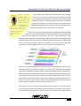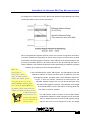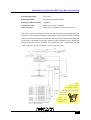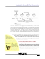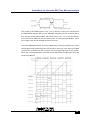
1
SmartBook for Renesas R8C/Tiny Microcontrollers
SmartBook
for
Renesas R8C/Tiny Microcontrollers
R 8C
/Ti
www.MightyMicons.com
1
con
Mi
ny
SmartBook for Renesas R8C/Tiny Microcontrollers
SmartBook
for
Renesas R8C/Tiny Microcontrollers
www.MightyMicons.com
2
SmartBook for Renesas R8C/Tiny Microcontrollers
www.MightyMicons.com
Phone : 0091 427 2449238 / 3209844
Fax : 0091 427 2431312
Email : [email protected]
Dear Reader,
Thanks for taking your time to read this SmartBook on Renesas R8C/Tiny Microcontrollers.
As you know well, we have been associated with this R8C/Tiny series since its introduction into the
market and we introduced many hardware and software tools to support this micon family.
Along the way, we realized a need to get a simple and easy to understand document on this micon
family ready to enable the Designers acquire a working knowledge on these micons without much
efforts. As a result, this SmartBook has come into existence. Use this SmartBook along with the micon
user guide when you need to get the complete picture on the features of the micon for your application.
Kindly send your feedback on this book to us. We welcome all your comments to make this book more
useful in the next edition.
Welcome to Renesas R8C/Tiny Micons!!
Balaji.
Technical Director.
Date : 04.07.2008.
Frontline Electronics Pvt. Ltd.
Pandian Street, Alagapuram,
Salem - 636 016, Tamilnadu, India.
www.MightyMicons.com
3
SmartBook for Renesas R8C/Tiny Microcontrollers
Contents
Chapter 1
R8C/Tiny Architecture
1.1
Introduction ............................................................................................................... 1
1.2
R8C/Tiny Family ....................................................................................................... 3
1.3
Overview of R8C/Tiny Family .................................................................................. 4
1.4
R8C/Tiny Architecture ............................................................................................. 5
1.5
Memory of the R8C/Tiny Devices ........................................................................... 8
Chapter 2
Clock Generating Mechanism
2.1
Introduction ............................................................................................................. 11
2.2
Main Clock .............................................................................................................. 12
2.3
On Chip Oscillator Clocks .................................................................................... 13
2.4
Low Speed On chip Oscillator .............................................................................. 13
2.5
High Speed On Chip Oscillator Clock .................................................................. 14
2.6
Power Control Modes ............................................................................................ 14
2.7
Wait Mode ............................................................................................................... 16
2.8
Stop Mode ............................................................................................................... 16
2.9
System Reset ......................................................................................................... 17
2.10
Hardware Reset 2 ................................................................................................... 18
2.11
Power on Reset Function ...................................................................................... 19
2.12
Software Reset ....................................................................................................... 20
2.13
Reset by Watch Dog Timer ................................................................................... 20
2.14
Voltage Detection Circuit ...................................................................................... 20
2.15
Voltage Detection Interrupt ................................................................................... 21
www.MightyMicons.com
89
SmartBook for Renesas R8C/Tiny Microcontrollers
Chapter 3
Instruction Set
3.1
Introduction ............................................................................................................. 23
3.2
Data Types .............................................................................................................. 23
3.3
Instruction Set ........................................................................................................ 24
3.4
Data Transfer (14 instructions) ............................................................................. 24
3.5
Arithmetic (21) ........................................................................................................ 24
3.6
Shift/Logic (10) ....................................................................................................... 25
3.7
Branch (8) ............................................................................................................... 25
3.8
Bit Manipulation (14) ............................................................................................. 26
3.9
String (3) ................................................................................................................. 26
3.10
Control/Other (19) .................................................................................................. 26
3.11
Repeat Multiple and Addition (RMPA) ................................................................. 28
3.12
String Move Forward (SMOVF) ............................................................................. 29
3.13
Save Multiple Registers (PUSHM) ....................................................................... 29
3.14
Store Context (STCTX) .......................................................................................... 30
3.15
String Store (SSTR) ............................................................................................... 31
3.16
Extend Sign (EXTS) ............................................................................................... 31
3.17
Instruction Format .................................................................................................. 31
3.17.1 Generic Format ......................................................................................... 32
3.17.2 Quick Format ............................................................................................. 32
3.17.3 Short Format ............................................................................................. 32
3.17.4 Zero Format ............................................................................................... 32
Chapter 4
Addressing Modes
4.1
Introduction ............................................................................................................. 35
4.2
Special Instruction Addressing ............................................................................. 37
4.3
Bit Instruction Addressing ..................................................................................... 38
www.MightyMicons.com
90
SmartBook for Renesas R8C/Tiny Microcontrollers
Chapter 5
Interrupt Mechanism
5.1
Introduction ............................................................................................................. 43
5.2
Software Interrupts ................................................................................................. 44
5.3
5.2.1
Undefined Instruction Interrupt ................................................................ 45
5.2.2
Overflow Interrupt ...................................................................................... 45
5.2.3
Break Interrupt ........................................................................................... 45
5.2.4
Instruction Interrupt .................................................................................. 45
Hardware Interrupts ................................................................................................ 46
5.3.1
Watch Dog Interrupt ................................................................................. 46
5.3.2
Oscillation Stop Detection Interrupt ....................................................... 46
5.3.3
Voltage Detection Interrupt ...................................................................... 46
5.3.4
Single Step Interrupt ................................................................................. 46
5.3.5
Address Match Interrupt ........................................................................... 46
5.4
Peripheral Function Interrupts .............................................................................. 47
5.5
Interrupt Control ...................................................................................................... 48
Chapter 6
5.5.1
Saving the Registers in the Interrupt Sequence .................................... 51
5.5.2
Managing Multiple Interrupts ................................................................... 51
5.5.3
External Hardware Interrupts ................................................................... 53
5.5.4
Interrupts for Keyboard and Switches .................................................... 53
5.5.5
Software Support for the Interrupt Operations ....................................... 54
Ports, Data Converters and Communication Facilities
6.1
Introduction ............................................................................................................. 55
6.2
I/O Port Lines ......................................................................................................... 55
6.3
Analog Interface ..................................................................................................... 56
6.4
Communication Facilities ...................................................................................... 58
6.5
Serial Communication Interface – IIC/SSU .......................................................... 60
www.MightyMicons.com
91
SmartBook for Renesas R8C/Tiny Microcontrollers
Chapter 7
Timer/Counter Functions
7.1
Introduction ............................................................................................................. 63
7.2
Timer Mode ............................................................................................................. 65
7.3
Even Counter Mode ................................................................................................ 66
7.4
Pulse Width Measurement Mode ......................................................................... 67
7.5
Pulse Period Measurement Mode ........................................................................ 68
7.6
Pulse Output Mode ................................................................................................ 68
7.7
Programmable Waveform Generation Mode ........................................................ 69
7.8
Programmable One Shot Generation Mode ......................................................... 70
7.9
Programmable Wait One Shot Generation Mode ............................................... 71
7.10
Input Capture Mode ................................................................................................ 71
7.11
Output Compare Mode ........................................................................................... 72
7.12
PWM Mode of Timer RD ........................................................................................ 74
7.13
PWM3 Mode of Timer RD ...................................................................................... 76
7.14
Reset Synchronous PWM Mode .......................................................................... 78
7.15
Complementary PWM Mode ................................................................................. 80
7.16
Real Time Clock ..................................................................................................... 83
Chapter 8
R8C/Tiny Micon Information
8.1
R8C/Tiny Micon Roadmap ..................................................................................... 85
8.3
R8C/20-23 Group Features ................................................................................... 86
8.4
R8C/24-25 Group Features ................................................................................... 87
8.5
R8C/26-29 Group Features ................................................................................... 87
8.6
R8C/2A-2D Group Features .................................................................................. 88
www.MightyMicons.com
92
SmartBook for Renesas R8C/Tiny Microcontrollers
Chapter 1. R8C/Tiny Architecture
1.1 Introduction:
Microcontrollers, an inevitable part of any embedded application always draw lots
of attention from the semiconductor manufacturers as well as designers. Evidently,
microcontrollers stay in limelight for a variety of reasons. A popular microcontroller
can keep the manufacturer happy for many years than any other component
because embedded applications demand the availability of the selected device for
a very long time. Also, the reliable and feature rich controllers promise huge volumes
to the semiconductor manufacturer. Manufacturers also work hard to keep the
interest on the microcontrollers alive and fresh by introducing many devices
maintaining the code compatibility among the member devices.
The devices may vary from low pin count to advanced versions with more memory,
peripherals to cover the spectrum of possible applications. In addition, the
designers are lured with development tools either costing very little or nothing. All
these factors lead to make the target microcontroller very friendly with the user,
who can in turn favors these devices till the design requirements do not outrun the
capabilities of the device.
Now, you can understand why technical superiority of the microcontrollers alone
is not enough to create the required impact with the designers. These are reasons
for many semiconductor manufacturers align themselves with the known
architecture rather than sorting out their own way. Existence of a range of 8051
derivatives even after 25 years of survival is the classical example.
Renesas Technology is one of the very few semiconductor
majors successfully created many microcontroller families
and maintaining them for a quite long time without
Renesas Technology
was formed after the
merger
bits to 32 bits with plenty of options. Each of
these controller families sports a wide range of
applications. Even though the list of available
devices seems mind blowing one for the
causal glance, Renesas has made sure that
Semiconductor
and
Mitsubishi
Hitachi
4
ws
e
Us
derivative devices catering to a range of
of
Ne
loosing any steam. These microcontrollers cover 8
Electric in 2003 and
has become the world
leader
in
the
microcontroller.
www.MightyMicons.com
1
SmartBook for Renesas R8C/Tiny Microcontrollers
e
Us
Ne
developed
every designer should find an optimized device for the target
R8C/Tiny family of
project. For the novices in electronics, Renesas Technology
microcontrollers
was formed after the merger of Hitachi Semiconductor and
Renesas
4
ws
incorporating
best
features of M16C
and H8 families to
exceed
the
expectations.
Mitsubishi Electric in 2003 and has become the world leader
in the microcontroller. As a result, many microcontrollers with
different architectures have come under the single banner to
create a single point source for the microcontrollers.
R8C/Tiny devices come with
the M16C core and the
peripherals of H8
family.
16-Bit microcontroller line up of Renesas, H8/300H series and M16C
series are very popular among the system designers. Even though these
devices have different architectures, they sport high performance CPU
integrated with the advanced peripherals. Both these families are designed with
Register based architecture where the dedicated Arithmetic logic unit is dispensed
with. The working registers have the facilities to do all the processing and
operations normally happen with the ALU. This leads to code efficiency.
M16C devices are designed with the specific goal of doing high speed processing
with low power consumption. In addition, the devices are made less susceptible
to the electro magnetic radiations and they emit less radiation than other devices.
Special protection mechanisms are built in to ensure trouble free operations. All
these features make the device suitable for reliable applications. On the other
hand, H8 device family is known for the range of advanced peripheral functions. A
variety of counter, timer functions, PWM, communication ports give these devices
a clear edge in developing solutions with only few chips.
Then along the way, Renesas developed R8C/Tiny family of microcontrollers
incorporating best features of M16C and H8 families to exceed the expectations
of ever demanding designers. Therefore, R8C/Tiny devices come with the M16C
www.MightyMicons.com
2
SmartBook for Renesas R8C/Tiny Microcontrollers
core and the peripherals of H8 family. Initially R8C/Tiny devices were made available
in low pin counts. Later on, Renesas started introducing other devices with more
peripherals and advanced features to cater to the more complex applications.
1.2 R8C/Tiny Family:
Following are key benefits designers get when they use R8C/Tiny devices:
• M16C Platform compatibility: To encourage the users with many design
choices using M16C family devices maintaining the code compatibility.
• Code compression: R8C/Tiny devices generate compact code for the given
application to save memory space.
• Low power consumption: Special power saving features of the microcontroller
extends the battery operating time.
• Extensive Fail-safe Features: The CPU core is supported with many fail safe
mechanisms to enable designers create stable and trouble free applications.
• Electro magnetic compatibility: R8C/Tiny based hardware generates less
electromagnetic radiations than any other solutions because the
microcontrollers are designed with special protection to suppress the EM
radiations.
• High performance Flash: To make designers life easy from the lab to the
field with flexible and high-speed flash memory options.
• Cost saving peripheral integration: R8C/Tiny devices
require less support devices to save the cost.
The
• Low cost development tools: Renesas
CPU core is supported
provides free development tools for program
development along with the flash
create
Emulators are available.
safe
stable
and
trouble
free
applications. R8C/Tiny based hardware
options:
range of packages from 20 pins to
84 pins to support different
generates
less
electro-
magnetic radiations than any
other solutions because the
4
ws
e
Us
R8C/Tiny devices are available in a
requirements.
fail
Ne
package
many
mechanisms to enable designers
programming facilities. Also low cost
• Small
with
microcontrollers are designed
with special protection to suppress
the EM radiations.
www.MightyMicons.com
3
SmartBook for Renesas R8C/Tiny Microcontrollers
1.3 Overview of R8C/Tiny Family:
• CPU: M16C Core with Register based architecture.
• Shortest Instruction Execution: 50 ns @ 20 MHZ.
• Number of base Instructions: 89.
• Operating mode: Single chip.
• Address space: 1 Mega Byte.
• Clock generation: 2 Circuits. Main clock generator with built in feedback
resistor and built in Ring oscillator.
• Interrupts: Internal - 10, External - 5, Software interrupts - 4, Priority levels - 7.
• Watchdog timer: Hardware timer with 15 bits using a Prescaler.
• Timers: These 8 bit timers (X,Y,Z) with 8 bit Prescaler. Timer C: 16 bits with
input capture.
• Serial I/O facilities: One Asynchronous port. One synchronous port.
• A-D converter: 8 channels of 10 bit AD converter with 2.8 µs conversion time
at 10 MHz.
• I/O ports: Minimum from 13 lines to 71 lines according to device package.
• Power supply: 3.0 V to 5.5V.
• Other peripherals:
• SPI (SSU).
• IIC.
• CAN bus.
• LIN bus.
• Power on Reset.
• Low voltage detect.
• Main clock stop detection.
• In circuit programming and debugging.
• Flash Memory: Single voltage programming with code protection facility.
• Device Packages: 20 pins to 84 pins.
www.MightyMicons.com
4
SmartBook for Renesas R8C/Tiny Microcontrollers
1.4 R8C/Tiny Architecture:
As you already know, R8C/Tiny CPU is compatible with other M16C devices to
maintain code compatibility. The architecture is derived using many registers.
Basically these devices are meant for single chip operations because bus
expansion facilities are not available with the controller. The program memory
space is made available within the device. The internal bus width is 8 bits. So, the
CPU accesses all the 16 bit data in two cycles.
The CPU register structure is given here. The CPU contains 13 registers of 16-bit
width. Of these, 4 registers, R0, R1, R2 and R3 are known as Data Registers
meant for data transfer and arithmetic/logic operations. Then comes two registers,
www.MightyMicons.com
5
SmartBook for Renesas R8C/Tiny Microcontrollers
registers,
A0 and A1 for manipulating address generation. These
R0-R3, address regis-
registers are meant for different kinds of addressing. They
ters, A0 and A1 and
can also be used for data transfers and arithmetic/logic
4 D esi gn
Data
D a ta
frame base register,
FB form a bank of
operations. Then there are 16-bit Base Registers, Frame
Base Register (FB) and Static Base Register (SB) used
registers. Any one of these two reg-
for relative addressing.
ister banks is always selected
as per the content of the
Of all these registers, data registers, R0-R3, address registers,
flag bit, B.
A0 and A1 and frame base register, FB form a bank of registers.
There is another bank of same registers that keeps copy of above
mentioned registers to speed up data transfer tasks during various operations.
Any one of these two register banks is always selected as per the content of the
flag bit, B.
There is a facility to configure the selected data registers and address registers
for different data formats. Data registers R0 and R1 can be used as 16 bit registers
and be divided into two 8-bit registers. For an example, R0 as a whole can be
used as a 16-bit register and when it is configured for the 8-bit data, it is divided
into two 8 bit registers like R0L and R0H. Then, R2 and R0 can be combined to
form a 32-bit register R2R0. Similarly, another 32 bit register can be formed using
R3 and R1. Like wise, address registers A1 and A0 can be combined to form a 32
bit register A1A0.
The Static Base (SB) Register and Frame Base (FB) Register are used for indexed
addressing. FB is especially useful in creating stack frames when programming
in C.
Two stack pointers, User Stack Pointer (USP) and Interrupt Stack Pointer (ISP)
combine to minimize RAM usage when the CPU is performing multiple tasks.
Apart from all this, the CPU contains a Flag Register, Program Counter and Interrupt
Table Pointer, INTB. This INTB allows you to position the beginning of the variable
vector table anywhere in the valid memory space.
The Flag Register (FLG) is a 16-bit register containing status of 11 flags indicating
various CPU operations:
www.MightyMicons.com
6
SmartBook for Renesas R8C/Tiny Microcontrollers
Carry (C) Flag: This flag retains a carry, borrow or shift out bit that has occurred
in the arithmetic/logic operations.
Debug (D) Flag: This D flag is used extensively for debugging purpose. During
normal use, it must be set with 0.
Zero (Z) Flag: This flag is set to 1 when an arithmetic operation resulted in
0.Otherwise, it is 0.
Sign (S) Flag: This flag is set to 1 when an arithmetic operation resulting in a
negative value. Otherwise, it is 0.
Register Bank Select (B) Flag: Register bank 0 is selected when this flag is 0.
Register bank 1 is selected when this flag is set to 1.
Overflow (0) Flag: This flag is set to 1 when the operation is resulted in an
overflow. Otherwise, it is 0.
Interrupt Enable (I) Flag: This flag enables a maskable interrupt. Maskable
interrupts are disabled when the I flag is 0 and are enabled when I flag is set to 1.
The I flag is cleared to 0 when the interrupt request is accepted.
Stack Pointer Select (U) Flag: ISP is selected when U flag is 0. USP is selected
when the U is set to 1. The U flag is cleared to 0 when a hardware interrupt
request is accepted or an INT instruction for software interrupt nos 1 to 31 is
executed.
Processor Interrupt Priority level (IPL): IPL is
configured with three bits to specify up to 8
This
processor priority levels from 0 to 7. If a
of an interrupt vector table. This
register indicating the address of the next
instruction that is to be executed.
www.MightyMicons.com
be relocated to any
other
place
by
defining this INTB.
4 D esi gn
i n t e r r u p t
vector table can
Program counter (PC): This is a 20-bit
INTB
register contains the address
requested interrupt has priority greater than
IPL, then the interrupt is enabled.
20-bit
D a ta
7
SmartBook for Renesas R8C/Tiny Microcontrollers
Renesas
Interrupt Table Register (INTB): This 20-bit register
devices come with
contains the address of an interrupt vector table. The
more
table may contain up to 63 interrupt vectors of 4 bytes
4 D esi gn
Normally
D a ta
RAM
area
than other similar
controllers.
Because
the large size, you can maintain
of
each. Using this INTB, this total interrupt space of 256
bytes (64x4) can be defined in any place in the memory
space. In addition, this interrupt vector table can be relocated
to any other place by defining this INTB.
a large stack in the RAM
area.
1.5 Memory of the R8C/Tiny Devices:
As you know, all the R8C/Tiny microcontrollers operate in single chip mode
because they do not have facility to add any memory externally. Therefore, the
devices come with the required program memory and static RAM area along with
the peripheral functions. This program memory is constructed using the high
performance flash memory that varies from 8K bytes to 64K bytes. Similarly,
available RAM portion varies from 512 bytes to 4K bytes. The controller’s flash
and RAM capacity vary from device to device.
The flash memory has many special features for your convenience. The most
usable one is the In System Programming for the flash area. In other words, the
contents of the flash memory can be changed after soldering the device in the
application hardware. This is an important facility enabling you to modify your
code or the application data in the field itself. Then the internal memory
management module safeguards the flash contents under an exclusive identity
code to prevent any unauthorized reading. You can define an identity code in 7
bytes of the flash memory. Then, every time you need to match this code to
access the flash contents.
Normally Renesas devices come with more RAM area than other similar controllers.
Having a large RAM area serves many purposes. Because of the large size, you
can maintain a large stack in the RAM area. Another useful feature is, with enough
RAM space, you can easily manage in system program operations.
Now, let us see how this flash memory and the RAM area are mapped in the
device. Since the program counter is of 20 bits width, the CPU can access up to
1M Byte memory. Both the program and the data memory reside in this memory
space.
www.MightyMicons.com
8
SmartBook for Renesas R8C/Tiny Microcontrollers
Following is the address scheme for the memory organization. As you can see,
the RAM area is made available at the lower end. Initial memory space, up to
02FFH is allotted for the Special Function Registers (SFR). SFR maintains all the
peripheral functions’ control registers and other registers meant for flash
programming and system management. Then the RAM area starts at 0400H and
expands upwards. The flash or program memory starts from 0FFFFH and grows
downwards. More than 64K byte is considered as expanded memory.
Now, we take up in system programming again for the discussion. The
microcontrollers come with the boot program to manage programming
operations. When this boot program is activated, the entire
When
flash area can be erased and then be reprogrammed using
the
a host computer. The boot program synchronizes the
first
mode
(E/W=0) is selected, the
microcontroller with the computer automatically
during data transfer operations. Apart form this
bulk erase and programming, the devices
is transferred to the RAM area
and then the program control is
support in system programming. You can
shifted to this
kernel.
Without
stopping the CPU,
any portion of the
For this, the controller comes with built
flash memory can be
in programming sequences. When the
reprogrammed.
www.MightyMicons.com
4 D esi gn
reprogram the contents of the flash memory
in two modes.
built in programming kernel
D a ta
9
4 Desig
n
SmartBook for Renesas R8C/Tiny Microcontrollers
D a ta
In the second mode
first mode (E/W=0) is selected, the built in programming
(E/W=1), you need
kernel is transferred to the RAM area and then the
not
program control is shifted to this kernel. Without stopping
transfer
the
programming
kernel
to
the
RAM. Keeping the programming
the CPU, any portion of the flash memory can be
reprogrammed. For this mode, the RAM area should be large
enough to keep the programming kernel.
control in the flash memory itself,
you can modify any other
flash area.
In the second mode (E/W=1), you need not transfer the
programming kernel to the RAM. Keeping the programming control
in the flash memory itself, you can modify any other flash area. These
programming modes are also known as user programming modes. In addition,
in many of the R8C/Tiny devices, you can get the facility to configure two blocks
of 1K byte flash memory as the Data flash for maintaining reference data or table,
etc.
www.MightyMicons.com
10
SmartBook for Renesas R8C/Tiny Microcontrollers
Chapter 2. Clock Generating Mechanism
2.1 Introduction:
R8C/Tiny microcontrollers sport a versatile clock generating mechanism to protect
the controller’s operations against going awry on the account of system clock
becoming faulty at any time. For this purpose, the device comes with built-in
Ring Oscillators to supply the required clock source to the CPU and the peripherals,
in case the main clock derived from the externally connected crystal or the
resonator becomes defective. As the result, the system’s reliability is very much
improved.
The controller’s clock generating circuit gets two clock sources: A main clock
source using external crystal or resonator and the internal ring oscillator circuit.
The main clock operates up to 20MHz using the external crystal. The internal
Ring oscillator operates independent of main clock and generates two clock signals
on its own. Low speed Ring Oscillator with about 125KHz and the high speed
Ring oscillator capable of generating the nominal clock signal of 8MHz with the
facility to vary the same from 5 MHz to 16 MHz. There is a control register
associated with the high speed ring oscillator to define the exact frequency of the
clock with the accuracy of +/- 1 nano seconds.
The Micon’s clock generating circuit also contains an Oscillator Stop Detection
function to monitor the main clock source. When the main clock source fails or
disconnected from the device, the oscillator stop detecting function automatically
substitutes the clock source of low speed ring oscillator to the CPU and the
peripheral functions to maintain the CPU operation or enables
the orderly shut down.
T
h
e
device comes with
The same oscillation detect function works in
built-in Ring Oscillators to
association with built-in voltage detection
supply the required clock source
circuit to feed the CPU and the peripherals
to the CPU and the peripherals, in
with the low speed ring oscillator till the
case the main
on or reset release conditions. Once the
derived
from the externally
main clock becomes stable, the
connected crystal or
application can switch from low speed
the resonator becomes
4 D esi gn
clock
main clock gets stabilized during power
D a ta
defective.
www.MightyMicons.com
11
4 Desig
n
SmartBook for Renesas R8C/Tiny Microcontrollers
The micon contains
clock to the high speed main clock source. This versatile
low
clock generating circuit is managed using a set of
speed
Ring
Oscillator of about
125KHz and the
D a ta
high speed Ring
registers. The clock generator also contains a set of
dividers to generate many clock derivatives to suit different
operating conditions.
oscillator capable of generating the
nominal clock signal of 8MHz
2.2 Main Clock:
with the facility to vary the
same from 5 MHz to
16 MHz.
The micon gets its main clock from the externally connected crystal
between the pins, XIN and XOUT. This clock can be used as the source
for the CPU and the peripheral functions. This main clock oscillating circuit
can also get externally generated clock at the XIN pin. This oscillating circuit
contains a feedback resistor, which can be disconnected from the oscillator to
reduce the power consumption during the Stop mode. The following figure shows
external clock generating options.
During reset and after reset, the main clock is turned off.
The main clock starts oscillating when the CM05 bit in the CM0 register is set to
“0” (main clock on) after setting the CM13 bit in the CM1 register to “1”.
To use the main clock for the CPU clock, set the OCD2 bit in the OCD register to
“0” (selecting main clock) after the main clock becomes oscillating stably.
The power consumption can be reduced by setting the CM05 bit in the CM0 register
to “1” (main clock off) if the OCD2 bit is set to “1” (On-chip Oscillator clock
selected). Note that if an externally generated clock is fed into the XIN pin, the
main clock cannot be turned off by setting the CM05 bit to “1”. If necessary, use
an external circuit to turn off the clock.
www.MightyMicons.com
12
SmartBook for Renesas R8C/Tiny Microcontrollers
During stop mode, all clocks including the main clock are turned off.
2.3 On Chip Oscillator Clocks.
The micons contain an on-chip oscillating circuitry that generates two clock
sources: High speed on chip oscillator and Low speed on chip oscillator. These
oscillators are selected by the bit, HR01 of HR0 register.
After reset, the
2.4 Low Speed On chip Oscillator:
on-chip clock derived
The clock derived from the low-speed on-chip
CPU clock, peripheral function clocks, fRING,
fRING128 and fRING-S. After reset, the onchip clock derived from low-speed on-chip
oscillator with the division of 8 is selected
as the CPU clock.
www.MightyMicons.com
oscillator
with
the
division of 8 is
selected as the
CPU clock.
4 D esi gn
oscillator is used as the clock source for the
from low-speed on-chip
D a ta
13
4 Desig
n
SmartBook for Renesas R8C/Tiny Microcontrollers
D a ta
The Micons deliver
If the main clock stops oscillating when the OCD1 to OCD0
more
bits in the OCD register are set to “11” (Oscillation Stop
processing
power with high
speed
s o u r c e s .
When the operating speed is re-
automatically starts operating, supplying the necessary clock
to the microcomputer. The frequency of the low-speed onchip oscillator varies depending on the supply voltage and the
duced, the power consumption also comes down
Detection function enabled), the low-speed on-chip oscillator
clock
operating ambient temperature. The applications must be
designed with sufficient margin to accommodate the frequency range.
significantly.
2.5 High Speed On Chip Oscillator Clock:
The clock derived from high-speed on-chip oscillator is used as the clock source
for the CPU clock, peripheral function clocks, fRING, fRING128, and fRING-fast.
After reset, the on-chip oscillator clock derived from high-speed on-chip oscillator
is disabled. The oscillation is started by setting the HR00 bit in the HR0 register
to “1” (high-speed on-chip oscillator on). The HR1 register can adjust the frequency
of this clock source.
2.6 Power Control Modes:
The R8C/Tiny family devices come with a versatile built in clock generating
mechanism that gives a range of clock sources to feed both the CPU and different
on chip peripheral functions. It also supports the usage of an external clock
source. Using these clock selecting options, the microcontrollers has the facility
to implement application specific power conserving tasks. The Micons deliver
more processing power with high speed clock sources. When the operating speed
is reduced, the power consumption also comes down significantly. These facilities
are much sought-after in power sensitive applications.
The R8C/Tiny devices have these power control modes: Normal mode, Wait mode
and Stop mode. The normal mode has its own operating modes: High speed
mode, Medium speed mode and High/Low speed on chip oscillator modes.
As you can recall from the pervious discussion on clock generating mechanism,
the chip operating system clock can get its clock from either external main clock
or from the internal ring oscillators. The CPU and the peripheral functions can get
the undivided system clock or one of the many divided clock options through
different clock dividers.
www.MightyMicons.com
14
SmartBook for Renesas R8C/Tiny Microcontrollers
These different operating modes are
From the reset
managed by proper initialization in few
condition,
Control Register 0), CM1 (System Clock
Control Register 1), HR0 (High Speed On-chip
Oscillator Control Register 0), OCD (Oscillation
n
4 Desig
selected registers: CM0 (System Clock
the
micon gets into
high
D a ta
speed
mode when
the main clock is selected as the
Stop Detection Register).
system clock by configuring
the
Oscillation
From the reset condition, the micon gets into high speed
Stop
Detection Register
mode when the main clock is selected as the system clock
(OCD2=0).
by configuring the Oscillation Stop Detection Register (OCD2=0).
In this mode, timers get high speed ring oscillator clocks, fRING-FAST, fRING or
fRING128. When the micon is activated for the medium speed mode, the CPU
gets the divided (by 2,4,8 or 16) main clock. Like the high speed mode, timers
also get similar clock options.
To get High/Low speed on-chip oscillator mode, on-chip ring oscillator should be
configured as the system clock (OCD2=1) and then either low speed or high speed
ring oscillator should be selected (HR01) and then the same is switched on
(CM14=0 for low speed oscillator, HR00=1 for high speed oscillator).
In addition, the CPU can get divided ring oscillator clocks, with the division of
1,2,4,8 or 16 by configuring the register CM1.
www.MightyMicons.com
15
SmartBook for Renesas R8C/Tiny Microcontrollers
2.7 Wait Mode:
Getting into the wait
4 Desig
n
mode is as easy as
Getting into the wait mode is as easy as executing
e x e c u t i n g t h e WA I T
instruction
D a ta
point
at
of
switched off and subsequently the CPU and the
watchdog timer are turned off to conserve the power.
operating mode consuming least amount
Since the main clock and the ring oscillator are already
of power among all the modes because
in on condition, peripheral functions can use them. When
all the clocks are turned off. The
the micon enters into this wait mode, pin status of the micon
microcomputer is placed into this
operating clocks (set
execution. In this wait mode, CPU system clock is
the
application execution. The stop mode is the
mode by stopping all the
the WAIT instruction at any point of the application
any
remain same as that of operating condition prior to the wait
mode entry.
CM10=1).
In the wait mode, the peripheral function clocks can also be stopped to
conserve more power. If the CM02 bit is set to 1, the clock divider is switched
off to stop f1, f 2, f 8, f 32, f1SIO, f8SIO, f32SIO and fAD clocks. But other
clocks, fRING, fRING128, fRING-FAST derived from ring oscillators can be used
for the applications.
To exit from the wait mode, a hardware reset or a peripheral function interrupt is
required. If the peripheral function clocks are already disabled in the wait mode,
only the peripheral functions which can use the external signals can activate an
interrupt to exit from the wait mode. Because of this, the program flow should
keep the interrupt conditions of the peripheral functions in the active condition,
which are likely to trigger the micon from the wait mode. The CPU clock turned on
when returning from the wait mode by a peripheral function interrupt is the same
CPU clock that was operating when the wait instruction is executed.
2.8 Stop Mode:
The stop mode is the operating mode consuming least amount of power among all
the modes because all the clocks are turned off. The microcomputer is placed
into this mode by stopping all the operating clocks (set CM10=1). But before
entering into stop mode, oscillator stop detection function should be disabled.
During active stop mode condition, pin status of the micon is maintained as the
operating condition prior to stop mode entry. If the operating voltage at the Vcc
pin is VRAM or more, the contents of the internal RAM area remain same as
before.
www.MightyMicons.com
16
Like wait mode, to exit from this stop
These devices also
mode, a hardware reset or a peripheral
contain a power on
function interrupt is required. Only the
reset
function
without
before entering into stop mode can be
any
external device to
used to bring the micon from the stop mode.
bring
Since all the peripheral clocks are already
stopped, these peripheral functions should use
4 Desig
peripheral functions already enabled
n
SmartBook for Renesas R8C/Tiny Microcontrollers
up
D a ta
the
h a r d w a r e i n a n o r d e r l y m a n n e r.
Whenever the operating voltage
the external signals to interrupt the micon.
crosses this Vdet, the voltage
When the stop mode is interrupted to bring the
micon into other operating modes, the CPU operating
system clock always gets divide by 8 clock from either
detector generates an interrupt
and
also
the
reset
condition can be
activated.
the main clock or the ring oscillator.
2.9 System Reset:
Reset facility of any microcontroller is an important mechanism to monitor and
safeguard the workings of the controllers within the defined operating environment.
It should also prevent the controller from going into any unknown state when the
operating environment is disturbed. To make any application reliable and trouble
free, a suitable reset management circuit should be included into the design. In
the simple designs, an external watchdog timer is used to monitor the operating
conditions and force the controller into reset state when the supply voltage goes
down below a reference voltage. Also, when the watch dog timer does not receive
the periodic system health signal from the controller within the underflow time,
this timer forces the microcontrollers into reset state to execute the defined program
flow. This way controller can be protected from executing anything unwanted.
www.MightyMicons.com
17
SmartBook for Renesas R8C/Tiny Microcontrollers
the
The R8C/Tiny controllers sport a versatile reset
registers become zero
facility to keep the controller working in the stable
and the PC gets the reset
conditions in spite of variations in the operating
4 Desig
n
After
reset,
v e c t o r.
D a ta
all
Also all the
ports are initialized
for the inputs. When the counter counts
upto 32 clocks (of the onchip low speed
ring oscillator), the internal reset
condition
is
exited
and
program is executed beginning
with the address indicated
the
voltage along with a dedicated watchdog timer. These
devices also contain a power on reset function without
any external device to bring up the hardware in an
orderly manner. Basically, this function is built using a
voltage detection circuit which compares the operating
voltage with a reference voltage, Vdet, of 3.8V. Whenever
the operating voltage crosses this Vdet, the voltage detector
generates an interrupt and also the reset condition can be
by the reset vector
activated. The voltage detector can generate interrupts for both rising
FFFCH.
and falling operating voltages. Apart from all these hardware facilities,
the controller can also be reset by software.
The R8C/Tiny devices have three types of resets: A Hardware Reset, Software
Reset and a Watchdog Timer Reset. Further, the hardware reset represents
Hardware Reset 1, Hardware Reset 2 and Power on Reset. Hardware Reset 1 is
the simple one, forcing the device into reset by applying a pulse signal at the
RESET pin with an active low level for atleast 500 microseconds. When this
RESET pin is in low level, pins of the controller are initialized. When the voltage
level is increased from low to high level, the CPU and SFR are initialized and the
program is executed starting from the address indicated by the Reset Vector
(FFFCH). After reset, all the registers become zero and the PC gets the reset
vector. Also all the ports are initialized for the inputs.
2.10 Hardware Reset 2:
The operation of this hardware reset depends upon the device operating voltage.
The device’s built in voltage detector circuit monitors the supply voltage at the
Vcc pin. When this voltage detector function is initialized (VC27 bit in the Voltage
Detection Register VCR2 is set to 1) the device gets ready to activate this hardware
reset.
When the supply voltage at the Vcc pin rises to Vdet or more, the pins, CPU and
SFR are initialized and the counting of low speed on chip oscillator starts. When
the counter counts upto 32 clocks (of the onchip low speed ring oscillator), the
www.MightyMicons.com
18
SmartBook for Renesas R8C/Tiny Microcontrollers
internal reset condition is exited and the program is executed beginning with the
address indicated by the reset vector FFFCH. The following figure indicates the
reset sequence:
Proper operating conditions are to be initialized to get this hardware reset ready.
Voltage Detection Interrupt Register, D4INT, should be properly initialized for this
purpose. Apart from enabling Voltage Detection circuit (VC27 of VCR2 to 1),
Voltage Detection Interrupt should be enabled (D40 bit of D4INT is set to 1).
Now, whenever the supply passes through Vdet, an interrupt request is generated.
By setting D46 bit of D4INT to 1, the voltage detector circuit generates the hardware
reset instead of interrupt request. This function is meant to keep the controller in
reset condition till the supply voltage rises to the safe operating
level. Because of this, the microcontroller starts up properly
Whenever
to execute the programs.
the supply passes
through Vdet, an interrupt
2.11 Power on Reset Function:
request is generated. By setting
The Power on Reset function operates on the
D46 bit of D4INT to 1, the voltage
top of Hardware Reset 2. This function is
detector circuit generates the hardware
meant to keep the controller in the reset
reset instead of interrupt request.
condition till the supply voltage reaches
Without requiring any external circuit,
this facility safeguards
requiring any external circuit, this
the controller during
facility safeguards the controller during
power on conditions by
power on conditions by having a
having a resister of about
resister of about 5K between the reset
5K between the reset and
and the Vcc pins.
the Vcc pins.
www.MightyMicons.com
4 D esi gn
to the safe operating level. Without
D a ta
19
4 Desig
n
SmartBook for Renesas R8C/Tiny Microcontrollers
D a ta
VC13 bit indicates
Like the Hardware Reset 2, the internal counter counts
the status of supply
low speed on chip oscillator upto 32 when the supply
voltage at Vcc
crosses Vdet and subsequently releases the internal reset.
pin. It becomes
zero
The reset conditions of CPU, pins, registers are same as
when
that of Hardware Reset 1. This power on reset function also
the supply voltage is less than
Vdet and gets one level when
automatically initializes D40 and D46 bits of D4INT registers
to 1 level and gets the Hardware Reset 2 into active condition.
the voltage rises to Vdet
or more.
2.12 Software Reset:
The microcontrollers can be reset by software by setting PM03 bit of the PMD
register to 1 level. The reset conditions are same as that of other reset options.
2.13 Reset by Watch Dog Timer:
When the PM12 bit of PM1 register is set to 1, the controller is reset when the watchdog
timer under flows. Then the program is executed from the address indicated by the
reset vector. The CPU gets divide by 8 low speed on chip oscillator as its clock.
2.14 Voltage Detection Circuit:
The Voltage Detection Circuit plays a vital role in device reset operating conditions.
This circuit monitors the supply voltage at Vcc pin with Vdet reference and
generates interrupts or hardware reset depending on the initialization conditions.
This detection circuit becomes active when bit VC27 of Voltage Detection Register
2, VCR2 is set to 1. The following figure gives overview of this circuit.
www.MightyMicons.com
20
SmartBook for Renesas R8C/Tiny Microcontrollers
Apart from VC27 of Voltage Detection Register 2, following bits play important
role when using this voltage detection circuit.
VC13: Voltage monitor flag of the register, Voltage Detection Register VCR1. This
bit indicates the status of supply voltage at Vcc pin. It becomes zero when the
supply voltage is less than Vdet and gets one level when the voltage rises to Vdet
or more.
This bit becomes valid only when VC27 is already set with the level 1.
In other words, only with the voltage detection circuit in enabled condition (by
VC27) then VC13 becomes valid. This VC27 has its own check point. Before
enabling voltage detection circuit, PRC3 bit of PRCR register (Protect Register)
should be set to one level.
D42 - Voltage Change Detection bit (of Voltage Detection Interrupt Register)
- 0: Not detected
- 1: Vdet pass detection.
D40 - Voltage Detection Interrupt Enable bit of D4INT.
- 0: Disable.
- 1: Enable.
D46 - Voltage monitor mode (bit of D4INT)
- 0: Voltage Detection Interrupt request when passing through Vdet.
- 1: Hardware Reset 2 when passing through Vdet.
A
voltage
detection interrupt
2.15 Voltage Detection Interrupt:
is generated when the
A voltage detection interrupt is generated when the
supply Voltage at Vcc pin rises
supply Voltage at Vcc pin rises to Vdet or more
are already initialized.
more
drops
Vdet
www.MightyMicons.com
or
below
n
to Vdet or
4 Desig
or drops below Vdet if the following conditions
D a ta
21
SmartBook for Renesas R8C/Tiny Microcontrollers
Voltage Detection Circuit should be enabled (set VC27 of VCR2 to 1)
Voltage Detection Interrupt is enabled (set D40 of D4INT to 1)
Voltage Detection Interrupt is selected (set D46 bit of D4INT is set to 0)
Enable Voltage Detection Digital Filter (D41 bit of D4INT register)
0: Enable Digital Filter.
1: Disable Digital Filter.
To use this digital filter, the low speed on chip oscillator should always be enabled
(set CM14 bit of CM1 register to 0)
The Voltage Detection Interrupt shares the interrupt vector with the Watchdog
Timer Interrupt and Oscillation Stop Detection Interrupt.
The Voltage De-
The D42 bit of the D4INT register becomes 1 when the supply voltage
tection Interrupt shares
the interrupt vector with the
passing through Vdet is detected. A voltage detection interrupt
Wa t c h d o g
4 Desig
n
Timer Inter-
D a ta
rupt and Oscil-
request is generated when the D42 bit changes from 0 to 1.
The D42 bit needs to be set to 0 by the software to generate
the next interrupt request.
lation Stop Detection Interrupt.
www.MightyMicons.com
22
SmartBook for Renesas R8C/Tiny Microcontrollers
Chapter 3. Instruction Set
3.1 Introduction:
In this chapter, we are going to discuss about the processing power of the
R8C/Tiny microcontrollers. The processing power of the device is influenced by
the respective instruction set and it plays a vital role in the application development
process. A versatile and flexible instruction set can help the designers finish their
application in less time using minimum code space. The right instruction set can
also make the applications run faster. Professional designers take this instruction
set very seriously to assess the power of the micon for their applications.
Subjecting the instruction set of R8C/Tiny into this discussion, we can easily
notice that the Renesas engineers have taken lots of time in designing the
instruction set to equip the designers create applications with the desired
performance. They could achieve this goal by introducing lots of redundancy in
the design and the structure of the instruction set. For a casual glance, the whole
thing seems like a waste of the resources. But, in real, this equips the designers
to create their applications with the desired level of efficiency. So, the following
discussion gives a complete picture on the instruction set and in turn about the
device processing power.
3.2 Data Types:
A
R8C/Tiny controllers can handle different types of data
ranging from four bit nibble to 32-bit long word.
The data is stored in the memory byte wise.
Renesas
signing the instruction set to equip the designers create applications with the desired
performance. They could
achieve this goal by introducing lots of redundancy
in the design and the structure of the instruction set.
www.MightyMicons.com
4 D esi gn
memory location.
can help the designers finish
engineers have taken lots of time in de-
higher byte is stored in the next higher
memory locations from the defined
flexible instruction set
ing minimum code space.
the defined memory location and next
data is stored in four consequent
and
their application in less time us-
For a 16-bit word, first data byte is stored in
memory location. Like wise, a 32-bit
versatile
D a ta
23
SmartBook for Renesas R8C/Tiny Microcontrollers
4 D esi gn
The instruction set
D a ta
of the R8C/Tiny
contains 89 discreet
instruc-
tions. Of these,
20
instruc-
tions require only one clock
cycle for the execution. 75%
of the instructions require
3.3 Instruction Set:
less than five cycles
for the execution.
The instruction set of the R8C/Tiny contains 89 discreet instructions. Of
these, 20 instructions require only one clock cycle for the execution. 75% of
the instructions require less than five cycles for the execution. Following list
indicates all these instructions arranged in different categories:
3.4 Data Transfer (14 instructions):
Transfer (MOV)
Save effective address (PUSHA)
Transfer effective address (MOVA)
Save multiple registers (PUSHM)
Transfer four bit data (MOVDir)
Transfer from extended data area (LDE)
Restore register (POP)
Transfer to extended data area (STE)
Restore multiple registers (POPM)
Conditional transfer (STNZ, STZ, STZX)
Save register (PUSH)
Exchange (XCHG)
3.5 Arithmetic (21):
Absolute value (ABS)
Decimal subtract with borrow
(DSBB)
Add with carry (ADC)
Decimal subtract without borrow
(DSUB)
Add with carry flag (ADCF)
Extend sign (EXTS)
Add without carry (ADD)
Increment (INC)
Compare (CMP)
Signed multiply (MUL)
www.MightyMicons.com
24
SmartBook for Renesas R8C/Tiny Microcontrollers
Decimal add with carry (DADC)
Unsigned multiply (MULU)
Decimal add without carry (DADD)
Two’s complement (NEG)
Decrement (DEC)
Calculate sum of products (RMPA)
Signed divide (DIV)
Subtract with borrow (SBB)
Unsigned divide (DIVU)
Subtract without borrow (SUB)
Signed divide extension (DIVX)
3.6 Shift/Logic (10):
Rotate left with carry (ROLC)
Logical AND (AND)
Rotate right with carry (RORC)
Invert all bits (NOT)
Rotate (ROT)
Logical OR (OR)
Shift arithmetic (SHA)
Test (TST)
Shift logic (SHL)
Exclusive OR (XOR)
Add and conditional jump (ADJNZ)
Jump indirect (JMPI)
Subtract and conditional jump
(SBJNZ)
Subroutine call (JSR)
Jump on condition (JCnd)
Indirect subroutine call (JSRI)
Unconditional jump (JMP)
Return from subroutine (RTS)
3.7 Branch (8):
www.MightyMicons.com
25
SmartBook for Renesas R8C/Tiny Microcontrollers
3.8 Bit Manipulation (14):
Logically AND bits (BAND)
Exclusive OR inverted bits (BNXOR)
Clear bits (BCLR)
Logically OR bits (BOR)
Conditional bit transfer (BMCnd)
Set bit (BSET)
Logically AND inverted bits (BNAND)
Test bit (BTST)
Logically OR inverted bits (BNOR)
Test bit and clear (BTSTC)
Invert bit (BNOT)
Test bit and set (BTSTS)
Test inverted bit (BNTST)
Exclusive OR bits (BXOR)
Transfer string backwards (SMOVB)
Store string (SSTR)
3.9 String (3):
Transfer string forward (SMOVF)
3.10 Control/Other (19):
Debug interrupt (BRK)
Set interrupt enable level (LDIPL)
Build stack frame (ENTER)
No operation (NOP)
Deallocate stack frame (EXITD)
Restore the control register (POPC)
Clear flag register bit (FCLR)
Save control register (PUSHC)
Set flag register bit (FSET)
Return from interrupt (REIT)
Interrupt by INT (INT)
Transfer from control register (STC)
www.MightyMicons.com
26
SmartBook for Renesas R8C/Tiny Microcontrollers
Interrupt on overflow (INTO)
Save context (STCTX)
Transfer to control register (LDC)
Interrupt for undefined instruction
(UND)
Restore context (LDCTX)
Wait (WAIT)
Transfer to INTB register (LDINTB)
Now, we proceed further into a detailed discussion to get the complete picture on
the processing power of the R8C/Tiny devices.
The device handles the multiplying operations at a faster rate thanks to the builtin hardware 16 X 16 multiplier. For an example, the 16 X 16 multiplying for both
signed and unsigned operation requires just a single instruction consuming only
three bytes and is executed in four instruction cycles.
Likewise, 8 X 8 unsigned multiply is another single instruction requiring three
bytes of program memory and gets done in four instruction cycles.
For the division operations, for both signed and unsigned data types, the device
has single instruction for 16 / 8 and 32 / 16 type divisions.
The 16
Signed data requires two bytes of program memory and
X 16 multiplying
the unsigned data needs three bytes of memory. 22
for both signed and
instruction cycles are required for the signed data
unsigned operation re-
and 18 cycles for the unsigned.
quires just a single instruction
consuming only three bytes and
Taking 16-bit addition/ subtraction into study,
instruction with two bytes of program memory
and getting executed in two instruction
cycles.
is executed in four instruction
cycles.
For the division operations,
for both signed
and unsigned data
types, the device has
single instruction for
The devices support arithmetic operations
16/8 and 32/16 type
on the decimal data using few instructions.
divisions.
www.MightyMicons.com
4 D esi gn
we find these operations require single
D a ta
27
4 D esi gn
SmartBook for Renesas R8C/Tiny Microcontrollers
D a ta
DADD instructions do
DADD instructions do an arithmetic addition on BCD
an arithmetic addition
coded data and keeps the results in the destination.
on BCD coded data and
DADC instructions do the similar operation on the two
keeps the results in the
destination.
Sum
of
Product
(RMPA) operation gives the micon the
MAC power that is available only
in the regular and high priced
DSP devices. This operation
data along with the carry flag.
The
Then, the devices support decimal subtraction on two BCD
coded data using DSUB instructions. DSUBB instructions
do the same operations along with the carry. Instructions
are available for both 8-bit and 16-bit operands.
gets executed in every
nine clocks.
Other microcontrollers manage these decimal operations using many
instructions. Here, availability of these instructions makes the designers
happy during their application development.
Apart from the above mentioned instructions, the R8C/Tiny devices sport many
useful special instructions which enable the designers embed math intensive
operations within their applications without much pain.
3.11 Repeat Multiple and Addition (RMPA):
This instruction performs sum of products calculations with the multiplicand
address indicated by A0 register, the multiplier address indicated by A1 and the
R3 register keeping the count of operation. The calculations continue till R3
becomes zero and the result is available in R2R0.
This sum of product operation gets executed in every nine clocks. This instruction
gives the micon the MAC power that is available only in the regular and high
priced DSP devices. In the high speed DSP devices, the MAC instruction requires
only a single clock cycle to finish operation. However, the R8C/Tiny devices take
more time to do the same operation. In the digital signal processing, you need to
finish all the required operations before you get the next sample in a loop to get
the required results. Even though the R8C/Tiny devices take more clock cycles to
finish the signal processing operations, the devices can be used on many low
speed signals without any problems.
www.MightyMicons.com
28
SmartBook for Renesas R8C/Tiny Microcontrollers
3.12 String Move Forward (SMOVF):
This instruction transfer a data string from a 20 bit source address to a 16 bit
destination address by successively incrementing the address. The transfer
continues till the count in R3 comes down to zero.
A single move operation consumes five clock cycles.
SMOVF
instruction transfer a data string from
3.13 Save Multiple Registers (PUSHM):
This instruction becomes handy and helpful when
more interrupts, you need to spend lots of code
space and time in saving and retrieving contents
a
16
bit
destination
address
by
successively
of the important registers very often. To save
incrementing the
you from the repeated task of doing this, the
address.
www.MightyMicons.com
4 D esi gn
managing interrupts. When you need to manage
a 20 bit source address to
D a ta
29
SmartBook for Renesas R8C/Tiny Microcontrollers
4 D esi gn
The controllers sport a
D a ta
controllers sport a special instruction to save many
special
instruction,
registers using a single instruction. The instruction does
PUSHM
to save many
the data transfer to and from the stack area in less time
registers using a single
instruction.
STCTX
instruction
takes
with minimum program code.
care of managing context details of
about 256 tasks without much inputs from the designers. It sim-
There is a complementary instruction, POPM, available to
retrieve the registers from the stack area.
plifies the complicated task
management exercise an
easy and interesting one.
3.14 Store Context (STCTX):
This context storing instruction does lots of work in the background to
save the designers large amount of attention seeking time during the
interrupt manipulating operations. Basically, this instruction takes care of
managing context details of about 256 tasks without much inputs from the
designers. Because of its versatile nature, it simplifies the complicated task
management exercise an easy and interesting one. Since it does all this using
less code, the speed of the interrupt manipulation becomes faster.
www.MightyMicons.com
30
SmartBook for Renesas R8C/Tiny Microcontrollers
There is a complementary instruction, Load Context, LDCTX, also available to
complete the picture.
An example using STCTX and LDCTX instructions.
3.15 String Store (SSTR):
This instruction stores the contents of R0 in block of memory area addressed by
A1. The block length is defined by R3. This instruction takes 2 bytes of program
code.
3.16 Extend Sign (EXTS):
This extends the sign of the data in 16 or 32 bits using two to four bytes of code.
The operation destination may be either register or the memory location.
EXTS extends the
sign of the data in 16 or
3.17 Instruction Format:
32 bits
the instructions in different formats to serve many
purposes. The instructions can be defined in
four different formats: Generic, Short, Quick
and Zero formats. Of these, the generic format
www.MightyMicons.com
using two
to four bytes
of code.
4 D esi gn
R8C/Tiny architecture has the facility to define
D a ta
31
SmartBook for Renesas R8C/Tiny Microcontrollers
4 D esi gn
The generic for-
D a ta
mat takes more
code
space,
the other hand, the zero format requires least amount of code,
may be a single byte to define the instruction.
varying from
two to eight
bytes. The zero format requires
least amount of code, may
3.17.1 Generic Format:
This generic format can be used to define almost all the
instructions of the micon. It takes two to eight bytes of code space.
be a single byte to de-
This format requires two bytes to define the opcode and zero to three
fine the instruction.
takes more code space, varying from two to eight bytes. On
bytes to define the source and then zero to three bytes to indicate the
destination of the results. If both the source and destination are the registers,
then the length of the instruction comes down to two bytes. In another scenario,
if the source operand uses the relative addressing, then the instruction length will
be increased either by three or four bytes. The displacement used in the relative
addressing may add one or two bytes to the basic opcode.
3.17.2 Quick Format:
The quick format takes about two to four instruction bytes. This format defines
the opcode in two bytes and up to two bytes to indicate the destination. The
source operand is always an immediate data defined using four bits with a range
of either -7 to + 8 or -8 to +7.
This immediate data is presented in the second byte of the opcode. If the
destination operand is a register, then the instruction length becomes only two
bytes.
3.17.3 Short Format:
This format contains an opcode in a single byte and zero to two source bytes
along with zero to two destination bytes.
3.17.4 Zero Format:
This format has one single byte opcode and zero to two destination bytes. When
using this format, addressing modes are limited. The source for this format is
always an immediate data with zero value. The destination is indicated by a two
byte data.
www.MightyMicons.com
32
SmartBook for Renesas R8C/Tiny Microcontrollers
The facility to define the required instructions in different formats seems like a
surprise to many designers. Many designers may also take the whole thing as a
kind of waste of the device resources. But, R8C/Tiny designers have done lots of
home work to create a way enabling the designers to finish their applications in
their target memory size with the required speed and performance.
In general, the designers need not worry about the type of the format for their
application code. Even though there is a space to define the instruction format in
the definition of the instructions, designers can happily ignore this part. The
software tools like Assemblers and the C Compilers take care of the optimum
format for the instructions to suit many applications. Suppose, if you ask the
compiler to work out your application code within the target memory size, you
can be sure that the compiler finishes the job meeting your requirements. Similarly,
when you need more performance from the device, when using compiler, you are
assured of the application code that could make you happy at the end of the
compilation.
In short, R8C/Tiny devices generate the required application code meeting your
exact needs by exploiting the redundancy built in the instruction set.
The
quick
format
takes about two to four
instruction bytes.
Short
format contains an opcode in a
single byte and zero to two source
bytes along with
tion bytes.
Zero for-
mat has one single byte
opcode and zero to two
destination bytes.
www.MightyMicons.com
4 D esi gn
zero to two destina-
D a ta
33
SmartBook for Renesas R8C/Tiny Microcontrollers
www.MightyMicons.com
34
SmartBook for Renesas R8C/Tiny Microcontrollers
Chapter 4. Addressing Modes
4.1 Introduction:
The facility to define the data that should be operated on and the target memory
location plays an important role in the instruction set of the microcontrollers.
With more options, the instruction set becomes very friendly to the system
designers. The instruction set of the R8C/Tiny micons sports versatile and flexible
addressing modes to empower the designers take control on the program flow
without much efforts.
The micons have three types of addressing: General instruction addressing,
Special instruction addressing and Bit instruction addressing. Because of this,
the designers can access any memory location in the address range of 00000H to
FFFFFH in many ways. In addition, the bit location of all the bytes within this
range can also be defined and used in the processing.
Within the general instruction addressing group, following are the options:
1. Immediate.
2. Register direct.
3. Absolute.
4. Address register indirect.
5. Address register relative.
6. SB relative.
T h e
7. FB relative.
instruction set of
8. Stack pointer relative.
the R8C/Tiny micons
sports versatile and flexible
When using immediate kind of addressing, the
data that is to be operated on should be
designers take control on the pro-
included within the instruction structure.
gram flow without much efforts. The
This immediate data can be represented
designers can access
any memory location
bits. For the register direct mode, the
in the address range of
contents of the registers R0-R3 and A0,
00000H to FFFFFH in
A1 become data for the operations.
many ways.
www.MightyMicons.com
4 D esi gn
in many formats: single byte, 16 and 20
addressing modes to empower the
D a ta
35
SmartBook for Renesas R8C/Tiny Microcontrollers
These registers can be used individually or can be combined to form bigger size
of data. The absolute mode gives direct address in the range 00000H to 0FFFFH
using 16 bits. When using address register indirect, the contents of the address
registers, A0 and A1 can be treated as the effective address required for the
operations.
In other relative modes, a displacement data plays a role in calculating the effective
address of the memory location. When using address register relative mode, the
displacement data using either eight bits or 16 bits is added with any of the address
registers to form the effective address of the target memory location. During this
calculation, sign bits are ignored and when the result exceeds 16 bits, all the bits
above 16 are ignored and the resulted address is reset with 00000H. Likewise, in
the SB relative mode, the displacement data is added with the Static base register
www.MightyMicons.com
36
SmartBook for Renesas R8C/Tiny Microcontrollers
to generate the effective address. In other two relative addressing modes, the
displacement is added with Frame base register or the Stack pointer along with
the sign bit to generate the effective address. If the result of this addition exceeds
the range 00000H to 0FFFFH, all the bits above 16 are ignored and the address
returns to either 00000H or 0FFFFH. This displacement is mentioned using a
byte.
4.2 Special Instruction Addressing:
In this category, few more addressing options are available:
1. 20 bit absolute addressing.
2. Address register relative with 20 bit displacement.
3. 32 bit address register indirect.
4. 32 bit register direct.
5. Control register direct.
6. Program counter relative.
When using the 20 bit absolute addressing, the data indicated using 20 bits is
treated as the effective address for the operation. The effective range of address
is from 00000H to FFFFFH. The next addressing mode, Address register relative
with displacement generates the effective operating address by adding the defined
20 bit displacement with either of the address registers, A0 or A1. However, if the
addition exceeds FFFFFH, all the bits above 20 are ignored and the result is
reset to 00000H.
www.MightyMicons.com
37
4 D esi gn
SmartBook for Renesas R8C/Tiny Microcontrollers
D a ta
The control regis-
The address registers A0 and A1 are joined together to
ter direct mode
generate a 32 bit address when using 32 bit address register
uses the regis-
I N T B H ,
ISP, SP,
SB, FB and FLG as the
object of the pro-
indirect mode. However, off these 32 bits, only lower 20 bits
ters, INTBL,
are considered to access the required memory location for the
subsequent processing. When using 32 bit register direct mode,
the register pairs R2 and R0, R3 and R1, A1 and A0 join together
to form a 32 bit space for the processing. These register pairs also
generate addresses for few jump operations.
cessing.
The control register direct mode uses the registers, INTBL, INTBH, ISP, SP, SB,
FB and FLG as the object of the processing. Some times, the contents of these
registers are used as the addresses for the interrupt operations.
The program counter relative mode generates jump addresses to a nearby instruction
and far away instructions using different types of the displacements. For a nearby
jump, only three bits specify a range of zero to seven from the current location
indicated by the program counter. The displacement value can also be indicated
by a byte as well as 16 bit word. During the address calculation, sign bits of the
displacements are taken into account. However, if the result of addition goes beyond
the range of 00000H to FFFFFH, all the bits above 20 will be ignored and the
result is reset to either 00000H or FFFFFH.
4.3 Bit Instruction Addressing:
This category of modes caters to the addressing of bits of the device memory
during boolean operations. Here, the subject of these binary operations is a bit
position. A range of addressing modes is available to take care of these bits.
www.MightyMicons.com
38
SmartBook for Renesas R8C/Tiny Microcontrollers
Following are the options available to
When using register
access different bit positions:
direct
the
4 D esi gn
mode,
specified bit of the
1. Register direct.
registers A0, A1, R0-
2. Absolute addressing.
R3
becomes
object
3. Address register indirect.
4. Address register relative.
of
D a ta
the
the
processing. In the mode, absolute
addressing the target bit is specified
5. SB relative.
with reference to the bit zero
6. FB relative.
position of the location
indicated by a base
7. FLG direct.
register.
When using register direct mode, the specified bit of the
registers A0, A1, R0-R3 becomes the object of the processing. In the
next addressing mode, absolute addressing, the target bit is specified with
reference to the bit zero position of the location indicated by a base register. For
this addressing mode, bits at the range 00000H to 01FFFH can become the object
of the operations.
The address registers, A0 and A1 play a role in indicating the target bit location
when using address register indirect mode. Contents of these address registers
indicate the number of bits away from the bit zero at the address 00000H to point
www.MightyMicons.com
39
SmartBook for Renesas R8C/Tiny Microcontrollers
the target bit in the device memory. Bits at the address range 00000H to 01FFFH
can be specified for the boolean operations.
When using address register relative mode, the contents of registers A0 and A1
is used to indicate the target bit from the bit zero position of the memory location
indicated by the base register. However, if the address of the target meant for the
processing exceeds 0FFFFH, all the bits above 16 are ignored and the result is
reset to 00000H. The address range that can be specified by the address registers
extends up to 8192 bytes from the base address.
For Ad-
In the next addressing mode, SB relative, the SB register holds the
dress register indirect mode, contents
reference address to which the base value is added to point out
of A0, A1 address registers
the target bit position. The base value can be defined in few forms:
indicate the number of bits
a byte, 11 bits and 16 bits. Because of these options, the
away from the bit zero at the
possible address ranges are 32, 256 and 8192 bytes from
address 00000H to point the target
the static base register. However, if the address of the target
bit in the device memory. When us-
bit exceeds 0FFFFH, all the bits above 16 are ignored and
ing address register relative mode, the
the result is reset to 00000H.
contents of registers A0 and A1 is used
4 D esi gn
to indicate the target
D a ta
bit from the bit zero
position of the memory
The FB relative mode is similar to that of SB relative
mode with a difference. When using this mode, the base
location indicated by
value is added with the contents of FB register taking
the base register.
sign bit also into account. Because of this, the target
www.MightyMicons.com
40
SmartBook for Renesas R8C/Tiny Microcontrollers
bit can be located either above or below the address indicated by FB.
When using FLG direct mode, different bits of the flag register can be accessed
for the boolean operations.
With this, we complete our discussion on the instruction set of the R8C/Tiny
microcontrollers. Your attention is drawn towards the versatile and flexible
instruction set of this micon, because this instruction set can be equated to the
vocabulary of the language. With the help of the rich vocabulary, any one can
easily create a classical work without much strain. This applies
well with the instruction set also!!.
In
relative,
the
the
SB
SB
register holds the reference
address to which the base value
is added to point out the target bit
position.
The FB relative mode is
similar to that of SB relative mode with
a difference. When
base value is added
with the contents of FB
register taking sign bit
4 D esi gn
using this mode, the
D a ta
also into account.
www.MightyMicons.com
41
SmartBook for Renesas R8C/Tiny Microcontrollers
Ne
e
Us
4
ws
With the help of the
rich vocabulary, any
one can easily create
a classical work
without
much
strain. This
applies well with the
instruction
set
also!!.
www.MightyMicons.com
42
SmartBook for Renesas R8C/Tiny Microcontrollers
Chapter 5. Interrupt Mechanism
5.1 Introduction:
Interrupt facilities of the target microcontrollers plays a vital role in the system
design. Professional designers may give a serious thought on these interrupt
features to find out the suitability of the controller to use in a range of complicated
applications. Lack of required interrupt power may even stall the project in the
mid way.
R8C/Tiny micons come with advanced and flexible interrupt facilities to make
even demanding designers feel motivated on using the controllers.
R8C/Tiny controllers have interrupt facilities for all the
The
m i c o n ’s
peripheral functions, few special functions apart from
chip
non-maskable software interrupts catering to few
single step executing facility and the
interrupts. In the hardware group, all the
address matching function generate
peripheral related interrupts are included.
step executing facility and the
interrupts when they are properly initiated.
For your information,
maskable interrupts are
the kind which can be
activated or disabled by
address matching function generate
configuring an Interrupt
interrupts when they are properly
enable flag (I flag).
www.MightyMicons.com
4 D esi gn
detection, voltage detection, single
like
stop detection, voltage detection,
divided into hardware and software
w a t c h d o g t i m e r, o s c i l l a t i o n s t o p
functions
w a t c h d o g t i m e r, o s c i l l a t i o n
instructions. Basically, these interrupts are
The micon’s special chip functions like
special
D a ta
43
4 D esi gn
SmartBook for Renesas R8C/Tiny Microcontrollers
D a ta
Each of these interrupts is
initiated. These interrupts also belong to the
associated with a four byte
hardware group. A few of the controller’s
long Interrupt Vector. This
instructions like Undefined Instruction (UND),
vector contains starting
Overflow (INTO), BRK and INT generate non-
address of the service
maskable interrupts.
routine meant for that
particular interrupt.The vectors for most
For your information, maskable interrupts are the kind
of the non-maskable interrupts contain
fixed and predefined addresses and
they are collectively called as the
Fixed Vector Table with the
which can be activated or disabled by configuring an
Interrupt enable flag (I flag). Also, the priority levels for
these interrupts can be modified as per the requirement.
Non-maskable interrupts cannot be controlled by initialization.
starting address ranging
Under the proper conditions, they are bound to happen for sure.
from 0FFDCH to
0FFFFH.
Each of these interrupts is associated with a four byte long Interrupt Vector.
This vector contains starting address of the service routine meant for that particular
interrupt. The structure of this vector is mentioned below:
These interrupt vectors are arranged in tables. The vectors for most of the nonmaskable interrupts contain fixed and predefined addresses and they are
collectively called as the Fixed Vector Table with the starting address ranging
from 0FFDCH to 0FFFFH. The other table for the interrupt vectors, known as
Relocatable Vector Table meant for the micon peripheral functions and the software
interrupts. The size of this relocatable table is 256 bytes accommodating 64
interrupts with the starting address defined in the INTB register. This vector table
can be created and moved to any memory area as and when it is required by
initializing the INTB register with the table address.
5.2 Software Interrupts:
Software interrupts which are non-maskable kind are activated when certain
instructions are executed.
www.MightyMicons.com
44
SmartBook for Renesas R8C/Tiny Microcontrollers
5.2.1 Undefined Instruction Interrupt.
The micon generates an interrupt when executing the UND, undefined instruction,
with the opcode of FFH, along the program flow. As you know, the un-programmed
memory space of the R8C/Tiny controllers contains only FFH. Therefore, using
this interrupt, a software protecting mechanism can be embedded into the
applications to sense the unwanted control flow and subsequently do the needful
correcting actions.
5.2.2 Overflow Interrupt.
If the previous arithmetic operation produced an overflow, the controller might
generate an interrupt when executing this INTO instruction. Otherwise, the
controller proceeds to execute the next immediate instruction. In other words,
the controller creates an interrupt when the arithmetic operation results with an
overflow. In general, overflow results indicate uncertain and doubtful operations.
Good programming practices always look for overflow generation in all the
computations.
So, the integrity of any calculation can be monitored by incorporating this INTO
instruction in the computing algorithm.
5.2.3 Break Interrupt.
The controller generates this interrupt when executing BRK instruction. It is not
useful for the designers. Most of the time, this interrupt is used for the debugging
purposes.
5.2.4 Instruction Interrupt.
Relocatable
This instruction, INT, generates 64 non-maskable
Vector Table is 256
software interrupts. The instruction contains
interrupt number also. These interrupts are
r e g i s t e r. T h i s v e c t o r t a b l e c a n b e
interrupts, interrupts 4 to 31 are assigned
created and moved
to the micon’s peripheral functions.
as and when it is
required by initializing
the INTB register with
use these INT interrupts (4 to 31) for the
the table address.
4 D esi gn
to any memory area
Because of this, the interrupts meant for
by this INT. But, it is not advisable to
interrupts with the starting
address defined in the INTB
assigned a number between 0 to 63. Of these
the peripheral functions are also managed
bytes accommodating 64
D a ta
peripheral functions.
www.MightyMicons.com
45
SmartBook for Renesas R8C/Tiny Microcontrollers
When any of these software interrupts in the range 0-
4 D esi gn
The micon generates
D a ta
an
interrupt
31 is executed, the U flag is saved in the stack and
when
executing the UND,
then is cleared to make ISP active before starting the
undefined instruction,
interrupt service routine. This U flag is restored from the
with the opcode of
FFH.
stack when returning from the service routine.
In general,
overflow results indicate uncertain
and doubtful operations. Good
For other interrupts in the range 32 - 63, the U flag is not
bothered and the SP is selected for further use.
programming practices always
look
for
overflow
5.3 Hardware Interrupts:
generation in all the
This hardware group contains a few special hardware interrupts and
computations.
all other interrupts resulting from the micon’s peripheral functions. These
special interrupts are of non maskable kind. Peripheral interrupts can be
maskable as per the requirements.
5.3.1 Watch Dog Interrupt.
Watch dog timer can generate an interrupt when timer underflow condition happens.
5.3.2 Oscillation Stop Detection Interrupt.
When the main clock is found not operating, this interrupt is activated for further
processing.
5.3.3 Voltage Detection Interrupt.
The internal voltage detector circuit keeps track of the supply voltage and it creates
an interrupt when the supply voltage comes down below or rises above the chip
reference voltage, Vdet.
5.3.4 Single Step Interrupt.
This interrupt is meant for the development tools and is not recommended for the
general use.
5.3.5 Address Match Interrupt.
When the micon executing its program, it keeps track of PC contents to compare
the address of the next instruction with the contents of the Address Match
Registers, RMADs. When there is a match, the micon generates an interrupt.
There are two address match registers, which can be enabled or disabled using
www.MightyMicons.com
46
the bits AIER0 or AIER1 of the
When the main clock is
register, AIER. When this bit is set
found not operating, this in-
to one, the corresponding address
terrupt is activated for fur-
match register comes into picture. As
ther processing. When the
you can understand, this interrupt may
not be used for regular operations and
micon executing its pro-
4 D esi gn
SmartBook for Renesas R8C/Tiny Microcontrollers
D a ta
gram, it keeps track of
mostly they are dedicated for the
PC contents to compare the address of
the next instruction with the contents
debugging purpose.
of the Address Match Registers,
5.4 Peripheral Function Interrupts:
RMADs. When there is a
match, the micon gener-
The micon’s peripheral functions generate a range
ates an interrupt.
of interrupts, which are maskable as and when required.
The interrupt vector details are available in the following table:
www.MightyMicons.com
47
SmartBook for Renesas R8C/Tiny Microcontrollers
4 D esi gn
The maskable interrupts can
D a ta
be enabled or disabled using I
flag of the FLG register. Each
In general, you need to study the operations of
the micon’s interrupt mechanism with care when
of these interrupts is associated
with an Interrupt Control Register, which contains infor-
mation on the priority level in 3 bits known as
ILVL0 to ILVL2 and the interrupt active condition in the bit IR (Interrupt Request
bit). When an interrupt happens during
the execution of an instruction, the
micon finalizes the priority of that
interrupt and shifts the programming control to that interrupt’s
service routine after finishing the current
5.5 Interrupt Control.
you expect to manage many uncertain and
asynchronous events in your applications. The
knowledge on the time taken by the controller to
service the interrupt requests can give you an idea
on the number of uncertain events you can manage
in your project. As you know already, when the
controller gets an interrupt request, it has to finish
executing the current instruction as the first step and
then save the important registers in the stack area before
jumping to execute the service routine meant for that interrupt.
All these operations happening before executing the service
routines are collectively known as the Interrupt Sequence.
instruction.
The maskable interrupts can be enabled or disabled using I flag of the FLG
register. Each of these interrupts is associated with an Interrupt Control Register,
which contains information on the priority level in 3 bits known as ILVL0 to ILVL2
and the interrupt active condition in the bit IR (Interrupt Request bit). When that
interrupt is activated, the IR bit contains a one level to indicate the active interrupt
status. These interrupts can be assigned a priority level from zero to seven using
these three bits. Following table gives details of interrupt control register.
www.MightyMicons.com
48
SmartBook for Renesas R8C/Tiny Microcontrollers
Now, we need to go back to interrupt sequence to know more about the workings
of the interrupt mechanism. When an interrupt happens during the execution of an
instruction, the micon finalizes the priority of that interrupt and shifts the
programming control to that interrupt’s service routine after finishing the current
instruction.
The micon has a few special macro kind instructions ( RMPA, SMOVB, SMOVF,
SSTR ), which do a series of operations on a string of data. These instructions
keep repeatedly doing certain operations on a defined data string up to a defined
count. These instructions take more time depending up on the count value. When
any interrupt becomes active during the execution of any of these special
instructions, the micon finishes all the operations of the current count and then
branches to the service routine. Anyhow, you need not worry about the time
consumed by these instructions because mainly adding or moving or shifting
operations happen continuously for these special instructions. In short, whatever
happen during these special instructions are the same as that of other instructions
of the micon, and then control branches to finish the service routine. So, you
never feel any undue delay for your interrupt call when using these special
instructions.
Following are the sequence of events happening for every interrupt activation:
1. The CPU reads the interrupt information from 0000H that gives details of interrupt
number and it’s priority level. This location always keeps the information
about the highest priority interrupt that is to be serviced at the
earliest. It also clears the IR bit of that particular interrupt
Whatever
to 0 to indicate that interrupt is currently engaged or
happen during these
not available for other applications.
special macro instructions are the same as that of
2. The FLG register is saved in an internal
temporary register.
other instructions of the micon,
and then control branches to fin-
3. The I, D and U flags of the FLG register
changes to the following:
routine. So, you
never feel any undue delay for your
The I flag is cleared to zero to indicate that
www.MightyMicons.com
interrupt call.
4 D esi gn
ish the service
D a ta
49
SmartBook for Renesas R8C/Tiny Microcontrollers
all the interrupts are engaged or not available for further use.
The D flag is cleared to zero to indicate that the single step interrupt is disabled.
The U flag initialization is depending upon the interrupt number. This flag becomes
zero for the interrupts up to 31 and the flag does not change for the software
interrupts between 32 and 63 generated by the INT instruction.
4. The CPU’s internal temporary register, which contains the copy of FLG register,
is saved to the stack.
5. The PC is saved to the stack.
6. Now the interrupt priority level of the accepted interrupt is stored in IPL for
further use.
7. PC is set with the starting address of the relevant interrupt service routine.
Now, the processor starts executing instructions from this address.
Then, we proceed to find out the time taken by the controller to react on the
interrupt events that is also known as Interrupt Response Time. The interrupt
response time or interrupt acknowledge time starts when the interrupt is generated
and includes the time required to finish the current instruction and also to finish
the operations of the interrupt sequence which normally takes about 20 cycles.
Address match and single step interrupts require 21 cycles for the interrupt
sequence. The time required to execute the current instruction depends upon the
type of the instruction. A worst case is the execution of DIVX instruction that may
take up to 30 cycles. Considering all this, the worst-case interrupt response time
is about 50 cycles.(2.5
µSec @20MHz)
When the maskable interrupt is accepted, the priority level of that interrupt is
stored in the IPL. This priority level is the highest , level 7, for the interrupts
generated by the watch dog timer, oscillation stop detection and the voltage
detection. The IPL contents do not change for the address match, single step and
the software interrupts.
www.MightyMicons.com
50
SmartBook for Renesas R8C/Tiny Microcontrollers
5.5.1 Saving the Registers in the Interrupt
When
Sequence.
more interrupts
or
The controller saves the contents of the FLG
with the same
and PC registers in the stack during interrupt
priority level
sequence phase. Totally, a space of 4 bytes is
4 D esi gn
two
D a ta
occur at the
required to keep this information in the stack. The
same time,
four higher order bits of the PC and four higher bits
the hardware circuit built in
of FLG register are stored first. Then, eight lower bits
the micon resolves the
of FLG are saved. Next, higher and lower bytes of PC
are stored one by one.
interrupt
priority
level.
Apart from above, if the application demands taking care of few more
registers, they should be also saved in the service routine.
When returning from the service routine, on executing the RETI instruction, the
FLG and PC registers will be restored with the original contents to enable the
micon continue from the place where the interrupt occurred.
5.5.2 Managing Multiple Interrupts.
When two or more interrupts are generated during the execution of an instruction,
the interrupt with the highest priority will be attended first and other interrupts are
kept in pending for further processing. Here, the contents of the IPL plays a major
role in determining the next higher priority interrupts.
www.MightyMicons.com
51
SmartBook for Renesas R8C/Tiny Microcontrollers
As you know well, the interrupts levels of the maskable interrupts meant for the
device’s peripheral functions can be set to the desired level using ILVL2-ILVL0
bits. When two or more interrupts with the same priority level occur at the same
time, the hardware circuit built in the micon resolves the interrupt priority level.
This hardware resolving circuit gives the highest priority to the watch dog timer/
oscillation stop detection and then to the voltage detection functions. After these
special functions, on chip peripherals get the priority and then single step and
address match interrupts get the priority.
Here is the arrangement of interrupts as per priority level:
Compare 0.
Highest Priority Level.
INT3.
Timer Z.
Timer X.
INT0.
Timer C.
INT1
Timer Y.
UART1 Reception.
UART0 Reception.
Compare1.
www.MightyMicons.com
52
SmartBook for Renesas R8C/Tiny Microcontrollers
Analog to Digital Converter.
INT2.
UART1 Transmission.
UART0 Transmission.
Key Input.
Lowest Priority Level.
5.5.3 External Hardware Interrupts.
R8C/Tiny controllers have many external hardware interrupts, which can sense
uncertain events in the target applications. They are known as INT interrupts,
from INT0 to INT3. Like other interrupts, each of these interrupt is supported with
an interrupt control register along with few other support registers. They also have
facility to select the trigger polarity.
Apart from all the above, these hardware interrupts are supported with input filters
to avoid false interrupts. These filters wait and watch the presence of the interrupt
pulse for a selected time. The interrupt calls are taken as the genuine only when
the interrupt pulse stays stable for a predefined time. There is a facility to select
this filtering time using three different frequencies.
These hardware interrupts lines are combined with timer/ counter lines to keep
the chip pin count low. So, proper initialization is required to get these interrupt
lines working in any application.
5.5.4 Interrupts for Keyboard and Switches.
This is a welcome feature with the R8C/Tiny micons to simplify
Interrupts
the interfacing of a matrix keyboard and keys or switches
for Keyboard and
with the device. As you know, the keys and switches
Switches is a welcome
are vital elements in any embedded application.
feature with the R8C/Tiny
There are four interrupt lines available to connect
micons to simplify the interfacing
made to act upon either falling or the rising
edge and all these interrupts share a
common service routine. In the routine, the
application should determine exactly which
i n t e r r u p t h a s b e e n c a l l e d f o r. T h e s e
www.MightyMicons.com
of
a
keyboard
matrix
or
individual keys or
switches with the
device.
4 D esi gn
keys and switches. These interrupts can be
D a ta
53
4 D esi gn
SmartBook for Renesas R8C/Tiny Microcontrollers
D a ta
There is a single
interrupts are controlled by the KEIN register, which keeps
instruction avail-
the details like interrupt enabling/disabling and the polarity
able (PUSHM
type.
and POPM),
to push and
pop
important registers in a
single shot with minimum code.
all
Along with four port lines, a key matrix of 4 x 4 size can be
easily realized using these key interrupts. The 16 keys are
connected at the intersection of four rows using the port lines and
four key interrupt lines configured as columns. When a key is pressed,
at any key interrupt line, an interrupt is generated, which prompts the
micon to service a routine that may identify the exact key to proceed further.
In the applications, these key interrupt lines can be used in Key-on-Wake-up
function to get the micon active from the wait or stop modes.
5.5.5 Software Support for the Interrupt Operations.
The versatile and flexible interrupt facilities are properly complemented with a set
of special instructions which make these interrupt calls fast and easy using
minimum code. Here, you may come to know about few relevant instructions to
understand the interrupt processing power of the R8C/Tiny micon.
There is a single instruction available (PUSHM and POPM), to push and pop all
important registers in a single shot using a single instruction with minimum code.
Then you can move and locate the interrupt vector table as per your convenience
anywhere in the memory space. It is an useful feature when handling more tasks.
There is another interesting instruction, STCTX, available to make the designers
life easy when incorporating full-fledged multi tasking environment in their designs.
When managing multiple tasks, this instruction stores the context ( all the required
registers meant for the task ) of any task in the memory in a single shot using
only one instruction. The complementary instruction, LDCTX, retrieves the context
from memory with the minimum code.
Combination of these power interrupts and flexible instructions makes the
complicated process of managing multiple tasks look like a breeze.
www.MightyMicons.com
54
SmartBook for Renesas R8C/Tiny Microcontrollers
Chapter 6. Ports, Data Converters and Communication Facilities
6.1 Introduction:
As you already know, Renesas microcontrollers are very popular for the rich set
of peripheral functions. R8C/Tiny controllers sport plenty of I/O lines, range of 8/
16 bit timer/counters, flexible communicating options like serial ports, IIC, SPI
compatible ports, CAN and LIN facilities apart from multi channel 10 bit Analog to
Digital converters. Also newly introduced R8C/Tiny controllers come with 8 bit
Digital to Analog converters. In fact, about 90% of the device pins correspond to
the peripheral functions in every device.
6.2 I/O Port Lines:
Now, we start our discussion on these peripheral functions by taking up the port
lines. In the R8C/Tiny devices, all the input and output lines of other peripheral
functions are tied up with these port lines. In other words, each of these port pins
act either as an I/O line or as a part of other peripheral functions. Proper initialization
is always required prior to using the pins in the applications. These I/O port lines
have facility to get internal pull up resistors by the software initialization. Also
few specified I/O ports have capacity to provide high current output under the
software control. These ports can directly drive LEDs.
These I/O ports are managed by using corresponding port control
registers like Port Direction Registers, Port Data Registers,
The I/O
Pull up Control Registers and Port Drive Capacity
ports are managed
Control Registers. Port direction registers define
by using corresponding
the port lines either as an input line or output
port control registers like
line. When the microcontroller comes out of
Port Direction Registers, Port
Data Registers, Pull up Control
reset, all the port lines are predefined as
Registers and Port Drive Capacity
the input lines. During application
Control Registers. Port data registers are
execution, the port lines are required to
r e g i s t e r.
A
high
level
at
the
corresponding bit defines the port line
as output line. Always the micon
comes with enough port direction
registers to match all the available
the intermediate stage between the CPU
and
the
port
lines
managing the external
events. These registers
come with input buffers and
output latches for all the
available port lines.
4 D esi gn
be configured properly by this direction
D a ta
port lines.
www.MightyMicons.com
55
4 D esi gn
SmartBook for Renesas R8C/Tiny Microcontrollers
D a ta
Pull up control reg-
Port data registers are the intermediate stage between the
isters manage the
CPU and the port lines managing the external events.
connection of built-
These registers come with input buffers and output latches
in pull up resistors
for all the available port lines. When the port lines are
with the corresponding
lines.
port
Port drive capacity con-
trol registers manage port output drive capacity of the se-
register, reading this port data register gets the levels present
at the corresponding port lines. Similarly when the port lines
are defined as the output lines, corresponding port latches drive
the output status. Proper data should be written in these latches
lected port lines by setting internal output
already defined as the input lines using port direction
to control port lines in output configuration. These latches can also
be read to get the status of port lines.
transistors.
Pull up control registers manage the connection of built-in pull up resistors
with the corresponding port lines. These pull up resistors are connected with the
port lines for a one level defined in this control register. Normally, four port lines
can be tied up with these pull up resistors using a single bit in the control register.
These pull up resistors are connected to the port lines only when these port lines
are used as input lines.
Port drive capacity control registers manage port output drive capacity of the
selected port lines by setting internal output transistors. Each port line has a
controlling bit in this register. By writing one level at these bits, the corresponding
transistors are set to provide high drive capacity at these port lines.
6.3 Analog Interface:
R8C/Tiny controllers come with data converters to monitor the external analog
input voltages as well as to generate external output analog voltages. Normally,
plenty of analog to digital converting circuits are made available to manage a
variety of applications. These A/D circuits contain 10 bit successive approximation
A/D converter with capacitive coupling amplifiers. The analog inputs share the
pins with the port lines. So, these port lines are to be initialized as the input lines
when using corresponding analog inputs. The characteristics of this A/D converter
is given here:
Type of data conversion : Successive approximation.
Resolution
: Either 8 bits or 10 bits (selectable).
www.MightyMicons.com
56
SmartBook for Renesas R8C/Tiny Microcontrollers
Analog Input range
: 0V to Vref.
Operating modes
: One shot and Repeat modes.
Sample and Hold circuits : Available.
Conversion time
: Minimum 2.8µSec at 10MHz.
Input channels
: Depends on the device. Varying from 4 to 20.
The A/D circuit has the software control to disconnect the Vref voltage from the
converter circuit to reduce the power consumption. Also there is a facility to control
A/D conversion rate by selecting different operating clocks. The sample and hold
circuit can be included in the A/D converter under software control. When the
sample and hold circuit is enabled, the conversion time is reduced to 33 A/D
clock cycles for 10 bits and 28 A/D clock cycles for 8 bits.
The
A/D circuit has
the software control to
disconnect the Vref voltage
the
converter
circuit
to
reduce the power
consumption.
www.MightyMicons.com
4 D esi gn
from
D a ta
57
SmartBook for Renesas R8C/Tiny Microcontrollers
4 D esi gn
Each
D a ta
of
independent of
other
each.
generate the required
clocks.
The operation of the A/D converter is managed by three A/D
They sport
baud rate generators to
transfer
register.
serial ports acts
exclusive
data
The result of A/D conversion is available in the 16 bit AD
these
control registers. The A/D conversion is started or stopped by
setting the bit ADST of A/D control register 0. Also the A/D
converter can be operated in either one shot mode or in repeat
mode. The mode is selected by defining MD bit of A/D control register
1. When the one shot mode is enabled, the A/D conversion starts by
setting ADST bit to one level for the selected analog input channel. The
conversion can also be stopped by setting the ADST bit with the zero level. There
is a facility available to generate interrupt request at the end of A/D conversion.
When the repeat mode is activated, only 8 bit conversion resolution is available.
As before, ADST bit can be set for controlling A/D conversion.
6.4 Communication Facilities:
R8C/Tiny controllers sport flexible communicating interfaces to equip the system
designers manage a variety of connections. Facilities like synchronous serial I/O
ports, asynchronous serial ports and IIC/SPI interfacing bus are available.
Networking features like CAN and LIN buses can be also be established.
6.31 Serial Communication Interface.
Entry-level R8C/Tiny devices come with two channels of serial communicating
interfaces: UART0 and UART1. Each of these serial ports acts independent of
other one. They sport exclusive baud rate generators to generate the required
data transfer clocks. UART0 can be defined in two operating modes: clock
asynchronous mode and clock synchronous mode. UART1 supports only clock
asynchronous mode. Just like other peripheral functions, these serial interfaces
are configured using few registers: UART Transmit Buffer Registers, UART Receive
Buffer Registers, UART Bit rate Registers, UART Transmit/Receive Mode
Registers, UART Transmit/Receive Control Registers. Using these registers, the
serial interfaces can be configured in many ways. Following gives a total picture
on the available facilities of these serial ports.
www.MightyMicons.com
58
SmartBook for Renesas R8C/Tiny Microcontrollers
6.32 Clock Asynchronous Serial Mode.
• Data Length: 7 or 8 or 9 bits with one or two stop bits.
• Also parity bit can be defined from these options: Odd, Even or none.
• Flexible clock options: f2SIO, f8SIO and f32SIO or external clock.
• Interrupt request can be generated for transmit buffer empty condition, transmit
end and reception end conditions.
• Error indicating flags are available: overrun, framing, parity and error sum
conditions.
6.33 Clock Synchronous Serial I/O.
• This is the fast serial I/O mode with transmission rate up to 10MHz.
• Supports only 8 bit data length.
• A variety of configurations are available: Polarity of the clock can be defined.
The transmit data can be output at the falling edge of the transfer clock and
the data is received at the rising edge of the clock.
• Data transfer format can be defined either as LSB first or MSB first.
• Continuous receiving mode can be enabled.
• Interrupt request can be generated for : Transmit buffer empty, transmit end or
reception end.
• Error detection facility can be enabled for overrun condition.
Clock
Asynchronous Se-
6.34 Multiprocessor Communication Facility.
rial Mode: Data Length:
This facility is available when the serial I/O port
is configured as asynchronous port with the
two stop bits. Interrupt request can
9 bit data format. This 9th bit defines this
be generated for transmit buffer
communicating facility among many
empty condition, transmit end and re-
microcontrollers. In this environment,
of the controllers as slaves. These
ception end conditions.
nous Serial I/O: Continuous receiving
mode can be enabled.
s l a v e s h a v e i n d i v i d u a l I D s . The
Interrupt request can be
multiprocessor communicating facility
generated for : Transmit
enables several processors to share a
common serial communication line.
Clock Synchro-
buffer empty, transmit end
or reception end.
www.MightyMicons.com
4 D esi gn
one micon acts as the master and rest
7 or 8 or 9 bits with one or
D a ta
59
SmartBook for Renesas R8C/Tiny Microcontrollers
Under this mode, each receiving processor is addressed by an ID. A serial
communication cycle consists of an ID sending cycle that identifies the receiving
processor and then a data sending cycle. The multiprocessor bit distinguishes ID
cycles from the data cycles. The master processor starts by sending the ID of the
receiving processor with which it wants to communicate with multiprocessor bit
set to 1. Next, the master sends the data with the multiprocessor bit cleared to 0.
Slaves skip incoming data until they receive data with the multiprocessor bit
set to 1. When they receive data with the multiprocessor bit set to 1,
T h e
multiprocessor
slaves compare data with their IDs. Processors with non-matching
communicating facility
IDs skip further incoming data until they again receive data with
enables several processors to
share
a
common
the multiprocessor bit set to 1.
serial
communication line. U n d e r t h i s
6.5 Serial Communication Interface – IIC/SSU:
mode, each receiving processor is
addressed
by
an
ID.
A
Recently R8C/Tiny controllers come with few important
serial
serial communication interfaces. Because of this, the R8C/
4 D esi gn
communication
D a ta
cycle consists of an ID
Tiny devices get the required power to interact with the
sending
popular serial interfaces like IIC and SPI. These facilities
cycle
that
identifies the receiving
are available independent of other serial I/O ports. The
processor and then a
characteristics of these interfaces are given here:
data sending cycle.
www.MightyMicons.com
60
SmartBook for Renesas R8C/Tiny Microcontrollers
6.4.1 IIC Bus Interface.
• Selectable master or slave modes.
• Continuous transmit or receive operation.
• Start and stop bits are automatically generated when defined as master.
• Bit synchronization/wait function.
• N-channel open drain output for direct drive of SCL and SDA pins.
• Overrun error detection.
• Up to 6 sources of interrupt requests: Slave – Address – Match, transmit-end,
receive data full, arbitration lost, etc…
6.4.2 SSU Bus interface.
• Can be defined as the SPI interface bus.
• Configurable as clock synchronous or 4 wire bus interface.
• Maximum transmission rate of 10MHz.
• Error detection facilities: Overrun and multi master detection.
• 5 sources of interrupts: Transmit end, transmit data empty, receive data full,
overrun and conflict.
• Other selectable functions: Data transfer direction, clock polarity and clock
phase.
This additional serial interface acts either as an IIC bus
or as a SPI bus.
IIC
Bus:
Selectable master or
slave modes. Continuous
transmit or receive operation.
Up to 6 sources of interrupt requests: Slave-Address- Match, transmit-end, receive data full, arbitration
lost, etc…
SSU Bus interface: Maxi-
mum transmission rate
interrupts: Transmit end,
transmit data empty, receive
data full, overrun and conflict.
www.MightyMicons.com
4 D esi gn
of 10MHz. 5 sources of
D a ta
61
SmartBook for Renesas R8C/Tiny Microcontrollers
www.MightyMicons.com
62
SmartBook for Renesas R8C/Tiny Microcontrollers
Chapter 7. Timer/Counter Functions
7.1 Introduction:
The Timer and Counter functions of any microcontroller play an active role in system
design. These facilities enable the designers manage many difficult tasks with
ease and confidence. This part of the series gives a complete picture on the
R8C/Tiny Microcontroller’s timing features.
R8C/Tiny Microcontrollers sport plenty of timer functions to give the system
designers power to handle a variety of applications. These timers can be configured
in many modes like pulse output, pulse width measurement, waveform generation,
input capturing, output comparing, PWM generation, etc. This kind of flexibility
enables the designers power to implement complicated timing tasks without any
pain.
The following gives the list of different timing modes possible with the R8C/Tiny
micons:
Timer mode: This timer mode generates periodical interrupts.
Event counter mode: In this mode, the timers count external signals.
Pulse output modes: R8C/Tiny micons generate definable pulses at the timer
output pins.
Pulse width measuring mode: The width of the external pulses can be measured
using this mode.
Pulse period measurement mode: This mode measures the period of the
externally applied pulses.
Programmable waveform generation mode: R8C/Tiny micons can also
generate continuous pulse signals with definable period and the width.
www.MightyMicons.com
63
SmartBook for Renesas R8C/Tiny Microcontrollers
Programmable one shot generation mode: This mode generates a one shot
pulse under the control of either software or the hardware trigger.
Programmable wait one shot generation mode: A mono shot pulse is
generated with a definable delay after getting the trigger command.
Input capture mode: In this mode, counting of the timer is captured with reference
to the presence of the active input pulse signals at the timer input pins.
Output compare mode: This mode generates square pulses at the output pins
when the timer contents match with the data stored in the compare registers.
PWM mode: The micon generates continuous output waveform with the
programmable duty cycle.
Reset synchronous PWM mode: The micon generates the 3 Phase PWM with
sawtooth wave modulation without any dead time.
Complementary PWM mode: Micon generates 3 Phase PWM with sawtooth
wave modulation with the dead time.
PWM2 Mode: Micon generates PWM or the one shot output after getting a trigger.
PWM3 Mode: The micon generates two independent PWM outputs with same
period.
Real time clock mode: Under this mode, the micon generates periodical
interrupts using internal clock signals to indicate real time functions.
The following table gives an idea on the timer functions of the first generation
R8C/Tiny devices:
www.MightyMicons.com
64
SmartBook for Renesas R8C/Tiny Microcontrollers
7.2 Timer Mode:
Most of the timers of the R8C/Tiny have this mode. This helps the designers
generate different time delays or generate the interrupts at the regular intervals.
The 8-bit timers are formed using an 8 bit timing mechanism along with an 8 bit
prescalar. These timers have an 8 bit prescalar cascaded with the timing register.
Every underflow of this prescalar decrements a count in the 8 bit timing register.
These two 8 bit registers are supported with two other 8 bit reloading registers.
When the timers are configured or set with the data during the initialization, these
reloading registers also get the same data and retain them till the next setting.
When these 8 bit registers, prescalar and the timing registers underflow, the reload registers automatically load these registers with their contents.
Timer
mode
helps the designers
Most of the time, these timers operate as down
generate different time de-
Facility is available to select the required clock
signal from few options through the clock dividers. Timers start their operation by setting a
start bit in the specified register. Then the selected clock signal starts counting the
www.MightyMicons.com
lays
or
generate the
interrupts at
the regular intervals.
4 D esi gn
counters using internally generated clock signals.
D a ta
65
4 D esi gn
SmartBook for Renesas R8C/Tiny Microcontrollers
D a ta
When configured
prescalar down. When the prescalar underflows, the count
for
value of the timer register decrements by one and at the same
the
event
counter mode,
the
timers
start counting
the
external signals connected
time the prescalar is set automatically by the contents of the
reload register and the counting operation keeps going. When
the timing register underflows, an interrupt is generated. Then
again, both the prescalar and the timing register are reloaded
and the counting continuous.
at the specified input
pins.
This timer mode is available in the following timers: Timer X, Timer Y, Timer Z,
Timer RA, Timer RB, Timer RC and Timer RD
7.3 Even Counter Mode:
When configured for the event counter mode, the timers start counting the external signals connected at the specified input pins, where as, in the timer modes,
the timers get the suitable clock signals from the internal sources.
Timer X under event counter mode, contains an 8 bit TX counter supported with
another 8 bit prescalar, PREX. These two 8 bit registers are supported with two
corresponding reload registers. These reload registers always keep the copy of
the original data that are initialized by the program for the counter operation.
When these registers underflow, the reload registers automatically load their contents into corresponding timer and prescalar registers for further counting.
www.MightyMicons.com
66
The event counter mode is available in
In pulse width measure-
Timer X and Timer RA. The external sig-
ment mode, either high
nal is applied to INT1/CNTR0 pin of the
level or the low level of
Timer X and INT1/TRAIO pin of the Timer
the input signal can be
RA. When the timing register underflows,
measured using the
an interrupt also can be generated for further processing. Apart from all above, either
4 D esi gn
SmartBook for Renesas R8C/Tiny Microcontrollers
D a ta
counter operation of the TX and TRA
Timers. The counter keeps counting
rising or the falling edge of the input signal can
down as long as the selected level
be selected as the active signal for the counting
operation. The Timer RA can introduce a digital filter with the suitable sampling frequency at the input
(either high or low) of the input signal is available at
the input pin.
pin to receive the stable signals.
7.4 Pulse Width Measurement Mode:
In this mode, either high level or the low level of the input signal can be measured
using the counter operation of the TX and TRA Timers. The counter gets the required clock signals from different internal clock sources. The counter keeps counting down as long as the selected level (either high or low) of the input signal is
available at the input pin.
During the counting operation, the reload registers keep loading the counters with
the initial set value during the underflow. An interrupt can also be generated to
indicate the end of the measurement.
The pulse width measuring facility is available with Timers X and RA. Timer X gets
the external input signal at the INT1/CNTR0 pin and Timer RA gets the input
signal at INT1/TRAIO. Timer RA can get stable input signals through the built in
noise filter.
www.MightyMicons.com
67
SmartBook for Renesas R8C/Tiny Microcontrollers
4 D esi gn
With the pulse period mea-
D a ta
surement mode , the timer
counts down all the input
signals between either two
rising or falling edges.
When the timers are
configured for the pulse output mode , the
underflow of the timing register changes
the output level at the specified pins
7.5 Pulse Period Measurement Mode:
This mode of operation is similar to the pulse width
measuring mode with a difference. In the pulse width
measurement, the counter takes all the input clocks
into account when the selected level of the input signal remains stable and available. With the pulse period measurement mode, the timer counts down all the
input signals between either two rising or falling edges.
to generate the pulse of required
duration. The waveform at
the timer output always
has
50%
duty
cycle.
7.6 Pulse Output Mode:
When the timers are configured for this pulse output mode, the
underflow of the timing register changes the output level at the speci-
fied pins to generate the pulse of required duration.
Two output pins are assigned to these selected timers under the proper initialization. One output pin is controlled by the timing register and the other output pin
always indicates the inverted signal of the timer output.
The following figure indicates the operation of the pulse output mode format for
Timer X.
Apart from this timer, only Timer RA has this pulse output generating facility. The
Timer X has two pins to indicate timing outputs: CNTR0 and Complement output
of CNTR0. When the timer underflows, the polarity of the signal at the output
changes. During the underflow, both the prescalar and the timing registers are set
again with the contents of the reload registers and the counting keeps going. The
waveform at the timer output always has 50% duty cycle. During the configura-
www.MightyMicons.com
68
tion, the initial state of the output pin,
In waveform generating
CNTR0, can be defined to meet the re-
mode, the duty cycle of
quirements.
the square waveform
can be varied. The
The other timer with this facility, Timer RA,
has two output pins: TRAIO and comple-
timing register gets
alternate
ment output of TRAIO.
4 D esi gn
SmartBook for Renesas R8C/Tiny Microcontrollers
D a ta
reload
values from both TYPR and TYSC registers. Because of this facility,
7.7 Programmable Waveform Generation Mode:
square waveform with different
primary and secondary
In this mode, the R8C/Tiny micon generates a
width can be gener-
square waveform at the timer output pin. In the pulse
ated.
output mode, the duty cycle of the generated waveform is
fixed at 50%, where as in this waveform generating mode, the
duty cycle of the square waveform can be varied.
This waveform generating mode is available only in these timers: Timer Y, Timer Z
and Timer RB.
Like other timers, these timers also have an 8 bit timing register along with the 8
bit prescalar. However, the timing register is supported with two reload registers,
Primary register, TYPR and Secondary register, TYSC. When the timer is set to
work, timing register is loaded with the TYPR value. This timing register counts
down the underflow of the prescalar. When the timing register underflows, the
timer output changes the polarity of the output pin. But the next reload value
comes from the TYSC register.
The timing register gets alternate reload values from both TYPR and TYSC regis-
www.MightyMicons.com
69
4 D esi gn
SmartBook for Renesas R8C/Tiny Microcontrollers
D a ta
Programmable one
ters. Because of this facility, square waveform with differ-
shot generation mode
ent primary and secondary width can be generated. Hence,
generates one shot
you get a variable duty cycle.
pulse
of
either
high or low level
at the output
pin. This pulse is activated by
The output level during the primary and secondary width can
be defined for all these timers. Like other timers, different
input clock options are also available.
either software or the
hardware
trigger
7.8 Programmable One Shot Generation Mode:
signal.
This mode generates one shot pulse of either high or low level at the
output pin. This pulse is activated by either software or the hardware trigger
signal. This one shot pulse is defined by the contents of the timer’s primary reload register.
This programmable one shot generating facility is available with these timers:
Timer Y, Timer Z and Timer RB.
This mode is discussed further using Timer Z.
For the Timer Z, the programmable one shot pulse is available at the TZO pin by
a software trigger through the program or an external trigger input signal at the
INT0 pin. The software trigger is initiated by setting TZOS bit to one level in the
TZSC register. After this active trigger signal, the timer starts counting down from
the value set by the TZPR register and the output gets the defined level till the
timing register underflows.
www.MightyMicons.com
70
SmartBook for Renesas R8C/Tiny Microcontrollers
For the hardware trigger signal, the polarity can also be selected either as rising
or falling edge. Timer ignores any other trigger signals till it finishes the counting
down operation.
7.9 Programmable Wait One Shot Generation Mode:
This is similar to other one shot mode with a difference. In this mode, a delay can
be introduced before generating the target one shot pulse after the active trigger
signal.
Taking the Timer Z as reference, the delay can be set in the TZPR register and the
one shot active level is defined in the TZSC register.
When the Timer Z is configured for this mode, it introduces a delay that is defined
in the TZPR register before generating the required one shot pulse set by the
TZSC register at the output pin.
7.10 Input Capture Mode:
This mode is quite interesting one that enables the designers find out the presence of active input signal using the timer functions of the R8C/Tiny. The counter
arrangement is relatively more complicated than other timers for the obvious reasons. Only 16 bit registers can handle this task.
When the selected timer is configured for this mode,
the timer starts counting from zero using the defined internal clock signal. The input signal
counting up.
mable wait one shot
be introduced before generating
tive input of the timer. The rising edge,
capture the value of the timer when
program-
generation mode , a delay can
under the question is applied to the respecthe falling edge, or both the edges can
In
the target one shot pulse after the active trigger signal. Input capture mode
enables the designers find out the presence
of active input signal using the timer functions
of the R8C/Tiny. The input
signal is applied to the respec-
is given here taking the Timer C as
tive input of the timer. The ris-
reference. The same facilities are
ing edge, the falling edge, or both
also available in other timers:
the edges can capture the value
Timer RC, Timer RD and Timer RF.
of the timer when counting up.
www.MightyMicons.com
4 D esi gn
More information about this mode
D a ta
71
SmartBook for Renesas R8C/Tiny Microcontrollers
Under this mode, the 16 bit timer is initialized to operate in free running counter
with the selected internal clock. Input signal is applied at the pin, INT3/TCIN of
the controller. Polarity of the input signal that should capture the free running
counter also to be defined.
After the start command, the timer starts counting upwards from zero. When the
defined polarity of the input signal arrives at the input, the current timer count is
copied to the input capture register, TM0 and an interrupt, INT3 is generated.
If the timer overflows, another interrupt will be generated to indicate that conOutput
dition. A digital filter can also be introduced at the timer input to generate
compare mode
generates
the stable signals.
square
pulses at the output pins
when the timer contents
match with
4 D esi gn
the
D a ta
data
7.11 Output Compare Mode:
This mode generates square pulses at the output pins when
stored in the
the timer contents match with the data stored in the compare
compare regis-
registers. This facility is available only with 16 bit timer circuits
ters.
like Timer C, Timer RC, Timer RD, Timer RE and Timer RF.
www.MightyMicons.com
72
Now, we discuss the operation of this timer
For every match with
using Timer C as reference.
the compare register,
timer
As you know well, Timer C is based on 16
output
pin
changes its level and
bit counter running from zero with the selected
at the same time
input clock signal. The content of this timer is
compared with the contents of TM0 register for
4 D esi gn
SmartBook for Renesas R8C/Tiny Microcontrollers
D a ta
timer contents are initialized to zero
and then the operation continues
every count. When the match is identified, timer
further. Hence, the timer output
output line changes its level. But the counting of
gets both high and low levels
timer continuous further and the counter contents are
alternatively and a square
continuously in check for the match with the contents
waveform is generated.
of other compare register, TM1. When there is a match,
again timer output pin changes its level and at the same time
timer contents are initialized to zero and then the operation continues
further.
Hence, the timer output gets both high and low levels alternatively and a square
waveform is generated.
Apart from the changes at the output pin, interrupts can also be generated for the
content matches of both compare circuits along with the Timer C overflow.
www.MightyMicons.com
73
4 D esi gn
SmartBook for Renesas R8C/Tiny Microcontrollers
D a ta
The RD timer has two channels
7.12 PWM Mode of Timer RD:
of 16 bit timers, which always
When the timers of R8C/Tiny micon are config-
count upwards. Each of these
channels can control up to 4
output lines and generates
PWM waveforms in three of
these port lines. These two timers can be used
individually or can be combined by synchronous signals to generate six PWM
ured under the PWM mode, they generate pulse
width modulated waveforms in many output pins.
These timers generate many forms of PWM signals meeting a variety of demands of the system
designers. The PWM generating facility is available
in timers RC and RD.
signals with the same period. Each of
this 16 bit timer is associated with
four compare match registers,
TRDGRAi, TRDGRBi,
TRDGRCi
and
Technically the PWM facilities can be treated as the extension of output compare match functions of these timers.
Now, we proceed with the timer RD to get more details of this
PWM generation.
TRDGRDi,
The RD timer has two channels of 16 bit timers, which always count upwards. Each of these channels can control up to 4 output lines and generates
PWM waveforms in three of these port lines. These two timers can be used individually or can be combined by synchronous signals to generate six PWM signals with the same period. These timers require two clock sources for the regular
operation. First clock source, anything from the options, f1,f2,f4,f8,f32 or external
clock and fOCO40M ( derived from the on chip high speed oscillator of 40 MHz ,
available only in R8C/Tiny 2X series onwards) should be connected with these
timers for the counting operation. Second clock source, either f1 or fOCO40M
should be connected with the timers for the internal operations.
Each of this 16 bit timer is associated with four compare match registers,
TRDGRAi, TRDGRBi, TRDGRCi and TRDGRDi, where i indicates the selected
timer, either 0 or 1. These four registers contain user defined data for the compare
www.MightyMicons.com
74
SmartBook for Renesas R8C/Tiny Microcontrollers
match functions of the RD timer. Each of the compare registers has its own port
lines which changes the state when the contents of that particular register matches
with the timer’s counting register, TRDi.
Normally, compare match values meant for the active level of the PWM signals
are loaded into these registers. TRDGRA1 determines the period of the PWM
waveform in general. Then the timer counter TRDi is kept initialized to zero. The
timer RD is triggered to start counting by a software command.
Initially all the PWM signal lines are kept at the inactive level, either zero or one
level, as per individual initialization defined in the program. When any of these
compare registers matches its contents with the contents of TRDi, the corresponding port line changes its state to the active level and stays in that level till
the contents of TRDi matches the PWM period data stored in the register,
TRDGRAi. Then the timer gets initialized to zero and the counting starts again to
generate the next set of PWM signals. The PWM signals are available at all port
lines pertaining to all compare registers except TRDRAi.
When these two timers are synchronously combined, up to six PWM waveforms
are available at the port lines.
www.MightyMicons.com
75
SmartBook for Renesas R8C/Tiny Microcontrollers
The status of all these compare match operations are indicated by the corresponding flag bits in the Timer Status Register. These flags are set to one level
when the match is established during the counting operation. Similarly, these
compare match conditions can also be used to generate the interrupts.
7.13 PWM3 Mode of Timer RD:
PWM3 mode of almost similar to PWM mode of the timer with few differences. In
this mode, both the timer channels are combined to generate only two PWM
waveforms in output pins, TRDIOA0 and TRDIOB0. Compare match functions are
extensively used to generate these two PWM signals.
For the PWM signal generated at the TRDIOA0 pin, the compare registers,
TRDGRA0 and TRDGRA1 are used. Similarly, other registers, TRDGRB0 and
TRDGRB1 are responsible for generating the required waveform in the TRDIOB0
pin. There is a facility available with the RD timer to configure other compare
registers, TRDGRC0, TRDGRC1, TRDGRD0 and TRDGRD1 work as the buffer registers for the active registers TRDGRA0, TRDGRA1, TRDGRB0 and TRDGRB1
respectively. These buffer registers keep the copy of contents of active comIn
pare registers and during the compare match operations, they transfer
PWM3
the contents to the active registers for the continuous and proper opera-
mode , both the timer
tions.
channels are combined to
generate only two PWM wave-
4 D esi gn
forms
D a ta
output
in
pins,
To generate this type of PWM signals, active compare registers
are loaded with the proper data related to the active output
TRDIOA0 and
conditions. As usual, TRDGRA0 contains data meant for the
TRDIOB0.
period of the PWM signal. The timer counter, TRDi is initialized
with zero and the start command is activated by the software.
www.MightyMicons.com
76
SmartBook for Renesas R8C/Tiny Microcontrollers
Initially, both the PWM output pins are in the inactive levels. First, both TRDGRB1
and TRDGRA1 registers are compared with the contents of timer counter, TRD0.
For the compare match with the register, TRDGRB1, the output pin, TRDIOB0 is
set to its active level and the counting continues upwards. At the same time,
when a match condition happens for the register, TRDGRA1, the output pin
TRDIOA0 is set to its defined active level. The timer continues further with the
counting and for the next change at the output pins, remaining registers, TRDGRA0
and TRDGRB0 will be taken into account.
For a compare match with the register, TRDGRB0, the corresponding output pin,
TRDIOB0 changes its state from the active level to normal and inactive condition.
Since other register, TRDGRA0 contains the data meant for the PWM period, the
output pin, TRDIOA0 changes its state from the active level to complete a single
cycle of the waveform and becomes inactive. The counter is then reset to zero
and the counting operation starts again to generate the continuous PWM waveforms.
Operating Conditions:
PWM period: 1/fk x (m+1)
Active level width of TRDIOA0 output: 1/fk x (m-n)
Active level width of TRDIOB0 output: 1/fk x (p-q)
fk :
Frequency of count source
m:
Value set in the TRDGRA0 register
n :
Value set in the TRDGRA1 register
p :
Value set in the TRDGRB0 register
q :
Value set in the TRDGRB1 register
www.MightyMicons.com
77
4 D esi gn
SmartBook for Renesas R8C/Tiny Microcontrollers
D a ta
The RD timer, when config-
To get the required PWM signals properly, the fol-
ured in the Reset Synchro-
lowing conditions are to be met in the program:
nous mode generates three
(TRDGRB1 ) < ( TRDGRB0 ) < ( TRDGRA0 ) and (
sets of PWM waveforms
TRDGRA1 ) < ( TRDGRA0).
along with the pulse signal
indicating
fre-
7.14 Reset Synchronous PWM Mode:
quency of the PWM signal. Each set contains one normal phase PWM signal
and counter phase PWM signal which
is just an inverted form of the normal signal. These PWM signals are available in
seven output pins.
The RD timer, when configured in the Reset Synchronous mode generates three sets of PWM waveforms along
with the pulse signal indicating frequency of the PWM signal. Each set contains one normal phase PWM signal and
counter phase PWM signal which is just an inverted form of the
normal signal. These PWM signals are available in seven output
pins as shown below:
To enable this timer mode, both the 16 bit timers are combined and TRD0 becomes operational for the job. Other timer, TRD1 is ignored during this mode.
Like other modes, a variety of clock options, f1,f2,f4,f8,f32,fOCO40M and external clock are available to drive this timer.
During the operation of this mode, four compare match registers, TRDGRB0,
TRDGRA1, TRDGRB1 and TRDGRA0 are used to generate active pulse level. As
usual, TRDRA0 keeps the data indicating the period of the PWM signals. The
following figure gives an idea of the pulse characteristics of the generated signal.
www.MightyMicons.com
78
SmartBook for Renesas R8C/Tiny Microcontrollers
The period of the PWM signal is 1/fk * ( m+1) where m is the count value kept in
the TRDGRA0 register and fk is the selected frequency for the counting operation. For the counter phase wave, the active level is 1/fk * ( n+1). For this discussion, low level is taken as the active level. But, for the signal generation, either
low or high level can be defined as the active level.
Like other PWM generation, the timer TRD0 starts counting operation for a software trigger using the defined clock input and for the every clock input, the TRD0
contents are checked with the contents of the compare registers for any match.
When the counting operation is started, the levels of all the output pins are in the
inactive conditions.
www.MightyMicons.com
79
4 D esi gn
SmartBook for Renesas R8C/Tiny Microcontrollers
D a ta
The complementary
Whenever the contents of the timer register, TRD0,
PWM mode intro-
matches with the contents of the predefined compare reg-
duces a dead time
isters, the corresponding output pins change the state to
in
the
counter
phase signals.
pulse width. At the end of the pulse width, for the match of
There is a time delay introduced
TRD0 and TRDGRA0, the output pin, TRDIOC0 changes its
between falling edge of counter
phase and the rising edge
the active level and stays in that state till the end of the
state and generates a pulse waveform equivalent to half of the
PWM waveform generated in other six pins.
of the normal phase
signal.
7.15 Complementary PWM Mode:
Most of the operations of this mode is similar to the other mode, Reset Synchronous mode, in which the timer generates three sets of PWM waveforms along
with the signal indicating the pulse period of the PWM waveforms. However, there
is an important difference between these two types: The complementary PWM
mode introduces a dead time in the counter phase signals. There is a time delay
introduced between falling edge of counter phase and the rising edge of the normal phase signal.
In this timer mode, two channels of timer RD are combined to generate three sets
of normal phase and counter phase signals with the same period as shown below.
Another output pin generates a waveform indicating the PWM period. The counter
operating clock options are f1, f2, f4, f8, f32, fOCO40M and the external clock
input.
For this type of PWM signals, both the timers, TRD0 and TRD1 are to be used.
These timers get incremented for a period of PWM signal as defined by the com-
www.MightyMicons.com
80
SmartBook for Renesas R8C/Tiny Microcontrollers
pare match register, TRDGRA0 and then get decremented for the next PWM period as indicated in the following figure. Because of this kind of arrangement,
these PWM waveforms contain center aligned active output levels.
Like other types of PWM modes, three compare registers; TRDGRB0, TRDGRA1
and TRDGRB1 contain the data relevant to the three sets of complementary PWM
waveforms. Following indicates the period calculation for these PWM signals.
Operating Conditions:
PWM period : 1/fk x (m+2-p) x 2
Dead time
: p
Active level width of normal-phase : 1/fk x (m-n-p+1) x 2
Active level width of counter-phase : 1/fk x (n+1-p) x 2
fk : Frequency of count source
m : Value set in the TRDGRA0 register
n : Value set in the TRDGRB0 register (PWM1 output)
Value set in the TRDGRA1 register (PWM2 output)
Value set in the TRDGRB1 register (PWM3 output)
p : Value set in the TRD0 register
During the initialization, TRD0 register is stored with the required dead time and
the other register, TRD1 is allowed to start from zero for every clock input. The
contents of these timers are checked with the compare match registers for every
clock input. All outputs stay in inactive levels.
When the TRDGRB0 register matches with TRD0, the counter phase PWM output
at the pin TRDIOD0 gets the active level. When the TRD1 matches with the other
register, TRDGRB0, normal phase signal output at TRDIOB0 gets an active level.
Similarly, other PWM signals are generated.
www.MightyMicons.com
81
SmartBook for Renesas R8C/Tiny Microcontrollers
When the contents of registers, TRD0 and TRDGRA0 matches, the timer registers start counting downwards. During this downward counting, all the outputs get
inactive levels for all the match conditions.
The PWM period signal gets toggled whenever the timer register, TRD0 matches
with the value of TRDGRA0.
Combining Analog to Digital Converter with this PWM Mode:
There is a facility to start AD conversion when the compare match is established
between TRD0 and TRDGRA0 and the underflow of TDR1 register. This feature is
very much required for many power managing algorithms.
www.MightyMicons.com
82
SmartBook for Renesas R8C/Tiny Microcontrollers
7.16 Real Time Clock:
Real time clock function is available with the timer RE and it generates one second signals. When the timer RE is configured for this mode, timer gets the required clock signal from the externally connected crystal of 32.768 KHz. The
required one second signal is generated through a set of dividing registers and is
fed to next level of registers to track other timing parameters like minutes, hours
and week.
Real
time
clock function is
This RTC generates timing information in both 12
and 24 hour formats. If required, an interrupt can
available with the timer
RE and it generates one sec-
also be generated at the rate of one second,
ond signals. If required, an inter-
minute, hour and so on.
rupt can also be
rate of one second,
minute, hour and so
on.
www.MightyMicons.com
4 D esi gn
generated at the
D a ta
83
SmartBook for Renesas R8C/Tiny Microcontrollers
www.MightyMicons.com
84
SmartBook for Renesas R8C/Tiny Microcontrollers
Chapter 8. R8C/Tiny Micon Information
8.1 R8C/Tiny Micon Roadmap:
www.MightyMicons.com
85
SmartBook for Renesas R8C/Tiny Microcontrollers
8.2 R8C/18-1B Group Features:
8.3 R8C/20-23 Group Features:
www.MightyMicons.com
86
SmartBook for Renesas R8C/Tiny Microcontrollers
8.4 R8C/24-25 Group Features:
8.5 R8C/26-29 Group Features:
www.MightyMicons.com
87
SmartBook for Renesas R8C/Tiny Microcontrollers
8.6 R8C/2A-2D Group Features:
www.MightyMicons.com
88
SmartBook for Renesas R8C/Tiny Microcontrollers
Supplementary Information for the SmartBook.
Kindly Keep visiting the following support page for this SmartBook to get more useful information
on the R8C/Tiny tools and documents developed by us.
www.MightyMicons.com/html/R8CTinyResources.htm
www.MightyMicons.com
4
SmartBook for Renesas R8C/Tiny Microcontrollers
www.MightyMicons.com
www.MightyMicons.com
5