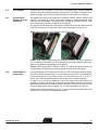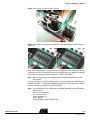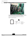
1
STK502
..............................................................................................
User Guide
Table of Contents
Section 1
Introduction ........................................................................................... 1-1
Section 2
Using the STK502 Top Module............................................................. 2-1
2.1
Connecting the STK502 to the STK500 Starter Kit ...................................2-1
2.1.1
2.2
Placing an ATmega169 on STK502 ...................................................2-1
PORT Connectors.....................................................................................2-2
2.2.1
PORT E/PORT F ................................................................................2-2
2.2.2
PORT G/RST......................................................................................2-2
2.3
Programming the ATmega169 ..................................................................2-4
2.3.1
In-System Programming.....................................................................2-4
2.3.2
High-voltage Programming.................................................................2-5
2.4
2.5
JTAG Connector .......................................................................................2-6
LCD Display ..............................................................................................2-7
2.5.1
Connecting the STK502 LCD to the ATmega169...............................2-7
2.5.2
Default Segment Configuration ..........................................................2-7
2.5.3
Using Both Colons on the Display ......................................................2-8
2.6
2.7
TOSC Switch...........................................................................................2-10
Sensor.....................................................................................................2-11
2.7.1
Sensor Switches...............................................................................2-11
Section 3
Troubleshooting Guide ......................................................................... 3-1
Section 4
Technical Specifications ....................................................................... 4-1
4.1
STK502 User Guide
STK502 LCD Bit Mappings .......................................................................4-3
4.1.1
Alphanumeric Digit Number Two........................................................4-3
4.1.2
Alphanumeric Digit Number Three .....................................................4-3
4.1.3
Alphanumeric Digit Number Four .......................................................4-3
4.1.4
Alphanumeric Digit Number Five........................................................4-3
4.1.5
Alphanumeric Digit Number Six..........................................................4-4
4.1.6
Alphanumeric Digit Number Seven ....................................................4-4
i
2528A–AVR–11/02
Table of Contents
Section 5
Technical Support................................................................................. 5-1
Section 6
Complete Schematics........................................................................... 6-1
ii
2528A–AVR–11/02
STK502 User Guide
Section 1
Introduction
The STK502 board is a top module designed to add ATmega169 support to the STK500
development board from Atmel Corporation.
STK502 includes connectors and hardware allowing full utilization of the new features of
the ATmega169. The Zero Insertion Force (ZIF) socket makes it easy to use of TQFP
packages for prototyping.
This user guide is a general getting started guide as well as a complete technical reference for advanced users.
The STK502 board also includes a demonstration application, and comes with two
application notes, “AVR064: STK502 – A Temperature Monitoring System with LCD
Output” and “AVR065: LCD Driver for the STK502”. These application notes explain
how to use the different modules in the device. Included in the kit is a pre-programmed
ATmega169. Insert the device in the ZIF socket and the demonstration application will
start immediately.
Figure 1-1. STK502 Top Module for STK500
STK502 User Guide
1-1
Rev. 2528A–AVR–11/02
Introduction
1.1
Features
Supports the ATmega169 with Built-in LCD Controller.
LCD-on-glass Display for Demonstrating the ATmega169 LCD Controller.
Supported by AVR Studio® 4.
Zero Insertion Force Socket for TQFP Packages.
High Voltage Parallel Programming.
Serial Programming.
TQFP Footprint for Emulator Adapters.
Port Extension Connectors for Port E, F, and G.
LCD Display Header for Using an External LCD Display.
LCD and Other Peripherals Can be Disconnected from the Device.
JTAG Connector for On-chip Debugging Using JTAG ICE.
On-board 32 kHz Crystal for Easy Real Time Clock Implementations.
Temperature Sensor for the Demo Application.
Quick Reference to all Switches and Jumpers in the Silk-Screen of the PCB.
Pre-programmed ATmega169 with Demonstration Application. Includes C-code
Examples for all Major Peripherals on the ATmega169 Device.
– The Way to Get Going with your ATmega169
1-2
2528A–AVR–11/02
STK502 User Guide
Section 2
Using the STK502 Top Module
This section describes in detail how the STK502 is used with the STK500.
2.1
Connecting the
STK502 to the
STK500 Starter
Kit
Connect STK502 to the STK500 expansion header 0 and 1. It is important that the top
module is connected in the correct orientation as shown in Figure 2-1. EXPAND0 written
on the STK502 top module should match EXPAND0 written beside the expansion
header on the STK500 board.
Figure 2-1. Connecting STK502 to the STK500 Board
Note:
2.1.1
Placing an
ATmega169 on
STK502
STK502 User Guide
Connecting STK502 with wrong orientation may damage the board.
STK502 contains both a ZIF socket, and a footprint for a TQFP package which allows an
easy way of soldering an emulator adapter directly into the STK502. Care should be
taken so that the device (or adapter) is mounted with the correct orientation. Figure 2-2
shows the location of pin1 for the ZIF socket and the TQFP footprint.
2-1
Rev. 2528A–AVR–11/02
Using the STK502 Top Module
Figure 2-2. Pin1 on ZIF Socket and TQFP Footprint
Caution: Do not mount an ATmega169 on the STK502 at the same time as an AVR is
mounted on the STK500 board. Neither of the devices will work as intended.
2.2
PORT
Connectors
ATmega169 have additional ports to those available on the STK500. The ports are
located on the STK502 board. They have the same pin out and functionality as the ports
on the STK500 board. Port A to Port D are already present on the STK500 board. They
are not duplicated on the STK502.
2.2.1
PORT E/PORT F
Figure 2-3 shows the pin out for the I/O port headers Port E and Port F.
Figure 2-3. General I/O Ports
1
2
2.2.2
PORT G/RST
2-2
2528A–AVR–11/02
2
PE0
PE1
PF0
PF1
PE2
PE3
PF2
PF3
PE4
PE5
PF4
PF5
PE6
PE7
PF6
PF7
GND
VTG
GND
VTG
PORTE
Note:
1
PORTF
Port E is also present on the STK500, but only PE0 to PE2 (three least significant bits) are accessible there. To access all Port E bits the connector on the
STK502 must be used.
In addition to the normal Port G pins, this connector has the RESET-signal. Se Figure 24.
STK502 User Guide
Using the STK502 Top Module
Figure 2-4. PORTG/RST
1
2
PG0
PG1
PG2
PG3
PG4
PG5
NC
RST
GND
VTG
PORTG/RST
2.2.2.1
PG0 - PG5
These are general I/O ports connected to ZIF socket and the TQFP footprint.
2.2.2.2
RST
On the ATmega169 the RESET-signal and PG5 share the same pin. The “RST” is the
RESET-signal that comes from the STK500 board. Please note that it is not directly connected to the ZIF socket or the TQFP footprint on the STK502. This because the
RESET-signal on the STK500 has an pull-up resistor to VCCT which will interfere with
PG5 when used as an ordinary I/O-pin.
If RESET/PG5-pin on ATmega169 shall be used as a Reset pin, the RST and PG5 on
the PORTG /RST must be connected with a jumper. See Figure 2-5.
If the pin shall be used as an I/O-pin the jumper must be removed.
Figure 2-5. The RESET Signal on PORTG/RST
STK502 User Guide
2-3
2528A–AVR–11/02
Using the STK502 Top Module
2.3
Programming the The ATmega169 can be programmed using both SPI and High-voltage Parallel Programming. This section will explain how to connect the programming cables to
ATmega169
successfully use one of these two modes. The AVR Studio STK500 software is used in
the same way as for other AVR parts as described in the STK500 User Guide.
2.3.1
In-System
Programming
Note:
The ATmega169 also support Self Programming, See AVR109 application note
for more information on this topic.
Note:
The jumper for the Reset-signal on PORTG/RST must be mounted before any
programming can take place. See Section 2.2.2.2
Figure 2-6. In-System Programming
To program the ATmega169 using ISP Programming mode, connect the 6-wire cable
between the ISP6PIN connector on the STK500 board and the ISP connector on the
STK502 board as shown in Figure 2-6. The device can be programmed using the Serial
Programming mode in the AVR Studio4 STK500 software.
Note:
2-4
2528A–AVR–11/02
See STK500 User Guide for information on how to use the STK500 front-end
software for ISP Programming.
STK502 User Guide
Using the STK502 Top Module
2.3.2
High-voltage
Programming
Figure 2-7. High-voltage (Parallel) Programming
To program the ATmega169 using High-voltage (Parallel) Programming, connect the
PROGCTRL to PORTD and PROGDATA to PORTB on the STK500 as shown in Figure
2-7. Make sure that the TOSC-switch is placed in the XTAL position. See Section 2.6,
“TOSC Switch”.
As described in the STK500 User Guide (jumper settings), mount the BSEL2 jumper in
order to High-voltage Program the ATmega devices. This setting also applies to Highvoltage Programming of the ATmega169.
The device can now be programmed using the High-voltage Programming mode in AVR
Studio STK500 software.
Note:
See the STK500 User Guide for information on how to use the STK500 frontend software in High-voltage Programming mode.
Note:
For the High-voltage Programming mode to function correctly, the target voltage
must be higher than 4.5V.
Caution: Make sure to disconnect LCD-display from the segment pins header. Otherwise the lifetime of the LCD display may be severely reduced. See Figure 2-10.
STK502 User Guide
2-5
2528A–AVR–11/02
Using the STK502 Top Module
2.4
JTAG Connector
Figure 2-8 shows how to connect the JTAG ICE probe on the STK502 board.
Figure 2-8. Connecting JTAG ICE to the STK502
The JTAG connector is used for the ATmega169 built-in JTAG interface. The pin out of
the connector is shown in Figure 2-9 and is compliant with the pin out of the JTAG ICE
available from Atmel. Connecting a JTAG ICE to this connector allows On-chip Debugging of the ATmega169.
More information about the JTAG ICE and On-chip Debugging can be found in the AVR
JTAG ICE User Guide, which is available at the Atmel web site, www.atmel.com.
Figure 2-9. JTAG Connector
1
2
TCK
GND
TDO
VTG
TMS
RST
VTG
NC
GND
TDI
JTAG
2-6
2528A–AVR–11/02
STK502 User Guide
Using the STK502 Top Module
2.5
LCD Display
STK502 includes a LCD display. It features six 14-segments digits, and some additional
segments. All in all the display supports 120 segments. The display is designed for 3V
operating voltage. See the Technical Specifications for more details on the display.
2.5.1
Connecting the
STK502 LCD to the
ATmega169
The segment-pins from the ATmega169 are located at PORTA, PORTC, PORTD, and
PORTG. For simplicity in use they are all joined together on the header labeled “Segment pins from ATmega169”. The header next to it, labelled “STK502 LCD pins” holds
all the segments-pins for the LCD-display on the STK502.
By using the 34-lead cable that comes with the STK502-kit, the two pin-headers can be
connected, allowing the ATmega169 to control the LCD-display. See Figure 2-10.
Figure 2-10. Connecting the ATmega169 to the STK502 LCD
Caution: High-voltage Programming uses PORTB and PORTD. Be sure to disconnect
any LCD-display connected to the ATmega169 during the High-voltage Programming.
Otherwise the lifetime of the display may be reduced.
Caution: When using PORTA, PORTC, PORTD, or PORTG as regular I/O ports, the
corresponding LCD-segment pins must be disconnected from the ATmega169.
2.5.2
Default Segment
Configuration
ATmega169 supports 100 segments. Thus not all of the 120 segments on the LCD-display can be shown simultaneously. Five of the 30 segment-pins on the LCD display has
to be left unconnected. The LCD-pins that are not connected are pin #: 3, 24, 30, 31,
and 32. See Technical Specifications for an overview of the excluded segments.
In order to use some of the segments on the LCD display that by default are not
included or in order to use some of the segment pins as ordinary I/O-pins, use a custom
strap between the two 34-pin headers. These to headers are lined up so they will fit in to
a 2.54 mm pitch grid for easy connecting, e.g., a experiment board on top of them.
The pin out for these two headers (Figure 2-11) can be found on the bottom-side of the
STK502-PCB or in Section 6 “Complete Schematics”.
STK502 User Guide
2-7
2528A–AVR–11/02
Using the STK502 Top Module
Figure 2-11. Pin out for LCD Headers
1
2
1
2
SEG01
SEG02
LCD27
LCD28
SEG03
SEG04
LCD29
LCD04
SEG05
SEG06
LCD06
LCD25
SEG07
SEG08
LCD26
LCD05
SEG09
SEG10
LCD08
LCD22
SEG11
SEG12
LCD23
LCD07
SEG13
SEG14
LCD10
LCD20
SEG15
SEG16
LCD21
LCD09
SEG17
SEG18
LCD14
LCD12
SEG19
SEG20
LCD11
LCD13
SEG21
SEG22
LCD18
LCD16
SEG23
SEG24
LCD15
LCD17
SEG25
NC
LCD19
LCD03
NC
NC
LCD24
LCD30
NC
NC
LCD31
LCD32
COM00
COM01
BP1
BP2
COM02
COM03
BP4
BP3
Seg. M169
LCD Pins
This hardware configuration will give a certain bit-mapping between the bits in the
ATmega169 LCDDRx Register and the segments on the STK502 LCD. See Section 4.1
“STK502 LCD Bit Mappings”
2.5.3
Using Both Colons
on the Display
2-8
2528A–AVR–11/02
With the header J300 labelled “19 24” one can connect LCD-pin 24 (which is default
unconnected) to LCD-pin 19 by the use of a jumper. See Figure 2-12. The reason for
doing so is that the LCD-pin 24 has the segment “COL1” and LCD-pin 19 has “COL2”. In
applications where a clock, date etc. shall be displayed, it can be useful to control both
colons on the LCD-display. But connecting these LCD-pins will also lead to a connection
between segment (see Technical Specifications) “S5” and “3”, “S8” and “S7”, “8” and
“7”, which will in practice make them useless. See Figure 2-13 showing which segments are available on the LCD-display with the default segment configuration.
STK502 User Guide
Using the STK502 Top Module
Figure 2-12. Jumper to connect COL1 to COL2
Figure 2-13. Default LCD-segment configuration, with and without the jumper shown in
Figure 2-12
Other LCD-displays can be connected to the ATmega169, either through the header
“Segment pins from ATmega169” where all the segment pins are gathered or through
the ordinary Port-connectors PORTA, PORTC, PORTD, and PORTG.
Note:
Make sure the display is compatible with the electrical characteristics on the
ATmega169.
For more information on how to write software for the LCD-display see application note
“AVR064: STK502 – A Temperature Monitoring System with LCD Output” and application note “AVR065: LCD Driver for the STK502 LCD”.
Note:
STK502 User Guide
The LCD-display on the STK502 can be ordered separately from ACTE Norway
(www.acte.no).
Phone: +47 63 89 89 00
Fax: +47 63 87 90 00
E-mail: [email protected]
Price: NOK 99,Ordering number: H4042-DL DE5156/L.
2-9
2528A–AVR–11/02
Using the STK502 Top Module
2.6
TOSC Switch
Figure 2-14. TOSC Switch
On the ATmega169 the TOSC1 and TOSC2 lines are shared with XTAL1 and XTAL2.
The TOSC switch selects whether the 32 kHz crystal on the STK502, or the XT1/XT2
signals from STK500 should be connected to these pins on the device.
Figure 2-15 shows a simplified block schematic on how this is implemented.
Figure 2-15. TOSC Block Schematic
32 kHz
AVR
XTAL1/TOSC1
XT1
To
STK500
XTAL2/TOSC2
XT2
TOSC
Switch
2-10
2528A–AVR–11/02
STK502 User Guide
Using the STK502 Top Module
2.7
Sensor
Figure 2-16. NTC-thermistor
STK502 includes a two screw-terminal block where a sensor can be connected. The
STK502 kit is shipped with a NTC-thermistor attached to this screw-terminal. A NTCthermistor is characterised by the fact that when the temperature goes down the resistance goes up. Using a voltage divider and reading the voltage over the thermistor
through the ADC-channels on ATmega169, the temperature can be calculated. Application note “AVR064: STK502 – A Temperature Monitoring System with LCD Output”
describes the details of the application.
2.7.1
Sensor Switches
Two switches on the STK502 are used to connect the sensor to the ADC-channels on
the ATmega169 as shown in Figure 2-17.
Figure 2-17. Temperature sensor switches
STK502 User Guide
2-11
2528A–AVR–11/02
Using the STK502 Top Module
2.7.1.1
AREF Switch
The switch named AREF selects the input to the AREF-pin on the ATmega169.
Figure 2-18. AREF Switch
AVR
From
STK500
AREF
AREF
STK502
STK502
VREF
Voltage refernce
for the sensor
AREF
Switch
Positions:
AREF: In this position the AREF from the STK500 is connected to the AREF pin on
the ATmega169. This is the default position.
VREF: In this position the VREF from the 1.263V voltage reference on the STK502 is
connected to the AREF pin on the ATmega169. Select this position in order to run the
code in Application Note “AVR064: STK502 – A Temperature Monitoring System with
LCD Output”
2.7.1.2
PF[1:0] Switch
The PF[1:0] switch selects the input to the PF1 and PF0 pins (ADC channel 1/0) on the
ATmega169.
Figure 2-19. PF[1:0] Switch
AVR
PORTF0
PF0 (ADC0)
Sensor
pin 1
PORTF1
PF1 (ADC1)
Sensor
pin 2
PF[1:0]
Switch
Positions:
PIN: In this position the PF0 and PF1 are from the PORTF on the STK502 are
connected to the PF0 and PF1 on the ATmega169. Default position.
Sensor: In this position the pin 1 from the screw-terminal on the STK502 are
connected to PF0 on the ATmega169, and the pin 2 from the screw-terminal are
connected to PF1 on the ATmega169. Select this position in order to run the code in
Application Note “AVR064: STK502 – A Temperature Monitoring System with LCD
output”
In the sensor position both PF0 and PF1 are connected to the senor pins, regardless of
using single ended or differential ADC-measurements in the application. This means
that it's not possible to use PF1 as an ordinary I/O-port even though only PF0 (single
ended) is used with the ADC.
2-12
2528A–AVR–11/02
STK502 User Guide
Section 3
Troubleshooting Guide
Table 3-1. Troubleshooting Guide
Problem
Reason
Solution
The LCD is not connected.
Attach the 34-pins cable between
the to 34-pins headers on the
STK502.
The LCD is not enabled in
the AVR device.
Check the LCD initialisation(1).
The update frequency is
not correct.
Verify that the clock prescaling
correspond with the clock source(1).
Some segments on the
LCD seems to be stuck
at high/low.
The PORTA/C/D and/or G
are connected to
something else than the
LCD display.
Check that nothing is connected to
these PORTS on the STK500 and
STK502.
Can’t control
PORTF[1:0]
PF[1:0] is not connected to
the ATmega169.
Set the PF[1:0] switch in the PINposition.
ISP cable not connected.
Connect the ISP cable according to
Figure 2-6.
STK500 target voltage
error.
Please refer to the ATmega169
datasheet for the Serial
Programming Voltage limits. Adjust
the target voltage on the STK500
board accordingly.
The RSTDISBL Fuse is
programmed.
Use Parallel Programming to
unprogram the RSTDISBL Fuse.
Nothing is displayed on
the LCD.
Serial Programming
does not work
STK502 User Guide
3-1
Rev. 2528A–AVR–11/02
Troubleshooting Guide
Table 3-1. Troubleshooting Guide
Problem
Parallel Programming
does not work.
No programming works.
Note:
3-2
2528A–AVR–11/02
Reason
Solution
Cables not connected
properly.
Please refer to Figure 2-7 for
correct Parallel Programming setup.
STK500 target voltage
error.
Please refer to the ATmega169 data
sheet for the Parallel Programming
Voltage limits. Adjust the target
voltage on the STK500 board
accordingly.
The TOSC switch is not
correctly set.
Set the TOSC switch in the XTALposition.
The RESET-signal is not
connected to the
ATmega169.
Connect PG5 and RST with a
jumper. See Section 2.2.2.2 RST.
1. See the application note “AVR065: LCD Driver for the STK502 LCD” on how to control the LCD-display or the the application note “AVR064: STK502 – A Temperature
Monitoring System with LCD Output”.
STK502 User Guide
Section 4v
Technical Specifications
System Unit
Physical Dimensions . . . . . . . . . . . . . . . . . . . . . . . . . . . . . . . . . . . . . . 56 x 119 x 27 mm
Weight . . . . . . . . . . . . . . . . . . . . . . . . . . . . . . . . . . . . . . . . . . . . . . . . . . . . . . . . . . . . 70 g
Operating Conditions
Voltage Supply . . . . . . . . . . . . . . . . . . . . . . . . . . . . . . . . . . . . . . . . . . . . . . . .1,8V - 5,5V
Temperature . . . . . . . . . . . . . . . . . . . . . . . . . . . . . . . . . . . . . . . . . . . . . . . . . . 0°C - 50°C
LCD-display
Operation voltage . . . . . . . . . . . . . . . . . . . . . . . . . . . . . . . . . . . . . . . . . . . . . . . . . . . . 3V
STK502 User Guide
4-1
Rev. 2528A–AVR–11/02
Technical Specifications
Figure 4-1. Layout for the STK502 LCD-display
4-2
2528A–AVR–11/02
STK502 User Guide
Technical Specifications
4.1
STK502 LCD Bit
Mappings
The LCD Data Registers (LCDDRx) in the ATmega169 are organized in groups according to the use of Backplane Control Lines (also known as Common Lines). The LCD on
the STK502 uses all four Common Lines and all 25 segments, in total 4 x 25 = 100 segments. As can be seen in the LCD data sheet (Figure 4-1) describing the internal
connection of pins, Common Lines and segments, the alphanumeric digits are referred
to with a number according to where they are located on the LCD. Listed below is a
description of the STK502 bit mappings according to this.
4.1.1
Alphanumeric Digit
Number Two
The bit mappings for the alphanumeric digit number two are listed below.
Table 4-1. Bit Mappings for LCD Alphanumeric Digit Number Two
Register Name
4.1.2
Alphanumeric Digit
Number Three
Bit7
Bit6
Bit5
Bit4
Bit3
Bit2
Bit1
Bit0
LCDDR0
2-K
1
S1
2-A
LCDDR5
2-J
2-F
2-H
2-B
LCDDR10
2-L
2-E
2-G
2-C
LCDDR15
2-M
2-P
2-N
2-D
The bit mappings for the alphanumeric digit number three are listed below.
Table 4-2. Bit Mappings for LCD Alphanumeric Digit Number Three
4.1.3
Alphanumeric Digit
Number Four
Register Name
Bit7
Bit6
Bit5
Bit4
LCDDR0
3-K
2
S2
3-A
LCDDR5
3-J
3-F
3-H
3-B
LCDDR10
3-L
3-E
3-G
3-C
LCDDR15
3-M
3-P
3-N
3-D
Bit3
Bit2
Bit1
Bit0
The bit mappings for the alphanumeric digit number four are listed below.
Table 4-3. Bit Mappings for LCD Alphanumeric Digit Number Four
Register Name
4.1.4
Alphanumeric Digit
Number Five
Bit7
Bit6
Bit5
Bit4
Bit3
Bit2
Bit1
Bit0
LCDDR1
4-K
S3
4
4-A
LCDDR6
4-J
4-F
4-H
4-B
LCDDR11
4-L
4-E
4-G
4-C
LCDDR16
4-M
4-P
4-N
4-D
Bit1
Bit0
The bit mappings for the alphanumeric digit number five are listed below.
Table 4-4. Bit Mappings for LCD Alphanumeric Digit Numer Five
STK502 User Guide
Register Name
Bit7
Bit6
Bit5
Bit4
LCDDR1
5-K
S4
5
5-A
LCDDR6
5-J
5-F
5-H
5-B
LCDDR11
5-L
5-E
5-G
5-C
LCDDR16
5-M
5-P
5-N
5-D
Bit3
Bit2
4-3
2528A–AVR–11/02
Technical Specifications
4.1.5
Alphanumeric Digit
Number Six
The bit mappings for the alphanumeric digit number six are listed below.
Table 4-5. Bit Mappings for LCD Alphanumeric Digit Number Six
Register Name
4.1.6
Alphanumeric Digit
Number Seven
Bit7
Bit6
Bit5
Bit4
Bit3
Bit2
Bit1
Bit0
LCDDR2
6-K
9
S9
6-A
LCDDR7
6-J
6-F
6-H
6-B
LCDDR12
6-L
6-E
6-G
6-C
LCDDR17
6-M
6-P
6-N
6-D
The bit mappings for the alphanumeric digit number seven are listed below.
Table 4-6. Bit Mappings for LCD Alphanumeric Digit Number Seven
4-4
2528A–AVR–11/02
Register Name
Bit7
Bit6
Bit5
Bit4
LCDDR2
7-K
10
S10
7-A
LCDDR7
7-J
7-F
7-H
7-B
LCDDR12
7-L
7-E
7-G
7-C
LCDDR17
7-M
7-P
7-N
7-D
Bit3
Bit2
Bit1
Bit0
STK502 User Guide
Section 5
Technical Support
For Technical support, please contact [email protected]. When requesting technical support, please include the following information:
Which target AVR device is used (complete part number).
Target voltage and speed.
Clock source and fuse setting of the AVR.
Programming method (ISP or High-voltage).
Hardware revisions of the AVR tools, found on the PCB.
Version number of AVR Studio. This can be found in the AVR Studio help menu.
PC operating system and version/build.
PC processor type and speed.
A detailed description of the problem.
STK502 User Guide
5-1
Rev. 2528A–AVR–11/02
Technical Support
5-2
2528A–AVR–11/02
STK502 User Guide
Section 6
Complete Schematics
On the following pages the complete schematics and assembly drawing of the STK502
revision B are shown.
STK502 User Guide
6-1
Rev. 2528A–AVR–11/02
A
B
C
1
PGT[5..0]
PBT[7..0]
PGT[5..0]
PBT[7..0]
PET[7..0] PET[7..0]
AREFT
AREFT
PFT[7..0] PFT[7..0]
ADC0
2
VTG
PBT7
GND
1
2
3
4
5
6
7
8
9
10
11
12
13
14
15
16
LCDCAP
PE0(RXD)
PE1(TXD)
PE2(AIN0/XCK)
PE3(AIN1)
PE4(SCL/USCK)
PE5(SDA/DI)
PE6(DO)
PE7
PB0(SS)
PB1(SCK)
PB2(MOSI)
PB3(MISO)
PB4(OC0)
PB5(OC1A)
PB6(OC1B)
C102
100N_16V_X7R
LCDCAP
PET0
PET1
PET2
PET3
PET4
PET5
PET6
PET7
PBT0
PBT1
PBT2
PBT3
PBT4
PBT5
PBT6
GND
GND
AVTG
C100
100N_16V_X7R
GND
C108
1U_16V_X7R
Not mounted
1
2
ADC1
VTG
GND
2
C103
100N_16V_X7R
PGT3
PGT4
PGT5
TQFP Footprint
1
2
1
ADC0
ADC1
PFT2
PFT3
PFT4
PFT5
PFT6
PFT7
D
1
2
PAT0
PAT1
PAT2
64
63
62
61
60
59
58
57
56
55
54
53
52
51
50
49
C104
100N_16V_X7R
GND
VTG
3
3
PCT7
PCT6
PCT5
PCT4
PCT3
PCT2
PCT1
PCT0
PAT3
PAT4
PAT5
PAT6
PAT7
2
ATMEGA169L-4AC
Not mounted
48
47
46
45
44
43
42
41
40
39
38
37
36
35
34
33
U100
BLM-21A102S
L100
C105
100N_16V_X7R
1
(COM3)PA3
(SEG0)PA4
(SEG1)PA5
(SEG2)PA6
(SEG3)PA7
(SEG4)PG2
(SEG5)PC7
(SEG6)PC6
(SEG7)PC5
(SEG8)PC4
(SEG9)PC3
(SEG10)PC2
(SEG11)PC1
(SEG12)PC0
(SEG13)PG1
(SEG14)PG0
AVCC
AGND
AREF
(ADC0)PF0
(ADC1)PF1
(ADC2)PF2
(ADC3)PF3
(TCK/ADC4)PF4
(TMS/ADC5)PF5
(TDO/ADC6)PF6
(TDI/ADC7)PF7
GND
VCC
(COM0)PA0
(COM1)PA1
(COM2)PA2
PB7(OC2)
PG3(T1/SEG24)
PG4(T0/SEG23)
PG5(RESET)
VCC
GND
XTAL2(TOSC2)
XTAL1(TOSC1)
PD0(ICP/SEG22)
PD1(INT0/SEG21)
PD2(SEG20)
PD3(SEG19)
PD4(SEG18)
PD5(SEG17)
PD6(SEG16)
PD7(SEG15)
17
18
19
20
21
22
23
24
25
26
27
28
29
30
31
32
PDT0
PDT1
PDT2
PDT3
PDT4
PDT5
PDT6
PDT7
1
2
C106
100N_16V_X7R
PDT[7..0]
PGT2
PAT[7..0]
XTAL2
XTAL1
PDT[7..0]
PGT1
PGT0
PCT[7..0]
4
C107
100N_16V_X7R
AVTG
PCT[7..0]
PAT[7..0]
4
5
PGT[5..0] PGT[5..0]
PBT[7..0]
PBT[7..0]
PET[7..0] PET[7..0]
AREFT
AREFT
PFT[7..0] PFT[7..0]
ADC0
ADC1
ZIF Socket
5
1
PBT7
LCDCAP
PET0
PET1
PET2
PET3
PET4
PET5
PET6
PET7
PBT0
PBT1
PBT2
PBT3
PBT4
PBT5
PBT6
GND
1
2
3
4
5
6
7
8
9
10
11
12
13
14
15
16
GND
AVTG
C101
100N_16V_X7R
GND
C109
1U_16V_X7R
ST100
1
2
2
1
2
1
2
1
2
VTG
GND
6
ADC0
ADC1
PFT2
PFT3
PFT4
PFT5
PFT6
PFT7
6
PGT3
PGT4
PGT5
2
PAT0
PAT1
PAT2
TQFP64 ZIF SOCKET
64
63
62
61
60
59
58
57
56
55
54
53
52
51
50
49
2528A–AVR–11/02
17
18
19
20
21
22
23
24
25
26
27
28
29
30
31
32
6-2
GND
VTG
48
47
46
45
44
43
42
41
40
39
38
37
36
35
34
33
7
27-Aug-2002
PCT7
PCT6
PCT5
PCT4
PCT3
PCT2
PCT1
PCT0
PAT3
PAT4
PAT5
PAT6
PAT7
16:12:06
PDT[7..0]
PCT[7..0]
PAT[7..0]
Revision: B
PAGE:
XTAL2
MCU.Sch
7
8
1
PDT[7..0]
of
PGT1
PGT0
PCT[7..0]
XTAL1
8
PGT2
PAT[7..0]
TITLE: STK502 add-on card for ATmega169, SOCKETS
Document number: A9903.3.1020.B
Date:
NORWAY
7075 TILLER
Vestre Rosten 78,
ATMEL Norway
PDT0
PDT1
PDT2
PDT3
PDT4
PDT5
PDT6
PDT7
1
3
A
B
C
D
Complete Schematics
Figure 6-1. Schematics, 1 of 3
STK502 User Guide
A
B
C
1
PGT[4..0]
PDT[7..0]
PCT[7..0]
PAT[7..0]
PFT[7..0]
PCT[7..0]
PAT[7..0]
RESET
PFT0
PFT2
PFT4
PFT6
PGT[4..0]
PDT[7..0]
PCT[7..0]
PAT[7..0]
GND
PFT[7..0]
PCT[7..0]
PAT[7..0]
1
3
5
7
9
VTG
PORTF
J204
C201
100N_16V_X7R
2
4
6
8
10
2
PFT1
PFT3
PFT5
PFT7
GND
VTG
NOT MOUNTED
1
2
GND
J206
EXPAND0
J200
2
4
6
8
10
12
14
16
18
20
22
24
26
28
30
32
34
2
4
6
8
10
12
14
16
18
20
22
24
26
28
30
32
34
36
38
40
PAT1
PAT3
PAT5
PAT7
PCT7
PCT5
PCT3
PCT1
PGT1
PDT7
PDT5
PDT3
PDT1
PGT4
3
PFT7
PFT4
PFT6
PFT5
GND
PCT6
PCT4
PCT2
PCT0
PAT6
PAT4
PAT2
PAT0
AREF
PET2
PET0
PH_2,54_17X2_GOLD
LCD signals from MCU
1
3
5
7
9
11
13
15
17
19
21
23
25
27
29
PAT0 31
PAT2 33
PAT4
PAT6
PGT2
PCT6
PCT4
PCT2
PCT0
PGT0
PDT6
PDT4
PDT2
PDT0
PGT3
GND
PCT7
PCT5
PCT3
PCT1
PAT7
PAT5
PAT3
PAT1
PET1
RESET
R200
0R
1
3
5
7
9
11
13
15
17
19
21
23
25
27
29
31
33
35
37
39
VTG
GND
1
3
5
7
9
JTAG
J202
2
4
6 RESET
8
10
VTG
GND
AREF
GND
GND
4
VTG
VTG
1
3
5
7
9
GND
C202
100N_16V_X7R
GND
PET0
PET2
PET4
PET6
2
4
6
8
10
LCD24
LCD31
COM0
COM2
VTG
2
4
6
8
10
12
14
16
18
20
22
24
26
28
30
32
34
GND
PGT0
PGT2
PGT4
LCD3
LCD30
LCD32
COM1
COM3
5
VTG
PGT1
PGT3
PGT5
RESET
GND
VTG
COM[3..0]
LCD[32..3]
2
4
6
8
10
PORTG/RES
J205
LCD28
LCD4
LCD25
LCD5
LCD22
LCD7
LCD20
LCD9
LCD12
LCD13
LCD16
LCD17
1
3
5
7
9
PH_2,54_17X2_GOLD
Signals to LCD
1
3
5
7
9
11
13
15
17
19
21
23
25
27
29
31
33
J207
PGT[5..0]
PET1
PET3
PET5
PET7
LCD27
LCD29
LCD6
LCD26
LCD8
LCD23
LCD10
LCD21
LCD14
LCD11
LCD18
LCD15
LCD19
PGT[5..0]
PORTE
J203
5
6
COM[3..0]
LCD[32..3]
GND
1
3
5
R201 7
9
0R
11
13
GND
15
17
XT1
19
21
23
PBT7
25
PBT5
27
PBT3
29
PBT1
31
PDT7
33
PDT5
35
PDT3
37
PDT1
39
JS200
6
2
1
D
1
2
PET[7..0]
4
GND
RESET 5
1
3
2
4
6 GND
8
10
12
14
16
18
XT2
20
22
24
PBT6
26
PBT4
28
PBT2
30
PBT0
32
PDT6
34
PDT4
36
PDT2
38
PDT0
40
ISP_CONNECTOR
MISO
VCC
SCK
MOSI
RESET GND
J208
7
27-Aug-2002
2
4
6
VTG
GND
VTG
16:12:07
GND
VTG
PBT[7..0]
PDT[7..0]
C200
100N_16V_X7R
GND
Connectors.Sch
7
8
PBT[7..0]
2
Revision: B
PAGE:
XT2
XT1
PDT[7..0]
8
of
3
C203
100N_16V_X7R
TITLE: STK502 add-on card for ATmega169, CONNECTORS
Document number: A9903.3.1020.B
Date:
NORWAY
7075 TILLER
Vestre Rosten 78,
ATMEL Norway
EXPAND1
J201
PBT1
PBT3
PBT2
1
2
PET[7..0]
3
1
2
2
1
STK502 User Guide
2
1
A
B
C
D
Complete Schematics
Figure 6-2. Schematics, 2 of 3
6-3
2528A–AVR–11/02
A
B
C
1
PFT[7..0]
GND
1
PFT[7..0]
C300
100N_16V_X7R
AREF
LCD[32..3]
COM[3..0]
VTG
1
2
1
2
2
NTC-RH16
R300
A sensor will be
attached to this
screw-terminal
U301
MAX6018AEUR12-T
2
IN
GND
OUT
3
1
2
2
2
1
MPT_0,5/2-2,54
J301
C301
100N_16V_X7R
1
2
1
2
1
R302
0R
R301
10K
R303
0R
GND
2
3
3
3
VREF
1
3
6
4
NTC1
PFT0
NTC2
PFT1
4
6
1
AREF
GND
ADC1
5
AREFT
COM2
COM3
LCD3
LCD4
LCD5
LCD6
LCD7
LCD8
LCD9
LCD10
LCD11
LCD12
LCD13
LCD14
LCD15
LCD16
LCD17
ADC0
4
4
2
SW301
JSM2220-0201
GND
5
2
SW300
JSM2220-0201
LCD[32..3]
COM[3..0]
7
7
2528A–AVR–11/02
H4042-DL
ADC1
ADC0
LCD display
5
BP3
BP4
1K/1L/1M/6
2K/2J/2L/2M
3K/3J/3L/3M
3A/3B/3C/3D
4K/4J/4L/4M
4A/4B/4C/4D
5K/5J/5L/5M
5A/5B/5C/5D
9/6F/6E/6P
S9/6H/6G/6N
6K/6J/6L/6M
6A/6B/6C/6D
10/7F/7E/7P
S10/7H/7G/7N
7K/7J/7L/7M
U300
AREFT
1
2
3
4
5
6
7
8
9
10
11
12
13
14
15
16
17
5
XTAL1
XTAL2
BP2
BP1
1F/1G/1E/X2
1A/1J/1N/1D
X1/1B/1C/S6
1/2F/2E/2P
S1/2H/2G/2N
2A/2B/2C/2D
2/3F/3E/3P
S2/3H/3G/3N
3/COL1/S7/7
S3/4F/4E/4P
4/4H/4G/4N
S4/5F/5E/5P
5/5H/5G/5N
S5/COL2/S8/8
7A/7B/7C/7D
COM1
COM0
LCD32
LCD31
LCD30
LCD29
LCD28
LCD27
LCD26
LCD25
LCD24
LCD23
LCD22
LCD21
LCD20
LCD19
LCD18
6
XTAL1
6
5
2
J300
PH_2,54_2 X 1
XTAL2
JS300
34
33
32
31
30
29
28
27
26
25
24
23
22
21
20
19
18
1
2
6-4
GND
TOSC1
XT1
4
4
3
7
1
2
27-Aug-2002
IQD32.768KHZ
XC300
16:12:07
3
Revision: B
PAGE:
XT1
XT2
8
of
Peripherals.Sch
7
8
TITLE: STK502 add-on card for ATmega169, LCD, Sensor, 32kHz
Document number: A9903.3.1020.B
Date:
NORWAY
7075 TILLER
Vestre Rosten 78,
ATMEL Norway
XT2
6
TOSC2
3
SW302
JSM2220-0201
1
7
D
1
3
A
B
C
D
Complete Schematics
Figure 6-3. Schematics, 3 of 3
STK502 User Guide
Complete Schematics
Figure 6-4. Assembly Drawing, 1 of 1
STK502 User Guide
6-5
2528A–AVR–11/02
Complete Schematics
6-6
2528A–AVR–11/02
STK502 User Guide
Atmel Headquarters
Atmel Operations
Corporate Headquarters
Memory
2325 Orchard Parkway
San Jose, CA 95131
TEL 1(408) 441-0311
FAX 1(408) 487-2600
Europe
Atmel Sarl
Route des Arsenaux 41
Case Postale 80
CH-1705 Fribourg
Switzerland
TEL (41) 26-426-5555
FAX (41) 26-426-5500
Asia
Room 1219
Chinachem Golden Plaza
77 Mody Road Tsimhatsui
East Kowloon
Hong Kong
TEL (852) 2721-9778
FAX (852) 2722-1369
Japan
9F, Tonetsu Shinkawa Bldg.
1-24-8 Shinkawa
Chuo-ku, Tokyo 104-0033
Japan
TEL (81) 3-3523-3551
FAX (81) 3-3523-7581
2325 Orchard Parkway
San Jose, CA 95131
TEL 1(408) 441-0311
FAX 1(408) 436-4314
RF/Automotive
Theresienstrasse 2
Postfach 3535
74025 Heilbronn, Germany
TEL (49) 71-31-67-0
FAX (49) 71-31-67-2340
Microcontrollers
2325 Orchard Parkway
San Jose, CA 95131
TEL 1(408) 441-0311
FAX 1(408) 436-4314
La Chantrerie
BP 70602
44306 Nantes Cedex 3, France
TEL (33) 2-40-18-18-18
FAX (33) 2-40-18-19-60
ASIC/ASSP/Smart Cards
1150 East Cheyenne Mtn. Blvd.
Colorado Springs, CO 80906
TEL 1(719) 576-3300
FAX 1(719) 540-1759
Biometrics/Imaging/Hi-Rel MPU/
High Speed Converters/RF Datacom
Avenue de Rochepleine
BP 123
38521 Saint-Egreve Cedex, France
TEL (33) 4-76-58-30-00
FAX (33) 4-76-58-34-80
Zone Industrielle
13106 Rousset Cedex, France
TEL (33) 4-42-53-60-00
FAX (33) 4-42-53-60-01
1150 East Cheyenne Mtn. Blvd.
Colorado Springs, CO 80906
TEL 1(719) 576-3300
FAX 1(719) 540-1759
Scottish Enterprise Technology Park
Maxwell Building
East Kilbride G75 0QR, Scotland
TEL (44) 1355-803-000
FAX (44) 1355-242-743
e-mail
[email protected]
Web Site
http://www.atmel.com
© Atmel Corporation 2002.
Atmel Corporation makes no warranty for the use of its products, other than those expressly contained in the Company’s standard warranty
which is detailed in Atmel’s Terms and Conditions located on the Company’s web site. The Company assumes no responsibility for any errors
which may appear in this document, reserves the right to change devices or specifications detailed herein at any time without notice, and does
not make any commitment to update the information contained herein. No licenses to patents or other intellectual property of Atmel are granted
by the Company in connection with the sale of Atmel products, expressly or by implication. Atmel’s products are not authorized for use as critical
components in life support devices or systems.
ATMEL ®, AVR ®, and AVR Studio ® are the registered trademarks of Atmel Corporation.
Microsoft ®, Windows ®, and Windows NT® are the registered trademarks of Microsoft Corporation.
Printed on recycled paper.
Other terms and product names may be the trademarks of others.
2528A–AVR–11/02
/0M