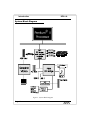
1
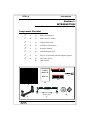
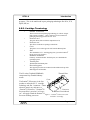
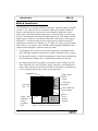
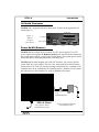
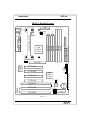
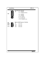
K P 6 -LA
A P e n tiu m ® II P r o c e s s o r b a s e d
A G P m a in b o a r d
TRADEMARK
All products and company names are trademarks or
registered trademarks of their respective holders.
These specifications are subject to change without notice.
Manual Revision 1.5
September 9, 1997
KP6-LA
KP6-LA
Technical Support Services
If you need additional information, help during installation or normal use of this
product, please contact your retailer. If your retailer can not help, you may E-Mail
us with any questions at the following address [email protected].
Record your serial number before installing your KP6-LA mainboard. (the serial
number is located near the ISA slots at the edge of the board)
EPoX KP6-LA serial number:
__________________________
BIOS Upgrades
Please use either our Web Site or BBS for current BIOS Upgrades.
Internet Access
http://www.epox.com
[email protected]
[email protected]
Modem Access
886-2-218-0997 (Taiwan)
31-182-618451 (The Netherlands)
You can access this number via a Hayes-compatible modem with a 2,400 to
28,800 baud rate. The following setup format is required:
8 Data Bits, No Parity, 1 Stop Bit.
If your modem is unable to connect at higher baud rates, try connecting at
2,400 baud before contacting Technical Support.
Thank you for using EPoX mainboards!
© Copyright 1997 EPoX Computer Company. All rights reserved.
KP6-LA
User Notice
No part of this product, including the product and software may be reproduced,
transmitted, transcribed, stored in a retrieval system, or translated into any language
in any form by any means without the express written permission of EPoX Computer
Company (hereinafter referred to as EPoX) except documentation kept by the
purchaser for backup purposes.
EPoX provides this manual “as is” without warranty of any kind, either express or
implied, including but not limited to the implied warranties or conditions of merchantability or fitness for a particular purpose. In no event shall EPoX be liable for
any loss or profits, loss of business, loss of use or data, interruption of business or
for indirect, special incidental, or consequential damages of any kind, even if EPoX
has been advised of the possibility of such damages arising from any defect or error
in the manual or product. EPoX may review this manual from time to time without
notice. For updated BIOS, drivers, or product release information you may visit
EPoX’s home page at: http://www.epox.com
Products mentioned in this manual are mentioned for identification purposes only.
Product names appearing in this manual may or may not be registered trademarks or
copyrights of their respective companies.
The product name and revision number are both printed on the mainboard
itself.
Handling Procedures
Static electricity can severely damage your equipment. Handle the KP6-LA and
any other device in your system with care and avoid unneccessary contact with
system components on the mainboard.
Always work on an antistatic surface to avoid possible damage to the motherboard
from static discharge.
We assume no responsibility for any damage to the KP6-LA mainboard that results
from failure to follow installation instructions or failure to observe safety precautions.
CAUTION
The KP6-LA mainboard is subject to
damage by static electricity. Always
observe the handling procedures.
KP6-LA
KP6-LA
KP6-LA
Table of Contents
Section 1
Introduction
Components Checklist ................................. 1-1
Overview
Pentium II ................................................... 1-2
S.E.C. Cartridge Terminology ..................... 1-3
Accelerated Graphics Port ........................... 1-4
Hardware Monitoring .................................. 1-4
Desktop Management Interface ................... 1-4
LANDesk Client Manager ........................... 1-4
KP6-LA Form-Factor .................................. 1-6
I/O Shield Connector ................................... 1-7
Power-On/Off (Remote) .............................. 1-7
System Block Diagram ................................ 1-8
Section 2
Features
KP6-LA Features ......................................... 2-1
Section 3
Installation
KP6-LA Detailed Layout ............................. 3-2
Easy Installation Procedure
Configure Jumpers ...................................... 3-3
System Memory Configuration .................... 3-5
Installing a Pentium® II Processor ................ 3-9
Device Connectors ...................................... 3-11
Section 4
Award BIOS Setup
BIOS Instructions ........................................ 4-1
Standard CMOS Setup ................................ 4-2
BIOS Features Setup ................................... 4-3
Chipset Features Setup ................................ 4-8
KP6-LA
Power Management Setup ........................... 4-13
PNP/PCI Configuration ............................... 4-16
Load Setup Defaults .................................... 4-18
Integrated Peripherals .................................. 4-19
Change Supervisor or User Password .......... 4-23
IDE HDD Auto Detection ............................ 4-24
HDD Low Level Format .............................. 4-26
Save & Exit Setup ....................................... 4-26
Exit Without Saving .................................... 4-27
Section 5
DMI
DMI Access ................................................ 5-1
Section 7
Appendix
Appendix A
Memory Map ............................................... A-1
I/O Map ....................................................... A-1
Timer & DMA Channels Map ..................... A-2
Interrupt Map .............................................. A-2
RTC & CMOS RAM Map ........................... A-3
Appendix B
POST Codes ................................................ A-5
Unexpected Errors ....................................... A-8
Appendix C
Load Setup Defaults .................................... A-9
KP6-LA
Introduction
Section 1
INTRODUCTION
Components Checklist
ü
ü
ü
ü
ü
ü
ü
ü
A.
(1)
KP6-LA mainboard
B.
(1)
KP6-LA user’s manual
C.
(1)
Floppy ribbon cable
D.
(2)
Hard drive ribbon cables
E.
(1)
Retention Module
F.
(1)
Heatsink Support Unit
G.
(1)
PS/2 to AT keyboard connector adapter (option)
H.
(1)
(1)
Bus master drivers
DMI (option)
USERS
MANUAL
C
G
KP6-LA
D
B
A
EPoX
Top Half
Bottom Half
E
C
D- R o m
or
H
F
Page 1-1
Introduction
KP6-LA
Overview
Pentium II
The Pentium® II Processor is the follow-on to the Pentium® Processor. The
Pentium® II Processor, like the Pentium® Pro processor, implements a Dynamic
Execution micro-architecture -- a unique combination of multiple branch prediction,
data flow analysis, and speculative execution. This enables the Pentium® II Processor to deliver higher performance than the Pentium® processor, while maintaining
binary compatibility with all previous Intel architecture processors.
A significant feature of the Pentium® II Processor, from a system perspective, is the
built-in direct multiprocessing support. In order to achieve multiprocessing, and
maintain the memory and I/O bandwidth to support it, new system designs are
needed. For systems with dual processors, it is important to consider the additional
power burdens and signal integrity issues of supporting multiple loads on a high
speed bus. The Pentium® II Processor card supports both uni-processor and dual
processor implementations.
The Pentium® II Processor utilizes Single Edge Contact (S.E.C.) (Figure 1) cartridge
packaging technology. The S.E.C. cartridge allows the L2 cache to remain tightly
coupled to the processor, while maintaining flexibility when implementing high
performance processors into OEM systems. The second level cache is performance
optimized and tested at the cartridge level. The S.E.C. cartridge utilizes surface
mounted core components and a printed circuit board with an edge finger connection. The S.E.C. cartridge package introduced on the Pentium® II Processor will also
be used in future Slot 1 processors.
The S.E.C. cartridge has the following features: a thermal plate, a cover and a PCB
with an edge finger connection. The thermal plate allows standardized heatsink
attachment or customized thermal solutions. The thermal plate enables a reusable
heatsink to minimize fit issues for serviceability, upgradeability and replacement.
The full enclosure also protects the surface mount components. The edge finger
connection maintains socketabilty for system configuration. The edge finger connector is denoted as ‘Slot 1 connector’ in this and other documentation.
The entire enclosed product is called the Pentium® II Processor. The packaging
technology and each of the physical elements of the product are referred to using
accurate technical descriptions. This allows clear reference to the products as just a
Page 1-2
KP6-LA
Introduction
processor. This is the model used in past packaging technologies like PGA, TCP,
PQFP, DIP, etc.
S.E.C. Cartridge Terminology
•
Pentium® II Processor
The new enclosed card packaging technology is called a “Single
Edge Contact cartridge.” This is similar to previous names for
packaging technology such as PGA or TCP.
•
Processor card
The green PCB (with or without components on it)
•
Processor core
The silicon on the PLGA package on the PCB
•
Cover
The plastic cover on the opposite side from the thermal plate.
•
Slot 1
The slot that the S.E.C. cartridge plugs into, just as the Pentium®
Pro processor uses Socket 8.
•
Retention mechanism
Formerly ‘retention module’ the dual posts, etc. that holds the
cartridge in place.
•
Thermal plate
The heatsink attachment plate.
•
Heat sink supports
The support pieces that are mounted on the mainboard to provide
added support for heatsinks.
The L2 cache (TagRAM, PBSRAM)
components keep standard industry
names.
Thermal Plate
Cover
The Pentium® II Processor is the first
product to utilize the S.E.C. cartridge
technology and Slot 1 connector. Unless
otherwise noted, any references to
“Pentium® II Processor,” “Pentium® II
Processor
Processor/Slot 1 processor” or ProcesPrinted Circuit Board
sor” will apply to both the Pentium® II
Figure 1: Pentium ® II Processor CPU
Processor desktop processors.
with S.E.C. Cartridge
Page 1-3
Introduction
KP6-LA
Accelerated Graphics Port
(AGP or A.G.P.)
Typically, 3D graphics rendering requires a tremendous amount of memory, and
demands ever increasing throughput speed as well. As 3D products for the personal
computer become more and more popular, these demands will only increase. This
will cause a rise in costs for both end users and manufacturers. Lowering these costs
as well as improving performance is the primary motivation behind AGP. By
providing a massive increase in the bandwidth available between the video card and
the processor, it will assist in relieving some of these pressures for quite sometime.
Hardware Monitoring
Hardware monitoring allows you to monitor various aspects of your systems operations and status. These include features such as CPU temperature, voltage and fan
RPM’s.
Desktop Management Interface
(DMI)
DMI, or Desktop Management Interface, is a BIOS level method for monitoring
specific BIOS related hardware features. It allows the BIOS to collect and store
information specific to the system, so that vendors and system integrators will have
greater access to information regarding system configuration and design. This
allows for better troubleshooting, migration planning, and upgradeability decision
making.
Page 1-4
KP6-LA
Introduction
Page Left Blank
Page 1-5
Introduction
KP6-LA
KP6-LA Form-Factor
The EPoX KP6-LA is designed with ATX form factor - the latest industry standard
of chassis. The ATX form factor is essentially a Baby-AT baseboard rotated 90
degrees within the chassis enclosure and a new mounting configuration for the
power supply. With these changes the processor is relocated away from the expansion slots, allowing them all to hold full length add-in cards. ATX defines a double
height aperture to the rear of the chassis which can be used to host a wide range of
onboard I/O. Only the size and position of this aperture is defined, allowing PC
manufacturers to add new I/O features (e.g.; TV input, TV output, joystick, modem,
LAN, audio, etc.) to systems. This will help systems integrators differentiate their
products in the marketplace, and better meet your needs.
• By integrating more I/O down onto the board and better positioning the hard
drive and floppy connectors material cost of cables and add-in cards is reduced.
• By reducing the number of cables and components in the system, manufacturing
time and inventory holding costs are reduced and reliability will increase.
• By using an optimized power supply, it's possible to reduce cooling costs and
lower acoustical noise. An ATX power supply, which has a side-mounted fan,
allows direct cooling of the processor and add-in cards making a secondary fan
or active heatsink unnecessary in most system applications.
Expandable I/O
ATX
Power
Supply
Full length
slots
Floppy / IDE
connectors
close to
peripheral
bays
Page 1-6
3 1/2"
Bay
5 1/4"
Bay
Figure 2: Summary of ATX chassis features
Single chassis
fan for
system
ATX power
connector
CPU located near
Power Supply
Easy to
access
memory
modules
KP6-LA
Introduction
I/O Shield Connector
The KP6-LA is equipped with an I/O back panel. Please use the appropriate I/O
shield (figure 3).
Parallel Port
Figure 3:
KP6-LA
I/O back
panel layout
PS/2 Mouse
PS/2 Keyboard
Power-On/Off (Remote)
USB
COM1
COM2
The KP6-LA has a single 20-pin connector for ATX power supplies. For ATX
power supplies that support the Remote On/Off feature, this should be connected to
the systems front panel for system Power On/Off button. The systems power On/Off
button should be a momentary button that is normally open.
The KP6-LA has been designed with “Soft Off" functions. You can turn Off the
system from one of two sources: The first is the front panel Power On/Off button,
and the other is the "Soft Off" function (coming from the KP6-LA’s onboard circuit
controller) that can be controlled by the operating system. Windows 95 will control
this when the user clicks that they are ready to Shutdown the system.
ATX
POWER SUPPLY
JP 7
KP6-LA Board
Case (chassis) Power
ON/OFF button (JP7)
Figure 4: Simple ATX Power
ON/OFF Controller
Page 1-7
Introduction
KP6-LA
System Block Diagram
Figure 5: System Block Diagram
Page 1-8
KP6-LA
Features
Section 2
FEATURES
KP6-LA Features:
• KP6-LA is based on the Pentium ® II Processor operating at 233 ~ 330 MHz
on Slot 1. The board is configured by an Easy-Setting-Single-Jumper
(E.S.S.J.) to match your CPU clock speed.
• Designed with Intel’s 82443 LX AGPset.
• Supports up to 1 Gigabyte of DRAM (minimum of 8 MB) on board, You
can use either 72-pin SIMM x 4 or 168-pin DIMM x 3 or both. (1 Bank is
shared between the SIMM & DIMM) It will automatically detect Extended
Data Output (EDO) DRAM or Synchronous DRAM memory (SDRAM)
(please see Section 3-2).
• KP6-LA will support Error Checking and Correcting (ECC) when using
parity DRAM memory modules. This will detect multiple bit errors and
correct 1-bit memory errors.
• Supports (3) 16 bit ISA slots, (4) 32 bit PCI slots, (1) AGP slot and provides
(2) independent high performance PCI IDE interfaces capable of supporting
PIO Mode 3/4 and Ultra DMA 33 devices. The KP6-LA supports (4) PCI
Bus Master slots and a jumperless PCI INT# control scheme which reduces
configuration confusion when plugging in PCI card(s).
• Supports ATAPI (e.g. CD-ROM) devices on both Primary and Secondary
IDE interfaces.
• Designed with Winbond W83977 Multi I/O: (1) floppy port, (1) parallel
port (EPP, ECP), and (2) serial ports (16550 Fast UART).
Note: Japanese “Floppy 3 mode” is also supported
• Includes a PS/2 mouse connector.
• Allows use of a PS/2 or AT keyboard.
• Features Award Plug & Play BIOS. With Flash Memory you can always
upgrade to the current BIOS as they are released. (http://www.epox.com/
please visit our Technical Support section for the latest updates)
Page 2-1
Features
KP6-LA
• KP6-LA utilizes a Lithium battery which provides environmental protection
and longer battery life.
• Supports the Universal Serial Bus (USB) connector. The onboard PIIX4 chip
provides the means for connecting PC peripherals such as; keyboards,
joysticks, telephones, and modems.
• Built-in ATX 20-pin power supply connector.
• Software power-down when using Windows
®
95.
• Supports ring-in feature (remote power-on through external modem,
allows system to be turned on remotely.
•
Resume by Alarm - Allows your system to turn on at a preselected time.
•
Power Loss Recovery - In the event of a power outtage your system will
automatically turn itself back on without user intervention.
• Supports CPU Hardware sleep and SMM (System Management Mode).
• Supports Desktop Management Interface (DMI) facilitating the management
of desktop computers, hardware and software components and peripherals,
whether they are stand-alone systems or linked into networks. (option)
• Supports LanDesk Client Manager (LDCM). (option)
Page 2-2
KP6-LA
Installation
Section 3
INSTALLATION
Real Picture
of
Motherboard
Page 3-1
Installation
KP6-LA
(Top)
USB 0
Winbond
83977
I/Oset
Bank 0
Bank 1
FDD Connector
Primary IDE
Secondary IDE
Intel
443LX
PCIset
1
J13
CPU Heat
Sensoring Chip
J5
J11
1
J12
1
1
Infrared
Power Supply
Fan Monitoring
CPU Fan Power
DIMM 1
DIMM 2
DIMM 3
Parallel Port
COM 2
COM 1
CPU Cartridge SLOT 1
(Bottom)
1
Bank 3
J8
J7
USB 1
Bank 2
Keyboard
(Bottom)
USB
ATX Power Input
(Top)
SIMM 1
SIMM 2
SIMM 3
SIMM 4
PS/2
J9
Mouse
Bank 2
KP6-LA Detailed Layout
AGP SLOT
JP12
JP11
JP10
JP9
Reserve
PCI Slot #1
330MHz
300MHz
266MHz
233MHz
200MHz
PCI Slot #2
Intel
PIIX4
PCIset
PCI Slot #3
JP7
Default
JP8
PWR/ON
H/D LED
G/LED
SLEEP
J10
JP5
1
J15
ISA Slot #1
LM79
Hardware
Monitor
1
KP6-LA
Rev. #
ISA Slot #2
RST
Chassis Power
J14
JP3
JP2
ISA Slot #3
Figure 1
Page 3-2
TBLED
Clear
CMOS
Battery
PCI Slot #4
Flash Memory
for BIOS
1
SPEAK
KEYLOCK
KP6-LA
Installation
Easy Installation Procedure
Easy Installation Procedure
The following must be completed before powering on your new system:
3-1.
3-2.
3-3.
3-4.
Configure Jumpers to match your hardware
Install memory chips
Install Pentium II Processor
Device Connectors
Section 3-1
Configure Jumpers
EPoX designs all motherboards with the fewest jumpers to make your install fast and
easy.
The following will describe all of the jumpers that you are required to set before
moving on to step 3-2.
Note: The jumpers as depicted as shown (Figure 1) in their correct physical
orientation.
JP2:
JP3:
JP5:
1
1
1
BIOS Voltage Setting
JP2, JP3: = 1-2 - +5V Flash (Default)
= 2-3 - +12V Flash
CMOS Clear
JP5:
= 1-2 - Run Mode (Default)
= 2-3 - Clear CMOS
Page 3-3
Installation
16
15
2
1
JP8:
JP9:
JP10:
JP11:
JP12:
Page 3-4
KP6-LA
CPU Processor Selection
JP8:
= 1-2 - 200MHz
= 3-4 - 233MHz (Default)
= 5-6 - 266MHz
= 7-8 - 300MHz
= 9-10 - 330MHz
= 11-12 - Reserved
= 13-14 - Reserved
= 15-16 - Disable E.S.S.J.
Reserved CPU Processor Selections
JP9:
= Reserved
JP10:
= Reserved
JP11:
= Reserved
JP12:
= Reserved
KP6-LA
Installation
Section 3-2
System Memory Configuration
Memory Layout
The KP6-LA supports (3) 168-pin DIMMs (Dual In-line Memory Module) and (4)
72-pin SIMMs (Single In-line Memory Module). The DIMMs can be either EDO
(Enhanced Data Out) or SDRAM (Synchronized DRAM). The 72-pin SIMMs must
be installed in pairs, and DIMMs may be installed using just one chip.
•
•
•
•
•
•
We only recommend using SDRAM and not mixing SIMM
with DIMM modules.
Same size and type EDO memory must be installed in pairs
so that memory modules are not mixed in each bank.
DIMM SDRAM may be 83MHz (12ns), 100MHz (10ns) or
120MHz (8ns) bus speed.
If you use both 50ns and 60ns memory you must configure
your BIOS to read 60ns.
When using Synchronous DRAM we recommend using the
4 clock variety over the 2 clock.
Fast Page Mode DRAM (FPM) is not supported by the LX
AGPset. Only EDO and SDRAM are supported.
Figure 2 and Table 1 show several possible memory configurations using both
SIMM and DIMM.
SIMM 1
Bank 2*
SIMM 2
- EDO
SIMM 3
Bank 3
SIMM 4
DIMM 1
Bank 2*
DIMM 2
Bank 1
DIMM 3
Bank 0
- Synchronous
- EDO
Figure 2
* Caution: DIMM BANK 2 & SIMM BANK 2 ARE SHARED
This means that if you use SIMM 1&2 you can not use DIMM 1
or if you use DIMM 1 you can not use SIMM 1&2.
Page 3-5
Installation
KP6-LA
DIMM 2
(Bank 1)
DIMM 1
(Bank 2)
Shared
EDO/SDRAM*
8MB, 16MB, 32MB
64MB, 128MB, 256M
X1
EDO/SDRAM*
8MB, 16MB, 32MB,
64MB, 128MB, 256MB
X1
EDO/SDRAM*
8MB, 16MB, 32MB,
64MB, 128MB, 256MB
X1
EDO/SDRAM*
8MB, 16MB, 32MB
64MB, 128MB, 256M
EDO/SDRAM*
8MB, 16MB, 32MB,
None
64MB, 128MB, 256MB
X1
= 768MB
Maximum
EDO/SDRAM*
8MB, 16MB, 32MB,
64MB, 128MB, 256MB
X1
EDO/SDRAM*
8MB, 16MB, 32MB,
64MB, 128MB, 256MB
X1
= 768MB
Maximum
EDO/SDRAM*
8MB, 16MB, 32MB,
64MB, 128MB, 256MB
X1
EDO/SDRAM*
8MB, 16MB, 32MB,
None
64MB, 128MB, 256MB
X1
= 768MB
Maximum
EDO/SDRAM*
8MB, 16MB, 32MB,
None
64MB, 128MB, 256MB
X1
= 512MB
Maximum
EDO/SDRAM*
8MB, 16MB, 32MB,
64MB, 128MB, 256MB
X1
= 512MB
Maximum
EDO/SDRAM*
8MB, 16MB, 32MB,
None
64MB, 128MB, 256MB
X1
= 512MB
Maximum
None
= 256MB
Maximum
None
= 256MB
Maximum
DIMM 3
(Bank 0)
Total Memory
= 1GB
Maximum
= 1GB
Maximum
SIMM 1-2
(Bank 2)
Shared
SIMM 3-4
(Bank 3)
EDO
4MB, 8MB, 16MB,
32MB, 64MB, 128MB
X2
None
EDO
4MB, 8MB, 16MB,
32MB, 64MB, 128MB
X2
EDO
4MB, 8MB, 16MB,
32MB, 64MB, 128MB
X2
EDO/SDRAM*
8MB, 16MB, 32MB,
None
64MB, 128MB, 256MB
X1
None
EDO
4MB, 8MB, 16MB,
32MB, 64MB, 128MB
X2
None
EDO
4MB, 8MB, 16MB,
32MB, 64MB, 128MB
X2
EDO
4MB, 8MB, 16MB,
32MB, 64MB, 128MB
X2
None
None
None
EDO
4MB, 8MB, 16MB,
32MB, 64MB, 128MB
X2
None
None
None
EDO
4MB, 8MB, 16MB,
32MB, 64MB, 128MB
X2
EDO
4MB, 8MB, 16MB,
32MB, 64MB, 128MB
X2
None
None
EDO
4MB, 8MB, 16MB,
32MB, 64MB, 128MB
X2
None
EDO/SDRAM*
8MB, 16MB, 32MB,
None
64MB, 128MB, 256MB
X1
None
None
None
None
EDO/SDRAM*
8MB, 16MB, 32MB,
None
64MB, 128MB, 256MB
X1
* SDRAM only supports 8, 16, 32, 64, 128MB DIMM modules.
Table 1
SIMM Module Installation
The SIMM memory modules only fit into the sockets one way. There is a notch at
one end of the memory that must fit into the SIMM socket.
Memory needs to be placed firmly into the SIMM socket at a 45 degree angle. Then
move it to the 90 degree position and make sure that all contacts are aligned. It will
then click into place (figure 3).
Page 3-6
KP6-LA
Installation
Figure 3
To remove the SIMM module: release the clips on both sides of the SIMM socket
(figure 4).
SIMM Release
Clip
Figure 4
DIMM Module Installation
Figure 5 displays the notch marks and what they should look like on your DIMM
memory module.
DIMMs have 168-pins and two notches that will match with the onboard DIMM
socket. DIMM modules are installed by placing the chip firmly into the socket at a
90 degree angle and pressing straight down (figure 6) until it fits tightly into the
DIMM socket (figure 7).
LEFT KEY ZONE
(UNBUFFERED)
CENTER KEY ZONE
(3.3 V DRAM)
Figure 5
Page 3-7
Installation
KP6-LA
Figure 6
DIMM Module clip before installation
Figure 7
DIMM Module clip after installation
To remove the DIMM module simply press down both of the white clips on either
side and the module will be released from the socket.
Page 3-8
KP6-LA
Installation
Section 3-3
Installing a Pentium II Processor
The KP6-LA uses the Single Edge Contact (SEC) slot for a Pentium II processor
packaged in an SEC cartridge. The SEC slot is not compatible with other nonPentium II processors.
Please have ready the following list of components so that we may install the processor onto the motherboard.
`
1.
2.
3.
4.
Pentium II retention mechanism with mounts
Heat sink support (top/bottom piece)
Pentium II processor heat sink
Intel Pentium II Processor
OK, now that you have all of your components ready, we can start.
The attach mount bridges (four screws mounted on the motherboard) are preinstalled for easy setup. Place the Pentium II Retention Mechanism over the attach
mount bridges. Make sure to line up the notch on the Retention Module (figure 8)
with the tab on the Slot 1 Socket.
The Notch
Figure 8
After placing the retention mechanism over the Slot 1 Socket, use a #2 Phillips head
screw driver to tighten the (4) screws. DUE NOT OVERTIGHTEN THE
SCREWS!
Now we are going to install the heatsink support base piece (figure 9) onto the
motherboard. There is both a large and small hole (figure 10) so that the base will
only fit in one direction. This piece needs to be pushed into the holes firmly until it
is seated.
Figure 9
Page 3-9
Installation
KP6-LA
Figure 9 shows the layout of Slot 1 and the holes for mounting the Heatsink base
piece (figure 8).
Motherboard
Layout
Large Hole for Heat Sink Base
Small Hole for Heat Sink Base
Figure 10
Now we are ready to install the SEC Cartridge (Pentium II Processor) into the
Retention Module. The SEC Cartridge is mounted by sliding the SEC Cartridge into
the Retention Module and letting it slide all the way down. Once it reaches the
bottom make sure you press firmly on SEC cartridge to firmly secure into the Slot 1
Socket.
Now we need to secure the heatsink with the top half of the support (figure 11).
Take the top piece of the support and slide it into the bottom fin (figure 11) on the
heatsink and then push forward until it clips into the bottom base (figure 9) that is
already there (figure 11).
Bottom fin
of heatsink
Bottom fin
of heatsink
Top half of the support
Figure 11
Page 3-10
KP6-LA
Installation
Section 3-4
Device Connectors
Please install the motherboard into the chassis.
Now that your motherboard is installed you are ready to connect all your connections
(figure 12).
PS/2 Mouse
(Top)
PS/2 Keyboard
(Bottom)
USB 1
(Top)
USB 0
(Bottom)
Parallel Port
(Top)
Com1
(Bottom Left)
Com2
(Bottom Right)
Figure 12
J7:
J8:
J9:
J10:
J11:
J12:
J13:
J14:
J15:
CPU Fan Power
• A plug-in for the CPU Fan Power
Power Supply Fan Monitoring
• A plug-in for the Power supply so that BIOS can monitor the RPM’s
ATX Power Connector
• 20-pin power connector
Chassis Panel Connector
• Keylock, Speaker, Reset, Turbo, Sleep, G/LED and HDD LED
Primary IDE
Secondary IDE
Floppy Controller
Chassis Fan Power
• A plug-in for the chassis Fan Power
Chassis open monitoring
• A plug-in to monitor the chassis
Page 3-11
Installation
KP6-LA
Section
Device Connectors (continued)
3-4
Power On/Off - This is connected to the power button on the case.
Using the Soft-Off by Pwr-BTTN feature, you can choose either Instant
Off (turns system off immediatly), or 4 sec delay (you need to hold the
button down for 4 seconds before the system turns off). When the
system is in 4 sec delay mode, EPoX has added a special feature to
make the system go into suspend mode when the button is pressed
momentarily.
JP7
+
IDE LED indicator - LED ON when Onboard PCI IDE Hard disks is
activate
+
Power Saving LED indicator - LED ON when system is in any power
saving mode
JP9
Sleep/Resume switch : Closed to enter sleep mode, a keystroke or
mouse movement will instantly "wake up" the system.
+
Turbo LED indicator - LED ON when higher speed is selected
+
Reset - Closed to restart system.
1
1
Page 3-12
Speaker - Connect to the system's speaker for beeping
1. Speaker
3. GND
2. N/C
4. GND
KeyLock - Keyboard lock switch & Power LED connector
1. Power LED(+)
4. Keylock
2. N/C
5. GND
3. GND
KP6-LA
DMI Access
Section 5
DMI ACCESS
DMI Access
DMI, or desktop Management Interface, is a feature that is able to auto-detect and
record information about your computer system. This information is used by computing professionals to accurately determine your system configuration and to
diagnose and resolve problems.
The computer’s BIOS will detect and record as much information as it is able to, and
will store that information in a special location in the BIOS.
The DMI configuration utility will allow system integrators to add information that
the BIOS cannot detect, such as model and brand of motherboard and other components. This information cannot be detected by the bios and must be added by the
system integrator or vendor.
Figure 1: DMI Screen Shoot
Page 5-1
DMI Access
KP6-LA
Page Left Blank
Page 5-2
KP6-LA
Appendix
Appendix A:
A-1
MEMORY MAP
Address Range
[00000-7FFFF]
[80000-9FBFF]
[9FC00-9FFFF]
[A0000-C7FFF]
[C8000-DFFFF]
[E0000-EEFFF]
[EF000-EFFFF]
Size
512K
127K
1K
160K
96K
60K
4K
[F0000-F7FFF]
[F8000-FCFFF]
[FD000-FDFFF]
[FE000-FFFFF]
32K
20K
4K
8K
A-2
Description
Conventional memory
Extended Conventional memory
Extended BIOS data area if PS/2 mouse is installed
Available for Hi DOS memory
Available for Hi DOS memory and adapter ROMs
Available for UMB
Video service routine for Monochrome & CGA
adaptor
BIOS CMOS setup utility
BIOS runtime service routine (2)
Plug and Play ESCD data area
BIOS runtime service routine (1)
I/O MAP
[000-01F]
[020-021]
[022-023]
[040-05F]
[060-06F]
[070-07F]
[080-09F]
[0A0-0BF]
[0C0-0DF]
[0F0-0FF]
[1F0-1F8 ]
[278-27F]
[2B0-2DF]
[2F8-2FF]
[360-36F]
[378-37F]
[3B0-3BF]
[3C0-3CF]
DMA controller.(Master)
INTERRUPT CONTROLLER.(Master)
CHIPSET control registers. I/O ports.
TIMER control registers.
KEYBOARD interface controller.(8042)
RTC ports & CMOS I/O ports.
DMA register.
INTERRUPT controller.(Slave)
DMA controller.(Slave)
MATH COPROCESSOR.
HARD DISK controller.
PARALLEL port 2.
GRAPHICS adapter controller.
SERIAL port 2.
NETWORK ports.
PARALLEL port 1.
MONOCHROME & PARALLEL port adapter.
EGA adapter.
A-1
Appendix
[3D0-3DF]
[3F0-3F7]
[3F8-3FF]
A-3
CGA adapter.
FLOPPY DISK controller.
SERIAL port 1.
TIMER & DMA CHANNELS MAP
TIMER MAP:
TIMER Channel 0
TIMER Channel 1
TIMER Channel 2
DMA CHANNELS:
DMA Channel 0
DMA Channel 1
DMA Channel 2
DMA Channel 3
DMA Channel 4
DMA Channel 5
DMA Channel 6
DMA Channel 7
A-4
KP6-LA
System timer interrupt.
DRAM REFRESH request.
SPEAKER tone generator.
Available.
Onboard ECP (Option).
FLOPPY DISK (SMC CHIP).
Onboard ECP (default).
Cascade for DMA controller 1.
Available.
Available.
Available
INTERRUPT MAP
NMI :
Parity check error.
IRQ (H/W):
0
System TIMER interrupt from TIMER 0.
1
KEYBOARD output buffer full.
2
Cascade for IRQ 8-15.
3
SERIAL port 2.
4
SERIAL port 1.
5
PARALLEL port 2.
6
FLOPPY DISK (SMC CHIP).
7
PARALLEL port 1.
8
RTC clock.
9
Available.
10
Available.
11
Available.
12
PS/2 Mouse.
13
MATH coprocessor.
A-2
KP6-LA
14
15
A-5
Appendix
Onboard HARD DISK (IDE1) channel.
Onboard HARD DISK (IDE1) channel.
RTC & CMOS RAM MAP
RTC & CMOS:
00
Seconds.
01
Second alarm.
02
Minutes.
03
Minutes alarm.
04
Hours.
05
Hours alarm.
06
Day of week.
07
Day of month.
08
Month.
09
Year.
0A
Status register A.
0B
Status register B.
0C
Status register C.
0D
Status register D.
0E
Diagnostic status byte.
0F
Shutdown byte.
10
FLOPPY DISK drive type byte.
11
Reserve.
12
HARD DISK type byte.
13
Reserve.
14
Equipment type.
15
Base memory low byte.
16
Base memory high byte.
17
Extension memory low byte.
18
Extension memory high byte.
19-2d
2E-2F
30
Reserved for extension memory low byte.
31
Reserved for extension memory high byte.
32
DATE CENTURY byte.
33
INFORMATION FLAG.
34-3F Reserve.
40-7F Reserved for CHIPSET SETTING DATA.
A-3
Appendix
KP6-LA
Page Left Blank
A-4
KP6-LA
Appendix
Appendix B:
B-1
POST CODES
ISA POST codes are typically output to I/O port address 80h.
POST (hex)
DESCRIPTION
01-02
Reserved.
C0
Turn off OEM specific cache, shadow.
03
1. Initialize EISA registers (EISA BIOS only).
2. Initialize all the standard devices with default values
Standard devices includes.
- DMA controller (8237).
- Programmable Interrupt Controller (8259).
- Programmable Interval Timer (8254).
- RTC chip.
04
Reserved
05
1. Keyboard Controller Self-Test.
06
2. Enable Keyboard Interface.
07
Reserved.
08
Verifies CMOS's basic R/W functionality.
C1
Auto-detection of onboard DRAM & Cache.
C5
Copy the BIOS from ROM into E0000-FFFFF shadow RAM so that
POST will go faster.
08
Test the first 256K DRAM.
09
OEM specific cache initialization. (if needed)
0A
1. Initialize the first 32 interrupt vectors with corresponding Interrupt
handlers. Initialize INT numbers from 33-120 with Dummy
(Spurious) Interrupt Handler.
2. Issue CPUID instruction to identify CPU type.
3. Early Power Management initialization. (OEM specific)
0B
1. Verify the RTC time is valid or not.
2. Detect bad battery.
3. Read CMOS data into BIOS stack area.
4. PnP initializations including. (PnP BIOS only)
- Assign CSN to PnP ISA card.
- Create resource map from ESCD.
5. Assign IO & Memory for PCI devices. (PCI BIOS only)
A-5
Appendix
0C
0D
0E
0F
10
11
12-13
14
15
16
17
19
1A-1D
1E
1F-29
30
31
32
33-3B
3C
3D
A-6
KP6-LA
Initialization of the BIOS Data Area. (40:ON - 40:FF)
1. Program some of the Chipset's value according to Setup.
(Early Setup Value Program)
2. Measure CPU speed for display & decide the system clock speed.
3. Video initialization including Monochrome, CGA, EGA/VGA. If
no display device found, the speaker will beep.
1. Test video RAM. (If Monochrome display device found)
2. Show messages including.
- Award Logo, Copyright string, BIOS Data code & Part No.
- OEM specific sign on messages.
- Energy Star Logo. (Green BIOS ONLY)
- CPU brand, type & speed.
- Test system BIOS checksum. (Non-Compress Version only)
DMA channel 0 test.
DMA channel 1 test.
DMA page registers test.
Reserved.
Test 8254 Timer 0 Counter 2.
Test 8259 interrupt mask bits for channel 1.
Test 8259 interrupt mask bits for channel 2.
Reserved.
Test 8259 functionality.
Reserved.
If EISA NVM checksum is good, execute EISA initialization.
(EISA BIOS only)
Reserved.
Detect Base Memory & Extended Memory Size.
1. Test Base Memory from 256K to 640K.
2. Test Extended Memory from 1M to the top of memory.
1. Display the Award Plug & Play BIOS Extension message.
(PnP BIOS only)
2. Program all onboard super I/O chips (if any) including COM ports,
LPT ports, FDD port ... according to setup value.
Reserved.
Set flag to allow users to enter CMOS Setup Utility.
1. Initialize Keyboard.
2. Install PS2 mouse.
KP6-LA
3E
3F-40
BF
41
42
43
45
44
45
46-4D
4E
4F
50
51
52
53
60
Appendix
Try to turn on Level 2 cache.
Note: Some chipset may need to turn on the L2 cache in this stage.
But usually, the cache is turn on later in POST 61h.
Reserved.
1. Program the rest of the Chipset's value according to Setup.
(Later Setup Value Program)
2. If auto-configuration is enabled, program the chipset with
pre-defined Values.
Initialize floppy disk drive controller.
Initialize Hard drive controller.
If it is a PnP BIOS, initialize serial & parallel ports.
Reserved.
Initialize math coprocessor.
Reserved.
If there is any error detected (such as video, kb...), show all error
messages on the screen & wait for user to press <F1> key.
1. If password is needed, ask for password.
2. Clear the Energy Star Logo. (Green BIOS only)
Write all CMOS values currently in the BIOS stack area back into the
CMOS.
Reserved.
1. Initialize all ISA ROMs.
2. Later PCI initializations. (PCI BIOS only)
- assign IRQ to PCI devices.
- initialize all PCI ROMs.
3. PnP Initialzations. (PnP BIOS only)
- assign IO, Memory, IRQ & DMA to PnP ISA devices.
- initialize all PnP ISA ROMs.
4. Program shadows RAM according to Setup settings.
5. Program parity according to Setup setting.
6. Power Management Initialization.
- Enable/Disable global PM.
- APM interface initialization.
1. If it is NOT a PnP BIOS, initialize serial & parallel ports.
2. Initialize time value in BIOS data area by translate the RTC time
value into a timer tick value.
Setup Virus Protection. (Boot Sector Protection) functionality
according to Setup setting.
A-7
Appendix
61
1. Try to turn on Level 2 cache.
Note: If L2 cache is already turned on in POST 3D, this part will be
skipped.
2. Set the boot up speed according to Setup setting.
3. Last chance for Chipset initialization.
4. Last chance for Power Management initialization. (Green BIOS
only)
5. Show the system configuration table.
1. Setup daylight saving according to Setup value.
2. Program the NUM Lock, typematic rate & typematic speed
according to Setup setting.
1. If there is any changes in the hardware configuration, update the
ESCD information. (PnP BIOS only)
2. Clear memory that have been used.
3. Boot system via INT 19H.
System Booting. This means that the BIOS already pass the control
right to the operating system.
62
63
FF
B-2
Unexpected Errors:
POST (hex)
B0
B1
A-8
KP6-LA
DESCRIPTION
If interrupt occurs in protected mode.
Unclaimed NMI occurs.0
KP6-LA
Appendix
Appendix C
NOTE:
The "LOAD SETUP DEFAULTS" function loads the system default data directly from ROM
and initializes the associated hardware properly. This function will be necessary when you accept
this mainboard, or the system CMOS data is corrupted.
LOAD SETUP DEFAULTS
A-9