1
68EVB912B32UM/D
February 1997
M68EVB912B32
EVALUATION BOARD
USER’S MANUAL
© MOTOROLA Inc., 1997; All Rights Reserved
Motorola reserves the right to make changes without further notice to any products herein to
improve reliability, function or design. Motorola does not assume any liability arising out of the
application or use of any product or circuit described herein; neither does it convey any license
under its patent rights nor the rights of others. Motorola products are not designed, intended, or
authorized for use as components in systems intended for surgical implant into the body, or other
applications intended to support or sustain life, or for any other application in which the failure of
the Motorola product could create a situation where personal injury or death may occur. Should
Buyer purchase or use Motorola products for any such unintended or unauthorized application,
Buyer shall indemnify and hold Motorola and its officers, employees, subsidiaries, affiliates, and
distributors harmless against all claims, costs, damages, and expenses, and reasonable attorney
fees arising out of, directly or indirectly, any claim of personal injury or death associated with
such unintended or unauthorized use, even if such claim alleges that Motorola was negligent
regarding the design or manufacture of the part.
ii
68EVB912B32UM/D
CONTENTS
TABLE OF CONTENTS
CHAPTER 1
GENERAL INFORMATION
1.1 INTRODUCTION.............................................................................................................. 1-1
1.2 GENERAL DESCRIPTION AND FEATURES................................................................ 1-1
1.3 FUNCTIONAL OVERVIEW ............................................................................................ 1-4
1.4 EXTERNAL EQUPMENT REQUIREMENTS ................................................................ 1-7
1.5 EVB SPECIFICATIONS ................................................................................................... 1-8
1.6 CUSTOMER SUPPORT.................................................................................................... 1-9
CHAPTER 2
CONFIGURATION AND SETUP
2.1 UNPACKING AND PREPARATION .............................................................................. 2-1
2.2 EVB CONFIGURATION .................................................................................................. 2-1
2.3 EVB TO POWER SUPPLY CONNECTION.................................................................... 2-3
2.4 EVB TO TERMINAL CONNECTION ............................................................................. 2-3
2.5 TERMINAL COMMUNICATIONS SETUP .................................................................... 2-5
2.5.1 Communication Parameters.......................................................................................... 2-5
2.5.2 Dumb-Terminal Setup .................................................................................................. 2-5
2.5.3 Host-Computer Setup ................................................................................................... 2-5
2.5.4 Changing the Baud Rate ............................................................................................... 2-6
CHAPTER 3
OPERATION
3.1 OPERATING MODES ...................................................................................................... 3-1
3.1.1 EVB Mode .................................................................................................................... 3-1
3.1.2 JUMP-EEPROM Mode ................................................................................................ 3-2
3.1.3 POD (Probe) Mode ....................................................................................................... 3-2
3.1.3.1 Target Types Supported......................................................................................... 3-2
3.1.3.2 Target MCU Characteristics.................................................................................. 3-3
3.1.3.3 Programming the Target’s EEPROM.................................................................... 3-3
3.1.3.4 Controlling Target Execution ................................................................................ 3-3
3.1.4 BOOTLOAD Mode ...................................................................................................... 3-3
3.2 STARTUP .......................................................................................................................... 3-4
68EVB912B32UM/D
iii
CONTENTS
3.2.1 Startup Procedure.......................................................................................................... 3-4
3.2.2 Operating Procedures.................................................................................................... 3-5
3.2.2.1 EVB Mode............................................................................................................. 3-5
3.2.2.2 JUMP-EEPROM Mode ......................................................................................... 3-5
3.2.2.3 POD Mode............................................................................................................. 3-6
3.2.2.4 BOOTLOAD Mode............................................................................................... 3-7
3.3 RESET................................................................................................................................ 3-7
3.4 ABORTING A USER PROGRAM ................................................................................... 3-8
3.5 USING D-BUG12 COMMANDS...................................................................................... 3-8
3.5.1 Command-Line Prompt ................................................................................................ 3-8
3.5.2 Entering Commands ..................................................................................................... 3-8
3.5.3 Command-Set Summary............................................................................................... 3-9
3.6 D-BUG12 COMMAND SET........................................................................................... 3-12
Assembler/Disassembler...................................................................................................... 3-13
Set Baud Rate ...................................................................................................................... 3-16
Block Fill ............................................................................................................................. 3-17
Breakpoint Set ..................................................................................................................... 3-18
Bulk Erase EEPROM .......................................................................................................... 3-20
Call Subroutine .................................................................................................................... 3-21
Specify Target MCU Device ............................................................................................... 3-22
Specify Target EEPROM Base Address.............................................................................. 3-26
Erase Target Flash EEPROM .............................................................................................. 3-28
Program Target Flash EEPROM ......................................................................................... 3-30
Go Execute a User Program................................................................................................. 3-32
Go Till.................................................................................................................................. 3-33
Onscreen Help Summary..................................................................................................... 3-34
Load S-Record File.............................................................................................................. 3-36
Memory Display .................................................................................................................. 3-37
Memory Display, Word ....................................................................................................... 3-38
Memory Modify................................................................................................................... 3-39
Memory Modify, Word........................................................................................................ 3-41
Move Memory Block........................................................................................................... 3-43
Remove Breakpoints............................................................................................................ 3-44
Register Display................................................................................................................... 3-45
Specify Target EEPROM Register Address ........................................................................ 3-46
Reset Target MCU............................................................................................................... 3-48
Register Modify ................................................................................................................... 3-49
iv
68EVB912B32UM/D
CONTENTS
Stop Execution on Target MCU .......................................................................................... 3-50
Trace .................................................................................................................................... 3-51
Display Memory in S-Record Format.................................................................................. 3-53
Verify S-Record File against Memory................................................................................. 3-54
Modify Register Value......................................................................................................... 3-56
3.7 OFF-BOARD CODE GENERATION............................................................................. 3-59
3.8 MEMORY USAGE.......................................................................................................... 3-59
3.8.1 Description.................................................................................................................. 3-59
3.8.2 Memory Map .............................................................................................................. 3-60
3.9 OPERATIONAL LIMITATIONS.................................................................................... 3-60
3.9.1 On-Chip RAM ............................................................................................................ 3-61
3.9.2 On-Chip EEPROM ..................................................................................................... 3-61
3.9.3 SCI Port Usage............................................................................................................ 3-61
3.9.4 Dedicated MCU Pins .................................................................................................. 3-61
3.9.5 Terminal Communications ......................................................................................... 3-62
CHAPTER 4
HARDWARE REFERENCE
4.1 PCB DESCRIPTION.......................................................................................................... 4-1
4.2 CONFIGURATION HEADERS AND JUMPER SETTINGS.......................................... 4-1
4.3 POWER INPUT CIRCUITRY........................................................................................... 4-5
4.4 TERMINAL INTERFACE................................................................................................. 4-6
4.5 MICROCONTROLLER..................................................................................................... 4-6
4.6 CLOCK CIRCUITRY........................................................................................................ 4-8
4.7 RESET................................................................................................................................ 4-8
4.8 LOW-VOLTAGE INHIBIT............................................................................................... 4-8
4.9 BACKGROUND DEBUG MODE (BDM) INTERFACE................................................. 4-8
4.10 PROTOTYPE AREA..................................................................................................... 4-10
4.11 MCU CONNECTORS ................................................................................................... 4-10
APPENDIX A
S-RECORD FORMAT
DESCRIPTION .....................................................................................................................A-1
S-RECORD CONTENT........................................................................................................A-1
S-RECORD TYPES ..............................................................................................................A-2
S-RECORD EXAMPLE........................................................................................................A-3
68EVB912B32UM/D
v
CONTENTS
APPENDIX B
COMMUNICATIONS PROGRAM EXAMPLES
INTRODUCTION .................................................................................................................B-1
PROCOMM FOR DOS — IBM PC......................................................................................B-1
Setup ..................................................................................................................................B-1
S-Record Transfers to EVB Memory ................................................................................B-3
KERMIT FOR DOS — IBM PC...........................................................................................B-3
Setup ..................................................................................................................................B-3
S-Record Transfers to EVB Memory ................................................................................B-3
KERMIT — SUN WORKSTATION....................................................................................B-5
Setup ..................................................................................................................................B-5
S-Record Transfers to EVB Memory ................................................................................B-5
MACTERMINAL — APPLE MACINTOSH.......................................................................B-6
Setup ..................................................................................................................................B-6
S-Record Transfers to EVB Memory ................................................................................B-6
RED RYDER — APPLE MACINTOSH..............................................................................B-7
Setup ..................................................................................................................................B-7
S-Record Transfers to EVB Memory ................................................................................B-7
APPENDIX C
APPENDIX D
D-BUG12 STARTUP CODE
D-BUG12 CUSTOMIZATION DATA
INITIAL USER CPU REGISTER VALUES........................................................................D-3
SysClk FIELD........................................................................................................................D-3
IOBase FIELD .......................................................................................................................D-3
SCIBaudRegVal FIELD ........................................................................................................D-4
EEBase AND EESize FIELDS..............................................................................................D-4
EEPROM ERASE/PROGRAM DELAY FUNCTION POINTER FIELD...........................D-5
AUXILIARY COMMAND TABLE ENTRIES....................................................................D-5
APPENDIX E
EEPROM BOOTLOADER
SERIAL S-RECORD BOOTLOADER................................................................................. E-1
(E)rase................................................................................................................................ E-3
(P)rogram........................................................................................................................... E-4
(L)oadEE............................................................................................................................ E-4
vi
68EVB912B32UM/D
CONTENTS
VECTOR JUMP TABLE: INTERRUPT AND RESET ADDRESSES .............................. E-4
RELOADING AND CUSTOMIZING D-BUG12................................................................. E-5
Obtaining D-Bug12 Upgrades ........................................................................................... E-6
Reloading D-Bug12........................................................................................................... E-6
Customizing D-Bug12....................................................................................................... E-6
INDEX
LIST OF ILLUSTRATIONS
Figure 1-1. EVB Layout and Component Placement ................................................................. 1-3
Figure 1-2. EVB Solder Side View ............................................................................................ 1-4
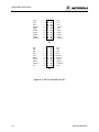
Figure 4-2. MCU I/O Headers P2, P3....................................................................................... 4-11
Figure 4-3. MCU I/O Headers P4, P6....................................................................................... 4-12
LIST OF TABLES
Table 1-1. EVB Specifications ................................................................................................... 1-8
Table 2-1. EVB Startup Mode Jumpers...................................................................................... 2-3
Table 2-2. RS-232C Interface Cabling ....................................................................................... 2-4
Table 2-3. Communication Parameters ...................................................................................... 2-5
Table 3-1. D-Bug12 Command-Set Summary............................................................................ 3-9
Table 3-2. M68HC11 to CPU12 Instruction Translation ......................................................... 3-14
Table 3-3. CPU12 Registers ..................................................................................................... 3-56
Table 3-4. Condition Code Register Bits.................................................................................. 3-56
Table 3-5. Factory-Configuration Memory Map...................................................................... 3-60
Table 4-1. Jumper and Header Functions ................................................................................... 4-3
Table 4-2. CPU Mode Selection................................................................................................. 4-6
Table 4-3. BDM Connector Pin Assignments .......................................................................... 4-10
68EVB912B32UM/D
vii
CONTENTS
viii
68EVB912B32UM/D
GENERAL INFORMATION
CHAPTER 1
GENERAL INFORMATION
1.1 INTRODUCTION
This manual provides the necessary information for using the M68EVB912B32 Evaluation
Board (the EVB), an evaluation, debugging, and code-generation tool for the MC68HC912B32
Microcontroller Unit (MCU) devices. The manual includes:
•
A general description of the EVB
•
Configuration and setup instructions
•
Startup and operating instructions
•
Detailed descriptions of the operating firmware’s command set
•
A detailed hardware-reference section
•
Appendices containing reference data
Additional reference items, such as schematic diagrams and parts lists, are shipped as part of the
EVB package.
1.2 GENERAL DESCRIPTION AND FEATURES
The EVB is an economical tool for designing and debugging code for, and evaluating the
operation of, the MC68HC192B32 MCU. By providing the essential MCU timing and I/O
circuitry, the EVB simplifies user evaluation of prototype hardware and software.
The board consists of a 5.15 by 3.4 inch (13.1 by 8.64 cm) double-sided printed circuit board
(PCB) that provides the platform for interface and power connections to the MC68HC912B32
MCU chip.
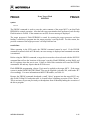
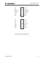
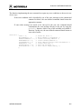
Figure 1-1 shows the EVB’s layout and locations of the major components, as viewed from the
component side of the board.
Hardware features of the low-cost EVB include:
•
Double-sided PCB
•
Single-supply +3 to +5 Vdc power input (P5)
•
RS-232C interface
•
BDM IN and BDM OUT connectors for remote debugging of a user’s target system
68EVB912B32UM/D
1-1
GENERAL INFORMATION
•
Header footprints for access to all MCU pins
•
16-MHz crystal for 8-MHz bus operation
•
Headers for jumper selection of and connection to hardware options:(1)
− RS-232 isolation (W1, W2))
− EVB mode selection (W3, W4)
− MCU mode selection (W5, W6)
− Vpp/Vdd selection (W7)
− Vpp input (W8)
− BDM IN (W9)
− BDM OUT Vdd/reset disconnects (W10, W11)
− BDM OUT (W12)
− Low-Voltage Inhibit (LVI) reset (W15)
− EXTAL source control and access (W16)
•
Four 2x20 header connectors for access to the MCU’s I/O lines (P2, P3, P4, and P6)
•
Prototype expansion area for customized interfacing with the MCU
•
Low-profile reset push-button switch (S1)
•
Low-voltage inhibit protection (U3)
(1)
For full details of the jumper settings, refer to Table 4-1.
Firmware features include:
1-2
•
The D-Bug12 monitor/debugger program, resident in on-chip Flash EEPROM
•
Full support for either dumb-terminal or host-computer terminal interface
•
Single-line assembler/disassembler
•
File-transfer capability from a host computer to RAM or EEPROM, allowing offboard code generation
•
Ability to program EEPROM on either the host EVB or a compatible target system
68EVB912B32UM/D
GENERAL INFORMATION
Figure 1-1. EVB Layout and Component Placement
68EVB912B32UM/D
1-3
GENERAL INFORMATION
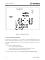
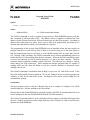
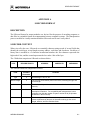
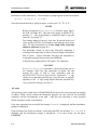
Figure 1-2. EVB Solder Side View
1.3 FUNCTIONAL OVERVIEW
The EVB is factory-configured to execute D-Bug12, the Flash EEPROM-resident monitor
program, without further configuration by the user. It is ready for use with an RS-232C terminal
for writing and debugging user code. Follow the setup instructions in Chapter 2 to prepare for
operation.
The EVB can also be jumper-configured to:
•
run a program directly out of EEPROM
•
control a remote "pod" MCU via the Background Debug Mode interface
•
reprogram EEPROM on either the host EVB or the "pod"
For the correct jumper settings, refer to 4.2 Configuration Headers and Jumper Settings.
1-4
68EVB912B32UM/D
GENERAL INFORMATION
NOTES
The D-Bug12 operating instructions in this manual presume the
factory-default memory configuration.
Other configurations
require different operating-software arrangements.
EEPROM resides in two areas of memory (refer to Table 3-5),
which are referred to in this manual as "byte-erasable EEPROM"
and "Flash EEPROM." This distinction is necessary because of the
different ways in which they may be programmed and used.
D-Bug12 uses the MCU’s Serial Communications Interface (SCI) for communications with the
user terminal. For information on the port and its connector, refer to 2.4 EVB to Terminal
Connection and 4.4 Terminal Interface.
If the MCU’s single-wire Background Debug Mode (BDM) interface serves as the user interface,
the SCI port becomes available for user applications. This mode requires either:
•
another M68EVB912B32 and a host computer
•
a background debug development tool, such as Motorola’s Serial Debug Interface
(SDI)
For more information, refer to the Motorola Serial Debug Interface User’s Manual.
Two methods may be used to generate EVB user code:
1. For small programs or subroutines, D-Bug12’s single-line assembler/disassembler
may be used to place object code directly into the EVB’s RAM or EEPROM.
2. For larger programs, P&E Microcomputer Systems' IASM12 or Motorola's MCUasm
assembler may be used on a host computer to generate S-Record object files, which
can then be loaded into the EVB’s memory using D-Bug12’s LOAD command.
The EVB features a prototype area, which allows custom interfacing with the MCU’s I/O and bus
lines. These connections are broken out via headers P2, P3, P4, and P6, which are immediately
adjacent to the MCU on the board. Wire-wrap pins may be placed in these headers to connect to
the prototyping area, as shown in Figure 1-1.
An on-board push-button switch, S1, provides for resetting the EVB hardware and restarting
D-Bug12.
The EVB can begin operation in any of four jumper-selectable (W3, W4) modes at reset:
1. In EVB mode, program execution begins in one of two ways:
a. If D-Bug12 is resident in Flash EEPROM (i.e., if Mode 4 below has not been
performed), D-Bug12 immediately issues its command prompt on the terminal display
and waits for a user entry.
68EVB912B32UM/D
1-5
GENERAL INFORMATION
b. If D-Bug12 has been replaced in Flash EEPROM with user code (i.e., Mode 4
below has been performed), execution begins with the user program.
2. In JUMP-EE mode, execution begins directly at location $0D00 with the user code
in byte-erasable EEPROM.
3. In POD mode, the board makes use of the BDM OUT header (W12) and uses the
D-Bug12 commands to non-intrusively interrogate an external target MCU. Special
prompts are displayed to let the user know if this mode is selected. If no external
MCU is detected, the software informs the user.
The target’s EEPROM may be programmed while the host M68EVB912B32 board is
in EVB mode, using the D-Bug12 commands BULK, LOAD, FBULK and FLOAD.
4. In BOOTLOAD mode, the host EVB’s byte-erasable or Flash EEPROM may be
reprogrammed with user code. This mode may also be used to reload or customize
D-Bug12.
D-Bug12 allows programming of the MC68HC912B32’s on-chip EEPROM through commands
that directly alter memory. For details of all D-Bug12 commands, refer to 3.6 D-Bug12
Command Set.
When operating in EVB mode, the MCU must manage the EVB hardware and execute D-Bug12
in addition to serving as the user-application processor, there are a few restrictions on its use.
For more information, refer to 3.9 Operational Limitations.
1.4 EXTERNAL EQUPMENT REQUIREMENTS
In addition to the EVB, the following user-supplied external equipment is required:
•
Power supply — see Table 1-1 for voltage and current requirements.
•
User terminal — options:
− RS-232C dumb terminal — allows single-line on-board code assembly and
disassembly.
− Host computer with RS-232C serial port — allows off-board code assembly
that can be loaded into the EVB’s memory. Requires a user-supplied
communications program capable of emulating a dumb terminal. Examples of
acceptable communications programs are given in Appendix B
Communications Program Examples.
− Host computer using the MCU’s BDM interface — frees the target MCU’s
SCI port for user applications. This requires another M68EVB912B32 for use
as the target or a background debug development tool, such as the Motorola
Serial Debug Interface (SDI).
•
1-6
Power-supply and terminal interconnection cables as required
68EVB912B32UM/D
GENERAL INFORMATION
For full details of equipment setup, cabling, and special requirements, refer to Chapter 2.
1.5 EVB SPECIFICATIONS
Table 1-1 lists the EVB specifications.
Table 1-1. EVB Specifications
Characteristic
Specifications
MCU
MC68HC912B32
MCU I/O ports
HCMOS compatible
Background Debug Mode
interface (IN and OUT)
two 2x3 headers
Communications port
RS-232C DCE port
Power requirements,
16 MHz clock source
+2.7 Vdc to +5.0 Vdc @ 100 mA (max.)
For low-voltage operation, refer to section 4.8.
Prototype area:
Area
Holes
approx. 1.5 x 3 in. (3.8 x 7.6 cm)
approx. 15 wide x 31 high, on 0.1 in. (2.54 mm) centers
Board dimensions
5.15 x 3.4 in. (13.1 x 8.64 cm)
68EVB912B32UM/D
1-7
GENERAL INFORMATION
1.6 CUSTOMER SUPPORT
AUSTRALIA,
Melbourne – (61-3)887-0711
Sydney – (61-2)906-3855
BRAZIL
Sao Paulo – 55(11)815-4200
CANADA
B.C., Vancouver – (604)606-8502
ONTARIO, Toronto – (416)497-8181
ONTARIO, Ottawa – (613)226-3491
QUEBEC, Montreal – (514)333-3300
CHINA
Beijing – 86-10-6843722
FINLAND
Helsinki – 358-9-6824-400
FRANCE
Paris – 33134 635900
GERMANY
Langenhagen/Hannover – 49(511)786880
Munich – 49 89 92103-0
Nuremberg – 49 911 96-3190
Sindelfingen – 49 7031 79 710
Wiesbaden – 49 611 973050
HONG KONG
Kwai Fong – 852-6106888
Tai Po – 852-6668333
INDIA
Bangalore – (91-80)5598615
ISRAEL
Herzlia – 972-9-590222
ITALY
Milan – 39(2)82201
JAPAN
Fukuoka – 81-92-725-7583
Gotanda – 81-3-5487-8311
Nagoya – 81-52-232-3500
Osaka – 81-6-305-1802
Sendai – 81-22-268-4333
Takamatsu – 81-878-37-9972
Tokyo – 81-3-3440-3311
KOREA
Pusan – 82(51)4635-035
Seoul – 82(2)554-5118
MALAYSIA
Penang – 60(4)374514
MEXICO
Mexico City – 52(5)282-0230
Guadalajara – 52(36)21-8977
PUERTO RICO
San Juan – (809)282-2300
SINGAPORE – (65)4818188
SPAIN
Madrid – 34(1)457-8204
SWEDEN
Solna – 46(8)734-8800
SWITZERLAND
Geneva – 41(22)799 11 11
Zurich – 41(1)730-4074
TAIWAN
Taipei – 886(2)717-7089
THAILAND
Bangkok – 66(2)254-4910
UNITED KINGDOM
Aylesbury – 44 1 (296)395252
UNITED STATES
Phoenix, AZ – 1-800-441-2447
For a list of the Motorola sales offices and distributors: http://www.mcu.mot.sps.com
1-8
68EVB912B32UM/D
CONFIGURATION AND SETUP
CHAPTER 2
CONFIGURATION AND SETUP
2.1 UNPACKING AND PREPARATION
Verify that the following items are present in the EVB package:
•
The M68EVB912B32 board assembly
•
Background Debug Mode(BDM) interface cable, 6-pin to 6-pin
•
Warranty and registration cards
•
EVB schematic diagram and parts list
•
M68EVB912B32 User’s Manual
•
MC68HC912B32 Technical Summary
•
MC68HC912B32 Electrical Specifications Supplement
•
CPU12 Reference Manual
•
MC68HC12 Family Brochure
•
Assembly Language Development Toolset
•
P&E Microcomputer Systems’ IASM12 Assembler and user’s manual on 3.5" diskette
•
Using D-Bug12 Callable Routines
Save all packing materials for storing and shipping the EVB.
Remove the EVB from its anti-static container.
2.2 EVB CONFIGURATION
Because the EVB has been factory-configured to operate with D-Bug12, it is not necessary to
change any of the jumper settings to begin operating immediately.
As shown in Table 2-1, only two jumpers (W3 and W4) should be changed during the course of
factory-default EVB operation with D-Bug12.
68EVB912B32UM/D
2-1
CONFIGURATION AND SETUP
Table 2-1. EVB Startup Mode Jumpers
Jumper
Positions
Startup Mode
W3
W4
0
0
EVB execution mode (default). D-Bug12 is executed from Flash EEPROM upon reset.
The D-Bug12 prompt appears immediately on the terminal display.
1
0
JUMP-EEPROM mode. User code is executed from byte-erasable EEPROM upon reset.
For more information, refer to 3.1 Operating Modes.
0
1
Remote Debugging through BDM OUT header (W12)
1
1
BOOTLOAD mode
Other jumper settings affect the hardware setup and/or MCU operational modes. For an
overview of all jumper-selectable functions, refer to 1.2 General Description and Features.
For details of the settings, see Table 4-1.
2.3 EVB TO POWER SUPPLY CONNECTION
The EVB requires a user-provided external power supply. See Table 1-1 for the voltage and
current specifications. For full details of the EVB’s power-input circuitry, refer to 4.3 Power
Input Circuitry.
A power supply with current-limiting capability is desirable. If this feature is available on the
power supply, set it at 200 mA.
Connect the external power supply to connector P5 on the EVB, using 20 AWG or smaller
insulated wire. Strip each wire’s insulation 1/4 in. from the end, lift the P5 contact lever to
release tension on the contact, insert the bare end of the wire into P5, and close the lever to
secure the wire. Observe the polarity carefully.
CAUTION
Do not use wire larger than 20 AWG in connector P5. Larger wire
could damage the connector.
2.4 EVB TO TERMINAL CONNECTION
For factory-default operation, connect the terminal to P1 on the EVB, as shown in Table 2-2.
This setup uses the MCU’s SCI port and its associated RS-232C interface for communications
with the terminal device.
2-2
68EVB912B32UM/D
CONFIGURATION AND SETUP
Standard, commercially available cables may be used in most cases. Note that the EVB requires
only three of the RS-232C signals. Table 2-2 lists these signals and their pin assignments. Other
signals have been routed through the RS-232C interface chip for proper levels. Some terminal
interface programs require proper levels on all pins to function correctly.
The EVB’s RS-232C connector, P1 , is wired as Data Circuit-terminating Equipment (DCE) and
employs a 9-pin subminiature D (DB-9) receptacle.
Most terminal devices — whether dumb terminals or the serial ports on host computers — are
wired as Data Terminal Equipment (DTE) and employ 9- or 25-pin subminiature D (DB-9 or
DB-25) plugs. In these cases, normal straight-through cabling is used between the EVB and the
terminal. Adapters are readily available for connecting 9-pin cables to 25-pin terminal
connectors.
If the terminal device is wired as DCE, the RXD and TXD lines must be cross-connected, as
shown in Table 2-2. Commercial "null modem" adapter cables are available for this purpose.
Table 2-2. RS-232C Interface Cabling
EVB P1
DTE Signal
Terminal
(1)
DCE
Receptacle
(1)
(2)
(2)
DCE
Receptacle
DTE
Plug
DB-9
DB-25
DB-9
DB-25
2
Receive Data (RXD)
2
2
3
3
3
Transmit Data (TXD)
3
3
2
2
5
Ground (GND)
5
7
5
7
Normal (DCE-to-DTE) cable connections
Null modem (DCE-to-DCE) cable connections
Optionally, the MCU’s Background Debug Mode (BDM IN W12) interface can serve as the
user interface. This setup makes the SCI port available for user applications. Additional
hardware and software are required. For more information, refer to the documentation for the
background debug development tool being used. This can be another M68EVB912B32 or a tool
such as Motorola’s Serial Debug Interface (SDI).
68EVB912B32UM/D
2-3
CONFIGURATION AND SETUP
2.5 TERMINAL COMMUNICATIONS SETUP
2.5.1 Communication Parameters
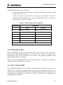
The EVB’s serial communications port uses the communication parameters listed in Table 2-3.
Of these, only the baud rate can be changed. For instructions on changing it, refer to 2.5.4
Changing the Baud Rate.
Table 2-3. Communication Parameters
Baud Rate
9600
Data Bits
8
Stop Bits
1
Parity
none
2.5.2 Dumb-Terminal Setup
Configuring a dumb terminal for use with the EVB consists of setting its parameters as shown in
Table 2-3. Many terminals are configurable with externally accessible switches, but the
procedure differs between brands and models. Consult the manufacturer’s instructions for the
terminal being used.
2.5.3 Host-Computer Setup
One advantage of using a host computer as the EVB’s terminal is the ability to generate code offboard, for subsequent loading into the EVB’s memory. It is thus desirable for the host to be
capable of running programs such as P&E Microcomputer Systems' IASM12 or Motorola’s
MCUasm assembler. For more information, refer to 3.7 Off-Board Code Generation.
To serve as the EVB’s terminal, the host computer must have an RS-232C serial port and an
installed communications program capable of operating with the parameters listed in Table 2-3.
Setting up the parameters is normally done within the communications program, after it has been
started on the host. Usually, the setup can be saved in a configuration file so that it does not have
to be repeated. Procedures vary between programs; consult the user’s guide for the specific
program.
Appendix B Communications Program Examples provides examples of using some of the
commonly available communications programs.
2-4
68EVB912B32UM/D
CONFIGURATION AND SETUP
2.5.4 Changing the Baud Rate
The EVB’s default baud rate for the RS-232C port is 9600. This can be changed in two ways:
•
For temporary changes, use the D-Bug12 BAUD command. This change remains in
effect only until the next reset or power-up, at which time the baud rate returns to
9600.
•
For permanent changes, the D-Bug12 baud-rate initialization value stored in Flash
EEPROM must be modified. For instructions, refer to Appendix D D-Bug12
Customization Data and Appendix E EEPROM Bootloader.
68EVB912B32UM/D
2-5
CONFIGURATION AND SETUP
2-6
68EVB912B32UM/D
OPERATION
CHAPTER 3
OPERATION
3.1 OPERATING MODES
The EVB can operate in one of four jumper-selectable modes:
EVB mode either D-Bug12 or the user code in Flash EEPROM executes.
JUMP-EEPROM mode user code in byte-erasable EEPROM executes.
POD mode D-Bug12 executes. EVB serves as the BDM probe for a target system.
BOOTLOAD mode the host EVB’s EEPROM may be reprogrammed.
The operating mode is determined by jumper headers W3 and W4, as shown in Table 4-1. The
modes are described in the following three sections.
NOTE
When operating in EVB mode, the M68EVB912B32 cannot fully
emulate a target system. The limitations are described in 3.9
Operational Limitations.
Target system emulation may, however, be performed by using the
EVB with D-Bug12 as an intelligent, non-intrusive BDM interface.
This operation is described in 3.1.3 POD (Probe) Mode.
3.1.1 EVB Mode
In the default EVB mode (W3-0 and W4-0), D-Bug12 begins execution immediately. The
D-Bug12 prompt appears on the terminal and commands may be entered as described in 3.5
Using D-Bug12 Commands.
If D-Bug12 has been replaced with user code in Flash EEPROM, execution begins with the
user’s program.
3.1.2 JUMP-EEPROM Mode
In this mode (W3-1 and W4-0), the EVB begins operation out of reset by executing the user
program in byte-erasable EEPROM starting at address $0D00, as shown in Table 3-5.
68EVB912B32UM/D
3-1
OPERATION
This mode is effected using the MCU’s PAD0 line. User code may be programmed into byteerasable EEPROM using the D-Bug12 commands listed in 3.5.3 Command-Set Summary.
Control can be returned to D-Bug12 in the following ways:
1. Move the jumpers on headers W3 and W4 to position 0 and reset the EVB.
2. Terminate the user program with code that returns to D-Bug12 after execution has
finished.
To return to D-Bug12 automatically after a user program has finished, include the following lines
as the last instructions to be executed in the program:
STACKTOP:
AltResetVect:
;
equ
equ
$0c00
$F7FE
lds
jmp
#STACKTOP
[AltResetVect,PCR]
; stack at top of on-chip RAM
; jump to start of D-Bug12
3.1.3 POD (Probe) Mode
In this mode (W3-0 and W4-1), the EVB and D-Bug12 serve as a POD ("probe") interface
between a target system and the user. Communications between the EVB and the target are by
means of the Background Debug Mode (BDM) interface, using the EVB header W12 (BDM
OUT).
This arrangement allows the target system to perform true emulation of an application, as the
BDM interface is non-intrusive upon the target’s foreground operation. The target’s on-chip
resources are all available for the application. The target may be a second M68EVB912B32
board or any other M68HC12 system. D-Bug12 commands are entered as usual on the user
terminal, which is served by the POD EVB.
3.1.3.1 Target Types Supported
All members of the M68HC12 family may be used in the target system.
3.1.3.2 Target MCU Characteristics
The following D-Bug12 commands must be used to inform D-Bug12 of the target MCU’s
essential operating characteristics in order to allow transparent modification of the target’s
EEPROM. For details, refer to the command descriptions in 3.6 D-Bug12 Command Set.
DEVICE specifies the target’s microprocessor type
EEBASE specifies the base address of the target’s Flash EEPROM
REGBASE specifies the base address of the target MCU’s I/O registers
3-2
68EVB912B32UM/D
OPERATION
3.1.3.3 Programming the Target’s EEPROM
The target MCU’s on-chip byte-erasable or Flash EEPROM may be programmed from userassembled S-Records on the host (terminal) computer by using the D-Bug12 commands BULK,
LOAD, FBULK, and FLOAD. For details, refer to 3.6 D-Bug12 Command Set.
3.1.3.4 Controlling Target Execution
All D-Bug12 commands that control the execution of user code may also be used in both EVB
mode and POD mode. Two additional commands are available in POD mode:
•
RESET resets the target MCU and places it in active background mode
•
STOP halts program execution on the target
For details, refer to the command descriptions in 3.6 D-Bug12 Command Set.
3.1.4 BOOTLOAD Mode
In this mode (W3-1 and W4-1), a user program may be loaded into the host EVB’s byte-erasable
or Flash EEPROM. D-Bug12 may be replaced as the startup "boot" program. This mode may
also be used to reload or customize D-Bug12. The procedures are described in Appendix E
EEPROM Bootloader.
3.2 STARTUP
3.2.1 Startup Procedure
The following startup procedure includes a checklist of configuration and setup items. To begin
operating the M68EVB912B32, follow these steps::
1. Configure the EVB if required — section 2.2.
2. Determine whether execution should begin in EVB mode (page 3-1), JUMPEEPROM mode (page 3-2), POD mode (page 3-2), or BOOTLOAD mode (page3-3).
Set the jumpers on headers W3 and W4 accordingly — sections 2.2 and 3.1.
3. Connect the EVB to the external power supply — section 2.3.
4. Connect the EVB to the terminal — section 2.4.
5. Configure the terminal communications interface — section 2.5.
68EVB912B32UM/D
3-3
OPERATION
6. Apply power to the EVB and to the terminal. If the terminal is a host computer,
a. Verify that it has booted correctly.
b. Start the communications program for terminal emulation — section 2.5.3 and
Appendix B Communications Program Examples.
7. Reset the EVB by pressing and releasing the on-board reset switch (S1).
3.2.2 Operating Procedures
After starting the EVB in accordance with section 3.2.1, follow the operating procedure for the
EVB mode that was selected: EVB mode, JUMP-EEPROM mode, POD mode, or BOOTLOAD
mode. These procedures are described in the following sections.
3.2.2.1 EVB Mode
In EVB mode, the MC68HC912B32 begins executing code at the address contained in the
alternate reset vector at $F7FE (for information on the alternate reset and interrupt vector table,
see Vector Jump Table: Interrupt and Reset Addresses on page E-4). The code pointed to by
the alternate reset vector may either be D-Bug12 (factory default) or a user’s program that has
replaced D-Bug12 in Flash EEPROM.
D-Bug12 upon reset, the D-Bug12 sign-on banner and prompt should appear on the terminal’s
display as follows:
D-Bug12 v 2.0.0
Copyright 1996 - 1997 Motorola Semiconductor
For Commands type "Help"
>
If the prompt does not appear, check all connections and verify that startup steps 1
through 7 in section 3.2.1 have been performed correctly.
When the prompt appears, D-Bug12 is ready to accept commands from the terminal as
described in section 3.5.
User boot program upon reset, the user program executes immediately. D-Bug12 commands
are not available. Terminal communications take place either via the SCI under control
of the user program or via the BDM interface and a serial debug interface tool such as
Motorola’s SDI.
3.2.2.2 JUMP-EEPROM Mode
In JUMP-EEPROM mode, the user code in byte-erasable EEPROM starting at address $0D00 is
executed immediately. Terminal communications are controlled by the user code via the SCI or
by an appropriate serial debug tool via the BDM interface. For more information, refer to
3-4
68EVB912B32UM/D
OPERATION
3.1.2 JUMP-EEPROM Mode. Control can be returned to the D-Bug12 terminal prompt by
doing one of the following:
1. terminating the user code with appropriate instructions — see section 3.1.2
2. pressing the reset button (S1)
3.2.2.3 POD Mode
In POD mode, the host EVB serves as a non-intrusive controller for the target system via the
BDM interface. The host EVB begins executing code at the address contained in the alternate
reset vector at $F7FE (for information on the alternate reset and interrupt vector table, see Vector
Jump Table: Interrupt and Reset Addresses on page E-4). The code pointed to by the
alternate reset vector may either be D-Bug12 (factory default) or a user’s program that has
replaced D-Bug12 in Flash EEPROM.
D-Bug12 upon power-up or reset, D-Bug12 attempts to establish communications with a
target system connected to BDM OUT (W11). Communications are first attempted
without resetting the target system. If communications cannot be established, the
following message is displayed:
Can’t Communicate With The Target Processor
To reset target, hit any key...
Pressing any key on the terminal’s keyboard causes D-Bug12 to assert the target’s reset
pin for approximately 2 mS and try again to establish communications.
If
communications fail, the above error message is redisplayed. Once communications have
been established with the target system, the D-Bug12 sign-on banner and prompt should
appear on the terminal’s display as follows:
D-Bug12 v 2.0.0
Copyright 1996 - 1997 Motorola Semiconductor
For Commands type "Help"
S>
If communications cannot be established with the target system after repeated attempts,
check for the following possible problems:
•
The host EVB's BDM OUT (W11) must be properly connected to the target system’s
BDM connector. If the target system is another EVB, make sure that the host EVB's
BDM OUT is connected to target EVB's BDM IN (W9).
•
If the target system is not another EVB, verify that its BDM connector is wired to the
proper MCU signals on each pin.
•
If the target MCU does not have any firmware to execute, it could "run away,"
possibly executing a STOP opcode and preventing BDM communications with the
host EVB.
Thus, it is strongly recommended that, if the target system does not have firmware to
execute at reset, the target MCU be initially configured to begin operation in Special
68EVB912B32UM/D
3-5
OPERATION
Single Chip mode. Resetting the target MCU in Special Single Chip mode places it
in active background mode. See the target MCU’s technical summary for details on
setting the MCU operating mode.
Special D-Bug12 command-line prompts indicate the status of the target system:
S>
target is in active background mode
R>
target is running a user program
In addition to the normal D-Bug12 commands that control execution of user code, the
RESET and STOP commands are available in POD mode. These commands are
described in 3.6 D-Bug12 Command Set.
D-Bug12 must be informed of the target MCU’s basic operating parameters. Refer to
section 3.1.3 for more information about setting up and using POD mode.
User boot program upon reset, the user program executes immediately. D-Bug12 commands
are not available. Communications with the user terminal and with the target system are
controlled by the user program.
3.2.2.4 BOOTLOAD Mode
In BOOTLOAD mode, a user program may be loaded into the host EVB's byte-erasable or Flash
EEPROM. If the user code replaces D-Bug12 in Flash EEPROM, it serves as the "boot" program
when the EVB is restarted in EVB or POD mode. This procedure is described in Appendix E
EEPROM Bootloader.
3.3 RESET
EVB operation can be restarted at any time by activating the hardware reset function. Do this in
one of two ways:
1. Press and release the on-board reset switch, S1 (always applicable).
2. Activate the external reset input if one has been provided for operation below 3.0
Vdc.
Note that the EVB’s reset circuitry is associated with the low-voltage protection. For more
information, refer to 4.7 Reset and 4.8 Low-Voltage Inhibit.
3.4 ABORTING A USER PROGRAM
When operating in EVB mode, the only way to recover from an erroneous or runaway user
program is to press the reset switch (S1). If this becomes necessary, the jumpers on headers W3
and W4 should be set to execute D-Bug12 at reset instead of the flawed user program.
3-6
68EVB912B32UM/D
OPERATION
When operating in POD mode, the D-Bug12 RESET or STOP command can be used to regain
control of the target system.
3.5 USING D-BUG12 COMMANDS
D-Bug12, the EVB’s firmware-resident monitor program, provides a self-contained operating
environment that allows writing, evaluation, and debugging of user programs.
3.5.1 Command-Line Prompt
D-Bug12 displays one of three command-line prompts, depending upon its operating mode
and/or the state of the target system. When D-Bug12 is operating in the EVB mode, it displays
the single character ">" at the beginning of a line when it is waiting for the user to enter a
command. When a command is issued that causes user code to run, D-Bug12 places the terminal
cursor on a blank line, where it remains until control returns to D-Bug12.
When operating in the POD mode, D-Bug12 displays one of two prompts, depending upon the
state of the attached target system. When the target system is in active background mode (not
running a user program), the two-character prompt "S>" is displayed, indicating that the target is
stopped and not running a user program. When the target system is running a user program, the
two-character prompt "R>" is displayed, indicating that the target is running a user program.
Because the M68HC12 Background Debug Mode interface allows the reading and writing of
target system memory even when the target is running a user’s program, the probe
microcontroller is always available for the entry of commands. D-Bug12 commands that
examine or modify target system memory may be issued when either the "S>" or "R>" prompt is
displayed.
3.5.2 Entering Commands
Commands are typed on the terminal’s D-Bug12 prompt line and executed when the carriagereturn (ENTER) key is pressed. D-Bug12 then displays either the appropriate response to the
command or an error indication.
The D-Bug12 command-line prompt is the greater-than sign (>). Type the command and any
other required or optional fields immediately after the prompt, as follows:
command-line syntax:
<command>
[<parameter>]
...[<parameter>]<ENTER>
where:
<command>
68EVB912B32UM/D
is the command mnemonic.
3-7
OPERATION
<parameter>
is an expression or address.
<ENTER>
is the terminal keyboard’s carriage-return or enter key.
NOTES
1. The command-line syntax is illustrated using the following special characters for
clarification. Do not type these characters on the command line:
<>
required syntactical element
[]
optional field
...[ ]
repeated optional fields
2. Fields are separated by any number of space characters.
3. All numeric fields, unless noted otherwise, are interpreted as hexadecimal.
4. Command-line entries are case-insensitive and may be typed using any combination
of upper- and lower-case letters.
5. A maximum of 80 characters, including the terminating carriage return, may be
entered on the command line. After the 80th character, D-Bug12 automatically
terminates the command-line entry and processes the characters entered to that point.
6. Before the <ENTER> or <RETURN> key is pressed, the command line may be
edited using the backspace key. Receiving the backspace character causes D-Bug12
to delete the previously-received character from its input buffer and erase the
character from the display.
3.5.3 Command-Set Summary
Table 3-1 summarizes the D-Bug12 commands. For detailed descriptions of each command,
refer to 3.6 D-Bug12 Command Set.
Table 3-1. D-Bug12 Command-Set Summary
Command
Description
ASM <address>
Single-line assembler/disassembler
BAUD <BAUDRate>
Set the SCI communications baud rate
BF <StartAddress><EndAddress> [<Data>]
Block fill user memory with data
BR [<Address><Address>...]
Set/display user breakpoints
BULK
Bulk erase byte-erasable EEPROM
3-8
68EVB912B32UM/D
OPERATION
Table 3-1. D-Bug12 Command-Set Summary (continued)
Command
Description
CALL [<Address>]
Execute a user subroutine; return to D-Bug12 when
finished
DEVICE [see description]
Select/define a new target MCU device
EEBASE <Address>
Inform D-Bug12 of the target’s EEPROM base address
FBULK
Erase the target processor’s on-chip Flash EEPROM
FLOAD <AddressOffset>
Program the target processor’s on-chip Flash EEPROM
from S-Records
G [<Address>]
Go — begin execution of user program
GT <Address>
Go Till — set a temporary breakpoint and begin execution
of user program
HELP
Display D-Bug12 command set and command syntax
LOAD [<AddressOffset>]
Load user program in S-Record format*
MD <StartAddress> [<EndAddress>]
Memory Display — display memory contents in hex
bytes/ASCII format
MDW <StartAddress> [<EndAddress>]
Memory Display Word — display memory contents in hex
words/ASCII format
MM <Address> [<data>]
Memory Modify — interactively examine/change memory
contents
MMW <address> [<data>]
Memory Modify Word — interactively examine/change
memory contents
MOVE <StartAddress> <EndAddress>
<DestAddress>
Move a block of memory
NOBR [<Address> <Address>...]
Remove individual user breakpoints
RD
Register Display — display the CPU register contents
REGBASE
Inform D-Bug12 of the target I/O register’s base address
RESET
Reset the target CPU
RM
Register Modify — interactively examine/change CPU
register contents
STOP
Stop execution of user code on the target processor and
place it in background mode
68EVB912B32UM/D
3-9
OPERATION
Table 3-1. D-Bug12 Command-Set Summary (continued)
Command
Description
T [<Count>]
Trace — execute an instruction, disassemble it, and
display the CPU registers
UPLOAD <StartAddress> <EndAddress>
Display memory contents in S-Record format*
VERF [<AddressOffset>]
Verify memory contents against S-Record Data
<RegisterName> <RegisterValue>
Set CPU <RegisterName> to <RegisterValue>
* Refer to Appendix A for S-Record information.
3.6 D-BUG12 COMMAND SET
In the following command descriptions, the examples represent what is seen on the terminal
display. For clarity, the user’s entry is underlined. This underlining does not actually appear
onscreen.
A typical example looks like this:
>baud 9600
Change Terminal BR, Press Return
>
3-10
user’s entry
D-Bug12’s response
D-Bug12 prompt for next entry
68EVB912B32UM/D
OPERATION
Assembler/Disassembler
ASM
ASM
syntax:
ASM
<Address>
where:
<Address>
is a 16-bit hexadecimal number.
The assembler/disassembler is an interactive memory editor that allows memory contents to be
viewed and altered using assembly language mnemonics. Each entered source line is translated
into object code and placed into memory at the time of entry. When displaying memory contents,
each instruction is disassembled into its source mnemonic form and displayed along with the
hexadecimal object code and any instruction operands.
Assembler mnemonics and operands may be entered in any mix of upper and lower case letters.
Any number of spaces may appear between the assembler prompt and the instruction mnemonic
or between the instruction mnemonic and the operand. Numeric values appearing in the operand
field are interpreted as signed decimal numbers. Placing a $ in front of any number will cause
the number to be interpreted as a hexadecimal number.
When an instruction is disassembled and displayed, the D-Bug12 prompt is displayed following
the disassembled instruction. If a carriage return is the first non-space character entered
following the prompt, the next instruction in memory is disassembled and displayed on the next
line.
If a CPU12 instruction is entered following the prompt, the entered instruction is assembled and
placed into memory. The line containing the new entry is erased and the new instruction is
disassembled and displayed on the same line. The next instruction location is then disassembled
and displayed on the screen.
The instruction mnemonics and operand formats accepted by the assembler follows the syntax as
described in the CPU12 Reference Manual.
There are a number of M68HC11 instruction mnemonics that appear in the CPU12 Reference
Manual that do not have directly equivalent CPU12 instructions. These mnemonics, listed in
Table 3-2, are translated into functionally equivalent CPU12 instructions. To aid the current
M68HC11 users who may desire to continue using the M68HC11 mnemonics, the disassembler
portion of the assembler/disassembler recognizes the functionally equivalent CPU12 instructions
and disassembles those instructions into the equivalent M68HC11 mnemonics.
When entering branch instructions, the number placed in the operand field should be the absolute
destination address of the instruction. The assembler calculates the two’s-complement offset of
the branch and places the offset in memory with the instruction
68EVB912B32UM/D
3-11
OPERATION
The assembly/disassembly process may be terminated by entering a period (.) as the first nonspace character following the assembler prompt.
restrictions:
None.
Table 3-2. M68HC11 to CPU12 Instruction Translation
M68HC11 Mnemonic
CPU12 Instruction
M68HC11 Mnemonic
CPU12 Instruction
CLC
ANCC # $FE
INS
LEAS 1, S
CLI
ANCC # $EF
TAP
TFR A, CC
CLV
ANCC # $FD
TPA
TFR CC, A
SEC
ORCC # $01
TSX
TFR S, X
SEI
ORCC # $10
TSY
TFR S, Y
SEV
ORCC # $02
XGDX
EXG D, X
ABX
LEAX B, X
XGDY
EXG D, Y
ABY
LEAY B, Y
SEX R8, R16
TFR R8, R16
DES
LEAS -1, S
example:
>ASM 800
0800
0803
0809
080F
0811
>
CC1000
1803123401FE
0EF9800001F1
18FF
183FE3
LDD
MOVW
BRSET
TRAP
ETBL
#$1000
#$1234,$01FE
-32768,PC,$01,$0700
$FF
<Illegal Addr Mode>
>.
assembly operand format:
This section describes the operand format used by the assembler when assembling CPU12
instructions. The operand format accepted by the assembler is described separately in the CPU12
Reference Manual. Rather than describe the numeric format accepted for each instruction, some
general rules are used. Exceptions and complicated operand formats are described separately.
In general, anywhere the assembler expects a numeric value in the operand field, either a decimal
or hexadecimal value may be entered. Decimal numbers are entered as signed constants having a
range of -32768 to 65535. A leading minus sign (-) indicates negative numbers, the absence of a
leading minus sign indicates a positive number. A leading plus sign (+) is not allowed.
3-12
68EVB912B32UM/D
OPERATION
Hexadecimal numbers must be entered with a leading dollar sign ($) followed by one to four
hexadecimal digits. The default number base is decimal.
For all branching instructions (Bcc, LBcc, BRSET, BRCLR, DBEQ, DBNE, IBEQ, IBNE,
TBEQ, and TBNE), the number entered as the branch address portion of the operand field is the
absolute address of the branch destination. The assembler calculates the two’s-complement
offset to be placed in the assembled object code.
disassembly operand format:
The operand format used by the disassembler is described separately in the CPU12 Reference
Manual. Rather than describing the numeric format used for each instruction, some general rules
are applied. Exceptions and complicated operand formats are described separately.
All numeric values disassembled as hexadecimal numbers are preceded by a dollar sign ($) to
avoid being confused with values disassembled as signed decimal numbers.
For all branch (Bcc, LBcc, BRSET, BRCLR, DBEQ, DBNE, IBEQ, IBNE, TBEQ, TBNE)
instructions the numeric value of the address portion of the operand field is displayed as the
hexadecimal absolute address of the branch destination.
All offsets used with indexed addressing modes are disassembled as signed decimal numbers.
All addresses, whether direct or extended, are disassembled as four digit hexadecimal numbers.
All 8-bit mask values (BRSET/BRCLR/ANDCC/ORCC) are disassembled as two-digit
hexadecimal numbers.
All 8-bit immediate values are disassembled as hexadecimal numbers.
All 16-bit immediate values are disassembled as hexadecimal numbers.
68EVB912B32UM/D
3-13
OPERATION
Set Baud Rate
BAUD
BAUD
syntax:
BAUD
<BAUDRate>
where:
<BAUDRate>
is an unsigned 16-bit decimal number.
The BAUD command is used to change the communications rate of the SCI used by D-Bug12 for
the terminal interface.
restrictions:
Because the <BAUDRate> parameter supplied on the command line is a 16-bit unsigned integer,
BAUD rates greater than 65535 baud cannot be set using this command. The SCI BAUD rate
divider value for the requested BAUD rate is calculated using the E-clock value supplied in the
D-Bug12 customization data area. Because the SCI BAUD rate divider is a 13-bit counter,
certain BAUD rates may not be supported at particular E-clock frequencies. If the value
calculated for the SCI’s BAUD rate divider is equal to zero or greater than 8191, command
execution is terminated and the communications BAUD rate is not changed.
example:
>BAUD 50
Invalid BAUD Rate
>BAUD 38400
Change Terminal BR, Press Return
>
3-14
68EVB912B32UM/D
OPERATION
Block Fill
BF
BF
syntax:
BF
<StartAddress>
<EndAddress>
[<Data>]
where:
<StartAddress>
is a 16-bit hexadecimal number.
<EndAddress>
is a 16-bit hexadecimal number.
<Data>
is an 8-bit hexadecimal number.
The Block Fill command is used to place a single 8-bit value into a range of memory locations.
<StartAddress> is the first memory location written with <data> and <EndAddress> is the last
memory location written with <data>. If the <data> parameter is omitted, the memory range is
filled with the value $00.
restrictions:
None.
example:
>BF 6400 6fff 0
>BF 6f00 6fff 55
>
68EVB912B32UM/D
3-15
OPERATION
Breakpoint Set
BR
BR
syntax:
BR
[<Address>
<Address>
...]
where:
<Address>
are optional 16-bit hexadecimal numbers.
The BR command is used to set a software breakpoint at a specified address or to display any
previously set breakpoints. The function of a breakpoint is to halt user program execution when
the program reaches the breakpoint address. When a breakpoint address is encountered,
D-Bug12 disassembles the instruction at the breakpoint address, prints the CPU12’s register
contents, and waits for a D-Bug12 command to be entered by the user.
Breakpoints are set by typing the breakpoint command followed by one or more breakpoint
addresses. Entering the breakpoint command without any breakpoint addresses will display all
the currently set breakpoints.
A maximum of 10 user breakpoints may be set at one time.
restrictions:
D-Bug12 implements the breakpoint function by replacing the opcode at the breakpoint address
in the users program with an SWI instruction when operating in EVB mode or with the BGND
instruction when operating in POD mode. A breakpoint may not be set on a user SWI instruction
when operating in EVB mode. In either mode, breakpoints may only be set at an opcode address,
and breakpoints may only be placed at memory addresses in alterable memory.
Even though D-Bug12 supports a maximum of 10 user-defined breakpoints, a maximum of 9
breakpoints may be set on the command line at one time. This restriction is due to the limitation
of the command-line processor, which allows a maximum of 10 command-line arguments,
including the command string.
When operating in POD mode, new breakpoints may not be set with the BR command when the
"R>" prompt is displayed. However, the BR command may be used to display breakpoints that
are currently set in the user's running program.
D-Bug12 version 2.0.0 does not support the MC68HC912B32's hardware breakpoint (H/W)
function. Later versions of D-Bug12, which may support this function, can be obtained from the
sources listed in Obtaining D-Bug12 Upgrades on page E-6.
3-16
68EVB912B32UM/D
OPERATION
example:
>BR 35ec 2f80 c592
Breakpoints: 35EC 2F80 C592
>BR
Breakpoints: 35EC 2F80 C592
>
68EVB912B32UM/D
3-17
OPERATION
BULK
Bulk Erase EEPROM
BULK
syntax:
BULK
The BULK command is used to erase the entire contents of byte-erasable EEPROM in a single
operation. After the bulk erase operation has been performed, each on-chip EEPROM location is
checked for an erased condition.
restrictions:
In order to erase EEPROM, the EEPROM block-protect control bits must be cleared. Refer to
the MC68HC912B32 Technical Summary for locations and operation of the block-protect
controls.
example:
>BULK
F/EEPROM Failed To Erase
>BULK
>
3-18
68EVB912B32UM/D
OPERATION
Call Subroutine
CALL
CALL
syntax:
CALL
[<Address>]
where:
<Address>
is an optional 16-bit hexadecimal number.
The CALL command is used to execute a subroutine and return to the D-Bug12 monitor program
when the final RTS of the subroutine is executed. When control is returned to D-Bug12, the
CPU register contents are displayed. All CPU registers contain the values at the time the final
RTS instruction was executed, with the exception of the program counter (PC). The PC contains
the starting address of the subroutine. If a subroutine address is not supplied on the command
line, the current value of the Program Counter (PC) is used as the starting address.
NOTE:
No user breakpoints are placed in memory before execution is
transferred to user code.
restrictions:
If the called subroutine modifies the value of the stack pointer during its execution, it must
restore the stack pointer’s original value before executing the final RTS of the called subroutine.
This restriction is required because a return address is placed on the users stack that returns to
D-Bug12 when the final RTS of the subroutine is executed. Obviously, any subroutine must
obey this restriction to execute properly.
The CALL command cannot be issued when the "R>" prompt is displayed, indicating that the
target system is already running a user program.
example:
>CALL 820
Subroutine Call Returned
PC
0820
>
SP
0A00
68EVB912B32UM/D
X
057C
Y
0000
D = A:B
0F:F9
CCR = SXHI
1001
NZVC
0000
3-19
OPERATION
DEVICE
Specify Target MCU Device
DEVICE
syntax:
DEVICE
DEVICE
<DeviceName> [<EEStart> <EEEnd> <FStart>
<FEnd> <RAMStart> <RAMEnd> <IOBase>]
where:
<DeviceName>
is the maximum of 7 ASCII characters used to select/define a target
MCU device.
<EEStart>
is the on-chip EEPROM starting address; a 16-bit hexadecimal
number.
<EEEnd>
is the on-chip EEPROM ending address; a 16-bit hexadecimal
number.
<FStart>
is the on-chip Flash EEPROM starting address; a 16-bit
hexadecimal number.
<FEEnd>
is the on-chip Flash EEPROM ending address; a 16-bit
hexadecimal number.
<RAMStart>
is the on-chip RAM starting address; a 16-bit hexadecimal number.
<RAMEnd>
is the on-chip RAM ending address; a 16-bit hexadecimal number.
<IOBase>
is the base address of the on-chip I/O registers; a 16-bit
hexadecimal number.
Selecting the proper target MCU with the DEVICE command provides D-Bug12 the information
necessary to allow transparent alteration of the target MCU’s on-chip EEPROM using any
D-Bug12 commands that modify memory. It also provides the necessary information to allow
the programming and erasure of on-chip Flash EEPROM. In addition, it allows D-Bug12 to
initialize the stack pointer to the top of on-chip RAM when the target MCU is reset by use of the
RESET command. The DEVICE command has three separate command line formats that allows
for the display, selection and/or definition of target device parameters.
Entering "DEVICE" on the command line followed by a carriage return displays the name of the
currently selected device, the on-chip EEPROM’s starting and ending address, the on-chip Flash
EEPROM’s starting and ending address, the on-chip RAM’s starting and ending address, and the
I/O Base address. This form of the command may be used when D-Bug12 is operating in either
EVB or POD mode.
When D-Bug12 is operated in the POD mode, the DEVICE command may also be used to select
or define a new target device. Entering the DEVICE command followed only by a device name
3-20
68EVB912B32UM/D
OPERATION
configures D-Bug12 for operation with the selected target device. The default device list
contains entries for the MC68HC912B32 and the MC68HC812A4. The table below shows the
command line name to use for the two default MCU devices.
Device Name
Target MCU
912B32
MC68HC912B32
812A4
MC68HC812A4
Entering the DEVICE command followed by a device name and seven hexadecimal parameters
allows new devices to be added to the target device table or existing device table entries to be
modified. When a new device is added or when an existing device entry is modified, it becomes
the currently selected device. If a new device does not contain a particular on-chip resource, such
as Flash EEPROM, a value of zero should be entered for the starting and ending addresses
Because the target device data and the current device selection are stored in the probe MCU’s onchip EEPROM, new device information and the device selection are retained when power is
removed from the POD. If the M68EVB912B32 is operated in EVB mode and the contents of
any locations of the on-chip EEPROM are altered it is strongly recommended that the on-chip
EEPROM be completely erased by using the BULK command before using the EVB in POD
mode again. Erasing the on-chip EEPROM causes D-Bug12 to reinitialize the device table with
the two default MCU devices. The information for any new devices that were added to the table
will be lost.
restrictions:
When operating the M68EVB912B32 in EVB mode, the DEVICE command may only be used to
display the current device information.
The DEVICE command maintains a 16-bit checksum on the contents of the entire on-chip
EEPROM to maintain the integrity of the device table. If any of the on-chip EEPROM locations
are altered while operating the M68EVB912B32 in EVB mode, D-Bug12 will reinitialize the
device table with the default device information contained in the on-chip Flash EEPROM.
However, it is possible for the checksum verification to fail (one case where the checksum will
fail is if the entire contents of the on-chip EEPROM is programmed with zeros). Therefore, it is
strongly recommended that the on-chip EEPROM be completely erased by using the BULK
command before using the EVB in POD mode again. Using the EVB in Probe mode with a
corrupt device data table may cause D-Bug12 to operate in an unpredictable manner.
The 768 bytes of on-chip EEPROM allows a total of 34 entries in the device table. Do not
exceed this number.
When adding a new device to the device table, the addresses provided for the on-chip Flash
EEPROM, on-chip RAM and the I/O Registers should reflect the locations of these resources
when the part is reset. This requirement is necessary for the FBULK and FLOAD commands to
work properly.
68EVB912B32UM/D
3-21
OPERATION
example:
>DEVICE
Device: 912B32
EEPROM: $0D00 - $0FFF
Flash: $8000 - $FFFF
RAM: $0800 - $0BFF
I/O Regs: $0000
S>DEVICE 912b32 1d00 1fff 8000 ffff 800 bff 0
Device: 912B32
EEPROM: $1D00 - $1FFF
Flash: $8000 - $FFFF
RAM: $0800 - $0BFF
I/O Regs: $0000
S>DEVICE 812a4
Device: 812A4
EEPROM: $1000 - $1FFF
RAM: $0800 - $0BFF
I/O Regs: $0000
S>
3-22
68EVB912B32UM/D
OPERATION
EEBASE
Specify Target EEPROM
Base Address
EEBASE
syntax:
EEBASE
<Address>
where:
<Address>
is an optional 16-bit hexadecimal number.
Each time D-Bug12 performs a memory write, it automatically performs the necessary register
manipulations to program the on-chip EEPROM if the write operation falls within the address
range of the target’s on-chip EEPROM. Because user code may change the EEPROM’s base
address by writing to the INITEE register, D-Bug12 must be informed of the EEPROM’s
location if automatic EEPROM writes are to occur. The EEBASE command is used to specify
the base address of the target processor’s on-chip EEPROM.
When operating in EVB mode, the default EEPROM base address and range are specified in the
customization data variables CustomData.EEBase and CustomData.EESize. The value
in CustomData.EEBase is used by the startup code to remap the EEPROM. The EEBASE
command may not be used to relocate the I/O registers.
When operating in POD mode, the target’s default EEPROM base address and range are
specified by the currently-selected device (See the DEVICE command for additional details).
The EEBASE command does not check to ensure that the parameter is a valid base address for
the selected M68HC12 family member. If an improper base address is provided, automatic
programming of the on-chip EEPROM will not operate properly.
NOTE
The EEBASE command does not automatically modify the
INITEE register. It is the responsibility of the user to ensure that
the INITEE register is modified either manually or through the
execution of user code.
restrictions:
The EEBASE command may not be used when D-Bug12 is operated in EVB mode.
68EVB912B32UM/D
3-23
OPERATION
example:
S>DEVICE
Device: 912B32
EEPROM: $0D00 - $0FFF
Flash: $8000 - $FFFF
RAM: $0800 - $0BFF
I/O Regs: $0000
S>EEBASE 1d00
Device: 912B32
EEPROM: $1D00 - $1FFF
Flash: $8000 - $FFFF
RAM: $0800 - $0BFF
I/O Regs: $0000
S>MM
0012
0013
S>MD
12
01 11
0F .
1d00
1D00 FF FF FF FF - FF FF FF FF - FF FF FF FF - FF FF FF FF
................
S>
3-24
68EVB912B32UM/D
OPERATION
FBULK
Erase Target Flash
EEPROM
FBULK
syntax:
FBULK
The FBULK command is used to erase the entire contents of the target MCU’s on-chip Flash
EEPROM in a single operation. After the bulk erase operation has been performed, each on-chip
Flash location is verified. If the contents are not $FF, an error message is displayed.
The target processor’s Flash EEPROM is erased by resetting the target processor and then
loading a small driver program into the target processor’s on-chip RAM. For this reason, the
previous contents of the target processor’s on-chip RAM are lost.
restrictions:
When operating in the EVB mode, the FBULK command cannot be used. If the FBULK
command is entered while in EVB mode, an error message is displayed and command execution
is terminated.
Before using the FBULK command, a target device must have been selected with the DEVICE
command that reflects the locations of the target’s on-chip Flash EEPROM, on-chip RAM, and
the I/O registers when the part is reset. Failure to follow this restriction will cause the FBULK
command to fail and may require that the EVB be reset.
Flash EEPROM programming voltage (Vpp) must be applied to the target MCU. If the target
system is another M68EVB912B32 board, Vpp may be supplied via header W8, with header W7
set accordingly. For more information on these EVB headers, see Table 4-1.
Because the FBULK command downloads a small "driver" program into the target MCU's onchip RAM, D-Bug12's breakpoint table is cleared before beginning execution of the "driver".
This is necessary to prevent previously-set breakpoints from accidentally halting the execution of
the driver program.
68EVB912B32UM/D
3-25
OPERATION
example:
S>FBULK
Flash Programming Voltage Not Present
S>FBULK
F/EEPROM Failed To Erase
S>FBULK
S>
>FBULK
Command Not Allowed In EVB Mode
>
3-26
68EVB912B32UM/D
OPERATION
FLOAD
Program Target Flash
EEPROM
FLOAD
syntax:
FLOAD [<AddressOffset>]
where:
<AddressOffset>
is a 16-bit hexadecimal number.
The FLOAD command is used to program a target device’s Flash EEPROM memory with the
data contained in S-Record object files. The address offset, if supplied, is added to the load
address of each S-Record before the S-Record’s data bytes are placed in memory. Providing an
address offset other than zero allows object code or data to be programmed into memory at a
location other than that for which it was assembled or compiled.
The programming of the on-chip Flash EEPROM uses an algorithm where the time required to
program each byte or word can vary from as little as 60 µS to as long as 3.5 mS (note, however
that the programming time for each byte or word should typically take no more than 120-180
µS). Because of this variability, the FLOAD command uses a software handshaking protocol to
control the flow of S-Record data from the host computer. When the FLOAD command is ready
to receive an S-Record, an ASCII asterisk character (*) is sent to the host computer. The host
computer should respond by sending a single S-Record. The S-Record may include a carriage
return and/or line feed character(s). Most commercial terminal programs that are capable of
sending ASCII text files have the ability to wait for a specific character or characters before
sending a line of text.
The FLOAD command is terminated when D-Bug12 receives an "S9" end-of-file record. If the
object file being loaded does not contain an "S9" record, D-Bug12 does not return its prompt and
continues to wait for the end-of-file record. Pressing the reset switch returns D-Bug12 to its
command line prompt.
restrictions:
The host program used to send the S-Record data must be capable of waiting for an ASCII
asterisk character (*) before sending each S-Record line.
Because the on-chip Flash EEPROM is only bulk-erasable, the FBULK command should be used
before loading new data into Flash EEPROM with the FLOAD command.
The FLOAD command cannot be used with S-Records that contain a code/data field longer than
64 bytes. Sending an S-Record with a longer field may cause D-Bug12 to crash or load incorrect
data into the Flash EEPROM.
68EVB912B32UM/D
3-27
OPERATION
Before using the FLOAD command, a target device must have been selected using the DEVICE
command that reflects the locations of the on-chip Flash EEPROM, on-chip RAM, and the I/O
registers when the part is reset. Failure to follow this restriction will cause the FLOAD
command to fail and may require that the EVB be reset.
Flash EEPROM programming voltage (Vpp) must be applied to the target MCU. If the target
system is another M68EVB912B32 board, Vpp may be supplied via header W8, with header W7
set accordingly. For more information on these EVB headers, see Table 4-1.
Because the FLOAD command downloads a small "driver" program into the target MCU’s onchip RAM, D-Bug12’s breakpoint table is cleared before beginning execution of the "driver".
This is necessary to prevent previously set breakpoints from accidentally halting the execution of
the driver program.
example:
S>FLOAD
Flash Programming Voltage Not Present
S>FLOAD
**********************************************************************
**********************************************************************
***********************
S>
3-28
68EVB912B32UM/D
OPERATION
Go Execute a User Program
G
G
syntax:
G
[<Address>]
where:
<Address>
is an optional 16-bit hexadecimal number.
The G command is used to begin the execution of user code in real time. Before beginning
execution of user code, any breakpoints that were set with the BR command are placed in
memory. Execution of the user program continues until a user breakpoint is encountered, a CPU
exception occurs, the STOP or RESET command is entered, or the EVB’s reset switch is pressed.
When user code halts for any of these reasons (except reset, which wipes the slate clean) and
control is returned to D-Bug12, a message is displayed explaining the reason for user program
termination. In addition, D-Bug12 disassembles the instruction at the current PC address, prints
the CPU12’s register contents, and waits for the next D-Bug12 command to be entered by the
user.
If a starting address is not supplied in the command line parameter, program execution will begin
at the address defined by the current value of the Program Counter.
restrictions:
The G command cannot be issued when the "R>" prompt is displayed, indicating that the target
system is already running a user program.
example:
S>G 800
R>MD 1000
1000 FF FF FF FF - FF FF FF FF - FF FF FF FF - FF FF FF FF
................
R>
User Breakpoint Encountered
PC
0820
0820
S>
SP
09FE
08
68EVB912B32UM/D
X
057C
Y
D = A:B
0000
00:00
INX
CCR = SXHI NZVC
1001 0100
3-29
OPERATION
Go Till
GT
GT
syntax:
GT
<Address>
where:
<Address>
is a 16-bit hexadecimal number.
The GT command is similar to the G command except that a temporary breakpoint is placed at
the address supplied on the command line. Any breakpoints that were set by the use of the BR
command are NOT placed in the user code before program execution begins. Program execution
begins at the address defined by the current value of the Program Counter. When user code
reaches the temporary breakpoint and control is returned to D-Bug12, a message is displayed
explaining the reason for user program termination. In addition, D-Bug12 disassembles the
instruction at the current PC address, prints the CPU12’s register contents, and waits for a
command to be entered by the user.
restrictions:
The GT command cannot be issued when the "R>" prompt is displayed, indicating that the target
system is already running a user program.
example:
S>GT 820
R>
Temporary Breakpoint Encountered
PC
0820
0820
S>
3-30
SP
09FE
08
X
057C
Y
D = A:B
0000
00:00
INX
CCR = SXHI NZVC
1001 0100
68EVB912B32UM/D
OPERATION
HELP
Onscreen Help Summary
HELP
syntax:
HELP
The HELP command is used to display a summary of the D-Bug12 command set. Each
command is shown along with its command line format and a brief description of its function.
restrictions:
None.
68EVB912B32UM/D
3-31
OPERATION
example:
>HELP
ASM <Address> Single line assembler/disassembler
<CR>
Disassemble next instruction
<.>
Exit assembly/disassembly
BAUD <baudrate> Set communications rate for the terminal
BF <StartAddress> <EndAddress> [<data>] Fill memory with data
BR [<Address>] Set/Display user breakpoints
BULK Erase entire on-chip EEPROM contents
CALL [<Address>] Call user subroutine at <Address>
DEVICE [<DevName> [<Address>...<Address>]] display/select/add
target device
EEBASE <Address> Set base address of on-chip EEPROM
FBULK Erase entire target Flash contents
FLOAD [<AddressOffset>] Load S-Records into target Flash
G [<Address>] Begin/continue execution of user code
GT <Address> Set temporary breakpoint at <Address> & execute
user code
HELP Display this D-Bug12 command summary
LOAD [<AddressOffset>] Load S-Records into memory
MD <StartAddress> [<EndAddress>] Memory Display Bytes
MDW <StartAddress> [<EndAddress>] Memory Display Words
MM <StartAddress>
Modify Memory Bytes
<CR>
Examine/Modify next location
</> or <=>
Examine/Modify same location
<^> or <->
Examine/Modify previous location
<.>
Exit Modify Memory command
MMW <StartAddress> Modify Memory Words (same subcommands as MM)
MOVE <StartAddress> <EndAddress> <DestAddress> Move a block of
memory
NOBR [<address>] Remove One/All Breakpoint(s)
RD Display all CPU registers
REGBASE <Address> Set base address of I/O registers
RESET Reset target CPU
RM Modify CPU Register Contents
STOP Stop target CPU
T [<count>] Trace <count> instructions
UPLOAD <StartAddress> <EndAddress> S-Record Memory display
VERF [<AddressOffset>] Verify S-Records against memory contents
<Register Name> <Register Value> Set register contents
Register Names: PC, SP, X, Y, A, B, D
CCR Status Bits: S, XM, H, IM, N, Z, V, C
>
3-32
68EVB912B32UM/D
OPERATION
Load S-Record File
LOAD
LOAD
syntax:
LOAD
[<AddressOffset>]
{Send File}
where:
<AddressOffset>
is an optional 16-bit hexadecimal number.
{Send File}
is the host-computer communications program’s utility for sending
an ASCII (text) file. Refer to Appendix B Communications
Program Examples.
The LOAD command is used to load S-Record object files into memory from an external device.
The address offset, if supplied, is added to the load address of each S-Record before its data bytes
are placed in memory. Providing an address offset other than zero allows object code or data to
be loaded into memory at a location other than that for which it was assembled. During the
loading process, the S-Record data is not echoed to the control console. However, for each ten
S-Records that are successfully loaded, an ASCII asterisk character (*) is sent to the control
console, When an S-Record file has been successfully loaded, control returns to the D-Bug12
prompt.
The LOAD command is terminated when D-Bug12 receives an S9 end-of-file record. If the
object file being loaded does not contain an S9 record, D-Bug12 does not return its prompt and
continues to wait for the end-of-file record. Pressing the reset switch returns D-Bug12 to its
command line prompt.
restrictions:
When operating in POD mode, the LOAD command does not support standard baud rates above
38400. This is due to the overhead involved in the implementation of the custom serial protocol
required by the single-wire Background Debug Mode interface.
example:
>LOAD 1000
********************
>
68EVB912B32UM/D
3-33
OPERATION
Memory Display
MD
MD
syntax:
MD
<StartAddress>
[<EndAddress>]
where:
<StartAddress>
is a 16-bit hexadecimal number.
<EndAddress>
is an optional 16-bit hexadecimal number.
The Memory Display command displays the contents of memory as both hexadecimal bytes and
ASCII characters, 16-bytes on each line. The <StartAddress> parameter must be supplied; the
<EndAddress> parameter is optional. When the <EndAddress> parameter is not supplied, a
single line is displayed.
The number supplied as the <StartAddress> parameter is rounded down to the next lower
multiple of 16, while the number supplied as the <EndAddress> parameter is rounded up to the
next higher multiple of 16 - 1. This causes each line to display memory in the range of $xxx0
through $xxxF. For example, if $205 is entered as the start address and $217 as the ending
address, the actual memory range displayed would be $200 through $21F.
restrictions:
None.
example:
>MD 800
0800 AA 04 37 6A - 00 06 27 F9 - 35 AE 78 0D - B7 56 78 20
..7j..’.5.x..Vx
>MD 800 87f
0800
0810
0820
0830
0840
0850
0860
0870
AA
B6
27
7C
00
78
37
A5
04
36
F9
10
0F
0D
86
00
37
27
35
37
27
B7
00
37
6A
F9
D6
B3
78
10
DE
65
-
00
35
37
00
37
78
F5
00
06
AE
B8
00
6A
3B
01
02
27
27
00
37
00
37
EA
27
F9
F9
0F
B6
06
86
09
F9
-
35
35
37
00
27
00
37
35
AE
9E
82
0F
F9
DC
B5
E8
78
27
01
AA
35
27
0D
37
0D
F9
0A
04
78
F9
0A
9C
-
B7
35
37
A5
27
35
27
37
56
BE
36
02
F9
48
F9
4C
78
B5
FF
37
35
78
36
F5
20
28
F0
B6
56
57
2A
02
..7j..’.5.x..Vx
.6’.5.’.5.’.5..(
’.5.7...7...76..
|.7...7.......7.
..’x7j..’.5x’.5V
x...x;7...’.5HxW
7.......7...’.6*
..7e..’.5.7.7L..
>
3-34
68EVB912B32UM/D
OPERATION
Memory Display, Word
MDW
MDW
syntax:
MDW
<StartAddress>
[<EndAddress>]
where:
<StartAddress>
is a 16-bit hexadecimal number.
<EndAddress>
is an optional 16-bit hexadecimal number.
The Memory Display Word command displays the contents of memory as hexadecimal words
and ASCII characters, 16-bytes on each line. The <StartAddress> parameter must be supplied;
the <EndAddress> parameter is optional. When the <EndAddress> parameter is not supplied, a
single line is displayed.
The number supplied as the <StartAddress> parameter is rounded down to the next lower
multiple of 16, while the number supplied as the <EndAddress> parameter is rounded up to the
next higher multiple of 16 - 1. This causes each line to display memory in the range of $xxx0
through $xxxF. For example, if $205 is entered as the start address and $217 as the ending
address, the actual memory range displayed would be $200 through $21F.
restrictions:
None.
example:
>MDW 800
0800 AA04 376A - 0006 27F9 - 35AE 780D - B756 7820
..7j..’.5.x..Vx
>MDW 800 87f
0800
0810
0820
0830
0840
0850
0860
0870
AA04
B636
27F9
7C10
000F
780D
3786
A500
376A
27F9
35D6
37B3
2778
B710
00DE
3765
-
0006
35AE
37B8
0000
376A
783B
F501
0002
27F9
27F9
000F
37B6
0006
3786
EA09
27F9
-
35AE
359E
3782
000F
27F9
00DC
37B5
35E8
780D
27F9
010A
AA04
3578
27F9
0D0A
379C
-
B756
35BE
3736
A502
27F9
3548
27F9
374C
7820
B528
FFF0
37B6
3556
7857
362A
F502
..7j..’.5.x..Vx
.6’.5.’.5.’.5..(
’.5.7...7...76..
|.7...7.......7.
..’x7j..’.5x’.5V
x...x;7...’.5HxW
7.......7...’.6*
..7e..’.5.7.7L..
>
68EVB912B32UM/D
3-35
OPERATION
Memory Modify
MM
MM
syntax:
MM
<Address>
[<Data>]
where:
<Address>
is a16-bit hexadecimal number.
<Data>
is an optional 8-bit hexadecimal number.
The Memory Modify command allows the contents of memory to be examined and/or modified
as 8-bit hexadecimal data. If the 8-bit data parameter is present on the command line, the byte at
memory location <Address> is replaced with <Data> and the command is terminated. If not,
D-Bug12 enters the interactive memory modify mode. In the interactive mode, each byte is
displayed on a separate line following the data’s address. Once the memory modify command
has been entered, single-character sub-commands are used for the modification and verification
of memory contents. These sub-commands have the following format:
[<Data>] <CR>
Optionally update current location and display the next location.
[<Data>] </> or <=> Optionally update current location and redisplay the current
location.
[<Data>] <^> or <-> Optionally update current location and display the previous
location.
[<Data>] <.>
Optionally update current location and exit Memory Modify.
With the exception of the carriage return, the sub-command must be separated from any entered
data with at least one space character. If an invalid sub-command character is entered, an
appropriate error message is issued and the contents of the current memory location are
redisplayed.
restrictions:
While there are no restrictions on the use of the MM command, caution should be used when
modifying target memory while user code is running. Accidentally modifying target memory
containing program code could lead to program runaway.
3-36
68EVB912B32UM/D
OPERATION
example:
>MM 800
0800 00
0801 F0
0802 00
0801 FF
0802 00
0803 08
0803 55
>
68EVB912B32UM/D
<CR>
FF
^
<CR>
<CR>
55 /
.
3-37
OPERATION
Memory Modify, Word
MMW
MMW
syntax:
MMW
<Address>
[<Data>]
where:
<Address>
is a 16-bit hexadecimal number.
<Data>
is an optional 16-bit hexadecimal number.
The Memory Modify Word command allows the contents of memory to be examined and/or
modified as 16-bit hexadecimal data. If the 16-bit data parameter is present on the command
line, the word at memory location <Address> is replaced with <Data> and the command is
terminated. If not, D-Bug12 enters the interactive memory modify mode. In the interactive
mode, each word is displayed on a separate line following the data’s address. Once the memory
modify command has been entered, single-character sub-commands are used for the modification
and verification of memory contents. These sub-commands have the following format:
[<Data>] <CR>
Optionally update current location and display the next location.
[<Data>] </> or <=> Optionally update current location and redisplay the current
location.
[<Data>] <^> or <-> Optionally update current location and display the previous
location.
[<Data>] <.>
Optionally update current location and exit Memory Modify.
With the exception of the carriage return, the sub-command must be separated from any entered
data with at least one space character. If an invalid sub-command character is entered, an
appropriate error message is issued and the contents of the current memory location are
redisplayed.
restrictions:
While there are no restrictions on the use of the MMW command, caution should be used when
modifying target memory while user code is running. Accidentally modifying target memory
containing program code could lead to program runaway.
3-38
68EVB912B32UM/D
OPERATION
example:
>MMW 800
0800 00F0
0802 0008
0804 843F
0802 AA55
0804 843F
0806 C000
>
68EVB912B32UM/D
<CR>
AA55 /
^
<CR>
<CR>
.
3-39
OPERATION
Move Memory Block
MOVE
MOVE
syntax:
MOVE
<StartAddress>
<EndAddress>
<DestAddress>
where:
<StartAddress>
is a 16-bit hexadecimal number.
<EndAddress>
is a 16-bit hexadecimal number.
<DestAddress>
is a 16-bit hexadecimal number.
The MOVE command is used to move a block of memory from one location to another, one byte
at a time. The number of bytes moved is one more than the <EndAddress> - <StartAddress>.
The block of memory beginning at the destination address may overlap the memory block
defined by the <StartAddress> and <EndAddress>.
One of the uses of the MOVE command might be to copy a program from RAM into the on-chip
EEPROM memory.
restrictions:
A minimum of one byte may be moved if the <StartAddress> is equal to the <EndAddress>. The
16
maximum number of bytes that may be moved is 2 - 1.
Caution should be exercised when moving target memory while user code is running.
Accidentally modifying target memory containing program code could lead to program runaway.
example:
>MOVE 800 8ff 1000
>
3-40
68EVB912B32UM/D
OPERATION
Remove Breakpoints
NOBR
NOBR
syntax:
NOBR
[<Address>
<Address>
...]
where:
<Address>
is an optional 16-bit hexadecimal number.
The NOBR command can be used to remove one or more previously entered breakpoints. If the
NOBR command is entered without any arguments, all user breakpoints are removed from the
breakpoint table.
restrictions:
When operating in the POD mode, breakpoints may not be removed with the NOBR command
when the "R>" prompt is displayed.
example:
>BR 800 810 820 830
Breakpoints: 0800 0810
>NOBR 810 820
Breakpoints: 0800
0820
0830
0830
>NOBR
All Breakpoints Removed
>
68EVB912B32UM/D
3-41
OPERATION
Register Display
RD
RD
syntax:
RD
The Register Display command is used to display the CPU12’s registers.
restrictions:
When operating in POD mode, the CPU registers may not be displayed when the "R>" prompt is
displayed.
example:
>RD
PC
0206
>
3-42
SP
03FF
X
1000
Y
3700
D = A:B
27:FF
CCR = SXHI NZVC
1001 0001
68EVB912B32UM/D
OPERATION
REGBASE
Specify Target EEPROM
Register Address
REGBASE
syntax:
REGBASE <Address>
where:
<Address>
is a 16-bit hexadecimal number.
Because D-Bug12 supports the ability to transparently program the on-chip EEPROM of the
target MCU, it must know the base address of the I/O registers. Because user code may change
the register block’s base address by writing to the INITRG register, D-Bug12 must be informed
of the register block’s base address for transparent EEPROM writes to occur. The REGBASE
command is used to specify the base address of the target processor’s on-chip registers.
The REGBASE command does not check to ensure that the <Address> parameter is a valid base
address for the selected M68HC12 family member. If an improper register base address is
provided, automatic programming of the on-chip EEPROM will not operate properly.
When operating in EVB mode, the default register base address is specified in the customization
data variable CustomData.IOBase. This value is used by the startup code to remap the I/O
registers. The REGBASE command may not be used to relocate the I/O registers.
NOTE
The REGBASE command does not automatically modify the
INITRG register. It is the responsibility of the user to ensure that
the INITRG register is modified either manually or through the
execution of user code.
restrictions:
The REGBASE command may not be used when D-Bug12 is operated in the EVB mode.
68EVB912B32UM/D
3-43
OPERATION
example:
S>DEVICE
Device: 912B32
EEPROM: $0D00 - $0FFF
Flash: $8000 - $FFFF
RAM: $0800 - $0BFF
I/O Regs: $0000
S>REGBASE 2000
Device: 912B32
EEPROM: $0D00 - $0FFF
Flash: $8000 - $FFFF
RAM: $0800 - $0BFF
I/O Regs: $2000
S>
3-44
68EVB912B32UM/D
OPERATION
RESET
Reset Target MCU
RESET
syntax:
RESET
The RESET command is used to reset the target system processor when operating in D-Bug12’s
POD mode. The target processor’s reset pin is held byte-erasable for approximately 2 mS.
When the reset line is released, BDM commands are sent to the target processor to place it in
active background mode. The target processor’s registers are initialized with the same values
used for the registers when operating in EVB mode.
The effects of the RESET command may be different from a user assertion of the target's
RESET* pin:
•
When the RESET command is issued, the host EVB controls the state of the target's
BKGD pin, placing the target processor in Special mode and active background
execution.
•
When a user assertion of the target's RESET* pin occurs, the target processor may
enter either Special or Normal mode, depending on the state of its BKGD pin.
D-Bug12 displays a message indicating that the target processor has been reset.
restrictions:
When operating in the EVB mode, the RESET command cannot be used. If the RESET
command is entered while in EVB mode, an error message is displayed and command execution
is terminated.
example:
S>RESET
Target Processor Has Been Reset
S>G 4000
R>RESET
Target Processor Has Been Reset
S>
68EVB912B32UM/D
3-45
OPERATION
Register Modify
RM
RM
syntax:
RM
The Register Modify command is used to examine and/or modify the contents of the CPU12’s
registers in an interactive manner. As each register and its contents is displayed, D-Bug12 allows
the user to enter a new value for the register in hexadecimal. If modification of the displayed
register is not desired, entering a carriage return will cause the next CPU12 register and its
contents to be displayed on the next line. When the last of the CPU12’s registers has been
examined and/or modified, the RM command displays the first register, giving the user an
opportunity to make additional modifications to the CPU12’s register contents. Typing a period
(.) as the first non space character on the line will exit the interactive mode of the register modify
command and return to the D-Bug12 prompt. The registers are displayed in the following order,
one register per line: PC, SP, X, Y, A, B, CCR.
restrictions:
When operating in POD mode, the CPU registers may not be modified when the "R>" prompt is
displayed.
example:
>RM
PC=0206 200
SP=03FF <CR>
X=1000 1004
Y=3700 <CR>
A=27 <CR>
B=FF <CR>
CCR=D0 D1
PC=0200 .
>
3-46
68EVB912B32UM/D
OPERATION
Stop Execution on Target
MCU
STOP
STOP
syntax:
STOP
When operating in D-Bug12’s POD mode, the STOP command is used to halt target program
execution and place the target processor in active Background Debug Mode.
restrictions:
When operating in the EVB mode, the STOP command cannot be used. If the STOP command
is entered while in EVB mode, an error message is displayed and command execution is
terminated.
example:
S>ASM 4000
4000 CCFFFF
LDD
4003 830001
SUBD
4006 26FB
BNE
4008 20F6
BRA
400A 00
BGND
S>G 4000
R>STOP
Target Processor Has Been
PC
4003
4003
S>
SP
X
0A00 0000
830001
68EVB912B32UM/D
#$FFFF
#$0001
$4003
$4000
>.
Stopped
Y
D = A:B
0000
37:3F
SUBD #$0001
CCR = SXHI NZVC
1101 0000
3-47
OPERATION
Trace
T
T
syntax:
T
[<Count>]
where:
<Count>
is an optional 8-bit decimal number in the range 1 to 255.
The Trace command is used to execute one or more user program instructions beginning at the
current Program Counter (PC) location. As each program instruction is executed, the CPU12’s
register contents are displayed and the next instruction to be executed is displayed. A single
instruction may be executed by entering the trace command immediately followed by a carriage
return.
restrictions:
Because of the method used to execute a single instruction, branch instructions (Bcc, LBcc,
BRSET, BRCLR, DBEQ/NE, IBEQ/NE, TBEQ/NE) that contain an offset that branches back to
the instruction opcode DO NOT execute. D-Bug12 appears to become stuck at the branch
instruction and does not execute the instruction even if the condition for the branch instruction is
satisfied. This limitation can be overcome by using the GT (Go Till) command to set a
temporary breakpoint at the instruction following the branch instruction.
In EVB mode, the Trace command may only be used for code located in alterable memory.
These restrictions do not apply when using D-Bug12 on a target system in POD mode.
3-48
68EVB912B32UM/D
OPERATION
example:
>T
PC
0803
0803
>T 3
SP
X
09FE 057C
830001
Y
0000
SUBD
D=A:B CCR=SXHI NZVC
10:00
1001 0000
#$0001
PC
0806
0806
SP
09FE
26FB
Y
0000
BNE
D=A:B CCR=SXHI NZVC
0F:FF
1001 0000
$0803
PC
SP
X
0803 09FE 057C
0803 830001
Y
0000
SUBD
D=A:B CCR=SXHI NZVC
0F:FF
1001 0000
#$0001
PC
SP
0806 09FE
0806 26FB
>
Y
0000
BNE
D=A:B CCR=SXHI NZVC
0F:FE
1001 0000
$0803
68EVB912B32UM/D
X
057C
X
057C
3-49
OPERATION
UPLOAD
Display Memory in S-Record Format
UPLOAD
syntax:
UPLOAD
<StartAddress>
<EndAddress>
where:
<StartAddress>
is a 16-bit hexadecimal number.
<EndAddress>
is a 16-bit hexadecimal number.
The UPLOAD command is used to display the contents of memory in Motorola S-Record
format. In addition to displaying the specified range of memory, the UPLOAD command also
outputs an S9 end-of-file record. The output of this command may be captured by the users
terminal program and saved to a disk file.
restrictions:
None.
example:
>UPLOAD 400 5ff
S123040000F0000843FC0000F50F379F37BF43FCF50F27FA757F177AFA047504177AFA21C5
S123042037B500FF37FAFB0437B5400037FAFB061735FB0037B500C137FAFA003715379C01
S1230440F50F379D37BC012C37BD400085009A003C023D02377C0140B6EE7A0F400037B583
S1230460000337FAFA4C37FAFA5037FAFA5437B5502037FAFA4E37B5302037FAFA5237B58A
S1230480682037FAFA5637BD014037BC000095008A003C023D02377D0172B6EE37BD017259
S12304A037BC020095008A003C023D02377D018EB6EE27F937B0F50F379C37BC00CE27F901
S12304C000FC27F9104C27F90E68378000BE0A0D442D42756731362056312E3033202D20E3
S12304E04465627567204D6F6E69746F7220466F7220546865204D363848433136204661ED
S12305006D696C790A0D2843292031393932204D6F746F726F6C612053656D69636F6E64BD
S12305207563746F7220496E632E000037B5FF0237FAFA4837B578B037FAFA4A7A0F005E52
S12305400000000000000000020002040208020C021000000000000000000000000002144F
S12305600000000000000000000000000000000002187A0F3BAC7A0F3BBC7A0F11E87A0F62
S12305803C727A0F3C847A0F3C967A0F3CA8F50F379C379D379E27FAF50F379F37BF43FCE8
S12305A07501177A4054173540523604361C27F90088B0D637BC01BC360227F70A0D3E00A9
S12305C04500B70427F936BC3C01B0F027F7277537BC400017BC405027F936CC780DB60477
S12305E027F936A0274A27F77803B6FEB03A7808B6162776B7DE3730000127F93686752002
S9030000FC
>
3-50
68EVB912B32UM/D
OPERATION
Verify S-Record File against Memory
VERF
VERF
syntax:
VERF
[<AddressOffset>]
{Send File}
where:
<AddressOffset>
is an optional 16-bit hexadecimal number.
{Send File}
is the host-computer communications program’s utility for sending
an ASCII (text) file. Refer to Appendix B Communications
Program Examples.
The VERF command is used to compare the data contained in an S-Record object file to the
contents of EVB memory. The address offset, if supplied, is added to the load address of each
S-Record before an S-Record’s data bytes are compared to the contents of memory. Providing an
address offset other than zero allows the S-Record’s object code or data to be compared against
memory other than that for which the S-Record was assembled.
During the verification process, an ASCII asterisk character (*) is sent to the control console for
each ten S-Records that are successfully verified. When an S-Record file has been successfully
verified, control returns to the D-Bug12 prompt.
If the contents of EVB memory do not match the corresponding data in the received S-Records,
an error message is displayed and the Verify command is terminated. D-Bug12 then returns to its
command-line prompt. If the host computer continues to send S-Records to the EVB, D-Bug12
tries to interpret each S-Record as a command and issues error message for each S-Record
received.
If the contents of EVB memory match the contents of the received S-Records, the Verify
command terminates when D-Bug12 receives an S9 end-of-file record. If the object file being
verified does not contain an S9 record, D-Bug12 continues to wait for an S9 record without
returning to the command-line prompt. Pressing the reset switch, S1, returns D-Bug12 to its
command-line prompt.
restrictions:
None.
example:
>VERF 1000
********************
>
68EVB912B32UM/D
3-51
OPERATION
<Register Name>
Modify Register Value
<Register Name>
syntax:
<RegisterName>
<RegisterValue>
where:
<RegisterName>
is one of the CPU12 registers listed in Table 3-3.
<RegisterValue>
is an 8- or 16-bit hexadecimal number.
Table 3-3. CPU12 Registers
Register Name
Description
Legal Range
PC
Program Counter
$0 to $FFFF
SP
Stack Pointer
$0 to $FFFF
X
X-Index Register
$0 to $FFFF
Y
Y-Index Register
$0 to $FFFF
A
A Accumulator
$0 to $FF
B
B Accumulator
$0 to $FF
D
D Accumulator (A:B)
$0 to $FFFF
CCR
Condition Code Register
$0 to $FF
Each of the fields in the Condition Code Register (CCR) may be modified by using the bit names
in Table 3-4.
Table 3-4. Condition Code Register Bits
3-52
CCR Bit Name
Description
Legal Values
S
STOP Enable
0 or 1
H
Half Carry
0 or 1
N
Negative Flag
0 or 1
Z
Zero Flag
0 or 1
68EVB912B32UM/D
OPERATION
Table 3-4. Condition Code Register Bits (continued)
CCR Bit Name
Description
Legal Values
V
Two’s Complement Overflow Flag
0 or 1
C
Carry Flag
0 or 1
IM
IRQ Interrupt Mask
0 or 1
XM
XIRQ Interrupt Mask
0 or 1
This set of "commands" uses a CPU12 register name as the command name to allow changing
the register’s contents. Each register name or CCR bit name is entered on the command line
followed by a space, then followed by the new register or bit contents. After successful alteration
of a CPU register or CCR bit, the entire CPU register set is displayed.
restrictions:
None.
example:
>PC 700e
PC
SP
700E 0A00
>X 1000
X
7315
Y
7D62
D=A:B CCR=SXHI
47:44
1001
NZVC
0000
PC
700E
>C 1
X
1000
Y
7D62
D=A:B CCR=SXHI
47:44
1001
NZVC
0000
D=A:B CCR=SXHI
47:44
1001
NZVC
0001
SP
0A00
PC
SP
700E 0A00
>Z 1
X
1000
Y
7D62
PC
SP
700E 0A00
>D adf7
X
1000
Y
7D62
D=A:B CCR=SXHI
47:44
1001
NZVC
0101
PC
700E
>
X
1000
Y
7D62
D=A:B CCR=SXHI
AD:F7
1001
NZVC
0101
SP
0A00
68EVB912B32UM/D
3-53
OPERATION
3.7 OFF-BOARD CODE GENERATION
Code developed outside the EVB environment should be generated with an M68HC12compatible assembler or C compiler that can generate object files in S-Record format. The
recommended assembler, P&E Microcomputer Systems’ IASM12, is supplied with the EVB
package on the diskette labeled "IASM12." The IASM12 user’s manual, IASM12.DOC, is also
on the diskette.
S-Records are described in Appendix A S-Record Format.
When the S-Record file has been generated, it may be loaded from the host computer into EVB
memory in the following ways:
•
into the host EVB’s byte-erasable EEPROM or RAM, using the D-Bug12 commands
BULK and LOAD when the host EVB is in EVB mode
•
into the host EVB’s byte-erasable or Flash EEPROM, using the EEPROM bootloader
when the host EVB is in BOOTLOAD mode
•
into a target MCU’s byte-erasable EEPROM or RAM, using the D-Bug12 commands
BULK and LOAD when the host EVB is in POD mode
•
into a target MCU’s Flash EEPROM, using the D-Bug12 commands FBULK and
FLOAD when the host EVB is in POD mode
More information on the EVB operating modes, the D-Bug12 commands, and the EEPROM
bootloader can be found in section 3.1, section 3.2.2, section 3.6, and Appendix E.
3.8 MEMORY USAGE
3.8.1 Description
The EVB’s memory usage and requirements are described below and summarized in Table 3-5.
The monitor program, D-Bug12, occupies the 32 Kbyte Flash EEPROM area of the MCU’s
memory map. To use the Flash EEPROM area for custom programs, refer to Appendix E
EEPROM Bootloader.
When operating in EVB mode, D-Bug12 requires 512 bytes of on-chip RAM, from $0A00 to
$0BFF, for stack and variable storage. The remaining 512 bytes of on-chip RAM, from $0800 to
$09FF, are available for variable storage and stack space by user programs.
3-54
68EVB912B32UM/D
OPERATION
NOTE
D-Bug12 sets the default value of the user’s stack pointer to
$0A00. This is not a mistake. The M68HC12’s stack pointer
points to the last byte that was pushed onto the stack, rather than to
the next available byte on the stack, as the M68HC11 does. The
M68HC12 first decrements its stack pointer, then stores data on the
stack. The M68HC11 stores data on the stack and then decrements
its stack pointer.
3.8.2 Memory Map
Table 3-5. Factory-Configuration Memory Map
Address Range
Usage
Description
$0000 - $01FF
CPU registers
on-chip registers
$0800 - $09FF
user code/data
1K on-chip RAM
$0A00 - $0BFF
reserved for D-Bug12
$0D00 - $0FFF
user code/data
768 bytes on-chip EEPROM
$8000 - $F67F
D-Bug12 code
32 Kbytes on-chip Flash
$F680 - $F6BF
user-accessible functions
EEPROM
$F6C0 - $F6FF
D-Bug12 customization data
$F700 - $F77F
D-Bug12 startup code
$F780 - $F7FF
interrupt vector jump table
$F800 - $FBFF
reserved for bootloader expansion
$FC00 - $FFBF
EEPROM bootloader
$FFC0 - $FFFF
reset and interrupt vectors
3.9 OPERATIONAL LIMITATIONS
In EVB mode, D-Bug12 requires many of the MC68HC912B32’s resources for execution. In
this mode, the EVB cannot provide true emulation of a target system. These limitations are
described in the following sections.
If target-system emulation is required, the EVB may be reprogrammed and controlled via the
BDM interface. Operation as a target is described in 3.1.3 POD (Probe) Mode.
68EVB912B32UM/D
3-55
OPERATION
3.9.1 On-Chip RAM
D-Bug12 requires 512 bytes of on-chip RAM for stack and variable storage. This usage is shown
in Table 3-5.
3.9.2 On-Chip EEPROM
D-Bug12 occupies Flash EEPROM starting at address $8000, as shown in Table 3-5. This area
is thus not available for emulation of a target application.
3.9.3 SCI Port Usage
D-Bug12 requires the MCU’s Serial Communications Interface (SCI) port for the terminal
interface. The SCI port is either connected (default) or disconnected from the RS-232C RXD
and TXD signals by means of jumpers W1 and W2.
3.9.4 Dedicated MCU Pins
As used on the EVB with D-Bug12, the following MCU lines perform specific functions. If an
application requires their use, the EVB hardware and/or operating software must be customconfigured, or special precautions must be taken in the application code to avoid conflicts with
the D-Bug12 usage.
PAD0 — EVB mode select pin (W3)
PAD1 — EVB mode select pin (W4)
PE5/MODA, and PE6/MODB — Sets MCU chip mode, normally single chip.
3-56
68EVB912B32UM/D
OPERATION
3.9.5 Terminal Communications
High baud rates occasionally result in dropped characters on the terminal display. This is not the
result of a baud rate mismatch; it is due to the host processor being too busy or too slow to
process incoming data at the selected baud rate. The D-Bug12 MD, MDW, T, and HELP
commands may be affected by this problem. Sometimes the problem can be ignored without
harm. If it requires correcting, try the following:
•
Use a slower baud rate.
•
Try a different communications program.
•
In multitasking environments such as Windows 3.1 and the MacIntosh System 7, the
problem can occur when several applications are running at once. Try closing
unnecessary applications or exiting Windows.
•
When using the MD, MDW, or T commands, try displaying fewer address locations
or tracing fewer instructions at a time.
68EVB912B32UM/D
3-57
OPERATION
3-58
68EVB912B32UM/D
HARDWARE REFERENCE
CHAPTER 4
HARDWARE REFERENCE
4.1 PCB DESCRIPTION
The EVB printed circuit board (PCB) is a 5.15 by 3.4 inch (13.1 by 8.64 cm) board with two
layers.
Most of the connection points on the EVB use headers spaced on 1/10-inch (2.54 mm) centers,
with the following exceptions:
•
Subminiature D connector for the RS-232C interface
•
External power-supply connections
4.2 CONFIGURATION HEADERS AND JUMPER SETTINGS
For maximum flexibility, the EVB uses two types of jumper headers:
Factory-installed headers are those most likely to be used for configuration without
major alteration of the EVB’s hardware operation. These headers
are populated, and the factory-installed jumpers on them are preset
for the default EVB hardware and firmware (D-Bug12)
configurations. Table 4-1 lists these headers by function and
describes their default and optional jumper settings.
Cut-trace header footprints offer EVB hardware options that are less likely to be
changed. These footprints are not populated. The default
connection between pins is a trace on the PCB. To change a cuttrace footprint, the PCB trace must be cut. To return to the original
configuration, a header and a jumper must be installed to reestablish the shunt.
NOTE
Use of the cut-trace header footprints requires a thorough
understanding of the MCU and of the EVB hardware. Refer to the
MC68HC912B32 Technical Summary and to the EVB schematic
diagram for design information.
68EVB912B32UM/D
4-1
HARDWARE REFERENCE
CAUTION
When cutting a PCB trace to customize a header footprint, use a
sharp blade. Be careful to avoid personal injury and not to cut
adjacent traces.
Key to Table 4-1:
Headers are depicted as viewed from either the
component side as shown in Figure 1-1 or the
solder side as shown in Figure 1-2.
2-pin header with no jumper installed or
2-pin cut-trace header with trace cut
2-pin header with jumper installed
2-pin cut-trace header with default trace intact
3-pin header with no jumper installed
3-pin header with jumper installed on left 2 pins
1-2
bold pin numbers indicate factory-default settings
1-2, cut
italics indicate alternate settings
Table 4-1. Jumper and Header Functions
Diagram
W1
Description
RS-232C TXD Connection to SCI PS1
1
2
W2
1-2
TXD enabled
cut
TXD disconnected from SCI port
RS-232C RXD Connection to SCI PS0
1
2
4-2
Pins
1-2
RXD enabled
cut
RXD disconnected from SCI port
68EVB912B32UM/D
HARDWARE REFERENCE
Table 4-1. Jumper and Header Functions (continued)
Diagram
Pins
W3, W4
EVB Mode Selection
1
0
1
0
W5, W6
2
1
Description
W3-0
W4-0
EVB mode execution from Flash EEPROM (D-Bug12 default)
W3-1
W4-0
Jump to EEPROM mode
W3-0
W4-1
POD mode remote BDM
W3-1
W4-1
BOOTLOAD mode
MCU Mode Selection: MODB (W5), MODA (W6)
MODB MODA
2
1
W5 in
W6 in
0
0
Single Chip mode
NOTE: If cut, these headers must be wired to external circuitry that provides
the desired levels for MODA and MODB. Refer to Table 4-2. CPU Mode
Selection.
W7
Vpp / Vdd Selection
1
2 3
W8
2-3
Connects MCU’s Vpp pin to Vdd (non-programming mode)
1-2
Connects MCU’s Vpp pin to Vpp input header (programming mode)
Vpp Input Header
2
1
2
1
W9
Vpp input
Ground
BDM IN
5
1
6
2
1
2
3
4
5
6
Input to MCU BKGD
Ground
NC
RESET* input to MCU
NC
Vdd
NOTE: At reset, the BKGD input serves with MODA and MODB to determine
the CPU mode. Refer to Table 4-2. CPU Mode Selection.
68EVB912B32UM/D
4-3
HARDWARE REFERENCE
Table 4-1. Jumper and Header Functions (continued)
Diagram
W10
2
1
1-2
Connects Vdd to BDM OUT pin 6
cut
BDM OUT pin 6 open
Reset Connection to BDM OUT
2
W12
1-2
Connects MCU-generated reset (PT6) to BDM OUT pin 4
cut
BDM OUT pin 4 open
BDM OUT
5
1
6
2
1
2
3
4
5
6
BKGD output from MCU PT7
Ground
NC
Reset output from MCU PT6
NC
Vdd
W13, W14
RS-232C Configuration (reserved)
in
W15
W16
Description
Vdd Connection to BDM OUT
W11
1
Pins
reserved
LVI Reset Enable
in
On-board low-voltage reset enabled
cut
On-board LVI reset disabled provide external reset
On-Board Crystal Enable
in
On-board crystal connected to MCU EXTAL
cut
On-board crystal disabled use W16 to provide external clock to EXTAL
4.3 POWER INPUT CIRCUITRY
The input power connector on the EVB is a 2-pin, lever-actuated connector (P5). Decoupling
capacitors filter ripple and noise from the supply voltage.
4-4
68EVB912B32UM/D
HARDWARE REFERENCE
4.4 TERMINAL INTERFACE
An RS-232C transceiver (U1A or U1B) links the MCU’s Serial Communications Interface to the
RS-232C DB-9 receptacle, P1. The communications parameters for this port are described in 2.5
Terminal Communications Setup.
4.5 MICROCONTROLLER
The MC68HC912B32 is the first of a family of next generation M68HC11 microcontrollers with
both on-chip memory and peripheral functions. The CPU12 is a high-speed, 16-bit processing
unit. The programming model and stack frame are identical to those of the standard M68HC11
CPU. The CPU12 instruction set is a proper superset of the M68HC11 instruction set. All
M68HC11 instruction mnemonics are accepted by CPU12 assemblers with no changes.
The EVB-resident MC68HC912B32 (U2) has seven modes of operation. These modes are
determined at reset by the state of three mode pins — BKGD, MODB, and MODA — as shown
in Table 4-2.
The EVB is factory-configured for MCU operation in the Normal Single Chip mode. In this
mode of operation, all port pins are available to the user. On-chip Flash EEPROM is used for
program execution, with byte-erasable EEPROM and some RAM available for user code/data.
Although other MCU modes are available, the EVB was designed for the Single Chip mode of
operation. There is no provision for external memory.
For more information on the CPU, refer to the CPU12 Reference Manual.
Table 4-2. CPU Mode Selection
BKGD
MODB
MODA
Through BDM IN
Header W5
Header W6
0
0
0
Special Single Chip
0
0
1
Special Expanded Narrow
0
1
0
Special Peripheral
0
1
1
Special Expanded Wide
1
0
0
Normal Single Chip
1
0
1
Normal Expanded Narrow
1
1
0
Reserved (currently defaults to
peripheral mode)
1
1
1
Normal Expanded Wide
68EVB912B32UM/D
Mode Description
4-5
HARDWARE REFERENCE
4.6 CLOCK CIRCUITRY
The EVB comes with a 16-MHz crystal, Y1, with appropriate startup capacitors. The board
should be able to accommodate most crystals and ceramic resonators.
Header W16 may be used to disconnect Y1 from the MCU’s on-chip oscillator. An external
clock may then be supplied to EXTAL through W16.
4.7 RESET
The reset circuit includes a pull-up resistor, reset switch (S1), and a low-voltage inhibit device
with a toggle voltage of 3.0 Vdc. This reset circuit drives the MCU’s RESET* pin directly.
Note that header W15 may be used to provide an alternate reset input.
4.8 LOW-VOLTAGE INHIBIT
Low voltage inhibition (LVI) uses a Motorola undervoltage sensing device (U1) to automatically
drive the MCU’s RESET* pin low when Vdd falls below U1's threshold. This prevents the
accidental corruption of EEPROM data if the power-supply voltage should drop below the
allowable level.
Depending on the date of manufacture, the sensing device installed on the EVB may have either a
2.7-volt or 4.5-volt threshold. U1 may be identified by part number:
MC34164P-3 2.7 Vdc
MC34164P-5 4.5 Vdc
If operation below U1's threshold (but no less than 2.7 Vdc) is required, one of two methods can
be used:
1. Replace U1 with a device that has the required threshold voltage.
2. Cut the trace on header W15 to disconnect U1 from the RESET* line. If this is done,
an external reset signal should be provided via W15 in case the supply voltage falls
below the acceptable level.
4.9 BACKGROUND DEBUG MODE (BDM) INTERFACE
The MCU’s serial BDM interface can be accessed through two 2x3 headers, BDM IN (W9) and
BDM OUT (W12). The pin assignments are shown in Table 4-3.
4-6
68EVB912B32UM/D
HARDWARE REFERENCE
The BDM interface may serve in two ways:
•
as the "probe" interface through which a host EVB in POD mode controls a target
system (see section 3.1.3)
•
as the user interface with the EVB. This requires a development tool such as
Motorola’s Serial Debug Interface. For more information, refer to the Motorola
Serial Debug Interface User’s Manual.
Table 4-3. BDM Connector Pin Assignments
Pin Number
Description
W9 (in)
(1)
W12 (out)
1
BKGD input to MCU
BKGD output from MCU PT7
2
Vss
Vss
3
no connection
no connection
4
RESET* input to MCU
Reset output from MCU PT6
5
no connection
no connection
6
Vdd
Vdd
(1)
(1)
Refer to Table 4-1. Jumper and Header Functions.
4.10 PROTOTYPE AREA
The EVB’s prototype area allows construction of custom I/O circuitry that can be connected to
the MCU’s I/O lines through connectors P2, P3, P4, and P6. This area is a grid of holes
(approximately 15 by 31) on 1/10-inch (2.54 mm) centers. This spacing accommodates most
sockets, headers, and device packages.
Figure 1-1 shows the component-side view of the prototype area. Adjacent Vss (ground) and
Vdd footprints are provided for wire-wrap pins.
4.11 MCU CONNECTORS
Four 2x20 header footprints, P2, P3, P4, and P6, surround the MCU and provide access to its I/O
and bus lines. They may be populated with wire-wrap pins or strip headers for use as I/O
connectors, connection points for instrumentation probes and target hardware, and connections to
the prototype area described in section 4.10. Figure 4-3 and Figure 4-4 depict the pin
assignments for these headers.
68EVB912B32UM/D
4-7
HARDWARE REFERENCE
PA2
PA4
PA6
VDD47
VRH
PAD0
PAD2
PAD4
PAD6
VDDAD
1
3
5
7
9
11
13
15
17
19
l
l
l
l
l
l
l
l
l
l
l
l
l
l
l
l
l
l
l
l
2
4
6
8
10
12
14
16
18
20
PA3
PA5
PA7
VSS48
VRL
PAD1
PAD3
PAD5
PAD7
VSSAD
l
l
l
l
l
l
l
l
l
l
2
4
6
8
10
12
14
16
18
20
PS1
PS3
PS5
PS7
PDLC6
PDLC4
PDLC2
PDLC0
VDDX78
PP6
P2
PS0
PS2
PS4
PS6
VFP
PDLC5
PDLC3
PDLC1
VSSX77
PP7
1
3
5
7
9
11
13
15
17
19
l
l
l
l
l
l
l
l
l
l
P3
Figure 4-3. MCU I/O Headers P2, P3
4-8
68EVB912B32UM/D
HARDWARE REFERENCE
PB3
PB5
PB7
PE6/MODB
PE4
VDDX31
EXTAL
PE3
PE1
PA0
1
3
5
7
9
11
13
15
17
19
l
l
l
l
l
l
l
l
l
l
l
l
l
l
l
l
l
l
l
l
2
4
6
8
10
12
14
16
18
20
PB4
PB6
PE7
PE5/MODA
VSSX30
RESET*
XTAL
PE2
PE0
PA1
l
l
l
l
l
l
l
l
l
l
2
4
6
8
10
12
14
16
18
20
PP4
PP2
PP0
PT1
VDD10
PT3
PT5
PT7
PB0
PB2
P4
PP5
PP3
PP1
PT0
PT2
VSS11
PT4
PT6
BKGD
PB1
1
3
5
7
9
11
13
15
17
19
l
l
l
l
l
l
l
l
l
l
P6
Figure 4-4. MCU I/O Headers P4, P6
68EVB912B32UM/D
4-9
HARDWARE REFERENCE
4-10
68EVB912B32UM/D
S-RECORD FORMAT
APPENDIX A
S-RECORD FORMAT
DESCRIPTION
The S-Record format for output modules was devised for the purpose of encoding programs or
data files in a printable format for transportation between computer systems. The transportation
process can thus be visually monitored and the S-Records can be more easily edited.
S-RECORD CONTENT
When viewed by the user, S-Records are essentially character strings made of several fields that
identify the record type, record length, memory address, code/data, and checksum. Each byte of
binary data is encoded as a 2-character hexadecimal number: the first character represents the
high-order 4 bits, and the second represents the low-order 4 bits of the byte.
The 5 fields that comprise an S-Record are shown below:
TYPE
RECORD LENGTH
ADDRESS
CODE/DATA
CHECKSUM
The S-Record fields are composed as follows:
Field
Printable
Characters
Type
2
S-Record type - S0, S1, etc.
Record length
2
The count of the character pairs in the record, excluding the type and
record length.
Address
4, 6, or 8
Code/data
0-2n
From 0 to n bytes of executable code, memory-loadable data, or
descriptive information. For compatibility with teletypewriters, some
programs may limit the number of bytes to as few as 28 (56 printable
characters in the S-Record).
Checksum
2
The least significant byte of the one’s complement of the sum of the
values represented by the pairs of characters making up the record
length, address, and the code/data fields.
68EVB912B32UM/D
Contents
The 2-, 3-, or 4-byte address at which the data field is to be loaded into
memory.
A-1
S-RECORD FORMAT
Each record may be terminated with a CR/LF/NULL. Additionally, an S-Record may have an
initial field to accommodate other data such as line numbers generated by some time-sharing
systems.
Accuracy of transmission is ensured by the record length (byte count) and checksum fields.
S-RECORD TYPES
Eight types of S-Records have been defined to accommodate the several needs of the encoding,
transportation, and decoding functions. The various Motorola upload, download, and other
record transportation control programs, as well as cross assemblers, linkers, and other filecreating or debugging programs, utilize only those S-Records that serve the purpose of the
program. For specific information on which S-Records are supported by a particular program,
the user manual for that program must be consulted.
NOTE
D-Bug12 supports only the S1 and S9 records. All data before the
first S1 record is ignored. Thereafter, all code/data records must be
of type S1 until the S9 record terminates data transfer.
An S-Record format module may contain S-Records of the following types:
S0
The header record for each block of S-Records. The code/data field may contain any descriptive
information identifying the following block of S-Records. The address field is normally zeroes.
S0 records are ignored by the EVB.
S1
A record containing code/data and the 2-byte address at which the code/data is to reside
S2-S8
Ignored by the EVB
S9
The termination record for a block of S1 records. Address field may optionally contain the 2-byte
address of the instruction to which control is to be passed. If not specified, the first entry point
specification encountered in the object module input is used. There is no code/data field.
Only one termination record is used for each block of S-Records. Normally, only one header
record is used, although it is possible for multiple header records to occur.
A-2
68EVB912B32UM/D
S-RECORD FORMAT
S-RECORD EXAMPLE
Shown below is a typical S-Record format module, as printed or displayed:
S00600004844521B
S1130000285F245F2212226A000424290008237C2A
S11300100002000800082629001853812341001813
S113002041E900084E42234300182342000824A952
S107003000144ED492
S9030000FC
The above module consists of an S0 header record, four S1 code/data records, and an S9
termination record.
The S0 header record is comprised of the following character pairs:
S0
S-Record type S0, indicating a header record.
06
Hexadecimal 06 (decimal 6), indicating six character pairs (or ASCII bytes) follow.
00
00
Four-character 2-byte address field, zeroes.
48
44
52
ASCII H, D, and R - "HDR".
1B
Checksum of S0 record.
The first S1 code/data record is explained as follows:
S1
S-Record type S1, indicating a code/data record to be loaded/verified at a 2-byte address.
13
Hexadecimal 13 (decimal 19), indicating 19 character pairs, representing 19 bytes of binary data,
follow.
00
00
Four-character 2-byte address field; hexadecimal address 0000, indicates location where the
following data is to be loaded.
68EVB912B32UM/D
A-3
S-RECORD FORMAT
The next 16 character pairs are the ASCII bytes of the actual program code/data. In this
assembly language example, the hexadecimal opcodes of the program are written in sequence in
the code/data fields of the S1 records:
Opcode
Instruction
28
24
22
22
00
29
08
BHCC
BCC
BHI
BHI
BRSET
BHCS
BRSET
.
.
.
5F
5F
12
6A
04 24
00
23 7C
$0161
$0163
$0118
$0172
0,$04,$012F
$010D
4,$23,$018C
(Balance of this code is continued in the
code/data fields of the remaining S1
records, and stored in memory location
0010, etc.)
2A
Checksum of the first S1 record.
The second and third S1 code/data records each also contain $13 (19) character pairs and are
ended with checksums 13 and 52, respectively. The fourth S1 code/data record contains 07
character pairs and has a checksum of 92.
The S9 termination record is explained as follows:
S9
S-Record type S9, indicating a termination record.
03
Hexadecimal 03, indicating three character pairs (3 bytes) follow.
00
00
Four-character 2-byte address field, zeroes.
FC
Checksum of S9 record.
Each printable character in an S-Record is encoded in hexadecimal (ASCII in this example)
representation of the binary bits which are actually transmitted. For example, the first S1 record
above is sent as shown below.
TYPE
S
5
LENGTH
1
3
3
1
1
3
ADDRESS
3
1
3
0
3
3
0
0
3
CODE/DATA
0
0
3
0
0
3
2
0
3
8
2
3
CHECKSUM
5
8
3
F
5
4
•••
6
0101 0011 0011 0001 0011 0001 0011 0011 0011 0000 0011 0000 0011 0000 0011 0000 0011 0010 0011 1000 0011 0101 0100 0110
A-4
•••
•••
2
3
A
2
4
1
0011 0010 0100 0001
68EVB912B32UM/D
COMMUNICATIONS PROGRAM EXAMPLES
APPENDIX B
COMMUNICATIONS PROGRAM EXAMPLES
INTRODUCTION
In all of these examples, first follow the EVB startup procedure in section 3.2. When the startup
procedure calls for setting up the host computer’s communications program for terminal
emulation, follow the steps in the examples.
Keyboard entries are illustrated in this appendix using the following conventions:
<ENTER>
Press the keyboard’s Enter, Carriage Return, or Return key.
<ALT-P>
While holding down the ALTERNATE key, press the P key.
<CTL-\>
While holding down the CONTROL key, press the backslash key.
<filename>
Supply the appropriate file name when required.
The stepwise procedures in this appendix are as accurate as possible. However, it is not feasible
to document all of the communications programs that are available or to guarantee that a newer
revision of a program behaves in exactly the same way as the version used to develop the
procedure. For this reason, the steps are as generic as possible in their descriptions. They can
thus serve as guidelines for programs not exemplified in this manual. Always consult the
documentation for the program being used.
PROCOMM FOR DOS — IBM PC
Setup
To set up Procomm using DOS on an IBM-compatible PC for use as the EVB terminal, first refer
to section 3.2 for the EVB startup procedure, which is inter-related with this example. Then
follow these steps:
1. At the DOS prompt, Invoke the Procomm program by typing:
PROCOMM<RETURN>
2. Enter the Setup menu by pressing <ALT-S>.
3. From the TERMINAL SETUP submenu, select the following:
Terminal emulation
WYSE 100
Duplex
FULL
68EVB912B32UM/D
B-1
COMMUNICATIONS PROGRAM EXAMPLES
Flow control
NONE
CR translation (in)
CR
CR translation (out)
CR
BS translation
DEST
BS key definition
BS
Line wrap
OFF
Scroll
ON
Break Length (ms)
350
Enquiry (CTRL-E)
OFF
4. From the ASCII TRANSFER SETUP submenu, select the following:
Echo locally
YES
Expand blank lines
YES
Pace character
0 (ASCII)
Character pacing
25 (1/1000th sec)
Line pacing
10 (1/10th sec)
CR translation
NONE
LF translation
NONE
5. Enter the Line Settings menu by pressing <ALT-P>. Select the following:
baud rate
9600 (or the customized EVB setting)
data bits
8
stop bits
1
parity
none
COM port
the host port used as the EVB terminal interface
6. Reset the EVB by pressing S1 or by activating the appropriate custom reset circuitry.
7. Press <ENTER>. The D-Bug12 prompt should appear on the display. Continue with
the startup procedure in section 3.2.
S-Record Transfers to EVB Memory
To load an S-Record file from the host computer into EVB memory using Procomm on an IBMcompatible host computer, first verify that the host is correctly configured and operating as the
EVB terminal. Then follow these steps:
1. At the D-Bug12 prompt, enter the LOAD or VERF command with any parameters.
B-2
68EVB912B32UM/D
COMMUNICATIONS PROGRAM EXAMPLES
2. Instruct Procomm to send the S-Record file by pressing the <Page Up> key. Follow
the onscreen instructions to select the S-Record file for transfer, using ASCII transfer
protocol.
Upon completion of the S-Record file transfer, the D-Bug12prompt is displayed.
KERMIT FOR DOS — IBM PC
Setup
To set up Kermit using DOS on an IBM-compatible PC for use as the EVB terminal, first refer to
section 3.2 for the EVB startup procedure, which is inter-related with this example. Then follow
these steps:
1. At the DOS prompt, invoke Kermit by typing:
kermit<ENTER>
2. Set the baud rate to 9600 (or the customized EVB setting) by typing:
set baud 9600<ENTER>
3. Connect to the EVB by typing:
connect<ENTER>
4. Reset the EVB by pressing S1 or by activating the appropriate custom reset circuitry.
The D-Bug12 prompt should appear on the display. Continue with the startup
procedure in section 3.2.
S-Record Transfers to EVB Memory
To load an S-Record file from the host computer into EVB memory using Kermit on an IBMcompatible host computer, first verify that the host is correctly configured and operating as the
EVB terminal. Then follow these steps:
1. At the D-Bug12 prompt, enter the LOAD or VERF command with any parameters.
2. "Escape" from the D-Bug12 prompt and start the Kermit file transfer by typing:
<CTL-]>c
push<ENTER>
type <filename> > com1<ENTER>
Upon completion of the S-Record file transfer, the D-Bug12 prompt is displayed.
68EVB912B32UM/D
B-3
COMMUNICATIONS PROGRAM EXAMPLES
KERMIT — SUN WORKSTATION
Setup
To set up Kermit on the Sun Workstation for use as the EVB terminal, first refer to section 3.2
for the EVB startup procedure, which is inter-related with this example. Then follow these steps:
1. In a shell window, invoke Kermit by typing:
kermit<ENTER>
2. Set the serial port to the one in use for the EVB (ttya, ttyb, etc.) by typing:
set line /dev/ttya<ENTER>
3. Set the baud rate to 9600 (or the customized EVB setting) by typing:
set speed 9600<ENTER>
4. Connect to the EVB by typing:
connect<ENTER>
5. Reset the EVB by pressing S1 or by activating the appropriate custom reset circuitry.
The D-Bug12 prompt should appear on the display. Continue with the startup
procedure in section 3.2.
S-Record Transfers to EVB Memory
To load an S-Record file from the host computer into EVB memory using Kermit on a Sun
Workstation, first verify that the host is correctly configured and operating as the EVB terminal.
Then follow these steps:
1. In the shell window being used for the EVB terminal interface, at the D-Bug12
prompt, enter the LOAD or VERF command with any parameters.
2. Open a shell window separate from the one being used for the EVB terminal
interface. In this window, type:
cat <filename> > /dev/ttya<ENTER>
Upon completion of the S-Record file transfer, the D-Bug12 prompt is displayed in the shell
window being used for the EVB terminal interface.
B-4
68EVB912B32UM/D
COMMUNICATIONS PROGRAM EXAMPLES
MACTERMINAL — APPLE MACINTOSH
Setup
To set up MacTerminal on an Apple MacIntosh computer for use as the EVB terminal, first refer
to section 3.2 for the EVB startup procedure, which is inter-related with this example. Then
follow these steps:
1. Select the following from the Terminal Settings menu:
Terminal:
TTY
Cursor Shape:
Underline
Line Width:
80 Columns
Select:
On Line
Auto Repeat
Click on:
OK
2. Select the following from the Compatibility Settings menu:
Baud Rate:
9600 (or the customized EVB setting)
Bits per Character:
8 Bits
Parity:
None
Handshake:
None
Connection:
Modem or Another Computer
Connection Port:
Modem or Printer
Click on:
OK
3. Reset the EVB by pressing S1 or by activating the appropriate custom reset circuitry.
4. Press <ENTER>. The D-Bug12 prompt should appear on the display. Continue with
the startup procedure in section 3.2.
S-Record Transfers to EVB Memory
To load an S-Record file from the host computer into EVB memory using MacTerminal, first
verify that the host is correctly configured and operating as the EVB terminal. Then follow these
steps:
1. At the D-Bug12 prompt, enter the LOAD or VERF command with any parameters.
2. From the MacIntosh File menu, select Send File - ASCII.
3. From the dialog box, select the S-Record file to be transferred.
68EVB912B32UM/D
B-5
COMMUNICATIONS PROGRAM EXAMPLES
4. Click on Send.
NOTES
1. S-Records are not displayed during the file transfer.
2. Following the file transfer, MacTerminal sends a carriage return-line feed pair,
which D-Bug12 interprets as an erroneous command. To return to the
D-Bug12 prompt, reset the EVB.
RED RYDER — APPLE MACINTOSH
Setup
To set up Red Ryder on an Apple MacIntosh computer for use as the EVB terminal, first refer to
section 3.2 for the EVB startup procedure, which is inter-related with this example. Then follow
these steps:
1. Launch the Red Ryder program.
2. Set up the Red Ryder parameters as follows:
9600 baud (or the customized EVB setting)
8 data bits
1 stop bit
no parity
full duplex
3. Reset the EVB by pressing S1 or by activating the appropriate custom reset circuitry.
4. Press <ENTER>. The D-Bug12 prompt should appear on the display. Continue with
the startup procedure in section 3.2.
S-Record Transfers to EVB Memory
To load an S-Record file from the host computer into EVB memory using Red Ryder, first verify
that the host is correctly configured and operating as the EVB terminal. Then follow these steps:
1. At the D-Bug12 prompt, enter the LOAD or VERF command with any parameters.
2. From the MacIntosh File menu, select Send File - ASCII.
3. From the dialog box, select the S-Record file to be transferred.
4. Click on Send.
B-6
68EVB912B32UM/D
COMMUNICATIONS PROGRAM EXAMPLES
NOTE
S-Records are not displayed during the file transfer.
Upon completion of the S-Record file transfer, the D-Bug12 prompt is displayed.
68EVB912B32UM/D
B-7
COMMUNICATIONS PROGRAM EXAMPLES
B-8
68EVB912B32UM/D
D-BUG12 STARTUP CODE
APPENDIX C
D-BUG12 STARTUP CODE
The D-Bug12 startup code is located in Flash EEPROM starting at address range $F700, as
shown in Table 3-5.
To customize this startup code, it is necessary to alter the startup code in Flash EEPROM. For
more information, refer to Appendix E EEPROM Bootloader.
;
MAP_PAGE:
equ
;
;
PORTE:
equ
DDRE:
equ
PEAR:
equ
MODE:
equ
INITRG:
equ
INITEE:
equ
COPCTL:
equ
CSCTL0:
equ
CSCTL1:
equ
CSSTR0:
equ
PORTAD:
equ
EEMCR:
equ
BPROT:
equ
FEELCK:
equ
;
MonRAMStart: equ
MonRAMSize: equ
$0000
$0008+MAP_PAGE
$0009+MAP_PAGE
$000a+MAP_PAGE
$000b+MAP_PAGE
$0011+MAP_PAGE
$0012+MAP_PAGE
$0016+MAP_PAGE
$003c+MAP_PAGE
$003d+MAP_PAGE
$003e+MAP_PAGE
$006f+MAP_PAGE
$00f0+MAP_PAGE
$00f1+MAP_PAGE
$00f4+MAP_PAGE
$0A00
$0200
RAM_START:
equ
$0800
RAMSize:
equ
$0400
STACKTOP:
equ
RAM_START+RAMSize ; stack at top of internal RAM
EE_START:
equ
$0d00
CustData:
IOBase:
equ
equ
$f6c0
CustData+15
EEBase:
equ
CustData+19
; EEPROM located here out of reset
;
;
;
;
location of user supplied base address
of I/O registers
location of user supplied base
address of EEPROM
;
xref
xdef
_BootLoad, _UserFnTable
__MonStartup, _EEDelay
switch
.text
;
;
68EVB912B32UM/D
C-1
D-BUG12 STARTUP CODE
;*****************************************************************************
**
; INITIALIZATION
;
; The code in this section is initialization for the monitor on the EVB12B32
;*****************************************************************************
**
__MonStartup:
lds
#STACKTOP
; initialize monitor stack pointer
;
;
Disable the COP watchdog by CR2:CR1:CR0 = 0:0:0
;
COPCTL = $07 when reset in normal modes
;
FCME and CRx bits are write once in normal modes
;
COPCTL [ CME :FCME : FCM : FCOP ! DISR : CR2 : CR1 : CR0 ] $--16
;
clr
COPCTL
; disable watchdog
;
;
Clear all monitor RAM to start from a known state
;
ldx
#MonRAMStart
ClrRAM:
clr
1,x+
; clear one and inc pointer
cpx
#MonRAMStart+MonRAMSize
bne
ClrRAM
; loop till RAM clear
;
;
;
;
Enable pipe signals, E, low strobe and read/write in port E
PIPOE, NECLK, LSTRE and RDWE are write once i n normal modes
PEAR
[ARSIE :CDLTE :PIPOE :NECLK !LSTRE : RDWE : 0
: 0
ldaa
staa
;
;
;
MODE,$08
: EME
] $--0B
; set IVIS
Enable EEPROM so monitor can program/erase bytes
EEMCR
[ 1
: 1
: 1
: 1
! 1
: 1
:PROTLK: EERC ] $--F0
BPROT
[ 1
:BPROT6:BPROT5:BPROT4!BPROT3:BPROT2: BPROT1:BPROT0] $--F1
ldaa
staa
clr
;
;
;
;
; prevent later protection lock
; PROTLK is write-once
Without changing modes, enable internal visibility
MODE
[SMODN : MODB : MODA : ESTR ! IVIS : 0
: EMD
bset
;
;
;
;
#$2c
PEAR
] $--0A
#$fc
EEMCR
BPROT
; prevent later protection lock
; PROTLK is write-once
; allow EE program and erase
Disable writing to the on-chip Flash EEPROM
FEELCK
[ 0
: 0
: 0
: 0
: 0
:
ldaa
#$01
staa
FEELCK
ldd
EEBase
oraa
staa
#1
INITEE
ldd
IOBase
0
:
0
: LOCK] $--F4
; write a 1 to the Flash LOCK bit to
; disable accidential reprogramming of
; the flash memory (where we’re located)
;
;
;
;
;
get the user supplied base address of the
on-chip EEPROM
make sure that the EEON bit remains set.
re-map the on-chip EEPROM.
;
C-2
; get the user supplied base address of the
; on-chip I/O registers
68EVB912B32UM/D
D-BUG12 STARTUP CODE
staa
INITRG
; re-map the on-chip registers.
ldx
#_UserFnTable
jmp
[0,x]
; point to the table of user accessible
;routines.
; the first entry is a pointer to main.
; GO.........
;
;
;
;
This small subroutine is used to produce a delay of approximately 10 mS.
;
This delay is based on the following conditions:
;
;
1.) An 8.00 MHz E-clock
;
2.) Subroutine located in internal memory
;
;
This routine is called by D-Bug12’s WriteEEByte() function (through a
;
pointer stored in the Customization Data Table).
;
_EEDelay:
ldx
#20000
; load delay count into x
DlyLoop:
dex
; decrement count
bne
DlyLoop
; loop till done.
rts
; return.
;
;
end
68EVB912B32UM/D
C-3
D-BUG12 STARTUP CODE
C-4
68EVB912B32UM/D
D-BUG12 CUSTOMIZATION DATA
APPENDIX D
D-BUG12 CUSTOMIZATION DATA
The customization data area, located in Flash EEPROM from $FC60 to $F6FF, allows users
to change default data parameters used by D-Bug12. The data contained in this area is described
by C data structure. The CustomData typedef is shown below. For those unfamiliar with C,
an assembly language equivalent is also shown. The purpose of each field is explained in the
following paragraphs.
C Format
typedef struct {
Byte UserCCR;
Byte UserB;
Byte UserA;
Address UserX;
Address UserY;
Address UserPC;
Address UserSP;
unsigned long SysClk;
Address IOBase;
unsigned int SCIBaudRegVal;
Address EEBase;
unsigned int EESize;
void (*Delay)(void);
int AuxCmdCount;
CmdTblEntryP AuxCmdTableP;
} CustomData;
/*
/*
/*
/*
/*
/*
/*
/*
/*
/*
/*
/*
/*
/*
/*
User CPU Condition Code Register */
User CPU B-accumulator */
User CPU A-accumulator */
User CPU X-index register */
User CPU Y-index register */
User CPU Program Counter */
User CPU Stack Pointer */
System Clock frequency (in Hz) */
Base address of I/O registers */
Initial SCI BAUD reg. value */
Base address of on-chip EEPROM */
Size of the on-chip EEPROM */
Pointer to EEPROM delay routine */
No. of commands in aux cmd table */
Pointer to auxiliary cmd table */
Assembly Format
org
;
CustData
UserCCR
UserB
UserA
UserX
UserY
UserPC
UserSP
SysClk
IOBase
SCIBaudRegVal
EEBase
EESize
EEDelay
AuxCmdCount
AuxCmdTableP
;
equ
dc.b
dc.b
dc.b
dc.w
dc.w
dc.w
dc.w
dc.l
dc.w
dc.w
dc.w
dc.w
dc.w
dc.w
dc.w
68EVB912B32UM/D
$F6C0
*
$90
$00
$00
$0000
$0000
$0000
$0A00
8000000
$0000
52
$0D00
768
_EEDelay
0
$0000
;
;
;
;
;
;
;
;
;
;
;
;
;
;
;
User CPU Condition Code Register
User CPU B-accumulator
User CPU A-accumulator
User CPU X-index register
User CPU Y-index register
User CPU Program Counter
User CPU Stack Pointer
System Clock frequency (in Hz)
Base address of the I/O registers
Initial SCI BAUD register value
Base address of the on-chip EEPROM
size of the on-chip EEPROM
address of EEPROM program/erase delay routine
number of commands in auxiliary command table
pointer to the auxiliary command table
D-1
D-BUG12 CUSTOMIZATION DATA
INITIAL USER CPU REGISTER VALUES
The first seven fields in the CustomData typedef struct are used to provide default
values for the user CPU12 registers. In this version of D-Bug12, the user CCR value is set to
0x90. This sets the S-bit, disabling the STOP instruction, and the I-bit, inhibiting IRQ interrupts.
The X-bit is cleared to allow the use of the XIRQ interrupt as a user-supplied programmer’s
switch when operating in EVB mode. The user SP value is set to 0x0a00 when operating in EVB
mode, which is one byte beyond the last on-chip RAM location available to the user. The
CPU12 stack pointer points to the last byte pushed onto the stack.
When operating the M68EVB912B32 in POD mode, the values in the table for the CCR and the
Stack Pointer are not used. Instead, when the target processor is reset by using the RESET
command, the target’s CCR is set to 0xd0. The stack pointer is set to one byte beyond the end of
the target system’s RAM, as specified by the DEVICE command.
In both operating modes, all of the other registers are initialized with the values contained in the
customization data table.
SysClk FIELD
The SysClk field is used to inform D-Bug12 of the system clock frequency, M. Its value, in
Hz, is set to 8,000,000. In this implementation, the E-clock frequency is the same as the system
clock frequency, M. SysClk is used by the D-Bug12 BAUD command in calculating the new
value of the SCI Baud register for the requested baud rate.
NOTE
It is the responsibility of the startup code to perform any actions
necessary to set the system clock frequency. D-Bug12 does not set
or change the system clock frequency using the SysClk value.
IOBase FIELD
The IOBase field defines the base address of the I/O registers. This address is used by
D-Bug12 when accessing the I/O registers associated with the SCI and when programming or
erasing the on-chip EEPROM. On the MC68HC912B32, the I/O registers are mappable to any
2-Kbyte memory space. Therefore, the IOBase entry should only be a multiple of 2048. The
value of IOBase is set to 0x0000, which is the default address of the I/O registers for the
MC68HC912B32.
D-2
68EVB912B32UM/D
D-BUG12 CUSTOMIZATION DATA
NOTE
It is the responsibility of the startup code to set the base address of
the I/O registers. D-Bug12 does not set or change the I/O register
base address.
SCIBaudRegVal FIELD
The SCIBaudRegVal field is used to set the initial baud rate of the SCI used for console I/O by
D-Bug12. Note that the value in SCIBaudRegVal is written directly to the Baud register of the
EVB being used for the SCI terminal interface..
Note that the value in SCIBaudRegVal is not the desired baud rate. The calculation of the
actual baud rate is not made by D-Bug12 because of the possibility of an invalid Baud register
value. Without a valid Baud register value during SCI initialization, D-Bug12 would have no
way to inform the user that a problem exists. Not all combinations of baud rates and system
clock frequencies produce a valid Baud register value. The formula used to calculate the Baud
register value is:
SCIBaudRegVal = MCLK ÷ ( 16 * SCIBaudRate)
The initial Baud register value for this version of D-Bug12 is 52 (0x0034). At a system clock
frequency of 8.0 MHz, this sets the EVB-to-terminal baud rate at 9600 baud.
NOTE
D-Bug12 takes care of initializing the SCI registers. The startup
code should not initialize the SCI. The SCI data format is set to 8
data bits, 1-start bit, 1-stop bit, and no parity.
EEBase AND EESize FIELDS
The EEBase and EESize fields are used to describe the base address and range of the
M68HC12’s on-chip byte-erasable EEPROM. This information is used by D-Bug12’s
WriteMem() function to determine when a byte is being written to the on-chip EEPROM.
D-Bug12 then calls its WriteEEByte() function to program the data into the on-chip EEPROM.
On the MC68HC912B32, the EEPROM base address is mappable to any 4-Kbyte memory space
and resides in the upper 768 bytes of the 4k block. Therefore, the EEBase entry should only be
a multiple of 0x1000. The value of EEBase is set to 0x0d00, which is the default base address
of the on-chip EEPROM for the MC68HC912B32. The value of EESize is also set to 0x0300
(768), which is the size of the on-chip EEPROM. Setting the value of EESize to zero disables
the WriteMem() function’s ability to write to on chip EEPROM.
68EVB912B32UM/D
D-3
D-BUG12 CUSTOMIZATION DATA
NOTE
It is the responsibility of the startup code to set the base address of
the EEPROM. D-Bug12 does not set or change the EEPROM base
address.
EEPROM ERASE/PROGRAM DELAY FUNCTION POINTER FIELD
The (void)(* Delay)(void) field is a function pointer that points to an EEPROM program/erase
delay routine. For the MC68HC912B32, the routine should produce a delay of 10 ms before it
returns. The current implementation of the delay routine is nothing more than a software delay
loop. The subroutine is located in the startup code area of the D-Bug12 Flash EEPROM from
$F700 to $F77F.
AUXILIARY COMMAND TABLE ENTRIES
The last two entries in this table provide a mechanism to extend D-Bug12’s command set. The
AuxCmdTableP points to an auxiliary command table, and AuxCmdCount contains the
number of entries in the auxiliary command table. The table is an array of entries of type
CmdTblEntry. Each CmdTblEntry in the auxiliary command table has the following
structure:
typedef struct {
/* pointer to the command string */
const char *CommandStr;
/* pointer to the function that implements the command */
int (*ExecuteCmd)(int argC, char *argV[]);
} CmdTblEntry, *CmdTblEntryP;
The first field is a character pointer to a null-terminated character array containing the command
name. The command name string must be in upper case. The second field, a function pointer,
points to a function that implements the new D-Bug12 command. The first parameter to this
function is a count of the number of arguments that the command-line interpreter found on the
command line. This count includes the command name itself The command line may contain no
more than a total of 10 arguments. The second function parameter is a pointer to an array of type
char *. Each element points to one of the command-line parameters parsed by the command
line interpreter.
D-4
68EVB912B32UM/D
D-BUG12 CUSTOMIZATION DATA
The function implementing the new command can report any error conditions to the user in one
of two ways:
If the error condition can be described by one of the error messages in the enumerated
constant list below, the user-defined command should return the
appropriate constant.
If some other message text needs to be conveyed to the user, the command should
communicate the error message directly to the user by using the
printf() function, which is one of the available user-callable C
functions. In this case, the user-defined command should return an
error code of noErr.
enum Error {
noErr = 0,
WrongNumArgs = 6,
BadStartAddress = 7,
BadEndAddress = 8,
StartEndError = 9,
BadHexData = 10,
DataSizeError = 11,
NoTargetWrite = 12,
};
68EVB912B32UM/D
/*
/*
/*
/*
/*
/*
/*
/*
Define No Error */
Wrong Number of Arguments */
Invalid Starting Address */
Invalid Ending Address */
Start Address Greater Than End Address */
Invalid Hex Data */
Data Out Of Range */
Can’t Write Target Memory */
D-5
D-BUG12 CUSTOMIZATION DATA
D-6
68EVB912B32UM/D
EEPROM BOOTLOADER
APPENDIX E
EEPROM BOOTLOADER
The EEPROM bootloader occupies 1 Kbyte of erase-protected Flash EEPROM starting at
address $FC00. It is invoked when the EVB is started in BOOTLOAD mode (W3-1 and W4-1).
The bootloader may be used to program user code into byte-erasable (byte-erasable) EEPROM
starting at address $0D00 and/or Flash EEPROM starting at address $8000. The user program in
Flash EEPROM may then serve as the "boot" (startup) code when the board is placed in EVB
mode (W3-0 and W4-0) or POD mode (W3-0 and W4-1) and reset.
D-Bug12 is overwritten when using Flash EEPROM for user code. But since the bootloader
itself cannot be overwritten, it is always available for loading new user code or reloading
D-Bug12.
NOTES
An additional 1 Kbyte of Flash EEPROM, starting at address
$F800, is reserved for future expansion of the bootloader. Thus,
user code may only occupy the 30 Kbytes from $8000 to $F7FF.
Programs loaded and used in this manner cannot be used for true
emulation of an application. Refer to the restrictions in section 3.9.
Use of the EEPROM bootloader is described in the following sections.
SERIAL S-RECORD BOOTLOADER
The bootloader contains a serial S-Record loader that can load assembled code from the host
computer into either Flash EEPROM or byte-erasable EEPROM. It uses the SCI for
communications with the host computer via the EVB’s RS-232C interface. The only special
requirements for the host computer’s communications program are:
•
It must operate at 9600 baud.
•
It must wait for the prompt string ’*’ (the ASCII asterisk character) before sending a
line of text to the EVB. This "handshaking" is necessary because of the variable
amount of time required to program each S-Record into byte-erasable or Flash
EEPROM. Byte-erasable EEPROM requires 10 ms per byte. Flash EEPROM
typically requires less than 180 µs per byte but can take as long as 3.5 ms.
When the EVB is restarted with jumpers W3 and W4 set for BOOTLOAD mode, the EEPROM
68EVB912B32UM/D
E-1
EEPROM BOOTLOADER
bootloader executes immediately. The bootloader’s prompt appears on the host terminal:
(E)rase, (P)rogram or (L)oadEE:
Select the desired function by typing an upper- or lower-case "E", "P", or "L".
NOTES
Before selecting the Erase or Program function, apply Vpp to
the EVB via header W8. Then move the jumper on header W7 to
position 1-2. After programming is completed, remove Vpp and
return W7 to position 2-3.
The starting address of the user code must be placed in the reset
vector position ($F7FE) of the alternate reset/interrupt vector jump
table. For more information, see Vector Jump Table: Interrupt
and Reset Addresses on page E-4.
The bootloader cannot be used with S-Records containing a
code/data field longer than 64 bytes (S-Record length field greater
than 67 bytes). Longer S-Records will cause the bootloader to
crash and/or program incorrect data into EEPROM.
S-Records may contain ASCII "CR" and/or "LF" characters.
CAUTION
If an Erase or Program operation is unsuccessful after one or
two attempts, check the Vpp connection on header W8 and
measure the value of Vpp to verify compliance with the
MC68HC912B32 Electrical Specifications Supplement. A Vpp
voltage lower than that specified may cause the erase or program
operation to fail. A Vpp voltage higher than that specified may
cause permanent damage to the device.
(E)rase
This selection causes a bulk erase of Flash EEPROM except for the erase-protected area starting
at address $F800, which contains the bootloader program, the area reserved for bootloader
expansion, and the reset/interrupt vector table. After the erase operation, a verify operation
checks for proper erasure of all locations.
If the erase operation was successful, the message "Erased" is displayed, and the bootloader’s
prompt is redisplayed.
If any locations were found to contain a value other than $FF, the message "Not Erased" is
displayed, and the bootloader’s prompt is redisplayed. If an error occurs, see the above
CAUTION.
E-2
68EVB912B32UM/D
EEPROM BOOTLOADER
(P)rogram
In Flash programming mode, the bootloader sends an ASCII "*" (asterisk character) to the host
computer, indicating that it is ready to receive an S-Record. The host then sends a single
S-Record and waits for the "*" prompt from the bootloader before sending the next S-Record.
This process is repeated until the bootloader receives an end-of-file (S9) record from the host
computer. If no S9 record is received, the bootloader continues to wait for another S-Record
indefinitely. In this situation, the EVB must be reset to return to the bootloader’s prompt
(S-Records already loaded into Flash EEPROM are unaffected by the missing S9 record;
reprogramming is not necessary).
If a Flash EEPROM location fails to program properly, the message "Not Programmed" is
displayed, and the bootloader’s prompt is redisplayed.
If an error occurs during programming, see the CAUTION on page E-3. If errors persist, the
problem may be caused by an S-Record containing data that is outside the range of the available
Flash EEPROM. The S-Record data must be within the range $8000 - $F7FF.
(L)oadEE
This selection causes a bulk erase of byte-erasable EEPROM in the address range $0D00 $0FFF. After the erase operation, a verify operation checks for proper erasure of all locations. If
any locations were found to contain a value other than $FF, the message "Not Erased" is
displayed, and the bootloader’s prompt is redisplayed.
If the erase operation was successful, the bootloader sends an ASCII "*" (asterisk character) to
the host computer, indicating that it is ready to receive an S-Record. The host then sends a single
S-Record and waits for the "*" prompt from the bootloader before sending the next S-Record.
This process is repeated until the bootloader receives an end-of-file (S9) record from the host
computer. If no S9 record is received, the bootloader continues to wait for another S-Record
indefinitely. In this situation, the EVB must be reset to return to the bootloader’s prompt
(S-Records already loaded into EEPROM are unaffected by the missing S9 record;
reprogramming is not necessary).
In case of errors during the (L)oadEE procedure, repeat the process several times. If the errors
persist, it is possible that the MCU may be damaged.
VECTOR JUMP TABLE: INTERRUPT AND RESET ADDRESSES
The CPU’s interrupt and reset vectors are located in the erase-protected area of Flash EEPROM
and thus cannot be reprogrammed with the S-Record bootloader.
68EVB912B32UM/D
E-3
EEPROM BOOTLOADER
To allow the user code to specify interrupt and reset addresses, each member of the eraseprotected vector table starting at address $FFC0 contains a pointer to a vector jump table, which
is located in user-programmable Flash EEPROM starting at address $F7C0.
Each entry in the vector jump table occupies two bytes of memory, which is adequate for the
addresses of user reset and interrupt service routines. The interrupt vector mapping is shown in
the table below.
Vector Address
$FFC0 - $FFCF
$FFD0
$FFD2
$FFD4
$FFD6
$FFD8
$FFDA
$FFDC
$FFDE
$FFE0
$FFE2
$FFE4
$FFE6
$FFE8
$FFEA
$FFEC
$FFEE
$FFF0
$FFF2
$FFF4
$FFF6
$FFF8
$FFFA
$FFFC
$FFFE
CPU Interrupt
reserved
BDLC (J1850)
ATD
reserved
SCI0
SPI
Pulse Acc. Input Edge
Pulse Acc. Overflow
Timer Overflow
Timer Channel 7
Timer Channel 6
Timer Channel 5
Timer Channel 4
Timer Channel 3
Timer Channel 2
Timer Channel 1
Timer Channel 0
Real Time Interrupt
IRQ
XIRQ
SWI
Illegal Opcode Trap
COP Failure Reset
Clock Mon. Fail Reset
Reset
Jump Table Address
$F7C0 - $F7CF
$F7D0
$F7D2
$F7D4
$F7D6
$F7D8
$F7DA
$F7DC
$F7DE
$F7E0
$F7E2
$F7E4
$F7E6
$F7E8
$F7EA
$F7EC
$F7EE
$F7F0
$F7F2
$F7F4
$F7F6
$F7F8
$F7FA
$F7FC
$F7FE
RELOADING AND CUSTOMIZING D-BUG12
D-Bug12 should be reloaded into Flash EEPROM when:
E-4
•
user code has been programmed into Flash EEPROM, and it is desired to restore
D-Bug12 as the boot program
•
upgrading to a newer version of D-Bug12
•
modifying the D-Bug12 startup code or customization data
68EVB912B32UM/D
EEPROM BOOTLOADER
Obtaining D-Bug12 Upgrades
Upgrades to D-Bug12 are made available for electronic downloading. S-Record files containing
the latest version may be obtained from Motorola Advanced Microcontroller Division at the
following locations:
BBS (512) 891-3733 (FREE)
Telnet/FTP freeware.aus.sps.mot.com
World Wide Web http://freeware.aus.sps.mot.com
Reloading D-Bug12
Whether reloading D-Bug12 from an upgrade file or from the file shipped with the EVB package
(on the IASM12 diskette), the S-Record file requires editing before programming it into Flash
EEPROM. This is necessary to remove the S-Records containing the bootloader and vectors,
which reside in erase-protected areas of Flash EEPROM. Failure to remove them will cause
errors.
Using a text editor, prepare the D-Bug12 S-Record file as follows:
1. Search for the S-Record line that begins with "S123FC00".
2. Delete this line and all remaining S-Records except for the last line in the file, which
is the S9 end-of-file record.
This removes the bootloader program and vector table from the file.
3. Make sure that no blank lines remain in the file, as they may cause the loading
process to fail.
The S-Record file may now be programmed into Flash EEPROM, using the "E" and "P"
bootloader procedures described in Serial S-Record Bootloader on page E-1.
Customizing D-Bug12
Two areas within D-Bug12 may be customized by the user:
customization data located from $F6C0 - $F6FF. This area contains default data
parameters that D-Bug12 uses for device initialization (e.g.., baud
rate for the communications interface).
startup code from $F700 - $F77F. This area contains program code used by D-Bug12
to initialize the MC68HC912B32’s hardware.
Appendix C D-Bug12 Startup Code and Appendix D D-Bug12 Customization Data
contain detailed explanations and source listings for these two areas.
68EVB912B32UM/D
E-5
EEPROM BOOTLOADER
First, generate S-Record files for the new data, using an M68HC12-compatible assembler or C
compiler.
Next, prepare the D-Bug12 S-Record file for loading and add the customized S-Records to it.
Using a text editor, perform the following steps:
1. Search for the S-Record line that begins with "S123FC00".
2. Delete this line and all remaining S-Records except for the last line in the file, which
is the S9 end-of-file record.
This removes the bootloader program and vector table from the file.
3. Search for the S-Record line that begins with "S120F6C0". Replace this line with the
S-Record containing the new customization data.
4. Search for the S-Record line that begins with "S123F700". Replace this line and the
next one, "S11FF720", with the S-Records containing the new startup code.
5. Make sure that no blank lines remain in the file, as they may cause the loading
process to fail.
The S-Record file may now be programmed into Flash EEPROM, using the "E" and "P"
bootloader procedures described in Serial S-Record Bootloader on page E-1.
E-6
68EVB912B32UM/D
INDEX
INDEX
—A—
ASM command, 3-11
assembler
program, 1-5, 2-4, 3-54
single-line (D-Bug12), 3-11
—B—
background debug mode (BDM)
as user interface, 1-5, 1-6, 2-3
interface connectors, 4-6
target-system interface, 3-2
BAUD command, 3-14
BF command, 3-15
BOOTLOAD mode, 3-3, 3-6, E-1
bootloader, EEPROM, E-1
BR command, 3-16
BULK command, 3-18
bulletin boards, 1-8, E-5
byte-erasable EEPROM. See EEPROM
—C—
CALL command, 3-19
clock
external input, 4-6
on-board, 4-6
code
generation, 1-5, 3-54
modifying D-Bug12, E-5
commands, D-Bug12
ASM — Assembler/Disassembler, 3-11
BAUD — Set Baud Rate, 3-14
BF — Block Fill, 3-15
BR — Breakpoint Set, 3-16
BULK — Bulk Erase EEPROM, 3-18
CALL — Call Subroutine, 3-19
DEVICE — Specify Target MCU Device, 3-20
EEBASE — Specify Target EEPROM Base Address, 323
FBULK — Erase Target Flash EEPROM, 3-25
FLOAD — Program Target Flash EEPROM, 3-27
G — Go Execute a User Program, 3-29
G Go Till, 3-30
HELP — Onscreen Help Summary, 3-31
LOAD — Load S-Record File, 3-33
MD — Memory Display, 3-34
MDW — Memory Display, Word, 3-35
MM — Memory Modify, 3-36
MMW — Memory Modify, Word, 3-38
MOVE — Move Memory Block, 3-40
68EVB912B32UM/D
NOBR — Remove Breakpoints, 3-41
RD — Register Display, 3-42
REGBASE — Specify Target EEPROM Register
Address, 3-43
REGISTER NAME — Modify Register Value, 3-52
RESET — Reset Target MCU, 3-45
RM — Register Modify, 3-46
STOP — Stop Execution on Target MCU, 3-47
T — Trace, 3-48
UPLOAD — Display Memory, S-Record Format, 3-50
VERF — Verify S-Record File against Memory, 3-51
communications, BDM, 1-5, 1-6, 2-3, 3-2, 4-6
communications, EVB-host
baud rate, 2-5, 3-14
limitations, 3-57
parameters, 2-4
SCI port, 2-2
software, 1-6, 2-4, B-1
configuration
D-Bug12, D-1, E-5
EVB, 2-1
jumpers, 4-1
connectors
locations, 1-3, 1-4
P1 — SCI RS-232C port, 2-2, 2-3
P2, P3, P4, P6 — MCU access, 1-5, 4-7
P5 — power input, 2-2, 4-4
types, 4-1
W15 external reset, 4-6
W16 — external clock, 4-6
W8 Vpp, E-2
W9, W12 — BDM interface, 4-6
CPU
instruction translation, 3-11, 3-12
modes, 4-5
registers. See registers
type. See MCU
customer support, 1-8
—D—
D-Bug12
aborting a user program, 3-6
command set, 3-8, 3-10
command-line format, 3-7
commands. See commands, D-Bug12
configuration requirements, 1-5, 2-1
customization data, D-1
customizing, E-5
description, 1-4, 1-6, 3-7
generating user code, 1-5, 3-11, 3-54
limitations imposed by, 3-55
memory usage, 3-54, 3-55
1
INDEX
operating, 3-4
reloading, E-5
resetting, 3-6
stack pointer, 3-55
starting, 3-3
startup code, C-1
startup modes, 1-5, 2-1, 3-3
terminal interface, 1-5
upgrades, E-5
DEVICE command, 3-20
—E—
EEPROM. See also memory
bootloader, E-1
byte-erasable
defined, 1-5
map, 3-55
erasing, 3-18, 3-25, E-1
Flash
defined, 1-5
map, 3-55
low-voltage protection, 4-6
operating modes, 1-4, 1-5, 2-1
programming, 3-27, 3-33, 3-54, E-1
starting execution from, 3-1, 3-3, E-1
usage, 3-54, 4-5
evaluation board. See EVB
EVB
component placement, 1-3
configuring, 2-1
description, general, 1-1
description, hardware, 4-1
features, 1-1
firmware. See D-Bug12
functional overview, 1-4
operating modes
BOOTLOAD, 3-3, 3-6
EVB, 3-1, 3-4
JUMP-EEPROM, 3-1, 3-4
POD, 3-2, 3-5
operating procedures, 3-4
packing list, 2-1
restrictions on use, 3-55
specifications, 1-7
startup procedure, 3-3
unpacking, 2-1
EVB mode, 3-1, 3-4
—F—
FBULK command, 3-25
file transfers, 3-33, 3-51, 3-54, B-1
firmware. See D-Bug12
Flash EEPROM. See EEPROM
FLOAD command, 3-27
2
—G—
G command, 3-29
GT command, 3-30
—H—
headers
connector, 4-1. See also connectors
cut-trace, 4-1
description, 4-1, 4-2
jumper, 4-1. See also jumper settings
HELP command, 3-31
—I—
IASM12 assembler, 1-5, 2-4, 3-54
—J—
JUMP-EEPROM mode, 3-1, 3-4
jumper settings, 1-2, 4-1, 4-2
—L—
LOAD command, 3-33
low voltage inhibit (LVI), 4-6
—M—
M68EVB912B32 Evaluation Board. See EVB
MC68HC912B32 Microcontroller Unit. See MCU
MCU
access interface, 1-5, 4-7
description, 4-5
location, 1-3
modes, 4-5
restrictions on use, 1-6, 3-54, 3-55
type, 1-7, 4-5
MCUasm assembler, 1-5, 2-4
MD command, 3-34
MDW command, 3-35
memory. See also EEPROM, RAM
limitations, 3-54, 3-56
map, 3-54, 3-55
microcontroller unit. See MCU
MM command, 3-36
MMW command, 3-38
modes, CPU, 4-5
modes, operating. See EVB modes
monitor program. See D-Bug12
MOVE command, 3-40
—N—
NOBR command, 3-41
68EVB912B32UM/D
INDEX
—P—
P1 — SCI RS-232C port, 2-2, 2-3
P2, P3, P4, P6 — MCU access, 1-5, 4-7
P5 — power input, 2-2, 4-4
packing list, 2-1
POD mode, 3-2, 3-5
power
distribution, 4-4, 4-7
input circuit and protection, 4-4
input connector, P5, 2-2
low-voltage inhibit, 4-6
supply, connecting to, 2-2
supply, requirements, 1-6, 1-7
printed circuit board
description, 4-1
layout, 1-3, 1-4
program abort, 3-6, D-2
prototype area, 1-5, 4-7
—R—
RAM. See also memory
map, 3-55
usage, 3-54, 4-5
RD command, 3-42
REGBASE command, 3-43
REGISTER NAME command, 3-52
registers, 3-16, 3-19, 3-29, 3-30, 3-42, 3-46, 3-48, 3-52, 355, D-1
reset, 1-5, 2-1, 2-5, 3-6, 4-5, 4-6
RESET command, 3-45
RM command, 3-46
ROM. See EEPROM
RS-232C interface, 2-2, 3-56
parameters, 3-2
programming, 3-3
terminal
baud rate, 2-5, 3-14
cabling, 2-3
communications parameters, 2-4
communications software, 1-6, 2-4, B-1
connectors, 2-2
interface circuitry, 4-5
limitations, 3-57
requirements, 1-6
SCI port, 1-5, 2-2, 4-5
setup, 2-2, 2-4, 4-5
—U—
UPLOAD command, 3-50
—V—
vectors
jump table, E-3
memory area, 3-55
VERF command, 3-51
—S—
S1. See switches
SCI port
baud rate, 3-14
configuration, 2-2
usage, 1-5, 1-6, 2-2, 2-3, 3-56
serial communications interface. See SCI port
Serial Debug Interface (SDI), 1-5, 1-6, 2-3, 4-7
specifications, EVB, 1-7
S-Records, 3-33, 3-51, A-1
STOP command, 3-47
switches, 1-5
locations, 1-3
S1 — reset, 3-6
—T—
T command, 3-48
target
BDM interface, 3-2
execution control, 3-3
MCU type, 3-2
68EVB912B32UM/D
3
INDEX
4
68EVB912B32UM/D