1
DTMF CONTROLLER
INTERFACE
Ramsey Electronics Model No.
DCI1
Have you ever wished you could call home and turn on the
lights late at night before you pull in the driveway?
Finally, an easy way to remotely control just about anything with
the touch of a button! The DCI1 offers full control of four
independent relay contacts for quick and easy custom
applications!
•
Remote control almost anything from any DTMF device!
•
Call in from the road to turn on your lights… and more!
•
User configurable security code for your protection
•
Easy administrative security code bypass for free running DTMF
control makes custom applications even easier!
•
User feedback tones confirm remote operation success!
•
Full microprocessor control for simple, but comprehensive features.
•
FLASH memory holds security code data for years!
•
Decodes all sixteen DTMF codes!
•
Built-in RJ-11 jack for easy interfacing with your phone line!
DCI1 • 1
RAMSEY TRANSMITTER KITS
• FM100B Professional FM Stereo Transmitter
• FM25B Synthesized Stereo FM Transmitter
• MR6 Model Rocket Tracking Transmitter
• TV6 Television Transmitter
RAMSEY RECEIVER KITS
• FR1 FM Broadcast Receiver
• AR1 Aircraft Band Receiver
• SR2 Shortwave Receiver
• SC1 Shortwave Converter
RAMSEY HOBBY KITS
• SG7 Personal Speed Radar
• SS70A Speech Scrambler
• BS1 “Bullshooter” Digital Voice Storage Unit
• AVS10 Automatic Sequential Video Switcher
• WCT20 Cable Wizard Cable Tracer
• LABC1 Lead Acid Battery Charger
• ECG1 Electrocardiogram Heart Monitor
• LC1 Inductance-Capacitance Meter
RAMSEY AMATEUR RADIO KITS
• DDF1 Doppler Direction Finder
• HR Series HF All Mode Receivers
• QRP Series HF CW Transmitters
• CW7 CW Keyer
• CPO3 Code Practice Oscillator
• QRP Power Amplifiers
RAMSEY MINI-KITS
Many other kits are available for hobby, school, Scouts and just plain FUN. New
kits are always under development. Write or call for our free Ramsey catalog.
DCI1 INSTRUCTION MANUAL
Ramsey Electronics publication No. MDCI1 Rev 1.1
First printing: April 2002
COPYRIGHT 2002 by Ramsey Electronics, Inc. 590 Fishers Station Drive, Victor, New York
14564. All rights reserved. No portion of this publication may be copied or duplicated without the
written permission of Ramsey Electronics, Inc. Printed in the United States of America.
DCI1 • 2
Ramsey Publication No. MDCI1
Price $5.00
KIT ASSEMBLY
AND INSTRUCTION MANUAL FOR
DTMF CONTROLLER
INTERFACE
TABLE OF CONTENTS
Introduction ................................. 4
Circuit Description....................... 5
Schematic Diagram .................... 8
Parts Layout Diagram ................. 9
Parts List .................................... 10
Learn As You Build ..................... 11
DCI1 Assembly ........................... 12
Custom Case Assembly ............. 18
Using Your DCI1 ......................... 19
Wiring & Custom Applications..... 22
Troubleshooting Guide ............... 24
DCI1 Specifications .................... 26
Conclusion .................................. 26
Warranty ..................................... 27
RAMSEY ELECTRONICS, INC.
590 Fishers Station Drive
Victor, New York 14564
Phone (585) 924-4560
Fax (585) 924-4555
www.ramseykits.com
DCI1 • 3
INTRODUCTION
The DTMF Controller Interface, or DCI1 for short, was designed to meet the
needs of the home automation experimenter. The easy hookup interface and
simple operational control lends itself well for a variety of applications.
The DCI1 continually monitors your phone line (or just about any other DTMF
audio source) and looks for the proper user programmed security code. Once it
is heard, the user may select which of the 4 trigger relays to turn on or off.
Feedback tones from the DCI1 are then sent back over the line to confirm your
selection. No more wondering if your commands are carried out as is
commonly found with other similar devices! Now you can call home and, when
your answering machine picks up, control lights, security systems, or just about
any number of other custom applications!
The DCI1 is a slim line unit with four 5 Amp (1250VA AC/150W DC) relay
outputs, each with its own sure grip screw terminal. It requires a 12 to 15 VDC
300 mA (positive tip) power source for operation; our standard AC125 110 VAC
power adapter works well. A matching case & knob set is also available to
make your kit look more professional and attractive in any setting (not to
mention cover up any potentially hazardous voltages you may be switching).
Note: The DCI1 does not answer or seize control of your phone line or other
audio source. An answering machine or similar device is needed to retain
control on a phone line. The DCI1 simply “listens” to the line.
DCI1 • 4
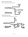
CIRCUIT DESCRIPTION
Take a look at the DCI1’s Schematic Diagram as we walk through the circuit
description. We will start with the DTMF audio input and work our way through
to the power supply section.
The DTMF audio input uses a standard style RJ-11 modular phone jack (J6 Phone Line Monitor In) for easy interfacing with your phone line or other audio
source (a direct audio pinout for J6 is shown in the wiring section). The input
circuitry near the phone jack allows you to continually monitor the audio signal
and pull off any DTMF data that comes in so it can be decoded. The audio
sniffer formed by C14, C15, R8, R9, and R10 will not capture the line so it does
not interfere with the normal use of your phones. All it does is quietly feed any
audio tones present to the decoder IC for processing. Protection diodes D2 and
D3 limit the incoming signal to +/- 0.7 V so that potentially damaging voltages
like the 90 Vp-p ‘Ring’ signal do not blow up your decoder IC!
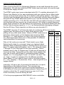
The DTMF decoder IC (U3) has the task of monitoring all the input audio
signals from the phone line (or other audio source) and
pulling off any valid audio tones. When a DTMF audio tone is DTMF 4-bit
Tone
Code
detected, U3 presents a 4 bit digital code (meaning 0000
through 1111, each position is a bit) to the micro-controller
1
0001
(U1) that represents which one of the possible 16 different
2
0010
valid characters it is receiving.
Why a 4 bit code you may ask? Think back to your High
School math class for a moment when you learned about
different base numbering systems. Humans like to work in a
base 10 system (decimal system, deci = 10) using the digits
1 through 10 (or 0 through 9 to be more precise). This is
probably due to the 10 fingers and 10 toes we all learned to
count on as kids. Computers on the other hand (pardon the
pun) like to work with a base 2 numbering system (binary
system, bi = 2) using digits 0 and 1; 0 for off / low and 1 for
on / high. In order to represent the 16 different possible
tones (base 10) you need to have 4 bits in a binary system
24 = 1111 (binary) = 16 (decimal). Wow… kind of got off on a
tangent there!
3
0011
4
0100
5
0101
6
0110
7
0111
8
1000
9
1001
0
1010
*
1011
Internally, U3 has a set of counters that latch the 4 outputs
depending on the detected tones. The counters are
referenced to a television color-burst crystal operating at
3.579 MHz (X1) for rock solid measurements. Notice how C1
couples a bit of the X1 crystal frequency over to U1 (the
micro-controller) to set its timing as well.
#
1100
A
1101
C
1110
C
1111
D
0000
U1 is the pre-programmed 68HC908JK1 micro-controller.
DCI1 • 5
This IC contains the developed code required to take the DTMF tone data
from U3 and process while reading and writing to FLASH memory, generating
the feedback tones, monitoring the programming switch, and turning the
relays on and off as needed. Quite a bit for one little part!
Since the four relay driver circuits are identical, we’ll walk through the
operation of one section and leave it to you to trace out the other three. Take
a look at the K1 relay driver circuit on the schematic. It consist of these 5
components: R1, R14, D5, Q1 and K1. When the relay driver output from the
micro-controller (RELAY_1) switches ‘High’, Q1 is forward biased pulling its
normally high impedance Collector down to ground potential. This completes
the circuit path for relay K1 to turn on causing its internal contacts to close
providing you with a ‘switch closure’ for your custom applications.
This all seems fairly simple, but what is the function of R1, R14, and D5?
Resistor R1 acts as a current limiter so that the Base-Emitter junction of the
transistor does not pull the ‘High’ output (+5 VDC) of the micro-controller down
to 0.7 VDC. In this way, the loading on the micro-controller is well within the
needed parameters for proper operation.
Resistor R14 is also used as a current limiting resistor just like R1. Since the
relays used in the DCI1 are all 9 VDC models and our power supply puts out
upwards of 12 VDC, R14 allows us to limit the current to the needed 50 mA or
so needed to fully activate the relay and set its terminal voltage to the desired
9 VDC.
Now why is Diode D5 placed across the input terminals of the relay? It looks
like it is always reverse biased (the Cathode is more positive than the Anode)
so it can never turn on! If you look on a schematic for any quality product that
uses a relay, you should see a diode set in the same configuration (we aren’t
just trying to dump off a few extra parts here!). Relays such as K1 are very
inductive due to there construction. Since inductors have the property V = L di/
dt, they resist changes in current over time (di/dt). As the magnetic field
begins to collapse when Q1 turns off, a huge ’kickback voltage’ is generated
with reverse polarity on the terminals of the inductor (upwards of a 1000 V is
easily possible!). This generated ’kickback voltage’ is more then enough to
destroy Q1 and other parts on the board! To avoid this, D5 is inserted to
provide a safe discharge path when the reverse ’kickback voltage’ starts to
rise above 0.7 VDC. Neat huh!
When the micro-controller receives valid data from the user, it flashes LED D4
(the activity indicator) and sends a feedback tone back over the phone line to
let you know the command was received. Components R19, R21, Q6, C5,
D10 and D11 work together with the micro-controller to generate the tone
pulse. The pulsed tone output from U1:pin 11 is amplified from 0 to 5 VDC up
to 0 to 12 VDC to ensure that enough signal will couple through to the phone
DCI1 • 6
line. Protection diodes D10 and D11 limit the incoming signal on the phone
line (between +12.7 and - 0.7 V) so that potentially damaging voltages like the
90 Vp-p ‘Ring’ signal does not blow up Q6!
So far we have covered most of the circuitry on the board with exception of
the power supply. VR1 and the surrounding parts C3, C4 and the polarity
protection diode D1 form a simple voltage regulator to supply a steady 5 VDC
to the ICs on the board. By using this scheme, we can operate the unit with a
single 12 VDC (positive tip on J5) source and have access to the multiple
voltages needed for the unit to operate.
DCI1 • 7
DCI1 • 8
DCI1 PARTS LAYOUT DIAGRAM
DCI1 • 9
PARTS SUPPLIED WITH YOUR DCI1 KIT
Capacitors
2 22 pF disc capacitor (marked 22) [C7,8]
1 470 pF disc capacitor (marked 470 or 471) [C1]
2 .01µF disc capacitor (marked .01, 103 or 10 nF) [C2,6]
5 .1 µF disc capacitor (marked .1 or 104) [C5,10,11,14,15]
1 10 µF electrolytic capacitors [C4]
1 100 µF electrolytic capacitors [C3]
Resistors
4 100 ohm (brown-black-brown) [R14,15,16,17]
2 220 ohm (red-red-brown) [R11,18]
1 1K ohm (brown-black-red) [R3]
10 10K ohms (brown-black-orange) [R1,2,5,8,9,10,12,13,19,21]
1 100K ohms (brown-black-yellow) [R4]
1 330K ohms (orange-orange-yellow) [R6]
Semiconductors and Integrated Circuits
5 1N4000 series diode (black body with white band) [D1,5,6,7,8]
-Note that 1N4002-1N4007 diodes may used.
4 1N4148 diodes (small glass diode) [D2,3,10,11]
5 2N3904 transistor (three leads TO-92 package marked 3904)
[Q1,2,3,4,6]
1 7805 +5 volt voltage regulator [VR1]
2 JUMBO red LED [D4,9]
1 68HC908JK1 pre-programmed micro-controller (20 pin DIP) [U1]
(marked with a sticker labeled DCI1)
1 HT9170B DTMF decoder IC (18 pin DIP) [U3]
Miscellaneous Components
4 2 screw terminal jack [J1,2,3,4]
1 2.1 mm DC power jack [J5]
1 RJ11 modular phone jack (PCB mount) [J6]
2 DPDT PC mount pushbutton switch [S1,2]
4 9 Volt Relay [K1,2,3,4]
1 3.579 MHz crystal (Marked 3.579 or 3.579545) [X1]
1 #4-40 kepnut [for VR1]
1 #4-40x1/4” screw [for VR1]
DCI1 • 10
RAMSEY "Learn-As-You-Build KIT ASSEMBLY
There are many solder connections on the DCI1 printed circuit board. PLEASE
take us seriously when we say that good soldering is essential to the proper
operation of your DTMF Controller Interface!
•
•
•
Use a 25-watt soldering pencil with a clean, sharp tip.
Use only rosin-core solder intended for electronics use.
Use bright lighting; a magnifying lamp or bench-style magnifier may be
helpful.
Do your work in stages, taking breaks to check your work. Carefully brush away
wire cuttings so they don't lodge between solder connections.
We have a two-fold strategy for the order of the following kit assembly steps.
First, we install parts in physical relationship to each other, so there's minimal
chance of inserting wires into wrong holes. Second, whenever possible, we
install in an order that fits our "Learn-As-You Build" Kit building philosophy. This
entails describing the circuit that you are building, instead of just blindly
installing components. We hope that this will not only make assembly of our kits
easier, but help you to understand the circuit you’re constructing.
For each part, our word "Install" always means these steps:
1. Pick the correct component with the proper value to start with.
2. Insert it into the correct PC board location.
3. Orient it correctly, following the PC board drawing and the written
directions for all parts - especially when there's a right way
and a wrong way to solder it in. (Diode bands, electrolytic
capacitor polarity, transistor shapes, dotted or notched ends
of IC's, and so forth.)
4. Solder all connections unless directed otherwise. Use enough heat
and solder flow for clean, shiny, completed connections.
5. Trim or nip the excess component lead wire after soldering.
NOTE: Save some of the longer wire scraps nipped from resistors and
capacitors. These will be used to form wire jumpers (JMP1, etc.) to be soldered
in just like parts during these construction steps.
Enough of that ... let’s get started!
DCI1 • 11
DCI1 DTMF CONTROLLER INTERFACE KIT ASSEMBLY
Although we know that you are anxious to complete the assembly of your
DTMF Controller kit it is best to follow the step-by-step instructions in this
manual. Try to avoid the urge to jump ahead installing components.
Since you may appreciate some warm-up soldering practice as well as a
chance to put some landmarks on the PC board, we’ll first install some of the
larger mounting components. This will also help us to get acquainted with the
up-down, left-right orientation of the circuit board. Remember that all of the
components will be mounted on the component side of the circuit board and
soldered on the solder side of the circuit board (the side that contains the
printed circuit traces). Have a look at the parts layout diagram to help with your
assembly.
Use the boxes to check off your progress.
Check all received parts against the parts list. The parts list describes the
various markings that may be found on the kit parts. Carefully sort the parts into
small piles, (an empty egg tray does nicely for this purpose) to aid in finding
the correct part at the required time.
Today's IC’s have achieved remarkable performance levels and it is extremely
unlikely that any of your chips will have problems, yet we know that some of our
hobbyists insist on socketing all IC components. The addition of these will not
“void” your warranty, but if a problem arises from a socketed component you
will be required to pay the additional technician fee for labor in the repair of your
kit, if necessary.
We will begin by installing the input and output connectors on the rear side of
the circuit board. These will act as our landmark components and make the
orientation of the rest of the parts a bit easier.
Proper Component Installation:
NOTE: All of the diodes and resistors used in the kit will be installed in a stand
up fashion. This means one lead will go straight into the board while the other
is bent around to go back down into the other hole. The straight lead goes into
the hole with the silk-screened circle around it on the circuit board.
DCI1 • 12
1. Locate and install J1, one of the green 2 screw terminal jacks. The
open holes should face outward from the center of the circuit board. These
holes are where you will interface your external wiring to the relay contacts.
2. Install J2, one of the green 2 screw terminal jacks.
3. Install J3, one of the green 2 screw terminal jacks.
4. Install J4, the last green 2 screw terminal jack.
5. Identify and install the power connector J5, the 2.1 mm DC power jack
at the edge of the PC board. Gently slide the leads through the component
side of the circuit board until the connector is mounted flush. Solder all
three connections using enough heat to flow the ground connection
completely.
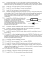
6. Install D5, a 1N4004 diode (black with
white band). The body of the part should
be placed in the hole with the silkscreened circle around it. The banded
end should be away from the board and
the wire lead needs to be bent over to into
position for the other hole.
Cathode
Anode
7. Install D6, another 1N4004 diode. Watch its orientation!
8. Install D7, another 1N4004 diode. No more reminders, you should
know by now that diode orientation is critical.
9. Install D8, another 1N4004 diode. Again, watch its orientation (sorry, I
had to do it)!
10. Install Q1, a three leaded transistor marked 2N3904. The flat side must
be placed as shown on the PC board silkscreen. Look at the Parts Layout
Diagram for further clarification. When you insert it, mount it as close to the
board as possible without forcing it.
11. Install Q2, another 2N3904 transistor.
12. Install Q3, can you guess? Yup… another 2N3904.
13. Install Q4, the last 2N3904 transistor used in the relay control circuit.
14. Install R1, a 10K ohm resistor (brown-black-orange). Save a few of the
clipped off wire leads from the resistors. We’ll use them to construct jumper
wires JMP1 and JMP2 later.
15. Install R14, a 100 ohm resistor (brown-black-brown).
16. Install R5, a 10K ohm resistor (brown-black-orange).
17. Install R15, a 100 ohm resistor (brown-black-brown).
DCI1 • 13
18. Install R12, a 10K ohm resistor (brown-black-orange).
19. Install R16, a 100 ohm resistor (brown-black-brown).
20. Install R13, a 10K ohm resistor (brown-black-orange).
21. Install R17, a 100 ohm resistor (brown-black-brown).
22. Locate and install K1, one of the large white relays
23. Install relay K2.
24. Install relay K3.
25. Install K4, the last relay.
Great job… you just finished building the relay driver circuit! The transistors (Q1
through Q4) energize their respective relays when they are turned on and off by
the micro-controller (U1). Next we’ll build the power supply section.
26. Install VR1, the 7805 voltage regulator. Install the three leads as shown
on the silkscreen and gently bend the part over to match the silkscreen
layout. Affix VR1 to the circuit board using the provided #4x40 screw and
kepnut; then solder all three leads. This part “smoothes” out any ripple that
may still be present on the main input supply voltage and provides us with
the needed 5 VDC the ICs operate on.
27. Install C3, the 100 µF electrolytic capacitor. This part must be installed
properly for it to function. In fact, this capacitor has the potential to explode
if installed in reverse polarity! The PC board silkscreen shows the positive
hole and the band on the capacitor shows the negative side. You’ll also
notice that the lead closest to the stripe is shorter the other lead; this also
indicates the negative side.
28. Install C4, the 10 µF electrolytic capacitor. Watch that polarity!
29. Install D1, the last 1N4004 diode. Watch your orientation like you did
for D5 through D8.
With exception of the power switch, which we’ll install a bit later, you just
finished the power supply section! Diode D1 acts as a polarity safety net so that
you don’t accidentally harm the unit should a miss wired plug be used. Since
diodes only conduct in one direction, the unit will only power up if a positive tip
DC power plug is hooked up to J5. Capacitors C3 and C4 work with VR1 to
provide you with a well regulated 5 VDC supply needed to power the ICs.
30. Install the 20 pin DIP socket for U1, the 68HC908JK1 micro-controller
IC. It doesn’t matter which way the socket is orientated, as long as the chip
is place in the socket the correctly. You can bend two of the corner leads
out slightly to hold the socket in place when you flip the board over to
solder it in. Make sure all 20 pins are through the holes and then solder
each one. Check your solder joints for even flow before moving on.
DCI1 • 14
31. Insert U1, the micro-controller marked with a sticker labeled DCI1 into
the socket. Orient the notched end as shown on the PC board silkscreen
and Parts Layout Diagram (toward the relays). Before you push it down into
the socket, check to be sure none of the pins are bent under or outside of
the socket. When you’re sure the pins are where they belong, press the
chip down so that it is seated flat within the socket.
32. Install C2, a .01µF ceramic capacitor (marked .01, 103 or 10 nF). Disc
capacitors are not polarized so they can be installed in either direction. The
reason we call them “disc” caps can be seen by the package style. The
capacitor itself is two conductive discs separated by a dielectric compound.
33. Install C1, a 470 pF disc capacitor (marked 470 or 471). This capacitor
couples over a bit of the X1 clock signal from U3 to run the micro-controller.
34. Install C10, a .1µF ceramic capacitor (marked .1 or 104).
Have you figured out what that 104 value stands for yet? Here’s the answer.
Disc capacitors are typically marked with their value in picofarads, or pF
(commonly pronounced “puff”), equal to a value of 1x10-12 Farad. A 104, or
100,000 pF disc cap (notice how 104 breaks up as a 1, 0, and then 4 more 0s
to equal 100,000) has an equivalent value of 0.1 microfarad or 0.1 µF.
Mathematically speaking, 100,000 x 10-12 = 0.1 x10⁻⁶. That’s how we switch
between the 104 and .1 values so easily.
35. Install R6, a 330K ohm resistor (orange-orange-yellow).
36. Install U3, the 18 pin DIP tone decoder chip marked HT9170B. Make
absolutely sure it is mounted in the proper direction. The small semi-circle
(or notch as commonly called) on the IC represents pin 1 and should be
mounted in the same direction as in the Parts Layout Diagram. The ICs in
this kit are not mounted in the same direction so look closely before
soldering it in.
37. Install JMP1 using one of the scrap wire leads you saved from the
earlier steps. Form the wire into a staple like shape and insert it from the
top side of the board in the holes shown on the silkscreen and the Parts
Layout Diagram. Solder it in place so that it will act like an electronic bridge
connecting the circuit traces over the top side of the circuit board.
38. Install JMP2 in the same fashion as the last step.
39. Install C8, a 22 pf ceramic capacitor (marked 22).
40. Install C7, another 22 pf ceramic capacitor (marked 22).
41. Install R21, a 10K ohm resistor (brown-black-orange).
42. Install X1, the 3.579 MHz crystal (silver can marked 3.579).
Make sure it is flush to the board before soldering.
43. Install R4, a 100K ohm resistor (brown-black-yellow).
DCI1 • 15
44. Install R3, a 1K ohm resistor (brown-black-red).
45. Install D10, one of the 1N4148 diodes (small glass diode with black
band). The lead closest to the black band is the Cathode end. Make sure
it lines up with the white band shown on the PC board silkscreen and the
Parts Layout Diagram. Be gentle with this fragile part and double check
the orientation before soldering.
46. Install D3, another 1N4148 diode in the same fashion as D10.
47. Install D11, another 1N4148 diode.
47. Install D2, the last 1N4148 diode.
48. Install Q6, the last 2N3904 transistor. Follow the same guidelines you
did for Q1 through Q4. We’re getting down to the last few parts!
49. Install C5, a .1µF ceramic capacitor (marked .1 or 104). This capacitor
is used to couple the feedback tone back onto the phone line.
50. Install C11, a .1µF ceramic capacitor (marked .1 or 104).
51. Install R9, a 10K ohm resistor (brown-black-orange).
52. Install R10, a 10K ohm resistor (brown-black-orange).
53. Install C15, a .1µF ceramic capacitor (marked .1 or 104).
54. Install C14, a .1µF ceramic capacitor (marked .1 or 104).
55. Install R8, a 10K ohm resistor (brown-black-orange).
With exception of the modular phone jack (J6), you just finished building the
entire DTMF detector circuit! Almost done… just a few more parts to go. Most
of the final few components form the user interface section of the kit.
56. Install R19, a 10K ohm resistor (brown-black-orange).
57. Install R18, a 220 ohm resistor (red-red-brown).
58. Install R11, a 220 ohm resistor (red-red-brown).
59. Install R2, a 10K ohm resistor (brown-black-orange).
60. Install C6, a .01µF ceramic capacitor (marked .01, 103 or 10 nF).
Almost there! Even though you can hardly wait to fire up the kit, take a few
minutes to recheck your assembly up to now. Touch up any solder
connections, recheck all electrolytic/diode/transistor component orientations. A
few minutes now can save time tenfold once you have energized the circuit.
Incorrectly installed parts can be damaged once power is applied.
61. Install pushbutton switch S1 by inserting all six leads through the
circuit board. The switch should fit flat to the circuit board before soldering.
DCI1 • 16
62. Install S2 the same way.
63. Install J6, the modular RJ-11 phone jack. Pay close attention to the
silkscreen and line up the four conductor wires with their respective holes
before snapping the part onto the board. Solder all four wire connections
being careful not to short them together (they’re really close to each
other). Do not solder the plastic posts. The snap fit design will hold it in
place.
Install LED D9. The flat side is oriented as shown in the diagram. Leave it
standing about 1/2 of an inch off of the board when soldering. After
soldering bend it over to a 90º angle at its midpoint so that it faces the
outside of the board. Observe the following diagrams for proper
orientation.
LED
Flat
Leave leads approximately
1/2 inch in length
LED
PC Board
Front View
Flat
Leave leads approximately
1/2 inch in length
PC Board
Front View after Bending
6. Install LED D4 the same way as D9.
CONGRATULATIONS !
Your DCI1 DTMF Controller Interface is now complete! Have a final look over
your work, paying particular attention to the orientation of all diodes,
capacitors, and ICs. Remember that any problems you find now can save time
and effort after the unit has been cased up.
DCI1 • 17
ASSEMBLY INSTRUCTIONS FOR CUSTOM CASE
The enclosure is a key element to the overall pride you will have upon completing your Ramsey kit. The enclosure will show how you were able to “build
from scratch” a commercial piece of high-tech electronics. For some of us,
the enclosure will also hide a number of “not-so-pretty” assembly mistakes.
Once the kit is enclosed, your friends will never know that you were new to
soldering. Finally, the enclosure case will protect your electronics from many
possible causes of damage so that you can receive years worth of enjoyment
using, talking about, and remembering the fun you had building your kit. In
short, TAKE YOUR TIME when assembling the enclosure. This is the part that
you and your friends will look at and admire for years!
1. Lay the front and rear plastic plates over their corresponding labels to
verify which sticker goes with which panel. You’ll want to work with one
panel at a time to avoid possible mix-ups.
2. Remove the backing material from one of the stickers and line it up
properly on its pre-punched panel. Make sure that they are aligned correctly before allowing them to touch the plastic plates. They stick the first
time; line them up right!
3. Use a sharp hobby knife to cut out the holes in the labels along the
pre-punched holes. A short sawing motion from the front side works well
around the inner circumference of the holes.
4. Repeat the above steps for the other panel.
5. Insert the board into the case with the buttons and LEDs extending
through the holes in the front panel.
6. Insert the rear panel into the grooves on the back of the base tray.
7. Secure the PC board to the bottom base tray with 4 short Phillips
head screws.
8. Mount the top cover using the 1” screws after you have completed the
testing phase and final hookup wiring.
Use of a case set with your DCI1 is highly recommended. The voltage on the
exposed traces near the relay contacts (bottom side of K1 through K4 and the
clamping screws themselves) may be potentially as high as 120 VAC depending on your target hookup configuration. The added security from using a plastic (non-conductive) enclosure ensures protection from any potentially lethal
voltages.
Great care should be taken with any wiring arrangement to guarantee the
safety of the operator and any others that may come into contact with this unit
DCI1 • 18
USING YOUR DCI1 DTMF CONTROLLER INTERFACE
Now we’re ready for the moment of truth, the initial power up and running of
your DCI1! It’s best to run through the initial power up with nothing wired to the
relays just incase you have any build errors. For testing and programming purposes, use a phone next to the DCI1. You will not need to call another phone
to work with the system. The unit has built in dial tone and busy tone rejection
filters so you can use just one phone to set it up. Pay no attention to the
TELCO busy tone or recorded voice messages while in programming or normal modes.
1. Connect your 12 VDC power supply (12 to 15 VDC) to the J5 Power jack.
2. Connect your phone line to the J6 Phone jack using a standard RJ-11
patch cord. Only the two center conductors are needed.
Note: The DCI1 does not answer or seize control of your phone line or
other audio source. An answering machine or similar device is needed to
retain control on a phone line. The DCI1 simply “listens” to the line.
User Controls:
DTMF Control Codes
1. 0, 1, 2, 3, 4, 5, 6, 7, 8, 9, A, B, C, D, ∗, # - Valid DTMF data
2. ∗ - Reset from any state and start of a valid security code.
- ∗ has no effect on the state of the relays, only command code entry.
1. # - Start of a new security code in Program Mode.
2. 1, 2, 3, 4 - Valid relay control numbers (1 = J1 output, 2 = J2 output, etc…)
3. 0 - Turn off relay X (X= relay number 1, 2, 3, or 4 ).
4. 1 - Turn on relay X (X= relay number 1, 2, 3, or 4).
Front Panel Buttons
1. S1 - Power Button with Power indicator LED (D9).
2. S2 - Program Button with multi-purpose ‘Activity’ LED (D4).
The default security code is 1, 2, 3, 4 from the factory. If you forget your security code at any time, you can override it by reprogramming the unit (you don’t
need to know the old security code to program a new one). This can only be
done while the Program button on the front panel is pressed in so that a remote user cannot change your code without your knowledge.
DCI1 • 19
Normal Mode Operation:
1. Turn on the unit with power switch S1; Power LED D9 should light up.
2. Lift the phone receiver and press ∗ followed by the 4 digit security code.
(The default code is 1, 2, 3, 4 until you change it.)
3. You should hear two quick confirmation tones and the Activity LED should
flash twice.
• If you enter the code incorrectly you will hear a low frequency error
tone and the Activity LED will only flash once. Press ∗ to reset the
system and go back to step 2 to try again.
4. Select the relay you want to control by pressing 1, 2, 3, or 4 (1 = J1 output, 2 = J2 output, etc…). You will hear X number of quick confirmation
tones (X= relay number 1, 2, 3, or 4) and the Activity LED will also flash
accordingly.
5. After the relay confirmation tones have stopped, press 1 to turn the relay
on or 0 to turn it off.
6. Continue to select the relays followed by the on/off command as long as
desired.
• Turn each relay output on and off individually the first time through
to verify that they are all working properly.
7. Press ∗ when you are finished to reset the system so the next command
entry will require the security code to be entered.
• The unit will time out automatically after 1 minute without valid
DTMF tones in order to ensure security.
8. Hang up the receiver.
DCI1 • 20
Programming Mode Operation (Setting A New Security Code):
NOTE: # and ∗ are special characters and should not be used in your security
code except for one special case (more on this below).
1.
2.
3.
4.
Turn on the unit with Power switch S1; Power LED D9 should light up.
Press in the Program button S2; Activity LED D4 should light up.
Lift the phone receiver and press # ; you should hear a confirmation tone.
Enter the new 4 digit security code; you should hear a confirmation tone
and the Activity LED (D4) should flash on and off until you press the Program button again to go back to normal operating mode.
• Avoid using codes that start with common TELCO feature numbers
like 69XX or 72XX as your security code. You may wind up accidentally activating some feature on your phone line! Check your phone
book for local feature codes to keep this from occurring.
• Entering #, #, #, # as the new security code will disable the security
check feature and allow the unit to operate in free running mode. In
this mode the DCI1 will always respond to any valid DTMF tones
without forcing you to enter a security code first.
• If you have any errors during the programming phase, recycle the
unit’s power and start again from step 1.
5. Once back in normal mode (Program button released), the Activity LED
(D4) should stop flashing and you’re ready to go!
DCI1 • 21
WIRING AND CUSTOM APPLICATION SUGGESTIONS
Using your DCI1 for a variety of applications is very simple. You just need to
keep in mind the ratings for the relay contacts listed on the specification page
to avoid any problems and use a common sense approach for personal
safety. If you need to operate a simple low voltage DC circuit or switch on and
off a low wattage 120 VAC lighting application, interface the your wiring directly to the J1 through J4 screw terminals and your off to the races! For heavily inductive loads such as a large motor or applications that exceed the power
ratings of the relays, the following diagrams will help you get started wiring the
DCI1 as a trigger source for a larger relay or similar device.
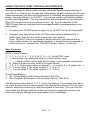
Typical Low Power DC Wiring:
-LED switch application
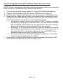
Line Level Audio Input Wiring:
-Custom Audio feed wiring arrangement using a
standard RJ-11 Patch cable.
J6
Front
View
Audio GND
DCI1 • 22
+ Audio In
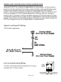
Typical Low Power AC Wiring:
-120 VAC light being switched on Hot side.
(Black-Hot)
(White-Neutral)
Typical High Power Relay:
-DCI1 used to trigger another Higher Power relay.
DCI1 • 23
TROUBLESHOOTING GUIDE
If your DCI1 does not work at all, recheck the following:
•
correct orientation of U1 and U3 (see PC board Parts Layout Diagram)
•
correct polarity of all electrolytic capacitors.
•
correct orientation of all diodes (especially D1).
•
all solder connections
•
jumper wires at all JMP locations.
Still having trouble?
While we had hoped that it wouldn’t come to this, if you are still having trouble
with your DCI1, here are a few additional suggestions.
PROBLEM: The Power LED (D9) doesn’t light and VR1 gets very hot quickly.
SOLUTION: You likely have a short across the power supply or you have a
component placed in the incorrect orientation. Check all of your parts to make
sure they correlate with those on the Parts Layout Diagram.
PROBLEM: The Power LED (D9) doesn’t light and VR1 remains cool.
SOLUTION: Using an oscilloscope or a frequency counter to verify that there
is a 3.579 MHz signal on pin 7 of U3 and pin 3 of U1. It should be
approximately 0.5 Vp-p or greater. If you cannot check the oscillator, verify
that 5 Volts DC is present on the IC power pins (U1:5 and U3:18). If not, check
VR1 for 5 VDC output with at least 12 VDC input from your power supply.
PROBLEM: It seems to be missing key entries when I try to enter commands.
SOLUTION: Wait until after the confirmation tones have stopped before entering new commands. This is most common when controlling the J4 relay output
due to the amount of time it takes to provide the four feedback tones telling
you which device is about to be controlled.
PROBLEM: My answering machine hangs up before I finish my commands.
SOLUTION: Some answering machines will hang up automatically if they do
not sense any voice activity. Try talking into the phone at the same time to
provide the needed audio for it to hold the line. Example: Say “relay #1 ON” at
the same time you are typing the commands. Some answering machines may
not be compatible.
DCI1 • 24
PROBLEM: The relays seem to get warm when they are on for a while.
SOLUTION: This is normal. These 9 VDC relays are rated to work up to
almost 12 VDC across their input windings without any problem. The series
limiting resistors (R14, 15,16, and 17) keep them well within range over the
normal 12 to 15 VDC input operating voltage. Their nominal operating power
is about 450 mW so they will get warm to the touch.
PROBLEM: It keeps giving me an error tone and it does do what I want.
SOLUTION: Press ∗ to reset the system. Then repeat your security code and
command string. More than likely you just wound up out of synch with the
DCI1 so you are not entering the data it is looking for. When in doubt, press
the ∗ button to reset the command entry algorithm back to a known state. Using the ∗ reset feature has no effect on the state of the relays, they hold their
last instruction state forever unless power is removed from the system or the
user commands a new state change.
PROBLEM: I forgot my security code!
SOLUTION: No problem, just follow the instructions in the Using Yout DCI1
DTMF Controller Interface section to program a new one.
PROBLEM: I’m trying to feed audio into the J6 input but it doesn’t work.
SOLUTION: Depending on your audio level, you may need to replace R8, a
10K ohm resistor (brown-black-orange), with a jumper wire to connect it directly to ground. This will increase your audio levels if needed.
Have another set of eyes look over your work. Here at the shop we have often
run into a “stone wall” of a problem only to have a fellow technician see our
obvious error. It is sometimes very difficult to see your own mistakes.
DCI1 • 25
DCI1 DTMF CONTROLLER INTERFACE SPECIFICATIONS
Here are few of the commonly requested specifications for the DCI1:
J1, 2, 3, and 4 Relay Outputs
- Contact Rating: 5 A, 120 VAC / 28 VDC (Resistive)
- Rated Contact Current: 5 A
- Max. Contact Capacity: 1250VA AC, 150W DC
- Contact Arrangement: SPST-NO
- Contact Material: AG Alloy
- Note: Not intended for heavily inductive loads such as large motors.
J5 Power Input
- Input working voltage range: 12 - 15 VDC
- Max DCI1 current draw is between 200 - 250 mA.
J6 DTMF Audio Input
- Signal Level = -29 to 1 dBm
- Dial Tone Tolerance = 10 dB
- Noise Tolerance = -12 dB
- Third Tone Tolerance = -16 dB
- Frequency Deviation Acceptance = +- 1.5%
Miscellaneous Information
- PCB Dimensions: 4.7” L x 4” W (max component height: 0.9”)
CONCLUSION
We sincerely hope that you enjoy the use of this Ramsey product. As always,
we have tried to compose our manual in the easiest, most user-friendly format
that is possible. As our customers, we value your opinions, comments, and
additions that you would like to see in future publications. Please submit
comments or ideas to:
Ramsey Electronics Inc.
Attn. Hobby Kit Department
590 Fishers Station Drive
Victor, NY 14564
Please also feel free to visit our Website at www.ramseykits.com and offer
your observations to other kit enthusiasts as well.
And once again, thanks from the folks here at Ramsey!
DCI1 • 26
The Ramsey Kit Warranty
Please read carefully BEFORE calling or writing in about your kit. Most problems can be
solved without contacting the factory.
Notice that this is not a "fine print" warranty. We want you to understand your rights and ours too!
All Ramsey kits will work if assembled properly. The very fact that your kit includes this new manual
is your assurance that a team of knowledgeable people have field-tested several "copies" of this kit
straight from the Ramsey Inventory. If you need help, please read through your manual carefully.
All information required to properly build and test your kit is contained within the pages!
1. DEFECTIVE PARTS: It's always easy to blame a part for a problem in your kit, Before you
conclude that a part may be bad, thoroughly check your work. Today's semiconductors and passive
components have reached incredibly high reliability levels, and it’s sad to say that our human
construction skills have not! But on rare occasions a sour component can slip through. All our kit
parts carry the Ramsey Electronics Warranty that they are free from defects for a full ninety (90)
days from the date of purchase. Defective parts will be replaced promptly at our expense. If you
suspect any part to be defective, please mail it to our factory for testing and replacement. Please
send only the defective part(s), not the entire kit. The part(s) MUST be returned to us in suitable
condition for testing. Please be aware that testing can usually determine if the part was truly
defective or damaged by assembly or usage. Don't be afraid of telling us that you 'blew-it', we're all
human and in most cases, replacement parts are very reasonably priced.
2. MISSING PARTS: Before assuming a part value is incorrect, check the parts listing carefully to
see if it is a critical value such as a specific coil or IC, or whether a RANGE of values is suitable
(such as "100 to 500 uF"). Often times, common sense will solve a mysterious missing part
problem. If you're missing five 10K ohm resistors and received five extra 1K resistors, you can
pretty much be assured that the '1K ohm' resistors are actually the 'missing' 10 K parts ("Hum-m-m,
I guess the 'red' band really does look orange!") Ramsey Electronics project kits are packed with
pride in the USA. If you believe we packed an incorrect part or omitted a part clearly indicated in
your assembly manual as supplied with the basic kit by Ramsey, please write or call us with
information on the part you need and proof of kit purchase.
3. FACTORY REPAIR OF ASSEMBLED KITS:
To qualify for Ramsey Electronics factory repair, kits MUST:
1. NOT be assembled with acid core solder or flux.
2. NOT be modified in any manner.
3. BE returned in fully-assembled form, not partially assembled.
4. BE accompanied by the proper repair fee. No repair will be undertaken until we have received
the MINIMUM repair fee (1/2 hour labor) of $25.00, or authorization to charge it to your
credit card account.
5. INCLUDE a description of the problem and legible return address. DO NOT send a separate
letter; include all correspondence with the unit. Please do not include your own hardware
such as non-Ramsey cabinets, knobs, cables, external battery packs and the like. Ramsey
Electronics, Inc., reserves the right to refuse repair on ANY item in which we find excessive
problems or damage due to construction methods. To assist customers in such situations,
Ramsey Electronics, Inc., reserves the right to solve their needs on a case-by-case basis.
The repair is $50.00 per hour, regardless of the cost of the kit. Please understand that our
technicians are not volunteers and that set-up, testing, diagnosis, repair and repacking and
paperwork can take nearly an hour of paid employee time on even a simple kit. Of course, if we find
that a part was defective in manufacture, there will be no charge to repair your kit (But please
realize that our technicians know the difference between a defective part and parts burned out or
damaged through improper use or assembly).
4. REFUNDS: You are given ten (10) days to examine our products. If you are not satisfied, you
may return your unassembled kit with all the parts and instructions and proof of purchase to the
factory for a full refund. The return package should be packed securely. Insurance is
recommended. Please do not cause needless delays, read all information carefully.
DCI1 • 27
DCI1 DTMF CONTROLLER INTERFACE KIT
Quick Reference Page Guide
Introduction ............................................4
Circuit Description ..................................5
Schematic Diagram ................................8
Parts List ................................................10
DCI1 Assembly.......................................12
Using Your DCI1 ....................................19
Wiring & Custom Applications ................22
DCI1 Specifications ................................26
Warranty.................................................27
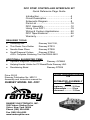
REQUIRED TOOLS
• Soldering Iron
Ramsey WLC100,
• Thin Rosin Core Solder
Ramsey RTS12
• Needle Nose Pliers
Ramsey RTS05
• Small Diagonal Cutters
Ramsey RTS04
<OR> Complete Soldering Tool Set RS64-2801
ADDITIONAL SUGGESTED ITEMS
• Optivisor Magnifier Headband
Ramsey OPMAG
• Helping Hands Holder for PC Board/Parts Ramsey HH3
• Desoldering Braid
Ramsey RTS08
Price: $5.00
Ramsey Publication No. MDCI1
Assembly and Instruction manual for:
RAMSEY MODEL NO. DCI1
TOTAL SOLDER POINTS
190
ESTIMATED ASSEMBLY
TIME
Beginner ...............3.5 hrs
Intermediate .........2 hrs
Advanced .............1.5 hrs
RAMSEY ELECTRONICS, INC.
590 Fishers Station Drive
Victor, New York 14564
Phone (585) 924-4560
Fax (585) 924-4555
www.ramseykits.com
DCI1 • 28